Conversion Guide: Numonyx Axcell Flash Memory P30 (256-Mbit ...
20
Application Note Mar 2010 1 Order Number: 320004-06 Conversion Guide: Numonyx ® Axcell TM Flash Memory P30 (256-Mbit, 256-Mbit/256-Mbit) 130nm to 65nm Application Note - 908 Mar 2010
-
Upload
khangminh22 -
Category
Documents
-
view
0 -
download
0
Transcript of Conversion Guide: Numonyx Axcell Flash Memory P30 (256-Mbit ...
Application Note Mar 20101 Order Number: 320004-06
Conversion Guide: Numonyx® AxcellTM Flash Memory P30 (256-Mbit, 256-Mbit/256-Mbit) 130nm to 65nmApplication Note - 908
Mar 2010
Application Note Mar 20102 Order Number: 320004-06
INFORMATION IN THIS DOCUMENT IS PROVIDED IN CONNECTION WITH NUMONYX™ PRODUCTS. NO LICENSE, EXPRESS OR IMPLIED, BY ESTOPPEL OR OTHERWISE, TO ANY INTELLECTUAL PROPERTY RIGHTS IS GRANTED BY THIS DOCUMENT. EXCEPT AS PROVIDED IN NUMONYX'S TERMS AND CONDITIONS OF SALE FOR SUCH PRODUCTS, NUMONYX ASSUMES NO LIABILITY WHATSOEVER, AND NUMONYX DISCLAIMS ANY EXPRESS OR IMPLIED WARRANTY, RELATING TO SALE AND/OR USE OF NUMONYX PRODUCTS INCLUDING LIABILITY OR WARRANTIES RELATING TO FITNESS FOR A PARTICULAR PURPOSE, MERCHANTABILITY, OR INFRINGEMENT OF ANY PATENT, COPYRIGHT OR OTHER INTELLECTUAL PROPERTY RIGHT. Numonyx products are not intended for use in medical, life saving, life sustaining, critical control or safety systems, or in nuclear facility applications.
Numonyx B.V. may make changes to specifications and product descriptions at any time, without notice.
Numonyx B.V. may have patents or pending patent applications, trademarks, copyrights, or other intellectual property rights that relate to the presented subject matter. The furnishing of documents and other materials and information does not provide any license, express or implied, by estoppel or otherwise, to any such patents, trademarks, copyrights, or other intellectual property rights.
Designers must not rely on the absence or characteristics of any features or instructions marked “reserved” or “undefined.” Numonyx reserves these for future definition and shall have no responsibility whatsoever for conflicts or incompatibilities arising from future changes to them.
Contact your local Numonyx sales office or your distributor to obtain the latest specifications and before placing your product order.
Copies of documents which have an order number and are referenced in this document, or other Numonyx literature may be obtained by visiting the Numonyx website at http://www.numonyx.com.
Numonyx, the Numonyx logo, and Axcell are trademarks or registered trademarks of Numonyx B.V. or its subsidiaries in other countries.
*Other names and brands may be claimed as the property of others.
Copyright © 2010, Numonyx, B.V., All Rights Reserved.
Application Note Mar 20103 Order Number: 320004-06
Conversion Guide: P30 130nm to 65nm
Contents
1.0 Introduction ..............................................................................................................5
2.0 Device Overview........................................................................................................52.1 P30 130nm Device ..............................................................................................52.2 P30 65nm Device ................................................................................................52.3 P30 130nm and 65nm Features Comparison ...........................................................6
3.0 Device Packaging and Ballout ....................................................................................73.1 Easy BGA Ballout.................................................................................................73.2 TSOP Pinout .......................................................................................................83.3 QUAD+ SCSP Ballout ...........................................................................................9
4.0 Hardware Design Considerations ............................................................................. 104.1 AC Read Specifications....................................................................................... 104.2 AC Write/Erase Specifications ............................................................................. 104.3 DC Current Specification .................................................................................... 11
5.0 Flash Software Design Considerations ..................................................................... 125.1 Device Identification .......................................................................................... 125.2 Read Configuration Register (RCR) ...................................................................... 125.3 Blank Check ..................................................................................................... 135.4 Device Commands............................................................................................. 145.5 WAIT State Comparison ..................................................................................... 145.6 CFI Differences ................................................................................................. 165.7 Performance Improvements in P30 65nm ............................................................. 17
6.0 Conversion Considerations ...................................................................................... 19

Conversion Guide: P30 130nm to 65nm
Application Note Mar 20104 Order Number: 320004-06
Revision History
Date of Revision Revision Description
May 2008 01 Initial Release
July 2008 02 Removed buffer programming difference; added in its place Section 5.7, “Perfor-mance Improvements in P30 65nm” on page 17.
Sep 2008 03Updated the new trademark of AxcellRemoved 64M related contents.
Nov 2008 04Return to StrataFlash trademark;Aligned the Address min to A1;Removed 128M related contents.
Jan 2009 05 Updated QUAD+ package ballout H8 from OE# to F2-OE#.
Mar 2010 06
Update the program performance and erase suspend latency, add tDVWH comment, Table 4, “Key AC Write/Erase Spec Comparison” on page 11.
Clarify the buffer program status polling on note1, Table 8, “Command Bus Operations” on page 14.
CFI update aligned with performance update, Table 11, “Value Changes” on page 17.
Add comments on power loss recovery, Section 6.0, “Conversion Considerations” on page 19.

Application Note Mar 20105 Order Number: 320004-06
Conversion Guide: P30 130nm to 65nm
1.0 Introduction
This application note describes the migration from the Numonyx® Axcell™ Flash Memory (P30-65nm) device to the Numonyx® Axcell™ Flash Memory (P30-130nm) device.
Note: Unless otherwise indicated, throughout the rest of this document, the Numonyx® Axcell™ Flash Memory (P30-130nm) device is referred to as the P30 130nm device and the Numonyx® Axcell™ Flash Memory (P30-65nm) device is referred to as the P30 65nm device.
This document was written based on device information available at the time. Any changes in specifications to either device might not be reflected in this document. Refer to the appropriate documents or sales personnel for the current product information before finalizing any design.
2.0 Device Overview
The following sections provide a brief overview of the feature differences between the P30 130nm and the P30 65nm devices.
2.1 P30 130nm Device
The P30 130nm device features 64-Mbit through 512-Mbit densities and AC/DC specifications for 52MHz operation. Other features include high performance synchronous-burst read, Buffered Enhanced Factory Programming (BEFP) with a 32-word buffer, and an expanded OTP register space. Packaging options include industry-standard Easy BGA, TSOP and QUAD+ packages.
2.2 P30 65nm Device
The P30 65nm device features 64-Mbit through 2-Gbit densities and AC/DC specifications for 52 MHz operation. This document covers specially 256-Mbit and 512-Mbit (256M/256M) product information. Other features include high performance synchronous-burst read, Buffered Enhanced Factory Programming (BEFP) with a 512-word buffer, and an expanded OTP register space. The P30 65nm device also features enhanced protection via a password access feature, which allows users to protect write access to the pre-defined blocks. Please contact the Numonyx Sales for further details concerning password access. Packaging options include industry-standard Easy BGA, TSOP and QUAD+ packages.
Conversion Guide: P30 130nm to 65nm
Application Note Mar 20106 Order Number: 320004-06
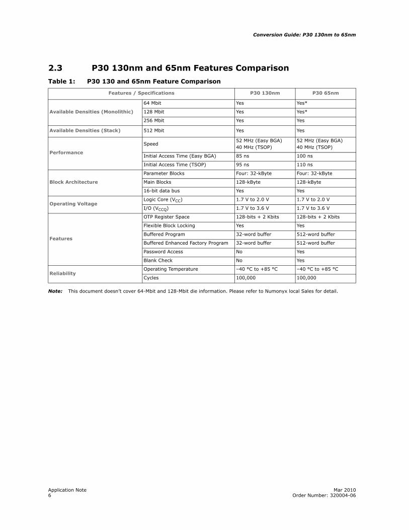
2.3 P30 130nm and 65nm Features Comparison
Note: This document doesn’t cover 64-Mbit and 128-Mbit die information. Please refer to Numonyx local Sales for detail.
Table 1: P30 130 and 65nm Feature Comparison
Features / Specifications P30 130nm P30 65nm
Available Densities (Monolithic)
64 Mbit Yes Yes*
128 Mbit Yes Yes*
256 Mbit Yes Yes
Available Densities (Stack) 512 Mbit Yes Yes
Performance
Speed52 MHz (Easy BGA)40 MHz (TSOP)
52 MHz (Easy BGA)40 MHz (TSOP)
Initial Access Time (Easy BGA) 85 ns 100 ns
Initial Access Time (TSOP) 95 ns 110 ns
Block Architecture
Parameter Blocks Four: 32-kByte Four: 32-kByte
Main Blocks 128-kByte 128-kByte
16-bit data bus Yes Yes
Operating VoltageLogic Core (VCC) 1.7 V to 2.0 V 1.7 V to 2.0 V
I/O (VCCQ) 1.7 V to 3.6 V 1.7 V to 3.6 V
Features
OTP Register Space 128-bits + 2 Kbits 128-bits + 2 Kbits
Flexible Block Locking Yes Yes
Buffered Program 32-word buffer 512-word buffer
Buffered Enhanced Factory Program 32-word buffer 512-word buffer
Password Access No Yes
Blank Check No Yes
ReliabilityOperating Temperature –40 °C to +85 °C –40 °C to +85 °C
Cycles 100,000 100,000
Application Note Mar 20107 Order Number: 320004-06
Conversion Guide: P30 130nm to 65nm
3.0 Device Packaging and Ballout
The following section provides a brief overview of the package and ballout differences between the P30 130nm and P30 65nm devices.
Notes:1. For 256-Mbit die, please refer to your local Numonyx Sales representative for leaded TSOP or Quad+ package option;2. For 256/256-Mbit TSOP migration options, please contact your local Numonyx local Sales representative.
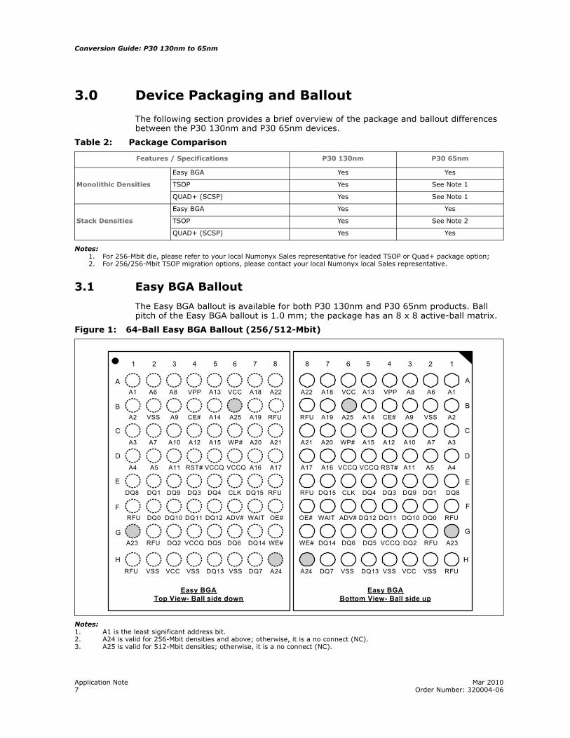
3.1 Easy BGA Ballout
The Easy BGA ballout is available for both P30 130nm and P30 65nm products. Ball pitch of the Easy BGA ballout is 1.0 mm; the package has an 8 x 8 active-ball matrix.
Notes:1. A1 is the least significant address bit.2. A24 is valid for 256-Mbit densities and above; otherwise, it is a no connect (NC).3. A25 is valid for 512-Mbit densities; otherwise, it is a no connect (NC).
Table 2: Package Comparison
Features / Specifications P30 130nm P30 65nm
Monolithic Densities
Easy BGA Yes Yes
TSOP Yes See Note 1
QUAD+ (SCSP) Yes See Note 1
Stack Densities
Easy BGA Yes Yes
TSOP Yes See Note 2
QUAD+ (SCSP) Yes Yes
Figure 1: 64-Ball Easy BGA Ballout (256/512-Mbit)
1 82 3 4 5 6 7
Easy BGATop View- Ball side down
Easy BGABottom View- Ball side up
18 234567
H
G
F
E
D
C
B
A
H
G
F
E
D
C
A
A2 VSS A9 A14CE# A19 RFUA25
RFU VSS VCC DQ13VSS DQ7 A24VSS
A3 A7 A10 A15A12 A20 A21WP#
A4 A5 A11 VCCQRST# A16 A17VCCQ
RFUDQ8 DQ1 DQ9 DQ4DQ3 DQ15CLK
RFU OE#DQ0 DQ10 DQ12DQ11 WAITADV#
WE#A23 RFU DQ2 DQ5VCCQ DQ14DQ6
A1 A6 A8 A13VPP A18 A22VCC
A23
A4A5A11VCCQ RST#A16A17 VCCQ
A1A6A8A13 VPPA18A22 VCC
A3A7A10A15 A12A20A21 WP#
RFU DQ8DQ1DQ9DQ4 DQ3DQ15 CLK
RFUOE# DQ0DQ10DQ12 DQ11WAIT ADV#
WE# RFUDQ2DQ5 VCCQDQ14 DQ6
A2VSSA9A14 CE#A19RFU A25
RFUVSSVCCDQ13 VSSDQ7A24 VSS
B
Conversion Guide: P30 130nm to 65nm
Application Note Mar 20108 Order Number: 320004-06
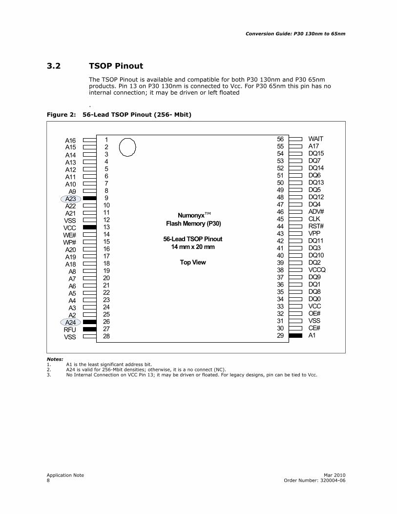
3.2 TSOP Pinout
The TSOP Pinout is available and compatible for both P30 130nm and P30 65nm products. Pin 13 on P30 130nm is connected to Vcc. For P30 65nm this pin has no internal connection; it may be driven or left floated
.
Notes:1. A1 is the least significant address bit.2. A24 is valid for 256-Mbit densities; otherwise, it is a no connect (NC).3. No Internal Connection on VCC Pin 13; it may be driven or floated. For legacy designs, pin can be tied to Vcc.
Figure 2: 56-Lead TSOP Pinout (256- Mbit)
Numonyx™ Flash Memory (P30)
56-Lead TSOP Pinout14 mm x 20 mm
Top View
1
34
2
5
78
6
9
1112
10
13
1516
14
17
1920
18
21
2324
22
25
2728
26
56
5453
55
52
5049
51
48
4645
47
44
4241
43
40
3837
39
36
3433
35
32
3029
31
A14A13A12
A10A9
A11
A23
A21VSS
A22
VCC
WP#A20
WE#
A19
A8A7
A18
A6
A4A3
A5
A2
RFUVSS
A24
WAIT
DQ15DQ7
A17
DQ14
DQ13DQ5
DQ6
DQ12
ADV#CLK
DQ4
RST#
A16
DQ3
VPP
DQ10
VCCQDQ9
DQ2
DQ1
DQ0VCC
DQ8
OE#
CE#A1
VSS
A15
DQ11

Application Note Mar 20109 Order Number: 320004-06
Conversion Guide: P30 130nm to 65nm
3.3 QUAD+ SCSP Ballout
The QUAD+ SCSP Balllout is available and compatible for both P30 130nm and P30 65nm products.
Notes:1. A23 is valid for 256-Mbit densities and above; otherwise, it is a no connect (NC).2. A24 is valid for 512-Mbit densities; otherwise, it is a no connect (NC).3. F2-CE# and F2-OE# are no connect (NC) for all densities.4. A0 is LSB for Address.
Figure 3: QUAD+ SCSP Ballout and Signals
Pin 11 2 3 4 5 6 7 8
A DU DU Depop Depop Depop Depop DU DU A
B A4 A18 A19 VSS VCC VCC A21 A11 B
C A5 RFU A23 VSS RFU CLK A22 A12 C
D A3 A17 A24 VPP RFU RFU A9 A13 D
E A2 A7 A25 WP# ADV# A20 A10 A15 E
F A1 A6 RFU RST# WE# A8 A14 A16 F
G A0 DQ8 DQ2 DQ10 DQ5 DQ13 WAIT F2-CE# G
H RFU DQ0 DQ1 DQ3 DQ12 DQ14 DQ7 F2-OE# H
J RFU OE# DQ9 DQ11 DQ4 DQ6 DQ15 VCCQ J
K F1-CE# RFU RFU RFU RFU VCC VCCQ RFU K
L VSS VSS VCCQ VCC VSS VSS VSS VSS L
M DU DU Depop Depop Depop Depop DU DU M
1 2 3 4 5 6 7 8
Control Signals
Reserved for Future Use DataDo Not Use Power/Ground
Address
Top View - Ball Side Down
Legends: De-Populated Ball

Conversion Guide: P30 130nm to 65nm
Application Note Mar 201010 Order Number: 320004-06
4.0 Hardware Design Considerations
The P30 130nm and P30 65nm flash memory devices provide reliable, two-bit-per-cell storage technology for embedded applications. They satisfy the need for more density in less space, with a high-speed interface. Both flash devices feature asymmetrically-blocked architecture, Buffered Enhanced Factory Programming, and synchronous-burst read mode. The following sections discuss hardware design considerations when converting from the P30 130nm device to the P30 65nm device.
4.1 AC Read Specifications
Note: Refer to the product datasheet for detailed list of all read timing specifications:
• Numonyx® Axcell™ Flash Memory (P30-130nm) Datasheet (306666)
• Numonyx® Axcell™ Flash Memory (P30-65nm) Datasheet (320002)
Note: Customers need to evaluate your own system power-up timing setting on a real case to meet the specification.
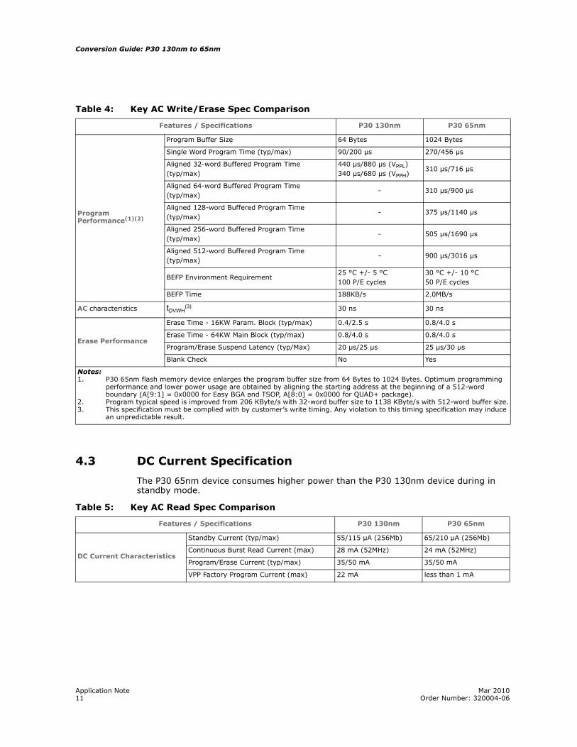
4.2 AC Write/Erase Specifications
Note: Refer to the product datasheet for detailed list of all write and erase timing specifications. You may see the improved buffered programming performance.
• Numonyx® Axcell™ Flash Memory (P30-130nm) Datasheet (306666)
• Numonyx® Axcell™ Flash Memory (P30-65nm) Datasheet (320002)
Table 3: Key AC Read Spec Comparison
Features / Specifications P30-130nm P30-65nm
Performance
Clock Frequency (Max)52 MHz (Easy BGA)
40 MHz (TSOP)52 MHz (Easy BGA)
40 MHz (TSOP)
Asynchronous Access (tAVQV tVLQV tELQV)Easy BGA: 85 ns Easy BGA: 100ns
TSOP: 95 ns TSOP: 110 ns
Asynch Page Access time (tAPA) 25 ns 25 ns
Clock-to-Data Burst Access (tCHQV) 17 ns (52 MHz) 17 ns (52 MHz)
Burst Data Hold Time (tCHQX) 3 ns 3ns
Address and ADV# Setup Time (tAVCH, tVLCH) 9 ns 9 ns
CE# Setup Time (tELCH) 9 ns 9 ns
Rise/Fall Time (tFCLK/LCLK) 3.0 ns 3.0 ns
Clock High/Low Time (tCH/CL) 5 ns 5ns
Vcc power valid to RST# de-assertion (high) 60us 300us(1)
Async Page Size 4 words 16 words
Synchronous Burst Length (word) 4-, 8-, 16-, and Cont. 4-, 8-, 16- and Cont.
Burst Suspend Mode Yes Yes
Application Note Mar 201011 Order Number: 320004-06
Conversion Guide: P30 130nm to 65nm
4.3 DC Current Specification
The P30 65nm device consumes higher power than the P30 130nm device during in standby mode.
Table 4: Key AC Write/Erase Spec Comparison
Features / Specifications P30 130nm P30 65nm
Program Performance(1)(2)
Program Buffer Size 64 Bytes 1024 Bytes
Single Word Program Time (typ/max) 90/200 µs 270/456 µs
Aligned 32-word Buffered Program Time (typ/max)
440 µs/880 µs (VPPL)340 µs/680 µs (VPPH)
310 µs/716 µs
Aligned 64-word Buffered Program Time (typ/max)
- 310 µs/900 µs
Aligned 128-word Buffered Program Time (typ/max)
- 375 µs/1140 µs
Aligned 256-word Buffered Program Time (typ/max)
- 505 µs/1690 µs
Aligned 512-word Buffered Program Time (typ/max)
- 900 µs/3016 µs
BEFP Environment Requirement25 °C +/- 5 °C100 P/E cycles
30 °C +/- 10 °C50 P/E cycles
BEFP Time 188KB/s 2.0MB/s
AC characteristics tDVWH(3) 30 ns 30 ns
Erase Performance
Erase Time - 16KW Param. Block (typ/max) 0.4/2.5 s 0.8/4.0 s
Erase Time - 64KW Main Block (typ/max) 0.8/4.0 s 0.8/4.0 s
Program/Erase Suspend Latency (typ/Max) 20 µs/25 µs 25 µs/30 µs
Blank Check No Yes
Notes:1. P30 65nm flash memory device enlarges the program buffer size from 64 Bytes to 1024 Bytes. Optimum programming
performance and lower power usage are obtained by aligning the starting address at the beginning of a 512-word boundary (A[9:1] = 0x0000 for Easy BGA and TSOP, A[8:0] = 0x0000 for QUAD+ package).
2. Program typical speed is improved from 206 KByte/s with 32-word buffer size to 1138 KByte/s with 512-word buffer size.3. This specification must be complied with by customer’s write timing. Any violation to this timing specification may induce
an unpredictable result.
Table 5: Key AC Read Spec Comparison
Features / Specifications P30 130nm P30 65nm
DC Current Characteristics
Standby Current (typ/max) 55/115 µA (256Mb) 65/210 µA (256Mb)
Continuous Burst Read Current (max) 28 mA (52MHz) 24 mA (52MHz)
Program/Erase Current (typ/max) 35/50 mA 35/50 mA
VPP Factory Program Current (max) 22 mA less than 1 mA
Conversion Guide: P30 130nm to 65nm
Application Note Mar 201012 Order Number: 320004-06
5.0 Flash Software Design Considerations
The following sections discuss software design considerations when converting from the P30 130nm device to the P30 65nm device.
5.1 Device Identification
The P30 130nm and P30 65nm flash devices have same device identification code.
5.2 Read Configuration Register (RCR)
Read configurations for the P30 130nm and P30 65nm devices are set using the Read Configuration Register (RCR). For example, to place the device in synchronous burst-read mode, you set the read mode bit in the RCR. The P30 65nm RCR includes the following modifications to the RCR:
• Latency Count RCR[14:11]: an additional bit, RCR14, has been added to the P30 65nm device; RCR14 was reserved on P30-130nm. P30 65nm supports latency counts of 8, 9, 10, 11, 12, 13, 14, and 15.
• WAIT Polarity RCR[10]: P30 130nm default setting high and P30 65nm default setting is low.
• Data Hold RCR[9]: P30 130nm supports 1-clock or 2-clock cycle data hold. RCR[9] is reserved for P30 65nm and supports a data hold of one cycle only.
• WAIT Delay RCR[8]: Same values for P30 130nm and P30-65nm.
• Burst Sequence RCR[7]: P30 130nm supports Linear “1” and Intel “0” burst order. P30 65nm supports linear “0” only. Setting P30 65nm to “1” will not affect the burst order; the burst order will always be linear.
• Clock Edge RCR[6]: Same values for P30 130nm130nm and P30-65nm.
• Reserved RCR[5:4]: Same values for P30 130nm and P30-65nm.
• Burst Wrap RCR[3]: Same values for P30 130nm and P30-65nm.
• Burst Length RCR[2:0]: Same values for P30 130nm and P30-65nm.
Note: The differences are summarized in the table below.
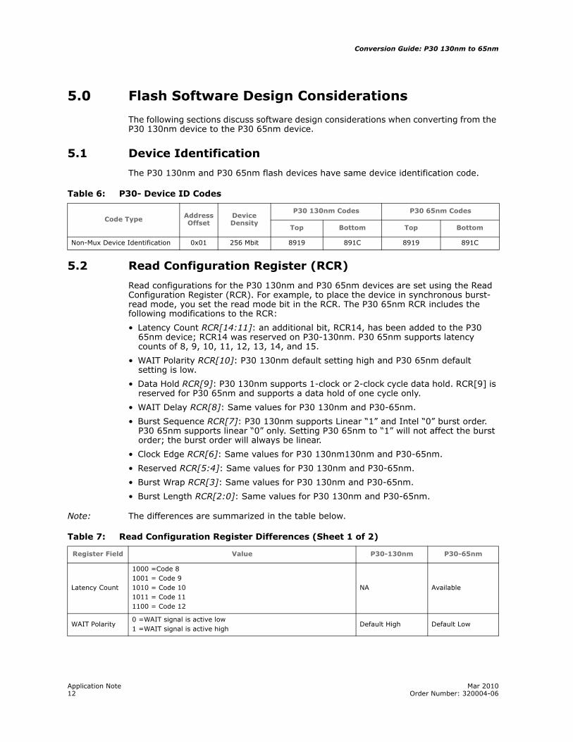
Table 6: P30- Device ID Codes
Code Type Address Offset
Device Density
P30 130nm Codes P30 65nm Codes
Top Bottom Top Bottom
Non-Mux Device Identification 0x01 256 Mbit 8919 891C 8919 891C
Table 7: Read Configuration Register Differences (Sheet 1 of 2)
Register Field Value P30-130nm P30-65nm
Latency Count
1000 =Code 8 1001 = Code 91010 = Code 101011 = Code 111100 = Code 12
NA Available
WAIT Polarity0 =WAIT signal is active low1 =WAIT signal is active high
Default High Default Low
Application Note Mar 201013 Order Number: 320004-06
Conversion Guide: P30 130nm to 65nm
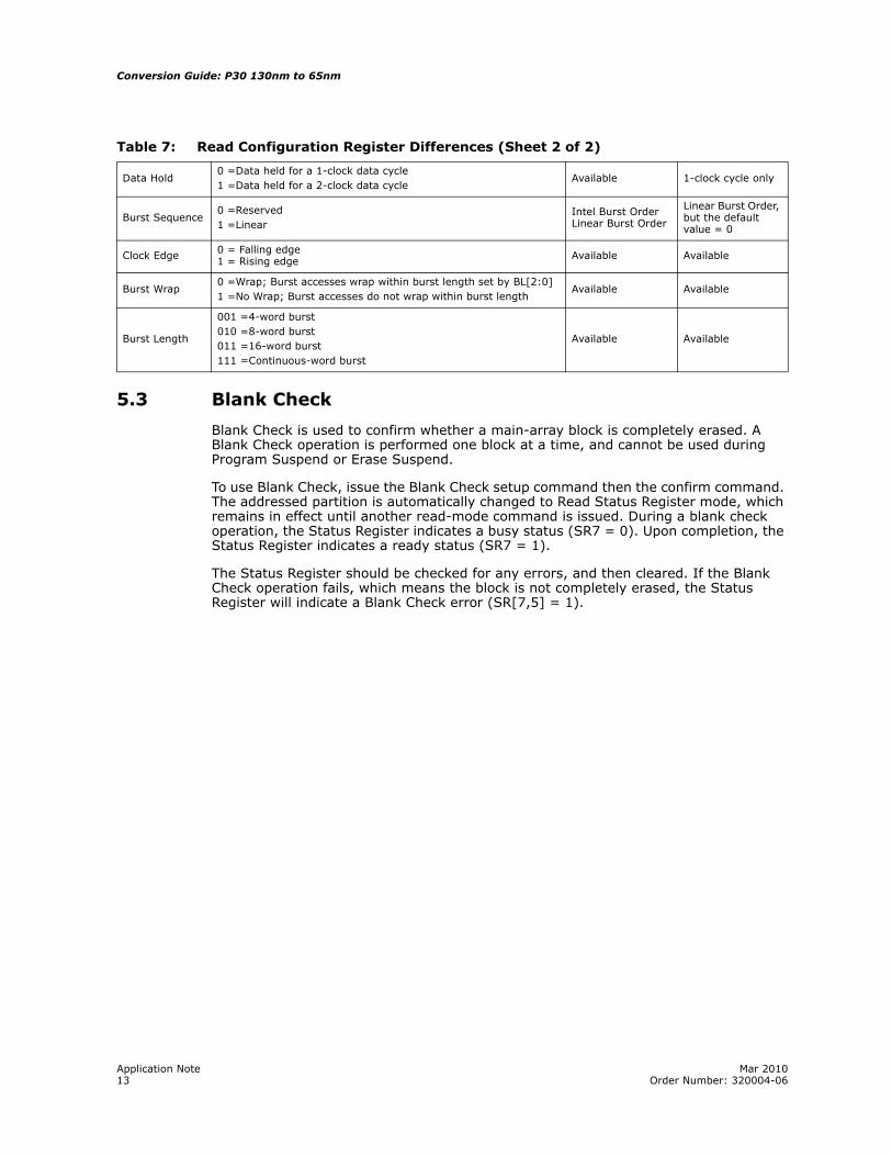
5.3 Blank Check
Blank Check is used to confirm whether a main-array block is completely erased. A Blank Check operation is performed one block at a time, and cannot be used during Program Suspend or Erase Suspend.
To use Blank Check, issue the Blank Check setup command then the confirm command. The addressed partition is automatically changed to Read Status Register mode, which remains in effect until another read-mode command is issued. During a blank check operation, the Status Register indicates a busy status (SR7 = 0). Upon completion, the Status Register indicates a ready status (SR7 = 1).
The Status Register should be checked for any errors, and then cleared. If the Blank Check operation fails, which means the block is not completely erased, the Status Register will indicate a Blank Check error (SR[7,5] = 1).
Data Hold 0 =Data held for a 1-clock data cycle1 =Data held for a 2-clock data cycle
Available 1-clock cycle only
Burst Sequence0 =Reserved1 =Linear
Intel Burst Order Linear Burst Order
Linear Burst Order, but the default value = 0
Clock Edge 0 = Falling edge1 = Rising edge Available Available
Burst Wrap0 =Wrap; Burst accesses wrap within burst length set by BL[2:0]1 =No Wrap; Burst accesses do not wrap within burst length
Available Available
Burst Length
001 =4-word burst010 =8-word burst011 =16-word burst111 =Continuous-word burst
Available Available
Table 7: Read Configuration Register Differences (Sheet 2 of 2)
Conversion Guide: P30 130nm to 65nm
Application Note Mar 201014 Order Number: 320004-06
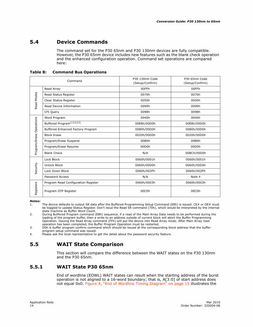
5.4 Device Commands
The command set for the P30 65nm and P30 130nm devices are fully compatible. However, the P30 65nm device includes new features such as the blank check operation and the enhanced configuration operation. Command set operations are compared here:
Notes:1. The device defaults to output SR data after the Buffered Programming Setup Command (E8h) is issued. CE# or OE# must
be toggled to update Status Register. Don’t issue the Read SR command (70h), which would be interpreted by the internal state machine as Buffer Word Count.
2. During Buffered Program command (E8h) sequence, if a read of the Main Array Data needs to be performed during the loading of the program buffer, then a write to an address outside of current block will abort the Buffer Programming Operation. Issuing the Read Array command (FFh) will put the device into Read Array mode. After Main Array read operation has been completed, the Buffer Program Operation must be restarted.
3. D0h is buffer program confirm command which should be issued at the corresponding block address that the buffer program setup command was issued.
4. Please ask the local representative to get the detail about the password security feature.
5.5 WAIT State Comparison
This section will compare the difference between the WAIT states on the P30 130nm and the P30 65nm.
5.5.1 WAIT State P30 65nm
End of wordline (EOWL) WAIT states can result when the starting address of the burst operation is not aligned to a 16-word boundary; that is, A[3:0] of start address does not equal 0x0. Figure 4, “End of Wordline Timing Diagram” on page 15 illustrates the
Table 8: Command Bus Operations
CommandP30 130nm Code(Setup/Confirm)
P30 65nm Code(Setup/Confirm)
Read M
odes
Read Array 00FFh 00FFh
Read Status Register 0070h 0070h
Clear Status Register 0050h 0050h
Read Device Information 0090h 0090h
CFI Query 0098h 0098h
Pro
gra
m/E
rase
Oper
ations Word Program 0040h 0040h
Buffered Program(1)(2)(3) 00E8h/00D0h 00E8h/00D0h
Buffered Enhanced Factory Program 0080h/00D0h 0080h/00D0h
Block Erase 0020h/00D0h 0020h/00D0h
Program/Erase Suspend 00B0h 00B0h
Program/Erase Resume 00D0h 00D0h
Blank Check N/A 00BCh/00D0h
Sec
urity
Lock Block 0060h/0001h 0060h/0001h
Unlock Block 0060h/00D0h 0060h/00D0h
Lock Down Block 0060h/002Fh 0060h/002Fh
Password Access N/A Note 4
Reg
iste
rs Program Read Configuration Register 0060h/0003h 0060h/0003h
Program OTP Register 00C0h 00C0h
Application Note Mar 201015 Order Number: 320004-06
Conversion Guide: P30 130nm to 65nm
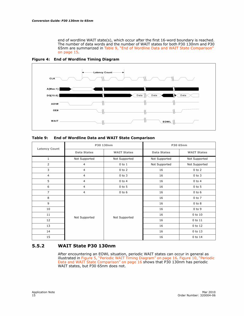
end of wordline WAIT state(s), which occur after the first 16-word boundary is reached. The number of data words and the number of WAIT states for both P30 130nm and P30 65nm are summarized in Table 9, “End of Wordline Data and WAIT State Comparison” on page 15.
5.5.2 WAIT State P30 130nm
After encountering an EOWL situation, periodic WAIT states can occur in general as illustrated in Figure 5, “Periodic WAIT Timing Diagram” on page 16. Figure 10, “Periodic Data and WAIT State Comparison” on page 16 shows that P30 130nm has periodic WAIT states, but P30 65nm does not.
Figure 4: End of Wordline Timing Diagram
Table 9: End of Wordline Data and WAIT State Comparison
Latency CountP30 130nm P30 65nm
Data States WAIT States Data States WAIT States
1 Not Supported Not Supported Not Supported Not Supported
2 4 0 to 1 Not Supported Not Supported
3 4 0 to 2 16 0 to 2
4 4 0 to 3 16 0 to 3
5 4 0 to 4 16 0 to 4
6 4 0 to 5 16 0 to 5
7 4 0 to 6 16 0 to 6
8
Not Supported Not Supported
16 0 to 7
9 16 0 to 8
10 16 0 to 9
11 16 0 to 10
12 16 0 to 11
13 16 0 to 12
14 16 0 to 13
15 16 0 to 14
A[Max:1]
ADV#
OE#
WAIT
DQ[15:0] Data Data Data
EOWL
CLK
Latency Count

Conversion Guide: P30 130nm to 65nm
Application Note Mar 201016 Order Number: 320004-06
5.6 CFI Differences
P30 65nm has same CFI revision. During adoption of Numonyx or third party software, several differences must be taken into account. This section will describe the changes.
5.6.1 CFI revision
The CFI minor revision sorted in offset (P+4)h remains as “4”.
CFI version 1.4 is supported in the software provided by Numonyx.
5.6.2 Time-out changes
All CFI time-out changes are listed in Table 11, “Value Changes”
Figure 5: Periodic WAIT Timing Diagram
Table 10: Periodic Data and WAIT State Comparison
Latency CountP30-130nm P30-65nm
Data States WAIT States Data States WAIT States
1 Not Supported Not Supported Not Supported Not Supported
2 4 0 Not Supported Not Supported
3 4 0 16 0
4 4 0 16 0
5 4 1 16 0
6 4 2 16 0
7 4 3 16 0
8
Not Supported Not Supported
16 0
9 16 0
10 16 0
11 16 0
12 16 0
13 16 0
14 16 0
15 16 0
Addr[ Max: 16]
Addr[15:0] Data Data Data Data
Periodic Periodic
Latency CountLatency Count
CLK
A[MAX:16]
ADV#
OE#
D[15:0]
WAIT
A [Max :1]
Data
Application Note Mar 201017 Order Number: 320004-06
Conversion Guide: P30 130nm to 65nm
5.7 Performance Improvements in P30 65nm
The write performance can be improved on P30 65nm by using the 1024 Byte/512 Word buffer. If buffered programming is being done using the 32 Byte buffer (similar to 130nm devices), no software changes need to be implemented.
To achieve maximum performance using the 1024 Byte/512 Word buffer on 65nm devices, the following considerations apply during software modifications:
1. Use the Full 1024 Byte/512 Word Buffer.
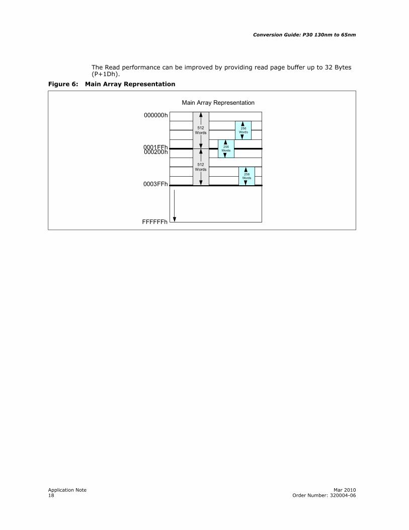
2. If 1024 Byte/512 Word Buffer is being used, the programming addresses should be aligned in 512 word address boundaries. For example: Start Programming address is 000000h and End Programming Address is 0001FFh. Please refer to Figure 3.
3. If the addresses must be mis-aligned, the maximum buffer size must be in chunks of 256 Words. For example: Start Programming Address to Start Programming Address + 0000FFh (256 Words). Please refer to Figure 3.
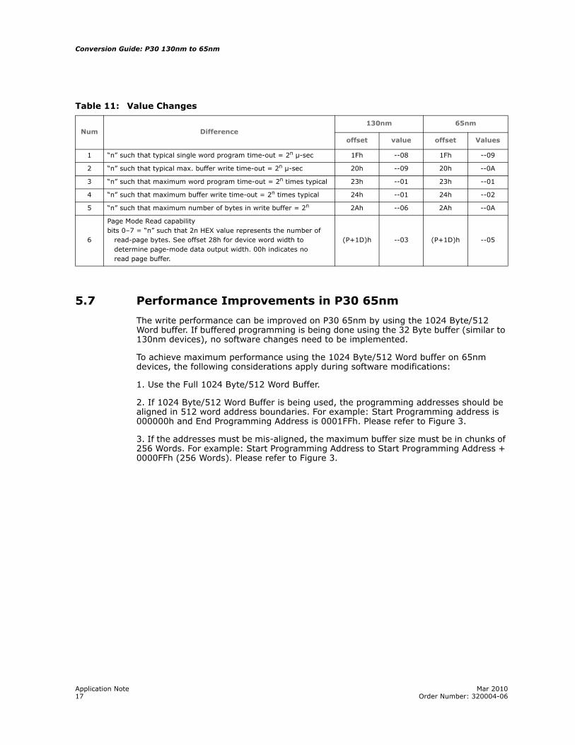
Table 11: Value Changes
Num Difference130nm 65nm
offset value offset Values
1 “n” such that typical single word program time-out = 2n µ-sec 1Fh --08 1Fh --09
2 “n” such that typical max. buffer write time-out = 2n µ-sec 20h --09 20h --0A
3 “n” such that maximum word program time-out = 2n times typical 23h --01 23h --01
4 “n” such that maximum buffer write time-out = 2n times typical 24h --01 24h --02
5 “n” such that maximum number of bytes in write buffer = 2n 2Ah --06 2Ah --0A
6
Page Mode Read capabilitybits 0–7 = “n” such that 2n HEX value represents the number of read-page bytes. See offset 28h for device word width to determine page-mode data output width. 00h indicates no read page buffer.
(P+1D)h --03 (P+1D)h --05
Conversion Guide: P30 130nm to 65nm
Application Note Mar 201018 Order Number: 320004-06
The Read performance can be improved by providing read page buffer up to 32 Bytes (P+1Dh).
Figure 6: Main Array Representation
256Words
000000h
000200h
0003FFh
Main Array Representation
512 Words
512 Words
256 Words
0001FFh 256 Words
256 Words
FFFFFFh

Application Note Mar 201019 Order Number: 320004-06
Conversion Guide: P30 130nm to 65nm
6.0 Conversion Considerations
P30-65nm has a larger program buffer size to greatly improves the write performance. Users should use appropriate program and read modes to take advantage of this Additional Information.
It is recommended that the user enable robust power loss recovery in software system, especially during flash write operations. Please refer to Application Note 309046 for detail information.
Order/Document Number Document/Tool
306666 Numonyx® Axcell™ Flash Memory (P30-130nm) Datasheet
320002 Numonyx® Axcell™ Flash Memory (P30-65nm) Datasheet
309046 Application Note: Power Loss Recovery for NOR Flash Memory
Note: Contact your local Numonyx or distribution sales office or visit Numonyx’s World Wide Web home page at http://www.Numonyx.com for technical documentation, tools, and additional information.

Conversion Guide: P30 130nm to 65nm
Application Note Mar 201020 Order Number: 320004-06


![0 [Type the document subtitle] [Pick the date] Dasar-Dasar Membuat Media Pembelajaran Dengan Dengan Dengan Dengan Flash Flash Flash Flash](https://static.fdokumen.com/doc/165x107/632259f164690856e109202b/0-type-the-document-subtitle-pick-the-date-dasar-dasar-membuat-media-pembelajaran.jpg)