
Properties of III-V semiconductor materials grown by HVPE
73
1 DEGREE PROJECT IN INDUSTRIAL ENGINEERING AND MANAGEMENT, SECOND CYCLE, 30 CREDITS STOCKHOLM, SWEDEN 2016 Properties of III-V semiconductor materials grown by HVPE STAMOULIS STERGIAKIS KTH ROYAL INSTITUTE OF TECHNOLOGY SCHOOL OF INFORMATION AND COMMUNICATION TECHNOLOGY
-
Upload
khangminh22 -
Category
Documents
-
view
1 -
download
0
Transcript of Properties of III-V semiconductor materials grown by HVPE

1
DEGREE PROJECT IN INDUSTRIAL ENGINEERING AND MANAGEMENT, SECOND CYCLE, 30 CREDITS STOCKHOLM, SWEDEN 2016
Properties of III-V semiconductor materials grown by HVPE
STAMOULIS STERGIAKIS
KTH ROYAL INSTITUTE OF TECHNOLOGY
SCHOOL OF INFORMATION AND COMMUNICATION
TECHNOLOGY

3
Supervisors: Examiner:
Doctor Yanting Sun (KTH) Professor Sebastian Lourdudoss (KTH) Professor Nini Pryds (DTU)
4
Table of Contents
KTH ROYAL INSTITUTE OF TECHNOLOGY ................................................................................... 1
Table of Contents ...................................................................................................................... 4
Abstract ..................................................................................................................................... 6
Acknowledgements ................................................................................................................... 7
List of figures ............................................................................................................................. 8
List of tables............................................................................................................................. 10
Abbreviations .......................................................................................................................... 11
1. Introduction ..................................................................................................................... 13
1.1 Compound semiconductors for photovoltaics ............................................................ 13
1.2 Current situation and challenges to be faced ............................................................. 13
1.3 Thesis outline and scope ............................................................................................. 14
2. Theoretical background ................................................................................................... 16
2.1 lll-V Semiconductors .................................................................................................... 16
2.1.1 General knowledge .................................................................................................. 16
2.1.2 Semiconducting alloys ............................................................................................. 17
2.1.2.1 InP ............................................................................................................................ 17
2.1.2.2 GaAs ......................................................................................................................... 17
2.1.2.3 GaInP ....................................................................................................................... 18
2.1.3 Studied Heterojunctions .......................................................................................... 18
2.2 Epitaxial growth ........................................................................................................... 20
2.2.1 Introduction ............................................................................................................. 20
2.2.2 Growth mechanisms and anisotropy ...................................................................... 21
2.2.3 Methods for epitaxial processes ............................................................................. 22
2.2.4 Hydride Vapor Phase Epitaxy .................................................................................. 22
2.3 Intermixing of elements .............................................................................................. 23
2.3.1 Introduction ............................................................................................................. 23
2.3.2 Diffusion mechanisms ............................................................................................. 23
2.3.2.1 Fundamental theory ................................................................................................ 23
2.3.2.2 Diffusion mechanisms ............................................................................................. 24
2.3.3 Other penetration mechanisms .............................................................................. 26
2.4 Characterizations ......................................................................................................... 28
5
2.4.1 Scanning Electron Microscopy ................................................................................ 28
2.4.2 Energy Dispersive X-ray Spectroscopy .................................................................... 29
2.4.3 High resolution X-ray Diffraction ............................................................................. 30
2.4.4 Photoluminescence ................................................................................................. 32
2.4.5 Atomic Force Microscopy ........................................................................................ 32
3. Experiment setup ............................................................................................................ 34
3.1 Samples’ preparation .................................................................................................. 34
3.2 HVPE Reactor and process description ....................................................................... 35
4. Analysis of Experimental Results ..................................................................................... 37
4.1 Samples description and dimensioning ....................................................................... 37
4.1.1 Heterostructure categories ..................................................................................... 37
4.1.2 Morphology of GaInP growths ................................................................................ 39
4.2 Composition analysis ................................................................................................... 45
4.2.1 By EDS ...................................................................................................................... 45
4.2.1.1 Introduction ............................................................................................................. 45
4.2.1.2 Applied method ....................................................................................................... 45
4.2.1.3 Investigation of EDS errors ...................................................................................... 52
4.2.2 XRD Characterization ............................................................................................... 54
4.2.2.1 Rocking curve measurements ................................................................................. 54
4.2.2.1.1 Introduction ......................................................................................................... 54
4.2.2.1.2 Data analysis ........................................................................................................ 54
4.2.2.1.3 Calculation model ................................................................................................ 55
4.2.2.2 Reciprocal lattice mapping ...................................................................................... 58
4.3 Investigation of Si incorporation ................................................................................. 60
4.4 Investigation of Gallium deficiency in certain crystallographic orientations .............. 62
4.5 Further observations and results ................................................................................ 64
4.5.1 AFM measurements ................................................................................................ 64
4.5.2 Photoluminescence measurements ........................................................................ 65
5. Conclusions and future work ........................................................................................... 69
References ............................................................................................................................... 71
6
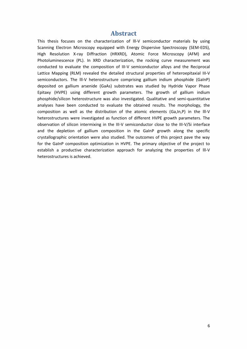
Abstract This thesis focuses on the characterization of lll-V semiconductor materials by using
Scanning Electron Microscopy equipped with Energy Dispersive Spectroscopy (SEM-EDS),
High Resolution X-ray Diffraction (HRXRD), Atomic Force Microscopy (AFM) and
Photoluminescence (PL). In XRD characterization, the rocking curve measurement was
conducted to evaluate the composition of III-V semiconductor alloys and the Reciprocal
Lattice Mapping (RLM) revealed the detailed structural properties of heteroepitaxial III-V
semiconductors. The lll-V heterostructure comprising gallium indium phosphide (GaInP)
deposited on gallium arsenide (GaAs) substrates was studied by Hydride Vapor Phase
Epitaxy (HVPE) using different growth parameters. The growth of gallium indium
phosphide/silicon heterostructure was also investigated. Qualitative and semi-quantitative
analyses have been conducted to evaluate the obtained results. The morphology, the
composition as well as the distribution of the atomic elements (Ga,In,P) in the lll-V
heterostructures were investigated as function of different HVPE growth parameters. The
observation of silicon intermixing in the III-V semiconductor close to the III-V/Si interface
and the depletion of gallium composition in the GaInP growth along the specific
crystallographic orientation were also studied. The outcomes of this project pave the way
for the GaInP composition optimization in HVPE. The primary objective of the project to
establish a productive characterization approach for analyzing the properties of lll-V
heterostructures is achieved.
7
Acknowledgements
First of all, I would like to express my gratitude to my supervisor Dr. Yanting Sun for
his important mentoring and high support during my master Thesis. His comments
and feedback in every step of the project were more than helpful. My grateful
thanks should also be given to my second supervisor Professor Nini Pryds for his
assistance and his important feedback as well as to the Professor Sebastian
Lourdudoss for his valuable support, his useful comments and for accepting to be my
examiner. In addition, I would like to express my thanks to the rest of the research
team, Giriprasanth Omarakuttan, and Niklas Larsson for assisting me in various tasks
of the project and for the excellent collaboration and communication we had during
these months. I would also like to thank my parents and my family and my friends
for assisting and supporting me in each of my education steps despite the distance
difficulties.
8
List of figures
Figure 1: Electron band gap as a function of lattice constant in semiconducting materials (9)
................................................................................................................................................. 17
Figure 2 ELOG for GaInP/GaAs and propagation of dislocations – Cross section ................... 21
Figure 3: Schematic illustration of vacancy diffusion in solids (23) ........................................ 24
Figure 4: Schematic illustration of interstitial diffusion in solids (23) ..................................... 25
Figure 5: Schematic illustration of interstitially diffusion in solids, Collinear jump. (23) ........ 25
Figure 6: Representation of Si incorporation through gas phase transportation mechanism
for CELOG process ................................................................................................................... 27
Figure 7: Photograph of the Scanning Electron Microscope used in this work ...................... 28
Figure 8: X-ray tube structure. X-ray radiation from the anode is guided by the windows of
the tube to produce an X-ray beam. (30) ................................................................................ 30
Figure 9: Bragg diffraction by crystal planes. The path difference between beams 1 and 2 is:
𝑺𝑸 + 𝑸𝑻 = 𝟐𝑷𝑸 𝒔𝒊𝒏𝜽. (30) ................................................................................................... 31
Figure 10: Detection of cantilever deflection by a laser beam reflected from the rear side of
the cantilever. (30) .................................................................................................................. 32
Figure 11: Explanation of the optical lithography and photolithography process - step by step
method .................................................................................................................................... 34
Figure 12: Simplified schematic of HVPE reactor (only the reaction chamber) ...................... 36
Figure 13: Representation of GaInP/GaAs planar growth ....................................................... 37
Figure 14: Graphical representation of substrate with line-opening used for ELOG process . 38
Figure 15: Graphical Representation of substrate with line-opening used for ELOG process
and the grown GaInP layer ...................................................................................................... 38
Figure 16: Graphical representation of substrate with circular openings used for ELOG
process..................................................................................................................................... 38
Figure 17: Schematic illustration of the InP/Si CELOG process - Reproduced under the
permission from ref. (38) ........................................................................................................ 39
Figure 18: SEM for planar 3166 GaInP/GaAs - hillocks observation ....................................... 40
Figure 19: Top view SEM image for the 3166 GaInP/GaAs heterostructure with 300 rotation.
................................................................................................................................................. 41
Figure 20: Cross section imaging obtained by SEM ................................................................. 42
Figure 21: Measurement of opening width, vertical and lateral growth rates ....................... 43
Figure 22: Aspect ratio fluctuation in the three examined samples ....................................... 43
Figure 23: Aspect ratio mean values of studied samples and their standard deviation ......... 44
Figure 24: Substrate opening widths fluctuation for the three studied samples ................... 44
Figure 25: Selected linescanning in the cross section’s edge for 3166 GaInP/GaAs 300 rotation
................................................................................................................................................. 46
Figure 26: Intensity counts of the cross section elements as a function of the linescanning
length ....................................................................................................................................... 46
Figure 27: Intensity counts as a function of linescanning length for the elements present in
the central magnified CS area ................................................................................................. 47
Figure 28: SEM image of a magnified area close to the cross section’s opening .................... 47
Figure 29: Indication of selected area mapping for the GaInP growth layer .......................... 49
9
Figure 30: SEM image for GaInP/Si cross section and area mapping for Si element in the
selected area ........................................................................................................................... 49
Figure 31: Evidence of gallium deficiency in specific cross section areas of 3168 GaInP/Si
sample grown by CELOG ......................................................................................................... 50
Figure 32: EDS automated elements graph; Average intensity counts as a function of X-ray
excitation energies for the total mapped area ....................................................................... 50
Figure 33: SEM image and graph depicting linescanning intensity as a function of
linescanning length (vertical yellow line - left image) in the middle area of the cross section
covering both GaInP/seed (InP) interface and GaInP/Si interface of sample 3166 GaInP/Si
grown by CELOG. ..................................................................................................................... 51
Figure 34: SEM image and graph depicting linescanning intensity as a function of
linescanning length (vertical yellow line - left image) in the side (lateral area) of the cross
section covering GaInP/Si interface sample 3168 GaInP/Si grown by CELOG ........................ 52
Figure 35: a) 3170 InP/Si heterostructure and linescanned area b) representation of tilting in
z-y plane c) cross section SEM image and intensity linescanning before tilting and d) cross
section SEM image and intensity linescanning after tilting .................................................... 53
Figure 36: Rocking curve for 3166 GaInP grown on GaAs substrate 30d rot. – 004 diffraction
plane ........................................................................................................................................ 55
Figure 37: Rocking curve for 3166 GaInP grown on GaAs substrate 30d rot. – 224 diffraction
plane ........................................................................................................................................ 55
Figure 38: RLM for planar 3123 GaInP/GaAs heterostructure – 004 plane (Table 5) ............. 58
Figure 39: RLM for planar 3125 GaInP/GaAs heterostructure – 004 plane, (Table 5) ............ 59
Figure 40: RLM for circular ELOG 3221 GaInP/GaAs heterostructure – 004 plane, (Table 5) . 60
Figure 41: Comparison between Si incorporation in the seed/Si interface (a, b) with Si
incorporation in the GaInP/Si interface (c, d) ......................................................................... 62
Figure 42: Gallium decrease in specific crystallographic areas of 3166GaInP/Si
heterostructure – EDS mapping for Cross section 1 ............................................................... 63
Figure 43: Gallium decrease in specific crystallographic areas of 3166GaInP/Si
heterostructure – EDS mapping for Cross section 2 ............................................................... 64
Figure 44: AFM scanning for 3166 GaInP/GaAs planar growth – 50X50 μm area and height
variations ................................................................................................................................. 64
Figure 46: Representation of indicative slit image and the corresponding PL spectrum ....... 65
Figure 45: AFM scanning for 3168 GaInP/GaAs planar growth – 75X575 μm area and height
variations ................................................................................................................................. 65
Figure 47: PL spectra of GaInP/GaAs for three samples grown with different GaCl flow ....... 67
Figure 48: PL spectrum for the planar and ELOG growth of sample 3221 GaInP/GaAs.......... 68

10
List of tables Table 1: List of heterostructure samples studied in the present project; a=lattice constant.
EG=bandgap ............................................................................................................................ 19
Table 2: GaInP/GaAs heterostructures grown by HVPE process ............................................ 40
Table 3: Islands’ widths for the three dimensioned samples measured by SEM .................... 41
Table 4: Calculated compositions, bandgap and lattice constants of GaInP in GaInP/GaAs and
GaInP/Si heterostructures from the XRD rocking curves ........................................................ 57
Table 5: GaInP/GaAs heterostructures for which RLM method was applied ......................... 58
11
Abbreviations
ELOG: Epitaxial Lateral Overgrowth
CELOG: Corrugated Epitaxial Lateral Overgrowth
SAG: Selective Area Growth
AR: Aspect Ratio
InP: Indium Phosphide
GaInP: Gallium Indium Phosphide
GaInAs: Gallium Indium Arsenide
GaAs: Gallium Arsenide
GaP: Gallium Phosphide
GaN: Gallium Nitride
SEM: Scanning Electron Microscopy
EDS: Energy Dispersive Spectroscopy
HRXRD: High Resolution X-ray Diffraction
RLM: Reciprocal Lattice Mapping
XRD: X-ray Diffraction
AFM: Atomic Force Microscopy
PL: Photoluminescence
InCl: Indium Chloride
GaCl: Gallium Chloride
HCl: Hydrochloric Acid
PH3: Phosphine
AsH3: Arsine
SiO2: Silicon Dioxide
SiCl4: Silicon Tetrachloride

12
LPE: Liquid Phase Epitaxy
MBE: Molecular Beam Epitaxy
VPE: Vapor Phase Epitaxy
MOVPE: Metalorganic Vapor Phase Epitaxy
HVPE: Hydride Vapor Phase Epitaxy
PECVD: Plasma Enhanced Chemical Vapor Deposition
UV: Ultraviolet
LP: Low Pressure
AR: Aspect Ratio
FWHM: Full Width at Half Maximum
FIB: Focused Ion Beam
CS: Cross-section
TEM: Transmission Electron Microscopy
NA: Numerical Aperture
UHV: Ultra High Vacuum

13
1. Introduction
1.1 Compound semiconductors for photovoltaics Photovoltaics (PV) technology is recognized as a promising replacement for fossil
fuel in electricity generation to reduce the adverse impact of CO2 emission on
environment. Si PV cell is the main technology on PV market due to the abundance
of Si in nature and low manufacturing cost. An efficiency of 25.6 has been reported
recently on Si solar cell, however, solar cells made of lll-V compound semiconductors
such as GaAs, InP, GaInP etc. are expected to have higher efficiency. (1) lll-V
compound semiconductors can create new kinds of compound combinations as well
as innovative heterostructures. The range of possible compounds is quite broad for
these lll and V groups because they can form binary, ternary or quaternary alloys.
Heterojunctions with different band gap have found applications in laser diodes (2),
photodetectors (3) and high efficiency multi-junction solar cells (3) Due to different
band gap energies, photon energies of different ranges of the solar spectrum can be
harvested. The understanding of properties of these compounds and
heterostructures is critical to achieve the optimum performance promised by
compound semiconductor heterostructures. Continuous research is held in the
optimization of lll-V semiconducting material combinations and their applications in
high efficiency photovoltaics.
1.2 Current situation and challenges to be faced Recently, considerable efforts have been made in growing lll-V materials on silicon
substrate because it combines the respective advantages of the lll-V materials like
high carrier mobility and band gap engineering in heterostructures with silicon’s
higher mechanical stability, thermal conductivity, lower density and cost. The latter
heterostructure combination is proved to be interesting from the photovoltaic point
of view. However, lll-V semiconductor materials have different lattice constants than
Si, therefore lattice mismatch is created between the grown lll-V layer and the Si
substrate. Consequently, lattice mismatch will provoke different kinds of defects
which will lead to deterioration of the electrical and mechanical properties of the
junctions. For instance, the major obstacle in the epitaxy of InP on Si is the major
difference in lattice constants (≈8%). (5) Moreover, differences in thermal expansion
coefficients of the heterostructure materials can also be a source of defects. As a
matter of fact, the need to identify the optimal growth technique and the optimal
growth parameters are essential for fabricating high quality lll-V/Si heterostructures.
That can be assured by characterizing the heterostructure properties by various
techniques.
14
1.3 Thesis outline and scope In the present thesis various characterization methods were applied to investigate
the morphology, impurity incorporation, composition uniformity of grown layer and
structural properties of InP/Si, GaInP/Si and GaInP/GaAs heterostructures. The
impact of growth parameters (i.e. Temperature, V/lll ratio etc.) on these properties
was examined. The semiconducting heterostructures that were examined in this
research were: GaInP ternary alloy on GaAs substrate, GaInP on Si substrate as well
as InP binary alloy on Si substrate. The following samples were considered for
characterization.
a) Reference samples which consisted of planar growths. Such heterostructures
were grown on the planar substrate(s).
b) Samples whose growth was initiated from an opening (Epitaxial Lateral
Overgrowth). The openings were lines or circles and were fabricated by
photolithography process. (15)
c) In samples in which growth was started from an InP seed on top of Si substrate.
(Corrugated Epitaxial Lateral Overgrowth) (45).
Characterization was done to understand the properties of heterostructure
fabricated under different growth conditions. The examined heterostructures were:
a) GaInP on GaAs substrate with good lattice matching. Planar growths and
ELOG heterostructures were investigated.
b) GaInP on Si substrate through “seed” (InP) for minimizing the lattice
mismatch.
c) InP on Si substrate through “seed” and by the CELOG process.
The goal of this characterization effort was to investigate standardized methods for
characterizing the lll-V heterostructure samples. These methods can be continuously
applied in the upcoming growths and can create a standardized model for
comparisons. The primary scopes and the objectives of the present master thesis are
the following;
Growth analysis for various heterostructures. Study of the selective area growth
aspect ratio as function of the geometrical characteristics of the substrate
(opening orientation, opening width) and the V/lll ratio parameter. The
investigated heterostructure was GaInP grown on GaAs substrate.
Characterization of heterostructures by X-ray diffraction (XRD). Calculation of
composition variation, lattice constants and band gaps energy of GaInP growth
under different growth parameters.
EDS analysis in cross sections of various samples and investigation of
composition fluctuation for the constituting elements. Research on the accuracy

15
of EDS measurements and identification of errors concerning X-rays excitation
volume and tilting in the measured sample.
Investigation of Si incorporation in deposited layers and the feasible mechanisms
that initiated it. Characterization of GaInP and InP grown layers on Si substrates.
SEM/EDS characterizations were applied.
Orientation dependent composition variation of GaInP in ELOG/CELOG growth.
16
2. Theoretical background
2.1 lll-V Semiconductors
2.1.1 General knowledge Semiconductors consist materials whose electrical conductivity lie between those of
conductors and insulators (0eV < Eg < 9eV). Semiconductor materials are
characterized by a specific band gap, measured between the valence band and the
conduction band. (6) This band gap energy is important for electronic applications
and as a matter of fact for photovoltaics. Carriers mobility and carriers transport are
closely related to the band gap energy. Due to heterostructure layers having
different band gaps, different ranges of the solar spectrum can be harvested. Doping
of the heterostructure layers can lead up to p-n junction formation (7). Through
photovoltaic effect, (8) solar radiation of various wavelengths can be absorbed by
the layers of the multijunction and be transformed into electric current. This process
can increase solar cell efficiency. Silicon is the most well-known semiconductor
material and finds extensive application in today’s electronic devices. However, a
great deal of lll-V compound semiconductors also created great interest because of
their high potential for electronics and also for solar cells. These lll-V compounds
consist of aluminium, gallium, indium from group lll and nitrogen, phosphorus,
arsenic and antimony from group V of the periodic table. Mixing these elements
provides 12 possible combinations the most important of which are GaAs, InP, GaP
and GaN. Apart from the ability of different band gaps to harvest different solar
spectrum ranges their importance is related to the lattice constant of the ternary
and quaternary alloys consisting of these elements that can be grown on the binaries
mentioned above. This is important for the quality of the structure because defects
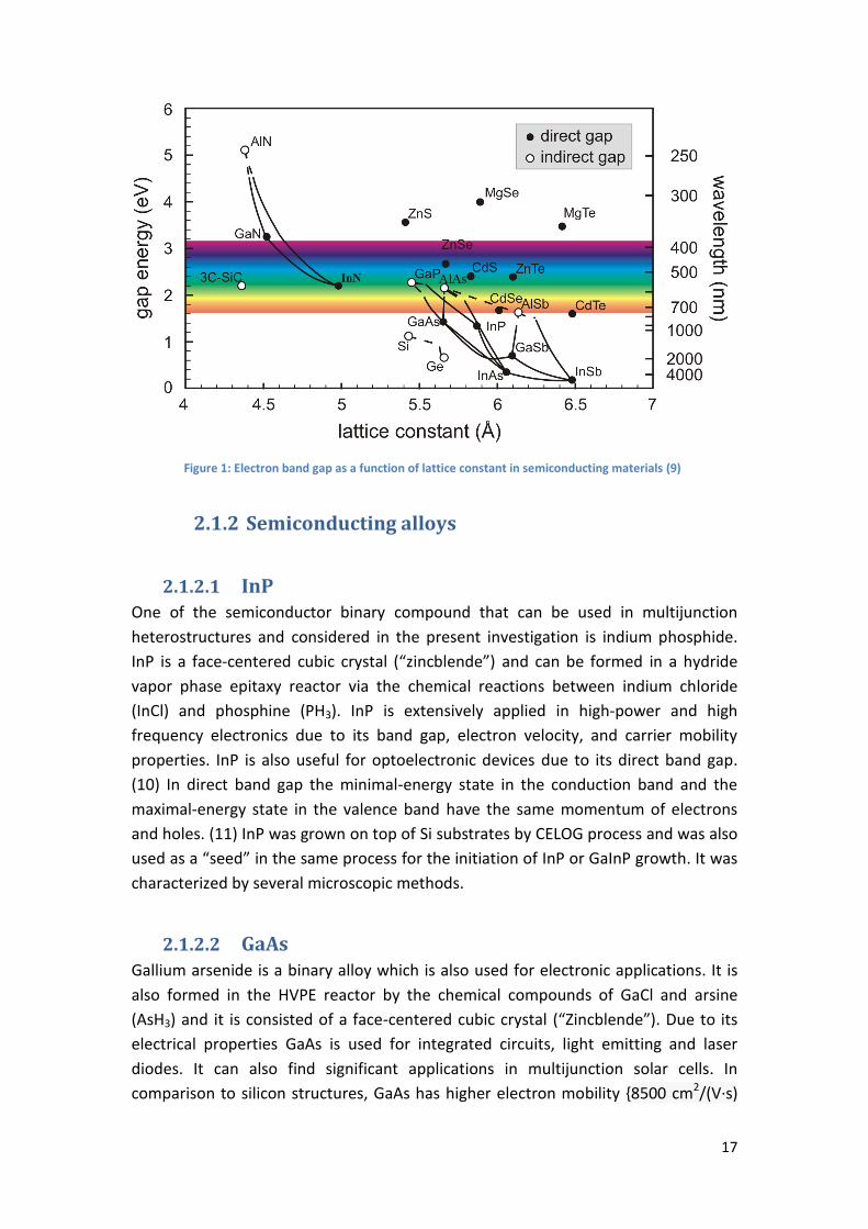
generated from mismatching could deteriorate electrical properties. In the following
diagram different semiconductors and semiconductor alloys are shown according to
their band gap energy and as a function of lattice constant. The colorful region in the
figure represents the wavelengths of the visible light. (9)
17
Figure 1: Electron band gap as a function of lattice constant in semiconducting materials (9)
2.1.2 Semiconducting alloys
2.1.2.1 InP One of the semiconductor binary compound that can be used in multijunction
heterostructures and considered in the present investigation is indium phosphide.
InP is a face-centered cubic crystal (“zincblende”) and can be formed in a hydride
vapor phase epitaxy reactor via the chemical reactions between indium chloride
(InCl) and phosphine (PH3). InP is extensively applied in high-power and high
frequency electronics due to its band gap, electron velocity, and carrier mobility
properties. InP is also useful for optoelectronic devices due to its direct band gap.
(10) In direct band gap the minimal-energy state in the conduction band and the
maximal-energy state in the valence band have the same momentum of electrons
and holes. (11) InP was grown on top of Si substrates by CELOG process and was also
used as a “seed” in the same process for the initiation of InP or GaInP growth. It was
characterized by several microscopic methods.
2.1.2.2 GaAs Gallium arsenide is a binary alloy which is also used for electronic applications. It is
also formed in the HVPE reactor by the chemical compounds of GaCl and arsine
(AsH3) and it is consisted of a face-centered cubic crystal (“Zincblende”). Due to its
electrical properties GaAs is used for integrated circuits, light emitting and laser
diodes. It can also find significant applications in multijunction solar cells. In
comparison to silicon structures, GaAs has higher electron mobility {8500 cm2/(V·s)

18
(at 300 K)}, similar to InP. It contributes to lattice matched heterostructures due to
its lattice constant value. GaAs can assist as an intermediate layer in minimizing
lattice mismatch of compounds having high lattice constant variations (i.e. Si and
InP). However, it falls behind silicon mostly because of its cost and its inability to
form inherent insulator layer as SiO2 in the case of silicon. (12) GaAs was studied in
different heterostructures both as a substrate for hosting the growth of GaInP layer
and as a thin “buffer” layer between silicon substrate and InP “seed” in order to
compensate for the lattice mismatch.
2.1.2.3 GaInP Gallium indium phosphide is a ternary semiconducting alloy which was also
investigated. GaInP was grown as a top layer on both GaAs and Si substrates and was
characterized by different microscopic methods. GaInP is an alloy composed of InP
and GaP. Similarly to the mentioned lll-V compounds, GaInP demonstrates superior
electrical properties (i.e. electron velocity, band gap). Similar to other lll-V
compounds, its applications in high efficiency photovoltaics show high potential
because of harvesting a specific energy range of the solar spectrum. Band gap energy
and lattice constant values of GaInP are between the corresponding values of the
binary alloys from which it is formed. (13) Especially the Ga0.5In0.5P is an alloy of
significant importance because it can be lattice matched to GaAs (a=0. 5654 nm).
Lattice matched heterostructures contain low density of defects (i.e. dislocations)
which can deteriorate the electrical properties. Thus, defect–free heterostructures
can be used for the formation of multijunction solar cells.
2.1.3 Studied Heterojunctions
Batch ref.
num.
Substrate Material
Process and
opening orientation
off [110]
Grown layer
Characterization Methods
Investigated parameters
SEM EDS XRD AFM PL
3166 GaAs Planar GaInP X
X X
Morphology, AR,
Composition, a, Eg,
roughness
3166 GaAs ELOG 300 GaInP X X X
Morphology, AR,
Composition, a, Eg
3166 GaAs ELOG 600 GaInP X X X
Morphology, AR,
Composition, a, Eg

19
3166 Si CELOG
(circular) GaInP X X X
Morphology, Composition,
Si penetration
3168 GaAs Planar GaInP X
X X
Morphology, AR,
Composition, a, Eg,
roughness
3168 GaAs ELOG 300 GaInP X X X X
Morphology, AR,
Composition, a, Eg
3168 Si CELOG
(circular) GaInP X X X
Morphology, Composition,
Si penetration
3172 Si Planar GaInP -
S X X X
X
Morphology, Composition
3170 Si CELOG
(circular) InP X X
X
Morphology, Composition,
Si penetration
3221 GaAs Planar GaInP
X
X Composition,
a, Eg
3221 GaAs ELOG
(circular) GaInP
X
X
Composition, a, Eg
3223 GaAs Planar GaInP
X
X Composition,
a, Eg
3223 GaAs ELOG
(circular) GaInP
X
X
Composition, a, Eg
3225 GaAs Planar GaInP
X
X Composition,
a, Eg
3225 GaAs ELOG GaInP
X
X Composition,
a, Eg
3227 GaAs Planar GaInP
X
X Composition,
a, Eg
3229 GaAs Planar GaInP
X
X Composition,
a, Eg
Table 1: List of heterostructure samples studied in the present project; a=lattice constant. EG=bandgap
20
The studied heterostructures in the present thesis are presented in (Table 1). Each
sample is identified by a number (growth run) given in the 1st column of the table.
They also refer to various characteristics for the studied samples (i.e. V/lll ratio,
openings rotation etc.). The highest effort in characterizations was put on the
ternary alloy GaInP which was grown either on GaAs or on Si substrate. Classification
according to the sample’s formation (i.e. planar, opening rotation etc.) and the
growing process is presented (3rd column). This classification is significant in order to
make the necessary comparisons and to extract information. The philosophy that
was applied is based on examining properties (i.e. aspect ratio, composition etc) by
changing one parameter at a time (i.e. opening rotation, growth method,
temperature etc.) while maintaining the rest of the parameters fixed. Openings were
used in both ELOG and CELOG growing process in order to minimize the defect
density of the grown material. The “Reference” notation corresponds to the planar
growth and describes the direct deposition of the grown material (GaInP) on the
substrate (GaAs). Planar samples act as references for comparisons.
Characterization methods that were applied for each heterostructure are marked
with an “X” (4th column). Useful comments regarding the type of growth (planar,
ELOG) or the seed’s morphology are also included. The investigated properties for
every sample are also briefly described. Focus was on the thickness of the grown
alloys, aspect ratio wherever applicable and composition variation in the case of
ternary alloys. Regarding the GaInP/Si heterostructure, gallium decrease in specific
growth areas and silicon penetration were investigated.
2.2 Epitaxial growth
2.2.1 Introduction Epitaxial growth is the process of growing a crystalline material on a crystalline
substrate and both have the same lattice constant. Selective area growth (SAG), a
growth process where the growth is conducted only in the open areas, is commonly
used for the monolithic integration of optoelectronic components such as laser
diodes, detectors and modulators. Epitaxial lateral overgrowth (ELOG) (44) and
corrugated epitaxial lateral overgrowth technique (CELOG) (45) are special forms of
SAG to grow crystalline layers on lattice mismatched substrates. Significant progress
has been made with the development of these techniques which can be used as a
“defect filter” for the grown layer and minimize the density of dislocation in the
laterally grown areas. (14) The latter ELOG processes can be used to prepare even
heterostructures of two lattice mismatched materials and can find great use in the
fabrication of multijunction solar cells.
21
2.2.2 Growth mechanisms and anisotropy The growth mode of the deposited layer is influenced partially by the kinetics during
impingement and by diffusion. Growth can get affected by reaction of precursor
atoms and partially by the strain that may occur in the layer itself. There are three
ways in which epitaxial growth can take place;
a) Frank-van der Merwe (FM) referred as layer-by-layer growth, i.e. two dimensional
growth. (15)
b) Volmer-Weber (VW) mode which is a three-dimensional growth. (16)
c) Stranski-Krastanov (SK) in which growth initially takes place layer-by-layer up to a
certain thickness (critical). By exceeding this specific thickness value, islands are
formed. (26)
The occurrence of each mode depends on; a) the energy of the free surface of the
substrate, b) the energy of the interface between the layer and the substrate and c)
the energy of free surface of the epitaxial layer. (41)
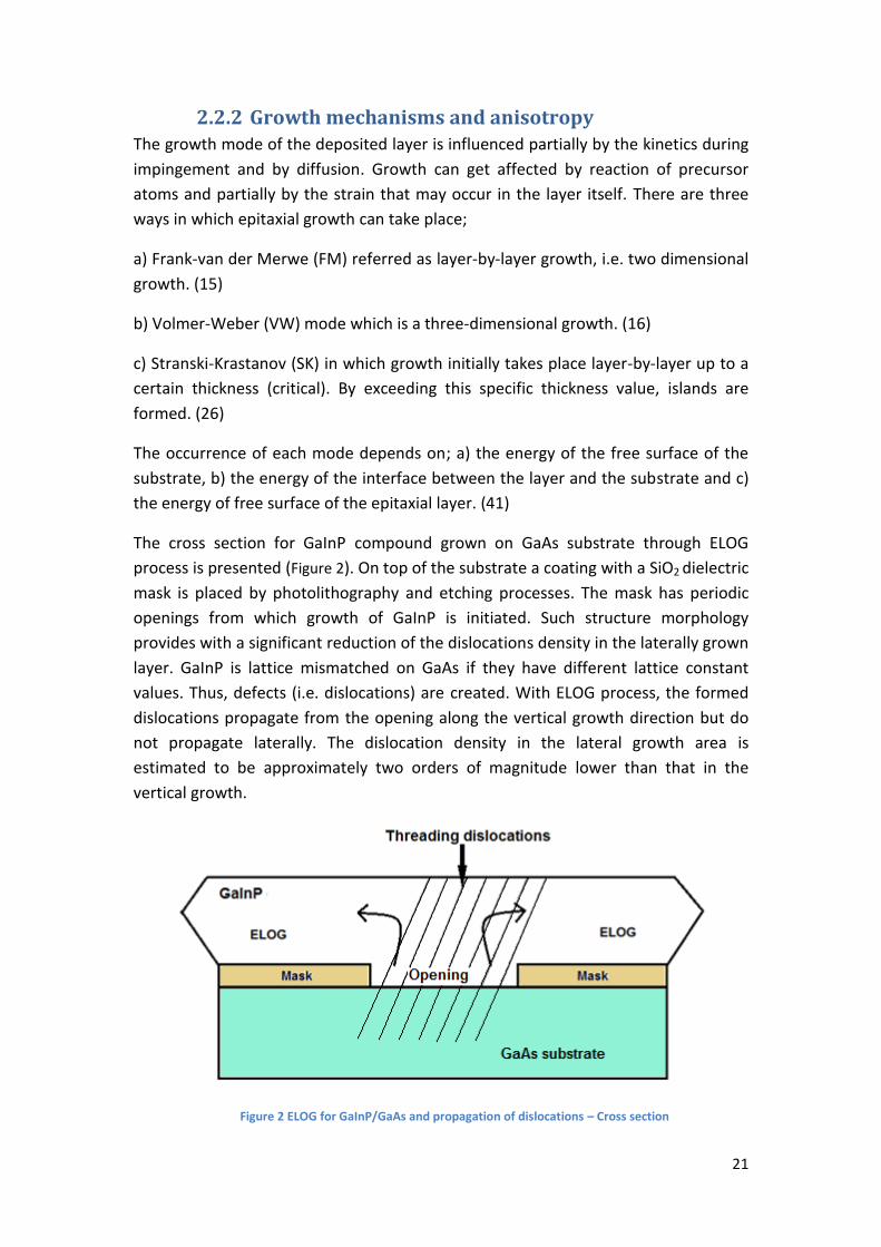
The cross section for GaInP compound grown on GaAs substrate through ELOG
process is presented (Figure 2). On top of the substrate a coating with a SiO2 dielectric
mask is placed by photolithography and etching processes. The mask has periodic
openings from which growth of GaInP is initiated. Such structure morphology
provides with a significant reduction of the dislocations density in the laterally grown
layer. GaInP is lattice mismatched on GaAs if they have different lattice constant
values. Thus, defects (i.e. dislocations) are created. With ELOG process, the formed
dislocations propagate from the opening along the vertical growth direction but do
not propagate laterally. The dislocation density in the lateral growth area is
estimated to be approximately two orders of magnitude lower than that in the
vertical growth.
Figure 2 ELOG for GaInP/GaAs and propagation of dislocations – Cross section

22
A significant characteristic which is closely related to the epitaxial processes is the
anisotropy of the growth. It corresponds to different growth rates on different
crystallographic planes. Growth rates are strongly orientation-dependent and
associated with surface kinetics. The zinc-blende crystal structure of the studied lll-V
semiconductors consists of two interpenetrating face-centered cubic (FCC)
sublattices. Each of them is shifted by a/4 to [111] direction relative to the other,
where a is the length of the fcc lattice constant. (41) Concerning the formed
crystallographic planes, the predominant plane used for the growth of lll-V
compounds on Si, InP and GaAs is (001). The {001}, {110} and {111} basic planes are
of high interest in order to understand the growth development. For instance, for
the ELOG InP on {001} Si substrate, the encountered boundary planes are {111} and
{110}. Others planes having high index can be decomposed to the basic ones. (41)
2.2.3 Methods for epitaxial processes Growth of epitaxial film can be made by using many different deposition techniques.
Three of these will be described. Liquid Phase Epitaxy (LPE) was one of the first
methods applied for the deposition of a crystalline material on a substrate. As an
equilibrium technique, it makes use of liquidus-solidus equilibrium to deposit the
solid material from the corresponding melt (or liquid solution). Molecular beam
Epitaxy (MBE) corresponds to the second way of epitaxial growth. It consists a
technique to grow crystalline thin films in ultrahigh vacuum (UHV) with precise
control of thickness, composition and morphology. In MBE material sources in liquid
phases are sublimated in a heated and ultra-high vacuum environment. The gaseous
elements condense on the substrate where they interact with each other. (20) Vapor
Phase Epitaxy (VPE) is the third technique and it is applied in the present
experiment. In VPE gaseous precursors of selected chemical compounds react with
the substrate. The reaction takes place in a fully controlled environment and for
identified temperature and pressure conditions. The result is the deposition of a lll-V
compound with crystalline structure. In the same time removing of the unnecessary
by-products with the aid of a continuous gas flow is conducted. VPE can be classified
into two branch processes which are the Metalogranic Vapor Phase Epitaxy (MOVPE)
and the Hydride Vapor Phase Epitaxy (HVPE). (46)
2.2.4 Hydride Vapor Phase Epitaxy HVPE is an optimal technique for growing heterostructures for multijunction solar
cell applications using ELOG or CELOG technique. (44),(45) In contrast to MOVPE, it is
a near-equilibrium process allowing the growth to be often modeled using
equilibrium thermodynamics. ELOG growth in HVPE has higher growths rates which
can approach or even exceed several hundred microns per hour. Thus, it can be
more time effective and cost efficient than MOVPE. HVPE is characterized by

23
selective and planar growth as well as by low background doping concentrations.
(21) In the present experiment HVPE allows good control of the experimental
conditions by monitoring separately InCl, GaCl, PH3 and HCl species. The
supersaturation of the gas phase can be retained at low values required for the
selective epitaxy. (23) For solar cell fabrication, the challenges that need to be
addressed are the formation of both sharp interfaces and the highly controlled
doping profiles. (22)
2.3 Intermixing of elements
2.3.1 Introduction In the process of depositing lll-V compounds like GaInP or InP on GaAs and on Si
substrates, different mechanisms take place and lead to intermixing of elements. To
be more specific, elements from the substrate can be transported to the grown
material and vice versa. Several parameters (i.e temperature, partial pressures) can
assist to intermixing. Growth rate, activation energies and chemical potentials of the
elements also play a fundamental role to this phenomenon. Intermixing of elements
can be subdivided into two main mechanisms which are the diffusion and the gas
phase transportation.
2.3.2 Diffusion mechanisms
2.3.2.1 Fundamental theory Diffusion is described as the flow of particles from high to low concentrations and is
analogous to the flow of heat. In solid state, diffusion can be facilitated by the
presence on defects in solids. Point defects like vacancies and interstitial ions are
responsible for lattice diffusion. Line and surface defects are places along which
diffusion can also take place. Grain boundaries, dislocations, inner and outer
surfaces are included in the former defect category. (23)
Fick’s first law describes diffusion as a flow. It correlates the diffusive flux with the
concentration under the assumption of the steady state and with properties that
remain unchanged with time. The equation is;
𝐽𝑝𝑎𝑟𝑡𝑖𝑐𝑙𝑒𝑠 = −𝐷𝑑𝑐
𝑑𝑥
Where; 𝐽𝑝𝑎𝑟𝑡𝑖𝑐𝑙𝑒𝑠 is the particles’ flux
𝑑𝑐
𝑑𝑥 is the concentration gradient of particles
24
D is the diffusion coefficient
Besides the first law which assumes a fixed concentration gradient, in numerous
practical cases concentration and concentration gradient change with time. (23) In
this case, Fick’s second law is applied and predicts how diffusion provokes the
concentration to change with time flow. (25) Assuming that diffusion coefficient can
be considered as independent of concentration the equation is;
𝑑𝑐
𝑑𝑡= 𝐷
𝑑2𝑐
𝑑𝑥2
Where; 𝑑𝑐
𝑑𝑡 is the concentration change with respect to time
D is the diffusion coefficient
𝑑2𝑐
𝑑𝑥2 consists the second derivative of concentration with respect to
the position x (length)
A method for calculating diffusion that can be followed is the random diffusion
model. The jumps of atoms which can contribute to diffusion can be considered as
independent of all previous jumps and can occur in every direction (random walk
method). The method of tracer diffusion can also be applied. In most cases, tracer
diffusion is not completely random but, to some extent, correlated with previous
atom jumps. (23)
2.3.2.2 Diffusion mechanisms Lattice diffusion takes place through the defects in crystal structure. The presence of
different types of defects enables different diffusion mechanisms. For elemental
solids such mechanisms can be classified in the following categories;
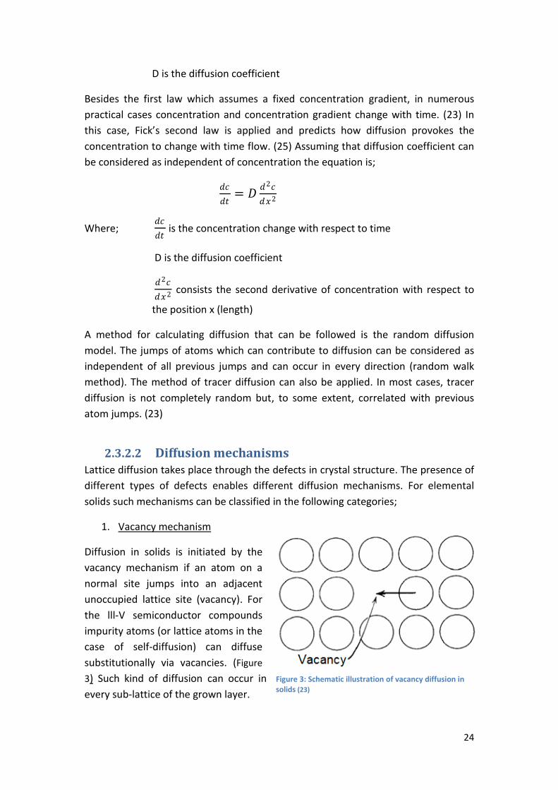
1. Vacancy mechanism
Diffusion in solids is initiated by the
vacancy mechanism if an atom on a
normal site jumps into an adjacent
unoccupied lattice site (vacancy). For
the lll-V semiconductor compounds
impurity atoms (or lattice atoms in the
case of self-diffusion) can diffuse
substitutionally via vacancies. (Figure
3) Such kind of diffusion can occur in
every sub-lattice of the grown layer.
Figure 3: Schematic illustration of vacancy diffusion in solids (23)
25
For instance, Si can diffuse in GaAs compound via vacancies on the Ga sub-lattice
and As sub-lattice. Another mechanism for the vacancy mechanism is initiated when
vacancies of the two sub-lattices tend to associate together and form vacancy pairs.
Impurity atoms can diffuse via such vacancy pairs. Concentration in such pairs is a
function of temperature. Diffusion via these pairs is supposed to be more probable
than diffusion via simple vacancies. (26)
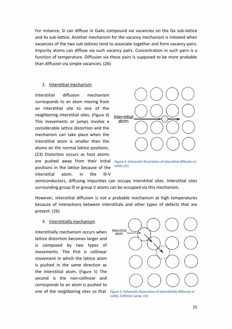
2. Interstitial mechanism
Interstitial diffusion mechanism
corresponds to an atom moving from
an interstitial site to one of the
neighboring interstitial sites. (Figure 4)
This movements or jumps involve a
considerable lattice distortion and the
mechanism can take place when the
interstitial atom is smaller than the
atoms on the normal lattice positions.
(23) Distortion occurs as host atoms
are pushed away from their initial
positions in the lattice because of the
interstitial atom. In the lll-V
semiconductors, diffusing impurities can occupy interstitial sites. Interstitial sites
surrounding group lll or group V atoms can be occupied via this mechanism.
However, interstitial diffusion is not a probable mechanism at high temperatures
because of interactions between interstitials and other types of defects that are
present. (26)
3. Interstitially mechanism
Interstitially mechanism occurs when
lattice distortion becomes larger and
is composed by two types of
movements. The first is collinear
movement in which the lattice atom
is pushed in the same direction as
the interstitial atom. (Figure 5) The
second is the non-collinear and
corresponds to an atom is pushed to
one of the neighboring sites so that
Figure 4: Schematic illustration of interstitial diffusion in solids (23)
Figure 5: Schematic illustration of interstitially diffusion in solids, Collinear jump. (23)

26
the jump direction is different from the interstitial atom. (23)
4. Interstitial-substitutional mechanism
A mechanism that can find strong application in lll-V compound semiconductors
takes place when many impurities are placed in both interstitial and substitutional
positions. Diffusion proceeds via the movement of interstitial atoms that are highly
mobile. These atoms, in turn, interact with vacancies which are diffused from the
interface and form stable substitutional atoms. Such process is concentration
dependent and is divided in two sub-processes. The “dissociative” and the “kick-out”
process. (26)
5. Pipe-diffusion mechanism
Diffusion may also take place due to the presence of line defects (i.e. dislocations).
This phenomenon is also critical in the field of lll-V semiconductors. Impurity atoms
are possible to find “paths’” to be transported and diffuse. Formed dislocations can
be considered as possible diffusion paths. For instance, Si atoms from Si substrate
can diffuse into the grown layer with the aid of existing dislocations. This mechanism
is enhanced by high dislocation densities. The phenomenon is called “pipe” diffusion.
(27)
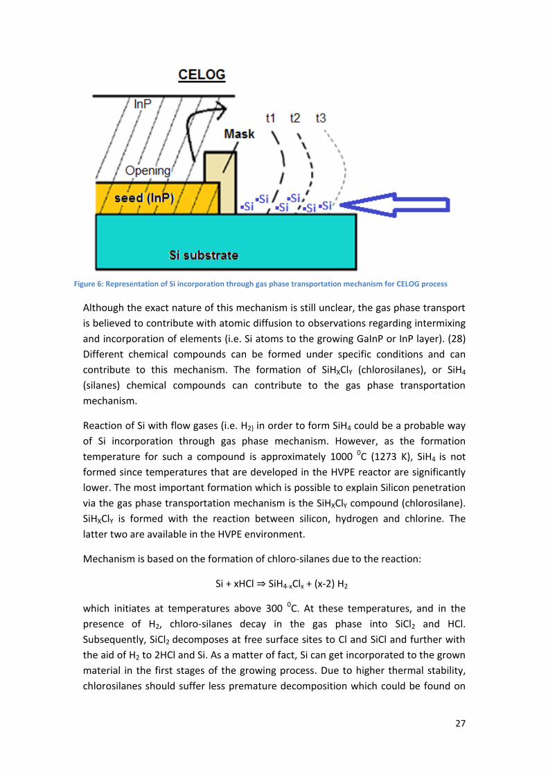
2.3.3 Other penetration mechanisms Despite diffusion, incorporation of the substrate elements to the grown lll-V layer
can also be attributed to atoms transported in a gas phase condition. Specific values
of growth parameters (partial pressures, temperature, growth rate etc) can initiate
and accelerate this mechanism. Substrate atoms (i.e. Si) can be transported to the
surface of the growth and get incorporated in the grown layer in the early stages of
its formation. (38) As deposition proceeds, surface formation layer is continuously
changing. Substrate atoms are transported to the growth through the boundary area
between the substrate and the newly formed surface in the grown layer. Such
incorporation procedure is indicatively depicted for the CELOG process of InP/Si
heterostructure (Figure 6). A magnified area of the cross section depicting the lateral
growth is represented. The lateral growth formation is indicatively distinguished in
three separate time steps (t1, t2 and t3). Si incorporated atoms (blue dots), which
are originated from Si substrate are represented. However, for ELOG process, due to
the seed (InP) and the mask (SiO2) presence between Si substrate and grown GaInP,
such incorporation mechanism is not possible to occur.
27
Although the exact nature of this mechanism is still unclear, the gas phase transport
is believed to contribute with atomic diffusion to observations regarding intermixing
and incorporation of elements (i.e. Si atoms to the growing GaInP or InP layer). (28)
Different chemical compounds can be formed under specific conditions and can
contribute to this mechanism. The formation of SiHXClY (chlorosilanes), or SiH4
(silanes) chemical compounds can contribute to the gas phase transportation
mechanism.
Reaction of Si with flow gases (i.e. H2) in order to form SiH4 could be a probable way
of Si incorporation through gas phase mechanism. However, as the formation
temperature for such a compound is approximately 1000 0C (1273 K), SiH4 is not
formed since temperatures that are developed in the HVPE reactor are significantly
lower. The most important formation which is possible to explain Silicon penetration
via the gas phase transportation mechanism is the SiHXClY compound (chlorosilane).
SiHXClY is formed with the reaction between silicon, hydrogen and chlorine. The
latter two are available in the HVPE environment.
Mechanism is based on the formation of chloro-silanes due to the reaction:
Si + xHCl ⇒ SiH4-xClx + (x-2) H2
which initiates at temperatures above 300 0C. At these temperatures, and in the
presence of H2, chloro-silanes decay in the gas phase into SiCl2 and HCl.
Subsequently, SiCl2 decomposes at free surface sites to Cl and SiCl and further with
the aid of H2 to 2HCl and Si. As a matter of fact, Si can get incorporated to the grown
material in the first stages of the growing process. Due to higher thermal stability,
chlorosilanes should suffer less premature decomposition which could be found on
Figure 6: Representation of Si incorporation through gas phase transportation mechanism for CELOG process

28
silanes. E.g. SiH2Cl2 can decompose heterogenously to SiCl and promote Si
incorporation. (29)
2.4 Characterizations
2.4.1 Scanning Electron Microscopy
Figure 7: Photograph of the Scanning Electron Microscope used in this work
One of the fundamental instruments used in the present study of lll-V
semiconducting compounds is the scanning electron microscope. SEM is the most
widely used type of electron microscope and it was extensively used in studying lll-V
heterostructures. Both the top views and the cross sections of several samples were
characterized. SEM examines the microscopic structure by scanning the surface of
materials in a similar way to confocal microscopes but with much higher resolution
and much greater depth of field. Magnification is also higher and expands to greater
than 100.00 X. SEM images are formed by a focused electron beam originating from
an emission gun. The beam scans over the surface of the specimen. The signal
electrons emitted from the specimen are collected by a detector, amplified and used
to reconstruct an image. Reconstruction occurs according to the one-to-one
correlation between scanning points on the specimen and picture points on the
screen. The deflection system of the electron probe is controlled by two pairs of
electromagnetic coils (scan coils). SEM resolution is determined by the gun`s probe
29
size and the probe current. (30) Compromise between these two parameters must
be made in order to obtain high resolution images. SEM capabilities contributed into
observing the detailed morphology and topological properties of GaInP and InP
compounds deposited on Si and GaAs substrates. Heterostructures were also studied
and important parameters like the relation between the opening pattern size and
aspect ratios (lateral growth/vertical growth) were determined.
2.4.2 Energy Dispersive X-ray Spectroscopy By equipping the SEM system with an energy-dispersive X-ray spectrometer, it is
possible to obtain chemical information of the studied specimens. EDS uses the SEM
electron beam to excite the emission of the characteristic X-rays from sample’s
atoms. X-rays are collected by the detector. According to the specific X-ray energies,
the elements that are present in the measured area are revealed. Since the electron
beam can be readily focused on a microscopic area of several tenths of nanometers
on the sample, EDS microanalyser can investigate the chemical compositions in the
scanned area. The electron`s energy beam is proportional to the excitation volume
of the emitting X-rays (pear shape). (30)
EDS was applied for the characterizations of various heterostructures having
different growth parameters. The identification of the atomic composition (%) as
well as the distribution analysis of the chemical elements was estimated. Errors and
drawbacks concerning EDS measurements will be analyzed.
Three characterization methods for EDS were applied;
The selected area mapping through which knowledge about the distribution
of elements in a selected area can be extracted. Every element can be
distinguished and represented with a specific color. The selected area
mapping is characterized by the selected area size and by the defined
acquisition time (scanned frames).
The intensity line-scanning is an EDS method that scans a heterostructure’s
region through a selected continuous line. Such a line is characterized by a
specific length, specific acquisition time and it provides a continuous intensity
spectrum of the elements that are present. It consists of an appropriate
method for studying penetration and intermixing of elements across
interfaces. It can correlate the presence of a chemical element to the X-ray
intensity values.
Point-line scanning is an EDS method that can be used in extracting the
specific atomic composition (%) of the present elements. By defining the
number of desired points and the scanning shape (line, area etc), user is able
to measure the chemical composition in a direct mode.
30
EDS is a powerful instrument and in combination with SEM, can be used in the
identification of the present elements in the examined areas of the sample. It is
structurally simple because it does not contain moving parts. EDS is relatively fast
because of the detector’s ability to collect the characteristic X-ray signals from the
total spectrum range. (30)
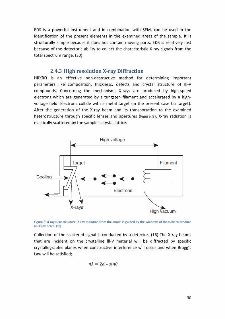
2.4.3 High resolution X-ray Diffraction HRXRD is an effective non-destructive method for determining important
parameters like composition, thickness, defects and crystal structure of lll-V
compounds. Concerning the mechanism, X-rays are produced by high-speed
electrons which are generated by a tungsten filament and accelerated by a high-
voltage field. Electrons collide with a metal target (in the present case Cu target).
After the generation of the X-ray beam and its transportation to the examined
heterostructure through specific lenses and apertures (Figure 8), X-ray radiation is
elastically scattered by the sample’s crystal lattice.
Figure 8: X-ray tube structure. X-ray radiation from the anode is guided by the windows of the tube to produce an X-ray beam. (30)
Collection of the scattered signal is conducted by a detector. (16) The X-ray beams
that are incident on the crystalline lll-V material will be diffracted by specific
crystallographic planes when constructive interference will occur and when Bragg’s
Law will be satisfied;
𝑛𝜆 = 2𝑑 ∗ 𝑠𝑖𝑛𝜃
31
Where; λ is the wavelength of the X-ray
θ is the angle between the incident X-ray and the surface of a set of
scattering planes
d is the spacing between planes
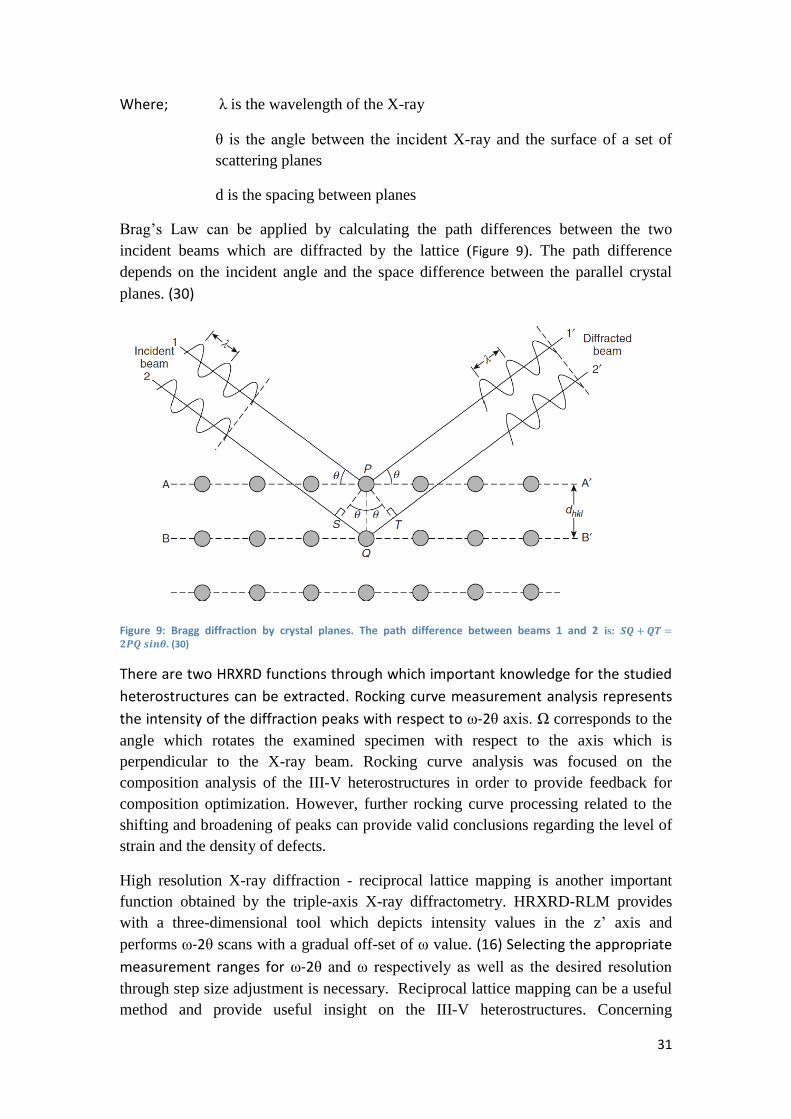
Brag’s Law can be applied by calculating the path differences between the two
incident beams which are diffracted by the lattice (Figure 9). The path difference
depends on the incident angle and the space difference between the parallel crystal
planes. (30)
Figure 9: Bragg diffraction by crystal planes. The path difference between beams 1 and 2 is: 𝑺𝑸 + 𝑸𝑻 =𝟐𝑷𝑸 𝒔𝒊𝒏𝜽. (30)
There are two HRXRD functions through which important knowledge for the studied
heterostructures can be extracted. Rocking curve measurement analysis represents
the intensity of the diffraction peaks with respect to ω-2θ axis. Ω corresponds to the
angle which rotates the examined specimen with respect to the axis which is
perpendicular to the X-ray beam. Rocking curve analysis was focused on the
composition analysis of the III-V heterostructures in order to provide feedback for
composition optimization. However, further rocking curve processing related to the
shifting and broadening of peaks can provide valid conclusions regarding the level of
strain and the density of defects.
High resolution X-ray diffraction - reciprocal lattice mapping is another important
function obtained by the triple-axis X-ray diffractometry. HRXRD-RLM provides
with a three-dimensional tool which depicts intensity values in the z’ axis and
performs ω-2θ scans with a gradual off-set of ω value. (16) Selecting the appropriate
measurement ranges for ω-2θ and ω respectively as well as the desired resolution
through step size adjustment is necessary. Reciprocal lattice mapping can be a useful
method and provide useful insight on the III-V heterostructures. Concerning
32
qualitative analysis, vertical and horizontal mismatch of the RLM peaks describe the
growth layer thickness, the magnitude of lattice strain and relaxation. Analysis for the
RLM scattering of the peaks provides us with knowledge regarding the quality of the
crystalline structure.
2.4.4 Photoluminescence Photoluminescence is a critical characterization method for investigation of the
optical properties of lll-V compounds. PL is based on measuring the radiative
recombination energy of the excited carriers in lll-V heterostructures after
illuminating them with a monochromatic laser beam. When band to band
recombination takes place, it provides knowledge about the band gap of the
semiconductor involved. PL can also be applied to examine the composition and
strain in lll-V heterostructures knowing the relation between the composition and
bandgap. Composition analysis obtained from PL method can be compared with XRD
analysis to verify the accuracy of observations. Strain can provide information about
lattice matching and strain effects can be studied from the PL peaks (i.e. shifting and
splitting). (16) PL measurements were focused on GaInP compound on GaAs
substrate and under low temperature of -263 0C (10 K). Morphology and roughness
of the studied cross section was crucial for PL analysis. For avoiding unwanted
reflections and to achieve accurate results about the bang gap variation highly planar
areas should be prepared. Polishing or creating new cross section areas with the aid
of focused ion beam instrument (FIB) is also necessary.
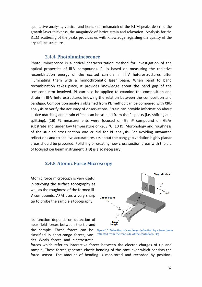
2.4.5 Atomic Force Microscopy
Atomic force microscopy is very useful
in studying the surface topography as
well as the roughness of the formed lll-
V compounds. AFM uses a very sharp
tip to probe the sample’s topography.
Its function depends on detection of near field forces between the tip and
the sample. These forces can be classified in short-range forces, van der Waals forces and electrostatic forces which refer to interactive forces between the electric charges of tip and sample. These forces generate elastic bending of the cantilever which consists the force sensor. The amount of bending is monitored and recorded by position-
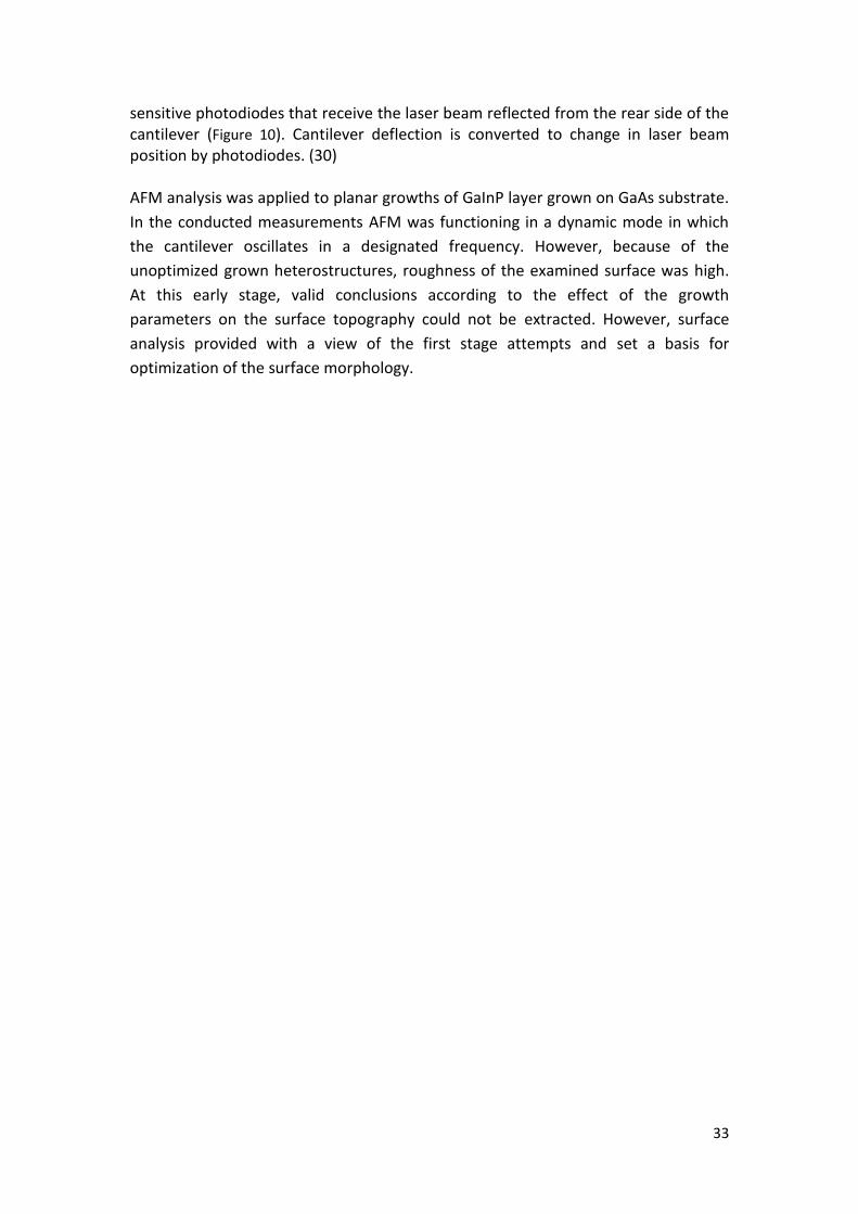
Figure 10: Detection of cantilever deflection by a laser beam reflected from the rear side of the cantilever. (30)
33
sensitive photodiodes that receive the laser beam reflected from the rear side of the cantilever (Figure 10). Cantilever deflection is converted to change in laser beam position by photodiodes. (30) AFM analysis was applied to planar growths of GaInP layer grown on GaAs substrate.
In the conducted measurements AFM was functioning in a dynamic mode in which
the cantilever oscillates in a designated frequency. However, because of the
unoptimized grown heterostructures, roughness of the examined surface was high.
At this early stage, valid conclusions according to the effect of the growth
parameters on the surface topography could not be extracted. However, surface
analysis provided with a view of the first stage attempts and set a basis for
optimization of the surface morphology.
34
3. Experiment setup
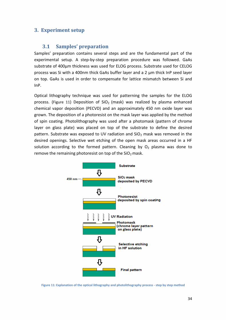
3.1 Samples’ preparation Samples’ preparation contains several steps and are the fundamental part of the
experimental setup. A step-by-step preparation procedure was followed. GaAs
substrate of 400μm thickness was used for ELOG process. Substrate used for CELOG
process was Si with a 400nm thick GaAs buffer layer and a 2 μm thick InP seed layer
on top. GaAs is used in order to compensate for lattice mismatch between Si and
InP.
Optical lithography technique was used for patterning the samples for the ELOG
process. (Figure 11) Deposition of SiO2 (mask) was realized by plasma enhanced
chemical vapor deposition (PECVD) and an approximately 450 nm oxide layer was
grown. The deposition of a photoresist on the mask layer was applied by the method
of spin coating. Photolithography was used after a photomask (pattern of chrome
layer on glass plate) was placed on top of the substrate to define the desired
pattern. Substrate was exposed to UV radiation and SiO2 mask was removed in the
desired openings. Selective wet etching of the open mask areas occurred in a HF
solution according to the formed pattern. Cleaning by O2 plasma was done to
remove the remaining photoresist on top of the SiO2 mask.
Figure 11: Explanation of the optical lithography and photolithography process - step by step method
35
The resolution of optical lithography is governed by the Rayleigh criterion and given
by;
𝑟 = 𝑘𝜆
𝛮𝛢
Where; r is the minimum dimension that can be resolved in units of λ wavelength
k is the process latitude factor that depends on the type of photoresist
λ is the wavelength of light and NA is the numerical aperture of the lens
Resolution can be increased (r decreased) by using light with a shorter wavelength.
(42) Besides ELOG samples, substrates for CELOG process were also prepared and
the processes are described later in (Figure 17).
3.2 HVPE Reactor and process description HVPE is a hot wall reactor heated by resistive heating. It contains five temperature
zones which can be independently controlled. The temperature profile from the
source region to the substrate is: Tzone1 ≥ Tzone2 < Tzone3 < Tzone4 < Tzone5. Zones 5 and 4
are the zones where metallic Indium and Gallium sources are placed. (Figure 12)
These zones are heated to 740 0C, temperature which is required for efficient
reaction between Ga or In with HCl gas to form GaCl or InCl. Zone 3 is the mixing
zone where the reactant species will be mixed. Zone 3 is heated at 630 0C. After
mixing, reactants are transported to substrate situated in zone 2. Zone 2 is the
growth zone and in the present research was heated to 590 - 660 0C for the
formation of several GaInP growths. Zone 1 is the exhaust zone and is heated at a
temperature equal or slightly higher than zone 2 so the exhaust gas can be
transported to scrubber. Growth rate can vary a lot in HVPE and in principle one can
achieve negative growth (etching) or positive growth; normally it is used to achieve
high growth rates > 10 μm/hour. Growth rate has a strong dependence on the
growth temperature and the substrate’s orientation depending upon the
thermodynamic or kinetic growth regimes, respectively.
By observing a simplified scheme of the HVPE rector (Figure 12), gas flows through
different pipes is depicted. Besides the flows of hydrides and metal organics, HCl gas
is also provided. HCl-line_1 is the HCl flow line to the lll-group metal boat (In/Ga) for
the production of InCl and GaCl compounds. HCl-line_2 consists an independent HCl
flow line for supersaturation modulation and reactor’s cleaning. By modifying HCl
flow and increasing supersaturation parameter from its equilibrium value, the
system is driven to produce more solid compounds (InP or GaInP). (30)
The reactor is divided into three regions;
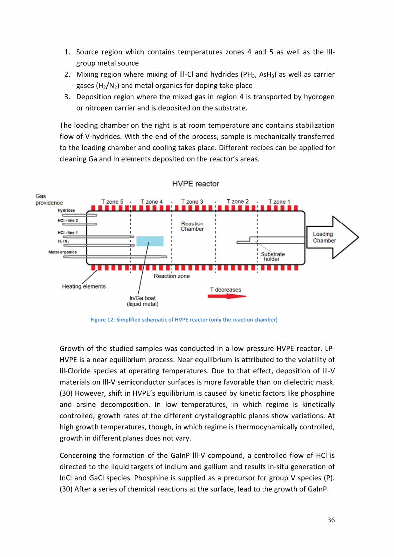
36
1. Source region which contains temperatures zones 4 and 5 as well as the lll-
group metal source
2. Mixing region where mixing of lll-Cl and hydrides (PH3, AsH3) as well as carrier
gases (H2/N2) and metal organics for doping take place
3. Deposition region where the mixed gas in region 4 is transported by hydrogen
or nitrogen carrier and is deposited on the substrate.
The loading chamber on the right is at room temperature and contains stabilization
flow of V-hydrides. With the end of the process, sample is mechanically transferred
to the loading chamber and cooling takes place. Different recipes can be applied for
cleaning Ga and In elements deposited on the reactor’s areas.
Growth of the studied samples was conducted in a low pressure HVPE reactor. LP-
HVPE is a near equilibrium process. Near equilibrium is attributed to the volatility of
lll-Cloride species at operating temperatures. Due to that effect, deposition of lll-V
materials on lll-V semiconductor surfaces is more favorable than on dielectric mask.
(30) However, shift in HVPE’s equilibrium is caused by kinetic factors like phosphine
and arsine decomposition. In low temperatures, in which regime is kinetically
controlled, growth rates of the different crystallographic planes show variations. At
high growth temperatures, though, in which regime is thermodynamically controlled,
growth in different planes does not vary.
Concerning the formation of the GaInP lll-V compound, a controlled flow of HCl is
directed to the liquid targets of indium and gallium and results in-situ generation of
InCl and GaCl species. Phosphine is supplied as a precursor for group V species (P).
(30) After a series of chemical reactions at the surface, lead to the growth of GaInP.
Figure 12: Simplified schematic of HVPE reactor (only the reaction chamber)
37
4. Analysis of Experimental Results
4.1 Samples description and dimensioning
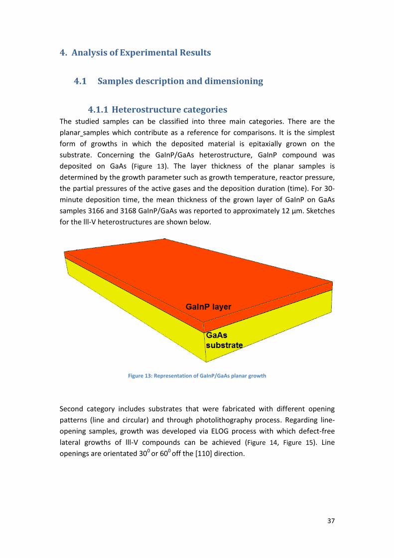
4.1.1 Heterostructure categories The studied samples can be classified into three main categories. There are the
planar samples which contribute as a reference for comparisons. It is the simplest
form of growths in which the deposited material is epitaxially grown on the
substrate. Concerning the GaInP/GaAs heterostructure, GaInP compound was
deposited on GaAs (Figure 13). The layer thickness of the planar samples is
determined by the growth parameter such as growth temperature, reactor pressure,
the partial pressures of the active gases and the deposition duration (time). For 30-
minute deposition time, the mean thickness of the grown layer of GaInP on GaAs
samples 3166 and 3168 GaInP/GaAs was reported to approximately 12 μm. Sketches
for the lll-V heterostructures are shown below.
Figure 13: Representation of GaInP/GaAs planar growth
Second category includes substrates that were fabricated with different opening
patterns (line and circular) and through photolithography process. Regarding line-
opening samples, growth was developed via ELOG process with which defect-free
lateral growths of lll-V compounds can be achieved (Figure 14, Figure 15). Line
openings are orientated 300 or 600 off the [110] direction.

38
Figure 14: Graphical representation of substrate with line-opening used for ELOG process
Figure 15: Graphical Representation of substrate with line-opening used for ELOG process and the grown GaInP layer
ELOG process was also developed on substrates with circular openings. Growth of
the GaInP compound was initiated by ring-shaped openings on GaAs substrate. The
rest of the substrate’s area was covered by SiO2 mask. (Figure 16)
Figure 16: Graphical representation of substrate with circular openings used for ELOG process

39
For the third category, heterostructures of InP and GaInP compounds were
respectively grown on Si substrates by CELOG process (Figure 17). CELOG is initiated
from an InP seed and, like ELOG process, minimizes the density of dislocations.
Figure 17: Schematic illustration of the InP/Si CELOG process - Reproduced under the permission from ref. (38)
InP or GaInP alloy is laterally grown on Si and results in higher crystal quality and
defect-free lateral layers. For GaInP/Si and InP/Si heterostructures, composition
analysis was conducted and intermixing of elements close to interface areas was
investigated.
Besides the layer structures, properties in characterized compounds can vary
according to the grown temperature and the flows of active gases (i.e. InCl, GaCl and
PH3). Such flow values are reflected in the lll-V ratio. The effect of change of one
parameter at a time while maintaining the rest of the parameters constant was
studied. The resultant growth morphology, composition of elements, lattice
parameters etc. were analyzed.
4.1.2 Morphology of GaInP growths

40
The planar samples of GaInP/GaAs where characterized first. By observing the planar
sample of 3166 GaInP on GaAs through top view, (Figure 18) growth area is
characterized by high roughness. Hillock formation has taken place all over the
surface. Their diameter is approximately 150 μm and their presence indicated that
further optimization of growth parameters is necessary. Due to lower temperature
values in the growing zone, chemical equilibrium is shifted to higher solid formation.
Moreover, the surface energy as well as the growth mechanism that takes place may
have an effect on hillocks formation. Similar observations were also made for the
3168 planar growth in which V/lll ratio is lower than 3166 batch.
Figure 18: SEM for planar 3166 GaInP/GaAs - hillocks observation
The growth morphology of three different lll-V heterostructures was analyzed. These
were all grown at 590 0C (863 K). Temperature variation in the growth zone was
neglected. Such heterostructures are:
Batch reference number
Substrate Material
Process and opening orientation
off [110]
Grown layer
V/III Ratio {PH3/(InCl+GaCl)}
3166 GaAs ELOG 300 GaInP 10
3166 GaAs ELOG 600 GaInP 10
3168 GaAs ELOG 300 GaInP 5.46 Table 2: GaInP/GaAs heterostructures grown by HVPE process
Top view of GaInP growth from the line-openings was examined (Figure 19) by SEM.
Apart from the growths through line openings, some islands of GaInP were formed
also on the SiO2 mask. Similar behavior was observed in all the top view images of
the three studied samples. This effect could take place due to the increased gas
phase supersaturation. Creation of non-equilibrium growth conditions, can increase

41
supersaturation parameter and force the system to produce more solid compound.
As a consequence, islands can be formed on the mask. For a given gas phase
composition, low temperature can increase gas phase supersaturation. The amount
of extraneous HCl flow might also have been low enough to cause higher gas phase
supersaturation.
Figure 19: Top view SEM image for the 3166 GaInP/GaAs heterostructure with 300 rotation.
The island size and island distribution were analyzed but no correlation concerning
islands distribution and sizes could be found for the three characterized samples
(Table 2: GaInP/GaAs heterostructures grown by HVPE process). The formed islands
demonstrated high variation and randomness in their size. Diameters and widths in
such islands could vary from a few microns to values that reach 40 microns (μm).
Besides isolated islands, ELOG GaInP took place along the line-opening despite island
deposition on the mask (Figure 19).
Islands width of 3166 GaInP/GaAs – 30d
(μm)
Islands width of 3166 GaInP/GaAs – 60d
(μm)
Islands width of 3168 GaInP/GaAs – 30d
(μm) 11 13 29
12 14 40
9 24 26
13 4 35
12 18 31
13 10 26
8 6 17 Table 3: Islands’ widths for the three dimensioned samples measured by SEM
42
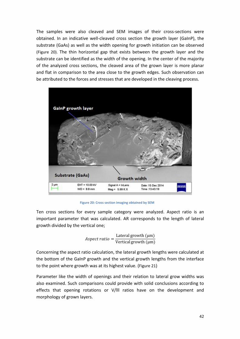
The samples were also cleaved and SEM images of their cross-sections were
obtained. In an indicative well-cleaved cross section the growth layer (GaInP), the
substrate (GaAs) as well as the width opening for growth initiation can be observed
(Figure 20). The thin horizontal gap that exists between the growth layer and the
substrate can be identified as the width of the opening. In the center of the majority
of the analyzed cross sections, the cleaved area of the grown layer is more planar
and flat in comparison to the area close to the growth edges. Such observation can
be attributed to the forces and stresses that are developed in the cleaving process.
Figure 20: Cross section imaging obtained by SEM
Ten cross sections for every sample category were analyzed. Aspect ratio is an
important parameter that was calculated. AR corresponds to the length of lateral
growth divided by the vertical one;
𝐴𝑠𝑝𝑒𝑐𝑡 𝑟𝑎𝑡𝑖𝑜 =Lateral growth (μm)
Vertical growth (μm)
Concerning the aspect ratio calculation, the lateral growth lengths were calculated at
the bottom of the GaInP growth and the vertical growth lengths from the interface
to the point where growth was at its highest value. (Figure 21)
Parameter like the width of openings and their relation to lateral grow widths was
also examined. Such comparisons could provide with solid conclusions according to
effects that opening rotations or V/lll ratios have on the development and
morphology of grown layers.
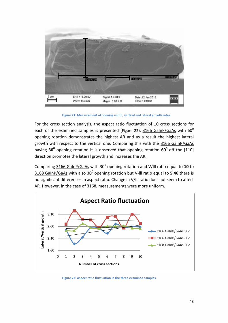
43
Figure 21: Measurement of opening width, vertical and lateral growth rates
For the cross section analysis, the aspect ratio fluctuation of 10 cross sections for
each of the examined samples is presented (Figure 22). 3166 GaInP/GaAs with 600
opening rotation demonstrates the highest AR and as a result the highest lateral
growth with respect to the vertical one. Comparing this with the 3166 GaInP/GaAs
having 300 opening rotation it is observed that opening rotation 600 off the [110]
direction promotes the lateral growth and increases the AR.
Comparing 3166 GaInP/GaAs with 300 opening rotation and V/lll ratio equal to 10 to
3168 GaInP/GaAs with also 300 opening rotation but V-lll ratio equal to 5.46 there is
no significant differences in aspect ratio. Change in V/lll ratio does not seem to affect
AR. However, in the case of 3168, measurements were more uniform.
Figure 22: Aspect ratio fluctuation in the three examined samples
1,60
2,10
2,60
3,10
0 1 2 3 4 5 6 7 8 9 10
Late
ral/
Ve
rtic
al g
row
th
Number of cross sections
Aspect Ratio fluctuation
3166 GaInP/GaAs 30d
3166 GaInP/GaAs 60d
3168 GaInP/GaAs 30d
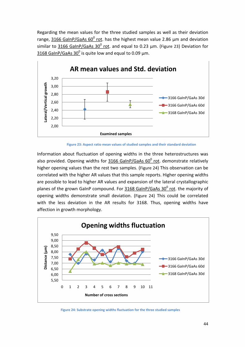
44
Regarding the mean values for the three studied samples as well as their deviation
range, 3166 GaInP/GaAs 600 rot. has the highest mean value 2.86 μm and deviation
similar to 3166 GaInP/GaAs 300 rot. and equal to 0.23 μm. (Figure 23) Deviation for
3168 GaInP/GaAs 300 is quite low and equal to 0.09 μm.
Figure 23: Aspect ratio mean values of studied samples and their standard deviation
Information about fluctuation of opening widths in the three heterostructures was
also provided. Opening widths for 3166 GaInP/GaAs 600 rot. demonstrate relatively
higher opening values than the rest two samples. (Figure 24) This observation can be
correlated with the higher AR values that this sample reports. Higher opening widths
are possible to lead to higher AR values and expansion of the lateral crystallographic
planes of the grown GaInP compound. For 3168 GaInP/GaAs 300 rot. the majority of
opening widths demonstrate small deviation. (Figure 24) This could be correlated
with the less deviation in the AR results for 3168. Thus, opening widths have
affection in growth morphology.
Figure 24: Substrate opening widths fluctuation for the three studied samples
2,00
2,20
2,40
2,60
2,80
3,00
3,20
Late
ral/
Ve
rtic
al g
row
th
Examined samples
AR mean values and Std. deviation
3166 GaInP/GaAs 30d
3166 GaInP/GaAs 60d
3168 GaInP/GaAs 30d
5,50
6,00
6,50
7,00
7,50
8,00
8,50
9,00
9,50
0 1 2 3 4 5 6 7 8 9 10 11
Dis
tan
ce (
μm
)
Number of cross sections
Opening widths fluctuation
3166 GaInP/GaAs 30d
3166 GaInP/GaAs 60d
3168 GaInP/GaAs 30d

45
4.2 Composition analysis
4.2.1 By EDS
4.2.1.1 Introduction For the characterization of the elements present in various lll-V heterostructure, EDS was
employed. INCA software was used for data processing. Concerning the GaInP layer,
composition variation of indium and gallium in the grown material is of high importance
since it determines the degree of lattice matching with GaAs substrate. EDS analysis was also
conducted for other heterostructures of 3166 and 3168 sample series. In these, the GaInP
growth takes place on top of Si substrate through an InP seed and by CELOG process.
4.2.1.2 Applied method EDS characterization was focused in the cross section of the GaInP/GaAs
heterostructures and started from point scanning measurements. However, even if
the point scanning can provide with the exact atomic percentage (%) of the
composition of elements, it takes place in specific points and not in continuous
areas. Thus, it does not act as a reliable tool for measuring composition fluctuation.
However, it can provide with information on the qualitative analysis of the present
elements. The methods of selected area mapping as well as intensity line scanning
analysis were massively applied to gain knowledge on the heterostructure elements.
Intensity line scanning depicts the continuous intensity spectrum of the generated X-
rays as a function of the linescanning distance.
GaInP/GaAs analysis
In GaInP/GaAs analysis, samples 3166 GaInP/GaAs 300 rot, 3166 GaInP/GaAs 600 rot.
and 3168 GaInP/GaAs 300 rot. were characterized. Intensity line scannings were
applied both in the areas of the lateral growth and in the areas close to the vertical
growth. of the cross section. Three cross sections were measured for each of the
examined samples. In every cross section, three vertical line scannings were applied
to measure the X-ray intensity variation for the chemical elements both in middle of
the growth and close to its sides (i.e. left) (Figure 25).

46
Figure 25: Selected linescanning in the cross section’s edge for 3166 GaInP/GaAs 300 rotation
Intensities of the present elements are represented as a function of the linescanning
length which in this case is about 20 μm. By moving from the grown material (GaInP)
to the substrate (GaAs) through the physical interface, In and P intensities drop to
background (noise) levels whereas Ga intensity rises up to reach the substrate levels.
(Figure 26) Such behavior was observed in all linescanned areas of the studied cross
sections.
Figure 26: Intensity counts of the cross section elements as a function of the linescanning length
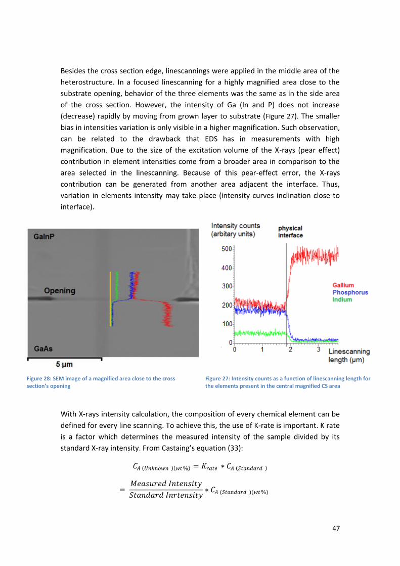
47
Besides the cross section edge, linescannings were applied in the middle area of the
heterostructure. In a focused linescanning for a highly magnified area close to the
substrate opening, behavior of the three elements was the same as in the side area
of the cross section. However, the intensity of Ga (In and P) does not increase
(decrease) rapidly by moving from grown layer to substrate (Figure 27). The smaller
bias in intensities variation is only visible in a higher magnification. Such observation,
can be related to the drawback that EDS has in measurements with high
magnification. Due to the size of the excitation volume of the X-rays (pear effect)
contribution in element intensities come from a broader area in comparison to the
area selected in the linescanning. Because of this pear-effect error, the X-rays
contribution can be generated from another area adjacent the interface. Thus,
variation in elements intensity may take place (intensity curves inclination close to
interface).
With X-rays intensity calculation, the composition of every chemical element can be
defined for every line scanning. To achieve this, the use of K-rate is important. K rate
is a factor which determines the measured intensity of the sample divided by its
standard X-ray intensity. From Castaing’s equation (33):
𝐶𝐴 𝑈𝑛𝑘𝑛𝑜𝑤𝑛 𝑤𝑡% = 𝐾𝑟𝑎𝑡𝑒 ∗ 𝐶𝐴 𝑆𝑡𝑎𝑛𝑑𝑎𝑟𝑑
= 𝑀𝑒𝑎𝑠𝑢𝑟𝑒𝑑 𝐼𝑛𝑡𝑒𝑛𝑠𝑖𝑡𝑦
𝑆𝑡𝑎𝑛𝑑𝑎𝑟𝑑 𝐼𝑛𝑟𝑡𝑒𝑛𝑠𝑖𝑡𝑦∗ 𝐶𝐴 (𝑆𝑡𝑎𝑛𝑑𝑎𝑟𝑑 )(𝑤𝑡%)
Figure 27: Intensity counts as a function of linescanning length for the elements present in the central magnified CS area
Figure 28: SEM image of a magnified area close to the cross section’s opening

48
Where 𝐶𝐴 𝑆𝑡𝑎𝑛𝑑𝑎𝑟𝑑 (𝑤𝑡%) and 𝐶𝐴 (𝑈𝑛𝑘𝑛𝑜𝑤𝑛 )(𝑤𝑡%) are the standard and measured
chemical composition respectively.
Regarding the standard composition of the elements, measurements for the
reference values should be taken. In that direction, an identified pure material or in
the case of Ga, the material’s intensity values in the GaAs substrate can be taken as
reference.
The calculated composition will be close to the real value but not the exact one.
Corrections can be applied by including the ZAF factor parameter. ZAF factor
considers the atomic number (Z) correction, the X-ray absorption (A) correction and
fluorescence (F) corrections.
Besides points characterizing and intensity linescanning, EDS mapping of the cross
section area in the measured heterostructures was also carried out. A broader view
and a colorful depiction of the chemical elements that are present in the examined
area were obtained. Mapping was used for a specific number of frames and defined
acquisition time. Even though it is a method of identifying the chemical elements, it
is not accurate in providing the specific composition values. Mapping investigates
the presence of a chemical element but not its quantity. However, regions that
demonstrate brighter colors can be correlated with higher element densities. For the
cross section of the GaInP/GaAs 300 rot. the present elements were represented
with discrete colors (Figure 29). The selected area corresponds to the grown layer.
Indium is presented with the green color, gallium with the red and phosphorus with
the blue one. The identified dark areas could denote lack of these three elements in
these regions. However, in that dark areas, the composition of the measured
elements might not be zero. Due to morphological variation and because of the
abrupt and not plannar cross sections, X-rays generated from this element are
possible to be defracted in another area far from the detector. Dark areas in the
cross section mapping may also occur due to height differences in the cross section
surface. Better cleaving, polishing or FIB applying are the proposed processes that
could be applied to improve the surface roughness of cross sections. Such dark areas
in area mapping image might also prove the existence of other contaminants and
elements (i.e. Si, O etc.).

49
Figure 29: Indication of selected area mapping for the GaInP growth layer
GaInP On Si analysis
EDS characterization was also focused on the intensity linescanning method and
mapping for the GaInP/Si heterostructures. Two samples that were characterized in
this case are the 3166 GaInP/Si and 3168 GaInP/Si. The difference between these
two samples is that in 3166 growth V/lll ratio is equal to 10 whereas in 3168 series
V/lll ratio is equal to 5.46. Growth in these samples was conducted by the CELOG
process (45) and two different cross sections of each sample were characterized.
Focusing was also tried in the GaInP/Si interfaces and GaInP/seed(InP) interfaces
respectively.
Figure 30: SEM image for GaInP/Si cross section and area mapping for Si element in the selected area
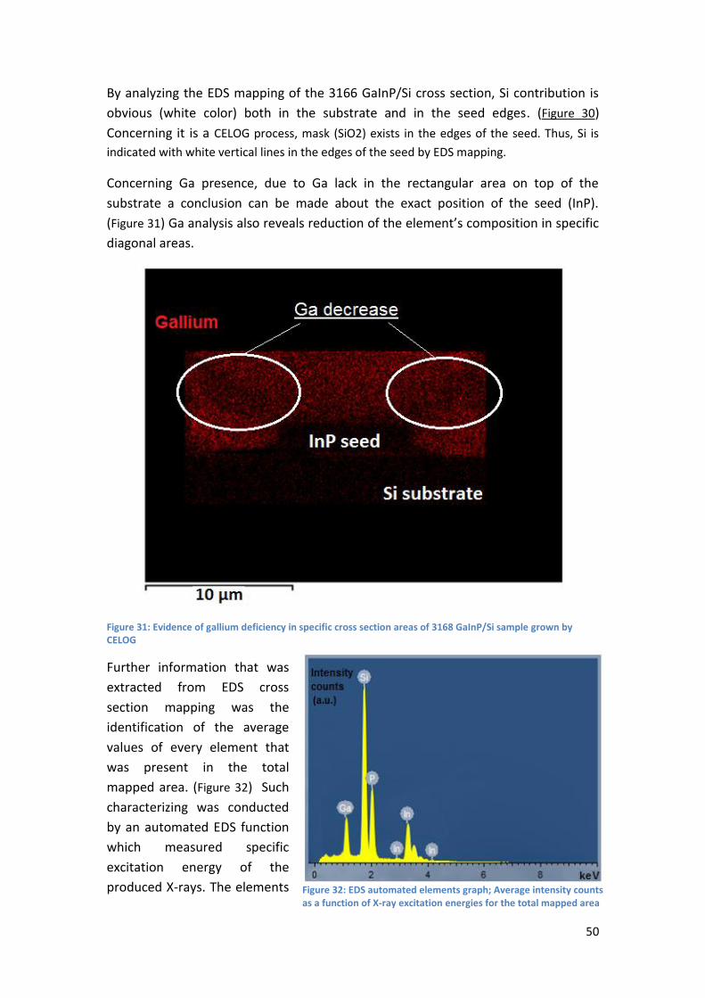
50
By analyzing the EDS mapping of the 3166 GaInP/Si cross section, Si contribution is
obvious (white color) both in the substrate and in the seed edges. (Figure 30)
Concerning it is a CELOG process, mask (SiO2) exists in the edges of the seed. Thus, Si is
indicated with white vertical lines in the edges of the seed by EDS mapping.
Concerning Ga presence, due to Ga lack in the rectangular area on top of the
substrate a conclusion can be made about the exact position of the seed (InP).
(Figure 31) Ga analysis also reveals reduction of the element’s composition in specific
diagonal areas.
Figure 31: Evidence of gallium deficiency in specific cross section areas of 3168 GaInP/Si sample grown by CELOG
Further information that was
extracted from EDS cross
section mapping was the
identification of the average
values of every element that
was present in the total
mapped area. (Figure 32) Such
characterizing was conducted
by an automated EDS function
which measured specific
excitation energy of the
produced X-rays. The elements Figure 32: EDS automated elements graph; Average intensity counts as a function of X-ray excitation energies for the total mapped area

51
for the 3166 and 3168 lll-V heterostructures (GaInP/Si) were confirmed. (Figure 32)
For every EDS characterization verification of the present elements was applied.
The area in the middle of the cross section covering the grown layer, the seed (InP)
and the substrate was examined for 3166 and 3168 samples. Regarding the 3166
heterostructure, linescanning length was set to 7 μm. By analyzing intensities
fluctuation through growth layers, from the grown GaInP layer area to the seed
(InP), Ga intensity (red line) dropped gradually between 1 and 2 μm as expected.
(Figure 33) When entering into the interface between InP (seed) and Si (red arrow),
Ga intensity exhibited a small peak as we have a thick GaAs buffer layer between Si
substrate and InP seed in order to minimize the lattice mismatch differences. Further
into the silicon substrate, both In and P intensities dropped and Si intensity
increased. We also observe certain amount of Si both in the InP seed layer and the
grown GaInP layer.
The same procedure was repeated in the laterally grown area close to the GaInP/Si
interface. (Figure 34) Both from the SEM image and from EDS linescanning, the
important observation of Si incorporation (red line) was also striking for the grown
layer. On the contrary, elements of the grown layer in the silicon substrate are found
to be insignificant.
Figure 33: SEM image and graph depicting linescanning intensity as a function of linescanning length (vertical yellow line - left image) in the middle area of the cross section covering both GaInP/seed (InP) interface and GaInP/Si interface of sample 3166 GaInP/Si grown by CELOG.
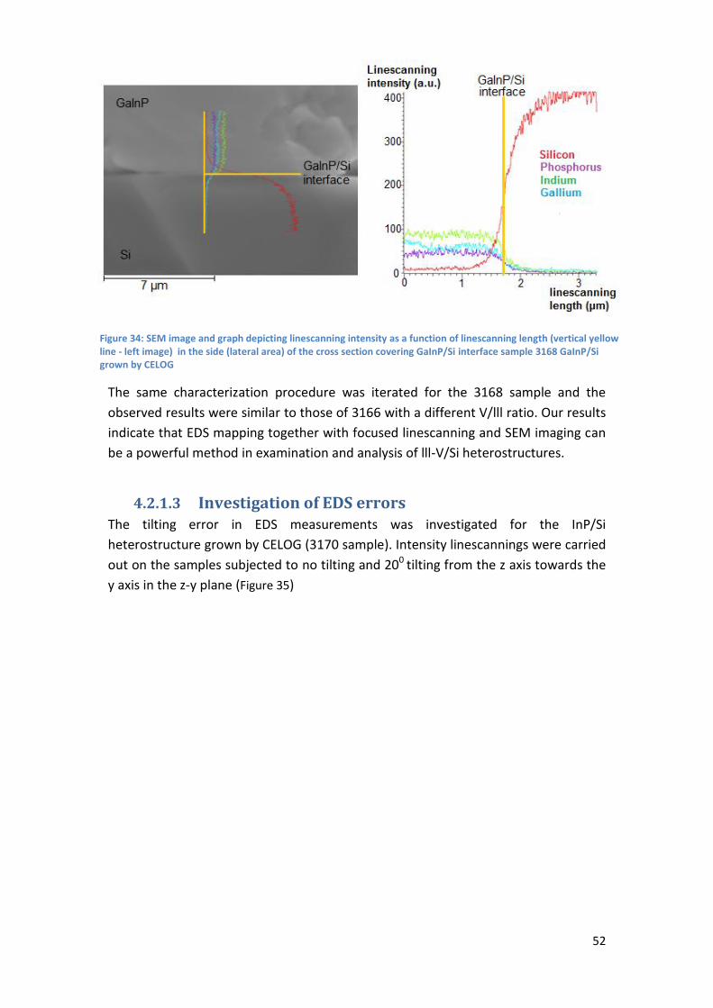
52
The same characterization procedure was iterated for the 3168 sample and the
observed results were similar to those of 3166 with a different V/lll ratio. Our results
indicate that EDS mapping together with focused linescanning and SEM imaging can
be a powerful method in examination and analysis of lll-V/Si heterostructures.
4.2.1.3 Investigation of EDS errors The tilting error in EDS measurements was investigated for the InP/Si
heterostructure grown by CELOG (3170 sample). Intensity linescannings were carried
out on the samples subjected to no tilting and 200 tilting from the z axis towards the
y axis in the z-y plane (Figure 35)
Figure 34: SEM image and graph depicting linescanning intensity as a function of linescanning length (vertical yellow line - left image) in the side (lateral area) of the cross section covering GaInP/Si interface sample 3168 GaInP/Si grown by CELOG

53
Figure 35: a) 3170 InP/Si heterostructure and linescanned area b) representation of tilting in z-y plane c) cross section SEM image and intensity linescanning before tilting and d) cross section SEM image and intensity linescanning after tilting
Linescanning lengths were identical and equal to 5 μm each. Acquisition time in both
linescannings was equal to 200 seconds (30 frames) Thus, intensity values as a
function of linescanning length were fully normalized. Intensity results between
tilted and non tilted sample were found identical for all the chemical elements. (Si,
In, P) Intensity values were the same in the grown InP, the substrate and the
interface area. Thus, tilting towards y axis does not have an influence on the
observed results at least within 200 rotation.

54
4.2.2 XRD Characterization
4.2.2.1 Rocking curve measurements
4.2.2.1.1 Introduction XRD characterization was carried out on the majority of the samples (GaInP/GaAs)
and (GaInP/Si) studied above. Its main focus was the investigation of the lattice
mismatch which can lead to the indication of the composition of the grown elements
(Ga and In) and thereby its bandgap via Vegard’s law. Powerful tool in this study is
the rocking curve analysis. Rocking curve is obtained by XRD and depicts the
intensity of the X-ray diffraction peaks as a function of the ω-2θ parameter. X-pert
epitaxy is the software used for XRD data processing.
4.2.2.1.2 Data analysis GaInP/GaAs analysis
XRD analysis was focused on the heterostructures of GaInP grown on GaAs. XRD
characterizations were carried out for various heterostructures (Table 3). We
exemplify the analysis by presenting the results obtained from the sample 3166
InGaP on GaAs 30d rot. heterostructure. Settings and optimizations of the
appropriate parameters for receiving the best diffraction outcome were conducted.
Such optimizations include the selection of the diffraction plane as well as phi (φ) psi
(ψ) optimizing and omega (ω) angle adjustments. For the 3166 InGaP on GaAs 30d
rot. sample, both 004 and 224 diffraction planes were measured. The substrate peak
as well as the peak for the grown layer (GaInP) were observed for both the planes.
(Figure 36, Figure 37) From the rocking curves, we observe that the crystalline quality
of the layer is not satisfying.
As it turns out, parameters like the Full Width at Half Maximum (FWHM) for the
grown layer was difficult to be calculated and could provide with misleading
information. Hence, more efforts were made to analyze the peak positions, to
correlate them with lattice mismatch, to derive material composition and bandgap.
Difficulties were faced in receiving diffraction peaks for (224) and (113) diffraction
planes of the heterostructure and hence XRD analysis was focused on the (004)
diffraction plane. Rocking curves characterizations for the 3168 series of GaInP/GaAs
heterostructure as well as for GaInP/Si were also obtained. The described
characterization procedure was employed for all the analyzed samples.
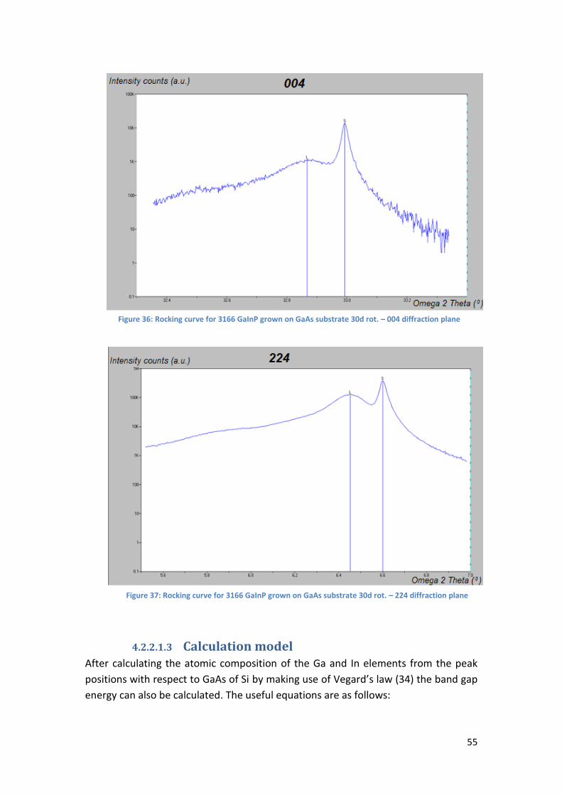
55
4.2.2.1.3 Calculation model After calculating the atomic composition of the Ga and In elements from the peak
positions with respect to GaAs of Si by making use of Vegard’s law (34) the band gap
energy can also be calculated. The useful equations are as follows:
Figure 36: Rocking curve for 3166 GaInP grown on GaAs substrate 30d rot. – 004 diffraction plane
Figure 37: Rocking curve for 3166 GaInP grown on GaAs substrate 30d rot. – 224 diffraction plane

56
𝑎𝐺𝑎𝐼𝑛𝑃 = 𝑥 ∗ 𝛼𝐺𝑎𝑃 + 1 − 𝑥 ∗ 𝛼𝐼𝑛𝑃
where α’s are the lattice constants of the binaries in the subscript aGaInP is the lattice
constant of the grown GaInP. aGaInP is derived from the peak position with respect to
that of the substrate whose lattice constant is known. This will yield x.
Knowing x and the Eg’s of the binaries, Eg,GaInP, the bandgap of the grown GaInP can
be calculated using the equation:
𝐸𝑔 ,𝐺𝑎𝐼𝑛𝑃 = 𝑥 ∗ 𝐸𝑔𝐺𝑎𝑃 + 1 − 𝑥 ∗ 𝐸𝑔 ,𝐼𝑛𝑃 − 𝑏 ∗ 𝑥 1 − 𝑥
where b is equal to the bowing parameter. (𝑏𝐺𝑎𝐼𝑛𝑃 = 0.65)
The specific value of the bowing parameter corresponds to the deviation from a
linear interpolation between the two binary alloys and is related to the valley of the
ternary’s bang gap. (35)
Thus the composition values, lattice constants and electron band gaps for the
characterized heterostructures are tabulated in. (Table 3: Islands’ widths for the three
dimensioned samples measured by SEM)
Even for the heterostructures GaInP/GaAs, the composition values for Ga and In are
far from the optimal values for lattice matched values (Ga51In49P). Composition
values with the highest proximity to lattice matched layers were found to be for
3166 GaInP/GaAs 30d rot. heterostructure with Ga and In values to be 48% and 52%
respectively.
Batch ref. num
Substrate material
Properties Deposited material
Dif. plane
V/III Ratio
Growth T (C)
In(%) Ga(%) Eg (eV)
α (Å)
3166 GaAs Planar GaInP 004 10 590 53.3 46.7 1.610 56.74
3166 GaAs 30d rot.
ELOG GaInP 004 10 590 52.5 47.6 1.617 56.70
3166 Si CELOG GaInP 004 10 590 57.8 42.2 1.572 56.92
3168 GaAs Planar GaInP 004 5.46 590 55.7 44.3 1.589 56.84
3168 GaAs 30d rot.
ELOG GaInP 004 5.46 590 54.7 45.3 1.598 56.80
3172 Si Planar - S dopped
GaInP 004 5.46 590 47.1 53.0 1.667 56.48
3221 GaAs Planar GaInP 004 5.46 610 44.0 56.0 1.697 56.35
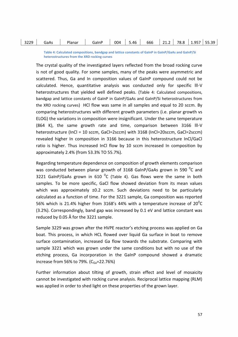
57
3229 GaAs Planar GaInP 004 5.46 666 21.2 78.8 1.957 55.39
The crystal quality of the investigated layers reflected from the broad rocking curve
is not of good quality. For some samples, many of the peaks were asymmetric and
scattered. Thus, Ga and In composition values of GaInP compound could not be
calculated. Hence, quantitative analysis was conducted only for specific lll-V
heterostructures that yielded well defined peaks. (Table 4: Calculated compositions,
bandgap and lattice constants of GaInP in GaInP/GaAs and GaInP/Si heterostructures from
the XRD rocking curves) HCl flow was same in all samples and equal to 20 sccm. By
comparing heterostructures with different growth parameters (i.e. planar growth vs
ELOG) the variations in composition were insignificant. Under the same temperature
(864 K), the same growth rate and time, comparison between 3166 lll-V
heterostructure (InCl = 10 sccm, GaCl=2sccm) with 3168 (InCl=20sccm, GaCl=2sccm)
revealed higher In composition in 3166 because in this heterostructure InCl/GaCl
ratio is higher. Thus increased InCl flow by 10 sccm increased In composition by
approximately 2.4% (from 53.3% TO 55.7%).
Regarding temperature dependence on composition of growth elements comparison
was conducted between planar growth of 3168 GaInP/GaAs grown in 590 0C and
3221 GaInP/GaAs grown in 610 0C (Table 4). Gas flows were the same in both
samples. To be more specific, GaCl flow showed deviation from its mean values
which was approximately ±0.2 sccm. Such deviations need to be particularly
calculated as a function of time. For the 3221 sample, Ga composition was reported
56% which is 21.4% higher from 3168’s 44% with a temperature increase of 200C
(3.2%). Correspondingly, band gap was increased by 0.1 eV and lattice constant was
reduced by 0.05 Å for the 3221 sample.
Sample 3229 was grown after the HVPE reactor’s etching process was applied on Ga
boat. This process, in which HCL flowed over liquid Ga surface in boat to remove
surface contamination, increased Ga flow towards the substrate. Comparing with
sample 3221 which was grown under the same conditions but with no use of the
etching process, Ga incorporation in the GaInP compound showed a dramatic
increase from 56% to 79%. (CGa=22.76%)
Further information about tilting of growth, strain effect and level of mosaicity
cannot be investigated with rocking curve analysis. Reciprocal lattice mapping (RLM)
was applied in order to shed light on these properties of the grown layer.
Table 4: Calculated compositions, bandgap and lattice constants of GaInP in GaInP/GaAs and GaInP/Si heterostructures from the XRD rocking curves

58
4.2.2.2 Reciprocal lattice mapping
Batch ref.
number
Substrate material
Properties Deposited material
Dif. plane
V/III Ratio
Growth T (C)
Ga flow
(sccm)
3221 GaAs 30d rot. ELOG
GaInP 4 5.46 611 2.0
3223 GaAs Planar GaInP 4 5.61 611 1.4
3225 GaAs Planar GaInP 4 5.56 611 1.6 Table 5: GaInP/GaAs heterostructures for which RLM method was applied
RLM method was applied for the new growths of 3221, 3223 and 3225 series of
GaInP compound on GaAs. (Table 5) Growth time in these samples was 10 minutes
and HCL flow 20 sccm. Analysis can provide information regarding growth tilting,
composition as well as the mosaic spread. (38) Optimizations in ω and ω2θ ranges as
well as adjustments of time-per-step parameter for improving the resolution were
applied. RLM was conducted in a 2-axes measurement process with intensity values
to be represented in a color scale in the z’ axis. Qualitative and semi-quantitative
analysis were applied and the chosen diffraction plane was (004).
Considering the planar
growth of 3123
GaInP/GaAs, PH3, InCl and
GaCl flow is 120, 20 and 1.6
sccm respectively (V/lll
ratio: 5.56). The scale was
chosen as logarithmic
similarly to the rocking
curves depiction. The QX
axis corresponds to
reciprocal space values of
the ω range whereas Qy
axis corresponds to the
ω2θ range. Substrate peak
(denoted with yellow-red
colors because of the high
intensity) is aligned with
the GaInP layer peak (blue
colors) along the Qy axis.
(Figure 38) The specific
spreading both in
horizontal and vertical axis Figure 38: RLM for planar 3123 GaInP/GaAs heterostructure – 004 plane (Table 5)

59
denotes the high thickness of the grown layer (approximately 12 μm). The growth is
graded with composition dissimilarities and not steady concentrations of the
elements along the growth. Thus composition of the GaInP compound can be
regarded as scaled and not uniform. Spreading in the QX axis was about 40-45 (X
100.000rtu) and in the Qy axis 120. High dislocation density, which contributes to a
decrease in crystal quality, and curvature of the examined surface (tilts) might also
be possible reasons for the present observation.
RLM was also conducted for the
planar growth of 3225
GaInP/GaAs. PH3, InCl and GaCl
flow is 120, 20 and 1.4 sccm
respectively. (V/lll ratio: 5.61).
Comparing with the previous
planar growth, Ga flow was
decreased in this sample from
1.6 to 1.4 sccm. A higher shifting
and spreading of about 100 (X
100.000 rtu) is observed along
the horizontal axis. (Figure 39)
Given the fact that apart from
GaCl flow the total growth
parameters are the same in
both heterostructures, peak
spreading can be correlated to
Ga decrease. Higher spreading
in the horizontal axis could
possibly denote mosaicity
increase, higher grading and
composition deterioration in the
growth. High thickness of the
grown layer is also attributed to the spreading observation. Dislocations and low
crystalline quality of the growth still exist.
RLM was also conducted for the 3221 GaInP/GaAs which was grown through circular
openings by ELOG process. PH3, InCl and GaCl flow is 120, 20 and 2 sccm respectively
(V/lll ratio: 5.46). (Figure 40) The difference between this observation and the
previous ones is that it is an ELOG process and GaCl flow is the highest of all and
equal to 2 sccm. As it consists an ELOG process, dislocation density in the lateral
growths should be significantly reduced. However, as it was indicated in the previous
samples, crystalline quality of the GaInP layer is worse that the GaAs substrate. The
Figure 39: RLM for planar 3125 GaInP/GaAs heterostructure – 004 plane, (Table 5)
60
mechanism of ELOG for GaInP growth is complicated and dislocations are hard to be
justified since lattice mismatch is high. Thus, more efforts are required to fully
understand the impact of ELOG on GaInP growth on GaAs substrate. The grown layer
spreading is similar to the first observation and proves the high thickness, the graded
composition and the low crystal quality of the grown layer (GaInP). No significant
correlation could be attributed to Ga increase or to the ELOG process. Considering
quantitative analysis and numerical results of how GaCl increase affects the
composition and the crystal structure further measurements and data processing are
necessary. Data normalizing and comparisons under the same data scales are also
important.
Figure 40: RLM for circular ELOG 3221 GaInP/GaAs heterostructure – 004 plane, (Table 5)
4.3 Investigation of Si incorporation
Si incorporation from Si substrate into the grown layer can be attributed to different
mechanisms. These can be solid state diffusion and gas phase transportation. For the
61
verification of the theoretical model, two samples were investigated. The 3166
GaInP/Si and 3170 InP/Si lll-V heterostructures which were both grown by CELOG
process. (Table 1)
Concerning the 3166 GaInP/Si sample, EDS intensity linescannings were conducted
both in the seed (InP)/Si interface and in the GaInP/Si interface in the lateral growth
region. In both areas linescanning length was equal to 3.6 μm with its middle point
to be set at the interface with an approximate error of (± 50 nm). The acquisition
time of the produced X-rays was set to 250 seconds for both measurements (40
frames). The obtained data were completely normalized and compared. The same
procedure was also followed for the 3170 lll-V heterostructure. (Table 1)
Si intensity demonstrated the same fluctuation in both examined interfaces.
Intensity slopes in both examined areas demonstrated the same inclination. The
penetration depth of Si in the seed (InP) layer was reported the same with Si
penetration in the laterally grown GaInP compound (Figure 41). Si intermixing due to
unintentional doping also consists a possible phenomenon that could take place in
both examined surfaces. Due to a large number of defects in the seed area (higher
dislocation density) it was expected that Si penetration through solid state diffusion
(via vacancies, interstitials, “pipe” diffusion via dislocations etc.) should be higher
than in the lateral growth area. In the lateral area because of the ELOG process,
density of defects and solid state diffusion should be minimized. In both interfaces Si
penetration was found the same, fact which minimizes the solid state diffusion
mechanism in the lateral growth area at 590 0C (864K). However, diffusion is feasible
in the lateral growth area in the case of high density of defects due to heavy lattice
mismatch Thus, with such a low crystal quality of the GaInP growth it is difficult to
have a solid conclusion about which of the two mechanisms is predominant for Si
contamination in the grown layer. More measurements on a high crystal quality
GaInP grown layer are recommended.
If it is not the diffusion mechanisms, Si penetration can be explained from the gas
phase transportation mechanism. During the first stages of growth formation, Si
reacts with HCl and forms several compounds known as chlorosilanes. Si can be
incorporated in the first layers of the grown compound. Such mechanism can take
place in both interfaces and depends on the temperature value as well as on the
area of the exposed source (material). (38) Due to the same growth temperature and
the uniform surface properties of Si substrate, the vapor phase incorporation
mechanism takes place in both regions and provokes the same Si incorporation.

62
The same result in Si autodoping for both interfaces can also be related to the EDS
analysis method due to the accuracy of X-rays detection. In high magnification (small
linescanned distance) because of the higher excitation volume of the generated X-
rays (pear effect), detection of Si coming from the substrate may give an output of Si
incorporation in the grown layer. As this error is common in every EDS
characterization it may contribute to the current observation. However, by EDS
analysis is difficult to distinguish whether the solid phase diffusion/gas phase
mechanism or the EDS error contributes to the detection of Si autodoping and to
what extent. Transmission electron microscopy (TEM) measurements, with much
thinner samples, are necessary to eliminate the X-rays excitation-volume drawback
or secondary ion mass spectroscopy (SIMS) should be conducted.
4.4 Investigation of Gallium deficiency in certain
crystallographic orientations Characterizations of the samples 3166 GaInP/Si and 3168 GaInP/Si grown by CELOG
process revealed certain deficiency in Ga composition in certain crystallographic
areas indicated by dark region in the EDS mapped regions. By conducting SEM
imaging in conjunction with EDS area mapping, such Ga decrease can be correlated
with specific crystallographic planes and plane boundaries of the GaInP growth
Figure 41: Comparison between Si incorporation in the seed/Si interface (a, b) with Si incorporation in the GaInP/Si interface (c, d)
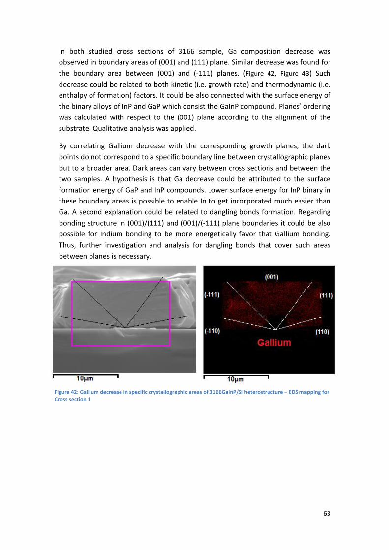
63
In both studied cross sections of 3166 sample, Ga composition decrease was
observed in boundary areas of (001) and (111) plane. Similar decrease was found for
the boundary area between (001) and (-111) planes. (Figure 42, Figure 43) Such
decrease could be related to both kinetic (i.e. growth rate) and thermodynamic (i.e.
enthalpy of formation) factors. It could be also connected with the surface energy of
the binary alloys of InP and GaP which consist the GaInP compound. Planes’ ordering
was calculated with respect to the (001) plane according to the alignment of the
substrate. Qualitative analysis was applied.
By correlating Gallium decrease with the corresponding growth planes, the dark
points do not correspond to a specific boundary line between crystallographic planes
but to a broader area. Dark areas can vary between cross sections and between the
two samples. A hypothesis is that Ga decrease could be attributed to the surface
formation energy of GaP and InP compounds. Lower surface energy for InP binary in
these boundary areas is possible to enable In to get incorporated much easier than
Ga. A second explanation could be related to dangling bonds formation. Regarding
bonding structure in (001)/(111) and (001)/(-111) plane boundaries it could be also
possible for Indium bonding to be more energetically favor that Gallium bonding.
Thus, further investigation and analysis for dangling bonds that cover such areas
between planes is necessary.
Figure 42: Gallium decrease in specific crystallographic areas of 3166GaInP/Si heterostructure – EDS mapping for Cross section 1
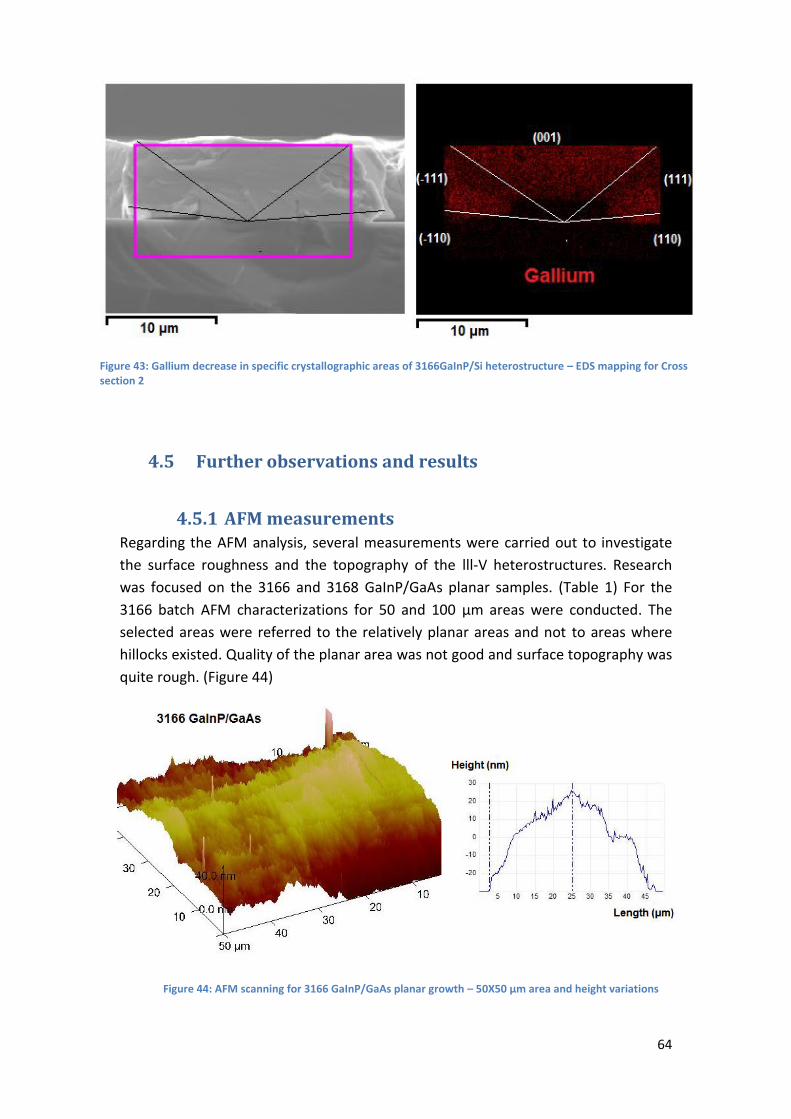
64
4.5 Further observations and results
4.5.1 AFM measurements Regarding the AFM analysis, several measurements were carried out to investigate
the surface roughness and the topography of the lll-V heterostructures. Research
was focused on the 3166 and 3168 GaInP/GaAs planar samples. (Table 1) For the
3166 batch AFM characterizations for 50 and 100 μm areas were conducted. The
selected areas were referred to the relatively planar areas and not to areas where
hillocks existed. Quality of the planar area was not good and surface topography was
quite rough. (Figure 44)
Figure 43: Gallium decrease in specific crystallographic areas of 3166GaInP/Si heterostructure – EDS mapping for Cross section 2
Figure 44: AFM scanning for 3166 GaInP/GaAs planar growth – 50X50 μm area and height variations

65
Considerable height variations in the range of 50 nm for 3166 and 60 nm for 3168
sample were reported (Figure 44, Figure 45). Mean values of surface roughness (Rq)
for the scanned areas were 63.8 nm and 56.7 nm for 3166 and 3168 samples
respectively. (Table 1) Further optimization in growth parameters (i.e. temperature,
gas flows, growth rate etc.) is necessary to improve the surface of the grown
compounds.
4.5.2 Photoluminescence measurements In addition to SEM/EDS and XRD characterizations, Photoluminescence analysis was
carried out to develop a standardized characterization way and to gain information
considering band gap and composition of the grown GaInP in the studied lll-V
heterostructures. PL analysis was done on the 3221, 3223 and 3225 samples (Table 5)
grown either by planar growth or by ELOG process. PL measurements were
conducted at room temperature. (300 K)
Slit images of the studied heterostructures were examined for spectroscopic analysis
and PL spectra were obtained. (Figure 46) Measurements were conducted in different
areas including the top view and the cross sections of the lll-V heterostructures.
Figure 46: Representation of indicative slit image and the corresponding PL spectrum
Figure 45: AFM scanning for 3168 GaInP/GaAs planar growth – 75X575 μm area and height variations
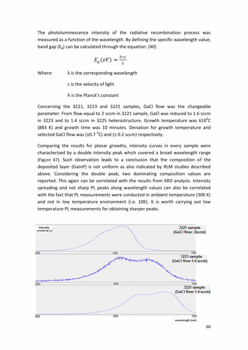
66
The photoluminescence intensity of the radiative recombination process was
measured as a function of the wavelength. By defining the specific wavelength value,
band gap (Eg) can be calculated through the equation: (40)
𝐸𝑔(𝑒𝑉) =ℎ∗𝑐
𝜆
Where: λ is the corresponding wavelength
c is the velocity of light
h is the Planck’s constant
Concerning the 3221, 3223 and 3225 samples, GaCl flow was the changeable
parameter. From flow equal to 2 sccm in 3221 sample, GaCl was reduced to 1.6 sccm
in 3223 and to 1.4 sccm in 3225 heterostructure. Growth temperature was 6100C
(883 K) and growth time was 10 minutes. Deviation for growth temperature and
selected GaCl flow was (±0.7 0C) and (± 0.2 sccm) respectively.
Comparing the results for planar growths, intensity curves in every sample were
characterized by a double intensity peak which covered a broad wavelength range
(Figure 47). Such observation leads to a conclusion that the composition of the
deposited layer (GaInP) is not uniform as also indicated by RLM studies described
above. Considering the double peak, two dominating composition values are
reported. This again can be correlated with the results from XRD analysis. Intensity
spreading and not sharp PL peaks along wavelength values can also be correlated
with the fact that PL measurements were conducted in ambient temperature (300 K)
and not in low temperature environment (i.e. 10K). It is worth carrying out low
temperature PL measurements for obtaining sharper peaks.
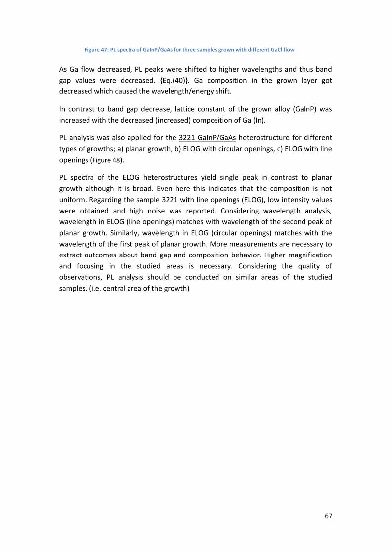
67
As Ga flow decreased, PL peaks were shifted to higher wavelengths and thus band
gap values were decreased. {Eq.(40)}. Ga composition in the grown layer got
decreased which caused the wavelength/energy shift.
In contrast to band gap decrease, lattice constant of the grown alloy (GaInP) was
increased with the decreased (increased) composition of Ga (In).
PL analysis was also applied for the 3221 GaInP/GaAs heterostructure for different
types of growths; a) planar growth, b) ELOG with circular openings, c) ELOG with line
openings (Figure 48).
PL spectra of the ELOG heterostructures yield single peak in contrast to planar
growth although it is broad. Even here this indicates that the composition is not
uniform. Regarding the sample 3221 with line openings (ELOG), low intensity values
were obtained and high noise was reported. Considering wavelength analysis,
wavelength in ELOG (line openings) matches with wavelength of the second peak of
planar growth. Similarly, wavelength in ELOG (circular openings) matches with the
wavelength of the first peak of planar growth. More measurements are necessary to
extract outcomes about band gap and composition behavior. Higher magnification
and focusing in the studied areas is necessary. Considering the quality of
observations, PL analysis should be conducted on similar areas of the studied
samples. (i.e. central area of the growth)
Figure 47: PL spectra of GaInP/GaAs for three samples grown with different GaCl flow
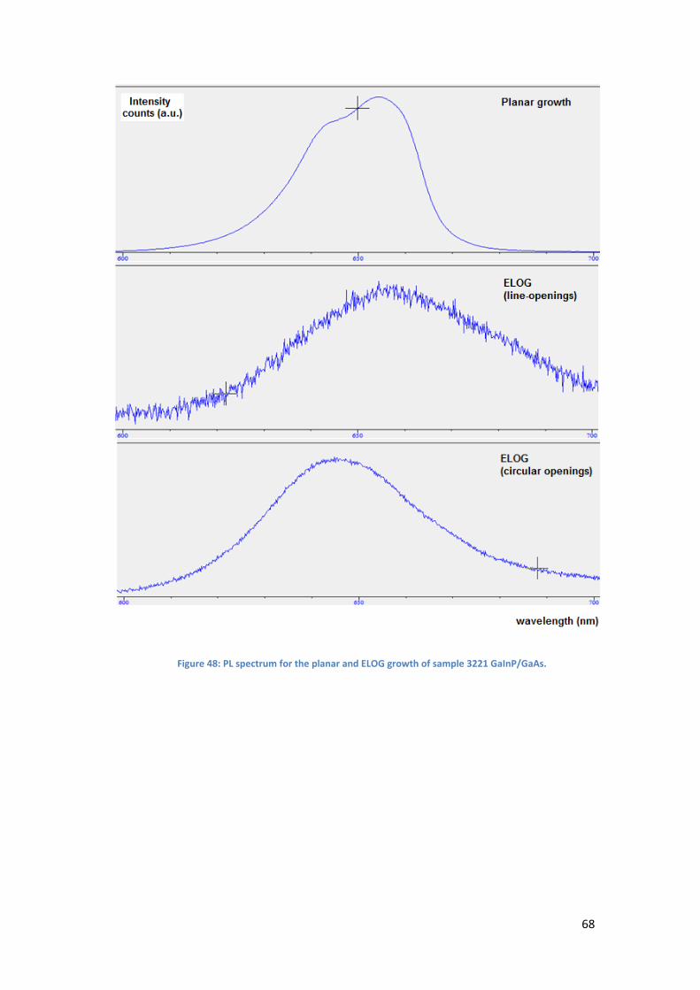
68
Figure 48: PL spectrum for the planar and ELOG growth of sample 3221 GaInP/GaAs.

69
5. Conclusions and future work With the applied characterization techniques in different lll-V heterostructures and
after the analysis of their properties with respect to growth parameters, several
conclusions can be extracted.
Measurements and cross sectional studies of the lll-V heterostructure of ELOG GaInP
on GaAs substrate revealed the dependence of aspect ratio on the rotation angle of
line-openings off [110] direction. ELOG GaInP in openings rotated 60 degrees off
[110] demonstrated higher aspect ratio values than growths in openings rotated 30
degrees off [110]. Furthermore, growth in openings rotated 60 degrees off [110]
yielded higher opening widths which may be also related to higher aspect ratio
indications. Reduced deviation in aspect ratio was observed because of lower
deviation in the opening widths. No relation was observed between aspect ratio
fluctuation and the change in V/lll ratio parameter.
EDS selected area mapping revealed the distribution of silicon, gallium, indium and
phosphorus in substrates and grown layers in the studied lll-V heterostructures.
Decrease of gallium (increase of Indium) composition was observed in the CELOG
GaInP grown on Si substrate in the areas bounded by specific crystallographic planes
of the GaInP growth. A hypothesis is that the surface formation energy of the two
constituent binary alloys (InP and GaP) as well as the dangling bonds configuration in
these boundary areas might cause that phenomenon. Further analysis about the
surface formation energy and the dangling bonds that are formed in the specific
crystallographic areas is recommended.
EDS intensity linescanning was applied on the cross sections of various lll-V
heterostructures. Intensity linescanning provided useful information regarding
elements distribution in the central and side areas of the cross section. Systematic
examinations were conducted close to the interfaces. In the analysis of GaInP/Si and
InP/Si heterostructures, silicon incorporation was observed in the grown III-V
semiconductor layers. These observations are attributed to Si diffusion and to the
gas phase transportation mechanism. Thus, with low crystalline quality of the grown
layer it is difficult to say whether gas phase transportation mechanism is
predominant or not in the lateral growth area of GaInP. In gas phase transportation
mechanism, Si can react with HCl gas to form chlorosilanes (SiCl) and incorporates in
the grown layer, during the early stage of the deposition process. Such chemical
reactions take place above 300 0C (573 K). Another explanation for the observed Si in
III-V semiconductor growths can be related to the EDS drawback because of the
higher excitation volume of the generated X-rays (pear shape) in comparison to the
linescanned length. Thus, characterization of much thinner samples by Transmission
Electron Microscopy is necessary in order to exclude this EDS error.
70
Composition of gallium and indium elements in GaInP growth was investigated both
qualitatively and quantitatively by XRD characterization. Analysis was applied on
(004) diffraction plane. Lattice constant and band gap were calculated by Vegard’s
Law. Composition of GaInP growth showed high deviation from the GaAs lattice
matched value. Crystal quality of the grown layers was found to be low.
Regarding composition analysis for GaInP on GaAs, with increasing of InCl flow from
10 sccm to 20 sccm (while maintaining all the other growth parameters same),
indium composition was increased by approximately 2.4% from 53% to 56%.
Moreover, with the growth temperature increase of 20 C (from 590 0C to 610 0C)
composition of Ga increased by 21.4% from 44% to 56%. The corresponding change
in band gap was from 1.59 eV to 1.70 eV and of the lattice constant was from 56.84
Å to 56.35 Å. The etching process of Ga boat lead to an increase of Ga composition
due to the increase of GaCl flow towards the substrate. Ga incorporation appeared
to be low in the beginning of the deposition and increased after the initial stages of
the epitaxial process. The broad peaks of grown layers (obtained from the rocking
curve) reduced the accuracy of composition calculations. Moreover, variations in the
gas flows and temperature during the epitaxy deteriorated the quality of the
produced layers. Fluctuations in growth parameters have to be monitored so as to
proceed to more accurate comparisons.
Qualitative analysis through Reciprocal Lattice Mapping was also applied for the lll-V
heterostructures of GaInP on GaAs. Planar samples and ELOG samples were
characterized. The results revealed the high thickness of the grown layer, graded
composition and a low quality of the crystal structure in the grown layer.
Quantitative analysis in more of heterostructures and systematic investigations with
respect to different gas flows has to be applied.
PL characterizations were conducted on lll-V heterostructures in order to verify the
composition analysis obtained by XRD. For the same samples, PL also revealed a non
uniform composition. PL peaks were quite broad in different areas of the studied
samples (top view, cross section). In addition, double intensity peaks were measured
in GaInP/GaAs planar growths. Further comparison with XRD analysis is also
recommended for the verification of composition results.
Last but not least, AFM characterizations should be continued and applied in more
lll-V heterostructures in order to investigate surface roughness as function of the
growth parameters.
71
References
1. Martin A. Green, Keith Emery, Yoshihiro Hishikawa, Wilhelm Warta and Ewan D. Dunlop,
“Solar cell efficiency tables (Version 45)”, Prog. Photovolt: Res. Appl. 2015; 231:–9
2. Laser Diodes, http://hyperphysics.phy-astr.gsu.edu/hbase/electronic/lasdio.html
3. Light Detectors, http://hyperphysics.phy-astr.gsu.edu/hbase/electronic/ligdet.html
4. Geoffrey S. Kinsey, Peter Hebert, Kent E. Barbour, Dmitri D. Krut, Hector L. Cotal and
Raed A. Sherif , “Concentrator multijunction solar cell characteristics under variable
intensity and temperature”, Prog. Photovolt: Res. Appl. (2008) 16, 503–508
5. Yan-Ting Sun, Sebastian Lourdudoss “Effect of growth conditions on ELOG of InP on
InP/Si (001) substrate by HVPE”, The International Society for Optical Engineering,
·(2003) 4997,221-231
6. “Semiconductor” http://encyclopedia2.thefreedictionary.com/Semiconductor
7. " Formation of PN junction”, http://www.pveducation.org/pvcdrom/pn-
junction/formation-pn-junction
8. “The Photovoltaic Effect”, http://www.pveducation.org/pvcdrom/solar-cell-
operation/photovoltaic-effect
9. “III-V compound semiconductor material systems”, http://gorgia.no-
ip.com/phd/html/thesis/phd_html/node4.html
10. “InP-Indium Phosphide”, http://www.ioffe.ru/SVA/NSM/Semicond/InP/
11. S. M. Sze, Ming-Kwei Lee “Semiconductor devices – physics and technology, 2nd edition”,
(2002), pp.
12. “ GaAs-Gallium Arsenide”, http://www.ioffe.ru/SVA/NSM/Semicond/GaAs/
13. “GaInP-Gallium Indium Phosphide”, http://www.ioffe.ru/SVA/NSM/Semicond/GaInP/
14. C. Junesand, M-H. Gau, Y.T. Sun, S. Lourdudoss, I. Lo, J. Jimenez, P. A. Postigo, F. M.
Morales, J. Hernandez, S. Molina, A. Abdessamad, G. Pozina, L. Hultman, P. Pirouz,
“Defect reduction in heteroepitaxial InP on Si by epitaxial lateral overgrowth”, Materials
Express, 4, 41 (2014)
15. R. H. Williams, Modern GaAs Processing Techniques (Artech House, Norwood,
Massachusetts, 1990)
16. C. Friger, R. Gleichmann, C. Pelosi and G. Attolini, “Relationship between dislocation
generation, vapour phase supersaturation and growth rate in InP layers obtained by
vapour phase epitaxy”, Mate. Sci. and Eng., (1991), B10, 197-207
17. F. C. Frank and J. H. van der Merwe, “One‐Dimensional Dislocations. II. Misfitting
Monolayers and Oriented Overgrowth”, Proceedings of the Royal Society
A:Mathematical, Physical and Engineering Sciences, (1949), 198, no. 1053, 216–225
18. M. Volmer and A. Weber, “Keimbildung in Übersattigten Gebilden”, Zeitschrift für
Physikalische Chemie, (1926), 119, 277–301
19. I. N. Stranski and L. Krastanow, “Zur Theorie der orientierten Ausscheidung von
Ionenkristailen aufeinander”, Monatshefte für Chemie und verwandte Teile anderer
Wissenschaften, (1937), 71, no. 1, 351–364
20. Klaus Ploog, “Molecular Bean Epitaxy”, 27th International conference of the Physics of
Semiconductors, (2004), 2-14
72
21. M. Snure, J. Jimenez, V. Hortelano, S. Swider, M. Mann, V. Tassev, C. Lynch, D. Bliss,
“Impurity incorporation in orientation patterned GaAs grown by low pressure HVPE”,
(2012) 352, 258–261
22. Kevin L. Schulte, William L Rance, Robert C Reedy, Aaron J Ptak, David, L Young, Thomas
Kuech, “Controlled formation of GaAs pn junctions during HVPE of GaAs”, (2011), 352,
253-257
23. O. Parillaud, N. Piffault, E. Gil-Lafon, R. Cadoret, “Defect free InP films no Si substrates
obtained by hydride vapor phase (conformal growth)”, (1994), 547 – 550
24. Pe`r Kofstad, Truls Norby, “Defects and transport in crystalline solids, Chapter 5”, (2007)
25. “The Physics of Diffusion”, http://www.iue.tuwien.ac.at/phd/ceric/node22.html
26. B.L. Sharma, “Diffusion in lll-V semiconductors and their alloys”, (1989), 64/65, 1-76
27. A.Bartels, E. Peiner, R. Klockenbrink, A. Schlachetzki, “The distribution of charge
concentration in InP/Si”,(1995), J. Appl. Phys. 78, 224
28. S. Nozaki, A.T. Wu. J. J. Murray, T. George, T. Egawa, M. Umeno “MOCVD growth of
undoped GaAs with a low electron concentration on a Si substrate”, (1990), Appl. Phys.
57, 2669
29. E Richter, Ch. Hennig, U. Zeimer, L. Wang, M. Weyers, G. Tränkle, “N-type doping of
HVPE-grown GaN using dischlorosilane”, plysuca status solidia, (2006), 203, 1658-1662
30. Yang Leng, “Materials characterization – Introduction to microscopic and spectroscopic
methods, second edition”, (2013)
31. E.R. Messmer, T. Lindström, S. Lourdudoss, “In situ mesa etching and immediate
regrowth in a HVPE reactor for buried heterostructure device fabrication”, J. Cryst.
Growth. 210 (2000), 600–612
32. Himanshu Kataria, “High quality lll-V semiconductors/Si heterostructures for photonic
integration and photonic applications”, KTH Royal Institute of Technology, (2014), 41-42
33. K.L. Williams, “Electron probe microanalysis of sphalerite”, (1967), 9-11
34. K. T. Jacob, Shubhra Raj, L. Rannesh, “Vegard's law: a fundamental relation or an
approximation?”, International Journal of Materials Research (formerly Zeitschrift fuer
Metallkunde) , (2007), 9, 1-12
35. I. Vurgaftmana, J. R. Meyer, L. R. Ram-Mohan, “Band parameters for III–V compound
semiconductors and their alloys”, J. Appl. Phys, (2000), 89, 5815
36. “Mosaicity of a macromolecular crystal”,
http://www.structbio.vanderbilt.edu/xray/tutorials/flash/mosaic.php
37. Gunther Bauer, Wolfgang Richter, ”Optical characterization of epitaxial semiconductor
layers”, (1995)
38. Michael Edward Groenert, “Monolithic heteroepitaxial intergration of lll-V
semiconductor lasers on Si substrates”, Massachusetts Institute of Technology, (1996)
39. Yan-Ting Sun, Himanshu Kataria, Wondwosen Metaferia, Sebastian Lourdudoss,
”Realization of an atomically abrupt InP/Si heterojunction via corrugated epitaxial lateral
overgrowth”, CrystEngComm , (2014), 16, 7889-7893
40. Kartik N. Shinde, S. J. Dhoble, H. C. Swart, “Kyeongsoon Park, Phosphate phosphors for
solid-state lighting”, (2012),174
41. John E. Ayers, “Heteroepitaxy of Semiconductors: Theory, Growth, and Characterization”,
CRC Press (2007)
73
42. R.C. Sangster, “Model studies of crystal growth phenomena in the III-V semiconducting
compounds”, in R.K. Willardson, H.L. Goering(Eds.), compound Semiconductors, Volume
1, Chapter 28, Reinhold Publishing Corporation, (1962),241-253
43. I.S. A. Ersen, “Direct bonding of GaAs films on silicon circuits by epitaxial liftoff,
Solid‐State Electron”, 36 (1993) 1731–1739.
44. Naritsuka, T. Nishinaga, M. Tachikawa, H. Mori, “InP Layer Grown on (001) Silicon
Substrate by Epitaxial Lateral Overgrowth”, Jpn. J. Appl. Phys. (1995), 34, 1432–1435.
45. Yan-Ting Sun, Himanshu Kataria, Wondwosen Metaferia and Sebastian Lourdudoss,
“Realization of an atomically abrupt InP/Si heterojunction via corrugated epitaxial lateral
overgrowth”, The Royal Society of Chemistry, (2014), 16, 7889-7893
46. Compound Semiconductors and Crystal Growth Techniques, Springer US, (2006)