Using coordination chemistry to develop new routes to semiconductor and other materials
11
Coordination Chemistry Reviews 251 (2007) 1878–1888 Review Using coordination chemistry to develop new routes to semiconductor and other materials Dongbo Fan, Mohammad Afzaal, M. Azad Mallik, Chinh Q. Nguyen, Paul O’Brien ∗ , P. John Thomas School of Chemistry, The University of Manchester, Oxford Road, Manchester M139PL, UK Received 11 January 2007; accepted 30 March 2007 Available online 5 April 2007 Contents 1. Introduction ........................................................................................................... 1878 2. Some single-molecular systems for semiconductor deposition .............................................................. 1879 2.1. Dichalcogenoimidophosphinate ([N(PR 2 E) 2 M]) .................................................................... 1879 2.2. Dialkylchalcogenophosphates ..................................................................................... 1879 2.3. Ionic dialkyldiselenophosphinate salts ............................................................................. 1880 2.4. Dithiocarbamates ................................................................................................ 1881 3. Routes from molecules to materials ...................................................................................... 1881 3.1. Solution phase thermal decomposition ............................................................................. 1881 3.2. Synthesis of thin films at the water–toluene interface ................................................................ 1884 3.3. Chemical vapour deposition ....................................................................................... 1885 4. Conclusions ........................................................................................................... 1887 Acknowledgements .................................................................................................... 1887 References ............................................................................................................ 1887 Abstract Recent results from our laboratory on the synthesis of single-source precursor (SSP) molecules and their use for the making nanomaterials by different techniques are presented. The precursors include dichalcogenoimidophosphinate, dialkylchalcogenophosphates, ionic dialkyldise- lenophosphinate salts and dithiocarbamates. Solution phase thermal decomposition, chemical vapour deposition (CVD) and interfacial deposition techniques have been used to obtain nanocrystals and thin films of semiconducting material. © 2007 Elsevier B.V. All rights reserved. Keywords: Single-source precursors (SSP); Nanomaterials; Semiconductors 1. Introduction The search for new routes to semiconducting material contin- ues to attract considerable attention, despite the many advances that have resulted in the semiconductor-based revolution in elec- tronic devices. The key reason for the sustained interest is that semiconductors as a class of materials remain to some extent Based on a keynote lecture presented at the 37th International Conference on Coordination Chemistry, 13–18 August 2006, Cape Town, South Africa. ∗ Corresponding author. E-mail address: [email protected] (P. O’Brien). poorly understood and significant synthetic challenges posed by the reactive nature of the semiconductors remain to be overcome. Among the class of semiconducting material, nanocrystalline semiconductors: crystallites with at least one of their dimen- sion in nanometric domain are possibly most researched class of present-day materials. Nanomaterials promise to unravel the secrets behind fundamental phenomena at the forefront of chem- istry and physics. Further, numerous applications have been envisaged for nanomaterials in physical, chemical and biologi- cal sciences. It is no surprise therefore that nanoscience, attracts practitioners from different disciplines. In this context, synthesis route to semiconducting material in general and nanocrystals in 0010-8545/$ – see front matter © 2007 Elsevier B.V. All rights reserved. doi:10.1016/j.ccr.2007.03.021
-
Upload
independent -
Category
Documents
-
view
1 -
download
0
Transcript of Using coordination chemistry to develop new routes to semiconductor and other materials

C
A
blt©
K
1
utts
o
0d
Coordination Chemistry Reviews 251 (2007) 1878–1888
Review
Using coordination chemistry to develop new routesto semiconductor and other materials�
Dongbo Fan, Mohammad Afzaal, M. Azad Mallik, Chinh Q. Nguyen,Paul O’Brien ∗, P. John Thomas
School of Chemistry, The University of Manchester, Oxford Road, Manchester M139PL, UK
Received 11 January 2007; accepted 30 March 2007Available online 5 April 2007
ontents
1. Introduction . . . . . . . . . . . . . . . . . . . . . . . . . . . . . . . . . . . . . . . . . . . . . . . . . . . . . . . . . . . . . . . . . . . . . . . . . . . . . . . . . . . . . . . . . . . . . . . . . . . . . . . . . . . 18782. Some single-molecular systems for semiconductor deposition . . . . . . . . . . . . . . . . . . . . . . . . . . . . . . . . . . . . . . . . . . . . . . . . . . . . . . . . . . . . . . 1879
2.1. Dichalcogenoimidophosphinate ([N(PR2E)2M]) . . . . . . . . . . . . . . . . . . . . . . . . . . . . . . . . . . . . . . . . . . . . . . . . . . . . . . . . . . . . . . . . . . . . 18792.2. Dialkylchalcogenophosphates . . . . . . . . . . . . . . . . . . . . . . . . . . . . . . . . . . . . . . . . . . . . . . . . . . . . . . . . . . . . . . . . . . . . . . . . . . . . . . . . . . . . . 18792.3. Ionic dialkyldiselenophosphinate salts . . . . . . . . . . . . . . . . . . . . . . . . . . . . . . . . . . . . . . . . . . . . . . . . . . . . . . . . . . . . . . . . . . . . . . . . . . . . . 18802.4. Dithiocarbamates . . . . . . . . . . . . . . . . . . . . . . . . . . . . . . . . . . . . . . . . . . . . . . . . . . . . . . . . . . . . . . . . . . . . . . . . . . . . . . . . . . . . . . . . . . . . . . . . 1881
3. Routes from molecules to materials . . . . . . . . . . . . . . . . . . . . . . . . . . . . . . . . . . . . . . . . . . . . . . . . . . . . . . . . . . . . . . . . . . . . . . . . . . . . . . . . . . . . . . 18813.1. Solution phase thermal decomposition . . . . . . . . . . . . . . . . . . . . . . . . . . . . . . . . . . . . . . . . . . . . . . . . . . . . . . . . . . . . . . . . . . . . . . . . . . . . . 18813.2. Synthesis of thin films at the water–toluene interface . . . . . . . . . . . . . . . . . . . . . . . . . . . . . . . . . . . . . . . . . . . . . . . . . . . . . . . . . . . . . . . . 18843.3. Chemical vapour deposition. . . . . . . . . . . . . . . . . . . . . . . . . . . . . . . . . . . . . . . . . . . . . . . . . . . . . . . . . . . . . . . . . . . . . . . . . . . . . . . . . . . . . . . 1885
4. Conclusions . . . . . . . . . . . . . . . . . . . . . . . . . . . . . . . . . . . . . . . . . . . . . . . . . . . . . . . . . . . . . . . . . . . . . . . . . . . . . . . . . . . . . . . . . . . . . . . . . . . . . . . . . . . 1887Acknowledgements . . . . . . . . . . . . . . . . . . . . . . . . . . . . . . . . . . . . . . . . . . . . . . . . . . . . . . . . . . . . . . . . . . . . . . . . . . . . . . . . . . . . . . . . . . . . . . . . . . . . 1887References . . . . . . . . . . . . . . . . . . . . . . . . . . . . . . . . . . . . . . . . . . . . . . . . . . . . . . . . . . . . . . . . . . . . . . . . . . . . . . . . . . . . . . . . . . . . . . . . . . . . . . . . . . . . 1887
bstract
Recent results from our laboratory on the synthesis of single-source precursor (SSP) molecules and their use for the making nanomaterialsy different techniques are presented. The precursors include dichalcogenoimidophosphinate, dialkylchalcogenophosphates, ionic dialkyldise-enophosphinate salts and dithiocarbamates. Solution phase thermal decomposition, chemical vapour deposition (CVD) and interfacial depositionechniques have been used to obtain nanocrystals and thin films of semiconducting material.
2007 Elsevier B.V. All rights reserved.
ptAs
eywords: Single-source precursors (SSP); Nanomaterials; Semiconductors
. Introduction
The search for new routes to semiconducting material contin-es to attract considerable attention, despite the many advances
hat have resulted in the semiconductor-based revolution in elec-ronic devices. The key reason for the sustained interest is thatemiconductors as a class of materials remain to some extent� Based on a keynote lecture presented at the 37th International Conferencen Coordination Chemistry, 13–18 August 2006, Cape Town, South Africa.∗ Corresponding author.
E-mail address: [email protected] (P. O’Brien).
sosiecpr
010-8545/$ – see front matter © 2007 Elsevier B.V. All rights reserved.oi:10.1016/j.ccr.2007.03.021
oorly understood and significant synthetic challenges posed byhe reactive nature of the semiconductors remain to be overcome.mong the class of semiconducting material, nanocrystalline
emiconductors: crystallites with at least one of their dimen-ion in nanometric domain are possibly most researched classf present-day materials. Nanomaterials promise to unravel theecrets behind fundamental phenomena at the forefront of chem-stry and physics. Further, numerous applications have been
nvisaged for nanomaterials in physical, chemical and biologi-al sciences. It is no surprise therefore that nanoscience, attractsractitioners from different disciplines. In this context, synthesisoute to semiconducting material in general and nanocrystals in
istry
pl
actsocdipttilafnowysrtafpta“
snolsaoteuriIhufit
2d
2
R
piRcopp
2
R
Bdct
RfTaNttNpi
2
Kap[carw
dsopaobrcable to synthesis and study vibration spectroscopic properties ofdiphenyldiselenophosphinato complexes of Ni, Co, Cd, Zn, Hg,and Bi [37,38]. However, this synthesis method has the draw-back of using highly toxic H2Se gas in the process of making
D. Fan et al. / Coordination Chem
articular assume significance. This paper is based on a keynoteecture delivered at the 37th ICCC conference in South Africa.
The unique properties of semiconductor nanocrystals areresult of two key effects. The first being quantum
onfinement—the changes in the electronic structure caused byhe confinement of the electronic wavefunction to the dimen-ions of the particle, which is less than the mean free pathf electrons. Quantum confinement, in the case of most semi-onductor particles, increases the band gap [1]. The inherentependence of the degree of quantum confinement on sizemplies that the electronic properties and thereby other materialroperties now become a function of the size of a nanopar-icle. Remarkably, it leads us to the possibility of being ableo engineer band gaps and tailor material properties by simplyncreasing or decreasing the size of nanoparticles of a particu-ar element or compound. Nanoparticles by virtue of their sizelso possess a high fraction of surface atoms with the surfaceraction falling gradually with increase in size. For example, aanocrystals with a diameter of 1 nm typically has over 75%f its atoms on its surface [2]. This fraction falls to about 30%hen the size is increased to 6 nm and to 15% for 10 nm. Catal-sis is a pertinent application that benefits from the increasedurface area. The incomplete coordination of the surface atomsesults in unsatisfied valences and dangling bonds, which ensurehat the surface layer of atoms are highly reactive. The atomst the surface tend to cause the nanocrystals to fuse together toorm larger crystallites. In order to avoid such coalescence andrecipitation, the surface atoms are rendered passive by bindinghem to a capping agent. The capping agents form a ligand shellround a nanocrystal and play the key role of determining thesolubility” of a nanocrystal in a solvent.
We have, for several years, been advocating the use of single-ource precursors (SSPs) for the synthesis of thin films andanocrystals. The use of SSPs provides several key advantagesver other routes. For example, the existence of preformed bondseads to material with lower defects. In the case of thin film depo-ition by chemical vapour deposition (CVD), conditions of flownd temperature become simpler. It is also possible to carryut deposition with relatively simple installations. Several ofhe single-source precursors are also air-stable and are thereforeasier to handle and characterize. Spurred by the success of these of SSPs and motivated by their potential to reduce the envi-onmental impact of material processing, we have been keenlynterested in investigation new routes to difficult to prepare SSPs.n this article, we shall briefly review the recent advances weave made in the easy synthesis of a family of SSPs and theirse for synthesis of semiconducting material in the form of thinlms and semiconductors by conventional and novel deposition
echniques.
. Some single-molecular systems for semiconductoreposition
.1. Dichalcogenoimidophosphinate ([N(PR2E)2M])
Imidodiphosphinic acid derivatives R2P(E)NH(E)PR′2 (R,
′ = CH3, C6H5; E = O, S, NH) were first prepared by Schmid-
Reviews 251 (2007) 1878–1888 1879
eter et al. [3]. The synthetic process has seen been adapted andmproved by others to make a wide range of derivatives with, R′ = iPr, tBu, Et, OEt, OPh and E = S, Se [4–11]. A typi-al synthesis involves two steps: a simple condensation reactionf R2PCl with NH(SiMe3)2 to give the phosphorous(III) com-ound, followed by oxidation with O, S or Se to give the desiredroduct (see Eqs. (2.1) and (2.2)).
R2PCl + NH(SiMe3)2 → R2PNHPR2 (2.1)
2PNHPR2E=O,S,Se−→ R2P(E)NHP(E)R2 (2.2)
y deprotonation of the amine H–N bond, the R2P(E)NH(E)PR2erivative can be transformed to a bidentate chelating ligand thatan form neutral complexes of the type M[N(R2PE)2]n withransition as well as main group metals.
It was not possible to prepare the tellurium analogue of2P(E)NH(E)PR2 by oxidizing R2PNHPR2 with tellurium,
ollowing the scheme outlined in Eqs. (2.1) and (2.2) [12].herefore, Chivers and co-workers have recently developednew scheme, in which R2PNHPR2 is first metalated by
aH to form Na[R2PNPR2] followed by a reaction withellurium powder in hot toluene in the presence of N,N,N′,N′-etramethylethylenediamine [13–15]. The as-produced ligand,a[N(TePPri2)2], when reacting with appropriate metal halideroduce complexes M[N(TePiPr2)]n with a range of metalsncluding Zn, Cd, Hg, Sb, Bi [16].
.2. Dialkylchalcogenophosphates
Dialkyldiselenophosphates ligands were first developed byudchadker et al. [17]. The coordination chemistry of the lig-
nds was investigated with the synthesis and study of spectralroperties of several (O,O′-diethyldiselenophosphato) metals18–20]. Recently, Liu and co-workers have reported a range ofluster compounds incorporating dialkyldiselenophosphate lig-nds [21–26]. Diselenophosphonate ligands were prepared byeaction of “woollins reagent” (PhPSe2)2 with RONa in ROH,hich involve cleavage of the four membered ring P2Se2 [9].In the case of dichalcogenophosphinate complexes, sulfur
erivatives have been investigated extensively [27–33] whiletudies on the seleno analogue are limited due to the difficultyf the synthesis process. The first synthesis of diselenonophos-hinate ligand and complexes were reported by Kuchen etl. [34–36]. The synthesis process started with the reactionf R2PCl with Se powder to initially form R2P(Se)Cl followy treatment with NaSeH to yield [R2PSe2]Na ligand, whicheacted further with metal salts to form diselenophosphinateomplexes (Scheme 2.1). Following same method, Mueller was
Scheme 2.1.

1880 D. Fan et al. / Coordination Chemistry Reviews 251 (2007) 1878–1888
Scheme 2.2.
NfNpaenpc[
bmwtsetamcHi
fii
ftfdii(
boc
Scheme 2.6.
Fig. 1. Structure of (R2PSe)2Se and (R2PSe)2Se2; (R = iPr, Ph).
fRtBe(
R
Bf(Rabr(c
2
lap
Scheme 2.3.
aSeH. Using a slightly different route, Pilkington was success-ul in structurally characterizing a diselenophosphinato complexa2[Ph2PSe2]2-THF·5H2O for the very first time [39]. The com-lex was prepared by reaction of Ph2PCl with the mixture of Nand Se in liquid NH3 at −78 ◦C. This synthetic scheme is how-ver, not reproducible. Recently, Davies et al. have developed aew method for making diselenophosphinate of lithium [40] andotassium [41]. Using the above, indium diselenophosphinatoomplex was made by exchange ion with potassium complex41] (Schemes 2.2 and 2.3).
During our attempts to synthesize imido-is(diisopropylphosphine selenide) ligands, following Woollinsethod, a mixture of iPr2P(Se)NHP(Se)iPr and (iPr2PSe)2Seere obtained at mild reaction conditions (low concentra-
ion, low temperature). The ligand, (iPr2PSe)2Se, which waserendipitously formed exhibited interesting coordination prop-rties when reacted with metal salts. In the reaction process,he P–Se bonds are broken to form iPr2PSe2 units, which couldct as bidentate chelating ligands to form complexes withetal ions. Mindful of the potential use of diselenophosphinato
omplexes as SSPs, we tried to improve the product yield.owever, despite numerous attempts, the yield could not be
mproved beyond 10%.In order to find a suitable alternative synthetic method
or obtaining the above ligands, the reaction mechanism wasnvestigated. The reaction mechanism for the formation ofPr2P(Se)NHP(Se)iPr has been established and includes theorming of an intermediate R2PNHPR2 followed by oxida-ion with elemental selenium (Scheme 2.4). The mechanismor the by-product may be proposed as forming an interme-iate R2PSi(Me)3 in the first step, followed by inserting Sento the P–Si bond (Scheme 2.5). This proposed mechanisms backed by the study of Horn and Lindner, who have preparedPh2P(Se)SeP(Se)Ph2) by reaction of Se with Ph2PSi(Me)3 [42].
It is clear that the diselenophosphinate ligand (R2PSe)2Se can
e prepared by inserting Se into P–Si of R2PSiR′. The efficiencyf the synthesis relies on the process of making R2PSiR′. Thisompound can be prepared by reaction of lithium with R2PCl toScheme 2.4.
Scheme 2.5.
ariop
Scheme 2.7.
orm R2PLi, follow by exchange reaction between R2PLi with′3SiCl at low temperature (Scheme 2.6) [43]. The disadvan-
age of this process is the extreme reaction conditions. Utilisingenkeser reaction [44–46], a similar moiety (R2PSiCl3) can beasily prepared with high yield at normal reaction conditionsEq. (2.3)).
2PCl + HSiCl3 + NEt3 → R2PSiCl3 + (HNEt3)Cl (2.3)
ased on the discussion above scheme, we have developed a newacile method for making dialkyldiselenophosphinate ligandsFig. 1). The synthesis process includes two steps: (a) making2PSiCl3 intermediate by the reaction of R2PCl with HSiCl3nd NEt3 in toluene under N2 at room temperature, followedy (b) inserting Se into the P–Si bond of the intermediate byefluxing the intermediate with Se powder in toluene. In stepb), by controlling the Se:R2PSiCl3 ratio, two different productsan be prepared (Scheme 2.7) [47].
.3. Ionic dialkyldiselenophosphinate salts
Further investigations on diselenophosphinate ligands haveed to new reaction pathways. With the notation that (R2PSe2)−nion may be stabilized, and crystallized as an ionic com-ound if there is enough counter cation in reaction solution,n excess amount of HSiCl3/NEt3 was used. However, HSiCl3eacts readily with NEt3 to form (HNEt3)(SiCl3) as a precip-
tate, making Se insertion difficult. The use of HSiEt3 insteadf HSiCl3 overcome this problem and yields the ionic com-ound (HNEt3+)(R2PSe2−) (Fig. 2). The synthesis process is
Fig. 2. Structure of (HNEt3+)(R2PSe2−); (R = iPr, Ph, tBu).

D. Fan et al. / Coordination Chemistry Reviews 251 (2007) 1878–1888 1881
opho
r
TyaTi(
(pwdat
2
cabbw(R
3
cats
3
t(oapmntvCnsanb
Fig. 3. Structure of some dialkyldiselen
epresented in Eq. (2.4).
R2PCl + 2HSiEt3 + 2NEt3Se−→
Toluene(R2PSe2)(HNEt3) + ClHNEt3 + Si2Et6
R = iPr; tBu; Ph (2.4)
hree ionic ligands (R = iPr, tBu, Ph) were synthesised with highield (>80%) by this new method [48]. All three compounds areir-stable and are soluble in most common organic solvents.he X-ray crystal structure of isopropyl derivative indicates that
t crystallizes as an ionic salt species, composed of the anioniPr2PSe2)− and the cation (Et3NH)+.
The reactions of p-block and d-block metal ions withiPr2PSe)2Se lead to formation of air-stable, inorganic com-lexes (Fig. 3). During the reaction, one P–Se bond is brokenithin (iPr2PSe)2Se and this moiety then acts as a source ofialkylselenophosphinate (R2PSe2)− [49]. All the compoundsre obtained in good yields as crystalline solids by recrystalliza-ion from organic solvents.
.4. Dithiocarbamates
Bis(dialkyldithio-/diseleno-carbamato)cadmium(II)/zinc(II)ompounds are prepared by reacting CS2 or CSe2 with excesslkylamine and NaOH or KOH at low temperatures, followed
y a reaction with zinc or cadmium chloride. The dithiocar-amtes are readily obtained in high yields. The precursorse have explored include those with symmetric alkyl groupsR = R′ = Me, Et, Pr, Pri) or asymmetric R groups such as= Me or Et, R′ = nHex, nBu.
on(ns
sphinato complexes (R = iPr, Ph, tBu).
. Routes from molecules to materials
We have explored the use of several conventional and non-onventional routes for the exploitation of inorganic complexess single-source precursors. The routes include solution phasehermal decomposition, chemical vapour deposition and depo-ition at the interface of water–toluene.
.1. Solution phase thermal decomposition
Nanocrystals are obtained by carrying out the decomposi-ion by injecting a solution of the SSPs into a hot solventat temperatures over 200 ◦C), typically a mixture of tri-n-ctylphosphineoxide (TOPO) and long chain alkylamine suchs hexadecylamine (HDA), followed by refluxing for a specificeriod of time. The particles are isolated by precipitating theixture with ethanol or methanol. The diameters of the obtained
anocrystals are dependent on the reaction time, temperature,he ratio of the capping agent and the precursor employed. Byarying the conditions employed during synthesis, CdS anddSe nanocrystals with sizes in the range of 5–6 nm and ZnSeanocrystals in the size range of 3.5–4.5 nm were obtainedtarting with dichalcogenocarbamates [50]. From the electronicbsorption spectra, it is possible to infer that the obtainedanocrystals possess a higher band gap than the correspondingulk. The band gaps for ZnSe nanocrystals were in the rangef 3.42–3.59 eV (bulk: 2.58 eV), while in the case of CdSe
anocrystals, the band gaps were between 2.02 and 2.09 eVbulk: 1.73 eV). The observed increase in band gap for CdSanocrystals was ∼0.1 eV. The alkyl chains present in the precur-or play a role in determining the products of the decomposition
1882 D. Fan et al. / Coordination Chemistry Reviews 251 (2007) 1878–1888
Fo[
rusgdenu[i
tsglasiavia
ecPad
F(
gTala(biPbSe nanocrystals with cubic shape have been obtained. In gen-eral, the synthetic schemes that are successful in producingsemiconductor nanocrystals of various groups are not readily
ig. 4. (a) PL spectra of CdSe QDs at various time intervals, (b) UV–vis spectraf CdSe QDs at various time intervals (reproduced with permission from Ref.53]).
eaction. In the case of diseleno carbamates, precursors withnsymmetrical R groups such as Cd(Se2CNMenHex)2, yieldtoichiometric nanocrystals, while those with symmetrical Rroups yield Se clusters and/or Se rich particulates [51]. Theithio precursors, on the other hand, exhibit no such prefer-nce. In addition to the dithio and diseleno carbamates, ZnSeanoparticles with higher diameters have been obtained by these of ethyl(diethyldiselenocarbamato)zinc(II), EtZnSe2CNEt252]. As expected, these nanocrystals exhibit a smaller increasen band gap (∼0.25 eV).
CdSe nanocrystals capped with HDA have been obtained byhermal decomposition of Cd[N(SePiPr2)2]2 [53]. Absorptionpectra reveal a blue-shifted band edge that shifts to higher ener-ies upon increasing growth time, indicating that nanocrystals ofarger diameters are obtained upon increasing growth time. Rel-tive to the bulk band edge (716 nm, 1.73 eV), absorption edgehifts of 0.35, 0.31 and 0.23 eV are observed for nanocrystalssolated after 5, 10 and 20 min, respectively (see Fig. 4a). Thes prepared nanocrystals exhibit size-dependent emission in theisible region (see Fig. 4b). Transmission electron microscopicmages reveal that the CdSe nanoparticles obtained are sphericalnd monodisperse with diameters of ∼6.0 nm (see Fig. 5).
In addition to II–VI material, it has also been possible toxtend the synthetic scheme to prepare other groups of semi-
onductors as well. Nanocrystals of IV–VI material such asbS and PbSe have been prepared by starting with lead dithiond diseleno carbamates [54]. PbS nanocrystals prepared byecomposition of Pb(S2CNiBu2)2 exhibit different morpholo-FPm
ig. 5. TEM micrographs of CdSe QDs isolated after 30 min reaction timereproduced with permission from Ref. [53]).
ies, based on the temperature employed for the preparation.he nanocrystals synthesized at 100 ◦C were spherical with aver-ge diameters of 6.3 nm. At 150 ◦C, a mixture consisting of aarge fraction of cubic crystallites with average size ∼60 nmnd a small fraction of spherical nanocrystals was obtainedsee TEM image Fig. 6). Much larger cubes were obtainedy the decomposition of Pb(S2CNEt2) at 250 ◦C (see TEMmage in Fig. 7). Similarly, by the use of Pb(Se2CnMenHex)2,
ig. 6. TEM image of PbS nanocrystals prepared by thermolysis ofb(S2CNtBu2)2 in TOPO at 150 ◦C (scale bar = 100 nm) (reproduced with per-ission from Ref. [54]).

D. Fan et al. / Coordination Chemistry Reviews 251 (2007) 1878–1888 1883
FPm
eptpo(eIF1h[nlssiIII
Fa(
tbC
Fw
ig. 7. TEM image of PbS nanocrystals prepared by thermolysis ofb(S2CNEt2)2 in TOPO at 250 ◦C (scale bar = 100 nm) (reproduced with per-ission from Ref. [54]).
xtendable to produce III–V material, owing to the limitationsosed by the increased covalency. However, it has been possibleo extend the single-molecule precursor synthesis scheme for thereparation of these nanocrystals as well. By prolonged refluxf indium/gallium diorganophosphide compounds, M(PtBu2)3M = Ga, In) in 4-ethylpyridine, nanocrystals of GaP and InPxhibiting quantum confinement have been obtained [55]. ThenP nanocrystals possessed an average diameter of 7.2 nm (seeig. 8). The band gap estimated from absorption edge was.92 eV (bulk: 1.27 eV). Nanocrystals of II–V material Cd3P2ave been obtained by using [MeCd(PtBu2)]3 in TOPO andMeCd(�-PPh2)]3 (HPPh2)2 in 4-ethylpyndine [55]. The Cd3P2anocrystals show marked changes in band gap due to thearge bulk exciton diameter. The Cd3P2 nanocrystals werelightly elongated with diameters of 5.0 and 4.0 nm and pos-ess band gap of 2.6 and 2.4 eV, respectively (see HRTEM
mages in Fig. 9). Nanoparticles of III–VI material, InS andnSe, have been prepared using single-molecule precursorsn(E2CNEt2)3 (E = S or Se) and In(Se2CNMenHex)3 [56–58].n addition to nanocrystals of binary semiconductors, nanocrys-toei
ig. 9. HRTEM images of: (a) 4-ethylpyridine capped Cd3P2 nanocrystals (scale barith permission from Ref. [55]).
ig. 8. TEM image of InP nanocrystals (scale bar = 200 nm). The inset showshigher resolution image of InP nanocrystals showing individual nanocrystals
scale bar = 20 nm) (reproduced with permission from Ref. [55]).
als of ternary semiconducting material such as CuInSe2 coulde prepared by using a mixture of In(Se2CNMenHex)3 andu(Se2CNMenHex)2 [59]. The diameters of CuInSe2 nanocrys-
als were ∼4.5 nm. The nanocrystals exhibit a large blue shiftf 1.95 eV in the absorption edge compared to the bulk andxhibit luminescence (see TEM images and the optical spectran Fig. 10).
= 3 nm); (b) TOPO capped Cd3P2 nanocrystals (scale bar = 5 nm) (reproduced

1884 D. Fan et al. / Coordination Chemistry Reviews 251 (2007) 1878–1888
F 0 nme . 4 nm
3
tdkolooayTtmortefiqovTw
ntslpcgtlhetSfl
ttcstaaoviTa3qfiicmonodispersed nanocrystals rather than by growth of seeds intolarge grains by aggregation. Following a similar procedure, ZnScan be deposited at the interface by using zinc diethyldithiocar-
ig. 10. (a) Optical absorption spectrum of CuInSe2 showing a band edge at 42mission at 440 nm. (c) HRTEM image of a single quantum dot of CuInSe2 (ca
.2. Synthesis of thin films at the water–toluene interface
The interface between different phases of matter has been puto various uses in the past. The Langmuir–Blodgett technique foreposition of thin films at an air–liquid interface is perhaps bestnown. There have been several recent reports on the depositionf nanocrystals and thin films at the interface of two immiscibleiquids [60]. In this method, a metal precursor dissolved in anrganic solvent such as toluene is held in contact with an aque-us layer containing, for example, a reducing agent, sulfidinggent or base. The reaction (reduction, sulfidation or hydrol-sis) proceeds via the ion transport mediated at the interface.he products of these reactions are deposited at the interface
ypically forming thin films or aggregates of nanocrystals. Theacroscopic structure of the deposit at the interface is reflective
f the structure of the interface. The interface, thus, has a dualole of moderating charge/ion transport and directing the struc-ure of the deposit. Such a method of interfacial deposition ismerging as a simple, convenient and inexpensive route to thinlms. Films can be deposited at low temperatures and subse-uently transferred to a variety of substrates. The thickness andther characteristics of the deposited layers may be controlled byariation of the deposition parameters such as deposition time.he process is potentially easily adapted to large area processingith low fabrication cost.We have grown freestanding thin films consisting of
anocrystalline CdS using this method [61]. In a typical reac-ion, cadmium diethyldithiocarbamate in toluene is allowed totand in contact with an aqueous solution of Na2S. A yel-ow deposit forms at the interface of the two liquids over aeriod of few hours. The aqueous and the organic phases remainolourless throughout. The films are lifted onto a substrate byently moving it across the interface. X-ray diffraction pat-erns reveal that the films are polycrystalline with grain sizesess than 10 nm. Investigations by atomic force microscopy,igh-resolution transmission electron microscopy and scanning
lectron microscopy (SEM) reveal the presence of diverse struc-ural features at different length scales in these CdS films.canning electron microscopy reveals that the films consist ofaky deposits that form a macroscopically smooth surface atFba[
and an excitonic peak at 352 nm. (b) Photoluminescence spectrum showing anin diameter) (reproduced with permission from Ref. [59]).
he interface (see Fig. 11). High-resolution transmission elec-ron microscopy on individual flakes reveals that each flakeonsists of a mosaic of single-crystalline grains with dimen-ions of ca. 6 nm (Fig. 12). Nano-scalar granules measuringens of nanometers that adorn the surface are discernible intomic force microscopic images. These granules presumablyre aggregates of single-crystalline grains. Absorption spectrumf a CdS film deposited on glass substrate at various time inter-als is shown in Fig. 13. The overall intensity increases withncrease in time, reflecting the increased thickness of the films.he extrapolations of the curves to the energy axis for the zerobsorption indicate a band gap of 2.53 eV with a defect state at.32 eV (Fig. 14). The higher than bulk band gap is indicative ofuantum confinement effects and is expected for nanogranularlms. It is significant that the band edge remains constant with
ncrease in deposition time (see Fig. 13), indicating that interfa-ial deposition is brought about by an increase in population of
ig. 11. Scanning electron microscopy (SEM) images of CdS thin films formedy reacting 30 ml toluene solution of 1.67 mM cadmium diethyldithiocarbamatend 30 ml sodium sulfide of 167 mM (reproduced with permission from Ref.61]).
D. Fan et al. / Coordination Chemistry Reviews 251 (2007) 1878–1888 1885
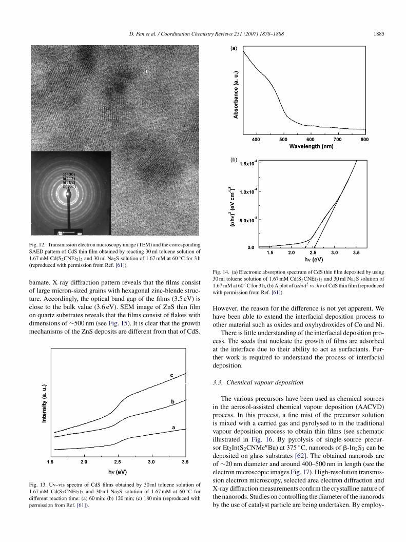
Fig. 12. Transmission electron microscopy image (TEM) and the correspondingS1(
botcodm
F1dp
Fig. 14. (a) Electronic absorption spectrum of CdS thin film deposited by using31w
AED pattern of CdS thin film obtained by reacting 30 ml toluene solution of.67 mM Cd(S2CNEt2)2 and 30 ml Na2S solution of 1.67 mM at 60 ◦C for 3 hreproduced with permission from Ref. [61]).
amate. X-ray diffraction pattern reveals that the films consistf large micron-sized grains with hexagonal zinc-blende struc-ure. Accordingly, the optical band gap of the films (3.5 eV) is
lose to the bulk value (3.6 eV). SEM image of ZnS thin filmn quartz substrates reveals that the films consist of flakes withimensions of ∼500 nm (see Fig. 15). It is clear that the growthechanisms of the ZnS deposits are different from that of CdS.ig. 13. Uv–vis spectra of CdS films obtained by 30 ml toluene solution of.67 mM Cd(S2CNEt2)2 and 30 ml Na2S solution of 1.67 mM at 60 ◦C forifferent reaction time: (a) 60 min; (b) 120 min; (c) 180 min (reproduced withermission from Ref. [61]).
Hho
catd
3
ipivisdoesXtb
0 ml toluene solution of 1.67 mM Cd(S2CNEt2)2 and 30 ml Na2S solution of.67 mM at 60 ◦C for 3 h, (b) A plot of (αhν)2 vs. hν of CdS thin film (reproducedith permission from Ref. [61]).
owever, the reason for the difference is not yet apparent. Weave been able to extend the interfacial deposition process tother material such as oxides and oxyhydroxides of Co and Ni.
There is little understanding of the interfacial deposition pro-ess. The seeds that nucleate the growth of films are adsorbedt the interface due to their ability to act as surfactants. Fur-her work is required to understand the process of interfacialeposition.
.3. Chemical vapour deposition
The various precursors have been used as chemical sourcesn the aerosol-assisted chemical vapour deposition (AACVD)rocess. In this process, a fine mist of the precursor solutions mixed with a carried gas and pyrolysed to in the traditionalapour deposition process to obtain thin films (see schematicllustrated in Fig. 16. By pyrolysis of single-source precur-or Et2In(S2CNMenBu) at 375 ◦C, nanorods of �-In2S3 can beeposited on glass substrates [62]. The obtained nanorods aref ∼20 nm diameter and around 400–500 nm in length (see thelectron microscopic images Fig. 17). High-resolution transmis-
ion electron microscopy, selected area electron diffraction and-ray diffraction measurements confirm the crystalline nature ofhe nanorods. Studies on controlling the diameter of the nanorodsy the use of catalyst particle are being undertaken. By employ-

1886 D. Fan et al. / Coordination Chemistry Reviews 251 (2007) 1878–1888
Fdt
iodhp
w4t
Ft
ig. 15. (Top) Scanning electron microscopy (SEM) image of ZnS thin filmeposited by liquid–liquid interface route. (Bottom) A plot (αhν)2 vs. hν of ZnShin film (reproduced with permission from Ref. [61]).
ng a slightly modified process, nanorods of PbS have beenbtained on Si substrates coated with Au nanocrystals. The imi-odiphosphinic acid derivative M[(TePiPr2)2N]2 (M = Cd, Hg)ave been used in aerosol-assisted chemical vapour depositionrocesses to prepare thin films of chalcogenide material [63].
The cadmium complex yields cubic CdTe films in between
hen deposition is carried out at temperatures in the range of25–475 ◦C. At low deposition temperatures (375 ◦C), a mix-ure of hexagonal tellurium and cubic cadmium telluride isig. 16. Schematic illustration of the aerosol-assisted chemical vapour deposi-ion setup.
Fig. 17. TEM (a) and HRTEM (b) images of �-In S nanowires obtained at3(
oietdwe
2 3
75 ◦C. (c) SEM image of as grown �-In2S3 nanowires on glass substratesreproduced with permission from Ref. [62]).
btained (Fig. 18). On the other hand, Hg[(TePiPr2)2N]2 resultsn hexagonal tellurium thin films only, possibly due to reductivelimination of mercury at elevated temperatures. It is knownhat the anionic ligand [(TePiPr ) N]− is readily oxidized to the
2 2itelluride (TePiPr2NiPr2PTe−)2 (which can be viewed as R2E2here R = TeiPr2NiPr2P and E = Te) [63]. Therefore, reductivelimination of mercury with the concomitant formation of this
D. Fan et al. / Coordination Chemistry Reviews 251 (2007) 1878–1888 1887
Fs
dch
ad(bcfat
aoddDTttidop
F5f
Fp
mp
4
shsdso
A
eto
ig. 18. A typical XRD pattern of cubic CdTe deposited at 475 ◦C on glassubstrate. Inset shows a representative SEM image of the film.
itelluride is a feasible pathway for the decomposition of pre-ursor. The subsequent degradation of this ditelluride to giveexagonal Te films may account for the current observations.
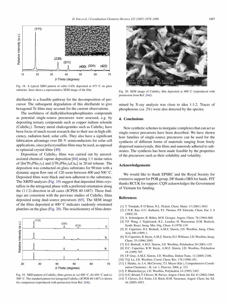
The usefulness of dialkyldiselenophosphinates compoundss potential single-source precursors were assessed, e.g. byepositing ternary compounds such as copper indium selenideCuInSe2). Ternary metal chalcogenides such as CuInSe2 haveeen focus of much recent research due to their use in high effi-iency, radiation hard, solar cells. They also have a significantabrication advantage over III–V semiconductors for solar cellpplications, since polycrystalline films may be used, as opposedo epitaxial crystal films [49].
Deposition of CuInSe2 films was carried out by aerosol-ssisted chemical vapour deposition [64] using 1:1 molar ratiosf [In(iPr2PSe2)3] and [(iPr2PSe2)4Cu4] in 20 ml toluene. Theeposition was conducted on glass substrates for 90 min with aynamic argon flow rate of 120 seem between 400 and 500 ◦C.eposited films were black and non-adherent to the substrates.he XRPD analyses (Fig. 19) suggest that deposited films crys-
allize in the tetragonal phase with a preferred orientation alonghe (1 1 2) direction in all cases (JCPDS 40-1487). These find-
ngs are consistent with the previous studies of CuInSe2 filmseposited using dual-source precursors [65]. The SEM imagef the films deposited at 400 ◦C indicates randomly orientatedlatelets on the glass (Fig. 20). The stoichiometry of films deter-ig. 19. XRD pattern of CuInSe2 films grown at: (a) 400 ◦C, (b) 450 ◦C and (c)00 ◦C. The standard pattern for tetragonal CuInSe2 (JCPDS 40-1487) is shownor comparison (reproduced with permission from Ref. [64]).
R
[[
[[[
ig. 20. SEM image of CuInSe2 film deposited at 400 ◦C (reproduced withermission from Ref. [64]).
ined by X-ray analysis was close to idea 1:1:2. Traces ofhosphorous (ca. 2%) were also detected by the spectra.
. Conclusions
New synthetic schemes to inorganic complexes that can act asingle-source precursors have been described. We have shownow families of single-source precursors can be used for theynthesis of different forms of materials ranging from freelyispersed nanocrystals, thin films and nanorods adhered to sub-trates. The synthesis has been made feasible by the propertiesf the precursors such as their solubility and volatility.
cknowledgements
We would like to thank EPSRC and the Royal Society forxtensive support for POB group. DF thanks ORS for funds. PJThanks RCUK for support. CQN acknowledges the Governmentf Vietnam for funding.
eferences
[1] T. Trindade, P. O’Brien, N.L. Pickett, Chem. Mater. 13 (2001) 3843.[2] C.N.R. Rao, G.U. Kulkarni, P.J. Thomas, P.P. Edwards, Chem. Eur. J. 8
(2002) 28.[3] A. Schmidpeter, R. Bohm, M.H. Groeger, Angew. Chem. 76 (1964) 860.[4] T.F. Wang, J. Najdzionek, K.L. Leneker, H. Wasserman, D.M. Braitsch,
Synth. React. Inorg. Met.-Org. Chem. 8 (1978) 119.[5] D. Cupertino, D.J. Birdsall, A.M.Z. Slawin, J.D. Woollins, Inorg. Chim.
Acta 290 (1999) 1.[6] D. Cupertino, R. Keyte, A.M.Z. Slawin, D.J. Williams, J.D. Woollins, Inorg.
Chem. 35 (1996) 2695.[7] D.J. Birdsall, A.M.Z. Slawin, J.D. Woollins, Polyhedron 20 (2001) 125.[8] D.C. Cupertino, R.W. Keyte, A.M.Z. Slawin, J.D. Woollins, Polyhedron
18 (1999) 707.[9] I.P. Gray, A.M.Z. Slawin, J.D. Woollins, Dalton Trans. 12 (2005) 2188.10] T.Q. Ly, J.D. Woollins, Coord. Chem. Rev. 176 (1998) 451.11] I. Haiduc, in: J.A. McCleverty, T.J. Meyer (Eds.), Comprehensive Coordi-
nation Chemistry—II, vol. 1, Elsevier, 2004, p. 323.12] P. Bhattacharyya, J.D. Woollins, Polyhedron 14 (1995) 3367.13] G.G. Briand, T. Chivers, M. Parvez, Angew. Chem. Int. Ed. 41 (2002) 3468.14] T. Chivers, D.J. Eisler, J.S. Ritch, H.M. Tuononen, Angew. Chem. Int. Ed.
44 (2005) 4953.

1 istry
[
[[
[[[[
[
[
[
[
[
[
[
[
[
[
[
[
[
[[[
[[
[[
[[
[
[
[[
[
[
[
[
[
[
[
[[[
[
[
[
[
888 D. Fan et al. / Coordination Chem
15] J. Ellermann, M. Schutz, F.W. Heinemann, M. Moll, Z. Anorg. Allg. Chem.624 (1998) 257.
16] T. Chivers, D.J. Eisler, J.S. Ritch, Dalton Trans. 16 (2005) 2675.17] M.V. Kudchadker, R.A. Zingaro, K.J. Irgolic, Can. J. Chem. 46 (1968)
1415.18] V. Krishnan, R.A. Zingaro, Inorg. Chem. 8 (1969) 2337.19] V. Krishnan, R.A. Zingaro, J. Coord. Chem. 1 (1971) 1.20] T.S. Lobana, J.-C. Wang, C.W. Liu, Coord. Chem. Rev. 251 (2007) 91.21] C.W. Liu, I.J. Shang, C.M. Hung, J.C. Wang, T.C. Keng, J. Chem. Soc.,
Dalton Trans. 9 (2002) 1974.22] C.W. Liu, H.C. Chen, J.C. Wang, T.C. Keng, Chem. Commun. 17 (1998)
1831.23] C.W. Liu, T.S. Lobana, B.K. Santra, C.M. Hung, H.Y. Liu, B.J. Liaw, J.C.
Wang, Dalton Trans. 4 (2006) 560.24] B.K. Santra, C.M. Hung, B.J. Liaw, J.C. Wang, C.W. Liu, Inorg. Chem. 43
(2004) 7570.25] C.W. Liu, H.C. Haia, C.M. Hung, B.K. Santra, B.J. Liaw, Z. Lin, J.C. Wang,
Inorg. Chem. 43 (2004) 4464.26] B.K. Santra, B.J. Liaw, C.M. Hung, C.W. Liu, J.C. Wang, Inorg. Chem. 42
(2003) 8866.27] M.A. Malik, C. Byrom, P. O’Brien, M. Motevalli, Inorg. Chim. Acta 338
(2002) 245.28] W.E.V. Zyl, J.M. Lopez-de-Luzuriaga, J.P. Fackler Jr., R.J. Staples, Can. J.
Chem. 79 (2001) 896.29] V. Garcia-Montalvo, A. Marcelo-Polo, R. Montoya, R.A. Toscano, S.
Hernandez-Ortega, R. Cea-Olivares, J. Organomet. Chem. 623 (2001) 74.30] R.G. Cavell, B. Creed, L. Gelmim, D.J. Law, R. McDonald, A.R. Sanger,
A. Somogyvan, Inorg. Chem. 37 (1998) 757.31] M.N. Gibbons, D.B. Sowerby, C. Silvestru, I. Haiduc, Polyhedron 15 (1996)
4573.32] S.N. Olafsson, T.N. Petersen, P. Andersen, Acta Chem. Scand. 50 (1996)
745.33] C.C. Landry, A. Hynes, A.R. Barron, I. Haiduc, C. Silvestru, Polyhedron
15 (1996) 391.34] W. Kuchen, J. Metten, A. Judat, Chemische Benchte-Recueil 97 (1964)
2306.35] W. Kuchen, B. Knop, Angew. Chem. Int. Ed. 4 (1965) 244.36] W. Kuchen, H. Hertel, Angew. Chem. Int. Ed. 8 (1969) 89.
37] A. Mueller, V.V.K. Rao, P. Christophliemk, J. Inorg. Nucl. Chem. 36 (1974)472.38] A. Mueller, P. Christophliemk, V.V.K. Rao, Chem. Ber. 104 (1971) 1905.39] M.J. Pilkington, A.M.Z. Slawin, D.J. Williams, J.D. Woollins, Polyhedron
10 (1991) 2641.
[[
[[
Reviews 251 (2007) 1878–1888
40] R.P. Davies, M.G. Martinelli, Inorg. Chem. 41 (2002) 348.41] R.P. Davies, C.V. Francis, A.P.S. Jurd, M.G. Martinelli, A.J.P. White, D.J.
Williams, Inorg. Chem. 43 (2004) 4802.42] H.G. Horn, H.J. Lindner, Chemiker-Zeitung 109 (1985) 77.43] G. Fritz, G. Becker, G. Poppenbu, M. Rocholl, G. Trenczec, Angew. Chem.
Int. Ed. 5 (1966) 53.44] W.W. duMont, L.P. Muller, L. Muller, S. Vollbrecht, A. Zanin, J.
Organomet. Chem. 521 (1996) 417.45] R.A. Benkeser, K.M. Foley, J.B. Grutzner, W.E. Smith, J. Am. Chem. Soc.
92 (1970) 697.46] R.A. Benkeser, Acc. Chem. Res. 4 (1971) 94.47] C.Q. Nguyen, A. Adeogun, M. Afzaal, M.A. Malik, P. O’Brien, Chem.
Commun. (2006) 2179.48] C.Q. Nguyen, M. Afzaal, M.A. Malik, M. Helliwell, J. Raftery, P. O’Brien,
J. Organomet. Chem., in press.49] C.Q. Nguyen, A. Adeogun, M. Afzaal, M.A. Malik, P. O’Brien, Chem.
Commun. (2006) 2182.50] B. Ludolph, M.A. Malik, P. O’Brien, N. Revaprasadu, Chem. Commun. 17
(1998) 1849.51] M. Chuggaze, J. McAleese, P. O’Brien, D.J. Otway, Chem. Commun. 7
(1998) 833.52] N. Revaprasadu, M.A. Malik, P. O’Brien, M.M. Zulu, G. Wakefield, J.
Mater. Chem. 8 (1998) 1885.53] D.J. Crouch, P. O’Brien, M.A. Malik, P.J. Skabara, S.P. Wright, Chem.
Commun. 9 (2003) 1454.54] T. Trindade, P. O’Brien, X. Zhang, M. Motevalli, J. Mater. Chem. 7 (1997)
1011.55] M. Green, P. O’Brien, Chem. Commun. (1998) 2459.56] M. Green, P. O’Brien, J. Mater. Chem. 9 (1999) 243.57] N. Revaprasadu, M.A. Malik, J. Carstens, P. O’Brien, J. Mater. Chem. 9
(1999) 2885.58] M.A. Malik, P. O’Brien, N. Revaprasadu, Adv. Mater. 11 (1999)
1441.59] J. McAleese, P. O’Brien, D.J. Otway, Mater. Res. Soc. Symp. Proc. 485
(1998) 157.60] C.N.R. Rao, G.U. Kulkarni, V.V. Agrawal, U.K. Gautam, M. Ghosh, U.
Tumkurkar, J. Colloid Interface Sci. 289 (2005) 305.61] D. Fan, P.J. Thomas, P. O’Brien, J. Mat. Chem. 17 (2007) 1381.
62] M. Afzaal, M.A. Malik, P. O’Brien, Chem. Commun. 3 (2004) 334.63] S.S. Garje, J.S. Ritch, D.J. Eisler, M. Afzaal, P. O’Brien, T. Chivers, J.Mater. Chem. 16 (2006) 966.64] C.Q. Nguyen, M. Afzaal, M.A. Malik, P. O’Brien, unpublished results.65] C.C. Landry, J. Lockwood, A.R. Barron, Chem. Mater. 7 (1995) 699.