
PlaneWave Admittance Method - a novel approach for determining the electromagnetic modes in photonic...
12
Plane Wave Admittance Method — a novel approach for determining the electromagnetic modes in photonic structures Maciej Dems Institute of Physics, Technical University of Lodz, ul. Wolczanska 219, 93-005 Lodz, Poland [email protected] Rafal Kotynski Warsaw University, Faculty of Physics, ul. Pasteura 7, 02-093 Warsaw, Poland Department of Applied Physics and Photonics, Vrije Universiteit Brussel, Pleinlaan 2, 1050 Brussels, Belgium [email protected] Krassimir Panajotov Department of Applied Physics and Photonics, Vrije Universiteit Brussel, Pleinlaan 2, 1050 Brussels, Belgium [email protected] Abstract: In this article we present a novel approach for determining the electromagnetic modes of photonic multilayer structures. We combine the plane wave expansion method with the method of lines resulting in a fast and accurate computational technique which we named the plane wave admittance method. In addition, we incorporate perfectly matched layers at the boundaries parallel to the multilayer surfaces which allow for easy determination of leaky modes. The convergence of the method is verified for the case of photonic crystal slab showing very good agreement with the results obtained with full three-dimensional plane wave expansion method while the numerical effort is largely reduced. The numerical implementation of the method will be soon available on the web. © 2005 Optical Society of America OCIS codes: (000.3860) Mathematical methods in physics; (000.4430) Numerical approxima- tion and analysis; (230.4170) Multilayers; (230.7400) Waveguides, slab; (250.5300) Photonic integrated circuits; (999.9999) Photonic crystals References and links 1. J. D. Joannopoulos, R. D. Meade, a J. N. Winn, Photonic Crystals: Molding the Flow of Light (Princeton Uni- versity Press, Princeton, 1995). 2. K. Sakoda, Optical Properties of Photonic Crystals (Springer-Verlag, Berlin 2001). 3. N. Yokouchi, A. J. Danner, and K. D. Choquette, “Two-Dimensional Photonic Crystal Confined Vertical-Cavity Surface-Emitting Lasers,” IEEE J. Sel. Top. Quantum Electron. 9, 1439–1445 (2003). 4. A. Taflove, Computational Electrodynamics: The Finite-Difference Time-Domain Method (Artec House Inc., Boston, 1995). 5. S. Datta, C. T. Chan, K. M. Ho, and C. M. Soukoulis, “Photonic band gaps in periodic dielectric structures: The scalar-wave approximation,” Phys. Rev. B 46, 10650–10656 (1992). (C) 2005 OSA 2 May 2005 / Vol. 13, No. 9 / OPTICS EXPRESS 3196 #6603 - $15.00 US Received 14 February 2005; revised 30 March 2005; accepted 1 April 2005
Transcript of PlaneWave Admittance Method - a novel approach for determining the electromagnetic modes in photonic...

Plane Wave Admittance Method —a novel approach for determining theelectromagnetic modes in photonic
structures
Maciej DemsInstitute of Physics, Technical University of Lodz, ul. Wolczanska 219, 93-005 Lodz, Poland
Rafal KotynskiWarsaw University, Faculty of Physics, ul. Pasteura 7, 02-093 Warsaw, Poland
Department of Applied Physics and Photonics, Vrije Universiteit Brussel, Pleinlaan 2,1050 Brussels, Belgium
Krassimir PanajotovDepartment of Applied Physics and Photonics, Vrije Universiteit Brussel, Pleinlaan 2,
1050 Brussels, Belgium
Abstract: In this article we present a novel approach for determiningthe electromagnetic modes of photonic multilayer structures. We combinethe plane wave expansion method with the method of lines resulting in afast and accurate computational technique which we named the plane waveadmittance method. In addition, we incorporate perfectly matched layersat the boundaries parallel to the multilayer surfaces which allow for easydetermination of leaky modes. The convergence of the method is verifiedfor the case of photonic crystal slab showing very good agreement with theresults obtained with full three-dimensional plane wave expansion methodwhile the numerical effort is largely reduced. The numerical implementationof the method will be soon available on the web.
© 2005 Optical Society of America
OCIS codes:(000.3860) Mathematical methods in physics; (000.4430) Numerical approxima-tion and analysis; (230.4170) Multilayers; (230.7400) Waveguides, slab; (250.5300) Photonicintegrated circuits; (999.9999) Photonic crystals
References and links1. J. D. Joannopoulos, R. D. Meade, a J. N. Winn, Photonic Crystals: Molding the Flow of Light (Princeton Uni-
versity Press, Princeton, 1995).2. K. Sakoda, Optical Properties of Photonic Crystals (Springer-Verlag, Berlin 2001).3. N. Yokouchi, A. J. Danner, and K. D. Choquette, “Two-Dimensional Photonic Crystal Confined Vertical-Cavity
Surface-Emitting Lasers,” IEEE J. Sel. Top. Quantum Electron. 9, 1439–1445 (2003).4. A. Taflove, Computational Electrodynamics: The Finite-Difference Time-Domain Method (Artec House Inc.,
Boston, 1995).5. S. Datta, C. T. Chan, K. M. Ho, and C. M. Soukoulis, “Photonic band gaps in periodic dielectric structures: The
scalar-wave approximation,” Phys. Rev. B 46, 10650–10656 (1992).
(C) 2005 OSA 2 May 2005 / Vol. 13, No. 9 / OPTICS EXPRESS 3196#6603 - $15.00 US Received 14 February 2005; revised 30 March 2005; accepted 1 April 2005
6. S. Johnson and J. D. Joannopoulous, “Block Iterative frequency-domain methodsfor Maxwell’s equations in a planewave basis,” Opt. Express 8, 173–190 (2001),http://www.opticsexpress.org/abstract.cfm?URI=OPEX-8-3-173.
7. S. Guo and S. Albin, “Simple plane wave implementation for photonic crystal calculations,” Opt. Express 11,167–175 (2003), http://www.opticsexpress.org/abstract.cfm?URI=OPEX-11-2-167.
8. H. S. Sozuer and J. W. Haus, “Photonic bands: convergence problems with the plane-wave method,” Phys. Rev.B 45, 13962–13972 (1992).
9. Ch. Sauvan, Ph. Lalanne, and J. P. Hugonin, “Truncation rules for modelling discontinuities with Galerkin methodin electromagnetic theory,” Opt. Quantum Electron. 36, 271–284, 2004.
10. R. D. Meade, A. M. Rappe, K. D. Brommer, J. D. Joannopoulous, and O. L. Alerhand, “Accurate theoreticalanalysis of photonic band-gap materials,” Phys. Rev. B 48, 8434–8437 (1993).
11. A. Ferrando, E. Silvestre, J. J. Miret, P. Andres, and M. V. Andres, ”Full-vector analysis of a realistic photoniccrystal fiber,” Opt. Lett. 24, 276–278 (1999).
12. J. M. Pottage, D. Bird, T. D. Hedley, J. C. Knight, T. A. Birks, P. S. J Russell, and P. J. Roberts, “Robust photonicband gaps for hollow core guidance in PCF made from high index glass,” Opt. Express 11, 2854–2861 (2003),http://www.opticsexpress.org/abstract.cfm?URI=OPEX-11-22-2854.
13. S. Shi, C. Chen, and D.W. Prather, “Revised plane wave method for dispersive material and its appli-cation to band structure calculations of photonic crystal slabs,” Appl. Phys. Lett. 86, 043104 (2005),http://scitation.aip.org/getabs/servlet/GetabsServlet?prog=normal&id=VIRT01000011000004000041000001.
14. P. Lalanne, “Electromagnetic Analysis of Photonic Crystal Waveguides Operating Above the Light Cone,” IEEEJ. Quantum Electron. 38, 800-804 (2002).
15. M. Qiu, “Effective index method for heterostructure-slab-waveguide-based two-dimensional photonic crystals,”Appl. Phys. Lett. 81 1163–1165 (2002).
16. P. Bienstman, “Two-stage mode finder for waveguides with a 2D cross-section,” Opt. Quantum Electron. 36,5–14, 2004.
17. K. Ohtaka, J. Inoue, and S. Yamaguti, “Derivation of the density of states of leaky photonic bands,” Phys. Rev.B 70 035109 (2004).
18. S. F. Helfert, R. Pregla,“Efficient Analysis of Periodic Structures,” J. Lightwave Technol. 16, 1694–1702 (1998).19. O. Conradi, S. F. Helfert, and R. Pregla, “Comprehensive Modeling of Vertical-Cavity Laser-Diodes by the
Method of Lines,” IEEE J. Quantum Electron. 37, 928–935 (2001).20. S. F. Helfert, A. Barcz, and R. Pregla, “Three-dimensional vectorial analysis of waveguide structures with the
method of lines,” Opt. Quantum Electron. 35, 381–394 (2003).21. J. P. Berenger, “A perfectly matched layer for the absorption of electromagnetic waves,” J. Comput. Phys. 114,
185–200 (1994).22. H. Derudder, F. Olyslager, D. De Zuter, S. Van den Berghe, “Efficient Mode-Matcing Analysis of Discontinuities
in Finit Planar Substrates Using Perfectly Matched Layers,” IEEE Trans. Antennas and Propagation 49, 185–195(2001).
23. T. Czyszanowski, “Comparative Analysis of Validity Limits of Scalar and Vector Approaches to Optical Fieldsin Diode Lasers,” Ph.D. diss., Technical University of Lodz (2004).
24. S. Shi, C. Chen, and D. W. Prather, “Plane-wave expansion method for calculating band structure of photoniccrystal slabs with perfectly matched layers,” J. Opt. Soc. Am. A 21, 1769–1775 (2004)
25. S. G. Johnson, S. Fan, P. R. Villeneuve, J. D. Joannopoulous, and L. A. Kolodziejski, “Guided modes in photoniccrystal slabs,” Phys. Rev. B 60, 5751–5758 (1999).
1. Introduction
Recently, photonic crystals [1] (PC) have been attracting a lot of interest due to their noveloptical properties such as the existence of photonic bandgaps, modified density of states, ap-pearance of localized states of light, anomalous dispersion, suppressed or enhanced nonlineareffects [2] etc. Photonic crystals enabled the development of a range of novel devices, includingwaveguides and fibers with bandgap guidance, cavities with improved Q-factors, fiber lasersand semiconductor lasers [3] with low threshold and other novel properties, to mention onlysome. In this paper we introduce a novel modeling method for photonic crystal slabs (PCS)as well as layered PC-devices, which are particularly important for applications in integratedphotonics. These are structures with two-dimensional periodicity in the horizontal plane (x, y),and a uniform or layered composition in the orthogonal (z) direction. In all cases, we assumethe structures to have a finite thickness, and for simplicity we term them generally as PCSalso when speaking of PC-multilayered stacks. The importance of finite thickness, except for
(C) 2005 OSA 2 May 2005 / Vol. 13, No. 9 / OPTICS EXPRESS 3197#6603 - $15.00 US Received 14 February 2005; revised 30 March 2005; accepted 1 April 2005
technological aspects, relates to the the appearance of leaky modes and to the confinementmechanism which for single layered structures is the total internal reflection.
Numerical modeling of PC structures is difficult mainly due to the importance of vectorialeffects that arise when high refractive index contrasts exist at sub-wavelength distances. Thisleads to the necessity of solving the fully vectorial wave equation and taking special care for theexact representation of the material properties near the boundaries. A large variety of methodshave been proposed for PC modeling, both in time [4] and in frequency domains. Among thefrequency domain modal methods, the plane-wave method [2, 5, 6] (PWM) in its numerousvariants has been particularly widely used. The PWM naturally includes the periodic bound-ary conditions of the PC structures. It can be easily adapted to any desired form of the waveequation. The plane-wave representation of the permittivity and permeability has an analyticalform for PC with most of regular geometries, however is not limited to them and can be easilydetermined numerically for arbitrary geometries as well [7]. Although the PWM is known tosuffer from convergence problems [8], the nature of these problems is well understood and canbe overcome by a proper choice of truncation rules [9] and by refractive index averaging [10],or by taking a sufficiently large number of basis functions. The PWM has been used for modalcalculations as well as for bandgap determination in PC with full 3D periodicity [6], but alsoin a 2D variant for PC-fibers [11, 12] and PCS [13, 14]. As opposed to the case of PC-fibers,the proper analysis of PCS of finite thickness is a 3D problem. One way to reduce it into a 2Dproblem is to apply the effective index technique as in ref. [13, 15]. Another is to make useof the analytical form of Bloch solution of Maxwell equations, propagating within every layeralong the direction z of translational invariance. Then, the matching condition may follow fromthe transmission matrix or better from the scattering matrix approach as in refs. [14, 16]. Thelatter is particularly useful in the determination of the density of states of leaky modes in PCS[17].
Here, we propose to follow another matching condition based on the admittance transferand developed by Pregla et al. under the name of Method of Lines [18, 19, 20] (MoL) orsimply the admittance transfer method. This method is characterized by a very good numericalstability and has been successfully applied to layered structures with use of discretization byfinite differences in the (x, y) plane.
In this paper we propose to combine the admittance transfer method and PWM to achievean efficient way of calculating the modes and bandgap structure of PCS. For the boundaryconditions, we use the Bloch expansion in (x, y) together with absorbing perfectly matchedlayer [21, 22] (PML) in z, to account for the horizontal periodicity of the PCS and out-of-plane losses, respectively. The equations assume a diagonal and independent permittivity andpermeability, and such media can be directly included in modeling. Clearly, adding a PML inthe horizontal plane is also straightforward within the same material model. In the formula-tion of the PWM eigenequations for every layer, we take care not to put the frequency as theeigenvalue, therefore the treatment of dispersive and active materials is also direct.
The paper is organized as follows: In the second section we describe in details the proposedalgorithm; we derive the necessary equations and suggest a way for their implementation. Inthe third section we apply our method to exemplary PCS structure and obtain the eigenmodesand their electromagnetic field distribution. Finally, in section 4 we demonstrate a full photonicband diagram computation and discuss the convergence and the accuracy of the results.
2. Computational method
2.1. Generalized transmission line equations
In the method of lines (MoL) the analyzed structure is divided into several layers in whichmaterial parameters are constant along the z direction making it possible to obtain analytical
(C) 2005 OSA 2 May 2005 / Vol. 13, No. 9 / OPTICS EXPRESS 3198#6603 - $15.00 US Received 14 February 2005; revised 30 March 2005; accepted 1 April 2005

solution [19]. In our work, the generalized transmission line (GTL) equations are used for thispurpose. However, contrary to MoL, they are derived in plane-wave basis without using finite-differences.
The time independent Maxwell equations with diagonal anisotropic dielectric and magnetictensors in Cartesian coordinates read
−∂zEy +∂yEz = −iωµxµ0Hx, (1)
∂xEz −∂zEx = −iωµyµ0Hy, (2)
−∂yEx +∂xEy = −iωµzµ0Hz, (3)
−∂zHy +∂yHz = iωεxε0Ex, (4)
∂xHz −∂zHx = iωεyε0Ey, (5)
−∂yHx +∂xHy = iωεzε0Ez. (6)
where ∂ξ means partial derivative in the ξ direction. From the Eq. (3) and (6) it is possible toexpress the z components of the electric and magnetic vectors as
Hz =[− i
k0η0µz∂x − i
k0η0µz∂y
][ −Ey
Ex
], (7)
Ez =[− iη0
k0εz∂y − iη0
k0εz∂x
][Hx
Hy
]. (8)
where k0 = ω/c = ω(µ0ε0)1/2 is the normalized frequency and η0 = (µ0/ε0)
1/2 is the freespace impedance. Substituting (7) and (8) into (1), (2), (4), and (5) we can obtain the GTLequations of the form
∂z
[ −Ey
Ex
]= −i
η0
k0
[∂yε−1
z ∂y + µxk20 −∂yε−1
z ∂x
−∂xε−1z ∂y ∂xε−1
z ∂x + µyk20
][Hx
Hy
], (9)
∂z
[Hx
Hy
]= −i
1η0k0
[∂xµ−1
z ∂x + εyk20 ∂xµ−1
z ∂y
∂yµ−1z ∂x ∂yµ−1
z ∂y + εxk20
][ −Ey
Ex
]. (10)
The partial derivatives in Eq. (9) and (10) have to be computed numerically. The traditionalapproach here is to use finite differences to discretize the right-hand sides of Eq. (9) and (10)leading to matrix equations
∂zE = −iRH H, (11)
∂zH = −iRE E. (12)
However, in order to ensure the satisfactory computational accuracy the number of the finitedifference grid points must be large, approaching even the number of 10000 in the case of fullythree-dimensional analysis [20]. This makes the computational procedure a very strenuous task,almost impossible to complete in a reasonable time, especially on a personal computer. For thisreason we propose an alternative numerical representation of Eq. (9) and (10). As it will beshown later the size of the obtained matrices can be as small as 500 or even less still resultingin a satisfactory precision.
2.2. Plane wave expansion of GTL equations
In general, GTL equations can be transformed into a finite problem by expanding the fields insome truncated basis {|ϕG〉}
Ψ = ∑G
ΨG|ϕG〉, (13)
where Ψ can be any of Ex, −Ey, Hx or Hy and{
ΨG}
is a set of expansion coefficients (Tosimplify the notation we expand −Ey as −Ey = ∑G EG
y |ϕG〉.).
(C) 2005 OSA 2 May 2005 / Vol. 13, No. 9 / OPTICS EXPRESS 3199#6603 - $15.00 US Received 14 February 2005; revised 30 March 2005; accepted 1 April 2005
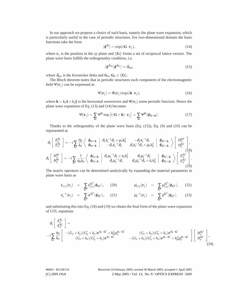
In our approach we propose a choice of such basis, namely the plane wave expansion, whichis particularly useful in the case of periodic structures. For two-dimensional domain the basisfunctions take the form
|ϕ G〉 = exp(iG · r‖), (14)
where r‖ is the position in the xy plane and {G} forms a set of reciprocal lattice vectors. Theplane wave basis fulfills the orthogonality condition, i.e.
〈ϕ Gm |ϕ Gn〉 = δmn, (15)
where δmn is the Kronecker delta and Gm,Gn ∈ {G}.The Bloch theorem states that in periodic structures each component of the electromagnetic
field Ψ(r‖) can be expressed as
Ψ(r‖) = Φ(r‖)exp(ik · r‖), (16)
where k = kxx+kyy is the horizontal wavevector and Φ(r‖) some periodic function. Hence theplane wave expansion of Eq. (13) and (14) becomes
Ψ(r‖) = ∑G
ΨG exp[i(G+k) · r‖
]= ∑
GΨG|ϕG+k〉. (17)
Thanks to the orthogonality of the plane wave basis (Eq. (15)), Eq. (9) and (10) can berepresented as
∂z
[EG
y
EGx
]= −i∑
G′
η0
k0
⟨ϕG+kϕG+k
∣∣∣∣ ∂yε−1z ∂y + µxk2
0 −∂yε−1z ∂x
−∂xε−1z ∂y ∂xε−1
z ∂x + µyk20
∣∣∣∣ ϕG′+kϕG′+k
⟩[HG′
x
HG′y
],
(18)
∂z
[HG
xHG
y
]= −i∑
G′
1η0k0
⟨ϕG+kϕG+k
∣∣∣∣ ∂xµ−1z ∂x + εyk2
0 ∂xµ−1z ∂y
∂yµ−1z ∂x ∂yµ−1
z ∂y + εxk20
∣∣∣∣ ϕG′+kϕG′+k
⟩[EG′
y
EG′x
].
(19)The matrix operators can be determined analytically by expanding the material parameters inplane wave basis as
εx/y(r‖) = ∑G′′
εG′′x/y|ϕG′′ 〉, (20)
ε−1z (r‖) = ∑
G′′κ G′′ |ϕG′′ 〉, (21)
µx/y(r‖) = ∑G′′
µG′′x/y|ϕG′′ 〉, (22)
µ−1z (r‖) = ∑
G′′γG′′ |ϕG′′ 〉 (23)
and substituting this into Eq. (18) and (19) we obtain the final form of the plane-wave expansionof GTL equations
∂z
[EG
y
EGx
]=
−i∑G′
η0
k0
[−(Gy + ky)(G′
y + ky)κ G−G′+ k2
0µG−G′x (Gy + ky)(G′
x + kx)κ G−G′
(Gx + kx)(G′y + ky)κ G−G′ −(Gx + kx)(G′
x + kx)κ G−G′+ k2
0µG−G′y
][HG′
x
HG′y
],
(24)
(C) 2005 OSA 2 May 2005 / Vol. 13, No. 9 / OPTICS EXPRESS 3200#6603 - $15.00 US Received 14 February 2005; revised 30 March 2005; accepted 1 April 2005
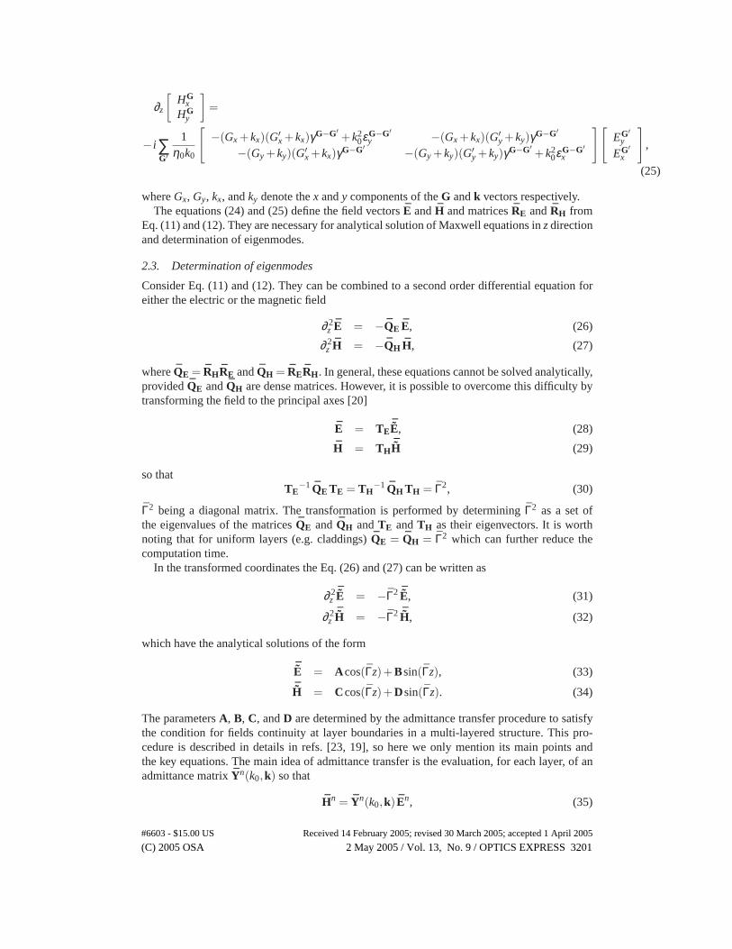
∂z
[HG
xHG
y
]=
−i∑G′
1η0k0
[−(Gx + kx)(G′
x + kx)γG−G′+ k2
0εG−G′y −(Gx + kx)(G′
y + ky)γG−G′
−(Gy + ky)(G′x + kx)γG−G′ −(Gy + ky)(G′
y + ky)γG−G′+ k2
0εG−G′x
][EG′
y
EG′x
],
(25)
where Gx, Gy, kx, and ky denote the x and y components of the G and k vectors respectively.The equations (24) and (25) define the field vectors E and H and matrices RE and RH from
Eq. (11) and (12). They are necessary for analytical solution of Maxwell equations in z directionand determination of eigenmodes.
2.3. Determination of eigenmodes
Consider Eq. (11) and (12). They can be combined to a second order differential equation foreither the electric or the magnetic field
∂ 2z E = −QE E, (26)
∂ 2z H = −QH H, (27)
where QE = RHRE and QH = RERH . In general, these equations cannot be solved analytically,provided QE and QH are dense matrices. However, it is possible to overcome this difficulty bytransforming the field to the principal axes [20]
E = TE¯E, (28)
H = TH¯H (29)
so thatTE
−1 QE TE = TH−1 QH TH = Γ2, (30)
Γ2 being a diagonal matrix. The transformation is performed by determining Γ2 as a set ofthe eigenvalues of the matrices QE and QH and TE and TH as their eigenvectors. It is worthnoting that for uniform layers (e.g. claddings) QE = QH = Γ2 which can further reduce thecomputation time.
In the transformed coordinates the Eq. (26) and (27) can be written as
∂ 2z
¯E = −Γ2 ¯E, (31)
∂ 2z
¯H = −Γ2 ¯H, (32)
which have the analytical solutions of the form
¯E = A cos(Γz)+Bsin(Γz), (33)¯H = Ccos(Γz)+Dsin(Γz). (34)
The parameters A, B, C, and D are determined by the admittance transfer procedure to satisfythe condition for fields continuity at layer boundaries in a multi-layered structure. This pro-cedure is described in details in refs. [23, 19], so here we only mention its main points andthe key equations. The main idea of admittance transfer is the evaluation, for each layer, of anadmittance matrix Yn(k0,k) so that
Hn = Yn(k0,k) En, (35)
(C) 2005 OSA 2 May 2005 / Vol. 13, No. 9 / OPTICS EXPRESS 3201#6603 - $15.00 US Received 14 February 2005; revised 30 March 2005; accepted 1 April 2005
where n denotes the number of the layer (En and Hn are fields at the boundary between n-thand (n+1)-th layer). The admittance matrix can be computed using the iterative relation
Yn = THn{
yn2
[yn
1 − (THn)−1Yn−1(TE
n)]−1
yn2 − yn
1
}(TE
n)−1, (36)
where yn1 = −iΓn tan−1(Γndn) and yn
2 = iΓn sin−1(Γndn), Γn, TEn and TH
n being the matricesdefined in Eq. (30) for n-th layer with the thickness dn. To commence the iterative computationof the admittance matrices we need to assume the electric field at the boundary to be equal tozero E0 = 0 and with this condition admittance matrix for the first layer can be written as
Y1 = −y11. (37)
The above computation can be performed starting from both upper and lower boundary ofthe analyzed structure, divided into two parts by the matching interface called also the matchingplane. At this interface the condition of fields continuity forms the following implicit eigenvalueproblem [
Ytop(k0,k)− Ybottom(k0,k)] · E = 0, (38)
where E is the electric field at the interface. The solution of this eigenproblem gives k0(k)relation in the photonic crystal slab.
In most cases, especially in the case of leaky modes, the assumption that E = 0 at the bound-aries is unphysical. In order to alleviate it we introduce absorbing perfectly matched layers(PML) [4]. For our new form of the GTL equations (Eq. (24) and (25)) this is straightforwardand does not increase the numerical effort.
3. Eigenmodes and field distribution in photonic crystal slab
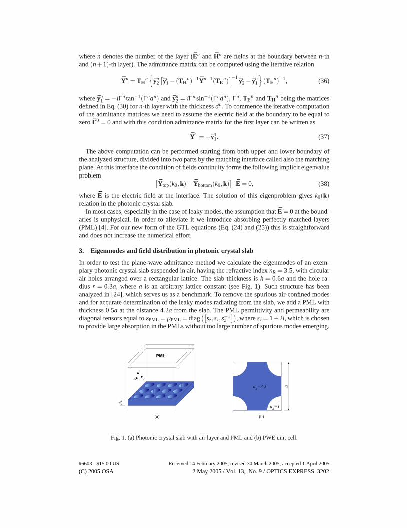
In order to test the plane-wave admittance method we calculate the eigenmodes of an exem-plary photonic crystal slab suspended in air, having the refractive index nR = 3.5, with circularair holes arranged over a rectangular lattice. The slab thickness is h = 0.6a and the hole ra-dius r = 0.3a, where a is an arbitrary lattice constant (see Fig. 1). Such structure has beenanalyzed in [24], which serves us as a benchmark. To remove the spurious air-confined modesand for accurate determination of the leaky modes radiating from the slab, we add a PML withthickness 0.5a at the distance 4.2a from the slab. The PML permittivity and permeability arediagonal tensors equal to εPML = µPML = diag
([sz,sz,s−1
z
]), where sz = 1−2i, which is chosen
to provide large absorption in the PMLs without too large number of spurious modes emerging.
Fig. 1. (a) Photonic crystal slab with air layer and PML and (b) PWE unit cell.
(C) 2005 OSA 2 May 2005 / Vol. 13, No. 9 / OPTICS EXPRESS 3202#6603 - $15.00 US Received 14 February 2005; revised 30 March 2005; accepted 1 April 2005
As the structure possesses an inversion symmetry in the z direction we reduce our calculationto the half of it. The disadvantage of this procedure is the inability to determine odd (TM-like [25]) modes, as for such modes the vector E from Eq. (38) is equal to zero. However,the analysis of odd modes is straightforward and requires only different choice of matchinginterface, namely out of symmetry plane. The alternative approach would be the choice of themagnetic field instead of the electric one in Eq. (38).
The structure is divided into three layers uniform in the z direction — the slab (actually onlya half of it is considered, as the matching plane is located in its center), the air layer and thePML. As the air and the PML are uniform layers, the computation is very efficient due to theabovementioned fact that for these layers the QH matrices are already diagonal. As for the corelayer the RE and RH matrices are computed using the Eq. (24) and (25) with the εG
x , εGy , κ G,
µGx , µG
y , γG determined analytically as Fourier expansion coefficients [2]. In order to improveconvergence the electric and magnetic constants are smoothed by convolution with Gaussianfunction
ε ′(r) = ε(r)∗ exp(−r2/σ), (39)
µ ′(r) = µ(r)∗ exp(−r2/σ). (40)
where σ is some small parameter which value has to be chosen empirically. For our calculationswe have chosen its value as 0.001a2.
The solution of Eq. (38) is searched, for an arbitrary wavevector k, by the determination ofthe complex roots of a function F(k0), which is defined as
F(k0) = min∣∣eigenvalues
([Ytop(k0,k)− Ybottom(k0,k)
])∣∣ . (41)
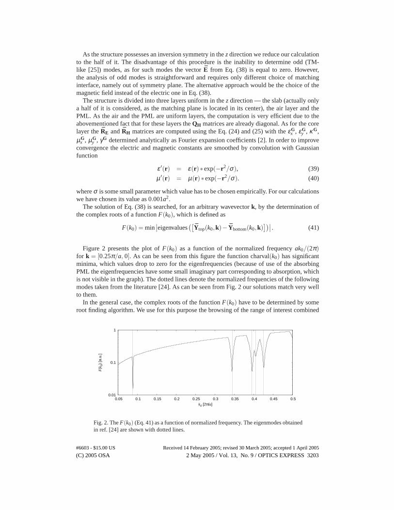
Figure 2 presents the plot of F(k0) as a function of the normalized frequency ak0/(2π)for k = [0.25π/a, 0]. As can be seen from this figure the function charval(k0) has significantminima, which values drop to zero for the eigenfrequencies (because of use of the absorbingPML the eigenfrequencies have some small imaginary part corresponding to absorption, whichis not visible in the graph). The dotted lines denote the normalized frequencies of the followingmodes taken from the literature [24]. As can be seen from Fig. 2 our solutions match very wellto them.
In the general case, the complex roots of the function F(k0) have to be determined by someroot finding algorithm. We use for this purpose the browsing of the range of interest combined
0.01
0.1
1
0.05 0.1 0.15 0.2 0.25 0.3 0.35 0.4 0.45 0.5
F(k
0) [a
.u.]
k0 [2π/a]
Fig. 2. The F(k0) (Eq. 41) as a function of normalized frequency. The eigenmodes obtainedin ref. [24] are shown with dotted lines.
(C) 2005 OSA 2 May 2005 / Vol. 13, No. 9 / OPTICS EXPRESS 3203#6603 - $15.00 US Received 14 February 2005; revised 30 March 2005; accepted 1 April 2005
with the Newton-Raphson method. However, numerical problems can arise when the holes arevery narrow, as one can see in the Fig. 2 (e.g. one around the frequency 0.08 ·2π/a) which maycause missing of some of the modes and therefore requires much denser sampling. This effectis especially strong for low frequencies.
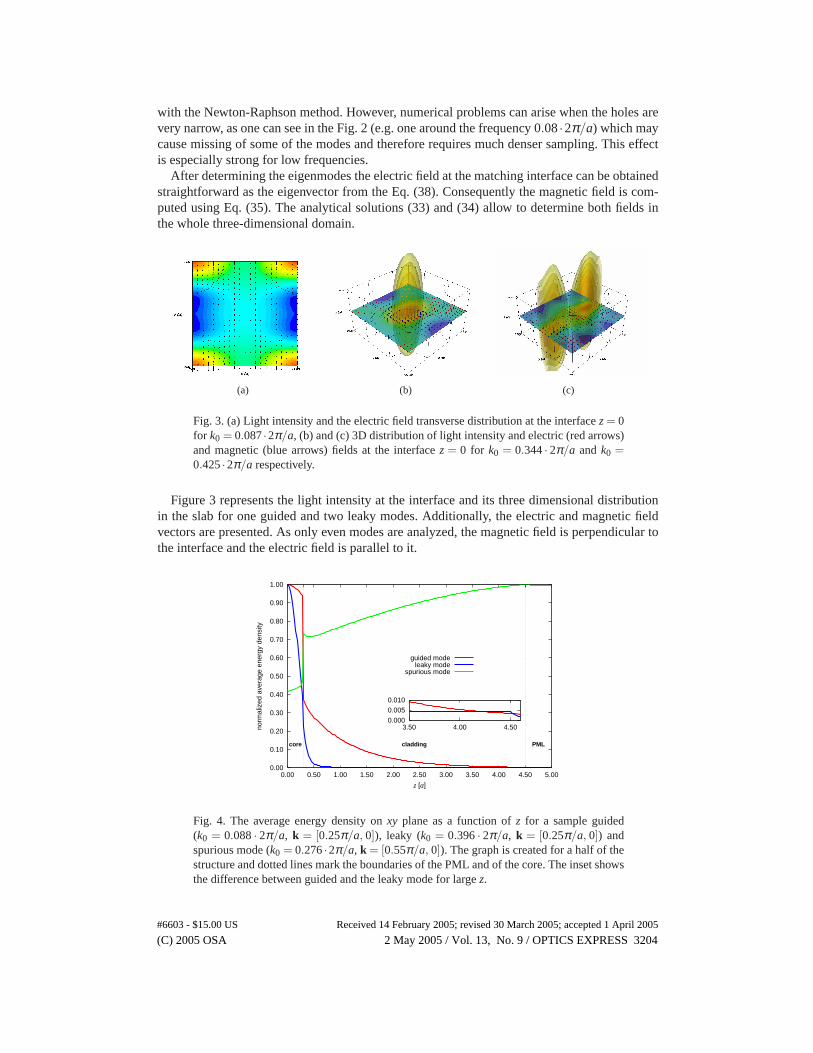
After determining the eigenmodes the electric field at the matching interface can be obtainedstraightforward as the eigenvector from the Eq. (38). Consequently the magnetic field is com-puted using Eq. (35). The analytical solutions (33) and (34) allow to determine both fields inthe whole three-dimensional domain.
(a) (b) (c)
Fig. 3. (a) Light intensity and the electric field transverse distribution at the interface z = 0for k0 = 0.087 ·2π/a, (b) and (c) 3D distribution of light intensity and electric (red arrows)and magnetic (blue arrows) fields at the interface z = 0 for k0 = 0.344 · 2π/a and k0 =0.425 ·2π/a respectively.
Figure 3 represents the light intensity at the interface and its three dimensional distributionin the slab for one guided and two leaky modes. Additionally, the electric and magnetic fieldvectors are presented. As only even modes are analyzed, the magnetic field is perpendicular tothe interface and the electric field is parallel to it.
0.00
0.10
0.20
0.30
0.40
0.50
0.60
0.70
0.80
0.90
1.00
0.00 0.50 1.00 1.50 2.00 2.50 3.00 3.50 4.00 4.50 5.00
norm
aliz
ed a
vera
ge e
nerg
y de
nsity
z [a]
core cladding PML
guided modeleaky mode
spurious mode
0.000
0.005
0.010
3.50 4.00 4.50
Fig. 4. The average energy density on xy plane as a function of z for a sample guided(k0 = 0.088 · 2π/a, k = [0.25π/a, 0]), leaky (k0 = 0.396 · 2π/a, k = [0.25π/a, 0]) andspurious mode (k0 = 0.276 ·2π/a, k = [0.55π/a, 0]). The graph is created for a half of thestructure and dotted lines mark the boundaries of the PML and of the core. The inset showsthe difference between guided and the leaky mode for large z.
(C) 2005 OSA 2 May 2005 / Vol. 13, No. 9 / OPTICS EXPRESS 3204#6603 - $15.00 US Received 14 February 2005; revised 30 March 2005; accepted 1 April 2005
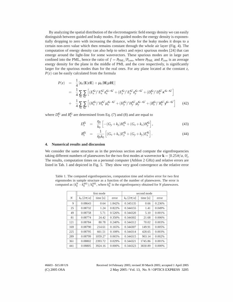
By analyzing the spatial distribution of the electromagnetic field energy density we can easilydistinguish between guided and leaky modes. For guided modes the energy density is exponen-tially dropping to zero with increasing the distance, while for the leaky modes it drops to acertain non-zero value which then remains constant through the whole air layer (Fig. 4). Thecomputation of energy density can also help to select and reject spurious modes [24] that canemerge around the light-line for some wavevectors. These spurious modes are in large partconfined into the PML, hence the ratio of f = PPML/Pcore, where PPML and Pcore is an averageenergy density for the plane in the middle of PML and the core respectively, is significantlylarger for the spurious modes than for the real ones. For any plane located at the constant z,P(z) can be easily calculated from the formula
P(z) =14
[ε0〈E|εE〉+ µ0〈H|µH〉]
=14 ∑
G∑G′
[(EG
x )∗EG′x εG−G′
x +(EGy )∗EG′
y εG−G′y +(DG
z )∗DG′z κ G−G′]
+14 ∑
G∑G′
[(HG
x )∗HG′x µG−G′
x +(HGy )∗HG′
y µG−G′y +(BG
z )∗BG′z γG−G′]
(42)
where DGz and BG
z are determined from Eq. (7) and (8) and are equal to
DGz =
η0
k0
[−(Gy + ky)HG
x +(Gx + kx)HGy
], (43)
BGz =
1η0k0
[(Gx + kx)EG
y +(Gy + ky)EGx
]. (44)
4. Numerical results and discussion
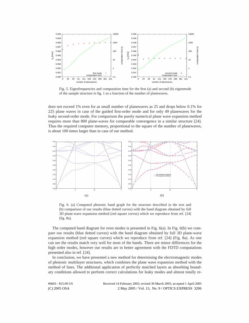
We consider the same structure as in the previous section and compute the eigenfrequenciestaking different numbers of planewaves for the two first modes at wavevector k = [0.25π/a, 0],The results, computation times on a personal computer (Athlon 2 GHz) and relative errors arelisted in Tab. 1 and depicted in Fig. 5. They show very good convergence as the relative error
Table 1. The computed eigenfrequencies, computation time and relative error for two firsteigenmodes in sample structure as a function of the number of planewaves. The error iscomputed as (kN
0 −k4410 )/k441
0 , where kN0 is the eigenfrequency obtained for N planewaves.
first mode second mode
N k0 [2π/a] time [s] error k0 [2π/a] time [s] error
9 0.08643 0.64 1.842% 0.345135 0.66 0.236%
25 0.08732 1.24 0.822% 0.344155 1.41 0.049%
49 0.08758 5.71 0.526% 0.344320 5.10 0.001%
81 0.08774 24.42 0.350% 0.344302 21.68 0.006%
121 0.08784 80.78 0.240% 0.344312 70.02 0.003%
169 0.08790 214.61 0.165% 0.344307 149.91 0.005%
225 0.08795 661.51 0.108% 0.344314 428.65 0.003%
289 0.08799 1059.27 0.065% 0.344315 903.14 0.002%
361 0.08802 2393.72 0.029% 0.344321 1745.86 0.001%
441 0.08805 3924.16 0.000% 0.344323 3830.89 0.000%
(C) 2005 OSA 2 May 2005 / Vol. 13, No. 9 / OPTICS EXPRESS 3205#6603 - $15.00 US Received 14 February 2005; revised 30 March 2005; accepted 1 April 2005
0.080
0.081
0.082
0.083
0.084
0.085
0.086
0.087
0.088
0.089
0.090
4413612892251691218149259 0.1
1
10
100
1000
10000
k 0 [2
π/a]
com
puta
tion
time
[s]
number of planewaves
first modecomputation time
0.340
0.341
0.342
0.343
0.344
0.345
0.346
0.347
0.348
0.349
0.350
4413612892251691218149259 0.1
1
10
100
1000
10000
k 0 [2
π/a]
com
puta
tion
time
[s]
number of planewaves
second modecomputation time
Fig. 5. Eigenfrequencies and computation time for the first (a) and second (b) eigenmodeof the sample structure in fig. 1 as a function of the number of planewaves.
does not exceed 1% even for as small number of planewaves as 25 and drops below 0.1% for225 plane waves in case of the guided first-order mode and for only 49 planewaves for theleaky second-order mode. For comparison the purely numerical plane wave expansion methodrequires more than 800 plane-waves for comparable convergence in a similar structure [24].Thus the required computer memory, proportional to the square of the number of planewaves,is about 100 times larger than in case of our method.
0.00
0.05
0.10
0.15
0.20
0.25
0.30
0.35
0.40
0.45
0.50
Γ X M Γ
(a)
0.00
0.05
0.10
0.15
0.20
0.25
0.30
0.35
0.40
0.45
0.50
Γ X M Γ
PW Admittance MethodPW Expansion Method
(b)
Fig. 6. (a) Computed photonic band graph for the structure described in the text and(b) comparison of our results (blue dotted curves) with the band diagram obtained by full3D plane-wave expansion method (red square curves) which we reproduce from ref. [24](fig. 8a).
The computed band diagram for even modes is presented in Fig. 6(a). In Fig. 6(b) we com-pare our results (blue dotted curves) with the band diagram obtained by full 3D plane-waveexpansion method (red square curves) which we reproduce from ref. [24] (Fig. 8a). As onecan see the results match very well for most of the bands. There are minor differences for thehigh order modes, however our results are in better agreement with the FDTD computationspresented also in ref. [24].
In conclusion, we have presented a new method for determining the electromagnetic modesof photonic multilayer structures, which combines the plane wave expansion method with themethod of lines. The additional application of perfectly matched layers as absorbing bound-ary conditions allowed to perform correct calculations for leaky modes and almost totally re-
(C) 2005 OSA 2 May 2005 / Vol. 13, No. 9 / OPTICS EXPRESS 3206#6603 - $15.00 US Received 14 February 2005; revised 30 March 2005; accepted 1 April 2005

duced spurious air-confined ones. The convergence of the method was improved by smoothingof the dielectric and magnetic tensors and proved to be very good even for small number ofplanewaves. Thus, the computations of band structure in photonic crystal slabs and generalelectromagnetic analysis of multi-layered structures can be performed with high efficiency.
Acknowledgments
This work is the result of Short Term Scientific Mission supported by the COST Action P11“Physics of linear, non-linear and active photonic crystals”. Additional contribution was pro-vided by the Polish Ministry of Science in the SPB grant DWM 86 associated to COST P11and the EC Network of Excellence on Micro-Optics “NEMO”.
We would like to thank Dr Tomasz Czyszanowski from Institute of Physics at the TechnicalUniversity of Lodz for his help in completing this work.
(C) 2005 OSA 2 May 2005 / Vol. 13, No. 9 / OPTICS EXPRESS 3207#6603 - $15.00 US Received 14 February 2005; revised 30 March 2005; accepted 1 April 2005