Nanoscale Texture on Glass and Titanium Substrates by Physical Vapor Deposition Process
6
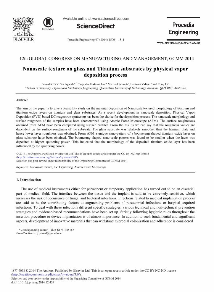
Procedia Engineering 97 (2014) 1506 – 1511 1877-7058 © 2014 The Authors. Published by Elsevier Ltd. This is an open access article under the CC BY-NC-ND license (http://creativecommons.org/licenses/by-nc-nd/3.0/). Selection and peer-review under responsibility of the Organizing Committee of GCMM 2014 doi:10.1016/j.proeng.2014.12.434 ScienceDirect Available online at www.sciencedirect.com 12th GLOBAL CONGRESS ON MANUFACTURING AND MANAGEMENT, GCMM 2014 Nanoscale texture on glass and Titanium substrates by physical vapor deposition process Prasad K.D.V. Yarlagadda a,* , Tuquabo Tesfamichael a Michael Schuetz a , Lalitsuri Valiveti a and Tong Li a , a School of chemistry, Physics and Mechanical Engineering, Queensland University of Technology, Brisbane, QLD 4001, Australia Abstract The aim of the paper is to give a feasibility study on the material deposition of Nanoscale textured morphology of titanium and titanium oxide layers on titanium and glass substrates. As a recent development in nanoscale deposition, Physical Vapor Deposition (PVD) based DC magnetron sputtering has been the choice for the deposition process. The nanoscale morphology and surface roughness of the samples have been characterized using Atomic Force Microscope (AFM). The surface roughnesses obtained from AFM have been compared using surface profiler. From the results we can say that the roughness values are dependent on the surface roughness of the substrate. The glass substrate was relatively smoother than the titanium plate and hence lower layer roughness was obtained. From AFM a unique nano-pattern of a boomerang shaped titanium oxide layer on glass substrate have been obtained. The boomerang shaped nano-scale pattern was found to be smaller when the layer was deposited at higher sputtering power. This indicated that the morphology of the deposited titanium oxide layer has been influenced by the sputtering power. © 2014 The Authors. Published by Elsevier Ltd. Selection and peer-review under responsibility of the Organizing Committee of GCMM 2014. Keywords: Nanoscale texture, PVD sputtering, Atomic Force Microscope 1. Introduction The use of medical instruments either for permanent or temporary application has turned out to be an essential part of medical field. The interface between the tissue and the implant is said to be extremely sensitive, which increases the risk of occurrence of fungal and bacterial infections. Infections related to medical implantation process are said to be the contributing factors to augmenting problems of nosocomial infections or hospital-acquired infections. To deal with these infections different specific strategies, various technical and non-technical prevention strategies and evidence-based recommendations have been set up. Strictly following hygienic rules throughout the insertion procedure or device implantation is of utmost importance. In addition to such fundamental and significant aspects, development of innovative materials that can withstand microbial colonization and adherence is considered * Corresponding author. Tel.:+ 61731385167 E-mail address: [email protected] © 2014 The Authors. Published by Elsevier Ltd. This is an open access article under the CC BY-NC-ND license (http://creativecommons.org/licenses/by-nc-nd/3.0/). Selection and peer-review under responsibility of the Organizing Committee of GCMM 2014
Transcript of Nanoscale Texture on Glass and Titanium Substrates by Physical Vapor Deposition Process
Procedia Engineering 97 ( 2014 ) 1506 – 1511
1877-7058 © 2014 The Authors. Published by Elsevier Ltd. This is an open access article under the CC BY-NC-ND license
(http://creativecommons.org/licenses/by-nc-nd/3.0/).
Selection and peer-review under responsibility of the Organizing Committee of GCMM 2014
doi: 10.1016/j.proeng.2014.12.434
ScienceDirect
Available online at www.sciencedirect.com
12th GLOBAL CONGRESS ON MANUFACTURING AND MANAGEMENT, GCMM 2014
Nanoscale texture on glass and Titanium substrates by physical vapor
deposition process
Prasad K.D.V. Yarlagaddaa,*, Tuquabo Tesfamichaela Michael Schuetza, Lalitsuri Valivetia and Tong Lia,
a School of chemistry, Physics and Mechanical Engineering, Queensland University of Technology, Brisbane, QLD 4001, Australia
Abstract
The aim of the paper is to give a feasibility study on the material deposition of Nanoscale textured morphology of titanium and titanium oxide layers on titanium and glass substrates. As a recent development in nanoscale deposition, Physical Vapor Deposition (PVD) based DC magnetron sputtering has been the choice for the deposition process. The nanoscale morphology and surface roughness of the samples have been characterized using Atomic Force Microscope (AFM). The surface roughnesses obtained from AFM have been compared using surface profiler. From the results we can say that the roughness values are dependent on the surface roughness of the substrate. The glass substrate was relatively smoother than the titanium plate and hence lower layer roughness was obtained. From AFM a unique nano-pattern of a boomerang shaped titanium oxide layer on glass substrate have been obtained. The boomerang shaped nano-scale pattern was found to be smaller when the layer was deposited at higher sputtering power. This indicated that the morphology of the deposited titanium oxide layer has been influenced by the sputtering power. © 2014 The Authors. Published by Elsevier Ltd. Selection and peer-review under responsibility of the Organizing Committee of GCMM 2014.
Keywords: Nanoscale texture, PVD sputtering, Atomic Force Microscope
1. Introduction
The use of medical instruments either for permanent or temporary application has turned out to be an essential part of medical field. The interface between the tissue and the implant is said to be extremely sensitive, which increases the risk of occurrence of fungal and bacterial infections. Infections related to medical implantation process are said to be the contributing factors to augmenting problems of nosocomial infections or hospital-acquired infections. To deal with these infections different specific strategies, various technical and non-technical prevention strategies and evidence-based recommendations have been set up. Strictly following hygienic rules throughout the insertion procedure or device implantation is of utmost importance. In addition to such fundamental and significant aspects, development of innovative materials that can withstand microbial colonization and adherence is considered
* Corresponding author. Tel.:+ 61731385167
E-mail address: [email protected]
© 2014 The Authors. Published by Elsevier Ltd. This is an open access article under the CC BY-NC-ND license
(http://creativecommons.org/licenses/by-nc-nd/3.0/).
Selection and peer-review under responsibility of the Organizing Committee of GCMM 2014

1507 Prasad K.D.V. Yarlagadda et al. / Procedia Engineering 97 ( 2014 ) 1506 – 1511
as major focus in current years. Surface modification by initial physical and chemical techniques may guide to change in unspecific and specific interactions with microbes and thus decrease in the adherence of microorganisms. Medical devices should be made with such materials that can resist microbial colonization and should be preferably anti-adhesive, so that, these kinds of devices can avoid any kind of severe infection inside the human system. Current researches have concentrated more on functionalizing implants related to biomedical field by surface alterations for the response of tailored tissue. Localized antimicrobial delivery methods have been explored as attempts for time effective treatment to prevent the origin of biofilm formation [1]. For the design of implant materials with therapeutic coatings for local drug administration, the coating requires to comply with certain requirements, for example: mechanical stability, bioactivity, good substrate adhesion and the ability to carry drugs [2]. These functionalities can contribute towards achieving a better fixation to the bone as well as the release of drugs to treat infections close to the implant. Hence, functional implant coatings are only seen as a potentially promising step to achieve longer life spans for implanted devices and long-term surgical success rates and thereby contribute towards reducing health care costs [3].
Surgical implants are mostly made up of titanium or titanium alloys [4]. Examples of their applications are as
dental implants, hip joints, artificial knee joints, bone plates, fixation screws and valve prostheses [5]. The clinical applications are established on biocompatibility, mechanical strength, non-toxicity, mechanical ability and their skill to osseous integration. Titanium is considered to be a very important metal and a preferable choice as surgical implant material because of its properties such as high strength, biocompatibility, lightweight, and durability in variety of environmental conditions. By creating a surface texture of titanium, we can explore the advantages of involving titanium in the areas like tissue growth by eradicating chances of infection, energy harvesting from solar radiation and catalysis [6].
In this paper we have illustrated one such attempt to modify the surface texture of titanium, which is to form a
nanoscale texture by physical modification technique. PVD-DC magnetron sputtering was used for the modification of the surface and atomic force microscopy (AFM) for the characterization. Sputtering is widely used in the industries because of its wide range of coatings, with the properties like hardness and wear-resistance, low friction and corrosion resistance. The sputtering process has been developed for many years, but with the development of unbalanced magnetron sputtering and the inclusion of multi-source system have brought a considerable rise in the importance for this technique. The DC magnetron sputtering is a process that is widely used to sputter metals such as titanium, where the deposition is of high quality and also well adhered. The AFM technique is used to obtain the quality of deposition of sample surfaces, which have a high resolution (in the order of fraction in nanometers). It is designed to measure the properties of the sample such as surface morphologies, roughness and size at nanoscale. The fundamental principles and the experimental procedures of both PVD and AFM are discussed in this paper. In this paper sputtering power and argon-to-oxygen gas ratio have been used as the main parameters for investigating the surface morphology changes of titanium and titanium oxide layers on titanium and glass substrates.
2. Methods
2.1. DC magnetron sputtering
Sputtering process interlinks many terms and they are cathodic sputtering, diode sputtering, RF sputtering, DC sputtering and ion-beam sputtering. Reactive process using oxygen or nitrogen gas may be applying duing sputtering to enhance materials properties and/or develop new material. However, all of these methods are variants of same physical phenomenon. The process in which the atoms or molecules of a material are released from the target by the bombardment of high-energy particles, it is known as sputtering. The target releases the material in such a way that usable quantities of material are procured, which can be directly coated onto substrates. There are two stages that are to be met to obtain sputtering as useful coating process. They are as follows [8][7]: first stage where ions of sufficient energy must be created in a plasma using argon gas and directed towards the surface of a target to release atoms from the material to be deposited. Next stage involves flexibility of released atoms due to vacuum so they can move freely towards the object to be coated with little independence to their movement. The tables below (Table 1

1508 Prasad K.D.V. Yarlagadda et al. / Procedia Engineering 97 ( 2014 ) 1506 – 1511
and 2) give the parameters involved in the process of DC magnetron sputtering during the deposition of elements.
Table 1. Technical parameters used in DC sputtering process
Parameters Values
Material Titanium Titanium oxide
Power (watt) 100, 200 200, 300
Ar:O2 gas ratio (%) 100:0 80:20 Time 60 min 90 min
Motor speed 10 rpm 10 rpm Deposition substrate temperature Room temperature Room temperature
Table 2. Sputtering processing variables for surface generation conditions
Variables Titanium layer Titanium oxide layer
Base pressure (mTorr) 6.8-7.0 E-8 6.4-6.8 E-8 Partial pressure (mTorr) 1.2 E-2 1.2-1.3 E-2
Ar Gas flow (SCCM) 30 27.9 O2 Gas flow (SCCM) 0 5.6
2.2. Atomic Force Microscopy
The first atomic force microscopy (AFM) is designed in 1986, a technique that emerged into a sequence of scanning exploration microscopes. The technique is to make use of the physical interactions involving a cantilevered probe (tip) in addition to sample for imaging while it scans over the specimen’s features. There are two imaging modes for AFM: contact and tapping modes. In the contact mode, the electronic feedback circuit, establishing a constant force of interaction between tip of the cantilever and the surface of the sample, can maintain a constant deflection. In the tapping mode, due to the resonance frequency, which is caused due to the piezoelectric element on the tip holder, the cantilever oscillates up and down. The AFM used in this work is FlexAFM C3000 (Nanosurf, Switzerland), installed on Leica inverted microscope. We were using silicon probes (Sicon, APPNano, US) for all the morphology scanning. The radius of the tip is 6nm and the spring constant is 0.3N/m.
Fig. 1 FlexAFM C3000 installed with Leica inverted microscope

1509 Prasad K.D.V. Yarlagadda et al. / Procedia Engineering 97 ( 2014 ) 1506 – 1511
In this work, AFM was used during the characterization of the Ti and TiO2 surfaces on glass and titanium substrates. The surface depositions of these substrates are obtained by AFM contact mode, and processed in SPIP imaging software. The cantilever tip scans the surface of the substrate, with the help of a laser beam that is positioned on the back of the cantilever [9]. A highly sharp cantilevered point passively detects the localized interaction forces in between the atoms associated with the scanning tip as well as the sample surface because sometimes the tip or even the specimen is raster scanned within the x-y plane over its supplement (tip or sample). Data was collected at an ambient air and in contact mode. The scans are ranged up to 10 om, with the resolution ranging from 256 pixels to 512 pixels [8][10]. Surface Profiler was used to measure the surface roughness of the deposited layers and compared with the AFM results.
3. Results and Discussion
There are various surface roughness parameters, each of these surface roughness parameters are calculated based on formula and are a standard reference describing the surface [11]. By using the modern digital equipment like the AFM, we can look at the scan and make sure that there are no noises from environment that are skewing the results. It is clear, for example that the average surface roughness (Ra) would fail to distinguish between two surfaces where one is composed of peaks on an otherwise smooth surface and the other is composed of troughs of the same amplitude. Height is presumed to be positive in the up direction, away from the material. In the analysis of samples obtained in this experiment both planer and 3D surface images were obtained. The surface roughness characterizations in the 3D images are denoted by S. Two samples of titanium layer deposited at 100 watt and 200 watt and two samples of titanium oxide layer obtained at 200 watt and 300 watt power are reported in the paper. The deposition parameters for obtaining these samples are shown in tables 1 and 2. Considering each as one case, there are four cases and the process details (tables 1 and 2) and the surface characteristics are discussed below and the results are shown in table 3.
Case 1: Titanium sputtered at 100 watt power for 60 min
This deposition was performed at 100-watt sputtering power for 60 minutes with other variables mentioned in tables 1 and 2. There was a good amount of deposition found on the surface of the substrates and the deposited layer appeared metallic-like reflective material. The deposited Ti layer surface roughness on titanium and glass substrates when measured in the profilometer were 51 nm and 12 nm, respectively. This indicated that the morphology of the deposited layer has been influenced by the type of substrate. When observed by AFM, nano-patterned peaks uniformly distributed on the surface of glass substrate have been observed (see Fig. 2a). There are peaks that are truncated when observed in the Ti layer on titanium substrate, because the heights of peaks were beyond the reach of the cantilever tip due to high surface roughness of the titanium substrate.
Case 2: Titanium sputtered at 200 watt power for 60 min
As expected a thicker Ti layer were obtained when the sputtering power was changed to 200 watt. The roughness of the titanium layer on titanium and glass substrates as measured with profiler were 151 nm and 17 nm, respectively. There is a large difference in the values of roughness of titanium layer on glass and titanium substrates. From AFM, there was no uniform distribution of the deposited layer as shown in Fig. 2b.
Case 3: Titanium oxide sputtered at 200 watt power for 90 min
Reactive DC sputtering was used when depositing titanium oxide layer. In this case oxygen of a given amount was introduced into the chamber during sputtering of titanium to form titanium oxide layer on glass and titanium substrates. The ratio of the argon to oxygen gases was selected, based on the desired level of metal-oxide layer to be deposition. A sputtering power of 200 watt for 90 minutes have been used as sputtering parameters and obtained transparent titanium oxide. The surface roughness of the oxide layer on titanium and glass substrates as measured using profiler were about 90 nm and 13 nm, respectively. As shown by AFM in Fig. 2c, a unique nano-pattern of a

1510 Prasad K.D.V. Yarlagadda et al. / Procedia Engineering 97 ( 2014 ) 1506 – 1511
boomerang shaped oxide layer on glass substrate has been deposited. The surface roughness on glass substrate was about 90 nm and this value is much larger than the results obtained using profiler (13 nm).
Case 4: Titanium oxide sputtering at 300 watt power for 90 min
A thick and transparent titanium oxide was found deposited on the substrates. This can be evaluated from the combined colors of blue green and pink observed on the surface of the oxide layer. AFM scans on glass (Fig. 2d) indicated a peculiar texture on the surface similar to the titanium oxide deposition at 200 watt but with smaller nano-scale boomerang shape.
Table 3. Surface roughness of titanium and titanium oxide layers on glass and titanium substrates obtained using surface profiler and AFM
Material Surface roughness on glass (Profiler)
Surface roughness on glass (AFM)
Surface roughness on Ti (Profiler)
Surface roughness on Ti (AFM)
Case 1 12 12.30 51 59.88 Case 2 17 17.62 151 51.26 Case 3 13 14.84 90 157.02 Case 4 11 11.26 - 72.664
Fig. 2 Surface morphology of Ti and TiO2 layers on Ti rough substrates obtained using DC sputtering method.

1511 Prasad K.D.V. Yarlagadda et al. / Procedia Engineering 97 ( 2014 ) 1506 – 1511
From the above table we can say that the roughness values are dependent on the surface roughness of the substrate. The glass substrate was relatively smoother than the titanium plate and hence lower layer roughness was obtained. It can be found that, under different PVD process conditions and different substrate materials, the nanoscale morphology of the newly generated surface varies. However, it is still not quite clear how these conditions directly change the morphology result, which needs further investigations.
4. Conclusion
In summary, titanium and titanium oxide layers were deposited on glass and titanium substrates using DC sputtering method. Reactive process of 80:20% Ar-to-oxygen ratio have been used when depositing the titanium oxide layer. We have demonstrated the deposition of nano-textured titanium and titanium oxide on the substrates of choice. From the AFM, the surface patterns of the two layers are found to be different with bigger hills and valleys and some peaks observed in the Ti layer on glass substrate. On the other hand a peculiar nano-scale texture of boomerang shaped titanium oxide layer on glass substrate has been achieved. The exact reason for the formation of the above-mentioned textures is unknown and requires further investigation.
Acknowledgements
Authors would like to thank all other technical staff of both PVD at AFM facility at Institute for Future
Environments, Queensland University of Technology. Reference
[1] Alhede, M., Høiby, N., Tvede, M., Bjarnsholt, T., Er, Ö., And Eickhardt, S.. Bacterial Biofilm Formation And Treatment In Soft Tissue Fillers. Pathogens and Disease , 70 (2014), 339 - 346. [2] Trajkovski, B., Petersen, A., Strube, P., Mehta, M., & Duda, G. N.. Intra-Operatively Customized Implant Coating Strategies For Local And Controlled Drug Delivery To Bone. Advanced Drug Delivery Reviews , 64 (2012), 1142. [3] Santin, M., & Phillips, G. J.. Biomimetic, Bioresponsive, And Bioactive Materials: An Introduction To Integrating Materials With Tissues. Wiley-Blackwell, Brighton, 2012. [4] Ellingsen, J. E., & Lyngstadaas, S. P. (2003). Bio-Implant Interface: Improving Biomaterials And Tissue Reactions. CRC Press, Boca Raton, 2003. [5] Matteo Santin, Gary Phillips. Biomimetic, Bioresponsive, And Bioactive Materials. Wiley & Sons Inc, 2012. [6] B.K. Nayak, M.C. Gupta1, K.W. Kolasinski, Formation Of Nano-Textured Conical Microstructures In Titanium Metal Surface By Femtosecond Laser Irradiation. Applied Physics A, 90(2008), 399-402. [7] S Swann, Magnetron Sputtering, Physics in Technology, 19(1988), 67. [8] Maryam Kharrazi Olsson. High-Rate Reactive Magnetron Sputter Deposition and Characterization of Metal Oxide Films, Uppsala Universitet, Uppsala, 2000. [9] Ratnesh Lal1, Srinivasan Ramachandran and Morton F.,Arnsdorf. Multidimensional Atomic Force Microscopy: a Versatile Novel Technology for Nanopharmacology Research, The AAPS Journal. 12(2010):716-28. [10] Jan Isidorsson. Lithium Intercalation In Tin Oxide Films, Physics and Electrochemistry, Acta Universitatis Upsaliensis, Uppsala, 1998, [11] Whitehouse, David. Surfaces and Their Measurement. Butterworth- Heinemann, Boston, 2012. [12] Q Chen, G Hubbard, PA Shields, C Liu, DWE Allsopp, WN Wang, S Abbott. Applied Physics Letters 94 (2009), 263118.