MnO2 decorated graphene nanoribbons with superior permittivity and excellent microwave shielding...
8
MnO 2 decorated graphene nanoribbons with superior permittivity and excellent microwave shielding properties† Tejendra K. Gupta, a Bhanu P. Singh, * a Vidya Nand Singh, b Satish Teotia, a Avanish Pratap Singh, c Indu Elizabeth, a Sanjay R. Dhakate, a S. K. Dhawan c and R. B. Mathur a Microwave shielding properties of chemically synthesized MnO 2 decorated graphene nanoribbons (GNRs) are reported for the first time. The nature of MnO 2 decoration on the GNRs has been investigated using scanning electron microscopy, X-ray diffraction, Raman spectroscopy and high resolution transmission electron microscopy. The electromagnetic interference (EMI) shielding effectiveness of this material was investigated in the microwave region (Ku-band, 12.4–18 GHz). The presence of MnO 2 on GNR enhances the interfacial polarization, multiple scattering, natural resonances and the effective anisotropy energy, which leads to absorption dominated high shielding effectiveness of 57 dB (blocking >99.9999% radiation) by a 3 mm thick sample. Dielectric attributes (3 0 and 3 00 ) were evaluated to understand the mechanism of the excellent shielding effectiveness. The material will be an excellent choice for radar absorbing applications. 1. Introduction Electromagnetic (EM) interference shielding materials are currently in high demand (for both commercial and defense purposes) because of electromagnetic pollution which is gener- ated due to extensive use of electrical and electronic equipment. EM radiation produced from an external source can disturb electrical circuits, cell phones, televisions, satellite communi- cations, global positioning systems (GPS), etc. The disturbances across communication channels, automation and process control lead to the loss of precious time, energy, resources and even life. Therefore, shielding must be provided to protect today's society from electromagnetic pollution. In general, there are two practical ways for shielding against electromagnetic interference (EMI): the rst is to protect certain components from the radiation by reecting or absorbing the waves; another is to reduce the reection and increase the absorption by incorporating dielectric or magnetic particles into it. In the present study, we focus on the second type of shielding, called absorption dominated microwave shielding. The complex dielectric permittivity is an important parameter for describing the properties of absorption dominated microwave shielding or radar absorbing materials (RAM). Excellent dielectric properties are needed for making good RAM. Therefore, lightweight EMI shielding materials 1–3 are sought in order to shield the workspace and environment from incoming radiation from computers and telecommunications as well as for protection of sensitive circuits. Previously, metal based microwave shielding materials were widely explored and utilized but the high specic gravity, corrosion proneness and cumbersome processing methods made these materials unsuitable for both the researchers and users. Furthermore, metals mainly reect the radiation and cannot be used for applications where absorption is mandatory. Nowadays, microwave shielding materials 4 with comparatively light weight, good exibility and strong absorption in the giga- hertz range are in high demand. Recently, carbon nanotubes (CNTs), 5 magnetic-particle-doped CNTs and nanostructured ZnO were intensively investigated and found to be promising shielding materials. Liu et al. 6 achieved a maximum absorption value of 22 dB at 8.8 GHz by 5 wt% single-walled carbon nanotubes (SWCNTs) loaded polyurethane composites. Fan et al. 7 reported a maximum absorption of about 24.3 dB at 15.3 GHZ by 8 wt% multi-walled carbon nanotubes (MWCNTs) loaded polymer (or varnish) composites. Singh et al. 8 reported a maximum shielding effectiveness due to absorption of 53 dB in the X-band (8.2–12.4 GHz) by 20.4 wt% MWCNTs loaded epoxy composites. Che et al. 9 have observed the microwave absorption of about 25 dB at 11 GHz by Fe–CNTs–epoxy composites. However, the complex fabrication process of CNTs a Physics and Engineering of Carbon, Division of Materials Physics and Engineering, CSIR-National Physical Laboratory, New Delhi, 110012, India. E-mail: bps@mail. nplindia.org; Fax: +91-11-45609310; Tel: +91-11-45608460 b Electron and Ion Microscopy Section, CSIR-National Physical Laboratory, New Delhi, 110012, India c Polymeric and So Materials Section, CSIR-National Physical Laboratory, New Delhi, 110012, India † Electronic supplementary information (ESI) available. See DOI: 10.1039/c3ta14854h Cite this: J. Mater. Chem. A, 2014, 2, 4256 Received 23rd November 2013 Accepted 19th December 2013 DOI: 10.1039/c3ta14854h www.rsc.org/MaterialsA 4256 | J. Mater. Chem. A, 2014, 2, 4256–4263 This journal is © The Royal Society of Chemistry 2014 Journal of Materials Chemistry A PAPER Published on 20 December 2013. Downloaded by National Physical Laboratory (NPL) on 24/06/2014 18:23:00. View Article Online View Journal | View Issue
-
Upload
independent -
Category
Documents
-
view
3 -
download
0
Transcript of MnO2 decorated graphene nanoribbons with superior permittivity and excellent microwave shielding...
Journal ofMaterials Chemistry A
PAPER
Publ
ishe
d on
20
Dec
embe
r 20
13. D
ownl
oade
d by
Nat
iona
l Phy
sica
l Lab
orat
ory
(NPL
) on
24/
06/2
014
18:2
3:00
.
View Article OnlineView Journal | View Issue
aPhysics and Engineering of Carbon, Divisio
CSIR-National Physical Laboratory, New D
nplindia.org; Fax: +91-11-45609310; Tel: +9bElectron and Ion Microscopy Section, CSIR-
110012, IndiacPolymeric and SoMaterials Section, CSIR-
110012, India
† Electronic supplementary informa10.1039/c3ta14854h
Cite this: J. Mater. Chem. A, 2014, 2,4256
Received 23rd November 2013Accepted 19th December 2013
DOI: 10.1039/c3ta14854h
www.rsc.org/MaterialsA
4256 | J. Mater. Chem. A, 2014, 2, 425
MnO2 decorated graphene nanoribbons withsuperior permittivity and excellent microwaveshielding properties†
Tejendra K. Gupta,a Bhanu P. Singh,*a Vidya Nand Singh,b Satish Teotia,a
Avanish Pratap Singh,c Indu Elizabeth,a Sanjay R. Dhakate,a S. K. Dhawanc
and R. B. Mathura
Microwave shielding properties of chemically synthesized MnO2 decorated graphene nanoribbons (GNRs)
are reported for the first time. The nature of MnO2 decoration on the GNRs has been investigated using
scanning electron microscopy, X-ray diffraction, Raman spectroscopy and high resolution transmission
electron microscopy. The electromagnetic interference (EMI) shielding effectiveness of this material was
investigated in the microwave region (Ku-band, 12.4–18 GHz). The presence of MnO2 on GNR enhances
the interfacial polarization, multiple scattering, natural resonances and the effective anisotropy energy,
which leads to absorption dominated high shielding effectiveness of �57 dB (blocking >99.9999%
radiation) by a 3 mm thick sample. Dielectric attributes (30 and 30 0) were evaluated to understand the
mechanism of the excellent shielding effectiveness. The material will be an excellent choice for radar
absorbing applications.
1. Introduction
Electromagnetic (EM) interference shielding materials arecurrently in high demand (for both commercial and defensepurposes) because of electromagnetic pollution which is gener-ated due to extensive use of electrical and electronic equipment.EM radiation produced from an external source can disturbelectrical circuits, cell phones, televisions, satellite communi-cations, global positioning systems (GPS), etc. The disturbancesacross communication channels, automation and processcontrol lead to the loss of precious time, energy, resources andeven life. Therefore, shielding must be provided to protecttoday's society from electromagnetic pollution. In general, thereare two practical ways for shielding against electromagneticinterference (EMI): the rst is to protect certain componentsfrom the radiation by reecting or absorbing the waves; anotheris to reduce the reection and increase the absorption byincorporating dielectric or magnetic particles into it.
In the present study, we focus on the second type of shielding,called absorption dominatedmicrowave shielding. The complex
n of Materials Physics and Engineering,
elhi, 110012, India. E-mail: bps@mail.
1-11-45608460
National Physical Laboratory, New Delhi,
National Physical Laboratory, New Delhi,
tion (ESI) available. See DOI:
6–4263
dielectric permittivity is an important parameter for describingthe properties of absorption dominated microwave shielding orradar absorbing materials (RAM). Excellent dielectric propertiesare needed for making good RAM. Therefore, lightweight EMIshieldingmaterials1–3are sought in order to shield theworkspaceand environment from incoming radiation from computers andtelecommunications as well as for protection of sensitivecircuits. Previously, metal based microwave shielding materialswere widely explored and utilized but the high specic gravity,corrosion proneness and cumbersome processing methodsmade these materials unsuitable for both the researchers andusers. Furthermore, metals mainly reect the radiation andcannot be used for applications where absorption is mandatory.Nowadays, microwave shielding materials4 with comparativelylight weight, good exibility and strong absorption in the giga-hertz range are in high demand. Recently, carbon nanotubes(CNTs),5 magnetic-particle-doped CNTs and nanostructuredZnO were intensively investigated and found to be promisingshielding materials. Liu et al.6 achieved a maximum absorptionvalue of �22 dB at 8.8 GHz by 5 wt% single-walled carbonnanotubes (SWCNTs) loaded polyurethane composites. Fanet al.7 reported a maximum absorption of about 24.3 dB at15.3 GHZ by 8 wt% multi-walled carbon nanotubes (MWCNTs)loaded polymer (or varnish) composites. Singh et al.8 reported amaximumshielding effectiveness due to absorption of�53 dB inthe X-band (8.2–12.4 GHz) by 20.4 wt% MWCNTs loaded epoxycomposites. Che et al.9 have observed the microwaveabsorption of about �25 dB at 11 GHz by Fe–CNTs–epoxycomposites. However, the complex fabrication process of CNTs
This journal is © The Royal Society of Chemistry 2014
Paper Journal of Materials Chemistry A
Publ
ishe
d on
20
Dec
embe
r 20
13. D
ownl
oade
d by
Nat
iona
l Phy
sica
l Lab
orat
ory
(NPL
) on
24/
06/2
014
18:2
3:00
. View Article Online
ormagnetic-particle-doped CNTs is a challenging task (for usingsuch absorbing nanocomposites in practical applications).Therefore, there is aneed to look for newmaterials with relativelylight weight, good exibility, long lasting and especially excep-tional microwave shielding properties.
Nanoscale materials based on single-layered 2-D graphenesheets have recently attracted great interest due to their manyextraordinary properties.10 At present, carbon based compositematerials employing CNTs are dominating the research andapplication elds. But the poor dispersion of CNTs due tobundling, the presenceof impurities, lack of interfacial adhesionwith other materials and high cost of production have marredtheir applications. It has been proposed that these issues couldbe reduced by incorporating graphene sheets into compositematerials.11,12 Graphene nanoribbons (GNRs) have also beenfound an important material in the carbon allotrope family.GNRs have been synthesized by different routes previously.13–18
On the other hand, manganese oxide (MnO2) offers a newpath for the development of advance microwave shieldingmaterials because of its low cost and environment friendlynature. It is well known that the pseudo-capacitive reaction ofMnO2 is a surface reaction and therefore only a very thin layer ofMnO2 is sufficient for high microwave shielding.19 Thus, ultra-thin MnO2 can deliver very high microwave shielding.
There are only few reports on using MnO2 as a microwaveshielding material. Duan et al.20 studied the microwaveabsorbing properties of a-MnO2–carbon black composites andshowed that these composites can absorb microwaves in a wideband range at about 8.7 GHz with lower than �10 dB (90%absorption) due to dielectric loss. Microwave absorption prop-erties of MnO2 composites were also studied by Guan et al.21 Intheir study, MnO2–SiO2–PVA composites had the strongestabsorbing peak of about 25 dB at 8.5 GHz for 30 vol% MnO2.
In the present study, we demonstrate the successful prepa-ration of MnO2 decorated GNRs via a chemical method in thepresence of concentrated sulfuric acid which plays an impor-tant role in increasing the interlayer distance of graphenelayers. The EMI shielding and dielectric properties of MnO2
decorated GNRs are studied and it is observed that the incor-poration of MnO2 improves the electromagnetic absorptionproperties which is due to the enhancement of dielectric loss.We also explored the effect of varying thickness of thecomposites on the EMI shielding performance.
2. Experimental2.1. Materials
Natural graphitewithpurity >99%andBSmesh500waspurchasedfrom Pune Carbon, Pune, India. KMnO4 (purity > 99%) and H2SO4
(purity > 98%) were purchased from Qualigens ne chemicals,Mumbai, India and RANKEM, New Delhi, India, respectively.
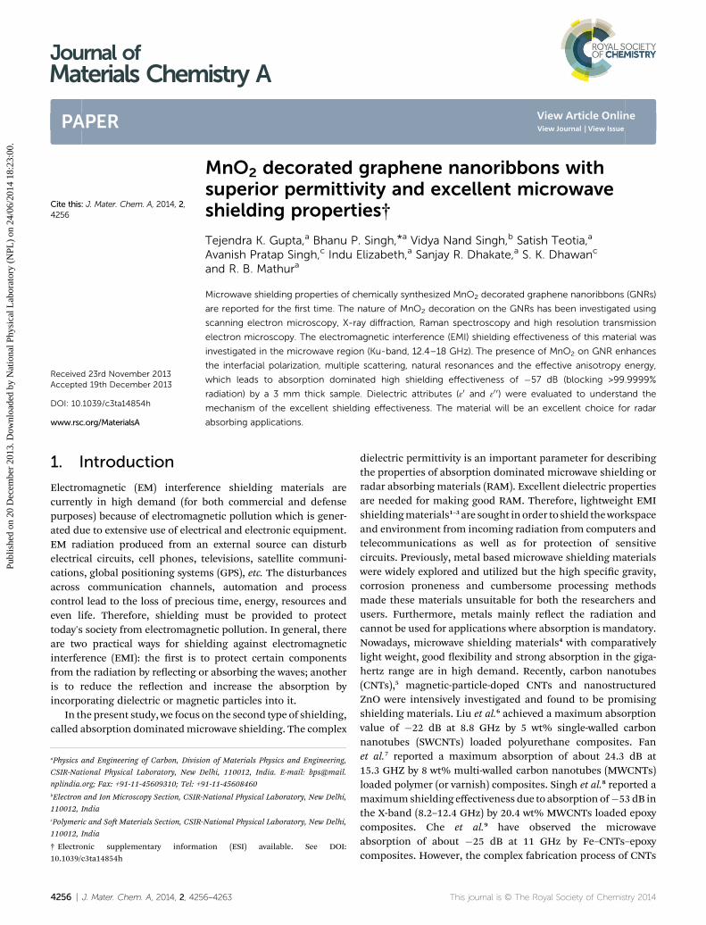
Scheme 1 Synthesis process of decoration of GNRs with MnO2.
2.2. Process for decoration of GNRs with MnO2
In a typical procedure as shown in Scheme 1, graphite akes(50 mg) were mixed with KMnO4 crystallites (300 mg) usingplanetary ball milling (2 h, 250 rpm) and a powder mixture was
This journal is © The Royal Society of Chemistry 2014
obtained. This mixture was suspended in 50 ml distilled waterand stirred using a magnetic stirrer (speed 600 rpm) at roomtemperature for 12 h. 5 ml of concentrated H2SO4 was intro-duced into the solution while continuing stirring (at 80 �C) foran additional 2 h. The reaction mixture was removed from theheat source, and poured into 500 ml distilled water to cool itdown and dilute it. The solution was then ltered using a0.22 mm pore size Whatman lter followed by several washingswith de-ionized water till the pH became neutral.
2.3. Characterization
Surface morphology of MnO2 decorated GNRs was investigatedusing SEM (Leo 440S, UK) and microstructural properties wereinvestigated using HRTEM (Technai G30-stwin, 300 kV instru-ment). Raman studies were carried out using a Renishaw inViareex Raman spectrometer, UK with an excitation source of514.5 nm. The XRD patterns were recorded using a Bruker D8Advance X-ray diffractometer in the diffraction (2q) range of 10–70� (slit width of 0.1 mm) using the Cu Ka line (l ¼ 1.5405 A) asradiation source. EMI shielding effectiveness (SE) and electro-magnetic attributes (real and imaginary permittivity) weremeasured using a vector network analyzer (VNA E8263B AgilentTechnologies) by placing pellet having dimensions 15.8 �7.9 mm2 inside a copper sample holder connected between thewave-guide anges of the network analyzer in the Ku-band(12.4–18.0 GHz) waveguide. These obtained complex parame-ters were estimated from experimental scattering parameters(S11 and S21) by standard Nicholson–Ross and Weir theoreticalcalculations.22 Furthermore, reection and transmission coef-cients were also evaluated using scattering parameters:, R ¼|S11|
2 ¼ |S22|2 and T ¼ |S21|
2 ¼ |S12|2. The absorbance was
calculated as A ¼ 1 � R � T.
3. Results and discussion3.1. Morphological and structural characterizations
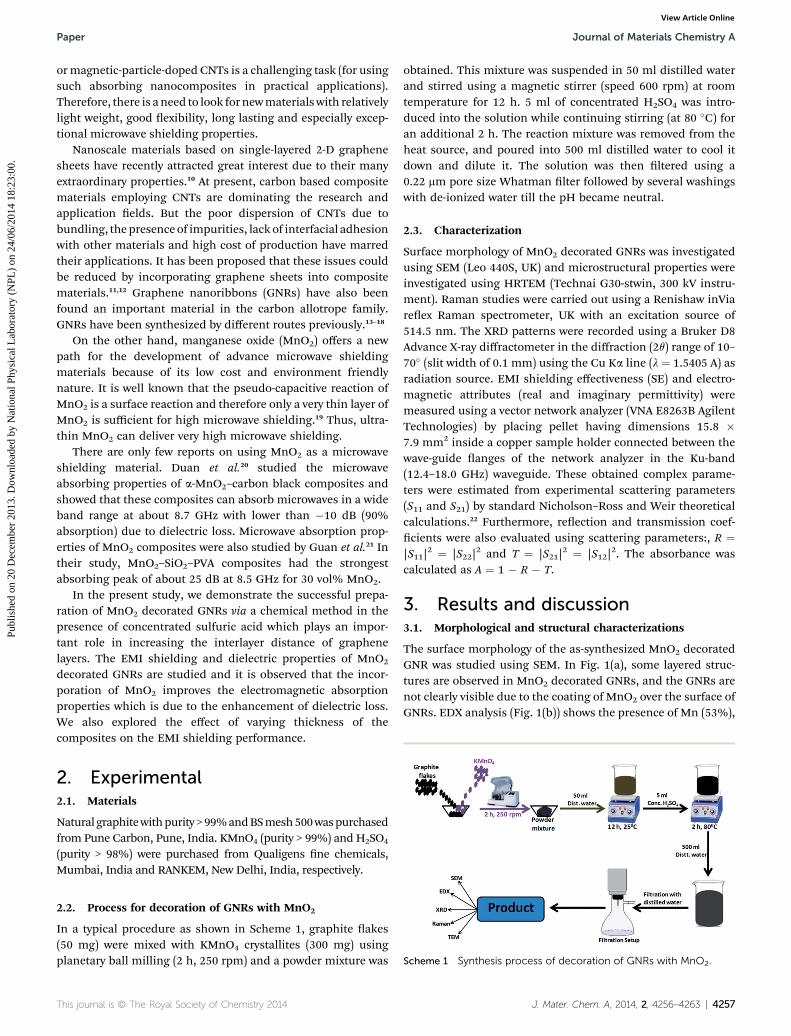
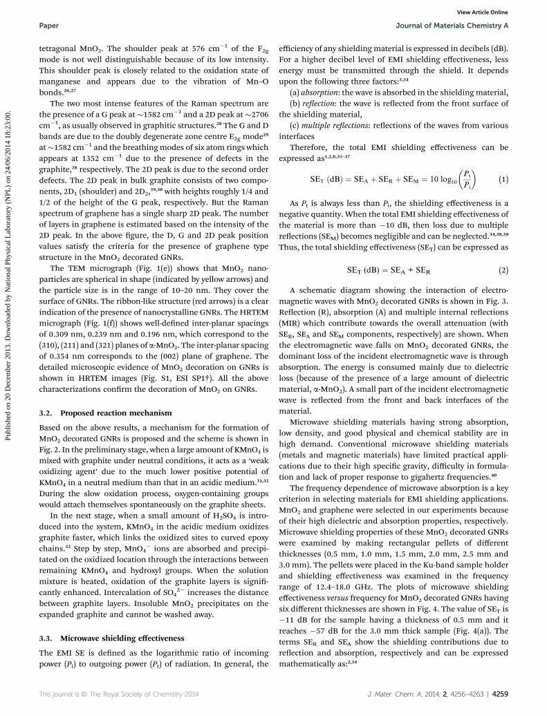
The surface morphology of the as-synthesized MnO2 decoratedGNR was studied using SEM. In Fig. 1(a), some layered struc-tures are observed in MnO2 decorated GNRs, and the GNRs arenot clearly visible due to the coating of MnO2 over the surface ofGNRs. EDX analysis (Fig. 1(b)) shows the presence of Mn (53%),
J. Mater. Chem. A, 2014, 2, 4256–4263 | 4257
Journal of Materials Chemistry A Paper
Publ
ishe
d on
20
Dec
embe
r 20
13. D
ownl
oade
d by
Nat
iona
l Phy
sica
l Lab
orat
ory
(NPL
) on
24/
06/2
014
18:2
3:00
. View Article Online
O (40%), and C (7%). XRD analysis was used to determine thestructure of the hybrid. The peak at a 2q value of 12.73� inFig. 1(c) is due to the (110) plane of a-MnO2. Other peaks areassigned to the tetragonal phase of a-MnO2 (JCPDS 44-0141)indicating better crystallinity in strong acidic medium.23,24
Moreover, a low intensity peak corresponding to the (002) plane(inset of Fig. 1(c)) of graphitic structure was observed in MnO2
decorated GNR samples. This might be due to the presence ofexcess MnO2 which prevented the stacking of graphene sheetsover each other to form crystalline structures.25 This is evident
Fig. 1 (a) SEM image, (b) EDX results, (c) XRD pattern, (d) Raman spectruMnO2 (yellow arrows) on the surface of GNR (red arrows) and (f) showilattice fringes (black circles).
4258 | J. Mater. Chem. A, 2014, 2, 4256–4263
from the EDX results which show that the carbon content inMnO2 decorated GNRs is only 7 wt%.
Fig. 1(d) shows the room temperature Raman spectrum ofMnO2 decorated GNRs. The Raman spectrum was recordedusing a low laser power of 5 mW in order to avoid any decom-position of the sample. The Raman spectrum of MnO2 deco-rated GNRs is dominated by a sharp and strong band atapproximately 645 cm�1 with a shoulder at 576 cm�1 which canbe assigned to a-MnO2. The Raman band at 645 cm�1 of the A1gmode is attributed to symmetric Mn–O stretching vibrations of
m of MnO2 decorated GNRs, (e) TEM image showing the presence ofng the inter-planar spacing (yellow lines) and an enlarged view of the
This journal is © The Royal Society of Chemistry 2014
Paper Journal of Materials Chemistry A
Publ
ishe
d on
20
Dec
embe
r 20
13. D
ownl
oade
d by
Nat
iona
l Phy
sica
l Lab
orat
ory
(NPL
) on
24/
06/2
014
18:2
3:00
. View Article Online
tetragonal MnO2. The shoulder peak at 576 cm�1 of the F2gmode is not well distinguishable because of its low intensity.This shoulder peak is closely related to the oxidation state ofmanganese and appears due to the vibration of Mn–Obonds.26,27
The two most intense features of the Raman spectrum arethe presence of a G peak at�1582 cm�1 and a 2D peak at�2706cm�1, as usually observed in graphitic structures.28 The G and Dbands are due to the doubly degenerate zone centre E2g mode29
at�1582 cm�1 and the breathingmodes of six atom rings whichappears at 1352 cm�1 due to the presence of defects in thegraphite,28 respectively. The 2D peak is due to the second orderdefects. The 2D peak in bulk graphite consists of two compo-nents, 2D1 (shoulder) and 2D2,29,30 with heights roughly 1/4 and1/2 of the height of the G peak, respectively. But the Ramanspectrum of graphene has a single sharp 2D peak. The numberof layers in graphene is estimated based on the intensity of the2D peak. In the above gure, the D, G and 2D peak positionvalues satisfy the criteria for the presence of graphene typestructure in the MnO2 decorated GNRs.
The TEM micrograph (Fig. 1(e)) shows that MnO2 nano-particles are spherical in shape (indicated by yellow arrows) andthe particle size is in the range of 10–20 nm. They cover thesurface of GNRs. The ribbon-like structure (red arrows) is a clearindication of the presence of nanocrystalline GNRs. The HRTEMmicrograph (Fig. 1(f)) shows well-dened inter-planar spacingsof 0.309 nm, 0.239 nm and 0.196 nm, which correspond to the(310), (211) and (321) planes of a-MnO2. The inter-planar spacingof 0.354 nm corresponds to the (002) plane of graphene. Thedetailed microscopic evidence of MnO2 decoration on GNRs isshown in HRTEM images (Fig. S1, ESI SP1†). All the abovecharacterizations conrm the decoration of MnO2 on GNRs.
3.2. Proposed reaction mechanism
Based on the above results, a mechanism for the formation ofMnO2 decorated GNRs is proposed and the scheme is shown inFig. 2. In the preliminary stage, when a large amount of KMnO4 ismixed with graphite under neutral conditions, it acts as a ‘weakoxidizing agent’ due to the much lower positive potential ofKMnO4 in a neutral medium than that in an acidic medium.31,32
During the slow oxidation process, oxygen-containing groupswould attach themselves spontaneously on the graphite sheets.
In the next stage, when a small amount of H2SO4 is intro-duced into the system, KMnO4 in the acidic medium oxidizesgraphite faster, which links the oxidized sites to curved epoxychains.33 Step by step, MnO4
� ions are absorbed and precipi-tated on the oxidized location through the interactions betweenremaining KMnO4 and hydroxyl groups. When the solutionmixture is heated, oxidation of the graphite layers is signi-cantly enhanced. Intercalation of SO4
2� increases the distancebetween graphite layers. Insoluble MnO2 precipitates on theexpanded graphite and cannot be washed away.
3.3. Microwave shielding effectiveness
The EMI SE is dened as the logarithmic ratio of incomingpower (Pi) to outgoing power (Pt) of radiation. In general, the
This journal is © The Royal Society of Chemistry 2014
efficiency of any shieldingmaterial is expressed in decibels (dB).For a higher decibel level of EMI shielding effectiveness, lessenergy must be transmitted through the shield. It dependsupon the following three factors:3,34
(a) absorption: the wave is absorbed in the shieldingmaterial,(b) reection: the wave is reected from the front surface of
the shielding material,(c) multiple reections: reections of the waves from various
interfacesTherefore, the total EMI shielding effectiveness can be
expressed as1,2,8,35–37
SET ðdBÞ ¼ SEA þ SER þ SEM ¼ 10 log10
�Pt
Pi
�(1)
As Pt is always less than Pi, the shielding effectiveness is anegative quantity. When the total EMI shielding effectiveness ofthe material is more than �10 dB, then loss due to multiplereections (SEM) becomes negligible and can be neglected.34,38,39
Thus, the total shielding effectiveness (SET) can be expressed as
SET (dB) ¼ SEA + SER (2)
A schematic diagram showing the interaction of electro-magnetic waves with MnO2 decorated GNRs is shown in Fig. 3.Reection (R), absorption (A) and multiple internal reections(MIR) which contribute towards the overall attenuation (withSER, SEA and SEM components, respectively) are shown. Whenthe electromagnetic wave falls on MnO2 decorated GNRs, thedominant loss of the incident electromagnetic wave is throughabsorption. The energy is consumed mainly due to dielectricloss (because of the presence of a large amount of dielectricmaterial, a-MnO2). A small part of the incident electromagneticwave is reected from the front and back interfaces of thematerial.
Microwave shielding materials having strong absorption,low density, and good physical and chemical stability are inhigh demand. Conventional microwave shielding materials(metals and magnetic materials) have limited practical appli-cations due to their high specic gravity, difficulty in formula-tion and lack of proper response to gigahertz frequencies.40
The frequency dependence of microwave absorption is a keycriterion in selecting materials for EMI shielding applications.MnO2 and graphene were selected in our experiments becauseof their high dielectric and absorption properties, respectively.Microwave shielding properties of these MnO2 decorated GNRswere examined by making rectangular pellets of differentthicknesses (0.5 mm, 1.0 mm, 1.5 mm, 2.0 mm, 2.5 mm and3.0 mm). The pellets were placed in the Ku-band sample holderand shielding effectiveness was examined in the frequencyrange of 12.4–18.0 GHz. The plots of microwave shieldingeffectiveness versus frequency for MnO2 decorated GNRs havingsix different thicknesses are shown in Fig. 4. The value of SET is�11 dB for the sample having a thickness of 0.5 mm and itreaches �57 dB for the 3.0 mm thick sample (Fig. 4(a)). Theterms SER and SEA show the shielding contributions due toreection and absorption, respectively and can be expressedmathematically as:2,34
J. Mater. Chem. A, 2014, 2, 4256–4263 | 4259
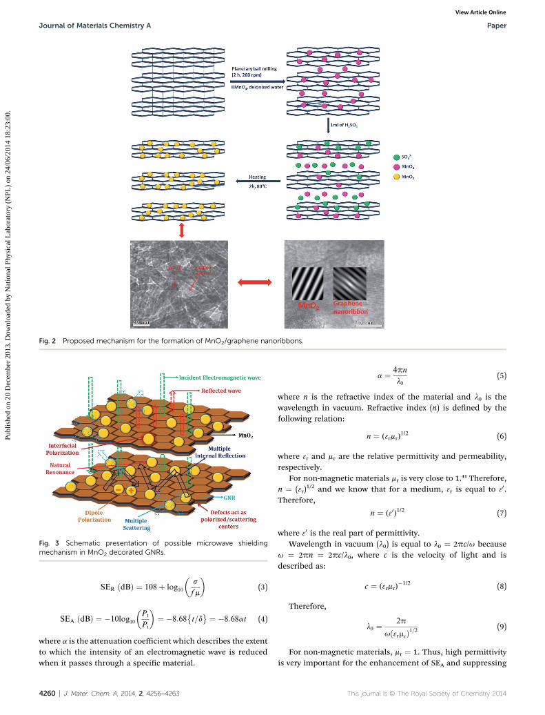
Fig. 2 Proposed mechanism for the formation of MnO2/graphene nanoribbons.
Fig. 3 Schematic presentation of possible microwave shieldingmechanism in MnO2 decorated GNRs.
Journal of Materials Chemistry A Paper
Publ
ishe
d on
20
Dec
embe
r 20
13. D
ownl
oade
d by
Nat
iona
l Phy
sica
l Lab
orat
ory
(NPL
) on
24/
06/2
014
18:2
3:00
. View Article Online
SER ðdBÞ ¼ 108þ log10
�s
f m
�(3)
SEA ðdBÞ ¼ �10log10
�Pt
Pi
�¼ �8:68
�t=d
� ¼ �8:68at (4)
where a is the attenuation coefficient which describes the extentto which the intensity of an electromagnetic wave is reducedwhen it passes through a specic material.
4260 | J. Mater. Chem. A, 2014, 2, 4256–4263
a ¼ 4pn
l0(5)
where n is the refractive index of the material and l0 is thewavelength in vacuum. Refractive index (n) is dened by thefollowing relation:
n ¼ (3rmr)1/2 (6)
where 3r and mr are the relative permittivity and permeability,respectively.
For non-magnetic materials mr is very close to 1.41 Therefore,n ¼ (3r)
1/2 and we know that for a medium, 3r is equal to 30.Therefore,
n ¼ (30)1/2 (7)
where 30 is the real part of permittivity.Wavelength in vacuum (l0) is equal to l0 ¼ 2pc/u because
u ¼ 2pn ¼ 2pc/l0, where c is the velocity of light and isdescribed as:
c ¼ (3rmr)�1/2 (8)
Therefore,
l0 ¼ 2p
uð3rmrÞ1=2(9)
For non-magnetic materials, mr ¼ 1. Thus, high permittivityis very important for the enhancement of SEA and suppressing
This journal is © The Royal Society of Chemistry 2014
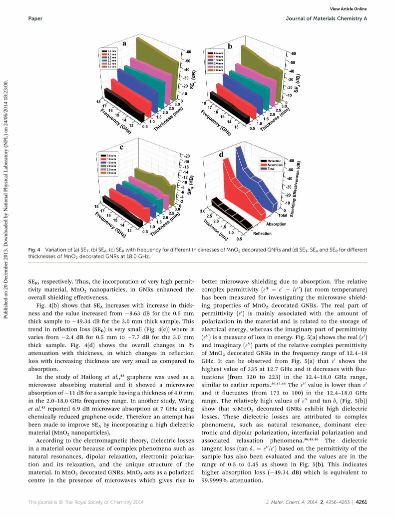
Fig. 4 Variation of (a) SET, (b) SEA, (c) SER with frequency for different thicknesses of MnO2 decorated GNRs and (d) SET, SEA and SER for differentthicknesses of MnO2 decorated GNRs at 18.0 GHz.
Paper Journal of Materials Chemistry A
Publ
ishe
d on
20
Dec
embe
r 20
13. D
ownl
oade
d by
Nat
iona
l Phy
sica
l Lab
orat
ory
(NPL
) on
24/
06/2
014
18:2
3:00
. View Article Online
SER, respectively. Thus, the incorporation of very high permit-tivity material, MnO2 nanoparticles, in GNRs enhanced theoverall shielding effectiveness.
Fig. 4(b) shows that SEA increases with increase in thick-ness and the value increased from �8.63 dB for the 0.5 mmthick sample to �49.34 dB for the 3.0 mm thick sample. Thistrend in reection loss (SER) is very small (Fig. 4(c)) where itvaries from �2.4 dB for 0.5 mm to �7.7 dB for the 3.0 mmthick sample. Fig. 4(d) shows the overall changes in %attenuation with thickness, in which changes in reectionloss with increasing thickness are very small as compared toabsorption.
In the study of Hailong et al.,42 graphene was used as amicrowave absorbing material and it showed a microwaveabsorption of�11 dB for a sample having a thickness of 4.0 mmin the 2.0–18.0 GHz frequency range. In another study, Wanget al.43 reported 6.9 dB microwave absorption at 7 GHz usingchemically reduced graphene oxide. Therefore an attempt hasbeen made to improve SEA by incorporating a high dielectricmaterial (MnO2 nanoparticles).
According to the electromagnetic theory, dielectric lossesin a material occur because of complex phenomena such asnatural resonances, dipolar relaxation, electronic polariza-tion and its relaxation, and the unique structure of thematerial. In MnO2 decorated GNRs, MnO2 acts as a polarizedcentre in the presence of microwaves which gives rise to
This journal is © The Royal Society of Chemistry 2014
better microwave shielding due to absorption. The relativecomplex permittivity (3* ¼ 30 � i30 0) (at room temperature)has been measured for investigating the microwave shield-ing properties of MnO2 decorated GNRs. The real part ofpermittivity (30) is mainly associated with the amount ofpolarization in the material and is related to the storage ofelectrical energy, whereas the imaginary part of permittivity(30 0) is a measure of loss in energy. Fig. 5(a) shows the real (30)and imaginary (30 0) parts of the relative complex permittivityof MnO2 decorated GNRs in the frequency range of 12.4–18GHz. It can be observed from Fig. 5(a) that 30 shows thehighest value of 335 at 12.7 GHz and it decreases with uc-tuations (from 320 to 223) in the 12.4–18.0 GHz range,similar to earlier reports.36,43,44 The 300 value is lower than 30
and it uctuates (from 173 to 100) in the 12.4–18.0 GHzrange. The relatively high values of 30 0 and tan d3 (Fig. 5(b))show that a-MnO2 decorated GNRs exhibit high dielectriclosses. These dielectric losses are attributed to complexphenomena, such as: natural resonance, dominant elec-tronic and dipolar polarization, interfacial polarization andassociated relaxation phenomena.36,45,46 The dielectrictangent loss (tan d3 ¼ 300/30) based on the permittivity of thesample has also been evaluated and the values are in therange of 0.5 to 0.45 as shown in Fig. 5(b). This indicateshigher absorption loss (�49.34 dB) which is equivalent to99.9999% attenuation.
J. Mater. Chem. A, 2014, 2, 4256–4263 | 4261
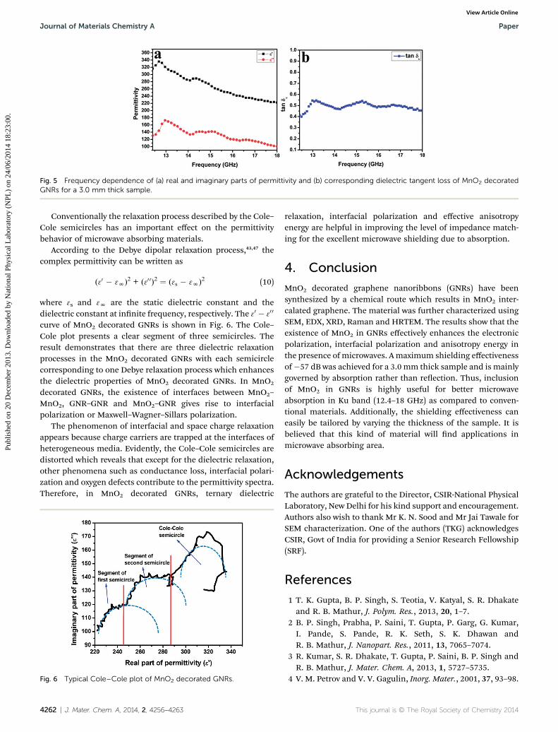
Fig. 5 Frequency dependence of (a) real and imaginary parts of permittivity and (b) corresponding dielectric tangent loss of MnO2 decoratedGNRs for a 3.0 mm thick sample.
Journal of Materials Chemistry A Paper
Publ
ishe
d on
20
Dec
embe
r 20
13. D
ownl
oade
d by
Nat
iona
l Phy
sica
l Lab
orat
ory
(NPL
) on
24/
06/2
014
18:2
3:00
. View Article Online
Conventionally the relaxation process described by the Cole–Cole semicircles has an important effect on the permittivitybehavior of microwave absorbing materials.
According to the Debye dipolar relaxation process,43,47 thecomplex permittivity can be written as
(30 � 3N)2 + (30 0)2 ¼ (3s � 3N)2 (10)
where 3s and 3N are the static dielectric constant and thedielectric constant at innite frequency, respectively. The 30 � 30 0
curve of MnO2 decorated GNRs is shown in Fig. 6. The Cole–Cole plot presents a clear segment of three semicircles. Theresult demonstrates that there are three dielectric relaxationprocesses in the MnO2 decorated GNRs with each semicirclecorresponding to one Debye relaxation process which enhancesthe dielectric properties of MnO2 decorated GNRs. In MnO2
decorated GNRs, the existence of interfaces between MnO2–
MnO2, GNR–GNR and MnO2–GNR gives rise to interfacialpolarization or Maxwell–Wagner–Sillars polarization.
The phenomenon of interfacial and space charge relaxationappears because charge carriers are trapped at the interfaces ofheterogeneous media. Evidently, the Cole–Cole semicircles aredistorted which reveals that except for the dielectric relaxation,other phenomena such as conductance loss, interfacial polari-zation and oxygen defects contribute to the permittivity spectra.Therefore, in MnO2 decorated GNRs, ternary dielectric
Fig. 6 Typical Cole–Cole plot of MnO2 decorated GNRs.
4262 | J. Mater. Chem. A, 2014, 2, 4256–4263
relaxation, interfacial polarization and effective anisotropyenergy are helpful in improving the level of impedance match-ing for the excellent microwave shielding due to absorption.
4. Conclusion
MnO2 decorated graphene nanoribbons (GNRs) have beensynthesized by a chemical route which results in MnO2 inter-calated graphene. The material was further characterized usingSEM, EDX, XRD, Raman and HRTEM. The results show that theexistence of MnO2 in GNRs effectively enhances the electronicpolarization, interfacial polarization and anisotropy energy inthe presence of microwaves. Amaximum shielding effectivenessof�57 dB was achieved for a 3.0 mm thick sample and is mainlygoverned by absorption rather than reection. Thus, inclusionof MnO2 in GNRs is highly useful for better microwaveabsorption in Ku band (12.4–18 GHz) as compared to conven-tional materials. Additionally, the shielding effectiveness caneasily be tailored by varying the thickness of the sample. It isbelieved that this kind of material will nd applications inmicrowave absorbing area.
Acknowledgements
The authors are grateful to the Director, CSIR-National PhysicalLaboratory, New Delhi for his kind support and encouragement.Authors also wish to thank Mr K. N. Sood and Mr Jai Tawale forSEM characterization. One of the authors (TKG) acknowledgesCSIR, Govt of India for providing a Senior Research Fellowship(SRF).
References
1 T. K. Gupta, B. P. Singh, S. Teotia, V. Katyal, S. R. Dhakateand R. B. Mathur, J. Polym. Res., 2013, 20, 1–7.
2 B. P. Singh, Prabha, P. Saini, T. Gupta, P. Garg, G. Kumar,I. Pande, S. Pande, R. K. Seth, S. K. Dhawan andR. B. Mathur, J. Nanopart. Res., 2011, 13, 7065–7074.
3 R. Kumar, S. R. Dhakate, T. Gupta, P. Saini, B. P. Singh andR. B. Mathur, J. Mater. Chem. A, 2013, 1, 5727–5735.
4 V. M. Petrov and V. V. Gagulin, Inorg. Mater., 2001, 37, 93–98.
This journal is © The Royal Society of Chemistry 2014
Paper Journal of Materials Chemistry A
Publ
ishe
d on
20
Dec
embe
r 20
13. D
ownl
oade
d by
Nat
iona
l Phy
sica
l Lab
orat
ory
(NPL
) on
24/
06/2
014
18:2
3:00
. View Article Online
5 N. Li, Y. Huang, F. Du, X. He, X. Lin, H. Gao, Y. Ma, F. Li,Y. Chen and P. C. Eklund, Nano Lett., 2006, 6, 1141–1145.
6 Z. Liu, G. Bai, Y. Huang, F. Li, Y. Ma, T. Guo, X. He, X. Lin,H. Gao and Y. Chen, J. Phys. Chem. C, 2007, 111, 13696–13700.
7 Z. Fan, G. Luo, Z. Zhang, L. Zhou and F. Wei,Mater. Sci. Eng.,B, 2006, 132, 85–89.
8 B. P. Singh, Prasanta, V. Choudhary, P. Saini, S. Pande,V. N. Singh and R. B. Mathur, J. Nanopart. Res., 2013, 15,1–12.
9 R. C. Che, L. M. Peng, X. F. Duan, Q. Chen and X. L. Liang,Adv. Mater., 2004, 16, 401–405.
10 A. K. Geim and K. S. Novoselov, Nat. Mater., 2007, 6, 183–191.11 S. Stankovich, D. A. Dikin, G. H. B. Dommett,
K. M. Kohlhaas, E. J. Zimney, E. A. Stach, R. D. Piner,S. B. T. Nguyen and R. S. Ruoff, Nature, 2006, 442, 282–286.
12 T. Ramanathan, A. A. Abdala, S. Stankovich, D. A. Dikin,M. Herrera-Alonso, R. D. Piner, D. H. Adamson,H. C. Schniepp, X. Chen, R. S. Ruoff, S. T. Nguyen,I. A. Aksay, R. K. Prud'Homme and L. C. Brinson, Nat.Nanotechnol., 2008, 3, 327–331.
13 L. Xie, H. Wang, C. Jin, X. Wang, L. Jiao, K. Suenaga andH. Dai, J. Am. Chem. Soc., 2011, 133, 10394–10397.
14 X. Li, X. Wang, L. Zhang, S. Lee and H. Dai, Science, 2008,319, 1229–1232.
15 L. Jiao, L. Zhang, X. Wang, G. Diankov and H. Dai, Nature,2009, 458, 877–880.
16 L. Jiao, L. Zhang, L. Ding, J. Liu and H. Dai, Nano Res., 2010,3, 387–394.
17 L. Jiao, X. Wang, G. Diankov, H. Wang and H. Dai, Nat.Nanotechnol., 2010, 5, 321–325.
18 L. Jiao, L. Xie and H. Dai, Nano Res., 2012, 5, 292–296.19 S. B. Ma, K. Y. Ahn, E. S. Lee, K. H. Oh and K. B. Kim, Carbon,
2007, 45, 375–382.20 Y. Duan, Y. Yang, M. He, S. Liu, X. Cui and H. Chen, J. Phys.
D: Appl. Phys., 2008, 41, 125403.21 H. Guan, S. Liu, Y. Zhao and Y. Duan, J. Electron. Mater.,
2006, 35, 892–896.22 A. M. Nicolson and G. F. Ross, IEEE Trans. Instrum. Meas.,
1970, 19, 377–382.23 J. Luo, H. T. Zhu, H. M. Fan, J. K. Liang, H. L. Shi, G. H. Rao,
J. B. Li, Z. M. Du and Z. X. Shen, J. Phys. Chem. C, 2008, 112,12594–12598.
24 W. Xiao, D. Wang and X. W. Lou, J. Phys. Chem. C, 2010, 114,1694–1700.
25 J. Yan, Z. Fan, T. Wei, W. Qian, M. Zhang and F. Wei, Carbon,2010, 48, 3825–3833.
26 C. Julien, M. Massot, R. Baddour-Hadjean, S. Franger,S. Bach and J. P. Pereira-Ramos, Solid State Ionics, 2003,159, 345–356.
This journal is © The Royal Society of Chemistry 2014
27 C. Julien and M. Massot, Phys. Chem. Chem. Phys., 2002, 4,4226–4235.
28 A. C. Ferrari, J. C. Meyer, V. Scardaci, C. Casiraghi,M. Lazzeri, F. Mauri, S. Piscanec, D. Jiang, K. S. Novoselov,S. Roth and A. K. Geim, Phys. Rev. Lett., 2006, 97, 187401.
29 R. J. Nemanich and S. A. Solin, Phys. Rev. B: Condens. MatterMater. Phys., 1979, 20, 392–401.
30 R. P. Vidano, D. B. Fischbach, L. J. Willis and T. M. Loehr,Solid State Commun., 1981, 39, 341–344.
31 K.-C. Chang, L. Li and E. F. Gloyna, J. Hazard. Mater., 1993,33, 51–62.
32 Y. Chen, Y. Zhang, D. Geng, R. Li, H. Hong, J. Chen andX. Sun, Carbon, 2011, 49, 4434–4442.
33 J.-L. Li, K. N. Kudin, M. J. McAllister, R. K. Prud'homme,I. A. Aksay and R. Car, Phys. Rev. Lett., 2006, 96, 176101.
34 T. K. Gupta, B. P. Singh, S. R. Dhakate, V. N. Singh andR. B. Mathur, J. Mater. Chem. A, 2013, 1, 9138–9149.
35 H.-B. Zhang, Q. Yan, W.-G. Zheng, Z. He and Z.-Z. Yu, ACSAppl. Mater. Interfaces, 2011, 3, 918–924.
36 A. P. Singh, M. Mishra, P. Sambyal, B. K. Gupta, B. P. Singh,A. Chandra and S. K. Dhawan, J. Mater. Chem. A, 2014, DOI:10.1039/c3ta14212d.
37 A. P. Singh, M. Mishra, A. Chandra and S. K. Dhawan,Nanotechnology, 2011, 22, 9.
38 K. Singh, A. Ohlan, V. H. Pham, B. R. S. Varshney, J. Jang,S. H. Hur, W. M. Choi, M. Kumar, S. K. Dhawan,B.-S. Kong and J. S. Chung, Nanoscale, 2013, 5, 2411–2420.
39 A. Ohlan, K. Singh, A. Chandra and S. K. Dhawan, ACS Appl.Mater. Interfaces, 2010, 2, 927–933.
40 X. Sun, J. He, G. Li, J. Tang, T. Wang, Y. Guo and H. Xue,J. Mater. Chem. C, 2013, 1, 765–777.
41 Y. A. Urzhumov, Sub-wavelength Electromagnetic Phenomenain Plasmonic and Polaritonic Nanostructures: From OpticalMagnetism to Super-resolution, The University of Texas atAustin, 2007.
42 H. Yu, T. Wang, B. Wen, M. Lu, Z. Xu, C. Zhu, Y. Chen,X. Xue, C. Sun and M. Cao, J. Mater. Chem., 2012, 22,21679–21685.
43 C. Wang, X. Han, P. Xu, X. Zhang, Y. Du, S. Hu, J. Wang andX. Wang, Appl. Phys. Lett., 2011, 98, 072906–072903.
44 T. K. Gupta, B. P. Singh, R. B. Mathur and S. R. Dhakate,Nanoscale, 2014, 6, 842–851.
45 X. G. Liu, D. Y. Geng, H. Meng, P. J. Shang and Z. D. Zhang,Appl. Phys. Lett., 2008, 92, 173117–173113.
46 Y.-F. Zhu, L. Zhang, T. Natsuki, Y.-Q. Fu and Q.-Q. Ni, ACSAppl. Mater. Interfaces, 2012, 4, 2101–2106.
47 M.-S. Cao, J. Yang, W.-L. Song, D.-Q. Zhang, B. Wen,H.-B. Jin, Z.-L. Hou and J. Yuan, ACS Appl. Mater.Interfaces, 2012, 4, 6949–6956.
J. Mater. Chem. A, 2014, 2, 4256–4263 | 4263