Vacancy effects on electronic and transport properties of graphene nanoribbons
13
Vacancy effects on electronic and transport properties of graphene nanoribbons Hai-Yao Deng and Katsunori Wakabayashi * International Center for Materials Nanoarchitechtonics (WPI-MANA), National Institute for Materials Science (NIMS), Namiki 1-1, Tsukuba 305-0044, Japan (Dated: January 7, 2015) We analytically study vacancy effects on electronic and transport properties of graphene nanoribbons and nanodots using Green’s function approach. For semiconducting systems, the presence of a vacancy induces a zero-energy midgap state. The spatial pattern of the wave functions critically depends on the atomistic edge structures, and can be used as an unambiguous probe of the edge structure. For metallic systems, the mid-gap vacancy state does not exist. In these systems, the vacancy mainly works as a source of electronic scattering and modifies electronic transmission. We derive that the electronic transmission coefficient can be written as T = cos 2 (α), where α denotes the phase angle of the on-site Green’s function at the vacancy site of the ideal systems. At small energies, T exhibits distinctly different functional form depending on edge structures. I. INTRODUCTION Vacancy in graphene has recently engrossed enormous at- tention 1–18 . The presence of vacancy significantly modifies the low-energy electronic properties of graphene 19–25 and gen- erates novel phenomena 26–31 . Vacancies cause resonant scat- tering at the Dirac points 8,20 and are considered a major fac- tor limiting graphene conductivity 22,32 . Most preceding the- oretical studies focused on infinite graphene (IG). In realistic samples, however, the presence of edges has been known to drastically affect the low-energy electronic properties of the system 33 . In Ref. 34 , by investigating semi-infinite graphene sheets (SIG), we showed that the vacancy state of graphene could be strongly modified in the presence of edges. In the present work, we extend our previous studies to graphene nanoribbons. We focus on armchair ribbons (ARs) and zigzag ribbons (ZRs), but also study bearded ZRs (BZRs, see Appendix A) and rectangular quantum dots (QDs, see Ap- pendix B). Since these systems possess two parallel edges in contrast to SIG, additional quantum confinement effects are expected. Adopting the nearest-neighbor tight-binding model, we analytically evaluate the Green’s functions and transition matrices for each system in the presence of a vacancy. We find that the vacancy is accompanied by a zero energy midgap state (ZES) in semiconducting systems. Nevertheless, the spa- tial profile of the ZES wave function turns out to critically de- pend on the edge structures. In metallic systems, no ZES is induced by the vacancy. Instead, the electronic transmission coefficient T shows subtle edge effects at low energies. We derive that T = cos 2 (α), where α denotes the phase angle of the on-site Green’s function at the vacancy site for the ideal systems. In the next section, we briefly recapitulate the formalism and summarize our main results. In Sec. III, we present the electronic structure for ideal ARs and ZRs. In Sec. IV, we analyze the Green’s functions and transition matrix. Section V is devoted to studying the ZES wave functions and their asymptotic long-distance behaviors. In Sec. VI we study the transport properties and derive a simple formula for T . We discuss our results and conclude the paper in Sec. VII. In Appendices A and B, we present calculation details for BZRs and QDs. II. FORMALISM AND RESULTS A. Formalism Graphene is a sheet of carbon atoms arranged on a honey- comb lattice, as depicted in Fig. 1 (a). In accordance with Ref. 34 , we designate each lattice site by (m, n,ν), where m counts the supercells, n the zigzag chains and ν = A, B refers to the sublattices. Further, we define ¯ A = B and ¯ B = A. In the paper, we choose unit of energy to be the nearest-neighbor electronic hopping integral γ 0 ≈ 2.7 eV and that of length to be the lattice constant a ≈ 0.142 nm. Without defects, the Hamiltonian of any graphene nanostructure is written as ˆ H 0 = - ∑ m,n,ν,m ′ ,n ′ |m, n,ν⟩⟨m ′ , n ′ , ¯ ν|, (1) where the sum runs over first neighbors throughout the en- tire structure. The effects of a single vacancy introduced at (m 0 , n 0 ,ν 0 ) are captured by the following on-site term, ˆ V = V |m 0 , n 0 ,ν 0 ⟩⟨m 0 , n 0 ,ν 0 |, (2) with the limit V →∞ implicitly understood. For IG, the eigenstates of ˆ H 0 are specified by the wave num- bers, k and p, and the particle-hole index s = ±1. We write them as 34,35 Ψ kps (m, n,ν) = e i[kx ν (m,n)+pn] f ν kps , (3) where x ν (m, n) denotes the x-coordinate of the site (m, n,ν) and f ν kps are components of the following spinor ˆ f kps := f A kps f B kps = √ 1 2 se -i θ(k, p) 2 e i θ(k, p) 2 , (4) with θ(k, p) being the phase angle of γ(k, p):= g k + e ip . Here g k := 2 cos( k 2 ). The dispersion relation is given by ε s (k, p) = s γ(k, p) = s √ 1 + g 2 k + 2g k cos( p). (5) In IG, in total four states are degenerate at the Dirac points, K ± = (k = ± 2π 3 , p = π).
-
Upload
manchester -
Category
Documents
-
view
1 -
download
0
Transcript of Vacancy effects on electronic and transport properties of graphene nanoribbons
Vacancy effects on electronic and transport properties of graphene nanoribbons
Hai-Yao Deng and Katsunori Wakabayashi∗International Center for Materials Nanoarchitechtonics (WPI-MANA),
National Institute for Materials Science (NIMS), Namiki 1-1, Tsukuba 305-0044, Japan(Dated: January 7, 2015)
We analytically study vacancy effects on electronic and transport properties of graphene nanoribbons andnanodots using Green’s function approach. For semiconducting systems, the presence of a vacancy induces azero-energy midgap state. The spatial pattern of the wave functions critically depends on the atomistic edgestructures, and can be used as an unambiguous probe of the edge structure. For metallic systems, the mid-gapvacancy state does not exist. In these systems, the vacancy mainly works as a source of electronic scatteringand modifies electronic transmission. We derive that the electronic transmission coefficient can be written asT = cos2(α), where α denotes the phase angle of the on-site Green’s function at the vacancy site of the idealsystems. At small energies, T exhibits distinctly different functional form depending on edge structures.
I. INTRODUCTION
Vacancy in graphene has recently engrossed enormous at-tention1–18. The presence of vacancy significantly modifiesthe low-energy electronic properties of graphene19–25 and gen-erates novel phenomena26–31. Vacancies cause resonant scat-tering at the Dirac points8,20 and are considered a major fac-tor limiting graphene conductivity22,32. Most preceding the-oretical studies focused on infinite graphene (IG). In realisticsamples, however, the presence of edges has been known todrastically affect the low-energy electronic properties of thesystem33. In Ref.34, by investigating semi-infinite graphenesheets (SIG), we showed that the vacancy state of graphenecould be strongly modified in the presence of edges.
In the present work, we extend our previous studies tographene nanoribbons. We focus on armchair ribbons (ARs)and zigzag ribbons (ZRs), but also study bearded ZRs (BZRs,see Appendix A) and rectangular quantum dots (QDs, see Ap-pendix B). Since these systems possess two parallel edges incontrast to SIG, additional quantum confinement effects areexpected. Adopting the nearest-neighbor tight-binding model,we analytically evaluate the Green’s functions and transitionmatrices for each system in the presence of a vacancy. Wefind that the vacancy is accompanied by a zero energy midgapstate (ZES) in semiconducting systems. Nevertheless, the spa-tial profile of the ZES wave function turns out to critically de-pend on the edge structures. In metallic systems, no ZES isinduced by the vacancy. Instead, the electronic transmissioncoefficient T shows subtle edge effects at low energies. Wederive that T = cos2(α), where α denotes the phase angle ofthe on-site Green’s function at the vacancy site for the idealsystems.
In the next section, we briefly recapitulate the formalismand summarize our main results. In Sec. III, we present theelectronic structure for ideal ARs and ZRs. In Sec. IV, weanalyze the Green’s functions and transition matrix. SectionV is devoted to studying the ZES wave functions and theirasymptotic long-distance behaviors. In Sec. VI we study thetransport properties and derive a simple formula for T . Wediscuss our results and conclude the paper in Sec. VII. InAppendices A and B, we present calculation details for BZRsand QDs.
II. FORMALISM AND RESULTS
A. Formalism
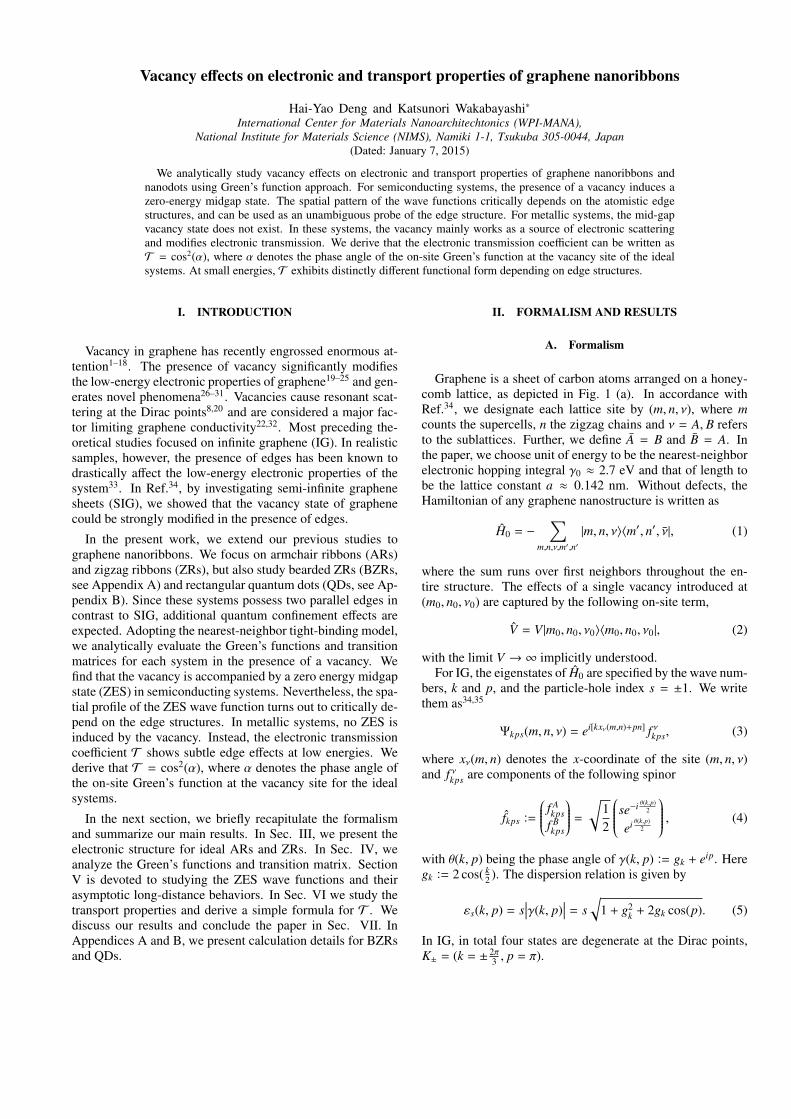
Graphene is a sheet of carbon atoms arranged on a honey-comb lattice, as depicted in Fig. 1 (a). In accordance withRef.34, we designate each lattice site by (m, n, ν), where mcounts the supercells, n the zigzag chains and ν = A, B refersto the sublattices. Further, we define A = B and B = A. Inthe paper, we choose unit of energy to be the nearest-neighborelectronic hopping integral γ0 ≈ 2.7 eV and that of length tobe the lattice constant a ≈ 0.142 nm. Without defects, theHamiltonian of any graphene nanostructure is written as
H0 = −∑
m,n,ν,m′,n′|m, n, ν⟩⟨m′, n′, ν|, (1)
where the sum runs over first neighbors throughout the en-tire structure. The effects of a single vacancy introduced at(m0, n0, ν0) are captured by the following on-site term,
V = V |m0, n0, ν0⟩⟨m0, n0, ν0|, (2)
with the limit V → ∞ implicitly understood.For IG, the eigenstates of H0 are specified by the wave num-
bers, k and p, and the particle-hole index s = ±1. We writethem as34,35
Ψkps(m, n, ν) = ei[kxν(m,n)+pn] f νkps, (3)
where xν(m, n) denotes the x-coordinate of the site (m, n, ν)and f νkps are components of the following spinor
fkps :=
f Akps
f Bkps
=√
12
se−i θ(k,p)2
ei θ(k,p)2
, (4)
with θ(k, p) being the phase angle of γ(k, p) := gk + eip. Heregk := 2 cos( k
2 ). The dispersion relation is given by
εs(k, p) = s∣∣∣γ(k, p)
∣∣∣ = s√
1 + g2k + 2gk cos(p). (5)
In IG, in total four states are degenerate at the Dirac points,K± = (k = ± 2π
3 , p = π).
2
a
AB
n
0
-1
-2
1
2
m0 1 2-1-2
m
x
y
(a) (b)
1
2
3
N
1 2 M
xx x x x x
x x x x x
N+1
0
a
unit cell
x
xx
xx
x
xx
xx
xx
x
0 M+1
n
(c)
unit cell
x
aT
FIG. 1: (Color online) Schematic of graphene lattice. In the longitudinal (x) direction, the lattice is viewed as a repetition of a supercell definedby the shaded rectangle. In the transverse (y) direction, it is a collection of zigzag chains. Each lattice site is coordinated as (m, n, ν), where mrefers to the supercells, n to the zigzag chains and ν = A, B the sublattices. The x-coordinates are chosen in such a way that xν(m, n) = m if thesite (m, n, ν) is to right of (m, n, ν). Otherwise, xν(m, n) = m − 1
2 . Schematic of graphene nanoribbons: (b) armchair nanoribbons (ARs) and (c)zigzag nanoribbons (ZRs). Crossed sites represent the boundaries of structures where the wavefunction should vanish. aT denotes the lengthof the AR unit cell.
The Green’s function of the defect-free system is defined as
Gνν′
τ (m, n,m′, n′; ε) =∫
dµΨτµ(m, n, ν)Ψτ∗µ (m′, n′, ν′)
ε + iη − ετµ, (6)
where ε is the energy, µ = (k, p, s),∫
dµ =∑
s
∫dk
∫dp
and η denotes a positive infinitesimal. We have introduceda superscript (subscript) τ to indicate the nanostructures. Tostudy the effects of a vacancy, we introduce a transition ma-trix, T τ = V(1 −GτV)−1, which has the following form,
T τ(ε) = T τ(ε) |m0, n0, ν0⟩⟨m0, n0, ν0|. (7)
Here T τ is given by
T τ(ε) = − 1Gτ
0(ε), (8)
with
Gτ0(ε) = Gν0ν0
τ (m0, n0,m0, n0; ε) =: Fτ(ε) − iπρτ0(ε), (9)
where ρτ0 stands for the local density of states (LDOS) of theideal system on the vacancy site. The quantity Fτ is related tothe LDOS by Kramers-Kronig relation.
The wave function of energy ε = 0 can be calculated in astandard manner (see Ref.34 for details). If ε = 0 correspondsto an isolated singularity of T τ(ε) inside the gap of the spec-trum of H0, then the wave function represents a midgap boundstate. It is given by
ψτ0(m, n, ν) = Gνν0τ (m, n,m0, n0; ε). (10)
On other hand, if T τ(ε) is regular at ε = 0, the wave functionis then obtained by the Lippmann-Schwinger equation36,
ψτε(m, n, ν) = Ψτi (m, n, ν)
− Gνν0τ (m, n,m0, n0; ε)
Gτ0(ε)
Ψτi (m0, n0, ν0). (11)
Here Ψτi depends on boundary conditions. In transport prob-lems, it describes a wave traveling toward the vacancy.
B. Results
In this subsection we briefly overview our results. TableI summarizes the low-energy behaviors of Gτ
0, T τ, ψτ0 and Tfor metallic ARs (mARs), semiconducting ARs (sARs), ZRs,BZRs and QDs.
In semiconducting (gapped) systems, i.e. sARs, BZRs andQDs, a vacancy produces a midgap state exactly at ε = 0.Nevertheless, the corresponding ψτ0 has completely differentspatial pattern. We find that ψsAR
0 represents a typical local-ized state of size M2, where M is the sAR width. It decaysexponentially with the increase of the distance R from the va-cancy. On the contrary, ψBZR
0 decays only as R−1 and hencelacks an intrinsic length, in analogy with what was observedof the resonant wave function in IG (ψIG
ε→0)34. However, thereasons are different. For ψBZR
0 , the R−1 dependence is rootedat the fact that the Dirac wave function has the phase differ-ence between A and B sublattices. For ψIG
ε→0, it arises becauseof the linear dispersion relation near the Dirac points in IG.Additionally, ψQD
0 is not localized about the vacancy at all.Rather, it is localized on the zigzag edge which belongs to thesublattice other than that of the vacancy.
In metallic systems, i.e. mARs and ZRs, no midgap stateis induced by a vacancy. Instead, the vacancy mainly causeselectronic scattering and is manifested in the low-energy elec-tronic transmission T . We find that T is totally determinedby the phase angle ατ of Gτ
0. Explicitly, we establish thatT = cos2(ατ). As displayed in Table I, T (ε) possesses verydifferent functional forms depending on the vacancy position
3
TABLE I: Asymptotic behaviors of Gτ0(ε) = Fτ(ε) − iπρτ0(ε), T τ(ε), ψτ0 and T (ε) in the limit ε→ 0. The exponents appearing in GZR
0 are givenby νρ ≈ 2n0−N
N−1 and |νF | ∼ |νρ|. The ατ in T is the phase angle of Gτ0(ε). The M in ψsAR
0 is the width of the sAR, x0 is the x-coordinate of thevacancy and R denotes the distance from the vacancy along the ribbon direction. A hyphen indicates the absence of the corresponding entry.
System sAR mAR(mod(x0,32 ) , 0) mAR(mod(x0,
32 ) = 0) ZR BZR QD
Vacancy (m0, 0, A) (m0, 0, A) (m0, 0, A) (0, n0, A) (0, n0, B) (m0, n0, A)ρτ0 0 const 0 |ε|νρ 0 0Fτ ε ε ε ε(n0−N/2)
|ε(n0−N/2)| |ε|νF ε ε
T τ ε−1 const ε−1 |ε|−νρ ε−1 ε−1
ψτ0 e−R/M - - - R−1 Edge-localizedψτ0 normalizable to unity Yes - - - Yes Yes
T = cos2(ατ) 0 ε2 1 (1 + const · ε2(νρ−νF ))−1 0 -
and the type of edges present in the system. In mAR, T (ε)either approaches zero or stays almost constant as ε → 0, de-pending on whether the vacancy sits off or on the nodal line ofthe wave function of ideal mAR. In ZR, a similar behavior oc-curs, depending on whether the vacancy is closer to the edgeof the same sublattice or not.
These results can be experimentally tested. The spatial pat-tern of ψτ0 may be mapped out using a scanning tunneling mi-croscope37, because the local tunneling conductivity is pro-portional to |ψτ0|2 at energies close to zero. Meanwhile, T canbe assessed on the basis of Landauer’s theory38,39, by directlymeasuring the linear ballistic conductance of the system.
III. IDEAL GRAPHENE NANORIBBONS
In this section, we present the electronic wave functions andband dispersions for ARs and ZRs, which are necessary ingre-dients of calculating the Green’s functions and other quantitiesin later sections. Results for BZRs and QDs will be describedin the Appendices A and B, respectively.
A. Armchair graphene ribbons
Figure 1 (b) schematically shows an AR consisting of Mcomplete supercells. We obtain its wave functions ΨAR
kps bysuperposingΨkps andΨ−kps of IG [Eq. (3)] so thatΨAR
kps vanishon the supercells m = 0 and m = M+1 [crossed sites in Fig. 1(b)]. We find
ΨARr,ps := ΨAR
kr ps =
√2
2M + 1eipn sin
[kr xν(m, n)
]f νkr ps. (12)
where the longitudinal wave number takes on discrete values,
kr =2π
2M + 1· r, r = 1, ..., M, (13)
leading to 2M subbands labeled by r and s. The correspondingdispersion relation is given by
εARrs (p) := εs(kr, p). (14)
−3
0
3
p
ε
π 2π0
k y
πT
a− π
Ta
(a) (b)
0
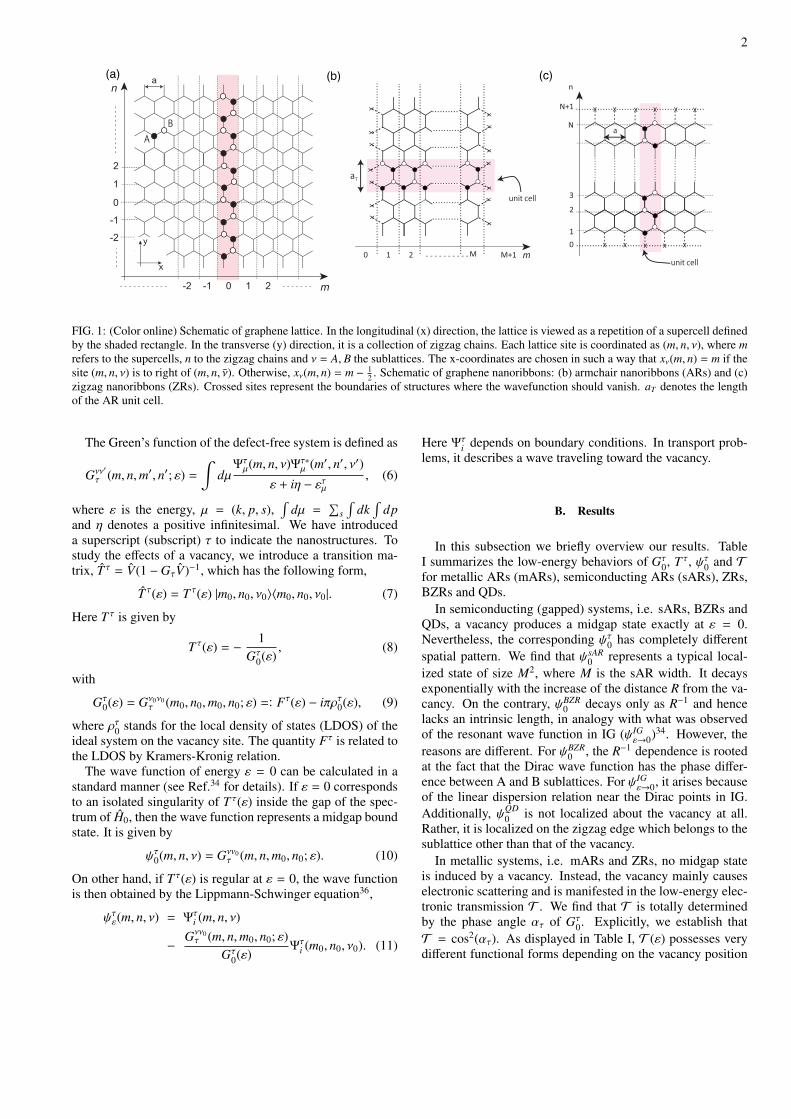
FIG. 2: (Color online) Energy spectrum for armchair graphene rib-bons with M = 7. (a) Energy dispersion obtained by Eq. (14). Notethe region of parameter p is 0 ≤ p ≤ 2π. (b) Band structure ofAR (see Fig. 2 in Ref.33) is obtained by folding the shaded regionin (a) into the central region. ky is the crystal momentum along they-direction in ARs.
Figure 2 (a) displays the band structure for M = 7. Panel(b) shows the same structure but with the shaded region in (a)folded into the central part40,41.
Metallic ARs (mARs) occur when mod(2M + 1, 3) = 0.Otherwise semiconducting ARs (sARs) occur. For mARs,there exist a pair of subbands with r = r0 =
2M+13 , which
pass through the Dirac point K+. The dispersion relation forthis pair becomes linear about p = π, i.e. εr0 s(p) ≈ s|δp|,where δp = p − π. For subbands other than r0, the dispersionrelations can be written as εrs(p) ≈ √gkr ·
√m2
r + δp2, where
mr =∣∣∣∣√gkr −
√1/gkr
∣∣∣∣ stands for a gap.
B. Zigzag graphene ribbons
Figure 1 (c) schematically shows a ZR composed of Nzigzag chains. We construct its wave functions ΨZR
kps by su-perposing Ψkps and Ψk−ps so that ΨZR
kps vanish on the crossed
4
−3
0
3
ε
(a)
(b)
00
k
kc-kc
π
ξ
Δ ZR
p
Δ ZR−
0
−π π
5π/6
4π/6
3π/6
2π/6
π/6
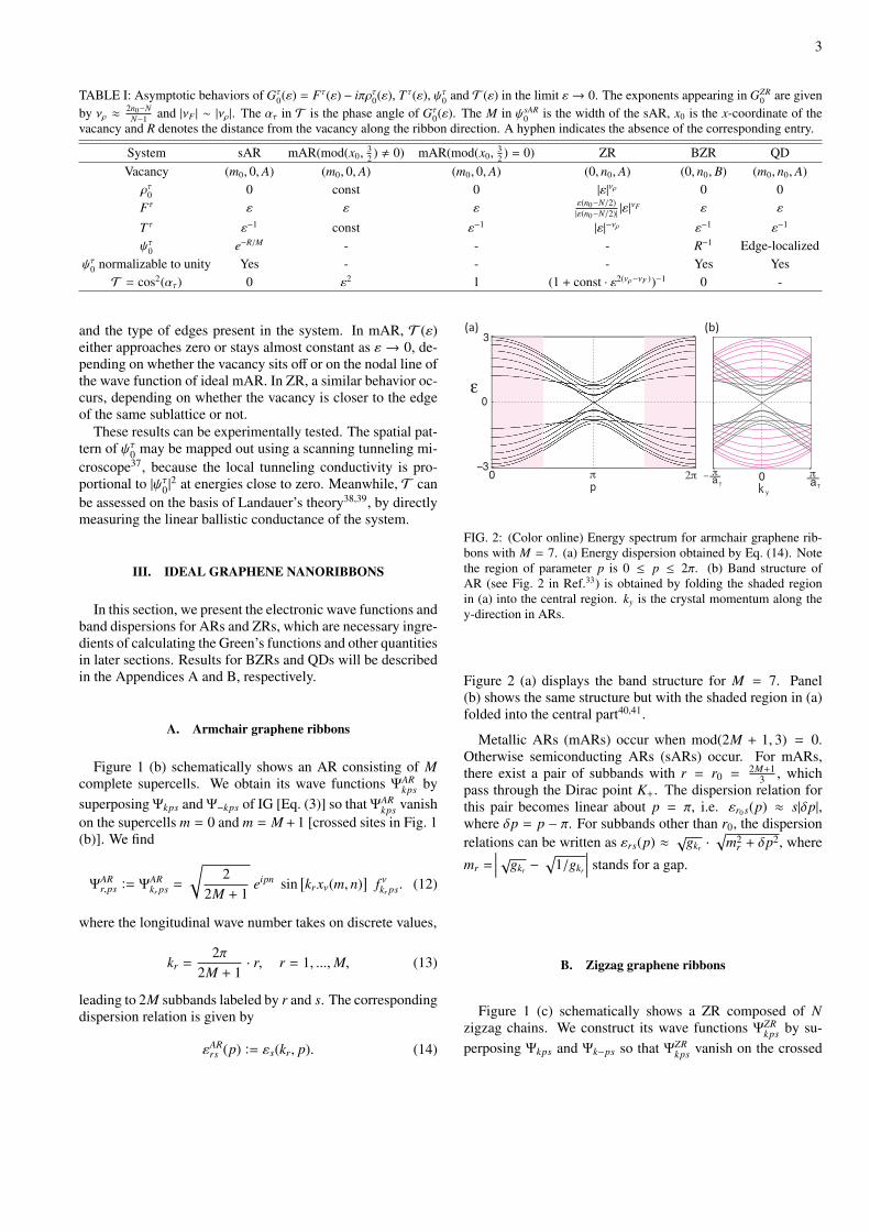
FIG. 3: (Color online) (a) Band structures for ZR with N = 6. (b)Numerical solution of Eq.(16) is plotted in k − p space, where thecurves beyond p = π represent the imaginary part of N-th root, i.e.pN = π − iξ, which gives edge states drawn in red lines in (a).
sites displayed in Fig. 1 (c). We obtain
ΨZRu,ks := ΨZR
kpu s =
√1Nu(k)
h(s, u) eikxν(m,n) sin[puyν(n)
].
(15)Here yA(n) = N + 1 − n, yB(n) = n and h(s, u) = (−1)u s forν = A whereas h(s, u) = 1 for ν = B. The normalization factorNu(k) = 2
∑n sin2[pun] can vary around N by a few percents
across the entire region of k. The transverse wave number pis quantized according to the following condition41,42,
sin[(N + 1)p − θ(k, p)] = 0. (16)
Given k, one can solve for p to get N physically different val-ues, pu, with u = 1, ...,N, resulting in 2N subbands labeled byu and s. The dispersion relation reads,
εZRu,s(k) = εs(k, pu). (17)
Figure 3 (a) exhibits the band structure of a ZR with N = 6.In Fig. 3 (b) we plot a numerical solution of Eq. (16) for
N = 6. As observed, we may write pu =uπN − δpu. For
u < N, δpu is a non-negative real value less than π/N for anyk. For u = N, however, there exists a critical value kc = 2 ·acos
(N
2(N+1)
). For |k| > kc, δpN =: iξ becomes pure imaginary,
which signifies the existence of edge states. For |k| < kc, weget real δpN , which decreases monotonically from ∼ π
N to zeroas |k| moves from zero toward kc.
ZRs are invariably metallic, because εN,+(k) and εN,−(k) al-ways touch at k = π. In the neighborhood of this point, thedispersion can be shown to be very flat43,44,
εN,s ≈ s · N · gN−1k (1 − g2
k) ≈ s · N · δkN−1, (18)
where δk > 0 denotes the deviation from π for k > 0 and thatfrom −π for k < 0, while the ΨZR
N,ks can be written as follows,
ΨZRN,ks(m, n, ν) ≈
√12
eikxν(m,n) δkN−yν(n)
−s , for ν = A1 , for ν = B
.
(19)Equations (18) and (19) will be used to study the low-energyproperties of ZRs.
IV. LOW-ENERGY BEHAVIORS OF Gτ0(ε)
In this section, we discuss the low-energy behaviors ofGτ
0(ε) near the Dirac point. The Green’s function is obtainedby inserting the wave functions and dispersion relations ob-tained in preceding section into Eq. (6). The vacancy-inducedZES can be located as the pole of T τ(ε). Since Gτ
0(−ε) =−Gτ∗
0 (ε), our analytical expressions will be explicitly givenfor ε ≥ 0.
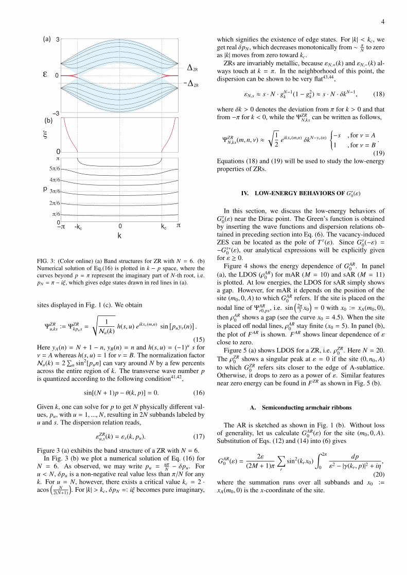
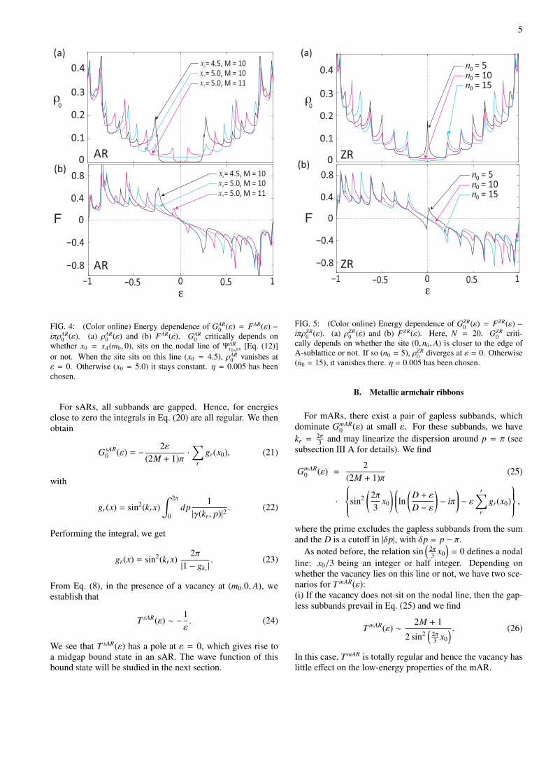
Figure 4 shows the energy dependence of GAR0 . In panel
(a), the LDOS (ρAR0 ) for mAR (M = 10) and sAR (M = 11)
is plotted. At low energies, the LDOS for sAR simply showsa gap. However, for mAR it depends on the position of thesite (m0, 0, A) to which GAR
0 refers. If the site is placed on thenodal line of ΨAR
r0,ps, i.e. sin(
2π3 x0
)= 0 with x0 := xA(m0, 0),
then ρAR0 shows a gap (see the curve x0 = 4.5). When the site
is placed off nodal lines, ρAR0 stay finite (x0 = 5). In panel (b),
the plot of FAR is shown. FAR shows linear dependence of εclose to zero.
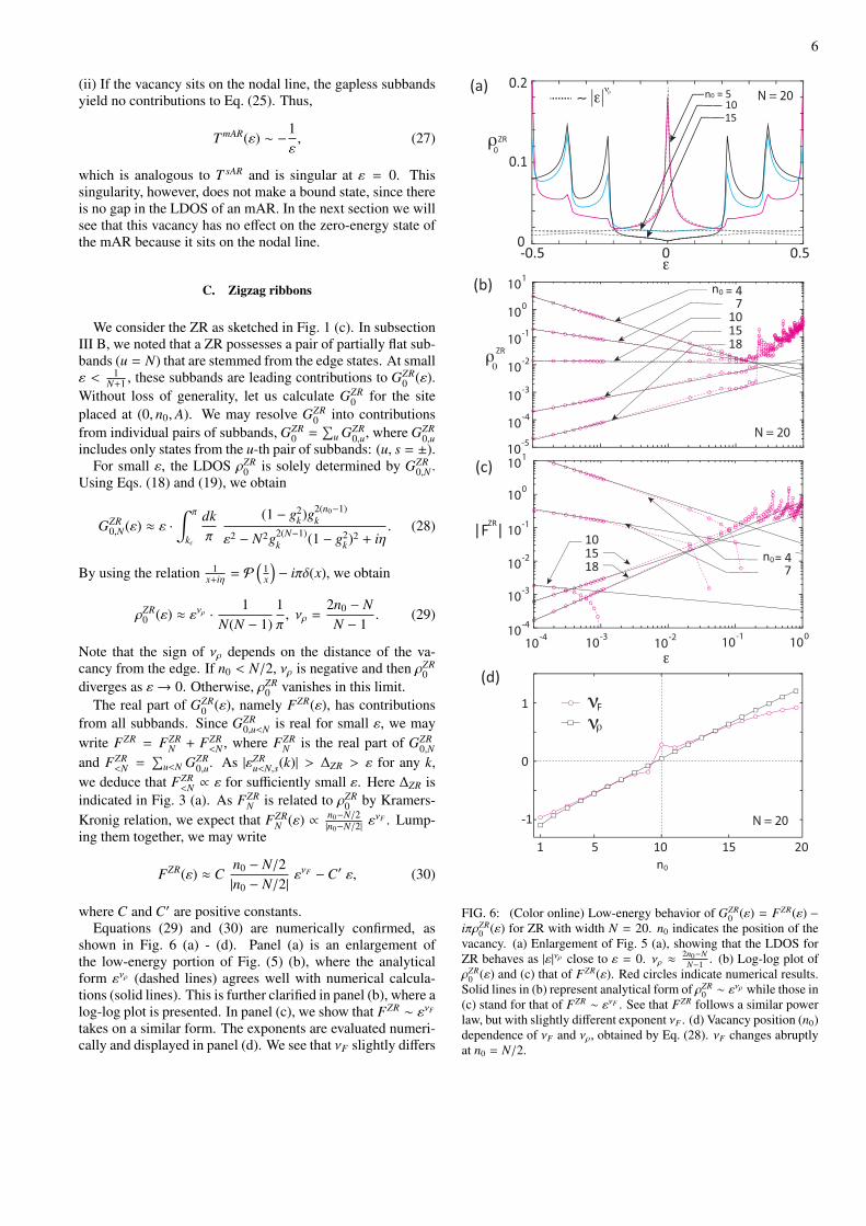
Figure 5 (a) shows LDOS for a ZR, i.e. ρZR0 . Here N = 20.
The ρZR0 shows a singular peak at ε = 0 if the site (0, n0, A)
to which GZR0 refers sits closer to the edge of A-sublattice.
Otherwise, it drops to zero as a power of ε. Similar featuresnear zero energy can be found in FZR as shown in Fig. 5 (b).
A. Semiconducting armchair ribbons
The AR is sketched as shown in Fig. 1 (b). Without lossof generality, let us calculate GAR
0 (ε) for the site (m0, 0, A).Substitution of Eqs. (12) and (14) into (6) gives
GAR0 (ε) =
2ε(2M + 1)π
∑r
sin2(kr x0)∫ 2π
0
dpε2 − |γ(kr, p)|2 + iη
,
(20)where the summation runs over all subbands and x0 :=xA(m0, 0) is the x-coordinate of the site.
5
(a)
ρ0
0.4
0.3
0.2
0.1
0
−1 0 1
−0.8
0
0.8
F
ε
x
0
= 4.5, M = 10
x
0
= 5.0, M = 10
x = 5.0, M = 110
AR
−0.4
0.4
x
0
= 4.5, M = 10
x
0
= 5.0, M = 10
x = 5.0, M = 110
AR
(b)
−0.5 0.5
FIG. 4: (Color online) Energy dependence of GAR0 (ε) = FAR(ε) −
iπρAR0 (ε). (a) ρAR
0 (ε) and (b) FAR(ε). GAR0 critically depends on
whether x0 = xA(m0, 0), sits on the nodal line of ΨARr0 ,ps [Eq. (12)]
or not. When the site sits on this line (x0 = 4.5), ρAR0 vanishes at
ε = 0. Otherwise (x0 = 5.0) it stays constant. η = 0.005 has beenchosen.
For sARs, all subbands are gapped. Hence, for energiesclose to zero the integrals in Eq. (20) are all regular. We thenobtain
GsAR0 (ε) = − 2ε
(2M + 1)π·∑
r
gr(x0), (21)
with
gr(x) = sin2(kr x)∫ 2π
0dp
1|γ(kr, p)|2 . (22)
Performing the integral, we get
gr(x) = sin2(kr x)2π
|1 − gkr |. (23)
From Eq. (8), in the presence of a vacancy at (m0.0, A), weestablish that
T sAR(ε) ∼ −1ε. (24)
We see that T sAR(ε) has a pole at ε = 0, which gives rise toa midgap bound state in an sAR. The wave function of thisbound state will be studied in the next section.
(a)
ρ0
0.4
0.3
0.2
0.1
0
−1 0 1
−0.8
0
0.8
F
ε
n = 5 n = 10 n = 15
0
0
0
ZR
(b)
−0.4
0.4
n = 5 n = 10 n = 15
0
0
0
ZR
−0.5 0.5
FIG. 5: (Color online) Energy dependence of GZR0 (ε) = FZR(ε) −
iπρZR0 (ε). (a) ρZR
0 (ε) and (b) FZR(ε). Here, N = 20. GZR0 criti-
cally depends on whether the site (0, n0, A) is closer to the edge ofA-sublattice or not. If so (n0 = 5), ρZR
0 diverges at ε = 0. Otherwise(n0 = 15), it vanishes there. η = 0.005 has been chosen.
B. Metallic armchair ribbons
For mARs, there exist a pair of gapless subbands, whichdominate GmAR
0 (ε) at small ε. For these subbands, we havekr =
2π3 and may linearize the dispersion around p = π (see
subsection III A for details). We find
GmAR0 (ε) =
2(2M + 1)π
(25)
·
sin2(
2π3
x0
) ln (D + εD − ε
)− iπ
− ε ′∑r
gr(x0)
,where the prime excludes the gapless subbands from the sumand the D is a cutoff in |δp|, with δp = p − π.
As noted before, the relation sin(
2π3 x0
)= 0 defines a nodal
line: x0/3 being an integer or half integer. Depending onwhether the vacancy lies on this line or not, we have two sce-narios for T mAR(ε):(i) If the vacancy does not sit on the nodal line, then the gap-less subbands prevail in Eq. (25) and we find
T mAR(ε) ∼ 2M + 1
2 sin2(
2π3 x0
) . (26)
In this case, T mAR is totally regular and hence the vacancy haslittle effect on the low-energy properties of the mAR.
6
(ii) If the vacancy sits on the nodal line, the gapless subbandsyield no contributions to Eq. (25). Thus,
T mAR(ε) ∼ −1ε, (27)
which is analogous to T sAR and is singular at ε = 0. Thissingularity, however, does not make a bound state, since thereis no gap in the LDOS of an mAR. In the next section we willsee that this vacancy has no effect on the zero-energy state ofthe mAR because it sits on the nodal line.
C. Zigzag ribbons
We consider the ZR as sketched in Fig. 1 (c). In subsectionIII B, we noted that a ZR possesses a pair of partially flat sub-bands (u = N) that are stemmed from the edge states. At smallε < 1
N+1 , these subbands are leading contributions to GZR0 (ε).
Without loss of generality, let us calculate GZR0 for the site
placed at (0, n0, A). We may resolve GZR0 into contributions
from individual pairs of subbands, GZR0 =
∑u GZR
0,u, where GZR0,u
includes only states from the u-th pair of subbands: (u, s = ±).For small ε, the LDOS ρZR
0 is solely determined by GZR0,N .
Using Eqs. (18) and (19), we obtain
GZR0,N(ε) ≈ ε ·
∫ π
kc
dkπ
(1 − g2k)g2(n0−1)
k
ε2 − N2g2(N−1)k (1 − g2
k)2 + iη. (28)
By using the relation 1x+iη = P
(1x
)− iπδ(x), we obtain
ρZR0 (ε) ≈ ενρ · 1
N(N − 1)1π, νρ =
2n0 − NN − 1
. (29)
Note that the sign of νρ depends on the distance of the va-cancy from the edge. If n0 < N/2, νρ is negative and then ρZR
0diverges as ε→ 0. Otherwise, ρZR
0 vanishes in this limit.The real part of GZR
0 (ε), namely FZR(ε), has contributionsfrom all subbands. Since GZR
0,u<N is real for small ε, we maywrite FZR = FZR
N + FZR<N , where FZR
N is the real part of GZR0,N
and FZR<N =
∑u<N GZR
0,u. As |εZRu<N,s(k)| > ∆ZR > ε for any k,
we deduce that FZR<N ∝ ε for sufficiently small ε. Here ∆ZR is
indicated in Fig. 3 (a). As FZRN is related to ρZR
0 by Kramers-Kronig relation, we expect that FZR
N (ε) ∝ n0−N/2|n0−N/2| ε
νF . Lump-ing them together, we may write
FZR(ε) ≈ Cn0 − N/2|n0 − N/2| ε
νF −C′ ε, (30)
where C and C′ are positive constants.Equations (29) and (30) are numerically confirmed, as
shown in Fig. 6 (a) - (d). Panel (a) is an enlargement ofthe low-energy portion of Fig. (5) (b), where the analyticalform ενρ (dashed lines) agrees well with numerical calcula-tions (solid lines). This is further clarified in panel (b), where alog-log plot is presented. In panel (c), we show that FZR ∼ ενF
takes on a similar form. The exponents are evaluated numeri-cally and displayed in panel (d). We see that νF slightly differs
10-4
10-3
10-2
10-1
100
10-5
10-4
10-3
10-2
10-1
100
101
ρ0
ε
10-4
10-3
10-2
10-1
100
101
|F |
νF
νρ
N = 20
1 5 10 15 20
-1
0
1
n0
n0 = 4
10
18
7
15
N = 20
N = 20
= 47
n0
10
1815
0.1
0.2
00-0.5 0.5ε
ρ0
ZR
n0 = 5
1510
∼ |ε|νρ
ZR
ZR
(a)
(b)
(c)
(d)
FIG. 6: (Color online) Low-energy behavior of GZR0 (ε) = FZR(ε) −
iπρZR0 (ε) for ZR with width N = 20. n0 indicates the position of the
vacancy. (a) Enlargement of Fig. 5 (a), showing that the LDOS forZR behaves as |ε|νρ close to ε = 0. νρ ≈ 2n0−N
N−1 . (b) Log-log plot ofρZR
0 (ε) and (c) that of FZR(ε). Red circles indicate numerical results.Solid lines in (b) represent analytical form of ρZR
0 ∼ ενρ while those in(c) stand for that of FZR ∼ ενF . See that FZR follows a similar powerlaw, but with slightly different exponent νF . (d) Vacancy position (n0)dependence of νF and νρ, obtained by Eq. (28). νF changes abruptlyat n0 = N/2.
7
from νρ and is always less than unity. Thus, the first term inEq. (30) always dominates at small energies.
The above reasoning shows that, as ε → 0, the T ZR(ε) [fora vacancy on site (0, n0, A)] vanishes if n0 < N/2 but divergesotherwise. The divergence does not indicate the existence ofbound state, because there is no gap about ε = 0 in the LDOS.Actually, as we will argue in the next section, the vacancy hasno effect on the states exactly at ε = 0.
D. Bearded zigzag ribbons and quantum dots
GBZR0 (ε) can be similarly calculated. Deferring the details
to Appendix A, here we state the results: GBZR(ε) goes as(ε + iη)−1 as ε → 0 if the site belongs to the sublattice of theedges or it goes as ε otherwise. This implies T BZR ∼ ε inthe former case whereas T BZR ∼ ε−1 in the latter case. Sucha difference comes from the fact that in BZRs there is a flatsubband of edge states whose wave functions are exclusivelyconcentrated on one sublattice.
In QDs, we have GQD0 (ε) ∼ ε and hence T QD ∼ ε−1. See
the details in Appendix B.
V. VACANCY-INDUCED ZERO-ENERGY STATE
In preceding section we showed that T τ(ε) can display a di-versity of behaviors at small |ε|, depending on edge structuresand vacancy position. In this section, we analyze the existenceof ZES in the presence of vacancy and the spatial pattern ofits wave function. The numerically calculated |ψτ0| for eachsystem is exhibited in Fig. 7 (a) - (c).
A. Armchair ribbons
As seen in subsection IV A, the vacancy bears very differenteffects on the low-energy properties of mARs and sARs. Wetherefore consider them separately.
1. mARs
As shown in subsection IV A, the vacancy effects on mARsdepend on whether the vacancy sits on the nodal line of ΨAR
µ
or not. Let us discuss these scenarios in order.(i) Vacancy off nodal line: In this case, T mAR(ε) is regularwhen ε → 0. Thus, the vacancy produces merely normalscattering effects and does not qualitatively change the stateat ε = 0.(ii) Vacancy on nodal line: In this case, T mAR(ε) becomes sin-gular at ε = 0. But this does not represent a pole, becauseε = 0 is not inside a gap. The vacancy effects on the state atε = 0 is given by the second term in Eq. (11). If we put ΨAR
µ
[Eq. (12)] in place ofΨstri in (11), we immediately see that this
term vanishes, since the vacancy is on the nodal line of ΨARµ .
2. sARs
Unlike what happens in mARs, a vacancy always induces amidgap state at ε = 0 in sARs, as T sAR(ε) ∼ ε−1. The wavefunction of this state, denoted by ψsAR
0 , can be calculated byEq. (10). Let us place the vacancy at (m0, 0, A). Then we have
ψsAR0 (m, n, ν) = δν,B GBA
sAR(m, n,m0, 0; 0). (31)
We have used the fact that GAAsAR(m, n,m0, 0; 0) = 0, which is
warranted by particle-hole symmetry.The Green’s function GBA
sAR is calculated using Eq. (6). Weresolve it into contributions from individual pairs of subbands(r,±). Namely,
GBAsAR = −
∑r
GBAsAR,r, (32)
where GBAsAR,r only includes states from the r-th pair. Using
Eqs. (12) and (14), we get
GBAsAR,r(m, n,m0, 0) =
S(kr, xB(m, n), x0
)M + 1/2
Ir(n), (33)
with S (k, x, x′) := sin (kx) sin(kx′
)and
Ir(n) =∫ 2π
0
dpπ
eipn γ(kr, p)|γ(kr, p)|2 . (34)
The integral Ir can be carried out explicitly.45 We obtain
Ir(n) = 2 · eiπn ·
Θ( 2π3 − kr) · g−(n+1)
kr, for n ≥ 0
Θ(kr − 2π3 ) · g1−n
kr, for n < 0
(35)
Here Θ(t) denotes the Heaviside step function.Since Ir(n) decays exponentially as |n| increases, the asso-
ciated decaying length is given by
Lr =∣∣∣ln gkr
∣∣∣−1. (36)
The largest length Lmax occurs for kr ∼ π, i.e., r ∼ M. Wethen infer that Lmax ∼ M. Evidently this Lmax determines thespatial extension of ψsAR
0 along the ribbon. Thus, this stateextends over an area of ∼ M2.
Distant from the vacancy, ψsAR0 is dominated by the contri-
bution from the pair that decays most slowly (with decayinglength Lmax). Hence we have
ψsAR0 (m, n, B) ∼ (−1)n · sin
(2π3
xB(m, n))· e− | n
M |. (37)
This exponentially decaying behavior is typical of a midgapstate in a conventional semiconductor. In Fig. 7 (a), an exam-ple ψsAR
0 is plotted.
B. Zigzag ribbons
In subsection IV C, we showed that T ZR(ε) vanishes as ε→0 if the vacancy sits closer to the edge of the same sublattice
8
0.05
0.35
0
1.2
Arm
chair edge
Arm
chair edge
Bearded edge
Zigzag edge Zigzag edge
Arm
chair edge
(a) (b) (c)
+
+
+
|ψ | |ψ | |ψ |0
sAR
0
BZR
0
QD
FIG. 7: (Color online) Spatial profile of ψτ0 for (a) sAR, (b) BZR and (c) QD. The color bar is shared between (a) and (b). The vacancy isindicated by a ’+’ in each panel. ψτ0 is normalizable in each case, but it has different asymptotic behaviors (see text).
whereas it diverges otherwise. In either case, no bound stateforms at ε = 0.
The vacancy effect on the ZESs of the system can be eval-uated using Eq. (11). As seen from Eq. (19), there are onlytwo states at ε = 0 in an ideal ZR. They are ΨZR
N,π+ andΨZR
N,π−. We can combine them to get ΨZRA ∼ ΨZR
N,π+ − ΨZRN,π−
and ΨZRB ∼ ΨZR
N,π+ + ΨZRN,π−, which are localized exclusively on
the edge of A sublattice and that of B sublattice, respectively.We take ΨZR
ν to be the Ψstri in Eq. (11). Since we presume
the vacancy to sit on A sublattice, the ΨZRB vanishes on the va-
cancy site and thus this state is not affected by the vacancy atall. We can show that ΨZR
A also remains intact. Actually, forthe vacancy to have any effects, it must sit on exactly on theedge of A sublattice (otherwise, the ΨZR
A would vanish on thevacancy site). In such case, however, T ZR(ε → 0) vanishesand hence the second term in Eq. (11) also vanishes, whichimplies no vacancy effect.
We conclude that the ZESs in ZRs are not affected by thevacancy.
C. Bearded zigzag ribbons
As stated in subsection IV D, T BZR has a simple pole at ε =0 if the vacancy is located on the sublattice other than that ofthe edges of the BZR. This implies the formation of a ZES. Letus assume the vacancy sit at (m0, 0, B) on sublattice B and theedges on A. As shown in Appendix A, the ZES wave functionvanishes on B sublattice and asymptotically goes as
ψBZR0 (m, n, A) ∼ 1
|xAB|, (38)
which is valid for large xAB = xA(m, n) − xB(m0, 0, ν0). Seethat ψBZR
0 is normalizable to unity. An example of |ψBZR0 | is
shown in Fig. 7 (b).There are two distinct features about ψBZR
0 . Firstly, unlikeother ZESs in BZs, which are localized on the edges, this stateis localized about the vacancy. Secondly, in contrast to ψsAR
0 ,it does not assume the exponentially decaying form. Rather,it decays in a power law with an oscillatory tail.
D. Quantum dots
As shown in Appendix B, a vacancy always induces a ZESin a rectangular QD. The wave function is determined byEq. (10):
ψQD0 (m, n, ν) = δν,B GBA
QD(m, n,m0, n0; 0), (39)
where we have assumed the vacancy be located at (m0, n0, A).Obviously, dominant contributions come from the edge states,which have energies close to zero. Therefore, ψQD
0 (m, n, )must be localized about the edge rather than the vacancy. Toconfirm this, we have numerically calculated ψQD
0 . An exam-ple is displayed in Fig. 7 (c), where we see that ψQD
0 is actuallylocalized on the edge of B sublattice.
VI. LOW-ENERGY ELECTRONIC TRANSPORT
Former work by numerical simulations26 revealed that asingle vacancy could totally block the electron flow in ZRs,i.e. zero-conductance anti-resonance in the single-channel re-gion. In this section, we analytically derive the electronictransmission coefficient T (ε) for ZRs at low energies in thepresence of vacancy. Our simple but exact expression statesthat T = cos2(α), where α denotes the phase angle of the on-site Green’s function at the vacancy site of the ideal systems.
We shall confine ourselves to energy region of 0 < ε < ∆ZR[see Fig. 3 (a)]. In this single-channel regime, only two states,ΨZR
N,k,+ andΨZRN,−k,+, are available at a given ε. They are counter-
propagating to each other. For definiteness, we take ΨZRN,k,+ to
represent a left-going mode, i.e. its group velocity is negative,vk =
∂εN,−(k)∂k < 0.
Let us place a vacancy at (0, n0, A) and assume that the elec-tron wave ΨZR
N,k,+ incidents upon the vacancy from the right, asdepicted in Fig. 8 (a). To obtain T (ε), we need to evaluate thesecond term (the scattering wave) in Eq. (11). The task is toanalyze the behaviors of GνA
ZR. Again we make the following
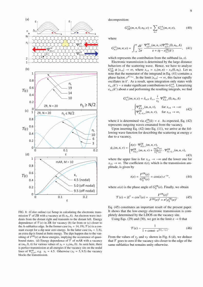
9
10
14
n 0
0.2
0.4
0.6
0.8
1
0
T( )ε
ε
4.5 (nodal)
9.5 (off nodal)
5.0 (off nodal)
mAR, M = 10
0 0.1 0.2
(b)
(d) ε
3
610
0 0.1 0.2
(c)
n > N/20
n < N/20
19
n 0
x 0
0.2
0.4
0.6
0.8
1
0
T( )ε
0.2
0.4
0.6
0.8
1
0
T( )ε
ZR, N = 20
ZR, N = 20
ΨZR
N,k,+
ΨZR
N,-k,+
ΨZR
N,k,+
n0
Δ ZR
(a)
1
2
N
n
AB
ε
k k
ε
FIG. 8: (Color online) (a) Setup in calculating the electronic trans-mission T of ZR with a vacancy at (0, n0, A). An electron wave inci-dents from the distant right and transmits to the distant left. Energydependence of T (ε) in ZR for vacancy (b) far from or (c) closer tothe A-sublattice edge. In the former case (n0 = 14, 19), T (ε) is a con-stant except for a dip near zero energy. In the latter case (n0 = 3, 6),an extra dip is found at finite energy. The dips happen due to the van-ishing of FZR(ε) at those energies, implying the occurrence of quasi-bound states. (d) Energy dependence of T of mAR with a vacancyat (m0, 0, A) for various values of x0 = xA(m0, 0). As seen here, thereis perfect transmission at all energies if the vacancy sits on the nodallines of ΨAR
r0 ,ps, e.g. x0 = 4.5. Otherwise (x0 = 5, 9.5) the vacancyblocks the transmission.
decomposition:
GνAZR(m, n, 0, n0; ε) =
∑u,s
GνAu,s(m, n; ε), (40)
where
GνAu,s(m, n; ε) =
∫ π
−π
dk′
2π
ΨZRu,k′ s(m, n, ν)Ψ
ZR∗u,k′ s(0, n0, A)
ε + iη − εZRu,s(k′)
, (41)
which represents the contribution from the subband (u, s).Electronic transmission is determined by the large distance
behaviors of the scattering wave. Hence, we have to analyzeGνA
ZR at |xνA| → ∞, where xνA = xν(m, n) − xA(0, n0). Let usnote that the numerator of the integrand in Eq. (41) contains aphase factor, eik′xνA . In the limit |xνA| → ∞, this factor rapidlyoscillates in k′. As a result, upon integration only states withεu,s(k′) ∼ εmake significant contributions to GνA
u,s. Linearizingεu,s(k′) about ε and performing the resulting integrals, we find
GνAu,s(m, n; ε) = δu,N δs,+
ivkΨZR∗
N,k,+(0, n0, A)
·
ΨZRN,k,+(m, n, ν), for xνA → −∞ΨZR
N,−k,+(m, n, ν), for xνA → ∞,(42)
where k is determined via εZRu,s(k) = ε. As expected, Eq. (42)
represents outgoing waves emanated from the vacancy.Upon inserting Eq. (42) into Eq. (11), we arrive at the fol-
lowing wave function for describing the scattering at energy εdue to a vacancy,
ψε(m, n, ν) =
t(ε) · ΨZRN,k,+(m, n, ν),
ΨZRN,k,+(m, n, ν) + iπρZR
0 (ε)GZR
0 (ε) · ΨZRN,−k,+(m, n, ν),
(43)where the upper line is for xνA → −∞ and the lower one forxνA → ∞. The coefficient t(ε), which is the transmission am-plitude, is given by
t(ε) =FZR(ε)GZR
0 (ε)= cos(α) e−iα, (44)
where α(ε) is the phase angle of GZR0 (ε). Finally, we obtain
T (ε) = |t|2 = cos2(α) =FZR(ε)2
FZR(ε)2 + π2ρZR0 (ε)2
. (45)
Eq. (45) constitutes an important result of the present paper.It shows that the low-energy electronic transmission is com-pletely determined by the LDOS on the vacancy site.
Using Eqs. (29) and (30), we get in the limit ε→ 0 that
T (ε) ∼ 11 + const · ε2(νρ−νF ) . (46)
From the values of νρ and νF shown in Fig. 6 (d), we deducethat T goes to zero if the vacancy sits closer to the edge of thesame sublattice but remains unity otherwise.
10
In Figs. 8 (b) and (c), the energy dependence of T for ZRsis shown. As seen in panel (b), for n0 < N/2, at some finiteenergy there appears an anti-resonance in T (ε). This hap-pens when FZR(ε) = 0, implying the formation of quasi-boundstates at the corresponding energy. Our results agree with thesimulations presented in Ref.26,46.
Equation (45) for the transmission coefficient can also beapplied to other systems in their single-channel regime, sincethe derivation of this equation is generic. As an example, letus consider the case of mARs, which have a single-channelregime, i.e. |ε| < ∆mAR. Here, ∆mAR ≈
√3π
2M . The electronictransmission along the ribbon direction can then be obtainedby replacing GZR
0 (and FZR) with GmAR0 (and FmAR) [Eq. (25)]
in T . As discussed in subsection IV A, two scenarios couldoccur depending on the vacancy position. Fig. 8 (d) showsthe energy dependence of transmission for mARs. When thevacancy is located on the nodal line ofΨAR
µ , the ρmAR0 vanishes.
Therefore, T (ε) = 1, implying that this kind of vacancy doesnot affect the low-energy electronic transport in mARs. Onthe other hand, when the vacancy is located off the nodal line,we find T (ε) ∼ ε2 as ε → 0, indicating efficient blocking ofelectronic flow at the Dirac point. Thus, the vacancy bearsessentially distinct effect on the transport in mARs from ZRs.
VII. SUMMARY
In summary, we have analytically studied the vacancyeffects on electronic and transport properties of graphenenanoribbons using Green’s function techniques. Our resultsevidence that the effects of a vacancy are critically sensitiveto the edge structures. In both sARs and BZRs a vacancy canintroduce an extra ZES, though the spatial pattern of the wavefunction of this state varies qualitatively from sAR to BZR.In sAR, the wave function follows the exponentially decay-ing pattern, resembling a typical midgap state in conventionalsemiconductors. In BZR, it shows a power law decay instead.The difference can be attributed to the pseudospin degree offreedom intrinsic to the graphene lattice. In ZRs, we find thatthe ZESs are not affected by a vacancy. In rectangular QDs,there is always a ZES accompanying the vacancy, whose wavefunction is concentrated on the zigzag edge rather than aboutthe vacancy. This is because the edge states dominate thiswave function.
Apart from the ZES, vacancy effects can also be seen inelectronic transport properties. We have derived a simple ex-pression [Eq. (45)] for the electronic transmission coefficientT (ε), in terms of the bare LDOS on the vacancy site. As thederivation does not rely on the specific electronic structure, itholds generally for any system. Applying it to ZRs, we findthat T (ε) exhibits an anti-resonance at finite energy if the va-cancy sits closer to the edge of the same sublattice; otherwise,it is less affected. For mARs, the electronic transmission wasshown to depend on whether the vacancy is located on thenodal line of the pure AR wave function or not.
In this paper, we focused on the effects of a single vacancy.However, the results may have implications for multiple va-cancy problems. As an example, we briefly consider the vari-
able range hopping theory for conduction47,48. This theorymay be particularly relevant for considering conduction insARs and BZRs. A crucial quantity is the overlap functionW(d), with d being the distance between the centers of local-ized states (mid-gap states). The form of W(d) is determinedby the spatial profile of the wave functions of these states. Forexponentially decaying wave functions (as e.g. with sARs), Wtakes on an exponential form. For power law decaying wavefunctions (as e.g with BZRs), it is likely to assume a powerlaw. Such a difference in W(d) can lead to dramatically differ-ent temperature dependence of the conductance due to vari-able range hopping30. A thorough analysis of these aspects isbeyond the scope of the present work and will be described infuture publications.
Acknowledgments
This work is supported by the Science of Atomic Layers(SATL) (Project No. 25107005) KAKENHI on Innovative Ar-eas from MEXT of Japan.
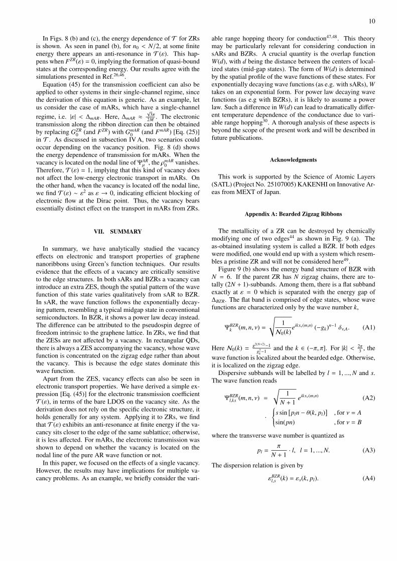
Appendix A: Bearded Zigzag Ribbons
The metallicity of a ZR can be destroyed by chemicallymodifying one of two edges44 as shown in Fig. 9 (a). Theas-obtained insulating system is called a BZR. If both edgeswere modified, one would end up with a system which resem-bles a pristine ZR and will not be considered here49.
Figure 9 (b) shows the energy band structure of BZR withN = 6. If the parent ZR has N zigzag chains, there are to-tally (2N + 1)-subbands. Among them, there is a flat subbandexactly at ε = 0 which is separated with the energy gap of∆BZR. The flat band is comprised of edge states, whose wavefunctions are characterized only by the wave number k,
ΨBZRk (m, n, ν) =
√1N0(k)
eikxν(m,n) (−gk)n−1 δν,A. (A1)
Here N0(k) = g2(N+2)−1g2
k−1 and the k ∈ (−π, π]. For |k| < 2π3 , the
wave function is localized about the bearded edge. Otherwise,it is localized on the zigzag edge.
Dispersive subbands will be labelled by l = 1, ...,N and s.The wave function reads
ΨBZRl,ks (m, n, ν) =
√1
N + 1eikxν(m,n) (A2)
·s sin
[pln − θ(k, pl)
], for ν = A
sin(pn) , for ν = B
where the transverse wave number is quantized as
pl =π
N + 1· l, l = 1, ...,N. (A3)
The dispersion relation is given by
εBZRl,s (k) = εs(k, pl). (A4)
11
(a)
(b)
1
2
3
N
x x x x x0
unit cell
n x x x x x
0−1
0
1
2
πk
ΔBZR
ε
n = 5 0
ν = A 0
B
ν = A 0
B
(c)
ρ0
0.4
0.2
0
F
-0.8
0
0.8
−1 0 1ε
n = 5 0
B
A
ΔBZR
n
εBZR
0 10 20
0
0.1
0.2
0.2
0.4N = 20
0
I
I
−ΔBZR
(d)
(e)
FIG. 9: (Color online) (a) Schematic of bearded zigzag ribbons (BZRs). (b) Band structure of a BZR with N = 6. (c) Energy dependenceof GBZR
0 = F + iρ0 at site (0, n0, ν0). Depending on whether ν0 = A or not, the LDOS shows either a peak or a zero. (a) Position of polesof T BZR(ε): εBZR =
√I(n0,N)/I(n0, A,N). For εBZR < ∆BZR these poles represent midgap bound states (shaded region). Otherwise, they
represent resonant states. Here ∆BZR = sin(
πN+1
). (b) Numerical evaluation of I(n,N) and I(n, A,N). The latter is almost a constant.
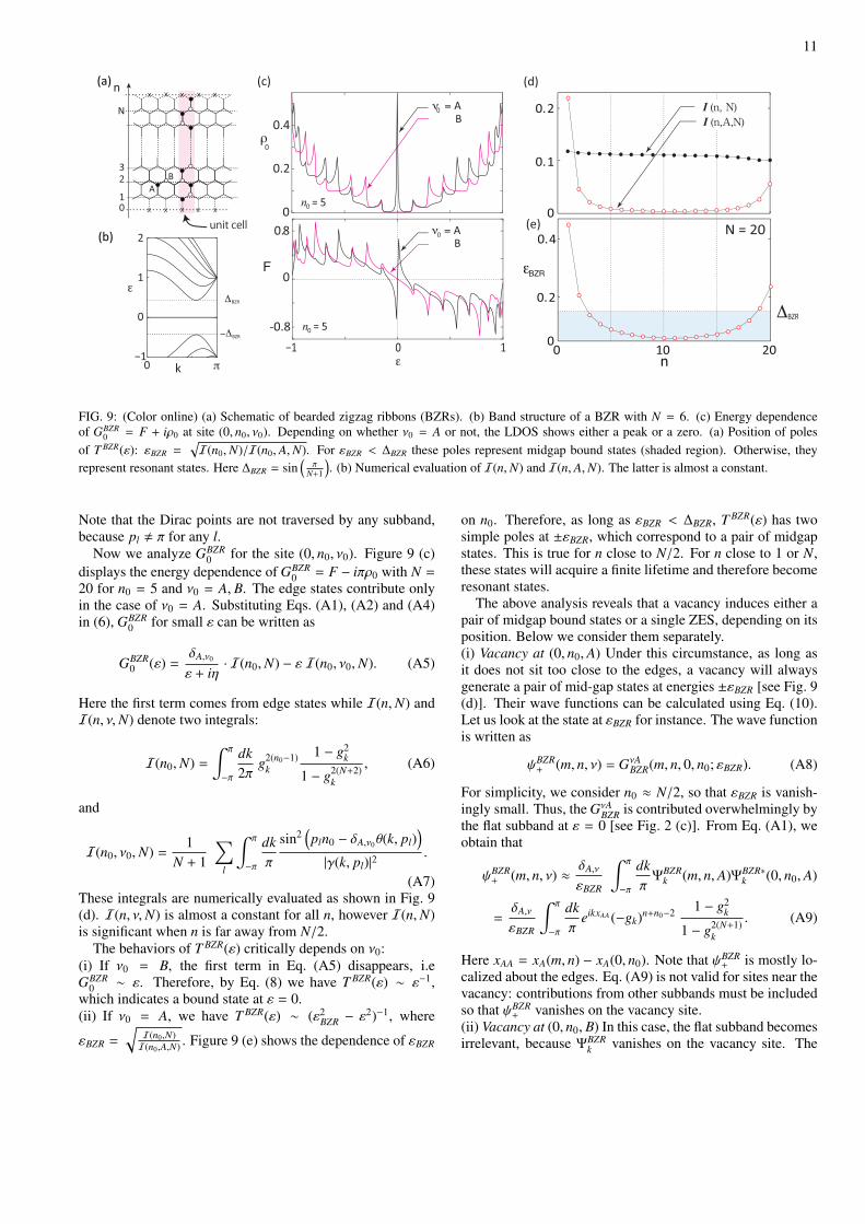
Note that the Dirac points are not traversed by any subband,because pl , π for any l.
Now we analyze GBZR0 for the site (0, n0, ν0). Figure 9 (c)
displays the energy dependence of GBZR0 = F − iπρ0 with N =
20 for n0 = 5 and ν0 = A, B. The edge states contribute onlyin the case of ν0 = A. Substituting Eqs. (A1), (A2) and (A4)in (6), GBZR
0 for small ε can be written as
GBZR0 (ε) =
δA,ν0
ε + iη· I(n0,N) − ε I(n0, ν0,N). (A5)
Here the first term comes from edge states while I(n,N) andI(n, ν,N) denote two integrals:
I(n0,N) =∫ π
−π
dk2π
g2(n0−1)k
1 − g2k
1 − g2(N+2)k
, (A6)
and
I(n0, ν0,N) =1
N + 1
∑l
∫ π
−π
dkπ
sin2(pln0 − δA,ν0θ(k, pl)
)|γ(k, pl)|2
.
(A7)These integrals are numerically evaluated as shown in Fig. 9(d). I(n, ν,N) is almost a constant for all n, however I(n,N)is significant when n is far away from N/2.
The behaviors of T BZR(ε) critically depends on ν0:(i) If ν0 = B, the first term in Eq. (A5) disappears, i.eGBZR
0 ∼ ε. Therefore, by Eq. (8) we have T BZR(ε) ∼ ε−1,which indicates a bound state at ε = 0.(ii) If ν0 = A, we have T BZR(ε) ∼ (ε2
BZR − ε2)−1, where
εBZR =
√I(n0,N)I(n0,A,N) . Figure 9 (e) shows the dependence of εBZR
on n0. Therefore, as long as εBZR < ∆BZR, T BZR(ε) has twosimple poles at ±εBZR, which correspond to a pair of midgapstates. This is true for n close to N/2. For n close to 1 or N,these states will acquire a finite lifetime and therefore becomeresonant states.
The above analysis reveals that a vacancy induces either apair of midgap bound states or a single ZES, depending on itsposition. Below we consider them separately.(i) Vacancy at (0, n0, A) Under this circumstance, as long asit does not sit too close to the edges, a vacancy will alwaysgenerate a pair of mid-gap states at energies ±εBZR [see Fig. 9(d)]. Their wave functions can be calculated using Eq. (10).Let us look at the state at εBZR for instance. The wave functionis written as
ψBZR+ (m, n, ν) = GνA
BZR(m, n, 0, n0; εBZR). (A8)
For simplicity, we consider n0 ≈ N/2, so that εBZR is vanish-ingly small. Thus, the GνA
BZR is contributed overwhelmingly bythe flat subband at ε = 0 [see Fig. 2 (c)]. From Eq. (A1), weobtain that
ψBZR+ (m, n, ν) ≈ δA,ν
εBZR
∫ π
−π
dkπΨBZR
k (m, n, A)ΨBZR∗k (0, n0, A)
=δA,ν
εBZR
∫ π
−π
dkπ
eikxAA (−gk)n+n0−2 1 − g2k
1 − g2(N+1)k
. (A9)
Here xAA = xA(m, n) − xA(0, n0). Note that ψBZR+ is mostly lo-
calized about the edges. Eq. (A9) is not valid for sites near thevacancy: contributions from other subbands must be includedso that ψBZR
+ vanishes on the vacancy site.(ii) Vacancy at (0, n0, B) In this case, the flat subband becomesirrelevant, because ΨBZR
k vanishes on the vacancy site. The
12
45 50 55 60
−4
−2
0
2
4
6
x 10−4
n
0
2
0 40 80
−2
0
2
4
x
0
1
x = half integers
N=100
500.5
x = 500
GA
B
BZ
R(m
,n,0
,50;0
)N = 100N = 20
I1(x)
I2(x)
I1,1(x)
I1,2(x)
I10,1(x)
I10,2(x)
I 1I 2
(x)
(c)(b)(a)
AB
0 5 10 15x
40
FIG. 10: (Color online) Numerical results for (a) Il,1 and Il,2 defined in Eq. (A13) (with l = 1, 10) and (b) their averages I1 and I2 [Eq. (A15)].(c) Ratio of I1 to I2. Note that this ratio relies on whether x is an integer or a half integer. (d) Green’s function GAB
BZR(m, n, 0, 50; 0), whichshows peaks at the position of the vacancy (0, 50, B) for xAB = xA(m, n) − xB(0, 50) being integers or at the neighboring site if xAB is a halfinteger.
vacancy produces a bound state exactly at ε = 0. The wavefunction of this state is given by Eq. (10):
ψBZR0 (m, n, ν) ∝ δν,A GAB
BZR(m, n, 0, n0; 0), (A10)
where we have used the fact that GBBBZR(m, n, 0, n0; 0) = 0. In
analogy with sARs, we make the following decomposition:
GABBZR(m, n, 0, n0; 0) = −
∑l
GABBZR,l(m, n, 0, n0), (A11)
where GABBZR,l only includes contributions from the pair of sub-
bands (l,+) and (l,−). Explicitly, we have
GABBZR,l(m, n, 0, n0) =
S (pl, n, n0)N + 1
Il,1(xAB)
+S (pl, n − 1, n0)
N + 1Il,2(xAB),(A12)
with xAB := xA(m, n) − xB(0, n0) andIl,1(x)Il,2(x)
= ∫ π
−π
dkπ
eikx
|γ(k, pl)|2
gk
1
. (A13)
The integrals Il,1 and Il,2 are analytically formiddable. Weperform them numerically and present the results in Fig. 10(a). As seen in this figure, both Il,1 and Il,2 are not sensitiveto l for large x. This may be understood by noting that thefactor |γ(k, p)|−2 does not change much as p is varied. It istherefore useful to introduce their averages:
I1 :=1
N + 1
∑l
Il,1, I2 :=1
N + 1
∑l
Il,2. (A14)
In Fig. 10 (b), we display I1 and I2. They resemble Besselfunctions. Approximately, we find that for large x
I1(x) ∼ sin(π|x| + φ1)|x| , I2(x) ∼ sin(π|x| + φ2)
|x| , (A15)
where φ1 ≈ π/2 and φ2 ≈ 0 stand for two phase constants.The period of 2 is already read off from Fig. 10 (b). Another
0
0
1
2
πk
ZR
QD, M=5, N=6
(a) (b)
ΔZR
ε
m
x
y
M
n
N
1 2
1
2
3
FIG. 11: (a) Schematic of a rectangular QD with size M × N, withwave functions vanishing on crossed sites. (b) Eigenstates of QD.
feature can be seen in Fig. 10 (c), where the ratio I1/I2 isexhibited. We see that for x being large half integers, I1 isvanishingly small in comparison with I2, whereas for x beinglarge integers, I2 becomes much smaller than I1.
The above analysis suggests to replace in Eq. (A12) Il,1and Il,2 by their averages. With this approximation and using
1N+1
∑l S (pl, n, n′) = δn,n′ , we find
ψBZR0 (m, n, A) ≈
I1(xAB) δn,n0 , for large xAB = mI2(xAB) δn,n0+1, for large xAB = m + 1
2
,
(A16)which indicates that ψBZR
0 (m, n, ν) peaks at n0 for large x = mbut at n0+1 for large x = m+ 1
2 . We have numerically evaluatedEq. (A12). As seen in Fig. 10 (d), this observation is wellborne out. Moreover, from Eq. (A15), we get
ψBZR0 (m, n, A) ∼ sin(π|xAB| + φ)
|xAB|, (A17)
which is valid for large xAB. Here φ is about π/2 or 0 depend-ing on xAB. See that ψBZR
0 is normalizable to unity.
13
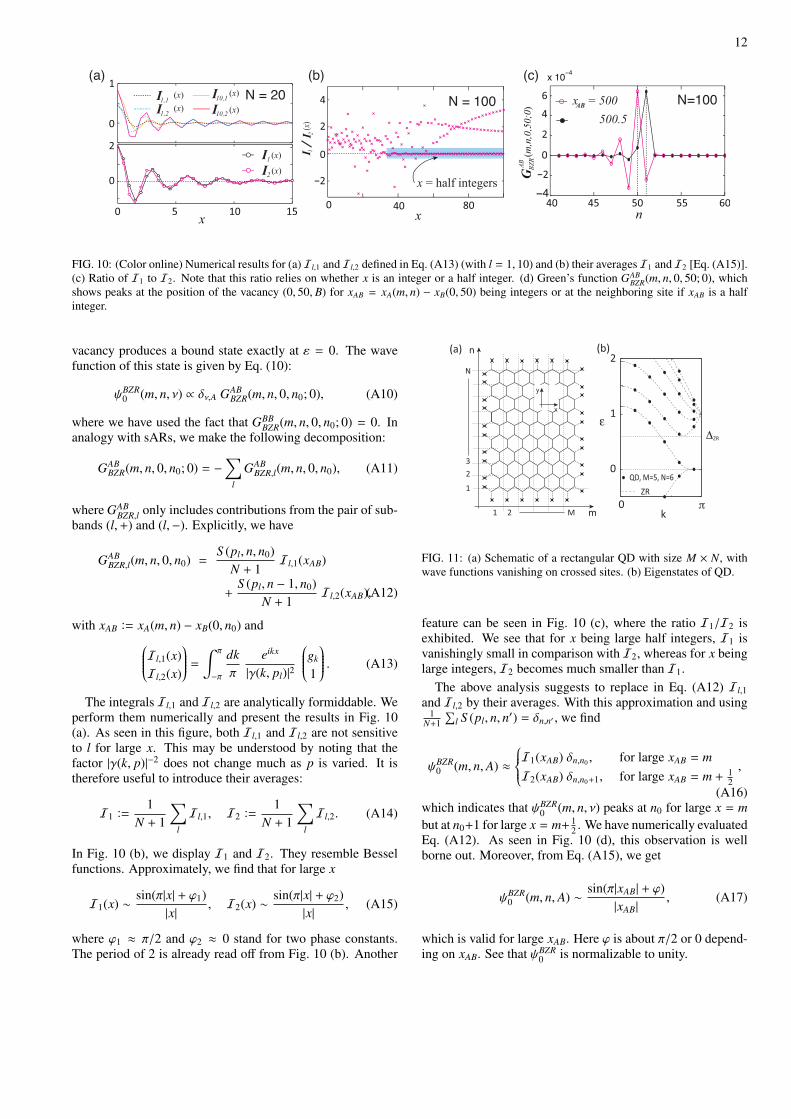
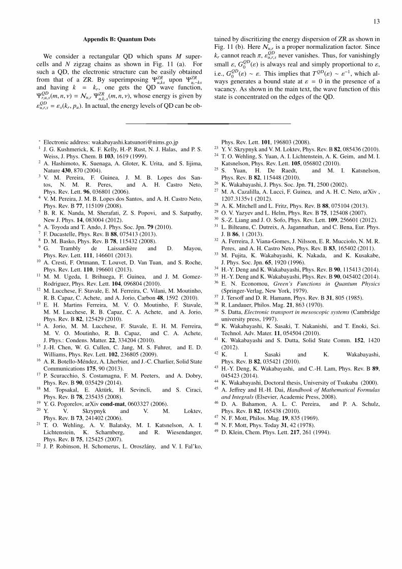
Appendix B: Quantum Dots
We consider a rectangular QD which spans M super-cells and N zigzag chains as shown in Fig. 11 (a). Forsuch a QD, the electronic structure can be easily obtainedfrom that of a ZR. By superimposing ΨZR
u,ks upon ΨZRu,−ks
and having k = kr, one gets the QD wave function,Ψ
QDr,u,s(m, n, ν) = Nu,r Ψ
ZRu,kr s(m, n, ν), whose energy is given by
εQDu,r,s = εs(kr, pu). In actual, the energy levels of QD can be ob-
tained by discritizing the energy dispersion of ZR as shown inFig. 11 (b). Here Nu,r is a proper normalization factor. Sincekr cannot reach π, εQD
u,r,s never vanishes. Thus, for vanishinglysmall ε, GQD
0 (ε) is always real and simply proportional to ε,i.e., GQD
0 (ε) ∼ ε. This implies that T QD(ε) ∼ ε−1, which al-ways generates a bound state at ε = 0 in the presence of avacancy. As shown in the main text, the wave function of thisstate is concentrated on the edges of the QD.
∗ Electronic address: [email protected] J. G. Kushmerick, K. F. Kelly, H.-P. Rust, N. J. Halas, and P. S.
Weiss, J. Phys. Chem. B 103, 1619 (1999).2 A. Hashimoto, K. Suenaga, A. Gloter, K. Urita, and S. Iijima,
Nature 430, 870 (2004).3 V. M. Pereira, F. Guinea, J. M. B. Lopes dos San-
tos, N. M. R. Peres, and A. H. Castro Neto,Phys. Rev. Lett. 96, 036801 (2006).
4 V. M. Pereira, J. M. B. Lopes dos Santos, and A. H. Castro Neto,Phys. Rev. B 77, 115109 (2008).
5 B. R. K. Nanda, M. Sherafati, Z. S. Popovi, and S. Satpathy,New J. Phys. 14, 083004 (2012).
6 A. Toyoda and T. Ando, J. Phys. Soc. Jpn. 79 (2010).7 F. Ducastelle, Phys. Rev. B 88, 075413 (2013).8 D. M. Basko, Phys. Rev. B 78, 115432 (2008).9 G. Trambly de Laissardiere and D. Mayou,
Phys. Rev. Lett. 111, 146601 (2013).10 A. Cresti, F. Ortmann, T. Louvet, D. Van Tuan, and S. Roche,
Phys. Rev. Lett. 110, 196601 (2013).11 M. M. Ugeda, I. Brihuega, F. Guinea, and J. M. Gomez-
Rodriguez, Phys. Rev. Lett. 104, 096804 (2010).12 M. Lucchese, F. Stavale, E. M. Ferreira, C. Vilani, M. Moutinho,
R. B. Capaz, C. Achete, and A. Jorio, Carbon 48, 1592 (2010).13 E. H. Martins Ferreira, M. V. O. Moutinho, F. Stavale,
M. M. Lucchese, R. B. Capaz, C. A. Achete, and A. Jorio,Phys. Rev. B 82, 125429 (2010).
14 A. Jorio, M. M. Lucchese, F. Stavale, E. H. M. Ferreira,M. V. O. Moutinho, R. B. Capaz, and C. A. Achete,J. Phys.: Condens. Matter. 22, 334204 (2010).
15 J.-H. Chen, W. G. Cullen, C. Jang, M. S. Fuhrer, and E. D.Williams, Phys. Rev. Lett. 102, 236805 (2009).
16 A. R. Botello-Mendez, A. Lherbier, and J.-C. Charlier, Solid StateCommunications 175, 90 (2013).
17 P. Scuracchio, S. Costamagna, F. M. Peeters, and A. Dobry,Phys. Rev. B 90, 035429 (2014).
18 M. Topsakal, E. Akturk, H. Sevincli, and S. Ciraci,Phys. Rev. B 78, 235435 (2008).
19 Y. G. Pogorelov, arXiv cond-mat, 0603327 (2006).20 Y. V. Skrypnyk and V. M. Loktev,
Phys. Rev. B 73, 241402 (2006).21 T. O. Wehling, A. V. Balatsky, M. I. Katsnelson, A. I.
Lichtenstein, K. Scharnberg, and R. Wiesendanger,Phys. Rev. B 75, 125425 (2007).
22 J. P. Robinson, H. Schomerus, L. Oroszlany, and V. I. Fal’ko,
Phys. Rev. Lett. 101, 196803 (2008).23 Y. V. Skrypnyk and V. M. Loktev, Phys. Rev. B 82, 085436 (2010).24 T. O. Wehling, S. Yuan, A. I. Lichtenstein, A. K. Geim, and M. I.
Katsnelson, Phys. Rev. Lett. 105, 056802 (2010).25 S. Yuan, H. De Raedt, and M. I. Katsnelson,
Phys. Rev. B 82, 115448 (2010).26 K. Wakabayashi, J. Phys. Soc. Jpn. 71, 2500 (2002).27 M. A. Cazalilla, A. Lucci, F. Guinea, and A. H. C. Neto, arXiv ,
1207.3135v1 (2012).28 A. K. Mitchell and L. Fritz, Phys. Rev. B 88, 075104 (2013).29 O. V. Yazyev and L. Helm, Phys. Rev. B 75, 125408 (2007).30 S.-Z. Liang and J. O. Sofo, Phys. Rev. Lett. 109, 256601 (2012).31 L. Bilteanu, C. Dutreix, A. Jagannathan, and C. Bena, Eur. Phys.
J. B 86, 1 (2013).32 A. Ferreira, J. Viana-Gomes, J. Nilsson, E. R. Mucciolo, N. M. R.
Peres, and A. H. Castro Neto, Phys. Rev. B 83, 165402 (2011).33 M. Fujita, K. Wakabayashi, K. Nakada, and K. Kusakabe,
J. Phys. Soc. Jpn. 65, 1920 (1996).34 H.-Y. Deng and K. Wakabayashi, Phys. Rev. B 90, 115413 (2014).35 H.-Y. Deng and K. Wakabayashi, Phys. Rev. B 90, 045402 (2014).36 E. N. Economou, Green’s Functions in Quantum Physics
(Springer-Verlag, New York, 1979).37 J. Tersoff and D. R. Hamann, Phys. Rev. B 31, 805 (1985).38 R. Landauer, Philos. Mag. 21, 863 (1970).39 S. Datta, Electronic transport in mesoscopic systems (Cambridge
university press, 1997).40 K. Wakabayashi, K. Sasaki, T. Nakanishi, and T. Enoki, Sci.
Technol. Adv. Mater. 11, 054504 (2010).41 K. Wakabayashi and S. Dutta, Solid State Comm. 152, 1420
(2012).42 K. I. Sasaki and K. Wakabayashi,
Phys. Rev. B 82, 035421 (2010).43 H.-Y. Deng, K. Wakabayashi, and C.-H. Lam, Phys. Rev. B 89,
045423 (2014).44 K. Wakabayashi, Doctoral thesis, University of Tsukuba (2000).45 A. Jeffrey and H.-H. Dai, Handbook of Mathematical Formulas
and Integrals (Elsevier, Academic Press, 2008).46 D. A. Bahamon, A. L. C. Pereira, and P. A. Schulz,
Phys. Rev. B 82, 165438 (2010).47 N. F. Mott, Philos. Mag. 19, 835 (1969).48 N. F. Mott, Phys. Today 31, 42 (1978).49 D. Klein, Chem. Phys. Lett. 217, 261 (1994).