Lossless Multi-Way Power Combining and Outphasing for ...
172
Lossless Multi-Way Power Combining and Outphasing for Radio Frequency Power Amplifiers by Alexander S. Jurkov B.S., University of Calgary (2010) Submitted to the Department of Electrical Engineering and Computer Science in partial fulfillment of the requirements for the degree of Master of Science at the MASSACHUSETTS INSTITUTE OF TECHNOLOGY February 2013 @ 2012 Massachusetts Institute of Technology. All rights reserved. Signature of A uthor .................................................................................................................................... Department of Electrical Engineering and Computer Science October 12, 2012 Certified by .......................................... ......... David J. Perreault Professor of Electrical gineering and Computer Science Thesis Supervisor A ccepted by ................................................................. . - . ..... . .. -- 7JS ie A. Kolodziejski Professor of Electrical Enain *n Computer Science Chair, Department Committee on Graduate Students - 1 - ~ARcH~t$E Ar%
-
Upload
khangminh22 -
Category
Documents
-
view
0 -
download
0
Transcript of Lossless Multi-Way Power Combining and Outphasing for ...

Lossless Multi-Way Power Combining and Outphasingfor Radio Frequency Power Amplifiers
by
Alexander S. Jurkov
B.S., University of Calgary (2010)
Submitted to the Department of Electrical Engineering and Computer Sciencein partial fulfillment of the requirements for the degree of
Master of Science
at the
MASSACHUSETTS INSTITUTE OF TECHNOLOGY
February 2013
@ 2012 Massachusetts Institute of Technology. All rights reserved.
Signature of A uthor ....................................................................................................................................Department of Electrical Engineering and Computer Science
October 12, 2012
Certified by .......................................... .........
David J. PerreaultProfessor of Electrical gineering and Computer Science
Thesis Supervisor
A ccepted by ................................................................. . - . ..... . .. --7JS ie A. Kolodziejski
Professor of Electrical Enain *n Computer ScienceChair, Department Committee on Graduate Students
- 1 -
~ARcH~t$EAr%

Lossless Multi-Way Power Combiningand Outphasing for Radio Frequency
Power Amplifiersby
Alexander S. Jurkov
Submitted to the Department of Electrical Engineering and Computer Scienceon October 12, 2012, in partial fulfillment of the
requirements for the degree ofMaster of Science
Abstract
For applications requiring the use of power amplifiers (PAs) operating at high frequencies and power levels,
it is often preferable to construct multiple low power PAs and combine their output powers to form a high-
power PA. Moreover, such PAs must often be able to provide dynamic control of their output power over a
wide range, and maintain high efficiency across their operating range. This research work describes a new
power combining and outphasing system that provides both high efficiency and dynamic output power
control. The introduced system combines power from four or more PAs, and overcomes the loss and
reactive loading problems of previous outphasing systems. It provides ideally lossless power combining,
along with nearly-resistive loading of the individual power amplifiers over a very wide output power range.
The theoretical fundamentals underlying the behavior and operation of this new combining system are
thoroughly developed. Additionally, a straight-forward combiner design methodology is provided. The
prototype design of a 27.12 MHz, four-way power combining and outphasing system is presented,
implemented, and its performance is experimentally validated over a 1OW-1OOW (10:1) output power range.
Thesis Supervisor: David J. Perreault
Title: Professor of Electrical Engineering and Computer Science
-2-

Acknowledgements
Alas, it's done! And most sincerely I must admit that from the very first moment in MIT, to the
writing of the very last letter of this thesis, it was one truly incredible journey. I cherish every tiny step of it,
and I am deeply grateful for having the opportunity to experience it. However, it was not just a journey of
pure academic enlightenment, but in fact - much more than that. It was a true pilgrimage of personal self-
discovery that allowed me to glimpse at who I really am, and to uncover my heart's most passionate desires.
And to all the people who made it possible, and whose personal journeys fate has intertwined with mine - I
humbly thank you!
I can still remember the day I was comfortably slouching in my airplane seat as a freshly-admitted
MIT graduate student on my way to the MIT visit week. I was eagerly flipping through the pages of one of
professor Perreault's papers on power combining and vividly dreaming of myself one day working on that
very same topic with him. And to my surprise, a few months later I was living my dream! It is to you,
professor Perreault that I want to express my deepest and most sincere gratitude for your constant guidance,
support, and believe in me. Thank you for this one-in-a-lifetime opportunity - without your help, it would
have all simply remained just a dream...And of course, how can one imagine it all happening without the
friendly LEES "gang" - it is a privilege working with you guys!
Thank you all my lovely friends for never giving up your determination to help me break-out from
my seemingly lonely cocoon, and for transforming me in the most extravagant social butterfly. To
Dobromir and Ludka for filling-up countless nights with joy and laughter; to Stevan for showing me the
path of the "Warrior of the Light"; to my roommate Omid for benevolently sharing his breakfast cereal and
milk on those empty-fridge mornings, and patiently bearing with my mid-night piano practices - thank you
all for coloring-up my life! Grazie to all of the Italian "mafia", especially Andrea, Stefano, Alessio, Giulia,
and Flavietissima for showing me the Italian way-of-life and for sharing with me the thrill of so many crazy
adventures - Vi amo, Socios!
Dear MIT Figure Skating Club, you changed my life forever! For the past year, you were as my
family on the ice. You taught me how to walk, fall, and most importantly, how to get-up and keep trying. It
is because of you that figure skating has forever invaded my heart. I dearly thank you for this amazing gift,
and I promise you for as long as my bones hold, ice will crumble under the blades of my skates!
It is however a very special friend to whom I owe my most subtle personal transformation. Dear,
"honey-honey", thank you for all the wonderful moments spent together; thank you for showing me your
warm and kind heart; thank you for your strong nerves and undepletable forgiveness; thank you for your
occasional reminders "...eat, Alex, eat... "I am blessed to know you, Milady!
And if I was to end the acknowledgement section right here, it will inevitably result in a request
for major thesis revision to the EECS department on behalf of my mother...Unfortunately, a simple
"thanks" wouldn't nearly cover it. I thank my dear family for standing by me every step of my journey. It is
-3-

to them that I dedicate this thesis: to my father - my patron of wisdom and ultimate health; to my sister - a
girl made of fire; and to my mother...To this very day it remains a mystery from where does this woman
find the energy to deal with all the crazy adventures of her son. Mother, please forgive me for any white
hairs I may have caused you. I secretly hope though that a bigger portion of them is attributed to my sister.
Finally, I thank to the whole of the universe for always conspiring in my favor.
-4-

Contents
1. Introduction..................................................................................................................................... 15
1.1. Background............................................................................................................................. 15
1.2. The Concept of Power Combining ........................................................................................ 16
1.2.1. The Isolating Combiner ................................................................................................. 18
1.2.2. Lossless Combining ........................................................................................................ 19
1.3. Thesis Scope and Objectives................................................................................................. 22
2. Power Com biner Fundam entals........................................................................................................ 24
2.1. Overview of Resistance Compression Networks................................................................... 24
2.2. Power Com biner Synthesis ................................................................................................... 29
2.3. Input-Port Combiner Characteristics ...................................................................................... 31
2.4. Output Power Control.............................................................................................................. 32
2.5. Outphasing Control Strategies............................................................................................... 33
2.5.1. Inverse Resistance Compression Network (IRCN) Control........................................... 33
2.5.2. Optim al-Susceptance (OS) Outphasing Control............................................................. 36
2.5.3. Optim al-Phase (OP) Outphasing Control....................................................................... 37
2.5.4. Com parison of Outphasing Control M ethods................................................................. 39
2.6. Com biner Design M ethodology ............................................................................................ 41
2.7. Com biner Sensitivity to Loading Variations......................................................................... 45
2.8. Topological Variations ............................................................................................................ 48
2.8.1. T-A Network Transformations ...................................................................................... 49
2.8.2. Network Duality.............................................................................................................. 51
2.9. Com bining Power Losses and Efficiency ............................................................................. 52
2.9.1. Quality-Factor Power Losses........................................................................................ 52
2.9.2. Effect of Topological Transform ations on Combiner Efficiency .................................... 54
3. Implem entation of a Power Combining and Outphasing System ................................................... 57
3.1. Overall System Architecture.................................................................................................... 57
3.2. Power Com biner Design and Implem entation....................................................................... 58
3.2.1. Performance Specifications........................................................................................... 58
3.2.2. Com biner Design ............................................................................................................ 59
3.2.3. Combiner Implementation ............................................................................................ 60
3.2.4. Com biner Tuning ............................................................................................................ 63
3.3. Power Am plifiers .................................................................................................................... 65
3.4. Outphasers ............................................................................................................................. 69
3.4.1. Outphaser Control and DAC Programm ing ................................................................... 72
-5-

3.4.2. DAC Calibration ............................................................................................................. 74
3.5. System Control........................................................................................................................ 74
4. Power Combining System Performance............................................................................................ 77
4.1. Combiner Port-Parameter M odel........................................................................................... 77
4.2. Experim ental System Setup .................................................................................................. 81
4.3. Combiner Performance............................................................................................................ 84
4.4. Overall System Performance ................................................................................................... 85
5. Power Combiner Adaptation for High-Frequency Applications...................................................... 89
5.1. Transmission-Line Implementation........................................................................................ 89
5.2. Input-Port Admittance Characteristics.................................................................................... 90
5.3. Output Power Control.............................................................................................................. 93
5.4. Outphasing Control Strategies............................................................................................... 94
5.4.1. Optim al-Susceptance Control ........................................................................................ 94
5.4.2. Optim al-Phase Control................................................................................................. 97
5.5. Design M ethodologies ............................................................................................................. 98
6. Conclusion ..................................................................................................................................... 100
6.1. Summary................................................................................................................................100
6.2. Directions for Future W ork..................................................................................................... 101
References.............................................................................................................................................102
Appendix A Design of M ulti-Stage RCNs. ..................................................................................... 107
Appendix B M ulti-W ay Power Combining ..................................................................................... 114
Appendix C M ATLAB Code. ........................................................................................................ 127
Appendix D Schematics, Bill-of-M aterials, and PCB Artwork. ....................................................... 150
Appendix E PIC32M X460 M icrocontroller Firmware....................................................................163
-6-

List of Figures
Fig. 1-1: Typical envelope of an RF signal driving a 7 T RF coil in an MRI application [3]............. 15
Fig. 1-2: The traditional outphasing and combining method. A desired output envelope Sow iscreated by appropriately outphasing two constant-envelope signals Si and S2 [29]. . .......... 17
Fig. 1-3: Addition of the two phase-modulated, equal-amplitude signals S, and S2 in the phasordomain. Any desired So. can be obtained by appropriately selecting the outphasingan gle 0 [29]......................................................................................................................... 17
Fig. 1-4: The conventional outphasing architecture implemented with an isolating combiner. Aportion of the total constant PA output power is delivered to the load (at thecombiner's summing port), while the remainder is dissipated as heat in an "isolation"resistor [29]......................................................................................................................... 18
Fig. 1-5: Example implementation of a single-stage Wilkinson combiner [49]................................. 19
Fig. 1-6: A simple two-way lossless combiner driven by two PAs outphased according to Fig. 3.PA interactions cause large susceptive variations in PA loading admittances Yi andY 2 .... ..............................---................................................................................................. 19
Fig. 1-7: Phasor diagram of the output voltage signals Vi and V2 of the PAs driving thecombiner of Fig. 6. The PA outphasing angle 1 controls the resulting load voltageVout across R and determines output power delivered by combiner. ................................. 20
Fig. 1-8: A simple two-way combiner including ±jXc reactances to partially compensate forsusceptive variations in PA loading admittances Y, and Y2. This combiner topologywas originally proposed in the 1930's by Chireix [29]..................................................... 21
Fig. 1-9: Susceptive versus conductive component of the loading admittance Yi seen by the topPA driving the combiners of Fig. 6 and Fig. 8. Although only Y, is plotted, Y2 is thecom plex conjugate of Y1................................................... .. . .. . .. . .. . .. . .. . .. . .. . .. .. . .. . .. . . .. .. . .. . . . . . 22
Fig. 2-1: (Left) a basic resistance compression network (RCN) and (right) its resistive inputimpedance Rn as a function of the matched load resistance value R&. As theresistances R& vary together over a range geometrically-centered on X, the inputimpedance is resistive and varies over a much smaller range than P. .............. .. .. . .. . .. . .. . . . . 25
Fig. 2-2: The basic RCN of Fig. 10 driven by a sinusoidal voltage source VL (left) and thephasor diagram of the voltages VA and VB across the loading resistors (right)................... 26
Fig. 2-3: A second-order resistance compression network driven by a sinusoidal voltage sourceVL at its operating frequency (left), and its overall resistance compressioncharacteristic (right)............................................................................................................. 26
Fig. 2-4: Phasor representation of the load voltages VA-VD of the RCN of Fig. 12symmetrically phase shifted with respect to the driving voltage VL -..-------........................ 29
Fig. 2-5: One possible topological implementation of a four-way power combiner obtained bynegating the reactances of the RCN of Fig. 12, replacing the R. loads with PAs, andreplacing the RCN driving source Vs with a combiner termination load RL-.----.............------ . 30
-7-

Fig. 2-6: Effective input conductance (top), susceptance (middle), and phase (bottom) seen byeach of the PAs (A-D) driving the four-way combiner of Fig. 14 with RL = 50 K, X1 =36.69 f, and X2 = 48.97 Q as a result of IRCN outphasing control.................................... 35
Fig. 2-7: Effective input conductance (top), susceptance (middle), and phase (bottom) seen byeach of the PAs (A-D) driving the four-way combiner of Fig. 14 with RL = 50 fl, X1 =36.69 fl, and X2 = 48.97 0 as a result of OS outphasing control........................................ 38
Fig. 2-8: Effective input conductance (top), susceptance (middle), and phase (bottom) seen byeach of the PAs (A-D) driving the four-way combiner of Fig. 14 with RL = 50 fl, X1 =36.69 Q, and X2 = 48.97 f as a result of OP outphasing control........................................ 39
Fig. 2-9: Outphasing control angles 0 and 4 for the Optimal Phase (OP), Optimal Susceptance(OS), Inverse RCN (IRCN) control methods for the four-way combiner of Fig. 14with RL = 50 9), X, = 36.69 K), and X2 = 48.97 0............................................................. 40
Fig. 2-10: Worst-case effective input admittance phase and susceptance seen by the PAs drivingthe for-way combiner of Fig. 14 with RL = 50 n, X1 = 36.69 n, and X2 = 48.97 n as aresult of the optimal-phase (OP), optimal-susceptance (OS) and inverse RCN (IRCN)outphasing control m ethods. ............................................................................................. 41
Fig. 2-11: Absolute value of the maximum effective input admittance phase seen at the inputports of a four-way power combiner versus the output power level for various k-values. The plot is normalized to Vs = 1 V and RL = 1 0; denormalize for a particularVs and RL by scaling the Pour axis by Vs /RL. ................................................................... 42
Fig. 2-12: Four-way combiner design curve: trace-out the specified power range ratio to thePower Ratio Curve to determine the appropriate design value for k. The Phase Curvesgive the corresponding peak effective input admittance phase that a PA can see at theinputs ports of the combiner over the specified operating range for IRCN, or OP/OSoutphasing control respectively........................................................................................ 44
Fig. 2-13: Four-way combiner design curve: trace-out the specified power range ratio to thePower Ratio Curve to determine the appropriate design value for k. The SusceptanceCurves give the corresponding peak effective input susceptance that a PA can see atthe inputs ports of the combiner over the specified operating range for IRCN, orOP/OS outphasing control respectively. The susceptance axis is normalized to acombiner load RL = 1 Q; to denormalize, multiply axis by 1/RL .........-...-------............... 44
Fig. 2-14: The output power level corresponding to each of the zero-points Pout,4,I - Pouis versusthe k-value for the four-way combiner. Output power is normalized to Vs = 1 V andRL = 1 f); denormalize for a particular Vs and RL by scaling the axis by Vs /RL. ................. 45
Fig. 2-15: Network utilized for analyzing the incremental change of sourced input currents bythe power amplifiers (Fig. 14) for a given incremental resistive/reactive change inload impedance RL by employing the Alteration Theorem [56]. IL is the load currentin Fig. 14 when ARL=AXL=O ............................................ .......................................... 46
Fig. 2-16: Phasor diagram illustrating the effect of combiner load variation on its effective inputadmittance. The input terminal current increments AIA.re and AIA,im resulting fromdeviation of the combiner's load from its nominal value introduce additional inputadm ittance phase. ................................................................................................................ 47
-8-

Fig. 2-17: Maximum admittance phase (absolute value) seen among the PAs driving the four-way combiner of Fig. 14 (RL = 50 n, X1 = 36.69 Q, and X2 = 48.97 n) versus outputpower back-off as a result of 2.5% and 5% purely-resistive (top plot) and purely-reactive (bottom plot) variations of the 50 Q nominal combiner load................................ 47
Fig. 2-18: A "binary tree" implementation of an 8-way power combiner........................................... 48
Fig. 2-19: T-A general network transform ation.................................................................................. 49
Fig. 2-20: T-to-A transformation applied to the top T-network of the four-way combiner in Fig.14 ........................................................................................................................................ 4 9
Fig. 2-21: Four possible topological variations (B)-(E) of the basic four-way combiner (A) asresult of T-A transformations on portions of the network and load. ................................... 50
Fig. 2-22: Circuits corresponding to the topological duals of the circuits in Fig. 30. Thesecircuits illustrate additional four-way combiner implementations. The poweramplifiers are modeled as current sources in this representation (illustrating the inputports of the combiners). Magnitude and phase of the current sources is respectivelyequivalent to the magnitude and phase of the voltage sources in Fig. 30............................ 51
Fig. 2-23: Fractional four-way combiner power loss due to the finite Q-factor of its reactivebranches versus output power for various operating range designs; a quality factor Q= 100 is assum ed for all reactive branches......................................................................... 54
Fig. 2-24: T-to-A transformation applied to a T-network in the "binary-tree" combinerim plem entation .................................................................................................................... 54
Fig. 2-25: Basic T-network implementation of a four-way power combiner along with outlinedpossible topological transformations and their corresponding incremental fractionalloss curves in Fig. 35........................................................................................................... 56
Fig. 2-26: Incremental fractional power loss curves for a four-way power combiner for variousoperating power range ratios versus output power (percentage of saturation powerlev el)................................................................................................................................... 5 6
Fig. 3-1: Block diagram of the implemented power combining and outphasing system..................... 57
Fig. 3-2: Prototype combiner specifications: operation over a 10 W to 100 W (10 dB) powerrange with 125 n and 12.5 0 effective loading resistance of the PAs at the outer twozero-points respectively. This curve is shown for IRCN control....................................... 59
Fig. 3-3: Effective input conductance (top), and phase (bottom) seen by each of the PAs (A-D)driving the four-way combiner of Fig. 2-5 with RL = 50 D, X, = 36.69 Q, and X2 =48.97 Q (k = 1.042) as a result of OP outphasing control................................................... 60
Fig. 3-4: Power combiner implementation. Each of the reactive branches in Fig. 2-5 is realizedw ith an L/C series com bination........................................................................................ 61
Fig. 3-5: Photograph of the tuned four-way combiner PCB with its four input ports A-D andsingle output port OUT. Ports E and F are used only for tuning the combiner..................... 62
Fig. 3-6: Simulated combiner efficiency including Q-factor losses................................................. 63
-9-

Fig. 3-7: Tuning set-up for tuning the L5/C5 and L6/C6 combiner reactive branches. Ports Eand F are loaded with RL = 50 f), while a 27.12 MHz test signal is injected at thecom biner's O U T term inal..................................................................................................... 64
Fig. 3-8: Topology of the implemented Class-E power amplifier. .................................................... 65
Fig. 3-9: Circuit schematic of the gate-driver employed in the PA of Fig. 3-8. ................................ 68
Fig. 3-10: Oscilloscope screenshot showing key voltage waveforms of a PA driving a 50 Q loadand powered by a supply voltage of 16 VDC. Channel 1: outphaser output Voutphaser(input to the gate-drive circuit), Channel 2: gate-drive signal Vgs, Channel 3: drainvoltage Vd,, and Channel 4: PA output waveform V............................ . . .. . . .. . .. . . .. . .. . .. . .. . . . . . 68
Fig. 3-11: Photograph of a single implemented Class-E PA PCB....................................................... 69
Fig. 3-12: Block diagram of a hypothetical IQ modulator.................................................................. 69
Fig. 3-13: Phasor representation of the I/Q modulator output signal (RF) and its reference localoscillator input (LO )............................................................................................................ 70
Fig. 3-14: Block diagram of the outphaser........................................................................................ 71
Fig. 3-15: Photograph of an assembled outphaser board. The entire power combining systememploys four such boards, each responsible for phase-shifting its corresponding PA.......... 72
Fig. 3-16: Control signal timing diagram for programming the DAC in the single-businterleaved operating m ode [62]........................................................................................ 73
Fig. 3-17: Photo of the PIC32MX460-based development board (LV32MX, MikroElektronika)........... 75
Fig. 3-18: State diagram of the PIC32MX460 firmware developed for controlling the outphasers............................................................................................................................................ 7 6
Fig. 4-1: Comparison between the expected output power from the implemented and idealcom biners versus commanded power ............................................................................... 79
Fig. 4-2: Comparison between the expected PA loading admittance characteristics of the idealand implemented combiners versus output power.............................................................. 80
Fig. 4-3: The expected PA loading characteristic of the implemented combiner after optimizingoutphasing control angles based on the measured port-parameter combiner model............. 81
Fig. 4-4: Comparison between the OS outphasing control angles of the ideal combiner and theoptimized OS control angles for the implemented combiner. ............................................. 81
Fig. 4-5: Photograph of the experimental setup................................................................................ 82
Fig. 4-6: Measured combiner output power P0. versus commanded output power Pemd...................... 85
Fig. 4-7: Measured overall system and PA efficiency versus combiner output power. ...................... 86
Fig. 4-8: Total input power distribution among PAs versus combiner output power. ........................ 86
Fig. 4-9: The magnitude of the fundamental component of each of the PA's output voltagewaveforms versus combiner output power......................................................................... 87
-10-

Fig. 4-10: Measured combiner output power Pot versus commanded power Pemd. ............................... 88
Fig. 4-11: Comparison between measured system power efficiency, expected system efficiency,average PA efficiency, and the efficiency that can be expected from a similar systemif it were implemented with an ideal linear class-B PA. .................................................... 88
Fig. 5-1: Transmission-line implementation of the four-way combiner of Fig. 2-5 usingtransmission lines with characteristic impedance of Zi and Z2. The lengths of thetransmission lines are defined as +AL and ±AL2 increments to a half-wavelength baselen gth .................................................................................................................................. 9 0
Fig. 5-2: Transmission-line networks for deriving the effective input admittance matrix of theTL com biner of Fig. 5-1. ................................................................................................. 90
Fig. 5-3: Phasor representation of the output voltages VA-VD of the PAs driving the combinero f F ig . 5 -1. .......................................................................................................................... 92
Fig. 5-4: Effective input conductance (top), susceptance (middle), and phase (bottom) seen byeach of the PAs (A-D) driving the four-way TL combiner of Fig. 5-1 with Z, = Z2 =567 Q, a, = 0.0628 and a2 = 0.0861, and RL = 50 fl as a result of the OS outphasingcon tro l................................................................................................................................. 9 5
Fig. 5-5: Effective input conductance (top), susceptance (middle), and phase (bottom) seen byeach of the PAs (A-D) driving the four-way TL combiner of Fig. 5-1 with Z, = Z2 =100 0, ai = 0.3640, a 2 = 0.5096, and RL = 50 92 as a result of the OS outphasingcon tro l................................................................................................................................. 9 6
Fig. 5-6: Effective input conductance (top), susceptance (middle), and phase (bottom) seen byeach of the PAs (A-D) driving the four-way TL combiner of Fig. 5-1 with Zi = Z2 =567 Q, a, = 0.0628, a2 = 0.0861, and RL = 50 f as a result of the OP outphasingcon trol................................................................................................................................. 9 7
Fig. 5-7: Outphasing control angles 0 and 4 for the Optimal Phase (OP) and OptimalSusceptance (OS) control methods for the four-way combiner of Fig. 5-1 with Zi = Z2= 567 n, a, = 0.0628, a2 = 0.0861, and RL = 50 n ............................................................ 98
Fig. 5-8: Four-way TL combiner design curves: trace-out the specified power range ratio to thePower Ratio Curve to determine the appropriate design value for k for particulartransmission line characteristic impedances. The Susceptance Curves give thecorresponding peak effective input susceptance that a PA can see at the inputs ports ofthe combiner over the specified operating range for OP/OS outphasing control. Thesusceptance axis is normalized to a combiner load RL = 1 Q; to denormalize, multiplyaxis by 1/RL-..........-------------...-....--------------------...-............................................... 99
Fig. A-1: N-stage resistance compression network obtained by cascading number of single-stage RCN networks. The input resistance Ri,, N seen by the voltage source VL variesover a much smaller range compared to that of the 2N matched load resistances R. ...... .. . .. .. 108
Fig. A-2: Resistive input impedance Rin, N as a function of the matched load resistance value Rofor the N-stage compression network of Fig. A-1. Selection of the compressionnetwork reactances as described provides this characteristic, which compressesresistance to a greater extent than is possible in a single-stage RCN design..........................110
Fig. A-3: Single-stage resistance compression network, driven by a voltage source VL ............. 111
- 11 -

Fig. A-4: Two-stage resistance compression network, driven by a voltage source VL ----------................ 11 I
Fig. A-5: A three-stage resistance compression network, driven by a voltage source VL-------.............113
Fig. B-1: A General N-stage example implementation of the proposed power combiner system.This implementation employs 2 N power amplifiers (PAs) illustrated as ideal voltagesources in this figure for analysis purposes. The power combiner is ideally lossless,and comprises reactive elements with specified impedances at the operating frequency.The combiner has 2 N power amplifier input ports and one power output port for theload RL- -----.............-------------.--- . -...............................................115
Fig. B-2: Network utilized for analyzing the incremental change of sourced input currents bythe power amplifiers (Fig. B-1) for a given incremental change in load resistance RLby employing the Alternation Theorem [56]. IL is the load current in Fig. B-i whenARL= 0- - - - - --.............------------------. . ------ .. . --------------............................................... 117
Fig. B-3: Phasor plot of the effective current Ieff sourced by a particular power amplifier ofFig. B-1 for a given combiner output power level................................................................117
Fig. B4: An example implementation of a three-stage power combiner. ............................................ 119
Fig. B-5: Phasor diagram showing the relationship among the phase voltages for a three-stagepower combiner. The outphasing control angles *, 0 and Y are used to regulate outputpower while maintaining desirable loading of the sources A-H............................................120
Fig. B-6: Plot showing the outphasing control angles 4, 0 and y versus commanded outputpower Pmnd according to (48) for the three-stage power combiner example design (V,= 1 V, RL = 50 0, X, = 18.13 Q, X2 = 42.29 fl and X 3 = 49.68 n)........................................121
Fig. B-7: Actual output power versus commanded power for the three-stage power combinerexample design (V,= 1 V, RL = 50 f, X, = 18.13 fl, X2 = 42.29 n and X3 = 49.68 Q).The actual power increases monotonically with Pema and saturates at approximately4.5 W for higher commanded power levels..........................................................................122
Fig. B-8: Real and imaginary components of the effective admittances seen at each of thepower combiner input ports (A-H) plotted as a function of actual output power Pout.The plots are shown for the three-stage combiner example (V, = 1 V, RL = 50 n, X =18.13 ,X = 42.29 0 and X3 = 49.68 9)............................................................................122
Fig. B-9: Magnitude and phase of the effective admittances seen at each of the power combinerinput ports (A-H) plotted as a function of actual output power Pwu,. The plots areshown for the two-stage combiner example (V, = 1 V, RL = 50 t, X = 18.13 Q, X 2 =42.29 Q and X 3 = 49.68 l). ................................................................................................ 123
Fig. B-10: Absolute value of the maximum effective input admittance phase seen at the inputports of a two-stage (top) and three-stage (bottom) power combiners versus the outputpower level for various k-values. The plot is normalized to Vs = 1 V and RL = 1 Q;
denormalize for a particular Vs and RL by scaling the Po0 , axis by Vs2 /RL. -------................. 124
Fig. B- 11: Design curves for the two-stage (top) and three-stage (bottom) power combiners:trace-out the desired operating output power range ratio to the Power Ratio Curve todetermine the appropriate design value for k. The Admittance Phase Curve gives thecorresponding worst-case effective input admittance phase that may be seen over theentire operating range at the input ports of the combiner......................................................125
12-

Fig. B-12: Normalized plot (Vs = 1 V, RL= 1 Q) of the minimum and maximum limits of the
output power operating range versus the k-value for a two-stage (top) and a three-
stage (bottom) power combiners. To denormalize for a particular Vs and RL, multiply2
the power axes by vs /RL ........................ .................................. 125
Fig. B-13: Basic T-network implementation of a three-stage power combiner along with outlined
possible topological transformations and their corresponding incremental fractional
loss curves in Fig. B -14. ..................................................................................................... 126
Fig. B-14: Incremental fractional power loss curves for a three-stage power combiner for various
operating power range ratios. P,, is normalized to RL = 1 f2 and Vs = 1 V...........................126
Fig. D- 1: Outphaser PCB top layer copper/silkscreen.........................................................................150
Fig. D-2: Outphaser PCB bottom layer copper/silkscreen ................................................................... 150
Fig. D-3: Outphaser PCB GND layer copper (2"d layer from the top)..................................................151
Fig. D-4: Outphaser PCB VDD layer copper (3 d layer from the top)..................................................151
Fig. D-5: Four-way power combiner PCB (top layer copper/silkscreen)..............................................158
Fig. D-6: Four-way power combiner PCB (bottom layer copper/silkscreen)..................158
Fig. D-7: Class-E PA PCB (top layer copper/silkscreen) .................................................................... 160
Fig. D-8: Class-E PCB (bottom layer copper/silkscreen)....................................................................160
Fig. D-9: Class-E PCB GND layer (lI" inner layer from top) .............................................................. 161
Fig. D-10: Class-E PCB VDD layer (2"d inner layer from top)..............................................................161
- 13 -

List of Tables
Table I: Power combiner component values................................................................................... 61
Table II: PA design specifications.................................................................................................. 66
Table III: Component values and their implementation for the Class-E PA...................................... 67
Table IV: Outphaser jumper configuration........................................................................................ 71
Table V: DAC control signal timing parameters ............................................................................ 73
Table VI: DAC calibration constants for each of the outphaser boards............................................... 74
Table VII: Mapping of the outphaser board signals to the pins of the microcontrollerdevelopment board .............................................................................................................. 76
Table D1: Outphaser PCB Bill-of-Materials........................................................................................153
-14-

Chapter 1
Introduction
1.1. Background
Radio-frequency (RF) power amplifiers are an integral component of many modem systems, and they
find wide applicability in a diverse range of applications including RF communications [1], medical
imaging [2, 3], industrial heating and processing [4], power conversion [5], and many others. Such power
amplifiers (PAs) are often constrained by two important requirements: (1) the ability to provide dynamic
control of their output power over a wide range, and (2) the necessity to maintain high efficiency across
their operating power range.
For example, Fig. 1-1 shows the envelope of a typical RF signal driving a 7 T MRI RF coil [3]. As
can be seen, the output power delivered to the coil is dynamically modulated, with the peaks of the power
pulses distributed over nearly a 20 dB of power range. It is highly desired to be able to operate efficiently
over such often-occurring, high output power pulses. Although linear power back-off techniques can be
utilized to handle the very low output power levels, power-efficient realization of an amplification system
that can handle the wide output power modulation range of high-power pulses is a significant challenge for
conventional amplification system topologies.
80
40 ---------------------------------------- ----
~20 --------
00 1 2 3 4 5 6Time (mS)
Fig. 1-1: Typical envelope of an RF signal driving a 7 T RF coil in an MRI application [3].
Conventional linear amplifiers such as Class A, AB, B and C allow for a dynamic output power
control over a vey wide power range while providing high-fidelity power amplification. However, they can
be designed to operate at optimum efficiency at only one particular power level, commonly referred in
literature as the output power saturation level. As their output power is backed-off from saturation, their
efficiency dramatically degrades. Various efficiency enhancement techniques have been previously
proposed to deal with the adverse affects of power back-off on linear PA efficiency [6, 7]. Most such
techniques can be categorized as either drain modulation, or load modulation [8, 9]. Drain modulation
- 15 -

techniques such as dynamic envelope tracking and Envelope Elimination and Restoration (EER) ensure that
the RF PA operates at or near the saturation level at all times by modulation of its drain voltage [10, 11].
Although drain modulation promises optimal efficiency over a wide operating power range, it requires wide
bandwidth, highly-efficient supply regulators; the design of such regulators is very challenging task by
itself, especially when wideband modulation is required [11].
On the other hand, load modulation maintains the PA operating at saturation by adjusting the effective
loading impedance seen by the PA according to the desired output power [6]. Nevertheless, implementation
of the load modulation scheme without introducing extra power loss is not a trivial task. Moreover, most
conventional implementations of the load modulation techniques, such as the Doherty amplifier [12-14],
allow the PA to operate at optimal efficiency only over a limited output power range (6 dB in the case of a
symmetric Doherty amplifier) [15]. The technique explored in this thesis likewise implements a form of
load modulation. Some recent digital PA architectures - digital envelope modulator [16-18] and digital
switching mixer [19] - offer both excellent linearity and high efficiency at peak output power. Under
output power back-off conditions, however, their efficiency degradation is no better than that of a linear
class B PA.
Although the discussed techniques reduce PA efficiency degradation with power back-off, their peak
efficiency remains low due to the use of linear PAs. On the other hand, switch-mode PAs, e.g., classes D, E,
F, E/F, inverse E, inverse F, etc., offer high peak efficiency (100% ideally), but at constant supply voltage
can only generate constant envelope signals while remaining in switched mode. Numerous techniques such
as drain modulation [20-22], direct digital RF modulation [23, 24], pulse-width or duty-cycle modulation
[25], and dynamic load modulation [26] have been proposed to introduce envelope variations in the output
of a switching PA. As was already mentioned, drain modulation [22] and its variants [20, 21] require wide
bandwidth supply regulators that exhibit poor efficiencies and immensely complicate the system. Direct
digital RF modulation [23, 24] demands high sampling speeds and lossy bandpass filters which adversely
impact efficiency and add to the overall system cost. Although both duty-cycle [25] and dynamic load
modulation [26] techniques offer reasonable efficiency over a narrow operating power range, operation
beyond it results in severe efficiency degradation under back-off conditions.
Simultaneously achieving wideband liner power amplification with high average efficiency has been a
longstanding challenge, and is the goal of the work presented in this thesis.
1.2. The Concept of Power Combining
One technique that has been explored for simultaneously achieving dynamic power control over a
wide operating range and high efficiency is that of outphasing and power combining. This concept,
originally proposed in the 1930's [27], is also sometimes referred to as "Linear Amplification with Non-
Linear Components" or LINC [28]. Traditionally, this method (see Fig. 1-2) consists of decomposing the
desired input signal to be amplified Si(t) into two phase-modulated signals with constant amplitudes Si(t)
and S2(t).
-16-

S (t) sI io S.(t)
Fig. 1-2: The traditional outphasing and combining method. A desired output envelope So,, is created byappropriately outphasing two constant-envelope signals Si and S2 [29].
These signals are then phase-shifted (outphased), amplified and combined (summed) to yield an
amplified version Sout(t) of the input signal. Fig. 1-3 shows a phasor representation of the signals. As can be
seen, any desirable output signal magnitude can be achieved by simply selecting the appropriate outphasing
angle 0. The fact that S, and S2 are constant-amplitude signals enables the use of highly-efficient PAs
including partially- and fully-switched-mode architectures such as classes D [31-32], E [33, 34], F [35-37],
E/F [38], F' [39], (D [40, 41], etc. The reason that such PAs can be designed to be highly-efficient is in part
due to the fact that they are not required to provide linear output power control.
ImS
0 S* , Re
S2)
Fig. 1-3: Addition of the two phase-modulated, equal-amplitude signals Si and S2 in the phasor domain.
Any desired Sou can be obtained by appropriately selecting the outphasing angle 0 [29].
Although the outphasing and combining methodology above is presented for two PAs, the concept
can be generalized for any N number of PAs, where the desired output signal is decomposed into N
constant-envelope signals, each being synthesized independently and then combined. A key consideration
is how the power combing is carried out, particularly because many high-efficiency power amplifiers are
highly sensitive to load impedance variations. Interactions between the PAs, as a result of the combining
network, causes the effective admittances (Yi and Y2 in Fig. 1-2) loading the PAs to vary with outphasing
angle (output power) [42-44]. However, variations in PA loading (especially susceptive variations) are
often problematic for high efficiency power amplifiers as they give rise to circulating currents, result in
- 17 -

output resonance tank mistuning, and introduce waveform distortions, ultimately leading to degraded PA
performance and efficiency. Most conventional combiners can be classified as either isolating or lossless
combiner. A brief overview of the key properties and characteristics of each combiner type follows.
1.2.1. The Isolating Combiner
One conventional approach to power combining while eliminating variations in PA loading
admittance is the isolating combiner [45]. Fig. 1-4 illustrates the LINC architecture implemented with an
isolating combiner [29]. The main advantage of an isolating combiner is that it eliminates PA interactions,
and thus provides constant PA loading impedance independent of the outphasing angle. As a consequence
of this, each power amplifier operates at a constant output power level. However, only a portion (controlled
by outphasing) of the total PA output power is delivered to the load (connected to the summing port 1 of
the combiner). The remainder must be instead delivered elsewhere, and usually, it is just dissipated by an
"isolation" resistor (connected to the difference port A of the combiner). This manifests in rapid efficiency
degradation of the combiner as output power is decreased, diminishing the attractiveness of this approach
[45]. Previous work has attempted to partially mitigate this problem by replacing the isolation resistor with
an AC/DC converter and thus "recycling" a portion of the output difference power back (from the A
combiner port) to the PA supply [46-48].
VDD
SAAA i(t) Signal1 0
S,(t) PA
Fig. 1-4: The conventional outphasing architecture implemented with an isolating combiner. A portion ofthe total constant PA output power is delivered to the load (at the combiner's summing port), while theremainder is dissipated as heat in an "isolation" resistor [29].
As an example implementation of an isolating combiner, consider Fig. 1-5, depicting a simple two-
way combiner, also known as a Wilkinson combiner [49, 50]. It comprises two 50 C) input power ports (1
and 2), combined through two 70.7 K2 quarter wavelength transformers, and a 100 Q resistor between the
two input ports to provide isolation, and make the output port (3) well matched to a 50 D) load. Provided
-18-

that the PAs driving the two combiner input ports are outphased according to Fig. 1-3, they will effectively
see a constant resistive loading impedance of 50 Q.
1 50 fl 70.7
100 a
2 70.7 il
50 an
Fig. 1-5: Example implementation of a single-stage Wilkinson combiner [49].
1.2.2. Lossless Combining
In contrast to the isolating combiner, the lossless combiner is implemented entirely using only
reactive elements such as capacitors and inductors, or transmission lines. Since these elements ideally do
not dissipate power, the combining process is ideally lossless, although in reality, some small power loss is
unavoidable due to finite quality factor of the components. Fig. 1-6 depicts the simplest two-way lossless
combiner comprising a single balun (or "balanced to unbalanced transformer") which is differentially
driven by two appropriately outphased PAs.
VDDY1
+0 PA +
_10-
N N R, Vu
VDD _
-Y6- PA T I --
.V2
Fig. 1-6: A simple two-way lossless combiner driven by two PAs outphased according to Fig. 1-3. PAinteractions cause large susceptive variations in PA loading admittances Yi and Y2.
To illustrate the operation of this combiner, suppose that the outputs of the PAs are sinusoidal voltage
signals with constant amplitude Vs, and a respective phase-shift of ± (see Fig. 1-7 for a phasor diagram).
As Fig. 1-7 shows, the magnitude of the output voltage across the load resistor RL (and hence, the output
power Po0 , delivered by the combiner) can be controlled by simply adjusting the outphasing angle 0. It can
be shown that output power is given by (1):
-19-

2V2 sin2 (g)P~t- SR L0
Im+V V
0Re
0
-Vs
Fig. 1-7: Phasor diagram of the output voltage signals V and V2 of the PAs driving the combiner of Fig. 1-6. The PA outphasing angle 0 controls the resulting load voltage V0u across RL and determines outputpower delivered by combiner.
Output power control can also be understood by considering the behavior of the PA interaction and its
effect on PA loading. As a result of PA interactions through the combiner network, the conductive
component of the loading admittances Y and Y2 "seen" by the PAs vary with outphasing angle. However,
since the PAs are biased to provide a constant-amplitude output, modulation of their loading conductance
results in modulation of the output power delivered by each PA, and hence, the total output power delivered
by the combiner to the load RL. In other words, in a lossless combiner, output power control is achieved by
modulation of the loading conductance (dependent on the interaction between the PAs) that the combiner
presents to the PAs. It can be shown that for the combiner of Fig. 1-6, the relationship between the loading
admittances Yi and Y2, and the outphasing angle 0 is given by (2):
Y, = 2 (sin 2(0)+ jcos(0)sin(0))RL
(2)
Y= 2 (sin2(0)- jcos(0)sin(0))SRL
A significant drawback of this simple combining approach is that in addition to the modulation of the
loading conductance, PA interactions also result in significant susceptive loading variations, which greatly
degrade the PA performance and the overall system efficiency. As an example, Fig. 1-6 shows a plot of
loading susceptance versus conductance for the PA driving the combiner of Fig. 1-6 with RL = 20.4 f. As
can be seen, the susceptive component varies over more than 50% of the range over which the PA loading
conductance is modulated.
- 20 -

The large variations in PA loading susceptance can be partially compensated by connecting additional
reactive components ±jXc to the PA output nodes (see Fig. 1-8). This configuration is also known as the
Chireix combiner [27, 42, 43, 45, 51] after its developer, who introduced it in the 1930's [27]. It can be
shown that the loading admittances Y and Y2 , and the combiner output power P.0 , as a function of PA
outphasing angle 0 are given respectively by (3) and (4):
Po.Ut =2RLsin 2(0) (3)xc
Y, - 2 sin 2(0)+ j cos(0)sin(0)- RLRL Xc
(4)
Y2 - 2 sin2 (0)- j cos(0)sin(0)- RLRL Xc)
Indeed, as can be seen from (4), the susceptive components have been shifted by an amount
proportional to the ratio of RL to Xc. Fig. 1-9 shows a susceptance/conductance plot for various Chireix
example designs with RL and Xc selected to reflect the same loading conductance modulation range for all
designs. As seen, the susceptive portions of the PA loading admittances are only zero for at most two
output power levels, and become large outside of a limited power range. Although the susceptive variations
of the Chireix combiner are smaller compared to those of the uncompensated combiner of Fig. 1-6, they are
still problematic for high-efficiency application requiring wide output power range [42-44].
VDD
Y,
+0 PA L.
Z=+jXe
_N NL
VDD Z=-j1X
-0PA
Fig. 1-8: A simple two-way combiner including ±jXc reactances to partially compensate for susceptivevariations in PA loading admittances Y and Y2. This combiner topology was originally proposed in the1930's by Chireix [29].
-21-

0.05
0.04 -
0.03 - C xeix (Fig- 8): RL 19.4 ,Xe45O0.023-. -W-,f - - - -c=4.0.02
-0.01-
-0.04 - --
-0.050 0.01 0.02 0.03 0.04 0.05 0.06 0.07 0.08 0.09 0.1
Conductance (mhos)Fig. 1-9: Susceptive versus conductive component of the loading admittance Yi seen by the top PA drivingthe combiners of Fig. 1-6 and Fig. 1-8. Although only Y, is plotted, Y2 is the complex conjugate of Y1.
1.3. Thesis Objectives and Organization
The primary objective of this thesis is to describe the development of a new multi-way power
combing and outphasing system that provides ideally lossless power combining from four or more PAs,
along with nearly-resistive loading of the individual power amplifiers over a very wide output power range.
More specifically, this thesis aims to achieve the following key objectives
* Describe the theoretical fundamentals necessary for understanding and analyzing the
operation of the proposed power combiner,
* Present a design methodology for designing the combiner according to specific performance
specifications,
* Develop outphasing control strategies for controlling the combiner's output power,
" Experimentally evaluate the performance of the proposed combiner, and validate the
effectiveness of the outphasing control strategies to control the output power of the combiner.
Following this introductory chapter, Chapter 2 discusses the fundamentals of operation of the
proposed power combiner, addressing combiner synthesis, combiner port characteristics, outphasing
-22-

control, design methodologies, and various implementation topologies. The implementation of an actual
power combining system prototype is presented in Chapter 3, while Chapter 4 evaluates its performance
and assesses the effectiveness of the proposed combining approach. Chapter 5 presents a transmission-line
implementation of the combiner suitable for power combining applications in the UHF band. The thesis is
concluded in Chapter 6 with remarks on possible areas of future development.
The appendices following the thesis include associated derivations referenced in the text, some
generalized theoretical developments on multi-way power combining, computer code employed in system
simulation, printed circuit board schematics and artwork, and embedded firmware code.
- 23 -

Chapter 2
Power Combiner Fundamentals
This chapter develops and presents the fundamentals of operation of the new outphasing power
combining architecture. It aims to layout necessary theoretical foundation and provide in-depth
understanding of the behavior and the principles of operation of the combiner. Furthermore, useful
techniques and methods are described which greatly facilitate future combiner design and analysis.
As a first step, the notion of multi-stage resistance compression networks is introduced. Although a
seemingly unrelated topic at first, it is shown how the design and behavior of multi-stage compression
networks can be effectively utilized in the synthesis of ideally lossless power combiners and in the
derivation of their corresponding outphasing control laws. Following subsections discuss important input-
port and output-port combiner characteristics along with various outphasing techniques to control combiner
output power and their loading affect on the driving power amplifiers. A methodology is presented which
allows for a straightforward combiner design based on given system performance specifications. The last
two subsections present various topological circuit implementations of the combiner and their effect on
non-ideal combining losses.
2.1. Overview of Resistance Compression Networks
Resistance Compression Networks (RCNs) are a class of lossless interconnection networks for
coupling a source to a set of matched (but variable) resistive loads [46, 52, 53] at a particular operating
frequency. Fig. 2-1 depicts one basic RCN and its operating characteristics. As the resistances R in Fig. 2-
1 vary together over a range geometrically-centered on X, the input impedance of the network is entirely
resistive and varies over a much smaller range compared to R, i.e. loading resistance variations are
compressed. In particular, it can be shown (5) that the input impedance Rin is resistive at the operating
frequency and it is a function of the load resistances R [29, 46, 52, 53]:
R2 +X 2R = R0 (5)
"2RO
As the load resistances R vary over the range [X/b, bX], the input resistance varies over the range [X,
kX], where k and b are related by (6):
k = 1b and b=k+ k2 -1 (6)2b
-24-

For example, if the loading resistances R, vary simultaneously over a range of 5 92 to 500 Q (a factor
of b = 10 variation from a 50 Q nominal resistance), then Rin varies only over a range of 50 fl to 252.5 Q.
Because the input impedance is resistive and varies over a much smaller range than the matched load
resistances RO, RCN networks offer numerous advantages in applications such as resonant rectifiers and dc-
dc converters [46, 52, 53].
Z=+jX R.
fZ R
7=-jX
X
ZR=R
X/b X bX RO
Fig. 2-1: (Left) a basic resistance compression network (RCN) and (right) its resistive input impedance Rias a function of the matched load resistance value R. As the resistances R vary together over a rangegeometrically-centered on X, the input impedance is resistive and varies over a much smaller range than R0 .
The RCN of Fig. 2-1 is a narrow-band network - it is designed for operation at a particular frequency
at which the values of the capacitive and inductive RCN impedances are tuned to +jX. Suppose that this
RCN is now driven by a sinusoidal voltage source VL at its operating frequency. Then, it can be shown that
the voltage waveforms VA and VB across the loads R have equal magnitudes and are symmetrically phase-
shifted by ±0 with respect to VL (see Fig. 2-2) according to (7) and (8):
[VA]=v R.+X [:2]j (7)
L2 +X2 e~j
tan-' (8)
The RCN discussed above can be thought of as a basic single-stage compression network. However,
even higher degrees of resistance compression (smaller input resistance variations for the same loading
resistance variation) can be achieved by constructing multiple-stage compression networks. Fig. 2-3 (left)
shows an example implementation of a two-stage RCN (other possible implementations exist). The
simultaneous resistance variations in the four loads R, is first compressed by a pair of single-stage RCNs.
In turn, their simultaneously varying effective input resistances Rinj are further compressed by another
single-stage RCN.
- 25 -

+jX,A
R0
R +
VB
Fig. 2-2: The basic RCN of Fig. 2-1 driven by a sinusoidal voltage source VL (left) and the phasor diagramof the voltages VA and VB across the loading resistors (right).
+jX, Z=R
k2X
VL
2
AR
AR
R P
in, I X,/b, X, b X,Fig. 2-3: A second-order resistance compression network driven by a sinusoidal voltage source VL at itsoperating frequency (left), and its overall resistance compression characteristic (right).
The design of the RCN of Fig. 2-3 is now considered. The following subsection shows how this RCN
relates to the proposed combining system. Suppose it is desired to design the RCN of Fig. 2-3 to provide an
input resistance Rin,2 within ±AR of a desired median value Rin,2,med while maximizing the range over which
Ro can vary [60]. First, select a value k2 (input resistance ratio of stage 2) of:
Rin,2,med + (9)R -AR
and choose a second stage reactance magnitude of
2R in.2,med (10)
k2 +1
-26-

Next, the reactance magnitude Xi of the first stage is selected to provide compression into a range that
makes best use of the second stage. Note that in order to limit Rin,2 variations within the specified design
range of Rin,2,med * AR , variations of Ri,, must be constrained to a range of [X2/b2 ; X2 b2 ]. Since the
effective resistance Ri, seen at the inputs of the first stage has a minimum value of X 1, to maximize the
range of R over which desired compression is achieved, select X1 to be:
X, 2(11)b2
where b2 is determined from k2 according to (6). Ri,1 has a maximum value of k1X = b2X2, from where the
value of k, can be determined. Thus, the desired degree of compression can be achieved for an R) operating
range of [XI/b 1 ; b1Xi], with b, given by (6). Equivalently, it can be shown that b, can be computed directly
from k2 as per (12):
b=(k2+ k - + (k2 + k-1 -1 (12)
Fig. 2-3 depicts the variation of the input resistance Rin,2 as a function of the load resistance R when
the compression network is designed according to the method outlined above. This particular resistance
compression characteristic is the result of selecting the network reactances X, and X2 as described; the
network exhibits far greater degree of resistance compression than its single-stage counterpart described
earlier. For instance, the two-stage RCN allows for input resistance compression within ±2.5% of the
desired median value (versus ±30.5% for the single-stage RCN) over a 12:1 ratio in load resistance R,
modulation. Note that other types of compression stages can yield similar performance [52, 53]. Moreover,
even greater degree of resistance compression (or similar input resistance deviations over a wider load
modulation range) can be achieved with more stages. A detailed methodology for designing and
synthesizing a general multi-stage RCN optimized for maximum resistance compression is presented in
Appendix A along with design examples and summary of performance characteristic for single-stage, two-
stage, and three-stage RCNs.
It is useful to be able to determine the value of R for which Rin,2 = Rin,2,med. This can be easily done by
employing the RCN compression equation (5), expressing Rin,2 as a function of R0 :
R,2 + X ' +2
R 2 +X2 2R ~Ri2= 2n 2 R 0 (12.1)
2Rinj 2R;2+ X
2RO
-27-

Solving for Rin,2 = Rin,2,med results in four distinct values of R. (for the case of the second-order RCN)
given by (12.2)-(12.5):
R in R id,med + R i,2,me -X 2 - 2R 2
-X2 + 2R med -2R in,2med X
Rn2. x2in,2,ine 2 m,2,med -~ 2 2(12.2)
R02 =Rn.2.med + R .2med -X + 2R 2,med -
rR F2 - 2 x R X 2,2me - in.2me 2 in,2,med
R= R in.2.med - Rin - X + 2R 2 med -X
+ 2R? d - 2R in 2 meX 2N2 R 2med - X
2R2.me - 2R n 2 meX 2
2 - 2R me -2R i,2,med
R 2 .me - X 2
It will be appreciated in the following subsection to know the load voltages VA-VD in terms of the
drive voltage VL- It can be shown by employing straightforward phasor analysis at the RCN's operating
frequency that these voltages are related according to (13)-(15).
~VA]
VB
V C
VDi
e e
V2 e-J+e+ o2R +XLf~~ ~2 +Xe+j+e+jo
S= tan~{ 22
$=tan-'
(13)
(14)
(15)
Fig. 2-4 illustrates their phasor relationship. Similarly to the single-stage RCN, it can be seen that VA-
VD have the same magnitude and symmetrical phase shifts with respect to VL (coincident with the the real
axis).
-28-
(12.3)
(12.4)
(12.5)

ImI-
Fig. 2-4: Phasor representation of the load voltages VA-VD of the RCN of Fig. 2-3 symmetrically phaseshifted with respect to the driving voltage VL.
2.2. Power Combiner Synthesis
The previous subsection discussed the concept of multi-stage resistance compression networks, and
examined in detail the behavior and design of a single-stage and two-stage RCNs. This subsection
demonstrates how the design of such compression networks may be employed in synthesizing the proposed
power combining system.
Consider the two-stage RCN of Fig. 2-3 driven by a voltage source VL. Suppose now that the sign of
every reactive and resistive element is negated. Neglecting the impact upon the natural response of the
circuit, the sinusoidal steady-state behavior of the transformed circuit would have all current flow
directions reversed, while preserving the node voltage relationships of the original circuit, thus yielding
reversed power flow (i.e. from the - now negative - resistors to the voltage source VL). (The validity of this
fact can be shown by taking the original circuit of Fig. 2-3 and applying to it type-I, followed by type-III
time reversal dualities according to [54, 55].) The ratio of the voltage VL to the current flowing into the
source would be that of Rin,2 of the original compression network, which is close to the value of Rin,2,med.
Likewise, the voltages across the now-negative resistors would be respectively equivalent to the ones in the
original network (13), and currents proportional to these voltages would flow into the network (i.e. the
apparent impedances seen looking into the network ports to which the negative resistances are connected
would be resistive with values 1R) [60].
To develop a power combining and outphasing system, one may take advantage of the above
observations. In particular, replace the source VL in Fig. 2-3 with a load resistance RL = Rin, 2, med and
replace the resistors R with voltage sources (or power amplifiers in practice). This leads directly to the
power combiner of Fig. 2-5. It has four input power ports A-D (driven by PAs) and a single output power
port terminated at a desired and well-known load at the operating frequency. The combiner provides ideally
lossless power combining in the sense that the reactive components it comprises are ideally lossless. Note
- 29 -

that, just as the compression network, the combiner is also a narrow-band network. Its reactances are tuned
to a particular value (determined by design) at the combiner's operating frequency.
By controlling the phases of the driving sources VA-VD to match (or at least approximately) the A-D
node voltage relationships in the original two-stage resistance compression network (see Fig. 2-4), one can
obtain power control over a wide range while preserving nearly resistive loading of the sources. The
following subsections develop and discuss in detail the actual outphasing techniques for controlling the
combiner's output power and the particular advantages and disadvantages associated with each one.
PowerCombiner
I -jX
Al
VB
Vs~~ with aj cobie temntonlaLL
VCV R
Vc +jX2
ID +jX
Fig. 2-5: One possible topological implementation of a four-way power combiner obtained by negating thereactances of the RCN of Fig. 2-3, replacing the Reloads with PAs, and replacing the RCN driving sourceVs with a combiner termination load RL-
While the employed circuit transformations considered above do not lead to precise duality between
RCNs and the proposed power combining network, they provide the means to develop effective outphasing
and power combing systems [29]. These same transformations can be applied to a general N-stage RCN
(having 2 N loads) to arrive at a respective 2N-way power combining network (combing power from 2 N PAs).
Interestingly, when this transformation is applied to the single-stage RCN, one obtains a topological
variation of the Chireix combiner of Fig. 1-8. Although the main portion of the work disclosed in this
thesis considers the four-way combiner of Fig. 2-5, the concepts, design techniques and outphasing control
methodologies developed herein can be easily adapted for any multi-way combiner. Appendix B
demonstrates how to do so for an eight-way combiner. Due to the non-ideal lossy character of the combiner
reactances, and the rapidly-growing system complexity, one would rarely consider in practice expanding
the proposed combiner architecture to provide power combining from more than eight PAs. Moreover, it is
worth recognizing that the "binary-tree" structure shown in Fig. 2-5 is not the only possible topological
implementation of the combiner; various topological variations exist. Later subsections enumerate some of
these variations and discuss their effect on combining power losses for the case of the four-way combiner.
Appendix B further extends these topological variations to the case of the eight-way combiner.
-30-

2.3. Input-Port Combiner Characteristics
In order to understand the behavior of the proposed combiner, it is important to examine the
current/voltage characteristic at the network's input ports and the loading it presents to the PAs that drive it.
Consider the four-way combiner of Fig. 2-5 terminated with a load RL. To simplify analysis, the PAs
driving the combiner are modeled here as ideal sinusoidal voltage sources VA-VD at the combiner's
operating frequency with amplitude Vs and phasor relationship as shown in Fig. 2-4. Simple AC analysis
reveals that the relationship between the input terminal voltages VA-VD and currents IA-ID is given by (16),
where y = RL/XI, p = X2/X [29].
IA y+j(1-p0) -y+jp y-7 V~
=B Y X I+PY -V=X- 1 - 7 V (16)Ic Y -y y+j(p+1) -(-jp Vc
ID_- 7j Y+ P - -VD_
Moreover, the input terminal voltages (Fig. 2-4) can be further expressed by (17). Note that their phases
have been chosen identical to those of the RCN's load voltages (13).
-V e -JoV V VS -iti'+jo (17)
VD _ +joe+j0
By combining (16) and (17), one can determine the effective input admittances the combiner network
presents to each of the PAs (18)-(21). The effective admittance at a combiner input port is the complex
ratio of current to voltage at the port with all sources (PAs) active. The effective admittances represent the
admittances "seen" by the PAs when they are operating under outphasing control [29].
YltTA = X1'(y - y cos(2* + 20) - y cos(24) + y cos(20) - p sin(2*))+ jX-1(1- P - 7sin(24+ 20)-y sin(2 )+ y sin(20)+ 0fcos(24Q) (18)
Yeff, B = X-'(y - y cos(20 - 2*) - y cos(2*) + y cos(20) + p sin(2*))+jX (-1 - P - y sin(20 - 24)+ sin( 24)+ y sin(20)+ P cos(24)) (19)
Yff,C = X(y - y cos(20 - 24)- ycos(24)+ y cos(20)+ psin(2 )) 20)-jX(-1- ysin(20 - 24)+ ysin(2 )+ ysin(20)+ p cos(24))
YtTD =X'(y - y cos(2++20)- y cos(24)+ y cos(20)- sin(2*)) (21)-jX '(1 -p -ysin(2*+ 20)- ysin(2#)+ ysin(20)+ cos(2*))
-31 -

It is important to consider the effective input admittance instead of the Thevinin input admittance at a
particular port, as the interaction of the PAs has a substantial effect on their actual loading. It is interesting
to note that as a result of the combiner structure and the employed PA outphasing relationship, the effective
input admittances at ports A/D, and C/ B are respectively complex conjugates. As can be seen from (18)-
(21), the loading of the PAs is a strong function of the outphasing angles 0 and *, and varies with
outphasing (output power control). The actual admittance characteristic over the combiner's operating
power range is specific to the particular outphasing control law employed (the method used for selecting 0
and 4 for a particular output combiner power level). These control laws and their affect on the PAs loading
are discussed in detail in Section 2.5. Moreover, it will be recognized that the exact expressions for the
effective input admittances depend on the number of PAs from which power is combined. Although this
section provides the expressions for the four-way combiner, Appendix B derives similar expressions for the
eight-way combiner.
2.4. Output Power Control
It is useful to know the load voltage VL and the output power Pou that the combiner delivers to the
load RL (see Fig. 2-5) for a given pair of outphasing control angles [0; 4]. By employing straightforward
linear circuit analysis techniques, it can be shown that the load voltage VL is given by (22):
VL jL (V +VD-VA -VC) (22)X1
Furthermore, as a result of the adopted voltage phase relationship of Fig. 2-4, the above equation
reduces to (23), from where the output power Pout delivered to the combiner load RL is easily determined
(24).
VL = 4RL Vs sin(*)cos(0) (23)XI
PI V= 2 8Vx n2(o)COS2() (24)2RL XI
Equation (24) is of great importance and value as it concisely expresses the exact relationship between
the output power delivered to the load RL and any pair of outphasing control angles [0; 4]. This equation
holds on the assumption that the combiner inputs are each driven with the specified voltage. It is the
fundamental basis for deriving the various outphasing control laws in the following subsection. As can be
seen from (24), output power may be controlled either through phase-modulation (adjusting the angles 0
and *), or through amplitude-modulation (adjusting the PA drive signal amplitude Vs), or through both. In
32-

practice, one may choose to employ simultaneously both phase- and amplitude-modulation to achieve an
even wider operating output power range.
It is readily observed from (24) that the maximum output power deliverable to the load by the power
combiner, termed here the saturated output power Po..t,, is given by (25), and corresponds to 0 = 00 and 4 =900. Although (25) is valid only for the four-way combiner, the only difference between it and that for the
general N-way combiner is the leading numeric constant. Appendix B derives the expression for output
power for the eight-way combiner.
8R (25)Pou, =x2 s(5
2.5. Outphasing Control Strategies
As described in the previous subsection, the output power of the proposed power combiner may be
controlled either by modulating the drive amplitude of the power amplifiers, or by appropriately adjusting
their phase shift (outphasing). For the four-way combiner of Fig. 2-5 with PAs outphased according to Fig.
2-4, the output power Pou, is given by (24). As can be seen from (24), for a particular PA drive amplitude
Vs, there are infinite many possible control angle pairs [0, *] that will result in the same output power level.
Thus, an additional constraint can be specified on 0 and # to allow for the selection of a particular control
angle pair. Depending on the nature of the constraint, many possible outphasing control methodologies
emerge. This subsection details several control methodologies and their key characteristics which are of
particular relevance to various practical applications.
2.5.1. Inverse Resistance Compression Network (IRCN) Control
This outphasing control strategy results by analogy of (approximate) reverse operation of the original
resistance compression network, i.e. the PAs driving the combiner are appropriately outphased so that their
terminal voltage characteristic matches the one of the load resistances in the original RCN. As a result, the
power delivered to load RL driven by the power combiner is approximately equivalent to the power that
would be delivered by a power source driving the original RCN and having the same terminal voltage as RL.
This outphasing control method yields desirable loading (almost entirely conductive effective input
admittance) of the PAs. Moreover, due to this control method, the necessary outphasing control angles can
be computed conveniently via a set of analytical expressions which are valid over the entire output power
operating range of the combiner assuming voltage-source drive of the combiner.
For the case of the four-way power combiner of Fig. 2-5, the outphasing control angles 0 and * for a
particular load RL and PA voltage drive amplitude Vs are given by (26) with the variable R0 determined
based on the desired combiner output power Po0 , (27).
- 33 -

0= tan 2R+X2 and tan~' R (26)
R_ P -X2 -2X 2 +2 4R2V_ 4RL 2X+X X2 +X4 (27)P0 t Po t P.t
As an example of the IRCN outphasing control, Fig. 2-6 depicts the loading admittance characteristic
of each of the A-D PAs driving the combiner of Fig. 2-5 versus output power back-off by outphasing. For
this example, the combiner has been designed to operate over approximately a 10 dB output power back-off
and drive a 50 n load (RL = 50 n, X1 = 36.69 0, X2 = 48.97 Q). The actual output power level is
proportional to the square of the PA drive amplitude Vs. (Selecting the appropriate values for the combiner
reactances X1 and X2 to achieve operation over a specified output power range is detailed in Section 2.7.)
As can be seen from Fig. 2-6, the PA loading conductance is modulated accordingly with output
power, while the susceptance and the admittance phase variations are limited to approximately 2.5 mS and
50 respectively over the intended operating range. For this particular example, the susceptive component of
the combiner's input admittances rapidly increase for more than 10 dB output power back-off, or for
operation at power levels above 0 dB. In fact, it can be shown in general from (18)-(21) and (26) that for
zero output power (Po,, = 0), all PA voltages VA-VD are in phase (0 = 0*, = 0*), and the effective input
admittances (purely susceptive) are:
Y,A = Yeff.C =(28)
Ycff.B = Yeff,D =8
On the other hand, when 0=0* and 4= 900, the output power saturates to Pout, (25) and the PAs are
loaded with an admittances having significant susceptive components given by (29), where y = RL/Xi, p =
X 2/XI.
Yeff A = X (4y + j(1 - 2p))YeffB =X-' (4y+ j(-1- 2))Yeff, = X' I 4-j -1--2p)) (29)
efD=X' (4y-j l-2p))
-34-

150
' 125
S100-
75
50 00
25 - -.-
0L-12 -10 -8 -6 -4 -2 0 2
Pout (dB) re 2Vs 12.5Q5
Con D-2.5 B
U
A-5
-12 -10 -8 -6 -4 -2 0 2Pout (dB) re 2V /12.5n
15
10--
5-B D
0 -
-5 C
-10 -
-15-12 -10 -8 -6 -4 -2 0 2
Pout (dB) re 2V /12.5f)
Fig. 2-6: Effective input conductance (top), susceptance (middle), and phase (bottom) seen by each of thePAs (A-D) driving the four-way combiner of Fig. 2-5 with RL = 50 C, X, = 36.69 f2, and X2 = 48.97 f as aresult of IRCN outphasing control.
One can also observe from Fig. 2-6 that all four susceptive components of the combiner's input
admittances vanish to zero at four distinct output power levels (termed here the zero-points). The output
power corresponding to these zero-points can be computed according to (30)-(33).
_ R -XPou =2V4 RL+ R -X 2 -2R -X -X(+2R 2RX (3)
Xf2 2 X2 2 + R -XR
2Vs'R L JR' 2R 2(30)
o~ut,zp2 (31)L
-35-

P =2V1RL2 R -X - 2R -X1 -X|- 2R -2RLX (32)
IR -X
P..t, =2V1RL L2 + R I- 2R-2RLX (33)2R - X2_2 x 2 + 2R2 -_X2 -_X2- L L2(3
One can think of a zero-point as a particular combiner output power level at which the combiner
happens to operate as an exact inverse of its corresponding resistance compression network. In other words,
at a particular zero-point, all driving PAs see a purely conductive loading impedance of 1/R, where R is
such that when compressed by the combiner's corresponding RCN, the RCN's input resistance is
equivalent to the combiner's load.
To understand this better, consider the combiner example discussed above. At each of the combiner's
four zero-points all four PAs are equally loaded with a purely conductive load of 1/R0 . The value of R0 is
such that when compressed by the combiner's corresponding RCN of Fig. 2-3, it will result in an RCN
input resistance Rin,2 equivalent to the combiner's load RL. One would usually design the combiner so that
RL = Rin,2,med. Then, as can be seen from Fig. 2-3, there are exactly four possible R values (12.2)-(12.5) at
which Rin,2 = Rinl,2,ded = RL (marked with a dot in Fig. 2-3), and hence, there are four zero-points in the
combiner's admittance characteristic. Equations (30)-(33) are readily obtainable from (12.2)-(12.5) by
replacing Rin,2,med with RL.
It can be shown that, in general, a 2N-way combiner will have 2 N zero-points. As Appendix B
demonstrates for, an eight-way combiner, for example, has eight zero-points spread over a wider power
range compared to the four-way combiner.
2.5.2. Optimal-Susceptance (OS) Outphasing Control
Another control methodology, optimal-susceptance (OS) outphasing control, is proposed which is
characterized with the following two main advantages: (1) it minimizes the effective input susceptance seen
by the PAs at each output power level, and (2) achieves even susceptive loading of the PAs (all PAs see
approximately equivalent susceptive loading) over the desired operating output power range. Such an
outphasing control methodology is advantageous in systems incorporating a power combiner driven by
non-linear, switched-mode inverters/PAs, where susceptive variations in their loading is detrimental to the
overall system efficiency.
For the four-way combiner discussed here (Fig. 2-3), the optimal susceptance control angle pair [0; <]
can be computed for a particular output power level Pout by numerically minimizing the largest effective
input susceptance Sm. seen by any of the PAs (at Pu,) (34) subject to the constraint (35):
-36-

S,. = max Im(Y,,, AImYeff,B } (34)
Pout =8R2 sin 2 (cos 2 () (35)X
It can be shown that for the range of output power levels given by (36), which includes the power
range between the combiner's outer two zero-points, the solutions of the preceding optimization problem
(34), (35) reduce to a set of convenient analytical expressions for calculating the control angles (37):
out,sat o P out sat( _- 2(
2 4 R 2 4R (
4V + P 2 x2PX= cos{ ,utRLV and *=tan-' outXjJ(37)
8PMRL V; 2Vs2
Fig. 2-7 shows a plot of the effective input conductance, susceptance and phase seen by each of the
PAs driving the power combiner from the previous example (RL = 50Q, Xi = 36.69 fl, and X2 = 48.97 Q).
The zero-points occur at the same output power levels as in the case of the IRCN outphasing control and
can be computed according to (30)-(33).
2.5.3. Optimal-Phase (OP) Outphasing Control
Third control methodology, optimal-phase outphasing control, is proposed which is characterized with
its two main advantages: (1) it minimizes the effective input admittance phase seen by the PAs at each
power level, and (2) ensures that each PA sees the same phase (in terms of absolute value) of the loading
admittance. This outphasing control method may be preferred in a combining system where the combiner is
driven by a set of linear amplifiers, such as class A, class B, or class AB.
For the 4-way combiner addressed here (see Fig. 2-5), the optimal susceptance control angle pair [0;
*] can be computed for a particular output power level Pou, by numerically minimizing the largest effective
input admittance phase (pma, seen by the PAs (at Pou,) (38) subject to the constraint (39):
{tnJIm(Yetr1tn Im{Ye, B } 1<pI = max tan~' Im f,AItan~'iny" (38)
"" mRe(Yeff j { Re(YeffB
P = 8RLVS sin 2 (,)CoS2(0) (39)PU x, CS(9
-37-

It can be shown that for the range of output power levels given by (40), which includes the main
operating range of practical interest, the solutions of the preceding optimization problem (38), (39) reduce
to a non-linear system of equations (41) which can be solved for [0; 4] by employing conventional
numerical methods.
150 -
125 -.-.-. ~
a-100-~
75
50 -
25
0
E 2_5-12 -10 -8 -6 -4 -2 02
Pout (dB) re 2V /12.5Q
5 -|
~2.5C, D
0 -- -. -..... . ..
A, B-2 .5 -. . . . . . . . . . . . . . . . . . . . .
-5-12 -10 -8 -6 -4 -2 0 2
Pout (dB) re 2V /l2.5L
15 1
10 C D5 - -.. .. .
ca 0~
-5 ---10 B A
-15-12 -10 -8 -6 -4 -2 0 2
Pout (dB) re 2V/12.5K
Fig. 2-7: Effective input conductance (top), susceptance (middle), and phase (bottom) seen by each of the
PAs (A-D) driving the four-way combiner of Fig. 2-5 with RL = 50 f, X, = 36.69 Q, and X2 = 48.97 n as a
result of OS outphasing control.
P_ X_ P X2_
"" 1
J <P X '2 P s."" 11+ 1- (40)2 4R "" 2 4RL
P0U = X sin2(4))cos2 (0) (41)8RL V
- 38 -

sin(2< )= - 2y cos 2 ()p2 +4y2 cos2 (0)- 2Pysin(20)
As an example, Fig. 2-8 shows a plot of the effective input conductance, susceptance and phase seen
by each of the PAs driving the previously considered combiner from Fig. 2-5 (RL = 50K2, Xi = 36.69 n, and
X2= 48.97 n).
150 1 1
' 125
''100--E
75
50
S250-1? -11- i' 4-
5
E2.5
0
-2.5
CO
-5 L.-12
1 5
10
5
0
-5
-10
-15 U
-10 -8 -6 -4 -2 0 2Pout (dB) re 2V /12.5fl
C, D
A, B
-12 -10 -8 -6 -4 -2 0 2Pout (dB) re 2V /12.5Q
Fig. 2-8: Effective input conductance (top), susceptance (middle), and phase (bottom) seen by each of thePAs (A-D) driving the four-way combiner of Fig. 2-5 with RL = 50 f, X, = 36.69 92, and X2 = 48.97 Q as aresult of OP outphasing control.
2.5.4. Comparison of Outphasing Control Methods
All of the above methodologies can be adopted for the outphasing control of a general N-way power
combiner. Moreover, one could switch methodologies based on operation over different power ranges or
for different operating conditions if desired. Nevertheless, to compare the relative performance of each
-39-

control method, consider as an example the power combiner of Fig. 2-5 with RL = 50Q, X, = 36.69 f, and
X2 = 48.97 n. Fig. 1-5 shows the appropriate outphasing control angles 0 and * for each of the above
control methods over a 20 dB output power range.
It can be clearly seen from Fig. 2-9 that the optimal-phase and optimal-susceptance control angles are
almost entirely identical over a significant portion of the output power operating range. Thus by choosing
the control angles to minimize the effective input admittance phase seen by the PAs, for all practical
purposes, one effectively minimizes the susceptive components as well, and vice versa. Fig. 2-10 further
demonstrates this observation by examining the worst-case input admittance phase and susceptance
(absolute value) seen by the PAs for a particular output power level in the operating region of interest for
the above 4-way power combiner example.
90
80 -___ OP:*OP: 0
70 - __ OS:*OS: 0IRCN:*IRCN: 0
304 0
-16 -14 -12 -10 -8 -6 -4 -2 0 2Pout (dB) re 2V /12.5Q
Fig. 2-9 Outphasing control angles 0 and * for the Optimal Phase (OP), Optimal Susceptance (OS), InverseRCN (IRCN) control methods for the four-way combiner of Fig. 2-5 with RL = 50 Q, X, = 36.69 n, and X2
=48.97 Q.
Furthermore, it is obvious from Fig. 2-10 that both control methods optimal-susceptance, and optimal-
phase result in approximately equivalent phase and susceptance characteristics over the main operating
power range with over four times improvement compared to the IRCN control method. For this example,
the IRCN control method yields less than 5 degrees of admittance phase (absolute value) over more than a
factor of ten in output power modulation, while the optimal-phase and optimal-susceptance methods result
in a peak admittance phase of approximately a degree (over the 10 dB operating range).
Here it is important to note that the combiner effective input admittance characteristic (and hence the
loading of the PAs) could very sensitive to the outphasing angles 0 and *. For a particular output power
level, the values of 0 and * can vary by a fraction of a degree from one control method to another.
Demanding such an accurate outphasing control in a real system could be a challenging task. And although,
one may not be able to guarantee a true OP, OS, or IRCN-control of the combiner in practice, modulation
- 40-

of the output power over a very wide range is still possible at the cost of slightly higher susceptive
variations in the PA loading. Nevertheless, it is important to present the OP, OS and IRCN control methods
as a guideline for outphasing control and an indication of the optimal admittance characteristics that can be
achieved for a particular combiner implementation. Appendix C (combiner4_outphasing-control.m)
provides a MATLAB script capable of computing the OP, OS, and IRCN outphasing control angles for an
arbitrary four-way combiner.
109_8- --- IRCN
OP6-- OS
Pout (dB) re 2V /2.50.5 -
4 --- IRCN2 3...---OP
&1.5
S0
-12 -10 -8 -6 -4 -2 0 2Pout (dB) re 2Vs/12.5f
Fig. 2-10: Worst-case effective input admittance phase and susceptance seen by the PAs driving the for-
way combiner of Fig. 2-5 with RL = 50 (Q, X1 = 36.69 Q, and X2 = 48.97 Q as a result of the optimal-phase(OP), optimal-susceptance (OS) and inverse RCN (IRCN) outphasing control methods.
2.6. Combiner Design Methodology
The previous subsection presented various outphasing control methodologies to control the output
power of the proposed combiner. These control methodologies are based on the assumption that the
combiner reactances were selected appropriately, i.e. the combiner was designed to operate over a
particular output power range. This subsection details the design methodology and the process for selecting
the combiner reactances (X1 and X2 in the case of the four-way combiner of Fig. 2-5).
Thinking of the proposed combiner architecture as an approximate inverse of the earlier-presented
resistance compression networks, one would expect a similar procedure for selecting the combiner
reactances, which are also equivalent to the reactances in the corresponding compression network. For
example, consider the four-way combiner of Fig. 2-5 and its corresponding RCN of Fig. 2-3. The source VL
driving the RCN (Fig. 2-3) sees an effective resistive loading Ri, which varies (with median Rin,2,med) as
-41-

the R0 resistances vary. When the described time-reversal dualities are applied to the RCN (negating the
sign of all reactances), the VL source effectively behaves as the combiner load resistance RL, and the R.
resistances behave as the PAs driving the combiner (see Fig. 2-5). If RL was to vary similarly to Rin,2, then
the combiner would behave as an exact inverse of the RCN, and the PAs would see an entirely resistive
load of Ro over the entire operating range. However, in practical combining applications, the load RL is
usually fixed. It is this mismatch between RL and Rin,2 that ultimately results in small, but non-zero
susceptive components of the PAs' loading. To minimize the mismatch between RL and Rin,2, one can
choose RL to be equivalent to the median of Rn,2, i.e. RL = Rin,2,med. Thus, the combiner reactances can now
be calculated by employing the same design equations as for the compression network. This approach for
selecting the combiner reactances is valid for any 2N -way combiner, and is further detailed in Appendix B.
In the case of the four-way combiner of Fig. 2-5, X, and X2 can be computed by reusing equations (6),
(10), (11), and setting Rin,2 = RL. In other words, to design the combiner for a particular load RL, select the
reactances X, and X2 according to (42) and (43):
X2 =--L (42)k +1I
X1 = ~ (43)k+ k 2 _I
One can think of k as a design parameter uniquely determining the behavior and performance of the power
combiner; its value directly controls the width of the output power operating range and the spread of the
zero-points. Fig. 2-11 plots the maximum absolute value of the loading admittance phase seen among the
PAs at a particular power level for various values of k.
20
18 - -
16 -
14 ... -. .
12 . .- -
10
8 -.. . .. . .
6 --
4_-
2--
0 m 0 P (W) max
Fig. 2-11: Absolute value of the maximum effective input admittance phase seen at the input ports of a
four-way power combiner versus the output power level for various k-values. The plot is normalized to Vs
= 1 V and RL = 1 fl; denormalize for a particular Vs and RL by scaling the Pout axis by Vs2 /RL.
-42 -

Although the plot is generated assuming an IRCN outphasing control, the observations discussed
below are valid for any of the proposed outphasing controls. The power axis is normalized to RL = 1 f and
Vs = IV. To denormalize for a particular value of RL and Vs, simply scale the axis by V /RL. As can be
seen from Fig. 2-11, a larger k-value results in a wider operating range at the cost of larger susceptive (and
phase) variations of the combiner's input admittances. On the other hand, smaller k-values reduce
susceptive variations (and phase), but in-turn narrow the operating range of the combiner. It is important to
clarify here that by talking about the operating range of the combiner, one refers to the power range
between the outer two zero-points of the combiner's admittance characteristic. For example, in Fig. 2-11,
the operating range for k = 1.12 will be [Pm, P.]. It is over this power range that the variations of the
combiner's input admittances are minimized. Of course, by selecting the appropriate outphasing control
angles, one could make the combiner to operate outside of this power range (beyond the outer zero-points),
although in this case, the PAs would see significant susceptive loading components which could adversely
impact the overall system efficiency. Nevertheless, if the combiner is occasionally required to operate
beyond the outer zero-points, this could be achieved by appropriately adjusting the PA drive amplitudes
instead of phase-shifting them.
The design chart of Fig. 2-12 has been generated (see Appendix C, combiner4_designcurves.m for
MATLAB script) to provide a convenient tool for selecting the appropriate k-value for a particular
combiner output power range ratio (PRR) for the four-way combiner of Fig. 2-5. PRR is the ratio of the
power levels at which the outer two zero-points occur (expressed in dB). The value of k is found by tracing
horizontally from the specified power ratio to the Power Ratio Curve of interest, and tracing vertically to
find k. The respective peak (worst-case) admittance phase that results from operation over this power range
can be obtained by tracing the k-value of choice vertically to the appropriate Phase Curve (depending on
whether OP, OS, or IRCN outphasing control is used) and then horizontally (right) to the corresponding
worst-case admittance phase. Similar design chart (Fig. 2-13) is provided which shows the corresponding
peak susceptance for a particular PRR (normalized to 1/RL) under OS, OP and IRCN outphasing control.
Moreover, Fig. 2-14 depicts the actual power levels corresponding to each of the four zero-points PouirI -
Poutrzp4 in the combiner's admittance characteristic given by (30)-(33). Note that the power axis is
normalized to RL = 1 0 and Vs = IV. To denormalize for a particular value of RL and Vs, simply scale the
axis by Vs /RL. It is easily seen from Fig. 2-14 that selecting a larger k-value results in spreading the zero-
points further apart, and hence increasing the combiner's operating range.
- 43 -

20
18
16
@ 14
10
8
6
50
45
40-
35
30
25 8
20 e
15
10
5
-J01.31 1.05 1.1 1.15 1.2 1.25
Value of k
Fig. 2-12: Four-way combiner design curve: trace-out the specified power range ratio to the Power RatioCurve to determine the appropriate design value for k. The Phase Curves give the corresponding peakeffective input admittance phase that a PA can see at the inputs ports of the combiner over the specifiedoperating range for IRCN, or OP/OS outphasing control respectively.
20
18
16
4~ 14
12
10
8
$6
4
2
01.15
Value of k
C
Z
C
Z
Fig. 2-13: Four-way combiner design curve: trace-out the specified power range ratio to the Power RatioCurve to determine the appropriate design value for k. The Susceptance Curves give the correspondingpeak effective input susceptance that a PA can see at the inputs ports of the combiner over the specifiedoperating range for IRCN, or OP/OS outphasing control respectively. The susceptance axis is normalized to
a combiner load RL = 1 fl; to denormalize, multiply axis by 1/RL.
- 44 -

-14 p
6 1 - -. - ...-.0P
-12 . . .
0 -
0
21.05 1.1 1.15 1.2 1.25 1.3Value of k
Fig. 2-14: The output power level corresponding to each of the zero-points Pot,zp- Pout,zp4 versus the k-value for the four-way combiner. Output power is normalized to Vs = 1 V and RL = 1 f2; denormalize for aparticular Vs and RL by scaling the axis by V /RL.
2.7. Combiner Sensitivity to Loading Variations
Although the combiner is ideally designed to deliver power to a fixed and well-known load
impedance (at the operating frequency), in reality, its value may vary by a certain amount (both resistively
and reactively). Consequently, this could result in significant variation to the PA loading characteristics
from the ones already described above. This subsection presents an intuitive approach for understanding the
effect of such loading impedance variations on the combiner's input port characteristics.
Consider the four-way combiner of Fig. 2-5 designed to operate with a loading impedance ZL = RL-
Now suppose that this impedance changes by a resistive increment ARL and a reactive increment AXL, i.e.
ZL = (RL + ARL) + jAXL. To determine the effect of this load variation on the combiner's effective input
admittances, one can first determine the resultant combiner input-port current increments AIA - AID
(sourced by the PAs). Since the driving voltage waveforms at the combiner input terminals are maintained
unchanged both in phase and amplitude by the PAs (treating the PAs as ideal voltage sources), the resultant
effective input admittances can then be easily determined.
One possible way for calculating AIA through AID is by applying the alteration theorem [56]: the PAs
are short-circuited, and the modified load ZL = (RL + ARL) + jAXL is replaced by a voltage source VT =
IL(ARL + jAXL), where IL is the original load current (when ZL = RL). The modified circuit is illustrated in
Fig. 2-15. By employing conventional linear circuit analysis techniques, it is readily shown that the
incremental currents are given by (50). This is easy to see since the effective parallel impedance of reactive
branch pairs A/B, and C/D is infinite, and so the voltage at nodes N1 and N2 is VNI = VN2 = VT = IL(ARL +
jAXL). Moreover, IL can be further expressed in terms of the output power Pou, delivered to the original load
- 45 -

RL (ARL = AXL = 0). The sign in (50) is selected depending on the nature of the X, reactive branch: (+) for
an inductive branch and (-) for a capacitive branch.
A D =+j IL(ARL +jAXL ) (AR L + jAX L ) 2PM _ 2P 0ut (- AX L + jAR LA-D XI X RL RL X1 (50)
A current increment AIA - AID can introduce additional phase p between a PA's output current and
voltage waveforms, and consequently alter its effective loading. Fig. 2-16 illustrates this in the case of the
PA driving the capacitive branch A (Fig. 2-5). Originally (when ARL = AXL = 0), the PA's output voltage
VA and current IA are approximately in phase (a reasonable approximation for narrow operating power
ranges and over much of the operating range of interest). A variation in the combiner's load produces a
current increment AIA = AIA,re + jAIAim, which adds to the original PA output current IA and results in an
effective input admittance phase <p.
Al A -j X-jX2
AIB +jX, N,
VT IL(ARL+jAXL)
AID +jX, N21E---
Fig. 2-15: Network utilized for analyzing the incremental change of sourced input currents by the poweramplifiers (Fig. 2-5) for a given incremental resistive/reactive change in load impedance RL by employingthe Alteration Theorem [56]. IL is the load current in Fig. 2-5 when ARL=AXL=0.
As an example, consider Fig. 2-17 illustrating the effect of 2.5% and 5% resistive variations (top) and
reactive variations (bottom) of the nominal 50 Q, purely-resistive combiner load on the input admittance
phase characteristic of the four-way combiner of Fig. 2-5 with X1 = 36.69 92, and X2 = 48.97 f2 (designed
to operate over a 10 dB power back-off range). As can be seen, even small variations of the combiner
loading may have appreciable effect on the effective PA loading, although even for +/- 5% variations the
PA loading still remains mostly resistive.
-46 -

Im
V
IA
I: P. Re
Fig. 2-16: Phasor diagram illustrating the effect of combiner load variation on its effective input admittance.The input terminal current increments AIA,,e and AIA,im resulting from deviation of the combiner's load fromits nominal value introduce additional input admittance phase.
20
,18 -
$16 -~l6 +5%14 . . .
o.12 . .
10+2.5% -.. . . . . . 50% . . ... . . . .8_-.-6 - -. . . . . 2.5% . .. . .
2650
012 -10 -8 -6 Pout (dB) -4 -2 0
20
18 -1l6
S14
1l2 . 15%
10E +/-2.5%
6 -.. .. .
2 20-
-12 -10 -8 -6 Pout (dB) -4 -2 0 2
Fig. 2-17: Maximum admittance phase (absolute value) seen among the PAs driving the four-way combinerof Fig. 2-5 (RL = 50 Q, X, = 36.69 Q, and X2 = 48.97 f) versus output power back-off as a result of 2.5%and 5% purely-resistive (top plot) and purely-reactive (bottom plot) variations of the 50 Q nominalcombiner load.
- 47 -

2.8. Topological Variations
The discussion in the above subsections has so far focused only on the combiner implementation
shown in Fig. 2-5. This combiner implementation may be thought of as including a binary tree of
reactances having complementary reactances at each bifurcation in the tree. For a "Binary Tree" combiner
implementation with M bifurcations, one has N = 2m inputs and 2N-2 reactive branches. As an example,
Fig. 2-18 depicts such a "binary tree" implementation of an eight-way combiner (N=8). Nevertheless,
various topological transformations may be applied to this basic "binary tree" realization to obtain other
useful implementations of the combiner. Two such types of topological transformations are discussed here:
(1) T-A network transformation (also known as the Y-A or star-triangle transformation), and (2) topological
duality transformation. These transformations are exemplified here to enumerate other possible topological
implementations of the four-way combiner; similar techniques can be used to synthesize higher-order
combiners. Although the input-port and output-port characteristics, as will be demonstrated below, remain
largely unaffected under these transformations, depending on the application of the combiner and
component values that result, one implementation may be preferred over another.
I A -jX
Fig. 2-18: A "binary tree" implementation of an 8-way power combiner.
-48-

2.8.1. T-A Network Transformations
The general T-A network transformation of a three-terminal network is illustrated in Fig. 2-19.
I, , I ZA
Z 3 1,1+1 2 T-to-A ' 1+1 2,
I, z2 A-to-T Z
Z = ZAZB ZA = Z,, + Z2Z + Z3Z,
ZA +ZB+ZC Z2
= Zc ZB- ZZ2 + Z2Z3 + ZZ
A Zc -+ Z2 ZZ,3
ZA = Z= ze z 2 + A + zZA +Z +ZC Z,
Fig. 2-19: T-A general network transformation
An important characteristic of the transformation is that it does not affect the transformed network's
interface with other networks connected to its terminals. In other words, the current-voltage relationship at
each terminal of the transformed network is preserved under the transformation. Fig. 2-20 depicts the same
transformation applied to top T-network of the power combiner in Fig. 2-5.
I -jX, IA -jX
-jX, A I B T-to-A jXA +IB
+jX, I X 2 +jX
Fig. 2-20: T-to-A transformation applied to the top T-network of the four-way combiner in Fig. 2-5.
Fig. 2-21 illustrates the four-way combiner implementations that can result from applying the T-A
transformation to the various T-networks found in the basic four-way combiner of Fig. 2-5 (repeated in Fig.
2-21(A) for convenience). Although unnecessary, it is convenient to think of the basic combiner in Fig. 2-
21(A) as the starting point for all the T-A transformations. For this reason, the reactance magnitudes in all
the implementation variants of Fig. 2-2 1(B)-(E) are given in terms of the reactance magnitudes of the basic
combiner. The suggested reactance magnitude values for a particular implementation ensure that its input-
port and output-port characteristics are identical to those of the basic combiner, i.e. as far as the PAs and
the load (transformed in the case of Fig. 2-21(B)) are concerned, the behavior of the transformed combiner
for any outphasing control method will be equivalent to that of the basic combiner for the same outphasing
control strategy and respective load. It should be noted that the same transformations can be applied to the
combiner and load networks in other power combiner implementations, including those of higher order N.
-49 -

-.jX,
VA
V B
Vc
VD
VA
V8
V C
V )
Fig. 2-21: Four possible topological variations (B)-(E) of thetransformations on portions of the network and load.
RL
VA
VB
Vc
VA
V8
VB
Vc
V D
:RL
basic four-way combiner (A) as result of T-A
-50-

2.8.2. Network Duality
Fig. 2-22 shows the topology of the corresponding topological duals of each of the networks including
four-way combiner implementations of Fig. 2-21.
IB
R'L
(A)
(B) (C)
(D) (E)
Fig. 2-22: Circuits corresponding to the topological duals of the circuits in Fig. 2-21. These circuitsillustrate additional four-way combiner implementations. The power amplifiers are modeled as currentsources in this representation (illustrating the input ports of the combiners). Magnitude and phase of thecurrent sources is respectively equivalent to the magnitude and phase of the voltage sources in Fig. 2-21.
-51 -
I (

Specific component values may be found for the dual network as is well known [61]. As a result of
this transformation, the PAs (approximated by voltage sources VA-VD in Fig. 2-21) are now modeled
respectively by currents sources IA-ID having equivalent magnitude and phase relationship as the voltage
sources of Fig. 2-21, though it is recognized that this is for modeling purposes, and to show the connection
ports of the power amplifiers - the power amplifiers needn't act as ideal voltage or current sources.
Further, it is of significant importance to note that for any particular outphasing control method, the
input admittance versus output power characteristic of the Fig. 2-21 permutations is equivalent to the input
impedance versus output power characteristic of their respective duals. Conveniently, the relationship
between the output power delivered to the load and the outphasing control methodology is unaffected by
the topological duality transformation. Thus, all of the presented outphasing control methods previously
introduced are directly applicable to the implementation variants of Fig. 2-22, although, in this case, it will
be more appropriate to refer to the optimal-susceptance control method as the optimal-reactance control
method, in keeping with the effects of topological duality on interchanging voltages and currents and
admittances and impedances. (Note that other methods exist for synthesizing the networks of Fig. 2-22,
such as starting with other types of multi-level resistance compression networks.)
2.9. Combining Power Losses and Efficiency
A concern with any power combining system is the efficiency of the combiner itself While ideally
lossless, the parasitic resistances of actual passive components (inductors and capacitors) in the combiner
may contribute a degree of loss which cannot be neglected in some cases [60]. This section explores the
impact of such combiner component power losses on the overall combining efficiency. Moreover, the
effect of the various topological combiner implementations on its combining efficiency is also addressed.
Note however that only power losses owing to the combiner components are treated here; driving-related
losses that may accrue in the power amplifiers themselves (e.g., due to variations in effective impedances at
the input ports of the power combiner) are not considered. The discussion here is limited to the four-way
combiner, although Appendix B extends it to the case of the eight-way combiner.
2.9.1. Quality-Factor Power Losses
Consider the "binary-tree" implementation of the four-way combiner of Fig. 2-5. Assume that each
branch in the combiner network has a series resistance Rs such that every branch has the same quality
factor Q = IX|/Rs. It is recognized that in general, capacitors tend to have higher quality factors than
inductors. However, in an actual combiner implementation, one usually would realize each of the reactive
branches as a series combination of an inductor and a capacitor (see Chapter 3 for details). As a result, the
effective quality factor of each combiner branch is dominated by that of the inductor, and so all branches
have approximately equivalent Q-factors (assuming identical types of inductors are used for every branch).
-52-

To estimate the losses and efficiency degradation owing to these parasitic resistances, a method that
has been previously employed in matching networks [56], [57] is adopted: the circuit currents are
calculated assuming no loss (i.e., assuming Rs = 0); the losses and circuit efficiency are then calculated
based on the losses induced by the calculated currents flowing through the parasitic resistances. This
method relies on the assumption that branch currents are not significantly affected by the presence of small
resistances [56], [57] and has been demonstrated to be sufficiently accurate in modeling Q-factor losses
associated with the power-combiner discussed here [29]. Using the above method, it can be shown that the
power loss in the combiner Pioss,av can be calculated as per (44) [29]:
Poss,av - H[Y HWY (44)2Q
where V and Y are defined as in (16) and (17), both being dependant on the particular outphasing strategy
employed, H is the Hermetian operator (conjugate transpose), and W is the loss matrix given in terms of the
combiner reactances X, and X2 (45).
IXII+|X- IX21 0 0
|= X-1 |X,+|XI 0 0W = (45)
0 , 0 IXII+IX-l |X21(50 0X2
Moreover, the fractional loss FL = (1-efficiency) of the combiner can be similarly calculated as [29]:
FL=-TI- H[YHWy (46)Q V"HYV
Thus, it is inversely proportional to the quality factor of the combiner branch reactances, and depends
on the operating point. Figure 2-23 shows the fractional power losses for Q = 100 (an achievable value in
practice for many applications) for the four-way combiner of Fig. 2-5 versus normalized output power as a
percentage of the combiner's saturation output power level (25) for several operating power range ratios.
Each fractional loss curve was obtained by evaluating (46) over the operating range of a power combiner
designed for the corresponding power range ratio according to the methodology outlined in Section 2.6 (see
Appendix C, combiner4_q_lossv2.m for a MATLAB script). An IRCN outphasing control (see Section
2.5.1) was assumed in this case, although results do not differ significantly from one control law to another.
As Fig. 2-23 demonstrates, combiners designed to operate over wider operating ranges are associated
with slightly higher combining losses. Nevertheless, the predicted losses even for a 16 dB combiner are less
than 10% (a combining efficiency greater than 90%). Thus, one would expect that the overall efficiency of
- 53 -

a power combining system will be mainly dominated by the PA efficiency, rather than the actual combining
losses.
09
- 4
00 0 20 30 40 50 60 70 80 90 100Output Power (% of Psat)
Fig. 2-23: Fractional four-way combiner power loss due to the finite Q-factor of its reactive branchesversus output power for various operating range designs; a quality factor Q = 100 is assumed for allreactive branches.
2.9.2. Effect of Topological Transformations on Combiner Efficiency
As was presented earlier (see Section 2.8), various topological transformations can be performed on
the basic "binary-tree" combiner implementation which can be classified in two main types: (1) the T-A
transformation, and (2) the duality transformation. Although both transformation have no effect on the
combiner's input/output-port characteristics (e.g. effective input admittances, output power control,
outphasing, etc.), the T-A transformation affects to a certain degree the power combiner efficiency related
to the finite Q-factor of its components. (It can be shown that the duality transform has no such effect on
the efficiency of the power combiner for given quality-factors remaining constant, though practical
components may have different achievable quality factors than yielded by the transformation.)
As can be seen from the general "binary-tree" combiner implementation, it consists entirely of
cascaded T-networks; these can be thought as the fundamental building blocks of the overall network.
Consider the T-A transformation of such a building block shown in Fig. 2-24. The corresponding Q-factor
loss matrices W-r and Wa for the T and A networks are respectively given by (47) and (48).
I, +jX,, +jX,
+jX2, 1+I2 , T-to-A jX1+12,
I, -jX, 12 , -X -jX,
Fig. 2-24: T-to-A transformation applied to a T-network in the "binary-tree" combiner implementation.
- 54-

, [XJIj+X 2 | X+IlX47W = X (47)X2 1 IXII+|X21
2 2
X X 2 l X 2 J X2+IX,X, + JXf+XI I+ X2 X, -X2 1 +X2 1+2
W1 = 2 X1 2(1X (48)
X 2 -_ X 2 1_ X + X 2(1+ -- =- X 2+ JX 2+ X 11 -2
XI) X1 X1 X1
Since the terminal currents I and 12 are not affected by the transformation, and assuming the same
quality factor Q for all inductive and capacitive components, it can be shown that the incremental power
loss associated with the transformation is given by:
APioss = Poss.A - PiossT = (WA - WTf{l] (49)Q I, 12_
where, Pioss,A and POSS,T are the power losses associated with the A and T networks of Fig. 2-24 respectively.
The corresponding incremental fractional power loss can easily be computed by finding the ratio of (49) to
the total delivered power to the power combiner. As can be seen from (47)-(49), the incremental loss for a
given T-A transformation depends only on the operating point and the elements which are involved in the
transformation. As a result, one can easily determine the effect of an arbitrary number of such T-A
transformations on the various branches of the basic "binary-tree" combiner implementation by simply
computing the incremental losses associated with each transformation and adding them to losses of the
"binary-tree" implementation (also referred to as the T-implementation). By plotting the incremental losses
for a given T-A transformations over the entire operating power range of a combiner, one obtains the so-
called incremental loss curves. This approach is applicable to the general multi-way power combiner (see
Appendix B for illustration in the case of the eight-way combiner).
Fig. 2-25 shows the T-implementation of a two-stage combiner along with outlined component groups
over which a T-A transformation may be applied, and Fig. 2-26 illustrates the respective incremental loss
curves. Note that if several possible transformations involve a common component, then only one of the
transformations can be applied. For example, as can be seen from Fig. 2-25, a p-transformation can not be
followed by an a-transformation. However, performing two a-transformations simultaneously (on the top
and bottom halves of the circuit) is a legitimate choice. As can be seen from Fig. 2-26, an a-transformation
degrades the combiner's efficiency (positive incremental loss) over a significant portion of its operating
range, assuming achievable component Quality factors remain unchanged by the transformation. On the
other hand, the improvements in efficiency introduced by the P -transformation (involving the load) may be
favorable depending on the application and actual operating range.
- 55 -

V ~ -Jk p-curve
- B 2
V Rr
VDRL
Fig. 2-25: Basic T-network implementation of a four-way power combiner along with outlined possible
topological transformations and their corresponding incremental fractional loss curves in Fig. 2-26.
4
2
0
10
~/0 10 20 30 40 50 60 70 80 90 100Output Power (% of Psat)
Fig. 2-26: Incremental fractional power loss curves for a four-way power combiner for various operatingpower range ratios versus output power (percentage of saturation power level).
-56-

Chapter 3
Implementation of a Power Combiningand Outphasing System
The previous chapter has provided a detailed discussion on the theoretical fundamentals necessary for
designing, analyzing, and understanding the operation of the proposed power combining architecture. In
practice however, the experimental evaluation of the combiner's actual performance requires numerous
additional components and systems such as power amplifiers, outphasing control systems, etc. The purpose
of this chapter is to present a detailed design and implementation of an entire outphasing and power
combining systems employing the already proposed combining architecture. The overall system
architecture is first briefly overviewed along with its key performance specifications and additional
components/sub-systems. The design and implementation of each individual sub-system is later explored in
detail.
3.1. Overall System Architecture
In order to evaluate the performance of the proposed power combiner architecture and its feasibility in
an actual combining system, the power combining and outphasing system of Fig. 3-1 is implemented. The
system is designed to operate at a 27.12 MHz carrier (base) frequency - a common choice for many radio-
frequency (RF) systems operating in the Industrial, Scientific, and Medical (ISM) band.
V-.
Fig. 3-1: Block diagram of the implemented power combining and outphasing system.
- 57 -

For the present system implementation, the four-way combiner of Fig. 2-5 is employed with branch
reactances appropriately selected to provide an operation over approximately a 10 dB output power range
(a 10:1 range of modulation in output power) and a 50 n loading impedance (a typical termination
impedance for many RF systems). The input power ports of the combiner are driven by four identical class-
E PAs which have been designed to deliver 25 W maximum output power at a 12.5 n load (when powered
from a 16 V DC supply), and operate over a 10:1 load modulation ratio (12.5 n to 125 Q) and
corresponding power ratio [58]. Operation of the PAs over their full load-modulation and output power
range (2.5 W to 25 W) allows one to achieve combiner output power levels in the range of 10 W to 100 W.
(Since the combiner is not 100% efficient in reality, the output power of the PAs may have to be driven
slightly above 25 W to achieve a total combiner output power of 100 W.)
In order to control the output power sourced from the PAs and delivered to the load, the PAs are
outphased according to one of the outphasing control methods discussed above (IRCN, OS, and OP). This
task is accomplished by employing specially designed outphasers which take a reference sinusoidal input
from a 27.12 MHz local oscillator and output a phase-shifted version of the input, which in turn serves as
the PA driving signal. All four outphasers use the same reference local oscillator (LO) signal, and the phase
shift between the PAs is referenced to the LO signal. The amount of phase shift introduced by each
outphaser is independently controlled (digitally) by a microcontroller (PIC32MX460, Microchip
Technology Inc.) pre-programmed with a set of outphasing control angles (stored in a look-up table)
corresponding to the desired output power levels. Moreover, if necessary, one is also able to manually
adjust the phase of each PA in real-time. The design of the control system, the PAs, and the combiner are
treated below.
3.2. Power Combiner Design and Implementation
3.2.1. Performance Specifications
For the purpose of demonstrating experimentally the proposed combiner architecture, the
implementation of the four-way combiner of Fig. 2-5 has been selected. Approximately, a 10 dB operating
power range (10 W to 100 W) has been chosen as a specification of the combiner prototype - a range that
can not be easily achieved by conventional combining/amplification systems without suffering major
power efficiency degradations. In addition, to comply with the traditional RF termination impedance
practice, it is desired to design the combiner for a 50 Q load. Fig. 3-2 illustrates the proposed combiner
prototype specifications. The 10 dB operating power range refers to the power range between the outer two
zero-points in the combiner's input admittance characteristic. Although the actual admittance characteristic
depends on the particular outphasing control method employed (IRCN, OP or OS), the position of the zero-
points remains unchanged with control methodology. Thus, for the specifications outlined here, one would
desire the outer two combiner zero-points to be located at 10 W and 100 W respectively. One can see from
-58-

Fig. 2-12 that a 10 dB operating range corresponds approximately to 2* and 50 input admittance peak phase
for OS/OP and IRCN outphasing control respectively. Although both control methods yield essentially a
resistive PA loading, such peak phase estimates assumes that the combiner's reactive branches are perfectly
tuned to the appropriate values, with the PAs outphased exactly according to Fig. 2-4. Determining the
degree to which this can be achieved in practice is one of the objectives of the experimental evaluation of
the proposed combiner prototype.
Moreover, since each of the PAs driving the combiner is designed to provide a 25 W peak output
power at a 12.5 n load (with 25Vpk PA drive amplitude), the combiner must be designed in such way as to
ensure that the effective PA loading at its highest zero-point (100 W) is 12.5 n. This implies that for a
factor of ten in output power back-off, the combiner will present a ten times higher input resistance load to
the PAs (125 Q), which is consistent with their loading requirement at one-tenth of their peak output power
level assuming the power amplifiers act as ideal voltage sources (i.e, voltage amplitude does not change
with loading impedance).
PRR =-10 dB
~Ppk
R iT=12 .50
nef=12 5 f
10 Output Power P (W) 100
Fig. 3-2: Prototype combiner specifications: operation over a 10 W to 100 W (10 dB) power range with 125C2 and 12.5 Q effective loading resistance of the PAs at the outer two zero-points respectively. This curveis shown for IRCN control.
3.2.2. Combiner Design
It can be seen from the design curves illustrated in Fig. 2-12 that a 10 dB combiner operating range
(between the outer two zero-points) corresponds to a design factor value of k = 1.053. Assuming a 50 0
combiner loading impedance RL, one can calculate the required combiner branch reactances X, and X2
from (42) and (43) to be 35.2 n and 48.7 Q respectively. The effective loading resistance R1oow of each PA
corresponding to the 100 W zero-point can now be calculated from (12.1) by replacing Rin,2,med with RL:
22RL -2R X2R ~ Rx2 - 2R _2 _2 +2R' -2L~f 1 1 -2100W L 2R -X -X + L L 2 1 (50)
R -X
-59-

However, as seen from (50), the effective PA loading at the 100 W zero-point is different from the
desired 12.5 C loading. Consequently, one could scale the combiner reactances by factor of 12.5 f/11.1 f)
= 1.12 to ensure that Rioow is indeed equal to 12.5 fl. However, this would also require the combiner to see
an effective loading impedance of 50 n*1.12 = 56.1 KI at its output port. Since it is desired to use the
combiner to drive a 50 f load, one could employ an impedance matching network (such as a transformer
with the appropriate winding ratio) at the combiner's output port to transform the 50 Q load to the desired
56.1 Q. Although such a transformation ratio can be easily achieved in practice, it would only further
complicate the system and introduce additional power loss.
Instead, a slightly different k-value of 1.042 can be chosen (at the cost of a slightly reduced power
range) allowing the combiner to be loaded directly with 50 0, while satisfying the PA loading requirement
of Rioow = 12.5 0 at the 100 W zero-point. The corresponding combiner output power range can be
estimated to be 9.4 dB (from Fig. 2-12), with the outer two zero-points located at 100 W and 11.6 W. The
branch reactances X1 and X2 for k = 1.042 can be calculate from (43) and (43) to be 36.69 f and 48.97 f)
respectively. Fig. 3-3 shows the expected effective combiner input admittance over its operating range for k
= 1.042 and RL = 50 0 under OP outphasing control. As can be seen from the conductance plot, the
combiner presents a resistive PA loading of 125 n and 12.5 n respectively at 10 W and 100 W, satisfying
the PA loading requirement.
1 10080 -~~~, -~ - ~ ~ ~ ~B ,C -.. -.--
9 40
80 20 -5 0
010 20 30 40 50 60 70 80 90 100 110 120
Output Power (W)10 20 30 40 50 60 70 80 90 100 110 120
Output Power (W)
Fig. 3-3: Effective input conductance (top), and phase (bottom) seen by each of the PAs (A-D) driving thefour-way combiner of Fig. 2-5 with RL = 50 Q, X1 = 36.69 gi, and X2 = 48.97 £Q (k = 1.042) as a result ofOP outphasing control.
3.2.3. Combiner Implementation
Each of the combiner reactances X1 and X2 (see Fig. 2-5) were realized with a series combination of
an inductor and a capacitor. This implementation blocks any direct-current (DC) paths from the combiner's
- 60 -

input ports to its output port, and helps suppress any harmonic content from the PAs. Moreover, it
facilitates combiner tuning: any branch reactance can be easily adjusted by simply adding some extra
capacitance in parallel with the already mounted branch capacitor. Fig. 3-4 depicts the actual combiner
implementation.
C1
L5 C5
BeBBe L2 C2
OUTC3
L6 C6
L4 C4
Fig. 3-4: Power combiner implementation. Each of the reactive branches in Fig. 2-5 is realized with an L/Cseries combination.
It was shown in the previous subsection that the desired branch reactance values for Xi and X2 are
respectively 36.69 0 and 48.97 Q. The values of the inductors and capacitors in Fig. 3-4 have been selected
appropriately to yield the required branch reactances at the combiner's operating frequency of 27.12 MHz.
It is important to properly tune the combiner (adjust the X1 and X2 reactances to their intended values), as
the combiner's performance is very sensitive to variations in the reactance values. Even a 5% deviation in
the reactance values may result in noticeable degradations to the combiner's input admittance characteristic
and considerable variation in the input admittance phase/susceptance. A simple methodology employed in
tuning the combiner is briefly described in the subsequent section. All of the employed components are
readily available off-the-shelf and are summarized in Table I. Fig. 3-5 shows a photograph of the tuned
combiner PCB, while Appendix D.2 provides the PCB artwork.
TABLE I: POWER COMBINER COMPONENT VALUES
Component Value Part # ManufacturerL1, L3 222 nH 132-14SMJLL2, L4 422 nH 132-18SMJLL5 307 nH 132-16SMJL oilcraft Inc.L6 538 nH 132-20SMJLXl-X7 3.3 uH 7M2-332Cl, C3 78.8 pF ATC100B AmericanC2, C4 167 pF C100B TechnicalC5 57.9 pF Capacitor CeramicsC6 137pF Corp.
-61-

LJ5
Fig. 3-5: Photograph of the tuned four-way combiner PCB with its four input ports A-D and single outputport OUT. Ports E and F are used only for tuning the combiner.
It is of interest to monitor the voltage waveforms at the combiner's input ports, and so, oscilloscope
probe connectors (Part #: 131-4244-00, Tektronix Inc.) have been mounted in parallel with the SMA input-
port connectors (TPl-TP4 in Fig. 3-5). However, the resultant parasitic capacitance (approximately 15 pF)
at each of the combiner's input ports (the parallel combination of the SMA connector and the oscilloscope
probe capacitances) can considerably affect the performance of the combiner and alter its input-impedance
characteristics. To address this issue, tunable inductors (7M2-332, Coilcraft Inc.) with a nominal
inductance of 3.3 pffH are installed in parallel with the probe connectors (Xl-X4, Fig. 3-5) to "resonate out"
the parasitic capacitances at 27.12 MIHz. Although there is some small parasitic capacitance associated with
the other nodes of the power combiner circuit, their value has been measured to be no greater than 3 pF,
and so their affect on the combiner's characteristics is negligible. Note however that during the combiner
tuning procedure (to be described shortly), oscilloscope probes are temporarily connected to ports E and F
to monitor the voltage waveforms. In order to "resonate-out" the probes' parasitic capacitances, similar
tuning inductors are temporarily installed in parallel with the probes, and are removed once after the tuning
procedure is completed.
Since the proposed power combiner is implemented entirely with reactive components, it is ideally
lossless. However, due to the finite Q-factor of the used components, and hence small, but non-zero
parasitic resistance of the capacitors and inductors, some resistive combiner power loss is expected
depending on the combiner's operating point and the respective combiner branch currents. It is useful to
briefly examine the effect of the components' finite Q-factor on the combiner's efficiency.
- 62 -

95.
0.
7512 10 20 30 40 50 60 70 80 90 100
Output Power (W)
Fig. 3-6: Simulated combiner efficiency including Q-factor losses.
According to the respective manufacturer's component datasheets, at the current system operating
frequency (27.12 MHz) inductors L1-L6 (see Fig. 3-4) have an approximate Q-factor of 90, while the
tunable inductors Xl-X4 have a Q-factor of 25. Capacitors Cl-C6 have a much higher Q-factor (greater
than 10,000), and so their resistive losses are negligible as compared to those of the inductors. Fig. 3-6
depicts the simulated efficiency of the combiner due solely to resistive power losses associated with the
component's finite Q-factors
3.2.4. Combiner Tuning
The behavior of the combiner is strongly dependent on its branch reactances, and variations or
mismatches in their values could dramatically alter the combiner's resistive input admittance characteristics
by introducing significant PA reactive loading. This in turn could have significant detrimental effects to the
performance and efficiency of the overall power amplification and combining system. Thus, before using
the combiner, it is important to tune its branch reactances to their appropriate values (determined by design)
at the combiner's operating frequency (27.12 MHz). This subsection describes the tuning procedure
undertaken and outlines the steps followed to assemble the combiner board.
The first step is to "resonate-out" the parasitic capacitance associated with the SMA port connectors
and the oscilloscope probes that are to be used in monitoring the port voltage waveforms. Starting with an
unpopulated combiner PCB (see Appendix D.2 for PCB artwork), firstly, only the SMA connectors (A-F),
the oscilloscope probe connectors (TP1-TP7), and the tunable can inductors (XI-X7) are populated (see Fig.
3-5). Beginning with port A, a 10 MG, 8 pF oscilloscope probe (P6139A, Tektronix Inc.) is connected to
TPL. The port A input impedance is measured with an impedance analyzer (4935A, Agilent Technologies
Inc.). The tuning inductor Xl is then adjusted until the port A input impedance peaks at 27.12 MHz. For the
present combiner, a peak input port impedance of approximately 2.5 kQ has been achieved with the tuning
inductor having a Q-factor of 25. This procedure is repeated for each of the remaining ports B-F.
- 63 -

Populating the rest of the combine PCB proceeds by first mounting C5, C6, L5, and L6. Initially,
slightly lower values for C5 and C6 are used (for example, 5% less than what is required). Ports E and F are
loaded with 50M (462-1, MECA Electronics Inc.). A 27.12 MHz, 2 Vpp sinusoidal signal is injected into
the output port (OUT) of the combiner using a waveform generator (33250A, Agilent Technologies Inc.).
The voltage waveforms at ports E and F are monitored by connecting two 10 M0, 8 pF oscilloscope probes
(P6139A, Tektronix Inc.) to TP6 and TP7 respectively. Small capacitance increments are added in parallel
with C5 and C6 (for example, 1 pF increments) until the waveforms at ports E and F have the same
amplitude, and a relative phase shift determined by the desired branch reactance value. The actual
amplitude of the injected sinusoidal signal is not of significant importance as long as the output voltage
waveforms at ports E and F are within the input range of the oscilloscope and can be measured with an
appreciable resolution. Here, one should be concerned only with the relative phase and amplitude of the
voltage waveforms at ports E and F. To understand better the nature of the employed tuning methodology,
consider Fig. 3-7 illustrating the tuning set-up described above. The voltages v, and vf at ports E and F
(expressed as phasors) are given by (51) as a function of the injected signal v,..
5OC5VC E L 5
R L 500 - --~ ---~ -
,v F Lv6
R50n --j--L 5
Fig. 3-7: Tuning set-up for tuning the L5/C5 and L6/C6 combiner reactive branches. Ports E and F are
loaded with RL = 50 f2, while a 27.12 MiHz test signal is injected at the combiner's OUT terminal.
v R L -
ve v ex4 j tan-'IR +X 2 RL) (51)
L -51Xv =V L -ejxtan-'
R +X 2 RL
As can be seen from (51), ve and vf have equal amplitudes only when the L5/C5 and L6/C6 branch
reactance magnitudes match (are equal). Furthermore, to achieve the desired branch reactance value, the C5
and C6 values must be adjusted until the right relative phase between ve and vj is obtained. In the case of the
L5/C5 and L6/C6 branches, it is desired to obtain X = 48.97 D. Thus, from (51) the relative phase between
ve and vf must be 2*tan-'(X/RL) = 88.8.
Once the L5/C5 and L6/C6 branches are tuned, the PCB copper traces connecting C5 and C6 to TP5
and TP6 (see Fig. 3-5) respectively are removed to prevent any undesirable loading to the summing nodes
E and F. An analogous tuning procedure is applied to branches Li/Cl and L2/C2, and branches L3/C3 and
L4/C4 with a sinusoidal signal injected respectively into ports E and F.
-64-

3.3. Power Amplifiers
In applications involving frequencies above 10 MHz, single-switch power amplifiers (or resonant
inverters) such as the Class-E inverter are often preferred. Fig. 3-8 depicts the topology of the 27.12 MHz
Class-E amplifiers employed for driving the combiner. The input inductor LF acts as a choke, while the
parallel-tuned output filter network Le-Ce improves the output waveform quality by attenuating higher-
frequency components. (Note that the combiner is designed to operate at a very narrow bandwidth, with the
input-port voltage waveforms ideally being sinusoidal.) In a traditional Class-E inverter [33, 34, 59] the
tuned load network comprising Cs, Ls, the total drain-to-source capacitance CF (the combination of CD and
the switch output capacitance Coss), and the inverter's loading impedance R0 (in this case, the effective
combiner input-port impedance) are selected to shape the drain-to-source switch voltage vDS to provide
zero-voltage switching (ZVS) and zero dvDs/dt switch turn-on.
VDCCVC L CS L V
to combineroutphaser Gate Cos C: L C i p R14J Q, D, P P input port
output D ver ......... C
Fig. 3-8: Topology of the implemented Class-E power amplifier.
Since the transistor's drain voltage waveform is shaped by the load network, the traditional Class-E
inverter is highly sensitive to loading variations [34, 52], and considerably deviates from zero-voltage
switching for load resistance variations of more than about a factor of two. Since in the present application,
the input-port combiner impedance is modulated over a 10:1 range, a recently proposed Class-E design
methodology was employed for selecting the inverter components (Ls, Cs, Le, Cp, and CF) so as to maintain
zero-voltage switching and constant switch duty-ratio over the entire load-modulation range, without
necessarily ensuring a zero dvDs/dt switch turn-on as loading resistance varies [58]. This design
methodology is outlined below.
The design of the PA (inverter) for load modulation begins by a set of performance specifications:
resonant (switching) frequency fl, rated output power P0, (at rated load Ror), and load resistance modulation
range (from minimum load resistance Rmin to maximum load resistance R.,,). The purpose of the employed
design methodology is to select the input network components (LF and CF), and the output network
components (Ls, Cs, Le, and Ce) based on the given specifications. For the present power combining and
outphasing system design, the required PA specifications are listed in Table II.
- 65 -

TABLE II: PA DESIGN SPECIFICATIONS
Parameter ValueRated load resistance Ror = Rmin 12.5 QRated output power Por 25 WSwitching frequency f, 27.12 MHz
It can be shown that load resistance R0, dc supply voltage VoDc, and output power P0 are related
approximately by (52):
P0 =1.32 (52)*R
Furthermore, the PA output voltage amplitude V0 is approximately invariant to modulation of its
loading resistance and is determined by the supply voltage (Vo,rms ~ 1.15VDc). Thus the minimum and
maximum output power levels are set by Ram and R, respectively. From (52) and the specifications given
in Table II, one can calculate that the required DC supply voltage is approximately 16 V.
It has been observed that in order for the PA to exhibit good power efficiency under load modulation,
it is desirable for the load network impedance to remain resistive as loading varies. Thus, one must tune the
Ls/Cs and L,/Cp networks to for resonance at the switching frequency (53):
1 1 =2nf1 (53)
The characteristic impedances of the Ls/Cs and L,/C, networks is selected such as to provide
sufficient filtering of the output voltage. While highly application dependent, for the present design a Qm of
approximately 5 is selected.
Ls /Cs R (54)=~i '"" Qf (54)RX, L /C,
On the other hand, tuning the input-side LF/CF network just slightly below 1.5 times the switching
frequency (55) allows one to achieve the desired soft-switching performance.
=3nfi (55)LFCF
The characteristic impedance of the LF/CF network is in turn selected based on the rated (minimum)
load resistance (56) where kf is a design constant and its value is typically selected between 0.5 and 1.5.
- 66 -

LF CF =kfRi,,n (56)
Detailed design of the PA for the specifications in Table II, by employing the method outlined above,
is presented in [58]. The PA design that served as the basis for this system was largely undertaken by Mr.
Lukasz Roslaniec, a visiting graduate student at MIT. Table III summarizes the PA components along with
their implementation.
TABLE III: COMPONENT VALUES AND THEIR IMPLEMENTATION FOR THE CLASS-E PA
Component Value Implementation3 parallel 132-09SMJL
LF 35.6 nH inductors(Coilcraft Inc.)
Ls 380 nH 132-17SMJL inductors0n(Coilcraft Inc.)
Lp 169 nH 132-12SMJL inductor(Coilcraft Inc.)
CD 377 pF ATC700A Capacitor SeriesCs 90 pF (American TechnicalCe 203 pF Ceramics Corp.)
Cs 150pF EPC1007Qi 0.03 0 (Efficient Power Conversion
Corp.)
The gate-driving circuit is shown in Fig. 3-9. Its purpose is to take the properly phase-shifted drive
signal generated by the outphasers and condition them for driving the gate of the PA transistor. Due to the
non-linear mixing process employed by the outphaser, significant harmonic content is introduced in the
phase-shifted signal (see Fig. 3-10). The outphaser output signal is band-pass filtered at 27.12 MHz to
isolate only the fundamental and correctly phase-shifted component. The sinusoidal filter output is then
"squared" with a comparator (LT1719, Linear Technology Inc.) and fed to a 3:1 tapered inverter driver
(NC7WZ04, Fairchild Semiconductor Inc.), which in turn drives directly the gate of the MOS transistor.
Fig. 3-10 shows the gate-drive signal Vg, generated by the gate driver having nearly 50% duty-cycle and
relatively fast rise and fall times (~ 2 ns). Note that the implemented gate-driving circuit conveniently
ensures the same gate signal duty-cycle irrelevant of the amplitude and phase of the outphaser's output
signal.
Lastly, it should be noted that in many RF applications incorporating switched-mode power
amplifiers, it is desirable to be able to use drive amplitude modulation to enable power to be reduced
continuously down to zero (albeit with poor efficiency). This particular prototype does not allow for such
operation owing to the structure of the selected gate drive. However, such capability could be easily
introduced.
- 67 -

+2.5V
4xNC7WZ04
27.12 MHzV
Fig. 3-9: Circuit schematic of the gate-driver employed in the PA of Fig. 3-8.
Fig. 3-10: Oscilloscope screenshot showing key voltage waveforms of a PA driving a 50 0 load andpowered by a supply voltage of 16 VDC. Channel 1: outphaser output Voups,,, (input to the gate-drivecircuit), Channel 2: gate-drive signal V,, Channel 3: drain voltage Vds, and Channel 4: PA outputwaveform V,.
Furthermore, one can clearly see from Fig. 3-10 that the transistor is indeed soft-switching at turn-on:
the drain voltage VdS returns to zero just before the transistor is turned on. Moreover, the PA output
waveform is nearly sinusoidal with amplitude of approximately 26 V corresponding to an output power of
6 W with the PA driving a 50 i load.
For illustrative purposes, Fig. 3-11 shows a photograph of the implementation of a single Class-E PA,
clearly outlining the gate driver circuit. The outphaser's output is fed to the PA's IN port, while its OUT
port connects directly to one of the four power combiner input ports. The PCB artwork and the detailed
schematic are included in Appendix D.3.
- 68 -

Fig. 3-11: Photograph of a single implemented Class-E PA PCB.
3.4. Outphasers
As described previously, the purpose of the outphasers is to introduce the desired phase-shift in each
of the PA drive signals and thus control the combiner's output power. The outphasers are designed to
operate over a very wide bandwidth (5 MHz - 200 MHz) in order to facilitate the eventual testing of power
combiners operating at various frequencies while alleviating the necessity for significant system
modifications and redesign. The outphaser implementation discussed here is capable of providing any
desired phase shift from -180" to 1800 with an accuracy of approximately +0.10 over the entire bandwidth.
This is achieved by employing an In-phase/Quadrature (IQ) Modulator (LTC5598, Linear Technology).
An IQ modulator allows one to effectively outphase a reference local oscillator (LO) signal by an amount
determined by the in-phase (I) and the quadrature (Q) components. The fundamental operation of an I/Q
modulator is illustrated in Fig. 3-12. The LO input signal is phase shifted to create two orthogonal signals
cos(ot) and sin(ot) having the same frequency as the LO signal. They are in turn mixed respectively with
the I and Q input signals, and the resulting signals are summed to produce the I/Q modulator output.
I input Q
cos((ot)
LO +0" I*cos((ot)-Q*sin((ot)
+900
-sin(ot)
Q input No )(
Fig. 3-12: Block diagram of a hypothetical IQ modulator.
- 69 -

Fig. 3-13 clearly illustrates the phasor relationship between the LO signal, and the fundamental
frequency component of the I/Q modulator output (the RF signal). By appropriately adjusting I and Q the
RF signal can be phase-shifted by any arbitrary amount with respect to the LO signal. The employed
LTC5598 I/Q modulator has differential I and Q inputs, and in order to minimize modulation distortions, it
requires that both the I and Q signals be limited to a 1 V,, differential range (-0.5 V to +0.5V).
0.5V
-0.5VI LO0.5V,
I-0.5V
Fig. 3-13: Phasor representation of the I/Q modulator output signal (RF) and its reference local oscillatorinput (LO).
An overall block diagram of the outphaser is shown in Fig. 3-14. A 2-channel, 12-bit DAC (DAC5662,
Texas Instruments Inc.) is used to generate the I and Q components. Although the maximum sampling rate
of the DAC is limited to 275 MSPS, 1 MHz low-pass filters are installed on each of its two analog output
channels to filter-out the DAC sampling frequency components and limit the I and Q signal bandwidths to
less than 1 MHz. This bandwidth is more than sufficient for the purpose of evaluating the quasi-static
behavior of the power combining system presented here. Nevertheless, if higher I and Q signal bandwidths
are desired, one can simply replace the filter's inductors (L2 and L3) and capacitors (C4-C7) to achieve a
higher cut-off frequency (see Appendix D. 1 for detailed outphaser schematic).
The DAC has been configured to operate in the interleaved data mode. In this mode of operation, a
single 12-bit digital bus is used to program both of the DAC's 12-bit channels. External clock signals are
required to synchronize the programming and update of the DAC's analog channels. A PIC32MX460
microcontroller-based development board (LV-32MX, MikroElektronika) is responsible for controlling all
outphasers and program their corresponding DACs. Since however, the micro-controller board and the
DACs have different supply and logic level voltages, three digital four-channel isolators (S18440, Silicon
Labs) are installed on the 12-bit DAC data bus.
- 70 -

Fig. 3-14: Block diagram of the outphaser.
On the output side of the I/Q modulator, the RF signal is coupled to a balun (T2-1T, Mini-Circuits)
with a 1:2 impedance ratio (1:1.414 primary-to-secondary turns ratio) thus producing two complementary
(1800 apart) versions of the RF signal, each further amplified by a 20 dB gain stage (MERA556, Mini-
Circuits). Each gain stage has 50 n input impedance, effectively resulting in a 100 K load for the balun's
secondary winding. Since the balun has a 1:2 impedance transformation ratio, the RF output port of the I/Q
modulator is effectively loaded with 50 Q in accordance with its termination requirements. The two
complementary outphaser outputs OUT1 and OUT2 allow the outphaser to be used with PAs requiring
complementary gate-driving signals (such as a Class-B push-pull stage). Note however that in the present
work only one of the outputs is used (OUT1 in Fig. 3-14) while the other is terminated with 50n. Due to
the non-linear mixing process incorporated inside the modulator to introduce the desired phase shift, its
output contains significant harmonic content, and so, a 27.12 MI-Iz band-pass filter (part of the PA gate-
driving circuit, discussed in subsection 3.3) must be used to extract the fundamental component from
OUT 1, which in turn, is coupled directly to the PA gate drivers (see Fig. 3-9).
A set of jumpers (J3-J6, outphaser PCB schematic, Appendix D. 1) is used to pre-select the operating
mode of the outphaser and some of its components. The configuration of the jumpers for the present power
combing and outphasing system, along with a brief description is included in Table IV. Refer to Appendix
D. 1 for a detailed outphaser schematic and PCB artwork along with the various jumpers and their pins. Fig.
3-15 shows a photograph of a single assembled outphaser board.
TABLE IV: OUTPHASER JUMPER CONFIGURATION
Jumper Configuration DescriptionJ3 2-3 Set DAC for interleaved mode
operation
J4 1-2 Set DAC to internally equalizethe gain of both analog outputchannels
J5 2-3 Disable DAC sleep mode
J6 2-3 Enable I/Q modulator
-71 -

0
Fig. 3-15: Photograph of an assembled outphaser board. The entire power combining system employs four
such boards, each responsible for phase-shifting its corresponding PA.
3.4.1. Outphaser Control and DAC Programming
The amount of phase introduced by the outphaser in the PA drive signal is controlled by appropriately
programming the DAC to produce the required I and Q values used by the I/Q modulator. The phase
(p between the modulator's reference LO signal and the fundamental harmonic component of its output is
given by (57):
<p = tan-' V(57)(VQ)
where VQ and V, are the differential voltages at the I and Q inputs of the modulator respectively. Note that
the employed DAC is a current-mode DAC, i.e. programming the DAC sets the output current of each of its
two analog outputs. External resistors (see the outphaser schematic, Appendix D. 1) are used to convert
these currents to the necessary differential voltages VQ and V to drive the modulator. For the present
outphaser design, V, and VQ are approximately given by (58), where CODEI and CODEQ are the 12-bit
digital codes programmed into the DAC respectively for the I and Q channels [62]. The DAC reference
voltage Vref is set to approximately 1 V.
V, Vre2*CODE_-140954096
(58)VQ Vr*CODEQ-4095
1 4096
- 72 -
A

In the present outphaser design, the DAC is configured to be programmed over a single 12-bit bus
D[1 1:0]. Thus, in order to program both of its channels and synchronize their output update rate, a few
external control signals are required. Fig. 3-16 illustrates the implemented signal timing diagram for a
single DAC programming cycle.
D[11:0] x x Valid Data
tsu th
SELECTIQ
WRTIQ
CLKIQ
RESETIQ
tsettle
tiat p
IOUTor
louT
Fig. 3-16: Control signal timing diagram for programming the DAC in the single-bus interleaved operatingmode [62].
The SELECTIQ signal allows the selection of the channel (1 - I, 0 - Q) that one desires to program.
The channel code on the digital bus (CODEI or CODEQ) is latched into the selected channel register on
a rising edge of CLKIQ and WRTIQ. Both DAC outputs are updated simultaneously on a rising edge of
WRTIQ and CLKIQ when RESETIQ = 0. The set-up time tu, hold time th, clock latency tiat, propagation
delay tpd, and output settling time tsettle are summarized in Table V [62].
TABLE V: DAC CONTROL SIGNAL TIMING PARAMETERS
Parameter ValueSet-up time ts, 0.5 nsHold time th 0.5 nsClock latency tlat 4 CLKIQ cyclesPropagation delay ta 1.5 ns
Settling time tsettle 20 ns
- 73 -

3.4.2. DAC Calibration
Although (58) gives the ideal relationship between the channel programming CODE word and the
respective channel output voltage, the DAC reference voltage is set by an external resistor, and so, its value
may differ from one outphaser to another. For better accuracy in the DAC's transfer function, it is desirable
to calibrate (empirically determine) the conversion relation once the outphaser boards are fully assembled.
The calibration process entails programming each of the DAC's channels with a set of 12-bit reference
CODE words spread over the entire DAC conversion range. The differential voltage at the DAC's output
channels is measured for each of the programmed codes, and a best-fit straight line is constructed through
the measured points (59):
CODE _ IQ = MIQVQ + BiQ (59)
where VIQ is the differential voltage (in mV) at the I or Q channels, and CODEIQ is the corresponding
channel programming word. The values of constants MIQ and BIQ are measured empirically for both the I
and Q channels. This calibration procedure is repeated for each of the four outphaser boards (A-D). For the
four implemented outphasers, these calibration constants are empirically determined and summarized in
Table VI.
TABLE VI: DAC CALIBRATION CONSTANTS FOR EACH OF THE OUTPHASER BOARDS
Calibration Outphaser BoardConstant A B C D
M, 2.1830 2.1959 2.2135 2.1780Me 2.2072 2.2115 2.2339 2.1867B1 2047.4 2047.5 2047.4 2047.8Bq 2047.7 2047.8 2047.3 2047.1
3.5. System Control
A PIC32MX460 microcontroller (Microchip Technology Inc.) is utilized to control the four outphaser
boards, and thus adjust the relative phase shift between the PAs driving the combiner. In order to facilitate
the rapid prototyping of various control schemes without the requirement for major hardware redesign, an
off-the-shelf development board (Fig. 3-17) was used (LV32MX v6, MikroElektronika). The four
outphaser boards are connected to the appropriate microcontroller pins through the factory-installed
development board connectors. The mapping of the various outphaser board control signals to the
development board pins is provided for each of the outphasers A-D in Table VII.
A simple firmware is developed for the microcontroller which allows one to adjust the outphasing of
the PAs and in turn control the combiner's output power. The appropriate outphasing angles for each PA for
various combiner output power levels are stored in a look-up table on the microcontroller's memory.
Through a couple of push-buttons located on the development board, one can communicate with the
microcontroller and cycle through the various outphasing angle settings. Moreover, the firmware allows for
-74 -

manual, real-time independent adjustments to the phase shift of each PA within increments of less than 0.10.
This feature is particularly useful for administering fine phase shift adjustment to the already pre-
programmed angles to calibrate-out any non-symmetric time delays introduced in the PA signal path.
However, it may be also used to adjust the PA outphasing angles to any desired value, and thus achieve
combiner output power levels other than the ones already pre-programmed in the microcontroller. A state-
diagram of the developed firmware is shown in Fig. 3-18. A total of six push-buttons located on the
development board (RC1-RC4, and RA14-RA15) are used to issue various commands to the
microcontroller.
Fig. 3-17: Photo of the PIC32MX460-based development board (LV32MX, MikroElektronika).
Upon a system power-on, or restart, the microcontroller automatically initializes the PA outphasing
angles to values corresponding to the lowest combiner output power level of 10 W. By using push-buttons
RA14 and RA1 5, once can cycles through the pre-programmed list of PA outphasing angle pairs. On the
other hand, push-buttons RCl and RC2 can be used to select a particular PA for manual phase shift
adjustment. Push-buttons RC4 and RC3 increment and decrement respectively the particular PA phase shift.
- 75 -

Fig. 3-18: State diagram of the PIC32MX460 firmware developed for controlling the outphasers.
TABLE VII: MAPPING OF THE OUTPHASER BOARD SIGNALS TO THE PINS OF THE MICROCONTROLLER
DEVELOPMENT BOARD
Outphaser Board Microcontroller Development Board PinSignal Outphaser A Outphaser B Outphaser C Outphaser D
DAO RBO RDO REO RG6DAl RB1 RD1 REL RG7DA2 RB2 RD2 RE2 RG8DA3 RB3 RD3 RE3 RG9DA4 RB4 RD4 RE4 RG12DA5 RB5 RD5 RE5 RG13DA6 RB6 RD6 RE6 RG14DA7 RB7 RD7 RE7 RG15DA8 RAO RB8 RD8 RFODA9 RAl RB9 RD9 RF1DA10 RA2 RB10 RD10 RF2DAl l RA3 RB11 RD11 RF3SELECTIQ RA4 RB12 RD12 RF8RESETIQ RA5 RB13 RD13 RF12CLKIQ RA6 RB14 RD14 RF13WRTIQ RA7 RB15 RD15 RE9
- 76 -

Chapter 4
Power Combining System Performance
The previous chapters have described in detail the principles of operation, the design, and the
implementation of the proposed power combining and outphasing system. This chapter evaluates the
practical performance of the implemented system. First, an empirical port-parameter network model is
constructed of the implemented four-way combiner based on various combiner port impedance
measurements. This model allows a crude evaluation of the accuracy with which the combiner has been
implemented, i.e. how closely do the values of the reactive elements of the built combiner match the
intended design values.
The utilized experimental setup is described in detail, and a step-by-step setup procedure is provided.
The performance of the combiner is first examined as an independent block and its ability to combine
power over its entire operating range while maintaining resistive PA loading is evaluated. Finally, the
performance of the entire outphasing and combining system as a whole is discussed.
4.1. Combiner Port-Parameter Model
By design, the ideal four-way combiner implementation of Fig. 3-4 has only twelve reactive
components. Its "real-world" implementation, however, includes many undesired parasitic reactances such
as stray capacitances between the combiner PCB traces and the ground plane, cross-coupling capacitances
and mutual inductances between the various combiner branches, PCB trace inductances and resistances, etc.
It is valuable to know how closely the actual combiner implementation matches the ideal one, and how the
parasitics affect the combiner's performance. Nevertheless, developing a model that takes into account each
individual parasitic element is quiet a cumbersome task. Instead, a more "macroscopic" approach is chosen,
where the combiner is modeled as a "black-box" with four input ports A-D and a single output port OUT
(see Fig. 3-4). In this case, impedance parameters have been selected to describe the relationship between
the various terminal voltages and currents at the combiner's ports (59).
V z1 z1 zA z z IVA z11 z12 z 3 zu z IB-
VB Z21 ZY2 Z 13 Z 14 Z25 'B
Vc =ZI= zu 35z z , IC (59)VC Z Z31 Z32 Z33 Z3 Z3 IC(9VD Z41 Z42 Z43 Z44 Z45 ID
OUT Z 5 1 Z52 Z5 3 Z54 __55 _ U
- 77 -

By empirically determining the z-parameters from actual combiner measurements, one can develop a
relatively accurate model of the real combiner which incorporates the effect of the various parasitic
elements and mismatches in the combiner branch reactances. Although this model does not offer significant
insight in the nature of the parasitics or branch reactance mismatches, it allows one to examine their effect
on the combiner's key characteristics. The z-parameters can be easily calculated from a set of impedance
measurements performed on the combiner's ports. Matrix M (60) is the result of performing such
measurements on the implemented combiner PCB. The diagonal entries of M (mA-mouT) correspond to the
impedance seen at the corresponding combiner port with all other ports left open, e.g. mA is the impedance
seen looking into port A with ports B, C, D, and OUT left open. On the other hand, matrix entries m,
correspond to the input impedance measured at port I, with port J shorted, and all other ports open. All
impedance measurements are performed at 27.12 MHz using an impedance analyzer (4395A, Agilent
Technologies Inc.). Shorted ports are terminated with a short-circuit stub (PE6006, Pasternack).
mA mA B mAC m AD mA,OUT
MBA MB mB,C MB,D MB,OJT
M= mCA meB mc mC,D mC,OUT
MDA mD,B mD,C MD mD.OUT
mOUTA MOUT,B mOUT,C 0 UT,D iOUT
(59)96.5 - 308j 2.18 + 0.887j 4.43 - 76.8j 4.23 + 1.49j 3.62 - 87.2j
1.72 + 0.740j 87.8 - 246j 3.24 - 2.91j 6.47 + 78.Oj 1.94 - 13.7jM = 3.88 - 70.Oj 3.49 - 3.36j 86.7 - 280j 2.38+ 3.41j 2.21 + 12.5j
3.01 + 1.16j 5.42 + 70.2j 1.76 + 2.75j 79.7 - 220j 4.68+ 86.6j4.45- 74.3j 1.70- 14.4j 1.82 + 11.7j 8.24+ 100j 85.9- 260j
Note that the diagonal elements of Z (58) correspond directly to the diagonal elements of M, as both
set of elements reflect the input port impedance of a particular combiner port with all other ports open-
circuited, i.e. z 1 = mA, z 22 = mB, etc. Once the diagonal elements of Z are known, the rest of the elements
can be easily computed. For example, consider measuring the input port impedance at port A, while port B
is shorted (all other ports are open-circuited). Then from (58):
VA =z IA +z 2I(60)
VB =z2A I ±zj I = 0
Also, note that as already mentioned zII = MA and Z22 = mB. Moreover, since the combiner comprises
only linear passive elements, it is reciprocal and its impedance matrix Z is symmetric, and so z12 = z2 1.Since VA/IA = mA,B for VB = 0 and ports C, D, and OUT open-circuited, it can be shown from (60) that z12 =
z21 is given by (61).
- 78 -

z12 =z 21 = m -- A, B (6
The rest of the z-parameters can be determined by applying an analogous approach. The full Z matrix is
given in (62).
96.5 - 309j 91.2 - 276j 90.0 - 255j 86.1 - 262j 89.9 - 240j
91.2 - 276j 87.8 - 246j 85.7 - 26lj 81.7 - 268j 86.0 - 250j
Z= 90.0 - 255j 85.7 - 261j 86.7 - 281j 82.3 - 250j - 85.4 - 276j (62)
86.1-262j 81.7-268j 82.3-250j 79.7-220j 81.1-283j
89.9 - 240j 86.0 - 250j 85.4 - 276j 81.1 - 283j 85.9 - 260j
Suppose that the combiner's output port is now loaded resistively with 50 0, i.e. Vor/IouT = 50 Q.
By imposing such a relationship between VoUT and IOUT, and employing (59), one can obtain the effective
input admittance matrix of the implemented combiner. This matrix is analogous to the one derived for the
ideal four-way combiner of Fig. 2-5 (16). As it is based on actual port-parameter measurements, one can
regard it as crude model of the implemented combiner. Thus, it can be used to compute approximately the
expected input admittance and output power characteristics of the implemented combiner. By comparing
these characteristics to those of the ideal combiner, one can appreciate how closely the combiner
implementation agrees (in terms of mismatch between the reactive elements and the presence of parasitics)
with the ideal combiner design. Fig. 4-1 and Fig. 4-2 illustrate respectively the output power and input
admittance characteristics of the ideal and implemented combiners (see Appendix C,
portparam-compare.m for a MATLAB script).
The commanded power is the combiner output power that one desires to achieve (the power based on
which the outphasing control angles are selected). As expected, in the case of the ideal combiner, the
output power is equivalent to the commanded power. Moreover, it can be seen from Fig. 4-1 that for the
same ideal outphasing control angles, the expected output power of the implemented combiner closely
matches that of the ideal one.
110100 - ideal combiner90 -- expected from implemented combiner80--70-60-5 0 -. -.-.- -.-
40-
o 30-20 - -.-.-
0 20 30 40 50 60 70 80 90 100Commanded Power (W)
Fig. 4-1: Comparison between the expected output power from the implemented and ideal combinersversus commanded power.
- 79 -
(61)

Furthermore, as can be seen from Fig. 4-2 (top), the expected effective input conductances of the
implemented combiner are in good agreement with those of the ideal combiner. Although the expected
input susceptance characteristic (Fig. 4-2, bottom) deviates appreciably from the ideal one, the overall input
admittance remains predominantly resistive, especially at higher output power levels.
Nevertheless, it is interesting to examine the extent to which the input admittance characteristic of the
implemented combiner can be corrected (altered to match better the ideal characteristic) by just tweaking
the outphasing control angles. Performing a numerical optimization on the outphasing control angles to
minimize the expected input susceptance of the implemented combiner over its operating power range
reveals the optimum input admittance characteristic shown in Fig. 4-3 (see Appendix C,
portparam-compare.m for a MATLAB script). Although the resultant peak loading susceptance is reduced
to approximately 4 mS, the susceptance characteristic is still appreciably different from the ideal one.
Based on the measured port-parameters of the implemented combiner, the susceptance characteristic of Fig.
4-3 is the most optimal one that can be achieved based on outphasing angle correction alone. A comparison
between the ideal outphasing control angles 0 and 4, and the optimized ones is shown in Fig. 4-4. This
suggests that even though one can tweak slightly the control angles to account for mismatches in the
combiner's reactances and its parasitics (to a somewhat limited extent), in order to obtain combiner
behavior close to that of the ideal one, it is crucial to accurately tune its reactive elements and minimize
parasitics.
n80 - ideal combiner
Z60 - -expected from implemented combiner
+ 40 - -.. -.. . .
20--U0
10 20 30 40 50 60 70 80 90 100Pout (W)
6
E PA-B,2 - -... .A-ADC
-2 -.. . . . . . .. . . . . .
-4 - -. . . . . . . . .
10 20 30 40 50 60 70 80 90 100Pout (W)
Fig. 4-2: Comparison between the expected PA loading admittance characteristics of the ideal andimplemented combiners versus output power.
- 80-

80
v 60
40
e 20
01
64
0
-2S-4
20 30 40 50 60Pout (W)
70 80 90 1
610 20 30 40 50 60 70 80 90 100Pout (W)
Fig. 4-3: The expected PA loading characteristic of the implemented combiner after optimizing outphasingcontrol angles based on the measured port-parameter combiner model.
7570
u6560
-55
<50.~45
S4035
- 3025
92015
"'10 15 20 25 30 35 40 45 50 55 60 65Pout (W)
Fig. 4-4: Comparison between the OS outphasing control angles ofOS control angles for the implemented combiner.
70 75 80 85 90 95 100
the ideal combiner and the optimized
4.2. Experimental System Setup
This section describes the experimental setup and provides a detailed step-by-step procedure for
setting-up the entire system and preparing it for performing the necessary performance measurements. A
block diagram of the overall power combining and outphasing system is shown in Fig. 4-3.
The PIC32MX46OF microcontroller is programmed with the developed system control firmware
(Appendix E), and the development board is connected to the four outphaser PCBs via a set of ribbon
cables as per the pin mapping given in Table VII. All outphaser PCBs share the same reference LO signal -
a 27.12 MHz, 5 V,, sinusoidal wave. The outphaser's outputs (OUT 1, Fig. 3-15) connect respectively to the
- 81 -
- . . . . . .
- original * -
- original 0- corrected *
- corrected 0
0
-- PA-A- _- PA-B
- -PA-C-- PA-D

input ports of the PAs via 50 n coaxial cables. Although in the present setup these coaxial cables have
nearly identical electrical length, this is not a crucial requirement. The developed microcontroller firmware
allows one to calibrate-out any undesired delays in the signal path through independent (and manual)
adjustment of each of the outphasing angles. The PAs are powered from a nominal +16V supply. Pair-
twisted 16AWG wires with 10 turns on a ferrite core (28B2000-100, Laird-Signal Integrity Products) are
used to connect the PA drain supply to the PA PCB power connector (SL1, PA schematic, Appendix D.3).
Four SMA-to-SMA (72964, Pomona Electronics) plugs connect each of the PA's outputs to the combiner's
respective input power ports.
Four 10 M£, 8 pF oscilloscope probes (P6139A, Tektronix Inc.) are connected respectively to test
points TP1-TP4 (see Fig. 3-5) to monitor the input voltage waveforms at the combiner's input ports and
ensure correct inputs signal phases (within ±1*) and fundamental harmonic amplitudes. A 100 W, 30 dB
attenuator (Part #: 690-30-1, Meca Electronics Inc.) loaded with the input channel of an oscilloscope
(TDS3014B, Tektronix Inc.), set to 50n input impedance, is employed as a load for the combiner. The
VSWR, as seen by the combiner's output port, is measured to be approximately 1.04. The combiner output
power is measured using a directional RF power meter (5010B, Bird Electronics Corp.). Fig. 4-5 shows
photograph of the entire experimental setup.
Fig. 4-5: Photograph of the experimental setup.
- 82 -

The procedure provided assumes that all the individual system blocks are fully assembled and
operational.
System Set-Up Procedure:
1. Program the microcontroller with the system control firmware (Appendix E).
2. Connect each of the four outphaser PCBs (A-D) with a ribbon cable to its corresponding connection
terminal on the development board as per Table VII.
3. Connect each of the supply terminals (+3V3, +5V, +12V) on the outphaser PCBs to the indicated
below DC power supply voltage levels. Do not power up the outphaser PCBs at this point.
+3V3 -+VDC > 3.5V
+5V - VDC > 5.5V
+12V -VDC > 12.5V
4. Connect all of the outphaser's LO reference oscillator input ports via a 50 n coaxial cable to the same
output port of a waveform generator capable of generating a 27.12 MHz, 5 Vpp sinusoidal signal into a
50 f load.
5. Connect the input port (Fig. 3-11, IN) of each of the four PAs (A-D) to the output port (Fig. 3-15,
OUT1) of a corresponding outphaser (A-D) using 50 fl BNC-to-SMA coaxial cables having equal
electrical lengths.
6. Connect the PA's output ports (Fig. 3-11, OUT) to the combiner's input power ports (A-D) using an
SMA (male)-to-SMA (male) plug (72964, Pomona Electronics).
7. Connect each of the PA logic circuit supply terminals (SL2, PA schematic, Appendix D.3) to +5V
supply. Do not power-up the PA logic circuitry at this point.
8. Connect each of the PA drain supply terminals (SL1, Appendix schematic) to +16V supply through a
16AWG wire with 10 turns on a ferrite core (such as 28B2000-100, Laird-Signal Integrity Products).
Do not power-up the PA at this point.
9. Connect the combiner's output power port (Fig. 3-5, OUT) to the input port of an oscilloscope
(TDS3014B, Tektronix Inc.) through a power meter sensor (5010B, Bird Electronics Corp.) and a
100W, 30 dB attenuator (Part #: 690-30-1, Meca Electronics Inc.). Set the oscilloscope port input
impedance to 50 n.
10. Connect the four oscilloscope probes (P6139A, Tektronix Inc.) to the four combiner test-points (Fig.
3-5, TP1-4).
System Power-Up Procedure:
11. Power-up the microcontroller and the development board. Restart the microcontroller (RESET push-
button on the development board)
12. Power-up the LO waveform generator and set it to generate a 27.12 MHz, 5 Vpp sinusoidal voltage
signal into a 50 Q load impedance.
- 83 -

13. Power-up the outphaser PCB supplies (+3V3, +5V, +12V). If the outphasers are powered correctly, a
green LED lights-up next to each supply terminal connector.
14. Restart the microcontroller (RESET push-button on the development board).
15. Power-up the PA logic circuitry.
16. Power-up the PA drain supply.
17. The system is operational. The development board can be used to outphase the PAs as per Section 3.5.
4.3. Combiner Performance
In order to evaluate the performance of the power combiner and asses the validity of the proposed
outphasing control law, the system is tested at various output power levels over approximately a 10 dB
power range ratio. For a given desired output power (termed here "commanded" power) the PAs are
outphased according to Fig. 2-4, with 0 and <b selected for the corresponding power level from Fig. 2-9.
Moreover, the PA's DC supply voltages are appropriately adjusted over the combiner's operating range to
ensure that the amplitude of the fundamental component of their output voltage waveforms is always
maintained at approximately 25 V for all output power levels (consistent with Fig. 2-4). Effectively, this
results in driving the combiner with zero-output impedance PAs (similar to treating the PAs as ideal
voltage sources). It is well recognized that this method for driving the combiner does not accurately reflect
the constraints of a "real-life" application; modulation of the PA's DC supply voltage is not a luxury that
one can afford in an actual power combining system. Nevertheless, it is important to clarify that the sole
purpose of the system implementation discussed above is to allow for an experimental verification of the
power combiner's combining characteristics and evaluation of the effectiveness of the proposed outphasing
law to control output power. The performance of the entire power combining system as a whole is
discussed in the following subsection.
The relationship between the measured combiner output power and commanded power is plotted in
Fig. 4-6. Ideally the output power should be equivalent to the commanded power (indicated with a dashed
line in Fig. 4-6). The close agreement between the actual output power and ideal output power is evident.
This demonstrates that the proposed outphasing control law can be effectively utilized in controlling the
output power delivered to a load.
It is also of interest to examine the efficiency of the entire combining and outphasing system. Here,
system efficiency is determined by the ratio of output power delivered to the load to the total PA DC drain
input power (i.e. excluding PA gate-driving power). Fig. 4-7 shows the measured system efficiency over a
10 dB output power range (plotted in red) with the error bars representing a ±5% measurement error of the
power meter measurements. The measured average PA efficiency curve (shown in blue) is obtained by first
measuring independently, and then averaging the efficiencies of each of the four PAs loaded resistively
over a range of output power levels, while maintaining a 25 V constant-amplitude fundamental frequency
- 84 -

component of the PA output voltages. These efficiency measurements are consistent with the combiner
driving methodology described earlier.
2 F
0 Measured ----- Idea
-6
-12 I
-12 -10 -8 -6 -4 -2 0Pcmd (dB re 100W)
Fig. 4-6: Measured combiner output power Po, versus commanded output power Pemd.
As can be seen from Fig. 4-7, the overall system efficiency is dominated by the PA losses. As it was
earlier mentioned, variations in susceptive loading of the PAs (due to any susceptive components of the
combiner's effective input admittances) can considerably mistune the output resonant tank of the PAs and
introduce additional losses (termed here combiner/PA interface losses). Neglecting such interface losses,
one would expect the overall system efficiency to be determined by the product of the PA and power
combiner efficiencies. Fig. 4-7 shows the expected system efficiency for the present system (ignoring
combiner/PA interface losses) obtained by multiplying the measured average PA efficiency with the
combiner efficiency of Fig. 3-6. As can be seen, the expected system efficiency is within the uncertainty of
the overall system efficiency measurements, suggesting that indeed, the combiner does maintain an overall
resistive loading of the PAs over most of the operating power range.
Fig. 4-8 further shows the distribution of total PA input power among the individual PAs. As can be
seen, the employed outphasing control law results in a relatively even loading of the PAs over most of the
considered operating range.
4.4. Overall System Performance
Similarly to the approach adopted for evaluating the performance of the combiner as an independent
block (Section 4.3), the overall system is tested at several output power levels over its intended 10 dB
operating range (10 W - 100 W). As already described above, for a given desired output power (termed
here "commanded" power) the PAs are outphased according to Fig. 2-4, with 0 and * selected for the
corresponding power level from Fig. 2-9. The essential difference in evaluating the performance of the
overall system in contrast to that of the combiner alone is that the PA drain supply powering all four PAs is
- 85 -

now fixed to 16 V. This reflects accurately the operating conditions in a "real-word" power amplification
system where efficient and dynamic PA drain-modulation is hard to achieve, and is usually avoided.
90
80 -
70F-
601 -
Measured average PA efficiencyExpected system efficiencyMeasured system efficiency
-12 -10 -8 -6 -4Measured Output Power (dB re 100W)
-2 0
Fig. 4-7: Measured overall system and PA efficiency versus combiner output power.
0
0
50
45
40
35
30
25
20 -
15
10
5--12 -10 -8 -6
Measured Output Power (dB-4re 100W)
-2 0
Fig. 4-8: Total input power distribution among PAs versus combiner output power.
As can be seen from Fig. 4-9, the fundamental component (at 27.12 MHz) amplitude of the PA's
output decreases with increasing combiner (and PA) output power. This is a clear manifestation of the finite,
but non-zero PA output impedance. Furthermore, the loading that the combiner presents to each PA
remains approximately evenly distributed among the four PAs as output power is modulated from 10 W to
100 W. This can be inferred from Fig. 4-9 by noting that the PA output amplitude-power characteristic is
approximately equivalent for all four PAs.
- 86 -
r0
50F -
- -.
PA-B
P)A-D-
PA -A.... - -
PA--
-. . . . . . . . -. ..
.~~~ ~ ~ . .
. . ... . .. . .. . -. .
40 --

23-- PA-A
22 -- +-PA-B3 -- PA-C
21 -+-PA-D -
20-
18
S17
6-
03 20 30 40 50 60 70 80 90 100Measured Combiner Output Power (W)
Fig. 4-9: The magnitude of the fundamental component of each of the PA's output voltage waveformsversus combiner output power.
The relationship between the combiner's output power and the commanded power is plotted in Fig. 4-
10. It is important to describe the exact steps involved in obtaining the commanded-output power
characteristic. In this case, the sets of PA outphasing angles used are identical to the ones used for testing
the performance of the combiner as an independent block (Section 4.3). For each set of outphasing angles,
the resulting combiner output power and PA output amplitudes (plotted in Fig. 4-9) are measured. A
simulation is then performed on the ideal combiner with its input power ports driven with signals having
exactly the same amplitudes as the one measured from the real system. The combiner output power
predicted from this simulation is effectively the commanded power. It is this commanded power that is
compared in Fig. 4-10 to the combiner measured output power, and as can be seen, the two are in
reasonable agreement over the entire operating range. In effect, this method is equivalent to pre-distorting
the PA outphasing control for a particularly desired output power level in order to compensate for the non-
zero PA output impedance and the resulting variation in the PA output amplitudes.
To achieve an accurate control of the system's output power in spite of the various non-idealities in
the implemented system (such as non-zero PA output impedance, mismatches in the combiner reactances,
parasitics, etc.), one usually must determine empirically the mapping between the outphasing angles and
the output power. This approach is often employed with the control of various non-linear systems.
It is also of interest to examine the efficiency of the entire combining and outphasing system. Here,
system efficiency is determined by the ratio of output power delivered to the load to the total PA DC drain
input power (i.e. excluding PA gate-driving power). Fig. 4-11 shows the measured system efficiency over a
10 dB output power range (plotted in red) with the error bars representing a ±5% measurement error of the
power meter measurements. The measured average PA efficiency curve (shown in blue) is identical to the
one depicted in Fig. 4-7.
- 87 -

0-
90- -
8 0 - - -. . .-..-.-
70 - - -
6 0 - - -.. . . . .. .. . ... . .. . . .. . ..
1010 20 30 40 50 60 70 80 90 100
Pcmd (W)
Fig. 4-10: Measured combiner output power Put versus commanded power Pemd.
90
80 -
70 -
50
-- Average PA efficiency40 --- Expected system efficiency
- Measured system efficiency30-
2 70 20 30 40 50 60 70 80 90 100Output Power (W)
Fig. 4-11: Comparison between measured system power efficiency, expected system efficiency, averagePA efficiency, and the efficiency that can be expected from a similar system if it were implemented with anideal linear class-B PA.
As can be seen from Fig. 4-11, similarly to Fig. 4-7, the overall system efficiency is dominated by the
PA losses. Moreover, the expected system efficiency (identical to the one shown in Fig. 4-7) is within the
uncertainty of the overall system efficiency measurements, suggesting that indeed, the combiner does
maintain an overall resistive loading of the PAs over most of the operating power range even with PA
output amplitude modulation.
For the sake of comparison, Fig. 4-11 illustrates the overall system efficiency one would expect to
achieve from a power combining system implemented with an ideal class-B linear amplifier. (At its peak
output power, an ideal class-B amplifier has an efficiency of n/4 or 78.5 %.) Clearly, the presently
implemented power combining system incorporating power combing from non-linear amplifiers exhibits
dramatic efficiency improvements compared to its class-B counterpart, not to mention that the class-B
efficiency curve shown in Fig. 4-11 is unattainable in reality.
- 88 -

Chapter 5
Power Combiner Adaptation for High-Frequency Applications
This thesis has so far considered only the design and implementation of a lumped-element combiner.
Although a lumped-element approach is a reasonable choice at 27.12 MIHz, for applications involving
much higher operating frequencies (in the GHz range) where the wavelength is comparable to the
combiner's physical size, one must take into account the transmission-line effects. Furthermore, at
sufficiently high frequencies the quality of discrete passive components (such as capacitors and inductors)
can significantly degrade, and accuracy and repeatability of component values and accuracy of component
placement become challenging issues. To address these issues, a transmission-line implementation of a
multi-way lossless outphasing combiner is proposed, which allows one to realize an outphasing architecture
and operating characteristics similar to those described above using only transmission lines. Asymmetric
transmission-line-only power combiners have been previously proposed in place of Chireix power
combiners for two-way outphasing systems [51, 63]; here we develop transmission-line-only combining for
multi-way lossless outphasing. Such a transmission-line implementation greatly simplifies the construction
of the combiner as the transmission lines can be laid out directly on a printed circuit board (PCB). This
chapter discusses one possible transmission-line implementation of the proposed combiner, presents its
combining characteristics, and outlines a design methodology.
5.1. Transmission-Line Implementation
One possible transmission-line (TL) implementation of the four-way combiner of Fig. 2-5 is shown in
Fig. 5-1, with each of the X, and X2 combiner reactances replaced respectively with transmission lines with
impedances Z, and Z2. Each of the transmission lines has a half-wavelength base length, i.e. their lengths
are defined as a particular increment/decrement AL] and AL2 from a half-wavelength transmission line.
This methodology for sizing the transmission lines allows for design symmetry and greatly simplifies the
analysis of the combiner. Although other base-length choices are possible, a half-wavelength is the shortest
possible TL length that will allow for symmetric length increments ±ALI,2. Half wavelength increments
may be added to the base transmission line lengths without changing the operating characteristics, but
shorter lengths are preferable when possible because of practical loss considerations. The design
methodology for selecting the TL impedances Z and Z2 and their respective length increments ALI, AL2 is
described in Subsection 5.5. Note that although the combiner network is designed for a particular load
resistance RL, its output may be terminated with an impedance transformation stage (such as matching
- 89 -

network, or transmission-line transformer) that converts the actual load impedance RLO to the impedance RL
for which the combiner is designed (see Fig. 5-1). Such impedance transformation introduces greater
design flexibility and allows one to design the combiner network without the necessity for transmission
lines with high characteristic impedances.
Power Combiner
A
I L=X/2-ALV E2
s Z'
I L=/2-ALz V
V - -R_-3 Z
C ' L=/2A F
D , | z -. ImpedanceTransformation
VD
Fig. 5-1: Transmission-line implementation of the four-way combiner of Fig. 2-5 using transmission lineswith characteristic impedance of Z, and Z2. The lengths of the transmission lines are defined as +AL and±AL2 increments to a half-wavelength base length.
5.2. Input-Port Admittance Characteristics
Understanding of the effective input admittance characteristics of the TL combiner of Fig. 5-1 is
important for its design and analysis. A convenient approach for determining these characteristics is to first
derive an effective admittance matrix similar to the one described in Section 2.3 (16), relating the input port
currents IA-ID to its input terminal voltages VA-VD. Based on this matrix, one can then easily compute the
input admittance (effective PA loading) of any input port of the combine for any arbitrary outphasing
control methodology.
IL = X/2-AL L = X/2-AL
+ - .+
V V
+ +L = X/2+AL V, L = /2+AL ZL. V
V2 v
-- (A) - (B)
Fig. 5-2: Transmission-line networks for deriving the effective input admittance matrix of the TL combinerof Fig. 5-1.
- 90-

To derive the admittance matrix of the TL combiner, consider the three-port network of Fig. 5-2(A).
Conventional transmission-line analysis methods can be employed to show that its terminal voltages and
input-port currents are related according to (63), where a = 2nAL/X. Furthermore, by loading port 3 with an
arbitrary impedance ZL and demanding that V3/13 = -ZL, one can show that (64) describes the relationship
between the terminal voltages and input currents of the network in Fig. 5-2(B).
I1 -cos(a) 0 -1I V1I2= 0 0 cos(a) 1 V2 (63)
13_ - _ -I 1 0.-_V3
I~Z Z 1 jcy)sin(ca) -lV= L (64)
I s2-1+ j-Z*-cos(a )ZL
Referring to Fig. 5-1, and employing the admittance matrices given by (62) and (63), the various
branch currents IA-IF, and node voltages VA-VF can be related according to (65).
IA - cos(aF) 0 - VA
IB = si 0 cos(a,) VB (65a)IE1 VE_
Ic . -cos(a1) 0 - 1 Vc
ID = 0 COs(a,) I VD (65b)IF- Z sin(i) -1 1 0 VFj
IE~ RL2)s 2)sin2VE
L(65c)I F _ Z 2 s in 2 ((Y 2 ) -1 + j Z 2 c oV2siF2 -V ,c
RL
By solving (65) for the combiner input-port currents IA-ID as a function of its terminal voltages VA-VD,
one can obtain the TL combiner admittance matrix (66), where sub-matrices M1, M2 and M3 are
respectively given by (67)-(69).
I V6 V
=B YP =B M M2V (66)Ic Vc M2 M3 VC
ID. _- VD_
-91-

M - [ sec2 (02)+ j(cos(a1 )sin(oj)- ptan(a2 ))
- ysec2(Y 2)+jP tan(a2)
M - sec (02 )+ j(cos(o1 )sin(a, )+ p tan(a2))3 -ysec2( 2)-j0tan(a 2)
-y sec2(o2)+ jp tan(o 2) 1 (67)ysec2 (02)- j(cos(O)sin(a, )+ ptan(a, ))j
-ysec2(( 2 )-jptan(a2)ysec2 (02)- j(cos(a, )sin(i )-ptan(a2))J
(68)
(69)
Furthermore, if one assumes that the PAs driving the TL combiner are outphased according to Fig. 5-
3 (also see Fig. 2-4) with the combiner terminal voltages VA-VD given by (17) (and repeated below for
convenience), then (66) can be solved to yield the effective combiner input admittances YeA-YeffD in
terms of the outphasing angles 0 and <:
Im
Fig. 5-3: Phasor representation of the output voltages VA-VD of the PAs driving the combiner of Fig. 5-1.
V e-Csoe-jo
-VB e de-jo
VVc Vs Cio . 0
VA] e**e*
(17)
As with to the lumped combiner implementation, it can be seen from (70) that the input admittances at
ports A/D and B/C are complex conjugate pairs. It is interesting to note that if the transmission line
impedances Zi and Z2 are selected to be respectively X1/sin(ai) and X2/sin(a 2), where X, and X2 are the
branch reactances of the lumped combiner of Fig. 2-5, then in the limit of ac and 02 being zero, (66)-(70)
become identical to (16) and (18)-(2 1). In other words, by making (i and 02 sufficiently small, and
choosing ZI=Xi/sin(ai) and Z2=X2/sin(a 2), one can design the TL combiner to approximately match the
behavior of the lumped combiner. Of course, there is a practical limit to how small one can pick ai and a2
to be, as too small values result in extremely large transmission-line impedances which are hard to realize.
- 92 -
M =[ysec2(G2) -ysec2 (T2)-7sec2 (G2) ysec2 (a2)

y, Csc 2 (a )sec 2 (a 2 ) [sin())(- pcos(+)sin(2a2)+ 4 y cos(O)sin(O + (70a)
+ j(cos(a1 )cos 2 (a2 )sin(a) + sin2 (+)X27 sin(20) - s sin(2a2 ))- 2y cos 2 (O)sin(2*))]
y.f,, s C2CseC2G2 )[2sin()X- 2y cos(O)sin(O -+)+ Pcos(+)sin(a2 )cos( 2 )) (
- j(cos(a1 )cos 2 (a2 )sin(a1 )+ sin(+)X- 4y cos(8)cos(O - +))+ P sin(2a 2 )sin(*)))]
YeffC = csca2 (aF )sec2 (a 2 ) [2sin(OX- 2y cos(O)sin(O - )+ p cos(#)sin(a2 )cos(a 2 ))
+ j(cos(a )cos 2 (a2 )sin(a )+ sin(4)X- 4y cos(O)cos(O - 4)+ p sin(2a2 )sin(*)))
effD - Csc 2 (a )sec 2 (a2 ) [sin()X- pcos(4)sin(2a2 )+ 4y cos(O)sin(O+ +))- j(cos(a, )cos 2 (a2 ) sin(a. )+ sin2 ()X2y sin(20)- p sin(2a2 ))- 2y cos 2 (O)sin(2+))]
5.3. Output Power Control
As with the lumped combiner implementation, in the case of the TL combiner, output power control
can be achieved by adjusting the signal amplitudes at the combiner inputs Vs (by modulating the PA drive
amplitudes and/or their supply voltages), or by adjusting their outphasing angles 0 and 4 (see Fig. 5-3).
Straightforward transmission-line analysis reveals that the load current IL of the TL combiner of Fig. 5-1
depends on the terminal voltage phasors VA-VD and is given by (71):
IL = s 2 (VA + VC - VB - VD)JZisn(a)V c(1
Assuming the phasor relationship between the combiner port voltages is as given by (17), then IL can
be expressed in terms of the outphasing angles 0 and 4, and the PA drive amplitude Vs:
4Vs sin(O)cos(0)Z, cos(a2 )sin(a ,) (72)
From here, one can easily compute the output power Pout that the combiner delivers to the load RL.
Note that by selecting ZI = X/sin(ai) and Z2 = X2/sin(a 2 ), where X1 and X2 are the branch reactances of
the lumped combiner of Fig. 2-5, in the limit of ai and a2 being zero (73) also reduces to the equation for
output power (35) in the case of the lumped combiner implementation.
P= 8 RLVs sin 2()cos2(6). (73)I sin2(ai )cos2(a2 )
- 93 -

Similar to the lumped combiner implementation, for 0 = 0 and 0 = 900, the output power saturates to
its saturation level Pou.d, given by (74).
= 8R L VS
outsat Z' sin2 (a1)cos2 (a, (74)
5.4. Outphasing Control Strategies
It can be seen from (73) that, just as in the case of the lumped combiner implementation, the output
power Pout depends on both 0 and *. Although infinitely many possible control angle pairs exist for a given
desired output power level, only a particular pair may be selected due to additional requirements on the
behavior of the combiner. This section explores adapting the optimal-phase (OP) and optimal-susceptance
(OS) control methodologies introduced earlier to the case of the transmission-line combiner
implementation.
5.4.1. Optimal-Susceptance Control
As was already described in Section 2.5.2, optimal-susceptance control entails the selection of the
control angle pair [0, 4] so that the combiner will deliver the desired output power level while minimizing
the peak susceptive loading of the PAs over the entire output power operating range. The OS control angles
can be calculated by employing the output power relation (73), and further imposing identical susceptive
components (by magnitude) of the TL combiner effective input admittances (70), i.e. |Im(YeffA) =
|lm(Yeff,B)I = Im(Yeff.C) = eIm(YeffD). Equations (75) and (76) give the OS control angles in terms of the
desired output power Pou.
t-' Z , tan(a I )Pt(5+)= tan (2 I (75)2 Vs
_ 4 + p 2,Z t2(a )0 = cos 'cos(a2)cos(a iJ 8R LVSPan C (76)
8R LV P
Fig. 5-4 illustrates the input admittance characteristics of an example design of the TL combiner of
Fig. 5-1 with Z1 = Z2 = 567 0, ai = 0.0628, a 2 = 0.0861, and RL = 50 fl as a result of the OS outphasing
control. Referring to Fig. 5-1 and Fig. 2-7, it is easy to see that the admittance characteristics of the TL and
lumped combiner implementations are approximately equivalent. The input conductance is modulated in
accordance with output power, while peak susceptance variations are limited to less than 2.5 mS. Note that
in the example design considered here fairly large transmission-line characteristic impedances of 567 0 are
used. Although the implementation of such transmission lines in reality may pose some challenges, the
-94-

purpose of this example is to demonstrate that a TL combiner can be designed to have almost identical
characteristics as its lumped-element counterpart. As will be discussed shortly, the higher the transmission-
line characteristic impedance relative to the load impedance, the closer the TL combiner mimics the
behavior of the lumped-element combiner. On the other hand, smaller transmission-line impedances will
result in slightly wider operating range at the expense of higher susceptance (and phase) variations in the
input admittances of the combiner. For example, Fig. 5-5 depicts the effective input admittance
characteristics of each of the combiner input ports A-D of an example design of the TL combiner of Fig. 5-
1 with Z, = Z2 = 100 n, a, = 0.3640, a2 = 0.5096, and RL = 50 Q as a result of OS outphasing control.
Comparing the susceptance characteristics of Fig. 5-4 and Fig. 5-5 reveals that decreasing the transmission-
line characteristic impedances for a given combiner load RL does indeed result in larger phase and
susceptance variations (and slightly wider operating range). In the former combiner example (ZI = Z2= 567
Q ~ llRL) the peak admittance phase and susceptance are 2* and 2.5 mS respectively, while in the later
example (Z, = Z2 = 100 n = 2 RL) the peak admittance phase and susceptance have dramatically increased
to approximately 150 and 20 mS respectively.
130 IB,125 -
E A, D100
75 -
50--
25
2.8
-12 -10 -8 -6 Pout (d) -4 -2 0 2
5
.5 -. -... . . . . .C, D
A, B.52
-12 -10 -8 -6 Pot() -4 -2 0 2
I ) I I I I IC10 .. .. .. ..
- -5
- A-10 -
12 -10 - -6 Pout (dB) -4 -2 0 2
Fig. 5-4: Effective input conductance (top), susceptance (middle), and phase (bottom) seen by each of thePAs (A-D) driving the four-way TL combiner of Fig. 5-1 with Z, = Z2 = 567 Q, a1 = 0.0628, a 2 = 0.0861,and RL = 50 Q as a result of the OS outphasing control.
The above example comparison suggests that in order for the TL combiner implementation to exhibit
approximately the same behavior as its lumped-element counterpart, the characteristic impedance of the
transmission lines in Fig. 5-1 must be selected to be significantly larger than the combiner loading
-95 -

impedance RL (by a factor of ten or larger). In a typical RF application where the intended load is 50 0,
similarly to the above example, one must use transmission lines with characteristic impedance on the order
of 500 E2 or higher. The implementation of transmission lines with such high characteristic impedances
may be quiet problematic however. This is where one can appreciate the design flexibility introduced by an
impedance transformation stage at the combiner's output. Suppose for example that one desires to drive a
50 C2 load with the TL combiner of Fig. 5-1. However, instead of designing the combiner network for a 50
fl load, it can be designed for 12.5 f). An additional impedance transformation stage (with a transformation
factor of 4) can be employed at the combiner's output to transform the actual 50 D load to a 12.5 n
combiner loading impedance RL. As a consequence, the characteristic impedance of the combiner's
transmission lines can be selected on the order of 125 C1 - a value that is significantly easier to implement
than 500 n in the case of the combiner driving the 50 n load directly. Of course, in the latter case one must
also redesign the PAs to handle the new loading impedance requirements: the combiner designed for a 12.5
C load will have effective input admittances that are a quarter of those of the combiner designed to operate
with a 50 f) load. The MATLAB script employed in simulating the TL combiner and generating Fig. 5-4
and Fig. 5-5 can be found in Appendix C (combiner4_outphasingcontrolTL.m).
6,,200
-14 -12 -10 -8 -6 Pout (dB) -4-2 0 2
S20 1 1 AB
E150 --
50 -D.. .. .
U 0
p 10 - ... .. ... I I...-20|1 1 1 1 1
14 -12 -10 -8 -6 Pout (dB) -4 -2 0 2
Fig. 5-5: Effective input conductance (top), susceptance (middle), and phase (bottom) seen by each of the
PAs (A-D) driving the four-way TL combiner of Fig. 5-1 with Z1 = Z2 = 100 Q, a1 = 0.3640, a 2 = 0.5096,and RL = 50 Q as a result of the OS outphasing control.
- 96 -

5.4.2. Optimal-Phase Control
By analogy to OS control, optimal-susceptance control entails the selection of the control angle pair
[0, $] so that the combiner will deliver the desired output power level while minimizing the peak phase of
the TL combiner's input admittances seen by the PAs over the entire output power operating range.
Although close-form expressions for the OP control angles have not been determined, they can be easily
computed numerically for any arbitrary combiner design. A MATLAB script that numerically determines
these angles for any four-way TL combiner design is included in Appendix C
(combiner4_outphasingcontrol_TL.m). Fig. 5-6 illustrates the input admittance characteristics of an
example design of the TL combiner of Fig. 5-1 with Z, = Z2= 567 Q, a, = 0.0628 and a2 = 0.0861 (the
same TL combiner design as in the example above) as a result of the OP outphasing control. Not
surprisingly, as can be seen from Fig. 5-4 and Fig. 5-6, both the OP and OS control methods result in
approximately identical input admittance characteristics. In fact, Fig. 5-7 shows that the OP and OS control
angles, for all practical purposes, are identical over almost the entire combiner operating range. Similarly to
the lumped-element combiner implementation, by outphasing the TL combiner for minimum susceptive
variations, one simultaneously achieves minimum input admittance phase variations, and vice-versa.
150 111111 B125 -
S100--
5 75 - -- -
050
25 --0-12 -10 -8 -6 Pout (d ) -4 -2 0 2
E 2.5 -C, D
C 0A, B
-512 -10 -- Pout (dB) - 2 0 2
151 1 110
0 - -6 -4 -2.0
-5. . . . .. . . ...
-10
-
-15.-12 -1 0 -8 -6 Pout (dB) 4 -2 0 2
Fig. 5-6: Effective input conductance (top), susceptance (middle), and phase (bottom) seen by each of thePAs (A-D) driving the four-way TL combiner of Fig. 5-1 with Zi = Z2= 567 Q, a, = 0.0628, a2 = 0.0861,and RL = 50 n as a result of the OP outphasing control.
- 97 -

~70 - -~- OP:0
60 - OS: *OS:O
50 -
040
30
020
10 I0-12 -10 -8 -6 Pout (W) 4 -2 0 2
Fig. 5-7: Outphasing control angles 0 and * for the Optimal Phase (OP) and Optimal Susceptance (OS)control methods for the four-way combiner of Fig. 5-1 with ZI = Z, = 567 D, a1 = 0.0628, a2 = 0.0861, andRL = 50 Q.
5.5. Design Methodologies
The methodology presented here for designing the transmission-line combiner of Fig. 5-1 is very
similar to the one employed for designing the lumped-element combiner (see Section 2.6). The design of
the TL combiner begins with a specification on its operating output power range and its load RL. As will be
discussed shortly, a design parameter k is selected based on the intended combiner operating range. The
reactance values Xi and X2 are then calculated according to (77) and (78). Note that these reactances are
equivalent to the branch reactances of the lumped-element combiner in Fig. 2-5; this is the starting point for
converting the lumped-element implementation into the transmission-line implementation.
2RLX2 = 2L (77)
k +1
X, = -, (78)k+ k 2 _
For given transmission-line characteristic impedances Zi and Z2 , the transmission-line length
increments ALI and AL2 can then be computed according to (79) and (80). The higher the values of ZI and
Z2, are selected, the closer is the behavior of the TL combiner to that of its lumped-element counterpart.
AL = sin~' (, (79)
AL, = sin-' X2 (80)2n Z2
- 98 -

A set of design curves analogical to the ones presented in Fig. 2-13 are shown in Fig. 5-8 for the TL
combiner for various transmission-line characteristic impedances ranging from 2RL to 1ORL 0. To
determine the appropriate design factor for a particular TL combiner operating output power range ratio
(PRR), start from the left Zero-Point Power Ratio axis and trace the desired PRR to a black curve
corresponding to the selected transmission-line characteristic impedances Z, and Z2. Tracing then vertically
down to the k-value axis yields the appropriate value of k. The resultant peak susceptive PA loading
(normalized to 1/RL) for the chosen value of k is then given by tracing the k value vertically up to a red
curve corresponding to the values of Zi and Z2, and then tracing horizontally (right) to the Susceptance axis.
It is interesting to note that although higher Z, and Z2 values result in a TL combiner whose behavior
closely mimics that of the lumped-element combiner, smaller Zi and Z2 values yield wider output power
operating range at the expense of larger peak susceptance variations. The design curves in Fig. 5-8 are
generated for transmission lines having identical characteristic impedances, which may result in certain
simplifications to the constriction of the combiner. However, similar design curves can be generated for
any arbitrary combination of Zi and Z2 values. A MATLAB script for generating such design curves is
included in Appendix C (combiner4_designcurves.m).
20
17 .5
10
7.5 - 5 Z:
1.025 1.05 1.075 1.1 1.125 1.15 1.175 1.2 1.225 1.25Value of k
Fig. 5-8: Four-way TL combiner design curves: trace-out the specified power range ratio to the PowerRatio Curve to determine the appropriate design value for k for particular transmission line characteristicimpedances. The Susceptance Curves give the corresponding peak effective input susceptance that a PAcan see at the inputs ports of the combiner over the specified operating range for OP/OS outphasing control.The susceptance axis is normalized to a combiner load RL = 1 n; to denormalize, multiply axis by 1/RL.
- 99 -

Chapter 6
Conclusion
Many of today's modern RF power amplification systems are required to provide dynamic control of
their output power over a wide operating power range. Conventionally, to achieve their performance
specifications, such systems typically employ linear power amplifiers whose output power can be easily
controlled over a wide operating range through direct amplitude modulation of their drive signals.
Unfortunately, the efficiency of linear power amplifiers degrades rapidly with output power back-off, and
consequently results in poor overall system efficiency. On the other hand, nonlinear, switch-mode power
amplifiers are characterized with higher operating efficiencies, although dynamic control of their output
power over a wide power range is a challenging task especially for the bandwidth requirements of modern
RF systems. Nevertheless, the ability to replace linear amplifiers in conventional RF power amplification
systems with more efficient non-linear amplifiers is highly desired, and it is an important step toward
improving the overall system efficiency.
6.1. Summary
This thesis describes the development of a new multi-way power combing and outphasing system that
provides ideally lossless power combining from four or more PAs, along with nearly-resistive loading of
the individual power amplifiers over a very wide output power range. The proposed combiner architecture
can be used with both linear and nonlinear PAs. Control of the combiner's output power is achieved either
through outphasing of the individual PAs, or through modulation the amplitude of the inputs to the
combiner (such as by drain modulation of the PAs or direct amplitude modulation of the PA drive signals).
Chapter 2 discusses the fundamentals of operation of the proposed power combiner. It addresses the
synthesis of this new combiner architecture and explores in detail its input/output-port characteristics. The
variation of the combiner's input-port admittances with modulation of its output power is thoroughly
examined, and various PA outphasing methodologies are presented for controlling the combiner's output
power. A useful combiner design methodology is outlined, and numerous implementation topologies are
discussed.
The implementation of an actual outphasing and power combining system prototype operating at
27.12 MHz and combining power from four class-E switched-mode amplifiers is described in Chapter 3.
Each of the Class-E PAs is designed to provide a peak output power of 25 W, while the combiner's output
power can be controlled over a 10 dB power range (from 10 W to 100 W) by appropriate outphasing of the
PAs. The design and implementation of the various sub-system components such as the PAs, the combiner,
the outphasers and the digital controller are addressed in detail.
100-

Chapter 4 evaluates experimentally the performance of the implemented outphasing and combining
system. It demonstrates that the proposed PA outphasing methods are effective in controlling the
combiner's output power while preserving a resistive loading of the PAs over the entire 10 dB operating
range. Furthermore, power efficiency measurements of the implemented system reveal dramatic efficiency
improvements over a linear PA-based amplification system.
Chapter 5 presents a transmission-line (TL) implementation of the proposed combiner suitable for
power combining applications at very high frequencies (such as UHF and above) where transmission lines
have advantages over discrete components. The key performance characteristics of the TL combiner such
as its input-port admittance behavior, and various outphasing methodologies for controlling its output
power are discussed. A TL combiner design procedure is included which facilitates the selection of the
various parameters of the transmission-lines making-up the combiner.
The work presented in this thesis lays-down the foundation of the proposed lossless multi-way power
combining architecture, and it can be used as a guide in the future design of various multi-way power
combining systems.
6.2. Directions for Future Work
The purpose of the work presented in this thesis is to develop and discuss the fundamentals of a new
power combining and outphasing architecture, and to experimentally verify its key performance
characteristics. However, several aspects of the proposed power combining system have been left as a
subject for future explorations.
Although in the present design, the outphasing control angles of the PAs were continuously monitored
and manually adjusted in real-time to reflect the required phase shift between the PAs, this is not a luxury
that one can afford in a real-life system implementation. An additional feedback system (such as a Phased-
Locked Loop) may have to be implemented to monitor the outphasing angles of the PAs and adjust them
automatically to their appropriate values.
In addition, this thesis has only explored the static behavior of the combiner, i.e. the behavior of the
combiner once it has reached its steady-state. It would be valuable to examine the transient effect of the
combiner. However, as the system's transient behavior is highly dependent on the type of power amplifiers
used to drive the combiner and the specific application requirements the system is designed for, it has been
left as the subject of a future study.
Moreover, this thesis has predominantly focused on the implementation of a four-way combiner.
Although the concepts have been extended for the case of a general multi-way combiner, it would be of
merit to evaluate the performance of an actual power amplification system that combines power from more
than four PAs and compare it to that of the four-way combiner presented here.
- 101 -

References
[1] T. Edwards, "Semiconductor technology trends for phased array antenna power amplifiers," 3rd
European Radar Conference, pp. 269-272, Sept. 2006.
[2] J. Sabate, L. J. Garces, P. M. Szczesny, L. Qiming, and W. F. Wirth, "High-power, high-fidelityswitching amplifier driving gradient coils for MRI systems," IEEE 35'h Annual Power ElectronicsSpecialist Conference, vol. 1, pp. 261-266, June 2004.
[3] A. C. Zelinski, L. L. Wald, K. Setsompop, V. K. Goyal, and E. Adalsteinsson, "Sparsity-enforcedslice-selective MRI RF excitation pulse design," IEEE Transactions on Medical Imaging, Vol. 27,No. 9, Sept. 2008.
[4] J. W. Kwan, G. J. deVries, G. D. Ackerman, and M. D. Williams, "Radio frequency power systemsfor inductive heating in ion sources," 15'h IEEE/NPSS Symposium on Fusion Engineering, vol. 2,pp.743-746, Oct. 1993.
[5] J. M. Rivas, 0. Leitermann, H. Yehui, and D. J. Perreault, "A very high frequency dc-dc converterbased on a class D2 resonant inverter," IEEE Power Electronics Conference, vol. 26, no. 10, pp.1657-1666, June 2008.
[6] F. H. Raab, P. Asbeck, S. Cripps, P. B. Kenington, Z. B. Popovic, N. Pothecary, J. F. Sevic, and N.0. Sokal, "Power amplifiers and transmitters for RF and microwave," IEEE Transactions onMicrowave Theory and Technology, vol. 50, no. 3, pp. 814-826, Mar. 2002.
[7] S. C. Cripps, RF Power Amplipers for Wireless Communications. Norwood, MA: Artech House,1999.
[8] J. Jinseong, and E. W. Yuanxun, "Pulsed load modulation (PLM) technique for efficient poweramplification," IEEE Transactions on Circuits and Systems II, vol. 55, no. 10, Oct. 2008.
[9] S. Nitesh, N. Nitin, P. Rishi, and P. Sudhakar, "A zero-voltage-switching contour-based poweramplifier with minimal efficiency degradation under back-off," IEEE transactions on MicrowaveTheory and Techniques, vol. 59, no. 6, Jun. 2011.
[10] L. Kahn, "Single sideband transmission by envelope elimination and restoration," in Proc. IRE52Conf, Jul. 1952, pp. 803-806.
[11] F. Wang, D. F. Kimball, D. Y. Lie, P. M. Asbeck, and L. E. Larson, " A monolithic high-efficiency2.4-GHz 20-dBm SiGe BiCMOS envelope-tracking OFDM power amplifier," IEEE Journal ofSolid-State Circuits, vol. 42, no. 6, pp. 12 7 1-1281.
[12] W. H. Doherty, "A new high efficiency power amplifier for modulated waves," in Proc. IRE, vol.24, pp. 1163-1182, Sep. 1936.
[13] N. Wongkomet, L. Tee, and P. R. Gray, "A +31.5 dBm CMOS RF Doherty power amplifier forwireless communications," IEEE Journal ofSolid State Circuits, vol. 41, no. 2, pp. 2852-2859, Dec.2006
[14] N. Srirattana, A. Raghavan, D. Heo, P. E. Allen, and J. Laskar, "Analysis and design of high-efficiency multistage Doherty power amplifier for wireless communications," IEEE Transactions onMicrowave Theory and Technology, vol. 53, no. 3, pt. 1, pp. 852-860, Mar. 2005.
-102-

[15] L. F. Cygan, "A high efficiency linear power amplifier for portable communications applications,"IEEE Compound Semiconductor Integrated Circuit Symposium, pp. 15 3-157, Oct. 2005.
[16] A. Kavousian, "A digitally modulated polar CMOS PA with 20 MHz signal BW," IEEE Journal ofSolid-State Circuits, vol. 43, no. 10, pp. 2251-2258, Oct. 2008.
[17] P. T. M. vanZeijl, and M. Collados, "A digital envelope modulator for a WLAN OFDM polartransmitter in 90 nm CMOS," IEEE Journal of Solid-State Circuits, vo. 42, no. 10, pp. 2204-2211,Oct. 2007.
[18] C. D. Presti, F. Carrara, A. Scuderi, P. M. Asbeck, and G. Palmisano, "A 25 dBm digitallymodulated CMOS power amplifier for WCDMA/EDGE/OFDM with adaptive digital predistortionand efficient power control," IEEE Journal ofSolid-State Circuits, vol. 44, no. 7, pp.1 883-1896, Jul.2009.
[19] S. Kousai, and A. Hajimiri, "An octave-range watt-level fully integrated CMOS switching powermixer arra for linearization and back-off efficiency improvements," IEEE Int. Solid-State CircuitsConf Tech. Dig., pp.376-377, Feb. 2009.
[20] P. Reynaert, and M. S. Steyaert, "A 1.75-GHz polar modulated CMOS RF power amplifier forGSM-EDGE," IEEE Journal of Soild-State Circuits, vol. 40, no. 12, pp. 2598-2608, Dec. 2005.
[21] T. Sowlati, D. Rozenblit, R Pullela, M. Damgaard, E. McCarthy, D. Koh, D. Ripley, F. Balteanu,and I. Gheorghe, "Quad-band GSM/GPRS/EDGE polar loop transmitter," IEEE Journal on Solid-State Circuits, vol. 39, no. 12, pp. 2179-2189, Dec. 2004.
[22] P. Senak Jr., "Amplitude modulation of the switched-mode tuned power amplifier," Proc. IEEE, vol.53, no. 10, pp. 1658-1659, Oct. 1965.
[23] A. Jayaraman, P. F. Chen, G. Hanington, L. Larson, and P. Asbeck, "Linear high-efficiencymicrowave power amplifiers using bandpass delta-sigma modulators," IEEE Microw. Guided WaveLett., vol. 8, no. 3, pp. 121-123, Mar. 1998.
[24] J. Keyzer, J. Hinrichs, A. Metzger, M. Iwamoto, I. Galton, and P. Asbeck, "Digital generation of RFsignals for wireless communications with bandpass delta-sigma modulation," in IEEE MTT-S Int.Microw. Symp. Dig., vol. 3, pp. 2127-2130, May 2001.
[25] J. S. Walling, H. Lakdawala, Y. Palaska, A. Ravi, 0. Degani, K. Soumyanath, and D. J. Allstot, "Aclass-E PA with pulse-width and pulse-position modulation in 65 nm CMOS," IEEE Journal onSolid-State Circuits, vol. 44, no. 6, pp. 1668-1678, Jun. 2009.
[26] F. H. Raab, "High-efficiency linear amplification by dynamic load modulation," in IEEE MTT-S Int.Microw. Symp. Dig., vol. 3, pp. 1717-1720, Jun. 2003.
[27] H. Chireix, "High power outphasing modulation," Proceedings of the IRE, vol. 23, no. 11, pp. 1370-1392, Nov. 1935.
[28] D. C. Cox, "Linear amplification with nonlinear components," IEEE Transactions onCommunication, vol. COM-23, pp.1942-1945, Dec. 1974.
[29] D. J. Perreault, "A new power combining and outphasing modulation system for high-efficiencypower amplification," IEEE 5 3 d International Symposium on Circuits and Systems, pp. 41-44, Aug.2010.
[30] S. A. Zhukov, and V. B. Kozyrev, "Push-pull switching generator without switching loss,"Poluprovodnikovye Pribory v Teknike Elektosvyazi, no. 15, 1975.
- 103 -

[31] D. C. Hamill, "Impedance plane analysis of class DE amplifier," Electronics Letters, vol. 30, no. 23,pp. 1905-1906, Nov. 1994.
[32] S. El-Hamamsy, "Design of high-efficiency RF class-D power amplifier," IEEE Transactions onPower Electronics, vol. 9, no. 3, pp. 297-308, May 1994.
[33] N. Sokal and A. Sokal, "Class E-a new class of high-efficiency tuned single-ended switchingpower amplifiers," IEEE Journal of Solid-State Circuits, Vol. SC-10, No. 3, pp. 168-176, Jun. 1975.
[34] N. Sokal, "Class-E RF power amplifiers," QEX, pp. 9-20, Jan./Feb. 2001.
[35] V. Tyler, "A new high-efficiency high-power amplifier," Marconi Review, Vol. 21, No. 130, pp.96-109, 3rd quarter 1958.
[36] R. H. Raab, "Class-F power amplifiers with maximally flat waveforms," IEEE Transactions onMicrowave Theory and Techniques, Vol. 45, No. 11, pp. 2007-2012, Nov. 1997.
[37] K. Honjo, "A simple circuit synthesis method for microwave class-F ultra-high-efficiency amplifierswith reactance compensation circuits," Solid-State Electronics, vol. 44, no. 8, pp. 1477-1482, Aug.2000.
[38] S. Kee, I. Aoki, A. Hajimiri, and D. Rutledge, "The class E/F family of ZVS switching amplifiers,"IEEE Transactions on Microwave Theory and Techniques, Vol. 51, No. 6, pp. 1677-1690, Jun.2003.
[39] F. Lepine, A. Adahl, and H. Zirath, "L-band LDMOS power amplifiers based on an inverse class-Farchitecture," IEEE Transactions on Microwave Theory and Techniques, Vol. 53, No. 6, pp. 2007-2012, Jun. 2005.
[40] J.W. Phinney, D.J. Perreault, and J.H. Lang, "Radio-Frequency Inverters with Transmission-LineInput Networks," IEEE Transactions on Power Electronics, Vol. 22, No. 4, pp. 1154-1161, July2007.
[41] J. M. Rivas, Y. Han, 0. Leitermann, A. Sagneri, and D. J. Perreault, "A high-frequency resonantinverter topology with low voltage stress," IEEE Transactions on Power Electronics, Vol. 23, No. 4,pp. 1759-1771, Jul. 2008.
[42] F. H. Raab, "Efficiency of outphasing RF power-amplifier systems," IEEE Transactions onCommunications, Vol. 33, No. 9, pp. 1094-1099, Oct. 1985.
[43] A. Birafane and A. Kouki, "On the Linearity and Efficiency of Outphasing Microwave Amplifiers,"IEEE Transactions on Microwave Theory and Techniques, Vol. 52, No. 7, pp. 1702-1708, July 2004.
[44] J. Yao and S.I. Long, "Power Amplifier Selection for LINC applications," IEEE Transactions onCircuits and Systems II, Vol. 53, No. 8, pp. 763-767, Aug. 2006.
[45] F.H. Raab, P. Asbeck, S. Cripps, P.B. Kennington, Z.B. Popovich, N. Pothecary, J.F. Sevic, andN.O. Sokal, "RF and Microwave Power Amplifier and Transmitter Technologies - Part 3," High-Frequency Electronics, pp. 34-48, Sept. 2003.
[46] R. Langridge, T. Thornton, P. M. Asbeck, and L. E. Larson, "A power re-use technique forimproved efficiency of outphasing microwave power amplifiers," IEEE Transactions on MicrowaveTheory and Techniques, vol. 47, no. 8, pp. 1467-1470, Aug. 1999.
- 104 -

[47] X. Zhang, L. E. Larson, P. M. Asbeck, and R. A. Langridge, "Analysis of power recyclingtechniques for RF and microwave outphasing power amplifiers," IEEE Transactions on Circuits andSystems II, vol. 49, no. 5, pp. 312-320, May 2002.
[48] P.A. Godoy, D.J. Perreault, and J.L. Dawson, "Outphasing Energy Recovery Amplifier withResistance Compression for Improved Efficiency, IEEE Transactions on Microwave Theory andTechniques, Vol. 57, No. 12, pp. 2895-2906, Dec. 2009.
[49] A. Wentzel, V. Subramanian, A. Sayed, and G. Boeck, "Novel broadband Wilkinson powercombiner," 36'h European Microwave Conference, pp. 212-215, Sept. 2006.
[50] E. Wilkinson, "An N-Way hybrid power divider," IRE Transactions on Microwave Theory andTechniques, pp. 116-119, Jan. 1960.
[51] I. Hakala, D. K. Choi, L. Gharavi, N. Kajakine, J. Koskela, and R. Kaunisto, "A 2.14-GHz Chireixoutphasing transmitter," IEEE Transactions on Microwave Theory and Techniques, vol. 53, no. 6,pp. 2129-2138, Jun. 2005.
[52] Y. Han, 0. Leitermann, D.A. Jackson, J.M. Rivas, and D.J. Perreault, "Resistance compressionnetworks for radio-frequency power conversion," IEEE Transactions on Power Electronics, vol. 22,no. 1, pp. 41-53, Jan. 2007
[53] D. J. Perreault, J. M. Rivas, Y. Han, 0. Leitermann, "Resistance compression networks for resonantpower conversion," US Patent No. 7,535,133, May 19, 2009.
[54] D. C. Hamill, "Time reversal duality between linear networks," IEEE Transactions on Circuits andSystems - I, vol. 43, no. 1, pp. 63-65, Jan. 1996.
[55] D. C. Hamill, "Time reversal duality in DC-DC converters," IEEE Power Electronics SpecialistsConference, pp. 789-795, June 1997.
[56] W. L. Everitt, and G. E. Anner, Communication Engineering 3'd Ed., New York: McGraw-Hill,1956.
[57] Y. Han, and D. J. Perreault, "Analysis and design of high efficiency matching networks," IEEETransactions on Power Electronics, vol. 21, no. 5, pp. 1484-149 1, Sept. 2006.
[58] L. Roslaniec, and D. J. Perreault, "Design of variable-resistance Class-E inverters for loadmodulation," 2012 IEEE Energy Conversion Congress and Exposition, submitted for publication.
[59] M. K. Kazimierczuk and K. Puczko, "Exact analysis of Class-E tuned power amplifiers at any Q andswitch duty-cycle, "IEEE Transactions on Circuits and Systems, Vol. CAS-34, No. 2, pp. 149-159,Feb. 1987.
[60] D. J. Perreault, "A new power combining and outphasing modulation system for high-efficiencypower amplification," IEEE Transactions on Circuits and Systems, Vol. 58, No. 8, pp. 1713-1726,Aug. 2011.
[61] W.H. Hayt and J.E. Kemmerly, Engineering Circuit Analysis, 4th Ed., chapter 4, 1986, McGraw-Hill.
[62] Texas Instruments Inc., "Dual, 12-bit 275 MSPS digital-to-analog converter," DAC5662 datasheetSLAS425B, May 2007.
- 105 -

[63] W. Gerhard, and R. Knoechel, "Novel transmission-line combiner for highly efficient outphasingRF power amplifiers," Proceedings of the 2"d European Microwave Integrated Circuits Conference,pp. 635-638, Oct. 2007.
-106-

Appendix A
Design of Multi-Stage RCNs
The structure, design and behavior of a single-stage RCN were already discussed in Section 2.1.
Multi-stage RCNs offer the possibility of even smaller input resistance variations (or wider load resistance
ranges) than single-stage designs. This appendix presents a general recursive procedure for designing a
multi-stage RCN to provide an input resistance that deviates by a specified peak amount away from a
desired median input resistance value, and determining the load resistance range over which this can be
accomplished.
A.1. Design Methodology
Consider the generalized N-stage RCN shown in Fig. A-1. Each of the 2 N R, resistances
simultaneously varies over a particular operating range [Xi/bi, bIXI] and serves as the load resistance of the
2 N-1 single-stage RCNs comprising the first stage. Respectively, each of the input resistances Rin,1 varies
over the compressed range [XI, k1XI] and in turn serves as the load resistance of the second stage RCN
stage, etc. The relationship between the corresponding k and b values for any particular single stage is
given by (Al).
b= k+ -k 2 -1 and k= +b (Al)2b
Suppose that it is desired to design the RCN of Fig. A-i to provide an input resistance RiN within
+ARN of a desired median value Rin,N,med over as wide range of Ro as possible. To accomplish this, first
select a kN value (stage N input resistance ratio) of
R inNmekNR medAR (A2)
in,N.med
and compute the corresponding stage N reactance magnitude.
2Rin ,Nmed 2ANXN = =RnNje 2 , (A3)
kN +I kN - A
Consequently, the bN value (stage N load resistance ratio), is given by:
- 107 -

bN N N *4
To determine the optimal value of the N-1 stage reactance, we must consider that in order to satisfy
the original range specification on R1 inN, Rin,N-1 must be constrained to [XN/bN, XNbN]. Thus, similarly to
Rin,N, we demand that variations of Rinl,N-1 are limited to within ARN-1 of some median value Rin,N-1,med,
where
Rbin,N-.med = and ARN-1 = XNbNXN/bN
2 2
II
II
(A5)
i22: I V\ L-
R V, +jX Z - RN _
R V, -jX '''~
2N x R0 Stage I Stage N-1 Stage N
Fig. A-1: N-stage resistance compression network obtained by cascading number of single-stage RCNnetworks. The input resistance Rin, N seen by the voltage source VL varies over a much smaller rangecompared to that of the 2N matched load resistances R.
Given (A5) and employing (A2) and (A3), values for kN-1, bN-1 and XN-1 are straightforward to
compute and in turn can be utilized for formulating the next set of corresponding constraints on Rin,N-2,med
etc. It can be shown that this iterative procedure can be simplified to a set of two recursive equations (A6)
which allow the computation of Xn-1 and bn-1 for any n, 25 n 5 N provided that Xn and bn are known.
-108-
(M4)
Z =R.. in, I
I

X_, = "n and b =b + (A6)
This process is repeated until reactance magnitudes for all stages have been determined. Fig. A-2
depicts how the input resistance Rin,N varies as a function of load resistance R0 for the general N-stage RCN
of Fig. A-i when compression network reactance values are selected as described above. It can be shown
that for any N-stage RCN, Rin,N will exhibit exactly 2 N-1- 1 local maxima (Rin,N = kNXN) and 2 N-1 local
minima (Rin,N = XN) within its operating range R. e [X. /b, ,XIbI]. In addition, for R, 5 X1 /bi and R >
X1bi, Ri,,N is always increasing monotonically. Moreover, it can be demonstrated that the equation Rin,N
Rin,N,med has exactly 2 N real roots (illustrated with the emphasized intersection points in Fig. A-2). The
importance of this subtle fact will become apparent later when we consider the design and performance of
multi-stage power combiner networks.
Suppose that the RCN of Fig. A-I is now driven with a voltage source VL. It is useful to consider the
general sinusoidal steady-state relationship between the voltages V, -V, across the 2 N load resistors R0
and the voltage VL. It can be shown that for a given selection of values of the RCN's reactive components,
this relationship is expressed by (A7), where f and gn are scalar functions dependant only on the RCN
component values and the load resistances R. In addition, any phase shift in the driving signal VL will
outphase all load voltages by the same amount. Furthermore, it can be demonstrated that phases
- 92 are distributed symmetrically, i.e. p, = -2N , _ 2= - ' etc.
V1 ei=Vf(RX 1 ,---,X 2 N
(A7)VN e J 'N
e =g(R,X,X 2 N )forlIn 2N
Three special cases of the general N-stage RCN (single-stage, two-stage, and three-stage designs) are
discussed below which will prove particularly useful for understanding the behavior of multi-stage power
combiners and their corresponding outphasing control laws.
- 109 -

in, N
kNX N
AR
Rin, N, med
AR
XN
R
X/b X b 1X
Fig. A-2: Resistive input impedance R., N as a function of the matched load resistance value R for the N-stage compression network of Fig. A-1. Selection of the compression network reactances as described
provides this characteristic, which compresses resistance to a greater extent than is possible in a single-
stage RCN design.
A.2. Single-Stage Resistance Compression Network
Fig. A-3 shows a single-stage resistance compression network driven by a voltage source VL. For the
sake of completeness, this sub-section summarizes key results along with important relationships for the
single-stage RCN. The input impedance (entirely resistive) as seen by the source VL is given by (A8).
R2 +X2Rmi = R I (A8)
2R0
The phasor representation of the voltages across each matched load resistor R is:
VA V R.X Ie-j] (A9)V RAX2 e(AO
<=ATAN . (A10)R, OI )
-110-

VL
R0
Fig. A-3: Single-stage resistance compression network, driven by a voltage source VL.
A.3. Two-Stage Resistance Compression Network
A two-stage RCN driven by a voltage source VL is depicted in Fig. A-4. The input resistance as seen
by the driving source is given by (Al l). Equations (A12)-(A14) express the dependence of load voltages
VA-VD in terms of the drive voltage VL.
2
+X,2R
~i, R;+X2
R.
(All)
VL
Fig. A-4: Two-stage resistance compression network, driven by a voltage source VL.
- 111 -

VA e-ie-j1
V R + XI e*+e-j0
Vj=L = V 2 2 e -Ne+j0 (A12)
2R0 +X e+e+Jj
SATAN 2X (A13)
=ATAN . (A14)
A.4. Three-Stage Resistance Compression Network
Schematic of a three-stage RCN is shown in Fig. A-5. The input resistance seen by the source VL is
given by (A15). The phasor load voltages VA-VH are related to the driving voltage VL via (A16) with the
phase angles respectively given by (A17-A19).
R 2 + X 2 + XA + X
Ra=in+X2 whr3R = 2 (A15)- 2R2 ,where m,2 R +X2
R 0VA e-Ae-J'e-
VB e+je-joe-ji
VC e "e+oe-w
VD V(XI + RO +4X 2R oe* e+ e~j'
V= VL 2(X + 2 e-Ae-joe+jy (A16)
V 4 R +X2 4 X + +RY +X e*Ne- eeJ'V 4R (X +ROVG
-jejew
VH e+je+jOe+jW
w=ATA 4R 3(X +R ] (A17)4R 2X2 +(X + R 2
0=ATAN( 2RoX 2 (A18)R +XI)
= ATAN X' (A19)RO
- 112-

Ro V +jX1
RO y -jX i -a e. VL
F -j X 3
RFg V A +jX r dn
Ro0 V H-j X
Fig. A-5: A three-stage resistance compression network, driven by a voltage source VL
- 113-

Appendix B
Multi-Way Power Combining
Chapter 2 has already laid-out the four-way combiner fundamentals, and it has thoroughly addressed
its design, implementation and key performance characteristics. This appendix aims to expand and
generalize the already presented power combining concepts to the case of the N-way combiner.
Furthermore, it briefly explores the design and performance of the eight-way combiner as a special case of
the generalized N-way combiner.
B.1. Synthesis of the N-Way Power Combiner
Consider the N-stage RCN shown on Fig. A-I driven by a voltage source VL- Suppose that the sign of
every reactive and resistive component in this network is negated. This is equivalent to taking the network
of Fig. A-1 and applying type-I time-reversal duality followed by type-III time-reversal duality [54], [55].
Neglecting the impact upon the natural response of the circuit, the sinusoidal steady-state behavior of such
a circuit would have all current flow directions reversed, while preserving voltage relationships, thus
yielding reversed power flow (i.e. from the - now negative - resistors to the voltage source VL). The ratio
of the voltage VL to the current flowing into the source would be that of Rinl,N of the original compression
network, which is close to the value of Ri,N,med. Likewise, the voltages across the now-negative resistors
would be respectively equivalent to the ones in the original network (A7), and currents proportional to
these voltages would flow into the network (i.e. the apparent impedances seen looking into the network
ports to which the negative resistances are connected would be resistive with values |1&) [29].
To develop a power combining and outphasing system, one can take advantage of the above
observations. In particular, replace the source VL in Fig. A-1 with a load resistance RL = Rin,N,med and
replace the resistors RO with voltage sources (or power amplifiers in practice). This leads directly to the
system of Fig. B- 1. By controlling the phases of the sources (B1) to match their behavior in the original N-
stage resistance compression network, one can obtain power control over a wide range while preserving
nearly resistive loading of the sources. While these substitutions do not lead to precise duality between
RCNs and the proposed power combining and outphasing system, they provide the means to develop
effective outphasing and power combing systems [29].
-V ejN0~
V2 e J.V
vs. (B 1)
V2 e 2(PN
114-
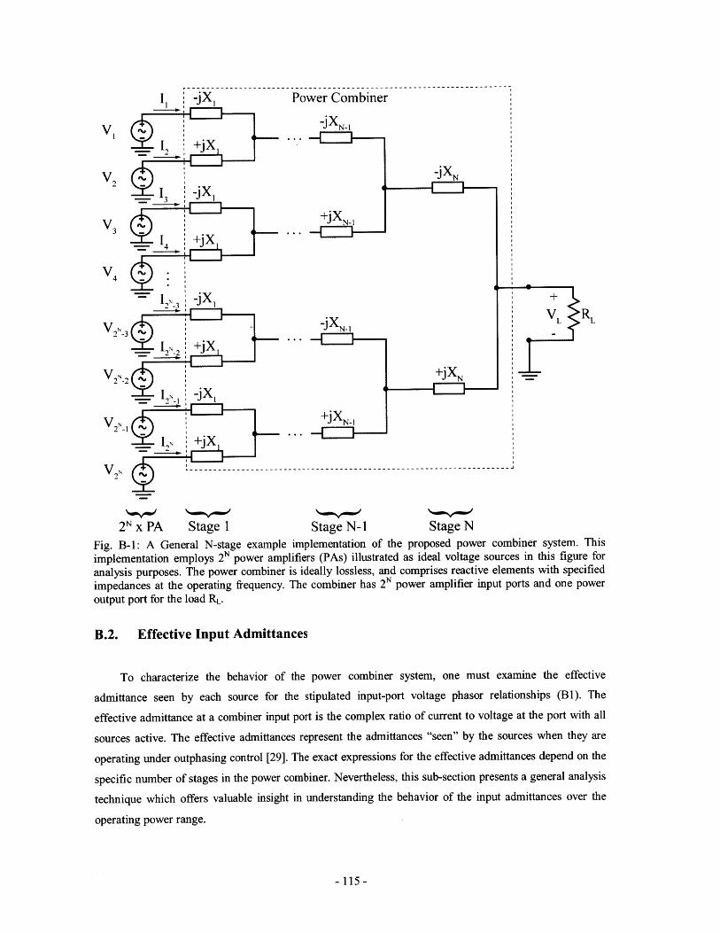
-jX, Power Combiner
V -j XN-1
__ I+j X
-XN
VN
VI -j X -I- ~~
V -'X N-1V
jXV
V2N +jXSae tg NISaeN--
jX+
V Nj N-1
V N_+
N x A Sae1SaeN-1StgN
Fig. B-1: A General N-stage example implementation of the proposed power combiner system. This
implementation employs 2N power amplifiers (PAs) illustrated as ideal voltage sources in this figure foranalysis purposes. The power combiner is ideally lossless, and comprises reactive elements with specifiedimpedances at the operating frequency. The combiner has 2 N power amplifier input ports and one poweroutput port for the load RL.
B.2. Effective Input Admittances
To characterize the behavior of the power combiner system, one must examine the effective
admittance seen by each source for the stipulated input-port voltage phasor relationships (B1). The
effective admittance at a combiner input port is the complex ratio of current to voltage at the port with all
sources active. The effective admittances represent the admittances "seen" by the sources when they are
operating under outphasing control [29]. The exact expressions for the effective admittances depend on the
specific number of stages in the power combiner. Nevertheless, this sub-section presents a general analysis
technique which offers valuable insight in understanding the behavior of the input admittances over the
operating power range.
- 115-

Consider the N-stage power combining system of Fig. B-I and its dual RCN of Fig. A-1, and let the
respective reactance magnitudes be equal (i.e. 1XIl in the combiner is equal to lxII in the RCN, etc.).
Suppose that the load resistance R in the RCN is set to a value that will force the input resistance Rin,N to
Rin,N,med (this corresponds to any of the intersection points in Fig. A-2). Further, suppose that RL in the
power combiner is equivalent to Ri,N,md in the RCN, and let the outphasing control angles be selected
according to (A7), i.e. the voltages at the combiner input terminals are equivalent to the respective voltages
across the R0 loads in the RCN network. In this scenario, the power combiner is a perfect dual of the RCN
(RCN node voltages are equal to the respective combiner node voltages, while RCN branch currents are the
negative of the respective combiner branch currents). As a result, the effective input impedance of each
input port of the power combiner is entirely resistive and equal to R.. This is also the case for any of the 2 N
intersection points in Fig. A-2. This leads to an important observation: for a given RL, an N-stage power
combiner will exhibit entirely resistive effective input admittances on all of its input ports for exactly 2 N
distinct combiner output power levels. Since the phases associated with the effective input admittances at
these power levels are identically zero, the operating points corresponding to these power levels are termed
here the zero-points. It is important to mention that at a zero-point, the sourced currents I - I2N (see Fig. B-
1) are in phase with the input voltages V, - V,, and given by:
I .2 Vs e jP (2.r, :
I 2N e 2q)N
Suppose now that it is desired to operate at another power level (not a zero-point). First compute the
resistive PA loading ro,new that corresponds to the selected combiner output power level Po,, based on the
PA drive amplitude Vs and the 2N number of PAs ().
ronew = V (B3)
Let the new input impedance of the dual RCN with R = r,ne, be RiN,new. Clearly, if the load RL of the
power combiner changes to Rin,N,new, then it would establish a new zero-point. However, in practical
applications, RL is fixed and determined by the actual load that one is driving. Nevertheless, this fact can be
modeled by incorporating an incremental resistance of ARL = RL - Rin,N,new in series with Rin,N,new thus
preserving a total resistance of RL. Next, the Alternation Theorem [56] can be employed to asses the effect
of ARL on the input currents I - N,, provided by each power amplifier (see Fig. B-1). According to the
Alternation Theorem, the resulting incremental currents Al, - Al 2N can be determined by analyzing the
network in Fig. B-2, where IL is the zero-point load current that would flow through RL if ARL = 0 (i.e. if
-116-

RL actually changes to Rin,N,new). Although Fig. B-2 presents only part of the N-stage combiner network in
Fig. B-1, it is sufficient the analysis purposes here and the obtained results are valid in general.
-jXN-1
-jXN ±ARL
ILARL
Fig. B-2: Network utilized for analyzing the incremental change of sourced input currents by the power
amplifiers (Fig. B-1) for a given incremental change in load resistance RL by employing the Alternation
Theorem [56]. IL is the load current in Fig. B-I when ARLO.
By employing conventional linear circuit analysis techniques, it is readily shown that the incremental
currents are given by (B4):
A I = j LL RL in,N.new 2
Pcmd for 1 rtn NX X R i.N,new
(B4)
where the sign is selected depending on the nature of the reactive element Xj: (+) for inductive elements,
and (-) for capacitive elements.
V,ImI
lA
Ineff
Re
Fig. B-3: Phasor plot of the effective current 1n,ef sourced by a particular power amplifier of Fig. B-i for a
given combiner output power level.
Fig. B-3 illustrates how such a current increment Al, can phase-offset the zero-point current In (the
current that would be sourced by a particular power amplifier in Fig. B-I if RL changes to Rin,N,new), and as
a result, introduce an effective input impedance phase of on. Vn is the voltage of the particular amplifier
with a desired outphasing control angle of <pn. Note that by choosing a smaller k-value for the
- 117-

combiner/RCN network design (see RCN design, Appendix A), one can reduce variations of Rin,N,new about
RL, and thus decrease the effective input impedance phases. However, as will be demonstrated, smaller k-
values are associated with limiting the power operating range of the power combiner.
B.3. Output Power Control
First, consider the combiner of Fig. B-i operating at a particular zero-point characterized with a
"commanded" power level Pemd. The "commanded" power is the output power level that one wishes the
combiner to deliver to its load based on which the outphasing control angles are selected. As already
demonstrated in the previous section, the effective input impedance ro "seen" by each PA driving the
combiner is entirely resistive at a zero-point. The resultant output power Pout supplied by all amplifiers to
the load RL is given by (B5) and is equivalent to Pem.
Po, = Pam = s . (B5)r0
Suppose now that one decides to operate the combiner at a Pem not associated with a zero-point. Then
it can be shown that due to the resultant purely-imaginary incremental offset Al 1 to the zero-point current
sourced by a particular amplifiers (B4), the power it supplies to the load is given by (B6) where Vs is the
amplitude of the voltage of each power amplifier and eN is its respective outphasing control angle.
Therefore, the total output power delivered to the load RL for a given Pd can be expressed by (B7).
P = Re{VnIe}= Re (I + AI) I= c' + M"A"'' sin(en) (B6)2 2 2 N 2j
2N N
Po= u Pt*1 = P + " s sin(P) (B7)n=1 n=1 2j
Selecting a sufficiently small design k-value reduces Aln and as a result can decrease the deviation
between Pout and Pma to an arbitrary amount. However, as already mentioned, this adversely affects the
power operating range. Nevertheless, the relationship between Pout and Pcmd (B7) is a monotonic function,
and nonlinearities can be readily addressed through predistortion or other means [29].
B.4. The Eight-Way Power Combiner
This sub-section summarizes some key characteristics of the eight-way combiner. One possible
implementation this combiner (the "binary-tree" implementation) is shown in Fig. B-4. The effective
-118-

admittance matrix Yeff relating the input currents to the source voltages of the above network is given by
(B8)-(B 11) where a = X2/X1 , P = X 3/X and y = RL/Xi.
+j(a +-1)-- j(a+$3)
M 7 ~11y+jp
-y-jp
M12
y - j( - a +1)
- y + j(p - a)y - jp
- y+ j$
yeff
- y - j(a+y + j(a + P
-y-jp
y+jP
M2 1
- y + j(p -y-j(3 - a
-Y+jp
y - j1
11 M 12
21 M 2 2 .P) y+jp
+1) -y-jpy-j(a-p+1)- y+ j(a - 1)
y -y y y
y -y y -y
y y -y ya) y-jjp-1) -y+jp
y - j(a + P +)
- y + j(a + P)
-y-j
y+jp
y-j(a-p3-1)j
- y + jC-P)
y - j$-y+j(a+p)
y - j(a + P -1)_
Fig. B-4: An example implementation of a three-stage power combiner
The PAs driving the combiner are outphased according to (B12) with Fig. B-5 depicting a phasor
representation of the combiner input-port terminal voltages.
-119-
(B8)
(B9)
(B 10)
M2 2
(BI 1)
VA
VB
Vc
VD
VE
VF
VG
VH

VA
VB
Vc
VD
VE
VF
VG
VH
= VS
e-3*e-ioe-iw
e*3e*j0e-iW
ei0e+j0e-jiW
eie-joe+i
e- *e* 0e*3W
_e+j* +j0 +jy
(B12)
Although the effective input admittance seen at each port of the power combiner can be derived
similarly to the case of the four-way combiner (Chapter 2), the exact expressions are omitted here due to
their complexity and large number of terms. Nevertheless, it is important to note that the effective input
admittances seen at the ports A and H, B and G, C and F, D and E are complex conjugate pairs (see Fig 2-
14).
Imn VH,
r ReV
PRe
VE
G
Fig. B-5: Phasor diagram showing the relationship among the phase voltages for a three-stage powercombiner. The outphasing control angles <, 8 and 4y are used to regulate output power while maintainingdesirable loading of the sources A-H.
Various outphasing control methodologies (OP, OS, and IRCN) were presented in Chapter 2 for
controlling the output power of a four-way combiner. These methodologies are also applicable to the case
of the eight-way combiner, although deriving the exact control angle expressions is a laborious procedure.
Of course, for any particular eight-way combiner design, the OP, OS, or IRCN control angles can be
computed numerically by simply sweeping the control angles over the range [0 to 1800] and selecting only
the control angle pairs which yield the desired combiner input admittance characteristics. Although a
MATLAB script that performs this operation can be easily created, another outphasing control
methodology is instead presented hear which results in combiner input admittance characteristics similar to
-120-

those of OP, OS and IRCN control. This new control strategy, termed approximate inverse RCN control
(AIRCN) entails outphasing the PAs according to (A17)-(A19) with R0 =4Vs/Pc , where Pcmd is the
commanded combiner power - the output power that one desires the combiner do deliver to its load.
Essentially, this control strategy aims to drive the input ports of the combiner with voltage waveforms that
are a replica of the voltages measured across the R, loads in the corresponding three-stage RCN network.
As was already discussed, the combiner network is not a true inversion of the RCN network, and hence this
outphasing control methodology inevitably results in a certain mismatch between the commanded power
Pemd and the actual combiner output power Po1u,. The outphasing AIRCN control angles and the resultant
Pemd-Pout characteristic are respectively shown in Fig. B-6 and Fig. B-7 for an example design of an eight-
way combiner with V, = 1 V, RL = 50 0, X, = 18.13 n, X, = 42.29 f and X = 49.68 Q. Furthermore, Fig.
B-8 and Fig. B-9 show its input admittance characteristics. Note that in an actual power combining system,
the mismatch between the commanded and the output power can be addressed easily by simply pre-
distorting the outphasing control - an approach widely used in many contemporary power amplification
systems. Similarly to the case of the four-way combiner, the conductive loading of the PA modulates in
accordance with output power, while susceptive (and phase) variations are limited to certain peak value.
90
8S 607@0
6 0 - -. . -.. . . ... . . .
50-0 -
C 2 0 -. . .. . . .
10 . . . .
01
Pcmd (W)
Fig. B-6: Plot showing the outphasing control angles *, 0 and W versus commanded output power Pesaccording to (48) for the three-stage power combiner example design (V, = 1 V, RL = 50 K, X = 18.13 n,X2= 42.29 n and X = 49.68 2).
- 121 -

54.5 -
ideal actual4
3.5 - -
1 .5 -. . . .
.5 . . . . . .
0.5 - -....0
0 1 2 3 4 5 6 7Pcmd (W)
Fig. B-7: Actual output power versus commanded power for the three-stage power combiner exampledesign (V,= 1 V, RL = 50 f, X = 18.13 fl, X2 = 42.29 C) and X3 = 49.68 f). The actual power increasesmonotonically with Pe, and saturates at approximately 4.5 W for higher commanded power levels.
It is readily observable from Fig. B-8 and Fig. B-9 that the three-stage combiner has exactly eight
zero-points associated with purely conductive input effective admittances (phase is zero). Moreover, if the
maximum effective admittance phase is constrained to 50, this design allows one to operate over an
approximate output power range of [0.02 W, 3.5 W], or an output power range ratio of 22.4 dB (compared
to approximately 12 dB for a four-way combiner).
0
0-
0.90.8-0.7-0.6-0.5-0.4-0.3-0.20.1-
01
0.010.0080.0060.0040.002
0-0.002-0.004-0.006-0.008
-0.011
10-'
10'1
P (W)
P (W)
100
100
10'
10'
Fig. B-8: Real and imaginary components of the effective admittances seen at each of the power combinerinput ports (A-H) plotted as a function of actual output power Pout. The plots are shown for the three-stagecombiner example (V,= 1 V, RL = 50 D, X, = 18.13 Q, X2 = 42.29 n and X3 = 49.68 n).
- 122 -
-~ - A_B
- C_D
-- E- - G
.................... _........ .- H
-
0-2
0-2
- - -.. . .. . .
-7

The k-value selection methodology presented in Chapter 2 is also adopted for the design of the eight-
way combiner (Fig. B-I1 and Fig. B- 12) Assuming Vs = 1 V and RL = 1 fl, the obtained results in this
section can be de-normalized for any particular Vs and RL by simply scaling all power levels by V /RL, and
all impedances by RL. Fig. B-10 shows the maximum absolute value of the phases associated with the
effective input admittances at the input ports of the eight-way combiner for various k-values versus the
output power ranges. Similar to the four-way power combiner, it can be observed that although smaller k
values result in overall smaller admittance phases, the operating power range is reduced. Also note that, in
contrast to the four-way combiner, the eight-way combiner has exactly eight zero-points.
Fig. 2-24 provides the design curves for the eight-way combiner which illustrate respectively the
largest obtainable output power range ratio for a given maximum admittance phase constraint and indicate
the corresponding k-value. The performance advantage of the eight-way combiner over that of the four-way
combiner (from the standpoint of the most resistive PA loading achievable) is obvious. For example, if one
demands an operating power range ratio of 20 dB, an amplifier driving the eight-way combiner may see a
maximum admittance phase of approximately 30, while an amplifier driving the four-way combiner with
the same PRR will observe a worst-case admittance phase of over 500 (see Fig. 2-12). After the appropriate
k-value has been selected, the expression in (A6) is applied to calculate the
combiner. The normalized limits of the operating output power range for each
combiner
0.90.8
2 0.70 =0.6
0.50.40.30.20.10
1'
864
S2
0N -2
-4-6
-81
necessary reactances in the
value of k for the eight-way
is plotted in Fig. B-12.
* -A-B
- C-D- E
- F-G
- -
02 10-o 100
-A-_-B
-~C-D-_-E
F_G
-..- .- G -
0-2 10-1P W)
100 10'
Fig. B-9: Magnitude and phase of the effective admittances seen at each of the power combiner input ports(A-H) plotted as a function of actual output power Po,. The plots are shown for the two-stage combinerexample (Vs= 1 V, RL = 50 Q, X = 18.13 , X2 = 42.29 Q and X3 = 49.68 f).
123 -
'

20
1 8 -.. . ... -
1 6 . . . . . .. .. . . . . . . . . . . . .
16
1 4 -. . . ... ..-. . .-.
12---
6 -. . . . .. . . .. .
2 . .. . . . . . . . . . . . . .
2 -. .-.-
0 100 10' P ou(W) 102
Fig. B-10: Absolute value of the maximum effective input admittance phase seen at the input ports of atwo-stage (top) and three-stage (bottom) power combiners versus the output power level for various k-
values. The plot is normalized to Vs = 1 V and RL = 1 0; denormalize for a particular Vs and RL by scaling
the Po, axis by Vs2 /RL.
Although so far only the "binary-tree" implementation of the eight-way combiner, just as in the case
of the four-way combiner, various topological transformations may be carried-out on the original combiner
implementation of Fig. B-4. Fig. B-13 shows the "binary-tree"-implementation of an eight-way combiner
along with outlined component groups over which a T-A transformation may be applied, and Fig. B-14
illustrates the respective incremental loss curves. Again, similarly to the transformations considered in the
four-way combiner, only transformations that do not involve common components may be performed
simultaneously - two a-transformations along with two p-transformations and a S-transformation preclude
y-transformations.
-124-

Value of k
30 30o
25 o c 25
20 20 -
15 - 15
10 10<
5
0 L I- 01 1.005 1.01 1.015 1.02 1.025 1.03 1.035 1.04
Value of k
Fig. B-11: Design curves for the two-stage (top) and three-stage (bottom) power combiners: trace-out thedesired operating output power range ratio to the Power Ratio Curve to determine the appropriate designvalue for k. The Admittance Phase Curve gives the corresponding worst-case effective input admittancephase that may be seen over the entire operating range at the input ports of the combiner.
Value of k103:
10
o 17.5 dB 20.5 dB 22.5 dB 24.0 dB 250 dB 26.0 dB 27.5 dB10 I oumi j................. .. ................ ........
1.005 1.01 1.015 1.02 1.025 1.03 1.035 1.04
Fig. B-12: Normalized plot (Vs = 1 V, RL = I f)) of the minimum and maximum limits of the output power
operating range versus the k-value for a two-stage (top) and a three-stage (bottom) power combiners. To
denormalize for a particular Vs and RL, multiply the power axes by v~ /RL-
- 125 -

:y-curveV --jxA ..l :+j X
- B . -X2
S-curveV --- - --- --- --- -- ---... -.. ..-... -... --..
B -curVe
.+jX3Vc -jX 2
D + X---------- ....------ ----
VDM
:y-curve -VE -j X..--------. ------------------. V R
I +jX:.--F -j -jX
VF 3
+jX -'
VH
Fig. B-13: Basic T-network implementation of a three-stage power combiner along with outlined possibletopological transformations and their corresponding incremental fractional loss curves in Fig. B-14.
2.5a-curve0-curve
2 y-curve
o 1 .5 - . .. . .. . . . . . . . .
0Q,91 1416 dB 18 d132 d
10 dB 12 dB 14 dB' 16 dB 18 dB 20 dB
4 -0.5( 20 40 60 80 100 120
Pout(W)Fig. B- 14: Incremental fractional power loss curves for a three-stage power combiner for various operatingpower range ratios. Pout is normalized to RL = 1 n and Vs = 1 V.
-126-

Appendix C
MATLAB Code
combiner4_outphasing-control.m% ---------------------------------------------------------------------
% Description:% ---------------------------------------------------------------------
% Compute the Optimal-Susceptance (OS), Optimal-Phase (OP) and InverseRCN
% (IRCN) control angles for a four-way combiner, and plot the resultant% combiner effective input admittances over its operating output power% range
close all;clear all;clc;
% Design Parameters
RL = 50;
Vs = 25;
k = 1.042;
charts)
Combiner Load (ohm)PA voltage drive amplitude (V)
% Combiner design factor (obtained from design
% Compute Combiner ReactancesX2 = 2*RL/(k+1);Xl = X2/(k+sqrt(k^2-1));c = RL/X1;
b = X2/X1;
% Stage 2 reactance (Closest to Load)% Stage 1 reactance (Closest to PA)
% Compute Admittance Matrix
Y_MX = [c+j*(1-b), -c+j*b, c, -c;-c+j*b, c-j*(b+l), -c, c;c, -c, c+j*(b+1), -c-j*b;-c, c, -c-j*b, c+j*(b-i)]/Xl;
Psat = 8*RL*Vs^2/Xl^2;Pout = [0:0.001:0.9]*Psat;phi = [0:0.00001:1]*pi/2;
% Output power saturation level% Output Power Range
% phi sweep range
% Result Arraysmin _phase = zeros(1, length(Pout));minphiphase = zeros(l, length(Pout));min _thetaphase = zeros(1, length(Pout));yeff_optimphase = zeros(4, length(Pout));
min imag = zeros(1, length(Pout));
min phi imag = zeros(1, length(Pout));min _thetaimag = zeros(1, length(Pout));yeff optim imag = zeros(4, length(Pout));
-127-

% Exhaustive Search for the Optimal Control Angles
for n=1llength(Pout)% Compute corresponding theta for a given Pout
theta = acos(sqrt(Xl^2/8/RL/Vs^2*Pout(n)./(sin(phi).*sin(phi))));
% Select all the possible real-valued control angle pairs
index = find(imag(theta)==O);phi new = phi(index);theta-new = theta(index);
% Determine Maximum Admittance Phase and Susceptance
% for each control angle pair
yeffphase max = zeros(l, length(phi_new));
yeff_imagmax = zeros(l, length(phi_new));
yeff = zeros(4, length(phi new));
for m=l:length(phi new)Vin = Vs*[exp(j*(-phi new(m)-thetanew(m)));exp(j*(phinew(m)-
thetanew(m)));exp(j*(-
phinew(m)+thetanew(m)));exp(j*(phi new(m)+thetanew(m)))];
Iin = Y MX*Vin;yeff(:,m) = Iin./Vin;yeff phasemax(m) = max(abs(angle(yeff(:,m))));
yeffimagmax(m) = max(abs(imag(yeff(:,m))));
end
% Store the optimal-phase control angle pairs
[min _phase(n), minindex] = min(yeffphasemax);min_phi phase(n) = phinew(min index);min thetaphase(n) = thetanew(minindex);yeffoptimphase(:,n)=yeff(:,min index);
% Store the optimal-susceptance control angle pairs[min _imag(n), minindex] = min(yeffimagmax);minphiimag(n) = phi_new(min index);min _thetaimag(n) = thetanew(minindex);yeff_optimimag(:,n)=yeff(:,min index);
display(Pout(n));end
% Compute IRCN control angles
a coef = 1;b coef = 4*X2^2+2*X1^2-8*RL*Vs^2./Pout;c coef = X1A4-8*RL*VsA2*Xl^2./Pout;Ro rcn = sqrt((-b coef+sqrt(b coef.A2-4*a coef.*ccoef))./(2*acoef));thetarcn = atan(2*Rorcn*X2./(Rorcn.*Rorcn+X1A2));phircn = atan(X1./Rorcn);phasercn = zeros(l, length(Pout));imag_rcn = zeros(l, length(Pout));
yeffrcn = zeros(4, length(Pout));
for m=1:length(Pout)Vin = Vs*[exp(j*(-phi rcn(m)-theta rcn(m)));exp(j*(phi rcn(m)-
-128-

thetarcn(m)));
exp(j*(-phircn(m)+thetarcn(m)));exp(j*(phircn(m)+thetarcn(m)))];
Iin = Y MX*Vin;yeffrcn(:,m)=Iin./Vin;phasercn(m) = max(abs(angle(Iin./Vin)));imagrcn(m) = max(abs(imag(Iin./Vin)));
end
% Plot OS input admittance characteristicfigure;title('OS');subplot (3,1,1)
plot(10*log10(Pout/100), reaxlabel('Pout (dB)');
ylabel('Conductance (mho)');grid on;subplot (3,1,2)
plot(10*log10(Pout/100), imaxlabel ('Pout (dB) ');ylabel('Susceptance (mho)');
grid on;subplot (3, 1,3)plot(10*log10(Pout/100), 180xlabel('Pout (dB) ');
ylabel('Phase (deg)');grid on;
1(yeffoptimimag));
g(yeffoptimimag));
/pi*angle(yeff optim imag));
% Plot OP input admittance characteristicfigure;title('OP');subplot (3, 1,1)plot (10*log1 (Pout/100), real (yeff optim_xlabel ('Pout (dB) ');
ylabel('Conductance (mho)');grid on;
subplot (3,1,2)plot(10*loglO(Pout/100), imag(yeff optim_xlabel('Pout (dB)');
ylabel('Susceptance (mho)');
grid on;subplot (3,1,3)plot (10*log1 (Pout/100), 180/pi*angle (yefxlabel('Pout (dB)');
ylabel ('Phase (deg)');grid on;
phase));
phase));
f-optim-phase));
% Plot IRCN input admittance characteristicfigure;title('IRCN');subplot (3, 1,1)plot (10*log1 (Pout/100), real (yeffrcn));xlabel('Pout (dB) ');
ylabel('Conductance (mho)')';
grid on;subplot (3,1,2)
-129-

plot(10*log10(Pout/100),xlabel ('Pout (dBW) ');ylabel('Susceptance (mho)grid on;subplot (3,1,3)plot(10*10g10(Pout/1OO),xlabel('Pout (dB) ');ylabel ('Phase (deg)');grid on;
imag(yeff_rcn));
180/pi*angle(yeffrcn));
% Compare IRCN, OP, and OS
figure;subplot (2,1,1)plot(10*log10(Pout/100), 180/pi*max(abs(a
10*log1O(Pout/100), 180/pi*max(abs(a10*log10(Pout/100), 180/pi*max(abs(a
xlabel ('Pout (dB) ');ylabel('Maximum Admittance Phase (deg)');
legend('IRCN', 'OP', 'OS');grid on;subplot (2,1,2)plot(10*log1O(Pout/100), max(abs(imag(yef
10*log10(Pout/100), max(abs(imag(yef10*loglO(Pout/100), max(abs(imag(yef
xlabel('Pout (dB)');ylabel('Maximum Susceptance (S)');
legend('IRCN', 'OP', 'OS');grid on;
% Plot Control Angles
figure;plot(10*log10(Pout/100), 1180/pi*min thetaimag, ...
10*log10(Pout/100), 1
180/pi*min thetaphase, ..10*10g10(Pout/100), 1
180/pi*thetarcn);xlabel('Pout (W)');
ngle(yeffrcn))), ...ngle(yeffoptimphase))),ngle(yeffoptimimag))));
f-rcn))), ...f_optimphase))), ...
f_optimimag))));
80/pi*min phi_imag, 10*log10(Pout/100),
80/pi*minphi_phase, 10*log10(Pout/100),
80/pi*phi-rcn,
ylabel('Outphasing Control Anglesgrid on;
10*log10(Pout/100),
(deg) ');
-130-

combiner4_designcurves.m% ---------------------------------------------------------------------
% Description:% ---------------------------------------------------------------------
% Compute the design curves and the zero-point output power levels% for the four-way combiner% --------------------------------------------------------------------
close all;clear all;clc;
% Combiner Load% PA voltage amplitude
k = [1:0.001:1.3];
max phase ircn [];controlmaxphaseos = [];control
max sscpt ircn = [];controlmaxsscptos = [];control
p_zero-points = [];k-value)
prr = [];
for n=l:length(k)
% Design factor range
% peak phase for a given k-value with IRCN
% peak phase for a given k-value with OP/OS
% peak susceptance for a given k-value with IRCN
% peak susceptance for a given k-value with OP/OS
% zero-point power levels (four zero-points per
% power-range ratio for a given k-value
X2 = 2*RL/(k(n)+l);Load)
X1 = X2/(k(n)+sqrt(k(n)^2-1));PA)
% Stage 2 reactance (Closest to
% Stage 1 reactance (Closest to
c = RL/X1;
b = X2/X1;
Y_MX = [c+j*(1-b), -c+j*b, c, -c;-c+j*b, c-j*(b+1), -c, c;C, -c, c+j*(b+1), -c-j*b;-c, c, -c-j*b, c+j* (b-1)]/X1;
% Calculate the zero-pointsvarl = sqrt(RL^2-X2^2);var2 = 2*RLA2-X1^2-X2^2;var3 = (2*RL^3-2*RL*X2A2)/varl;
pzl = 2*VsA2/(RL+varl-sqrt(var2+var3));pz2 = 2*VsA2/(RL+varl+sqrt(var2+var3));pz3 = 2*Vs^2/(RL-varl-sqrt(var2-var3));pz4 = 2*VsA2/(RL-varl+sqrt(var2-var3));p zeropoints(n,:) = [pzl, pz2, pz3, pz4];prr(n) = 10*loglO(max([pzl, pz2, pz3, pz4])/min([pzl, pz2, pz3,
- 131 -
RL = 1;
Vs = 1;
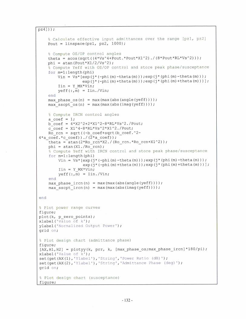
pz4] ) ) ;
% Calculate effective input admittances over the range [pzl, pz2]
Pout = linspace(pzl, pz2, 1000);
% Compute OS/OP control angles
theta = acos(sqrt((4*VsA4+Pout.*Pout*Xl^ 2 )./(8*Pout*RL*VsA2)));phi = atan(Pout*X1/2/Vs^2);% Compute Yeff with OS/OP control and store peak phase/susceptance
for m=l:length(phi)Vin = Vs*[exp(j*(-phi(m)-theta(m)));exp(j*(phi(m)-theta(m)));
exp (j* (-phi (m) +theta (m))) ;exp (j* (phi (m) +theta (m)));
Iin = Y MX*Vin;yeff(:,m) = Iin./Vin;
endmaxphaseos(n) = max(max(abs(angle(yeff))));maxsscptos(n) = max(max(abs(imag(yeff))));
% Compute IRCN control anglesa_coef = 1;b coef = 4*X2A2+2*Xl^2-8*RL*Vs^2./Pout;c coef = X1A4-8*RL*Vs^2*X1^2./Pout;Rorcn = sqrt((-bcoef+sqrt(b_coef.^2-
4*acoef.*ccoef))./(2*acoef));theta = atan(2*Rorcn*X2./(Rorcn.*Rorcn+XA2));phi = atan(X1./Ro_rcn);% Compute Yeff with IRCN control and store peak phase/susceptancefor m=1llength(phi)
Vin,= Vs*[exp(j*(-phi(m)-theta(m)));exp(j*(phi(m)-theta(m)));exp (j* (-phi (m) +theta (m))) ;exp (j* (phi (m) +theta (m)));
Iin = YMX*Vin;yeff(:,m) = Iin./Vin;
endmaxphaseircn(n) = max(max(abs(angle(yeff))));maxsscpt ircn(n) = max(max(abs(imag(yeff))));
end
% Plot power range curvesfigure;plot(k, pzero points);xlabel('value of k');ylabel('Normalized Output Power');
grid on;
% Plot design chart (admittance phase)
figure;[AX,H1,H2] = plotyy(k, prr, k, [maxphaseos;maxphaseircn]*180/pi);xlabel('Value of k');set(get(AX(1),'Ylabel'),'String','Power Ratio (dB)');
set(get(AX(2),'Ylabel'),'String','Admittance Phase (deg)');
grid on;
% Plot design chart (susceptance)figure;
- 132-

- 133 -
[AX,H1,H2] = plotyy(k, prr, k, [maxsscptos;maxsscptircn]);xlabel('Value of k');set(get(AX(1),'Ylabel'),'String','Power Ratio (dB)');
set(get(AX(2), 'Ylabel'), 'String','Normalized Susceptance');grid on;

combiner4_qJoss v2.m% ---------------------------------------------------------------------% Description:
% ---------------------------------------------------------------------
% Evaluate the Q-loss curves for several 4-way combiners designed to
% oeprate over 10dB, 12dB, 14dB and 16dB output power range ratio (PRR)% ---------------------------------------------------------------------
close all;clear all;clc;
RL = 50; % Load ImpedanceVs = 1; % PA voltage amplitudeQ = 100; % Incremental Loss Qk = [1.052, 1.095, 1.16, 1.25]; % Design Factor List
Poutk = []; % Loss-free output powerpout_rangek = []; % Limits of Pout to comply with maxadmittance phasefl_0_k = []; % Fractional loss of binary treeimplementation (NSEO)flincalphak = []; % Fractional Loss by alpha transform vs kflincbetak = []; % Fractional Loss by beta transform vs k
for n=1:length(k)
X2 = 2*RL/(k(n)+1); % Stage 2 reactance (Closest toLoad)
X1 = X2/(k(n)+sqrt(k(n)^2-1)); % Stage 1 reactance (Closest toPA)
c = RL/X1;b = X2/X1;
% Calculate the zero-pointsvarl = sqrt(RLA2-X2A2);var2 = 2*RL^2-X1A2-X2^2;var3 = (2*RLA3-2*RL*X2A2)/varl;
pzl = 2*Vs^2/(RL+varl-sqrt(var2+var3));pz2 = 2*Vs^2/(RL+varl+sqrt(var2+var3));pz3 = 2*VsA2/(RL-varl-sqrt(var2-var3));pz4 = 2*Vs^2/(RL-varl+sqrt(var2-var3));prr(n) = 10*loglO(max([pzl, pz2, pz3, pz4])/min([pzl, pz2, pz3,
pz4]));
Y_MX = [c+j*(1-b), -c+j*b, c, -c;-c+j*b, c-j*(b+l), -c, c;c, -c, c+j*(b+l), -c-j*b;-c, c, -c-j*b, c+j*(b-i)]/X1;
% Define Combiner Network Loss Matrices% NSEO Network:TO = [1 0 0 0;
-134-

0 1 0 0;1 1 0 0;o 0 1 0;o o 0 1;o 0 1 1];
WO = TO'*[X1/Q 0 0 0 0 0;0 X1/Q 0 0 0 0;0 0 X2/Q 0 0 0;0 0 0 X1/Q 00;0 0 0 0 X1/Q 0;0 0 0 0 0 X2/Q]*TO;
% Define Incremental Loss Matrices% -----------------------------------------------------------------
T_delalpha = [-X2/X1, -X2/X1; 1+X2/X1, X2/X1; -X2/X1 1-X2/X1]*[1 00 0;
0 10 0];
W_delalpha = T_delalpha'*[X1^2/X2/Q 0 0; 0 X1/Q 0; 0 0X1/Q]*Tdelalpha;
T_ talpha = [1 0; 0 1; 1 1]*[1 0 0 0; 0 1 0 0];W_t_alpha = T t_alpha'*[X1/Q 0 0; 0 X1/Q 0; 0 0 X2/Q]*T-t-alpha;W inc alpha = W_delalpha-W_t_alpha;
T_delbeta = [1-(RL/j)/X2, -(RL/j)/X2;(RL/j)/X2, 1+(RL/j)/X2]*[1 1 0 0; 0 0 1 1];
W_delbeta = T_delbetal*[X2/Q 0;0 X2/Q]*T del beta;
T_t_beta = [1 0; 0 1]*[1 1 0 0; 0 0 1 1];W t beta = T t beta'*[X2/Q 0;
0 X2/Q]*T_t_beta;W inc beta = Wdelbeta-W_t_beta;% -----------------------------------------------------------------
Psat = 8*RL*VsA2/X1A2;Pout = linspace(0,Psat,1000);fl 0 = zeros(1,length(Pout));fl incalpha = zeros(l,length(Pout));flinc beta = zeros(l,length(Pout));
% Compute IRCN control anglesa_coef = 1;b_coef = 4*X2^2+2*X1^2-8*RL*VsA2./Pout;c_coef = Xl^4-8*RL*VsA2*X1A2./Pout;Rorcn = sqrt((-bcoef+sqrt(bcoef.A2-
4*acoef.*ccoef))./(2*acoef));theta = atan(2*Ro rcn*X2./(Rorcn.*Ro rcn+XA2));phi = atan(Xl./Ro-rcn);
for m=l:length(Pout)Vin = Vs*[exp(j*(-phi(m)-theta(m)));exp(j*(phi(m)-theta(m)));
exp(j*(-phi(m)+theta(m)));exp(j*(phi(m)+theta(m)))];Iin = YMX*Vin;Pin = real(Vin'*Iin/2);
% Compute Q-lossesPdav_0 = real(Iin'*WO*Iin)/2; % Average power dissipated
by NSEOfl 0(m) = Pdav 0/Pin; % Fractional Loss for NSEO
-135-

% Compute Incremental Q-losses
P_incalpha = real(Iin'*Wincalpha*Iin)/2;average power dissipated by alpha transform
flincalpha(m) = P inc alpha/Pin;
Fractional Loss by alpha transform
P_incbeta = real(Iin'*Wincbeta*Iin)/2;average power dissipated by beta transform
flincbeta(m) = P_incbeta/Pin;
Fractional Loss by beta transform
end
fl 0 k = [fl 0 k;fl 0];
fl incbetak = [flincbetak;flincbeta];fl-incalpha k = [ft inc alphak;flinc alpha];
% Incremental
% Incremental
% Incremental
% Incremental
Pout k = [Poutk; Pout];
display(k(n));end
% NORMALIZED Q-LOSS CURVES %
figure;hold on;for n=l:length(k)
Pout = Pout k(n,:);Psat = max(Pout);fl 0 = fl 0 k(n,:);plot(100*Pout/Psat, 100*fl_0);
endhold off;xlabel('% of Psat');
ylabel('Fractional Power Loss (%)');
legend(strcat('prr=', num2str(prr',3)));
grid on;
% NORMALIZED INCREMENTAL QLOSS CURVES
figure;hold on;for n=l:length(k)
Pout = Poutk(n,:);Psat = max(Pout);fl incalpha = flinc_alphak(n,:);fl-incbeta = flincbetak(n,:);plot(100*Pout/Psat, 100*flincalpha,...
100*Pout/Psat, 100*fl inc beta);
endhold off;xlabel('% of Psat');ylabel('Incremental Fractional Power Loss (%)');grid on;
-136-

combiner4_deltaRL.m%-------------------------------------------------------------------
% Description:
% --------------------------------------------------------------
% Plot max effective input admittance phase vs output power of a 4-way% combiner for various resistive/reactive changes in the combiner'sload
close all;clear all;clc;
% Design ParametersRLO = 50;
Vs = 25;
k = 1.042;
charts)
% Nominal Combiner Load (ohm)% PA voltage drive amplitude (V)% Combiner design factor (obtained from design
% Compute Combiner ReactancesX2 = 2*RLO/(k+1); %X1 = X2/(k+sqrt(k^2-1)); %
% Define full output power rangePsat = 8*RLO*Vs^2/X1^2;Pout = [0:0.001:0.9]*Psat;
Stage 2 reactance (Closest to Load)Stage 1 reactance (Closest to PA)
% Output power saturation levelOutput Power Range
% Compute IRCN control angles
a_coef = 1;
b_coef = 4*X2A2+2*X1^2-8*RLO*Vs^2./Pout;ccoef = X1^4-8*RLO*Vs^2*X1^2./Pout;Ro rcn = sqrt((-bcoef+sqrt(bcoef.A2-4*a coef.*ccoef))./(2*a coef));theta rcn = atan(2*Ro_rcn*X2./(Rorcn.*Ro rcn+X1A2));phi rcn = atan(X1./Ro rcn);
% Define RL resistive variation range (in %)RL = (1+[-5 -2.5 0 2.5 5]/100)*RLO;maxphase = [];
for n=1:length(RL)
% Compute Admittance Matrixc = RL(n)/X1;
b = X2/X1;YMX = [c+j*(1-b), -c+j*b, c, -c;
-c+j*b, c-j*(b+1), -c, c;C, -C, c+j*(b+1), -c-j*b;-c, c, -c-j*b, c+j* (b-1)]/X1;
% Evaluate max phase for every output power levelfor m=l:length(Pout)
Vin = Vs*[exp(j*(-phi_rcn(m)-thetarcn(m)));exp(j*(phi rcn(m)-theta_rcn (m)));
exp(j* (-
-137-

phircn(m)+thetarcn(m)));exp(j*(phircn(m)+thetarcn(m)))];Iin = Y MX*Vin;phase(m) = max(abs(angle(Iin./Vin)));
endmax_phase = [max_phase;phase];
end
% Plot max phase vs Pout for all RL valuesfigure;title('Resistive Load Variations');plot(10*log10(Pout/100), maxphase*180/pi);xlabel ('Pout (dB) ');ylabel('Max Admittance Phase (deg)');legend(num2str(RL'));grid on;
% Define RL reactive variation range (in %)RL = (1+j*[-5 -2.5 0 2.5 5]/100)*RLO;maxphase = [];
for n=1:length(RL)
% Compute Admittance Matrixc = RL(n)/X1;b = X2/X1;YMX = [c+j*(1-b), -c+j*b, c, -c;
-c+j*b, c-j*(b+1), -c, c;c, -c, c+j*(b+1), -c-j*b;-c, C, -c-j*b, c+j*(b-1)]/X1;
% Evaluate max phase for every output power levelfor m=1:length(Pout)
Vin = Vs*[exp(j*(-phircn(m)-thetarcn(m)));exp(j*(phi rcn(m)-thetarcn(m)));
exp(j* (-phi rcn(m)+theta rcn(m)));exp(j*(phi rcn(m)+theta rcn(m)))];
Iin = Y MX*Vin;phase(m) = max(abs(angle(Iin./Vin)));
endmaxphase = [maxphase;phase);
end
% Plot max phase vs Pout for all RL valuesfigure;title('Reactive Load Variations');plot(10*log10(Pout/100), maxphase*180/pi);xlabel('Pout (dB)');ylabel('Max Admittance Phase (deg)');legend(num2str(RL'));grid on;
-138-

port_param compare.m%---------------------------------------------------------------------
% Description:% ---------------------------------------------------------------------% Compare the output power and input admittance characteristics of the% ideal and implemented combiners based on the measured port-parameters%6 --------------------------------------------------------------------
clc;close all;clear all;
%---------------------------------------------------------------------% Determine the effective admittance matrix for the ideal combiner%---------------------------------------------------------------------
% Design ParametersRL = 50; % Combiner Load (ohm)k = 1.042; % Combiner design factor (obtained from designcharts)Vs = 25; % PA drive amplitude
% Compute Combiner ReactancesX2 = 2*RL/(k+1); % Stage 2 reactance (Closest to Load)X1 = X2/(k+sqrt(k^2-1)); % Stage 1 reactance (Closest to PA)c = RL/X1;b = X2/Xl;
% Compute Admittance MatrixY MX 1 = [c+j*(1-b), -c+j*b, c, -c;
-c+j*b, c-j*(b+1), -c, c;c, -c, c+j*(b+1), -c-j*b;-c, c, -c-j*b, c+j*(b-i)]/X1;
% Compute OS/OP control anglesPsat = 8*RL*VsA2/X1^2; % Output power saturation levelPout = (0.04:0.001:0.9)*Psat; % Output Power Rangetheta = acos(sqrt((4*VsA4+Pout.*Pout*X1A2)./(8*Pout*RL*VsA2)));phi = atan(Pout*X1/2/Vs^2);% ---------------------------------------------------------------------
%---------------------------------------------------------------------% Determine the effective admittance matrix for the implementedcombiner% based the measured port-parameters% ---------------------------------------------------------------------% Measurement Matrix% Z-Analyzer (AV=8, IF=300Hz, Pout=15dBm)M = [96.50-j*308.7, 2.182+j*0.887, 4.428-j*76.83, 4.232+j*1.487, 3.621-j*87 .22;
1.718+j*0.740, 87.76-j*246.2, 3.239-j*2.912, 6.468+j*77.97, 1.937-j*13.70;
3.880-j*70.04, 3.490-j*3.358, 86.70-j*280.7, 2.378+j*3.408,2.207+j*12.45;
3.016+j*1.156, 5.416+j*70.23, 1.755+j*2.753, 79.69-j*220.3,4.682+j*86.55;
-139-

4.447-j*74.31, 1.704-j*14.36, 1.822+j*11.67, 8.238+j*100.4, 85.94-j*260.0];
% Compute Z-parameters of combiner (treated as five-port network with% output being the fifth port)Z5x5 = zeros(size(M));for m=1:4
for n=(m+1):5Z5x5(m,n) = sqrt((M(m,m)-M(m,n))*M(n,n));Z5x5(n,m) = Z5x5(m,n);
endZ5x5(m,m) = M(m,m);
endZ5x5(5,5) = M(5,5);
% Determine 4x4 admittance matrix at combiner's input% port loaded with RL)RL = 50;Z4x4 = Z5x5(1:4,1:4)-1/(Z5x5(5,5)+RL)*[Z5x5(1,5)*Z5x5
Z5x5 (2,5) *Z5x5Z5x5(3,5)*Z5x5Z5x5 (4,5) *Z5x5
Y_MX_2 = inv(Z4x4);% --------------------------------------------------------------------
ports
(5,(5,(5,(5,
(output
1:4);1:4);1:4);1:4)];
% Calculate the effective input admittancesoperating
% power rangeyeffl =yeff2 = [];Poutl = [];Pout2 = [];for m=l:length(phi)
Vin = Vs*[exp(j*(-phi(m)-theta(m)));expexp(j*(-phi(m)+theta(m)));exp
Iin = Y MX 1*Vin;yeffl(:,m) = Iin./Vin;Poutl(m) = 0.5*real(Iin'*Vin);Iin = Y MX 2*Vin;yeff2(:,m) = Iin./Vin;Pout2(m) = 0.5*real(Iin'*Vin);
end
seen by the PAs over
(j * (phi (m) -theta (m)));(j*(phi(m)+theta(m)))];
% Compare input admittance characteristicfigure;subplot (2,1,1)plot(Poutl, real(yeffl),Pout2, real(yeff2));xlabel ('Pout (dB) ');ylabel('Conductance (mho)');grid on;legend('A','B','C','D','A-cor','B cor','C-cor','D-cor');subplot (2, 1,2)plot(Poutl, imag(yeffl),...
Pout2, imag(yeff2));xlabel ('Pout (dB) ');ylabel('Susceptance (S)');
-140-

grid on;legend('A', 'B','C','D', 'A cor', 'B cor','C cor', 'D cor');
% Compare output power characteristicsfigure;plot(Pout, Pout1, Pout, Pout2);xlabel('Commanded Power (W)');ylabel('Output Power (W)');grid on;legend('Ideal','Actual');
phi ideal = phi;theta ideal = theta;% --- -----------------------------------------------------------------
% Numerically determine best OS/OP control angles for the implementedcombiner% ---------------------------------------------------------------------
% Result Arraysmin _phase = zeros(1, length(Pout));min phi phase = zeros(l, length(Pout));min theta phase = zeros(l, length(Pout));yeffoptimphase = zeros(4, length(Pout));
min _imag = zeros(l, length(Pout));min phi imag = zeros(l, length(Pout));min _thetaimag = zeros(l, length(Pout));yeffoptimimag = zeros(4, length(Pout));
Pout op = [];Pout os = [];
% Exhaustive Search for the Optimal Control Anglesphi = [0:0.001:l]*pi/ 2 ; phi sweep rangefor n=l:length(phi)
Poutnew = [];phi new = phi(n);thetanew = [0:0.001:l1]*pi/ 2 ; % theta sweep range
% Determine Maximum Admittance Phase and Susceptance% for each control angle pairyeffphasemax = zeros(1, length(phinew));yeffimagmax = zeros(l, length(phinew));yeff = zeros(4, length(phinew));for m=l:length(thetanew)
Vin = Vs*[exp(j*(-phi_new-thetanew(m)));exp(j*(phi new-
thetanew(m)));exp(j*(-
phinew+thetanew(m)));exp(j* (phinew+thetanew(m)))];Iin = YMX_2*Vin;yeff(:,m) = Iin./Vin;yeff phasemax(m) = max(abs(angle(yeff(:,m))));yeffimagmax(m) = max(abs(imag(yeff(:,m))));Poutnew(m) = 0.5*real(Iin'*Vin);
end
- 141 -

% Store the optimal-phase control angle pairs
[min _phase(n), minindex] = min(yeffphase max);minphiphase(n) = phi_new;minthetaphase(n) = thetanew(minindex);yeff_optim_phase(:,n)=yeff(:,minindex);Poutop(n)=Poutnew(min index);
% Store the optimal-susceptance control angle pairs
[min _imag(n), minindex] = min(yeff imagmax);min_phi imag(n) = phinew;minthetaimag(n) = thetanew(minindex);yeff_optimimag(:,n)=yeff(:,minindex);Pout os(n)=Pout new(min index);
display(phi(n));end
% Plot OS input admittance characteristic of implemented combiner after
% correcting the outphasing control angles
figure;title('OS');subplot (2,1,1)plot(Poutos, real(yeff-optim-imag));xlabel('Pout (W)');
ylabel('Conductance (mho)');grid on;legend('A','B','C','D');subplot (2,1,2)plot(Poutos, imag(yeff-optim-imag));xlabel ('Pout (W) ') ;ylabel('Susceptance (mho)');grid on;legend('A','B','C','D');
% Compare Ideal Control Angles with Corrected Control Angles
figure;plot(Poutos, 180/pi*min phi imag, Poutos, 180/pi*min theta imag,
Pout, 180/pi*phi ideal, Pout, 180/pi*thetaideal);
xlabel ('Pout (W)') ;ylabel('Outphasing Control Angles (deg)');
legend('phi cor', 'theta cor', 'phi id','theta id');
grid on;
-142-

combiner4 outphasing controlTL.mDescription: Determine OP and OS control angles for a transmission
line% implementation of a four-way combiner and examine effective input% admittance under each controll strategy% Version 2: Maintain equal transmission line characteristic impedances
close all;clear all;clc;
% Design ParametersRL = 50; % Load ImpedanceVs = 1; % PA voltage amplitudek = 1.05; % Range of Design Factor
% Compute Combiner Reactances (use them as a starting point forcomputing% TL impedances)X2 = 2*RL/(k+1); % Stage 2 reactance (Closest to Load)Xl = X2/(k+sqrt(k^2-1)); % Stage 1 reactance (Closest to PA)
Compute Transmission Line Parameters% Design constants used with Xldeltal = 0.01; % Design Constant = abs(TLl length-lambda/2)/lambdasigmal = 2*pi*deltal;% Transmission Line ParametersZl = Xl/sin(sigmal); % TLl characteristic impedance (closest to PAs)Z2 = Zl; % TL2 characteristic impedance (closest to load)c=RL/Zl;b=Z2/Zl;% Design constants used with X2sigma2 = asin(X2/Z2);delta2 = sigma2/2/pi; % Design Constant = abs(TL2 length-lambda/2)/lambda
% Compute Admittance MatrixY_MX = csc(sigmal)^2/Zl*[c*sec(sigma2)^2+j*(cos(sigmal)*sin(sigmal)-b*tan(sigma2)),-c*sec(sigma2)^2+j*b*tan(sigma2),c*sec(sigma2)^2,-c*sec(sigma2)^2; ...
c*sec(sigma2)^2+j*b*tan(sigma2),c*sec(sigma2)^ 2-j*(cos(sigmal)*sin(sigmal)+b*tan(sigma2)),-c*sec(sigma2)A2,c*sec(sigma2)^2; ...
c*sec(sigma2)^2,-c*sec(sigma2)^ 2,c*sec(sigma2)^2+j*(cos(sigmal)*sin(sigmal)+b*tan(sigma2
)),-c*sec(sigma2)A2-j*b*tan(sigma2); ...-c*sec(sigma2)^ 2,c*sec(sigma2)^ 2,-
c*sec(sigma2)^2-j*b*tan(sigma2),c*sec(sigma2)^2-j*(cos(sigmal)*sin(sigmal)-b*tan(sigma2))];
Psat = 8*RL*VsA2/Zl^2/sin(sigmal)^2/cos(sigma2)A2; % Maximum outputpower levelPout = Psat*[0:0.001:0.91; % Output Power Rangephi = 0:0.001:pi/ 2 ; % Control angle phi range
-143-

% Result Arraysminphase = zeros(l, length(Pout));
min _phiphase = zeros(l, length(Pout));
mintheta_phase = zeros(l, length(Pout));
yeff_optimphase = zeros(4, length(Pout));
minimag = zeros(1, length(Pout));
min_phi imag = zeros(l, length(Pout));
minthetaimag = zeros(l, length(Pout));
yeffoptimimag = zeros(4, length(Pout));
% Exhaustive Search of the Optimal Control Angles
for n=1:length(Pout)% Compute corresponding theta for a given Pout
theta =acos(sqrt(Z1A2*sin(sigmal)A2*cos(sigma2)^2/8/RL/VSA
2 *Pout(n)./(sin(phi)
.*sin(phi))));
% Select the allowed angles only (-l<sin(phi)<1; -l<cos(theta)<1)
index = find(imag(theta)==O);phi new = phi(index);theta-new = theta(index);
% Determine Maximum Admittance Phase for each control angle pairyeff_phasemax = zeros(1, length(phi_new));yeffimagmax = zeros(l, length(phi_new));
yeff = zeros(4, length(phi new));
for m=l:length(phi new)Vin = Vs*[exp(j*(-phi_new(m)-thetanew(m)));exp(j*(phinew(m)-
thetanew(m)));exp(j*(-
phinew(m)+thetanew(m)));exp(j*(phi new(m)+thetanew(m)))];
Iin = Y MX*Vin;yeff(:,m) = Iin./Vin;yeff_phasemax(m) = max(abs(angle(yeff(:,m))));yeffimag-max(m) = max(abs(imag(yeff(:,m))));
end
% Store the optimal control angle pair (the one that minimizes
% effective input admittance phases, or susceptances)
[min _phase(n), minindex] = min(yeffphasemax);min_phi phase(n) = phinew(min index);min thetaphase(n) = thetanew(minindex);yeff_optimphase(:,n)=yeff(:,minindex);
(min _imag(n), minindex] = min(yeffimagmax);min.phiimag(n) = phinew(min index);min thetaimag(n) = thetanew(minindex);yeffoptimimag(:,n)=yeff(:,min index);display(Pout(n));
end
-144-

% Plot OS input admittance characteristicfigure;title('OS');subplot (3,1,1)
plot(1O*log1O(Pout/0.18), rexlabel('Pout (dB)');
ylabel('Conductance (mho)');
grid on;subplot (3,1,2)plot(10*loglO(Pout/0.18), imxlabel('Pout (dB)');
ylabel('Susceptance (mho)');grid on;subplot (3,1,3)plot(10*loglO(Pout/0.18), 18xlabel ('Pout (dB) ');
ylabel ('Phase (deg)');grid on;
al(yeff_optimimag));
ag(yeffoptimimag));
0/pi*angle(yeff optim imag));
% Plot OP input admittance characteristicfigure;title('OP');subplot (3,1,1)plot(10*loglO(Pout/0.18), real(yeff optimxlabel('Pout (dB) ');ylabel('Conductance (mho)');
grid on;subplot (3,1,2)plot(10*loglO(Pout/0.18), imag(yeff optimxlabel('Pout (dB)');
ylabel('Susceptance (mho)');grid on;subplot (3,1,3)plot(10*loglO(Pout/0.18), 180/pi*angle(yexlabel('Pout (dB)');
ylabel('Phase (deg)');grid on;
% Plot Control Angles
figure;plot(10*log10(Pout/0.18),180/pi*mintheta_imag, ..
10*1og10(Pout/0.18),180/pi*min thetaphase);xlabel('Pout (W)');ylabel ('grid on;
_phase));
_phase));
ff optim phase));
180/pi*minphiimag, 10*loglO(Pout/0.18),
180/pi*min phiphase,
Outphasing Control Angles
10*10g10(Pout/0.18),
(deg) ');
- 145-

combiner4 designcurvesTL.m% Description: Calculate the set of design/performance curves for a
four% way combiner
% Version 4: - Transmission line combiner implementation
% - OS control% - Output power range is bound by zero-points
% - Sweep k-value and Z2-value over a predefined range
% Last Update: July 31, 2011
close all;clear all;clc;
% Design Parameters
RL = 50; % Load ImpedanceVs = 1; % PA voltage amplitude
% Range of k-values to explorek = [1:0.001:1.005, 1.01, 1.02:0.02:1.24, 1.25];
% Range of Z2 values to explore (TL2 characteristic impedance)
%Z2_range = [100, 125, 150, 200, 500];Z2_range = 500;
poutratio_k_delta = [];peaksscpt_k_delta = [];
for t=1:length(Z2_range)
% Result Arrayspout ratio k =peaksscptk =yeff os abs max k = [];Pout_k = [];
for q=l:length(k)% -------------------------------------------------------------% Compute Transmission Line Parameters for given k-value
Z2 = Z2 range(t);sigma2 = asin(2*RL/(k(q)+1)/Z2); % Range of corresponding
sigma2delta2 = sigma2/pi/2;Zl = Z2;X2 = Z2*sin(sigma2); % Stage 2 reactance (Closest to
Load)X1 = X2/(k(q)+sqrt(k(q)^2-1)); % Stage 1 reactance (Closest to
PA)sigmal = asin(X1/Zl);deltal = sigmal/pi/2;c=RL/Zl;b=Z2/Zl;
% Compute Admittance Matrix for given k
-146-

Y_MX =csc (sigmal) ̂2/Z1* [c*sec (sigma2) ̂2+j* (cos (sigmal) *sin (sigmal) -b*tan(sigma2)),-c*sec(sigma2)^2+j*b*tan(sigma2),c*sec(sigma2)^2,-c*sec(sigma2)^2; ...
-c*sec(sigma2)^2+j*b*tan(sigma2),c*sec(sigma2)^2-j* (cos(sigmal)*sin(sigmal)+b*tan(sigma2)),-c*sec(sigma2)A2,c*sec(sigma2)^2; ...
c*sec(sigma2)^ 2,-c*sec(sigma2)^2,c*sec(sigma2)A2+j*(cos(sigmal)*sin(sigmal)+b*tan(sigma2
)),-c*sec(sigma2)^2-j*b*tan(sigma2); ...-c*sec(sigma2)^ 2,c*sec(sigma2)^2,-c*sec(sigma2)^ 2-
j*b*tan(sigma2),c*sec(sigma2)A2-j*(cos(sigmal)*sin(sigmal)-b*tan (sigma2))];
% -------------------------------------------------------------
%-------------------------------------------------------------
% Calculate zero-pointstheta_zl = 0.5*asin(Z2*sin(2*sigma2)/2/RL); % theta
corresponding to one set of zero-pointstheta z2 = pi/2 - theta zl; % theta
corresponding to a second set of zero-points% polynomial for finding first set of zero-pointspoly zl = [ZlA2*tan(sigmal)A2*cos(sigma2)A2*cos(sigmal)A2, -
cos(theta_zl)A2*8*RL*VsA2, 4*VS^4*cos(sigma2)^2*cos(sigmal)^2];zl = roots(poly_zl);index zl = find(imag(zl)==0);% polynomial for finding second set of zero-pointspoly z2 = [Z1A2*tan(sigmal)A2*cos(sigma2)^2*cos(sigmal)A2, -
cos(thetaz2)A2*8*RL*VsA2, 4*VsA4*cos(sigma2)^2*cos(sigmal)A2];z2 = roots(polyz2);indexz2 = find(imag(z2)==0);P_zero = [zl(index_zl)', z2(indexz2)'];Pmax = max(Pzero);Pmin = min(Pzero);% -------------------------------------------------------------
% -------------------------------------------------------------
% Determine OS control angles numericallyPsat = 8*RL*VsA2/ZlA2/sin(sigmal)A2/cos(sigma2)^2; % Maximum
output power levelPout = linspace(Pmin, Pmax, 100); % Output Power Rangephi = 0:0.001:pi/ 2 ; % Control angle phi
range
min imag = zeros(1, length(Pout));phi os = zeros(l, length(Pout));theta os = zeros(1, length(Pout));yeff os zeros(4, length(Pout));
for n=1:length(Pout)% Compute corresponding theta for a given Pouttheta =
acos(sqrt(Z1A2*sin(sigmal)^2*cos(sigma2)^2/8/RL/Vs^2*Pout(n)./(sin(phi).*sin(phi))));
% Select the allowed angles only (-1<sin(phi)<1; -
-147-

1<cos (theta) <1)index = find(imag(theta)==O);phi = phi(index);theta = theta(index);
% Determine Maximum Susceptance for each control angle pair
yeff_imagmax = zeros(1, length(phi));yeff = zeros(4, length(phi));for m=1llength(phi)
Vin = Vs*[exp(j*(-phi(m)-theta(m)));exp(j*(phi(m)-theta(m)));
exp(j*(-phi(m)+theta(m)));exp(j*(phi(m)+theta(m)))];
Iin = Y MX*Vin;yeff(:,m) = Iin./Vin;yeffimagmax(m) = max(abs(imag(yeff(:,m))));
end
% Store the optimal control angle pair (the one thatminimizes% effective input susceptances)[min_imag(n), min index] = min(yeff imag max);phi os(n) = phi(min_index);thetaos(n) = theta(minindex);yeffos(:,n) = yeff(:,minindex);
endyeffos_abs max = max(abs(imag(yeff_os)));% -------------------------------------------------------------
% -------------------------------------------------------------
% Find optimum output power range for each k-valuepeaks = findpeaks(yeffos abs max);if isempty(peaks)
peaksscpt = 0;pout-ratio = 1;
elsepeak_sscpt = max(peaks);pout-ratio = Pmax/Pmin;
end% -------------------------------------------------------------
poutratio k = [poutratiok, pout_ratio];peaksscptk = [peak_sscpt_k, peaksscpt];
k(q)end
% Check the validity% plot(Poutk', yeffpoutratio_k_delta =peaksscpt_k delta =Z2_range(t)
of the data
os abs max k');[poutratio_k_delta; poutratio_k];[peaksscpt-k-delta; peaksscpt_k];
end
-148-

- 149 -
% DESIGN CURVESfigure;[AX,H1,H2] = plotyy(k, 10*loglO(poutratio_k_delta), k,RL*peaksscpt_k_delta);xlabel('Value of k');set(get(AX(l),'Ylabel'),'String','Zero-Point Power Ratio (dB)');set(get(AX(2),'Ylabel'),'String','Susceptance Normalized to RL');title('4-Way Power Combiner Design Curves');grid on;

Appendix D
Schematics, Bill-of-Materials, and PCBArtwork
D.1. The Outphaser PCB
Fig. D-1: Outphaser PCB top layer copper/silkscreen
Fig. D-2: Outphaser PCB bottom layer copper/silkscreen
-150-

Fig. D-3: Outphaser PCB GND layer copper (2"d layer from the top)
Fig. D-4: Outphaser PCB VDD layer copper (3'd layer from the top)
- 151 -

* :t~1
T~ 2Am
~,p, 9~91O22±OC4M I'P~'~
~11Th~JI~~N * ~
-2±RAl
-UL REn
MR
RM
.~ ;
205" N,.k A
ICU
m~.~AJ1,P , -,
IL
41
.1)
I A
AI
TITLE: Outphasinq Boad ,re,4
- - - - 7-- , - - -- -- -- ...... .... ........ .... ........................................... I .......... MENNEERNW -- '-- - -
T". i(L -E

TABLE D1: OUTPHASER PCB BILL-OF-MATERIALS
Parts Value Package Description Manufacturer Manufacturer Part# Qty
Header
J2, , Male Through TERM
J7 Pins, Hole, BLOCK HDR TE Connectivity 282825-2 3J8 Shroud 5.08MM 2POS VERT
ed (2 Pitch 5.08MMSide)
D1, 0805 LED GRN S-D2, (2012 TYPE GULL Panasonic - SSG LNJ306G5TR02 3D3 Metric) WING SMD
J3, Header Through BERGSTIK 11
J, Unshro 2.54MM .100" SR FCI 68000-203HLF 4
J6 uded Pitch STRAIGHT
Header Through ADERHole, HAE
SV Shroud 2.54MM VERT TE Connectivity 5499922-9 1ehrud Ph 40POS .100ed Pitch 15AU
RES 1.00
R18 1 1608 OHM 1/10W Yageo RC0603FR-071RL 1Metric) 1% 0603
SMDRES 1.0K
R14 1k (1608 OHM 1/10W Yageo RC0603JR-071KL 1Metric) 5% 0603
SMDC8,00 CAP CER MrtC9 1n 1005 1 OOPF 50V Electronics North GRM155R71H102KA 4C27, Metric) 10% X7R America 01DC29 0402
1206(3216Metric) CAP CER
C3 lu Wng 1OUF V TDK Corporation C1632X7R1C105K 2Side), 06120612(1632Metric)
RES 2.0KRI, 2k 0603 OHM 1/10W Susumu RG1608N-202-W-T1 2R2 (1608) .05%0603RG
Metic) SMD _____________________
- 153 -

C10,C11,C26,C28,C48,C49,C50,C51,C52,C53,C54,C55,056,057,C58,C59,C60,Cr
JWK212C6475KD-T 1 18
RES 5.60
R19 5.6 1608 OHM 1/10W Vishay/Dale CRCW06035R60FKEMetric) 1% 0603 A
SMD
0603(1608Metric) CAP CER
Wie0n nUF 1 V TDK Corporation C0816X7R1C103K 2Side), 03060306(0816Metric)
0402 CAP .01UFC12, 10n 1005 25V Kemet C0402C103J3RACT 2C13 Mtn CERAMIC U
Metric) X7R 04020603 CAP CER
C15 10n (1608 1000OPF 50V AVX Corporation 06035C103JAT2A 1Metric) X7R 5%
0603C16, 2917 CAP TANTC21, 10u (7343 10UF 35V Vishay/Sprague TR3D106K035C0250 3C22 Metric) 10% SMDL1, 1008 INDUCTORL2, 33u (2520 POWER TDK Corporation NLV25T-330J-PF 4L3, Metric) 33UH 1008L4 I_ _ _ _ _ _ _ _ _ _ _ __ _ _ _ _ _ _ _ _ _ _ _
C20, 0603 CAP CER023, 39n (1608 .039UF 10% AVX Corporation 06035C393KAT2A 4C24, Metric) 5 6X7R025 _____ M ti) 0603 _____________
-154-
Taiyo Yuden4.7u
0805(2012Metric)Wide(LongSide),0508(1220Metric)
CAP CER4.7UF 6.3VX6S 0508

AVX Corporation TPSD476KO20RO100 6
0603 RES 50 OHM FC0603E50ROBTBSR11 50 (1608 125MW .1% Vishay/Thin Film T1R1
Metric) 0603 SMD TIR3,R4,R5, 0603 RES 100R6, 100 (1608 OHM 1/10W Vishay/Dale TNPW0603100RBEE 8
R8, Metric) 0.1% 0603 A
R9,R1O
0603 CAP CER MurataC1 100n (1608 .1UF 16V Electronics North GRM188R71C104KA
Metric) 10% X7R America 01D0603
0805 RES 220
3' 220 (2012 % 1054W SReconductor ESR10EZPF2200 4R3Metric) SMD80 Semiondcto
SMD
0603 RES 130R30 130 (1608 OHM 1/1OW Yageo RC0603JR-07130RL 1
Metric) 5% 0603SMD
0603 RES 300R31 300 (16 OHM 1/10W Yageo RC0603JR-07300RL 1
SMD0402 CAP CER Murata GRMI55R6IA474KE
C14 470n (1005 .47UF 10V Electronics North 15D 5 4Metric) X5R 0402 America
C4, 0603 CAP CER Murata
C5' 750p (1608 750PF 50V Electronics North GRM1885C1H751JA 4C6' Metric) 5% COG America 01DC7 0603
X4, CONN
X5, BN35N Through SOCKET TE Connectivity 5-1634503-1 3X6 61 Hole BNC STR 50
OHM PCBIC DAC
DAC56 12BIT TexasDA56PF1U1 62PFB 48-TQFP 200MSPS Instruments DAC56621PFB 1
DUAL48TQFPIC REG
U9 LM108 TO-220- POSITIVE 3A National51T-3.3 3 LDO T0220- Semiconductor LM10851T-3.3/NOPB I
___ _ I _ _ _ _1 __ 13
- 155 -
C18,019,044,C45,C46,C47
47u2917(7343Metric)
CAP TANT47UF 20V10% 2917

IC REGPOSITIVE 3ALDO T0220-
NationalSemiconductor LM10851T-5.0-ND
3
LM108 IC REG
U3 5IT- TO-220-3 POSITIVE 3A National L181-2NP12.0 LDO T0220- Semiconductor LM10851T-12/NOPB I
3
24- ICLTC55 WFQFN MODULATO Linear
U2 98 Exposed R Technology LTC55981UF#PBF 1Pad QUADRATU
Pad RE 24-QFNAmplifier,Monolithic,
U6 MERA DL1 020 Dual Mini-Circuits MERA-556+ 1556+ Matched,
RoHSU11,U12, IC
S144 16-SOIC ISOLATOR SiliconU14, S18440 W 4CH 5.5V 16- Laboratories Inc 518440BB-D-lS 7UI15, OCU16,SOICU17
T1 T2-1T KK81 Transformer, Mini-Circuits T2-1T-KK81 1____ RF,RoHS5 __
L5, TCCH- GU1604 RF Choke, Mini-Circuits TCCH-80+ 2L6 180 1___ jRoHS I
Additional Components/Mounting HardwareCONN IDC
N/A N/A N/A SOCKET TE Connectivity 1658623-9 140P0SGOLDHEAT SINK
N/A N/A N/A TO-220 .250" Aavid Thermalloy 577002B00000G 3COMPACTTERMBLOCK
N/A N/A N/A PLUG 2POS TE Connectivity 284041-2 3VERT5.08MMSHUNT
N/A N/A N/A JUMPER .1 3M 969102-0000-DA 4BLACKGOLDCONN IDC
N/A N/A N/A IOO 15 TE Connectivity 1658620-1 4
GOLDSTDOFF
N/A N/A N/A HEX FLA- Keystone 8440G 4RET 4-40 Electronics1.000"L
156-
U10LM10851T-5.0 TO-220-3 1

SCREWMACH PHIL4-40X1/2NYLON
B&F FastenerSupply
NYPH
PMS 440 0050
STANDOFF
N/A N/A N/A 56THR Electronics 1797D 4
.375"L ALUMSCREW
N/A N/A N/A MACHINE B&F Fastener PMS 256 0025 PH 4PHILLIPS 2- Supply__ __ _ __ _ _ __ __ _ 56X1 /4 1_ _ _ _ _ _ _ 1_ _ _ _ _ _ _ _ _ _ _
- 157 -
N/A N/A N/A 4

D.2. Four-Way Combiner PCB
Fig. D-5: Four-way power combiner PCB (top layer copper/silkscreen)
Fig. D-6: Four-way power combiner PCB (bottom layer copper/silkscreen)
- 158-

1 2 3 4 5 6
A A
B B
D D
27.12 MHz, 10-100W Combiner
TITLE: Combiner rev3
Document Number: PEU:
Date: not saved~ Sheet: 1/1
EE
Sheet: 1/1Date: not saved!

D.3. Class-E Power Amplifier PCB
Fig. D-7: Class-E PA PCB (top layer copper/silkscreen)
Fig. D-8: Class-E PCB (bottom layer copper/silkscreen)
-160-

Fig. D-9: Class-E PCB GND layer (1V inner layer from top)
Fig. D-10: Class-E PCB VDD layer (2 d inner layer from top)
- 161 -

SL2 -0 -7V2 1 T C26
C27 C14 C11 c C1 C1 Cj62n210n210V2n 1V 2112 10V 2n)2 10V 2210 V
N
RI R2 R3s R6 R7 8 85 15C 15 15 O
Date: 3/8/2012 3:48:01 PMTITLE: ClassEinv-vl Sheet: 1/1
- 162 -
X2G2
,G3

Appendix E
PIC32MX460 Microcontroller Firmware
phase shifter v2.c/** Name: phase shifterv2.c* Description: Manually set the outphasing angle of each of the four outphaser* PCBs (A, B, C, D). The outphasing angle of each outphaser is* set via a pair of 12-bit integers which represnt the voltage on* the respective I and Q modulator channels (set through a DAC).* RG 1 5/RG3 - increment/decrement A outphasing angle* RG14/RG2 - increment/decrement B outphasing angle* RG 1 3/RG1 - increment/decrement C outphasing angle* RG 12/RGO - increment/decrement D outphasing angle* Last Update: Nov. 23, 2011*/
#define SIZE 1 8#include <builtin.h>
// DAC codes for outphaser Aunsigned int Alvalue[SIZE1]= {3139, 3139, 3139, 3139, 3139, 3139, 3139, 3139};unsigned int AQ value[SIZE1] = {2048, 2048, 2048, 2048, 2048, 2048, 2048, 2048};
// DAC codes for outphaser Bunsigned int BIvalue[SIZE1] = {1016, 1002, 1083, 1296, 1668, 2105, 2450, 2634};unsigned int BQvalue[SIZE1]= {2428, 1710, 1519, 1242, 1010, 944, 1019, 1113};
// DAC codes for outphaser Cunsigned int Clvalue[SIZE1]= {985, 1538, 1763, 1960, 2033, 1960 ,1759, 1531};unsigned int CQ value[SIZE1]= {2359, 1056, 968, 934, 930, 934, 969 , 1060};
// DAC codes for outphaser Dunsigned int DIvalue[SIZE1]= {1316, 3097, 3127, 2925 , 2540 ,2188, 2039, 2076};unsigned intDQ-value[SIZE1]= {1237, 1755, 2194 ,2695, 3022 ,3131 ,3140, 3140};
unsigned long indexI = 0; // index to Ivalue and Q valueunsigned int datai = 2048;unsigned int data q= 2048;unsigned int num = 1; // active channel number
double m_ia = 2.1830;double mqa = 2.2072;double n ia= 2047.4;double nqa = 2047.7;
double m_ib = 2.1959;double m_qb = 2.2115;double n ib = 2047.5;double n_qb = 2047.8;
- 163 -

double mic = 2.2135;double mqc = 2.2339;double n_ic= 2047.4;double nqc = 2047.3;
double m id = 2.1780;double m qd = 2.1867;double n id = 2047.8;double nqd = 2047.1;
void set_phase a(void); // set the outphasing angle of outphaser Avoid setphase b(void); // set the outphasing angle of outphaser Bvoid set_phase c(void); // set the outphasing angle of outphaser Cvoid setphase-d(void); // set the outphasing angle of outphaser D
void main() {double CODE_I;double CODEQ;
DDPCON.JTAGEN=0;AD1PCFG = OxFFFFFFFF; // Configure AN pins as digital I/O
TRISA = OxOOOOCOOO;PORTA = 0;TRISB=0;PORTB=0;TRISC = OxFF;TRISD=0;PORTD =0;TRISE = 0;PORTE = 0;TRISF =0;PORTF =0;TRISG =0;PORTG =0;
/ Initialize outphasersset_phase_a(;set_phase_bo;setphase_co;set_phase_do;
while(1) {if(PORTA.B15){index1+=1;if(index1 > SIZEI-1) index1 = SIZE1-1;set_phase ao;set_phase_bo;set_phase-co;set_phase do;while(PORTA.B 15) {}Delay ms(20);}if(PORTA.B 14){indexl-=1;if(index1 > SIZE-l1) index 1 =0;
-164-

set_phase-ao;setphase-bo;set_phase co;set_phasedo;while(PORTA.B 14) {}Delayms(20);Iif(PORTC.B2){num+=1;if(num > 4) num=4;while(PORTC.B2) {}Delayms(20);}if(PORTC.B1){num-=1;if(num < 1) num= 1;while(PORTC.B1){}Delayjms(20);Iif(PORTC.B4){if(num== 1){AIvalue[indexl]+=10;if(Alvalue[index1]>4095) Al value[indexl]=4095;CODEI = (double) Al value[index 1];CODEQ = sqrt((double) 250000 - pow(((CODE_I-nia)/m-ia),2))*mqa+nqa;AQvalue[index1] = (unsigned int) CODEQ;Iif(num==2){BIvalue[indexl]+=10;if(BIvalue[index1]>4095) BIvalue[indexl]=4095;CODEI = (double) BIvalue[index1];CODEQ = sqrt((double) 250000 - pow(((CODE_I-nib)/m-ib),2))*mqb+nqb;BQvalue[indexl] = (unsigned int) CODEQ;}if(num==3) {CI value[indexl]+=10;if(Clvalue[indexl]>4095) Clvalue[indexl]=4095;CODE I = (double) CI value[index1];CODEQ = sqrt((double) 250000 - pow(((CODEI-nic)/m ic),2))*mqc+nqc;CQvalue[indexl] = (unsigned int) CODEQ;}if(num==4){DIvalue[indexl]+=10;if(DIvalue[index1 ]>4095) DIvalue[index1]=4095;CODEI = (double) DIvalue[index 1];CODEQ = sqrt((double) 250000 - pow(((CODEI-n_id)/mid),2))*mqd+nqd;DQvalue[indexl]= (unsigned int) CODEQ;Iset_phase ao;set_phase_b(;setphase-c;set_phase do;//while(PORTC.B4){}Delayms(100);Iif(PORTC.B3){
- 165 -

if(num==1){ALvalue[indexl]-=10;if(Alvalue[indexl]>4095) Al value[indexl]=0;CODEI = (double) Alvalue[index 1];CODEQ = sqrt((double) 250000 - pow(((CODEI-n-ia)/m-ia),2))*mqa+nqa;AQ~value[index1] = (unsigned int) CODEQ;}if(num==2){BIvalue[indexl]-=10;if(BIvalue[indexl]>4095) BIvalue[indexl]=0;CODEI = (double) BI value[index 1];CODEQ = sqrt((double) 250000 - pow(((CODEI-n ib)/mib),2))*m_qb+nqb;BQ~value[indexl] = (unsigned int) CODEQ;}if(num==3){CIvalue[indexl]-=10;if(Cl-value[indexl]>4095) CIvalue[indexl]=0;CODEI = (double) Clvalue[index 1];CODEQ = sqrt((double) 250000 - pow(((CODEI-n ic)/m ic),2))*mqc+nqc;CQ_value[index1] = (unsigned int) CODEQ;}if(num==4){DIvalue[indexl]-=10;if(DIvalue[index1]>4095) DI value[indexl]=0;CODE I = (double) DIvalue[index 1];CODEQ = sqrt((double) 250000 - pow(((CODEI-n-id)/mid),2))*mqd+nqd;DQ~value[indexl] = (unsigned int) CODEQ;}setphase-a(;set_phasebo;set_phase-co;set_phase do;//while(PORTC.B3){}Delayms(100);}
}
return;
}void set_phase a(void) {data _i = Al-value[indexl];data_q= AQ value[index 1];
PORTA = Hi(datai**;PORTB = Lo(data-i);PORTASET = 0x0030; // RESTEIQ(RA5)= 1, SELECTIQ(RA4)= 1PORTASET = OxOOCO; // WRTIQ(RA7) = 1, CLKIQ(RA6)= 1PORTACLR = OxOOCO; // WRTIQ(RA7) 0, CLKIQ(RA6)= 0
PORTA = Hi(data_q); // Also clears RA5 and RA4PORTB = Lo(dataq);PORTACLR = 0x0030; // RESTEIQ(RA5)= 0, SELECTIQ(RA4) = 0 (for redundancy)PORTASET = OxOOCO; // WRTIQ(RA7) = 1, CLKIQ(RA6) = 1
-166-

PORTACLR = OxOOCO; // WRTIQ(RA7)= 0, CLKIQ(RA6)= 0
PORTA = Hi(data i);PORTB = Lo(data i);PORTASET = 0x0030; // RES,TEIQ(RA5) = 1, SELECTIQ(RA4) = 1PORTASET = OxOOCO; // WRTIQ(RA7)= 1, CLKIQ(RA6)= 1PORTACLR = OxOOCO; // WRTIQ(RA7) 0, CLKIQ(RA6)= 0
PORTA = Hi(dataq); // Also clears RA5 and RA4PORTB = Lo(dataq);PORTACLR = 0x0030; // RESTEIQ(RA5)= 0, SELECTIQ(RA4)= 0PORTASET 0x00C0; // WRTIQ(RA7)= 1, CLKIQ(RA6)= 1PORTACLR = OxOOCO; // WRTIQ(RA7) 0, CLKIQ(RA6)= 0
(for redundancy)
PORTA = Hi(data i);PORTB = Lo(data i);PORTASET = 0x0030; // RESTEIQ(RA5)= 1, SELECTIQ(RA4) = 1PORTASET = OxOOCO; // WRTIQ(RA7)= 1, CLKIQ(RA6)= 1PORTACLR = OxOOCO; // WRTIQ(RA7) 0, CLKIQ(RA6)= 0
PORTA = Hi(dataq); // Also clears RA5 and RA4PORTB = Lo(dataq);PORTACLR = 0x0030; // RESTEIQ(RA5)= 0, SELECTIQ(RA4) = 0 (for redundancy)PORTASET OxOOCO; // WRTIQ(RA7)= 1, CLKIQ(RA6)= 1PORTACLR = OxOOCO; // WRTIQ(RA7) =0, CLKIQ(RA6) =0
PORTA = *i(datai);PORTB = Lo(data-i);PORTASET = 0x0030; // RESTEIQ(RA5)= 1, SELECTIQ(RA4) = 1PORTASET = OxOOCO; // WRTIQ(RA7)= 1, CLKIQ(RA6)= 1PORTACLR = OxOOCO; // WRTIQ(RA7) 0, CLKIQ(RA6) =0
PORTA = Hi(dataq); // Also clears RA5 and RA4PORTB = Lo(dataq);PORTACLR = 0x0030; // RESTEIQ(RA5)= 0, SELECTIQ(RA4)PORTASET = OxOOCO; // WRTIQ(RA7)= 1, CLKIQ(RA6)= 1PORTACLR = OxOOCO; // WRTIQ(RA7) 0, CLKIQ(RA6) =0
= 0 (for redundancy)
return;}
void set_phase b(void){data_i = BIvalue[index1];data_q = BQ~value[index1];
PORTB = Hi(data i) << 8;PORTD = Lo(data-i);PORTBSET = 0x3000; // RESTEIQ(RB13) = 1, SELECTIQ(RB132) = 1PORTBSET = 0xCOOO; // WRTIQ(RB15) = 1, CLKIQ(RB14) = 1PORTBCLR = OxC000; // WRTIQ(RB 15) 0, CLKIQ(RB 14)= 0
PORTB = Hi(dataq) << 8; // Also clears RB12 and RB13PORTD = Lo(dataq);PORTBCLR = 0x3000; // RESTEIQ(RB13) = 0, SELECTIQ(RB 12) = 0 (redundant)
-167-

PORTBSET = OxCO00; // WRTIQ(RB15) = 1, CLKIQ(RB14)= 1PORTBCLR = OxCO00; // WRTIQ(RB 15) =0, CLKIQ(RB 14)= 0
PORTB = Hi(datai) << 8;PORTD = Lo(data i);PORTBSET = 0x3000; // RESTEIQ(RB13) =1, SELECTIQ(RB132) = 1PORTBSET = OxCO00; // WRTIQ(RB15) = 1, CLKIQ(RB14)= 1PORTBCLR = OxCO00; // WRTIQ(RB15) =0, CLKIQ(RB14) =0
PORTB = Hi(dataq) << 8; // Also clears RB 12 and RB 13PORTD = Lo(dataq);PORTBCLR = 0x3000; // RESTEIQ(RB 13) = 0, SELECTIQ(RB 12)= 0 (redundant)PORTBSET = 0xC000; // WRTIQ(RB15) = 1, CLKIQ(RB14)= 1PORTBCLR = OxC000; // WRTIQ(RB 15) =0, CLKIQ(RB 14) =0
PORTB = Hi(data i)<< 8;PORTD = Lo(data-i);PORTBSET = 0x3000; // RESTEIQ(RB13) =1, SELECTIQ(RB132) = 1PORTBSET = 0xCO00; // WRTIQ(RB15)= 1, CLKIQ(RB14)= 1PORTBCLR = 0xC000; // WRTIQ(RB 15) 0, CLKIQ(RB 14)= 0
PORTB = Hi(data_q) << 8; // Also clears RB 12 and RB13PORTD = Lo(dataq);PORTBCLR = 0x3000; // RESTEIQ(RB 13) = 0, SELECTIQ(RB 12) =0 (redundant)PORTBSET = OxC000; // WRTIQ(RB15) = 1, CLKIQ(RB14)= 1PORTBCLR = 0xC000; // WRTIQ(RB15) =0, CLKIQ(RB 14) =0
/******************** * ***********************/
PORTB = Hi(datai) <<8;PORTD = Lo(data-i);PORTBSET = 0x3000; // RESTEIQ(RB13) =1, SELECTIQ(RB132)= IPORTBSET = OxCO00; // WRTIQ(RB15) 1, CLKIQ(RB14)= 1PORTBCLR = 0xC000; // WRTIQ(RB 15) =0, CLKIQ(RB 14)= 0
PORTB = Hi(dataq) << 8; // Also clears RB12 and RB13PORTD = Lo(dataq);PORTBCLR = 0x3000; // RESTEIQ(RB 13) = 0, SELECTIQ(RB 12) =0 (redundant)PORTBSET = 0xC000; // WRTIQ(RB15) = 1, CLKIQ(RB14)= 1PORTBCLR = 0xC000; // WRTIQ(RB15) 0, CLKIQ(RB14) =0
return;}
void set_phase-c(void) {datai = CI value[index1];data_q= CQvalue[index 1];
PORTD = Hi(data i)<< 8;PORTE = Lo(data-i);PORTDSET = 0x3000; // RESTEIQ(RD 13) = 1, SELECTIQ(RD12) = 1PORTDSET = OxCO00; // WRTIQ(RD 15) = 1, CLKIQ(RD 14)= 1PORTDCLR = OxCO00; // WRTIQ(RD 15) 0, CLKIQ(RD 14)= 0
PORTD = Hi(dataq) << 8; // Also clears RD12 and RD13PORTE = Lo(dataq);PORTDCLR = 0x3000; // RESTEIQ(RD 13)= 0, SELECTIQ(RD13)= 0 (redundant)
-168-

PORTDSET = OxCO00; // WRTIQ(RD15) 1, CLKIQ(RD14)= 1PORTDCLR = OxCO00; // WRTIQ(RD 15) 0, CLKIQ(RD 14)= 0
/* **** * ** *** * ** ** ** ** ** ** ** * *** ** ** ** ** * *** *** ** ** ** */
PORTD = Hi(data i)<< 8;PORTE = Lo(datai);PORTDSET = 0x3000; // RESTEIQ(RD13) = 1, SELECTIQ(RD12) = 1PORTDSET = OxCO00; // WRTIQ(RD15) = 1, CLKIQ(RD14) = 1PORTDCLR = OxCO00; // WRTIQ(RD 15) 0, CLKIQ(RD 14)= 0
PORTD = Hi(data_q) << 8; // Also clears RD12 and RD13PORTE = Lo(dataq);PORTDCLR = 0x3000; // RESTEIQ(RD13) = 0, SELECTIQ(RD13) = 0 (redundant)PORTDSET = OxCO00; // WRTIQ(RD15) = 1, CLKIQ(RD14) = 1PORTDCLR = 0xC000; // WRTIQ(RD 15) 0, CLKIQ(RD 14)= 0
PORTD = Hi(data i) <<8;PORTE = Lo(data-i);PORTDSET = 0x3000; // RESTEIQ(RD13) = 1, SELECTIQ(RD12) = 1PORTDSET = 0xC000; // WRTIQ(RD 15) = 1, CLKIQ(RD 14) = 1PORTDCLR = OxCO00; // WRTIQ(RD15) =0, CLKIQ(RD 14)= 0
PORTD = Hi(dataq) << 8; / Also clears RD12 and RD13PORTE = Lo(dataq);PORTDCLR = 0x3000; // RESTEIQ(RD13)= 0, SELECTIQ(RD13)= 0 (redundant)PORTDSET = 0xC000; // WRTIQ(RD15) =1, CLKIQ(RD14)= 1PORTDCLR 0xC000; // WRTIQ(RD 15) =0, CLKIQ(RD 14)= 0
PORTD = Hi(data i) <<8;PORTE = Lo(data-i);PORTDSET = 0x3000; // RESTEIQ(RD13) = 1, SELECTIQ(RD12) = 1PORTDSET = OxCO00; // WRTIQ(RD15) = 1, CLKIQ(RD14)= 1PORTDCLR = OxCO00; // WRTIQ(RD 15) =0, CLKIQ(RD 14)= 0
PORTD = Hi(data q) << 8; // Also clears RD12 and RD13PORTE = Lo(dataq);PORTDCLR = 0x3000; // RESTEIQ(RD13)= 0, SELECTIQ(RD13) = 0 (redundant)PORTDSET = OxCO00; // WRTIQ(RD15) = 1, CLKIQ(RD14)= 1PORTDCLR = 0xCO00; // WRTIQ(RD 15) =0, CLKIQ(RD 14)= 0
return;}
void setjphase d(void) {unsigned long tmpl;unsigned long tmp2;data i = DI value[index1];data_q= DQvalue[index1];
tmp1 = Lo(data-i)&OxOF;tmpl = tmpl << 6;tmp2 = Lo(data-i)&xFO;tmp2 = tmp2 << 8;PORTF = Hi(data i);PORTG = tmp I| tmp2;PORTFSET = Ox1 100; // SELECTIQ(RF8)= 1, RESETIQ(RF 12)= 1
169-

PORTESET = 0x0200; // WRTIQ(RE9) = 1PORTFSET = 0x2000; // CLKIQ(RF13)= 1PORTECLR = 0x0200; /WRTIQ(RE9) =0PORTFCLR = 0x2000; // CLKIQ(RF13)= 0
tmpl = Lo(data_q)&OxOF;tmpl = tmpl << 6;tmp2 = Lo(dataq)&OxF0;tmp2 = tmp2 << 8;PORTF = Hi(dataq); //Also clears RF8 and RF 12PORTG = tmp1 I tmp2;PORTFCLR = Oxi 100; // SELECTIQ(RF8) =0, RESETIQ(RF 12) 0 (redundant)PORTESET = 0x0200; // WRTIQ(RE9) = 1PORTFSET = 0x2000; // CLKIQ(RF13)= 1PORTECLR = 0x0200; // WRTIQ(RE9)= 0PORTFCLR = 0x2000; I/ CLKIQ(RF13)= 0
tmpl = Lo(data-i)&OxOF;tmp1 = tmp1 << 6;tmp2 = Lo(data-i)&OxFO;tmp2= tmp2 << 8;PORTF = Hi(datai);PORTG = tmp II tmp2;PORTFSET = Ox1 100;!! SELECTIQ(RF8)= 1, RESETIQ(RF12)= 1PORTESET = 0x0200; // WRTIQ(RE9) = 1PORTFSET = 0x2000; // CLKIQ(RF13)= 1PORTECLR = 0x0200; // WRTIQ(RE9)= 0PORTFCLR = 0x2000; // CLKIQ(RF13)= 0
tmpl = Lo(dataq)&Ox0F;tmpl = tmpl <<6;tmp2 = Lo(dataq)&OxFO;tmp2 = tmp2 << 8;PORTF = Hi(dataq); //Also clears RF8 and RF12PORTG = tmp1 I tmp2;PORTFCLR = Oxi 100; ! SELECTIQ(RF8) = 0, RESETIQ(RF12) 0 (redundant)PORTESET = 0x0200; // WRTIQ(RE9) = 1PORTFSET = 0x2000; // CLKIQ(RF13)= 1PORTECLR = 0x0200; // WRTIQ(RE9)= 0PORTFCLR = 0x2000; // CLKIQ(RF13)= 0
tmp1 = Lo(data i)&OxOF;tmpl = tmpl << 6;tmp2 = Lo(datai)&xFO;tmp2 = tmp2 << 8;PORTF = Hi(data i);PORTG = tmpl I tmp2;PORTFSET = Oxi 100;!! SELECTIQ(RF8)= 1, RESETIQ(RF12)= 1PORTESET = 0x0200; // WRTIQ(RE9) = 1PORTFSET = 0x2000; // CLKIQ(RF13)= 1PORTECLR = 0x0200; // WRTIQ(RE9)= 0PORTFCLR = 0x2000; /! CLKIQ(RF13)= 0
tmpI = Lo(dataq)&OxOF;tmpl = tmpl << 6;tmp2 = Lo(data q)&OxFO;
-170-

tmp2 = tmp2 << 8;PORTF = Hi(data q); /Also clears RF8 and RF12PORTG = tmp1 | tmp2;PORTFCLR = Oxi 100; // SELECTIQ(RF8) 0, RESETIQ(RF12) =0 (redundant)PORTESET = 0x0200; // WRTIQ(RE9) = 1PORTFSET = 0x2000; // CLKIQ(RF13)= 1PORTECLR = 0x0200; // WRTIQ(RE9)= 0PORTFCLR = 0x2000; // CLKIQ(RF13)= 0
tmpl = Lo(data i)&OxOF;tmpl = tmpl << 6;tmp2 = Lo(data i)&xFO;tmp2 = tmp2 << 8;PORTF = Hi(datai);PORTG = tmp1 | tmp2;PORTFSET = Ox 1100; // SELECTIQ(RF8) = 1, RESETIQ(RF12)= 1PORTESET = 0x0200; // WRTIQ(RE9) = 1PORTFSET = 0x2000; // CLKIQ(RF13)= 1PORTECLR = 0x0200; // WRTIQ(RE9)= 0PORTFCLR = 0x2000; // CLKIQ(RF13)= 0
tmp1 = Lo(dataq)&OxOF;tmp1 = tmpl << 6;tmp2 = Lo(dataq)&xFO;tmp2 = tmp2 << 8;PORTF = Hi(data _q); //Also clears RF8 and RF12PORTG = tmpl | tmp2;PORTFCLR = Ox 1100; // SELECTIQ(RF8)= 0, RESETIQ(RF12)PORTESET = 0x0200; // WRTIQ(RE9) = 1PORTFSET = 0x2000; // CLKIQ(RF13)= 1PORTECLR = 0x0200; // WRTIQ(RE9) = 0PORTFCLR = 0x2000; // CLKIQ(RF13)= 0
= 0 (redundant)
return;
- 171 -

-172-