Large Melting-Point Hysteresis of Ge Nanocrystals Embedded in SiO2
11
eScholarship provides open access, scholarly publishing services to the University of California and delivers a dynamic research platform to scholars worldwide. Lawrence Berkeley National Laboratory Lawrence Berkeley National Laboratory Peer Reviewed Title: Large melting point hysteresis of Ge nanocrystals embedded in SiO2 Author: Xu, Q. Sharp, I.D. Yuan, C.W. Yi, D.O. Liao, C.Y. Glaeser, A.M. Minor, A.M. Beeman, J.W. Ridgway, M.C. Kluth, P. Ager III, J.W. Chrzan, D.C. Haller, E.E. Publication Date: 05-04-2006 Publication Info: Lawrence Berkeley National Laboratory Permalink: http://escholarship.org/uc/item/4fs5c916
-
Upload
independent -
Category
Documents
-
view
1 -
download
0
Transcript of Large Melting-Point Hysteresis of Ge Nanocrystals Embedded in SiO2

eScholarship provides open access, scholarly publishingservices to the University of California and delivers a dynamicresearch platform to scholars worldwide.
Lawrence Berkeley National LaboratoryLawrence Berkeley National Laboratory
Peer Reviewed
Title:Large melting point hysteresis of Ge nanocrystals embedded in SiO2
Author:Xu, Q.Sharp, I.D.Yuan, C.W.Yi, D.O.Liao, C.Y.Glaeser, A.M.Minor, A.M.Beeman, J.W.Ridgway, M.C.Kluth, P.Ager III, J.W.Chrzan, D.C.Haller, E.E.
Publication Date:05-04-2006
Publication Info:Lawrence Berkeley National Laboratory
Permalink:http://escholarship.org/uc/item/4fs5c916

Large melting point hysteresis of Ge nanocrystals embedded in SiO2
Q. Xu,1, 2 I. D. Sharp,1, 2 C. W. Yuan,1, 2 D. O. Yi,3, 2 C. Y. Liao,1, 2 A. M. Glaeser,1, 2 A. M. Minor,4 J.
W. Beeman,2 M. C. Ridgway,5 P. Kluth,5 J. W. Ager III,2 D. C. Chrzan,1, 2 and E. E. Haller1, 2
1Department of Materials Science & Engineering,
University of California, Berkeley, CA 94720, USA
2Materials Sciences Division, Lawrence Berkeley National Laboratory, Berkeley, CA 94720, USA
3Applied Science & Technology, University of California, Berkeley, CA 94720, USA
4National Center for Electron Microscopy,
Lawrence Berkeley National Laboratory, Berkeley, CA 94720,USA
5Department of Electronic Materials Engineering,
Research School of Physical Sciences and Engineering,
Australian National University, Canberra ACT 0200, Australia
(Dated: May 4, 2006)
Abstract
The melting behavior of Ge nanocrystals embedded within SiO2 is evaluated using in situ transmission electron
microscopy. The observed melting point hysteresis is large (±17%) and nearly symmetric about the bulk melting
point. This hysteresis is modeled successfully using classical nucleation theory without the need to invoke epitaxy.
PACS numbers: 64.60.-i,64.70.Dv,61.46.Hk
1
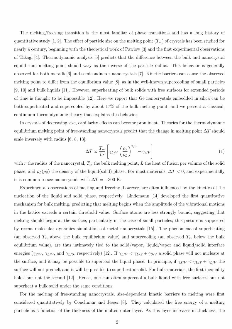
The melting/freezing transition is the most familiar of phase transitions and has a long history of
quantitative study [1, 2]. The effect of particle size on the melting point (Tm) of crystals has been studied for
nearly a century, beginning with the theoretical work of Pawlow [3] and the first experimental observations
of Takagi [4]. Thermodynamic analysis [5] predicts that the difference between the bulk and nanocrystal
equilibrium melting point should vary as the inverse of the particle radius. This behavior is generally
observed for both metallic[6] and semiconductor nanocrystals [7]. Kinetic barriers can cause the observed
melting point to differ from the equilibrium value [8], as in the well-known supercooling of small particles
[9, 10] and bulk liquids [11]. However, superheating of bulk solids with free surfaces for extended periods
of time is thought to be impossible [12]. Here we report that Ge nanocrystals embedded in silica can be
both superheated and supercooled by about 17% of the bulk melting point, and we present a classical,
continuum thermodynamic theory that explains this behavior.
In crystals of decreasing size, capillarity effects can become prominent. Theories for the thermodynamic
equilibrium melting point of free-standing nanocrystals predict that the change in melting point ∆T should
scale inversely with radius [6, 8, 13]:
∆T ∝ Tm
Lr
[γL/V
(ρS
ρL
)2/3
− γs/V
](1)
with r the radius of the nanocrystal, Tm the bulk melting point, L the heat of fusion per volume of the solid
phase, and ρL(ρS) the density of the liquid(solid) phase. For most materials, ∆T < 0, and experimentally
it is common to see nanocrystals with ∆T = −300 K.
Experimental observations of melting and freezing, however, are often influenced by the kinetics of the
nucleation of the liquid and solid phase, respectively. Lindemann [14] developed the first quantitative
mechanism for bulk melting, predicting that melting begins when the amplitude of the vibrational motions
in the lattice exceeds a certain threshold value. Surface atoms are less strongly bound, suggesting that
melting should begin at the surface, particularly in the case of small particles; this picture is supported
by recent molecular dynamics simulations of metal nanocrystals [15]. The phenomena of superheating
(an observed Tm above the bulk equilibrium value) and supercooling (an observed Tm below the bulk
equilibrium value), are thus intimately tied to the solid/vapor, liquid/vapor and liquid/solid interface
energies (γS/V , γL/V , and γL/S, respectively) [12]. If γL/V < γL/S + γS/V a solid phase will not nucleate at
the surface, and it may be possible to supercool the liquid phase. In principle, if γS/V < γL/S + γL/V the
surface will not premelt and it will be possible to superheat a solid. For bulk materials, the first inequality
holds but not the second [12]. Hence, one can often supercool a bulk liquid with free surfaces but not
superheat a bulk solid under the same conditions.
For the melting of free-standing nanocrystals, size-dependent kinetic barriers to melting were first
considered quantitatively by Couchman and Jesser [8]. They calculated the free energy of a melting
particle as a function of the thickness of the molten outer layer. As this layer increases in thickness, the
2

free energy passes through a maximum, creating a kinetic barrier to melting. The experimentally observed
melting point is deduced from the nucleation rate for the transition. Using this treatment, Couchman and
Jesser modeled experimental data for several types of nanocrystals that displayed superheating relative to
their (depressed) equilibrium melting points predicted by Eq. (1).
Consideration of embedded nanocrystals greatly expands the range of possible behaviors and allows
for complete study of the melting point hysteresis. From a classical thermodynamics perspective, there
are two major differences between the free-standing and embedded nanocrystal cases. First, the interface
energies involved in the melting process differ between the two configurations. In fact, the liquid/vapor
and solid/vapor interfaces may no longer be relevant to the melting process, and may be replaced by the
liquid/matrix and solid/matrix interface energies. Second, the geometric constraints implied by embedding
might lead to different equilibrium and kinetic behaviors.
There are a handful of prior experimental observations of superheating (relative to bulk melting points)
of embedded nanocrystals [16–21]. A common feature of most of these studies is the suggestion that
interface epitaxy suppresses the vibrational motion of the surface atoms, thus limiting surface premelting
and increasing the melting point in accord with the Lindemann criterion. This notion has been incorporated
into a phenomenological model for melting [22]. From this perspective, then, it is interesting to consider
the melting of nanocrystals confined to an amorphous matrix, as this eliminates the role of epitaxy in any
potential superheating [19].
To investigate the effects of confinement in an amorphous matrix on melting, we performed electron
diffraction on Ge nanocrystals embedded in silica formed using the process reported earlier [23]. We note
that free-standing nanocrystalline Ge has been reported to show the typical melting point depression found
for most materials [24].
Electron diffraction was used to study the melting behavior of the embedded nanocrystals. Here the
melting temperature is defined as the temperature at which the disappearance of the diffraction pattern
occurs, indicating the loss of lattice order. The in situ heating and cooling experiments were performed
inside a JEOL 3010 transmission electron microscope operating at 300kV. A plan-view specimen was
prepared by backthinning the Si substrate and leaving the implanted silica film side untouched. The
specimen was then placed in the Gatan Ta628 holder which contains a tantalum furnace and a pair of
calibrated thermocouples. The lowest possible electron beam intensity was used to prevent excessive beam
heating. Diffraction experiments on Au nanocrystals embedded in SiO2 were employed to confirm the
accuracy of the experimentally measured temperatures. Measurements of their melting point with our
experimental approach yielded a melting point in good agreement with expectations, thus validating the
experimental technique.
Several heating/cooling cycles were performed in steps of 15 K per 5 minutes from room temperature
3

FIG. 1: Diffraction patterns and integrated intensity plots obtained during measurements of the Ge melting point.
1308 K is 97 K above the bulk melting point of Ge; diffraction rings are clearly observed, demonstrating the
superheating (relative to the melting point of the bulk) of embedded Ge nanocrystals.
to 1470 K on three Ge nanocrystal specimens. (The nanocrystal coarsening rate was negligible.) All
cycles gave identical results. The melting and crystallization were characterized by the intensity change
of the diffraction peaks in the selective area diffraction patterns obtained on a 0.2 µm2 field of embedded
nanocrystals. The ring patterns were recorded by a Gatan optically coupled TV-rate CCD camera and
integrated circumferentially about the pattern center to produce the reported diffracted intensity.
Electron diffraction patterns obtained while heating Ge nanocrystals in SiO2 from ambient temperature
to 1450 K are shown in Fig 1. The 111, 202, and 113 diffraction peaks persist to 1400 K, nearly 200 K
above the bulk melting point (1211 K). Figure 2 displays diffracted intensities (computed by circumferential
integration of the patterns shown in Fig. 1) as a function of temperature for heating and cooling cycles, for
Ge nanocrystals embedded in silica. Melting starts at 1350 K and is complete by 1450 K; resolidification
begins at 980 K and is complete by 880 K. This corresponds to a hysteresis loop approximately 470 K
wide and centered (approximately) on the bulk melting temperature.
The observation of a large hysteresis (±17% of Tm) nearly symmetric about the bulk melting point is
4
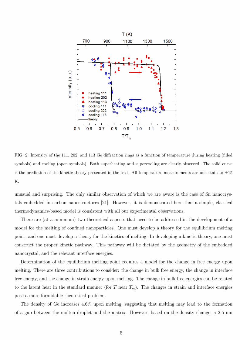
FIG. 2: Intensity of the 111, 202, and 113 Ge diffraction rings as a function of temperature during heating (filled
symbols) and cooling (open symbols). Both superheating and supercooling are clearly observed. The solid curve
is the prediction of the kinetic theory presented in the text. All temperature measurements are uncertain to ±15
K.
unusual and surprising. The only similar observation of which we are aware is the case of Sn nanocrys-
tals embedded in carbon nanostructures [21]. However, it is demonstrated here that a simple, classical
thermodynamics-based model is consistent with all our experimental observations.
There are (at a minimum) two theoretical aspects that need to be addressed in the development of a
model for the melting of confined nanoparticles. One must develop a theory for the equilibrium melting
point, and one must develop a theory for the kinetics of melting. In developing a kinetic theory, one must
construct the proper kinetic pathway. This pathway will be dictated by the geometry of the embedded
nanocrystal, and the relevant interface energies.
Determination of the equilibrium melting point requires a model for the change in free energy upon
melting. There are three contributions to consider: the change in bulk free energy, the change in interface
free energy, and the change in strain energy upon melting. The change in bulk free energies can be related
to the latent heat in the standard manner (for T near Tm). The changes in strain and interface energies
pose a more formidable theoretical problem.
The density of Ge increases 4.6% upon melting, suggesting that melting may lead to the formation
of a gap between the molten droplet and the matrix. However, based on the density change, a 2.5 nm
5

interface interface notes
energy
(J m−2)
γGe(L)/Ge(S) 0.26 Determined from present experiments;
close to value in ref. [10].
γGe(L)/V 0.59 Linearly extrapolated from
experimental values [25].
γGe(S)/V 1.0 References [26, 27].
γGe(L)/SiO2(S) 0.91 Reference [25].
γGe(S)/SiO2(S) 0.91 Determined from present experiments.
γSiO2(S)/V 0.41 Extrapolated from
reference [28] data.
TABLE I: Interface energies employed in kinetic model of melting.
radius molten sphere will have an average gap of 0.4 A between its surface and the matrix (barring the
effects of thermal expansion). While this gap is well defined within a continuum theory, its effects at the
atomic scale are unclear. Within a continuum theory, the fate of this interface depends upon the values of
γGe(L)/SiO2(S), γGe(L)/V , and γSiO2(S)/V , and the change in strain energy associated with the suppression or
formation of a gap. [Here, (L) indicates liquid, (S) indicates solid and V indicates vapor.] Formation of
a gap creates Ge(L)/V and SiO2/V interface at the expense of Ge(L)/SiO2(S) interface. Suppression of
gap formation puts the liquid Ge in tension, shears the SiO2 matrix, and might lead to an overall increase
in elastic energy. To make further progress, one needs estimates of the interface and strain energies.
The interface energies used on our analysis are given in Table 1. These values, with the exceptions
of γGe(L)/Ge(S) and γGe(S)/SiO2(S), are extrapolated from values in the literature or deduced from other
experiments independent of the present melting point measurements. Applying the kinetic model de-
scribed below to description of the experimental data establishes that γGe(S)/SiO2(S) ≈ γGe(L)/SiO2(S), and
γGe(L)/Ge(S) = 0.26. This latter value of differs from that quoted by Turnbull [10]. However, Turnbull’s anal-
ysis employed a calculated heat of fusion, L, that differs from more recent estimates. The melting behavior
depends only on the ratio γGe(L)/Ge(S)/L, and scaling Turnbull’s value accordingly yields γGe(L)/Ge(S) = 0.23
J/m2. Our value differs by only 13% - a negligible difference.
The surface energies listed in Table 1 imply the following properties for the embedded nanocrystals.
First and foremost, in the solid state, the solid Ge/SiO2 interface will not premelt because γGe(L)/SiO2(S) +
γGe(L)/Ge(S) > γGe(S)/SiO2(S). Second, the molten phase will not “presolidify” at the interface because
6

γGe(S)/SiO2(S) + γGe(L)/Ge(S) > γGe(L)/SiO2(S). Thus the solid/liquid transformation will require nucleation
in both directions. Third, according to the criteria expressed above, supercooling but not superheating of
bulk Ge is predicted, which is consistent with experimental observations.
Based on these interface energies, the opening of a gap would increase the surface energy of a nanocrystal
5 nm in diameter by roughly 70 eV. This increase in surface free energy, would have to be countered through
a reduction in strain energy. In the absence of a gap, the liquid would be placed under tension, and be
strained roughly 1%. Assuming reasonable values for the bulk modulus of the liquid and the interface
stress and applying the formalism in ref. [29], the elastic strain energy is computed to be (roughly) 6
eV. Thus the increase in surface energy associated with opening a gap is roughly an order of magnitude
larger than the total strain energy of the liquid phase. In this continuum picture, the elastic energy cannot
compensate the increase in interface energy, and a gap will not open. Further, this analysis suggests that
elastic contributions are within the accuracy of our theory, negligible.
With these values for the surface energies and neglect of the elastic energy, one can compute two useful
quantities for the confined Ge nanocrystals. First, an estimate for the equilibrium melting point can be
ascertained. Specifically, we find an expression similar to that of Couchman and Jesser [8] for the change
in melting point:
∆T =3Tm
Lr
[γGe(L)/SiO2(S) − γGe(S)/SiO2(S)
], (2)
For our choice of parameters, the term in square brackets is identically zero, as is ∆T .
Second, we can compute an approximate rate for melting and solidification of the confined Ge nanocrys-
tals. The energy barriers are computed by first solving for the equilibrium geometry of the nucleus as a
function of liquid volume (using Young’s equation and conservation of mass, etc.), and then computing
the change in free energy as a function of nucleus size. The maximum in the free energy vs liquid volume
plot yields the energy barrier that must be overcome in order to melt or solidify the nanocrystal. Figs.
3(a)-(d) display select configurations along the kinetic pathway. The kinetic theory assumes an attempt
frequency per atom of 1011 sec−1, that nucleation is heterogeneous at the Ge/SiO2 interface, and that a
nucleation rate of 1 sec−1 is experimentally observable. Fig. 3(a) is the predicted critical nucleus for the
melting of 5 nm diameter nanocrystal and Fig. 3(d) is the critical nucleus associated with solidifying the
same nanocrystal. The corresponding predicted superheating and supercooling temperatures are 199 K
above and 256 K below the bulk melting point of Ge, respectively. The energy barrier to melting is 3.91
eV, and that associated with solidification is 2.65 eV.
The kinetically determined melting temperatures for the model are plotted in Fig. 3(f). These melting
point predictions are then combined with a simple model for diffraction to model the electron diffraction
results [30]. Specifically, the diffracted intensity from each nanocyrstal is assumed to scale with the sixth
power of the radius, and is corrected for Debye-Waller effects by extrapolating known sub-melting point
7
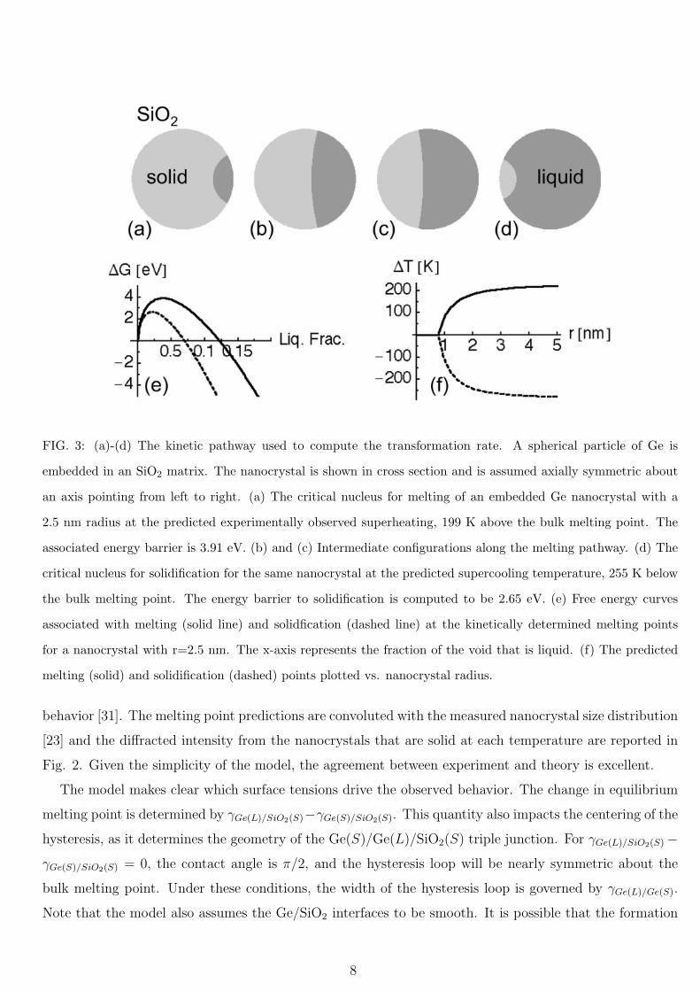
FIG. 3: (a)-(d) The kinetic pathway used to compute the transformation rate. A spherical particle of Ge is
embedded in an SiO2 matrix. The nanocrystal is shown in cross section and is assumed axially symmetric about
an axis pointing from left to right. (a) The critical nucleus for melting of an embedded Ge nanocrystal with a
2.5 nm radius at the predicted experimentally observed superheating, 199 K above the bulk melting point. The
associated energy barrier is 3.91 eV. (b) and (c) Intermediate configurations along the melting pathway. (d) The
critical nucleus for solidification for the same nanocrystal at the predicted supercooling temperature, 255 K below
the bulk melting point. The energy barrier to solidification is computed to be 2.65 eV. (e) Free energy curves
associated with melting (solid line) and solidfication (dashed line) at the kinetically determined melting points
for a nanocrystal with r=2.5 nm. The x-axis represents the fraction of the void that is liquid. (f) The predicted
melting (solid) and solidification (dashed) points plotted vs. nanocrystal radius.
behavior [31]. The melting point predictions are convoluted with the measured nanocrystal size distribution
[23] and the diffracted intensity from the nanocrystals that are solid at each temperature are reported in
Fig. 2. Given the simplicity of the model, the agreement between experiment and theory is excellent.
The model makes clear which surface tensions drive the observed behavior. The change in equilibrium
melting point is determined by γGe(L)/SiO2(S)−γGe(S)/SiO2(S). This quantity also impacts the centering of the
hysteresis, as it determines the geometry of the Ge(S)/Ge(L)/SiO2(S) triple junction. For γGe(L)/SiO2(S)−
γGe(S)/SiO2(S) = 0, the contact angle is π/2, and the hysteresis loop will be nearly symmetric about the
bulk melting point. Under these conditions, the width of the hysteresis loop is governed by γGe(L)/Ge(S).
Note that the model also assumes the Ge/SiO2 interfaces to be smooth. It is possible that the formation
8

of a very thin Ge-oxide layer between the Ge and SiO2 might lead to a sufficiently smooth interface.
These experiments demonstrate clearly the advantages of studying embedded nanocrystals. First and
foremost, the embedded structure allows for complete study of the melting point hysteresis. Therefore one
can assess the relative importance of kinetically limited and equilibrium behaviors directly. Further, the
embedded geometry enables the engineering of interface energies and expands substantially the scope of
observable melting point behavior.
The authors acknowledge A. Robinson and N. Phillips for their careful reading and insightful critique
of this manuscript. I.D.S. acknowledges support from the Intel Robert N. Noyce fellowship. D.O.Y.
acknowledges support from U.C. Berkeley and Luce Foundation Fellowships. Q.X. acknowledges support
through a U.C. Berkeley Fellowship. D.C.C. and E.E.H. acknowledge support from the Miller Institute for
Basic Research in Science. M.C.R. and P.K. acknowledge support from the Australian Research Council.
This work is supported in part by the Director, Office of Science, Office of Basic Energy Sciences, Division
of Materials Science and Engineering, of the U.S. Department of Energy under contract No. DE-AC02-
05CH11231 and in part by U.S. NSF Grant No. DMR-0405472. Electron microscopy was performed at
the National Center for Electron Microscopy, LBNL.
[1] R. W. Cahn, Nature 323, 668 (1986).
[2] R. W. Cahn, Nature 413, 582 (2001).
[3] P. Pawlow, Z. Phys. Chem. 65, 1 (1909).
[4] M. Takagi, J. Phys. Soc. Japan 9, 959 (1954).
[5] K. J. Hansen, Z. Phys. 157, 523 (1960).
[6] P. Buffat and J.-P. Borel, Physical Review A 13, 2287 (1976).
[7] A. N. Goldstein, C. M. Echer, and A. P. Alivisatos, Science 256, 1425 (1992).
[8] P. R. Couchman and W. A. Jesser, Nature 269, 481 (1977).
[9] D. Turnbull and R. E. Cech, Journal of Applied Physics 21, 804 (1950).
[10] D. Turnbull, Journal of Applied Physics 21, 1022 (1950).
[11] A. Defrain, J. Chim. Phys. 74, 851 (1977).
[12] L. D. Landau and E. M. Lifshitz, Statistical Physics Part I (Pergamon Press, Oxford, 1980).
[13] F. Baletto and R. Ferrando, Reviews of Modern Physics 77, 371 (2005).
[14] F. A. Lindemann, Z. Phys. 11, 609 (1910).
[15] Y. Qi, T. Cagin, W. L. Johnson, and W. A. Goddard III, J. Chem. Phys. 115, 385 (2001).
[16] C. J. Rossouw and S. E. Donnelly, Physical Review Letters 55, 2960 (1985).
[17] J. Dages, H. Gleiter, and J. H. Perepezko, Mat. Res. Soc. Symp. Proc. 57 (1986).
9

[18] L. Grabaek, J. Bohr, H. H. Andersen, A. Johansen, E. Johnson, L. Sarholt-Kristensen, and I. K. Robinson,
Physical Review B 45, 2628 (1992).
[19] O. S. Mei, S. C. Wang, H. T. Cong, Z. H. Jin, and K. Lu, Physical Review B 70, 125421 (2004).
[20] Z. Zollmer, K. Ratzke, F. Faupel, and A. Meyer, Physical Review Letters 90, 195502 (2003).
[21] F. Banhart, E. Hernandez, and M. Terrones, Physical Review Letters 90, 185502 (2003).
[22] Q. Jiang, Z. Zhang, and J. C. Li, Chem. Phys. Lett. 322, 549 (2000).
[23] I. D. Sharp, D. O. Yi, C. Y. Liao, J. W. Beeman, Z. Liliental-Weber, K. Yu, D. N. Zakharov, J. W. Ager III,
D. C. Chrzan, and E. E. Haller, Applied Physics Letters 86, 063107 (2005).
[24] N. T. Gladkich, R. Neidermayer, and K. Spiegel, Phys. Stat. Sol. 15, 181 (1966).
[25] N. Kaiser, A. C. F. R. Szofran, S. D. Cobb, and K. W. Benz, Journal of Crystal Growth 231, 448 (2001).
[26] M. Albrecht, P. O. Hansen, S. Christiansen, W. Dorsch, H. P. Strunk, and E. Bauser, Scanning Microscopy
8, 925 (1994).
[27] R. J. Jaccodine, J. Elec. Soc. 110, 524 (1963).
[28] A. Roder, W. Kob, and K. Binder, J. Chem. Phys. 114, 7602 (2001).
[29] J. W. Cahn and F. Larche, Acta metallurgica 30, 51 (1982).
[30] Details will be published elsewhere.
[31] V. F. Sears and S. A. Shelley, Acta Cryst. A47, 441 (1991).
10