Kuhnke Electronics Instruction Manual - Impulse Automation
166
Kuhnke Electronics Instruction Manual Eco Control 667E Small compact PLC E 556 GB 3 December 1998 / 77.931
-
Upload
khangminh22 -
Category
Documents
-
view
0 -
download
0
Transcript of Kuhnke Electronics Instruction Manual - Impulse Automation

Kopfzeile ungerade Seite
1
Kuhnke ElectronicsInstruction ManualEco Control 667ESmall compact PLCE 556 GB 3 December 1998 / 77.931

Kopfzeile gerade Seite
This data sheet is primarily intended for use by design, project, and deve-lopment engineers. It does not give any information about delivery possibili-ties. Data is only given to describe the product and must not be regarded asguaranteed properties in the legal sense. Any claims for damages against us- on whatever legal grounds - are excluded except in instances of deliberateintent or gross negligence on our part.
We reserve the rights for errors, omissions and modifications.Reproduction even of extracts only with the editor's express and written priorconsent.
Table of contents
3
Table of contents
1 Introduction................................................................................... 111.1 Features................................................................................. 111.2 Successor to Pico/Compact Control KUAX 667......................... 12
2 Reliability, safety ........................................................................... 132.1 Target group .......................................................................... 132.2 Reliability ............................................................................... 132.3 Notes .................................................................................... 14
2.3.1 Danger ........................................................................... 142.3.2 Dangers caused by high contact voltage............................ 142.3.3 Important information / cross reference.............................. 14
2.4 Safety .................................................................................... 152.4.1 Observe during planning and installation........................... 152.4.2 Observe during maintenance or servicing .......................... 16
2.5 Electromagnetic compatibility................................................... 172.5.1 Definition ........................................................................ 172.5.2 Resistance to interference.................................................. 172.5.3 Interference emission........................................................ 182.5.4 General notes on installation............................................. 182.5.5 Protection against external electrical influences.................. 192.5.6 Cable routing and wiring.................................................. 192.5.7 Location of installation...................................................... 192.5.8 Particular sources of interference ....................................... 20
3 Hardware..................................................................................... 213.1 Model variants ....................................................................... 213.2 Top view................................................................................ 22
3.2.1 Eco Control 667E 8/8...................................................... 22

Table of contents
4
3.2.2 Eco Control 667E 16/16.................................................. 233.2.3 Eco Control 667E 32/32.................................................. 24
3.3 Mechanical design ................................................................. 243.3.1 Installation....................................................................... 253.3.2 Earthing .......................................................................... 26
3.4 Power supply.......................................................................... 273.4.1 System power supply........................................................ 27
3.5 Digital inputs .......................................................................... 283.6 Digital outputs ........................................................................ 293.7 Serial interface COM1............................................................ 303.8 Light emitting diodes ............................................................... 303.9 Processor ............................................................................... 31
3.9.1 On-chip RAM................................................................... 313.10 Memory distribution................................................................ 31
3.10.1 Operating system............................................................. 313.10.2 User program .................................................................. 313.10.3 Data memory................................................................... 333.10.4 NV-RAM: special features ................................................. 333.10.5 On-chip RAM: special features .......................................... 34
4 Software....................................................................................... 354.1 Operative approach ............................................................... 35
4.1.1 PLC cycle......................................................................... 364.2 Operand ranges..................................................................... 43
4.2.1 Definitions ....................................................................... 444.2.2 Summary of operands ...................................................... 454.2.3 Set operand functions ....................................................... 46
4.3 Description of commands ........................................................ 474.4 Types of operands .................................................................. 48
4.4.1 Addressing...................................................................... 49

Table of contents
5
4.4.2 Summary of commands .................................................... 504.5 Programming modules............................................................. 65
4.5.1 Organisation module........................................................ 664.5.2 Program module .............................................................. 664.5.3 KUBES module................................................................. 664.5.4 Module hierarchy............................................................. 67
5 KUBES modules............................................................................. 695.1 KUBES module libraries........................................................... 70
5.1.1 Contents of the KUBES module library................................ 715.1.2 Loading KUBES modules................................................... 72
5.2 Communication modules ......................................................... 735.2.1 Reserved operands........................................................... 745.2.2 V.24 mode settings .......................................................... 755.2.3 Sending single characters (V24667IS) ............................... 765.2.4 Receiving single characters (V24667IE) ............................. 775.2.5 Sending strings (SST667IN) .............................................. 785.2.6 Example program “serial communication“.......................... 79
5.3 Copying data (blocks)............................................................. 835.3.1 Reserved operands........................................................... 835.3.2 Operands’ intermediate code addresses ............................ 845.3.3 Reading data (RD_OFFS) .................................................. 855.3.4 Writing data (WR_OFFS).................................................. 865.3.5 Example program “copy data block“................................. 87
6 Examples ...................................................................................... 916.1 Basic functions........................................................................ 91
6.1.1 AND............................................................................... 916.1.2 OR.................................................................................. 916.1.3 Negated input ................................................................. 926.1.4 Negated output................................................................ 92

Table of contents
6
6.1.5 NAND............................................................................ 936.1.6 NOR............................................................................... 936.1.7 XO: exclusive OR (antivalence) ......................................... 946.1.8 XON: exclusive NOR (equivalence) ................................... 946.1.9 Seal-in circuit ................................................................... 95
6.2 Memory functions ................................................................... 966.2.1 Mainly resetting ............................................................... 966.2.2 Mainly setting.................................................................. 96
6.3 Switching circuits .................................................................... 976.3.1 OR-AND circuit ................................................................ 976.3.2 Parallel circuit to output .................................................... 976.3.3 Network with one output................................................... 986.3.4 Networ with outputs and marker........................................ 99
6.4 Special markers used as AND/OR marker.............................. 1006.4.1 Network with OR marker ................................................ 1006.4.2 Network with AND marker ............................................. 1016.4.3 Network with multiple use of the OR marker ..................... 102
6.5 Circuit conversion................................................................. 1036.6 Special-purpose circuits ......................................................... 104
6.6.1 Impulse relay ................................................................. 1046.6.2 Reversing circuit (reversing starter) with forced stop........... 1056.6.3 Reversing circuit (reversing starter) without forced stop ...... 106
6.7 Edge evaluation (wiping pulse) .............................................. 1076.7.1 Programmable wiping pulse at rising edge....................... 1076.7.2 Programmable wiping pulse at falling edge...................... 1086.7.3 Wiping pulse at positive signal ....................................... 1096.7.4 Wiping pulse at negative signal ...................................... 110
6.8 Software timers..................................................................... 1116.8.1 Mnemonics.................................................................... 111

Table of contents
7
6.8.2 Impulse at start-up .......................................................... 1136.8.3 Impulse of constant duration............................................ 1146.8.4 Raising delay................................................................. 1156.8.5 Falling delay.................................................................. 1166.8.6 Pulse generator with wiping pulse output.......................... 1176.8.7 Flash generator with one timer ........................................ 1186.8.8 Flash generator with two timers ....................................... 119
6.9 Programmable clock ............................................................. 1206.10 Software counters ................................................................. 121
6.10.1 Mnemonics.................................................................... 1216.10.2 Up-counter to 12............................................................ 122
6.11 Programming a sequential process ......................................... 1236.12 Register circuits..................................................................... 125
6.12.1 1-bit shift register............................................................ 1256.12.2 8-bit shift register............................................................ 126
6.13 Copy commands (bit-to-byte transfer) ...................................... 1276.13.1 Copy eight 1-bit operands to one byte............................. 1276.13.2 Copy one byte to eight 1-bit operands............................. 1276.13.3 Copy sixteen 1-bit operands to two bytes ......................... 1276.13.4 Copy two byte to sixteen 1-bit operands .......................... 128
6.14 Comparator circuits .............................................................. 1286.14.1 8-bit comparator ............................................................ 1286.14.2 16-bit comparator .......................................................... 129
6.15 Arithmetic functions............................................................... 1306.15.1 Binary 8-bit adder .......................................................... 1306.15.2 Binary 16-bit adder........................................................ 1316.15.3 8-bit BCD adder............................................................. 1326.15.4 Binary 8-bit subtractor .................................................... 1336.15.5 Binary 16-bit subtractor .................................................. 134

Table of contents
8
6.15.6 8-bit BCD subtractor ....................................................... 1356.15.7 Binary 8-bit multiplicator ................................................. 1366.15.8 Binary 16-bit multiplicator ............................................... 1376.15.9 Binary 8-bit divider......................................................... 1386.15.10 Binary 16-bit divider ................................................... 139
6.16 Code converters ................................................................... 1406.16.1 BCD-to-binary converter, 8-bit.......................................... 1406.16.2 Binary-to-BCD converter, 8-bit.......................................... 1416.16.3 BCD-to binary converter, 16 bit ....................................... 1426.16.4 Binary-to-BCD converter, 16 bit........................................ 144
6.17 Modular programming.......................................................... 1466.17.1 Part task definition.......................................................... 146
7 Troubleshooting........................................................................... 1537.1 “Failure“ LED flashing? à Short circuit................................... 1537.2 LEDs „run/stop“ and „failure“ light up red à Undervoltage..... 1537.3 No online connection to KUBES?............................................ 154
8 Data summary............................................................................. 1578.1 Technical data...................................................................... 157
8.1.1 Design .......................................................................... 1578.1.2 System power supply...................................................... 1578.1.3 System status indicators .................................................. 1588.1.4 Serial interface .............................................................. 1588.1.5 Programming................................................................. 1588.1.6 Digital inputs ................................................................. 1598.1.7 Digital outputs................................................................ 1608.1.8 Processor and memory ................................................... 1618.1.9 Operands...................................................................... 161
8.2 Order specifications.............................................................. 1628.2.1 Controllers..................................................................... 162

Table of contents
9
8.2.2 Accessories ................................................................... 1629 Index.......................................................................................... 163Sales & Service

Table of contents
10

Introduction
11
1 IntroductionEco Control 667E is a small high-performance PLC. Due toits compact design it is well-suited for all applications thatexpect a lot of “functionality” from a small machine.
Fig. 1: Eco Control 667E 16/16
1.1 FeaturesØ Easy installation due to the integrated snap-on devicefor carrier rails.Ø Program and data memories are located in the built-inNV-RAM (non-volatile RAM).Ø Program and remanent operands are permanently sto-red without any energy from outside (battery or accumula-tor).Ø Set of operands:- Inputs: 8, 16, 32 (depending on model)– Outputs: 8, 16, 32 (depending on model)– Bit markers: 1320, inc. 512 remanent markers– Byte markers: 2816, inc. 2304 remanent markers– Timers: 32, 10 ms...65535 min, quartz-precision– Counters: 32, 0...65535Ø Programming via PC, MSWindows und KUBES

Introduction
12
1.2 Successor to Pico/Compact Control KUAX 667Eco Control 667E is the legitimate replacement for “Pico/Compact Control KUAX 667“.Apart from its software being compatible with the older ty-pes it also features a couple of major improvements:Ø The device is smaller although its performance is the
same.Ø Installation is easier due to the integrated snap-on de-
vice.Ø Modern manufacturing techniques ensure that you get a
lot more value for more money.Ø A plug-type memory module is no longer required be-
cause the program is stored in the built-in NV-RAM.Ø No battery or accumulator because the NV-RAM safely
stores programs and data.Ø The controller is CE-certified.

Reliability/Safety
13
2 Reliability, safety
2.1 Target groupThis instruction manual contains all information necessaryfor the use of the described product (control device, controlterminal, software, etc.) according to instructions. It is writ-ten for the personnel of the construction, project planning,service and commissioning departments. For proper under-standing and error-free application of technical descripti-ons, instructions for use and particularly of notes of dangerand warning, extensive knowledge of automation techno-logy is compulsory.
2.2 ReliabilityReliability of Kuhnke controllers is brought to the highestpossible standards by extensive and cost-effective means intheir design and manufacture.These include:Ø selecting high-quality components,Ø quality agreements with our sub-suppliers,Ø measures for the prevention of static charge during thehandling of MOS circuits,Ø worst case planning and design of all circuits,Ø inspections during various stages of fabrication,Ø computer aided tests of all assembly groups and theircoefficiency in the circuit,Ø statistical assessment of the quality of fabrication andof all returned goods for immediate taking of corrective ac-tion.

Reliability/Safety
14
2.3 NotesDespite the measures described in chapter 2.2, the occur-rence of faults or errors in electronic control units - even ifmost highly improbable - must be taken into consideration.Please pay particular attention to the additional noteswhich we have marked by symbols in this instruction ma-nual:
2.3.1 DangerThis symbol warns you of dangers which may causedeath, (grievous) bodily harm or material damage if thedescribed precautions are not taken.
2.3.2 Dangers caused by high contact voltageThis symbol warns you of dangers of death or (grievous)bodily harm which may be caused by high contact volta-ge if the described precautions are not taken.
2.3.3 Important information / cross referenceThis symbol draws your attention to important additionalinformation concerning the use of the described product. Itmay also indicate a cross reference to information to befound elsewhere.

Reliability/Safety
15
2.4 SafetyOur product normally becomes part of larger systems or in-stallations. The following notes are intended to help inte-grating the product into its environment without dangers forhumans or material/equipment.
2.4.1 Observe during planning and installationØ 24V DC power supply: Generate as electrically safelyseparated low voltage. Suitable devices are, for example,split transformers constructed in compliance with Europeanstandard EN 60742 (corresponds to VDE 0551).Ø In case of power breakdowns or power fades: theprogram is to be structured in such a way as to create adefined state at restart that excludes dangerous states.Ø Emergency switch-off installations must comply withEN 60204/IEC 204 (VDE 0113). They must be effective atany time.Ø Safety and precautions regulations for qualified appli-cations have to be observed.Ø Please pay particular attention to the notes of warningwhich, at relevant places, will make you aware of possiblesources of dangerous mistakes or faults.Ø Relevent standards and VDE regulations are to be ob-served in every case.Ø Control elements are to be installed in such a way asto exclude unintended operation.Ø Control cables are to be layed in such a way as to ex-clude interference (inductive or capacitive) which could in-fluence controller operation or its functionality.To achieve a high degree of conceptual safety in planningand installing an electronic controller it is essential to ex-

Reliability/Safety
16
actly follow the instructions given in the manual becausewrong handling could lead to rendering measures againstdangers ineffective or to creating additional dangers.
2.4.2 Observe during maintenance or servicingØ Precautions regulation VBG 4.0 must be observed,and section 8 (Admissible deviations during working onparts) in particular, when measuring or checking a control-ler in a power-up condition.Ø Repairs must only be made by specially trained Kuhn-ke staff (usually in the main factory in Malente). Warrantyexpires in every other case.Ø Spare parts:Ø Only use parts approved of by Kuhnke. Only genuineKuhnke modules must be used in modular controllers.Ø In the case of modular systems: modules are to bedead when plugging or unplugging them. They mayotherwise be destroyed or their functionality adversely af-fected, the latter without you necessarily noticing immedia-tely.Ø Dispose of any batteries and accumulators as hazar-dous waste.

Reliability/Safety
17
2.5 Electromagnetic compatibility
2.5.1 DefinitionElectromagnetic compatibility is the ability of a device tofunction satisfactorily in its electromagnetic environment wi-thout itself causing any electromagnetic interference thatwould be intolerable to other devices in this environmentOf all known phenomena of electromagnetic noise, only acertain range occurs at the location of a given device. Thisnoise depends on the exact location. It is defined in the re-levant product standards.The international standard regulating construction and de-gree of noise resistance of programmable logic controllersis IEC 1131-2 which, in Europe, has been the basis for Eu-ropean standard EN 61131-2.
2.5.2 Resistance to interference
Ø Electrostatic discharge, ESDin acc. with EN 61000-4-2, 3rd degree of sharpnessØ Irradiation resistance of the device, HFin acc. with EN 61000-4-3, 3rd degree of sharpnessØ Fast transient interference, burstin acc. with EN 61000-4-4, 3rd degree of sharpnessØ Immunity to damped oscillationsin acc. with EN 61000-4-12 (1 MHz, 1 kV)
Reliability/Safety
18
2.5.3 Interference emissionInterfering emission of electromagnetic fields, HFin acc with EN 55011, limiting value class A, group 1
If the controller is designed for use in residential areas,then high-frequency emissions must comply with limitingvalue class B as described in EN 55011.Fitting the controller into an earthed metal cabinet andequipping the supply cables with filters are appropriatemeans for maintaining the relevant limiting values
2.5.4 General notes on installationAs component parts of machines, facilities and systems,electronic control systems must comply with valid rules andregulations, depending on the relevant field of application.General requirements concerning the electrical equipmentof machines and aiming at the safety of these machines arecontained in Part 1 of European standard EN 60204 (cor-responds to VDE 0113.
For safe installation of our control system please observethe following notes
:

Reliability/Safety
19
2.5.5 Protection against external electricalinfluences
Connect the control system to the protective earth conduc-tor to eliminate electromagnetic interference. Ensure practi-cal wiring and laying of cables.
2.5.6 Cable routing and wiringSeparate laying of power supply circuits, never togetherwith control current loops:Ø DC voltage 60 V ... 400 VØ AC voltage 25 V ... 400 V
Joint laying of control current loops is allowed for:
Ø shielded data signalsØ shielded analogue signalsØ unshielded digital I/O linesØ unshielded DC voltages < 60 VØ unshielded AC voltage < 25 V
2.5.7 Location of installationMake sure that there are no impediments due to temperatu-res, dirt, impact, vibration and electromagnetic interfe-rence.
TemperatureConsider heat sources such as general heating of rooms,sunlight, heat accumulation in assembly rooms or controlcabinets.

Reliability/Safety
20
DirtUse suitable casings to avoid possible negative influencesdue to humidity, corrosive gas, liquid or conducting dust.
Impact and vibrationConsider possible influences caused by motors, compres-sors, transfer lines, presses, ramming machines and ve-hicles.
Electromagnetic interferenceConsider electromagnetic interference from various sourcesnear the location of installation: motors, switching devices,switching thyristors, radio-controlled devices, weldingequipment, arcing, switched-mode power supplies, conver-ters / inverters.
2.5.8 Particular sources of interference
Inductive actuatorsSwitching off inductances (such as from relays, contactors,solenoids or switching magnets) produces overvoltages. Itis necessary to reduce these extra voltages to a minimum.Reducing elements may be diodes, Z-diodes, varistors orRC elements. To find the best adapted elements, we re-commend that you contact the manufacturer or supplier ofthe corresponding actuators for the relevant information.

Hardware
21
3 HardwareEco Control 667E is a compactly built controller in a hou-sing with an integrated snap-on device for installation oncarrier railsInputs and outputs are connected to it by means of screw-type locking terminals. A female 9-pin D-Sub connectorserves as the interface for communication with program-ming PCs or other devices such as dialogue terminals.
3.1 Model variantsThe different variants vary in their I/O configuration.Ø Eco Control 667E 8/8
8 digital inputs8 digital outputs1 serial interface (V.24)
Ø Eco Control 667E 16/1616 digital inputs16 digital outputs1 serial interface (V.24)
Ø Eco Control 667E 32/32 (in preparation)32 digital inputs32 digital outputs1 serial interface (V.24)

Hardware
22
3.2 Top viewThis view tells you where the connectors and light emittingdiodes (LEDs) are located on the device.
3.2.1 Eco Control 667E 8/8System response LEDs
Power supply to outputs8 digital outputs(underneath:red LEDs)
90
152
com1
L1+L1-
failure
667.751.00
run/stop L2-L2+24VDC
Digital Output 24V DC 0.5A
Digital Input 24V DC24VDC 0 1 2 3 4 5 6 7
0 1 2 3 4 5 6 7
8 digital inputs(above: green LEDs)
Power supply to systemSerial interface (V.24)
Fig. 2: Top view of Eco Control 667E 8/8

Hardware
23
3.2.2 Eco Control 667E 16/16System response LEDs
Power supply to outputs16 digital outputs(underneath:red LEDs)
90152
com1
L1+L1-
failure
667.752.00
run/stop L2-L2+24VDC
Digital Output 24V DC 0.5A
Digital Input 24V DC24VDC 0 1 2 3 4 5 6 7 8 910 11121314 15
0 1 2 3 4 5 6 7 8 91011 12 131415
16 digital inputs(above: green LEDs)
Power supply to systemSerial interface (V.24)
Fig. 3: Top view of Eco Control 667E 16/16
Hardware
24
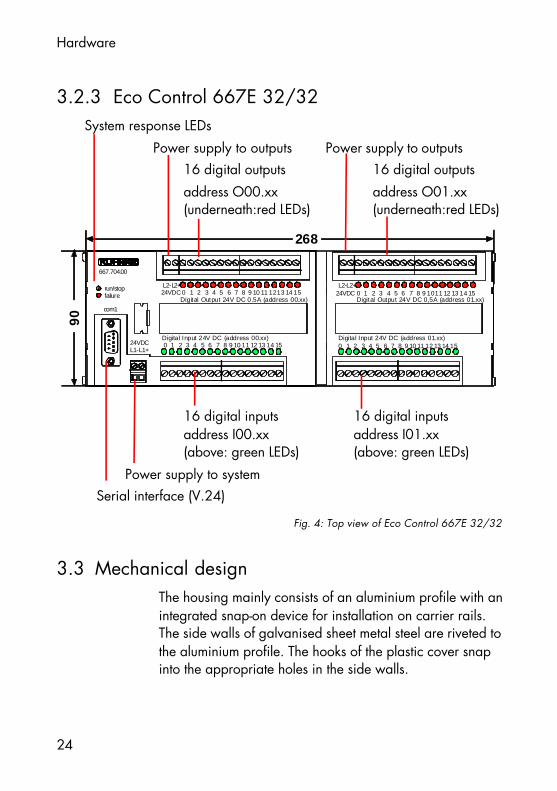
3.2.3 Eco Control 667E 32/32 System response LEDs Power supply to outputs Power supply to outputs
16 digital outputsaddress O00.xx(underneath:red LEDs)
16 digital outputsaddress O01.xx(underneath:red LEDs)
90
268
com1
L1+L1-
failure
667.704.00
run/stop L2-L2+24VDC
Digital Output 24V DC 0.5A (address 00.xx)
Digital Input 24V DC (address 00.xx)24VDC 0 1 2 3 4 5 6 7 8 9 10 11 12 13 14 15
0 1 2 3 4 5 6 7 8 9 10 11 1213 14 15L2-L2+
24VDCDigital Output 24V DC 0,5A (address 01.xx)
Digital Input 24V DC (address 01.xx)
0 1 2 3 4 5 6 7 8 9 1011 12 13 14 15
0 1 2 3 4 5 6 7 8 9 10 11 12 13 14 15
16 digital inputsaddress I00.xx(above: green LEDs)
16 digital inputsaddress I01.xx(above: green LEDs)
Power supply to system Serial interface (V.24)
Fig. 4: Top view of Eco Control 667E 32/32
3.3 Mechanical designThe housing mainly consists of an aluminium profile with anintegrated snap-on device for installation on carrier rails.The side walls of galvanised sheet metal steel are riveted tothe aluminium profile. The hooks of the plastic cover snapinto the appropriate holes in the side walls.

Hardware
25
3.3.1 InstallationEco Control 667E is designed for installation on carrierrails (in acc. with DIN EN 50022, 35 x 7.5 mm).
Procedure1 Push the device against the
carrier rail such that the me-tal spring snaps into thespace between carrier railand installation surface (seeillustration).
Metal spring
2 Push the device upagainst the installationwall until it snaps in.
Fig. 5: Installation on carrier rail
Hardware
26
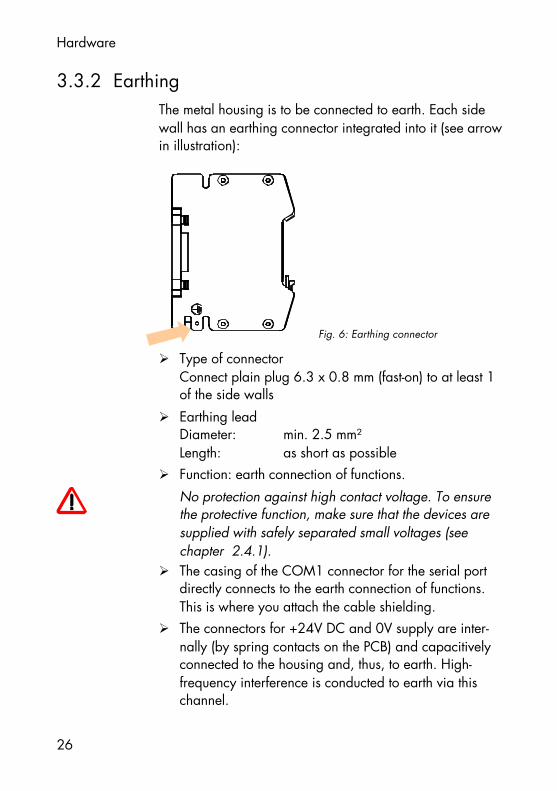
3.3.2 EarthingThe metal housing is to be connected to earth. Each sidewall has an earthing connector integrated into it (see arrowin illustration):
Fig. 6: Earthing connector
Ø Type of connectorConnect plain plug 6.3 x 0.8 mm (fast-on) to at least 1of the side walls
Ø Earthing leadDiameter: min. 2.5 mm²Length: as short as possible
Ø Function: earth connection of functions.No protection against high contact voltage. To ensurethe protective function, make sure that the devices aresupplied with safely separated small voltages (seechapter 2.4.1).
Ø The casing of the COM1 connector for the serial portdirectly connects to the earth connection of functions.This is where you attach the cable shielding.
Ø The connectors for +24V DC and 0V supply are inter-nally (by spring contacts on the PCB) and capacitivelyconnected to the housing and, thus, to earth. High-frequency interference is conducted to earth via thischannel.

Hardware
27
3.4 Power supplySystem and outputs are supplied via separate connectors(for the location of the connectors see chapter 3.2). This al-lows you to switch off all outputs without having to discon-nect the controller from its power source.To ensure uninterrupted operation, lay the supply cablesseparately, using the shortest possible cables to connectthe power source with the controller’s supply terminals.If you are using two different power source, you are obli-ged to equalise the potential between the 0V connectors.
3.4.1 System power supplyThe system power supply connects to a 2-pin plug-type ter-minal block.Ø Connectors: L1- à 0V
L1+ à+24V DC
Ø Voltage: 24 V DC -20%/+25%Ø Power consumption: c. 100 mA
The outputs are supplied separately. However, potentials ofsystem and output supplies are not separated.
For a description of the output supply voltage connectorrefer to chapter 3.6.

Hardware
28
3.5 Digital inputsThe inputs pick up the digital signals of a variety of sour-ces. They connect to the device by screw-type locking ter-minals (à illustrations in chapter 3.2). Make sure that theywork within the switching thresholds indicated below,which particularly applies to proximity switches and semi-conductor sensors. The input circuitry adapts the incomingsignals to the system voltage.Ø Defined signals and switching thresholds
Logical 0 ≤ 5 VLogical 1 ≥ 15 V(Hysteresis 1...4 V)
Ø Signal delayPeak voltages (noise impulses) are filtered to avoidthem being considered as valid signals which might tripunintended switching actions. This delays signal detec-tion by rated 5 ms:
Input signals are read between program cycles and writ-ten into the process image . To calculate the averageavailability of signals to the user program, you must there-fore add the program cycle time to the specified delays.
24
15
5
t[ms ]
U [V]
1
0
S ignal t ve tva
Raising delay: tve = 3.0...7.0 msFalling delay: tva = 4.0...7.0 ms
Fig. 7: Input signal delay

Hardware
29
3.6 Digital outputsDigital outputs are the connection to external actuators (re-lays, contactors, solenoids, valves...). They connect to thecontroller by screw-type locking terminals (à illustrations inchapter 3.2). You can control resistive and inductive loads.Free-wheeling diodes suppress inductive switch-off peaks.The output status is indicated by LEDs.
Output power supplyThe output power supply connects to a 2-pin plug-type ter-minal block (à illustrations in chapter 3.2).Ø Connectors: L2- à 0V
L2+ à+24V DC
Ø Voltage: 24 V DC -20%/+25%Ø Power consumption: depends on the load on the
outputs
Protection against short circuit- and overloadOutputs are protected against destruction by overload orshort circuit. In case of a fault, all outputs are disabled andthe “failure” LED flashes (à 7.1)

Hardware
30
3.7 Serial interface COM1The serial interface mainly provides a connection to pro-gramming PCs. Apart from that it can also be used forcommunication with other devices such as dialogue termi-nals, for example.Ø Type
V.24 (RS 232)Ø Connector
female 9-pin D-Sub connectorØ Pin wiring
2 TxD3 RxD5 Gnd
Ø Cable shieldingconnects to the plug’s frame ground.The metal connector casing is directly connected to theframe and, thus, to earth if the device is properly eart-hed (see chapter 3.3.2).
3.8 Light emitting diodesTwo LEDs indicate the system status:Ø run/stop
lights up green while the PLC program is runninglights up red when the PLC program stops
Ø failureflashes red if there is a short at an output

Hardware
31
3.9 ProcessorThe core unit of the controller is its single-chip microproces-sor, type 80C535. It gets its commands from the monitorprogram and the user program (à 3.10).
3.9.1 On-chip RAMThe microprocessor features an integrated on-chip RAM (à3.10.5) which allows very fast accesses.
3.10 Memory distributionThe controller has four types of memory:Flash EPROM, NV-RAM, SRAM and on-chip RAM.
3.10.1 Operating systemThe operating system is stored in the flash EPROM. It con-tains the system software and is loaded at the Kuhnke fac-tory before delivery. Users cannot directly access this typeof memory.
3.10.2 User programThe user program is safely stored in the NV-RAM (à3.10.4). The device reserves 32 kbyte for the user pro-gram.By default, the user program is stored in machine languagecode and also in KUBES’ intermediate code. The latter al-lows KUBES to retrieve the program from the controller.

Hardware
32
3.10.2.1 Disable retrievability = increase capacity
Storing the intermediate code in memory can be disabledby writing into operand SLG14.05 via the user program.There are two effects:Ø The capacity of the program memory is increased.Ø The program is secured against unauthorised access be-
cause it can no longer be disassembled.SLG14.05 = 0
<> 0enable intermediate code storagedisable intermediate code storage
Before the program is transmitted to the controller, KUBES(version 5.30 or higher) displays the following dialog:
Fig. 8: Program retrievability settings in KUBES
KUBES automatically writes into SLG14.05Ø Setting “All modules retrievable“:
[SLG14.05] ç 0Ø Setting “No module retrievable“:
[SLG14.05] ç 255

Hardware
33
3.10.3 Data memoryData in this context comprises all operands (inputs andoutputs, bit markers, byte marker, timers and counters). Themonitor program also falls back on some parts of this me-mory for internal purposes.8 kbyte of the NV-RAM described in chapter 3.10.4 arereserved for no-voltage protected operands (also calledremanent operands).The volatile (non-remanent) operands are stored in a 24kbyte S-RAM. This type of memory is cleared when the de-vice is being initialised to ensure that all memory cells havea defined status (0).Inputs and output (Ixx.xx and Oxx.xx) as well as 40markers (M00.00...M02.07) are mapped onto the micro-processor’s so-called on-chip RAM. These addresses can beaccessed particularly fast (à 3.10.5).
3.10.4 NV-RAM: special featuresNV-RAM technology (non-volatile RAM) ensures that pro-grams and data are stored safely without the use of exter-nal energy (accumulator or battery) even if you disconnectthe device from the mains. They’re stored without any limi-tation in time no matter how long the device remains swit-ched off for. They resume their previous status when yourestart the controller.

Hardware
34
3.10.5 On-chip RAM: special featuresThe on-chip RAM is part of the microprocessor. It can beaddressed by individual bits. Accesses to this type of me-mory are about twice as fast as accesses to the external ty-pes of memory, i.e. S-RAM and NV-RAM. The on-chip RAMis therefore fully occupied. Addresses are assigned to thefollowing operands:Ø 32 inputs (I00.00...I01.15)Ø 32 outputs (O00.00...O01.15)Ø 40 markers (M00.00...M02.07)

Software
35
4 Software
4.1 Operative approachThe microprocessor receives its program from two programmemories:Ø the memory containing the operating systemØ the memory containing the user program
Operating system memoryIt contains the operating system and all system features ofEco Control 667E. It is permanently installed in the device(à 3.10.1).
User program memoryIt contains the programs required for controlling the machi-ne or system. The programs are written in KUBES, Kuhnkeprogramming software package. The user program memo-ry is permanently installed in the device (à 3.10.2).
The next chapters only detail the knowledge you need towrite user programs for Eco Control 667E.The method of how to actually input the program is not ex-plained. For a description refer to:
Instruction manuel KUBES, E327GB

Software
36
4.1.1 PLC cycleAs a typical PLC, Eco Control 667E cyclically processes theuser program in the program memory.
Cycle timeThe controller’s overall action in time is indicated by thecycle time which is influenced by a variety of factors:Ø command execution timeØ length and structure of the programØ monitor functionsØ self-test functionsØ KUBES functions

Software
37
4.1.1.1 The 4 phases of a PLC cycle
Ø Update process imageThe status of the inputs is read and written into an in-ternal RAM range (operand range I00.00 ...). Theprogram uses these values in the next cycle.Exception:Operations with byte input markers BIxx.xx immediate-ly read the inputs without waiting for the next updateof the process image.
Ø Process programProgram processing always starts with the first line ofthe ORG module and ends with the last line of theORG module (see example "structured programming").The calculated values (assignments) are written into theprocess image memory.
Ø Update outputsThe output markers are copied to the outputs only atthe end of a complete program processing cycle. Thus,even if the outputs have been changed by the programseveral times, only the last status will be output to therelevant terminal.Exception:Assignments to byte output markers BOxx.xx immedia-tely write their result into the output memories withoutwaiting for the process image to update the outputs.
Ø Internal PLC actionIn certain cases, the CPU has to respond to requeststhat are required for self-testing or for communicationwith the programming PC.

Software
38
4.1.1.2 Minimum cycle time
The time it takes to complete a PLC cycle is shortest if thePLC just processes the program.
Calculating the cycle timeØ Sum total of execution times of module call commandsØ Sum total of command execution times(see table Set of Commands)Ø Process image update: 25 µsHowever, due to the possibility of using conditional modulecalls and conditional jump commands (JPC...), the cycle ti-me also depends on the internal and external states usedas conditions.This gives the programmer the chance to optimise the pro-gram runtime by cleverly arranging his program.A clear project structure ensures that the PLC is only enga-ged in operations that are relevant to the control process atthat time.Another benefit ensues from storing the most frequentlyused bit operands in the on-chip RAM, because accesses tothis memory are twice as fast as accesses to other types ofmemory (à 3.10.5).
Software
39
4.1.1.3 Influence of timer interrupts on the cycle time
The programmable timers depend on highest precision.This is ensured by a quartz crystal and the relevant fre-quency dividers that generat impulses which, in turn, gene-rate interrupts at the intervals set by the programmable ti-mers (10 ms, 100 ms, 1 s, 10 s).If the timers are enabled, these timer interrupts lead to thecurrent time values being incremented or decrementedwhich means that the timer outputs may have to be adju-sted. This is added to by the updating of the clock pulsemarkers (C00.00-03).Processing of the current program is therefore to be inter-rupted, the contents of the CPU registers is to be saved andstored for continuation later.
4.1.1.3.1 Extension of the cyle time
The amount of time by which the cycle is extended due tothe handling of timer interrupts depends on the number ofcurrently active programmable timers.
Worst caseEvery 10 ms, the PLC cycle is extended by c. 2 ms if all ofthe 32 possible timers have been programmed as clockpulses with the same time on the basis of 10 ms and if theyare all enabled.
Best caseIn the best case, the cycle time is extended by only 0.4 ms.

Software
40
4.1.1.4 Influence of communication on the cycle time
Both programming and testing online in the KUBES envi-ronment and man-machine communication with operatingterminals demand data exchange via the V.24 port. thiscommunication is interrupt-controlled and can extend thecycle time by up to 10%, given a transfer rate of 9600baud.
Status informationIn certain intervals, KUBES requests information from thecontroller even if there is no actual communication:Frequency: every 5 sDelay: 1 ms
Dynamic displaysThe single address and address range displays, the logicdiagram or the dynamic display in the Module Editor allowyou to permanently read and display up to 256 operands.You can reduce the resulting time load by either loadingfewer program lines into the Module Editor or by using thesingle address instead of the address range displayExamplesØ The dynamic display of 224 byte (14 lines withC1T16 SMxx.xx) in the Module Editor can extend a pro-gram cycle of 2 ms by another 2 ms (worst case).Ø Having the address range display dynamically rea-ding a complete marker range extends the cycle time by c.0.5 ms.

Software
41
4.1.1.5 Changing the program in run mode, transmittinga module
The user program can be changed without interrupting theprogram run. When you transmit a changed module, thecontroller needs some time to receive, interpret and insertthe module as well as to calculate its checksum.Extension of cycle time: c. 10 %Duration: depends on the length of program and the cycletime
4.1.1.6 Restarting the controller after changes in Stop/Reset mode
Modifying the program memory while the controller is inStop or Reset mode also modifies the checksum requiredfor the memory test. The checksum is calculated when yourestart the controller (RUN). The controller will resume runmode only when the checksum test has been completedsuccessfully.
Software
42
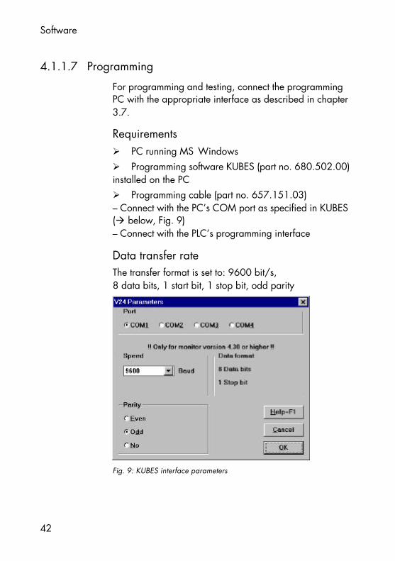
4.1.1.7 Programming
For programming and testing, connect the programmingPC with the appropriate interface as described in chapter3.7.
RequirementsØ PC running MSWindowsØ Programming software KUBES (part no. 680.502.00)installed on the PCØ Programming cable (part no. 657.151.03)– Connect with the PC’s COM port as specified in KUBES(à below, Fig. 9)– Connect with the PLC’s programming interface
Data transfer rateThe transfer format is set to: 9600 bit/s,8 data bits, 1 start bit, 1 stop bit, odd parity
Fig. 9: KUBES interface parameters
Software
43
4.2 Operand rangesAll addresses used by the program for signal processing ordata storage are called operands. They are “operated”with.Eco Control 667 provides a large number of operands.Please refer to the table in chapter 4.2.2.
Software
44
4.2.1 Definitions
InputsSignals that are fed into the controller and read by the userprogram.
OutputsSignals that are generated by the program in the controllerand picked up externally as control signals. They switch onlamps, drives etc.
MarkersSignals that are used inside the controller for storing statesand supporting complex logical operations. There are twotypes of markers:Ø bit markers (1-bit signals) andØ byte marker (8-bit signals).
TimersThey control time processes.
CountersThey count events or increments output by pulse generators.

Software
45
4.2.2 Summary of operandsOperands
from toName Max.
qty.Bits Description
I00.00 I01.15 Digitalinputs
32 1
O00.00 O01.15 Digitaloutputs
32 1
Max. I/O configuration depends on themodel variant (à 3.1).The process image of inputs and outputs isstored in the on-chip RAM (à 3.10.5),therefore fast access
BI00.00
BO00.00
BI00.03
BO00.03
ByteinputsByteoutputs
44
88
For reading inputs directly by byte (wi-thout process image).For writing outputs directly by byte (wi-thout process image).
M00.00 M02.07 Fast bitmarkers
40 1 Bit markers in the on-chip RAM (à3.10.5), therefore fast access
SM00.00FM00.00LM00.00
SM15.15FM15.15LM15.15
Bit markers 256256256
111
Bit markers. Divided into groups of 256for better differentiation.
R00.00SR00.00
R15.15SR15.15
Remanentbit markers
256256
11
Bit markers, stored remanently in the NV-RAM (à 3.10.4)
BM00.00SBM00.00
BM15.15SBM15.15
Bytemarkers
256256
88
Byte markers. Divided into groups of 256for better differentiation.
BR00.00SBR00.00BC00.00SBC00.00BD00.00SBD00.00FBM00.00LBM00.00ZBM00.00
BR15.15SBR15.15BC15.15SBC15.15BD15.15SBD15.15FBM15.15LBM15.15ZBM15.15
Remanentbytemarkers
256256256256256256256256256
888888888
Byte markers, stored remanently in the NV-RAM (à 3.10.4)
PL00.00PL00.01
Logical 0Logical 1
11
11
Programmed logical signals, changing notpossible.
PC00.00 PC00.03 Clock pulsemarker
4 8 Byte operands, incremented at pulse rates10 ms, 100 ms, 1 s, 10 s.
PP00.00 PP07.15 Progr. pulse 128 1 Evaluates the 0/1 changeover (edges) ofdigital signals.
PT00.00 PT01.15 Timers 32 16 Programmable, range: 10 ms – 65535 sC00.00 C01.15 Counters 32 16 Programmable, range: 10 – 65535SLF, SLG... Special functions 8 Partly reserved for monitor, KUBES modu-
les, additional modules

Software
46
4.2.3 Set operand functionsWhen you are planning your project, please take into ac-count that some of the operands listed above have set func-tions:
4.2.3.1 Operands reserved for monitor functions
Operand FunctionSLG14.00 Internal useSLG14.01 Undervoltage monitoring (n * 10 ms)SLG14.02 Reads inputs in case of undervoltageSLG14.03 Internal useSLG14.04 Internal useSLG14.05 Generates the intermediate codeSLG14.06 Transmitting projects: retains remanent data
These operands must not be used for any other purposes.Failure to obey may render the controller functions unsafe.
4.2.3.2 Operands reserved for KUBES modules
Eco Control 667E has no KUBES module parameters. Indi-vidual KUBES modules use defined operands that youshould reserve in case you wish to use these operands.Operand Used by KUBES moduleBM00.00...03BM01.00FBM00.00...01
WR_OFFS, RD_OFFS
FBM01.00...09 V24667IS, V24667IE, V24667IN
If you wish to embed one or several of the above KUBESmodules in your project, you must make sure that the rele-vant operands are reserved for this purpse only.

Software
47
4.3 Description of commandsAll operations are started by commands. They are execu-ted in the accumulator of the CPU. Basic terms:Ø Load commands load a value into the accumulatorØ Logical operations link the operand value with the con-tents of the accumulatorØ Assignments write the contents of the accumulator intothe specified operands (in the case of bit operations: thestatus of bit 7)Ø Set commands set (S) or reset/clear (R) the contents ofthe operand if the previous operation in the accumulatorresults in “logical 1”.

Software
48
4.4 Types of operandsEco Control 667E differentiates between three types ofoperands which are marked by their size:Ø Bit 1 bitØ Byte 8 bitØ Word 16 bit (2 byte)The accumulator in the CPU of Eco Control 667E can beused as a bit, byte or word register.Bit operations are carried out like byte operations, the dif-ference being that only bit 7 of the 8 bit accumulator isevaluated.Byte operations are executed in the same accumulator asbit operations.Word operations use a 16-bit accu whose low byte con-tains the accumulator where bit and byte operations areexecuted. Word operations are started by commands who-se last character is a D (not applicable to byte inputs BIxxand byte outputs Boxx).
To avoid mistakes we recommend that you do not usedifferent types of operands in operations that belong toge-ther.

Software
49
4.4.1 AddressingThere are two different ways of assigning operand values:Ø absolute value (constant)Ø contents of an operandsOperand specifiers are made up as follows:
BM00.00
Group mark Group number Channel numberYou can use the mnemonic (symbolic name) previously as-signed to an operands via KUBES’ Symbol Table Editor.Complete commands (instructions) consist of a commandand an operand (rare exceptional cases have no operand):
ExampleL BM00.00Loads the contents of byte marker BM00.00 into the accu.

Software
50
4.4.2 Summary of commandsThe purpose of commands is to “operate” with the ope-rands (see "4.2 Operand ranges").Eco Control 667E provides a large number of commands.They are listed and described in the tables starting on thenext page.
Memory requirements of commandsNormally, the user program is stored twice in the user pro-gram memory:Ø as machine code which is read by the processor;Ø as intermediate code which is used for transfer actionsbetween PC and PLC in accordance with the KUBES proto-col. Storing the intermediate code can be disabled by therelevant instruction in the user program (à 3.10.2.1).The “No. of bytes” table columns list the memory require-ments for both cases.

Software
51
4.4.2.1 Logical operation commands
No. of byteswith w/o
Com-mand
Operand
interm. code
Proces-singtime[µs]
Description
L I00.00
SM00.00BM00.00100
5
996
2
664
2.0
6.06.03.0
Load bit operand in on-chipRAM (à 3.10.5)Load bit operandLoad byte operand (8 bit)Load byte constant (8 bit)
LD BM00.00
1000
15
20
12
7
12.5
5.0
Load word operand (16 bit or2 byte)Load byte constant (16 bit)
LN I00.00
SM00.00BM00.00
6
1010
3
77
3.0
6.07.0
Load and negate bit operandin on-chip RAM (à 3.10.5)Load and negate bit operandLoad and negate byte ope-rand (8 bit)
A I00.00
SM00.00BM00.00100
5
15138
2
12106
2.0
12.010.05.0
And bit operand in on-chipRAM (à 3.10.5)And bit operandAnd byte operand (8 bit)And byte constant (8 bit)
AN I00.00
SM00.00BM00.00
5
1614
2
1311
2.0
13.011.0
And bit operand (negated) inon-chip RAM (à 3.10.5)And bit operand (negated)And byte operand (negated)(8 bit)
O I00.00
SM00.00BM00.00100
5
15138
2
12106
2.0
12.010.05.0
Or bit operand in on-chipRAM (à 3.10.5)Or bit operandOr byte operand (8 bit)Or byte constant (8 bit)

Software
52
No. of byteswith w/o
Com-mand
Operand
interm. code
Proces-singtime[µs]
Description
ON I00.00
SM00.00BM00.00
5
1614
2
1311
2.0
13.011.0
Or bit operand (negated) inon-chip RAM (à 3.10.5)Or bit operand (negated)Or byte operand (negated) (8bit)
XO I00.00
SM00.00
BM00.00
100
13
15
13
8
10
12
10
6
8.0
12.0
10.0
5.0
Exclusive-Or (antivalence) bitoperand in on-chip RAM (à3.10.5)Exclusive-Or (antivalence) bitoperandExclusive-Or (antivalence) byteoperand (8 bit)Exclusive-Or (antivalence) byteconstant (8 bit)
XON I00.00
SM00.00BM00.00
14
1414
11
1111
8.0
13.011.0
Equivalence bit operand in on-chip RAM (à 3.10.5)Equivalence bit operandEquivalence byte operand(8 bit)

Software
53
4.4.2.2 Assignments and store commands
No. of byteswith w/o
Com-mand
Operand
interm. code
Proc.time [µs]
Description
= O00.00
SM00.00
BM00.00
5
11
9
2
8
6
2.0
8.0
6.0
Equal (assignment) to bit ope-rand in on-chip RAM (à3.10.5)Equal (assignment) to bit ope-randEqual(assignment) to byteoperand (8 bit)
=D BM00.00 17 14 16.0 Equal (assignment) to wordoperand (16 bit)
=N O00.00
SM00.00BM00.00
7
1311
4
108
4.0
12.08.0
Equal to negated bit operandin on-chip RAM (à 3.10.5)Equal to negated bit operandEqual to negated byte ope-rand (8 bit)
S O00.00
SM00.00
7
11
4
8
3.0
8.0
Set bit operand in on-chipRAM (à 3.10.5)Set bit operand
R O00.00
SM00.00
7
15
4
12
3.0
12.0
Reset bit opernd in on-chipRAM (à 3.10.5)Reset bit operand
Please also read the explanatory notes on the next page.

Software
54
Notes on assignments and store commandsØ Assignments (=...)Assignments write the contents of the accumulator into thespecified operand.Ø Set command (S)Writes “logical 1” into the specified operand if the prece-ding operation in the accu resulted in “logical 1”. There isno influence on the operand if the result in the accu was“logical 0”.Ø Reset command (R)Writes “logical 0” into the specified operand if the prece-ding operation in the accu resulted in “logical 1”. There isno influence on the operand if the result in the accu was“logical 1”.

Software
55
4.4.2.3 Arithmetical operation commands
No. of byteswith w/o
Com-mand
Operand
Interm. code
Proc.time [µs]
Description
ADD BM00.00100
116
48
8.03.0
Add byte operandAdd byte constant
ADDDBM00.001000
2820
2517
26.018.0
Add word operandAdd word constant
SUB BM00.00100
137
105
8.03.0
Subtract byte operandSubtract byte constant
SUBD BM00.001000
3021
2718
28.018.0
Subtract word operandSubtract word constant
MUL BM00.00100
129
97
11.07.5
Multiply byte operandMultipliy byte constant
MULDBM00.001000
1816
1513
variablevariable
Multiply word operandMultiply word constant
DIV BM00.00100
1711
149
12.57.5
Divide byte operandDivide byte constant
DIVD BM00.001000
2119
1816
variablevariable
Divide word operandDivide word constant
The contents of the accu is arithmetically combined withthe specified operandThe result of the operation is written into the accu. Youcan either use it for further operations or assign it to anoperand.

Software
56
4.4.2.4 Comparison,- shift- and incrementation commands
No. of byteswith w/o
Com-mand
Operand
Interm. code
Proc.time [µs]
Description
CMP BM00.00100
2419
2117
16.011.0
Compare with byte operandCompare with byte constant
CMPD BM00.001000
4440
4137
38.030.0
Compare with word operandCompare with word constant
LSL No ope-rand
6 5 3.0 8-bit shift left of contents ofaccu
LSR No ope-rand
6 5 5.0 8-bit shift right of contents ofaccu
INC BM00.00 13 10 12.0 Increment byte operand (con-tents + 1)
DEC BM00.00 13 10 12.0 Decrement byte operand (con-tents - 1)
INCD BM00.00 45 42 45.0 Increment word operand (con-tents+ 1)
DECD BM00.00 45 42 45.0 Decrement word operand(contents - 1)
CLR BM00.00 14 11 14.0 Clear byte operandNOP No ope-
rand2 1 1.0 Dummy instruction
Please also read the explanatory notes on the next page.

Software
57
Notes on comparison, shift and incrementationcommandsØ Compare (CMP...)Compares the contents of the accu with the contents of theoperand. The result is set as internal flag which is evalua-ted by jump commands (see "4.4.2.5 Jump commands").Ø Shift (LS...)Shifts the contents of the accu by one place.Ø Increment (INC...), Decrement (DEC...)Increments or decrements the contents of the accu by 1.

Software
58
4.4.2.5 Jump commands
No. of byteswith w/o
Com-mand
Operand
Interm. code
Proc.time [µs]
Description
JP Label 12 10 5.0 Unconditional jump to spe-cified label
JPC Label 14 12 6.0 Conditional jump (if logical1) to specified label
JPCN Label 14 12 6.0 Conditional jump (if logical0) to specified label
JP= Label 12 13 6.0 Jump to specified label ifequal (after comparison)
JP<> Label 15 13 6.0 Jump to specified label ifnot equal (after compari-son)
JP< Label 18 16 7.5 Jump to specified label ifsmaller (after comparison)
JP> BM00.00 15 13 7.5 Jump to specified label ifgreater (after comparison)
JP<= Label 18 16 7.5 Jump to specified label ifsmaller or equal (aftercomparison)
JP>= Label 18 16 7.5 Jump to specified label ifgreater or equal (aftercomparison)
JPP Program modu-le
5 3 18.0 Unconditional jump to spe-cified program module
JPCP Program modu-le
9 7 18.0 Conditional jump (if logical1) to specified programmodule

Software
59
No. of byteswith w/o
Com-mand
Operand
Interm. code
Proc.time [µs]
Description
JPK KUBES module 7 3 18 Unconditional jump to spe-cified KUBES module
JPCK KUBES module 11 7 18 Conditional jump (if logical1) to specified KUBES mo-dule
Jumps in the program immediately move program proces-sing to the destination line. This can be either a so-calledlabel (i.e. a symbolic jump mark) or another module.
Ø Conditional jumps (JPC...)The jump is taken if the preceding operation resulted in“logical 1” or “logical 0” (JPCN).Ø Jumps after comparison (JP= to JP>=)The jump is taken if the contents of the accu has the speci-fied mathematical relation to the operand.

Software
60
4.4.2.6 Copy commands
No. of byteswith w/o
Com-mand
Operand
Interm. code
Proc.time [µs]
Description
C1T8 I00.00
SM00.00
7
8
4
5
3/350
200
Copy 8 bit operands fromthe on-chip RAM(à 3.10.5) to the accuCopy 8 bit operands to theaccu
C8T1 O00.00
SM00.00
5
8
2
5
1/400
200
Copy the contents of theaccu to 8 bit operands inthe on-chip RAM (à3.10.5)Copy the contents of theaccu to 8 bit operands
C1T16 I00.00
SM00.00
10
8
7
5
5/650
300
Copy 16 bit operands fromthe on-chip RAM(à 3.10.5) to the accuCopy 16 bit operands tothe accu
C16T1 O00.00
SM00.00
8
8
5
5
3/750
300
Copy the contents of theaccu to 16 bit operands inthe on-chip RAM (à3.10.5)Copy the contents of theaccu to 16 bit operands
Please also read the explanatory notes on the next page.

Software
61
Notes on the copy commandsCopy commands are used to parallely load the contents of8 or 16 bit operands into the accu or write the contents ofthe accu into 8 or 16 bit operands.
Practical applications:Ø reading binary or BDC values via inputsØ controlling numerical displays (e.g. 7-segment display)The time it takes to process copy commands depends onthe last number of the bit operand’s channel number.The channel number is indicated after the separating point:
I00.00 channel number
Processing time is shorter if the channel number ends with0 or 8.
Example 1C1T8 I00.00 => processing time: 3 µs
Example 2C1T8 I00.13 => processing time: 350 µs

Software
62
4.4.2.7 Programmable pulses , timers and counters
No. of byteswith w/o
Com-mand
Operand
Interm. code
Proc.time[µs]
Description
=
=N
LA,O...
PP00.00
PP00.00
PP00.00PP00.00
11
11
913
8
8
610
42
42
610
Activate pulse atpositive edge(0/1)Activate pulse atnegative edge(0/1)Load pulseLink pulse
=
=
LA,O..LD
=TH
PT00.00:1000*1s:E 1)
PT00.00:BM00.00*1s:E 1)
PT00.00PT00.00PT00.00
PT00.00
16
34
91315
26
8
26
61012
23
32
~60
610
12.5
22
Start timer withconst. preset valueStart timer withvariable presetvalue(BM00.00+01)Load timer outputLink timer outputLoad current timervalueHalt timer (withoutclearing it)
= C00.00:10000:V 1) 14 6 35 Start counter withconst. preset value
= C00.00:BM00.00:V 1) 32 24 ~60 Start counter withvar. preset value(BM00.00+01)

Software
63
No. of byteswith w/o
Com-mand
Operand
Interm. code
Proc.time[µs]
Description
L C00.00 9 6 6 Load counter out-put (count at presetvalue)
A,O...
C00.00 13 10 10 Link counter output
LD C00.00 15 12 12.5 Read current coun-ter value
=C C00.00 9 6 25 Assign pulse signal1) Adding “R” to the operand declaration makes the current timer or
counter value remanent (à 3.10.4).Example: “ = PT00.00:1000:1s:E:R“
Please also read the explanatory notes on the next page.

Software
64
Notes on programmable pulses, timers and coun-tersThese are more or less special forms of the commands de-scribed earlier. For a more detailed description refer tochapter “6 Examples“.Ø Programmable pulseWhen a wipe pulse has been set (=, =N...) and the corre-sponding code line is skipped, the output signal will be re-tained until the line is processed again.Ø RemanenceThe “R” operand supplements listed in the table are optio-nal parameters. Add them if you wish a timer or counter tobe remanent (when you stop or reset the controller, the cur-rent (time) count will be stored and retrieved when you re-start the controller).Ø TimersOnce started, timers run regardless of whether the corre-sponding code line is being processed or not.

Software
65
4.5 Programming modulesThe user program of Eco Control 667E is structured bymodules. This helps you to break up the technological pro-blem to be controlled into separate part tasks. The modulesform a hierarchical system (at max. 5 levels) that allowsmodules at higher levels to call modules at lower ones. Aprogram of this structure is very clear and helps a lot withunderstanding or updating of finished programs. The fol-lowing types of modules are available:Ø organisation moduleØ program modulesØ KUBES modulesProcessing of individual modules is monitored by awatchdog which is triggered every time a module is called.After that the system has 70 ms to process the module.Program and KUBES modules are subroutines. The return tothe calling module is ensured by the module organisationand must not be programmed separately. Modules mustnot call themselves.The maximum length of a module is 128 instructions. Tothese you may add extra comment lines so that the maxi-mum number of lines is 253.

Software
66
4.5.1 Organisation moduleFunction: organises the other modulesName: ORGQuantity: 1
It is practical if the ORG module contains the program se-lection and calls of the modules that are relevant to theoverall task. All PLC instructions can be used without limita-tion.
4.5.2 Program moduleFunction: PLC program module for a separate part task.
Organises the next module level.Name: OptionalQuantity: Max. 255
4.5.3 KUBES moduleFunction: Library module for the solution of a specific,
defined basic task. KUBES modules are pro-grammed by Kuhnke in a high-level languageand added as code to a library.
Name: SetQuantity: Max. 255
Software
67
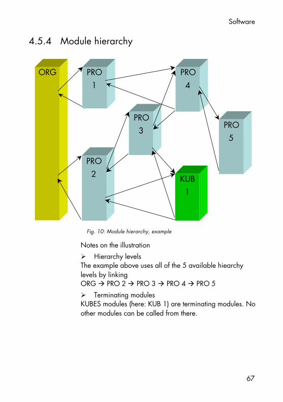
4.5.4 Module hierarchy
Notes on the illustrationØ Hierarchy levelsThe example above uses all of the 5 available hiearchylevels by linkingORG à PRO 2 à PRO 3 à PRO 4 à PRO 5Ø Terminating modulesKUBES modules (here: KUB 1) are terminating modules. Noother modules can be called from there.
ORG PRO1
PRO2
PRO3
PRO4
PRO5
KUB1
Fig. 10: Module hierarchy, example

Software
68
KUBES modules
69
5 KUBES modulesKUBES modules are subroutines translated into machinecode. Their job is to solve compley tasks that program mo-dules written by the user can solve only with difficulties ornot at all.
Reserved operandsThe KUBES modules of Eco Control 667E accept no para-meters. Data is exchanged via reserved operands (à4.2.3) which must not be assigned to any other addressesby the user program if the relevant KUBES modules arebeing used.
Standard modulesA set of standard KUBES modules is automatically installedtogether with KUBES.
Special modulesThere is the option of delivering customised software soluti-ons in the shape of KUBES modules. They are deliveredseparately and installed in the PC by means of BIBS, thelibrary service program (part of the KUBES softwarepackage).Feel free to contact us if and when required.

KUBES modules
70
5.1 KUBES module librariesKBUES modules are combined in libraries which are storedin the KUBES program root created when installing KUBES.
Hard disk arrangement of KUBES
Fig. 11: Hard disk arrangement of KUBES
The KUBES module library is called:Ø KULIB667.LIBOther libraries are available. They apply to Kuhnke’s othercontrollers which we do not want to discuss at this point.KUBES automatically chooses the correct library for theproject work. You are obliged to specify the type of con-troller when you open a new project. KUBES uses this in-formation for library selection.The type of controller to be chosen for Eco Control 667E is“667“.
KUBESEXE
KUBES Project 1
Project 2
.
.
.
Project n
KUBIB KUBES
Folder 2
.
.
.
Folder n
Program root inc.KUBES module libraries
Main project directory
Project directories
Module library
Library folder

KUBES modules
71
5.1.1 Contents of the KUBES module libraryLibrary “KULIB667.LIB“ not only applies to Eco Control667E as described in this manual but also to the older ty-pes, Pico Control 667 and Compact Control 667.Please note that some modules in the library can be usedfor the last two devices only, because they can be configu-red with an additional module if and when required.The table lists the available modules in alphabetical order:
KUBES module Used in Eco Control 667E Function
CNT_ENCCNT_EVENT
no Counter functions for theadd. “counter” module
RD_OFFS Read with offset
SST667IN V.24 communication:send strings
V24667IE V.24 communication:receive individual char.s
V24667IS
yes
V.24 communication:send individual char.s
V24667STV24667XE
V24667XS
no Communication via addi-tional “V.24” module
WR_OFFS yes Write with offset
The library can be viewed in KUBES:Ø Module EditorØ Open “Module” menuØ Choose “KUBES modules”

KUBES modules
72
5.1.2 Loading KUBES modulesThe required KUBES module is started by a jump commandat the appropriate place in the user program (organisationor program module):Ø JPK <module name>
Absolute jump. It is taken every time the microprocessorreads the program line. The module is not called if a jumpskips the program line.orØ JPCK <module name>
Conditional jump. It is only taken if the preceding operati-on results in “logical 1”. The module is not called if a jumpskips the program line.

KUBES modules
73
5.2 Communication modulesCommunication modules allow you to use the program-ming interface for simle data traffic.There are three KUBES modules available for this task:Ø V24667ISSends single charactersØ V24667IEReceives single charactersØ V24667INSends strings (data ranges)The data transfer format is set and cannot be changed:Ø 8 data bitsØ 1 stop bitØ no parity checkØ 1200 bit/s

KUBES modules
74
5.2.1 Reserved operandsSuggestedsymbol
Address Used byKUBES mod.
Value 1) Function
INIT_V24 FBM01.00 K:255 V24 mode settings okRES_1 FBM01.01 K:<n> Internally used markerKUBES FBM01.02
V24667IS,V24667IE,V24667IN
U:255U:0
V24 mode:Programming/KUBES prot.Communicating
FBM01.03 V24667IS U:<Chr> Char. to be sentFBM01.04 V24667IS,
V24667INU:255K: 0
Start transferAcknowledge
REC_CHR FBM01.05 K:<Chr> Char. to be receivedFBM01.06
V24667IEK:255U:0
Character receivedAcknowledge
FBM01.07 K:<n> Internal counter of bytes sentFBM01.08 U:<n> Qty. of data bytes (1...230)
SDATA FBM01.09 toFBM15.15
V24667IN
U:<Dat> Data field to be sent
1) K: KUBES module writes U: user writest
These operands are reserved for the described functions.They must not be used for any other purposes if the rele-vant KUBES modules are embedded in the program.

KUBES modules
75
5.2.2 V.24 mode settingsReserved operand “FBM01.02” enables communication.This operand’s status decides whether the KUBES protocolin programming mode (also supporting communicationwith suitable dialogue terminals, for example) or the com-munication mode is activated:Operand Status V.24 mode
255 Programming (KUBES protocol)FBM01.020 Communicating by means of the
KUBES modules described below
To switch over to communication mode please make sureto use an external input as suggested in the example pro-gram below (à 5.2.6). Failure to comply may permanent-ly disable the programming mode.
The chosen mode becomes active as soon as at least oneof the KUBES modules has been run.Ø The KUBES module acknowledges the change of set-tings:[FBM01.00] ç 255Clear operand (FBM01.00) at the start of the programbecause it is undefined when you switch on the controller.
Example program (à 5.2.6) lines 3...26
KUBES modules
76
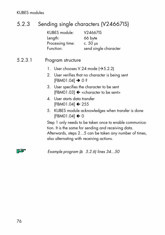
5.2.3 Sending single characters (V24667IS)KUBES module: V24667ISLength: 66 byteProcessing time: c. 50 µsFunction: send single character
5.2.3.1 Program structure
1. User chooses V.24 mode (à5.2.2)2. User verifies that no character is being sent
[FBM01.04] è 0 ?3. User specifies the character to be sent
[FBM01.03] ç <character to be sent>4. User starts data transfer
[FBM01.04] ç 2555. KUBES module acknowledges when transfer is done
[FBM01.04] ç 0Step 1 only needs to be taken once to enable communica-tion. It is the same for sending and receiving data.Afterwards, steps 2...5 can be taken any number of times,also alternating with receiving actions.
Example program (à 5.2.6) lines 34...50

KUBES modules
77
5.2.4 Receiving single characters (V24667IE)KUBES modules: V24667IELength: 106 byteProcessing time: c. 90 µsFunction: receive single character
5.2.4.1 Program structure
1. User chooses V.24 mode(à5.2.2)2. User checks whether a character was received
[FBM01.06] è 255 ?3. User reads the character received
[FBM01.05] è <character received>4. User acknowledges reception
[FBM01.06] ç 0Step 1 only needs to be taken once to enable communica-tion. It is the same for sending and receiving data.Afterwards, steps 2...4 can be taken any number of times,also alternating with sending actions.
Example program (à 5.2.6) lines 75...83

KUBES modules
78
5.2.5 Sending strings (SST667IN)KUBES module: SST667INLength: 104 byteProcessing time: c. 60 µsFunction: send strings (of characters)
5.2.5.1 Program structure
1. User chooses V.24 mode (à5.2.2)2. User verifies that no strings are being sent
[FBM01.04] è 0 ?3. User writes the data to be sent into the data field
[FBM01.09 ff] ç <data bytes to be sent>4. User specifies the quantity of data bytes
[FBM01.08] ç <quantity of data bytes to be sent)5. User starts transfer
[FBM01.04] ç 2556. KUBES module acknowledges when transfer is done
[FBM01.04] ç 0Step 1 only needs to be taken once to enable communica-tion. It is the same for sending and receiving data.Afterwards, steps 2...6 can be taken any number of times,also alternating with receiving single characters.
Example program (à 5.2.6) lines 52...73

KUBES modules
79
5.2.6 Example program “serial communication“This program uses all KUBES modules available for serialcommunication.
======== KUBES =======================================================
Project structure
Project : 667_COMM Network :
created : Aug 19 1998 10:03
User : changed : Aug 19 1998 16:39
Comment: 667E: Data communication via V.24
======================================================================
ORG.ORG/1
|
*------>SST667IN.KNK/6
|
*------>V24667IE.KNK/9
|
*------>V24667IS.KNK/10
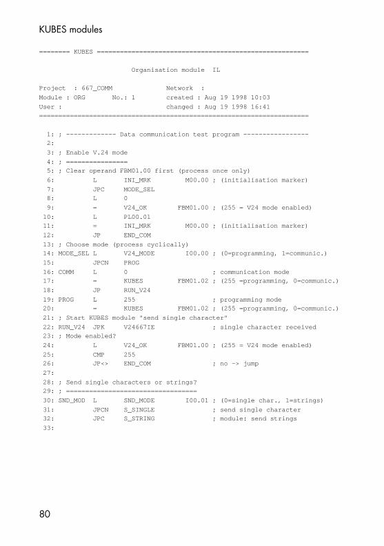
KUBES modules
80
======== KUBES =======================================================
Organisation module IL
Project : 667_COMM Network :
Module : ORG No.: 1 created : Aug 19 1998 10:03
User : changed : Aug 19 1998 16:41
======================================================================
1: ; ------------- Data communication test program -----------------
2:
3: ; Enable V.24 mode
4: ; ================
5: ; Clear operand FBM01.00 first (process once only)
6: L INI_MRK M00.00 ; (initialisation marker)
7: JPC MODE_SEL
8: L 0
9: = V24_OK FBM01.00 ; (255 = V24 mode enabled)
10: L PL00.01
11: = INI_MRK M00.00 ; (initialisation marker)
12: JP END_COM
13: ; Choose mode (process cyclically)
14: MODE_SEL L V24_MODE I00.00 ; (0=programming, 1=communic.)
15: JPCN PROG
16: COMM L 0 ; communication mode
17: = KUBES FBM01.02 ; (255 =programming, 0=communic.)
18: JP RUN_V24
19: PROG L 255 ; programming mode
20: = KUBES FBM01.02 ; (255 =programming, 0=communic.)
21: ; Start KUBES module "send single character"
22: RUN_V24 JPK V24667IE ; single character received
23: ; Mode enabled?
24: L V24_OK FBM01.00 ; (255 = V24 mode enabled)
25: CMP 255
26: JP<> END_COM ; no -> jump
27:
28: ; Send single characters or strings?
29: ; ==================================
30: SND_MOD L SND_MODE I00.01 ; (0=single char., 1=strings)
31: JPCN S_SINGLE ; send single character
32: JPC S_STRING ; module: send strings
33:

KUBES modules
81
34: ; Send single characters
35: ; ======================
36: ; Specify transfer interval (every second)
37: S_SINGLE L T00.02 ; current value
38: CMP SBM00.00 ; old value
39: JP= REC ; second not passed yet
40: = SBM00.00 ; store new value
41: ; Send
42: SEND JPK V24667IS ; KUBES module
43: L SND_RUN FBM01.04 ; (255 =start transfer, 0=ackn.)
44: JPC END_SNGL ; still sending
45: L PC00.02 ; clock gen. value as s_char.
46: = SND_CHR FBM01.03 ; (character to be sent)
47: C8T1 O00.08 ; show SND_CHR at outputs
48: L 255
49: = SND_RUN FBM01.04 ; (255 =start transfer, 0=ackn.)
50: END_SNGL JP REC
51:
52: ; Send strings
53: ; ============
54: ; Specify data to be sent (here: "<STX>PLC<ETX>")
55: S_STRING JPK SST667IN ; KUBES module
56: L $02 ; STX (Start of Text)
57: = SDATA FBM01.09 ; (start of s_data field)
58: L 'S'
59: = FBM01_10 FBM01.10 ; (data to be sent)
60: L 'P'
61: = FBM01_11 FBM01.11 ; (data to be sent)
62: L 'S'
63: = FBM01_12 FBM01.12 ; (data to be sent)
64: L $03 ; ETX (End of Text)
65: = FBM01_13 FBM01.13 ; (data to be sent)
66: LENGTH L 5 ; length of data to be sent
67: = SDAT_LEN FBM01.08 ; (qty. of s_data bytes)
68: ; Send
69: SEND_STR L SND_RUN FBM01.04 ; (255 =start transfer, 0=ackn.)
70: JPC END_STRG ; still sending
71: L 255
72: = SND_RUN FBM01.04 ; (255 =start transfer, 0=ackn.)
73: END_STRG NOP
74:

KUBES modules
82
75: ; Receive single character
76: ; ========================
77: REC L REC_RUN FBM01.06 ; (255 =receive char., 0=ackn.)
78: CMP 255
79: JP<> END_REC
80: L REC_CHR FBM01.05 ; (received character)
81: C8T1 A00.00 ; show REC_CHR at outputs
82: CLR REC_RUN FBM01.06 ; (255 =char. received, 0=ackn.)
83: END_REC NOP
84:
85:
86: ; End of communication program
87: ; ============================
88: END_COM NOP

KUBES modules
83
5.3 Copying data (blocks)The two KUBES modules described next serve the followingpurposes:Ø KUBES module “RD_OFFS“reads a specified operand rangeØ KUBES module “WR_OFFS“writes into a specified operand rangeØ both KUBES modulescopy data from one operand range to anotherThe operand range is accessed via its intermediate codeaddress (à 5.3.2). You can add an offset to address 1 (ortwo in the case of word operands) particular operand inthe range.
5.3.1 Reserved operandsSuggestedsymbol
Address Used by KUBESmodule
Function
WR_SRC BM00.00...01 WR_OFFS Data source (2 byte)RD_DEST BM00.02...03 RD_OFFS Data destination (2 byte)
OFFSET BM01.00 RD_OFFS andWR_OFFS
Pointer (offset) to an address inthe operand range
ADDRESS FBM00.00...01 RD_OFFSWR_OFFS
First address of the operandrange
These operands are reserved for the described functions.They must not be used for any other purposes if the rele-vant KUBES modules are embedded in the program.

KUBES modules
84
5.3.2 Operands’ intermediate code addressesThe operands can only be accessed directly if the normalmnemonic (M00.00, SBM03.15...) is used.Internal markers can only be accessed indirectly by meansof their intermediate code addresses:
Operand range Intermediate codeaddress
(hexadecimal)Start End Start End
R00.00 R15.15 $0100 $01FFBM00.00 BM15.15 $0200 $02FFSBM00.00 SBM15.15 $0300 $03FF
BR00.00 BR15.15 $0400 $04FFSBR00.00 SBR15.15 $0500 $05FF
- - $0600 $06FF
ABM00.00 ABM15.15 $0700 $07FFFM00.00 FM15.15 $0800 $08FF
- - $0900 $09FF
SR00.00 SR15.15 $0A00 $0AFFBC00.00 BC15.15 $0B00 $0BFFSBC00.00 SBC15.15 $0C00 $0CFF
BD00.00 BD15.15 $0D00 $0DFFSBD00.00 SBD15.15 $0E00 $0EFFLBM00.00 LBM15.15 $0F00 $0FFF

KUBES modules
85
5.3.3 Reading data (RD_OFFS)KUBES module: RD_OFFSLength: 58 byteProcessing time: c. 89 µsFunction: read operand data
5.3.3.1 Program structure
Ø Specify the first address of the source operand rangefor reading[FBM00.00...01] ç <intermediate code address>Ø Set the offset of an address in the range (0 = first)[BM01.00] ç <offset>Ø Start KUBES module RD_OFFSØ Evaluate 1 or 2 byte of data[BM00.02...03] è <evaluation>Example program (à 5.3.5)
First address Operand range
Offset:
FBM00.00...01
BM01.00
01234
.
.
.n
0+Offset0+Offset+1
BM00.02BM00.03
Data
Fig. 12: KUBES module "RD_OFFS"
KUBES modules
86
5.3.4 Writing data (WR_OFFS)KUBES module: WR_OFFSLength: 74 byteProcessing time: c. 33 µsFunction: write data into operand
5.3.4.1 Program structure
Ø Provide 1 or 2 byte of data[BM00.00...01] ç <data>Ø Specify the first address of the target operand rangefor writing[FBM00.00...01] ç <intermediate code address>Ø Set the offset of an address in the range (0 = first)[BM01.00] ç <offset>Ø Start KUBES module WR_OFFSExample program (à 5.3.5)
Operand range First address
Offset
01234
.
.
.n
FBM00.00...01
0+Offset0+Offset+1
BM00.00BM00.01
Data
BM01.00
Fig. 13: KUBES module "WR_OFFS"

KUBES modules
87
5.3.5 Example program “copy data block“This program is to copy 16 byte of data. The source andtarget ranges are very near each other so that the programcan be easily tested by means of KUBES’ Address Rangedisplay function:
Data ranges First address(interm. code)
Source SBM00.00...SBM00.15 $0300Target SBM01.00...SBM01.15 $0310
We took the first intermediate code address of every rangefrom the table in chapter (à 5.3.2).Proceed as follows:Ø Write and transmit program (see next page)Ø Start controller (RUN)Ø Display Address Range, choose “byte markers SBM“
Ø Set and reset input I00.00.After a short while you will find the data in SBM01.00...15and SBM00.00...15 are identical (see screen dump).

KUBES modules
88
======== KUBES =======================================================
Project structure
Project : 667_COPY Network :
created : Aug 17 1995 11:28
User : changed : Aug 17 1998 09:59
Comment: 667E: Copy data block
======================================================================
ORG.ORG/1
|
*------>RD_OFFS.KNK/3
|
*------>WR_OFFS.KNK/4
|
*------>DAT_SET.PRO/1

KUBES modules
89
======== KUBES =======================================================
Organisation module IL
Project : 667_COPY Network :
Module : ORG No.: 1 created : Aug 17 1995 11:28
User : changed : Aug 17 1998 08:47
======================================================================
1: ; ------------------ Test program "Copy data blocks" -----------------
***************************************************************************
3: ; To be able to easily repeat the test, the provided data is modified
4: ; by a randomizer via I00.00 (see module "DAT_SET").
***************************************************************************
6:
7: ; Jump to "Provide data"
8: ; ----------------------
9: L SET_DAT I00.00 ; (set data)
10: JPCP DAT_SET 1
11:
12: ; First steps
13: ; -----------
14: ; Clear offset memory to be on the safe side
15: CLR OFFSET BM01.00 ; (points to oper. in data field)
16:
17: ; Specify length of data fields (here: BM01.01 chosen)
18: L 16 ; 16 byte
19: = DAT_LEN BM01.01 ; (length of data fields)
20:
21: ; Program for copying (designed as a loop)
22: ; ----------------------------------------
23: LOOP NOP
24: ; Specify start of source memory (SBM00.00)
25: SOURCE LD $0300 ; interm. code of 1st source addr.
26: =D ADDR_1 FBM00.00 ; (1st addr. of operand range)
27: JPK RD_OFFS ; source data to BM00.02...03
28: ; Transfer data
29: LD DATA_RD BM00.02 ; (data from source memory, byte)
30: =D DATA_WR BM00.00 ; (data to target memory, byte 1)
31: ; Specify start of target memory (SBM01.00)
32: DEST LD $0310 ; interm. code of 1st target addr.
33: =D ADDR_1 FBM00.00 ; (1st addr. of operand range)
34: JPK WR_OFFS ; data from BM00.00...03 to target
35: ; Increment offset (twice because your’re copying by word
36: INCOFFS INC OFFSET BM01.00 ; (pointer to oper. in data field)
37: INC OFFSET BM01.00 ; (pointer to oper. in data field)
38: ; Complete range copied?
39: L OFFSET BM01.00 ; (pointer to oper. in data field)
40: CMP DAT_LEN BM01.01 ; (length of data fields)
41: JP< LOOP ; no -> get next set of data
42: END_COPY NOP

KUBES modules
90
======== KUBES =======================================================
Program module IL
Project : 667_COPY Network :
Module : DAT_SET No.: 1 created : Aug 14 1998 16:47
User : changed : Aug 19 1998 09:37
Comment: Provide data
======================================================================
1: ; A kind of randomizer writes the contents of the internal clock pulse
2: ; generators into byte markers SBM00.00...15 while the module is running
3: ; ---------------------------------------------------------------------
4: L PC00.00
5: = SBM00.00
6: L PC00.01
7: = SBM00.01
8: L PC00.02
9: = SBM00.02
10: L PC00.03
11: = SBM00.03
12: L PC00.00
13: = SBM00.04
14: L PC00.01
15: = SBM00.05
16: L PC00.02
17: = SBM00.06
18: L PC00.03
19: = SBM00.07
20: L PC00.00
21: = SBM00.08
22: L PC00.01
23: = SBM00.09
24: L PC00.02
25: = SBM00.10
26: L PC00.03
27: = SBM00.11
28: L PC00.00
29: = SBM00.12
30: L PC00.01
31: = SBM00.13
32: L PC00.02
33: = SBM00.14
34: L PC00.03
35: = SBM00.15
36:

Examples
91
6 Examples
6.1 Basic functions
6.1.1 ANDWiring diagram Logic diagram Instruction list
L I00.00A I00.01= O00.0
0
6.1.2 ORWiring diagram Logic diagram Instruction list
L I00.02O I00.03= O00.01

Examples
92
6.1.3 Negated inputWiring diagram Logic diagram Instruction list
LN I00.04= O00.02
6.1.4 Negated output
Wiring diagram Logic diagram Instruction list
L I00.05=N O00.03

Examples
93
6.1.5 NAND
Wiring diagram Logic diagram Instruction list
L I00.06A I00.07
=N O00.04
6.1.6 NOR
Wiring diagram Logic diagram Instruction list
L I00.08O I00.09=N O00.05

Examples
94
6.1.7 XO: exclusive OR (antivalence)
Wiring diagram Logic diagram Instruction list
L I00.10XO I00.11= O00.06
6.1.8 XON: exclusive NOR (equivalence)
Wiring diagram Logic diagram Instruction list
L I00.12XON I00.13
= O00.07
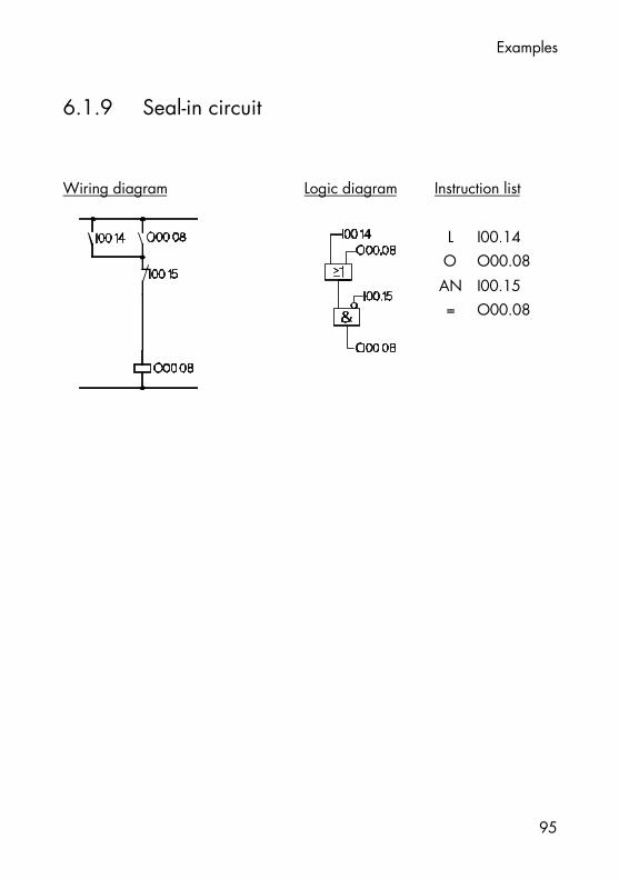
Examples
95
6.1.9 Seal-in circuit
Wiring diagram Logic diagram Instruction list
L I00.14O O00.08AN I00.15= O00.08
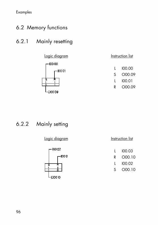
Examples
96
6.2 Memory functions
6.2.1 Mainly resetting
Logic diagram Instruction list
L I00.00S O00.09L I00.01R O00.09
6.2.2 Mainly setting
Logic diagram Instruction list
L I00.03R O00.10L I00.02S O00.10

Examples
97
6.3 Switching circuits
6.3.1 OR-AND circuit
Wiring diagram Logic diagram Instruction list
L I00.04ON I00.05A I00.06= O00.11
6.3.2 Parallel circuit to output
Wiring diagram Logic diagram Instruction list
LN I00.07A I00.13= O00.12A I00.14= O00.13

Examples
98
6.3.3 Network with one output
Wiring diagram Logic diagram Instruction list
L I00.15ON I00.00A I00.01O O00.14AN I00.02= O00.14

Examples
99
6.3.4 Network with outputs and markersWiring diagram
Logic diagram Instruction listL I00.12O M00.02
AN I00.13AN I00.14= M00.02L I00.15O M00.03
AN M00.02AN I00.14= M00.03L M00.02
AN I00.00= O00.04LN M00.02A M00.03= O00.05
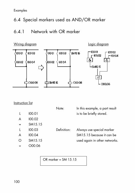
Examples
100
6.4 Special markers used as AND/OR marker
6.4.1 Network with OR marker
Wiring diagram Logic diagram
Instruction listNote: In this example, a part result
L I00.01 is to be briefly stored.A I00.02= SM15.15L I00.03 Definition: Always use special markerA I00.04 SM15.15 because it can beO SM15.15 used again in other networks.= O00.06
OR marker = SM 15.15
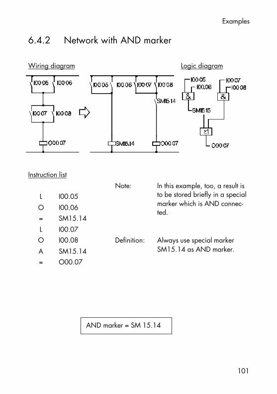
Examples
101
6.4.2 Network with AND marker
Wiring diagram Logic diagram
Instruction listNote:
L I00.05O I00.06= SM15.14L I00.07
In this example, too, a result isto be stored briefly in a specialmarker which is AND connec-ted.
O I00.08 Definition:A SM15.14= O00.07
Always use special markerSM15.14 as AND marker.
AND marker = SM 15.14

Examples
102
6.4.3 Network with multiple use of the OR markerWiring diagram Logic diagram
Instruction listL I00.00A I00.01= SM15.15 ;OR markerL I00.02A I00.03O SM15.15= SM15.14 ;AND markerL I00.04A I00.05= SM15.15 ;OR markerL I00.06A I00.07O SM15.15A SM15.14= O00.09
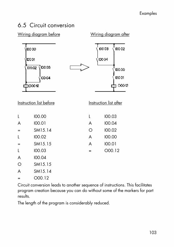
Examples
103
6.5 Circuit conversionWiring diagram before Wiring diagram after
Instruction list before Instruction list after
L I00.00 L I00.03A I00.01 A I00.04= SM15.14 O I00.02L I00.02 A I00.00= SM15.15 A I00.01L I00.03 = O00.12A I00.04O SM15.15A SM15.14= O00.12Circuit conversion leads to another sequence of instructions. This facilitatesprogram creation because you can do without some of the markers for partresults.The length of the program is considerably reduced.

Examples
104
6.6 Special-purpose circuits
6.6.1 Impulse relay
Wiring diagram
Instruction list
L I00.00= PP00.00L PP00.00
XO O00.00= O00.00
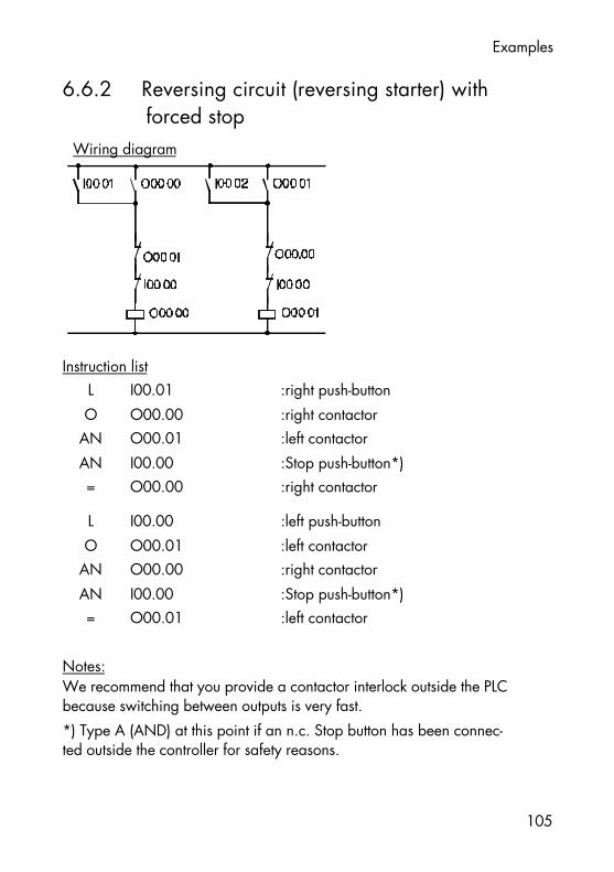
Examples
105
6.6.2 Reversing circuit (reversing starter) withforced stop
Wiring diagram
Instruction listL I00.01 :right push-buttonO O00.00 :right contactor
AN O00.01 :left contactorAN I00.00 :Stop push-button*)= O00.00 :right contactor
L I00.00 :left push-buttonO O00.01 :left contactor
AN O00.00 :right contactorAN I00.00 :Stop push-button*)= O00.01 :left contactor
Notes:We recommend that you provide a contactor interlock outside the PLCbecause switching between outputs is very fast.*) Type A (AND) at this point if an n.c. Stop button has been connec-ted outside the controller for safety reasons.

Examples
106
6.6.3 Reversing circuit (reversing starter) withoutforced stop
Wiring diagram
Instruction listL I00.01 ; right push-buttonO O00.00 ; right contactor
AN I00.02 ; left push-buttonAN O00.01 ; left contactorAN I00.00 ; Stop push-button*)= O00.00 ; right contactor
L I00.02 ; left push-buttonO O00.01 ; left contactor
AN I00.01 ; right push-buttonAN O00.00 ; right contactorAN I00.00 ; Stop push-button*)= O00.01 ; left contactor
Notes: We recommend that you provide a contactor interlock outside thePLC because switching between outputs is very fast.*) Type A (AND) at this point if an n.c. Stop button has been connected out-side the controller for safety reasons.

Examples
107
6.7 Edge evaluation (wiping pulse)
ECO Control 667E has 128 programmable wiping pulses for the detectionof status changes of logical signals (edge evaluation). The pulses can beused for both rising and falling edges.
6.7.1 Programmable wiping pulse at rising edge
Wiring diagram Circuit symbol Instruction list
L I00.00= PP00.00L PP00.00= O00.00
Signal curve
T = cycle time

Examples
108
6.7.2 Programmable wiping pulse at falling edge
Wiring diagram Circuit symbol Instruction list
L I00.01=N PP00.01L PP00.01= O00.01
Signal curve
T = cycle time
As opposed to the programmable wiping pulses of the previous examples,which were activated by a change of edge, the next two examples evalua-te the signal state. This influences the start-up behaviour.

Examples
109
6.7.3 Wiping pulse at positive signal
Wiring diagram Circuit symbol Instruction list
L I00.02AN M00.00= O00.02L I00.02
Signal curve
= M00.00

Examples
110
6.7.4 Wiping pulse at negative signal
Wiring diagram Circuit symbol Instruction list
LN I00.03AN M00.01= O00.03LN I00.03
Signal curve
= M00.01

Examples
111
6.8 Software timers
6.8.1 MnemonicsYou can program up to 32 software timers in the range between 10 ms and65535 s. Timer addresses are PT00.00 – PT01.15.
Start timerAssignment Address :Time value *Time basis :Function :Remanence *)
:R remanence
:R raising delay:F falling delay:P impulse:C clock pulse
10 ms (or *100 ms, or *1s
16 bit constant (1 – 65535 ) or16 bit variable (e.g. BM01.02 (+BM01.03
Address of software timer (e.g. PT01.05)
= Start of software timer at edge 0 → 1, RESET at log. 0
*) Note: Adding the “R” parameter (remanence of current timervalue) is optional.
• Read output L PTxx.xx “1“= time run out
• Read current value(remaining time)
LD PTxx.xx 16 bit value of remainingtime
• Stop timer =TH PTxx.xx stop without RESET

Examples
112
6.8.1.1 Syntax examples
Start raising delay of 17.5 s with remanent current value:
= PT01.00:175*100ms:R:R
Start falling delay with variable timer value (timer value in BM06.02/03):
= PT01.01:BM04.06*100ms:F
Read timer value and store in BM06.02/03:
LD PT01.02=D BM06.02
Stop timer while I01.00 is on:
L I01.00=TH PT01.03
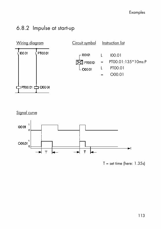
Examples
113
6.8.2 Impulse at start-up
Wiring diagram Circuit symbol Instruction list
L I00.01= PT00.01:135*10ms:PL PT00.01= O00.01
Signal curve
T = set time (here: 1.35s)

Examples
114
6.8.3 Impulse of constant duration
Wiring diagram Circuit symbol Instruction list
L I00.02O PT01.02= PT01.02:123*100ms:PL PT01.02
Signal curve
= O00.02
T = set time (here: 12.3s)

Examples
115
6.8.4 Raising delay
Circuit symbol Instruction list
L I00.03= PT00.03:185*10ms:RL PT00.03
Signal curve
= O00.03
T = set time (here: 1.85s)

Examples
116
6.8.5 Falling delay
Circuit symbol Instruction list
L I00.04= PT01.04:35*100ms:FL PT01.04
Signal curve
= O00.04
T = set time (here: 3.5s)

Examples
117
6.8.6 Pulse generator with wiping pulse output
Circuit symbol Instruction list
L I00.05AN O00.05= PT00.00:55*10ms:RL PT00.05
Signal curve
= O00.05
T1 = set time (here: 0.55s) T2 = cycle time

Examples
118
6.8.7 Flash generator with one timer
Circuit symbol Instruction list
L I00.06= PT01.06:50*10ms:CL PT01.06
Signal curve
= O00.06
T = set time (here: 0.5s), flashing frequency = 1Hz

Examples
119
6.8.8 Flash generator with two timers
Circuit symbol Instruction list
L I00.00AN PT00.02= PT00.01:5*100ms:PL PT00.01= O00.00LN PT00.01
Signal curve
= PT00.02:10*100ms:P
T1 = set switch-on time (here: 500ms=0.5s) T2 = set switch-off time (here 1000ms=1s)

Examples
120
6.9 Programmable clockApart from the software timers there are also four 8-bit operands availablewhich are incremented at set clock pulses.Operand addresses are PC00.00-PC00.03:Operand Clock pulse Range
10 msPC00.01PC00.02
10 s0...255
The pulse markers are incremented by 1 in the range from 0 to 255 at thespecified clock pulse. When the count reaches 255, the next clock cycle setsthe operand back to 0.
Application exampleOne part of the program is to be processed only every 100 ms.
L PC00.01 ;if 100 ms clock pulse memory isCMP BM03.14 ;the same as the old value?JP= ;go to end of program 1 if yes= BM03.14 ;else new = old″″
″ ;this part of the program is processed″ ;only every 100 ms″″″LN O01.03 ;program for 100 ms flash generator= O01.03″″″″
L PCxx.xx=
changes the bit marker’s logical state every (128*clock pulse time) becau-se the status of bit 7 in the accumulator is used for bit processing.

Examples
121
6.10 Software counters
6.10.1 Mnemonics
You can program up to 32 software counters in the range from 1 to 65535.Counter addresses are C00.00-C01.15.
Assignment Address :Counter val. :Function :Remanence *):R remanence
:F count up:B count down
16 bit constant (1 – 65535 ) or16 bit variable (e.g. BM01.02 (+BM01.03))
Address of software counter (e.g. C00.05)
= Starts the software counter at edge 0 → 1, RESET at log. 0
*) Note: Adding the “R” parameter (remanence of current countervalue) is optional.
ààRead output L Cxx.xx “1“= count complete
ààRead current value(remaining value)
LD Cxx.xx 16 bit value of the cur-rent count
àà Count (transfer pulse) L stop without RESET
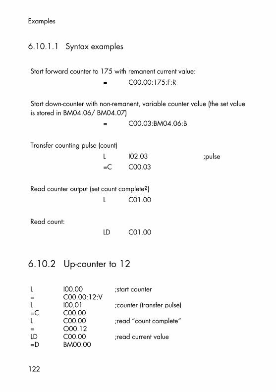
Examples
122
6.10.1.1 Syntax examples
Start forward counter to 175 with remanent current value:= C00.00:175:F:R
Start down-counter with non-remanent, variable counter value (the set valueis stored in BM04.06/ BM04.07)
= C00.03:BM04.06:B
Transfer counting pulse (count)L I02.03 ;pulse=C C00.03
Read counter output (set count complete?)L C01.00
Read count:LD C01.00
6.10.2 Up-counter to 12
L I00.00 ;start counter= C00.00:12:VL I00.01 ;counter (transfer pulse)=C C00.00L C00.00 ;read “count complete“= O00.12LD C00.00 ;read current value=D BM00.00

Examples
123
6.11 Programming a sequential process
Path-step diagram
A+ B+ A- A+ A-C+ B- C-

Examples
124
Start I00.00 L I00.00 ;starta0 I00.01 A I00.01 ;limit switch a0b0 I00.03 A I00.03 ;limit switch b0c0 I00.05 A I00.05 ;limit switch c0
AN SM00.01 ;step 11 S SM00.01 ;step 1
SM00.01 S O00.00 CYL.A+ S O00.00 ;cylinder A+a1 I00.02
L I00.02 ;limit switch a12 A SM00.01 ;step 1
SM00.02 S O00.01 CYL.B+ AN SM00.02 ;step 2b1 I00.04 S SM00.02 ;step 2
S O00.01 ;cylinder A+3
SM00.03 R O00.00 CYL.A- L I00.04 ;limit switch b1S O00.02 CYL.C+ A SM00.02 ;step 2
a0 I00.01 AN SM00.03 ;step 3c0 I00.06 S SM00.03 ;step 3
R O00.00 ;cylinder A-4 S O00.02 ;cylinder C+
SM00.04 S O00.00 CYL.A+R O00.01 CYL.B- L I00.01 ;limit switch a0
a1 I00.02 A I00.06 ;limit switch c1b0 I00.03 A SM00.03 ;step 3
AN SM00.04 ;step 45 S SM00.04 ;step 4
SM00.05 R O00.00 CYL.A- S O00.00 ;cylinder A+R O00.02 CYL.C- R O00.01 ;cylinder B-
L I00.02A I00.03 ;limit switch b0
6 END A SM00.04AN SM00.05 ;step 5S SM00.05 ;step 5R O00.00 ;cylinder A-R O00.02 ;cylinder C-
L I00.01 ;limit switch a0A I00.05 ;limit switch c0A SM00.05 ;step 5R SM00.01 ;step 1R SM00.02 ;step 2R SM00.03 ;step 3R SM00.04 ;step 4R SM00.05 ;step 5
Logic diagram Program

Examples
125
6.12 Register circuits
6.12.1 1-bit shift registerIn this example, the shift register is 6 steps long. The signal input is shiftedfrom O00.01 to O00.06 when the shift clock pulse is comes in from I00.00.
Circuit symbolI00.01 SII00.00 PC SO.1 O00.01 SI: signal input I00.01
SO.2 O00.02 PC: I00.00: : SO.1: signal output 1 O00.01SO.n O00.06 SO.2: signal output 2 O00.02
: :1 bit shift SO.n: signal output n O00.06
register
Instruction listL I00.00 ;shift clock pulse= PP00.00 ;wiping pulseL PP00.00 ;wiping pulseJPCN NORM ;go to normal programif noL O00.05 ;step 5= O00.06 ;step 6L O00.04 ;step 4= O00.05 ;step 5L O00.03 ;step 3= O00.04 ;step 4L O00.02 ;step 2= O00.03 ;step 3L O00.01 ;step 1= O00.02 ;step 2
L I00.01 ;signal input= O00.01 ;step 1
NORM :: ;normal program

Examples
126
6.12.2 8-bit shift register
In this example, the shift register is 6 steps long. The set information is shiftedfrom BM00.00 to BM00.06 when the shift clock pulse comes in fromI00.00.
Circuit symbolBM00.00 SI
I00.00 PC SO.1 BM00.01 SI: signal input BM00.01SO.2 BM00.02 PC: I00.00: : SO.1: signal output 1 BM00.01SO.n BM00.06 SO.2: signal ouput 2 BM00.02
: :8 bit shift SO.n: signal output n BM00.06
register
Instruction listL I00.00 ;shift clock pulse= PP00.00 ;wiping pulseL PP00.00 ;wiping pulseJPCN NORM ;go to normal program if notL BM00.05 ;step 5= BM00.06 ;step 6L BM00.04 ;step 4= BM00.05 ;step 5L BM00.03 ;step 3= BM00.04 ;step 4L BM00.02 ;step 2= BM00.03 ;step 3L BM00.01 ;step 1= BM00.02 ;step 2
L I00.01 ;signal input= BM00.01 ;step 1
NORM :: ;normal program

Examples
127
6.13 Copy commands (bit-to-byte transfer)
6.13.1 Copy eight 1-bit operands to one byteC1T8 I00.00 load contents of I00.00-I00.07 into the accumulator= BM00.00 copy contents of accumulator to BM00.00
7 6 5 4 3 2 1 0
I00.00 accumulatorI00.01I00.02I00.03I00.04 BM00.00I00.05I00.06I00.07
6.13.2 Copy one byte to eight 1-bit operandsL BM00.01 ;load contents of BM00.01 into accumulatorC8T1 O00.03 ;copy contents of accumulator to O00.03-O00.10
6.13.3 Copy sixteen 1-bit operands to two bytesC1T16 I01.00 ;load contents of I01.00-I01.15 into accumulator=D BM00.02 ;copy contents of accumulator to BM00.02-BM00.03
;(I01.00-I01.07 to BM00.02,; I01.08-I01.15 to BM00.03)

Examples
128
6.13.4 Copy two byte to sixteen 1-bit operandsLD BM00.04 ;load contents of BM00.04-BM00.05 into accumulatorC16T1 O00.00 ;copy contents of accu to addresses O00.00-O00.15
;(BM00.04 to O00.00-O00.07,; BM00.05 to O00.08-O00.15)
6.14 Comparator circuits
6.14.1 8-bit comparatorThe program in this example compares the contents of two 8-bit markers. Theresult (greater, smaller, or equal) is evaluated by conditional jumps (see jumpoperations). In this case, O00.00 is set if reference value 1 is greater thanreference value 2.
V1: reference value 1 BM00.00V2: reference value 2 BM00.01CO: comparator output O00.00
BM00 00 V1BM00.01 V2 CO O00.0 V1 > V2
comparator
ProgramL BM00.00 ;compare V1V BM00.01 ;with V2JP> MARK1 ;jump if V1 greater than V2L PL00.00 ;log. 0JP MARK2 ;jump to CO
MARK1 L PL00.01 ;logical 1MARK2 = O00.00 ;CO
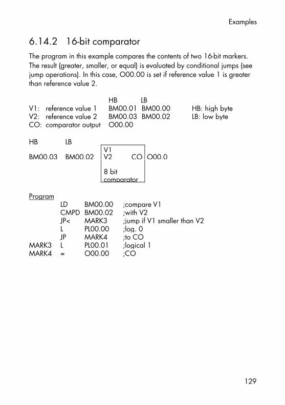
Examples
129
6.14.2 16-bit comparatorThe program in this example compares the contents of two 16-bit markers.The result (greater, smaller, or equal) is evaluated by conditional jumps (seejump operations). In this case, O00.00 is set if reference value 1 is greaterthan reference value 2.
HB LBV1: reference value 1 BM00.01 BM00.00 HB: high byteV2: reference value 2 BM00.03 BM00.02 LB: low byteCO: comparator output O00.00
HB LBV1
BM00.03 BM00.02 V2 CO O00.0
8 bitcomparator
ProgramLD BM00.00 ;compare V1CMPD BM00.02 ;with V2JP< MARK3 ;jump if V1 smaller than V2L PL00.00 ;log. 0JP MARK4 ;to CO
MARK3 L PL00.01 ;logical 1MARK4 = O00.00 ;CO

Examples
130
6.15 Arithmetic functions
6.15.1 Binary 8-bit adderZ1: 1st addend 8 bit 0-255 ($FF) BM00.00Z2: 2nd addend 8 bit 0-255 ($FF) BM00.01Z3: sum 8 bit 0-255 ($FF) BM00.02
Z1
BM00.01 Z2 Z3 BM00.02
Binary8-bitadder
ProgramL BM00.00 ;Z1 1st addendADD BM00.01 ;Z2 2nd addend= BM00.02 ;Z3 sum
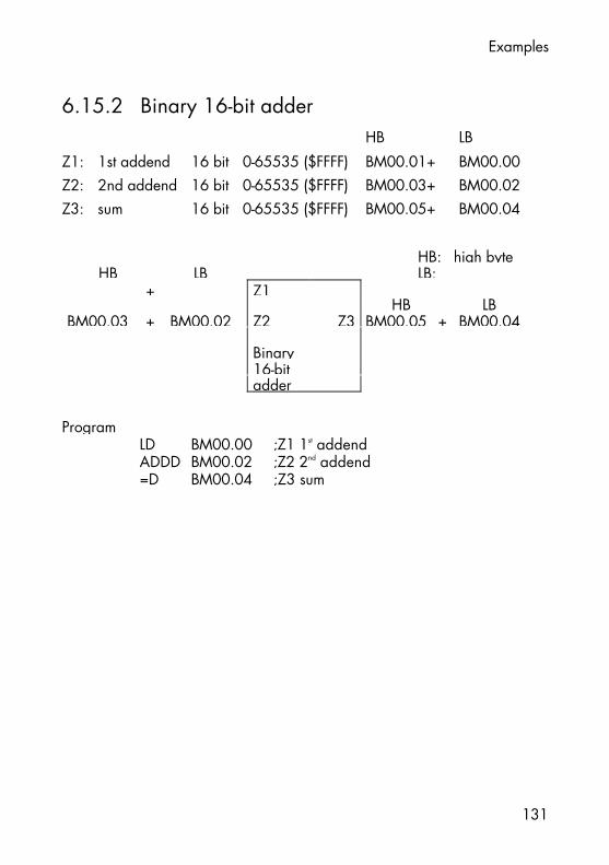
Examples
131
6.15.2 Binary 16-bit adderHB LB
Z1: 1st addend 16 bit 0-65535 ($FFFF) BM00.01+ BM00.00Z2: 2nd addend 16 bit 0-65535 ($FFFF) BM00.03+ BM00.02Z3: sum 16 bit 0-65535 ($FFFF) BM00.05+ BM00.04
HB: high byteHB LB LB:
+ Z1HB LB
BM00.03 + BM00.02 Z2 Z3 BM00.05 + BM00.04
Binary16-bitadder
ProgramLD BM00.00 ;Z1 1st addendADDD BM00.02 ;Z2 2nd addend=D BM00.04 ;Z3 sum

Examples
132
6.15.3 8-bit BCD adderZ1: 1st addend 8 bit 0-99 BM00.00Z2: 2nd addend 8 bit 0-99 BM00.01Z3: sum 8 bit 0-99 BM00.02
BM00 00 Z1
BM00.01 Z2 Z3 BM00.02
8 bitBCDadder
Programm
****** BCD correction ***************************
CLR LBM00.01 ;marker for BCD correctionL BM00.00 ;Z1 1st addendA 15= LBM00.00 ;1st decadeL BM00.01 ;Z2 2nd addendA 15 ;davon 1. DekadeADD LBM00.00CMP 10 ;BCD correction required?JP< ADDIT ;jump if notL 6 ;if so:= LBM00.01 ;load correction
****** Addition ********************************
ADDIT L LBM00.01ADD BM00.00 ;Z1 1st addendADD BM00.01 ;Z2 2nd addend= BM00.02 ;Z3 sum

Examples
133
6.15.4 Binary 8-bit subtractorCaution: Z3 becomes negative and is filed as two’s complement if Z2 > Z1.Further evaluation of Z3 has to take this into account.
Z1: minuend 8 bit 0-255 ($FF) BM00.00Z2: subtrahend 8 bit 0-255 ($FF) BM00.01Z3: difference 8 bit 0-255 ($FF) BM00.02
Z1
BM00.01 Z2 Z3 BM00.02
Binary
subtractor
ProgrammL BM00.00 ;Z1 minuendSUB BM00.02 ;Z2 Ssbtrahend= BM00.04 ;Z3 difference

Examples
134
6.15.5 Binary 16-bit subtractorHB LB
Z1: minuend 16 bit 0-65535 ($FFFF) BM00.01+ BM00.00Z2: subtrahend 16 bit 0-65535 ($FFFF) BM00.03+ BM00.02Z3: difference 16 bit 0-65535 ($FFFF) BM00.05+ BM00.04
HB: high byteHB LB LB:
+ Z1HB LB
BM00.03 + BM00.02 Z2 Z3 BM00.05 + BM00.04
Binary
subtractor
ProgramLD BM00.00 ;Z1 minuendSUBD BM00.02 ;Z2 subtrahend=D BM00.04 ;Z3 difference
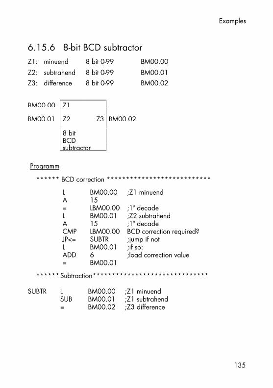
Examples
135
6.15.6 8-bit BCD subtractorZ1: minuend 8 bit 0-99 BM00.00Z2: subtrahend 8 bit 0-99 BM00.01Z3: difference 8 bit 0-99 BM00.02
BM00 00 Z1
BM00.01 Z2 Z3 BM00.02
8 bitBCDsubtractor
Programm
****** BCD correction ***************************
L BM00.00 ;Z1 minuendA 15= LBM00.00 ;1st decadeL BM00.01 ;Z2 subtrahendA 15 ;1st decadeCMP LBM00.00 BCD correction required?JP<= SUBTR ;jump if notL BM00.01 ;if so:ADD 6 ;load correction value= BM00.01
******Subtraction******************************
SUBTR L BM00.00 ;Z1 minuendSUB BM00.01 ;Z1 subtrahend= BM00.02 ;Z3 difference

Examples
136
6.15.7 Binary 8-bit multiplicatorZ1: multiplicand 8 bit 0-255 ($FF) BM00.00Z2: multiplicator 8 bit 0-255 ($FF) BM00.01
HB LBZ3: product 16 bit 0-65025 ($FI01) BM00.03+ BM00.02
HB: high byteLB: low byte
BM00 00 Z1HB LB
BM00.01 Z2 Z3 BM00.03 +BM00.02
Binary8/16-bitmultiplicator
ProgramL BM00.00 ;Z1 multiplicandMUL BM00.01 ;Z2 multiplicator=D BM00.02 ;Z3 product

Examples
137
6.15.8 Binary 16-bit multiplicatorHB LB
Z1: multiplicand 16 bit 0-65535 ($FFFF) BM00.01+ BM00.00Z2: multiplicator 16 bit 0-65535 ($FFFF) BM00.03+ BM00.02Z3: product 16 bit 0-65535 ($FFFF) BM00.05+ BM00.04
HB: high byteHB LB LB:
+ Z1HB LB
BM00.03 + BM00.02 Z2 Z3 BM00.05 + BM00.04
Binary
multiplicator
ProgramLD BM00.00 ;Z1 multiplicandMULD BM00.02 ;Z2 multiplicator=D BM00.04 ;Z3 product

Examples
138
6.15.9 Binary 8-bit dividerZ1: dividend 8 bit BM00.00Z2: divisor 8 bit BM00.01Z3: quotient 8 bit BM00.02
BM00 00 Z1
BM00.01 Z2 Z3 BM00.02
Binary
divider
ProgrammL BM00.00 ;Z1 dividendDIV BM00.01 ;Z2 divisor= BM00.02 ;Z3 quotient

Examples
139
6.15.10 Binary 16-bit dividerHB LB
Z1: dividend 16 bit 0-65535 ($FFFF) BM00.01+ BM00.00Z2: divisor 16 bit 0-65535 ($FFFF) BM00.03+ BM00.02Z3: quotient 16 bit 0-65535 ($FFFF) BM00.05+ BM00.04
HB: high byteHB LB LB:
+ Z1HB LB
BM00.03 + BM00.02 Z2 Z3 BM00.05 + BM00.04
Binary
divider
ProgrammLD BM00.00 ;Z1 dividendDIVD BM00.02 ;Z2 divisor=D BM00.04 ;Z3 quotient
The resulting quotient is an integer number. Proceed as follows to find the rest:
LD BM00.04 ;Z3 quotientMULD BM00.02 ;Z2 divisor=D LBM00.00 ;Z3(integer!) *Z2LD BM00.00 ;Z1 dividendSUBD LBM00.00=D BM00.06 ;rest

Examples
140
6.16 Code converters
6.16.1 BCD-to-binary converter, 8-bitBCD: 8-bit 0-99 BM00.00Binary: 8-bit 0-99($63) BM00.01
BM00 00 BCD Bin BM00 01
8 bitBCD-to-binaryconverter
ProgramL BM00.00 ;load BCD valueLSR ;shiftLSR ;tensLSR ;toLSR ;onesMUL 10 ;multiply= BM00.01 ;storeL BM00.00 ;load BCD valueA 15 ;extract tensADD BM00.01 ;add binary tens= BM00.01 ;store binary value

Examples
141
6.16.2 Binary-to-BCD converter, 8-bitBinary: 8-bit 0-99($63) BM00.00BCD: 8-bit 0-99 BM00.01
Bin BCD
binary-to-BCDconverter
ProgramL BM00.00 ;load binary valueDIV 10 ;find and= LBM00.00 ;store tensMUL 10 ;calculate and register= LBM00.01 ;integer amount of tensL BM00.00 ;SUB LBM00.01 ;find and= LBM00.01 ;store tensL LBM00.00 ;shiftLSL ;tensLSL ;into the upperLSL ;nibbleLSL ;O LBM00.01 ;compress and= BM00.01 ;output BCD value

Examples
142
6.16.3 BCD-to binary converter, 16 bitHB LB
BCD: 16 bit 0-9999 BM00.01+ BM00.00Binary: 16 bit 0-9999($270F) BM00.03+ BM00.02
HB:LB: low byte
HB LB HB LB+ Bin BCD +
BCD-to-binaryconverter

Examples
143
ProgramCLR BM00.03 ;clear because of LD BM00.02CLR LBM00.03 ;clear because of LD LBM00.02L BM00.00 ;separate ones decadeA 15= BM00.02 ;binary onesL BM00.00 ;separate tens decadeLSRLSRLSRLSL ;binary tensMUL 10ADD BM00.02= BM00.02 ;ones + tensL BM00.01 ;separate hundreds decadeA 15= LBM00.02 ;binary hundredsLD LBM00.02 ;same as wordMULD 100ADDD BM00.02=D BM00.02 ;ones + tens + hundredsL BM00.01 ;separate thousands decadeLSRLSRLSRLSR= LBM00.02 ;binary thousandsLD LBM00.02 ;same as wordMULD 1000ADDD BM00.02=D BM00.02 ;complete binary value
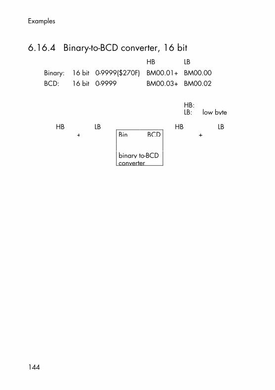
Examples
144
6.16.4 Binary-to-BCD converter, 16 bitHB LB
Binary: 16 bit 0-9999($270F) BM00.01+ BM00.00BCD: 16 bit 0-9999 BM00.03+ BM00.02
HB:LB: low byte
HB LB HB LB+ Bin BCD +
binary to-BCDconverter

Examples
145
ProgramCLR BM00.02 ;set to zeroCLR BM00.03 ;“
THOU1 LD BM00.00 ;load binary valueCMPD 1000JP< THOU2 ;smaller than one-thousand ?SUBD 1000 ;if yes: subtract 1000=D BM00.00INC BM00.03 ;count subtraction stepsJP THOU1 ;check again
THOU2 L BM00.03 ;if not: shift thousandsLSL ;to the upperLSL ;nibble of theLSL ;BCD output’sLSL ;high byte= BM00.03 ;prepare high byte
HUND LD BM00.00 ;remaining binary value (no thousands)CMPD 100JP< TEN1 ;smaller than one-hundred?SUBD 100 ; if yes: subtract 100=D BM00.00INC BM00.03 ;count subtraction steps (in lower
;nibble of BCD output’s high byte)JP HUND ;check again
TEN1 L BM00.00 ;rem. binary value (no hundreds either)V 10JP< TEN2 ;smaller than ten ?SUB 10 ;if yes: subtract 10= BM00.00INC BM00.02 ;count subtraction stepsJP TEN1 ;check again
TEN2 L BM00.02 ;if not: shift tensLSL ;into the upperLSL ;nibble of theLSL ;BCD output’sLSL ;low byteADD BM00.00 ;remaining ones into lower nibble= BM00.02 ;output low byte

Examples
146
6.17 Modular programming
TaskSets of 12 pieces each are to be transported on a con-veyor belt. The belt drive is operated by start and stopkeys. The belt is stopped after every twelfth piece. Beforeleaving the belt, each piece triggers an impulse via an in-itiator. The impulse is used for counting.
A binary display is to show:Ø while the belt is moving:the current number in the set (0...12)Ø else:the sum total of all parts transported already (0...65536)
You should be able to reset the counter via the Clear keys.
6.17.1 Part task definitionThe part tasks are to be defined under technological as-pects and aim for clearly arranged modules that can beused several times. Our example only indicates an under-standing of the modules’ interaction.

Examples
147
6.17.1.1 Module structure
ORG ONOFF(1)
JPP ONOFF L STARTERS IOMARKERL STOPON READYO DONER IOMARKERL IOMARKER= MOTOR
COUNTER(2) SUM(5)
JPP COUNTER L C00.00 LD C00.00O STOP ADDD BM00.00= PP00.00 =D BM00.00L PP00.00JPCP SUML IOMARKER= C00:12:FL CIMP
NEW(6)
=C C00.00 LD 0L CLEAR =D BM00.00JPCP NEW
DISCUR(3)L MOTORJPCP DISCUR LD C00.00
=D BM00.02JPP DISPLAY DISPLAY(7)
LD BM00.00DISSUM(4)
C16T1 BIT1LN MOTOR LD BM00.00JPCP DISSUM =D BM00.02
JPP DISPLAY
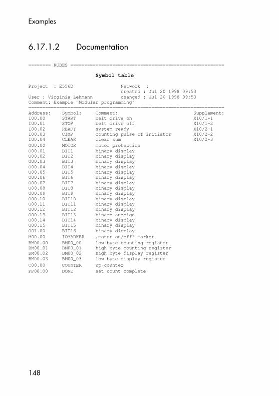
Examples
148
6.17.1.2 Documentation
======== KUBES =======================================================
Symbol table
Project : E556D Network : created : Jul 20 1998 09:53User : Virginia Lehmann changed : Jul 20 1998 09:53Comment: Example "Modular programming"======================================================================Address: Symbol: Comment: Supplement:I00.00 START belt drive on X10/1-1I00.01 STOP belt drive off X10/1-2I00.02 READY system ready X10/2-1I00.03 CIMP counting pulse of initiator X10/2-2I00.04 CLEAR clear sum X10/2-3O00.00 MOTOR motor protectionO00.01 BIT1 binary displayO00.02 BIT2 binary displayO00.03 BIT3 binary displayO00.04 BIT4 binary displayO00.05 BIT5 binary displayO00.06 BIT6 binary displayO00.07 BIT7 binary displayO00.08 BIT8 binary displayO00.09 BIT9 binary displayO00.10 BIT10 binary displayO00.11 BIT11 binary displayO00.12 BIT12 binary displayO00.13 BIT13 binare anzeigeO00.14 BIT14 binary displayO00.15 BIT15 binary displayO01.00 BIT16 binary displayM00.00 IOMARKER „motor on/off“ markerBM00.00 BM00_00 low byte counting registerBM00.01 BM00_01 high byte counting registerBM00.02 BM00_02 high byte display registerBM00.03 BM00_03 low byte display register
C00.00 COUNTER up-counterPP00.00 DONE set count complete

Examples
149
======== KUBES =======================================================
Project structure
Project : E556D Network : created : Jul 20 1998 09:53User : Virginia Lehmann changed : Jul 20 1998 09:53Comment: Example “Module programming"======================================================================ORG.ORG/1|*------>ONOFF.PRO/1|*------>COUNTER.PRO/2| || *------>SUM.PRO/5| || *------>NEW.PRO/6|*------>DISCUR.PRO/3| || *------>DISPLAY.PRO/7|*------>DISSUM.PRO/4 | *------>DISPLAY.PRO/7
======== KUBES =======================================================
Organisation module IL
Project : E556D Network :Module : ORG No.: 1 created : Jul 20 1998 09:53User : Virginia Lehmann changed : Jul 20 1998 10:27======================================================================
1: JPP ONOFF 1 2: JPP COUNTER 2 3: L MOTOR O00.00 ; (motor protection) 4: JPCP DISCUR 3 5: LN MOTOR O00.00 ; (motor protection) 6: JPCP DISSUM 4 7:

Examples
150
======== KUBES =======================================================
Program module IL
Project : E556D Network :Module : ONOFF No.: 1 created : Jul 20 1998 10:40User : Virginia Lehmann changed : Jul 20 1998 10:40Comment: ONOFF ====================================================================== 1: L START I00.00 ; (belt drive on) 2: S IOMARKER M00.00 ; („motor on/off“ marker) 3: L STOP I00.01 ; (belt drive off) 4: ON READY I00.02 ; (system ready) 5: O DONE PP00.00 ; (set count complete) 6: R IOMARKER M00.00 ; („motor on/off“ marker) 7: L IOMARKER M00.00 ; („motor on/off“ marker) 8: = MOTOR O00.00 ; (motor protection) 9:
======== KUBES =======================================================
Program module IL
Project : E556D Network :Module : COUNTER No.: 2 created : Jul 20 1998 10:42User : Virginia Lehmann changed : Jul 20 1998 10:42Comment: COUNTER======================================================================
1: L COUNTER C00.00 ; (up-counter) 2: O STOP I00.01 ; (belt drive off) 3: = DONE PP00.00 ; (set count complete) 4: L DONE PP00.00 ; (set count complete) 5: JPCP SUM 5 6: L IOMARKER M00.00 ; („motor on/off“ marker) 7: = COUNTER:12:F C00.00 ; (up-counter) 8: L CIMP I00.03 ; (counting pulse of initiator) 9: =C COUNTER C00.00 ; (up-counter) 10: L CLEAR I00.04 ; (clear sum) 11: JPCP NEW 6 12:
======== KUBES =======================================================
Program module IL
Project : E556D Network :Module : DISCUR No.: 3 created : Jul 20 1998 10:45User : Virginia Lehmann changed : Jul 20 1998 10:45Comment: DISCUR======================================================================
1: LD COUNTER C00.00 ; (up-counter) 2: =D BM00_02 BM00.02 ; (high byte display register) 3: JPP DISPLAY 7 4:

Examples
151
======== KUBES =======================================================
Program module IL
Project : E556D Network :Module : DISSUM No.: 4 created : Jul 20 1998 10:48User : Virginia Lehmann changed : Jul 20 1998 10:48Comment: DISSUM======================================================================
1: LD BM00_00 BM00.00 ; (low byte counting register) 2: =D BM00_02 BM00.02 ; (high byte display register) 3: JPP DISPLAY 7 4:
======== KUBES =======================================================
Program module IL
Project : E556D Network :Module : SUM No.: 5 created : Jul 20 1998 10:49User : Virginia Lehmann changed : Jul 20 1998 10:49Comment: SUM======================================================================
1: LD COUNTER C00.00 ; (up-counter) 2: ADD BM00_00 BM00.00 ; (low byte counting register) 3: =D BM00_00 BM00.00 ; (low byte counting register)======== KUBES =======================================================
Program module IL
Project : E556D Network :Module : NEW No.: 6 created : Jul 20 1998 10:50User : Virginia Lehmann changed : Jul 20 1998 10:50Comment: NEW======================================================================
1: LD 0 2: =D BM00_00 BM00.00 ; (low byte counting register) 3:
======== KUBES =======================================================
Program module IL
Project : E556D Network :Module : DISPLAY No.: 7 created : Jul 20 1998 10:50User : Virginia Lehmann changed : Jul 20 1998 10:50Comment: DISPLAY======================================================================
1: LD BM00_00 BM00.00 ; (low byte counting register) 2: C16T1 BIT1 O00.01 ; (binary display) 3:

Examples
152
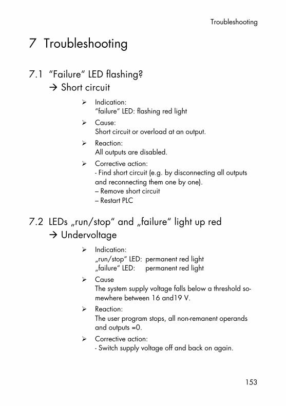
Troubleshooting
153
7 Troubleshooting
7.1 “Failure“ LED flashing?à Short circuit
Ø Indication:“failure“ LED: flashing red light
Ø Cause:Short circuit or overload at an output.
Ø Reaction:All outputs are disabled.
Ø Corrective action:- Find short circuit (e.g. by disconnecting all outputsand reconnecting them one by one).– Remove short circuit– Restart PLC
7.2 LEDs „run/stop“ and „failure“ light up redà Undervoltage
Ø Indication:„run/stop“ LED: permanent red light„failure“ LED: permanent red light
Ø CauseThe system supply voltage falls below a threshold so-mewhere between 16 and19 V.
Ø Reaction:The user program stops, all non-remanent operandsand outputs =0.
Ø Corrective action:- Switch supply voltage off and back on again.

Troubleshooting
154
7.3 No online connection to KUBES?The following error message may be displayed when youare trying to go online with the PLC (via V.24):
Fig. 14: V.24-synchronisation error message
If it does, please check whether:Ø the PLC is switched on,Ø the programming cable is connected to the PLC,Ø the programming cable is properly connected to the
PC (check port! the standard port is COM1),Ø the cable is a genuine KUBES programming cable
(part no.: 657.151.03).If all of the above points are okay, but the PLC still does notreact, it could be that the PLC no longer accesses the port.Ø Switch the supply voltage off and back on again.In some cases, the PLC still does not react. The followingcauses are possible:Ø PLC defectiveØ program error (CPU no longer accepts KUBES’ online
message)Ø wrong V.24 parameter settings
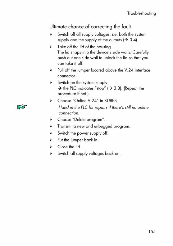
Troubleshooting
155
Ultimate chance of correcting the faultØ Switch off all supply voltages, i.e. both the system
supply and the supply of the outputs (à 3.4).Ø Take off the lid of the housing
The lid snaps into the device’s side walls. Carefullypush out one side wall to unlock the lid so that youcan take it off.
Ø Pull off the jumper located above the V.24 interfaceconnector.
Ø Switch on the system supply.è the PLC indicates “stop” (à 3.8). (Repeat theprocedure if not.).
Ø Choose “Online V.24” in KUBES.Hand in the PLC for repairs if there’s still no onlineconnection.
Ø Choose “Delete program”.Ø Transmit a new and unbugged program.Ø Switch the power supply off.Ø Put the jumper back in.Ø Close the lid.Ø Switch all supply voltages back on.

Troubleshooting
156

Data summary
157
8 Data summary
8.1 Technical data
8.1.1 DesignType openDimensions (L x W x H) depend on model variant
Eco Control 667E 8/8 152 x 90 x 73 mmEco Control 667E 16/16 152 x 90 x 73 mmEco Control 667E 32/32 268 x 90 x 73 mm
Installation on carrier railWeight depends on model variant
Eco Control 667E 8/8 c. 570 gEco Control 667E 16/16 c. 580 gEco Control 667E 32/32 c. 970 g
Admissible ambient conditionsStorage temperature -25...+70 °CAmbient temp. during operation 0...55 °CRelative humidity 50...95%
8.1.2 System power supplyVoltage 24 V DC -20% / +25%Power consumption 100 mAConnectors clamp-screw term. up to 2.5mm²
L1+ + 24 V DCL1- 0 V

Appendix
158
8.1.3 System status indicatorsType light emitting diodes, class 1
(in acc. with EN 60825-1)Run/stop (duo-LED, green/red) program running/stoppedFailure (LED, red) failure indicator
8.1.4 Serial interfaceType V.24 (RS 232)Connector female, 9-pin D-SubFunction programming and
data communicationMaximum baud rate 9.6 kbit/sTransfer format 8 data bits, 1 start bit,
1 stop bit
8.1.5 ProgrammingProgramming device PC with MSWindowsProgramming software KUBES (version 5.30 or higher)Programming cable 657.151.03
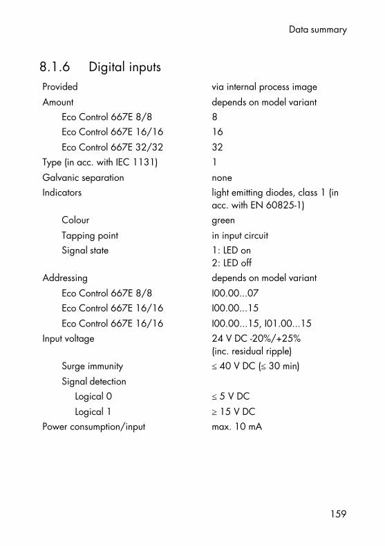
Data summary
159
8.1.6 Digital inputsProvided via internal process imageAmount depends on model variant
Eco Control 667E 8/8 8Eco Control 667E 16/16 16Eco Control 667E 32/32 32
Type (in acc. with IEC 1131) 1Galvanic separation noneIndicators light emitting diodes, class 1 (in
acc. with EN 60825-1)Colour greenTapping point in input circuitSignal state 1: LED on
2: LED offAddressing depends on model variant
Eco Control 667E 8/8 I00.00...07Eco Control 667E 16/16 I00.00...15Eco Control 667E 16/16 I00.00...15, I01.00...15
Input voltage 24 V DC -20%/+25%(inc. residual ripple)
Surge immunity ≤ 40 V DC (≤ 30 min)Signal detection
Logical 0 ≤ 5 V DCLogical 1 ≥ 15 V DC
Power consumption/input max. 10 mA

Appendix
160
8.1.7 Digital outputsControl via internal process imageAmount depends on model variant
Eco Control 667E 8/8 8Eco Control 667E 16/16 16Eco Control 667E 32/32 32
Type semiconductorIndicators light emitting diodes, class 1 (in
acc. with EN 60825-1)Colour redTapping point in the load circuitSignal state 1: LED on
2: LED offAddressing depends on model variant
Eco Control 667E 8/8 O00.00...07Eco Control 667E 16/16 O00.00...15Eco Control 667E 32/32 O00.00...15, O01.00...15
Output supply 24 V DC -20%/+25%Connectors clamp-screw term. up to 2.5mm²
L1+ + 24 V DCL1- 0 V
Output current/output max. 0.5 AShort-circuit protection yes

Data summary
161
8.1.8 Processor and memoryMicroprocessor 80C535Memory
Operating system Flash-EPROMUser program NV-RAM, 32 kbyteData, remanent NV-RAM, 8 kbyteData, non-remanent S-RAM, 24 kbyte
8.1.9 OperandsProgrammable timers remanent if required
Amount/range 32/10 ms ... 65535 sProgrammable counters remanent if required
Amount/range 32/0...65535Inputs and outputs à 8.1.4 und 0Bit markers 1320, inc. 512 remanentByte markers 2816, inc. 2304 remanent

Appendix
162
8.2 Order specifications
8.2.1 ControllersProduct Part numberEco Control 667E 8/8 upon request
8 digital inputs, 8 digital outputsEco Control 667E 16/16 667.752.00
16 digital inputs, 16 digital outputsEco Control 667E 32/32 667.704.00
32 digital inputs, 32 digital outputs
8.2.2 AccessoriesProduct Part numberSimulator plug for 8 digital inputs 667.155.50Starter kit Eco Control 667E, German, containing: 667.502.00
KUBES light (programming software just for EcoControl 667), programming cable 657.151.03,instruction manuals E 327 D and E 556 D.à Available as from week 44/98
Starter kit Eco Control 667E, English, containing: 667.502.11KUBES light (programming software just for EcoControl 667), programming cable 657.151.03,instruction manuals E 327 GB and E 556 GB.à Available as from week 51/98

Index
163
9 Indexaddressing 49AND 91AND marker 101arithmetic functions 130arithmetical operation commands
55cable routing and wiring 19code converters 140com1 30commands
description 47summary 50
communication modules 73comparison commands 56copy commands 60, 127data 33
read 85summary 157write 86
data (blocks)copy 83
design 24digital inputs 28digital outputs 29dirt 20earthing 26Eco Control 667E 16/16 23
Eco Control 667E 32/32 24Eco Control 667E 8/8 22electromagnetic compatibility 17electromagnetic interference 20examples 91exclusive OR 94falling delay 116Hardware 21impact and vibration 20impulse relay 104incrementation commands 56inductive actuators 20installation 15, 25
notes 18interference emission 18intermediate code addresses 84jump commands 58KUBES module 66KUBES module libraries 70KUBES modules 69location of installation 19logical operation commands 51maintenance 16memory distribution 31memory function
mainly resetting 96mainly setting 96

Appendix
164
model variants 21modular programming 146module hierarchy 67modules
programming 65NAND 93negation
at input 92at output 92
NOR 93notes 14NV-RAM 33On-chip RAM 31operand ranges 43operands
set functions 46summary 45types 48
operating system 31operative approach 35OR 91OR marker 100order specifications 162organisation module 66overload 29PLC cycle 36power supply 27, 29
outputs 29system 27
process image 28, 37processor 31program module 66programmable clock 120programmable counter commands
62programmable pulse commands
62programmable timer commands
62project planning 15raising delay 115RD_OFFS 85receive single character 77Reliability 13resistance to interference 17retrievability 32safety 15seal-in circuit 95send single character 76send strings 78sequential process 123servicing 16shift commands 56shift register 125short circuit 29, 153Software 35software counters 121SST667IN 78target group 13

Index
165
technical data 157temperature 19troubleshooting 153undervoltage 153user program 31
V24667IE 77V24667IS 76wiping pulse 107WR_OFFS 86

Appendix
166
10