The Project Manual of Technical Documents for ... - City of Charlotte
Upload
independentCategory
view
2download
0
O r e g o n I n s t i t u t e o f T e c h n o l o g y
Three-Phase Inverter – Lab Manual Tai Huynh
Spring 14
08 Fall

2
REE 413
Electric Power Conversion Systems
Oregon Tech
Three-Phase Square Wave Inverter
BEFORE STARTING…
Due See Class Schedule
Prerequisite EE 419 or similar
Expected Knowledge Basic knowledge of power electronics
Basic knowledge of LTSpice
Basic knowledge of electronic test
equipment
Basic knowledge of Arduino
programming
Test Equipment Lab Computers with LTSpice
DC Power Supply
Oscilloscope
Four Voltage Probes
A622 Current Probe (in the black lab cabinet)
Digital Multi-meter
Materials (per group) Breadboard (36V, 2A Max) and Jumper Wires
Three P-Channel MOSFET (Digikey IRF9640PBF-ND)
Three N-Channel MOSFET (Digikey IRF530PBF-ND)
Six Opto-isolator (Digikey 4N37-ND)
Arduino Uno Development Board
6ft USB Cable
Various capacitors, inductors, diodes, LEDs, and resistors
References The class textbook
http://www.bristolwatch.com/ele/arduino_power_inverter.htm
An Arduino PWM Website: http://www.arcfn.com/2009/07/secrets-of-arduino-pwm.html
Datasheets from Digikey and Jameco.

3
OBJECTIVES
To design, simulate, build, and analyze a three phase, DC to AC inverter.
To gain a better understanding MOSFET gate control.
EXPERIMENT
Introduction
An inverter is used to convert DC to AC power. Inverters are used in many
applications like solar PV, wind turbines, vehicle 120 VAC power supplies, and UPSs.
Various switching schemes are used with inverters, but this lab focus on a full bridge,
active, 60 Hz six-step three-phase inverter. Figure 1 shows a generic full-bridge three-
phase inverter from pp. 374 in the textbook.
Figure 1 - Full bridge three-phase inverter schematic.
The control strategy, often called a switching scheme, needs to match the majority
of the motors and generators used in industry, thus the phases are 120 º apart from each
other. Every switch has a 50 % duty cycle and are 60 º out of phase from each other.
Active switches allow the full control, and differently from a single-phase inverter, three
switches conduct at a time. However, both configurations share the same limitations.
Note that switches S1 and S4 close and open opposite of each other, as do switch pairs
(S3, S6) along with (S3, S6). As with the single-phase inverter, these switch pairs must
coordinate so they are not closed at the same time, which would result in a short circuit
across the source. With this scheme, the instantaneous voltages vA0, vB0, and vC0 are
+Vdc or zero, and line-to-line output voltages vAB, vBC, and vCA are +Vdc, 0, or -Vdc.

4
This scheme brings with it one big advantage: changing the switching frequency
can control the output frequency. However, the magnitude of the output voltage depends
on the value of the dc supply voltage. Thus to control the output voltage of a six-step
inverter, the dc input voltage must be adjusted. The expected output is shown in Figure 2.
Figure 2 - Expected output waveforms. Note the voltages are line-to-neutral.
Design, simulate, build, and analyze a three-phase inverter that will provide
12 VAC rms to a resistive and inductive load, with a 12 VDC voltage source.
Basic Calculations
See sections 8.15 and example 8-12 in the textbook for equations and examples.
1. Download the datasheets for the particular components used in this lab, and
become familiar with the MOSFETS, opto-isolators, and Arduino development
board. Pay special attention to the opto-isolator terminals. Terminal 6 (transistor
base) does not need to be connected to anything.
2. Calculate the maximum and minimum current in the load like in example 8-12
and create a similar table for the Fourier series terms.
3. Calculate the load current THD, as shown in example 8-12.
4. Calculate what the current THD would be if the inductance were 5, 50, and 500
mH. Discuss why changing the load inductance has such an effect on the output
current harmonics in the final lab report.
5. Sum the power at each harmonic level, and find the total power over the load.
6. Find the rms current in the load by back-solving the power and current
relationship:

5
7. Can the components handle the current, voltage, and power levels previously
calculated? Remember to compare with the thermal resistance rating using
equation 10-16.
NOTE: You can use MATLAB or a calculator to calculate the junction to
ambient air max power dissipation for the MOSFET according to example
10.5 and 10.6 in the textbook for how to do this.
8. Why or why not a heat sink for this design is needed?
LTSpice Simulation
Students who are not familiar with LTSpice, must go through Tutorial #1 in
the “Beginner’s Guide to LTSpice,” found on Blackboard, making sure to complete
the entire “simulations” section, including DC, transient, and AC analysis of the
circuit.
1. Create an LTSpice model of the inverter, using Figure 3 below.
Figure 3 - LTSpice schematic for the circuit.
2. For the gate drivers simulation, use pulse voltage sources connected to 4N27
opto-isolators since we cannot simulate the Arduino output in LTSpice, Figure 4.
Figure 4 - Gate driver schematic for: a) P-type MOSFET, and b) N-type MOSFET
6
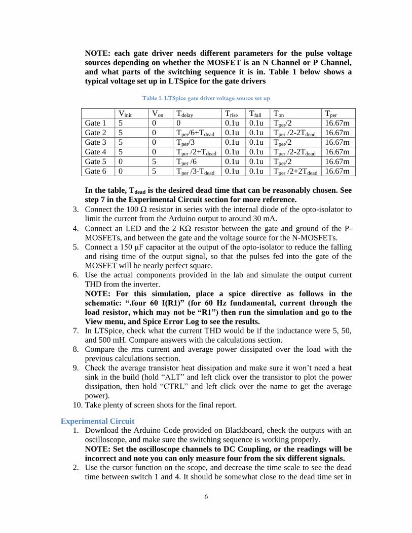
NOTE: each gate driver needs different parameters for the pulse voltage
sources depending on whether the MOSFET is an N Channel or P Channel,
and what parts of the switching sequence it is in. Table 1 below shows a
typical voltage set up in LTSpice for the gate drivers
Table 1. LTSpice gate driver voltage source set up
Vinit Von Tdelay Trise Tfall Ton Tper
Gate 1 5 0 0 0.1u 0.1u Tper/2 16.67m
Gate 2 5 0 Tper/6+Tdead 0.1u 0.1u Tper /2-2Tdead 16.67m
Gate 3 5 0 Tper/3 0.1u 0.1u Tper/2 16.67m
Gate 4 5 0 Tper /2+Tdead 0.1u 0.1u Tper /2-2Tdead 16.67m
Gate 5 0 5 Tper /6 0.1u 0.1u Tper/2 16.67m
Gate 6 0 5 Tper /3-Tdead 0.1u 0.1u Tper /2+2Tdead 16.67m
In the table, Tdead is the desired dead time that can be reasonably chosen. See
step 7 in the Experimental Circuit section for more reference.
3. Connect the 100 resistor in series with the internal diode of the opto-isolator to
limit the current from the Arduino output to around 30 mA.
4. Connect an LED and the 2 K resistor between the gate and ground of the P-
MOSFETs, and between the gate and the voltage source for the N-MOSFETs.
5. Connect a 150 μF capacitor at the output of the opto-isolator to reduce the falling
and rising time of the output signal, so that the pulses fed into the gate of the
MOSFET will be nearly perfect square.
6. Use the actual components provided in the lab and simulate the output current
THD from the inverter.
NOTE: For this simulation, place a spice directive as follows in the
schematic: “.four 60 I(R1)” (for 60 Hz fundamental, current through the
load resistor, which may not be “R1”) then run the simulation and go to the
View menu, and Spice Error Log to see the results.
7. In LTSpice, check what the current THD would be if the inductance were 5, 50,
and 500 mH. Compare answers with the calculations section.
8. Compare the rms current and average power dissipated over the load with the
previous calculations section.
9. Check the average transistor heat dissipation and make sure it won’t need a heat
sink in the build (hold “ALT” and left click over the transistor to plot the power
dissipation, then hold “CTRL” and left click over the name to get the average
power).
10. Take plenty of screen shots for the final report.
Experimental Circuit
1. Download the Arduino Code provided on Blackboard, check the outputs with an
oscilloscope, and make sure the switching sequence is working properly.
NOTE: Set the oscilloscope channels to DC Coupling, or the readings will be
incorrect and note you can only measure four from the six different signals.
2. Use the cursor function on the scope, and decrease the time scale to see the dead
time between switch 1 and 4. It should be somewhat close to the dead time set in

7
the Arduino. Make sure to record the actual dead time on the scope, and make
sure that will work with the delay, rise and fall time of the switches.
NOTE:
a. A good start point is 100 μs that can be changed later, after testing it
with the load.
b. To change the dead time in the provided Arduino script, go to
“#define DEAD_TIME” and change the value in the parenthesis. The
lowest dead time is 47 μs corresponding to the value of 1.
3. Build the circuit on a breadboard, without the load connected. Note that the
ground from the Arduino is different from the power supply ground. Make sure to
do the correct connections.
a. Use the LED and 2 K resistor in series to each output of the opto-
isolators to see it turning on and off correctly. Try using one color of
LEDs for switches 1, 3 and 5, and another color of LEDs for switches 4, 6
and 2. This way it will be easier to tell what the switching sequence is.
b. Use the “#define INTERVAL” variable in the code to make the switching
sequence viewable with the naked eye. Modify the number in the
parenthesis to larger values, 3600 is a good starting point.
4. Once the LEDs and switching scheme seems to be working properly;
a. Remove the LEDs from the circuit. The 2 KΩ resistors will be connected
between the gate and ground. If the LEDs are left in the circuit, the
isolators may not be able to provide enough power to the gates since they
can only deliver 100 mA. The MOSFETs may not be driven properly,
causing them to overheat and smoke out of the box.
5. Remember to reconfigure your switching frequency before testing the circuit.
6. Turn the power supply off and limit current output to 0.75 A before connecting
the load to the circuit.
7. Connect two channels from the oscilloscope to monitor the dead time between
switch 1 and 4. Find an appropriate dead time that will ensure one switch is not on
at the same time as the other (5 μs to 200 μs are some typical values, but 100 μs is
a good starting place).
NOTE: The dead time will act differently between loaded and unloaded
conditions, so it is always a good idea to leave some buffer room for dead
time.
8. Once the dead time is set, disconnect the two probes from the gates, then use three
probes to measure three phase voltage output at the load.
NOTE:
a. Since the load is Y-connected, it is ok to connect negative terminal of
the probes to the common node of three loads, and positive terminal
of the probes go to each phase.
b. The output might have some spikes. It is due to the characteristic of
the inductive load. To terminate those voltage spikes, just simply
remove the inductors from the load.
9. Connect a Digital Multimeter to one phase of the load for measuring the rms line-
to-neutral voltage. Depending on the dead time and because of the rms value
characteristics, the output voltage may not be close to 12 V.

8
10. Gradually increase the voltage of the Power Supply until the Digital Multimeter
reads 12 V at the output. The typical range will be from 14 to 17 V.
11. Connect the A622 current probe on another channel of the scope, and monitor the
output current in the load, making sure to configure the channel for current
readings at 100mV / A (for higher resolution), and that the probe itself is set this
way. Also, make sure that it has a 9 V battery in it and that it is turned on.
NOTE: Make sure to turn this probe off, once the measuring is completed.
There is no auto-off functionality on these probes!
12. The following picture shows what the probe looks like:
13. Show the instructor the final working circuit.
14. Record the current and voltage over the load with the scope, and record the
current being drawn from the power supply.
15. Finally, check the current (not voltage) harmonic frequencies and levels on the
scope by pressing the math button, operation, and FFT to see the real time values
(on the current-probe channel).
NOTE: Please see page 61- 68 in the TPS 2014 user’s manual (on
Blackboard) for details on how to use the FFT function on the scope.
16. Turn the Vertical Scale knob to ensure that the entire waveform shows up on
the screen, before going to the FFT screen. It may display erroneous FFT
results if the entire waveform is not visible on the Time Domain screen for a
couple cycles. Try doing an “auto-set” before going to the FFT screen.
17. Once on the FFT screen, turn the horizontal knob to change the frequency range
in view. 50 Hz per division should show the current harmonics properly.
18. Convert the y-axis (shown in dB) by hand to current (in amps) with the following
process (the scope does not convert it) and discuss these findings as compared to
the theoretical and simulated harmonic levels.
a. The vertical scale is most likely in 10 dB per division increments (0 dB
equals 1 Vrms measured voltage), shown on the bottom left hand side of the
screen for the channel that the current probe is on.
b. Record the level in dB.
c. Use the following equation to solve for measured Vrms
i. dB = 20log10(A/Aref)
Where A is the measured amplitude in units of milliAmps rms and
Aref is the reference amplitude (assumed to be 1 mA rms).
ii. As an example of how to calculate the inverse log of 1.25, simply
raise 10 to that power (i.e. 10^1.25, which returns 17.7828).
iii. The following is an example equation, using 50 dB as the
fundamental frequency amplitude, shown on the scope:
, A being in units of milliAmps

9
iv. See this link for more details http://www.ni.com/white-
paper/4278/en/, under the “Converting to Logarithmic Units”
section
Don’t forget to take plenty of pictures for the final lab report!
19. Develop a full lab report
a. Please include an introduction and separate sections on all phases of the
design (i.e. the calculation phase, LTSpice, and actual resulting data, with
pictures from the Oscilloscope and the final circuit) for the Experimental
Circuit of the lab, with any problems or discrepancies between the design
phases, equations used in the design, and all plots, m-files, and screen
shots of the pertinent data.
b. Also, include a table at the end comparing all the important data values for
all three phases, which should include the peak to peak output voltage, the
rms output voltage, the total output power, the peak to peak current in the
load, and the rms current.
Deliverables
A hard copy of the full lab report, including:
a. A title page with the lab title, class, due date, group names, and term
b. Items described in task 4
c. 7 to 12 pages in length (including all of the discussion points, plots, tables and
pictures), double spaced, 12 point font, Times New Roman, standard report
format (NOT IEEE)
d. REMEMBER: Professional presentation goes a long way!

10
APPENDIX
Figure 5 - LTSpice final line-to-neutral voltage output.
Figure 6 - Oscilloscope final line-to-neutral voltage output
Figure 7 - Switching scheme

11
Figure 8 - Sequence test
Figure 9 - Deadtime between switches

12
Figure 10 - Final built circuit
Figure 11 - RMS output voltage

13
Figure 12 - The circuit, three phase output and rms value
Arduino Code
//REE 413
//Electric Power Conversion Systems
//Oregon Tech
//The Three Phase Square Wave Inverter
#include <TimerOne.h>
#define ch1High (12)
#define ch1Low (9)
#define ch2High (11)

14
#define ch2Low (8)
#define ch3High (10)
#define ch3Low (7)
#define MOSFET_ON LOW
#define MOSFET_OFF HIGH
// we divide 360 degree (1 sin wave cycle (~16,667us) into 360 parts)
// 16,667 / 360 = 47 us
// cycle time in us
#define CYCLE_TIME (47)
// interval = 360*47us = 16680 us ~ 60Hz
#define INTERVAL (360)
// 1/2 deadtime in multiple of 47us
#define DEAD_TIME (1)
#define DUTY_CYCLE ((INTERVAL - 4*DEAD_TIME)/2)
// define on and off point
#define TIME_POINT_HIGH_ON (DEAD_TIME)
#define TIME_POINT_HIGH_OFF (TIME_POINT_HIGH_ON + DUTY_CYCLE)
#define TIME_POINT_LOW_ON (TIME_POINT_HIGH_OFF + 2*DEAD_TIME)
#define TIME_POINT_LOW_OFF (TIME_POINT_LOW_ON + DUTY_CYCLE)
int counter_ch1 = 0,
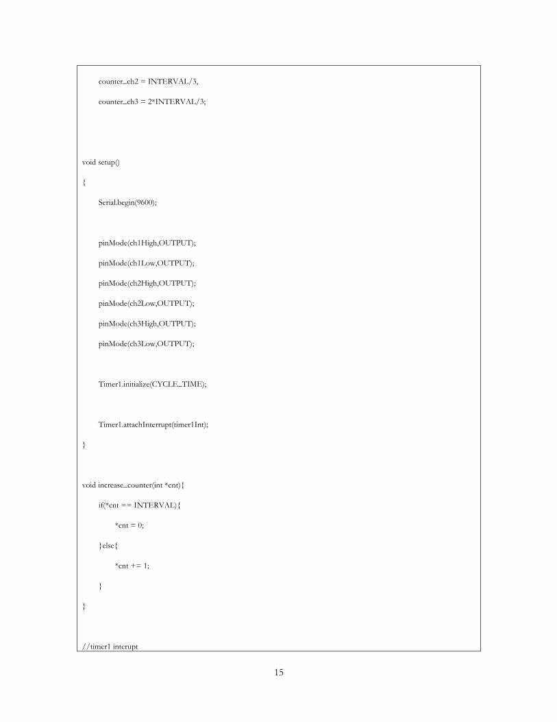
15
counter_ch2 = INTERVAL/3,
counter_ch3 = 2*INTERVAL/3;
void setup()
{
Serial.begin(9600);
pinMode(ch1High,OUTPUT);
pinMode(ch1Low,OUTPUT);
pinMode(ch2High,OUTPUT);
pinMode(ch2Low,OUTPUT);
pinMode(ch3High,OUTPUT);
pinMode(ch3Low,OUTPUT);
Timer1.initialize(CYCLE_TIME);
Timer1.attachInterrupt(timer1Int);
}
void increase_counter(int *cnt){
if(*cnt == INTERVAL){
*cnt = 0;
}else{
*cnt += 1;
}
}
//timer1 interupt

16
void timer1Int(void) //cycleTime us
{
increase_counter(&counter_ch1);
increase_counter(&counter_ch2);
increase_counter(&counter_ch3);
}
void control_channel(int ch, int counter, int time_point_on, int time_point_off)
{
if((counter > time_point_on) && (counter < time_point_off)){
digitalWrite(ch, MOSFET_ON);
}else{
digitalWrite(ch, MOSFET_OFF);
}
}
void loop()
{
control_channel(ch1High, counter_ch1, TIME_POINT_HIGH_ON, TIME_POINT_HIGH_OFF);
control_channel(ch1Low, counter_ch1, TIME_POINT_LOW_ON, TIME_POINT_LOW_OFF);
control_channel(ch2High, counter_ch2, TIME_POINT_HIGH_ON, TIME_POINT_HIGH_OFF);
control_channel(ch2Low, counter_ch2, TIME_POINT_LOW_ON, TIME_POINT_LOW_OFF);
control_channel(ch3High, counter_ch3, TIME_POINT_HIGH_ON, TIME_POINT_HIGH_OFF);
control_channel(ch3Low, counter_ch3, TIME_POINT_LOW_ON, TIME_POINT_LOW_OFF);
}
Copyright © 2022 FDOKUMEN