Galvanic Vestibular Stimulation Unit Design for the ...
73
Zentralinstitut für Elektronik Forschungszentrum Jülich
-
Upload
khangminh22 -
Category
Documents
-
view
0 -
download
0
Transcript of Galvanic Vestibular Stimulation Unit Design for the ...

Jül-
4232
Gou
tham
C.Y
apam
anu
Lab
el-f
ree
dect
ecti
on o
f bi
omol
ecul
es
Jül-4
232
Zentralinstitut für Elektronik
Galvanic Vestibular Stimulation Unit Designfor the Therapeutic Treatment of NeglectSyndrome Patients
Goutham C. Yapamanu
Jül-4232November 2006ISSN 0944-2952
Forschungszentrum Jülichin der Helmholtz-Gemeinschaft


!"#$ $
%& '%()* !%% $)+!,*-%$,!./0./*1"!2&./0././*!&%-%$! 3"45

GALVANIC VESTIBULAR STIMULATION UNIT DESIGN FOR THE THERAPEUTIC TREATMENT OF THE NEGLECT SYNDROME
Abstract Galvanic vestibular stimulation (GVS) is a technique that has been used for a clinical
measure. GVS is performed by passing small currents through the vestibular
labyrinth, using surface electrodes. To measure the effect on the vestibular system,
one may record either eye movements or postural movements (which can be
controlled with the help of a computer based Matlab simulink program). Typical
stimulus configurations include placing an electrode on each mastoid, one positive
and one negative, to produce medial / lateral sway or horizontal / vertical eye
movements. The ability of this technique in reducing the neglected region of the
patient suffering from the ‘Neglect syndrome’ is an important issue in therapeutic
neurological research.
In the Institute of Medicine (Research Centre Juelich), novel GVS-based stimulation
techniques for the therapeutic treatment of the so called ‘Neglect syndrome’ are
under development. There are how ever only a few systems for Vestibular Galvanic
Stimulation available in the market. These systems for GVS are much restricted with
their stimulation parameters such as the frequency ranges and stimulation patterns.
So we at Central Institute for Electronic, Research Centre Juelich, developed a dual
channel GVS unit both in positive and negative directions independently, therefore
enabling independent current stimuli in the frequency range from 0 to 10 KHz,
voltage range from 0v to ±35 V, current range from 0 to ±7.5 mA timer up to 2 hours
for the safety of the patient. The purpose of this designed GVS device is to optimize
GVS stimulation pattern for reducing the neglected region in Neglect Syndrome
patients and can is aimed to be used for research purposes.


CONTENTS
Summary………………………………………………………………………………...1
1. Introduction 1.1 Neglect syndrome…….................................………………....………………...2
1.2 Neglect syndrome symptoms………………............……………..…...………..3
1.3 Directed attention and the brain……………………............……………….…..4
1.4 Hemi spatial neglect and visual awareness………………….............…….….5
2. Basics 2. 1 Galvanic vestibular stimulation (GVS)……..........………………….…...…….6
2.1.1 Vestibular system…….............………….….…………………………………...8
2.1.2 Semicircular canals……….............……….….…………………………………8
2.1.3 Push-pull systems………….……….............….………………………………..9
2.1.4 Vestibulo-ocular reflex (VOR)……………................…….……………………9
2.1.5 Mechanics………………..……………….………..............…………………...10
2.1.6 Central processing…..………….……..…………………..............…………..11
2.1.7 Otoliths……………………………………………………………….................11
2.1.8 Pathologies ………………………………..……………….………..................12
2.1.9 Benign Paroxysmal Positional Vertigo (BPPV)………...………….............11
3. Material and methods 3.1 Methods of Stimulation ….........…………………………………..…………...13
3.1.2 Caloric vestibular stimulation…………………….………………. .................14
3.1.3 Constant current vs constant voltage…...………………………………….…14
3.1.4 Stimulus generation……...........…………..…………………………………...14
3.2.1 Concept of Galvanic vestibular stimulation unit(GVS)……...………..……..16
3.2.2 Specifications of the Galvanic vestibular stimulation unit…...……………...16
3.2.3 General safety regulations IEC 60601-1……...………………….………….17
3.2.4 Galvanic vestibular stimulation unit system design ….…………………….18
4. Results I 4.1.1 Design of current source "TEST CASE" ……..……..…………….……... ...20
4.1.2 Task of opamps…………………………...…………..…………………….….20
4.1.3 Operational amplifier (op27c)…………….…………………………….……..22
4.1.4 Test circuit components………………………………………….…….……...24
4.1.5 Simulation with 5Spice……………………………….………………..….…...25
4.1.6 Analysis in 5Spice…………………………………………………….………..25
4.1.7 Circuit Analysis……………………………………..………………..…………24
4.1.8 Test Circuit diagram…..………………………………………………………..26
4.1.9 Working circuit diagram of an operational amplifier………...……………..25
4.1.10 Circuit simulation for DC & Transient bias......…………………..………….28
4.1.11 The transient analysis ………………………………………….…………….29
4.2.1 Testing of the current source circuit…..…………..………......…………..29
4.2.2 Circuit assembled on board...…………..…………………....…….………..29
4.2.3 Principal test setup of the circuit …………………………………...……....30
4.2.4 Current vs Voltage…………………………………………….……………….31
4.2.5 Adaptation (response time) of the operational amplifier…......…….………32
4.2.6 Voltage vs Load...…………………………………………..….......…….……33
5. Results II 5.1 Galvanic vestibular stimulation unit design………………….………………..34
5.1.1 ‘Channel1’ of the Galvanic vestibular stimulation unit………..…………….35
5.1.2 Working of the Channels (channel 1)………..……………..…………………35
5.1.3 CURRENT SOURCE- Ch1_100 Circuit diagram…...…….…………………33
5.1.4 Operational amplifier ’op97’……..……….………………..…………………..38
5.1.5 Timer ‘CD4541B’…………………………....…………………...……………..39
5.1.6 Operational amplifier ‘OP445A’………….….……….........................………40
5.1.7 High-linearity Analog optocouplers………….………….....................………41
5.1.8 Simulation of HCNR201 (Optocoupler)…..…….………….…………........…42
5.1.9 The voltage measurement circuit ‘ISO_Umeas_ch1_200’……..……….….43
5.1.10 Operational amplifier ‘OP27’ ratings…………………………………………45
5.1.11 The current measurement circuit ‘ISO_Imeas_ch1_400’..……………......45
5.1.12 The measuring circuit ‘MEASURE-CH1_900’……………………………...46
5.1.13 Circuit design for measurement ‘MEASUREMENT-CH1A_800’…..........44
5.1.14 Galvanic vestibular stimulation unit ‘CHANNEL 2’ ………….…………….48
5.1.13 Circuit design ‘DC_DC_Converter_300’ (power supply)…………………..50
6 Discussion & conclusion 6.1 The Designed Galvanic vestibular stimulation unit Board………….………52
6.1.1 Principal test setup for the Galvanic vestibular stimulation unit…….……...54
6.1.2 Test results of the Galvanic stimulation unit…………………….……………50
6.2.1 Input voltage vs Current………………………………………………………..55
6.2.2 Voltage over the load………………………………….………..………………56
6.2.3 Adaptation (response) time...….…………………………..……..……………57
7. References….....………………...…………………………………………………55


1
Summary ____________________________________________________________________
Galvanic vestibular stimulation (GVS) is a technique that has been used for a clinical
measure. GVS is performed by passing small currents through the vestibular labyrinth,
using surface electrodes. To measure the effect on the vestibular system, one may
record either eye movements or postural movements (which can be controlled with the
help of a computer based Matlab simulink program). Typical stimulus configurations
include placing an electrode on each mastoid, one positive and one negative, to
produce medial / lateral sway or horizontal / vertical eye movements. The ability of this
technique in reducing the neglected region of the patient suffering from the ‘Neglect
syndrome’ is an important issue in therapeutic neurological research.
In the Institute of Medicine (Research Centre Juelich), novel GVS-based stimulation
techniques for the therapeutic treatment of the so called ‘Neglect syndrome’ are under
development. There are how ever only a few systems for Vestibular Galvanic
Stimulation available in the market. These systems for GVS are much restricted with
their stimulation parameters such as the frequency ranges and stimulation patterns.
So we at Central Institute for Electronic, Research Centre Juelich, developed a dual
channel GVS unit both in positive and negative directions independently, therefore
enabling independent current stimuli in the frequency range from 0 to 10 KHz, voltage
range from 0v to ±35 V, current ranges from 0 to ±7.5 mA timer up to 2 hours for the
safety of the patient. The purpose of this designed GVS device is to optimize GVS
stimulation pattern for reducing the neglected region in Neglect Syndrome patients
and is aimed to be used for research purposes.
____________________________________________________________________
2
1. Introduction ___________________________________________________________________
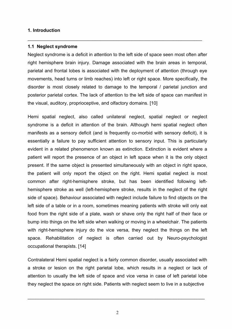
1.1 Neglect syndrome Neglect syndrome is a deficit in attention to the left side of space seen most often after
right hemisphere brain injury. Damage associated with the brain areas in temporal,
parietal and frontal lobes is associated with the deployment of attention (through eye
movements, head turns or limb reaches) into left or right space. More specifically, the
disorder is most closely related to damage to the temporal / parietal junction and
posterior parietal cortex. The lack of attention to the left side of space can manifest in
the visual, auditory, proprioceptive, and olfactory domains. [10]
Hemi spatial neglect, also called unilateral neglect, spatial neglect or neglect
syndrome is a deficit in attention of the brain. Although hemi spatial neglect often
manifests as a sensory deficit (and is frequently co-morbid with sensory deficit), it is
essentially a failure to pay sufficient attention to sensory input. This is particularly
evident in a related phenomenon known as extinction. Extinction is evident where a
patient will report the presence of an object in left space when it is the only object
present. If the same object is presented simultaneously with an object in right space,
the patient will only report the object on the right. Hemi spatial neglect is most
common after right-hemisphere stroke, but has been identified following left-
hemisphere stroke as well (left-hemisphere stroke, results in the neglect of the right
side of space). Behaviour associated with neglect include failure to find objects on the
left side of a table or in a room, sometimes meaning patients with stroke will only eat
food from the right side of a plate, wash or shave only the right half of their face or
bump into things on the left side when walking or moving in a wheelchair. The patients
with right-hemisphere injury do the vice versa, they neglect the things on the left
space. Rehabilitation of neglect is often carried out by Neuro-psychologist
occupational therapists. [14]
Contralateral Hemi spatial neglect is a fairly common disorder, usually associated with
a stroke or lesion on the right parietal lobe, which results in a neglect or lack of
attention to usually the left side of space and vice versa in case of left parietal lobe
they neglect the space on right side. Patients with neglect seem to live in a subjective
____________________________________________________________________

3
____________________________________________________________________
world that is skewed away from the left side. “In daily life, such patients may eat food
from only the right side of their plate, ignore people who approach from their left, miss
words on the left of the page when reading, and omit details on the left when copying
pictures, and so on”. They practically ignore all sounds and sites coming from their left
side. In case of left parietal lobe injury the Hemi spatial neglect syndrome patients
ignore the things on there right, addition to vision and sound, Hemi spatial neglect can
also affect motor function of the patient. Patients with Hemi spatial neglect, tend to
behave as if nothing of importance is expected to be happening in the left hemi space
or right hemi space and refrain from moving their left side or right side respectively.
There is also an emotional factor to this disorder. Patients with Hemi spatial neglect
sometimes have a profound hatred towards the left side and may even physically
abuse the left side. [9]
1.2 Neglect syndrome symptoms
• Failure to shave, groom or dress the left side of the body
• Failure to orient to events in the left hemi space.
• When copying drawings they omit detail on left side.
• When reading they fail to read the left half of each sentence.
• Hemiplegia due to failure to move the left limbs.
• Unable to recognize and accept the left side as being a part of their body.
• Delusional views concerning left side of body.
Hemi spatial neglect syndrome has at least three behavioural components. The
perceptual component involves patients paying attention only to the right side of
space. These patients can also give attention to the left side only if there is no stimulus
on the right side. In reality, a person will always be exposed to stimuli from both the
right and left side of space (light, sound, objects, etc.). Neglect behaviour also has a
motor component. Patients are disinclined to direct scanning, orienting and exploring
movements towards the neglected left hemi space. When blindfolded patients are
asked to manually retrieve small objects from a table, they show good movement with
either hand in the right hemi space but poor movement even with the right hand) into
____________________________________________________________________
4
____________________________________________________________________
the left hemi space of the table. The third component of neglect is motivational.
Patients with neglect tend to act as if there is nothing happening on the left side of
space that is of any importance. [9]
1.3 Directed attention and the Brain Hemi spatial neglect reflects a disturbance in the spatial distribution of directed
attention
(a) Objects on the patient's right-hand side easily capture their attention. They are
unable to withdraw their attention form objects on the right in order to attend to the left
hemisphere.
(b) Studies regarding Hemi spatial neglect syndrome in humans and monkeys suggest
that four cerebral regions provide an integrated network for directed attention. Each
component region has a unique functional role and gives rise to a different clinical type
of neglect when damaged.
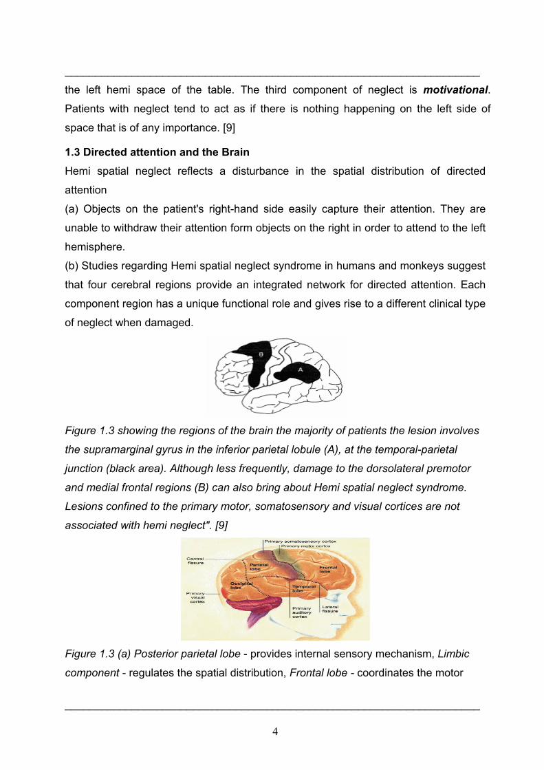
Figure 1.3 showing the regions of the brain the majority of patients the lesion involves
the supramarginal gyrus in the inferior parietal lobule (A), at the temporal-parietal
junction (black area). Although less frequently, damage to the dorsolateral premotor
and medial frontal regions (B) can also bring about Hemi spatial neglect syndrome.
Lesions confined to the primary motor, somatosensory and visual cortices are not
associated with hemi neglect". [9]
Figure 1.3 (a) Posterior parietal lobe - provides internal sensory mechanism, Limbic
component - regulates the spatial distribution, Frontal lobe - coordinates the motor
____________________________________________________________________
5
____________________________________________________________________
programs for scanning, reaching and exploring, Reticular component - provides levels
of arousal. Lesions in one of the components of this network cause only partial Hemi
spatial neglect, while lesions that encompass all the components result in huge deficits
and a more severe case of Hemi spatial neglect. [16]
1.4 Hemi spatial neglect and visual awareness
Patients with Hemi spatial neglect syndrome show a loss of visual awareness of the
left hemi space even though their primary visual cortex is intact and functional. The
most puzzling aspect of Hemi spatial neglect syndrome is why patients are unaware of
visual information on the left, even though nothing is wrong with their vision. Studies
have shown that when visual stimuli on both the left and right side is present, the
patient’s attention is fully captured by the visual stimuli on the right. The patient is
lacking the ability to give attention to the visual stimuli on the left, even though his
primary visual cortex is fully intact. Patients with hemianopia fail to see the left side of
space because of damage to their primary visual cortex. [9]
These patients cannot see the left side but they are aware that the left side exists and
do not have neglect. In order to see the other half of space, these patients will turn
towards their left side so that they can see from their good visual field. Patients who
have Hemi spatial neglect syndrome can see both sides of space but their mind
convinces them that only the right side is of importance.
Visual Awareness is the key to understanding Hemi spatial neglect syndrome patients.
Patients with Hemi spatial neglect don’t have the visual awareness that is necessary
to process visual signals from the left side. The parietal lobe is known to be
responsible for visual awareness because it integrates extra-retinal and retinal
information together. Now it makes sense why damage to the right parietal lobe can
lead to neglect.
The Hemi spatial neglect deficit differs greatly from the retinotopic scotoma patients
caused by damage the primary visual cortex of cerebral hemispheres in the brain. In
one study, a female patient with Hemi spatial neglect syndrome appeared to be blind
____________________________________________________________________
6
____________________________________________________________________
in the left visual field when she was looking straight ahead or to her left. However,
when she looked slightly to her right, she could then see objects in her left visual field.
This indicates that the visual information relative to her body and head was critical
(extra-retinal information), not the retinal position.
Hemi spatial neglect patients have trouble seeing objects in the left visual field, they
can turn their trunk slightly towards those objects and then they can see them (even
though the location where visual information hits their retina did not change). These
results show that the spatial visual signals which indicate the position of an object
relative to the head, body, or the hand, “can contribute to the spatial coordinates in
which Hemi spatial neglect arises”. This evidence from Hemi spatial neglect patients
suggests that the integration of retinal and extra-retinal information could play a role in
visual awareness. [11]
____________________________________________________________________
7
2. Basics ____________________________________________________________________
2. 1 Galvanic vestibular stimulation (GVS)
Galvanic vestibular stimulation is performed by passing small DC currents through the
vestibular labyrinth using surface electrodes. Typical stimulus configurations include
placing an electrode on each mastoid, one positive and one negative, to produce
medial – lateral sway or horizontal / torsional eye movements. Previous research and
clinical application have been limited by the requirement for relatively high sometimes
painful, electric currents to produce recordable horizontal eye movements. A
significant advantage of galvanic stimulation is that each labyrinth can be tested
separately. How ever, it is not yet certain which vestibular end organs are responsible
for either the eye movements or postural movements induced by such a stimulus.
Offsetting this limitation, however, is the fact that galvanic stimulation is believed to
excite the synapse between the hairy cell and the eighth cranial afferent nerve. As a
result, galvanic stimulation can provide information regarding ‘neural’ versus sensory
function. That is individuals with hairy cell damage with preserved eight nerve function
may have normal or increased responses to galvanic stimulation. However it is
technically challenging to deliver a well controlled galvanic stimulus while recording
eye movements or postural sway determine the stimulation effects. [8]
The technique provides a derived measure of vestibular function that relies upon the
ocular motor system. When recording postural responses during galvanic stimulation
there is an additional difficulty based on the complexity of the postural control system,
which is neither linear nor time invariant. As for Vestibulo-ocular reflex (VOR) tests,
recording postural sway during galvanic stimulation provides only a derived measure
of peripheral vestibular function. Further, the stimulus may produce a skin sensation
that cues the patient. Additional unresolved issues concerning the effect of galvanic
stimulation on postural sway include the influence of head- on- torso position the
waveform of the electrical stimulus, i.e. constant versus sinusoidal and the timing of
the galvanic stimulus with respect to the patient’s own sway. Despite these limitations
and unresolved issues, however, with the advent of three dimensional video-
oculography and lower cost motion analysis systems galvanic stimulation may emerge
as a clinically useful too. That is, low intensity galvanic currents may produce small but
___________________________________________________________________________

8
____________________________________________________________________
recordable non-horizontal eye movements and / or small but recordable postural
movements that can be measured reliably using sensitive recording instruments. [8]
2.1.1 Vestibular system
The vestibular system, or balance system, is the sensory system that provides the
dominant input about our movement and orientation in space. Together with the
cochlea, the auditory organ, it is situated in the vestibulum in the inner ear (Figure
2.1.1). As our movements consist of rotations and translations, the vestibular system
comprises two components: the semicircular canals, which indicate rotational
movements and the otoliths, which indicate linear translations. The vestibular system
sends signals primarily to the neural structures that control our eye movements, and to
the muscles that keep us upright. The projections to the former provide the anatomical
basis of the vestibulo-ocular reflex, which is required for clear vision and the
projections to the muscles that control our posture are necessary to keep us upright.
Figure 2.1.1 Human labyrinth, from the left ear. It contains i) the cochlea (yellow),
which is the peripheral organ of our auditory system; ii) the semicircular canals
(brown), which transduce rotational acceleration and iii) the otoliths in sacculus and
utriculus (in the blue/purple pouches), which transduces linear accelerations. The light
blue pouch is the endolymphatic sac, and contains only fluid. [14]
2.1.2 Semicircular canals
Our world has three spatial dimensions. Accordingly, our vestibular system contains
three semicircular canals in each labyrinth. They are approximately orthogonal to each
____________________________________________________________________
9
____________________________________________________________________
other, and are called horizontal, anterior, and posterior canal. (Alternatively, they may
be referred to as lateral, superior, and inferior, respectively)
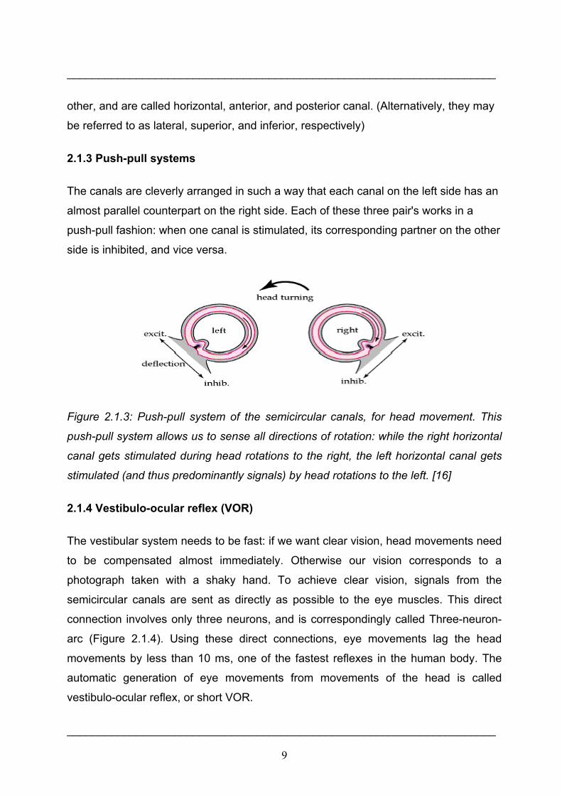
2.1.3 Push-pull systems
The canals are cleverly arranged in such a way that each canal on the left side has an
almost parallel counterpart on the right side. Each of these three pair's works in a
push-pull fashion: when one canal is stimulated, its corresponding partner on the other
side is inhibited, and vice versa.
Figure 2.1.3: Push-pull system of the semicircular canals, for head movement. This
push-pull system allows us to sense all directions of rotation: while the right horizontal
canal gets stimulated during head rotations to the right, the left horizontal canal gets
stimulated (and thus predominantly signals) by head rotations to the left. [16]
2.1.4 Vestibulo-ocular reflex (VOR)
The vestibular system needs to be fast: if we want clear vision, head movements need
to be compensated almost immediately. Otherwise our vision corresponds to a
photograph taken with a shaky hand. To achieve clear vision, signals from the
semicircular canals are sent as directly as possible to the eye muscles. This direct
connection involves only three neurons, and is correspondingly called Three-neuron-
arc (Figure 2.1.4). Using these direct connections, eye movements lag the head
movements by less than 10 ms, one of the fastest reflexes in the human body. The
automatic generation of eye movements from movements of the head is called
vestibulo-ocular reflex, or short VOR.
____________________________________________________________________

10
____________________________________________________________________
Figure 2.1.4: Three-neuron arc, during a head movement to the right. 8th cranial
nerve, from the peripheral vestibular sensors to vn, the vestibular nuclei in the
brainstem. VI abducens nucleus. The medial longitudinal fascicle (mlf) projects from
the abducens nucleus to III, the oculomotor nucleus. The left lateral rectus muscle lr
and the right medial rectus muscle mr get contracted, turning the eyes to the left. The
green objects are excited, the orange ones inhibited. [10]
This reflex, combined with the push-pull principle described above, forms the
physiological basis of the Rapid head impulse test or Halmagyi-Curthoys-test, when
the function of the right balance system is reduced by a disease or by an accident,
quick head movements to the right cannot be sensed properly any more. As a
consequence, no compensatory eye movements are generated, and the patient
cannot fixate a point in space during this rapid head movement.
2.1.5 Mechanics
The mechanics of the semicircular canals can be described by a damped oscillator. If
we designate the deflection of the cupula with θ, and the head velocity with,
the cupula deflection is approximately
____________________________________________________________________

11
____________________________________________________________________
α is a proportionality factor, and s corresponds to the frequency. For humans, the time
constants T1 and T2 are approximately 3 ms and 5s, respectively. As a result, for
typical head movements, which cover the frequency range of 0.1 Hz and 10 Hz, the
deflection of the cupula is approximately proportional to the head acceleration velocity.
This is very useful, since the velocity of the eyes must be opposite to the velocity of
the head in order to have clear vision. [10]
2.1.6 Central processing
Signals from the vestibular system also project to the cerebellum (where they are used
to keep the VOR working, a task usually referred to as learning or adaptation) and to
different areas in the cortex. The projections to the cortex are spread out over different
areas, and their implications are currently not clearly understood.
2.1.7 Otoliths
Figure 2.1.7: Otolith or otoconia is a structure in the saccule or utricle of the inner ear.
It is comprised of a combination of a gelatinous matrix and calcium carbonate crystals.
Otolith crystals are relatively dense and heavy - they are connected to the rest of the
body by the sensory processes of the macular cells. [15]
The otolith organs (the utricle and the saccule) are structures in the inner ear,
specifically in the semicircular canals, that are sensitive to gravity and linear
acceleration. Because of their orientation in the head, the utricle is sensitive to a
change in horizontal movement, and the saccule gives information about vertical
acceleration (such as when in an elevator). Otoliths are small particles of calcium
____________________________________________________________________
12
____________________________________________________________________
carbonate in the viscous fluid of the saccule and utricle. The inertia of these small
particles causes them to stimulate hair cells when the head moves. The hair cells send
signals down sensory nerve fibres, which are interpreted by the brain as motion. The
interpretation of the rotation signals from the semicircular canals is straightforward, the
interpretation of otoliths signals is more difficult, since gravity is equivalent to a
constant linear acceleration we somehow have to distinguish otoliths signals that are
caused by linear accelartion such as those caused by gravity. We can do that quite
well, but the neural mechanisms underlying this separation are not yet fully
understood.
2.1.8 Pathologies
Diseases of the vestibular system can take different forms, and usually induce vertigo
and instability, often accompanied by nausea. The most common ones are vestibular
neuritis, also called Labyrinthitis, and BPPV (Benign Paroxysmal Positional Vertigo). In
addition, the function of the vestibular system can be affected by tumours on the
cochleovestibular nerve, an infarct in the brain stem or in cortical regions related to the
processing of vestibular signals, and cerebellar atrophy. Less severe, but often also
with large consequences, is vertigo caused by the intake of large amounts of alcohol.
2.1.9 Benign paroxysmal positional vertigo (BPPV)
Benign paroxysmal positional vertigo (BPPV) is probably caused by pieces that have
broken off from the otoliths, and have slipped into one of the semicircular canals. In
most cases it is the posterior canal that is affected. In certain head positions, these
particles push on the cupula of the canal affected, which leads to dizziness and
vertigo. This problem occurs rather frequently, often after hits to the head or after long
bed rest. The tell-tale sign of BPPV are vertigo attacks which repeatable appear when
the head is brought into a specific orientation. In most cases BPPV can be eliminated
(for the patient in an almost miraculous way) by lying down, bringing the head in the
right orientation and sitting up quickly. [14]
____________________________________________________________________
13
3. Material and methods ____________________________________________________________________
3.1 Methods of Stimulation
The objective of the electrical stimulation system is excitation of the desired
physiological effect. The desired physiological effect may be considerably different in
therapeutic as opposed to functional applications. The electrode type used to elicit the
physiological response may thus be quite different. The considerations for selection of
electrode type that must be included are the selectivity and gradation of excitation
required, the repeatability from one application to the next and the allowable level of
invasiveness. Two types of electrodes are used surface (or cutaneous) and
subcutaneous, all of which are applied externally.
Surface electrodes include a wide variety of specific types, each of which is placed on
the skin surface over the area where the stimulus is to be delivered. Placement is on
the individual muscle or muscle group, the peripheral nerve, or over cutaneous skin
afferents for the case in which sensory activation is the objective.
Surface electrodes have low impedance, and even distribution of current, flexibility to
maintain good skin contact ease of application and removal suitable mounting for days
without irritation to the skin. Each of the surface electrode configurations has three
elements the conductor, the interfacial layer and the adhesive.
Surface electrodes generally have a geometric surface area of 5cm2 or larger. They
may be applied in either a monopolar configuration or a bipolar configuration. In the
monopolar configuration, the working electrode is placed over the nerve to be excited
and the counter (or indifferent) electrode, which is larger in surface area, is placed
remotely. In the bipolar configuration, the most common for surface stimulation, both
electrodes typically are the same size and are placed over the site to be excited.
The stimulus parameters required for activation over surface electrodes are dependent
on the stimulus waveform, the surface area, electrode materials, placement, skin
impedance, current density and other factors. Typically, for the rectangular pulsatile
waveform frequently used, threshold values are 10 mA. [6]
____________________________________________________________________
14
____________________________________________________________________
3.1.1 Caloric vestibular stimulation One technique to influence the vestibular system is the caloric vestibular stimulation
which is not in use today anymore. When around 20 cc of ice water is squirted into the
left ear of the Hemi spatial neglect syndrome patient for approximately 1min, dramatic
improvements in visual and personal Hemi spatial neglect syndrome are observable in
many, but not all, cases a similar result is obtained when a similar amount of warm
water is inserted into patients right ears, also found temporary remission of
hemianaesthesia following vestibular stimulation. The precise mechanisms for this
effect are at present unknown. This method is very unpleasant and therefore not
feasible for therapeutic application. [10]
3.1.3 Constant current vs constant voltage
A constant-current stimulator attempts to maintain a specified current between its
output terminals, regardless of the load that is connected between the terminals. A
constant-voltage stimulator attempts to maintain a specified voltage.
Although both kinds of stimulator can work satisfactorily for nerve stimulation, the
constant current type has the advantage of greater consistency in threshold stimulus
strength, because the effectiveness of a stimulus is related directly to the current
density. Variations in the load do not affect the current from a constant current
stimulator, provided only that they are not as extreme as to cause the stimulator to
exceed its compliance voltage.
3.1.4 Stimulus generation
The stimulus that is delivered to the nerve should achieve the desired result (e.g.
evoke the action potential) without deleterious effects to the tissue or to the electrode.
Output impedance to the stimulus circuit determines the degree to which changes in
load (i.e. impedance due to leads, electrodes, skin interfaces, and tissue) alter the
actual stimulus delivered to the tissue. High-output impedance devices will deliver the
set current to the tissue, regardless of the changes in load (e.g. tissue drying) up to
____________________________________________________________________

15
____________________________________________________________________
the voltage capacity available. These constant current stimulators are more properly
called current-regulated stimulators. Devices having low-output impedance, constant-
voltage stimulators, will change the delivered stimulus with change in load. Because
the user is generally unaware of the precise load at any point in time, most stimulator
devices are current regulated so that the consequences of modest impedance
changes can be ignored.
The stimulus waveform selected for the excitation process must take into
consideration the desired physiological effect (action potential generation), potential
damage to the tissue and the potential degradation of the electrode. The waveform
selected generally is rectangular. A non rectangular pulse could be utilized, but the
rise time must be sufficiently fast that the nerve membrane does not accommodate
and fail to fire if an action potential is wanted. The stimulus waveform may be
unidirectional (monophasic) or bidirectional (biphasic).
Biphasic stimulus is recommended for several reasons. Surface stimulation is more
safe with biphasic than monophasic stimulation. Tissue damage is believed to be
significantly related to the pH change at the electrode tissue interface. At the cathode,
the pH may increase due to the production of OH- , while at the anode the
environment will become more acidic. While there exists some buffering capacity of
pH changes in the tissue, the changes with monophasic stimulation are greater than
those with biphasic. Although reactions at the electrodes are not completely reversed
with the biphasic stimulation, this stimulus allows significantly greater charge injection
before tissue damage is encountered. [7]
____________________________________________________________________
16
____________________________________________________________________
3.2.1 Concept of Galvanic vestibular stimulation unit (GVS)
For designing any medical equipment several safety regulations have to be followed.
According to the IEC 60601-1 Medical safety regulations the GVS unit that is to be
designed should obey certain rules. In designing we had to follow the requirements
given by the researchers. They want to use the equipment to develop new, mild, and
effective GVS stimulation for the therapeutic treatment of neglect patients and
therefore this new device will be applied to patients. Unfortunately the flexibility
needed by the researchers is somehow in contradiction to the safety regulations. To
overcome this problem we decided to develop a current controlled GVS device whose
stimulation current follows linearly an externally applied voltage over a broad
frequency range. A galvanic decoupling within the GVS device is amended and also a
micro controller based control unit to double check the control voltage, the applied
stimulation voltage and current. With a direct access that can be controlled by a switch
to disconnect the patient from the GVS device so as to protect the patient from any
electricity based harm.
3.2.2 Specifications of the Galvanic vestibular stimulation unit (GVS) For designing the equipment according to the flexibility and way of testing of clinicians
and researchers, we were provided with certain specifications to fulfil there needs of
testing the GVS unit on the Hemi spatial neglect syndrome patient. The following are
the specifications given to us.
Table 3.2.2: Specifications of GVS unit
S.no Description Range
1 Voltage range 0 to ± 35V
2 Current range 0 to ± 7.5mA
3 Bandwidth 0 to 10 kHz
4 Security shutdown after 2 hours
5 Two channels ± polarity
6 Isolation Voltage 1 KV
____________________________________________________________________

17
____________________________________________________________________
These specifications as shown in ‘table 4.1’ were to be achieved while obeying the
safety regulations of medical equipment.
3.2.3 General safety regulations IEC 60601-1 The International technical committee (IEC) came up with certain general safety
regulations. These safety regulations have to be kept in mind before designing any
medical equipment. EQUIPMENT shall, when transported, stored, installed, operated
in NORMAL USE, and maintained according to the instructions of the manufacturer,
cause no SAFTEY HAZARD which could reasonably be foreseen and which is not
connected with its intended application, in NORMAL CONDITION and in SINGLE
FAULT CONDITION. EQUIPMENT or parts thereof, using materials or having forms of
construction different from those detailed in this Standard, shall be accepted if it can
be demonstrated that an equivalent degree of safety is obtained.
The following SINGLE FAULT CONDITIONS are the subject of specific requirements
and tests in this Standard:
a) interruption of a PROTECTIVE EARTH CONDUCTOR
b) interruption of one supply conductor
c) appearance of an external voltage on an F-TYPE APPLIED PART
d) appearance of an external voltage on SIGNAL INPUT or on a SIGNAL
OUTPUT PART
e) leakage of the ENCLOSURE of a FLAMMABLE ANAESTHETIC MIXTURE
WITH OXYGEN OT NITROUS OXIDE
f) failure of an electrical component which might cause SAFTEY HAZARD
g) failure of mechanical parts which might cause SAFTEY HAZARD
h) failure of temperature limiting devices
Where a SINGLE FAULT CONDITION results unavoidably in another SINGLE FAULT
CONDITION, the two failures are considered as one SINGLE FAULT CONDITION.
The following phenomena are considered by this Standard as unlikely to occur:
a) Total electrical breakdown of DOUBLE INSULATION
b) Electrical breakdown of a REINFORCED INSULATION
____________________________________________________________________
18
____________________________________________________________________
c) Interruption of a fixed and permanently installed PROTECTIVE EARTH
CONDUCTOR.
Earthing of a PATIENT is considered as a NORMAL CONDITION.
Unless otherwise specified in the instructions for use, EQUIPMENT shall not be
required to withstand the effects of operation under separate dust covers or sterile
covers. Compliance with the requirements of this clause is considered to exist when
the criteria of the relevant inspections and tests in this standard are achieved
(IEC60601). [7]
To design any medical equipment these general safety considerations are to be
considered. So we had to think of a design which would follow these regulations and
our purpose of the equipment is therefore fulfilled. The GVS unit was designed and
implemented considering the safety hazards to avoid any kind of electrical shock
hazards to the patient. Several optocouplers have been used to provide total isolation
and insulation. The device will be shutting down itself if it exceeds the desired output
voltages, with the help of a fuse. Proper earthing is given to the entire device if in case
of a short circuit will ensure no harm is caused to the patient by any of the components
on the board.
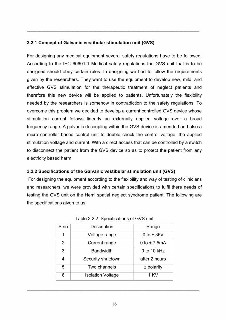
3.2.4 Galvanic vestibular stimulation unit system design
Figure 3.2.4 Block diagram showing the various components in the system design
____________________________________________________________________

19
____________________________________________________________________
The basic idea was to design a galvanic vestibular stimulation device with a current
source following the researcher’s needs for flexibility for any experimental setup and
additionally considering very strictly the safety regulations for medical devices. There
are several aspects which we have considered in our design such as the isolation
voltage, which is limited with the help of optocouplers which carry out galvanic
decoupling. The analog inputs from the two channels are being passed through the
optocoupler to protect the patient with any kind of electric shock. The voltage should
be regulated, so we have used voltage regulators which can shutdown if they are
exceeding the voltage limits. To protect the overload in case of a short circuit, a fuse is
also being implemented to shut down the entire supply given from the battery. A
switch is implemented in the power supply to turn of the device and the supply given to
the patient at the two channels. We made use of relays to avoid any kind of
inconsistency in the supply. All the operational amplifiers are being provided with
capacitors to prevent any kind of overload or noise at the outputs.
The switch is capable of enabling or disabling the patient contact. To ensure constant
supply, we have special operational amplifiers have been used only for measurement
purposes such as the voltage and current outputs. To make a proper analysis of the
analog input/output supply a continuous monitoring of the output voltages is also a
priority to double check what the patient is provided with. An micro controller based
control unit to double check the control voltage and the applied stimulation voltage and
current with direct access to the switch to disconnect the patient from the GVS device
should protect the patient from any electricity based harm. However the design of this
control unit was not part of this project.This device is also being provided with
programmable timer which shall stop the supply to the patient after e.g. 2 hours to
ensure patients security. The device after being designed has to undergo various tests
before being implemented on a neglect patient. Various safety regulations have been
followed as per the International Electro technical Committee (IEC) published IEC
61010-1.
____________________________________________________________________

20
4. Results ____________________________________________________________________
4.1.1 Design of current source "TEST CASE"
The task was to design a circuit for a constant current controlled stimulator, adapting
change in loads and which can work both long lasting constant current stimulation and
short high frequency pulsed current stimuli. With a proceeded ‘miniproject’ a current
source with different specifications had been developed. The required parameters
were:
1. Current amplitude 0 - 7.5 mA
2. Voltage range 0 – 35 V
3. Max load up to - 1.5 kΩ
4. Response time to changes in load ~100 µs
5. Frequency changes of stimulation 0 – 5 KHz
The necessary changes were due to different specifications. It can act equally well in
any application where a low power external stimulator with adjustable current and
pulse width is required and is also suitable for use with surface electrodes. It is an
analog circuit which is using a power source of 5V DC supply. The circuit is designed
using 5spice software for simulation.
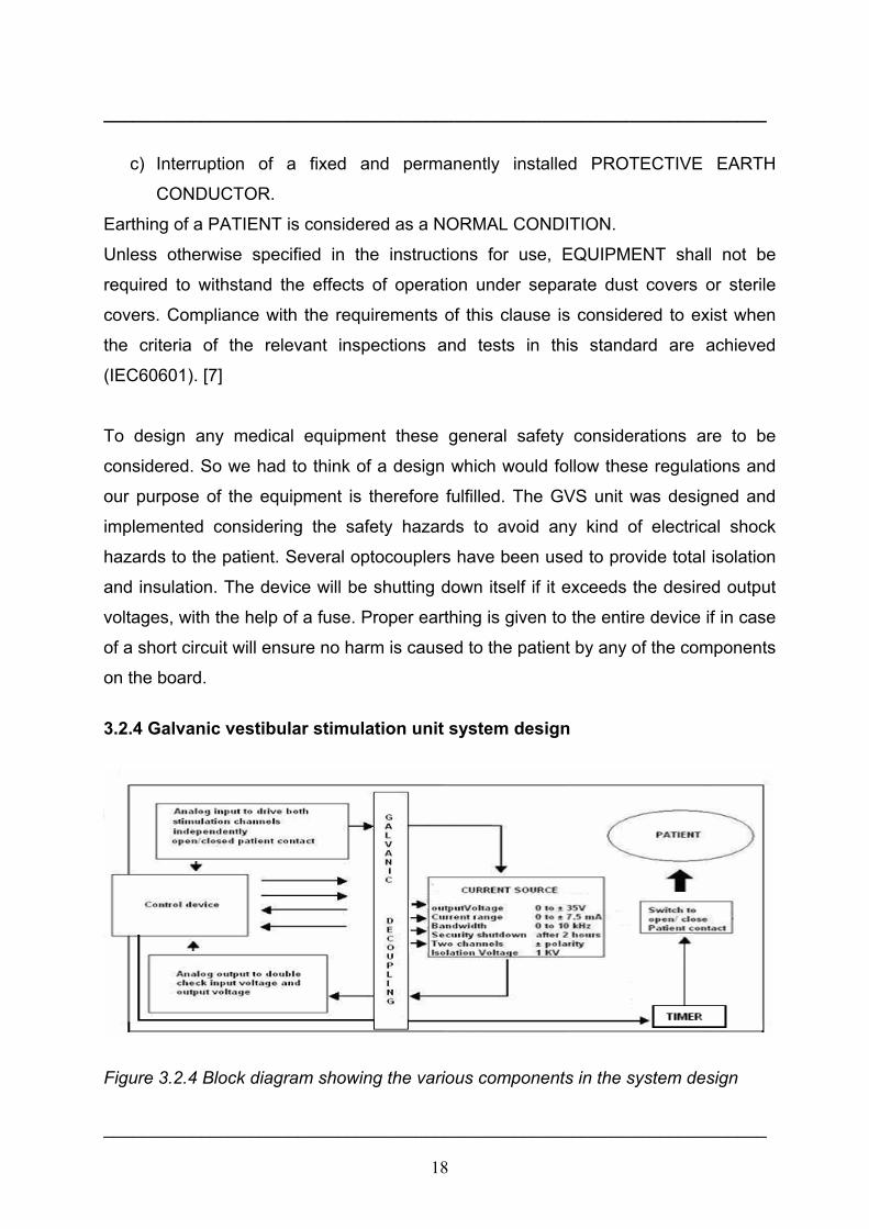
4.1.2 Task of operational amplifiers (opamps)
The concept is based on operational amplifiers (opamp), with feed back voltage
measured on the output. Operational amplifier in general has five pins, two of those
are inputs, two of the pins are supply pins and finally there’s an output pin. Some
opamps may have more pins for external compensation. Some opamps have
shutdown pins and some may have a differential output stage. Opamps must have
very high input impedance, very high open loop gain and very low output impedance.
It is not possible to achieve all these in one single stage. Opamps generally have three
different stages.
Stage1: The first stage is a differential amplifier. Stage2: The second stage is the
gain stage and finally the third stage is the output stage of the operational amplifier.
____________________________________________________________________
21
____________________________________________________________________
Figure 4.1.2: Operational amplifier (opamp) block diagram, showing various stages
Stage1 (Differential Amplifier Stage):
• Provides differential input for the opamp
• Provides dc gain
• Has very high input impedance which draws negligible input current and enables
user to utilize ideal opamp equations for circuit analysis.
The next stage of the opamp is the voltage gain stage. This gain stage is mainly
responsible for gaining up the input signal and sending it to the output stage.
Stage2 (HIGH gain voltage amplifier):
• Provides the “gain” of the amplifier
• Gains up the differential signal from input and conveys it to the output stage.
Stage3 (Low Impedance output stage):
• Delivers current to the load
• Very low impedance output stage - To minimize loading the output of the op-
amp may have short circuit protection.
The opamp must have very low output impedance. This minimizes the loading of the
output of the opamp by stage of the opamp. The output stage delivers current to the
opamp’s load and it may or may not have short circuit protection.
____________________________________________________________________
22
____________________________________________________________________
Inputs of operational amplifier
Two input terminals
• Positive Input (Non-Inverting)
• Negative Input (Inverting)
Can be used in three different “input” modes
• Different input mode
• Inverting Mode
• Non-Inverting mode
Differential input mode
• Both input terminals are used
• Input signals are 180° out of phase
• Output is in phase with non-inverting input
In general, operational amplifier (opamp) can be setup in three different input modes.
These three are differential input mode, inverting input mode and non-inverting input
mode. In the differential input mode, the signal is applied to both of the input terminals.
These signals have to be out of phase and the output is going to be completely in
phase with the non-inverting signal. In case the signals that are applied to both the
inputs are in phase, there should be no output and that input signal is referred to as
the common mode signal. The output is grounded or output is sitting at mid-supply or
output is zero. So basically we have a negative voltage and a positive voltage on the
supply ends of the opamp.
Inverting mode
• Non-Inverting input is grounded (connected to mid-supply)
• Signal is applied to the inverting input
• Output is 180 out of phase with input
____________________________________________________________________
23
____________________________________________________________________
In the inverting mode the non-inverting input of the amplifier is grounded or it’s
connected to mid-supply. Input signal is applied to the negative input and the output
signal is completely out of phase with the input signal.
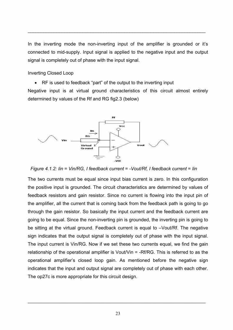
Inverting Closed Loop
• RF is used to feedback “part” of the output to the inverting input
Negative input is at virtual ground characteristics of this circuit almost entirely
determined by values of the Rf and RG fig2.3 (below)
Figure 4.1.2: Iin = Vin/RG, I feedback current = -Vout/Rf, I feedback current = Iin
The two currents must be equal since input bias current is zero. In this configuration
the positive input is grounded. The circuit characteristics are determined by values of
feedback resistors and gain resistor. Since no current is flowing into the input pin of
the amplifier, all the current that is coming back from the feedback path is going to go
through the gain resistor. So basically the input current and the feedback current are
going to be equal. Since the non-inverting pin is grounded, the inverting pin is going to
be sitting at the virtual ground. Feedback current is equal to –Vout/Rf. The negative
sign indicates that the output signal is completely out of phase with the input signal.
The input current is Vin/RG. Now if we set these two currents equal, we find the gain
relationship of the operational amplifier is Vout/Vin = -Rf/RG. This is referred to as the
operational amplifier’s closed loop gain. As mentioned before the negative sign
indicates that the input and output signal are completely out of phase with each other.
The op27c is more appropriate for this circuit design.
____________________________________________________________________
24
____________________________________________________________________
4.1.3 Operational amplifier (op27c)
The op27c is a precision operational amplifier combines the low offset and drift of the
op07 with both high speed and low noise. Offsets down to 25µV and maximum drift of
0.6µV/C, makes the ‘op27’ ideal for the precision instrumentation applications.
Exceptionally low noise, en = 3.5nV/√(Hz), at 10Hz, a low 1/f noise corner frequency of
2.7Hz and high gain, allow accurate high gain amplification of low-level signals. A
gain-bandwidth product of 8MHz and a 2.8V/µsec slew rate provides excellent
dynamic accuracy in high-speed, data acquisition systems. A low input bias current of
±10nA is achieved by use of a bias-current cancellation circuit. Over the military
temperature range, this component typically holds input bais current (IB) and input
offset current (IOS) to ± 20nA and 15nA, respectively. The output stage has good load
driving capability. A guaranteed swing of ±10V into 600Ω and low output distortion
make the op27c an excellent choice. [4]
4.1.4 Test circuit components:
Table 4.1.4: Test circuit components
S.no Description quantity
1 Opamp OP27 2
2 Resistors R6,R5 (1kΩ) 2
3 Resistor R (1.51kΩ) 1
4 Ammeter, Tpi 1
5 Resistor R8, R3 100Ω 2
6 Resistor R7 -50Ω 1
7 Voltage source 5V 1
8 Tpv1 , test point 1
9 Ui , test point 1
10 Ua , test point 1
11 Tpi , test point 1
____________________________________________________________________

25
____________________________________________________________________
4.1.5 Simulation with 5Spice 5Spice is a general-purpose electronic circuit simulation program with a full graphical
user interface. It wraps around a traditional Spice simulation engine, presenting a
single application to the user. 5Spice provides specific schematic entry, the ability to
define and save an unlimited number of analyses and graph setups, and integrated
graphing of simulation results. Spice concepts like sub circuits, coupled inductors,
nonlinear functions, initial conditions and node voltages are represented visually in the
schematic. The simulation engine is based on Spice version 3.4/3.5 with syntax
extensions for improved compatibility with PSpice® sub circuits.
The program is intended to provide the analysis and documentation capabilities
needed by experienced circuit designers while remaining easy to use - a step up from
student oriented Spice programs. The focus is on analog circuit analysis and circuit
design at the component level. 5Spice provides ‘DC Bias’, ‘non-linear analyses’: DC,
Transient, Harmonic Distortion and DC Sensitivity and ‘linearized analyses’: AC and
‘Noise analysis’. ‘AC Sensitivity’ analysis is expected soon. Results of Distortion,
Noise and Sensitivity analyses are displayed only after the program has been
registered. Circuits may contain resistors, capacitors, inductors, transformers (coupled
inductors), transmission lines, independent voltage and current sources, four types of
linear dependent sources, non-linear (arbitrary formula) dependent sources, linear
opamps, switches, and semiconductor devices: diodes, Bipolar Junction Transistor
(BJT’s), junction field effect transistor (JFET) and Metal-Oxide Semiconductor Field-
Effect Transistor (MOSFET). Specific device Models as well as sub circuits built from
parts listed above may be stored in the program’s library and represented by symbols
in the schematic. Almost all manufacturer supplied sub-circuits will work.
4.1.6 Analysis in 5Spice Analysis consists of a 5Spice simulation such as:
DC bias, DC, AC, Transient, Noise, Distortion and
• Parameters defining the simulation,
• An associated graph (DC bias has no graph)
____________________________________________________________________
26
____________________________________________________________________
• A selection list of the voltage and current Signal Sources that will be active during
the analysis.
• At least one Test Point that defines the circuit point for graphing or table of
results.
Selecting, creating and editing of analyses and associated graphs are performed using
the Analysis dialog. Open the Analysis dialog through Main Menu Analyze. There is
an Analysis RUN button at the top of the vertical toolbar. [12]
4.1.7 Circuit Analysis To perform an analysis, each circuit node must have a DC path to ground unless it is
terminated with a ‘No Connect symbol’. (Circuitry with no AC or DC connection to
ground whatsoever is ignored during analysis). There must be at least one ground
symbol in the schematic. The circuit was initially simulated using 5Spice software,
where we have assembled all the above said components. The simulation was carried
out by putting up test points such as the ammeter (Tpi) and voltage test point (Tpv1).
The current (Ui) was measured using this test point. The 5Spice software was enabled
to make a simulation and learn the circuit outputs at various test points. Voltage and
current outputs were studied to make a proper circuit design. The circuit stimulation
using the software is represented in below in fig 4.7.
4.1.7 Test Circuit diagram
The below circuit below was modified by placing in a relay/switch in between the two
loads as shown below in figure 4.1.7. The opamp enables the circuit to switch between
the two loads. From the figure 4.1.7, we can see that we have made use of two
OP445A opamps which are additionally supplied with several resistors, battery supply
and a voltage source. A relay is implemented across the load resistor, which gives us
the flexibility to switch between the loads. Before implementing the above circuit we
had to simulate the circuit using 5spice simulation software. After achieving the
required results we had to proceed with the assembling of the components on a PCB
(printed circuit board) board.
____________________________________________________________________
27
____________________________________________________________________
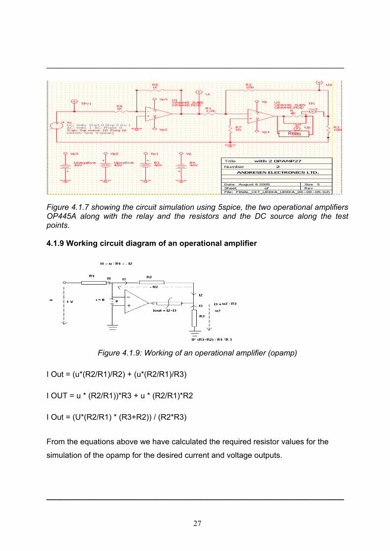
Figure 4.1.7 showing the circuit simulation using 5spice, the two operational amplifiers OP445A along with the relay and the resistors and the DC source along the test points. 4.1.9 Working circuit diagram of an operational amplifier
Figure 4.1.9: Working of an operational amplifier (opamp)
I Out = (u*(R2/R1)/R2) + (u*(R2/R1)/R3)
I OUT = u * (R2/R1))*R3 + u * (R2/R1)*R2
I Out = (U*(R2/R1) * (R3+R2)) / (R2*R3)
From the equations above we have calculated the required resistor values for the
simulation of the opamp for the desired current and voltage outputs.
____________________________________________________________________

28
____________________________________________________________________ 4.1.10 Circuit simulation for DC & Transient bias
The DC-Bias simulation of the circuit gave these values below considering the various
test points. Ua, Ui and TPv1 as shown in figure below.
Figure 4.1.10: The DC simulation values of the circuit that were achieved after the
simulation of the circuit.
The values in figure 5.9 are as follows:
The test points Ua = -1.326*10-6 A
The test point Ui = -1.4271* 10-6 A
The test point TPv1 = -1.2915*10-12 V
The test point Up = 4.9012*10-5 A
The test point TPi = -1,225*10-8 A
The test point ‘Ua’ near the load resistor, gave us a current of 1.326*10-6 A. The test
point ‘Ui’ after the first opamp ‘op445’ gave us the current value of -1.4271* 10-6 A. The
test point ‘Tpv1’ which is taken after the voltage source was -1.2915*10-12 V. The test
point of ‘Up’ across the load resistor was 4.9012*10-5 A. The test point ‘Tpi’ after the
load resistor gave us the current value of -1,225*10-8 A. These values ensured us of a
proper output from the simulated circuit.
____________________________________________________________________

29
____________________________________________________________________ 4.1.11 The transient analysis
Figure 4.1.11: The transient simulation analysis graph of the circuit
From figure 4.1.11, we can see that, the transient analysis achieved the desired
voltage and current ranges. On the right y-axis we have the current ranging from ±10
mA. The voltage ranges between ±40 V on the left y-axis. The time range on the x-
axis is starting from 0 to 2 ms. The voltage 'Up' starts from zero and ranges up to ±35
V approximately. The current ranges from ±8.5 mA. Seeing this result we have
proceeded with the circuit assembly.
4.2.1 Testing of the current source circuit
After the circuit designing was complete we built up a test setup for testing the circuit.
This included various test equipments such as the DC power supply, DC voltage
regulator and an oscilloscope.
4.2.2 Circuit assembled on board
The circuit assembly was done on a single layer printed circuit board (PCB) of 10*6.8
cm, the circuit design was made with the proper assembly and there by soldering was
done according to the circuit design as shown below in figure 6.5. This is the final built
in Test circuit on the PCB board.
____________________________________________________________________

30
____________________________________________________________________
Figure4.2.2: The designed test circuit
4.2.3 Principal test setup of the circuit
Figure 4.2.3: The principal test setup of the circuit showing, DC power supply,
oscilloscope, DC voltage regulator.
DC power supply: - The DC power supply is a constant voltage generator gives a
voltage of 5 V to the circuit input.
DC Voltage regulator: - The voltage is regulated by the DC voltage regulator; it
maintains adequate power supply as per our settings.
Circuit load: - The circuit loads, load1 and load2 where the opamps switch between
with the help of the relay/switch.
Oscilloscope: - The outputs in the form of graphs were collected at the load and can
be viewed in the form of graphs by using the oscilloscope.
____________________________________________________________________
31
____________________________________________________________________ The circuit after designing was made to test by the above said setup. The DC power
supply provides a voltage of 5 V to the circuit the voltage was regulated by the voltage
regulator. The DC power supply and the DC voltage regulator provided adequate
power supply to the circuit. The opamps after receiving this power supply react to the
input voltage supply and thereby enable the circuit loads to switch between loads
(load1 & load2). The oscilloscope was connected at the output loads which enabled us
to take the graphs for the time delay and the response time. The graph values were
there by stored in a floppy with the oscilloscope and then reopened with Microsoft XL.
The time delay and the response of the loads were studied by this setup. The values
that were collected on testing the circuit were reused to plot the graphs of Time delay
and the response of the load.
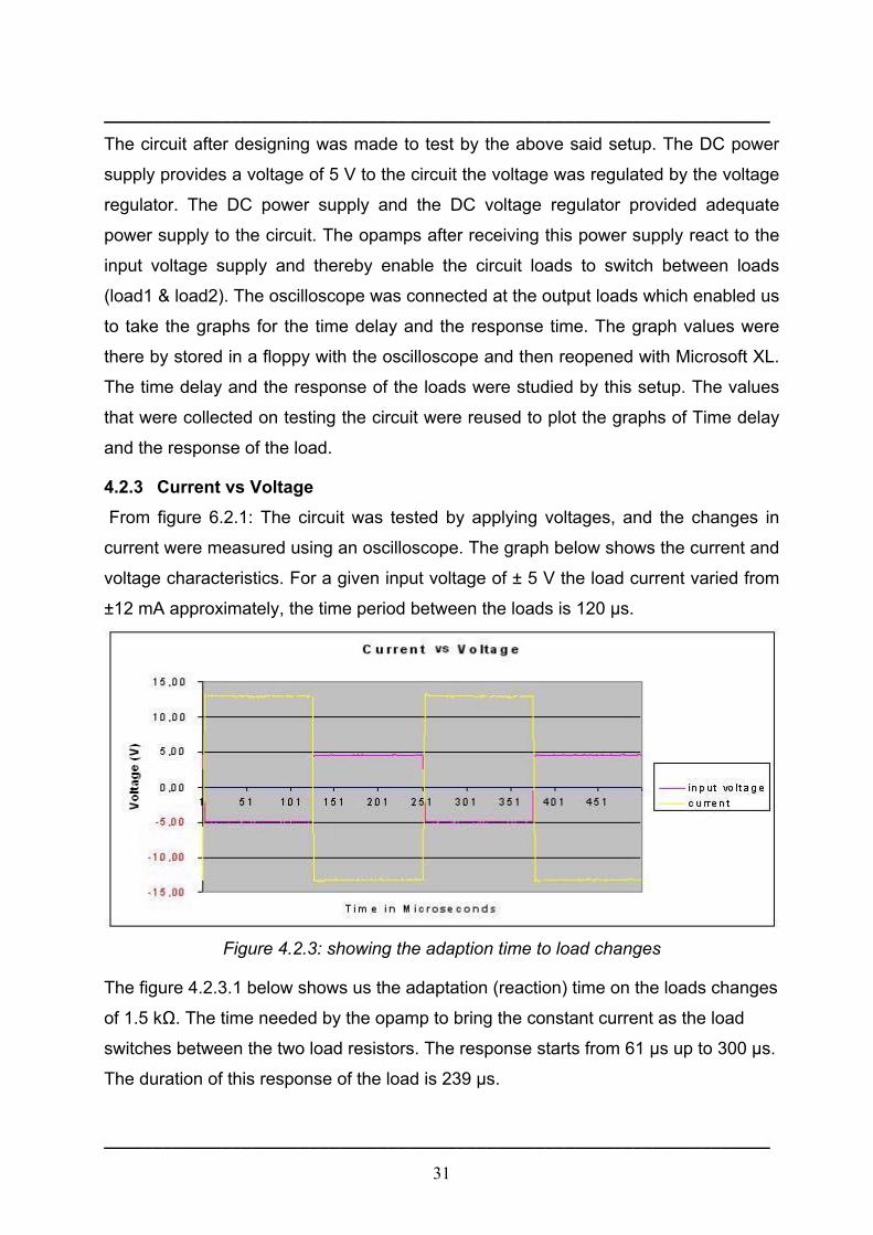
4.2.3 Current vs Voltage From figure 6.2.1: The circuit was tested by applying voltages, and the changes in
current were measured using an oscilloscope. The graph below shows the current and
voltage characteristics. For a given input voltage of ± 5 V the load current varied from
±12 mA approximately, the time period between the loads is 120 µs.
Figure 4.2.3: showing the adaption time to load changes
The figure 4.2.3.1 below shows us the adaptation (reaction) time on the loads changes
of 1.5 kΩ. The time needed by the opamp to bring the constant current as the load
switches between the two load resistors. The response starts from 61 µs up to 300 µs.
The duration of this response of the load is 239 µs.
____________________________________________________________________
32
____________________________________________________________________
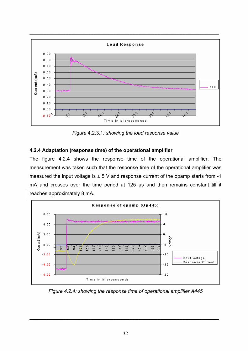
Figure 4.2.3.1: showing the load response value
4.2.4 Adaptation (response time) of the operational amplifier The figure 4.2.4 shows the response time of the operational amplifier. The
measurement was taken such that the response time of the operational amplifier was
measured the input voltage is ± 5 V and response current of the opamp starts from -1
mA and crosses over the time period at 125 µs and then remains constant till it
reaches approximately 8 mA.
Figure 4.2.4: showing the response time of operational amplifier A445
____________________________________________________________________
33
____________________________________________________________________ 4.2.4 Voltage vs Load From the graph 4.2.4 below the load measurement shows the changes in voltage over
the load at a frequency of 1 kHz. As seen above from the values of the graph, the load
current remains constant. Starting from zero reaching approximately ±14 mV and the
time period between them is measured to be 0.5 ms.
voltage over the Load @ 1kHz
-15
-10
-5
0
5
10
15
0 0,5 1 1,5 2
time [ms]
Volta
ge [V
]
Figure 4.2.4: showing the Voltage over the load graph
After successfully testing with the test circuit for the current source, the complete GVS
device was planned to be made using Protel which is more sophisticated software,
used in ZEL (Central Institute for Electronics, Research Centre Juelich) for various
circuit designs. The difference between the earlier mini project (CONSTANT
CURRENT STIMULATION CIRCUIT DESIGN FOR THE BRAIN) is that it had different
requirements compared to the Main project test circuit. To achieve the requirements of
the Main project test circuit we had to use different operational amplifier op445A where
as previously we used operational amplifier op27.
Table 4.2.4: showing the specifications of Mini and Main project
S.no Description Miniproject
(test circuit)
Main project
(test circuit)
1 Current range 0 to ±10 mA 0 to ±7.5 mA
2 Voltage range 0 to ±15 V 0 to ±35 V
3 Max loads 1.5 kΩ 6.5 kΩ
4 Response time 5 µs µseconds
____________________________________________________________________

34
5. Results II ____________________________________________________________________ 5.1 Galvanic vestibular stimulation unit design After the test circuit being successfully tested and implemented we have proceeded
with Protel for a final circuit assembly following the safety regulations. Perhaps the
greatest challenge when working on a complex electronics design is managing the
large number of design objects. From the components, net labels and text strings on
the schematic sheets, through to the hundreds of components and the tens of
thousands of track objects that make up the routing on the PCB, as the designer we
need to be able to access, review and edit these objects. Altium Designer Protel has it
all.
The Altium Design Explorer is an integrated environment for electronics design. It
provides tools for all tasks from schematic and VHDL design capture, circuit
simulation, signal integrity analysis through to PCB design. In addition, the
environment can be customized to meet a wide variety of user requirements.
Design explorer allows you to access all documents related to a design via its user
Interface. The basis of any design is the project. The project links the elements of your
design together, including the source schematics, the netlist, any libraries or models
you want to keep in the project and the PCB. The project also stores the project-level
options, such as the error checking settings, the multi-sheet connectivity mode, and
the multi-channel annotation scheme.
There are three project types – Printed circuit board (PCB) projects, FPGA projects,
core projects, Embedded Projects, Script Projects and Library Packages (the source
for an integrated library). Related projects can also be linked under a common
Workspace, giving easy access to all files related to a particular design. When you add
documents to a project, such as a schematic sheet, a link to each document is entered
into the project file. The documents can be stored anywhere on your network; they do
not need to be in the same folder as the project file. [13]
____________________________________________________________________
35
____________________________________________________________________ 5.1.1 ‘Channel1’ of the Galvanic vestibular stimulation unit The following are the given circuit names of ‘channel 1’ while designing with Protel.
1. ‘CURRENT SOURCE-Ch1_100’: This is the name given to the ‘Current source’ of
the circuit; it is mainly responsible for the current supply to the patient with the help of
timer and a relay. The outputs from this circuit are given to the patient with the help of
electrodes. The voltage and current delivered to the patient are being measured by the
measuring opamps.
2. ‘ISO_Imeas_ch1_400’: This is the name given for the ‘Current measurement’ the
purpose of this circuit is the current measurement after galvanic decoupling.
3. ‘MEASURE-CH1_900’: This is the circuit for the ’enable signal’ the purpose of this
circuit is to make the enable signal pass through the galvanic decoupling, so that
enable signal does not carry any high currents. The optocoupler provides with the
isolation of the enable signal.
4. ‘MEASUREMENT-CH1A_800’: The purpose of this circuit is to measure the current
signal that shall be provided to the current source.
5. ‘ISO_Umeas_ch1_200’: The purpose of this circuit is the ‘voltage measurement’
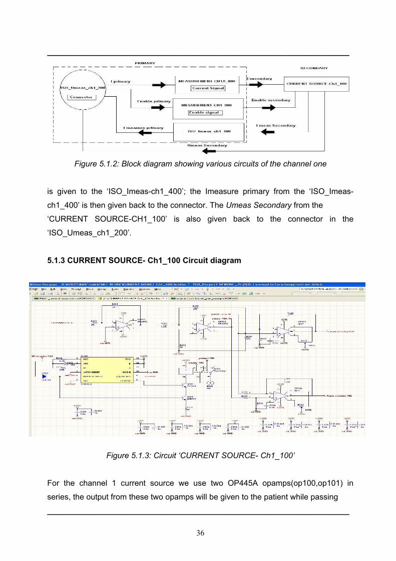
5.1.2 Working of the Channels (channel 1) The each block in the above block diagram represent sub circuit diagrams of an entire
channel (channel1), the connection between them is being shown by arrows.
‘Iso_Umeas-ch1_200’ circuit has the connector, which allows several connections
such as the Iprimary, Enable primary, I measure primary (Current measurement),
Umeas secondary (voltage measurement). To start with the Iprimary signal is given to
the ‘MEASUREMENT_CH1A_800’, a current signal, from here in the form of
Isecondary is given to the ‘Current Source-CH2_100’. The Imeas Secondary (Current
measurement) signal is given to the ‘Iso_Imeas-ch1_400’ there by enabling the
isolation. The Imeasure primary from the ‘ISO_Imeas-ch1_400’ is then passed on to
the connector at ‘Iso_Umeas-ch1_200’. The Enable primary from the ‘Iso_Umeas-
ch1_200’ is given to the ‘MEASURE-CH2_900’, in the form of enable secondary this
signal is then passed to the ‘CURRENT SOURCE-CH1_100’ which has the ‘enable
signal as an output. The Imeas Secondary from the ‘CURRENT SOURCE-CH1_100’
____________________________________________________________________
36
____________________________________________________________________
Figure 5.1.2: Block diagram showing various circuits of the channel one
is given to the ‘ISO_Imeas-ch1_400’; the Imeasure primary from the ‘ISO_Imeas-
ch1_400’ is then given back to the connector. The Umeas Secondary from the
‘CURRENT SOURCE-CH1_100’ is also given back to the connector in the
‘ISO_Umeas_ch1_200’.
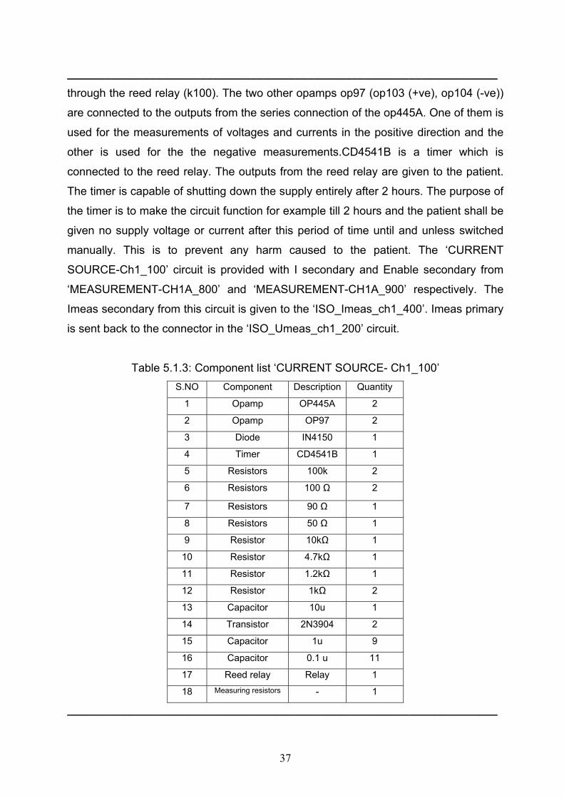
5.1.3 CURRENT SOURCE- Ch1_100 Circuit diagram
Figure 5.1.3: Circuit ‘CURRENT SOURCE- Ch1_100’
For the channel 1 current source we use two OP445A opamps(op100,op101) in
series, the output from these two opamps will be given to the patient while passing
____________________________________________________________________
37
____________________________________________________________________ through the reed relay (k100). The two other opamps op97 (op103 (+ve), op104 (-ve))
are connected to the outputs from the series connection of the op445A. One of them is
used for the measurements of voltages and currents in the positive direction and the
other is used for the the negative measurements.CD4541B is a timer which is
connected to the reed relay. The outputs from the reed relay are given to the patient.
The timer is capable of shutting down the supply entirely after 2 hours. The purpose of
the timer is to make the circuit function for example till 2 hours and the patient shall be
given no supply voltage or current after this period of time until and unless switched
manually. This is to prevent any harm caused to the patient. The ‘CURRENT
SOURCE-Ch1_100’ circuit is provided with I secondary and Enable secondary from
‘MEASUREMENT-CH1A_800’ and ‘MEASUREMENT-CH1A_900’ respectively. The
Imeas secondary from this circuit is given to the ‘ISO_Imeas_ch1_400’. Imeas primary
is sent back to the connector in the ‘ISO_Umeas_ch1_200’ circuit.
Table 5.1.3: Component list ‘CURRENT SOURCE- Ch1_100’ S.NO Component Description Quantity
1 Opamp OP445A 2
2 Opamp OP97 2
3 Diode IN4150 1
4 Timer CD4541B 1
5 Resistors 100k 2
6 Resistors 100 Ω 2
7 Resistors 90 Ω 1
8 Resistors 50 Ω 1
9 Resistor 10kΩ 1
10 Resistor 4.7kΩ 1
11 Resistor 1.2kΩ 1
12 Resistor 1kΩ 2
13 Capacitor 10u 1
14 Transistor 2N3904 2
15 Capacitor 1u 9
16 Capacitor 0.1 u 11
17 Reed relay Relay 1
18 Measuring resistors - 1
____________________________________________________________________

38
____________________________________________________________________ 5.1.4 Operational amplifier ’op97’ The op97 is a low power alternative to the industry standard op07 precision amplifier.
The op97 maintains the standards of performance set by the op07 while utilizing only
600 µA supply current, less than 1/6 that of an op07. Offset voltage is an ultra low 25
µV, and drift over temperature is below 0.6 µV/ºC. External offset trimming is not
required in the majority of circuits.
Improvements have been made over op07 specifications in several areas. Notable is
bias current, which remains below 250 pA over the full military temperature range. The
op97 is ideal for use in precision long-term integrators or sample-and-hold circuits that
must operate at elevated temperatures.
Common-mode rejection and power supply rejection are also improved with the op97,
at 114 dB minimum over wider ranges of common-mode or supply voltage.
Outstanding power supply rejection (PSR) a supply range specified from ±2.25 V to
±20 V and minimal power requirements of op97's combine to make the op97 a
preferred device for portable and battery-powered instruments.
The op97 conforms to the op07 pin out, with the null potentiometer connected
between pins 1 and 8 with the wiper to V+. The op97 will upgrade circuit designs using
725, op05, op07, op12, and 1012 type amplifiers. It may replace 741-type amplifiers in
circuits without nulling or where the nulling circuitry has been removed.
Absolute maximum ratings:
Supply voltage…………………….…………….…………………………………… ...± 20V
Input Voltage………….…………………….……………………………………………± 20V
Differential Input voltage………………………………………………………………...± 1V
Differential Input Current…………………………………………………………….± 10mA
Output Short-Circuit Duration……………...Indefinite. [5]
____________________________________________________________________
39
____________________________________________________________________
5.1.5 Timer ‘CD4541B’ CD4541B is a programmable timer, it consists of a 16-stage binary counter, an
oscillator that is controlled by external R-C components (2 resistors and a capacitor),
an automatic power-on reset circuit, and output control logic. The counter increments
on positive-edge clock transitions and can also be reset via the MASTER RESET input
.The output from this timer is the Q or Q output from the 8th, 10th, 13th, or 16th counter
stage. The desired stage is chosen using time-select inputs A and B (see Frequency
Select Table). The output is available in either of two modes selectable via the MODE
input, pin 10. When this MODE input is a logic “1”, the output will be a continuous
square wave having a frequency equal to the oscillator frequency divided by 2 N.
With the MODE input set to logic “0” and after a MASTER RESET is initiated,
the output (assuming Q output has been selected) changes from a low to a high state
after 2N-1 counts and remains in that state until another MASTER RESET pulse is
applied or the MODE input is set to logic “1”.
Timing is initialized by setting the AUTO RESET input (pin 5) to logic “0” and
turning power on. If pin 5 is set to logic “1”, the AUTO RESET circuit is disabled
and counting will not start until after a positive MASTER RESET pulse is applied
and returns to a low level. The AUTO RESET consumes an appreciable amount of
power and should not be used if low-power operation is desired. For reliable
automatic power-on reset, VDD should be greater than 5V.
The RC oscillator, shown in Figure 2, oscillates with a frequency
determined by the RC network and is calculated using:
f = 1 / 2.3 RTC CTC
Where f is frequency between 1 kHz and 100 kHz and Rs ≥ 10kΩ and ≈ 2 RTC
____________________________________________________________________

40
____________________________________________________________________
Figure 5.1.5: Block diagram of the timer ‘CD4541B’
Absolute Maximum Ratings
DC Supply – voltage Range, VDD
Voltage Referenced Range, VDD Terminal …………….……………..…….0.5 V to +20 V
Input Voltage Range, All inputs……………………...............................-0.5 to VDD +0.5 V
DC input Current, Any one inputs………………………………………………....± 10 mA
Device Dissipation per Output Transistor for TA = Full package Temperature Range
(All Package Types)………………………….. 100 mw
Operating Conditions Temperature Range TA ……………...…………-55 ºC to 125 ºC
Supply Voltage Range for TA = Full Package Temperature Range.3V (Min), 18 V (Typ).
[1]
5.1.6 Operational amplifier ‘OP445A’
The op445A is a monolithic operational amplifier capable of operation from power
supplies up to ±45 V and output currents of 15 mA. It is useful in a wide variety of
applications requiring high output voltage or large common-mode voltage swings.
The op445A's high slew rate provides wide power bandwidth response, which is often
required for high voltage applications. Field effect transistor (FET) input circuitry allows
the use of high-impedance feedback networks, thus minimizing their output loading
effects. Laser trimming of the input circuitry yields low input offset voltage and drift.
____________________________________________________________________
41
____________________________________________________________________
The op445A is available in standard pin-out TO-99, DIP-8, and SO-8 surface-mount
packages. It is fully specified from -25 ºC to +125 ºC.
Absolute maximum ratings (op445A)
Power supply…………..…………………………….……..…..………….…..…….......±50 V
Differential Input voltage…………….…………….……………….…………….…......±80 V
Input Voltage range……………………………………………..………..……….…|±Vs| -3V
Operating Temperature range…..………..…………………..……...-55 ºC to +125 ºC. [3]
5.1.7 High-linearity Analog optocouplers The HCNR200/201 high-linearity analog optocoupler consists of a high-performance
AlGaAs LED that illuminates two closely matched photodiodes. The input photodiode
can be used to monitor, and therefore stabilize, the light output of the LED. As a result,
the nonlinearity and drift characteristics of the LED can be virtually eliminated. The
output photodiode produces a photocurrent that is linearly related to the light output of
the LED. The close matching of the photodiodes and advanced design of the package
ensure the high linearity and stable gain characteristics of the optocoupler.
The HCNR200/201 can be used to isolate analog signals in a wide variety of
applications that require good stability, linearity, bandwidth and low cost. The
HCNR200/201 is very flexible and, by appropriate design of the application circuit, is
capable of operating in many different modes, including unipolar / bipolar, AC / DC
and inverting / non-inverting. The HCNR200/201 is an excellent solution for many
analog isolation problems. [2]
____________________________________________________________________
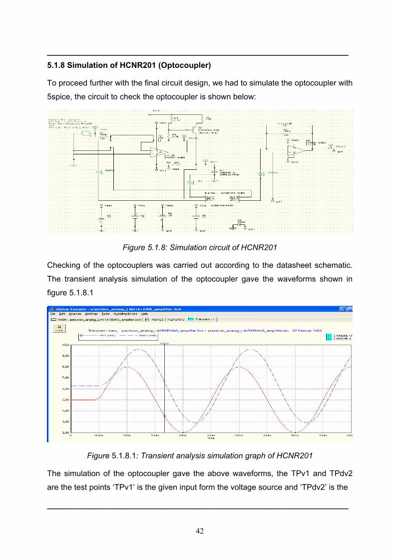
42
____________________________________________________________________ 5.1.8 Simulation of HCNR201 (Optocoupler)
To proceed further with the final circuit design, we had to simulate the optocoupler with
5spice, the circuit to check the optocoupler is shown below:
Figure 5.1.8: Simulation circuit of HCNR201
Checking of the optocouplers was carried out according to the datasheet schematic.
The transient analysis simulation of the optocoupler gave the waveforms shown in
figure 5.1.8.1
Figure 5.1.8.1: Transient analysis simulation graph of HCNR201
The simulation of the optocoupler gave the above waveforms, the TPv1 and TPdv2
are the test points ‘TPv1’ is the given input form the voltage source and ‘TPdv2’ is the
____________________________________________________________________
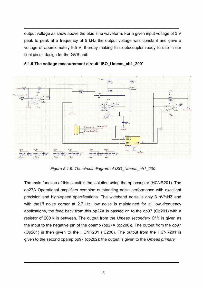
43
____________________________________________________________________ output voltage as show above the blue sine waveform. For a given input voltage of 3 V
peak to peak at a frequency of 5 kHz the output voltage was constant and gave a
voltage of approximately 9.5 V, thereby making this optocoupler ready to use in our
final circuit design for the GVS unit.
5.1.9 The voltage measurement circuit ‘ISO_Umeas_ch1_200’
Figure 5.1.9: The circuit diagram of ISO_Umeas_ch1_200
The main function of this circuit is the isolation using the optocoupler (HCNR201). The
op27A Operational amplifiers combine outstanding noise performance with excellent
precision and high-speed specifications. The wideband noise is only 3 nV/√HZ and
with the1/f noise corner at 2.7 Hz, low noise is maintained for all low.-frequency
applications, the feed back from this op27A is passed on to the op97 (Op201) with a
resistor of 200 k in between. The output from the Umeas secondary CH1 is given as
the input to the negative pin of the opamp (op27A (op200)). The output from the op97
(Op201) is then given to the HCNR201 (IC200). The output from the HCNR201 is
given to the second opamp op97 (op202); the output is given to the Umeas primary
____________________________________________________________________

44
____________________________________________________________________
CH1. The circuit also has a connector which has the following pins, such as
1. Iprimary CH1,
2. EN primary CH1
3. Umeas primary CH1
4. Imeas primary CH1,
5. Ground.
The Iprimary current from this circuit is passed on to the ‘MEASUREMENT-
CH1A_800’ circuit. The ‘Iso_Umeas_ch1_200’ provides the enable signal to the
‘MESUREMENT-CH1_900’ circuit.
Table 5.1.9: List of components ‘Iso_Umeas_ch1_200’
S.no Component Description Quantity
1 Opamp op97 2
2 Opamp op27A 1
3 Diode IN4150 1
4 Optocoupler HCNR201 1
5 Resistor 270Ω 1
6 Resistor 200 kΩ 1
7 Resistor 33 kΩ 1
8 Resistor 10 kΩ 1
9 Resistor 2.2 kΩ 1
10 Resistor 6.8 kΩ 1
11 Capacitor 47 p 1
12 Capacitor 33 p 1
13 Capacitor 1 u 6
14 Capacitor 0.1 u 6
15 Connector - 1
16 Tansistor 2N3906 1
____________________________________________________________________
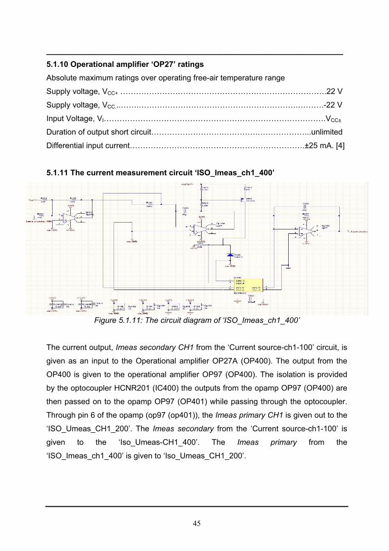
45
____________________________________________________________________ 5.1.10 Operational amplifier ‘OP27’ ratings Absolute maximum ratings over operating free-air temperature range
Supply voltage, VCC+ …………………………………………………………………….22 V
Supply voltage, VCC...…….…………………………………………………….……….-22 V
Input Voltage, VI………………………………………………………………………….VCC±
Duration of output short circuit……………………….………….………………...unlimited
Differential input current………………………………………………………….±25 mA. [4]
5.1.11 The current measurement circuit ‘ISO_Imeas_ch1_400’
Figure 5.1.11: The circuit diagram of ‘ISO_Imeas_ch1_400’
The current output, Imeas secondary CH1 from the ‘Current source-ch1-100’ circuit, is
given as an input to the Operational amplifier OP27A (OP400). The output from the
OP400 is given to the operational amplifier OP97 (OP400). The isolation is provided
by the optocoupler HCNR201 (IC400) the outputs from the opamp OP97 (OP400) are
then passed on to the opamp OP97 (OP401) while passing through the optocoupler.
Through pin 6 of the opamp (op97 (op401)), the Imeas primary CH1 is given out to the
‘ISO_Umeas_CH1_200’. The Imeas secondary from the ‘Current source-ch1-100’ is
given to the ‘Iso_Umeas-CH1_400’. The Imeas primary from the
‘ISO_Imeas_ch1_400’ is given to ‘Iso_Umeas_CH1_200’.
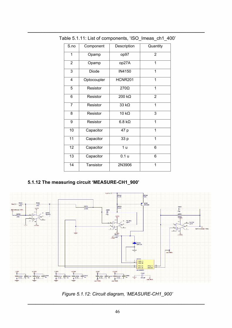
46
____________________________________________________________________
Table 5.1.11: List of components, ‘ISO_Imeas_ch1_400’ S.no Component Description Quantity
1 Opamp op97 2
2 Opamp op27A 1
3 Diode IN4150 1
4 Optocoupler HCNR201 1
5 Resistor 270Ω 1
6 Resistor 200 kΩ 2
7 Resistor 33 kΩ 1
8 Resistor 10 kΩ 3
9 Resistor 6.8 kΩ 1
10 Capacitor 47 p 1
11 Capacitor 33 p 1
12 Capacitor 1 u 6
13 Capacitor 0.1 u 6
14 Tansistor 2N3906 1
5.1.12 The measuring circuit ‘MEASURE-CH1_900’
Figure 5.1.12: Circuit diagram, ‘MEASURE-CH1_900’
____________________________________________________________________
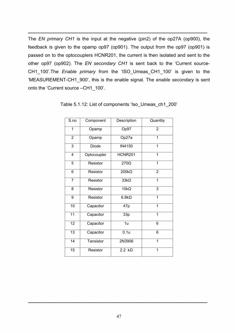
47
____________________________________________________________________
The EN primary CH1 is the input at the negative (pin2) of the op27A (op900), the
feedback is given to the opamp op97 (op901). The output from the op97 (op901) is
passed on to the optocouplers HCNR201, the current is then isolated and sent to the
other op97 (op902). The EN secondary CH1 is sent back to the ‘Current source-
CH1_100’.The Enable primary from the ‘ISO_Umeas_CH1_100’ is given to the
‘MEASUREMENT-CH1_900’, this is the enable signal. The enable secondary is sent
onto the ‘Current source –CH1_100’.
Table 5.1.12: List of components ‘Iso_Umeas_ch1_200’
S.no Component Description Quantity
1 Opamp Op97 2
2 Opamp Op27a 1
3 Diode IN4150 1
4 Optocoupler HCNR201 1
5 Resistor 270Ω 1
6 Resistor 200kΩ 2
7 Resistor 33kΩ 1
8 Resistor 10kΩ 3
9 Resistor 6.8kΩ 1
10 Capacitor 47p 1
11 Capacitor 33p 1
12 Capacitor 1u 6
13 Capacitor 0.1u 6
14 Tansistor 2N3906 1
15 Resistor 2.2 kΩ 1
____________________________________________________________________
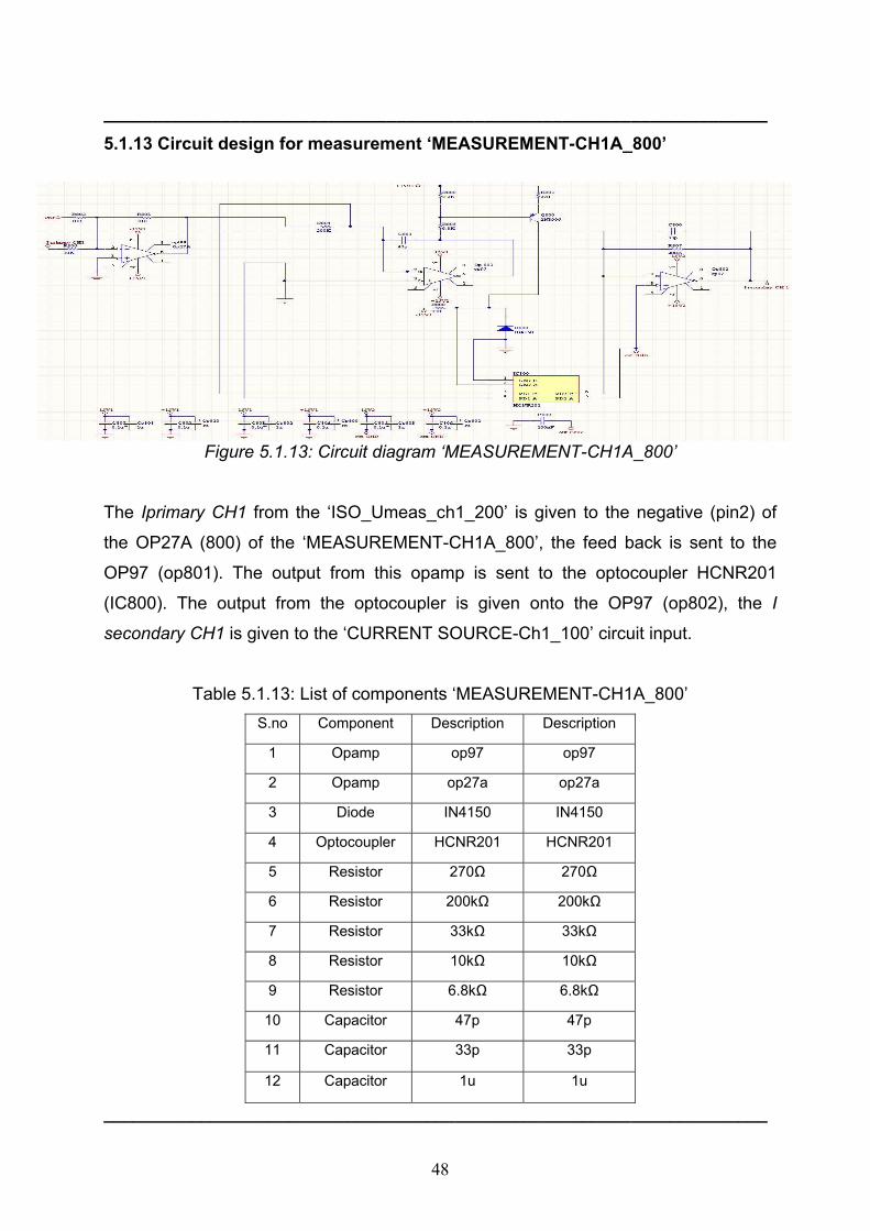
48
____________________________________________________________________
5.1.13 Circuit design for measurement ‘MEASUREMENT-CH1A_800’
Figure 5.1.13: Circuit diagram ‘MEASUREMENT-CH1A_800’
The Iprimary CH1 from the ‘ISO_Umeas_ch1_200’ is given to the negative (pin2) of
the OP27A (800) of the ‘MEASUREMENT-CH1A_800’, the feed back is sent to the
OP97 (op801). The output from this opamp is sent to the optocoupler HCNR201
(IC800). The output from the optocoupler is given onto the OP97 (op802), the I
secondary CH1 is given to the ‘CURRENT SOURCE-Ch1_100’ circuit input.
Table 5.1.13: List of components ‘MEASUREMENT-CH1A_800’ S.no Component Description Description
1 Opamp op97 op97
2 Opamp op27a op27a
3 Diode IN4150 IN4150
4 Optocoupler HCNR201 HCNR201
5 Resistor 270Ω 270Ω
6 Resistor 200kΩ 200kΩ
7 Resistor 33kΩ 33kΩ
8 Resistor 10kΩ 10kΩ
9 Resistor 6.8kΩ 6.8kΩ
10 Capacitor 47p 47p
11 Capacitor 33p 33p
12 Capacitor 1u 1u
____________________________________________________________________
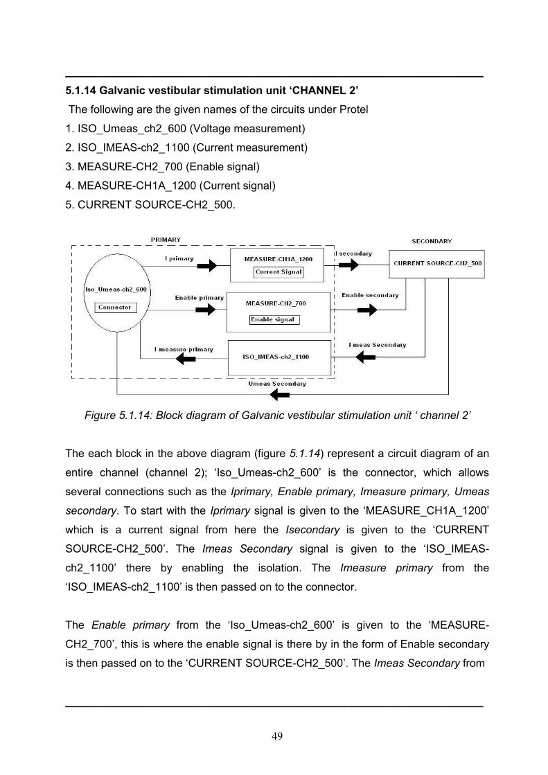
49
____________________________________________________________________
5.1.14 Galvanic vestibular stimulation unit ‘CHANNEL 2’ The following are the given names of the circuits under Protel
1. ISO_Umeas_ch2_600 (Voltage measurement)
2. ISO_IMEAS-ch2_1100 (Current measurement)
3. MEASURE-CH2_700 (Enable signal)
4. MEASURE-CH1A_1200 (Current signal)
5. CURRENT SOURCE-CH2_500.
Figure 5.1.14: Block diagram of Galvanic vestibular stimulation unit ‘ channel 2’
The each block in the above diagram (figure 5.1.14) represent a circuit diagram of an
entire channel (channel 2); ‘Iso_Umeas-ch2_600’ is the connector, which allows
several connections such as the Iprimary, Enable primary, Imeasure primary, Umeas
secondary. To start with the Iprimary signal is given to the ‘MEASURE_CH1A_1200’
which is a current signal from here the Isecondary is given to the ‘CURRENT
SOURCE-CH2_500’. The Imeas Secondary signal is given to the ‘ISO_IMEAS-
ch2_1100’ there by enabling the isolation. The Imeasure primary from the
‘ISO_IMEAS-ch2_1100’ is then passed on to the connector.
The Enable primary from the ‘Iso_Umeas-ch2_600’ is given to the ‘MEASURE-
CH2_700’, this is where the enable signal is there by in the form of Enable secondary
is then passed on to the ‘CURRENT SOURCE-CH2_500’. The Imeas Secondary from
____________________________________________________________________

50
____________________________________________________________________
the ‘CURRENT SOURCE-CH2_500’ is given to the ‘ISO_IMEAS-ch2_1100’; the
Imeasure primary from the ‘ISO_IMEAS-ch2_1100’ is then given back to the
connector. The Umeas Secondary from the ‘CURRENT SOURCE-CH2_500’ is also
given back to the connector.
5.1.13 Circuit design ‘DC_DC_Converter_300’ (power supply)
Figure 5.1.13: Circuit diagram ‘DC_DC_Converter_300’
The Battery is connected along with a fuse and then a switch in series, which will
disconnect if there is a low supply voltage i.e. if the battery is low. A reed relay is
connected in between which will allow, voltage to pass through two RS1215D, which is
a wide range voltage inputs with an isolation voltage up to 1kV DC isolation. The
voltage from the first RS1215D (U301) is made to pass through MC79L05CP which is
a three terminal negative voltage regulator. The voltage from the second RS1215D
(U304) is sent to the 15SM48D, which is a DC-DC converter. The positive voltage
output (+Vout) from the DC-DC converter is passed onto the LM337T (U300), which is
a three terminal negative adjustable regulator. LM337 supplies in excess of 1.5 A over
an output voltage range of -1.2 V to -37 V. This regulator requires only two external
resistors to set the output voltage. The negative voltage (-Vout) is given to the
LM317BT, which is a three terminal adjustable output positive voltage regulator
capable of supplying in excess of 1.5 A over an output voltage range of 1.2 V to 37 V.
____________________________________________________________________

51
____________________________________________________________________
This voltage regulator is exceptionally easy to use and requires only two external
resistors to set the output voltage. Further, it employs internal current limiting; thermal
shutdown and safe area compensation, making it essentially blow-out proof.
Table 5.1.13 List of components ‘DC_DC_Converter_300 ‘ S.no COMPONENT Description quantity
1 Capacitor 0.1u 2
2 Capacitor 1uf 4
3 Resistor 5k 1
4 Resistor 10k 1
5 DC-DC 15SM48D 1
6 Resistor 120Ω 1
7 Resistor 240Ω 1
8 Resistor 300Ω 1
9 Battery - 1
10 Diode zener 1
11 Fuse - 1
12 LED - 1
13 +V regulator LM317BT 1
14 -V regulator LM337T 1
15 Regulator MC79L05 1
16 Reed relay - 1
17 Connector RS1215D 2
18 Switch SW-SPST 1
____________________________________________________________________
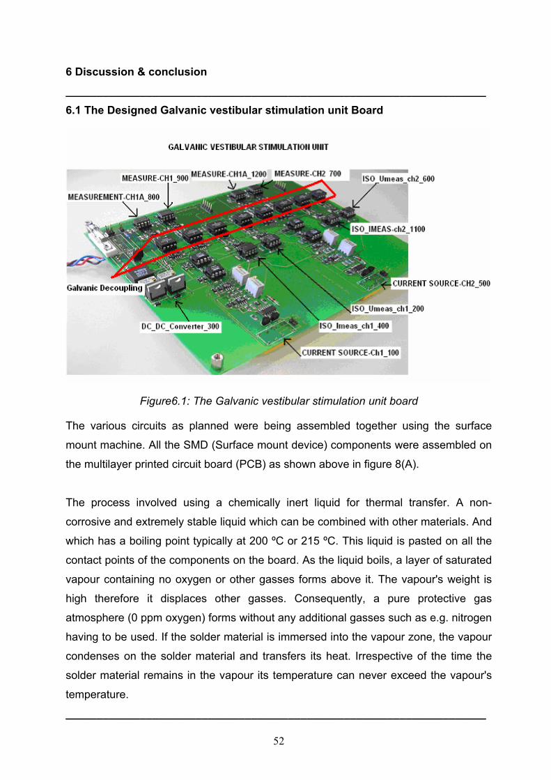
52
6 Discussion & conclusion ____________________________________________________________________
6.1 The Designed Galvanic vestibular stimulation unit Board
Figure6.1: The Galvanic vestibular stimulation unit board
The various circuits as planned were being assembled together using the surface
mount machine. All the SMD (Surface mount device) components were assembled on
the multilayer printed circuit board (PCB) as shown above in figure 8(A).
The process involved using a chemically inert liquid for thermal transfer. A non-
corrosive and extremely stable liquid which can be combined with other materials. And
which has a boiling point typically at 200 ºC or 215 ºC. This liquid is pasted on all the
contact points of the components on the board. As the liquid boils, a layer of saturated
vapour containing no oxygen or other gasses forms above it. The vapour's weight is
high therefore it displaces other gasses. Consequently, a pure protective gas
atmosphere (0 ppm oxygen) forms without any additional gasses such as e.g. nitrogen
having to be used. If the solder material is immersed into the vapour zone, the vapour
condenses on the solder material and transfers its heat. Irrespective of the time the
solder material remains in the vapour its temperature can never exceed the vapour's
temperature.
____________________________________________________________________

53
____________________________________________________________________
So the components are put upon the paste and put into the oven. The steps involved
in the machine were as follows: - 1. The assembly is moved to the vapour phase after
it was preheated by IR radiators from the top side. It is also possible to do preheating
on the top boundary of the vapour phase. Then the heat is predominantly transferred
from below. Vapour with a boiling point of 200°C. Boiling fluid used to build up the
vapour phase.
2. The assembly dives into the vapour phase. There it is heated up. It is possible to
control the heat transfer to the assembly to perform smooth temperature gradients.
3. The vapour condenses on the assembly and transfers its heat. Since the vapour is
chemically inert it performs an inert gas atmosphere with 0 ppm oxygen. This is done
automatically without the use of nitrogen.
4. The assembly can be heated up to a maximum temperature that is limited by the
vapours temperature. This temperature cannot be exceeded even if the assembly
stays for long time inside the vapour. Therefore it is impossible to overheat.
5. After leaving the vapour phase there is still condensed fluid left on the board. Due to
the inner heat of the assembly the liquid evaporates without residues. A completely
dry board leaves the machine.
The laws of physics determine the framework conditions. The key factor: The
temperature of the vapour can never exceed the temperature of the boiling liquid, and
it is fixed. The consequence: The solder process can be reliably reproduced and offers
ideal conditions for controlling the process. This enables soldering to be carried out on
a wide range of assemblies, from flex print to multi-layer, reliably and without
overheating.
____________________________________________________________________
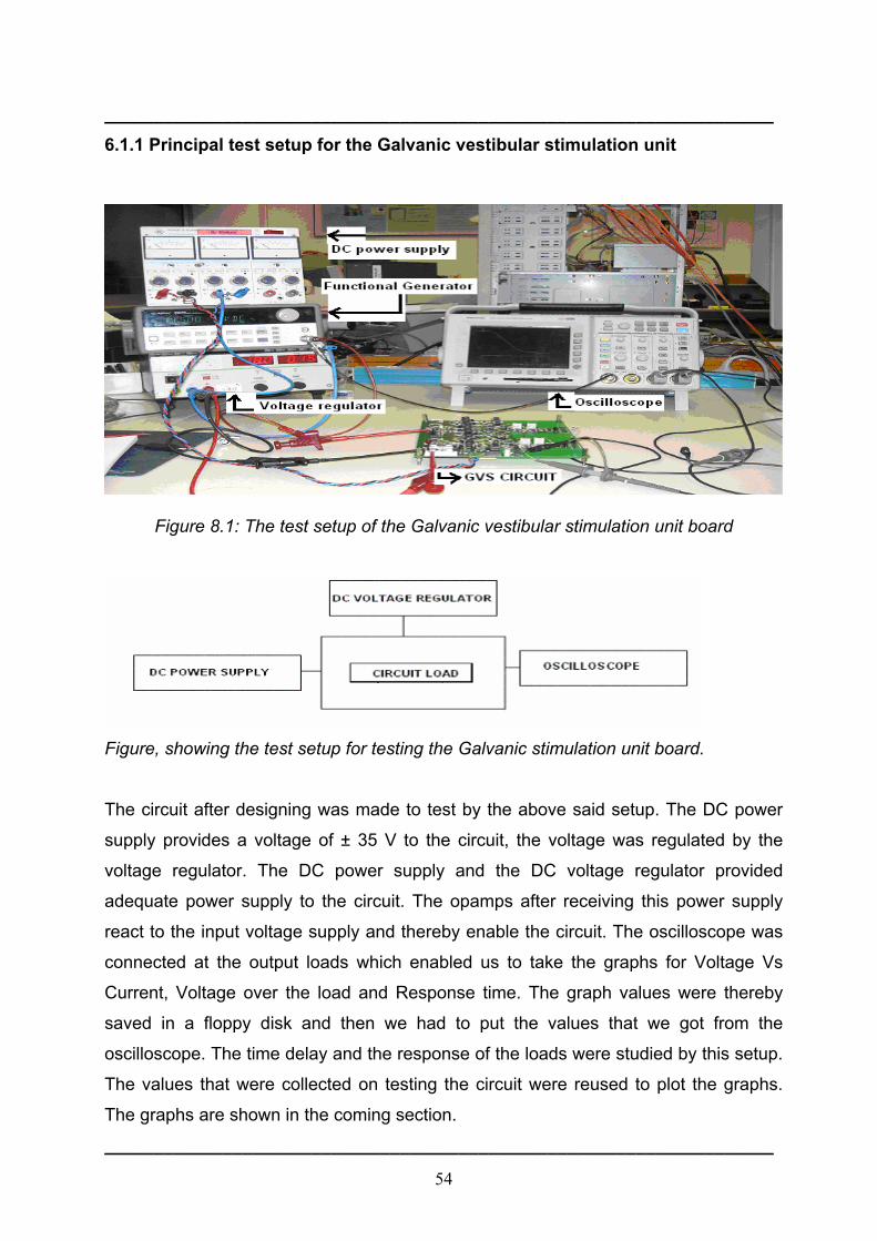
54
____________________________________________________________________
6.1.1 Principal test setup for the Galvanic vestibular stimulation unit
Figure 8.1: The test setup of the Galvanic vestibular stimulation unit board
Figure, showing the test setup for testing the Galvanic stimulation unit board.
The circuit after designing was made to test by the above said setup. The DC power
supply provides a voltage of ± 35 V to the circuit, the voltage was regulated by the
voltage regulator. The DC power supply and the DC voltage regulator provided
adequate power supply to the circuit. The opamps after receiving this power supply
react to the input voltage supply and thereby enable the circuit. The oscilloscope was
connected at the output loads which enabled us to take the graphs for Voltage Vs
Current, Voltage over the load and Response time. The graph values were thereby
saved in a floppy disk and then we had to put the values that we got from the
oscilloscope. The time delay and the response of the loads were studied by this setup.
The values that were collected on testing the circuit were reused to plot the graphs.
The graphs are shown in the coming section.
____________________________________________________________________
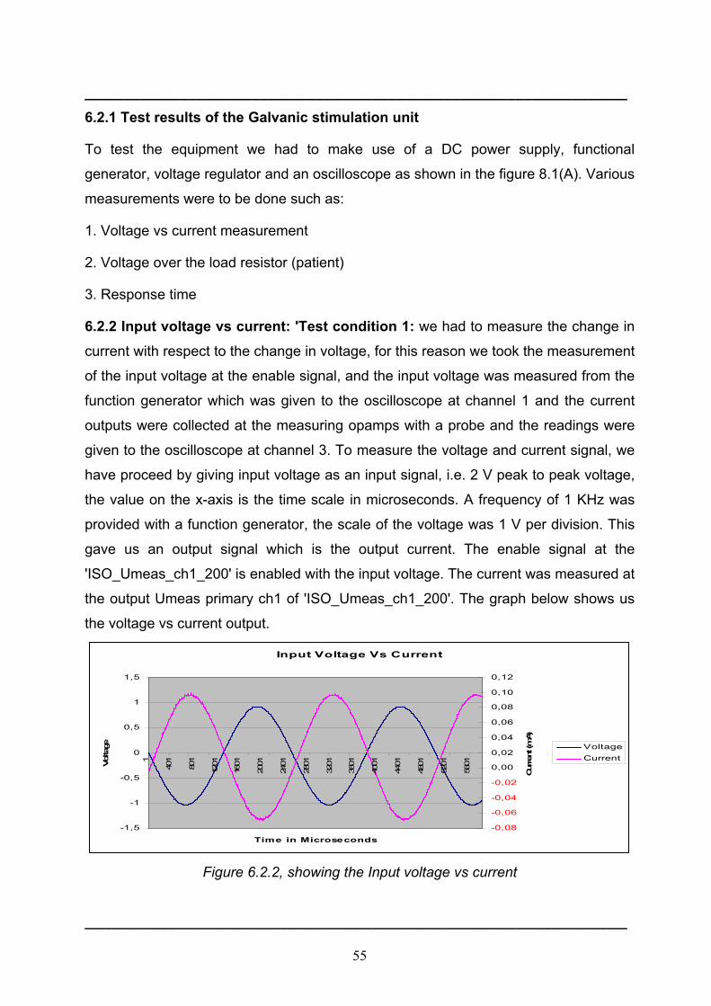
55
____________________________________________________________________
6.2.1 Test results of the Galvanic stimulation unit
To test the equipment we had to make use of a DC power supply, functional
generator, voltage regulator and an oscilloscope as shown in the figure 8.1(A). Various
measurements were to be done such as:
1. Voltage vs current measurement
2. Voltage over the load resistor (patient)
3. Response time
6.2.2 Input voltage vs current: 'Test condition 1: we had to measure the change in
current with respect to the change in voltage, for this reason we took the measurement
of the input voltage at the enable signal, and the input voltage was measured from the
function generator which was given to the oscilloscope at channel 1 and the current
outputs were collected at the measuring opamps with a probe and the readings were
given to the oscilloscope at channel 3. To measure the voltage and current signal, we
have proceed by giving input voltage as an input signal, i.e. 2 V peak to peak voltage,
the value on the x-axis is the time scale in microseconds. A frequency of 1 KHz was
provided with a function generator, the scale of the voltage was 1 V per division. This
gave us an output signal which is the output current. The enable signal at the
'ISO_Umeas_ch1_200' is enabled with the input voltage. The current was measured at
the output Umeas primary ch1 of 'ISO_Umeas_ch1_200'. The graph below shows us
the voltage vs current output.
Input Voltage Vs Current
-1,5
-1
-0,5
0
0,5
1
1,5
1
401
801
1201
1601
2001
2401
2801
3201
3601
4001
4401
4801
5201
5601
Time in Microseconds
Volta
ge
-0,08
-0,06
-0,04
-0,02
0,00
0,02
0,04
0,06
0,08
0,10
0,12
Curren
t (m
A)
VoltageCurrent
Figure 6.2.2, showing the Input voltage vs current
____________________________________________________________________
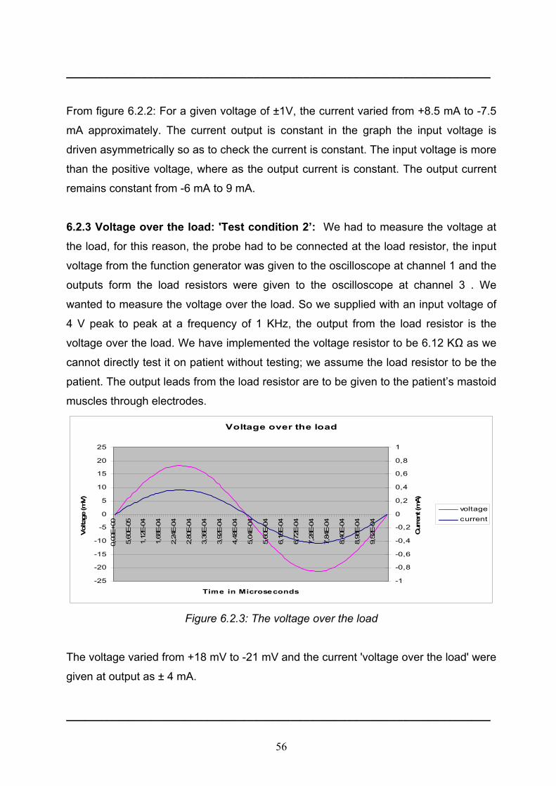
56
____________________________________________________________________
From figure 6.2.2: For a given voltage of ±1V, the current varied from +8.5 mA to -7.5
mA approximately. The current output is constant in the graph the input voltage is
driven asymmetrically so as to check the current is constant. The input voltage is more
than the positive voltage, where as the output current is constant. The output current
remains constant from -6 mA to 9 mA.
6.2.3 Voltage over the load: 'Test condition 2’: We had to measure the voltage at
the load, for this reason, the probe had to be connected at the load resistor, the input
voltage from the function generator was given to the oscilloscope at channel 1 and the
outputs form the load resistors were given to the oscilloscope at channel 3 . We
wanted to measure the voltage over the load. So we supplied with an input voltage of
4 V peak to peak at a frequency of 1 KHz, the output from the load resistor is the
voltage over the load. We have implemented the voltage resistor to be 6.12 KΩ as we
cannot directly test it on patient without testing; we assume the load resistor to be the
patient. The output leads from the load resistor are to be given to the patient’s mastoid
muscles through electrodes.
Voltage over the load
-25
-20
-15
-10
-5
0
5
10
15
20
25
0,00
E+0
0
5,60
E-0
5
1,12
E-0
4
1,68
E-0
4
2,24
E-0
4
2,80
E-0
4
3,36
E-0
4
3,92
E-0
4
4,48
E-0
4
5,04
E-0
4
5,60
E-0
4
6,16
E-0
4
6,72
E-0
4
7,28
E-0
4
7,84
E-0
4
8,40
E-0
4
8,96
E-0
4
9,52
E-0
4
Time in Microseconds
Vol
tage
(mV)
-1
-0,8
-0,6
-0,4
-0,2
0
0,2
0,4
0,6
0,8
1
Cur
rent
(mA)
voltagecurrent
Figure 6.2.3: The voltage over the load
The voltage varied from +18 mV to -21 mV and the current 'voltage over the load' were
given at output as ± 4 mA.
____________________________________________________________________

57
____________________________________________________________________
6.2.3 Adaptation (response) time: 'Test condition 3': We had to measure the
response time of the opamps.The output voltage from the function generator was
given to the oscilloscope at channel 1 and the outputs from the opamp were given to
the scope at channel 3., to measure the response time we had to supply an Input
signal of 0 V to 3 V, then we had an output of change in current at, time scale is 10µS.
The time interval between the starting & ending point was 80µS (response time) as
seen in the oscilloscope.
Response time
-0.5
0
0.5
1
1.5
2
2.5
3
3.5
1 51 101 151 201 251 301 351 401 451
Time in microseconds
Vol
tage
-0.25
-0.2
-0.15
-0.1
-0.05
0
0.05
Cur
rent
(mA)
TimeVoltageCurrent
Figure 6.2.3, showing the response time
For a given voltage of 3V, the response time was measured to be 80µs, on the
oscilloscope
The aim of our thesis was to design a galvanic vestibular stimulation unit which
provides a complete test environment to the scientists with a flexibility to monitor the
effects of stimulation. We came up with an idea to build a GVS unit, which can fulfil the
task. During the process, we had to make sure that there should be a galvanic
decoupling of the currents/voltages delivered to the patient. There should be also a
facility not to burden the patient with continuous stimulus delivery therefore we have
built in a security shutdown of the device to the patient after the device has been
stimulation for a specified time (e.g. 2 hours). To ensure that there is a correct current
____________________________________________________________________
58
____________________________________________________________________
supply, we made used of relays, which only give galvanic contact to the patient, if the
current provided is accurate. We also had to consider if in any case due to some
failure or the other the patient is not to be given more stimulation the device is capable
of shutting down so that no harm is caused to the patient knowing or unknowingly with
the help of a fuse.
Various voltage and current regulators have also been installed so that the device
delivers precisely the expected stimulation. All of this can be controlled to by a switch
which can disconnect the patient contact. We had to go through the Medical
equipment norms, to fulfil that this equipment can be used once it attains its patents
after implementing the said suggestions. To attain the patents, we have come in
contact with a company that is engaged in developing medical devices, bytech
(http://www.bytec-gmbh.de/) to proceed with the medical testing according to the IEC
60601-1 norms. We showed our designed device to a company, they made some
suggestions in improving the GVS unit by changing the battery or power line to the
isolation side and also to have more space between the pins. And finally, the
equipment is ready for medical safety testing as described in the attachment. Overall
the aim of this thesis is being concluded with the desired requirements. How ever
further safety tests have to be carried out to finally use it on a Hemi spatial Neglect
syndrome patient and a microcontroller based control unit has to be implemented for
research purposes.
The necessary safety tests:1. Protective Earth Continuity
2. Insulation Tests.
3. Earth Leakage Current
4. Enclosure leakage current
5. Patient leakage current
6. Patient auxiliary current
These safety tests shall be carried out according to the IEC 60601 norms, which shall
be carried out with the cooperation of a biomedical company.
____________________________________________________________________

59
7. References ____________________________________________________________________
1. Datasheet CD4541B Texas Instruments, September 2000
2. Data sheet HCNR200/201 Agilent Technologies, March 2005
3. Data sheet OP445 Burr Brown, march 2000
4. Data sheet op27c, Texas Instruments, Analog Devices, 2003
5. Data sheet OP97 Analog devices 2003
6. Deep brain stimulation & epilepsy (ed. by Hans O.Lüders) – T.Bajd; Functional
electrical stimulation of extremities. Ljubljana, 1983 Yugoslavia, J.Stephan Institute,
page 1331-1332
7. IEC 60601- page 36-37
8. Luxon, L.M, 1989 Textbook of Audiological Medicine Clinical Aspects of hearing and
balance. Page 765-766
9. Turnbull, O.H.Mirror, mirror, 1997 on the wall - is the left side there at all ? Current
Biology 7, page 709-711.
10. Unilateral neglect: Clinical and experimental studies Ian H. Robertson and John
C.Marshall (eds). Page 27,Page 289.
11. G Vallar, D Perani – Neuropsychologia, 1986 The anatomy of unilateral neglect
after right hemisphere stroke lesions. pages 24, 609-612.
12. www.5spice.com_helpfile, 5spice
13. www.altium.com, helpfile, protel
14. www.Wikipedia.com, Stephen M. Highstein,S.M, Fay, R.R, Popper,A.N - The Vestibular System (Eds) Springer-Verlag (2004)
15. www.cami.jccbi.gov/AAM-400A/Brochures/spatialD2/spatialdgraphics/bigotolith.jpg
16. www.thalamus.wustl.edu/course/basvis.html

60
Appendix ___________________________________________________________________ Altium Design 34 Benign paroxysmal positional vertigo (BPPV) 12 Caloric Vestibular stimulation 14 Contralateral Hemi spatial neglect 2 Galvanic vestibular stimulation 1, 7 Neglect syndrome 2 Operational amplifier 21 Optocoupler 42 Otolith 11 Saftey regulations 17 Vestibulo-ocular reflex 9 5spice 25
___________________________________________________________________

Acknowledgements
To dear God, whose eternal blessings and divine presence helps us to fulfil all our goals.
When emotions are profound words sometimes are not sufficient to express our thanks and
gratitude. With these few words, I am trying to express my extreme gratitude and sincere
thanks to all those people who have helped and provided the very much needed enthusiasm
and consistent encouragement required to complete this work. This piece of work is now
placed in front of you for your judgement and assessment.
I owe a depth of gratitude and solemnly honour to Dr.Micheal Schiek who had been my very
foundation and route cause, without whom I would not be successful in stipulated period of
time. Being the only person to solve intricate problems. I devote myself to such beneficial
person.
Prof. Dr. Hans-Joachim Weber, I don’t have words to express my gratitude. Words are hard
to find when it comes to highlighting his role during my stay in Germany. He is the person
responsible for giving me the admission in Masters course, I express my thanks to him who
stood by me as a pillar of strength during my courses and his guidance is impeccable. Thank
you Prof. Weber for everything..!
I would like to thank Mr. Frank Boers, who showed me the way into ZEL department. I would
like to thank Christop Parl, for his continuous support and encouragement whenever needed.
I strongly believe that he was the one who taught me the ABC’s of PROTEL. My sincere
thanks to Horst Larue and Andreas Schittzner who helped me a lot and boosted my moral
when I was down and also contributed a great deal to complete my work successfully.
My parents have always been a perpetual source of inspiration and encouragement
throughout all my endeavours. No words can ever express what their constant undemanding
love, sacrifice, dedication and prayers have done to help me achieve, whatever I am today.
This project would not have been possible, had it not been for them.
I would like to thank Aachen University of Applied Sciences for giving me an opportunity to
do my masters programme.
Yapamanu, goutham chakravarthy
28th August 2006, Jülich, Germany.

Jül-
4232
Gou
tham
C.Y
apam
anu
Lab
el-f
ree
dect
ecti
on o
f bi
omol
ecul
es
Jül-4
232
Zentralinstitut für Elektronik
Galvanic Vestibular Stimulation Unit Designfor the Therapeutic Treatment of NeglectSyndrome Patients
Goutham C. Yapamanu
Jül-4232November 2006ISSN 0944-2952
Forschungszentrum Jülichin der Helmholtz-Gemeinschaft