Femtosecond laser written volumetric diffractive optical ...
188
HAL Id: tel-00583861 https://tel.archives-ouvertes.fr/tel-00583861 Submitted on 6 Apr 2011 HAL is a multi-disciplinary open access archive for the deposit and dissemination of sci- entific research documents, whether they are pub- lished or not. The documents may come from teaching and research institutions in France or abroad, or from public or private research centers. L’archive ouverte pluridisciplinaire HAL, est destinée au dépôt et à la diffusion de documents scientifiques de niveau recherche, publiés ou non, émanant des établissements d’enseignement et de recherche français ou étrangers, des laboratoires publics ou privés. Distributed under a Creative Commons Attribution - NonCommercial - NoDerivatives| 4.0 International License Femtosecond laser written volumetric diffractive optical elements and their applications Ji yeon Choi To cite this version: Ji yeon Choi. Femtosecond laser written volumetric diffractive optical elements and their applications. Material chemistry. Université Sciences et Technologies - Bordeaux I; University of Central Florida, 2010. English. NNT : 2010BOR14037. tel-00583861
-
Upload
khangminh22 -
Category
Documents
-
view
1 -
download
0
Transcript of Femtosecond laser written volumetric diffractive optical ...
HAL Id: tel-00583861https://tel.archives-ouvertes.fr/tel-00583861
Submitted on 6 Apr 2011
HAL is a multi-disciplinary open accessarchive for the deposit and dissemination of sci-entific research documents, whether they are pub-lished or not. The documents may come fromteaching and research institutions in France orabroad, or from public or private research centers.
L’archive ouverte pluridisciplinaire HAL, estdestinée au dépôt et à la diffusion de documentsscientifiques de niveau recherche, publiés ou non,émanant des établissements d’enseignement et derecherche français ou étrangers, des laboratoirespublics ou privés.
Distributed under a Creative Commons Attribution - NonCommercial - NoDerivatives| 4.0International License
Femtosecond laser written volumetric diffractive opticalelements and their applications
Ji yeon Choi
To cite this version:Ji yeon Choi. Femtosecond laser written volumetric diffractive optical elements and their applications.Material chemistry. Université Sciences et Technologies - Bordeaux I; University of Central Florida,2010. English. �NNT : 2010BOR14037�. �tel-00583861�
Université Bordeaux 1 Les Sciences et les Technologies au service de l’Homme et de l’environnement
N° d’ordre : 4037
THÈSE en cotutelle
ENTRE
L’UNIVERSITÉ BORDEAUX 1 ÉCOLE DOCTORALE DES SCIENCES CHIMIQUES
et UNIVERSITY OF CENTRAL FLORIDA
Par Ji Yeon CHOI
POUR OBTENIR LE GRADE DE
DOCTEUR
SPÉCIALITÉ : Laser, matière, nanosciences Ecriture par Laser de fonctionnalités optiques : éléments diffractifs et ONL
Soutenue le : 14 juin 2010 (University of Central Florida) Après avis de : Mme K. RICHARDSON Professeur – COMSET Rapporteur M. S. NOLTE Professeur – IAP Rapporteur Devant la commission d’examen formée de : M. D. HAGAN Professeur – CREOL Président du Jury Mme K. RICHARDSON Professeur – COMSET Rapporteur M. S. NOLTE Professeur – IAP Rapporteur M. M. RICHARDSON Professeur – CREOL Examinateur M. L. CANIONI Professeur – CPMOH Examinateur M. T. CARDINAL Chargé de Recherche – ICMCB Examinateur

Université Bordeaux 1 Les Sciences et les Technologies au service de l’Homme et de l’environnement
ii
ABSTRACT
Since the first demonstration of femtosecond laser written waveguides in 1996,
femtosecond laser direct writing (FLDW) has been providing a versatile means to fabricate
embedded 3-D microstructures in transparent materials. The key mechanisms are nonlinear
absorption processes that occur when a laser beam is tightly focused into a material and the
intensity of the focused beam reaches the range creating enough free electrons to induce
structural modification. One of the most useful features that can be exploited in fabricating
photonic structures is the refractive index change which results from the localized energy
deposition. The laser processing system for FLDW can be realized as a compact, desktop station,
implemented by a laser source, a 3-D stage and focusing optics. Thus, FLDW can be readily
adopted for the fabrication of the photonic devices. For instance, it has been widely employed in
various areas of photonic device fabrication such as active and passive waveguides, couplers,
gratings, opto-fluidics and similar applications. This dissertation describes the use of FLDW
towards the fabrication of custom designed diffractive optical elements (DOE’s). These are
important micro-optical elements that are building blocks in integrated optical devices including
on-chip sensors and systems. The fabrication and characterization of laser direct written DOEs in
different glass materials is investigated. The design and performance of a range of DOE’s is
described, especially, laser-written embedded Fresnel zone plates and linear gratings. Their
diffractive efficiency as a function of the fabrication parameters is discussed and an optimized
fabrication process is realized. The potential of the micro-DOEs and their integration shown in
this dissertation will impact on the fabrication of future on-chip devices involving customized

iii
DOEs that will serve great flexibility and multi-functional capability on sensing, imaging and
beam shaping.

iv
ACKNOWLEDGMENTS
I have to confess that the accomplishment I present in my dissertation is not my own, but
an outcome made by great teamwork with people who I met in and out of CREOL and Orlando
in the last five years. I have been one of the primary participants in making the research work. I
have been very fortunate to have them in my life.
First and foremost, I would like to thank my advisor, Dr. Martin Richardson, for his
support and endless encouragement. He has provided me amazing opportunities I could not even
imagine before my doctoral study. I saw him at a conference in Seoul, Korea in 2003, and that
was the prelude to my blessed five years. He has encouraged me to continue research and led me
to move forward every moment I was stuck somewhere without any progress. He also broadened
my sight to see not only obstacles I faced but also the things beyond them to keep me motivated.
I am deeply thankful to my French advisors, Dr. Thierry Cardinal at ICMCB and Dr.
Lionel Canioni at CPMOH in University of Bordeaux, for giving me an opportunity to work in
their laboratories. It was a great experience to work with people who are passionate and active in
the lab. I have learned a lot from our many discussions. I will also never forget Dr. Cardinal’s
warm and friendly help in everything I needed when I was in Bordeaux.
I would also like to thank my dissertation committee professors, Dr. Aravinda Kar, Dr. M.
G. “Jim” Moharam, Dr. David Hagan, Dr. Stefan Nolte and Dr. Kathleen C. Richardson for their
useful advice which inspired me to be aware of other disciplines. I was able to improve my
research with their guidance. In particular, Dr. Kathleen C. Richardson has taught me invaluable
knowledge in material science and guided me to have a broad sight in that area. She has also

v
been my mentor who showed me the life of the enthusiastic female scientist which I have always
dreamed about.
I would like to thank Troy Anderson and Mark Ramme for being great colleagues and
friends all the time. It was a pleasure to have both in the lab at the same time. I would also like to
thank Michaël Hemmer for his enthusiastic support on lasers. I was deeply impressed and
grateful for his spending many weekends and holidays to fix lasers.
I am truly thankful to the current laser plasma laboratory (LPL) members, Nicholas
Barbieri, René Berlich, Andrew Housman, Nathan Bodnar, Christopher G. Brown, Matthew
Fisher, Clémence Jollivet, Pankaj Kadwani, Reuvani Devi Kamtaprasad, Yuan Liu, Timothy S.
McComb, Richard Ty Olmstead, Omar Rodriguez, Robert Andrew Sims, John Szilagyi, Andreas
Vaupel, Benjamin Webb, Matthew Weidman, Christina Willis, Somsak (Tony)
Teerawattanasook, Dr. Robert Bernath, Dr. Matthieu Baudelet, Dr. Lawrence Shah and Dr. Ilja
Mingareev. I also have to thank all old LPL members, including Dr. Kazutoshi Takenoshita, Dr.
Simi George, Dr, Vikas Sudesh and Dr. Santiago Palanco. In particular, I am thankful to Dr.
Arnaud Zoubir for his pioneer work on femtosecond laser direct writing which impacted my
research. I am also thankful to many CREOL colleagues including Georgios Siviloglou and Max
Obando for their cheerful messages every time I was depressed. CREOL staff has provided me
their wonderful support and I would like to thank them including Ms. Amy Perry and Ms. Rachel
Franzetta.
I owe many things in my research from the Clemson team. Dr. Laeticia Petit deserves my
deepest gratitude for her endless help and valuable discussions and comments. Nathan Carlie and
Jonathan Massera have been the most excellent collaborators I could ever meet. I also want to

vi
thank my collaborators in Bordeaux, Dr. Arnaud Royon, who was also a member of LPL as a co-
tutelle graduate student, Matthieu Bellec in CPMOH and Kevin Bourhis, Clement Maurel in
ICMCB. Specifically, I am grateful to Dr. Evelyne Fargin for helping me to work with her group
and teaching me many things. I also thank Dr. Michel Couzi for his expertise on micro Raman
measurement, which is a very important part in my research. Rémi Bourdieu who was a REU
from Bordeaux in summer 2009 helped me to gain interesting results. I appreciate the
collaboration of Dr. Kye-Sung Lee, Dr. Supraja Murali and Dr. Rolland, in Rochester.
I am very thankful to Matthew Weidman, Christopher G. Brown, Reuvani Devi
Kamtaprasad and John Broky for their great and timely help on editing my dissertation.
I deeply appreciate the warmth and friendship from the Korean community in Orlando
including Bansok Church and Koreans in CREOL/UCF. I never felt alone with their prayer and
support. I would like to thank many people in the US and Korea, including Pastor Kuh’s family,
Dr. Hong and his family, Prof. Cho and Mrs. Cho, The Chons, The Lims, Dr. Song Hee Han, Dr.
Hyejeong Chang and many others.
Finally, I would like to thank my parents, my sister Sukin, my brother Bongwon and my
sister-in-law Sujin for their love, patience and encouragement. They believed in me and showed
me their endless love throughout my graduate years. I could not be done with this race without
their loving support.

vii
LIST OF CONTENTS
LIST OF FIGURES ........................................................................................................................ x
LIST OF TABLES ...................................................................................................................... xvii
LIST OF ABBREVIATIONS .................................................................................................... xviii
CHAPTER 1 : INTRODUCTION .................................................................................................. 1
CHAPTER 2 : THEORETICAL BACKGROUND ON FEMTOSECOND LASER-MATTER
INTERACTION .............................................................................................................................. 5
2.1 Femtosecond laser-matter interaction ................................................................................... 52.2 Ionization mechanisms in transparent media ........................................................................ 7
2.2.1 Avalanche ionization ..................................................................................................... 82.2.2 Photo-ionization ........................................................................................................... 102.2.3 Contribution of avalanche and photo-ionization to free electron generation .............. 12
2.3 Heat accumulation effect .................................................................................................... 13CHAPTER 3 : FEMTOSECOND LASER DIRECT WRITING ................................................. 19
3.1 Femtosecond laser direct writing techniques ...................................................................... 193.1.1 Longitudinal vs. transverse writing .............................................................................. 213.1.2 Beam and pulse-shaping .............................................................................................. 26
3.2 Femtosecond laser direct writing facilities used in this study ............................................ 38CHAPTER 4 : CHOICE OF MATERIALS AND THEIR CHARACTERIZATION OF PHOTO-
RESPONSE ................................................................................................................................... 42
4.1 Optical materials and their potential in photonic device fabrication .................................. 424.1.1 Oxide glasses ............................................................................................................... 434.1.2 Photosensitive glasses .................................................................................................. 464.1.3 Noble metal ion containing glasses .............................................................................. 49
4.2 Characterization of laser-written structures ........................................................................ 514.2.1 Physical domain ........................................................................................................... 514.2.2 Chemical domain ......................................................................................................... 57
4.3 Photo-response of materials under femtosecond laser irradiation ...................................... 614.3.1 Ablation threshold measurements ................................................................................ 614.3.2 Photoexpansion and related structural modification .................................................... 664.3.3 Metallic nanoparticle formation ................................................................................... 694.3.4 Refractive index change ............................................................................................... 71
CHAPTER 5 : FEMTOSECOND LAER WRITTEN DIFFRACTIVE OPTICAL ELEMENTS 73
viii
5.1 Prior results of fabrication of FZPs using FLDW ............................................................... 735.1.1 Embedded Fresnel zone plates ..................................................................................... 735.1.2 Surface relief Fresnel zone plates ................................................................................ 77
5.2 Femtosecond laser written FZPs ......................................................................................... 785.2.1 Fresnel zone plates ....................................................................................................... 785.2.2 Fabrication and diffraction efficiency measurement ................................................... 82
5.3 Results ................................................................................................................................. 845.3.1 Single layer .................................................................................................................. 855.3.2 Multi layer .................................................................................................................... 92
5.4 Conclusion and possible applications ................................................................................. 97CHAPTER 6 : INTEGRATION OF MULTIPLE PHOTONIC STRUCTURES ........................ 98
6.1 Type of integration .............................................................................................................. 986.1.1 Multiplexing (homogeneous integration) .................................................................... 986.1.2 Integration of heterogeneous structures ..................................................................... 101
6.2 Realization of the integration via FLDW .......................................................................... 1026.2.1 Multiplexing ............................................................................................................... 1026.2.2 Integration of heterogeneous structures ..................................................................... 104
CHAPTER 7 : FEMTOSECOND LAER WRITTEN NONLINEAR OPTICAL STRUCTURES
..................................................................................................................................................... 110
7.1 Nonlinear optical properties of glass ................................................................................ 1107.1.1 Second-order nonlinearity .......................................................................................... 1117.1.2 Third-order nonlinearity ............................................................................................. 1127.1.3 Induced second-order nonlinearity of amorphous glass ............................................ 113
7.2 Laser-induced depletion .................................................................................................... 1147.2.1 Microstructuring of silver containing zinc phosphate glass ...................................... 1157.2.2 Theoretical model of laser-induced depletion ............................................................ 1177.2.3 Second harmonic generation of silver ion containing glass ....................................... 1187.2.4 Polarization dependence ............................................................................................ 1227.2.5 Parametric dependence on fabrication parameters .................................................... 125
CHAPTER 8 : RELAXATION OF THE FEMTOSECOND LASER WRITTEN DEVICES .. 128
8.1 Relaxation of chalcogenide glass ...................................................................................... 1298.1.1 Fabrication and measurement of test platform ........................................................... 1298.1.2 Decrease of photo-expansion ..................................................................................... 1308.1.3 Decrease of photo-induced refractive index change .................................................. 1348.1.4 Reduction of the photo-induced structure by heat treatment ..................................... 135
CHAPTER 9 : CONCLUSIONS AND PERSPECTIVES ......................................................... 138
APPENDIX A : THERMO-PHYSICAL PROPERTIES OF OPTICAL MATERIALS ............ 141

ix
APPENDIX B : ABSORPTION PROCESS CONSISTING OF THE NONLINEAR
ABSORPTION WITH WEAK LINEAR ABSORPTION ......................................................... 143
APPENDIX C : PHOTO-INDUCED REFRACTIVE INDEX CHANGE IN As0.42-x-yGexSbyS0.58
AND THE EFFECT OF MEAN POLARIZABILITY CHANGE ............................................. 146
LIST OF REFERENCES ............................................................................................................ 149

x
LIST OF FIGURES
Figure 1.1 Schematic of femtosecond laser direct writing in a transparent medium ...................... 2
Figure 2.1 A chart showing schematically the relevant time and intensity scales for laser - matter interaction regime, modified from [28, 29] ................................................................................... 5
Figure 2.2 Fluence of the surface damage initiation in fused silica and CaF2 as a function of pulse width. From [32]. ............................................................................................................................ 7
Figure 2.3 Schematic diagram of avalanche ionization consists of free carrier absorption and impact ionization ............................................................................................................................. 8
Figure 2.4 Comparison of micro drilling of PET plastic with different pulse widths at 800 nm. (a),(b) 80 fs, 5 µJ/pulse, with translation speed at 20 mm/s, 8 mm/s (c),(d) 200 ps. 20 µJ/pulse, 15 mm/s and 150 µJ/pulse, 20 mm/s. 80 fs pulses shows regularly ablated dots compared to 200 ps. From [37] ................................................................................................................................... 9
Figure 2.5 Schematic diagram of (left) Tunneling ionization and (right) multiphoton ionization 11
Figure 2.6 Electron density of the material irradiated by a ultrashort pulse with/without a participation of avalanche ionization. From [32]. ......................................................................... 12
Figure 2.7 Comparison of the material response at 1 kHz vs. 36 MHz pulses ............................. 14
Figure 2.8 Optical microscopic image of structural modification by a 25 MHz oscillator (NA=1.4) (a) single pulse by 10 nJ, 100 fs and (b) by 5 nJ-30 fs pulses. Note that the scales are different. (modified from [43, 44]) ............................................................................................................... 15
Figure 2.9 Ablation threshold map as functions of repetition rate and number of pulses. AF45 borosilicate irradiated with 450 nJ pulses from 1045 nm femtosecond laser. From [46] ............. 16
Figure 2.10 Heat accumulation effect. Finite-difference model of glass temperature at a radial position of 2 µm from the center of the laser pulse. From [46] .................................................... 16
Figure 2.11 Optical images of the cross-section of the laser generated structures using a focusing objective with NA=0.4 at (a) 100 kHz (b) 500 kHz ..................................................................... 17
Figure 3.1 Schematic diagram of linear (a) vs. nonlinear absorption (b) in a transparent medium. From [47] ...................................................................................................................................... 20

xi
Figure 3.2 Schematic diagram of longitudinal writing (left) vs. transverse writing (right) ......... 21
Figure 3.3 The schematic illustration of the comparison of the voxel length by low NA and high NA objectives ................................................................................................................................ 22
Figure 3.4 The side view and cross sections of waveguides in PMMA. The diameter of the waveguide varies with the writing speeds. (from left to right, 20 µm/s, 30 µm/s and 40 µm/s) .. 24
Figure 3.5 Optical images of the cross-section of the generated structures using various focusing objectives with (a-c) numerical aperture variation at 100 kHz (a) NA = 0.4 (b) NA = 0.3 (c) NA = 0.2, (d-g) pulse energy variation (NA=0.4) pulse (d)Ep=150 nJ (e) Ep=300 nJ (f) Ep=900 nJ (g) Ep=1500 nJ .................................................................................................................................... 25
Figure 3.6 Astigmatical beam shaping using a cylindrical lens (left, From [50]) and a waveguide written in a phosphate glass with/without a slit with width of 500 µm(right, From [51]) ........... 28
Figure 3.7 A setup using axicon(a) and its beam profile (b) (c-d) micro channel formation using an axicon ( From [52, 54]) ........................................................................................................... 29
Figure 3.8 A four-level phase DOE used for the laser drilling of SiO2 glass. (a) focal shape of the DOE pattern (left-without objective, right-with objective), (b,c) optical microscope images of (b)ablation pattern on the surface of SiO2 glass (c) embedded structures within SiO2 glass (From [6]) ................................................................................................................................................. 29
Figure 3.9 Holographic writing method using a diffractive beam splitter (left) and photo-written grating (mid) and 2-D photonic crystal (right) demonstrated by Misawa group. From [55-57] .. 30
Figure 3.10 (a) Holographic recording setup using two beam interferometry and (b) surface and (c)volumetric gratings written in fused silica ( From [58, 59]) .................................................... 31
Figure 3.11 Interferometric configuration for burst pulse generation ( From [63]) and 8-pulse Hyper Michelson interferometer built in the laser plasma laboratory in CREOL ........................ 33
Figure 3.12 The scheme of the gating with an AO modulator for burst pulse generation. ........... 34
Figure 3.13 The etch rate of single pulse vs. burst mode drilling ( From [60]) ............................ 35
Figure 3.14 Drilled hole by a burst drilling with different sub-pulses. From [67] ....................... 35
Figure 3.15 Surface profile of drilled holes via single pulse and burst pulse (Borosilicate glass) 37

xii
Figure 3.16 Burst mode ablation of tooth with ultrashort pulsetrain-bursts with 5,10 and 20 µs (From [61]) and alumina ceramic. (produced by Laser plasma lab, From [65]) .......................... 37
Figure 3.17 Schematic diagram of a laser direct writing system .................................................. 39
Figure 3.18 (a) 26 MHz extended cabity Ti:sapphire oscillator (LS I) (b) 1 kHz regenerative amplified Ti:Sapphire laser system (LS II) with an optical parametric oscillator (OPO) ............ 40
Figure 3.19 Laser direct writing system with (a) Yb-doped fiber femtosecond laser (LS III) (b) a custom-built auto-correlator (c) auto-correlation at 1 MHz ( <510 fs) ......................................... 40
Figure 3.20 Refractive and reflective type objective lenses with various NA .............................. 41
Figure 4.1 Absorption spectra of tellurite family ((70TeO2-10Bi2O3-20ZnO (undoped), 2.5%Ag - 97.5%(70TeO2-10Bi2O3-20ZnO) .................................................................................................. 46
Figure 4.2 Refractive index of given materials (top) in NIR region (bottom) in MIR region. From [84] ................................................................................................................................................ 48
Figure 4.3 Absorption and emission spectra of 1 % silver containing zinc-phosphate glass. From [92] ................................................................................................................................................ 50
Figure 4.4 Photoexpansion of bulk As36Ge6S58 glass measured by zygo white light surface profiler ........................................................................................................................................... 52
Figure 4.5 (a) Map of the buried structure (b) optical image of the laser-written structure in fused silica .............................................................................................................................................. 54
Figure 4.6 OCM images of buried 3-D structure (a) side view (b-d) top views at different depths (Images were provided by the ODA lab, led by Dr. Rolland.) ..................................................... 54
Figure 4.7 An embedded FZP written in borosilicate ................................................................... 55
Figure 4.8 OCM images of an embedded FZP written in borosilicate (a) top view (b) side view (a mirror image is also shown in the side view which can be removed by a appropriate data analysis) (Images were provided by the ODA lab, led by Dr. Rolland.) ..................................................... 55
Figure 4.9 A schematic illustration of a measurement of the refractive index change using a grating method. ............................................................................................................................. 56
Figure 4.10 E level diagram of Raman scattering (a) Stokes (b) Anti-Stokes .............................. 58

xiii
Figure 4.11 VBG coupled multi-pump Raman spectroscope ....................................................... 59
Figure 4.12 Diagram of the energy levels involved in fluorescence ............................................ 61
Figure 4.13 Optical microscopic image of an ablation threshold map (PMMA) ......................... 62
Figure 4.14 Schematic diagram of the ablation threshold ranges of optical material families ..... 64
Figure 4.15 Absorption spectra(top) and ablation threshold (bottom) of borophosphate and tellurite (Te9) glass ....................................................................................................................... 65
Figure 4.16 Ablation threshold map of PFCB at different repetition regime ............................... 66
Figure 4.17 (a) Photoexpansion of bulk As36Ge6S58 glass measured by zygo white light surface profiler (the translation speed was varied from the highest line, 5, 10, 20, 40, 80 and 160 µm/s) (b) Photoexpansion of As42S58/ As36Ge6S52/ As36Sb6S58 as a function of laser dose. . From [109]
....................................................................................................................................................... 67
Figure 4.18 Raman spectra of given materials after fs irradiation (a) As42S58 (b) As36Sb6S58 (c) As36Ge6S58 ..................................................................................................................................... 68
Figure 4.19 Formation / dissolution of nanoparticles in SiO2 thin film (a) dissolution of Cu nanoparticles by irradiation of CW/ns light at 355 nm. (b) Formation of Au particles by UV light followed by 30 min heat treatment at 520 °C ............................................................................... 70
Figure 4.20 (a) Fluorescence microscopic image of laser-induced silver clusters (b) fluorescence spectra of the emission of silver clusters with the excitation at 405 nm ....................................... 71
Figure 4.21 Laser-induced Δn of bulk As42S58 /As36Sb6S58 / As36Ge6S58 .................................... 72
Figure 5.1 Amplitude type by void formation from [20] (left) and phase type FZP by laser-induced refractive index change from [22] (right) ........................................................................ 74
Figure 5.2 Four-level FZP from [21] (left), and volume Fresnel Zone Plate composed of central ring. From [23] (right) ................................................................................................................... 75
Figure 5.3 Reflective diffractive FZP fabricated by two-photon polymerization. From [114] .... 77
Figure 5.4 Binary FZP created on a coreless silica fiber attached on to a single mode fiber. From [115]. ............................................................................................................................................. 78
Figure 5.5 Side view of a binary FZP (reproduced from the illustration in [113]) ...................... 79

xiv
Figure 5.6 Illustration of (a) refractive lens (η=100%) and (b,c) surface relief diffractive lenses (b) Binary lens (N=2, η=40.5%) (c) Quaternary lens (N=4, η=81%), (d-e) embedded phase lenses (d) Binary and (e) Quaternary lens ..................................................................................................... 81
Figure 5.7 Laser written embedded FZPs at 100 kHz (a) 7 layers of single track with 0.5 mm/s writing speed (b) 4 layers of full zone with 1 mm/s ..................................................................... 84
Figure 5.8 Diffraction efficiency varied by a function of NA (inlet, diffraction efficiency varied by a confocal length) ..................................................................................................................... 86
Figure 5.9 Diffraction efficiency for a single layer of the single track FZPs as a function of laser dose at different repetition rate. The scanning speed was converted as laser dose ...................... 88
Figure 5.10 Diffraction efficiency as a function of laser dose at 100 kHz and 200 kHz. ............. 89
Figure 5.11 8 Full zone with different writing speed at 200 kHz (inlet is figure of merit) .......... 91
Figure 5.12 Full zone with different spacing with the writing speed of 1 mm/s at 200 kHz ........ 92
Figure 5.13 DE of the stacked single track FZPs (a) FZPs written at 100 kHz . The corresponding writing speeds are 2, 1, 0.5 and 0.1 mm/s (b) FZPs written at 100 kHz and 200 kHz ................. 94
Figure 5.14 (a) DE of the full zone FZPs written at 100 kHz, (b) DE of the full zone FZPs written at 200 kHz (c) DE of the full zone FZPs written at 2 mm/s, 100 / 200 kHz ................................. 96
Figure 6.1 Schematic diagram of beam splitting devices (a) type I, fragmentation (spatial division) (b) type II, partial transmission (power attenuation) ..................................................... 99
Figure 6.2 An optical multiplex system utilizing an array of the combination of fiber channels and micro lenses. From [121] ..................................................................................................... 100
Figure 6.3 Schematic diagram of a stack of spread FZPs ........................................................... 101
Figure 6.4 Schematic depiction of the integration of a FZP and a waveguide array .................. 102
Figure 6.5 Micro FZP array ........................................................................................................ 103
Figure 6.6 (a) Optical microscopic image of a stacked FZP (b) intensity profile of input from a He-Ne laser (c) four focused beams through a spread FZP measured at the focus plane. The scale of the (b) and (c) is different ....................................................................................................... 104
Figure 6.7 A schematic diagram of the integrated optical structure. .......................................... 105
xv
Figure 6.8 Setup for the near field image of the propagation through an integrated structure ... 105
Figure 6.9 Near field image of the propagation through a FZP coupled waveguide array ......... 106
Figure 6.10 Three-piece multiplex FZPs shifted with 60 µm and a 7 × 1 waveguide array ...... 108
Figure 6.11 Near field images of a waveguide array coupled with a multiplex consists of three FZPs the power ratio is (a) 4.1:4:3.2 (b) 5.4:3.8:2.7 ................................................................... 109
Figure 7.1 Schematic energy diagram of second harmonic generation ...................................... 111
Figure 7.2 Thermal poling of glass ............................................................................................. 114
Figure 7.3 Illustration of depletion zone via thermal poling ...................................................... 114
Figure 7.4 HRSEM and AFM characterization of the nanostructures. (a) HRSEM (b) the transversal profile of the rim (c,d) profiles across the ring. From [131] .................................... 116
Figure 7.5 Mechanism of the formation of a silver tube. From [131] ........................................ 117
Figure 7.6 Femtosecond laser induced depletion. White arrows indicate the direction of the permanent electric field between Ag2+ and +x
mAg ....................................................................... 118
Figure 7.7 SHG measurement setup ........................................................................................... 119
Figure 7.8 3-D SHG profile of (a) silver tube and (b) quartz ..................................................... 120
Figure 7.9 Schematic diagram of the convolution of the SHG of the silver ring and quartz with pump beam .................................................................................................................................. 120
Figure 7.10 (a,b) Measured SHG of a silver tube (b) shows a quadratic relation to the probe beam intensity (c,d) Quartz ................................................................................................................. 121
Figure 7.11 Intensity map of the SHG of Ag micro-structure (a) no analyzer, the direction of the analyzer (b) parallel (HH) and (c) perpendicular (HV) to the polarization of the laser ............. 123
Figure 7.12 SHG distribution at horizontal polarization of probe and analyzer, (a) theoretical (b) experimental ................................................................................................................................ 123
Figure 7.13 Polarization angle dependence of SHG signal ........................................................ 124
Figure 7.14 SHG intensity plot of HH, HV polarization and without analyzer. ......................... 125

xvi
Figure 7.15 SHG intensity vs. materials at (a) 500 kHz (b) 1500 kHz ....................................... 126
Figure 7.16 SHG intensity vs. repetition rate and materials as functions of probe intensity (a) zinc phosphate (b) FOTURAN ................................................................................................... 127
Figure 8.1 Photo-expansion of ChGs after irradiation, after 9 months and after annealing ....... 131
Figure 8.2 Raman shift of irradiated and non-irradiated As42S58, As36Sb6S58 and As36Ge6S58 after annealing ..................................................................................................................................... 133
Figure 8.3 Photo-induced expansion and refractive index change of bulk As42S58 after irradiation and after 9 months ....................................................................................................................... 134
Figure 8.4 Optical microscopic image of the photo- expansion change of bulk As36Sb6S58 before and after annealing for 15 hours at 160 °C in air environment ................................................... 136
Figure 8.5 Optical microscopic image of the photo-expansion change produced at various dose and intensity in bulk As36Sb6S58 before and after annealing for 15 hours at 160 °C in an air environment ................................................................................................................................ 137


xvii
LIST OF TABLES
Table 3.1 Specifications of laser systems ..................................................................................... 38
Table 4.1 Refractive index and thermal properties of fused silica and borosilicate [72] ............. 44
Table 4.2 Compositional difference of Zn-Bi-tellurite with/without silver doping ...................... 45
Table 4.3 material properties of the system .................................................................................. 47
Table 4.4 Ablation threshold of various glasses and polymers at different repetition rates ......... 63
Table 5.1 Specifications of FZP demonstrations .......................................................................... 76
Table 5.2 Laser parameters at 1 k, 100k, 200 kHz and 1 MHz .................................................... 83
Table 5.3 Fabrication time, diffraction efficiency and figure of merit of 3-D FZPs .................... 91
Table A.1 Thermal coefficients of selected optical materials (From [42]) ................................. 142

xviii
LIST OF ABBREVIATIONS
2-D Two Dimension
3-D Three Dimension
AFM Atomic Force Microscopy
AO Acousto-Optic
CCD Charge Coupled Device
ChG Chalcogenide
DE Diffraction Efficiency
DIC Differential Interference Contrast
DOE Diffractive Optical Element
EO Electro-Optic
FLDW Femtosecond Laser Direct Writing
FZP Fresnel Zone Plate
ICCD Intensified Charge-Coupled Device
IR Infrared
MIR Mid-infrared
NIR Near-infrared
OCT Optical Coherence Tomography
OCM Optical Coherence Microscopy
SHG Second Harmonic Generation
THG Third Harmonic Generation
UV Ultraviolet
VIS Visible

1
CHAPTER 1 : INTRODUCTION
Recent years have seen increasing demands for a variety of “integrated” on-chip
photonic devices, as manufacturers of micro-sensors, micro-fluidics, micro-imaging systems, and
photonic circuits continue to seek more compact, more portable, and even disposable platforms.
Furthermore, as consumers of biological, medical, and informational technologies ask for more
versatility and greater functionality, it has also seen demands increase for “customized” photonic
devices that can readily accommodate the frequent revisions and customizations of the integrated
platforms.
Until recently, custom-designed diffractive optical elements (DOEs) have played a key
role in meeting the demands for these customized photonic devices, as they have many attractive
features that their competitions do not have; for example, DOEs such as Fresnel zone plates
(FZPs) are functionally very similar to refractive optics but have a much smaller component size
and have the ability to reform the input beam distribution as well. That is why DOEs have been
used in many compact optical devices such as micro imaging systems[1], EUV/X-ray imaging [2,
3], optical MEMS [4], micro sensors [5] and laser micromachining [6].
Despite these distinct advantages, however, conventional DOEs may not be the way to go,
when we consider the current trend in micro-fabrication to move from planar to volumetric
structures for higher-order integration. When it comes to customized 3-D micro-fabrication,
conventional DOE fabrication techniques such as E-beam lithography, focused ion beam direct
writing, UV laser direct writing, and a holographic recording technique are not practical. For
example, E-beam lithography is a well-developed technique with high precision and throughput,
especially suitable for mass production, but is complicated a multi-step process requiring long

2
process time and high cost. To take another example, UV laser direct writing on photo-resist has
the advantage of ease of fabrication, as it is based on the mask-free fabrication scheme, but it is
also a complicated multi-step process, requiring longer fabrication time and higher cost, because
both techniques have been developed and optimized for 2-D structures.
Given these limitations of DOEs, perhaps femtosecond laser direct writing (FLDW) is the
most prominent technique for custom-designed 3-D fabrication, the concept of which is
illustrated in Figure 1.1.
Figure 1.1 Schematic of femtosecond laser direct writing in a transparent medium
FLDW has many advantages over conventional DOEs. First, FLDW overcomes all the
limitations of DOEs mentioned above. Second, with its nonlinear absorption process, it can
produce a truly 3-D volumetric photonic structure in transparent optical materials. Third, it is so
flexible that it does not require expensive photo-masks or any additional pre- or post-
development process. Indeed, FLDW is a versatile tool that can be used in fabricating a variety
of 3-D photonic structures such as active and passive waveguides[7-11], couplers[12, 13],
gratings[14-19], and diffractive optical elements (DOEs) [20-23].

3
However, it also has difficulties to overcome to be a truly viable alternative to the
conventional manufacturing techniques. First, its laser-written structures suffer from a low
photo-induced refractive index change, resulting in low confinement in waveguide structures and
low diffraction efficiency in DOEs. Second, its fabrication time is not competitive yet, because it
is a “serial” process and thus limited by laser power, repetition rate, and focusing geometry.
Third, its application so far has been limited; although many laser-written single elements have
been developed, advanced platforms (such as integrated 3-D devices consisting of multiple laser-
written structures integrated on a single chip) have not been fully explored, with the honorable
exception of simple waveguide arrays and a stack of FZPs [23-25].
This dissertation is an attempt to overcome these difficulties, thereby furthering the
potential of laser written volumetric DOEs that enable custom-designed micro optics for
integrated on-chip devices. Specifically Fresnel zone plates and gratings are intensively
investigated as the main topic of this dissertation. Moreover, this work explores a variety of
novel optical materials to broaden the types of integrated optical device platforms possible, and
investigates fabrication protocol required by evaluating material specific photo-response.
The scope of this dissertation is to discuss the fabrication of volumetric DOEs using
FLDW in various bulk glass materials and their characterization. The diffraction efficiency
dependence on the fabrication parameters is investigated in order to optimize the laser and optics
parameters, respectively. The optimized parameters are then used to fabricate on-chip integrated
devices involving DOEs in the bulk glass substrate.
Chapter Two discusses the distinctive features of femtosecond laser-matter interaction,
especially its nonlinear absorption processes and localized heat accumulation. Chapter Three
reviews the current techniques used in femtosecond laser direct writing, with their advantages

4
and disadvantages, and introduces the laser systems that have been used for this work. Chapter
Four presents the candidate materials with their distinct properties, methods and techniques to
observe their properties, and their photo-response when exposed by a femtosecond laser. In
Chapters Five and Six present a demonstration of a fabrication of custom designed laser direct
written DOEs and of their integration with other photonic devices, respectively. The diffraction
efficiency as a function of fabrication parameters is investigated as well as the coupling
efficiency of DOEs with direct written waveguides. Chapter Seven presents a model of “laser
depletion” as a way to create second-order nonlinear structure in amorphous glass, with recent
experimental data supporting the model. Chapter Eight discusses the degradation of functionality
of photo-written devices caused by the relaxation of material due to time and heat treatment.
Chapter Nine summarize the main points of the thesis as well as perspectives.

5
CHAPTER 2 : THEORETICAL BACKGROUND ON FEMTOSECOND LASER-MATTER INTERACTION
This chapter discusses the distinctive features of femtosecond laser-matter interaction,
especially its nonlinear absorption (ionization) processes and heat accumulation effect.
2.1
Femtosecond lasers deliver a highly intense photon flux in an ultrashort time duration
that is comparable to the order of elementary interaction time scales such as electron-electron or
electron-phonon interaction times. The characteristic time scales of the electron collision time,
the electron cooling time and lattice heating time are a few fs, 1~10 ps, and 0.1~1 ns,
respectively[26, 27].
Femtosecond laser-matter interaction
Figure 2.1 depicts the different laser-matter interactions for metals,
semiconductors and insulators and their characteristic interaction time – laser intensity regimes.
Figure 2.1 A chart showing schematically the relevant time and intensity scales for laser - matter interaction regime, modified from [28, 29]

6
It is to be noted that the mechanisms of light-matter interaction with ultrashort pulses differ
from those of CW or longer pulse lasers; thus the resulting structures may exhibit many
distinctive features. First, the interaction time is short enough to limit the interactions within a
tiny focal volume, namely the “voxel” (volume pixel) because the energy transfer time is much
shorter than the thermal diffusion time of the most materials in nature. The laser exposure is thus
concluded even before the energy is transported to the surroundings within the material. A two-
temperature model, described by a non-equilibrium state of extremely “hot” excited electrons
combined with relatively “cold” surroundings, explains this situation [30, 31]. This plasma
interaction, driven by a very short energy deposition time, leads to desirable features for
micromachining such as the near absence of scarf material and the creation of a limited heat
affected zone (HAZ). The energy loss due to thermal diffusion is negligible compared to the
nanosecond laser pulse–matter interaction regime. The material damage thresholds expressed in
J/cm2 are reduced for ultrashort pulse irradiation [32, 33]. Figure 2.2 shows the reduction of
damage thresholds of both fused silica and CaF2 as the pulse width is decreased. It can also be
seen that the plot fits well with the τ1/2 scaling, implying the effect is governed by thermal
diffusion whose characteristic time is longer than ~10 ps where τ is the pulse width of the laser
[28, 32, 34]. For material interaction with a laser pulse(s) whose pulse durations are shorter than
10 ps, the thermal diffusion is no longer the dominant factor that the damage threshold obeys.
The threshold becomes less dependent on the τ1/2 scaling in this regime.

7
Figure 2.2 Fluence of the surface damage initiation in fused silica and CaF2 as a function of pulse width. From [32].
In addition, extremely high laser intensity leads to nonlinear absorption processes in
transparent dielectric materials that enable the highly localized energy deposition in the material
with a lack of linear absorption. These processes are the most important features of ultrashort
pulse – matter interaction in FLDW, another topic of this chapter.
2.2
In transparent materials where the linear absorption is not present in the range of incident
laser frequency ω (
Ionization mechanisms in transparent media
0≈oα ), nonlinear ionization processes are the dominant excitation
mechanisms. These promote a bound electron to the conduction band. In this case single photon
excitation does not take place. Ionization processes in transparent materials consist of two
complementary mechanisms. One is avalanche ionization and the other is photo-ionization [32-
36].

8
2.2.1 Avalanche ionization
Avalanche ionization is itself a two-step process, where free carrier absorption by an
electron in the conduction band is followed by impact ionization. A free electron in the
conduction band absorbs photons until its energy exceeds the bandgap energy (Eg) of the
material. An electron with an energy E > Eg can then collide with, and excite another electron
from the valence band to the conduction band. A schematic diagram of impact ionization is
depicted in Figure 2.3,. This process will continue throughout the duration of a light pulse
increasing the free electron density in the focal volume [32].
Figure 2.3 Schematic diagram of avalanche ionization consists of free carrier absorption and impact ionization
This process requires seed electrons in the conduction band to initiate photo-absorption.
In the high intensity regime created by ultrashort pulses, the seed electrons can be generated
directly by photo-ionization. This defines why femtosecond laser micromachining has a
deterministic threshold because seed electrons can be always generated by photo-ionization

9
whether or not seed electrons exist in the material. Long laser pulses, however, show a statistical
behavior depending on the density of seed electrons and defects resulting in unevenly processed
features in a high bandgap transparent material. This deterministic (statistical) behavior of
ultrashort (long) pulse irradiation is clearly seen in Figure 2.4.
Figure 2.4 Comparison of micro drilling of PET plastic with different pulse widths at 800 nm. (a),(b) 80 fs, 5 µJ/pulse, with translation speed at 20 mm/s, 8 mm/s (c),(d) 200 ps. 20 µJ/pulse, 15 mm/s and 150 µJ/pulse, 20 mm/s. 80 fs pulses shows regularly
ablated dots compared to 200 ps. From [37]
To formulate the avalanche ionization, the time dependent differential of the free electron
density is described as Eq. (2.1) when a small number ne of free electrons initially present within
the voxel interact with the laser field
ee ntI
dtdn
)(α= , (2.1)
where α, I(t), ne are the avalanche ionization coefficient[cm2/J], the incident laser
intensity[W/cm2] and the free electron density respectively.
(a)
(b)
(c)
(d)

10
2.2.2 Photo-ionization
If the material of interest is a transparent dielectric with a bandgap whose energy Eg >
ωh , where ωh is the photon energy of the incident laser wavelength, a single photon cannot
excite an electron from the valence band to the conduction band. In this regime, only nonlinear
absorption processes can excite the valence electron. Photo-ionization is the process of direct
excitation of the electrons in the valence band by photons ωh . There are two regimes of photo-
ionization, multiphoton ionization and tunneling ionization. Multiphoton ionization is the process
in which an atom is ionized by absorbing n photons from the laser field, described as the Eq.
(2.2 ) [38]:
−+ +=+ eAAn qq 1ωh , (2.2)
where q is the charge of the target atomic system A, expressed in atomic units (a.u.), ωh
is the photon energy, and n > 1 is an integer indicating the number of participating photons.
Multiphoton ionization of transparent material is the dominant mechanism for intensities in the
range from 1012 to 1016 W/cm2 [36].
The rate W of the multi-photon ionization can also be described as the differential of the
free electron density,
nng tIEIW )(),,( σω =h , (2.3)
where )(nσ is the n-photon absorption cross section described with intensities, which is
measured in photons cm-2 s-1. For n-photon absorption cross section, the unit is expressed as
[cm2nsn-1] [39, 40].

11
In tunneling ionization, the electric field of the laser is comparable to the binding
potential of the atom and can suppress the potential so that the electron can escape from the
potential well by the suppression. This process is expected to become dominant if the peak laser
field strength exceeds the atomic field strength. Figure 2.5 illustrates two regimes of photo-
ionization, tunneling and multiphoton ionization.
Figure 2.5 Schematic diagram of (left) Tunneling ionization and (right) multiphoton ionization
These two ionization processes are characterized by the Keldysh parameter γ [41] given
as Eq. (2.4)
2
1
=
IEmcn
egooεωγ , (2.4)
where m and e are the mass and charge of the electron respectively, c is the speed of light,
no is the refraction index of the material, εo is the permittivity in vacuum, Eg is the bandgap
energy of the material, and ω and I are the frequency and intensity of the laser, respectively. If
the value of γ is greater than 1.5, the ionization follows multiphoton ionization, otherwise

12
tunneling takes place. Because of its nonlinear nature, the absorption is confined only to the
tightly focused volume in the medium.
2.2.3 Contribution of avalanche and photo-ionization to free electron generation
The electron excitation kinetics is determined by the interplay of the photo-ionization and
avalanche ionization, which can be described by [34]
en
ne ntItI
dtdn
)()( ασ += . (2.5)
Figure 2.6 shows the electron density of a transparent material irradiated by a single pulse.
As is seen, the free electron density populated only by multiphoton ionization reaches a
maximum at the peak of the pulse. However, the plot shows that the free electron density
resulting from the interplay between multiphoton and avalanche ionization grows to reach a
maximum throughout the pulse duration (FWHM of the pulse). Consequently, the latter results in
the higher electron density (approximately three orders of magnitude).
Figure 2.6 Electron density of the material irradiated by a ultrashort pulse with/without a participation of avalanche ionization. From [32].

13
2.3
The thermal diffusivity D [cm2/s] of a given material is described as
Heat accumulation effect
pc
Dρκ
= , (2.6)
where κ is the thermal conductivity [W/cmK], ρ is the density of mass [ g/cm3], pc is
the specific heat capacity [J/gK] of the material [42]. Values of the thermo-physical properties of
various materials including metals, semiconductors and optical glasses are listed in Appendix A.
The thermal diffusivity of common transparent dielectrics is the order of ~10-3 cm2/s which is
~100 times smaller than metals. Thus, localized heat accumulation in transparent dielectric
materials becomes significant when the dielectrics are subjected to the high repetition rate
irradiation, whose pulse-to-pulse interval is shorter than the diffusion time of the material, the
order of a few μs in general case. Figure 2.7 illustrates the difference of material response with 1
kHz and 36 MHz laser exposure. As depicted, the pulse interval of 1 kHz laser is 1ms which is
longer than the material response time, therefore every pulse behaves single pulse irradiation
while the interval of 36 MHz laser is shorter than the thermal response time so that the next pulse
comes even though the material is not cooled enough. Consequently the required energy to excite
material is reduced by heat accumulation from prior pulses. Localized heat accumulation is
therefore the unique feature of the high repetition rate pulses.

14
Figure 2.7 Comparison of the material response at 1 kHz vs. 36 MHz pulses
There are several aspects on the heat accumulation in femtosecond laser materials
processing. In the case of laser micromachining seeking sub-micron precision quality with a
minimized heat affected zone (HAZ), heat accumulation may undermine the advantage of
femtosecond machining. However, in the other case, one can actively introduce heat
accumulation to process fragile high bandgap materials by reducing the formation of a shock
wave due to use of a low applied pulse energy; this offers the benefit of an enhanced photo-
induced response (reduced damage threshold). Furthermore, incorporating heat accumulation
may enhance (suppress) certain processes such as photo-thermo-chemical reactions locally. The
details of these mentioned aspects are discussed in the following paragraphs.
Schaffer et al. investigated the localized heat accumulation in bulk zinc-doped
borosilicate (Corning 0211) using a 25 MHz repetition rate pulses as a function of number of
pulses [40, 41]. Optical images of the permanent structures produced by a single pulse and
multiple pulses are seen in Figure 2.8. The structures in (a) have approximately sub-micron
diameter, which is predicted by the spot size of the NA(=1.4) while the structures in (b) show

15
drastically increased diameters. It is also noticed that the structures created by successive pulses
show multiple rings implying regions of different refractive index change.
Figure 2.8 Optical microscopic image of structural modification by a 25 MHz oscillator (NA=1.4) (a) single pulse by 10 nJ, 100 fs and (b) by 5 nJ-30 fs pulses. Note
that the scales are different. (modified from [43, 44])
Gattass et al. extended the investigation to soda lime glass by the use of an acousto-optic (AO)
gate to obtain variable repetition rates from a 25 MHz oscillator [45] . Eaton et al. also reported a
heat accumulation effect in borosilicate glass at a range of 0.1 – 1 MHz by burst irradiation
using an AO modulator [46]. Figure 2.9 shows the effect of heat accumulation produced by a
variable repetition rate femtosecond laser. As shown in the micrograph, researchers observed
\initiation of melting due to the cumulative heating started at 200kHz which became significant
over 500 kHz. It can also be seen that there is significant difference of the ablated spot size
between 200kHz and 500kHz implying that heat accumulation effect become dominant at >
500KHz.

16
Figure 2.9 Ablation threshold map as functions of repetition rate and number of pulses. AF45 borosilicate irradiated with 450 nJ pulses from 1045 nm femtosecond
laser. From [46]
Figure 2.10 depicts a calculation of the material temperature as a function of pulse
number at different repetition rates calculated with thermal diffusion coefficient of borosilicate
glass. As is seen, a heat accumulation effect increases the material temperature significantly
higher than non-thermal process at 100 kHz.
Figure 2.10 Heat accumulation effect. Finite-difference model of glass temperature at a radial position of 2 µm from the center of the laser pulse. From [46]

17
Both results reveal that cumulative local heating plays an important role in photo-induced
structural change at high pulse repetition rate. In general, heat accumulation is not precisely
controllable since the effect is closely related to the thermal properties of the materials matrix.
Hence it may cause material degradation and distortion in post-processed region.
Differential interference contrast (DIC) optical microscopic images of directly written
grating structures embedded in borosilicate glass are shown in Figure 2.11 as an example of
excessive cumulative heating produced. The gratings were written using the same objective lens
with pulse energies of ~1800 nJ at 100 kHz and ~375 nJ at 500 kHz respectively. Whereas well
defined fine structures are created at 100 kHz, it can clearly be seen that the excessive
cumulative heating results in a more complicated secondary pattern at 500 kHz with the smaller
pulse energy and the similar laser dose. It is thought that an increase of the local temperature by
cumulative heating resulted in melting, causing localized high pressure followed by the
generation of a shock wave. Thus the beam propagation mode is not uniform at 500 kHz while
the guiding mode is uniform and evenly localized at 100 kHz. These results directly show that
the management of cumulative local heating is important to the fabrication of desired structures
at high repetition rate.
Figure 2.11 Optical images of the cross-section of the laser generated structures
18
using a focusing objective with NA=0.4 at (a) 100 kHz (b) 500 kHz
Lastly, as is mentioned above, localized cumulative heating can enhance photo-thermo-
chemical reaction in the material, which may be advantageous for development of opto-chemical
sensors and similar applications utilizing thermo-catalytic reaction. As an example of the former,
Ag clusters can be formed in Ag+ doped glass from the photo-reduction of Ag+ to Ago followed
by an aggregation process driven by heat accumulation effect at MHz regime femtosecond laser
irradiation. In other words, the use under MHz regime removes the post heat treatment, which is
not observable at 1 kHz repetition rate regime, where requires a post annealing process for the
aggregation of reduced silver atoms is required. The detail of the experimental result on the
formation of Ag clusters will be presented in the Chapters 4 and 7.

19
CHAPTER 3 : FEMTOSECOND LASER DIRECT WRITING
This chapter reviews the major femtosecond laser direct writing techniques currently
available, paying a special attention to those novel laser and optical techniques, which rely on a
precise control of the femtosecond laser-matter interaction for successful device fabrication. It
also presents the femtosecond laser systems used for this research, with their specifications.
3.1
The laser direct writing technique has been widely used in various areas of laser materials
processing for its convenience and flexibility. It produces arbitrary patterns using a tightly
focused beam, which is used as “optical pen” while photolithographic technique only produces
pre-determined patterns through photo-masks, which are expensive consumable parts. This
feature makes the technique suitable for the fabricaton of customized devices and prototypes by
simply changing the computer-generated writing pattern and optical configuration. In addition to
this advantage, femtosecond laser direct writing (FLDW) offers a capability of 3-D patterning in
transparent materials owing to the nonlinear absorption processes, discussed in the previous
chapter. Figure 3.1 illustrates how embedded 3-D arbitrary patterning is available in FLDW by a
comparison of the nonlinear absorption to the linear absorption process. The material (a) is
supposed to have an absorption band at the incident wavelength while the material (b) to be
transparent to the incident wavelength, which means the absence of linear absorption. When
ultrashort pulse are incident, the nonlinear absorption in (b) is localized within a focal volume
where the laser intensity exceeds the threshold of structural modification while the linear one is
not confined, even though there is stronger absorption at the focal region in (a).
Femtosecond laser direct writing techniques

20
Figure 3.1 Schematic diagram of linear (a) vs. nonlinear absorption (b) in a transparent medium. From [47]
The least requirement for 3-D FLDW is therefore high transparency of the material and
high intensity of the laser pulse. The combination of a transparent dielectric material and a
femtosecond laser equipped with a focusing optics is then the minimum utility for the 3-D
FLDW to fulfill those requirements. With these circumstances, nonlinear absorption is confined
only in a voxel. A voxel can be used as an “optical pen” to write desired photo-written 3-D
structures in a transparent medium. In addition, this fabrication protocol allows us to control over
the laser-matter interactions in microscopic scale by well defined external parameters (laser and
optical parameters). The properties of the structure are highly dependent on the optical parts and
the irradiation scheme. In general, the dimensions (e.g. line width) and properties of the laser-
written structure, such as photo-induced refractive index change of waveguides, are controlled by
the following writing parameters.
• Laser parameters ( laser wavelength, pulse width, laser power, repetition rate)
• Mechanical parameters (translation speed and precision of the stage )
• Optical parameters ( NA of lenses, beam delivery optics )
21
In other words, those given writing parameters are the driving factors in FLDW, implying that a
wise control of those parameters guarantees successful fabrication using FLDW. This section
discusses the various techniques of controlling those writing parameters.
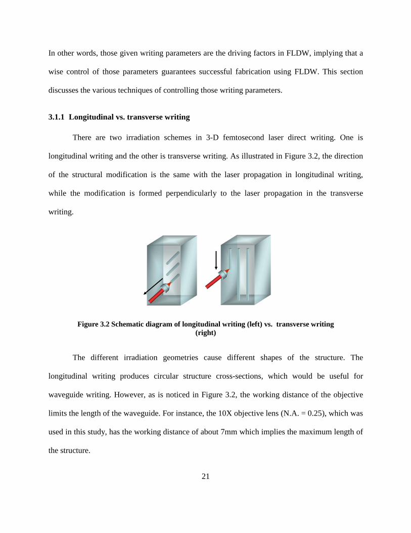
3.1.1 Longitudinal vs. transverse writing
There are two irradiation schemes in 3-D femtosecond laser direct writing. One is
longitudinal writing and the other is transverse writing. As illustrated in Figure 3.2, the direction
of the structural modification is the same with the laser propagation in longitudinal writing,
while the modification is formed perpendicularly to the laser propagation in the transverse
writing.
Figure 3.2 Schematic diagram of longitudinal writing (left) vs. transverse writing (right)
The different irradiation geometries cause different shapes of the structure. The
longitudinal writing produces circular structure cross-sections, which would be useful for
waveguide writing. However, as is noticed in Figure 3.2, the working distance of the objective
limits the length of the waveguide. For instance, the 10X objective lens (N.A. = 0.25), which was
used in this study, has the working distance of about 7mm which implies the maximum length of
the structure.

22
In transverse writing, the limiting factor of the length of the written structure is not the
working distance of the objective lenses, but the stroke of the translation stage and the sample
length. The transverse writing scheme is thus suitable for large area structuring. In this scheme,
the confocal length (twice of the Rayleigh length), which is determined by the NA of the
objective lens, can be another limiting factor depending upon the application. Figure 3.3
describes the difference between low and high NA lenses, which affects the shape of the voxel
and resulting structures.
Figure 3.3 The schematic illustration of the comparison of the voxel length by low NA and high NA objectives
In the longitudinal writing, the irradiation profile follows the cross-section of the writing
beam in the x-y plane, which is normal to the propagation direction along the z axis. This means
that the irradiation profile is always circular regardless of the NA of objective as mentioned
above. In transverse writing, the irradiation profile is the cross-section in the x-z plane, which is
elliptical in general.

23
In addition to the difference of irradiation cross-section, the beam overlap rate is also
described differently for each writing scheme. In Figure 3.3, the focal volume V of the voxel
produced by a microscope objective can be estimated as 0202 zwV π≈ with a beam waist 0w ,
Rayleigh length 0z and laser wavelength λ . Then the beam overlap rate r is described as Eq.
(3.1),
fznvr
fwvr
ol
t
0
0
21
21
−=
−=
, (3.1)
where f is the repetition rate of the laser system, v is a translation speed of the stage, no is
the refractive index of the medium, rt is the rate for transverse writing and rl is for longitudinal
writing.
The Beam overlap rate is an important fabrication factor determining the dimension and
resolution of the structure. Figure 3.4 shows an example of the longitudinal writing performed in
bulk PMMA, using LS I and a 10X objective (NA=0.25). As expected, perfect circular
waveguides are produced. It is also noticed that the line widths of the waveguides are different
although same objective lens was used. That is due to the different overlap rate varied by
different writing speeds, 20, 30 and 40µm/s. It shows clearly that longitudinal writing (or
alternatively a high NA (oil immersion) lens) is a suitable writing scheme in many applications,
which require well defined waveguide structures. For those applications, transverse writing with
low NA objectives may cause difficulty generating nicely shaped waveguides competitive

24
against the longitudinal scheme due to the long Rayleigh length of the lenses compared to beam
waist.
Figure 3.4 The side view and cross sections of waveguides in PMMA. The diameter of the waveguide varies with the writing speeds. (from left to right, 20 µm/s, 30 µm/s
and 40 µm/s)
For other applications seeking an elongated modification region (it is the main focus of
this dissertation), transverse writing using low NA objectives are a solution. Figure 3.5 shows the
microscopic images of the modification lengths variation of gratings produced by the transverse
writing scheme. The gratings were produced in a borosilicate glass as functions of NA of
objectives and laser pulse energy. A femtosecond laser system( LS III) with a repetition rate of
100 kHz created those gratings using various objective lenses from NA=0.2 to NA= 0.4 (a-c).
As is seen in Figure 3.5 (a-c), the difference of the lengths as a function of NA of the objectives
is observed. The writing speed and pulse energy were kept constant at 0.5 mm/s and ~2.4 µJ. The
modification length at NA=0.2 is approximately twice as long with respect to the length at
NA=0.4. Figure 3.5(d-g) shows the induced refractive index (Δn) variation of the modification.
In this case, Δn is induced as a function of the pulse energy (150 ~ 1500 nJ) under the same
focusing geometry (NA=0.4). It is clearly seen that the guided region from (d) to (g) becomes
brighter, which means higher guided light due to higher laser-induced Δn in (g). It implies that

25
the higher pulse energy induces higher refractive index change. The demonstration shown in
Figure 3.5 indicates that the dimension and the optical properties of the laser produced structures
can be controlled quantitatively by a single or combination of fabrication parameters listed above.
The following chapters will discuss the detail of the relationship between the NA and diffraction
efficiency of the diffractive optical element written by this scheme.
Figure 3.5 Optical images of the cross-section of the generated structures using
various focusing objectives with (a-c) numerical aperture variation at 100 kHz (a) NA = 0.4 (b) NA = 0.3 (c) NA = 0.2, (d-g) pulse energy variation (NA=0.4) pulse
(d)Ep=150 nJ (e) Ep=300 nJ (f) Ep=900 nJ (g) Ep=1500 nJ
As discussed in this section, the wise choice of the laser writing layout and irradiation
parameters as well as appropriate fabrication parameters is the key for the successful fabrication.
However, there is always a challenge in choosing appropriate parameters because of the
limitation of resources such as a limited choice of NA and a lack of the laser power causing low
throughput. One way to overcome those limitations is beam (pulse) shaping. The following
section discusses various beam (pulse) shaping techniques employed in laser direct writing to
achieve the desired results on each application.
26
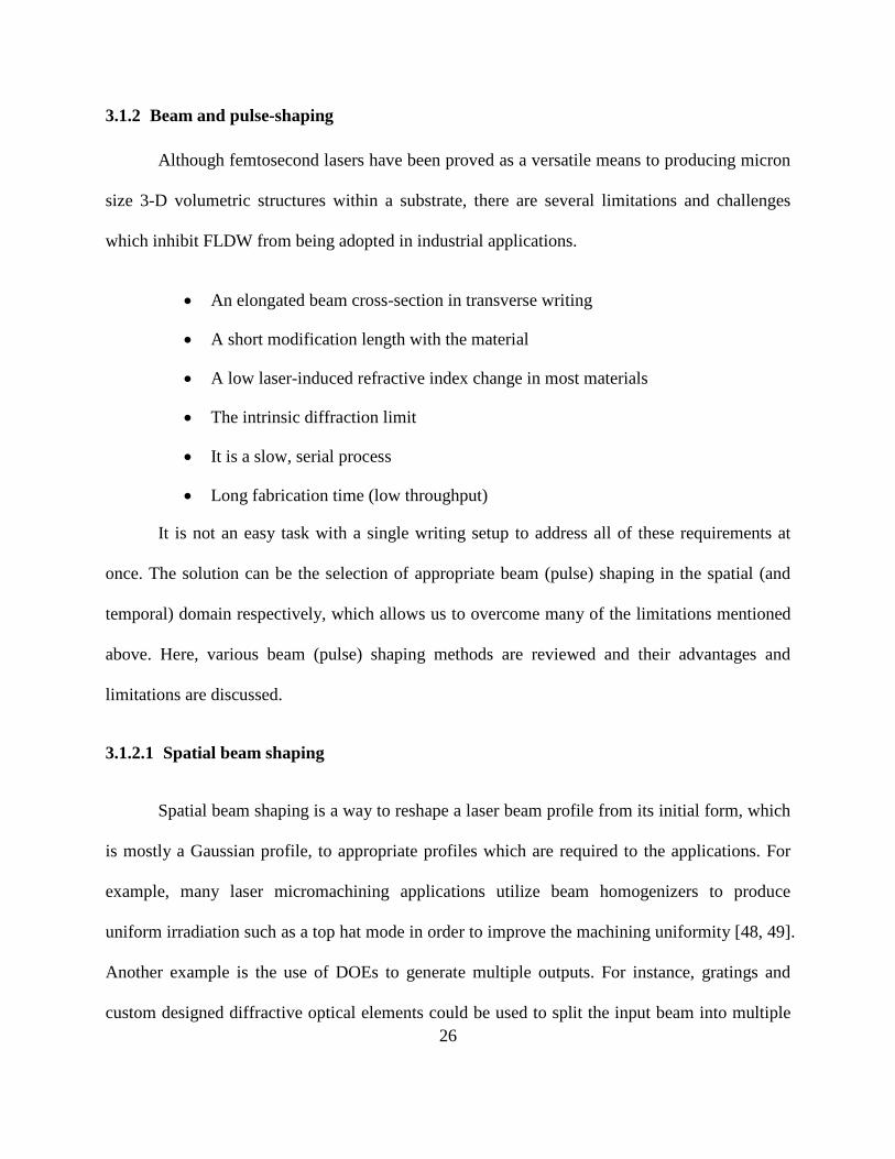
3.1.2 Beam and pulse-shaping
Although femtosecond lasers have been proved as a versatile means to producing micron
size 3-D volumetric structures within a substrate, there are several limitations and challenges
which inhibit FLDW from being adopted in industrial applications.
• An elongated beam cross-section in transverse writing
• A short modification length with the material
• A low laser-induced refractive index change in most materials
• The intrinsic diffraction limit
• It is a slow, serial process
• Long fabrication time (low throughput)
It is not an easy task with a single writing setup to address all of these requirements at
once. The solution can be the selection of appropriate beam (pulse) shaping in the spatial (and
temporal) domain respectively, which allows us to overcome many of the limitations mentioned
above. Here, various beam (pulse) shaping methods are reviewed and their advantages and
limitations are discussed.
3.1.2.1 Spatial beam shaping
Spatial beam shaping is a way to reshape a laser beam profile from its initial form, which
is mostly a Gaussian profile, to appropriate profiles which are required to the applications. For
example, many laser micromachining applications utilize beam homogenizers to produce
uniform irradiation such as a top hat mode in order to improve the machining uniformity [48, 49].
Another example is the use of DOEs to generate multiple outputs. For instance, gratings and
custom designed diffractive optical elements could be used to split the input beam into multiple
27
outputs with various intensities depending on the diffraction efficiency of DOEs [6]. These
elements enable parallel processing, thereby increasing the throughput of the machining system.
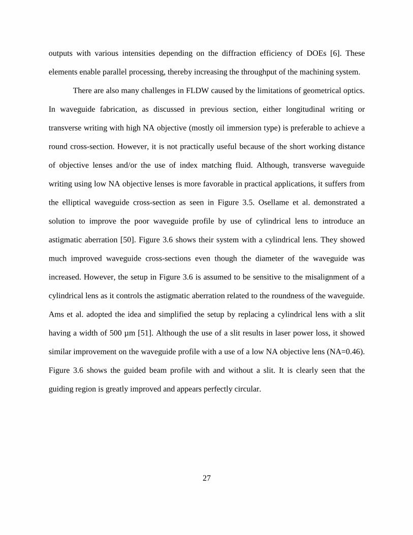
There are also many challenges in FLDW caused by the limitations of geometrical optics.
In waveguide fabrication, as discussed in previous section, either longitudinal writing or
transverse writing with high NA objective (mostly oil immersion type) is preferable to achieve a
round cross-section. However, it is not practically useful because of the short working distance
of objective lenses and/or the use of index matching fluid. Although, transverse waveguide
writing using low NA objective lenses is more favorable in practical applications, it suffers from
the elliptical waveguide cross-section as seen in Figure 3.5. Osellame et al. demonstrated a
solution to improve the poor waveguide profile by use of cylindrical lens to introduce an
astigmatic aberration [50]. Figure 3.6 shows their system with a cylindrical lens. They showed
much improved waveguide cross-sections even though the diameter of the waveguide was
increased. However, the setup in Figure 3.6 is assumed to be sensitive to the misalignment of a
cylindrical lens as it controls the astigmatic aberration related to the roundness of the waveguide.
Ams et al. adopted the idea and simplified the setup by replacing a cylindrical lens with a slit
having a width of 500 µm [51]. Although the use of a slit results in laser power loss, it showed
similar improvement on the waveguide profile with a use of a low NA objective lens (NA=0.46).
Figure 3.6 shows the guided beam profile with and without a slit. It is clearly seen that the
guiding region is greatly improved and appears perfectly circular.

28
Figure 3.6 Astigmatical beam shaping using a cylindrical lens (left, From [50]) and a waveguide written in a phosphate glass with/without a slit with width of 500
µm(right, From [51])
Another method of beam shaping is through the use of axicons. Axicons have been
widely used in trepanning drilling [52], optical tweezers [53] and many other applications
requiring a ring shape beam profile. Figure 3.7(a,b) shows a configuration of an axicon and its
ring-shaped intensity profile. Another advantage of using axicons is their very long beam waist.
Figure 3.7(c,d) shows the intensity profile of the setup with an axicon used for the fabrication of
very thin and long micro-channels [54].

29
Figure 3.7 A setup using axicon(a) and its beam profile (b) (c-d) micro channel formation using an axicon ( From [52, 54])
Splitting an input beam into multiple output beams is another pathway to improve not
only the throughput, but also the positional accuracy of a desired sub-pattern. Here we discuss
several examples of the use of DOEs and interferometric methods in femtosecond laser
processing. Figure 3.8 shows the laser micro-patterning using a four-level phase DOE which has
22 focal points with a partial periodic structure, demonstrated by Kuroiwa et al. [6]. The
researchers used a DOE designed by a computer generated hologram method for the wavelength
at 800nm.
Figure 3.8 A four-level phase DOE used for the laser drilling of SiO2 glass. (a) focal shape of the DOE pattern (left-without objective, right-with objective), (b,c) optical

30
microscope images of (b)ablation pattern on the surface of SiO2 glass (c) embedded structures within SiO2 glass (From [6])
Another case is the use of DOEs to produce multiple beam interferometer, demonstrated
by Misawa et al., for either holographic recording[55, 56] or multi-beam recording [57]. Figure
3.9 shows the universal configuration using a DOE for both recording types. The sample position
1 in Figure 3.9 is to irradiate the sample by a holographic interferogram while position 2 is for
the multi-beam scheme exposure. The laser-written grating shown in Figure 3.9 was recorded in
bulk As2S3 by direct multi-beam writing (31 inline beams) inducing photo-darkening. The same
exposure strategy was used to create 2-D micro rods using an interferogram via two-photon
polymerization, which is also shown in Figure 3.9(right).
Figure 3.9 Holographic writing method using a diffractive beam splitter (left) and photo-written grating (mid) and 2-D photonic crystal (right) demonstrated by
Misawa group. From [55-57]
Kawamura et al. also demonstrated a similar technique based on holographic recording to
create a micro grating in fused silica, which is shown in Figure 3.10. The colliding angle
between two beams was varied from 15~158°, corresponding to the fringe spacing of 3~0.43µm,
shown in Figure 3.10 (b) [58]. The second grating, which is in Figure 3.10 (c), was recorded by a
double exposure [59]. Once the hologram was recorded in one direction, the sample was rotated

31
90° to record the same grating in the perpendicular direction, so that the resulting pattern shows
buried periodic 2-D micro structure as seen below.
(a) (b) (c)
Figure 3.10 (a) Holographic recording setup using two beam interferometry and (b) surface and (c)volumetric gratings written in fused silica ( From [58, 59])
3.1.2.2 Pulse shaping in the temporal domain
As discussed above, the primary strategy of the beam shaping is to modify the input
beam’s spatial intensity either by diffraction, interference or any other method. However, it is not
closely related to the materials properties. Pulse shaping is also the reformation of the beam
intensity, but in the temporal domain. It can be related to the materials properties such as thermal
diffusivity and characteristic time constants of energy transfer between elementary particles and
plasma formation. Thus the aim of the pulse shaping is to enhance the photo-response of
materials to increase the efficiency of modification.
One of the commonly used techniques in FLDW is burst mode processing. The key idea
of the technique is converting a single input pulse into a burst, which consists of multiple sub
pulses with a sub-pulse interval τ. In general, τ is much shorter than the inverse of the repetition

32
rate of the laser system. Burst mode pulses are generated either by implementation of a two
(multiple) beam interferometer or by use of acousto-optic (AO) modulators, which enables fast
gating. In addition, the former has an advantage to have arbitrary sub-pulse interval depending
on a delay stage. However, the alignment required is very sophisticated. The advantage of the
latter scheme is the simplicity and easy configuration as well as quasi-arbitrary burst repetition
rate. In this case, the sub-pulse interval is not variable since the interval is the same as initial
repetition rate of the laser system. The interferometric configuration has been demonstrated
using the low repetition rate laser systems (a few kHz) and AO modulators are widely used for
the MHz repetition rate regime. The realization of the former has been demonstrated with a few
different schemes by Herman et al.[60], Marjoribanks group [61, 62], Siders et al. [63] and the
Laser plasma laboratory in CREOL [64, 65]. The typical implementation based on interferometry
is shown in Figure 3.11.

33
Figure 3.11 Interferometric configuration for burst pulse generation ( From [63]) and 8-pulse Hyper Michelson interferometer built in the laser plasma laboratory in
CREOL
The schematic of the use of AO modulator is illustrated in Figure 3.12. The
implementation has been demonstrated by Gattass et al.[45], Eaton et al. [46], Canioni et al.[66]
and other research groups.

34
Figure 3.12 The scheme of the gating with an AO modulator for burst pulse generation.
Figure 3.13 shows the comparison of the etch rate for single pulse and burst mode drilling
[60]. Two advantageous aspects of burst mode drilling are clearly seen in the figure. One is the
decease of the laser fluence for the onset of drilling. The other is the steeper slope of the etch
rate as a function of laser fluence. These attributes of burst mode drilling promises more efficient
drilling since the burst pulses enhance the photo-induced response of material either by
stimulating the formation of electron plasma or by increasing the local temperature due to the
heat accumulation. Figure 3.14(a) shows that the drilled diameter is increased and the onset of
the structural modificaiton is decreased as the number of the sub-pulse increases. It is probably
due to the efficient local heat accumulation in focal volume shown in Figure 3.14 (b).

35
Figure 3.13 The etch rate of single pulse vs. burst mode drilling ( From [60])
Figure 3.14 Drilled hole by a burst drilling with different sub-pulses. From [67]
Burst pulse processing has advantages not only in the increase of processing efficiency,
but also for the improvement of processing quality. Figure 3.15 shows the difference of single
and burst pulse drilling quality on the borosilicate glass. It is clearly noticed that the edge of
burst pulse drilled hole is much smoother than single pulse drilled hole at the same fluence. It is
due to lower sub pulse energy generating weaker shockwaves and less debris to the substrate
even though the total fluence of a burst is kept the same with the single pulse.
As mentioned briefly above, the control of the sub-pulse interval and burst pulse
repetition rate is important since it is closely related to the intrinsic material properties such as

36
thermal diffusivity and plasma formation. This infers that a sub-pulse interval should be
optimized for the material of interest. Figure 3.16 shows the difference of the burst pulse ablation
as a function of repetition rate and pulse interval on a tooth and on an alumina ceramic substrate
respectively.

37
Figure 3.15 Surface profile of drilled holes via single pulse and burst pulse (Borosilicate glass)
Figure 3.16 Burst mode ablation of tooth with ultrashort pulsetrain-bursts with 5,10 and 20 µs (From [61]) and alumina ceramic. (produced by Laser plasma lab,
From [65])

38
3.2
In this dissertation, three femtosecond laser systems were used for the different
requirements of investigations on a variety of materials and applications. The first system (LS I)
is a custom built extended cavity Ti:Sapphire oscillator with 26MHz rep. rate at ~800 nm center
wavelength. The second system (LS II) is a regenerative amplified Ti:Sapphire laser (Spitfire,
Spectra Physics) with the repetition rate of 1 kHz at 800 nm center wavelength. The third system
(LS III) is an Yb-doped femtosecond fiber laser (FCPA µJewel D-400-VR, IMRA America Inc.)
operating at various repetition rates from 100 kHz up to 5 MHz. The center wavelength is at
~1043nm with the pulse width of around 450fs. Table 3.1 shows the details of these laser
systems. With these three systems, customized laser irradiation in the low/ intermediate/ high
intensity regimes at various repetition rates is available on the materials of interest depending
upon the target materials for each application.
Femtosecond laser direct writing facilities used in this study
Table 3.1 Specifications of laser systems
LS I LS II LS III Type Ti:Sapphire Ti:Sapphire Yb doped fiber
Center wavelength (nm) 800 800 1043
Pulse width (fs) ~60 ~120 400 ~ 450
Rep. rate (MHz) 26 0.1 0.1 – 5
Pulse energy (Max) (µJ) <0.02 ~1000 < 51
1 At 100 kHz

39
These laser systems are integrated with laser direct writing systems consisting of
computer controlled 3 dimensional writing stages (VP-25XA, Newport and ALS-130, Aerotech),
and beam delivery optics including microscope objectives (NA=0.1~0.65) to deliver the
femtosecond beam to the sample. A LabView based program was developed to control the 3-D
stages in order to produce various diffractive patterns. Figure 3.17 depicts the laser writing setup.
Figure 3.17 Schematic diagram of a laser direct writing system
Figure 3.18(a) and (b) shows fully equipped laser direct writing setups for LS I and LS II
respectively. The beam (pulse) profiles of both laser systems were characterized using a
Grenouille (Model 8-20, Swamp optics), which is shown in Figure 3.18(b). The pulse widths
were measured to be ~60 fs and ~110 fs respectively. An optical parametric oscillator (OPO) was
attached to LS II to generate tunable wavelengths λ > 1 μm via parametric conversion. The
variable wavelength range of the OPO system is about from 1.2 to 2.6 μm.

40
Figure 3.18 (a) 26 MHz extended cabity Ti:sapphire oscillator (LS I) (b) 1 kHz regenerative amplified Ti:Sapphire laser system (LS II) with an optical parametric
oscillator (OPO)
Figure 3.19 shows a laser direct writing station using a Yb doped fiber laser system
which is referred to LS III above. The pulse width of the system was characterized by a custom
built auto-correlator, which is shown in Figure 3.19(b). The auto-correlation trace at 1 MHz
repetition rate is shown in Figure 3.19(c).
Figure 3.19 Laser direct writing system with (a) Yb-doped fiber femtosecond laser (LS III) (b) a custom-built auto-correlator (c) auto-correlation at 1 MHz ( <510 fs)

41
Various types of objective lenses are used for this work as shown in Figure 3.20. Low NA
refractive lenses (NA=0.1 ~ 0.4) were used for applications requiring long working distance and
deep modification depth while oil immersion lenses (NA=1.25) were used for high resolution
sub micron structuring. A Schwarzschild reflective objective (NA=0.5) offered small focused
beam size with long working distance (~ 10mm) which was useful for longitudinal writing in a
thick sample.
Figure 3.20 Refractive and reflective type objective lenses with various NA


42
CHAPTER 4 : CHOICE OF MATERIALS AND THEIR CHARACTERIZATION OF PHOTO-RESPONSE
This chapter discusses the potentials of various optical materials used in photonic device
fabrication, various methods and techniques used to observe the physical and chemical properties
of laser-written structures, and the photo-responses of materials under femtosecond laser
irradiation.
4.1
The first step to successful femtosecond material processing is to choose the right material
for the desired application guided by a deep understanding of material science. The second step
is to determine proper optical means for delivering light to the material including the laser
wavelength, pulse width, and pulse energy maximizing the photo-response of the material. A
variety of optical materials including (non) oxide glasses and photosensitive glasses were chosen
to explore the feasibility for a suitable platform of buried volumetric optical structures written by
a femtosecond laser. The candidate materials for photonic devices should possess the following
attributes:
Optical materials and their potential in photonic device fabrication
• High transmittance in the NIR for 3-D direct writing
• Low loss in the desired wavelength range
• Stability (chemically stable and robust to the air / moisture environment)
• Low thermal mechanical degradation with irradiated structure
43
Fused silica, borosilicate, and tellurite glasses have been chosen as oxide glass families of
interest and As0.42-x-yGexSbyS0.58 glass as non oxide glass family for the photosensitivity in NIR
range as newly developed for high nonlinear optical coefficient and superb MIR transparency.
Novel metal doped SiO2 thin films, silver containing tellurite, and zinc phosphate glass were also
investigated for the space selective photo-precipitation of metal nanoparticles. The samples,
except for commercial fused silica and borosilicate glass (EAGLE2000, PGO), were provided
from our collaboration groups at Clemson University and the University of Bordeaux I.
4.1.1 Oxide glasses
Oxide glasses have been widely used in the history of optics due to their superior optical
properties such as high transparency in the range from NUV to NIR as well as their robust
thermal, mechanical, and chemical stability. Furthermore, the explosive development of fiber
optic communication resulting from these glasses has brought much attention to oxide glasses. In
this research, fused silica and borosilicate glasses are discussed as conventional and
commercially available glasses and tellurite glass as an advanced optical material for novel
photonics application.
4.1.1.1 Fused silica / borosilicate
Fused silica is a preferred optical glass for the investigation of laser-matter interaction for
its simplest molecular structure to analyze underlying physical and chemical mechanisms by
femtosecond laser irradiation. Borosilicate glass is also a widely used commercially available
oxide glass because of its low thermal expansion coefficient. Many investigations using these
glasses have been demonstrated for FLDW such as passive and active waveguides [11, 68, 69],

44
Bragg gratings, and Fresnel zone plates. Recently, the huge interest in the micro-fluidic channels
fabrication has been rising towards the fabrication of lab-on-a-chip and disposable sensors [70,
71]. A great concern for many researchers has been fabricating reliable photonic structures,
which consist of micro-fluidic channels and waveguides, using FLDW. The refractive index and
thermal properties are given in Table 4.1.
Table 4.1 Refractive index and thermal properties of fused silica and borosilicate [72]
Fused silica2 Borosilicate (EAGLE 2000) 3
Refractive index
1.460 (1014.0nm) nD = 1,5068 (589,3nm)
Density (g/cm3) 2.202 g/cm3 (20°C) 2,37 g/cm3 (20°C)
Thermal expansion coefficient
(0-300°C) 5.5 x 10⁻⁷/ °C 31.8 x 10⁻⁷/ °C
(25-670°C) 36.1 x 10⁻⁷/ °C
4.1.1.2 Tellurite
Tellurite glasses exhibit high transparency in MIR, good thermal-mechanical stability,
and laser damage resistance. This glass family is also considered as good optical host materials
for rare-earth doping due to low phonon energy. Furthermore, these glasses are promising for
high Raman gain platform as they possess high linear and nonlinear optical refractive indices
compared to other oxide glass such as fused silica or phosphate glass. As a consequence, this
tellurite glass family has been investigated for Raman gain amplifier [73, 74], SHG [75-79] and
2 From ref[72]
3 From http://www.pgo-online.com/intl/katalog/eagle2000.html

45
nanofabrication[80]. In this dissertation, a tellurite glass with a composition of 70TeO2-10Bi2O3-
20ZnO is investigated as a base glass matrix and silver doped glasses from 2.5% to 7.5% Ag are
studied as well. This research explores the means by which one can locally precipitate silver
nanoparticles using femtosecond laser irradiation so that the glass can be a platform towards
nonlinear optical applications such as SHG. The details of the composition are shown in Table
4.2. This investigation aims to provide a summary of photo-induced responses of the newly
processed tellurite glass series subjected to the femtosecond laser irradiation.
Table 4.2 Compositional difference of Zn-Bi-tellurite with/without silver doping
Doping Composition
Undoped 70TeO2-10Bi2O3-20ZnO
Silver doped 2.5%Ag - 97.5%(70TeO2-10Bi2O3-20ZnO)
5%Ag - 95%(70TeO2-10Bi2O3-20ZnO) 7.5%Ag - 92.5%(70TeO2-10Bi2O3-20ZnO)
The absorption spectra near the femtosecond laser are shown in Figure 4.1.

46
300 400 500 600 700 800 9000.0
0.2
0.4
0.6
0.8
1.0
1.2
1.4
Abs
(a.u
.)
Wavelength (nm)
Undoped 2.5% Ag
Figure 4.1 Absorption spectra of tellurite family ((70TeO2-10Bi2O3-20ZnO (undoped), 2.5%Ag - 97.5%(70TeO2-10Bi2O3-20ZnO)
The absorption spectrum of 2.5% shows decrease of transparency in the range from 450
nm to 550 nm which may infer the insufficient quality of the glass due to the scattering. An
optical microscopic image of the sample confirmed that the glass has defects explaining the
absorption band.
4.1.2 Photosensitive glasses
The term “photosensitive” is used here in the sense of a material with narrow bandgap
with respect to the wide bandgap exhibited by materials such as fused silica, which leads to low
ablation threshold that is two orders of magnitudes lower than oxide glass in NIR range.
Fused silica has a bandgap of 8.9 eV which requires a multiphoton (~6) process for 800
nm femtosecond laser irradiation. This means that either a single photon in the deep UV regime
or multiple photons in ultrahigh intensity regimes (which enables multiphoton absorption) is
required to excite electrons from the ground state. Photosensitive glasses have, as their name

47
indicates, much lower band-gaps resulting in a lower damage threshold at NIR femtosecond
irradiation.
Chalcogenide glasses are amorphous semiconductors containing Chalcogen (Group VI: S,
Sb, and Te) species which are responsible for the high nonlinearity in this glass family as well as
high IR transparency and photosensitivity. The giant photo-expansion and photo-darkening by
near bandgap laser irradiation in ChG has been well known since a few decades ago, and studied
by many investigations [81]. Series of research on femtosecond laser irradiation in these glasses
have been intensively conducted by Laser Plasma Laboratory group as well [82-87]. In this
dissertation, home-made ChGs have been investigated in bulk form to study their laser-induced
photo-response when subjected to the femtosecond laser irradiation. As0.42-x-yGexSbyS0.58 glasses
have been also investigated, with glasses provided by the Clemson University team. The
preparation of the glass sample is described in [84, 88]. Table 4.3 and Figure 4.2 show their
chemical and optical properties. It is noted that as heavy Sb content is increased, the material
density is increased and the bandgap of the system is red-shifted. The refractive index is also
increased whereas in the case of increasing Ge content, the refractive index decreased from that
of As42S58.
Table 4.3 material properties of the system
Sample
EDS (±5%) Density
(g/cm3 ±0.02) Tg (°C ±5)
Cutoff wavelength (nm)
@ 10cm-1
As42S58 As42S58 3.20 210 580
As36Ge6S58 As34Ge8S59 3.15 220 580
As36Sb6S58 As37Sb6S57 3.40 208 625

48
Figure 4.2 Refractive index of given materials (top) in NIR region (bottom) in MIR region. From [84]4
4 Provided by N. Carlie at Clemson University

49
4.1.3 Noble metal ion containing glasses
Nobel metal nanoparticles embedded within glass provide a great opportunity to tune
optical properties of glass matrix by changing their metallic compositions, size, and
concentration. They exhibit large third-order nonlinear susceptibility and ultrafast nonlinear
response which promotes them to be promising materials for an ultrafast all-optical switch in the
THz region [89-91]. Moreover, these glasses would be suitable for the platforms of nano-
structured surface plasmonics prepared by laser irradiation. Commonly, ion exchange and ion
implantation are used to provide a means of space-selective precipitation of nanoparticles in a
substrate [92-94]. However, after further treatment, both the composition of the glass matrix and
the nanoparticles-precipitated area are restricted in the ion-exchange method. Laser direct writing
can offer versatility of space selective formation/dissolution of nanoparticles without any
restriction and damage.
4.1.3.1 Ag/Cu/Au doped silica glass prepared by sol-gel method
Three metal species (Ag, Au, Cu) have been used as dopant ions in silica glass films
prepared by sol-gel method to investigate photo-induced metallic nanoparticles
formation/dissolution using UV and NIR light sources including a CW UV lamp, a 3rd harmonic
Nd:YAG laser, and a 1 kHz Ti:Sapphire laser. The metallic precursors were dissolved in a
solvent to be mixed with a tetraethylorthosilicate (TEOS, C8H20O3Si, Sigma –Aldrich), using
ethanol as the solvent. The final solution was sealed and stirred at room temperature for 24 h.
The films were spin-coated on microscope slides with the thickness less than 1 µm and annealed
for 15 h at 150 ºC. The absorption spectra before and after the irradiation will be presented in the
next section.

50
4.1.3.2 Silver containing zinc phosphate glass
The glass composition of the matrix is 40P2O5-xAg2O-(5-x) Ga2O3-55ZnO (molar
percent) [95, 96]. The glass was produced using a melt-quench method. (NH4)2HPO4, ZnO,
AgNO3, and Ga2O3 were the raw materials. Gallium oxide was introduced to increase the glass
stability. The raw materials were placed in platinum crucible and heated up to 1000 ºC with the
heating rate of 1 ºC/min. Then the glass was annealed at 320 ºC (55 ºC below Tg) for 3 hours.
The concentrations of silver oxide (Ag2O) for this research were 1% and 4% (mol %). Figure
4.3 shows the absorption and emission spectra of the glass [96]. The emission located at 380 nm,
corresponding to the absorption at 265nm, is attributed to isolated Ag+ silver ions.
Figure 4.3 Absorption and emission spectra of 1 % silver containing zinc-phosphate glass. From [92]

51
4.2
4.2.1 Physical domain
Characterization of laser-written structures
4.2.1.1 Differential interference contrast (DIC) optical microscopy
Optical microscopy is the most commonly used technique to observe the physical
appearance of surface features. Although the resolution of the technique is governed by the
optical diffraction limit, various image quality enhancement techniques generally enable micron
to submicron resolution. Specifically, a DIC optical microscope exploiting a polarizer and an
analyzer provides the ability to increase the contrast of the region possessing slightly different
refractive indices. This configuration has provided powerful imaging means for transparent
specimen such as biological cells, tissues, and glasses. Therefore, it is suitable not only for
surface modifications, but also for the observation of femtosecond laser-written embedded
structures in a transparent substrate such as a photo-induced refractive index change exhibiting a
similar refractive index with their transparent surroundings.
4.2.1.2 White light surface profiler
White light interferometeric surface profilometry is a non-contact method to characterize
the surface of the specimen. The Zygo NewView 6300 (Zygo Coporation, http://www.zygo.com/)
was used to measure and characterize the surface expansion or contraction induced by laser
irradiation with nanometer resolution. The Zygo profiler is based on the Fizeau interferometry:
the light from a white light LED is split into two arms. One is reflected from the surface of the
sample and then interferes with the other arm reflected from the reference surface. The resulting

52
interferogram is analyzed to be converted as the surface profile. This profiler offers high vertical
resolution (< 0.1 nm) since it is based on white light interferometry and the coherence length of
the light source is very short. The lateral resolution is from 0.36 to 9.5 µm, which is objective
dependent. Figure 4.4 shows an example of the surface profile measurement. Femtosecond laser
irradiated bulk As36Ge6S58 exhibits photo-expansion on the order of up to a few hundred
nanometers. The surface profile reveals that the expanion is laser dose dependent. The detail of
the analysis is presented in section 4.3.2.
Figure 4.4 Photoexpansion of bulk As36Ge6S58 glass measured by zygo white light surface profiler
4.2.1.3 Optical coherence microscopy
Optical coherence microscopy (OCM) provides noninvasive highly resolved 3-
dimensional images of biological specimens [97, 98]. To date, very few studies on imaging
femtosecond laser directly written samples have been carried out [13]. As OCM implementations
have been constructed with Ti:Sapphire-based femtosecond lasers to take an advantage of its
broadband spectrum, the materials of interest for femtosecond laser machining such as oxide
glass and optical polymers possess the same transparent windows as the OCM probe source. This
means that it is possible to perform low noise measurements relying on low intrinsic extinction
ratios. Because this technique does not require any sample preparation prior to the measurement,

53
it may be utilized as a fast diagnostic means of the laser direct writing to evaluate the real time
quality of the processed structure in the specimen.
The OCM system used in this research provides ~2.5 µm axial resolution in air and ~1.72
µm in fused silica corresponding to a 120 nm bandwidth. The lateral resolution is dependent on
the objective lens. In this work, 0.12 NA objective lens providing 4.4 µm lateral resolution and
35 µm depth of focus in fused silica was used. Figure 4.5 shows an embedded laser-induced
refractive index change and void formation written in fused silica substrate. The sample was
produced to examine the detectability of the OCM facility with the S/N ratio of ~ 97 dB. Figure
4.6 is the OCM images of the side view and top views of the void formation created by 8.3 µJ.
The 3-D structures are clearly seen without any shadow effect. However, the refractive index
change is not detected, probably due to the low index change of the fused silica, implying the
induced index is less than 10-5 corresponding to the sensitivity of 97dB [99].

54
Figure 4.5 (a) Map of the buried structure (b) optical image of the laser-written structure in fused silica
Figure 4.6 OCM images of buried 3-D structure (a) side view (b-d) top views at different depths (Images were provided by the ODA lab, led by Dr. Rolland.)

55
To increase the photo-induced refractive index change and improve detectivity of
refractive index change, a bolosilicate glass was used as a substrate. Figure 4.7 and Figure 4.8
are the images of a buried FZP taken by a DIC optical microscope and OCM respectively. The
172 images of side view in x-z plane were acquired by scanning in x-direction. The top view
image was then reconstructed from re-slicing 172 images. This image clearly proved that OCM
can detect refractive index changed structrures. Furthermore, the modified length can be
measured without any sample preparation such as grinding and polishing.
Figure 4.7 An embedded FZP written in borosilicate
Figure 4.8 OCM images of an embedded FZP written in borosilicate (a) top view (b) side view (a mirror image is also shown in the side view which can be removed by a
appropriate data analysis) (Images were provided by the ODA lab, led by Dr. Rolland.)

56
4.2.1.4 Laser-induced refractive index change
Refractive index change of laser-written structure can be measured with several methods
such as refracted-near field profilometry [9, 47], microellipsometer [7], cylindrical waveguide
mode solving routine (Rsoft BeamPROP) [46, 100] OCT [13], guided mode analysis of a written
waveguide [13], white light interferometry [82, 86], Swanepoel analysis [86, 101] and grating
method [14, 16]. These methods are complementary to each other in terms of accuracy and ease
of measurement. Grating method is a measurement of diffractive power of input beam via a
laser-induced grating. This method does not provide either a precise number or sign of the index
change, but estimation of overall change due to the formation of a grating. However, it is often
used for its easy scheme as well as simple implementation. Figure 4.9 depicts the concept of the
measurement. The refractive index change is deduced from the measured diffraction efficiency
which is the ratio of the 1st diffracted power to the input power.
Figure 4.9 A schematic illustration of a measurement of the refractive index change using a grating method.
The diffraction efficiency of the amplitude / phase grating can be represented by the Eq. 4.1[102]

57
22 )4
()( Kdndm
∆+
∆=
λπη ,
(4.1)
where η is a diffraction efficiency of the 1st order, Δn and ΔK are the refractive index and
absorption coefficient of the glass, and d is the depth of the grating, and λ is the wavelength of
input beam. In this work, most transparent phase gratings utilized for the estimation of laser-
induced gratings. In phase grating, ΔK is negligible, thus Eq. (4.3) involving Bessel function is
often used alternatively [14].
)cos
2()( 22
θλπδη nLJJ mmm
∆== .
(4.2)
4.2.2 Chemical domain
4.2.2.1 Raman spectroscopy
Raman spectroscopy is a means to investigate a transition which is forbidden by one-
photon excitation. It is useful to investigate the change of molecular structure by stimulation,
specifically in this study, stimulation by intense laser irradiation. Figure 4.10 shows a depiction
of the Raman scattering. The involved energy levels are indicated as g, n and n’ which are a
ground level and upper states respectively. Stokes Raman scattering is a transition from g to n
via intermediate state related to n’ (ω > ωs) and Anti-Stokes scattering is vice versa (ω < ωs)
where ω and ωs represents excitation photon and Raman scattering respectively.
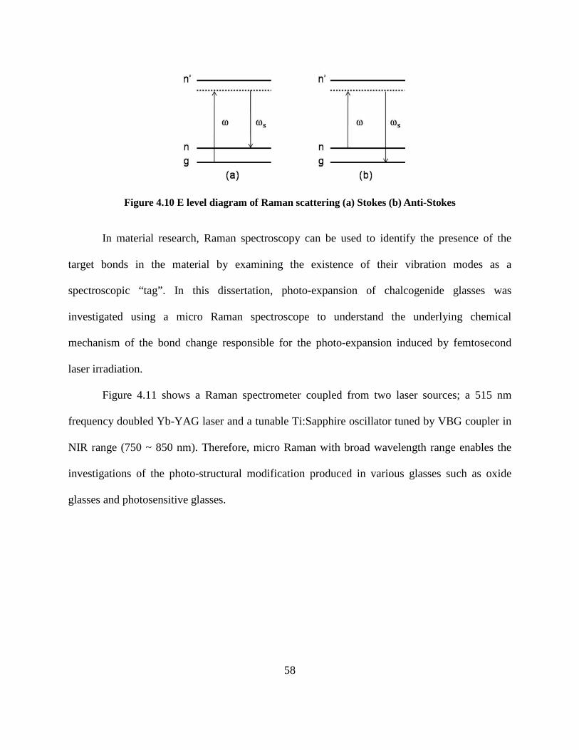
58
Figure 4.10 E level diagram of Raman scattering (a) Stokes (b) Anti-Stokes
In material research, Raman spectroscopy can be used to identify the presence of the
target bonds in the material by examining the existence of their vibration modes as a
spectroscopic “tag”. In this dissertation, photo-expansion of chalcogenide glasses was
investigated using a micro Raman spectroscope to understand the underlying chemical
mechanism of the bond change responsible for the photo-expansion induced by femtosecond
laser irradiation.
Figure 4.11 shows a Raman spectrometer coupled from two laser sources; a 515 nm
frequency doubled Yb-YAG laser and a tunable Ti:Sapphire oscillator tuned by VBG coupler in
NIR range (750 ~ 850 nm). Therefore, micro Raman with broad wavelength range enables the
investigations of the photo-structural modification produced in various glasses such as oxide
glasses and photosensitive glasses.

59
Figure 4.11 VBG coupled multi-pump Raman spectroscope
4.2.2.2 UV-VIS-IR spectrophotometry
The UV-VIS-IR spectrophotometer is an apparatus consisting of a broadband light source,
a monochrometer, a photo detector, beam delivery optics, and sample holder. It is used to
measure the fraction of light that passes through a sample. The light is then detected through a
monochrometer to select only one wavelength from the continuum to measure the portion of the
wavelength. The monochrometer is swept throughout the desired wavelength range. Thus, the
linear optical properties such as transmission and absorption of the sample are measured. A
CARY 500 (Varian Inc), which offers a detection range from 170 nm to 3300 nm, was used for
this investigation. It was intensively used for extinction spectroscopy experiment (attenuation by
absorption and scattering) to confirm the formation/dissolution of metallic nanoparticles in
Ag/Au/Cu doped SiO2 thin film by UV laser or NIR femtosecond laser irradiation. It is well
known that noble metal nanoparticles such as Ag and Au induce additional absorption bands in
the host material at the visible range due to surface plasmon resonance, which can be explained

60
by Mie theory [103]. The location of the absorption band depends on their size, shape, and
density. Therefore, not only the existence of metallic nanoparticles, but also their physical
properties can be deduced from the extinction measurement. The example of the measurement is
shown in 4.3.3.
4.2.2.3 Fluorescence (confocal) microscopy
Photoluminescence is an emission from a semi-stable level to the ground level. This
process occurs when an electron is excited from the ground state to higher energy level by
absorption of photon via external excitation. The electron spontaneously decays to the next lower
level by energy loss until it reaches the semi-stable level. The electron emits a photon
corresponding to the difference of energy from upper level to ground level. If the radiation is
spin-allowed transition, the process is called “fluorescence” whose lifetime is typically 0.1 ~10
ns[104]. Figure 4.12 shows a schematic diagram of fluorescence process. As is seen, the energy
of the emitted photon cannot exceed the energy of excitation photon due to energy conservation.
In general, fluorescence provides the information on the intrinsic electronic configuration in the
material which can be used as a “fingerprint” of the presence of the material. Fluorescence
(confocal) microscopy is widely used for biological imaging and material science for the
investigation of the fluorophore tagged specimen or intrinsic fluorescent materials.

61
Figure 4.12 Diagram of the energy levels involved in fluorescence
In this dissertation, fluorescence microscopy was also used to investigate the properties
of photo-reduced silver clusters since their photoluminescence properties are well known [105-
107]. One-photon or two-photon fluorescence spectroscopy using femtosecond laser irradiated
silver containing zinc phosphate glass was investigated to confirm the existence of photo-
reduced silver clusters in the glass after irradiation. The details of the experiment to confirm the
precipitation of silver nanoparticles in zinc phosphate glass by their photoluminescence
properties will be present in section 4.3.3.
4.3
4.3.1 Ablation threshold measurements
Photo-response of materials under femtosecond laser irradiation
Ablation is the process describing destructive, violent removal of the material from the
surface by intense laser irradiation. “Optical breakdown” is often misused as an alternative term
in similar phenomena by laser pulses, but it is a more general process regarding the breaking
bonds between molecules, and not necessarily either material removal or confined on the surface.

62
However, ablation and optical breakdown thresholds of a material of interest are similar in the
order of magnitude. Thus, bond strength of the material of interest is often estimated by
measuring ablation threshold because phenomena on the surface are easier to observe and
analyze than the events in the bulk. Figure 4.13 shows a typical ablation threshold map whose
one axis represents an intensity of the irradiation and the other axis is a function of time (or
number of pulses). Black dots are a physical removal of material from the surface of the sample.
Figure 4.13 Optical microscopic image of an ablation threshold map (PMMA)
Table 4.4 shows ablation thresholds of a variety of optical materials including glasses and
PFCB polymer. As discussed, the ablation threshold of materials can be estimated through their
absorption properties. As is shown in the table, borosilicate glass exhibits the highest ablation
threshold while chalcogenide glass family has the lowest value.

63
Table 4.4 Ablation threshold of various glasses and polymers at different repetition rates5
Sample
Irradiance ( GW/cm2 )
1 kHz (800 nm)
9.44 MHz (1030 nm)
26 MHz (800 nm)
Microscope slide glass (borosilicate)
55.2E+3
Tellurite TeO2-Bi2O3-ZnO (TeBiZn) 12.9E+3 3.0E+3
TeO2-Na2B4O7 (Te9) 930.0
Borophosphate (1-x)(0.514Ca(PO3)2-
0.436NaPO3-0.05Na2B4O7) – x
Nb2O5
X=0.025 8.4E+3
X=0.30 3.4E+3
X=0.40 3.4E+3
X=0.45 2.5E+3
Chalcogenide
As42S58 446.3
As36Sb6S58 297.6
As36Ge6S58 485.1
PFCB (polymer) 813.0 419.06
In Figure 4.14, schematic depiction of the ablation threshold of the optical materials
tested for this dissertation is illustrated as functions of intensity and repetition rate. It should be
noted that, even for the same material composition, higher repetition rates tend to reduce ablation
threshold. This issue will be discussed later.
5 Measurement errors are less than ±5%
6 Measured at different repetition rate of 36 MHz

64
Figure 4.14 Schematic diagram of the ablation threshold ranges of optical material families
It may also be noticed that ablation threshold variance is dependent on the absorption
properties in the similar composition with the same base material. For instance, in the
borophosphate family, the absorption bandgap shifts to longer wavelength as the amount of
Nb2O5 increases. The shift leads to a decrease of the ablation threshold, as shown in Figure 4.15.
The same trend is also seen in Chalcogenide glass family. In Table 4.3, The bandgap of As42S58
and As36Sb6S58 has similar at 580nm while As36Sb6S58 has a red-shifted bandgap at 625nm. As
seen in Table 4.4, As36Sb6S58 has the lowest ablation threshold that results from the red shift of
the absorption bandgap closed to the laser wavelength of λ = 800 nm.

65
300 350 400 450 500 550 6000
2
4
6
8
10
12
14
Abso
rptio
n Co
effic
ient
(cm
-1)
Wavelength (nm)
Nb2.5 Nb30 Nb40 Nb45
Te9
Figure 4.15 Absorption spectra(top) and ablation threshold (bottom) of
borophosphate and tellurite (Te9) glass
It should also be noted that, even same material shows different ablation threshold at
different repetition rate, as discussed in Chapters 2 and 3. In the case of tellurite glass (TeBiZn),
the ablation threshold at 1 kHz is one order of magnitude higher than 9.44 MHz, even though the
laser wavelength is slightly different in NIR regime. PFCB polymer shows the same result, but
not as drastic as tellurite. This confirms that it is the heat accumulation effect which reduces the

66
onset of material damage. Figure 4.16 shows threshold maps of 10 µm thick PFCB thin film
irradiated at different repetition rate, 1 kHz and 36 MHz.
Figure 4.16 Ablation threshold map of PFCB at different repetition regime
(a) 36 MHz (b) 1 kHz
4.3.2 Photoexpansion and related structural modification
Photo-expansion of chalcogenide glass induced by laser irradiation is quite well known
feature. Tanaka et al. [81, 108] observed giant photo-expansion of As2S3 by HeNe laser
irradiation. In this investigation, photo-expansion via femtosecond laser irradiation was
systematically investigated as a function of laser dose. Six lines with 200 µm were written on the
each bulk ChG glasses (As42S58 /As36Sb6S58/ As36Ge6S58) via 26 MHz femtosecond laser pulses
centered at ~800nm. A 10X microscope objective with NA=0.25 was used to focus the laser
beam into the sample. The laser pulse energy was kept constant, ~90% of the ablation threshold
of materials to produce the maximum photo-expansion. In this way, laser dose was controlled
only by writing speed and is inversly proportional to the writing speed. Laser dose was changed

67
as a function of writing speed. The writing speed was varied from 5~160 µm/s. Figure 4.17(a)
shows the photo-expansion of bulk As36Ge6S58. In the picture, the photo-expansion decreases as
writing speed increases due to the reduced laser dose. The trend is clearly seen in other glasses
shown in Figure 4.17(b).
0 50 100 150 200 250 300 350 4000
10
20
30
40
50
60
70
AsSbS AsGeS AsS
Phot
oexp
ansi
on (n
m)
Dose (kJ/cm2)
(a) (b)
Figure 4.17 (a) Photoexpansion of bulk As36Ge6S58 glass measured by zygo white light surface profiler (the translation speed was varied from the highest line, 5, 10, 20, 40, 80 and 160 µm/s) (b) Photoexpansion of As42S58/ As36Ge6S52/ As36Sb6S58 as a
function of laser dose. . From [109]
The photo-expansion by femtosecond laser irradiation was investigated with micro
Raman in order to understand the molecular bond changes responsible for the photo-expansion.
In Figure 4.18, the Raman spectra of three compositions after laser irradiation are shown. There
is no real change in the main band of As42S58 after irradiation while As36Sb6S58 and As36Ge6S58
has significant decrease of peak in the main band. However, all three compositions exhibit
changes in the regions from 200 to 250 cm-1 and 450 to 500cm-1. This is attributed to the creation
of As-As and S-S bonds. As36Ge6S58 also shows a broadening of the main band with increasing
dose.
0.00 0.02 0.04 0.06 0.08 0.10 0.12 0.14
-0.02
-0.01
0.00
0.01
0.02
0.03
0.04
0.05
Phot
oexp
ansi
on (µ
m)
Distance (mm)

68
(a)
(b)
(c)
Figure 4.18 Raman spectra of given materials after fs irradiation (a) As42S58 (b) As36Sb6S58 (c) As36Ge6S58
69
4.3.3 Metallic nanoparticle formation
The conventional method used to form metallic nanoparticles is thermal treatment or via
γ-ray or e-beam irradiation for localized formation. The underlying mechanism of the formation
of nanoparticles in the metal ion containing glass is well understood [92, 94, 105, 107, 110]. The
intense irradiation from these sources forms color centers, which exist as e- and hole trap pairs.
Consequently, metallic ions can be then reduced by the free electrons generated during
irradiation. Post irradiation annealing helps the reduced atoms to aggregate (by diffusion) and
become larger clusters. After annealing, the glass turns colored due to newly generated
absorption by the surface plasmon resonance of metallic nanoparticles formed in the glass.
Different metal species, particle size, and concentration of metal nanoparticles lead to different
absorption properties. This means that one can tune the absorption properties by changing those
parameters. Several research groups including Qiu et al. demonstrated that femtosecond laser
irradiation can also form metal nanoparticles in the glass [111, 112]. The advantage of this
method over the conventional means discussed above is the ability to create 3-D structures
consisting of metal nanoparticles which might be useful for fabricating surface plasmonic
structures.
UV-VIS-IR spectrophotometers are commonly used for extinction spectroscopy to verify
the existence of absorption band resulting from surface Plasmon resonance. By measuring
absorption bandwidth and its peak location, the size and concentration of metal nanoparticles can
be estimated. Figure 4.19 shows the transmission spectra of laser irradiated metal doped film.

70
(a) (b)
Figure 4.19 Formation / dissolution of nanoparticles in SiO2 thin film (a) dissolution of Cu nanoparticles by irradiation of CW/ns light at 355 nm. (b) Formation of Au
particles by UV light followed by 30 min heat treatment at 520 °C
In the picture, it is seen that the amplitude of the absorption peak decreased by 355 nm
CW/ns irradiation which confirms that UV light source dissolves metal nanoparticles in the glass
film. Figure 4.19(a) shows opposite result. Irradiation of UV nanosecond laser or IR
femtosecond laser followed by heat treatment for 30 minutes at 520°C changes the location of
the absorption peak. It should be noted that the absorption peak resulting from surface plasmon
resonance was shifted to the blue region also the bandwidth of the peak was decreased which
means the laser irradiation changed the size distribution of the nanoparticles.
Partial reduction of silver and formation of clusters formed of Ag0 and Ag+ can be
detected by investigation of the luminescence property of the materials. Figure 4.20 shows the
photoluminescence of silver ion containing zinc phosphate (P2O5-Ag2O-Ga2O3-ZnO) after
1043nm fs laser irradiation. The glass was excited at 405 nm and emitted typical red color near
600nm which proves the existence of silver clusters Agmx+ (m<10) formed by laser irradiation.
200 400 600 8000
20
40
60
80
100
Un-treated cw 450J/cm2
ns 1500J/cm2
%tra
nsmi
ssion
Wavelength (nm)
400 600 800
80
A.U
300 6000
20
40
60
80
100
%
Tran
smiss
ion
Wavelength (nm)
non irradiated cw irradiated ns irradiated

71
450 500 550 600 650 700 7500.0
0.5
1.0
Norm
alize
d In
tensit
y
Wavelength (nm)
A2 A4 C2 C4
λexc = 405 nm
(a) (b)
Figure 4.20 (a) Fluorescence microscopic image of laser-induced silver clusters (b) fluorescence spectra of the emission of silver clusters with the excitation at 405 nm
4.3.4 Refractive index change
The complete mechanism for laser-induced refractive index change of all optical
materials is not well understood yet. However, for a few cases, rigorous investigations have
clarified the underlying mechanism responsible for laser-induced refractive index change Δn. For
instance, laser-induced densification of fused silica, which is a glass with a simple (binary)
molecular form, is well understood as to its origin of the laser-induced refractive index change
[113]. In this study, femtosecond pulse-induced Δn in bulk ChGs has been systematically studied
in the relation of photo-expansion involved with a photo-induced structural change.
The embedded gratings were written in bulk ChGs (As42S58 /As36Sb6S58/ As36Ge6S58) via
26 MHz femtosecond laser pulses at ~800 nm wavelength. A 10X microscope objective
(NA=0.25) was used to focus the laser beam into the sample. The laser pulse energy was kept
constant below the ablation threshold of each material and only the writing speed was varied to
change the laser dose. The size of written gratings was 1.5 mm × 1.5 mm and the grating period

72
was 20 µm. The grating depth was estimated via DIC optical microscope measurements. The
diffraction efficiency was measured and laser-induced Δn was calculated from the measured
diffraction efficiency and grating depth with the equation in the section 4.2.1.4. Figure 4.21
shows the estimated laser-induced Δn as a function of laser dose. It can be seen that Δn exhibits a
similar trend to the laser dose induced photo-expansion. It should be noticed that although the
laser-induced Δn is proportional to the laser dose, the compositional difference leads to different
magnitudes of Δn at similar laser dose. It is evidenced that near a laser dose ~10kJ/cm2, up to
3~4 times greater Δn is seen in As36Ge6S58 as compared to As42S58. It is also interesting to note
that the peak Δn of almost 10-2 is seen in the binary glass.
Figure 4.21 Laser-induced Δn of bulk As42S58 /As36Sb6S58 / As36Ge6S58
0 10 20 30 40 500
1
2
3
4
5
6
7
8
9 AsSbS AsGeS AsS
Refra
ctiv
e in
dex
chan
ge (
X 10
-3)
Dose (kJ/cm2)


73
CHAPTER 5 : FEMTOSECOND LAER WRITTEN DIFFRACTIVE OPTICAL ELEMENTS
As discussed in the previous chapters, the strength of the FLDW technique is its flexible
patterning scheme and 3-D structuring capability, making it a natural choice for fabricating
custom-designed 3-D photonic devices, especially volumetric 3-D phase DOEs that require
precisely controlled refractive index modification in micrometer scale.
This chapter reviews the current state-of-the-art in 3-D DOE fabrication, mainly
concentrating on embedded phase type FZPs using FLDW, and makes suggestions on how to
overcome the limitations of the prior works.
5.1
5.1.1 Embedded Fresnel zone plates
Prior results of fabrication of FZPs using FLDW
FZPs, perhaps the most classical and simplest form of DOEs, are thin and planar
diffractive structures operating as focusing optics that are preferred in many applications seeking
compactness and simple fabrication process. Thus, FZPs have been investigated as a substitution
of refractive optics for their compactness towards integrated micro-optical devices and imaging
systems utilizing micro-optics.
Watanabe et al. demonstrated the first femtosecond laser written embedded FZP in fused
silica which was an amplitude type binary FZP; this structure however possessed micrometer
size voids leading to high scattering and additional absorption [20]. As a consequence, this type
of FZP exhibited extremely poor diffraction efficiency, less than 3 % at 632.8 nm, limited
primarily by void-induced loss.

74
The phase type binary FZP demonstrated by Bricchi et al. overcame this diffraction
efficiency drawback by replacing voids with laser-induced refractive index change to increase
diffraction efficiency [22]. These FZPs showed highly improved diffraction efficiency, up to 39%
at 404 nm, and relatively lower efficiencies at 550 nm and 642 nm. They explained that the laser-
written structure provided greater phase shift for shorter wavelength because the effective length
of the modified region is longer for shorter wavelength even though the physical modification
length is fixed. Interestingly, their FZPs exhibited birefringence, hence, the diffraction efficiency
was varied not only as a function of wavelength but also the polarization of the probe beam. The
diffraction efficiency in one polarization was only ~17% of the diffraction efficiency of the
orthogonal direction. Figure 5.1 shows the optical microscopic images of both amplitude [20]
and phase [22] type laser written FZPs.
Figure 5.1 Amplitude type by void formation from [20] (left) and phase type FZP by
laser-induced refractive index change from [22] (right)
Binary FZPs (Figure 5.1) have a theoretical diffraction efficiency of 40.5%, insufficient
for most applications. In 2004, Yamada et al. demonstrated a multilevel FZP which was realized
as a four-level structure and provided ~58% diffraction efficiency at 632.8 nm (Figure 5.2, left)
[21]. In the case of four-level FZP, the theoretical diffraction efficiency is 81%.

75
In spite of this high efficiency, the fabrication time to create the FZP structure was
extremely long (21 hours). Such a long manufacturing time is not attractive for practical use.
Srisungsitthisunti et al. proposed a central ring method which is the replacement of a full-width
Fresnel zone by the single track of index change to reduce the fabrication time (Figure 5.2, right)
[23]. Consequently, their central ring FZP showed very low diffraction efficiency with a single
layer. In order to increase the device efficiency, they proposed a volumetric scheme which
accumulates the phase shift by the stacking of appropriately located layers of the central ring
FZP. They optimized the distance between layers to cause an in-phase cumulative phase shift
from each layer.
Figure 5.2 Four-level FZP from [21] (left), and volume Fresnel Zone Plate composed of central ring. From [23] (right)
In Table 5.1, the specifications of the femtosecond laser written embedded FZPs are
shown. The majority of the prior works have been done using 1 kHz repetition rate pulses. Laser
written FZPs suffer from low diffraction efficiency due to the low photo-induced refractive index
change. To increase the refractive index change, either a slow writing speed to increase
cumulative laser dose or thick FZPs consists of many layers to increase cumulative phase shift
are required. However, both cases cause extremely long fabrication time at 1 kHz which is not

76
desired for practical applications. The demonstration in ref [22] provided high diffraction
efficiency, close to its theoretical limit (40.5%), however previous research results showed only
at limited range in polarization and short wavelength.
This section clearly shows the challenges in fabrication of embedded FZPs using FLDW
as following. First, it should offer high diffraction efficiency regardless of the input polarization.
Second, the fabrication should be compatible with a practical requirement which implies short
fabrication time. Then the aim of this dissertation, to provide a solution of those challenges, can
be justified. The investigation to develop a protocol towards the goal is present in section 5.3.
Table 5.1 Specifications of FZP demonstrations
Type Material Diffraction efficiency
(%)
Probe beam wavelength
(nm)
Writing Rep. rate
(kHz)
Pulse energy
(µJ) NA
Writing speed
(mm/s)
Fabrication time (h)
Amplitude [20]
Fused silica 2 632.8 1 0.4 0.55 - -
Phase (binary) [22]
Fused silica 39 404 250 1.3 0.55 0.4 -
Phase (multilevel)
[21]
Synthesized silica
56.9 632.8 1 0.8 0.3 0.005 21
Phase (central ring)
[110] Fused silica
71.57
632.8
7.1 1
10 ~ 15 0.1
0.15 0.8
0.01 < 68
7 For eight layers
8 Estimated from ref[6],40 minutes per layer

77
5.1.2 Surface relief Fresnel zone plates
Two-photon polymerization is a pathway to realizing 3-D free standing structures that
exploits FLDW. Chen et al. demonstrated eight-level reflective diffractive FZP shown in Figure
5.3 by two-photon polymerization followed by electroless plating [114]. It is probably the
highest multilevel FZP structure fabricated via FLDW up to date. They obtained high diffraction
efficiency up to ~68 %.
Figure 5.3 Reflective diffractive FZP fabricated by two-photon polymerization.
From [114]
Kim et al. produced a binary FZPs on the surface of a mode-expanded hybrid optical
fiber shown in Figure 5.4, which can also be an example of the post processing of FZP onto a
commercial device [115]. To enlarge the surface area of the single mode fiber whose diameter is
10 µm, a coreless silica fiber with 200 µm diameter was attached as a beam extension element on
the single mode fiber. The FZPs were produced on the other end of the coreless fiber by direct
ablation using a 1 kHz femtosecond laser and 23 and 11 Fresnel zones were produced for the
focal lengths of 300 µm and 600 µm respectively (Figure 5.4(b)). The focused beam sizes were
estimated to be 10.9 µm for f = 600 µm and 10.4 µm for f = 300 µm. The diffraction efficiency

78
was not specified; however, binary type FZPs made by direct ablation are supposed to have low
diffraction efficiency due to the scattering loss.
Figure 5.4 Binary FZP created on a coreless silica fiber attached on to a single mode fiber. From [115].
5.2
In this section, the basic knowledge on the FZPs, including the formulation, is offered. The
custom design parameters and fabrication conditions of laser written FZPs produced by this work
are also provided.
Femtosecond laser written FZPs
5.2.1 Fresnel zone plates
A side view of a binary FZP is shown in Figure 5.5. To formulate the radius of a Fresnel
zone plate, the illustration depicts two light paths traveling from s to p: one is d + d’ and the
other is z + f. The path difference between two paths can be expressed as Δ(r) shown in Eq.
(5.1)[116].
)()()'()( 2222 fzfrzrfzddr +−+++=+−+=∆ . (5.1)

79
In order to have an integer multiple of half the wavelength for the condition of the Fresnel zone
plate (the phase of adjacent zones cancel each other out), the path difference Δ(r) has to satisfy
Eq. (5.2)
)(2
rn ∆=λ , (5.2)
where λ is the wavelength of interest and f is the focal length of the FZP.
Figure 5.5 Side view of a binary FZP (reproduced from the illustration in [113])
The Rn, which is the nth zone boundary radius of a FZP is then
22
2
2 oon fnfR −
+=
λ . (5.3)
When n becomes large, the square of λ can be ignored and the Rn can be approximated as
fnRn λ≅ . (5.4)
For multilevel FZP with N-level, the equation can be modified as Eq. (5.5) [117]
+
=
Nfn
NnRn
λλ 22
. (5.5)

80
It should be noted that the formulation is made under the assumption that the focal point
is in air. In the case of embedded FZP produced by FLDW, Eq. (5.4) and Eq. (5.5) should be
modified as Eq. (5.6) when the focus is located in the same media. Therefore, the λ has to be
substituted by λ/no , where no is the refractive index of the substrate.
o
n nfnR λ
≅ ,
+
=
Nnfn
NnnR
oon
λλ 22
.
(5.6)
Diffraction efficiency of the multilevel FZP with N levels can be described as Eq.(5.7)
[117]
2
)/()/sin(
=
NN
N ππη .
(5.7)
Figure 5.6(a-e) shows the illustration of the common refractive lens and several FZP
schemes. Figure 5.6(b) and (d) shows binary phase lenses while Figure 5.6(c) and (e) shows
quaternary lenses which are four level phase lenses.

81
Figure 5.6 Illustration of (a) refractive lens (η=100%) and (b,c) surface relief diffractive lenses (b) Binary lens (N=2, η=40.5%) (c) Quaternary lens (N=4, η=81%),
(d-e) embedded phase lenses (d) Binary and (e) Quaternary lens
For the binary FZP with single layer, N=2 and the theoretical diffraction efficiency is
40.5% while the quaternary FZP has 81% diffraction efficiency. In terms of the FZP shape,
Figure 5.6(b) and (c) depict surface relief zone plates and (d) and (e) illustrate embedded zone
plates. In laser direct writing, Figure 5.6(b-c) can be produced by either direct ablation or laser-
assisted etching in order to produce surface relief by material removal. The phase difference
results from the index difference between air (n=1) and the refractive index of the substrate (no).
For embedded zone plate in Figure 5.6 (d) and (e), the index difference between the laser
modified region and the refractive index of the material causes a phase difference.
The maximum diffraction efficiency is obtained when the optical phase shift is π,
corresponding to the half of the wavelength, and causes constructive interference at the primary
focal point. The phase shift Δф induced by femtosecond laser writing is defined as

82
πλφ ==∆=∆2
nl (5.8)
where Δn is a photo-induced refractive index change, l is a modification length, and λ is
the wavelength of interest. Hence, the phase shift (ultimately diffraction efficiency) can be
controlled by changing Δn or l. It implies that the manipulation of diffraction efficiency as
functions of Δn or l is achievable by changing fabrication parameters, such as laser dose, laser
repetition rate, the NA of focusing optics, substrate materials, or the number of stacked layers.
5.2.2 Fabrication and diffraction efficiency measurement
The FZP was designed for a wavelength of 543.5 nm which is selected for the test
wavelength in the diffraction efficiency measurement setup. The focal length and the diameter of
the FZP was 20 mm and 1.3 mm respectively. The NA of the FZP was calculated as ~ 0.033.
Designed FZPs were created in bulk borosilicate (EAGLE2000, PTG). The thickness of the
substrate was 1.1 mm and the surface area was 2 × 2 square inches. FZPs were written using
different laser repetition rates, NA of objectives and pulse energies.
Two femtosecond laser systems (LS II and LS III) described in Chapter 3 were used to
fabricate FZPs. The laser irradiance was below the damage threshold of borosilicate, and
therefore did not create voids in the glass. A phase type FZP, relying on the photo-induced
refractive index change, was produced. The laser parameters for the different repetition rates
used in the fabrication process are shown in Table 5.2.
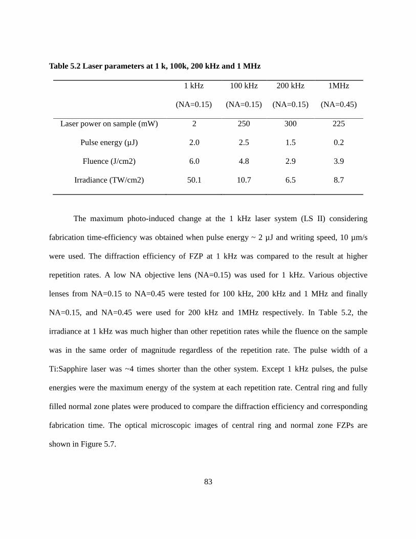
83
Table 5.2 Laser parameters at 1 k, 100k, 200 kHz and 1 MHz
1 kHz
(NA=0.15)
100 kHz
(NA=0.15)
200 kHz
(NA=0.15)
1MHz
(NA=0.45)
Laser power on sample (mW) 2 250 300 225
Pulse energy (µJ) 2.0 2.5 1.5 0.2
Fluence (J/cm2) 6.0 4.8 2.9 3.9
Irradiance (TW/cm2) 50.1 10.7 6.5 8.7
The maximum photo-induced change at the 1 kHz laser system (LS II) considering
fabrication time-efficiency was obtained when pulse energy ~ 2 µJ and writing speed, 10 µm/s
were used. The diffraction efficiency of FZP at 1 kHz was compared to the result at higher
repetition rates. A low NA objective lens (NA=0.15) was used for 1 kHz. Various objective
lenses from NA=0.15 to NA=0.45 were tested for 100 kHz, 200 kHz and 1 MHz and finally
NA=0.15, and NA=0.45 were used for 200 kHz and 1MHz respectively. In Table 5.2, the
irradiance at 1 kHz was much higher than other repetition rates while the fluence on the sample
was in the same order of magnitude regardless of the repetition rate. The pulse width of a
Ti:Sapphire laser was ~4 times shorter than the other system. Except 1 kHz pulses, the pulse
energies were the maximum energy of the system at each repetition rate. Central ring and fully
filled normal zone plates were produced to compare the diffraction efficiency and corresponding
fabrication time. The optical microscopic images of central ring and normal zone FZPs are
shown in Figure 5.7.

84
Figure 5.7 Laser written embedded FZPs at 100 kHz (a) 7 layers of single track with 0.5 mm/s writing speed (b) 4 layers of full zone with 1 mm/s
After direct writing, the diffraction efficiency was measured using a power meter (Ophir,
PD200) and near field focus profiles of the fabricated FZPs were acquired using a CCD beam
profiler (Spiricon Inc., SP-980M). Diffraction efficiency was systematically investigated as
functions of laser writing parameters. It was estimated by calculating a power ratio between an
input beam and its primary focus through the FZP.
5.3
The diffraction efficiency of phase type FZP are present as functions of laser repetition
rate, laser dose, optical power of the objective lens and number of layers of FZP. First, this work
describes the influence of NA, repetition rate and laser dose and the number of layers to obtain
the maximum DE. Both single track FZPs and full zone FZPs are investigated. This section also
discusses fabrication time of FZPs under various repetition rates.
Results

85
5.3.1 Single layer
A central ring method was first investigated to simplify fabrication process for
minimization of fabrication error which might be introduced by cumulative uncertainty. With
this approach, photo-induced refractive index change and modification length per single layer
could be optimized. A normal FZP was produced to study the figure of merit of the fabrication
time as functions of writing speed and beam overlap rate of each track in a filled zone.
5.3.1.1 Central Ring: optimization of NA
A variation of the diffraction efficiency (DE) depending on the NA of the objectives was
investigated. Three objectives (NA=0.15, 0.25 and 0.45) were examined at 200 kHz. The
corresponding pulse energy was 1.31~1.52 µJ depending on the transmission of the objectives.
The confocal lengths are calculated to be 156 µm, 56 µm and 17 µm for NA =0.15, 0.25 and
0.45 respectively at 1043 nm in the borosilicate (no=1.5). Figure 5.8 shows the DE of central ring
FZPs as a function of NA and their confocal length (shown in the inlet). At 200 kHz, the highest
DE was obtained with the lowest NA (0.15) and it is decreased as NA is increased. As shown in
inlet of Figure 5.8, the DE for 200 kHz was proportional to the confocal length.

86
Figure 5.8 Diffraction efficiency varied by a function of NA (inlet, diffraction efficiency varied by a confocal length)
5.3.1.2 Central Ring: optimization of repetition rate
The DE was investigated in terms of the repetition rate as a function of laser dose. Laser
dose can also be varied as functions of laser pulse energy and number of pulses, which can be
easily controlled by varying translation speed of the sample. Since the FZPs were made in the
bulk material, this work assumed a 3-D unit of the laser dose involving pulse energy and
translation speed to describe the influence of the laser dose to 3-D structure. Laser dose D,
having unit of J/cm2 is redefined as volumetric unit J/cm3 by Eq.(5.9) [118].
Av
QED p= (5.9)
Where Ep is the pulse energy, Q is the laser repetition rate, and v is the writing speed. A
is the cross sectional area of the voxel normal to the direction of the sample translation. In our

87
case, A is equal to 2 ooo zwnπ which is the cross section of the ellipsoid where no is a refractive
index of the medium, wo is the beam waist and zo is the Rayleigh length. All DE measurements
were present using this unit.
Single layers of FZP were made at 1 kHz, 100 kHz, and 200 kHz by a central ring
method. An objective with NA=0.15 was used to obtain high a DE. Laser power was kept
constant (Table 5.2) during all fabrications at each repetition rate. The laser dose was thus
only varied as a function of writing speed which varies the number of pulses per unit area. The
laser parameters at different repetition rates are given in Table 5.2. The scanning speed was 0.1,
0.5, 1 and 2 mm/s at 100 kHz and as 0.25, 0.5 and 1 mm/s at 200 kHz. The corresponding laser
doses are given in the x axis in Figure 5.9. Clearly, faster writing speed corresponds to the lower
laser dose and vice versa.
As shown in Figure 5.9, the overall trend of the DE of single layer FZP was proportional
to the laser dose, which corresponds with the prior research that indicates higher laser dose
induces more refractive index change [82, 86, 119]. The DE at 100 kHz and 200 kHz is much
higher than 1 kHz at the laser dose of under 1 MJ/cm3, although the pulse energy and irradiance
at 1 kHz was higher than 100~200 kHz (Table 5.2). It is three times higher at similar laser dose
for 200 kHz than 1 kHz. First, it is thought that the longer modification length due to the longer
wavelength of 1043 nm would be one reason to lead to the higher DE. The confocal length of the
objective lens (NA=0.15) is ~156 µm at 1043 nm and ~125 µm at 800 nm. The modification
length was close to the confocal length for both cases. But, it is not the dominant factor to
explain the difference. It is assumed that high repetition rate, over one hundred kHz, produces
higher Δn resulting from the thermal effect due to accumulation [46, 120].

88
Figure 5.9 Diffraction efficiency for a single layer of the single track FZPs as a function of laser dose at different repetition rate. The scanning speed was converted
as laser dose
5.3.1.3 Normal FZP: optimization of repetition rate
The increase in DE is dependent on the repetition rate is clearer in Figure 5.10 for normal
zone FZPs. The DE at 200 kHz is higher than at 100 kHz even at similar dose and at the same
wavelength. The pulse energy was smaller at 200 kHz under similar dose. It implies that the
higher photo-induced Δn, due to the localized heat accumulation is primarily responsible for the
difference. It confirms the prior research by Eaton et al. [120] that indicates the initiation of heat
accumulation was found at 200 kHz with the same type of glass.
The fabrication times are also drastically reduced at 100 kHz and 200 kHz, ranging from
~2 minutes for the lowest DE (1.7%) to 40 minutes for the highest DE (10.2%) whereas prior
result demonstrated 90 minutes for 1 kHz (DE = 0.5%). It supports that high repetition rate lasers
are very useful, not only for high efficiency but also fast fabrication process. The evidence of the

89
increase of the diffraction efficiency due to high repetition rate is discussed in detail in the next
section.
Figure 5.10 Diffraction efficiency as a function of laser dose at 100 kHz and 200 kHz.
5.3.1.4 Normal FZP: Figure of merit
There is a tradeoff between fabrication time and diffraction efficiency for FZPs produced
by FLDW. Table 5.3shows the fabrication time depending on the writing speed and FZP type
(normal zone vs. central ring). Figure of merit (F) was defined as diffraction efficiency per
fabrication time in minutes compared to the efficiency generated from the different fabrication
conditions. As shown in Table 5.3, normal zone plate shows much higher F than the central ring
zone plate. In the prior research [23], the central ring volume FZP method was considered to
reduce the fabrication time. However, the method is not suitable where compact device size is
required since they obtained maximum DE with 8 layers of Central ring volume FZPs which is
~1 mm thickness. As the fabrication time is dramatically reduced by the use of high repetition

90
rate pulses, several layers of normal zone plates produced by using higher repetition rates over
100 kHz would be more efficient for compact device fabrication than central ring volume FZPs.
The FZPs produced by faster writing speed exhibit higher F (Figure 5.11). As the
fabrication time is decreased, the DE is also decreased, but the decrease rate is slower than the
fabrication time. Hence the figure of merit increases as writing speed increases, but is slightly
saturated over 1mm/s. Optimization of spacing between tracks is also investigated. The
maximum figure of merit was obtained for 2 µm spacing, corresponding to the ~ 67% overlap
between adjacent tracks in a filled zone (Figure 5.12). The most efficient single layer of normal
zone FZP can be produced with the writing speed around or greater than 1 mm/s with 67%
overlap. One can produce efficient FZPs by stacking several layers of the optimized single layer
with reasonable fabrication time. It is interesting to compare the figure of merit, F of the DOEs
demonstrated in the prior work, reviewed in the previous section with the best result of this work,
which is F=2.55 for 2mm/s writing speed. As present in Table 5.1, the FZP produced by
Srisungsitthisunti et al. exhibited 71.5% efficiency with ~ 6 hours of fabrication time. The F of
their FZP is 0.23, which is only 10% of the result shown here. The F of Yamada et al. shows
poorer value: with the 56.9% diffraction efficiency and 21 hours of fabrication time, the F is only
0.047, which is 2% of this work. This comparison proves clearly that the fabrication protocol
suggested by this investigation achieved not only the improvement of diffraction efficiency, but
also short fabrication time.

91
Table 5.3 Fabrication time, diffraction efficiency and figure of merit of 3-D FZPs
Writing
speed at
200 kHz
Single track plate Full zone plate
(67% overlap between tracks)
Fabrication
time, T
(minute)
DE, η
(%)
Figure of
merit, η/ T
(%/minute)
Fabrication
time, T
(minute)
DE, η
(%)
Figure of
merit, η/ T
(%/minute)
2mm/s 1:40 - - 3:50 9.8 2.55
1mm/s 3:00 1.7 0.57 6:54 14.9 2.16
0.5mm/s 6:00 2.5 0.42 13:45 19.1 1.39
0.01mm/s
(at 1kHz) 300:00 0.5 0.0017 - - -
Figure 5.11 8 Full zone with different writing speed at 200 kHz (inlet is figure of merit)

92
Figure 5.12 Full zone with different spacing with the writing speed of 1 mm/s at 200 kHz
5.3.2 Multi layer
It is a challenge to obtain very high DE with single layer phase FZP due to small photo-
induced Δn. Consequently stacking of multiple layers is of interest to increase DE of the laser
written FZPs [21, 23]. Here the trend of DE as a function of the number of layers was
investigated to look at the evolution regarding phase accumulation. This work describes the
effect of stacking for central ring and normal zone FZPs under various fabrication conditions.
Layers of central ring and normal zone FZP were stacked coaxially with the separation distance
of ~150 µm. The first layer was written at the location which was the bottom layer. Then the
sample was moved downward as the layers separated (~150 µm) so that the writing beam
propagation was not interrupted by the written structures. The stacked FZPs were produced at
100 kHz and 200 kHz with up to 6 layers.

93
Figure 5.13(a) shows the DEs of stacked central ring FZPs written at 100 kHz. As shown
in the graph, the DE increases as either number of layer or laser dose increases. As described in
the previous section, the laser dose was changed by varying the writing speed. The speed was 2,
1, 0.5 and 0.1 mm/s corresponding to the laser dose of 0.13, 0.25, 0.5 and 2.5 MJ/cm3. The
maximum DE for given parameters were ~23% for six layers at dose of 2.5 MJ/cm3. The
fabrication time of a single layer was about 30 minutes. The plateau of DE was observed
between the 5th and 6th layer at the highest dose. This is probably caused by the fabrication error.
Incoherence between diffracted beams multi-layer configuration would allow higher order phase
depth because the theoretical DE of binary FZP is given as ~40%.
Figure 5.13(b) shows the DEs of the central ring FZPs with selected conditions with
different writing speed at 100 kHz and 200 kHz. The corresponding laser dose at 1 mm/s and
0.25 mm/s for 200 kHz is 0.3 MJ/cm3 and 1.2MJ/cm3 respectively. It is interesting to note that
similar DE results were obtained for 100 kHz and 200 kHz even though much less of a dose (fast
speed) was applied at 200 kHz.

94
(a)
(b)
Figure 5.13 DE of the stacked single track FZPs (a) FZPs written at 100 kHz . The corresponding writing speeds are 2, 1, 0.5 and 0.1 mm/s (b) FZPs written at 100 kHz
and 200 kHz
This also implies the evidence of heat accumulation effects proposed in the previous
section that higher repetition rate would give increased photo-induced refractive index change
than lower repetition rate. Using higher repetition rate pulses can reduce fabrication time and
laser dose to produce FZPs possessing similar DE written by lower repetition rate pulses. The
fabrication time for 0.25 mm/s is ~12 minutes which is only 40% of the fabrication time for

95
0.1mm/s. In this case, about 50% of the reduction of the fabrication time is obtained for
increasing repetition rate from 100 kHz to 200 kHz.
Figure 5.14(a-c) shows the DE of stacked normal zone FZPs at 100 kHz and 200 kHz
with varied writing speeds with identical pulse energy across the variance of speed. The DE is
increased as the number of FZPs is increased. However, after it reached the theoretical maximum
of ~40%, the DE is decreased although the number of layers is increased. It shows intuitively the
optical phase shift of a layer under certain fabrication parameters. It is shown in Figure 5.14(a)
that the maximum DE is located between 2nd and 3rd layer of FZP at 0.5 mm/s while 3rd and
4th layer for 2 mm/s. It shows the same trend for 200 kHz in Figure 5.14(b). It is also shown to
be true for different repetition rates in Figure 5.14(c). The result written with 2 mm/s at 100 kHz
and 200 kHz, calculated laser doses are 0.13 and 0.15 MJ/cm3 respectively.

96
(a)
(b)
(c)
Figure 5.14 (a) DE of the full zone FZPs written at 100 kHz, (b) DE of the full zone FZPs written at 200 kHz (c) DE of the full zone FZPs written at 2 mm/s, 100 / 200
kHz

97
5.4
In conclusion, it was clearly seen that a use of multi-hundred kHz repetition rate laser
increased significantly the DE of laser written FZPs. Localized heat accumulation is considered
to be responsible for the increase. Fabrication time was also drastically reduced compared to that
of 1 kHz. In this way, not only central ring scheme, but also full zone FZPs can be fabricated in a
hour with high DE, which is a great improvement from a prior works.
Conclusion and possible applications
Both central ring FZP and normal FZP was discussed in single layer or multilayer form.
The advantage of a single layer of high DE FZP may be the disadvantage of a stacked FZP in
terms of number of layers. For instance, single layer FZP with reasonable DE would be
appropriated in compact micro-optical device fabrication or imaging application which requires
least aberration from FZP. For the application seeking highest DE, multi-layer structures will be
suitable, but the image resolution may be decreased while light signal passes multi-layer
structure. In this case, multi-layer FZP would fit to applications such as light collection optics.


98
CHAPTER 6 : INTEGRATION OF MULTIPLE PHOTONIC STRUCTURES
Numerous demonstrations have been made of laser directly-written single photonic
devices exploiting FLDW. However, advanced device schemes consisting of multiple laser-
written structures integrated on a single chip have not been fully explored. Simple waveguide
arrays and a stack of FZPs are the only exceptions [23-25].
This chapter explores the feasibility of integrating multiple photonic structures, as a way
to develop a fabrication protocol based on FLDW for integrated optical device platforms. This
chapter also presents a few examples of the integrated optical structures that are truly all-optical
directly written devices, along with a discussion of their characterization.
6.1
In this section, this work proposes types of integration involving laser written structures
and their properties. One is multiplexing and the other is heterogeneous integration. Multiplexing
is realized by constructing arrays of the same type of devices to enhance functionality.
Heterogeneous integration can be realized by integrating multiple structures with different
functionality in a single device. The latter may be a more general meaning of integration. More
details of each regime are discussed below.
Type of integration
6.1.1 Multiplexing (homogeneous integration)
The first regime of integration is multiplexing which is the addition of plural structures or
duplication that perform identical functions. The purpose of multiplexing is to increase the
number of events of interest via parallel processes so that the overall system speed or output can

99
be enhanced. For instance, a 1 × N channel increases the number of event N times. In optical
systems, multiplexing can be implemented by such optical elements like beam splitters and
micro lens arrays which divide the input beam into plural output beams.
Conceptually, there are two types of beam dividing methods. One is fragmentation (or
spatial division) and the other is partial transmission (or power attenuation). Figure 6.1 shows
two schematic diagrams of beam division. Figure 6.1(a) is a depiction of spatial beam division
using a means to split the input beam spatially. Micro lens arrays or mirrors can be the means in
this case. It is easily assumed that the output beams through a micro lens array with N micro
lenses can have an equal split 1/N of input power only when the input beam has uniform power
distribution and the micro lenses have the same size. Otherwise, the beam profile of the whole
input beam cannot be duplicated but fragmented and the power cannot be equally divided in free
space optics. The conventional micro lens array as a free space optic belongs to the
fragmentation type. Sometimes, this feature is useful for analysis of wave-front distortion and is
also known as Shack-Hartmann wave-front sensor.
(a) (b)
Figure 6.1 Schematic diagram of beam splitting devices (a) type I, fragmentation (spatial division) (b) type II, partial transmission (power attenuation)
Figure 6.2 shows an example of multiplexing implemented by a fiber array and an array
of micro lens.
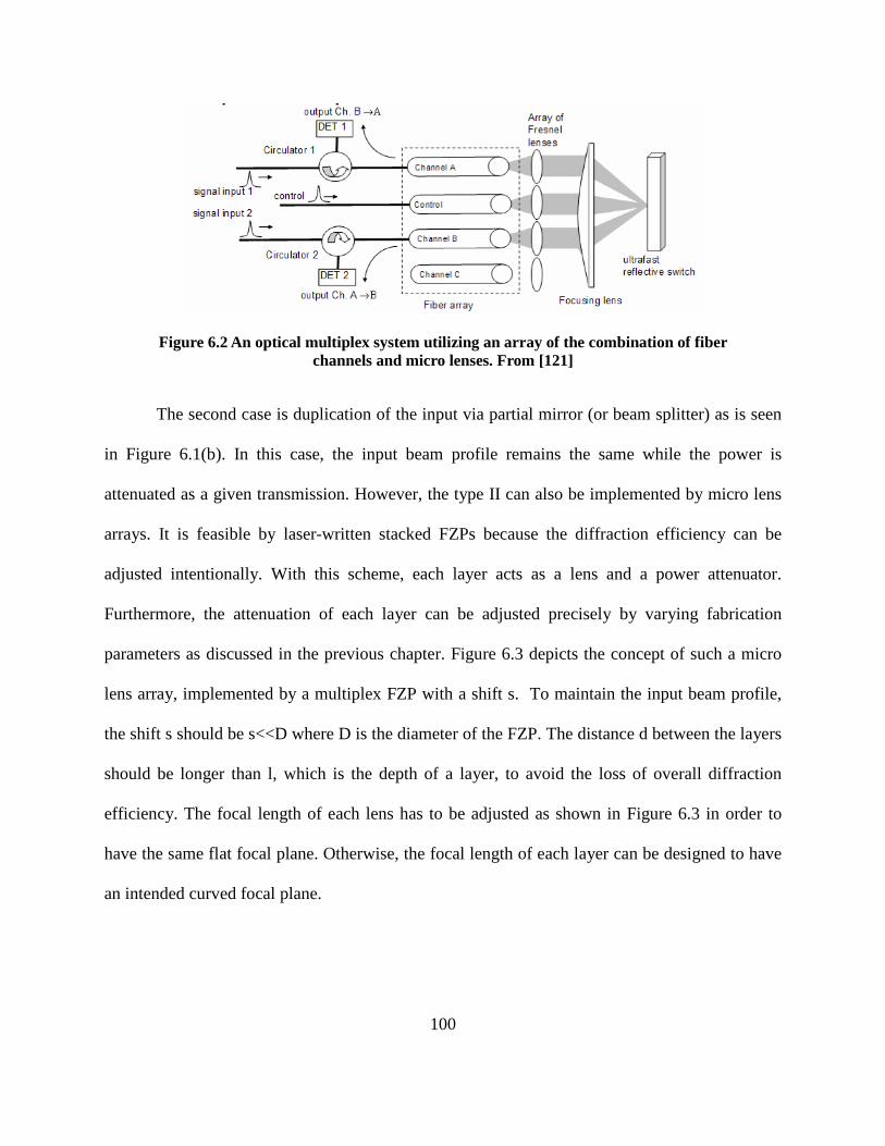
100
Figure 6.2 An optical multiplex system utilizing an array of the combination of fiber channels and micro lenses. From [121]
The second case is duplication of the input via partial mirror (or beam splitter) as is seen
in Figure 6.1(b). In this case, the input beam profile remains the same while the power is
attenuated as a given transmission. However, the type II can also be implemented by micro lens
arrays. It is feasible by laser-written stacked FZPs because the diffraction efficiency can be
adjusted intentionally. With this scheme, each layer acts as a lens and a power attenuator.
Furthermore, the attenuation of each layer can be adjusted precisely by varying fabrication
parameters as discussed in the previous chapter. Figure 6.3 depicts the concept of such a micro
lens array, implemented by a multiplex FZP with a shift s. To maintain the input beam profile,
the shift s should be s<<D where D is the diameter of the FZP. The distance d between the layers
should be longer than l, which is the depth of a layer, to avoid the loss of overall diffraction
efficiency. The focal length of each lens has to be adjusted as shown in Figure 6.3 in order to
have the same flat focal plane. Otherwise, the focal length of each layer can be designed to have
an intended curved focal plane.

101
Figure 6.3 Schematic diagram of a stack of spread FZPs
The attenuation power of a layer is determined by the diffraction efficiency of the layer.
Then, the input to each layer is affected by the attenuation of the previous layer as in the Eq. (6.1)
11)1( −−−= nnn II η , (6.1)
where nI and nη are the input and the diffraction efficiency for the nth FZP respectively.
6.1.2 Integration of heterogeneous structures
The second category is the integration of heterogeneous structures that is the combination
of different type of photonic structures performing different functions in a single chip or
substrate. In this way, the device exhibits multi-functional performance. Conventional integrated
devices require multi-step fabrication processes to construct a combined structure. In FLDW,
multiple structures can be written in 3-D within a bulk transparent substrate by a single step
process. In Figure 6.4, a schematic depiction of a “built-in coupler” consists of a FZP and
waveguide array is shown as an example of this type of integration. The structure has an
advantage in terms of robustness and reliability over the conventional coupling devices which
are separately made and integrated. The structure is expected to be free from any misalignment

102
issues resulting from thermal or mechanical stress due to the difference of material properties of
the devices.
Figure 6.4 Schematic depiction of the integration of a FZP and a waveguide array
6.2
This work demonstrates a few examples of the realization of the integration of laser-
written photonic structures. The characteristic features of each device platform are discussed as
well. All the structures demonstrated in this section were produced by the Yb-doped fiber
femtosecond laser (LS III) which was described in Chapter 3. In the fabrication process, two
microscope objective lenses were used. A lens with NA=0.15 was used for FZP fabrication to
obtain long modification depth for high diffraction efficiency. The other is NA=0.4 for
waveguide writing to minimize the elongation of the cross-section of the waveguides.
Realization of the integration via FLDW
6.2.1 Multiplexing
Figure 6.5 shows a micro lens array consisting of laser-written binary FZPs created in a
borosilicate substrate. Each lenslet has a diameter of 600 µm.

103
Figure 6.5 Micro FZP array
Another scheme, referred to as a spread FZP stack, was suggested as a 1 × n focused
beam separator in the previous section. The realization of 1 × 4 beam separator with a stack of
four layers of FZP is shown in Figure 6.6. The structure was inscribed in a borosilicate substrate.
For simplicity, the fabrication parameters were kept the same and the single track fabrication was
used in order to obtain similar diffraction efficiency. The diffraction efficiency of a layer is not
high but the diffracted power was similar among each layer. In this way, simplicity was saved by
ignoring the higher order diffraction and possible cross-talk between layers so that the power
from the primary focus remained dominant. An assumption was also made that the input beam
was diffracted only once at a layer then propagated without further diffraction. As shown in
Figure 6.6(c), the intensity of four outputs looks equally distributed and the Gaussian beam
profile of the input beam was maintained. The individual diffraction efficiency for primary focus
of each layer was measured as DE1:DE2:DE3:DE4=3.2:3.1:2.9:2.9 and the total diffraction
efficiency was 11.5%.

104
(a) (b) (c)
Figure 6.6 (a) Optical microscopic image of a stacked FZP (b) intensity profile of input from a He-Ne laser (c) four focused beams through a spread FZP measured at
the focus plane. The scale of the (b) and (c) is different9
6.2.2 Integration of heterogeneous structures
A built in coupler consists of a FZP and a waveguide array with 5 × 5 + 2 array size were
fabricated in a borosilicate substrate. The size of the substrate is 50 mm × 50 mm with 1.1mm
thickness. The two large surfaces have a good optical quality, but the side wall was not polished.
Hence, the surface of the side wall was polished before writing process. Firstly, a FZP with a
diameter of ~ 1.1 mm was written ~ 200 µm below the surface. The focal length f of the FZP was
designed to be f = 10 mm at 543.5 nm. The sample was then rotated to write a waveguide array.
One end of the array was placed at the focal point of the FZP to couple the focused input into the
waveguides. The length of the waveguides were made to be ~35mm. Figure 6.7 shows the
schematic diagram of the fabricated structure.
9 The 1/e2 beam size of input beam is about ~1mm

105
Figure 6.7 A schematic diagram of the integrated optical structure.
The propagated power through the structure was measured using a setup illustrated in
Figure 6.8. A HeNe laser at 543.5 nm was used for a probe beam. Although the picture shows
that the incidence angle of the input beam was tweaked, in fact, the sample was rotated to change
the incidence angle. The sample was mounted on a 5 axis manual stage to tweak not only the
translation, but also yaw and tilt. A 10X objective lens was coupled with a CCD beam profiler to
acquire near field images of the propagation.
Figure 6.8 Setup for the near field image of the propagation through an integrated structure
Figure 6.9 is the near field images of the propagation through the waveguide array
launched by a built-in FZP coupler. Interestingly, the coupling to each waveguide through a FZP
was available by rotating the sample with small angle. As is seen, launching from the leftmost
waveguide to the rightmost one corresponding to 300 µm distance required a rotation less than
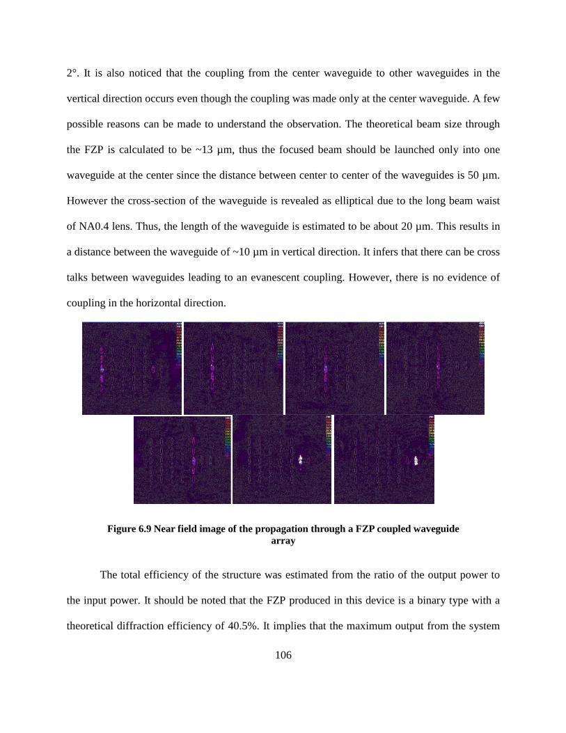
106
2°. It is also noticed that the coupling from the center waveguide to other waveguides in the
vertical direction occurs even though the coupling was made only at the center waveguide. A few
possible reasons can be made to understand the observation. The theoretical beam size through
the FZP is calculated to be ~13 µm, thus the focused beam should be launched only into one
waveguide at the center since the distance between center to center of the waveguides is 50 µm.
However the cross-section of the waveguide is revealed as elliptical due to the long beam waist
of NA0.4 lens. Thus, the length of the waveguide is estimated to be about 20 µm. This results in
a distance between the waveguide of ~10 µm in vertical direction. It infers that there can be cross
talks between waveguides leading to an evanescent coupling. However, there is no evidence of
coupling in the horizontal direction.
Figure 6.9 Near field image of the propagation through a FZP coupled waveguide array
The total efficiency of the structure was estimated from the ratio of the output power to
the input power. It should be noted that the FZP produced in this device is a binary type with a
theoretical diffraction efficiency of 40.5%. It implies that the maximum output from the system
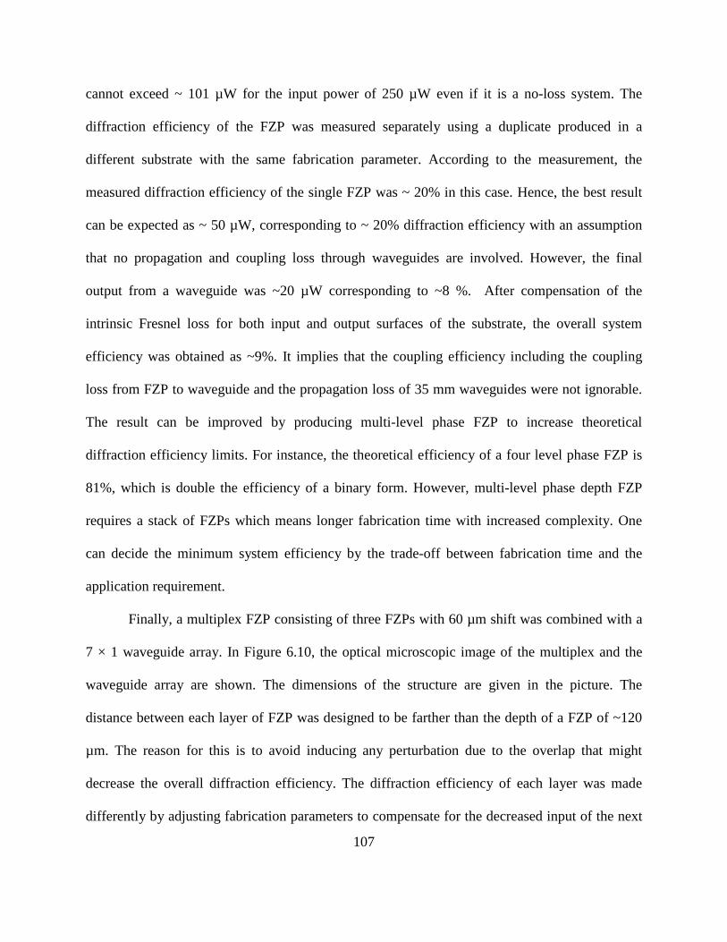
107
cannot exceed ~ 101 µW for the input power of 250 µW even if it is a no-loss system. The
diffraction efficiency of the FZP was measured separately using a duplicate produced in a
different substrate with the same fabrication parameter. According to the measurement, the
measured diffraction efficiency of the single FZP was ~ 20% in this case. Hence, the best result
can be expected as ~ 50 µW, corresponding to ~ 20% diffraction efficiency with an assumption
that no propagation and coupling loss through waveguides are involved. However, the final
output from a waveguide was ~20 µW corresponding to ~8 %. After compensation of the
intrinsic Fresnel loss for both input and output surfaces of the substrate, the overall system
efficiency was obtained as ~9%. It implies that the coupling efficiency including the coupling
loss from FZP to waveguide and the propagation loss of 35 mm waveguides were not ignorable.
The result can be improved by producing multi-level phase FZP to increase theoretical
diffraction efficiency limits. For instance, the theoretical efficiency of a four level phase FZP is
81%, which is double the efficiency of a binary form. However, multi-level phase depth FZP
requires a stack of FZPs which means longer fabrication time with increased complexity. One
can decide the minimum system efficiency by the trade-off between fabrication time and the
application requirement.
Finally, a multiplex FZP consisting of three FZPs with 60 µm shift was combined with a
7 × 1 waveguide array. In Figure 6.10, the optical microscopic image of the multiplex and the
waveguide array are shown. The dimensions of the structure are given in the picture. The
distance between each layer of FZP was designed to be farther than the depth of a FZP of ~120
µm. The reason for this is to avoid inducing any perturbation due to the overlap that might
decrease the overall diffraction efficiency. The diffraction efficiency of each layer was made
differently by adjusting fabrication parameters to compensate for the decreased input of the next

108
layer by the previous one. In the picture, the bottom layer is the first FZP toward the laser. To
generate a bottom layer with the lowest diffraction efficiency, the lowest laser dose was applied
to the bottom layer while the highest dose was applied to the top layer which is the nearest to the
waveguide array.
Figure 6.10 Three-piece multiplex FZPs shifted with 60 µm and a 7 × 1 waveguide array
The measured efficiency ratio of each layer is bottom : middle : top = 8:18:23. However,
the output which is estimated by the ratio was 7.4:15.3:16 due to the decreased input. Figure 6.11

109
is the near field images of the integrated structure shown above. As is expected, the propagated
beams from three coupled waveguides are seen. However, the coupling and propagation
efficiency shows a different ratio compared to the estimation. Figure 6.11(a) has 4.1:4:3.2 while
(b) has 5.4:3.8:2.7. This implies that although the structure has definitive diffraction efficiency
and propagation loss, small tweak angle variance could change the coupling efficiency to vary
the coupling ratio. This also means that variable power transmission through this structure is
available even though the optical properties of the structure are fixed.
(a) (b)
Figure 6.11 Near field images of a waveguide array coupled with a multiplex consists of three FZPs the power ratio is (a) 4.1:4:3.2 (b) 5.4:3.8:2.7

110
CHAPTER 7 : FEMTOSECOND LAER WRITTEN NONLINEAR OPTICAL STRUCTURES
So far it has been shown that FLDW can fabricate building blocks for integrated optical
devices in bulk optical materials based on a modification of their linear optical properties.
In this chapter, another way to enrich photonic applications utilizing FLDW is explored:
utilizing nonlinear optical properties of materials. First, nonlinear optical processes and their
phenomena are reviewed as a background, and the limitations of amorphous materials as the
platform of second-order nonlinear properties are discussed. Then, the recent new finding of
“laser-depletion” by this investigation is discussed as a pathway to create second-order nonlinear
structures in amorphous glass via high repetition rate femtosecond pulses. The theoretical model
of laser-depletion, which enables second-order susceptibility in amorphous glass, is described.
Silver ion-containing zinc phosphate glasses are utilized as a substrate of the new scheme of
laser-induced second-order nonlinear structure. The most recent experimental result supporting
the model is presented. Finally, a series of parametric experimental results as well as analyses of
the measurement are presented at the end.
7.1
Nonlinear optical processes were discovered immediately after the invention of the laser
in 1960 because these phenomena require intense beam intensity to be measured experimentally.
Now, numerous applications based on nonlinear optics are providing great opportunities in
photonics and optoelectronics. It is well studied that the polarization of dielectric material can be
expressed as [36]
Nonlinear optical properties of glass

111
LL +++≡+++= )(~)(~)(~])(~)(~)(~[)(~ )3()2()1()3()3()2()2()1(0 tPtPtPtEtEtEtP χχχε . (7.1)
In this equation, the polarization of materials has two parts: linear and nonlinear
polarization. Linear polarization, which is the first term in the bracket consisting of the linear
susceptibility )1(χ and an applied optical field )(~ tE , is responsible for the material responses in
general, such as dispersion, refraction, reflection, and other linear optical phenomena. The rest of
the equation which is nonlinearly proportional to the E field is called nonlinear optical parts
which are not negligible and often dominant when an intense optical field is applied.
7.1.1 Second-order nonlinearity
The polarization of the second-order of nonlinearity can be described as
)2()2()2( )(~)(~ tEtP o χε= . Second harmonic generation (SHG), the Electro-optic effect (or Pockels
effect), and sum (difference) frequency generation are all included in the second-order of
nonlinear optical phenomena. For example, SHG can be depicted as the schematic energy
diagram in Figure 7.1. As is shown, two photons with frequency ω reach the intermediate state
which immediately re-emits a photon with frequency 2ω, which is doubled energy.
Figure 7.1 Schematic energy diagram of second harmonic generation

112
Enormous applications such as frequency doubled lasers are relying on this process,
which widens the span of laser frequencies from, generally limited laser gain media. The Electro-
optic effect is another useful feature of the second-order of nonlinear optic properties. It is
widely used for high speed optical switching and the modulation of optical signals in optical
communications and laser engineering field [122, 123].
Although these fascinating applications are offered by second-order nonlinearity,
amorphous materials possessing inversion symmetry are unable to exhibit second-order
nonlinearity. This is because the induced polarization involving )2(χ is proportional to the vector
quantity which is the external electric field in this case. Therefore, the macroscopic vector sum
of the polarization is always null in amorphous materials such as glass.
7.1.2 Third-order nonlinearity
The polarization of third-order nonlinearity can be described as [36]
3)3()3( )(~)(~ tEtP o χε= . (7.2)
Some examples of the third-order of nonlinear optical phenomena are third-harmonic
generation, the optical Kerr effect, two-photon absorption, and self-focusing. These phenomena
are free from the limitations of the material symmetry since these effects depend on the square of
the external electric field, which is the laser intensity as a scalar quantity. As a consequence,
third-order nonlinearity is, in general, the least order of the nonlinear optical properties allowed
in amorphous glasses. For instance, many investigations regarding self-focusing in glasses have
been carried out to clarify the laser-induced damage mechanism in optical glasses due to the

113
delivery of the high power laser beam. Another example is two-photon absorption which was
intensively discussed in Chapter 2.
7.1.3 Induced second-order nonlinearity of amorphous glass
Glasses have several advantages over nonlinear crystals in terms of practical use. First,
there is more freedom in tailoring their optical properties with compositional variance. Also,
glasses are easily developed in certain shapes for desired device dimensions from fiber form to
bulky, curved shapes. Low cost and ease of handling is another benefit. Although the intrinsic
limitations are well understood, utilizing glasses for second-order nonlinear optical applications
has been investigated. In 1986, SHG in Si-Ge glass fibers was discovered by Österberg and
Margulis [124]. Stolen and Tom [125] proposed a mechanism involving the electric field from a
third-order optical rectification. SHG in thermally poled bulk fused silica was first demonstrated
by Myers et al. in 1991[126]. Since then, extensive research using poled glasses including
silicate, phosphate, and tellurite have been performed to take the advantage of glasses, which are
promising for low cost, robust fabrication processes [77, 126-128].
The basic understanding of the second-order susceptibility in poled glass is provided in
ref. [125, 126]. The second-order nonlinear susceptibility can be represented as
dcE)3()2( 3χχ = , (7.3)
where Edc is the internal electric field induced by a poling process. Thermal poling is commonly
used to produce an internal DC field in the material by depletion. Figure 7.2 depicts a schematic
of the process. As is shown, the glass substrate is sandwiched by two electrodes in a furnace.
Then, the temperature is increased to offer a higher mobility of ions. When the temperature
reaches between 200°C to 300°C, a high voltage of 1~3 kV is applied to force the mobile ions to

114
move. The high temperature is kept for ~30 minutes and then is decreased to TRm. The voltage is
then removed from the glass after the glass is cooled down.
Figure 7.2 Thermal poling of glass
By the thermal poling process, mobile ions migrated from the anode side to the cathode size
leaving a depletion zone of few microns at the anode side, depicted in Figure 7.3. The permanent
internal electric field from the shift of ions is generated in a depletion zone, which is the basis of
the second-order susceptibility of poled glass. Silver, sodium and a few more substances are
most commonly used as dopants for depletion.
Figure 7.3 Illustration of depletion zone via thermal poling
7.2
As an analogy of the charge depletion via thermal poling, laser-induced depletion is
suggested. Laser-written micro-structures consist of silver clusters with a redistribution of
charges resulting in a permanent electric field in the vicinity of the micro-structure. As a
Laser-induced depletion

115
consequence, second-order susceptibility involving third-order susceptibility and the internal
electric field can be induced. In this section, the mechanism of the creation of micro-structures
and laser-induced depletion is described.
7.2.1 Microstructuring of silver containing zinc phosphate glass
It is well known that silver ion containing glass has photosensitivity that helps to create
3-D embedded structures in the glass using laser direct writing [129, 130]. Recently, Bellec et al.
[131], who are the collaborators for this investigation, demonstrated sub-diffraction limit laser
structuring based on the formation of silver clusters using femtosecond laser irradiation. Figure
7.4 shows a high resolution SEM image of the embedded silver micro-structure and
corresponding profiles measured by AFM. The surface of the sample was ground and polished
to bring the structure to the glass surface. Next, it was acid-etched for measurement. The width
of the rim was measured to be ~ 81 nm (FWHM) which is less than 1/10 of the wavelength of the
writing beam.
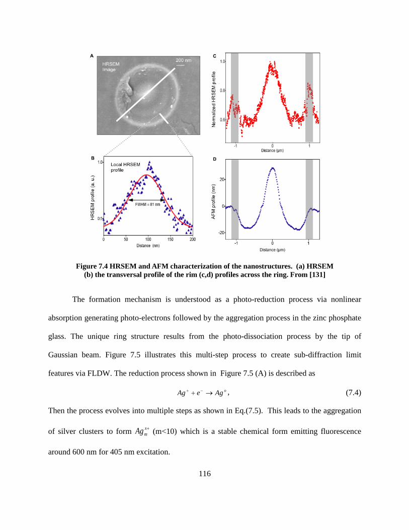
116
Figure 7.4 HRSEM and AFM characterization of the nanostructures. (a) HRSEM
(b) the transversal profile of the rim (c,d) profiles across the ring. From [131]
The formation mechanism is understood as a photo-reduction process via nonlinear
absorption generating photo-electrons followed by the aggregation process in the zinc phosphate
glass. The unique ring structure results from the photo-dissociation process by the tip of
Gaussian beam. Figure 7.5 illustrates this multi-step process to create sub-diffraction limit
features via FLDW. The reduction process shown in Figure 7.5 (A) is described as
oAgeAg →+ −+ , (7.4)
Then the process evolves into multiple steps as shown in Eq.(7.5). This leads to the aggregation
of silver clusters to form +xmAg (m<10) which is a stable chemical form emitting fluorescence
around 600 nm for 405 nm excitation.

117
++ →+ 20 AgAgAg ,
+++ →+ 232 AgAgAg ,
++ →+ xmAgAgAg 02
3 .
(7.5)
In step (B) in, Thermal diffusion occurs after a few thousands pulses. The last step Figure 7.5 (C)
is a photo-dissociation process, which occurs only at the center of the beam due to the high
intensity over the dissociation threshold of the silver clusters.
Figure 7.5 Mechanism of the formation of a silver tube. From [131]
7.2.2 Theoretical model of laser-induced depletion
As a consequence, the ring structure has redistributed charges which provide a permanent
internal DC field across the wall of the tube. The situation is depicted in Figure 7.6. Because of
the intense femtosecond laser irradiation, two most possible identified types of color centers,
Ag2+ and +xmAg , which play as hole trap and electron trap respectively, are generated. They are
indicated as blue and red dot lines respectively in the picture. With the process described in

118
previous section, +xmAg clusters are rich at the rim of the silver structures. As illustrated, the
permanent electric field, which is depicted as black arrows, is formed between Ag2+ and +xmAg .
Figure 7.6 Femtosecond laser induced depletion. White arrows indicate the direction of the permanent electric field between Ag2+ and +x
mAg
The induced polarization in the structure is represented as decomposed forms in n and y
in Eq. (7.6). [36]
2)3(
2)3(
)sin(3)2(
)cos(3)2(
probedcyynny
probedcnnnnn
EEP
EEP
θχω
θχω
=
=, (7.6)
7.2.3 Second harmonic generation of silver ion containing glass
The second-order of susceptibility can be induced by the interplay of third-order
susceptibility and the internal electric field. Thus, second harmonic generation measurement with
the laser written structure was tested to explore the existence of second-order susceptibility.
Figure 7.7 is the SHG microscopy setup attached to the direct writing station. A femtosecond
laser was used as a writing beam to form the silver structure and also used as a probe beam with
reduced power.

119
Figure 7.7 SHG measurement setup
The SHG signal was collected by a 0.4 NA objective lens, then delivered into the double
monochrometer with an intensified CCD camera (ICCD) as a detector. The fundamental
wavelength was rejected by a dichroic mirror. Any possible fluorescence near 600nm by multi-
photon excitation was blocked by a bandpass filter at 520nm with 40nm bandwidth. Figure 7.8(a)
and (b) show the SHG signal distribution of the silver micro-structures in zinc phosphate and a
piece of z-cut quartz respectively imaged by a CCD beam profiler. As is inferred from Figure 7.4
and Figure 4.20, an annular SHG distribution of silver clusters is seen. It is interesting to
compare the distribution with the signal from quartz, which is taken at the same probe intensity10
10 ND filters were used for quartz to attenuate the SHG intensity (attenuation 99.77%) .
.
The latter shows the same profile with the probe beam which is a Gaussian beam distribution.

120
Figure 7.8 3-D SHG profile of (a) silver tube and (b) quartz
Since quartz is an intrinsic second-order nonlinear optical material, the maximum
intensity of the SHG is found at the intensity peak of the input beam as illustrated in Figure 7.9.
In the silver cluster ring, the nonlinear region is located only at the rim of the structure since the
internal electric field only exists in this region. The maximum SHG can also be found at the rim
of the structure.
Figure 7.9 Schematic diagram of the convolution of the SHG of the silver ring and quartz with pump beam
Figure 7.10(a,c) shows the SHG from a micro-structure and quartz respectively measured
by an intensified CCD detector. The center wavelength is located at ~522 nm, which is half of
the fundamental wavelength, so it confirms that the signal is the second harmonic of the probe

121
beam. The FWHM bandwidth of the SHG signal is about ~1.4 nm, which is smaller than the
bandwidth of the fundamental laser of ~7.5 nm. Figure 7.10(b,d) is the SHG as a function of
probe intensity.
Figure 7.10 (a,b) Measured SHG of a silver tube (b) shows a quadratic relation to the probe beam intensity (c,d) Quartz 11
The SHG intensity of a micro-structure was compared to the SHG intensity of quartz to
estimate the SHG efficiency of the structure. To normalize the gained signal from the structure,
the same probe intensity was irradiated both on quartz and on the micro-structure using the same
11 Acquisition times are different in zinc phosphate (10s) and in quartz (10ms)

122
objective lens. The SHG intensity from the silver structure was divided by the SHG intensity of
the quartz crystal. In addition, the effective NLO area was taken into account since only the rim
of the structure plays as NLO region. Therefore, the area of the ring was applied. The estimated
)2(χ is 2.44, )2(quartzχ which corresponds to ~ 1.5 pm/V. The laser-induced )2(χ is comparable to the
thermal poling of the similar composition that is reported as 1.8 pm/V [132].
7.2.4 Polarization dependence
Since the internal DC field has a radial direction, it can be decomposed into the
horizontal and vertical direction. In Figure 7.11(a-c), near field images of SHG distribution are
shown. White and green arrows indicate the polarization of the laser and the direction of an
analyzer respectively. In Figure 7.11(a), the raw SHG intensity without an analyzer is shown as a
ring. The highest intensity is in the direction of the polarization of the laser. When the direction
of the analyzer is aligned with the laser polarization (HH), the signal looks similar to the signal
in Figure 7.11(a). When the analyzer is rotated perpendicularly (HV), there is a very weak signal
from the other component of the electric field. It is important to note that the intensity at the
center is the same regardless of the direction of the analyzer. It is assumed that the signal could
be a result from either the unfiltered fundamental beam or from hyper Rayleigh scattering.

123
Figure 7.11 Intensity map of the SHG of Ag micro-structure (a) no analyzer, the direction of the analyzer (b) parallel (HH) and (c) perpendicular (HV) to the
polarization of the laser
In Figure 7.12, a simulated image of a theoretical model for the horizontal polarization
and its experimental result is shown. As is seen in Figure 7.11, both images agree with each other
well with the exception of the center signal present in the experimental image. The signal at the
center is assumed to be a residue of the peak of the fundamental beam since the signal is not
filtered out by the polarizer and does not show the intensity change by the rotation of the
polarizer for green wavelength.
Figure 7.12 SHG distribution at horizontal polarization of probe and analyzer, (a) theoretical (b) experimental
Figure 7.13 is the intensity of the SHG as a function of angle for both polarization
orientations. It should be noted that the intensity ratio of HH (horizontal laser polarization and
horizontal analyzer) and HV (horizontal for laser polarization and perpendicular analyzer) is

124
about 1:9: =VH II . The relationship between the two intensity ratios can be supported because
the ratio of corresponding elements in the third-order susceptibility tensors is known as
1:3: )3()3( =yynnnnnn χχ in glass and thus the intensity ratio is squared.
Figure 7.13 Polarization angle dependence of SHG signal
In Figure 7.14, a polar plot of all intensity distributions is shown for both HH and HV
configurations as well as the intensity without the analyzer. It is clearly confirmed that the SHG
intensity is directional which is determined by the laser polarization.

125
Figure 7.14 SHG intensity plot of HH, HV polarization and without analyzer.
7.2.5 Parametric dependence on fabrication parameters
In order to investigate the parametric dependence of the fabrication factors and material
difference, laser repetition rate and numerical aperture were chosen as primary fabrication
parameters in zinc phosphate/FOTURAN glasses. FOTURAN glass is a commercially available
glass with less than 1% of silver12 Figure 7.15[133]. shows the SHG intensities of zinc phosphate
and FORURAN glass irradiated as a function of probe intensity.
7.2.5.1 focused beam size by different objective lenses
It would be expected that the distribution of the spatial charge can be modified by
varying the size of the structure through changing the irradiation beam size. Thus, a laser-
induced permanent electric field might be changed due to the variation of ion distribution. This
may lead to the enhancement of )2(χ since )2(χ is directly proportional to the permanent electric
12 The composition is found in ref [132] as B2O3, CeO2, Sb2O3, Ag2O<1%, K2O 1–20%, SiO2 > 80%, Al2O3, Na2O, ZnO, Li2O 1–10%

126
field. Two microscope objective lenses (NA=0.25 and 0.4) are used for the investigation.
However, there is no significant trend with a small beam size change of a few microns.
7.2.5.2 Material dependence
It should be noted that the difference of the SHG intensity level between zinc phosphate
and FOTURAN results not from a single origin but possibly because of several reasons. First,
the concentration of the mobile species is different; the silver concentration is 1% for zinc
phosphate and <1% for FOTURAN. Secondly, the threshold for color center formation would
be different due to the interplay of multi-contents affecting the bandgap of the material. As is
shown, the thermal properties, such as the diffusion coefficient, would also differ from
phosphate glass and perhaps affect the mobility of nanoparticles. This is supported by Figure
7.15. Higher efficiency is shown for zinc phosphate at high repetition rate (b) whereas similar
efficiencies are shown for both glasses at lower repetition rate (a).
(a) (b)
Figure 7.15 SHG intensity vs. materials at (a) 500 kHz (b) 1500 kHz

127
7.2.5.3 Laser repetition rate
Figure 7.16 shows the repetition rate dependence of the materials of SHG intensity. As is
shown above, zinc phosphate shows higher SHG efficiency than FOTURAN. Furthermore, in
Figure 7.16(a), significant enhancement of SHG intensity is shown as the laser repetition rate
increases. This would indicate that heat accumulation increases the mobility of clusters leading
to the enhanced permanent static electric field.
(a) (b)
Figure 7.16 SHG intensity vs. repetition rate and materials as functions of probe intensity (a) zinc phosphate (b) FOTURAN

128
CHAPTER 8 : RELAXATION OF THE FEMTOSECOND LASER WRITTEN DEVICES
Since its first demonstration with directly-written waveguides in 1996 [7], femtosecond
laser direct-writing has been actively adopted in fabricating 3-D photonic devices. However,
only a few of thorough investigations have been conducted regarding the reliability and
degradation of the performance of the laser-written photonic structures over time and thermal
fluctuation. Will et al. demonstrated the characterization of their annealed laser-written
waveguide in fused silica [134]. They observed that light guiding properties were not changed by
annealing up to 500 °C for a few hours. However, the characteristic fluorescence of laser-
induced color centers excited between 560 nm and 630 nm disappeared by annealing at 400 °C.
Zhang et al. also reported the annealed Bragg grating waveguide in borosilicate glass and its
diffraction efficiency [135]. They observed a serious decrease of grating strength over 250 °C
and no guiding over 500 °C. To the best of our knowledge, there is no rigorous investigation on
relaxation or degradation properties of the laser-written structure either by heat treatment or time
for chalcogenide. Zhang et al. reported the enhancement of n2 (nonlinear index) in bulk As2S3
induced by a femtosecond laser that lasted for 9 months while the reduction of n2 induced by a
cw laser was completely recovered after 4 months [136]. However, they did not carry out a
quantitative investigation on this topic. In this chapter, photo-induced structural modification in
bulk chalcogenide glasses and corresponding refractive index change is discussed in terms of
time and heat treatment conditions. Some ideas for reliability towards the practical use of laser-
written structures are discussed as well.
129
8.1
Chalcogenide glasses (ChGs) have been considered as a candidate for MIR photonic
applications due to their wide transparency window in the range from ~0.6 µm to ~16 µm There
have been numerous investigations in the fabrication and characterization of femtosecond laser
directly-written photonic structures using ChGs [8, 82, 86] Their performances, such as
propagation loss and diffraction efficiency, were reported in [137]. However, only limited
numbers of investigations have focused on their reliability and thermal issues causing reduction
of the performance of the femtosecond laser-written devices. This work used the same
composition of bulk ChGs, demonstrated in Chapter 4, to investigate time-involved and annealed
glass to show the reliability change of the laser-induced refractive index change in terms of time
and thermal treatment.
Relaxation of chalcogenide glass
8.1.1 Fabrication and measurement of test platform
Two different femtosecond laser written structures were made at the surface and in the
volume of bulk glasses with the composition As42S58/As36Sb6S58/As36Ge6S58 in order to
investigate the relaxation of the photo-induced structure of the glasses. The first structure is a
short line (the length of 200 μm) array written at the surface of the glass as a function of laser
dose to monitor the photo-expansion over time and thermal-induced relaxation. The second
structure consists of buried linear diffraction gratings formed within the glass samples to
estimate the photo-induced refractive index change Δn in bulk. The details of the fabrication are
described in Chapter 4. The photo-expansion or diffraction efficiency of each structure was
measured using a white light surface profiler and a diffraction efficiency setup consisting of a
CW 800 nm Ti:Sapphire laser and a power meter. These results were used as references to

130
normalize the future measurement after 9 months and after annealing. Then, the samples were
stored in a desiccator in the dark at room temperature. After 9 months, the same measurements
were taken with the structures to compare with the freshly laser-written samples. The samples
were then annealed in air for 15 hours at 150°C (As42S58 /As36Ge6S58) and at 160°C (As36Sb6S58)
depending on the Tg of the glass. Surface photo-expansion and diffraction efficiency were
measured after annealing. Micro Raman spectroscopy was performed on the annealed structure
to investigate the bond change caused by the heat treatment.
8.1.2 Decrease of photo-expansion
Figure 8.1 shows the photo-expansion of freshly irradiated, 9 months old, and annealed (a)
As42S58 (b) As36Sb6S58 (c) As36Ge6S58 as a function of inverse writing speed which is
proportional to the laser dose. They are normalized with the highest photo-expansion of each
composition. It is shown that 10 ~ 25 % of relaxation occurs after 9 months, 27 ~ 56% after
annealing with respect to the 9 months (32 ~ 65% from freshly irradiated sample). It is noted that
although the 3 investigated glasses show reduction from their initial photo-expansion, there is a
difference between compositions. The introduction of Sb in the As-S network shows the largest
reduction of the photo-expansion after 9 months while the addition of Ge in a similar network
shows the least reduction at the highest laser dose over time. It is assumed due to the 3-D
network of Ge containing ChG to be resistant to relaxation at room temperature. The decrease is
more pronounced in the glass with the composition As36Sb6S58. This is attributed to the less
constrained glass network.

131
0.00 0.05 0.10 0.15 0.20
0
10
20
30
40
50
0.0
0.2
0.4
0.6
0.8
1.0 Fresh 9 months Annealed
Phot
oexp
ansi
on (n
m)
Inverse writing speed (s/µm)
As36Sb6S58 N
ormalized H
eight
(a) (b)
0.00 0.05 0.10 0.15 0.200
10
20
30
40
50
60
0.0
0.2
0.4
0.6
0.8
1.0 Fresh 9 months Annealed
Phot
oexp
ansio
n (n
m)
Inverse writing speed (s/µm)
As36Ge6S58
Normalized Height
(c)
Figure 8.1 Photo-expansion of ChGs after irradiation, after 9 months and after annealing
After the heat treatment, the decrease of photo-expansion for all compositions is even
more drastically changed. The two photo-expanded lines completely disappeared and were
barely seen using a white light surface profilometer. The glass with the composition As36Ge6S58
exhibits the smallest decrease in photo-expansion amplitude which is consistent with the result
above.
0.00 0.05 0.10 0.15 0.200
5
10
15
20
25
30
0.0
0.2
0.4
0.6
0.8
1.0 Fresh 9 months Annealed
Phot
oexp
ansio
n (n
m)
Inverse writing speed (s/µm)
As42S58
Normalized Height

132
Figure 8.2 shows the corresponding Raman spectra of three compositions after annealing.
The comparison of the Raman shift between fresh and irradiated samples was discussed in
Chapter 4. The micro Raman spectra of the annealed sample were acquired at the blank region
and at the photo-expansions written by the first and second highest doses, corresponding to the
inverse writing speeds of 0.1 and 0.2 s/μm shown in Figure 8.1. Intensity changes due to the
irradiation are found in the regions from 200 to 250 cm-1 for all compositions, but not in the
region from 450 to 500 cm-1, except As42S58. The band was shown for all compositions after
irradiation in Figure 4.18. The black arrows in Figure 8.2 indicate the effect of laser irradiation.
In the spectra of As36Sb6S58 and As36Ge6S58, variation of the amplitude of the band located near
360 cm-1 is also seen. In addition, a new peak is found after annealing in 200 to 250 cm-1 for
As42S58. The narrow band width of the new peak is suspected to be evidence of partial
crystallization. To compare these spectra with Figure 4.18, it is noticed that the laser-induced
change in the range of 200 to 250 cm-1 and 450 to 500 cm-1 seems diminished after annealing, but
is not completely reversible as the corresponding photo-expansion still remains as seen in Figure
8.1.
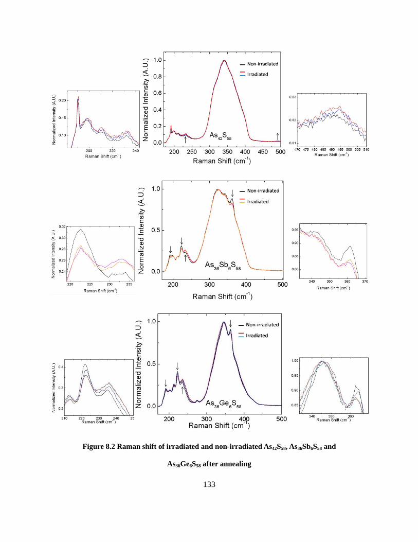
133
Figure 8.2 Raman shift of irradiated and non-irradiated As42S58, As36Sb6S58 and
As36Ge6S58 after annealing

134
8.1.3 Decrease of photo-induced refractive index change
As explained in the previous chapter, the calculated Δn is proportional to the laser dose,
which leads to proportional surface photo-expansion[82, 86]. Therefore, the decrease of photo-
expansion may imply the decrease of Δn as well. The Δn after 9 months and after annealing was
measured to justify the assumption. Figure 8.3 shows the result of Δn measurement of As42S58
before and after 9 months. As expected, the decrease of Δn is shown with the reduction of ~10%.
After annealing, the diffraction power at the 1st order was smaller than a measurable range. Thus,
it was not possible to detect any Δn. For the other compositions, unexpected defects, which
distorted the input laser beam, were generated within the samples. Therefore, the diffraction
powers were not able to be measured. However, the origin of the generation of defect is unclear.
Figure 8.3 Photo-induced expansion and refractive index change of bulk As42S58 after irradiation and after 9 months

135
8.1.4 Reduction of the photo-induced structure by heat treatment
In the previous section, the photo-expansion and corresponding Δn was measured for the
overall change due to the combination of aging and annealing. Although Δn of an embedded
structure was shown to be proportional to photo-expansion, the linear correlation between two
dimensional and three dimensional change is uncertain. Thus, the change of embedded photo-
induced structure by heat treatment is measured separately to investigate the sole change via
thermal effect in the bulk. Several embedded gratings were inscribed in bulk As36Sb6S58 with
various laser doses and intensities. The annealing was carried out immediately after irradiation.
The annealing parameters were the same as the previous experiment, for 15 hours at 160°C (Tg -
40°C) in an air environment. Figure 8.4 (top) and (bottom) show the optical microscopic images
of the gratings written in the As36Sb6S58 with the dose of 11.1 kJ/cm2 for Figure 8.4(a) and 5.6
kJ/cm2 for (b) under the same intensity of ~ 53.7 GW/ cm2, respectively prior to and after
annealing. After annealing, the structures were shrunk about 36% and 34% with respect to the
initial lengths for Figure 8.4 (a) and (b) respectively.

136
Figure 8.4 Optical microscopic image of the photo- expansion change of bulk As36Sb6S58 before and after annealing for 15 hours at 160 °C in air environment
In order to clarify the relation of dose and intensity dependence on relaxation, various
laser doses and intensities were applied. Figure 8.5 shows the DIC optical microscopic image of
embedded gratings created using various laser doses prior to and after annealing. The modified
region is clearly seen in Figure 8.5 (a, b) while the region is distinguishable but not significant in
Figure 8.5 (c, d) compared to (a, b). The former is thought to be at the start of the saturation
process. It is interesting to note that the relaxation behavior is also different in both cases. The
annealed structures are shown in Figure 8.5 (a-d). It seems that the modification shown in (a, b)
is more resistant to annealing than (c, d). Micro Raman spectroscopy and a near-field refractive
index measurement may distinguish the difference between both modifications for chemical and
optical properties.

137
Figure 8.5 Optical microscopic image of the photo-expansion change produced at various dose and intensity in bulk As36Sb6S58 before and after annealing for 15 hours
at 160 °C in an air environment

138
CHAPTER 9 : CONCLUSIONS AND PERSPECTIVES
Increasing demands for a variety of integrated, on-chip photonic devices have stimulated
researchers to work on customized photonic devices that can be used in micro-sensors, micro-
fluidic on-chip devices, and photonic circuits. Femtosecond laser direct-writing has been a
promising technique in meeting these demands, as it enables the production of truly 3D
volumetric photonic structures embedded in transparent optical materials such as fused silica,
photosensitive glasses, and metal ion-containing glass. Despite the extensive investigations that
have been done on FLDW, however, the potential for its applications has not been fully explored.
This dissertation was an attempt to make an improvement on the existing FLDW technique to
achieve a reliable fabrication protocol for integrated optical devices involving micro diffractive
optical elements, such as Fresnel zone plates and volumetric gratings.
As the first step toward the goal is to find appropriate optical materials and to know their
photo-responses, various novel materials were investigated—which include chalcogenide,
tellurite, silver ion-containing zinc phosphate glasses. The ablation thresholds of the given
materials were measured as well as their unique photo-responses such as photo-expansion and
photo-reduction/photo-dissociation. These were discussed in Chapter 4.
Next, the fabrication parameters of Fresnel zone plates were systematically investigated
to maximize their diffraction efficiency by optimizing fabrication parameters, and it was found
that a high repetition rate in the range of a few hundred kHz with low NA objective was useful
for maximizing the diffraction efficiency. These were discussed in Chapter 5.
Then, various types of integrating directly-written structures were characterized. A
directly written embedded multiplex FZP was produced in borosilicate glass—the first of its kind,

139
to the best of our knowledge. This device was found to provide 11.5% diffraction efficiency at
the primary focus and perform as a 1 × 4 focused beam splitter. Then, this multiplex FZP was
integrated with a waveguide array so that all-optically written integrated structures consisting of
a coupling lens and a waveguide array were realized in borosilicate glass.
In addition, a SHG in laser-structured silver containing zinc phosphate (P2O5-Ag2O-
Ga2O3-ZnO) by “laser depletion” was demonstrated, as an analogy to the depletion in thermal
poled glass—this, too, is the first of its kind to the best of our knowledge. The silver micro-
structures were formed via a three-step process (photo-reduction, diffusion and photo-
dissociation) by femtosecond laser pulses at high repetition rate, which can increase local
temperature in a voxel due to the heat accumulation. Ag2+ as a hole trap and Agmx+ (m<10) as an
e- trap were two bases formed during the process to generate the permanent electric field due to
the charge separation across the ring. The distribution of silver clusters, Agmx+ (m<10) was
investigated via high resolution microscopy and photoluminescence study. Interestingly, the
formed clusters were shaped as ring structures depending upon the focused beam size. The
nonlinear region was the same as the rim of the ring structure. Therefore, the SHG signal was
only found at the rim. It showed polarization-dependent SHG distribution, which implied that the
induced polarization, defined by the second-order susceptibility in the material, obeys different
tensor elements. It was also revealed that laser depletion is enhanced by a higher repetition rate,
which implies it is governed by a thermal effect. In addition, the material differences also
exhibited different SHG efficiencies, which means that laser depletion can be described as
functions of the concentration of mobile ions, Tg of the glass, color-center generation threshold,
and repetition rate of the writing laser and other chemical and optical properties of the glass.
Extended investigation such as XPS and EDS could be carried out to measure the distribution of
140
mobile ions and clusters formed by different irradiation parameters so that the origin of the
permanent DC field can be clarified.
Finally, the relaxation of directly-written structures in bulk chalcogenide glass (As42S58
/As36Sb6S58 /As36Ge6S58) was studied by measuring the surface photo-expansion as well as the
diffraction efficiency of embedded gratings after irradiation, after 9 months, and after heat
treatment. It was found that relaxation occurred in all compositions but the amounts of
relaxation were slightly different among the compositions. The samples showed 10 ~ 25 % of
relaxation after 9 months and 27 ~ 56% after annealing with respect to the 9 months (32 ~ 65%
from freshly irradiated sample). Ge containing bulk chalcogenide showed the highest resistance
against relaxation while As containing glass exhibited the lowest durability. This is attributed to
the 3D network of the glass matrix involving Ge atoms. The sole change of embedded 3D
photo-induced modification only due to the heat treatment was also investigated, and it was
found that there were two types of modifications depending upon laser dose and intensity.
However, laser dose was considered to be the primary factor of photo-induced modification.
Future work could investigate the relationship between chemical and optical properties of
embedded 3D photo-induced structural modifications via micro Raman spectroscopy and
rigorous near field refractive index mapping. That way, laser-induced 3D modification can be
controlled with quantitative fabrication parameters, a crucial factor in fabricating reliable
photonic devices utilizing chalcogenide glasses owing to the embedded 3D structures.


141
APPENDIX A : THERMO-PHYSICAL PROPERTIES OF OPTICAL MATERIALS

142
Table A.1 Thermal coefficients of selected optical materials13
(From [42])
κ [W/cmK] ρ [ g/cm3] pc [J/gK] D [cm2/s]
Ag 4.28 10.5 0.23 1.72
Al 2.37 2.7 0.90 1.03
Cu 4.0 (273) 8.94 0.39 1.14
Stainless steel (304) 0.15 8.03 0.5 0.04
a-Si 0.018 2.32 0.8 0.0097
c-Si 1.5 2.32 0.71 0.85
Water (H2O) 0.06 1 4.18 0.014
Glass (Crown) 0.01 2.4 0.89 0.0058
Glass (BK7) 0.011 2.51 0.86 0.0052
LiNbO3 0.042 4.46 0.64 0.015
PI (Kapton) 0.0012 1.42 1.09 0.0008
PMMA 0.0020 1.18 1.41 0.0011
a-SiO2 0.014 2.2 0.72 0.009
SiO2 0.014 2.5 0.74 0.0086
TiO2 (rutile) 0.089 (273) 4.26 0.93 0.031 (273)
13 If temperature is not specified in parentheses, all values refer to T~300K

143
APPENDIX B : ABSORPTION PROCESS CONSISTING OF THE NONLINEAR ABSORPTION WITH WEAK LINEAR ABSORPTION

144
When the laser beam with a frequency of ω is propagating a medium with no gain, the
intensity I(z) of the laser beam propagating in z direction in a medium is described as
L−−−−= 32 )()()()( IIIdz
zdIo ωγωβωα , (B.1)
where αo is the linear (or single photon) absorption coefficient, given as coκωα 2=
(κ is the
extinction coefficient of the medium), β and γ are the two- and three-photon absorption
coefficients respectively. Therefore, the absorption process involving n photons is proportional
to the intensity to the nth power of the incident laser beam. If the medium exhibits absorption in
the range of the laser frequency ω, the linear absorption process is the dominant excitation
mechanism which promotes a bound electron to the conduction band. Thus Eq. (B.1) is
approximated as
Idz
zdIo )()( ωα−= . (B.2)
In transparent materials where the linear absorption is not present in the range of incident
laser frequency ( 0≈oα at ω), nonlinear absorption processes are dominant. Here, single photon
excitation does not take place. For two-photon absorption [138], the Eq. (B.1) is then reduced as
2)()( Idz
zdI ωβ−= . (B.3)
Two photon absorption coefficient β is given as )3(Im
022
023 χ
εωβcn
=, where )3(
Imχ is the imaginary
part of the third-order susceptibility. The solution of the Eq. (B.3) is obtained as
zIIzI
)0(1)0()(
β+= . (B.4)

145
When linear absorption is small, but not negligible ( 1<<oα at ω), the differential equation
in Eq. (B.1) for two photon absorption is modified as
2)()()( IIdz
zdIo ωβωα −−= . (B.5)
The solution of the equation is then described as,
.
)1)(0(1
)0()(0
0
0
z
z
eI
eIzIα
α
αβ −
−
−+=
(B.6)
The two-photon absorption process is affected by the linear absorption process, thus the
contribution of two-photon absorption in terms of the generation of free electron is dependent on
the depth of the medium where the laser beam is focused.


146
APPENDIX C : PHOTO-INDUCED REFRACTIVE INDEX CHANGE IN As0.42-x-yGexSbyS0.58 AND THE EFFECT OF MEAN POLARIZABILITY
CHANGE

147
The number of bond N involving an atom K in a voxel of the femtosecond laser
irradiation is described as [86]
VM
NKN AatK
ρζ %= . (C.1)
KAt% is the atomic fraction of atom K (At%), which represents the atom of interest in the bulk
glass, ζ indicates the ζ –fold coordination of atom K, NA is Avogadro’s number, ρ and M is the
density and the molecular weight of the bulk ChG glasses respectively, V is the volume of a
voxel, which is estimated as 0202 zwV π≈ . ρ and M for As42S58, As36Ge6S58 and As36Sb6S58 is 3.20,
3.15, 3.40 g/cm3 and 50.06, 49.92, 52.87 g/mol respectively. The volume of a voxel produced by
an objective with NA=0.25 is estimated as 1.54 × 10⁻¹⁰ cm3. Therefore, the numbers of As-S
bond within a voxel in As42S58 is estimated to be 6.88 × 1012 cm-3 and either As-S or Ge-S (Sb-S)
in As36Ge6S58 (As36Sb6S58) are 6.79 × 10¹² (6.92 × 10¹² ) cm-3 respectively using the fraction of S
(0.58)14
The mean polarizability of the material is described by Lorentz-Lorenz equation
.
αρπM
Nnn A
34
21
20
20 =
+−
. (C.2)
where no and α is the refractive index and the mean polarizability of the material. α in As42S58
(no = 2.468 at 800 nm) , As36Ge6S58 (no = 2.364 at 800 nm) and As36Sb6S58 (no = 2.541 at 800 nm)
are estimated using Eq. (C.2) to be 3.90 × 10⁻²⁴, 3.80 × 10⁻²⁴, 3.98 × 10⁻²⁴ cm3 respectively.
Photo-expansion and photo-induced index change (Δno) due to the femtosecond laser
irradiation result from the decrease of the density ρ and the increase of the refractive index no in
14 From a micro-Raman study shown in Figure 4.18, the presence of not only As-S, but also the different
type of bonds such as As-As, As-Sb and Sb-Sb are seen before laser irradiation.

148
the given bulk ChG glasses. Thus, the re-calculation of Eq. (C.2) with ρ+Δρ and no+Δno may
provide information on the photo-induced mean polarizability change. Δ(ρα), the difference of
the product of the density and the mean polarizability, is calculated using Δno provided from the
measurement shown in Figure 4.21. Δ(ρα) in As42S58, As36Ge6S58 and As36Sb6S58 after fs pulse
exposure using the similar laser dose (~ 10 kJ/cm2) is obtained as 0.12%, 0.20% and 0.05%
respectively. However, the photo-expansion measured from the irradiated surface of the bulk
ChGs, which is shown in Figure 4.17, provides only 2-D information of the expansion, whereas
the photo-induced Δn was measured using an embedded grating in the bulk, which resulted from
3-D photo-expansion. Therefore, it is not able to determine the mean polarizability change Δα
separately from Δ(ρα) without measuring Δρ three dimensionally.
To conclude, the femtosecond laser-induced structural changes represented as photo-
expansion and photo-induced refractive index change may result from the change of either the
density or the mean polarizability, which is due to the increase of the number of homo polar
bonds. However, it is not clear that the photo-induced refractive change can be directly linked to
the photo-expansion and is proportional to the photo-expansion. Further studies such as selective
etching followed by HRSEM imaging may be required to measure 3-D photo-expansion in bulk
ChG glasses to estimate Δρ separately.


149
LIST OF REFERENCES
[1] S. Sinzinger and J. Jahns, "Integrated micro-optical imaging system with a high interconnection capacity fabricated in planar optics," Appl. Opt., vol. 36, pp. 4729-4735, 1997.
[2] Y. Wang, W. Yun, and C. Jacobsen, "Achromatic Fresnel optics for wideband extreme-ultraviolet and X-ray imaging," Nature, vol. 424, pp. 50–53, 2003.
[3] Y. S. Chu, J. M. Yi, F. De Carlo, Q. Shen, W. K. Lee, H. J. Wu, C. L. Wang, J. Y. Wang, C. J. Liu, and C. H. Wang, "Hard-x-ray microscopy with Fresnel zone plates reaches 40 nm Rayleigh resolution," Appl. Phys. Lett., vol. 92, p. 103119, 2008.
[4] K. Hedsten, J. Melin, J. Bengtsson, P. Modh, D. Karlén, B. Löfving, R. Nilsson, H. Rödjegård, K. Persson, and P. Enoksson, "MEMS-based VCSEL beam steering using replicated polymer diffractive lens," Sensors & Actuators: A. Physical, vol. 142, pp. 336-345, 2008.
[5] J. Fonollosa, R. Rubio, S. Hartwig, S. Marco, J. Santander, L. Fonseca, J. Wöllenstein, and M. Moreno, "Design and fabrication of silicon-based mid infrared multi-lenses for gas sensing applications," Sensors & Actuators: B. Chemical, vol. 132, pp. 498-507, 2008.
[6] Y. Kuroiwa, N. Takeshima, Y. Narita, S. Tanaka, and K. Hirao, "Arbitrary micropatterning method in femtosecond laser microprocessing using diffractive optical elements," Appl. Phys. Lett., vol. 12, 2004.
[7] K. M. Davis, K. Miura, N. Sugimoto, and K. Hirao, "Writing waveguides in glass with a femtosecond laser," Opt. Lett., vol. 21, pp. 1729-1731, 1996.
[8] K. Miura, J. Qiu, H. Inouye, T. Mitsuyu, and K. Hirao, "Photowritten optical waveguides in various glasses with ultrashort pulse laser," Appl. Phys. Lett., vol. 71, pp. 3329-3331, 1997.
[9] S. Nolte, M. Will, J. Burghoff, and a. Tünnermann, "Femtosecond waveguide writing: a new avenue to three-dimensional integrated optics," Appl. Phys. A, vol. 77, pp. 109-111, 2003.
[10] R. Osellame, S. Taccheo, M. Marangoni, R. Ramponi, P. Laporta, D. Polli, S. De Silvestri, and G. Cerullo, "Femtosecond writing of active optical waveguides with astigmatically shaped beams," J. Opt. Soc. Am. B, vol. 20, pp. 1559-1567, 2003.
[11] S. Taccheo, G. Della Valle, R. Osellame, G. Cerullo, N. Chiodo, P. Laporta, O. Svelto, A. Killi, U. Morgner, and M. Lederer, "Er: Yb-doped waveguide laser fabricated by femtosecond laser pulses," Opt. Lett., vol. 29, pp. 2626-2628, 2004.
150
[12] A. M. Streltsov and N. F. Borrelli, "Fabrication and analysis of a directional coupler written in glass by nanojoule femtosecond laser pulses," Opt. Lett, vol. 26, pp. 42-43, 2001.
[13] K. Minoshima, A. M. Kowalevicz, I. Hartl, E. P. Ippen, and J. G. Fujimoto, "Photonic device fabrication in glass by use of nonlinear materials processing with a femtosecond laser oscillator," Opt. Lett., vol. 26, pp. 1516-1518, 2001.
[14] S. Katayama, M. Horiike, K. Hirao, and N. Tsutsumi, "Diffraction measurement of grating structure induced by irradiation of femtosecond laser pulse in acrylate block copolymers," Jpn. J. Appl. Phys., vol. 41, pp. 2155-2162, 2002.
[15] Y. Kondo, K. Nouchi, T. Mitsuyu, M. Watanabe, P. G. Kazansky, and K. Hirao, "Fabrication of long-period fiber gratings by focused irradiation of infrared femtosecond laser pulses," Opt. Lett, vol. 24, pp. 646-648, 1999.
[16] P. J. Scully, D. Jones, and D. A. Jaroszynski, "Femtosecond laser irradiation of polymethylmethacrylate for refractive index gratings," Journal of Optics A: Pure and Applied Optics, vol. 5, pp. S92-S96, 2003.
[17] A. Martinez, M. Dubov, I. Khrushchev, and I. Bennion, "Direct writing of bre Bragg gratings by femtosecond laser," Electron. Lett, vol. 40, pp. 31-32, 2004.
[18] H. Zhang, S. M. Eaton, J. Li, and P. R. Herman, "Femtosecond laser direct writing of multiwavelength Bragg grating waveguides in glass," Opt. Lett., vol. 31, pp. 3495-3497, 2006.
[19] H. Zhang, S. M. Eaton, and P. R. Herman, "Single-step writing of Bragg grating waveguides in fused silica with an externally modulated femtosecond fiber laser," Opt. Lett., vol. 32, pp. 2559-2561, 2007.
[20] W. Watanabe, D. Kuroda, K. Itoh, and J. Nishii, "Fabrication of Fresnel zone plate embedded in silica glass by femtosecond laser pulses," Opt. Express, vol. 10, pp. 978-983, 2002.
[21] K. Yamada, W. Watanabe, Y. Li, K. Itoh, and J. Nishii, "Multilevel phase-type diffractive lenses in silica glass induced by filamentation of femtosecond laser pulses," Optics Letters, vol. 29, pp. 1846-1848, 2004.
[22] E. Bricchi, J. D. Mills, P. G. Kazansky, B. G. Klappauf, and J. J. Baumberg, "Birefringent Fresnel zone plates in silica fabricated by femtosecond laser machining," Opt. Lett, vol. 27, pp. 2200-2202, 2002.
[23] P. Srisungsitthisunti, O. K. Ersoy, and X. Xu, "Volume Fresnel zone plates fabricated by femtosecond laser direct writing," Appl. Phys. Lett., vol. 90, p. 011104, 2007.

151
[24] A. Szameit, F. Dreisow, H. Hartung, S. Nolte, A. Tünnermann, and F. Lederer, "Quasi-incoherent propagation in waveguide arrays," Appl. Phys. Lett., vol. 90, p. 241113, 2007.
[25] A. Szameit, H. Hartung, F. Dreisow, S. Nolte, and A. Tünnermann, "Multi-waveguide excitation in fs laser written waveguide arrays," Appl. Phys.Lett., 2006.
[26] S. Nolte, C. Momma, H. Jacobs, A. Tünnermann, B. N. Chichkov, B. Wellegehausen, and H. Welling, "Ablation of metals by ultrashort laser pulses," J. Opt. Soc. Am. B, vol. 14, pp. 2716 - 2722, 1997.
[27] Q. Sun, H. Jiang, Y. Liu, Z. Wu, H. Yang, and Q. Gong, "Measurement of the collision time of dense electronic plasma induced by a femtosecond laser in fused silica," Opt. Lett., vol. 30, pp. 320-322, 2005.
[28] H. Misawa and S. Juodkazis, 3D Laser Microfabrication: Principles and Applications: Wiley-VCH, 2006.
[29] B. Rethfeld, K. Sokolowski-Tinten, D. Von Der Linde, and S. I. Anisimov, "Timescales in the response of materials to femtosecond laser excitation," Applied Physics A: Materials Science & Processing, vol. 79, pp. 767-769, 2004.
[30] E. G. Gamaly, A. V. Rode, B. Luther-Davies, and V. T. Tikhonchuk, "Ablation of solids by femtosecond lasers: Ablation mechanism and ablation thresholds for metals and dielectrics," Physics of plasmas, vol. 9, p. 949, 2002.
[31] L. Jiang and H. L. Tsai, "Improved two-temperature model and its application in ultrashort laser heating of metal films," Journal of Heat Transfer, vol. 127, p. 1167, 2005.
[32] B. C. Stuart, M. D. Feit, A. M. Rubenchik, B. W. Shore, and M. D. Perry, "Laser-Induced Damage in Dielectrics with Nanosecond to Subpicosecond Pulses," Phys. Rev. Lett., vol. 74, pp. 2248-2251, 1995.
[33] D. Du, X. Liu, G. Korn, J. Squier, and G. Mourou, "Laser-induced breakdown by impact ionization in SiO with pulse widths from 7 ns to 150 fs," Appl. Phys. Lett., vol. 64, p. 3071, 1994.
[34] B. C. Stuart, M. D. Feit, S. Herman, A. M. Rubenchik, B. W. Shore, and M. D. Perry, "Nanosecond-to-femtosecond laser-induced breakdown in dielectrics," Phys. Rev. B, vol. 53, pp. 1749-1761, 1996.
[35] C. B. Schaffer, "Interaction of femtosecond laser pulses with transparent materials," Harvard University, 2001.
[36] R. W. Boyd, Nonlinear Optics: Academic Press, 2008.
[37] X. Liu, D. Du, and G. Mourou, "Laser ablation and micromachining with ultrashort laser pulses," Quantum Electronics, IEEE Journal of, vol. 33, pp. 1706-1716, 1997.
152
[38] D. Batani, Atoms, solids, and plasmas in super-intense laser fields: Kluwer Academic/Plenum Publishers New York, 2001.
[39] P. Braunlich, G. Brost, A. Schmid, and P. Kelly, "The role of laser-induced primary defect formation in optical breakdown of NaCl," IEEE Journal of Quantum Electronics, vol. 17, pp. 2034–2041, 1981.
[40] P. Kelly, S. Jones, X. Shen, L. Simpson, P. Braunlich, and R. Casper, "Measurement of the three-photon-absorption cross section and intrinsic optical breakdown of KI at 532 nm," Phys. Rev. B, vol. 42, pp. 11370-11372, 1990.
[41] L. V. Keldysh, "Ionization in the field of a strong electromagnetic wave(Multiphonon absorption processes and ionization probability for atoms and solids in strong electromagnetic field)," ZHURNAL EKSPERIMENTAL'NOI I TEORETICHESKOI FIZIKI, vol. 47, pp. 1945-1957, 1964.
[42] D. Bauerle, Laser processing and chemistry: Springer, 2000.
[43] C. B. Schaffer, J. F. Garc, and E. Mazur, "Bulk heating of transparent materials using a high-repetition-rate femtosecond laser," Appl. Phys. A, vol. 76, pp. 351-354, 2003.
[44] C. B. Schaffer, A. Brodeur, J. F. Garcia, and E. Mazur, "Micromachining bulk glass by use of femtosecond laser pulses with nanojoule energy," Opt. Lett, vol. 26, pp. 93-95, 2001.
[45] R. R. Gattass, L. R. Cerami, and E. Mazur, "Micromachining of bulk glass with bursts of femtosecond laser pulses at variable repetition rates," Opt. Express, vol. 14, pp. 351-354, 2006.
[46] S. Eaton, H. Zhang, P. Herman, F. Yoshino, L. Shah, J. Bovatsek, and A. Arai, "Heat accumulation effects in femtosecond laser-written waveguides with variable repetition rate," Opt. Express, vol. 13, pp. 4708-4716, 2005.
[47] A. Zoubir, "Towards direct writing of 3D-Photonic circuits using ultrafast lasers," in School of Optics. vol. Ph.D Orlando: University of Central Florida, 2004.
[48] D. M. Karnakis, J. Fieret, P. T. Rumsby, and M. C. Gower, "Microhole drilling using reshaped pulsed Gaussian laser beams," in Proc. SPIE 2001, pp. 150-158.
[49] C. Abbott, R. Allott, B. Bann, K. Boehlen, M. Gower, P. Rumsby, I. Stassen-Boehlen, and N. Sykes, "New techniques for laser micromachining MEMS devices," in Proc. SPIE, 2002, p. 281.
[50] R. Osellame, S. Taccheo, M. Marangoni, R. Ramponi, P. Laporta, D. Polli, S. De Silvestri, and G. Cerullo, "Femtosecond writing of active optical waveguides with astigmatically shaped beams," J. Opt. Soc. Am. B, vol. 20, pp. 1559-1567, 2003.

153
[51] M. Ams, G. D. Marshall, D. J. Spence, and M. J. Withford, "Slit beam shaping method for femtosecond laser direct-write fabrication of symmetric waveguides in bulk glasses," Opt. Express, vol. 13, pp. 2626-2628, 2005.
[52] D. Zeng, W. P. Latham, and A. Kar, "Shaping of annular laser intensity profiles and their thermal effects for optical trepanning," Opt. Eng., vol. 45, pp. 014301-014301, 2006.
[53] Z. Jaroszewicz, A. Burvall, and A. T. Friberg, "Axicon - the Most Important Optical Element," Optics & Photonics News, 2005.
[54] S. Juodkazis and H. Misawa, "Forming tiny 3D structures for micro-and nanofluidics," SPIE Newsroom, DOI, vol. 10, p. 0510, 2007.
[55] T. Kondo, S. Matsuo, S. Juodkazis, V. Mizeikis, and H. Misawa, "Multiphoton fabrication of periodic structures by multibeam interference of femtosecond pulses," Appl. Phys. Lett., vol. 82, p. 2758, 2003.
[56] T. Kondo, S. Matsuo, S. Juodkazis, and H. Misawa, "Femtosecond laser interference technique with diffractive beam splitter for fabrication of three-dimensional photonic crystals," Appl. Phys. Lett., vol. 79, p. 725, 2001.
[57] S. Juodkazis, T. Kondo, H. Misawa, A. Rode, M. Samoc, and B. Luther-Davies, "Photo-structuring of As 2 S 3 glass by femtosecond irradiation," Opt. Express, vol. 14, pp. 683 - 685, 2006.
[58] K.-i. Kawamura, N. Sarukura, M. Hirano, and H. Hosono, "Holographic encoding of fine-pitched micrograting structures in amorphous SiO[sub 2] thin films on silicon by a single femtosecond laser pulse," Appl. Phys. Lett., vol. 78, p. 1038, 2001.
[59] K.-i. Kawamura, M. Hirano, T. Kamiya, and H. Hosono, "Holographic writing of volume-type microgratings in silica glass by a single chirped laser pulse," Appl. Phys. Lett., vol. 81, p. 1137, 2002.
[60] P. R. Herman, R. Marjoribanks, and A. Oettl, "Burst-ultrafast laser machining method," USPTO, Ed. USA, 2003.
[61] C. Dille, P. Kaifosh, P. Forrester, A. G. Mordovanakis, L. Lilge, and R. Marjoribanks, "Ablation of Hard Dental Tissue Using Ultrashort Pulsetrain-Burst (> 100MHz) Laser," in Conference on Lasers and Electro-Optics/, 2009, p. JThE67.
[62] C. Dille, P. Kaifosh, P. Forrester, R. Marjoribanks, and L. Lilge, "Ablation of Dental Hard Tissue with an Ultrashort Pulsetrain-Burst (> 100MHz) Laser," in Laser Science XXIV, 2008, p. JSuA12.
[63] C. W. Siders, J. L. W. Siders, A. J. Taylor, S. G. Park, and A. M. Weiner, "Efficient high-energy pulse-train generation using a 2^ n-pulse Michelson interferometer," Appl. Opt., vol. 37, 1998.

154
[64] C. W. Siders, M. Richardson, N. Vorobiev, T. Ohlmstead, R. Bernath, and T. Shih, "Burst-mode femtosecond ablation in copper and lexan," 2003, p. 2.
[65] J. Choi, R. Bernath, M. Ramme, and M. Richardson, "Increase of ablation rate using burst mode femtosecond pulses," in Proc CLEO/QELS, Baltimore, MD, USA, 2007, p. JThD101.
[66] L. Canioni, M. Bellec, A. Royon, B. Bousquet, and T. Cardinal, "Three-dimensional optical data storage using third-harmonic generation in silver zinc phosphate glass," Opt. Lett., vol. 33, pp. 360-362, 2008.
[67] R. R. Gattass, "Femtosecond-laser interactions with transparent materials: applications in micromachining and supercontinuum generation," Harvard university, 2006.
[68] R. Osellame, N. Chiodo, G. Della Valle, S. Taccheo, R. Ramponi, G. Cerullo, A. Killi, U. Morgner, M. Lederer, and D. Kopf, "Optical waveguide writing with a diode-pumped femtosecond oscillator," Optics Letters, vol. 29, pp. 1900-1902, 2004.
[69] R. Osellame, S. Taccheo, M. Marangoni, R. Ramponi, P. Laporta, D. Polli, S. De Silvestri, and G. Cerullo, "Femtosecond writing of active optical waveguides with astigmatically shaped beams," Journal of the Optical Society of America B, vol. 20, pp. 1559-1567, 2003.
[70] K. C. Vishnubhatla, N. Bellini, R. Ramponi, G. Cerullo, and R. Osellame, "Shape control of microchannels fabricated in fused silica by femtosecond laser irradiation and chemical etching," Optics Express, vol. 17, pp. 8685-8695, May 11 2009.
[71] R. M. Vazquez, R. Osellame, D. Nolli, C. Dongre, H. van den Vlekkert, R. Ramponi, M. Pollnau, and G. Cerullo, "Integration of femtosecond laser written optical waveguides in a lab-on-chip," Lab on a Chip, vol. 9, pp. 91-96, 2009.
[72] M. Wakaki, K. Kudo, and T. Shibuya, Physical properties and data of optical materials: CRC, 2007.
[73] M. D. O'Donnell, K. Richardson, R. Stolen, A. B. Seddon, D. Furniss, V. K. Tikhomirov, C. Rivero, M. Ramme, R. Stegeman, G. Stegeman, M. Couzi, and T. Cardinal, "Tellurite and fluorotellurite glasses for fiberoptic raman amplifiers: glass characterization, optical properties, raman gain, preliminary fiberization, and fiber characterization," J. Am. Ceram. Soc., vol. 90, pp. 1448-1457, 2007.
[74] C. Rivero, K. Richardson, R. Stegeman, G. Stegeman, T. Cardinal, E. Fargin, M. Couzi, and V. Rodriguez, "Quantifying raman gain coefficients in tellurite glasses," J. Non-Cryst. Solids, vol. 345-346, pp. 396-401, 2004.
[75] E. Fargin, A. Berthereau, T. Cardinal, G. Leflem, L. Ducasse, L. Canioni, P. Segonds, L. Sarger, and A. Ducasse, "Optical non-linearity in oxide glasses," J. Non-Cryst. Solids, vol. 203, pp. 96-101, 1996.

155
[76] G. Vrillet, P. Thomas, V. Couderc, a. Barthelemy, and J. Champarnaudmesjard, "Second harmonic generation in optically poled tellurite glasses doped with heavy metal oxides," J. Non-Cryst. Solids, vol. 345-346, pp. 417-421, 2004.
[77] K. Tanaka, K. Kashima, K. Hirao, N. Soga, A. Mito, and H. Nasu, "Second Harmonic Generation in Poled Tellurite Glasses," Jpn. J. Appl. Phys., vol. 32, pp. L843-L845, 1993.
[78] Y. Yonesaki, K. Tanaka, J. Si, and K. Hirao, "Second-harmonic generation in optically poled tellurite glasses doped with V2O5," J. Phys.: Condens. Matter, vol. 14, pp. 13493-13503, 2002.
[79] B. Ferreira, "Second harmonic generation in poled tellurite glass," J. Non-Cryst. Solids, vol. 332, pp. 207-218, 2003.
[80] Y. Shimotsuma, K. Hirao, J. Qiu, and K. Miura, "Nanofabrication in transparent materials with a femtosecond pulse laser," J. Non-Cryst. Solids, vol. 352, pp. 646-656, 2006.
[81] H. Hisakuni and K. Tanaka, "Giant photoexpansion in As 2 S 3 glass," Applied Physics, vol. 65, pp. 2925-2927, 1994.
[82] A. Zoubir, M. Richardson, C. Rivero, A. Schulte, C. Lopez, K. Richardson, N. Ho, and R. Vallee, "Direct femtosecond laser writing of waveguides in As2S3 thin films," Opt. Lett., vol. 29, pp. 748-750, 2004.
[83] L. Petit, J. Choi, T. Anderson, R. Villeneuve, J. Massera, N. Carlie, M. Couzi, M. Richardson, and K. C. Richardson, "Effect of Ga and Se addition on the "near-surface" photo-response of new Ge-based chalcogenide glasses under IR femtosecond laser exposure," Opt. Mater., vol. 31, pp. 965-969, 2009.
[84] L. Petit, N. Carlie, T. Anderson, M. Couzi, J. Choi, M. Richardson, and K. C. Richardson, "Effect of IR femtosecond laser irradiation on the structure of new sulfo-selenide glasses," Opt. Mater., vol. 29, pp. 1075-1083, 2007.
[85] L. L. Petit, N. N. Carlie, T. T. Anderson, J. J. Choi, M. M. Richardson, and K. K. C. Richardson, "Progress on the Photoresponse of Chalcogenide Glasses and Films to Near-Infrared Femtosecond Laser Irradiation: A Review," Selected Topics in Quantum Electronics, IEEE Journal of, vol. 14, pp. 1323-1334, 2008.
[86] T. Anderson, L. Petit, N. Carlie, J. Choi, J. Hu, A. M. Agarwal, L. C. Kimerling, K. Richardson, and M. Richardson, "Femtosecond laser photo-response of Ge23Sb7S70 films," Opt. Express, vol. 16, pp. 20081–20098, 2008.
[87] J. Hu, X. Sun, A. M. Agarwal, J. F. Viens, L. C. Kimerling, L. Petit, N. Carlie, K. C. Richardson, T. Anderson, and J. Choi, "Studies on structural, electrical, and optical properties of Cu doped As-Se-Te chalcogenide glasses," Journal of Applied Physics, vol. 101, p. 063520, 2007.

156
[88] L. Petit, N. Carlie, T. Anderson, J. Choi, C. Maurel, M. Couzi, T. Cardinal, M. Richardson, and K. Richardson, "Engineering of glasses for advanced optical applications," The 58th Southeast Regional Meeting, pp. 34604-34604, 2007.
[89] Y. Hamanaka, K. Fukuta, a. Nakamura, L. M. Liz-Marzán, and P. Mulvaney, "Enhancement of third-order nonlinear optical susceptibilities in silica-capped Au nanoparticle films with very high concentrations," Appl. Phys. Lett., vol. 84, p. 4938, 2004.
[90] F. Hache, D. Ricard, and C. Flytzanis, "Optical nonlinearities of small metal particles: surface-mediated resonance and quantum size effects," J. Opt. Soc. Am. B, vol. 3, p. 1647, 1986.
[91] D. Ricard, "Surface-mediated enhancement of optical phase conjugation in metal colloids," Opt. Lett., vol. 10, pp. 511-513, 1985.
[92] M. Dubiel and G. Mosel, "Extended X-Ray Absorption Fine Structure Investigations at the Silver K-Edge of Ion Exchanged Sodium Silicate Glasses," Jpn. J. Appl. Phys, vol. 33, pp. 5892-5893, 1994.
[93] F. Gonella, G. Mattei, P. Mazzoldi, C. Sada, G. Battaglin, and E. Cattaruzza, "Au-Cu alloy nanoclusters in silica formed by ion implantation and annealing in reducing or oxidizing atmosphere," Applied Physics Letters, vol. 75, p. 55, 1999.
[94] H. Hofmeister, S. Thiel, M. Dubiel, and E. Schurig, "Synthesis of nanosized silver particles in ion-exchanged glass by electron beam irradiation," Applied Physics Letters, vol. 70, p. 1694, 1997.
[95] I. Belharouak, C. Parent, B. Tanguy, G. L. Flem, and M. Couzi, "Silver aggregates in photoluminescent phosphate glasses of the 'Ag2O?ZnO?P2O5' system," J. Non-Cryst. Solids, vol. 244, pp. 238-249, 1999.
[96] C. Maurel, T. Cardinal, M. Bellec, L. Canioni, B. Bousquet, M. Treguer, J. J. Videau, J. Choi, and M. Richardson, "Luminescence properties of silver zinc phosphate glasses following different irradiations," J. Lumin., 2009.
[97] D. Huang, E. A. Swanson, C. P. Lin, J. S. Schuman, W. G. Stinson, W. Chang, M. R. Hee, T. Flotte, K. Gregory, and C. A. Puliafito, "Optical coherence tomography," Science, vol. 254, pp. 1178-1181, 1991.
[98] J. A. Izatt, M. R. Hee, G. M. Owen, E. A. Swanson, and J. G. Fujimoto, "Optical coherence microscopy in scattering media," Opt. Lett, vol. 19, pp. 590-592, 1994.
[99] J. Choi, K.-S. Lee, J. P. Rolland, T. Anderson, and M. C. Richardson, "Nondestructive 3-D Imaging of Femtosecond Laser Written Volumetric Structures Using Optical Coherence Microscopy," submitted.

157
[100] M. Will, S. Nolte, B. N. Chichkov, and A. T?nermann, "Optical properties of waveguides fabricated in fused silica by femtosecond laser pulses," Appl. Opt, vol. 41, p. 4360?364, 2002.
[101] R. Swanepoel, "Determination of the thickness and optical constants of amorphous silicon," Journal of Physics E: Scientific Instruments, vol. 16, pp. 1214-1222, 1983.
[102] H. J. Eichler, P. Gunter, and D. W. Pohl, "Laser induced dynamic gratings (ed.)," Berlin: Springer-Verlag, 1986.
[103] U. Kreibig and M. Vollmer, Optical properties of metal clusters: Springer, 1995.
[104] B. E. A. Salech and M. C. Teich, "Fundamentals of photonics," Willey, NY, 1991.
[105] R. Yokota and H. Imagawa, "ESR Studies of Radiophotoluminescent Centers in Silver-Activated Phosphate Glass," J. Phys. Soc. Jpn., vol. 20, pp. 1537-1538, 1965.
[106] R. Yokota and H. Imagawa, "Radiophotoluminescent Centers in Silver-Activated Phosphate Glass," J. Phys. Soc. Jpn., vol. 23, pp. 1038-1048, 1967.
[107] A. V. Dmitryuk, S. E. Paramzina, A. S. Perminov, N. D. Solov'eva, and N. T. Timofeev, "The influence of glass composition on the properties of silver-doped radiophotoluminescent phosphate glasses," J. Non-Cryst. Solids, vol. 202, pp. 173-177, 1996.
[108] K. Tanaka, "Photoexpansion in As2 S3 glass," Phys. Rev. B, vol. 57, pp. 5163-5167, 1998.
[109] J. Choi, N. Carlie, L. Petit, T. Anderson, K. Richardson, and M. Richardson, "Measurement of Photo-Induced Refractive Index Change in As 0.42-xy Ge x Sb y S 0.58 Bulks Induced by Fs Near IR Laser Exposure," 2007, pp. 100-101.
[110] T. Feldmann and A. Treinin, "Inorganic Radicals Trapped in Glasses at Room Temperature: IV. Silver Radicals in Metaphosphate Glass," J. Chem. Phys., vol. 47, pp. 2754-2754, 1967.
[111] J. Qiu, M. Shirai, T. Nakaya, J. Si, X. Jiang, C. Zhu, and K. Hirao, "Space-selective precipitation of metal nanoparticles inside glasses," Appl. Phys. Lett., vol. 81, pp. 3040-3042, 2002.
[112] S. Qu, J. Qiu, C. Zhao, X. Jiang, H. Zeng, C. Zhu, and K. Hirao, "Metal nanoparticle precipitation in periodic arrays in au[sub 2]o-Doped glass by two interfered femtosecond laser pulses," Appl. Phys. Lett., vol. 84, p. 2046, 2004.
[113] J. W. Chan, T. Huser, S. Risbud, and D. M. Krol, "Structural changes in fused silica after exposure to focused femtosecond laser pulses," Opt. Lett, vol. 26, pp. 1726-1728, 2001.
158
[114] Q.-D. Chen, D. Wu, L.-G. Niu, J. Wang, X.-F. Lin, H. Xia, and H.-B. Sun, "Phase lenses and mirrors created by laser micronanofabrication via two-Photon photopolymerization," Appl. Phys. Lett., vol. 91, pp. 171105-171105, 2007.
[115] J. K. Kim, J. Kim, K. Oh, I.-B. Sohn, W. Shin, H. Y. Choi, and B. Lee, "Fabrication of Micro Fresnel Zone Plate Lens on a Mode-Expanded Hybrid Optical Fiber Using a Femtosecond Laser Ablation System," in IEEE Photonics Technology Letters, pp. 2008-2010.
[116] O. K. Ersoy, Diffraction, fourier optics, and imaging. Hoboken, N.J.: Wiley-Interscience, 2007.
[117] B. Kress and P. Meyrueis, Digital diffractive optics : an introduction to planar diffractive optics and related technology. Chichester ; New York: John Wiley, 2000.
[118] A. Zoubir, M. Richardson, L. Canioni, A. Brocas, and L. Sarger, "Optical properties of infrared femtosecond laser-modified fused silica and application to waveguide fabrication," J. Opt. Soc. Am. B, vol. 22, pp. 2138-2143, 2005.
[119] S. M. Eaton, H. Zhang, P. R. Herman, F. Yoshino, L. Shah, and A. Y. Arai, "Writing optical waveguides with a 0.1-5MHz repetition rate femtosecond fiber laser," in Conference on Lasers & Electro-Optics (CLEO), pp. 2174-2176.
[120] S. M. Eaton, H. Zhang, M. L. Ng, J. Li, W. J. Chen, S. Ho, and P. R. Herman, "Transition from thermal diffusion to heat accumulation in high repetition rate femtosecond laser writing of buried optical waveguides," Opt. Express, vol. 16, pp. 9443-9458, 2008.
[121] D. Wu, W. Mohammed, P. Srinivasan, E. G. Johnson, L. Qian, and P. W. E. Smith, "Multi-Fiber-Channel, Ultrafast, All-Optical Switch Utilizing a 2D Fresnel Lens Array," in CLEO/QELS, pp. 5-6.
[122] Y. Shi, W. Wang, J. H. Bechtel, a. Chen, S. Garner, S. Kalluri, W. H. Steier, D. Chen, H. R. Fetterman, L. R. Dalton, and L. Yu, "Fabrication and characterization of high-speed polyurethane-disperse red 19 integrated electrooptic modulators for analog system applications," IEEE Journal of Selected Topics in Quantum Electronics, vol. 2, pp. 289-299, 1996.
[123] D. Chen, H. R. Fetterman, A. Chen, W. H. Steier, L. R. Dalton, W. Wang, and Y. Shi, "Demonstration of 110 GHz electro-optic polymer modulators," Appl. Phys. Lett., vol. 70, p. 3335, 1997.
[124] U. Osterberg and W. Margulis, "Dye laser pumped by Nd:YAG laser pulses frequency doubled in a glass optical fiber," Opt. Lett., vol. 11, pp. 516-516, 1986.
[125] R. H. Stolen and H. W. K. Tom, "Self-organized phase-matched harmonic generation in optical fibers," Opt. Lett., vol. 12, pp. 585-585, 1987.

159
[126] R. A. Myers, N. Mukherjee, and S. R. J. Brueck, "Large second-order nonlinearity in poled fused silica," Opt. Lett, vol. 16, pp. 16-22, 1991.
[127] M. Dussauze, E. Fargin, V. Rodriguez, A. Malakho, and E. Kamitsos, "Enhanced Raman scattering in thermally poled sodium-niobium borophosphate glasses," J. Appl. Phys., vol. 101, pp. 083532-083532, 2007.
[128] P. G. Kazansky, A. R. Smith, P. S. J. Russell, G. M. Yang, and G. M. Sessler, "Thermally poled silica glass: Laser induced pressure pulse probe of charge distribution," Appl. Phys. Lett., vol. 68, pp. 269-269, 1996.
[129] K. Sugioka, Z. Wang, and K. Midorikawa, "3D integration of microfluidics and microoptics inside photosensitive glass by femtosecond laser direct writing for photonic biosensing," Proceedings of SPIE, vol. 6879, pp. 68790M-68790M-7, 2008.
[130] L. A. Siiman, J. Lumeau, and L. B. Glebov, "Phase Fresnel lens recorded in photo-thermo-refractive glass by selective exposure to infrared ultrashort laser pulses," Opt. Lett., vol. 34, pp. 40-42, 2009.
[131] M. Bellec, A. Royon, B. Bousquet, K. Bourhis, M. Treguer, T. Cardinal, M. Richardson, and L. Canioni, "Beat the diffraction limit in 3D direct laser writing in photosensitive glass," Opt. Express, vol. 17, pp. 10304-10318, 2009.
[132] M. Dussauze, E. I. Kamitsos, E. Fargin, and V. Rodriguez, "Structural Rearrangements and Second-Order Optical Response in the Space Charge Layer of Thermally Poled Sodium-Niobium Borophosphate Glasses," Journal of Physical Chemistry C, vol. 111, pp. 14560-14566, 2007.
[133] I. Rajta, I. Gomez-Morilla, M. H. Abraham, and A. Z. Kiss, "Proton beam micromachining on PMMA, Foturan and CR-39 materials," Nuclear Inst. and Methods in Physics Research, B, vol. 210, pp. 260-265, 2003.
[134] M. Will, S. Nolte, B. N. Chichkov, and A. Tünnermann, "Optical Properties of Waveguides Fabricated in Fused Silica by Femtosecond Laser Pulses," Appl. Opt., vol. 41, pp. 4360-4364, 2002.
[135] H. Zhang, S. M. Eaton, J. Li, A. H. Nejadmalayeri, and P. R. Herman, "Type II high-strength Bragg grating waveguides photowritten with ultrashort laser pulses," Electron. Lett, vol. 15, pp. 3495-3497, 2007.
[136] Q. Zhang, W. Liu, L. Liu, L. Xu, Y. Xu, and G. Chen, "Large and opposite changes of the third-order optical nonlinearities of chalcogenide glasses by femtosecond and continuous-wave laser irradiation," Appl. Phys. Lett., vol. 91, p. 181917, 2007.
[137] A. Zoubir, L. Shah, K. Richardson, and M. Richardson, "Practical uses of femtosecond laser micro-materials processing," Appl. Phys. A, vol. 77, pp. 311-315, 2003.

160
[138] F. Yoshino, "Multiphoton effects in the polydiacetylene poly bis(p-toluene sulfonate) of 2,4-hexadiyne-1,6-diol (PTS)," in School of Optics. vol. Doctor of Philosophy Orlando: University of Central Florida, 2003.

Résumé: A la suite de la première démonstration de l'écriture de guide d'onde au sein de verres en 1996 par laser femtoseconde, l'écriture direct par Laser Femtoseconde (Femtoseconde Direct Laser Writing - FLDW) est apparu comme une technique souple pour la fabrication de structure photonique en trois dimensions au sein de matériaux pour l'optique. La thèse a porté sur l'inscription par laser femtoseconde de fonctionnalités optiques au sein de verres. Des éléments diffractifs par modification de l'indice de réfraction et des structures présentant des propriétés de luminescence ou d'optique non linéaire d'ordre deux ont pu être obtenus au sein de matériaux vitreux et étudiés.
Mots Clés : Verre Eléments diffractifs Inscription laser Laser femtoseconde Optique non linéaire
Summary Since the first demonstration of femtosecond laser written waveguides in 1996, femtosecond laser direct writing (FLDW) has been providing a versatile means to fabricate embedded 3-D microstructures in transparent materials. The key mechanisms are nonlinear absorption processes that occur when a laser beam is tightly focused into a material and the intensity of the focused beam reaches the range creating enough free electrons to induce structural modification. This dissertation was an attempt to make an improvement on the existing FLDW technique to achieve a reliable fabrication protocol for integrated optical devices involving micro diffractive optical elements and laser-structures exhibiting second order nonlinear optical properties. Relaxation processes of directly-written structures in chalcogenide glasses have been also investigated.
.
Key Words : Glass Diffractive optical elements Direct Laser writing Femtosecond laser Nonlinear properties