Electronic damage to single biomolecules in femtosecond X ...
Upload
khangminh22Category
view
4download
0
Femtosecond ThermomodulationMeasurements of Transport and
Relaxation in Metals andSuperconductors
RLE Technical Report No. 557
June 1990
Stuart D. Brorson
Research Laboratory of ElectronicsMassachusetts Institute of Technology
Cambridge, MA 02139 USA
___

1 IO

Femtosecond ThermomodulationMeasurements of Transport and
Relaxation in Metals andSuperconductors
RLE Technical Report No. 557
June 1990
Stuart D. Brorson
Research Laboratory of ElectronicsMassachusetts Institute of Technology
Cambridge, MA 02139 USA
__1 �____11_________1__1__-·111 --�-·1�-_·�·I _ ��-·1�111111 _11_ II--� - IIIIIICl^rlL�-LIIP-L-- -------IW·II*LI-I�··I�-^lil�ll9�·L·IIIIY _


Femtosecond Thermomodulation Measurements ofTransport and Relaxation in Metals and Superconductors
by
Stuart D. Brorson
Submitted to the Department of Electrical Engineering and Computer Science onMay 25th, 1990 in partial fulfillment of the requirements for the degree of Doctorof Philosophy.
Abstract
This thesis presents measurements of ultrafast electronic transport and energy lossphenomena in metals and superconductors using the so-called "femtosecond ther-momodulation" technique. Using an extension of the well known thermomodulationtechnique made possible by the use of femtosecond laser pulses, we are able to studythe time development of hot electron distributions induced in metallic systems.First of all, we have observed ultrafast heat transport in thin gold films under fem-tosecond laser irradiation. Time-of-flight (front-pump back-probe) measurementsindicate that the heat transit time scales linearly with the sample thickness, andthat heat transport is very rapid, occurring at a velocity close to the Fermi velocityof electrons in Au. This raises the possibility of ballistic electron transport in thinfilms for very short times.
Second, we report the first systematic femtosecond pump-probe measurementsof the electron-phonon coupling constant in thin films of Cu, Au, Cr, Ti, W,Nb, V, Pb, NbN, and V 3 Ga. The agreement between our measured A values andthose obtained by other techniques is excellent, thus confirming recent theoreticalpredictions of P. B. Allen. By depositing thin Cu overlayers when necessary, we canextend this technique to nearly any metallic thin film.
Finally, we use this technique to study the new copper oxide superconductors.Three oriented superconductors were studied: YBa 2Cu307- 6, Bi 2Sr 2CaCu 208+,and Bi2Sr2Ca 2Cu30s0+y. The observed changes in E2 can be related to the dynamicsof the Cu d to O p band charge transfer excitation occurring in the Cu - O planes.By depleting the YBa2 Cu3 0 7_s sample of oxygen, we can simultaneously vary theFermi level and the T. The sign of Ae 2 was found to depend on the Fermi levelposition, while the recovery time was found to increase with decreasing T,.
Thesis Supervisor: Erich P. IppenTitle: Elihu Thomson Professor of Electrical Engineering
1
�--l-�.r-l*l-- �III I�-·-L�Y·r^s�--·-----�1-·--·I�·il�-�-··- I ___~~~_ -I-_--- ~~~~~~----^-- -rr -~~~~~~~~L-~~~--·--~~~~I-...-

_ � _�

A cknow ledgem ents
This work would not have been possible without the creative input and encourage-ment of many people. Whereas it is nearly impossible to list everybody who playeda role, there are those who deserve acknowledgement, since without then none ofthis work could have come together. First of all, I would like to thank my advisor,Prof. Erich Ippen, whose tireless creativity and incisive intelligence always keptme pointed in the right direction throughout my graduate career. The unyieldingsupport and sage advice offered by Prof. Mildred Dresselhaus was also essential atcountless times during the course of this work. I have also benefited enormouslyfrom many technical discussions with Prof. Hermann Haus, a man whose brillianceis happily matched by his enthusiasm. I would also like to thank Prof. James Fu-jimoto, Prof. John Graybeal, Dr. Gene Dresselhaus, Prof. Clifton Fonstad, andProf. Peter Hagelstein, all of whom have played a major role in helping me alongin my graduate studies.
MIT is a scientific crossroads; during my tenure there I have been privileged towork with many of the best people in the scientific community who had come to MITas visitors. I am happy to acknowledge Dr. Wei Zhu Lin, Dr. Paolo Mataloni, Dr.Beat Zysset, Dr. Jyhpyng Wang, Dr. Giuseppe Gabetta, Dr. Hiroyuki Yokoyama,Dr. Elias Towe, Dr. Dean Face, and Dr. Gary Doll for the many ideas andsuggestions they contributed to this thesis.
I have also learned a lot from my colleagues who were students during my timeat MIT. Although it is probably impossible to list them all, I would especially liketo thank Dr. Mohammed N. Islam, Dr. Robert W. Schoenlein, Dr. Michael J.LaGasse, Dr. Morris Kesler, Paul Dresselhaus, Dr. Mary R. Phillips, Leslie Lin,Dr. Kristin K. Rauschenbach (nee Anderson), Dr. Lauren F. Palmateer, Dr. RandaSeif, Janice M. Huxley, Nick Ulman, John Moores, Ling-Yi Liu, Yin Chieh (Jay)Lai, Joe Jacobson, James Goodberlet, Claudio Chamon, Charles T. Hultgren, KerenBergman, Andrew Brabson, Katie Hall, Ann Tulintseff, Joseph (Richard) Singer,Dr. Kimberley Elcess, Dr. Charles Kane, Dr. John Marko, Jason Stark, ElisaCaridi, Maya Paczuski, and John Scott-Thomas. Particular thanks are due to T.K. (Steve) Cheng and Ali Kazeroonian who were both instrumental in performingthe measurements on the superconductors described in chapters 5 and 6. I am alsodeeply indebted to our secretary, Ms. Cindy Y. Kopf, for her help with some ofthe figures herein, as well as her assistance and good humor during my stay in theoptics group.
It is entirely fitting that I thank my close friends Lisa Russell, Mark Pesce,Joseph Q. Boyle, and Bob Koch for their support during this truly stressful time.Without their friendship, graduate school would have been a much bleaker periodthan it was. I would also like to acknowledge Building 36's custodian, EdwardLizine, who kept me company during many overnight experiments. Thanks are alsodue to the IBM Corporation (and in particular, Dr. Dan DiMaria) for granting me
2
I____ -- --------- �-l�--l�-�CIII�-L1*-LI-�^ ^··-Y�-I_�IYULIL-- -D- II

a fellowship covering 1984 - 1986, as well as the AT&T Corporation for grantingme a fellowship covering 1988 - 1990. Without these grants it is unlikely that thisthesis could have been completed.
Finally, I am forever indebted to my parents, who, early on, instilled in me anabiding desire for education, as well as the fortitude required to sustain it duringmy graduate studies. If anyone at all deserves credit for whatever is good aboutthis work, it is them.
It goes without saying that only I am responsible for whatever flaws are con-tained herein.
3
--.- I ��____��

Contents
1 Introduction. 10
2 Production, Manipulation, and Use of Femtosecond Pulses.
2.1 Short Pulses and Dispersion ..................
2.2 The CPM Laser Set-Up. .....................
2.3 Theoretical Aspects of Passive Modelocking in the CPM . .
2.4 The Pump-Probe Technique.
2.4.1
2.4.2
Optical Set-Up....................
Theory of Pump-Probe ..............
3 The Physics of Pump-Probe Thermomodulation in the
als.
Noble Met-
3.1 Conventional (Slow) Thermomodulation .
3.1.1 Experimental. . . . . . . . . . . . . . . . . . . . . . . . . . .
3.1.2 Conventional Thermomodulation - Theory. ..........
3.2 Femtosecond Thermomodulation. ....................
3.2.1 Experimental. . . . . . . . . . . . . . . . . . . . . . . . . . . .
3.2.2 Femtosecond Thermomodulation - Theoretical Aspects of the
Excitation Process. ........................
3.2.3 Femtosecond Theromodulation - Theoretical Aspects of the
Decay Mechanism. ........................
4 Femtosecond Electronic Heat Transport in Thin Gold Films.
4.1 Pump-Probe Measurements of Transport . . . . . . . . . . . . . . .
4.2 Theoretical Aspects of Femtosecond Electron Transport in Metals.
4
16
17
.... 28
. . . 32
... . . . . . . . . . . . . . . . . . . . 35
35
38
44
45
45
48
58
58
61
63
70
70
78
(· I ~~__I · _ _ 1~--·III · ·lll~-l-~-i-_l~l-CI~ I1_1II- ~~Y------·-P~LII--. ~-~-- -------

5 Femtosecond Room-Temperature Measurement of the Electron-
Phonon Coupling Constant A in Metallic Superconductors 85
5.1 Theory ................................... 86
5.1.1 Essential Superconductivity .................... 86
5.1.2 Allen's Theory ........................... 92
5.2 Experimental Determination of A from Femtosecond Thermomodu-
lation Measurements. .......................... 97
6 Femtosecond Thermomodulation Study of High-To Superconduc-
tors. 110
6.1 Essential High-T, Superconductivity ................... 111
6.2 Experimental Work ............................ 119
6.3 Critique .................................. . 129
7 Future Work. 137
7.1 Extensions of A Measurements in Metals. ............... 137
7.2 Extensions of A Measurements in the Hi-T, Superconductors. .... 138
7.3 Ultrafast (< 20 fs) Dynamics in Metals. ................. 140
7.4 Impulsive Raman Measurements of Phonon Lifetime .......... 141
7.5 Sound Velocity Measurements with Au Films .............. 143
7.6 Carrier Transport Measurements in Semiconductors and Dielectrics. 144
A Geometrical Phase Shifts in Directional Couplers. 149
A.1 The Poincare Sphere. ........................... 150
A.2 Geometrical Phase Factors. ....................... 153
A.3 Berry's Phase. ............................... 158
A.4 Discussion ................................ .163
A.5 Device Realization ............................. 164
A.6 Conclusions ................................ .168
5
a

List of Figures
2.1 Cavity modes and modelocking ................
2.2 Diffraction grating pair used in pulse compression ......
2.3 Prism pair used to produce negative dispersion .......
2.4 Geometry of prism pair analyzed in the text .........
2.5 Prism defining the angles used in the dispersion law ....
2.6 Four prism sequence offering negative dispersion without
walk-off.
2.7 Physical layout of CPM laser .................
2.8 Proper position of the gain jet .................
2.9 Cavity gain and loss as functions of time ...........
2.10 Conceptual picture of pump-probe experiment .......
2.11 Optical layout of pump-probe experiment ..........
3.1 Schematic of (slow) thermomodulation set-up ........
3.2 Thermomodulation data for W, Pb, NbN, Cr, Nb, and Cu.
3.2 Thermomodulation data for Au ................
3.3 Band structure of noble metal showing d to p states involved i
the prominent thermomodulation feature ..........
3.4 Schematic band diagram depicting "Fermi level smearing" .
3.5 Thermomodulation spectra of Cu at 300 K and 155 K . . .
3.6
3.7
3.8
..... .. 16
..... ..21
..... ..24
. . . . . 25
..... ..26
spectral
..... ..27
..... .. 28
..... .. 31
. . . . . 32
. . . . . 35
- .... 37
47
49
50
n giving
51
53
57
Picosecond thermomodulation response of Cu .............
AR vs. energy for various delay times in Au ..............
Time dependence of the Te profile in a metal after pumping .....
4.1 Conceptual drawing of the transport experiment ...........
60
61
64
71
6
I I� _ 11 111_ _1_ I�·-LI··�-·IU�-·LL�·---·111^--�1*-� ..-�---·II�---·-CIYI-Y··�-LLII-�---.- -_ .��--I-----�

4.2 Schematic diagram of front-pump back-probe experimental set-up.. 73
4.3 Back surface reflectivity as a function of delay . ............ 74
4.4 Delay vs. sample thickness ........................ 76
4.5 Front surface reflectivity vs. time delay for various film thicknesses . 77
4.6 Selected results of the numerical simulation of the nonlinear diffusion
equations ................................. 80
5.1 Frequency space attractive potential V(w) given in equation (5.2) . . 88
5.2 Excitation spectrum of a BCS superconductor ............. 90
5.3 The four scattering processes contributing to the relaxation of the
electron gas ................................ 93
5.4 AR vs. time delay data for Cu and Au ................. 101
5.5 AR vs. time delay data for Pb, W, Cr, V, Ti, Nb, NbN, and V 3 Ga . 102
5.6 Relaxation data for W samples with Cu overlayers .......... 105
6.1 Illustration of the Jahn-Teller effect . . . . . . . . . . . . . . ..... 111
6.2 Crystal structure of perovskite superconductors . . . . . . . . .... 113
6.3 Structure of "123" showing the planes and the chains ......... 114
6.4 Phase diagram of "123" ........................ . 115
6.5 Schematic diagram of the energy levels predicted by the generalized
Hubbard model . . . . . . . . . . . . . . . . . . . . . . . ..... 117
6.6 Optical transitions near 2 eV in "123" ................. 118
6.7 Time resolved AE2 data for "123", "2212', and "2223" ....... . 122
6.8 Ac1 and Ae2 vs. delay t for samples of "123", "2212", and "2223" . 123
6.9 Pump-probe data obtained after sample damage . . . . . . . .... 125
6.10 A62 data for "123" before and after deoxygenation . . . . . . . ... 128
7.1 Oscillations in the reflectivity of Bi and Sb films caused by stimulated
Raman scattering ................ .......... 142
7.2 Schematic of sound velocity measurement using thin Au films ... . 144
7.3 Energy band diagram illustrating experiment to measure vd as a func-
tion of applied field in thin SiO2 films ................. 145
7

A.1 Schematic drawing of an optical waveguide coupler .......... 150
A.2 Bloch vector representation of an optical field ............. 155
A.3 Illustration of how Berry's phase occurs ................ 159
A.4 Optical circuit capable of displaying Berry's phase .......... 165
A.5 Path traveled by the Bloch vector under the action of the circuit
depicted in Fig. A.4 ........................... 166
A.6 Interferometer circuit for detection of Berry's phase ......... 167
8
_·I �___I��ILII·I__LI_____- �I�-·I�------ .._I _ _C ·---- I I _
I ·II�----· ____ I�lli�--L-- -----1 Y--�·LIIIPIII**IY-(�- �

List of Tables
5.1 Experimental values for the electron-phonon coupling constant A,,, . 103
6.1 Summary of high-To sample properties ................. 121
9
I �Lr

Chapter 1
Introduction.
The high frequency operation of electronic devices is intimately linked to the physics
of carrier transport and relaxation. For example, the microwave performance of both
the FET[ 1] and the bipolar transistor[2 ] is determined in part by the carrier trans-
port time in the device. Reduction of this transport time is one of the motivations
behind the ongoing drive towards ever smaller devices. An example of a relax-
ation time limited device is the resonant tunneling diode[3 ]. There, the ultimate
frequency at which the device is operable is established by the lifetime of the quan-
tum state created by the double barriers! 4 ] . Understanding the physics of transport
and relaxation is key to continued improvement of high speed device performance.
In part, this physics is determined by the physics of transport and relaxation in
the constituent materials making up the device. This macroscopic materials physics
is in turn chiefly a product of the microscopic electronic dynamics in the materials.
A simple example illustrating the interplay of macroscopic and microscopic physics
is the conductivity of a material. The conductivity a relates the induced current
density to the applied field in a conductor. Since both these are macroscopic quanti-
ties, a is also. Elementary solid state theory[5] gives the result a = ne2 r/m*, where
r is the mean time between scattering events experienced by the carriers. Since
carrier scattering is a microscopic process, the connection between the macroscopic
world of material properties and the microscopic one of electronic dynamics occurs
through the parameter r. For it to be truly meaningful and applicable to under-
standing materials, r should be either calculable from first principles, or measurable
10
_I IIPI I� · _X__I__IIIII__I��__YW _ II�CIIIP·lllllll�rml11·�·�--·1

in a direct and meaningful way. Herein is the problem: On the theoretical side, even
steady-state scattering processes are hard to calculate because of their complexity.
In steady-state, r is never a simple constant, but is rather a function of carrier
density, temperature, and carrier energy [6]. This problem is compounded since for
device applications we are most interested in non-steady-state processes (e.g., turn
on and turn off times). In this situation, we need to know the actual microscopic
scattering times. The r given by Drude theory is an average quantity. On the ex-
perimental side, most experiments can measure steady-state scattering phenomena,
but non-equilibrium or non-steady-state processes occur on a time scale shorter
than can be measured by standard transport techniques (< 10 ps). Simply put: no
electronic instrument is fast enough to directly resolve the events taking place in a
single device on a time scale comparable to T.
Spurred by the invention of ultrafast lasers [7 ] and the associated armada of exper-
imental techniques[7] came the hope that new insight into transport and scattering
phenomena in devices might be gained. This is because optical pulses are avail-
able having duration equal to or less than typical scattering times which dominate
carrier transport. The shortest pulse reported to date is 6 fs in duration - only
3 optical cycles long![ s] It is natural to expect that the ability to experimentally
resolve dynamic events using ultrafast laser pulses will increase our understanding
of these events, and help in making the connection between microscopic dynamics
and macroscopic transport and energy loss (relaxation) phenomena. Because of the
newness of these techniques, the field has not yet reached full maturity. For exam-
ple, some work has been performed in devices [9], but the techniques have not yet
found wide-spread application. The situation in studying scattering in electronic
materials is somewhat better. A lot of experiments have been performed to mea-
sure scattering rates in semiconductors[ l ] (e.g., GaAs); the best work has gone to
provide raw numbers which can be fed into Monte-Carlo calculations [ ]ll. However,
quantitative theories providing analytical expressions for carrier scattering dynam-
ics are rare; contact between the microscopic physics of scattering and the optically
observed relaxation signals remains to be made.
The greatest successes have been in systems where the microscopic physics is
11
_ _ __. �__I___ �

clean and simple. One particular area which has proven particularly amenable to
study with femtosecond spectroscopy is the study of metals. That this is true is
testament to the depth and power of modern many-body physics, as well as the
simplicity of the degenerate Fermi gas. Because of both these factors, a significant
theoretical apparatus exists which can in principle be used to calculate ab ini-
tio amongst other quantities, the resistivity[121 and the superconducting transition
temperaturel [3] of any given metal - quantities which are necessarily determined
by its microscopic scattering dynamics. This same theoretical apparatus is essen-
tial in meaningfully interpreting the results obtained in femtosecond pump-probe
experiments.
The research discussed here is concerned mainly with the study of transport
and relaxation in metals and superconductors using femtosecond pump-probe tech-
niques. The goal of this work is to explore certain ultrafast dynamical processes
occurring in these systems, and attempt to relate them to the important physical
properties of the materials. Three experimental programs will be discussed. The
first describes a measurement of heat transport dynamics occurring in thin films of
Au [14]. This measurement constitutes a determination of the Fermi velocity of elec-
trons in Au. The second experiment is designed to measure the electron-phonon
coupling parameter A occurring in superconductivity theory[13] by measuring the
ultrafast relaxation rate of the non-equilibrium electron gas in a metal[15 ]. The
third is an extension of this technique to measure the hot-carrier relaxation rate in
high-To superconductors[16 ] . The motivation behind this experiment is to attempt
to learn something about the nature of high-Tc superconductivity.
In this thesis, chapter 2 discusses some of the considerations important in the
production and use of short optical pulses, including the theory of dispersion and
modelocking, as well as aspects of the pump-probe technique. Chapter 3 discusses
the physics of both conventional and femtosecond thermomodulation in metals,
shows how the electronic dynamics and the optical properties of a metal are re-
lated, and attempts to show how ultrafast time-resolved optical measurements can
be related to transport and relaxation processes occurring in metals. Chapter 4
describes the experiment designed to measure the transport of heat in thin gold
12
._ ____ _III I�-·IUII---· ·�CIIIII�-LULIII�·I(·LL��··)··II�*IIIIII -�·-�-LII-_ ------ ·--I·�

films. Chapter 5 dwells on the physics of superconductivity in metals. The theory
relating the relaxation rate of hot electrons to the superconducting Tc is outlined,
and the results of the experimental program designed to measure the relaxation
rates are presented. Chapter 6 is concerned with measuring relaxation dynamics
in the new high-To superconductors, and attempts to relate the observed depen-
dence on doping with the physics of the materials. Directions for future work are
sketched out in chapter 7, with particular emphasis placed on electron-phonon in-
teractions in superconductors. Finally, appendix A treats a completely unrelated -
but nonetheless interesting - topic: the occurrence of phase shifts when light prop-
agates through directional couplers, and how one might observe Berry's phase [ 71 in
an optical circuit.
13

References.
1. C. Mead, Introduction to VLSI Systems (Addison-Wesley, Reading, MA, 1980);
also see Sze, Physics of Semiconductor Devices (Wiley, New York, 1981),
Chapt. 6.4.1.
2. See, for example, Sze, Physics of Semiconductor Devices (Wiley, New York,
1981), Chapt. 3.3.1.
3. T. C. L. G. Sollner, W. D. Goodhue, P. E. Tannenwald, C. D. Parker, and D.
D. Peck, Appl. Phys. Lett. 43, 588 (1983).
4. S. Luryi, Appl. Phys. Lett. 47, 490 (1985); T. C. L. G. Sollner, E. R. Brown,
W. D. Goodhue, and H. Q. Lee, Appl. Phys. Lett. 50, 332 (1987).
5. See, for example, N. W. Ashcroft, and N. D. Mermin, Solid State Physics
(Saunders College, Philadelphia, 1976).
6. Amongst other places, the complexities of carrier scattering in semiconductors
are discussed in mind-numbing detail in K. Seeger, Semiconductor Physics
(Springer, Berlin, 1985), particularly in Chapts. 6 - 8.
7. A history of the field is given in S. L. Shapiro, Ultrashort Light Pulses (Springer,
Berlin, 1977); The current status of the field is reviewed every two years in
the series, Ultrafast Phenomena (Springer, Berlin).
8. R. L. Fork, C. H. Brito-Cruz, P. C. Becker, and C. V. Shank, Opt. Lett. 12,
483 (1987).
9. There are many good reviews of this technique, on all different levels of
sophistication. See, for example, J. A. Valdmanis, and G Mourou, Laser
Focus/Electro-Optics Magazine, pp. 84 - 106, Feb. 1986; C. V. Shank, and
D. H. Auston, Science 215, 797 (1982); J. A. Valdmanis, G. Mourou, and C.
W. Gabel, IEEE J. Quantum Electron. QE-19, 664, (1983).
14
_·ICI_· _·-1--·IIII... YI1--LIX·I -I~-~·~LLI·LIIY·U~··y·LY·II~· LIIIY·IC - .------ I

10. There are several review articles on this application in IEEE J. Quantum Elec-
tron. QE24, "Special Issue on Ultrafast Optics and Electronics", February,
1988.
11. D.W. Bailey, "Numerical Studies of Femtosecond Laser Spectroscopy Exper-
iments in GaAs Material and Quantum Well Structures," Ph.D. Thesis, Uni-
versity of Illinois, 1990.
12. P. B. Allen, T. P. Beaulac, F. S. Khan, W. H. Butler, F. J. Pinski, and J. C.
Swihart, Phys. Rev. B 34, 4331 (1986).
13. W. L. McMillan, Phys. Rev. 167, 331 (1968); P. B. Allen, R. C. Dynes, Phys.
Rev. B 12, 905 (1975).
14. S. D. Brorson, J. G. Fujimoto, and E. P. Ippen, Phys. Rev. Lett. 59, 1962
(1987).
15. S. D. Brorson, A. Kazeroonian, J. S. Moodera, D. W. Face, T. K. Cheng,
E. P. Ippen, M. S. Dresselhaus, and G. Dresselhaus, "Femtosecond Room-
Temperature Measurement of the Electron-Phonon Coupling Constant A in
Metallic Superconductors", Accepted for publication in Phys. Rev. Lett.
16. S. D. Brorson, A. Kazeroonian, D. W. Face, T. K. Cheng, G. L. Doll, M. S.
Dresselhaus, G. Dresselhaus, E. P. Ippen, T. Venkatesan, X. D. Wu, and A.
Inam, "Femtosecond Thermomodulation Study of High-T, Superconductors",
Accepted for publication in Solid State Comm.
17. M. V. Berry, Proc. Roy. Soc. Lond. A 392, 45 (1984).
15
.· I

Chapter 2
Production, Manipulation, andUse of Femtosecond Pulses.
The production of ultrashort light pulses involves modelocking a laser.[l] The essen-
tial idea is quite simple. A laser cavity defines a spectrum of allowable cavity modes
wn which are separated by a constant frequency difference Aw (in the absence of
dispersion). A gain medium inside the cavity provides energy to the cavity modes
over a spectral region defined by the gain bandwidth of the laser medium. (See Fig.
2.1(a).) The field in the cavity is a superposition of all the different modes:
C/2L
-1 Resonator Modes
' ' ' ' ! | | } | : | i : : (a )i , , ,, ,, i , .
I I I I I I I i
LaserGain
Gai1T Fn ~ ResonatorO i i Loss
Oscillating Spectrum
At -/AlY (b)
JUJ-. 2L/C - - t
Mode-Locked Output
Figure 2.1: (a) Cavity modes and gain profile of typical laser system. (b) When themodes are locked together, the output of the laser is a series of pulses. From Ref.
[1].
A(z,t) = E an(z)e- iw " t+O" (t) n
where an(z) is the amplitude, and n,,(t) is the phase of the nth mode. In the
absence of gain competition effects, each mode in the gain bandwidth will oscillate
16
_�^i^^LI_�I_ I�I ·I-.-- IIIIIXI· �-^·110�--·lll·--IUIII�UIP^III�·L-·II�- -II-·-·-·----- ·------ ·�·II�IC-·---- - ^IY�IIIPslll�l-

at frequency w,, but the phases will fluctuate randomly with respect to each other.
Thus, the intensity output from the cavity will have a constant average value,
with fluctuations determined by the amplitude of the phase fluctuations. However,
if some method can be contrived to lock all the phases to a constant (in-phase)
value, the laser output will be a train of pulses having duration determined by the
frequency bandwidth of the laser (as in Fig. 2.1(b)). Hence the term modelocking.
Modelocking can be achieved in one of two ways. In active modelocking[2], the
gain medium (or the cavity loss) is modulated periodically at a frequency corre-
sponding to the cavity mode spacing Aw. This nonlinear perturbation serves to
lock the phases of adjacent modes. The first achievement of modelocking was re-
ported in 1963 by Hargrove, Fork, and Pollack who actively modelocked a HeNe
laser[3]. Passive modelocking[4], on the other hand, involves introducing strongly
nonlinear gain and/or loss into the laser cavity. The interaction of the field in the
cavity and the nonlinearity can produce modelocked pulses at a repetition rate cor-
responding to the cavity round-trip time. In a loose sense, the nonlinearity allows
adjacent modes to beat together producing frequency components at Aw which
interact nonlinearly with the modes w,, locking their phases together. Passively
modelocked lasers produce the shortest pulses of light currently available from any
modelocked laser[5].
In this chapter we are concerned with issues related to the production and use of
short optical pulses. Section 2.1 deals with the effect of dispersion on short pulses,
and analyzes methods used to compensate for it. In section 2.2 we describe the CPM
laser, which was used to perform the experiments discussed in the thesis. Section
2.3 briefly summarizes the theory behind its operation. In section 2.4 we describe
the pump-probe technique, which is the method used to perform the time-resolved
experiments forming the bulk of this thesis.
2.1 Short Pulses and Dispersion.
One of the main problems faced in using short optical pulses is temporal dispersion.
It occurs when the group velocity experienced by a propagating optical beam varies
with its optical frequency. A short pulse is composed of many different frequency
17

components. Since different frequency components experience different delays when
traveling through a dispersive optical system, the shape of a pulse will be altered.
This is usually undesired, since a bandwidth limited pulse (i.e., one having minimum
pulsewidth for its bandwidth via the uncertainty relation AwAt _ 1) will be spread
out in time by the effect of dispersion. This occurs whenever a pulse travels through
an optical element made of glass. Dispersion must be understood and controlled if
femtosecond pulses are to be manipulated and used effectively for experiments.
As an illustration, the widening induced in a transform limited pulse when
passing through a glass slab is easily calculated in the frequency domain. The effect
of the glass is to impart a frequency-dependent phase shift to the pulse. We can
express this phase shift with a Taylor series expansion:
1D(W) = (o) + 4 1()( - Wo) + 2 2(W)(w - )2 + ... , (2.1)
where 0,, = d"nq/dwn. We take the input pulse to be a transform limited Gaussian,
Ui(t) C e- t2/r 2
with r being the initial pulse width. Fourier transforming this gives the spectrum
T () ocie a- t1hf2r2
The phase shift caused by the glass (2.1) simply adds to the term in the exponential.
Then, upon Fourier transform, the output pulse has form:
Uo(t) oC ei 4° exp - (2 + 2i2 )
The constant term is the phase delay, 0 = n(w/c)l. The 1 term is the group delay,
since it corresponds to the time it takes a wave packet to propagate through the
system. The O2 term represents pulse widening via dispersion. This can be seen if
we identify the output pulsewidth by
1 = Re { 2 / V }To
so that
= 1+ (T)4)T, =T 1 -
18
_�III1_1__·C_1_I__CI·I^ XC----- ·I_I II IIP-Y-··s�s�s�s�s�s��-·-�YIII�··^1IIIIDI .-.-111�^� 1---1�-��- --*P�·IY-UIIYIPIIIIIIYI�C-·III�

where C, = 22 is the so-called "critical pulsewidth" which depends on the material
dispersion d2 n/dA2 , and the length of material traversed by the pulse. For 1 mm
of quartz, we have c, = 10 fs.[6] As can be seen, when >> r,, the pulse propagates
without appreciable broadening, whereas for r < T,, the broadening can be quite
large indeed. Great care must be taken in using femtosecond pulses so that the
pulse widening caused by dispersion is minimized.
In certain situations, it is desirable to introduce controlled amounts of disper-
sion into a beam, usually with the object of canceling undesired material dispersion.
For example, around 630 nm (our laser wavelength), the group velocity in glass of
the high frequency (blue) components is less than that of the low frequency (red)
components. Thus, the delay experienced upon propagation by blue light is greater
than that for red. This is the case of normal or positive dispersion. This material
dispersion can be compensated by a system which creates geometrical dispersion
of the opposite sign. Geometrical dispersion occurs when light of different fre-
quencies travel different paths, thus experiencing different delays. Using dispersive
components, optical systems can be made to produce both positive and negative
geometrical dispersion.
Geometrical dispersion originates when light of different frequencies experiences
different group delays by traveling different paths. In general, the group delay is
given by Tg = dq/dw. In a system with both material and geometric dispersion,
the phase shift experienced upon propagation is
(w) = n(w)l(w),C
where l(w) is the (frequency-dependent) path length. From this, one would naively
expect that the (frequency-dependent) group delay is
nl I dn w dlTg=+w- +n-.c cdw c dw
This, however, is not true. Instead, the correct expression is
nl I dnT =n- + w- d (2.2)
c cdw
The term dl/dw does not enter. This was first shown by Treacy[7 1 in a grating pair
system using rather subtle arguments specific to the phase shift caused by a grating.
19
I ·

This theorem was placed on a deeper physical basis by Brorson and Haus [8 ]. The
essence of their argument was to show that the grating law followed directly from
Fermat's principle. (To their knowledge, this was the first time such a proof had
ever been given.) Then, since light energy transport occurs at the group velocity
precisely over the path predicted by geometrical optics, the group delay is exactly
given by (2.2) (with n = 1 for the grating example).
Although (2.2) has never been directly proven for systems with both material
and geometric dispersion, it is consonant with calculations made for prism pair
dispersion using other methods, as will be shown below. One might also make a
plausibility argument for (2.2) in the following way. If we adopt the viewpoint of
Feynmann, the field seen at some point B due to a source at point A is given by the
superposition of wavefunctions which have traversed all possible paths available for
propagation[91. That is:
B - E hAe 'I (r ) (2.3){r}
where O'A is the wavefunction at A, FOB is the wavefunction at B, and {} denotes
the set of all paths connecting A and B. The phase advance experienced over one
particular path is given by
(r) = fr ds n(s) (2.4)
where s is the position vector along the path.
It is well known that the only non-zero contributions to the sum (2.3) occur along
those paths which extremize (2.4). This follows from the method of stationary
phase, and is the physical basis of Fermat's principle[ l°] . Since r is a function and 4is a number, (2.4) defines a functional 9] relating r and . The extremum condition
is
r jds n(s)= 0 (2.5)
where 6/Sr denotes functional differentiation.[ 9] In general, we can write the deriva-
tive of the phase as
dw w bw rwhere
'go I I dn= n- c w-
Ow c cdw
20
�I I� I_ �·· _____II(_____·I_�I�__I_ *·····IUILLLIIIII·^�--�-·II_--�--- �·----�I -·--

contains the explicit frequency dependence of . However, we have 6/6r = 0 from
(2.5). This gives the result (2.2): terms in dl/dw do not appear in the group delay.
For the dispersion, however, we have
d2 +d+ a2 (2.6)
This time, functional differentiation by r gives a non-zero result because 08o/8w is
not (necessarily) an extremum along the path r. (Note that 6/61r and 8/aw are
not commuting operators.) Then, /Sr = /81l and dr/6w = dl/dw. It follows
that terms in dl/dw can appear in d2 4/dw2. These are the terms that give rise
to geometric dispersion. The expression (2.6) generalizes the results presented in
Brorson and Haus[8] to dispersive media.
One major use of geometrically dispersive systems is in optical pulse compres-
sion[ ]ll. In this technique, short pulses produced by a modelocked laser are focussed
into an optical fiber. There, self-phase modulation and group velocity dispersion act
to broaden the bandwidth of the pulse and impart to it an upchirp [ 12]. That is, the
low frequency (red) components of the pulse arrive before the high frequency (blue)
components. A pair of diffraction gratings are placed following the fiber. (See Fig.
2.2.) The first grating spatially disperses the pulse, turning the red components
Figure 2.2: Diffraction grating pair used in pulse compression.
through a larger angle than the blue components. The second grating gathers the
21
I -

dispersed pulse and re-columnates the beam. Since the red components travel a
longer distance through the system than the blue, the lagging blue components can
catch up with the leading red components. In this way the spectral components of
the pulse are pushed together in time. The net effect of the fiber/grating system
is to produce an output pulse which is shorter than the input pulse because of the
additional frequencies generated in the fiber.
Following Brorson and Haus[13], the dispersion of the grating pair can be calcu-
lated easily by finding the frequency dependent group delay. We begin by deriving
an expression for the optical path through the grating pair. The total path l(w) is
composed of two parts, Il(w) and 12(w). (Fig. 2.2.) Both are functions of frequency
w. By geometry,
11(w) = L secO(w),
12 (W) = 11 (w) COS(Oi + Or(W))
= L [cosO - sin Oi tan O,(w)].
The sign of 0, is chosen according to the convention obeyed by the diffraction law.
For a narrow bandwidth input pulse, we can expand (w) using a Taylor's series:
I(w) = L[p(wo) + ( -o() + -w)p'(o)2p"(wo) + -'].
The coefficients are found via the grating law:
sin , = sin i + m--,w
where = 2rc/A and A is the inverse line spacing. For the first derivative of the
path, we have:
p'(w) =- ( -) - (sin0i + mroo )
The group velocity dispersion is exactly given by dT~/dw = Lp'(Wo). We note that
it is negative, confirming the physical picture of red components traveling farther
than blue components.
We may also find the cubic dispersion term (cubic since it is d3 3/dw3 ). It is
pl"(w 0 ) = 3-m 1-sini( sinO + m-)] [1- (sin0i + m-) L, Wo Loo Lo
22
_I 1____1 I I·_I_ I^ Y____Y___··_ICI I ___ --· · · · ~--- ---- I~·~-·--

The quantity p"(wo) was also derived by Treacy [7]. The expression given by him was
incorrect, as was first noted independently by Brorson and Haus[13], and Christov
and Tomov[14].
The grating spacing needed to compress a chirped pulse can be estimated as
follows. Suppose we have a linearly chirped input pulse with time dependent fre-
quencyAw
w(t) = wo + t,At,
where Aw is the bandwidth of the pulse and Ate is its duration. Maximum compres-
sion of the pulse is achieved when the linear term of the compressor delay cancels
the linear chirp. This occurs when
L At-p'(wo) + ,,-- = . (2.7)
Since p'(wo) is negative, adjusting the perpendicular distance between the gratings
L allows the arrival time of each spectral component to be minimized to linear order
in frequency. Expression (2.7) can be used to find the optimal path length.
In the general case, however, the quadratic term in the path length inhibits the
ability to compress the pulse fully [13 l4]. In fact, if the minimum width implied by
the bandwidth of the pulse is less than the amount of spreading due to the second
order term, bandwidth limited pulse compression cannot be achieved. In this limit,
the minimum pulse width is given by
Atmin P (w')
This expression is exact only when the output pulse is very much longer than the
transform limit. In the opposite limit, the output pulse width is determined by its
spectral width. Any successful grating compressor must operate in the transform
limit.
The dispersive action of prism pairs is similar to that of grating pairs, but not
quite as simple. The idea is illustrated in Fig. 2.3. A pulse strikes prism 1, which
again turns different spectral components of the beam through different angles. The
different components again travel different distances to prism 2. This distance is
denoted 11 (w) in Fig. 2.3. In contrast to the grating pair, however, the group delay
23
I

1 2
Figure 2.3: Prism pair used to produce negative dispersion.
over this path, Tg = /llc is larger for blue components than for red, since blue
components are turned through a larger angle than red. We have dTgl/dw > 0.
The difference occurs in prism 2. The group delay through prism 2 is
2 2(n + dn (2.8)
from equation (2.2). Prism 1 directs the blue components towards the apex of
prism 2, and the red components towards the base so that the red components
travel through more glass. If the separation between red and blue components is
large enough, one can obtain an overall dT9 /dw < 0 since the delay caused by the
glass, Tg2, is larger than the geometrical delay Tgl for the red than the blue. The
magnitude of dTg/dw depends on the amount of spatial separation between red and
blue components, which is determined by the prism separation 1.
The original calculation for prism pair dispersion was performed by Fork, Mar-
tinez, and Gordon in 1984115]. Their method was based on finding an expression for
the phase delay through the prism pair. The approach was very elegant, but tended
to obscure the physics of the group delay. We shall not reproduce their calculation
here, but rather show that the group delay derived by them is exactly the same as
that obtainable via simple ray optics. We refer to the prism pair system shown in
Fig. 2.4. Note that this prism pair is composed of two right angle prisms. To get
24
_-- ~~-- ----- ~ _-~ Iqp-)--·l"l^--. �yl- --·LII--LYI-IIP·-·L-C-(--··^llii--·��·II -·-��---I�----L�--L-s�-L�YI�-^L1I1-I- ��

the total dispersion of two Brewster angle prisms, we must multiply the dispersion
obtained here by 2. Following Fork, et al.[1s], the phase front AC translates exactly
E
Figure 2.4: Geometry of prism pair analyzed in the text.
to BE in the prism. Thus, the distance IP is exactly given by
Il = II + n12 = 1cos (2.9)
and the phase shift upon propagation is
W= - cos/3
C
where 1 is the (constant) apex to apex distance. Thus, the group delay according
to reference [151 is:d/
cTg = cos 3 - wlsin /d.
Note the absence of terms in dl/dw, a consequence of (2.2) above.
On the other hand, in the language of ray optics, the group delay is
(2.10)
dncTg = l(w) + 12(w)(n + wy)
dnI L12dw
(2.11)
25

Expressions (2.10) and (2.11) are equal if
12 = -sin:/3 dn
That this is so can be seen in the following way. Referring to Fig. 2.4, we have
11 = b sec(a/2 + <p),
I = b sec(a/2 + ' 0 ),
where b = - /3. If we define A = a/2 + q 0 for convenience, we can write 12 as
n12 = b secA cos -b sec(A -).
Using standard trig identities, this can be written as
2 = I sin tan(A -n
Now, for an arbitrary prism, the dispersion caused by a prism can be written[16]
dO2 1d = -- (sin +2 cos tan '1)dn cos 2
where the angles are defined as shown in Fig 2.5. Comparing the prism in Fig.
Figure 2.5: Prism defining the angles used in the dispersion law.
2.5 with that in 2.4, we have 2 = A - , O4 = a/2, O' = 0, and by Snell's law
sin 2 = n sin 44. Thus, we get
dnq2dn
1- tan(A- )
n
26
__I--I II~~- _._ _ l e~
- �-- 11 1111·-·11111---·1----·^-----·IIYU----�I_

and since 02 and have opposite senses, we get
12 = -I sin d3dn
as was to be shown. Accordingly, the group delay found by Fork, et al.[ 15] is exactly
that obtained from path delay arguments.
By itself, a prism pair will introduce time dispersion into the beam. However,
the prism pair has the side effect of introducing spectral walk-off to the beam (see
Fig. 2.3).[151 This undesirable effect is fixed by following one prism pair with a
second, oppositely oriented, pair (Fig. 2.6), which again gives (desirable) time
dispersion, and additionally puts all the spectral components of the beam back
together again[15]. Without this feature, the prism sequence would be useless for
ills\fKJ
Figure 2.6: Four prism sequence offering negative dispersion without spectralwalk-off. From Ref. [15].
applications inside a laser cavity, as discussed in the next section.
The amount of dispersion available from the prism sequence obviously depends
on the prism spacing 1, and also on the amount of excess glass in the prism itself
through which the beam travels. The two effects are subtractive in that the geomet-
rical configuration gives negative dispersion while the glass gives positive dispersion.
The total dispersion available from the system can be continuously tuned without
moving the beam by translating one of the prisms along its perpendicular axis,
thereby placing more or less excess glass in the path of the beam. This feature,
combined with the low loss available from prisms, facilitates their use as dispersion
control elements in CPM laser cavities.
27
_
r.
1-
I

2.2 The CPM Laser Set-Up.
The CPM laser was invented by Fork, Greene, and Shank in 1981[17]. It is a ring
dye laser having both saturable gain and saturable loss media inside the cavity
in order to produce the modelocking. Two pulses are always present in the cavity,
propagating in opposite directions. It is "energetically favorable" for them to collide
in the saturable absorber, where their combined intensity saturates the absorber
"harder" than one pulse alone, thereby improving the modelocking performance
and hence giving rise to the name CPM - "colliding pulse modelocking[ 7].
The CPM used for our experiments was originally constructed by Dr. A. Weiner;
it is well documented in his PhD thesis[1l], so we will only briefly review the laser
itself, and focus on some practical details relevant to keeping the laser running.
The main cavity is a ring formed by three planar mirrors oriented in a triangle.
(Mirrors 1, 2, and 3 in Fig. 2.7.) Two sub-cavities are formed by confocal spherical
mirrors which focus the beam into the gain and loss media. (See Fig. 2.7.) The
Figure 2.7: Physical layout of CPM laser. The main cavity is formed by fiat mirrors1, 2, and 3. Spherical mirrors 4 and 5 form the gain subcavity. Spherical mirrors 6and 7 form the absorber subcavity.
28
·��__ICI _ _ I_ _�I____ ___I-�--l----�·-·^·p·r�--·ll--�----·C-··r� 9 Il·--··c-^-·�yu�--u---rC-uu�r-rru�l-I--- �-

gain and loss media are organic dyes dissolved in Ethylene Glycol. The gain cavity
is oriented in a Z configuration with the dye jet approximately 3.7 cm from the
pump focussing mirror (mirror 4 in Fig. 2.7). The mirrors are 8.7 cm apart from
one another. The loss cavity is also oriented in a Z configuration, with the absorber
dye situated more or less exactly between the two focussing mirrors which are 5 cm
apart. In each cavity, the cavity spacing is adjustable since one of the mirrors in
each cavity is mounted on a manual translation stage.
Our CPM incorporates a sequence of four prisms in order to provide user control
of temporal dispersion as discussed in section 2.1. (These are shown in Fig. 2.7.)
The prisms are cut so the beams enter and exit the prisms at Brewster's angle for
630 nm light, thereby minimizing the cavity loss due to their insertion. The first
CPM laser including prisms was reported by Valdmanis, et al. in 1984.[5] With the
inclusion of prisms, pulses as short as 27 fs could be obtained directly at the output
of the laser. Without the prisms, our laser's shortest pulse was 55 fs[18], which
improved to 35 fs by the addition of prisms[191. In actual operation of the laser,
adjustment of the prism position along its perpendicular axis is useful to tune the
pulsewidth of the laser. Less glass in the beam path gives more negative dispersion,
and tends to produce longer pulses and stable, high power operation. More glass
produces less negative dispersion and gives shorter pulses with less stable, lower
power operation. Successful use of the CPM in experiments requires that a balance
be struck between short pulses and stable operation.
The gain dye used in the CPM is Rhodamine 590 Chloride (Rhodamine 6G), an
organic dye. It is dissolved in Ethylene Glycol with a concentration of 1.5 g dye/
1.5 1 solvent, and stirred for 1 Hr before it is put into the pump. All laser dyes
degrade over time, but Rhodamine 6G is amongst the most stable of them. We find
that it requires replacement only every 6 months or longer. The symptom which
signals that the dye needs replacement is when the dye in the pump reservoir turns
from a clear bright orange (new) to a kind of murky green (needs replacement).
Experience has shown that the laser power does not significantly degrade as the
Rhodamine 6G ages, nor does its replacement ever bring about a dramatic increase
in power.
29
I - -�

In contrast, the saturable absorber is the Achilles heel of the CPM. The dye
used is DODC Iodide (DODCI). It is again dissolved in ethylene glycol, with a
concentration of 1.5 g dye/ 800 ml solvent. Preparation of the dye solution is a
three step process. First, 1.5 g of DODCI are dissolved in 100 ml of ethylene glycol,
and stirred vigorously with a magnetic stirrer for > 1 Hr. It is also helpful to agitate
the dye in an ultrasonic cleaner since DODCI is not easily soluble in ethylene glycol.
After it is dissolved, the 100 ml of solution is vacuum filtered to remove dye particles
larger than roughly 2 Lm. This step is necessary, because the jet nozzle through
which the dye is to flow is quite narrow - 50 itm. Particles of undissolved dye can
easily clog the nozzle, so filtration is very important. Finally, additional ethylene
glycol is added to the mixture to bring the total amount of solvent up to 800 ml.
Despite all this care, the DODCI solution tends to degrade within one or two
weeks. At first, the degradation is noticeable as a reduced threshold for modelocked
operation. As degradation progresses, the achievement of modelocking becomes ever
more difficult, while the pulses obtainable become longer and the laser operation less
stable. The loss of stability is manifested in several ways: the system will sporadi-
cally break into chaotic and/or double pulse operation, the window of modelocking
in pump power will decrease, so that the pump power at which the system enters
chaotic operation will be just slightly above the threshold for lasing, and the system
will experience more and more micro-dropouts, which are periods of 50 - 100 IL sec
during which the laser stops lasing. Finally, when the absorber dye degradation is
fairly advanced, visual inspection of the dye jet will show that the dye stream looks
fairly transparent, instead of red and opaque. When the dye has degraded, new dye
must be added. Apparently, the DODCI molecule itself is unstable, and tends to
undergo some reaction over a period of weeks which leads to this degradation.
The gain dye is pumped with the 5145 A line of a CW Ar + laser. The pump beam
is focussed onto the gain jet with the pump focussing mirror (see Fig. 2.7). Correctly
focussing the pump onto the jet is very important for optimum laser performance.
If the gain jet is placed right at the focus of the Ar + laser, the intensity of the
pump causes thermal blooming in the ethylene glycol, which causes the transmitted
pump beam to be distorted into a "bird" shaped pattern. In this situation, stable
30
_. ___�II1_II1IIII1__�__· Illl·-I--�·IIIP--·ll� �-�I-*L�(ln�L-_�-·Il�-- -�1_�1�1_111 11_·--11 -q-- -I-_

R66
pumpsteerngmirror
A
baim
Figure 2.8: Proper position of the gain jet. (Top view.)
modelocking cannot be achieved. Proper operation is obtained when the jet is
moved somewhat beyond the pump focal position (Fig. 2.8). However, moving the
jet too far away decreases the laser power. Proper operation is obtained by carefully
balancing these two effects.
When the saturable absorber and the prism sequence is removed from the cavity,
the CPM will lase CW in the yellow-orange, with a threshold of 0.4 - 0.6 W of
Ar+ power. Inclusion of the prisms (but not the saturable absorber) raises the
threshold to t 0.7 - 0.9 W. The best way to align the cavity is to remove the
saturable absorber jet and adjust the cavity to bring the CW threshold into this
range. Then, when the absorber dye is new, inserting the absorber jet into the
cavity will raise the threshold to - 3.8 - 4.0 W, and shift the laser output to the
red (- 630 nm). When the CPM is first lased in the red, the prisms should be
adjusted so that a minimum of glass intersects the laser beam. This is because
stable modelocking is more easily obtained with the prisms adjusted for minimum
glass. Careful adjustment of the absorber jet position will bring on the production
of stable modelocked operation. Afterwards, the pulse duration may be tuned by
adjusting the prisms.
When successfully mode locked, the CPM produces pulses which can be tuned
in width between 40 and > 200 fs by adjustment of the prisms. The pulse
repetition frequency is z 100 MHz, which corresponds to the cavity round-trip
time. The spectrum of the output is centered on 630 nm, with a bandwidth of -
10 nm. The output power is usually 8 mW, which corresponds to a pulse energy
31

of 10-1 ° J/pulse.
2.3 Theoretical Aspects of Passive Modelockingin the CPM.
The mechanism of passive modelocking in the CPM is best understood in the time
domain. A simple, intuitive picture may be obtained by considering the gain and
loss experienced by a pre-existing pulse as it travels around the laser cavity. For
passive modelocking to work, it is necessary that both the gain and loss media be
saturable, and that the loss recovery time, r, be shorter than that of the gain,
Tg. Furthermore, it is also important that the loss cross-section, or, be larger than
the gain cross-section, g, so the absorber can be saturated faster than the gain.
The reason behind these criteria will become clear by considering the pulse shaping
mechanism.
We refer to Fig. 2.9, which plots the cavity gain and loss as a function of
time. For simplicity we assume that the gain and loss media are situated at the
GAIN
I(t)
LOSS GAINLOSS
TIME
Figure 2.9: Cavity gain and loss a functions of time showing how pulses are producedwhen loss < gain. (After Weiner[l8].)
32
i -
1� 1___1_1 1_I I___II1___I11IYI_____1_11�··�41·1�111 �.1�-_111-·III����·I·� IIYI(C-IIII^_·11_1 - ·- I -·I 1 - I ---·
l

same point in space, so that both gain and loss jets are encountered by the pulse
simultaneously. We also assume that a pulse already exists, and is traveling around
the cavity, encountering the gain and the loss jets. We start when the loss has
achieved a steady state value, while the gain is still ramping up since it is being
pumped by the Ar + laser. In steady state, such a condition can exist only if the gain
recovery time is longer than the loss recovery time, as mentioned above. As long
as gain < loss, no amplification may occur. However, when the pulse encounters
the absorber jet, it saturates the absorber, driving the loss in the cavity down.
For a brief instant, there is more gain in the cavity than loss, so the pulse can
experience gain. The pulse takes energy from the gain medium, is amplified, and
simultaneously pulls the gain down, since the gain is saturable. In order that net
gain exist for the pulse, the absorber must saturate faster than the gain. This
restricts the loss cross section to be larger than the gain, as mentioned previously.
Once the gain is pulled below the loss level, no further amplification of the pulse
occurs. The pulse receives amplification only during the brief window between loss
saturation and gain saturation.
With this picture in mind, the pulse shortening mechanism is easy to see. When
the pulse encounters the loss, part of the energy in the front part is used to saturate
the absorption, thereby shaving off the front of the pulse. The rear of the pulse
then passes through the absorber without change. In the gain jet, only the front
of the pulse is amplified; the rear of the pulse receives no amplification, since the
pulse saturates the gain. In this way the rear of the pulse is shaved off. The rate
at which the pulse shortens can be at least qualitatively understood in terms of the
"pulse shortening velocity" [20],
vp oc 6T/r
where 6r is the decrease in pulse duration experienced by the pulse after one round
trip in the cavity, and r is the pulse duration. The effect of the saturable gain and
loss is to continuously decrease the pulse width by a constant fraction (r/r < 0),
thereby giving a constant, negative v,.
The pulse shortening effect of modelocking is balanced by spreading of the pulse
as it is amplified[20] , and by pulse widening caused by dispersion in the cavity[21].
33
I _ I _ _ _ _

The pulse width is determined by the condition that makes these two effects cancel.
We can write a simple expression for the "spreading velocity" due to the bandwidth
of the gain medium as:[20]
2 2T BW Wc2T 2
where wc is the gain bandwidth. Clearly, as r get smaller and smaller, the spreading
effect due to finite gain bandwidth will increase without bound. This is even more
evident when considering the pulse spreading caused by dispersion in the cavity[20 ].
There, the pulse spreading velocity is
dis 2 r
where rc is the "critical pulse width" defined in section 2.1. Since typical values of
rc are on the order of 50 fs,[6] cavity dispersion plays a major role in determining the
ultimate pulse width for pulses below this width. This also theoretically confirms
the experimental observation that controlling the cavity dispersion with prisms is
beneficial to the production of very short pulses. 5 ]
The phenomena of pulse shortening emerges in a natural way from the rate
equations describing pulse amplification in the presence of a saturable gain and
loss medium. Using such an approach, New [22 1 showed that the total pulse energy
can experience a positive net gain while the instantaneous gain experienced by
both the leading and the trailing edges of the pulse is less than zero (i.e., they are
attenuated). Thus, the center of the pulse grows at the expense of the wings. New's
theory, unfortunately, was unable to provide closed form solutions for the pulse
shape. Such a theory was provided by Haus[23], who simplified the rate equation
analysis of New, thereby deriving a differential equation for the pulse which could
be solved. The derived pulse shape was sech2(t/rp), which seems to be well satisfied
by the experimentally observed pulses from a CPM[23].
34
_�C��I 1·__1I IIICPIII�III·U_.--i·�-·lllly*i��-� -^lli-_llllilllllpIII�·�L·�·Y·IYYLI--I �-·llll·C�I�-�l II ----·I

2.4 The Pump-Probe Technique.
2.4.1 Optical Set-Up.
Because the pulses produced by the CPM are orders of magnitude shorter than the
response time of any electronic device, use of the pulses to perform measurements
must, by necessity, involve an all-optical technique. The measurements described
herein utilize the pump-probe technique [241. The basic idea is depicted in Fig. 2.10.
The output of the laser is split into two: the pump beam and the probe beam.
, Detector ~/ -~_ 0 Delay
CPM LaserA = 630 nm-a ,, a
AT Pump evzr = 60 fs
Samllple Delay = 0 Probe
Figure 2.10: Conceptual picture of pump-probe experiment illustrating how de-laying the probe with respect to the pump allows one to map out AR or AT intime.
A pulse from the pump is focussed onto the sample, where it impulsively induces
an excitation. The excitation causes the optical properties (i.e., the reflectance or
transmittance) of the sample to change. This change is sampled by a pulse from
the probe beam, whose intensity change upon reflectance or transmittance is altered
by the sample's change. The probe can be variably delayed from the pump (see
Fig. 2.10), allowing the development of the excitation to be mapped out in time by
scanning the probe delay.
35
I
A\
1____I

The pump-probe set-up used in our experiments is shown in Fig. 2.11. A small
portion of the output of the CPM is split off of the main beam with a microscope
slide (BS1 in Fig. 2.11), and is detected with a photodiode for use as a reference
signal in a noise cancellation scheme to be described below. The main portion of
the CPM output is split into pump and probe beams with a beamsplitter (BS2 in
Fig. 2.11). The probe beam is passed through a A/2 plate to make pump and probe
polarizations orthogonal, retroreflected towards the sample, and focussed onto the
sample with a lens. The pump beam is chopped, and travels through a variable
optical delay formed by retroreflecting mirrors mounted on a computer controlled
translation stage (XS in Fig. 2.11). It is then steered to the sample with a steering
mirror (m5 in the figure), and focussed through the lens onto the same spot on the
sample as the probe. Focussing pump and probe to the same spot is accomplished
by careful adjustment of the steering mirror. As a point of good optical technique,
it is desirable to construct a pump-probe set-up with all angles being right angles,
and keeping the beam height constant throughout the set-up. In this way, very
little adjustment should be necessary to focus pump and probe to the same spot.
Furthermore, the pump and probe delay arms should be carefully made to be of
equal length, so that the translation stage may be operated in the middle of its
operating range.
After the sample, the probe beam is detected using photodiodes. For transmis-
sion experiments, an aperture and a sheet polarizer (P1 in Fig. 2.11) is placed before
the photodiode to cut any stray light from the pump. In reflection, a beam splitter
(usually a microscope slide - BS3 in Fig. 2.11) picks off the returned probe. Again,
an aperture and a sheet polarizer is placed before the photodiode to eliminate any
stray pump light.
The photodiodes are run in reverse bias by a 6 V battery, and are loaded with a
100 KQ resistor. The electrical signal from the photodiodes is fed to one channel of
a two channel oscilloscope plug-in. The other channel receives the signal from the
reference photodiode. The reference channel is run in "invert" mode, both channels
set to AC input, and the two channels are added together at the plug-in. The result
is that fluctuations of the CPM output intensity are nearly canceled, leaving only
36
�_I·III IY·__�_�^l� __I _ ___11 ---*111_ _ -------� l�lll"rrr�l�-�--�--

RefPROBE
BSI
AR
P2A2
PUMP
XL
L
AT
Figure 2.11: Optical layout of pump-probe experiment.
37
1 �� _ _ _ � ���� __
- - -

the AC signal caused by the chopped pump. The output of the oscilloscope is sent
to a lock-in amplifier, which is phase locked to the chopper. This is important for
two reasons. First, a lock-in amplifier discards all signals which are not at exactly
the same frequency as, and in phase with, the phase reference. Thus, lock-in detects
modulations in the received probe intensity which are caused by the effect of only
the pump on the sample. All stray (uninteresting) signals are rejected. Second, the
lock-in - chopper arrangement allows one to choose a modulation (i.e., chopping)
frequency in a spectral region which is free of extraneous noise (e.g., 60 Hz noise
from room lights). With this system, we are able to detect pump-probe signals with
fractional magnitudes on the order of a little less than 10-6.
Alignment of this system usually proceeds by first performing an autocorrelation
measurement of the CPM pulse output. (This technique is adequately described
elsewhere[24 ] , so we won't dwell on it here.) This ensures that the pump-probe set-
up is aligned correctly, and the zero time delay point is adequately known. Upon
inserting the sample, some minor adjustments might need to be made, but the
major task is to find the correct phase setting of the lock-in. This is necessary
because it is important to know the correct sign of the pump-probe signal. Setting
the phase is accomplished by blocking the probe beam with a card, turning off the
reference channel (to eliminate noise), and increasing the gain on the lock-in until
some constant signal is observed. This signal is caused by the detection of minute
amounts of scattered pump light; the correct phase setting is that which maximizes
this signal.
2.4.2 Theory of Pump-Probe.
Although the physics of the pump-probe technique is conceptually straightforward,
some subtleties are involved in analyzing the results so obtained. Therefore, it is
instructive to consider briefly the theory of pump-probe.
From the outset, we make the assumption that the response of the sample under
study is linear in pump intensity. Assuming that the "impulse response" of, say, the
sample's absorption is h(t), the time development of the absorption change under
38
I _ I_ �_1�1� _jl Il___*II_^II__I1LI�I��-�- ·I-·�·YIIIII--I-LIIIYI·LL�··IIIIIUIYYIYI --- X-Lr~-·I·-- ---- r

the action of the pump is
Aa(t) = / dtIp,,(t)h(t - tl), (2.12)
where Aa(t) is the absorption change, and Iu(t) is the pump pulse intensity. Sub-
sequent to pumping, the probe pulse arrives at the sample after some delay T and
is modulated by Aa. We denote the delayed probe pulse by Ip(T - t) and the
delay-dependent modulation of the probe by AIp,(r). Since the probe is detected
with an averaging detector, the change in the probe beam is
AIp,(r) oc J dt 2Ipr(r - t 2 )Aa(t2), (2.13)
which shows that the modulation of the probe is a function of the pump-probe delay
T.
If we insert (2.12) into (2.13) and define a new variable t' = t2 - t, we get
AIp,(T) J dt'h(t')A(r + t'), (2.14)-o
where
A(r) = dt2oIp ( - t2) Ipu(t2)-oo
is the autocorrelation of the pulse intensity profile. A(r) can be obtained by second
harmonic generation in a non-linear crystal.[24] Expression (2.14) shows that the
pump-probe signal is given by the convolution of the impulse response of the system
under study with the intensity autocorrelation of the laser pulse.
Unfortunately, life is not quite as simple as suggested by (2.14). When the pump
and probe pulses are co-incident, additional terms can contribute to AIpr(T). These
terms arise from coherent interactions between the pump and the probe beams.[2425]
These lead to the so-called "coherent artifact" signal which occurs around zero
time delay in certain pump-probe experiments. Physically, what happens is that
interference between the pump and the probe creates a grating in the sample which
can diffract light from the pump beam into the probe beam (and vice versa), thus
contributing to AIpr(r). In the case of parallel pump and probe polarizations,
"coherent coupling" is unavoidable, since the sample's impulse response (which is
in general a fourth-rank tensor) always has on-diagonal terms, h ,[25] thereby
39

allowing this interference to occur. None of the experiments reported here were
performed with parallel polarization, so we will not consider this case further here.
In the case of perpendicular polarization, the pump-probe signal can be written:
roo roo
A Ipr (r) Cx J dt J dt2 E, (ti - r) 2h�,, (tl - t2) E (t 2)j 2-00 -00
+ dtlf dt 2Ez(tl - r)E-(tl)h,)(tl - t2)E(t2)E(t2 - r), (2.15)-00 -00
where E(t) is the electric field of the laser pulse. The first term in (2.15) is the
desired pump-probe response discussed above. The response function hyVY couples
the y polarized pump to the x polarized probe. The second term is the coherent
artifact, which mixes the pump and probe beam via the hyYX term in the optical
response. As can be seen, the coherent artifact appears only for delays r less than
the laser pulse width.
In general, only materials in which one can create an orientational grating have
non-zero hVX. [25 An orientational grating occurs when the polarization induced
in the sample by the local electric field does not decay via dephasing, but rather
persists for a period of time comparable to the laser pulsewidth. This is called
"polarization memory". It occurrs in dyes in solution, but has been found to be
negligible in semiconductors and metals, since orientational dephasing in these sys-
tems occurs on a time scale much shorter than the pulsewidth, thereby destroying
the polarization memory.
40
--p-..-^-- - -�---�'c-·-sl�L-l"-crrrpr�-rrrr�------^� -- ----- ·------- __ 11�---·1

References.
1. A good introduction to modelocking is given in C. V. Shank, in Ultrafast Light
Pulses and Applications, W. Kaiser, ed. (Springer, Berlin, 1988).
2. O. P. McDuff, and S. E. Harris, IEEE J. Quantum Electron. QE-3, 101
(1967); D. J. Kuizenga, and A. E. Siegman, IEEE J. Quantum Electron. QE-
6, 694 (1970); H. A. Haus, IEEE J. Quantum Electron. QE-11, 323 (1975).
3. L. E. Hargrove, R. L. Fork, and M. A. Pollack, Appl. Phys. Lett. 5, 4 (1964).
4. G. H. C. New, IEEE J. Quantum Electron. QE-10, 115 (1974); H. A. Haus,
IEEE J. Quantum Electron. QE-11, 736 (1975).
5. J. A. Valdmanis, R. L. Fork, and J. P. Gordon, Optics Lett. 10, 131 (1985).
6. For this r, we use 21 = 54 x 10-30 sec2 for 1 mm of quartz. See S. DeSilvestri,
P. Laporta, and 0. Svelto, IEEE J. Quantum Electron. QF-20, 533 (1984).
7. E. B. Treacy, IEEE J. Quantum Electron. QE-5, 454 (1969).
8. S. D. Brorson and H. A. Haus, J. Opt. Soc. Am. B 5, 247 (1988).
9. R. P. Feynmann and A. R. Hibbs, Quantum Mechanics and Path Integrals
(McGraw-Hill, New York, 1965).
10. V. Guillemin and S. Sternberg, Geometric Asymptotics (American Mathemat-
ical Society, Providence, RI, 1977).
11. Historically, pulse compression has been the route to the shortest pulses on
record. Since 1982, the record breaking pulses (all achieved via fiber/grating
compression) have been, in historical order: C. V. Shank, R. L. Fork, R. Yen,
R. M. Stolen, and W. J. Tomlinson, Appl. Phys. Lett. 40, 761 (1982); J. G.
Fujimoto, A. M. Weiner, and E. P. Ippen, Appl. Phys. Lett. 44, 832 (1984);
J. M. Halbout and D. Grischkowsky, Appl. Phys. Lett. 45, 1281 (1984); W.
H. Knox, R. L. Fork, M. C. Downer, R. H. Stolen, C. V. Shank, and J. A.
Valdmanis, Appl. Phys. Lett. 46, 1120 (1985); R. L. Fork, C. H. Brito Cruz,
P. C. Becker, and C. V. Shank, Optics Lett. 12, 483 (1987).
41

12. W. J. Tomlinson, R. H. Stolen, and C. V. Shank, J. Opt. Soc. Am. B 1, 139
(1984).
13. S. D. Brorson and H. A. Haus, Appl. Opt. 27, 23 (1988).
14. I. P. Christov and I. V. Tomov, Optics Comm. 58, 338 (1986).
15. R. L. Fork, O. E. Martinez, and J. P. Gordon, Optics Lett. 9, 150 (1984).
16. M. Born, and E. Wolf, Principles of Optics, 6th ed. (Pergamon, Oxford,
1980), Chapt. 4.7.
17. R. L. Fork, B. I. Greene, and C. V. Shank, Appl. Phys. Lett. 38, 671 (1981);
R. L. Fork, C. V. Shank, R. Yen, and C. A. Hirlimann, IEEE J. Quantum
Electron. QE-19, 500 (1983).
18. A. M. Weiner, PhD. Thesis, Mass. Inst. Tech., Dept of Electrical Engineering,
1984.
19. These pulses were used to perform the measurements described in W. Z. Lin,
J. G. Fujimoto, E. P. Ippen, and R. A. Logan, Appl. Phys. Lett. 50, 124
(1987); W. Z. Lin, J. G. Fujimoto, E. P. Ippen, and R. A. Logan, Appl. Phys.
Lett. 51, 161 (1987);
20. M. S. Stix, and E. P. Ippen, IEEE J. Quantum Electron. QE-19, 520 (1983).
21. S. DeSilvestri, P. Laporta, and O. Svelto, Optics Lett. 9, 335 (1984); also see
Ref. [6].
22. G. H. C. New, Optics Comm. 6, 188 (1972); G. H. C. New, IEEE J. Quantum
Electron. QE-10, 115 (1974).
23. H. A. Haus, IEEE J. Quantum Electron. QE-11, 736 (1975).
24. This is well described in E. P. Ippen, and C. V. Shank, in Ultrashort Light
Pulses, S. L. Shapiro, ed. (Springer, Berlin, 1977).
42
1_1_ 1P_ --- _ _I~·__ _I·_ ICIC_1__I__IIYLIILIYIIPII_1P~·~ ·-__- -. ~---.~.---_-_·------- - -- ----- -- - -- L- --

25. Good references on the coherent artifact include Z. Vardeny and J. Tauc,
Optics Comm. 39, 396 (1981); H. J. Eichler, D. Langhans, and F. Massmann,
Optics Comm. 50, 117 (1984); also see Ref. [24].
43
U

Chapter 3
The Physics of Pump-ProbeThermomodulation in the NobleMetals.
The art of pump-probe spectroscopy is to be able to identify the physics of both the
excitation and decay processes, and to understand them well enough that meaningful
information can be extracted from pump-probe results. This requires the support of
other experiments and a reasonably detailed knowledge of the physics of the system
under study. It is rarely enough to simply measure time constants. The purpose
of this chapter is to explicate the physics of thermomodulation, particularly in the
noble metals Cu and Au and thereby lay the groundwork for the results of the
following chapters. Section 3.1.1 discusses the experimental aspects of conventional
thermomodulation, and presents data taken for a variety of metal samples. Section
3.1.2 discusses the physics of thermomodulation, and develops a model applicable
to the noble metals (particularly Au and Cu) which shows how the reflectivity of a
metal may change with temperature. Then, in section 3.2.1 we discuss the physics
of femtosecond thermomodulation (pump-probe) spectroscopy and briefly review
the experimental work performed prior to this study. Section 3.2.2 deals with the
theory of the excitation process. Finally, in section 3.2.3 we will briefly touch on
the theory of the decay of the femtosecond thermomodulation signal, and suggest
how one may separate decay processes due to electron transport from those due to
hot electron relaxation.
44
aT"�I�---. I -�L--�-�-"- -I_^...- �IT·---·*--�-l�-xl�yI�-.---.-^--��..�mr+ --·· rrsrr�-·-�-·lll^----LIII�-�-ll·l--ll -_-L�. .··-·l�---·--�----LI- -�--------- 1 __111

3.1 Conventional (Slow) Thermomodulation.
3.1.1 Experimental.
Prior to the advent of modulation spectroscopy in 1967,[1] the detailed band struc-
ture of metals was only imperfectly known. The reason for this is quite simple: most
experimental band structure information was obtained from static optical spectra or
from photoemission measurements. In systems with very low carrier density (viz.,
semiconductors and insulators), optical spectral experiments work quite well since
features in the optical reflection or transmission spectra corresponding to interband
absorption are quite large. This is not true in metals since free carrier dynamics
mask the interband transitions for energies below the plasma frequency (typically 4
- 10 eV). On the other hand, photoemission suffers from limited energy resolution.
Indeed, there were very few attempts to accurately calculate metallic band struc-
tures before modulated spectroscopy data became available because very little data
existed which could be compared fruitfully to theoretical calculations.
Modulation spectroscopy involves periodically perturbing the sample, and mea-
suring changes in the optical spectrum which occur in synchronism with the per-
turbation.[1] Since only changes in the optical spectrum are measured, modulation
spectroscopy is extremely sensitive to critical points in the band structure. This
makes it ideal for the study of metals, since it allows one to "see through" the fea-
tureless reflectivity of the free electrons. There are several different types of mod-
ulation spectroscopy, each characterized by the kind of perturbation used. Each
has advantages for different types of samples. For example, in piezomodulation the
modulation is a periodic stress, whereas in electromodulation an electric field is
used. Both these techniques are useful in the study of dielectrics. In the case of
(slow) thermomodulation, a periodic current is used to perturb the sample, making
it particularly advantageous for conducting samples. The current modulates the
sample's temperature in phase with the current. Then, the change in the metal's
reflectivity spectrum is measured.
The change in temperature can change the metal's reflectivity in a variety of
ways[2]:
45
I --- - - - - -- II

1. The temperature change will cause the occupation of states near the Fermi
level to broaden slightly, thereby blocking some states and opening others for
optical transitions. This changes the sample's absorption spectrum, which can
be sensed as a change in the reflectivity spectrum. This is a purely electronic
effect, meaning that electron dynamics alone cause changes in the absorption
spectrum via changing state occupancy.
2. The temperature change will cause strain in the sample due to thermal expan-
sion. Since the energy band structure is determined primarily by the lattice
(to a first approximation), strain causes the bands to shift in energy, thereby
affecting optical transitions involving these bands. The reflectivity changes
accordingly. This is a lattice effect determined by the response of the lattice
to the increase in temperature.
3. The phonon population increases. This will cause the linewidths of sharp
transitions to broaden due to increased scattering. The change in the absorp-
tion spectrum will cause a corresponding change in the reflectivity. This effect
is probably small since many thermomodulation experiments are performed
at room temperature and the phonon population is already quite large.
4. The Fermi level itself changes, and the Fermi sphere moves in k space because
of the influence of the current. Thus, transitions involving momentum states
near the Fermi level will be affected, thereby changing the reflectivity for those
wavelengths. This effect, too, is small since the electron density of the metal
is too large to be affected by a current pulse.
Experimentally, effects due to 1 and 2 figure most prominently in slow thermo-
modulation spectra of thin films [2 ]. To study the ultrafast dynamics of hot electrons
in thin metal films, we are most interested in exploiting process 1 since it is a purely
electronic effect - and hence presumably has dynamics occurring on a femtosecond
time scale. Since process 2 is a lattice effect, its dynamics are much slower, taking
place on a time scale determined by the time it takes heat to diffuse away from
the sample. Features due to lattice effects are important since they constitute a
46
__----·--· -··^---�--···-- · ul-·-----�··"l�--^lI----·-I�-·1---L-�··

background signal in femtosecond thermomodulation experiments. Typically, one
ignores processes 3 and 4 in interpreting thermomodulation data since they are
presumed too small to be observed.
In conjunction with finding samples suitable for femtosecond thermomodulation
measurements, we have performed slow thermomodulation measurements on a vari-
ety of different metals over a restricted wavelength range. The experimental set-up
is shown in Fig. 3.1. Light from a tungsten-halogen source is filtered through a
Figure 3.1: Schematic of (slow) thermomodulation set-up.
scanning monochromator, reflected off a thin film of the metal under study, and is
detected with a PMT. The sample is driven at 10 Hz with a current source consisting
of a signal generator driving a 2N3055 emitter follower with the sample as the load.
The signal from the PMT is input to a lock-in amplifier, using a reference derived
from the signal generator. The output of the lock-in is sent to a computer, which
is also interfaced to the monochromator. The raw thermomodulation data is a plot
of the reflectance change AR vs. wavelength A. Often (but not always) a simple
linear reflectance scan (R vs. A) is taken immediately after the thermomodulation
47

scan to normalize for the optical system throughput and the sample's reflectivity,
giving AR/R as the desired result.
Typical data obtained with this system is shown in Fig. 3.2, where we show
thermomodulation spectra obtained on thin films of W, Pb, NbN, Cr, Nb, and
Cu (all in Fig. 3.2(a)), as well as Au (Fig. 3.2(b)), all at room temperature
(nominally T = 300 K). (This data was supplied courtesy of T. K. Cheng.) Of
particular interest are the thermomodulation spectra of Au and Cu, which display
the characteristic "derivative like" feature related to the presence of d-band to Fermi
level transitions. These are transitions occurring at 2.15 eV in Cu[2] (Fig. 3.2(a))
and at 2.38 eV in Au[3] (Fig. 3.2(b)) corresponding to the promotion of a d-band
electron to a state in the s-p bands near the Fermi level (see Fig. 3.3) [4]. These
are electronic features which occur in accordance with item 1. Smooth features are
also apparent in many of the samples. (e.g., W, and Mo.) These are probably due
to strain induced band shifting effects, as described by 2.
3.1.2 Conventional Thermomodulation - Theory.
Most of this thesis is concerned with exploiting the change in reflectance AR as-
sociated with the change in the temperature of a metal. In particular, we focus
on exploiting the prominent thermomodulation feature near 2 eV associated with
d-band to Fermi level transitions in Au and Cu. We are interested in these transi-
tions for two major reasons. First, since the modulated reflectivity feature is due
to changes in the occupancy of electronic states near EF (as in point 1 above), its
magnitude is directly related to the temperature change of the electron gas. In
a femtosecond thermomodulation experiment, this makes the metal's reflectivity
change a good indicator of the time development of the electronic temperature.
Second, its occurrence near 2 eV places it near the wavelength of the CPM laser,
which is fortuitous indeed, since one can thereby resolve the time behavior of AT,
on time scales well below 100 fs.
Because of the importance of this transition, it is imperative to have a picture of
how changes in the electron temperature can cause changes in the metal's reflectivity
around the d-band to EF transition energy. The physical mechanism responsible
48
_ �CI_ �_ I �_ 1 -·_1--_1�·11�--·11�1^_------��-- -II_-CI1--·II�-Y�IYI�---···-�-·ICI �IIII·I(I�·UP··�-·IIUII-�_ ----�-·--��I·I_1I1 C·�---�----�--I ----

w
6500 A (A) 4500
Figure 3.2: (a) Thermomodulation data for W, Pb, NbN, Cr, Nb, and Cu. Thezero AR for each sample is indicated by the horizontal line. Note that these dataare not normalized by the absolute reflectivity of the metal.
49
_ � __

+
10000 A (A) 4000
Figure 3.2: (b) Thermomodulation data for gold. Note the extended wavelengthscale.
50
-- i --- ~~~~~- ~ ~ -------- -- - -

IEF
CCLL
w L r
Figure 3.3: Schematic band structure of Cu and Au showing the states involved inthe d to p band transitions giving the prominent feature in the thermomodulationspectra. The Fermi level is indicated by the solid line.
51
'hw p-band
d-band
kL kll
"

for the feature is as follows. Before the current pulse arrives, the electronic states
are either mostly occupied or mostly empty except within an energy of kT of the
Fermi level. When the current turns on, the temperature of the sample increases
due to resistive heating. Thus, the tails of the Fermi distribution spread further out
in energy (Fermi level smearing), emptying states below and filling states above the
Fermi level. (See Fig. 3.4(a).) The sample is probed by measuring its reflectivity
change as a function of photon energy. If the Fermi level lies slightly above the
optically probed states, the effect of heating is to cause an increase in absorption,
since heating increases the number of states for absorption. Conversely, if the
Fermi level lies slightly below the optically probed states, decreased absorption will
occur since Fermi level smearing decreases the number of states available for optical
transitions. Scanning the probe light in energy around the d-band to Fermi level
transition reveals the "derivative like" feature shown in Fig. 3.4(b).
In order to quantify this picture, and place it on a sound physical basis, we
must use the complex dielectric function, e = E1 + i 2, or equivalently, the complex
refractive index, h = n + ik, where h = .5] From electrodynamics[ 6], the electro-
magnetic power dissipated in any medium is proportional to Im{jiE12}. Features
in the absorption spectrum of a material thus correspond to features in E2 , which
is itself determined by the possible microscopic excitations in the medium. On
the other hand, in a semi-infinite medium the macroscopic optical reflectivity R is
related to n and k via the well known formula 5 ]:
R (n - 1)2 + k2
(n + 1)2 + k2
Microscopically, the object of the thermomodulation experiment is to perturb the
spectrum of available excitations, which changes el and 2, thereby changing R.
Since links the microscopic physics of transitions in the metal with the macro-
scopically observable reflectivity, we will focus on understanding how can change
due to electron dynamics in the sample, and thereby cause the reflectivity to change.
We may write the fractional change of the reflectivity AR/R due to changes in
asAR d In R d In R
R = nAEl + A9 2, (3.1)R aE1 tE 2
52
··-· *r�-;rr·r�·-·rr�arorr-l�---·r^·-·�-� -·r·---ru�*·L-------r�-_-l-r�-·l--·---r� -- -^--r -- p

E
EE
dband
- a +
Figure 3.4: Schematic band diagram showing the "Fermi level smearing" mechanism(a). The "derivative like" feature is shown in (b).
53
__

WheredlnR n ( n- n+l
E1 . n2 + k 2 (n - 1) 2 + k (n + 1)2 + k2
k k kn Jr k2 (n - 1)2 + k2 (n + 1)2 + k2
andalnR k n --1 n+l 1
ae2 -n2 +k2 (n - 1)2 +k2 (n + 1)2 + k2
n k k
n2 + k2 ((n - 1)2 + k2 (n + 1)2 + k2 )
are numbers determined by n and k at a particular wavelength. These relations
simply follow from the expression for the reflectivity.
For sufficiently thin films, one may also measure the modulated transmission.
For a sample of thickness L, ignoring the effects of multiple reflections, the trans-
missivity is4n -2kL
(n + 1) 2 + k2
So in analogy to (3.1), the fractional change in transmission, AT/T is
AT d In T a nTT - A E1 -+ , A2, (3.2)
withaInT n I 1 n +1 +
Ec1 n2 + k2 2n (n + 1)2 + k 2
k k n + ((n - 1)2 + k L)
andalnT k I 1 n+l 1
dc 2 n2 + k2 2n (n + )2 + k2
n k wn2 k2((n-1)2k + cL)
These expressions will become important in chapter 6 when considering the results
of femtosecond thermomodulation measurements of high-T¢ superconductors.
Assuming the thermomodulation picture discussed above is correct, we may
make a model calculation of AR/R pertinent to the d-band to Fermi level transition
in Au. We adopt the picture given in Fig. 3.4(a) for the density of states in Au.
There, most of the electrons in the metal are in s-p states, and so make up a free
54
__I CI�_I�-IXC-_ -�ll�-�--·P I·IIII�·IC*·PY-L·II�XIYI�·---QI··�·IPU.I -- 1-·�--·1111111- _

electron gas with density of states g(E) c E 1/ 2. We assume that the d states enter
into the density of states as a delta function 2.38 eV below the Fermi level, EF.
For detailed comparison with experiments, this approximation is questionable, but
for the purposes of making a model calculation, it is adequate. We also take the
density of states near the Fermi level to be roughly constant. This approximation
is fine, since we are only interested in states within kT of the Fermi level, and
the variation of the density of states is minimal in the noble metals at EF over this
small interval. The number of electrons of energy E is given by
n(E) = f(E,T)g(E),
where g(E) is the density of states, and
f(TE) - e(E-EF)/kT +1
is the Fermi-Dirac distribution.
Now we want to calculate the change in e2 due to Fermi level smearing caused
by the increase of T. We may separate 2 into free and bound parts[7]:
e2 = 2 + c2(T)
where E2f is the contribution from the free electrons (given by standard Drude
formulae[5]), and e4 represents the contribution of interband absorption. In our
model, the amount of absorption depends on the availability of electrons for tran-
sitions in the d states, as well as the number of empty states near EF. Assuming
g(EF) = N,, we can write:
e (hw, T) oc NdN f (Ed, T) (1 - f(Ed + hw, T)) (3.3)
where Nd is the density of states in the d band. Note that implicit in (3.3) is that
the d-bands are delta functions in energy, while we ignore variations in g(E) around
EF. (3.3) could be derived from Fermi's golden rule, but this is an unnecessary
detail. Now, since the d-bands are 2 eV down from EF, we have f(Ed, T) = 1.
Then, when T changes, 4 changes as
AC 2 (hw) oc NdN (f(hw, T + AT)-f(hw, T))
55
__

= C aT AT (3.4)
where C is some constant which can be determined experimentally, and AT is the
temperature rise of the electron gas. We note the appearance of the term f/cdT
which gives rise to the characteristic lineshape observed in thermomodulation (see
Fig. 3.4(b)).
Unfortunately, this picture is qualitatively, but not quantitatively correct. The
derivative of f(E,T) is appreciable in magnitude only over an interval of width
kT. The experimental data is nonzero over a much wider range. Furthermore,
experiments conducted by T. K. Cheng showed that the width of the 2.15 eV feature
in Cu does not change when the sample is cooled from room temperature to 155 K.
(See Fig. 3.5.) Such behavior is also inconsistent with equation (3.4).
There are several possible explanations for this result. First, neither the d-
bands nor the p-like states near the Fermi level are dispersionless. Both display
marked curvature as k is varied around the Brillouin zone. (See Fig. 3.3) In this
case, the optical absorption will not occur at one precisely defined energy and the
width of the thermomodulation feature will be broadened. The second possible
explanation is that the width of the feature is broadened by the enormous carrier
density present in the metal. The presence of the other carriers greatly reduces
the lifetime of both the hole created in the d-bands as well as the electron placed
in the p-band near the Fermi level. This makes sense in the spirit of Fermi liquid
theory[8 ] , since a hole created 2.38 eV away from the Fermi level would have a very
short lifetime indeed. A rough estimation of the lifetime necessary to create an
observable thermomodulation effect at 2.0 eV can be obtained from the uncertainty
principle. Assuming the energy spread is roughly equal to AE - 0.38 eV, we find a
state lifetime At z 1.7 fs, which may not be unreasonable for an electron dephasing
time in a metal. Finally, this simple model ignores the change in E1 which must
accompany changes in 2. Since qc and E2 are related via Kramers-Kronig relations [5],
one can also derive an expression relating AE1 and AE2:
1 OK) (AE 2 (w')Aq1 () = 1p dw'
7r -00oo W-W
where P signifies that the principal value of the integral is to be taken. In general,
56
-- L--·----l·--�l. ---------r -�·yrr�-·rrrrr�·-r�--mwr�------· L_ ___L

AR
300 K
155 K
6500 (A) 4500
Figure 3.5: Thermomodulation spectra of Cu at 300 K and 155 K showing thatthe Fermi level smearing signal remains unaffected by cooling the sample. The twocurves are vertically displaced from each other to enable comparison.
57
Is

features in E2 show up as features in el, with broader wings. Since AR/R depends
on both AE2 and Ae1, induced changes in e1 may contribute to the AR/R signal
far away from the d-band to Fermi level transition.
3.2 Femtosecond Thermomodulation.
3.2.1 Experimental.
Any pump-probe experiment is a type of modulation experiment. Typically, a pump
pulse of light causes some sort of perturbation of the optical properties of the sample;
the decay of this perturbation is mapped out in time by monitoring either AR or
AT as a function of time delay. In femtosecond thermomodulation, the pump pulse
heats the electron gas of the metal, like the current pulse in slow thermomodulation.
Unlike slow thermomodulation, where the current pulse is typically several hundred
milliseconds long, in femtosecond thermomodulation, the time scale of the pump is
so short that the electron gas can be thrown out of equilibrium with the lattice [9] .
Since AR depends on the occupancy of states near EF, and thusly on electronic
temperature, femtosecond thermomodulation allows one to resolve the electronic
equilibration process in the time domain. It is this fact that makes femtosecond
thermomodulation an important technique.
In detail, the femtosecond thermomodulation process is a four step process:
1. The pump pulse arrives and dumps energy into the electron gas. The lattice
does not participate in the absorption of light in the visible portion of the
spectrum, so it may be ignored. The energy will be deposited within one
optical skin depth of the sample's surface, typically - 150 A.1' °] Thus, the
electron energy will be a function of z, the depth into the sample. The coupling
to the electrons occurs in two ways. First, the optical pump may induce
interband transitions, promoting electrons into higher energy states. Second,
some of the pump may be absorbed by free carrier absorption. In either
case, the electron gas will have a non-thermal distribution immediately after
excitation, and for a very short time thereafter (< 20 fs).
58
- -- -�-----·lp---l�-ill�-Ip- UILIIIII�I�·III*IIIPYII�--·- I�--�--C_ _____ -·--- -

2. Very quickly, the non-equilibrium electrons will scatter among themselves via
electron-electron scattering[8]. Since this process is very fast, the electrons
will soon thermalize, creating a distribution of electrons characterized by a
temperature T. On this time scale, (less than the period of a phonon vi-
bration) the electrons are uncoupled from the lattice. (This is the essence of
the Born-Oppenheimer approximationl01].) Therefore, we obtain a situation
in which T, > T, where T is the lattice temperature. Furthermore, the heat
capacity of the electron gas is much smaller than that of the lattice. Thus, T,
can rise very high - as much as several hundred degrees K above the lattice
temperature. This entire process takes place on a time scale of - 20 fs, which
is much shorter than the pumping pulse width. By the time the pump pulse
is over, we have a non-equilibrium system characterized by two temperatures,
T, and Tl.
3. Since we have a non-equilibrium situation (T, > T), one or more processes will
occur in order to re-establish equilibrium. First, the hot electrons will move
out of the optically pumped region via some transport process. Second, since
the electrons and the lattice are coupled via the electron-phonon interaction,
the electrons will lose energy (relax) by emitting phonons. Both these effects
are detected in femtosecond thermomodulation; they are discussed in more
detail in section 3.2.3.
4. Since changes in T, cause changes in the sample's reflectivity AR, the recov-
ery process can be monitored in Cu and Au by measuring AR as a function
of time delay with a suitably delayed probe pulse. Although all metals expe-
rience electron heating upon pumping as given by 1 - 3, only those showing
thermomodulation signals due to an electronic response allow one to monitor
the fast electronic recovery. This fact makes Cu and Au particularly amenable
for studying fast electron dynamics. It should be emphasized, however, that
any metal having a transition which either starts or ends within kT, of the
Fermi level can display a femtosecond decay signal.
Femtosecond thermomodulation experiments were first performed by Eesley in
59
I -r
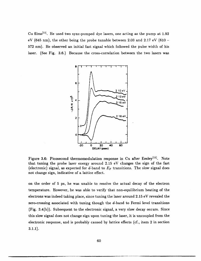
Cu films["1 . He used two sync-pumped dye lasers, one acting as the pump at 1.92
eV (645 nm), the other being the probe tunable between 2.03 and 2.17 eV (610 -
572 nm). He observed an initial fast signal which followed the pulse width of his
laser. (See Fig. 3.6.) Because the cross-correlation between the two lasers was
a
6
u,
x
c
!
4
2
0
-20 0 20 40 60DELAY (psec)
Figure 3.6: Picosecond thermomodulation response in Cu after Eesleytll]. Notethat tuning the probe laser energy around 2.15 eV changes the sign of the fast(electronic) signal, as expected for d-band to EF transitions. The slow signal doesnot change sign, indicative of a lattice effect.
on the order of 5 ps, he was unable to resolve the actual decay of the electron
temperature. However, he was able to verify that non-equilibrium heating of the
electrons was indeed taking place, since tuning the laser around 2.15 eV revealed the
zero-crossing associated with tuning though the d-band to Fermi level transitions
(Fig. 3.4(b)). Subsequent to the electronic signal, a very slow decay occurs. Since
this slow signal does not change sign upon tuning the laser, it is uncoupled from the
electronic response, and is probably caused by lattice effects (cf., item 2 in section
3.1.1).
60
q· �_ -Il�-l·_·--·ly^··-··1111111111�� �-�--�-··l^-Y�*�··---�---_l�.-lll�-�-·ly �� --

Direct observation of the electron relaxation was first reported independently
by Elsayed-Ali, et al. 12] in Cu and by Schoenlein, et al.13] in Au. Both experiments
used a CPM laser as the source, with a copper vapor laser (CVL) pumped amplifier
to provide high power sub-picosecond pulses [l4]. In Schoenlein's experiment, the
high power probe pulses were focussed into a jet of ethylene glycol in order to
produce a broadband continuum. With these pulses as a probe, he was able map
out the change in the reflectivity spectrum as a function of time (see Fig. 3.7).
His data clearly showed the zero crossing associated with d-band to EF transitions.
q.U
3.0
2.0O
so, 1.0
O
-I .0
-2.0
,an- .v
Figure 3.7: AR vs energy for various delay times in a Au sample. From Schoenlein,et al.13].
Since his pulses were - 65 fs in duration, he was able to resolve the hot electron
decay time, finding it to be - 2 - 3 ps.
3.2.2 Femtosecond Thermomodulation - Theoretical Aspectsof the Excitation Process.
As discussed in items 1 and 2 in section 3.2.1, the action of the pump pulse in
femtosecond thermomodulation is to cause an increase in the electron temperature,
throwing Te out of equilibrium with the lattice. The size of the AR signal detected
by the probe will be directly proportional to ATe. To get a rough idea of the
size of AT,, we can make a model calculation for gold. We take the pump to
61
is I
I

be a delta function in time, and assume that the electrons equilibrate amongst
themselves instantaneously. (This second assumption is questionable at best, since
the electrons do not make optical transitions directly into equilibrium states, but it
is fine as a rough approximation since the electron-electron scattering rate is faster
than the actual laser pulse - refer to item 2 in section 3.2.1.) We further assume
that the energy loss rate to the lattice is slow enough that it may be ignored for
times less than - 100 fs. The energy deposited by the pump in the metal, E, then
causes an increase in Te given by
TO+AT,E=f TdTC(T)
where Ce(Te) = Te is the electronic heat capacity (linear in Te)101°]. For Au,
- = 6.1 x 10⁻⁵ J cm-3 K-2 .[10] Taking the CPM pulse energy density as 10- 3
J/cm 3 (assuming a 40x microscope objective giving a spot diameter of - 21zm), the
increase in electron temperature induced by the pump is ATe = 500 K. Although
this seems like a large temperature increase, the pertinent temperature scale is de-
termined by the Fermi temperature, which is typically on the order of 104 K.[10]
Thus, we are (usually) justified in treating ATe as a small perturbation.
Now we can ask what the expected change in reflectivity of the metal is using
the model given in section 3.1.2. Since the CPM emits 1.98 eV photons, while the
d-bands lie 2.38 eV below the Fermi level, we have AE = E - l > kT,, so we may
approximate af/dT asf 1 AE akT
Off ~ e-^ETe . (3.5)aT Te kcTe
With AE = 0.4 eV, kTe 0.025 eV and inserting (3.5) into (3.4) we get
AE = -3.8 x 10⁻⁶C A T (3.6)2 Te
Next, we take the bound contribution to E2 at 2.0 eV to be C 0.5[7]. The opti-
cal constants of gold at 2.0 eV are n = 0.21 and k = 3.272[ 7]. Using ATe = 500
K, the estimate of A Eb given by (3.6), and (3.1), we get an estimate for AR/R
6 x 10⁻¹⁰. This value is many orders of magnitude smaller than the observed value.
(AR/R - 10- 5 for Au.) This discrepancy probably comes from the fact that ac-
cording to (3.4) and (3.5), Aeb includes a term e -aE/kT, which is exponentially small
62
I --- I - ·----�-�---·U--·-----CL�1-�·l·--·rm---- --*·I III"IP�--·-·-·II^LII-C·I_-�--YIII^·YI�·- -

for AE > kT. The observed thermomodulation feature has spectral wings which
spread much further out in energy than kT. Again, it is likely that the discrepancy
may be explained by the fact that the bands participating in the transition are not
dispersionless, the extremely short lifetime of the excited state contributes to the
broadening, and/or effects due to AEl.
It is important to recall that not only Cu and Au can give fast thermomodulation
signals at 2 eV. (This is mentioned as point 4 in section 3.2.1.) In order to see a
fast signal, the only requirement is that the optical transition either start or end
in a state which is close to the Fermi level. The transition metals have their Fermi
levels lying right in the middle of a large density of d states['0]. A priori, one might
expect that many of the transition metals would also have other states near 2 eV
away from the Fermi level, so a fast thermomodulation signal would be obtained in
many metals. Serendipidously, this is indeed the case in some (but not all) transition
metals (e.g. Cr, W, Ni). Thus, fast thermomodulation spectroscopy is not limited to
studying only Cu and Au. However, this is not always the case. In certain metals
of technological importance (e.g., Nb, and Pb), no fast electronic signal occurs.
This situation can be remedied by depositing thin (- 40 A) Cu overlayers on the
metal under study. The Cu film changes its reflectivity in response to the electron
temperature of the underlying metal, thereby acting as a thermometer for Te. This
technique is further discussed in chapter 5.
3.2.3 Femtosecond Theromodulation - Theoretical Aspects
of the Decay Mechanism.
Once the pump pulse has heated the electron gas and caused a AR, the return
to equilibrium may be mapped out in time by measuring AR s. t with a pump-
probe experiment. The trick is to relate the AR decay signal to the underlying
microscopic physical processes under way in the metal. We know that in general,
AR arises from both changes in the electronic occupancy (like Fermi level smearing),
as well as changes in band structure due to lattice strain (cf.: section 3.1.1). In
order to separate the two effects, we make the approximation: electronic processes
are fast, i.e., they occur on a time scale of a few picoseconds or less. Lattice
63
__ � � __ �� _ __

processes are slow, usually appearing on a > 10 ps time scale. For this reason we
can say with confidence that the d-band to Fermi level transition model used to
explain the "derivative-like" feature in the thermomodulation spectra of Cu and
Au is correct, in spite of the apparent contradictions between the model calculation
and the experimental results. The rule of thumb is: if the decay is fast, the physical
mechanism is related to the dynamics of the electrons.
This rule of thumb is borne out by considering the time scales relevant to vari-
ous physical processes that can take place in a solid as a result of laser irradiation.
In general, effects due to both relaxation and transport must be considered when
examining the AR decay signal in femtosecond thermomodulation. Relaxation oc-
curs when the nonequilibrium electrons scatter among themselves or with other
excitations (e.g., phonons, fixed impurities, etc.). Thus, the energy distribution of
the electrons is altered. On the other hand, transport of electrons away from the
optically probed region also causes AR to decay. These two processes are illus-
trated schematically in Fig. 3.8. We can get an idea about what sort of time scales
z z
(a) (b)
Figure 3.8: Time dependence of the Te profile in a metal after pumping. The twodecay mechanisms of the pump-probe signal are relaxation (a), or transport (b).
are relevant to different processes by considering the frequencies or velocities which
characterize the physical processes.
In a metal, the fastest processes are individual electron-electron scattering events,
64
- --------- I�----·.. I- �.l·C�---�-- III�LI-·�·�·"�-l--�--_411·11111�··1111_- sll�·1-s 111�1111�·111(1111)/·11�11�-·11111 -

which occur on a time scale of order - (EF/h)- 1 Since EF is on the order of 5 eV for
many metals, electron-electron scattering is a 10-15 sec process. This is much faster
than our laser pulse so these dynamics are unobservable. Single electron collisions
with the entire electron plasma are also possible. Since wp is also on the order of 5
eV, these are also 10-15 sec processes. Individual electron-phonon scattering events
are characterized by the phonon frequencies, which are typically tens of meV. Thus,
we expect that the single electron-phonon scattering time is of order 100 fs. Similar
estimates may be made for other electron scattering processes by considering the
energy of the excitation with which the electron is scattering.
Lattice decay processes can also be observed in pump-probe experiments. Al-
though none of the experiments reported in chapters 4 - 6 directly observe lattice
dynamics, it is interesting to consider these processes since recent experiments in
our laboratory have observed optical phonon oscillations in samples of Bi and Sb.[ '5]
These oscillations appear as periodic modulations in AR as a function of time de-
lay, with a period exactly given by w/27r. The oscillation amplitude decays on a
time scale of 6 ps, which is presumably the optical phonon lifetime. Since optical
phonons can decay via plasma damping (in conducting samples) or via anharmonic
decay to acoustic phonon modes, this lifetime is related to the coupling of the optical
phonons to the plasma and/or other phonons.
The other mechanism by which AR decays is transport. In particular, the
importance of electron transport can be seen by considering the relevant velocity
scale in metals: the Fermi velocity VF. When the sample is pumped, all the energy
of the laser is deposited within the first skin depth of the metal, do (150A for Au).
Since this is also the region of the sample being probed, we can estimate a decay time
associated with the transport of electrons out of this region: = d/vF. For typical
metals, VF - 108 cm/sec, giving r ~ 15 fs, which is very short indeed. Because this
time is so short, electron temperature relaxation and transport compete with each
other in femtosecond thermomodulation.
Transport of heat via phonons may also occur in pump-probe. One can obtain
an estimate of the importance of this process by considering the order of magnitude
of the sound velocity in various materials. In metals, c, 106 cm/sec, typically,
65

which is 100 times slower than VF. Thus, it is a good approximation to ignore heat
transport by the lattice in femtosecond thermomodulation measurements of metals.
This is consistent with the fact that the thermal conductivity of metals is domi-
nated by the thermal conductivity of the electron gas. In experiments in insulators,
however, this effect cannot be neglected. However, because we are concerned with
metals here, we will not consider it further.
Any theory attempting to treat the dynamics of laser irradiation of metals must
include the effects of both transport and relaxation. As a first approximation,
the transport of heat may be treated qualitatively as a diffusion process. This is
the historic approach taken by Anisimov, et al.[ 9] who studied the non-equilibrium
heating behavior of a metal heated by nano- and picosecond pulses. They assumed
that the electron gas can be assigned a well-defined temperature, Te (cf. point 2 in
section 3.2.1). Then, the exchange of heat between the electron gas and the lattice
can be characterized by a pair of coupled diffusion equations governing the lattice
and electron temperature:
a tCe(Te) '= IcV2Te - g(Te - T) + A(z,t) (3.7)
C, at = g(T, - T). (3.8)at
Equation (3.7) describes the evolution of the electron temperature. It is a simple
diffusion equation, with (non-constant) electronic heat capacity C,(T,), and thermal
conductivity c. Since C, = T, this equation is non-linear. Coupling to the lattice
occurs through the coefficient g. Finally, since the pulse imparts energy only to the
electrons, the source term (i.e., laser) A(z,T) occurs only in the equation for T,.
Equation (3.8) describes the lattice temperature. No diffusion term (V 2TI) occurs
here since it is assumed that negligible heat diffusion takes place through the lattice,
in accordance with the previous discussion.
These equations were postulated to describe the behavior of hot electrons in
metals on a nano- or picosecond time scale. Whether they can be applied to dy-
namics occurring on a femtosecond time scale is not a priori clear. Since our laser
pulse width is on the same order as the Drude scattering time[l"], a diffusion model
may not be appropriate in describing a metal's transport dynamics. In chapter 4
66
I I __ _ _Ipl� I�_ _ I- I 1·I II -- _ _

we describe an experiment designed to shed light on just how heat is transported
in metals on a femtosecond time scale.
67

References.
1. M. Cardona, Modulation Spectroscopy, Supplement 11 to Solid State Physics,
ed. by F. Seitz, D. Turnbull, and H. Ehrenreich (Academic, New York, 1969).
2. R. Rosei, and D. W. Lynch, Phys. Rev. B 5, 3883 (1972).
3. W. J. Scouler, Phys. Rev. Lett. 18, 445 (1967).
4. N. E. Christensen, and B. O. Seraphin, Phys. Rev. B 4, 3321 (1971).
5. F. Wooten, Optical Properties of Solids (Academic Press, San Diego, 1972).
6. See, for example, J. A. Stratton, Electromagnetic Theory (McGraw-Hill, New
York, 1941).
7. P. B. Johnson and R. W. Christy, Phys. Rev. B 6, 4370 (1972).
8. For example, see D. Pines, and P. Nozieres, The Theory of Quantum Liquids
(Addison-Wesley, Reading, MA 1989).
9. S. I. Anisimov, B. L. Kapeliovich, and T. L. Perelman, Zh. Eksp. Teor. Fiz.
66, 776 (1974) [Sov. Phys. JETP 39, 375 (1975)].
10. N. W. Ashcroft, and N. D. Mermin, Solid State Physics (Saunders College,
Philadelphia, 1976).
11. G. L. Eesley, Phys. Rev. Lett. 51, 2140 (1983).
12. H. E. Elsayed-Ali, T. B. Norris, M. A. Pessot, and G. A. Mourou, Phys. Rev.
Lett. 58, 1212 (1987).
13. R. W. Schoenlein, W. Z. Lin, J. G. Fujimoto, and G. L. Eelsey, Phys. Rev.
Lett. 58, 1680 (1987).
14. W. H. Knox, M. C. Downer, and C. V. Shank, Optics Lett. 9, 552 (1984).
68
_�III I�I�L�_ ______1_1_�_^� _1YC_·I____ I·__� I__X__II_/LIIY__�WI_1/1_1__1-�� ..̂ ·--�-- -----· II
15. T. K. Cheng, S. D. Brorson, A. Kazeroonian, J. S. Moodera, M. S. Dressel-
haus, G. Dresselhaus, and E. P. Ippen, "Time-Resolved Impulsive Stimulated
Raman Scattering Observed in Reflection with Bismuth and Antimony", sub-
mitted to Appl. Phys. Lett.
69
I I

Chapter 4
Femtosecond Electronic HeatTransport in Thin Gold Films.
As discussed in Chapter 3, two competing mechanisms contribute to the decay of
the transient signal observed in femtosecond thermomodulation experiments: trans-
port and energy relaxation. The aim of the present chapter is to discuss the kinds
of heat transport effects occurring in thin films of gold on a femtosecond time scale.
Section 4.1 presents results of both front-probe and back-probe thermomodulation
measurements designed to isolate the effects of transport from those of energy re-
laxation. Using films of varying thickness, we are able to determine the heat transit
time through the sample as a function of sample thickness. For very thin films
(< 3000 A) we find that heat transport occurs at the Fermi velocity, VF. Section
4.2 deals with some aspects of the theory of scattering relevant to femtosecond
transport dynamics of electrons in metals.
4.1 Pump-Probe Measurements of Transport.
Our experiment exploits the reflectivity changes induced by electronic temperature
changes in a metal film as described in Chapter 3. We pump the front surface of the
sample and probe the reflectivity change at either the back or front surface (Fig.
4.1). Probing the back surface reflectivity allows us to measure the heat transit time,
while probing the front monitors the reflectivity transient decay due to both heat
transport and energy relaxation. The two measurements are complementary, and
yield additional information about the electronic dynamics when taken together.
70
- -*_ I·_ · C--l�l----��^ll-r�----rurr�-.^�--rrr�-- �-·-- -----_�^-_-__.____-_-_·I�--- ·r�·(·l···�----· -�-C· . ---- I-- I^·

d
/
/
Heat ~
Flow4-4-
4-4'
Ausample
thickness
\y probe
(back)
Figure 4.1: Conceptual drawing of the experiment. The pump pulse heats theelectrons at the front of the sample. By probing the front, we perform a traditionalfemtosecond thermomodulation experiment. Probing the back allows us to directlymeasure the heat transport time.
71
probe
t-
The experiments were performed on films of gold deposited on sapphire using
e-beam vacuum deposition. Sample thicknesses ranged from 200 to 3000 . All
samples used were thicker than the optical skin depth (- 150 i). The thickness
of the films was monitored during deposition, and was also measured using a Dak-
tek film thickness instrument. The laser source was a colliding pulse mode-locked
(CPM) dye laser employing 4 prisms to control the cavity dispersion as discussed
in Chapter 2. , = 630 nm, t = 96 fs FWHM (sech2 ) for all results shown here.
For these experiments, the average output power of the CPM is about 10mW, and
the pulse repetition rate is 100 MHz. The pump and probe beams were derived
from a conventional pump/probe set up. A motor driven stepper stage with 0.1tm
resolution was employed to vary the delay between the pump and probe pulses.
For the back-probe experiment, the pump beam was chopped and focused onto the
front surface of the sample with a 40x microscope objective, while the probe was
similarly focused onto the back of the sample. The experimental set-up is shown
schematically in Fig. 4.2. The focal spot diameter was measured with a pinhole
to be 2m, giving an energy fluence of - 1 mJ/cm2 at the focus. The reflected
probe beam was monitored with a photodiode. The thermomodulation signal was
detected with a lock-in amplifier tuned to the chopping frequency of the pump. The
zero delay point was determined by reversing the role of pump and probe beams
and repeating the experiment. In the case of the front-probe experiment, the pump
was chopped, both beams were focused through a 40x microscope objective, and
the reflected probe was monitored as described above.
Shown in Fig. 4.3 are back-probe data for films 500, 1000, 2000, and 3000 Athick. The sign of AR/R is negative, since smearing the occupancy of states at
the Fermi level causes an increase in absorption at our wavelength (c.f. chapter
3). Note that the delay time of the rise of the reflectivity change increases with
sample thickness. This is a direct consequence of the finite time needed for heat
to propagate through the sample. Furthermore, note that the measured delay is
very short, i.e., it takes only 100 fs for heat to travel 1000o. The experiment was
repeated several times for different film thicknesses. Numerical fits were performed
on each trace to determine the rising edge delay as a function of sample thickness.
72
is -- -" -_____.- ----- --- T~~~~~~~'~' .-l-I I- II IY___--__' ------ -~ ~ -_

Experimental Set-up
CPM
ef
Choi
Sample
BS
A/2
.BS
Sig
Figure 4.2: Schematic diagram depicting the experimental set-up used for thefront-pump back-probe experiment.
73
_ 1 _���__�

500
1000 A
2000 A
3000 A3000 A
0.0 0.5 1.0 1.5At (ps)
Figure 4.3: Back surface reflectivity as a function of delay.
74
C)
z
a:
r-:aI
1-^-- -· ---- I�--- ---·^--·---.-·-·CI1I�XYIII�-IOI �-I- �lrrr_-·YII111 � ����-� PYI·IIII�LIILI�

These results are summarized in Fig. 4.4. Several features are noteworthy. First, the
measured delays are much shorter than would be expected if the heat were carried
by the diffusion of electrons in equilibrium with the lattice (tens of picoseconds)[l l].
This suggests that heat is transported via the electron gas alone, and that the
electrons are out of equilibrium with the lattice on this time scale. Second, since
the delay increases approximately linearly with the sample thickness (see Fig. 4.4),
we may extract a heat transport velocity of 10 8cm/sec. This is of the same order
of magnitude as the Fermi velocity of electrons in Au, 1.4 x 108 cm/sec.[2 ]
The magnitude of the observed reflectivity change was monitored at the lock-
in amplifier. The normalized modulation AR/R was on the order of 1 x 10⁻⁵ for
500A films, and decreased slowly to - 3 x 10⁻⁶ for Au film thickness L of 2000A.
It was not possible to determine the functional dependence of AR/R on L since
the sample-to-sample variations of AR/R were quite large. We performed these
experiments using laser intensities varying over a factor of 10 on the 500A sample,
and over a factor of 2 on the 1000A sample. We found that the delay, as well as
the shape of each trace, was not affected by intensity changes. The modulation
AR/R was observed to vary linearly with the intensity of the pump laser for all
film thicknesses.
The effects of ultrafast heat transport are also observed in the results of front
probe experiments when the sample thickness is varied. Figure 4.5 shows reflectivity
decay data for gold films of 200, 500, 1000, and 2000 A thick. As can be seen,
increasing L decreases the observed reflectivity decay time constant. This can be
understood in the following way. When the sample thickness is long compared to
the optical skin depth (L d, where do ,. 150 A), transport and energy relaxation
occur simultaneously. In this case, the observed reflectivity decay is very fast since
two competing processes remove energy from the probed region of the sample.
Conversely, when the sample thickness decreases to the order of the optical skin
depth (L - d), less transport occurs, and the reflectivity decay is primarily due
to energy relaxation. The net result is that as the sample dimensions decrease, the
front surface reflectivity decay time increases.
The magnitude of AR/R at the front surface was 3 x 10 - 4 for samples with
75
_ I _ __

3000
2000
oor
J
1000
290
0 l0o 200At (fsec)
Figure 4.4: Delay vs. sample thickness.
300
76
c11311111111� - - -·----·r*---.----------·------- --r---·--l��...���.l.�r--l.- -1...·--�--�- �� __ I.�.� _ ���� _ _

O,-
:i
-1 0 1 2 3 4
At (ps)
Figure 4.5: Front surface reflectivity vs. time delay for various film thicknesses.
77
__

L = 200. AR/R dropped to 2 x 10⁻⁵ for L = 500A, and then decreased more
slowly as L increased. Presently, it is unclear why AR/R changes so dramatically
for thin samples, although it is well known [3 ] that the optical properties of very thin
(< 300 A) Au samples can differ from bulk values. For a given L, varying the laser
intensity over one order of magnitude did not affect the shape of the front probe
curves for L > 500A, and AR/R varied linearly with pump intensity.
4.2 Theoretical Aspects of Femtosecond ElectronTransport in Metals.
Since the heat moves at a velocity comparable to VF, it is natural to question exactly
how the transport takes place. Recall that the motion of an individual transport
electron is a random walk. Since those electrons which lie close to the Fermi surface
are the principal contributors to transport, the heat carrying electrons move at VF.
In the limit of lengths longer than the momentum relaxation length, p, the random
walk behavior is averaged, and the electron motion is subject to a diffusion equation.
Conversely, on a length scale shorter than Ip the electrons move ballistically with a
velocity close to VF. In our experiments, it is not clear which effect (if either) will
dominate the transport process. We shall treat each limiting case in turn.
In the diffusion limit, it is assumed that the electronic and lattice systems are
in local equilibrium with themselves, and can hence be described as a coupled, two
temperature system as discussed in chapter 3.3. The space and time evolution of
the electron and lattice temperatures (Te and T respectively) is governed by the
coupled diffusion equations[ 4]
Ce(Te) _ = KV2Te - g(Te - T) + A(z,t) (4.1)ataT,
C, = g(T, - T) (4.2)
In the uncoupled limit (g = 0), for small changes in electron temperature, the elec-
tronic heat capacity may be approximated as constant and equation (4.1) reduces
to the linear diffusion equation. In this case, the heat transit time is proportional
to the square of the sample thickness (At - L2 ), as is well known for the case of
78
_1 _1-11�-�11- 1 -�_-�I _·IIL-UI�-�··I�1PYI·I - 11�-·1--·1�· -·- -- - -

linear diffusion. Since this relation does not seem to hold for our experiment, the
possibility of simple linear heat diffusion can be ruled out. However, the full non-
linear behavior of the coupled system (4.1 - 4.2) is much more complex, and can
only be simulated numerically.
The behavior of eqs (4.1 - 4.2) was simulated using the Crank-Nicholson methodNs5 .
Selected results are shown in Fig. 4.6 which shows the back surface electron tem-
perature vs. delay for a variety of sample lengths. As can be seen, the peak in
rear surface temperature indeed scales linearly with sample thickness, at least for
the parameters used in the simulations. Thus it is difficult to distinguish between
diffusive and ballistic behavior on the basis of transit time measurements.
For length scales shorter than the scattering length, the electron motion is bal-
listic. In this situation, hot electrons are created at the front of the sample by
the pump pulse. This can occur by interband transitions and by Joule heating
of the electron gas, resulting in a non-thermal electron distribution as discussed
in section 3.2.1, point 1. Two things might happen next. In the first scenario,
some of the very hot electrons might then propagate through the sample without
scattering, signalling their arrival at the rear of the sample by a change in reflectiv-
ity. Although this possibility cannot be discounted, it seems unlikely because the
scattering length for electron-electron scattering is a strongly increasing function
of the electron's energy. High energy electrons have a much higher probability of
scattering than do those close to the Fermi level. Also, if the electrons involved
in the femtosecond transport were significantly hotter than EF, one would expect
them to have a velocity greater than VF, which is not observed here.
The other scenario is close to the spirit of point 2 from section 3.2.1: the initial
non-thermal electrons extremely rapidly scatter amongst themselves, creating a hot
- but thermal - electron distribution. Then, these electrons propagate through the
sample, "surfing" along at an energy just above EF. These electrons arrive at the
rear surface without experiencing any large angle scattering, and are detected after
a delay At = L/vF. Whether or not this can happen in our samples depends on the
scattering length near EF. The crux of the issue is: what determines the scattering
length in any metal? Recall that at T = 0 K an electron introduced at the Fermi
79
rl I _ .�_ _ - __ � _ �_� _ _

1I
Heating pulse -
2 3 4 & 61 I 1 1 1
Delay time (ps)
Heating pulse -AT. on Back Surface for Different L.
L ATe (peak)(A) (K)
1 500 22482 1000 9303 2000 1604 3000 26.75 4000 4.426 5000 0.74
I, = 10°
W/cm'-1011 J cm
-' sec-t K-'
0 Delay time (ps) 10
Figure 4.6: Selected results of the numerical simulation of (4.1 - 4.2) showing backsurface electron temperature as a function of time. From the results descussed inchapter 5, we obtain g = 2.5 x 10¹⁰ J cm-3 sec- K-'. For our laser power (Io - 1010W/cm2 ), we have a situation intermediate between the two calculations shown here.
80
0
1 2 3456I II
10
�1� �·_111_· _ ··_ __�_II_ �ylllll__ll___ldlY_�··�·lll--^llli---L��

level will never scatter, since there are no lower energy states available into which to
scatter[6]. In this case, I = oo. At non-zero temperatures, an estimation of I may be
obtained by considering the effect of temperature on the electron-electron scattering
rate. We take the electron-electron interaction to be mediated by a Yukawa type
potential,l6]
r
where A is the screening length of the metal, which may be deduced e.g., from the
Thomas-Fermi method[6]. The total scattering cross section of the Yukawa potential
is known to bet 7]2m 47re4
aT(k) = -th2 ) k2(k2 + 4k 2)'
where k = 1/A is the screening wavevector.
The classical scattering rate of a particle moving with velocity v in the presence
of n cm-3 scatterers of cross section a is
W = nva.
For this calculation, we ask for the scattering rate of a single electron against all
other electrons in the Fermi sea. The electron moves at the Fermi velocity VF.
At zero temperature, an electron at the Fermi level cannot scatter. But when the
temperature is raised above zero, two effects take place which affect the scattering
rate. First, the number of conduction electrons with which the electron can scatter
increases as
n = no(2,
where no is the total density of conduction electrons. Second, the number of possible
final states into which the electron can scatter will also increase, thereby increasing
the cross section as
T a t E o
where a, is given above. From this, the scattering rate becomes W = novFo, (kT/EF)2 ,
giving a scattering length
I = VFT - (nOu (kT/ EF )2
81
__

Using numbers from Ashcroft and Mermin[2], we get the scattering length at T = 300
K is I = 460 A.
The results of this simple minded calculation are consonant with more rigorous
(many-body) hot electron scattering length calculations reported in the literature.
The electron - electron scattering length in Au, l4e, has been calculated by Kro-
likowski and Spicer from the optical density of states deduced from photoemission.[8 ]
They find that lee cc (E - EF)- 2 for electrons close to the Fermi level. This func-
tional form is consonant with a simple density of states argument: electrons with
energy within (E - EF) can only scatter with other electrons in the same energy
range (at T = 0 K). The total number of possible scattering processes is thus pro-
portional to (E - EF)2 . For 2 eV electrons, lee z 350A, increasing to 800A, for
1 eV electrons. The electron - phonon scattering length, ,,, is usually inferred
from conductivity data. Using Drude relaxation times[2], we compute le, P 420i
at 273 K. This is shorter than lee, but of the same order of magnitude. Thus, we
would expect that both electron - electron and electron - phonon scattering are
important on this length scale. However, since conductivity experiments are steady
state measurements, the contribution of phonon scattering in a femtosecond regime
experiment like ours is uncertain.
On the experimental side, internal photoemission measurements of - 1 eV hot
electrons generated in Au yield "attenuation lengths", ,, of 700 [191 or 740A['01].
Although 1,a is not equivalent to the momentum relaxation length, it does indicate
the distance over which large angle scattering becomes importantill. Also, I, is
indicative of the combined effects of electron - electron and electron - phonon
scattering[ 9] which determine the heat transport behavior in our experiment.
Since our samples dimensions are not much larger than both theoretically pre-
dicted and experimentally measured momentum and energy relaxation lengths, bal-
listic motion near EF can be assumed to play a role in the transport we observe.
This is consistent with our observation that the heat transit time does not change
with laser intensity over the range of our experiment. In ballistic transport, chang-
ing the pump intensity only changes the number of electrons which participate in
the transport process; the actual transport dynamics remain unaffected.
82
- -- ·-- ··*------- ~~~~~~~~~- -

In summary, we have measured the dynamics of ultrafast heat transport in
thin Au films by femtosecond thermomodulation. Our results indicate that heat
is carried by non-equilibrium electrons. Heat transport occurs on a femtosecond
timescale, with a delay which scales approximately linearly with thickness. Using
both front-probe and back-probe techniques, we observe a heat transport velocity of
the same order as VF. Simple scattering arguments suggest that ballistic electronic
motion may contribute to heat transport in the time and length regime under
study. Finally, these results show that measurements designed to measure electronic
relaxation phenomena in metals must use thin films to avoid the complicating effects
of transport.
83
II

References.
1. S. D. Brorson, J. G. Fujimoto, and E. P. Ippen, Phys. Rev. Lett. 59, 1962
(1987).
2. N. W. Ashcroft, and N. D. Mermin, Solid State Physics (Saunders College,
Philadelphia, 1976).
3. P. B. Johnson, and R. W. Christy, Phys. Rev. B 6, 4370 (1972).
4. S. I. Anisimov, B. L. Kapeliovich, and T. L. Perelman, Zh. Eksp. Teor. Fiz.
66, 776 (1974) [Sov. Phys. JETP 39, 375 (1975)].
5. W. H. Press, B. P. Flannery, S. A. Teukolsky, and W. T. Verrerling, Numerical
Recipes (Cambridge Univ. Press, Cambridge, 1988).
6. C. Kittel, Quantum Theory of Solids (Wiley, New York, 1963).
7. J. S. Dugdale, The Electrical Properties of Metals and Alloys (Arnold, London,
1977).
8. W. F. Krolikowski, and W. E. Spicer, Phys. Rev. B 1, 478 (1970).
9. S. M. Sze, J. L. Moll, and T. Sugano, Solid State Electron. 7, 509 (1964).
10. W. G. Spitzer, C. R. Crowell, and M. M. Atalla, Phys. Rev. Lett. 8, 57
(1962); C. R. Crowell, W. G. Spitzer, L. E. Howarth, and E. E. LaBate, Phys.
Rev. 127, 2006 (1962).
11. C. R. Crowell, and S. M. Sze, in Physics of Thin Films, ed. by G. Hass and
R. E. Thus (Academic, New York, 1967), Vol. 4.
84
_ Ils� II � · I__II__IY__III_1_I__III_1IIC·LI__I�··

Chapter 5
Femtosecond Room-TemperatureM easurem ent of theElectron-Phonon CouplingConstant A in Metallic
Superconductors
As discussed in Chapter 3, hot electron in metals relax on a 100 fs time scale via
electron-phonon interactions. That is, the excited electron gas loses its energy by
emitting phonons. Since the rate of this process is determined by the strength of the
electron-phonon coupling, one might expect that one could work backwards from
a knowledge of the relaxation rate to get the electron-phonon coupling constant.
Indeed, this was the motivation for the early work of Fujimoto, Liu and Bloembergen
on femtosecond photoemission from tungsten[ l].
It has also long been known that the electron-phonon interaction in many met-
als can give rise to superconductivityl2]. One might expect that pump-probe mea-
surements of the strength of the electron-phonon interaction might be of use in
superconductivity theory. This possibility was first pointed out by P. B. Allen
in 1987.[3 The purpose of this chapter is to explore this idea, and to present the
results of a measurement program designed to determine the electron-phonon cou-
pling constant in a variety of superconducting and non-superconducting metals and
alloys. In section 5.1.1 we review superconductivity theory, starting from the at-
tractive interaction experienced by electrons in the presence of phonons. Then we
85
I -

briefly consider the results of BCS theoryi4] and its generalization to real systems by
McMillan[5 ]. Because of its central importance to the experiments discussed in this
chapter, section 5.1.2 details the modern theory of electron-phonon relaxation in
metals due to P. B. Allen.[31 In particular, we show how the electronic temperature
relaxation rate is related to the electron-phonon coupling constant A which occurs
in McMillan's theory. Section 5.2 covers the results of the experimental program.
5.1 Theory.
5.1.1 Essential Superconductivity.
The phenomenon of superconductivity was discovered almost 50 years before it
received a satisfactory explanation. One of the intervening advances in understand-
ing superconductivity took place in 1950 when Frohlich showed that the effective
electron-electron interaction might be attractive in the presence of phonons.[ 2 ] His
hypothesis was confirmed experimentally by the discovery of the isotope effect. 16]
In 1956, Cooper showed that in the presence of an attractive potential, individual
electrons in a dense Fermi sea could bind into pairs, called Cooper pairs. 17] It was
felt that the composite object would be a charge carrier (charge 2e) obeying Bose-
Einstein statistics, and could accordingly condense into a superfluid like ground
state. Although this superfluid analogy has since proven to be misguided, the essen-
tial feature of superconductivity remains the binding of electrons into Cooper pairs
via an attractive electron-electron interaction caused by the presence of phonons.
A simple argument demonstrating the appearance of the electron-electron at-
traction due to phonons can be made by considering the electron-electron interaction
in jellium - that is, a uniform positive background capable of supporting density
waves.?8] Jellium is meant to model the background of positive ions which form the
lattice of a metal. Ordinarily, in the unscreened case, the electrons interact with
each other via the bare Coulomb potential47re2
Vo(k) = (5.1)
In jellium, the electrons are screened. The screening arises from two effects: first,
the electrons themselves screen each other, giving rise to a Yukawa type interaction
86
i _I _·I 1I___1____I________YII__�(_Y__YILIYY�·q

between electrons. Second, since the positive background can support density waves,
the background can also screen the electrons.
Screening can be incorporated into the electron-electron interaction by reduc-
ing Vo(k) by the dielectric function of the electron-jellium system.[8] The dielectric
function, , is a product of two terms. One is given by the dielectric response of the
electron gas alone, E, the other is the dielectric response of the jellium, ph. Both
contribute to the renormalized electron-electron interaction.
To begin, we adopt the Born-Oppenheimer approximation,l] which says that
the lattice moves on a 10 - 12 second time scale, while the electrons move on a 10-15
sec time scale. Thus, the jellium (i.e., ion) motion is screened by the electrons,
while the electrons adiabatically follow the motion of the jellium. If the jellium was
simply a positively charged fluid, its dielectric function would be[8 ]
f12
Eph =1 wd2
where Qp = 4rNZ2e 2/M is the square of the jellium plasma frequency. N is the
density of ions in the lattice, Ze is their charge, and M is their mass. Since the jel-
lium motion is screened by the electrons, its plasma frequency must be renormalized
asn2
f2P(k) PE,(k)
The function p (k) can be regarded as a rough approximation to the phonon dis-
persion curve of a metal.
The electronic dielectric function E,(k) may be found via the Thomas-Fermi
method,[1] and is usually written as
k 2E(k) 1 + k
where k, is the screening wavevector. Then renormalizing the bare Coulomb poten-
tial by c,(k) and Eph(k,W) we get the effective electron-electron interaction
V(k) 47re2 47re2 ( n(2(k)V(k, w)= + I Ik2
E, (k) ph(k, w) k2 + 2 + kk W2 - fl k)j (2
The first term corresponds to the screened electron-electron interaction whereas
the second is the electron-electron interaction mediated by phonons. The essential
87
__

feature of (5.2) is that for certain values of w (w < Qp(k)), the electron-electron
interaction can be attractive. This is illustrated in Fig. 5.1 where we plot V(w)
vs. w assuming an Einstein model for the phonon spectrum - i.e.: lp(k) = 2p is
a constant. Of course, in reality, the actual interaction will depend on the detailed
V(@)
0 (
Figure 5.1: Frequency space attractive potential V(w) given in equation (5.2).
nature of the phonon spectrum.
It should be noted that anomalous frequency domain behavior (like the attrac-
tive electron-electron interaction) is a generic feature of systems with resonances.
As an illustration, we consider a simple example: a dielectric made of Lorentz os-
cillators. We take the electrons in a solid to be bound to specific lattice sites with
a harmonic potential. The response of such a bound electron to the local electric
field is determined by the equation of motion:
d2 x ed + w2x = -E(t),dt2 M
where x is the coordinate describing the displacement of the electron from its equilib-
rium position. (Note that we are ignoring dissipative effects - they are unimportant
88
C- '- -- I· I-·1 -··III--^P~r-·~--- ~ _I· -~- ___ ---------- -- ·

for the argument here.)
If a sinusoidal field is applied, E(t) = Ee-iwt, the response is
x e/m Ex- E.W2 _-W2
The microscopic polarization is
e2 /mP = ex = 2 2 E.
Now, the displacement field D corresponds to the externally applied macroscopic
field. If the density of oscillators is n, we have,
D = E + 47rP2
(1 + 2 P 2)E,
with w 2 = 4rne2 /m. Re-arranging, we can get the microscopic field seen by the
electrons E in terms of the applied field:
2 2
E= )D.E = ( 2 _ m t a2)o p
The expression in braces is negative for w2 < 2 < 2 + W2. This means that
the microscopic field experienced by the electrons is in opposition to the applied
field. This is the physical origin of the so-called "dielectric anomaly". The anal-
ogous effect occurs between electrons in metals over the frequency range w < WD.
The occurrence of an attractive interaction between electrons should not be at all
unexpected!
The frequency domain attractive interaction is exploited in BCS theory.4] We
consider a Hamiltonian
H = E EkCkk + E Vk,k'CkLCkTC-kl, (5.3)k k,k'
where
Vk,k { - for IWI < WD }
0 otherwise
This potential is meant to model the essential features of the potential shown in
Fig. 5.1 - that is, it is attractive only for electrons which have energies lying
89

within an energy characterized by wD, the Debye frequency. BCS showed that this
Hamiltonian has a ground state wavefunction[4 ]
I'BCS) = lI(Uk + VkCktC kj)O)k
where IUkl 2 + Ivkl 2 = 1. The important feature of this wave function is the appear-
ance of the operator pair Ctt These create two electrons of opposite momenta
and spin in a paired state, which are the Cooper pairs.
The excitation spectrum is shown in Fig. 5.2, where the gap between the ground
state and the continuum of excited states is
A = 2hwDe- 1/NV
where No is the density of states at the Fermi level, and V is the effective electron-
electron interaction. Furthermore, the superconducting transition temperature TC
E
Ep +2A -.
EF
a24
T
g(E)
Figure 5.2: Excitation spectrumthe gap at the Fermi level.
of a BCS superconductor. Note the presence of
90

is found to be
kTc = 1.14hwDe -1/NOV.
In this simple model, we may define the coupling constant due to electron-phonon
interactions as A = NoV. This corresponds to including only the second term of
(5.2) in the Hamiltonian (5.3).
The next level of sophistication in superconductivity theory is to include effects
due to the Coulomb repulsion term in (5.2). Such an interaction causes the TC
equation to take the form
T, oc e - 1/( A- " )
where it describes the size of the Coulomb interaction averaged over the surface of
the Fermi sphere. The size of the Fermi sphere is roughly the same for most metals,
so the parameter t does not vary significantly from one metal to another. As can
be seen, attraction via phonon interactions and repulsion because of the Coulomb
interaction work against one another in determining Tc; since values of ,i are close
for different metals, T, depends most sensitively on the size of A, and hence on the
details of the phonon spectrum.
To be able to formulate a theory capable of predicting T for real metals, we
must be able to incorporate information about the phonon spectrum into the T¢
equation. Such a theory was devised by McMillan 5 ], who derived an equation for
To:eOD 1.04(1 A)
Tc = 145 exp -A - u*'(1 + 0.62A) (5.4)
where OD is the Debye temperature, and * is a reduced Coulomb interaction. The
electron-phonon coupling constant A is given by
lAo= 2j'd a 2F(w) (5.5)
where a represents the electron-phonon matrix element, and F(w) is the phonon
spectrum. One can also define a hierarchy of moments of the phonon spectrum:
2 2p l(wn = dw a2F(w)w"-. (5.6)
A o
Traditionally, the function a 2F(w) has been measured by tunneling,["ll] allowing A
to be calculated by (5.5), or F(w) is measured by neutron scattering, while a can
91

be calculated via pseudopotential methods.[ ' 2 ] Alternately, A itself can be obtained
by measuring the electron mass enhancement seen in measurements of the specific
heat C, at low temperatures,[13], or by measuring the saturation of the resistivity
with increasing temperature.[14 ]
5.1.2 Allen's Theory.
In 1987, P. B. Allen proposed that A might also be measured by femtosecond
thermomodulation.[ 3 ] We review his calculation here, and attempt to fill in de-
tails which had to be left out of his original paper. We consider the time rate of
change of the electron and phonon distributions, fk and nq respectively. Here, k
labels the electron wavevector, and q labels the phonon wavevector. We assume
that both distributions are thermal, and are characterized by temperatures Te and
T1, which are, in general, not equal. This approximation is that used in section
3.2.2. Presumably, electron-electron scattering keeps the electrons in equilibrium
amongst themselves, while phonon-phonon scattering via anharmonicity keeps the
phonon distribution thermal. In this situation, fk is a Fermi-Dirac function, while
nq is a Bose-Einstein function.
The rate equations describing the time development of fk and nq can be derived
from Fermi's golden rule. They are:
afk -ir. E Mkk 2 {fk(1 - fk)[(nq + 1)6 (Ek - Ek' - hwq) + nqb(Ek - Ek, + hwq)]
-(1 - f)fk,[(nq + -1) 6 (Ek - k' + hWq) nq 6 (Ek - - hWtq)]}
aq= - 7 EN lMkk'12fk(l - fk')[nlq6(Ek - Ek' + hWq) - (nq + 1)6(Ek - Ek' - hwq)]at hNC M
where N, is the number of cells in the sample, and Mkk' is the matrix element for
electron-phonon scattering. In the language of McMillan, Mkk' corresponds to a.
We also denote the single particle energy of an electron of wavevector k by ok. The
four types of interactions included in the sums are shown schematically in Fig. 5.3.
The total energy of the electrons is given by
Ee = 2Ekfkk
92
Q--C -I --

I-'
q
r'
k(a) (b)
K k' k'
(c) (d)
Figure 5.3: The four scattering processes contributing to the relaxation of theelectron gas.
93
�I
I

where the factor of 2 is included to account for both spin orientations of the elec-
trons. From this, the time rate of change of E is
aEe afk- = 2 E Ek ata t k at
= 2 E Ek{ (a) + (b) + (c) + (d)}k q
where (a), (b), (c), and (d) correspond to the processes illustrated in Fig. 5.3.
The summation in brackets can be re-arranged, and the sum index can be changed
q -- k' to yield
aEt - h E k MMkk' { (fk - fk')nqb(Ek -Ek - hWq) + (fk - fk,)nq6(Ek - Ck' + hWq)at hN1 ,kkt
+fk(l - fk')b(ek - k' - hwq) - (1 - fk)fk6(k - ek' + hwq)} (5.7)
In (5.7) we replace k with k' in the second and fourth term, and add, yielding,
(Ek - k')(fk - fk,)nqb(Ek - Ek' + hWq) - (Ek - Ek')fk'(l -fk)b(Ek - Ek' + htq)
Then, because of the delta functions, we have Ek - Ek hwq, so we may write
equation (5.7) as
dE, 47rat = hN~ jwq Mkk< 2 S(k,k')6(Ek - k' + hWq) (5.8)kk'
where we define a "thermal factor" which depends on the electron and phonon
distribution functions:
S(k,k') = (fk - fk,)nq - f( - fk) (5.9)
These equations are Allen's (6) and (7)[3 ].
Now we insert three factors of unity into (5.8), giving
94
___C _1~---1___-· sI- Ipl-l~*---~ -I· P·- - Y- -- -_I~-LIIIII-I~

aEe =- _ dZ6(E -hN) f dE'6((E -- /') f drb6(wq -n)
hwqMkkIl 2S(k, k')b(ek - k' + hwq). (5.10)kk'
Next we consider the function a 2F(n). By definition:[5
a 2 F(k,k', 2) = No IMkk' 12 6( - Wk-k') (5.11)
This is the full definition of the phonon spectral function taken from Allen and
Mitrovic,[1 5 ] which includes the dependence on the initial and final scattered electron
states, as well as the phonon spectrum. To place this in a form convenient for further
analysis, we change variables to and ' thusly:
o2F(e, )= - 2 N , o: 2 F(k,k',)6(c - k)b(E -k)-k k'
Then, upon substituting (5.11) into this, and substituting the result into (5.10), the
energy decay rate becomes:
adE = 27rNNo f dla 2F(e, e', l)hf
f df d''S(k, k') (k - + hQ)
where we have ignored the slow dependence of F(E, ', fQ) on energies and '. This
is a good approximation, since the variation of F with F is much faster than with
energy. In fact, this is the approximation that is traditionally made to deduce A
from neutron scattering experiments[ l5]. Consequently, we shall henceforth write
F(Q) only.
Now we do the f de f de' integrals. After using the properties of the 6 function,
the thermal factor becomes
jo dE [f() - f(e + hn)] n(h) - f(E + hn) (1 - f(E))
For convenience, we take = (e - F)/kTe, and =- h/llkT. The first integral is,
with a little re-arrangement,
n(hn)(e - 1) o d(ee + 1)(eC+ + 1)
95

Next, if we define x = e, and a = e n, we obtain an integral which can be done in
closed form:[ l6]
f d( +)( ) a 1 in (1 + ax
The overall contribution due to this term is n(hf,T 1)hf1, where we have used the
approximation e - pl/kTe ; O. The second term can be integrated in a similar way
yielding n(hfl, T,) h.
With these expressions, the electron energy decay rate is
aEt = 27rNNo J dfa2F()(h)2[n(hf, T) - n(,T,)]. (5.12)
Now, we expand the term in the braces. Define = hlQ/kT, and a = hfl/kT1. We
are above the Debye temperature, so e < 1 and < 1. Thus, we can expand:
1 1 1e-k 1 _k(1+ + 1 2 + ... )-1
SO
n(TI) - n(Te ) k h -hi) 2 hMI
Substituting this into (5.12), and using the definition of A(w 2) from section 5.1.1,
we get an expression for the energy relaxation rate:
dEea= rthNcNoA(w 2) (kT - kT,). (5.13)at
Next, we recall that the energy of the electron gas is related to its temperature
by Ee = T2/2, where y = r2NNok2/3.[3 ] This yields
aE, aT,at at
Substituting this into (5.13) gives our desired result:
aT = -3h (w 2 ) T - T(5.14)at 7rk T,
This is the equation relating electronic temperature relaxation to A first given by
Allen in 1987[3].
Equation (5.14) assumes that the energy deposited in the sample by the pump
pulse is distributed uniformly, so that we may neglect the effects of heat transport.
96
IC--·- CI~~~-----CUII - l--·ll-l~~~~~---Y-··-~~-·^···~~~----·~~-U1I_ -.I .-II· .~-- -----

In all the experiments reported in the next section very thin samples were used, so
that no heat transport could take place. In this case, Te and T1 are related by (cf.
Chapt. 3.2.3.)dT
Ce(Te) = -g(T - T), (5.15)dt
dTCl = (Te - T), (5.16)
where C is the lattice specific heat (constant at 300 K), and Ce = YTe is the
electronic specific heat. Comparison of (5.14) and (5.15) shows that the coupling
constant g = 3h'yA(w 2)/rkB. Combining (5.15) and (5.16) leads to a non-linear
differential equation for T,
Te2T- + ( d ) + A w(1 ) = 0. (5.17)dt2 dt 7rkB CL dt
This equation may be solved analytically given initial and final electron tempera-
tures, Te(O) and T,(oo). The result, due to A. Kazeroonian, is
t hA(w2 (T - T2) [T2In T( 0) - T )-T, In (T( T )] (5.18)
whereCL fC+ 2+ 2kcBCLII
T +\ )+htyA (W2)'
ClT2 =-2-T,
and
,= h() (T () + Te(0)2).kB 2-y
The solution (5.18) can be turned around numerically yielding Te as a function
of time. All the parameters entering (5.18) are known physical constants except
T,(O) and Te(oo) (which may be estimated to within 20% knowing the laser pulse
energy) and A(w2). Thus, knowing T, vs. delay time t determines A(w2) with no
free parameters.
5.2 Experimental Determination of A from Fem-tosecond Thermomodulation Measurements.
The measurements are performed using a standard pump-probe set-up as described
in section 2.4[17]; the signal of interest is the change in intensity of the reflected probe
97

beam, AR, as a function of time delay t after the arrival of the pump pulse. The
laser source is a balanced CPM dye laser[18i producing 60 fs pulses at a repetition
rate of - 100 MHz. The average output power is 10 mW. The wavelength is 630
nm, corresponding to a photon energy of htw - 1.98 eV. The pump beam is chopped
to enable lock-in detection. The polarization of the probe beam is rotated to be
orthogonal to the pump beam, so that stray light from the pump beam may be
rejected using polarizers before detection. Both beams are focused on the sample
with a microscope objective. Silicon photodiodes are used to monitor the reflected
beam. After amplification, the AR(t) signal is detected using a lock-in amplifier
and stored on a computer to facilitate the numerical fits.
For this technique to work, changes in T must cause R, the reflectivity of the
sample at our laser energy, to change. This is known to occur in Cu and Au as well as
certain other transition metals via the Fermi level smearing mechanism discussed
in chapter 3.2. Care must be taken, however, in interpreting the experimentally
observed relaxation traces. Changes in the metal's reflectivity can also arise from
lattice temperature changes. For example, band shifting arising from thermal strain
will cause the reflectivity to change[1 9] (cf., point 2 in section 3.1.1). Thus, the
reflectivity of the metal will change in response to both ATe and AT as
AR = aAT + bATI (5.19)
where a and b are constant coefficients describing how electron heating and lattice
heating affect R. The AR arising from changes in T will typically decay on a very
slow time scale ( 10 ps) determined by the rate at which heat can diffuse away
from the optically pumped region. In fitting the data, we make the (physically
reasonable) assumption that any relaxation signal occurring on a fast ( 1 ps) time
scale is due to electronic relaxation alone.
The experimental AR vs. t curves are computer fit to the solution (5.18) using
a least-squares method with only A,,p(w 2) as the fitting parameter. The other
parameters needed in (5.18) are T (0) and T,(oo): T,(O) is determined by knowing
the pump laser energy and the linear coefficient of the specific heat, y as described
in chapter 3.2.2. We also have Te(oo) = Tl(oo), which can be determined from the
laser pump energy and the total specific heat of the metal. Estimation of T,(0) and
98
I -- --- --- -- - ---"" - I --

T,(oo) is the major source of uncertainty in determining AeXp(w 2). Furthermore, as
mentioned above, changes in electron and lattice temperature may both give rise
to a AR as in (5.19); the ratio a/b is determined by comparing the peak of AR(t)
to the value of AR after the fast transient has decayed away. The data are then fit
using the procedure discussed in section 2.4.2117]: the impulse response of R(t) (the
solution of (5.17) inserted in (5.19) ) is convolved with the pump pulse intensity
autocorrelation function, yielding a theoretical AR vs. t curve which may be fit to
the data. (It should be noted that this procedure is strictly valid only for linear
systems, i.e., those governed by linear rate equations. That is not the case in (5.17),
which is clearly non-linear. However, this will cause errors only for the fit to the
peak of the pump-probe trace, while the pump pulse is still present. Since we are
interested in the relaxation rate, whose decay proceeds after the end of the pump,
this will not effect our determination of A(w2).)
The various metal samples were deposited on clean glass slides by e-beam evap-
oration. The base pressure for evaporation was < 10-6 torr to insure sample purity.
As described below, certain samples (see Table 5.1) had a thin overlayer of Cu de-
posited on top of the evaporated metal sample. This layer was deposited without
breaking vacuum to avoid contaminating the metal/Cu interface. All samples used
were optically thin (sample thickness < optical skin depth at 1.98 eV) so that the
pump laser energy was distributed uniformly over the depth of the sample. It is
very important that the sample be optically thin so that there is no transport of
heat [20] or electrons[21] out of the optically pumped region during the time over which
electron temperature relaxation takes place - effects which can mask the desired
relaxation signal[21]. After preparation, the T¢ of the superconducting films was
measured using either a SQUID magnetometer or via a resistivity measurement.
As discussed in Chapter 3, not all metals display a fast relaxation signal. This
is because only a few metals have an optical transition near 1.98 eV which involves
the Fermi level. In order to study important materials which do not have such a
transition (viz., Nb, V, and Pb), we deposited a very thin overlayer ( 40 A) of
Cu on top of these samples immediately after they were deposited1 22 ]. The electron
temperature in the Cu overlayer is exactly the same as that in the metal under
99
I _
study, since the two materials are in close contact. Since the relaxation rate of
Te in Cu is very long ( several ps), and the Cu layer is very thin compared to
the underlying metal, the relaxation rate of the composite structure is determined
solely by the underlying metal. The Cu overlayer acts then as a thermometer, since
its reflectivity is sensitive to Te in the underlying metal. Using this method, we are
able to extend the femtosecond pump-probe technique to metals which ordinarily
do not display a fast Te response at 1.98 eV.
The observed AR vs. time delay t signals for Cu and Au are shown in Fig.
5.4. The data for Pb, W, Cr, V, Ti, Nb, NbN, and V 3Ga are shown in Fig. 5.5.
Note that Fig. 5.4 and Fig. 5.5 use different time scales. Au and Cu are good
conductors because the electron-phonon interaction in them is relatively weak. This
is consonant with the fact that their relaxation times are much longer than those
of the other metals. The computer generated fit is shown for each sample as the
solid line. As can be seen, the theoretical fits to the relaxation data are quite close
to the observed decay traces for delay times after the pump pulse. However, a
slight delay (- 20 fs) occurs between the rising edges of the theoretical fit and the
data. This may signal the occurrence of a non-thermal distribution of electrons for
these very short times. Such an effect will not hamper the measurement of A, since
electron-phonon relaxation takes place on a somewhat longer time scale.
The derived values of Aezp(w 2) are given in Table 5.1. Values for (w2) were culled
from the literature, and were used to get A,,zp. These results are summarized in
Table 5.1, where we also show the results of other published experiments measuring
the electron-phonon coupling, Alit. In nearly every case the agreement is excellent,
within experimental error. A little discrepancy occurs in the values obtained for
NbN and V 3Ga. Inspection of Fig. 5.5 reveals that the response of NbN nearly
follows the envelope of the pump pulse. This is because the relaxation time of T,
in NbN is on the order of the pulsewidth itself. This is similarly true of the V3 Ga
data. Such behavior is consonant with Allen's theory: these materials have among
the highest Ts (for metals), and thus their relaxation times are the shortest. The
values of A,,p(w 2) and Aezp for these samples given in Table 5.1 should cautiously
be regarded as lower bounds.
100
II �. - lll�ll·IL---7-P-lll-1�--111�---- �I--------- p� _I _ �

cv
0U)-6
Lc5
'1
-1 0 1 2 3 4 5 6 7Delay (ps)
Figure 5.4: AR vs. time delay data for Cu and Au. The solid line is the theoreticalfit to the data.
101

Figure 5.5: AR vs. time delay data for Pb, W, Cr, V, Ti, Nb, NbN, and V 3Ga.The solid line is the theoretical fit to the data. Note that a different time scale isused from Fig. 5.4.
102
- I__ _ 111 L I -_..__ 7 -- ._-·-·--·-------- ---- II�L��·--�-----------�1-111111�-- -I I �

Table 5.1: Experimental values for the electron-phonon coupling A,,p and otherparameters: literature values of , initial electronic temperature Te(O), experimentalvalues of A,,p(w 2 ), literature values of (w 2), and ,,,p. Error in Te(0) is 20%. Forcomparison, values of the electron-phonon coupling Alit from the literature are alsoshown (where available).
I Te (0) Aezp (w2 ) (W2 ) Aezp Alit(mJ Mol-1 K- 2 )a (K)a (meV2 ) (meV2 )
Cu 0.70 590 29±4 3 77 b 0.08I0.01 0.1 0 b
Au 0.73 650 23±4 178C 0.13±0.02 0.15cCr 2.9 716 128±15 9 87 d 0.13±0.02 -W 0.9 1200 112±15 425 e 0.26±0.04 0.26eV 9.9 700 280±20 352f 0.80±0.06 0.82f
Nb 7.80 790 320±30 2 7 5g 1.16I0.11 1 .04gTi 3.32 820 350±30 6 01 h 0.58I0.05 0 .5 4 hPb 2.94 570 45±5 31' 1.45±0.16 1.55
NbN 1.38 1070 640±40 673j 0.95±0.06 1.46JV 3Ga 25.6 1110 370±60 4 48 k 0.83±0.13 1 . 12k
a y values from Ref. [23] were used to determine T,(0).b Ref. [24]; Ref. [25]; d Ref. [26]; e Ref. [27]; f Ref. [28];g Ref. [29]; h Ref. [30]; i Ref. [31]; i Ref. [32]; k Ref. [33].
103

We would like to highlight our value of Aep,,, for Cr. To date, only a few - widely
varying - values of A for Cr have appeared in the literature.[3 4] It is well known that
Cr is antiferromagnetic below 315 K; it is widely supposed that the antiferromag-
netism contributes to the suppression of superconductivity. Estimates of A based
on resistivity data [34 1 do not account for the effect of the antiferromagnetism on the
resistivity, and hence tend to overestimate A[35] . Estimates of A based on specific
heat measurements [ s ] tend to underestimate A for the same reason[35]. Since our
measurement of Te relaxation is sensitive only to the electron-phonon interaction,
the value of A,,ezp given in Table 5.1 is probably the best determination of A to date,
and is certainly the first direct determination of this important quantity in Cr.
To insure that the Cu overlayer deposited on certain samples did not affect
the experimentally observed relaxation process, we deposited Cu layers of different
thicknesses on identical W samples. W has the property that a fast electronic relax-
ation signal can be observed even without a Cu overlayer. The overlayer thickness
were 0 A (no Cu), 40 A, and 100 A. Relaxation data obtained on these samples
are shown in Fig. 5.6. The 0 A and 40 A overlayer samples give similar values of
Aezp(W 2) (0 A Cu: 112 meV2, 40 A Cu: 137 meV2 ). The 100 A overlayer sample
gives a much lower value (65 meV2 ) since the presence of the thicker Cu layer tends
to decrease the measured relaxation time. From this, we conclude that thin (< 40
A) Cu layers do not significantly perturb the relaxation process occurring in the
underlayer.
On the V and Nb samples having a Cu overlayer, resistance measurements
showed that T had dropped below 4 K in the V and below 1.5 K in the Nb.
T, measurements performed on samples made simultaneously with these, but hav-
ing no Cu overlayer, showed the usual values of T,. We attribute the suppression
of T in the samples with overlayers to a proximity effect. This effect should not
alter the values of Ae,p(w2) we measure here, since A 2,p(W2) depends on the phonon
mode spectrum and the electron-phonon matrix element, while the proximity effect
is a purely electronic effect. This proximity effect did not occur in NbN samples
prepared with Cu overlayers. (These samples are not shown in Table 5.1.) This be-
havior is reasonable since the coherence length of both Nb and V is larger than the
104
�I __ __ll__l___ll_·ILII1___IILLY�I-�

O
-n
0
-0.4 0 0.4 0.8 1.2Delay ( ps)
Figure 5.6: Relaxation data for W samples with Cu overlayers of different thick-nesses.
105

film thickness, while the coherence length of NbN is smaller than the film thickness.
Thus, the superconducting wavefunction in Nb and V is more seriously perturbed
by the Cu overlayer than is the superconducting wavefunction of NbN.
In summary, we have performed the first femtosecond pump-probe measure-
ments of in metals. This method has several advantages over other techniques
(e.g., tunneling, or heat capacity measurements): it is a direct measurement of
A(w2), it works at room temperature, it can be applied to both superconducting
and non-superconducting samples, and it is not affected by extraneous effects such
as the antiferromagnetism in Cr. By depositing thin Cu overlayers when necessary,
our technique is extendable to nearly any metallic thin film. Finally, the agreement
between our measured Aezp values and those available in the literature is excellent,
thus confirming the predictions of Allenl3 ] .
106
_ �I 1_1� _I_ II^Y-^·---_�---·-�^-�--L - ·�---_-_�-··L--ll�--_-·^--�·111 ----�---- __-^_---1·11_-----11I�I�-P-----

References.
1. J. G. Fujimoto, J. M. Liu, E. P. Ippen, and N. Bloembergen, Phys. Rev. Lett.
53, 1837 (1984).
2. H. Fr6hlich, Phys. Rev. 79, 845 (1950).
3. P. B. Allen, Phys. Rev. Lett. 59, 1460 (1987).
4. J. Bardeen, L. N. Cooper, and J. R. Schrieffer, Phys. Rev. 108, 1175 (1957).
5. W. L. McMillan, Phys. Rev. 167, 331 (1968).
6. C. A. Raynolds, B. Serin, W. H. Wright, and L. B. Nesbitt, Phys. Rev. 78,
487 (1950); E. Maxwell, Phys. Rev. 78, 477 (1950).
7. L. N. Cooper, Phys. Rev. 104, 1189 (1956).
8. For instance, see D. Pines and P. Nozi/res, The Theory of Quantum Liquids,
Vol. 1, (Addison-Wesley, Reading MA, 1989).
9. See, for example, N. W. Ashcroft and N. D. Mermin, Solid State Physics,
(Saunders College, Philadelphia, 1976).
10. This is well treated in a number of books, including C. Kittel, Quantum Theory
of Solids, (John Wiley, New York, 1963).
11. W. L. McMillan and J. M. Rowell, in Superconductivity, R. D. Parks, ed.
(Marcell Dekker, New York, 1969), p. 561.
12. R. C. Dynes, J. P. Carbotte, D. W. Taylor, and C. K. Campbell, Phys. Rev.
178, 713 (1969); P. B. Allen and M. L. Cohen, Phys. Rev. 187, 525 (1969).
13. G. S. Knapp and R. W. Jones, Phys. Rev. B 6, 1761 (1972).
14. P. B. Allen, Phys. Rev. B 17, 3725 (1978); P. B. Allen, Phys. Rev. B 36,
2920 (1987).
107
�_�� I I � __

15. P. B. Allen and B. MitroviC, in Solid State Physics, vol. 37, H. Ehrenreich
and D. Turnbull, eds. (Academic, New York, 1982).
16. I. S. Gradshteyn and I. M. Ryzhik, Table of Integrals, Series, and Products,
(Academic, Orlando FL, 1980), formula number 2.154.
17. E. P. Ippen and C. V. Shank, in Ultrashort Light Pulses, S. L. Shapiro, ed.
(Springer, Berlin, 1977).
18. J. A. Valdmanis, R. L. Fork, and J. P. Gordon, Optics Lett. 10, 131 (1985).
19. R. Rosei and D. W. Lynch, Phys. Rev. B 5, 3883 (1972).
20. B. M. Clemens, G. L. Eesley, and C. A. Paddock, Phys. Rev. B 37, 1085
(1988).
21. S. D. Brorson, J. G. Fujimoto, and E. P. Ippen, Phys. Rev. Lett. 59, 1962
(1987).
22. Dean Face, Unpublished.
23. y for Cu and Au are from D. L. Martin, Phys. Rev. 141, 576 (1966); for
Pb is from B. J. van der Hoeven, Jr., and P. H. Keesom, Phys. Rev. 137,
A103 (1965); -y's for the other films are from F. Heiniger, E. Bucher, and J.
Muller, Phys. Kondens. Materie. 5, 243 (1966).
24. (w2) is from T. P. Beaulac, P. B. Allen, and F. J. Pinski, Phys. Rev. B 26,
1549 (1982); Alit is from P. M. Chaikin, G. Arnold, and P. K. Hansma, J. Low
Temp. Phys. 26, 229 (1977).
25. (w2) is from J. W. Lynn, H. G. Smith, and R. M. Nicklow, Phys. Rev. B 8,
3493 (1973). Alit is from P. B. Allen, Phys. Rev. B 36, 2920 (1987).
26. (w2) is from W. M. Shaw and L. D. Muhlestein, Phys. Rev. B 4, 969 (1971).
27. (w 2) is from A. Larose and B. N. Brockhouse, Can. J. Phys. 54, 1819 (1976).
Alit is from P. B. Allen, Phys. Rev. B 36, 2920 (1987).
108
------ ---------------"-�-- '------�CII--�l `-�-2�--UPYYI�I -__ - - -·-·II�CIYIIP�---·L-··

28. (w2) and Alit are from J. Zasadzinski, D. M. Burnell, E. L. Wolf, and G. B.
Arnold, Phys. Rev. B 25, 1622 (1982).
29. (w2 ) and Alit are from G. B. Arnold, J. Zasadzinski, J. W. Osmun, and E. L.
Wolf, J. Low Temp. Phys. 40, 225 (1980).
30. (w2) is from C. Stassis, D. Arch, B. N. Harmon, and N. Wakabayashi, Phys.
Rev. B 19, 181 (1979); Alit is from S. V. Vonsovsky, Yu. A. Izyumov, and E.
Z. Kurmaev, Superconductivity of Transition Metals (Springer-Verlag, Berlin,
1982).
31. (w2) and Alit are from R. C. Dynes and J. M. Rowell, Phys. Rev. B 11, 1884
(1975).
32. (w2) and Alit are from K. E. Kihlstrom, R. W. Simon, and S. A. Wolf, Phys.
Rev. B 32, 1843 (1985).
33. (w2) and Alit are from J. Zasadzinski, W. K. Schubert, E. L. Wolf, and G. B.
Arnold, in Superconductivity in d- and f-Band Metals, edited by H. Suhl and
M. B. Maple (Academic, New York, 1980), p. 159.
34. P. B. Allen, Phys. Rev. B 36, 2920 (1987).
35. P. B. Allen, Private communication.
109

Chapter 6
Femtosecond ThermomodulationStudy of High-Tc Superconductors.
Following the success of using femtosecond thermomodulation spectroscopy to mea-
sure A (and hence T,) in metals, we attempted to perform similar measurements
in a system of current interest: the copper oxide high-T, superconductors. The
motivation for this study can be summarized in the following way: A question
of considerable contemporary interest is whether or not superconductivity in the
high-T, materials is phonon mediated. Since Allen's theory['l directly gives the
electron-phonon coupling in terms of the carrier temperature relaxation rate, mea-
surement of the relaxation rate may reveal if the coupling is anomously large, and is
thus capable of playing a role in causing superconductivity. Furthermore, since the
high-T, compounds are Cu-based, one might expect that the presence of Cu d-bands
would allow one to observe carrier temperature relaxation via Fermi level smearing.
Thus, these are ideal systems in which to perform femtosecond thermomodulation
measurements.
This chapter presents the results of this experimental program. Section 6.1
reviews the properties of high-To materials germane to understanding the pump-
probe results. Section 6.2 covers the actual experiment and the results obtained.
Finally, section 6.3 offers a detailed critique of the results and their relation to the
current understanding of high-T, superconductivity.
110
I �· 1_ 11·1__ _ �ID---�-I-C-XII I--·-II_�I__--I-��.1I-·. LI. ·-�-- -l-U-^lllll)l·^ IL�.�-Y--_II�··IIIII1l11111�

6.1 Essential High-T, Superconductivity.
The first high-To compound was discovered by Bednorz and Miiller in 1986. [12] Un-
satisfied by contemporary attempts to raise T in metallic alloys, they set out on
a new path: searching for high-To in transition metal oxides. Transition metal ox-
ides had long been known to display a variety of novel behaviors, including strong
electron-phonon coupling due to the Jahn-Teller effect.[3 ] The Jahn-Teller effect is a
symmetry breaking distortion of the crystal lattice which can occur in certain tran-
sition metals of specific valences, including Cu 2+ . What happens is that Cu-d levels
which are degenerate in other valence states split for Cu 2+ via a spontaneous lattice
deformation and thereby lower the crystal energy. (See Fig. 6.1.) In a crystal, an
Cus+ Cu2+
3de Orbitals 3d9
3z2 - r, X2- y2 teg
It 1T 1 ~ T ~xy, yz, tx zlt $ t2g
/i 3z 2 -r/ I1"
Jahn-Teller Effect:Elongation of
the Octahedron
Figure 6.1: Illustration of the Jahn-Teller effect. (a) shows a Cu 3+ ion which expe-riences no distortion. When another electron is added, Cu 2+ is formed, which canlower its energy via a lattice distortion (b).
electron surrounded by this lattice distortion can propagate as a polaron, with a
correspondingly large electron-phonon coupling. The implication is that extremely
111
-- -_ -�---- I I
%U /

high-To might be realizable in such a system.[ 4]
After a couple of false starts, the suspicions of Bednorz and Muller were con-
firmed when they discovered that the resistivity of samples of La 1. 25Ba 0.75CuO 4
showed signs of the onset of superconductivity around 30 K. [2] Soon thereafter,
Meissner effect measurements of this system showed flux exclusion, confirming that
true superconducting behavior was indeed taking place.[5] Soon after their dis-
covery, superconducting behavior was discovered in a whole slew of Cu-O com-
pounds, including YBa2 Cu30 7-6 (hereafter called "123") with a T of 92 K,[61
Bi2Sr 2CaCu 2Os+z (hereafter called "2212") with T¢ = 80 K, [7] and Bi2Sr2Ca 2Cu 3sO10+
(hereafter known as "2223") with T¢ = 110 K.[ 7] These three materials are the com-
pounds under study here.
The amount of experimental work performed on high-T, superconductivity since
1986 has been simply phenomenal. Since we cannot hope to review all that has been
discovered since, we will only give results that are important to the interpretation
of our pump-probe results. By far the preponderance of data has been taken on
the "123" system, we will discuss it explicitly here. Similar results are true for
"2212" and "2223", so this discussion is also implicitly about them. Where major
differences between these systems exist, they will be mentioned explicitly.
The basic crystal structure of superconducting "123" is derived from the well
known perovskite structure depicted in Fig. 6.2(a).[8 ] Three perovskite units are
stacked on top of each other to yield the basic "123" unit cell (Fig. 6.2(b)). The
crystal type of this structure is orthorhombic.[ 9] Non-superconducting "123" ( = 1)
is similar, but removal of oxygen causes a phase transition to occur, giving a tetrag-
onal unit cell. (Fig. 6.2(c).) Early on, it was found that "123" superconducting
is composed of planes formed by Cu-O bonding units, alternating with chains of
Cu-O bonding units.[l °] (See Fig. 6.3.) Two planes exist in each unit cell situated
between the Y and Ba atoms, perpendicular to the c axis. The chains are at the
top and bottom of the unit cell, between adjacent Ba atoms, and running in the b
direction. In "2212", each unit cell has 2 Cu-O planes, but the chains are absent;
"2223" has 3 planes per unit cell. Current understanding is that the supercurrent
flows mainly in the plane.[ l°'
112
�I I _ �_II·_ I _·__� I�-D-C-� I^··I�-·mC·-�_·II-LI-^·----·-·--LYICI·� ��-�P--PII�1-XI �·�·lly-1�II11��---·1�-·11�111�·�

(a)
(b) (c)
Figure 6.2: (a) The basic perovskite structure. (b) depicts the superconducting"123" ( = 0) unit cell. The crystal structure is othhorhombic. (c) shows the unitcell for non-superconducting ( = 1) "123". In this case, the structure is tetragonal.
Based on valence considerations, one would expect that the charge carriers in
"123" were holes; this expectation has been confirmed by Hall effect measure-
ments.[ l l] In "123" the hole concentration varies with the oxygen stoichiometry.[12 ]
The hole concentration is highest for 6 = 0 (i.e., YBa 2Cu 3sO 7 ); this phase is conduct-
ing at room temperature. For decreasing oxygen concentration, the hole concentra-
tion, and hence the conductivity, drops. When 6 = 1 (YBa 2Cu30 6), the result is an
antiferromagnetic insulator. The mobile holes seem to come from oxygens forming
the chains.[l ° ] T also varies with oxygen content. l'0 ] For 6 = 0 (fully oxygenated),
T, is the highest (92 K) dropping to - 60 K for - .3 - .5, and thence to zero
for 6 > .7. These behaviors are shown in the phase diagram (Fig. 6.4). As of this
writing, the reason for this behavior remains unknown. Unlike "123", there is no
easy way to vary T¢ in the "2212" or the "2223" compounds.
One of the original questions about superconductivity in these novel system
113
- - ----- IIY

"123"
, ChainsIo~a= ( 6 Planes
-- a = 2 ap--
Figure 6.3: Structure of superconducting "123" showing the planes and the chains.
was: "Are there Cooper pairs present in the materials, or is some new, exotic
form of superconductivity taking place?" This question was soon answered in favor
of Cooper pairs. Measurements of the AC Josephson effect in La1.85Sr0.1 5 CuO4
suggested that the current carrying excitations have charge 2e - indicative of Cooper
pairing. [13] This conclusion was supported by measurements of flux quantization in
rings of Y 1.2 Ba0 8CuO 4. The measured flux quantum , = hc/q clearly showed
q = 2e, confirming the presence of Cooper pairs.[ 4 ]
An important question is the electronic structure of the high-T materials. In
particular, what types of electronic states are present in the vicinity of EF? Band
structure calculations of 6 = 1 "123" indicate that it should be metallic, but in
reality it is insulating. l ° ] A similar result holds for La 2CuO4 . This is not a failure of
the details of the band structure calculations, since chemical valency considerations
also imply that it should be metallic.[ l° ] Such behavior is not all that unusual in the
transition metal oxides; it is well known that many transition metal oxides (e.g.,
NiO) are insulating when they should in theory be conducting.[l5 ] Traditionally,
114
__ ___� I__ ·--- ·IIIIPIICIIIIII Il·l^·---·�-(·-C-----��--·IIII�*YYCIIW�1 ---�YWI�*13·lllllll�·1111111111111111111

500
400-
wm 300:)
X 200
100
n1.0 0.8 0.6 0.4 0.2 0.0
OXYGEN DEFICIENCY 8
Figure 6.4: Phase diagram of "123" showing regions of superconducting andnon-superconducting behavior. T is indicated by the solid line for 6 < 0.7. FromRef. [10].
115
_1__ I _ _�_ � _ __ I _ __

this behavior is ascribed to the strong electron correlation present in the materials.
This correlation arises because EF lies in the middle of the d states of the transition
metal.[15] The charge distribution of the d states is more concentrated near the
nucleus of the atom than is that of the s or p states. Consequently, when the d
states participate in bonding, they do not overlap strongly with each other. The
bands that are formed do not have strong dispersion; the d electrons are more
localized and hence are more sensitive to the presence of electrons on neighboring
lattice sites.
Theoretically, one treats this problem using the so-called Hubbard model.[l61] In
the single band Hubbard model, one constructs a model Hamiltonian for a system
of n electrons on a lattice of Nc = n atoms. We start with a local description of the
electron's wavefunctions, using, for example, the Wannier basis. The Hamiltonian
includes two terms: a hopping term which is essentially the energy overlap term
between adjacent sites, and a Coulomb repulsion term for two electrons sitting on
the same lattice site (with opposite spin). We have:
H = t E E cacja + U i ni (6.1)(ii) a i
where t is the hopping strength, U characterizes the strength of the Coulomb re-
pulsion, and a denotes the electron spin. In the itinerant limit (t > U), this Hamil-
tonian reduces to the tight binding approximation; the system is a metal since EF
lies right in the middle of the allowed energy band. However, in the limit of large
repulsion (U > t), a gap opens in the excitation spectrum at the Fermi level. This
is the so-called "correlation gap" and the material is an insulator. Loosely speak-
ing, the electrons cannot move because they must pay too high an energy price to
delocalize and become mobile; H is minimized when the electrons are localized on
specific lattice sites.
Originally, it was assumed that (6.1) was a good model of the insulating phases
of the high-T, compounds. The spectrum of electronic states obtained for the half
filled lattice (n = N) was taken as the starting point for perturbation theory.
Then, by adding holes the system undergoes an insulator-metal transition, where
the metallic phase is superconducting at low temperatures. Unfortunately, not a
116
- -- I--------�--- ---�--·----"-�f�-r�,----·r�lp�- --------- ----- ----- -·I---c----·-------- ---···-·- ---

great deal is known about (6.1) when n is varied away from N,. Several models
have been proposed to explain superconductivity in the context of the single band
Hubbard model. These include Schrieffer's "bag model" [17], which applies in the
t > U limit, and Anderson's "resonating valence bond model" [18] which holds in the
t << U limit. In this limit, other exciting possibilities also exist, including "anyon"
superconductivity [' 9 ] which postulates the existence of quasiparticles in the system
obeying fractional statistics. The literature is rapidly swelling with novel theoretical
ideas related to the single band Hubbard model, but these is growing consensus
that they are not adequate to explain either the actual electronic structure of the
materials or the presence of superconductivity. [ l° ]
Current attention has turned to models generalizing the Hubbard Hamiltonian
to systems with bands originating from Cu d and O p levels separately.[20] Although
different models treat the conduction process differently, the important common
feature in all these models is that the Hubbard mechanism splits the Cu d levels
into two, with a large correlation gap Ud. The O p levels also split, but not enough
to form a gap. The O p states lie in the middle of the Cu d correlation gap, and
the Fermi level resides in these states. [20] This is shown schematically in Fig. 6.5.
Ud
Cu-d m Cu-d
HoleEnergy
ElectronEnergy
Figure 6.5: Schematic diagram of the energy levels predicted by the generalizedHubbard model for the Cu-O superconductors.
117
_ �· _

This picture of the electronic structure has received support from optical mea-
surements of el and 2 in crystals of "123".21] In insulating crystals (corresponding
to no holes in the O p bands) a peak appears in 2 at around 1.7 eV. (Refer to
Fig. 6.6(a).) Although the origin of this feature is still being debated, many the-
orists believe that it is due to a charge transfer excitation in which holes in the
Cu d band are promoted into the O p band. (This is shown schematically in Fig
6.6(b).) This feature disappears when the crystal is doped, which is consistent with
I(a)
4HoleEnetrg
(a)EF
(b)EF
(hkkLJ
hw (eV)
Figure 6.6: (a) Optical transitions occurring around 2 eV in "123". (From Ref.[21].) (b) Energy level diagram illustrating the charge transfer excitation occurringnear 2 eV.
the transitions into empty O p states being blocked by the addition of holes and
the consequent increase of the Fermi level for holes. Furthermore, this feature is
also present in BIS spectra, which are sensitive to empty electronic states (i.e.: full
hole states). [22] These considerations will achieve prominence when considering the
results of the femtosecond thermomodulation measurements discussed in the next
section.
In spite of all the theoretical work, the superconducting mechanism in the Cu-O
compounds remains a mystery. Besides the models built on novel extensions of
the Hubbard model, the possibility of superconductivity arising from phonon-type
interactions remains viable.1 23] This approach remains closest to the original idea
118
�I ---·--�--- --31 ----� -- ---- - --- -- --
3

of Bednorz and Muller to look for high-To in systems having large polaron effects.
Although proponents of phonon models have a loose confederation of ideas and
observations to support their claims, no consistent theoretical picture has evolved
from this camp either.
6.2 Experimental Work.
Many differences exist between the high-T¢ compounds and simple metals; beyond
that, much less is known in general about the electronic structure of the high-To
compounds. Therefore, we would like to know about the time development of AE2 ,
rather than simply AR. This is because AE2 is the physical quantity which is
actually related to the density of states in the material, and is thus presumably
closer to the microscopic physics we are interested in observing. Interpreting the
pump-probe data depends on knowing AC2 and relating it to changes in how the
available states are occupied when the sample is optically pumped. To find AE2 , we
measure the fractional change in both the transmission through the sample (AT/T)
and the reflection off the sample (AR/R). Both R and T are functions of E1 and 2 ;
by measuring both AR/R and AT/T we can separate c1 changes from E2 changes.
Determination of At 2 involves converting the raw AR/R and AT/T data into
AE1 and AE2 as functions of time. As discussed in section 3.1.2, variations in el and
E2 give rise to AR/R and AT/T as:
R = alA 1 + 22AE2 , (6.2)R
AT= 31ACl + /2A 2, (6.3)
T
where oj and ,i are constants. From this we get AR/R and AT/T as functions of
AE1 and AE2. Inverting these relations gives the quantities of interest, AC1 and AE2
as functions of AR/R and AT/T. Unlike the situation discussed in section 3.1.2,
the films studied here have thicknesses on the order of the optical penetration depth.
Thus, multiple reflection effects must be accounted for in determining R(n, k) and
T(n, k);[2 4] the expressions given in section 3.1.2 are not appropriate for this case
since they are for semi-infinite media, and ignore the presence of a rear interface.
119

We use the general expressions for thin films given in reference [24]. The a and P
coefficients so obtained are given in Table 6.1. It should be noted, however, that
very similar results are obtained for Ae 2 if expression (3.1) is used. In particular,
the signs of both Ael and AE2 are not changed when the simple expressions are
used.
The measurements are performed using a standard pump-probe set-up as dis-
cussed in chapter 2.[25] The laser source is a balanced CPM dye laser[26] producing
60 fs pulses at a repetition rate of - 100 MHz. The average output power is 10
mW. The wavelength is 630 nm, corresponding to a photon energy of hw _ 1.98
eV. The output beam is split into pump and probe beams with a beam splitter.
The pump beam can be variably advanced with respect to the probe beam using
a computer controlled translation stage with 0.1/tm accuracy. The polarization of
the probe beam is rotated orthogonally to the pump beam, so that stray light from
the pump beam may be rejected using polarizers before detection. Both beams are
focused on the sample with a 10x microscope objective. Silicon photodiodes are
used to monitor both the reflected and the transmitted probe beams. Following the
detector, the signal from each beam is detected and amplified separately. For com-
parison of the measured signals, we set the gain on the AR and the AT channels
so that the measured reflectivity and transmissivity signals are equal. Hence, we
directly measure normalized changes in reflection AR/R and transmission AT/T.
We carried out the pump - probe measurements on three high-T, oriented film
samples. Parameters describing the samples are summarized in Table 6.1. All
measurements were performed at room temperature. The "123" film was fabricated
by pulsed laser deposition from a single target of YBa 2Cu 30 7-6 onto a LaAlO 3
substrate.[2 7] The "2212" and "2223" films were prepared by reactive magnetron
sputtering on [100] MgO substrates.[2 8] The polarization of the pulses was parallel
to the Cu-O planes. All samples were on the order of one optical penetration depth
in thickness to enable transmission measurements, and to eliminate the transport of
heat [2 9] or carriers[30] out of the optical penetration depth - effects which complicate
the interpretation of reflectance-only experiments in optically thick films.
Time-resolved plots of AE2 are presented in Fig. 6.7 for each of the three samples.
120
_�_ 11� 11_1___ 1_ _ __I1 __I____ IC_ ___ _ ILPI__IL1I�·III��--�

Table 6.1: Superconducting transition temperature T (zero resistance), film thick-ness L, and calculated cal, a 2, p1, 2. T is the maximum electronic temperatureafter the arrival of the pump pulse. Allen's theory[l] is used to deduce A(w2) fromTe and the measured decay time constant r. A was calculated from A(w2) by taking(w2) = WD2/2, where WD is the Debye frequency. WD for the "123" samples is fromRef. [31], and wD's for the other samples are assumed to be equal and are from Ref.[32].
"123 " a "123" b "2212" "2223"T,(K) 90 <5c 75 100L(A) 1500 1500 2500 2500
aq 0.14 0.19 0.23 0.52a2 0.24 0.21 0.33 0.23'P1 0.14 0.09 0.31 0.28/32 -0.71 -0.68 -1.51 -1.58
Te(K) 410±60 420±60 560±190 560±190r(ps) 0.06±0.01 1.0±0.1 0.11±0.02 0.16±0.02A(w2) 475±30 28±5 220±45 138±22
(meV2)A 0.90±0.20 0.07±0.03 0.82±0.41 0.50±0.24
a The "123" film before annealing in Ar at 450 °Cb The "123" film after annealing in Ar at 450 °C
c Measured with a SQUID magnetometer
Plotted in the inset are the corresponding AR/R and AT/T raw data. In each case,
there is an initial fast (< 0.25 ps) transient relaxation subsequent to the optical
excitation, followed by a slower long term recovery. The relaxation data for each
sample have been fit to a decaying exponential using a least squares method. The
relaxation time constants are given in Table 6.1, as well as the coefficients ai and
,3i used to determine AE2 . For the superconducting "123" and "2212" samples, the
initial AE2 is positive, corresponding to increased absorption after the arrival of the
pump pulse, whereas in the "2223" sample the initial AE2 is negative. We have also
computed Ae1 for each of the samples; these data are plotted in Fig. 6.8. A 1 /E1
and AE2/E2 are of the order of 10 - 4 .
It should be noted that the pump-probe signal obtained for the "123" sample
would change over a period of minutes while the data were being taken. If the laser
121
___ I __�

a)
U0n
N
<3
Ia)
C-)
0 04-
N
0
.5U
cu
-0.4 0 0.4 0.8 1.2Delay ( ps)
Figure 6.7: Time resolved A 2 data for "123", "2212', and "2223". Plotted in theinset are the AR/R and AT/T raw data.
122
_I_ �I __ � II�_ Il-�I�LI� ---WI-YI·IY·II�-·II�I�-----L-·--PY-·� --�IIP---C- _-_ -- - -

"2212"
0.0 1.2
t (ps)Figure 6.8: AEx and AE2 vs. delay t for samples of "123", "2212", and "2223".
123
_

remained focussed on the sample for a period of about one hour, the pump-probe
trace became that shown in Fig. 6.9. As can be seen, the initial fast transient
remains, but the long time (> 100 fs) signal begins to rise. This effect was inter-
preted as sample damage, perhaps caused by gradual de-oxygenations of the sample
because of heating caused by the laser. Other groups performing pump-probe ex-
periments on "123" have also observed this signal.[33] We were careful to shield the
sample from the laser beam except during measurement, and to take all the data
as quickly as possible in order to minimize the appearance of this damage signal in
our "123" data.
A word should be said about the possibility of coherent coupling in these data.
In particular, since the pump-probe response of the "123" sample appears so short,
some groups[ 3 3] have erroneously attributed this signal entirely to coherent coupling.
First of all, these experiments were performed using perpendicular pump and probe
beams; coherent coupling is only possible if the system has polarization memory.
Since this does not occur in either metals or semiconductors (because dephasing
occurs rapidly in these systems), it is unlikely that it would occur in the high-T¢
materials. This is particularly true since the high-T¢ superconductors are metallic
systems, and the presence of free carriers is usually associated with extremely rapid
dephasing processes. Second, even if coherent coupling were occurring, its presence
could account for at most one-half of the peak of the pump-probe signal at zero
delay. The rest of the signal must be the desired pump-probe trace, which, because
the relaxation process is so fast, is almost (but not quite) pulsewidth limited, as is
evident from Figs. 6.7 and 6.8.
These data are related to the dynamics of the proposed charge transfer excita-
tion associated with the copper - oxygen "planes" characteristic of all the high-T¢
superconductors. The excitation is observed as a peak in optical reflectivity[21] and
bremsstrahlung isochromat spectra[22] of superconducting "123" starting at 1.7
eV, and peaking at - 2.5 eV. Similar structure is seen in CuO,[3 4 and is probably
a generic feature of Cu-O based superconductors. This feature has been explained
as the excitation of a hole in a copper d/dl0-like state to an oxygen p-like state
with the accordant absorption of a photon[21]. In this picture, the copper d band is
124
_ ^_II I _I�_ X_ III_____II_1_I____11111_1___111_ -1_.- _.___--·-II --- �Llll(li�--�----�-�1111��--�1 Is -I II_ --- ·I_

HTCB
"123"AR
1.33 ps full scaleAfter 1 hour burn
0 Delay Time (ps) 1.33
Figure 6.9: Pump-probe data obtained after sample damage.
125
A

split into two via the Hubbard mechanism [l6]. The oxygen p band lies between the
two Cu d bands, the d 9 /d l0 band being completely full of holes, and the d8 /d 9 band
having no holes.[l ° ] The Fermi level, EF, lies somewhere in the oxygen p band (see
Fig. 6.5), but the exact position of EF is not well known. EF varies with oxygen
doping, which has the effect of placing holes in the p band.
We interpret the change in induced by the pump to be similar to that ob-
served at - 2.1 eV in thermomodulation spectra of copper films[35]. There, when
the electron temperature is increased by the pump pulse, the tails of the Fermi
distribution spread far out in energy (Fermi level smearing), opening states below
and filling states above the Fermi level. Subsequent to pumping, the electron gas
relaxes, leading to an optical response that decays in time. This is the "femtosecond
thermomodulation" process. The situation is presumably the same in the high-T,
materials, except that the carriers are holes instead of electrons, and it is more
convenient to consider optical transitions of holes rather than electrons. The final
states for optical transitions of holes are the p states, which are in close proximity to
the Fermi level. If the hole Fermi level lies slightly above the optically probed states
(as is the case of E (a) in Fig. 6.6(b)), the effect of heating is to cause AE2 to become
positive, since pumping opens more states for absorption. This is the case in the
"123" and "2212" samples. Conversely, if the hole Fermi level lies slightly below
the optically probed states, a negative AE2 is expected since Fermi level smearing
blocks the states involved in transitions. This occurs in the "2223" sample. Thus,
the sign of the pump-probe signal is a sensitive indicator of the Fermi level posi-
tion relative to the optically probed states. The limitations of this "femtosecond
thermomodulation" interpretation are discussed in detail in section 6.3.
In phonon-mediated superconductors, the relaxation rate is correlated with T.11]
Both the relaxation rate and T are determined by the electron-phonon coupling
constant A.[36] When the carriers are strongly coupled (large A), T is large, and
the transient relaxation is fast. In the opposite case of weak coupling (small A),
a smaller T, and a longer relaxation time are obtained. Although the coupling
mechanism in the high-To materials is unknown, some relation between the carrier
relaxation time and T may hold.
126
- ------- "Ir-·-- ··-------·l-cl-·ru�-------rr�---ulr�---- -·---------�rrr�

We therefore looked for a relationship between T and the observed dynamics
by deoxygenating the "123" sample in an Ar ambient at 450 °C for 1 hour. This
has the effect of removing holes from the Cu - O planes, and thereby depressing
T,. Meissner effect measurements performed on the deoxygenated sample showed
that T had in fact dropped below 5 K after deoxygenation, which was the lowest
temperature achievable in our measurement system. We shall henceforth refer to
this sample as "non-superconducting". Pump-probe measurements performed on
the sample subsequent to deoxygenation yield two important results (see Fig. 6.10).
First, the relaxation time increased dramatically, going from - 60 fs to 1 ps -
consistent with the idea that the same interaction causing the femtosecond relax-
ation also contributes strongly to the superconducting pairing. Second, the sign of
AE2 reversed after the annealing treatment. This is consistent with the Fermi level
for holes lying above the final state for optical transitions in the superconducting
sample (E(a) in Fig. 6.6(b)), and lying below the probed states after deoxygenation
has removed the holes (Eb) in Fig. 6.6(b)).
Since the relaxation time and TC seem to be related at least qualitatively, con-
sistent with Allen's theory['l], we used his theory to find A(w2) from the measured
relaxation times. For metals, this quantity is given directly by our experiment.
Assuming that ( 2) = w2/2, we can get an estimate for A in the high-To materials.
At the time of this study, no numbers were available for WD in "2223", so we used
wD for "2212" in estimating A for this material. To get the initial temperature, we
used the value of -y for the "123" sample since no data on y exists for either "2212"
or "2223". The calculated values are given in Table 6.1. For comparison, Kirtley, et
al.[3 7] report an upper bound of 2.5 for A based on tunneling measurements of the
energy gap in superconducting "123". Further interpretation of the pump-probe
results await a more complete understanding of the electronic structure and carrier
interactions in high-To materials. We discuss the limitations of our experiment in
the next section.
127
I I - -

a)0
Cl)-6
0
%a)
C)
U1)
£,%A)
t0
-0.5U
-0
0 0.5 1.5 2.5 3.5
.5Delay (ps)
Figure 6.10: AE2 data for "123" before and after deoxygenation. Note that the signof AE2 has reversed, and that the time constant has increased dramatically upondeoxygenation.
128
Superconducting "123"
v , . . . .~~~~~~~~~~~~~~~~
." 11�1. �-�-�--c-1- ----------------�--�--�

6.3 Critique.
This work is the first femtosecond pump-probe measurement of high-To supercon-
ductors. The significant results are: By monitoring both AR/R and AT/T in thin
film samples, we are able to infer the relative change of 2 induced in the samples.
We find that AE2 recovers on a - 100 fs time scale for all the superconducting sam-
ples. The sign of the AE2 signal is sensitive to the position of the Fermi level relative
to the initial and final states. And finally, removing holes from the Cu - O planes
in the "123" sample simultaneously depresses Tc and increases the Ae2 relaxation
time, in qualitative agreement with the theory of Allen l']. However, owing to the
current lack of insight into the physics of the high-T¢ materials, many questions
remain unanswered. The central issue is: What does the measured value of A really
mean (if anything)? In this section we examine the assumptions which underpin
the derivation of a A value from pump-probe experiments.
First of all, recall the original raison d'etre for these experiments. Assuming
that all other parameters entering McMillan's formula (5.4) [36] remain fixed, one
expects that the materials with the highest T¢ will relax the fastest. Then, plotting
T, vs. relaxation rate 1/r would reveal a monotonically increasing curve. From this,
one could deduce T via a room temperature measurement of the relaxation rate
1/r. This is not the case, since the "123" sample relaxes the fastest (T, = 92 K,
r = 60± 10 fs), whereas the "2223" sample displays the slowest relaxation (T¢ = 100
K, r = 120 ± 20 fs).
This is reflected in the numbers derived for A - we have A123 > 2212 > 2223-
However, it should be remembered that two other parameters are important in
determining T, from McMillan's formula: the Coulomb repulsion kY, and the Debye
frequency WD. It would be convenient to explain away the lack of relationship
between T, and A as being due to variations in *, but since there is no data at all
on AL* in any of the high-To compounds, it is dangerous to draw conclusions about its
effect on T,. However, although variations of T, between "123", "2212", and "2223"
may be hidden in their respective values of M', it is unlikely that compounds with
such similar physics as the Cu-O superconductors could have sufficiently different
129

values of u*.
The value used to obtain A in each case was ui = 0.13, which is the accepted
value for the transition metals[38] - completely different physical systems than the
high-To compounds. Whether or not the absolute size of t is appropriate for highly
correlated systems such as the high TC superconductors is another issue, one which
we discuss later in this section.
Another possible difference between the three high-T, samples studied here are
their respective Debye frequencies. Since T, depends linearly upon Debye frequency,
WD would have to vary by 50% between the different samples in order to explain
their different TCs. Again, this seems somewhat unlikely given the similarities the
materials exhibit with each other.
Finally, in order to estimate the initial carrier temperature, we had to use the
value of -y for the "123" sample for the "2212" and "2223" samples. Since Allen's
equation is non-linear, the relaxation rate can be affected by the initial tempera-
ture. Once again, although it is possible that the different superconductors have
radically different values of y, it is probably not likely that they differ enough to
explain the discrepancy between the measured As in the three samples. It should
be noted that the -y value for "123" is rather small, and has a lot of uncertainty
associated with it. However, experience with analyzing the metal superconductors
indicates that the derived value of A(w2 ) is not particularly sensitive to the initial
temperature. The lack of correlation between T¢ and relaxation time between the
different superconductors must be regarded as an open question.
Beyond the lack of relationship between the As measured for the different samples
and their TCs, there is also the problem that all the A values are too low. A useful
comparison exists between "123", with a measured A = 0.90 ± 0.20, and Nb, for
which we measure A = 1.16 ± 0.11. For superconducting "123", Tc = 92 K, whereas
for Nb, TC = 9.26 K - a difference of an order of magnitude.
There are several reasons why this discrepancy might exist. First, it is quite
possible that the Cooper pairing mechanism - whatever it is - is unrelated to the
cause of the decay of the pump-probe signal. This would be the case if Allen/Mc-
Millian/Eliashberg theory does not hold for the high-Tcs, as is discussed below. It
130
_I_� �I_ _ __ _r__ _II�1��_·__�_^__��· _ _�*III1____UII·IE__I___1_1-.--·--1Ll(ll� �--·�

is also possible that the observed relaxation signals might not be related to carrier
temperature relaxation. Instead, we might be simply measuring the scattering
time out of an optically filled state, as in pump-probe experiments in GaAs.[3 9]
Then, no matter what physics is behind the Cooper pairing, we are not observing
it since the signal we see is not femtosecond thermomodulation. Although this
scenario is possible, two observations speak against it. First, the sign of A\ 2 for
superconducting "123" is positive - indicative of an increase in absorption after
the pump has arrived. This is inconsistent with state filling as occurs in GaAs,
but is consistent with the thermomodulation mechanism. Second, the sign of At 2
flips when the sample is de-oxygenated - a result which is again consistent with
thermomodulation. If state filling was occurring, one would not expect that AE2
would change sign.
The second reason why our measured values of A are low is related to the issue
of whether or not the pairing is caused by ordinary electron-phonon coupling. In
McMillan's theory, information about the phonons enters in two ways: first via
the coupling parameter A, and second via the prefactor WD which sets the relevant
energy scale. Now if the relaxation rate and the pairing mechanism are related, but
pairing is not caused by phonons, then WD is an inappropriate parameter and should
be replaced by whatever is appropriate: a magnetic energy if the superconductivity
is related to magnetic interactions, or a polaron energy if the superconductivity
is polaronic in origin. Presumably, these energies would be greater than WD, thus
increasing the Tc expected from our measured As.
A similar situation might hold if the values of l* used here were different. If
11* is made smaller, the effect of A increases, since the two effects are subtractive.
However, this doesn't seem likely for two reasons. First, the value used here is
already small, A* = 0.13. Decreasing this to zero does not drastically increase the
effective value of A, and one would not expect that T would drastically increase.
Second, electron correlation effects are probably greater in the high-T¢ compounds
than in the transition metals. This is reflected in their insulating properties when
metallic properties are expected from valence considerations. Given this, one would
expect that * is greater in the high-T, materials, reflecting the high degree of
131

correlation, and hence T would be lower.
Finally, there is the possibility that McMillan's formula is simply inappropriate
in describing high-T, superconductivity. One significant reason why this might be
so is that high-To superconductivity is probably 2-dimensional, whereas McMillan's
theory rests on Eliashberg theory, and both presume 3-dimensional systems. Some
studies have shown that if these theories are reformulated in a way applicable to
2-dimensional systems, the measured values of T are consistent with the lower
values of A seen here. [40] Another possibility is that the rigid band model does not
describe the situation in the high-T, superconductors. In this case, the density
of states for holes might depend strongly on temperature. If this were the case,
the room temperature relaxation data does not carry any information about the
low temperature behavior. Whether or not these (or any other) ideas explain the
apparent discrepancy between our measured As and TCs remains a problem for the
future.
132
__1_��_1 ·�-�--··Y·�----·--·-sq---r··-s�--·-�C- ·-- II -1 I --·I I^-·I P"^Yllpl-·�·CII�--l·srm�·�il��-III1IY�I

References.
1. P. B. Allen, Phys. Rev. Lett. 59, 1460 (1987).
2. J. G. Bednorz and K. A. Muller, Z. Phys. B 64, 189 (1986).
3. An elementary discussion of the Jahn-Teller effect is given in M. Karplus and
R. N. Porter, Atoms and Molecules, An Introduction for Students of Physical
Chemistry, (Benjamin, Reading, MA, 1970).
4. J. G. Bednorz and K. A. Miiller, Rev. Mod. Phys. 60, 585 (1988).
5. J. G. Bednorz, M. Takashige, and K. A. Miiller, Europhys. Lett. 3, 379
(1987).
6. M. K. Wu, J. R. Ashburn, C. J. Torng, P. H. Hor, R. L. Meng, L. Goa, Z. J.
Huang, Y. Q. Wang, and C. W. Chu, Phys. Rev. Lett 58, 908 (1987); P. H.
Hor, L. Gao, R. L. Meng, Z. J. Huang, Y. Q. Wang, K. Forster, J. Vassilious,
C. W. Chu, M. K. Wu, J. R. Ashburn, and C. J. Torng, Phys. Rev. Lett. 58,
911 (1987).
7. H. Maeda, Y. Tanaka, M. Fukutomi, and T. Asano, Jpn. J. Appl. Phys. 27,
L209 (1988).
8. R. M. Hazen, Scientific American, June, 1988, p. 74.
9. R. Beyers and T. M. Shaw, in Solid State Physics, Vol. 42, H. Ehrenreich and
D. Turnbull, eds. (Academic Press, San Diego, 1989).
10. K. C. Hass, in Solid State Physics, Vol. 42, H. Ehrenreich and D. Turnbull,
eds. (Academic Press, San Diego, 1989); also W. E. Pickett, Rev. Mod. Phys.
61, 433 (1989).
11. N. P. Ong, Z. Z. Wang, J. Clayhold, J. M. Tarascon, L. H. Greene, and W.
R. McKinnon, Phys. Rev. B 35, 8807 (1987); M. F. Hundley, A. Zettl, A.
Stacy, and M. L. Cohen, Phys. Rev. B 35, 8800 (1987); A. J. Panson, G. R.
Wagner, A. I. Braginski, J. R. Gavaler, M. A. Janocko, H. C. Phol, and J.
Talvacchio, Appl. Phys. Lett. 50, 404 (1987).
133
1. _ _ I _ _ _ _ __��_

12. M. W. Shafer, T. Penny, and B. L. Olson, Phys. Rev. B 36, 4047 (1987).
13. D. Esteve, J. M. Martinis, C. Urbina, M. H. Devoret, G. Colin, P. Monod, M.
Ribault, and A. Revcolevschi, Europhys. Lett. 3, 1237 (1987).
14. C. E. Gough, M. S. Colclough, E. M. Forgan, R. M. Jordan, M. Keene, C. M.
Muirhead, A. I. M. Rae, N. Thomas, J. S. Abell, and S. Sutton, Nature 326,
855 (1987).
15. D. Adler, in Solid State Physics, vol. 21, F. Seitz, D. Turnbull, and H. Ehren-
reich, eds. (Academic Press, New York, 1968).
16. An elementary discussion of the Hubbard model is presented in O. Madelung,
Introduction to Solid-State Theory, (Springer, Berlin, 1978); also see D. Adler,
Ref. [15], for a more advanced discussion.
17. J. R. Schrieffer, X. -G. Wen, and S. -C. Zhang, Phys. Rev. Lett. 60, 944
(1988).
18. P. W. Anderson, Science 235, 1196 (1987).
19. V. Kalmeyer and R. B. Laughlin, Phys. Rev. B 59, 2095 (1987); P. B.
Wiegmann, Phys. Rev. Lett. 60, 821 (1988).
20. One of the first such models was proposed by V. J. Emery, Phys. Rev. Lett.
58, 2794 (1987); see also the discussion in K. C. Hass, Ref. [10].
21. M. K. Kelley, P. Barboux, J. -M. Tarascon, D. E. Aspnes, W. A. Bonner, and
P. A. Morris, Phys. Rev. B 38, 870 (1988); M. K. Kelley, P. Barboux, J. -M.
Tarascon, and D. E. Aspnes, Phys. Rev. B 40, 6797 (1989).
22. D. van der Marel, J. van Elp, G. A. Sawatzky, and D. Heitmann, Phys. Rev.
B 37, 5126 (1988).
23. J. C. Phillips, Physics of High-T, Superconductors, (Academic Press, San
Diego, 1989).
134
�_�_� I_ CI I I_ _ II I __ I� I_ _I�-·�·VI_---·--l�---�I ---��

24. F. Abeles, in Advanced Optical Techniques, A. C. S. Van Heel, ed. (North-
Holland, Amsterdam, 1967), chap. 5, p. 144.
25. E. P. Ippen and C. V. Shank, in Ultrashort Light Pulses, S. L. Shapiro, ed.
(Springer, Berlin, 1984).
26. J. A. Valdmanis and R. L. Fork, IEEE J. Quantum Electron. QE-22, 112
(1986).
27. T. Venkatesan, X. D. Wu, B. Dutta, A. Inam, M. S. Hedge, D. M. Hwang, C.
C. Chang, L. Nazar, and B. Wilkens, Appl. Phys. Lett. 54, 581 (1989).
28. D. W. Face, J. T. Kucera, J. Crain, M. M. Mathiessen, D. Steel, G. Somer, J.
Lewis, J. M. Graybeal, T. P. Orlando, and D. A. Rudman, IEEE Trans. Magn.
MAG-25, 2341 (1989); also D. W. Face, M. J. Neal, M. M. Matthiessen, J. T.
Kucera, J. Crain, J. M. Graybeal, T. P. Orlando, and D. A. Rudman, Appl.
Phys. Lett. 53, 246 (1988).
29. B. M. Clemens, G. L. Eesley, and C. A. Paddock, Phys. Rev. B 37, 1085
(1988).
30. S. D. Brorson, J. G. Fujimoto, and E. P. Ippen, Phys. Rev. Lett. 59, 1962
(1987).
31. S. E. Stuppand and D. M. Ginsberg, Physica C 158, 299 (1989).
32. S. J. Collocott, R. Driver, and C. Andrikidis, Physica C 156, 292 (1988).
33. S. G. Han, K. S. Wong, Z. V. Vardeny, O. G. Symko, and G. Koren, Bull.
Am. Phys. Soc. 35, 678 (1990) - Presented at the 1990 March Meeting of
the American Physical Society.
34. A. J. Viescas, J. M. Tranquada, A. R. Moodenbaugh, and P. D. Johnson,
Phys. Rev. B 37, 3738 (1988); this is also discussed in K. C. Haas, Ref. [10].
35. R. Rosei and D. W. Lynch, Phys. Rev. B 5, 3883 (1972).
135

36. W. L. McMillan, Phys. Rev. 167, 331 (1968); also P. B. Allen and R. C.
Dynes, Phys. Rev. B 12, 905 (1975).
37. J. R. Kirtley, T. R. Collins, Z. Schlesinger, W. J. Gallagher, R. L. Sandstrom,
T. R. Dinger, and D. A. Chance, Phys. Rev. B 35, 8846 (1987).
38. See, for example, S. V. Vonsovsky, Yu. A. Izyumov, and E. Z. Kurmaev,
Superconductivity of Transition Metals, (Springer, Berlin, 1982).
39. For example, see W. Z. Lin, J. G. Fujimoto, E. P. Ippen, and R. A. Logan,
Appl. Phys. Lett. 50, 124 (1987); W. Z. Lin, J. G. Fujimoto, E. P. Ippen,
and R. A. Logan, Appl. Phys. Lett. 51, 161 (1987).
40. C. C. Tsuei, Private Communication.
136
_1__1 ·I_--·CI·^l--_-CI-�I�-·-·C--l--- -··I--1I .. �.� ..�-�1 1··1--l�rm·�·----..1_�·-mlq�·IYLII1�·II

Chapter 7
Future Work.
One of the hallmarks of exploratory work employing a new experimental technique
(such as the femtosecond thermomodulation experiments discussed herein) is that
every experiment opens several doors for future work. In this chapter we list several
possibilities for extensions of the work described previously. This list is by no
means complete, nor is it particularly coherent; rather, it is just a potpourri of
ideas that seem interesting for future experimentation. Caveat Emptor: none of the
experiments described here are guaranteed to work!
7.1 Extensions of A Measurements in Metals.
As can be seen from chapter 5, measurement of A for elemental metals gives very
good agreement with previously measured values (where they exist). The situation
with NbN and V 3Ga is not quite as rosy. This may occur for two reasons: either
the relaxation times measured for NbN and V3 Ga are pulsewidth limited because
of their large A values (as discussed in chapter 5), or Allen's theory[1'] requires mod-
ification when applied to AB and A 3B type superconductors. Although the bulk of
the experimental evidence suggests the former possibility, one cannot offhandedly
preclude the latter, particularly because of the complexities involved in treating the-
oretically a crystal with a multi-atomic basis. To separate these two possibilities,
pulses having shorter widths than 60 fs should be employed. Ideally, the experiment
could be repeated using a CPM laser/ CVL amplifier system with a fiber/grating
compression stage to compress the pulses into the 10 fs range.[21 Work on such a
137
- I __

system is currently underway in the laboratory. Furthermore, pump-probe mea-
surements should be made on a wide variety of AB and A 3B type superconductors
to definitely determine whether or not one can apply Allen's theory to them.
On another track, it would be very nice to have a material system where A could
be tuned continuously in which to perform femtosecond thermomodulation measure-
ments. Measuring A in a variety of different elements and compounds is simply a
"shotgun" approach: one tries to hit as many different metals as possible while
hoping for the best. A more systematic study of one particular superconducting
alloy system would provide a more careful "consistency check" of the femtosecond
thermomodulation results. It would also be nice if the properties of this system were
already well characterized, so that the results obtained via femtosecond thermomod-
ulation could be correlated with previously known data. Such a system exists: the
Pbl_-Bix alloy system.[3 ] In Pbl_Bi, A and TC are functions of the Bi concentration
x. This allows A and T to be tuned by changing x, making it an ideal system for
systematic study with femtosecond thermomodulation. Furthermore, because it is
a well known strongly coupled superconductor, its properties have been extensively
studied, including neutron scattering studies of the phonon density of states F(w),[4]
as well as tunneling measurements of a 2F(w).5] A project for the near future is to
continue the measurements on this system for a variety of Bi concentrations, x,
thereby further refining the results obtained from femtosecond thermomodulation.
It should be noted that a couple of measurements were attempted in the course
of this work. It was found that PbBi also did not give a "fast" thermomodulation
signal. As discussed in chapter 5, Cu overlayers must be deposited on top of the
PbBi films in order to get a fast response and thereby measure A.
7.2 Extensions of A Measurements in the Hi-T¢Superconductors.
As in the case of the metallic superconductors, performing femtosecond thermomod-
ulation measurements on high-T, compounds where T, can be varied continuously
would provide a good check on the interpretation of our results. There are two
138
�II·_� _ �L I II_ III__IY__LIIIII1_� _ �·I�LIIIIII�--LUI�I�·� �---YU�

ways that this might be accomplished. First, the deoxygenation experiments in
'123" should be performed again for a variety of oxygen concentrations, rather than
just two as was described in chapter 6. This way, one could confirm that the decay
time increases continuously as T¢ decreases, and one could see the sign of AE2 be
continuously tuned through zero. These results would provide a nice check on our
interpretation of the results as being due to a thermomodulation-type mechanism.
The main obstacle to performing this experiment is to obtain or fabricate a se-
ries of "123" samples having oxygen stoichiometry in the range of interest: 6 =0 -
0.7. Although the literature provides many recipes detailing various annealing treat-
ments which purport to reliably give samples having desired oxygen concentrations,[6]
in practice, doing so has turned out to be somewhat more difficult than anticipated.
More work should be spent on perfecting the sample preparation technique.
The second way to vary T¢ in "123" is to dope the superconductor with Pr. It is
known that Pr substitutes for Y in the material, giving a sample of concentration
Yl-zPrzBa 2Cu307_.[7] It is believed that the Pr enters with a different valency than
Y, thereby binding the holes which come from the oxygen chains.[ 71 This, then, has
the effect of lowering the Fermi level (for holes) and depressing T,.
Since Pr doping acts exactly like deoxygenation, the same sorts of measurements
could be performed on Pr doped samples as on deoxygenated samples, including
measurements designed to detect the position of the Fermi level. Indeed, since it
is only hypothesized that Pr doping acts like deoxygenation, this experiment could
serve as confirmation that this is in fact taking place. The virtue of Pr doping is
that the Pr stoichiometry is set during the growth process. Therefore, it is easier
and a more reliable way of getting samples of varying EF and T,.
Another revealing experiment to be tried is femtosecond thermomodulation with
a continuum probe (like that done by Schoenlein, et al.[8] for Au films). This would
also provide a nice method to confirm that thermomodulation is indeed taking place.
By looking for the zero crossing in the thermomodulation signal, the Fermi level
position could be located. Finally, varying the oxygen content in such an experiment
should cause this zero crossing to move its position in wavelength.
Finally, all the measurements described herein are room temperature measure-
139
_ ���______

ments. In metals, room temperature measurements suffice to measure the electron-
phonon coupling[ l] since the physics of the electron-phonon coupling doesn't change
upon going to low temperatures (barring phonon softening). Since very little is
known about high-To superconductivity, there remains the intriguing possibility
that the relaxation signal might significantly change upon going to lower temper-
atures. Indeed, at the time of this writing (May 1990), a couple of groups were
already reporting femtosecond thermomodulation measurements performed at low
temperatures in various systems. [ 9] Preliminary results indicate that the relaxation
time does vary with temperature. Temperature-dependent measurements of the
relaxation rate should be vigorously pursued.
It should be noted that "conventional" superconductivity theory (i.e., phonon
mediated) does not predict a change in the relaxation rate with decreasing temper-
ature unless phonon softening is occurring. There is evidence that such softening
does occur to one of the phonon modes in "123",[10] but it is debatable if this alone
is enough to account for the extraordinarily high Ts. If it could be established
that the relaxation mechanism and the Cooper pairing interaction are related, then
observing a large change in relaxation time with decreasing temperature would be
a very significant finding - one that might testify against electron-phonon coupling,
and conceivably in favor of some other mechanism.
7.3 Ultrafast (< 20 fs) Dynamics in Metals.
The occurrence of the 20 fs delay between the arrival of the pump pulse and the
onset of AR in the metal samples is an interesting phenomenon, and should be
perused experimentally. The output of the CPM is really too long to accurately
study phenomena on this kind of time scale. The logical experiment to perform in
this system is femtosecond thermomodulation using pulses 20 fs or less in duration
- pulses which can be obtained by compressing the output of a CPM laser/CVL
amplifier system.[2]
The question about this delay is: What is it due to? One possible scenario is
the following. The pump pulse lifts electrons close to EF way up in energy to states
; 2 eV above the Fermi level. Then, these hot electrons interact with each other
140
_1___�(··1 ._II^--�I�I ·IC.. -LIL·llllt-L��·- �--�--�L---�l� I-·-�-�----P- --·-- · ·I�--·IIIIIIII1�··111)1111� _ �..pl---. -

and with the "cold" electrons left in the Fermi sea via electron-electron scattering.
Upon each collision the hot electrons lose some amount of energy, until their average
energy is close to EF. At this time, the entire electron distribution is probably close
to being thermal. It is the establishment of a thermal distribution of electrons with
the concordant smearing of the Fermi level which causes the onset of AR. In this
scenario, the 20 fs delay is linked to the amount of time required to establish a
thermal electron distribution via electron-electron scattering.
If an individual electron-electron scattering event takes place in Z 1 fs, and the
amount of time required to establish a thermal distribution is Z 20 fs, then many
collisions must occur in order to create the thermal distribution. On the other
hand, if the electron-electron scattering time is longer than I fs, or - more likely
- the scattering time is strongly energy dependent, fewer collisions are required.
The question is: How long do "hot" (i.e., nonthermal) electrons remain hot in the
presence of the Fermi sea in metals? Femtosecond thermomodulation measurements
with < 20 fs pulses might reveal important information about the physics of this
process. Also, answering this question may shed light on the question raised in
chapter 4: Do the electrons participating in non-equilibrium transport surf along at
EF, or do some of them manage to propagate over significant distances at a much
higher energy?
7.4 Impulsive Raman Measurements of PhononLifetime.
While performing thermomodulation measurements in PbBi alloys, T. K. Cheng
discovered that oscillations in the reflectivity signal occurred at a frequency which
matched the LO phonon frequency of the material under study.[l l] (See Fig. 7.1.)
Measurements of thin film and bulk samples both displayed the effect, signifying
that the signal was not an artifact caused by propagating sound modes in the
crystal or multiple reflections of the pump beam. This signal was interpreted as
being due to stimulated impulsive Raman scattering.[ll ] Because the pump pulse is
shorter than a phonon oscillation period, it can excite the phonon modes coherently
141
*__ I __

0.0 0.5 1.0 1.5 2.0 2.5
Time (ps)
0.0 0.5 1.0 1.5
Time (ps)2.0 2.5
Figure 7.1: Oscillations in the reflectivityRaman scattering.
of Bi and Sb films caused by stimulated
142
U)
C(U
t
cc
*2- �---LIII-�CII-�I LII�IIIIYIYIII�III�.·I·IIIIIY�II�I*II-W

- much like hitting a bell with the sharp tap of a hammer. Because the index n
depends on the polarizibility of the atoms constituting the material, which in turn
depends on the atomic position in the lattice, lattice vibrations can cause the index,
and hence R to oscillate at the phonon frequency.
Observation of this effect suggests an intriguing possibility: measuring opti-
cal phonons in dielectric crystals directly in the time domain. Perhaps the major
reason for doing so is to directly resolve the phonon decay process. In insulating
dielectrics, the only decay process for optical modes is via anharmonic terms in
the crystal Hamiltonian.[12] Thus, measurement of the phonon lifetime constitutes
a measurement of the lattice anharmonicity. Although the lattice anharmonicity
can be obtained by other methods, those techniques are bulk methods, relying
on thermodynamics to make contact with the microscopic physics of the phonons.
Measurement with femtosecond pulses is a beautiful way to directly observe the
micro-world of phonon physics.
7.5 Sound Velocity Measurements with Au Films.
Phonon transport experiments are also possible using femtosecond thermomodula-
tion. One such is a sound velocity measurement in thin dielectric films as depicted in
Fig. 7.2. This is an extension of the technique pioneered by Thomsen, et al.,[131 and
Grahn, et al.[14] In this experiment, a femtosecond pump pulse heats the electron
gas in a thin (- 250 A) Au film on top of the dielectric. The heat deposited strains
the metal, thereby sending a femtosecond strain pulse into the sample. This pulse
will propagate through the sample as a sound pulse, and be reflected off the back
interface. The reflected pulse will cause the reflectivity of the Au film to change via
lattice strain. By measuring the time delay between the arrival of the pump and
the occurrence of the reflectivity change, the sound velocity in the sample may be
measured.
Although time of flight measurements of the sound velocity in bulk samples are
quite old, the use of femtosecond pulses adds two new features to this method. First,
ultrashort pulses enable the measurement to be performed in thin film samples,
where one may, for example, study the effects of strain on the elastic constants
143
� -- .I - - _

Pump anc
---- 4r, ._ - 4
Sound Pulse
Figure 7.2: Schematic of sound velocity measurement using thin Au films.
in strained layer superlattices. Second, because the sound pulse is so short, its
frequency bandwidth will be comparable to the Debye frequency of the material.
Thus, the original pulse shape will be distorted by dispersion as it propagates. This
distortion can be related to the phonon dispersion relation, in essence allowing one
to measure the phonon spectrum using a time domain method.
7.6 Carrier Transport Measurements in Semicon-ductors and Dielectrics.
In the previous section, we discussed using a thin Au film on a dielectric as a
transducer to create and sense a strain impulse in the underlaying film. A metal
film deposited on top of a dielectric film might also be used as a source and/or
detector of electrons in carrier transport experiments. A long standing problem in
dielectrics is to determine their non-equilibrium transport properties, particularly
for fields higher and times shorter than those for which LO phonon scattering can
stabilize the electron energy distribution. [5 ] One specific question is what happens
in thin films of SiO 2 in fields greater then 1 MV/cm. Experiments conducted at
IBM[ 16 ] show that electrons in fields above 2 MV/cm can "run away" from the LO
phonons, and are subsequently stabilized at an energy roughly 2 - 3 eV hotter than
144
_1__1_1 __ I___P··^·_ _________________I 1- 1 11 Illl 1 __···____ l ~ll~l__1111_11. -)_--- ____-~I
re
e:

the bottom of the conduction band. This phenomenon should be manifested by a
saturation of the drift velocity at these high fields. This effect has not yet been
experimentally measured.
One might measure the drift velocity d as a function of electric field in SiO 2
using a modification of the transport technique discussed in chapter 4 for Au films.
The experiment is shown schematically in Fig. 7.3. The sample is a thin film of
be
Figure 7.3: Energy band diagram illustrating experiment to measure Vd as a functionof applied field in thin SiO 2 films.
SiO 2 deposited on Cs by PECVD. The barrier for electron injection from Cs in to
SiO 2 is X - 2 eV. On top of the sample is deposited a thin (- 250 A) film of Au.
An electric field is established in the sample by the application of an external bias,
V,. A pump pulse having energy greater than X photoinjects electrons from the Cs
back electrode into the SiO 2. The electrons then propagate through the sample at
Vd and enter the Au front electrode. Because the electrons enter the Au electrode
with 3 eV of excess energy, they will heat the electron gas in the Au, causing its
reflectivity to change. The change in reflectivity can be detected by using a suitably
delayed probe pulse via Fermi level smearing. Using samples of different thickness
under different bias conditions allows one to study electron transport as a function
of electric field.
145
I

Application of this technique is not limited to SiO 2; one may easily imagine
performing this experiment in many technologically important materials, including
GaAs and other III-Vs. There are two necessary conditions for the experiment
to succeed: First, there must be a barrier for electron injection from the metal
contact into the sample, so that a packet of electrons can be injected by internal
photoemission. This will be true for most of the III-Vs, since Au readily forms a
Schottky barrier on them. Second, the band gap of the material must be larger than
the laser pulse energy, so that electron injection is localized at the metal/dielectric
interface. This can be achieved by matching the laser source to the semiconductor
under study.
146
·--L-�---X�·�-·L�-�I·.- .-�l�_�ili-·11·1�---�--yllll�--·l_------ 1�11�111�-----

References.
1. P. B. Allen, Phys. Rev. Lett. 59, 1460 (1987).
2. Such a system was used to create the 6 fs pulse. See R. L. Fork, C. H. Brito-
Cruz, P. C. Becker, and C. V. Shank, Optics Lett. 12, 483 (1987).
3. R. C. Dynes and J. M. Rowell, Phys. Rev. B 11, 1884 (1975).
4. S. C. Ng and B. N. Brockhouse, Solid State Comm. 5, 79 (1967); B. N.
Brockhouse, E. D. Hallman, and S. C. Ng, in Magnetic and Inelastic Scattering
of Neutrons by Metals, T. J. Rowland and P. A. Beck, eds. (Gordon and
Breach, New York, 1968).
5. R. C. Dynes, J. P. Carbotte, D. W. Taylor, and C. K. Campbell, Phys. Rev.
178, 713 (1969).
6. For example, see W. E. Farneth, R. K. Bordia, E. M. McCarron III, M. K.
Crawford, and R. B. Flippen, Solid State Comm. 66, 953 (1988).
7. J. J. Neumeier, T. Bjornholm, M. B. Maple, and I. K. Schuller, Phys. Rev.
Lett. 63, 2516 (1989).
8. R. W. Schoenlein, W. Z. Lin, J. G. Fujimoto, and G. L. Eesley, Phys. Rev.
Lett. 58, 1212 (1987).
9. As of May 1990, one report was made by a group at the Univ. of Utah:
S. G. Han, K. S. Wong, Z. V. Vardeny, O. G. Symko, and G. Koren, Bull.
Am. Phys. Soc. 35, 678 (1990) - Presented at the 1990 March Meeting
of the American Physical Society; the other report comes from the Univ. of
Michigan: J. Chwalek, Private Communication.
10. J. C. Phillips, Physics of High-T, Superconductors, (Academic Press, San
Diego, 1989).
11. T. K. Cheng, S. D. Brorson, A. Kazeroonian, J. S. Moodera, M. S. Dressel-
haus, G. Dresselhaus, and E. P. Ippen, "Time-Resolved Impulsive Stimulated
147
I

Raman Scattering Observed in Reflection with Bismuth and Antimony", sub-
mitted to Appl. Phys. Lett.
12. N. W. Ashcroft and N. D. Mermin, Solid State Physics, (Saunders College,
Philadelphia, 1976).
13. C. Thomsen, H. T. Grahn, H. J. Maris, and J. Tauc, Optics Comm. 60, 55
(1986); C. Thomsen, H. T. Grahn, H. J. Maris, and J. Tauc, Phys. Rev. B
34, 4129 (1986).
14. H. T. Grahn, H. J. Maris, J. Tauc, and K. S. Hatton, Appl. Phys. Lett. 53,
2281 (1988).
15. The original work on electron - polar optical phonon scattering is H. Frahlich,
Proc. Roy. Soc. 160A, 230 (1937); for a discussion germane to the situation
in SiO2 see M. V. Fischetti, D. J. DiMaria, S. D. Brorson, T. N. Theis, and
J. R. Kirtley, Phys. Rev. B 31, 8124 (1985).
16. D. J. DiMaria, T. N. Theis, J. R. Kirtley, F. L. Pesavento, D. W. Dong, and
S. D. Brorson, J. Appl. Phys. 57, 1214 (1985).
148
-1 IIIII_- I~·~-~·~~··--~P I I 00"LIU-· ULI ---

Appendix A
Geometrical Phase Shifts inDirectional Couplers.
Coupled mode theory[1l2] has been around for a long time. Its usefulness has been
demonstrated repeatedly in analyzing the action of both microwave and optical
devices. In spite of this, some features of the theory remain unexplored. Specifically,
mysterious phase factors occasionally appear in the matrices governing the evolution
of two or more coupled fields. These phase terms are unrelated to the usual phase
advance experienced by traveling waves. The recent commotion surrounding the
discovery of Berry's phase in certain quantum mechanical problems [3'4 ] suggests
that the time is ripe for reassessing the phase shifts occurring in coupled mode
theory. That is our aim here.
Beyond exploring phase shifts occurring in coupled mode systems in general,
we will dwell on how Berry's phase can appear in a coupled mode system. Berry's
phase is the phase advance experienced by a system whose Hamiltonian is changed
cyclically and adiabatically. It occurs over and above the usual phase advance
arising from the dynamical evolution of the system in time. It is not a quantum
effect - the only prerequisite for its appearance is that the system's Hamiltonian
be Hermitian.l3] Since this is true in coupled mode theory, any device obeying the
coupled mode equations potentially can display the effect.
As a concrete example of a coupled mode system, we shall examine the waveg-
uide directional coupler[ s ,67]. Besides being easily integrable, the directional coupler
has the useful property that the field state in the device possesses an intuitive, read-
149

ily visualizable Poincare sphere representation.[8s Berry's phase has been observed in
other systems having a Poincare sphere representation: noteworthy is the polariza-
tion rotation experiment of Bhandari and Samuel.[9] As we shall see, consideration
of the Poincare sphere's evolution is the key to understanding how mysterious phase
factors can appear in coupled mode systems.
A.1 The Poincare Sphere.
In coupled mode theory, we deal with the dynamics of several propagating fields
which are coupled to each other. For example, this is the situation obtained in
a directional coupler (see Fig. A.1). It consists of two optical waveguides with
+V
0 (0) /L) Vl I 111111
02(0)
-V
Figure A.1: Schematic drawing of an optical waveguide coupler. The optical fieldsenter the device from the left, and are brought together to interact over the distanceL. While they are coupled, electrodes placed over the waveguides can "unbalance"the coupler by the application of a differential voltage. Afterwards, the fields exitthe device to the right.
propagation constant /o,. They are brought into close proximity over a distance
L. In this region, the optical fields in each waveguide are spatially close enough
together that they interact. The field in each waveguide is coupled to the field in
the other waveguide via a coupling parameter c which depends upon the geometry
of the interaction region alone. The coupler is commonly employed as a voltage
150
'�I --" �-~~-"----- ---- 1"1 I-�--·1I ___Il---l-*ly-·ll�

controlled waveguide optical switch 5S]. In order to make a voltage controlled device,
electrodes are placed over each waveguide. The entire structure is fabricated on
an electro-optic material such as LiNbO 3 or GaAs. Application of a differential
voltage to the electrodes "unbalances" the device by changing the effective index
in each waveguide by An via the electro-optic effect. This in turn changes the
propagation constant in each waveguide to ,o ± A,3, where Al = An(w/c), and +
or - is obtained depending on the sign of the applied voltage. Judicious choice of
coupling rc and mismatch A/, enables one to switch the field from one waveguide to
the other.
To analyze the device, we denote the fields in the two waveguides by al(z) and
a2(z). The evolution of the fields as they propagate through the device is described
by the differential equation
d (a + Ad a (A a 1)dz a2 ; 0C p0 - A3 a21)
We can write this symbolically as
dd-la) = iMa), (A.2)dz
where
Ia) ( a, )a2
and M is the (Hermitian) dynamical matrix.
For constant fo, AL,, and c, (A.1) may be readily integrated giving
a(z) = 8iz cos oz + i sin noz i sin z al(Va2(Z) JV i sin1oz cos2olz-iin oz V a2(0) )
(A.3)
where fo = /Af 2 + 2 . Symbolically, we can abbreviate this as
la(z)) = eMzla(O)) = Ula(O)).
Since power is conserved in the device, we may normalize al and a 2 so that la1 (z) 12 +
la2(z)12 = 1. Since U preserves this sum, it is an element of the matrix represen-
tation of the Lie group SU(2,c)[1°]. This property allows us to form the Poincare
151

sphere representation of the state of the fields in the coupler at any position along
z.
The geometrical representation of the coupler's excitation state is found as
follows.8] Define the variables sl, s 2, and s 3 (the Stokes' parameters) by
S1 = ala2 + ala2 ,
s2 = -i(aja2 - aa2), (A.4)
q3 = la, 2 - la212
Simple algebra reveals that s2 + S2 - s2 = 1. Thus, any arbitrary field state in the
coupler may be pictured as a vector of unit magnitude, s, whose coordinates are
given by sl, 2, and S3 . This is the Bloch vector which is familiar from the analysis
of NMR systems. We may furthermore picture the tip of the Bloch vector as lying
on the surface of a unit sphere - the Poincare sphere.
What we have done is mapped the state vector la) which lives in complex two-
dimensional space C2 onto the surface of a sphere (living obviously in R 3 ). Since
U is an element of SU(2, c), the action of U upon la) is homomorphic to a rotation
in R3 [10]. That is, for every U operating on la), there is a corresponding rotation
operator R which operates on the Poincare sphere, and hence on the Bloch vector
s. We can write this schematically as
la) sI I * (A.5)
Ula) X Rs
In a directional coupler with mismatch A# and coupling ec, the Bloch vector rotates
around the axis given by
6 = 1 (Re{K}, Im{c}, ) (A.6)0 2 v/ + A.12
The magnitude of the rotation is proportional to the coupler length L. In what
follows, it helps to imagine a triad of mutually orthogonal unit vectors spanning the
space of the Poincare sphere. The Bloch vector is taken as the s vector, the other
two vectors lie in the subspace orthogonal to it.
152
sl I __ _I _IIII·I___LXIIII__YYIIIVII�-·IIYLII� 11LII�- -----· UIL1111�····-�IIIIIIIIIUC-·IIIC--- -CXI I-- -·-- I

The connection between U and R is in fact a very deep one. It happens because
the group SU(2,c) can be homomorphically mapped onto the group of continuous
three dimensional (proper) rotations SO(3,r)[' 0 ]. Thus, each U operating in C 2 has
a homomorphic image R operating on the Poincar6 sphere in R 3:
SU(2,c) K S0(3,r)
I . (A.7)U X R
If we want to study the effect of different Us on a), we can examine the more readily
visualizable effects of three dimensional rotations R on the Poincar6 sphere. The
beauty of this picture is that, knowing the initial orientation of the Bloch vector
s, the effect of an arbitrary cascade of couplers can be determined by successive
rotations of s around (possibly) different axes corresponding to different A,3 and .
The final field state is given by the final position of the triad. The rotations may
be cascaded because of the group property of SO(3,r). This is a strongly intuitive
approach to understanding the effect of a series of couplers, as has previously been
stressed elsewhere. I[8
A.2 Geometrical Phase Factors.
Traditionally, the Bloch vector is used to determine the magnitude and relative
phase of the fields exiting from some arbitrary coupler. Usually, absolute phase
information is ignored since it plays no part in switching. However, it happens that
examination of the coordinate triad's evolution can also tell the absolute phase.
Until now this point has remained unappreciated in the literature.
In order for the idea of phase advance to make sense, the magnitudes of the
fields at the output of the device must be the same as those at the input. This
is true since we must compare like modes at the input and output to determine
the total phase shift. If the field magnitudes are different at input and output, we
are not comparing similar modes, and the concept of total phase shift is hard to
define. However, the behavior of the fields inside the coupler is immaterial. In fact,
phase shifts other than the usual eioz phase advance associated with wave motion
do not occur unless the fields are affected by the action of the coupler. Thus, the
153

interesting cases involve motions of the coordinate triad which leave the output
Bloch vector pointing in the same direction as the input.
Examination of equation (A.3) shows we can distinguish two sources of phase
advance in this equation. The first is the ordinary dynamical phase factor eipz
characteristic of traveling waves. This is well understood, and can always be nor-
malized away by the change of variables la) - e-i',Zla) (a gauge transformation).
Since its occurrence doesn't affect the Poincare sphere, we will not consider it any
further.
The second source of phase shifts appears in the evolution matrix U. As an
example, suppose we have a coupler having no mismatch (A/3 = 0), and real .
Take as initial field vector la(0)) = (1 1)T. The Bloch vector s points in the (1,0,0)
direction (see Fig. A.2). From (A.3) the output field vector is la(L)) = eiKLla(O)).
In this example the relative magnitudes of the fields in each waveguide do not
change while propagating - only the phase. That is, the field vector (1 1)T is the
eigenvector for the evolution operator U. Accordingly, the Bloch vector s doesn't
move as U operates on la). However, the coordinate triad rotates about the axis
0 = (1,0,0) as is evident from equation (A.6) (see Fig. A.2). The essential point of
this paper is that the presence of this rotation is mirrored in the occurrence of the
phase advance experienced by the fields.
This assertion remains to be proved for the case of an arbitrary input field
vector. To do so, we recall the homomorphism (A.7) between U and R. The relation
between phase factors appearing in U and rotations of the Poincar6 sphere generated
by R will appear when comparing homomorphic images of each other. Constructing
group elements of SU(2,c) and SO(3,r) from isomorphic Lie algebras assures that
the group elements are homomorphic to each other. An element of the associated
algebra is specified by three parameters, 01, 2, and 03. By exponentiating this
element, we can find the corresponding group element. This procedure is discussed
in detail in Gilmore[l°]; we will not dwell on it here. For SU(2,c) the group element
is
154
--· ·- ---- I �I -·-·II.--- ------LsPI·III�---------·1111111�

S 3
SI
S 2
Figure A.2: Bloch vector representation of the optical field la(O)) = (1 1)T. TheBloch vector s points in the (1,0,0) direction. In this example we take A/3 = 0 andc to be real, so the effect of the coupler is to rotate the coordinate triad by an angle
8 = 2L around the (1,0,0) axis. This means that the fields have experienced aphase advance of cL.
155
_j

U(81,0 2, 83) =
with
The corresponding
3 i(Z -0)2 = (1)2
=1 2 2
element of SO(3,r) is
R(01,02, 3) =
cos 0+2 -21 1os 0)
-83 sin 8+0201(1 - COS 8)
02 sin 0+8381(1 - COS 8)
03 sin 8+0102(1 - cos 0)
cos 0
+02 (1- cos 0)
-01 sin 8+8382(1 - cos 0)
-02 sin 0+8103(1 - cos 8)
81 sin 0+0283(1 - cos 8)
Cos 0
+ 2(1 -cos 8)
where 82 + 2 + 83 = 1. For specified values of 01, 02, and 03, the matrices U and R
may be compared, since they are homomorphic images of each other.
Now consider what happens when the Bloch vector s and the axis of rotation 0
are the same. Call the rotation axis 0 = s. Since s is an eigenstate of the operator
R, we have
Rso = se
as may be readily checked by performing the matrix multiplication, and using the
identity 8 + 82 + 80 = 1. Keep in mind that although the Bloch vector s has not
moved, the unit vectors orthogonal to it have been rotated.
Now what happens when the corresponding U is applied to the corresponding
eigenstate la)? To answer this, we must find the la) homomorphic to the Bloch
vector se. Directly inverting (A.4) is not possible, since the map a) -, s is many to
one - total phase information is lost. However, it can be generated by the projective
mapEll:al
a 2
81 - ZS2
1 - S3
156
Cos 2 + io3 sin i 1sin i0 2 sin
i sin-02 sin c --i 3 sin 2iO sn 0- 0 sin cos - ls sin I (A.8)
(A.9)
_ I· _____ __1�1 _ -- �_II� _I__LI1II__1ILUq�F·�1- --· �

This gives only the ratio al/a2. The initial phase is not known. However, since we
are only interested in the phase shift induced by the coupler, the initial phase is
arbitrary. Thus, we may take the initial field vector to be
la(O)) = a 1-;31
where a is a real normalization factor. The effect of U(81, 02, 83) on la) is
cos 2 + io3 sin M sin + 02 sin a I-i02la(O)) = a2 1-03 . (A.10)
i 2si sin COS i 3 sin sin
Direct matrix multiplication yields
a(0)) = la(O))ei2
Thus, rotating the Poincare sphere by 0 around the Bloch vector causes a phase
factor of 0/2 to appear in the evolution matrix U. From (A.6) we see that proper
choice of A3 and c will facilitate rotations along any axis in the space of the Poincar6
sphere. For a given field state, we can always induce a geometrical phase shift via
rotation of the Poincare sphere along the Bloch vector's axis.
We have previously argued that for the idea of phase shift to make sense, the
input and output fields must be the same. The phase shift occurs when the entire
Poincare sphere rotates around the Bloch vector's axis. Thus, the input and output
Bloch vector must point in the same direction. During the field's evolution inside
the coupler, however, the Bloch vector may change its direction. We can divide the
instantaneous motions of the Poincare sphere into two classes: 1) rotations occurring
parallel to the Bloch vector's axis, and 2) rotations occurring perpendicular to
the axis. (Rotations along axes neither parallel nor perpendicular can always be
decomposed into two rotations - one parallel and one perpendicular - by the group
property of R.) The first set of rotations are those which give rise to the ordinary
phase shifts observed in coupled mode theory. We have already seen one example
of these (Fig. A.2). The second set of rotations have elicited a lot of interest
recently. They correspond to Berry's geometrical phase factor known from quantum
mechanics s'34]. This is the topic of the next section.
157

A.3 Berry's Phase.
We may understand Berry's phase in couplers in two complementary ways. From
a purely geometrical standpoint, its occurrence is straightforward. It is the phase
advance experienced by a system whose Poincare sphere is rotated around its Bloch
vector by a series of rotations along axes lying perpendicular to the (instantaneous)
Bloch vector. For example, the series of rotations shown in Fig. A.3 results in a net
rotation of the Poincare sphere while returning the Bloch vector s back to its initial
position. Because rotations parallel to the Bloch vector cause phase changes to the
state function la), the net result of this series of operations is a phase advance. We
shall return to this point later.
We may alternately understand the phase's origin from an algebraic approach.
This is the original approach due to Berry. One focuses on the Hamiltonian (or,
equivalently, the dynamical matrix M in (A.2) ) as it is changed adiabatically.
In a sense, this is a Heisenberg representation approach. For our purposes, the
Schr6dinger representation - dealing directly with the system's state vector - is
more appropriate. This is the tack we shall adopt here.
We start with a system whose equation of motion is
dIdtl) = -iH[b), (A.11)
where H is a Hermitian operator, and [/,) is the state vector of the system. Although
this is Schrodinger's equation, it is identical to the coupled mode equation (A.2)
where the ket 1) represents the column vector (al a2)T. A time independent
eigenstate of (A.11) obeys
H(t)Ju(t)) w(t)Iu(t)), (A.12)
where u) is the (real) eigenvector. Now, by the adiabatic theorem, if a system
starts in an eigenstate, and the Hamiltonian is varied slowly enough, the system
will always remain in the instantaneous eigenstate of the Hamiltonian. That is,
even though the eigenstate itself changes slowly with time, no transitions to other
states occur.
158
_ � I_ 1�1_ _I� ^�II1�L � ���U� �l__lll______alllI_^ _II__YIL_1___I__PLLI-__IIII^··I�·P*-· ·-- �--·--_I_----------

a)
S
Ad)
1- 'S s t .:ex~1%
e
S* #~~~~~~~' 0
Figure A.3: Illustration of how Berry's phase occurs. Start with s pointing up (a).Three successive rotations ((b), (c), and (d)) along axes perpendicular to it returns to the vertical position. Afterward, the coordinate triad has rotated by an angle0 which is equal to the area A shown in (d).
159
C)
-
-- -- --··
b)

If the Hamiltonian is carried through a complete cycle, the eigenstate returns to
its original value. At the end of the cyclic evolution we may ask, what is the phase
of the wavefunction? With ansatz
(t) =- e - i fdt' w(t') ei7 u(t) (A.13)
we obtain, upon inserting (A.13) into the equation of motion (A.12),
av) CgUe-i f d+(t') aYi(t') e,-y u -"
- =(t-dw(t') e) -(iw(t)e-if d(t') ± (ie-id' (t') e'
-= iw(t)e-if dt' w(t') ei7 u.
The lower equality comes via the time independent relation (12). Canceling terms
gives
dt dtu).
By taking the scalar product of this with (u , and integrating over a complete cycle
(t e [O, T]) we get
-i dt (u I dt) (A.14)
(The phase change is here found by following the evolution of the system's time
independent state vector. More advanced treatments show that lu) may be re-
placed by any choice of smoothly connected unit vectors lying in the instantaneous
eigenspace of H(t) - something that needn't worry us here. It is sufficient to realize
that this fact allows us to write (A.14).) Since the evolution is presumed cyclic,
Ju(0)) = lu(T)). Then, we may focus our attention on the cyclic change of u) alone
by writing
= f(Iu du), (A.15)
where AM denotes the line traced out by the state u) in the Hilbert space of lu).
By Stokes's theorem, we may rewrite this expression as
=-if (du Idu). (A.16)
Here, the integral is taken over the surface M which is bounded by the path AM, and
A denotes the totally antisymmetric wedge product used in differential geometry.
The wedge product is akin to a multi-dimensional generalization of the familiar three
160
I -��T---I-·I�-·I�-�C-IIII�·III�^IIYL·l-�I -

dimensional vector product x. The integrand is the differential two-form (dul A du)
which denotes an area integral. This is all fancy language to say something simple:
The additional phase shift picked up by the system during its evolution () is
proportional to the area enclosed by the state vector's trajectory in Hilbert space.
It is worth stressing again that our derivation of (A.16) uses the Schr6dinger
- rather than the usual Heisenberg - representation. That is, it is the differential
of the wavefunction which is inserted into the integral (A.16), not the gradient of
the Hamiltonian as in other treatments[3 ]. Since it is easiest to follow the evolution
of the state vector in a coupled mode system, it makes sense to express in these
terms.
So far, we have worked in the Hilbert space of the wavefunction tl+). Everything
we have said holds for the general case of a multi-dimensional Hilbert space. To
treat directional couplers, we need to specialize to systems with SU(2, c) evolution
matrices - that is, those systems admitting a Poincare sphere representation. In
particular, we would like to relate the C2 area integral (A.16) to an integral in
R3 - the space of the Poincar6 sphere. To do this, consider how to construct the
differential form = sl ds 2 A ds 3. The Stokes parameters (A.4) can be written as
si = (ulailu), (A.17)
where the ai, i = 1,2,3, are the Pauli matrices. Taking the differential of (A.17)
yields
dsi = (dulcilu) + (ulaildu).
Thus, we see
0 = (uoirlu)[(duJo21u) + (uU 2 1du)] A [(duloasu) + (uIas3du)] (A.18)
Rearrangement gives
0 = -(ululu) [(du A du)(ulo'2o 3 - o'32 u)],
as may be verified by writing (A.18) out in components.
Employing the commutation relation
[u2,u3] = 2ia1,
161
and relation (A.17), we obtain
sl ds2 A ds3 =-2is (du A du). (A.19)
Analogously, it follows that
s2 ds3 A ds1 = -2is2(dul A Idu) (A.20)
and
3 d d A ds 2 = -2is(du A Idu). (A.21)
Summing (A.19), (A.20), and (A.21) and recalling s2 + s22 + 2 = 1, we obtain
(dul A du) = ds2 A ds3 + 2 ds3 A dsi + 3 ds A ds2 ]. (A.22)
This is our desired result.
The right hand side of (A.22) is the area 2-form for the surface of the sphere in
the coordinate system (sl, 52, S3). This is suggested since it is manifestly symmetric
for certain operations, e.g. cyclic permutations of the subscripts (corresponding to
120 ° rotations around the sl -= 2 = ss axis) leave (A.22) unchanged. Alternatively,
we may recast (A.22) into spherical coordinates. With the parameterization
sl = sin 0 cos
s2 = sin 0 sin g1
s3 = COS 0,
the coordinate differentials become
ds1 = cos 0 cos q dO - sin 0 sin d,
ds 2 = cos 0 sin q dO + sin 0 cos d,
ds3 = - sin 0 dO.
Then we get
sl ds 2 A ds3 = sin3 0 cos 2 4 dO A do,
s2 ds3 A dsl = sin3 0 sin2 dO A db,
162
/I __I_( Y-----·llsl�--sll�··I�ECI--···�---·III II_.I -^--·�-II_�----^--�·L·I�·^LIL_-UY·-*I�·· I

53 dsl A ds 2 = cos 2 0 sin dO A d+.
Summing these gives
s d 2 A ds3 + s2 ds 3 A ds1 + s3 dsl A ds 2 = sin dO A do. (A.23)
The right hand side is quite recognizably the differential area element for the surface
of a unit sphere in three dimensions, as desired.
Finally, upon combining equations (A.16), (A.22), and (A.23) we obtain our
final result = (dul A Idu) J d, (A.24)
where d is the surface area element on the Poincar6 sphere, and A is the area
enclosed by the Bloch vector's trajectory on the sphere. Thus, the phase advance
experienced by the coupled mode system is 1/2 the area enclosed by the trajectory
for the system's Bloch vector on the Poincar6 sphere.
A.4 Discussion.
Thus far we have seen how rotations of the Poincare sphere can give rise to phase
shifts in la). We have also shown analytically how Berry's phase arises in coupled
mode theory, and that the phase is related to an area integral on the Poincar6
sphere. These two ideas are related; here we discuss the connection between the
two.
Differential geometry tells us a rather amazing fact: Imagine a triad of mutually
orthogonal unit vectors sitting on top of a sphere. Take one of the vectors to be
a radial one - it always points normally outward from the surface of the sphere.
Now suppose the triad is transported over some closed path on sphere's surface.
The motion is performed so that the triad is never rotated along the radial axis. In
differential geometry, this type of motion is called parallel transport. At the end of
its travels, we will find that the triad will have returned to its original position, but
it will have been rotated around the radial axis. Astonishingly, the angle through
which the triad will have rotated will be exactly equal to the surface area of the
sphere which is enclosed by the triad's path - regardless of the exact details of the
163

path. In the language of differential geometry, we say that the holomony of this
path is the angular rotation.
All the rotations experienced by a coordinate triad sliding around the surface of
a sphere occur along axes perpendicular to the normal axis. Thus, rotations along
axes normal to the Bloch vector are instances of parallel transport. Figure A.3
illustrates this motion. We start with s pointing straight up (Fig. A.3(a)). Three
successive rotations along axes perpendicular to s return it to its original position
(Figs. A.3(b), A.3(c), and A.3(d)). The net result of this series of rotations gives a
rotation of the coordinate triad by around the vertical axis. During its evolution,
s has traced a path on the surface of the Poincar6 sphere. The area enclosed by this
path, A, is equal to the angle 0. (Note that no instantaneous rotation has occurred
around the s axis - this is the parallel transport condition.) Since a rotation by
0 along s causes a phase advance of 20 in la), the area swept out by the system's
Bloch vector on the surface of the Poincar6 sphere will be equal to one half the
phase change. This is the content of eq. (A.24)[1 2]
From this point of view, it is clear why Berry's phase only occurs under cyclic
evolution of the Bloch vector: the input and output field magnitudes must be the
same to have a reasonable definition of the phase. (Rotations parallel to the Bloch
vector also preserve the relative magnitude, but they are not instances of parallel
transport. Thus, although they certainly give rise to phase shifts, eq (A.24) will not
give the full rotation of the coordinate triad.) Furthermore, we can see that adia-
baticity is not required - as long as the Bloch vector moves without rotating along
its axis, we will pick up Berry's phase at the end of its evolution [ 131. Finally, it is
also apparent that la) need not be an eigenstate of the system [ 13]. This requirement
was used only to invoke the adiabatic theorem. Parallel transport of the coordinate
triad can be arranged for any given field state by the proper choice of rotation axes.
A.5 Device Realization.
In order to make the theory concrete, we will examine an optical circuit which causes
phase shifts due entirely to Berry's phase. Consider the optical circuit shown in
Fig. A.4. It consists of three parts. Light enters the first stage (stage A) through
164
1·11_-·--·11111 1111 1 ·-I�·- --··--·II*·I��--PCII�·II�-s�-�LIII-I·_I�LIU .II�� _�-lllll�-�LIIIIIIII�·I���- Il---�--C� --�l----X -^· --.··111 pl__�� --.·-- �--

Vdif Vm
1
2
A B C
Figure A.4: Optical circuit capable of displaying Berry's phase. Section A is abalanced directional coupler. Section B is a A/3 section followed by electrodes forapplication of a common mode phase shift (via Vcom). Section C is another balanceddirectional coupler.
one of the two ports on the left. Stage A consists of a balanced directional coupler
fabricated on a grating having length L and coupling K1. The reason for the grating
is discussed below. Following the directional coupler, the fields are separated and
passed through a A3 section. The magnitude of A is determined by the magnitude
of the voltage impressed, Vdif. In this section there are also electrodes for the
application of a common mode phase shift set by Vcom. Then, the waveguides come
together again, and the fields interact in a second balanced directional coupler of
coupling coefficient 2 . This coupler is also fabricated on a grating. If the proper
interaction lengths, A3 and ecs are chosen for each stage, this circuit can make the
Bloch vector rotate around any of the three axis sl, s2, or 3s.
Consider the action of this circuit on a field entering port 1. At the beginning,
this field is represented by a Bloch vector pointing straight up. We choose circuit
parameters so that the Bloch vector traverses the path shown in Fig. A.5. Stage A
is set so that clL = r/4, giving a 7r/2 rotation around sl in the space of the Poincar6
sphere. Next, in section B, we set A/#L = r/2 corresponding to rotating the Bloch
vector around S3 by r. Finally, in the last coupler, we again use 2L = 7r/4 so that
165
_ L

S 3
Figure A.5: Path traveled by the Bloch vector under the action of the circuitdepicted in Fig. A.4.
the Bloch vector is rotated to its original vertical position. The total area swept
out by the Bloch vector during its travel over the Poincar6 sphere is A = 7r, giving
a geometrical phase advance of r/2 for this field. Now if we had instead launched a
field into arm 2 of the circuit, the Bloch vector would have again swept out an area
of r, except this time it would have traveled in the opposite sense, thus giving a
phase shift of -r/2. The two fields which originally were in phase with each other
would now be out of phase!
This interesting result drops immediately out of the evolution matricies govern-
ing the action of the coupler. For the first stage, we have:
UA=( 1
for the second stage:
UB ' )
and for the third:
Multiplying these out gives
(i O )0 -i '
166
I - -- I ·-- ~~--i-~--- IIIr-li-- I1III L--·PY I~-III1I -· -~-·II
S2

indicating that a field entering arm 1 experiences a phase shift of r/2 whereas one
entering arm 2 is shifted by -7r/2.
In order to detect the phase advance, an interferometer circuit may be used.
Referring to Fig. A.6, a field is input to the center arm of the interferometer
circuit. The field is split into two, and half the light travels through the top arm
+ VbIas
A B C
Figure A.6: Interferometer circuit for detection of Berry'stext.
phase described in the
and half through the bottom. Apparently, each field travels through identical optical
circuits, but one field experiences a r/2 phase shift while the other experiences a
-Ir/2 shift. When they are recombined, the two waves will be exactly out of phase
with each other. Thus, the two fields will interfere destructively even though they
have traversed (what seem to be) identical optical paths.
Regions of constructive and destructive interference may be mapped out by
traveling different paths on the surface of the sphere, thereby enclosing different
areas. Section B allows for changing A#/ by changing Vom, thereby permitting
voltage control of the total amount of rotation around s3. Following this rotation,
167
---~

the Bloch vector can then be rotated directly back to vertical by rotating along an
axis perpendicular to it in the sl - s2 plane. How to do this in the circuit presented
here? The axis of rotation is specified by a;, which is, in general, complex. In the
case of a simple (no grating) coupler, we need never consider the case of complex
rc since by choosing the appropriate phase reference plane (before the coupler), we
can force Ic to be real. However, in the circuit depicted in Fig. A.4, the coupler is
fabricated on top of a grating. Choosing the appropriate reference plane for stage
A allows ;l to be real. However, since the coupler in stage C is also formed on a
grating, the reference plane chosen for A also applies to stage C. The phase of c2
then depends on the phase of the grating. In essence, the grating has broken the
translational symmetry of the coupler which ordinarily allows the phase of ic to be
arbitrary. Consequently, by appropriately spacing stage C with respect to stage A,
we can rotate around any axis we want in the sl - 2 plane. A simple way to do
this in the circuit is to artificially set the correct spacing by controlling the optical
path traveled using a pair of bias electrodes in section B which adjust the index and
hence the optical path. In an experimental circuit, a common mode voltage (Vcom)
can be impressed on both electrodes to give the correct phase for section C. In this
manner any arbitrary area can be traced out on the surface of the Poincare sphere,
thereby giving any desired Berry's phase.
A.6 Conclusions.
We have explored the occurrence of non-dynamical phase shifts in coupled mode
theory. These phase shifts can be understood as happening when the Poincare
sphere is rotated around the system's Bloch vector - a point that has previously
been unappreciated. The connection between phase shifts in the coupled mode
system's state vector (or wavefunction) and rotations of the Poincar6 sphere was
found to arise from group theory.
Rotations of the Poincar6 sphere can occur in one of two (geometrically) dif-
ferent ways: First, the rotation can be performed using the Bloch vector as the
instantaneous axis of rotation. Alternatively, the rotation can occur as the result of
a series of rotations along axes perpendicular to the Bloch vector. This is the case
168
._____ ~·1 1--·--··1---~1·Y I -1. -- 1~_1~_ 1_~-~.lj~y ~- .___.___ -)- �-111 1 CI-�----·l

of parallel transport. In this situation, a theorem from geometry relates the angle
of rotation to the area enclosed by the trajectory of system on the surface of the
Poincare sphere.
A new derivation of Berry's phase factor using the Schr6dinger representation
was presented. It has the advantage that it focuses entirely on the evolution of
the system's state function, rather than the gradient of the Hamiltonian in some
parameter space. This method is particularly germane to coupled mode problems,
since it deals in a straightforward manner with the actual quantity of interest - the
state function.
Berry's phase factor is given by an area integral in the wavefunction's state
space C2 . This integral was shown to equal one half of an area integral taken over
the surface of the Poincare sphere. Thus, to find the phase advance, we need only
examine the Bloch vector's trajectory on the Poincar6 sphere - a visually appealing
result. The relation between the C2 area integral and parallel transport on the
Poincare sphere was discussed.
To make the ideas presented concrete, we used a circuit employing the two
waveguide directional coupler. The directional coupler is a nice, well understood
system which has the useful property of having a Poincar6 sphere representation.
Of course, it is not the only system which has such a representation. Any two
level system governed by Hermitian matrices can be analyzed in this way. Other
examples include: spin 1/2 particles, two level atoms in an optical or microwave
field, two coupled pendulums, and - the antecedent of all these - the polarization
state of a monochromatic electromagnetic wave. Naturally, everything said here is
also valid for these systems.
169
I_ I

References.
1. H. Kogelnik, in Integrated Optics, vol. 7, T. Tamir, ed. Berlin: Springer-
Verlag, 1979, Chap. 2, pp. 15-83.
2. A. Yariv, "Coupled-Mode Theory for Guided-Wave Optics," IEEE J. Quan-
tum Electron., vol. QE-9, pp. 919-933, 1973.
3. M. V. Berry, "Quantal phase factors accompanying adiabatic changes," Proc.
Roy. Soc. Lond. A, vol. 392, pp. 45-57, 1984.
4. B. Simon, "Holonomy, the Quantum Adiabatic Theorem, and Berry's Phase,"
Phys. Rev. Lett., vol. 51, pp. 2167-2170, 1983.
5. R. C. Alferness, "Waveguide Electrooptic Modulators," IEEE Trans. Mi-
crowave Theory Tech., vol. MTT-30, pp. 1121-1137, 1982.
6. E. A. J. Marcatili, "Dielectric Rectangular Waveguide and Directional Coupler
for Integrated Optics," Bell Syst. Tech. J., vol. 48, pp. 2071-2102, 1969.
7. J. M. Hammer, in Integrated Optics, vol. 7, T. Tamir, ed. Berlin: Springer-
Verlag, 1979, chap. 4, p. 140-201.
8. N. J. Frigo, "A generalized geometrical representation of coupled mode the-
ory," IEEE J. Quantum Electron., vol. QE-22, pp. 2131-2140, 1986.
9. R. Bhandari and J. Samuel, "Observation of Topological Phase by Use of a
Laser Interferometer," Phys. Rev. Lett., vol. 60, pp. 1211-1213, 1988.
10. R. Gilmore, Lie Groups, Lie Algebras, and Some of Their Applications New
York: Wiley, 1974.
11. See, for example, L. V. Ahlfors, Complex Analysis, New York: McGraw-Hill,
1966.
170
I _· I_� P� I_ I --1·�1_---111 �1-�1_-11 _-�-� -

12. The relationship between Berry's phase and parallel transport in quantum
systems is discussed lucidly in J. Anandan and L. Stodolsky, "Some geomet-
rical considerations of Berry's phase," Phys. Rev. D, vol. 35, pp. 2597-2600,
1987.
13. These results were originally deduced from an analytical argument by Y.
Aharonov and J. Anandan, "Phase Change during a Cyclic Quantum Evolu-
tion," Phys. Rev. Lett., vol. 58, pp. 1593-1596, 1987.
171
4 __ -1 _ _ __ � _--1� --- I
Copyright © 2022 FDOKUMEN