Complex Pressure Pulses in Micro-Channels Magnetically Induced

Abstract. This work examines the effect of high-powerfemtosecond laser pulses on Ni/Cu bilayer foils produced byelectrodeposition. We consider nanostructures formed atdifferent laser beam parameters and under different ambientconditions. The surface nanostructures obtained in air andwater have mostly the form of quasi-periodic ripples with acharacteristic period of 400 ë 450 and 370 ë 390 nm, respec-tively, at a laser wavelength of 744 nm, whereas thenanostructures produced in ethanol and benzine have theform of spikes, typically spaced 400 ë 700 nm apart. Femto-second laser nanostructuring of metals is for the érst timeproposed, and experimentally tested, as a viable approach toproducing anti-reêective coatings on the surface of polymerreplicas.
Keywords: femtosecond laser nanostructuring, anti-reêective coa-tings, diffractive optics.
1. Introduction
Recent work has shown that high-power femtosecond laserpulses incident on the surface of some metals (tantalum,nickel, copper, tungsten and others) and semiconductors(silicon and germanium) produce quasi-periodic surfacenanostructures with a characteristic period, 100 ë 800 nm,smaller than the laser wavelength [1 ë 10]. According to anumber of hypotheses [1, 2, 9, 11], the formation of suchstructures can be accounted for in terms of a universalpolariton (`interference') model [3, 12, 13] and is due to theinterference between the incident electromagnetic wave andthe surface plasmons it excites, as evidenced by the
particular character of ablation near individual nanodefectsand by the fact that rapid ablation occurs only locally.Makin et al. [3] think that laser pulses incident on amaterial in air generate a nonequilibrium plasma on itssurface, resulting in local surface oxidation. This inêuencesthe wavelength of the excited surface electromagnetic waveand, hence, the period of the forming surface proéle[12, 13].
The structures (gratings) in question may impart unique,wavelength-dependent physical and chemical properties tothe surface [5] and may act as nanoparticle sources[1, 2, 5 ë 7]. A noteworthy feature of nanostructured surfa-ces is their ability to absorb almost all the visible and near-IR light incident on them. In particular, this effect can beemployed to produce anti-reêective coatings of high-eféciency photodetectors and emitters for converting thecombustion energy spectrum to the spectral range wherephotoelectric detectors have the highest sensitivity. Theability to transfer such a surface relief nanopattern froma metal to the surface of transparent materials via areplication process would allow one to envisage a novel,promising application area for femtosecond laser nano-structuring (FLN): fabrication of anti-reêective non-absorbing coatings for optical elements.
Coatings of this type are produced as subwavelengthgrating structures. Such gratings exhibit only zero-orderdiffraction and change the effective refractive index in thesurface layer of the material. At the same time, the anti-reêective properties of linear subwavelength gratings dependon the incident wave polarisation. Subwavelength gratingsare commonly fabricated by interference lithography using aphotoresist layer and short-wavelength laser sources. Thisapproach is however only applicable to êat surfaces.Nikolajeff et al. [14] experimentally demonstrated thefeasibility of writing a subwavelength grating coating byan electron beam and simultaneously forming the topologyof the diffractive optical element, but the method provedvery time-consuming and expensive.
The replication of optical elements through thermo- andphotopolymerisation and injection moulding (in particular,using glass) is widely employed to mass produce diffractiveoptics, microoptics and aspherical lenses. Eliminating theclassic anti-reêective coating deposition step by creating ananostructured injection mould might signiécantly simplifythe optical element fabrication process. This is of particularinterest for diffractive optical elements because a classicsputter-deposited coating smooths out the diffraction micro-relief proéle, thereby considerably reducing the diffractioneféciency.
V.P. Korolkov Institute of Automation and Electrometry, SiberianBranch, Russian Academy of Sciences, prosp. Akad. Koptyuga 1, 630090Novosibirsk, Russia; e-mail: [email protected];A.A. Ionin, S.I. Kudryashov, L.V. Seleznev, D.V. Sinitsyn P.N. LebedevPhysics Institute, Russian Academy of Sciences, Leninsky prosp. 53,119991 Moscow, Russia; e-mail: [email protected];R.V. Samsonov Novosibirsk State University, ul. Pirogova 2, 630090Novosibirsk, Russia;A.I. Masliy, A.Zh. Medvedev Institute of Solid-State Chemistry andMechanochemistry, Siberian Branch, Russian Academy of Sciences,ul. Kutateladze 18, 630128 Novosibirsk, Russia;B.G. Goldenberg G.I. Budker Institute of Nuclear Physics, SiberianBranch, Russian Academy of Sciences, prosp. Akad. Lavrent'eva 11,630090 Novosibirsk, Russia
Received 20 October 2010; revision received 17 December 2010Kvantovaya Elektronika 41 (4) 387 ë 392 (2011)Translated O.M. Tsarev
LASER NANOTECHNOLOGIES
PACSnumbers:81.16.^c; 78.67.^n; 42.65.ReDOI:10.1070/QE2011v041n04ABEH014464
Surface nanostructuring of Ni/Cu foilsby femtosecond laser pulses
V.P. Korolkov, A.A. Ionin, S.I. Kudryashov, L.V. Seleznev, D.V. Sinitsyn,R.V. Samsonov, A.I. Masliy, A.Zh. Medvedev, B.G. Goldenberg
255/102 ë KAI ë 27/iv-11 ë SVERKA ë 6 ÒÑÎÑÔ ÍÑÏÒ. å 1Quantum Electronics 41 (4) 387 ë 392 (2011) ß2011 Kvantovaya Elektronika and Turpion Ltd

Nickel is a typical material for the electroformingreplication of diffractive optical structures and microoptics.This work is the érst to examine the FLN of electro-deposited nanocrystalline nickel élms and to demonstratethe possibility of replicating the nanostructure on thesurface of optically transparent polymers. We also analysethe optical properties of the surface-nanostructured polymerreplicas in order to verify whether such coatings have anti-reêective properties.
2. FLN experiments with nickel foils
First, we studied the effect of multiple weakly focused high-power femtosecond Ti : sapphire laser pulses (centre wave-length, 744 nm; pulse duration, 110 fs; pulse energy, up to5 mJ; beam spot diameter, � 1 mm; pulse repetition rate,10 Hz) on Ni/Cu bilayer foils at a scan rate of 6 mm sÿ1.The foils were prepared as follows: First, an opticallypolished glass substrate carrying a chemically depositedthin silver layer was coated with a 30- to 50-mm-thick low-stress copper layer, which was deposited from a binarysulphate electrolyte solution containing bis(sodium sulpho-propyl) disulphide additions. The êat copper replica wasthen separated from the glass substrate (together with thesilver underlayer) and a 3- to 10-mm-thick functional nano-crystalline nickel layer was electrodeposited onto itsfrontside [15]. The thick copper layer ensured sufécientrigidity and planarity of the Ni/Cu foil and improved heatremoval during laser processing.
The use of nanocrystalline nickel was critical for ourpurposes because previous studies concerned with the FLNof metals had employed polished specimens of cast, coarse-grained metals. We assumed that the previously observed
erosion of laser-written linear gratings (see e.g. Golosov etal. [9]) had been initiated at grain boundaries and that themuch smaller grain size in electrodeposited élms wouldenable the fabrication of more ordered gratings.
We investigated nanostructures produced on specimensurfaces by linearly polarised laser radiation at an energydensity of 50 ë 300 mJ cmÿ2 in different media (air, distilledwater, reagent-grade ethanol and benzine). FLN under aliquid layer was performed in order to assess the feasibilityof producing two-dimensional (2D) nanostructures withpolarisation-independent optical properties.
Surface topography was examined on a Carl ZeissAxioImager optical microscope and Hitachi S3400N scan-ning electron microscope (SEM). The results demonstratethat exposure under certain conditions in air or through athin (1 ë 1.5 mm) water layer produces quasi-periodic sur-face trenches (ripple pattern) with a characteristic period of400 ë 450 (Fig. 1a) or 370 ë 390 nm (Fig. 1b). As expected,the wave vector of the gratings thus formed is parallel to thepolarisation direction of the laser beam (in accordance withpolariton interference model predictions [3, 12, 13], rotatingthe specimen or the polarisation direction of the incidentbeam causes the resulting nanograting to rotate, as shownby Huang et al. [7], and the grating period is closely relatedto the laser wavelength [7, 8]). When the process is run inwater, grating formation is to some extent obscured by thecontamination of the élm surface with nanoparticles, whichmay differ in chemical nature from the élm in the case ofnickel [16] (e.g., nickel oxide nanoparticles) and other targetmaterials [17]. In the other liquids tested, no nanoparticleswere formed, and we obtained nanospike arrays (Figs 1c,1d) instead of surface nanoripples.
As an example, Fig. 2a shows the Fourier spectrum of
2 mm 2 mm
2 mm2 mm
a c
b d
Figure 1. SEM images of nanostructures produced (a) in air at a laser êuence F � 150 mJ cmÿ2, (b) in water at F � 100 mJ cmÿ2, (c) in ethanol atF � 100 mJ cmÿ2 and (d) in benzine at F � 90 mJ cmÿ2. The arrows indicate the polarisation direction of the laser beam.
388 V.P. Korolkov, A.A. Ionin, S.I. Kudryashov, L.V. Seleznev, et al.
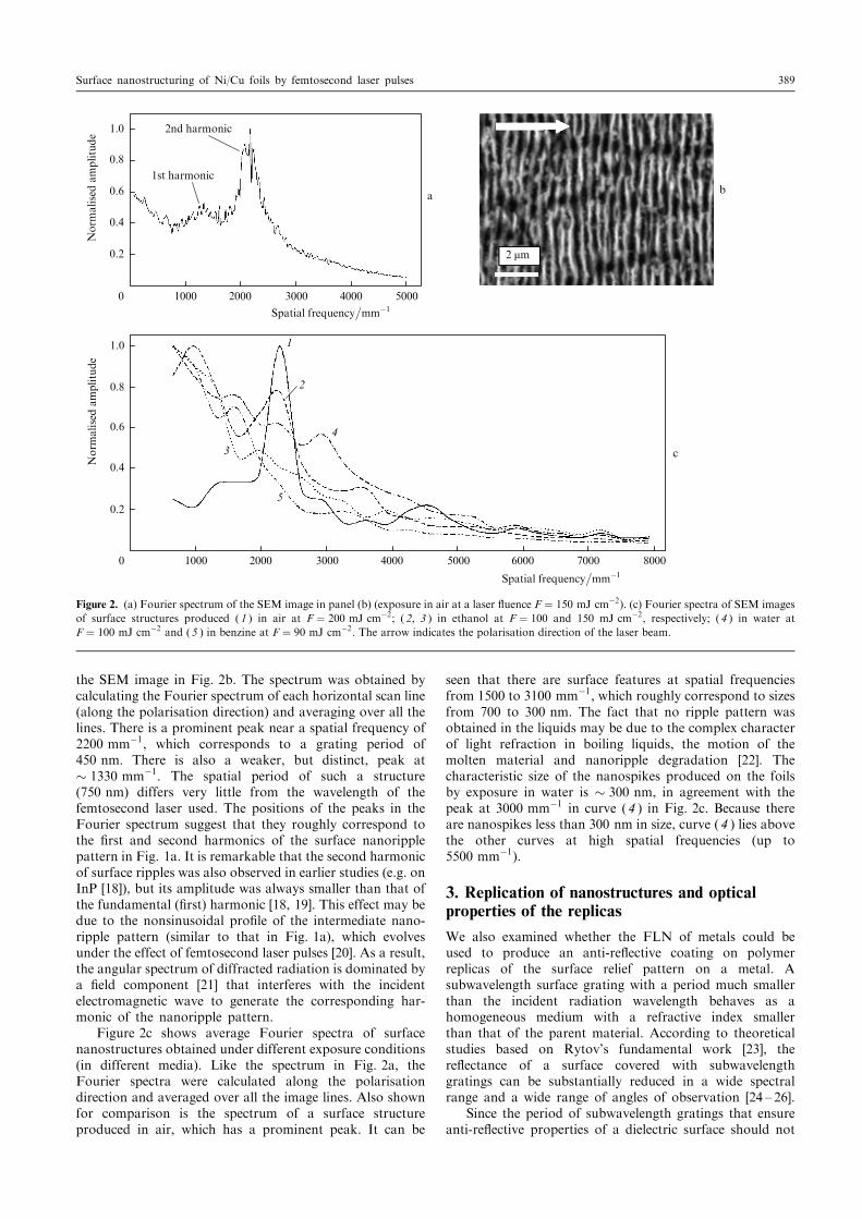
the SEM image in Fig. 2b. The spectrum was obtained bycalculating the Fourier spectrum of each horizontal scan line(along the polarisation direction) and averaging over all thelines. There is a prominent peak near a spatial frequency of2200 mmÿ1, which corresponds to a grating period of450 nm. There is also a weaker, but distinct, peak at� 1330 mmÿ1. The spatial period of such a structure(750 nm) differs very little from the wavelength of thefemtosecond laser used. The positions of the peaks in theFourier spectrum suggest that they roughly correspond tothe érst and second harmonics of the surface nanoripplepattern in Fig. 1a. It is remarkable that the second harmonicof surface ripples was also observed in earlier studies (e.g. onInP [18]), but its amplitude was always smaller than that ofthe fundamental (érst) harmonic [18, 19]. This effect may bedue to the nonsinusoidal proéle of the intermediate nano-ripple pattern (similar to that in Fig. 1a), which evolvesunder the effect of femtosecond laser pulses [20]. As a result,the angular spectrum of diffracted radiation is dominated bya éeld component [21] that interferes with the incidentelectromagnetic wave to generate the corresponding har-monic of the nanoripple pattern.
Figure 2c shows average Fourier spectra of surfacenanostructures obtained under different exposure conditions(in different media). Like the spectrum in Fig. 2a, theFourier spectra were calculated along the polarisationdirection and averaged over all the image lines. Also shownfor comparison is the spectrum of a surface structureproduced in air, which has a prominent peak. It can be
seen that there are surface features at spatial frequenciesfrom 1500 to 3100 mmÿ1, which roughly correspond to sizesfrom 700 to 300 nm. The fact that no ripple pattern wasobtained in the liquids may be due to the complex characterof light refraction in boiling liquids, the motion of themolten material and nanoripple degradation [22]. Thecharacteristic size of the nanospikes produced on the foilsby exposure in water is � 300 nm, in agreement with thepeak at 3000 mmÿ1 in curve ( 4 ) in Fig. 2c. Because thereare nanospikes less than 300 nm in size, curve ( 4 ) lies abovethe other curves at high spatial frequencies (up to5500 mmÿ1).
3. Replication of nanostructures and opticalproperties of the replicas
We also examined whether the FLN of metals could beused to produce an anti-reêective coating on polymerreplicas of the surface relief pattern on a metal. Asubwavelength surface grating with a period much smallerthan the incident radiation wavelength behaves as ahomogeneous medium with a refractive index smallerthan that of the parent material. According to theoreticalstudies based on Rytov's fundamental work [23], thereêectance of a surface covered with subwavelengthgratings can be substantially reduced in a wide spectralrange and a wide range of angles of observation [24 ë 26].
Since the period of subwavelength gratings that ensureanti-reêective properties of a dielectric surface should not
2nd harmonic
1st harmonic
Spatial frequency�mmÿ1
Norm
alised
amplitude
Spatial frequency�mmÿ1
Norm
alised
amplitude
ab
c
1.0
0.8
0.6
0.4
0.2
0 1000 2000 3000 4000 5000
1.0
0.8
0.6
0.4
0.2
0 1000 2000 3000 4000 5000 6000 7000 8000
2 mm
1
4
2
3
5
Figure 2. (a) Fourier spectrum of the SEM image in panel (b) (exposure in air at a laser êuence F � 150 mJ cmÿ2). (c) Fourier spectra of SEM imagesof surface structures produced ( 1 ) in air at F � 200 mJ cmÿ2; ( 2, 3 ) in ethanol at F � 100 and 150 mJ cmÿ2, respectively; ( 4 ) in water atF � 100 mJ cmÿ2 and ( 5 ) in benzine at F � 90 mJ cmÿ2. The arrow indicates the polarisation direction of the laser beam.
Surface nanostructuring of Ni/Cu foils by femtosecond laser pulses 389

exceed half the incident radiation wavelength, with thecharacteristic nanostructure periods obtained in this study(400 ë 450 nm) anti-reêective properties may show up in thenear-IR spectral region. The surface proéle depth of apolymer replica then should be at least 200 nm (Fig. 3) at arefractive index of the polymer in the range 1.5 ë 1.6. It isalso known that crossed gratings and 2D regular spikelike
structures are preferable for producing less polarisation-sensitive anti-reêective coatings.
Our interest in the FLN of nickel stems from theassumption that it can be applied in the technology ofdiffractive optical elements with an anti-reêective surfacenanostructure. The fabrication process may include thefollowing steps (Fig. 4a): laser direct writing of a primarydiffraction microrelief proéle into photoresist (steps 1 and2), fabrication of a nickel copy of the photoresist master byelectroplating (steps 3 and 4), exposure of the nickel copy(stamper) to femtosecond laser pulses in order to writesubwavelength nanogratings (steps 5 and 6) and replicationof the hybrid proéle on the surface of an optically trans-parent polymer by hot embossing or photopolymerisation(steps 7 and 8).
In our experiments, we used a simpliéed process for thefabrication of nanostructures on the surface of opticallytransparent polymer layers (Fig. 4b). Copper/nickel foil thatwas prepared as described above and had a mirror-smoothsurface was exposed to femtosecond laser pulses in order toproduce a nanoripple pattern (step 1). The pattern was thenreplicated on the surface of a transparent polymer (PMMA)by hot embossing or photopolymerisation of the hybridphotopolymer Ormocomp [27] (steps 2 and 3). Figure 5shows an exposed Ni/Cu foil and its polymer replica.
Figure 6 presents transmission spectra of polymer rep-licas of unexposed and exposed areas of Ni/Cu foil(Shimadzu UV-3600 spectrophotometer). As seen, the coat-ing strongly scatters near-IR and visible light. At the sametime, at wavelengths above 1670 nm the surface nano-structure produced by replicating the foil exposed to alaser êuence of 200 mJ cmÿ2 begins to exhibit anti-reêective
n1
n2
a
l=4n3 � ���������n1n2p
Substrate
b
L Lf
d
Figure 3. Geometric parameters of anti-reêective coatings based on (a) athin élm and (b) a subwavelength binary phase grating: n1, n2 and n3 arethe refractive indices of the medium, substrate and élm, respectively; Land d are the grating period and depth; l is the incident radiationwavelength; f is the grating duty cycle (0 < f < 1�; and d � ���������
n1n2p
l=4.
Laser
3
Cu
Glass
Laser
Laser
Photoresist 1 2 Ni 4
8765
Ni
1 2 3
a
b Polymer Replica
Figure 4. Schematics of (a) the proposed process for the fabrication of diffractive optical elements with an anti-reêective surface nanostructure and (b)the implemented process for the fabrication of nanostructured polymer replicas. The numbers specify the steps of the processes.
390 V.P. Korolkov, A.A. Ionin, S.I. Kudryashov, L.V. Seleznev, et al.

properties. In the range 1700 ë 2200 nm, the increase intransmittance is 3%ë 7%. At wavelengths above� 2250 nm, the transmittance of the replica of the exposedarea sharply rises by � 20%. We cannot gain insight intothe mechanism of this sharp rise in transmittance becausethe refractive index of Ormocomp at wavelengths above1550 nm is not available in the literature.
Figure 7 is an optical micrograph of Ni/Cu foil afterexposure to femtosecond laser pulses. One can see structureswith a characteristic length scale of the order of severalmicrons. Incident light is diffracted by these structures,which leads to reêected light energy losses. Anti-reêectiveproperties of the nanostructure were observed at longerwavelengths than was expected. The likely reason for this isthat it had a more complex surface proéle than the binaryproéle in Fig. 3b.
A necessary condition for the ability to produce dif-fractive optical elements with an anti-reêective surfacenanostructure (Fig. 4a) is that the FLN of the stampersurface should not signiécantly distort the original diffrac-tion microrelief proéle. Our experimental data demonstratethat the surface layer removed through laser ablation in theFLN process was no thicker than 150 ë 200 nm. This is quiteacceptable in the fabrication of diffractive elements with atypical depth of 1 ë 1.5 mm (Fig. 4a).
4. Conclusions
We have studied surface nanostructures generated on Ni/Cu foils by femtosecond laser pulses. The foils wereproduced by electrodeposition under conditions thatensured an essentially amorphous structure of the nickelfront surface. The nanostructures generated on nickel by alaser beam in air and water had for the most part the formof ripples. On a smaller length scale, we observed erosion,directed largely along the ripples, like in the case ofmicrocrystalline metals exposed to femtosecond laserpulses. Thus, there is conclusive evidence that the micro-structure of the metal does not play a key role indetermining nanoripple degradation. Increasing the laserêuence in the range 150 ë 200 mJ cmÿ2 (in air) enables thefabrication of more ordered gratings. The wave vector ofthe gratings is parallel to the polarisation direction of thelaser beam.
When the foils were exposed through an organic liquid(benzine or ethanol) layer, no ripples were formed, whichcan be interpreted in terms of erosion of the surface proéle.
This work is the érst to demonstrate the possibility ofproducing anti-reêective coatings on polymeric diffractiveoptical elements through the replication of the master proéleformed on photoresist by photolithography or laser directwriting.
Acknowledgements. This work was supported in part by theSiberian Branch of the Russian Academy of Sciences(Interdisciplinary Project No. 55) and the Russian Foun-dation for Basic Research (Grant Nos 09-02-12018-oé_m,09-02-01065-a, 10-08-00941-a, 11-02-01202-a and 11-08-01165-a).
References1. Zabotnov S.V., Golovan' L.A., Ostapenko I.A., et al. Pis'ma Zh.
Eksp. Teor. Fiz., 83, 76 (2006).2. Vorobyev A.Y., Makin V.S., Guo C. J. Appl. Phys., 101, 034903
(2007).3. Makin V.S., Makin R.S., Vorobyev A.Ya., Guo C. Pis'ma Zh.
Tekh. Fiz., 34, 55 (2008).4. Wagner R., Gottmann J., Horn A., Kreutz E.W. Appl. Surf. Sci.,
252, 8576 (2006).
a b
Figure 5. (a) Ni/Cu foil nanostructured by femtosecond laser pulses inethanol and (b) its transparent replica on the surface of the hybridphotopolymer Ormocomp.
1, 3
Transm
ittance
(%) 1
2
3
2
300 600 900 1200 1500 1800 2100 2400
Wavelength�nm
0
20
40
60
80
100
Figure 6. Transmission spectra of Ormocomp replicas of ( 1 ) unexposedand ( 2, 3 ) exposed areas of Ni/Cu foil: F � 200 ( 2 ) and 300 mJ cmÿ2
( 3 ).
20 mm
Figure 7. Optical micrograph of the surface of nanostructured Ni/Cu foil(Carl Zeiss AxioImager, exposure in air, F � 150 mJ cmÿ2).
Surface nanostructuring of Ni/Cu foils by femtosecond laser pulses 391

5. Yang Y., Yang J., Liang C., Wang H. Opt. Express, 16, 11259(2008).
6. Miyaji G., Miyazaki K. Opt. Express, 16, 16265 (2008).7. Huang M., Zhao F., Cheng Y., et al. Opt. Express, 16, 19354
(2008).8. Huang M., Zhao F., Cheng Y., et al. Phys. Rev. B, 79, 125436
(2009).9. Golosov E.V., Ionin A.A., Kudryashov S.I., et al. Pis'ma Zh.
Eksp. Teor. Fiz., 90, 116 (2009).10. Liu X., Wang Y. Chin. Opt. Lett., 3, 1 (2005).11. Sakabe S., Hashida M., Tokita S., et al. Phys. Rev. B, 79, 033409
(2009).12. Akhmanov S.A., Emel'yanov V.I., Koroteev N.I.,
Seminogov V.N. Usp. Fiz. Nauk, 147, 6755 (1985).13. Klimov V.V. Nanoplasmonics (Singapore: Pan Stanford, 2010;
Moscow: Fizmatlit, 2009).14. Nikolajeff F., L�ofving B., Johansson M., et al. Appl. Opt., 39,
4842 (2000).15. Modern Electroplating. Ed. by M.Schlesinger, M.Paunovic
(New York: John Wiley & Sons, 2000) p.147.16. Barmina E.V., Lau Truong S., Bozon-Verduraz F., Levi G.,
Simakin A.V., Shafeev G.A. Kvantovaya Elektron., 40, 346 (2010)[Quantum. Electron., 40, 346 (2010)].
17. Barmina E.V., Stratakis E., Fotakis C., Shafeev G.A. arXiv:1003.2796v1 [cond-mat.mes-hall] (2010).
18. Bonse J., Munz M., Sturm H. J. Appl. Phys., 97, 013538 (2005).19. Borowiec A., Haugen H.K. Appl. Phys. Lett., 82, 4462 (2003).20. Golosov E.V., Ionin A.A., et al. Phys. Rev. B, 83, 115426 (2011).21. Soifer V.A. Komp'yut. Opt., 32, 110 (2008).22. Golosov E.V., Ionin A.A., Kolobov Y.R., Kudryashov S.L.,
Ligachev A.E., Makarov S.V., Novoselov Y.N., Seleznev L.V.,Sinitsyn D.V. Appl. Phys. A, DOI 10.1007/s 00339-011-6323-2.
23. Rytov S.M. Zh. Eksp. Teor. Fiz., 29, 605 (1955).24. Gaylord T.K., Baird W.E., Moharam M.G. Appl. Opt., 25, 4562
(1986).25. Ono Y., Kimura Y., Ohta Y., Nishida N. Appl. Opt., 26, 1142
(1987).26. Grann E.B., Varga M.G., Pommet D.A. J. Opt. Soc. Am. A, 12,
333 (1995).27. http://www.microresist.de/products/ormocers/ormocomp_en.htm.
392 V.P. Korolkov, A.A. Ionin, S.I. Kudryashov, L.V. Seleznev, et al.
Copyright © 2022 FDOKUMEN