Direct investigation of the electrochemical double layer using the STM
Upload
independentCategory
view
1download
0
arX
iv:1
206.
4338
v1 [
cond
-mat
.mes
-hal
l] 1
9 Ju
n 20
12
Excess noise in scanning tunneling microscope-style break
junctions at room temperature
Ruoyu Chen1, Patrick J. Wheeler1, D. Natelson1,2
1 Department of Physics and Astronomy,
Rice University, 6100 Main St., Houston, TX 77005 and
2 Department of Electrical and Computer Engineering,
Rice University, 6100 Main St,.Houston, TX 77005
(Dated: June 21, 2012)
Abstract
Current noise in nanoscale systems provides additional information beyond the electronic con-
ductance. We report measurements at room temperature of the nonequilibrium “excess” noise in
ensembles of atomic-scale gold junctions repeatedly formed and broken between a tip and a film,
as a function of bias conditions. We observe suppression of the noise near conductances associated
with conductance quantization in such junctions, as expected from the finite temperature theory
of shot noise in the limit of few quantum channels. In higher conductance junctions, the Fano
factor of the noise approaches 1/3 the value seen in the low conductance tunneling limit, consis-
tent with theoretical expectations for the approach to the diffusive regime. At conductance values
where the shot noise is comparatively suppressed, there is a residual contribution to the noise that
scales quadratically with the applied bias, likely due to a flicker noise/conductance fluctuation
mechanism.
PACS numbers: 71.30.+h,73.50.-h,72.20.Ht
1
Shot noise, first discussed by Schottky in 1918[1], comprises fluctuations in the steady-
state, nonequilibrium current that originate from the discreteness of the electron charge.
This is “excess” noise in addition to the Johnson-Nyquist[2, 3] current fluctuations that
are present at equilibrium in the absence of an applied bias current. Shot noise tends
to be suppressed in macroscopic structures at finite temperatures due to electron-phonon
interactions. In many mesoscopic systems small compared to the inelastic scattering length
for the electrons, shot noise survives and is strongly related to the quantum nature of
transport[4]. Many measurements have been performed in this regime on various devices in
past two decades, including quantum point contacts[5, 6], diffusive metal conductors[7, 8],
break junctions[9, 10], and quantum Hall systems[11, 12]. Most of these experiments are
conducted at cryogenic temperatures to avoid thermal smearing of the noise, though shot
noise measurements are possible at room temperature in sufficiently nanoscale structures[13].
The classical Schottky shot noise power in the current is SI = 2eI , where SI is
the spectral density of shot noise, expressed as the mean squared variation in the current
〈∆I2〉 per unit frequency. Here e is the magnitude of the electron charge, and I is the
average DC bias current. This expression is derived assuming the arrival of charge carriers
is Poisson distributed, with each electron unaffected by the arrival of a previous electron.
Deviations from Poissonian statistics may alter the noise, and these changes are usually
expressed in terms of a Fano factor, F , such that the measured noise SI = 2eI × F . Values
of F 6= 1 provide clues about the possible effects of interactions and underlying transport
processes. The shot noise of mesoscopic conductors at zero temperature is expressed[4] in
terms of quantum channels:
SI = 2eV G0
N∑
i
τi(1− τi) (1)
where G0 = 2e2/h is the quantum of conductance, V is the bias voltage across the junction,
and τi is the transmission probability of the ith quantum channel. Combining with the
Landauer formula of G = G0
∑N
i τi , the Fano factor at zero temperature is:
F =
∑N
i τi(1− τi)∑N
i τi(2)
The Fano factor carries extra information about the transmission probabilities that a con-
ductance measurement alone cannot provide. At nonzero temperature (though assuming
that energy is not exchanged between the charge carriers and other degrees of freedom such
2
as phonons), the situation is more complex, as the thermal Johnson-Nyquist noise and shot
noise are not readily separable. The total current noise will be:
SI = G0[4kBT
N∑
i
τ 2i + 2eV coth(eV
2kBT)
N∑
i
τi(1− τi)] (3)
kB is the Boltzmann constant. In the equilibrium limit V = 0, both terms in this formula will
survive and contribute to Johnson-Nyquist thermal noise of 4kBTG. In the zero temperature
limit, the total noise power will reduce to Eq. (1). Temperature manifests itself through the
smearing of the Fermi-Dirac distribution of the electrons.
From these equations it is clear that fully transmitting channels (τi → 1) do not contribute
to the shot noise. This leads to a relative suppression of the noise in nanoscale systems
when the conductance is largely from such open channels, as in semiconductor point contacts
exhibiting quantized conductance[5], and in metal point contacts[9]. In the few channel limit,
the conductance combined with the noise allow the determination of the number of channels
and their transmission probabilities[10]. In the many-channel limit of diffusive conductors,
random matrix theory has provided valuable insights, and the Fano factor is expected to
approach an average value between 1/3 and√3/4[14–17] depending on bias conditions and
sample geometry. These predictions have been confirmed in the low temperature limit[7, 8,
18, 19].
Inelastic processes such as the excitation of local vibrational modes are predicted to alter
F as the bias voltage exceeds the energy scale of such excitations[20–22]. Such effects have
been observed at low temperatures in nanotubes[23], bilayer graphene[24], and very recently
in atomic-scale Au junctions[25], though the particular changes in F depend in detail on
channel transmission. One motivation of this work is the need to perform experimental
comparisons with Eq. (3) in a temperature regime where inelastic processes are favored by
kBT exceeding the characteristic energy scale for other degrees of freedom. For example, at
300 K, the lowest optical phonon mode in Au (∼ 17 meV[25]) should already be populated.
In this paper, we consider the noise properties of ensembles of atomic-scale metal point
contacts from tunneling to the multichannel (G ∼ 6G0) regime, at room temperature, when
inelastic processes involving phonons should be considerably more important than in the
cryogenic limit. Of particular interest are the accuracy and utility of Eq. (3) under these con-
ditions, over a broad range of applied bias, and the relative contributions of other noise mech-
anisms, such as conductance fluctuations[26]. With biases ranging from 1 < eV/kBT < 10,
3
we find noise consistent with Eq. (3), with clear relative suppression of the noise at conduc-
tance values corresponding to the quantized conductance peaks in the ensemble histograms.
At still lower bias, we cannot resolve the excess noise, while conductance peaks remain still
clear. The Fano factor in the high conductance, high bias regime is approximately a third
of that in the G < G0 tunneling regime. At the conductances where noise is relatively sup-
pressed, the bias scaling of the averaged noise is consistent with conductance fluctuations,
and the magnitude is not unreasonable considering previous experiments[27].
!"#
!"#
$%&'
(
(
%
%
)*##"+ ,#"
- !"#
.-/
0 1
2
0 1
2
32
4
567
567
2 7
87
3 9
$%&'
:
8 8
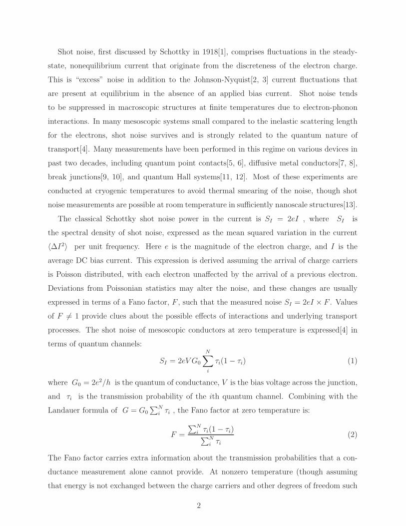
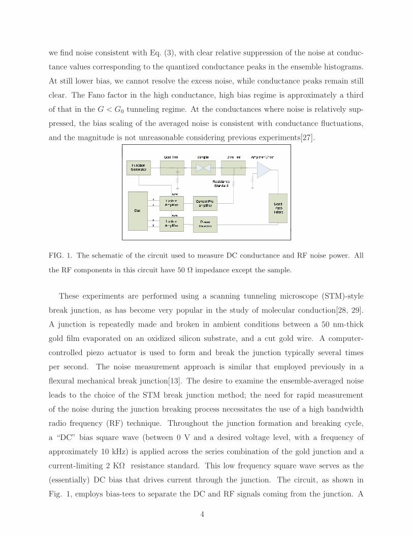
FIG. 1. The schematic of the circuit used to measure DC conductance and RF noise power. All
the RF components in this circuit have 50 Ω impedance except the sample.
These experiments are performed using a scanning tunneling microscope (STM)-style
break junction, as has become very popular in the study of molecular conduction[28, 29].
A junction is repeatedly made and broken in ambient conditions between a 50 nm-thick
gold film evaporated on an oxidized silicon substrate, and a cut gold wire. A computer-
controlled piezo actuator is used to form and break the junction typically several times
per second. The noise measurement approach is similar that employed previously in a
flexural mechanical break junction[13]. The desire to examine the ensemble-averaged noise
leads to the choice of the STM break junction method; the need for rapid measurement
of the noise during the junction breaking process necessitates the use of a high bandwidth
radio frequency (RF) technique. Throughout the junction formation and breaking cycle,
a “DC” bias square wave (between 0 V and a desired voltage level, with a frequency of
approximately 10 kHz) is applied across the series combination of the gold junction and a
current-limiting 2 KΩ resistance standard. This low frequency square wave serves as the
(essentially) DC bias that drives current through the junction. The circuit, as shown in
Fig. 1, employs bias-tees to separate the DC and RF signals coming from the junction. A
4
current preamplifier measures the current and is recorded electronically, giving a measure
of the junction’s conductance. At the same time, a lock-in amplifier synchronized to the
square wave detects the difference between the RF power with and without bias applied to
the junction; this is the excess noise power. The bandwidth of the noise measurement is
roughly 250-580 MHz. A detailed gain-bandwidth product measurement is employed. Since
both shot noise and Johnson-Nyquist noise are expected to be white over this bandwidth,
deviations from white noise arise from the impedance properties of the measurement circuit
as a whole. The details of the noise analysis and background subtraction are described in
supplemental material.
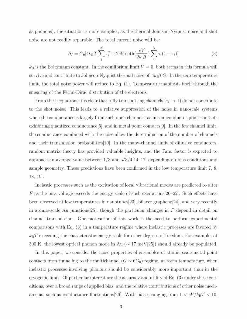
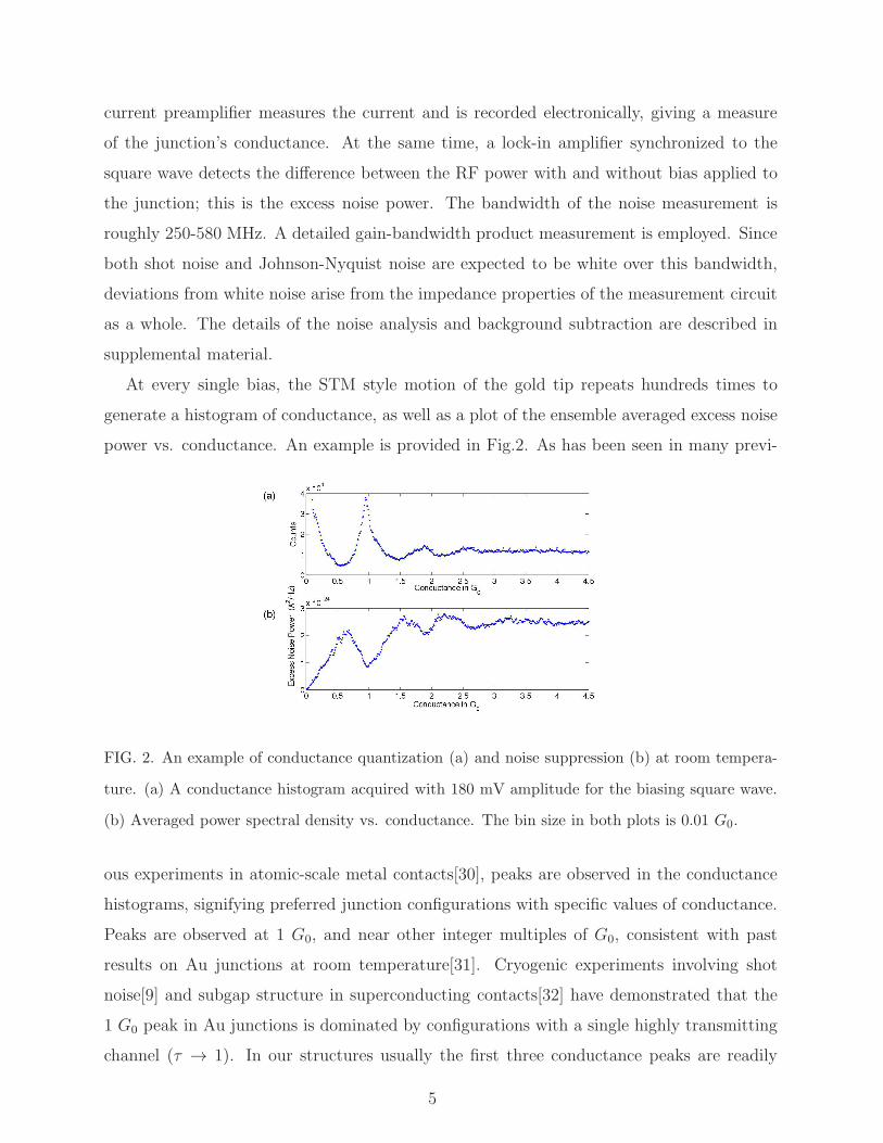
At every single bias, the STM style motion of the gold tip repeats hundreds times to
generate a histogram of conductance, as well as a plot of the ensemble averaged excess noise
power vs. conductance. An example is provided in Fig.2. As has been seen in many previ-
FIG. 2. An example of conductance quantization (a) and noise suppression (b) at room tempera-
ture. (a) A conductance histogram acquired with 180 mV amplitude for the biasing square wave.
(b) Averaged power spectral density vs. conductance. The bin size in both plots is 0.01 G0.
ous experiments in atomic-scale metal contacts[30], peaks are observed in the conductance
histograms, signifying preferred junction configurations with specific values of conductance.
Peaks are observed at 1 G0, and near other integer multiples of G0, consistent with past
results on Au junctions at room temperature[31]. Cryogenic experiments involving shot
noise[9] and subgap structure in superconducting contacts[32] have demonstrated that the
1 G0 peak in Au junctions is dominated by configurations with a single highly transmitting
channel (τ → 1). In our structures usually the first three conductance peaks are readily
5
resolvable in the histogram. The related ensemble-averaged noise power measurement is also
shown. As is clear from the figure, the ensemble-averaged noise power is clearly suppressed
near conductance values where the conductance histogram is peaked.
The transmission of RF signals always faces the problem of power reflection, which orig-
inates from impedance mismatch. Conversely, reflection itself carries information about
impedance. In our measurement circuit, all the commercial RF electronic components are
of 50Ω impedance. We therefore expect significant impedance mismatch and reflections
only between the STM-style gold junction and the transmission lines. As an added com-
plication compared to a fixed device configuration, the tip’s repeatedly vertical motions in-
troduce the extra complexity of a strongly time-varying DC conductance into the junction’s
RF properties. In principle a measurement should be performed to properly characterize
the impedance mismatch between the junction and the RF measurement circuitry at each
conductance value. Ideally, knowing the RF properties of the nanoscale junction and the
accompanying electronics, including the gain-bandwidth product of the amplifier chain, it
should be possible to infer the actual current noise (A2/Hz across the junction) from the
measured RF power seen by the power meter. However, in the STM breakjunction setup, in
which the DC conductance of the junction changes by orders of magnitude on millisecond
timescales, with our equipment it is not possible to measure all of the relevant RF parame-
ters in real time. As an approximation to this, we instead measure the reflection properties
as a function of conductance averaged over the ensemble of junction configurations. This
should at least indicate whether there are gross variations in the efficiency of the junction’s
RF coupling to the rest of the circuit.
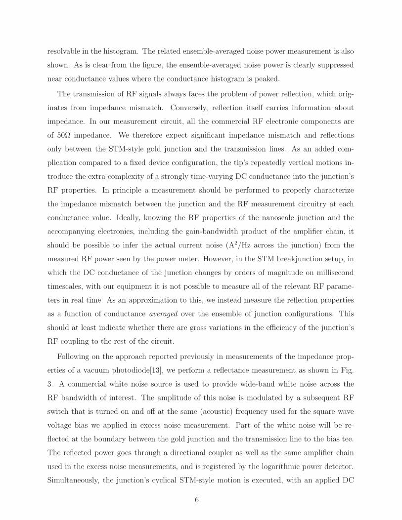
Following on the approach reported previously in measurements of the impedance prop-
erties of a vacuum photodiode[13], we perform a reflectance measurement as shown in Fig.
3. A commercial white noise source is used to provide wide-band white noise across the
RF bandwidth of interest. The amplitude of this noise is modulated by a subsequent RF
switch that is turned on and off at the same (acoustic) frequency used for the square wave
voltage bias we applied in excess noise measurement. Part of the white noise will be re-
flected at the boundary between the gold junction and the transmission line to the bias tee.
The reflected power goes through a directional coupler as well as the same amplifier chain
used in the excess noise measurements, and is registered by the logarithmic power detector.
Simultaneously, the junction’s cyclical STM-style motion is executed, with an applied DC
6
bias across the junction to allow the simultaneous acquisition of a conductance histogram.
This measurement gives a picture of the relation between ensemble averaged reflections and
the conductance of the junction. While the reflection measurement cannot provide all the
information about the junction’s RF properties, at least it provides a rough check that
nothing dramatic happens in terms of the ensemble-averaged impedance mismatch over the
conductance range. The reflection averaged over the ensemble of junction configurations is
around 22%. There is some systematic variation with conductance, but this is small, less
than 2% over 10 G0.
Since the impedance mismatch between the junction and the measurement circuit does
not vary dramatically on average over the range of junction configurations, there should be
a scale factor (approximately constant across the conductance range) between the measured
power and the true current noise across the junction. We attempt to find this factor by using
the knowledge that the Fano factor in the tunneling regime G << G0 approaches one in
the limit that a single poorly transmitting channel dominates the conductance, as apparent
from Eq. (1).
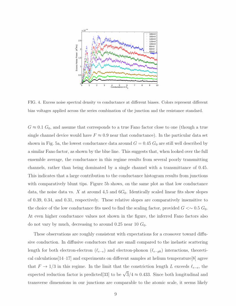
We acquire conductance histograms and ensemble-averaged noise using a series of square
wave bias voltages from a few millivolts to several hundreds of millivolts. An example
of such ensemble-averaged noise data for eight different bias levels is shown in Fig.4. All
the data shown in this figure were taken continuously in one day to ensure an identical
experimental environment (lab temperature, any stray RF background). In our system
no clear excess noise can be detected at bias voltages below about 25 mV, corresponding
to kBT at T ≈ 300 K. Noise suppression at conductances corresponding to the first three
peaks in the conductance histograms are very clear, and the magnitude of the detected noise
power is monotonously increasing with bias as expected. Note that the suppressions are not
complete. This indicates that at least some of the junction configurations corresponding to
peak conductance values result from a mixture of multiple, partially transmitting quantum
channels.
We are interested in the scaling of the noise with bias, as this reveals the Fano factor.
Working with the data sets in Fig. 4, we can specify a particular conductance value, and for
each applied square wave bias voltage we can compute the actual voltage drop, V , across the
junction. Starting from Eq. (3), we can see that plotting the detected power spectral density
as a function of X = 4kBTG[(eV/2kBT ) coth(eV/2kBT )− 1] should produce a linear graph,
7
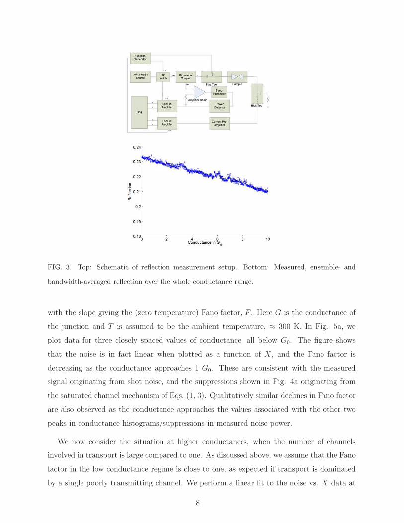
FIG. 3. Top: Schematic of reflection measurement setup. Bottom: Measured, ensemble- and
bandwidth-averaged reflection over the whole conductance range.
with the slope giving the (zero temperature) Fano factor, F . Here G is the conductance of
the junction and T is assumed to be the ambient temperature, ≈ 300 K. In Fig. 5a, we
plot data for three closely spaced values of conductance, all below G0. The figure shows
that the noise is in fact linear when plotted as a function of X , and the Fano factor is
decreasing as the conductance approaches 1 G0. These are consistent with the measured
signal originating from shot noise, and the suppressions shown in Fig. 4a originating from
the saturated channel mechanism of Eqs. (1, 3). Qualitatively similar declines in Fano factor
are also observed as the conductance approaches the values associated with the other two
peaks in conductance histograms/suppressions in measured noise power.
We now consider the situation at higher conductances, when the number of channels
involved in transport is large compared to one. As discussed above, we assume that the Fano
factor in the low conductance regime is close to one, as expected if transport is dominated
by a single poorly transmitting channel. We perform a linear fit to the noise vs. X data at
8
0 1 2 3 4 5 6 7 8 9 100
0.5
1
1.5
2
2.5
x 10−24
Conductance in G0
Exc
ess
Noi
se P
ower
(A
2 /Hz)
180mV160mV140mV120mV100mV80mV60mV40mV
FIG. 4. Excess noise spectral density vs conductance at different biases. Colors represent different
bias voltages applied across the series combination of the junction and the resistance standard.
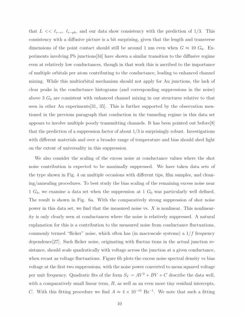
G ≈ 0.1 G0, and assume that corresponds to a true Fano factor close to one (though a true
single channel device would have F ≈ 0.9 near that conductance). In the particular data set
shown in Fig. 5a, the lowest conductance data around G = 0.45 G0 are still well described by
a similar Fano factor, as shown by the blue line. This suggests that, when looked over the full
ensemble average, the conductance in this regime results from several poorly transmitting
channels, rather than being dominated by a single channel with a transmittance of 0.45.
This indicates that a large contribution to the conductance histogram results from junctions
with comparatively blunt tips. Figure 5b shows, on the same plot as that low conductance
data, the noise data vs. X at around 4,5 and 6G0. Identically scaled linear fits show slopes
of 0.39, 0.34, and 0.31, respectively. These relative slopes are comparatively insensitive to
the choice of the low conductance fits used to find the scaling factor, provided G <∼ 0.5 G0.
At even higher conductance values not shown in the figure, the inferred Fano factors also
do not vary by much, decreasing to around 0.25 near 10 G0.
These observations are roughly consistent with expectations for a crossover toward diffu-
sive conduction. In diffusive conductors that are small compared to the inelastic scattering
length for both electron-electron (ℓe−e) and electron-phonon (ℓe−ph) interactions, theoreti-
cal calculations[14–17] and experiments on different samples at helium temperature[8] agree
that F → 1/3 in this regime. In the limit that the constriction length L exceeds ℓe−e, the
expected reduction factor is predicted[33] to be√3/4 ≈ 0.433. Since both longitudinal and
transverse dimensions in our junctions are comparable to the atomic scale, it seems likely
9
that L << ℓe−e, ℓe−ph, and our data show consistency with the prediction of 1/3. This
consistency with a diffusive picture is a bit surprising, given that the length and transverse
dimensions of the point contact should still be around 1 nm even when G ≈ 10 G0. Ex-
periments involving Pb junctions[34] have shown a similar transition to the diffusive regime
even at relatively low conductances, though in that work this is ascribed to the importance
of multiple orbitals per atom contributing to the conductance, leading to enhanced channel
mixing. While this multiorbital mechanism should not apply for Au junctions, the lack of
clear peaks in the conductance histograms (and corresponding suppressions in the noise)
above 3 G0 are consistent with enhanced channel mixing in our structures relative to that
seen in other Au experiments[31, 35]. This is further supported by the observation men-
tioned in the previous paragraph that conduction in the tunneling regime in this data set
appears to involve multiple poorly transmitting channels. It has been pointed out before[8]
that the prediction of a suppression factor of about 1/3 is surprisingly robust. Investigations
with different materials and over a broader range of temperature and bias should shed light
on the extent of universality in this suppression.
We also consider the scaling of the excess noise at conductance values where the shot
noise contribution is expected to be maximally suppressed. We have taken data sets of
the type shown in Fig. 4 on multiple occasions with different tips, film samples, and clean-
ing/annealing procedures. To best study the bias scaling of the remaining excess noise near
1 G0, we examine a data set when the suppression at 1 G0 was particularly well defined.
The result is shown in Fig. 6a. With the comparatively strong suppression of shot noise
power in this data set, we find that the measured noise vs. X is nonlinear. This nonlinear-
ity is only clearly seen at conductances where the noise is relatively suppressed. A natural
explanation for this is a contribution to the measured noise from conductance fluctuations,
commonly termed “flicker” noise, which often has (in macroscale systems) a 1/f frequency
dependence[27]. Such flicker noise, originating with fluctua tions in the actual junction re-
sistance, should scale quadratically with voltage across the junction at a given conductance,
when recast as voltage fluctuations. Figure 6b plots the excess noise spectral density vs bias
voltage at the first two suppressions, with the noise power converted to mean squared voltage
per unit frequency. Quadratic fits of the form SV = AV 2 +BV + C describe the data well,
with a comparatively small linear term, B, as well as an even more tiny residual intercepts,
C. With this fitting procedure we find A ≈ 4 × 10⁻¹⁵ Hz−1. We note that such a fitting
10
FIG. 5. Noise as a function of scaled bias, for all eight data sets shown in Fig. 4. Top panel: Data
below 1 G0. Data points at around 0.45 G0, 0.78 G0 and 0.85 G0 are shown in the plot as well as
linear fits to X for those points. Bottom panel: Data around 4 G0, 5 G0 and 6 G0, with inferred
Fano factors (relative to that at ∼ 0.1 G0) of 0.39, 0.34 and 0.31 separately.
procedure overestimates the size of A, since the hyperbolic cotangent term in Eq. (3) does
contribute some nonlinearity in such a plot even when the only noise is finite temperature
shot noise. Instead if we fit a quadratic in voltage term in addition to the finite temperature
shot noise expectation of Eq. 3, we find A ≈ 1.4×10⁻¹⁵ Hz−1, smaller but of the same order
of magnitude. Using the phenomenological Hooge’s law[26],
SR(f)/R2 =
α
Nf ν(4)
with power ν ranging between 1 ∼ 2, we compared our inferred magnitude of A with values
observed at lower frequencies and higher junction conductances in other gold point contacts
by Wu et al.[27]. The result depends strongly on the assumed value of ν, which is expected
to fall between 1 (traditional 1/f noise) and 2 (expected for a single two-level fluctuator[27]).
We find a flicker noise amplitude smaller than the Wu et al. values extrapolated to 1 G0 with
11
FIG. 6. In the upper panel, off-suppression data and on-suppression noise data are compared. The
former still has good linearity as a function of X. However, for the latter a deviation from a linear
dependence is observed when the conductance is around 1 G0 and the shot noise contribution is
relatively suppressed. The lowest (gray) points and linear fit correspond to the 1 G0 data with
a best-fit quadratic-in-voltage contribution removed. Panel (b) is a purely quadratic fit of the
excess noise vs. bias voltage at the conductances corresponding to the first two suppressions. The
noise power here has been converted to mean squared voltage per frequency, for comparison with
flicker noise. Both of these fitting procedures give flicker noise contributions of the same order of
magnitude.
the fitted ν value in their case; however, if ν ≈ 1.7 over frequency from their sub-100 kHz
measurements to our RF scale, our value for A is compatible with their results. We can
reasonably conclude that much of the nonlinearity in the noise vs. bias at conductances when
shot noise is suppressed results from flicker noise/conductance fluctuations. The relatively
small magnitude of this noise suggests a comparatively rapid decay of flicker noise with
frequency in the RF range in atomic-scale junctions. It would be interesting to consider the
12
temperature variation of the flicker noise magnitude over this frequency range, which would
help clarify whether thermal activation of defect motion is relevant here.
FIG. 7. Models of channel mixing and Fano factors. The top panel is the expected Fano factor as
a function of conductance for the particular channel mixing shown in the second panel. The third
panel shows the measured Fano factor for a particular set of data, and a theoretical approximation
to that data based on the channel openings shown in the bottom panel. Colors and linestyles
represent different evolutions of τi as a function of conductance.
It is worth considering what kind of mixing of quantum channels is required to produce
the evolution of Fano factor with conductance that we infer from our data, within the nonin-
teracting picture of Eq. 1. A simple “toy model” simulation of possible Fano factor evolution
is provided, which depends on the choice of how the channels τi open as conductance is
increased. The result is shown in Fig.7 (a). We assume for simplicity a set of uniformly
separated hyperbolic tangent functions for the form of τi as a function of G, which is
shown on the bottom. Each hyperbolic tangent is specified by a central conductance at
which τi = 0.5, and a width in G over which the channel “turns on”. The resulting Fano
13
factors have been plotted on the top. Multiple colors/linestyles represent different choices
of the central conductances and turn-on widths. In top graph, the uppermost line (blue)
shows no clear suppression of noise vs. G due to the heavy overlaps between channels. In
contrast, the lower most curve (black) is in the limit of well-separated channels that do not
mix. Channels’ mixture tends to smear out suppressions and raise the Fano factor, which
is the qualitative reason that in a larger-sized diffusive conductor only a roughly constant
Fano factor results. Figure 7b shows an example (nonunique), of a set of transmission chan-
nels that agree reasonably well with the measurements. Additional constraints (such as
those provided by subgap conductance in superconducting junctions[32, 36]) are necessary
to better constrain the specific channels and their evolution.
We note that we do not see clear signatures of bias-dependent changes in the Fano factor
in these ensemble averaged measurements. As the low temperature data in Kumar et al.
shows[25], changes in the apparent Fano factor due to excitation of optical phonons can be of
either sign in single-channel devices, with a crossover between enhancement and suppression
of F taking place at a particular transmittance, around 0.95. With respect to the Au optical
phonon at ∼ 17 meV, all of the data in this paper are in the high bias regime above the
voltage threshold. Our measurements show that in Au junctions at room temperature,
there are no clear inelastic thresholds above this energy that survive ensemble averaging
over junction configurations. Other analysis approaches that look at subensembles may be
more revealing[37] and are in progress.
Here we have reported a calibrated measurement of shot noise and its bias dependence in
STM-style gold junctions at room temperature. We observe in general that the shot noise
spectral density is proportional to X ≡ 4kBTG[eV/2kBT coth(eV/2kBT )−1], as expected for
a nanoscale junction with a small number of channels. The slope of such a plot is a means of
extracting the zero-temperature Fano factor of the noise. The Fano factor observed at higher
conductances (several conductance quanta) is roughly 1/3 that seen in the tunneling regime,
consistent with expectations as the diffusive limit is approached. At suppressions where shot
noise is comparatively small, nonlinearities in the noise vs. X are observed. It is likely that
the origin of this nonlinearity is conductance fluctuation/flicker noise; this is supported
by fits showing an approximate quadratic dependence of the noise on the bias across the
junction, and the magnitude of this noise is roughly consistent with that extrapolated from
other experiments[27]. The evolution of the Fano factor with conductance can be described
14
adequately within the noninteracting picture through reasonable choices of the evolution
of channel numbers and transmittances with conductance. These experiments highlight
that the quantum nature of the electronic conduction remains detectable and important as
electronic systems approach the atomic scale, even at room temperature.
The authors acknowledge the support of NSF award DMR-0855607, and useful conver-
sations with J. van Ruitenbeek, C. Schonenberger, and L. Richardson.
APPENDIX: BACKGROUND SUBTRACTION
Scanning tunneling microscope-style break junctions provide us with a way to sample a
wide range of conductance values quickly. However, when using a lock-in measurement of the
conductance, the repeated change of the conductance over orders of magnitude also causes
rapid changes in the phase of the conductive (as opposed to displacement) contribution
to the current, and therefore the noise signal. As a practical matter it is not possible to
adjust the phase of the lock-in measurement “on the fly” to separate out the conductive and
displacement contributions to the current and the noise. Instead, in our measurement the
lock-in was set to measure the rms magnitude R of the output of the power detector.
Unfortunately, this introduces an effective background. To see this, recall that R =√
(X2 + Y 2), where X , Y are the two orthogonal components of the measured signal. Even
without any input signal from the power detector X and Y fluctuate about zero due to
amplifier noise. As a result, R averages to a non-zero positive value even in the absence of a
real noise signal, and this value is not negligible in our measurement. During a real measure-
ment, R can be expressed as R =√
(X +Xr)2 + (Y + Yr)2, where Xr and Yr represent the
random errors (amplifier noise, fluctuating about zero) on the two components. To remove
this background on average, we have to perform one extra measurement at essentially zero
bias, to characterize the background. Practically we still use a very low bias voltage, usually
around 3 millivolts, which is small enough that no true excess noise is detectable at room
temperature, but we are still able to measure conductance. In principle the output of the
noise measurement lock-in during this measurement gives R0 =√
X2r + Y 2
r . After average
〈R2
0〉 = 〈X2
r 〉 + 〈Y 2
r 〉, while 〈R2〉 = 〈X2〉 + 〈X2
r 〉 + 〈Y 2〉 + 〈Y 2
r 〉, because the 〈Xr〉 and 〈Yr〉terms average to zero. We can then consider 〈R2〉−〈R2
0〉 as the averaged mean square signal
15
from the power detector, which is the desired quantity.
[1] W. Schottky, Ann. der Physik 57, 541 (1918).
[2] J. B. Johnson, Phys. Rev. 32, 97 (1928).
[3] H. Nyquist, Phys. Rev. 32, 110 (1928).
[4] Y. Blanter and M. Buttiker, Physics Reports 336, 1 (2000).
[5] M. Reznikov, M. Heiblum, H. Shtrikman, and D. Mahalu, Phys. Rev. Lett. 75, 3340 (1995).
[6] A. Kumar, L. Saminadayar, D. C. Glattli, Y. Jin, and B. Etienne,
Phys. Rev. Lett. 76, 2778 (1996).
[7] F. Liefrink, J. I. Dijkhuis, M. J. M. de Jong, L. W. Molenkamp, and H. van Houten,
Phys. Rev. B 49, 14066 (1994).
[8] M. Henny, S. Oberholzer, C. Strunk, and C. Schonenberger, Phys. Rev. B 59, 2871 (1999).
[9] H. E. van den Brom and J. M. van Ruitenbeek, Phys. Rev. Lett. 82, 1526 (1999).
[10] D. Djukic and J. M. van Ruitenbeek, Nano Letters 6, 789 (2006)..
[11] L. Saminadayar, D. C. Glattli, Y. Jin, and B. Etienne, Phys. Rev. Lett. 79, 2526 (1997).
[12] R. de Picciotto, M. Reznikov, M. Heiblum, V. Umansky, G. Bunin, and D. Mahalu, Nature
389, 162 (1997).
[13] P. J. Wheeler, J. N. Russom, K. Evans, N. S. King, and D. Natelson, Nano Letters 10, 1287
(2010)..
[14] C. W. J. Beenakker and M. Buttiker, Phys. Rev. B 46, 1889 (1992).
[15] A. Shimizu and M. Ueda, Phys. Rev. Lett. 69, 1403 (1992).
[16] K. Nagaev, Physics Letters A 169, 103 (1992).
[17] M. J. M. de Jong and C. W. J. Beenakker, Phys. Rev. B 51, 16867 (1995).
[18] A. H. Steinbach, J. M. Martinis, and M. H. Devoret, Phys. Rev. Lett. 76, 3806 (1996).
[19] R. J. Schoelkopf, P. J. Burke, A. A. Kozhevnikov, D. E. Prober, and M. J. Rooks,
Phys. Rev. Lett. 78, 3370 (1997).
[20] A. Mitra, I. Aleiner, and A. J. Millis, Phys. Rev. B 69, 245302 (2004).
[21] J. Koch and F. von Oppen, Phys. Rev. Lett. 94, 206804 (2005).
[22] J. Koch, F. von Oppen, and A. V. Andreev, Phys. Rev. B 74, 205438 (2006).
[23] R. Leturcq, C. Stampfer, K. Inderbitzin, L. Durrer, C. Hierold, E. Mariani, M. G. Schultz,
16
F. von Oppen, and K. Ensslin, Nature Phys. 5, 327 (2009).
[24] A. Fay, R. Danneau, J. K. Viljas, F. Wu, M. Y. Tomi, J. Wengler, M. Wiesner, and P. J.
Hakonen, Phys. Rev. B 84, 245427 (2011).
[25] M. Kumar, R. Avriller, A. L. Yeyati, and J. M. van Ruitenbeek,
Phys. Rev. Lett. 108, 146602 (2012).
[26] M. B. Weissman, Rev. Mod. Phys. 60, 537 (1988).
[27] Z. M. Wu, S. M. Wu, S. Oberholzer, M. Steinacher, M. Calame, and C. Schonenberger,
Phys. Rev. B 78, 235421 (2008).
[28] B. Xu and N. J. Tao, Science 301, 1221 (2003)..
[29] L. Venkataraman, J. E. Klare, I. W. Tam, C. Nuckolls, M. S. Hybertsen, and M. L. Steiger-
wald, Nano Letters 6, 458 (2006).
[30] N. Agraıt, A. L. Yeyati, and J. M. van Ruitenbeek, Physics Reports 377, 81 (2003).
[31] I. K. Yanson, O. I. Shklyarevskii, S. Csonka, H. van Kempen, S. Speller, A. I. Yanson, and
J. M. van Ruitenbeek, Phys. Rev. Lett. 95, 256806 (2005).
[32] E. Scheer, W. Belzig, Y. Naveh, M. H. Devoret, D. Esteve, and C. Urbina,
Phys. Rev. Lett. 86, 284 (2001).
[33] K. E. Nagaev, Phys. Rev. B 52, 4740 (1995).
[34] J. J. Riquelme, L. de la Vega, A. L. Yeyati, N. Agraıt, A. Martin-Rodero, and G. Rubio-
Bollinger, Europhys. Lett. 70, 663 (2005).
[35] B. Ludoph and J. M. van Ruitenbeek, Phys. Rev. B 61, 2273 (2000).
[36] E. Scheer, N. Agraıt, J. C. Cuevas, A. L. Yeyati, B. Ludoph, A. Mart’in-Rodero, G. R.
Bollinger, J. M. van Ruitenbeek, and C. Urbina, Nature 394, 154 (1998).
[37] P. Makk, D. Tomaszewski, J. Martinek, Z. Balogh, S. Csonka, M. Wawrzyniak, M. Frei,
L. Venkataraman, and A. Halbritter, ACS Nano 6, 3411 (2012).
.
17
Copyright © 2022 FDOKUMEN