Direct investigation of the electrochemical double layer using the STM
13
Direct investigation of the electrochemical double layer using the STM Renate Hiesgen a, * , Dirk Eberhardt a , Dieter Meissner b,c a University of Applied Sciences, Department of Basic Science, Kanalstrasse 33, D-73728 Esslingen, Germany b University of Applied Sciences Wels, Roseggerstrasse 12, A-4600 Wels, Austria c LIOS, Johannes Kepler University, Linz, Austria Available online 1 August 2005 Abstract A first investigation of the electrochemical double layer in the tunneling gap between a WSe 2 semiconductor elec- trode and a Pt:Ir STM tip was performed by current–distance spectroscopy. The magnitude of the current between tip and semiconductor depends exponentially on the barrier height limiting this current. The local barrier height can be derived from the slope of a semi-logarithmic plot of the current versus the distance. For a fully developed Helmholtz double layer the Schottky barrier height within the semiconductor surface dominates the tunneling barrier. However, the charge of the semiconductor surface and thereby the Schottky barrier height also depends on the counter charges located on the tip and within the Helmholtz double layers in the electrolyte inside the gap. Changes in the distribution of the charges lead to a change of the Schottky barrier height. Thereby, the influence of the first and the second water layers can be detected as well as the penetration of positive and negative ions into the gap when the tip is removed from the surface. Thereby the space needed by specifically adsorbed as well as by solvated ions to fit into the gap and to built up the inner Helmholtz layer can directly be measured. Ó 2005 Elsevier B.V. All rights reserved. Keywords: Electrochemistry; Helmholtz double layer; STM; Tunneling spectroscopy; Semiconductor/electrolyte interfaces; Schottky barrier 1. Introduction Scanning tunneling microscopy (STM) is a well-established technique to study physical and chemical properties of surfaces by imaging as well as by performing spectroscopic investigations. The STM has the advantage that it is applicable not only to systems in UHV environment, or sys- tems in ambient air, but also to the in situ study of the solid–liquid interface under potential con- trol of both the STM tip and the sample [1]. So far, the large majority of in situ STM studies 0039-6028/$ - see front matter Ó 2005 Elsevier B.V. All rights reserved. doi:10.1016/j.susc.2004.10.057 * Corresponding author. E-mail address: [email protected] (R. Hies- gen). Surface Science 597 (2005) 80–92 www.elsevier.com/locate/susc
-
Upload
independent -
Category
Documents
-
view
3 -
download
0
Transcript of Direct investigation of the electrochemical double layer using the STM
Surface Science 597 (2005) 80–92
www.elsevier.com/locate/susc
Direct investigation of the electrochemical doublelayer using the STM
Renate Hiesgen a,*, Dirk Eberhardt a, Dieter Meissner b,c
a University of Applied Sciences, Department of Basic Science, Kanalstrasse 33, D-73728 Esslingen, Germanyb University of Applied Sciences Wels, Roseggerstrasse 12, A-4600 Wels, Austria
c LIOS, Johannes Kepler University, Linz, Austria
Available online 1 August 2005
Abstract
A first investigation of the electrochemical double layer in the tunneling gap between a WSe2 semiconductor elec-trode and a Pt:Ir STM tip was performed by current–distance spectroscopy. The magnitude of the current betweentip and semiconductor depends exponentially on the barrier height limiting this current. The local barrier height canbe derived from the slope of a semi-logarithmic plot of the current versus the distance. For a fully developed Helmholtzdouble layer the Schottky barrier height within the semiconductor surface dominates the tunneling barrier. However,the charge of the semiconductor surface and thereby the Schottky barrier height also depends on the counter chargeslocated on the tip and within the Helmholtz double layers in the electrolyte inside the gap. Changes in the distributionof the charges lead to a change of the Schottky barrier height. Thereby, the influence of the first and the second waterlayers can be detected as well as the penetration of positive and negative ions into the gap when the tip is removed fromthe surface. Thereby the space needed by specifically adsorbed as well as by solvated ions to fit into the gap and to builtup the inner Helmholtz layer can directly be measured.� 2005 Elsevier B.V. All rights reserved.
Keywords: Electrochemistry; Helmholtz double layer; STM; Tunneling spectroscopy; Semiconductor/electrolyte interfaces; Schottkybarrier
1. Introduction
Scanning tunneling microscopy (STM) is awell-established technique to study physical and
0039-6028/$ - see front matter � 2005 Elsevier B.V. All rights reservdoi:10.1016/j.susc.2004.10.057
* Corresponding author.E-mail address: [email protected] (R. Hies-
gen).
chemical properties of surfaces by imaging as wellas by performing spectroscopic investigations.The STM has the advantage that it is applicablenot only to systems in UHV environment, or sys-tems in ambient air, but also to the in situ studyof the solid–liquid interface under potential con-trol of both the STM tip and the sample [1]. Sofar, the large majority of in situ STM studies
ed.
R. Hiesgen et al. / Surface Science 597 (2005) 80–92 81
focuses on the study of the electrode surfacestructure or on properties of the solid electrode.But the STM can also be used to in situ probeproperties of the liquid side of the interface. Asa consequence of the requirement of charge neu-trality for the whole system the charge densityof the solid electrode has to be compensatedby counter charges which are located in the elec-trolyte. The well ordered part of the chargedinterface nearest to the electrode surface, theHelmholtz double layer [2], is of special interestand only few methods are available to probe thisinterfacial region. As a consequence, only fewstudies have been published investigating the in-ner double layer by in situ and ex situ methodsbased on the macroscopic measurements [3].Due to the large electric field present at the inter-face, the inner Helmholtz layer is highly ordered.The dielectric constant of the interfacial electro-lyte compared to the bulk indicates that it con-sists of highly ordered layers of water moleculesat the surface in which ions are integrated to bal-ance the charge and are probably forming struc-tures similar to solid state phases. Only recently,measurements have been performed to investigateits structure in real space at a local scale [4–7].
In metals, the charged surface layer is verythin, typically in the order of only one atom,due to their high charge carrier concentration.In an electrolyte solution as well as in a semi-conductor the charge carrier concentration is nor-mally much lower and the extension of the spacecharge region is therefore much larger. In semi-conductors it can be in the order of several hun-dred nanometers depending on the concentrationof doping atoms. In the electrochemical cell theextension of a fully developed double layer variesbetween 0.1 nm and several 10 nm depending onthe ion concentration in the electrolyte [8]. Com-pared to the typical dimension of the tunnellinggap used in the STM, which is in the orderof 1 nm, the extension of a full double layer iscomparable or even larger. As a consequence,depending on the concentration of the electrolyte,the distance between the STM tip and the surfaceis not sufficient to accommodate a full set of elec-trolytic double layers. In this case, the screeningof the charges by the counter charges is not com-
pletely accomplished and an electrostatic induc-tion with changed local surface potentials isexpected.
In support of this expectation, a tip induced ef-fect on an electrode surface has been observedeven for metal electrodes [9–11]. A change of thelocal potential can be expected to have a larger im-pact for a lower concentration of charge carriers ina material such as for semiconductors. In a systemconsisting of a metallic STM tip, a dilute electro-lyte solution, and a semiconductor sample, the po-tential of the semiconductor surface should beindependent of the tip potential for a fully devel-oped double layer. However, if not all countercharges to those in the space charge layer findspace in the electrolyte interface, the surface poten-tial of the semiconductor and thereby the Schottkybarrier height will change with the tip potential[6,7]. In addition, in the tunnelling gap even theamount of solvent molecules and thereby thedielectric constant is influenced by the distance be-tween tip and surface. Recent experiments haveshown that it is possible to directly investigatethe build-up of water layers in front of a gold elec-trode using an electrochemical STM with a goldtip [4]. In addition, concurrently with the limita-tion of the number of water layers, also theamount of counter charges present in the gap islimited depending on their size: The number ofions in the tunneling gap changes with the exten-sion of the tunnelling gap depending on both,the potential of the semiconductor surface as wellas that of the tip when changing the distance be-tween tip and surface. A change in the potentialof the semiconductor surface causes a change inthe potential drop across the space charge layer,the band bending, and therefore also in the barrierheight of the semiconductor. As found before [5,6],this barrier height directly controls the currentbetween tip and semiconductor surface for semi-conductors polarized in depletion. Thereby thetunneling current Itunnel is a very sensitive probeof the electrical properties of the gap in these kindof structures. So the current–distance spectroscopyon a semiconductor sample monitoring the currentflowing from the semiconductor to the STM underpotential control here is used as a suitable methodto study the structure of the double layer.
82 R. Hiesgen et al. / Surface Science 597 (2005) 80–92
2. Experimental
The experiments were performed using a com-mercial STM (Nanoscope III, Digital Instruments,Santa Barbara) equipped with a bipotentiostat. Agold wire was used as the common counter elec-trode to the tip and semiconductor electrodes,and a Au oxide covered gold wire was used asthe common reference electrode. The potential ofthe gold oxide wire was controlled regularly tobe 1200 mV versus the reversible hydrogen elec-trode (RHE). All potentials quoted are given withrespect to the RHE scale. The measurements wereperformed in an aqueous solution of 0.01 MH2SO4. The STM was operated in a closed cham-ber where the atmosphere can be maintained freeof oxygen. As tunneling tips electrochemicallyetched Pt:Ir (80:20) wires were used and the tipswere insulated with an electrochemically appliedlacquer in order to minimise the Faraday currentsfollowing the instructions given in [12]. Forpolycrystalline platinum the point of zero chargehas been measured to be about +300 mV (RHE)[13]. Since the tip is composed of 80% platinumthe pzc can be expected to have at a similarvalue.
2.1. Semiconductor
Monocrystalline n-WSe2 samples with a dopinglevel of 1017 cm�3 have been used as samples.WSe2 is a layered semiconductor and can becleaved with adhesive tape so that very large ter-races of the non-reactive van der Waals surfacesare exposed. They are separated by steps that areonly a few monolayers high. These flat surfaceshave a very low density of surface states [14–16].WSe2 has an indirect bandgap of 1.2 eV. In thedark the flatband potential has a value ofUFB = �20 ± 50 mV independent of the pH [14].Due to the layered crystal structure its propertiesare anisotropic and differ in the direction perpen-dicular to the layers with respect to the directionparallel to the layers. With the doping level men-tioned above this results in a Debye length ofabout 20 nm for the direction perpendicular tothe surface [11].
2.2. Current–distance measurements
Current–distance curves were measured by aninterrupted feedback method. In contrast to themeasurements on metallic samples the contactpoint and thereby the zero distance point to the sur-face cannot be easily extracted from the current, be-cause there is no abrupt change in resistance whenthe tip penetrates the semiconductor surface. Theabsolute distance between tip and surface is deter-mined by these values and depends on the localresistances in the system. The absolute distancefrom the tip to the surface was therefore unknownduring the measurement. Relative changes of thetip distance from the surface were measured bymonitoring themovement of the z-piezo. Themove-ment of the z-piezo was measured by recordings thechange of its driving voltage during the potentialchanges. The relative distance correlation of tippositions for different tip potentials was therebymeasured to vary by 0.06 nm/V. The current–dis-tance-curve was measured by switching off the feed-back control, retracting the tip perpendicular to thesurface and subsequently approaching the surfacewith the tip at a speed of 6 nm/s. After switchingoff the feedback control the potentials were setto the desired values. The feedback control wasswitched on again and the setpoint distance wasre-established. During the retraction and approachof the tip the current through the tip, the potentialsand the time were measured externally with an ADcard (National Instruments, PCI 6035E) at 400 Hzand stored in a separated computer. Control ofthe influence of thermal drift was performed bycomparing the measurements for both directions.
2.3. Barrier height
The variation of the tunneling current Itunnelwith the gap width corresponds to the vacuumtunneling process in UHV [17]. Accordingly, thetunneling barrier Ueff can be derived from the slopeof the tunneling current Itunnel as a function of thedistance z in a semi-logarithmic plot.
I tunnel /UBias
z� expð�A
ffiffiffiffiffiffiffiffiffiffiffiffiffiUeff � z
pÞ ð1Þ
using the vacuum value of A ¼ 10.12 ðeVÞ�12 nm�1.
R. Hiesgen et al. / Surface Science 597 (2005) 80–92 83
In solutions the curves often exhibit a non-exponential behaviour and therefore deviate froma straight line in the semi-logarithmic plot. In thiscase very often still a linear fit to the data is madeand a mean barrier height is derived. The valuesreported range from 1.78 eV [18] to values below1 eV and are significantly smaller than thosemeasured in UHV experiments [19–21]. Thishas been attributed to tunneling through interme-diate tunneling states due to unknown moleculesin the gap [21]. In a recent study on gold inperchloric acid, an oscillating change of thelocal barrier height with the distance from the sur-face between 0.8 eV and 2.3 eV was reported [4].Here, the local barrier height Ulocal was calculatedfrom
Ulocal �d ln I tunnel
dz
� �2
� A�2
!ð2Þ
Thereby a characteristic length of 0.35 nm was de-rived from a sinusoidal fit to the measured curvesand attributed to the thickness of a water layer.This result is explained by a stepwise filling ofthe tunneling gap by water molecules limited bytheir lateral extension. Following this interpreta-tion in Ref. [4], the maximum of the local barrierheight corresponds to a gap width where the tun-neling process is basically vacuum-like until thefirst water molecules enter the tunneling gap. Fur-ther maxima and minima in the barrier height areassociated with additional water layers. Since acompleted water layer is associated with a mini-mum in the local barrier height, the change frommaximal to minimal barrier heights should berather abrupt due to the small difference in thegap width which allows the penetration of addi-tional water. From these considerations we expecta saw tooth-like curvature of the local barrierheight rather than a harmonic behaviour.
3. Model considerations of the metal–electrolyte–
semiconductor gap at different tip to surface
distances
As it is well known, the extension of a fullycompleted Helmholtz layer, consisting of most or
all of the charges necessary for neutralising thecharges inside the sample surface, varies stronglywith the concentration of ions in the electrolyte.The Debye length is in the order of 1–30 nmfor a concentration of the electrolyte between10�1 mol/l and 10�4 mol/l [8]. For the electrolyteconcentration of 10�2 mol/l used in these experi-ments the Debye length has a value of 3 nm. Inour experiments the gap width was always smallerthan 3 nm because the Faraday current at the tipdetermines the minimum detectable tunneling cur-rent Itunnel and restricts the available travelling dis-tance between the tip and the surface to valuesbelow 1.5 nm. For this gap width the existence oftwo fully completed electrochemical double layerscannot be expected.
There are two different barriers which influencethe current flow from the semiconductor to the tip,the tunneling barrier through the gap and the bar-rier inside the semiconductor surface. For smalldistances of the tip from the sample the tunnelingbarrier height is small. In this case the magnitudeof the current will be determined by the semicon-ductor barrier height. The influence of the tunnel-ing barrier grows exponentially with the distancewhile the barrier in the semiconductor is notdependent on the tunneling gap. As a result, thetunneling barrier will become dominant for largerdistances. Therefore it is useful to discuss sepa-rately these two different measurement ranges aswell as to distinguish the effect of ions in the gap.
3.1. Gap width between 0 and 0.35 nm
Diminishing the distance between the tip andthe semiconductor surface in this range, the devicechanges from one with two surfaces in a liquid tofinally a solid-state metal–semiconductor contactwithout a tunneling gap. For this solid-state con-tact the energy levels addressable are determinedby the potential of the metal tip with respect tothe semiconductor potential. The electrochemicalpotential of the tip determines the Fermi levelsof the solid state device and the bias voltage be-tween the tip and the semiconductor Fermi levelbecause the charge carrier concentration of themetal is orders of magnitude higher compared tothat of the semiconductor.
84 R. Hiesgen et al. / Surface Science 597 (2005) 80–92
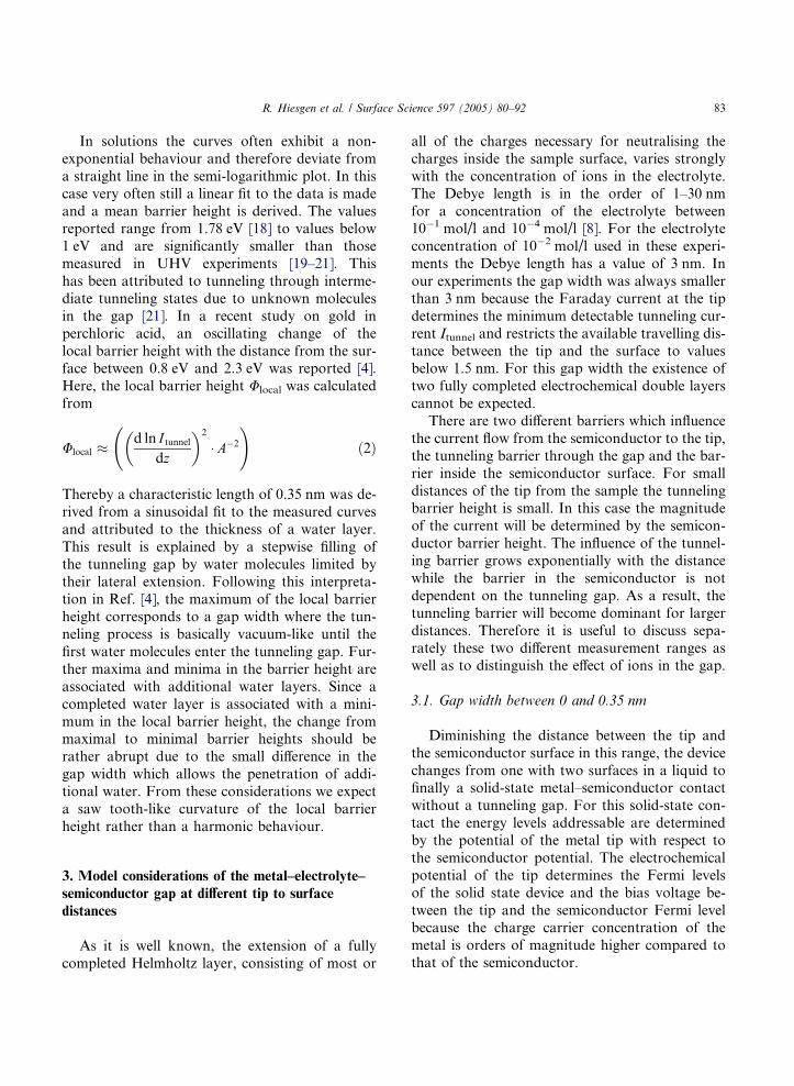
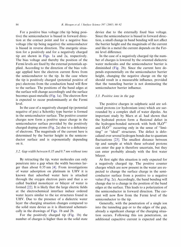
For a positive bias voltage (the tip being posi-tive) the semiconductor is biased in forward direc-tion at the contact point and for a negative biasvoltage (the tip being negative) the semiconductoris biased in reverse direction. The energetic situa-tion for a positively and for a negatively chargedtip are shown in Figs. 1a and 2a, respectively.The bias voltage and thereby the position of theFermi levels are fixed by the external potentials ap-plied. According to the direction of the bias volt-age applied here the electron current flows fromthe semiconductor to the tip. In the case wherethe tip is positively charged (potential positive ofpzc) electrons from the conduction band will flowto the surface. The positions of the band edges atthe surface will change accordingly and the surfacebecomes quasi-metallic (Fig. 1a). The electron flowis expected to occur predominantly at the Fermilevel.
In the case of a negatively charged tip (potentialnegative of pzc) a Schottky type barrier is formedin the semiconductor surface. The positive countercharges now form a positive space charge in thesemiconductor surface provided by the positivelycharged doping atoms (Fig. 2a) due to a deficiencyof electrons. The magnitude of the current here isdetermined by the barrier height in the semicon-ductor surface and is exponentially dependingon it.
3.2. Gap width between 0.35 and 0.7 nm without ions
By retracting the tip, water molecules can onlypenetrate into a gap when the width becomes lar-ger than about 0.35 nm [4]. From investigationsof water adsorption on platinum in UHV it isknown that adsorbed water here is attachedthrough the oxygen electron pairs and that a socalled buckled monolayer or bilayer of water isformed [22]. It is likely that the large electric fieldsat the electrochemical interface induce orderedwater layers similar to the ice structures found inUHV. Due to the presence of a dielectric waterlayer the charging situation changes compared tothe solid state device as it is illustrated schemati-cally in the drawings of Figs. 1b and 2b.
For the positively charged tip (Fig. 1b) thenumber of charges is higher than in the solid state
device due to the externally fixed bias voltage.Since the semiconductor is biased in forward direc-tion, a small change in band bending will not affectthe barrier height and the magnitude of the currentand like in a metal the current depends on the Fer-mi level difference.
In the case of a negatively charged tip the num-ber of charges is lowered by the oriented dielectricwater molecules and the semiconductor barrier isdiminished (Fig. 2b). Since the current here de-pends exponentially on the semiconductor barrierheight, changing the negative charge on the tipshould result in a measurable influence, providedthat the tunneling barrier is not dominating thesemiconductor barrier influence.
3.3. Positive ions in the gap
The positive charges in sulphuric acid are sol-vated protons (or hydronium ions) which are sur-rounded by a complex shell of water dipoles. Animportant study by Marx et al. had shown thatthe hydrated proton form a fluxional defect inthe hydrogen-bonded network with both H9O
4+
and H5O2+ occurring only in the sense of ‘‘limi-
ting’’ or ‘‘ideal’’ structures. The defect is delo-calized over several hydrogen bonds due to quantumfluctuations [23]. The smallest distance betweentip and sample at which these solvated protonscan enter the gap is therefore uncertain, but theycan enter probably already with the first waterbilayer.
At first sight this situation is only expected fora negatively charged tip. The positive countercharges which are now present in the water are ex-pected to change the surface charge in the semi-conductor surface from a positive to a negativevalue (Fig. 2c). Accordingly, the band bending willchange due to a change in the position of the bandedges at the surface. This leads to a polarization ofthe semiconductor in forward direction. The cur-rent will now flow from the Fermi level of thesemiconductor to the tip.
Generally, with the penetration of a single ioninto the tunneling gap or to the edges of the gap,already a significant change of the charging situa-tion occurs. Following this ion penetration, anadditional capacitive current is expected and the
+++++++++
+++++++
+++++++
Φsc
bias voltage fixed
n-type semiconductor
Φtip
metal tip
++++++++++++++++++
++++++++++++++
++++++++++++++
Φsc+++++++++
+++++++
++++++
bias voltage fixed
+
+
+
+
+
+
+ n-type semiconductor
Φtip
metal tip
++++++++++++++++++
++++++++++++++
+++++++++++++
+
+
+
+
+
+
+++
+++
+++
+++
+++
+++
+++
ti
+++
+
+
+
0.75 nm
bias voltage fixed
-
-
-
+
Φsc
n-type semiconductor
Φtip
metal tip
++++++
++
++
++
-
-
-
--
--
--
++
a
b
c
Fig. 1. The STM tip is charged positive of pzc: (a) 0 nm < z < 0.35 nm; solid state device for small distances, the semiconductor isbiased in forward direction, the current occurs from the Fermi-level. (b) 0.35 nm < z < 0.6 nm; one water layer fits into the gap, thedielectric constant of the first water layer is significantly smaller than for bulk water, only a small increase of the band bending isexpected but no measurable change in the slope of the current–distance curve should occur. (c) z > 0.6 nm; negative sulphate ions arepresent in the gap and are specifically adsorbed at the platinum tip, positive space charge in the semiconductor surface leads to a barrierfor the current, a significant change of the current–distance curve should occur.
R. Hiesgen et al. / Surface Science 597 (2005) 80–92 85
bias voltage fixed Φsc
n-type semiconductor
Φtip
metal tip ++
++
++
++++++
+++
+++++ ++
bias voltage fixed Φsc
n-type semiconductor
Φtip
metal tip
+ +
++++++++++ ++++++ ++
bias voltage fixed
+
+
+
+
+
+
+
Φsc
n-type semiconductor
Φtip
metal tip
+++ +++
+
+
+
+
+
+
+
+++
+++
+++
+++
+++
+++
+++++++++ ++++++
a
b
c
Fig. 2. The STM tip is charged negative of pzc: (a) 0 nm < z < 0.35 nm; solid state device for small distances, the semiconductor isbiased in reverse direction, the current is determined by the semiconductor barrier. (b) z > 0.35 nm; one water layer fits into the gap, thedielectric constant of the first water is significantly smaller than for bulk water, a small decrease of barrier height is expected, a smallchange in the slope of the current–distance curve may occur or alternatively. (c) z > 0.35 nm; positive hydronium ions are alreadypresent in the gap, a negative space charge is built up in the semiconductor surface and the current flow occurs from the Fermi level ofthe semiconductor, big change of the current–distance curve should results.
86 R. Hiesgen et al. / Surface Science 597 (2005) 80–92
R. Hiesgen et al. / Surface Science 597 (2005) 80–92 87
movement of charges can even be accompanied byspikes in the current signal.
3.4. Negative ions in the gap
In the case of a positively charged tip, no posi-tive ions are expected to enter the gap at small dis-tances. At a separation where the negative ions, inour case the sulfate ions, can enter the gap, adistinct change in the current–distance curve is ex-pected to occur. Now the negative counter chargesfor the metal tip will partly be found in the waterphase. Due to these negative charges in the gap,the surface of the semiconductor develops a posi-tive space charge. The magnitude of the currentwill now be determined by the semiconductor bar-rier height rather than by the tunneling barrier(Fig. 1c).
The diameter of the negatively charged solvatedsulfate ions is taken from reported measurementsof ion vacancies in aqueous solutions to be about0.58 nm [24]. At a positively charged platinumtip, sulfate ions are specifically adsorbed. There-fore only a part of the solvation shell can beformed, and the width of the gap needed for theions to fit in is probably smaller than the full diam-eter of the ion in water. From STM experimentsthe lateral structure of the specifically adsorbedsulfate ion adlayer has been measured [25,26].The distance between two sulfate ions was re-ported to be 0.45 nm and 0.71 nm in the two latticedirections, in the former lattice direction they areclosely packed and in the latter direction they areseparated by one water molecule. From these datathe diameter of the sulfate ions is estimated to beless than 0.45 nm without any solvation shell,which is in accordance with a value of 0.4 nm fromvolume measurements [24]. The space needed per-pendicular to the surface in the adsorbed state isunknown. We estimate from these data, that thesulfate ions probably can enter the tunneling gapat a separation of more than 0.45 nm. If the gapwidth is below 0.40 nm, only water molecules areexpected to be present in front of a positivelycharged tip.
In the case of a neutral tip (potential at the pzc),the ions coming into the gap only depend on thecharge of the semiconductor surface. At the semi-
conductor surface, no specific adsorption isexpected due to the van der Waals surface of theWSe2. In this case the separation needed bysolvated negative sulfate ions to enter the gapshould be larger than in the case of a positivetip.
For a tunneling gap larger than needed forthe penetration of ions, changes in the current–distance curve are not expected. The charging sit-uation will gradually change until two fully com-pleted electrochemical double layers are formed.For large distances the barrier height of the tun-nel barrier is expected to fully control the currentflow.
In the above considerations for simplicity thepenetration of only one type of ions into the gapis discussed, positive or negative ones. If thecharge at the semiconductor surface is negative(forward direction), positive charges can be ex-pected to be part of the Helmholtz layer at thesemiconductor surface outside the tunneling gap.There should at least be a shielding effect of thesepositive charges on the negative charge of the con-tact point. On the other hand, the charged Helm-holtz layer will stabilize the negative charge ofthe surface compared to flatband conditions. Inthis case the negative charges of the sulfate ionsentering the gap is shielded to a certain extentand additional negative charges are needed proba-bly provided by ions at the side of the gap notbeing able to enter. Since only the net negativecharge is important, the gap width at which thecharge in the semiconductor surface changes topositive values should be larger than under flat-band conditions. For larger distances, both ionswill always be present in the double layer becauseof the requirement of charge neutrality in the elec-trolyte volume, too.
4. Results and discussion
All measurements are shown as semi-logarith-mic plot of the tunneling current Itunnel versusthe travelling distance of the STM tip. The dis-tance to the setpoint position is marked as ‘‘0’’ atthe x-axis. The absolute remaining separationfrom the surface is unknown.
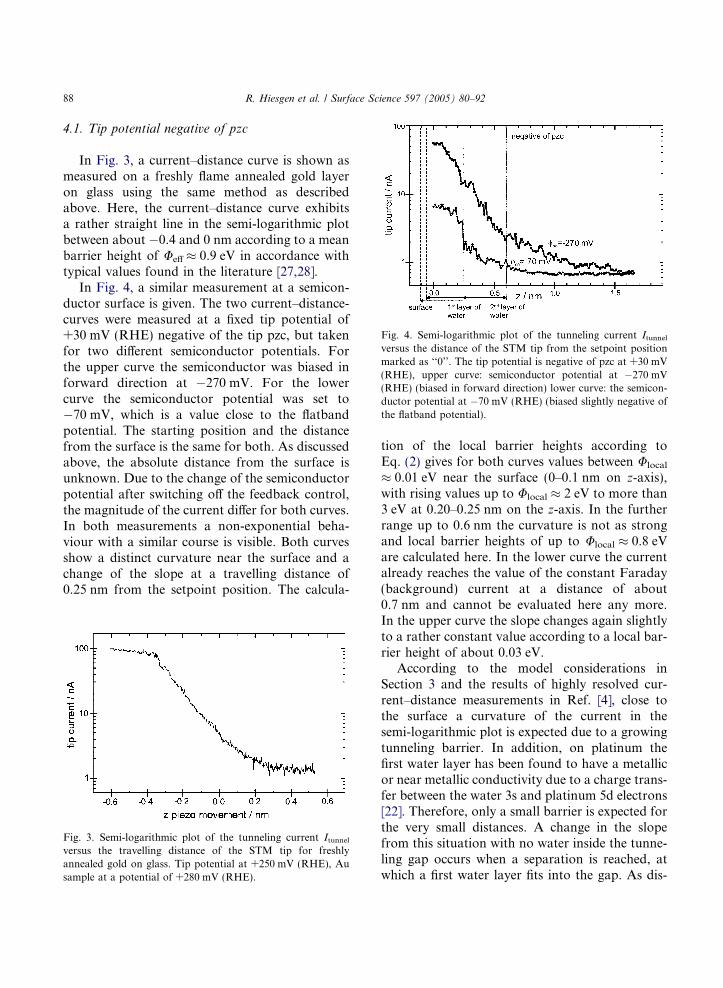
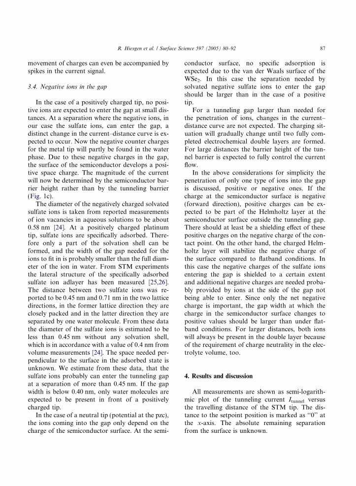
Fig. 4. Semi-logarithmic plot of the tunneling current Itunnelversus the distance of the STM tip from the setpoint positionmarked as ‘‘0’’. The tip potential is negative of pzc at +30 mV(RHE), upper curve: semiconductor potential at �270 mV(RHE) (biased in forward direction) lower curve: the semicon-ductor potential at �70 mV (RHE) (biased slightly negative ofthe flatband potential).
88 R. Hiesgen et al. / Surface Science 597 (2005) 80–92
4.1. Tip potential negative of pzc
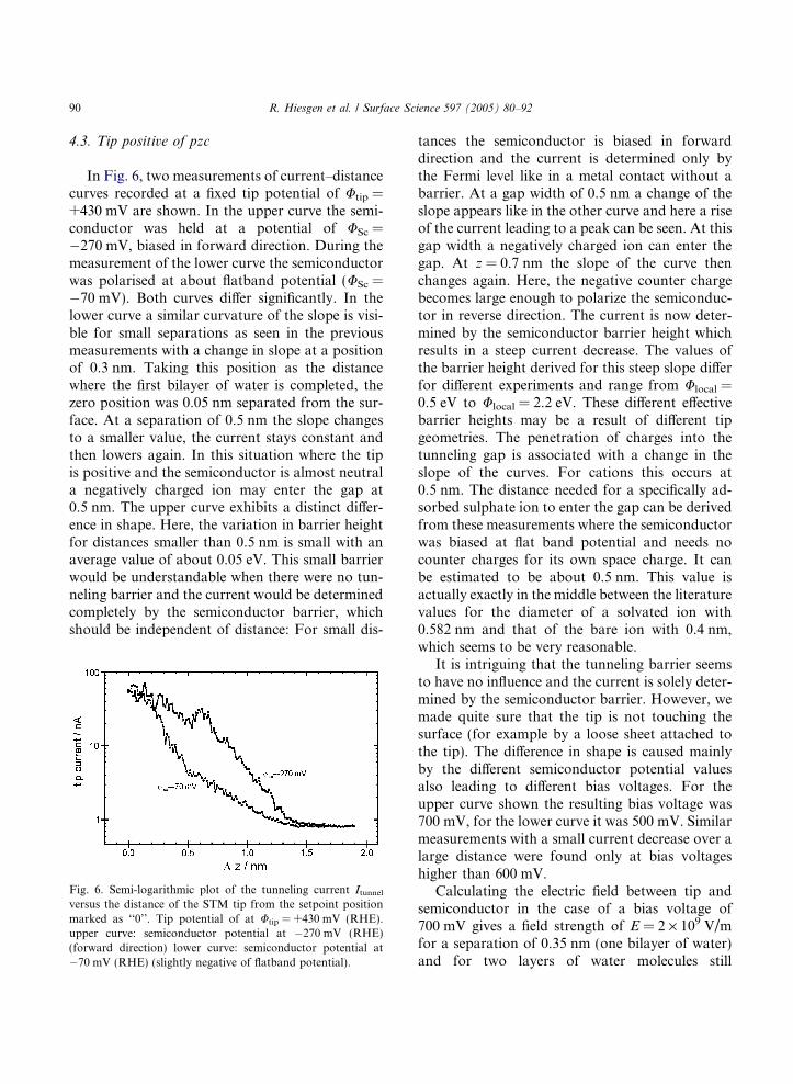
In Fig. 3, a current–distance curve is shown asmeasured on a freshly flame annealed gold layeron glass using the same method as describedabove. Here, the current–distance curve exhibitsa rather straight line in the semi-logarithmic plotbetween about �0.4 and 0 nm according to a meanbarrier height of Ueff � 0.9 eV in accordance withtypical values found in the literature [27,28].
In Fig. 4, a similar measurement at a semicon-ductor surface is given. The two current–distance-curves were measured at a fixed tip potential of+30 mV (RHE) negative of the tip pzc, but takenfor two different semiconductor potentials. Forthe upper curve the semiconductor was biased inforward direction at �270 mV. For the lowercurve the semiconductor potential was set to�70 mV, which is a value close to the flatbandpotential. The starting position and the distancefrom the surface is the same for both. As discussedabove, the absolute distance from the surface isunknown. Due to the change of the semiconductorpotential after switching off the feedback control,the magnitude of the current differ for both curves.In both measurements a non-exponential beha-viour with a similar course is visible. Both curvesshow a distinct curvature near the surface and achange of the slope at a travelling distance of0.25 nm from the setpoint position. The calcula-
Fig. 3. Semi-logarithmic plot of the tunneling current Itunnelversus the travelling distance of the STM tip for freshlyannealed gold on glass. Tip potential at +250 mV (RHE), Ausample at a potential of +280 mV (RHE).
tion of the local barrier heights according toEq. (2) gives for both curves values between Ulocal
� 0.01 eV near the surface (0–0.1 nm on z-axis),with rising values up to Ulocal � 2 eV to more than3 eV at 0.20–0.25 nm on the z-axis. In the furtherrange up to 0.6 nm the curvature is not as strongand local barrier heights of up to Ulocal � 0.8 eVare calculated here. In the lower curve the currentalready reaches the value of the constant Faraday(background) current at a distance of about0.7 nm and cannot be evaluated here any more.In the upper curve the slope changes again slightlyto a rather constant value according to a local bar-rier height of about 0.03 eV.
According to the model considerations inSection 3 and the results of highly resolved cur-rent–distance measurements in Ref. [4], close tothe surface a curvature of the current in thesemi-logarithmic plot is expected due to a growingtunneling barrier. In addition, on platinum thefirst water layer has been found to have a metallicor near metallic conductivity due to a charge trans-fer between the water 3s and platinum 5d electrons[22]. Therefore, only a small barrier is expected forthe very small distances. A change in the slopefrom this situation with no water inside the tunne-ling gap occurs when a separation is reached, atwhich a first water layer fits into the gap. As dis-
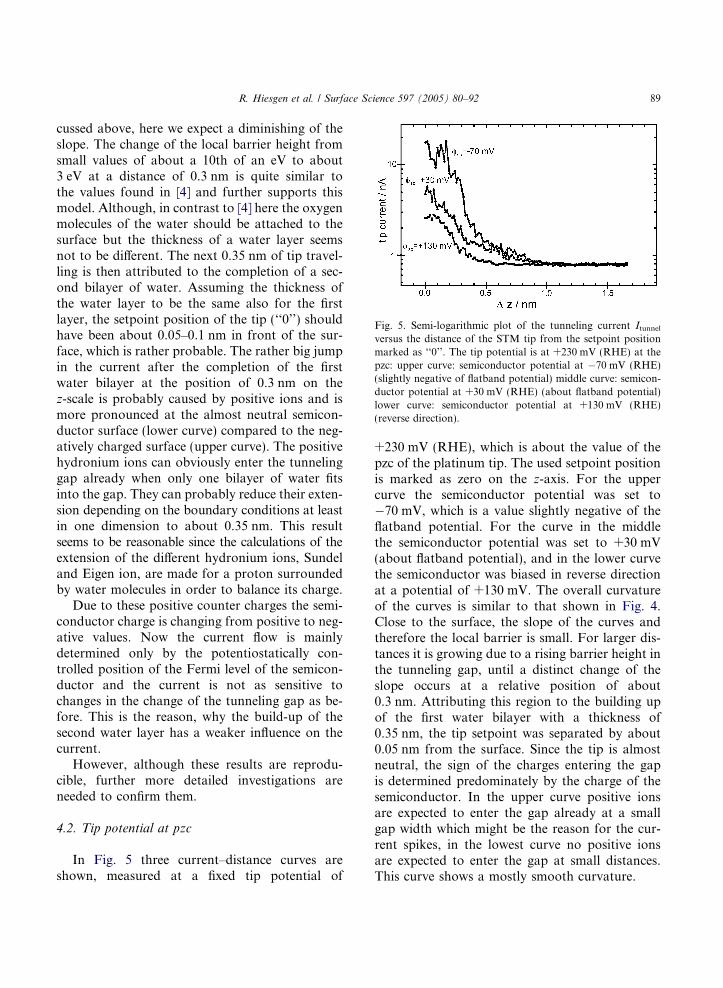
Fig. 5. Semi-logarithmic plot of the tunneling current Itunnelversus the distance of the STM tip from the setpoint positionmarked as ‘‘0’’. The tip potential is at +230 mV (RHE) at thepzc: upper curve: semiconductor potential at �70 mV (RHE)(slightly negative of flatband potential) middle curve: semicon-ductor potential at +30 mV (RHE) (about flatband potential)lower curve: semiconductor potential at +130 mV (RHE)(reverse direction).
R. Hiesgen et al. / Surface Science 597 (2005) 80–92 89
cussed above, here we expect a diminishing of theslope. The change of the local barrier height fromsmall values of about a 10th of an eV to about3 eV at a distance of 0.3 nm is quite similar tothe values found in [4] and further supports thismodel. Although, in contrast to [4] here the oxygenmolecules of the water should be attached to thesurface but the thickness of a water layer seemsnot to be different. The next 0.35 nm of tip travel-ling is then attributed to the completion of a sec-ond bilayer of water. Assuming the thickness ofthe water layer to be the same also for the firstlayer, the setpoint position of the tip (‘‘0’’) shouldhave been about 0.05–0.1 nm in front of the sur-face, which is rather probable. The rather big jumpin the current after the completion of the firstwater bilayer at the position of 0.3 nm on thez-scale is probably caused by positive ions and ismore pronounced at the almost neutral semicon-ductor surface (lower curve) compared to the neg-atively charged surface (upper curve). The positivehydronium ions can obviously enter the tunnelinggap already when only one bilayer of water fitsinto the gap. They can probably reduce their exten-sion depending on the boundary conditions at leastin one dimension to about 0.35 nm. This resultseems to be reasonable since the calculations of theextension of the different hydronium ions, Sundeland Eigen ion, are made for a proton surroundedby water molecules in order to balance its charge.
Due to these positive counter charges the semi-conductor charge is changing from positive to neg-ative values. Now the current flow is mainlydetermined only by the potentiostatically con-trolled position of the Fermi level of the semicon-ductor and the current is not as sensitive tochanges in the change of the tunneling gap as be-fore. This is the reason, why the build-up of thesecond water layer has a weaker influence on thecurrent.
However, although these results are reprodu-cible, further more detailed investigations areneeded to confirm them.
4.2. Tip potential at pzc
In Fig. 5 three current–distance curves areshown, measured at a fixed tip potential of
+230 mV (RHE), which is about the value of thepzc of the platinum tip. The used setpoint positionis marked as zero on the z-axis. For the uppercurve the semiconductor potential was set to�70 mV, which is a value slightly negative of theflatband potential. For the curve in the middlethe semiconductor potential was set to +30 mV(about flatband potential), and in the lower curvethe semiconductor was biased in reverse directionat a potential of +130 mV. The overall curvatureof the curves is similar to that shown in Fig. 4.Close to the surface, the slope of the curves andtherefore the local barrier is small. For larger dis-tances it is growing due to a rising barrier height inthe tunneling gap, until a distinct change of theslope occurs at a relative position of about0.3 nm. Attributing this region to the building upof the first water bilayer with a thickness of0.35 nm, the tip setpoint was separated by about0.05 nm from the surface. Since the tip is almostneutral, the sign of the charges entering the gapis determined predominately by the charge of thesemiconductor. In the upper curve positive ionsare expected to enter the gap already at a smallgap width which might be the reason for the cur-rent spikes, in the lowest curve no positive ionsare expected to enter the gap at small distances.This curve shows a mostly smooth curvature.
90 R. Hiesgen et al. / Surface Science 597 (2005) 80–92
4.3. Tip positive of pzc
In Fig. 6, two measurements of current–distancecurves recorded at a fixed tip potential of Utip =+430 mV are shown. In the upper curve the semi-conductor was held at a potential of USc =�270 mV, biased in forward direction. During themeasurement of the lower curve the semiconductorwas polarised at about flatband potential (USc =�70 mV). Both curves differ significantly. In thelower curve a similar curvature of the slope is visi-ble for small separations as seen in the previousmeasurements with a change in slope at a positionof 0.3 nm. Taking this position as the distancewhere the first bilayer of water is completed, thezero position was 0.05 nm separated from the sur-face. At a separation of 0.5 nm the slope changesto a smaller value, the current stays constant andthen lowers again. In this situation where the tipis positive and the semiconductor is almost neutrala negatively charged ion may enter the gap at0.5 nm. The upper curve exhibits a distinct differ-ence in shape. Here, the variation in barrier heightfor distances smaller than 0.5 nm is small with anaverage value of about 0.05 eV. This small barrierwould be understandable when there were no tun-neling barrier and the current would be determinedcompletely by the semiconductor barrier, whichshould be independent of distance: For small dis-
Fig. 6. Semi-logarithmic plot of the tunneling current Itunnelversus the distance of the STM tip from the setpoint positionmarked as ‘‘0’’. Tip potential of at Utip = +430 mV (RHE).upper curve: semiconductor potential at �270 mV (RHE)(forward direction) lower curve: semiconductor potential at�70 mV (RHE) (slightly negative of flatband potential).
tances the semiconductor is biased in forwarddirection and the current is determined only bythe Fermi level like in a metal contact without abarrier. At a gap width of 0.5 nm a change of theslope appears like in the other curve and here a riseof the current leading to a peak can be seen. At thisgap width a negatively charged ion can enter thegap. At z = 0.7 nm the slope of the curve thenchanges again. Here, the negative counter chargebecomes large enough to polarize the semiconduc-tor in reverse direction. The current is now deter-mined by the semiconductor barrier height whichresults in a steep current decrease. The values ofthe barrier height derived for this steep slope differfor different experiments and range from Ulocal =0.5 eV to Ulocal = 2.2 eV. These different effectivebarrier heights may be a result of different tipgeometries. The penetration of charges into thetunneling gap is associated with a change in theslope of the curves. For cations this occurs at0.5 nm. The distance needed for a specifically ad-sorbed sulphate ion to enter the gap can be derivedfrom these measurements where the semiconductorwas biased at flat band potential and needs nocounter charges for its own space charge. It canbe estimated to be about 0.5 nm. This value isactually exactly in the middle between the literaturevalues for the diameter of a solvated ion with0.582 nm and that of the bare ion with 0.4 nm,which seems to be very reasonable.
It is intriguing that the tunneling barrier seemsto have no influence and the current is solely deter-mined by the semiconductor barrier. However, wemade quite sure that the tip is not touching thesurface (for example by a loose sheet attached tothe tip). The difference in shape is caused mainlyby the different semiconductor potential valuesalso leading to different bias voltages. For theupper curve shown the resulting bias voltage was700 mV, for the lower curve it was 500 mV. Similarmeasurements with a small current decrease over alarge distance were found only at bias voltageshigher than 600 mV.
Calculating the electric field between tip andsemiconductor in the case of a bias voltage of700 mV gives a field strength of E = 2 · 109 V/mfor a separation of 0.35 nm (one bilayer of water)and for two layers of water molecules still
R. Hiesgen et al. / Surface Science 597 (2005) 80–92 91
E = 1 · 109 V/m. This high electric field has at leasta strong aligning effect on the water molecules andadditionally they are influenced by the Stark effectwhich tends to rise the energy of the electron states.The first bilayer of water already has reduceddielectric properties and a finite state density ofstates at the Fermi level [24]. The strength of theelectric field is also already high enough to lowerthe tunneling barrier (E > 1 · 109 V/m) until fieldemission starts. The existence of field emission cur-rents is well known and has been observed and usedquite often even before the STM has been invented.Therefore it seems to be quite reasonable that aconducting path with a quasi-metallic conductivityconnecting the semiconductor and the tip could beformed. A tunneling barrier would not exist in thiscase. The situation changes when the gap separa-tion allows counter ions to enter. Due to the spe-cific adsorption of sulphate ions onto platinumthey will stick to the tip. The negative counter ionssubsequently change the charge of the semiconduc-tor surface. Now the current flow is controlled bythe semiconductor barrier and is decreasingaccording to this barrier height. There is no furtherchange visible in the current–distance curve untilthe magnitude of the current reaches the level ofthe Faraday current. Probably there is also ashielding effect of the electric field by the positiveions in the Helmholtz layer in front of the semicon-ductor outside the gap and the negative ions at thetip around the contact point which may restrict theelectric field discussed above to a small area. Thisrestriction in area leads to an even higher electricfield compared to a case without ions. The positivespace charge in front of the semiconductor will alsostabilize the negative charge of the semiconductorsurface and support a high field strength. Therebythe processes in the case of large bias voltageswould be different from the measurements with alower bias voltage, where no visible influence offield emission can be detected.
5. Summary and conclusions
Due to unique properties of the semiconductorelectrolyte interface forming a current limitingSchottky barrier which depends on the surface po-tential of the semiconductor electrode even in STM
experiments, a system very sensitive to potentialmodifications at the interface is formed. This sys-tem has been used in first investigations of the for-mation and structure of the electrochemical doublelayer. In order to crosscheck the results obtainedthe well known sulphuric acid systems was investi-gated with sulphate ions being specifically adsorbedat the platinum tip electrode used. Thereby thediameter of this ion as known from different exper-iments was also confirmed here to be the characte-ristic length when the Helmholtz layer is formedinside a tunnelling gap opening up when a STMtip is removed from an atomically flat semiconduc-tor surface under electrochemical potential control.
However, the model considerations presentedhere are still quite simplified and for the time beingstill neglect the influence of the actual geometry ofthe tunneling tip. A different shape of the tip maylead to a hindering of the movement of ions andmay change the positions at which the countercharges can enter the opening gap. In addition,the electrostatic shielding effect of the surroundingHelmholtz layer on the tunnel gap may be quiteimportant. This has not yet been taken into ac-count and will certainly play a role for the shapeof the measured curves. If the tip is not sharp en-ough, parallel tunneling paths may occur whichlead to a lowering of the apparent barrier height.
Although the absolute position of the tip can becalculated from the change in the slope of the cur-rent–distance curve where the first monolayer ofwater is completed, it would be desirable to mea-sure it independently.
In conclusion, the use of a semiconductor sam-ple offers the possibility to analyse the structureof the Helmholtz layer and the extension of the ionsin real space. Since the amount and sign of countercharges at the semiconductor surface is accompa-nied by changes in the local barrier height, the cur-rent flow to and from the tip is a sensitive tool todetect also the structure of the electrolyte with veryhigh resolution.
Acknowledgments
The authors gratefully acknowledge financialsupport by the Volkswagen foundation under
92 R. Hiesgen et al. / Surface Science 597 (2005) 80–92
contracts I/71 902 and I/72 365 and the DeutscheForschungsgemeinschaft (DFG) within the pro-gram: ‘‘Grundlagen der elektrochemischen Nano-technologie’’ under contracts ME 855/3-1, STI74/9-2 and HI 522/2-3. We thank Prof. Dr. W.Schmickler, Ulm, and Prof. Dr. D.M. Kolb,Ulm, for valuable discussions. We also thank Prof.Dr. Levy, EPFL Lausanne, Prof. Dr. Lux-Steiner,Dr. W. Jaegermann, and Dr. Y. Tomm for provi-ding semiconductor samples. One of us (DM) alsoexpresses sincere thanks to the Hanse Wis-senschaftskolleg Delmenhorst, Germany, for a fel-lowship in its material science program.
References
[1] K. Itaya, Prog. Surf. Sci. 58 (1998) 121.[2] H.L.F. von Helmholtz, Ann. Physik 89 (1853) 211;
G. Gouy, Compt. Rend. 149 (1910) 654;D.L. Chapman, Phil. Mag. 25 (1913) 475.
[3] W.N. Hansen, D.M. Kolb, D.L. Rath, R. Wille, J.Electroanal. Chem. 110 (1980) 369.
[4] M. Hugelmann, W. Schindler, Surf. Sci. Lett. 541 (2003)L643.
[5] R. Hiesgen, D. Meissner, W. Schmickler, Surf. Sci. 479(2001) 183.
[6] R. Hiesgen, M. Krause, D. Meissner, Electrochim. Acta 45(2000) 3213.
[7] G. Nagy, T. Wandlowski, Z. Physikal. Chemie 217 (2003)587.
[8] W. Schmickler, Grundlagen der Elektrochemie, Vieweg,Braunschweig, 1996.
[9] H. Nacha, S. Ye, K. Uosaki, Appl. Phys. A: Mater. Sci.Process. 66 (1998) 457.
[10] R. Ullmann, T. Will, D.M.J. Kolb, Ber. Bunsenges. Phys.Chem. 99 (1995) 1414.
[11] Z.X. Xie, D.M. Kolb, J. Electroanal. Chem. 481 (2000) 177.
[12] C.E. Bach, R.J. Nichols, W. Beckmann, H. Meyer, A.Schulte, J.O. Besenhard, P.D. Jannakoudakis, J. Electro-chem. Soc. 140 (1993) 1281.
[13] A. Lopez-Cudero, A. Cuesta, C. Gutierrez, J. Electroanal.Chem. 548 (2003) 109.
[14] C. Sinn, D. Meissner, R. Memming, J. Electrochem. Soc.137 (1990) 168;Compare also: C. Sinn, PhD thesis, University of Ham-burg, 1989.
[15] W. Jaegermann, in: A. Aruchamy (Ed.), Photoelectro-chemistry and Photovoltaics of Layered Semiconductors,Kluwer Academic Publishers, Dordrecht, 1992.
[16] R. Schlaf, A. Klein, C. Pettenkofer, W. Jaegermann, Phys.Rev. B 48 (1993) 14242.
[17] J. Tersoff, D.R. Hamann, Phys. Rev. B 31 (1985) 805.[18] W. Schindler, P. Hugelmann, M. Hugelmann, in: W.
Schwarzacher, G. Zangari (Eds.), The ElectrochemicalSociety Proceedings. Vol. 2002: Electrodeposition ofAlloys, The Electrochemical Society, Pennington, 2003.
[19] M. Binggeli, D. Carnal, R. Nyffenegger, H. Siegenthaler,R. Christoph, H. Rohrer, J. Vac. Sci. Technol. B 9 (1991)1985.
[20] J. Pan, T.W. Jing, S.M. Lindsay, J. Phys. Chem. 98 (1994)4205.
[21] J. Halbritter, G. Repphun, S. Vinzelberg, G. Staikov, W.J.Lorenz, Electrochem. Acta 40 (1995) 1385.
[22] P.A. Thiel, T.E. Madey, Surf. Sci. Rep. 7 (1987) 211, andref. therein;M. Morgenstern, J. Muller, T. Michely, G. Comsa, Z.Phys. Chemie 198 (1997) 43.
[23] D. Marx, M.E. Tuckermann, J. Hutter, M. Parinello,Nature 397 (1999) 601.
[24] Gmelins, Handbuch der anorganischen Chemie, part B,eighth ed., Schwefel.
[25] A.M. Funtikov, U. Stimming, R. Vogel, J. Electroanal.Chem. (1997) 147.
[26] A.M. Funtikov, U. Linke, U. Stimming, R. Vogel, Surf.Sci. 324 (1995) L343.
[27] G.E. Engelmann, J. Ziegler, D.M. Kolb, Surf. Sci. Lett.401 (1998) L420.
[28] J. Halbritter, Appl. Phys. A 66 (1998) 181.