Low-temperature atomic layer deposition of Al2O3 thin coatings for corrosion protection of steel:...
8
Low-temperature atomic layer deposition of Al 2 O 3 thin coatings for corrosion protection of steel: Surface and electrochemical analysis Belén Díaz a , Emma Härkönen b , Jolanta S ´ wiatowska a , Vincent Maurice a,⇑ , Antoine Seyeux a , Philippe Marcus a,⇑ , Mikko Ritala b,⇑ a Laboratoire de Physico-Chimie des Surfaces, CNRS (UMR 7045) – Chimie-ParisTech (ENSCP), 11 rue Pierre et Marie Curie, F-75005 Paris, France b Laboratory of Inorganic Chemistry, University of Helsinki, P.O. Box 55, FIN-00014 Helsinki, Finland article info Article history: Received 20 January 2011 Accepted 26 February 2011 Available online 3 March 2011 Keywords: A. Steel B. EIS B. XPS B. SIMS C. Oxide coatings abstract ToF-SIMS, XPS, voltammetry and EIS investigation of the anti-corrosion properties of thin (10, 50 and 100 nm) alumina coatings grown by atomic layer deposition at 160 °C on steel is reported. Surface anal- ysis shows a thickness-independent Al 2 O 3 stoichiometry of the coating and trace contamination by the growth precursors. The buried coating/alloy interface has iron oxide formed in ambient air and/or result- ing from the growth of spurious traces in the initial stages of deposition. Electrochemical analysis yields an exponential decay of the coating porosity over four orders of magnitude with increasing thickness, achieved by sealing of the more defective first deposited 10 nm. Ó 2011 Elsevier Ltd. All rights reserved. 1. Introduction Atomic layer deposition (ALD) is a CVD derived thin film deposition technique, developed in the 1970s by Suntola et al. for thin film electroluminescent flat panel displays manufacturing [1]. Nowadays the spectrum of applications includes microelec- tronics, nano-electronic devices and barriers, high surface area and protective coatings [2]. ALD is characterised by separate pulsing of precursors to a substrate surface [2,3]. The precursor pulses are isolated by inert gas purging so that they can only interact on the surface. The growth proceeds through cyclic rep- etition of self-limiting surface reactions, which leads to extremely precise thickness control and high thin film uniformity and conformality. The different materials that have been deposited by ALD pro- cesses include several oxides, some nitrides, carbides, fluorides, sulphides, metals and even some polymers [2–4]. The growth temperatures vary from room temperature to over 500 °C, the most usual ALD window being between 200 and 350 °C. Best quality films in terms of purity and density are usually obtained at the highest possible deposition temperature [3]. The upper limit is usually determined by the precursor decomposition temperature. The particular properties of the ALD process makes it an ideal candidate method to manufacture conformal sealing coatings on precision metallic parts sensitive to corrosion. The well controlled surface reactions are expected to diminish the pinhole density en- abling sealing even with thin coatings of nanometre thicknesses. At the same time the entire surface is equally coated, avoiding shad- owing effects and, as a result, the influence of surface roughness of the substrate is minimised [2,3]. Thermal ALD has been employed as a method for depositing metal oxide layers onto stainless steel [5–7] and aluminium alloys [8], which improved the resistance to corrosion in acidic, neutral and alkaline solutions. Plasma-en- hanced ALD [9,10] is an alternative for the coating of heat-sensitive engineering alloys for corrosion protection even at room tempera- ture [11]. However, to our knowledge, no attempt of using thermal ALD has been reported for corrosion protection of carbon steel with a low tempering temperature range. In this paper an assessment of the corrosion protection perfor- mance of 100Cr6 carbon steel by thin (10, 50 and 100 nm) alumina coatings grown by ALD at 160 °C is reported. Time-of-flight sec- ondary ion mass spectrometry (ToF-SIMS) and X-ray photoelectron spectroscopy (XPS) were used for chemical surface analysis and depth profiling of the coated specimens. Voltammetry and electro- chemical impedance spectroscopy (EIS) were applied to character- ise the corrosion resistance and to quantify and discuss the coating sealing properties. 0010-938X/$ - see front matter Ó 2011 Elsevier Ltd. All rights reserved. doi:10.1016/j.corsci.2011.02.036 ⇑ Corresponding authors. E-mail addresses: [email protected] (V. Maurice), philip [email protected] (P. Marcus), Mikko.Ritala@Helsinki.fi (M. Ritala). Corrosion Science 53 (2011) 2168–2175 Contents lists available at ScienceDirect Corrosion Science journal homepage: www.elsevier.com/locate/corsci
Transcript of Low-temperature atomic layer deposition of Al2O3 thin coatings for corrosion protection of steel:...

Corrosion Science 53 (2011) 2168–2175
Contents lists available at ScienceDirect
Corrosion Science
journal homepage: www.elsevier .com/locate /corsc i
Low-temperature atomic layer deposition of Al2O3 thin coatings for corrosionprotection of steel: Surface and electrochemical analysis
Belén Díaz a, Emma Härkönen b, Jolanta Swiatowska a, Vincent Maurice a,⇑, Antoine Seyeux a,Philippe Marcus a,⇑, Mikko Ritala b,⇑a Laboratoire de Physico-Chimie des Surfaces, CNRS (UMR 7045) – Chimie-ParisTech (ENSCP), 11 rue Pierre et Marie Curie, F-75005 Paris, Franceb Laboratory of Inorganic Chemistry, University of Helsinki, P.O. Box 55, FIN-00014 Helsinki, Finland
a r t i c l e i n f o
Article history:Received 20 January 2011Accepted 26 February 2011Available online 3 March 2011
Keywords:A. SteelB. EISB. XPSB. SIMSC. Oxide coatings
0010-938X/$ - see front matter � 2011 Elsevier Ltd.doi:10.1016/j.corsci.2011.02.036
⇑ Corresponding authors.E-mail addresses: vincent-maurice@chimie-paris
[email protected] (P. Marcus), Mikko.Ri
a b s t r a c t
ToF-SIMS, XPS, voltammetry and EIS investigation of the anti-corrosion properties of thin (10, 50 and100 nm) alumina coatings grown by atomic layer deposition at 160 �C on steel is reported. Surface anal-ysis shows a thickness-independent Al2O3 stoichiometry of the coating and trace contamination by thegrowth precursors. The buried coating/alloy interface has iron oxide formed in ambient air and/or result-ing from the growth of spurious traces in the initial stages of deposition. Electrochemical analysis yieldsan exponential decay of the coating porosity over four orders of magnitude with increasing thickness,achieved by sealing of the more defective first deposited 10 nm.
� 2011 Elsevier Ltd. All rights reserved.
1. Introduction
Atomic layer deposition (ALD) is a CVD derived thin filmdeposition technique, developed in the 1970s by Suntola et al.for thin film electroluminescent flat panel displays manufacturing[1]. Nowadays the spectrum of applications includes microelec-tronics, nano-electronic devices and barriers, high surface areaand protective coatings [2]. ALD is characterised by separatepulsing of precursors to a substrate surface [2,3]. The precursorpulses are isolated by inert gas purging so that they can onlyinteract on the surface. The growth proceeds through cyclic rep-etition of self-limiting surface reactions, which leads to extremelyprecise thickness control and high thin film uniformity andconformality.
The different materials that have been deposited by ALD pro-cesses include several oxides, some nitrides, carbides, fluorides,sulphides, metals and even some polymers [2–4]. The growthtemperatures vary from room temperature to over 500 �C, themost usual ALD window being between 200 and 350 �C. Bestquality films in terms of purity and density are usually obtainedat the highest possible deposition temperature [3]. The upper
All rights reserved.
tech.fr (V. Maurice), [email protected] (M. Ritala).
limit is usually determined by the precursor decompositiontemperature.
The particular properties of the ALD process makes it an idealcandidate method to manufacture conformal sealing coatings onprecision metallic parts sensitive to corrosion. The well controlledsurface reactions are expected to diminish the pinhole density en-abling sealing even with thin coatings of nanometre thicknesses. Atthe same time the entire surface is equally coated, avoiding shad-owing effects and, as a result, the influence of surface roughness ofthe substrate is minimised [2,3]. Thermal ALD has been employedas a method for depositing metal oxide layers onto stainless steel[5–7] and aluminium alloys [8], which improved the resistanceto corrosion in acidic, neutral and alkaline solutions. Plasma-en-hanced ALD [9,10] is an alternative for the coating of heat-sensitiveengineering alloys for corrosion protection even at room tempera-ture [11]. However, to our knowledge, no attempt of using thermalALD has been reported for corrosion protection of carbon steel witha low tempering temperature range.
In this paper an assessment of the corrosion protection perfor-mance of 100Cr6 carbon steel by thin (10, 50 and 100 nm) aluminacoatings grown by ALD at 160 �C is reported. Time-of-flight sec-ondary ion mass spectrometry (ToF-SIMS) and X-ray photoelectronspectroscopy (XPS) were used for chemical surface analysis anddepth profiling of the coated specimens. Voltammetry and electro-chemical impedance spectroscopy (EIS) were applied to character-ise the corrosion resistance and to quantify and discuss the coatingsealing properties.

B. Díaz et al. / Corrosion Science 53 (2011) 2168–2175 2169
2. Experimental
2.1. Sample preparation
The nominal chemical composition in weight % of the carbonsteel alloy substrate employed in this study (DIN 100Cr6, AISI5210; tempering temperature: 150–180 �C) is presented in Table1. The samples were mechanically polished with 9, 3 and 1 lm dia-mond suspensions, leading to a final surface roughness of about1 nm as measured by profilometry (Ra parameter). After polishing,the samples were rinsed with isopropanol in an ultrasonic bath for5 min, and immediate dried with compressed air. The sampleswere then protected with silicone oil (Sigma–Aldrich GmbH, No.85409) and packed in membrane boxes to avoid any risk ofscratching or corrosion before coating.
The Al2O3 coatings were prepared at 160 �C with a Picosun SU-NALE R-150 ALD reactor. Trimethyl aluminium (TMA, Al(CH3)3)and water were used as precursors. The ALD reactor was operatedwith a constant nitrogen flow at a pressure of about 5 mbar. Thenitrogen carrier and purge gas flow was 1000 sccm with an impu-rity content of 10�5 (impurity flow of 0.0001 sccm). The reactionchamber volume was 1 l and the gas volume inside the chamberwas replaced twice every second. The deposition rate was about0.1 nm cycle�1.
Films of 10, 50 and 100 nm thickness were prepared. The filmthickness of the coatings was measured using a silicon wafercoated simultaneously with the steel substrates. The thickness ofthe thicker films was measured with an UV–VIS spectrophotome-ter (Hitachi U-2000) and simulated using the Ylilammi and Ran-ta-aho [12] software. The thickness of the thinner films wasmeasured with X-ray reflectance (XRR, Bruker AXS D8 Advance)and modelled using Leptos 7.03 [13]. Cross-sectional transmissionelectron microscopy measurements performed for analogous coat-ings but on different substrates confirmed that the actual thicknessnever deviated more than 5% from the targeted thickness. Theyalso revealed a good adherence, an essentially amorphous aluminamatrix and the possible presence of some nanocrystals.
2.2. Surface analysis
Time-of-flight secondary ion mass spectrometry was used forelemental depth profiling. A ToF-SIMS 5 spectrometer (IonToF)was employed. The spectrometer was run at an operating pressureof 10�9 mbar. A pulsed 25 keV Bi+ primary ion source was em-ployed for analysis, delivering 1.8 pA of target current over a100 lm � 100 lm area. Depth profiling was done using a 2 keVCs+ sputter beam giving a 100 nA target current over a1000 lm � 1000 lm and 400 lm � 400 lm area for the 10 and50 nm films, respectively. Data acquisition and post-processinganalyses were performed using the Ion-Spec software. Only nega-tive ions profiles were recorded in order to have a higher sensitiv-ity to fragments coming from oxide matrices. The ToF-SIMSanalyses were performed on pristine samples, which were previ-ously degreased with ethanol in an ultrasonic bath for 10 minand dried with compressed air.
X-ray photoelectron spectroscopy chemical analysis was carriedout using a VG ESCALAB 250 spectrometer operating at a residualpressure of 10�9 mbar. An Al Ka monochromatized radiation(hm = 1486.6 eV) was employed as X-ray source. Survey and high
Table 1Chemical composition (wt.%) of the carbon steel substrate (DIN 100Cr6, AISI 5210) used i
C Si Mn P S
0.9–1.05 0.15–0.35 0.25–0.45 Max. 0.03 Max. 0
resolution spectra were recorded with a pass energy of 100 and20 eV, respectively. The photoelectrons were collected at a 90�take-off angle with respect to the substrate surface. Bindingenergies were calibrated versus the C1s signal (–CH2–CH2– bonds)set at 285.0 eV. The data processing was performed with theAdvantage software using a Shirley background. The measuredcore level intensities were converted in atomic concentrationsusing Scofield values for the photoionization cross sections r,Tanuma et al. [14] values for the attenuation lengths of the photo-electrons k, and calibrated values for the transmission factors T ofthe spectrometer.
2.3. Electrochemical analysis
The electrochemical measurements were carried out in a con-ventional three-electrode cell using a saturated calomel electrode(SCE) and a platinum wire as reference and counter electrodes,respectively. The working electrode area was 0.44 cm2 delimitedby a Viton O ring. All experiments were performed at room tem-perature in 0.2 M NaCl aqueous solution prepared with ultra purewater (resistivity >18 MX cm) and reagent grade chemicals (NaClAnalar Normapur analytical reagent, VWR� BDH Prolabo�). Thesolution was deaerated by bubbling argon gas for 30 min prior tothe measurements and the bubbling was maintained during theexperiments. The pH was 7.2 ± 0.2 before the corrosion tests. AnAutolab PGSTAT30 potentiostat/galvanostat was used.
The same sample cleaning procedure as described above forToF-SIMS was performed before the electrochemical measure-ments and the protocol was as follows. First the open circuit poten-tial (OCP) was measured in order to reach a stable potential (allpotentials are given versus SCE). Then, the EIS measurements wereperformed at OCP, in a frequency range between 105 and 10�2 Hzand with the amplitude of the exciting signal set at 10 mV. After-wards, polarisation curves were recorded by linear sweep voltam-metry (LSV) starting at �0.9 V(SCE) and stopping the anodic scanwhen the current reached the value of 0.01 mA cm�2. The scan ratewas 1 mV s�1.
2.4. Porosity evaluation
The coating quality was studied by quantifying the sealing per-formance from both the potentiodynamic polarisation and electro-chemical impedance measurements. The sealing performance wasmeasured by evaluating the surface fraction of the uncoated sub-strate exposed to the electrolyte. This is hereafter defined as thecoating porosity. Defects, pores and/or pinholes, present in thecoating are assumed to connect the bulk electrolyte to the sub-strate surface where the electrochemical reactions proceed.
Assuming that the coating is not electrochemically active in thevoltage range of interest, the coating porosity (P/%) can be calcu-lated from the polarisation resistance, Rp, using Eq. (1) [15,16]:
PR ¼R0
p
Rp� 100% ð1Þ
where R0p (X) corresponds to the polarisation resistance of the un-
coated substrate and Rp (X) describes the polarization resistanceof the coated specimen. The polarisation resistance is obtained fromthe potentiodynamic polarization curves using Eq. (2) [17]:
n this study.
Cr Ni Cu Fe
.025 1.35–1.65 Max. 0.3 Max. 0.3 Balance

A
0 100 200 300 400 500 600100
101
102
103
104
Inte
nsity
(co
unts
)
Sputtering time / s
C-
O-
OH-
Si- CAl-SiC-
AlO-
Cr-
Fe-
AlO2
-
FeO-
coating interface substrateAl2O
3
10 nm
B
3
104
105
Al2O
3
50 nm
ts)
coating interface substrate
OH-
18O-
AlO-
AlO2
-
FeO-
2170 B. Díaz et al. / Corrosion Science 53 (2011) 2168–2175
Rp ¼B
icorrwith B ¼ babc
2:303ðba þ bcÞð2Þ
where ba and bc are the Tafel slopes (V) and icorr is the corrosion cur-rent density (A cm�2).
The coating porosity can be also obtained from the EIS data. Thecharge transfer resistance (Rct), obtained at the low frequency lim-it, corresponds well to the polarisation resistance [18]. Eq. (1) couldthereafter be used for porosity calculation.
3. Results and discussion
Fig. 1 presents optical micrographs of the 100Cr6 alloy surfacecovered by the 10 and 50 nm Al2O3 coatings. The surface coveredwith the thicker coating appears more homogeneous and clearlyshows fewer defects (pinholes), suggesting improved sealing andsmoothening of the surface defects with thicker coatings.
3.1. ToF-SIMS depth profile analysis
Fig. 2 shows the ToF-SIMS depth profiles for the 10 and 50 nmthick aluminium oxide coatings prepared on the 100Cr6 alloy byALD at 160 �C. The distribution of ions is plotted versus the sputter-ing time with Cs+ ions. The time scale has been normalised to the
Fig. 1. Optical images taken with the camera of ToF-SIMS spectrometer of the100Cr6 sample surface coated with 10 nm (A) and 50 nm (B) thick Al2O3 coatingsprepared on 100Cr6 alloy by LT-ALD.
0 500 1000 1500 2000 2500100
101
102
10In
tens
ity (
coun
Sputtering time / s
C-
Si-
CAl-SiC-
Cr-
Fe-
Fig. 2. ToF-SIMS negative ions depth profiles for the (A) 10 nm and (B) 50 nm Al2O3
coatings prepared on 100Cr6 alloy by LT-ALD.
same target current density to allow direct comparison of thetwo samples. The intensity is plotted in logarithmic scale in orderto emphasise the low intensity signals. The coating region, thecoating/substrate interfacial region, and the alloy substrate regioncan be easily distinguished for both samples.
The coating region is characterised by a plateau in the AlO�2 ,AlO� and 18O� ion intensities. At 100 s for the 10 nm film and1500 s for the 50 nm film the intensities of the Fe�, FeO� and Cr�
ions start to increase marking the beginning of the coating/sub-strate interfacial region in which the intensities of the Al-contain-ing ions drop. The end of this interfacial region was defined wherethe intensities of ions characteristic of the coating intersect theintensities of ions characteristic of the substrate (the AlO�2 andFe- ions were chosen for this evaluation).
The longer time necessary to reach the coating/substrate inter-facial region, 1500 s vs. 100 s, for the 50 and 10 nm films, respec-tively, confirms the increase of coating thickness. However, theratio of the sputtering time (15) is significantly higher than the ra-tio of the coating thickness (5) for the same target current density.This suggests improved densification with increasing thickness ofthe film. Thus the first deposited layers appear to be more defectiveand can be expected to have a higher porosity as discussed below.
The C� ion profile evidences the presence of organic contamina-tion at the extreme coating surface. This contamination is removedafter a few seconds of sputtering for both films showing that itoriginates from ambient air exposure. The C� ion profile also evi-dences carbon contamination in the bulk of oxide coatings. The

1100 1000 900 800 700 600 500 400 300 200 100
Al2O
3 50 nm
Al2O
3 10 nm
Inte
nsity
/ a.
u.
Binding energy / eV
O-KLL
O1s
C1sAl2s
Al2p
O2s
Fig. 3. XP survey spectra for the 10 and 50 nm thick Al2O3 coatings prepared on100Cr6 alloy by LT-ALD.
B. Díaz et al. / Corrosion Science 53 (2011) 2168–2175 2171
CAl� ion profile is parallel in this region showing that this contam-ination results from incomplete removal of the TMA precursorfragments, as also observed previously for ALD films [3,19]. The le-vel of this contamination in the coating region appears indepen-dent on the thickness for these samples. A peak in the CAl� ionintensity is well-marked in the interfacial region of both coatingsindicating that unreacted precursor fragments are more prominentin the first stages of growth and/or a marked influence of organiccontamination present at the substrate surface in the initial stagesof growth.
The OH- ion profile evidences OH contamination. At the extremecoating surface, it originates from surface hydroxylation of the alu-mina in ambient conditions [20,21]. Inside the coating region, thepresence of OH is consistent with incomplete surface reactions,as also observed previously for ALD films deposited at tempera-tures between 33 and 500 �C [18,22]. The higher OH content inthe bulk of the 10 nm film is consistent with a more pronouncedeffect of environmental hydroxylation implying that the thinnercoating is more defective. In the interfacial region, the OH contam-ination increases which is consistent with hydroxylation of thesubstrate surface prior to deposition
The FeO� profiles peak at the same intensity in the interfacialregion for both samples. This is consistent with the presence ofan oxide layer mostly consisting of iron oxide on the substrate sur-face. An artefact effect of the change of matrix can be excludedsince the FeO�:Fe� intensity ratio is markedly higher in the inter-facial region than in the substrate region. This interfacial layer cancorrespond to the native oxide formed in ambient air before coat-ing and/or result from the growth of spurious thermal oxides in theinitial stages of the thermal ALD process.
The FeO� ions of the interfacial oxide are also detected,although at a much lower intensity, inside the coating region ofthe 10 nm film. This is consistent with the existence of uncoveredareas corresponding to cracks or pinholes of the coating exposingthe substrate surface to the Bi+ primary ions. In the case of this10 nm thick film, pinholes of at least 10 nm in lateral size must ex-ist in order for the primary ions to reach the substrate surface asestimated from their 45 incidence angle and the known thicknessof the film. In the case of the 50 nm film, no intensity of the FeO�
ions is detected in the coating region, suggesting an improved seal-ing performance of the substrate by the coating which is proved bythe electrochemical data shown below. Note however that in thiscase a minimum lateral dimension of 50 nm is required for detec-tion of the interface through the defects.
The depth profiles also show the presence of trace Si–C contam-ination peaking at the same intensity in the interfacial region ofboth samples. It results from the silicone oil used to protect thesurface prior to coating, not fully removed before the Al2O3 depo-sition. The silicone oil residues most likely affect the film growthin the initial stages of deposition. Thickness-independent tracecontamination by Cl (not shown) was also observed in the coatingregion.
3.2. XPS surface analysis
The XP survey spectra presented in Fig. 3 for the 10 and 50 nmAl2O3 layers deposited on the 100Cr6 alloy show that Al, O and Care the main elements at the surface. Fig. 4 show the high resolu-tion C1s, O1s and Al2p core level spectra for the 10 nm sample.These data are complemented by Table 2 which compiles the bind-ing energy (BE), the full-width at half maximum (FWHM) and theconcentration values (at.%, converted from the intensity) of thepeaks used for fitting the data for the 10 and 50 nm samples.
The C1s region (Fig. 4A) is indicative of the contaminationalways detected on the extreme surface of samples exposed toambient air. The C1s core level was fitted with four peaks assigned
to –CH2–CH2– bonds (C1sA peak set at 285 eV), C–O bonds (C1sB
peak at 286.5 ± 0.1 eV), O@C bonds (carboxyl groups, C1sC peakat 288.8 ± 0.1 eV) and carbonates (C1sD peak at 289.7 ± 0.1 eV)[23,24]. The total concentration of C is nearly the same for the 10and 50 nm samples (Table 2). Spectra (not shown) obtained aftersputtering the extreme surface revealed a zero intensity C1s re-gion. They confirm that the observed carbon contamination is atthe extreme surface, and that the carbon contamination of the bulkcoating originating from unreacted precursor fragments and ob-served by ToF-SIMS is beyond the detection limit of the XPS anal-ysis (<0.5 at.%). This is in agreement with previous Elastic RecoilDetection Analysis data that showed that the carbon content was<0.2 at.% in a Al2O3 film deposited at 250 C from Al(CH3)3 andwater [19].
Three peaks were used for fitting the O1s spectra (Fig. 4B). Themain component (O1sA), at the lowest BE of 531.2 ± 0.1 eV, isattributed to the oxide ions of the alumina matrix [23,25–27].The O1sB peak observed at 532.3 ± 0.1 eV can be assigned to hydro-xyl groups (likely AlOOH or Al(OH)3 species) or contaminants (car-boxyls and/or carbonates) [23–29] already observed in the C1s corelevel region. The third peak, O1sC at 533.2 ± 0.1 eV, can be attrib-uted to water molecules adsorbed on the surface [28]. The totalconcentration of oxygen is the same within a few percents forthe two samples (Table 2), showing that the depth probed byXPS is essentially the same (�10 nm) on the two samples due tothe attenuation length of the photoelectrons.
Two peaks were used for fitting the Al2p core level spectra(Fig. 4C). The Al2pA peak at 74.3 ± 0.1 eV is assigned to the Al(III)ions of an oxide matrix [24–28]. The Al2pB peak at higher BE(75.7 ± 0.1 eV) is assigned to the Al(III) ions of an hydroxide matrix[24–29]. The O:Al atomic ratio calculated with the O1sA and Al2pA
components is 1.48 for the two samples. This is in excellent agree-ment with the stoichiometry of Al2O3 (O:Al ratio of 1.5) and con-firms the assignment of the O1sA and Al2p peaks. This result alsoproves that the matrix of the coating is essentially Al2O3 in the firstdeposited 10 nm (measured on the 10 nm sample) and in the lastdeposited 10 nm (the depth probed by XPS for the 50 nm sample).Together with the ToF-SIMS depth profile that shows no in-depthstoichiometry variation of the 50 nm film, it shows that the Al2O3
stoichiometry of the bulk coating is independent of thickness.The O1sB:Al2pB intensity ratio is 13.2 and 5.8 for the 10 and
50 nm samples, respectively. This is far beyond values expectedfor an aluminium hydroxide (3 for Al(OH)3), in agreement with

A
294 292 290 288 286 284 2821.0x103
1.5x10³
2.0x10³
2.5x10³
3.0x10³
3.5x10³
4.0x10³
4.5x10³
C1sD
C1sB
C1sC
Inte
nsity
/ cp
s
Binding energy / eV
C1s
C1sA
B
540 538 536 534 532 530 528 526
0.0
5.0x10³
1.0x10⁴
1.5x10⁴
2.0x10⁴
2.5x10⁴
O1sB
O1sC
Inte
nsity
/ cp
s
Binding energy / eV
O1s
O1sA
C
84 82 80 78 76 74 72 70 68 660
1x10³
2x10³
3x10³
4x10³
5x10³
Al2pB
Inte
nsity
/ cp
s
Binding energy / eV
Al2pAl2p
A
Fig. 4. XP C1s (A), O1s (B) and Al2p (C) core level spectra for the 10 nm thick Al2O3
coating prepared on 100Cr6 alloy by LT-ALD.
Table 2Binding energies (BE), full-widths at half maximum (FWHM) and intensities (converted in
Peak Al2O3 10 nm
BE (eV) FWHM (eV) Intensity (at.%
O1sA 531.2 1.6 30.6O1sB 532.1 1.7 23.7O1sC 533.1 1.7 7.1Al2pA 74.3 1.5 20.7Al2pB 75.0 1.4 1.8C1sA 285.0 1.4 11.4C1sB 286.6 1.4 2.6C1sC 288.8 1.6 1.5C1sD 289.7 1.4 0.4Fe2pA 707.7 1.9 0.03Fe2pB 710.3 1.8 0.05Si2p 101.7 1.8 0.7
2172 B. Díaz et al. / Corrosion Science 53 (2011) 2168–2175
the assignment of the oxygen component not only to OH but alsoto carboxyl and/or carbonate groups contaminating the surface.Still, the higher value obtained for the 10 nm sample is in agree-ment with the ToF-SIMS data that also show an increase of theOH content for the thinner sample.
The Fe2p and Si2p core levels regions show low intensity peaksfor the 10 nm sample (Table 2). The Si2p peak at 101.7 eV is as-signed to siloxane groups (R2SiO) from the silicone oil [23,24].The Fe2p peaks at 707.7 and 710.3 eV peaks are assigned to metal-lic iron and to oxidised iron in a Fe3O4-like matrix, respectively[30,31]. The Fe3O4-like matrix implies a mixture of Fe(II) and Fe(III)ions [32]. Both core level regions have zero intensity for the 50 nmsample, which is consistent with the full attenuation of the photo-electrons emitted from the buried coating/substrate interface by acoating thicker than 10 nm. Thus, XPS confirms the presence ofiron oxide in the buried interfacial region observed by ToF-SIMSand shows that it consists of Fe(II) and Fe(III) ions. No signal is ob-served in the Cr2p core level region showing the presence, if any, ofonly traces of chromium in the interfacial oxide layer also in agree-ment with the ToF-SIMS data. The trace concentration of siliconobserved at the extreme surface of the 50 nm sample by ToF-SIMSis under the detection limit of the XPS (i.e. <0.5 at.%). Likewise, thetrace contamination by Cl revealed by ToF-SIMS is under the detec-tion limit of XPS.
3.3. Corrosion resistance and sealing performance
3.3.1. Voltammetry measurementsThe polarisation curves for the uncoated and the coated sam-
ples are presented in Fig. 5A. In both cases, the curves are charac-teristic for a non-passivating surface that remains active in theanodic branch where Tafel behaviour can be observed, i.e. thereis no drop of the current in the anodic region. This is consistentwith the low Cr content of the 100Cr6 alloy. The absence of markedchange in the shape of the curves of the coated samples also indi-cates that the coatings are not electrochemically active. The ob-served electrochemical behaviour is thus that of the substrateeven for the coated samples and the methodology described aboveto quantify the coating sealing performance can be applied.
The corrosion potential of the bare substrate is located at about�0.78 V(SCE). It is shifted anodically by about 0.1 V for the coatedsamples, showing ennoblement by modification of the reactive un-coated surface as supported by the change of Tafel slope of thecathodic branch. The reduction of current densities in the cathodicand anodic branches by one, two and four orders of magnitude forthe 10, 50 and 100 nm coatings, respectively, further evidences themuch higher corrosion resistance performance of the coatedsamples.
atomic percentages) for the ALD Al2O3 coatings.
Al2O3 50 nm
) BE (eV) FWHM (eV) Intensity (at.%)
531.2 1.7 27.5532.3 1.7 24.7533.2 1.7 5.7
74.3 1.5 18.574.9 1.4 4.2
285.0 1.4 14.0286.6 1.5 3.4288.8 1.5 1.6289.7 1.3 0.5– – –– – –– – –

A
-1.0 -0.9 -0.8 -0.7 -0.6 -0.5 -0.4 -0.3 -0.210-10
10-9
10-8
10-7
10-6
10-5
10-
bare substrate 10 nm Al
2O
3
50 nm Al2O
3
100 nm Al2O
3
Cur
rent
den
sity
/ A
cm
-2
Potential / V(SCE)
B
0 20 40 60 80 1000
20
40
60
80
100
0 20 40 60 80 100
10 -2
10 -1
10 0
10 1
Por
osity
/ %
T h ickness / nm
poros ity
log (P ) = 1 .48-0 .0348*d linear f it
4
Fig. 5. (A) Polarisation curves for the uncoated and Al2O3 coated samples in NaCl0.2 M solution. (B) Plot of the porosity as a function of the film thickness. The insetshows the exponential decay of the coating porosity with increasing thickness forthe 10–100 nm range.
B. Díaz et al. / Corrosion Science 53 (2011) 2168–2175 2173
Table 3 compiles the polarisation resistance values obtainedfrom Eq. (2) and the resulting coating porosity values obtainedfrom Eq. (1). The coating porosity decreases with increasingthickness as shown in Fig. 5B. The inset shows that the decay isexponential in the tested range of 10–100 nm in thickness. Theinserted equation can be used to estimate the porosity value fora given layer thickness in this range but it is expected that ordinateand slope will vary depending on the system under study.
The observed decrease of the porosity with increasing thicknessof the coating is consistent with the view that more defective lay-ers are formed in the initial stages of growth. Because of the excel-lent conformality of ALD, topography of the substrate alone shouldnot cause defects and they are thus probably an outcome of thechemical state and mechanical heterogeneity of the substrate sur-face. Progressive sealing of the coating defects initially formedtakes place with ongoing deposition of the coating. This view isalso supported by the ToF-SIMS data where iron oxide characteris-tic for the interfacial region could be detected in the more defective
Table 3Polarisation resistances (Rp) for the uncoated and the coated samples, and corresponding poand coated samples using the equivalent circuit shown in Fig. 7. The capacitance values afollowing Eqs. (1) and (8) are also reported: PR was obtained from Rct and PC was obtaine
Polarisation Impedance
Rp (X) P (%) Re (X) Rct
Bare substrate 4.13 � 104 100 81.2 255Al2O3 10 nm 3.08 � 105 13.4 81 1.3Al2O3 50 nm 7.54 � 106 0.55 69.4 7.4Al2O3 100 nm 3.94 � 108 0.010 91.9 4.7
coating region of the 10 nm film but not after further depositionuntil 50 nm. It is to be noted that 10 nm ALD Al2O3 films are usu-ally continuous film and the results obtained here are associatedwith the substrate surface.
3.3.2. Electrochemical impedance measurementsFig. 6 shows the electrochemical impedance spectra (Bode
plots) for the uncoated and coated systems. A clear increase inthe global impedance, more marked for the thicker layers, is ob-served for the coated samples.
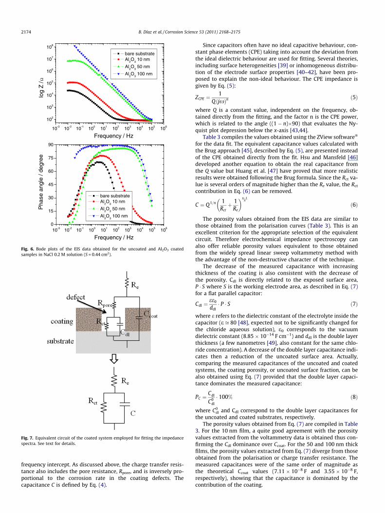
Two time constants are generally considered to describe coatedsystems [15,6,33–36]. The coating properties are evaluated in thehigh frequency region and the low frequency region gives informa-tion about the corrosion process. However, following this treat-ment, coating capacitances in the order of 10�5 F cm�2, or higherin some cases, have been obtained which are completely out ofrange for the studied thicknesses and coatings. For a typical coatingwith 1 lm thickness, the capacitance value should be of the orderof 10�8 F cm�2. Therefore the choice of the generally adoptedequivalent circuit with two hierarchically distributed time con-stants must be considered critically.
The diagram presented in Fig. 7 can help to better understandthe coated system. The charge transfer resistance can be associatedto the rate of the corrosion reaction of an active substrate such ascarbon steel in the coating defects. Some authors make distinctionbetween the charge transfer resistance (Rct) and the pore resistance(Rpore). In the case of thin coatings in the nanometre range, Rpore
will be significantly lower than Rct [16,35,37] so it may be consid-ered as negligible. Thus, only one element (Rct) is considered in theproposed simplified equivalent circuit (Rct� Rpore). The coatingcapacitance value (Ccoat) is expected to be around 10�7 F cm�2
assuming a flat parallel capacitor. The double layer capacitance(Cdl) corresponding to the substrate/electrolyte interface in thecoating defects is of the order of 10�6 F cm�2 [37]. These twocapacitances are in parallel so the contribution of both should beconsidered. The uncoated surface fraction (P) will play an impor-tant role to define the final capacitance value, given by Eq. (4):
C ¼ P � Cdl þ ð1� PÞ � Ccoat ð4Þ
For porous coatings with a high uncoated surface fraction, thedouble layer capacitance contribution (P � Cdl) will dominate,whereas, with increasing sealing properties, the coating capacitance(ð1� PÞ � Ccoat) will become dominant.
Some attempts were made to include two time constants in ourfitting procedure but the resulting high error, typically obtainedwhen using a model that contains more elements than representedby the experimental data, pointed the inaccuracy of this approach.Moreover, the shape of the EI spectra does not indicate the pres-ence of two time constants so that coating and corrosion propertiescannot be distinguished [38]. Thus, the simplified model presentedin the bottom part of Fig. 7 and corresponding to one time constantwas used instead. This equivalent circuit includes the electrolyteresistance, Re, measured at the high frequency intercept with thereal axis, and the charge transfer resistance Rct found at the low
rosity values (P, %) calculated using Eq. (1), and EIS fitting parameters for the uncoatedre shown instead of the CPE values obtained by fitting. The porosity values obtainedd from Cdl (S = 0.44 cm2).
(X) C (F) n PR (%) PC (%)
30 2.59 � 10�5 0.85 100 1009 � 105 3.41 � 10�6 0.86 18.3 13.24 � 106 5.95 � 10�8 0.95 0.34 0.238 � 108 3.61 � 10�8 0.99 0.005 0.14
10-3 10-2 10-1 100 101 102 103 104 105 106
102
103
104
105
106
107
108
bare substrate Al
2O
3 10 nm
Al2O
3 50 nm
Al2O
3 100 nm
log
Z /
Ω
Frequency / Hz
10-3 10-2 10-1 100 101 102 103 104 105 1060
15
30
45
60
75
90
Pha
se a
ngle
/ de
gree
Frequency / Hz
bare substrate Al
2O
3 10 nm
Al2O
3 50 nm
Al2O
3 100 nm
Fig. 6. Bode plots of the EIS data obtained for the uncoated and Al2O3 coatedsamples in NaCl 0.2 M solution (S = 0.44 cm2).
Fig. 7. Equivalent circuit of the coated system employed for fitting the impedancespectra. See text for details.
2174 B. Díaz et al. / Corrosion Science 53 (2011) 2168–2175
frequency intercept. As discussed above, the charge transfer resis-tance also includes the pore resistance, Rpore, and is inversely pro-portional to the corrosion rate in the coating defects. Thecapacitance C is defined by Eq. (4).
Since capacitors often have no ideal capacitive behaviour, con-stant phase elements (CPE) taking into account the deviation fromthe ideal dielectric behaviour are used for fitting. Several theories,including surface heterogeneities [39] or inhomogeneous distribu-tion of the electrode surface properties [40–42], have been pro-posed to explain the non-ideal behaviour. The CPE impedance isgiven by Eq. (5):
ZCPE ¼1
QðjxÞnð5Þ
where Q is a constant value, independent on the frequency, ob-tained directly from the fitting, and the factor n is the CPE power,which is related to the angle ((1 � n)�90) that evaluates the Ny-quist plot depression below the x-axis [43,44].
Table 3 compiles the values obtained using the ZView software�
for the data fit. The equivalent capacitance values calculated withthe Brug approach [45], described by Eq. (5), are presented insteadof the CPE obtained directly from the fit. Hsu and Mansfeld [46]developed another equation to obtain the real capacitance fromthe Q value but Huang et al. [47] have proved that more realisticresults were obtained following the Brug formula. Since the Rct va-lue is several orders of magnitude higher than the Re value, the Rct
contribution in Eq. (6) can be removed.
C ¼ Q 1=n 1Rctþ 1
Re
� �n�1n
ð6Þ
The porosity values obtained from the EIS data are similar tothose obtained from the polarisation curves (Table 3). This is anexcellent criterion for the appropriate selection of the equivalentcircuit. Therefore electrochemical impedance spectroscopy canalso offer reliable porosity values equivalent to those obtainedfrom the widely spread linear sweep voltammetry method withthe advantage of the non-destructive character of the technique.
The decrease of the measured capacitance with increasingthickness of the coating is also consistent with the decrease ofthe porosity. Cdl is directly related to the exposed surface area,P � S where S is the working electrode area, as described in Eq. (7)for a flat parallel capacitor:
Cdl ¼ee0
ddl� P � S ð7Þ
where e refers to the dielectric constant of the electrolyte inside thecapacitor (e ffi 80 [48], expected not to be significantly changed forthe chloride aqueous solution), e0 corresponds to the vacuumdielectric constant (8.85 � 10�14 F cm�1) and ddl is the double layerthickness (a few nanometres [49], also constant for the same chlo-ride concentration). A decrease of the double layer capacitance indi-cates then a reduction of the uncoated surface area. Actually,comparing the measured capacitances of the uncoated and coatedsystems, the coating porosity, or uncoated surface fraction, can bealso obtained using Eq. (7) provided that the double layer capaci-tance dominates the measured capacitance:
PC ¼Cdl
C0dl
� 100% ð8Þ
where C0dl and Cdl correspond to the double layer capacitances for
the uncoated and coated substrates, respectively.The porosity values obtained from Eq. (7) are compiled in Table
3. For the 10 nm film, a quite good agreement with the porosityvalues extracted from the voltammetry data is obtained thus con-firming the Cdl dominance over Ccoat. For the 50 and 100 nm thickfilms, the porosity values extracted from Eq. (7) diverge from thoseobtained from the polarisation or charge transfer resistance. Themeasured capacitances were of the same order of magnitude asthe theoretical Ccoat values (7.11 � 10�8 F and 3.55 � 10�8 F,respectively), showing that the capacitance is dominated by thecontribution of the coating.

B. Díaz et al. / Corrosion Science 53 (2011) 2168–2175 2175
The CPE power value, n = 0.86, indicated in Table 3, obtained forthe 10 nm thick layer is very close to that, n = 0.85, for the refer-ence substrate (Table 3). This is consistent with the high confor-mality of the ALD coating. The thinner Al2O3 coating basicallymimics the existing surface roughness. For 50 and 100 nm thickfilms, the CPE power value increases up to 0.95 and 0.99, respec-tively. This suggests a higher surface homogeneity as previouslyreported [43,50]. As the coating thickness increases the small sur-face heterogeneities will become sealed, and thus a smoother sur-face is obtained as already indicated by the optical micrographspresented in Fig. 1.
4. Conclusions
Surface and depth profile analysis of ultra thin (10 and 50 nm)aluminium oxide coatings deposited by ALD at 160 �C on steelshows that the coating stoichiometry is Al2O3 and does not varywhen increasing the coating thickness. Trace contamination byunreacted trimethyl aluminium and water precursor fragments isobserved by ToF-SIMS in the bulk coating. The C contaminationis below the detection limit of XPS (<0.5 at.%). The buried coat-ing/alloy interfacial region is contaminated by carbon and OH alsooriginating from surface contamination of the alloy before coating.An Fe(II) and Fe(III) oxide interfacial layer corresponding to the na-tive oxide formed in ambient air before coating and/or resultingfrom the growth of spurious oxide traces in the initial stages ofthe ALD process was also found at the buried interface. The firstdeposited 10 nm of the alumina coating are more defective con-taining cracks or pinholes exposing the substrate. Increasing thethickness seals these defects.
Electrochemical analysis in 0.2 M NaCl shows markedly im-proved corrosion resistance. The corrosion rate decreases by one,two and four orders of magnitude for the 10, 50 and 100 nm thickfilms, respectively. Quantification of the uncoated surface fractionyielded an exponential decay with increasing thickness in the 10–100 nm range, with values going down to 0.01%. Very good agree-ment was achieved for the data obtained by voltammetry and non-destructive EIS analysis at open circuit potential.
These data show that thin oxide coatings deposited by atomiclayer deposition at relatively low temperature can achieve effectiveprotection against corrosion of heat-sensitive engineering alloys.Coating thickness is a critical issue and its increase beyond 10 nmappears to be necessary to seal the defects that form in the initialstages of growth and that expose the substrate surface as shownby our study. The evolution with time of the present ALD coatingsand of their protection properties will be reported separately.
Acknowledgements
The research leading to these results has received funding fromthe European Community’s Seventh Framework Programme (FP7/2007-2013) under grant agreement no CP-FP 213996-1 (CORRAL).Region Ile-de-France is acknowledged for partial support for theToF-SIMS equipment.
References
[1] T. Suntola, J. Antson, US Patent 4058430, 1977.[2] M. Ritala, J. Niinistö, in: A.C. Jones, M.L. Hitchman (Eds.), Chemical Vapour
Deposition: Precursors, Processes and Applications, Royal Society of Chemistry,2009, p. 158 (Chapter 4).
[3] M. Ritala, M. Leskelä, in: H.S. Nalwa (Ed.), Handbook of Thin Film Materials, vol.1, Academic Press, San Diego, 2001, p. 103 (Chapter 2).
[4] S. George, B. Yoon, A. Dameron, Acc. Chem. Res. 42 (2009) 498–508.[5] R. Matero, M. Ritala, M. Leskelä, T. Salo, J. Aromaa, O. Forsén, J. Phys. IV, 9 (Pr8)
(1999) 493–499.[6] C.X. Shan, X. Hou, K.L. Choy, Surf. Coat. Technol. 202 (2008) 2399–2402.[7] B. Díaz, J. Swiatowska, V. Maurice, A. Seyeux, B. Normand, E. Härkönen, M.
Ritala, P. Marcus, Electrochim. Acta. doi:10.1016/j.electacta.2011.02.074.[8] X. Du, K. Zhang, K. Holland, T. Tombler, M. Moskovits, Appl. Opt. 48 (2009)
6470–6474.[9] W.M.M. Kessels, S.B.S. Heil, E. Langereis, J.L. van Hemmen, H.C.M. Knoops, W.
Keuning, M.C.M. van de Sanden, ECS Trans. 3 (2007) 183–190.[10] S.E. Potts, W. Keuning, E. Langereis, G. Dingemans, M.C.M. van de Sanden,
W.M.M. Kessels, J. Electrochem. Soc. 157 (2010) 66–74.[11] S.E. Potts, L. Schmalz, M. Fenker, B. Diaz, J. Swiatowska, V. Maurice, P. Marcus,
G. Radnóczi, L. Tóth, M.C.M. van de Sanden W.M.M. Kessels, J. Electrochem.Soc., doi:10.1149/1.3560917.
[12] M. Ylilammi, T. Ranta-aho, Thin Solid Films 232 (1993) 56–62.[13] J. Daillant, A. Gibaud (Eds.), X-ray and Neutron Reflectivity: Principles and
Applications, Lecture Notes in Physics, vol. 770, Springer, 2009.[14] S. Tanuma, C.J. Powell, D.R. Penn, Surf. Interface Anal. 20 (1993) 77–89.[15] W. Tato, D. Landolt, J. Electrochem. Soc. 145 (1998) 4173–4181.[16] S.H. Ahn, Y.S. Choi, J.G. Kim, J.G. Han, Surf. Coat. Technol. 150 (2002) 319–326.[17] M. Stern, A.L. Geary, J. Electrochem. Soc. 104 (1957) 56–63.[18] C. Andrade, F. Bolzoni, M. Cabeza, X.R. Nóvoa, M.C. Pérez, in: L. Bonora, F.
Deflorian (Eds.), Electrochemical Approach to Selected Corrosion andCorrosion Control Studies, European Federation of Corrosion Pub., No. 28,The Institute of Materials, London, 2000, pp. 332–343.
[19] R. Matero, A. Rahtu, M. Ritala, M. Leskelä, T. Sajavaara, Thin Solid Films 368(2000) 1–7.
[20] J. Kelber, Surf. Sci. Rep. 62 (2007) 271–303.[21] V. Maurice, I. Bennour, S. Zanna, L.H. Klein, P. Marcus, J. Phys Chem. C 114
(2010) 7132–7140.[22] M.D. Groner, F.H. Fabreguette, J.W. Elam, S.M. George, Chem. Mater. 16 (2004)
639–645.[23] G. Beamson, D. Briggs, High Resolution XPS of Organic Polymers, TheScienta
ESCA 300 Database, John Wiley and Sons, 1992.[24] V. Crist, Handbook of Monochromatic XPS Spectra (Elements and Native
Oxides), XPS International LLC, CA, USA, 2004.[25] P. Marcus, C. Hinnen, I. Ofefjord, Surf. Interface Anal. 20 (1993) 923–929.[26] M.R. Alexander, G.E. Thompson, G. Beamson, Surf. Interface Anal. 29 (2000)
468–477.[27] J.A. Rotole, P.M.A. Sherwood, Surf. Sci. Spectra 5 (1998) 18–25.[28] J. Theo Kloprogge, L.V. Duong, B.J. Wood, R.L. Frost, J. Colloid Interface Sci. 296
(2006) 572–576.[29] F. Rueda, J. Mendialdua, A. Rodriguez, R. Casanova, Y. Barbaux, L. Gengembre,
L.J. Jalowiecki, J. Electron Spectrosc. Relat. Phenom. 82 (1996) 135–143.[30] D.D. Hawn, B.M. DeKoven, Surf. Interface Anal. 10 (1987) 63–74.[31] M. Muhler, R. Schlögl, G. Ertl, J. Catal. 138 (1992) 413–444.[32] T. Yamashita, P. Hayes, Appl. Surf. Sci. 254 (2008) 2441–2449.[33] C. Liu, Q. Bi, A. Mathews, Corros. Sci. 43 (2001) 1953–1961.[34] V.K.W. Grips, V.E. Selvi, H.C. Barshilia, K.S. Rajam, Electrochim. Acta 51 (2006)
3461–3468.[35] R.C. Barik, J.A. Wharton, R.J.K. Wood, K.R. Stokes, R.L. Jones, Surf. Coat. Technol.
199 (2005) 158–167.[36] C. Liu, Q. Bi, A. Leyland, A. Matthews, Corros. Sci. 45 (2003) 1257–1273.[37] A.J. Bard, L.R. Faulkner, Electrochemical Methods: Fundamentals and
Applications, John Wiley and Sons, New York, 1980.[38] S. Rudenja, C. Leygraf, J. Pan, P. Kulu, E. Talimets, V. Mikli, Surf. Coat. Technol.
114 (1999) 129–136.[39] W.H. Mulder, J.H. Sluyters, T. Pajkossy, I. Nyikos, J. Electroanal. Chem. 285
(1990) 103–115.[40] C.A. Schiller, W. Strunz, Electrochim. Acta 46 (2001) 3619–3625.[41] C.H. Kim, S.I. Pyun, J.H. Kim, Electrochim. Acta 48 (2003) 3455–3463.[42] J.B. Jorcin, M.E. Orazem, N. Pebere, B. Tribollet, Electrochim. Acta 51 (2006)
1473–1479.[43] E. Barsoukov, J.R. Macdonald, in: E. Barsoukov, J.R. Macdonald (Eds.),
Impedance Spectroscopy, Theory, Experiment, and Applications, second ed.,John Wiley and Sons, Inc., 2005 (Chapter 1).
[44] E.M.A. Martini, I.L. Muller, Corros. Sci. 42 (2000) 443–454.[45] G.J. Brug, A.L.G. van den Eeden, M. Sluyters-Rehbach, J.H. Sluyters, J.
Electroanal. Chem. 176 (1984) 275–295.[46] C.H. Hsu, F. Mansfeld, Corrosion 57 (2001) 747–748.[47] V.M.-W. Huang, V. Vivier, M.E. Orazem, N. Pébère, B. Tribollet, J. Electrochem.
Soc. 154 (2007) C99–C107.[48] D.R. Lide (Ed.), Handbook of Chemistry and Physics, 75th ed., CRC Press,
1995.[49] F. Scholz (Ed.), Electroanalytical Methods, second ed., Springer, 2010.[50] Y.-Y. Chang, D.-Y. Wang, Surf. Coat. Technol. 200 (2005) 2187–2191.