Mesoscopic predictions of the effective thermal conductivity for microscale random porous media
Upload
khangminh22Category
view
4download
0
HAL Id: tel-00261434https://tel.archives-ouvertes.fr/tel-00261434v2
Submitted on 7 Mar 2008 (v2), last revised 10 Oct 2008 (v3)
HAL is a multi-disciplinary open accessarchive for the deposit and dissemination of sci-entific research documents, whether they are pub-lished or not. The documents may come fromteaching and research institutions in France orabroad, or from public or private research centers.
L’archive ouverte pluridisciplinaire HAL, estdestinée au dépôt et à la diffusion de documentsscientifiques de niveau recherche, publiés ou non,émanant des établissements d’enseignement et derecherche français ou étrangers, des laboratoirespublics ou privés.
Cryogenic AFM-STM for mesoscopic physicsHélène Le Sueur
To cite this version:Hélène Le Sueur. Cryogenic AFM-STM for mesoscopic physics. Condensed Matter [cond-mat]. Uni-versité Pierre et Marie Curie - Paris VI, 2007. English. tel-00261434v2

THESE DE DOCTORAT DE
L’UNIVERSITÉ PARIS 6 – PIERRE ET MARIE CURIE
Spécialité
Physique des Solides
Présentée par Hélène le Sueur
pour obtenir le grade de
DOCTEUR de l’UNIVERSITÉ PIERRE ET MARIE CURIE
Sujet de la thèse :
Développement d’un AFM-STM pour la spectroscopie électronique haute résolution de
nanostructures et application à la supraconductivité de proximité
soutenue le 21 septembre 2007
devant un jury composé de
M Marco APRILI
M Claude CHAPELIER rapporteur
M Juan Carlos CUEVAS rapporteur
M Daniel ESTEVE directeur de thèse
M William SACKS
M Christian SCHÖNENBERGER

2
This thesis can be downloaded as a pdf file at:
http://www-drecam.cea.fr/drecam/spec/pres/quantro/qsite/index.htm
or
http://tel.archives-ouvertes.fr/
COVER:
The front cover shows an AFM image of a small circuit fabricated by electronic lithography
and double angle evaporation, comprising a 350 nm long, 30 nm thick silver wire (colorized
in orange) and a 60 nm thick aluminium half loop (dark grey). This structure has been imaged
using an atomic force sensor, and tunneling spectroscopy was subsequently performed at
several positions. Curves on the background are tunneling spectra measured for different
values of the superconducting phase difference across the normal wire (at the location of the
tip represented on the AFM image).
The graph on the backside of the cover is a 3D plot of the predicted local density of states
along a 1D S-N-S structure, with a normal wire length L = 1.4 ξ (corresponding to 350 nm),
and perfect interfaces.

3
REMERCIEMENTS
Ce fût un réel plaisir pour moi de travailler au Service de Physique de l’Etat Condensé. Je ne
parle pas ici du seul groupe Quantronique, car ce sont réellement le rassemblement en un lieu
unique d’autant de compétences diverses et leur prompte disponibilité qui m’ont donné la
chance inouïe de mener à bon terme ce projet.
Tout d’abord, un grand merci à Eric Vincent qui m’a soutenue dans toutes mes demandes
auprès du CEA, et m’a ainsi permis de rester parmi vous le temps nécessaire à la réalisation
de notre première expérience de physique mésoscopique : quel bonheur ! Merci à ceux qui ont
rendu cela possible, par leur intervention à divers niveaux : Louis Laurent, Philis Livanos, lors
de mon entrée au SPEC, Didier Normand lors de la prolongation de mon contrat CFR,
Sandrine Thunin et Nathalie Royer dans mes diverses démarches administratives.
Merci infiniment à Daniel Esteve, mon directeur de thèse, pour avoir appuyé sans réserve ma
candidature, et tout ce qui s’en est suivi : Travailler avec un « chef » comme toi est un
enrichissement extrême, tant pour ton recul sur la compréhension des phénomènes envisagés,
que pour ton esprit pratique qui nous permet de parvenir plus vite (et mieux bien sûr !) au
résultat souhaité… Et puis tu n’es pas chef pour rien : ce don d’ubiquité qui te permet de
consacrer à tous les projets simultanément la même attention exclusive force sincèrement
l’admiration !
J’espère avoir mérité toute la confiance que m’a accordée Philippe Joyez en me laissant la
responsabilité de porter avec lui son projet de recherche, à ses débuts lors de mon arrivée dans
le groupe. Ma seule gratitude ne peut exprimer justement tout ce que tu as fait pour moi car tu
m’as fait vivre durant cette thèse une expérience de recherche inoubliable : construire une
manip’ entière depuis la racine, l’élaborer pas par pas, et la faire marcher pour en tirer des
mesures de premier ordre ! Quel thésard peut rêver mieux ?
Bien entendu une telle entreprise n’aurait pu aboutir sans le soutien technique de nombreuses
personnes. Sans les compétences de Pascal Senat, les pièces du microscope seraient
probablement usinées de travers, et cette mécanique si délicate n’aurait jamais fonctionné.
Pief Orfila, non content de gérer la logistique du groupe ainsi que l’installation et le bon
fonctionnement de la majorité des machines de nano-fabrication au SPEC, a de plus aménagé
notre labo de manière astucieuse et confortable. Jean-Claude Tack a été d’une grande
disponibilité pour l’usinage d’un bon nombre de pièces de câblage. Grâce à Michel Juignet,
qui m’a initiée aux machines d’atelier, j’ai pu usiner moi-même –avec les conseils de Pascal-

4
quelques pièces du microscope. Je remercie chaleureusement toutes ces personnes pour leur
aide précieuse.
Le réfrigérateur que nous utilisons pour faire l’expérience présentée dans ce manuscrit est un
modèle construit par Air-Liquide, qui a présenté dès son achat de nombreux
dysfonctionnements. Ce réfrigérateur a été envoyé en réparation avant le début de ma thèse, et
n’est revenu qu’au milieu de la 2è année, en raison des difficultés rencontrées pour le réparer.
Je tiens à remercier chaudement le personnel du CRTBT qui s’est attaché à ce travail difficile
et peu gratifiant, en sus de leur taches personnelles. Le travail bénévole de Thomas Prouve, un
étudiant en thèse, et Lionel Germani, un technicien cryogéniste m’aura permis -malgré le
retard pris- d’utiliser le microscope que j’avais construit à des fins de recherche. Patrick Pari a
aussi contribué à cette réparation puisqu’il a levé le tout dernier problème de cryogénie, nous
permettant de récupérer ce réfrigérateur tant attendu pour commencer à le câbler. Patrick Pari
continue, avec Mathieu de Combarieu et Philippe Forget, le groupe de cryogénie du SPEC, de
nous aider à améliorer le fonctionnement du réfrigérateur. Merci à eux !
Faire de la physique dans le groupe Quantronique est en soi une chance, tant pour l’éclectisme
que pour l’effervescence scientifique qui y règnent. Difficile de passer quatre années au
contact de ses membres sans être contaminé par la passion qui les anime…
Denis Vion d’un enthousiasme constant pour mes divers balbutiements en montage de
manip’, et d’un dévouement exceptionnel pour améliorer mon discours de soutenance : merci
de ton soutien dans ces moments difficiles, et merci d’avoir pris sur toi tout mon stress le jour
J, comme en témoignaient tes grimaces pendant mon exposé!
Hugues Pothier sans qui la salle café serait jonchée de miettes de gâteau. Cette seule
description est un peu réductrice je l’avoue : il faut aussi noter la finesse de ses explications
physiques qui savent aborder la problématique de manière simple et limpide en utilisant les
bonnes images. Merci à toi de m’avoir introduite aux subtilités de l’effet de proximité, et
m’avoir évité de tourner en rond trop longtemps pour choisir les bons paramètres
d’expérience.
J’ai beaucoup apprécié les compétences et l’exigence de Cristiàn Urbina, dans de multiples
domaines et notamment en matière d’écriture anglaise. Merci pour ta relecture attentive de
mon manuscrit et tes corrections qui sont sûrement responsables des compliments que j’ai
reçus en ce sens.
Merci à Patrice Bertet, nouveau membre permanent du groupe, pour ses idées originales en
provenance du grand nord, sa grande capacité d’écoute et de conseil, et sa contenance qui
contraste avec l’impertinence du groupe ! A bientôt à La tuile à loup…

5
Je souhaite une bonne continuation aux thésards et post-docs que j’ai côtoyés durant mon
séjour : Martin Chauvin et Peter Vom Stein, le premier duo P08, responsable de nombreuses
soirées pizza / vidéo-projecteur qui m’ont souvent remonté le moral ! Anne Anthore et Ronald
Cron, qui ont partagé durant quelques mois ces soirées avec nous, Benjamin Huard et Maria-
Luisa Della-Rocca dignes successeurs de Peter et Martin, et Quentin Le Masne, qui prend
maintenant la relève avec autant de punch. Bon vent aux manipulateurs de Q-Bit : Eddy
Collin, Grégoire Ithier, Nicolas Boulant, François Nguyen, François Mallet et Agustin
Palacios : puissent les suivants animer la P4 team aussi bien que vous !
J’ai apprécié de passer ce temps en compagnie des divers groupes du SPEC : les
magnétiseurs, le groupe bruitonique (le sous-sol humide est-il toujours propice à la culture des
blagues graveleuses ?), les LEMuriens, les turbulents… thésards, post-doc ou permanents
avec qui il était toujours agréable d’échanger.
Je remercie également les différentes personnes qui m’ont accordé leur disponibilité et m’ont
fait partager leurs connaissances de manière toujours très sympathique : merci tout
particulièrement à Juan Carlos Cuevas, Wolfgang Belzig, Elke Sheer, Terö Heikkilä, Mathias
Eschrig, Takis Kontos, Audrey Cottet, Anne Anthore, Sophie Guéron, Hélène Bouchiat,
Francesca Chiodi pour nos échanges très instructifs sur l’effet de proximité, à Hervé Courtois,
Gabino Rubio-Bollinger, Nicolas Agrait, Herman Suderow et Olivier Klein pour avoir partagé
avec moi leur expérience sur la microscopie, à Marcelo Goffman et Roland Lefebvre pour
m’avoir fourni des échantillons lors des tests initiaux du microscope.
Je suis très reconnaissante envers Juan Carlos Cuevas, Claude Chapelier, Marco Aprili,
William Sacks, et Christian Schönenberger d’avoir accepté de faire partie de mon jury.
Enfin, mes pensées vont vers tous ceux qui m’ont épaulé durant cette thèse et ont rendu ces
années plus agréables. Je pense tout particulièrement à mon père Henri, ma mère Marie-
Claude, et à Florence et Benjamin, ma famille au sens large, qui accompagnent mes réussites
et mes échecs depuis le début.
Je regrette déjà cette dualité d’une grande profondeur d’esprit avec des discours
irrévérencieux, qui caractérise le groupe Quantronique, et souhaite sincèrement pouvoir
prolonger dans l’avenir nos discussions passionnantes -de tout ordre- et notamment celles sur
les macarons !

6

7
TABLE OF CONTENTS
1 General introduction --------------------------------------------------------------------------11
1.1 Tunneling spectroscopy..........................................................................................................151.2 Spatially resolved measurement of the LDOS with a combined AFM-STM ....................181.3 An AFM-STM in a table-top dilution refrigerator. .............................................................211.4 Benchmarking tunneling spectroscopy.................................................................................221.5 An experiment on the proximity effect in S-N-S structures................................................241.6 Perspectives .............................................................................................................................30
1.6.1 Proximity effect in ballistic 1D systems ...............................................................................................301.6.2 Proximity effect in a 2D system............................................................................................................301.6.3 Spin injection and relaxation in superconductors .................................................................................311.6.4 Energy relaxation in quasi-ballistic (“Superdiffusive”) structures........................................................31
2 Design, Fabrication and Operation of the Microscope----------------------------------33
2.1 The microscope structure.......................................................................................................352.1.1 General description ...............................................................................................................................352.1.2 Materials and construction....................................................................................................................36
2.1.2.1 Material selection...................................................................................................................................362.1.2.2 Mechanical structure ..............................................................................................................................382.1.2.3 CAD Design...........................................................................................................................................382.1.2.4 Assembly ...............................................................................................................................................422.1.2.5 Plating of titanium..................................................................................................................................43
2.2 Piezoelectric actuators ............................................................................................................442.2.1 The piezoelectric effect.........................................................................................................................44
2.2.1.1 General mathematical description of piezoelectricity ............................................................................442.2.1.2 Practical equations for piezoelectric devices..........................................................................................45
2.2.2 Practical piezoelectric materials............................................................................................................462.2.2.2 Quartz crystal .........................................................................................................................................462.2.2.3 PZT piezoelectric material .....................................................................................................................47
2.2.2.3.a Description....................................................................................................................................472.2.2.3.b PZT ceramics: poling and depoling ..............................................................................................472.2.2.3.c PZT actuators shapes and functioning...........................................................................................482.2.2.3.d Imperfections of PZT ceramics: drift and hysteresis.....................................................................512.2.2.3.e PZT ceramics at low temperature..................................................................................................52
2.2.3 The piezoelectric tube ...........................................................................................................................522.2.3.1 Poling procedure ....................................................................................................................................532.2.3.2 Calibration at high and low temperatures...............................................................................................53
2.3 Coarse positioning and indexing ...........................................................................................552.3.1 Design & principle................................................................................................................................55
2.3.1.1 Stick-slip motion....................................................................................................................................552.3.1.2 Electrical requirements...........................................................................................................................562.3.1.3 Mechanical performance of the motors..................................................................................................572.3.1.4 Inertial vs. non-inertial stick-slip motion ...............................................................................................58
2.3.2 Position indexing ..................................................................................................................................582.3.2.1 Design ....................................................................................................................................................582.3.2.2 Resolution and accuracy of the capacitive position sensors ...................................................................592.3.2.3 Practical implementation........................................................................................................................602.3.2.4 Testing actuators and sensors.................................................................................................................62
2.4 The atomic force sensor..........................................................................................................652.4.1 implementing AFM sensors at low temperature ...................................................................................66
2.4.1.1 Optical sensors .......................................................................................................................................662.4.1.2 Electrical sensors....................................................................................................................................67
2.4.2 Quartz Tuning Fork (TF) ......................................................................................................................682.4.2.1 A high Q harmonic oscillator .................................................................................................................68

8
2.4.2.2 Tuning forks for atomic force microscopes............................................................................................682.4.2.3 Oscillating modes of the tuning fork......................................................................................................712.4.2.4 Basic analysis of a tuning fork: 1 Degree-of-Freedom harmonic oscillator model. ...............................72
2.4.2.4.b Mechanical analysis ......................................................................................................................732.4.2.4.c Tip-sample interaction ..................................................................................................................74
2.4.2.5 Discussion of the 1-DOF model.............................................................................................................762.4.2.6 Model of a tuning fork as three coupled masses and springs .................................................................77
2.4.2.6.b Free dynamics of the 3-DOF model..............................................................................................782.4.2.6.c Balanced tuning fork: the unperturbed modes...............................................................................802.4.2.6.d Broken symmetry: a perturbative analysis ....................................................................................802.4.2.6.e Discussion.....................................................................................................................................82
2.4.2.7 Estimating characteristics of the connecting wire for preserving the tuning fork balance......................832.4.2.8 Measuring the oscillator parameters.......................................................................................................85
2.4.2.8.b Resonance curves during the setup ...............................................................................................862.4.2.8.c Capacitance compensation ............................................................................................................872.4.2.8.d Extracting the resonator parameters..............................................................................................87
2.4.3 Force measurement ...............................................................................................................................882.4.3.1 Typical forces on the atomic scale .........................................................................................................892.4.3.2 “Force” measurements: sensor stability and sensitivity .........................................................................902.4.3.3 “Force” measurements: detection schemes ............................................................................................922.4.3.4 Phased locked loop detection .................................................................................................................942.4.3.5 Feedback loop in imaging mode ............................................................................................................96
2.4.3.5.b Optimizing AFM imaging.............................................................................................................97
3 Experimental techniques ---------------------------------------------------------------------99
3.1 A dilution refrigerator well adapted for a local probe microscope..................................1013.1.1 Functioning of the inverted dilution refrigerator.................................................................................1013.1.2 (not so good) Vibrations in dilution refrigerator.................................................................................1043.1.3 Living with vibrations.........................................................................................................................1073.1.4 Possible improvements .......................................................................................................................108
3.2 Wiring a microscope for very low temperature experiments ...........................................1093.2.1 Thermal load .......................................................................................................................................1093.2.2 Low level signals and low noise requirements....................................................................................1113.2.3 Filtering...............................................................................................................................................111
3.2.3.1 Necessity of filtering............................................................................................................................1123.2.3.2 Why filtering all the lines?...................................................................................................................1123.2.3.3 Propagation of thermal noise in networks ............................................................................................1133.2.3.4 Filtering technique ...............................................................................................................................1173.2.3.5 Fabrication ...........................................................................................................................................1193.2.3.6 Electromagnetic simulations of the filters. ...........................................................................................1243.2.3.7 Filter attenuation ..................................................................................................................................1273.2.3.8 Analysing the full setup .......................................................................................................................1283.2.3.9 Experimental validation of the filtering setup ......................................................................................1303.2.3.10 Article reprint: microfabricated filters................................................................................................130
3.2.4 Tunneling spectroscopy ......................................................................................................................1363.2.4.1 Tunneling spectroscopy measurements................................................................................................1363.2.4.2 Data acquisition setup ..........................................................................................................................1383.2.4.3 Article reprint : Tunnel current pre-amplifier.......................................................................................142
3.3 Fabrication techniques .........................................................................................................1483.3.1 Tip fabrication.....................................................................................................................................148
3.3.1.1 Electrochemical etching .......................................................................................................................1483.3.1.2 Tungsten tips........................................................................................................................................1503.3.1.3 Niobium tips.........................................................................................................................................1553.3.1.4 In-situ tip cleaning ...............................................................................................................................1553.3.1.5 Tip damages and tip reshaping.............................................................................................................156
3.3.2 Sample preparation .............................................................................................................................1593.3.2.1 Position encoding grid..........................................................................................................................1593.3.2.2 Multiple angle evaporation...................................................................................................................162

9
4 Mesoscopic superconductivity ------------------------------------------------------------- 165
4.1 Introduction to proximity effect ..........................................................................................1664.2 Theoretical description of Proximity Effect .......................................................................167
4.2.1 Inhomogeneous superconductivity .....................................................................................................1674.2.2 The Bogolubov – de Gennes equations...............................................................................................1674.2.3 Theoretical description of the proximity effect in diffusive systems at equilibrium...........................168
4.2.3.1 Electronic Green functions...................................................................................................................1684.2.3.2 Green functions in the Nambu space....................................................................................................1684.2.3.3 Quasiclassical Green functions in the dirty limit - Usadel equation.....................................................1694.2.3.4 Properties of the Green function elements - Physical quantities ..........................................................1694.2.3.5 Boundary conditions ............................................................................................................................171
4.2.4 Parameterization of the Green functions.............................................................................................1734.2.4.1 θ, φ parameterization............................................................................................................................173
4.2.4.1.b Nazarov's Andreev circuit theory................................................................................................1744.2.4.2 Ricatti parameterization .......................................................................................................................175
4.2.4.2.a Advantages of this parameterization ...........................................................................................1764.2.4.2.b Ricatti parameters in reservoirs...................................................................................................1764.2.4.2.c (Dis-)Continuity of Ricatti parameters at interfaces....................................................................177
4.2.5 Spectral quantities in the Ricatti parameterization..............................................................................1774.2.6 A word on the non-equilibrium theory................................................................................................178
4.3 Solving the Usadel equations numerically ..........................................................................1794.3.1 Reduction of the problem dimensionality ...........................................................................................1794.3.2 Specifying the 1-D problem................................................................................................................1804.3.3 Solving strategy - self-consistency......................................................................................................1814.3.4 Implementation details........................................................................................................................181
4.4 General results on proximity effect in SNS structures ......................................................1854.4.1 “Minigap” in the DOS ........................................................................................................................1854.4.2 Inverse proximity effect – Pairing amplitude and pairing potential....................................................186
4.4.2.2 Self-consistency ...................................................................................................................................1874.4.3 Role of interfaces ................................................................................................................................1894.4.4 Dependence of the minigap on N size.................................................................................................1904.4.5 Phase modulation of the proximity effect ...........................................................................................191
4.5 SNS systems viewed as scattering structures .....................................................................1924.6 An STM experiment on the proximity effect......................................................................194
4.6.1 Sample geometry ................................................................................................................................1944.6.2 Implementation of the experiment ......................................................................................................195
4.6.2.1 Achieving a good phase bias................................................................................................................1954.6.2.1.a Kinetic inductance correction......................................................................................................1964.6.2.1.b Circulating currents correction....................................................................................................196
4.6.2.2 Sample fabrication ...............................................................................................................................1974.6.2.3 Overview of the measured SNS structures...........................................................................................198
4.6.3 What do we measure? .........................................................................................................................1994.6.4 Density of states in a long SNS structure............................................................................................2004.6.5 Density of states in a short SNS structure...........................................................................................201
4.6.5.1 position dependence.............................................................................................................................2014.6.5.2 phase dependence.................................................................................................................................205
4.6.5.2.b Phase calibration .........................................................................................................................2084.6.5.2.c minigap as a function of phase....................................................................................................208
4.6.5.3 Is the Al electrode affected by the applied field? .................................................................................2094.6.6 Density of states in a medium-size SNS structure ..............................................................................211
4.6.6.1 Intermediate regime .............................................................................................................................2114.6.7 Comparison with theory......................................................................................................................212
4.6.7.1 Parameters entering the theory.............................................................................................................2124.6.7.2 Comparison with theoretical predictions..............................................................................................215
4.6.7.2.a Determination of the parameters .................................................................................................2154.6.7.2.b Position dependence....................................................................................................................2184.6.7.2.c Phase dependence .......................................................................................................................2204.6.7.2.d Length dependence .....................................................................................................................221
4.6.7.3 Summary of the fitting parameters.......................................................................................................2224.6.7.4 Experimental limitations ......................................................................................................................223
10
4.6.7.4.a Positioning accuracy ...................................................................................................................2234.6.7.4.b Energy resolution........................................................................................................................223
4.6.7.5 Model limitations .................................................................................................................................2244.6.7.5.a Depairing.....................................................................................................................................2244.6.7.5.b Self consistent treatment of the proximity effect ........................................................................2244.6.7.5.c 1-D model of the NS interface ....................................................................................................2244.6.7.5.d Transverse extension, sample geometry......................................................................................225
4.6.8 Article reprint: proximity effect in S-N-S structures...........................................................................2254.7 Conclusions............................................................................................................................237
4.7.1 Further experiments ............................................................................................................................2374.7.1.1 Out of equilibrium proximity effect .....................................................................................................2374.7.1.2 Gapless superconductivity ...................................................................................................................238

11
CHAPTER 1
11GGEENNEERRAALL
II NNTTRROODDUUCCTTII OONN
12

13
The ability to combine in a given nanostructure materials with different electronic properties
such as normal metal conductors, magnetic or superconducting electrodes, conductors of
reduced dimensionality, single molecules,… has opened new perspectives in mesoscopic
physics and nanophysics. The operation of field-effect transistors based on single gated
carbon nanotubes [1], and the production of spintronic devices in which the orientation of a
single nano-size magnetic domain controls (or is controlled by) an electrical current [2],
exemplify the progress achieved during the recent years. A wide range of electronic
phenomena have been found in the numerous combinations of materials explored:
superconductivity in nanostructures made of both superconducting and non-superconducting
materials, Kondo effect in quantum dots connected to bulk Fermi reservoirs [3], spin and
charge transport in spintronic devices… Understanding the behaviour of such heterogeneous
nanostructures with competing electronic orders remains a major challenge in mesoscopic
physics.
At an interface between two different materials, variations of the electronic properties often
occur on short length-scales. Local probing of electronic spectroscopy, with a good spatial
resolution, is therefore necessary. Besides, such local spectroscopic measurements are often
more direct tests of microscopic models of the system than transport measurements are.
Moreover, the energy range over which these effects appear is often quite small (typically
~1 meV and down to a few 10 µeV), compared to, for instance, the thermal energy at room
temperature (kBT~30 meV). It is thus mandatory to cool the experiments down to very low
temperatures, in the millikelvin range, first to make these phenomena observable, as well as to
measure them without thermal blurring.
Many different kinds of spectroscopies using electron, ion or photon beams, such as Electron
Energy Loss Spectroscopy or photo-emission, can be used to perform a local electronic
characterisation. However, their spatial resolution is often poor, and the probed energy range
(eV or higher) is larger than the relevant one for mesoscopic physics. In order to obtain
spatially resolved information, and to probe small energies, various types of scanning probe
microscopies have been developed. Two main operation modes, electronic or optical, can be
used to probe either electronic or electro-magnetic spectroscopies. In the electronic mode, a
very sharp conducting tip is scanned above the sample surface, while the conductance
between the tip and the sample is recorded. This method used in the low conductance regime
measures the ability to inject electrons from the tip to the sample. It is called “tunneling
spectroscopy”. In the optical mode, an optical fiber with a very narrow apex is used to collect
optical photons from the sample surface, to probe for instance the electromagnetic density of

14
states [4]. Combined electronic-optical systems operating both in excitation and detection
modes are also feasible [5, 6].
The aim of this thesis work was precisely to design, fabricate and operate an apparatus able to
probe the electronic ordering in isolated conducting nanostructures using tunneling
spectroscopy, in the low energy range suitable for mesoscopic physics.
For this purpose, a microscope with both imaging and local electron spectroscopy abilities
was built and mounted in a dilution refrigerator.

15
1.1 Tunneling spectroscopy
Tunneling spectroscopy was experimentally introduced in 1960 by Giaever in the particular
case of tunneling of quasiparticles between a superconductor and a normal metal, using planar
junctions [7]. In 1981, Binnig and Rohrer developed the Scanning Tunneling Microscope,
providing condensed matter physics with a tool able to perform spatially resolved electronic
spectroscopy [8].
Although the basic theory of tunneling dates back to the early days of quantum mechanics [9],
the interpretation of most tunneling measurements relies on the tunneling-Hamiltonian
formalism introduced in the early 1960s, in particular by Bardeen [10, 11], and by Cohen,
Falicov and Philips [12]. In this framework, two independent systems are linked by a
Hamiltonian of the form
†,
,
. .= +∑T a b a ba b
H T c c h c , ( 1.1)
which transfers single electrons between states in electrode a and states in electrode b, and
where c+ and c are the creation and annihilation operators of single particle states in the
electrodes, and 2 *
, 2 Ψ ( )Ψ ( )= ∫ℏa b b amT r r dr is the tunneling matrix element between a states and
b states1.
In the case of tunneling from a sharp STM tip, one expects the tunneling process to be
essentially local, limited to the close vicinity of the tip apex. Indeed, Tersoff and Hammann
[13] have shown that, assuming the tip apex can be modelled by a sphere, the tunneling
matrix elements ,a bT are such that
( )2 2
, Ψ∝a b b cT r , ( 1.2)
where ( )Ψb cr is the value of the sample single-particle wave function b at the center (rc) of
the tip apex. For the sake of simplicity, the contact point between tip and sample is
assimilated to rc.
From this result, one easily derives a perturbative expression for the tunneling current
within the linear response theory, involving only quantities in the electrodes at rc [13]:
1 We neglect here the possible coupling of tunneling electrons to collective electromagnetic or phonon modes
which would give rise to inelastic processes that modify the tunneling current. This is generally valid when
dealing with “good” metallic electrodes having low electromagnetic impedance, and at voltages below a few
mV.

16
224( ) ( ) ( , ) ( ) ( , ) = − − − ∫
ℏtip sample c tip sample c
e τI V dε f ε eV f r ε ρ ε eV ρ r ε , ( 1.3)
where ,tip sampleρ denote the local electronic densities of states (LDOS) in the tip, and in the
sample at the contact point cr and , ( )tip samplef ε are the local energy distribution functions - or
occupation number of electronic states - in the electrodes (which reduce to Fermi functions at
thermal equilibrium). τ is the average value of the tunneling matrix elements ,a bT .
Expression ( 1.3) can be easily understood in terms of a balance of tunneling events in both
directions from occupied to empty states. It is the usual basis for analysing local tunneling
spectroscopy experiments and it is worth noticing and stressing that, to date, most STM
spectroscopic measurements have been successfully and often accurately analysed within this
rather simple Tersoff and Hammann picture. Thus, deviations from this description due to tip
shape effects or tip-sample interactions are generally negligible.
As we will now show, under favourable conditions, one can disentangle the factors
contributing in ( 1.3), thereby gaining knowledge of local spectral functions in the electrodes.
The case when both tip and sample are Fermi liquids with arbitrary densities of states is
depicted in Fig. 1.1, where it is further assumed that both electrodes are at thermal
equilibrium.
When one wants to probe the LDOS in the sample, one uses a tip where the density of states
can be assumed as constant over the probed relevant energy range (see Fig. 1.2). This is the
case for normal-metal tips, in the energy range suitable for mesoscopic physics (meV). The
LDOS plays a major role in the knowledge of physical properties of the system. It is formally
amenable to calculation once the Hamiltonian of the system is known; for instance it can be
expressed as a retarded Green function for electrons.
In order to determine the local energy distribution function in a sample, one rather uses a
superconducting tip1. In this case the sharp BCS singularity [14] of the tip DOS probes the
energy distribution discontinuities. In this mode, out-of-equilibrium situations can be probed,
giving access to fast dynamics inside the structure. Out-of-equilibrium distribution functions
can in principle be calculated from Green functions, but here within the Keldysh formalism.
1 It is possible to access energy distribution of electrons using a normal tip in a high impedance environment,
using the Zero Bias Anomaly (ZBA) induced in the density of states of the tip by dynamical coulomb blockade
[15]. However, the ZBA has a less sharp singularity, compared to the BCS singularity (which is nearly a delta
peak) and is thus a less efficient probe.

17
fSample(ε)
ρSample(ε)
ftip(ε)
ρtip(ε)
I(V)
Ta,b
a b
T S
V
Fig. 1.1 On the left are shown side to side the densities of states of arbitrary probe (ρtip) and sample (ρsample) as a function of energy (vertical axis). The filling of states (f between 0 and 1) is represented in plain color (orange for the tip, blue for the sample). Fermi levels are shifted by the voltage bias applied to the junction. The current flowing through a tunnel junction between the tip and the sample involves the convolution product of spectral functions ρ and f of the electrodes (see expression ( 1.3)). The right panel exemplifies tunneling from a state a in the tip into a state b of the sample with a coupling Ta,b.
fsample(ε)
ρsample(ε)
fN(ε)
ρN(ε)=cst
~3.5kBT
ρsample(ε)
fS(ε) fsample(ε)
ρBCS(ε)
(a)
(b)
( ) BCSsamplef
V
I
VρV
∂ ∝ ∗∂
∂∂
BCS 2 2Re
ερ =
ε − ∆
( ) sampleNfI
VVV
ρ∂∂
∂ ∝ ∗∂
εF
Fig. 1.2 Tunneling spectroscopy with normal metal (a), and with superconducting tips (b). (a) When ρtip(ε) is featureless (normal metal), the differential conductance, which is the derivative of current with respect to applied voltage, gives direct access to the local density of states in the sample, with a maximal resolution given by the sharpness of the Fermi-Dirac function, involving the temperature T in the tip (note that temperatures are not necessarily equal). (b) With a superconducting tip, tunneling gives access to the energy distribution function in the sample, provided ρsample(ε) is constant at Fermi level, using a deconvolution procedure. Experimental techniques about the DOS measurement are discussed in chapter 3.

18
1.2 Spatially resolved measurement of the LDOS with a
combined AFM-STM
Scanning Tunneling Microscopes have been exploited for spectroscopy purposes since the
very beginning. The visualization by D. Eigler et al. of a quantum corral for electronic surface
states delimited by atoms added on a crystalline surface is one famous example [16, 17].
Despite its obvious interest, scanning tunneling spectroscopy has however not been much
used to probe nanostructures. There are two main reasons for this:
• Circuits are designed on insulator:
Most of nanostructures are fabricated on an insulating substrate, on which an
STM cannot be operated: as soon as the tip hovers on an insulating part, tunneling
current drops to zero, just as if it were far from the sample surface. Therefore, the
feedback mechanism lowers the tip to reach the target tunnel current, unavoidably
resulting in a “tip crash” most dreaded by all STM users. In order to perform local
probe measurements on such samples, one needs to resort to another type of local
probe. Atomic Force Microscopy (AFM) is the most obvious choice since it has
topographic imaging capability with high spatial resolution, quite independently
of the sample properties, in particular of its conductivity.
• Circuits are small compared to the chip:
On a given sample of macroscopic size, there is often one or a few nanostructures
connected to the outside by large bonding pads. Fig. 1.3 shows as an example one
of the samples measured during this thesis work. The area of interest has a
characteristic size of a few microns, located at the center of a 5x5 mm2 chip.
Reliably bringing the local probe of a microscope on top of the nanostructure
requires precise mechanical alignment capabilities of the local probe with respect
to the sample in all three dimensions.
In order to perform spatially resolved tunneling spectroscopy on nanostructures, and to cope
with the first point above, we have built a near-field microscope having a combined Atomic
Force and Tunneling probe, which can be used in either mode. In AFM mode, topographic
images of the sample can be obtained whatever its electrical properties. The STM mode is
primarily used to measure LDOS at desired locations. This dual mode sensor is shown in
Fig. 1.4, and will be described in chapter 2. It is based on a tuning fork normally used as the
time-base resonator in wristwatches. Such a tuning fork resonator is made of quartz, a

19
piezoelectric material, which allows easy, low power, electrical excitation and detection of its
mechanical resonance (~32 kHz) and is thus well adapted for very low temperature
experiments. This tuning fork is equipped with a metallic probe tip attached to one arm. The
attractive or repulsive interaction between the tip and the sample surface affects the tuning
fork resonance. A feedback system regulating the tip-to-sample distance is used to maintain a
constant target resonance frequency while the tip scans the sample surface. This way, one can
form topographic images of the sample surface. Once the area of interest is located, switching
to the STM mode, and performing tunneling spectroscopy at precise locations is then possible
without endangering the tip. The small wire connected to the tip carries the tunnel current, and
allows tip biasing with respect to sample.
To cope with the second point, we incorporated in our microscope means of precisely displace
the sensor with respect to the sample in all three directions of space over large distances
(several mm). This motion is performed by piezoelectric actuators based on stick-slip motion.
To compensate for the lack of reproducibility of these actuators, and since operation at very
low temperatures does not allow visual access, we fitted our microscope with position
sensors. We further designed the samples so as to help us rapidly locate the nanostructure of
interest. All these features are described in details in chapters 2 and 3.

20
Fig. 1.3 A typical sample made on a 5 mm chip by standard e-beam lithography and metal deposition, is glued by silver paint on a sample holder, and bonded to contacts for transport measurements. The Moiré patterns that can be seen on a 3 mm field in the center of the sample are position encoding marks for the microscope. For the description of the encoding see chapter 3.
Fig. 1.4 (a) Picture of the combined AFM-STM probe, attached to the end of a piezoelectric scanning tube. A sharp metallic tip (inset) is glued at the end of the lower arm of the tuning fork. The fork senses the interaction between tip and sample, which allows to image topography with a precision mainly limited by the shape of the tip apex. The tip is electrically connected by a thin wire to a filtered measuring line for performing tunneling spectroscopy. (b) Picture of the microscope mounted and wired on the top plate of an inverted dilution refrigerator. (c) Ensemble view of the dilution refrigerator, model SIONLUDI designed by A. Benoit from the CNRS (Grenoble). This fridge cools the experiment down to 30mK in about 8 hours.

21
1.3 An AFM-STM in a table-top dilution refrigerator
Mesoscopic physics experiments are often performed at low temperature since the
characteristic energy scales of the investigated phenomena are generally small: for instance,
for pure metals superconductivity occurs only below a critical temperature of the order of
1 -10 K. Moreover, electron coherence effects tend to disappear as temperature rises, due to
incoherent scattering by phonons… In general, a temperature higher than the relevant energy
scale blurs the measurement: as explained in Fig. 1.2, the energy resolution of tunneling
spectroscopy is ultimately limited by the temperature at which the experiment is performed.
However, to reach this ultimate limit, or even approach it, it is not enough to cool the sample
and the microscope. It is also necessary to carefully thermalize and filter all the lines
connected to the sample so that not only the external noise (either noise from room-
temperature apparatus, or ambient noise), but also the Johnson-Nyquist noise arising from all
dissipative elements placed in these lines at temperatures higher than the sample temperature,
are suitably attenuated.
For these reasons, the microscope was placed in thermal contact with the mixing chamber of a
dilution refrigerator with a base temperature of about 30 mK and the wiring of the experiment
was carefully designed so as to benefit from the low operating temperature. In particular,
special filters were designed, fabricated and installed on every line, and a new type of tunnel
current preamplifier was designed. The fabrication and setup of the full apparatus is described
in chapter 3.
We use a table-top dilution refrigerator, developed by Alain Benoit from the Centre de
Recherche sur les Très Basses Températures (CRTBT), and which has the advantage of being
of comfortable use and suitable for a microscope such as ours. All leak-tight seals are situated
at room temperature, and the whole fridge and the experiment are placed inside the same
vacuum chamber. This fridge is not surrounded by a cryostat filled with liquid helium, but it
operates with circulating liquid helium fed from a slightly pressurized storage Dewar placed
underneath. Although a couple of groups are successfully using this type of dilution
refrigerator with STMs, we found our own fridge, which was actually fabricated by Air
Liquide, to be plagued by internal vibrations, presently forbidding normal tunnel vacuum
STM operation. We could nevertheless perform very stable tunneling spectroscopy by
bringing the tip in mechanical contact with the sample, through a thin insulating layer grown
on the sample surface.

22
1.4 Benchmarking tunneling spectroscopy
A convenient benchmark for tunneling spectroscopy is the measurement of the DOS of a BCS
superconductor with a normal metal tip, as shown in Fig. 1.2. Ideally, the measured
conductance of a N-S tunnel junction should be the convolution of the BCS DOS [14]
( )2 2
Re∆
=−
BCS
ερ ε
ε, ( 1.4)
where ∆ is the superconducting gap, with the derivative of the Fermi function in the tip at a
temperature given by the thermometer.
In practice, it turns out that in most very low temperature experiments one can only account
for the measurements by assuming that the energy distribution function in the tip is at an
effective temperature higher than that of the refrigerator. Such a discrepancy is usually
attributed to an imperfect filtering of the electric signals. The practical energy resolution
achieved in such experiments is then determined by this effective temperature.
In order to test the performance of our setup, we measured the DOS of a thin aluminum film
(thickness: 25 nm), with a chemically etched tungsten tip (see fabrication process in chapter
3). The differential conductance curve, shown in Fig. 1.5 was taken at a fridge temperature of
40 mK. The data are best fitted using the BCS density of states for aluminum (with a gap
energy 187 µeV), and a Fermi distribution function of 50 mK for the electrons in the tip. This
result already demonstrates that the electrons in the tip are fairly well thermalized, and that
not much extra noise is present.
This result presently displays the best effective temperature ever obtained in STM tunneling
spectroscopy. Although the effective temperature is still higher than the thermometer
temperature, this result validates our work on wiring, filtering and instrumentation (Chap. 3).

23
10µeV
150 ∆ 200 250
energy (µeV)
Fig. 1.5 First measurement of the tunneling density of states performed at low temperature (40 mK) on an aluminum film with a tungsten tip. The data (green points) are fitted using the BCS density of states with a superconducting gap ∆=187 µeV for the sample, and an electronic temperature of 45 mK (red curve) and 60 mK (black curve) for the electron energy distribution in the tip, with no other adjustable parameter. The best fits are obtained for an effective temperature in the tip around 50 mK. The corresponding energy resolution for the density of states measurement is about 15 µeV. Right panel shows a zoom on the peak. The discrepancy between fit and data cannot be explained for a standard BCS-normal junction, even by inputting a higher effective temperature, or by introducing a depairing parameter; it is not presently understood.

24
1.5 An experiment on the proximity effect in S-N-S
structures
Spatially resolved tunneling spectroscopy is the ideal method to investigate the various kinds
of proximity effects that develop at interfaces between materials having different electronic
orderings. The superconducting proximity effect occurring at an interface between a
superconducting material (S) and a non-superconducting one (N) is one good example. It
manifests itself as the N side acquiring some superconducting properties, and a weakening of
superconductivity on the S side. It can be described microscopically using Andreev-Saint
James ([18, 19]) reflection processes in which an electron with a given spin coming from the
N side onto the interface at a sub-gap energy is retro-reflected as a hole of opposite spin (the
electron time-reversed particle), resulting in a Cooper pair being transferred to the
superconductor’s condensate (see Fig. 1.6). Proximity induced superconductivity is quite
different from bulk superconductivity: for instance, the conductance of an N wire in contact at
one end with an S electrode is unchanged at zero temperature despite the exclusion of the
electric field in the N side close to the interface [20]; on the contrary, transport of Cooper
pairs can develop in short enough SNS nanostructures, yielding a zero resistance state for the
normal region ([21, 22]).
Normal metal
Superconductor
Normal metal
Superconductor
Fig. 1.6 At an interface between a superconductor and a normal metal, Andreev reflection processes take place. They account for the coupling between time-reversed states of quasiparticles propagating in the normal metal due to a pairing potential in the superconductor. Andreev reflection allows as well to describe supercurrent flow through a piece of normal metal connected at both ends to a superconductor.
Prior to this thesis work, superconducting proximity effect had been extensively investigated,
both experimentally and theoretically. For reviews on this field see [23] and [24].
The theory for superconducting proximity effect is based on the de Gennes microscopic
theory for inhomogeneous superconductivity which allows to treat consistently a space-

25
dependent mean-field coupling between time-reversed electrons in an arbitrary structure [25].
Eilenberger showed how these equations could be more conveniently handled under a
quasiclassical form, in which one focuses only on the variations of the (quasiclassical) Green
functions of the electron-hole pairs at the scale of the so-called superconducting coherence
length ∆= ℏ Fξ v , much larger than the Fermi wavelength λF [26]. Here, vF denotes the Fermi
velocity and ∆ the superconducting gap of the bulk superconductor1. When one considers the
generally relevant experimental case of diffusive conductors having a mean free path ξℓ≪ ,
one can introduce further approximations for the behavior of the quasiclassical Green
functions leading to the Usadel equations which are much easier to handle than Eilenberger’s
[27]. The Usadel equations are the diffusion differential equations for the Green functions in
heterogeneous superconductors. Most of the theoretical results on proximity superconducting
structures have been obtained within this framework2.
Predicting the behavior of a diffusive proximity effect structure amounts to solving the Usadel
differential equations for the given sample geometry. The outcome of these equations is
directly the space dependent field of Green functions. In particular, the real part of the
retarded Green function is nothing else than the LDOS in the structure. Thus, measuring the
LDOS in a superconducting proximity structure with our microscope is a means of directly
and thoroughly testing the basic predictions of the quasiclassical theory of superconductivity.
Within this theoretical framework, several generic features of the diffusive NS structures are
known. In particular, it predicts that in an N wire of finite length L in good contact at one end
with a superconducting electrode, a reduced superconducting gap with no available
quasiparticle states, the so-called minigap, develops in the LDOS with a uniform value
everywhere in the wire. This minigap is related to the characteristic time for diffusion
2=Dτ L D through the whole wire, or, equivalently, is proportional to the Thouless energy
ℏ Dτ , where D is the diffusion constant. Note however that while the minigap is expected to
be uniform, the detailed shape of the full DOS is space dependent. In the case where the wire
is connected at both ends to superconducting electrodes, the LDOS is predicted to be a 2π-
periodic function of the superconducting phase difference δ between the two superconductors,
with the minigap being maximum at δ = 0 and suppressed at δ = π.
1 This definition for ξ is valid in the ballistic regime. In the diffusive limit it becomes∆
= ℏDξ .
2 Some results on proximity effect can be derived within the scattering formalism [28] and using the random
matrix theory for some classes of structures.

26
Most experiments performed up to now on superconducting proximity effect consisted in
transport measurements, for which comparison with theory implies integration over position,
in contrast to LDOS measurement. Still, in some experiments the tunneling LDOS in NS
proximity structures was measured [30], and STMs were already used for this on entirely
conducting samples ([31, 32]). These measurements were generally found in good agreement
with the predictions. However, none of these previous experiments investigated the phase
dependence of the LDOS in a superconducting proximity structure.
With our instrument, it was possible to investigate the position and phase dependences of the
LDOS in a superconducting proximity structure. The obtained results were assessed with the
corresponding predictions of the Usadel equations.
In order to perform this test, we measured the LDOS along silver wires connected on both
sides to a U-shaped superconducting Aluminum electrode. This way, by applying a magnetic
flux Φ through the loop (see Fig. 1.7) on can control the phase difference δ across the wire
according to:
0
Φ2
Φ=δ π , with 0Φ
2= h
e the superconducting flux quantum.
Additionally, a set of normal wires of different lengths were fabricated on the same chip
under the same conditions, thus keeping all other parameters (e.g. diffusion constant, N-S
interfaces transparency, layer thickness etc) constant.
Our instrument is convenient to test such a geometric dependence, because it can easily probe
multiple devices on the same chip, whereas in a transport measurement, this would imply
connecting 2 to 4 times as many wires as devices to test, which rapidly becomes impractical.
The LDOS was measured at different positions in a normal wire of 300 nm (see Fig. 1.7). We
found the presence of a minigap independent of position both on the normal and the
superconducting sides, an essential feature predicted for proximity effect. In the normal
region, (black, orange, and green curves in Fig. 1.7 b), a gap in the density of states of
~50 µeV is observed. Conversely, on the superconducting side, states are measured in the
energy range between the minigap and the BCS gap (about 170 µeV in our sample): states
leak from the normal region into the superconductor, at energies below the gap, and above the
minigap (compare blue and red curves). The observation of the proximity effect in both the S
and the N sides exemplifies the interest of our apparatus.

27
Fig. 1.7 (a) AFM image taken at 30 mK of a hybrid Normal-Superconductor structure. The U-shaped electrode is made of 60 nm thick, ~200 nm wide aluminum, and the silver wire inserted in the U is 30 nm thick, 50 nm wide, and 300 nm long. The structure was fabricated on an insulating Si/SiO2 substrate by standard e-beam lithography, and double-angle evaporation. (b) Density of states measured at various positions in the structure, with zero phase difference between both ends of the normal wire. The positions where the different curves of the graph were measured are indicated on the AFM image by arrows of the same color.
-400 -200 0 200 4000
1
2
3
4
5
6
7
8
9
10
11
12
13 120 mA
110 mA
100 mA
90 mA
80 mA
73.5 mA
70 mA
60 mA
50 mA
40 mA
20 mA
0 mA
G (
norm
aliz
ed)
V (µV)
Fig. 1.8 Variations of the LDOS in the silver wire in presence of an applied magnetic field inducing a superconducting phase difference across the wire. Data are taken on the wire shown in Fig. 1.7, at the position labeled in black. Each curve is normalized to the high energy conductance value, and shifted vertically by 1 for clarity. This gives an overview of the closing of the minigap, when phase reaches π (Icoil= 73,5 mA) and of the overall variations of the DOS. Noticeably, a peak rises on the minigap edge and its position decreases simultaneously with the minigap. A rounder peak appears around ∆, which does not depend on the phase difference. Such features were observed at all positions.
The phase difference dependence of the LDOS, and of the minigap were also probed. The
phase modulation of the LDOS is shown in Fig. 1.8 for the position colored in black on the

28
wire of Fig. 1.7. We indeed clearly observed a periodic modulation of the minigap, with its
disappearance at half-integer flux quantum in the loop.
Finally, we have probed the variation of the minigap as a function of the normal wire length.
For all wires, the nominal transverse dimensions were the same (width: 50 nm wide,
thickness: 30 nm thick). A summary of the results obtained at different positions in 4 wires
ranging from 300 nm to 2.7 µm is shown in Fig. 1.9.
When the wire is short enough, a minigap independent of position is present throughout the
structure, with an energy gap depending on the length of the normal region, When the wire
length is longer than the thermal length (equal to 1.8 µm at 40 mK with D=170 cm2/s), no
minigap is observed. This is similar to the case of an infinite normal wire.
These results are discussed in chapter 4.
We have compared our measurements with the predictions of the Usadel equations. In doing
this we have tried to render the essential features observed in the experiment, while keeping a
minimum number of adjustable parameters and a numerical problem of reasonable size. We
found it a good compromise to settle to a one-dimensional approximation of the SNS
structure, taking into account reverse proximity effect, i.e. the modification of the
superconducting order parameter close to the interface. As shown in Fig. 1.10, this modeling
enables us to reproduce quite well the features observed in the experimental data. This
agreement is obtained with only a few adjustable parameters. Indeed, the superconducting gap
is known from a direct measurement on aluminum, the position in the wire is known from the
AFM picture, and one can only vary the interface transparency (equal for all positions in a
wire) and the diffusion constant (equal for all the different wires).
A detailed account for this comparison is given in chapter 4.

29
Fig. 1.9 On the same chip were fabricated SNS structures with normal wires of different lengths. Here we show a summary of the results obtained for 4 different structures. In each panel, an AFM picture taken at 40 mK shows the structure on which the LDOS was measured. Each position is marked by a colored arrow corresponding to a curve of the same color. Data are normalized to their high energy conductance and shifted by one for clarity. Top-left: in the shortest 300 nm wire, the minigap is ~50 µeV. Bottom-left: in a 500 nm long wire, the minigap is still clearly observed (~28 µeV). Top-right: In the 900 nm long wire, the predicted minigap of 9 µeV is smaller than the energy resolution of 15 µeV achieved with electrons at 50 mK, which explains why the measured density of states does not fall to zero. Bottom-right: Case of a long wire (2.7 µm): the DOS is modified by proximity effect only close to the interface.
-200 -1000.0
0.5
1.0
1.5
2.0
V (µV)
dI/d
V (
norm
aliz
ed)
0 100 200
ϕ 0 3π/8 4π/8 6π/8 7π/8 8π/8
-400 -200 0 200 400
0.01
0.1
10
1
2
3
4
dI/d
V (
no
rmal
ize
d)
V (µV)
B
C
D
E
(a) (b)
C
Fig. 1.10 (a) Comparison between measurements (color) and predictions (black lines) of the quasiclassical theory for the different positions already shown in Fig. 1.7. Data curves are plotted in the same color as in Fig. 1.7. (b) DOS at six different phases at the position labeled in orange on Fig. 1.7 (Left panel: data, right panel: theoretical predictions). The superconducting gap (170 µeV), and the positions were measured, while the interfaces parameters, the effective temperature (60 mK) as well as the diffusion constant (170 cm2/s) were adjusted to obtain a good overall reproduction of all the data.

30
1.6 Perspectives
The experiment on the superconducting proximity effect demonstrates the ability of our
apparatus to probe the LDOS of nanostructures. This method is clearly more versatile than the
fabrication of tunnel junctions at all the places where the DOS has to be measured. Thanks to
the installed filtering and to the low temperatures, the unprecedented energy resolution of
~15 µeV for an STM gives access to many interesting phenomena in mesoscopic physics.
We outline here some possible experiments for which our apparatus would be best adapted.
Some of them are already on the bench.
1.6.1 Proximity effect in ballistic 1D systems
We have probed the superconducting proximity effect in a diffusive N wire, which is
described by the Usadel formalism. Another simple and poorly explored regime is the case of
a ballistic 1D system. Possible N systems for this type of experiments are single wall carbon
nanotubes (SWCNT), in which proximity superconductivity has already been demonstrated
[33], or metallic wires carved from an epitaxially grown thin film of refractory metal such as
tungsten (see 1.6.4). In either cases the proximity LDOS is expected to be different from the
diffusive case. In particular, in the case of metallic SWCNT, where transport occurs through
only two conduction channels, we ought to observe a discrete spectrum of Andreev Bound
States.
The interest of single wall nanotubes is their ballistic behavior, but achieving good interface
with a metal electrode is not easy. Metallic wires would provide much better NS interfaces,
thus giving a better chance to observe proximity effect [34], but genuinely ballistic metallic
wires have not been fabricated yet (except in 2DEGs).
1.6.2 Proximity effect in a 2D system
Bidimensional structures are also worth being investigated. Here, we think more specifically
of graphene, which has attracted a lot of interest due to its very peculiar electronic properties.
Even though transport in ideal graphene should be ballistic, the actually achieved mean-free
paths in present experiments are still rather short, 10 -100 nm, due to impurity scattering.
A very interesting phenomenon was predicted by C. Beenakker to occur in graphene: Andreev
reflection is expected to be specular, instead of a retro-reflection, provided the doping is low
(close to the Dirac point) [35]. A possible geometry to probe this prediction is the electron

31
focusing geometry developed at Stanford University in the group of D. Goldhaber-Gordon,
which would allow to select electrons with a given incidence angle on the interface. Our goal
would be to probe the electron-hole coupling at the specular reflection angle. However, this
experiment would only be feasible if longer mean-free paths were achieved. We have already
performed a preliminary experiment on a sample provided by D. Goldhaber-Gordon. The
geometry of the graphene sheet was however not well defined, and we could not draw general
conclusions from our preliminary measurements.
1.6.3 Spin injection and relaxation in superconductors
When a current flows between a ferromagnet and a BCS singlet superconductor, spin-
polarized quasiparticles accumulate at the interface since Cooper pairs carry no spin. The
recombination of these excess quasiparticles involves spin-flip processes, which were
investigated long ago [36], but never satisfactorily explained. By measuring the local DOS,
our instrument could bring some useful insight on these processes.
The investigation of the local DOS of the proximity induced spin-triplet superconductivity in
CrO2 is also very interesting [37]. In particular, here again a spin-flip process is necessary at
the interface between spin singlet and spin triplet superconductors.
In both cases, using a spin polarized tip would give access to the DOS for each spin state, and
provide even more detailed information.
1.6.4 Energy relaxation in quasi-ballistic (“Superdiffusive”)
structures
In usual metallic thin films, electric transport is diffusive, due to electron scattering by
impurities and crystalline defects. Recently, epitaxially grown metallic films of refractory
metals (W, Mo…) in which bulk electron scattering is very small, were produced. In
nanostructures carved in these films, electrons are mainly scattered by the boundaries of the
conductors, and electric transport is dominated by the electrons in the lowest energy
transverse sub-band, which are less scattered by the wire boundaries [38, 39]. In this so-called
super-diffusive regime, electron-electron interactions are also expected to be modified with
respect to the standard diffusive wires. In order to address this issue, we propose to determine
the energy exchange rate between electrons in a super-diffusive wire. For this purpose, we
propose to use a technique pioneered in the group 10 years ago in the case of diffuse wires
[40]. In this technique one measures the out-of-equilibrium energy distribution function in a

32
wire connected to two reservoirs with a potential difference V. This measurement gives
access to the energy exchange rate between electrons. In a nut, the distribution function in the
middle of the wire is the average of those in the reservoirs in the case of negligible energy
exchange, whereas it is Fermi function with a local temperature 3B 2π
k T eV≈ in the case of
strong energy exchange.
Probing the energy distribution function could provide useful insight on experiments in super-
diffusive devices (see Fig. 1.11). Instead of a wire, more complex geometries can be thought
of to exploit the challenging and interesting features of super-diffusive structures1.
Fig. 1.11 (a) A transport experiment has already been performed in the Quantronics group on epitaxial films of tungsten or molybdenum to show evidences of superdiffusive transport in such materials [38]. Below a certain temperature, phonon scattering becomes negligible and electrons motion is determined mostly by interface roughness. The measurement of the cross resistance in an epitaxial film shows a inversion of sign below 50 K, indicating departure from the diffusive transport, as pictured in the insets. (b) An experiment designed to probe the energy exchange rate between electrons by measuring the distribution function f(ε) has already been performed on diffusive wires [40]. The case of weak electron interactions (left) and strong electron interactions (right) are pictured. The same experiment can be envisioned on superdiffusive wires. In both situations (a) and (b), using our microscope with a superconducting tip would allow us to probe in great detail the spatial and energy dependences of the distribution function.
1 In super-diffusive systems, the relation between electric field and electrons motion is a tensor, which depends
on geometry. Spatial variation of the distribution function f(ε) gives access to ballistic electronic paths, and the
exact shape of f(ε) depends on energy redistribution between electrons (see Fig. 1.11 b), which is different for
ballistic and for diffusive electrons.

33
CHAPTER 2
22DDEESSII GGNN,, FFAABBRRII CCAATTII OONN
AANNDD OOPPEERRAATTII OONN OOFF
TTHHEE MM II CCRROOSSCCOOPPEE

34
In this Chapter, I will describe the local probe microscope which was designed, assembled
and operated during my thesis. This project aimed to build an instrument able to perform high
resolution local tunneling spectroscopy at any point on a nanocircuit. This goal imposed a
number of requirements which have driven the design of the microscope:
• High resolution tunneling spectroscopy requires low noise, low
temperature operation. In turn, low temperature operation and
implementation in a dilution refrigerator impose constraints on the choice
of materials and actuators and on the construction of the microscope. This
will be explained in § 2.1 and § 2.2, while low temperature instrumentation
aspects will be addressed in the next chapter.
• Probing a single nanostructure necessitates aligning the tip on this
particular nanostructure. Thus, the microscope must have accurate 3D
displacement capability of the tip with respect to the sample. Coarse
actuating will be discussed in § 2.3.
• The nanostructures to be probed have insulating and conducting parts. As
STMs unavoidably crash their tip on insulators, this requires a dual-mode
probe. We have used a combined AFM-STM probe based on a quartz
tuning fork which had already been used in several low temperature
AFMs. This sensor will be presented in detail in § 2.4.

35
2.1 The microscope structure
2.1.1 General description
Fig. 2.1 CAD image of the microscope. Part n°2 in front, separated for clarity, is normally aligned to part n°3 by threaded rods (symbolized by dashed lines), and gently pressed against part n°1 by springs. Mating prismatic shapes are used to guide sliding parts (along the indicated X, Y and Z axes) which provide coarse positioning of the sensor tip above a fixed sample on three independent orthogonal axes. The sliding parts are actuated by inertial stick-slip motion of four shear-mode piezo stacks for each axis. Fine scanning of the sample surface is done by a vertical piezoelectric tube, which performs 3-D positioning. The sample is fixed and connected onto a sample holder, which plugs into a socket soldered onto a printed circuit board (PCB). The base is thermally anchored to the 30 mK plate of the inverted dilution fridge.

36
Fig. 2.1 is an illustration of the overall structure of the microscope. It has a mobile tip above a
fixed sample so that the sample can be electrically connected with fixed wires and thermally
anchored to the mixing chamber of the refrigerator. The tip can be coarse-positioned above
the sample using 3 independent orthogonal actuators indexed by capacitive sensors which will
be discussed in § 2.3.1 and § 2.3.2. Fine scanning is performed by a piezoelectric scanning tube
supporting the sensing system. This latter system consists of a metallic sensor tip mounted at
one end of an arm of a miniature quartz tuning fork. This sensor will be described in § 2.4.2.
2.1.2 Materials and construction
2.1.2.1 Material selection
As in any complex assembly made for cryogenic use, we had to take great care of choosing
materials with compatible contractions upon cooling down. This is particularly true for
materials which are meant to be glued together. In this respect, the selection is primarily
dictated by the use of available cryogenic piezoelectric actuators, all based on so-called PZT
ceramics (See § 2.2 p. 44). Thus, we tried to use materials matching as closely as possible the
contraction of theses PZT ceramics (See Table. 2.1).
Besides contractions, other criteria enter the material selection:
(i) It is important that bulk materials used at low temperature are good thermal conductors to
thermalize well and rapidly.
(ii ) The materials chosen for the microscope body should be preferably easily machined.
For both the above reasons, to fabricate the body of the microscope, we preferred using a
metal such as Ta6V (a titanium alloy), which can be machined similarly to stainless steel,
rather than machinable ceramics such as Macor® (used in STM bodies because of its
matching to PZT contractions). Titanium has the further advantage, as compared to common
metals, to be non magnetic which is mandatory for applications in a magnetic field or when
using superconductors.
The fact that titanium is superconducting at low temperature (critical temperature of 390 mK)
makes it a bad thermal conductor. This was cured by gold-plating the titanium parts with a
few microns thick gold layer, to help their thermalization as much as possible (See § 2.1.2.5).

37
Material
linear CTE @ 320K
∆l
l(x10-6/K)
integrated thermal contraction
( )* 300K 4K∆ −
ave
l
l (x10-3)
Titanium Ta6V 8.9 1.71
Copper 16.4 3.26
Brass 18.9 3.97
Stainless Steel, not used 13 2.97
Tungsten 4.4 1.1
PIC151® from Politec PI (the tube) 6 no published data1
PIC255®, Politec PI (the stacks) 4 no published data1
Al alloy 24 4.19
Sintered alumina 7.8 ~1
Quartz 8.1 -0.01 (silica)
0.22 (silicon)
Vespel® SP-22 (plastic)
(tube and tuning fork support) 38 6.3
Stycast® 2850 FT (epoxy) 35 4.2
Stycast® 1266 (epoxy), not used 11
Epotek® H20E, Politec PI (conductive epoxy) 31 no published data2
Macor® (ceramic), not used 9.3 1.67
Table. 2.1 Comparison of thermal contractions of the main materials used in the microscope assembly. Thermal contraction below 4 K is negligible.
1 Matching of PZT ceramics and titanium thermal expansion down to cryogenic temperatures was brought to our
knowledge by the UAM low temperature lab group. 2 Epoxies can have thermal expansion coefficients up to 40 times higher than common metals.

38
2.1.2.2 Mechanical structure
Local probe measurements, and, above all, tunneling spectroscopy, are very sensitive to
vibrations. It is therefore crucial that a local probe microscope is built to be as much as
possible immune to vibrations [41]. This means that vibrations reaching the base of the
microscope should not change the tip-to-sample distance. This implies a very rigid structure
with large eigenfrequencies.
In this respect, Ta6V is also a good choice: It is lighter and stiffer than other materials we
could have chosen, so that the eigenfrequencies of the structure will be pushed up. We further
tried to make it as small as possible, to minimize the mass and thus the cooling time.
2.1.2.3 CAD Design
I designed the structure of the microscope using "Solid Concept", a 3-D parametric CAD
software. In this software, designing a fairly complex assembly such as this microscope is
done quite simply by listing constraints (such as mating faces, dimensions, parallelism...) on
the different parts. Changing any of these constraints automatically propagates and updates
the design.
With such a tool, starting from preliminary ideas on how one would implement coarse
motions, what would be a stiff and stable structure, what are the piezoelectric actuators
dimensions and the required relative motions of the different parts, etc, one can rapidly end up
with blueprints for machining the parts. Those blueprints are reproduced on Fig. 2.4. Each
element is shown under the standard blueprint views, plus an additional isometric view for
clarity.
In many respects, this design is not original, as it borrows many ideas to low-temperature
STMs already successfully operated in other labs1. In particular, the coarse motion
displacement motors based on stick-slip motion, shear mode piezo stacks and prismatic
guiding, can be traced to the Pan design [42].
We also benefited from the knowledge of the low temperature laboratory of the Universidad
Autónoma de Madrid [43] where such motors had been successfully operated prior to this
work.
1 Prior to this thesis no STM had been built in the laboratory.

39
Fig. 2.2 Blueprints of part 1 and 2 of Fig. 2.1

40
Fig. 2.3 Blueprints of part 3 and 4 of Fig. 2.1

41
Fig. 2.4 Blueprints of part 5 and 6 of Fig. 2.1.

42
2.1.2.4 Assembly
Epoxy Stycast® 2850 FT is ubiquitously used by cryogenists, thanks to its thermal matching
to copper. All joint parts which do not necessitate electrical bonding are glued together using
Stycast®. This concerns all piezoelectric stacks which are glued to the titanium parts, as well
as the alumina plates, and the connectors of the microscope (see Fig. 1.4).
Electrically connected parts are bonded together by silver epoxy, Epotek® H20E or H20F
from Politec PI. Since H20F is cured at a lower temperature than H20E, it is more appropriate
for the assembly of the PZT piezo parts (see § 2.2.2.3). However, it is softer, and more fragile.
The AFM-STM probe is glued at the end of the piezoelectric tube using General Electric
varnish, usually employed as an insulator on electronic circuits. The reason to use it here is
that it is easily removable using isopropanol, and allows quick mount and un-mount of the
probe sensor when necessary (for instance when the tuning fork is broken).
At the other end, the piezoelectric tube is glued with conductive epoxy to a tiny threaded
titanium cap. When gluing the cap on the tube (see Fig. 2.5), one has to care about alignment
of the axis of the cap with respect to the tube axis. This cap has two functions: first to connect
the inner electrode of the tube, and second to hold the tube onto its support. The piezo tube is
screwed on a machined Vespel® part (non conductive polymer, see Table. 2.1), which is itself
screwed on the prismatic Z titanium part. Therefore the tube can be easily removed and
replaced when needed (for instance to repolarize it (see 2.2.3.1). The electrical connections of
the electrodes of the tube are done using conducting epoxy as shown in Fig. 2.5.
This holding of the piezo tube is made as rigid as a direct gluing of the tube in the titanium
part would be, except that it can be conveniently replaced.

43
Titanium
Vespel (insulator)
Silver Epoxy(conductive)
Vz V+xV-x
Brass
piezoelectrictube
Titanium
Vespel (insulator)
Silver Epoxy(conductive)
Vz V+xV-x
Brass
piezoelectrictube
Fig. 2.5 Schematic view of the mounting of the tube in the titanium Z prism (part 1 of Fig. 2.1). The external electrodes (see § 2.2.2.3.b p47) of the tube are connected by silver epoxy to throughputs, and the central electrode is glued to a threaded titanium cap.
2.1.2.5 Plating of titanium
For better thermalization, the Ti parts of the microscope are covered with a thick gold and
copper layer by local electrochemical deposition. The thickness is of the order of 10 µm, but
is not uniform, due to the technique employed.
In this electrochemical technique, adhesion of the deposited metal onto titanium is normally
poor due to bad sticking onto the uniform TiO2 layer covering titanium.
To improve this, we first perform a local anodization of titanium with a
4 3HClO CH COOH+ solution at 30V− potential. In this step we grow porous titanium
oxide, which yields better adhesion of the metallic layer.
We then deposit alternatively gold and copper layers. These layers are deposited from
cyanide-complexed gold and CuSO4 solutions at respective potentials of +12V and +6V, with
a carbon electrode.
44
2.2 Piezoelectric actuators
Piezoelectric materials are the standard actuators used in local probe microscopy. They allow
controlling electrically very small displacements, down to subatomic levels. In the following,
I first review the basics of these actuators. Then, I detail how we use them in our microscope
• for accurately scanning the tip over the sample,
• for performing coarse positioning over the sample,
• in the AFM sensor.
2.2.1 The piezoelectric effect
Piezoelectricity was first predicted and explained by the Curie brothers in 1880. It is the
property of certain crystals to generate charge when stressed. This effect is due to the intrinsic
polarization of the crystalline unit cell (e.g. pyroelectric materials), and more generally to a
non-centro-symmetric charge distribution.
When a crystalline cell with non uniform charge distribution is mechanically deformed, the
geometric centers of positive and negative charges move by a different amount resulting in
electric polarization. Conversely, the application of an electrical field results in different
motions of the charges geometric centers in the cell, that finally induce macroscopic
deformation of the material, either shear or longitudinal.
The converse piezoelectric effect was mathematically deduced by Lippmann in 1881 and was
immediately confirmed by the Curie brothers, proving the complete reversibility of electro-
elasto-mechanical strains.
2.2.1.1 General mathematical description of piezoelectricity
In a microscopic (local) view, strain (S) develops within any material, due to an applied stress
(T), and the link between those quantities is the mechanical compliance1 (s). Mechanical
compliance is a local tensor (6x6), when describing continuous media with a large number of
degrees of freedom (DOF)2.
Identically, from the electrical point of view, the electric displacement (D) is related to the
electric field (E) by the permittivity (ε), where D an E are 3-dimensional vectors, and ε is a
rank 3 diagonal matrix.
1 Compliance is homogeneous to the inverse of the Young modulus. 2 It can be reduced to a global tensor or even to a scalar when the material has symmetries, or is homogeneous.

45
In a piezoelectric material, all the above mechanical and electrical quantities are coupled. The
piezoelectric effect can be described by the so-called strain-charge coupled tensorial
equations:
[ ] [ ][ ] [ ]
t = +
= +
S s T d E
D d T ε E, ( 2.1)
where [ ]d is the piezoelectric coupling matrix (3x6) (t stands for transposition of a matrix).
Polarization and strain are therefore related by the coefficients of the [ ]d matrix, depending
on the orientation of the crystalline cells relative to the electric field. The coefficient dij of the
[ ]d matrix represents the induced strain (relative length change) along axis j with j 1,6∈ ,
per unit of electric field applied in direction i: numbers from 1 to 3 identify the three
directions in the crystal cell referential, and 4 to 6 label the shear modes1. Usually, the 3rd
direction is taken as the polarization direction.
2.2.1.2 Practical equations for piezoelectric devices
Piezoelectric devices are objects made of piezoelectric materials. Their shape is cut relative to
the polarization axis of the material and they are covered with metallic electrodes to apply an
electric field to the material or to collect the piezoelectric charges, whether it is used in
reverse or direct piezoelectric mode.
The tensorial relation ( 2.1) is a local microscopic description of the piezoelectric effect. By
integration over the spatial coordinates, taking into account the shape of the electrodes, one
establishes a link between the charge q on the electrodes (from ∫∫D), the voltage U applied
(∫E), the displacement z of the object (∫S), and the force F applied (∫∫T), of the same form as
( 2.1), but with macroscopic parameters.
For example, in the case of a one dimensional actuator (i.e. designed to move an extremity in
a single given direction), this yields a linear relationship between electrical and mechanical
quantities:
1− =
z Fk s
q Us c,
where z is the motion of the extremity along the proper axis, F the force applied at that point
in the relevant direction, q the charge collected by the electrodes, U the voltage across the
1 We use here the Voigt notation, where S and T appear as 6D vectors instead of rank 2 tensors, and [ ]d as a
rank 2 instead of a rank 4 tensor.

46
electrodes, s the unloaded (i.e. with F=0) deflection of the actuator under unit applied voltage,
c the capacitance between electrodes (charge collected per unit voltage when F=0) and k the
actuator spring constant (deflection per unit force when U=0).
Energy conservation arguments further imply that the determinant of the above matrix is zero,
and that its coefficients are linked by
2 cs
k= .
This in turn implies that under all circumstances there is proportionality between z and q in
piezoelectric materials:
,
with
=
= =
q
zc
kss
α
α
Most devices are thus characterized by giving the ratio α, the so-called piezoelectric coupling
coefficient (in C/m), and their capacitance.
2.2.2 Practical piezoelectric materials
In the following I present the materials we have used in the microscope, quartz and the so-
called PZT ceramics.
Piezoelectric coupling
(10-12 C/m) or (10-12 N/V) Material
Room Temperature Low Temperature (4K)
Quartz dij ~ 1 ~ unchanged
PZT dij ~ 200-550 reduced by a factor 5 to 10
Table. 2.2 piezoelectric coupling constants dij of the piezoelectric materials used in the microscope.
2.2.2.2 Quartz crystal
Crystalline quartz in its most abundant form (α) exhibits spontaneous piezoelectricity. Quartz
can be produced in high quality monocrystals with excellent mechanical properties. This
enables to fabricate extremely stable, high quality factor, electromechanical resonators based
on the piezoelectric effect. Such resonators are ubiquitously used as time bases in electronic
systems. The AFM sensor of our microscope uses such a resonator (see § 2.4).
47
For practical applications other than resonators, such as actuators, transducers, etc., quartz (or
other natural piezoelectric material) is not very attractive because of its low intrinsic coupling
constant. Quartz is however free from hysteresis and drift problems found in synthetic
materials (see below).
2.2.2.3 PZT piezoelectric material
2.2.2.3.a Description
In order to improve the applicability of piezoelectric devices in particular in the domain of
actuators, material research came up with ceramics having much larger coupling coefficients.
The most widely used of these is a mix oxide of lead, zirconium, and titanium, the so-called
PZT. It has a composition Pb(ZrxTi1-x)O3 with x ≈ 0.52, and can achieve strains of up to
0.2%1. At this particular composition, crystal is at a morphotropic phase2 boundary which
greatly enhances its piezoelectric properties.
The crystalline structure of PZT is a perovskite. The unit cell consists of a small tetravalent
metal ion, (Ti or Zr) in a lattice of larger metal ions (Pb, Ba) and O2- ions. Below the Curie
temperature of the crystal, the cell acquires spontaneous anisotropy, and presents a permanent
dipolar moment. The orientation of this moment can adopt several orientations, and can be
changed by applying a sufficiently large electric field (it is thus a ferroelectric material). The
adjacent cells in a crystal all have the same polarization orientation; a grain therefore presents
a permanent macroscopic polarization.
2.2.2.3.b PZT ceramics: poling and depoling
For most applications3 the material consists of a ceramic made of small sintered grains. As
fabricated, all the grains are randomly oriented, so that the ceramic element has no global
dipolar moment, and no net piezoelectric effect.
1 In view of the enormous potential for applications this is an active research field and since 2000 several "giant
piezoelectric effect" materials such as PMN-PT, PZN-PT with coupling constants one order of magnitude
larger than PZT have been obtained. 2 A phase transition between two crystallographic arrangements occurs when changing the stoechiometric
composition (in PZT materials, it is a transition between rhombohedral and tetragonal phases). 3 PZT is also used in monocrystalline thin films in infrared imaging applications, for its pyroelectric properties.

48
In order to make them usable, a net macroscopic piezoelectric effect is obtained in these
ceramics by poling (i.e. polarizing) them. The poling process consists in using the
ferroelectric property of the material: under a sufficiently large electric field (typically in the
MV/m range at room temperature), the microscopic individual crystalline cell dipoles can be
permanently rotated. This process is often assisted thermally as the ferroelectric coercive field
vanishes at the Curie temperature, which typically ranges from 150 to 350°C depending on
the type of PZT. After this process, the grains that were earlier randomly oriented are globally
aligned along the direction of the poling field, and a permanent polarization remains.
However, care must be exerted with these ceramics, as they may be “depoled” by applying a
too large reverse electric field or by raising temperature above the Curie temperature.
2.2.2.3.c PZT actuators shapes and functioning
One can construct a variety of piezoelectric actuators which can be classified as follows:
• "normal" piezoelectric mode.
In these devices, the poling direction coincides with the subsequently applied field, and the
resulting local deformation consists in a d33 elongation (respectively compression) along the
applied field, accompanied by a transverse (d31, d32) contraction (resp. expansion) when the
field is applied in (resp. opposite to) the direction of the poling field (see Fig. 2.6).
V=0 V>0 V<0
33∝ d 33∝ d
P+
-
P+
-
P+
-
P+
-
P+
-
P+
-
-
+ -
+
13∝ d13∝ d
23∝ d 23∝ d
Fig. 2.6 Deformation of a piezoelectric material when an electric field is applied parallel to the polarization direction.
• "shear" piezoelectric mode.
In this kind of devices, the applied field is perpendicular to the poling field (indexes
i = 1 or 2): a unit field applied in direction 1 (resp 2) yields a shear deformation of the
material in the poling direction (see Fig. 2.7) proportional to d15 (resp. d24). The particularity

49
of these devices is that poling was done prior to cutting the ceramic and plating it with
electrodes parallel to the poling field. Consequently, if accidentally depoled, the device cannot
be repoled in-situ and must be replaced.
P
+ -P
+ - P
+ -P
+ - P
+ -P
+ -V=0 V>0 V<0
15∝ d 15∝ d
-
+
+
-
P
+ -P
+ - V=0 V>0 V<0
-
+
+
-
P
+ -P
+ -P
+ -
24∝ d
P
+ -P
+ -P
+ -
24∝ d
Fig. 2.7 Deformation of piezoelectric material when an electric field is applied perpendicular to the polarization direction: a torque is applied to crystalline cells which result in shear deformation.
• Normal and shear stacked devices.
Voltages can be easily produced and controlled up to a few 100 V. For these voltages, the
magnitude of the piezo coefficient (d33, d15, …) limits achievable displacements by an
individual slab of material to the nm range. In order to increase these displacements, one
resorts to stacking several slabs, so that their individual displacements add1. To do so, one
stacks slabs with alternate polarization together with intermediate electrodes (see Fig. 2.8).
These stacks form the most powerful piezoelectric devices, with displacements up to several
hundred µm, able to carry heavy loads. Stacks are usually made of many thin layers (to
maximize the electric field, and therefore, the strain), which translates in devices having large
capacitances. Also, large voltages must be handled with care in these devices, as one is more
likely to exceed the breakdown field or the depoling field in thin layers.
1 Large deflexions can be obtained in tubes, unimorph and bimorph structures without resorting to stacking, but
then the available actuating force is small.

50
Fig. 2.8 Piezoelectric sheets can be stacked to increase their achievable displacement. Adjacent sheets have opposite polarizations, to share the same common potential. For a given applied voltage, the displacement is enhanced by a factor equal to the number of sheets in the stack. Stacks can be made either of normal or shear mode piezoelectric sheets.
• Piezo-tube devices.
The poling process of a ceramic allows orienting the polarization of the material in any
convenient spatial distribution. Most notably, in tubes, one can easily obtain a radial
polarization ( Fig. 2.9).
+
PP
-
polarization
-
PP
+
Fig. 2.9 Radial polarization of the tube is performed by setting all outer electrodes at the same potential with respect to the inner electrode. The polarization can be done indifferently setting the center electrode at the lowest bias or at the highest. This will result in opposite directions of polarization, and reverse scanning behaviours.
With such tubes, split electrodes allow to move the tube extremity in all 3 directions (see
Fig. 2.10). The deflection of the piezoelectric tube works on the principle of a bi-metal: one
can apply to two opposite electrodes an electric field in opposite radial direction, by applying
them opposite voltages with respect to center electrode as depicted on Fig. 2.10. This results
on one side in a dilatation of the wall, meanwhile the other side experiences a contraction. As
a result of volume conservation, the whole tube bends in the direction where the radial
dilatation has occurred, like in a bi-metal.

51
Vz= 0V , VX += 0V
Vz= 200V , VX += 0V
Vz= 100V , VX += 0V
Vz= 0V , VX += 0V
Vz= 200V , VX += 0V
Vz= 100V , VX += 0V
Vz
VY-
VY+
VX+
VX+ = 200V
VZ
VX+
Fig. 2.10 Principle of piezoelectric tube X-Y deflection. In such tube, one uses the d31 piezoelectric coefficient, that is, the polarization being along the electric field. When the field is applied uniformly between inner and outer electrodes, the wall thickness increases (decreases) and the tube globally retracts (extends). If the outer (or inner) electrode is cut into different pieces polarized independently, one can deflect selectively in a given X-Y direction.
Lateral displacement at the tube end is proportional to the length of the tube and to elongation
(contraction), and inversely proportional to the diameter. Elongation (contraction) is itself
proportional to length, and inversely proportional to the wall thickness: for maximal
displacement one has to choose the longest, smallest and thinnest tube. The drawback of this
choice is to lower the resonant frequency of the structure (see discussion above).
Piezotubes are the most commonly used scanners for local probe microscopes.
2.2.2.3.d Imperfections of PZT ceramics: drift and hysteresis
Since the macroscopic piezoelectric effect of PZT ceramic devices results from the addition of
microscopic contributions, it is subject to the motion of screening charges in the material and
to thermodynamic fluctuations. As a result, the material has large drift and hysteresis
(typically a sizeable fraction of the total range), as well as noise and energy losses.
In practice, no bi-univocal relationship exists between the position of an actuator and the
voltage applied to it: an actual position depends on the history before reaching this point, and,
for a fixed applied voltage, the position slowly relaxes (drifts) towards an equilibrium
position. These imperfections are particularly pronounced when performing finite frequency
motion of the actuator: the amplitude rapidly decreases with frequency and one must take care
to avoid having too much internal dissipation which could lead to damaging the device
(overheating the glue in stacks, for instance), or partly depoling it.

52
As well, the piezoelectric coupling depends on temperature, and this also can cause drifts in
position if the temperature changes.
Finally, PZT ceramics are prone to ageing, i.e. they are gradually depolarized, even in absence
of a large reverse electric field.
These effects limit SPMs applications, as they hamper the stability of the local probe, the
reproducibility of the tip positioning, etc. Modern SPMs overcome these problems by using
linearized closed-loop scanners, where the piezo position is constantly monitored and
corrected.
Note that these imperfections are not present in quartz actuators.
2.2.2.3.e PZT ceramics at low temperature
Fortunately, the above imperfections of PZT ceramics are cured when operating them at low
temperature, and PZT actuators become nearly ideal with low losses and hardly any hysteresis
and drift at all. This is probably due to the freezing of most mobile screening charges. The
ageing is reduced as well, because spurious depolarization occurs at a lower rate.
The counterpart for this improvement in stability is that the piezoelectric coupling constant is
considerably reduced, typically by a factor 5 to 10. Note that contrary to PZT, the Quartz
coupling constant very weakly depends on temperature (see Table. 2.2).
Overall, PZT ceramics are very convenient actuators for cryogenic applications: they provide
high energy efficiency (thus low spurious heating), and they are very simple to use, with only
electrical connections to implement. In practice, they are the most used actuators at low
temperature.
In our microscope, coarse motion and fine scanning are made with PZT ceramics parts.
2.2.3 The piezoelectric tube
We use a 4 quadrants piezoelectric tube from Politec PI model PT130.94, with an inner
diameter of 2.2 mm, an outer diameter of 3.2 mm, a length of 30 mm, yielding at 300 K a
longitudinal displacement of 2.1 µm/100 V, and a lateral displacement of 14 µm/100 V. The
maximal voltage one can apply in the direction reverse to polarization is 200 V. The
capacitance of each electrode is 2.4 nF.
Piezoelectric coupling of the tube is reduced at low temperature roughly by a factor 8, giving
a lateral motion of 1.8 µm/100 V, and a vertical motion of 150 nm/100 V. The maximum scan
range we can reach during our experiments is ±300 nm vertically, and ±4 µm horizontally.

53
2.2.3.1 Poling procedure
Due to ageing, or accidental depoling, it is necessary to repolarize the tube, to recover a full
piezoelectric coupling. In our case, ageing occurs at low rates of a few percent per year,
because we work with the tube only at very low temperatures.
Poling can be done as explained before by applying a very high electric field, however we
found it safer and more reliable to heat the ceramic above its Curie temperature to fully
release the constraint on dipole orientation, and cool it down while applying a substantial
electric field. Curie temperature of our tube is around 250°C, so we heated it around 350°C,
and the field we used was a little higher than the depoling field, i.e. 5 105 V/m.
By monitoring the capacitance of the electrodes before and after the polarization procedure,
one notices an increase by ~20% (from 2.4 nF up to ~3 nF): indeed, after polarization, all
charges have a maximal displacement in the field direction, enhancing the signal measured
with the capacitance meter for a given applied voltage amplitude.
Right after polarization, the piezoelectric cell is highly hysteretic, and one has to “cycle” it by
applying sinusoidal excitations on the full range of deflection. After a few hours of cautious
cycling (not exceeding the depoling field etc), the piezoelectric cells relax and one gets a
more predictable and less hysteretic behaviour.
2.2.3.2 Calibration at high and low temperatures
After poling or repoling, a calibration of the tube motion can be done by imaging patterns of
known dimensions to determine the effective displacement per volt in the three directions. For
this purpose, we use a design grid whose patterns consist in pads of known height and lateral
dimensions engraved in the sample. Details of the fabrication are presented in chapter 3.
The scanner controller is a commercial controller model PicoPlusTM from Molecular Imaging.
This controller comes with the software “Picoscan” that includes a calibration script. Other
features are included in the software like spectroscopy functions, that record inputs/outputs of
the controller versus one another (I(V), I(z), etc…).
The procedure is the following: calibration factors are set to unity (say 1nm/V) and hysteresis
corrections are set to zero. The grid is scanned once, yielding an image which is a priori
distorted if performed at room temperature. Dimensions of the grid patterns known from the
fabrication are input in the imaging software which deduces axis coefficients, and hysteresis
corrections. A subsequent second-order polynomial fit permits to linearize the tube motion.
As an illustration, images taken both before and after calibration are presented in Fig. 2.11.
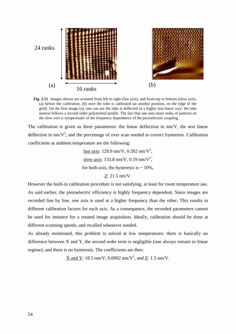
54
16 ranks
24 ranks
(a) (b)
Fig. 2.11 Images shown are scanned from left to right (fast axis), and from top to bottom (slow axis). (a) before the calibration. (b) once the tube is calibrated (at another position, on the edge of the grid). On the first image (a), one can see the tube is deflected in a highly non linear way: the tube motion follows a second order polynomial profile. The fact that one sees more ranks of patterns on the slow axis is symptomatic of the frequency dependence of the piezoelectric coupling.
The calibration is given as three parameters: the linear deflection in nm/V, the non linear
deflection in nm/V2, and the percentage of over scan needed to correct hysteresis. Calibration
coefficients at ambient temperature are the following:
fast axis: 129.9 nm/V, 0.392 nm/V2,
slow axis: 133.8 nm/V, 0.19 nm/V2,
for both axis, the hysteresis is ~ 10%,
Z: 21.5 nm/V.
However the built-in calibration procedure is not satisfying, at least for room temperature use.
As said earlier, the piezoelectric efficiency is highly frequency dependent. Since images are
recorded line by line, one axis is used at a higher frequency than the other. This results in
different calibration factors for each axis. As a consequence, the recorded parameters cannot
be used for instance for a rotated image acquisition. Ideally, calibration should be done at
different scanning speeds, and recalled whenever needed.
As already mentioned, this problem is solved at low temperatures: there is basically no
difference between X and Y, the second order term is negligible (one always remain in linear
regime), and there is no hysteresis. The coefficients are then:
X and Y: 18.5 nm/V, 0.0002 nm/V2, and Z: 1.5 nm/V.

55
2.3 Coarse positioning and indexing
The coarse positioning system of the tip relative to the sample, briefly mentioned previously,
is now explained in more details.
2.3.1 Design & principle
Each axis of the coarse positioning system is independent, and they are all similar. A given
axis is schematically figured in Fig. 2.12. It is composed of a fixed part comporting a
V-shaped groove, on the side of which are glued four shear mode piezo stacks. A mobile
V-shaped part comes resting on these four stands, and slides along the groove. The contact
surfaces are alumina plates (not shown on Fig. 2.12); one is glued on top of the piezo stacks,
and the other one onto the moving part. For the X and Y axes, the fixed and moving parts are
maintained in contact by gravity, whereas for the Z axis, the sliding part is gently pressed onto
the piezo stacks by soft, adjustable springs.
2.3.1.1 Stick-slip motion
The shear mode piezo stack generates the motion along one axis using the stick-slip
mechanism [44] described in Fig. 2.12: during a slow voltage ramp, the deformation of the
piezo stacks drives the mobile part by static friction between the alumina plates. Then, in a
very fast reverse voltage ramp, the piezo stacks are returned to their original position. During
this fast motion, the friction force is not enough to overcome the inertia of the moving part
which will essentially remain in place.
Electrically, this is equivalent to slowly charging the capacitance of the piezo stacks, and
subsequently discharging it as fast as permitted by the driving circuit.
By repeating these cycles, arbitrary large displacement can be performed, limited only by the
mechanical constraints (i.e. size of the moving parts…). In our design the accessible range is
about 10 mm for both X and Y axes and 5 mm for the Z axis, which is comfortably large for
the kind of samples we want to measure. We can even imagine putting two samples side by
side in the microscope so that they are measured in the same cooling cycle.
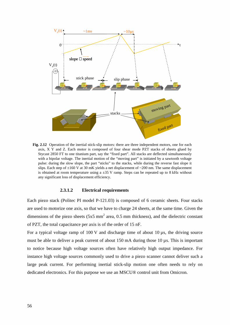
56
Vx(t)
t0
~10µs~1ms
slip phase
slope∝ speedslope∝ speed
stick phase
Vx(t)
fixed part
moving part
stacks
Fig. 2.12 Operation of the inertial stick-slip motors: there are three independent motors, one for each axis, X Y and Z. Each motor is composed of four shear mode PZT stacks of sheets glued by Stycast 2850 FT to one titanium part, say the “fixed part”. All stacks are deflected simultaneously with a bipolar voltage. The inertial motion of the “moving part” is initiated by a sawtooth voltage pulse: during the slow slope, the part “sticks” to the stacks, while during the reverse fast slope it slips. Each step of ±160 V at 30 mK yields a net displacement of ~200 nm. The same displacement is obtained at room temperature using a ±35 V ramp. Steps can be repeated up to 8 kHz without any significant loss of displacement efficiency.
2.3.1.2 Electrical requirements
Each piezo stack (Politec PI model P-121.03) is composed of 6 ceramic sheets. Four stacks
are used to motorize one axis, so that we have to charge 24 sheets, at the same time. Given the
dimensions of the piezo sheets (5x5 mm2 area, 0.5 mm thickness), and the dielectric constant
of PZT, the total capacitance per axis is of the order of 15 nF.
For a typical voltage ramp of 100 V and discharge time of about 10 µs, the driving source
must be able to deliver a peak current of about 150 mA during those 10 µs. This is important
to notice because high voltage sources often have relatively high output impedance. For
instance high voltage sources commonly used to drive a piezo scanner cannot deliver such a
large peak current. For performing inertial stick-slip motion one often needs to rely on
dedicated electronics. For this purpose we use an MSCU® control unit from Omicron.

57
Another factor which can limit the discharging current of the piezo stacks is the resistance in
the wires and filters connecting the room-temperature source to the microscope in the
refrigerator. In our case, the total wiring resistance for an axis, when the refrigerator is cold, is
of the order of 600 Ω, giving an RC time constant of 10 µS. Anyhow, I checked that the
efficiency of the motors at room temperature was not reduced by the introduction of a series
resistance: they work properly with a bias resistance up to more than 1.4 kΩ, without any
measurable reduction of the average step size.
2.3.1.3 Mechanical performance of the motors
The behaviour of such an inertial stick-slip motor highly depends on the static and dynamic
friction coefficients, which are hardly controlled. Thus, one has to find a trade -off between
two opposite behaviors: on one limit, friction is too low, and the object slips even during the
“stick phase”, which limits the maximum frequency the motors can be driven at. On the
opposite limit, friction is too high and the object sticks onto the ceramic during both
alternations. Between those two limits, lies a usable dynamic range which is found more or
less empirically.
The plates used are 0.254 mm -thick polished sintered alumina plates. Their typical roughness
is less than 80 nm RMS according to manufacturer. They are thick and rigid enough to remain
very flat during assembly. Furthermore this material is extremely tough so that it would not
wear when used repeatedly.
I found that the procedure chosen to assemble the constituting parts of a motor had a direct
impact on its behaviour. The best performance and reliability were obtained when all
elements were glued simultaneously to ensure that facing alumina plates are well resting one
onto another.
On the other hand, one may fear that very flat plates perfectly facing each other may stick to
each other upon cooling down, because of the freezing of adsorbed water on the surfaces.
We found that the “inertial stick-slip” motion works reliably at low temperature, even without
special cleaning, or using any dry lubricant onto the alumina plates. This was a rather good
surprise, since such actuators are notoriously tricky to operate at low temperature: they tend to
stay blocked, or to operate erratically.
In practice, the good performance of the motors can be degraded by its surroundings. In
particular, one must take care that all the wiring connecting the microscope, and the copper
braids for thermalization, do not limit or hamper the displacements.

58
2.3.1.4 Inertial vs. non-inertial stick-slip motion
In the driving mode we use, all four piezo stacks are driven at the same time and require a
single driving line.
Several other implementations of stick-slip actuators in SPM rely on controlling individually
each piezo stack [45], so that only one stack is sliding at a time. Of course such approach
requires a more complex wiring and control process.
An intermediate approach, keeping a simple wiring, consists in dephasing the signal arriving
on each stack, by making an RC cascade at low temperature [46]. In this latter approach,
however, extra Joule power is dissipated at low temperature compared to our implementation.
2.3.2 Position indexing
When the microscope is operated at low temperature, we have no optical means to know
whether the motors are moving properly, or to control their actual position. Because of their
intrinsic irreproducibility, it is highly desirable to control that the motors move properly and
even better to measure their position with sufficient accuracy to enable fast navigation on the
samples. I now describe how such a position measurement is performed in our microscope.
2.3.2.1 Design
The benefit brought by a position indexing system should not be outweighed by a too large
extra complexity in the setup. In particular, the mechanical assembly must be handy because
the microscope should be easily mounted and dismounted, for instance to change the sample.
Furthermore, the operation of the position indexing system must also be compatible with the
low temperature environment and should be simple. These conditions forbid for instance the
use of an optical interferometer.
We met these requirements with a rather simple solution, by incorporating a variable
capacitor to each of the stick-slip actuators. These are planar variable capacitors consisting in
gold electrodes deposited on the back side of the facing alumina plates sliding one onto
another. The alumina plates therefore constitute the dielectric insulator of the capacitor.
The gold electrodes are 12 mm-long, 6.5 mm-wide rectangles on one side, and 12x8 mm on
the other side. Neglecting edge effects, the maximum capacitance (when the electrodes fully
face each other) is
0max 13.5pF
2≈ =rε εWL
Ct
,

59
where W and L are the length and width of the electrodes, 0.254mm=t the thickness of one
alumina plate, and 9.9=rε the dielectric constant of alumina.
2.3.2.2 Resolution and accuracy of the capacitive position sensors
To be useful, this position measurement should have a resolution at least equal to the range of
the scanner, which is 8 µm in our case. Thus, the resolution of the variable X and Y
capacitances measurement should be better than ( ) 4max max8µm /12mm 6x10 8 fF−≈ ≈C C .
These rather small capacitance values can still be easily measured using standard impedance
bridges (so-called RLC meters).
In practice, however, measuring such capacitances requires some care, since the wiring
capacitance presents a stray capacitance much larger than Cmax, in parallel with the variable
capacitor. This would then necessitate a much higher resolution in the capacitance
measurements. In our setup, cross-talk in the electrical lines connecting the variable
capacitors to the C-meter were carefully considered and minimized by running the cables in
different shields.
To circumvent the problem associated with measuring small capacitances, one can think of
making capacitors with much smaller dielectric thickness. Actually, we deliberately chose to
go the other way because it improves the accuracy of the position measurement, as I will now
explain. In fact, in these variable planar capacitors, one has to worry about the thin air gap
(vacuum gap at low temperature) between the two alumina plates. The gap thickness depends
both on the roughness of the plates and on the mounting of the alumina plates. To be more
explicit, in an imperfect setup, a displacement along the axis of the actuator is accompanied
by another uncontrolled motion in the perpendicular direction. This changes the average air
gap and the value of the capacitance by an amount not related to the actual displacement of
the actuator we want to measure. Ideally, the design and the mounting of the system should be
such that these parasitic capacitance changes are negligible.

60
Au
Au
0
tt+e
2t+e
z
Al 2O3
Al 2O3
vacuum
Fig. 2.13 Schematics of the 3-layer capacitance composed by two counterpart alumina plates and a gap of air in between.
Taking into account an average thickness e of the air gap, the effective capacitance of the
planar capacitor is:
10
2( )−= +
r
tC εWL e
ε
If one assumes that e takes more or less random values with typical distribution width δe, the
relative change in the capacitance due to this randomness is:
d Log
d
C Ce
C e
δ δ=
Optimally, we should make this quantity smaller than the measurement resolution, so that it
does not affect our determination of the position. Since it is difficult to control the amplitude
δe, because it depends on how the system is assembled, it is safer to minimize e/t right from
the start.
It is this reasoning which led us to put the electrodes on the back side of these rather thick
alumina plates. And this is why we are bound to measuring small capacitance values with the
associated aforementioned difficulties.
2.3.2.3 Practical implementation
To increase the signal of interest on X and Y axis, we measure two capacitance elements, by
tooling two neighbouring stacks up with gold plated alumina. The facing alumina plate, glued
on the opposite titanium part, has thus two electrodes patterned on it (see Fig. 2.14). Care
must be taken to assemble the setup so that the electrodes face each other correctly.
To mount these capacitances in the microscope, first of all, the two piezo stacks are glued
with Stycast® 2850 FT to their respective alumina plates. Then, all the three alumina plates
are glued together with correct spacing using a glue which is soluble in acetone. This insures

61
both planarity of the contact between the plates, and correct lateral positioning of the two
small plates. After that, all the alumina plates are glued simultaneously onto their respective
titanium parts. The removable glue is subsequently dissolved when the Stycast is set.
This procedure ensures as well that potential non planarity or misfit between the titanium
parts is corrected.
In order to avoid measuring capacitance between the diagonally opposed electrodes, we set
them at the same potential, and measure the sum of capacitance thus given. Fig. 2.14 shows
how the motors are installed on one axis X or Y.
Ti
Au
PZTStycast 2850 FT
X , Y
Al 2O3
Fig. 2.14 Installation of the piezo stacks and of the gold plated alumina plates, and wiring of the capacitances. The schematic picture presented her stands for X and Y axis.
Al 2O3
Ti
Au
PZTStycast 2850 FT
Z
Z1 Z2
Fig. 2.15 Same installation as in Fig. 2.14 for the Z axis. The two piezo stacks are linked by the same alumina plate for reasons detailed in the text.
For X and Y axis indexing we have rectangular gold electrodes, which provide a linear
variation as a function of displacement. For the Z motor, precision on position is not needed
but instead, since the approach procedure involves small steps, we ideally need more
sensitivity to displacements. Indeed, during the tip approach sequence, we typically perform

62
displacements of 500 nm at a time, roughly equal to the maximal extension of the tube
(600 nm), and it would be convenient to resolve these steps.
By using fingered capacitances as pictured in Fig. 2.15, instead of rectangles we tried to
increase sensitivity. In this configuration, the capacitance variation is sinusoidal, instead of
linear, and the absolute position is not known, unless periods are counted from the beginning
of the course.
At first glance, the derivative of capacitance with respect to displacement is higher because
one adds the signal from all fingers (increasing or decreasing at the same time). However, the
edge effect limits the actual advantage of having a large number of parallel eletrodes, and one
has to find a compromise: given the thickness of the plates, the optimum period (giving
maximum contrast, together with fast enough oscillations) is 1.5 mm.
In order to keep the same sensitivity on the whole period, we use two series of fingers, shifted
by a quarter of a period. We read alternatively from one or the other quadrature. Two
capacitances are thus measured on the Z axis.
These quadrature signals are summed with respectively X and Y signals, so that we only need
3 wires in all for capacitance measurements: one for X+Z1, one for Y+Z2, and one common
wire. The first two are wired individually in coaxial lines, whereas the third one is part of a
multi-wire line (see chapter 3).
Alumina plates were bought from Reinhard Microtech GmBh, already plated with a few
nanometers of a tungsten/titanium adhesion layer and with 5µm of gold. Electrodes are
patterned by optical lithography, and wet chemical etching. Gold is etched in a warm (30°C)
KI+I 2 agitated solution (in ~1 hour, no sonication), and W / Ti is etched in a H2O2 solution.
2.3.2.4 Testing actuators and sensors.
The RCL meter used for capacitance measurements (LCR819 from INSTEK) displays a 5-
digit value and is specified for 20 fF maximal precision when measuring a typical 40 pF
capacitance at 20 kHz during 1 s. For a 3 s long measurement of our variable capacitance at a
fixed position, we obtain a typical accuracy of 5 fF (~5 µm) that sets the position resolution.
Given that, we could check the motors behaviour and calibrate the variations of the
capacitance for a given displacement of the motors, at room temperature.
We present in Fig. 2.16 a record of the capacitance as a function of the number of steps
performed, on both X and Y axis, on the whole range of displacement (i.e. 12 mm), and on Z
axis in a shorter range.

63
This test was performed starting from one extremity of the course of X and Y motors,
applying a given number of voltage ramps of 70 V amplitude at 200 Hz, and measuring
capacitance variations after each series of pulses.
Doing this, we cannot distinguish between two separate behaviours: the true variation of the
capacitance with actual displacement, and the true displacement of the motors. The first is
assumed perfectly linear, at least far from the edges, whereas the second is less predictable.
We attribute the deviations from linear behaviour to bad functioning of the motors, except at
the start and end points.
A check of the capacitance variations alone should consist in measuring separately the actual
displacement with an interferometer for instance.
Au
Au
Al2O3
Al2O3
vacuum
Au
Au
Al2O3
Al2O3
vacuum
0 10000 20000 30000 40000 500000
2
4
6
8
10
12
14
16
18
Y c
apac
itanc
e (p
F)
# of steps
CY measure
linear fit
0 5000 10000 15000 20000 25000 30000 35000-0.6
-0.4
-0.2
0.0
0.2
0.4
0.6
Z c
apac
itanc
e (p
F)
# of steps
CZ1
CZ2
0 10000 20000 30000 40000 50000 60000 700000
2
4
6
8
10
12
14
16
18
20
22
X c
apac
itanc
e (p
F)
# of steps
CX measure
linear fit
edge effect
Fig. 2.16 Measurement at room temperature of the capacitances of the three axes when moving the motors by applying voltage ramps of 70 V amplitude at 200 Hz. On the whole travel length, which is 12 mm, the X and Y axis respond quasi linearly. At starting and ending points, when the electrodes do not cover each other, one observes edge effect. A linear fit of the central part allows to calibrate the capacitances at room temperature, assuming the linear range is 12 mm. The Z1 and Z2 signals are plotted on the right bottom side: a constant value has been subtracted to plot their variations around zero. The procedure has been done in both directions (up and down) and the curves are similar, except of course that the efficiency is lower by ~20% in the upwards direction.

64
The linear fits of the X and Y motors give a value of 2 fF/µm, nominal variation being
2.25 fF/µm. The Z axis capacitance has a maximal variation of 2.5 fF/µm. This value should
be increased, for instance by using thinner and/or wider plates, because the current setup has
proven not fully satisfactory. Indeed, the achieved resolution is a factor 4 to 5 higher than the
small approach steps.
This X,Y calibration was used at low temperature to position the tip over the sample,
assuming constant dielectric and mechanical parameters of alumina upon cooling down.
Until now the motors have proven to work reliably at low temperature, by never being
blocked for instance, and with relatively good reproducibility (though less than at room
temperature). The well-behaved quasi-linear responses at room temperature, as well as the
overall good functioning at low temperature validate our design of the microscope and the
procedure for the assembly of the motors.

65
2.4 The atomic force sensor
Binnig and co-workers implemented the first atomic force microscope in 1986 [47] in order to
measure forces as small as 10-18 N, with in mind applications in the field of nanotribology.
They revisited the concept of the stylus profilometer (one could also evocate the phonograph),
scaling it down to access inter-atomic interactions. They wanted to go beyond the native
limitation of the STM, invented 5 years earlier (see chapter 1), which does not allow to probe
a non-conducting material. In their original design, a soft lever to which was attached a sharp
tip was probing the surface, and an STM was used to monitor the deflexion of the lever.
Since 1986, Atomic force microscopy has been developed in various domains. This field has
brought great progress in surface science by allowing to access surface properties down to the
atomic scale, involving various forces such as electrostatic, magnetic forces, force
spectroscopy, tribology, etc. AFM has even been used as a lithography tool to manipulate and
pattern nanostructures, and massively parallelized integrated AFMs were proposed as scheme
to make read/write memory devices [48].
An atomic force microscope probe sensor is generically constituted of a lever to which is
attached a tip. When approaching the tip from a surface, the short range forces affect the
whole sensor, changing the lever static and dynamic properties. Surface imaging is done by
scanning the tip above the sample and monitoring an appropriate sensor variable, such as its
static deflexion or the amplitude of a resonant mode. In most cases, the dynamic range of the
AFM is increased by implementing a feed-back mechanism which maintains the measured
variable at a constant set point while scanning.
There are several ways of acquiring topographic images:
• Maintaining the tip in close contact with the surface all the time. This is
the “contact mode”, in which one detects the lever static deflection. In this
mode, however, the tip generally wears quite rapidly, and there is a
possibility that what is observed on the sample is due to the action of the
tip.
Other modes are dynamic, with the tip performing an oscillatory motion. Dynamic AFM
experiments are done by exciting the lever in a resonant mode. When the tip interacts with the
surface, the lever resonance is modified. The dynamic modes file in two categories:

66
• The tapping mode where the tip "hits" the surface at every point of the
image. This mode yields the highest resolution, and much reduces the
problem of surface and tip deterioration with respect to contact mode.
• The non-contact mode where the tip remains in the attractive field of the
surface, and never reaches the repulsive part. The lateral resolution is
degraded due to a larger tip-sample distance, but this allows a larger
imaging speed.
2.4.1 implementing AFM sensors at low temperature
Among the many possible force detection methods, we need one suitable for operation in a
dilution refrigerator. Despite their widespread development, atomic force microscopes have
not been easily adapted to cryogeny, because of the difficulties to fit the force sensors to
cryogenic environments.
2.4.1.1 Optical sensors
Indeed, the standard method used in commercial AFMs consists in measuring the deflection
of the lever with a laser beam focused on its end (see Fig. 2.17), and reflected towards a
4 quadrants diode. In this approach, both the laser and the detector use semi -conductors
which do not function at low temperatures since their charge carriers are frozen. It is still
possible to use this technique in a low temperature AFM, by deporting the laser and diode
outside of the fridge and using an optical fiber [49] to bring in and out the laser signal. Such a
setup was successfully operated at 4K [50] and down to 20 mK [51]. Others have modified
the photodiodes to work under vacuum and low temperatures [52], though not at temperatures
below 4K. However the optical alignment remains a delicate issue in those setups, especially
because differential thermal contractions of the materials employed cause spurious
displacements of the laser beam upon cooling.

67
Fig. 2.17 Illustration of standard AFM deflection measurement. A laser beam is reflected on the end of the lever towards a 4 quadrants diode which measures the deflection of the lever either statically or dynamically.
Moreover, when operating at dilution fridge temperatures, the cooling power is very limited
(of the order of 40 µW at 100 mK in our case), and the laser itself (with typical power in the
mW range) would likely bring too much heat load to the fridge.
Finally, in low temperature experiments, the laser photons have energies much larger than that
of thermal fluctuations and could cause unwanted excitations in the sample.
2.4.1.2 Electrical sensors
Given the above problems associated with optical detection, one quite naturally thinks of
electrical detection.
Indeed, the use of piezoelectric and piezoresistive materials for local probe sensors was
introduced just a couple of years after Binnig's original AFM publication. Those materials
overcome the problems described above for low temperature experiments.
First came the piezoelectric quartz tuning fork ( [53]) and then piezoresistive cantilevers
([54, 55, 56]). In the latter, a deformation is converted into a resistance variation, which, with
suitable design and operating conditions, can lead to detectable deflections as low as 0.01 nm.
However, given the intrinsic sensitivity and noise of these sensors, such performance with a
reasonable bandwidth requires operating the sensor at large bias voltage, with a dissipated
power in the mW range, which again is not suitable for very low temperature.
Thus, upon examination, the only remaining option for very low temperature AFM is the use
of piezoelectric devices. In these devices, one naturally obtains low dissipation
electromechanical oscillators, which are very simple to integrate in an electric circuit and to
operate in a dilution refrigerator.

68
Compared to optical and piezoresistive cantilevers, these sensors are only operated in
dynamic mode. On the other hand, for this dynamic mode, piezoelectric sensors incorporate
their own dithering actuator “for free”, whereas the other types of sensors require a separate
device to excite the resonator (a device which, ironically, is usually a piezoelectric element).
Hence, regarding their implementation, piezoelectric sensors are the simplest possible AFM
sensors.
In our microscope, the AFM sensor is a piezoelectric tuning fork which is intrinsically a
high -Q resonator. This high -Q provides high sensitivity, which allows very low excitation
amplitudes (of less than 1 nm), with a minute dissipated power (~ pW).
2.4.2 Quartz Tuning Fork (TF)
The tuning fork was invented in 1711 by a trumpeter named John Shore, to ease tuning
trumpets correctly. It is made of two parallel beams linked together by a common base (see
Fig. 2.18 and Fig. 2.24).
2.4.2.1 A high Q harmonic oscillator
The tuning fork is a harmonic oscillator with inherent high quality factor. The main resonant
mode of the tuning fork is a symmetric mode with respect to the symmetry planes of the
device (see Fig. 2.19).
This symmetric resonance is commonly used to provide the correct tune to musicians. The use
of this peculiar fork shape instead of a single beam with the same resonant frequency is easy
to understand: in the symmetric resonant mode, the motion of the arms is totally decoupled
from the motion of the center of mass, and the frequency and the quality factor are then
independent of the holder, but only depend on the damping within the material and
surrounding air. By choosing stiff materials with low loss, the tone is accurate, lasts long and
enables the musician to tune with a single bow on the tuning fork.
2.4.2.2 Tuning forks for atomic force microscopes
The first implementation of quartz tuning forks in local probe microscope was in a Scanning
Near-field Acoustic Microscopy (SNAM) experiment by Günther et al. and dates back to
1988 ( [53]). The growing use of tuning forks in different branches of local probe microscopy
was initiated by the need to suppress light from laser-based detection and to ease experimental
setups. Karrai and Grober for example expanded its use to Scanning Near-field Optical
Microscopy (SNOM) in 1995 [57].

69
A
A’
P
P(a)(b)
A
A’
Fig. 2.18 (a) Photograph of a piezoelectric quartz tuning fork used in our AFM microscope. Gold electrodes are deposited on top of the quartz, in a special shape designed to excite selectively the symmetric mode (i.e. both arms move in phase opposition). (b) Schematic of a cross section A-A’ of the tuning fork, showing the connections of the electrodes. P is the intrinsic polarization of the piezoelectric quartz. The dotted lines represent the field lines.
contraction
e x t e n s i o n
e x t e n s i o n
contraction
PP
PP
A
A’ A’
A
Fig. 2.19 The motion of the prongs can be explained as follows: when a potential difference is applied to the electrodes, opposite charges appear on facing electrodes, so that the arms deflect in opposite directions. To be more specific, when for instance polarization is opposite to electric field, dipoles experience a vertical contraction, and due to volume conservation, perpendicular directions experience a dilatation (see § 2.2.2.3.c). Moreover, if the upper region of the cross section experiences an extension, the lower part will experience a contraction since the electric field reverses in the arm, as depicted by the field lines. These stresses lead to a bending of the arm. The other arm being connected the opposite way simultaneously bends the opposite direction, yielding a symmetric motion.

70
The Tuning Forks (TFs) used in AFM are standard parts mass-produced by the clockwork
industry. They are made of monocrystalline piezoelectric quartz, a material with high stiffness
and low loss. They are engineered [58] so that the symmetric mode frequency is accurately
32768 Hz (215 Hz), designed to provide the 1 s time base of low power electric circuits
(wristwatches for example) upon division by a simple shift register. Engineering also
optimizes the stability of oscillation parameters versus temperature(1), and the balance of the
fork's arms (generally involving post-fabrication laser trimming).
To fabricate TFs, a quartz monocrystal is cut such that polarization is nearly1 aligned along
the arms’ thickness (see Fig. 2.18), and metallic electrodes are deposited on the arms in a way
that only the symmetric mode can be electrically excited (see Fig. 2.18). Conversely, when a
motion of the arms is initiated by an external force, only its symmetric part will be detected
via the electrodes.
As fabricated, forks are sealed in a small can under rarefied atmosphere, so that their Q is
typically 105 at room temperature. We have to remove this case for our application. We do
this manually on a lathe, and we end with a bare tuning fork as shown in Fig. 2.18. We
subsequently glue the fork on a stand, connect it, and then glue a tip on the end of the lower
arm, as shown on Fig. 2.20.
1 The so-called +5° X cut of the quartz crystal, in which polarization is tilted by 5° off the plane, is purposely
chosen to cancel at first order the temperature dependence of the resonance frequency of the fork at room
temperature.

71
Fig. 2.20 Tuning fork fully mounted, hold at the end of the piezoelectric tube. The base of the tuning fork is glued onto the support, and the support itself is glued to the tube using GE varnish. The tip and the wire are glued with conductive silver epoxy Epotek H20E from Polytec PI. Both arms of the fork are free to move. Note the tuning fork is hold in a way that the tip is roughly aligned with the axis of the tube.
In our setup, we chose to connect the tip to the tunnel current amplifier through an additional
wire, like in Refs.[59, 60]. It would have been possible instead (and indeed much easier) to
connect the tip to one of the electrodes of the tuning fork.
This brings benefits and raises issues:
• The tunneling current can be measured independently of the piezo current.
This enables, to perform simultaneously STM and AFM measurements, at
least in principle. If this separation is not done, tunneling current and piezo
current mix and controlling the system becomes harder.
• This wire adds mass on one of the fork's arms. Doing so, it seems we
unbalance the tuning fork more than if we only mount a tip. However, as
we will see below, the wire also brings stiffness, which gives the
opportunity to better preserve the fork's balance.
2.4.2.3 Oscillating modes of the tuning fork
A finite element modeling (FEM) performed on the geometry of our forks yields their
eigenmodes of oscillation. Next figure shows the first six resonant modes, along with their
frequencies. Out of these modes, only one (the symmetric mode, labeled 4) does not induce
force or torque on the support. It will hence have the highest quality factor.

72
By design, the geometry of the electrodes patterned on the tuning fork is such that for all
modes except the symmetric mode (4), the electrical signal cancels. Thus, electrically, one can
only induce and detect this mode.
11.7 kHz 13.4 kHz
19.0 kHz 32.7 kHz
66.7 kHz 88.2 kHz
(1) (2)
(3) (4)
(5) (6)
Fig. 2.21 First six resonant modes of the tuning fork. The frequencies are obtained by a finite element modeling. In these simulations the circumference of the cap is fixed. The three in-plane modes (2-4-6) can be described in a 3-Degrees of Freedom (DOF) oscillator model with three masses and three springs (see § 2.4.2.6).
2.4.2.4 Basic analysis of a tuning fork: 1 Degree-of-Freedom
harmonic oscillator model.
Let's first assume for the time being that the tuning fork can be described as a mechanical
harmonic oscillator with a single degree-of-freedom (DOF). This corresponds to practical
cases where the tuning fork is mounted as indicated in Fig. 2.22, in which only a single beam
of the fork moves. While it does not correspond to our setup, it has been actually used in some
experiments (see e.g. [61]).

73
L
tρw
Fig. 2.22 An equivalent to the harmonic oscillator model with one DOF is represented here where the tuning fork is attached by one arm to ground. This yields the same result as a single beam attached at one end. Theory of elastic beams provides the correspondence between the geometrical parameters of the beam and the effective mass and spring constant of the corresponding 1-DOF model.
Even when the two arms are free to move, in the symmetric mode, the motion of one beam
can be approximated by the mode of a fixed-free beam, neglecting the deformation in the base
of the tuning fork.
We will thus first assume we can describe the tuning fork as such as single degree-of-freedom
(1-DOF) harmonic oscillator. This, simple picture allows to obtain a good initial
understanding of how the force sensor works.
2.4.2.4.b Mechanical analysis
In this framework, one can use the results from the theory of elasticity, to obtain the
characteristics of the oscillator from the dimensions of the beams and quartz properties [62].
In this case, for a homogeneous parallelepiped, one can predict the stiffness of the beam as
measured from its free extremity:
3
34= Yt w
kL
and the frequency of the resonant modes:
2
212= i
i
t xYω
ρ L
where ρ is the volumic mass and Y the Young modulus of the material, L, w and t are
respectively the beam length, width and thickness, and xi the roots of Cosh Cos 1x x = − :
1.8751, 4.69409, 7.85476, 10.9955, ...∈ ix

74
The mode of interest to us is the first one. Note that these formula only approximately predict
the properties of a tuning fork, as many details are not taken into account in this simple
modeling: the anchoring of the beam is not absolutely fixed in an actual tuning fork (the base
also deforms), the electrodes are not taken into account, and, finally, elastic properties of
quartz are not fully isotropic.
As seen from its free extremity, when considering only the fundamental mode1, such a beam
can be modeled as a simple 1-DOF mass and spring system, with the above calculated spring
stiffness and an effective mass 21=effm k ω . This model is depicted in Fig. 2.23. Our forks
have the following specifications: the arms are 2.4 mm long, 214 µm thick and 130 µm wide.
Therefore, their spring constant is 1800 N/m∼k (see Table. 2.4 for young modulus of
quartz), and the effective mass is 43 µg≈effm , to be compared to the weight of one arm
178 µg≈armm .
2.4.2.4.c Tip-sample interaction
We now come to the point of analyzing how the tip-sample interaction modifies the fork's
resonance, within the above 1-DOF model. We also take into account the piezoelectric
coupling and further assume that the oscillator is driven by a low impedance source, so that
voltage is imposed from the outside. Proportionality between position and charge mentioned
in § 2.2.1.2, allows for two equivalent representations of the resonator: one mechanical, and
one electrical. These representations are depicted in Fig. 2.23, and correspondences among
parameters in both languages are given in Table. 2.3. In the absence of tip-sample interaction,
the bare resonance pulsation is 1 1k m LCω = = . When the oscillator is subject to both a
driving voltage and an interaction force, its dynamics obeys the mechanical equation:
( )0 int 0 drive( )mz gz z z k F z z aU+ + + = + +ɺɺ ɺ ( 2.2)
where only viscous damping force is assumed with coefficient γ, Udrive is the driving voltage,
α the piezo coupling constant, ( )intF z the interaction force with the sample, z0 the equilibrium
position of the oscillator (i.e. the mean distance between tip and surface), and z the deviation
thereof. For small oscillation amplitude, Fint can be expanded about z0,
( ) ( ) ( )intint 0 int 0 0
FF z z F z z z
z
∂+ = +∂
1 The electrodes excite and detect only this fundamental mode, and the next bending mode is at a frequency ~6.3
time higher than the fundamental.

75
which shows that the gradient of the interaction force can be treated as an additional spring
constant ( )intint 0
Fk z
z
∂= −∂
. Hence the modified resonance pulsation is
int1
k kω
m
+=ɶ
If we assume the interaction only weakly changes the bare resonance frequency, the shift of
the resonance frequency is, at first order:
int1
1
∆
2
kω
ω k= ( 2.3)
(b)
1
0
0
1ω
Z
Z
L
L
C
RQ
C
= =
=
C0C0
C
R
L
~
I
U drive
(a)
k
m
sample surface
kint(z0)
z0
zγ
γ int
~
Fdrive
1
0
0
=
= =
meca
meca
ω
Z
Z
γQ
k
m
km
int1 1 1
2
kω ω
k = +
ɶ
interaction:
int int
int int
1 /c k
r γ
↔↔
cint
r int
Fig. 2.23 Tuning fork as an electro-mechanical oscillator (a) Schematics of the mechanical oscillator model derived in section 2.4.2.4.c (b) Schematics of the electrical model of a quartz tuning fork. As stressed in § 2.2.1.2 mechanical and electrical parameters are rigidly coupled through the piezoelectric relations. Only C0 does not have any mechanical interpretation: it represents the stray capacitance between the electrodes (i.e. the electrical coupling between the leads outside the piezoelectric, e.g. through air…).
The frequency shift thus senses only the interaction force gradients; it is insensitive to
homogeneous field such as gravity, which only displaces the equilibrium point of the
oscillator.
In the actual measurements we perform, and more generally when using piezoelectric
resonators in electronic engineering, one does not measure the position of the oscillator, but
rather the current flowing through the resonator
( ) ( ) ( )I t q t z tα= =ɺ ɺ . ( 2.4)
For an harmonic drive Uω, it is more convenient to work in Fourier transform, for which
( )I ω obeys electrical counterpart of ( 2.2):

76
int
1IiL I RI U F
iC a+ + = +ωω
ω.
The electrical parameters of the resonator can be extracted by fitting the electrical resonance
line shape (see § 2.4.2.8.d p 87). From this and knowing the piezoelectric coupling coefficient
α, one can obtain all the mechanical parameters of the model, and in particular the amplitude
of the oscillation, which is important for AFM measurements. The piezoelectric coupling
coefficient α is most accurately obtained from an optical measurement of the resonance
[63, 64]. In the case of a single beam oscillator, Giessibl [61] also gave an analytical
expression for α, as a function of geometric parameters of the beam and of Y (Young
modulus) and d31 (piezoelectric coefficient).
Electrical Mechanical
parametertypical value
[4K-300K] parameter typical value
ratio
ElectricalMechanical
[unit]
Energy
correspondence
q (charge) z (position) α [C/m]
U Fd 1/α [V/N]
L 200 kH m 43 µg 2
1
α [NmA-2/kg ]
2 21 1mz lq
2 2≡ ɺɺ
kinetic
C 0.13 fF 1/k 5.5 10-4 mN-1 α2 [F / mN-1]
221 q
kz2 2c
≡
potential
R or Lω0/Q500 kΩ-
10 MΩγ or mω0/Q (200 µg/s) 2
1
α
2 2γz rq≡ ɺɺ
dissipation
Table. 2.3 Connection between electrical and mechanical models of the piezoelectric oscillator (see Fig. 2.22). The values correspond to beams found in most 32 kHz tuning forks. The typical magnitude of the coupling constant is 1.35µC/m≈α .
2.4.2.5 Discussion of the 1-DOF model
Implementing an AFM piezoelectric “force” measurement such as described above, where
one arm of the tuning fork is fixed, is simple and easy to understand, but is not ideal. In
particular, one looses the main benefit of using a tuning fork, namely that the oscillator is
decoupled from its support. On the contrary, the motion of the beam couples with the whole

77
structure of the microscope. In particular, when the tuning fork is mounted at the end of the
piezo scanning tube, as in our setup, the stiffness of the tube depends on its deflection and
extension, and thus changes while scanning an image. This change in stiffness induces a
spurious change in the resonance frequency of the resonator, not related to the tip-to sample
interaction, and appears as artifacts in the AFM image. It may also happen that the resonance
of the beam mixes with other modes of the structure1.
To avoid such problems, we considered it was important to keep as much as possible the
benefit of using a balanced resonator, naturally decoupled from its mechanical environment.
In our setup, the tuning fork is held by its base, with its two arms free. In this case, however,
the above 1-DOF model is not sufficient to establish the link between the frequency shift and
the tip-sample interaction. There is actually a factor ½ missing in relation ( 2.3) due to the fact
there are 2 prongs instead of the one considered above (see below). Furthermore, as we
necessarily break the built-in symmetry of the TF by gluing onto it the tip and its connecting
wire, we need to understand how this changes its behavior. In particular we need to address
the following questions:
- By which amount does this symmetry breaking couple the symmetric mode of the bare TF to
its other modes?
-What is the oscillation amplitude of the tip in an asymmetric TF, and what is the link
between the current flowing in the TF and the tip amplitude?
Such questions have not been investigated in depth in the past. The asymmetry was discussed
in Ref [65] and [59], which describe the fork as two oscillating beams coupled by a spring.
This analysis is however insufficient to answer all the above questions.
To address these issues, I present in the following a more complete model of the TF.
2.4.2.6 Model of a tuning fork as three coupled masses and springs
In the following we describe a simplified model developed during this thesis. In this model,
the tuning fork as 3 masses coupled to each other and to ground by the means of 3 springs,
each mass having only one degree of freedom (see Fig. 2.24). In this description, a central
mass representing the base of the TF is coupled to the support through a spring k0. In the ideal
1 Standard AFM cantilevers should in principle have the same problems. However, their effective mass is about
1000 times lower than a tuning fork beam, so they comparatively couple much less to the rest of the structure.
Also their Q factor is smaller which further reduces the visibility of such effects.

78
symmetric case, this central mass would be at rest, and the TF would be decoupled from its
support, as expected. However, when symmetry is broken, this central part has a finite motion
and excites the rest of the microscope structure. This 3-DOF model allows to describe the first
three in-plane modes of the TF (modes n°2, 4 and 6 pictured in Fig. 2.21), and how they are
modified, when symmetry is broken.
It is important to stress that, in our model, all the resonant modes of the connecting wire and
the tip are not described, hence they are modelled as a 1DOF oscillator, rigidly linked to the
fork.
(a) (b)
kk
k0
kk
z0
z1
z-1
δkδkδk
supportsupport
Sample
tip
connectingwire
tuning fork
m0
m
m δm
Fig. 2.24 (a) Schematics of a quartz tuning fork, with tip and wire for tunneling current. (b) Equivalent mechanical 3 DOF model. Both arms of the fork have the same effective mass m and spring constant k. The mass m0 is the effective mass of the TF’s base, and k0 is the stiffness of its link of the fork to the support. The symmetry of the tuning fork is broken by the extra mass δm and extra stiffness δk due to the tip, wire and interaction with the surface.
2.4.2.6.b Free dynamics of the 3-DOF model
We can find the modes of the structure by solving the coupled equations of motion for the free
dynamics of the three masses in a harmonic analysis. These equations can be conveniently
written in a matrix form:
2. .K Z M Zω= , ( 2.5)
where ω is the pulsation of the mode,
1
0
1
z
Z z
z
− =

79
is the position vector of the three masses,
0
0
2
0
− = − + − − +
k k
K k k k k
k k δk
is the stiffness matrix coupling the displacements of the 3 masses, and
0
0 0
0 0
0 0
m
M m
m mδ
= +
is the diagonal matrix of effective masses. Equation ( 2.5) can be conveniently written as
2.Z ZωΩ = ,
where
1 0
0 0 0
0
2
0
k k
m mk kk k
M Km m m
k k k
m m m m
δδ δ
−
−
+ Ω = = − −
+ − + +
.
The modes of the structure are the eigenvectors of Ω, and the resonant frequencies are the
corresponding eigenvalues. Introducing the notations
1
k
mω = the pulsation of the unperturbed symmetric mode (or of an isolated arm),
0k
kγ = the ratio of stiffnesses in the tuning fork model,
0
m
mβ = the ratio of effective masses in the tuning fork,
m
m
δµ = the relative change of mass of the lower arm, and
k
k
δκ = the relative change of stiffness for the lower arm,
the matrix Ω reads:
21
1 1 0
(2 )
1 10
1 1
ω β β γ βκ
µ µ
−
Ω = − + − + − + +
.

80
2.4.2.6.c Balanced tuning fork: the unperturbed modes
Assuming first 0µ κ= = , one recovers the symmetric tuning fork. The eigenvectors then
have the following components:
1 1
2 2 1
3 3 1
1
0 ,
1
1
1 ,
1
1
1 ,
1
= −
= − + = −
= − − = +
Z with frequencyω
Z x y with frequencyω ω x y
Z x y with frequencyω ω x y
where ( )1 12 21= + +x β γ and 2= −y x βγ . These eigenmodes can be respectively identified
with modes 4, 2 and 6 of Fig. 2.21. If the frequencies of these modes are known from
experiment or from finite element calculations, one can deduce β and γ, and finally extract all
the values of our 3-DOF model, up to a global scaling factor. Fixing this global factor requires
one more input value which can be, for instance, a static measurement (or Finite Element
Model (FEM) calculation, or beam theory result) of the stiffness of an arm. For example, for
the tuning fork we use, the ratios between resonance modes shown in Fig. 2.21 obtained from
FEM yield β = 2.61, γ = 0.468, and k = 1800 N/m, completely determining the 3-DOF model.
2.4.2.6.d Broken symmetry: a perturbative analysis
In the case of interest to us where the symmetry of the tuning fork is broken by the presence
of the tip, general analytical results can still be obtained with the above method.
Unfortunately these analytical results involve general roots of a third degree polynomial and
are so inconvenient to write and use, that, in practice, it is more efficient to perform numerical
diagonalization.
The questions we want to address, however, do not require the knowledge of the general
solution of the asymmetric case: we are only interested in weak asymmetry of the fork, and
hence a perturbative approach at the lowest order in µ and κ is sufficient.
Performing Taylor expansions on the general analytical solution to obtain the perturbative
results is also impractical, because the general cubic roots prevent simplifying the
expressions. Hence, we apply directly the perturbation theory, that relies only on the linearity
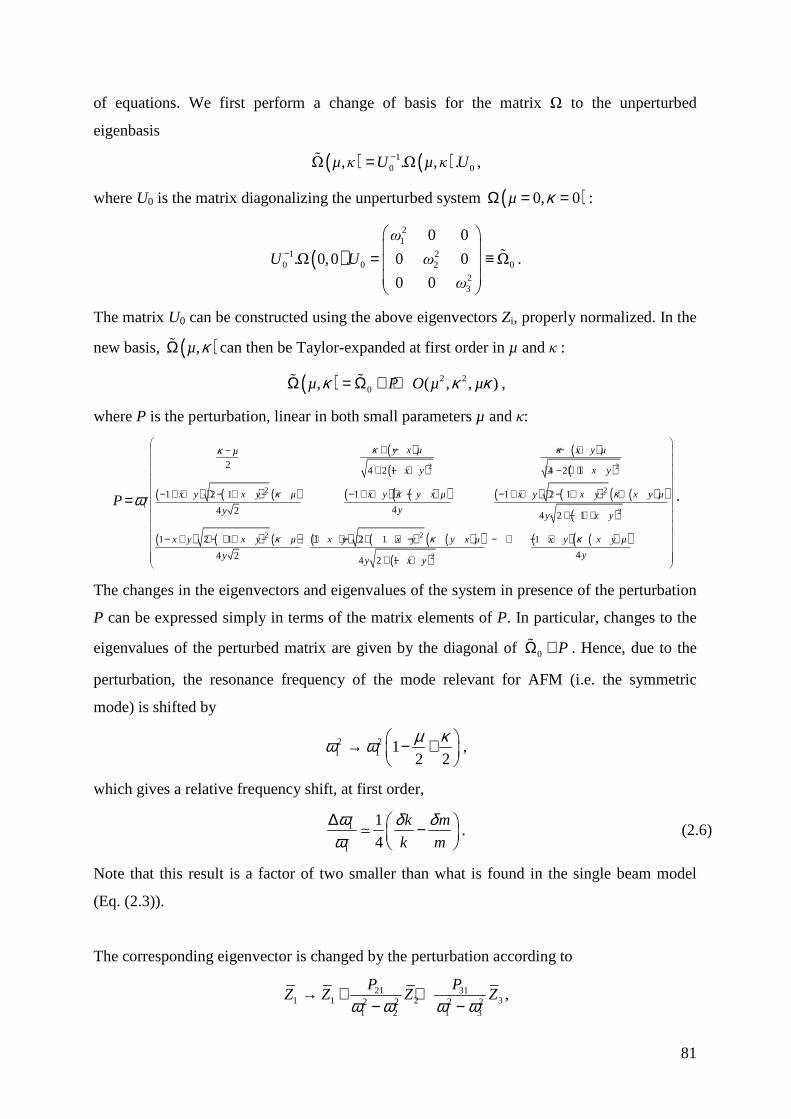
81
of equations. We first perform a change of basis for the matrix Ω to the unperturbed
eigenbasis
( ) ( )10 0Ω , .Ω , .−=ɶ µ κ U µ κ U ,
where U0 is the matrix diagonalizing the unperturbed system ( )0, 0µ κΩ = = :
( )21
1 20 0 2 0
23
0 0
.Ω 0,0 . 0 0 Ω
0 0
−
= ≡
ɶ
ω
U U ω
ω
.
The matrix U0 can be constructed using the above eigenvectors Zi, properly normalized. In the
new basis, ( ),µ κΩɶ can then be Taylor-expanded at first order in µ and κ :
( ) 2 20, ( , , )µ P O µ µκ κ κΩ = Ω + +ɶ ɶ ,
where P is the perturbation, linear in both small parameters µ and κ:
( )( )
( )( )
( ) ( ) ( ) ( ) ( )( ) ( ) ( ) ( )( )( )
( ) ( ) ( ) ( ) ( ) ( )( )( )
( ) ( )( )
21
2 2
2 2
2
2 2
2
24 2 1 4 2 1
1 2 1 1 2 11
44 2 4 2 1
1 2 1 1 2 1 1
44 2 4 2 1
y x µ x y µµ
x y x y
x y x y µ x y x y x y µx y y x µ
yy y x y
x y x y µ x y x y y x µ x y x y µ
yy y x y
P
κ κκ
κ κκ
κ κ κ
ω
+ − − +−
+ − + + − + + − + + + − + − − + + + − + − +− + + + −
+ − + + − + + − + + − − + + − + + + − − + − + + − +
= .
The changes in the eigenvectors and eigenvalues of the system in presence of the perturbation
P can be expressed simply in terms of the matrix elements of P. In particular, changes to the
eigenvalues of the perturbed matrix are given by the diagonal of 0 PΩ +ɶ . Hence, due to the
perturbation, the resonance frequency of the mode relevant for AFM (i.e. the symmetric
mode) is shifted by
2 21 1 1
2 2
µ κω ω → − +
,
which gives a relative frequency shift, at first order,
1
1
1
4
k m
k m
ω δ δω
∆ −
≃ . ( 2.6)
Note that this result is a factor of two smaller than what is found in the single beam model
(Eq. ( 2.3)).
The corresponding eigenvector is changed by the perturbation according to
31211 1 2 32 2 2 2
1 2 1 3
PPZ Z Z Z
ω ω ω ω→ + +
− −,

82
where the overbar denotes the properly normalized unperturbed eigenvectors (other modes are
obtained by circular permutation on indices). All calculations performed, the amplitudes of
the perturbed symmetric mode are changed according to
( )
( )1
1
1 2
1 1∆
0 0 2
1 1 1 2
− + + − −
→ + − + +
β γ
βω
ωβ γ
β
.
2.4.2.6.e Discussion
From this calculation one can draw a number of important conclusions regarding the influence
of the tip, the wire and the sample:
• All changes of the symmetric mode are proportional to its relative
frequency change.
• The frequency shift due to loading the tuning fork with the tip’s mass can
be, in principle, exactly compensated by the extra stiffness brought by the
connecting wire (as already noted in [59]). This compensation then
maintains a perfectly symmetric tuning fork, completely decoupled from
the rest of the structure.
• The amplitudes of deformation of the two arms in the symmetric
eigenmode, relevant for AFM, are changed by opposite amounts. The
current we measure is related to the sum of the deflections as indicated by
eq. ( 2.4). Hence, the changes in the arms individual currents cancel, and
for a given excitation amplitude one keeps a constant signal at resonance
(see § 2.4.2.8).
• The arms’ amplitudes can be left unchanged when weakly breaking the
symmetry of the tuning fork, provided 0 02m k
m k= + , even if the resonance
frequency changes.
• When loading the tuning fork with the tip, for a given current flowing in
the tuning fork, the change in the amplitude of the arm carrying the tip
with respect to the unloaded tuning fork can be directly linked to the
observed relative frequency shift between the two situations. This link is

83
quantitative if the model parameters of the bare tuning fork are known (see
above). This can be useful for calibrating the tip amplitude.
• The re-coupling of the resonator to the rest of the structure due to the
motion of the tuning fork base (mass m0 in the model) is also proportional
to the relative frequency shift. Relative to the amplitude of the arms
motion, the base amplitude is exactly twice the relative frequency shift and
(surprisingly) independent of the stiffness k0 of the mounting of the tuning
fork.
In practice, using tips and connecting wires of very small diameters (10 - 25 µm) with a
minimum amount of glue, together with proper shaping of the connecting wire (found
empirically), I could obtain quite consistently frequency shifts lower than 200 Hz, i.e. a
relative frequency change of the order or better than 0.5%. Correspondingly, the amplitude of
the tuning fork base is only of order 1% of the tip's amplitude. Such small amplitude can still
excite resonances in the microscope structure, but given that the quality factors of typical
structures are much lower than that of the tuning fork, it is unlikely that these resonances can
cause problems during measurement.
The present results assume negligible damping, which is confirmed by experiment since the Q
factor remains very high even when the tip interacts with the sample. A more complete
description making use of imaginary spring constants could account for damping in the tuning
fork, as well as non-conservative tip-sample interaction forces. Provided a model is known for
the non-conservative interaction forces, this would give a more realistic evolution of the mode
amplitudes, at the expense of introducing more parameters in the model.
2.4.2.7 Estimating characteristics of the connecting wire for
preserving the tuning fork balance
From the above discussion, preserving the balance of the tuning fork requires that the added
mass δm and spring constantδk are in the same ratio k k
m m
δδ
= as that of the tuning fork’s
arms.
Our model turns into adding to the fork an “extra resonator” with ideally the same resonance
frequency as the TF. However, this “extra resonator” is completely constrained by the TF

84
since it shares the same z1 DOF as the bottom arm. Hence, no mode mixing occurs, in contrast
with the usual case of coupled oscillators bearing their own DOF.
Note however that our model is an approximation since the wire is a complex body having a
lot more than 1 DOF. We thus pay special attention to constrain (i.e. plastically deform) the
wire prior to adding it to the TF, so that its apex faces exactly the TF’s end (position z1 at
rest).
Using the characteristics of the materials involved in the tip mounting, one can try to estimate
the dimensions of the connecting wire so that its effective spring constant is in the correct
range to perform the compensation.
For a well defined geometry, one can imagine to use FEM simulations. However, since one
can hardly mount the tip and the wire in a perfectly controlled and reproducible manner, we
found it simpler to have only estimates of the correct parameters ranges, and we subsequently
relied on empirical observation to obtain reproducible low frequency shifts and high quality
factors.
Simple estimates can be obtained by considering the masses added by the tip and glue, and
treating the wire as a vibrating beam.
material Y (1010 N/m2) ρ (kg/m3)
Epotek H20E 7.13 2550
tungsten 40 19300
gold 7.72 19320
quartz 7.87 2659
Table. 2.4 Mechanical parameters of typical materials used in our AFM/STM probe.
The tungsten tip's mass is estimated to be 0.9 µg, for 400 µm-length, 6 µm-radius. The glue's
mass is estimated to be 0.7 µg for a hemisphere of radius 50 µm. An upper value of added
weight is of the order of δm1 = 2 µg.
To estimate the role of the connecting wire, we now assume it is a cylindrical rod, mounted in
prolongation of the tuning fork's arm. For a clamped-free cylindrical beam1, the added
1 In fact, the wire is clamped at both ends in a way which makes it difficult to perform calculations. Since we are
looking only for orders of magnitude, we take here this simple approach, knowing that the numbers obtained
for the stiffness will be underestimated.

85
effective mass *
*2*
= km
ω of the connecting wire is given by the ratio of its spring constant
4
3
3*
4= πYR
kL
and its eigenfrequency 2
3.52*
2= R Y
ωL ρ
, R being the wire radius, Y the young
modulus, ρ the density of the material, L the length of wire. Hence, the effective mass of this
rod is 2* 0.76m R Lρ= . Solving 21
1
*
*
k
m mω
δ=
+, we find the necessary length of wire lies in a
range of 100 to 300 µm. It is however very difficult to mount such a short wire. We instead
mount a longer wire with a bend so that a ~100 µm-long section is in the prolongation of the
tuning fork beam and that it holds itself into that position before gluing it to the fork. By this
procedure, we observed we could induce reproducible low perturbations on the fork's
resonance, with frequency shifts of the order of 100 Hz (0.3%), and a quality factor of more
than 6000 at room temperature and ambient pressure, instead of 8000 for the bare fork. The
quality factor achieved by this method increases up to 150000 at low temperature. The results
presented here are of course fork-dependant, and the forks employed in this work are among
the lightest and smallest commercially available. That makes them more sensitive to force
gradients since k is proportional to the thickness, but they are also more sensitive to
asymmetry, which results in damping associated to the motion of the TF’s base (see § 2.4.2.5,
p. 76).
2.4.2.8 Measuring the oscillator parameters
The first step in our AFM experiments is to set up the resonator for imaging, and first of all,
we have to characterize its resonance, to ensure the fork is properly mounted.
The principle of the resonance measurement is the following: we impose an AC voltage bias
at a known frequency, and measure the current flowing through the tuning fork at this
frequency. This admittance measurement is done with a standard current amplifier (Current-
Voltage converter or CVC), and a lock-in synchronous detection. A complete schematic of the
measurement is shown in Fig. 2.25.
Typical resonance curves recorded with this setup are shown in Fig. 2.26, for different stages
of tooling up the tuning fork with a wire and a tip.

86
Y(ω)Voltagesource
C0
transformer1:1-1
CVC
Lock-inamplifier
ref
ref
Ccomp
Fig. 2.25 Block diagram of the measurement setup. A voltage source excites the tuning fork (symbolized by an admittance Y(ω)). The current that flows through this admittance is amplified by a CVC, and fed to a lock-in. Current has a maximal amplitude at resonance, and is in-phase with the excitation voltage. With the lock-in, one can record in-phase and out of phase signals (or amplitude and phase), and by properly adjusting the phase of the incoming signal with respect to the reference, one can record a perfect Lorentzian resonance, such as shown in Fig. 2.27). The variable capacitance and the transformer allow to cancel the current flowing in the stray capacitance C0, and thus to extract the part of the signal corresponding to the resonance of the oscillator alone.
2.4.2.8.b Resonance curves during the setup
32450 32500 32550 32600 326500.00
0.02
0.04
(2')(4'')
(4')X
frequency (Hz)
(4)
(3)
(1)
(2)
Fig. 2.26 Resonance curves measured in various mounting configurations of the tuning fork. The signal plotted is the in-phase lock-in signal measured with the setup described in Fig. 2.25. All data were taken at room temperature and ambient pressure. (1) is a bare tuning fork attached to its holder. (2) is taken after soldering at the end of one arm a 12 µm diameter, ~500 µm long gold wire. (3) is taken after attaching the gold wire at its other end to the connection pad. (4) is taken after the tip was glued. The different curves associated with the same number are taken at different moments, by placing the wire in different positions.

87
2.4.2.8.c Capacitance compensation
At resonance, the admittance of the resonator is real and maximal, however it is small
compared to the imaginary admittance iC0ω1 of the capacitance C0 ~100 pF of the coaxial
wire connecting the tuning fork to room-temperature apparatus, in parallel with the resonator1.
In order to properly measure only the current flowing through the resonator we use a bridge
technique introduced by Grober et al. in Ref. [66]: a transformer and an adjustable capacitor
are used to precisely compensate the current flowing in C0 (see Fig. 2.25).
This compensation is important, because reliably tracking the tuning fork resonance in AFM
imaging depends on having a change of sign of the imaginary part of the admittance at
resonance (see § 2.4.3). The procedure for this compensation is the following: we first take an
uncompensated resonance curve of the tuning fork, in a frequency range large enough that we
are sure it encompasses the resonance. Then we can determine the resonance frequency and
set the generator to it. We then compensate the capacitance, trimming an adjustable capacitor
down to the sub-pF level, canceling the out-of phase measurement of the lock-in at resonance
frequency. This procedure can be iterated if necessary.
2.4.2.8.d Extracting the resonator parameters
To determine the resonator parameters we have set up a fitting procedure, which enables
accurate extraction of all the parameters, among which the resonance frequency, the quality
factor, and a measurement of the accuracy of the capacitance compensation. This also enables
to accurately tune the phase of the PLL sensor (see below).
The procedure involves fitting simultaneously the in-phase and quadrature lock-in
measurements of the resonance as a function of frequency f, and fitting them with the
corresponding prediction for the RLC circuit.
The fitting function has the following mathematical expression for the in-phase expression:
( ) ( )( )( )
( )2
3 2
1
4 2 2 2 2 2 4
1 1
2 2 2
1 1
4 2 2 2 2 2 4
1 1
2cos
1 2
2 sin1 2
= ++ − +
−− +
+ − +
ratio
cπf QfX f offset
f Q f Q f Q f
f Q f fcπf C
f Q f Q f Q f
φ
φ
( 2.7)
The quadrature expression is the same, with φ replaced by / 2+φ π . In these expressions, the
fitting parameters are the central frequency f1, the resonator capacitance c, the stray shunt
1 C0 also incorporates a small stray capacitance contribution from the tuning fork itself.

88
capacitance *0 0 *= − =comp ratioC C C c C (which is zero when compensation is perfect, and
which can be negative when over compensated), the Q factor, the dephasing φ due to cables
and amplifiers, and a small offset that slightly improves the fit and can be seen as a leakage
resistor in the setup in the range of 10-30 MΩ. The last two parameters arise from the setup
and measurement technique, while the first four describe the system shown on Fig. 2.23.
When the lock-in phase is correctly set (i.e. when it compensates for dephasing in amplifier
and cables), 0=φ and the cos φ term (resp. sin φ term) of equation ( 2.7) describes the real
(resp. imaginary) part of the impedance of the tuning fork.
Such a fitting procedure yields a very high quality fit, and provides an accurate determination
of the parameters. An example of fit is shown on Fig. 2.27.
32600 32610 32620 32630 32640 32650 32660
0.005
0.010
-0.005
0.000
0.005
Chi^2/DoF = 4.7693E-10
f0 32630.06525 ±29.59751capa 1.166E-11 ±2.1313E-12cratio 47.45365 ±27.15886q 3888.99617 ±8.71374offsetX0.00307 ±5.6981E-6phiX -0.64742 ±0.05582
X
X
Frequency (Hz)
Y
Y
32600 32610 32620 32630 32640 32650 326600.000
0.005
0.010
0.015-0.010
-0.005
0.000
0.005
0.010
0.015
X
Frequency (Hz)
(1)
(3)
Y
(2)
(b)(a)
Fig. 2.27 Fit of the resonance curve and adjustment of the resonance parameters: (a) A resonance curve fitted with the model presented above. The resonance is shown in the in-phase (X) out-of-phase (Y) representation, with different scales. Taking into account all setup parameters, the impedance Y-1(ω) at resonance is ~5 MΩ. (b) Plot of resonance curves obtained with three different values of the compensation capacitance: (1) is obtained when the compensation is quasi perfect, (2) when the stray capacitance is under compensated, (3) when the stray capacitance is over compensated. For low quality factors, the compensation has to be accurate: curves shown here are obtained by a displacement of the order of ~1pF of the adjustable capacitance.
2.4.3 Force measurement
I now discuss the nature of the interactions we typically detect in our experiments, and
describe how we perform their measurement in AFM mode, using the tuning fork.

89
2.4.3.1 Typical forces on the atomic scale
I consider here the general case of a metallic tip on a metallic or insulating sample. When the
tip approaches the surface, atoms of the tip and of the surface interact. Detailed descriptions
and measurements of these interactions can be found in several articles [64, 67, 68].
In the following, I assume there are no magnetostatic interactions so that only electro-
magnetic interactions between charges in the tip and the sample are to be considered, all other
physical forces being neglected.
At infinitely large tip-sample distances, the tip does not interact with the surface, and the force
is thus zero. The potential energy of the tip in the field of the sample is taken to be zero.
When lowering the tip, one encounters several attractive or repulsive forces which come into
play at different scales [69].
If the surface is conductive, and if there is an electric potential difference between tip and
sample, charges of opposite signs accumulate on facing electrodes. This leads to a “long
range” attractive force between the two electrodes that depends on their shape, since the
electrostatic potential energy writes ( ) 212=elecV C z U , U being the applied bias voltage, and C
the capacitance between the electrodes. We are mainly insensitive to this force since we
normally keep a low bias voltage. However, varying the applied voltage would be a way to
characterize the tip aspect ratio [69, 70] by measuring the capacitance (within e.g. a sphere-
cone model, presented in ref [71]) or to perform scanning capacitance measurements [72].
An electrostatic force can also occur on a metallic tip above a charged insulating surface. I
assume that the insulating parts of our samples are not charged, which seems to describe well
the experimental observations.
In absence of a voltage applied to the tip and of a static charged sample, the dominating force
at large tip-to-sample distance is the Van der Waals force. This is a net attractive force due to
the polarizability of the materials. It is also a long-range tip-shape dependent force, with an
approximate d-2 dependence, where d is the tip-to-sample distance.
At some point, the foremost atoms of the tip begin to experience a shorter range “chemical”
interaction with the atoms of the surface. This can be seen as overlapping of orbitals at large
distances and becomes eventually Coulomb repulsion when the atoms of the tip try to “enter”
the sample. When both the tip and sample are metals, this interaction can be approximately
described by the energy ( )1 xBE E x e−= − + , with ( )mx d d λ= − , where EB is the binding
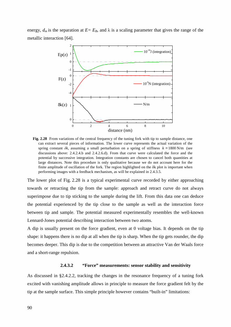
90
energy, dm is the separation at E= EB, and λ is a scaling parameter that gives the range of the
metallic interaction [64].
0 2 4 6 8 10
0
1
-4
-2
0
-1
0
1
2
N/mδk(z)
distance (nm)
10-9N (integration)F(z)
10-18J (integration)Ep(z)
Fig. 2.28 From variations of the central frequency of the tuning fork with tip to sample distance, one can extract several pieces of information. The lower curve represents the actual variation of the spring constant δk, assuming a small perturbation on a spring of stiffness 1800 N/m=k (see discussions above: 2.4.2.4.b and 2.4.2.6.d). From that curve were calculated the force and the potential by successive integration. Integration constants are chosen to cancel both quantities at large distances. Note this procedure is only qualitative because we do not account here for the finite amplitude of oscillation of the fork. The region highlighted on the δk plot is important when performing images with a feedback mechanism, as will be explained in 2.4.3.5.
The lower plot of Fig. 2.28 is a typical experimental curve recorded by either approaching
towards or retracting the tip from the sample: approach and retract curve do not always
superimpose due to tip sticking to the sample during the lift. From this data one can deduce
the potential experienced by the tip close to the sample as well as the interaction force
between tip and sample. The potential measured experimentally resembles the well-known
Lennard-Jones potential describing interaction between two atoms.
A dip is usually present on the force gradient, even at 0 voltage bias. It depends on the tip
shape: it happens there is no dip at all when the tip is sharp. When the tip gets rounder, the dip
becomes deeper. This dip is due to the competition between an attractive Van der Waals force
and a short-range repulsion.
2.4.3.2 “Force” measurements: sensor stability and sensitivity
As discussed in § 2.4.2.2, tracking the changes in the resonance frequency of a tuning fork
excited with vanishing amplitude allows in principle to measure the force gradient felt by the
tip at the sample surface. This simple principle however contains “built-in” limitations:

91
• First of all, measuring the frequency of the resonator requires a finite
vibration amplitude. During an oscillation, the tip-to-sample distance
changes and hence, the actual frequency shift corresponds to an average
force gradient. When the amplitude used is large compared to the scale of
variation of the gradient at the surface, the features are smeared out.
Notably, the measured dip in the frequency shift is smeared and reduced
[75].
• A simple stability criterion of the tip-to-sample distance prevents to have
the tip at rest, at distances z where the force gradient is such that
( )eff
dF zk
dz< − where F(z) is the total tip-to-sample force and keff the
effective spring constant of the tip holder. In these regions, the tip cannot
be held at rest (neither with vanishing excitation) at a fixed distance from
the sample and jumps to the nearest stable point. Using a sensor with high
stiffness avoids such instability, which is mandatory for STM
measurements. In this respect, the use of a tuning fork is much better than
standard AFM cantilevers [77]; on most contacts it allows to measure the
whole tip-to sample distance range, with a very low excitation amplitude,
without the jump-to-contact usually observed with AFM cantilevers.
• Other stability criteria can be formulated in dynamic oscillation: since the
force gradient δk(z) is non constant in z (anharmonic potential), there may
be several stable oscillation modes at a given average distance, each mode
having a different amplitude [68]. This results in the hysteretic behaviour
(as a function of amplitude and frequency), encountered with soft standard
AFM cantilevers. Non-conservative interaction forces can also induce such
dynamic instabilities. However, when using a tuning fork, the interaction
non-linearities weakly affect the dynamics of the oscillator ( ( )≪δk z k)
which is mainly determined by the high spring constant and, as a
consequence hysteretic behaviours are not observed.
• The ability of a resonator to measure frequency shifts is ultimately limited
by the intrinsic thermal noise due to dissipative parts in the resonator. One
can show [73, 74] that min2
1 1
2= Bδω k T B
ω k A ω Qwhere kB is the Boltzmann

92
constant, T the temperature of the dissipative part of the oscillator, Q the
quality factor, k the spring constant, A the mechanical amplitude of the
oscillator, and B the bandwidth of the frequency measurement. From this
expression, and given that the frequency shift 1δω of the oscillator in
response to a force gradient δk is 1 1 4=δω δkω k (see 2.4.2.6.d), one can
estimate the minimum detectable force gradient to be min 21
4≈ Bk T B kδk
ω A Q.
From the above analysis, one sees that the choice of a resonator is a balance between greater
stiffness which gives better stability of operation and lower stiffness which gives better
overall sensitivity. Quartz tuning forks being much stiffer than conventional cantilevers, they
are very stable and convenient to use in AFM: they are not easily prone to jump-to-contact or
hysteretic behavior upon a change of amplitude. Years of development on dynamic AFM
have shown that k values exceeding hundreds of N/m provide adequate sensitivity and
stability [75]. The tuning forks we mostly used had k = 1800 N/m, and are among the softest
(i.e. thinnest) available. Those tuning fork typically yield a sensitivity to a force gradient:
( )1 / 2.3Hz/ N/m= ≈δω δk η , which is a standard value [74].
Furthermore, for a given sensitivity, lower excitation amplitudes can be achieved by using
higher Q-factor or higher resonant frequencies. Since well balanced tuning forks can have
high Q-factor (see discussion above), they can be very good AFM sensors, yielding atomic
resolution [75].
In our setup, the above minimum detectable force gradient is not reached, by far, due to extra
sources of noise introduced in the measurement of the sensor. Indeed, the above predicted
ultimate frequency resolution we should be able to achieve with our tuning fork with, say, a
1 nm amplitude of the sensor and a 100 Hz (respectively, 1 kHz) bandwidth should be of the
order of 0.15 mHz (resp. 0.5 mHz) whereas the output noise of the PLL alone is already
2 mHz rms (resp. 40 mHz rms) when fed with a noiseless signal. In actual measurements of
the resonator, the PLL frequency measurement accuracy is further degraded by the noise
coming from the amplifier.
2.4.3.3 “Force” measurements: detection schemes
The easiest operation mode of a resonator is to drive it at a fixed amplitude and frequency, on
the side of the resonance peak, and to measure its amplitude. This was the first mode used in
dynamic AFM. In this mode, known as AM mode, when the tip-to-sample interaction changes

93
in a step-like manner, the central frequency of the oscillator changes and its amplitude
experiences a transient which damps exponentially with the characteristic time 12Qτ ω= .
For a 32 kHz oscillator with a Q-factor of the order 105, this transient, also known as the
ringing-down (or up) of the oscillator amplitude associated with changing the energy of the
oscillator, can last several seconds and makes it unusable as a practical AFM detector.
Still, high Q-factor oscillators can be used as AFM detectors by tracking the resonance
frequency of the oscillator [76]. This frequency tracking mode is also called FM mode and
can be implemented in two ways:
• In the first method, the oscillator is placed in a loop with an effective
negative resistance around the resonance frequency (i.e. an amplifier with
~π phase shift) so that it enters self-oscillation.
• In the second method, the oscillator is inserted in a phase-locked loop
(PLL) controller, such as described below. This latter method is somewhat
more flexible than the first one in terms of controlling the resonance, and it
has the advantage of directly providing a signal proportional to the
frequency shift of the oscillator. This is the mode we used.
In either of these FM modes, when applying a step change in the interaction, there is no time
penalty associated with changing the energy stored in the oscillator, like in the AM mode. In
FM mode, one indeed tracks the change of the resonator parameters themselves that
effectively occur at the sound velocity [77], rather than measuring the rate at which the
oscillator absorbs (looses) energy.
In the self-oscillation mode the change in frequency is thus as fast as the resonance frequency
itself.
In the PLL case, which is of interest to us, the response time is limited by the speed at which
one can measure the changes in the phase of the oscillation [73, 74, 77]. Of course, this speed
has a tradeoff with the stability of the frequency, and therefore with the sensitivity and the
accuracy of the force measurement. The actual accuracy and speed of the AFM sensor then
depends on details of the setup, and in particular on the signal-to-noise ratio in the
measurement of the oscillator. In practice, with our setup which uses standard room-
temperature amplifiers and PLL electronics and reasonable excitation amplitude, it is possible
to track the resonance frequency within a bandwidth in the 100-1000 Hz range, i.e. much
faster than 11 2 0.2HzQτ ω− = ∼ , which allows reasonable scanning rates in AFM imaging, in
the 0.1-1 Hz range.

94
2.4.3.4 Phased locked loop detection
In the following, I describe more in details the operation of the tuning fork in FM mode with a
PLL detector. The block diagram of the PLL is shown in Fig. 2.29.
x LP PI VCO
xx LP PI
G
~π/2
-
Amp
drive(t)
signal(t)
Dissipation
δf(t) f0
fm
PLL
φ
φ
x LP PI VCO
xx LP PI
G
~π/2
-
Amp
drive(t)
signal(t)
Dissipation
δf(t) f0
fm
PLL
φ
φ
Fig. 2.29 Block diagram of a PLL detector (yellow path) with automatic amplitude control (pink path). VCO stands for Voltage Controlled Oscillator, PI for Proportional-Integral, LP for Low Pass, x for multiplier, ∆ for difference, φ for dephaser, G for amplifier. The input control signals for the PLL are the amplitude set point Amp, the central VCO frequency f0 and the dephasing angle φ. The output monitoring signals are the frequency shift δf(t) and the amplitude of the drive signal “Dissipation”, which is proportional to the sum of the sensor dissipation and the dissipation due to non-conservative tip-sample interaction.
Its principle of operation is the following: the VCO is set with a central frequency f0 close to
the experimentally determined resonance by fitting the resonance curve. It delivers a sine
oscillation at a frequency 0= +f f λ fm, where fm is the voltage at the VCO fm input and λ a
constant giving the frequency sensitivity of the VCO. This signal, multiplied by the amplitude
control signal is sent to the sensor, amplified and comes back at the PLL input. There, it
enters a phase comparator, composed of a multiplier and a low pass filter to remove the 2f
component. The PLL dephaser can be tuned to accommodate for dephasing in the amplifier. It
is set such that it delivers a signal with a π/2 phase lag signal with respect to the input signal
right on resonance, so that the phase comparator signal is zero on resonance. This way, on
resonance, the system is at a fixed stable point: the integrator output is constant and the
frequency remains fixed. On the other hand, when the VCO frequency does not correspond to
the sensor resonance, the response of the sensor is not in phase with the drive and the phase
detector gives a non-zero phase shift, with a negative sign (resp. positive) if the drive
frequency is above (resp. below) the resonance frequency. This phase shift is integrated by the
PI resulting in a change in the drive frequency until the phase detector signal drops to zero,
when resonance condition is met again.

95
This phase-locking mechanism has a single (stable) operation point when the resonator output
is such that the signal component in quadrature with respect to the drive goes through zero in
the frequency range of the VCO. This condition is met only when the parallel stray
capacitance is perfectly compensated (see Fig. 2.27 b). When the capacitance compensation is
imperfect, there may be zero or two solutions. In the first case the system cannot phase lock
on resonance and the VCO oscillates either at its maximum or minimum frequency. In the
second case, one solution corresponds to an unstable situation, and the other to a metastable
phase locking. In the latter case, operating an AFM is possible although risky, as the PLL can
unlock when scanning over large steps on the sample.
Our PLL further controls the amplitude of the drive so that the output signal remains constant.
The amplitude (in fact, the power) of the input signal is determined by squaring it and filtering
to remove the 2f component. This filtered value is compared to the setpoint and the difference
is integrated to obtain the amplification factor to be applied to the drive. This way, the
difference between the setpoint and the detected amplitude eventually drops to zero.
This implementation of a PLL actually consists in two parallel loops:
• A first loop that feeds a correct frequency to the tuning fork, to avoid
detuning from the resonance. This one is the fastest (see 2.4.3.3).
• Another loop that compensates for energy losses either due to a detuning
of the excitation, or to damping in the tip-sample interaction. Energy loss
has a time constant 12Qτ ω= , as discussed above. Amplitude regulation
is essential to prevent from loosing signal when the Q-factor drops while
scanning the surface. This loop should not be set to regulate at a rate
higher than τ-1, to prevent amplitude oscillations.
We use a commercially available PLL system to control the tuning fork: the Nanosurf Easy
PLL system. This system is partly analog, and partly digital, which is convenient to interface
and control the PLL from within a program. However, the analog multipliers used in the
system are noisy components which make the PLL behave less than optimally regarding the
sensitivity and frequency stability. A well designed fully digital PLL should outperform it
easily.

96
2.4.3.5 Feedback loop in imaging mode
Once the PLL is locked, image in AFM mode is performed by closing the feedback loop
which controls the average tip-to-sample distance. The Block diagram of this loop is shown in
Fig. 2.30.
PLL
PI
G
drive
signal
δf
-
δf setpoint
f0
setpoint
piez
osc
ann
er Z control
support
Sample
tiptuning fork
PLL
PI
G
drive
signal
δf
-
δf setpoint
f0
setpoint
piez
osc
ann
er Z control
support
Sample
tiptuning fork
Fig. 2.30 The feedback loop operated for AFM imaging is composed of the following elements: the quartz tuning fork (TF) whose resonant frequency is a measure of the tip-sample distance, the PLL that both drives the TF at its resonant frequency and measures the error δf in frequency signal, and a controller that adjust the piezo scanner voltage so as to keep a constant tip-sample interaction (≡distance). What is important to notice here is that we basically have two imbricate loops: one for the excitation at resonance of the fork, having typical response up to 1 kHz, and another one for the tip-sample distance adjustment, which has a time response of ~1 Hz. Speed limitation of the feedback on position comes from the noise on the δf signal which imposes inserting a low pass filter (120 Hz). Given this limitation, an optimization of the scanning speed is done by choosing appropriate feedback parameters (see text).
When the tip-to-sample distance is varied, the resonance of the oscillator changes as shown in
Fig. 2.28. In regions of the curve where δf varies with the distance, this signal can be used to
maintain the distance at a fixed value. Given the shape of the curve, different imaging modes
exist:
• The so-called “tapping mode” is operated closest to the sample surface in
the negative slope region (of δk(z)), where coulomb repulsion dominates
all other contributions. The feedback is then set in “negative” direction,
meaning that it will react to an increase of gradient by retracting the tip.
The tapping mode, though oscillating, operates similarly to the "contact
mode" in non-dynamic AFM.

97
• The non-contact mode is operated in the region of positive slope, where
either electrostatic or Van der Waals force dominate. The feedback is then
set to “positive” direction.
It is clear that the region in-between (emphasized by a red line on Fig. 2.28) is subject to
ambiguous and slow behavior of the feedback loop. Moreover when imaging in non-contact
mode, one has to be very careful in order not to trespass the cross-over region or the tip will
crash. For this reason, it is better to image reasonably flat surfaces or at higher distances in
this mode. When imaging is performed in contact mode, there is no unstable behavior. This is
why we preferred this mode. In this mode, however, the cross-over region is responsible for a
slower feedback response to an increase in tip-to sample distance (a “down” step on the
sample surface) than for a decrease (up step). In order to compensate for this asymmetric
behavior, we found convenient to use logarithmic feedback control, similar to what is used in
STM mode [78].
To operate in tapping mode, we set a positive δf setpoint, typically 1 Hz. Alternatively, we
could set the VCO center frequency below the free resonance frequency. The piezoelectric
tube voltage is adjusted by the PI element of the controller to keep δf at the setpoint. Hence,
the sign of the feedback is set so that an increase in the resonant frequency yields a retraction
of the piezotube.
While imaging, the tube is deflected laterally by the controller to scan the sample, at a typical
rate of 1 line per 5 seconds (vx ~ 1.6 µm/s), while maintaining δf at the setpoint. One line is
8µm wide for our tube, at 30 mK, and the number of lines (depending on the desired
resolution) is typically 100. Thus it takes about 8’20 to record an 8x8 µm image.
2.4.3.5.b Optimizing AFM imaging
Good performance of AFM imaging requires tuning the gains of the PI elements in the feed-
back loops properly, for optimizing the desired characteristics (scanning speed, topographic
resolution…). Several articles have addressed this point both experimentally and theoretically
[59, 68, 79-81]. Theoretical analysis enables determining the feedback settings for optimal
dynamic performance. These analyses however rarely take into account the adverse effect of
noise on imaging and stability. In practice we determined “optimal” feedback parameters by
tuning the step-response of the AFM loop of Fig. 2.30 to a small voltage step added to the
piezo tube polarization Vz (in both directions), which simulates a topographic step.

98
Fig. 2.31 Full range (8x8 µm2) image of a sample studied during this thesis (see chapter 4). Here, the resolution is limited by the number of pixels recorded, fixed to 64 pts/lines. The maximum step size on this sample is 60 nm. This image was scanned at 2 µm/s, and the whole feedback parameters set such that an upward step has the same cross-section profile as a downward step. Thus no overshooting may occur while climbing up a step, which sets the upper limit to the gains though getting down a step must be done fast enough, which sets their lower limit. The achieved speed is constrained by the combination of frequency setpoint (see p. 65) and frequency sensitivity together with feedback gains. It is however limited by the sample aspect ratio. Other parameters such as phase, amplitude, amplitude feedback, etc govern the stability of the PLL loop, i.e. its robustness against unlocking.

99
CHAPTER 3
33EEXXPPEERRII MMEENNTTAALL
TTEECCHHNNII QQUUEESS

100
In this Chapter, I will give an overview of the experimental techniques involved in the
environment and operation of the AFM-STM built during this thesis work. I will give details
regarding:
• the special type of dilution refrigerator we have used, and the problems
encountered,
• the requirements on wiring and filtering for very low temperature
experiments in general, and how we implemented them in the present case,
• data acquisition and experiment control,
• fabrication techniques for tips and sample.

101
3.1 A dilution refrigerator well adapted for a local probe
microscope
3.1.1 Functioning of the inverted dilution refrigerator
To cool our microscope down to the 50 mK temperature range we use a special 3He-4He
dilution refrigerator, designed by Alain Benoit at the CRTBT (Grenoble) and called Sionludi.
It has an “inverted” geometry, in which the coldest plate is topmost (see Fig. 3.1), contrary to
most dilution fridges. This is very convenient for an application like ours, which requires
good accessibility to the experiment, to be able for instance to work comfortably on the
microscope with binocular lenses. The microscope is simply laid (and screwed) on the
Sionludi top plate. No additional setup is required to hold it, and it is easily removable. This is
required because the mounting of the tip on the tuning fork, for instance, cannot be done in
place: it requires removing part of the microscope to work on it on a workbench under
binocular lenses (see Chapter 2).
Another specificity of the fridge is the absence of a helium bath, ensuring a steady stage at
~ 4.2 K in ordinary dilution fridges (see Fig. 3.1 and Fig. 3.2). Instead, the cryogenic liquid is
contained in a Helium dewar placed underneath the fridge, which one slightly pressurizes
(~0.1 atm) to obtain a cooling L4He circulation inside a dedicated circuit of the fridge. Liquid
reaches a box anchored to the “4 K stage”, evaporates in that box and circulates downwards
into a continuous exchanger. The output goes directly to the helium recovery. Helium flow is
regulated by a Bronkhorst EL-FLOW® digital mass flow controller. The flow is set large
enough to provide a steady 4 K stage temperature, while keeping a reasonable helium
consumption of about 12 L of liquid per day. The downward 4He flow is used in permanent
regime to thermalize the incoming cooling mixture, so the “main exchanger” is properly
dimensioned to recover the enthalpy of the outgoing 4He. Temperature fluctuations on the 4 K
stage can cause fluctuations of the mixing chamber temperature, either because the mixture is
not properly cooled when it reaches the dilution stages, or due to radiations.
The Sionludi has a second separate circuit, containing the 3He -4He mixture with an
approximate atomic ratio 30%-70%. Capillaries passing inside the 4 K exchanger bring the
mixture up into the fridge. One of them is a low impedance bypass circuit that brings the
mixture to the mixing chamber without passing through any impedance. This bypass circuit
lets cold mixture gas circulate with a large flow for precooling the upper stages from room

102
temperature down to 4 K. Such a circuit is necessary in this design since, as a consequence of
the absence of a Helium bath, one cannot use exchange gas in the vacuum can to cool down as
in ordinary fridges. The other capillary brings mixture to the impedances at the input of
dilution exchanger.
Still(~1K)
Dilutionheatexch.
4K
20K
80K
basetemp.(~30mK)
mixingchamber
« coldplate »(~400mK)
Mainheatexch.
Still(~1K)
Dilutionheatexch.
4K
20K
80K
basetemp.(~30mK)
mixingchamber
« coldplate »(~400mK)
Mainheatexch.
Fig. 3.1 Photograph of the Sionludi where the principal components are indicated.

103
CP3He
4He
Main Still
MC
0.5x0.9
2x2.5
2nd Still
main pumping
brassvalve
2nd radiationshield
1st radiationshield
4Herecovery
experiment
main pumping
fast injection
dilution injection
: impedance ~[1-1.5] 10-2mb.l.s-1
: main stages
: fridgeCP : Cold Plate
MC : Mixing Chamber
LEGEND
0.5x0.9 : inner x outer diameter (mm)
: impedance ~[1-1.5] 10-2mb.l.s-1: impedance ~[1-1.5] 10-2mb.l.s-1
: main stages: main stages
: fridge: fridgeCP : Cold Plate
MC : Mixing Chamber
LEGEND
0.5x0.9 : inner x outer diameter (mm)
4K
dilutionexchanger
Mainexchanger
Z1Z2
pressurised4He dewar
rotarypumpcompressor
bypass
~80K
~20K
Fig. 3.2 Schematic of the principle of gas flows in the Sionludi (see text). The fridge’s enclosing is shown by a dotted line, corresponding to the vacuum can represented on Fig. 3.3.
He dewar
Vaccum cancontaining fridge
gas handling cabinet
air-suspended table
EMI shielding cabinet
Instrumentationracks
microscope controller
main pumping
Fig. 3.3 Ensemble view of the lab. From left to right: the gas handling system, the vibration isolation table, on which is laid the fridge (enclosed in vacuum can here) and the helium Dewar attached under the table, the shielding cabinet linked to the fridge by metallic shields, and finally the electronic cabinets and the operator in front of the command computer.

104
To reach such low temperatures, one must take great care to avoid thermal leaks through
radiation and conduction. To limit them, our fridge is enclosed in a vacuum can and a set of
copper thermal radiation shields arranged like Russian dolls and tightly screwed to stages of
the refrigerator, to ensure their good thermalization. In this way, each stage receives
radiations only from a stage close in temperature, and the inner stage (the coldest) is well
separated from the outside room temperature radiations.
When this thesis work started the refrigerator was being completely refurbished at the CNRS
Grenoble, because the main heat exchanger had become leaky due to defective materials, and
the dilution heat exchanger had completely plugged. This reparation lasted much more than
anticipated. During this phase I participated in testing and debugging the refrigerator on
several occasions. Even after we recovered a working fridge in Saclay, we made some
modifications, aiming at reducing liquid helium consumption and oscillatory instabilities in
the 4K stage temperature.
3.1.2 (not so good) Vibrations in dilution refrigerator
Vibrations are a major problem in STM experiments since the tunnel current varies
exponentially with the tip to sample distance, with a characteristic scale of ~ 0.1 nm. Many
setups try to compensate, or eliminate vibrations reaching the microscope, which introduce
noise in the measurement. As already mentioned in Chap. 2, the general strategy for
decoupling from external vibrations is to design a microscope that is as stiff and as light as
possible to increase the resonance frequencies of the structure, and to embed it into a low-pass
mechanical filtering system with a cut-off frequency as low as possible, typically <1 Hz. In
our case, this system consists of an air-suspended vibration isolation table onto which the
fridge is mounted (the Dewar being suspended below the table) to isolate the microscope from
the vibrations of the building (see Fig. 3.3)1. However, this setup does not fully eliminate
vibrations from the environment of the microscope, as explained below.
In usual dilution fridges, the incoming mixture is condensed at ~100 mb by thermal contact
on a 1.5 K pumped liquid 4He bath called the “1 K pot”. Another difference between Sionludi
1 However the table does not protect well against acoustic vibrations transmitted by air. For instance, clapping
hands induces vibrations which are easily detected with the STM. Efforts could be made to further enhance
acoustic isolation.

105
and more standard dilution fridges is the absence of a 1 K pot. The initial condensation of the
mixture is thus operated on the 4 K stage, which means that it is necessary to pressurize above
atmospheric pressure, using a compressor. Once the dilution is started, condensation is
achieved by exchanging heat with cold gases in the main pumping line (see Fig. 3.2), and one
should normally be able to switch off the compressor and work with an injection pressure in
the 500-700 mb range which can be delivered by the rotary pump alone. In our Sionludi,
however, this is not the case, and we can only work in a steady state with a pressure of the
mixture injection line permanently above 1.5 bars, i.e. with the compressor permanently on.
This generates some acoustic pressure and a substantial level of vibrations, both of which are
a nuisance for the microscope operation. Even worse, the mixture flow itself becomes
turbulent and generates a lot of vibrations, presumably when it flows through the impedances,
at a stage that is tightly linked to the experiment plate.
We diagnosed this problem and somewhat measured the level of vibrations in the fridge by
putting a microphone on the experiment plate, next to the microscope. The microphone is
made of a piezoelectric multilayer stack PICMA® P-885.30 from PI glued vertically, at the
end of which a ~ 6 g copper block is attached1 (see Fig. 3.4). When vibrations arrive on the
microphone, the copper block provides an "inertial force" proportional to its mass, which the
stack converts to an electrical signal. This electric signal is amplified by a fixed-gain (x100)
low noise amplifier LI75A by NF-Electronics and fed to the input audio line of the computer.
Note that the setup is sensitive only to vertical vibrations of the experimental plate.
1 The model we use has a bare structural resonant frequency of 90kHz, and a stiffness of 68N/µm. With the
copper block, the resonance frequency is 17 kHz.

106
piezo actuator
copper mass
braid for thermalization
connection
13.5mm
Fig. 3.4 Photography of the microphone used to detect vibrations inside the refrigerator. The electric signal produced by a stress (induced by vibrations of the plate) is collected on the electrodes of a piezoelectric actuator, amplified and fed to the audio input of the computer.
Fig. 3.5 Audio trace of vibrations of the fridge, recorded at the base temperature. Top: spectrum of the signal from ~DC to 11 kHz. The color indicates the amplitude of the Fourier component relative to the maximum amplitude, in dB. The signal spectrum presents the characteristic resonant frequencies of the fridge structure. Bottom: Corresponding wave signal, in arbitrary units.

107
We have recorded several tracks in different circulation regimes of the refrigerator.
Sometimes it sounds more or less like a continuous turbulent flow, and sometimes it sounds
more like metallic pings on pipes or bells ( Fig. 3.5). We do not understand the differences
observed between the various regimes. In all cases, the level of vibration is too high to allow
stable spectroscopic measurements in true vacuum tunneling. It would even hinder
performing STM imaging of a clean metallic surface. Note however that these vibrations do
not seriously affect AFM mode operation.
We have checked that when the return line pressure is reduced by diverting the mixture
momentarily, the fridge becomes indeed much quieter. There is no fundamental reason why
our refrigerator could not operate with a lower return line pressure, like other Sionludis. We
believe that the high return line pressure is due to some defective part, (likely a heat
exchanger), and it will eventually be fixed, when the problem is precisely understood. This
will certainly require a few trial-and-error runs involving modifications to the dilution circuit,
and it is hardly predictable how long this can take. Since we were still able to perform stable
tunneling spectroscopy in spite of the vibrations (see below), we decided this needed not be
done during this thesis work.
3.1.3 Living with vibrations
In spite of this annoying level of vibrations, we have found a way to perform stable and
accurate local electronic spectroscopy with our STM. Since our setup is too unstable to
perform tunneling through a vacuum gap (as in normal STM operation), we instead put the tip
in mechanical contact with the sample and tunnel through a thin oxide barrier covering the
sample. This way, the distance between the two metals is well defined and remains fixed, in
spite of the vibrations. In some sense, we mimic here the fabrication of planar tunnel junctions
in situ, during the experiment.
Of course this requires the presence of an appropriate oxide layer on the sample. Such oxide
spontaneously grows on aluminum films exposed to air. However, noble or semi-noble metals
do not naturally form a good oxide layer appropriate for tunneling. In this case, one can still
obtain a good tunnel barrier by covering the noble metal by a thin aluminum layer (i.e. a
couple of nm thick) which will completely oxidize in air and form the barrier.
We can let the STM tip stand on this oxide layer and perform stable spectroscopy, with
contacts lasting for hours without any change in transmission, in spite of the vibrations.

108
3.1.4 Possible improvements
For increased immunity to vibrations, most local probe microscopes used at low temperature
are suspended by springs [82, 83]. We did not initially choose this option because of the
coarse motion mechanism which changes the balance of the microscope when displaced, and
because it complicates wiring and thermalizing the sample. If much better stability becomes
necessary for some future experiment, this choice could be reconsidered.

109
3.2 Wiring a microscope for very low temperature
experiments
Connecting a 30 mK experiment with room temperature equipment requires fulfilling a
number of requirements which are detailed below.
3.2.1 Thermal load
The most basic requirement for the installation of a low temperature setup is to properly
thermalize all the elements, without warming up the refrigerator. Wires need to be thermally
anchored at each temperature stage, and one has to adjust the necessary length in between
stages such that thermal flux that can be compensated by the available cooling power. As one
goes down in temperature, the cooling power is reduced, but thermal conductivity of materials
as well.
Estimating the thermal load brought by the wires (and optimizing their length) is done by
using tables of temperature dependent thermal conductivity of typical materials used (steel,
Cu-Ni, copper, manganin®, superconducting wire in resistive matrix…) and by calculating
the thermal flux as a function of their cross-section and temperature difference between
stages.
Our fridge has a cooling power of ~50 µW at 100 mK, which means that if we feed a total
power of 50 µW down to the mixing chamber, its temperature will establish at 100 mK.
The steady state temperature of a dilution fridge is given by the balance of the cooling power
284=ɺ ɺQ T n (T is the temperature of the mixing chamber, the power is expressed in Watts and
nɺ is the 3He throughput, in mole.s-1), and the heat load brought by:
• radiation from hotter parts of the fridge,
• conduction through the materials,
• convective heat brought by the incoming fluid, due to imperfect heat
exchangers.
Our bare fridge had a base temperature of ~20 mK. From the measured cooling power at
100 mK, one can then estimate that the residual heat loads listed above are of the order of
2 µW in total. When installing the wiring for the experiment, this obviously increases the
conduction heat load and the final base temperature will be more or less affected depending
on how this additional load compares with the former figure.

110
We installed a total of 50 shielded wires from ambient temperature down to the mixing
chamber. They are divided as follows:
• a 15-wire line for the thermometry of the experiment,
• a 21-wire line for the control of the microscope,
• a twisted pair line for a small superconducting coil,
• 4 twisted pair cables
• and 4 coaxial lines for transport measurements on the sample or other
purpose1.
Most lines are home made with common cryogenic materials having low thermal
conductivity. For the shielding, we employ stainless steel or Cu-Ni tubes. Because of their
cross-section, the thermal conductance of the shielding capillaries is the dominant
contribution, so we diminished as much as we could their diameter and wall thickness: for
instance, we fitted 24 50 µm-diameter wires in a 0.6-0.7 mm CuNi capillary to make the
multi-wire line from 4 K to 30 mK.
Inner conductors are chosen depending on their use: the lines through which large currents are
fedwere made of superconducting wires which do not dissipate, and are good thermal
insulators. For current feeding of the coil we use 100 µm-diameter Cu/Mn down to 4 K and
50 µm-diameter Nb/Ti in Cu/Ni matrix insulated wires from 4 K to 30 mK. Lines where high
currents are not needed (DC transport, thermometers, tunnel and tuning fork measurement)
are made of resistive material: for those we use either 70 µm-diameter insulated manganin all
along, or commercial 0.5 mm diameter microcoax®, made of stainless steel both for the inner
conductor and the shielding. Finally for the (21 wires) control lines of the microscope we use
70 µm manganin down to 4 K and then NbTi in CuNi matrix down to 30 mK; the latter choice
is done to minimize the thermal load brought by this multi-wire line.
The multi-wires lines are assembled by pulling all the wires along with silicon glue into a tube
of adjusted length and minimal diameter. Glue is used to improve the thermal contact between
the inner conductors and the shielding, to ensure that conductors are well thermalized. It also
prevents vibrations, which are sources of microphonic or triboelectric noise. Prior to inserting
the wires, the inside of the tube is polished by passing through it a coiled tungsten or steel
wire, to prevent wearing the wire insulation on the tube wall asperities which could cause
shunts to ground.
1 In addition to these wires going to the mixing chamber, other unshielded wires are installed for auxiliary
thermometry and microphony (See previous section) purpose at higher temperatures.
111
Before the installation of the wires, our fridge had a base temperature of 20 mK, and the
whole wiring raised the temperature to 30 mK, corresponding to an additional load of
~ 2.5 µW. Given the large number of lines installed, this is satisfactory.
3.2.2 Low level signals and low noise requirements
As explained above, all the lines reaching the 30 mK plate are shielded. This is necessary to
prevent electromagnetic noise from the outside (antennas, power supply, cell phones…) to
couple to the experiment, which would prevent us from measuring low level signals. It is also
integral part of the filtering strategy described below.
To reach a high signal-to-noise ratio, it is also necessary to avoid cross talk between some
lines, in particular between low-level and high level signals. There are two kinds of wire
geometry that can be used: when one wants to measure small voltages differential signals, it is
necessary to minimize magnetic flux picking by twisting two wires all along. When one needs
large bandwidths above 100 MHz, the coaxial geometry is the best solution.
Finally, in low-noise measurements, the grounding of the signals has to be carefully
considered to avoid ground loops in which uncontrolled flux pickup from the lab ambient
magnetic noise harshly affect measurements. Ground loops can generally be avoided by
selecting a proper wiring topology with a unique, well localized, voltage reference point. In
low temperature experiments, however, good grounding practice sometimes conflict with
cable thermalization, and compromises have to be made. This topic is further discussed in the
article on the tunnel current amplifier published in Review of Scientific Instruments 77,
123701 (2006), reproduced below ( 3.2.4.3).
3.2.3 Filtering
The last requirement for setting up properly the wiring is to filter the high frequency noise in
each line. This is necessary to ensure that the experiments are performed in thermal
equilibrium at the fridge temperature. During my thesis we have developed microfabricated
filters to fulfil this requirement. We have published this work in Review of Scientific
Instruments 77, 115102 (2006). Below I give detailed explanations regarding these filters
which did not all fit in the article. The article itself is reproduced at the end of this section.

112
3.2.3.1 Necessity of filtering
Black-body radiations emitted by dissipative elements can propagate inside the fridge,
especially on the coaxial lines which are good wave guides. They are absorbed and re-emitted
by electrons all along the lines. These radiations extend in a frequency range up to hν ~ kBT,
as stated by Planck’s law, where T is the emitter's temperature.
When a photon emitted from a distribution at temperature T1 is absorbed by a metal at a
temperature T2, an electron of this metal may go out of equilibrium with the distribution at T2
if T1 > T2. Its only way to relax is either to exchange energy with the surrounding electron
bath, to reemit the radiation, or to give the extra energy to the phonons of the lattice. The
latter process has a temperature-dependent rate. At room temperature, electron-phonon
coupling is so strong that difference between electron temperature and phonon temperature is
hardly ever measurable. But the coupling decreases as temperature decreases, so that at
T < 1 K, electrons can be easily out of equilibrium with the phonons [84]. In particular, if one
does not take great care to cut the black-body radiations from wires at 300 K, it is unlikely
that electrons in the lines ever get as cold as the refrigerator.
In order to perform high resolution tunneling spectroscopy with a normal probe (see
chapter 1), it is important to take appropriate measures to ensure that electrons are in
equilibrium at low temperature. In many other types of mesoscopic physics experiments a
good filtering is also necessary to protect from unwanted photon assisted processes [85-89].
3.2.3.2 Why filtering all the lines?
One could think that by filtering properly the low-level signals connecting the sample, one
would obtain the desired electronic temperature in the sample.
However, any unshielded cable acts as an antenna that absorbs from the environment and
radiates on the experiment. It is therefore mandatory that all the lines entering the
experimental environment are properly filtered and shielded all along so that they do not bear
thermal radiations from 300 K.
Most STM experiments performed in dilution refrigerators did not filter all the lines (or not
sufficiently), including the controls of the microscope, which may partly explain why they
could not reach the desired low effective electronic temperatures [90-92] (see Chap. 1 and
below).

113
3.2.3.3 Propagation of thermal noise in networks
When setting up an experiment that aims at performing low noise measurements at low
temperatures, one needs to know the effective “electromagnetic temperature” of the lines
connected to the sample. Assuming the instrumentation is ideal, the minimum noise reaching
the sample is due to thermal noise propagating down the lines and emitted from all
impedances connected in the setup, from 300 K to the base temperature. The question for the
experimentalist is to know whether the noise density reaching the sample can be expressed as
a thermal noise at base temperature, i.e. as emitted by an impedance at a temperature close to
the fridge’s.
In the following, I present a general treatment of this problem, and derive useful formulas to
evaluate the effectiveness of a filtering setup.
The first goal is to find which amount of the noise produced by an impedance in the system is
radiated on the sample. One basically uses Thevenin’s theorem.
As seen from any two connections of the sample, the wiring connecting it to the outside can
be modeled by an arbitrary network of impedances like the one described on Fig. 3.6.
We assume here that the network is sufficiently subdivided that each impedance Zi of the
network is at equilibrium at its local temperature Ti. The non-symmetrised thermal noise
spectral density, distinguishing emission (ω > 0) and absorption (ω < 0), across impedance Zi
is given by Planck’s law:
Re ( )2( )
1i
B i
iV ω
k T
ω Z ωS ω
πe
=−
ℏ
ℏ ( 3.1)
One can obtain the contribution to the noise generated at the sample port due to each source in
the following way (see Fig. 3.6 and Fig. 3.7 for a pictorial description):

114
Zi
Zj
Zp
Z n
Z1 T1
Ti
TnTj
Tp
Zi
Ti i i
i i
a b
c d
V iV i
i ii i isis
VsVs
sam
ple
sam
ple
sam
ple
sam
ple
Fig. 3.6 As seen from the sample, the wiring is modeled by a network of impedances at different temperatures. To know the thermal noise spectrum seen by the sample, one may evaluate the contribution to noise at the sample from one particular impedance Zi, and then sum all contributions from all Zis. For each Zi, one can reduce the rest of the network to an equivalent transfer matrix.
~
Zi
~
Zi
ui
VSi
ZS
Zi
Zj
Zp
Zn
Z1T1
Ti
TnTj
Tp
ViVi
i ii i n.c.
~
~
ui
VS
(a)
(b)
~ uj~ uj
~ u1~ u1
~ up~ up
~ un~ un
i i
i i
a b
c d
Fig. 3.7 Any impedance of the network can be modeled as a noiseless element in series with a voltage noise source ui having a power spectrum given by ( 3.1). Each noise source ui contributes to the output with an attenuation ai that has to be determined. (a) Thevenin theorem tells us that the network viewed from the sample port is equivalent to ZS in series with a voltage source VS. The relation between ZS and the Zis is known from the network theory (see text). (b) To know the relation between VS and the uis, one switches off all the noise sources except one (ui), and
calculates its voltage transfer at the sample port i
S iV u .

115
An individual impedance Zi is singled out from the rest of the network. The network in
between Zi and the sample is linear and can be modelled by its M matrix. The sample load is
not included in this picture. Following the conventions of Fig. 3.6, transfer equations between
input port (indices i corresponding to Zi) and output port (indices s for Sample) quantities
write
= + = +
i i S i S
i i S i S
V aV b i
i cV d i ( 3.2)
The total equivalent impedance ZS seen from output is defined by the ratio − S SV i . From ( 3.2)
one gets
+=+
i i iS
i i i
b Z dZ
a Z c ( 3.3)
Thermal noise generated by Zi can be represented by a random voltage source ui placed in
series with Zi. Let’s estimate the contributions of ui to the output voltage, with no load
connected (see Fig. 3.7). Since = −i i i iV u Z i , one has1
1= =+
Si
i i i i
Vα
u a c Z ( 3.4)
From the observation that
( )2
2
1∂ = =∂ +
Si
i i i i
Zα
Z a c Z,
one sees that the transfer coefficient for ui is readily obtained from the network's output
impedance function, as seen from the sample. Using the superposition theorem, the voltage VS
at output port, due to all voltage noise sources ui in each arm Zi is:
=∑S i ii
V α u ( 3.5)
The power spectral density radiated at the sample port by source i writes:
( ) ( )2=i iVs i uS ω α S ω ( 3.6)
with iα the voltage gain calculated above, and 2
iα the power gain from source i to the
output.
1 Since a reciprocal network verifies i i i ia d b c 1− = , there exists a reversed similar relation between currents:
i
i
S
iα
i= .

116
All noise sources are uncorrelated so their contributions add quadratically at the output
(powers add):
( ) ( ) ( )2 ∂= =∂∑ ∑i i
SVs i u u
i i i
ZS ω α S ω S ω
Z ( 3.7)
If we first imagine the whole network to be at an homogeneous temperature 0T , the noise at
the sample is a perfect thermal noise at temperature 0T , ( )SVS ω given by
0
Re ( )2( )
1S
B
SV ω
k T
ω Z ωS ω
πe
=−
ℏ
ℏ ( 3.8)
using ( 2.2), ( 3.7) and ( 3.8), and simplifying the Bose factors, one then obtains the following
relation of general validity1:
Re( ) Re( )∂=∂∑ S
S ii i
ZZ Z
Z ( 3.9)
However, in the general situation when the network is not at a single temperature, the noise
does not have the simple ( 3.8) form with a fixed temperature. Instead, to easily quantify the
thermal character of noise at the output, we express SV(ω) as in ( 3.8), but with an effective
frequency-dependent temperature Teff(ω):
( )
( )
Re ( )2( )
1
2Re ( )
1
=
−∂=∂
−∑
ℏ
ℏ
ℏ
ℏ
S
B eff
B eff
SV ω
k T ω
Siω
i ik T ω
Z ω ωS ω
πe
ZωZ ω
π Ze
. ( 3.10)
Making use of ( 3.7) and inverting the latter relation, we get the effective temperature Teff(ω)
of electrons at the output port:
1 A similar relation exists linking not only the real parts of ZS and all the Zi: ∂
=∂
∑ S
S i
ii
ZZ Z
Z. This latter relation
is an expression of Euler's relation for the impedance Zs. Euler's relation applies to homogeneous functions of
class k, defined by ( ) ( )1 1, ..., , ...,= k
n nf tx tx t f x x . Any impedance is thus a homogeneous function of class 1.
This general result for networks is not directly useful for our situation but it is nonetheless remarkable.

117
( )( ) ( )
( ) ( )
1
Re
ln 1Re
1
−
+
−
∂ ∂
= ∂
∂
∑
∑ ℏ
ℏ
B i
ω
k T
Si
i ieff
iB S
i i
Z
Z
e
Zω ω
ZωT ω
ωk Zω
Z
( 3.11)
As could be expected, this noise is in general not equivalent to the noise of a single
impedance thermalized at an intermediate temperature.
To sum up, knowing only the Zi, their individual temperatures, and the topology of the
network, one can calculate the output impedance Zs as a function of the Zi, and subsequently
using ( 3.1) and ( 3.7) the exact total output noise density as seen from the sample. With ( 3.11),
one can finally check the efficiency of the filtering setup at each frequency. In a real setup the
question is: how far is ( )effT ω from the temperature of the refrigerator?
We made use of these results, combined with the calculated characteristics of our filters to
predict their performance for thermalizing the electric lines (See below, section 3.2.3.8).
3.2.3.4 Filtering technique
Filtering the lines and thermalizing electrons is done using dissipative low pass filters, which
attenuate the electromagnetic radiations received from hotter parts above their cutoff
frequency, and reemit a thermal spectrum at their own temperature. Room temperature
blackbody radiation extends up to frequencies ( )/ 300K 6THz=∼ Bν k h . In order to properly
thermalize photons at 30 mK the filters have to cut the spectrum above
( )/ 30mK 600M Hz=∼ Bν k h , and all the way up to 6 THz with very high attenuation. In
particular, there must be no “hole” in the stop-band. Thus, one has to be particularly careful
when designing the filter to avoid transmission resonances. This is why we always prefer
dissipative rather than reflective ones, which unavoidably present complicated resonances
above their cutoff frequencies.
The filters usually consist of distributed RC lines providing better high frequency attenuation
than a cascade of discrete R and C elements with the same total values. Indeed, for a cascade
of discrete RC elements, the attenuation slope above the cut-off is given by the number of
poles. In a distributed line, the attenuation starts more slowly but its slope keeps increasing

118
with frequency. Furthermore, at very high frequency (typically a few GHz), discrete elements
like surface mounted resistors get shunted by their parasitic parallel capacitance and
attenuation decreases.
Diverse methods have been successfully applied to fabricate such devices: resistive coaxial
cables [87, 88], and powder filters based essentially on the skin effect in small metallic grains
[89].
During this thesis work, we have redesigned micro-fabricated meander filters that had been
developed in the Quantronics group in 1994 [86]. The new design has an improved geometry
to get a better attenuation, in particular to avoid TE and TM transmission resonances [93]. It
also involves new materials, fabrication process and packaging with the goal of getting more
robust filters than those of the old version, which were fabricated on silicon substrates, and for
which the insulator was SiN which cracked after a few thermal cycles and provoked shunts to
ground. The design of our distributed RC lines is shown in Fig. 3.8.
metallic substrate
insulating layers signal line
ground plane
Si/SiO2 substrate
insulating layers signal line
ground plane
(a)
(b)
signal
(c)
signalsignal
(c)
cracks
Fig. 3.8 Cross section view of the micro-fabricated filters. For readability, height and width are not to scale. (a) New design. (b) Former design. (c) Schematic top view. The new design is equivalent to an on-chip coaxial resistive line. The line is meandering on the chip to increase the available total length, to reach a sufficient attenuation with a single chip. The resistance and capacitance are distributed along the line, like in the old design, but no cross-talk can happen between two parts of the line since the line is fully encapsulated by ground.

119
3.2.3.5 Fabrication
We have chosen the various materials by paying special attention to differential thermal
contractions, which, in the old version of the filters, were responsible for failure either by
shunt to ground or open circuit after a couple of thermal cycles. Filters are mounted in
metallic shielding boxes made of brass, and we chose a brass substrate for the meanders
accordingly.
As can be seen in Fig. 3.8, the meander is completely enclosed by ground, in a “coaxial”
geometry. To make this geometry requires 4 fabrication steps, to pattern each layer: the first
insulating layer, the meander, the second insulating layer, and the top ground plane. All
patterns are done by lithography of photo-resists using a UV mask aligner MJB 3 UV 400 IR
from Karl Suss.
All fabrication parameters are given in the article Rev. Sci. Instrum. 77, 115102 (2006)
reproduced below. Here I just add schematic views of the process, and detailed comments.
Insulating layers ( Fig. 3.9)
The insulating layers consist of Cyclotene® 402440 BysbenzoCycloButene (BCB), a photo-
sensitive polymer from Dow Chemicals. Their thickness can be adjusted at will from a few
hundreds nanometers up to a few microns, by properly choosing the viscosity and the
spinning velocity of the resist. This is useful for filters since, depending on the desired
application, this tuneable thickness allows to vary capacitance to ground without changing the
filter layout. In our case, we had an additional constraint on the dielectric thickness since the
filters need to withstand the high voltages necessary for the piezoelectric actuators. To
withstand 400 V with BCB (nominal electric field breakdown of 300 V/µm), we need at least
1.3 µm. This sets a lower limit to thickness, keeping in mind that sharp defects will enhance
the field and may provoke breakdowns at lower voltages. To be on the safe side, we planned
twice that thickness, i.e. between 2.5 and 3 µm. The first step of the process is schematically
pictured in Fig. 3.9.

120
Brass substrate 400 µm
polish
BCB 5 µm
spin
exposuredevelopment
bake 200°C
BCB 3 µm
Brass substrate 400 µm
polish
Brass substrate 400 µm
polish
BCB 5 µm
spin
exposuredevelopment
bake 200°C
BCB 3 µm
Fig. 3.9 Fabrication of the filters: step n°1, insulating layer. A BCB layer of 5 µm is spinned onto a polished brass substrate, to yield a final thickness of 3 µm. It is then UV exposed through a mask. BCB cross-linking is initiated where it is exposed (negative resin). After development, a 200°C 1 hour cure is done in vacuum oven to yield ~75% cross-linking of the BCB. This step allows BCB to endure the following fabrication steps while enhancing subsequent layers adhesion onto the BCB, in comparison to a fully cured BCB (98%).
Meander ( Fig. 3.10)
• Design
The control lines used for inertial piezoelectric coarse motion of the microscope must allow
fast (~µs) charging of capacitances (~10nF). This imposes an upper limit of the order of
~100 Ω for the series resistance of the filters. Given this resistance, and the dielectric
thickness already mentioned, the geometry of the filter was chosen to provide a suitable cut-
off frequency. After considering several designs, we found that the layout shown in Fig. 3.11,
was satisfactory: it presents parts with a small cross-section, intended to procure series
resistance, and pads with a large cross-section providing with capacitance to ground. It is thus
an intermediate design between a uniform cross-section distributed RC line and a cascade of
discrete RC elements. For the same total R and C, it even provides a steeper cut-off than the
uniform cross-section line, due to reflections at impedance (cross-section) discontinuities.
Besides electromagnetic propagation, another important consideration in the design of the
meander is the total volume of resistive material, because large volumes are needed to
thermalize well electrons at the lowest temperature, due to weak electron-phonon coupling.

121
For a given layout, the volume of the resistive material can be changed by using materials
with different resistivities.
• Fabrication
We fabricated the meander with a 50% atomic content copper-gold alloy.
The reason to choose an alloy is to introduce as much disorder as possible so that the ratio of
residual resistance (RRR) at 4 K would be as close as possible to 1, in order to have rather
constant filtering performances over the temperature range.
The alloy was deposited by co-evaporation in a Joule evaporator. Since gold and copper
evaporate at different rates, we prepared each time a fresh load that was fully evaporated, so
that reproducible properties were achieved. In a fixed geometry, one can tune the total
resistance to the design target by varying the layer thickness. We obtained 75-90 Ω total
resistance by evaporating a full load of 0.4 g of copper and 1.2 g of gold, at an initial rate
~1 nm/s, yielding a total thickness of about 350 nm.
A 5 nm-thick Ti layer was deposited as an adhesion layer for the alloy on BCB. However, the
adhesion remains poor, and the final yield is of the order of 50%, in good part because of
pealing of the meander which causes open circuits and/or shorts to ground. To improve
adhesion, a process is described in the BCB technical data. It consists in a short time ion
milling with 1 keV argon ions prior to deposition, in order to create carbon radicals that would
make chemical links to titanium. We have not tried this process since we do not have the
available ion gun in our joule evaporator, but this will hopefully solve most adhesion
problems encountered in the process.
We have tested an alternative solution to solve these adhesion issues, consisting in plasma
etching the surface of BCB with a mixture of O2 and SF6 in a Reactive Ion Etching machine
just before introducing the sample in the evaporator. This has improved slightly the results but
progress needs to be done to improve the yield.
Fabrication step n°2 is explained in Fig. 3.10. It consists in patterning a mask in a
photosensitive resist soluble in acetone through which one evaporates the meander. The mask
is then removed leaving only the patterns of the meander on top of the BCB. To obtain a neat
lift-off, we harden the resist skin (the first ~100 nm) in chlorobenzene prior to development,
to make an overhang. It is also possible to spin a true bilayer, using LOR 30B as a first layer
(see 3.3.2.2).

122
evaporation
spinS1813 1.3 µm
exposure
development
lift-off350 nmAu Cu 50%
hardening in chlorobenzeneoverhang
Fig. 3.10 Fabrication of the filters: step n°2, meander deposition. For masking the alloy evaporation we use positive photosensitive resist soluble in acetone. The surface of the resist is hardened in chlorobenzene to make a “crust” that does not dissolve during development. This yields an overhang which eases the lift-off. Otherwise, since the flanks of the resist are smooth the metal layer can be continuous, and lift may result in uprising of the edges, and sometimes complete removal of the circuit, since adhesion is poor.
Ground plane and shielding ( Fig. 3.11)
The final ground plane is made of a 1 µm-thick gold layer. This film is made thick enough to
be a perfect reflector in the whole relevant frequency range, hence providing good isolation of
adjacent arms of the meander.
Filters are batch processed on 75 mm diameter wafers; they are subsequently cut into chips of
8 mm per 4 mm, and mounted in the boxes as depicted in Fig. 3.11. The chips are contacted to
the connectors by 100 µm-diameter insulated copper wires. These wires are glued to the chip
bonding pad with conductive silver epoxy Epotek H20E from Politec PI, and soldered to the
connector. The empty space around the chip is filled with H20E, to shield as well as possible
the input from the output.
We chose this one because it is of convenient use, with a reasonable polymerisation
temperature (~100°C), and a long life (up to one day) at room temperature once the
ingredients are mixed. However, its thermal contraction is higher than that of brass. To our

123
knowledge, there is no conductive epoxy whose thermal contraction is matched to brass (or
copper). Despite this we observed only a few percent failures after about ten brutal cycles in
liquid nitrogen. We do not have yet much statistics on the ageing of these filters, but they
have proved quite reliable until now, over the first year of experiment (4 out of 76 failed at the
first cooling, and none since then).
(a)
(b)
(c)
Fig. 3.11 (a) Photo and cross section view of a filter. The connecting pads are laid on a layer of BCB. There are two pads in series (second not shown on the photograph) to insert, if desired, a CMS component like a ferrite. (b) Scheme of the mounting: the chip is installed in a tightly adjusted housing. A brass part comes above the filter: It is electrically contacted to the ground plane and shields the input from the output. To avoid microwave leaks, electrical continuity is ensured by filling the vacuum intervals with silver epoxy. Finally the box cover is glued with silver epoxy as well. (c) The smallest boxes are 12x10x8 mm3 containing one filter connected with SMC connectors. The largest box is 34.5x30.1x13 mm3 containing 28 filters out of which 25 are used. Its connectors are micro-SubD from Cinch. We also use 13x22x8 mm3 boxes containing 2 filters connected by miniature triaxial Fischer series 101 connectors. All the boxes have a male connector on one side and a female on the other so they can be easily inserted or removed from the lines.
By design, the filters are not matched to 50 Ω, and the connection by bonding pads provides
as well a poor impedance matching. If necessary, efforts could be made to perform for
instance high frequency experiments in the 100 MHz-1 GHz range, by making use of
appropriate 50 Ω microstrip design and launcher connectors.

124
3.2.3.6 Electromagnetic simulations of the filters.
Fig. 3.12 The picture shows the design file used for electromagnetic simulation with Sonnet® software. The green areas represent the resistive meander and the red rectangles are vias connecting top and bottom ground planes (not shown) to isolate adjacent arms. In the bottom part, a 3D view is shown, with a 40x magnification in vertical scale.
Electromagnetic simulations were carried out to check the design and performance of the
filters. For this purpose we have mostly used Sonnet, a 2.5D simulator well adapted for planar
circuits. In these simulations, we used the exact filter layout shown in Fig. 3.12. This
technique relies on finite elements subdivision of the structure. As the frequency increases,
the size of elements is reduced too so that in a planar EM simulation software as we use, in
worse cases, the size of the memory requirement scales as fmax2 , and the computation time as
fmax6. As a result, these simulations are rapidly computationally demanding and intensive.
Indeed, above 100 GHz it became impossible to run the full simulation of a filter on our PCs

125
within a reasonable time (because memory swapping occurred). Moreover the accuracy of the
simulation is challenged even before one runs out of memory, since already at 12 GHz the
noise floor of the calculation is reached due to the very high attenuation of the filters
around 150dB−∼ .
Fig. 3.13 In order to reduce the computational size of the simulation, to be able to reach very high frequencies, we have subdivided the filter in smaller independent parts and cascaded the resulting S matrices as depicted in this figure.
To extend the simulation at very high frequencies and still obtain meaningful results, we have
subdivided the simulation in smaller parts whose S matrices are subsequently cascaded to
obtain the full behaviour of the filter. These subdivisions require less memory and time to be
simulated and, since their attenuation is smaller, there is no problem with accuracy anymore.
The subdivision we made is shown in Fig. 3.13. We have checked that, in the range where
both the complete simulation and the subdivided simulation are possible, they give the same
result. In this way we were able to perform simulations up to 6 THz. We have checked that
the hypotheses on which the simulation is based (namely that the propagation effects in the
films thicknesses are not important) are still valid at such high frequencies. In particular, we
have used a quasi-optical program (MODE, from Lumerical Inc.) to check whether TE or TM
waveguide modes could propagate in the narrow cross sections of the filters (in contrast to the
TEM coaxial mode we are simulating with Sonnet), and we found that no such mode can

126
propagate below ~20 THz, and even then, they propagate with very large losses (data not
shown).
Using the exact geometric and material (dielectric constant) parameters, and the measured
total DC resistance of the meander to get the material resistivity, the simulations give the
results shown on Fig. 3.15, with no adjustable parameter.
Of course, when predicting attenuations in the hundreds of dBs, one must be very careful as
there is absolutely no way to check such predictions. One can even be sceptical because leaks
in connectors, for instance, can easily produce much larger transmissions.
We have compared the predicted performance of the present filter design with that of the
former generation [86] where the adjacent arms were not isolated. To do this, we have simply
removed the vias connecting top and bottom ground plane in Fig. 3.12. When doing so, we
see that the attenuation of the filters saturates around -90 dB above 5 GHz, and shows
transmission peaks around 50 GHz, due to TE modes. Such simulations cannot be performed
above 100 GHz, because here we cannot subdivide the network into independent smaller
pieces.
0.01 0.1 1 10 100 1000
-400
-200
0
simulation of coaxial type meander filter simulation of old version filter (not coaxial)
Ta
nsm
issi
on
(d
B)
Frequency (GHz)
Fig. 3.14 Simulation of the filters using Sonnet, up to very high frequencies (1.2 THz) in order to check their theoretical efficiency. The transmission curve obtained with the actual geometry of filters is plotted in red. The transmission of the former design filters, where the adjacent arms are not isolated is plotted in green. This shows the theoretical expectation is far better for the coaxial type filter, since no transverse electric or magnetic mode can be transmitted directly from input to output in this version, whereas with no encapsulation, it is easy to find transmission resonances, even at about ten GHz.

127
3.2.3.7 Filter attenuation
Figure ( Fig. 3.15) shows transmission measurement from 40 MHz to 65 GHz of one of the
filters (connected with coaxial SMC connectors). These data are taken at room temperature,
using a 65 GHz vector network analyzer (Anritsu 37297D).
From DC to 4 GHz, the measured filter attenuation follows very closely what is expected
from simulations (see § 3.2.3.6). Above 4 GHz, we do not measure any transmission above the
noise floor of the analyzer, which suggests that no sharp resonances are present. The finite
attenuation at low frequency comes from the dc resistance of the filter which makes a divider
with the 50 Ω port of the analyzer.
SMC connectors are specified to pass signals from DC up to 12 GHz. They introduce 3 dB
reflection at 12 GHz. The measurement was done with SMA to SMC transitions and thus does
not give access to the filter attenuation alone, but rather to the full assembly including the
adapters. The noise floor for ambient temperature measurements was around -100 dB. It was
worse for 4 K measurements, due to losses in cables. In principle, it would be possible to
reach a ~ 20 dB lower noise floor by using a large bandwidth amplifier, but we had none with
an appropriate bandwidth.
0.1 1 10-140
-120
-100
-80
-60
-40
-20
0
m easurem ent simulation calibration floor
Rto t
=77Ω CG ND
=80 pF
Tra
nsm
issi
on (
dB)
f (G H z)Fig. 3.15 Transmission of a coaxial meander low pass filter, mounted in a shielded case, and
connected with SMC connectors. Data (red curve) is taken at room temperature with a Anritsu 37297D 65 GHz network analyzer. On the same plot we show the noise floor of the network analyzer (grey dots). These data are to be compared to the simulations done under Sonnet electromagnetic simulation software (blue curve). Around 5 GHz, the curve crosses the noise floor, but the prediction states that it should continue to go down. The peak in the data around 9 GHz is a calibration artifact (also present on the calibration floor). The small discrepancy between simulation and data between 2 and 6 GHz is probably due to the connection to the filter which introduces reflection not included in the simulation with direct 50 Ω ports connection.

128
3.2.3.8 Analysing the full setup
We chose to install 2 sets of filters for each line; one is anchored at 4 K and the other at
30 mK. First, in order to have an idea whether this filtering setup is appropriate, one can plot
the expected spectrum of a black body radiation emitted at 300 K and filtered by the setup.
The resulting spectrum is plotted in Fig. 3.16.
0.1 1 10 100 1000 10000 100000-100
-80
-60
-40
-20
0
20
40
radiations seen by the sample
1x filtered 300K BB
2x filtered 300K BB
black body @ 300K
filtered 4K BB
BB @ 4K
BB @ 30mK
Noi
se p
ower
(dB
)
f (GHz)
50Ω
S
4K
30mK
300K
50Ω
S
4K
30mK
300K
Fig. 3.16 Graphical analysis of the thermal noise filtering. One can calculate the thermal noise power spectrum received by the sample at the end of a filtered line, using the simulation results. The setup envisioned here consists of a 50 Ω resistor at 300 K and a line that includes two stages of filters: one at 4 K, and one at 30 mK. To obtain the total noise at 30 mK, one has to sum up the contributions from all impedances, with the corresponding attenuation provided by the filters. Contributions are plotted at different stages of filtering: full lines correspond to the effective radiations seen by the sample, which consist of the 300 K black body (BB) spectrum attenuated twice, the 4 K BB spectrum filtered once, and the 30 mK BB spectrum. The dot-dashed curve shows the 300 K BB spectrum filtered once. Dashed curves show the 300 K and 4 K BB spectrums not filtered. For clarity, all curves are referenced to the noise power spectrum Sv(0) @30 mK (cf equation ( 2.2)). From this picture one can grasp the very large attenuation needed to filter the 300 K radiation for proper 30 mK thermalization.
Sonnet simulations also provide the Π or T impedance model of the filter at all simulated
frequencies. We can use this output, together with the analysis performed in 3.2.3.3, to
calculate the effective frequency dependent radiation temperature as seen from the
experiment, given by ( 3.11). The outcome of this calculation is shown in Fig. 3.17. In this
calculation, the role of the lossy coaxial line connecting the filters is neglected, for
simplicity1.
1 It is in principle possible to include these lossy lines in the noise analysis of the network. To do this, one has to
take into account the temperature gradient (which has to be calculated), and to subdivide the line into several
sections assumed at thermal equilibrium. However, since these lines have a higher cut-off frequency than the
microfabricated filters, the full analysis would not change much the results presented here.

129
From this result, one sees that the effective photon temperature is equal to the fridge
temperature from 1 GHz to 50 GHz. At low frequencies, radiations are out of equilibrium, but
are not too dangerous since they correspond to photons already present in the spectrum of a
dissipative element placed at 30 mK, with a higher level though (equivalent to that of a high
impedance). This could be solved by increasing attenuation in that range, using discrete
elements as mentioned in the paper. At higher frequency, the effective temperature of the
noise reaching the sample is also out of equilibrium, but since ≫ B effhν k T the corresponding
photon flux density is negligibly small. To fix ideas, the flux is plotted on Fig. 3.17, assuming
that the sample is a 50 Ω resistor. The number of photons reaching the sample can be found
by integrating this curve over the bandwidth of the setup; the integral from 10 MHz to 6 THz
corresponds to one photon every 1016 s.
0.01 0.1 1 10 100 1000
0.1
1
10
100
Single 30mKfilter
4.2K &30mK filters
30mK
Effe
ctiv
e T
empe
ratu
re (
K)
f (GHz)10
-30
10-20
10-10
100
effective temperature photon flux density
Pho
ton
flux
dens
ity (
Hz-1 s
-1)
Fig. 3.17 Solid lines: effective temperature of the radiations emitted by elements at 300 K with a single stage of filter at 30m K (red curve), and after two stages, one at 4 K, the other at 30 mK (black curve). The effective temperature is calculated using the expressions of the network theory given in 3.2.3.3 and the results of the numerical simulations. Dashed lines: the photon flux density, given by the noise power spectrum absorbed by a load impedance of 50 Ω at 30 mK (the sample), divided by the energy of one photon hν. This tells us for instance that one photon reaches the sample every 1016 s in the total energy interval shown here.
These results give us confidence that the electrons of the sample can be brought to
equilibrium with the phonon distribution at 30 mK. As already mentioned, no microwave
network measurements can check in detail these predictions. The only possible check comes
from real experiments: for instance tunneling spectroscopy, or josephson junction switching
probability measurement.

130
3.2.3.9 Experimental validation of the filtering setup
To demonstrate the effect of filtering the lines, we compared conductance curves of an N-S
tunnel contact obtained in the two different configurations: first using the bare lines with no
micro-fabricated filter installed, second with all the micro-fabricated filters installed. The data
obtained are plotted in Fig. 3.18. Data are taken in each case on a 25 nm-thick aluminum film,
with a tungsten tip, at a fridge temperature around 40 mK.
0 ∆=182µeV0
1
-∆
data T fridge = 40mK fit BCS + tip @ 45mK fit BCS + tip @ 60mK
DOS
energy (µeV)-∆ ∆0
0
1
data T fridge = 40mK fit BCS + tip @ 1.27K
DOS
energy (µeV)(a) (b)
with no filterswith filters
Fig. 3.18 Comparison of tunneling density of states measurements of a superconductor with a normal tip. (a) with no microfabricated filters installed, (b) with the filters. In the first case, the measured density of states is convoluted with a Fermi distribution at 1.27 K, indicating that the electrons are very poorly thermalized. In the second case, the measured density of states can be fitted using an electronic temperature in the tip of about 50 mK.
These measurements completely validate the filtering setup, since electrons of the tip are
thermalized to a temperature very close to the fridge’s when all lines are filtered. The
effective temperature obtained in our experiments is the best electronic temperature achieved
with an STM until now: our setup enhances by a factor ~3 results obtained in former
experiments, and allows to envision several experiments where a high resolution is needed.
3.2.3.10 Article reprint: microfabricated filters
The article published in Rev. Sci. Instrum. 77, 115102 (2006) is reproduced hereafter.

Microfabricated electromagnetic filters for millikelvin experiments
Hélène le Sueur and Philippe JoyezService de Physique de l’Etat Condensé (CNRS URA 2464), CEA Saclay, 91191 Gif sur Yvette Cedex, France
Received 26 July 2006; accepted 30 September 2006; published online 16 November 2006
In this article we report on the design, fabrication, and tests of microfabricated broadband filters
suitable for proper electromagnetic thermalization of electrical lines connected to sensitive quantum
electronics experiments performed at dilution fridge temperatures. Compared to previous such
miniature filters, the new design improves on performance and reliability. These filters can be
packed in space-saving cases with either single or multicontact connector. Measured performance in
the accessible range compares well to simulations. We use these simulations to discuss the
effectiveness of these filters for electromagnetic thermalization at 30 mK. © 2006 American
Institute of Physics. DOI: 10.1063/1.2370744
INTRODUCTION
A number of quantum electrical experiments need to be
operated at millikelvin temperatures for optimum perfor-
mance. One can think, for instance, of solid-state qubits or of
tunnel spectroscopy experiments in which energy resolution
is directly proportional to the temperature. If cooling a
sample down to the millikelvin range is rather easy, ensuring
that an experiment is performed at full thermal equilibrium is
not. The reason is well known: leads connecting the sample
to room temperature apparatus feed in electromagnetic noise,
which may directly couple with the device under test e.g., in
the case of a qubit and/or heat up the electrons of a small
device above the temperature of the crystalline network. In-
deed, many experimental results in the field of low tempera-
ture quantum electronics can only be interpreted with an
electronic temperature greater than that of the refrigerator.
The noise generated by room temperature instruments is at
the minimum the Johnson thermal noise the electrical
equivalent of Planck’s blackbody radiation extending in fre-
quency up to 300 K kB /h 6 THz, in the infrared frequency
range. One, thus, needs to insert in the leads connected to the
sample filters able to absorb this very wide band noise and to
reemit a thermal spectrum at the experiment temperature
which corresponds to a bandwidth of a fraction of 1 Ghz.
This problem has been investigated theoretically, and the
stringent requirements this imposes on noise attenuation
have been evaluated for operating Coulomb blockade
devices.1,2
Unfortunately, there exists no ready-made commercial
filters with such wide stop band and sufficient attenuation.
This is why in the last 25 years many custom filter designs
have been proposed in order to effectively thermalize experi-
ments at millikelvin temperatures. Most solutions rely on the
use of shielded lines usually coaxial lines and shielded dis-
tributed RC filters. These filters being dissipative, they must
themselves be placed at the lowest temperature so that their
own thermal noise is at equilibrium. A popular solution easy
to make and use is to combine both the line and the filter by
using a lossy coax such as Thermocoax®.3,4
One drawback
with this approach is that the length required for a low
enough cutoff frequency is often of the order of meters,
which is impractical to install in many dilution fridges where
space is often scarce. Moreover, when such a line is running
between two or more different temperatures, estimating the
resulting output noise temperature is not easy. Other popular
filters are powder filters based on skin effect in metallic
grains.5
These are very effective filters, but once again they
tend to be rather large and their performance is not reliably
predictable at design time.
Some ten years ago, with the need for space-saving fil-
ters for Coulomb blockade experiments, one of us was in-
volved in the design and fabrication of miniature filters, as
reported in Ref. 2. These filters were based on microfabri-
cated chips made by optical lithography which consisted of a
resistive meander line sandwiched between two insulating
layers and ground planes, implementing a distributed RC fil-
ter. These filters had a predictable performance in the
0–20 GHz range, which could be tailored at design time.
They had several weaknesses, though: i their very high
frequency attenuation was intrinsically limited by residual
coupling between adjacent meander lines and ii it was fur-
ther degraded by shortcomings in the casing design. Finally,
iii these filters had reliability issues upon thermal cycling
attributed to differential contraction of the various materials
involved in the filter assembly. Critically reviewing these
problems, we came up with a new design of microfabricated
filters which corrects all these problems. We now consis-
tently obtain much better stop-band attenuation together with
other desirable characteristics: less dc resistance, less total
capacitance, better aging, and high voltage capability. In this
article we describe this design, along with the fabrication,
packing, and performance of the corresponding filters.
DESIGN
When designing a filter such as we need, one can imag-
ine that very high frequency electromagnetic waves here-
after microwaves for short, but extending, in fact, up to in-
frared will sneak into the least metallic hole, slot, or crack
and propagate through vacuum or dielectric much like a
fluid would: If there is a dielectric path between input and
REVIEW OF SCIENTIFIC INSTRUMENTS 77, 115102 2006
0034-6748/2006/7711/115102/5/$23.00 © 2006 American Institute of Physics77, 115102-1
Downloaded 06 Apr 2007 to 132.166.16.102. Redistribution subject to AIP license or copyright, see http://rsi.aip.org/rsi/copyright.jsp

output, microwaves will find their way. Thus, designing an
efficient filter is much like making the device leak tight to
fluids. The key step towards electromagnetic “hermeticity” in
our new design is the use of a brass substrate for the micro-
fabricated filter chip in place of the more standard silicon
substrate used in the old design. This way, not only do we
suppress the dielectric substrate which is difficult to seal per-
fectly and which behaves as a wave guide, but we also sup-
press differential thermal contraction of the filter chip with
respect to the brass case, which ensures that no cracks will
appear upon thermal cycling. The design of the filter chip
itself is shown in Fig. 1. It consists of a resistive meander
line connecting the input pad to the output pad. The meander
line alternates narrow parts and large pads. This provides a
steeper cutoff than a meander with uniform width having the
same total resistance and capacitance, due to reflections on
impedance discontinuities. The meander line is completely
surrounded by an insulating material and a ground sheath,
which provides decoupling of adjacent arms of the meander
at high frequency. Apart from the different sections, it is like
a miniature distributed resistive coaxial cable. Its behavior is
thus somewhat similar to that of Thermocoax-type filters, but
its waveguide modes are rejected at higher frequencies due
to the smaller cross sections of the dielectric.
FABRICATION
Fabrication starts from 0.4 mm thick brass sheet, out of
which we cut 75 mm diameter wafers. Each wafer is me-
chanically polished down to a 1/4 m grain size to yield a
fair optical polish. Then we deposit the bottom insulating
layer using spin coating. This layer consists of Cyclotene
4024 bisbenzocyclobutene-based BCB negative photoresist
from Dow Chemicals. For our requirements we chose a spin
speed of 6000 rpm, thus obtaining a resist thickness of
2.5 m. By varying the dilution of the photoresist or/and the
spin speed we can tune this thickness reliably down to
500 nm and change the filter capacitance accordingly. The
resist is then patterned using UV photolithography. The wa-
fer is subsequently immersion developed and submitted to a
moderate cure at 210 °C under inert atmosphere to convert
about 75% of the resist into the final polymer. This hardens
the layer, which can then handle further microfabrication
steps, and enhances subsequent layer adhesion. In this step,
the BCB loses 10% thickness. Then, following the manu-
facturers recommendation, the wafer is submitted to a
SF6 /O2 reactive ion etching plasma to eliminate resist resi-
dues and enhance subsequent layer adhesion on BCB. This
plasma etching further reduces the resist thickness by about
100 nm. Next, we spin on a 1.3 m thick layer of Shipley
S1813 positive photoresist. The meander pattern is then ex-
posed, aligned onto the previous insulating layer. Prior to
developing, the wafer is immersed for 30 s at 30 °C in
dichlorobenzene to obtain after developing an overhanging
resist profile needed for a good lift-off. The substrate is then
placed in a Joule evaporator and we deposit a 5 nm thick
titanium adhesion layer followed by a 100–400 nm thick
copper-gold alloy at 50% atomic content with a resistivity of
1.310−7 m to form the resistive meander. The thick-
ness of the layer is chosen to obtain the desired total resis-
tance of the meander and filter characteristics. As copper and
gold evaporate at different rates, we prepare a fresh load at
each pump down and evaporate it completely to obtain a
reproducible alloy. After deposition the resist is lifted off in
acetone. In a third lithographic step, we pattern a second
BCB layer to cover the meander in the central part of the
chip while leaving uncovered the substrate between arms of
the meander and the connecting pads of the meander see
Fig. 1. The BCB is finally hard cured for 1 h at 250 °C
under inert atmosphere to achieve 98% polymer conversion
and bring it to nominal electrical and mechanical character-
istics. In the last lithographic step, another layer of Shipley
S1813 is used to evaporate a 1 m thick gold sheath on
top of the meander to terminate encapsulation and electrical
shielding of the meander in the central part. Finally, the brass
wafer is diced into 38 mm2 chips for individual filters. For
multiline filters, several adjacent filters are left attached to-
gether.
ASSEMBLY
Filter chips are then mounted in cases. In Fig. 2 we show
the design of a case for a single filter equipped with soft-
soldered standard SMC coaxial connector. The goal is to
mount the filter chip in between two perfectly separated
chambers. The two chambers are separated by a small me-
tallic barrier running across the meander. Perfect electromag-
netic separation of the chambers is reached by filling all ma-
chining gaps with silver epoxy. In each chamber we establish
a connection from the connector pin to the filter pad using
thin wire and silver epoxy. Finally, we close the cover apply-
ing here also silver epoxy to make it electromagnetically leak
tight. Following the same design, other cases with different
connectors can be made. In particular, double filters for
shielded twisted pair lines are assembled in cases fitted with
FIG. 1. Picture of a microfabricated filter chip and cross section of a me-
ander arm with materials and respective thickness note different vertical
and horizontal scales.
115102-2 H. le Sueur and P. Joyez Rev. Sci. Instrum. 77, 115102 2006
Downloaded 06 Apr 2007 to 132.166.16.102. Redistribution subject to AIP license or copyright, see http://rsi.aip.org/rsi/copyright.jsp

miniature triaxial connectors Fischer series 101, and up to
25 filters can be packed in a 34.530.113 mm3 case
equipped with two 25 contact shielded micro-subD connec-
tors.
TESTING
Figure 3 shows the measured attenuation of a single fil-
ter equipped with SMC coaxial connectors. These measure-
ments were performed using a 65 GHz, two 50 port vector
network analyzer Anritsu 37297D. The S21 forward trans-
mission data show that the filter has a steep cutoff reaching
an attenuation greater than the −100 dB noise floor of the
analyzer at 4.5 GHz and remains below the noise floor up to
65 GHz. Attenuation measurements carried out at 4.2 K
data not shown show little change in the response of the
filter, essentially due to a 20% reduction of the resistivity
of the alloy we use. However, due to losses in the cables
running from the network analyzer into the liquid helium
Dewar, the sensitivity of this low temperature measurement
is much lower than that of the room temperature measure-
ments shown in Fig. 3, and thus it is less suited to test for
proper attenuation performance. Repeated thermal cycling of
the filter showed no measurable change in properties. Since
one application for these filters in our laboratory will be to
filter high voltage lines connected to piezoelements in a low
temperature scanning probe microscope, we further submit
all assembled filters to a 30 s, 400 V test between the mean-
der line and ground. A significant fraction of the filters do not
pass this test, developing a permanent short to ground. Ac-
cording to the specifications, the BCB breakdown field is
greater than 300 V/m. Given the BCB thicknesses used,
400 V should not exceed the breakdown voltage of the di-
electric. We think the lower breakdown voltage observed in
many filters is due to the field enhancement occurring on
sharp defects. The overall yield after assembly and high volt-
age test is of the order of 50%, which could likely be im-
proved by a better control of process parameters and clean-
liness. Note that given their rather low resistance, these
filters are acceptable on lines driving 10 nF piezoelements
used for inertial stick-slip motion, where a large instanta-
neous current is needed.
SIMULATIONS
We now compare the measurements shown in Fig. 3 to
the expected behavior of this filter. For this we have modeled
the full filter chip using a 2.5-D planar electromagnetic simu-
lator Sonnet. Given the feature sizes and aspect ratios used,
approximations made in such a simulation are valid through-
out the whole frequency range we consider.6
The data input
in the geometrical model were the nominal dimensions of the
meander line and the measured thickness of both BCB layers
1.6 m for the bottom layer and 2.2 m for the top layerobtained using a thin film profile meter. The sheathing of the
meander is modeled using vias between metallic layers
above and below the dielectric layers. Electrical data for the
BCB are taken from the manufacturer: r=2.5, the relative
dielectric constant, and a loss tangent of 210−3. These in-
puts yield an 81 pF capacitance to ground of the filter at low
frequency, in remarkable agreement with the 80 pF measured
value. The conductivity of the meander is adjusted to repro-
duce the 77 dc resistance of the filter. Given these inputs,
the calculated forward transmission also shown in Fig. 3 is in
very good agreement with the measurements. The small dis-
crepancy showing up above 2 GHz might be due to the fact
that we do not take into account the circuit outside the filter
chip. For instance, the small wires connecting the chip to the
connectors introduce some inductance in series with the fil-
ter, which increases attenuation as frequency rises. The con-
nectors also introduce losses in the transmission above
FIG. 2. Exploded view of a single filter case equipped with SMC coaxial
connectors. Connections between connector pins and filter pads are made
with thin insulated wire and silver epoxy not shown. All machining gaps
and joints are filled with silver epoxy to achieve perfect electromagnetic
separation between input and output connector chambers. Screws can be
used to thermally anchor the case.
FIG. 3. In the main panel, transmission of an assembled filter having a dc
resistance of 77 and capacitance to ground of 80 pF. The data were mea-
sured using a microwave network analyzer up to 65 GHz. Above 4.5 GHz
the noise floor of the analyzer is reached the peak at 9 GHz is also noise
and is due to a calibration artifact. We also plot the results of a microwave
simulation with no adjustable parameters see text. In the inset, results of
the microwave simulation at higher frequency and predictions for the trans-
mission of the same filter if the meander arms were not screened, as in
Ref. 2.
115102-3 Microfabricated electromagnetic filters Rev. Sci. Instrum. 77, 115102 2006
Downloaded 06 Apr 2007 to 132.166.16.102. Redistribution subject to AIP license or copyright, see http://rsi.aip.org/rsi/copyright.jsp

10 GHz. These simulations also show the superiority of the
present design compared to the former one:2
if we remove
isolation between adjacent arms of the meander, the filter
transmission remains between −85 and −95 dB in the
5–100 GHz range see inset of Fig. 3.Given the good agreement obtained, one can wish to
push this simulation up to higher frequencies to get insight
on the behavior of the filter in ranges where it would be
extremely difficult to measure. However, it turns out that the
full chip simulation remains at the simulator noise floor be-
tween −150 and −170 dB, depending on the frequency7
above 12 GHz, and furthermore, becomes too large to be
performed on an average workstation for frequencies larger
than 100 GHz. In order to go beyond these limitations one
needs to recourse to subdividing the filter into smaller parts
and to cascading the resulting S matrices. Note that this as-
sumes that the subdivided parts are coupled exclusively
through their connecting ports i.e., no coupling through the
sheathing, which is what one expects from a bulk metallic
shield. Doing so, we can push the simulation up to 6 THz
without excessive complications see inset of Fig. 3. We find
that above 50 GHz oscillating features appear with a 95 GHz
period, corresponding to standing waves in the 1 mm long
features of the meanders, and a second one at 400 GHz
corresponding to a standing wave in the width of a large pad
in the meander. To sketch the filter behavior, we can say that
after the initial cutoff, the transmission curve forms a quasi-
plateau between roughly 20 and 400 GHz with a maximum
transmission of −220 dB and subsequently falls rapidly
again with an overall exp−f dependence due to skin effect
losses.8
Note that these simulations do not take into account
a number of effects which might be important at very high
frequency such as the increase of the loss tangent of the
dielectric or the surface roughness of the conductors, which
likely would further increase filter attenuation.
DISCUSSION
Based on these simulations, we can evaluate the effec-
tiveness of these filters for experiment thermalization. To do
so, we calculate the effective temperature seen by a device
connected to a line comprising a 50 source at 300 K and
either a single filter anchored at 30 mK or two filters respec-
tively placed at 4.2 K and 30 mK. This frequency-dependent
effective temperature is the temperature at which an imped-
ance equal to the output impedance of the line should be to
have the same noise level as that reaching the device con-
nected to the line at 30 mK at a given frequency. The equiva-
lent noise source at the output of the line can be evaluated
exactly by adding properly the contributions coming from
the various parts of the line situated at different temperatures
weighted with the corresponding attenuation provided by the
setup.9
The result is displayed in Fig. 4 and shows that ef-
fective 30 mK thermalization is reached in the 1–30 GHz
range when using two filters in series.10
At higher frequen-
cies, the photon flux at the output of the line is larger than
that of a 30 mK impedance but remains, in absolute, so low
that its probability to spoil an actual experiment is negligible.
On the lower end of the spectrum, the effective temperature
is also above equilibrium but corresponds to photons present
in the thermal spectrum at 30 mK. Further reduction of noise
in this part of the spectrum may be desired, in particular, to
protect the experiment against electromagnetic interferences
EMIs in the laboratory ambient. In this frequency range,
this can be done using carefully assembled discrete elements.
In this goal, the connecting pad of the filter chip were made
to accommodate 0805-size surface mounted components
such as readily available lossy inductors sold for EMI filter-
ing with good attenuation in the 0.1–1 GHz range.
At low temperature, Joule effect in such a resistive filter
can easily heat the electrons of the filter out of equilibrium,
due to the poor electron-phonon coupling.11
Therefore, care
should be taken not to drive excessive currents through these
filters. For a given allowed relative increase of the elec-
tronic temperature, we can evaluate at lowest order the maxi-
mum dc current allowed to flow in the filter as imax
=5VTph5 −1 /R, where 1 nW/m3 /K5 is the cou-
pling constant, V is the volume of the resistive material vol-
ume where electron-phonon coupling takes place, Tph is the
phonon temperature, and R is the resistance of the filter. To
fix ideas, if one takes the whole volume of resistive material
of the filter measured above, V=1.5106 m3, and a
5% increase in the electron temperature =1.05 above
Tph=30 mK, one gets a maximum allowed dc current
imax=0.34 A.
POSSIBLE IMPROVEMENTS
As mentioned above, the resistivity of the copper-gold
alloy we use depends on temperature. This alloy was chosen
mainly for its ease of use in our Joule evaporator as it yields
a relatively low-stress film. This alloy could be replaced by
another type of resistive alloy less dependent on temperature,
provided maybe another deposition technique was used. Pos-
sible choices could then be Ni–Cr, Cu–Ni, or Cu–Mn.
ACKNOWLEDGMENTS
The authors gratefully thank P. F. Orfila, P. Senat, D.
Vion, and D. Esteve for their help and support throughout
FIG. 4. Calculated effective temperature full lines, left axis seen by a
device connected to a line comprised of a 50 source at 300 K and either
a single filter red curves anchored at 30 mK or two filters black curvesrespectively placed at 4.2 K and 30 mK and photon flux density dashed
lines, right axis at the output of this line on a 50 load.
115102-4 H. le Sueur and P. Joyez Rev. Sci. Instrum. 77, 115102 2006
Downloaded 06 Apr 2007 to 132.166.16.102. Redistribution subject to AIP license or copyright, see http://rsi.aip.org/rsi/copyright.jsp

this development, and N. Feltin, B. Steck, and P. Bertet for
their interest and involvement in this project. They acknowl-
edge useful discussions with H. Courtois and D. C. Glattli.
This work was supported in part by the French Research
Ministry Project No. AC Nano 2003 NR110.
1J. M. Martinis and M. Nahum, Phys. Rev. B 48, 18316 1993.
2D. Vion, P. F. Orfila, P. Joyez, D. Esteve, and M. H. Devoret, J. Appl.
Phys. 77, 2519 1995.3A. B. Zorin, Rev. Sci. Instrum. 66, 4296 1995.
4D. C. Glattli, P. Jacques, A. Kumar, P. Pari, and L. Saminadayar, J. Appl.
Phys. 81, 7350 1997.5J. M. Martinis, M. H. Devoret, and J. Clarke, Phys. Rev. B 35, 4682
1987.6From modal analysis in the narrowest part of the meander we conclude
that a 2.5 D solver remains appropriate up to 20 THz, when TE modes
start to propagate in the waveguide but with high losses.7J. C. Rautio, 33rd European Microwave Conference Proceedings, Munich,
Germany, 7–9 October 2003, pp. 463–466.8D. Pozar, Microwave Engineering Addison-Wesley, Reading, MA, 1990.
9P. Lafarge, Ph.D. thesis, Université Paris VI, 1993, p. 30.
10Note that this effective temperature prediction relies on calculated attenu-
ations of several hundred decibels. In practice, leaks in the connectors of
the filters or any other part of the system could much reduce effective
attenuation.11
C. Wellstood, C. Urbina, and J. Clarke, Phys. Rev. B 49, 5942 1994.
115102-5 Microfabricated electromagnetic filters Rev. Sci. Instrum. 77, 115102 2006
Downloaded 06 Apr 2007 to 132.166.16.102. Redistribution subject to AIP license or copyright, see http://rsi.aip.org/rsi/copyright.jsp

136
3.2.4 Tunneling spectroscopy
3.2.4.1 Tunneling spectroscopy measurements
The first step in local spectroscopy is to identify where the measurement will take place in the
circuit under investigation. This is done visually, on an AFM topographic image (see
Chap. 2). Once a satisfying image is taken, the tip is retracted, the tuning fork is stopped, and
the microscope is switched to STM (current) feedback mode.
Then, we choose the position at which we want to perform spectroscopy on the AFM image,
by just clicking at the desired location on the image. In response, the control software deflects
the piezoelectric tube at the designated point of the image, by applying the appropriate static
voltages to the tube’s outer electrodes. Afterwards, we only change the tube elongation by
varying the inner electrode’s potential, to close or open the contact at will, so that the tip
remains at the same position over the sample.
When first closing the contact, we apply a constant bias voltage between the tip and the
sample, large enough to ensure that a current will flow when the desired contact transparency
is reached (if a superconductor is probed, the bias voltage should not be in the gap of the
superconductor). We typically used a few mV for the experiments performed so far on
aluminum. Then we tune the contact transparency by extending or retracting the tube to reach
contact resistances in the range from the hundreds of kΩ to a few MΩ. This can either be done
manually, or by setting a current setpoint and putting the STM in closed loop. These
resistance values are used because they are well suited for tunneling spectroscopy
(R>>h/2e2≈13 kΩ) while still providing currents which can be measured with a good signal-
to-noise ratio. Indeed, the tunneling spectroscopy method presented in Chapter 1 is based on
the assumption that the tunnel coupling of the states in both electrodes is only a weak
perturbation of these states, and that tunneling can be treated at the lowest order in
perturbation theory. This is the case only if the normal state tunnel resistance of each
conduction channel in the contact is much larger than h/2e2≈13 kΩ. On clean surfaces the
contact resistance can be made much lower if desired but such measurements cannot be
interpreted simply as spectroscopy measurements (see chapter 1).
Once a stable contact established, we perform spectroscopic measurements which consist in
measuring the differential conductance of the tunnel contact. This can be done in two ways:

137
(i) the first one is to record I(V) curves, and perform numerical differentiation with respect to
voltage. Better results can be obtained by averaging several such curves to reduce the noise.
(ii) The second method is to measure directly the derivative dI(V)/dV using a lock-in
technique: a small sinusoidal signal is added to the DC voltage and the corresponding AC
response current is measured synchronously. In such a measurement, the energy resolution is
given by 2 2AC NoiseV V+∼ , where VNoise is the equivalent total RMS noise including both
instrumental contributions and intrinsic thermal width of the Fermi distribution in the tip (See
reprint in section 3.2.4.3, page 142), and VAC is the AC drive amplitude. Hence, to preserve
the resolution it is best to work at low AC drive, but it reduces the signal to be measured. In
our experiments VNoise was a couple of µV (See reprint). We normally operated with
[ ]1 3 µV∈ −ACV , which means that the typical magnitude of the AC current to be measured
was of the order of 1 pA, and much less in the gap of a superconductor.
The main advantage of this synchronous detection with respect to the previous one is that it
picks only noise in a narrow band around the frequency of the modulation, resulting generally
in a much better signal to noise ratio. In particular one can avoid this way the 1/f noise which
cannot be averaged with the first method. The lock-in frequency is optimally chosen where
the signal-to-noise ratio at the output of the tunnel current amplifier is optimum. Given the
amplitude of the signal measured, it was important to optimize this point, as well as the tunnel
current amplifier sensitivity (See reprint, in 3.2.4.3).
A high quality dI/dV spectrum with very low noise required long lock-in averaging time for
each voltage point, and was typically taken over a couple of minutes. This makes those
measurements very sensitive to mechanical drift or sudden reconfiguration in the contact
transmissions. Fortunately, as already mentioned, by operating in contact on a thin oxide layer
we could often measure reproducible spectra on timescales of a few hours.
When for some reason a good stability cannot be reached, it is often worth to use the first
method, which, however also requires some cautions: when successive I(V) characteristics
deviate too much from each other, averaging them makes no real sense. So it is more a
question of how to accept or reject the data, and it can become more subjective in the end,
even though objective rules have been tentatively formulated [94].

138
In the following I discuss the data acquisition setup and more specific details regarding the
current measurement.
3.2.4.2 Data acquisition setup
A schematics of the setup is shown in Fig. 3.19
The DC voltage source is a programmable DC source 7651 from Yokogawa. It allows to
voltage bias from -30 V to 30 V, with 5 digits precision, down to 100 nV increments using the
appropriate range.
The lock-in is a Stanford Research SR830 DSP digital lock-in amplifier. It has internal AC
source, providing AC excitation, from 4 mV to 5 V and from 1 mHz to 102 KHz.
7651Yokogawa
SR830StanfordResearch
π1000
VDC
VAC π100
+
tip
coldground
Pre-amplifier
- 300 0 3000.0
0.5
1.0
1.5
2.0
2.5
3.0
3.5 K5 K7 K9 K10 K11 K12 K13 bulk alu
G (
norm
alis
ed)
polar µV
GPIB
coldfeedbackresistor
differentialamplifier
filtersgain
EMI shielding case
fridge
VBIAS
CVC
VOUT
ITUN
I
biasswitch
V summingdifferential
amplifier
Fig. 3.19 Block diagram of the density of states measurement setup. Via the GPIB bus, a computer controls a DC source and a lock-in amplifier to make DC voltage ramps of desired speed and step
size, and record the differential conductance ( )VdI dV of the contact. Voltage bias is applied to
the tip and the current flow is pre-amplified by a custom current to voltage converter (CVC) we have developed (see § 3.2.4.3, p 142). The input and output connections to the preamplifier are made through a home made instrumentation amplifier, that decouples the experiment ground from the rest of the electronics. On the output it provides, if desired, another stage of amplification and filtering, with adjustable parameters. Its output is fed through a differential connection to the input A-B of the lock-in.
Both the AC excitation delivered by the lock-in source and the DC voltage enter a battery
powered differential low noise summing amplifier to decouple the experiment ground from
the rest of the electronics (PC etc.). Additionally this differential amplifier divides the AC
signal by a factor 100, and adds it to the DC bias. This composite signal is then sent to the
current preamplifier to be applied as the tip bias. Optionally, the preamplifier can further
divide again this signal by a factor of 1000, when low level bias are required, as when

139
measuring the superconducting gap of aluminium. The summing differential amplifier is
situated in a so-called "Electro-Magnetic Interference" (EMI) shielding case. This shield also
contains all the batteries that power the pre-amplifier and the differential input and output
amplifiers. The pre-amplifier is mounted right at the output connector of the refrigerator, to
avoid for extra noise and stray capacitance (see Fig. 3.20). It contains the heart of the current
amplification system, and was carefully optimized to deliver minimal back-action noise on the
tunnel contact, high current sensitivity and large bandwidth. A complete description of the
pre-amplifier and its performances was done in an article, which is reproduced below (see
reprint, 3.2.4.3), so I will not discuss this part further here.
The output signal of the pre-amplifier is again amplified by a home-made low noise
differential amplifier. The gain of this stage can be chosen from 1 to 1000, and filters can be
applied from DC to 100 kHz, either low, high or band pass. This amplifier is also battery
powered and situated in the EMI shielding case.
The signal coming out of the differential amplifier is fed to the input of the lock-in, used in
differential mode (A-B) to avoid ground loops. Input parameters of the lock-in were typically:
AC coupled, normal reserve, 300 ms integration time.
In our setup, the tip is polarized, though one could imagine polarizing the sample instead,
while setting the tip to ground. However, this choice was made to allow independent sample
transport measurements, requiring sample biasing.

140
Fig. 3.20 Picture of the tunnel current pre-amplifier, with cover and shield removed. It is plugged right at the output of the refrigerator.
refrigerator
Fig. 3.21 Details for the installation of the low noise electronics

141
FF
FF
4 K
300 K
30 mK
Piezoelectric drive X, Y, Z
F
F
F
F
14 MΩ
-3 00 0 3 000 .0
0 .5
1 .0
1 .5
2 .0
2 .5
3 .0
3 .5 K5 K7 K9 K10 K11 K12 K13 bulk alu
G (n
orm
alise
d)
polar µV
-3 00 0 3 000 .0
0 .5
1 .0
1 .5
2 .0
2 .5
3 .0
3 .5 K5 K7 K9 K10 K11 K12 K13 bulk alu
G (n
orm
alise
d)
polar µV
PLL∆f
ItunnelLock-in
VDC
HVcontrol
RCfilter
CVC
diffamp
diffamp
CVC
EMI shielding
Fridge
Fig. 3.22 Block diagram of the setup of the AFM-STM microscope in the dilution refrigerator. A computer controls all the electronics through buses. The tuning fork is connected to the PLL which gives the information of the frequency shift to the feedback system. The tip is electrically connected to our home-made amplifier, which gives information on the tunnel current. The feedback can be set to control either frequency or current, depending on the desired operating mode. The high voltage electronic drives the piezoelectric tube for precise motion of the tip. All quantities can be recorded by the computer. Symbols F represent the microfabricated filters; an additional low pass filter stage consisting of discrete RC elements is set at room temperature on the high voltage lines. All setups pictured here were already presented in the previous sections (see chapter 2 for the AFM control).
As already mentioned, the EMI shielding case contains all low level signals amplifiers, and
their batteries. It is laid on the vibration isolation table, and is a through-route to all
connections to the fridge. High level signals entering the cabinet, like high voltages for piezo
elements go through feed-through low-pass filters. All connections between this cabinet and
the refrigerator are completely shielded with flexible metallic µ-metal EMI shielding tube, as
can be seen in Fig. 3.21.
Data are acquired by a personal computer that commands the different apparatus through the
available I/O ports (GPIB and RS232). These instruments are interfaced by a program I have

142
developed using Testpoint® from National Instruments, that performs the simultaneous
operations necessary for a good control over the microscope, and data acquisition.
Many modules are used to control the microscope:
-Coordination of stick-slip actuators & capacitive position sensors
-Tuning fork control: resonance measurements, PLL control.
-Interfacing with the standard Molecular Imaging microscope front-end program, for
controlling approach and withdraw of tip, changing between AFM and STM mode...
-Interfacing with remote refrigerator temperature monitor.
For dI/dV measurements, the program sets the instrument parameters and subsequently
controls the DC voltage sweep and data acquisition. The DC voltage sweep is done by
changing the Yokogawa source output stepwise. After each step, the program waits five times
the integration constant of the lock-in and then reads the lock-in measurement over the GPIB
bus before performing the next DC voltage increment.
3.2.4.3 Article reprint : Tunnel current pre-amplifi er
The article published in Review of Scientific Instruments, 77, 123701, (2006), is reproduced
below.

Room-temperature tunnel current amplifier and experimental setupfor high resolution electronic spectroscopy in millikelvin scanningtunneling microscope experiments
Hélène le Sueur and Philippe JoyezService de Physique de l’Etat Condensé (CNRS URA 2464), CEA Saclay, 91191 Gif sur Yvette Cedex, France
Received 26 July 2006; accepted 26 October 2006; published online 1 December 2006
The spectroscopic resolution of tunneling measurements performed with a scanning tunneling
microscope is ultimately limited by the temperature at which the experiment is performed. To take
advantage of the potential high spectroscopic resolution associated with operating a scanning
tunneling microscope in a dilution refrigerator we have designed a room-temperature tunnel current
amplifier having very small back action on the tunnel contact and allowing to nearly reach the
predicted energy resolution. This design is a modification of the standard operational amplifier based
tip-biasing current-voltage converter which implements differential voltage sensing and whose back
action on the tip voltage is only 2 V rms for a 14 MV/A transimpedance and 22 kHz
bandwidth. © 2006 American Institute of Physics. DOI: 10.1063/1.2400024
INTRODUCTION
Scanning tunneling microscope STM operated in spec-
troscopy mode provides valuable local information on the
energy dependence of electronic mechanisms in the sample.
For this purpose, low temperature STMs are, in particular,
widely used to investigate recently discovered superconduct-
ors or proximity effects. In this tunneling spectroscopy tech-
nique, when one of the electrodes is nonsuperconducting, the
energy resolution is ultimately limited by the temperature at
which the experiment is carried out. Indeed, the most precise
results in this field are obtained using STMs in dilution
refrigerators1–7
with which one can commonly cool experi-
ments in the 10–100 mK range. However, in these experi-
ments the energy resolution usually achieved is in practice
significantly less than the thermal fundamental limit. There is
thus a need for better instrumentation allowing to fully ex-
ploit the potential of these low temperature measurements.
In this article we discuss the required characteristics of
the experimental setup in order to achieve optimal spectro-
scopic resolution and we present a room-temperature ampli-
fier optimized to have a back-action noise on the tunnel con-
tact low enough that the energy resolution is close to the
temperature limited value in an experiment carried out at
40 mK.
TUNNEL SPECTROSCOPY BASICS
For a perfect voltage bias between two electrodes made
of good metals, the tunnel current can be expressed as
IV =4e2
nL − eV − nRL − eV
Rd ,
where nL,R are the occupancies of the electronic states at
energy in the left or right electrode, L,R are the densi-
ties of states in the electrodes, and is the tunneling Hamil-
tonian matrix element between the two electrodes, assumed
here to be independent of energy. When one knows the den-
sity of states and the occupation of the energy levels in one
of the electrodes, the measurement of the I-V characteristic
of the contacts allows us to extract information on the elec-
tronic state of the second electrode. For instance, if the left
electrode is a normal metal in equilibrium at zero tempera-
ture, L can be assumed nearly constant near the Fermi level
and nL is a step function at the Fermi energy. Then, the
derivative dIV /dV gives a direct measurement of ReV. If
the temperature T is finite, the step function becomes a Fermi
function, i.e., a rounded step function. In this case, the dif-
ferential conductance dIV /dV is given by the convolution
product R fL
dIV
dV
−
RfLeV − d , 1
where fL is the derivative of the Fermi function fL of the left
electrode which is a bell-shaped function having a full width
at half maximum of 2ln3+22 kT. Such a convolution
product smears out the details in R, limiting the energy reso-
lution to 3 kT.
In real life experiments the bias voltage cannot be per-
fectly fixed, however. It has fluctuations characterized by a
distribution function PV and what is actually measured is
the average value,8
dI
dVV =
−
dIV
dVPVdV , 2
where V=VPVdV is the average voltage. By inserting 1into 2 and permuting integration orders, Equation 2 can
be rewritten under the same form as 1 with the convolution
product P fL in place of fL Thus, not surprisingly, noise will
further blur the resolution and appear under most circum-
stances as an excessive temperature. If PV is Gaussian with
REVIEW OF SCIENTIFIC INSTRUMENTS 77, 123701 2006
0034-6748/2006/7712/123701/5/$23.00 © 2006 American Institute of Physics77, 123701-1
Downloaded 06 Apr 2007 to 132.166.16.102. Redistribution subject to AIP license or copyright, see http://rsi.aip.org/rsi/copyright.jsp

a rms width Vn, the effective temperature can be evaluated as
Teff=T2+3eVn /k2.9
EXPERIMENTAL CONSIDERATIONS
Following the above discussion, in order to reach the
highest level of spectroscopic resolution in a tunneling spec-
troscopy experiment it appears necessary to perform the ex-
periment at the lowest possible temperature, which in prac-
tice means in a dilution refrigerator. It also appears equally
important that the electromagnetic noise reaching the tunnel
contact through the connecting wires has both a distribution
and a spectrum compatible with the energy resolution
sought. To reach such a low noise level in an experiment one
must act at three levels. At the first level, the wires reaching
the tunnel contact must be properly thermalized, so that the
contact really “sees” an electromagnetic temperature equal to
that of the refrigerator. This is achieved by careful shielding
and filtering of the cables connected to the tunnel contact so
that thermal radiation coming from room-temperature appa-
ratus is removed.10
At the second level, the wiring of the
experiment must follow well established low noise tech-
niques to avoid stray pickup of electromagnetic signals in the
laboratory ambient mains, radio signals, etc. by the wires
connected to the tunnel contact. In particular, if not using a
magnetic shield enclosing the whole experimental setup, one
has to select a proper circuit topology and grounding strategy
to avoid noise due to inductive coupling in so-called ground
loops.11
At the third level, the intrinsic voltage noise of any
instrument connected to the tunnel contact must be consid-
ered. Contrary to the output noise of voltage generators
which can usually be reduced to appropriate levels by using
simple voltage dividers, the input noise of amplifiers is gen-
erally fully present on the tunnel contact in the bandwidth of
the setup and can be seen as a back-action on the tunnel
contact. Thus, in order to reach the ultimate energy resolu-
tion, one must use an amplifier with rms input voltage noise
Vn such that VnkT /e. As experiments are performed at
lower temperatures, this puts more stringent requirements on
the amplifier noise characteristics. Yet, in the low tempera-
ture STM literature, this back-action is seldom considered
and the current sensitivity i.e., output voltage noise density
divided by the transimpedance is often the only figure of
merit given to characterize the measurement chain.
IMPLEMENTATION
In our installation of a STM in a dilution refrigerator we
have followed systematically the above considerations. The
electromagnetic thermalization of all the wiring connected to
the STM is achieved using shielded lines and custom micro-
fabricated low-pass filters described in Ref. 10. Besides this,
we realized that having a very good control of the effective
bias voltage applied to the tunnel contact is almost impos-
sible when one uses a standard current-voltage converter
CVC because such a circuit does not follow the good prac-
tice of having a single voltage reference point in a low signal
level circuit. Namely, the voltage reference “ground” of the
CVC usually sitting at room temperature is physically sepa-
rated from the electrode of the tunnel contact which should
be precisely at the same potential. This makes the system
prone to ground-loop noise problems. To overcome this
problem we designed a modified CVC which allows differ-
ential sensing of the voltage on the tunnel contact. A simpli-
fied schematics of this amplifier in shown in Fig. 1.
FIG. 1. Simplified schematics of the amplifier and connection to the tunnel contact. The tip and sample “cold ground” are connected to the amplifier through
a shielded twisted pair with filters not shown. The “cold ground” signal is sensed by an LT1028 ultralow voltage noise operational-amplifier and used to
offset the desired tip bias voltage. This sum is then used as the voltage reference of the current voltage converter. The first difference amplifier Diff. Amp.
1 is made using high precision resistors 0.01% to accurately subtract the bias voltage from the output of the CVC. The two other circuits Diff. Amp. 2 and
Cap. Comp. compensate the ac currents flowing to ground in the stray capacitance Cstray200 pF. For best current sensitivity, the 14 M feedback resistor
of the CVC is placed at low temperature and connected through a coaxial cable. Bandwidth of the CVC is adjusted to 22 kHz to limit noise peaking by the
use of CBW1 pF.
123701-2 H. le Sueur and P. Joyez Rev. Sci. Instrum. 77, 123701 2006
Downloaded 06 Apr 2007 to 132.166.16.102. Redistribution subject to AIP license or copyright, see http://rsi.aip.org/rsi/copyright.jsp

In this design, tip and sample “cold ground” are con-
nected to the amplifier through a shielded twisted pair. The
“cold ground” signal is sensed by an LT1028 ultralow volt-
age noise operational amplifier and added to the desired tip
bias voltage. This sum is then used as the voltage reference
of the CVC. This design allows to cancel tip voltage fluctua-
tions due to magnetic noise pickup from the laboratory en-
vironment at low frequency which cannot be easily shielded.
The current-voltage converter is made with an OPA627
which offers a good combination of current and voltage
noises and bandwidth. Given the 200 pF total capacitance
to ground of the tunnel current line in the twisted pair cable,
the 14 M feedback resistor and an 1 pF capacitor which
limits output noise peaking at cutoff frequency,12
the
OPA627 delivers a 22 kHz bandwidth, sufficient for STM
imaging. The noise coming from the LT1028 is also limited
by reducing its bandwidth using a 100 nF overcompensation
capacitor and RC low-pass filter neither shown. The opera-
tional amplifiers used in the rest of the circuit are low noise
operational amplifiers OP27 or similar which add negli-
gible noise to the signal.
The amplifier is constructed using surface mounted com-
ponents and fits easily on a 4550 mm2 printed circuit
board. The circuit board is mounted in a small metallic box
which plugs directly into the socket of the twisted pair cable
at the output of the refrigerator to avoid adding further cable
length and stray capacitance. The amplifier is battery pow-
ered and ground loops with other instruments are strictly
avoided by using differential instrumentation amplifiers both
in front of the bias input and following the output of the
amplifier. Batteries and instrumentation amplifiers are placed
in an electromagnetic interference EMI shielding cabinet
and a continuous metallic shield between the refrigerator and
the cabinet completely encloses the amplifier and its connec-
tions to the batteries and the instrumentation amplifiers.
AMPLIFIER PERFORMANCE
We used SPICE13
simulations extensively during the de-
sign stage to optimize the level of noise of our amplifier and
its dynamic behavior. SPICE simulations offer a rapid and
simple way to evaluate several design options. This is par-
ticularly helpful for selecting the best suited operational am-
plifiers, as most manufacturers provide SPICE models for
their operational amplifiers and many of these models in-
clude noise characteristics. In Fig. 2 we show the predicted
frequency dependences for key properties of our amplifier.
The ac response to changes in the tunnel contact resistance
and in the bias voltage are flat up to a −3 dB bandwidth of
22 and 30 kHz, respectively. The input impedance of the
amplifier as seen from the tunnel contact is 14 at very low
frequency and then rises linearly with frequency up to a
maximum of 10 k at the cutoff frequency of the amplifier.
The CVC thus delivers a good voltage bias at all frequencies
for a tunnel contact in standard tunneling conditions tunnel
resistance h /e226 k. We have also investigated the
efficiency of the differential voltage sensing scheme imple-
mented in the amplifier at different frequencies. For this we
simulated an ac voltage difference between the cold ground
and the room-temperature ground and looked how much of
this voltage was present on the tunnel contact bias
Fig. 2d. This shows that this setup can efficiently sup-
press low frequency noises due to currents flowing in the
ground, and thus, provided the twisted pair wiring avoids
picking up flux, it should be effective against pickup of
mains power and its harmonics.
In order to make accurate noise calculations, we need to
properly take into account the noise due to the dissipative
wires and filters sitting at different temperatures in our setup.
Even though SPICE normally has a single temperature for all
elements in the model, it is fairly easy to make a model for
resistors at different temperatures for this purpose.14
What
the noise calculations show is that the input voltage noise of
the amplifier, i.e., the back action of the amplifier on the
tunnel contact, is essentially determined by the input voltage
noise of the CVC OPA627 and resistor noise in the twisted
pair and its filters.15
The input voltage noise of the amplifier
does not depend on the input current noise of the CVC nor
on the Johnson noise in the feedback resistor which both
only appear in the output noise of the OPA627 owing to the
low input impedance of the CVC provided by feedback loop.
It neither depends on the LT1028 voltage sensor because its
FIG. 2. Color online Results of SPICE simulations.
Panel A: normalized linear ac response at the output
of the amplifier in response to a small variation of the
tunnel resistance, as a function of frequency. The nor-
malization value is 1.4 V per % variation of a 1 M
tunnel resistance under a dc bias of 10 V. Panel B:normalized linear ac response at the output of the am-
plifier in response to ac bias. The normalization value is
14 V per V ac bias on a 1 M tunnel resistance.
Panel C: input impedance of the CVC as seen from
the tunnel contact. Panel D: assuming an ac voltage
difference between hot and cold grounds, fraction of
which still present in the tunnel contact bias.
123701-3 mK spectroscopy resolution STM amplifier Rev. Sci. Instrum. 77, 123701 2006
Downloaded 06 Apr 2007 to 132.166.16.102. Redistribution subject to AIP license or copyright, see http://rsi.aip.org/rsi/copyright.jsp

noise at the noninverting input of the OPA627 is negligible
compared to the intrinsic voltage noise of the OPA627. For
this setup, SPICE simulations predict that when running the
experiment at 30 mK, the amplifier and wiring make an
2.0 V rms back-action noise on the tip bias voltage. The
smearing of the spectroscopic resolution due to this voltage
noise has the same rms width than a 13 mK Fermi function,
and its broadening of a 30 mK Fermi function is similar to a
2.6 mK increase in temperature. Since this noise level is es-
sentially due to the input voltage noise of the OPA627, it
could be reduced by narrowing the bandwidth or by substi-
tuting it by an operational amplifier with less voltage noise.
For this purpose one could use, for instance, an AD745, but
its greater current noise would adversely affect the output
noise of the CVC, i.e., its current sensitivity. As stated above,
the output noise also depends on the Johnson noise of the
feedback resistor of the CVC. In fact, for the large resistor
value we use, at room temperature this is the dominant out-
put noise contribution at low frequency. Consequently, the
sensitivity of the amplifier can be significantly improved by
reducing the temperature of this resistor,16
as shown in Fig.
3. Using one extra coaxial line in the refrigerator, we placed
the feedback resistor at the temperature of the microscope
see Fig. 1 but it could also be placed at 4 K with no change
in performance. This, together with the twisted pair cable,
makes a total of three lines for the tunnel contact bias and
measurement. In this configuration, the output noise of the
amplifier is peaked around the cutoff frequency of the am-
plifier, typical of an optimized CVC.12
At low frequency, it
rises due to 1/ f noise. In between, around 100 Hz, the output
noise has a flat minimum corresponding to a current sensi-
tivity of 4 fA/Hz1/2. This minimum is the most favorable
frequency range for lock-in measurements of differential
conductance since it provides the highest signal-to-noise ra-
tio for the weak ac current one needs to measure when using
an ac bias voltage well below kT /e, which is necessary to
preserve the spectral resolution.
EXPERIMENTAL RESULT
In Fig. 4, we show a differential tunnel conductance
measured with this amplifier. In this experiment the STM
was equipped with a tungsten tip and the sample was a
25 nm thick evaporated aluminum film deposited on an oxi-
dized silicon substrate. The data were recorded at a tempera-
ture of 40 mK, well below the superconducting transition
FIG. 3. Color online Noise performance of the ampli-
fier. Dash-dotted curve: predicted input noise voltage
density on the tunnel contact. The input noise is inde-
pendent of the feedback resistor temperature in this
range. The integrated noise gives 2V rms. Thick top
curves: predicted output noise with the feedback resis-
tor at room temperature dashed line or at low tem-
perature solid line. Thin gray line: measured output
noise while experiment was at low temperature. No ad-
justable parameters are used. The discrepancy above
10 kHz is attributed to an additional stray feedback ca-
pacitor on the OPA627 in parallel to the CBW=1 pF
installed capacitor see Fig. 1.
FIG. 4. Color online Experimental differential con-
ductance taken on a 25 nm thick aluminum film with a
tungsten tip for two different temperatures and ac exci-
tations, and comparison with the prediction for normal-
superconductor tunnel spectrum at different tempera-
tures, with a gap =182eV. On the right panel, a
close-up on the right hand side peak. In spite of the
unexplained discrepancy, the aspect ratio of the peak
and its dependence on ac amplitude and/or temperature
in this range indicate that the effective temperature of
the measurement is close to the refrigerator temperature
and proves that the back action of our amplifier is not
larger than expected from the simulations.
123701-4 H. le Sueur and P. Joyez Rev. Sci. Instrum. 77, 123701 2006
Downloaded 06 Apr 2007 to 132.166.16.102. Redistribution subject to AIP license or copyright, see http://rsi.aip.org/rsi/copyright.jsp

temperature of the aluminum film, but above that of tungsten
15 mK. In this case, theory predicts that the differential
conductance should be simply proportional to a convolution
product of the density of state of the BCS theory for the film
with the derivative of the Fermi function of the normal state
tip. The only adjustable parameters in this curve are the su-
perconducting gap of aluminum,17
the asymptotic value of
the conductance at large voltage, and the temperature of the
tip. Fitting the data with theory should thus give access to the
effective temperature of the tip, including all noise contribu-
tions. In our case, for a reason not presently understood, a
precise fitting of the data within this model is not possible.
Nevertheless, the peak height in the differential conductance
of such normal metal-superconductor contact gives a good
indication of the effective temperature of the normal metal.
Based only on the height of the peak, the effective tempera-
ture would be around 45 mK for a measurement performed
at 40 mK. The fact that the peak height still varies when
temperature and ac excitation are lowered confirms such an
estimate and it also proves that the amplifier input noise is
close to the predicted value. Thus, the spectroscopic resolu-
tion of this measurement is very close to the ultimate thermal
limit and a factor of 4 better than the best previously pub-
lished resolution obtained with a STM.
ACKNOWLEDGMENTS
The authors gratefully acknowledge discussions with G.
Rubio-Bollinger and H. Courtois and useful comments of C.
Urbina. This work was supported in part by the French Re-
search Ministry project AC Nano 2003 NR110.
1L. Crétinon, A. K. Gupta, H. Sellier, F. Lefloch, M. Fauré, M. Fauré, A.
Buzdin, and H. Courtois, Phys. Rev. B 72, 024511 2005.2M. Crespo, H. Suderow, S. Vieira, S. Bud’ko, and P. C. Canfield,
Phys. Rev. Lett. 96, 027003 2006.
3B. Sacépé, C. Chapelier, C. Marcenat, J. Kačmarčik, T. Klein, M. Bernard,
and E. Bustarret, Phys. Rev. Lett. 96, 097006 2006.4T. Hanaguri, C. Lupien, Y. Kohsaka, D.-H. Lee, M. Azuma, M. Takano, H.
Takagi, and J. C. Davis, Nature London 430, 1001 2004.5M. D. Upward, L. P. Kouwenhoven, A. F. Morpurgo, N. Kikugawa, Z. Q.
Mao, and Y. Maeno, Phys. Rev. B 65, 220512 2002.6E. Ishikawa, R. Shoda, N. Matsuura, M. Ono, T. Eguchi, A. Sakai, M.
Kubota, and Y. Hasegawa, e-J. Surf. Sci. Nanotechnol. 2, 151 2004.7H. Kambara, T. Matsui, Y. Niimi, and H. Fukuyama, Jpn. J. Appl. Phys.,
Part 1 45, 1909 2006.8This result is valid if the measurement time is long compared to the
typical time scales of voltage noise variations, which are themselves slow
compared to the tunneling process. This is generally the case when per-
forming lock-in measurements of the differential conductance. More de-
tailed analysis is needed for peculiar noise sources, like slow telegraphic
noise or for very high frequency noise for which photon assisted tunneling
may appear.9In tunnel spectroscopy experiments where the tip and the sample are both
superconductors well below their transition temperature, the ultimate reso-
lution is fixed by the width of the singularities in the density of states and
not by the temperature. However, the actual energy resolution is still af-
fected in the same way by the bias voltage noise, and the amplifier we
present here will also help improving these measurements.10
H. le Sueur and P. Joyez, Rev. Sci. Instrum. 77, 115102 2006.11
H. W. Ott, Noise Reduction Techniques in Electronic Systems, 2nd ed.
Wiley, New York, 1988.12
Texas Instrument application note SBOA055A available at http://
focus.ti.com/lit/an/sboa055a/sboa055a.pdf13
SPICE circuit simulation software. See SPICE entry at www.wikipedia. org,
for instance.14
In SPICE, a resistor at lower temperature can be simulated by a smaller
resistor in series with a “noiseless resistor” made with a behavioral volt-
age source with a voltage proportional to the current in the small resistor.
Some commercial versions of SPICE can natively handle elements at dif-
ferent temperatures.15
Each line has a total resistance of 300 coming from two 80 filters
sitting at 4 K and 30 mK, the rest being in the wires themselves, mostly
between 4 K and 30 mK. The total capacitance of each line to ground is
200 pF.16
N. Moussy, H. Courtois, and B. Pannetier, Rev. Sci. Instrum. 72, 128
2001.17
In Al thin films the actual gap depends on the impurity content of the film
and on its thickness.
123701-5 mK spectroscopy resolution STM amplifier Rev. Sci. Instrum. 77, 123701 2006
Downloaded 06 Apr 2007 to 132.166.16.102. Redistribution subject to AIP license or copyright, see http://rsi.aip.org/rsi/copyright.jsp

148
3.3 Fabrication techniques
3.3.1 Tip fabrication
The preparation of the tip is essential to obtain at the same time a good spatial resolution
using the Atomic Force sensor, and good tunneling results.
The first point is obvious: lateral resolution achieved with a force sensor depends on the tip
shape and the sample local topography. Ideally, the “perfect tip” should have, at large scale a
high aspect ratio, and at small scale, an apex with a small radius. However, tips that are too
thin are very fragile and should be avoided in low temperature experiments where there is no
way to interchange the tip.
The second point deals with tunneling spectroscopy: we need a well characterized metallic
tip, with a known density of states around Fermi level. This requirement is worth mentioning,
as most metals tend to spontaneously oxidize in air, and some of these oxides (mixed valence
oxides of Nb, for instance) may have “exotic” electronic properties. Also, obviously, the
oxide should not be so thick as to prevent tunneling at all. In most cases it is preferable to
clean the tip from its oxide prior to attempt tunneling.
Materials commonly used for STM tips are thus preferably stiff, not too reactive metals, either
normal or superconducting depending on the application, and easily machined to form high
aspect ratio tips. Those are typically Tungsten, Gold and Iridium or Platinum / Iridium alloys
for normal tips, and Niobium for superconducting ones.
3.3.1.1 Electrochemical etching
The simplest yet effective way to fabricate tips consists in cutting a wire with a blade. This
works for STM images on rather flat sample typically used in STM surface studies, where tips
with high aspect ratios are not needed: there is an atom of the tip which is closest to the
surface, and tunneling occurs from this atom. Such tips are not suited for our needs, as there is
little hope that they would have the desired high aspect ratio shape needed for AFM. The need
for sharp, high quality tips has fostered strong research effort during the past years (for
reviews on the subject see [95-97]), and a large number of methods are now employed in the
field of microscopy to fabricate local probe tips.
Among the possibilities to fabricate AFM-STM tips, electrochemical etching is one of the
simplest and most reproducible method. Its main drawback is the sequential processing of

149
tips, contrary to parallel procedures where many tips are processed together out of the same
wafer, which has long been done for e.g. silicon AFM Probes [98]. In contrast,
electrochemical etching is "craftsmanship": each tip is fabricated individually out of a thin
wire of the desired metal. The wire is cut to desired length and dipped into an adequate
electrolyte. Either DC or AC voltage polarization is applied to the setup until the wire is
sufficiently etched to display a sharp shape.
We usually process tips in small batches. After fabrication, each tip is subsequently observed
in a Scanning Electron Microscope (SEM) to determine which tips of the batch are the best
suited for the experiments, taking into account both fragility (i.e. aspect ratio), and sharpness
(i.e. apex radius).
The setup for electrochemical etching of tips is described in Fig. 3.23. The principle is to etch
the metal of the wire (oxidize it) and benefit from the differential mobility of ions in the
solution to get a differential etch rate, and the desired final shape. Indeed, near the surface of
the solution, ions are less mobile than in the “bulk”, due to confinement. Consequently the
wire will be preferentially etched in the bulk of the solution, and with a decreasing
effectiveness as reaching the surface. In tungsten there is an additional effect enhancing the
latter, called the necking phenomenon [99] that is responsible for such accentuated concave
profiles most valued by AFM users.
This setup has originated from a very well known setup for etching STM tips, actually derived
from the first makings of field emission electron microscopy (FEEM) and field ion
microscopy (FIM) tips ([100-103]) and modified by Kulawik et al. [104] to provide easy
control over the end of the chemical reaction. Indeed, in an electrochemical etching process it
is mandatory to turn the reaction off when the optimal sharpness is reached. If the reaction is
prolonged after this optimal point is reached, the tip only gets blunter, and one might not get
the desirable overall shape either [105]. The key advantage of the specific setup shown in
Fig. 3.23 is to automatically (and simply) stop the chemical etching when the tip is well-
formed, and the apex is sufficiently thin for the wire to break under its own weight.

150
Vsource
A
Vsource
Aetched wire
gold ring
electrolyte
conductingsolution
Fig. 3.23 Setup used for electrochemical etching of tips. The two gold electrodes soaked with a different solution. The wire to be etched links electrically the two electrodes: at one end (the anode) the wire is oxidized, at the other end (the cathode), water is reduced. Here the wire is oxidized on the top gold ring, in which the etchant (electrolyte) is held by capillary forces; charges produced by oxidation flow to the bottom electrode passing by the wire, and into the conducting solution. When the wire is completely oxidized at the anode, it breaks under its own weight, thus opening the circuit, and falls in the bottom beaker, where one can collect it. The upper part can make good tips as well (see Fig. 3.24).
3.3.1.2 Tungsten tips
Tungsten is the most widely used material to form electrochemically etched STM tips for
several reasons:
• High stiffness:
It is among the stiffest materials with a Young modulus of 4.1011 N/m2, about 7 times more
than quartz for instance (cf Chap. 2). This confers it an appropriate behaviour for controlling
contacts of atomic size: for instance tungsten apex are not prone to the so-called “jump to
contact” usual for gold and other ductile materials. Indeed the dynamics of the jump is
governed by a competition between bonding forces and elastic forces in the material [106]. In
tungsten, the stiffness is high enough to prevent from a jump to contact in a Mechanically
Controlled Break Junction (MCBJ) [107] experiment.
In our case tips made of tungsten are interesting because they are more robust than tips of
other materials suitable for STM, and, if short enough their (elastic) resonance modes do not
interfere with the use of the tuning fork.

151
• Electrical properties of tungsten:
Tungsten is a non-magnetic normal metal with good conductivity (~1.8.107 Ω-1m-1, ~4 times
less than gold) down to very low temperatures, and becomes superconducting with a variable
Tc from ~ 15 mK for the crystalline form alpha up to 3.5 K for the beta form. Experimental
studies on the diverse crystalline forms of tungsten have shown that the critical temperature
can be tuned at will by varying the proportions of those phases in a polycrystalline system
([108-110]).
We have tried several diameters, starting with a pure 90 µm-diameter drawn wire from an old
stock, a 25 µm-diameter pure (99,95%) and a 10 µm-diameter gold-coated (~1 µm) both
bought from Goodfellow®. All the types tried showed normal densities of states at 30 mK.
• Drawbacks:
The main drawback of tungsten for STM applications is the formation of an oxide layer which
hampers correct tuning of the contacts conductance. In STM applications this requires in-situ
cleaning of the tip before making measurements. Most in-situ cleaning techniques require
very high temperatures or intense electric fields [111].
Another technique consists in covering the tip with a thin inert gold layer, after removing the
oxide by ion-milling for instance (see below)
• Simple etching procedure:
A key advantage of Tungsten is the ease with which it can be electrochemically etched: it is
very simply oxidized in a basic aqueous solution like KOH, NaOH, at low chemical
potentials, and its most stable oxide 24WO − forms a soluble complex with OH− , easy to
remove by dipping the wire in deionised water. The basic oxydo-reduction reactions involved
in the etching process are [99]:
Cathode: (g)2 26H O 6e 3H 6OH− −+ → +
Anode: 2(s)4 2W 8OH WO 4H O 6e−− −+ → + +
Actually, a correct description would involve the creation of intermediate chemical species
like tungsten trioxide 3WO , which is not soluble. Furthermore, the reaction at the anode
involves the formation of bubbles, which is not mentioned in the reaction above. The
formation of an oxide layer during electrochemical etching is discussed in several papers
[99, 112, 113], though none of them really concludes on the dependency of its thickness on

152
the applied external parameters like the bias voltage, current density, OH− concentration etc.
It is usually a few nanometers thick, and has to be subsequently removed using either of the
techniques described in literature [111].
We have tried to improve several aspects of the fabrication. First of all, the curvature radius as
well as the aspect ratio are thought to depend a lot on the thickness of the meniscus in which
the reaction takes place [99]. This parameter is controlled by the surface tension of the
electrolyte, and that is the reason why one generally adds to the etchant (in our case KOH
4M) a significant proportion (20%) of ethanol, acetone [114], or isopropanol which lowers
surface tension. We use a setup in which a drop of electrolyte is held in a gold ring, which
also requires in itself a low surface tension. Reviewing those points, we decided to
incorporate soap in the solution. In that manner, the electrolyte film held in the gold ring can
be almost as thin as desired.
In our application, the need to connect the tip electrically and to unbalance the tuning fork as
little as we could (see chapter 2), made us opt for a very thin 10 µm-diameter wire, and
several millimetres long, to ensure electrical continuity from the tip to the big gold pad (see
tuning fork setup). Thus, because of its thinness, it is prone to be stuck by capillary forces in
the electrolyte film, instead of falling. We thus attach at the bottom end a small copper chip,
which smoothly stretches the wire, and helps it falling when the reaction is over.
The wire we use is ~ 1 µm gold coated to prevent the tungsten from oxidizing. The presence
of gold does not prevent the reaction to take place.
After etching, tips have to be cleaned in deionised water using ultra sound to remove some
chemical reaction by-products. Some of them are not easily removed [112, 115, 116] so a
subsequent step of ion milling mechanical cleaning can be necessary [113]. After having done
several experiments using non ion-milled tips, we decided it was preferable to process this
second step, to avoid in-situ tip cleaning, which are not really controlled, and result in tip
blunting, and/or damage to the sample.
The ion-milling consists in exposing the tips ~ 30 min to a 1 keV Ar ions beam. We have
verified, according to [113], that the tip radius further decreases when submitted to ion
milling, but we have not experienced double tips forming or other non desirable effects due to
crystalline structure of tungsten. However, we are not able to draw ferm conclusions based on
our few tests since we had no tool to investigate the crystalline structure. A subsequent gold
layer of 10 nm is deposited in-situ after ion-milling, to protect tungsten from oxidation, and
hopefully enhance the tunneling behaviour.

153
Parameters of tungsten tip etching processes are gathered in the following figure together with
illustration of the results obtained. We quite reproducibly obtain ~ 10 nm radius of curvature
directly after etching, and an etching length of ~ 400% of the original diameter. As already
noted, the 10 µm diameter wire is more difficult to etch using this setup due to its lightness.
Φ=10µm (4M )KOH ,3g soap,0.2g+
ρup,down~10nmV=10VΦ=10µm (4M )KOH ,3g soap,0.2g+
ρup,down~10nmV=10V
10µm10µm
ρ~200nmΦ=10µm (4M)KOH ,3g soap, 0.2g+
V=10Vρ~200nmΦ=10µm
(4M)KOH ,3g soap, 0.2g+V=10V
+ ion milling Ar, 1.1keV, 35’ + Au 10nm ρ~25nm

154
Φ=90µm ( 4M )KOH ,80% ethanol, 20%+
ρup=15nmρdown=100nm
V=10V
100µm
ρdown~20nmΦ=20µm ( 4M )KOH ,3g soap,0.2g+
V=10V ρup~6nm
ρdown~20nmΦ=20µm ( 4M )KOH ,3g soap,0.2g+
V=10V ρup~6nmΦ=90µm
( 4M )KOH ,3g soap,0.2g+ρup=10nmρdown=30nm
V=10V
up
down
50nm
100nm
Φ=90µm ( 4M )KOH ,3g soap,0.2g+
ρup=10nmρdown=30nm
V=10VΦ=90µm ( 4M )KOH ,3g soap,0.2g+
ρup=10nmρdown=30nm
V=10V
up
down
50nm
100nm
Fig. 3.24 Parameters used in this thesis work for the fabrication of tungsten tips, and the corresponding results photographed in a scanning electron microscope (SEM). The measured curvature radius of the apex is noted ρ, with a subscript up for the upper part and a subscript down for lower part of the etched wire. The best tip profiles (see text) were obtained using a 90 µm diameter wire. We could reproducibly obtain good tip apex with the 20 µm diameter wire, though the profile was less predictable. The 10 µm diameter wire gives the worst results, both concerning shape and curvature, because we have to attach some mass to it, and this is not much reproducible from one batch to another. Wigles observed on the greatest magnifications are due to mechanical noise in the SEM, enhanced by the fact that wires are ~ 1mm long.

155
3.3.1.3 Niobium tips
We have not used so far superconducting tips for energy distribution function measurements.
However we have tried making some either by electrochemical etching or by RIE. Niobium
reacts mainly with Fluor based chemicals, so a wet etching would imply Hydrofluorhydric
acid (HF), and a dry etching SF6 or CF4. It is also possible to attack niobium using a mix of
Nitric, sulphuric and acetic acid.
A major problem with niobium, also encountered in thin films fabrication is the formation of
badly conductive oxides. These oxides may change the superconducting gap amplitude,
provoke losses in resonators or quasiparticles traps in single electron devices. These oxides
are of course also annoying for STM use, and need to be removed before tip use.
3.3.1.4 In-situ tip cleaning
Our experiment is very different from high vacuum setups, in which all devices are fabricated
under extreme cleanness conditions, and never exposed to air before being measured.
Indeed, the first time we want to form a tunnel contact, it is necessary to remove the oxide
layer formed on the tip, which is too thick to tunnel through. Moreover, some parts of the
sample might present thick enough native oxide layers and/or ice, to prevent tunneling as
well. We found this in particular on bulk aluminum, where the native oxide is of a few
nanometers (~ 5-10 nm).
To do in-situ cleaning, we apply a relatively high voltage to the tip (~ +5 to +10 V), and
extend the piezoelectric tube manually (i.e. not in feedback mode) at low speed towards the
surface until a current flows. Then we quickly go back to lower bias voltage (~ a few mV) and
try to tune the conductance and get stable contacts. After performing such “cleaning”, the
conductance is higher than before at the same Z position, indicating that oxide layers have
been removed either from the tip or from the sample.
The mechanism likely to be involved in such cleaning is electron sputtering: a bias voltage of
up to 10 V is applied over distances of the order of 1 nm. The resulting field of 1010 V/m is
therefore intense. Electrons are thus much accelerated and can leave the metal more easily
[111]. This may allow some contaminants to be sputtered from the tip, or from the sample,
depending on the polarization.
If the sample cleaning is too long, one might remove completely the oxide layer on the sample
so that a stable contact is not any longer possible at the same place.

156
3.3.1.5 Tip damages and tip reshaping
Depending on the nature of the local oxide layer and of the tip apex, it may be necessary to
press the tip down on the sample to obtain the desired tunnel conductance for tunneling
spectroscopy.
How hard one needs to press can be estimated by noting the difference in Z position of the
piezoelectric tube between the two modes AFM and STM at the same (X,Y) position.
Knowing the amplitude of excitation of the tuning fork (see chapter 2), one can roughly
deduce the actual tip position and determine whether it is harshly pushed in the sample or
not1.
Under such stresses, the tip may bend or deform, becoming blunter. This can in principle be
diagnosed by checking that the feedback in AFM mode is the same before and after the
contact has been established. Also, after the tip has been laid on the structure to make tunnel
contacts it is likely to be contaminated with some material unintentionally collected from the
surface (ice, oxide...). After having established a few contacts, we often observe that the AFM
imaging resolution is much worse than initially.
Since changing a rounded tip requires a complete thermal cycling for the refrigerator, we have
investigated possibilities to re-sharpen the tip, by using the procedure described in [117] (also
applied in [118]) and consisting of pulling a small metallic neck out of a metallic electrode on
the sample. Using this method, we were able to more or less restore sharp tip apex from badly
rounded tips. The procedure is not fully reproducible, for example when the tip is bent, but it
has had a good yield until now.
1 This is only an estimation since the position of the tube recorded in the AFM mode is not the average position
of the tip, but depends on the tip-sample potential shape, and on the amplitude of oscillation of the tuning fork
(see Chap. 2). Therefore, one cannot simply subtract the fork amplitude to deduce the rest position.

157
In practice, the following reshaping procedure was done with the tungsten tip over a silver
electrode:
• The tube is extended roughly a few nanometers above the surface (found
from the force mode feedback position), and the feedback is turned off.
• The feedback gains are set to very low values, so that the maximum tip
velocity obtained is around ~0.5 nm/s.
• Current setpoint is set to 80 nA, which is the maximum signal one can
measure with the cold feedback resistor. The setup of the amplifier allows
us to plug a different resistance at room temperature. By switching to
lower resistance, one could reach higher currents, but we found the actual
current flow convenient.
• Tip voltage bias is set to ~ -10 V.
• Feedback is turned ON. The tube extends towards the sample until it
reaches the setpoint value, and the feedback then regulates current.
• Then voltage bias is set to lower absolute values ~ -4 V. The tube further
extends towards the sample.
• Some back and forth movements of low amplitude (~2 nm) are done
slowly with the tip to enhance sticking of the metal onto the tip.
• Current setpoint is now reduced to ~2 nA, so the tube retracts, very slowly.
Since the feedback is slow, the actual current remains at the maximum
value (~80 nA) during a few nanometers while the tip is rising, indicating
that the tip-to sample contact is submitted to deformation (preferably
plastic). Current now diminishes by steps, corresponding to new
configurations in the tip shape.
• The current setpoint has to be increased once more, to repeat the
procedure.
One stops the procedure when the current remains high while retracting over large distances,
approximately equal to the thickness of the metallic layer: this is roughly the best one can
hope to do. Of course this depends on mechanical properties of the material in which one dips
the tip: a ductile, low melting temperature material is preferable. Fig. 3.25 shows the
mechanism of tip reshaping.
Capillary forces exerted by plunging the tip into the electrode may not alone be responsible
for tip sharpening: the same typical applied voltages have been reported elsewhere [119] to

158
provoke tip sharpening while keeping the tip away from the surface. Atomic migration under
a high electric field is likely to be involved in such procedure. It may also be part of the
process of in-situ tip cleaning described above, which amounts to reorganizing the tip apex.
Fig. 3.25 When one plunges the tip in a ductile material, adhesive forces may overcome elastic deformation of the material, so that it can stick to the tip. If the two materials can melt, sticking can be enhanced by flowing a current meanwhile dipping the tip. When the tip is retracted, a neck forms. This neck should ideally form as late as possible during the retraction. The neck goes thinner as the tip moves back and finally breaks leaving a fine tip apex.
Finally, the type of metal used to reform the tip has to be compatible with the spectroscopic
measurement carried out. That is to say if the tip is normal, one should not use
superconducting metal...
In Fig. 3.26 we show an example of how the image quality can be greatly enhanced after
performing such a reshaping procedure. The same region of a sample is shown before and
after a tip was reformed. The maximum height of the sample is ~ 60 nm, and the tip has been
reshaped in a 30 nm silver thin film.
The edge of the 60 nm features are well distinguished, indicating the procedure was
successful over expectancies: indeed, this implies the tip had been refined over a length at

159
least equal to 60 nm. On other trials to reshape the tip, the features walls were not as distinct
as on Fig. 3.26, though small features could be distinguished on the flat parts.
(a) before
silver 30nmaluminum 60nm
silicon
1500nm
(b) after
(c) SEM
where the tip has been reformed(2 spots)
Fig. 3.26 (a), (b), Two images taken with the microscope in AFM mode at 40 mK, on approximately the same region of the sample, comprising a silver layer of 30 nm, and one of aluminium of 60 nm as indicated on the images. The left image (a) is taken after the tip had been damaged by laying on the sample to make tunnel contacts through the oxide layer (see 3.1.2, p104). The right one (b) is taken just after having reshaped the tip in the silver film located on the left. (c) Scanning Electron Microscope image taken after the experiment was finished.
3.3.2 Sample preparation
Samples were prepared using standard lithography techniques: e-beam or UV patterning of
sensitive resists, dry or wet etching, joule or electron gun evaporation for the deposition of
thin films... I describe here the different processes used during this work.
3.3.2.1 Position encoding grid
As briefly mentioned in the introduction chapter, our samples were designed so that it is
possible to find easily a particular nanostructure of a few microns wide in the middle of a
sample of a few millimetres. Since our imaging range with the piezoelectric tube at low
temperatures does not exceed 8 µm, this would require way too much efforts in trials-errors, if
no means of locating the tip with respect to the sample were included.
The microscope possesses its own relative position meter, owing to the capacitive
measurement (see chapter 2), but it does not give access to the absolute position over the
sample.

160
This drawback has several origins:
• The sample is glued by hand on the sample holder, hence not reproducibly,
• The tip does not always have the same length, neither does the sample
have the same thickness,
• Finally, stray capacitances are sensitive to the detailed arrangement of the
cables, humidity levels, etc, which change from one run to another.
All these typically change the capacitance measurement by ~0.1 pF from one run to the other,
which corresponds to a fictitious displacement of 100 µm.
One then has to tackle the problem differently, and encode directly on the sample a coordinate
system relative to e.g. the center, which can be seen as a local map of the sample.
Since the full range of our scanner is 8 µm, we pattern a coordinate code every 16 µm, such
that wherever the scanner lands on the sample surface, the first image contains at least a part
of a code. After having deciphered the position, using the motors combined to capacitance
measurements, the desired nanostructure can be reached in only a couple of images and
displacements. The whole procedure of finding a nanostructure thus takes generally less than
½ hour.
The binary code is presented in Fig. 3.27. Each axis X and Y is encoded on 8 bits spread over
two lines. The first two lines encode the X position, the last two the Y position. The first line
left bit of each axis is the sign bit, and the other 7 bits stand for powers of 2. The full code
tells the position from the center in the form of a multiple of 16 µm.
8µm
8µm
X
Y 8µm
8µm
X
Y
dot = 1no dot = 0
20 21 22
23 24 25 26
±
Fig. 3.27 Binary code patterned all over the surface of our samples to ease the location of the interesting structure. This is the local map of the sample.

161
It is encoded as bumps or dips in the sample surface, much like the Braille alphabet for blinds.
This technique of patterning the sample with recognizable shapes is standard in near-field
microscopy (as opposition to far field, where the area of interest can be accessed at a glance).
The true innovation in the form presented here, is that information is everywhere so that it is
impossible to miss it, and it is unique so that there is no ambiguity. This lightens very much
the efforts to reach the interesting point, as compared to other techniques, and it is not too
difficult to design. Note however that the design of the encoding grid must not disturb the
fabrication and the functioning of the structures to be studied. For this reason, we leave intact
a square of 100 µm side at the center of the sample on which we fabricate the finest patterns.
Within this area, there are usually enough recognizable objects with small designs (connecting
pads etc…) so that if the tip lands there, it is not difficult to locate.
Fabrication of the encoding grids was done usually by optical lithography, prior to fabrication
of structures on the sample. This way, it can be wafer processed, using photolithography
masks.
• One starts from a standard Si/SiO2 substrate, on which one spins Shipley®
S1805 photoresist at 4000 rpm during 45”. The resist is then dried 1’30 at
110°C, and cooled down at ambient temperature. The thickness yield of
the film is about 500 nm.
Resist should not be thicker than the minimal pattern size which is 1 µm, because of light
diffraction by the edges of the mask. A 1 µm resolution is commonly achievable with most
photosensitive resists and UV mask aligners, but requires some care: in particular the contact
between the mask and the wafer has to be very tight.
• The resist is exposed at 100 mJ/cm2 using a MJB3 UV Aligner from Karl
Süss (λ = 365 nm), with hard contact using a vacuum chuck. The exposure
dose is ~ 10% lower than recommended, to avoid enlarging of the patterns.
• The resist is developed 35” in MF319 Shipley® developer, ODI rinsed and
dried.
The substrate is subsequently engraved with reactive ion etching using fluor based chemicals
adequate for Si.
• We used a flow of SF6 at 28 cc/min, in a chamber pressure of 10 µbar. RF
power is set to 50 W, which results in ions being accelerated at 170 V.
These parameters yield an anisotropic etching, at a rate of ~ 1 nm/s.

162
We generally etched ~ 70 nm down in the substrate to provide clear contrast on AFM images.
Fig. 3.28 shows the aspect of samples with an encoding grid.
50 µm
scanner range
50 µm
scanner range
8 µm8 µm8 µm
(a)
(b) (c)
Fig. 3.28 (a) large range SEM image of the sample once the grid is engraved. The center is bare to let some room for fine structures. Large pads can be deposited without problem over the grid: one can still see the code, and the pads are continuous. (b) fine SEM zoom on three consecutive patterns. The dots represent a one, and the absence of dot (marked by red dashed circles) stands for a zero. (c) AFM image taken just after the landing; the position with respect to the center is known immediately from the code: (1+4)x16 µm to the left (1st bit on) in X and (1+8)x16 µm to the bottom (1st bit on) in Y.
With this engraving recipe, the codes appear as dips in the topography of the sample.
It is also possible to evaporate material through the resist mask, which would result in bumps
on the topography. This technique is applied for instance when the grid cannot be patterned
before the fabrication of structures.
3.3.2.2 Multiple angle evaporation
Metallic circuits we measure generally consist in multiple metallic layers of various shapes,
which are deposited one after another. These layers can be deposited by metal evaporation
through a mask of resist, or they can be etched out of uniform layers.
Whenever possible, it is convenient to evaporate all the different metallic layers under the
same vacuum, using a unique resist mask.
This is true for several reasons: first, when small structures are patterned, it is technically
challenging, and time-consuming to carry out several lithography steps aligned on each other.

163
Second, when one needs to control the contact transparency between two layers, it is better to
evaporate them in a controlled environment, without breaking the vacuum. It is possible
though to circumvent the latter problem by machining the surface of an air (water)
contaminated sample using argon ion beam milling (see 3.3.1.2).
Suspended masks are used to evaporate multiple metallic layers of different shapes without
having to break the vacuum, as depicted on Fig. 3.29. They are formed with a bilayer of resist,
either photosensitive or electro-sensitive, depending on the size of patterns required. The top
layer has less solubility in the developer than the bottom layer so that one can form an
undercut in the mask. The top layer should also be stiff enough so that it does not collapse
when the bottom is evacuated.
Finally, the height of the bilayer and the angle under which one evaporates define the
displacement between the patterns.
For electron beam lithography, we use a bilayer fabricated in the following way:
• spin of MMA 8.5 MAA EL10 from Micro Chem at 1500 rpm 60”,
• bake on the hot plate for 2’ at 170°C,
• wait for thermalization at ambient temperature,
• go through the procedure from step 1 to 3 once again, to increase, if
needed, the thickness of MMA (caution: one has to start the spin as soon
as the resist is dispensed on the wafer to avoid re-dissolution of the first
layer)
• spin PMMA A3 from Microchem® at 5000 rpm for 60”
• bake 20’ at 170°C
These yield a bilayer thickness of ~ 1 µm MMA, and 70 nm PMMA on top. MMA is more
sensitive than PMMA to electron exposure so it is possible to expose the MMA with low
doses without breaking the PMMA layer. This is basically how one can do undercut, and
overhang masks as shown in Fig. 3.29.
For optical lithography, we use LOR30B from Micro Chem as the under layer, and S1800
from Shipley® as the top layer. LOR30B is not an optically sensitive resist, it can be made
very thick and it does not disolve into S18 developer. All this makes fabrication less tricky
than using MMA/PMMA bilayers.

164
MMA~1µm
PMMA ~70nm
substrate
layer1layer 2
substrate
cross section
PMMA
Fig. 3.29 The suspended mask is formed by a a first thick layer of resist, and a thin top layer of another resist that is less soluble or less sensitive. One can form circuits with two different metallic layers as pictured on the scheme, by simply evaporating materials through the same mask under different angles.

165
CHAPTER 4
44MMEESSOOSSCCOOPPII CC
SSUUPPEERRCCOONNDDUUCCTTII VVII TTYY

166
4.1 Introduction to proximity effect
The superconducting order parameter is a subtle quantity whose space and time variations
present a great richness of behaviours. It describes the pairing correlations between electrons
with opposite spins occupying time-reversed orbital states. The pairing potential that drives
the superconducting order only occurs in superconducting materials, and originates in BCS
superconductors from the electron-phonon coupling [14].
The interest of mesoscopic superconductivity is to combine materials with different
properties, and to probe the superconductivity on all the relevant scales.
Proximity superconductivity occurs when a non-superconducting (N) material is placed in
contact with a superconducting (S) one. Pairing correlations leak from the S side into the N,
and the order parameter of the S is reduced close to the interface. Some superconducting
properties are transferred onto the N side: the electric field is excluded close to the interface,
diamagnetism occurs [120], the density of states is modified and may sometimes acquire a
true gap [121, 122], and a supercurrent may flow across an SNS structure [123]. However, the
resistance of an N wire connected on one end to an S electrode is equal to its normal state
value at zero temperature, despite a reduction at intermediate temperatures [124]. Proximity
superconductivity is thus not simply a reduced superconductivity, and its investigation, started
in the years 1960s, is not yet completed.
A key element in our understanding of proximity effect is the Andreev reflection process
[125]: when an electron incoming from the N side impinges an NS interface with an energy
smaller than the superconducting gap energy, it is not simply transmitted to the S side, but is
retro-reflected as a hole, with an extra pair transferred to the superconductor. We will exploit
this very physical point of view whenever possible.
An SNS structure in which an N wire is connected at both ends to S electrodes is a model
structure for probing proximity superconductivity. Up to now, most experiments measured
only the maximum supercurrent in such structures, and the theoretical predictions have not
been fully probed. Our aim was to exploit the space and energy resolution of our AFM/STM
machine to investigate proximity superconductivity through the local DOS in a model SNS
structure in which the phase difference is controlled externally.

167
4.2 Theoretical description of Proximity Effect
4.2.1 Inhomogeneous superconductivity
The investigation of proximity superconductivity was initiated by the Russian school around
Bogolubov [126- 128], and by the Orsay group led by de Gennes [129]. From the theoretical
point of view, proximity superconductivity is part of the wider field of inhomogeneous
superconductivity. In metallic structures containing superconducting materials, the quantum
states of quasiparticles obey the celebrated Bogolubov-de Gennes equations [130]. A solution
for the treatment of inhomogeneous superconductivity was derived by Gor’kov [131] using
quantum field theory methods for calculating electronic Green functions. This formalism was
further simplified by Eilenberger [132] using the disorder averaged Green function technique.
In the case of diffusive conductors in which the electronic mean free path is short, Usadel
[133] derived a set of equations sufficiently simple to be handled. Other important situations
have also been addressed. In particular, the transport properties of fully coherent proximity
effect structures were calculated by Beenaker [134] in terms of their scattering matrix, which
allowed to make predictions using the Random Matrix Theory (RMT).
4.2.2 The Bogolubov – de Gennes equations
The formation of pairs is described in the BCS theory by the exchange of virtual phonons
[14], but it can be equivalently formulated as an interaction between time-reversed
conjugates, without specifying the nature of the coupling. In this point of view, the electron
and hole quasiparticles of the normal metal are coupled by the pairing Hamiltonian. Thus, the
eigenstates of the system no longer correspond to electron or hole-like quasiparticles, but to a
superposition of them. The two corresponding amplitudes ( )u r and ( )v r obey the
Bogolubov-de Gennes equations [130]:
( )( )
( )( )
∆
∆∗
= −
e
e
u uHε
v vH
r r
r r ( 4.1)
where eH is the usual electronic Hamiltonian containing the kinetic and potential terms, and
( )∆ r is the pair potential, to be determined self-consistently. A way to solve a system is to
determine all eigenstates of Eq. ( 4.1), and to fill the states up to the Fermi level. In most
circumstances, this strategy is however too difficult to handle.

168
4.2.3 Theoretical description of the proximity effect in diffusive
systems at equilibrium
The Green function formalism does not require to determine the solutions of the Bogolubov-
de Gennes equations. Here, the formalism is outlined, and the main results pertaining to
diffusive conductors are presented.
Symbols employed in this part follow the following rules: U is a scalar, U is a vector, U is
a 2x2 matrix, ...n is an average, [ ]...,... a commutator, and ..,.. an anti-commutator.
4.2.3.1 Electronic Green functions
Different types of electronic Green functions are defined. The retarded one write:
( ) ( ) ( ) ( ) , | ', ' ' , , ', '+= − −RH σ σ HG t t iθ t t ψ ψ t ψ t ψr r r r
where Hψ is the ground state stationary wave function of the system, ( )θ t the Heaviside
function, and ( )rσψ (resp. ( )+ rσψ ) is the annihilation (resp. creation) operator of a fermionic
quasiparticle with spin σ at position r . The advanced Green function writes:
( ) ( ) ( ) ( ) , | ', ' ' , , ', '+= −AH σ σ HG t t iθ t t ψ ψ t ψ t ψr r r r
The retarded Green function contains the full information on equilibrium properties.
4.2.3.2 Green functions in the Nambu space
Due to electron-hole coupling, superconductors are described by a richer set of field
correlators, represented by a 2x2 matrix in the so-called Nambu space:
( )( ) ( ) ( ) ( ) ( ) ( ) ( ) ( )
0
, , ', ' , , ', 'ˆ , | ', '
, , ', ' , , ', '
+↑ ↑ ↑ ↓
+ + +↓ ↑ ↓ ↓
= − −
ψ t ψ t ψ t ψ tM t t
ψ t ψ t ψ t ψ t
r r r rr r
r r r r,
where diagonal elements 0
, +σ σψ ψ represent the conventional occupation numbers or
“normal” correlations, while anti-diagonal elements measure the so-called “anomalous” pair
correlations, 0
,↓ ↑ψ ψ or the amplitude for creating or annihilating a pair from the system,
0 being a statistical average over the state of the system. Since in the following we only
discuss equilibrium situations, we limit the discussion to the retarded Green function:
( ) ( ) ( )ˆ ˆ, | ', ' ' , | ', '= − −RG t t iθ t t M t tr r r r ( 4.2)

169
4.2.3.3 Quasiclassical Green functions in the dirty limit - Usadel
equation
The above Green functions obey the microscopic Gor'kov equations [131]. They oscillate
with the difference r - r' at the scale of the Fermi wavelength, which is much shorter than
characteristics lengthscales occurring in superconducting devices, such as ∆ℏ Fv , the
coherence length in a clean superconductor. By integrating over the relative coordinate one
obtains the quasiclassical Green functions, which follow the Eilenberger equations [132, 135].
Usadel [133] showed that a further simplification can be carried out when considering
diffusive conductors, in which case one needs only considering isotropic Green functions of
the type
( ) ( ) ( )..
ˆ ˆ, ' ' , | , '− = − −RDis
DisG t t iθ t t M t tr r r
where .Dis denotes disorder and statistical averaging over the state of the system. By taking
the Fourier transform F over the time coordinate one obtains the position-energy retarded
Green function in the diffusive case1
( ) ( )( ).ˆˆ , , '= −R
DisR E G t tr rF
R obeys the Usadel equation :
( ) 0ˆ ˆ ˆ ˆ ˆ ˆ ˆˆ ˆΓ , ∇ ∇ = − + ℏ ℏ sf z zD R R i H σ Rσ Rr r ( 4.3)
where D is the diffusion constant of the material, Γsf is the spin-flip scattering rate and
( )( )0 *
∆ˆ∆
= −
E iH
i E
r
r,
where E is the energy referenced to the Fermi level (EF = 0) and ∆(r) is the mean-field
effective pair potential of the BCS theory, which a priori depends on space in a proximity
system. We discuss it further below.
4.2.3.4 Properties of the Green function elements - Physical
quantities
The R matrix can be written as
1 The advanced Green function can be expressed as †ˆ ˆˆ ˆz zA σ R σ= − , with ˆzσ the third Pauli matrix.

170
( ) †ˆ ,
= −
G FR E
F Gr ,
where F, the anomalous Green function, and G, the normal Green function, are complex-
valued functions of space and energy, and † denotes time-reversal. The Green function is
traceless ( ˆTr 0=R ) and normalized ( 2ˆ ˆ=R I ), so that
2 † 1+ =G FF .
Expressed in terms of F and G, the Usadel equation becomes:
( )( ) ( )
2 2
2 † * † 2
2 2∆ 4 Γ
2∆ 2∆
∇ − ∇ = − − +
∇ + = ∇ +
ℏ ℏ
ℏ ℏ
r r sf
r r
D G F F G iEF G GF
F D F F D F ( 4.4)
All the equilibrium physical quantities can be obtained from these Green functions. For
instance,
• The quasiparticle density of states is given by
( ) ( ), Re ,Nρ ε ρ G ε=r r , ( 4.5)
where Nρ is the normal state density at the Fermi level.
• The supercurrent writes
( )† †
0
d tanh Re2 2
= ∇ − ∇
∫ℏ Dw
N
B
σ EE F F F F
e k TJ
where 2=N Nσ ρ e D is the normal state conductivity of the electrode
• The superconducting pair potential (also known as order parameter) is
( ) ( ) ( ) ( )( )( )*†
0
∆ d tanh , ,2 2
= −
∫ℏ Dω
N
B
ρ V EE F E F E
i k T
rr r r ( 4.6)
where V(r) is the phonon-mediated interaction potential, which is zero in normal metals and
finite in superconductors [136].
The last equation ( 4.6) explains why solving the Usadel equations in proximity effect
problems is generally hard. Indeed, solving ( 4.4) for F and G is “only” a non-local problem in
space which can be treated energy by energy. Equation ( 4.6) however transforms the problem
into a much more complicated energy-integral problem, since the solutions for F and G at a
given energy then also depend on the solutions at all other energies!

171
One can express the pair potential as the product
( ) ( ) ( )∆ = Nρ Vr r r ( 4.7)
of space-dependent material properties with the pair amplitude function ( )r . This
distinction between the pair potential and the pair amplitude is important: in NS
heterostructures for instance, the discontinuity of V(r) at interfaces will show up in ∆(r),
resulting in ∆(r) = 0 in normal metal regions, whereas ( )r is generally non-zero even in the
normal metal regions and varies smoothly across clean interfaces (for an illustration see
below, Fig. 4.10). The pair amplitude function can itself be expressed as the integral of an
energy-resolved pair amplitude function ( ),E r :
( ) ( )0
d ,= ∫ℏ Dω
E Er r , ( 4.8)
where
( ) ( ) ( )( )( )*†, tanh , ,2
= −
B
EE F E F E
k Tr r r . ( 4.9)
4.2.3.5 Boundary conditions
Deep inside reservoir electrodes at equilibrium, in the absence of supercurrent flow, the
gradient terms in ( 4.4) vanishes and the Green functions assume their bulk values. In a normal
metal ˆ ˆ= zR σ . In a superconducting electrode
( )*22
Sign ∆ ∆ˆ∆∆
+ = − −
S
E E iR
i EE.
At an interface between two metals, one needs in general to take into account scattering due to
an imperfect interface. The (dis)continuity of the Green functions in this case has been
worked out in Refs.[137- 140]. Introducing the spectral current density
( )ˆ ˆ ˆ, = ∇NE σ R Rj r , ( 4.10)
the Green functions (dis)continuity relations can be expressed as a spectral current
conservation equation across the interface
12 1 12 21 2S S
ˆ ˆˆd . d .I= = −∫ ∫S j S j ( 4.11)
where the subscripts 1,2 denote the side of the interface, dSij an elementary surface element
pointing from side i to side j, and with the current

172
( )1 2
12 01
1 22
ˆ ˆ,ˆ
ˆ ˆ4 Tr , 2
=
+ −∑
n
n n
T R RI G
T R R.
In the latter expression, 20 2=G e h is the conductance quantum and the Tn are the
transmissions of the channels across the interface, considered as a scatterer for electrons, à la
Landauer.
Following Nazarov [139], we re-write
( )112 1 2 1 24ˆ ˆ ˆ ˆ ˆ, Tr ,
4NG
I R R Z R R = ( 4.12)
where 0= ∑N nn
G G T is the normal state conductance of the interface and Z(u) is a function
characterizing the distribution of the interface channel transmissions:
( ) ( )0 2
2 1=
+ −∑ n
nN n
G TZ u
G T u
which is such that for any interface ( )1 1= =Z u .
For various known probability distribution functions P(T) of transmissions across the
interface, Z(u) can be evaluated as
( )
( )( )
( )
( )1
0
1
0
2
2uniform
2 1
2 tunnel 1d
2 1 2ballistic
1d
2dirty
1arccos
diffusive1
t u
T P TT
T uZ u
uT P T T
uu
u
→+ −
→+ −
= = → +
→+
→
−
∫
∫
Above we have considered several distributions for the Tn
• Uniform stands for an interface having all channels with identical
transmissions =nT t .
• Tunnel and ballistic are sub-cases of the above with 1≪t and, 1=t
respectively.
• The “dirty” case assumes the universal Schep & Bauer channel
transmission distribution valid for disordered interfaces [141]

173
( )3/ 2
0
2 1
1=
−NG
P TπG T T
• Finally, the “diffusive” case assumes the Dorokhov distribution [142]
found in diffusive conductors.
( )0
1
1=
−NG
P TG T T
Note however that the latter case is given just for information: it cannot correspond to a
physically realistic interface since the Dorokhov distribution is valid only for transport
through a thick diffusive medium.
4.2.4 Parameterization of the Green functions
The retarded Green function matrix is a 2x2 matrix with the following constraints:
2 2 †
ˆTr 0
ˆ ˆ 1
=
= ⇔ + =
R
R I G FF
Hence, the four elements of the matrix are not independent; only two independent parameters
need to be specified to construct the matrix, with several possible choices. In the following I
present two common parameterizations of the retarded Green function.
4.2.4.1 θ, φ parameterization
The most widely used parameterization in the literature is the θ-φ parameterization:
( ) cos sin,
sin cos−
= −
iφ
iφ
θ θ eR E
θ e θr ,
where ( ),θ Er and ( ),φ Er are generally complex functions. This parameterization provides
an intuitive geometrical representation of the Green function at the Fermi level, when both θ
and φ are real angles, allowing picturing the state of the system on a sphere (see Fig. 4.1):
θ is the “pairing angle”, with 0=θ for a normal metal at the pole of the sphere and
/ 2=θ π for a BCS superconductor at the equator.
φ is the phase of the superconductor, corresponding to the “longitude”.
In this representation, the density of states of excitations is given by ( )0 Recos= =ρ E θ ,
corresponding to the projection of the point on the vertical axis of the sphere.

174
N
Sϕϕϕϕ
θθθθ
Fig. 4.1 Geometrical representation of the state of a proximity system at zero energy in the ,θ φ
parameterization.
In absence of a magnetic field, θ and φ satisfy the coupled second order differential equations:
( ) ( )( )2* " '
*' ' "
4 sin 2cos ∆ ∆ 2 sin 2 4 Γ
∆ ∆2cos sin
−
−
+ + + = +
−+ =
ℏ ℏ ℏ
ℏ
iφ iφsf
iφ iφ
iE θ θ e e Dθ θ D φ
e eθ θ φ θ φ i
D
( 4.13)
derived from the Usadel equations ( 4.4), where the symbol prime denotes the spatial
derivative.
4.2.4.1.b Nazarov's Andreev circuit theory
Based on this geometrical interpretation, Nazarov has described an elegant mechanical
analogue way of solving the Usadel equations at the Fermi energy in arbitrary proximity
effect networks [137]: he showed that the state of a proximity system can be found by solving
the mechanical equilibrium of a set of springs on the surface of the sphere, where the springs
represent the links of the network with strengths proportional to their conductance.
As a simple example, one can determine the Fermi level density of states of a system schemed
on Fig. 4.2, representing a T-shaped normal metal connecting a normal reservoir and two
superconducting reservoirs to which a phase difference is applied. One can guess that, if short
enough, the normal wire connecting the two superconductors may sustain supercurrent,
though since it is attached to a normal reservoir, its density of states will be finite at the Fermi
energy. We are in the presence of what is called a “gapless” superconductor.

175
ρP(E=0)
SL
SR
φR-φL
N
P
RN-1
RSR-1
RSL-1
leftsuperconducting
reservoir
right superconducting
reservoir
normal reservoir
N
SL SR
RSL RSR
RN
P
∼L ξφL φR
Fig. 4.2 Left: Sketch of an SNS system where the normal region is gapless, but can sustain a supercurrent. Right: circuit representation on the unit sphere: one finds a finite density of states at zero energy.
4.2.4.2 Ricatti parameterization
An alternate parameterization scheme of the Green function is the Ricatti parameterization
[143, 144, 146, 149]:
1 21ˆ2 11
− = −+
ɶ
ɶ ɶɶ
γγ γR
γ γγγγ, ( 4.14)
where γ and ɶγ are also complex functions of r and E .
The Usadel equations ( 4.4) expressed in terms of theγ and ɶγ functions are:
( ) ( )( ) ( )
22 * ' "
2* 2 ' "
1 22 ∆ ∆ 4 Γ 0
1 1
1 22 ∆ ∆ 4 Γ 0
1 1
− − + + + − + = + +
− − + + + − + = + +
ɶɶ ɶ ɶ ɶ ɶℏ ℏ
ɶ ɶ
ɶ ɶℏ ℏ
ɶ ɶ
sf
sf
γγ γiEγ γ γ D γ γ
γγ γγ
γγ γiEγ γ γ D γ γ
γγ γγ
( 4.15)
the prime still representing the spatial derivative. One notes here the symmetry between the
two equations, which yields the general relation:
( ) ( )*= −ɶγ E γ E , ( 4.16)
related to the electron-hole (or time reversal) symmetry. In general, this symmetry does not
simplify the task of solving the system, except in situations where ∆ can be taken real
throughout the system (i.e. no phase difference is present). In this case, = ɶγ γ and has an
energy-even real part and an odd imaginary part, and the Usadel equations reduce to a single
differential equation.

176
4.2.4.2.a Advantages of this parameterization
Compared to the θ-φ parameterization, the two parameter functions are here treated on the
same footing, and they are only algebraically combined instead of through transcendental
functions. As a consequence, Equations ( 4.15) are somewhat more easily handled numerically
than ( 4.13).
On a more physical ground, the Ricatti parameters are deeply related to the Andreev equations
[125] themselves derived from the Bogolubov - de Gennes equations ( 4.1). This link is
particularly obvious if one considers the clean case, in which the impurity scattering is
neglected [143] (i.e. the Eilenberger equations in the clean limit). In the diffusive case, this
formal link is still visible in the boundary conditions for γ and ɶγ , deep in the
superconducting reservoirs (see below).
4.2.4.2.b Ricatti parameters in reservoirs
Deep into reservoirs, the gradient terms in ( 4.15) vanish. For a normal reservoir the solution is
then trivial: 0= =ɶγ γ . For a BCS reservoir with a pair potential ∆ ieϕ (with ∆ real positive),
assuming there is no pair-breaking (Γ 0=sf ), γ and ɶγ verify
2
2
2 ∆ ∆
2 ∆ ∆
−
−
= −
= −
ɶ ɶiφ iφ
iφ iφ
iEγ e γ e
iEγ e γ e,
whose solutions are given by either of the following equivalent expressions1
( )( )
( )
Sign2 2
2 2
( ) ( ) exp Sign Arccos2
Sign
− ∆+
= = + − ∆ − ∆
+ − ∆= ∆
− ∆ + ∆ − = ∆
S
E
i
i
EE E i i i E
E Ei e
i E E Ee
ϕ
ϕ
πγ γ ϕ
. ( 4.17)
Expressions for ɶγ are the same with φ replaced by -φ. The physical solution is retained by the
argument that correlations must tend to zero for high energies. These expressions coincide
with the Andreev reflection amplitudes [125] and are plotted in Fig. 4.3.
1 Here, the principal determination of square roots of negative number are always taken: x i x− = + .

177
-2 -1 0 1 2
-1
0
1
0 1 2 30.0
0.5
1.0
Re(γS)
Im(γS)
γS
E/∆
Abs(γS)2
Fig. 4.3 Ricatti parameter γ(E) of the retarded Green function in bulk superconductor with real pairing potential (φ = 0), as a function of energy. In this case, γɶ = γ. These functions coincide with the Andreev reflection amplitude at a perfect N-S interface. In the inset, the modulus square of γ is plotted as a function of energy. It coincides with the Andreev reflection probability which is unity below the gap of the superconductor.
4.2.4.2.c (Dis-)Continuity of Ricatti parameters at interfaces
Expressing Green functions in terms of the Ricatti parameters, Equations ( 4.11)-( 4.12)
transform to
( )( )( )
( )( )( )( )
( )( )( )
( )( )( )( )
1 2 1 2 1 2 1 21
1 1 2 2 1 1 2 2
1 2 1 2 1 2 1 21
1 1 2 2 1 1 2 2
1 2' 1
1 1 1
1 2' 1
1 1 1
− + − −= − − + + +
− + − −= − − + + +
ɶ ɶ ɶ
ɶ ɶ ɶ
ɶ ɶ ɶ ɶ ɶɶ
ɶ ɶ ɶ
N
N
GZ
A
GZ
A
γ γ γ γ γ γ γ γγ
σ γ γ γ γ γ γ
γ γ γ γ γ γ γ γγ
σ γ γ γ γ γ γ
( 4.18)
where GN denotes the conductance of the interface, A1 the area of the conductor on side 1 of
the interface1, and σ1 the normal state conductivity of electrode 1. The above expressions are
symmetric by exchanging tilde and non-tilde terms, and similar terms are obtained on side 2,
by permuting indices 1 and 2, and changing sign (see ( 4.11)). These equations link the
derivative of the Ricatti parameters on either side of the interface to the jump of the
parameters across the interface.
4.2.5 Spectral quantities in the Ricatti parameterization
Following from ( 4.5), the normalized density of states writes
( ) 1, Re
1
−= +
ɶ
ɶN
γγρ E ρ
γγr ( 4.19)
1 In the 1-D approximation discussed below, the difference between cross sections of the electrodes on both sides
of a contact can be accounted for by the term Ai.

178
the order parameter is expressed as the integral over energy of the pair amplitude:
( ) ( )*
0
∆ tanh d2 1 1
= − − + +
∫ℏ
ɶ
ɶ ɶ
Dω
NB
E γ γiρ V r E
k T γγ γγr ( 4.20)
4.2.6 A word on the non-equilibrium theory
In non-equilibrium situations the retarded and advanced Green functions need to be
supplemented with the Keldysh Green function which contains the electron and hole
distribution functions. In this non-equilibrium formalism the equations are very similar to
those presented here. In spite of this formal similarity, solving numerically the non-
equilibrium equations [144] can be much more complicated than solving the equilibrium
situation, which is already not so easy, as will be explained in the next section..

179
4.3 Solving the Usadel equations numerically
As explained above, for a given diffusive proximity effect structure at equilibrium, all
physical properties can be obtained from the field of the retarded Green function, which is the
solution of the Usadel equation in the whole structure, with the appropriate boundary
conditions. However, since the Usadel equations are coupled non-linear differential equations,
it is not possible to obtain analytical solutions (except in rare limit cases [145]). Hence, one
needs to recourse to some numerical method to solve these equations. Many fields in physics
(hydrodynamics, plasmas...) face problems of similar type and generic Finite Element engines
have been developed to solve for multi-dimensional non-linear differential equations. One
could in principle use these tools for proximity effect too, as they allow for arbitrary shapes
and easily make use of distributed computing architectures.
4.3.1 Reduction of the problem dimensionality
However, up to now, all numerical work on Usadel equations was done using specifically
written code applicable only to idealized reduced dimensionality problems, mostly 1-D1. This
approach allows reducing the number of geometrical parameters, maintaining better control
on the numerical process and having much shorter resolution times. This approach is
particularly well suited to model large translation-invariant systems like planar junctions
made of different stacked materials. It is also applicable for small systems having a typical
"wire" geometry with transverse dimensions small enough to assume the Green functions are
homogeneous in any cross-section of the wire, while varying along the wire. In practice, this
1-D approximation is a good assumption for diffusive wires if the diameter of the wire is
small compared to the diffusive coherence length / ∆= ℏξ D , where D is the diffusion
constant of the material and ∆ the relevant order parameter in the structure. For proximity
structures made with Aluminum as the superconductor, and standard diffusive metals, ξ is of
the order of a hundreds of nm. Hence, one can easily fabricate a quasi 1-D structure using e-
beam lithography.
We have used the 1-D approximation of the Usadel equations for modelling the SNS
experiment we have performed and which is presented in § 4.6. In the following we assume
and discuss only this case.
1 Notable exceptions are 2D resolutions in [146] for the diffusive limit and [147] in the ballistic case.

180
4.3.2 Specifying the 1-D problem
From now on we consider the resolution of the SNS problem shown in Fig. 4.4, in the 1-D
approximation. We thus have to solve the Usadel equations to obtain the set of functions
( ) ( ) ( ), , , ,∆ɶγ x E γ x E x where x is the coordinate along the system and these functions obey
( 4.15) in the bulk of the electrodes and ( 4.18) at the interfaces. Far enough in the
superconducting electrodes we assume the superconductor reaches the bulk Green functions.
Hence at the left and right boundaries ( )2= ± + Sx L L where is LS taken large enough, we
impose the bulk Green functions ( 4.17) as boundary conditions, with the appropriate phase
difference. Assuming an exponential relaxation of the superconductor towards its bulk Green
function, 5∼SL ξ should make a negligible difference with an infinitely long system. Note
that the problem is not necessarily symmetric due to the possibility of specifying different
interfaces.
( )∆ x
x0
∆
2− L
2
L
( ) ( )1 1,γ x γ xɶ
S1 N S2
Interface discontinuityrelations
( ) ( )2 2,γ x γ xɶ( ) ( ),n nγ x γ xɶ1 1,S Sγ γɶ 2 2,S Sγ γɶ
Fig. 4.4 1-D SNS system to be solved using Usadel equations with the Ricatti parameters. In each electrode we must solve for a pair of coupled energy and space dependent functions, plus the self consistency equation giving the order parameter. At the left and right of the system we assume the electrodes recover the state of the bulk BCS superconductor, with possibly a phase difference between them, while at the imperfect NS interfaces, a discontinuity relation links the derivatives of the functions on both sides with the jump in the functions. The initial profile of the order parameter is plotted in the bottom part: the modulus of the order parameter is assumed constant in the superconductors and zero in the normal part.
181
4.3.3 Solving strategy - self-consistency
As a starting point to numerical computation, it is necessary to impose a profile for the order
parameter ( )∆ x . The simplest starting assumption is to take ( )∆ x as a step function,
assuming constant values inside the superconductors and zero inside N, for the phonon-
mediated attraction doesn’t exist in normal metals: 0=NV (See Fig. 4.4).
From this point, corresponding ( ),γ x E and ( ),ɶγ x E are then found by solving ( 4.15) and
( 4.18) energy by energy in a large enough energy range (from 0=E to many times ∆) so that
we can subsequently compute an updated profile of the order parameter using ( 4.20). The
procedure is then iterated until consistency is reached. An example showing the convergence
of such iterative calculation is shown below, in section 4.4.2.2, Fig. 4.10.
In inhomogeneous phase situations, we will assume a weak supercurrent density in the
superconductors so that the phase drop occurs only across the normal wire. Otherwise, the
boundary conditions we consider for the extremities are not suited. Note further that self-
consistent magnetic effects may need to be taken into account if the supercurrent is large. In
the present treatment we neglect the effect of the magnetic field, except maybe through a
spin-flip scattering rate [146, 148].
4.3.4 Implementation details
The interface boundary conditions introduce point-like discontinuities in ( ) ( ), ɶγ x γ x at
2= ±x L . Such discontinuities cannot be handled by standard numerical integration
algorithms which assume smooth functions. It is better to split γ and ɶγ into distinct functions
having different domains:
( ) ( )( ) ( )( ) ( )( ) ( )
1 1
2 2
, for 2,
, , for 2 2,
, for 2,
< −
→ − < < >
ɶ
ɶ ɶ
ɶ
n n
γ x γ x x L
γ x γ x γ x γ x L x L
γ x γ x x L
so that these functions are smooth and have boundary conditions only at their ends. These
functions need to be solved simultaneously even though they are now on distinct intervals. In
order to solve them in a single differential integration, and not sequentially, we apply a trick
which consists in “folding” them onto a single interval, as schematized in Fig. 4.5. We thus
need to solve a set of 6 second-order differential equation (DE), on a single interval. These

182
equations are coupled 2 by 2 (by sets of , ɶγ γ ) along the interval and re-coupled altogether at
the extremities (by the boundary conditions).
SL SRN
N
SR (flipped & scaled)
SL (flipped & scaled)
,L LS Sγ γɶ
Interfacediscontinuity
relations
,R RS Sγ γɶ
,L LS Sγ γɶ
,R RS Sγ γɶ
x2L− 2L 2 SL L+2 SL L− −
"Folding"
Fig. 4.5 To numerically solve the equation for boundary conditions in the SNS system, it is convenient to fold the system as described, so that all boundary conditions are brought at the extremities of a single interval, a standard situation for which algorithms exist.
The Usadel equations to solve for each electrode are non linear differential equations (NLDE)
with boundary conditions given across an interval. There are no efficient algorithms for
solving this kind of NLDE; they all basically work by trial and error, trying to find the initial
value of the derivatives on one side of the interval which allow meeting the boundary
conditions of the function on the opposite side. These so-called "shooting" algorithms may
converge badly, for instance when the DE has an exponential sensitivity to its initial
conditions. In contrast, for linear DE, deterministic algorithms exist to solve such boundary
condition problems. We can thus use such an algorithm by linearizing the Usadel equation. To
do so, we express each of the above 6 Ricatti parameters as ( ) ( ) ( )0, , ,= +γ x E γ x E δγ x E
where ( )0 ,γ x E is a trial function and ( ),δγ x E is a corrective term (assumed small) to be
determined. By performing a first-order expansion in ( ),δγ x E , one obtains a linear DE for
( ),δγ x E :

183
( )
2 22' '2 * '' *0 0 0 0
0 0 0 0 20 0 0 0
'' ''0 0
0 0
∆ 2 ∆ 2 2 2 ∆ 21 1
4 01
+ − + − + − +
+ +
− + =+
ɶ ɶℏ ℏ
ɶ ɶ
ɶℏ ℏ
ɶ
γ γ γ γiEγ γ D γ iE γ D δγ
γ γ γ γ
γ γD δγ Dδγ
γ γ
,
(written here for Γ 0=sf , for simplicity) which can be solved efficiently, yielding a calculated
first-order correcting function. If the computed correcting function is indeed found small
everywhere, it is added to 0γ , while if it is large at some places, only a small fraction of it is
added to 0γ to obtain a new function closer to the real solution. The process is iterated until
sufficient convergence is reached. Finally, each second order DE is transformed to two
coupled first order equations for numerical resolution.
We have first implemented such a numerical resolution using Mathematica, which allows
flexible and compact programming of complex problems and immediate visualization of the
results. In particular, in numerical integrations of DE problems one does not need to spend
much effort about numerical details such as the discretization of the equations. This
implementation worked, but was too slow to realistically perform self-consistent gap profile
calculations, or to explore many interface parameters when trying to reproduce the
experimental data presented in the second part of this chapter.
With the help of Juan Carlos Cuevas (D.F.T.M.C. Universidad Autónoma de Madrid), and
based on one of his programs which solved the SNS problem in N with rigid S boundary
conditions, we implemented this calculation in FORTRAN code. This code makes use of a
very efficient algorithm from Numerical Recipes, known as the “relaxation method”. The
algorithm is based on computing a large matrix linking finite differences in δγ and inverting it
with a highly optimized routine. Filling the matrix coefficients necessitates ~ 800 lines of
algebraic FORTRAN code. Since producing such a large piece of code error-free (or even
debugging it) is clearly beyond possibilities of mere humans, we generated this FORTRAN
code automatically. Starting from the Usadel equations, all the required algebraic
manipulations were carried out using Mathematica. Finally the FORTRAN syntax itself was
output using the FortranForm function. For nearly interactive use, we still call the
FORTRAN program from within Mathematica and visualize its results with Mathematica.
Parameters and results are passed through text files. The resulting FORTRAN code is about
two orders of magnitude faster than the corresponding (perhaps not fully optimized)
Mathematica program. Using the FORTRAN code, Green functions of an SNS structure at a
hundred points in each electrode (i.e. 300 in all) can be calculated for 1500 values of the

184
energy in ~ 60 s on a regular PC. Self-consistent gap calculation, if needed, requires further
iterating this whole calculation, usually less than 10 times. Note that if gap self-consistency is
not necessary, one can much reduce the number of energies to sample while still obtaining
accurate Density of States (DOS) profiles in the structure in only about ~10 s. Hence, a self-
consistent DOS calculation can be 60 times longer than its non-self consistent counterpart.
( )xδγsolve Usadel equation for the error
γ γ δγ← +iterate
converged solution ( ),γ x E
calculate the new 2 ( , )1 ( , ) ( , )0
∆( ) d Im += ∫ℏ
ɶ
Dω γ x EN eff γ x E γ x Ex ρ V E
initial guess of order parameter ( )∆ xinitial guess of order parameter ( )∆ x
For E from Emin to Emax
( , )initγ x Echoose a trial function
Fig. 4.6 Steps for the numerical resolution of the Usadel equations. First a profile of order parameter is guessed. Then for each energy, we first guess an initial value for the γ functions, and use a linearized Usadel equation to compute a corrective term which we add to the guess function. This step is repeated until convergence is reached, then the next energy is evaluated. Once the correlations are found at all positions and energies, one can deduce the corresponding profile of the order parameter and iterate the procedure, if a full self-consistent calculation is desired.
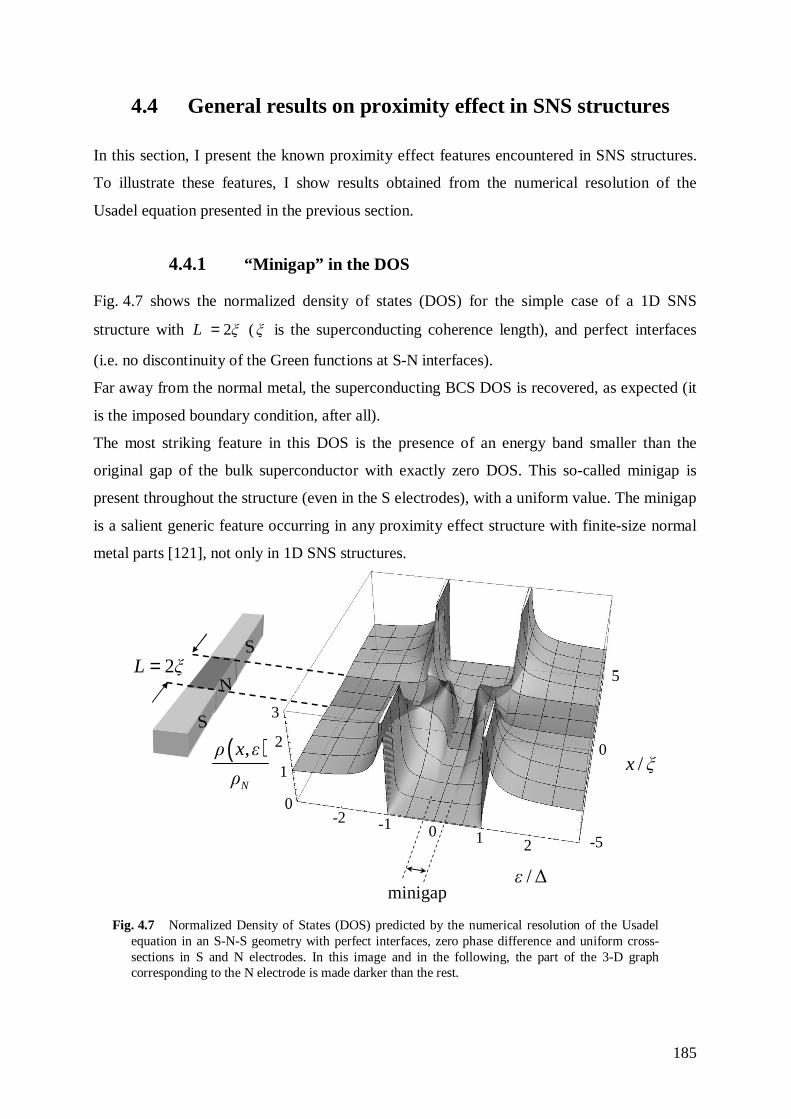
185
4.4 General results on proximity effect in SNS structures
In this section, I present the known proximity effect features encountered in SNS structures.
To illustrate these features, I show results obtained from the numerical resolution of the
Usadel equation presented in the previous section.
4.4.1 “Minigap” in the DOS
Fig. 4.7 shows the normalized density of states (DOS) for the simple case of a 1D SNS
structure with 2=L ξ (ξ is the superconducting coherence length), and perfect interfaces
(i.e. no discontinuity of the Green functions at S-N interfaces).
Far away from the normal metal, the superconducting BCS DOS is recovered, as expected (it
is the imposed boundary condition, after all).
The most striking feature in this DOS is the presence of an energy band smaller than the
original gap of the bulk superconductor with exactly zero DOS. This so-called minigap is
present throughout the structure (even in the S electrodes), with a uniform value. The minigap
is a salient generic feature occurring in any proximity effect structure with finite-size normal
metal parts [121], not only in 1D SNS structures.
S
N
S
/ ∆ε
( ),
N
ρ x ε
ρ/x ξ
2=L ξ
0
1
2
3
0
1
2
3
0 1-1
2
-20 1
-12
-2
minigap
0
-5
5
0
-5
5
Fig. 4.7 Normalized Density of States (DOS) predicted by the numerical resolution of the Usadel equation in an S-N-S geometry with perfect interfaces, zero phase difference and uniform cross-sections in S and N electrodes. In this image and in the following, the part of the 3-D graph corresponding to the N electrode is made darker than the rest.
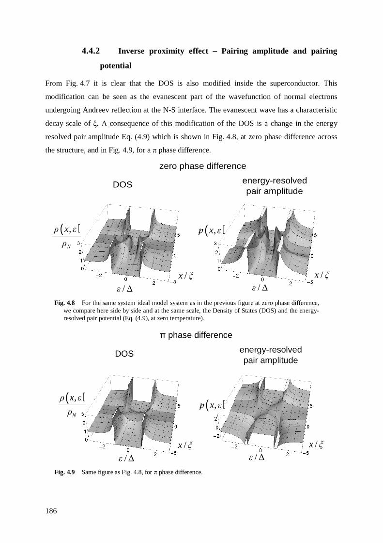
186
4.4.2 Inverse proximity effect – Pairing amplitude and pairing
potential
From Fig. 4.7 it is clear that the DOS is also modified inside the superconductor. This
modification can be seen as the evanescent part of the wavefunction of normal electrons
undergoing Andreev reflection at the N-S interface. The evanescent wave has a characteristic
decay scale of ξ. A consequence of this modification of the DOS is a change in the energy
resolved pair amplitude Eq. ( 4.9) which is shown in Fig. 4.8, at zero phase difference across
the structure, and in Fig. 4.9, for a π phase difference.
energy-resolvedpair amplitude
zero phase difference
/x ξ
DOS
( ),x ε( ),
N
ρ x ε
ρ
/x ξ
/ ∆ε / ∆ε
Fig. 4.8 For the same system ideal model system as in the previous figure at zero phase difference, we compare here side by side and at the same scale, the Density of States (DOS) and the energy-resolved pair potential (Eq. ( 4.9), at zero temperature).
π phase difference
/x ξ
DOS
( ),x ε( ),
N
ρ x ε
ρ
/x ξ
/ ∆ε / ∆ε
energy-resolvedpair amplitude
Fig. 4.9 Same figure as Fig. 4.8, for π phase difference.

187
Both of these phenomena occurring on the superconductor side of the contact are known as
the “inverse” proximity effect.
We see that the amplitude of the energy-resolved pair amplitude function bears many
resemblances with the DOS: it displays the same “minigap” feature, and peaks at the same
positions. However, it falls to zero at high energy where the DOS goes to 1. In the case of the
π phase difference, there is no minigap (or its width is zero). Here the pair potential changes
sign across the structure (corresponding to the eiπ term of the phase shift), and exactly in the
middle of this symmetric structure, one recovers a normal state metal (i.e. constant DOS and
zero pair amplitude).
4.4.2.2 Self-consistency
The pair potential is obtained according to Eq. ( 4.7)-( 4.9), by integrating ( ),E r to obtain
the integrated pair amplitude. As previously explained (see § 4.3.3), this calculation involves
iterating the numerical resolution of the Usadel equations to reach self-consistency. Fig. 4.10,
shows the iterated calculation of the pair potential in the structure shown in Fig. 4.7 to
Fig. 4.10. One observes the reduction of the pair potential in the S electrodes on a length scale
of the order of ξ , a manifestation of the inverse proximity effect. In the system we consider
here, with high transparency interfaces and equal S and N area, the inverse proximity effect is
particularly important, which makes reaching full self-consistency difficult. Here, it can be
considered reached after 10 iterations. In many cases when quantitative predictions are not
needed, the first iteration already qualitatively predicts correctly the behaviour of the system.
This can be seen for instance in Fig. 4.11, where we compare the self-consistent value of the
minigap to the non-self-consistent value obtained at first iteration assuming a step like
potential, and the result of a calculation not taking into account inverse proximity effect (i.e.
assuming rigid bulk superconducting Green functions up to the interface) [144]. In this figure
we can also check the accuracy of our numerical results by comparing the predicted minigap
in SNS system with clean interfaces as a function of the N length, to previously published
results. We more or less recover the results of Belzig et al. [143], but the observed
discrepancy is presently not understood1.
1 A careful examination of our numerical results shows that the calculated solutions for symmetrical structures
are slightly asymmetric (See e.g. Fig. 4.10), for a reason not yet elucidated. This could explain the
discrepancy.

188
-4 -2 0 2 4
0.0
0.5
1.0
Orderparameter Initial guess
Iterated
∆(x)
/∆0
x/ξ
0.0
0.5
1.0
Pair interactionpotential
V (
A.U
.)
0.0
0.5
1.0
Pairamplitude
====
××××
P (
x)
Initial guess Iterated
Fig. 4.10 Iterated pair amplitude and order parameter profiles along the S-N-S structure. The curves in the bottom panel are obtained by multiplying the curves in the top panel by the pair interaction potential depicted in the middle panel. Hence, inside the normal metal the pair amplitude is non zero, while the order parameter is zero due to the absence of pairing interaction. The pair potential is reduced in the superconducting electrodes, due to the inverse proximity effect. One sees clearly that the typical length scale is of the order of ξ .

189
0 2 4 6 8 10 12 140.0
0.2
0.4
0.6
0.8
1.0
no inverse PE (Cuevas et al) inverse PE, non self-consistent self-consistent inverse PE self-consistent (Belzig et al)
Min
igap
/∆0
L/ξ
0.1 1 100.01
0.1
1
Fig. 4.11 Predicted values of the minigap in SNS structures with clean interfaces, as a function of L, the normal metal length. Green and red curves are the results of our calculation, taking into account the inverse proximity effect. Green is the non-self-consistent obtained at first iteration, and red is the converged result at iteration 10. The blue curve is taken from Fig. 1 in [144] and the open dots, from Fig. 3 in [143]. In the inset, the same data are plotted in a log-log scale, showing an asymptotic L-2 dependency of the minigap at large L.
4.4.3 Role of interfaces
Imperfect interfaces reduce the strength of the proximity effect: the minigap is reduced, and
on the S side, the inverse proximity effect, with the associated reduction of the pair potential
is weaker (See Fig. 4.12). This can be easily understood in terms of scattering : at a dirty
interface, an electron coming from the normal metal has, in addition to the Andreev reflection
process, a finite probability to experience a normal reflection, which does not induce pair
correlations in the N part. For a detailed investigation of the role of the interface parameters
see Ref. [149].
Even with perfect interfaces, the 1D model can still show discontinuities in the derivatives of
the Green functions at interfaces if the electrodes do not have the same cross-section (while
sill staying in the 1D approximation). In this case, if the superconductor is much larger than
the normal metal, the inverse proximity effect is also reduced (See Fig. 4.13).

190
/x ξ
perfect interfaces
/ ∆ε
scattering interfaces
( ),
N
ρ x ε
ρ
( ),
N
ρ x ε
ρ
/x ξ
/ ∆ε
Fig. 4.12 Comparison of the DOS in the same ideal SNS structure with perfect interfaces as in Fig. 4.7 - Fig. 4.8 (left) and same structure with resistive interfaces (right), at zero phase difference. In this latter plot we assume the interfaces contribute to the total normal state resistance by the same amount than the wire.
/x ξ
uniform cross-section
/ ∆ε
larger S cross-section
( ),
N
ρ x ε
ρ
( ),
N
ρ x ε
ρ
/x ξ
/ ∆ε
Fig. 4.13 Comparison of the DOS in SNS structures with perfect interfaces but different cross sections in S and N parts. On the left, N and S are of equal cross-section ( Fig. 4.7 - Fig. 4.8), while on the right, the S cross section is ten times larger than the N cross sections. In this case, the superconductor appears more “rigid”: the inverse proximity effect is reduced, and the minigap increased.
4.4.4 Dependence of the minigap on N size
Fig. 4.11, shows the dependence of the minigap in a 1D SNS structure with clean interfaces,
as a function of the length L of the N part. In the log-log inset, one sees that at large L, the
minigap varies as L-2. This dependence can be traced to the diffusive character of the problem:
an electron in the N part has a characteristic dwell time 2τ L D= , which defines the Thouless
energy scale 2TE τ D L= =ℏ ℏ , frequently encountered in mesoscopic systems. The

191
proportionality noted above shows that the minigap Eg is proportional to the Thouless energy
when ∆gE << [143]. The precise proportionality factor depends on the details of the system,
and, in particular, on the interfaces, as shown in the previous section.
4.4.5 Phase modulation of the proximity effect
The originality of the equilibrium SNS system is that one can impose a fixed superconducting
phase difference δ across the structure. Experimentally, this can be achieved by closing the
system in a loop and threading a flux in the loop (see below) or by driving a supercurrent
though the system. This phase difference affects the DOS of the whole structure in a periodic
manner [150]. We show the evolution of the DOS of an SNS structure with δ in Fig. 4.14.
When the phase is varied, the minigap evolves roughly as cosδ , pinching off linearly at
mod 2δ π π= .
3
8
πδ =
2
πδ =
3
4
πδ = 7
8
πδ =
5
8
πδ =
δ π=
8
πδ =
4
πδ =0δ =
Fig. 4.14 Evolution of the DOS of an SNS structure (same as in Fig. 4.7 - Fig. 4.9 ) for a phase difference between the superconductors varying between 0 and π (the behavior is even, 2π-periodic in phase difference).

192
4.5 SNS systems viewed as scattering structures
Pioneered by Landauer, the description of quantum coherent structures in terms of scatterers
for electronic conduction channels has proved a powerful way of understanding mesoscopic
devices. In particular, its formal simplicity often allows intuitive insights on the behaviour of
the systems. For proximity effect structures, it is a complementary tool for the Green
functions approach which gives its predictions only through the “black box” of numerical
resolution of the Usadel equations.
The scattering approach of SNS structures is well explained by Beenakker in Ref. [134]. In
this approach one combines the ordinary electronic scattering matrix s of the N part with the
Andreev scattering matrix ( ),a ε φ describing the NS interfaces and which couples electron
and hole motions in the N part of the structure. This matrix ( ),a ε φ depends on both the
energy and the phase of the superconductor and can be expressed with the Sγ given in ( 4.17).
Working out the scattering matrix of the whole structure, one finds resonant conditions at well
defined energies |ε|<∆, given by the roots of
( ) ( ) ( ) ( )* *
1 2Det , , 0 − − − =
a ε φ s ε a ε φ s ε ( 4.21)
where is the unity matrix [134]. These resonances correspond to quasiparticle states for
which after an Andreev reflection at each extremity the particle interferes in phase with itself
( Fig. 4.15), giving rise to a localized state inside the N part, called an Andreev Bound State
(ABS). Such a structure can be viewed as a Fabry-Perot resonator made with phase-
conjugation mirrors, and the ABS are the modes of the resonator.
e
hNS1 S2
1ϕ
2ϕ
Fig. 4.15 Sketch explaining the formation of Andreev bound states in an SNS structure. At well defined energies, when following a trajectory such as described in this figure, the particle can interfere constructively, giving rise to a localized state with the particle confined mostly inside the normal metal.
All the properties of the system can be obtained from the global scattering matrix, provided
the statistical properties of the constituents are known (and, in particular, their energy
dependence) [151]. This is where this approach merges with the field of Random Matrix
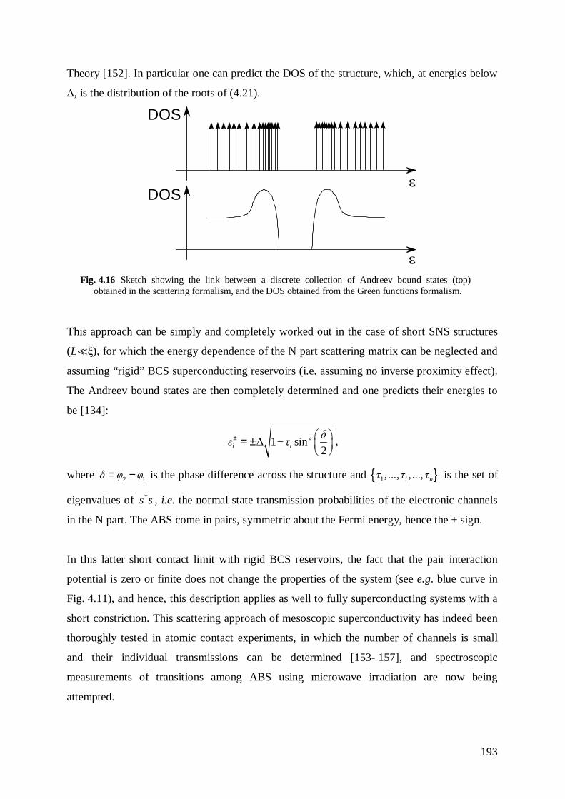
193
Theory [152]. In particular one can predict the DOS of the structure, which, at energies below
∆, is the distribution of the roots of ( 4.21).
DOS
DOS
Fig. 4.16 Sketch showing the link between a discrete collection of Andreev bound states (top) obtained in the scattering formalism, and the DOS obtained from the Green functions formalism.
This approach can be simply and completely worked out in the case of short SNS structures
(L`ξ), for which the energy dependence of the N part scattering matrix can be neglected and
assuming “rigid” BCS superconducting reservoirs (i.e. assuming no inverse proximity effect).
The Andreev bound states are then completely determined and one predicts their energies to
be [134]:
2∆ 1 sin
2± = ± −
i i
δε τ ,
where 2 1= −δ φ φ is the phase difference across the structure and 1,..., ,...,i nτ τ τ is the set of
eigenvalues of †s s, i.e. the normal state transmission probabilities of the electronic channels
in the N part. The ABS come in pairs, symmetric about the Fermi energy, hence the ± sign.
In this latter short contact limit with rigid BCS reservoirs, the fact that the pair interaction
potential is zero or finite does not change the properties of the system (see e.g. blue curve in
Fig. 4.11), and hence, this description applies as well to fully superconducting systems with a
short constriction. This scattering approach of mesoscopic superconductivity has indeed been
thoroughly tested in atomic contact experiments, in which the number of channels is small
and their individual transmissions can be determined [153- 157], and spectroscopic
measurements of transitions among ABS using microwave irradiation are now being
attempted.

194
4.6 An STM experiment on the proximity effect
Although the proximity effect in various structures has been investigated for many years
[158], no experiment could investigate it in detail. Many predictions were found in agreement
with the theoretical predictions, though a comprehensive comparison is still lacking. The main
results obtained are:
• The tunneling density of states was measured at a few distances away from
a NS interface using a few fixed tunneling probes [122].
• The maximum supercurrent of an SNS structure was determined [159].
In order to probe the proximity effect in greater detail, we have fabricated a series of SNS
structures of various sizes and measured the local tunneling DOS at many different positions
in the structure. Our aim was in particular to investigate the dependence with the length of the
N part, and the dependence of the proximity effect with the phase difference between the two
S electrodes. Here, an important goal was to probe and measure the minigap in the local DOS
predicted to occur for short enough N wires.
Last but not least, this experiment provided us with a real test-bed for the experimental
system.
4.6.1 Sample geometry
Our aim is to investigate quasi-1D S-N-S structures in which the phase difference can be
controlled externally. For this purpose, we have inserted an N wire in a superconducting loop,
which allows to control this phase difference by an applied magnetic field. On the same
sample, we designed many wires with different lengths covering all the different regimes of
the proximity effect (§ 4.4.4): the long junction regime equivalent to two independent S-(semi-
infinite N wire) systems and in which the local DOS does not vary with the phase difference,
and the short junction regime in which proximity superconductivity develops all along the N
wire and in which the local DOS varies with the phase difference as explained in § 4.4.5. The
samples fabricated using electron beam lithography are shown in Fig. 4.17.

195
NNS
10 µm
Fig. 4.17 Our samples consist of an array of SNS structures with a loop geometry, the normal wire being inserted in a superconducting loop. The normal length, ranges from 300nm to 3µm. The labels (number or letters) allow to identify the structure using AFM imaging. Leads connect all the structures to a common ground, necessary to sink the tip current in tunnel spectroscopy measurements.
4.6.2 Implementation of the experiment
4.6.2.1 Achieving a good phase bias
We discuss in this section the conditions for a suitable control of the phase difference across
the N wire. The flux of the magnetic field determines the integral of the phase gradient around
the loop. We designed our experiment so that the phase difference across the N wire is given
by the flux applied externally. Two correcting effects have to be considered:
• A part of the integral arises from the S part of the wire due to its non-zero
inductance.
• The applied magnetic flux is modified by the screening current that
develops in the loop.

196
4.6.2.1.a Kinetic inductance correction
At a given flux, the ratio between the phase difference accumulated along the S wire and
along the N wire, ( ) ( )/S Nδ δ , is also the ratio of their kinetic inductances, if their geometric
inductance is relatively small. The kinetic inductance of an S wire writes [160]:
( ) ( )1
∆= ℏS S
K NRπ
where ( )SNR is the normal state resistance of the (S) wire. Similarly, the kinetic inductance of
the N wire subject to proximity effect takes, up to a numerical factor1, a similar expression:
( ) ( )N NK N
G
Rε
∝ℏ
,
with Gε the minigap energy. One thus obtains the relation:
( )( )
( ) ( )∆
SSG N
N NN
ε Rδ
δ R≈
This ratio is small for all our samples. It decreases from about 10-1 in the shortest wire down
to 10-3 in the longest one.
4.6.2.1.b Circulating currents correction
The geometric self-inductance G of the loop brings a correction to the externally applied
flux, due to the circulating currents (see Fig. 4.18). Since those currents depend themselves on
the phase bias, this gives rise to a self-consistent equation for the true phase bias
( )( )0
2Φ
Φext G
πδ I δ= − , ( 4.22)
whose solutions are a reduced phase δ for flux 0Φ Φ<ext and an enhanced phase above
[161, 162].
When the product G Ci of the inductance and the critical current of the weak link is not
small compared to the flux quantum, this causes hysteretic behaviour and a jump of phase
bias around π (see Fig. 4.18) [163].
However if the geometrical inductance term of Eq. ( 4.22) can be neglected, this effect does
not show up. The geometrical inductance is at first order 0G µ l∝ with l the effective loop
1 From [148] and [159], one can evaluate the kinetic inductance of a diffusive normal wire subject to proximity
superconductivity, assuming 3.1G Tε ε∼ [143].

197
radius (for the short wires the loop is almost circular, whereas for the long wires, the shape is
ellipsoidal - see Fig. 4.19). For all wires, G is lower than ( )NK (see 4.6.2.1.a).
Since the critical current of the N part is ( )/( )NC T Ni ε eR∝ [159], the maximum phase
correction is ( )0 02 /(Φ )N
G T Nδ πµ lε eR≈ . This correction is negligible for all samples, including
the shortest N wires. Numerical estimates are in the following ranges:
[ ]1 2 pHG∈ − ,
[ ]( ) 3 9 pHSK ∈ − ,
[ ]( ) 25 5300 pHNK ∈ − ,
[ ]1.5 90 µeVTε ∈ − ,
[ ]0.04 17.5 µACi ∈ − ,
yielding in the worst case (the smallest loop) a geometrical flux ( G Ci ) around 1% of 0Φ .
Ф0/2 Ф0 Фext
δ
π
2π
0
ФG
δ
Фext
ФG
δ
Фext
Fig. 4.18 Currents in the wire contribute to the total flux through the loop, which affects the phase difference across the N wire. In our experiment, this correction is small since the geometric inductance is small compared to the total kinetic inductance of the loop. The phase difference accumulated along the S part is also small compared to that along the N part because its kinetic inductance is smaller. Right: red curve: when the geometric inductance of the loop is not negligible the S-N-S junction exhibits an hysteretic behaviour, and there is a jump of phase around π; blue curve: in our experiment, the geometric inductance is negligible, and we can achieve phase biases continuously from 0 to π.
4.6.2.2 Sample fabrication
We have fabricated SNS structures made of aluminum and silver. Aluminum is a
weak-coupling superconductor well described by the BCS theory, and silver a metal with

198
good electronic coherence properties due to the rarity of magnetic impurities in the sources1.
Furthermore, the Al-Ag interface can have a good transparency, which is essential to obtain a
sizeable proximity effect. The interface quality is indeed of great importance for the
propagation of electronic correlations into the normal metal (see § 4.4.3 p 189).
For that reason, one has either to fabricate the sample by evaporating both layers without
breaking the vacuum, or to mill the surface of the first layer before depositing the second one.
Both techniques are described in Chapter 3. We have opted for the first one, using shadow-
mask deposition at two angles, with a bilayer of resist forming a suspended mask.
This method faces the difficulty that two distinct electrodes (the normal and the
superconducting ones) have to be deposited, with only two connections, and no overlap at any
other place. This imposes both small structures and large deposition angles through a
suspended mask with a large height. To put numbers, we employed ±17° deposition angles on
a ~ 1 µm / 70 nm thick MAA / PMMA bilayer, which yields a ~ 600 nm lateral displacement
sufficient to avoid overlap between the patterns. The loops are half ellipses, with one radius
defined by half the normal length from 150 nm to 1.5 µm, the other radius being at most 1 µm
for the largest and 0.6 µm for the smallest. This method also faces the challenge to deposit
thin and narrow wires (nominal width of 50 nm) at large angles. Indeed, the deformation of
the suspended mask due to stresses results in wires wider than expected (up to 70 nm), and
with a poorly defined shape.
Avoiding overlaps between N and S in another place than the wire edges ensures that the
superconducting region remains genuine, which allows considering a bulk superconductor
away from the interface, and investigating the inverse proximity effect in the superconductor.
4.6.2.3 Overview of the measured SNS structures
Some of the structures of Fig. 4.17 which we measured during the experiment are shown
below with their dimensions. Those photographs were taken in a SEM after the experiment
was completed.
1Fe is often the dominant impurity in Au, and copper oxide is magnetic.

199
meas
nom.
meas
nom.
2700900500300
28001000600400
2810975575405
300175d
240
61
870
3
360300e
220275220c
646559b
2550430307a
421
meas
nom.
meas
nom.
2700900500300
28001000600400
2810975575405
300175d
240
61
870
3
360300e
220275220c
646559b
2550430307a
421
1a
bc
d
e
2a
bc
d
e
3 b c
a
4
a
bc
1a
bc
d
e11
a
bc
d
e
2a
bc
d
e22
ab
c
d
e
3 b c
a
33 b c
a
4
a
bc
44
a
bc
Table: dimensions (nm)
NLNL
Fig. 4.19 Scanning electron micrographs of the S-N-S proximity structures. The darker material is aluminum, and the lighter is silver. Silver (normal) wires of different lengths are connected across a loop of aluminum (superconductor). The total length LN of each wire (indicated on the table) was measured from the maxima of the overlap regions, with an AFM. Both nominal and measured length are mentioned. Other dimensions were measured with the SEM; in particular the “free” length (a) of the wires, difficult to obtain with the AFM due to tip size effects. The wires were designed to be 50nm wide but they come out slightly wider. Marks on the different structures come from the tip reshaping procedures (see chap 3), done to recover a good tip shape in situ. From place to place, the normal wire is enlarged, possibly due to mask deformation.
4.6.3 What do we measure?
During this experiment we have first used our AFM to locate the systems, and image them.
Once a satisfying image was obtained, we turned off the AFM mode (see chap 2), positioned
our tip above the desired place, formed a tunneling contact between the tip and the sample
with a resistance in the 100 k-1 MΩ range, and recorded the conductance of the contact as a
function of voltage, flux through the loop....
We first present the complete set of data taken on the four systems shown in Fig. 4.19, and we
draw the main conclusions that can be inferred from them. The longest wire (#4) in which the
proximity effects developed at both ends do not interfere in the middle of the wire is
described first; we then present the strong interference regime that occurs in the short wires #1
and #2; the intermediate regime found in wire #3 is then presented .
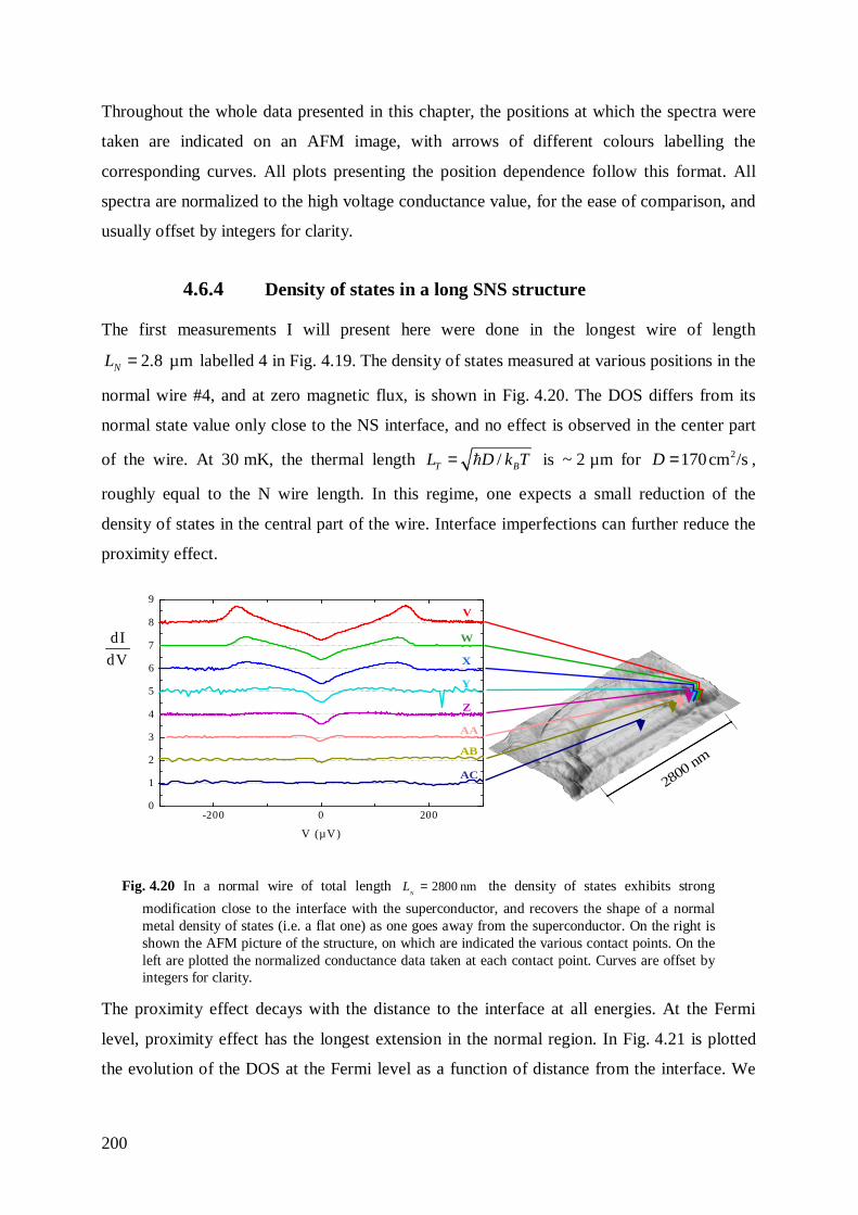
200
Throughout the whole data presented in this chapter, the positions at which the spectra were
taken are indicated on an AFM image, with arrows of different colours labelling the
corresponding curves. All plots presenting the position dependence follow this format. All
spectra are normalized to the high voltage conductance value, for the ease of comparison, and
usually offset by integers for clarity.
4.6.4 Density of states in a long SNS structure
The first measurements I will present here were done in the longest wire of length
2.8 µmNL = labelled 4 in Fig. 4.19. The density of states measured at various positions in the
normal wire #4, and at zero magnetic flux, is shown in Fig. 4.20. The DOS differs from its
normal state value only close to the NS interface, and no effect is observed in the center part
of the wire. At 30 mK, the thermal length /= ℏT BL D k T is ~ 2 µm for 2170cm /s=D ,
roughly equal to the N wire length. In this regime, one expects a small reduction of the
density of states in the central part of the wire. Interface imperfections can further reduce the
proximity effect.
-200 0 2000
1
2
3
4
5
6
7
8
9
V (µ V)
dI
dV
2800
nm
V
W
X
Y
Z
AA
AB
AC
Fig. 4.20 In a normal wire of total length 2800 nm=N
L the density of states exhibits strong
modification close to the interface with the superconductor, and recovers the shape of a normal metal density of states (i.e. a flat one) as one goes away from the superconductor. On the right is shown the AFM picture of the structure, on which are indicated the various contact points. On the left are plotted the normalized conductance data taken at each contact point. Curves are offset by integers for clarity.
The proximity effect decays with the distance to the interface at all energies. At the Fermi
level, proximity effect has the longest extension in the normal region. In Fig. 4.21 is plotted
the evolution of the DOS at the Fermi level as a function of distance from the interface. We

201
find that the recovery to the normal DOS is close to an exponential, with a characteristic
length of 240 nm.
In absence of proximity effect in the central part of the wire, no effect of the phase difference
is expected. This will have to be checked in the next experiment since it was not done during
the present one. When these data were taken, we could not drive enough current in the coil,
and this wire was not measured again once we had solved the coil issue.
0 200 400 600 800 1000 1200 14000.0
0.1
0.2
0.3
0.4
0.5
0.6
0.7
0.8
0.9
1.0
1.1
y0+Ae^(-x/t)
Value Error---------------------------------------------y0 1.0119 0.03764A -0.74447 0.04039t 242.7 37.55---------------------------------------------
dI/d
V (
V=
0)
distance from interface (nm)
Fig. 4.21 Normalized conductance at the Fermi level as a function of distance to the interface. The density of states recovers progressively its normal state value, with a characteristic distance of 240 nm. The positions are indicated with an error bar of 50 nm (see § 4.6.7).
4.6.5 Density of states in a short SNS structure
4.6.5.1 position dependence
We consider here wires with total length 400 nm (#1) and 600 nm (#2), and with an overlap
region of ~ 50 nm for #1 and ~ 70 nm for #2 at each end (see discussion in § 4.6.7).
Local DOS data are presented for the two wires in Fig. 4.22 and Fig. 4.23. In each structure
the density of states was measured at various positions in the normal wire and in the
superconducting electrode.
• Wire #1 (length: 400 nm)
One observes on those plots the presence of a true energy gap independent of position in the
N wire: this is the predicted minigap. On the superconducting side, and close to the interface,
one notices the existence of states between the minigap and the superconducting gap. This
phenomenon, called the inverse superconducting proximity effect (see 4.4.2), had not been
observed before.

202
These measurements of inverse proximity effect are technically challenging, because the DOS
is small, which requires a high current sensitivity (see chapter 3). The measured currents were
of the order of 20 fA in the minigap region, and 100 fA in between the minigap and the gap,
with a noise of ~5 fA. Data B shown on a logarithmic scale in Fig. 4.22 allows to estimate the
measurement noise: an apparent conductance of ~7 10-3 µS is measured in the minigap with
an AC excitation of 3 µV, and the peak to peak noise is 2 10-3 µS. We take the value of
7 10-3 µS to be the offset of our measurement in that case: this was the typical value that we
read when the tip was away from the sample, which can be seen as a leak resistor in the setup.

203
dI
dV
400 nm
-400 -200 0 200 4000
1
2
3
4
5
6
7
V (µV)
-400 -200 0 200 4000.0
0.5
1.0
1.5
2.0
2.5
3.0
3.5
V (µV)
A
B
C
D
E
A
B
reduced gapnear interface(inverse PE)
A
-100 0 100 2000
0.02
0.1
1
S side
0
0.5
1.0
1.5
2.0
N side
V (µV)
inverse PEstates
C
D
E
B
Fig. 4.22 Local DOS in the shortest wire measured, with total length 400 nm and “free” length around 300 nm. The spectra are recorded at various points in the structure, both in the normal and the superconducting regions. Data are plotted on the graph (upper left), and the corresponding positions are shown on the AFM image (upper right). In the normal wire, we show three contact positions labeled C, D and E. Tunneling data at those points exhibit a true minigap around the Fermi level, with a width independent of position. The density of states varies nevertheless strongly with position, as shown in the lower-right graph. The tunnel spectroscopy has also been recorded in the superconducting region at positions labeled A and B, A being far from the normal region, and B close to it. Data taken at these points are shown on the lower-left graph: the density of states at position B is non-zero below the gap energy. To make it clear, data at position A and B are also shown using a logarithmic scale, on the lower-right graph. Unfortunately, data were noisier at pos. A due to less averaging, and they are spoiled by a high noise level, compared to pos. B. A non-zero DOS is observed below the superconducting gap, but not below an energy close to the minigap energy, observed in curves C, D, E and B.
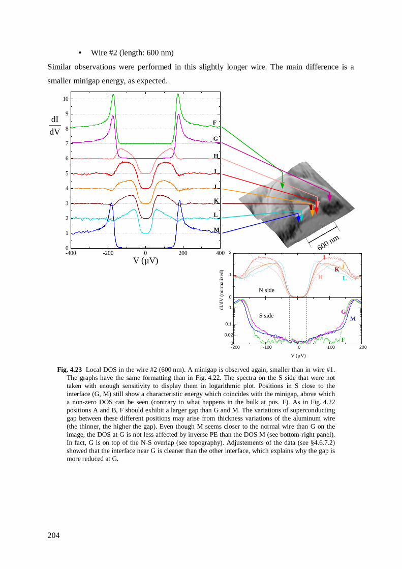
204
• Wire #2 (length: 600 nm)
Similar observations were performed in this slightly longer wire. The main difference is a
smaller minigap energy, as expected.
600 nm600 nm
-400 -200 0 200 4000
1
2
3
4
5
6
7
8
9
10
V (µV)
F
G
H
I
J
K
L
M
dI
dV
0
1
2
-200 -100 0 100 2000
0.02
0.1
1dI/d
V (
norm
aliz
ed)
V (µV)
GM
L
I
H
JK
F
S side
N side
Fig. 4.23 Local DOS in the wire #2 (600 nm). A minigap is observed again, smaller than in wire #1. The graphs have the same formatting than in Fig. 4.22. The spectra on the S side that were not taken with enough sensitivity to display them in logarithmic plot. Positions in S close to the interface (G, M) still show a characteristic energy which coincides with the minigap, above which a non-zero DOS can be seen (contrary to what happens in the bulk at pos. F). As in Fig. 4.22 positions A and B, F should exhibit a larger gap than G and M. The variations of superconducting gap between these different positions may arise from thickness variations of the aluminum wire (the thinner, the higher the gap). Even though M seems closer to the normal wire than G on the image, the DOS at G is not less affected by inverse PE than the DOS M (see bottom-right panel). In fact, G is on top of the N-S overlap (see topography). Adjustements of the data (see § 4.6.7.2) showed that the interface near G is cleaner than the other interface, which explains why the gap is more reduced at G.

205
4.6.5.2 phase dependence
At each position presented on Fig. 4.22 and Fig. 4.23, the phase was modulated by applying a
magnetic flux. Fig. 4.24 shows how the minigap closes as the phase goes through π, as well as
the appearance of features in the DOS shape.
Noticeably, a peak emerges on the minigap edge, similar to the BCS coherence peak in a true
superconductor. This is what one would naively expect in a superconductor with an order
parameter equal to the minigap. Since the minigap varies with the phase difference, the peak
is displaced and its shape evolves with the phase difference.

206
-200 -100 0 100 2000
0.02
0.1
1
0 mA 26 mA 39 mA 52 mA 65 mA 78 mA
-400 -200 0 200 4000
1
2
3
4
5
6
7
8
9
10
11
12
100 mA
90 mA
78 mA
70 mA
60 mA
50 mA
40 mA
30 mA
20 mA
10 mA
0 mA
V (µV)
C
B
400 nm
E DC B
-400 -200 0 200 4000
1
2
3
4
5
6
7
8
9
10
11
12
13 125 mA
115 mA
105 mA
95 mA
85 mA
78.5 mA
75 mA
65 mA
55 mA
45 mA
25 mA
5 mAD
-200 -180 -160 -140 -120
1
2 0 mA 26 mA 39 mA 52 mA 65 mA 78 mA
G (
no
rma
lized
)
-200 -180 -160 -140 -120
1
2 0 mA 26 mA 39 mA 52 mA 65 mA 78 mA
G (
no
rma
lized
)-400 -200 0 200 4000
1
2
3
4
5
6
88 mA
78 mA
49 mA
30 mA
10 mA
G (
no
rmal
ized
)
V (µV)
E
Fig. 4.24 Normalized conductance for different values of current in the coil; each graph represents a different positions in wire #1, labeled by the same letters as in Fig. 4.22. For clarity, curves are displaced by integers on all graphs except for the position B in the superconductor where data are shown on a logarithmic scale, for there is only a small amount of states that are modified by inverse proximity effect.

207
-200 0 140 2000
1
2
3
4
5
6
7
8
9
10
66 mA
49.5 mA
33 mA
16.5 mA
0 mA
-16.5 mA
-33 mA
-49.5 mA
-65.5 mA
-200 0 140 2000
1
2
3
4
5
6
7
8
9 65 mA
57 mA
48.5 mA
40.5 mA
32 mA
24 mA
16 mA
8 mA
0 mA
V (µV)J
-200 0 130 2000
1
2
3
4
5
6
7
8
67 mA
66 mA
53 mA
39.5 mA
26.5 mA
13 mA
0 mA
H
-200 0 2000
1
2
3
4
5
66 mA
49.5 mA
33 mA
16.5 mA
0 mA
L
600nm
K
JI
H
L
-200 0 130 2000
1
2
3
4
5
6
7
8 65 mA
56 mA
51 mA
48 mA
42 mA
32 mA
16 mA
0 mA
G (
norm
aliz
ed)
V (µV) K
I
Fig. 4.25 Same as in Fig. 4.24 for wire #2. Positions G and M on the superconducting side were not measured as a function of phase bias.

208
4.6.5.2.b Phase calibration
In order to obtain the coil current to phase conversion, we determine the flux which
corresponds to a π phase difference. We find 78±1 mA in wire #1, and 65±1 mA in wire #2.
All data plotted as a function of the phase assume those values calibration values.
-100 -50 0 50 100 150 200 250 3000.0
0.5
1.0
phase difference
500 nm wire 300 nm wire
G (
norm
aliz
ed)
Coil current (mA)
-1ππππ 0ππππ 1ππππ 2ππππ 3ππππ 4ππππ
-1ππππ 1ππππ 3ππππ
wire n°1wire n°2
Fig. 4.26 Normalized conductance at the Fermi level, as a function of coil current, at one position in the two wires presented in this section. Since the size of the loop is not constant, one has to apply a higher magnetic field to thread one flux quantum through the loop, so the period is not a constant function of coil current. The X axis is shown either in direct coil current values (bottom axis) or in phase value (top axis), assuming the aforementioned values of the current for a π phase bias. When the coil current is too high, one can observe depairing in the superconductor, resulting in an increase in the Fermi level density of states. This is observed above 180 mA at the position presented here in wire #2. The data were not taken in wire #2 for I>125mA.
4.6.5.2.c minigap as a function of phase
The criterion employed to determine the amplitude of the minigap should rigorously detect
the value of polarization at which the density of states begins to be non zero, with a threshold
as small as the accuracy in the DOS measurement. However, due to finite energy resolution of
the density of states measurement (see Chap. 3), this criterion yields a zero gap value over a
whole phase range around π. To go beyond this limitation, and show data on the whole range
of phase bias, we define the minigap amplitude to be the position of the maximum of the

209
derivative of each curve, obtained numerically from the data. Gap determinations obtained
with this procedure are shown in Fig. 4.27.
-π 0π π 2π0
10
20
30
40
50
60
70
C D wire #1H J K wire #2
gap
(µ
V)
phase-π 0π π 2π
0
10
20
30
40
50
60
70
C D wire #1H J K wire #2
gap
(µ
V)
phaseFig. 4.27 In wires #1 and #2 the gap amplitude has been plotted as a function of phase bias. One sees
a diminution of the gap amplitude as the phase increases towards π, and an increase after π. Considering all the data, one can see this behavior is symmetric around 0 and π. For each wire, data are shown for various positions, and the coincidence between data show that the minigap amplitude is independent on position.
4.6.5.3 Is the Al electrode affected by the applied field?
The phase modulation data that we have presented require to apply magnetic fields not small
compared to the critical field of the Aluminum films. Our current to field calibration, derived
from the flux calibration using the loop area, is 0.65 Gauss/mA. The field applied in the
phase modulation experiments, up to about 50 Gauss, is not small compared to the critical
field of Al wires. The depairing due to the field is characterized by the depairing energy [148]
( ) 2 2 2Γ6
DB e B w=
ℏ, ( 4.23)
with B the magnetic field and w the width of the superconductor.
The predictions of this model were found in quantitative agreement with experiments
performed on Al wires with similar widths [148, 164].
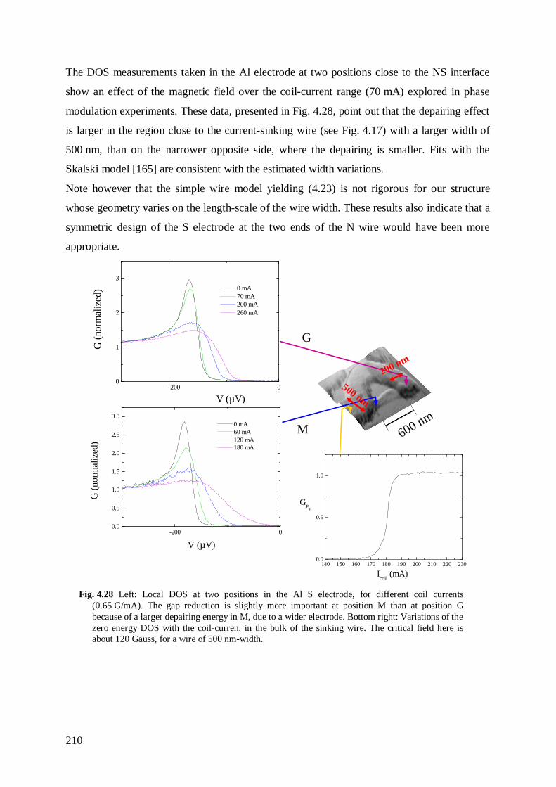
210
The DOS measurements taken in the Al electrode at two positions close to the NS interface
show an effect of the magnetic field over the coil-current range (70 mA) explored in phase
modulation experiments. These data, presented in Fig. 4.28, point out that the depairing effect
is larger in the region close to the current-sinking wire (see Fig. 4.17) with a larger width of
500 nm, than on the narrower opposite side, where the depairing is smaller. Fits with the
Skalski model [165] are consistent with the estimated width variations.
Note however that the simple wire model yielding ( 4.23) is not rigorous for our structure
whose geometry varies on the length-scale of the wire width. These results also indicate that a
symmetric design of the S electrode at the two ends of the N wire would have been more
appropriate.
-200 00
1
2
3
0 mA 70 mA 200 mA 260 mA
G (
norm
aliz
ed)
V (µV)
-200 00.0
0.5
1.0
1.5
2.0
2.5
3.0 0 mA 60 mA 120 mA 180 mA
G (
norm
aliz
ed)
V (µV)
600 nm600 nm
500 nm
200 nm
G
M
140 150 160 170 180 190 200 210 220 2300.0
0.5
1.0
GE
F
Icoil
(mA)
Fig. 4.28 Left: Local DOS at two positions in the Al S electrode, for different coil currents (0.65 G/mA). The gap reduction is slightly more important at position M than at position G because of a larger depairing energy in M, due to a wider electrode. Bottom right: Variations of the zero energy DOS with the coil-curren, in the bulk of the sinking wire. The critical field here is about 120 Gauss, for a wire of 500 nm-width.

211
4.6.6 Density of states in a medium-size SNS structure
4.6.6.1 Intermediate regime
When the length of the normal wire is increased, superconducting correlations are expected to
be present throughout the structure, till it exceeds the thermal length. From the experimental
point of view, the picture is however less simple because, when the minigap becomes too
small, the resolution achieved with the tunneling method (see chapter 1 and 3) does not allow
to observe a zero DOS inside the minigap, but only a dip. Note that this was already observed
in the phase dependence of the minigap around π.
In the 1 µm-long wire #3 the minigap, estimated by extrapolating the values obtained on the
other wires, is 9 µV. Given the 10 µV resolution of our microscope, we indeed cannot expect
to observe a true gap.
Data taken in wire #3 are plotted on Fig. 4.29. Close to the interface, the curves distinguish by
pronounced features just below ∆ on the N side, and by a peak at ∆=E on the S side. As
one goes towards the middle of the wire, features appear at lower energy: states aggregate at
the minigap edge.

212
1000 nm
-400 -200 0 200 4000
1
2
3
4
5
6
7
8
V (µV)
dI
dV
N side
S side
N
O
P
Q
R
S
T
U
U
NOP QR S
0
1
2
-200 -100 0 100 2000
0.02
0.1
1
V (µV)
Fig. 4.29 Left: Local DOS in the 1 µm long wire #3. Spectra were taken at positions very close to the N S interface, as shown at U on the S side, and S,T on the N side. The spectrum evolves from a near-BCS spectrum at position U (see Fig. 4.7), to a gapless spectrum at position T still on the S side. Other positions display some of the features shown in Fig. 4.22 and Fig. 4.23. An estimated minigap can be obtained from the width of the conductance dip (dashed lines). Position T is noisy partly due to mechanical instabilities of this contact, and partly to the very low conductance of the contact: we did not achieve more than ~0.04 µS at this position and could never again observe this kind of data.
4.6.7 Comparison with theory
We now compare the above results to the predictions of the quasiclassical theory presented
above, using the the technique described in § 4.3.
4.6.7.1 Parameters entering the theory
(i) For the superconducting aluminum electrode, we only need to know the value of the gap of
aluminum ∆ . This value is obtained from a separate DOS measurement in the bulk, i.e. “far
away” from the normal region and at zero magnetic field. As discussed in chapters 1 and 3,
the conductance is the density of states convolved with the electronic energy distribution

213
function in the tip. From the fits, one obtains both the temperature of electrons in the tip, and
the gap of the superconductor. This value of ∆ should be constant on all the samples, but
actually, the apparent gap near low resistance interfaces needs to be reduced by a few percent,
to take into account inverse proximity effect which is not calculated self-consistently here, for
simplicity (cf. Fig. 4.22).
(ii ) For the N wire, we mainly need to know the diffusion constant D. It is assumed to be the
same for all wires, fabricated in the same deposition step. The diffusion constant in the S
electrode also enters the theory, but we noticed that the predictions are weakly sensitive to
this value, due to interface parameters (see point (iv)), so we took the same value as for silver.
(iii ) Geometrical parameters and positioning accuracy: The 1-D approximation used in the
numerical calculations requires making some simplifying assumptions on the geometry and
defining effective lengths (See Fig. 4.30). In particular, the effective length ℓ of the wire is
taken intermediate between the “free” length a and the total length LN. Even in the absence of
positional uncertainty relative to the sample image, the position of the tip in the model also
needs to be redefined: in the model, what is relevant is the distance to a sharp interface,
whereas in the experiment, the position of the tip is not at a well defined distance from the
interface. Furthermore, the tip-to-interface distance xeff entering the 1-D model is different
from the distance x to the apparent interface in the AFM image. In the crudest approximation,
we consider, in the N wire,
eff 2
ax x
−= + ℓ .
We stress here that this is not to be taken as an exact mapping: such a mapping does not exist.
On the S side also, a similar redefinition is required, since the Al thickness has to be taken
into account.
Once this mapping done, one expects the discrepancies between the 1-D model and the
experiment to be in relative most important for the shortest wires and close to the interfaces.
Additionally, the experimental tip positioning accuracy, mainly limited by tip deformations, is
estimated at ±25nm in worst cases. Hence, small adjustments of the positions were allowed
for a few curves in order to obtain a predicted DOS in better agreement.

214
LN
Al Al,A σAl Al,A σ
Ag Ag,A σ
Aσλ×Aσλ×Aσ
a
Tip
x
ℓℓℓℓ
xeff
Tip
Fig. 4.30 Top: relevant geometric and material parameters to describe the overlap junctions in the SNS structures. AAg,Al, are the nominal cross sections of the structure. Bottom: in the 1-D model, we introduce effective parameters discussed in the text.
(iv) As discussed in the theory section, the interface transparency is an important parameter,
which, experimentally, is not well controlled. In the model we have to provide the
transmission distribution ( )P T of the conduction channels of the interface (see § 4.2.3.5,
p. 171). While attempting to reproduce the experimental measurements, we found the
depression just above ∆ found in some data could only be reproduced by assuming the
channels transmission is close to unity. For simplicity, and to reduce the number of
parameters, we assumed all transmitted channels are ballistic channels ( 1=τ ). This is
consistent with the fabrication procedure where both metal are deposited in the same vacuum,
thereby ensuring interface relatively good cleanness. Doing so, we are left only with the
number of interface channels as a free parameter. This also is reasonable since the effective
overlap between the electrodes can vary due to the dispersion in the fabrication process,
which is clearly seen on the scanning electron micrographs of the structures ( Fig. 4.19).
Moreover, as already mentioned, the cross-section area differs from one side to the other side
of the interface. Thus, some channels belonging to the superconductor are not coupled to the
normal region, which weakens the inverse proximity effect in the superconductor. For
convenience in the dimensionless numerical equation, for each interface we rather specify the
resistance ratio Nr R Rξ= , where ( ) 110N NR G G
−−= = is the normal state resistance of the
contact and the number of transmitted channels, and

215
2N N
RA A e Dξ
ξ ξσ ρ
= =
is the resistance of a length ξ of the N wire, A being its cross-section, and ρN, the density of
states.
Finally, in the parameters describing the interfaces in ( 4.18) enters the product of the cross
section with the conductivity of the material. Since we assume (ii ) D is the same in both
materials, and knowing the density of states of Al at the Fermi energy,
47 -1 -3Al 2.15 10 J mρ = × and of Ag, 47 -1 -31.03 10 J mAgρ = × , we expect a conductivity about
twice as large in Al. According to the nominal geometrical parameters AAl = 8AAg. Hence, in
the calculation we take the product AAlσAl = λ AAgσAg, with λ = 16.
4.6.7.2 Comparison with theoretical predictions
4.6.7.2.a Determination of the parameters
Determining appropriate model parameters was done in an trial and error process in order to
obtain a good overall rendering of the data. First, the diffusion constant is fixed and then the
left and right interface resistance ratios rL,R are adjusted for each wire in order to try
reproducing the width of the minigap, and, if possible, the individual shapes of the curves. In
spite of the apparent large parameter space, by playing with the numbers one rapidly acquires
the feeling of the direction in which to adjust the various parameters.
Indeed, initially the parameters space was even much larger since we were also adjusting the
average transmission of the interface channels (and even trying other distributions), before
realizing that the optimum was consistently found only for high transmissions, at which point
we decided to freeze this parameter to unity for all interfaces. The fact that only high
transmissions allow to account for the data may appear inconsistent with the mismatch
between Fermi velocities of silver and aluminum, which are respectively 1.39 106 m/s and
2.03 106 m/s. Such mismatch unavoidably induces reflection however it is well-known that
very good contacts can be achieved between materials having different Fermi wavevectors.
One may invoke interdiffusion of materials at the interface, or other microscopic process that
allow departure from the theoretical behaviour of the interface.
In the following table are summarized the set of parameters we have converged to.

216
wire #1 wire #2 wire #3wire #4
Effective length ℓ (nm) 350 550 950 2750
Diffusion constant D (cm2s-1) 170
Gap energy (µeV) 165 170;173 175 170
average τ 1 Left interface
rL ratio 0.7 4.0 0.5 1.0
average τ 1 Right interface
rR ratio 0.5 0.05 2.0 0.6
Table. 4.1 Sample parameters used for the calculated results presented in this section. In wire #2, the gap energy differs between the two superconducting electrodes: the first given value corresponds to the left one.
One can check whether these parameters are reasonable. From the diffusion constant, one can
calculate ξ = 250 nm, and Rξ = 3.7 Ω, corresponding to a resistance per square Rá= 0.7 Ω
quite reasonable for this kind of films. From the nominal cross-section of the wires
(30×50 nm2), and the silver Fermi wavelength λF = 5.24 10-10 m, one arrives to a number of
~22000 channels in the wire corresponding to a minimum interface resistance
Rmin =( G0)-1 = 0.6 Ω. Hence the interface resistance ratio could be as low as
Rmin / Rξ = 0.015. The values obtained are globally larger, indicating either a deviation from
clean interfaces, or a variation in the number of transmitted channels from the simple
estimation above. Since we obtain a better agreement in the fits by assuming ballistic channels
rather than a disordered interface, we conclude that the actual overlap between aluminium and
silver is responsible for the observed variations. This is checked by having a look at AFM
images, where the overlap can be roughly evaluated. This method is not really sensitive, and
only allows checking whether interface parameters are reasonable or not, especially for wire
#2 where there is a huge variation between left and right interfaces. In next figure are plotted
the cross sections measured parallel to the silver wire on AFM images, for both wire #1 and
wire #2. On this figure, one can observe that (i) on wire #1 the overlap is quite equivalent for
both interfaces, wich is consistent with the values rL and rR for this wire, and (ii ) on the
contrary, in wire #2, the right interface overlap is clearly observable whereas the left one does
not appear at all, which once again backs up the fitting values rL and rR. On wire #3 and #4,
the left and rigth overlaps look similar (data not shown).
These observations allow us to infer that the number of transmitted channels is not limited by
the wire cross section, but rather by the overlaps.

217
0 200 400 600 800 1000 1200 1400 16000
10
20
30
40
50
60
70
80
90
position (nm)
heig
ht (
nm)
wire #1
wire #2
0 200 400 600 8000
10
20
30
40
50
60
70
80
90
position (nm)
heig
ht (
nm)
50 nm
Fig. 4.31 Cross-section views of wire #1 and wire #2. Left panel: AFM images, on which are indicated by a straight line the locations where were taken the height data. Right panel: height data along the line. One can see that on wire #1 the overlap is balanced between left and right interfaces. On the contrary, on wire #2 one can see the overlaps are really asymmetric.
Finally, regarding the value of the gap used for each wire (to avoid doing self-consistent
calculations), we see that indeed these gap values correlate somewhat with the quality of the
interfaces we consider: lower gap values are found for wires with clean interfaces. A finer
analysis would have required taking two gaps to take into account the asymmetry of the
contacts. Indeed, careful examination of the curves G and M in Fig. 4.23 shows that the gap is
larger on the “left” side of the wire (M curve) than on the “right” side (G curve),
corresponding to the interface resistances we find. Since by construction the model cannot
capture all details of the experiment, we thought it was a bit pointless trying to refine further
this particular aspect. In principle, though, as explained in the theory part, such details on the
order parameter should be captured by performing self-consistent calculations, which are only
a matter of patience.
Using the above parameters, the calculated DOS profiles at δ=0 for the four wires are shown
in Fig. 4.32.

218
E
x
Wire 1 Wire 2
Wire 3 Wire 4
Fig. 4.32 Calculated DOS profiles at δ=0 for the four wires. The interface parameters are shown in Table. 4.1 and have been chosen to obtain the best overall fit at all the measured positions, presented hereafter.
4.6.7.2.b Position dependence
The theoretical predictions for the conductance, obtained by convolving the DOS with a
thermal rounding function taken at 60 mK, are plotted in Fig. 4.33 together with the
experimental data for the 4 wires measured. All positions are labeled with the same letters as
in Fig. 4.22, Fig. 4.23 and Fig. 4.29.

219
Most features of the conductance curves are quantitatively accounted for, except at a few
positions such as C and E in the shortest wire #1. Here, we attribute the discrepancy to the
failure of the 1D model, which is corroborated by the better agreement obtained for the longer
wires. Note that some small position adjustments, within the estimated position accuracy,
have been made for fitting some curves.
The dip predicted at zero voltage at positions AA, AB, AC is not observed experimentally. A
possible explanation for this effect is the presence of a small depairing process in the N wire.
More calculations are needed to test this hypothesis.
0.1
1
-400 -200 0 200 4000
0.02
1
2
3
4
5
6
7
8
dI/d
V (
norm
aliz
ed)
V (µV)
B
C
D
E
G
H
I
J
K
L
M
N
O
P
Q
R
S
T
U
V
W
X
Y
Z
AA
AB
AC
-200 0 2000
1
2
3
4
5
6
7
8
9
V (µV)
0.1
1
-400 -200 0 200 4000
0.02
0
1
2
3
4
dI/d
V (
norm
aliz
ed)
0.1
1
00.02
0.1
1
-400 -200 0 200 4000
0.02
1
2
3
4
5
6
7
dI/d
V (
no
rmal
ize
d)
Fig. 4.33 Comparison of data with theory at zero phase bias for all wires (top left: #1, top-right: #2, bottom-left: #3, bottom-right: #4) presented in sections 4.6.4 to 4.6.6. Each curve is labeled by a letter corresponding to the position labels.

220
4.6.7.2.c Phase dependence
We have then compared the data with the predicted phase variations for the conductance. Data
and predictions are compared in Fig. 4.34 for two positions on the two sides of the NS
interface in wire #1.
The important result demonstrated here is that the minigap is observed unambiguously on the
S side: the minigap measured in the N part and the associated feature observed on the S side
have the same phase evolution.
The presence of the same energy scale (the minigap) thoughout the SNS structure is an
important characteristic of the influence of the finite N electrode on the S side, which is well
reproduced by the theoretical predictions.
0.5
1.0
1.5
2.0
N side
Experiment
dI/d
V (
norm
aliz
ed)
0.5
1.0
1.5
2.0Theory
δ 0 3π/8 4π/8 6π/8 7π/8 8π/8
-200 -100 00.00
0.02
0.1
1
S side
0 100 2000.00
0.02
V (µV)
0.1
1
Fig. 4.34 Comparison between tunneling conductance data and predictions at two positions on the two sides of the NS interface in wire #1. Experimental data (left) and theoretical predictions (right) at position C on the normal side (top), and at position B on the S side (bottom). The minigap in the N part and its associated feature in the S side follow the same phase variations.

221
4.6.7.2.d Length dependence
The different S-N-S structures were fabricated altogether on the same chip. In these
conditions, one can hope to get the most similar interface parameters and metal properties.
Although interfaces are not identical (see Table. 4.1), the dependence of the minigap with the
N wire length could be approximately checked during the experiment.
Tunneling spectra are shown in Fig. 4.35 in the central positions of the four wires measured.
The measured minigaps are in agreement with the calculated ones. On Fig. 4.35 are also
shown theoretical curves presented in a paper from J.C. Cuevas et al. [144].
-1.5 -1.0 -0.5 0.0 0.5 1.0 1.50.0
0.5
1.0
1.5
2.0
2.5
3.0
3.5
4.0 aluminum
400 nm ~1.6 ξ 600 nm ~2.4 ξ 1 µm ~4 ξ 2.8 µm ~11 ξ
G (
norm
aliz
ed
)
Fig. 4.35 Top: tunneling spectra in the middle of four wires (#1-4) with different lengths, expressed in units of ξ . Bottom: theoretical predictions for the DOS in the middle of the N wire for different lengths, assuming perfect interfaces, and neglecting inverse PE. This figure is reproduced from FIG. 1 of Ref. [144]. The dependence of the measured minigap is not easily comparable to theoretical predictions because the interface parameters vary from one wire to another. However, our measurements already qualitatively resemble the predictions.

222
4.6.7.3 Summary of the fitting parameters
Position x
(nm) x/a
xeff
(nm) δxeff
(nm)
E 41 13% 62
D 154 50% 175
C 266 87% 287 Wire 1
B 338 110% 420
M 0 0% -66
L 67 16% 127
K 255 59% 315
J 304 71% 364 -31
I 324 75% 384 -40
H 421 98% 485 -73
Wire 2
G 516 120% 660 110
U -19 -2% -1
T 26 3% 66
S 52 6% 92
R 131 15% 171 -21
Q 191 22% 231 -44
P 261 30% 301
O 348 40% 388
Wire 3
N 435 50% 475
AC 1352 53% 1402
AB 2066 81% 2116
AA 2193 86% 2243
Z 2346 92% 2498 -102
X 2499 98% 2549
W 2547 100% 2677 -89
Wire 4
V 2576 101% 2597
Table. 4.2 Parameters used for the fits presented in Fig. 4.33 & Fig. 4.34. x is the effective apparent position of the tip from the AFM image, while xeff is the effective position using the crude mapping discussed in § 4.6.7.1. The last column are shifts which were applied to the listed effective positions to improve the fits. The most important corrections were needed in wire 2, in which the geometry of the wire was not nominal (See micrograph in Fig. 4.19)

223
4.6.7.4 Experimental limitations
Some experimental limitations were already discussed at the beginning of the experimental
section. We discuss here several aspects of the experimental realization of importance for the
comparison wit theory.
4.6.7.4.a Positioning accuracy
AFM pictures were usually taken just before the acquisition of the spectra. Whenever it was
necessary to take more extra image(s), they were superimposed with the reference image, in
order to show all points on the same image, and be able to compare the position of the
different contacts. Although this superimposition procedure is accurately done on visual
appreciation, it induces a small inaccuracy in the absolute position of the tunneling contacts
measured, because the imaging resolution generally changes from image to image. Note
however that an extra uncertainty on the tip position arises from tip deformations during the
establishment of a tunneling contact with sufficiently large conductance (see chapter 3). The
overall positioning accuracy is estimated at 25 nm± .
For this reason, some conductance curves may be better fitted by theoretical predictions at
slightly different positions.
4.6.7.4.b Energy resolution
A standard issue in STM spectroscopy is the energy resolution linked to the electronic
temperature in the tip, when using a normal tip, and to the external electromagnetic noise. The
broadening of the DOS by these effects hinders the observation of too small minigaps, as
discussed in § 4.6.4, p. 200.
To reproduce the data, we convolved the calculated LDOS with a thermal broadening
function at an effective temperature of 65 mK, inferred from tunneling experiments on the S
electrode.
We could, in principle, take the problem the other way around, and deconvolve the
experimental data from this broadening to allow a more accurate determination of the
minigap. However, we did not try this procedure because it does not work well on noisy data,
with non-monotonic shapes.

224
4.6.7.5 Model limitations
Here are presented some points that could be enhanced in the theoretical treatment used to
reproduce the data.
4.6.7.5.a Depairing
At low energies, on the LDOS of wire #4 ( Fig. 4.33), and far in the normal region, one
predicts a dip in the density of states at low energy which is not observed.
The thermal broadening introduced in the calculation, which accounts well for the other data,
and in particular for the rounding of the DOS at the minigap edges, does not account well here
for the data at small energies.
A possible explanation for this discrepancy is the existence of a small depairing process in the
N wire.
This can be handled theoretically in the quasiclassical formalism, by setting a non zero spin-
flip rate term in the Usadel equations ( 4.15).
However, the source of silver was specified with a very high purity (1 ppm impurity), which
does not favour this hypothesis.
4.6.7.5.b Self consistent treatment of the proximity effect
As mentioned above, the order parameter in the S part close to the NS interface is reduced.
This implies in return a reduction of the induced proximity effect. An iterative calculation has
to be performed until the process converges (see § 4.4.2.2 p. 187) and yields a stable order
parameter profile (see Fig. 4.10). Note that this inverse proximity effect is small because the
superconducting electrode has more channels than the narrow normal wire.
4.6.7.5.c 1-D model of the NS interface
In our 1-D model, the geometry of the NS interface is not taken into account. In our samples,
the superconducting electrode is deposited on top of the N wire, over a 50 nm nominal
overlap length, comparable to the width of the N wire. Since this overlap length is smaller
than the coherence length, <<overlapL ξ , a 1-D model is roughly justified, but may yield
quantitative differences. Note however that the collapse of the suspended mask, observed
sometimes, may have resulted in a larger overlap. In any case, the precise position of the N-S
interface is not known with a better accuracy than the overlap length, comparable to the
positioning accuracy.

225
A simplified analysis of a 3-D system, nevertheless capturing some of changes brought by the
3-D geometry [166], yielded a modified profile of the order parameter, with two steps instead
of a single one as shown in Fig. 4.36. This prediction could not be checked in our
experiments. The full self-consistent solution of a 3-D model, and the detailed investigation of
an N-S overlap junction, constitutes a real challenge in the field.
Fig. 4.36 Model of the overlap junction considered in [166]. A two step profile is predicted for the order parameter.
4.6.7.5.d Transverse extension, sample geometry
In our case, another, and probably more critical, assumption is the 2-D character of the
electrodes.
The 1-D model applies when the transverse dimensions are much smaller than ξ . In our
situation, / ∆ 250= ≈ℏξ D nm for the assumed value 2170cm /s=D . The diffusion constant
in aluminum was not measured in the samples, but other experiments have given values in the
range 2100 300cm /s= −D . The width of the aluminum wire is thus not small compared to
the coherence length, and lateral inhomogeneities have to be expected in the contact area.
A more symmetric design between the wide current-sinking side and the other one would also
avoid a dissymmetry in the boundary conditions for the superconducting gap. Indeed, when a
magnetic field is applied for varying the phase difference, the width dependent depairing
affects both sides differently: the gap on the wider current-sinking side is more depressed than
on the other side (see Fig. 4.17).
4.6.8 Article reprint: proximity effect in S-N-S structur es
We reproduce below a preprint, supplemented by live materials (available in online version).

Phase controlled superconducting proximity effect probed by
tunneling spectroscopy
H. le Sueur, P. Joyez, H. Pothier, C. Urbina, and D. Esteve
Quantronics group, Service de Physique de l’Etat Condense (CNRS URA 2464),
CEA-Saclay, 91191 Gif-sur-Yvette, France
(Dated: January 31, 2008)
Abstract
Using a dual-mode STM-AFM microscope operating below 50 mK we measured the Local Density
of States (LDoS) along small normal wires connected at both ends to superconductors with different
phases. We observe that a uniform minigap can develop in the whole normal wire and in the
superconductors near the interfaces. The minigap depends periodically on the phase difference.
The quasiclassical theory of superconductivity applied to a simplified 1D model geometry accounts
well for the data.
PACS numbers: 07.79.-v, 74.45.+c, 74.78.Na, 73.20.At
1

The proximity effect at the interface between a normal metal (N) and a superconductor
(S) consists in the appearance of electron pair correlations on the N side and in their weak-
ening on the S side (for a review, see [1]). These correlations confer to the normal metal
superconductor-like properties near the interface. The quasiclassical theory of superconduc-
tivity [2] provides a powerful framework to describe this proximity effect in diffusive metals.
It predicts that if the normal metal has a finite extension, it then behaves as a genuine
superconductor, i.e. it can carry a supercurrent and there is an energy range around the
Fermi energy in which there are no available states for quasiparticles. As shown in Fig. 1a
for the case of a one dimensional SNS structure, the Local Density of States (LDoS) is ex-
actly zero in an energy range [−δ, +δ]. However, δ is smaller than the gap ∆ of the bulk
superconductor and it is therefore called the “minigap”. It is predicted to be the same
everywhere in the structure, i.e. both in the N metal and in the S electrodes. However,
the finite LDoS appearing in the superconductors between δ and ∆, which can be seen as
the evanescent tail of normal electrons undergoing Andreev reflection [1] at the NS inter-
faces, dies exponentially away from the interfaces. Another important prediction is that
δ depends periodically on the phase difference ϕ between the order parameters of the two
superconductors [3] and vanishes at ϕ = π mod2π, as shown in Fig. 1b. Although spectral
properties of proximity structures have been partially probed in spatial measurements of the
LDoS [4–8] and in transport measurements (refs. in [1] and [9–12]), neither the existence of
a uniform minigap nor its phase modulation have been reported. In this Letter we report
on high resolution measurements of the phase and space dependence of the LDoS on both
sides of the interfaces of SNS structures, that allow to complete our understanding of the
proximity effect.
Variations of the LDoS over small distances can be accessed using a Scanning Tunnel-
ing Microscope (STM) because the dependence of the tunneling current on tip-to-sample
voltage V directly probes the available electronic states at energy eV . In a measurement
with a normal metal tip, the differential conductance dI/dV (V ) at small energies is sim-
ply proportional to the LDoS of the electrode under the tip, broadened by an instrumental
function which is ideally the derivative of the Fermi distribution function of the electrons in
the tip at temperature Te [13]. This sets a limit to the energy resolution at around 3.5 kBTe,
which can be nevertheless small enough to resolve the features due to the proximity effect,
provided the electrons in the tip are cooled well below the temperature δ/kB.
2

In order to perform such measurements on nanocircuits, which contain large insulating
areas on which STMs cannot be operated, we have designed and built a cryogenic dual
mode STM-AFM (Atomic Force Microscope) [14, 15]. Other dual mode instruments are
being developed and used elsewhere [16, 17]. The AFM mode is used to acquire detailed
topographic images of the samples which later on allow for accurate positioning of the STM
probe. The microscope is mounted in a table-top dilution refrigerator with a base tempera-
ture of ∼35 mK. By itself this is not sufficient to ensure a low electronic temperature Te and
therefore a high energy resolution: it is of critical importance to also shield and filter all the
electrical lines needed to operate the microscope, and to measure the tunnel current with a
low back-action amplifier. For these purposes, we developed microfabricated cryogenic fil-
ters [18] and a custom low-noise, differential-sensing current amplifier [19]. The local probe
sensor of the microscope consists of an electrochemically etched tungsten tip [20] glued on
one prong of a miniature piezoelectric quartz tuning fork. The latter is a high quality factor
electromechanical resonator, which here serves as the AFM transducer [21]. In this appli-
cation, a room-temperature phase-locked loop detector drives the tuning fork at resonance.
The actual resonance frequency, which depends on the short range interaction between tip
and sample, is regulated by a slower feed-back loop acting on the tip-to-sample distance.
After cooling down, the tip is moved on the sample substrate towards the structures of
interest, using a 3-axes capacitance-indexed coarse-positioning system based on stick-slip
motion. During this stage, the microscope is operated in AFM mode, and recognition of
superficial patterns etched in the substrate is used to locate the structures. Once a satis-
factory AFM image is recorded, the tuning fork excitation is switched off, and spectroscopy
measurements are performed in STM mode, at several positions along the structure. At each
point, the tip is first biased at a voltage larger than ∆/e and lowered until a conductance of
the order of 1 µS is reached. The differential conductance at this position is then recorded
as a function of the DC tip-sample bias voltage, using a lock-in amplifier with typically a
1 µV AC excitation.
AFM pictures of four of the SNS structures that were measured are shown in Fig. 2.
They consist of a loop formed with a 60 nm-thick, 200 nm-wide U-shaped superconducting
aluminum (Al) electrode and a nominally 50 nm-wide and 30 nm-thick normal silver (Ag)
wire. The Al film is designed to overlap the Ag wire at both ends over nominally 50 nm.
Several structures were fabricated simultaneously on the same insulating substrate chip
3

with Ag wire lengths ranging from 300 nm to 3 µm. The aspect ratio of the structures
was chosen such that, at low temperature, a magnetic flux Φ threading the loop imposes a
phase difference ϕ = 2πΦ/Φ0 across the silver wire, with Φ0 = h/2e the flux quantum (the
magnetic field is produced by a small superconducting coil under the chip). To sink the
tunnel current when performing spectroscopy, the Al electrode is connected to ground on
one side. The visible part of the Ag wires is covered by a fully oxidized 2 nm-thick aluminum
film. By putting the tip in mechanical contact with this oxide layer, one can obtain nearly
drift-free tunnel contacts, which allows to take reproducible, high resolution spectra.
When the tip is placed on top of an Al electrode far away from any contact to the Ag,
the differential conductance (Fig. 2a curve A, and Fig. 2b curve F) displays the well known
behavior of a Bardeen–Cooper–Schrieffer (BCS) superconductor, with an energy gap and
its characteristic singularity at the gap edge. These curves are well fitted with a BCS DoS,
with an energy gap ∆ ∼ 170 µV for Al, and Te = 65 mK. This effective temperature is
higher than the temperature of the refrigerator during the measurements (35 mK), probably
because of a still insufficient reduction of the electrical noise. The corresponding energy
resolution of 20 µeV is nevertheless, to our knowledge, the best obtained so far in STM
spectroscopy.
In Fig. 2 we also show the LDoS measured at zero flux for several positions along each
of the four normal wires. Both in the 300 and in the 500 nm-long Ag wire, the differential
conductance vanishes around zero voltage, on an energy range independent of position, which
is the signature of a minigap in the DoS. The minigap is larger for the shorter wire. In the
900 nm-long wire, the conductance is strongly reduced on a smaller energy range around
zero, but remains always finite. Finally, in the middle of the 2.7 µm-long wire, dI/dV (V ) is
nearly constant, i.e. unaffected by the proximity effect. Yet, in this long wire, the LDoS is
strongly affected near the ends of the wire. When the tip is placed on the Al near a contact
to the Ag wire, a small finite conductance is observed at subgap voltages (see e.g. curve
G in Fig. 2b, curve T in Fig. 2c and curve B in Fig. 2a and the corresponding close-up in
the bottom part of Fig. 4). In structures displaying a finite minigap in the N wire we find
that the same minigap is also present on the S side, despite very different overall shapes
of the LDoS. Correlatively, the order parameter is slightly reduced close to the interface as
shown by a shift in the position of the peak in the density of states (160 µV at position B
vs. 170 µV at position A in Fig. 2a). Farther from the normal metal (positions A and F in
4

Fig. 2), the subgap LDoS vanishes.
The variations with the phase difference ϕ of the LDoS in the middle of the shortest
wire (position D) are shown in Fig. 3. As ϕ is increased, dI/dV (V ) gradually deforms
and δ disminishes. Around ϕ = π, the minigap vanishes, and the LDoS approaches that
of the normal state: superconductivity is then maximally frustrated in the wire. This
behavior is Φ0-periodic with the applied flux [15], which provides the phase calibration for
each structure. The left quadrants of Fig. 4 show the measured variations of the subgap
conductance on both the S and N side (positions B and C respectively), establishing further
that for all values of ϕ, the minigap is the same in both the S and N part of the structure.
A similar phase modulation is observed in the 500 and 900 nm-long wires.
The above measurements can be compared with the predictions of the quasiclassical the-
ory of superconductivity in diffusive metals. This theory is based on the evaluation of the
quasiclassical retarded Green function which, for a superconductor, is a 2 × 2 matrix of
disorder-averaged correlation functions in electron-hole (or Nambu) space. This matrix de-
pends on position and energy and obeys a diffusion equation, known as the Usadel equation,
with boundary conditions at the interfaces [22]. Finding the LDoS in our structures requires,
in principle, to specify their full 3-D geometry (including the interfaces and their properties),
a complex task which, as far as we know, has never been done. For simplicity, we restrict
here to solving a crude one-dimensional SNS model involving geometrical and material pa-
rameters common to all structures (as they are fabricated simultaneously), and per-structure
parameters characterizing the NS interfaces [15]. Due to the finite extension of the overlap
interfaces of N and S in the samples, one cannot define exactly the tip-to-interface distance.
Hence, for simplicity, in the model the effective position of the tip along the effective N wire
length is crudely mapped to the apparent position of the tip on the AFM image, with an
offset roughly equal to half the overlap length (see [15] for further details). Finally, in order
to account for the effective temperature of the tip, we compare the measurements with the
outcome of this model convolved with the derivative of Fermi function at 65 mK. In spite
of the simplifying assumptions of the model, an overall agreement is obtained for the phase,
space, wire length and energy dependence of all the conductance curves, as shown in Figures
2 and 4. Deviations are most pronounced in the shortest wire at positions near the wire ends
(e.g. positions C and E), for which the 1D approximation neglecting the finite extension
of the overlap junction geometry is relatively more important. Also, a narrow dip in the
5

conductance predicted near V = 0 at the middle of the 2.7 µm-long wire is not observed
(see Fig. 2d), which may point to some uncontrolled depairing mechanism not taken into
account in the model.
In conclusion, we have measured with unprecedented energy resolution the spatial and
phase dependence of the superconducting proximity effect in a series of diffusive structures.
In particular, we have shown that an identical phase-dependent minigap is present in both
the N and S electrodes, an important prediction of the quasiclassical theory. These find-
ings are a first illustration of what can be achieved with this low temperature AFM-STM.
There is a large variety of hybrid nanocircuits, which combine for example magnetic ma-
terials, semiconductors or even molecules such as carbon nanotubes, that should also give
rise to a number of interesting short range “proximity effects” at interfaces. In addition, the
capabilities of this new instrument can be extended in various ways. For instance, a super-
conducting tip would allow probing the superconducting condensate [23] or the electronic
distribution functions in nanocircuits driven out-of-equilibrium, providing insight on local
electron dynamics in the samples [24]. One could also use spin-polarized tips [25] to resolve
spin order, or use the sensor for local gating or electrostatic force measurements [26] on the
circuit. This combined AFM-STM cryogenic microscope is thus a versatile tool that opens
broad perspectives in mesoscopic physics.
We gratefully acknowledge technical support by P.-F. Orfila and P. Senat and help from
the whole Quantronics group. We are also indebted to N. Agraıt, H. Bouchiat, C. Chapelier,
H. Courtois, S. Gueron, T. Heikkila, G. Rubio-Bollinger, E. Scheer, H. Suderow and Y. de
Wilde for useful exchanges. We particularly thank J.C. Cuevas for guidance on theory and
numerics. We acknowledge support by ANR-07-Blan-0240-01 and AC Nano 2003 NR110.
[1] B. Pannetier and H. Courtois, J. Low Temp. Phys. 118, 599 (2000).
[2] W. Belzig et al., Superlatt. and Microstruct. 25, 1251 (1999).
[3] F. Zhou et al., J. Low Temp. Phys. 110, 841 (1998).
[4] S. Gueron et al., Phys. Rev. Lett. 77, 3025 (1996).
[5] M. Vinet, C. Chapelier, and F. Lefloch, Phys. Rev. B 63, 165420 (2001).
[6] N. Moussy, H. Courtois, and B. Pannetier, Europhys. Lett. 55, 861 (2001).
6

[7] A.K. Gupta et al., Phys. Rev. B 69, 104514 (2004).
[8] W. Escoffier et al., Phys. Rev. Lett. 93, 217005 (2004).
[9] P. Dubos et al., Phys. Rev. Lett. 87, 206801 (2001).
[10] V.T. Petrashov et al., Phys. Rev. Lett. 95, 147001 (2005).
[11] M. S. Crosser et al., Phys. Rev. Lett. 96, 167004 (2006).
[12] L. Angers et al., arXiv:0708.0205 (2007).
[13] O. Fischer et al., Rev. Mod. Phys. 79, 353 (2007).
[14] H. le Sueur, Ph.D. Thesis (in English), Universite Paris 6, 2007. Available online at
http://tel.archives-ouvertes.fr
[15] See EPAPS Document No. E-PRLTAO-??-????? for additional data, as well as experimental
and modeling details (http://www.aip.org/pubservs/epaps.html).
[16] J. Senzier, P.S. Luo, and H. Courtois, Appl. Phys. Lett. 90, 043114 (2007).
[17] R. H. M. Smit et al., Rev. Sci. Instrum. 78, 113705 (2007).
[18] H. le Sueur and P. Joyez, Rev. Sci. Instrum. 77, 115102 (2006).
[19] H. le Sueur and P. Joyez, Rev. Sci. Instrum. 77, 123701 (2006).
[20] M. Kulawik et al., Rev. Sci. Instrum. 74, 1027 (2003).
[21] K. Karrai and R. D. Grober, Appl. Phys. Lett. 66, 1842 (1995).
[22] Yu.V. Nazarov, Superlatt. and Microstruct. 25, 121 (1999).
[23] Th. Proslier et al., Europhys. Lett. 73, 962 (2006).
[24] H. Pothier et al., Phys. Rev. Lett. 79, 3490 (1997).
[25] M. Bode and R. Wiesendanger, in Magnetic Microscopy of Nanostructures, H. Hopster and
H. P. Oepen, Eds, Springer (Berlin, Heidelberg) (2005).
[26] M. T. Woodside and P. L. McEuen, Science 296, 1098 (2002).
7

0 2ππ0
0.2
Phase ϕ
b)
δ /∆
a)
EnergyN
S
∆
Position
DoSϕ
δ-δ-∆
S
S
FIG. 1: (color online) (a) LDoS in a 1-D SNS structure, obtained by solving the Usadel equations
of the quasiclassical theory of superconductivity in diffusive metals, taking into account scattering
at interfaces and geometrical parameters [15]. ∆ is the gap of the superconductor. A uniform
minigap δ, defining a range of energy 2δ in which the LDOS is exactly zero, appears across the
normal region and in the S electrodes. In the latter, the finite conductance between δ and ∆
decreases exponentially away from the interfaces, and the BCS DoS is eventually recovered. The
color scale was chosen to enhance the visibility of the minigap. (b) Predicted 2π-periodic phase
modulation of δ.
8

300 n
m
-400 -200 0 200 400
0
2
4
6
8
10
E
D
C
B
A
dI/dV
(norm
alized)
V (µV)
(a)
500 n
m
-400 -200 0 200 400
0
2
4
6
8
10
L
J
I
G
F
dI/dV
(norm
alized)
V (µV)
(b)
900 n
m
-400 -200 0 200 400
0
2
4
6
8
V (µV)
T
R
P
N
dI/dV
(norm
alized)
(c)
2700 n
m
-400 -200 0 200 400
0
2
4
6
8
BB
Z
X
V
dI/dV
(norm
alized)
V (µV)
(d)
FIG. 2: (color online) Measured (thick grayed lines) differential conductance taken for zero flux
through the loop at various positions (indicated by the arrows and labeled by capital letters) of the
four SNS structures shown by the AFM images (taken at 35 mK). The length of the silver wire is
respectively (a) 300 nm, (b) 500 nm, (c) 900 nm, (d) 2700 nm. The curves are normalized to 1 at
large voltage and are shifted by integer numbers for clarity. The thin black solid lines correspond
to the model based on the quasiclassical theory of superconductivity introduced in the text and
described more in depth in Ref. [15].
9

-200 0 200 -200 0 200-200 0 200-200 0 200
0
1
2
0p 0p
dI/d
V (
norm
aliz
ed)
V (µV)
0p
0p
0p0p
2
1
0
0p
2
1
0
0p
0p
0p
0p
FIG. 3: Differential conductance dI/dV (V ) versus voltage measured in the middle of the 300 nm-
long Ag wire (position D) for different values of the phase difference across it as shown by the
phase-clocks (ϕ/π = 0.06, 0.32, 0.57, 0.83; 0.96, 1.00, 1.08; 1.21, 1.34, 1.46, 1.59).
10

0.5
1.0
1.5
2.0Experiment
pos. C(N side)
dI/d
V (n
orm
aliz
ed)
0.5
1.0
1.5
2.0Theory
0 3 /8 4 /8 6 /8 7 /8
-200 -100 00.00
0.02
0.1
1 pos. B(S side)
0 100 2000.00
0.02
V (µV)
0.1
1
FIG. 4: (color online) Differential conductance versus voltage, for different values of the phase
difference ϕ across the 300 nm-long Ag wire. Left quadrants : measured; Right quadrants :
calculated. Top : on the N side (position C); Bottom : on the S side, close to the interface (position
B - Note that the scale is linear up to 0.02 and logarithmic above, to magnify the variation for
small subgap conductance). This shows that the minigap is also present on the superconductor
side with the same value as on the N side. Dashed lines are guides to the eye.
11
237
4.7 Conclusions
There is an overall excellent agreement between the conductance data taken at various
positions in SNS structures with different lengths and the predictions based on the theory of
inhomogeneous superconductivity in diffusive conductors, using a 1-D model, and
supplemented with tunneling theory.
Many aspects of the superconducting proximity effect in a diffusive system were observed.
Noticeably the normal length dependence of the minigap gε , as well as its modulation with
the phase bias, were observed and found in quantitative agreement with the predictions. The
inverse proximity effect, i.e. the existence of a sizeable DOS in the S electrode in the energy
range gε − ∆ was investigated for the first time. Remaining small discrepancies with the
predictions can be attributed to a combination of experimental problems, and of an
insufficient modelling of the complex sample 3-D geometry.
From the experimental point of view, a more detailed investigation of the N-S interface region
would allow to probe the validity of the 1-D model, and of more advanced 3-D calculations.
Solving Usadel equations self-consistently in a full 3-D geometry with finite element
methods, and boundary conditions (see § 4.2.3.5, p171) is worth only if an appropriate
pavement of the system allows to limit the amount of calculations to be performed.
4.7.1 Further experiments
Some interesting experiments follow from those presented in this thesis.
4.7.1.1 Out of equilibrium proximity effect
A full derivation of the out-of-equilibrium proximity effect in diffusive S-N-S structures was
performed recently [144]. The I(V) characteristic and filling factors of a long SNS junction
were predicted, as a function of the normal wire length.
The investigation of this well defined non-equilibrium situation is important because even its
transport properties, i.e. the I(V) characteristic, has not been probed yet. We propose to
perform a combined investigation of the local DOS and of transport properties. Note that the
present theory does not take into account the inverse proximity effect, which was shown to be
important in our experiments. In particular, we wonder how the subgap density of states is
modified in out-of-equilibrium situations.

238
4.7.1.2 Gapless superconductivity
Proximity SNS structures in which the N electrode is also connected to a normal reservoir
have a zero minigap, but can still carry a supercurrent. This gapless superconductivity still
deserves more detailed investigations (see § 4.2.4.1.b, Fig. 4.2).

239
REFERENCES
[1] S.J. Tans, A. Verschueren, and C. Dekker, “Room-temperature transistor based on a
single carbon nanotube”, Nature 393, 49 (1998).
[2] E.B. Myers et al., “Current-Induced Switching of Domains in Magnetic Multilayer
Devices”, Science 285, 867 (1999).
[3] D. Goldhaber-Gordon, Hadas Shtrikman, D. Mahalu, D. Abusch-Magder, U. Meirav
and M. A. Kastner, “Kondo effect in a single-electron transistor”, Nature 391, 156
(1998).
[4] D.W. Pohl, W. Denk, and M. Lanz, “Optical stethoscopy: Image recording with
resolution lambda/20”, Appl. Phys. Lett. 44, 651 (1984).
[5] A.V. Bragas and O.E. Martínez, “Field-enhanced scanning optical microscope”,
Optics Letters 25, 631 (2000).
[6] F.-R.F. Fan, and A.J. Bard, “Photoassisted scanning tunneling microscopy and
tunneling spectroscopy of n-type tungsten diselenide (n-WSe[2]) single crystals”, J.
Phys. Chem. 97, 1431 (1993).
[7] I. Giaever, “Energy gap in superconductors measured by electron tunneling”, Phys.
Rev. Lett. 5, 147 (1960); I. Giaever, “Electron tunneling between two
superconductors”, Phys. Rev. Lett. 5, 147 (1960); I. Giaever, “Electron tunneling and
superconductivity”, Rev. Mod. Phys 46, 245 (1974).
[8] G. Binnig, H. Rohrer, Ch. Gerber, and E. Weibel, “Tunneling through a controllable
vacuum gap”, Appl. Phys. Lett. 40, 178 (1981).
[9] For recent a review on tunneling spectroscopy, see O. Fischer, M. Kugler, I. Maggio-
Aprile, C. Berthod, C. Renner, “Scanning tunneling spectroscopy of high-temperature
superconductors”, Rev. Mod. Phys. 79, 353 (2007).
[10] J. Bardeen, “Tunneling from a Many-Particle Point of View”, Phys. Rev. Lett. 6, 57
(1960).
[11] J. Bardeen, “Tunneling Into Superconductors”, Phys. Rev. Lett. 9, 147 (1962).
[12] M.H. Cohen, L.M. Falicov and J.C. Philips, “Superconductive Tunneling”, Phys.
Rev. Lett. 8, 316 (1962).
[13] J. Tersoff and D.R. Hamann, “Theory and Application for the Scanning Tunneling
Microscope”, Phys. Rev. Lett. 50, 1998 (1983); J. Tersoff and D.R. Hamann, “Theory
of the scanning tunneling microscope”, Phys. Rev. B 31, 805 (1985).

240
[14] J. Bardeen, L.N. Cooper and J.R. Shrieffer, “Theory of Superconductivity”, Phys.
Rev. 108, 1175 (1957).
[15] A. Anthore, F. Pierre, H. Pothier, and D. Esteve, “Magnetic-Field-Dependent
Quasiparticle Energy Relaxation in Mesoscopic Wires” , Phys. Rev. Lett. 90, 076806
(2003).
[16] M.F. Crommie, C.P. Lutz, D.M. Eigler, “Confinement of electrons to quantum
corrals on a metal surface”, Science 262, 218 (1993).
[17] For a review see H.J. Güntherodt and R. Wiesendanger, “Scanning Tunneling
Microscopy”, volume I (Springer-Verlag) (1994).
[18] A.F. Andreev, “The thermal conductivity of the intermediate state in
superconductors”, Zh. Eksp. Teor. Fiz. 46, 1823 (1964) [Sov. Phys. JETP, 19, 1228].
[19] P. de Gennes, and D. Saint-James, “Elementary excitations in the vicinity of a
normal metal-superconducting metal contact”, Phys. Lett. 4, 151 (1963).
[20] F. Zhou, B. Spivak, and A. Zyuzin, “Coherence effects in a normal-metal–insulator–
superconductor junction”, Phys. Rev. B 52, 4467 (1995).
[21] H. Courtois, Ph. Gandit, and B. Pannetier, “Proximity-induced superconductivity in a
narrow metallic wire”, Phys. Rev. B 52, 1162 (1995).
[22] F. Zhou, B. Spivak, “Resistance of superconductor-normal-metal-superconductor
(SNS) junctions”, JETP Letters 65, 369 (1997) [arXiv:cond-mat/9604185].
[23] W. Belzig, F.K. Wilhelm, C. Bruder, G. Schon, and A.D. Zaikin, “Quasiclassical
Green’s function approach to mesoscopic superconductivity” , Superlattice and
Microstructures 25, n° 5/6 (1999) [arXiv:cond-mat/9812297].
[24] B. Pannetier and H. Courtois, “Andreev Reflection and Proximity effect”, J. Low
Temp. Phys. 118, 599 (2000) [arXiv:cond-mat/9912024].
[25] P.G. de Gennes, “Superconductivity of Metals and Alloys”, Benjamin, New York
(1966).
[26] G. Eilenberger, “Transformation of Gorkov's equation for type II superconductors
into transport-like equations”, Z. Phys. 214, 195 (1968).
[27] K. Usadel, “Generalized diffusion equation for superconducting alloys”, Phys. Rev.
Lett. 25, 507 (1970).
[28] C. Beenakker, “Universal limit of critical-current fluctuations in mesoscopic
Josephson junctions”, Phys. Rev. Lett. 67, 3836 (1991) [arXiv:cond-mat/0406127].

241
[29] J.A. Melsen, P.W. Brouwer, K.M. Frahm, and C.W.J. Beenakker, “Superconductor-
proximity effect in chaotic and integrable billiards” , Physica Scripta T69, 223 (1997)
[arXiv:cond-mat/9607036].
[30] S. Guéron, H. Pothier, N.O. Birge, D. Esteve, and M.H. Devoret, “Superconducting
Proximity Effect Probed on a Mesoscopic Length Scale” , Phys. Rev. Lett. 77, 3025
(1996).
[31] M. Vinet, C. Chapelier and F. Lefloch, “Spatially resolved spectroscopy on a
superconducting proximity structure”, Phys. Rev. B 63, 165420 (2001)
[arXiv:cond-mat/0004340].
[32] N. Moussy, H. Courtois and B. Pannetier, “Local spectroscopy of a proximity
superconductor at very low temperature”, Europhysics Letters 55, 861 (2001)
[arXiv:cond-mat/0106299].
[33] A.Yu. Kasumov, R. Deblock, M. Kociak, B. Reulet, H. Bouchiat, I.I. Khodos, Yu.B.
Gorbatov, V.T. Volkov, C. Journet, and M. Burghard, “Supercurrents Through Single-
Walled Carbon Nanotubes”, Science 284, 1508 (1999).
[34] G.E. Blonder, M. Tinkham, and T.M. Klapwijk, “Transition from metallic to
tunneling regime in superconducting microstrictions: excess current, charge imbalance,
and supercurrent conversion”, Phys. Rev. B 25, 4515 (1982).
[35] C.W.J. Beenaker, “Specular Andreev reflection in graphene”, Phys. Rev. Lett. 97,
067007 (2006) [arXiv:cond-mat/0604594].
[36] B. Leridon, J. Lesueur, and M. Aprili, “Spin-bottleneck due to spin-charge
separation in a superconductor”, Phys. Rev. B 72, 180505 (2005).
[37] R.S. Keizer, S.T.B. Goennenwein, T.M. Klapwijk, G. Miao, G. Xiao and A. Gupta,
“A spin triplet supercurrent through the half-metallic ferromagnet CrO2”, Nature 439,
825 (2006).
[38] G.M. Mikhailov, A.V. Chernykh, J.C. Maan, J.G.S. Lok, A.K. Geim, D. Esteve, P.
Joyez, “The edge and bulk electron state dominated magnetotransport in multi-terminal
single-crystalline refractory metal nanostructure”, Nanotechnology 11, 379 (2000).
[39] G.M. Mikhailov, I.V. Malikov, A.V. Chernykh, L.A. Fomin, P. Joyez, H. Pothier, D.
Esteve, E. Olsson, “Signatures of ballistic transport in the magnetoresistance of
nanostructures made of single-crystalline refractory metals”, Nanotechnology 13, 226
(2002).
[40] H. Pothier, S. Guéron, N.O. Birge, D. Esteve, and M.H. Devoret, “Energy
distribution of quasiparticles in mesoscopic wires”, Phys. Rev. Lett. 79, 3490 (1997).

242
[41] Y. Kuk and P.J. Silverman, “Scanning tunneling microscope instrumentation”, Rev.
Sci. Instrum. 60, 165 (1989).
[42] S.H. Pan, E.W. Hudson, and J.C. Davis, “3He refrigerator based very low
temperature scanning tunneling microscope”, Rev. Sci. Instrum. 70, 1459 (1999).
[43] J.G. Rodrigo, H. Suderow, S. Vieira, E. Bascones, and F. Guinea, “Superconducting
nanostructures fabricated with the scanning tunneling microscope”, J. Phys. Condens.
Matter 16, 1151 (2004).
[44] D.W. Pohl, “Dynamic piezoelectric translation devices”, Rev. Sci. Instrum. 58, 54
(1987).
[45] Maud Vinet, “Etude par STM de nanostructures supraconductrices par proximité”,
PhD thesis, Université Joseph Fourier, Grenoble (2001).
[46] G. Rubio Bollinger, private communication.
[47] G. Binnig, Ch. Gerber, and C.F. quake, "Atomic Force Microscope", Phys. Rev. Lett.
56, 930 (1986).
[48] IBM, “ Millipede project”, http://www.zurich.ibm.com/news/05/millipede.html .
[49] D. Rugar, H.J. Mamin, R. Erlandsson, J.E. Stern, and B.D. Terris, "Force
microscope using a fiber-optic displacement sensor", Rev. Sci. Instrum. 59, 2337
(1988).
[50] R. Euler, U. Memmert, and U. Hartmann, "Fiber interferometer-based variable
temperature scanning force microscope", Rev. Sci. Instrum. 68, 1776 (1997).
[51] D.V. Pelekhov, J.B. Becker, and G. Nunes Jr, “Atomic force microscope for
operation in high magnetic fields at millikelvin temperatures”, Rev. Sci. Instrum. 70,
114 (1999).
[52] A. Radenović, E. Bystrenová, L. Libioulle, M. Taborelli, J.A. DeRose, and G.
Dietler, “A low-temperature ultrahigh vacuum atomic force microscope for biological
applications”, Rev. Sci. Instrum., 74, 1022 (2003).
[53] P. Günther, U.Ch. Fischer, and K. Dransfeld, “Scanning near-field acoustic
microscopy”, Appl.Phys. B: Laser and Optics 48, 89 (1988).
[54] M. Tortonese, H. Yamada, R.C. Barrett, CF Quate, and E. Ginzton, “Atomic Force
microscopy using a piezoresistive cantilever”, IEEE conference on Solid-State Sensors
and Actuators p448-453, San-Francisco, USA, (1991).
[55] M. Tortonese, R.C. Barrett, and C.F. Quate, “Atomic resolution with an atomic force
microscope using piezoresistive detection”, Appl. Phys. Lett. 62, 834 (1993).

243
[56] R.E. Thomson, “Low-temperature atomic force microscope using piezoresistive
cantilevers”, Rev. Sci. Instrum. 70, 3369, (1999).
[57] K. Karrai, and R.D. Grober, “Piezoelectric tip-sample distance control for near field
optical microscopes”, Appl. Phys. Lett. 66, 1842, (1995).
[58] Fortiming Corporation, “Basic technology of Quartz crystal resonator”,
http://www.4timing.com/techcrystal.htm, M-tronTM engineering notes, p100.
[59] T. Ihn, T. Vančura, A. Baumgartner, P. Studerus, K. Ensslin, “Operating a phase
locked loop controlling a high-Q tuning fork sensor for scanning force microscopy”,
arXiv:cond-mat/0112415, (2001).
[60] J. Rychen, T. Ihn, P. Studerus, A. Herrmann, and K. Ensslin, “A low-temperature
dynamic mode scanning force microscope operating in high magnetic fields”, Rev. Sci.
Instrum. 70, 2765 (1999) [arXiv:cond-mat/9901023].
[61] F. Giessibl, “Atomic resolution on Si(111)-(7x7) by noncontact atomic force
microscopy with a force sensor based on a quartz tuning fork”, Appl. Phys. Lett. 76,
1470 (2000).
[62] Khaled Karrai, “Lecture notes on shear and friction force detection with quartz
tuning fork”, Ecole thématique du CNRS on near field optics, La Londe les Maures,
France, (march 2000).
[63] J. Rychen, T. Ihn, P. Studerus, A. Herrmann, and K. Ensslin, H.J. Hug, P.J.A. van
Schendel, and H.J. Güntherodt, “Operation characteristics of piezoelectric quartz
tuning forks in high magnetic fields at liquid helium temperatures”, Rev. Sci. Instrum.
71, 1695 (2000).
[64] G. Rubio-Bollinger, P. Joyez, N.Agrait, “Metallic adhesion in atomic-size
junctions”, Phys. Rev. Lett. 93, 116803 (2004).
[65] Nanonis GmbH, “Piezoelectric Quartz Tuning Forks for Scanning Probe
Microscopy”, (2003).
[66] R.D. Grober, J. Acimovic, J. Schuck, D. Hessman, P. Kindelmann, J. Hespanha, A.S.
Morse, K. Karrai, I. Tiemann, S. Manus, “Fundamental limit to force detection using
quartz tuning fork”, Rev. Sci. Instrum., 71, 2776, (2000).
[67] F. Giessibl, “Forces and frequency shifts in atomic-resolution dynamic-force
microscopy”, Phys. Rev. B 56, 16010 (1997).
[68] J. Polesel, “Modeling an Experiments in Dynamic Force Microscopy in Ultra High
Vacuum”, PhD Thesis, Université Paul Sabatier, Toulouse III (2005). http://tel.archives-
ouvertes.fr/tel-00009666

244
[69] B. Gottsmann and H. Fuchs, “Dynamic Force Spectroscopy of Conservative and
Dissipative Forces in an Al-Au(111) Tip-Sample System”, Phys. Rev. Lett. 86, 2597
(2001).
[70] S. Belaidi, P. Girard and G. Leveque, “Electrostatic forces acting on the tip in
atomic force microscopy: modelization and comparison with analytic expressions”, J.
Appl. Phys. 81, 1023 (1997).
[71] S. Hudlet, M. Saint Jean, C. Guthmann, and J. Berger, “Evaluation of the capacitive
force between an atomic force microscopy tip and a metallic surface”, Eur. Phys. J. B
2, 5 (1998).
[72] R.P. Stomp, “Dissipative and Electrostatic Force Spectroscopy of InAs Quantum
Dots by Non-contact Atomic Force Microscopy”, Ph.D. Thesis, McGill University,
Montreal (2005).
[73] T.R. Albrecht, P. Grütter, D. Horne, and D. Rugar, “Frequency modulation detection
using High-Q cantilevers for enhanced force microscope sensitivity”, J. Appl. Phys. 69,
668-673, (1991).
[74] J. Rychen, T. Ihn, P. Studerus, A. Herrmann, and K. Ensslin, H.J. Hug, P.J.A. van
Schendel, and H.J. Güntherodt, “Force-distance studies with piezoelectric tuning forks
below 4.2K”, Appl. Surf. Sci. 157, 290 (2000).
[75] F. J. Giessibl, “Advances in atomic force microscopy”, Rev. Mod. Phys. 75, 949
(2003).
[76] T.R. Albrecht, P. Grütter, D. Horne, and D. Rugar, “Frequency modulation detection
using high-Q cantilevers for enhanced force microscope sensitivity”, J. Appl. Phys. 69,
668 (1991).
[77] H. Edwards, L. Taylor, W. Duncan, and A.J. Melmed, “Fast, high-resolution atomic
force microscopy using a quartz tuning fork as actuator and sensor”, J. Appl. Phys. 82,
980, (1997).
[78] F.Giessibl, M. Reichling, “Investigating atomic details of the CaF2(111) surface with
a qPlus sensor”, Nanotechnology 16, 118 (2005) [arXiv:cond-mat/04124430].
[79] G. Couturier, R. Boisgard, L. Nony, and J.P. Aimé, “Noncontact atomic force
microscopy: stability criterion and dynamical responses of the shift of frequency and
damping signal”, Rev. Sci. Instrum. 74, 2726 (2003).
[80] U. Dürig, H.R. Steinauer, and N. Blanc, “Dynamic force microscopy by means of the
phase-controlled oscillator method”, J. Appl. Phys. 82, 3641 (1997).
245
[81] Ch. Loppacher, M. Bammerlin, F. Battiston, M. Guggisberg, D. Müller, H.R. Hidber,
R. Lüthi, E. Meyer, H.J. Güntherodt, “Fast digital electronics for application in
dynamic force microscopy using high-Q cantilevers”, Appl. Phys. A 66, 215 (1998).
[82] S. Park and F. Quate, “Scanning tunneling microscope”, Rev. Sci. Instrum. 58, 2010
(1987).
[83] S. Park and F. Quate, “Theories of the feedback and vibration isolation for the
scanning tunneling microscope”, Rev. Sci. Instrum. 58, 2004 (1987).
[84] F.C. Wellstood, C. Urbina, and J. Clarke, “Hot-electron effects in metals”, Phys.
Rev. B 49, 5942 (1994).
[85] J.M. Martinis and M. Nahum, “Effect of environmental noise on the accuracy of
Coulomb-blockade devices”, Phys. Rev. B 48, 18316 (1993).
[86] D. Vion, P.F. Orfila, P. Joyez, D. Esteve, and M.H. Devoret, “Miniature electrical
filters for single electron devices”, J. Appl. Phys. 77, 2519 (1995).
[87] A.B. Zorin, “The thermocoax cable as the microwave frequency filter for single
electron circuits”, Rev. Sci. Instrum. 66, 4296 (1995).
[88] D.C. Glattli, P. Jacques, A. Kumar, P. Pari, and L. Saminadayar, “A noise detection
scheme with 10 mK noise temperature resolution for semiconductor single electron
tunneling devices”, J. Appl. Phys. 81, 7350 (1997).
[89] J.M. Martinis, M.H. Devoret, and J. Clarke, “Experimental test for the quantum
behaviour of a macroscopic degree of freedom: The phase difference across a
Josephson junction”, Phys. Rev. B 35, 4682 (1987).
[90] B. Sacépé, C. Chapelier, C. Marcenat, J. Kaćmarćik, T. Klein, M. Bernard, and E.
Bustarret, “Tunneling spectroscopy and vortex imaging in boron-doped diamond”,
Phys. Rev. Lett. 96, 097006 (2006) (cond-mat/0510541).
[91] J. Senzier, P.S. Luo, H.Courtois, “Combined scanning force microscopy and
scanning tunneling spectroscopy of an electronic nano-circuit at very low
temperature”, Appl. Phys. Lett. 90, 043114 (2007).
[92] H. Suderow, M. Crespo, P. Martinez-Samper, J.G. Rodrigo, G. Rubio-Bollinger, S.
Vieira, N. Luchier, J.P. Brison, P.C. Canfield, “Scanning tunneling microscopy and
spectroscopy at very low temperatures”, Physica C 369, 106 (2002).
[93] H. Courtois, O. Buisson, J. Chaussy, and B. Pannetier, “Miniature low-temperature
high-frequency filters for single electronics”, Rev. Sci. Instrum. 66, 3465 (1995).

246
[94] W. Escoffier, “Quantum coherence in superconductor – normal metal systems
studied by scanning tunnelling microscopy and spectroscopy”, PhD thesis, p30,
Université Joseph Fourier, Grenoble (2004). http://tel.archives-ouvertes.fr/tel-00007327
[95] A.J. Melmed, “Art and science and other aspects of making sharp tips” , J. Vac. Sci.
Technol. B 9, 601 (1991).
[96] R. Wiesendanger, “Scanning Probe Microscopy and Spectroscopy: Methods and
Applications”, Cambridge University Press (1994).
[97] D. Bonnell, “Scanning Probe Microscopy and Spectroscopy: Theory, Techniques,
and Applications”, Wiley-VCH, 2nd edition (2001).
[98] T.R. Albrecht, S. Akamine, T.E. Carver, and C.F. Quate, “Microfabrication of
cantilever styli for the atomic force microscope”, J. Vac. Sci. Technol. A 8, 3386
(1990).
[99] J.P. Ibe, P.P. Bey Jr., S.L. Brandow, R.A. Brizzolara, N.A. Burnham, D.P. DiLella,
K.P. Lee, C.R.K. Marrian, and R.J. Colton., “On the electrochemical etching of tips for
scanning tunneling microscopy”, J. Vac. Sci. Technol. A 8, 3570 (1990).
[100] E.W. Muller, “Beobachtungen über die Feldemission und die Kathodenzerstäubung
an thoriertem Wolfram”, Z. Phys. 106, 132 (1937).
[101] E.W. Muller and T.T. Tsong, “Field Ion Microscopy—Principles and Applications”
p. 187–189, Elsevier, New York (1969).
[102] P.J. Bryant, H.S. Kim, Y.C. Zheng, and R. Yang, “Technique for shaping scanning
tunneling microscope tips”, Rev. Sci. Instrum. 58, 1115 (1987).
[103] M. Klein and G. Schwitzgebel, “An improved lamellae drop-off technique for sharp
tip preparation in scanning tunneling microscopy”, Rev. Sci. Instrum. 68, 3099 (1997).
[104] M. Kulawik, M. Nowicki, G. Thielsch, L. Cramer, H.P. Rust, H.J. Freund, T.P. Pearl
and P.S. Weiss, “A double lamellae dropoff etching procedure for tungsten tips
attached to tuning fork atomic force microscopy/scanning tunneling microscopy
sensors”, Rev. Sci. Instrum. 74, 1027 (2003).
[105] R. Nicolaides et al., “Scanning tunneling microscope tip structures”, J. Vac. Sci.
Technol. A 6, 445 (1988).
[106] P.A. Taylor, J.S. Nelson, and B.W. Dodson, “Adhesion between atomically flat
metallic surfaces”, Phys. Rev. B 44, 5834 (1991).

247
[107] A. Halbritter, Sz. Csonka and G. Mihály, E. Jurdik, O.Yu. Kolesnychenko, O.I.
Shklyarevskii, S. Speller and H. van Kempen, “Transition from tunneling to direct
contact in tungsten nanojunctions”, Phys. Rev. B 68, 035417 (2003) [arXiv:cond-
mat/0304389].
[108] W.L. Bond, A.S. Cooper, K. Andres, G.W. Hull, T.H. Geballe, and B.T. Matthias,
“Superconductivity in films of β tungsten and other transition metals”, Phys. Rev. Lett.
15, 260 (1965).
[109] S. Basavaiah and S. R. Pollack, “Superconductivity in evaporated tungsten films”
Appl. Phys. Lett. 12, 259 (1968).
[110] A.E. Lita, D. Rosenberg, S. Nam, A.J. Miller, D. Balzar, L.M. Kaatz, R.E. Schwall,
“Tuning of tungsten thin film superconducting transition temperature for fabrication of
photon number resolving detectors”, IEEE Transactions on Applied Superconductivity
15, 3528 (2005).
[111] A.S. Lucier, “Preparation and Characterization of Tungsten Tips Suitable for
Molecular Electronics Studies”, PhD Thesis, McGill University, Montreal (2004).
[112] J. Garnaes, F. Kragh, K.A. Mørch, and A.R. Thölén, “Transmission electron
microscopy of scanning tunneling tips”, J. Vac. Sci. Technol. A 8, 441 (1990).
[113] D.K. Biegelsen, F.A. Ponce, J.C. Tramontana and S.M. Koch, “Ion milled tips for
scanning tunneling microscopy”, Appl. Phys. Lett. 50, 696, (1987).
[114] L. Libioulle, Y. Houbion, J.M. Gilles, “Very sharp platinum tips for scanning
tunneling microscopy”, Rev. Sci. Instrum. 66, 97 (1995).
[115] A. Cricenti, E. Paparazzo, M.A. Scarselli, L. Moretto and S. Selci, “Preparation and
characterization of tungsten tips for scanning tunneling microscopy”, Rev. Sci.
Instrum. 65, 1558 (1994).
[116] R. Zhang and D. G. Ivey, “Preparation of sharp polycrystalline tungsten tips for
scanning tunneling microscopy imaging”, J. Vac. Sci. Technol. B 14, 1 (1996).
[117] J.G. Rodrigo, H. Suderow, S. Vieira, E. Bascones, F. Guinea, “Superconducting
nanostructures fabricated with the STM”, arXiv:cond-mat/0410500 (2004).
[118] A.E. Gildemeister, T. Ihn, M. Sigrist, K. Ensslin, D.C. Driscoll and A.C. Gossard,
“In Situ Treatment of a Scanning Gate Microscopy Tip” , arXiv:cond-mat/0703605
(2007).
[119] J. Wintterlin, J. Wiechers, H. Brune, T. Gritsch, H. Höfer, and R. J. Behm, “Atomic-
Resolution Imaging of Close-Packed Metal Surfaces by Scanning Tunneling
Microscopy”, Phys. Rev. Lett. 62, 59 (1989).

248
[120] Y. Oda and H. Nagano, “Meissner effect in Cu of thick Cu clad Nb”, Solid State
Commun. 35, 631 (1980).
[121] W.L. McMillan, “Tunneling Model of the Superconducting Proximity Effect”, Phys.
Rev. 175, 537 (1968).
[122] S. Guéron, H. Pothier, N.O. Birge, D. Esteve, and M.H. Devoret, “Superconducting
Proximity Effect Probed on a Mesoscopic Length Scale” , Phys. Rev. Lett. 77, 3025
(1996).
[123] H. Courtois, Ph. Gandit, and B. Pannetier, “Proximity-induced superconductivity in a
narrow metallic wire”, Phys. Rev. B 52, 1162 (1995).
[124] F. Zhou, B. Spivak, “Resistance of superconductor-normal-metal-superconductor
(SNS) junctions”, JETP Letters 65, 369 (1997) [arXiv:cond-mat/9604185].
[125] A.F. Andreev, “The thermal conductivity of the intermediate state in
superconductors”, Zh. Eksp. Teor. Fiz. 46, 1823 (1964) [Sov. Phys. JETP 19, 1228].
[126] N.N. Bogoliubov, “A New Method of Superconductivity I”, Zh. Eksp. Teor. Fiz., 34,
58-73 (1958) [Sov. Phys. JETP 7 41 (1958)].
[127] N.N. Bogoliubov, V.V. Tolmachev, and D.V. Shirkov, “A New Method of
Superconductivity”, Academy of Sciences of USSR, Moscow, (1958).
[128] N.N. Bogoliubov, Uspekhi Fiz. Nauk 67, 549 (1959) [Soviet Phys. Uspekhi 67, 236
(1959)].
[129] G. Deutcher and P.G. de Gennes, “Superconductivity”, edited by R.D. Parks, Marcel
Dekker, New York p1005 (1969).
[130] P.G. de Gennes, “Superconductivity of metals and allloys”, W.A. Benjamin, New
York (1966), Addison-Wesley Chapter 4, 5.
[131] L.P. Gor’kov, Zh. Eksp. Teor. Fiz. 36, 1918 (1959); 37, 1407 (1959) [Sov. Phys.
JETP 9, 1364 (1959); 10, 998 (1960)].
[132] G. Eilenberger, “Transformation of Gorkov's equation for type II superconductors
into transport-like equations”, Z. Phys. 214, 195 (1968).
[133] K. Usadel, “Generalized diffusion equation for superconducting alloys”, Phys. Rev.
Lett. 25, 507 (1970).
[134] C.W.J. Beenakker, “Universal limit of critical-current fluctuations in mesoscopic
Josephson junctions”, Phys. Rev. Lett. 67, 3836 (1991) [arXiv:cond-mat/0406127].
[135] G. Eilenberger, “General approximation method for the free energy functional of
superconducting alloys”, Z. Phys. 190, 142 (1966).

249
[136] P.G. de Gennes, “Impurity and boundary effects in superconductors”, Rev. Mod.
Phys. 36, 225 (1964).
[137] Y.V. Nazarov, “Circuit theory of Andreev conductance”, Phys. Rev. Lett. 10, 1420
(1994).
[138] M.Y. Kuprianov and V.F. Lukichev, “Influence of boundary transparency on the
critical current of “dirty” SS’S structures”, Sov. Phys. JETP 67, 1163 (1988).
[139] Y.V. Nazarov, “Novel circuit theory of Andreev reflection”, arXiv:cond-mat/981155
(1998).
[140] T.T. Heikkilä, J. Särkkä and F.K. Wilhelm, “Supercurrent-carrying density of states
in diffusive mesoscopic Josephson weak links”, Phys. Rev. B 66, 184513 (2002).
[141] K.M. Schep and G.E.W. Bauer, “Universality of Transport through Dirty
Interfaces”, Phys. Rev. Lett. 78, 3015 (1997).
[142] O.N. Dorokhov, “Transmission coefficient and the localization length of an electron
in N bound disorder”, JETP Lett. 36, 318 (1982).
[143] For a review on the quasiclassical approach see: W. Belzig, F.K. Wilhelm, C.
Bruder, G. Schon, and A.D. Zaikin, “Quasiclassical Green’s function approach to
mesoscopic superconductivity”, Superlattice and Microstructures 25, n° 5/6 (1999)
[arXiv:cond-mat/9812297].
[144] J.C. Cuevas, J. Hammer, J. Kopu, J.K. Viljas, M. Eschrig., “Proximity Effect and
Multiple Andreev Reflections in Diffusive SNS Junctions”, Phys. Rev. B 73, 184505
(2006) [arXiv:cond-mat/0507247].
[145] D.A. Ivanov, R. von Roten, and G. Blatter, “Minigap in a long disordered SNS
junction: Analytical results”, Phys. Rev. B 66, 052507 (2002).
[146] J.C. Cuevas and F.S. Bergeret, “Magnetic Interference Patterns and Abrikosov
Vortices in Diffusive SNS junctions”, (preprint).
[147] V. Barzykin and A.M. Zagoskin, “Coherent transport and nonlocality in mesoscopic
SNS junctions: anomalous magnetic interference patterns”, Superlat. and Microstruct.
25, 797 (1999) [arXiv:cond-mat/9805104].
[148] A. Anthore, “Decoherence mechanisms in mesoscopic conductors”, PhD Thesis,
Université Paris 6, CEA - Saclay (2003). http://tel.archives-ouvertes.fr/tel-00003518
[149] J.C. Hammer, J.C. Cuevas, F.S. Bergeret, W. Belzig, “Density of states and
supercurrent in diffusive SNS junctions: role of non-ideal interfaces and spin-flip
scattering”, arXiv:cond-mat/07042358.

250
[150] F. Zhou, P. Charlat, B. Spivak, B. Pannetier, “Density of States in Superconductor-
Normal Metal-Superconductor Junctions” J. Low Temp. Phys. 110, 841 (1998).
[151] C.W.J. Beenakker, “Andreev Billiard” , Lect. Notes Phys. 667, 131 (2005)
[arXiv:cond-mat/0406018].
[152] For a review on the use of the scattering formalism for quantum objects see: C.W.J.
Beenakker, “Random-matrix theory of quantum transport”, Rev. Mod. Phys. 69, 731
(1997).
[153] N. Agrait, A. Levy-Yeyati, J.M. van Ruitenbeek “Quantum properties of atomic-
sized conductors” Phys. Reps. 81, 377 (2003).
[154] M.F. Goffman, R. Cron, A. Levy Yeyati, P. Joyez, M.H. Devoret, D. Esteve, C.
Urbina, “Supercurrent in atomic point contacts and Andreev states”, Phys. Rev. Lett.
85 170 (2000).
[155] M.L. Della Rocca, M. Chauvin, B. Huard, H. Pothier, D. Esteve and C. Urbina,
“Measurement of the current-phase relation of superconducting atomic contacts”, to
appear in Phys. Rev. Lett.
[156] R. Cron, “Atomic contacts: a test bed for mesoscopic physics” , PhD Thesis,
Université Paris 6, CEA-Saclay (2001). http://tel.archives-ouvertes.fr/tel-00001329
[157] J.J. Riquelme, L. de la Vega, A. Levy Yeyati, N. Agrait, A. Martin-Rodero, G.
Rubio-Bollinger “Distribution of conduction channels in nanoscale contacts: Evolution
towards the diffusive limit”, Europhys. Lett., 70, 663 (2005) [arXiv:cond-mat/0506017].
[158] For a review, see B. Pannetier and H. Courtois, “Andreev reflection and proximity
effect”, J. Low Temp. Phys. 118, 599 (2000) [arXiv:cond-mat/9912024].
[159] P. Dubos, H. Courtois, B. Pannetier, F.K. Wilhelm, A.D. Zaikin, and G. Schön,
“Josephson critical current in a long mesoscopic S-N-S junction”, Phys. Rev. B 63,
064502 (2001).
[160] M. Tinkham, “Introduction to Superconductivity”, McGraw-Hill, New York, 1975.
[161] A. Barone and G. Paternò, “Physics and Applications of the Josephson Effect”,
Wiley-Interscience, p359 (1982).
[162] W. Belzig, R. Shaikhaidarov, V.V. Petrashov, and Yu.V. Nazarov, “Negative
magnetoresistance in Andreev interferometers”, Phys. Rev. B 66, 220505 (2002).

251
[163] V. Antonov, V. T. Petrashov and P. Delsing, “Phase sensitive phenomena in
Andreev interferometer”, Physica C: Superconductivity 352, 173 (2001); B.J. van
Wees, S.G. den Hartog, and A.F. Morpurgo, “Comment on "Phase Controlled
Conductance of Mesoscopic Structures with Superconducting Mirrors"” , Phys. Rev.
Lett. 76, 1402 (1996).
[164] A. Anthore, H Pothier, and D. Esteve, “Density of States in a Superconductor
Carrying a Supercurrent”, Phys. Rev. Lett. 90, 127001 (2003).
[165] S. Skalski, O. Betbeder-Matibet, and P.R. Weiss, “Properties of Superconducting
Alloys Containing Paramagnetic Impurities”, Phys. Rev. 136, 1500 (1964).
[166] W. Belzig, “Magnetic and spectral properties of superconducting proximity-
systems”, PhD Thesis, Universität Karlsruhe (TH), Karlsruhe (1999).
Copyright © 2022 FDOKUMEN