
English Proceedings
308
College of Instrumentation & Electrical Engineering, Jilin University Academic Practice “Six in One” Training Project English Proceedings 2015 (First Half)
-
Upload
khangminh22 -
Category
Documents
-
view
0 -
download
0
Transcript of English Proceedings

College of Instrumentation & Electrical Engineering, Jilin University
Academic Practice “Six in One” Training Project
English Proceedings
2015 (First Half)


I
CONTENTS
GPS-based bus stop speeding and arrival alarm ...................................................................................... .................................................................................................... ZhengHui; XueZihao; LiuYuxuan 1 Cleaning device for airport runway lights ............................................................................................... ................................................................... Si Changpeng; Liu Meng; Zhao Dong; Liu Changying 5 Noncontact monitoring of ECG ............................................................................................................... ............................................................... HONG Jia-chen; WANG Jing-ye; LENG Si-da; LI Su-yi 9 Research and design of the attenuation network for the surface nuclear magnetic resonance (NMR) groundwater detection calibration device ................................................................................................ ....................................................................... Zhiyao Liu; Peng Xu; Ying Zhao; Chuandong Jiang 16 The Design and Implementation of Follow-Up Vehicle System Based on Ultrasonic Ranging ............. ........................................................................................... Hong tiange; Guan zhao; Tong yongjun 20 Research on System of Remove Breathing Monitor ................................................................................ ...................................................................... Luo Jia-cheng; Liu Yu-xuan; Gao Hong-wei; Xin Yi 26 Study of Power System based on Piezoelectric Thin Films..................................................................... ........................................................................................................ Zhaolu Li; Renpeng; Renqiang 29 Design of Quad-rotor Control System Based on Arduino ....................................................................... .................................................. WanYunxia; XU Lunbao; HU Long; WU Jiaxin; WangYanzhang 34 Wireless configuration method of nuclear magnetic resonance amplifier ............................................... ..................................................................................... Du Wenyuan; Lin Xiaoxue; Wang Shunyue 40 Three Dimension Imaging for Results of TEM Interpretation Based on MATLAB ............................... ..................................................................................................... Lu Tao; Wang Xue;, Wang Ziyun 44 Plane positioning system .......................................................................................................................... ......................................................................... DAI Qiang; YUAN Quan; ZHANG Di; LV Bonan 48 Resonance Detection of Inductance Measuring Instrument .................................................................... ................................................................................................. Xin LI; Yufeng GUO; Xin ZHENG 53 Design of virtual correlation filter nuclear magnetic resonance sounding signal .................................... .................................................................................................... Feng Tengfei; Pan Lei; Zhang Bo 57 The Design of Explosion-proof robot Based on MSP430 ....................................................................... ................................................................. Cai Jing; Wang Wei ;Zhang Huanhuan ; Meng Xiaowei 62 Research of the noise cancellation method for surface NMR signal based on the coincident loop ........ ..................................................................................... Wang Guannan; Zhao Junyi; Wang Yunkun 69 Driverless cars road system design .......................................................................................................... .......................................................................... Wang Qiao; Xiao Bing; Yin Haibo; Zhang Tianyu 74
II
Dynamic modeling and control of PID four rotor autonomous vehicle .................................................. ................................................................................................. SHI KE; LI Jin Jie; XIE Zhi Guang 80 The designing and optimizing of hardware used to a portable water formaldehyde detector ................. .............................................................................. Huiting Zhang; Weiping Song; Guanbao Xiong 86 Development of a Portable PM2.5 Monitor ............................................................................................. ....................................................... Wang Hong-yuan; Zhao Peng-cheng; Gao Weng-zhi; Li Su-yi 90 Tester of frequency characteristic based on virtual instrument ................................................................ ....................................................................................... Junhao Ouyang; Hequn Bai; Tianfeng Wu 95 NC DC Resistance Box ............................................................................................................................ .......................................................................................... Shanqing Jiang; Cheng Yang; Xin Chen 99 The Design of the auxiliary teaching system Based on the IOT and GSM ............................................. ................................................................................................ Wang xu; Xu zetao; Zhang chenghao 105 Study on Inversion of Ground Transient Electromagnetic Data Based on Singular Value Decomposition ............................................................................................................................... ........................................................................................ Wang pengxiang; Wang shuo; Wang shuai 110 Research on conditioning circuit with ultralow-frequent signal and low noise used to photo-electric SPO2 probe ............................................................................................................................................... .......................................................................................... Dai Xinliang; Long Ye; Zhang Shaosong 115 The design of eighteen leads’electrocardiogram equipment based on ADAS1000 ................................. .................................................................................. Liuhongshi; Chenxin; Wangweijiao; Zhanghe 119 Intelligent Home Furnishing curtain system based on singlechip ........................................................... ..................................................................... Xu Wei ;Zhang Haoyu;Mao Rui ; Liu Changying 123 The Design of the Three Degrees of Freedom Parallel Motion Platform ................................................ .................................................................................................. Zhu Jing; Zhang Miao; Yu Haiming 128 Design of the analog controller for wheel speed signal of automobile abs ............................................. ........................................................................................ Tian Wenbo; Wang Zhongqi; Zhang Jiyue 134 Intelligent Alarm Lock based on GSM Modules ..................................................................................... ....................................................................................... Wen Xu; Yuan Jingyi; Liu Tong; Sun Feng 141 Research on the Simulation of Grounding Electrode’s Electromagnetic Characteristics Based on ANSOFT .................................................................................................................................................. .............................................................................................. Ning Wang; Qilin Sun; Mingliang Ma 145 The Design of Smart Door Lock State Monitoring System ..................................................................... .................................................................................. Wan Yunxia; Li Shilong; Jiang Lei; Song Tao 149 ICL7107 digital DC voltage and current meter based on ........................................................................ ..................................................................................................... Liu Youtao; Liu Ziqi; Zhao Dong 153 Development of real time monitoring system of negative oxygen ion .................................................... .................................................................................................. Liu Tianpeng; Chen Nie; Cong Xin 157
III
Design of a switching power supply with PWM technique ..................................................................... .................................................................................................................... Liu Haitao; Feng Jinzhu 161 Dipole radiation field based on the Matlab simulation ............................................................................ ............................................................................................... Sunshikun; Muzongpeng; Songqinrui 166 Based on the independent MPPT photovoltaic battery charging system design ..................................... ............................................................................................ Feng Jiaxing; Liang Tianxu; Li Jisheng 169 Design of Programmable DC Power Supply ........................................................................................... ........................................................................... Xu Depeng; Zhang He; Wang Xiaodan; Sun Feng 174 Design of Signal Source for the Frequency Characteristic Test of Dielectric Resistivity ....................... ................................................................ XU Depeng; WANG Zaiyang; SHI Ke; LIU Changsheng 178 Based on the digital integrated circuit tester of VIIS – EM ..................................................................... .......................................................................... Zhang Bingren; Wang Xin; Wang Zhao; Zhao Jian 183 Optimized design based on VIIS-EM frequency domain electronic measuring instruments .................. ............................................................... Zhangbingren; Baoxiaodong; Lijianqiang; Jiangshenghui 187 Automatic solar tracking device .............................................................................................................. ....................................................................... Cheng yuqi; Shan jingfeng; Kang xin; Shen yingzuo 191 Design of a Flip-flop Circuit with in Digital Logic Analyzer Based on LabVIEW ................................ ................................................................................................................ Mu Liu; Xin Liu; Qiuyi Li 196 The detection device about the key parameters of optical pumping magnetic sensor ............................. ................................................................................. Wenzhuo Shan; Pengfei Wang; Linghao Meng 200 The Detection System for RTD-Fluxgate ................................................................................................ ..................................................................... Wang Yanzhang; Li Jingjie; Liu Wei; Zhao Chenyang 204 Car headlights automatic switching system ............................................................................................. .................................................................................................. Weng Zihan; Hao Shuai; Jin Canlin 209 The design of 12V DC power supply based on SG3525 ......................................................................... ................................................................................................................................... Huang Jinyuan 213 Design of handwritten drawing board based on Stm32 microprocessor ................................................. ........................................................................................................ Fan Wang ;Xin Zhao ;Yanni Lv 218 Implementation of Larmor frequency measurement for Groundwater Investigation .............................. ....................................................................................................................................... LI Hong-Yu 223 Research on Based on the Available Solar Mobile Power Transformer Output ...................................... ...................................................................................... Wang Chong; Ren Hang; Song Chengzhuo 227 System design and implementation of the receiver coil stance and track record .................................... .................................................................................................... Qiu Shuo;Lu Yihan; Chen Shiwen 231 The design of vehicle micro traffic weather station based on 51SCM .................................................... ............................................................................................................. AN Yan; SHI Jing; WEI Xin 236
IV
The design of Power quality monitoring system based on LABVIEW ................................................... ................................................................................ Zhang Bing-Ren; FuYu-Ce;Fu Hua ; Liu Huan 241 Multi-point wireless environment monitoring system ............................................................................. ................................................................................................... Peng Liu; Yankai Ma; Chuan Jiang 243 The Comparison Study of the SPWM Signal Generator between two methods Based on FPGA .......... ................................................................................................. Yao Yao; Teng Yongping; Hu Yanan 246 Design of Automatic Analysis System for Microtremor Waveform Characteristics ............................... .............................................................................. WANG Xiao-dan; JIA Fang-fang; LIU Nan-nan 250 Research of the portable multi-index oil quality analysis instrument ...................................................... ...................................................................................... SONG Ji-bin; WANG Tian-zi; QIN Jia-nan 255 Solar energy and piezoelectric power generation shoes combined application technology research ...... ...................................................................................... Wang hong-xia; Gao ning; Chen Guo-chao 260 Design and Research for Comfort-Control-Algorithm Based on Somatosensory Robotic Arm ............. ............................................................................................... BAI Yang; SHI Zhen; WANG Da-ren 265 Design of low-altitude observation system on crops based on Raspberry Pi and wireless network ....... ............................................................... ZHANG Huaizhu; YAO Linlin; SHEN Yang; YAO Xinyi 272 A Frequency Noise Eliminating Design for the NMR Water-detecting Instrument ................................ .................................................................................................................... Wangzheng; ZuoLianrui 278 The automatic tuned pre-amplifier of TEM receive coil ......................................................................... ................................................................................................... Wu Yanqi; Sun Zhe; Zou Xueliang 282 The design of intelligent air humidifier telecontrolled by mobile phone ................................................ ................................................................................................ Yue Yuan; Xuan Dong; Longlong He 287 High-precision dual-mode automatic solar tracking system .................................................................... ............................................................................................................... Zuxianda; daiyou; fanshuai 291 Real-time Aerial Photography and Global Positioning System For a Quadrotor Design ........................ ................................................................................... Yang Hui-ting; Ren Tong-yang; Li Zhi-xiong 295
ZhengHui etc.: GPS-based bus stop speeding and arrival alarm
1
GPS-based bus stop speeding and arrival alarm
ZhengHui, XueZihao, and LiuYuxuan (College of instrumentation and Electrical Engineering, Jilin University, Changchun 130012, China)
Abstract—In this paper,we will design a new bus speed automatic alarm system and speed limits system.It will use
microcontrollers combined with the use of GPS. GPS receiver module will receive the information and it will pass it to the
microcontroller for data and logic processing.The system will alarm when the bus comes into the station without stopping, and
it can provide accurate information to the driver or passengers.When the bus exceeds the preset speed limit, it can inform the
driver to slowdown in time.So we can greatly increase the driving safety and convenience
I. INTRODUCTION
THE rapid development of all walks of life in contemporary society, including transport development by leaps and bounds.With the continuous improvement of people's living standards, automobile transportation in the most representative force of transport, became the most people travel or everyday necessities. With the increasing number of private cars, the more serious road traffic congestion, security risks are increasing. Buses may also exist, such as speeding, and the station did not stop, the passengers added inconvenience. So the need for a warning system alerts drivers to reduce security risks and inconvenience. We use GPS technology to design a station stop speeding and alarm, via GPS bus location, according to the known routes to get buses running away, and then use this journey with the time used to calculate the speed of the car buses to determine whether speeding, according to the GPS shows the location of the bus time spent at the site to determine whether the case did not stop arriving.
II.GPS POSITIONING PRINCIPLE
Any location on Earth can be observed at least three satellites that continuously transmit coded modulation of electromagnetic waves, accurate satellite signals transmit accurate time and satellite position with electromagnetic waves in space. Users can use the GPS receiving module receives the satellite signal transmitted, decodes the received signal and calculating the position of the receiver can be determined.
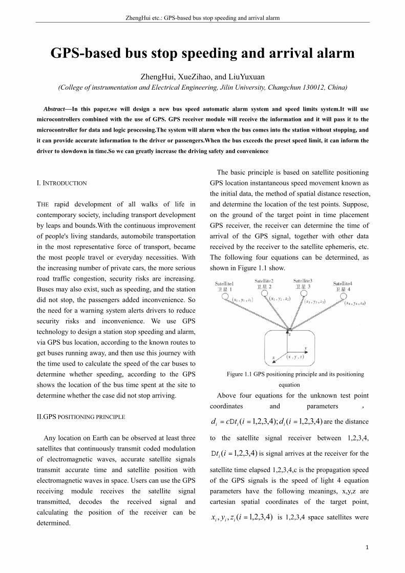
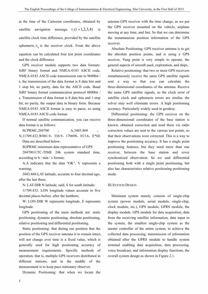
The basic principle is based on satellite positioning GPS location instantaneous speed movement known as the initial data, the method of spatial distance resection, and determine the location of the test points. Suppose, on the ground of the target point in time placement GPS receiver, the receiver can determine the time of arrival of the GPS signal, together with other data received by the receiver to the satellite ephemeris, etc. The following four equations can be determined, as shown in Figure 1.1 show.
Figure 1.1 GPS positioning principle and its positioning
equation
Above four equations for the unknown test point coordinates and parameters ,
)4,3,2,1();4,3,2,1( ==D= iditcd iii are the distance
to the satellite signal receiver between 1,2,3,4,
)4,3,2,1( =D iti is signal arrives at the receiver for the
satellite time elapsed 1,2,3,4,c is the propagation speed of the GPS signals is the speed of light 4 equation parameters have the following meanings, x,y,z are cartesian spatial coordinates of the target point,
)4,3,2,1(,, =izyx iii is 1,2,3,4 space satellites were
The English Proceedings of the College of Instrumentation & Electrical Engineering, Jilin University, in the First Half of 2015
2
at the time of the Cartesian coordinates, obtained by
satellite navigation message, )4,3,2,1( =ivi is
satellite clock time difference, provided by the satellite
ephemeris,0t
v is the receiver clock. From the above
equation can be calculated four test point coordinates and the clock difference
GPS receiver module supports two data formats: SiRF binary format and NMEA-0183 ASCII code, NMEA-0183 ASCII code transmission rate to 9600bit / s, the transmission of the data format is 8 data bits and 1 stop bit, no parity, data for the ASCII code. Baud SiRF binary format communication protocol 4800bit / s. Transmission of data format is 8 data bits and 1 stop bit, no parity, the output data in binary form. Because NMEA-0183 ASCII format is easy to parse, so using NMEA-0183 ASCII code format.
If normal satellite communication, you can receive data format is as follows:
SCPRMC,204700 , A,3403.868 ,
N,11709.432,W001.9,336.9,170698,013.6,E*6E Data are described below: $GPRMC:minimum data representative of GPS 204700:UTC-TIME 24h system standard time,
according to h / min / s format; A:A indicates that the data "OK", V represents a
warning; 3043.868:LAT latitude, accurate to four decimal ago,
after the last three; N: LAT-DIR N latitude, said, S for south latitude; 11709.432: LON longitude values accurate to five
decimal places before, after the lastthree; W: LON-DIR W represents longitude, E represents
longitude. GPS positioning of the main methods are: static
positioning, dynamic positioning, absolute positioning, relative positioning and differential positioning.
Static positioning: that during our position that the position of the GPS receiver antenna is to remain intact, will not change over time is a fixed value, which is generally used for high positioning accuracy of measurement requirements. Specific methods of operation, that is, multiple GPS receivers distributed in different stations, and in the middle of the measurement is to keep pace stationary observer.
Dynamic Positioning: that when we locate the
antenna GPS receiver with the time change, as we put the GPS receiver mounted on the vehicle, airplane moving at any time, and fast. So that we can determine the instantaneous position information of the GPS receiver.
Absolute Positioning: GPS receiver antenna is to get the absolute position points, and is using a GPS receiver, Yung point is very simple to operate, the general aspects of aircraft used, exploration, and ships.
Relative positioning: that two or more GPS receivers simultaneously receive the same GPS satellite signals sent a way so that you can calculate the three-dimensional coordinates of the antenna. Receive the same GPS satellite signals, so the clock error of satellite clock and ephemeris errors are similar, the solver may well eliminate errors. A high positioning accuracy. Particularly widely used in geodesy.
Differential positioning: the GPS receiver on the three-dimensional coordinates of the base station is known, obtained correction and send them via radio correction values are sent to the various test points, so that their observations were corrected. This is a way to improve the positioning accuracy. It has a single point positioning features, but they need more than one receiver, between the base station and rover synchronized observation. So we said differential positioning both with a single point positioning, but also has characteristics relative positioning positioning mode.
III.SYSTEM DESIGN
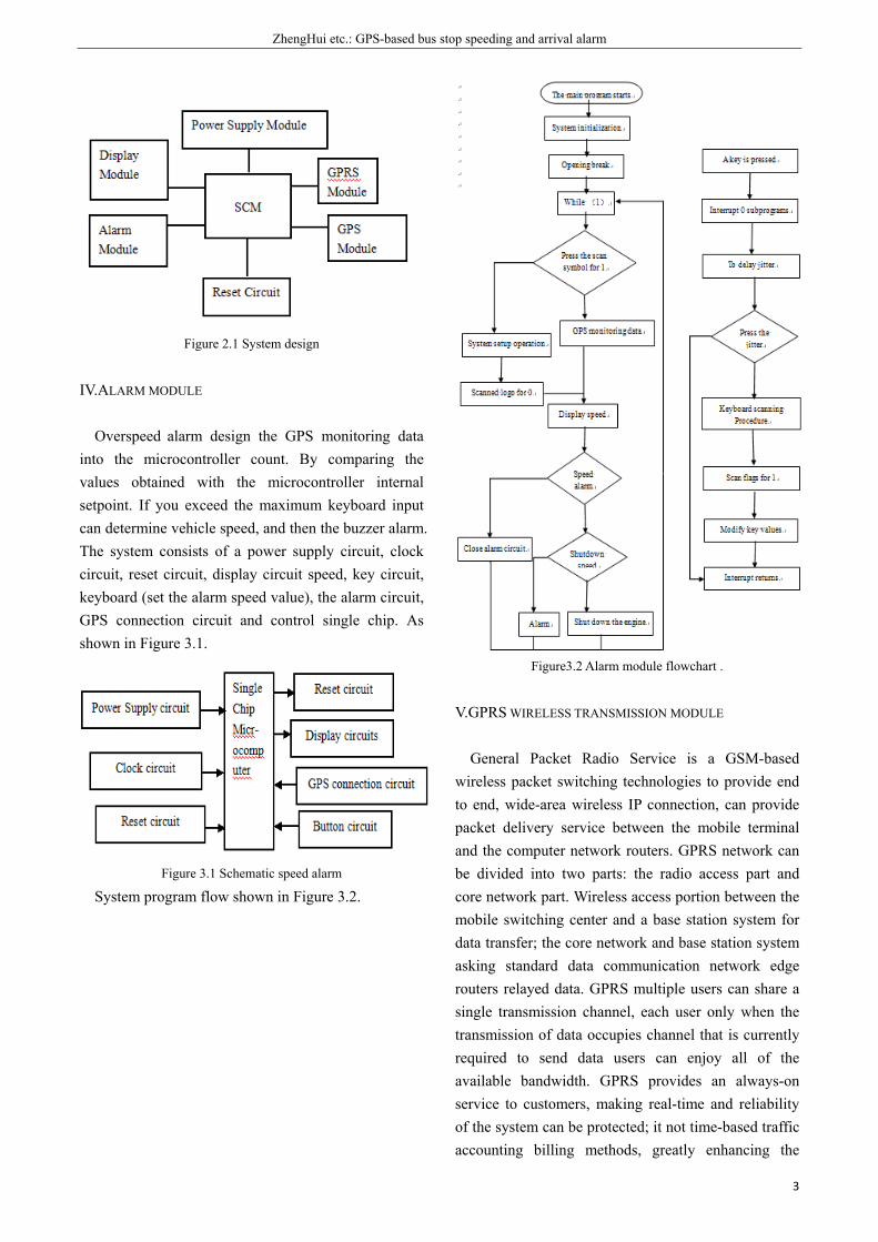
Minimum system mainly consists of single-chip system (power module, serial module, single-chip, clock module, etc.), GPS module, GPRS module, the display module. GPS module for data acquisition, data from the receiving satellite information, data input to the system, the smallest single-chip system as the master controller of the entire system, to achieve the collected data processing, transmission of information obtained after the GPRS module to handle system terminal enabling data acquisition, data processing, voice broadcast, and information display functions, the overall system design as shown in Figure 2.1.
ZhengHui etc.: GPS-based bus stop speeding and arrival alarm
3
Figure 2.1 System design
IV.ALARM MODULE
Overspeed alarm design the GPS monitoring data into the microcontroller count. By comparing the values obtained with the microcontroller internal setpoint. If you exceed the maximum keyboard input can determine vehicle speed, and then the buzzer alarm. The system consists of a power supply circuit, clock circuit, reset circuit, display circuit speed, key circuit, keyboard (set the alarm speed value), the alarm circuit, GPS connection circuit and control single chip. As shown in Figure 3.1.
Figure 3.1 Schematic speed alarm
System program flow shown in Figure 3.2.
Figure3.2 Alarm module flowchart .
V.GPRS WIRELESS TRANSMISSION MODULE
General Packet Radio Service is a GSM-based wireless packet switching technologies to provide end to end, wide-area wireless IP connection, can provide packet delivery service between the mobile terminal and the computer network routers. GPRS network can be divided into two parts: the radio access part and core network part. Wireless access portion between the mobile switching center and a base station system for data transfer; the core network and base station system asking standard data communication network edge routers relayed data. GPRS multiple users can share a single transmission channel, each user only when the transmission of data occupies channel that is currently required to send data users can enjoy all of the available bandwidth. GPRS provides an always-on service to customers, making real-time and reliability of the system can be protected; it not time-based traffic accounting billing methods, greatly enhancing the
The English Proceedings of the College of Instrumentation & Electrical Engineering, Jilin University, in the First Half of 2015
4
feasibility of the system for commercial applications. GRPS system itself uses IP network architecture,
and assign a separate address of the user, the user's data as a separate user, enabling mobile users to the network from end to end data applications. In order to carry data, GPRS system introduces a number of new network elements, such as PCU, SGSN, GGSN, and other units, such as DNS and DHCP server to assist with data management and application services, also includes the Network Time Protocol NTP and charging gateway CG and so on. GPRS network structure shown in Figure 4.1
V.CONCLUSION
GPS positioning technology, designed a new bus station stop speeding and alarm systems, using SCM to process the data through GPRS speed value, location and information transmission bus is speeding to the system terminal, you can quickly based timely to remind drivers to reduce inconvenience to passengers, in practical applications are broad prospects.
References
[1] Guyuan Ping, He Qun, Wu Xuexu .GPS coordinate data
collection technology in the city of application [J] ore
measuring, 2005,2 (1): 39-42
[2] Zhang Yang GPRS wireless data transmission technology
based inquiry [J] Computer CD software and applications,
2012,13 (2): 3-5
[3] Yangzhou, Wuhan Research and Design of GPRS wireless
information gathering monitoring system [D] based on:
Huazhong University of Science and Technology, 2011
[4] Design Week South .GPS vehicle terminal equipment and
realization [D] Lanzhou: Lanzhou University, 2009
[5] Chen Jianmei, design and implementation of [D] GPS
Vehicle Location Monitoring System for North ST:. Beijing
Posts and human science 2011
[6] Zhang Bo, design and implementation of GPS auto-stop
system [J] .2006 electronic components (2): 57-59
[7] arts, Zhang Yongsheng, based on GPS technology, the bus
controller [J] Automation and Instrumentation .2009 (2):
19-21
[8] The design and implementation of [D] Xu Yang cars with
wireless data logger detection system. South pyrene South
dumplings people learn .2013
[9] Micro-Electronics Co., Ltd. .MRU3 GPS & GPRS
networking module technical specifications V1.0 [DB /
2L].http://www.vkelcom.com/web/down.html, 2013-06-07
[10] Liu Xiaojie Research and Design of Automotive GPRS
burglar alarm system [D] Dalian: Dalian University of
Technology, 2010
[11] Dinc, Yang Chen lying mobile communication [M] Beijing:
People's Posts and Telecommunications Press, 2011: 99-102
[12] MARKET. GIS and GPS vehicle location monitoring
system based on [D] Tianjin: Tianjin University, 2012
[13] Zhang Yongsheng design [J] based on GPS / GPRS
automatic bus stop announcement systems of modern
electronic technology, 2009,32 (19): 325-333
[14] Zhang Cuifang .GPS satellite positioning algorithm design
and verification [D] Chengdu: University of Electronic
Science and Technology, 2011

Si Changpeng etc.: Cleaning device for airport runway lights
5
Cleaning device for airport runway lights
Si Changpeng; Liu Meng; Zhao Dong; Liu Changying (College of instrumentation and Electrical Engineering, Jilin University, Changchun 130012, China)
Abstract—When the plane took off and fall, because of the high-speed friction between tire and track, it will
generate a lot of rubber dust. After a period of time, these rubber dust and exhaust gas pollutants will accumulate on the surface of the runway lights. The brightness of the runway lights will gradually decrease,
and it will affect the landing of the aircraft. In order to enhance the cleaning effect and compensate for the lack of manual cleaning, we can use water cannons to spray runway lights. After the end of the spray, brush
inside the machine will automatically wipe clean runway lights, reaching the point of light. Meanwhile dirty water will be recycled, so as to achieve the goal of clean emissions. In this paper, Siemens S7-200 control motor, coordinated with the brightness of the light sensor feedback, so as to achieve the purpose of self-cleaning.
Key words— Siemens S7-200 Automatic cleaning Illuminance sensor
Ⅰ.INTRODUCTION
IN this paper, the brightness detection device is used to detect whether the runway lights comply with the requirements. Brush cleaning the runway lights based light illumination. Brush work, constantly spraying water cannons, a combination of both and achieve clean results. After cleaning, drying fan for drying the runway lights will be on top of the water droplets, the brightness is detected again after stop cleaning standards. Otherwise, continue cleaning. Sewage will enter recovery system means to achieve recovery and no pollution. Focus is on the need to use the brightness of the light detection device sensing brightness, and then set the timing of the cleaning device and circulation. Difficulty is a combination of equipment and automation implementations.
Ⅱ.OVERALL SYSTEM ARCHITECTURE
1.Water cannons 2.Brush 3.Runway lights 4.Light sensor 5.Drying
fan 6.Rotating disk 7.Sewage recovery
Water cannons: to provide water, rinse the stain surface runway lights. Brush: scrubbing stains on the runway lights. Rotating disk: drive connection and brush it on the gun rotated, so that each corner of the runway lights can be cleaned. Drying fan: Drying. Light sensor: After detecting the brightness of the runway lights clean. Stop working afterthe standard brightness.Otherwise,continue cleaning. Sewage recovery: cleaning up sewage collection. Reduce pollution.
III .CENTRAL CONTROL UNIT
S7-200PLC is Germany's Siemens production of a small PLC, which can reach a large number of functions, the level of medium-sized PLC, while the price is the same as with the small PLC, so it once launched, it received widespread attention.
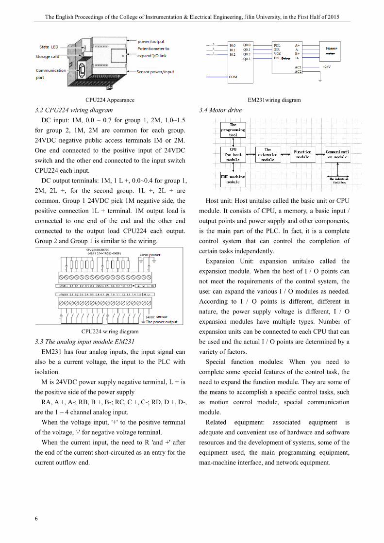
Its main features are: high reliability, rich instruction set, extensive built-in integration capabilities, real-time characteristics of strong and powerful communication capabilities. The device contains a Siemens S7-200 CPU224 and analog input module EM231. 3.1 CPU224 technical indicators
CPU224 native integrated 14 input / 10 output, total 24 digital I / O., It can be connected to seven expansion modules.
The English Proceedings of the College of Instrumentation & Electrical Engineering, Jilin University, in the First Half of 2015
6
CPU224 Appearance
3.2 CPU224 wiring diagram DC input: 1M, 0.0 ~ 0.7 for group 1, 2M, 1.0~1.5
for group 2, 1M, 2M are common for each group. 24VDC negative public access terminals IM or 2M. One end connected to the positive input of 24VDC switch and the other end connected to the input switch CPU224 each input.
DC output terminals: 1M, 1 L +, 0.0~0.4 for group 1, 2M, 2L +, for the second group. 1L +, 2L + are common. Group 1 24VDC pick 1M negative side, the positive connection 1L + terminal. 1M output load is connected to one end of the end and the other end connected to the output load CPU224 each output. Group 2 and Group 1 is similar to the wiring.
CPU224 wiring diagram
3.3 The analog input module EM231 EM231 has four analog inputs, the input signal can
also be a current voltage, the input to the PLC with isolation.
M is 24VDC power supply negative terminal, L + is the positive side of the power supply
RA, A +, A-; RB, B +, B-; RC, C +, C-; RD, D +, D-, are the 1 ~ 4 channel analog input.
When the voltage input, '+' to the positive terminal of the voltage, '-' for negative voltage terminal.
When the current input, the need to R 'and +' after the end of the current short-circuited as an entry for the current outflow end.
EM231wiring diagram
3.4 Motor drive
Host unit: Host unitalso called the basic unit or CPU
module. It consists of CPU, a memory, a basic input / output points and power supply and other components, is the main part of the PLC. In fact, it is a complete control system that can control the completion of certain tasks independently.
Expansion Unit: expansion unitalso called the expansion module. When the host of I / O points can not meet the requirements of the control system, the user can expand the various I / O modules as needed. According to I / O points is different, different in nature, the power supply voltage is different, I / O expansion modules have multiple types. Number of expansion units can be connected to each CPU that can be used and the actual I / O points are determined by a variety of factors.
Special function modules: When you need to complete some special features of the control task, the need to expand the function module. They are some of the means to accomplish a specific control tasks, such as motion control module, special communication module.
Related equipment: associated equipment is adequate and convenient use of hardware and software resources and the development of systems, some of the equipment used, the main programming equipment, man-machine interface, and network equipment.
Si Changpeng etc.: Cleaning device for airport runway lights
7
PLC Control wiring diagram
LD SM0.1 R M0.0, 8 R Q0.0, 2 R T37, 8 LD I0.0 LPS AN T38 TON T37, 100 --Forward 10 seconds LPP A T37 TON T38, 100 --Reverse 10 seconds
IV .LIGHT DETECTION DEVICE
4.1 Illumination Sensor Overview Illumination transmitter is using sensitive detectors
with higher sensitivity, with high-precision linear amplifier, rigorous testing, production measurement range with a variety of illumination and signal output type of practical products. Using wall mount transmitter housing design, delicate structure, beautiful appearance, is an extensive range of applications,highly-cost-effective,illumination measurement products.
Sensors Appearance
This section contains three external sensor pins, which are red (positive) and black (negative), and blue (analog output). 4.2 Technical parameters of the sensor light 1. Power: 0 ~ 10mA output type
2. measuring range: 0 ~ 2000Lux (recommended indoor) 3. Accuracy: ± 5% 4. the measurement resolution: 1Lux (2000Lux) 5. Installation: Wall 6. the output: 0 ~ 10V 4.3 Data Measurement Full shadow: 0.15v, penumbra: 0.61v Daylight: 1.45v shimmer: 1.75v Strong light: 2.92v (Test distance: Light from the sensor 7cm) Note: When the distance from the light sensor decreases with increasing light intensity, voltage increases, the maximum 10v. 4.4 Program LD I0.0 --Illumination Detection
LPS
AW<= VW0, 4751 --Motor rotation
= M0.0
LPP
AW> VW0, 4751 --Stop the motor
= M0.1
Ⅴ.ANALYSIS OF THE RESULTS OF SYSTEM TESTING
Reference value set 1.45v (sunlight), the voltage value increases with increasing light intensity. When the voltage is less than 1.45v (lights dim, indicating a greater degree of guidelines and other surface dirt), motor rotation, driven brush for cleaning the lamp. When the voltage is greater than 1.45v, lamp brightness is low. The motor does not rotate.It will not clean lights.
Ⅵ. CONCLUSION
This paper discusses the design method based on stepper motor control system of the PLC and the development process, hardware design, software design and other aspects of system configuration includes. Siemens PLC, drives and stepper motors make up the hardware circuit. PLC Ladder and Statement List language is used to write software programs.
In this design, we implemented to control the stepper motor working status through a combination of hardware and software. PLC with pulse and direction
The English Proceedings of the College of Instrumentation & Electrical Engineering, Jilin University, in the First Half of 2015
8
signal output, changing the way of energizing and electrifying sequence stepper motor windings, to accurately control the stepper motor forward, reverse, acceleration, deceleration, uniform state. By setting different values of the timer, to change the operating frequency of the stepper motor. At present, the use of programmable logic controller (PLC technology that is) can be easily implemented on the motor speed and position control, easy to carry out a variety of stepper motor operation, complete a variety of complex work, which represents the advanced industrial automation technology level, to accelerate the realization of mechatronics.
References
[1] Zhang Jun Dong, Ren Guang, LAN airfield
lighting design is based on comprehensive
monitoring [J] Transportation Engineering, 2002, 2
(1): 122-126.
[2] Chen Lei airport airfield lighting computer
monitoring system [J] Fujian computer, 2002 (9):
29-31.
[3] Wu Ming, auto high beam light intensity and
illumination test analysis [J] road with trucks, 2005,
4 (2): 11-12.
[4] Xiao Jin Lin,Weng Zheng Xin,Siemens Data
Communication Research [J] Beijing:
Microcomputer Applications, 2006,22 (4): 50-51.
[5] Liao Changchu,et.PLC programming and application [M]
Beijing: Mechanical Industry Press, 2005.
[6] Siemens .SIMATICS7-200 Programmable Controller
System Manual [M] Beijing: Mechanical Industry Press,
1999.
[7] Qin Yilin, Zhang Zhibo.Siemens layman S7-200PLC [M]
Beijing: Mechanical Industry Press, 2003.
[8] Hu Qiusheng,Liu houhua,ZhangYunxiang.Stencilled design
style fruit washing machine [J] 2007.6: 91-93;
[9] Cui Jian, Li Jia, Yang Guang. Siemens Industry Network
Communications Guide [J] Journal of Scientific Instrument,
2001 (6): 34-38,48.

HONG Jia-chen etc.: Noncontact monitoring of ECG
9
Noncontact monitoring of ECG
HONG Jia-chen ;WANG Jing-ye ;LENG Si-da;LI Su-yi ; (School of Instrtument Science and electrical engineering, Jilin University, Changchun)
Abstract—This paper introduces a circuit design of non-contacting ECG acquisition device. This design employs textile
electrode , based on the capacitive coupling theory between the electrode and body . This design employes AD620 and OP07 as
its core. Through the major components of the ECG signal and the frequency range of interference were analysed, weak ECG
signal collected by the electrodes was amplified by the preamplifier circuit, and then was filtered out the interference by using
a low-pass filter,a high-pass filter,50Hz notch filter and back amplifier circuit, a right wave of ECG was gotten.Finally The
wave can be registered after converted to digital signals by MSP430 single chip. Also the real-time cardiograph can be
displayed by LCD. The characteristics of the system show in the merits of high input impedance , high CMRR , low noise and
high SNR ( signal to noise ratio ) and so on.
Key words—Noncontact;ECG ;filter;amplifier circuit;MSP430 single chip; CLC: TN791 Document code: A
0 INTRODUCTION
ON AUGUST 8,2014, "China Cardiovascular Report 2013" released [1].The report shows that total cardiovascular disease mortality accounted for the first cause of death in urban and rural residents was 38.7% in rural areas, the city was 41.1%. China risk factor for cardiovascular disease trends evident, leading to the onset of cardiovascular disease continue to increase the number, and the next 10 years the number of cardiovascular illness will continue rapid growth [2]. Thus, long-term monitoring of early cardiovascular disease is very necessary and important. As a recording ECG heart electrical activity through the skin treatment technology, its diagnosis is reliable, easy way, no harm to the patient, etc.,and it has become an important means of diagnosis of cardiovascular disease [3].
However, at any time and long-term monitoring of ECG to detect if used directly for cardiovascular disease, there are many limitations: Conventional ECG monitoring system needs to be in direct contact with the patient's skin electrodes, ECG acquisition but if prolonged contact with human skin electrodes can cause patient skin redness, itching and other symptoms, reduce the comfort of signal detection process, but can also cause heart the electrode polarization, the polarization voltage, the introduction of baseline drift noise affect the test results [4]。
The experimental research and development of non-contact ECG detection system can signal detection process to minimize the discomfort caused by the subjects, and the system is simple, easy operation, small signal detection conditions. Subjects do not need to bare skin, ECG detection can be performed anywhere. Therefore, the non-connected
ECG-touch detection system can meet at any time to detect cardiovascular disease prevention and long-term monitoring requirements, with good prospects and development potential.
1 NON-CONTACT ECG ACQUISITION PRINCIPLES
AND METHODS
1.1 Non-contact ECG acquisition principle Medical grade conductive textile either
physiological signal acquisition and conduction through direct contact with the skin surface of the fabric, but also by capacitive coupling principle, in the case of the fabric layer of the clothing and the body surface spaced performed ECG Bian set. When the fabric layer of the electrode and the skin surface interval clothing, conductive fabric, skin and clothing can be approximately considered to constitute a capacitive element, according to the charges repel each other, the principle attraction of opposite charges, conductive fabric close to the skin's part would have
The English Proceedings of the College of Instrumentation & Electrical Engineering, Jilin University, in the First Half of 2015
10
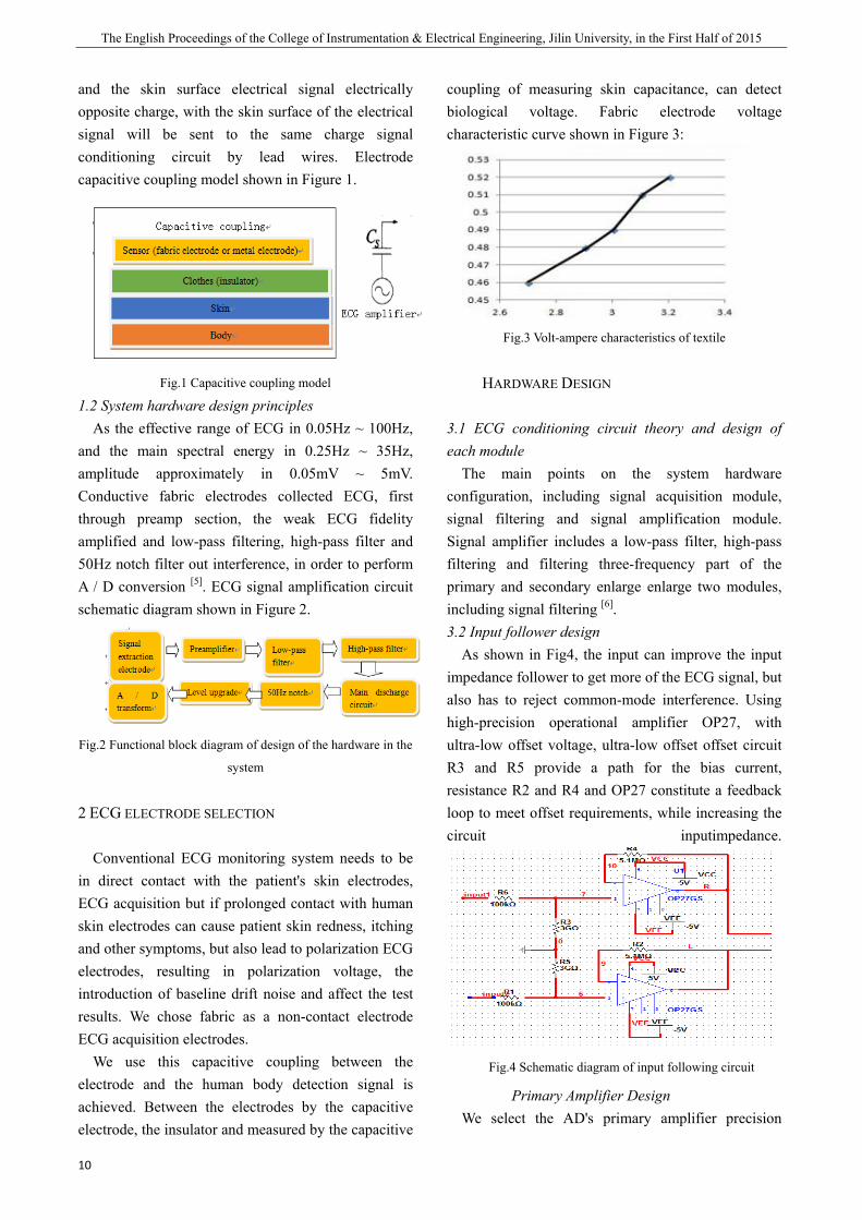
and the skin surface electrical signal electrically opposite charge, with the skin surface of the electrical signal will be sent to the same charge signal conditioning circuit by lead wires. Electrode capacitive coupling model shown in Figure 1.
Fig.1 Capacitive coupling model
1.2 System hardware design principles As the effective range of ECG in 0.05Hz ~ 100Hz,
and the main spectral energy in 0.25Hz ~ 35Hz, amplitude approximately in 0.05mV ~ 5mV. Conductive fabric electrodes collected ECG, first through preamp section, the weak ECG fidelity amplified and low-pass filtering, high-pass filter and 50Hz notch filter out interference, in order to perform A / D conversion [5]. ECG signal amplification circuit schematic diagram shown in Figure 2.
Fig.2 Functional block diagram of design of the hardware in the
system
2 ECG ELECTRODE SELECTION
Conventional ECG monitoring system needs to be in direct contact with the patient's skin electrodes, ECG acquisition but if prolonged contact with human skin electrodes can cause patient skin redness, itching and other symptoms, but also lead to polarization ECG electrodes, resulting in polarization voltage, the introduction of baseline drift noise and affect the test results. We chose fabric as a non-contact electrode ECG acquisition electrodes.
We use this capacitive coupling between the electrode and the human body detection signal is achieved. Between the electrodes by the capacitive electrode, the insulator and measured by the capacitive
coupling of measuring skin capacitance, can detect biological voltage. Fabric electrode voltage characteristic curve shown in Figure 3:
Fig.3 Volt-ampere characteristics of textile
HARDWARE DESIGN
3.1 ECG conditioning circuit theory and design of each module
The main points on the system hardware configuration, including signal acquisition module, signal filtering and signal amplification module. Signal amplifier includes a low-pass filter, high-pass filtering and filtering three-frequency part of the primary and secondary enlarge enlarge two modules, including signal filtering [6]. 3.2 Input follower design
As shown in Fig4, the input can improve the input impedance follower to get more of the ECG signal, but also has to reject common-mode interference. Using high-precision operational amplifier OP27, with ultra-low offset voltage, ultra-low offset offset circuit R3 and R5 provide a path for the bias current, resistance R2 and R4 and OP27 constitute a feedback loop to meet offset requirements, while increasing the circuit inputimpedance.
Fig.4 Schematic diagram of input following circuit
Primary Amplifier Design We select the AD's primary amplifier precision

HONG Jia-chen etc.: Noncontact monitoring of ECG
11
instrumentation amplifier AD620, the circuit schematic shown in Figure 5. FIG U3 is the primary amplification circuit. U4 for the right leg drive circuit, right leg drive circuit is mainly used to filter out the body by introducing common mode interference, especially 50Hz frequency interference, thereby improving the CMRR. The primary amplifier circuit of the common-mode signal detection, after inverting, zoom back into the right leg, through the resistor network effectively suppress 50Hz frequency interference [7].
Because AD620 input terminal connected directly to the ECG electrodes, and the electrode potential of the electrode will usually exist, when there is the external electric field, the electrode potential will vary. If the values of the two electrode potentials are the same, as a common-mode signal flowing into the primary amplifying circuit, the preamplifier can be overcome with a common-mode voltage. However, the electrode potential is usually not completely equal, then the potential difference between the two electrodes of a differential mode signal is amplified, it will lead to a total op amp's quiescent operating point is unstable, prone to distortion or saturation distortion deadline. This makes the electrode potential presence of primary amplifier gain can not be too large, generally set at less than 10 times, on the one hand to avoid saturation, it also reduces the CMRR.
Rg is R7, R8, R9 in parallel, so we see formula(1)
G =8.4 (1)
Fig.5 Schematic diagram of primary amplification
Low -pass filter design Due to the frequency of ECG below 100Hz, in order
to eliminate the EMG frequency interference and electromagnetic signals,we design the low-pass filter,
its upper cut-off frequency = 100Hz. Figure 6 shows the use of the filter circuit, this circuit is a commonly used second-order low-pass filter [8].
Cutoff frequency is set to see the formula(2)
(2)
Fig.6 Schematic diagram of low pass filter
High -pass filter design In order to eliminate the pre-amplifier output ECG,
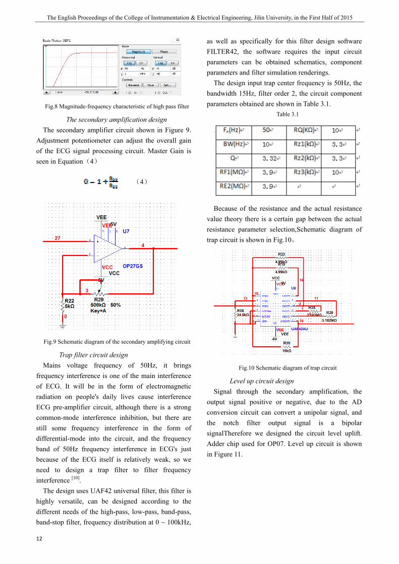
respiration, and electrode movement by the body caused by low-frequency interference signals and reduce distortion, get better attenuation characteristics reduce the sensitivity of components, the use of second-order Butterworth filter high-pass filter design using multiple feedback of second-order active high pass filter structure [9], This design of a high-pass filter circuit is shown in Figure 7. High-pass filter amplitude-frequency characteristics is shown in Figure 8.
We set a cutoff frequency of to see(3)
(3)
Fig.7 Schematic diagram of high pass filter
The English Proceedings of the College of Instrumentation & Electrical Engineering, Jilin University, in the First Half of 2015
12
Fig.8 Magnitude-frequency characteristic of high pass filter
The secondary amplification design The secondary amplifier circuit shown in Figure 9.
Adjustment potentiometer can adjust the overall gain of the ECG signal processing circuit. Master Gain is seen in Equation(4)
(4)
Fig.9 Schematic diagram of the secondary amplifying circuit
Trap filter circuit design Mains voltage frequency of 50Hz, it brings
frequency interference is one of the main interference of ECG. It will be in the form of electromagnetic radiation on people's daily lives cause interference ECG pre-amplifier circuit, although there is a strong common-mode interference inhibition, but there are still some frequency interference in the form of differential-mode into the circuit, and the frequency band of 50Hz frequency interference in ECG's just because of the ECG itself is relatively weak, so we need to design a trap filter to filter frequency interference [10].
The design uses UAF42 universal filter, this filter is highly versatile, can be designed according to the different needs of the high-pass, low-pass, band-pass, band-stop filter, frequency distribution at 0 ~ 100kHz,
as well as specifically for this filter design software FILTER42, the software requires the input circuit parameters can be obtained schematics, component parameters and filter simulation renderings.
The design input trap center frequency is 50Hz, the bandwidth 15Hz, filter order 2, the circuit component parameters obtained are shown in Table 3.1.
Table 3.1
Because of the resistance and the actual resistance value theory there is a certain gap between the actual resistance parameter selection,Schematic diagram of trap circuit is shown in Fig.10。
Fig.10 Schematic diagram of trap circuit
Level up circuit design Signal through the secondary amplification, the
output signal positive or negative, due to the AD conversion circuit can convert a unipolar signal, and the notch filter output signal is a bipolar signalTherefore we designed the circuit level uplift. Adder chip used for OP07. Level up circuit is shown in Figure 11.
HONG Jia-chen etc.: Noncontact monitoring of ECG
13
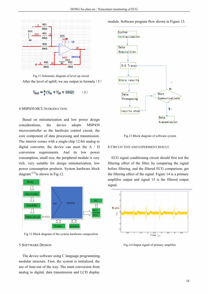
Fig.11 Schematic diagram of level up circuit
After the level of uplift, we see output in formula(5)
(5)
4 MSP430 MCU INTRODUCTION
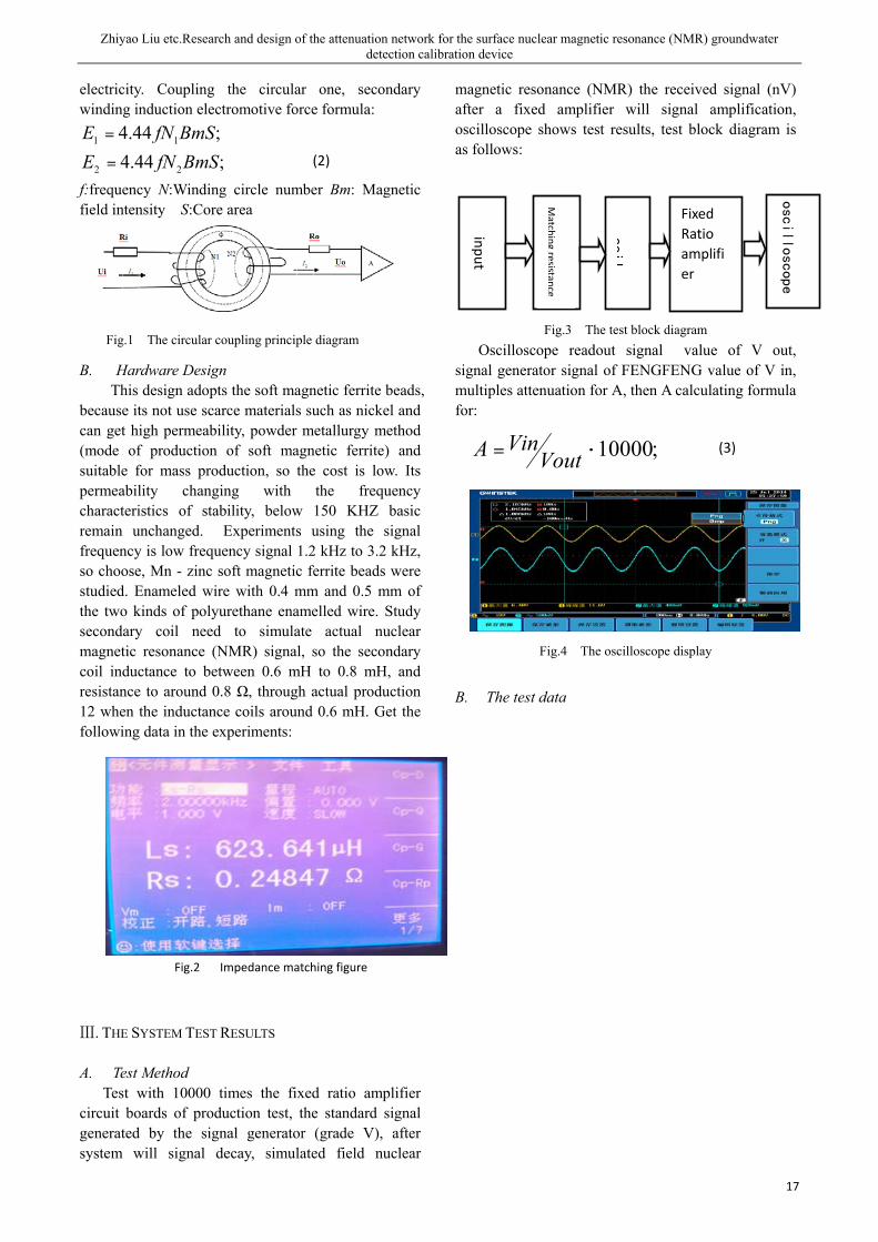
Based on miniaturization and low power design considerations, the device adopts MSP430 microcontroller as the hardware control circuit, the core component of data processing and transmission. The interior comes with a single-chip 12-bit analog to digital converter, the device can meet the A / D conversion requirements. And its low power consumption, small size, the peripheral module is very rich, very suitable for design miniaturization, low power consumption products. System hardware block diagram [15]is shown in Fig.12.
Fig.12 Block diagram of the system hardware composition
5 SOFTWARE DESIGN
The device software using C language programming, modular structure. First, the system is initialized, the use of time-out of the way. The main conversion from analog to digital, data transmission and LCD display
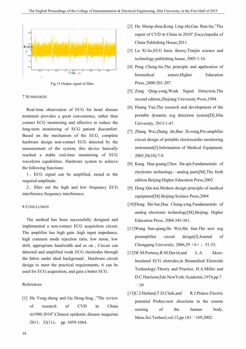
module. Software program flow shown in Figure 13.
Fig.13 Block diagram of software system
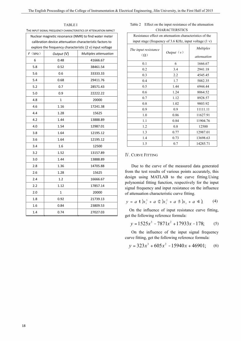
6 CIRCUIT TEST AND EXPERIMENT RESULT.
ECG signal conditioning circuit should first test the filtering effect of the filter, by comparing the signal before filtering, and the filtered ECG comparison, get the filtering effect of the signal. Figure 14 is a primary amplifier output and signal 15 is the filtered output signal.
Fig.14 Output signal of primary amplifier
The English Proceedings of the College of Instrumentation & Electrical Engineering, Jilin University, in the First Half of 2015
14
Fig.15 Output signal of filter
7 SUMMARIZE
Real-time observation of ECG for heart disease treatment provides a great convenience, rather than contact ECG monitoring and effective to reduce the long-term monitoring of ECG patient discomfort. Based on the mechanism of the ECG, complete hardware design non-contact ECG detected by the measurement of the system, this device basically reached a stable real-time monitoring of ECG waveform capabilities. Hardware system to achieve the following functions:
1、ECG signal can be amplified, raised to the required amplitude;
2、filter out the high and low frequency ECG interference frequency interference;
8 CONCLUSION
The method has been successfully designed and implemented a non-contact ECG acquisition circuit, The amplifier has high gain ,high input impedance, high common mode rejection ratio, low noise, low drift, appropriate bandwidth and so on , Circuit can detected and amplified weak ECG electrodes through the fabric under ideal background . Hardware circuit design to meet the practical requirements, it can be used for ECG acquisition, and gain a better ECG.
References
[1] Hu Yong-sheng and Gu Dong-feng ,”The review
of research of CVD in China
in1980-2010”,Chinese epidemic disease magazine,
2011,32(11), pp. 1059-1064.
[2] Hu Sheng-shou,Kong Ling-zhi,Gao Run-lin,”The
report of CVD in China in 2010”,Encyclopedia of
China Publishing House,2011.
[3] Lu Xi-lie,ECG basic theory,Tianjin science and
technology publishing house, 2005:1-16.
[4] Peng Cheng-lin,The principle and application of
biomedical sensor,Higher Education
Press.,2000:201-207.
[5] Zeng Qing-yong,Weak Signal Detection,The
second edition,Zhejiang University Press,1994.
[6] Huang Yue,The research and development of the
portable dynamic ecg detection system[D].Jilin
University, 2013:1-47.
[7] Zhang Wei,Zhang shi,Bao Xi-rong,Pre-amplifier
circuit design of portable electrocardio monitoring
instrument[J].Information of Medical Equipment,
2005,20(10):7-9.
[8] Kang Hua-guang,Chen Da-qin.Fundamentals of
electronic technology—analog parts[M].The forth
edition.Beijing:Higher Education Press,2002
[9] Deng Qin-kai.Modern design principle of medical
equipment[M].Beijing:Science Press,2004
[10] Dong Shi-bai,Hua Cheng-ying.Fundamentals of
analog electronic technology[M].Beijing: Higher
Education Press, 2004:345-361.
[11] Wang San-qiang,He Wei,Shi Jian.The new eeg
preamplifier circuit design[J].Journal of
Chongqing University, 2006,29(6):51-53.
[12] W.M.Portnoy,R.M.David,and L.A. Akers.
Insulated ECG eletrodes,in Biomedieal Eleetrode
Teehnology-Theory and Practice, H.A.Miller and
D.C.Harrison,Eds.NewYork:Academic,1974,pp.7
一39
[13] C.J.Harland,T.D.Clark,and R.J.Prance.Electric
potential Probes-new directions in the remote
sensing of the human body,
Meas.Sci.Teehnol,vol.13,pp.163一169,2002.

HONG Jia-chen etc.: Noncontact monitoring of ECG
15
[14] H.W.Ott,Noise Reduetion Teehniques in
Electronic Systems,NewYork: W11ey, 1988,
pp.244一273.
[15] Jiang Lu-jun,Yang Li-ping,Chen Hui,Based on the
MSP430FG439 study of ultra-low power MCU
portable ecg monitor[J].Popular Science,
2010(10):48-50.

The English Proceedings of the College of Instrumentation & Electrical Engineering, Jilin University, in the First Half of 2015
16
Research and design of the attenuation network for the surface nuclear magnetic resonance (NMR)
groundwater detection calibration device
Zhiyao Liu. Peng Xu. Ying Zhao. Chuandong Jiang
(jilin university instrument science and engineering institute,changchun,130021)
Abstract—The application of the method of circular and coupled to the nuclear magnetic resonance(NMR) to find water
meter calibration device attenuation in the design of the network. Through the cricular, the strict screening of winding and the coil number of turns, the input impedance contrast test, to achieve stable and reliable multiples attenuation. For circular and coupling impedance circuit of input stage, the impedance matching design, make the simulation of the impedance of the outdoor environment and impedance as far as possible, in order to achieve the result of the nuclear magnetic resonance (NMR) water meter more accurate calibration. This design with the method of the coupling coil, the magnetic flux distribution in the circular, reduced the magnetic leakage, effectively restrain interference environment, improve the calibration accuracy and efficiency of field work.
Key words—Cicular coupling Impedance matching Attenuation network
I. INTRODUCTION
NUCLEAR magnetic resonance (NMR) to find water meter indoor test calibration device is one of the nuclear magnetic resonance (NMR) water witch related devices, is responsible for making a nuclear magnetic resonance (NMR) to find water meter installation for testing, calibration, guarantee the stability and accuracy of each instrument, is nuclear magnetic resonance (NMR) to find water meter support and guarantee for the stable work.. Nuclear magnetic resonance (NMR) to find water meter sensor receives the NMR signal in the receiver, within the scope of a few nV to hundreds of nV, frequency from 1 kHz to 3 kHz, which requires high gain amplifier, in the face of such a high gain amplifier, how to carry on the calibration indoors is particularly important. Ying-ji Wang for detecting nuclear magnetic resonance (NMR) to find water meter indoor calibration device for research and development, provides to a certain extent, can be in indoor simulated field experimental condition testing instrument normal functioning of the device and testing methods, and the nuclear magnetic resonance (NMR) water system testing and calibration. This article will be to the calibration of the amplifier attenuation network for further research and design. This design will be the circular coil coupling method is applied to the nuclear magnetic resonance (NMR) to find water meter calibration attenuation in the network, through to the level before and after the
circular coil winding circle number, impedance matching and impedance, gain more stable, attenuation multiples larger, stronger attenuation network reliability. In under the condition of different winding turns and the input impedance, attenuation network compared to test, will get fitting curve, obtain more accurate reference curve and coil properties.
II.THE PROJECT DESIGN
A. Test Method This design USES the similar to the single-phase
transformer and small size transformer device, the pressure device multiples attenuation is stable and less susceptible to interference. It through electromagnetic induction coil, a voltage level of ac electric energy is converted into another kind of voltage grade with frequency ac power. Coupling magnetic ring connect ac power with a winding, winding through the alternating current and generate magneto motive force, under the effect of the magneto motive force, the iron core in alternating magnetic flux, namely a winding will draw power from the power supply into magnetic energy, at the same time pay (ring) in the core chain of the original, deputy winding (secondary winding), due to the electromagnetic induction effect, in the primary and secondary windings respectively with the same frequency induction electromotive force. If the secondary winding is connected to the load, under the effect of secondary winding induction electromotive force, there is electric current flows through the load, the core of the magnetic energy is converted to
(1)
Zhiyao Liu etc.Research and design of the attenuation network for the surface nuclear magnetic resonance (NMR) groundwater detection calibration device
17
electricity. Coupling the circular one, secondary winding induction electromotive force formula:
;44.4;44.4
22
11
BmSfNEBmSfNE
=
=
f:frequency N:Winding circle number Bm: Magnetic field intensity S:Core area
Fig.1 The circular coupling principle diagram
B. Hardware Design This design adopts the soft magnetic ferrite beads, because its not use scarce materials such as nickel and can get high permeability, powder metallurgy method (mode of production of soft magnetic ferrite) and suitable for mass production, so the cost is low. Its permeability changing with the frequency characteristics of stability, below 150 KHZ basic remain unchanged. Experiments using the signal frequency is low frequency signal 1.2 kHz to 3.2 kHz, so choose, Mn - zinc soft magnetic ferrite beads were studied. Enameled wire with 0.4 mm and 0.5 mm of the two kinds of polyurethane enamelled wire. Study secondary coil need to simulate actual nuclear magnetic resonance (NMR) signal, so the secondary coil inductance to between 0.6 mH to 0.8 mH, and resistance to around 0.8 Ω, through actual production 12 when the inductance coils around 0.6 mH. Get the following data in the experiments:
Ⅲ. THE SYSTEM TEST RESULTS
A. Test Method Test with 10000 times the fixed ratio amplifier circuit boards of production test, the standard signal generated by the signal generator (grade V), after system will signal decay, simulated field nuclear
magnetic resonance (NMR) the received signal (nV) after a fixed amplifier will signal amplification, oscilloscope shows test results, test block diagram is as follows:
input
Fig.3 The test block diagram Oscilloscope readout signal value of V out, signal generator signal of FENGFENG value of V in, multiples attenuation for A, then A calculating formula for:
;10000·= VoutVinA
Fig.4 The oscilloscope display
B. The test data
Fig.2 Impedance matching figure
input
coil
Fixed Ratio amplifier
oscilloscope
Matching
resistance
(2)
(3)
The English Proceedings of the College of Instrumentation & Electrical Engineering, Jilin University, in the First Half of 2015
18
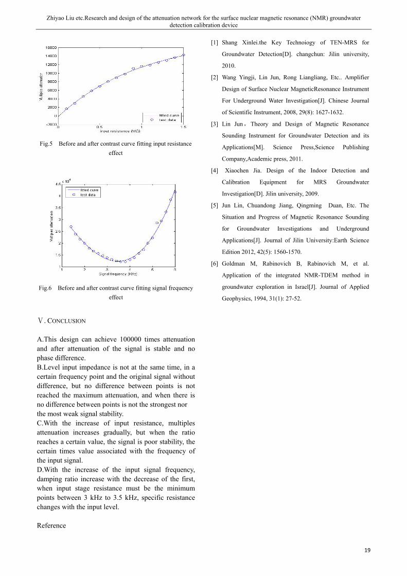
Table 2 Effect on the input resistance of the attenuation CHARACTERSTICS
Resistance effect on attenuation characteristics of the input stage (frequency of 3.6 KHz, input voltage (1 v)
The input resistance(Ω)
Output(v) Multiples
attenuation
0.1 6 1666.67 0.2 3.4 2941.18 0.3 2.2 4545.45 0.4 1.7 5882.35 0.5 1.44 6944.44 0.6 1.24 8064.52 0.7 1.12 8928.57 0.8 1.02 9803.92 0.9 0.9 11111.11 1.0 0.86 11627.91 1.1 0.84 11904.76 1.2 0.8 12500 1.3 0.77 12987.01 1.4 0.73 13698.63 1.5 0.7 14285.71
Ⅳ. CURVE FITTING
Due to the curve of the measured data generated from the test results of various points accurately, this design using MATLAB to the curve fitting.Using polynomial fitting function, respectively for the input signal frequency and input resistance on the influence of attenuation characteristic curve fitting.
() ( ) ( ) ( );4321 12
131 axaxaxay +++= (4)
On the influence of input resistance curve fitting, get the following reference formula:
;1781793378711525 23 -+-= xxxy (5)
On the influence of the input signal frequency curve fitting, get the following reference formula:
;4690115940605323 23 +-+= xxxy (6)
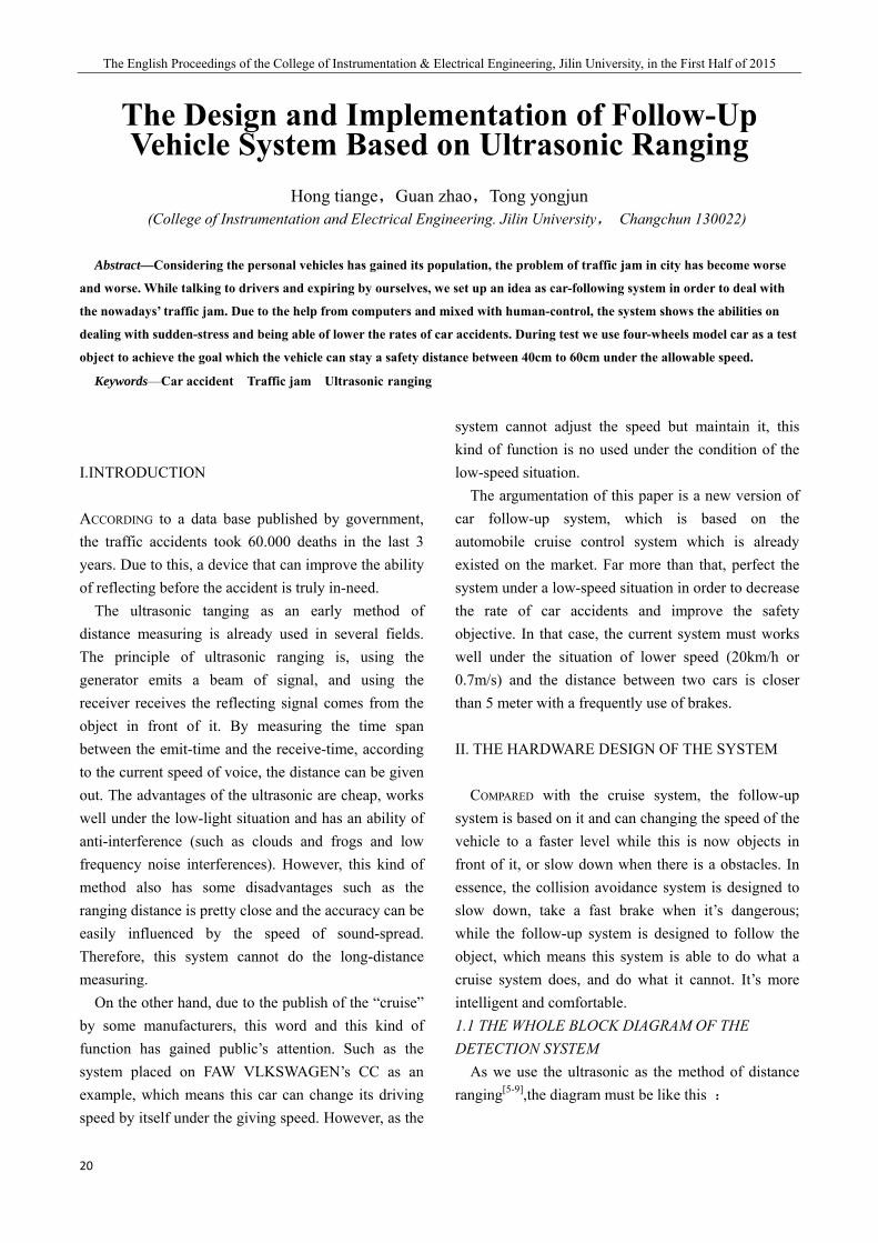
TABLE I THE INPUT SIGNAL FREQUENCY CHARACTERISTICS OF ATTENUATION IMPACT
Nuclear magnetic resonance (NMR) to find water meter calibration device attenuation characteristic factors to explore the frequency characteristic (2 v) input voltage
F(kHz) Output (V) Multiples attenuation 6 0.48 41666.67
5.8 0.52 38461.54
5.6 0.6 33333.33
5.4 0.68 29411.76
5.2 0.7 28571.43
5.0 0.9 22222.22
4.8 1 20000
4.6 1.16 17241.38
4.4 1.28 15625
4.2 1.44 13888.89
4.0 1.54 12987.01
3.8 1.64 12195.12
3.6 1.64 12195.12
3.4 1.6 12500
3.2 1.52 13157.89
3.0 1.44 13888.89
2.8 1.36 14705.88
2.6 1.28 15625
2.4 1.2 16666.67
2.2 1.12 17857.14
2.0 1 20000
1.8 0.92 21739.13
1.6 0.84 23809.53
1.4 0.74 27027.03
Zhiyao Liu etc.Research and design of the attenuation network for the surface nuclear magnetic resonance (NMR) groundwater detection calibration device
19
Fig.5 Before and after contrast curve fitting input resistance
effect
Fig.6 Before and after contrast curve fitting signal frequency effect
Ⅴ. CONCLUSION
A.This design can achieve 100000 times attenuation and after attenuation of the signal is stable and no phase difference. B.Level input impedance is not at the same time, in a certain frequency point and the original signal without difference, but no difference between points is not reached the maximum attenuation, and when there is no difference between points is not the strongest nor the most weak signal stability. C.With the increase of input resistance, multiples attenuation increases gradually, but when the ratio reaches a certain value, the signal is poor stability, the certain times value associated with the frequency of the input signal. D.With the increase of the input signal frequency, damping ratio increase with the decrease of the first, when input stage resistance must be the minimum points between 3 kHz to 3.5 kHz, specific resistance changes with the input level.
Reference
[1] Shang Xinlei.the Key Technoiogy of TEN-MRS for
Groundwater Detection[D]. changchun: Jilin university,
2010.
[2] Wang Yingji, Lin Jun, Rong Liangliang, Etc.. Amplifier
Design of Surface Nuclear MagneticResonance Instrument
For Underground Water Investigation[J]. Chinese Journal
of Scientific Instrument, 2008, 29(8): 1627-1632.
[3] Lin Jun,Theory and Design of Magnetic Resonance
Sounding Instrument for Groundwater Detection and its
Applications[M]. Science Press,Science Publishing
Company,Academic press, 2011.
[4] Xiaochen Jia. Design of the Indoor Detection and
Calibration Equipment for MRS Groundwater
Investigation[D]. Jilin university, 2009.
[5] Jun Lin, Chuandong Jiang, Qingming Duan, Etc. The
Situation and Progress of Magnetic Resonance Sounding
for Groundwater Investigations and Underground
Applications[J]. Journal of Jilin University:Earth Science
Edition 2012, 42(5): 1560-1570.
[6] Goldman M, Rabinovich B, Rabinovich M, et al.
Application of the integrated NMR-TDEM method in
groundwater exploration in Israel[J]. Journal of Applied
Geophysics, 1994, 31(1): 27-52.
The English Proceedings of the College of Instrumentation & Electrical Engineering, Jilin University, in the First Half of 2015
20
The Design and Implementation of Follow-Up Vehicle System Based on Ultrasonic Ranging
Hong tiange,Guan zhao,Tong yongjun
(College of Instrumentation and Electrical Engineering. Jilin University, Changchun 130022)
Abstract—Considering the personal vehicles has gained its population, the problem of traffic jam in city has become worse
and worse. While talking to drivers and expiring by ourselves, we set up an idea as car-following system in order to deal with
the nowadays’ traffic jam. Due to the help from computers and mixed with human-control, the system shows the abilities on
dealing with sudden-stress and being able of lower the rates of car accidents. During test we use four-wheels model car as a test
object to achieve the goal which the vehicle can stay a safety distance between 40cm to 60cm under the allowable speed.
Keywords—Car accident Traffic jam Ultrasonic ranging
I.INTRODUCTION
ACCORDING to a data base published by government, the traffic accidents took 60.000 deaths in the last 3 years. Due to this, a device that can improve the ability of reflecting before the accident is truly in-need.
The ultrasonic tanging as an early method of distance measuring is already used in several fields. The principle of ultrasonic ranging is, using the generator emits a beam of signal, and using the receiver receives the reflecting signal comes from the object in front of it. By measuring the time span between the emit-time and the receive-time, according to the current speed of voice, the distance can be given out. The advantages of the ultrasonic are cheap, works well under the low-light situation and has an ability of anti-interference (such as clouds and frogs and low frequency noise interferences). However, this kind of method also has some disadvantages such as the ranging distance is pretty close and the accuracy can be easily influenced by the speed of sound-spread. Therefore, this system cannot do the long-distance measuring.
On the other hand, due to the publish of the “cruise” by some manufacturers, this word and this kind of function has gained public’s attention. Such as the system placed on FAW VLKSWAGEN’s CC as an example, which means this car can change its driving speed by itself under the giving speed. However, as the
system cannot adjust the speed but maintain it, this kind of function is no used under the condition of the low-speed situation.
The argumentation of this paper is a new version of car follow-up system, which is based on the automobile cruise control system which is already existed on the market. Far more than that, perfect the system under a low-speed situation in order to decrease the rate of car accidents and improve the safety objective. In that case, the current system must works well under the situation of lower speed (20km/h or 0.7m/s) and the distance between two cars is closer than 5 meter with a frequently use of brakes.
II. THE HARDWARE DESIGN OF THE SYSTEM
COMPARED with the cruise system, the follow-up system is based on it and can changing the speed of the vehicle to a faster level while this is now objects in front of it, or slow down when there is a obstacles. In essence, the collision avoidance system is designed to slow down, take a fast brake when it’s dangerous; while the follow-up system is designed to follow the object, which means this system is able to do what a cruise system does, and do what it cannot. It’s more intelligent and comfortable. 1.1 THE WHOLE BLOCK DIAGRAM OF THE DETECTION SYSTEM
As we use the ultrasonic as the method of distance ranging[5-9],the diagram must be like this :
Hong tiange etc.: The Design and Implementation of Follow-Up Vehicle System Based on Ultrasonic Ranging
21
Figure 1 The design of detection system
The overall design is simple, as the principle of ultrasonic ranging is easy to understand and use, the requirements of system’s hardware is not strictly. However, as we use the different level of the interrupts in the 51 MCU including the inner time interruption, therefore we need to avoid the interference between different kinds of interruptions. On the other hand, consider the ultrasonic propagation speed is about 330m/s, we should fully consider the response time of SCM to ensure we hold enough time for the chip to response and calculate.
1.2 THE DRIVE MODULE FOR this four-wheel car, we use the PWM principle
as the basic rule to drive the car do some acts like move forward and back or take a turn. The essence of PWM is to change the duty ratio of the pulse signal. When it’s high, the motor works a longer time in one period time; while it’s low, the motor works a shorter time.
In the driving module, we need to use the L298N chip which connect the motor and the 51 MCU. The L298N chip is produced by the SGS company, the most common series is the 15 pins Multiwatt package L298N, which also has the drive circuit inside of it. The figure of how does it connect to the 51 SCU is showed below:
Figure 2 L298N connects to the 51 SCU.
To SCU
To SCU
To SCU
To SCU
To SCU
Able when
the voltage
is high
Circuit A
Circuit B
Circuit C
Circuit D
The English Proceedings of the College of Instrumentation & Electrical Engineering, Jilin University, in the First Half of 2015
22
It is easy to figure out that in the figure 2, one L298N chip can easily drive a two-phase sepper motor to make it do some actions like pushing forward,
driving back etc. In this design, the two motors are parallel, so that one L298N chip can drive motors. The figure below is showed how a H-bridge circuit works:
Forward direction Backward direction
Figure 3 The H-bridge circuit
The reason for choosing the H-bridge circuit is it’s stable and has a strong ability of driving the motor. The
driving mode of explanation is as follows:
Figure 4 H-bridge’s forward and backward driving
As can be seen from Figure 4, in order to drive the motor, the electronic must go through the diagonal of a pair of triode. For example, when we need to turn the motor into a forward-driving mode, like it’s showed in the right side of Figure 4, the Q1 and the Q4 triode is conducted. Otherwise when the conduction triode is Q2 and Q3, the motor goes in a backward-driving mode, like it dose in the left side of the Figure 4.
III、THE SOFTWARE DESIGN OF THE SYSTEM
AS during the design of the process, while using the ultrasonic ranging we need to consider the moving situation between two vehicles or objects under a high-speed condition. Therefore, we need a perfect process of judgment. The judging process of this system is as follow:

Hong tiange etc.: The Design and Implementation of Follow-Up Vehicle System Based on Ultrasonic Ranging
23
Start
Using the sensor to measuring the
diatance
Is it under the safe distance?
No
Is it getting closer?
Yes
Stay the current speed No
YesCalculate the
relative speed and distance
Is the vehicle slower than the cbject in front of it?
Yes
Slower down until back to the safety distance
Is the speed of the object is increasing?Yes
No
Brake
End
Figure 5 The overall chart
In the whole process of follow-up system, except the driving module for motion simulation of the vehicle, it can be divided in to several parts: follow-up module, emergency brake module and ultrasonic distance measuring module. Among them, the brake module has the highest priority in order to achieve what an anti-collision system does; the follow-up module is the spirit of the whole system, it’s the main different to distinguish it from an anti-collision system; the ultrasonic ranging module is a providing module for the above two. In this paper, through fully comprehensive and evaluation, we set the safety distance between the car and the object is 0.4m to 0.6m. When the system works, first using the ultrasonic twice to get the relative distance of two cars, after a simple calculate and consider the current speed of vehicle, we know the relative speed and the speed of the front car, then start the follow-up module. When the
distance between two vehicles is farther than the safe area and the speed is slower than the front car, this vehicle will do a slowly accelerating, until it enters the safe distance; while it’s in this area, the sensor do a quick scan in order to change the speed rapidly; otherwise the car will slow down to get away from crash, achieve the smooth-braking effect.
III. THE TESTING CAR AND THE RESULT
3.1 THE DIAGRAME OF THE TESTING CAR USING the 51 MCU internal interruption TIMER0, to
drive the car through the L298N chip, in oder to control the speed of the car. But because of the characteristics of friction and transmission device between trolley itself, the speed of the car ncreasing in a step-mode.
The English Proceedings of the College of Instrumentation & Electrical Engineering, Jilin University, in the First Half of 2015
24
(a) (b)
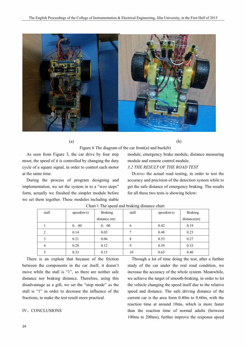
Figure 6 The diagram of the car front(a) and back(b) As seen from Figure 3, the car drive by four step
moor, the speed of it is controlled by changing the duty cycle of a square signal, in order to control each motor at the same time.
During the process of program designing and implementation, we set the system in to a “weo steps” form, actually we finished the simpler module before we set them together. These modules including stable
module, emergency brake module, distance measuring module and remote control module. 3.2 THE RESULT OF THE ROAD TEST
DURING the actual road testing, in order to test the accuracy and precision of the detection system while to get the safe distance of emergency braking. The results for all these two tests is showing below:
Chart 1 The speed and braking distance chart stall speed(m/s) Braking
distance (m)
stall speed(m/s) Braking
distance(m)
1 0.00 0.00 6 0.42 0.19
2 0.14 0.03 7 0.48 0.23
3 0.21 0.06 8 0.53 0.27
4 0.28 0.12 9 0.59 0.33
5 0.33 0.15 10 0.65 0.40
There is an explain that because of the friction between the components in the car itself, it doesn’t move while the stall is “1”, so there are neither safe distance nor braking distance. Therefore, using this disadvantage as a gift, we set the “stop mode” as the stall is “1” in order to decrease the influence of the fractions, to make the test result more practical.
IV、CONCLUSIONS
Through a lot of time doing the test, after a further study of the car under the real road condition, we increase the accuracy of the whole system. Meanwhile, we achieve the target of smooth-braking, in order to let the vehicle changing the speed itself due to the relative speed and distance. The safe driving distance of the current car is the area form 0.40m to 0.60m, with the reaction time at around 10ms, which is more faster than the reaction time of normal adults (between 100ms to 200ms), further improve the response speed

Hong tiange etc.: The Design and Implementation of Follow-Up Vehicle System Based on Ultrasonic Ranging
25
of the driver and effectively reduce the rate of car accidents.
On the other hand, as the starting point of this design is the distance measurement and follow-up in the city, the characteristic of the system if close distance and works well when the speed is low. So the further improve features are that may do a lane-changing program if it is necessary or may inject it to the follow-up system working on the highway. Meanwhile, working under a high speed may need another kinds of distance measuring methods as the ultrasonic way may doesn’t work as the sound need to travel about 2 seconds or even more.
The third reason is, as the highway is relatively empty, but the road may be ups and downs, therefore may pay attention on how to do a accuracy measuring. Based on the two reasons above, the laser ranging may ineed.
References
[1] Wang Shichuan, China traffic accident mortality
report, people.com.cn
[2] The principle of ultrasonic ranging, Wikipedia search
[3] Wu Hao, Automobile cruise system, Xiangjie car network
[4] Hao Jizhe, Market Research Report of Chinese automobile
collision avoidance system, China industrial competitive
intelligence network
[5] Wu Jianping, Usage of the reflected infrared sensor in
automatic guiding car [J] , China measurement technology,
Vol.30 NO.6, Nov,2004.
[6] Zhang Minghuan, A better obstacle detection method based
on tentacle algorithm of obstacle avoidance for intelligent
vehicle [J], Journal of Northwestern Polytechnical
University, Oct.2012, Vol.30 No.5
[7] Zhou Fuliang, Algorithm of highway vehicle
passive ranging system, [D], Zhejiang
University.2003 February
[8] Wang Yuncai, Correlation range finding with chaotic laser
signal,[J], Journal of Shenzhen University Scirnce And
engineering, Vol.27,No.4,Oct,2010.
[9] Qiu Rong, Research on architecture and design of
automotive auto distance-finding system with risk
estimation and decision making[J], The electronic
technology of cars, 2007
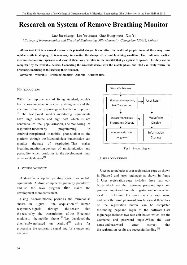
The English Proceedings of the College of Instrumentation & Electrical Engineering, Jilin University, in the First Half of 2015
26
Research on System of Remove Breathing Monitor
Luo Jia-cheng;Liu Yu-xuan;Gao Hong-wei;Xin Yi (College of instrumentation and Electrical Engineering, Jilin University, Changchun 130012, China)
Abstract—SAHS is a normal disease with potential danger. It can affect the health of people. Some of them may couse
sudden death in sleeping. It is necessary to monitor the change of current breathing condition. The traditional medical
instrumentations are expensive and most of them are centralize in the hospital that go against to spread. This duty can be
competent by the wearable devices. Connecting the wearable device with the mobile phone and PDA can easily realize the
breathing conditiong of the users by their terminal.
Key words—Wearable Breathing-Monitor Android Current-time
0 INTRODUCTION
WITH the improvement of living standard, people's health consciousness is gradually strengthens and the attention of human physiological health has improved [1]. The traditional medical monitoring equipments have large volume and high cost which is not conducive to the popularization,.The monitoring of respiration function by programming in Android transplanted to mobile phone, tablet as the platform through the Bluetooth data transmission can monitor the state of respiration. That makes breathing monitoring devices of miniaturization and portability which conforms to the development trend of wearable devices[2] .
Ⅰ SYSTEM OVERVIEW
Android is a popular operating system for mobile equipments. Android equipments gradually popularize and use the Java program that makes the development more convenient.
Using Android mobile phone as the terminal, as shown in Figure 1, the acquisition of human respiratory signals through the sensor that the results by the transmission of the Bluetooth module to the mobile phone [3]. We developed the client software based on Android[4] using for processing the respiratory signal and for storage and analysis.
Fig.1 System diagram
ⅡUSER LOGIN DESIGN
User page includes a user registration page as shown in Figure 2 and user loginpage as shown in figure 3 . User registration page includes three text edit boxes which are the username, password input and password input and have the registration button which used to determine. The user enter a user name and enter the same password two times and then click on the registration button can be completed the landing page and login to the software. User login page includes two text edit boxes which are the username and password input .When the user name and password enter correct that the registration results are successful landing [5].
Wearable Devices
User Login
Waveform Display
Waveform Analysis,
Frequency Display
Information Storage
Abnormal situation
judgment
BluetoothConnection,
DataTransmission
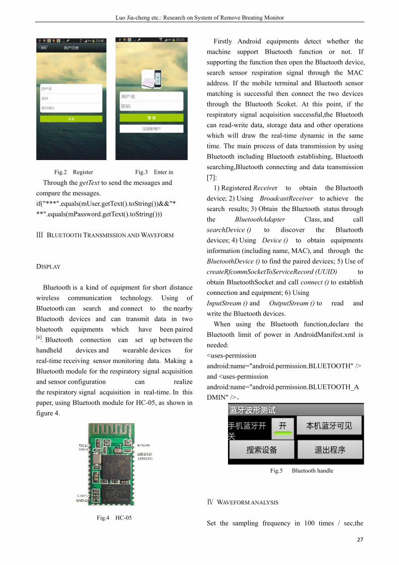
Luo Jia-cheng etc.: Research on System of Remove Breating Monitor
27
Fig.2 Register Fig.3 Enter in
Through the getText to send the messages and compare the messages. if("***".equals(mUser.getText().toString())&&"***".equals(mPassword.getText().toString()))
Ⅲ BLUETOOTH TRANSMISSION AND WAVEFORM
DISPLAY
Bluetooth is a kind of equipment for short distance wireless communication technology. Using of Bluetooth can search and connect to the nearby Bluetooth devices and can transmit data in two bluetooth equipments which have been paired [6]. Bluetooth connection can set up between the handheld devices and wearable devices for real-time receiving sensor monitoring data. Making a Bluetooth module for the respiratory signal acquisition and sensor configuration can realize the respiratory signal acquisition in real-time. In this paper, using Bluetooth module for HC-05, as shown in figure 4.
Fig.4 HC-05
Firstly Android equipments detect whether the machine support Bluetooth function or not. If supporting the function then open the Bluetooth device, search sensor respiration signal through the MAC address. If the mobile terminal and Bluetooth sensor matching is successful then connect the two devices through the Bluetooth Scoket. At this point, if the respiratory signal acquisition successful,the Bluetooth can read-write data, storage data and other operations which will draw the real-time dynamic in the same time. The main process of data transmission by using Bluetooth including Bluetooth establishing, Bluetooth searching,Bluetooth connecting and data teansmission [7]:
1) Registered Receiver to obtain the Bluetooth device; 2) Using BroadcastReceiver to achieve the search results; 3) Obtain the Bluetooth status through the BluetoothAdapter Class, and call searchDevice () to discover the Bluetooth devices; 4) Using Device () to obtain equipments information (including name, MAC), and through the BluetoothDevice () to find the paired devices; 5) Use of createRfcommSocketToServiceRecord (UUID) to obtain BluetoothSocket and call connect () to establish connection and equipment; 6) Using InputStream () and OutputStream () to read and write the Bluetooth devices.
When using the Bluetooth function,declare the Bluetooth limit of power in AndroidManifest.xml is needed: <uses-permission android:name="android.permission.BLUETOOTH" /> and <uses-permission android:name="android.permission.BLUETOOTH_ADMIN" />。
Fig.5 Bluetooth handle
Ⅳ WAVEFORM ANALYSIS
Set the sampling frequency in 100 times / sec,the
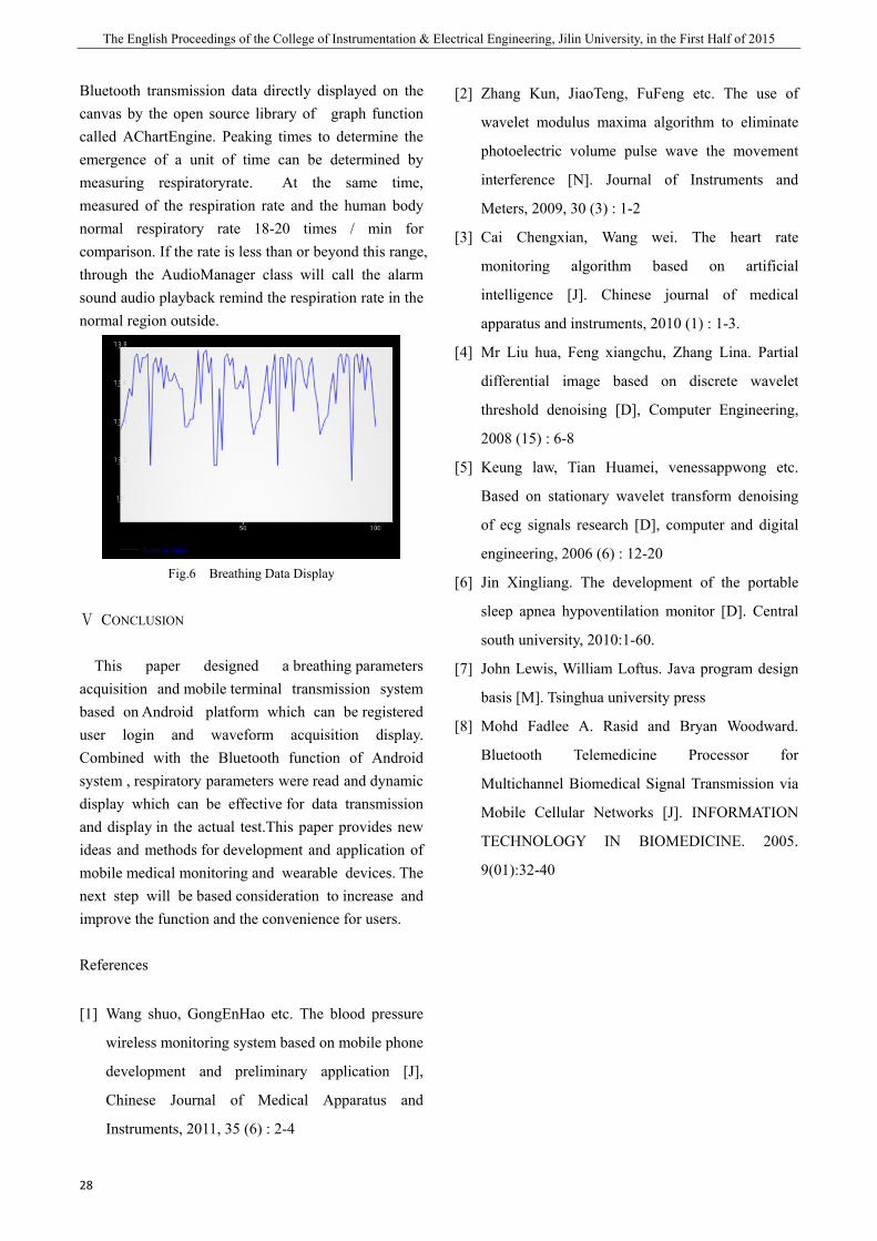
The English Proceedings of the College of Instrumentation & Electrical Engineering, Jilin University, in the First Half of 2015
28
Bluetooth transmission data directly displayed on the canvas by the open source library of graph function called AChartEngine. Peaking times to determine the emergence of a unit of time can be determined by measuring respiratoryrate. At the same time, measured of the respiration rate and the human body normal respiratory rate 18-20 times / min for comparison. If the rate is less than or beyond this range, through the AudioManager class will call the alarm sound audio playback remind the respiration rate in the normal region outside.
Fig.6 Breathing Data Display
Ⅴ CONCLUSION
This paper designed a breathing parameters acquisition and mobile terminal transmission system based on Android platform which can be registered user login and waveform acquisition display. Combined with the Bluetooth function of Android system , respiratory parameters were read and dynamic display which can be effective for data transmission and display in the actual test.This paper provides new ideas and methods for development and application of mobile medical monitoring and wearable devices. The next step will be based consideration to increase and improve the function and the convenience for users.
References
[1] Wang shuo, GongEnHao etc. The blood pressure
wireless monitoring system based on mobile phone
development and preliminary application [J],
Chinese Journal of Medical Apparatus and
Instruments, 2011, 35 (6) : 2-4
[2] Zhang Kun, JiaoTeng, FuFeng etc. The use of
wavelet modulus maxima algorithm to eliminate
photoelectric volume pulse wave the movement
interference [N]. Journal of Instruments and
Meters, 2009, 30 (3) : 1-2
[3] Cai Chengxian, Wang wei. The heart rate
monitoring algorithm based on artificial
intelligence [J]. Chinese journal of medical
apparatus and instruments, 2010 (1) : 1-3.
[4] Mr Liu hua, Feng xiangchu, Zhang Lina. Partial
differential image based on discrete wavelet
threshold denoising [D], Computer Engineering,
2008 (15) : 6-8
[5] Keung law, Tian Huamei, venessappwong etc.
Based on stationary wavelet transform denoising
of ecg signals research [D], computer and digital
engineering, 2006 (6) : 12-20
[6] Jin Xingliang. The development of the portable
sleep apnea hypoventilation monitor [D]. Central
south university, 2010:1-60.
[7] John Lewis, William Loftus. Java program design
basis [M]. Tsinghua university press
[8] Mohd Fadlee A. Rasid and Bryan Woodward.
Bluetooth Telemedicine Processor for
Multichannel Biomedical Signal Transmission via
Mobile Cellular Networks [J]. INFORMATION
TECHNOLOGY IN BIOMEDICINE. 2005.
9(01):32-40

Zhaolu Li etc.: Study of power system based on piezoelectric thin films
29
Study of Power System based on Piezoelectric Thin Films
Zhaolu Li;Renpeng;Renqiang
( Jilin university instrument science and engineering institute,changchun ,130026)
Abstract—According to statistics, the annual radiation to the earth's solar power is 1780000000 kilowatts, the development
and utilization of 500 to 100000000000 degrees. But because of its distribution is very dispersed, now can use the little. The
global land part 3 km depth, high temperature above 150 DEG C in geothermal energy resources of 1400000 tons of standard
coal, at present, some countries have begun to develop the use of commercial.The people in the search for new energy
sources, the way to improve the earth's environment and arduous exploration. The body will be accompanied with a lot
of energy produced during the activity, like we were walking or running vibration generated when the energy and potential
energy to produce its center of gravity changes, its body temperature heat release of thermal energy and so
on. Imagine these wasted energy collection and use, will be able to drive the micro electronic equipment works.As mobile
phone, MP3 and other electronic equipment to carry, can be generated by itself in need of power
supply or charging energy convenient for charging power supply. Based on the above consideration, puts forward the idea
of walking power. This paper is the use of PVDF piezoelectric thin film piezoelectric power generation way, by putting one or
more pieces of PVDF in the inter layer of the shoe sole piezoelectric film, walk the heel of the sole spring device of pressure
fluctuations of PVDF piezoelectric film pressure is generated, through piezoelectric effect of the pressure energy into electrical
energy, the energy storage in the super capacitor or micro battery, give power electronic equipment.
Keywords—energy; PVDF piezoelectric thin film; walk generation;piezoelectric effect
0. INTRODUCTION
WATER is the source of life, life comes from water, but the dynamics of life is an energy, nature is our mother, mother provides coal and oil for our fossil energy, but the fossil energy isn’t inexhaustible,as we uncontrolled exploitation, energy is less and less, moreover, the combustion of fossil energy will increase the pressure on the natural purification, resulting in more serious environmental problems, therefore, to find and use of new energy is our mission and responsibility to protect future generations of the earth protection.
However, looking for new energy path of thorns, misty such as wind energy, water energy is swift and violent, dangerous lightning energy, we forget to spread around the waste of energy,such as when the person walks, the foot will produce energy, this is this article center.
At present, some scientists USA invented a power generation device can be placed in the shoes, the principle is to make full use of an advanced energy
harvesting technology now --reverse electric wetting, which is based on the voltage to change the hydrophobic surface of droplet shape, the researchers turn to using this principle, the micro droplet flow in the process of energy conversion to electricity. The device is similar to the insole and a layer containing thousands of drip, micro droplet. Inside the shoe, can move around and with power generation [1]. At the same time, China also has a similar innovation, in China's Sichuan Chengdu, an ordinary man Shi Caijun, the use of devices such as diodes and wire, invented the sport shoes to light the way back, but also can charge the mobile phone[2]. Do not need to bring a flashlight, does not need power supply, power shoes for us to illuminate the way home, so that we become "mobile" power, the personal "power plants" when the earthquake disaster ridden also will take some give us light and hope.
1. DESIGN PRINCIPLES
PVDF piezoelectric material is a new functional
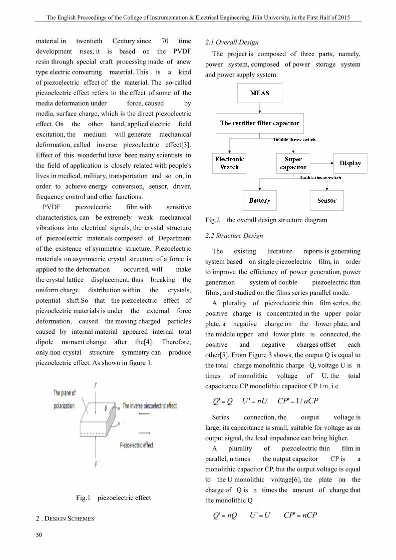
The English Proceedings of the College of Instrumentation & Electrical Engineering, Jilin University, in the First Half of 2015
30
material in twentieth Century since 70 time development rises, it is based on the PVDF resin through special craft processing made of anew type electric converting material. This is a kind of piezoelectric effect of the material. The so-called piezoelectric effect refers to the effect of some of the media deformation under force, caused by media, surface charge, which is the direct piezoelectric effect. On the other hand, applied electric field excitation, the medium will generate mechanical deformation, called inverse piezoelectric effect[3]. Effect of this wonderful have been many scientists in the field of application is closely related with people's lives in medical, military, transportation and so on, in order to achieve energy conversion, sensor, driver, frequency control and other functions.
PVDF piezoelectric film with sensitive characteristics, can be extremely weak mechanical vibrations into electrical signals, the crystal structure of piezoelectric materials composed of Department of the existence of symmetric structure. Piezoelectric materials on asymmetric crystal structure of a force is applied to the deformation occurred, will make the crystal lattice displacement, thus breaking the uniform charge distribution within the crystals, potential shift.So that the piezoelectric effect of piezoelectric materials is under the external force deformation, caused the moving charged particles caused by internal material appeared internal total dipole moment change after the[4]. Therefore, only non-crystal structure symmetry can produce piezoelectric effect. As shown in figure 1:
Fig.1 piezoelectric effect
2 . DESIGN SCHEMES
2.1 Overall Design
The project is composed of three parts, namely, power system, composed of power storage system and power supply system:
Fig.2 the overall design structure diagram
2.2 Structure Design
The existing literature reports is generating system based on single piezoelectric film, in order to improve the efficiency of power generation, power generation system of double piezoelectric thin films, and studied on the films series parallel mode.
A plurality of piezoelectric thin film series, the positive charge is concentrated in the upper polar plate, a negative charge on the lower plate, and the middle upper and lower plate is connected, the positive and negative charges offset each other[5]. From Figure 3 shows, the output Q is equal to the total charge monolithic charge Q, voltage U is n times of monolithic voltage of U, the total capacitance CP monolithic capacitor CP 1/n, i.e.
QQ =' nUU =' nCPCP /1'=
Series connection, the output voltage is large, its capacitance is small, suitable for voltage as an output signal, the load impedance can bring higher.
A plurality of piezoelectric thin film in parallel, n times the output capacitor CP is a monolithic capacitor CP, but the output voltage is equal to the U monolithic voltage[6], the plate on the charge of Q is n times the amount of charge that the monolithic Q
nQQ =' UU =' nCPCP ='
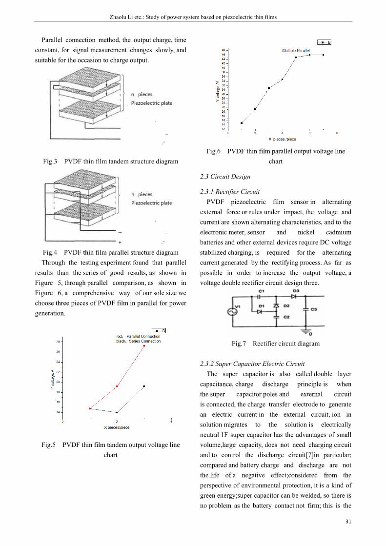
Zhaolu Li etc.: Study of power system based on piezoelectric thin films
31
Parallel connection method, the output charge, time constant, for signal measurement changes slowly, and suitable for the occasion to charge output.
Fig.3 PVDF thin film tandem structure diagram
Fig.4 PVDF thin film parallel structure diagram Through the testing experiment found that parallel
results than the series of good results, as shown in Figure 5, through parallel comparison, as shown in Figure 6, a comprehensive way of our sole size we choose three pieces of PVDF film in parallel for power generation.
Fig.5 PVDF thin film tandem output voltage line chart
Fig.6 PVDF thin film parallel output voltage line
chart
2.3 Circuit Design
2.3.1 Rectifier Circuit PVDF piezoelectric film sensor in alternating
external force or rules under impact, the voltage and current are shown alternating characteristics, and to the electronic meter, sensor and nickel cadmium batteries and other external devices require DC voltage stabilized charging, is required for the alternating current generated by the rectifying process. As far as possible in order to increase the output voltage, a voltage double rectifier circuit design three.
Fig.7 Rectifier circuit diagram
2.3.2 Super Capacitor Electric Circuit
The super capacitor is also called double layer capacitance, charge discharge principle is when the super capacitor poles and external circuit is connected, the charge transfer electrode to generate an electric current in the external circuit, ion in solution migrates to the solution is electrically neutral 1F super capacitor has the advantages of small volume,large capacity, does not need charging circuit and to control the discharge circuit[7]in particular; compared and battery charge and discharge are not the life of a negative effect;considered from the perspective of environmental protection, it is a kind of green energy;super capacitor can be welded, so there is no problem as the battery contact not firm; this is the
The English Proceedings of the College of Instrumentation & Electrical Engineering, Jilin University, in the First Half of 2015
32
choice of super capacitor as an important part of electricity storage circuit.
As shown in figure PVDF, the piezoelectric film generated electrical energy stored in super capacitors C4, stored energy can give nickel cadmium rechargeable battery or sensors and other electronic devices.
Fig.8 Super capacitor energy storing electric circuit
2.4 Display Design
As shown in Figure 9, the display module comprises a MSP430 processor and a 1602 liquid crystal display module two. Among them, MSP430[8] the internal impedance than ordinary AD acquisition chip impedance is high, so it won't be consumed quickly charging voltage, charging voltage can display the values of effective.
Fig.9 Display circuit connection diagram
3. TEST AND ANALYSIS
To give the electronic meter charging module test, the wire and the power supply switch to electronic shoe end table block, the electronic meter charging switch is opened, 1.6V lighting electronic watches, walking two steps per second in frequency, filtering on both ends of the capacitor voltage from
1.0V up to 2.0V takes three minutes and fifty-six seconds, 30 seconds can make the electronic table light.
On to the super capacitor charging module test, open the file with the frequency of the super capacitor, walking three steps per second, super capacitor voltage at both ends of the increase of 0.001V.
The module test to the sensor power supply, double throw switch to stop power supply mode of sensor, sensor work in super voltage 2.0V, 2.5V sensor can work for 11 minutes.
The test module to charge the battery power supply mode, double throw switch to charge the battery block, in the voltage at both ends of the super capacitor is 2.82V, in 1 minutes to charge the battery charging 0.01V.
4. CONCLUSION
The test results prove that the function effect of the power system to achieve the expected standard, can satisfy the actual consumption needs; at the same time through the system display module can directly see the amount of power. Therefore, the system can realize will walk vibration mechanical energy into electrical energy, or storage or to electronic products supply, have very good research prospect.
Reference
[1] anonymous.USA researchers invented _ electricity
generating shoes[N]. Qianjiang Evening News, 2012 (1).
[2] Jiahui.Chengdu old invention for mobile
phone charging shoes [N]. shoes news general report, 2009.
[3] Mao Qin,Wang Tao.PVDF piezoelectric power generation
characteristics based on [J]. Journal of Beijing Institute of
Technology, 2012, 32 (11): 1140-1144.
[4] Liu Chengyu The PVDF piezoelectric films carotid pulse
sensor [C].Shandong University Medical Engineering
Research Institute of control science and engineering based
on biological engineering. China Joint Symposium
(first), 2007.4:200-210.

Zhaolu Li etc.: Study of power system based on piezoelectric thin films
33
[5] Terry Chui .The PVDF piezoelectric films of large caliber
gun projectile base propellant charge compression stress
test method and the impact of vibration based
on [J]., 2012, 31(22).
[6] Zhong Zhengqing. Piezoelectric generator in tire design
and experiment [D]. Chongqing:Chongqing
University, 2009.
[7] Xu Hongxing, Luo Ying.PVDF piezoelectric thin
film application [J]. Journal of Jiangsu University of
science and engineering, 1999, 20 (5):88-91.
[8] Hong Li, Zhang Yang, Li Shibao.MSP430 single chip
microcomputer principle and application example of [M].
Beijing: Beihang University press, 2010: 0-500.
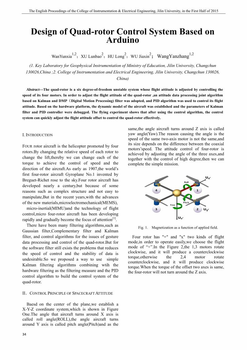
The English Proceedings of the College of Instrumentation & Electrical Engineering, Jilin University, in the First Half of 2015
34
Design of Quad-rotor Control System Based on Arduino
WanYunxia1,2;XU Lunbao2
;HU Long2;WU Jiaxin2;WangYanzhang1,2
(1. Key Laboratory for Geophysical Instrumentation of Ministry of Education, Jilin University, Changchun 130026,China ;2. College of Instrumentation and Electrical Engineering, Jilin University, Changchun 130026,
China)
Abstract—The quad-rotor is a six degree-of-freedom unstable system whose flight attitude is adjusted by controlling the speed of its four motors. In order to adjust the flight attitude of the quad-rotor ,an attitude data processing joint algorithm based on Kalman and DMP(Digital Motion Processing) filter was adopted, and PID algorithm was used to control its flight attitude. Based on the hardware platform, the dynamic model of the aircraft was established and the parameters of Kalman filter and PID controller were debugged. The flying experiment shows that after using the control algorithm, the control system can quickly adjust the flight attitude offset to control the quad-rotor effectively.
I. INTRODUCTION
FOUR rotor aircraft is the helicopter promoted by four rotors.By changing the relative speed of each rotor to change the lift,thereby we can change each of the torque to achieve the control of speed and the direction of the aircraft.As early as 1907,the world’s first four-rotor aircraft Gyroplane No.1 invented by Breguet-Richet rose to the sky.Four rotor aircraft has developed nearly a century,but because of some reasons such as complex structure and not easy to manipulate,But in the recent years,with the advances of the new materials,microelectromechanical(MEMS),
micro-inertial(MIMU)and the technology of flight control,micro four-rotor aircraft has been developing rapidly and gradually become the focus of attention[1].
There have been many filtering algorithms,such as Gaussian filter,Complementary filter and Kalman filter, and control algorithms for the issues of gesture data processing and control of the quad-rotor.But for the software filter still exists the problems that reduces the speed of control and the stability of data is undesirable.So we proposed a way to use simple Kalman filtering algorithms combining wtih the hardware filtering as the filtering measure and the PID control algorithm to build the control system of the quad-rotor.
II.CONTROL PRINCIPLE OF SPACECRAFT ATTITUDE
Baesd on the center of the plane,we establish a X-Y-Z coordinate system,which is shown in Figure One.The angle that aircraft turns around X axis is called roll angle(ROLL),the angle aircraft turns around Y axis is called pitch angle(Pitch)and as the
same,the angle aircraft turns around Z axis is called yaw angle(Yaw).The reason causing the angle is the speed of the same two-axis motor is not the same,and its size depends on the difference between the coaxial motors’speed. The attitude control of four-rotor is achieved by adjusting the angle of the three axes,and together with the control of high degree,then we can complete the simple mission.
Four rotor has "+" and "x" two kinds of flight
mode,in order to operate easily,we choose the flight mode of “+”.In the Figure 2,the 1,3 motors rotate clockwise, and it will produce a counterclockwise torque,otherwise the 2,4 motor rotate counterclockwise, and it will produce clockwise torque.When the torque of the offset two axes is same, the four-rotor will not turn around the Z axis.
Fig. 1. Magnetization as a function of applied field.
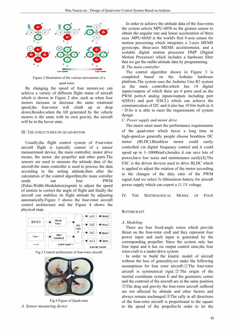
Wan Yunxia etc.: Design of Quad-rotor Control System Based on Arduino
35
Figure 2 Illustration of the various movements of a
quad-rotor. By changing the speed of four motors,we can
achieve a variety of different flight status of aircraft which is shown in Figure 2 also ,such as when four motors increase or decrease the same rotational speed,the four-rotor will climb up or drop down.Besides,when the lift generated by the vehicle motors is the same with its own gravity, the aircraft will be in the hover state.
III. THE STRUCTURES OF QUAD-ROTOR
Usually,the flight control system of Four-rotor aircraft flight is typically consist of a sensor measurement device, the main controller, motor drive means, the motor ,the propeller and other parts.The sensors are used to measure the attitude data of the aircraft.the main controller is used to process the data according to the setting attitude,then after the calculation of the control algorithm,the main cotroller sends out four PWM (Pulae-Width-Modulation)signals to adjust the speed of motors to correct the angle of flight and finally the aircraft can stabilize its flight attitude by adjusting automatically.Figure 3 shows the four-rotor aircraft control architecture and the Figure 4 shows the physical map.
Fig.3 Control architecture of four-rotor aircraft
Fig.4 Figure of Quad-rotor
A. Sensor measuring device
In order to achieve the attitude data of the four-rotor, the system selects MPU-6050 as the gesture sensor to obtain the angular rate and linear acceleration of three axes .MPU-60X0 is the world's first 9-axis sensor for motion processing which integrates a 3-axis MEMS gyroscope, three-axis MEMS accelerometer, and a scalable digital motion processor DMP (Digital Motion Processor) which includes a hardware filter that we get the stable attitude data by programming. B. The main controller
The control algorithm shown in Figure 3 is completed based on the Arduino hardware platform.The system uses the Arduino Uno R3 system as the main controller,which has 14 digital inputs/outputs of which there are 6 ports used as the PWM ports,6 analog inputs/outputs including port 4(SDA) and port 5(SCL) which can achieve the communication of I2C and it also has 10 bits built-in A / D.So it is able to meet the requirements of system design. C. Power supply and motor drive
The motor must meet the performance requirements of the quad-rotor which haves a long time in high-speed,so generally people choose brushless DC motor (BLDC).Brushless motor could easily controlled via digital frequency control and it could speed up to 1~10000rad/s,besides it can save lots of power,have low noise and maintenance easily[4].The ESC is the driven devices used to drive BLDC which is applied to adjust the rotation of the motor according to the changes of the duty ratio of the PWM signal.And we select 3s lithiumiron battery for aircraft power supply which can export a 11.1V voltage.
IV. THE MATHEMATICAL MODEL OF FOUR
ROTORCRAFT
A. Modeling There are four fixed-angle rotors which provide
thrust on the four-rotor craft and they represent four power input and each input is generated by the corresponding propeller. Since the system only has four input and it has six output control state,the four rotor-craft is a under-drive system.
In order to build the kinetic model of aircraft without the loss of generality,we make the following assumptions for four rotor aircraft:①The four-rotor aircraft is symmetrical rigid.②The origin of the inertial coordinate system E and the geometric center and the centroid of the aircraft are in the same position.③The drag and gravity the four-rotor aircraft suffered are not affected by altitude and other factors and always remain unchanged.④The rally in all directions of the four-rotor aircraft is proportional to the square to the speed of the propeller.In order to let the

The English Proceedings of the College of Instrumentation & Electrical Engineering, Jilin University, in the First Half of 2015
36
four-rotor aircraft fly to a fixed point in space from the ground,we establish transform matrix of direction cosine.We select the Cartesian coordinates of right-hand rule as the ground coordinate[5].
jj
jj
jqf
cos0sin010
sin0cos
1000cossin0sincos
),,(-
-
=R
ff
ff
cossin0sincos0001
-
- (1)
Which q is the pitch angle along the pitching rotation of Ey-Pitch,j is yaw angle along the rotation of the direction of Ez-Yaw,f is the rotating angle along the rotation of the direction of Ex-Roll.The model of kinetic using the balance between the equations and moments and the model of Lagrangian simplifies approach can in the equations written as the follow:
1 1
1 2
1 3
(cos sin cos sin sin ) /(sin sin cos cos sin ) /(cos cos ) /
x U K x my U K y mz U g K z m
j q f j f
j f f j f
j f
= + -
= - -
= - -
(2)
In which g represents the acceleration due to gravity,m
is the total mass of the aircraft, 321 ,, KKK are the resistance coefficient for the system.When in the low-speed the resistance is very small ,so we can neglect it.To operate conveniently we define the input which is shown in the following formula:
343214
241323
121432
43211
/)(
/)(/)(
/)(
IHHHHCU
IHHHHlUIHHHHlU
mHHHHU
+++=
--+=
--+=
+++=
(3) In which U1 is the vertical force generated by four rotors,U2 is the pitching moment,U3 is the yawing moment,U4 is the rolling moment.Hi(i=1,2,3,4)is the thrust generated by the four rotors,Ii(i=1,2,3)is the moment inertia corresponding to each axis.And the Euler angels( )qjf ,, of the aircraft is shown in the following equations[4]:
2 4 1
3 5 2
4 6 3
/
/
/
U lK I
U lK I
U lK I
q q
j j
f f
= -
= -
= -
(4)
In which l s the length of the radius of the stand of
the aircraft,Ki(i=1,2,3)are the resistance coefficient Four rotor system can be illustrated as the following picture after using the Newton-Euler model to model the aircraft[5].
fqj
xyz
Fig.5 Block modeling of Four rotor-craft control system B.The state equations of system
The simulation of the aircraft requires the transfer function of the whole system,and we had get the relationship between the input and output through the mathematical modeling of the four-rotor,so we suppose the form of the state equation as follow:
⎩⎨⎧
+=
+=
DUCXYBUAXX
(5)
( )TUUUUU 4321 ,,,= is the input vector,
( )TgzyxzyxX ,,,,,,,,,,,, jfqjfq= is the state
vector, ( )TzyxY jqf ,,,,,= is the output vector,so we can get each equation of the state space obtained from the mathematical model[8]:
0 0 0 1 0 0 0 0 0 0 0 0 00 0 0 0 1 0 0 0 0 0 0 0 00 0 0 0 0 1 0 0 0 0 0 0 00 0 0 0 0 0 0 0 0 0 0 0 00 0 0 0 0 0 0 0 0 0 0 0 00 0 0 0 0 0 0 0 0 0 0 0 10 0 0 0 0 0 0 0 0 1 0 0 00 0 0 0 0 0 0 0 0 0 1 0 00 0 0 0 0 0 0 0 0 0 0 1 00 0 0 0 0 0 0 0 0 0 0 0 00 0 0 0 0 0 0 0 0 0 0 0 00 0 0 0 0 0 0 0 0 0 0 0 00 0 0 0 0 0 0 0 0 0 0 0 0
A
⎧ ⎫⎪ ⎪⎪ ⎪⎪ ⎪⎪ ⎪⎪ ⎪⎪⎪
-⎪⎪
= ⎨ ⎬⎪⎪⎪⎪⎪⎪⎪⎪⎪⎩
⎪⎪⎪⎪
⎪⎪⎪⎪⎪⎪⎪⎪⎪⎭
(6)
⎪⎪⎪⎪⎪⎪⎪⎪⎪
⎭
⎪⎪⎪⎪⎪⎪⎪⎪⎪
⎬
⎫
⎪⎪⎪⎪⎪⎪⎪⎪⎪
⎩
⎪⎪⎪⎪⎪⎪⎪⎪⎪
⎨
⎧
-
+
=
-
-
-
-
-
-
0000000
000000000000000000000)cos(cos000)sincoscossin(sin000)cossincossin(sin000000000000
13
12
11
1
1
1
IlI
lI
mmm
B
l
jf
jfjjf
jqffj(7)
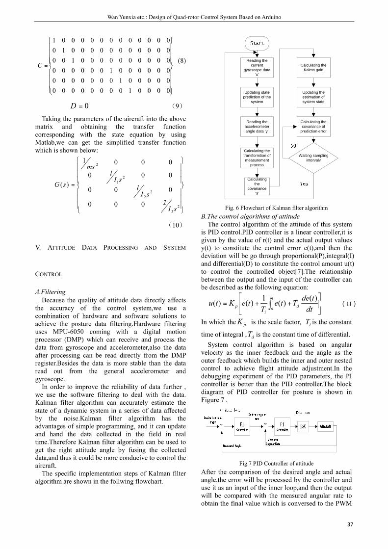
Wan Yunxia etc.: Design of Quad-rotor Control System Based on Arduino
37
⎪⎪⎪⎪
⎭
⎪⎪⎪⎪
⎬
⎫
⎪⎪⎪⎪
⎩
⎪⎪⎪⎪
⎨
⎧
=
000010000000000000100000000000001000000000000000010000000000000100000000000001
C (8)
0=D (9)
Taking the parameters of the aircraft into the above matrix and obtaining the transfer function corresponding with the state equation by using Matlab,we can get the simplified transfer function which is shown below:
⎪⎪⎪
⎭
⎪⎪⎪
⎬
⎫
⎪⎪⎪
⎩
⎪⎪⎪
⎨
⎧
=
23
22
21
2
000
000
000
0001
)(
sI
sIl
sIl
ms
sG
l
(10)
V. ATTITUDE DATA PROCESSING AND SYSTEM
CONTROL
A.Filtering Because the quality of attitude data directly affects
the accuracy of the control system,we use a combination of hardware and software solutions to achieve the posture data filtering.Hardware filtering uses MPU-6050 coming with a digital motion processor (DMP) which can receive and process the data from gyroscope and accelerometer,also the data after processing can be read directly from the DMP register.Besides the data is more stable than the data read out from the general accelerometer and gyroscope.
In order to improve the reliability of data further , we use the software filtering to deal with the data. Kalman filter algorithm can accurately estimate the state of a dynamic system in a series of data affected by the noise.Kalman filter algorithm has the advantages of simple programming, and it can update and hand the data collected in the field in real time.Therefore Kalman filter algorithm can be used to get the right attitude angle by fusing the collected data,and thus it could be more conducive to control the aircraft.
The specific implementation steps of Kalman filter algorithm are shown in the follwing flowchart.
Reading the current
gyroscope data ‘u’
Updating state prediction of the
system
Reading the accelerometer angle data ‘y’
Calculating the transformtion of measurement
process
Calculating the
covariance ‘s’
Calculating the Kalmn gain
Updating the estimation of system state
Calculating the covariance of
prediction error
Waiting sampling intervalv
Fig. 6 Flowchart of Kalman filter algorithm
B.The control algorithms of attitude The control algorithm of the attitude of this system
is PID control.PID controller is a linear controller,it is given by the value of r(t) and the actual output values y(t) to constitute the control error e(t),and then the deviation will be go through proportional(P),integral(I) and differential(D) to constitute the control amount u(t) to control the controlled object[7].The relationship between the output and the input of the controller can be described as the following equation:
⎥⎦
⎤⎢⎣
⎡++= ∫ dt
tdeTteT
teKtu d
t
oi
p)()(1)()( (11)
In which the pK is the scale factor, iT is the constant
time of integral , dT is the constant time of differential. System control algorithm is based on angular
velocity as the inner feedback and the angle as the outer feedback which builds the inner and outer nested control to achieve flight attitude adjustment.In the debugging experiment of the PID parameters, the PI controller is better than the PID controller.The block diagram of PID controller for posture is shown in Figure 7 .
˜˜
Fig.7 PID Controller of attitude
After the comparison of the desired angle and actual angle,the error will be processed by the controller and use it as an input of the inner loop,and then the output will be compared with the measured angular rate to obtain the final value which is conversed to the PWM
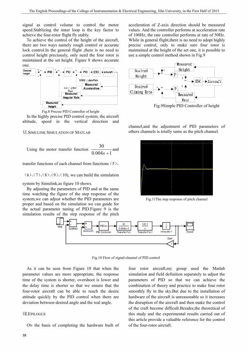
The English Proceedings of the College of Instrumentation & Electrical Engineering, Jilin University, in the First Half of 2015
38
signal as control volume to control the motor speed.Stablizing the inner loop is the key factor to achieve the four-rotor flight fly stably.
To achieve the control of the height of the aircraft, there are two ways namely rough control or accurate lock control.In the general flight ,there is no need to control height preciously, only need the four rotor is maintained at the set height. Figure 8 shows accurate one.
˜ ˜ ˜
Fig.8 Precise PID Controller of height In the highly precise PID control system, the aircraft
altitude, speed in the vertical direction and
acceleration of Z-axis direction should be measured values. And the controller performs at acceleration rate of 100Hz, the rate controller performs at rate of 50Hz. While in general flight,there is no need to adopt highly precise control, only to make sure four rotor is maintained at the height of the set one, it is possible to use a simple control method shown in Fig.9
˜
˜˜
Fig.9Simple PID Controller of height
Ⅵ.SIMULINK SIMULATION OF MATLAB
Using the motor transfer function 1004.0
30+s
and
transfer functions of each channel from functions(5)、
(6)、(7)、(8)、(9)、(10), we can build the simulation
system by Simulink,as figure 10 shows. By adjusting the parameters of PID and at the same
time watching the figure of the step response of the system,we can adjust whether the PID parameters are proper and based on the simulation we can guide for the actual parameter tuning of PID.Figure 9 is the simulation results of the step response of the pitch
channel,and the adjustment of PID parameters of others channels is totally same as the pitch channel.
Fig.11The step response of pitch channel
Fig.10 Flow of signal-channel of PID control
As it can be seen from Figure 10 that when the
parameter values are more appropriate, the response time of the system is shorter, overshoot is lower and the delay time is shorter so that we ensure that the four-rotor aircraft can be able to reach the desire attitude quickly by the PID control when there are deviation between desired angle and the real angle.
Ⅶ.EPILOGUE
ON the basis of completing the hardware built of
four rotor aircraft,my group used the Matlab simulation and field definition separately to adjust the parameters of PID so that we can achieve the combination of theory and practice to make four rotor smoothly fly in the sky.But due to the installation of hardware of the aircraft is unreasonable so it increases the disruption of the aircraft and then make the control of the craft become difficult.Besides,the theoretical of this study and the experimental results carried out of this article provide a valuable reference for the control of the four-rotor aircraft.

Wan Yunxia etc.: Design of Quad-rotor Control System Based on Arduino
39
References
[1] Lie Wen-bo,Ma Hong-xu,Wang Jian. Small quad-totor
aircraft present research situation and key technology[J].
technology[J].ElectronicsOptics&Control , 2007,06 :
0113-05.
[2] Cai Ruiyan.Principle and application of Arduino
[J].Electronic Design Engineering. 2012, 16:0155-03
[3] Lai Yi-han,Wang Kai . Two-wheel Balancing car control
system based on MPU6050[J].Journal of Henan institute of
engineering(natural science edition).,2014,01:0053-05
[4] Li Xiu-ying,,Liu Yan-bo. Control method of quad-totor
based on PWM [J]. Journal of JiLin
University(Information Science Edition),
2011,05:0464-09.
[5] Duan Shi-hua.Design and Implementation of Quad Control
System[D].Chengdu Electronic Technology University.
2012.5.
[6] Wang Shuai,Wei Guo. Application of Kalman Filter in the
Attitude Measurement of Quad-rotor[J].Ordnance Industry
Automation,2011,01:022-03.
[7] Wang Shu-qing,Jiang Wei-fu. PID Parameters tuning based
on MATLAB/Simulink[J]. Industrial Control and
Application,2009,03:0024-03.
[8] Guo Qian-qian. Research of micro Quad in Design and
Control method [D]. Changchun:JiLin University. 2013.6.
[9] Domingues J M B. Quadrotor prototype[J]. Uneversidade
Tecnica deLisboa. Dissertacio, 2009.
[10] Bouabdallah S, Siegwart R. Full control of a
quadrotor[C]//Intelligent robots and systems, 2007. IROS
2007. IEEE/RSJ international conference on. IEEE,
2007:153-158 .
[11] Lim H, Park J, Lee D, et al. Build your own quadrotor:
Open-source projects on unmanned aerial vehicles[J].
Robotics & Automation Magazine, IEEE, 2012,
19(3):33-45.
[12] Patel V K R S, Pandey A K. Modeling and Performance
Analysis of PID Controlled BLDC Motor and Different
Schemes of PWM Controlled BLDC Motor[J].
International Journal of Scientific and Research
Publications, 141.
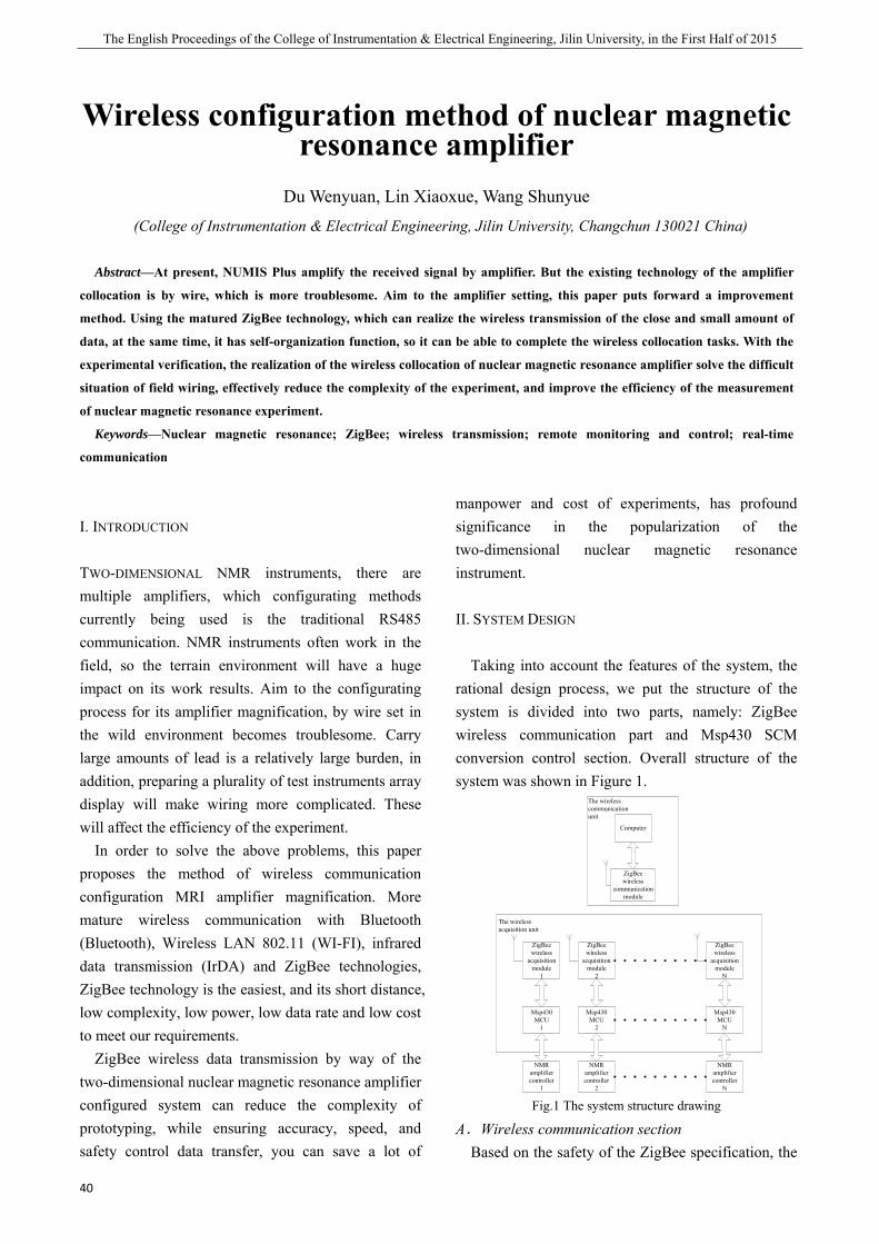
The English Proceedings of the College of Instrumentation & Electrical Engineering, Jilin University, in the First Half of 2015
40
Wireless configuration method of nuclear magnetic resonance amplifier
Du Wenyuan, Lin Xiaoxue, Wang Shunyue
(College of Instrumentation & Electrical Engineering, Jilin University, Changchun 130021 China)
Abstract—At present, NUMIS Plus amplify the received signal by amplifier. But the existing technology of the amplifier
collocation is by wire, which is more troublesome. Aim to the amplifier setting, this paper puts forward a improvement
method. Using the matured ZigBee technology, which can realize the wireless transmission of the close and small amount of
data, at the same time, it has self-organization function, so it can be able to complete the wireless collocation tasks. With the
experimental verification, the realization of the wireless collocation of nuclear magnetic resonance amplifier solve the difficult
situation of field wiring, effectively reduce the complexity of the experiment, and improve the efficiency of the measurement
of nuclear magnetic resonance experiment.
Keywords—Nuclear magnetic resonance; ZigBee; wireless transmission; remote monitoring and control; real-time
communication
I. INTRODUCTION
TWO-DIMENSIONAL NMR instruments, there are multiple amplifiers, which configurating methods currently being used is the traditional RS485 communication. NMR instruments often work in the field, so the terrain environment will have a huge impact on its work results. Aim to the configurating process for its amplifier magnification, by wire set in the wild environment becomes troublesome. Carry large amounts of lead is a relatively large burden, in addition, preparing a plurality of test instruments array display will make wiring more complicated. These will affect the efficiency of the experiment.
In order to solve the above problems, this paper proposes the method of wireless communication configuration MRI amplifier magnification. More mature wireless communication with Bluetooth (Bluetooth), Wireless LAN 802.11 (WI-FI), infrared data transmission (IrDA) and ZigBee technologies, ZigBee technology is the easiest, and its short distance, low complexity, low power, low data rate and low cost to meet our requirements.
ZigBee wireless data transmission by way of the two-dimensional nuclear magnetic resonance amplifier configured system can reduce the complexity of prototyping, while ensuring accuracy, speed, and safety control data transfer, you can save a lot of
manpower and cost of experiments, has profound significance in the popularization of the two-dimensional nuclear magnetic resonance instrument.
II. SYSTEM DESIGN
Taking into account the features of the system, the rational design process, we put the structure of the system is divided into two parts, namely: ZigBee wireless communication part and Msp430 SCM conversion control section. Overall structure of the system was shown in Figure 1.
Fig.1 The system structure drawing
A.Wireless communication section Based on the safety of the ZigBee specification, the
ZigBee wireless
communication module
ZigBee wireless
acquisition module
1
ZigBee wireless
acquisition module
2
Computer
ZigBee wireless
acquisition module
N
Msp430MCU
1
Msp430MCU
2
Msp430MCU
N
The wireless communication unit
The wireless acquisition unit
NMR amplifier controller
1
NMR amplifier controller
2
NMR amplifier controller
N
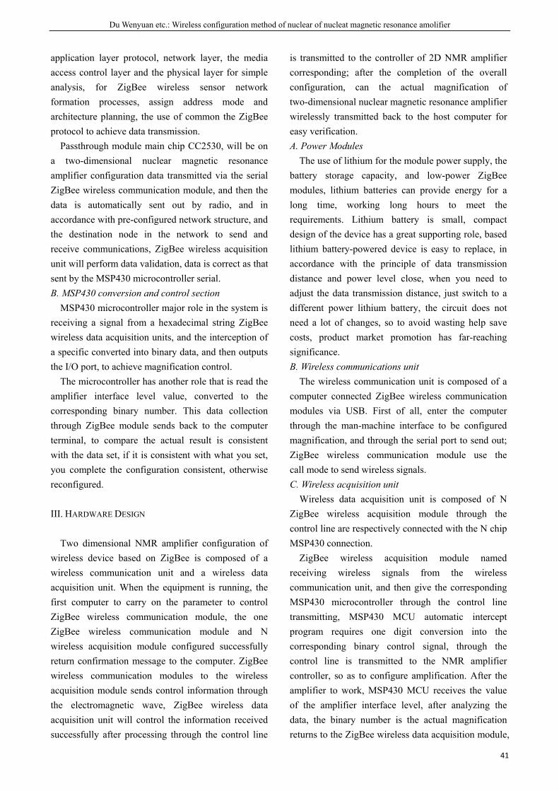
Du Wenyuan etc.: Wireless configuration method of nuclear of nucleat magnetic resonance amolifier
41
application layer protocol, network layer, the media access control layer and the physical layer for simple analysis, for ZigBee wireless sensor network formation processes, assign address mode and architecture planning, the use of common the ZigBee protocol to achieve data transmission.
Passthrough module main chip CC2530, will be on a two-dimensional nuclear magnetic resonance amplifier configuration data transmitted via the serial ZigBee wireless communication module, and then the data is automatically sent out by radio, and in accordance with pre-configured network structure, and the destination node in the network to send and receive communications, ZigBee wireless acquisition unit will perform data validation, data is correct as that sent by the MSP430 microcontroller serial. B. MSP430 conversion and control section
MSP430 microcontroller major role in the system is receiving a signal from a hexadecimal string ZigBee wireless data acquisition units, and the interception of a specific converted into binary data, and then outputs the I/O port, to achieve magnification control.
The microcontroller has another role that is read the amplifier interface level value, converted to the corresponding binary number. This data collection through ZigBee module sends back to the computer terminal, to compare the actual result is consistent with the data set, if it is consistent with what you set, you complete the configuration consistent, otherwise reconfigured.
III. HARDWARE DESIGN
Two dimensional NMR amplifier configuration of wireless device based on ZigBee is composed of a wireless communication unit and a wireless data acquisition unit. When the equipment is running, the first computer to carry on the parameter to control ZigBee wireless communication module, the one ZigBee wireless communication module and N wireless acquisition module configured successfully return confirmation message to the computer. ZigBee wireless communication modules to the wireless acquisition module sends control information through the electromagnetic wave, ZigBee wireless data acquisition unit will control the information received successfully after processing through the control line
is transmitted to the controller of 2D NMR amplifier corresponding; after the completion of the overall configuration, can the actual magnification of two-dimensional nuclear magnetic resonance amplifier wirelessly transmitted back to the host computer for easy verification. A. Power Modules
The use of lithium for the module power supply, the battery storage capacity, and low-power ZigBee modules, lithium batteries can provide energy for a long time, working long hours to meet the requirements. Lithium battery is small, compact design of the device has a great supporting role, based lithium battery-powered device is easy to replace, in accordance with the principle of data transmission distance and power level close, when you need to adjust the data transmission distance, just switch to a different power lithium battery, the circuit does not need a lot of changes, so to avoid wasting help save costs, product market promotion has far-reaching significance. B. Wireless communications unit
The wireless communication unit is composed of a computer connected ZigBee wireless communication modules via USB. First of all, enter the computer through the man-machine interface to be configured magnification, and through the serial port to send out; ZigBee wireless communication module use the call mode to send wireless signals. C. Wireless acquisition unit
Wireless data acquisition unit is composed of N ZigBee wireless acquisition module through the control line are respectively connected with the N chip MSP430 connection.
ZigBee wireless acquisition module named receiving wireless signals from the wireless communication unit, and then give the corresponding MSP430 microcontroller through the control line transmitting, MSP430 MCU automatic intercept program requires one digit conversion into the corresponding binary control signal, through the control line is transmitted to the NMR amplifier controller, so as to configure amplification. After the amplifier to work, MSP430 MCU receives the value of the amplifier interface level, after analyzing the data, the binary number is the actual magnification returns to the ZigBee wireless data acquisition module,
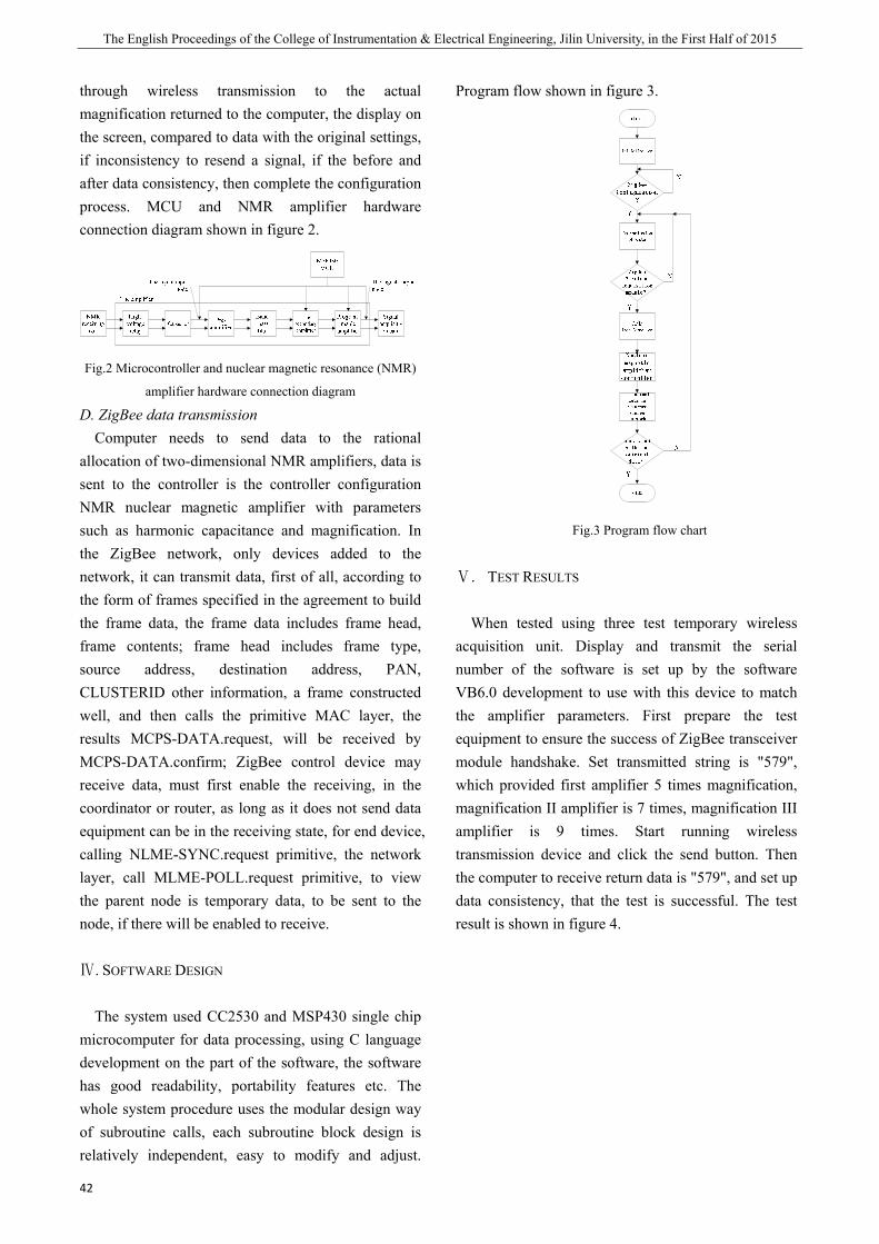
The English Proceedings of the College of Instrumentation & Electrical Engineering, Jilin University, in the First Half of 2015
42
through wireless transmission to the actual magnification returned to the computer, the display on the screen, compared to data with the original settings, if inconsistency to resend a signal, if the before and after data consistency, then complete the configuration process. MCU and NMR amplifier hardware connection diagram shown in figure 2.
Fig.2 Microcontroller and nuclear magnetic resonance (NMR)
amplifier hardware connection diagram
D. ZigBee data transmission Computer needs to send data to the rational
allocation of two-dimensional NMR amplifiers, data is sent to the controller is the controller configuration NMR nuclear magnetic amplifier with parameters such as harmonic capacitance and magnification. In the ZigBee network, only devices added to the network, it can transmit data, first of all, according to the form of frames specified in the agreement to build the frame data, the frame data includes frame head, frame contents; frame head includes frame type, source address, destination address, PAN, CLUSTERID other information, a frame constructed well, and then calls the primitive MAC layer, the results MCPS-DATA.request, will be received by MCPS-DATA.confirm; ZigBee control device may receive data, must first enable the receiving, in the coordinator or router, as long as it does not send data equipment can be in the receiving state, for end device, calling NLME-SYNC.request primitive, the network layer, call MLME-POLL.request primitive, to view the parent node is temporary data, to be sent to the node, if there will be enabled to receive.
Ⅳ. SOFTWARE DESIGN
The system used CC2530 and MSP430 single chip microcomputer for data processing, using C language development on the part of the software, the software has good readability, portability features etc. The whole system procedure uses the modular design way of subroutine calls, each subroutine block design is relatively independent, easy to modify and adjust.
Program flow shown in figure 3.
Fig.3 Program flow chart
Ⅴ. TEST RESULTS
When tested using three test temporary wireless acquisition unit. Display and transmit the serial number of the software is set up by the software VB6.0 development to use with this device to match the amplifier parameters. First prepare the test equipment to ensure the success of ZigBee transceiver module handshake. Set transmitted string is "579", which provided first amplifier 5 times magnification, magnification II amplifier is 7 times, magnification III amplifier is 9 times. Start running wireless transmission device and click the send button. Then the computer to receive return data is "579", and set up data consistency, that the test is successful. The test result is shown in figure 4.
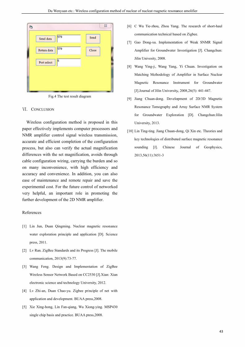
Ⅵ. CONCLU
Wireless cpaper effectivNMR amplifaccurate and process, but differences wcable configuon many inaccuracy andease of mainexperimentalvery helpfulfurther devel
References
[1] Lin Jun,
water exp
press, 201
[2] Lv Ran. Z
communic
[3] Wang Fe
Wireless S
electronic
[4] Lv Zhi-an
application
[5] Xie Xing-
single chip
Du Wenyuan
Fig.4 The te
USION
configurationvely implemefier control s
d efficient comalso can ver
with the set muration wiringnconvenienced conveniencntenance andl cost. For thel, an importlopment of th
Duan Qingmin
ploration princi
1.
ZigBee Standard
cation, 2013(9)
eng. Design a
Sensor Network
science and tec
n, Duan Chao-
n and developm
-hong, Lin Fan
p basis and prac
n etc.: Wireless
st result diagram
n method is pents computesignal wirelempletion of trify the actu
magnificationg, carrying th
e, with high ce. In additiod remote repae future contrtant role in
he 2D NMR a
ng. Nuclear m
iple and applic
ds and its Progr
:73-77.
and Implemen
k Based on CC2
chnology Unive
-yu. Zigbee pri
ment. BUAA pr
n-qiang, Wu Xi
ctice. BUAA pr
configuration m
m
proposed in er processors ess transmisshe configuratal magnificat
n, avoids throhe burden and
efficiency on, you can aair and save rol of networ
promoting amplifier.
magnetic resona
cation [D]. Scie
ress [J]. The mo
ntation of Zig
2530 [J].Xian: X
ersity, 2012.
inciple of net
ess,2008.
ong-ying. MSP
ress,2008.
method of nucle
this and ion,
ation ation ough d so and also the
rked the
ance
ence
obile
gBee
Xian
with
P430
[6]
[7]
[8]
[9]
[10]
ear of nucleat m
C Wu Tie-zh
communicatio
Gao Dong-xu
Amplifier for
Jilin Univesity
Wang Ying-ji
Matching Me
Magnetic R
[J].Journal of
Jiang Chuan-
Resonance To
for Groundw
University, 20
] Lin Ting-ting,
key technolog
sounding [J
2013,56(11):3
magnetic resona
ou, Zhou Yang
on technical bas
u. Implementat
Groundwater I
y, 2008.
i, Wang Yang,
thodology of A
Resonance Ins
Jilin University
-dong. Develo
omography and
water Explora
013.
Jiang Chuan-d
gies of distribute
J]. Chinese
651-3
ance amolifier
g. The research
sed on Zigbee.
tion of Weak
Investigation [
, Yi Chuan. In
Amplifier in S
strument for
y, 2008,26(5): 4
opment of 2D
d Array Surface
ation [D]. C
dong, Qi Xin et
ed surface mag
Journal of
43
h of short-haul
SNMR Signal
J]. Changchun
nvestigation on
Surface Nuclear
Groundwater
441-447.
D/3D Magnetic
e NMR System
Changchun:Jilin
tc. Theories and
netic resonance
f Geophysics
3
l
l
:
n
r
r
c
m
n
d
e
,
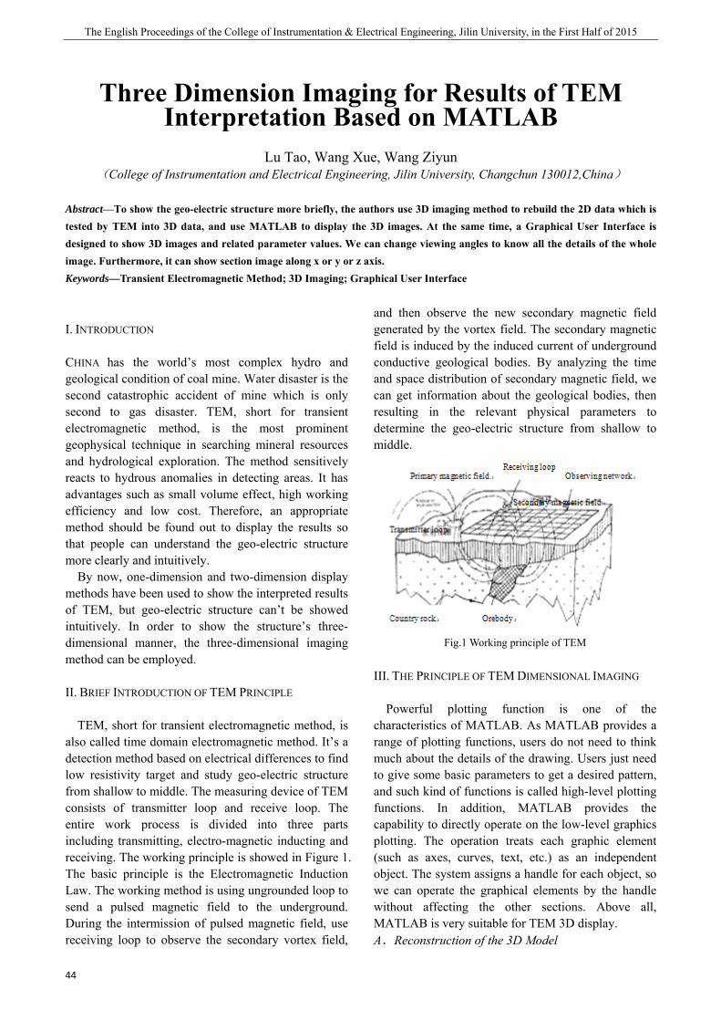
The English Proceedings of the College of Instrumentation & Electrical Engineering, Jilin University, in the First Half of 2015
44
Three Dimension Imaging for Results of TEM Interpretation Based on MATLAB
Lu Tao, Wang Xue, Wang Ziyun
(College of Instrumentation and Electrical Engineering, Jilin University, Changchun 130012,China) Abstract—To show the geo-electric structure more briefly, the authors use 3D imaging method to rebuild the 2D data which is tested by TEM into 3D data, and use MATLAB to display the 3D images. At the same time, a Graphical User Interface is designed to show 3D images and related parameter values. We can change viewing angles to know all the details of the whole image. Furthermore, it can show section image along x or y or z axis. Keywords—Transient Electromagnetic Method; 3D Imaging; Graphical User Interface
I. INTRODUCTION
CHINA has the world’s most complex hydro and geological condition of coal mine. Water disaster is the second catastrophic accident of mine which is only second to gas disaster. TEM, short for transient electromagnetic method, is the most prominent geophysical technique in searching mineral resources and hydrological exploration. The method sensitively reacts to hydrous anomalies in detecting areas. It has advantages such as small volume effect, high working efficiency and low cost. Therefore, an appropriate method should be found out to display the results so that people can understand the geo-electric structure more clearly and intuitively.
By now, one-dimension and two-dimension display methods have been used to show the interpreted results of TEM, but geo-electric structure can’t be showed intuitively. In order to show the structure’s three- dimensional manner, the three-dimensional imaging method can be employed.
II. BRIEF INTRODUCTION OF TEM PRINCIPLE
TEM, short for transient electromagnetic method, is also called time domain electromagnetic method. It’s a detection method based on electrical differences to find low resistivity target and study geo-electric structure from shallow to middle. The measuring device of TEM consists of transmitter loop and receive loop. The entire work process is divided into three parts including transmitting, electro-magnetic inducting and receiving. The working principle is showed in Figure 1. The basic principle is the Electromagnetic Induction Law. The working method is using ungrounded loop to send a pulsed magnetic field to the underground. During the intermission of pulsed magnetic field, use receiving loop to observe the secondary vortex field,
and then observe the new secondary magnetic field generated by the vortex field. The secondary magnetic field is induced by the induced current of underground conductive geological bodies. By analyzing the time and space distribution of secondary magnetic field, we can get information about the geological bodies, then resulting in the relevant physical parameters to determine the geo-electric structure from shallow to middle.
Fig.1 Working principle of TEM
III. THE PRINCIPLE OF TEM DIMENSIONAL IMAGING
Powerful plotting function is one of the characteristics of MATLAB. As MATLAB provides a range of plotting functions, users do not need to think much about the details of the drawing. Users just need to give some basic parameters to get a desired pattern, and such kind of functions is called high-level plotting functions. In addition, MATLAB provides the capability to directly operate on the low-level graphics plotting. The operation treats each graphic element (such as axes, curves, text, etc.) as an independent object. The system assigns a handle for each object, so we can operate the graphical elements by the handle without affecting the other sections. Above all, MATLAB is very suitable for TEM 3D display. A.Reconstruction of the 3D Model

Lu Tao etc.: Three Dimension Imaging for Results of TEM Interpretation Based on MTLAB
45
Three-dimensional map is the display of subsurface resistivity distribution, showing different resistivity with different colors. Data that obtained by the transient electromagnetic method is two-dimensional data, in order to get the visual display of the geo-electric model, we need to reconstruct the two-dimensional data (including x-axis probe length, z-axis probing depth and apparent resistivity values) into three-dimensional data, and finally get the three-dimensional map. To achieve the goal of visualizing the transient electromagnetic data of 3D, the acquired data should be organized firstly, and then converted into scatter data on the three-dimensional coordinates, and converted to the corresponding three-dimensional matrix at the meanwhile. Then, use program to select the resistivity range that we need to display, and then use MATLAB to interpolate the three-dimensional array. Use PATCH and ISOSURFACE functions of MATALAB to draw the equivalent resistivity distribution points together as an isosurface, and modify the coordinates, finally the three-dimensional model is finally constructed.
MATLAB also provides rotation function, makes it better to show the location and extent of the conductor, and provides convenience for studying the distribution of the conductor from different angles.
The main steps of three-dimensional reconstruction can be divided into four parts: extracting database, converting a three-dimensional matrix, three-dimensional reconstruction and display, post-processing.
1) Extracting database: By importing the database which is acquired and analyzing the capacity and type of the data, make the data available to the program.
2) Converting a three-dimensional matrix: Since the data is a list, each position corresponding to a numerical value. It is needed to integrate the three-dimensional data into the four data matrix (x, y, z, u) according to the actual situation of the measurement system.
3) Three-dimensional reconstruction and display: Use the three-dimensional imaging algorithm of MATLAB, link the equivalent points in the three-dimensional matrix together, optimize it with interpolation, make it available to plot as geometric elements and finally display it.
4) Post-processing: Color and add light to the three-dimensional images as that of the two-dimensional apparent resistivity images. Optimize the imaging results, and then get the image data that would be used in the later interpretation of TEM data.
B.Schematic of the Program
Figure 2 shows the principle of 3D imaging
program.
Fig.2 Principle of 3D imaging program
To provide convenience for the further studying of underground electrical conductivity, three-dimensional image should be mapped from the interior. The three-dimensional data of position can be obtained by the program, choose a section within the area freely to show its section image, then the image will show a two-dimensional function like C = f (x, y), C = f (x, z), or C = f (y, z). Use the contourf function built-in MATLAB to plot the contour line and the whole image. In the picture, X and Y axis represent different positions and different colors represent the different resistivity.
Figure 3 shows the principle of section program.
Fig.3 Principle of section program
C. The Three-dimensional Image The following two figures are drawn by using
MATLAB TEM data graph. Figure 4 is a
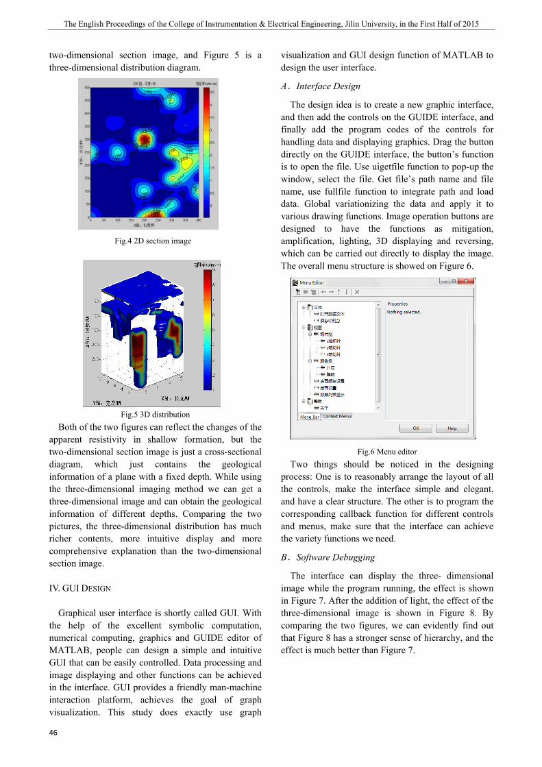
The English Proceedings of the College of Instrumentation & Electrical Engineering, Jilin University, in the First Half of 2015
46
two-dimensional section image, and Figure 5 is a three-dimensional distribution diagram.
Fig.4 2D section image
Fig.5 3D distribution
Both of the two figures can reflect the changes of the apparent resistivity in shallow formation, but the two-dimensional section image is just a cross-sectional diagram, which just contains the geological information of a plane with a fixed depth. While using the three-dimensional imaging method we can get a three-dimensional image and can obtain the geological information of different depths. Comparing the two pictures, the three-dimensional distribution has much richer contents, more intuitive display and more comprehensive explanation than the two-dimensional section image.
IV. GUI DESIGN
Graphical user interface is shortly called GUI. With the help of the excellent symbolic computation, numerical computing, graphics and GUIDE editor of MATLAB, people can design a simple and intuitive GUI that can be easily controlled. Data processing and image displaying and other functions can be achieved in the interface. GUI provides a friendly man-machine interaction platform, achieves the goal of graph visualization. This study does exactly use graph
visualization and GUI design function of MATLAB to design the user interface.
A.Interface Design
The design idea is to create a new graphic interface, and then add the controls on the GUIDE interface, and finally add the program codes of the controls for handling data and displaying graphics. Drag the button directly on the GUIDE interface, the button’s function is to open the file. Use uigetfile function to pop-up the window, select the file. Get file’s path name and file name, use fullfile function to integrate path and load data. Global variationizing the data and apply it to various drawing functions. Image operation buttons are designed to have the functions as mitigation, amplification, lighting, 3D displaying and reversing, which can be carried out directly to display the image. The overall menu structure is showed on Figure 6.
Fig.6 Menu editor
Two things should be noticed in the designing process: One is to reasonably arrange the layout of all the controls, make the interface simple and elegant, and have a clear structure. The other is to program the corresponding callback function for different controls and menus, make sure that the interface can achieve the variety functions we need.
B.Software Debugging
The interface can display the three- dimensional image while the program running, the effect is shown in Figure 7. After the addition of light, the effect of the three-dimensional image is shown in Figure 8. By comparing the two figures, we can evidently find out that Figure 8 has a stronger sense of hierarchy, and the effect is much better than Figure 7.
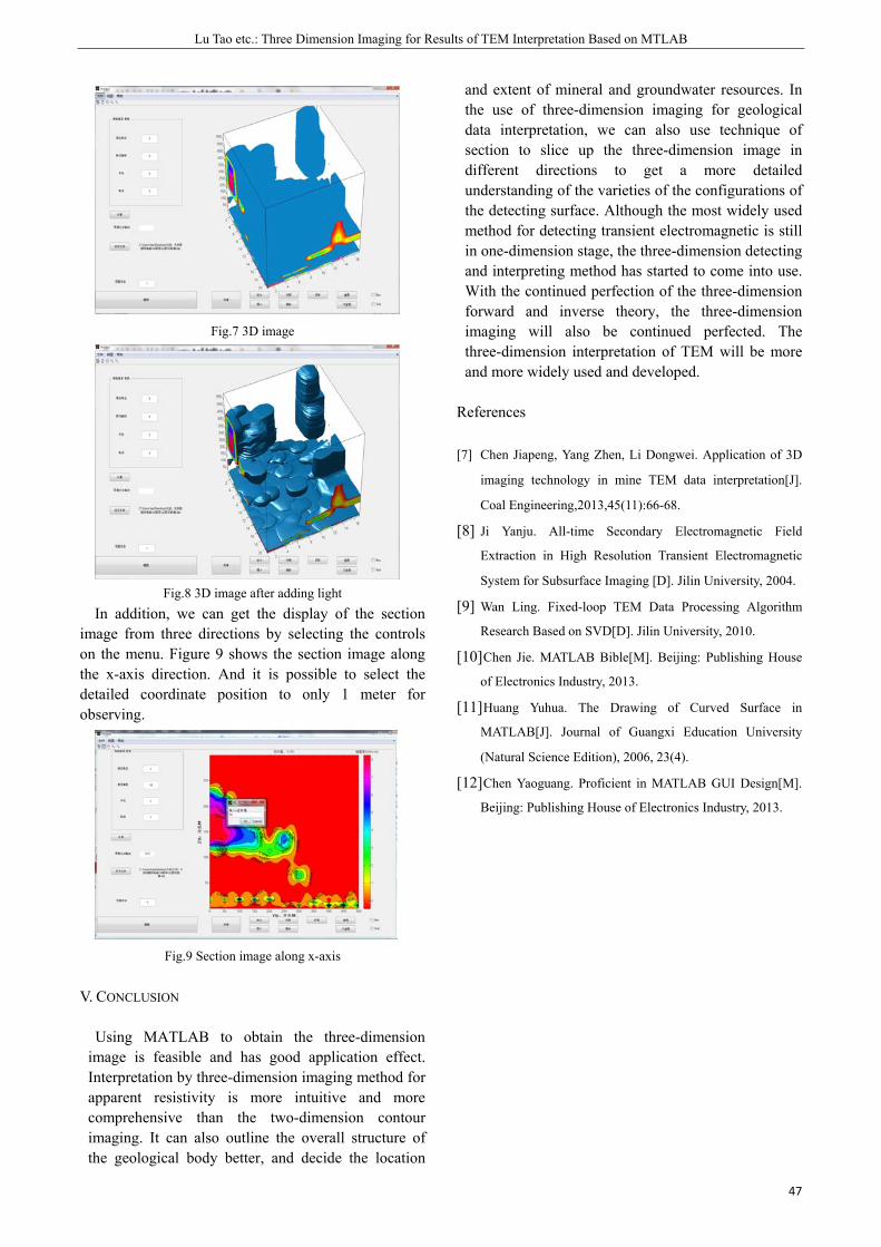
Lu Tao etc.: Three Dimension Imaging for Results of TEM Interpretation Based on MTLAB
47
Fig.7 3D image
Fig.8 3D image after adding light
In addition, we can get the display of the section image from three directions by selecting the controls on the menu. Figure 9 shows the section image along the x-axis direction. And it is possible to select the detailed coordinate position to only 1 meter for observing.
Fig.9 Section image along x-axis
V. CONCLUSION
Using MATLAB to obtain the three-dimension image is feasible and has good application effect. Interpretation by three-dimension imaging method for apparent resistivity is more intuitive and more comprehensive than the two-dimension contour imaging. It can also outline the overall structure of the geological body better, and decide the location
and extent of mineral and groundwater resources. In the use of three-dimension imaging for geological data interpretation, we can also use technique of section to slice up the three-dimension image in different directions to get a more detailed understanding of the varieties of the configurations of the detecting surface. Although the most widely used method for detecting transient electromagnetic is still in one-dimension stage, the three-dimension detecting and interpreting method has started to come into use. With the continued perfection of the three-dimension forward and inverse theory, the three-dimension imaging will also be continued perfected. The three-dimension interpretation of TEM will be more and more widely used and developed.
References
[7] Chen Jiapeng, Yang Zhen, Li Dongwei. Application of 3D
imaging technology in mine TEM data interpretation[J].
Coal Engineering,2013,45(11):66-68.
[8] Ji Yanju. All-time Secondary Electromagnetic Field
Extraction in High Resolution Transient Electromagnetic
System for Subsurface Imaging [D]. Jilin University, 2004.
[9] Wan Ling. Fixed-loop TEM Data Processing Algorithm
Research Based on SVD[D]. Jilin University, 2010.
[10] Chen Jie. MATLAB Bible[M]. Beijing: Publishing House
of Electronics Industry, 2013.
[11] Huang Yuhua. The Drawing of Curved Surface in
MATLAB[J]. Journal of Guangxi Education University
(Natural Science Edition), 2006, 23(4).
[12] Chen Yaoguang. Proficient in MATLAB GUI Design[M].
Beijing: Publishing House of Electronics Industry, 2013.
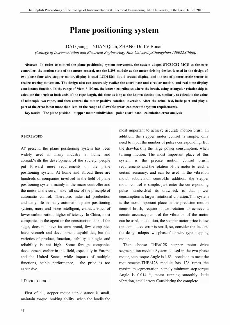
The English Proceedings of the College of Instrumentation & Electrical Engineering, Jilin University, in the First Half of 2015
48
Plane positioning system
DAI Qiang, YUAN Quan, ZHANG Di, LV Bonan (College of Insrumentation and Electrical Engineering, Jilin University,Changchun 130022,China)
Abstract—In order to control the plane positioning system movement, the system adopts STC89C52 MCU as the core
controller, the motion state of the motor control, use the L298 module as the motor driving device, is used in the design of
two-phase four wire stepper motor, display is used LCD12864 liquid crystal display, and the use of photoelectric sensor to
realize tracing movement. The design also can accurately realize the coordinate and circular motion, and real-time display
coordinates function. In the range of 80cm * 100cm, the known coordinates where the brush, using triangular relationship to
calculate the brush at both ends of the rope length, this time as long as the known destination, similarly to calculate the value
of telescopic two ropes, and then control the motor positive rotation, inversion. After the actual test, basic part and play a
part of the error is not more than 1cm, in the range of allowable error, can meet the system requirements.
Key words—The plane position stepper motor subdivision polar coordinate calculation error analysis
0 FOREWORD
AT present, the plane positioning system has been widely used in many industry at home and abroad.With the development of the society, people put forward more requirements on the plane positioning system. At home and abroad there are hundreds of companies involved in the field of plane positioning system, mainly in the micro controller and the motor as the core, make full use of the principle of automatic control. Therefore, industrial production and daily life in many automation plane positioning system, more and more intelligent, characteristics of lower carbonization, higher efficiency. In China, most companies in the agent or the construction side of the stage, does not have its own brand, few companies have research and development capabilities, but the varieties of product, function, stability is single, and reliability is not high. Some foreign companies development earlier in this field, especially in Europe and the United States, while imports of multiple functions, stable performance, the price is too expensive.
1 DEVICE CHOICE
First of all, stepper motor step distance is small, maintain torque, braking ability, when the loadis the
most important to achieve accurate motion brush. In addition, the stepper motor control is simple, only need to input the number of pulses corresponding. But the drawback is the large power consumption, when turning motion. The most important place of this system is the precise motion control brush, requirements and the rotation of the motor to reach a certain accuracy, and can be used in the vibration motor subdivision control.In addition, the stepper motor control is simple, just enter the corresponding pulse number.But its drawback is that power consumption is larger, rotational vibration.This system is the most important place in the precision motion control brush, require motor rotation to achieve a certain accuracy, control the vibration of the motor can be used, in addition, the stepper motor price is low, the cumulative error is small, so, consider the factors, the design adopts two phase four-wire type stepping motor.
Then choose THB6128 stepper motor drive segmentation module.System is used in the two-phase motor, step torque Angle is 1.8° , precision to meet the requirements.THB6128 module has 128 times the maximum segmentation, namely minimum step torque Angle is 0.014 °, motor running smoothly, little vibration, small errors.Considering the complete
DAI Qiang etc.: Plane Detection of Inductance Measuring Instrument
49
design is one of the most important precision requirement, so choose THB6128 stepper motor driver module segment.Finally using photoelectric tracing module testing black line.Panel on the black line was lower than those of surrounding light color background reflectivity, by comparing the light of the received signal strength can know in front of the black line, thus adjust the route, tracing function.
2 SYSTEM DESIGN
System is mainly divided into two parts, control and execution.Control terminal use STC89C52 MCU as the core controller, the relative motion of the end use motor brush achieve. First, use the keyboard to the selected mode of motion and set the current coordinate systemof the Communist Party of China, there are four kinds of motion, were custom motion, circular motion, coordinate and tracking.If selected custom movement, the brush automatically run the distance of more than 100 cm.If the selected coordinate movement, set target after began to exercise.If selected tracing movement, the brush should be placed in the starting position of the black line, and then began to run, tracing is completed, the system stops running.
3 DATA ANALYSIS
1. Coordinate motion analysis Set the lower left corner coordinates (0, 0).First set brush location coordinates for (x0, y0), are the two right triangle, the right triangle trilateral relationship can get the following formula:
20
20
20
20
20
20
b)x95()y115(
a)15x(y115
=-+-
=++- )(
So can calculate the cord length respectively a0, b0.After the movement for the coordinates of (x1, y1), the same method to calculate the cord length of a1, b1 respectively.So, if you want to complete the target motion, the left side of the rope need to shrink the
)( 00 ba - cm, on the right side of the rope will
contration )( 00 ba - cm.After determining the
difference, can control the motor rotation corresponding laps. In addition, through the actual test,
motor coil 0.45 per rotation, corresponding shrinkage
or rope elongation 1 cm, so the 45.0ba 00 ·- )(
circle on the left side of the motor, motor reverse
45.0ba 00 ·- )( circle on the right side.
2. Tracking motion analysis Using three photoelectric tube tests for detecting the black placed side by side.Known for detecting tube output for the low level to the black line.If the output low level O1, O2, O3, output level is motor A and B at the same time reversal (contraction), every time A given eight pulse.If O1, O2 output low level, O3, output level off track to the right, the motor A reversal, the motor forward B.If O1, O2, O3 output low level, the output level show left off track, the motor is A turn, the motor reverse B.Judge three output state, keeps the tracing module is always follow the black line.
In addition, as shown in figure 6 shows the trajectory have breakpoints, three at A breakpoint on tube, output level does not meet the above any state, so to increase control is: when the O1, O2, O3 output are high electricity at ordinary times, eight pulse motor A and B at the same time reversal, and then in the above three output state, final movement.Because of the problems in a total of two breakpoint, so the number of identification ofbreakpoints, then don't go the third of breakpoint, that the completion of tracing moving, then stop working.
4 CIRCUIT DESIGN
Hardware circuit part is divided into three aspects, only MCU minimum system (including liquid crystal display), motor drive and photoelectric tracking module in the pipe. 1. Display circuit
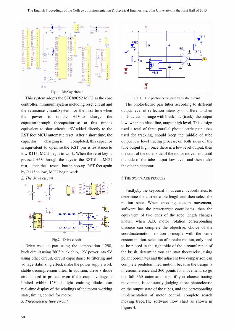
The English Proceedings of the College of Instrumentation & Electrical Engineering, Jilin University, in the First Half of 2015
50
P101
P112
P123
P134
P145
P156
P167
P178
RESET9
P3010
P3111
P3212
P3313
P3414
P3515
P3616
P3717
XTAL218
XTAL119
GND20 P20 21P21 22P22 23P23 24P24 25P25 26P26 27P27 28
PSEN 29ALE 30EA 31
P07 32P06 33P05 34P04 35P03 36P02 37P01 38P00 39VCC 40U1
89C51
123456789
RP1
电阻排
C1 1234567891011121314151617181920
JP1
12864
12345678910111213141516
JP2
1602
R1
12
Y1XTAL
11
22
S1
502R3
33pF
C2
33pF
C3
GND
GND
D0D1D2D3D4D5D6D7
GND
EN
RS
D0D1D2D3D4D5D6D7
R4
GND
GND
GND
VOVORSR/W
R/WEN
END0D1D2D3D4D5D6D7
GND
GND
R/WRS PSB
RST
C4Cap
GND
PSBRST
1234567891011121314151617181920
JP3
Header 20
1234567891011121314151617181920
JP4
Header 20
ENR/WRSRSTPSB
262728
2930VCCOD7D6D5D4D3D2D1D0VCCO 1
23
J1
PWR2.5
123
456
SW
Header 3X2A VCC
GND
P10P11P12P13P14P15P16P17
RST1P30P31P32P33P34P35P36P37
XTAL2XTAL1
262728
2930VCCO
12
P1
Header 2
R5
Res1
DS1
LED0
VCCO
VCCO
VCCO
VCCO
VCCO
GND VCCO
GNDVCC
P10P11P12P13P14P15P16P17
P30P31P32P33P34P35P36P37
XTAL1XTAL2
RST1
GND
Fig.1 Display circuit
This system adopts the STC89C52 MCU as the core controller, minimum system including reset circuit and the resonance circuit.System for the first time when the power is on, the +5V to charge the capacitor through thecapacitor, so at this time is equivalent to short-circuit, +5V added directly to the RST foot,MCU automatic reset. After a short time, the capacitor charging is completed, this capacitor is equivalent to open, so the RST pin is resistance to low R113, MCU begin to work. When the reset key is pressed, +5V through the keys to the RST foot, MCU rest, then the reset button pop-up, RST feet again by R113 to low, MCU begin work. 2. The drive circuit
Fig.2 Drive circuit
Drive module part using the composition L298, buck circuit using 7805 buck chip, 12V power into 5V using other circuit, circuit capacitance to filtering and voltage stabilizing effect, make the power supply work stable decompression after. In addition, drive 8 diode circuit used to protect, even if the output voltage is limited within 12V, 4 light emitting diodes can real-time display of the windings of the motor working state, timing control for motor. 3. Photoelectric tube circuit
Fig.3 The photoelectric pair transistor circuit
The photoelectric pair tubes according to different output level of reflection intensity of different, when in its detection range with black line (track), the output low, when no black line, output high level. This design used a total of three parallel photoelectric pair tubes used for tracking, should keep the middle of tube output low level tracing process, on both sides of the tube output high, once there is a low level output, then the control the other side of the motor movement, until the side of the tube output low level, and then make the other sidemotor.
5 THE SOFTWARE PROCESS
Firstly,by the keyboard input current coordinates, to determine the current cable length,and then select the motion state. When choosing custom movement, software has the presettarget coordinates, then the equivalent of two ends of the rope length changes known when A,B, motor rotation corresponding distance can complete the objective. choice of the coordinatemotion, motion principle with the same custom motion. selection of circular motion, only need to be placed in the right side of the circumference of the brush, determine you can start theexercise, using polar coordinates and the adjacent two comparison can complete predetermined motion, because the design is in circumference and 360 points for movement, so go the full 360 automatic stop. if you choose tracing movement, is constantly judging three photoelectric on the output state of the tubes, and the corresponding implementation of motor control, complete search moving trace.The software flow chart as shown in Figure 4.
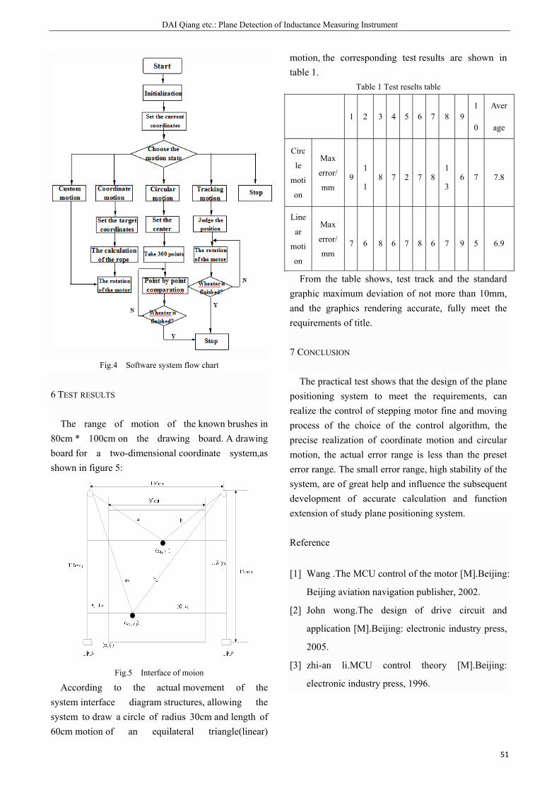
DAI Qiang etc.: Plane Detection of Inductance Measuring Instrument
51
Fig.4 Software system flow chart
6 TEST RESULTS
The range of motion of the known brushes in 80cm * 100cm on the drawing board. A drawing board for a two-dimensional coordinate system,as shown in figure 5:
Fig.5 Interface of moion
According to the actual movement of the system interface diagram structures, allowing the system to draw a circle of radius 30cm and length of 60cm motion of an equilateral triangle(linear)
motion, the corresponding test results are shown in table 1.
Table 1 Test reselts table
1 2 3 4 5 6 7 8 91
0
Aver
age
Circ
le
moti
on
Max
error/
mm 9
1
18 7 2 7 8
1
3 6 7 7.8
Line
ar
moti
on
Max
error/
mm 7 6 8 6 7 8 6 7 9 5 6.9
From the table shows, test track and the standard graphic maximum deviation of not more than 10mm, and the graphics rendering accurate, fully meet the requirements of title.
7 CONCLUSION
The practical test shows that the design of the plane positioning system to meet the requirements, can realize the control of stepping motor fine and moving process of the choice of the control algorithm, the precise realization of coordinate motion and circular motion, the actual error range is less than the preset error range. The small error range, high stability of the system, are of great help and influence the subsequent development of accurate calculation and function extension of study plane positioning system.
Reference
[1] Wang .The MCU control of the motor [M].Beijing:
Beijing aviation navigation publisher, 2002.
[2] John wong.The design of drive circuit and
application [M].Beijing: electronic industry press,
2005.
[3] zhi-an li.MCU control theory [M].Beijing:
electronic industry press, 1996.

The English Proceedings of the College of Instrumentation & Electrical Engineering, Jilin University, in the First Half of 2015
52
[4] Sun and Ann.Stepping driving system [M].Beijing:
Beijing university of aeronautics and astronautics
press, 2002.
[5] Wang Xiaomin The C program of the motor
control [M].Beijing: mechanical industry
publishing house, 2002.
[6] HuoYingHui .Stepper motor microcomputer and
MCUcontrol [M].Beijing: Beijing university of
aeronautics and astronautics press, 2000.
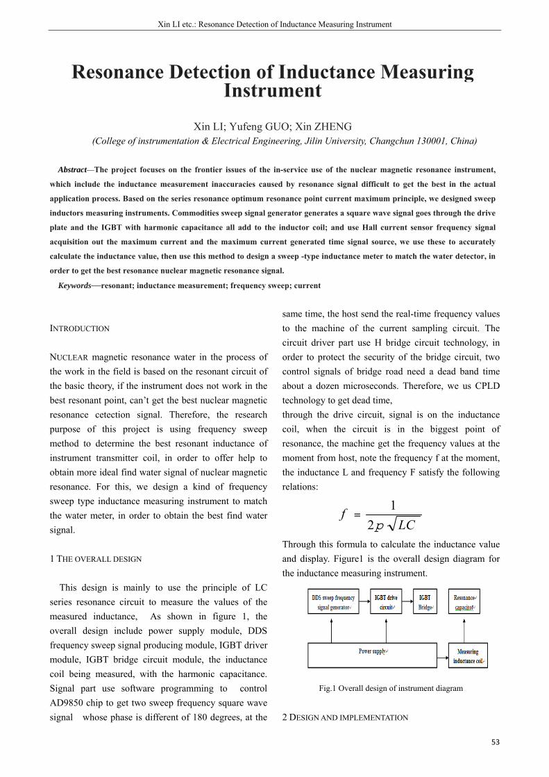
Xin LI etc.: Resonance Detection of Inductance Measuring Instrument
53
Resonance Detection of Inductance Measuring Instrument
Xin LI; Yufeng GUO; Xin ZHENG
(College of instrumentation & Electrical Engineering, Jilin University, Changchun 130001, China)
Abstract—The project focuses on the frontier issues of the in-service use of the nuclear magnetic resonance instrument,
which include the inductance measurement inaccuracies caused by resonance signal difficult to get the best in the actual
application process. Based on the series resonance optimum resonance point current maximum principle, we designed sweep
inductors measuring instruments. Commodities sweep signal generator generates a square wave signal goes through the drive
plate and the IGBT with harmonic capacitance all add to the inductor coil; and use Hall current sensor frequency signal
acquisition out the maximum current and the maximum current generated time signal source, we use these to accurately
calculate the inductance value, then use this method to design a sweep -type inductance meter to match the water detector, in
order to get the best resonance nuclear magnetic resonance signal.
Keywords—resonant; inductance measurement; frequency sweep; current
INTRODUCTION
NUCLEAR magnetic resonance water in the process of the work in the field is based on the resonant circuit of the basic theory, if the instrument does not work in the best resonant point, can’t get the best nuclear magnetic resonance cetection signal. Therefore, the research purpose of this project is using frequency sweep method to determine the best resonant inductance of instrument transmitter coil, in order to offer help to obtain more ideal find water signal of nuclear magnetic resonance. For this, we design a kind of frequency sweep type inductance measuring instrument to match the water meter, in order to obtain the best find water signal.
1 THE OVERALL DESIGN
This design is mainly to use the principle of LC series resonance circuit to measure the values of the measured inductance, As shown in figure 1, the overall design include power supply module, DDS frequency sweep signal producing module, IGBT driver module, IGBT bridge circuit module, the inductance coil being measured, with the harmonic capacitance. Signal part use software programming to control AD9850 chip to get two sweep frequency square wave signal whose phase is different of 180 degrees, at the
same time, the host send the real-time frequency values to the machine of the current sampling circuit. The circuit driver part use H bridge circuit technology, in order to protect the security of the bridge circuit, two control signals of bridge road need a dead band time about a dozen microseconds. Therefore, we us CPLD technology to get dead time, through the drive circuit, signal is on the inductance coil, when the circuit is in the biggest point of resonance, the machine get the frequency values at the moment from host, note the frequency f at the moment, the inductance L and frequency F satisfy the following relations:
LCf
p21
=
Through this formula to calculate the inductance value and display. Figure1 is the overall design diagram for the inductance measuring instrument.
Fig.1 Overall design of instrument diagram
2 DESIGN AND IMPLEMENTATION
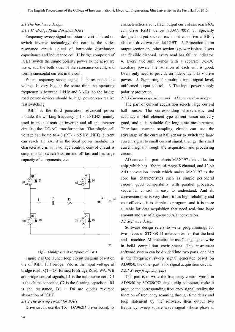
The English Proceedings of the College of Instrumentation & Electrical Engineering, Jilin University, in the First Half of 2015
54
2.1 The hardware design 2.1.1 H -Bridge Road Based on IGBT Frequency sweep signal emission circuit is based on switch inverter technology, the core is the series resonance circuit united of harmonic distribution capacitance and inductance coil. H bridge composed of IGBT switch the single polarity power to the acsquare wave, add the both sides of the resonance circuit, and form a sinusoidal current in the coil.
When frequency sweep signal is in resonance the voltage is very big, at the same time the operating frequency is between 1 kHz and 3 kHz, so the bridge road power devices should be high power, can realize fast switching.
IGBT is the third generation advanced power module, the working frequency is 1 ~ 20 KHZ, mainly used in main circuit of inverter and all the inverter circuits, the DC/AC transformation. The single cell voltage can be up to 4.0 (PT) ~ 6.5 kV (NPT), current can reach 1.5 kA, it is the ideal power module. Its characteristic is with voltage control, control circuit is simple, small switch loss, on and off fast and has large capacity of components, etc.
Fig.2 H-bridge circuit composed of IGBT
Figure 2 is the launch loop circuit diagram based on the of IGBT full bridge. Vdc is the input voltage of bridge road,Q1 ~ Q4 formed H-Bridge Road, WA, WB are bridge control signals, L1 is the inductance coil, C1 is the chime capacitor, C2 is the filtering capacitors, R1 is the resistance, D1 ~ D4 are diodes reversed absorption of IGBT. 2.1.2 The driving circuit for IGBT
Drive circuit use the TX - DA962D driver board, its
characteristics are: 1. Each output current can reach 6A, can drive IGBT bellow 300A/1700V. 2. Specially designed output socket, each unit can drive a IGBT, also can drive two parallel IGBT. 3. Protection alarm output section and other section is power isolate. Users can flexible disposal, every road has failure indicator. 4. Every two unit comes with a separate DC/DC auxiliary power. The isolation of each unit is good. Users only need to provide an independent 15 v drive power. 5. Supporting for multiple input signal level, uniformed output control. 6. The input power supply polarity protection. 2.1.3 Current acquisition and AD conversion design
The part of current acquisition selects large current hall sensor. The corresponding characteristic and accuracy of Hall element type current sensor are very good, and it is suitable for long time measurement. Therefore, current sampling circuit can use the advantage of the current hall sensor to switch the large current signal to small current signal, then get the small current signal through the acquisition and processing circuit.
AD conversion part selects MAX197 data collection chip ,which has the multi-range, 8 channel, and 12 bit. A/D conversion circuit which makes MAX197 as the core has characteristics such as simple peripheral circuit, good compatibility with parallel processor, sequential control is easy to understand. And its conversion time is very short, it has high reliability and cost-effective, it is simple to program, and it is more suitable for data acquisition that need real-time large amount and use of high-speed A/D conversion. 2.2 Software design
Software design refers to write programmings for two pieces of STC89C51 microcontroller, that the host and machine. Microcontroller use C language to write in keil4 compilation environment. This instrument software system can be divided into two parts, one part is the frequency sweep signal generator based on AD9850, the other part is for signal acquisition circuit. 2.2.1 Sweep frequency part
This part is to write the frequency control words in AD9850 by STC89C52 single-chip computer, make it produce the corresponding frequency signal, realize the function of frequency scanning through time delay and loop statement by the software, then output two frequency sweep square wave signal whose phase is
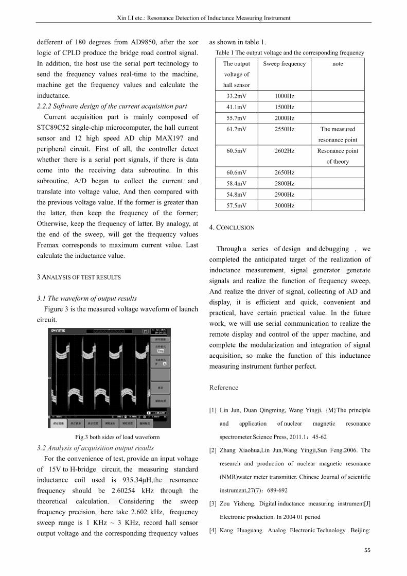
Xin LI etc.: Resonance Detection of Inductance Measuring Instrument
55
defferent of 180 degrees from AD9850, after the xor logic of CPLD produce the bridge road control signal. In addition, the host use the serial port technology to send the frequency values real-time to the machine, machine get the frequency values and calculate the inductance. 2.2.2 Software design of the current acquisition part
Current acquisition part is mainly composed of STC89C52 single-chip microcomputer, the hall current sensor and 12 high speed AD chip MAX197 and peripheral circuit. First of all, the controller detect whether there is a serial port signals, if there is data come into the receiving data subroutine. In this subroutine, A/D began to collect the current and translate into voltage value, And then compared with the previous voltage value. If the former is greater than the latter, then keep the frequency of the former; Otherwise, keep the frequency of latter. By analogy, at the end of the sweep, will get the frequency values Fremax corresponds to maximum current value. Last calculate the inductance value.
3 ANALYSIS OF TEST RESULTS
3.1 The waveform of output results Figure 3 is the measured voltage waveform of launch
circuit.
Fig.3 both sides of load waveform
3.2 Analysis of acquisition output results For the convenience of test, provide an input voltage
of 15V to H-bridge circuit, the measuring standard inductance coil used is 935.34μH,the resonance frequency should be 2.60254 kHz through the theoretical calculation. Considering the sweep frequency precision, here take 2.602 kHz, frequency sweep range is 1 KHz ~ 3 KHz, record hall sensor output voltage and the corresponding frequency values
as shown in table 1. Table 1 The output voltage and the corresponding frequency
The output
voltage of
hall sensor
Sweep frequency note
33.2mV 1000Hz
41.1mV 1500Hz
55.7mV 2000Hz
61.7mV 2550Hz The measured
resonance point
60.5mV 2602Hz Resonance point
of theory
60.6mV 2650Hz
58.4mV 2800Hz
54.8mV 2900Hz
57.5mV 3000Hz
4. CONCLUSION
Through a series of design and debugging , we completed the anticipated target of the realization of inductance measurement, signal generator generate signals and realize the function of frequency sweep, And realize the driver of signal, collecting of AD and display, it is efficient and quick, convenient and practical, have certain practical value. In the future work, we will use serial communication to realize the remote display and control of the upper machine, and complete the modularization and integration of signal acquisition, so make the function of this inductance measuring instrument further perfect.
Reference
[1] Lin Jun, Duan Qingming, Wang Yingji. MThe principle
and application of nuclear magnetic resonance
spectrometer.Science Press, 2011.1:45-62
[2] Zhang Xiaohua,Lin Jun,Wang Yingji,Sun Feng.2006. The
research and production of nuclear magnetic resonance
(NMR)water meter transmitter. Chinese Journal of scientific
instrument,27(7):689-692
[3] Zou Yizheng. Digital inductance measuring instrument[J]
Electronic production. In 2004 01 period
[4] Kang Huaguang. Analog Electronic Technology. Beijing:

The English Proceedings of the College of Instrumentation & Electrical Engineering, Jilin University, in the First Half of 2015
56
Higher Education Press,2002
[5] ZhangJianzhong,SunCunpu.1996.Magnetic resonance
Tutorial.Hefei: University of Science & Technology China
press
[6] Wang Lixin. Design of a new digital inductance measuring
instrument[J].Chinese Journal of scientific instrument,
2001,S2:113-114.
[7] He Qiao, Duan Qingming, Qiu Chunling. Principle and
application of single chip microcomputer[M].Beijing:
China Railway Press, 2004.3
[8] RongLiangliang, WangZhongxing, LinJun, DuanQingming,
Shang Xinlei. Factor analysis of waveform
quality assessment and effects of nuclear magnetic
resonanceemission. Chinese Journal of scientific instrument,
31(2):442-448
Feng Tengfei etc.: Design of virtual correlation filter nuclear magnetic resonance sounding signal
57
Design of virtual correlation filter nuclear magnetic resonance sounding signal
Feng Tengfei, Pan Lei, Zhang Bo
(School of Instrument Science and electrical engineering, Jilin University, Changchun 130001)
Abstract—The receiving sensitivity of magnetic resonance water detector is high, the MRS signal received (NV level) is very weak, interference of electromagnetic noise is random noise , power line noise environment, thus affecting the extraction of MRS signal is effective,resulting in lower accuracy of subsequent inversion and interpretation. Aiming at this problem, on the basis of random noise, power line noise autocorrelation function characteristic, put forward the related detection methods based on the development of suitable for filter designfor MRS signal denoising. At the same time, in view of the fact that the Labview has a processschema programming ideas and MATLAB with powerful matrix calculation and data processingtoolbox function and other advantages, combining with Labview and Matlab two kinds of programming software MRS, realize the separation of signal and noise. Numerical simulation and design results show that the correlation detection, the designer filter has good performance, the signal-to-noise ratio can improve 3~5dB.
Keywords—LabVIEW Matlab autocorrelation filter
0.INTRODUCTION
MAGNETIC resonance sounding method (MRS) is a direct method of geophysical prospecting groundwater, it can determine the depth, thickness , moisture quantity, average porosity of the aquifer and other aquifer Information no drilling, and the completion of a nuclear magnetic resonance sounding points hydrogeological exploration costs only 1/10 of the cost of drilling,thus this method has been widely used in groundwater exploration, water census and other aspects [1]. However, due to MRI exploring water meter high receiver sensitivity, the MRS signal (nanovolt) received is very weak, thus susceptible to electromagnetic noise interference, including natural environment random noise, power line noise (50Hz and its harmonics) effects are more severe. The presence of these disturbances will affect the valid signal extracted of MRS, thereby affecting the accuracy of the subsequent interpretation of the inversion.
Experts and scholars are also attached great importance to electromagnetic noise interference MRS explore issues of water meter in the practical application of the existence. Data collected by the general multiple stacking to some extent overcome the electromagnetic noise in order to improve signal to noise ratio, however, this method has a fatal weakness that will reduced efficiency of the entire system because its excessive number superposition [2].In 2001, French Anatoly Legchenko and Pierre Valla used block cancellation method, sine on consumer law and notch filter method to study removal methods of
power line harmonic interference[3]. In 2003, Strehl Berlin Technical University Institute of Applied Geophysics.S.and Rommel.I., etc, classified the electromagnetic noises that impact MRS signal quality,and gave the notch filter and low-pass filter and the method of combining wavelet transform to respectively filter electromagnetic noise[4].In 2008,David.O.Walsh designed a multi-channel ground equipment ,adapted the principle of noise cancellation to filter out the noise realization [5]. At home, in 2006 , Chinese Geology University’s researchers under the leadership of Professor Pan Yuling studied MRI researchers to find water with the introduction of the French experiment, NUMIS system ,to find water, Zeng Liang, Li Zhenyu published articles discusses the application of wavelet analysis method to improve nuclear magnetic resonance signal to noise ratio[6].In 2006,Jilin University Professor Lin Jun assumed the Eleventh Five-Year National Science and Technology Support Program: "nuclear magnetic resonance instrument research and development" project in the "Scientific equipment research and development", successfully developed JLMRS-I-type water probe meter, broken the situation only by the introduction of long-standing domestic French NUMIS instrument systems to detect groundwater, and also on the hardware and software for electromagnetic noise filtering methods are appropriate research[7-8].
Research Status Summary can be seen at home and abroad, there is no human studies conducted filtered conducted MRS signal noise detection methods based on the correlation function .At the same time , the Labview programming flowcharts have the thought
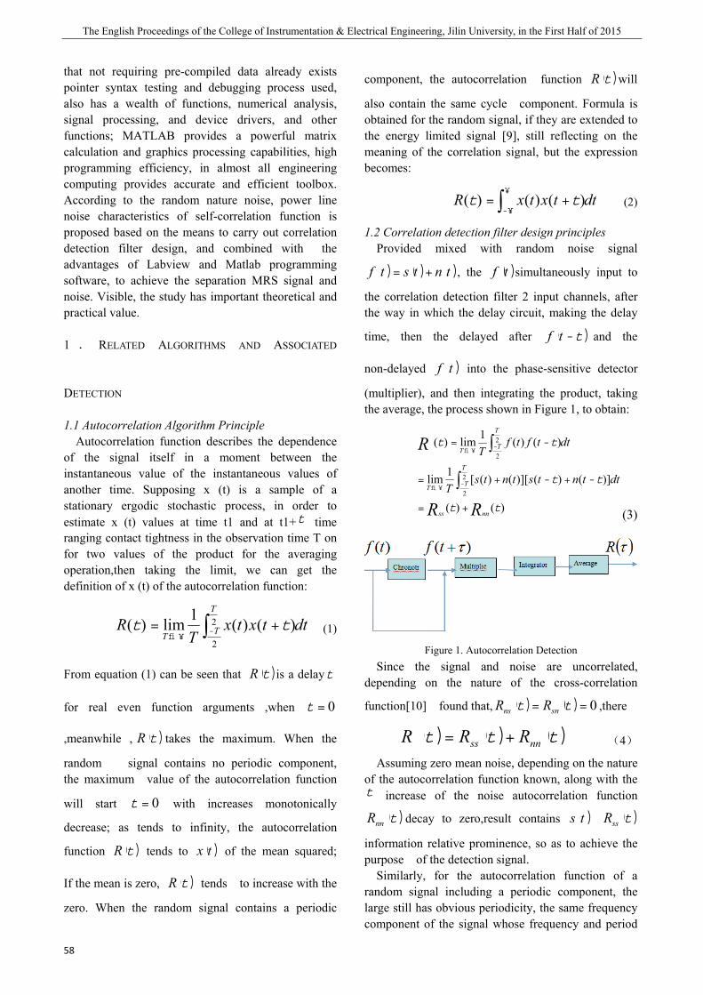
The English Proceedings of the College of Instrumentation & Electrical Engineering, Jilin University, in the First Half of 2015
58
that not requiring pre-compiled data already exists pointer syntax testing and debugging process used, also has a wealth of functions, numerical analysis, signal processing, and device drivers, and other functions; MATLAB provides a powerful matrix calculation and graphics processing capabilities, high programming efficiency, in almost all engineering computing provides accurate and efficient toolbox. According to the random nature noise, power line noise characteristics of self-correlation function is proposed based on the means to carry out correlation detection filter design, and combined with the advantages of Labview and Matlab programming software, to achieve the separation MRS signal and noise. Visible, the study has important theoretical and practical value.
1 . RELATED ALGORITHMS AND ASSOCIATED
DETECTION
1.1 Autocorrelation Algorithm Principle Autocorrelation function describes the dependence
of the signal itself in a moment between the instantaneous value of the instantaneous values of another time. Supposing x (t) is a sample of a stationary ergodic stochastic process, in order to estimate x (t) values at time t1 and at t1+t time ranging contact tightness in the observation time T on for two values of the product for the averaging operation,then taking the limit, we can get the definition of x (t) of the autocorrelation function:
dttxtxT
RT
TT ∫-¥fi+= 2
2
)()(1lim)( tt (1)
From equation (1) can be seen that ( )tR is a delayt
for real even function arguments ,when 0=t
,meanwhile , ( )tR takes the maximum. When the
random signal contains no periodic component, the maximum value of the autocorrelation function
will start 0=t with increases monotonically
decrease; as tends to infinity, the autocorrelation
function ( )tR tends to ()tx of the mean squared;
If the mean is zero, ( )tR tends to increase with the
zero. When the random signal contains a periodic
component, the autocorrelation function ( )tR will
also contain the same cycle component. Formula is obtained for the random signal, if they are extended to the energy limited signal [9], still reflecting on the meaning of the correlation signal, but the expression becomes:
dttxtxR ∫¥
¥-+= )()()( tt (2)
1.2 Correlation detection filter design principles Provided mixed with random noise signal
() () ()tntstf += , the ()tf simultaneously input to
the correlation detection filter 2 input channels, after the way in which the delay circuit, making the delay
time, then the delayed after ( )t-tf and the
non-delayed ()tf into the phase-sensitive detector
(multiplier), and then integrating the product, taking the average, the process shown in Figure 1, to obtain:
)()(
)]()()][()([1lim
)()(1lim)(
2
2
2
2
tt
tt
tt
RR
R
nnss
T
TT
T
TT
dttntstntsT
dttftfT
+=
-+-+=
-=
∫
∫
-¥fi
-¥fi
(3)
Figure 1. Autocorrelation Detection
Since the signal and noise are uncorrelated, depending on the nature of the cross-correlation
function[10] found that, ( ) ( ) 0== tt snns RR ,there
( ) ( ) ( )ttt nnss RRR += (4)
Assuming zero mean noise, depending on the nature of the autocorrelation function known, along with the t increase of the noise autocorrelation function
( )tnnR decay to zero,result contains ()ts ( )tssR
information relative prominence, so as to achieve the purpose of the detection signal.
Similarly, for the autocorrelation function of a random signal including a periodic component, the large still has obvious periodicity, the same frequency component of the signal whose frequency and period
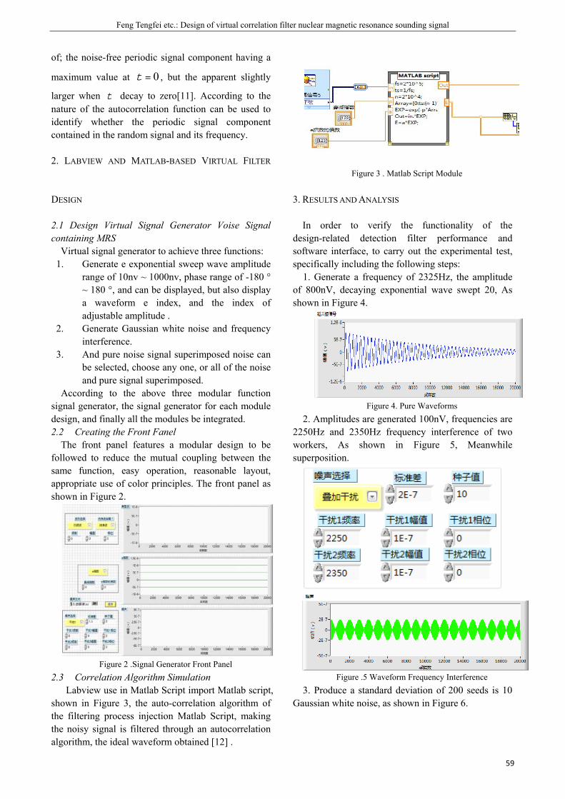
Feng Tengfei etc.: Design of virtual correlation filter nuclear magnetic resonance sounding signal
59
of; the noise-free periodic signal component having a
maximum value at 0=t , but the apparent slightly
larger when t decay to zero[11]. According to the nature of the autocorrelation function can be used to identify whether the periodic signal component contained in the random signal and its frequency.
2. LABVIEW AND MATLAB-BASED VIRTUAL FILTER
DESIGN
2.1 Design Virtual Signal Generator Voise Signal containing MRS
Virtual signal generator to achieve three functions: 1. Generate e exponential sweep wave amplitude
range of 10nv ~ 1000nv, phase range of -180 ° ~ 180 °, and can be displayed, but also display a waveform e index, and the index of adjustable amplitude .
2. Generate Gaussian white noise and frequency interference.
3. And pure noise signal superimposed noise can be selected, choose any one, or all of the noise and pure signal superimposed.
According to the above three modular function signal generator, the signal generator for each module design, and finally all the modules be integrated. 2.2 Creating the Front Fanel
The front panel features a modular design to be followed to reduce the mutual coupling between the same function, easy operation, reasonable layout, appropriate use of color principles. The front panel as shown in Figure 2.
Figure 2 .Signal Generator Front Panel
2.3 Correlation Algorithm Simulation Labview use in Matlab Script import Matlab script,
shown in Figure 3, the auto-correlation algorithm of the filtering process injection Matlab Script, making the noisy signal is filtered through an autocorrelation algorithm, the ideal waveform obtained [12] .
Figure 3 . Matlab Script Module
3. RESULTS AND ANALYSIS
In order to verify the functionality of the design-related detection filter performance and software interface, to carry out the experimental test, specifically including the following steps:
1. Generate a frequency of 2325Hz, the amplitude of 800nV, decaying exponential wave swept 20, As shown in Figure 4.
Figure 4. Pure Waveforms
2. Amplitudes are generated 100nV, frequencies are 2250Hz and 2350Hz frequency interference of two workers, As shown in Figure 5, Meanwhile superposition.
Figure .5 Waveform Frequency Interference
3. Produce a standard deviation of 200 seeds is 10 Gaussian white noise, as shown in Figure 6.
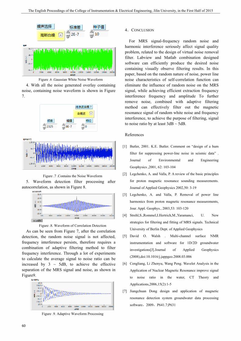
The English Proceedings of the College of Instrumentation & Electrical Engineering, Jilin University, in the First Half of 2015
60
Figure .6 .Gaussian White Noise Waveform
4. With all the noise generated overlay containing noise, containing noise waveform is shown in Figure 7.
Figure .7 .Contains the Noise Waveform
5. Waveform detection filter processing after autocorrelation, as shown in Figure 8.
Figure .8. Waveform of Correlation Detection
As can be seen from Figure 7, after the correlation detection, the random noise signal is not affected, frequency interference persists, therefore requires a combination of adaptive filtering method to filter frequency interference. Through a lot of experiments to calculate the average signal to noise ratio can be increased by 3 ~ 5dB, to achieve the effective separation of the MRS signal and noise, as shown in Figure9.
Figure .9. Adaptive Waveform Processing
4.CONCLUSION
For MRS signal-frequency random noise and harmonic interference seriously affect signal quality problem, related to the design of virtual noise removal filter. Labview and Matlab combination designed software can efficiently produce the desired noise containing visually observe filtering results. In this paper, based on the random nature of noise, power line noise characteristics of self-correlation function can eliminate the influence of random noise on the MRS signal, while achieving efficient extraction frequency interference frequency and amplitude To further remove noise, combined with adaptive filtering method can effectively filter out the magnetic resonance signal of random white noise and frequency interference, to achieve the purpose of filtering, signal to noise ratio by at least 3dB ~ 5dB.
References
[1] Butler, 2001. K.E. Butler. Comment on “design of a hum
filter for suppressing power-line noise in seismic data” .
Journal of Environmental and Engineering
Geophysics ,2001, 62: 103-104
[2] Legchenko, A. and Valla, P. A review of the basic principles
for proton magnetic resonance sounding measurements.
Journal of Applied Geophysics 2002,50: 3-19
[3] Legchenko, A. and Valla, P. Removal of power line
harmonics from proton magnetic resonance measurements,
Jour. Appl. Geophys., 2003,53: 103-120
[4] Strehl,S.,Rommel,I.Hertrich,M.,Yaramanci, U. New
strategies for filtering and fitting of MRS signals. Technical
University of Berlin Dept. of Applied Geophysics
[5] David O. Walsh . Multi-channel surface NMR
instrumentation and software for 1D/2D groundwater
investigations[J].Journal of Applied Geophysics
(2008),doi:10.1016/j.jappgeo.2008.03.006
[6] Cengliang, Li Zhenyu, Wang Peng. Wavelet Analysis in the
Application of Nuclear Magnetic Resonance improve signal
to noise ratio in the water, CT Theory and
Applications,2006,15(2):1-5
[7] Jiangchuan Dong design and application of magnetic
resonance detection system groundwater data processing
software,2009,P641.7;P631

Feng Tengfei etc.: Design of virtual correlation filter nuclear magnetic resonance sounding signal
61
[8] Aggregated wing bright, Lin Jun. SNMR water signal
singular interference suppression, Jilin University
(Engineering Science)2009,,39(05)1282-1287
[9] Yuan Pei Duo Application Based on LabVIEW and
MATLAB mixed programming,2007,1671-5276(2007)
06-0129-03
[10] Hao Zhang, Liu Xianyong, Yuan Ying long denoising and its
implementation in LabVIEW,2008,1004-373x(2008)
07-166-02
[11] Hou Guoping. LabVIEW 7. 1 programming and virtual
instrument design, Tsinghua University Press,2005-02-01
[12] Zhou Zhan seeking money Excel, LIU Ping-ping, etc.
LabVIEW virtual instruments and programming, Beijing
University of Aeronautics and Astronautics Press,2004-6-1
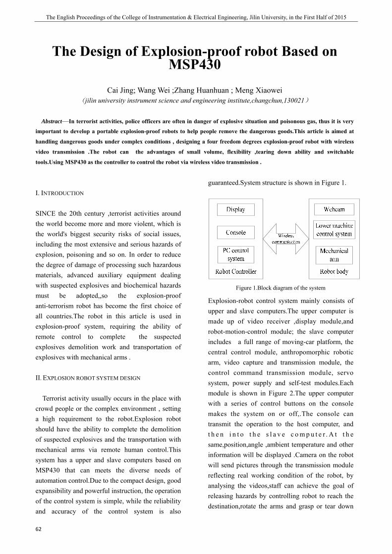
The English Proceedings of the College of Instrumentation & Electrical Engineering, Jilin University, in the First Half of 2015
62
The Design of Explosion-proof robot Based on MSP430
Cai Jing; Wang Wei ;Zhang Huanhuan ; Meng Xiaowei
(jilin university instrument science and engineering institute,changchun,130021)
Abstract—In terrorist activities, police officers are often in danger of explosive situation and poisonous gas, thus it is very
important to develop a portable explosion-proof robots to help people remove the dangerous goods.This article is aimed at
handling dangerous goods under complex conditions , designing a four freedom degrees explosion-proof robot with wireless
video transmission .The robot can the advantages of small volume, flexibility ,tearing down ability and switchable
tools.Using MSP430 as the controller to control the robot via wireless video transmission .
I. INTRODUCTION
SINCE the 20th century ,terrorist activities around the world become more and more violent, which is the world's biggest security risks of social issues, including the most extensive and serious hazards of explosion, poisoning and so on. In order to reduce the degree of damage of processing such hazardous materials, advanced auxiliary equipment dealing with suspected explosives and biochemical hazards must be adopted,,so the explosion-proof anti-terrorism robot has become the first choice of all countries.The robot in this article is used in explosion-proof system, requiring the ability of remote control to complete the suspected explosives demolition work and transportation of explosives with mechanical arms .
II. EXPLOSION ROBOT SYSTEM DESIGN
Terrorist activity usually occurs in the place with crowd people or the complex environment , setting a high requirement to the robot.Explosion robot should have the ability to complete the demolition of suspected explosives and the transportation with mechanical arms via remote human control.This system has a upper and slave computers based on MSP430 that can meets the diverse needs of automation control.Due to the compact design, good expansibility and powerful instruction, the operation of the control system is simple, while the reliability and accuracy of the control system is also
guaranteed.System structure is shown in Figure 1.
Figure 1.Block diagram of the system
Explosion-robot control system mainly consists of upper and slave computers.The upper computer is made up of video receiver ,display module,and robot-motion-control module; the slave computer includes a full range of moving-car platform, the central control module, anthropomorphic robotic arm, video capture and transmission module, the control command transmission module, servo system, power supply and self-test modules.Each module is shown in Figure 2.The upper computer with a series of control buttons on the console makes the system on or off,.The console can transmit the operation to the host computer, and t h e n i n t o t h e s l a v e c o m p u t e r . A t t h e same,position,angle ,ambient temperature and other information will be displayed .Camera on the robot will send pictures through the transmission module reflecting real working condition of the robot, by analysing the videos,staff can achieve the goal of releasing hazards by controlling robot to reach the destination,rotate the arms and grasp or tear down
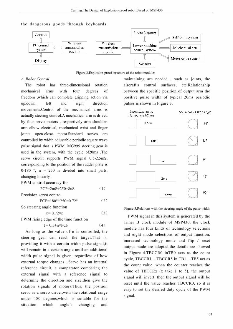
Cai jing:The Design of Explosion-proof robot Based on MSP430
63
the dangerous goods through keyboards .
Figure 2.Explosion-proof structure of the robot modules
A. Robot Control The robot has three-dimensional rotation
mechanical arms with four degrees of freedom ,which can complete gripping action via up,down, left and right direction movements.Control of the mechanical arms is actually steering control.A mechanical arm is drived by four servo motors , respectively arm shoulder, arm elbow electrical, mechanical wrist and finger joints open-close motor.Standard servos are controlled by width adjustable periodic square wave pulse signal that is PWM. MG995 steering gear is used in the system, with the cycle of20ms .The servo circuit supports PWM signal 0.5-2.5mS, corresponding to the position of the rudder plate is 0-180 °, n = 250 is divided into small parts, changing linearly, PWM control accuracy for PCP=2mS÷250=8uS (1) Precision servo control
ECP=180°÷250=0.72° (2) So steering angle function
φ= 0.72×n (3) PWM rising edge of the time function
t = 0.5+n×PCP (4) As long as the value of n is controlled, the
steering gear can reach the target.That is, providing it with a certain width pulse signal,it will remain in a certain angle until an additional width pulse signal is given, regardless of how external torque changes ..Servo has an internal reference circuit, a comparator comparing the external signal with a reference signal to determine the direction and size,then give the rotation signals of motors.Thus, the position servo is a servo driver,with the rotational range under 180 degrees,which is suitable for the situation which angle’s changing and
maintaining are needed , such as joints, the aircraft's control surfaces, etc.Relationship between the specific position of output arm the positive pulse width of typical 20ms periodic pulses is shown in Figure 3.
Figure 3.Relations with the steering angle of the pulse width
PWM signal in this system is generated by the Timer B clock module of MSP430, the clock module has four kinds of technology selections and eight mode selections of output function, increased technology mode and flip / reset output mode are adopted,the details are showed in Figure 4.TBCCR0 inTB0 acts as the count cycle, TBCCR1 ~ TBCCR5 in TB1 ~ TB5 act as the count value ,when the counter reaches the value of TBCCRx (x take 1 to 5), the output signal will invert, then the output signal will be reset until the value reaches TBCCR0, so it is easy to set the desired duty cycle of the PWM signal.
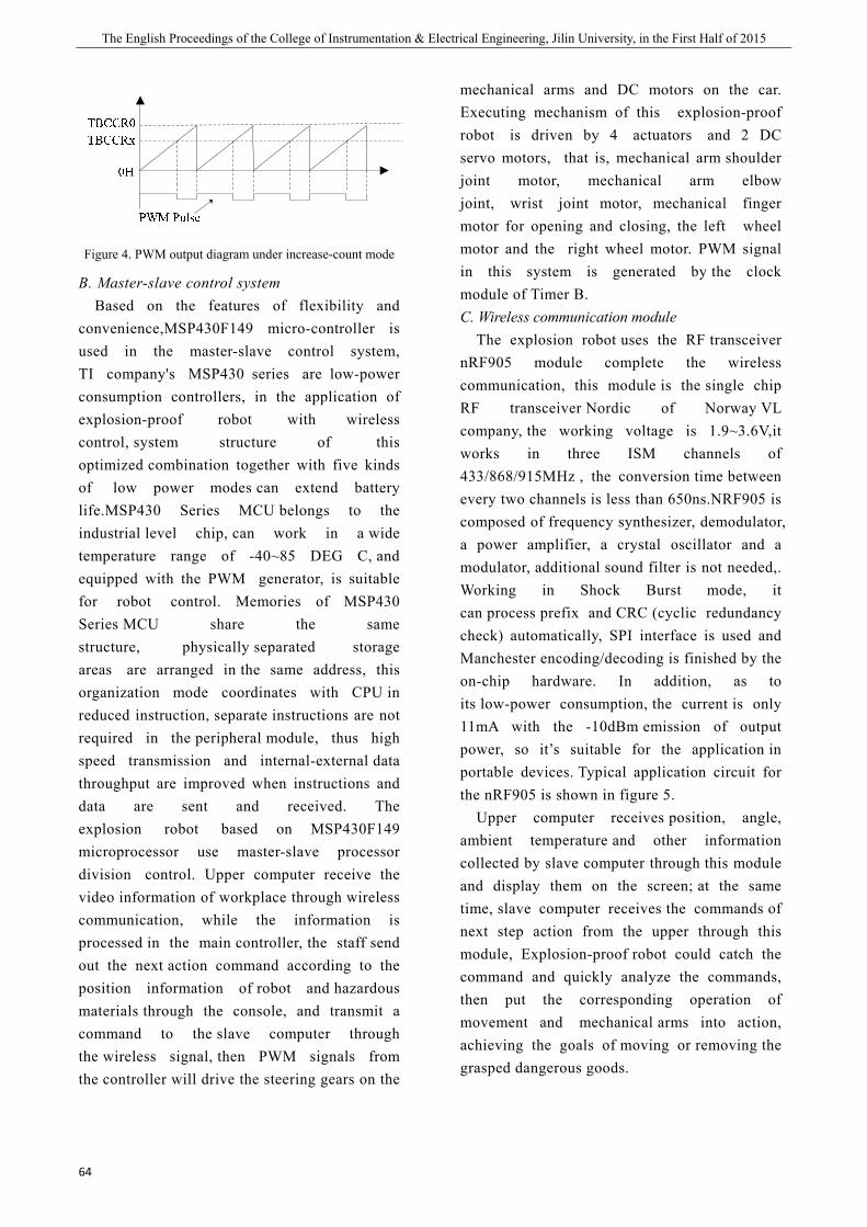
The English Proceedings of the College of Instrumentation & Electrical Engineering, Jilin University, in the First Half of 2015
64
Figure 4. PWM output diagram under increase-count mode
B. Master-slave control system Based on the features of flexibility and
convenience,MSP430F149 micro-controller is used in the master-slave control system, TI company's MSP430 series are low-power consumption controllers, in the application of explosion-proof robot with wireless control, system structure of this optimized combination together with five kinds of low power modes can extend battery life.MSP430 Series MCU belongs to the industrial level chip, can work in a wide temperature range of -40~85 DEG C, and equipped with the PWM generator, is suitable for robot control. Memories of MSP430 Series MCU share the same structure, physically separated storage areas are arranged in the same address, this organization mode coordinates with CPU in reduced instruction, separate instructions are not required in the peripheral module, thus high speed transmission and internal-external data throughput are improved when instructions and data are sent and received. The explosion robot based on MSP430F149 microprocessor use master-slave processor division control. Upper computer receive the video information of workplace through wireless communication, while the information is processed in the main controller, the staff send out the next action command according to the position information of robot and hazardous materials through the console, and transmit a command to the slave computer through the wireless signal, then PWM signals from the controller will drive the steering gears on the
mechanical arms and DC motors on the car. Executing mechanism of this explosion-proof robot is driven by 4 actuators and 2 DC servo motors, that is, mechanical arm shoulder joint motor, mechanical arm elbow joint, wrist joint motor, mechanical finger motor for opening and closing, the left wheel motor and the right wheel motor. PWM signal in this system is generated by the clock module of Timer B. C. Wireless communication module
The explosion robot uses the RF transceiver nRF905 module complete the wireless communication, this module is the single chip RF transceiver Nordic of Norway VL company, the working voltage is 1.9~3.6V,it works in three ISM channels of 433/868/915MHz , the conversion time between every two channels is less than 650ns.NRF905 is composed of frequency synthesizer, demodulator, a power amplifier, a crystal oscillator and a modulator, additional sound filter is not needed,. Working in Shock Burst mode, it can process prefix and CRC (cyclic redundancy check) automatically, SPI interface is used and Manchester encoding/decoding is finished by the on-chip hardware. In addition, as to its low-power consumption, the current is only 11mA with the -10dBm emission of output power, so it’s suitable for the application in portable devices. Typical application circuit for the nRF905 is shown in figure 5.
Upper computer receives position, angle, ambient temperature and other information collected by slave computer through this module and display them on the screen; at the same time, slave computer receives the commands of next step action from the upper through this module, Explosion-proof robot could catch the command and quickly analyze the commands, then put the corresponding operation of movement and mechanical arms into action, achieving the goals of moving or removing the grasped dangerous goods.
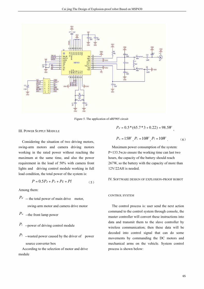
Cai jing:The Design of Explosion-proof robot Based on MSP430
65
Figure 5. The application of nRF905 circuit
III. POWER SUPPLY MODULE
Considering the situation of two driving motors, swing-arm motors and camera driving motors working in the rated power without reaching the maximum at the same time, and also the power requirement in the load of 50% with camera front lights and driving control module working in full load condition, the total power of the system is:
PlPcPPP wd +++= 5.0 (5)
Among them:
dP -- the total power of main drive motor,
swing-arm motor and camera drive motor
wP --the front lamp power
cP --power of driving control module
lP --wasted power caused by the driver of power
source converter box According to the selection of motor and drive
module
WPd 5.98)22.03*7.65(*5.0 =+= ,
WPw 15= , WPc 10= , WPl 10= . (6)
Maximum power consumption of the system: P=133.5w,to ensure the working time can last two hours, the capacity of the battery should reach 267W, so the battery with the capacity of more than 12V/22AH is needed.
IV. SOFTWARE DESIGN OF EXPLOSION-PROOF ROBOT
CONTROL SYSTEM
The control process is: user send the next action command to the control system through console, the master controller will convert these instructions into data and transmit them to the slave controller by wireless communication; then these data will be decoded into control signal that can do some movements by commanding the DC motors and mechanical arms on the vehicle. System control process is shown below:
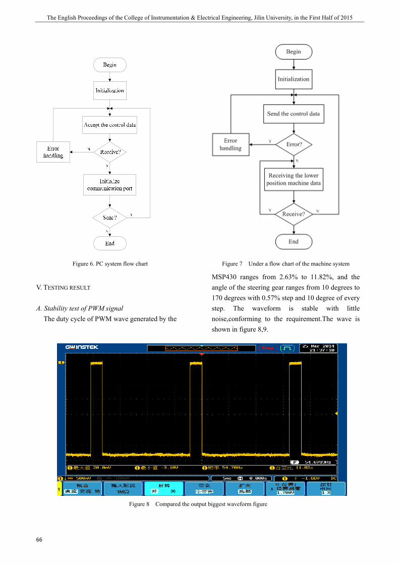
The English Proceedings of the College of Instrumentation & Electrical Engineering, Jilin University, in the First Half of 2015
66
Figure 6. PC system flow chart Figure 7 Under a flow chart of the machine system
V. TESTING RESULT
A. Stability test of PWM signal The duty cycle of PWM wave generated by the
MSP430 ranges from 2.63% to 11.82%, and the angle of the steering gear ranges from 10 degrees to 170 degrees with 0.57% step and 10 degree of every step. The waveform is stable with little noise,conforming to the requirement.The wave is shown in figure 8,9.
Figure 8 Compared the output biggest waveform figure
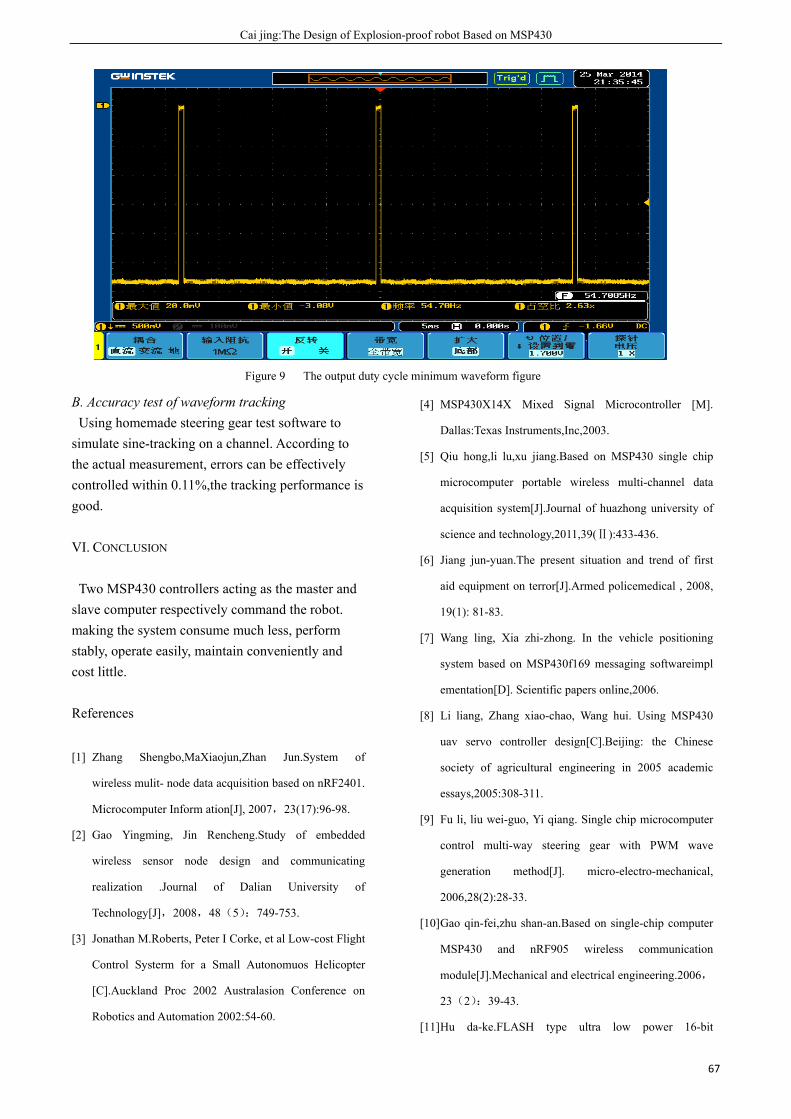
Cai jing:The Design of Explosion-proof robot Based on MSP430
67
Figure 9 The output duty cycle minimum waveform figure
B. Accuracy test of waveform tracking Using homemade steering gear test software to
simulate sine-tracking on a channel. According to the actual measurement, errors can be effectively controlled within 0.11%,the tracking performance is good.
VI. CONCLUSION
Two MSP430 controllers acting as the master and slave computer respectively command the robot. making the system consume much less, perform stably, operate easily, maintain conveniently and cost little.
References
[1] Zhang Shengbo,MaXiaojun,Zhan Jun.System of
wireless mulit- node data acquisition based on nRF2401.
Microcomputer Inform ation[J], 2007,23(17):96-98.
[2] Gao Yingming, Jin Rencheng.Study of embedded
wireless sensor node design and communicating
realization .Journal of Dalian University of
Technology[J],2008,48(5):749-753.
[3] Jonathan M.Roberts, Peter I Corke, et al Low-cost Flight
Control Systerm for a Small Autonomuos Helicopter
[C].Auckland Proc 2002 Australasion Conference on
Robotics and Automation 2002:54-60.
[4] MSP430X14X Mixed Signal Microcontroller [M].
Dallas:Texas Instruments,Inc,2003.
[5] Qiu hong,li lu,xu jiang.Based on MSP430 single chip
microcomputer portable wireless multi-channel data
acquisition system[J].Journal of huazhong university of
science and technology,2011,39(Ⅱ):433-436.
[6] Jiang jun-yuan.The present situation and trend of first
aid equipment on terror[J].Armed policemedical , 2008,
19(1): 81-83.
[7] Wang ling, Xia zhi-zhong. In the vehicle positioning
system based on MSP430f169 messaging softwareimpl
ementation[D]. Scientific papers online,2006.
[8] Li liang, Zhang xiao-chao, Wang hui. Using MSP430
uav servo controller design[C].Beijing: the Chinese
society of agricultural engineering in 2005 academic
essays,2005:308-311.
[9] Fu li, liu wei-guo, Yi qiang. Single chip microcomputer
control multi-way steering gear with PWM wave
generation method[J]. micro-electro-mechanical,
2006,28(2):28-33.
[10] Gao qin-fei,zhu shan-an.Based on single-chip computer
MSP430 and nRF905 wireless communication
module[J].Mechanical and electrical engineering.2006,
23(2):39-43.
[11] Hu da-ke.FLASH type ultra low power 16-bit

The English Proceedings of the College of Instrumentation & Electrical Engineering, Jilin University, in the First Half of 2015
68
microcontroller.Beijing: Beijing university of
aeronautics and astronautics press,2002.
[12] Gao chao,zhou peng,guo yong-cai.Based on MSP430
multi-function design of wireless monitoring system[J].
Laser magazine,2009,,30(2):66-67.
[13] Xu zheng-fei.The development of type ZXP J01
fire-fighting robot[J].The robot,2002,24(2):159-164.
Wang Guannan etc.: Research of the noise cancellation method for surface NMR signal based on the coincident loop
69
Research of the noise cancellation method for surface NMR signal based on the coincident loop
Wang Guannan, Zhao Junyi, and Wang Yunkun
(College Instrumentation & Electrical Engineering, Jilin University, Changchun, 130026)
Abstract—The sensitivity of the groundwater NMR detector is high; nV level NMR signals are vulnerable
to interference from strong-frequency signals, leading the accuracy of the extracted characteristic parameter of the signal reduced, and affect on the inversion of the hydro-geological parameters results. To solve this problem, usually use multiple coils on noise cancellation. However, this method requires two or more coils; measurement in the field is very difficult. So we put forward a MRI system based on the coincident loop, it removes the noise of MRS signal through the NLMS and Frequency-domain algorithm. The simulation results show that Frequency-domain algorithm is better than NLMS algorithm in the aspect of improving SNR and noise removal, SNR can reach more than 5dB.
Key words—Nuclear magnetic resonance the coincident loop Frequency domain Adaptive cancellation
I. INTRODUCTION
NUCLEAR magnetic resonance (NMR, Nuclear Magnetic Resonance) is a physical phenomenon of nuclear; it means a substance with nuclear Para-magnetism selectively absorbs electromagnetic energy. Proton is the highest abundance and the largest nuclear magnetic spin among paramagnetic substances in the stratum. In addition to oil, gas reservoir, the hydrogen nuclei in the water is the body of the stratum, and the macroscopic magnetic moment processing in the geomagnetic field, pickup electromagnetic signal from macroscopic magnetic processing with coil, To detect the presence or absence of groundwater. Compared to traditional methods of geophysical groundwater, it is high-resolution, high-efficiency, information-rich unique advantages of reconciliation. Quality of surface NMR signal detection system collected data is the judgment standard, the NMR signal amplitude produced by hydrogen nuclei in water is small (NV level), so it will introduce a large number of natural and man-made noise, resulting in lower SNR signal acquisition. In order to obtain the more pure collection signals, it is necessary to design algorithms for real-time signal acquisition correction; the usual practice is to use adaptive filtering techniques for noise cancellation.
For noise problems in MRS signal, many domestic experts and scholars have taken the corresponding research. Jiang Chuandong[3] studied the response based on magnetic resonance imaging techniques to
directly detect groundwater technology, design and application focus on the MRS signal data processing software. And put forward many kinds of data process methods for low SNR, much noise and other issues, and design appropriated application software. Tian Baofeng [4] Based on the principle of correlation cancellation for full-wave resonance signals, designed 90 ° phase shift adaptive noise cancellation system with reference coil, Theoretical calculation of the reference coil relative to the distance detection coil, put forward variable step size LMS algorithm noise suppression[5]. Simulation results show that under different signal strength and different SNR, when the signal-frequency harmonic interference spectrum does not coincide, use adaptive noise cancellation system and variable step algorithm designed, SNR can be increased to more than 5.94 dB, the initial amplitude characteristic parameter of relaxation time fitting error is within 2.8%; when the signal-frequency harmonic interference spectrum coincides, use bidirectional adaptive filtering algorithms, SNR can reach more than 5dB,the initial amplitude characteristic parameter of relaxation time fitting error is within 10%;meet the requirements of practical application; measured data processing is further evidence of the effectiveness of the method. Because the system with reference coil, in the measurement need to bring more than two sets of coils, the measurement will be very difficult in the field. To solve this problem, this paper presents the NMR signal cancellation system based on the same coil.
In this paper, aiming the MRS signal common-frequency harmonic noise, noise singular

The English Proceedings of the College of Instrumentation & Electrical Engineering, Jilin University, in the First/ Second Half of 2015
70
strong interference noise, simulated the wild noise environment. According to the characteristics of noise, design the adaptive noise cancellation system based on the same coil. Determining an adaptive filter key expression, to maximize the noise signal in the noise cancellation signal MRS, get the highest SNR.
II. MRI SYSTEM BASED ON A SINGLE COIL
Fig.1. Detection System Diagram of MRI system based on a single
Detection System Diagram of MRI system based on a single as shown in Fig.1. The system needs to record noise for a period of time before the acquisition MRS signal. Make use of adaptive filtering algorithm for the operations of the data and achieving noise cancellation when the acquisitions MRS signal done.
Ⅲ. ADAPTIVE NOISE ALGORITHM
A. Principle of adaptive noise cancellation Adaptive noises cancel as shown, the noise signal as it is process, after a certain treatment, the noise suppression.
Fig. 2. Principle of adaptive noise cancellation
In general, the adaptive filter consists of two parts, one is filter structure, the second is the adaptive algorithm of adjusting the filter coefficients. Fig.2. gives the general structure of adaptive filter, in the drawing, )(nd is the desired response, )(nx is the adaptive filter input, )(ny is the output of the adaptive filter, )(ne is the estimation error. Filter coefficients of the adaptive filter is controlled by the error signal )(ne , automatically adjusted according to value of )(ne and adaptive algorithms. B. the adaptive noise cancellation algorithm research Based on the same coil.
To get better noise cancellation results, two programs designed to achieve noise cancellation, select the output SNR is relatively high and the data fitting error is small noise cancellation scheme.
Option Ⅰ: Direct use of noise canceling algorithms
NLMS NLMS algorithm known as normalized LMS
algorithm, which is use variable step adaptive method to shorten the convergence process, variable step formula:
)()()1( nXnenWnW )(+=+ (1)
In the formula, )()( nXne represents the updated
filter weight vector iterative adjustment amount. In order to achieve fast convergence of purpose, must choose the appropriate value of variable step, a possible strategy is to reduce as much as possible to reduce instantaneous squared error, which uses the instantaneous squared error as a simple estimate MSE mean square error, which is the basic LMS algorithm thought. Can get the weights iterative correction formula:
)()()()()()1( nXnenXnXnWnW T++=+ mg (2)
Variable step can be represented by )( nm , namely:
)()()( nXnXn T++ mgm ,Wherein the parameter
m is a fixed convergence factor control disorders,
parameter g is set to avoid )()( nXnX Ttoo
small and cause the step size too much,0≤g ≤1. In
order to ensure stable operation of the adaptive filter,
the range of values fixed convergence factor m
should meet the following selection:0<m <2. As can
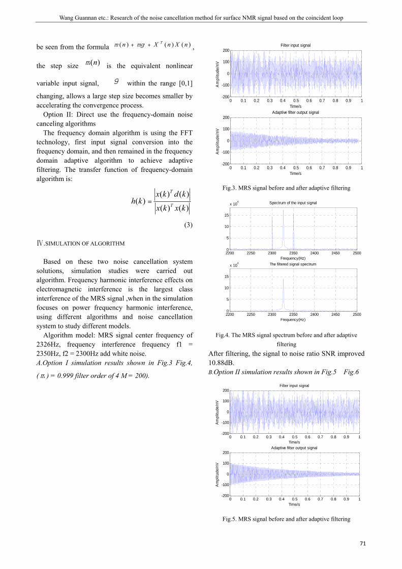
Wang Guannan etc.: Research of the noise cancellation method for surface NMR signal based on the coincident loop
71
be seen from the formula )()()( nXnXn T++ mgm ,
the step size )(nm is the equivalent nonlinear
variable input signal, g within the range [0,1]
changing, allows a large step size becomes smaller by accelerating the convergence process.
Option II: Direct use the frequency-domain noise canceling algorithms
The frequency domain algorithm is using the FFT technology, first input signal conversion into the frequency domain, and then remained in the frequency domain adaptive algorithm to achieve adaptive filtering. The transfer function of frequency-domain algorithm is:
)()(
)()()(
kxkx
kdkxkh
T
T
=
(3)
Ⅳ.SIMULATION OF ALGORITHM
Based on these two noise cancellation system solutions, simulation studies were carried out algorithm. Frequency harmonic interference effects on electromagnetic interference is the largest class interference of the MRS signal ,when in the simulation focuses on power frequency harmonic interference, using different algorithms and noise cancellation system to study different models.
Algorithm model: MRS signal center frequency of 2326Hz, frequency interference frequency f1 = 2350Hz, f2 = 2300Hz add white noise. A.Option I simulation results shown in Fig.3 Fig.4,
(m ) = 0.999 filter order of 4 M = 200).
0 0.1 0.2 0.3 0.4 0.5 0.6 0.7 0.8 0.9 1-200
-100
0
100
200
Am
plitu
de/n
V
Time/s
Filter input signal
0 0.1 0.2 0.3 0.4 0.5 0.6 0.7 0.8 0.9 1-200
-100
0
100
200
Am
plitu
de/n
V
Time/s
Adaptive filter output signal
Fig.3. MRS signal before and after adaptive filtering
2200 2250 2300 2350 2400 2450 25000
5
10
15
x 104 Spectrum of the input signal
Frequency(Hz)
2200 2250 2300 2350 2400 2450 25000
5
10
15
x 104 The filtered signal spectrum
Frequency(Hz)
Fig.4. The MRS signal spectrum before and after adaptive filtering
After filtering, the signal to noise ratio SNR improved 10.88dB. B.Option II simulation results shown in Fig.5 Fig.6
0 0.1 0.2 0.3 0.4 0.5 0.6 0.7 0.8 0.9 1-200
-100
0
100
200
Am
plitu
de/n
V
Time/s
Filter input signal
0 0.1 0.2 0.3 0.4 0.5 0.6 0.7 0.8 0.9 1-200
-100
0
100
200
Am
plitu
de/n
V
Time/s
Adaptive filter output signal
Fig.5. MRS signal before and after adaptive filtering
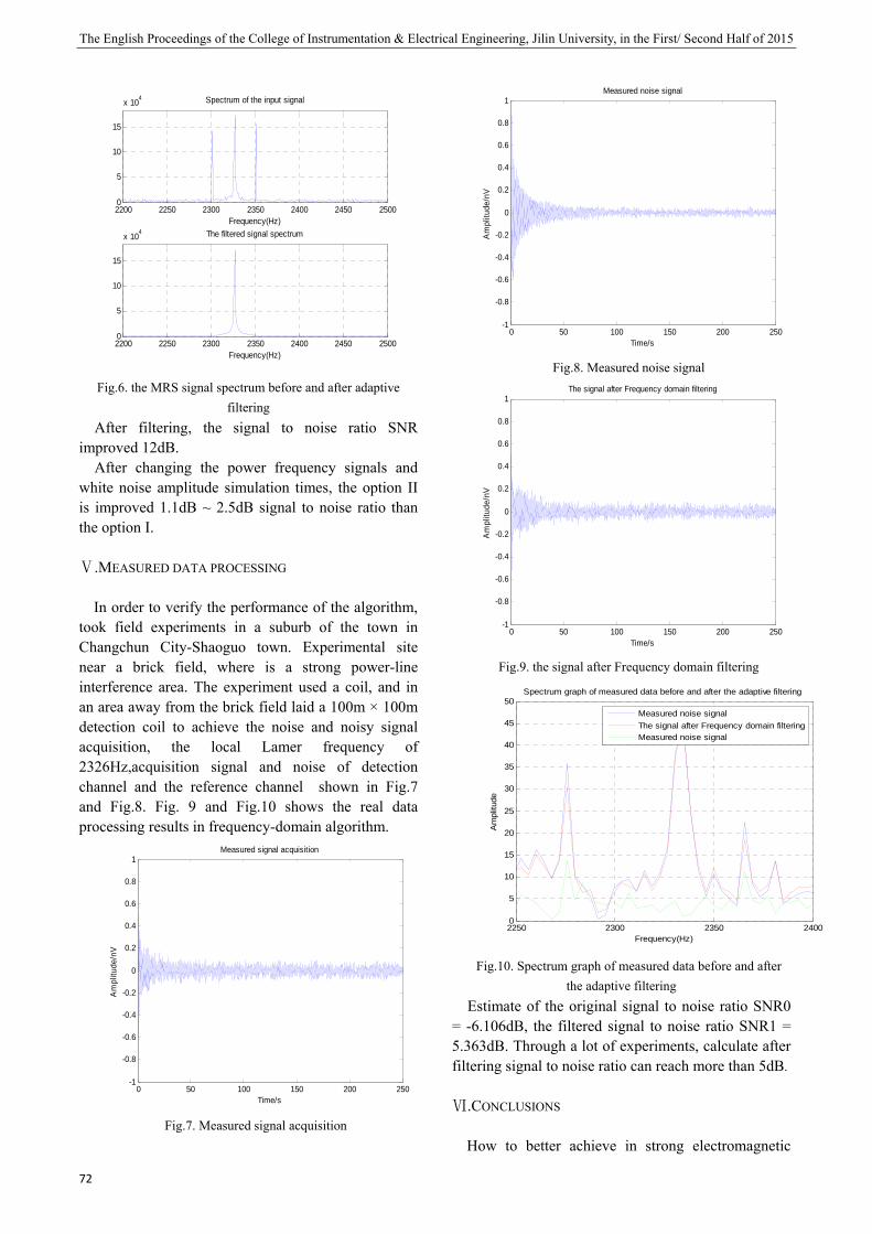
The English Proceedings of the College of Instrumentation & Electrical Engineering, Jilin University, in the First/ Second Half of 2015
72
2200 2250 2300 2350 2400 2450 25000
5
10
15
x 104 Spectrum of the input signal
Frequency(Hz)
2200 2250 2300 2350 2400 2450 25000
5
10
15
x 104 The filtered signal spectrum
Frequency(Hz)
Fig.6. the MRS signal spectrum before and after adaptive filtering
After filtering, the signal to noise ratio SNR improved 12dB.
After changing the power frequency signals and white noise amplitude simulation times, the option II is improved 1.1dB ~ 2.5dB signal to noise ratio than the option I.
Ⅴ.MEASURED DATA PROCESSING
In order to verify the performance of the algorithm, took field experiments in a suburb of the town in Changchun City-Shaoguo town. Experimental site near a brick field, where is a strong power-line interference area. The experiment used a coil, and in an area away from the brick field laid a 100m × 100m detection coil to achieve the noise and noisy signal acquisition, the local Lamer frequency of 2326Hz,acquisition signal and noise of detection channel and the reference channel shown in Fig.7 and Fig.8. Fig. 9 and Fig.10 shows the real data processing results in frequency-domain algorithm.
0 50 100 150 200 250-1
-0.8
-0.6
-0.4
-0.2
0
0.2
0.4
0.6
0.8
1Measured signal acquisition
Am
plitu
de/n
V
Time/s Fig.7. Measured signal acquisition
0 50 100 150 200 250-1
-0.8
-0.6
-0.4
-0.2
0
0.2
0.4
0.6
0.8
1Measured noise signal
Am
plitu
de/n
V
Time/s
Fig.8. Measured noise signal
0 50 100 150 200 250-1
-0.8
-0.6
-0.4
-0.2
0
0.2
0.4
0.6
0.8
1
Am
plitu
de/n
V
Time/s
The signal after Frequency domain filtering
Fig.9. the signal after Frequency domain filtering
2250 2300 2350 24000
5
10
15
20
25
30
35
40
45
50
Frequency(Hz)
Am
plitu
de
Spectrum graph of measured data before and after the adaptive filtering
Measured noise signalThe signal after Frequency domain filteringMeasured noise signal
Fig.10. Spectrum graph of measured data before and after
the adaptive filtering Estimate of the original signal to noise ratio SNR0
= -6.106dB, the filtered signal to noise ratio SNR1 = 5.363dB. Through a lot of experiments, calculate after filtering signal to noise ratio can reach more than 5dB.
Ⅵ.CONCLUSIONS
How to better achieve in strong electromagnetic

Wang Guannan etc.: Research of the noise cancellation method for surface NMR signal based on the coincident loop
73
noise interference MRS signal is weak extract groundwater NMR detection is a key issue. It will affect the accuracy of the hydro-geological interpretation inversion parameter information. In no prior knowledge of the case, the adaptive filter can use the recursive method to update parameters, so that the data approximate the optimal value.
Through the NLMS algorithm and Frequency-domain algorithm MRS signal noise removal, respectively, and the two algorithms were compared with the following conclusions:
1.Frequency-domain algorithm is better than NLMS algorithm both in improving the SNR and noise removal.
2.Both algorithms or less inn running speed, run faster, but Frequency-domain algorithm is more stable and reliable.
References
[13] Sun Shuqin, Lin Jun, Zhang Qingwen, Ji Yanju. Proton
relaxation process [J] Geophysical and Geo-chemical
Exploration .2005, 29 (2): 153-156.
[14] Deng Jingwu, Pan Yuling, Xiong Yuzhen. New
groundwater exploration method - the method of
application of water [J] SNMR modern geology 2004, (01):
121-126.
[15] Jiang Chuandong. Design and Application of NMR
detection system groundwater data processing software
[D]. Jilin University, 2009.
[16] Tian Baofeng, Lin Jun, Duan Qingming, etc. Based on the
reference coil and variable step size adaptive resonance
signal noise suppression method [J] Journal of Geophysics,
2012, 55 (7): 2462-2472.
[17] Wang Zhongxing, Rong Liangliang, Lin Jun. Ground
nuclear magnetic resonance signal singular interference
suppression, Jilin University (Engineering Science) 2009,
39 (05) 1282-1287.

The English Proceedings of the College of Instrumentation & Electrical Engineering, Jilin University, in the First Half of 2015
74
Driverless cars road system design
Wang Qiao, Xiao Bing, Yin Haibo , Zhang Tianyu, (College of Instrument Science and Electrical Engineering, Jilin University, Changchun 130022)
Abstract —Smart car is the inevitable developing trend of modern life, is the direction of future development. Smart cars can
be in accordance with the advance of set in a specific environment to operate, without human management, can achieve the
expected goal. The body of the design is based on the freescale MC112MAA microprocessor system and ov7620 camera sensors,
to realize the car tracking, split tacks, overtaking function. As automatic control technology, electrical engineering and
machinery, and automobile electronic technology of intelligent vehicle in the traffic system, such as machinery manufacturing
system has been widely used, etc. In the development of the intelligent vehicle control system, accurately identify road,
analyzed all kinds of complex traffic information and real-time testing and control of intelligent vehicle speed is the key of the
intelligent vehicle system.
I. INTRODUCTION
SMART cars rely mainly on the car of the microprocessor system of intelligent driving device to realize unmanned. It is to use various features of the current sensor to sense vehicles in the road and the surrounding traffic information, and according to the perception of road conditions, vehicle location and size of obstacles distance, control the driving direction and speed of the vehicle, so that the vehicle safely on the road. Driverless cars has changed the traditional "people - car - road closed loop control mode, will have an unstable pilot removed from the closed loop system, which greatly improved the security of the traffic system.
II RESEARCH STATUS
Since the late 1960s, the United States, Britain, France, Germany and other developed countries began to self-driving car research, made a breakthrough in the related progress. China's success in 1992 to create China's first driverless cars in the true sense. Unmanned road system's success is that it represents the trend of the development of the vehicle
engineering field, this technology can be applied to vehicle engineering, intelligent systems, and other fields, can reduce the traffic accidents caused by human error, decrease the loss of the people and the country.
III THE OVERALL DESIGN
A.Research ideas and methods Smart car hardware design mainly includes the
path identification, single-chip microcomputer control, the design of motor drive etc. Path identification module USES CCD sensor; Motor driver module based on closed loop feedback control, using dc motor to control the intelligent vehicle speed. Images by CCD sensor in path, the path of the smart car track ahead of image information, through information processing control of intelligent vehicle steering, at the same time, according to the speed of photoelectric encoder feedback signal to calculate the speed of the smart car, and acceleration deceleration control according to the front path information. B.Overall functional block diagram
The principal compositions of the system function module, the module design overall block diagram is shown in figure 1:
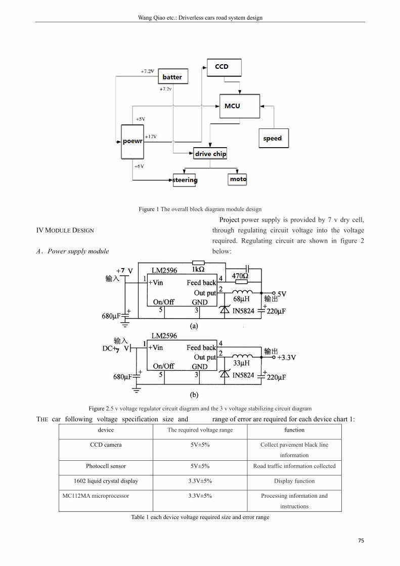
Wang Qiao etc.: Driverless cars road system design
75
Figure 1 The overall block diagram module design
IV MODULE DESIGN
A.Power supply module
Project power supply is provided by 7 v dry cell, through regulating circuit voltage into the voltage required. Regulating circuit are shown in figure 2 below:
Figure 2.5 v voltage regulator circuit diagram and the 3 v voltage stabilizing circuit diagram
THE car following voltage specification size and range of error are required for each device chart 1: device The required voltage range function
CCD camera 5V±5% Collect pavement black line
information
Photocell sensor 5V±5% Road traffic information collected
1602 liquid crystal display 3.3V±5% Display function
MC112MA microprocessor 3.3V±5% Processing information and
instructions
Table 1 each device voltage required size and error range
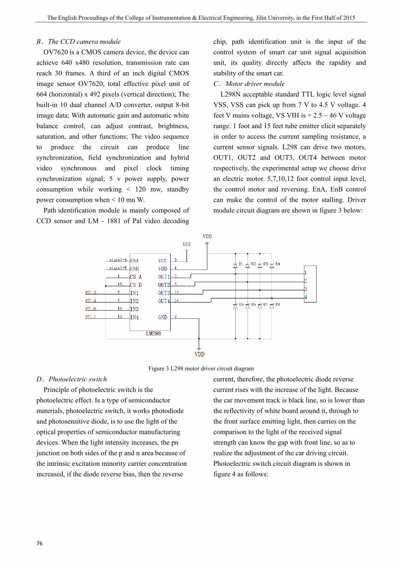
The English Proceedings of the College of Instrumentation & Electrical Engineering, Jilin University, in the First Half of 2015
76
B.The CCD camera module OV7620 is a CMOS camera device, the device can
achieve 640 x480 resolution, transmission rate can reach 30 frames. A third of an inch digital CMOS image sensor OV7620, total effective pixel unit of 664 (horizontal) x 492 pixels (vertical direction); The built-in 10 dual channel A/D converter, output 8-bit image data; With automatic gain and automatic white balance control, can adjust contrast, brightness, saturation, and other functions; The video sequence to produce the circuit can produce line synchronization, field synchronization and hybrid video synchronous and pixel clock timing synchronization signal; 5 v power supply, power consumption while working < 120 mw, standby power consumption when < 10 mu W.
Path identification module is mainly composed of CCD sensor and LM - 1881 of Pal video decoding
chip, path identification unit is the input of the control system of smart car unit signal acquisition unit, its quality directly affects the rapidity and stability of the smart car. C.Motor driver module
L298N acceptable standard TTL logic level signal VSS, VSS can pick up from 7 V to 4.5 V voltage. 4 feet V mains voltage, VS VIH is + 2.5 ~ 46 V voltage range. 1 foot and 15 feet tube emitter elicit separately in order to access the current sampling resistance, a current sensor signals. L298 can drive two motors, OUT1, OUT2 and OUT3, OUT4 between motor respectively, the experimental setup we choose drive an electric motor. 5,7,10,12 foot control input level, the control motor and reversing. EnA, EnB control can make the control of the motor stalling. Driver module circuit diagram are shown in figure 3 below:
Figure 3 L298 motor driver circuit diagram
D.Photoelectric switch Principle of photoelectric switch is the
photoelectric effect. Is a type of semiconductor materials, photoelectric switch, it works photodiode and photosensitive diode, is to use the light of the optical properties of semiconductor manufacturing devices. When the light intensity increases, the pn junction on both sides of the p and n area because of the intrinsic excitation minority carrier concentration increased, if the diode reverse bias, then the reverse
current, therefore, the photoelectric diode reverse current rises with the increase of the light. Because the car movement track is black line, so is lower than the reflectivity of white board around it, through to the front surface emitting light, then carries on the comparison to the light of the received signal strength can know the gap with front line, so as to realize the adjustment of the car driving circuit. Photoelectric switch circuit diagram is shown in figure 4 as follows:
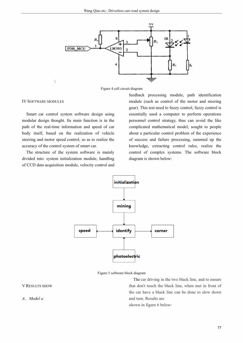
Wang Qiao etc.: Driverless cars road system design
77
\ Figure 4 cell circuit diagram
IV SOFTWARE MODULES
Smart car control system software design using modular design thought. Its main function is in the path of the real-time information and speed of car body itself, based on the realization of vehicle steering and motor speed control, so as to realize the accuracy of the control system of smart car.
The structure of the system software is mainly divided into: system initialization module, handling of CCD data acquisition module, velocity control and
feedback processing module, path identification module (such as control of the motor and steering gear). This test need to fuzzy control, fuzzy control is essentially used a computer to perform operations personnel control strategy, thus can avoid the like complicated mathematical model, sought to people about a particular control problem of the experience of success and failure processing, summed up the knowledge, extracting control rules, realize the control of complex systems. The software block diagram is shown below:
Figure 5 software block diagram
V RESULTS SHOW
A.Model a
The car driving in the two black line, and to ensure that don't touch the black line, when met in front of the car have a black line can be done to slow down and turn. Results are shown in figure 6 below:
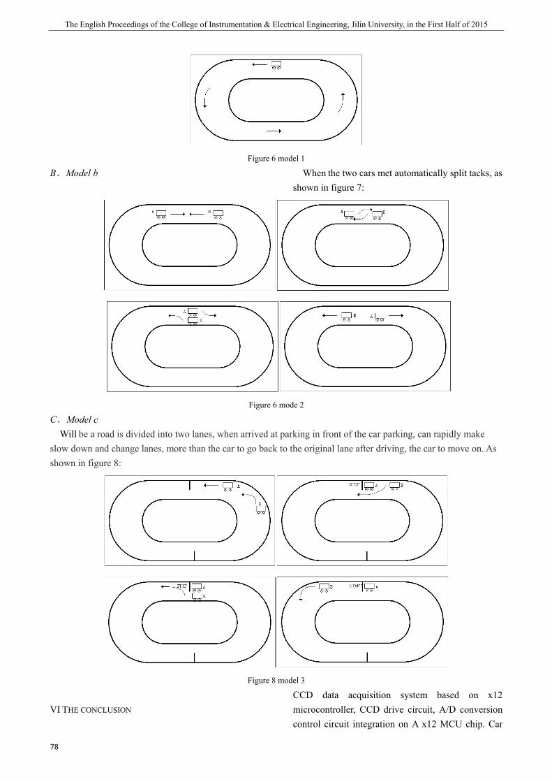
The English Proceedings of the College of Instrumentation & Electrical Engineering, Jilin University, in the First Half of 2015
78
Figure 6 model 1
B.Model b When the two cars met automatically split tacks, as shown in figure 7:
Figure 6 mode 2
C.Model c Will be a road is divided into two lanes, when arrived at parking in front of the car parking, can rapidly make
slow down and change lanes, more than the car to go back to the original lane after driving, the car to move on. As shown in figure 8:
Figure 8 model 3
VI THE CONCLUSION CCD data acquisition system based on x12 microcontroller, CCD drive circuit, A/D conversion control circuit integration on A x12 MCU chip. Car

Wang Qiao etc.: Driverless cars road system design
79
power supply module for power supply, car CCD camera module is used to find lane trajectory, motor driver module for cars driving power. Eventually the car can drive along the black line trajectory; When a vehicle ahead to it can automatically avoid when driving, pull over driving; The current party is safe to overtake vehicles and return to the original lane after passing to continue driving, so as to realize the intelligence of the car.
References
[1] Yuan Yadong, "the development of the CCD sensor
intelligent car. Hefei industrial university press
[2] Kang hua, "electronic technology foundation (simulated).
Higher education press
[3] Kang hua, "electronic technology foundation (part
number). Higher education press.
[4] Chien-yu Lin, the intelligent car control system based on
CCD sensor design. Institute of Shanghai electric power
[5] The intelligent vehicle in the world are reviewed.
Automotive engineering, 2001, 23 (5) : 289-295
[6] The smart car based on photoelectric sensor automatic
tracking control system ". [J]. Instrument technique and
sensor, 2012 (1) : 108-110
[7] Good is introduced. The fuzzy PID control algorithm in
the research and application of the smart car [D]. Hefei
university of technology, 2009
[8] Mr. Wong, weng moguls, Liang Ye. Automatic tracing car
sensor module design [J]. Journal of modern electronic
technology. 2008 (22)
[9] Tian-qiang wu, Li Haoqi Wu Zhou, xiao-yang huang,
frankie lam. Smart car line control and trace branch
identification scheme design [J]. Journal of taizhou school.
2012 (3)
[10] Mr. Wong. Smart car motion control technology research
[D]. Wuhan university of technology, 2009
[11] Lu Wei. The design and implementation of intelligent
vehicle obstacle avoidance system [D]. 2012, nanchang
university
[12] Emily. Based on the ARM of the design and
implementation of intelligent tracking car [D]. University
of north 2012 Emily. Based on the ARM of the design and
implementation of intelligent tracing car [D]. North
university in 2012
[13] Wang dong. Based on the ARM of the design and
implementation of intelligent detection car [D]. Suzhou
university in 2010
[14] Jian-gang liu, ciro, Huang Jian ZhangZheng. Based on the
CCD image recognition HCS12 MCU intelligent car
control system [J]. Journal of photoelectric technology.
2007 (6)
[15] Jia Xiujiang, li hao finds. Camera black line recognition
algorithm and the car driving control strategy [J]. Journal
of electronic products in the world. 2007 (05)
[16] Were, xiao-hui qi, yong-ke li. Based on the intelligent car
design and implementation of camera [J]. J 2008 (02)
sensors in the world.
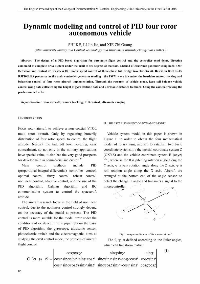
The English Proceedings of the College of Instrumentation & Electrical Engineering, Jilin University, in the First Half of 2015
80
Dynamic modeling and control of PID four rotor autonomous vehicle
SHI KE, LI Jin Jie, and XIE Zhi Guang
(jilin university Survey and Control Technology and Instrument institute,changchun,130021)
Abstract—The design of a PID based algorithm for automatic flight control and the controller send delay, direction
command to complete drive system under the orbit of six degrees of freedom. Method of electronic governor using back EMF
Detection and control of Brushless DC motor speed control of three-phase full bridge inverter circuit. Based on RENESAS
R5F100LEA processor as the main controller generates sending the PWM wave to control the brushless motor, tracking and
balancing control of four rotor aircraft implementation. Through the research of vehicle mode, keep self-balance vehicle
control using data collected by the height of gyro attitude data and ultrasonic distance feedback. Using the camera tracking the
predetermined orbit.
Keywords—four rotor aircraft; camera tracking; PID control; ultrasonic ranging
I.INTRODUCTION
FOUR rotor aircraft to achieve a non coaxial VTOL multi rotor aircraft. Only by regulating butterfly distribution of four rotor speed, to control the flight attitude. Needn`t the tail, off low, hovering, easy concealment, so not only in the military applications have special value, it also has the very good prospects for development in commercial and civilof [9].
Main control methods include PID (proportional-integral-differential) controller control, optimal control, fuzzy control, robust control, nonlinear control, adaptive control, and the use of the PID algorithm. Calman algorithm and IIC communication system to control the spacecraft attitude.
The aircraft research focus in the field of nonlinear control, due to the nonlinear control strongly depend on the accuracy of the model at present. The PID control is more suitable for the model error under the conditions of existence. In this paper,rely on the basis of PID algorithm, the gyroscope, ultrasonic sensor, photoelectric switch and the electromagnetic, aims at studying the orbit control mode, the problem of aircraft flight control.
II.THE ESTABLISHMENT OF DYNAMIC MODEL
Vehicle system model in this paper is shown in Figure 1, in order to obtain the four mathematical model of rotary wing aircraft, to establish two basic coordinate systems,it`s the inertial coordinate system Z (OXYZ) and the vehicle coordinate system B (oxyz) [2,3], where in the θ is pitching rotation angle along the Y axis, ψ is yaw rotation angle along the Z axis; φ is roll rotation angle along the X axis. Aircraft are arranged at the bottom end of the angle sensor, to detect the change in angle and transmits a signal to the microcontroller.
Fig.1. map coordinates of four rotor aircraft
The θ, ψ, φ defined according to the Euler angles, which can transform matrix:
(1)
fqfyyfqfyfqy
fqfyfyqfyfqy
qyqyq
fyq
coscossincossincossinsinsincossincossincoscoscossinsinsincossinsinsincos
sinsinsincoscosC
-+
+-
-
=),,(
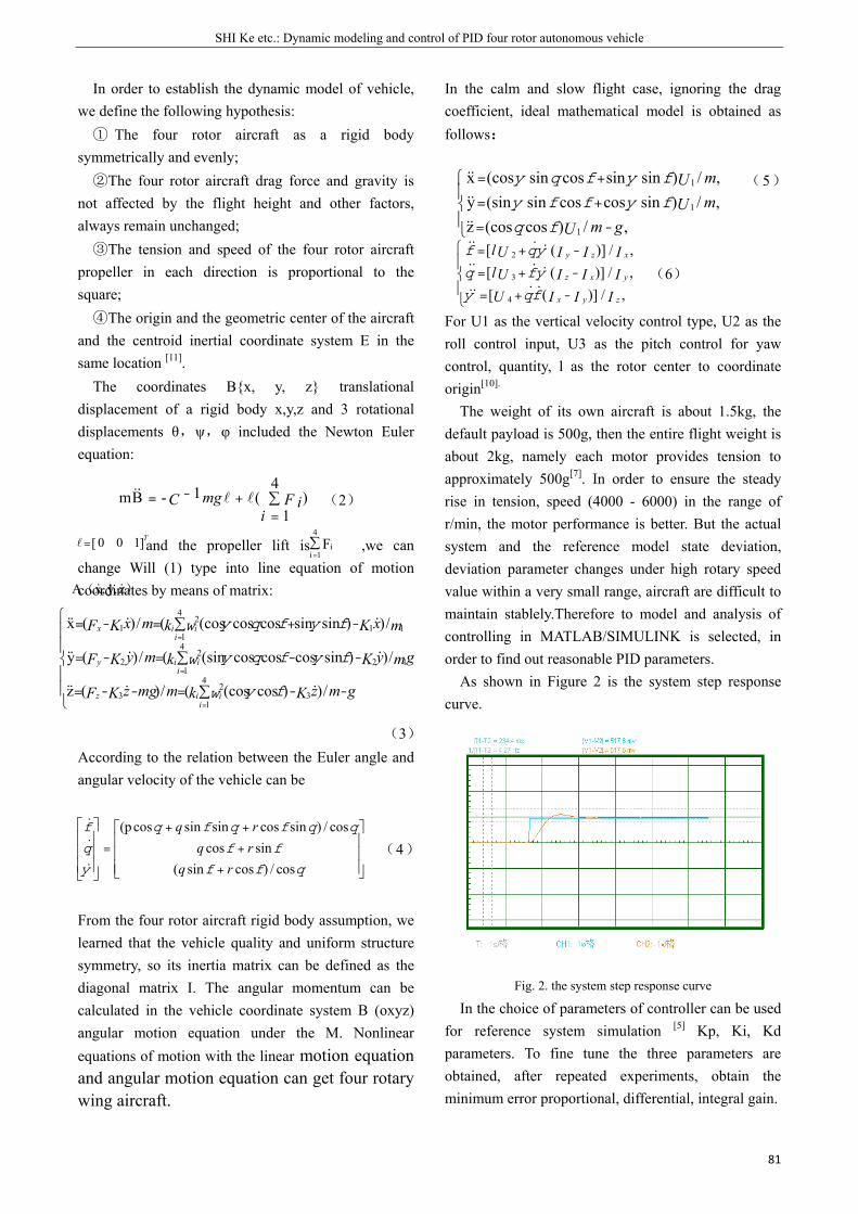
SHI Ke etc.: Dynamic modeling and control of PID four rotor autonomous vehicle
81
)4
1(1-Bm ∑=
+-=i
F imgC
g
gmzKkmmgzKF
myKkmyKF
mxKkmxKF
iiiz
iiiy
iiix
⎪⎪
⎩
⎪⎪
⎨
⎧
-∑ -=--=
∑ --=-=
∑ -+=-=
=
=
=
/))cos(cos(/)(z
/))sincoscoscos(sin(/)(y
/))sinsincoscos(cos(/)(x
4
13
23
1
4
12
22
1
4
11
21
fyw
fyfqyw
fyfqyw
⎪⎩
⎪⎨
⎧
-=
+=
+=
,/)cos(cosz,/)sincoscossin(siny,/)sinsincossin(cosx
1
1
1
gmUmUmU
fq
fyffy
fyfqy
⎪⎩
⎪⎨
⎧
-+=
-+=
-+=
,/)]([,/)]([,/)]([
4
3
2
IIIUIIIUlIIIUl
zyx
yxz
xzy
fqy
yfq
yqf
In order to establish the dynamic model of vehicle, we define the following hypothesis: ① The four rotor aircraft as a rigid body
symmetrically and evenly; ②The four rotor aircraft drag force and gravity is
not affected by the flight height and other factors, always remain unchanged; ③The tension and speed of the four rotor aircraft
propeller in each direction is proportional to the square; ④The origin and the geometric center of the aircraft
and the centroid inertial coordinate system E in the same location [11].
The coordinates Bx, y, z translational displacement of a rigid body x,y,z and 3 rotational displacements θ,ψ,φ included the Newton Euler equation:
(2)
and the propeller lift is ,we can change Will (1) type into line equation of motion coordinates by means of matrix:
(3) According to the relation between the Euler angle and angular velocity of the vehicle can be
(4)
From the four rotor aircraft rigid body assumption, we learned that the vehicle quality and uniform structure symmetry, so its inertia matrix can be defined as the diagonal matrix I. The angular momentum can be calculated in the vehicle coordinate system B (oxyz) angular motion equation under the M. Nonlinear equations of motion with the linear motion equation and angular motion equation can get four rotary wing aircraft.
In the calm and slow flight case, ignoring the drag coefficient, ideal mathematical model is obtained as follows:
(5)
(6)
For U1 as the vertical velocity control type, U2 as the roll control input, U3 as the pitch control for yaw control, quantity, l as the rotor center to coordinate origin[10].
The weight of its own aircraft is about 1.5kg, the default payload is 500g, then the entire flight weight is about 2kg, namely each motor provides tension to approximately 500g[7]. In order to ensure the steady rise in tension, speed (4000 - 6000) in the range of r/min, the motor performance is better. But the actual system and the reference model state deviation, deviation parameter changes under high rotary speed value within a very small range, aircraft are difficult to maintain stablely.Therefore to model and analysis of controlling in MATLAB/SIMULINK is selected, in order to find out reasonable PID parameters.
As shown in Figure 2 is the system step response curve.
Fig. 2. the system step response curve
In the choice of parameters of controller can be used for reference system simulation [5] Kp, Ki, Kd parameters. To fine tune the three parameters are obtained, after repeated experiments, obtain the minimum error proportional, differential, integral gain.
)( z,y,xA
]100[ T= ∑=
4
1iiF
⎥⎥⎥
⎦
⎤
⎢⎢⎢
⎣
⎡
+
+
++
=⎥⎥⎥
⎦
⎤
⎢⎢⎢
⎣
⎡
qff
ff
qqfqfq
y
q
f
cos/)cossin(sincos
cos/)sincossinsincos(p
rqrqrq
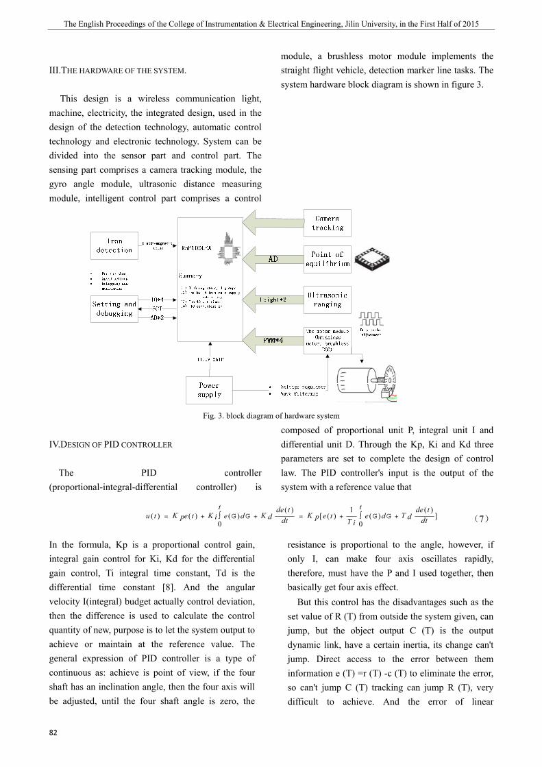
The English Proceedings of the College of Instrumentation & Electrical Engineering, Jilin University, in the First Half of 2015
82
III.THE HARDWARE OF THE SYSTEM.
This design is a wireless communication light, machine, electricity, the integrated design, used in the design of the detection technology, automatic control technology and electronic technology. System can be divided into the sensor part and control part. The sensing part comprises a camera tracking module, the gyro angle module, ultrasonic distance measuring module, intelligent control part comprises a control
module, a brushless motor module implements the straight flight vehicle, detection marker line tasks. The system hardware block diagram is shown in figure 3.
Fig. 3. block diagram of hardware system
IV.DESIGN OF PID CONTROLLER
The PID controller (proportional-integral-differential controller) is
composed of proportional unit P, integral unit I and differential unit D. Through the Kp, Ki and Kd three parameters are set to complete the design of control law. The PID controller's input is the output of the system with a reference value that
( ) 1 ( )( ) ( ) ( ) [ ( ) ( ) ]
0 0
t tde t de tK K K K Tu t e t e d e t e dp i d p ddt dtT i
∫ ∫= + G G + = + G G + (7)
In the formula, Kp is a proportional control gain, integral gain control for Ki, Kd for the differential gain control, Ti integral time constant, Td is the differential time constant [8]. And the angular velocity I(integral) budget actually control deviation, then the difference is used to calculate the control quantity of new, purpose is to let the system output to achieve or maintain at the reference value. The general expression of PID controller is a type of continuous as: achieve is point of view, if the four shaft has an inclination angle, then the four axis will be adjusted, until the four shaft angle is zero, the
resistance is proportional to the angle, however, if only I, can make four axis oscillates rapidly, therefore, must have the P and I used together, then basically get four axis effect.
But this control has the disadvantages such as the set value of R (T) from outside the system given, can jump, but the object output C (T) is the output dynamic link, have a certain inertia, its change can't jump. Direct access to the error between them information e (T) =r (T) -c (T) to eliminate the error, so can't jump C (T) tracking can jump R (T), very difficult to achieve. And the error of linear
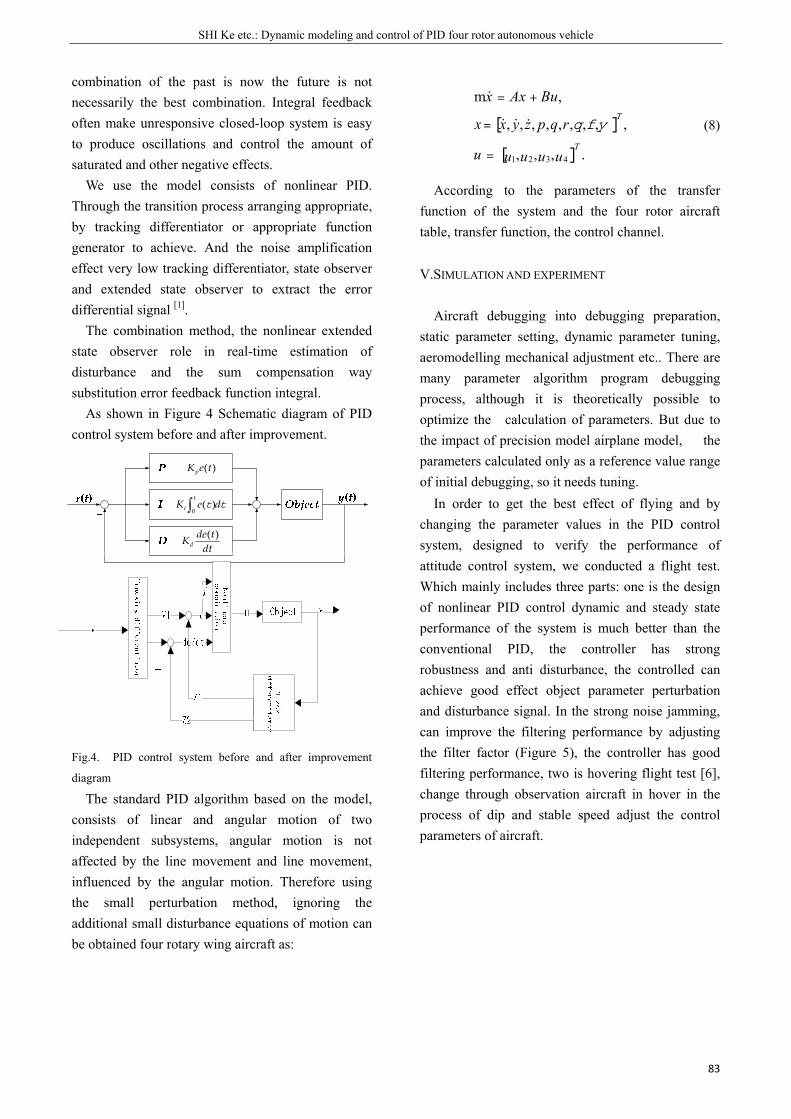
SHI Ke etc.: Dynamic modeling and control of PID four rotor autonomous vehicle
83
[ ]
[ ].,,,
,,,,,,,,,
,m
4321 uuuuu
rqpzyxx
BuAxx
T
T
=
=
+=
yfq
combination of the past is now the future is not necessarily the best combination. Integral feedback often make unresponsive closed-loop system is easy to produce oscillations and control the amount of saturated and other negative effects.
We use the model consists of nonlinear PID. Through the transition process arranging appropriate, by tracking differentiator or appropriate function generator to achieve. And the noise amplification effect very low tracking differentiator, state observer and extended state observer to extract the error differential signal [1].
The combination method, the nonlinear extended state observer role in real-time estimation of disturbance and the sum compensation way substitution error feedback function integral.
As shown in Figure 4 Schematic diagram of PID control system before and after improvement.
Fig.4. PID control system before and after improvement
diagram
The standard PID algorithm based on the model, consists of linear and angular motion of two independent subsystems, angular motion is not affected by the line movement and line movement, influenced by the angular motion. Therefore using the small perturbation method, ignoring the additional small disturbance equations of motion can be obtained four rotary wing aircraft as:
(8)
According to the parameters of the transfer function of the system and the four rotor aircraft table, transfer function, the control channel.
V.SIMULATION AND EXPERIMENT
Aircraft debugging into debugging preparation, static parameter setting, dynamic parameter tuning, aeromodelling mechanical adjustment etc.. There are many parameter algorithm program debugging process, although it is theoretically possible to optimize the calculation of parameters. But due to the impact of precision model airplane model, the parameters calculated only as a reference value range of initial debugging, so it needs tuning.
In order to get the best effect of flying and by changing the parameter values in the PID control system, designed to verify the performance of attitude control system, we conducted a flight test. Which mainly includes three parts: one is the design of nonlinear PID control dynamic and steady state performance of the system is much better than the conventional PID, the controller has strong robustness and anti disturbance, the controlled can achieve good effect object parameter perturbation and disturbance signal. In the strong noise jamming, can improve the filtering performance by adjusting the filter factor (Figure 5), the controller has good filtering performance, two is hovering flight test [6], change through observation aircraft in hover in the process of dip and stable speed adjust the control parameters of aircraft.
( )pK e t
t t∫0 ( )t
iK e d
( )dde tKdt
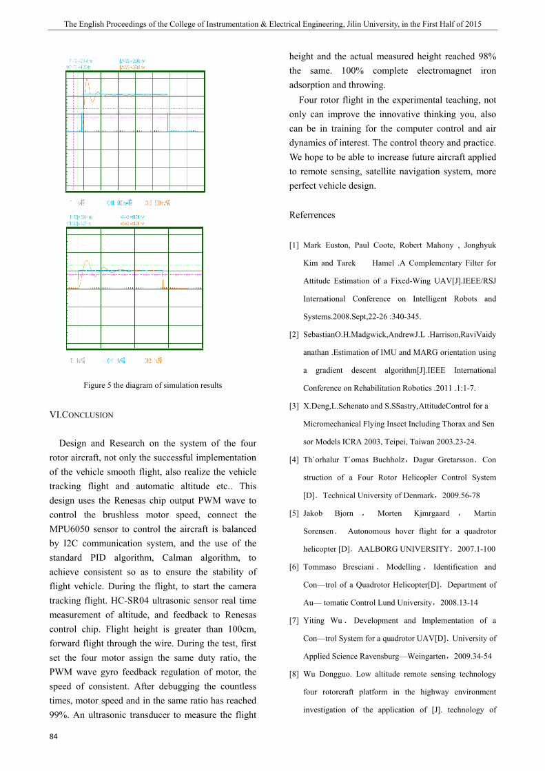
The English Proceedings of the College of Instrumentation & Electrical Engineering, Jilin University, in the First Half of 2015
84
Figure 5 the diagram of simulation results
VI.CONCLUSION
Design and Research on the system of the four rotor aircraft, not only the successful implementation of the vehicle smooth flight, also realize the vehicle tracking flight and automatic altitude etc.. This design uses the Renesas chip output PWM wave to control the brushless motor speed, connect the MPU6050 sensor to control the aircraft is balanced by I2C communication system, and the use of the standard PID algorithm, Calman algorithm, to achieve consistent so as to ensure the stability of flight vehicle. During the flight, to start the camera tracking flight. HC-SR04 ultrasonic sensor real time measurement of altitude, and feedback to Renesas control chip. Flight height is greater than 100cm, forward flight through the wire. During the test, first set the four motor assign the same duty ratio, the PWM wave gyro feedback regulation of motor, the speed of consistent. After debugging the countless times, motor speed and in the same ratio has reached 99%. An ultrasonic transducer to measure the flight
height and the actual measured height reached 98% the same. 100% complete electromagnet iron adsorption and throwing.
Four rotor flight in the experimental teaching, not only can improve the innovative thinking you, also can be in training for the computer control and air dynamics of interest. The control theory and practice. We hope to be able to increase future aircraft applied to remote sensing, satellite navigation system, more perfect vehicle design.
Referrences
[1] Mark Euston, Paul Coote, Robert Mahony , Jonghyuk
Kim and Tarek Hamel .A Complementary Filter for
Attitude Estimation of a Fixed-Wing UAV[J].IEEE/RSJ
International Conference on Intelligent Robots and
Systems.2008.Sept,22-26 :340-345.
[2] SebastianO.H.Madgwick,AndrewJ.L .Harrison,RaviVaidy
anathan .Estimation of IMU and MARG orientation using
a gradient descent algorithm[J].IEEE International
Conference on Rehabilitation Robotics .2011 .1:1-7.
[3] X.Deng,L.Schenato and S.SSastry,AttitudeControl for a
Micromechanical Flying Insect Including Thorax and Sen
sor Models ICRA 2003, Teipei, Taiwan 2003.23-24.
[4] Th`orhalur T`omas Buchholz,Dagur Gretarsson.Con
struction of a Four Rotor Helicopler Control System
[D].Technical University of Denmark,2009.56-78
[5] Jakob Bjorn , Morten Kjmrgaard , Martin
Sorensen. Autonomous hover flight for a quadrotor
helicopter [D].AALBORG UNIVERSITY,2007.1-100
[6] Tommaso Bresciani . Modelling , Identification and
Con—trol of a Quadrotor Helicopter[D].Department of
Au— tomatic Control Lund University,2008.13-14
[7] Yiting Wu . Development and Implementation of a
Con—trol System for a quadrotor UAV[D].University of
Applied Science Ravensburg—Weingarten,2009.34-54
[8] Wu Dongguo. Low altitude remote sensing technology
four rotorcraft platform in the highway environment
investigation of the application of [J]. technology of

SHI Ke etc.: Dynamic modeling and control of PID four rotor autonomous vehicle
85
highway and transport based on.2012. Sixth: 137-138.
[9] Ji Jiang Tao, Hu Fei, He Zhitao, Du Xinwu, Liu Jianjun.
The four rotor UAV in the farmland information
acquisition in the application of [J]. in research of.2013
second: 1-4..
[10] Zhao Chen, Du Yong. The four rotor without [J].
application of human in the patrol of transmission line of
Hubei power.2012. thirty-sixth volume sixth: 35-36.
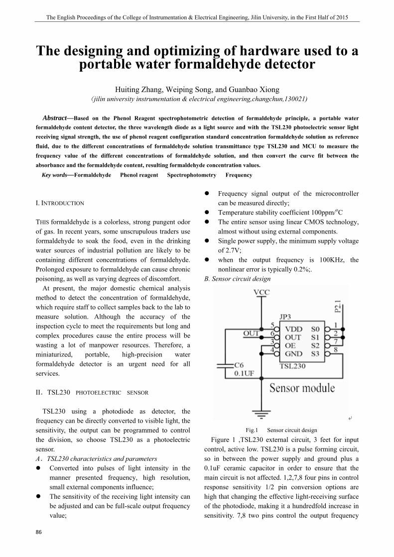
The English Proceedings of the College of Instrumentation & Electrical Engineering, Jilin University, in the First Half of 2015
86
The designing and optimizing of hardware used to a portable water formaldehyde detector
Huiting Zhang, Weiping Song, and Guanbao Xiong
(jilin university instrumentation & electrical engineering,changchun,130021)
Abstract—Based on the Phenol Reagent spectrophotometric detection of formaldehyde principle, a portable water formaldehyde content detector, the three wavelength diode as a light source and with the TSL230 photoelectric sensor light receiving signal strength, the use of phenol reagent configuration standard concentration formaldehyde solution as reference fluid, due to the different concentrations of formaldehyde solution transmittance type TSL230 and MCU to measure the frequency value of the different concentrations of formaldehyde solution, and then convert the curve fit between the absorbance and the formaldehyde content, resulting formaldehyde concentration values.
Key words—Formaldehyde Phenol reagent Spectrophotometry Frequency
I. INTRODUCTION
THIS formaldehyde is a colorless, strong pungent odor of gas. In recent years, some unscrupulous traders use formaldehyde to soak the food, even in the drinking water sources of industrial pollution are likely to be containing different concentrations of formaldehyde. Prolonged exposure to formaldehyde can cause chronic poisoning, as well as varying degrees of discomfort.
At present, the major domestic chemical analysis method to detect the concentration of formaldehyde, which require staff to collect samples back to the lab to measure solution. Although the accuracy of the inspection cycle to meet the requirements but long and complex procedures cause the entire process will be wasting a lot of manpower resources. Therefore, a miniaturized, portable, high-precision water formaldehyde detector is an urgent need for all services.
II.TSL230 PHOTOELECTRIC SENSOR
TSL230 using a photodiode as detector, the frequency can be directly converted to visible light, the sensitivity, the output can be programmed to control the division, so choose TSL230 as a photoelectric sensor. A.TSL230 characteristics and parameters
Converted into pulses of light intensity in the manner presented frequency, high resolution, small external components influence;
The sensitivity of the receiving light intensity can be adjusted and can be full-scale output frequency value;
Frequency signal output of the microcontroller can be measured directly;
Temperature stability coefficient 100ppm/oC The entire sensor using linear CMOS technology,
almost without using external components. Single power supply, the minimum supply voltage
of 2.7V; when the output frequency is 100KHz, the
nonlinear error is typically 0.2%;. B. Sensor circuit design
Fig.1 Sensor circuit design
Figure 1 ,TSL230 external circuit, 3 feet for input control, active low. TSL230 is a pulse forming circuit, so in between the power supply and ground plus a 0.1uF ceramic capacitor in order to ensure that the main circuit is not affected. 1,2,7,8 four pins in control response sensitivity 1/2 pin conversion options are high that changing the effective light-receiving surface of the photodiode, making it a hundredfold increase in sensitivity. 7,8 two pins control the output frequency
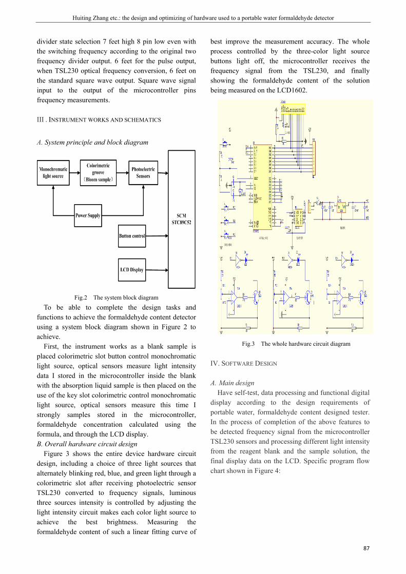
Huiting Zhang etc.: the design and optimizing of hardware used to a portable water formaldehyde detector
87
divider state selection 7 feet high 8 pin low even with the switching frequency according to the original two frequency divider output. 6 feet for the pulse output, when TSL230 optical frequency conversion, 6 feet on the standard square wave output. Square wave signal input to the output of the microcontroller pins frequency measurements.
III . INSTRUMENT WORKS AND SCHEMATICS
A. System principle and block diagram
Fig.2 The system block diagram
To be able to complete the design tasks and functions to achieve the formaldehyde content detector using a system block diagram shown in Figure 2 to achieve.
First, the instrument works as a blank sample is placed colorimetric slot button control monochromatic light source, optical sensors measure light intensity data I stored in the microcontroller inside the blank with the absorption liquid sample is then placed on the use of the key slot colorimetric control monochromatic light source, optical sensors measure this time I strongly samples stored in the microcontroller, formaldehyde concentration calculated using the formula, and through the LCD display. B. Overall hardware circuit design
Figure 3 shows the entire device hardware circuit design, including a choice of three light sources that alternately blinking red, blue, and green light through a colorimetric slot after receiving photoelectric sensor TSL230 converted to frequency signals, luminous three sources intensity is controlled by adjusting the light intensity circuit makes each color light source to achieve the best brightness. Measuring the formaldehyde content of such a linear fitting curve of
best improve the measurement accuracy. The whole process controlled by the three-color light source buttons light off, the microcontroller receives the frequency signal from the TSL230, and finally showing the formaldehyde content of the solution being measured on the LCD1602.
Fig.3 The whole hardware circuit diagram
IV. SOFTWARE DESIGN
A. Main design Have self-test, data processing and functional digital
display according to the design requirements of portable water, formaldehyde content designed tester. In the process of completion of the above features to be detected frequency signal from the microcontroller TSL230 sensors and processing different light intensity from the reagent blank and the sample solution, the final display data on the LCD. Specific program flow chart shown in Figure 4:
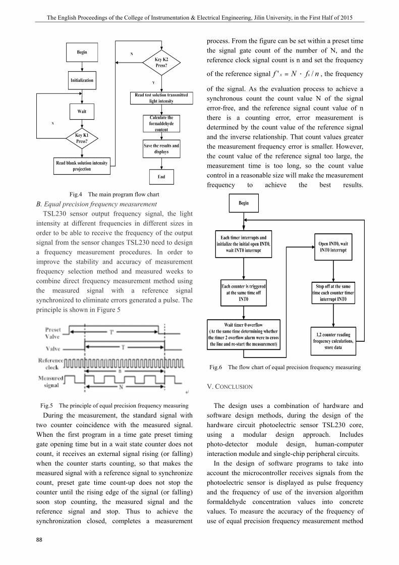
The English Proceedings of the College of Instrumentation & Electrical Engineering, Jilin University, in the First Half of 2015
88
Fig.4 The main program flow chart
B. Equal precision frequency measurement TSL230 sensor output frequency signal, the light
intensity at different frequencies in different sizes in order to be able to receive the frequency of the output signal from the sensor changes TSL230 need to design a frequency measurement procedures. In order to improve the stability and accuracy of measurement frequency selection method and measured weeks to combine direct frequency measurement method using the measured signal with a reference signal synchronized to eliminate errors generated a pulse. The principle is shown in Figure 5
Fig.5 The principle of equal precision frequency measuring
During the measurement, the standard signal with two counter coincidence with the measured signal. When the first program in a time gate preset timing gate opening time but in a wait state counter does not count, it receives an external signal rising (or falling) when the counter starts counting, so that makes the measured signal with a reference signal to synchronize count, preset gate time count-up does not stop the counter until the rising edge of the signal (or falling) soon stop counting, the measured signal and the reference signal and stop. Thus to achieve the synchronization closed, completes a measurement
process. From the figure can be set within a preset time the signal gate count of the number of N, and the reference clock signal count is n and set the frequency
of the reference signal nfNf xx /' ·= , the frequency
of the signal. As the evaluation process to achieve a synchronous count the count value N of the signal error-free, and the reference signal count value of n there is a counting error, error measurement is determined by the count value of the reference signal and the inverse relationship. That count values greater the measurement frequency error is smaller. However, the count value of the reference signal too large, the measurement time is too long, so the count value control in a reasonable size will make the measurement frequency to achieve the best results.
Fig.6 The flow chart of equal precision frequency measuring
V. CONCLUSION
The design uses a combination of hardware and software design methods, during the design of the hardware circuit photoelectric sensor TSL230 core, using a modular design approach. Includes photo-detector module design, human-computer interaction module and single-chip peripheral circuits.
In the design of software programs to take into account the microcontroller receives signals from the photoelectric sensor is displayed as pulse frequency and the frequency of use of the inversion algorithm formaldehyde concentration values into concrete values. To measure the accuracy of the frequency of use of equal precision frequency measurement method

Huiting Zhang etc.: the design and optimizing of hardware used to a portable water formaldehyde detector
89
effectively reduces the measurement error. Proposed a portable water formaldehyde detector
design based on the above section. It has the automation, easy operation and low cost, and the use of the microcontroller to achieve a test of intelligence. After error analysis results show that the design is feasible. However, due to limited time and can not apply this product to everyday life, but in a state of the testing machine. If time allows practical issues need to study the stability of the next instrument, and the application status in different environments.
References
[18] Popov A,Sherstnev V,Yakovlev Y,etal. Application of
Antimonide Laser to HCHO measurements at
Spam[J].VDI-Ber, 2008,1336: 173一176
[19] Fried A,Wert B P,Henry B .Airborne Tunable Decide
Laser Measurement of Formaldehyde [ J] .Spectrographical.
Acta. Part A,1999 55:2097一2110
[20] D. Riehter et al. Development of a tunable mid-IR
difference frequency laser source for highly sensitive
airborne trace gas detection. Applied Physics B: Lasers and
Optics. 2008,75: 281288
[21] P.S.Manoonkitiwongsa eta. Proper nomenklatura of
formaldehyde and paraformaldehyde fixative for
histochemistry.The Histochemical Journal.2002,
34:365-367
[22] Y. Herschkovitz,I. Eshkenazi, C. E. Campbell et al. An
electrochemical biosensor for formaldehyde. Journal of
electroanalytical Chemistry. 2000, 491:182-187
[23] F. Vianello et al. Potentiometric detection of
formaldehyde in air by an aldehyde dehydrogenase FET.
Sensors and Actuators B. 1996, 37: 49一54

The English Proceedings of the College of Instrumentation & Electrical Engineering, Jilin University, in the First Half of 2015
90
Development of a Portable PM2.5 Monitor
Wang Hong-yuan, Zhao Peng-cheng, Gao Weng-zhi, Li Su-yi (College of instrumentation and Electrical Engineering, Jilin University, Changchun 130022, China)
Abstract—In recent years, with the development and popularization of the motor vehicle industry, the number of motor
vehicles is increasing heavily, and the impact of them on urban environment is getting more and more obvious. Urban air quality in China is becoming worse and worse, and people pay more and more attention to the air quality of living environment. So, aiming at current conditions, we develop a portable PM2.5 monitor to monitor PM2.5 in family. We use low power consumption microprocessor MSP430 as the core, DSM501 made in SYHITECH Company as sensor , and combine SIM900A dual-band GSM/GPRS module with GPS blox NEO-6m module in device. It realizes real-time monitoring of PM2.5, position information display as well as the function of the remote testing information of PM2.5 by mobile phone after transformation of hardware level, software filtering and data post-processing. It shows from actual test data that the device can be used to monitor PM2.5 in the air within the error range.
Keywords—PM2.5 monitor; GPS module; GPRS SMS transcenciving
I. INTRODUCTION
ONE forth of China have appeared haze since 2013 [1],which has affected about 600 million people.
Particle matter whose size is 10um or more will be kept outside the human nose; Those sized between 2.5 and 10 um can enter human respiratory , but some may be excreted through the sputum, which is less harmful to human health [2]; While the particle matter whose size is 2.5 um or less (known as "PM2.5") and just one-tenth of a human hair will enter bronchial after being inhaled and disturb pulmonary gas exchange, causing including asthma, bronchial inflammation and cardiovascular disease and other diseases. Harmful gases and heavy metals goes into the blood from Bronchi and alveoli. Once they are dissolved, it will seriously affect human health. PM2.5 in haze becomes the latest killer [3], affecting the body's respiratory, reproductive and blood system. It is reported by WHO that 120 million people died early because of outdoor air pollution in China.
Compared to "fog", "haze" is produced due to air pollution. Therefore, living in haze is greater harmful to human health than that in the fog. Recent years ,Northern China has been affected by the global climate anomalies, resulting in increasingly severe drought. At the same time, it emits a lot of greenhouse gas in city life, causing times of haze day rising [4]. It indicates from research that particulate matter has a worse influence on human health hazards even than the storms [5].
What does harm to human body is not particulate matter itself, but chemical substance adhered to it.PM2.5 to influence on human health is essentially
chemical substance adhered to particulate matter to it. For example, if PM2.5 absorbs carcinogens, it will
have carcinogenic effects; if it absorbs dioxin, it’ll have pregnancy hazards; if heavy metals, it’ll have heavy metal hazards. What affect is decided by something PM2.5 adsorbs [9].
The result shows that if PM2.5 exceeded, emergency and mortality rate of cardiovascular system in hospital will increase 6-7%,while emergency rate of hypertension will increase 5%,especially the particle matter sized 1-3 um, those matter could go into the alveoli where is used to make gas exchange. Those particles will be swallowed by macrophages and stay in the alveoli all the time, which has bad effect on not only respiratory system but also cardiovascular, nervous and other system.
So with the development of the times, a portable PM2.5 detector with positioning and messaging features was born[7],which is easy to use and with small size and low price [6]
With the help of SIM900A GSM module and GPS blox NEO-6M module, the instrument goes though level conversion [10], filtering and data post-processing to achieve PM2.5 detection [11] by the main controller MSP430 controlling DSM501 sensor [8].
II. PM2.5 MONITORING SYSTEM
A. Working Principle Of Sensor And Data Processing
The sensor has heating equipment which can be heated, so that dust particles will be heated to rise. One end of the sensor is a light emitting diode that can give off light of a certain intensity and frequency. The other
Wang Hong-yuan etc; Development of a Portable PM2.5 Monitor
91
end exists a receiving diode, and light emitted by LED will be reflected when it meets dust, which can be received by receiving diode. The larger the dust concentration is, the greater the intensity of reflected light is, and the stronger the received optical signal is. After going through amplifying and shaping, the output signal is PWM wave. When there are dust particles blocking the output port, it will get out a low level and last a period of time about a substantially continuous range of 10-50ms.Or it’ll output a high level. You can usually choose 30 seconds as a clock signal to measure the low PWM pulse time when measurement. And then you can get a low pulse rate. Low pulse rate are raw data, and you can get real-time PM2.5 data by going through mathematical operation. The data acquisition information and real-time display will be updated every 30 seconds when collecting data. The value is the current value for PM2.5.
Fig.1 Working principle of the sensor diagram
B. Level Conversion Module Design The output level of sensor is between 0.7~4.5V.If we put the PWM signal into MSP430 MCU, we’ll meet the situation that the level doesn’t match each other. Here, we have designed the level conversion module to solve the problem. The instrument total input power supply is 5V/2A, and MSP430 needs 3.3V.Here, we use a highly efficient linear regulator ASM1117-3.3V (Figure 2) to output 3.3V, so we can supply for MSP430 MCU. However, the output level of sensor does not match MSP430.Here,we use comparator circuit, a single supply operational amplifier OP27 which is drived by 3.3V power supply. Comparison reference voltage is 2.5V which is got by ASM1117-2.5, a high efficiency linear power. So, the output voltages are 0V and 2.5V. Finally, we complete the desired output level after voltage attenuation. Sensor’s output and a comparator are connected, and they go through level conversion to achieve a PWM signal of 0~3.3V.Finally,it matches with MSP430 MCU.
Fig.2 ASM1117-3.3V switching circuit
III. SYSTEM DESIGN OF GPS DATA ACQUISITION
A. The Working Principle Of GPS Module GPS blox NEO-6M module is used in positioning system, and the u-blox chip is a high-performance one.
TABLE1 Parameters Of GPS Blox NEO-6M Module Parameters Values
The C/A code 1.023mhz Receive band L1 [1575.42mhz]
The track sensitivity -161dbm Acquisition sensitivity -148dbm
Cold start-time 38s Warm start-time 35s Hot start-time 1s
Recapture time 0.1s. It is able to meet the needs of real-time positioning. The chip adopts serial communication to transmit coordinates, latitude and longitude ,and other information to the master chip, and it’ll finally be displayed on LED. Through the GPS module, you can obtain the coordinate of surveyor, and pass it to the master chip, recording the coordinate orientation. GSM module is also added in the system, and the location coordinates, PM2.5 values and other data s are sent to mobile terminals via GSM network. B. Brief Introduction Of NMEA-0183 Protocol NMEA0831 is a standard format of America National Marine Electronics Association for use in marine electronic equipment. It has become a unified RTCM standard protocol of GPS navigation equipment. NMEA-0831 protocol makes the ASCII code to transmit of GPS positioning information, which we call frame. Here is frame format: $aaccc, ddd, ddd,..., ddd*hh (CR) (LF) 1. "$": frame command initiation bit 2. Aaccc: address field, the top two for the identifier (AA), three for the statement name (CCC) 3. ddd,... ddd :data 4."*": check and prefix (also marked the end of statement data) 5. hh: The checksum

The English Proceedings of the College of Instrumentation & Electrical Engineering, Jilin University, in the First Half of 2015
92
6. (CR) (LF): The end of the frame, a carriage return and linefeed character Commonly used NMEA-0183 commands are shown in table 2:
TABLE2 Common Commands Of NMEA-0183
NO. Instruction Introduction Maximum frame size
1 $GPGGA GPS Location 72 2 $GPGSA Current Satellite 65 3 $GPGSV Visible Satellite 210 4 $GPRMC Recommended
Positioning 70
5 $GPVTG Ground Speed 34 6 $GPGLL Geodetic Information / 7 $GPZDA Current Time /
Here, what we use is 4, the $GPRMC (recommended location information). The basic format of the $GPRMC statement is showm as follows: $GPRMC,(1),(2),(3),(4),(5),(6),(7),(8),(9),(10),(11) ,(12)*hh (CR)(LF) Information we have used are: (1) The UTC time, hhmmss (when) (2) The Positioning state, the effectiveness of A= positioning, V= positioning is invalid (3) The latitude of ddmm.mmmmm (degree) (4) The latitude hemisphere N (northern hemisphere) or S (southern hemisphere) (5) The accuracy of dddmm.mmmmm (degree) (6) The accuracy of E (n) or hemispheric W (West) C. Module Connected With The Single Chip Module is connected with the single chip by at least only four wires: VCC, GND, TXD, RXD. The VCC and GND is for module power supply, TXD and RXD is respectively connected to RXD and TXD of MCU, which is for information transfer. And the module is compatible with 5V and 3.3V microcomputer system.
Fig.3 Connection schematic of GPS module and MUC
IV. DESIGN OF REMOTE MESSAGING SYSTEM
A. Principles Of GSM Text SIMCom introduced a new wireless module --SIM900A. It belongs to the quad-band GSM / GPRS
module, completed with SMT package, while using the powerful ARM926EJ-S processor chip. SIM900A has a stable performance, and it is small, cost-effective and can meet a variety of needs. Industry-standard interface was used on SIM900,It’s operating frequencies are 850/900/1800/1900MHz of GSM/GPRS, and can achieve low-power transmission of voice, SMS, data and fax information. In addition, SIM900A can meets various types of design requirements in M2M applications, especially for compact product design, the size of which are 24x24x3mm,. We only use SMS function throughout the system, so we just introduce SMS Principles of SIM900. GSM SMS code. One is TEXT mode, and the other PDU mode; (1)Text mode. The transmitter sends not only English words, but also Chinese-English. Sent "AT + CMGF = 1" by serial communication, you can choose Text mode. When it needs to send Chinese-English contents, it should send "AT + CSCS =" UCS2 " to the module to select "UCS2 encode". At this same time, the contents must be Unicode encoded, and then the target terminal can read them. When receiving SMS, SMS content are equally Unicode encoding. Therefore, it needs to transcode to get the message content in English & Chinese. (2) PDU mode. Text encoding includes three modes, namely 7-bit encoding, 8-bit encoding and UCS2 encoding. Sent "AT+CMGF=0" by Serial communication, you can choose PDU mode. Due to PDU mode being more complex than Text mode, this information transmission system requires no higher than real phone communication requirements, and therefore we plan to select Text mode, a simpler way, to realize our SMS system. UCS2 encoding: 1, Convert string to unicode encoded mode. 2, Convert unicode encoded to UCS2 encoded mode.
First, we know that UCS2 encoded mode is converting single character into 16 bits wide characters.
TABLE3 Property Set Of The Serial Interface
B. GPRS hardware system design a) GPRS System Principles System block diagram is shown in Figure 4. What GSM communication needs to realize is packaging the PM2.5 data processed by the main control chip and the
Baud (bits per second) 9600
Data bits 8
Parity None
Stop bits 1

Wang Hong-yuan etc; Development of a Portable PM2.5 Monitor
93
position data obtained by the GPS module, and sending them to the target phone. Meantime, it’ll display the resulting real-time information on NOKIA5110 LCD screen. So how the whole system works is to use MSP430 MCU controlling to collect data, and then GSM module performs data transmission. This system can make PM2.5 data send to any cell phone, China Mobile and China Unicom have been tested. It simply send a specified format message to module equipped with a mobile phone, and the module will be able to read the short message content, then the real-time PM2.5 data will be returned to the target cell phone in the way of short message. This function is convenient, eliminating the need for a large number of buttons and restrictions over the distance to get data directly.
Fig.4 System block diagram
b) SIM900A power supply module SIM900A module provides a power interface, and it needs to add more than 5V 2A or 2A DC power supply. Positive and negative pole has been marked in the back of the circuit board: VCC represents the power positive pole, and GND does negative. Here is power supply circuit design. Please attention that IN4007 allows a maximum current of 1A, and it recommends to add 470uF or more polar capacitor between the positive and negative pole on VCC_4.
Fig.5 SIM900A power supply circuit
SIM900A module is designed to start up when power is on. SIM900A module level matching circuit exists as follows:
Fig.6 Module SIM900A level matching circuit
Fig.7 The main function program flowchart
c) GPRS software system design In software, MSP430F449 was controlled to store PM2.5 data from sensors and sent to a designated phone via GSM communication module. When the system starts up, it firstly operates a variety of initialization operations, open main disruption, display start-up screen and so on. Finally, GSM module gets to work properly. If GSM module is working properly, it can extract the phone number and then send real-time PM2.5 values to this phone when receiving the specified format message; or NOKIA 5110 LCD screen displays the current PM2.5 concentration information all the time. This function is so convenient that it could eliminate the need for a large number of buttons and restrictions over the distance to get data directly.
The English Proceedings of the College of Instrumentation & Electrical Engineering, Jilin University, in the First Half of 2015
94
V. RESULT AND CONCLUSION
After testing, PM2.5 detector has already achieved PM2.5 monitoring function, and the LCD screen also shows the PM2.5 concentration and position where was measured. The instrument, which has remote messaging capabilities and could read fixed format message, will send screen information to the target mobile phone users by receiving and processing messages. Finally, it realizes the goal of remote PM2.5 monitoring. Here are the PM2.5 data in a day in Changchun we use
the instrument to measure as follows: TABLE 4
Measurement Data Sheet
* Measured PM2.5 values on March 2 in Changchun (ug / m3)
Draw the chart based on measured data as follows, We’ll clearly observe the PM2.5 trends in a day:
Fig.8 PM2.5 change trend chart
It shows that PM2.5 concentration reached its peak value at eleven clock’ and the valley value at three PM through observation. But it still has a relatively large fluctuation in a day. The instrument has some advantages: comprehensive function, innovative design, low cost, long service life, and suitable for family use. Human computer interaction is convenient, easy to use, and clear to read. It suits for all kinds of people to use. And this instrument has real-time location and PM2.5 display function. The collected data can be sent by GSM module, greatly facilitating users to transfer information. The instrument has a small size, carries conveniently, and is applied by Li battery to supply power which endures a lot and could works for long hours. All in all, it is portable, real-time and accurate.
References
[1] Yang Yongjie, Zhang Yusheng, Yang Saicheng, Zhang
Xiaomei. The design of a kind of PM2.5 detection
sensor[J].Sensor and micro system,2014,03:76-78+81
[2] Roman.Monitoring and analysis of concentration of PM2.5
based on a portable monitor[J].Technology and enterprise
of science,2014,14:408-410.
[3] Wang Yan, Wang Hui.The present situation and detection
technology of PM_(2.5)[J].Resource conservation and
environmental protection,2014,12:139.
[4] Wang Qingyuan. The principle and application of new
type of sensor [M]. Beijing: China Machine Press,2003.
[5] Zhang Wenge, Gao Sitian,Song Xiaoping, Liu Junjie, Liu
Wei, Chen Zhonghui. Concentration measurement and
measurement technology of fine particles
PM_(2.5)[J].Powder and technology of
China,2013,06:69-72.
[6] Tan Haoqiang. Program Design in C Language[M].The
fourth edition.Beijing:Tsinghua University Press,2010.
[7] Guo Tianxiang. C language program of 51 single chip
tutorial [M].Beijing: Publishing House of Electronics
Industry,2010.
[8] Zhao Jianling, Xue Yuanyuan explanation of 51 MCU
development and application technology[M].Beijing:
Publishing House of Electronics Industry,2009.
[9] Wang Ju, Li Na, Fang Chunsheng. The research of
correlations of TSP、PM_(10) and PM_(2.5) in the air in
Chang Chun[J].Environmental monitoring in
China,2009,02:19-21+56.
[10] Zhen Feng, Wang Qiaozhi, Cheng Liping.The typical
application examples of 51 single-chip microcomputer[M]
Beijing: China railway industry press,2011.
[11] Fan Honggang, Wei Xuehai, Ren Sijing 51 microcontroller
self-study notes [M].Beijing: Beijing university of
aeronautics and astronautics press,2010.
TIME PM2.5 LOCATION 8:00 76ug/m³ 125°55′ 43°43′ 10:00 103ug/m³ 125°58′ 44°09′ 12:00 42ug/m³ 124°07′ 43°56′ 14:00 28ug/m³ 125°74′ 43°92′ 16:00 39ug/m³ 124°19′ 43°96′ 18:00 71ug/m³ 124°19′ 45°10′ 20:00 73ug/m³ 125°41′ 43°12′

Junhao Ouyang etc.: Tester of frequency characteristic based on virtual instrument
95
Tester of frequency characteristic based on virtual instrument
Junhao Ouyang, Hequn Bai, and Tianfeng Wu
(jilin university instrument science and engineering institute,changchun,130021)
Abstract—Compared with traditional frequency characteristic test instrument, the virtual instrument is cheaper, its
maintenance cost is lower, technology update cycle is shorter, and its function is more complete. Frequency characteristic is a method of exhibiting the amplitude and phase characteristics of network, using frequency as reference. To testing the frequency characteristic of the network, designed a frequency characteristic tester based on virtual instrument, using the LabVIEW platform and NI USB - 4431 data acquisition card. Trigger synchronization method is used to make the instrument input signal and output signal synchronized strictly, using the correlation analysis to reducing the noise of the measurement. Measured some network which frequency characteristic are known, measurement results are the same as the results of the dynamic signal analyzer Agilent 35670a.
I. PREFACE
THE beginning model of frequency characteristic tester is measured in a frequency point as a unit, most are composed of discrete elements, so the volume of the instrument is too large, operation is also difficult, with the development of electronic information technology and improvement of the process level, frequency characteristics test instrument is improving toward digital direction. The measuring precision is obviously improved based on MCU minimum system, but there are still many problems such as frequency band is narrow, expensive price etc...
Direct digital frequency synthesis technology has been applied to the design of the frequency characteristic test instrument with the development of modern electronic technology, realizing the true sense of the digital instrument. Virtual instrument technology get the favor in various fields by its advantages, Frequency characteristics measurement based on virtual instrument technology intelligent instrument has opened up a new road. There are a lot of frequency characteristic testers, compared with the virtual instrument, the traditional frequency characteristic test instrument is expensive, maintenance costs high, technology update cycle is long, function is single. Designed the frequency characteristic testing instrument using USB-4431 data acquisition card, because the main body in the software, it makes the instrument development and makes maintenance costs to a minimum. It can easily extending function by using the virtual instrument. Testing the frequency characteristics of the dynamic
components can provide more accurate mathematical model for control system design, providing the basis for the laboratory simulation and theoretical studies. Frequency characteristics test instrument is composed of two parts, LabVIEW and USB-4431 data acquisition card. Test a low pass network with dynamic signal analysis and our frequency characteristic tester, compare the two test results for correction.
II. PRINCIPLE OF FREQUENCY CHARACTERISTIC TESTER
Frequency characteristic is a method of exhibiting the amplitude and phase characteristics of network, using frequency as reference. When the structure and components of the concrete circuit system with unknown parameters, we can put the circuit system as a black box, use the transfer function H (s) to characterize its transmission characteristics. It does not need to know the structure and components of circuit system specific parameters to get the transfer function of the system, it can be obtained through the zero input response and the zero state. Because the input signal and the output signal can be measured by easy access. So the frequency characteristics of application has a very practical value, it is widely used in the scientific research of University and social engineering project. Frequency characteristic tester is an instrument or device used for frequency characteristic test system.
III. INSTRUMENT DESIGN
In the phase and amplitude measurement method,
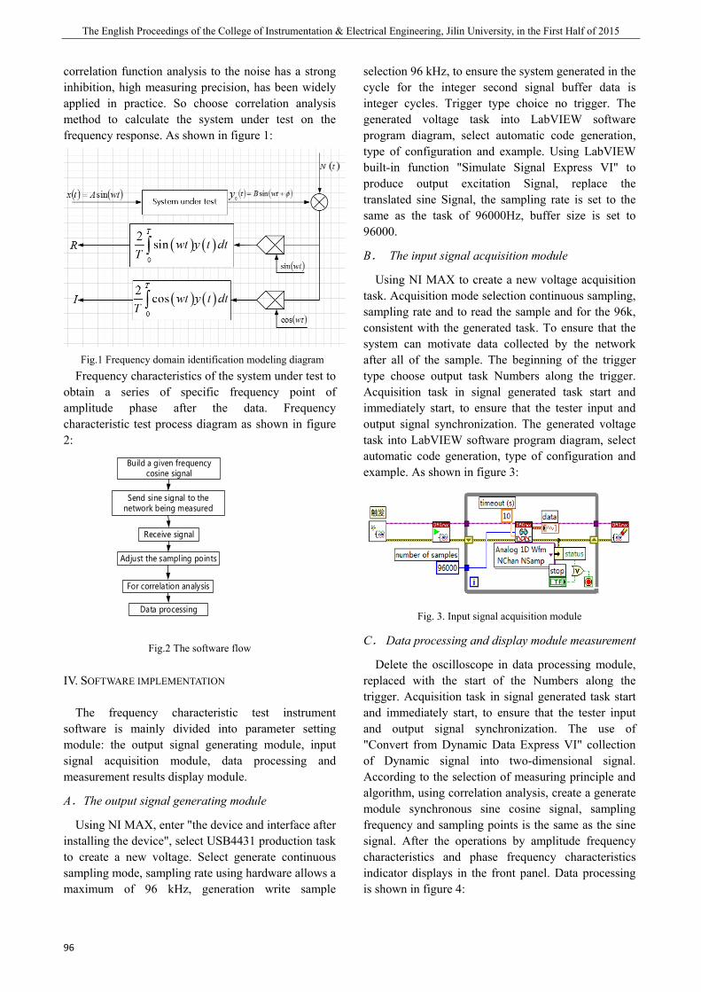
The English Proceedings of the College of Instrumentation & Electrical Engineering, Jilin University, in the First Half of 2015
96
correlation function analysis to the noise has a strong inhibition, high measuring precision, has been widely applied in practice. So choose correlation analysis method to calculate the system under test on the frequency response. As shown in figure 1:
Fig.1 Frequency domain identification modeling diagram Frequency characteristics of the system under test to
obtain a series of specific frequency point of amplitude phase after the data. Frequency characteristic test process diagram as shown in figure 2:
Build a given frequency cosine signal
Send sine signal to the network being measured
Receive signal
Adjust the sampling points
For correlation analysis
Data processing
Fig.2 The software flow
IV. SOFTWARE IMPLEMENTATION
The frequency characteristic test instrument software is mainly divided into parameter setting module: the output signal generating module, input signal acquisition module, data processing and measurement results display module.
A.The output signal generating module
Using NI MAX, enter "the device and interface after installing the device", select USB4431 production task to create a new voltage. Select generate continuous sampling mode, sampling rate using hardware allows a maximum of 96 kHz, generation write sample
selection 96 kHz, to ensure the system generated in the cycle for the integer second signal buffer data is integer cycles. Trigger type choice no trigger. The generated voltage task into LabVIEW software program diagram, select automatic code generation, type of configuration and example. Using LabVIEW built-in function "Simulate Signal Express VI" to produce output excitation Signal, replace the translated sine Signal, the sampling rate is set to the same as the task of 96000Hz, buffer size is set to 96000.
B. The input signal acquisition module
Using NI MAX to create a new voltage acquisition task. Acquisition mode selection continuous sampling, sampling rate and to read the sample and for the 96k, consistent with the generated task. To ensure that the system can motivate data collected by the network after all of the sample. The beginning of the trigger type choose output task Numbers along the trigger. Acquisition task in signal generated task start and immediately start, to ensure that the tester input and output signal synchronization. The generated voltage task into LabVIEW software program diagram, select automatic code generation, type of configuration and example. As shown in figure 3:
Fig. 3. Input signal acquisition module
C. Data processing and display module measurement
Delete the oscilloscope in data processing module, replaced with the start of the Numbers along the trigger. Acquisition task in signal generated task start and immediately start, to ensure that the tester input and output signal synchronization. The use of "Convert from Dynamic Data Express VI" collection of Dynamic signal into two-dimensional signal. According to the selection of measuring principle and algorithm, using correlation analysis, create a generate module synchronous sine cosine signal, sampling frequency and sampling points is the same as the sine signal. After the operations by amplitude frequency characteristics and phase frequency characteristics indicator displays in the front panel. Data processing is shown in figure 4:
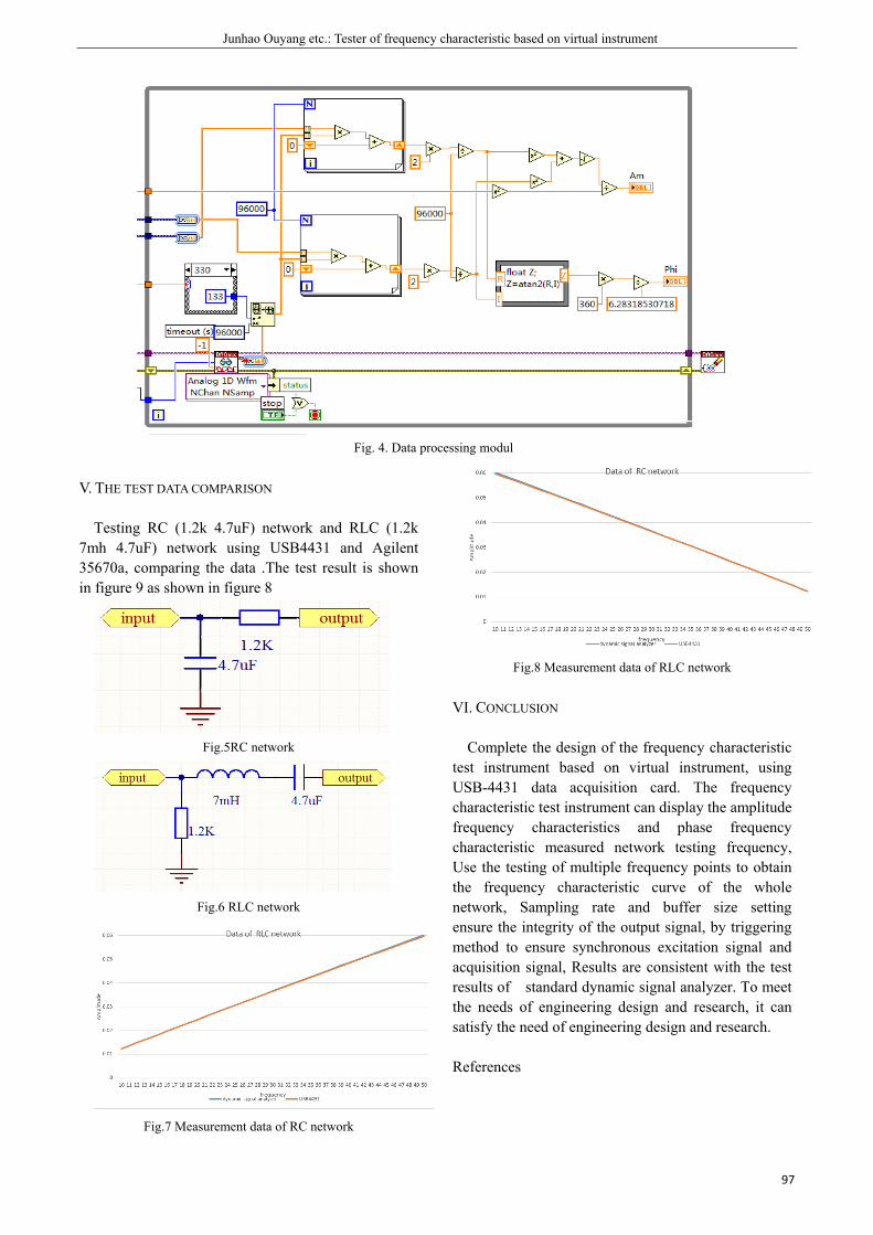
Junhao Ouyang etc.: Tester of frequency characteristic based on virtual instrument
97
Fig. 4. Data processing modul
V. THE TEST DATA COMPARISON
Testing RC (1.2k 4.7uF) network and RLC (1.2k 7mh 4.7uF) network using USB4431 and Agilent 35670a, comparing the data .The test result is shown in figure 9 as shown in figure 8
Fig.5RC network
Fig.6 RLC network
Fig.7 Measurement data of RC network
Fig.8 Measurement data of RLC network
VI. CONCLUSION
Complete the design of the frequency characteristic test instrument based on virtual instrument, using USB-4431 data acquisition card. The frequency characteristic test instrument can display the amplitude frequency characteristics and phase frequency characteristic measured network testing frequency, Use the testing of multiple frequency points to obtain the frequency characteristic curve of the whole network, Sampling rate and buffer size setting ensure the integrity of the output signal, by triggering method to ensure synchronous excitation signal and acquisition signal, Results are consistent with the test results of standard dynamic signal analyzer. To meet the needs of engineering design and research, it can satisfy the need of engineering design and research.
References

The English Proceedings of the College of Instrumentation & Electrical Engineering, Jilin University, in the First Half of 2015
98
[24] Zong Rong Fang. The design of frequency characteristic
tester based on virtual instrument technology [J].
Instrument technique and sensor. 2010, 10 (3) : 24-26
[25] XueYuanyuan, frequency characteristic test instrument
virtual instrument design [J]. Journal of measurement and
control technology. 2009, 12 (1) : 11-12
[26] XuanZhaoYan. The design of frequency characteristic
tester based on virtual instrument technology [J].
Instrument technique and sensor. 2010, 10 (3) : 24-26
[27] Jian-rong cao qing-mei yao,. The frequency characteristic
test instrument based on LabVIEW design [J]. Instrument
technology. 2003, 10 (3) : 20-21
[28] Zhu Jiangle. Low frequency sweep meter based on
virtual instrument technology research [D]. Xi 'an:
northwestern poly technical university, 2007.
[29] Ye Ji xin Hou Guobing, zhao xu. Under the environment
of virtual instrument frequency characteristic test method
[J]. Electric measurement and instrument, 2005, (6).
[30] Fan Shixiong, da-peng fan, zhang zhi4 courageously.
Electromechanical device frequency characteristic of
digital test method research [J]. Journal of dynamics and
control, 2007, 5 (1)
[31] Zhang am. Automatic control principle [M]. Beijing:
tsinghua university press, 2006.
[32] National Instruments Shanghai branch. Virtual instrument
testing and the best choice of the measurement and control
instrument [J]. Mechanical and electrical integration, 2000
(2)
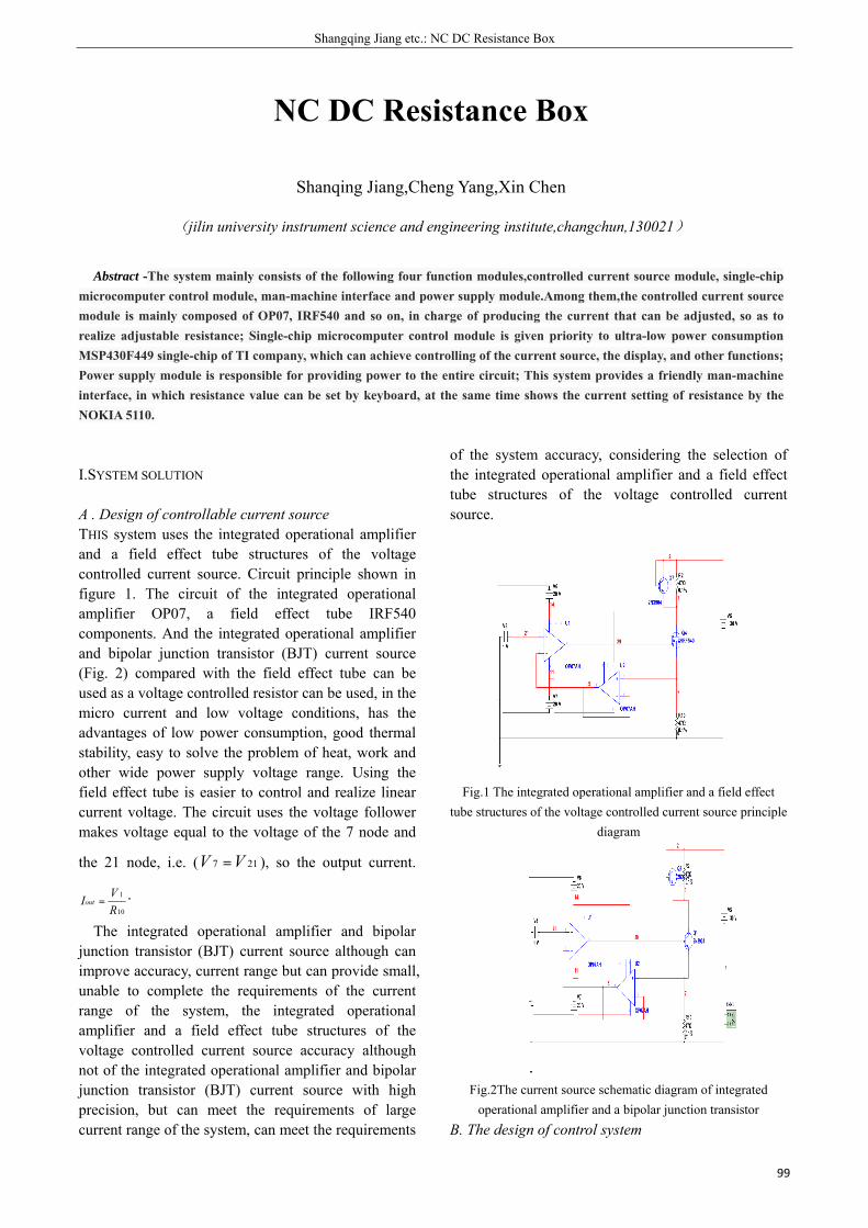
Shangqing Jiang etc.: NC DC Resistance Box
99
NC DC Resistance Box
Shanqing Jiang,Cheng Yang,Xin Chen
(jilin university instrument science and engineering institute,changchun,130021)
Abstract -The system mainly consists of the following four function modules,controlled current source module, single-chip
microcomputer control module, man-machine interface and power supply module.Among them,the controlled current source module is mainly composed of OP07, IRF540 and so on, in charge of producing the current that can be adjusted, so as to realize adjustable resistance; Single-chip microcomputer control module is given priority to ultra-low power consumption MSP430F449 single-chip of TI company, which can achieve controlling of the current source, the display, and other functions; Power supply module is responsible for providing power to the entire circuit; This system provides a friendly man-machine interface, in which resistance value can be set by keyboard, at the same time shows the current setting of resistance by the NOKIA 5110.
I.SYSTEM SOLUTION
A . Design of controllable current source THIS system uses the integrated operational amplifier and a field effect tube structures of the voltage controlled current source. Circuit principle shown in figure 1. The circuit of the integrated operational amplifier OP07, a field effect tube IRF540 components. And the integrated operational amplifier and bipolar junction transistor (BJT) current source (Fig. 2) compared with the field effect tube can be used as a voltage controlled resistor can be used, in the micro current and low voltage conditions, has the advantages of low power consumption, good thermal stability, easy to solve the problem of heat, work and other wide power supply voltage range. Using the field effect tube is easier to control and realize linear current voltage. The circuit uses the voltage follower makes voltage equal to the voltage of the 7 node and
the 21 node, i.e. ( 217 VV = ), so the output current.
10
1
RVIout = .
The integrated operational amplifier and bipolar junction transistor (BJT) current source although can improve accuracy, current range but can provide small, unable to complete the requirements of the current range of the system, the integrated operational amplifier and a field effect tube structures of the voltage controlled current source accuracy although not of the integrated operational amplifier and bipolar junction transistor (BJT) current source with high precision, but can meet the requirements of large current range of the system, can meet the requirements
of the system accuracy, considering the selection of the integrated operational amplifier and a field effect tube structures of the voltage controlled current source.
Fig.1 The integrated operational amplifier and a field effect tube structures of the voltage controlled current source principle
diagram
Fig.2The current source schematic diagram of integrated
operational amplifier and a bipolar junction transistor B. The design of control system
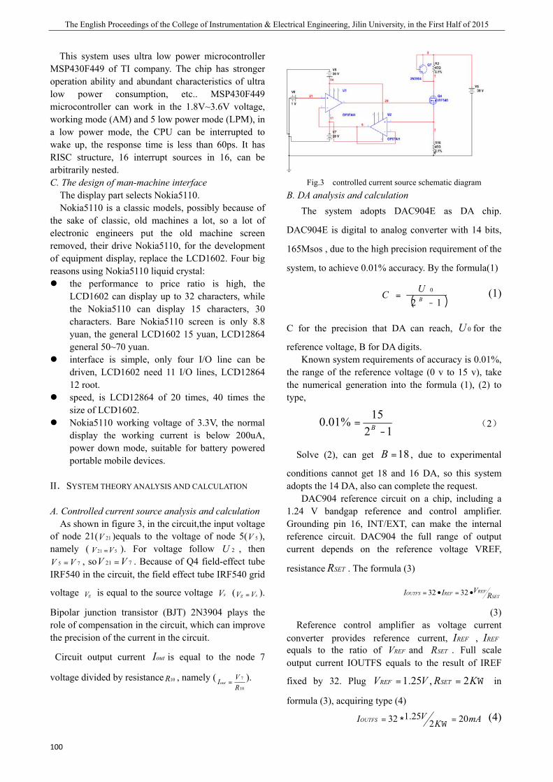
The English Proceedings of the College of Instrumentation & Electrical Engineering, Jilin University, in the First Half of 2015
100
This system uses ultra low power microcontroller MSP430F449 of TI company. The chip has stronger operation ability and abundant characteristics of ultra low power consumption, etc.. MSP430F449 microcontroller can work in the 1.8V~3.6V voltage, working mode (AM) and 5 low power mode (LPM), in a low power mode, the CPU can be interrupted to wake up, the response time is less than 60ps. It has RISC structure, 16 interrupt sources in 16, can be arbitrarily nested. C. The design of man-machine interface
The display part selects Nokia5110. Nokia5110 is a classic models, possibly because of the sake of classic, old machines a lot, so a lot of electronic engineers put the old machine screen removed, their drive Nokia5110, for the development of equipment display, replace the LCD1602. Four big reasons using Nokia5110 liquid crystal:
the performance to price ratio is high, the LCD1602 can display up to 32 characters, while the Nokia5110 can display 15 characters, 30 characters. Bare Nokia5110 screen is only 8.8 yuan, the general LCD1602 15 yuan, LCD12864 general 50~70 yuan.
interface is simple, only four I/O line can be driven, LCD1602 need 11 I/O lines, LCD12864 12 root.
speed, is LCD12864 of 20 times, 40 times the size of LCD1602.
Nokia5110 working voltage of 3.3V, the normal display the working current is below 200uA, power down mode, suitable for battery powered portable mobile devices.
II.SYSTEM THEORY ANALYSIS AND CALCULATION
A. Controlled current source analysis and calculation As shown in figure 3, in the circuit,the input voltage of node 21( 21V )equals to the voltage of node 5( 5V ), namely ( 521 VV = ). For voltage follow 2U , then
75 VV = , so 721 VV = . Because of Q4 field-effect tube IRF540 in the circuit, the field effect tube IRF540 grid
voltage gV is equal to the source voltage sV ( sg VV = ).
Bipolar junction transistor (BJT) 2N3904 plays the role of compensation in the circuit, which can improve the precision of the current in the circuit.
Circuit output current outI is equal to the node 7
voltage divided by resistance 10R , namely (10
7
RVIout = ).
Fig.3 controlled current source schematic diagram
B. DA analysis and calculation The system adopts DAC904E as DA chip.
DAC904E is digital to analog converter with 14 bits,
165Msos , due to the high precision requirement of the
system, to achieve 0.01% accuracy. By the formula(1)
( )120
-= B
UC (1)
C for the precision that DA can reach, 0U for the
reference voltage, B for DA digits. Known system requirements of accuracy is 0.01%, the range of the reference voltage (0 v to 15 v), take the numerical generation into the formula (1), (2) to type,
1215%01.0-
= B (2)
Solve (2), can get 18=B , due to experimental
conditions cannot get 18 and 16 DA, so this system adopts the 14 DA, also can complete the request. DAC904 reference circuit on a chip, including a 1.24 V bandgap reference and control amplifier. Grounding pin 16, INT/EXT, can make the internal reference circuit. DAC904 the full range of output current depends on the reference voltage VREF,
resistance SETR . The formula (3)
SET
REFREFOUTFS RVII •=•= 3232
(3) Reference control amplifier as voltage current converter provides reference current, REFI , REFI equals to the ratio of REFV and SETR . Full scale output current IOUTFS equals to the result of IREF
fixed by 32. Plug W== KRVV SETREF 2,25.1 in
formula (3), acquiring type (4)
mAKVIOUTFS 202
25.132 =W*= (4)
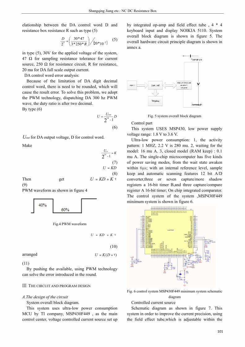
Shangqing Jiang etc.: NC DC Resistance Box
101
elationship between the DA control word D and resistance box resistance R such as type (5)
( )10*20*250*347*30
2 314 -⎟⎠⎞
⎜⎝⎛
=R
D (5)
in type (5), 30V for the applied voltage of the system, 47 Ω for sampling resistance tolerance for current source, 250 Ω for resistance circuit, R for resistance, 20 ma for DA full scale output current.
DA control word error analysis: Because of the limitation of DA digit decimal control word, there is need to be rounded, which will cause the result error. To solve this problem, we adopt the PWM technology, dispatching DA 300 hz PWM wave, the duty ratio is after two decimal. By type (6)
DUU out
1214-
=
(6)
outU for DA output voltage, D for control word.
Make
KUout=
-1214
(7) KDU =
(8) Then get τKKDU += (9) PWM waveform as shown in figure 4
Fig.4 PWM waveform
τKKDU +=
(10)
arranged )( τ+= DKU
(11) By pushing the available, using PWM technology
can solve the error introduced in the round.
Ⅲ THE CIRCUIT AND PROGRAM DESIGN
A.The design of the circuit System overall block diagram. This system uses ultra-low power consumption MCU by TI company, MSP430F449 , as the main control center, voltage controlled current source set up
by integrated op-amp and field effect tube , 4 * 4 keyboard input and display NOIKIA 5110. System overall block diagram is shown in figure 5. The overall hardware circuit principle diagram is shown in annex a.
Fig. 5 system overall block diagram
Control part This system USES MSP430, low power supply voltage range: 1.8 V to 3.6 V.
Ultra-low power consumption: 1, the activity pattern: 1 MHZ, 2.2 V is 280 mu. 2, waiting for the model: 16 mu A. 3, closed model (RAM keep) : 0.1 mu A. The single-chip microcomputer has five kinds of power saving modes, from the wait state awaken within 6μs; with an internal reference level, sample keep and automatic scanning features 12 bit A/D converter,three or seven capture/more shadow registers a 16-bit timer B,and three capture/compare register A 16-bit timer; On chip integrated comparator. The control system of the system ,MSP430F449 minimum system is shown in figure 6.
Fig. 6 control system MSP430F449 minimum system schematic
diagram Controlled current source Schematic diagram as shown in figure 7. This system in order to improve the current precision, using the field effect tube,which is adjustable within the
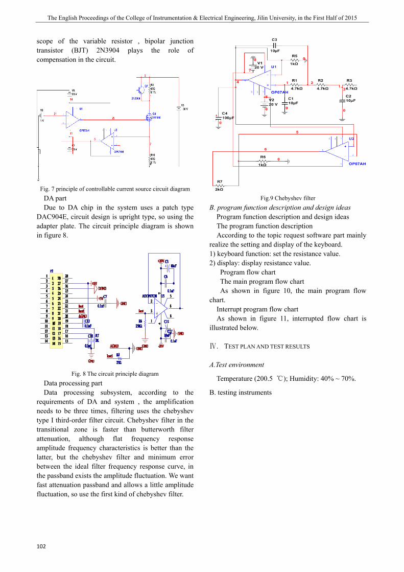
The English Proceedings of the College of Instrumentation & Electrical Engineering, Jilin University, in the First Half of 2015
102
scope of the variable resistor , bipolar junction transistor (BJT) 2N3904 plays the role of compensation in the circuit.
Fig. 7 principle of controllable current source circuit diagram
DA part Due to DA chip in the system uses a patch type DAC904E, circuit design is upright type, so using the adapter plate. The circuit principle diagram is shown in figure 8.
Fig. 8 The circuit principle diagram
Data processing part Data processing subsystem, according to the requirements of DA and system , the amplification needs to be three times, filtering uses the chebyshev type I third-order filter circuit. Chebyshev filter in the transitional zone is faster than butterworth filter attenuation, although flat frequency response amplitude frequency characteristics is better than the latter, but the chebyshev filter and minimum error between the ideal filter frequency response curve, in the passband exists the amplitude fluctuation. We want fast attenuation passband and allows a little amplitude fluctuation, so use the first kind of chebyshev filter.
Fig.9 Chebyshev filter
B. program function description and design ideas Program function description and design ideas The program function description According to the topic request software part mainly realize the setting and display of the keyboard. 1) keyboard function: set the resistance value. 2) display: display resistance value. Program flow chart The main program flow chart As shown in figure 10, the main program flow chart. Interrupt program flow chart As shown in figure 11, interrupted flow chart is illustrated below.
Ⅳ. TEST PLAN AND TEST RESULTS
A.Test environment
Temperature (200.5 ); Humidity: 40% ~ 70%.
B. testing instruments
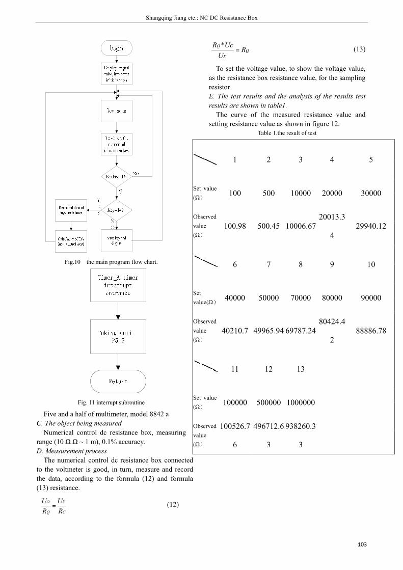
Shangqing Jiang etc.: NC DC Resistance Box
103
Fig.10 the main program flow chart.
Fig. 11 interrupt subroutine
Five and a half of multimeter, model 8842 a C. The object being measured
Numerical control dc resistance box, measuring range (10 Ω Ω ~ 1 m), 0.1% accuracy. D. Measurement process
The numerical control dc resistance box connected to the voltmeter is good, in turn, measure and record the data, according to the formula (12) and formula (13) resistance.
C
X
Q
O
RU
RU
= (12)
QX
Q RU
UcR=
* (13)
To set the voltage value, to show the voltage value, as the resistance box resistance value, for the sampling resistor E. The test results and the analysis of the results test results are shown in table1.
The curve of the measured resistance value and setting resistance value as shown in figure 12.
Table 1.the result of test
1 2 3 4 5
Set value (Ω) 100 500 10000 20000 30000
Observed value (Ω)
100.98 500.45 10006.67 20013.3
4 29940.12
6 7 8 9 10
Set value(Ω) 40000 50000 70000 80000 90000
Observed value (Ω)
40210.7 49965.94 69787.24 80424.4
2 88886.78
11 12 13
Set value (Ω) 100000 500000 1000000
Observed value (Ω)
100526.7
6
496712.6
3
938260.3
3

The English Proceedings of the College of Instrumentation & Electrical Engineering, Jilin University, in the First Half of 2015
104
0 2 4 6 8 10 12 140
1
2
3
4
5
6
7
8
9
10x 105
Fig. 12 the measured resistance value and set the resistance
curve The measured resistance value and the setting value of resistance curve in Figure 12 the solid line in Figure 12 as the setting value, star line were measured value.
Ⅴ. CONCLUSION
From the test results that the measured resistance value relation curves and setting the resistance value, the system can carry out the resistance value range is 100 ~ 1M Omega set through the keyboard, and the resistance of the accuracy can reach 0.1%, the resistance power of not less than 1W.
References
[1] Yi Lingzhi.Wang Genping.Peng Hanmei.The Design of
Digital Resistance Box with Power Source[J].Metrology
and Measurement Technique,2004(7):9-11
[2] He Xianhua.Luo Xuefeng.The Design of Digital Resistance
Box with Power Source[J].Weekend Digest Composition
Guide,2006(1):10-13
[3] Wu Haiming.The design of voice resistance box[J].IT
Time,2014(300):23-25
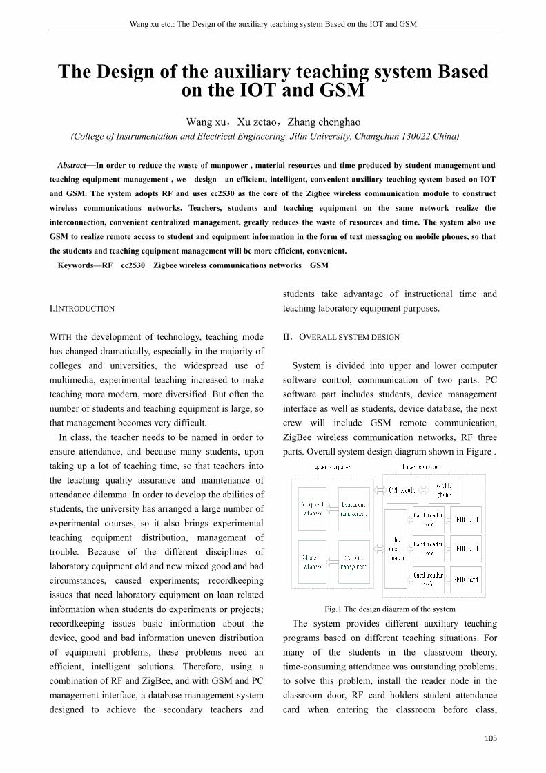
Wang xu etc.: The Design of the auxiliary teaching system Based on the IOT and GSM
105
The Design of the auxiliary teaching system Based on the IOT and GSM
Wang xu,Xu zetao,Zhang chenghao
(College of Instrumentation and Electrical Engineering, Jilin University, Changchun 130022,China)
Abstract—In order to reduce the waste of manpower , material resources and time produced by student management and
teaching equipment management , we design an efficient, intelligent, convenient auxiliary teaching system based on IOT
and GSM. The system adopts RF and uses cc2530 as the core of the Zigbee wireless communication module to construct
wireless communications networks. Teachers, students and teaching equipment on the same network realize the
interconnection, convenient centralized management, greatly reduces the waste of resources and time. The system also use
GSM to realize remote access to student and equipment information in the form of text messaging on mobile phones, so that
the students and teaching equipment management will be more efficient, convenient.
Keywords—RF cc2530 Zigbee wireless communications networks GSM
I.INTRODUCTION
WITH the development of technology, teaching mode has changed dramatically, especially in the majority of colleges and universities, the widespread use of multimedia, experimental teaching increased to make teaching more modern, more diversified. But often the number of students and teaching equipment is large, so that management becomes very difficult.
In class, the teacher needs to be named in order to ensure attendance, and because many students, upon taking up a lot of teaching time, so that teachers into the teaching quality assurance and maintenance of attendance dilemma. In order to develop the abilities of students, the university has arranged a large number of experimental courses, so it also brings experimental teaching equipment distribution, management of trouble. Because of the different disciplines of laboratory equipment old and new mixed good and bad circumstances, caused experiments; recordkeeping issues that need laboratory equipment on loan related information when students do experiments or projects; recordkeeping issues basic information about the device, good and bad information uneven distribution of equipment problems, these problems need an efficient, intelligent solutions. Therefore, using a combination of RF and ZigBee, and with GSM and PC management interface, a database management system designed to achieve the secondary teachers and
students take advantage of instructional time and teaching laboratory equipment purposes.
II.OVERALL SYSTEM DESIGN
System is divided into upper and lower computer software control, communication of two parts. PC software part includes students, device management interface as well as students, device database, the next crew will include GSM remote communication, ZigBee wireless communication networks, RF three parts. Overall system design diagram shown in Figure .
Fig.1 The design diagram of the system
The system provides different auxiliary teaching programs based on different teaching situations. For many of the students in the classroom theory, time-consuming attendance was outstanding problems, to solve this problem, install the reader node in the classroom door, RF card holders student attendance card when entering the classroom before class,
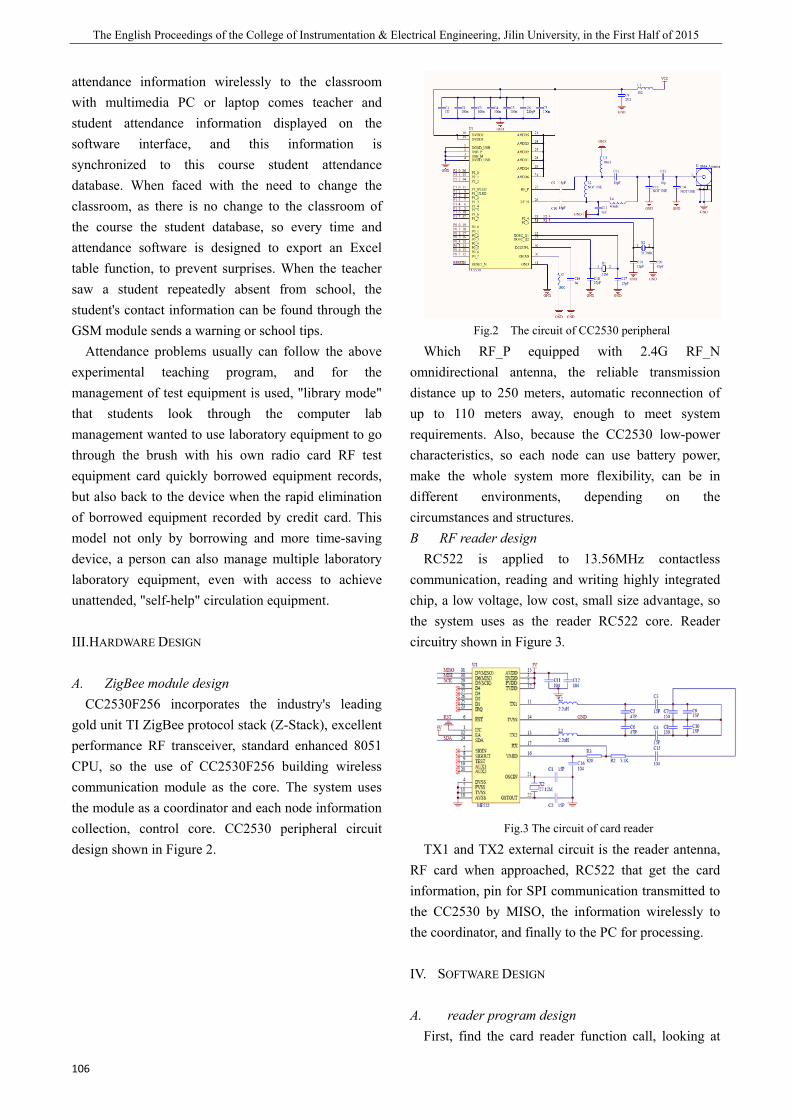
The English Proceedings of the College of Instrumentation & Electrical Engineering, Jilin University, in the First Half of 2015
106
attendance information wirelessly to the classroom with multimedia PC or laptop comes teacher and student attendance information displayed on the software interface, and this information is synchronized to this course student attendance database. When faced with the need to change the classroom, as there is no change to the classroom of the course the student database, so every time and attendance software is designed to export an Excel table function, to prevent surprises. When the teacher saw a student repeatedly absent from school, the student's contact information can be found through the GSM module sends a warning or school tips.
Attendance problems usually can follow the above experimental teaching program, and for the management of test equipment is used, "library mode" that students look through the computer lab management wanted to use laboratory equipment to go through the brush with his own radio card RF test equipment card quickly borrowed equipment records, but also back to the device when the rapid elimination of borrowed equipment recorded by credit card. This model not only by borrowing and more time-saving device, a person can also manage multiple laboratory laboratory equipment, even with access to achieve unattended, "self-help" circulation equipment.
III.HARDWARE DESIGN
A. ZigBee module design CC2530F256 incorporates the industry's leading
gold unit TI ZigBee protocol stack (Z-Stack), excellent performance RF transceiver, standard enhanced 8051 CPU, so the use of CC2530F256 building wireless communication module as the core. The system uses the module as a coordinator and each node information collection, control core. CC2530 peripheral circuit design shown in Figure 2.
Fig.2 The circuit of CC2530 peripheral
Which RF_P equipped with 2.4G RF_N omnidirectional antenna, the reliable transmission distance up to 250 meters, automatic reconnection of up to 110 meters away, enough to meet system requirements. Also, because the CC2530 low-power characteristics, so each node can use battery power, make the whole system more flexibility, can be in different environments, depending on the circumstances and structures. B RF reader design
RC522 is applied to 13.56MHz contactless communication, reading and writing highly integrated chip, a low voltage, low cost, small size advantage, so the system uses as the reader RC522 core. Reader circuitry shown in Figure 3.
Fig.3 The circuit of card reader
TX1 and TX2 external circuit is the reader antenna, RF card when approached, RC522 that get the card information, pin for SPI communication transmitted to the CC2530 by MISO, the information wirelessly to the coordinator, and finally to the PC for processing.
IV. SOFTWARE DESIGN
A. reader program design First, find the card reader function call, looking at
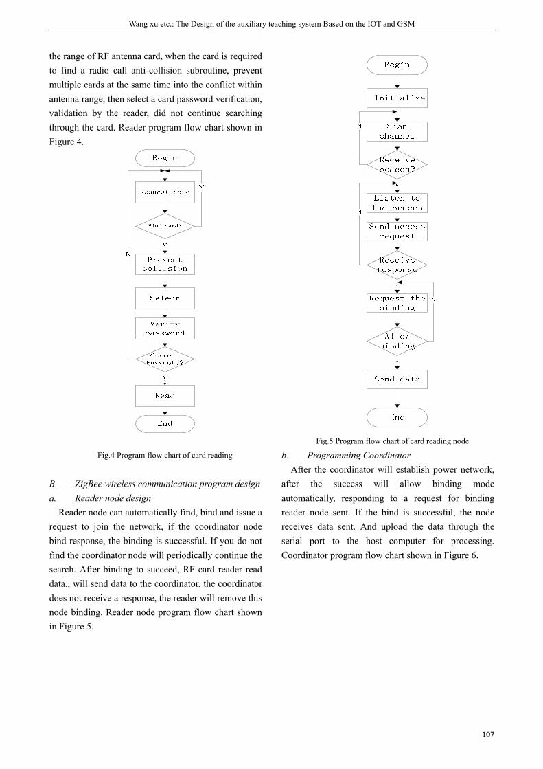
Wang xu etc.: The Design of the auxiliary teaching system Based on the IOT and GSM
107
the range of RF antenna card, when the card is required to find a radio call anti-collision subroutine, prevent multiple cards at the same time into the conflict within antenna range, then select a card password verification, validation by the reader, did not continue searching through the card. Reader program flow chart shown in Figure 4.
Fig.4 Program flow chart of card reading
B. ZigBee wireless communication program design a. Reader node design
Reader node can automatically find, bind and issue a request to join the network, if the coordinator node bind response, the binding is successful. If you do not find the coordinator node will periodically continue the search. After binding to succeed, RF card reader read data,, will send data to the coordinator, the coordinator does not receive a response, the reader will remove this node binding. Reader node program flow chart shown in Figure 5.
Fig.5 Program flow chart of card reading node
b. Programming Coordinator After the coordinator will establish power network,
after the success will allow binding mode automatically, responding to a request for binding reader node sent. If the bind is successful, the node receives data sent. And upload the data through the serial port to the host computer for processing. Coordinator program flow chart shown in Figure 6.
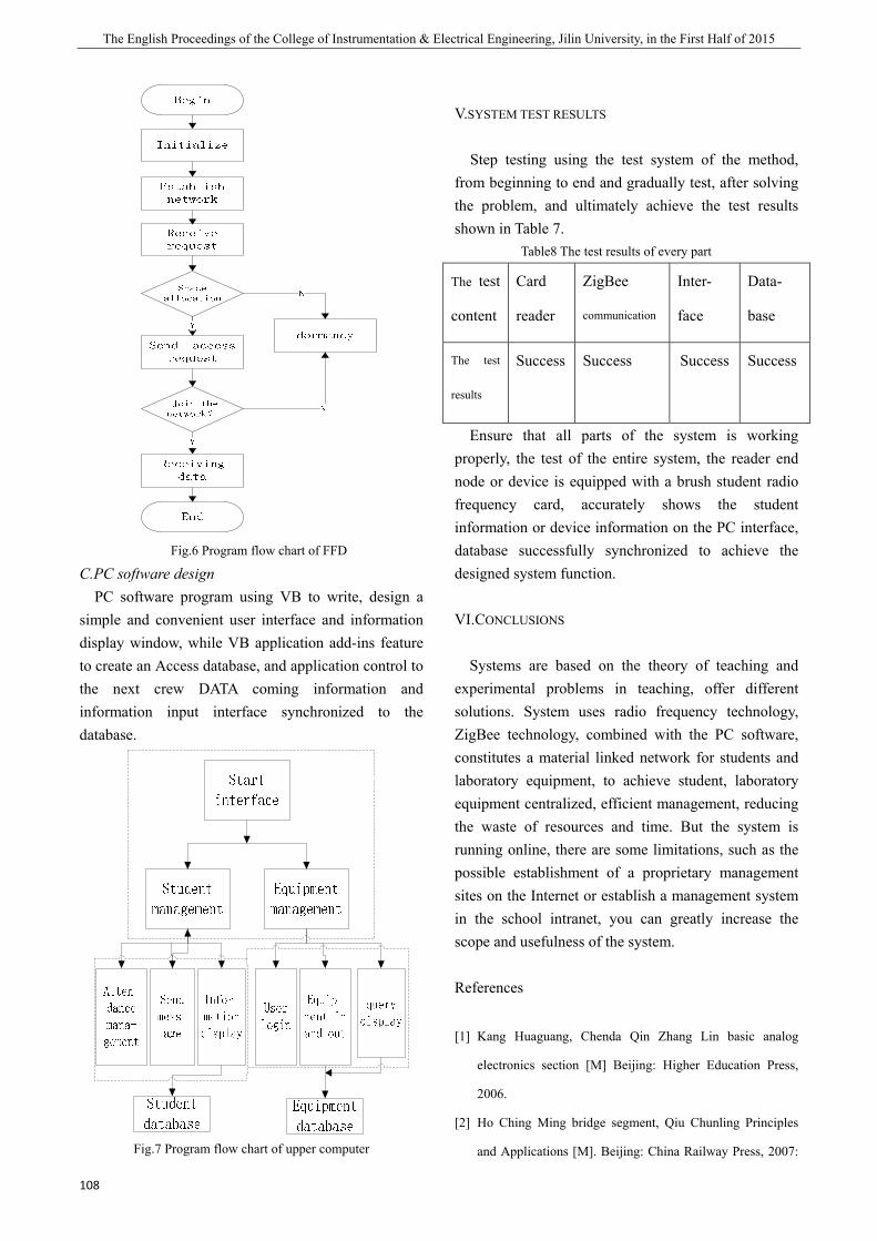
The English Proceedings of the College of Instrumentation & Electrical Engineering, Jilin University, in the First Half of 2015
108
Fig.6 Program flow chart of FFD
C.PC software design PC software program using VB to write, design a
simple and convenient user interface and information display window, while VB application add-ins feature to create an Access database, and application control to the next crew DATA coming information and information input interface synchronized to the database.
Fig.7 Program flow chart of upper computer
V.SYSTEM TEST RESULTS
Step testing using the test system of the method, from beginning to end and gradually test, after solving the problem, and ultimately achieve the test results shown in Table 7.
Table8 The test results of every part
The test
content
Card
reader
ZigBee
communication
Inter-
face
Data-
base
The test
results
Success Success Success Success
Ensure that all parts of the system is working properly, the test of the entire system, the reader end node or device is equipped with a brush student radio frequency card, accurately shows the student information or device information on the PC interface, database successfully synchronized to achieve the designed system function.
VI.CONCLUSIONS
Systems are based on the theory of teaching and experimental problems in teaching, offer different solutions. System uses radio frequency technology, ZigBee technology, combined with the PC software, constitutes a material linked network for students and laboratory equipment, to achieve student, laboratory equipment centralized, efficient management, reducing the waste of resources and time. But the system is running online, there are some limitations, such as the possible establishment of a proprietary management sites on the Internet or establish a management system in the school intranet, you can greatly increase the scope and usefulness of the system.
References
[1] Kang Huaguang, Chenda Qin Zhang Lin basic analog
electronics section [M] Beijing: Higher Education Press,
2006.
[2] Ho Ching Ming bridge segment, Qiu Chunling Principles
and Applications [M]. Beijing: China Railway Press, 2007:

Wang xu etc.: The Design of the auxiliary teaching system Based on the IOT and GSM
109
169-187.
[3] Jiang Zhong, Dan ZigBee technology and training tutorial
[M] Beijing: Tsinghua University Press, 2014: 296-316.
[4] Huangjun Xiang MFRC522 based RFID readers module
design [D] ITS APPLICATIONS, 2010: 19.
[5] Linai Wei non-contact IC card reader module MFRC522
working principle and application [J] electronic devices,
2003,26 (2): 160 ~ 162.
[6] Ye Wei, Hu Jun reached based on TC35i GSM short
messaging system [J] test and measurement technology,
2008 (6): 27 - 29.
[7] Support Break Hu Yongzhong application design CC2530
ZigBee-based communication network [J] Electronic
Design Engineering, 2011,19 (16): 108--111.
[8] Deng Yun, Cheng Xiaohui designed for smart home
networking system [J] Guilin University of Technology,
2012,32 (2): 259-264.
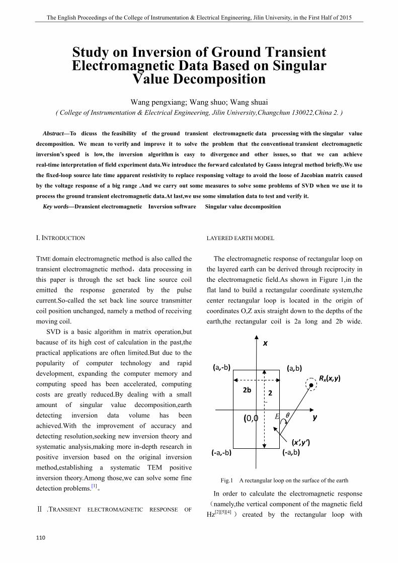
The English Proceedings of the College of Instrumentation & Electrical Engineering, Jilin University, in the First Half of 2015
110
Study on Inversion of Ground Transient Electromagnetic Data Based on Singular
Value Decomposition
Wang pengxiang; Wang shuo; Wang shuai
( College of Instrumentation & Electrical Engineering, Jilin University,Changchun 130022,China 2. )
Abstract—To dicuss the feasibility of the ground transient electromagnetic data processing with the singular value
decomposition. We mean to verify and improve it to solve the problem that the conventional transient electromagnetic
inversion’s speed is low, the inversion algorithm is easy to divergence and other issues, so that we can achieve
real-time interpretation of field experiment data.We introduce the forward calculated by Gauss integral method briefly.We use
the fixed-loop source late time apparent resistivity to replace responsing voltage to avoid the loose of Jacobian matrix caused
by the voltage response of a big range .And we carry out some measures to solve some problems of SVD when we use it to
process the ground transient electromagnetic data.At last,we use some simulation data to test and verify it.
Key words—Dransient electromagnetic Inversion software Singular value decomposition
I. INTRODUCTION
TIME domain electromagnetic method is also called the transient electromagnetic method,data processing in this paper is through the set back line source coil emitted the response generated by the pulse current.So-called the set back line source transmitter coil position unchanged, namely a method of receiving moving coil.
SVD is a basic algorithm in matrix operation,but bacause of its high cost of calculation in the past,the practical applications are often limited.But due to the popularity of computer technology and rapid development, expanding the computer memory and computing speed has been accelerated, computing costs are greatly reduced.By dealing with a small amount of singular value decomposition,earth detecting inversion data volume has been achieved.With the improvement of accuracy and detecting resolution,seeking new inversion theory and systematic analysis,making more in-depth research in positive inversion based on the original inversion method,establishing a systematic TEM positive inversion theory.Among those,we can solve some fine detection problems.[1]。
Ⅱ .TRANSIENT ELECTROMAGNETIC RESPONSE OF
LAYERED EARTH MODEL
The electromagnetic response of rectangular loop on the layered earth can be derived through reciprocity in the electromagnetic field.As shown in Figure 1,in the flat land to build a rectangular coordinate system,the center rectangular loop is located in the origin of coordinates O,Z axis straight down to the depths of the earth,the rectangular coil is 2a long and 2b wide.
Fig.1 A rectangular loop on the surface of the earth
In order to calculate the electromagnetic response(namely,the vertical component of the magnetic field Hz[2][5][4] ) created by the rectangular loop with
(a,-b)
(-a,-b)
(a,b)
(0,0
2b 2
a
Rx(x,y)
y
(-a,b)
θ
(x’,y’)
Ef
x
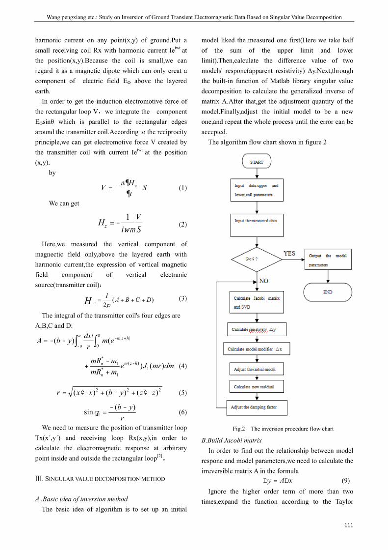
Wang pengxiang etc.: Study on Inversion of Ground Transient Electromagnetic Data Based on Singular Value Decomposition
111
harmonic current on any point(x,y) of ground.Put a small receiving coil Rx with harmonic current Ieiwt at the position(x,y).Because the coil is small,we can regard it as a magnetic dipote which can only creat a component of electric field EΦ above the layered earth.
In order to get the induction electromotive force of the rectangular loop V,we integrate the component EΦsinθ which is parallel to the rectangular edges around the transmitter coil.According to the reciprocity principle,we can get electromotive force V created by the transmitter coil with current Ieiwt at the position (x,y).
by
StHV z
¶-=m
(1)
We can get
SV
iHz wm
1-= (2)
Here,we measured the vertical component of magnectic field only,above the layered earth with harmonic current,the expression of vertical magnetic field component of vertical electranic source(transmitter coil):
( )2zI A B C DH p
= + + + (3)
The integral of the transmitter coil's four edges are A,B,C and D:
||
0()( hzma
aem
rxdybA +-¥
- ∫∫¢
--=
dmmrJemmRmmR hzm
n
n )() 1)(
1*
1*
-
+
-+ (4)
222 )()()( zzybxxr -¢+-+-¢= (5)
ryb )(sin 1
--=q (6)
We need to measure the position of transmitter loop Tx(x´,y´) and receiving loop Rx(x,y),in order to calculate the electromagnetic response at arbitrary point inside and outside the rectangular loop[2]。
Ⅲ. SINGULAR VALUE DECOMPOSITION METHOD
A .Basic idea of inversion method The basic idea of algorithm is to set up an initial
model liked the measured one first(Here we take half of the sum of the upper limit and lower limit).Then,calculate the difference value of two models' respone(apparent resistivity) Δy.Next,through the built-in function of Matlab library singular value decomposition to calculate the generalized inverse of matrix A.After that,get the adjustment quantity of the model.Finally,adjust the initial model to be a new one,and repeat the whole process until the error can be accepted.
The algorithm flow chart shown in figure 2
Fig.2 The inversion procedure flow chart
B.Build Jacobi matrix In order to find out the relationship between model
respone and model parameters,we need to calculate the irreversible matrix A in the formula
xAy D=D (9) Ignore the higher order term of more than two
times,expand the function according to the Taylor
The English Proceedings of the College of Instrumentation & Electrical Engineering, Jilin University, in the First Half of 2015
112
formula in the neighborhood of an initial model,we can get the element aij in the matrix A
i
iij x
xfa
¶=
)( (10)
The function is a very complicated multivariate function,we can't calculate its first order partial derivative,so we use approximate value to replace the first order partial derivative[3]。
j
kjk
j xxifxxif
xxf
-+=
¶ ),(),()( d (11)
Among them jx¶ equals to 0.001.
C.SVD To solve the linear system of equations bAx = is
the basic issue of inversion interpretation of transient electromagnetic data.A is a irreversible matrix mn· 。
SVD and the least-squares method are the most commonly used two methods solving this kind of equations[1][8][9]。
Here,by solving the equation (9), we can get the adjustment quantity of the initial model. Δy is apparent resistivity calculated by the measured
voltage data, set it as (M x 1) matrix.Δxis the underground model reduction need to be adjusted,set it as (N×1) matrix.A is for Jacobi matrix(M×N)[1]。
We have known the method of astablish yD and A.We need to calculate the inverse matrix of A to get
xD .But A is a irreversible matrix,so we can only use
the generalized inverse matrix +A to replace 1-A :
yAx D=D +
(12)
In order to get the generalized inverse matrix of A,doing SVD on A
TVUA L= (13)
Among these,U is an unitary matrix MM · ;L is a positive semi-definite diagonal matrix NM · ;as for
TV ,namely the conjugate transpose of V ,is an unitary matrix NN · .The element on the diagonal of L is the sigular value of A.
So that we can get the generalized inverse matrix of A
TUVA+
+ L= (14)
+
L is the pseudo inverse of L
yUVx TDL=D+
(15) D.Enhance convergence inversion method
SVD is mainly based on singular value decomposition theorem,truncating small singular value and keeping large singular value,this inversion method requires high accuracy in estimating the initial model,but its convergence is fast.The least square method is to add a small damping factor d to every singular value.This method has a low convergence speed,but it doesn't require that high accuracy in estimating the initial model. Combine these two inversion method,we use a method of adding damping and truncating singular value at the same time.Through this we achieve the complementary advantages of two methods and good inversion result[3].
When calculate the matrix in (15),it's always the element in the position of the denominator on the diagonal of matrix L (namely the too small singular value)have the effect of the error amplifier.So we usually use the method of truncating SVD or adding damping SVD in actual operation.
Truncating SVD is a method using the larger singular value while laying down the smaller one.Because there is only a part of singular value involved in the operation,the stability of the algorithm is very good,but the model parameter precision is not high[3][4].
Adding damping SVD,(15) wil be changed into
yUIVx TD+LL=D -122 )( e (16)
Adding a quantity 2e to each element on the diagonal of matrix L can avoid the affected by small singular values,and the parameter of matrix won’t be too large in the inversion process.All singular value involved in the operation,improving the precision of model parameters,but due to the damping factor,the estimation precision of the model parameters will be reduced[5].
In order to improve the stability of the algorithm, eliminate the influence of the smaller singular value, ensure the accuracy of the model parameter at the same time,considering all of the advantages and disadvantages of two methods,the project use the method of adding damping truncated singular
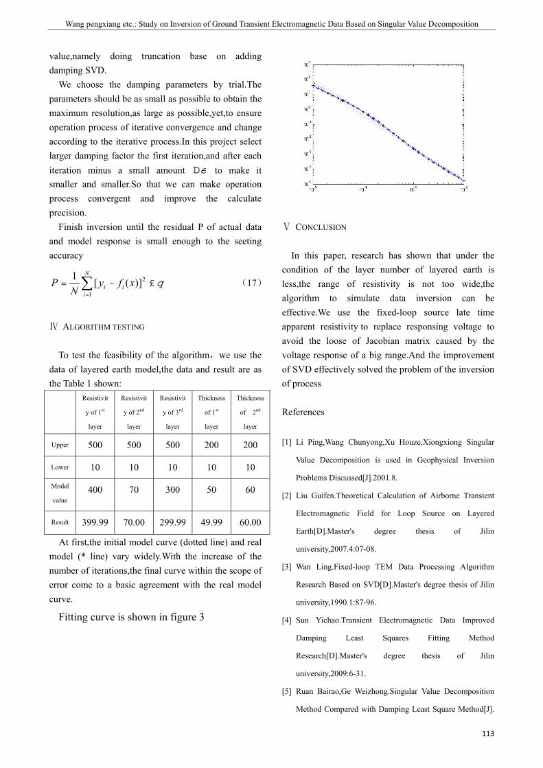
Wang pengxiang etc.: Study on Inversion of Ground Transient Electromagnetic Data Based on Singular Value Decomposition
113
value,namely doing truncation base on adding damping SVD.
We choose the damping parameters by trial.The parameters should be as small as possible to obtain the maximum resolution,as large as possible,yet,to ensure operation process of iterative convergence and change according to the iterative process.In this project select larger damping factor the first iteration,and after each iteration minus a small amount eD to make it smaller and smaller.So that we can make operation process convergent and improve the calculate precision.
Finish inversion until the residual P of actual data and model response is small enough to the seeting accuracy
q£-= ∑=
2
1)]([1 xfy
NP i
N
ii (17)
Ⅳ ALGORITHM TESTING
To test the feasibility of the algorithm,we use the data of layered earth model,the data and result are as the Table 1 shown:
Resistivit
y of 1st
layer
Resistivit
y of 2nd
layer
Resistivit
y of 3rd
layer
Thickness
of 1st
layer
Thickness
of 2nd
layer
Upper 500 500 500 200 200
Lower 10 10 10 10 10
Model
value 400 70 300 50 60
Result 399.99 70.00 299.99 49.99 60.00
At first,the initial model curve (dotted line) and real model (* line) vary widely.With the increase of the number of iterations,the final curve within the scope of error come to a basic agreement with the real model curve.
Fitting curve is shown in figure 3
Ⅴ CONCLUSION
In this paper, research has shown that under the condition of the layer number of layered earth is less,the range of resistivity is not too wide,the algorithm to simulate data inversion can be effective.We use the fixed-loop source late time apparent resistivity to replace responsing voltage to avoid the loose of Jacobian matrix caused by the voltage response of a big range.And the improvement of SVD effectively solved the problem of the inversion of process
References
[1] Li Ping,Wang Chunyong,Xu Houze,Xiongxiong Singular
Value Decomposition is used in Geophysical Inversion
Problems Discussed[J].2001.8.
[2] Liu Guifen.Theoretical Calculation of Airborne Transient
Electromagnetic Field for Loop Source on Layered
Earth[D].Master's degree thesis of Jilin
university,2007.4:07-08.
[3] Wan Ling.Fixed-loop TEM Data Processing Algorithm
Research Based on SVD[D].Master's degree thesis of Jilin
university,1990.1:87-96.
[4] Sun Yichao.Transient Electromagnetic Data Improved
Damping Least Squares Fitting Method
Research[D].Master's degree thesis of Jilin
university,2009:6-31.
[5] Ruan Bairao,Ge Weizhong.Singular Value Decomposition
Method Compared with Damping Least Square Method[J].

The English Proceedings of the College of Instrumentation & Electrical Engineering, Jilin University, in the First Half of 2015
114
Geophysical computing technology,1997.2:47-49
[6] Pang Xueliang,Lin Chunsheng,Zhang Ning.The Plane
Magnetic Field Model Coefficient of Truncated Singular
Value Decomposition Method to Estimate[J].Journal of
detection and control,2009.10:49-51.
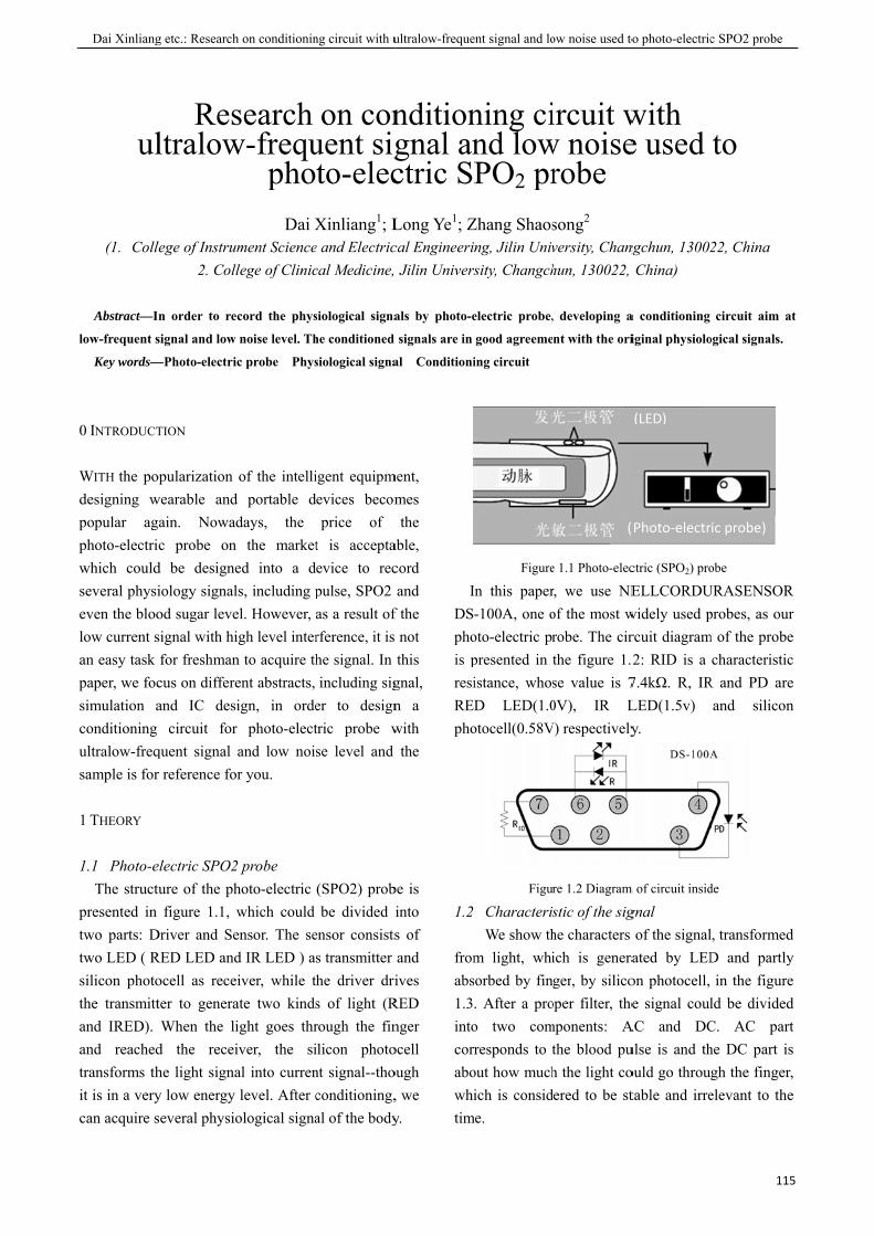
Dai Xinliang
ul
(1. Coll
Abstract—I
low-frequent s
Key words—
0 INTRODUCT
WITH the podesigning wpopular agphoto-electriwhich couldseveral physieven the bloolow current san easy task paper, we focsimulation aconditioning ultralow-freqsample is for
1 THEORY
1.1 Photo-eThe struct
presented in two parts: Dtwo LED ( Rsilicon photothe transmittand IRED). and reachedtransforms thit is in a verycan acquire s
g etc.: Research
Resltralow
lege of Instrum2. Coll
n order to re
signal and low
—Photo-electric
TION
opularization wearable andgain. Nowadc probe on
d be designeiology signalod sugar levesignal with hifor freshmancus on differeand IC desi
circuit forquent signal r reference fo
electric SPO2ture of the ph
figure 1.1, wDriver and SeRED LED andocell as receter to generaWhen the li
d the receihe light signay low energy several physio
h on conditionin
search w-frequ
phoDai X
ment Sciencelege of Clinic
cord the phys
noise level. Th
c probe Phys
of the intellid portable ddays, the
the marketed into a dls, including pel. However, igh level intern to acquire thent abstracts, ign, in orde
r photo-electand low noir you.
2 probe hoto-electric which could ensor. The sed IR LED ) aiver, while t
ate two kindsight goes thriver, the sial into currenlevel. After c
ological signa
ng circuit with u
on conuent sigto-elecXinliang1; L
e and Electriccal Medicine,
siological signa
he conditioned
siological signa
igent equipmevices becomprice of
t is acceptaevice to recpulse, SPO2 as a result ofrference, it is he signal. In including sig
er to designtric probe wse level and
(SPO2) probbe divided i
ensor consistss transmitter he driver dris of light (Rrough the finilicon photont signal--thoconditioning,al of the body
ultralow-freque
nditiongnal anctric SLong Ye1; Zcal Engineeri Jilin Univers
als by photo-e
signals are in
al Conditioni
ment, mes the
able, cord and
f the not this
gnal, n a with
the
be is into s of and ives
RED nger ocell ough , we y.
IDSphois presiREpho
1.2
fromabs1.3intocorabowhitim
ent signal and lo
ning cind lowPO2 pr
Zhang Shaosng, Jilin Univsity, Changch
electric probe,
good agreeme
ing circuit
Figure
In this paper-100A, one o
oto-electric prpresented in istance, whosD LED(1.0
otocell(0.58V
Figur
CharacterisWe show th
m light, whisorbed by fin. After a proo two comresponds to t
out how muchich is consid
me.
ow noise used to
ircuit ww noiserobe
song2
versity, Changhun, 130022,
, developing a
nt with the ori
e 1.1 Photo-elec
r, we use NEof the most wrobe. The cirthe figure 1.2se value is 70V), IR L
V) respectively
re 1.2 Diagram
stic of the sighe characters ich is generager, by silico
oper filter, themponents: A
the blood puh the light coered to be st
(
o photo-electric
with e used
ngchun, 13002China)
a conditioning
iginal physiolo
ctric (SPO2) pro
ELLCORDUwidely used prcuit diagram2: RID is a
7.4kΩ. R, IRLED(1.5v) y.
m of circuit insid
gnal of the signalated by LEDon photocell, e signal coul
AC and DCulse is and thould go throutable and irre
(LED)
(Photo-electr
c SPO2 probe
115
to
22, China
circuit aim a
ogical signals.
obe
URASENSORprobes, as our
m of the probecharacteristic
R and PD areand silicon
de
l, transformedD and partlyin the figure
ld be dividedC. AC parthe DC part isgh the fingerelevant to the
ic probe)
5
at
R r e c e n
d y e d t s r, e
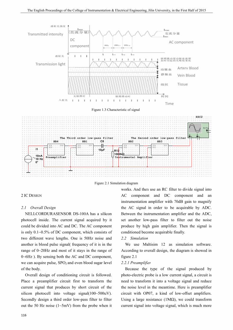
The Englis
116
2 IC DESIGN
2.1 OverallNELLCOR
photocell inscould be diviis only 0.1~0two differenanother is blorange of 0~20~6Hz ). By we can acquiof the body.
Overall dePlace a precurrent signasilicon photSecondly desout the 50 H
Tran
Transmit
sh Proceedings
l Design RDURASENside. The cuided into AC 0.5% of DC cnt wave lengtood pulse sig
20Hz and mosensing both
ire pulse, SPO
esign of condeamplifier ciral that produtocell into sign a third o
Hz noise (1~5
nsmission ligh
ted intensity
of the College
NSOR DS-100urrent signaland DC. The
component, wths. One is gnal( frequenost of it staysh the AC andO2 and even b
ditioning circrcuit first touces by shorvoltage signorder low-pa
5mV) from th
ht
DC compone
of Instrumentat
Figure 1.3
Figure 2
0A has a siliacquired by
e AC componwhich consist50Hz noise
ncy of it is in s in the rangeDC compon
blood sugar le
cuit is followo transform rt circuit of nal(100~500uass filter to fihe probe whe
ent
tion & Electrica
3 Characteristic
2.1 Simulation
icon y it nent ts of and
n the e of
nent, evel
wed. the the
uV). filter en it
worACinstthe Betset procon2.2
WAccfigu2.2
Bphoneethe circUsicur
al Engineering,
c of signal
diagram
rks. And thenC componentrumentation
AC signal tween the ins
another lowoduce by hignditioned beco
SimulationWe use Mucording to ovure 2.1
.1 PreamplifiBecause the oto-electric pred to transfor
noise level cuit with OPing a large rrent signal in
Jilin University
n use an RC nt and DC
amplifier wiin order to
strumentationw-pass filter gh gain amplome acquirab
n ultisim 12 verall design,
ier type of th
robe is a low rm it into a vin the meant
P07, a kind esistance (1M
nto voltage sig
Tim
ty, in the First H
filter to dividC componeith 70dB gaibe acquirab
n amplifier ar to filter oulifier. Then ble finally.
as simulatio the diagram
the signal pw current signa
voltage signatime. Here isof low-offse
MΩ), we cougnal, which i
AC compone
Artery B
Vein Blo
Tissue
me
Half of 2015
de signal intont and ann to magnify
ble by ADCand the ADCut the noisethe signal is
on softwareis showed in
produced byal, a circuit isal and reduces preamplifieret amplifiersuld transformis much more
ent
Blood
ood
o n y . , e s
. n
y s e r .
m e
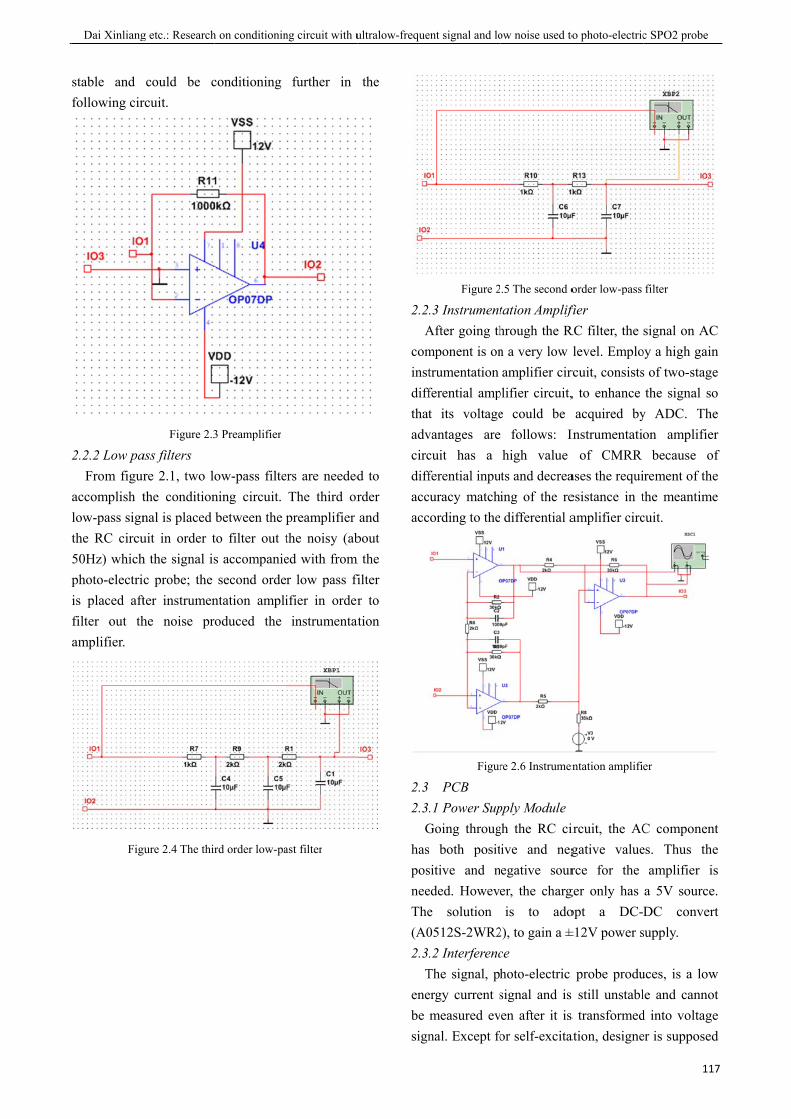
Dai Xinliang
stable and following cir
2.2.2 Low paFrom figur
accomplish tlow-pass signthe RC circu50Hz) whichphoto-electriis placed aftfilter out thamplifier.
Fig
g etc.: Research
could be crcuit.
Figure 2.3
ass filters re 2.1, two lothe conditionnal is placed uit in order th the signal isc probe; the ter instrumenhe noise pr
gure 2.4 The thir
h on conditionin
conditioning
3 Preamplifier
ow-pass filtening circuit. between the to filter out ts accompaniesecond orde
ntation amplioduced the
rd order low-pa
ng circuit with u
further in
ers are neededThe third orpreamplifier the noisy (abed with from r low pass fiifier in orderinstrumentat
ast filter
ultralow-freque
the
d to rder and
bout m the filter r to
ation
2.2A
cominstdiffthatadvcircdiffaccacc
2.3 2.3
GhasposneeThe(A02.3
Tenebe sign
ent signal and lo
Figure 2
.3 InstrumentAfter going thmponent is ontrumentation ferential ampt its voltage
vantages arecuit has a ferential inpucuracy matchcording to the
Figur
PCB .1 Power Sup
Going througs both positsitive and neded. Howeve solution 0512S-2WR2.2 Interferenc
The signal, phergy current smeasured evnal. Except fo
ow noise used to
.5 The second o
tation Amplifhrough the Rn a very low amplifier circ
plifier circuit,e could be
follows: Ihigh value ts and decreaing of the redifferential a
re 2.6 Instrumen
pply Module gh the RC ciive and negegative sourer, the chargis to ado
2), to gain a ±ce hoto-electric signal and is en after it is or self-excita
o photo-electric
order low-pass
fier RC filter, the
level. Emplorcuit, consists, to enhance acquired by
Instrumentatioof CMRR
ases the requiesistance in tamplifier circ
ntation amplifi
ircuit, the ACgative valuerce for the
ger only has opt a DC-±12V power s
probe produs still unstabls transformedation, designe
c SPO2 probe
117
filter
signal on ACoy a high gains of two-stagethe signal so
y ADC. Theon amplifier
because ofirement of thethe meantimecuit.
er
C componentes. Thus the
amplifier isa 5V sourceDC convert
supply.
uces, is a lowle and cannotd into voltageer is supposed
7
C n e o e r f e e
t e s . t
w t e d
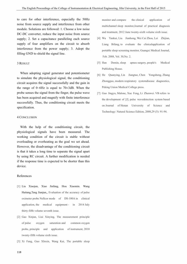
The English Proceedings of the College of Instrumentation & Electrical Engineering, Jilin University, in the First Half of 2015
118
to care for other interference, especially the 50Hz noise from source supply and interference from other module. Solutions are followed: 1. Choose a low noise DC-DC converter, reduce the input noise from source supply; 2. Set a capacitance paralleling each source supply of four amplifiers on the circuit to absorb interference from the power supply; 3. Adopt the filling GND to shield the signal line.
3 RESULT
When adopting signal generator and potentiometer to simulate the physiological signal, the conditioning circuit acquires the signal successfully and the gain in the range of 0~6Hz is equal to 70±3dB. When the probe senses the signal from the finger, the pulse wave has been acquired and magnify with finite interference successfully. Thus, the conditioning circuit meets the specification.
4 CONCLUSION
With the help of the conditioning circuit, the physiological signals have been measured. The working condition of the circuit is stable without overloading or overheating as the goal we set ahead. However, the disadvantage of the conditioning circuit is that it takes a long time to separate the signal apart by using RC circuit. A further modification is needed if the response time is expected to be shorter than this device.
References
[1] Liu Xiaojun, Xiao Jinfang, Hou Xiaomin. Wang
Haitang,Tang Jianjun,, Evaluation of the accuracy of pulse
oximeter probe Nellcor mode of DS-100A in clinical
application, the medical equipment - in 2014 July
thirty-fifth volume seventh issue.
[2] Gao Xinjun, Liui Xinying, The measurement principle
of pulse oxygen saturation and common oxygen
probe, principle and application of instrument, 2010
twenty-fifth volume sixth issue.
[3] Xi Fang, Guo XInxin, Wang Kai, The portable sleep
monitor and compare the clinical application of
multichannel sleep monitor,Journal of practical diagnosis
and treatment, 2012 June twenty-sixth volume sixth issue.
[4] Wu Yankui, Liu Jianhong, Wei Cai Zhou, Lei Zhijian,
Liang Bifang, to evaluate the clinicalapplication of
portable sleep screening monitor, Guangxi Medical Journal,
Feb. 2008, Vol. 30,No. 2.
[5] Han Demin, sleep apnea surgery, people's Medical
Publishing House.
[6] He Quanying, Lin Jiangtao, Chen Yongsheng, Zhang
Zhongguo, modern respiratory systemdisease diagnostics,
Peking Union Medical College press.
[7] Guo Jingyu, Malone, Xue Feng, Li Zhenwei. VB refers to
the development of [J]. pulse wavedetection system based
on Journal of Henan University of Science and
Technology: Natural Science Edition, 2008,29 (5): 91-94.

Liuhongshi etc.: The design of eighteen leads’electrocardiogram equipment based on ADAS1000
119
The design of eighteen leads’electrocardiogram equipment based on ADAS1000
Liuhongshi;Chenxin;Wangweijiao;Zhanghe
(College of Instrument Science and Electrical Engineering, Jilin University, Changchun 130022)
Abstract—In order to observe the state of the posterior wall in the right and left ventricles in the circumstances of
synchronization ,and solve the problem that it is difficult to monitor the dynamic electrocardiogram (ecg) changes for a long
time and at the same time caused by the ischemia, damage and necrosis in left ventricle back wall and right ventricle
myocardium ,topic of this paper is to design a eighteen leads’ acquisition system for monitoring electrocardiogram changes.
The system includes five parts: power modules, front-end conditioning module, right leg drive module, data acquisition
modules and controllers. ECG simulation mainly produced by the generator is fed through the front-end analog-digital
conversion processing circuit into the chip ADAS1000. MSP430F5438A controller via the SPI interface communicates with
ADAS1000 , receives the ECG data (ECG) for analysis and processing and transmits the waveform to the software. 18 -lead is
a more advanced method for non-invasive cardiac examination , able to get a lot more comprehensive data, with more
practical diagnosis value in myocardial ischemia and coronary artery diseases.
Keywords—Eighteen leads , Heart disease , ECG , Arrhythmia , Myocardial ischemia.
I. INTRODUCTION
IN general, the problem about observing ECG signal has been partly solved by 12 lead ECG monitor which is most popular on the market. However, using 18 lead ECG monitor, we can acquire proper physiological signal to measure the condition about the posterior wall in the right and left ventricle. Therefore, it is important to design an acquisition circuit for 18 lead ECG monitor.
II.MEASUREMENT AND SPECIFICATIONS
A.Principle of measuring
The system consists of a power supply, a Preconditioning module, driver, a DATA acquiring module and a controller. In order to test the system, an ECG simulative generator is needed to produce signal for the system. After going through the Preconditioning circuit, the signal is sent into an ADC, ADA1000. Via SPI, the controller, MSP430F5438A, gain the ability to communicate with ADAS1000. Analyzing the signal the system received, the controller transmits the result to monitor it on the window of a upper-computer. B. Content and Specifications
Designing a 18 lead ECG signal acquisition system based on ADAS1000. The content is followed:
Multi-power-supply circuit,
Preconditioning circuit for original signal, Driver circuit, Realizing multichip ADAS1000 by setting
several ADAS1000s, SPI communication interface , Realizing 18 lead DATA acquisition and
algorithm processing by controlling multichip ADAS100.
The specifications are followed according to the content we mentioned above.
Power consumption of each lead is less than 15mW ,
Power consumption in total is less than 100mW, Working temperature is in the range of -30°~80°.
Ⅲ. CIRCUIT DESIGN
System consists of a power supply, ECG simulative generator, conditioning circuit, driver and controller.As shown in figure 1.
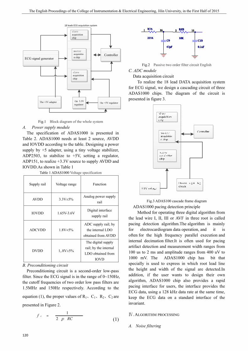
The English Proceedings of the College of Instrumentation & Electrical Engineering, Jilin University, in the First Half of 2015
120
slave acquisition chip
master acquisition chipECG signal generator
Controller
The +5V adapter the 3.3V regulator
the +5V regulator
18 leads ECG acquisition system
slave acquisition chip
Fig.1 Block diagram of the whole system
A. Power supply module The specification of ADAS1000 is presented in
Table 2. ADAS1000 needs at least 2 source, AVDD and IOVDD according to the table. Designing a power supply by +5 adapter, using a tiny voltage stabilizer, ADP2503, to stabilize to +5V, setting a regulator, ADP151, to realize +3.3V source to supply AVDD and IOVDD.As shown in Table 1
Table 1 ADAS1000 Voltage specification
Supply rail
Voltage range Function
AVDD 3.3V±5% Analog power supply
rail
IOVDD 1.65V-3.6V Digital interface
supply rail
ADCVDD 1.8V±5% ADC supply rail; by
the internal LDO obtained from AVDD
DVDD 1,.8V±5%
The digital supply rail; by the internal LDO obtained from
IOVD B. Preconditioning circuit
Preconditioning circuit is a second-order low-pass filter. Since the ECG signal is in the range of 0~150Hz, the cutoff frequencies of two order low pass filters are 1.5MHz and 150Hz respectively. According to the
equation (1), the proper values of R1、C1、R2、C2 are
presented in Figure 2.
RC
f cp2
1=
(1)
Fig.2 Passive two order filter circuit English
C. ADC module Data acquisition circuit
To realize the 18 lead DATA acquisition system for ECG signal, we design a cascading circuit of three ADAS1000 chips. The diagram of the circuit is presented in figure 3.
Fig.3 ADAS100 cascade frame diagram
ADAS1000 pacing detection principle Method for operating three digital algorithm from the lead wire I, II, III or AVF in three root is called pacing detection algorithm.The algorithm is mainly for electrocardiogram data operation, and it is often for the high frequency parallel execution and internal decimation filter.It is often used for pacing artifact detection and measurement width ranges from 100 us to 2 ms and amplitude ranges from 400 uV to 1000 mV. The ADAS1000 chip has bit that specially is used to express in which root lead line the height and width of the signal are detected.In addition, if the user wants to design their own algorithm, ADAS1000 chip also provides a rapid pacing interface for users, the interface provides the ECG data, using a 128 kHz data rate at the same time, keep the ECG data on a standard interface of the invariant.
Ⅳ. ALGORITHM PROCESSING
A. Noise filtering
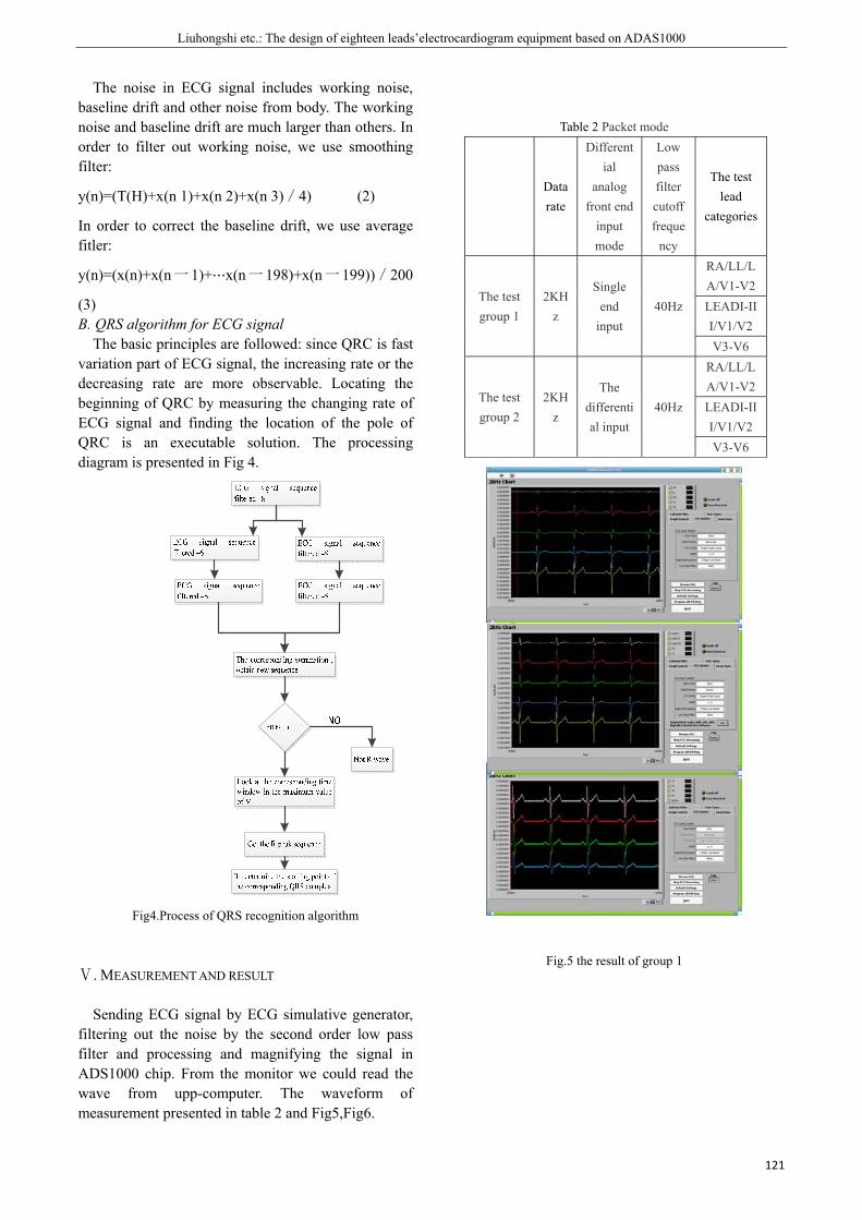
Liuhongshi etc.: The design of eighteen leads’electrocardiogram equipment based on ADAS1000
121
The noise in ECG signal includes working noise, baseline drift and other noise from body. The working noise and baseline drift are much larger than others. In order to filter out working noise, we use smoothing filter:
y(n)=(T(H)+x(n 1)+x(n 2)+x(n 3)/4) (2)
In order to correct the baseline drift, we use average fitler:
y(n)=(x(n)+x(n一1)+⋯x(n一198)+x(n一199))/200
(3) B. QRS algorithm for ECG signal
The basic principles are followed: since QRC is fast variation part of ECG signal, the increasing rate or the decreasing rate are more observable. Locating the beginning of QRC by measuring the changing rate of ECG signal and finding the location of the pole of QRC is an executable solution. The processing diagram is presented in Fig 4.
Fig4.Process of QRS recognition algorithm
Ⅴ. MEASUREMENT AND RESULT
Sending ECG signal by ECG simulative generator, filtering out the noise by the second order low pass filter and processing and magnifying the signal in ADS1000 chip. From the monitor we could read the wave from upp-computer. The waveform of measurement presented in table 2 and Fig5,Fig6.
Table 2 Packet mode
Data rate
Differential
analog front end
input mode
Low pass filter cutoff freque
ncy
The test lead
categories
The test group 1
2KHz
Single end
input 40Hz
RA/LL/LA/V1-V2LEADI-III/V1/V2 V3-V6
The test group 2
2KHz
The differential input
40Hz
RA/LL/LA/V1-V2LEADI-III/V1/V2 V3-V6
Fig.5 the result of group 1
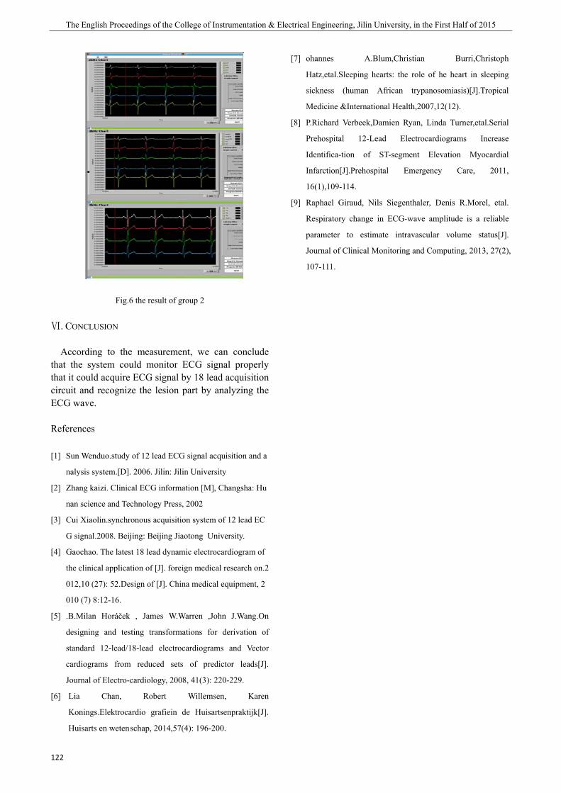
The English Proceedings of the College of Instrumentation & Electrical Engineering, Jilin University, in the First Half of 2015
122
Fig.6 the result of group 2
Ⅵ. CONCLUSION
According to the measurement, we can conclude that the system could monitor ECG signal properly that it could acquire ECG signal by 18 lead acquisition circuit and recognize the lesion part by analyzing the ECG wave.
References
[1] Sun Wenduo.study of 12 lead ECG signal acquisition and a
nalysis system.[D]. 2006. Jilin: Jilin University
[2] Zhang kaizi. Clinical ECG information [M], Changsha: Hu
nan science and Technology Press, 2002
[3] Cui Xiaolin.synchronous acquisition system of 12 lead EC
G signal.2008. Beijing: Beijing Jiaotong University.
[4] Gaochao. The latest 18 lead dynamic electrocardiogram of
the clinical application of [J]. foreign medical research on.2
012,10 (27): 52.Design of [J]. China medical equipment, 2
010 (7) 8:12-16.
[5] .B.Milan Horáček , James W.Warren ,John J.Wang.On
designing and testing transformations for derivation of
standard 12-lead/18-lead electrocardiograms and Vector
cardiograms from reduced sets of predictor leads[J].
Journal of Electro-cardiology, 2008, 41(3): 220-229.
[6] Lia Chan, Robert Willemsen, Karen
Konings.Elektrocardio grafiein de Huisartsenpraktijk[J].
Huisarts en weten schap, 2014,57(4): 196-200.
[7] ohannes A.Blum,Christian Burri,Christoph
Hatz,etal.Sleeping hearts: the role of he heart in sleeping
sickness (human African trypanosomiasis)[J].Tropical
Medicine &International Health,2007,12(12).
[8] P.Richard Verbeek,Damien Ryan, Linda Turner,etal.Serial
Prehospital 12-Lead Electrocardiograms Increase
Identifica-tion of ST-segment Elevation Myocardial
Infarction[J].Prehospital Emergency Care, 2011,
16(1),109-114.
[9] Raphael Giraud, Nils Siegenthaler, Denis R.Morel, etal.
Respiratory change in ECG-wave amplitude is a reliable
parameter to estimate intravascular volume status[J].
Journal of Clinical Monitoring and Computing, 2013, 27(2),
107-111.
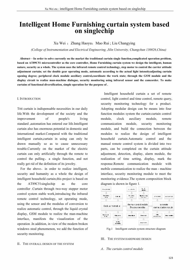
Xu Wei etc.: intelligent Home Furnishing curtain system based on singlechip
123
Intelligent Home Furnishing curtain system based on singlechip
Xu Wei ;Zhang Haoyu;Mao Rui ; Liu Changying
(College of Instrumentation and Electrical Engineering, Jilin University, Changchun 130026,China)
Abstract—In order to solve currently on the market the traditional curtain single function,complicated operation problem, based on AT89C51 microcontroller as the core controller, Home Furnishing curtain system we design the intelligent, human nature, security as a whole. The system uses the infrared remote control technology, step motor to control the carrier attitude adjustment curtain; set the double gear operating mode, automatic according to the actual light intensityadjusting curtain opening degree; peripheral clock module auxiliary control,coordinate the work state; through the GSM module and the display circuit to realize man-machine dialogue, security monitoring using infrared sensor and the camcorder. To make curtains of functional diversification, simple operation for the purpose of .
I. INTRODUCTION
THE curtain is indispensable necessities in our daily life.With the development of the society and the improvement of people's living standard ,automation has entered our life.Intelligent curtain also has enormous potential in domestic and international market.Compared with the traditional intelligent curtain,curtain in using can only be drawn manually so as to cause unnecessary trouble.Currently on the market of the electric curtain can only artificially through the remote to control the pulling,a single function, and not really get rid of the definition of its jewelry.
For the above,in order to realize intelligent, security and humanity as a whole the design of intelligent household curtain,this project is based on the AT89C51singlechip as the core controller .Curtain through two-way stepper motor control system stable work,introducing the infrared remote control technology, set operating mode, using the sensor and the modulus of conversion to realize automatic control, through the liquid crystal display, GSM module to realize the man-machine interface, manifests the visualization of the operation .In addition, in view of the modern broken windows steal phenomenon, we add the function of security monitoring.
II.THE OVERALL DESIGN OF THE SYSTEM
Intelligent household curtain a set of remote control, light control and time control, remote query, security monitoring technology for a product. Adopting modular design can be means into four function modules system the curtain:curtain control module, clock auxiliary module, remote communication module, security monitoring module, and build the connection between the modules to realize the design of intelligent household curtain.Automatic control and the manual remote control system is divided into two parts, can be completed on the curtain attitude adjustment, detection, display, alarm module, the realization of time setting, display, mark the response.Remote communication module with mobile communication to realize the man - machine interface, security monitoring module to meet the monitoring evidence.The system composition block diagram is shown in figure 1.
Fig.1 Intelligent curtain system structure diagram
III.THE SYSTEM HARDWARE DESIGN
A.The curtain control module
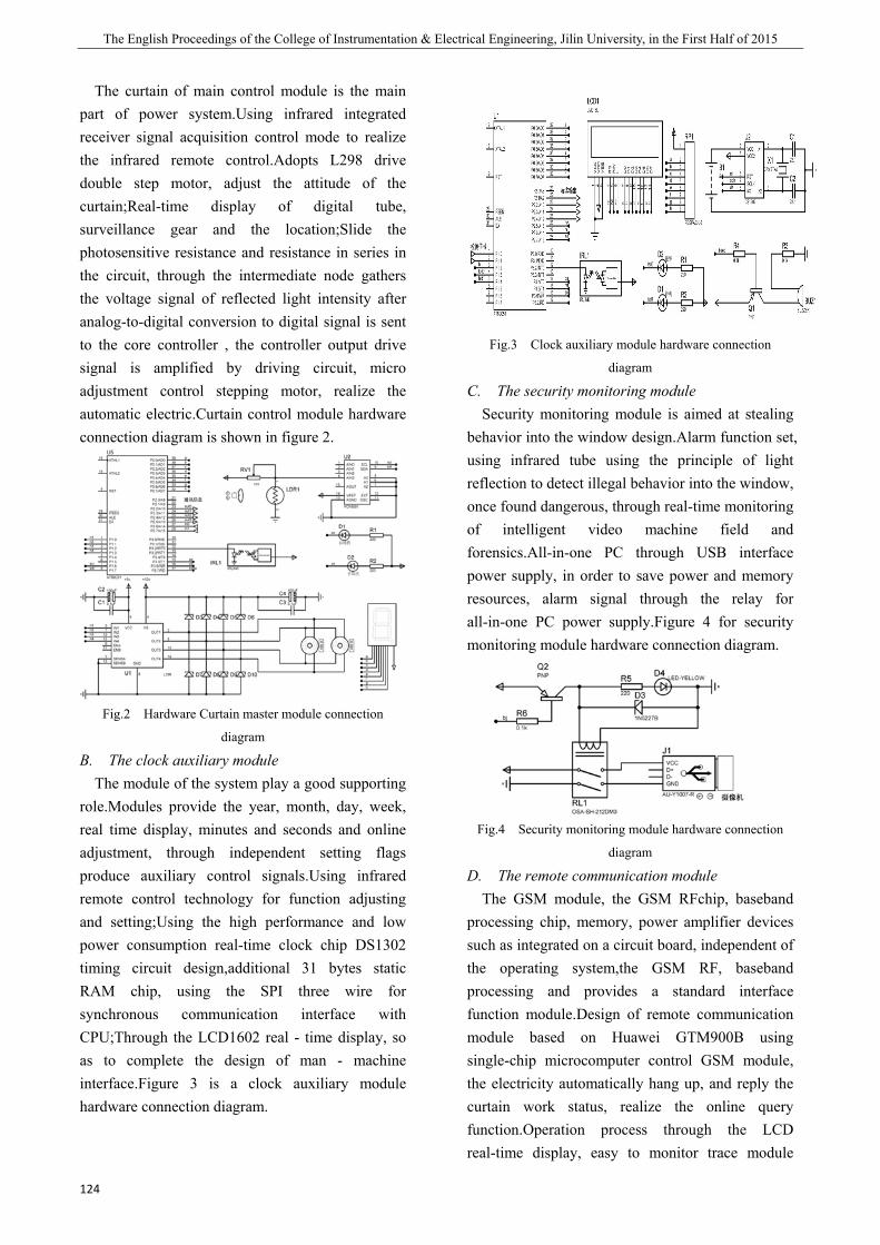
The English Proceedings of the College of Instrumentation & Electrical Engineering, Jilin University, in the First Half of 2015
124
The curtain of main control module is the main part of power system.Using infrared integrated receiver signal acquisition control mode to realize the infrared remote control.Adopts L298 drive double step motor, adjust the attitude of the curtain;Real-time display of digital tube, surveillance gear and the location;Slide the photosensitive resistance and resistance in series in the circuit, through the intermediate node gathers the voltage signal of reflected light intensity after analog-to-digital conversion to digital signal is sent to the core controller , the controller output drive signal is amplified by driving circuit, micro adjustment control stepping motor, realize the automatic electric.Curtain control module hardware connection diagram is shown in figure 2.
Fig.2 Hardware Curtain master module connection
diagram
B. The clock auxiliary module The module of the system play a good supporting
role.Modules provide the year, month, day, week, real time display, minutes and seconds and online adjustment, through independent setting flags produce auxiliary control signals.Using infrared remote control technology for function adjusting and setting;Using the high performance and low power consumption real-time clock chip DS1302 timing circuit design,additional 31 bytes static RAM chip, using the SPI three wire for synchronous communication interface with CPU;Through the LCD1602 real - time display, so as to complete the design of man - machine interface.Figure 3 is a clock auxiliary module hardware connection diagram.
Fig.3 Clock auxiliary module hardware connection
diagram
C. The security monitoring module Security monitoring module is aimed at stealing
behavior into the window design.Alarm function set, using infrared tube using the principle of light reflection to detect illegal behavior into the window, once found dangerous, through real-time monitoring of intelligent video machine field and forensics.All-in-one PC through USB interface power supply, in order to save power and memory resources, alarm signal through the relay for all-in-one PC power supply.Figure 4 for security monitoring module hardware connection diagram.
Fig.4 Security monitoring module hardware connection
diagram
D. The remote communication module The GSM module, the GSM RFchip, baseband
processing chip, memory, power amplifier devices such as integrated on a circuit board, independent of the operating system,the GSM RF, baseband processing and provides a standard interface function module.Design of remote communication module based on Huawei GTM900B using single-chip microcomputer control GSM module, the electricity automatically hang up, and reply the curtain work status, realize the online query function.Operation process through the LCD real-time display, easy to monitor trace module
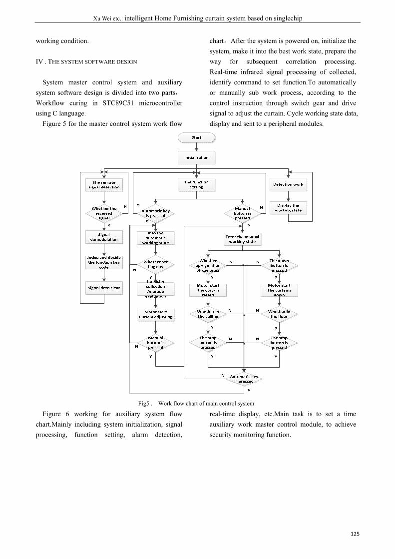
Xu Wei etc.: intelligent Home Furnishing curtain system based on singlechip
125
working condition.
IV . THE SYSTEM SOFTWARE DESIGN
System master control system and auxiliary system software design is divided into two parts,Workflow curing in STC89C51 microcontroller using C language.
Figure 5 for the master control system work flow
chart。After the system is powered on, initialize the system, make it into the best work state, prepare the way for subsequent correlation processing. Real-time infrared signal processing of collected, identify command to set function.To automatically or manually sub work process, according to the control instruction through switch gear and drive signal to adjust the curtain. Cycle working state data, display and sent to a peripheral modules.
Fig5 . Work flow chart of main control system
Figure 6 working for auxiliary system flow chart.Mainly including system initialization, signal processing, function setting, alarm detection,
real-time display, etc.Main task is to set a time auxiliary work master control module, to achieve security monitoring function.
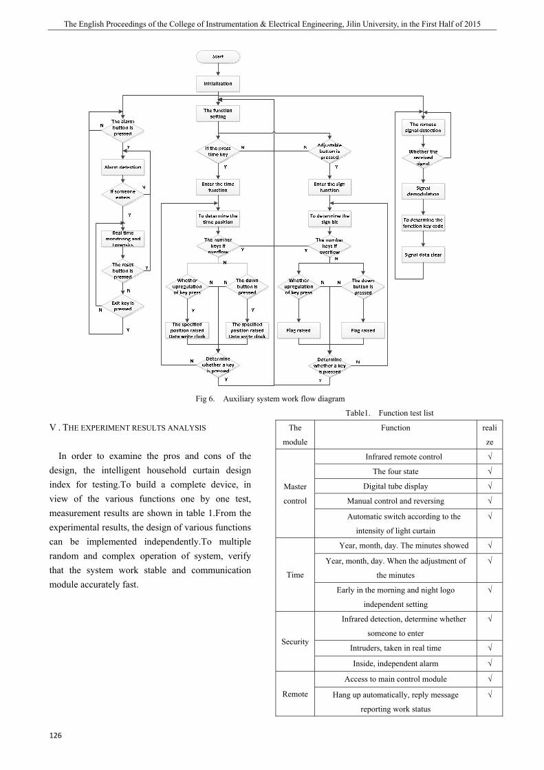
The English Proceedings of the College of Instrumentation & Electrical Engineering, Jilin University, in the First Half of 2015
126
Fig 6. Auxiliary system work flow diagram
V . THE EXPERIMENT RESULTS ANALYSIS
In order to examine the pros and cons of the design, the intelligent household curtain design index for testing.To build a complete device, in view of the various functions one by one test, measurement results are shown in table 1.From the experimental results, the design of various functions can be implemented independently.To multiple random and complex operation of system, verify that the system work stable and communication module accurately fast.
Table1. Function test list
The
module
Function reali
ze
Master
control
Infrared remote control √
The four state √
Digital tube display √
Manual control and reversing √
Automatic switch according to the
intensity of light curtain
√
Time
Year, month, day. The minutes showed √
Year, month, day. When the adjustment of
the minutes
√
Early in the morning and night logo
independent setting
√
Security
Infrared detection, determine whether
someone to enter
√
Intruders, taken in real time √
Inside, independent alarm √
Remote
Access to main control module √
Hang up automatically, reply message
reporting work status
√
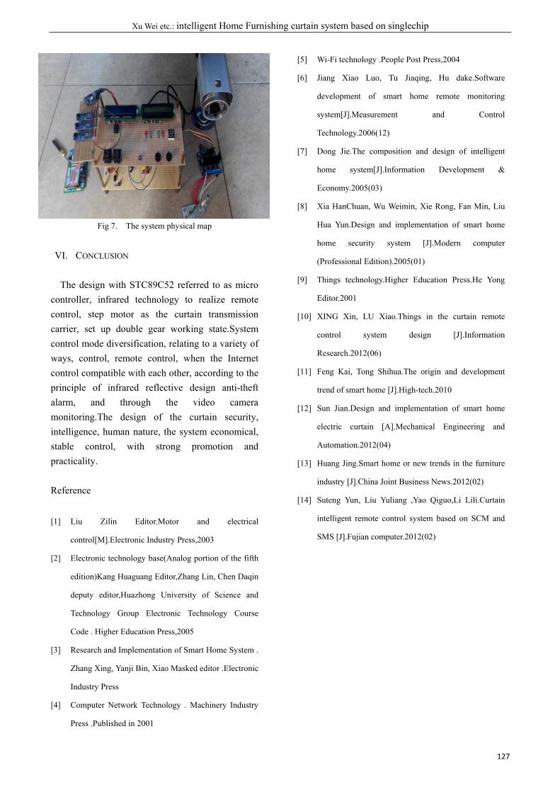
Xu Wei etc.: intelligent Home Furnishing curtain system based on singlechip
127
Fig 7. The system physical map
VI. CONCLUSION
The design with STC89C52 referred to as micro controller, infrared technology to realize remote control, step motor as the curtain transmission carrier, set up double gear working state.System control mode diversification, relating to a variety of ways, control, remote control, when the Internet control compatible with each other, according to the principle of infrared reflective design anti-theft alarm, and through the video camera monitoring.The design of the curtain security, intelligence, human nature, the system economical, stable control, with strong promotion and practicality.
Reference
[1] Liu Zilin Editor.Motor and electrical
control[M].Electronic Industry Press,2003
[2] Electronic technology base(Analog portion of the fifth
edition)Kang Huaguang Editor,Zhang Lin, Chen Daqin
deputy editor,Huazhong University of Science and
Technology Group Electronic Technology Course
Code . Higher Education Press,2005
[3] Research and Implementation of Smart Home System .
Zhang Xing, Yanji Bin, Xiao Masked editor .Electronic
Industry Press
[4] Computer Network Technology . Machinery Industry
Press .Published in 2001
[5] Wi-Fi technology .People Post Press,2004
[6] Jiang Xiao Luo, Tu Jiaqing, Hu dake.Software
development of smart home remote monitoring
system[J].Measurement and Control
Technology.2006(12)
[7] Dong Jie.The composition and design of intelligent
home system[J].Information Development &
Economy.2005(03)
[8] Xia HanChuan, Wu Weimin, Xie Rong, Fan Min, Liu
Hua Yun.Design and implementation of smart home
home security system [J].Modern computer
(Professional Edition).2005(01)
[9] Things technology.Higher Education Press.He Yong
Editor.2001
[10] XING Xin, LU Xiao.Things in the curtain remote
control system design [J].Information
Research.2012(06)
[11] Feng Kai, Tong Shihua.The origin and development
trend of smart home [J].High-tech.2010
[12] Sun Jian.Design and implementation of smart home
electric curtain [A].Mechanical Engineering and
Automation.2012(04)
[13] Huang Jing.Smart home or new trends in the furniture
industry [J].China Joint Business News.2012(02)
[14] Suteng Yun, Liu Yuliang ,Yao Qiguo,Li Lili.Curtain
intelligent remote control system based on SCM and
SMS [J].Fujian computer.2012(02)
The English Proceedings of the College of Instrumentation & Electrical Engineering, Jilin University, in the First Half of 2015
128
The Design of the Three Degrees of Freedom Parallel Motion Platform
Zhu Jing, Zhang Miao, Yu Haiming
(jilin university instrument science and engineering institute,changchun,130021)
Abstract— In the industrial automatic production, the serial robots with the advantages of large working space
and simple control have been dominant. The mechanical structure is connected by many joints in order to achieve
the goal of multi-degrees of freedom control. However, due to various joints will produce certain error which cause
the error accumulation, and this situation cause the loss of precision. Compared with the serial robots, the parallel
will not have this kind of problems. Because there is no cumulative error, the parallel structure is much more
accurate. At present, the parallel motion platform has been involved in many fields, such as the parallel printer and
the technology of intelligent sorting. This technology has an advantage of high speed and light load, which is very
important in many industries and will has a bright future. In our paper, the focus is on the three degrees of freedom
parallel motion platform and how to use it to realize the function of move on space and intelligent sorting. We will
introduce its principle , practices and results specifically in the following content.
I. INTRODUCTION
A. The Research Background and Significance IN 1965, the parallel structure was put forward by
Stewart, which is used to train pilots as flight simulator. In 1978, the famous Australian mechanisms professor Hunt put forward that the platform can be applied to the parallel robot. Since then ,the research and development of parallel robot began. After decades of exploration, the research of parallel robot has transformed from basic theory to actual practice. The parallel robot application is very extensive in the machinery industry ,aviation industry and mining. With the advantage of its good rigidity structure, strong carrying capacity, the small cumulative error and the simple parts, the parallel robots gradually occupy the market of the machine tool industry at home and abroad, and it will become the 21st century high-speed light nc machining equipment. B. The Classification of Parallel Robot
Since 1993,the first parallel robot was born in the Automation and Robotics institute in the Texas, the parallel robot was developed fully both in structure and shape, but in terms of its category, it can be divided into the following categories:(1) According to the classification of the number of degrees of
freedom, if the parallel robot can do F degrees of freedom, we call it F-DOF parallel robot. For example, a robot can do 6 degrees of freedom, we call it 6-DOF parallel robot.(2)According to the classification of the form of parallel mechanism, we can divide it into: linear drive input parallel robot and rotary actuation input parallel robot. The former is researched more, the inverse solution of this kind of robot is very easy, and it has uniqueness. Compared with the linear drive input parallel robot, the rotary actuation input parallel robot has the advantages of more compact structure, less inertia, and relative capacity; however, the input motion form of its rotation determines the complexity and uncertainty of the inverse solution. (3)According to the length of the pillar change classification, we can divide it into: one use the changeable pillars to support the platform of parallel robot. For example: a kind of 6-pole parallel robot is called Hexa2pod, its motion platform and base is connected with 6 pillars, whose length is changeable, at the end of each pillar , it will be connected by a hinge on the moving platform and pedestal, by adjusting the length of the pillar to change the position. Another use the unchangeable pillars to support the platform of parallel robot. For example: another kind of 6-pole parallel robot is called Hexaglide, its motion
Zhu Jing etc.: The Design of the Three Degrees of Freedom Parallel Motion Platform
129
platform and base is connected with 6 pillars, whose length is unchangeable, at the end of each pillar, it will be connected by a hinge on the moving platform and pedestal, the hinge on the pedestal can move along the base fixed chute, in this way to change the position of the moving platform. C. Kinematics Analysis and Calculating of Parallel Robot
The parallel robot kinematics analysis includes two aspects: the platform position and speed is known, the length of driving of vice, the angle and the speed is to solve, this is called inverse solution. If the length or angle of each driving of vice is known, the speed or the angle is to solve, then this is called positive solution. There are two of the most common research methods: the numerical solution and the closed solution. The numerical method refers to solving a set of nonlinear equations, nonlinear equation is directly exported from the vector loop equations after some concrete structure of algebraic treatment. Then obtained the position and posture of moving platform, which is corresponding with input. The advantage of the numerical solution is its mathematical model is much simpler, and it get rid of the locked mathematical derivation. But its computational speed is slow, and it can not get the all the solution of the institutions, and the final result has a big relationship with the initial value. But this method can solve any problems of parallel mechanism, and it is easy for this method to set up mathematical model, also, it can analyze the position immediately. D. The Research Status at Home and Abroad
The parallel robot has an immeasurable effect on nc machine tool, the academic world home and abroad and the engineering world both attache great importance to the development of parallel robot. Parallel machine tool has a wide application in engineering. The nc machine tools and machining center showed the Hexapod and the VARTAX for the first time in the international machine tool fair in Chicago in 1994,and this caused a sensation. After that, the major industrial countries have invested a lot of manpower and material resources to the research of the development of parallel
machine tool. Such as the American companies : Ingersoll Milling company, the Giddings & Lewis company and the Hexal company; and the English companies such as the Geodetic Technology company. They developed different machine tools based on the parallel structure.
The research of multi-axis machine tool which is based on the parallel robot has become a hot research topic in the field of robot and the machinery manufacture. At present, most of parallel machine tools at home and abroad are using parallel structure to manufacture machine tools simply(especially stewart platform structure). According to the degree of freedom of the parallel structure , it can be divided into two kinds:6-degree of freedom and 3-degree of freedom; according to the driving mode of each branch chain ,it can be divided into : one changes the moving platform by sliding its leg; another changes the moving platform by scaling its leg.
II. DESIGN SCHEME
A. Research Principle and Main Task Principle: The principle of the robot is made up
of swinging arm and driven arm connection static platform and moving platform. One end of the active arm connect with static platform by tuning pair. By the driving of the motor or other power plant do reciprocating swing movement. The other end of the active arm through coupling connected to the slave arm, The slave arm has a parallelogram structure, The slave arm through coupling connected to the moving platform. Along the moving platform that can realize three coordinates of the direction of movement .
Our main task is designing a controlled parallel robot., including automatic control. We put the data acquisition card as the core controller, and we use the data acquisition card control the child controllers to realize some advanced features. Our target is :1. the construction of the parallel platform ; 2. achieve the rapid sorting function. B. Module Design Scheme
You can through computer control center and data acquisition card to communicate with the pc, through the program control of intelligent machines
The English Proceedings of the College of Instrumentation & Electrical Engineering, Jilin University, in the First Half of 2015
130
you can turn left and right, up and down etc. We will, through the AutoCAD to draw models of parallel motion platform, to determine the proportion of each part and the specific size, drawing generation and processing is to produce a prototype. At the same time through the data acquisition card to output the signal to control the whole system. LABVIEW contains a lot of data collection, analysis and function signals, its data is powerful and the DAQ assistant is powerful too. all above will make the Data acquisition system is much easier to build.
Relevant parts of constitute : (1) The rigid coupling ,cut off the rigid coupling
in the middle, to fix motor, and make motor can control the initiative arm, consolidated with screw in the middle.
(2) Motor, compared with the traditional three-phase motor, slow step motor has many advantages, when has the maximum torque motor stalling,( when the winding excitation). Motor rotation angle is proportional to the pulse number, and the response of the motor only be determined by the digital input pulse, thus it can be using open loop control. This makes the structure of the motor could be simpler and cost control, due to the precision of each step from three percent to five percent, and would not step error accumulation to the next step and thus has good location accuracy and repeatability of the movement. Another slowdown stepper motor has excellent start stop and reverse response, since there is no brush, high reliability, so the service life of motor only depends on the service life of bearing. Only the load directly connected to the motor shaft, can also be extremely low speed synchronous rotation. In addition because speed is proportional to the pulse frequency, and therefore there is a wide speed range. Three motors came on static platform into 120 degrees, the white steel stents to lift the whole platform, the motor and coupling and active arm together, three motor rotation control active arm at the same time, the reduction ratio of 18:1. By programming control, data from the data acquisition card, each pulse transfer 0.1 degrees.
(3) Data acquisition card, used as a vehicle for data transmission, connection and computer and
external control motor power. (4) Stepper Data acquisition card, used as a
vehicle for data transmission, connection and computer and external motor drives, used to drive the motor.
(5)Fold the pen, converted into joint, connected with the carbon fiber tube, make the slave arm.
(6) Carbon fiber tube, and the modified folding pen together form the initiative arm, connect to the active arm.
(7) Moving platform materials, refit to moving platform.
III . THE SPECIFIC IMPLEMENTATION STEP AND
PICTURE OF REAL PRODUCTS
A. Part of the material figure and function Figure 1 is the rigid coupling. The middle is a
hollow steel cylinder and the lateral open holes which can embed screw for fixed step motor.
Fig.1 The rigid coupling
Fig.2 The folding pen Fig.3 Data acquisition card
Fig.4 Carbon fiber tube Fig.5 Acrylic material
Zhu J
Fig.6 Slo
in step and p
Fig.7 Th
is the slave afiber tube th
h of 1 meter al due to id good toughvice that is
pen and th steel core. Ted on the mylic materialreduce the lthe precisionorm and it clave arm is cis still mad
of the activo.
Jing etc.: The D
ow step motor
production di
he slave arm
arm of the mhat is on the and is selec
its characterhness and ligon the blue wo pens arThe bottom moving platl, its great stoad of the mn. The mechan afford 2.connected wde of the fove arm is m
Design of the Th
iagram
moving platfoblack part e
cted as the slristics of gght quality. part is mad
re fixed in end of the sltform. Platftrength and lmoving platfhanical sucke5 kg. The up
with the coupolding pen. made of acr
hree Degrees of
orm. each lave
great The
de of the
lave form light form er is pper
pling The
rylic
FwhirespactirotawhiachacqtranpulcooWematstatthe speperposinto
C. stru
f Freedom Para
Figure 8 is thich three stpectively onive arm by ates, the actiich move th
hieve the pquisition cardnsmit step mse passing.
ordinate syst can calculthematical tic platform
slave arm ecific locatioform the sp
sition for soo the specifie
Platform pucture
allel Motion Pla
Fig.8 Stati
he upper partep motors n the staticthe rigid couve arm rotat
he chuck on purpose of d gather the motor that rSo, we esta
em with statlate the comethod, beand the lengis known. S
on of the soecific progra
orting and ped location.
Fig.9 The wh
part of spe
atform
c platform
rallel motionwith 120 d
c platform oupling. Whetes to drive tthe movingquick sort
signal fromrotates 0.1 ablish spacetic platform aordinates b
ecause the gth of the acSo we can corting itemsam to reach
put the item
hole frame
ecific size
13
n platform, indegree angleconnect the
en the motothe slave armg platform tot. The data computer todegree each
e rectangulaas the originy means odiameter o
ctive arm andcalculate the. The moto
h the specificms sorted ou
and design
1
n e e r
m, o a o h r
n. f f d e r c
ut
n

The English Proceedings of the College of Instrumentation & Electrical Engineering, Jilin University, in the First Half of 2015
132
In order to conveniently display specific value and clearly see the specific shape, the drawings has been given according to the actual ratio.
Fig.10 The three view drawing of the moving platform
Figure 10 is the three view drawing of the moving platform that is made of acrylic material. It is in the slave arm bottom that the hardness is larger and quality is lighter.
Fig.11 The three view drawing of the motor bracket
Fig.12 The size of the slave arm
Fig.13 The three view drawing of the step motor
Fig.14 Hardware block diagram of the overall control scheme
IV. CONCLUSION
This project with the subject of parallel robot is divided into external hardware structures and
software programming two parts. We have reached the design target. We have completed the whole external hardware building, up and down platforms connection, and stepper motors, stepper motor drives, power connection. We
Reduction Step Motor
Core Controller
Robot Arm
Moving platform
Static platform
Removal
Move Up and Down
Grasp
Loosen
Direction and Other Control

Zhu Jing etc.: The Design of the Three Degrees of Freedom Parallel Motion Platform
133
write software using LABVIEW software program. Through the data acquisition card, program written has autonomous recognition in the three-dimensional space coordinate, fast sorting function of point to point.
The project has trained our manipulative ability, Literature retrieval ability, English reading ability, team cooperation ability and communication ability. There are still some shortcomings, in accuracy and theory still slight differences, while it can satisfy the requirements of the project, but has not reached the ideal state. In the next project, we will fix gap and further reduce the error.
Reference
[1] Clavel R.DELTA,A fast robot with parallel
geometry.Pro.int.symposium on Industrial robots.
[2] Sternheim F.computation of the direct and inverse
geometric models of the delta parallel robot.
[3] Pierrot.Towards a fully 2 parallel 6 DOF robot for
high 2 speed applications 1991 ieee int.
[4] Stewart. D .A platform with 6 degrees of reedom.
Proc. Mech. Engineer.
[5] Viera. DELTA RPBOTS FOR HIGH SPEED
MANIPULATION TECHNICAL GAZETTE.
[6] Liu Zilin, Motor and Electric Control[M].Electric
Industry Press.2003. Cl
[7] Yao Bei, Zhang Lijian, Zhou Jingxiang .Intelligent
TOUR Track and Obstacle Avoidance Car Based on
single-chip Microcomputer [J].Mechanical and
Electric Information.2010(12).
[8] Yang Dongyan, A Mobile Robot Car’s Motor
Control System.[J]. Nei Mmng gu Sience and
Technology and Ecnomy. 2008(20).
[9] Hua Weishi,Stacking Robot Based on Delta
Agency[J].Journal of Xi An Jiao Tong University
[10] Dong Haiwen etc,The Present Situation and Future
Development of Parallel Robot In the Domestic
[J].Automation Expo.
[11] Hua Zhen etc, Theory And Control of Parallel Robot
Mechanism.[M].Beinjing Mechanical Industry
Press.
[12] Gao Xiulan etc, The Work Space Analytic of Delta
Parallel Mechanism [J]. Journal of Agricultural
Machinery.
[13] Ji Minggang etc,Mechanical Design (the seventh
Edition)[M].Harbin Institute of Technology Press.
[14] Zha Zhanpeng, A Three Degrees of Freedom
Platform of Parallel Robot Mechanism, Automation
Expo, 2006, 6:40-43.
imofinmis spmtere
A
The Englis
134
Desi
(
Abstract—U
circuit analys
C to the Sin
Single-chip m
controller.
I. INTRODUC
ABS (autommportant kinf ABS is alsnstitutions haethod of AB
not mapeed sensor odel, in ordsting, coopesearch and g
II. DESIGN
A. DesignPC softwa
platform is simulation csoftware. Vdesign softwfeatures andlanguage itinterface desoftware function. Tcontroller cMSP430. Bysoftware conand acceptsoftware contransmission
sh Proceedings
gn of
(College of
Use the theor
sis to research
ngle-chip mi
microcomput
CTION
motive anti-ld of brakingso necessaryave been doiBS review, bu
ture. By sisignal, we
er to realizeerate with regreatly reduc
N METHOD
n method of Pare controlleautomobile control platfVisual Studware. By ud combiningt can realiesign of thecontroller
Through RScan connecty the serial ntroller sendt it’s feedbntroller will n is wrong.
of the College
the ansignTian We
f Instrumenta
y of PC contr
h of car whee
icrocomputer,
er and the
ock braking g system. Thy. Some uniing domesticut most of thimulating the can build e the ABS sielated theorce the cost o
PC software er which is ABS wheel
form and coio is the sing the wig with c # ize the hoe controller
serial co232 chip, t with the port commu
ds instructionback signajudge wheth
of Instrumentat
nalog cal of a
enbo; Waation & Elec
rol technology
el speed signa
, established
hardware ci
system) is ahe evaluatioiversities anc study on thhe technologhe car whee
ABS objecimulation anry technologf research.
controllerbased on PCspeed signa
ommunicatioprogramminindow desigprogrammin
ost computeand the PC
ommunicatioPC softwarmachine o
unication, PCns to MSP43l. Then PCher the signa
tion & Electrica
controautomang Zhongqctrical Engin
y of Single-ch
al, use C# to t
a PC and
ircuit of the
an on nd he gy el ct
nd gy
C al
on ng gn ng er C
on re of C
30 C al
wto
infofothpomfewal
al Engineering,
oller fmobile
qi; Zhangneering, Jilin
ip microcomp
he PC softwa
single chip
control me
Visual Stuwhich is a rico create a eas
Fig.1 Th
PC connterface brinor input, choor users. Its he input dataort commu
machine's weedback to th
working proclways accep
Jilin University
for whabs g Jiyue n University
puter control.
re design bas
microcomput
chanism and
udio Windoch programmsier way to u
he working pri
ntrol softwngs the funcices of amplrole as the c of user to th
unication wworking stahe user. Durcess, the PCpt the user's
ty, in the First H
heel sp
,130021)
. The design o
sed on Visual
ter control m
d a general
ows forms ming framewuse client.
inciple of PC c
ware of thections of thelitude and stcore lies in whe MSP430 bway, deterate and rering the lowC control sos new instru
Half of 2015
peed
of hardware
Studio, use
mechanism.
simulation
applicationwork is used
controller
e controllere frequencytatus displaywhich sendsby the serialrmines theesends theer computeroftware canuctions, and
r
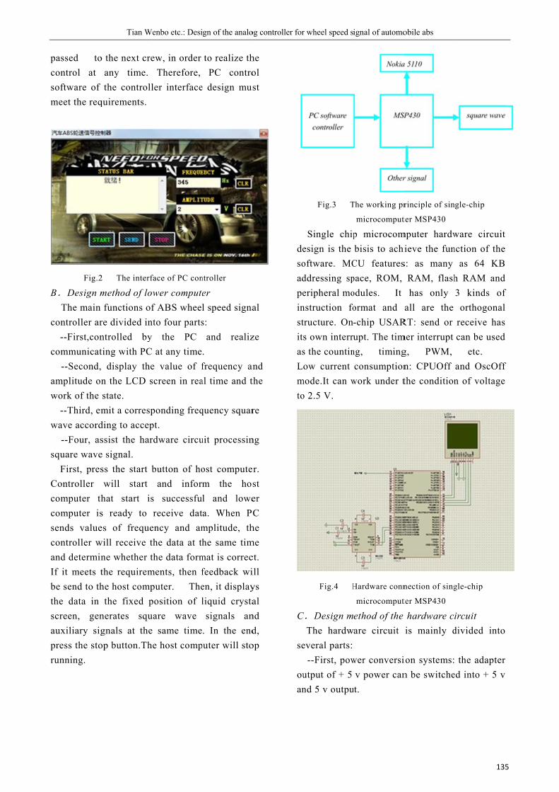
B
passed tocontrol at software of meet the req
Fig.2
B.Design mThe main
controller ar--First,con
communicat--Second,
amplitude onwork of the
--Third, emwave accord
--Four, assquare wave
First, presController computer thcomputer issends valuecontroller wand determinIf it meets tbe send to ththe data in screen, genauxiliary sigpress the storunning.
Tian W
o the next creany time. the controll
quirements.
2 The interf
method of lofunctions of
re divided inntrolled byting with PC display then the LCD sstate. mit a corresp
ding to accepssist the hare signal. ss the start will start
hat start iss ready to es of frequewill receive t
ne whether tthe requiremhe host comp
the fixed pnerates squgnals at theop button.Th
Wenbo etc.: Desi
ew, in order Therefore,
ler interface
face of PC con
ower computef ABS whee
nto four partsy the PC C at any timee value of fscreen in rea
ponding freqpt. rdware circu
button of hoand infor
s successfureceive dat
ency and amthe data at ththe data form
ments, then fputer. Theposition of luare wave e same timehe host comp
ign of the analo
to realize thPC contro
e design mus
ntroller
er l speed signas:
and realiz. frequency anal time and t
quency squar
uit processin
ost computem the hosl and lowea. When PCmplitude, thhe same tim
mat is correcfeedback wien, it displayliquid crystasignals an
. In the endputer will sto
og controller for
he ol st
al
ze
nd the
re
ng
r. st er C
he me ct. ill ys al
nd d,
op
desoadpeinstitasLmto
C
se
ouan
r wheel speed s
Fig.3 T
Single chipesign is the oftware. MCddressing speripheral monstruction fotructure. Ons own interrus the countinow current
mode.It can wo 2.5 V.
Fig.4 H
C.Design mThe hardw
everal parts:--First, pow
utput of + 5 nd 5 v outpu
ignal of automo
The working pr
microcomput
p microcombisis to achi
CU featurespace, ROM, odules. It ormat and a-chip USARupt. The tim
ng, timingconsumption
work under t
Hardware conn
microcomput
ethod of the are circuit
wer conversiv power cant.
obile abs
rinciple of sin
ter MSP430
mputer hardwieve the fun
s: as many RAM, flashhas only
all are the RT: send or mer interrupt g, PWM, n: CPUOff the condition
nection of sing
ter MSP430
hardware ciis mainly d
ion systems:n be switche
135
gle-chip
ware circuitnction of the
as 64 KBh RAM and3 kinds oforthogonal
receive hascan be used etc. and OscOffn of voltage
gle-chip
ircuit divided into
the adaptered into + 5 v
5
f
f
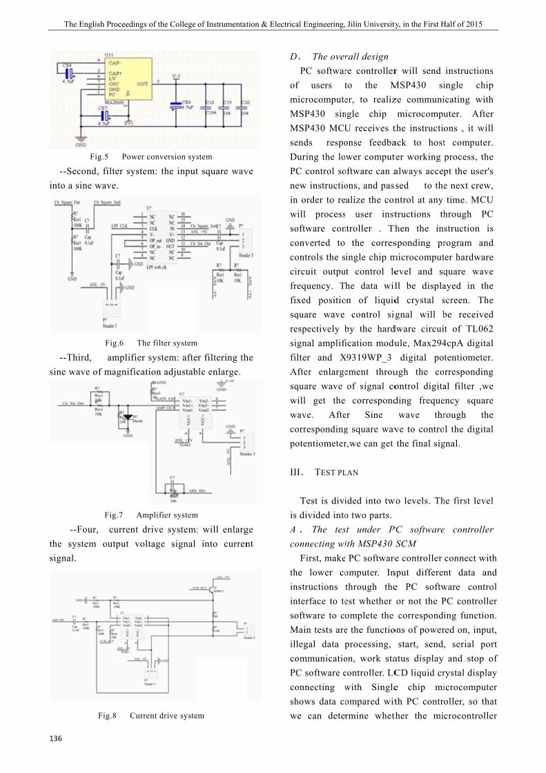
The Englis
136
Fig
--Second,into a sine w
--Third, sine wave of
--Four,the system signal.
F
sh Proceedings
g.5 Power c
filter systemwave.
Fig.6 The
amplifier f magnificat
Fig.7 Am
current droutput vol
Fig.8 Curre
of the College
conversion sys
m: the input
e filter system
system: afteion adjustab
mplifier system
rive system:tage signal
ent drive syste
of Instrumentat
stem
t square wav
r filtering thble enlarge.
m
: will enlarginto curren
m
tion & Electrica
ve
he
ge nt
D
ofmMMseDPCneinwsocococifrfisqresifiAsqwwcopo
II
isAco
thininsoMilcoPCcoshw
al Engineering,
D. The overPC softwar
f users tmicrocomputeMSP430 sinMSP430 MCUends respo
During the loC control soew instruction order to re
will processoftware cononverted to ontrols the sircuit outpurequency. Txed positioquare wave espectively bignal amplifilter and X
After enlargequare wave
will get thewave. Afteorrespondingotentiometer
II. TEST PL
Test is divis divided into. The tes
onnecting wiFirst, make
he lower constructions nterface to teoftware to co
Main tests arelegal data pommunicatioC software connecting whows data co
we can deter
Jilin University
rall design re controllerto the Mer, to realizngle chip U receives tonse feedbawer comput
oftware can aons, and pasalize the con user inst
ntroller . Ththe corres
ingle chip mt control lehe data wil
on of liquidcontrol sig
by the hardication modu
X9319WP_3 ement throuof signal co
corresponder Sine g square wavr,we can get
LAN
ided into two two parts. st under Pith MSP430 PC softwareomputer. Inthrough theest whether omplete the e the functioprocessing, on, work stacontroller. LCwith Singleompared witrmine wheth
ty, in the First H
r will send MSP430 size communi
microcomputhe instructioack to hostter working always accepsed to thentrol at any tructions thhen the insponding pr
microcomputevel and sqll be displad crystal sgnal will b
dware circuiule, Max294
digital pough the coontrol digitading freque
wave thrve to controthe final sig
wo levels. Th
PC softwareSCM e controller
nput differene PC softwor not the Pcorrespondi
ons of powerstart, send,
atus display CD liquid cre chip mith PC controther the mi
Half of 2015
instructionsingle chipicating withuter. Afterons , it willt computer.process, thept the user'se next crew,time. MCU
hrough PCstruction isrogram andter hardwarequare waveayed in thescreen. Thebe receivedt of TL062
4cpA digitaltentiometer.rrespondingal filter ,weency squarerough thel the digital
gnal.
he first level
e controller
connect withnt data and
ware controPC controlleing functionred on, input, serial porand stop o
rystal displayicrocomputeoller, so thacrocontrolle
r
h d
ol r
n. t, rt f y r
at r
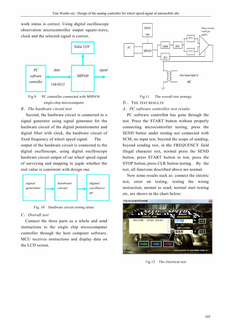
B
work status observation clock and th
Fig.9
B.The hard Second, t
signal generhardware cirdigital filterfixed frequeoutput of thedigital oscihardware cirof surveyingreal value is
Fig. 1
C.Overall Connect t
instructions controller thMCU receivthe LCD scr
Tian W
is correct. Umicrocontro
he selected si
PC controller
single-chip m
dware circuithe hardwarerator using rcuit of the r with clockency of wheee hardware clloscope, usrcuit output g and mapps consistent w
10 Hardware
test the three pa
to the sinhrough the ves instructireen.
Wenbo etc.: Desi
Using digitaoller outputignal is corre
connected wit
microcomputer
it test e circuit is csignal genedigital poten
k, the hardwel speed signcircuit is consing digital of car wheeling to jugdewith design o
e circuit testing
arts as a whngle chip m
host compuions and dis
ign of the analo
al oscilloscosquare-wav
ect.
th MSP430
r
onnected to erator for thntiometer anare circuit o
nal. The nnected to th
oscilloscopl speed signae whether thone.
g alone
hole and senmicrocomputeuter softwaresplay data o
og controller for
pe ve,
a he nd of
he pe al he
nd er e.
on
Ⅳ
A
tecoSESCbeilbuSTte
teinet
r wheel speed s
Fig.
Ⅳ.THE TEST
.PC softwaPC softwar
est. Press thonnecting mEND buttonCM, no inpueyond sendilegal characutton, press TOP button,
est, all functiNow some
est, error nstruction, ntc, are shown
F
ignal of automo
11 The ove
T RESULTS are controllere controllere START b
microcontroln under testiut test, beyonng test, in tcter test, no
START bu press CLR bions describeresults suchon testingormal to senn in the char
Fig.12 The e
obile abs
erall test strate
er test resultr has gone button witholler testing,ing not connd the scopethe FREQUEormal press utton to testbutton testined above are
h as: connect, testing nd, normal rt below:
electrical test
137
gy
ts through the
out properly press thenected with
e of sending,ENCY field
the SENDt, press theng. By thee normal. t the electricthe wrongstart testing
7
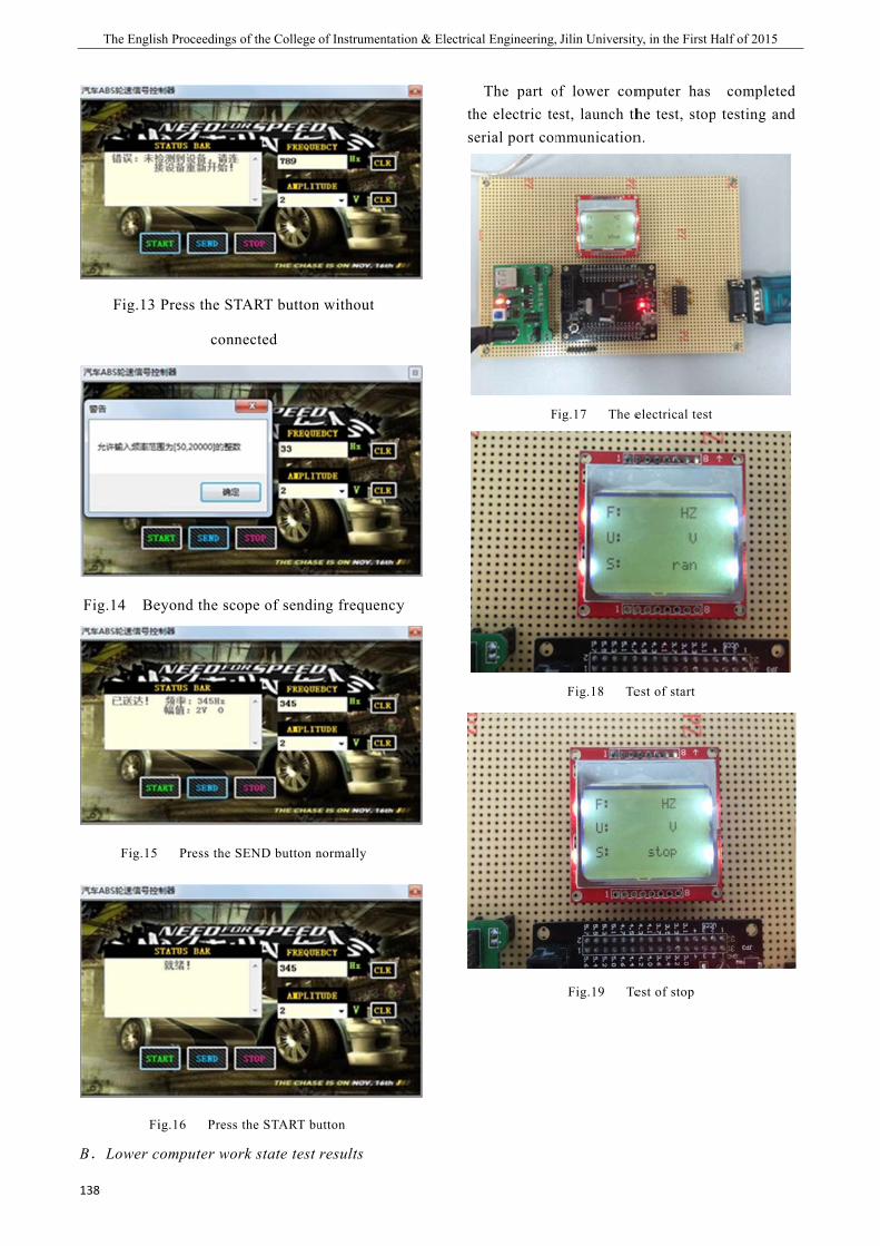
B
The Englis
138
Fig.13
Fig.14 Be
Fig.15
Fi
B.Lower c
sh Proceedings
Press the ST
conn
eyond the sco
Press the S
ig.16 Press
omputer wor
of the College
TART button
nected
ope of sendin
SEND button n
the START bu
rk state test
of Instrumentat
n without
ng frequency
normally
utton
results
tion & Electrica
y
thse
al Engineering,
The part ohe electric teerial port com
F
Jilin University
of lower comest, launch thmmunication
Fig.17 The e
Fig.18 Te
Fig.19 Te
ty, in the First H
mputer has he test, stopn.
electrical test
est of start
est of stop
Half of 2015
completed testing and
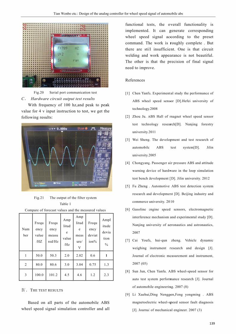
Fig.20
C. HardwWith fre
value for 4 vfollowing re
Fig.21
Compare of
Num
ber
Frequ
ency
value
/HZ
1 50.0
2 80.0
3 100.0
Ⅳ.THE TE
Based owheel speed
Tian W
0 Serial por
ware circuit oequency of v input instr
esults:
1 The outpu
Tab
f forecast valu
u
y
e
Frequ
ency
measu
red/Hz
A
l
v
50.3
80.6
0 101.2
EST RESULTS
on all parts d signal simu
Wenbo etc.: Desi
rt communicat
output test re100 hz,and ruction to te
ut of the filter
ble 1
es and the mea
Amp
litud
e
value
/Hz
Amp
litud
e
meas
ure/
V
2.0 2.02
3.0 3.04
4.5 4.6
of the autoulation cont
ign of the analo
tion test
esults peak to peast, we get th
system
asured values
Frequ
ency
deviat
ion%
Am
itu
dev
tio
%
0.6 1
0.75 1.
1.2 2.
omobile ABtroller and a
og controller for
ak he
mpl
ude
via
on
%
1
.3
.3
BS all
fuimwcothwTne
R
[1
[2
[3
[4
[5
[6
[7
[8
[9
r wheel speed s
unctional templemented.
wheel speed ommand. Thhere are stil
welding and he other is eed to impro
References
] Chen Yanfu
ABS whee
technology
2] Zhou Ju. A
test techn
university.2
3] Wei Sheng
automobile
university.2
4] Chongyang
warning de
test bench d
5] Fu Zheng
research an
commerce u
6] Gasoline e
interference
Nanjing un
2007
7] Cai Youfa
weighing
Journal of
2007 (05)
8] Sun Jun, C
auto test sy
of automob
9] Li Xuehui
magnetoele
[J]. Journal
ignal of automo
ests, the ovIt can gsignal acc
he work is rll insufficienwork appeathat the pr
ove.
u. Experimenta
el speed senso
.2008
ABS Hall of m
nology resear
2011
. The develop
ABS t
2005
g. Passenger ai
evice of hardw
development [
. Automotive
nd developmen
university. 201
engine speed
e mechanism a
niversity of ae
a, hui-qun
instrument r
electronic me
Chen Yanfu. A
ystem perform
bile engineerin
,Ding Nengge
ectric wheel-sp
l of mechanica
obile abs
verall funcgenerate cocording to roughly comnt. One is arance is norecision of
al study the pe
or [D].Hefei
magnet wheel
rch[D]. Nanj
pment and tes
test system
ir pressure AB
ware in the lo
[D]. Jilin unive
ABS test det
nt [D]. Beijing
10
d sensors, ele
and experimen
eronautics and
zheng. Vehi
research and
easurement an
ABS wheel-spe
mance research
ng. 2007 (8)
en,Feng yong
peed sensor fa
al engineer. 20
139
tionality isrrespondingthe preset
mplete . Butthat circuit
ot beautiful.final signal
erformance of
university of
speed sensor
jing forestry
st research of
m[D]. Jilin
S and attitude
op simulation
ersity. 2012
ection system
g industry and
ectromagnetic
ntal study [D].
d astronautics,
cle dynamic
design [J].
nd instrument,
eed sensor for
h [J]. Journal
gming . ABS
ault diagnosis
007 (3)
9
f
f
f

The English Proceedings of the College of Instrumentation & Electrical Engineering, Jilin University, in the First Half of 2015
140
[10] Wang Zhiwang ,Fang Xibang ,Chen yan.Automobile
ABS wheel speed sensor and signal processing [J].
Journal of automotive technology. 2006 (04)
[11] Wang Qirui ,Li Yao. ABS wheel-speed sensor for
auto fault diagnosis circuit design [J]. 2001 (02)
automotive electronics.
[12] Wu wenmin ,Li E`shou . The structure of the wheel
speed sensor and maintenance [J]. Journal of
automotive technology. 2000 (9)
[13] Chen Zaifeng ,Song Jian ,Yu Liangyao . Automotive
anti-lock braking system of wheel speed sensor
signal processing [J]. Journal of automobile
engineering. 2000 (04)
[14] Sun Jun Jiang Weilong, Wang Penglu. ABS wheel
angular acceleration of kalman filtering technology
research [J]. J 2010 (05) cars and accessories.
[15] Zhu Junmin ,Zhang Xiao ,Wang Jingyang ,Wu
Yuebei . The audio noise reduction based on the
theory of the modulus maxima and scale method [J].
Journal of vibration and shock. 2009 (11)
[16] Georg F.Mauer, Gerard F.Gissinger and Yann
Chamaillard. "Fuzzy Logic Continuous and
Quantizing Control of an ABS Braking System".
SAE Journal .
[17] Jeremy Broughton,Chris Baughan.The effectiveness
of antilock braking systems in reducing accidents in
Great Britain. Accident Analysis and Prevention .
2002
[18] Alok Sharma,Kuldip K. Paliwal,Seiya Imoto,Satoru
Miyano. Principal component analysis using QR
decomposition[J]. International Journal of Machine
Learning and Cybernetics . 2013 (6)
[19] Yinggan Tang,Xiangyang Zhang,Dongli
Zhang,Gang Zhao,Xinping Guan. Fractional order
sliding mode controller design for antilock braking
systems[J].Neurocomputing . 2013
[20] Azadeh,M. Saberi,A. Gitiforouz. An integrated
fuzzy mathematical model and principal component
analysis algorithm for forecasting uncertain trends
of electricity consumption[J]. Quality & Quantity .
2013 (4)
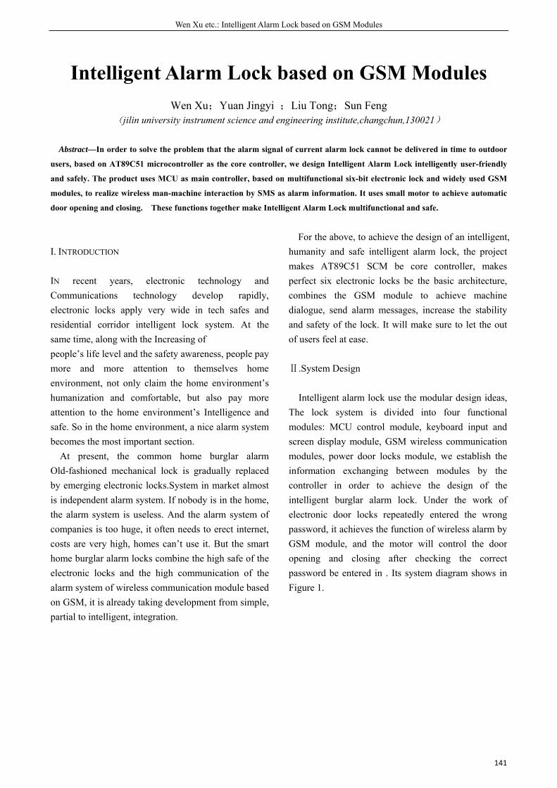
Wen Xu etc.: Intelligent Alarm Lock based on GSM Modules
141
Intelligent Alarm Lock based on GSM Modules
Wen Xu;Yuan Jingyi ;Liu Tong;Sun Feng (jilin university instrument science and engineering institute,changchun,130021)
Abstract—In order to solve the problem that the alarm signal of current alarm lock cannot be delivered in time to outdoor
users, based on AT89C51 microcontroller as the core controller, we design Intelligent Alarm Lock intelligently user-friendly
and safely. The product uses MCU as main controller, based on multifunctional six-bit electronic lock and widely used GSM
modules, to realize wireless man-machine interaction by SMS as alarm information. It uses small motor to achieve automatic
door opening and closing. These functions together make Intelligent Alarm Lock multifunctional and safe.
I. INTRODUCTION
IN recent years, electronic technology and Communications technology develop rapidly, electronic locks apply very wide in tech safes and residential corridor intelligent lock system. At the same time, along with the Increasing of people’s life level and the safety awareness, people pay more and more attention to themselves home environment, not only claim the home environment’s humanization and comfortable, but also pay more attention to the home environment’s Intelligence and safe. So in the home environment, a nice alarm system becomes the most important section.
At present, the common home burglar alarm Old-fashioned mechanical lock is gradually replaced by emerging electronic locks.System in market almost is independent alarm system. If nobody is in the home, the alarm system is useless. And the alarm system of companies is too huge, it often needs to erect internet, costs are very high, homes can’t use it. But the smart home burglar alarm locks combine the high safe of the electronic locks and the high communication of the alarm system of wireless communication module based on GSM, it is already taking development from simple, partial to intelligent, integration.
For the above, to achieve the design of an intelligent, humanity and safe intelligent alarm lock, the project makes AT89C51 SCM be core controller, makes perfect six electronic locks be the basic architecture, combines the GSM module to achieve machine dialogue, send alarm messages, increase the stability and safety of the lock. It will make sure to let the out of users feel at ease.
Ⅱ.System Design
Intelligent alarm lock use the modular design ideas, The lock system is divided into four functional modules: MCU control module, keyboard input and screen display module, GSM wireless communication modules, power door locks module, we establish the information exchanging between modules by the controller in order to achieve the design of the intelligent burglar alarm lock. Under the work of electronic door locks repeatedly entered the wrong password, it achieves the function of wireless alarm by GSM module, and the motor will control the door opening and closing after checking the correct password be entered in . Its system diagram shows in Figure 1.
A
B
The Englis
142
Ⅲ. HARDWA
A.MCU MastMCU cont
lock system. ATEML comthe chip ofoperational cindependent basic functiopassword setlight alarm. matrix keybomemory 24Cinstructions long-distancecoordinating relationshipsprogram and
Fig.2 M
B.Keyboard iThese two
Keyboard
sh Proceedings
ARE DESIGN
ter module trol module i In this desig
mpany's 51 sef electronic control. MasSCM minim
ons of a sixttings, modifyControl the oard, read in
C02 and outputo GSM
e machine dthe rem
, complete sinterlock fun
MCU core cont
input and scro modules ar
MCU
Memor
of the College
s the main pogn, we take teries SCM Alocks data
ster control mum systemsx electronic y, proofreadinLCD1602 dinput data, stut to the displalarm modu
dialogue, wirmaining mself-locking lnctions.
troller connecti
reen display mre the main i
E
ry unit
of Instrumentat
Fig.1 Intelligen
ortion of the dthe choice of
AT89C51 chipprocessing
module use s to achieve locks, includ
ng and soundisplay and 4 tored in extelay module. Sule to achreless alarm.
modules timloop runs to
on diagram
module input and ou
Lcd1602
rror warnin
Sub-controll
tion & Electrica
nt alarm lock st
door f the p as and the
the ding
d and * 4
ernal Send hieve By
ming o the
utput
mod4 mkey160ensThepowkeyunlopasC.G
TselemodbasdevboaprofunSIE180supin tranSIMandcominst300115(sho
ng
ler
al Engineering,
tructure diagram
dules of this matrix keyboays and functi02 LCD screure that the ee entire systwer lcd1602 eyboard input ock, lock, mosword to clea
GSM WirelessThe design ection is extendule. GSM meband proce
vices such asard, is an indcessing, basectional modu
EMENS (Siem00MHZ highpply voltage rSleep state insportable voM card readed data connemmands cantructions and0b / s ~ 115kb5kb / s. It suort message)
Voltage tr
Clo
GS
Motor d
Jilin University
m
work. Keyboard to compleion keys; sceen, adjust effect displaytem is automenter the pass
are 0-9 tenodify, reset, car six functions communicatof remote nsive range o
module is putssor chip, m
s sub-moduledependent opeband and proules. TC35i mens) compa
hly integratedrange 3.3 ~ 4is 3.5mA, idoice and dater and antennectors. TC35n be bi-dired data, selectb / s. Automaupports Text , it also can
ransform
ock
M
drive
ty, in the First H
oard input mete the settin
creen displaythe screen
yed by 10k pmatically inisword entry sn-digit key aclear the passn keys. tion module communicati
of applicationtting the GSMmemory, powe integrated perating systeovides a stand
is designedany, is a duad GSM mod4.8V, current dle state is 2ta signals, cna by interfa5i data interectional trantable baud i
atic baud rateand PDU fouse AT com
Lock
Half of 2015
odule use 4 *ng of numericy module usebrightness topotentiometeritialized aftescreen, 16-keyand includingword, and the
ion module’ns TC35iGSMM RF chip, awer amplifiein the circuiem, GSM RFdard interface
d by Germanal-band 900 dule, the DC
consumption25mA; it canconnected viaace connectorface via ATnsmission ois the rate o is 1.2kb / s ~rmat of SMS
mmands or of
* c e o r. er y g e
s M a
er it F e n /
C n n a
or T of of ~ S ff
D
signal to achof the main commands tcommands tusers, achiev
F
D. Power doThe modu
28BYJ-48 sdriver chip a28BYJ48 typmotors, voltais applied cocontinue to rostepper motoonce, it alsoWhen the porotor turned array, whicDarlington a500mA / 5Vwide tempercharacteristicor lock the stepper motoopening and
Ⅳ. SOFTWAR
System soSTC89C51 m
Figure 4 After a systeoperation stoperations. Pidentify keypassword inpfunction keymotor. Collecthe display m
hieve the restcontroller uso TC35i, theto send text ve the remote
Fig.3 TC35i phy
or lock moduule uses a tepper motoand simple lpe stepper moage DC5V-Dontinuously totate. Each p
or or two-phao correspondsower is chana pitch. UL
ch consists and 5VTTL
V.It has a higrature range, cs. The desig
latch by thor reversing,closing.
RE DESIGN
ftware designmicrocontrollis a flowcha
em power-on,tate to prepPost real-timey bit and put process, sys and controct cycle the d
module.
Wen Xu
tart and recosing SCM ATe GSM mod
messages twireless alar
ysical object dia
ule four-phase f
or reducer, Ulock to achieotor is a four
DC12V. Whento the steppiulse signal cose windings es to its rotor
nged to compLN2003 is hi
of seven input level
gh current gahigh load ca
gn sends come microcontr, to achieve
n use C languer. art of the o, initialize thepare for sube scanning forfunction setswitch states ol the driver data of work
u etc.: Intelligen
very. The deT89C51 senddule receivedo mobile ph
rm function.
agram
five-wire sysULN2003 meve the funct-phase eight-n a control png motor, it orresponding energized char turned a anplete a cycle,igh current d
silicon’s Nl, output up
ain, high voltapacity and o
mmands to unroller, contro
automatic d
uage and write
peration syste system, go bsequent relr keyboard intting, enter according tomodule to dstate, and sen
nt Alarm Lock b
esign d AT d AT hone
stem motor
tion. -shot pulse
can g to a ange ngle. , the drive NPN p to tage, other nlock olled door
e in
tem. into
lated nput,
the o the drive nt to
Ⅴ.
Tstatspefunresurealthe com
Ⅵ.C
Tund
based on GSM
Fig
ANALYSIS
To test the futus of intecifications. Bctions one bults, the desiglized. We opsystem is sta
mmunication.
Fi
CONCLUSIO
This design rder the electr
Enter the while
The password can be reset.
Modules
g.4 Work flow c
OF EXPERIM
unctionality olligent burgBuild a compby one testingn of the indiverate the sys
able, each mo
g.5 The system
ON
researches a ronic door lo
the passwonumeric kethe display o
Yes
Open.
chart of system
MENTAL RE
of the designglar alarm
mplete systemng, from the ividual functistem once byodule has fast
m physical map
smart burglaocks passwor
ord on eypad, on the
NO
Aets
sa
s
143
ESULTS
n, we test thelock design
m, for variouexperimenta
ons all can bey once, verifyt and accurate
ar alarm lockrd input erro
Re-enter. After the error of three self-locking and send alarm messages
3
e n s
al e y e
k, or

The English Proceedings of the College of Instrumentation & Electrical Engineering, Jilin University, in the First Half of 2015
144
several times, achieve the wireless communication alarm function by GSM module, after checking the correct password, then open and close the door by the motor control. Fully integrated with today's hottest GSM mobile communications equipment to achieve human-computer dialogue, enhanced the safety and reliability of the intelligent burglar alarm lock.
Reference
[1] Han Tuanjun, Electronic locks microcontroller based design
[J]. Foreign Electronic Measurement Technology 2010 (07)
[2] Zhang Ying, Design of multi-user locks [J]. Electronic
Technology 2010 (08)
[3] Zhang Yun, Zhou Minghui, Zhou Hailin, Li Aihua, Meng
Wei, Baced on AT89S51 multifunctional electronic lock
design [J] Electronic Design Engineering 2010 (06)
[4] Wang Kuanren, Reliable and secure smart locks [J].
Application of Electronic Technique.2001(02)
[5] Zhang Yonghua, Zhang Shiwu, Yang Jie, Shape memory
alloy driving microcomputer lock design [J]. Automation
and Instrumentation. 2007 (03)
[6] Zhang Fan, GSM-based electronic locks [J]. Digital
technology and applications. 2011 (06)
[7] Li Jintan, MCU design use GSM locks [J]. Electronic Test.
2006 (10)
[8] Chen Song, Chen Jiapin, Li Zhenbo, Chen Wenyuan, Zhao
Xiaolin. Based on electromagnetic micro-motor lock control
system development [J]. Electronic Technology 2003 (10)
[9] Gao Hai, Guo Hongxia. AT89S51 password lock design [J]
Based on modern electronic technology. 2010 (18)
[10] Chen Yanchun. Lock improvements - Single button [J]
electronic production 2003 (10).
[11] Liu Yongchun, Guan yipping, Yang Jing. Design [J] GSM
and microcontroller-based automotive anti-theft alarm
system. Southwest University (Natural Science) 2011 (07)
[12] Luo Binglian. Design GSM smart home burglar alarm
system [J]. Based on Fujian computers. 2011 (10)
[13] Yan Yongsheng, Wang Haiyan, Bai Jun, Zhu Mengyang.
Design [J] HPI interface based on a dual CPU underwater
target detection platform electronic technology. 2011 (09)
[14] Zhou Meili, Li Jianxin, Bai Zonwen. Multifunction design
GSM burglar alarm system [J]. Based on modern electronic
technology. 2011 (23)
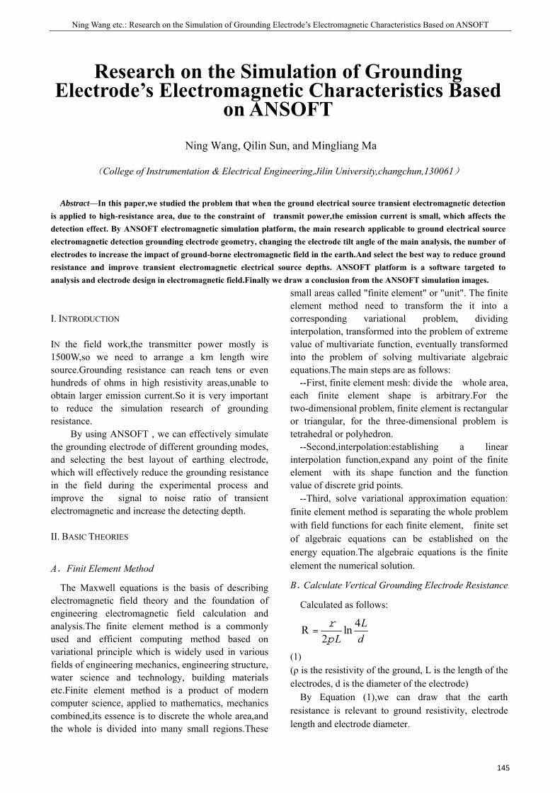
Ning Wang etc.: Research on the Simulation of Grounding Electrode’s Electromagnetic Characteristics Based on ANSOFT
145
Research on the Simulation of Grounding Electrode’s Electromagnetic Characteristics Based
on ANSOFT
Ning Wang, Qilin Sun, and Mingliang Ma
(College of Instrumentation & Electrical Engineering,Jilin University,changchun,130061)
Abstract—In this paper,we studied the problem that when the ground electrical source transient electromagnetic detection
is applied to high-resistance area, due to the constraint of transmit power,the emission current is small, which affects the detection effect. By ANSOFT electromagnetic simulation platform, the main research applicable to ground electrical source electromagnetic detection grounding electrode geometry, changing the electrode tilt angle of the main analysis, the number of electrodes to increase the impact of ground-borne electromagnetic field in the earth.And select the best way to reduce ground resistance and improve transient electromagnetic electrical source depths. ANSOFT platform is a software targeted to analysis and electrode design in electromagnetic field.Finally we draw a conclusion from the ANSOFT simulation images.
I. INTRODUCTION
IN the field work,the transmitter power mostly is 1500W,so we need to arrange a km length wire source.Grounding resistance can reach tens or even hundreds of ohms in high resistivity areas,unable to obtain larger emission current.So it is very important to reduce the simulation research of grounding resistance. By using ANSOFT , we can effectively simulate the grounding electrode of different grounding modes, and selecting the best layout of earthing electrode, which will effectively reduce the grounding resistance in the field during the experimental process and improve the signal to noise ratio of transient electromagnetic and increase the detecting depth.
II. BASIC THEORIES
A.Finit Element Method
The Maxwell equations is the basis of describing electromagnetic field theory and the foundation of engineering electromagnetic field calculation and analysis.The finite element method is a commonly used and efficient computing method based on variational principle which is widely used in various fields of engineering mechanics, engineering structure, water science and technology, building materials etc.Finite element method is a product of modern computer science, applied to mathematics, mechanics combined,its essence is to discrete the whole area,and the whole is divided into many small regions.These
small areas called "finite element" or "unit". The finite element method need to transform the it into a corresponding variational problem, dividing interpolation, transformed into the problem of extreme value of multivariate function, eventually transformed into the problem of solving multivariate algebraic equations.The main steps are as follows:
--First, finite element mesh: divide the whole area, each finite element shape is arbitrary.For the two-dimensional problem, finite element is rectangular or triangular, for the three-dimensional problem is tetrahedral or polyhedron.
--Second,interpolation:establishing a linear interpolation function,expand any point of the finite element with its shape function and the function value of discrete grid points.
--Third, solve variational approximation equation: finite element method is separating the whole problem with field functions for each finite element, finite set of algebraic equations can be established on the energy equation.The algebraic equations is the finite element the numerical solution.
B.Calculate Vertical Grounding Electrode Resistance
Calculated as follows:
4R ln2
LL d
r
p=
(1) (ρ is the resistivity of the ground, L is the length of the electrodes, d is the diameter of the electrode)
By Equation (1),we can draw that the earth resistance is relevant to ground resistivity, electrode length and electrode diameter.
The English Proceedings of the College of Instrumentation & Electrical Engineering, Jilin University, in the First Half of 2015
146
C.The Similarity Criteria of Electromagnetic Method
In order to make a more accurate simulation results, we use similar criteria in the model which the linear dimensions followed by the electromagnetic method:
2 2( )fm
f m
Lk
Ls
s= =
(2) ( σ is the conductivity, L is the length. The subscript m is an analog system, f is the simulated field system, k is a linear scale)
Similar criteria can make the response characteristics under experimental simulation consistent with the corresponding response characteristics under field conditions.
Table I gives a detailed list of the actual size and the
size of the simulation, , , ,fg fc fg fcL Ls s respectively
represent the actual ground conductivity, the conductivity of the ground electrode, the actual size of the earth, the actual size of the ground electrode.
, , ,mg mc mg mcL Ls s respectively represent the earth
conductivity of model, the ground electrode conductivity of model, the earth size of model, the grounding electrode size of model. According to the linear scale for 1000 needs to be set.
III.SIMULATION MODEL
A. Grounding Electrode Model Use Ansoft Maxwell 3D three-dimensional
simulation software to build 1000mm· 1000mm· 1000mm earth model under conditions of transient field. Electrode materials made of copper conductor, the length and the width is 1mm and the height is 2mm, according to the similar simulation scaled down. Figure 1 shows the grounding electrode and the earth model, based on the actual situation of the land set for three, in turn to increase the conductivity.
Fig. 1. The model of ground electrode and earth.
B.Definition and Distribution of Material
Select the grounding electrode model, double click electrode,in the dialog box click on the edit options. According to the data in Table I,we define the material and create a new earth materials in the material editor library,set their own parameters such as resistance, and assigned to the earth model.
C.The Excitation Source
Selecte the surface of electrode,designated voltage excitation.Or use Ansoft Maxwell Circuit Editor software into an external circuit shown in Figure 2.The introduction of an external circuit excitation voltage is 1000V,1Hz,R3 represents a long lead source resistance, LWinding1 representative grounding electrode.
Fig.2. The Circuit of external excitation.
C.Set the Solution Mode and Precision
Right click Analysis/Add Solution Setup, respectively filled 1s and 0.1s in Stop time and Time step column , shown in Figure 3.
TABLE I THE PARAMETERS OF THE ACTUAL SIZE AND THE SIMULATION MODEL
BASED ON THE GROUNDING RESISTANCE OF ANSOFT
Conductivity(S/m) Linear Dimension(m) k
fgs
mgs
fcs
mcs
fgL
mgL
fcL
mcL
1000
0.01
10000
5.8E7
5.8E11
1000
1 1 0.001
Ning Wang etc.: Research on the Simulation of Grounding Electrode’s Electromagnetic Characteristics Based on ANSOFT
147
Fig.3. Solution setup.
D . Set Solution Area and Boundary Conditions
(Choose the default boundary condition)
IV.TRANSIENT FIELD SIMULATION AND ANALYSIS OF
THE ELECTRODE MODEL
A.Change the Angle of the Electrode
According to Figure 1,simulate the model.Electrode is inclined 15 °, 30 °, 45 °, 90 °. Simulation results shows in Figure 4, 5, 6 and 7.Comparing the four figures,we can see the distribution of the current density basically the same,but the corresponding current density distribution is different,in order to facilitate comparison, the image formed by the system are using the default logarithmic scale, it can be seen when the electrode is inclined 45°,the maximum current density and the electrode effect are the best.
Fig. 4. The current density of electrode tilted 15 degrees.
Fig.5. The current density of electrode tilted 30 degrees.
Fig.6. The current density of electrode tilted 45 degrees.
Fig.7. The current density of vertical electrode.
B. Increase the Number of Electrodes The single-layer earth model is simulated, Figure 8
and 9 are single electrode and four-electrode current density simulation map.From the simulation chart of single electrode and the four electrode model, we can see that they are consistent and uniform distribution of color, but the color corresponding to the current density values are different, four-electrode model significantly greater than a single electrode.

The English Proceedings of the College of Instrumentation & Electrical Engineering, Jilin University, in the First Half of 2015
148
Fig.8. The current density of one-electrode model.
Fig.9. The current density of four-electrode model.
V.CONCLUSION
By using Ansoft Maxwell electromagnetic field simulation software, multi-media simulation setting two-electrode earth model.We studied the tilt angle of the electrode, the number of electrodes,which have some impacts on resistance and ground current distribution.The electrical conductivity of earth and electrode provided references of similar simulation ratio.Through the comparative analysis of the simulation results, the conclusion is as follows:
(1) Electric field spread of the figures are to meet energy conservation,the electric field distribution in line with the law,Electric field direction tilted whenthrough the medium fault .Consistent with the theory .
(2) Compared the current density distribution shown in the Figure 4, Figure 5, Figure 6 and Figure 7,we can get that tilted 30 degree to 50 degree,the electric field distribution is the most widespread, the utilization of electrode is the best.
(3) Comparing Figure 8 and 9,we found that the increasing number of electrodes can effectively reduce the resistance.
References
[21] Xv Hua, Lv Jinhuang, Chen Yuan etc. Discuss on Tower
Impulse Grounding Resistance [J]. High Voltage
Technology, 2005, pp.73-75.
[22] Liu Chun, He Junjia, Yin Xiaogen etc. The Computer
Simulation of Composite Grounding Resistance[J].
Chinese Society for Electrical Engineering, 2003,
pp.159-163.
[23] Feng Cizhang,Ma Xikui,Introduction of Engineering
Electromagnetic Field. Beijing: Higher Education
Press,2000.6. [24] Feng Zhiwei,Xiao Wenan,Ma Jinfu. Analysis on the
Factors Influencing the Measurement Results of
Grounding Resistance[J]. Electrical Applications.2010.
[25] Chen Xianlu, Liu Yugen, Huang Yong. Grounging.
Chongqing: Chongqing University press.2002.
[26] Wu Bo.Various Measures to Reduce Resistance and
Calculation Method of Grounding Resistance in
Substation.2007.
[27] Zeng Rong,Gao Yanqing,Ke Jinliang. Effect of Electrode
Position on Measuring Grounding Resistance in
Measurement System of the Vertical Three-layer Soil
Structure[J]. Journal of Tsinghua University (Natural
Science Edition).2001.
[28] Liu Junfeng,Deng Juzhi,Zhang Zhiyong,Chen Hui.The
Theoretical Calculation of the Grounding Resistance to
Electrical Source and Its Affecting Factors Analysis.
Chinese Journal of Engineering Geophysics.2012,09(4).
[29] Zhao Bo,Zhang Hongliang. Application of Ansoft 12 in
Engineering Electromagnetic Field[M].Beijing: China
Water&Power Press,2010.
Wan Yunxia etc.: The Design of Smart Door Lock State Monitoring System
149
The Design of Smart Door Lock State Monitoring System
Wan Yunxia1,2 Li Shilong1 Jiang Lei1 Song Tao1
(1.College of Instrumentation and Electrical Engineering, Jilin University, Changchun 130012,China; 2. Key Laboratory for Geophysical Instrumentation of Ministry of Education, Jilin University, Changchun 130012,
China )
Abstract—In view of the complex structure and low intelligence of anti-theft door lock, and design a kind of mechanical anti-theft lock with the combination of electronic intelligence door lock state monitoring system. Smart door lock monitoring system is processing the STC89C51 microcontroller as the mainly control chip, with mechanical locks as the carrier, using GSM information module, the infrared monitoring module, camera monitor module and information displaying module. The system realize the monitoring of door lock state situations, such as unlock and forget key... Response show that this kind of system design has important significance for home furnishing guard against thief
Keywords—intelligent monitoring GSM module Infrared detection
I. INTRODUCTION
IN the security issues become increasingly referred to a high level of today, a practical, safe door lock set there is a great demand in the market. Intelligent door monitoring system, is to make life let Home Furnishing more safety. For the first point, developed a kind of high safety, good reliability, door monitoring system of electronic and mechanical durability high combination. In view of the existing in the market of electronic password lock is complex, complicated installation, design a general convenient installation and safety of not less than intelligent door lock detection system on the market the password lock, meet more users and market demand.
II. INTEGRAL DESIGN
Intelligent door lock state monitoring system consists of the following modules: power supply module, GSM module, infrared monitoring module; STC89C51 microcontroller; voice module; a camera module; display module. Figure 1 is a block diagram of the whole system.
Fig.1 Diagram of the whole system
III. MODULE DESIGN
A. Design of GSM Module The GSM module is connected with
the MCU minimum system, when the lock state monitoring module detects the unsafe state, by the GSM module to send text messages to remind users and the video monitoring module is opened at the same time.
We have selected the Huawei chip GTM900-B, the main parameters of the receiving sensitivity: <-106dB,which is meeting the requirements of the design, the power supply voltage of 3.3V to 4.8V. Supporting the GSM standard AT command. It’s also Supports the computer serial port (232 level) and the SCM connected MCU (3.3V-5V can) is connected directly, and can simultaneously connect computer when using MCU debugging, without jumper setting, use the computer serial debugging
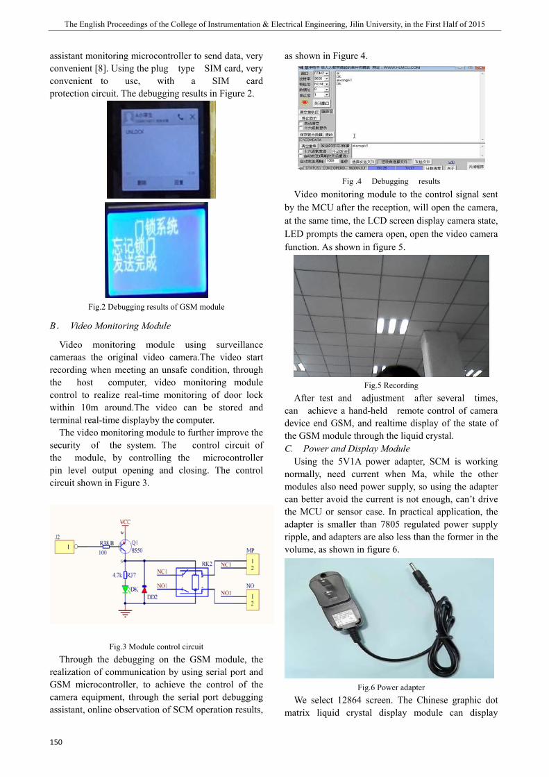
The English Proceedings of the College of Instrumentation & Electrical Engineering, Jilin University, in the First Half of 2015
150
assistant monitoring microcontroller to send data, very convenient [8]. Using the plug type SIM card, very convenient to use, with a SIM card protection circuit. The debugging results in Figure 2.
Fig.2 Debugging results of GSM module
B. Video Monitoring Module
Video monitoring module using surveillance cameraas the original video camera.The video start recording when meeting an unsafe condition, through the host computer, video monitoring module control to realize real-time monitoring of door lock within 10m around.The video can be stored and terminal real-time displayby the computer.
The video monitoring module to further improve the security of the system. The control circuit of the module, by controlling the microcontroller pin level output opening and closing. The control circuit shown in Figure 3.
Fig.3 Module control circuit Through the debugging on the GSM module, the
realization of communication by using serial port and GSM microcontroller, to achieve the control of the camera equipment, through the serial port debugging assistant, online observation of SCM operation results,
as shown in Figure 4.
Fig .4 Debugging results
Video monitoring module to the control signal sent by the MCU after the reception, will open the camera, at the same time, the LCD screen display camera state, LED prompts the camera open, open the video camera function. As shown in figure 5.
Fig.5 Recording
After test and adjustment after several times, can achieve a hand-held remote control of camera device end GSM, and realtime display of the state of the GSM module through the liquid crystal. C. Power and Display Module
Using the 5V1A power adapter, SCM is working normally, need current when Ma, while the other modules also need power supply, so using the adapter can better avoid the current is not enough, can’t drive the MCU or sensor case. In practical application, the adapter is smaller than 7805 regulated power supply ripple, and adapters are also less than the former in the volume, as shown in figure 6.
Fig.6 Power adapter
We select 12864 screen. The Chinese graphic dot matrix liquid crystal display module can display
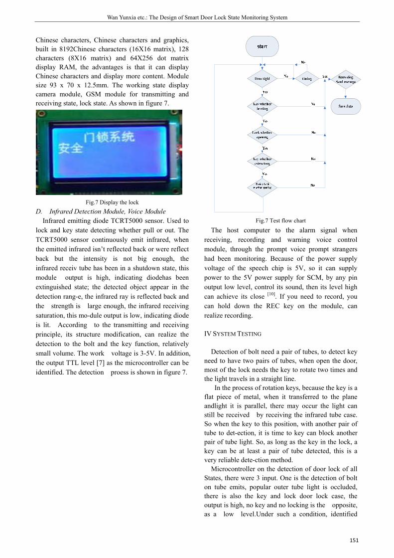
Wan Yunxia etc.: The Design of Smart Door Lock State Monitoring System
151
Chinese characters, Chinese characters and graphics, built in 8192Chinese characters (16X16 matrix), 128 characters (8X16 matrix) and 64X256 dot matrix display RAM, the advantages is that it can display Chinese characters and display more content. Module size 93 x 70 x 12.5mm. The working state display camera module, GSM module for transmitting and receiving state, lock state. As shown in figure 7.
Fig.7 Display the lock
D. Infrared Detection Module, Voice Module Infrared emitting diode TCRT5000 sensor. Used to
lock and key state detecting whether pull or out. The TCRT5000 sensor continuously emit infrared, when the emitted infrared isn’t reflected back or were reflect back but the intensity is not big enough, the infrared receiv tube has been in a shutdown state, this module output is high, indicating diodehas been extinguished state; the detected object appear in the detection rang-e, the infrared ray is reflected back and the strength is large enough, the infrared receiving saturation, this mo-dule output is low, indicating diode is lit. According to the transmitting and receiving principle, its structure modification, can realize the detection to the bolt and the key function, relatively small volume. The work voltage is 3-5V. In addition, the output TTL level [7] as the microcontroller can be identified. The detection proess is shown in figure 7.
Fig.7 Test flow chart The host computer to the alarm signal when
receiving, recording and warning voice control module, through the prompt voice prompt strangers had been monitoring. Because of the power supply voltage of the speech chip is 5V, so it can supply power to the 5V power supply for SCM, by any pin output low level, control its sound, then its level high can achieve its close [10]. If you need to record, you can hold down the REC key on the module, can realize recording.
IV SYSTEM TESTING
Detection of bolt need a pair of tubes, to detect key need to have two pairs of tubes, when open the door, most of the lock needs the key to rotate two times and the light travels in a straight line.
In the process of rotation keys, because the key is a flat piece of metal, when it transferred to the plane andlight it is parallel, there may occur the light can still be received by receiving the infrared tube case. So when the key to this position, with another pair of tube to det-ection, it is time to key can block another pair of tube light. So, as long as the key in the lock, a key can be at least a pair of tube detected, this is a very reliable dete-ction method.
Microcontroller on the detection of door lock of all States, there were 3 input. One is the detection of bolt on tube emits, popular outer tube light is occluded, there is also the key and lock door lock case, the output is high, no key and no locking is the opposite, as a low level.Under such a condition, identified
The English Proceedings of the College of Instrumentation & Electrical Engineering, Jilin University, in the First Half of 2015
152
several circumstances. Reactive programming according to this several circumstances should arise. State 1:
At this time for the safe state, that is, the doors were locked, the key is pulled out. There will be no hint. As shown in figure 8-A. State 2:
At this time the door is locked, but the key is pulled out. At this time the alarm and the camera is opeded bythe MCU, prompting and recording, 30 seconds later, the mobile phone will got a short message by the GSMmodule. This time display mobile phone received tips, content: ULOCK. As shown in figure 8-B.
State 3: When it is detected that the door is not locked, the
key is not removed the, system will send out alarm sound and turn on the camera, prompt and video, timer 30s, by the GSM module to the mobile phone sends a short message, prompt, this time display mobile phone received tips, content is: ULOCK AND KEY FORGETTEN. As shown in figure 8-C. State 4:
When the key is down, the system will alarm and turn on the camera, prompt and video, timer 30s, by GSM module sends a message to the mobile phone, prompting, This shows that the mobile phone to receive prompt, content: FORGET KEY. As shown in figure 8-D.
A B
C D Fig.8 Lock state debugging
V. CONCLUSION
By the use of STC89C51 single chip computer and its auxiliary circuit to complete the design of mechanical lock intelligent monitoring system, realizing the monitoring, SMS to different lock states reminder, voice alarm, image monitoring. Intelligent Home safety towards more choices. This paper studies
for the door lock monitoring system, to generate an important significance to improve the Home Furnishing security, let us live safer and more convenient.
References
[1] Kim, to Guoliang. C singlechip STC89C52 language
electronic code lock design and Simulation of [J]. based on
modern electronic technology. 2010 (19)
[2] Han Tuanjun. SCM electronic combination lock design [J].
foreign electronic measurement technology based on 2010
(07).
[3] Zhang Yun, Zhou Minghui, Zhou Hailin, Li Aihua, Meng
Wei. The multifunction electronic code lock design
AT89S51 [J]. electronic design engineering based on 2010
(06).
[4] Cao Jianlin, Sun Jie, Sun Xueying, Ren Lei, Du Kangping.
The electronic code lock design [J]. Journal of Chengdu
University of Information Technology. 2010 (02)
[5] Zhu Xuan, Tang Xiaoqian, Yin Jianjun. Intelligent
encrypted electronic code lock design of [J]. Light Industry
Machinery Based on 2009 (04).
[6] Chen Jianlin, Zhao Lihong. Digital Proteus password lock
[J]. simulation design of mechanical engineering and
automation based on 2009 (04).
[7] Lin Lichun. New iButton electronic lock controller design
based on 2009 [J]. Journal of Guangdong University of
Technology (02).
[8] Gu Guangxu. Intelligent electronic cipher lock design [J].
Journal of Yan Cheng Institute Of Technology (NATURAL
SCIENCE EDITION). 2009 (01)
[9] Yue Xue Jun, Chen Shan, Lu Jianqiang, Xu Xing, Song Shu
ran. Electronic password lock design of MCU and serial
communication [J]. Journal of Yunnan Agricultural
University based on 2009 (01).
[10] Wang Zhihong, Xue Zengtao, Chen Zhijun, Du Shen hui.
Smart card electronic lock design [J]. modern electronic
technology, 2007 (09).
Liu Youtao etc.: ICL7107 digital DC voltage and current meter based on
153
ICL7107 digital DC voltage and current meter based on
Liu Youtao ; Liu Ziqi ; Zhao Dong
( Instrument Science and Electrical Engineering, Jilin University, Changchun 130022 )
Abstract—The main module of this design uses ICL7107 chip as the digital meter, so that the circuit has many advantages
with a simple design, high integration, high reliability, and high performance. The system can measure 0 ~ 1.99V, 0 ~ 19.99V, 0
~ 199V, 0 ~ 1999V, a total of four scale voltage values, and 0 ~ 19mA, 0 ~ 199mA, 0 ~ 1999mA, 0 ~ 5A, a total of four the
current value of the measurement range The system is made of a kind and has been tested with good test results.
Keywords—ICL7107 chip, digital, DC, voltage and current measurement
1 INTRODUCTION
BECAUSE traditional voltage meter needs latches, ad converters, digital control circuits to drive multiple modules, making the entire system structure is complex, high cost. The integrated chip design based ICL7107 meter fully overcome the above disadvantages of the meter and has the advantage of high stability.
Given the high rate of laboratories using ammeter and voltmeter, the failure rate of large, independent design and complete the voltmeter and ammeter can effectively improve the experimental environment and reduce losses.
For different measurement requirements, specific design meter stalls, can improve the accuracy and reliability, economical and practical experimental data.
2 SYSTEM DESIGN
In this paper, the accuracy of the meter designed for three and a half, five voltage ranges are 0 ~ 199mV, 0 ~ 1.99V, 0 ~ 19.99V, 0 ~ 199V, 0 ~ 1999V, four current ranges are 0 ~ 19mA, 0 ~ 199mA, 0 ~ 1999mA, 0 ~ 5A, by four digital display reading is not able to stabilize the beating. This product can be used alone or can be shown to DDSZ-1 motors and electrical test equipment supporting the use of technology system structure shown in Figure 1.
Figure 1 System Block Diagram
3 SYSTEM AND THE REALIZATION OF EACH MODULE
FUNCTIONS
3.1 Power Module Due to the high precision circuit, the power supply voltage or power supply ripple instability presence
will affect the results, so in order to ensure accurate supply voltage 5V, the power used for continuously adjustable DC power, ripple control requirements within 10mv, for ripple requirements can be a simple voltage regulator circuit to meet the requirements. Power module circuit shown in picture two.
Power Modules PSA Rectifier Regulators
Detection module AD conversion Data Processing Data output
Display Module Digital Display Conversion stalls Fault Display
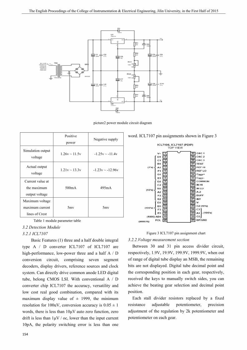
The English Proceedings of the College of Instrumentation & Electrical Engineering, Jilin University, in the First Half of 2015
154
picture2 power module circuit diagram
Positive
power Negative supply
Simulation output
voltage 1.26v ~ 11.5v -1.25v ~ -11.4v
Actual output
voltage 1.21v ~ 13.3v -1.23v ~ -12.96v
Current value at
the maximum
output voltage
500mA 495mA
Maximum voltage
maximum current
lines of Crest
5mv 5mv
Table 1 module parameter table
3.2 Detection Module 3.2.1 ICL7107
Basic Features (1) three and a half double integral type A / D converter ICL7107 of ICL7107 are high-performance, low-power three and a half A / D conversion circuit, comprising seven segment decoders, display drivers, reference sources and clock system. Can directly drive common anode LED digital tube, belong CMOS LSI. With conventional A / D converter chip ICL7107 the accuracy, versatility and low cost real good combination, compared with its maximum display value of ± 1999, the minimum resolution for 100uV, conversion accuracy is 0.05 ± 1 words, there is less than 10μV auto zero function, zero drift is less than 1μV / oc, lower than the input current 10pA, the polarity switching error is less than one
word. ICL7107 pin assignments shown in Figure 3
Figure 3 ICL7107 pin assignment chart
3.2.2.Voltage measurement section Between 30 and 31 pin access divider circuit,
respectively, 1.9V, 19.9V, 199.9V, 1999.9V, when out of range of digital tube display an MSB, the remaining bits are not displayed. Digital tube decimal point and the corresponding position in each gear, respectively, received the keys to manually switch sides, you can achieve the beating gear selection and decimal point position.
Each stall divider resistors replaced by a fixed resistance adjustable potentiometer, precision adjustment of the regulation by 2k potentiometer and potentiometer on each gear.
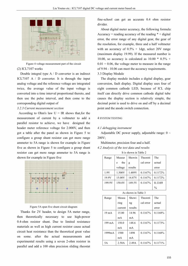
Liu Youtao etc.: ICL7107 digital DC voltage and current meter based on
155
Figure 4 voltage measurement part of the circuit
(2) ICL7107 works Double integral type A / D converter is an indirect
ICL7107 A / D converter. It is through the input analog voltage and the reference voltage are integrated twice, the average value of the input voltage is converted into a time interval proportional thereto, and then use the pulse interval, and then come to the corresponding digital output of 3.2.3 Current measurement section
According to Ohm's law U = IR shows that,for the measurement of current by a voltmeter to add a parallel resistor to achieve, we have designed the header meter reference voltage for 2.000V, and then got a table after the panel as shown in Figure 5 to configure a group shunt resistor can get more range ammeter to 5A range is shown for example in Figure five as shown in Figure 5 to configure a group shunt resistor can get more range ammeter to 5A range is shown for example in Figure five
Figure 5A span five shunt circuit diagram
Thanks for 2V header, to design 5A meter range, then theoretically necessary to use high-power 0.4-ohm resistor shunt. Due to limited resistance materials as well as high current resistor cause actual circuit heat resistance than the theoretical great value on some. after the actual measurements and experimental results using a seven 2-ohm resistor in parallel and add a 100 ohm precision sliding rheostat
fine-school can get an accurate 0.4 ohm resistor divider.
About digital meter accuracy, the following formula: Accuracy = reading accuracy of the reading * + digital error, the error range of any digital gear, the gear of the resolution, for example, three and a half voltmeter with an accuracy of 0.5% + 1dgt, select 20V range (maximum display 19.99). If the measured number is 10.00, so accuracy is calculated as 10.00 * 0.5% + 0.01 = 0.06, the voltage meter to measure in the range of 9.94 - 10.06 can meet the accuracy requirements. 3.3 Display Module
The display module includes a digital display, gear conversion, fault display. Digital display uses four of eight common cathode LED, because of ICL chip itself can directly drive common cathode digital tube causes the display section is relatively simple, the decimal point is used to drive on and off by a decimal point and the anode switch connection.
4 SYSTEM TESTING
4.1 debugging instrument Adjustable DC power supply, adjustable range: 0 ~
200V; Multimeter, precision four and a half.
4.2 Analysis of the test data and results It is shown in Table 2
Range Measur
e the
voltage
Showin
g
results
Theoreti
cal error
The
actual
error
1.9V 1.500V 1.489V 0.1167% 0.1172%
19.9V 15.00V 14.87V 0.1167% 0.1172%
199.9V 150.0V 149.5V 0.1167% 0.1169%
As shown in Table 3
Range Measu
ring
current
Showi
ng
results
Theoreti
cal error
The
actual
error
19 mA 15.00
mA
14.96
mA
0.1167% 0.1168%
199 mA 150.0
mA
148.6
mA
0.1167% 0.1173%
1999mA 1500
mA
1498
mA
0.1167% 0.1168%
5A 2.50A 2.49A 0.1167% 0.1171%

The English Proceedings of the College of Instrumentation & Electrical Engineering, Jilin University, in the First Half of 2015
156
U2V=±2/1999=0.001V U20V=±20/1999=0.01V U200V=±200/1999=0.1V
Theoretical 2V block with relative error of measurement γ1 = (± 0.05% * 1.5 ± 0.001) /1.5=0.1167%
Actual relative error measurement block is 2V γ2 = ± 0.05% ± 1/1489 = 0.1172% γ1 and γ2 compared to almost equal, with a description of the design and testing of four and a half meter accuracy rather, that meet the requirements. By that calculation, the meter measured experimental data more accurate, with a multimeter to measure the data errors are reasons divider resistors and switches caused
5 CONCLUSION
In this study, the ICL7107 chip, according to the high integration and low power consumption of this chip has designed a multi-range voltage meter. Low cost device designed to take this approach, high reliability, simple installation and commissioning. And passed the test, get a good result.
References
[1] Chen Hong in. Digital voltmeter. Water Power Press, 1989
[2] Ho Bridge, Principles and Applications, China Railway
Publishing House
[3] Hemopurification .C programming Beijing: Tsinghua
University Press, 2005.
[4] Hou Zhenpeng Embedded C language programming
Beijing: People's Posts and Telecommunications Press,
2006.
[5] Chen Rensen. Integral DC digital voltmeter design.
NATURAL SCIENCE
[6] Barry B.brey, "The inter microprocessors", China machine
press
[7] Zhu Caixia based research 89c51ad conversion circuit.
NATURAL SCIENCE
[8] Jiang Wenbo, often double integral AD converter automatic
range switching interface circuits, instrumentation
technology, 2007 (6)
[9] Du Hulin, digital ammeter actual measurement techniques
and troubleshooting, the People's Posts and
Telecommunications Press
[10] Du Haixia study. Full digital carrier meter Northeast
Electric Power University
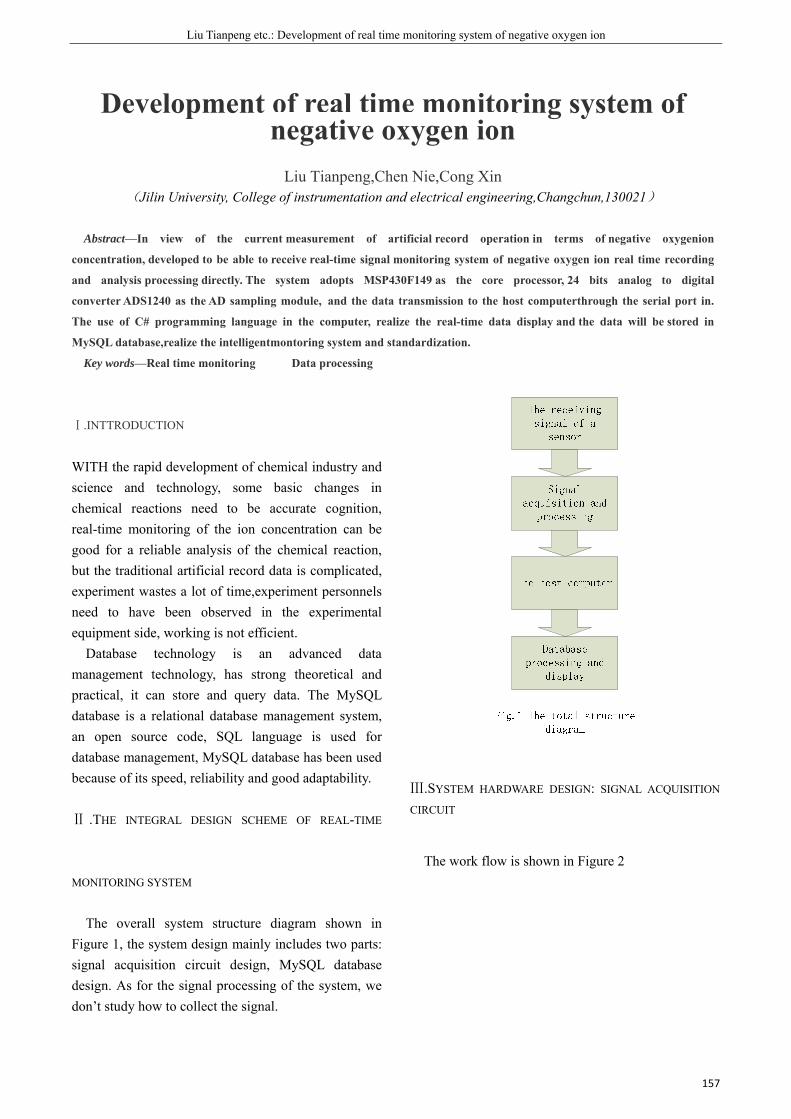
Liu Tianpeng etc.: Development of real time monitoring system of negative oxygen ion
157
Development of real time monitoring system of negative oxygen ion
Liu Tianpeng,Chen Nie,Cong Xin
(Jilin University, College of instrumentation and electrical engineering,Changchun,130021) Abstract—In view of the current measurement of artificial record operation in terms of negative oxygenion
concentration, developed to be able to receive real-time signal monitoring system of negative oxygen ion real time recording
and analysis processing directly. The system adopts MSP430F149 as the core processor, 24 bits analog to digital
converter ADS1240 as the AD sampling module, and the data transmission to the host computerthrough the serial port in.
The use of C# programming language in the computer, realize the real-time data display and the data will be stored in
MySQL database,realize the intelligentmontoring system and standardization.
Key words—Real time monitoring Data processing
Ⅰ.INTTRODUCTION
WITH the rapid development of chemical industry and science and technology, some basic changes in chemical reactions need to be accurate cognition, real-time monitoring of the ion concentration can be good for a reliable analysis of the chemical reaction, but the traditional artificial record data is complicated, experiment wastes a lot of time,experiment personnels need to have been observed in the experimental equipment side, working is not efficient. Database technology is an advanced data management technology, has strong theoretical and practical, it can store and query data. The MySQL database is a relational database management system, an open source code, SQL language is used for database management, MySQL database has been used because of its speed, reliability and good adaptability.
Ⅱ .THE INTEGRAL DESIGN SCHEME OF REAL-TIME
MONITORING SYSTEM
The overall system structure diagram shown in Figure 1, the system design mainly includes two parts: signal acquisition circuit design, MySQL database design. As for the signal processing of the system, we don’t study how to collect the signal.
Ⅲ.SYSTEM HARDWARE DESIGN: SIGNAL ACQUISITION
CIRCUIT
The work flow is shown in Figure 2
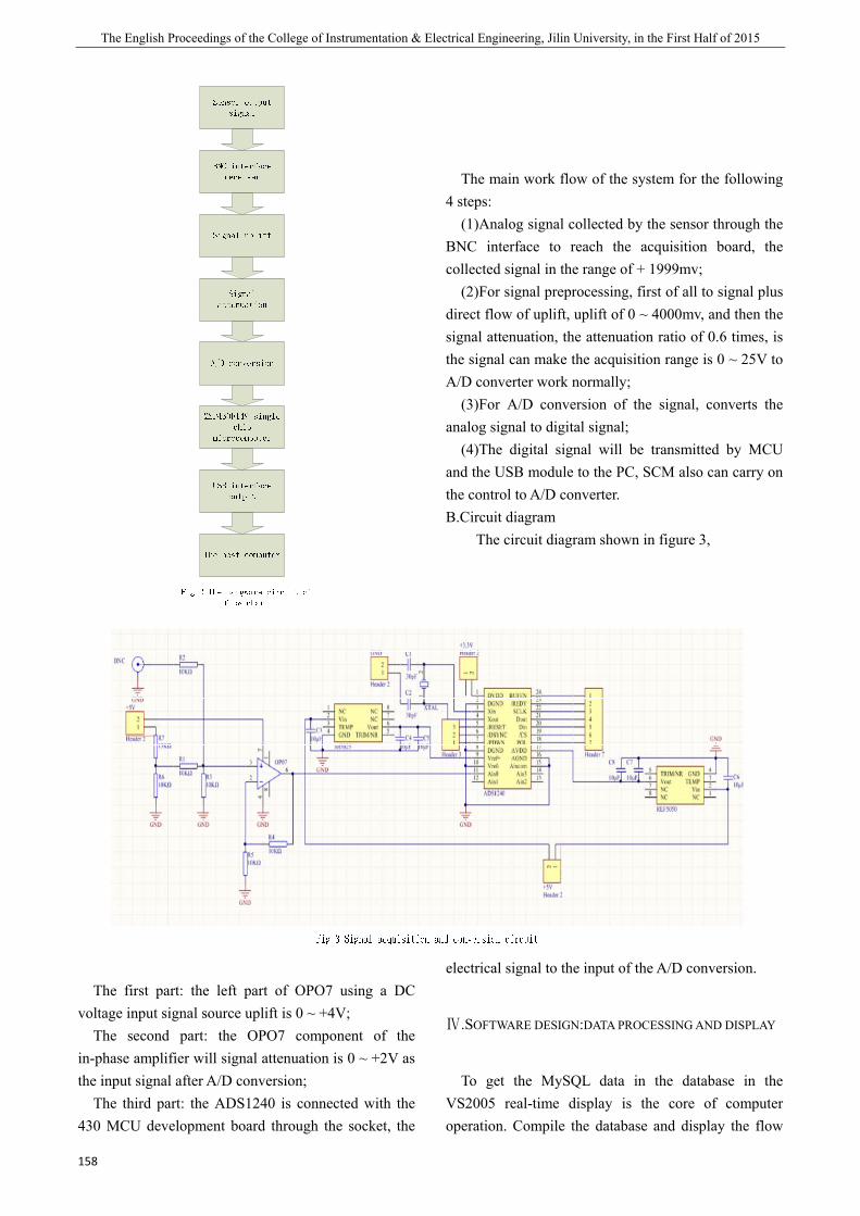
The English Proceedings of the College of Instrumentation & Electrical Engineering, Jilin University, in the First Half of 2015
158
The main work flow of the system for the following 4 steps: (1)Analog signal collected by the sensor through the BNC interface to reach the acquisition board, the collected signal in the range of + 1999mv; (2)For signal preprocessing, first of all to signal plus direct flow of uplift, uplift of 0 ~ 4000mv, and then the signal attenuation, the attenuation ratio of 0.6 times, is the signal can make the acquisition range is 0 ~ 25V to A/D converter work normally; (3)For A/D conversion of the signal, converts the analog signal to digital signal; (4)The digital signal will be transmitted by MCU and the USB module to the PC, SCM also can carry on the control to A/D converter. B.Circuit diagram
The circuit diagram shown in figure 3,
The first part: the left part of OPO7 using a DC voltage input signal source uplift is 0 ~ +4V; The second part: the OPO7 component of the in-phase amplifier will signal attenuation is 0 ~ +2V as the input signal after A/D conversion; The third part: the ADS1240 is connected with the 430 MCU development board through the socket, the
electrical signal to the input of the A/D conversion.
Ⅳ.SOFTWARE DESIGN:DATA PROCESSING AND DISPLAY
To get the MySQL data in the database in the VS2005 real-time display is the core of computer operation. Compile the database and display the flow
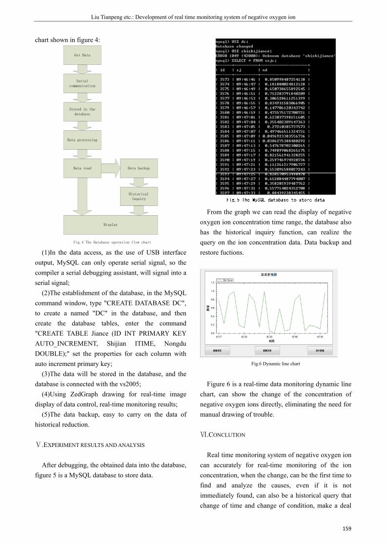
Liu Tianpeng etc.: Development of real time monitoring system of negative oxygen ion
159
chart shown in figure 4:
Get Data
Serial communication
Stored in the database
Data processing
Data backupData read
Historical inquiry
Display
Fig.4 The Database operation flow chart (1)In the data access, as the use of USB interface output, MySQL can only operate serial signal, so the compiler a serial debugging assistant, will signal into a serial signal; (2)The establishment of the database, in the MySQL command window, type "CREATE DATABASE DC", to create a named "DC" in the database, and then create the database tables, enter the command "CREATE TABLE Jiance (ID INT PRIMARY KEY AUTO_INCREMENT, Shijian ITIME, Nongdu DOUBLE);" set the properties for each column with auto increment primary key; (3)The data will be stored in the database, and the database is connected with the vs2005; (4)Using ZedGraph drawing for real-time image display of data control, real-time monitoring results; (5)The data backup, easy to carry on the data of historical reduction.
Ⅴ.EXPERIMENT RESULTS AND ANALYSIS
After debugging, the obtained data into the database, figure 5 is a MySQL database to store data.
From the graph we can read the display of negative oxygen ion concentration time range, the database also has the historical inquiry function, can realize the query on the ion concentration data. Data backup and restore fuctions.
Fig.6 Dynamic line chart
Figure 6 is a real-time data monitoring dynamic line chart, can show the change of the concentration of negative oxygen ions directly, eliminating the need for manual drawing of trouble.
Ⅵ.CONCLUTION
Real time monitoring system of negative oxygen ion can accurately for real-time monitoring of the ion concentration, when the change, can be the first time to find and analyze the causes, even if it is not immediately found, can also be a historical query that change of time and change of condition, make a deal

The English Proceedings of the College of Instrumentation & Electrical Engineering, Jilin University, in the First Half of 2015
160
with it.
Reference
[1] Zhang Yingping, Zhang Zhaoyang. The MCU based
successive comparison type AD conversion circuit design.
Journal of Fuyang Normal College (NATURAL SCIENCE
EDITION), 2014,01:102-124;
[2] Li Jianzhong. Principle and application of single chip
microcomputer. Xi'an: Xi'an Electronic and Science
University press,.2008;
[3] Fan Huimin, Li Jinhui. Micro computer principle and
interface technology and application. Beijing: Science
Press,.2001;
[4] Ma Zhigang, Liu Wenyi, Zhang Wendong. A Methed for
Data Processing and Dynamic Curve Plotting in Real-time
Monitoring System. (JOURNAL OF GRAPHICS),
2015,01:133-138;
[5] Dan Fei. The design and optimization of [D]. wireless meter
reading of Shandong University heating database system
based on MySQL, 2014;
[6] Baron Wang Xiaodong. A high performance MySQL
(Second Edition). Publishing House of electronics
industry,2014;
[7] Jiang Chengyao.MySQL technology insider: InnoDB
storage engine, mechanical industry publishing house,2013;
[8] Andrew Troelsen. Zhu Ye.C# and.NET4 advanced
programming. The posts and Telecommunications
Press.2011

A
Des
(C
Abstract—T
PWM signal. signal to chanthe output volshows the perf
I. INTRODUCT
PULSE widthwhich is appsignal by adjkept unchansemiconductosimple. And
Ⅱ. SYSTEM
A. GeneratorThe refere
compared wproduce errorinput of the
sign of
(College of In
This paper desThe topology
nge the output ltage as a conformance of th
TION
h modulatioplied more wjusting the sw
nged to contor module. it is easy to im
DESIGN OF T
r of PWM ence signal iith samplingr signal. Put comparator.
Liu Haitao etc
f a swi
strumentation
scribes the desof the switchivoltage. So wistant. The des
he power suppl
n is a modwidely. PWMwitch. The putrol the on-oIn this waymplement.
THE POWER SU
s produced bg signal of outhe error signRamp gener
.: Design of a s
itchingtec
Liu Ha
n &Electrica
sign of a switcng power suppith the feedbacsign of high frly.
dulation metM controls puulse frequencoff ratio of y, the design
UPPLY
by the oscillutput voltage
nal to the reverator circuit w
Fig.2 M
switching powe
g powechniquaitao; Feng
al Engineering
ching power suply is half brick of the outprequency trans
thod ulse
cy is the
n is
ator e to erse will
proto th
TfreqsignB. M1. T
Main circuit dia
er supply with P
er supue Jinzhu
g, Jilin Unive
upply. The codge converterut voltage andsformer is exp
duce a certainhe comparato
Fig.1 PWMThis will proquency after nal will contrMain circuit sThe main circ
agram
PWM technique
ply wi
ersity, Changc
ntrol chip is S. SG3525 adju
d the referenceplained in deta
n frequency ror.
M modulation coduce a pulse
processed byol the switch scheme uit diagram
e
ith PW
gchun 130012
SG3525 whichusts the duty ce value, SG352ail. The experi
ramp voltage
circuit principlee signal whiy comparato
h to be connec
16
WM
2)
can generate cycle of PWM 25 can control imental result
, and put it in
e diagram ich is certainr. This pulsected.
1
n
n e
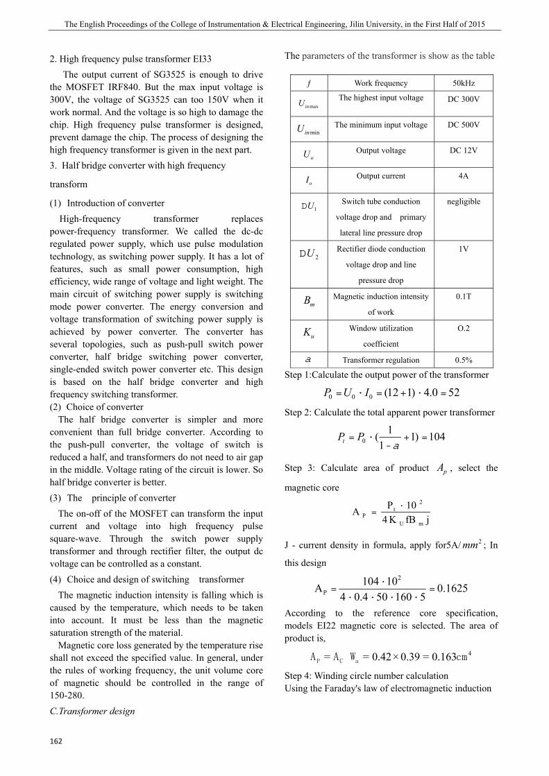
The English Proceedings of the College of Instrumentation & Electrical Engineering, Jilin University, in the First Half of 2015
162
2. High frequency pulse transformer EI33 The output current of SG3525 is enough to drive
the MOSFET IRF840. But the max input voltage is 300V, the voltage of SG3525 can too 150V when it work normal. And the voltage is so high to damage the chip. High frequency pulse transformer is designed, prevent damage the chip. The process of designing the high frequency transformer is given in the next part. 3. Half bridge converter with high frequency
transform
(1) Introduction of converter High-frequency transformer replaces
power-frequency transformer. We called the dc-dc regulated power supply, which use pulse modulation technology, as switching power supply. It has a lot of features, such as small power consumption, high efficiency, wide range of voltage and light weight. The main circuit of switching power supply is switching mode power converter. The energy conversion and voltage transformation of switching power supply is achieved by power converter. The converter has several topologies, such as push-pull switch power converter, half bridge switching power converter, single-ended switch power converter etc. This design is based on the half bridge converter and high frequency switching transformer. (2) Choice of converter
The half bridge converter is simpler and more convenient than full bridge converter. According to the push-pull converter, the voltage of switch is reduced a half, and transformers do not need to air gap in the middle. Voltage rating of the circuit is lower. So half bridge converter is better. (3) The principle of converter
The on-off of the MOSFET can transform the input current and voltage into high frequency pulse square-wave. Through the switch power supply transformer and through rectifier filter, the output dc voltage can be controlled as a constant. (4) Choice and design of switching transformer
The magnetic induction intensity is falling which is caused by the temperature, which needs to be taken into account. It must be less than the magnetic saturation strength of the material.
Magnetic core loss generated by the temperature rise shall not exceed the specified value. In general, under the rules of working frequency, the unit volume core of magnetic should be controlled in the range of 150-280. C.Transformer design
The parameters of the transformer is show as the table
ƒ Work frequency 50kHz
maxinU The highest input voltage DC 300V
mininU The minimum input voltage DC 500V
oU Output voltage DC 12V
Output current 4A
1UD Switch tube conduction
voltage drop and primary
lateral line pressure drop
negligible
2UD Rectifier diode conduction
voltage drop and line
pressure drop
1V
mB Magnetic induction intensity
of work
0.1T
uK Window utilization
coefficient
O.2
a Transformer regulation 0.5%
Step 1:Calculate the output power of the transformer
Step 2: Calculate the total apparent power transformer
Step 3: Calculate area of product pA , select the
magnetic core
jfBK410PA
mU
2t
P·
=
J - current density in formula, apply for5A/ 2mm ; In
this design
1625.05160504.04
10104A2
P =····
·=
According to the reference core specification, models EI22 magnetic core is selected. The area of product is,
4163.0=39.0×42.0== cmWAA aCP Step 4: Winding circle number calculation Using the Faraday's law of electromagnetic induction
oI
520.4)112(000 =·+=·= IUP
104)11
1(0 =+-
·=a
PPt

Among them
To determinvoltage (mini
=1N
The actual taPrimary wind
Ns =
The actual taStep 5: DeterCurrent trans
Secondary cu
Bare area of
A
The primary
Ips =
The primary
Bare area of
A
In the deorder to ensuconsider theresistance of
Skin depth is
6=e
The diameter
Wires bare ar
KN =
m 0.4=fK
e the minimimum numbe
5×16.0×4×13
=
ake 10 turns. ding number
NU2
U1
o
in
·
ake 115 turns.rmine the wirsformer secon
Ip
urrent valid v
D2I1 =
secondary wi
jIA 1
1WS ==
winding curr
UP
minin
o ==h
winding curr
D2Ip =
secondary wi
0j
IA p
wp ==
esign of higure the wire
e influence of the wire less
R AC
s
f626.
300
66.=
r of wire AWD
DAWG =
rea wA
Liu Haitao etc
Cmf
4
fABK
10U ·
0 (Square wa
mum number er of turns) w
42.0×5000010× 4
of turns
1013300
1 ·=
. re specificationdary winding
51 =
values
474ID 1p .=
inding wires
0500
474.
.==
rent peak
%8030052·
=
rent valid valu
380Ips .=
inding wires
00.0500385.0
=
gh-frequency loss is miniof skin effecs than the dc r
1R DC £
0390000
62.=
WG
079202 .=e
.: Design of a s
ave)
of turns of inding
67.9=2
31150 .=
ons g peaks
7
0089
430.=
ues
85
0077
transformer,imal, we shoct. It makesresistance:
cm96
2
switching powe
the
, in ould s ac
A
Cis 0satiprimbifi
Thtim
In t
Inchois 4Ind
Cor
WiHS7foll
AL
BF
IplyarouD.
Cfigu
InsignSG3ach
er supply with P
(4
DA AWW =
p
Check the wir0.0785 cm, bisfy the desigmary side is ilar winding i
31135 ·· .
he output free is 2 us.
this design, it
n order to rosen. The p4A and AC iuctance energ
W
re area of ring
2Ap =
ith the above72T * 22 * 6lows:
24400L –=
mmB 0.14=
n practical aand around
und. Each co Feedback c
Circuit of the ure 3.
Fig.3 Circun figure 3, thnal, and the3525 feedbac
hieved. When
PWM technique
) 14132WG .
=
re specificatiobare wire ar
gn requiremen115 turns. Ts 10 turns. To
cmcm 7024 =
quency is 10
u =D
is selection o
reduce the cparameter of is 0.4A. gy processing
LIpkW 22=
g powder
1042 JBW m·
e data, we ca6.5 x 14 ring
/2%25 nHN
56.0Ap =
application, cd 5 turns. Thpper wire aro
circuit feedback of
uit of the feedhe circuit is ue output sigck. So the the output vo
e
40792016 2.·
on table, 21 wrea is 0.0042nts. Single str
The secondaryotal length is,
mm 7= 00 KHz. The
dtLdi /
of = 0.4,
current ripplf inductance i
g power
mJ88.0=
49.0 cJKu =
an choose TDcore. Its par
6.25 mAe =
26cm
=N
copper wire ihe total lengound is 9 m.
f output signa
dback of outputused to sampgnal is convoltage feedoltage is chan
di
163
004902
.=
wire diameter2, and it canrand windingy side of the,
e current fall
, L=60
le, 100uH iss 100uH. DC
4cm
DK companyrameters is as
2m
5=LAL
is designed 3gth is 1.5 m
al is shown in
t signal ple the outputnnected withdback loop isnged, SS9013
uH
3
r n g e
l
s C
y s
3 m
n
t h s 3
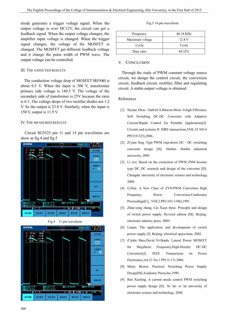
The Englis
164
triode generaoutput voltagfeedback signamplifier inpsignal changchanged. Theand it changoutput voltag
III. THE EXPE
The conduabout 0.5 V.primary sidesecondary sidis 6:1. The voV. So the out150 V, outpu
IV. THE MEAS
Circuit SGshow as fig.4
sh Proceedings
ates a triggege is over Dnal. When thput voltage isges, the voe MOSFET gge the pulse ge can be con
ECTED RESUL
uction voltageV. When the e voltage is de of transforoltage drops otput is 23.8 V
ut is 11.9 V.
SURED RESUL
G3525 pin 114 and fig.5
Fig.4 11
of the College
er voltage siDC12V, the che output volts changed. W
oltage of thget different f
width of PWntrolled.
LTS
e drop of MOinput is 300149.5 V. Thermer is 25V bof two rectifi
V. Similarly, w
LTS
1 and 14 pin
pin waveform
of Instrumentat
ignal. When circuit can geage changes,
When the trighe MOSFETfeedback voltWM wave.
OSFET IRF840 V, transforme voltage of because the rier diodes arewhen the inpu
n waveforms
tion & Electrica
the et a , the gger T is tage The
40 is rmer f the ratio e 1.2 ut is
are
V.
Tcirccirccirc
Ref
[1]
[2]
[3]
[4]
[5]
[6]
[7]
[8]
[9]
al Engineering,
Frequenc
Maximum vo
Cycle
Duty rati
CONCLUSI
Through the scuit, we desigcuit, feedbackcuit. A stable
ferences
] Siyuan Zhou
Soft Switch
Current-Ripp
Circuits and
PP(319-323)
] Zi-jian feng.
converter d
university, 2
] Li wei. Base
type DC_DC
Chengdu: un
2008.
] G.Hua. A N
Frequency
Proceedings
] Zhan-song z
of switch po
electronic in
] Liujun. The
power supply
] Z.John Shen
for Mega
Converters[J
Electronics,V
] Marty Brow
Design[M].A
] Ren Xuefen
power suppl
electronic sc
Jilin University
Fig.5 14 pin w
cy
oltage
io
ON
tudy of PWMgn the controk circuit, rectoutput voltag
u,Gabriel A.Ri
hing DC-DC
ple Control f
systems II: IEE
),2006.
. Type PWM st
design [D].
009.
ed on the corre
C research and
niversity of elec
New Class of
Power
[C], .VOL2.PP(
zhang, Cai Xua
ower supply. R
dustry press, 20
e application
y [J]. Beijing: e
n,David N.Oka
ahertz Freque
J]. IEEE
Vol.21 No.1 PP
wn. Practical
Academic Press
g. A current m
ly design [D].
cience and techn
ty, in the First H
waveform
48.18 K
12.8
Cyc
44.32
M constant vool circuit, thtifier, filter ange is obtained
incon-Mora. A
Converter w
for Portable A
EE transactions
tep-down DC -
Harbin: Har
ection of PWM
d design of the
ctronic science
ZVS-PWM C
Convers
(1101-1106),19
an three. Princi
Revised edition
005.
and developm
electrical space
ada. Lateral Po
uency,High-Den
Transactions
P(11-17) 2006.
Switching P
s,Inc,1990.
mode control P
Xi 'an: xi 'an
nology, 2008.
Half of 2015
KHz
V
le
2%
oltage sourcehe conversionnd regulating
d.
high Efficiency
with Adaptive
Applications[J]
s,VOL.53 NO.4
- DC switching
rbin industrial
M_PSM booster
converter [D]
and technology
onverters High
sion.Conference
991
iple and design
n [M]. Beijing
ment of switch
-time, 2002.
ower MOSFET
nsity DC-DC
on Power
Power Supply
PWM switching
n university of
e n g
y
e
.
4
g
l
r
.
y,
h
e
n
:
h
T
C
r
y
g
f

Liu Haitao etc.: Design of a switching power supply with PWM technique
165
[10] Feng Qiuxia. A synchronous buck type DCDC switching
power supply management IC design [D]. Dalian: dalian
university of technology, 2007.
[11] He Yun. CMOS step-down voltage converter of
high-level modeling and circuit design [D]. Xi 'an: xi 'an
university of electronic science and technology, 2009.
[12] Lin Ganglei. A high precision type PWM step-down DC
- DC converter design [D]. Shanghai: Shanghai jiaotong
university, 2008.
[13] Li-fang zhu. PWMPSM dual-mode high-voltage direct
current voltage converter [D]. Hangzhou: zhejiang
university college of electrical engineering, 2010.
[14] Jiann-Jong Chen,Juing-Huei Su,Hung-Yih Lin.Integrated
Current Sensing Circuit Suitable for Step-Down DC-DC
Converters[C].2004 35th Annul IEEE Power Electronics
Specialists Conference,Vol:2 PP(1140-1142),2004.
[15] Li Yanming,Lai Xinquan,Ye Qiang,et al.A current-mode
buck DC-DC controller with adaptive on-time
control[J].Journal of Semiconductor , Vol:8
PP(2602-2605) ,2009.

The English Proceedings of the College of Instrumentation & Electrical Engineering, Jilin University, in the First Half of 2015
166
Dipole radiation field based on the Matlab simulation
Sunshikun;Muzongpeng;Songqinrui
(jilin university instrument science and engineering institute,changchun,130021) Abstract - Our goal is to complete the analysis and calculation of dipole radiation field distribution by using Matlab
simulation. We derive the dipole radiation field distribution formula and use the electromagnetic duality principle dual
relationship of the power supply as well as the source of magnetic electric field and magnetic field distribution calculated
formula .The simulation conclusion is the distribution curve of electric and magnetic fields ,which help to analyse and
optimize design dipole antenna and its electromagnetic detection system performance .
1. INTRODUCTION
IF the positive and negative charge on the charged system presented dipole distribution and the charge weight don't overlap, so it can be as within easy reach of both the amount of unlike charges, namely,the electric dipole. Antenna is an important component of the modern communication facilities, it can be to the radiation of electromagnetic wave in the space, the antenna is the most simple dipole antenna, various forms of the new antenna can be regarded as a combination of dipole antenna. So the research on the issues about dipole excitation of electromagnetic field in the space is of great significance. Fixed frequency signal radiation and receiving often use dipole antenna,among them, VHAP and UHAP were designated anechoic chamber and open field site attenuation measurements of special wire by the Japanese VCCI,it is standard in a lot of laboratory.
2.PROCEDURE FOR PAPER SUBMISSION
First of all, our goal is to master the definition, formation and types of electromagnetic radiation causes, conditions, electromagnetic radiation antenna.According to the radiation in the class of time-varying electromagnetic field calculation of electric dipole field method,we make the calculation of magnetic field of magnetic dipole radiation
analogy.With dipole magnetic field lines and power line equation are derived, we calculate the distribution of the unit dipole radiation electromagnetic field radiation.
Fig.1 System diagram
3. THE BASIC FORMULA
Current direction is z,current is I,length is l, so
z zIJdV e Sdz e IdzS
¢ ¢ ¢= = (1)
Substitute
( )4
jkr
V
JeA r dVr
m
p
-
= ∫ (2)
Get electric dipole vector
( )4 4
jkrjkr
z zC
e IlA r e Idz e er r
m m
p p
--¢= =∫ (3)
In the spherical coordinate system
( ) cos cos4
jkrr r z
IlA r A e A er
mq q
p-= = =

Sunshikun etc:Dipole radiation field based on the Matlab simulation
167
( )
sin sin4
jkrz
A r A eIlA er
q q
mq q
p-
=
= - = - (4)
( ), 0A r t A eq f= =
The electric dipole magnetic field
( )
2
21 sin 1
4jkrk Il jH A e e
kr krf
q
m p-
⎡ ⎤= · = +⎢ ⎥
⎢ ⎥⎣ ⎦
( ) ( )
( ) ( )
3
2 3
3
2 3
1
cos 12
sin 14
jkrr
jkr
E Hj
k Il je ekr kr
k Il j je ekr kr krq
we
q
p
q
pwe
-
-
= ·
⎡ ⎤= -⎢ ⎥
⎢ ⎥⎣ ⎦⎡ ⎤
+ + -⎢ ⎥⎢ ⎥⎣ ⎦
(5)
Then the electric dipole near zone quasi static field
3 3
3 3
2
coscos2 2
sinsin4 2
sin4
er
e
pqlEr r
pqlEr r
IlHr
q
f
pe peqq
pe peq
p
= =
= =
= (6)
The far zone field for electric dipole
sin2sin2
jkr
jkr
IlE j er
IlH j er
q
q
qh
lq
l
-
-
=
=
(7)
According to the charge, current, magnetic charge, magnetic flow principle of duality,the far field of a magnetic dipole is shown below
rmθ
rmθ
θr
I
θr
I
jk
jk
eSH
eSE
-
-
=
=
sin2
sin2
0
00
0
m
e
l
wm
l
wm
(8)
The dipole radiation field in component form:
r
θ
r
rθ
rr
rr
θ
H
0
rrr
θ
rr
θ
jk
jk
jk
ekk
jkH
H
E
ek
jkk
jkE
ek
jk
kE
-
-
-
+=
=
=
=
-+=
-=
))(
1(4
cos
00
))()(
1(4
cos
))()(
1(2
cos
2
2
32
3
32
3
p
pwe
p
f
f
Il
Il
Il
(9)
4 . DESIGN OF SIMULATION SOFTWARE
Electric power line dipole in spherical coordinates satisfy the vector equation:
rrθ
r ddEE 1
=q (10)
Come to conclusion:
Kr
rtrrtθ =
---
kkkk )sin()cos(sin2 ww
(11)
Electric field visualization converted to Cartesian coordinates:
222 zyxr ++=
)(tan)(cos
1
1
y/xφ
zyxz/θ 222
-
-
=
++= (12)
Because the electric field distribution and angle independent, so the symmetry on the Z axis and you can use a z plane replacement.
)arccos(; 2222 zxz/θzxr +=+= (13)
The range of x、z is [-r, r]. So we can draw the electric field in the space
distribution plotted dipole by using scalar contour in Matlab equation [c,h]=contour(X, Z, m, K) and drawing the contour function. K is a function U (x, z) in the coordinates X, Z value,V is a vector,it designated contour height values (such as power line in the K value). The h is the return of the handle value.
5.THE RESULT OF SIMULATION
The Matlab simulation results is shown below:
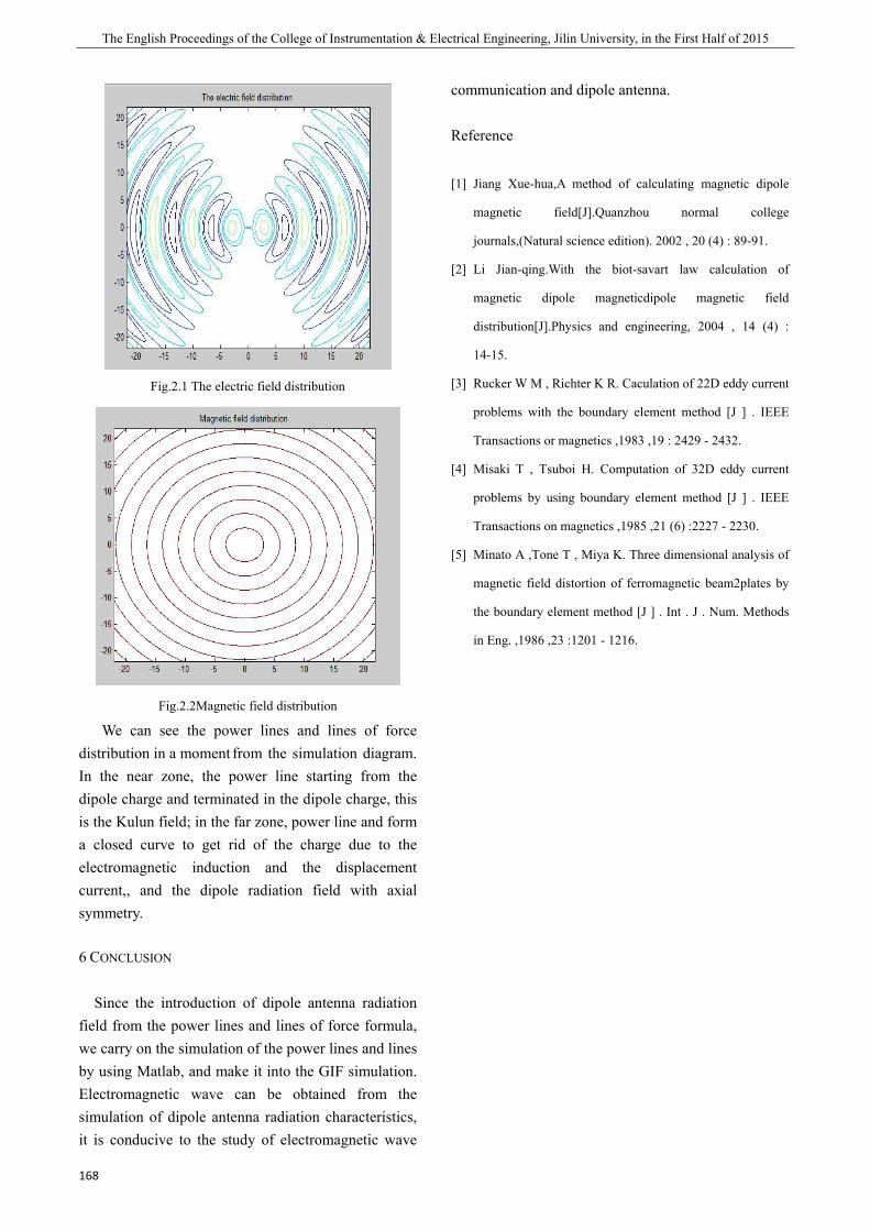
The English Proceedings of the College of Instrumentation & Electrical Engineering, Jilin University, in the First Half of 2015
168
Fig.2.1 The electric field distribution
Fig.2.2Magnetic field distribution
We can see the power lines and lines of force distribution in a moment from the simulation diagram. In the near zone, the power line starting from the dipole charge and terminated in the dipole charge, this is the Kulun field; in the far zone, power line and form a closed curve to get rid of the charge due to the electromagnetic induction and the displacement current,, and the dipole radiation field with axial symmetry.
6 CONCLUSION
Since the introduction of dipole antenna radiation field from the power lines and lines of force formula, we carry on the simulation of the power lines and lines by using Matlab, and make it into the GIF simulation. Electromagnetic wave can be obtained from the simulation of dipole antenna radiation characteristics, it is conducive to the study of electromagnetic wave
communication and dipole antenna.
Reference
[1] Jiang Xue-hua,A method of calculating magnetic dipole
magnetic field[J].Quanzhou normal college
journals,(Natural science edition). 2002 , 20 (4) : 89-91.
[2] Li Jian-qing.With the biot-savart law calculation of
magnetic dipole magneticdipole magnetic field
distribution[J].Physics and engineering, 2004 , 14 (4) :
14-15.
[3] Rucker W M , Richter K R. Caculation of 22D eddy current
problems with the boundary element method [J ] . IEEE
Transactions or magnetics ,1983 ,19 : 2429 - 2432.
[4] Misaki T , Tsuboi H. Computation of 32D eddy current
problems by using boundary element method [J ] . IEEE
Transactions on magnetics ,1985 ,21 (6) :2227 - 2230.
[5] Minato A ,Tone T , Miya K. Three dimensional analysis of
magnetic field distortion of ferromagnetic beam2plates by
the boundary element method [J ] . Int . J . Num. Methods
in Eng. ,1986 ,23 :1201 - 1216.

Feng Jiaxing etc.: Based on the independent MPPT photovoltaic battery charging system design
169
Based on the independent MPPT photovoltaic battery charging system design
Feng Jiaxing , Liang Tianxu. Li Jisheng
(jilin university Instrument science and electrical engineering college ,changchun,130021)
Abstract—The world today is facing energy depletion problem, to solve this problem has two aspects: first, energy
conservation, and the second is the development of new energy to solve this problem fundamentally, the development of new energy is the key. Development and use of new energy technologies is one of the world's economic development in the most decisive influence, which is a photovoltaic technology on the development of new energy path most attention.
Independent photovoltaic power generation is the most important use of the largest PV array, to improve the efficiency of power generation. In addition, an effective way to improve the battery charging, longer battery life, but also can greatly improve the efficiency of photovoltaic power generation.
In this paper, design independent photovoltaic charging system. Charging circuit uses BOOST boost circuit, the circuit design parameters were reasonable. Among MSP430 MCU controller, using the maximum power point tracking (MPPT) algorithm - perturbation and observation method, to achieve the lead-acid battery. Charging by constant voltage fast charging method, and the battery charge and discharge were reasonably designed to prevent damage to the battery waste and energy.
PREFACE
INDEPENDENT photovoltaic power generation systems include household photovoltaic power system and the independent photovoltaic power station, the power supply reliability is highly affected by the factors such as environment, climate, load, power supply stability is relatively poor, therefore, need to join in the system of energy storage and energy management link, so we need to research a kind of charging and discharging controller.
Photovoltaic charge and discharge controller is combined battery characteristics of photovoltaic power generation systems, is can realize the control of battery charging and discharging equipment. Effectively for the storage battery charging and discharging controller should also be charging, with maximum extend the service life of battery, prevent excessive charging and discharging the battery life. Photovoltaic power generation system power supply by the more uncertain factors, and the operation is not stable, so the battery charge and discharge control system, is much more difficult than other applications to charge and discharge control. Therefore, in the independent photovoltaic power generation system used in good charge and discharge controller to manage batteries and photovoltaic cells, has very important significance.
I. THE WORKING PRINCIPLE OF THE SYSTEM
Independent photovoltaic battery charging system
schematic diagram is shown in Fig 1 :
II.THE HARDWARE CIRCUIT DESIGN
Independent of solar photovoltaic battery charging system of rated output of 12V10W, his request is for two 12 V lead-acid battery charging, the DC - DC transform circuit, due to the booster, so use the Boost booster circuit. DC/DC switching power supply with high efficiency, high power density and high reliability etc, so it can well meet the demand of the system. A. The Boost circuit principle of work
The Boost converter circuit structure as shown in Fig 2:
Fig. 1. Independent photovoltaic charging system schematic
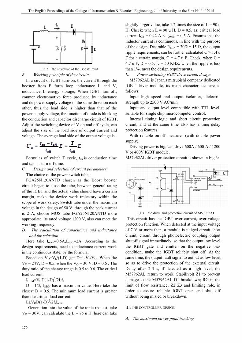
The English Proceedings of the College of Instrumentation & Electrical Engineering, Jilin University, in the First Half of 2015
170
Fig.2 the structure of the Boostcircuit
B. Working principle of the circuit: In a circuit of IGBT turn-on, the current through the
booster from E form loop inductance L and V, inductance L energy storage; When IGBT turn-off, counter electromotive force produced by inductance and dc power supply voltage in the same direction each other, thus the load side is higher than that of the power supply voltage, the function of diode is blocking the conduction and capacitor discharge circuit of IGBT. Adjust the switching device of V on and off cycle, can adjust the size of the load side of output current and voltage. The average load side of the output voltage is:
Formulas of switch T cycle, ton is conduction time
and toff is turn off time. C. Design and selection of circuit parameters
The choice of the power switch tube: FGA25N120ANTD chosen as the Boost booster
circuit began to close the tube, between general rating of the IGBT and the actual value should have a certain margin, make the device work trajectory within the scope of work safety. Switch tube under the maximum voltage in the design of 50 V, through the peak current is 2 A, choose MOS tube FGA25N120ANTD more appropriate, its rated voltage 1200 V, also can meet the working frequency. D. The calculation of capacitance and inductance
and the selection Here take Iomin=0.5A,Iomax=2A. According to the
design requirements, need to inductance current work in the continuous state, by the formula:
Based on VO=VS/(1-D) get D=1-VS/VO .When the VO = 24V, D = 0.5; when the VO = 30 V, D = 0.6 . The duty ratio of the change range is 0.5 to 0.6. The critical load current:
IOBM=VOD(1-D)2/2Lfs D = 1/3, IOBM has a maximum value. Here take the
closest D = 0.5. The minimum load current is greater than the critical load current:
L≥VOD(1-D)2/2fsIomin Generation into the value of the topic request, take
VO = 30V, can calculate the L = 75 u H. here can take
slightly larger value, take 1.2 times the size of L = 90 u H. Check: when L = 90 u H, D = 0.5, as: critical load current IOB = 0.42 A < IOMIN = 0.5 A. Ensures that the inductor current is continuous, in line with the purpose of the design. Desirable RMIN = 30/2 = 15 Ω, the output ripple requirements, can be further calculated C > 1.4 u F for a certain margin, C = 4.7 u F. Check: when C = 4.7 u F, D = 0.5, fc = 50 KHZ: when the ripple is less than 1%, meet the design requirements. E. Power switching IGBT drive circuit design
M57962AL is Japan's mitsubishi company dedicated IGBT driver module, its main characteristics are as follows:
Input high speed and output isolation, dielectric strength up to 2500 V AC/min.
Input and output level compatible with TTL level, suitable for single chip microcomputer control.
Internal timing logic and short circuit protection circuit, and at the same time also has a time delay protection features.
With reliable on-off measures (with double power supply).
Driving power is big, can drive 600A / 600 A / 1200 V or 400V IGBT module. M57962AL driver protection circuit is shown in Fig 3:
Fig.3 the drive and protection circuit of M57962AL
This circuit has the IGBT over-current, over-voltage protection function. When detected at the input voltage of 7 V or more than, a module is judged circuit short circuit, circuit through photoelectric coupling output shutoff signal immediately, so that the output low level, the IGBT gate and emitter on the negative bias condition, make the IGBT reliably shut off. At the same time, the output fault signal to output as low level, so as to drive the protection of the external circuit. Delay after 2-3 s, if detected as a high level, the M57962AL return to work. Stabilivolt Z1 to prevent damage to the M57962AL D1 breakdown; RG in the limit of flow resistance; Z2 Z3 and limiting role, in order to assure reliable IGBT open and shut off without being misled or breakdown.
III.THE CONTROLLER DESIGN
A. The maximum power point tracking
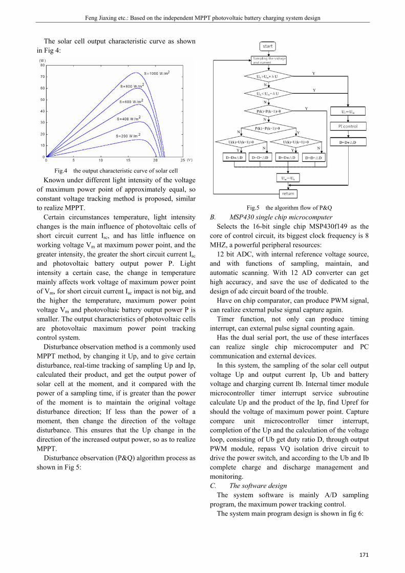
Feng Jiaxing etc.: Based on the independent MPPT photovoltaic battery charging system design
171
The solar cell output characteristic curve as shown in Fig 4:
Fig.4 the output characteristic curve of solar cell
Known under different light intensity of the voltage of maximum power point of approximately equal, so constant voltage tracking method is proposed, similar to realize MPPT.
Certain circumstances temperature, light intensity changes is the main influence of photovoltaic cells of short circuit current Isc, and has little influence on working voltage Vm at maximum power point, and the greater intensity, the greater the short circuit current Isc and photovoltaic battery output power P. Light intensity a certain case, the change in temperature mainly affects work voltage of maximum power point of Vm, for short circuit current Isc impact is not big, and the higher the temperature, maximum power point voltage Vm and photovoltaic battery output power P is smaller. The output characteristics of photovoltaic cells are photovoltaic maximum power point tracking control system.
Disturbance observation method is a commonly used MPPT method, by changing it Up, and to give certain disturbance, real-time tracking of sampling Up and Ip, calculated their product, and get the output power of solar cell at the moment, and it compared with the power of a sampling time, if is greater than the power of the moment is to maintain the original voltage disturbance direction; If less than the power of a moment, then change the direction of the voltage disturbance. This ensures that the Up change in the direction of the increased output power, so as to realize MPPT.
Disturbance observation (P&Q) algorithm process as shown in Fig 5:
Fig.5 the algorithm flow of P&Q
B. MSP430 single chip microcomputer Selects the 16-bit single chip MSP430f149 as the
core of control circuit, its biggest clock frequency is 8 MHZ, a powerful peripheral resources:
12 bit ADC, with internal reference voltage source, and with functions of sampling, maintain, and automatic scanning. With 12 AD converter can get high accuracy, and save the use of dedicated to the design of adc circuit board of the trouble.
Have on chip comparator, can produce PWM signal, can realize external pulse signal capture again.
Timer function, not only can produce timing interrupt, can external pulse signal counting again.
Has the dual serial port, the use of these interfaces can realize single chip microcomputer and PC communication and external devices.
In this system, the sampling of the solar cell output voltage Up and output current Ip, Ub and battery voltage and charging current Ib. Internal timer module microcontroller timer interrupt service subroutine calculate Up and the product of the Ip, find Upref for should the voltage of maximum power point. Capture compare unit microcontroller timer interrupt, completion of the Up and the calculation of the voltage loop, consisting of Ub get duty ratio D, through output PWM module, repass VQ isolation drive circuit to drive the power switch, and according to the Ub and Ib complete charge and discharge management and monitoring. C. The software design
The system software is mainly A/D sampling program, the maximum power tracking control.
The system main program design is shown in fig 6:
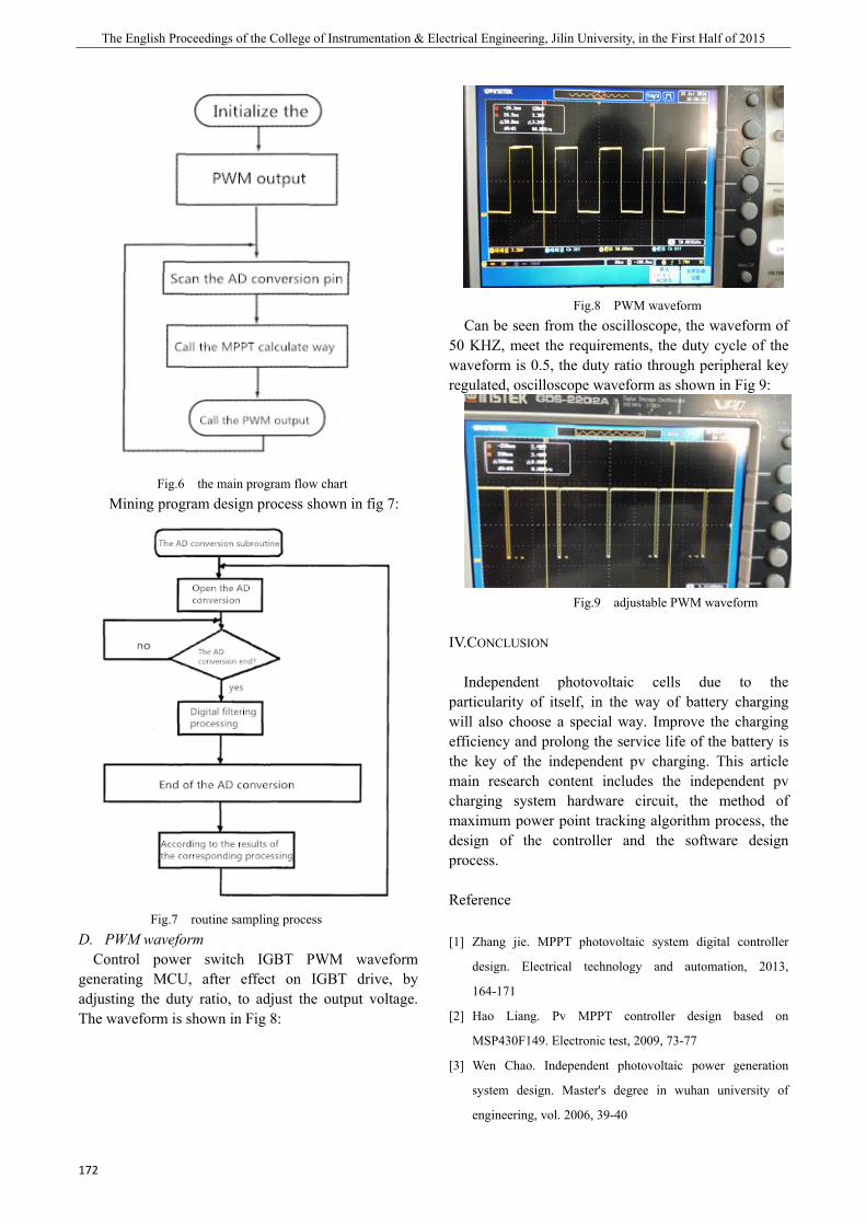
The English Proceedings of the College of Instrumentation & Electrical Engineering, Jilin University, in the First Half of 2015
172
Fig.6 the main program flow chart
Mining program design process shown in fig 7:
Fig.7 routine sampling process
D. PWM waveform Control power switch IGBT PWM waveform
generating MCU, after effect on IGBT drive, by adjusting the duty ratio, to adjust the output voltage. The waveform is shown in Fig 8:
Fig.8 PWM waveform
Can be seen from the oscilloscope, the waveform of 50 KHZ, meet the requirements, the duty cycle of the waveform is 0.5, the duty ratio through peripheral key regulated, oscilloscope waveform as shown in Fig 9:
Fig.9 adjustable PWM waveform
IV.CONCLUSION
Independent photovoltaic cells due to the particularity of itself, in the way of battery charging will also choose a special way. Improve the charging efficiency and prolong the service life of the battery is the key of the independent pv charging. This article main research content includes the independent pv charging system hardware circuit, the method of maximum power point tracking algorithm process, the design of the controller and the software design process.
Reference
[1] Zhang jie. MPPT photovoltaic system digital controller
design. Electrical technology and automation, 2013,
164-171
[2] Hao Liang. Pv MPPT controller design based on
MSP430F149. Electronic test, 2009, 73-77
[3] Wen Chao. Independent photovoltaic power generation
system design. Master's degree in wuhan university of
engineering, vol. 2006, 39-40

Feng Jiaxing etc.: Based on the independent MPPT photovoltaic battery charging system design
173
[4] Wang Min. Photovoltaic maximum power point tracking
system research in the system. A master's degree in wuhan
university of engineering vol. 2012, 40-50
[5] Wang Changgui. New energy and renewable energy status
quo and its prospect. Proceedings of solar photovoltaic
industry development BBS, 2003, 94-17.
[6] Wang Fei. Analysis and study of single-phase photovoltaic
(pv) grid system [D]. PhD thesis of hefei university of
technology, 2005.
[7] Yang Guiheng, Qiang Shengze,Zhang Yingchao. Solar
photovoltaic power generation system and its application
[M]. Beijing: chemical industry press, 2010
[8] Nicola Femia,Giovanni Petrone,Giovanni Spagnuolo,
et al.Optimization of Perturb and Observe Maximum Power
Point Tracking Method[J].IEEE Trans. on Power Electron.,
2005,20(4):963-973.
[9] V Salas,E Olias,A Barrado, et al.Review of the
MaximumPower Point Tracking Algorithms for Stand-alone
Photovoltaic Systems[J].Solar Energy Materials & Solar
Cells,2006,90(3):1555-1578.
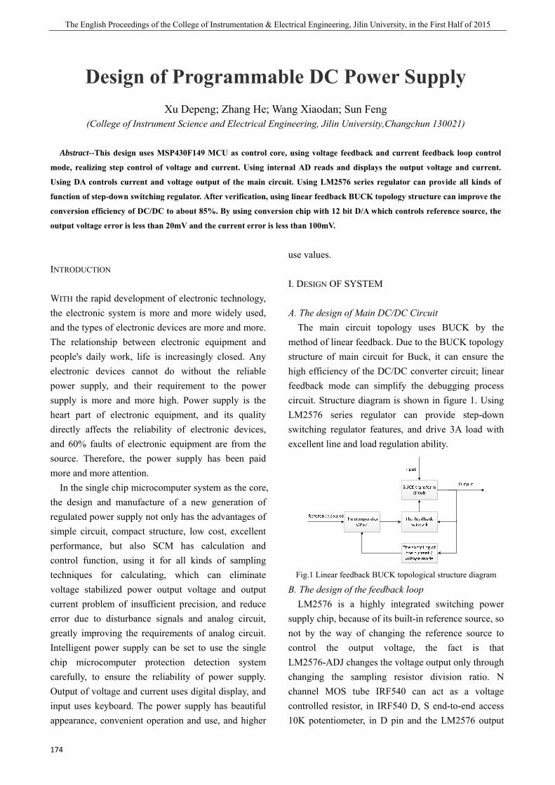
The English Proceedings of the College of Instrumentation & Electrical Engineering, Jilin University, in the First Half of 2015
174
Design of Programmable DC Power Supply
Xu Depeng; Zhang He; Wang Xiaodan; Sun Feng (College of Instrument Science and Electrical Engineering, Jilin University,Changchun 130021)
Abstract--This design uses MSP430F149 MCU as control core, using voltage feedback and current feedback loop control
mode, realizing step control of voltage and current. Using internal AD reads and displays the output voltage and current.
Using DA controls current and voltage output of the main circuit. Using LM2576 series regulator can provide all kinds of
function of step-down switching regulator. After verification, using linear feedback BUCK topology structure can improve the
conversion efficiency of DC/DC to about 85%. By using conversion chip with 12 bit D/A which controls reference source, the
output voltage error is less than 20mV and the current error is less than 100mV.
INTRODUCTION
WITH the rapid development of electronic technology, the electronic system is more and more widely used, and the types of electronic devices are more and more. The relationship between electronic equipment and people's daily work, life is increasingly closed. Any electronic devices cannot do without the reliable power supply, and their requirement to the power supply is more and more high. Power supply is the heart part of electronic equipment, and its quality directly affects the reliability of electronic devices, and 60% faults of electronic equipment are from the source. Therefore, the power supply has been paid more and more attention.
In the single chip microcomputer system as the core, the design and manufacture of a new generation of regulated power supply not only has the advantages of simple circuit, compact structure, low cost, excellent performance, but also SCM has calculation and control function, using it for all kinds of sampling techniques for calculating, which can eliminate voltage stabilized power output voltage and output current problem of insufficient precision, and reduce error due to disturbance signals and analog circuit, greatly improving the requirements of analog circuit. Intelligent power supply can be set to use the single chip microcomputer protection detection system carefully, to ensure the reliability of power supply. Output of voltage and current uses digital display, and input uses keyboard. The power supply has beautiful appearance, convenient operation and use, and higher
use values.
I. DESIGN OF SYSTEM
A. The design of Main DC/DC Circuit The main circuit topology uses BUCK by the
method of linear feedback. Due to the BUCK topology structure of main circuit for Buck, it can ensure the high efficiency of the DC/DC converter circuit; linear feedback mode can simplify the debugging process circuit. Structure diagram is shown in figure 1. Using LM2576 series regulator can provide step-down switching regulator features, and drive 3A load with excellent line and load regulation ability.
Fig.1 Linear feedback BUCK topological structure diagram
B. The design of the feedback loop
LM2576 is a highly integrated switching power supply chip, because of its built-in reference source, so not by the way of changing the reference source to control the output voltage, the fact is that LM2576-ADJ changes the voltage output only through changing the sampling resistor division ratio. N channel MOS tube IRF540 can act as a voltage controlled resistor, in IRF540 D, S end-to-end access 10K potentiometer, in D pin and the LM2576 output
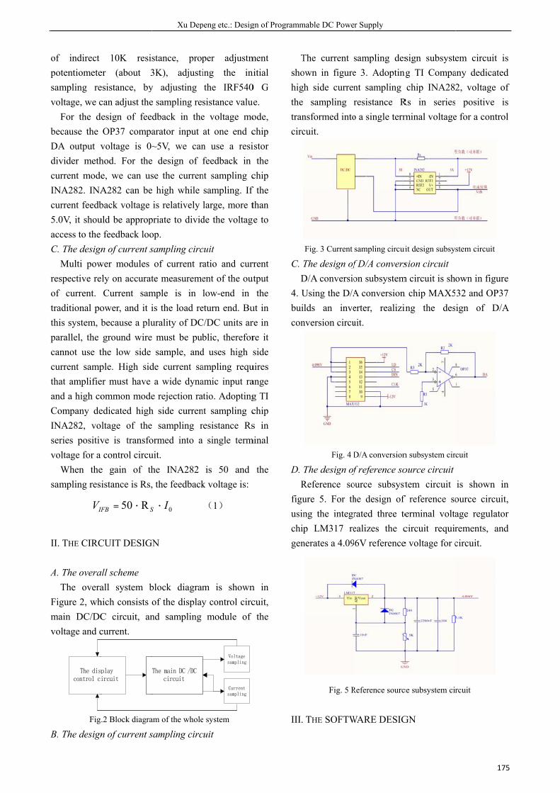
A
B
of indirect potentiometesampling revoltage, we c
For the debecause the DA output vdivider methcurrent modeINA282. INAcurrent feedb5.0V, it shouaccess to the C. The design
Multi powrespective reof current. traditional pothis system, bparallel, the cannot use tcurrent sampthat amplifieand a high coCompany deINA282, voseries positivvoltage for a
When thesampling res
VIF
II. THE CIRC
A. The overaThe overa
Figure 2, whmain DC/DCvoltage and c
The dispcontrol ci
Fig
B. The design
10K resier (about 3esistance, bycan adjust theesign of feeOP37 compavoltage is 0~hod. For thee, we can usA282 can beback voltage uld be approp
feedback loon of current s
wer modules ely on accurat
Current samower, and it ibecause a pluground wire
the low side ple. High sider must have ommon modeedicated highltage of theve is transfocontrol circu
e gain of thistance is Rs,
R50 SIFB ·=
CUIT DESIG
all scheme all system bhich consists C circuit, ancurrent.
play ircuit
.2 Block diagra
n of current s
Xu Dep
stance, prop3K), adjustiy adjusting e sampling redback in thearator input ~5V, we can
e design of se the currene high while is relatively
priate to dividop. sampling circof current r
te measurememple is in is the load reurality of DC
e must be pubsample, and
de current saa wide dyna
e rejection rah side currene sampling rormed into auit. he INA282 , the feedback
0IS ·
GN
block diagramof the displaynd sampling
The main DC /DCcircuit
am of the whole
sampling circ
peng etc.: Desig
per adjustming the inithe IRF540sistance valuee voltage moat one end cn use a resifeedback in
nt sampling csampling. If large, more t
de the voltag
cuit atio and current of the outlow-end in
eturn end. BuC/DC units arblic, therefor
d uses high sampling requamic input raatio. Adoptingnt sampling cresistance Rsa single term
is 50 and k voltage is:
(1)
m is showny control circ
module of
Voltage sampling
Current sampling
e system
cuit
gn of Programm
ment nitial 0 G e. ode, chip istor
the chip f the than e to
rrent utput
the ut in re in re it side
uires ange g TI chip s in
minal
the
n in cuit,
the
Tshohigthe trancirc
C. TD
4. Ubuicon
D. R
figuusinchipgen
III.
mable DC Powe
The current sown in figureh side curren
sampling rnsformed intocuit.
Fig. 3 Current
The design ofD/A conversioUsing the D/Alds an inve
nversion circu
Fig. 4 D
The design ofReference soure 5. For thng the integrp LM317 re
nerates a 4.09
Fig. 5 R
THE SOFTW
r Supply
sampling dese 3. Adoptingnt sampling resistance Ro a single term
sampling circui
f D/A converson subsystemA conversion erter, realizinuit.
D/A conversion
f reference soource subsysthe design of rated three teealizes the c6V reference
Reference sourc
WARE DESIG
sign subsysteng TI Compa
chip INA282Rs in seriesminal voltage
it design subsy
sion circuit m circuit is shn chip MAX5ing the des
n subsystem cir
ource circuit tem circuit
f reference soerminal voltacircuit require voltage for c
ce subsystem cir
GN
175
em circuit isany dedicated2, voltage of positive is
e for a control
stem circuit
own in figure32 and OP37ign of D/A
cuit
is shown inource circuitage regulatorrements, andcircuit.
rcuit
5
s d f s l
e 7 A
n , r d

The English Proceedings of the College of Instrumentation & Electrical Engineering, Jilin University, in the First Half of 2015
176
The program flow chart of the main controller is shown in figure 6.
The program flow chart of the main controller includes the initialization function, the main function, the keyboard function, the DA function, the AD function and the display function. The main task is to realize the keyboard settings and display.
Fig. 6 Flow chart of main program
IV. TEST PLAN AND TEST RESULTS
A. The test scheme Voltage, current hardware test schematic diagram
are shown in figure 7 and figure 8.
Fig. 7 Schematic diagram of voltage hardware test
Fig. 8 Schematic diagram of current hardware test
B. The test results The test results of the voltage signal are shown in
table 1 (carrying 6Ω) (unit /V)
TABLE I
THE TEST RESULTS OF THE VOLTAGE SIGNAL
The signal
value 6.000 7.000 8.000 9.000 9.500 10.000 11.000 12.000
Display 6.00 7.01 8.01 9.01 9.52 10.02 11.01 12.00
UIN 20.00 21.00 22.00 23.00 24.00 26.000 28.00 30.000
Uout 12.00 12.01 12.01 12.01 12.01 12.02 12.02 12.02
When UIN=24V, UO=12V, IO =2A, UOPP=0.17V. The test results of the current signal are shown in
table 2 (carrying 4.5Ω) (unit /A)

Xu Depeng etc.: Design of Programmable DC Power Supply
177
TABLE II
THE TEST RESULTS OF THE CURRENT SIGNAL
The signal
value 0.3000 0.6000 0.9000 1.2000 1.5000 18000 1.9000 2.000
Display 0.30 0.60 0.91 1.20 1.49 1.80 1.89 1.99
RS 3Ω 6Ω IO 2.00A 1.90A
C. Analysis and conclusion of the test results According to the test data, the following
conclusions can be drawn: 1、When the input of DC voltage is 20V to 30V, the output voltage can be set to 6 to 12V, and the maximum output current is not less than 2A, and the voltage step accuracy is 100mV; 2、When the input voltage UIN is 20V to 30V, output voltage is 12V, and the voltage adjustment rate SU is less than or equal to 2% (IO =2A); 3、The output voltage ripple peak-peak value UOPP is less than or equal to 0.2V (UIN=24V, UO=12V, IO =2A); 4、When the output current changes from 0 to 2A, the current step precision is 100mA, and the load impedance is less than 6Ω; 5、When the output current IO is 2A and the load is from the 3Ωto 6Ω, the current adjusting rate SI is less than or equal to 5% (UIN =20V); 6、Regardless of the working mode of the voltage source or current source, under the full load condition the efficiency of converter is higher than or equal to 70% (UIN=30V).
In summary, this design can meet requirements.
V. CONCLUSION
This paper design a programmable DC power source. It uses MSP430F149 microcontroller as the control core, and uses double loops of voltage feedback and current feedback. Program-controlled DC
regulated power supply system has the advantages of simple design, low cost, wide application range, and applicable in different fields such as laboratory, factory.
Of course, there are also many problems, such as the more complex algorithm and AD conversion is not linear change. Investigating its reason, the ground is a plane, and it is largely affected by the outside interference, so it has large output ripple. When it changes from low-end sampling into high-end sampling, it can effectively reduce the outside interference, so that the output is stable.
References
[1] Kang Huaguang. Electronic technology based
on the analog part [M]. Fifth edition. Beijing:
Higher Education Press, 2006.301-305.
[2] Liang Shian. Switching power supply theory
and design practice [M]. Beijing: Publishing
House of electronics industry, 2013.10-12.
[3] Abraham I.Pressman. The design of switch
power supply [M]. Beijing: Publishing House
of electronics industry, 2010.123-126.
[4] Wang Zhaoan, Liu Jinjun. The power
electronic technology [M]. Fifth edition.
Beijing: Mechanical Industry Press,
2011.135-138.
[5] Xie Kai, Zhao Jian. The system design and
engineering practice of MSP430 Series MCU
[M]. Beijing: Mechanical Industry Press, 2011.
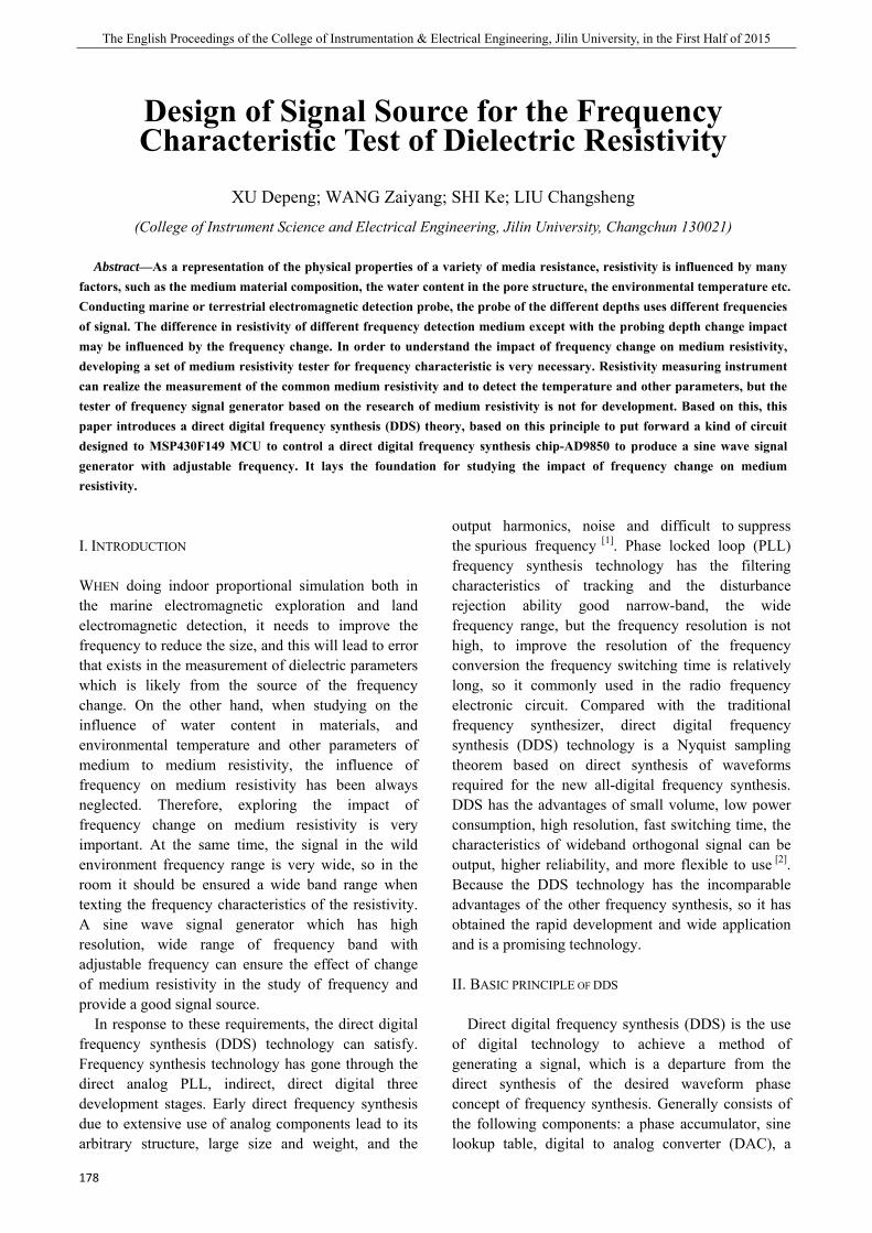
The English Proceedings of the College of Instrumentation & Electrical Engineering, Jilin University, in the First Half of 2015
178
Design of Signal Source for the Frequency Characteristic Test of Dielectric Resistivity
XU Depeng; WANG Zaiyang; SHI Ke; LIU Changsheng
(College of Instrument Science and Electrical Engineering, Jilin University, Changchun 130021)
Abstract—As a representation of the physical properties of a variety of media resistance, resistivity is influenced by many factors, such as the medium material composition, the water content in the pore structure, the environmental temperature etc. Conducting marine or terrestrial electromagnetic detection probe, the probe of the different depths uses different frequencies of signal. The difference in resistivity of different frequency detection medium except with the probing depth change impact may be influenced by the frequency change. In order to understand the impact of frequency change on medium resistivity, developing a set of medium resistivity tester for frequency characteristic is very necessary. Resistivity measuring instrument can realize the measurement of the common medium resistivity and to detect the temperature and other parameters, but the tester of frequency signal generator based on the research of medium resistivity is not for development. Based on this, this paper introduces a direct digital frequency synthesis (DDS) theory, based on this principle to put forward a kind of circuit designed to MSP430F149 MCU to control a direct digital frequency synthesis chip-AD9850 to produce a sine wave signal generator with adjustable frequency. It lays the foundation for studying the impact of frequency change on medium resistivity.
I. INTRODUCTION
WHEN doing indoor proportional simulation both in the marine electromagnetic exploration and land electromagnetic detection, it needs to improve the frequency to reduce the size, and this will lead to error that exists in the measurement of dielectric parameters which is likely from the source of the frequency change. On the other hand, when studying on the influence of water content in materials, and environmental temperature and other parameters of medium to medium resistivity, the influence of frequency on medium resistivity has been always neglected. Therefore, exploring the impact of frequency change on medium resistivity is very important. At the same time, the signal in the wild environment frequency range is very wide, so in the room it should be ensured a wide band range when texting the frequency characteristics of the resistivity. A sine wave signal generator which has high resolution, wide range of frequency band with adjustable frequency can ensure the effect of change of medium resistivity in the study of frequency and provide a good signal source.
In response to these requirements, the direct digital frequency synthesis (DDS) technology can satisfy. Frequency synthesis technology has gone through the direct analog PLL, indirect, direct digital three development stages. Early direct frequency synthesis due to extensive use of analog components lead to its arbitrary structure, large size and weight, and the
output harmonics, noise and difficult to suppress the spurious frequency [1]. Phase locked loop (PLL) frequency synthesis technology has the filtering characteristics of tracking and the disturbance rejection ability good narrow-band, the wide frequency range, but the frequency resolution is not high, to improve the resolution of the frequency conversion the frequency switching time is relatively long, so it commonly used in the radio frequency electronic circuit. Compared with the traditional frequency synthesizer, direct digital frequency synthesis (DDS) technology is a Nyquist sampling theorem based on direct synthesis of waveforms required for the new all-digital frequency synthesis. DDS has the advantages of small volume, low power consumption, high resolution, fast switching time, the characteristics of wideband orthogonal signal can be output, higher reliability, and more flexible to use [2]. Because the DDS technology has the incomparable advantages of the other frequency synthesis, so it has obtained the rapid development and wide application and is a promising technology.
II. BASIC PRINCIPLE OF DDS
Direct digital frequency synthesis (DDS) is the use of digital technology to achieve a method of generating a signal, which is a departure from the direct synthesis of the desired waveform phase concept of frequency synthesis. Generally consists of the following components: a phase accumulator, sine lookup table, digital to analog converter (DAC), a
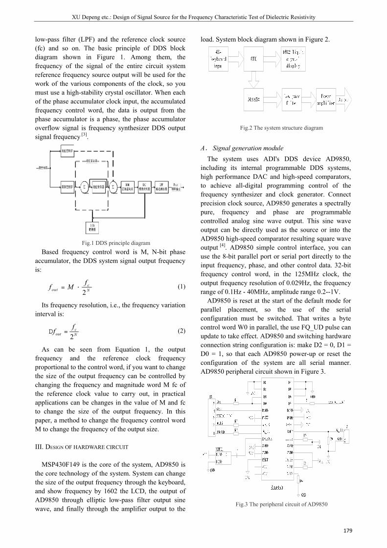
XU Depeng etc.: Design of Signal Source for the Frequency Characteristic Test of Dielectric Resistivity
179
low-pass filter (LPF) and the reference clock source (fc) and so on. The basic principle of DDS block diagram shown in Figure 1. Among them, the frequency of the signal of the entire circuit system reference frequency source output will be used for the work of the various components of the clock, so you must use a high-stability crystal oscillator. When each of the phase accumulator clock input, the accumulated frequency control word, the data is output from the phase accumulator is a phase, the phase accumulator overflow signal is frequency synthesizer DDS output signal frequency [3].
Fig.1 DDS principle diagram
Based frequency control word is M, N-bit phase accumulator, the DDS system signal output frequency is:
2c
out N
ff M= · (1)
Its frequency resolution, i.e., the frequency variation interval is:
2c
out N
ffD = (2)
As can be seen from Equation 1, the output frequency and the reference clock frequency proportional to the control word, if you want to change the size of the output frequency can be controlled by changing the frequency and magnitude word M fc of the reference clock value to carry out, in practical applications can be changes in the value of M and fc to change the size of the output frequency. In this paper, a method to change the frequency control word M to change the frequency of the output size.
III. DESIGN OF HARDWARE CIRCUIT
MSP430F149 is the core of the system, AD9850 is the core technology of the system. System can change the size of the output frequency through the keyboard, and show frequency by 1602 the LCD, the output of AD9850 through elliptic low-pass filter output sine wave, and finally through the amplifier output to the
load. System block diagram shown in Figure 2.
Fig.2 The system structure diagram
A. Signal generation module The system uses ADI's DDS device AD9850,
including its internal programmable DDS systems, high performance DAC and high-speed comparators, to achieve all-digital programming control of the frequency synthesizer and clock generator. Connect precision clock source, AD9850 generates a spectrally pure, frequency and phase are programmable controlled analog sine wave output. This sine wave output can be directly used as the source or into the AD9850 high-speed comparator resulting square wave output [4]. AD9850 simple control interface, you can use the 8-bit parallel port or serial port directly to the input frequency, phase, and other control data. 32-bit frequency control word, in the 125MHz clock, the output frequency resolution of 0.029Hz, the frequency range of 0.1Hz - 40MHz, amplitude range 0.2--1V.
AD9850 is reset at the start of the default mode for parallel placement, so the use of the serial configuration must be switched. That writes a byte control word W0 in parallel, the use FQ_UD pulse can update to take effect. AD9850 and switching hardware connection string configuration is: make D2 = 0, D1 = D0 = 1, so that each AD9850 power-up or reset the configuration of the system are all serial manner. AD9850 peripheral circuit shown in Figure 3.
Fig.3 The peripheral circuit of AD9850
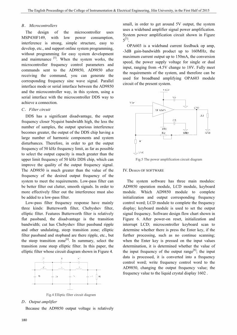
The English Proceedings of the College of Instrumentation & Electrical Engineering, Jilin University, in the First Half of 2015
180
B. Microcontrollers The design of the microcontroller uses
MSP430F149, with low power consumption, interference is strong, simple structure, easy to develop, etc., and support online system programming, without programming for easy system development and maintenance [5]. When the system works, the microcontroller frequency control parameters and commands sent to the AD9850, AD9850 after receiving the command, you can generate the corresponding frequency sine wave signal. Parallel interface mode or serial interface between the AD9850 and the microcontroller way, in this system, using a serial interface with the microcontroller DDS way to achieve a connection.
C. Filter circuit DDS has a significant disadvantage, the output
frequency closer Nyquist bandwidth high, the less the number of samples, the output spurious interference becomes greater, the output of the DDS chip having a large number of harmonic components and system disturbances. Therefore, in order to get the output frequency of 50 kHz frequency limit, as far as possible to select the output capacity is much greater than the upper limit frequency of 50 kHz DDS chip, which can improve the quality of the output frequency signal. The AD9850 is much greater than the value of the frequency of the desired output frequency of the system to meet the requirements. Low-pass filter can be better filter out clutter, smooth signals. In order to more effectively filter out the interference must also be added to a low-pass filter.
Low-pass filter frequency response have mainly three kinds: Butterworth filter, Chebyshev filter, elliptic filter. Features Butterworth filter is relatively flat passband, the disadvantage is the transition bandwidth; cut has Chebyshev filter passband ripple and other undulating, steep transition zone; elliptic filter passband and stopband are there ripple, etc., but the steep transition zone[6]. In summary, select the transition zone steep elliptic filter. In this paper, the elliptic filter whose circuit diagram shown in Figure 4.
Fig.4 Elliptic filter circuit diagram
D. Output amplifier Because the AD9850 output voltage is relatively
small, in order to get around 5V output, the system uses a wideband amplifier signal power amplification. System power amplification circuit shown in Figure 5[7].
OPA603 is a wideband current feedback op amp, -3dB gain-bandwidth product up to 160MHz, the maximum current output up to 150mA, the conversion speed, the power supply voltage for single or dual input, ranging from -4.5V change to 18V. Fully meet the requirements of the system, and therefore can be used for broadband amplifying OPA603 module circuit of the present system.
Fig.5 The power amplification circuit diagram
IV. DESIGN OF SOFTWARE
The system software has three main modules: AD9850 operation module, LCD module, keyboard module. Which AD9850 module to complete initialization and output corresponding frequency control word; LCD module to complete the frequency display; keyboard module is used to set the output signal frequency. Software design flow chart shown in Figure 6. After power-on reset, initialization and interrupt LCD; microcontroller keyboard scan to determine whether there is press the Enter key, if the further processing, such as no continue scanning; when the Enter key is pressed on the input values determination, it is determined whether the value of the input frequency of the output range[8]; the input data is processed, it is converted into a frequency control word; write frequency control word to the AD9850, changing the output frequency value; the frequency value to the liquid crystal display 1602 .
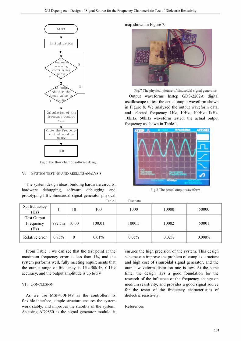
XU Depeng etc.: Design of Signal Source for the Frequency Characteristic Test of Dielectric Resistivity
181
Start
Initialization
Keyboard scanning
confirm key press
To judge whether the
input value in range
Calculation of the frequency control
word
Write the frequency control word to
AD9850
LCD
N
N
Y
Y
Fig.6 The flow chart of software design
V. SYSTEM TESTING AND RESULTS ANALYSIS
The system design ideas, building hardware circuits, hardware debugging, software debugging and prototyping FBI. Sinusoidal signal generator physical
map shown in Figure 7.
Fig.7 The physical picture of sinusoidal signal generator
Output waveforms Instep GDS-2202A digital oscilloscope to test the actual output waveform shown in Figure 8. We analyzed the output waveform data, and selected frequency 1Hz, 10Hz, 100Hz, 1kHz, 10kHz, 50kHz waveform tested, the actual output frequency as shown in Table 1.
Fig.8 The actual output waveform
Table 1 Test data
Set frequency (Hz) 1 10 100 1000 10000 50000
Test Output Frequency
(Hz) 992.5m 10.00 100.01 1000.5 10002 50001
Relative error 0.75% 0 0.01% 0.05% 0.02% 0.008%
From Table 1 we can see that the test point at the maximum frequency error is less than 1%, and the system performs well, fully meeting requirements that the output range of frequency is 1Hz-50kHz, 0.1Hz accuracy, and the output amplitude is up to 5V.
VI.CONCLUSION
As we use MSP430F149 as the controller, its flexible interface, simple structure ensures the system work stably, and improves the stability of the system. As using AD9850 as the signal generator module, it
ensures the high precision of the system. This design scheme can improve the problem of complex structure and high cost of sinusoidal signal generator, and the output waveform distortion rate is low. At the same time, the design lays a good foundation for the research of the influence of the frequency change on medium resistivity, and provides a good signal source for the tester of the frequency characteristics of dielectric resistivity.
References
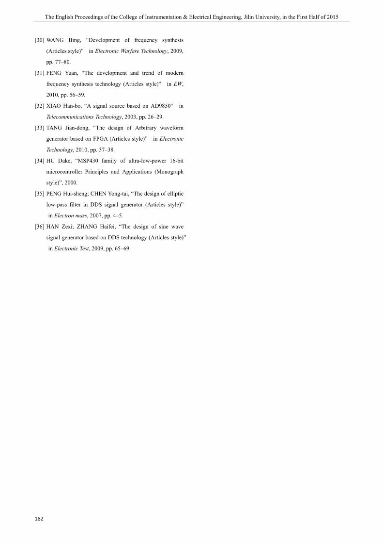
The English Proceedings of the College of Instrumentation & Electrical Engineering, Jilin University, in the First Half of 2015
182
[30] WANG Bing, “Development of frequency synthesis
(Articles style)” in Electronic Warfare Technology, 2009,
pp. 77–80.
[31] FENG Yuan, “The development and trend of modern
frequency synthesis technology (Articles style)” in EW,
2010, pp. 56–59.
[32] XIAO Han-bo, “A signal source based on AD9850” in
Telecommunications Technology, 2003, pp. 26–29.
[33] TANG Jian-dong, “The design of Arbitrary waveform
generator based on FPGA (Articles style)” in Electronic
Technology, 2010, pp. 37–38.
[34] HU Dake, “MSP430 family of ultra-low-power 16-bit
microcontroller Principles and Applications (Monograph
style)”, 2000.
[35] PENG Hui-sheng; CHEN Yong-tai, “The design of elliptic
low-pass filter in DDS signal generator (Articles style)”
in Electron mass, 2007, pp. 4–5.
[36] HAN Zexi; ZHANG Haifei, “The design of sine wave
signal generator based on DDS technology (Articles style)”
in Electronic Test, 2009, pp. 65–69.
Bas
Abstract—B
system, on the
also can test so
test trigger fun
circuit industr
only has more
Key words—
I. INTRODUCT
With the rap
industry, a
emerging te
applications
widely. Ther
quality are m
The rapid
the same tim
associated w
rapid improv
integrated
tremendous
applications,
session are r
quality of h
areas, the pre
circuit is par
stability and
become the
industry, and
technical fou
Zh
sed on
(jilin uni
Based on instr
e basis of it, the
ome pulse clas
nction at the s
ry, leading to i
e powerful func
— Virtual inst
TION
pid developm
variety of
echnology of
in many indu
refore, the I
more importan
developmen
me, it encou
with the IC
vements in tec
circuit ind
contribution
developme
equired for c
his. In partic
ecise verifica
rticularly imp
d reliability
focus of
d IC test te
undation for a
hang Bingren e
n the d
Zhang Biversity instru
rument science
e system can n
ss trigger chips
ame time, to a
ncreased to th
ctions, have a c
trument; The
ment of inte
new design
f integrated
ustry sectors
IC process
nt.
nt of integrat
urages signifi
test technolo
chnology, the
dustry, prec
ns. In integ
ent, producti
circuit testing
cular, certain
ation test on
portant. Thus,
of integrated
attention is
echnology ha
all of these job
tc.: Based on th
igital VII
ingren, Wanument science
e and electric
not only test tri
s, by adding a f
add rich the ch
e requirement
combination of
e trigger; Chip
egrated circui
and a new
circuits an
are also mor
accuracy an
ted circuits a
icant progres
ogy. The tes
e quality of th
cision mad
grated circui
ion of eac
g to ensure th
n confidentia
the integrate
, to ensure th
d circuits ha
now testin
as become th
bs.
he digital integr
integrIS – E
ang Xin, Wae and enginee
cal engineering
igger level clas
filter circuit m
hip database of
t of digital inte
f economic, fas
p library
uit
w,
nd
re
nd
at
ss
st
he
de
uit
ch
he
al
ed
he
as
ng
he
II
co
th
an
D
be
co
th
an
op
rated circuit tes
rated cEM
ang Zhao, Zering institute
g college of ji
ss of middle an
make the system
f the system.Th
egrated circuit
st, simple oper
. SYSTEM DES
The tester
onnected to a
he controller t
System uses
nd the chassi
DC power supp
eing passed
ommands. Am
he following f
Fig.1
PC syste
nd through
peration of th
ter of VⅡS—E
circuit
Zhao Jian e,changchun,
lin university
nd small scale d
m more standa
he rapid develo
testing techno
ration and so o
SIGN
will test eac
a system bus
through unifie
s a 3U chas
s contains a
ply. In operat
in a back
mong them, t
figure on the
The system ha
em primarily
the USB
he system.
EM
t tester
130021)
self-develope
digital integra
ard input pulse
opment of digi
ology.Virtual in
on many virtue
ach modular
s, and it is c
ed.
ssis and mod
system back
tion, the soun
kplane bus
the digital IC
7th slot.
hardware panel f
y uses LabV
interface to
183
r of
d VIIS - EM
ted chips, and
e signal.In add
ital integrated
nstrument not
es.
instruments
ontrolled by
dular design,
kplane and a
nd quality by
to various
C tester using
figure
View software
control th
3
e,
he
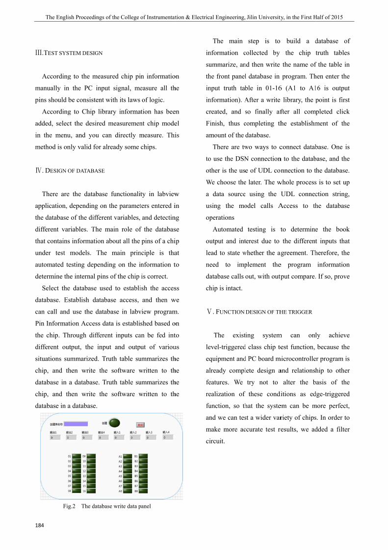
The Englis
184
Ⅲ.TEST SYST
According
manually in
pins should b
According
added, select
in the menu
method is on
Ⅳ. DESIGN O
There are
application, d
the database
different var
that contains
under test m
automated te
determine the
Select the
database. Es
can call and
Pin Informat
the chip. Th
different out
situations sum
chip, and th
database in a
chip, and th
database in a
Fig
sh Proceedings
TEM DESIGN
g to the meas
the PC inpu
be consistent
g to Chip lib
t the desired
u, and you c
nly valid for a
OF DATABASE
the database
depending on
of the differe
riables. The m
information
models. The
esting depend
e internal pin
database us
stablish datab
use the data
tion Access d
hrough differe
tput, the inp
ummarized. T
hen write the
a database. T
hen write the
a database.
g.2 The databa
of the College
sured chip pi
ut signal, me
with its laws
rary informa
d measuremen
an directly m
already some
e functionali
n the paramet
ent variables,
main role of
about all the
e main prin
ding on the i
ns of the chip
sed to establi
base access,
abase in labv
data is establi
ent inputs ca
put and outp
Truth table su
e software w
Truth table su
e software w
ase write data p
of Instrumentat
in informatio
easure all th
of logic.
ation has bee
nt chip mode
measure. Thi
chips.
ty in labview
ters entered i
and detectin
f the databas
pins of a chi
nciple is tha
information t
is correct.
ish the acces
and then w
view program
shed based o
an be fed int
ut of variou
ummarizes th
written to th
ummarizes th
written to th
panel
tion & Electrica
on
he
en
el
is
w
in
ng
se
ip
at
to
ss
we
m.
on
to
us
he
he
he
he
in
su
th
in
in
cr
Fi
am
to
ot
W
a
us
op
ou
le
ne
da
ch
Ⅴ
le
eq
al
fe
re
fu
an
m
ci
al Engineering,
The main
nformation c
ummarize, an
he front panel
nput truth tab
nformation). A
reated, and s
inish, thus c
mount of the
There are tw
o use the DSN
ther is the us
We choose the
data source
sing the mo
perations
Automated
utput and int
ead to state w
eed to imp
atabase calls
hip is intact.
Ⅴ. FUNCTION
The exist
evel-triggered
quipment and
lready compl
eatures. We
ealization of
unction, so th
nd we can tes
make more ac
ircuit.
Jilin University
step is to
collected by
nd then write
l database in
ble in 01-16
After a write
so finally af
completing th
database.
wo ways to c
N connection
e of UDL con
e later. The w
using the U
odel calls A
testing is t
terest due to
whether the ag
plement the
out, with outp
DESIGN OF TH
ing system
d class chip te
d PC board m
lete design a
try not to
these condi
hat the syste
st a wider var
ccurate test re
ty, in the First H
build a d
the chip
the name of
program. Th
6 (A1 to A1
e library, the p
fter all com
he establishm
connect datab
n to the datab
onnection to t
whole process
UDL connec
Access to th
to determine
the different
agreement. Th
e program
tput compare.
HE TRIGGER
m can onl
est function,
microcontrolle
and relationsh
alter the b
ditions as ed
em can be m
riety of chips
results, we ad
Half of 2015
database of
truth tables
f the table in
hen enter the
16 is output
point is first
mpleted click
ment of the
base. One is
base, and the
the database.
s is to set up
ction string,
he database
e the book
t inputs that
herefore, the
information
. If so, prove
ly achieve
because the
er program is
hip to other
basis of the
dge-triggered
more perfect,
s. In order to
dded a filter
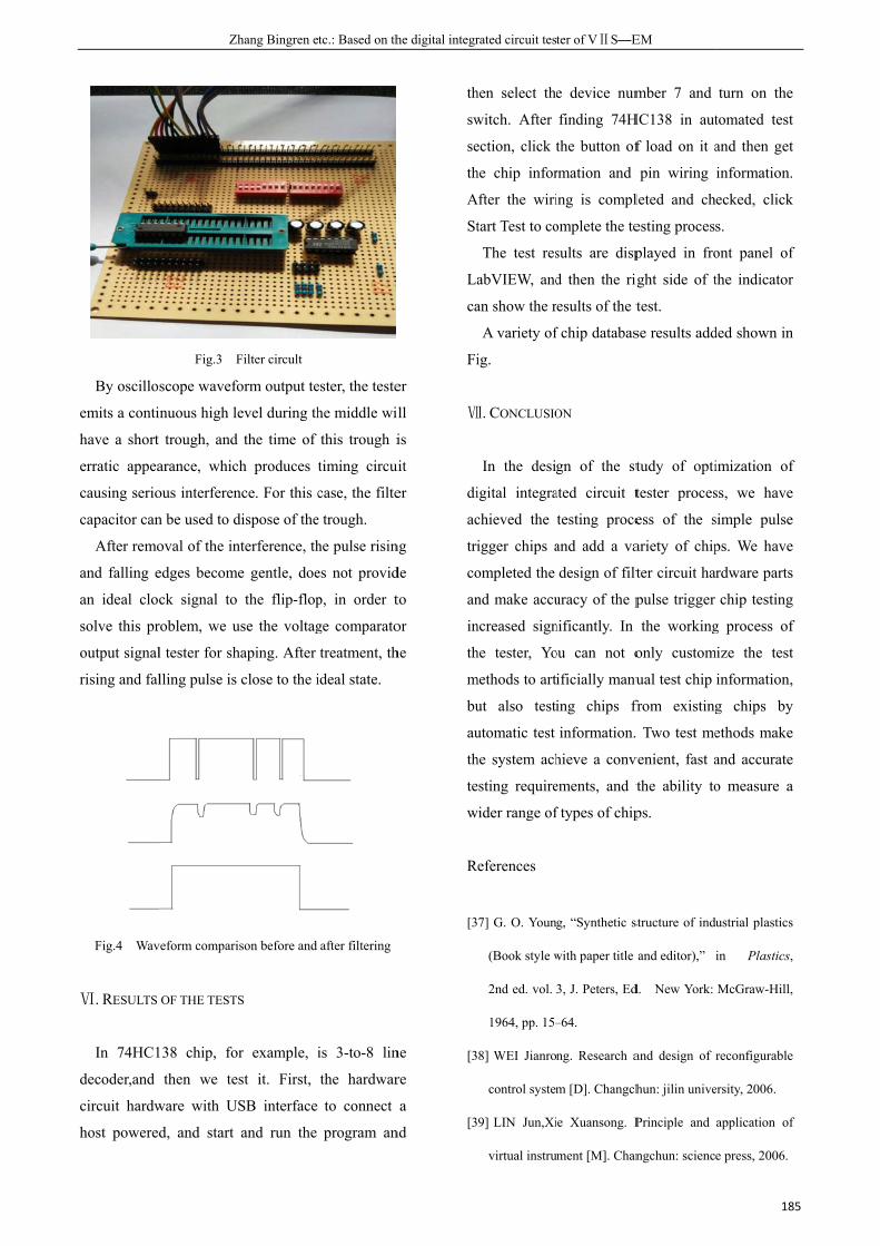
By oscillo
emits a conti
have a short
erratic appea
causing serio
capacitor can
After remo
and falling e
an ideal cloc
solve this pr
output signal
rising and fal
Fig.4 Wav
Ⅵ. RESULTS
In 74HC1
decoder,and
circuit hardw
host powered
Zh
Fig.3 F
scope wavefo
inuous high le
trough, and
arance, whic
ous interferen
n be used to d
oval of the in
edges become
ck signal to
roblem, we u
l tester for sh
lling pulse is
veform compari
OF THE TESTS
138 chip, for
then we te
ware with US
d, and start
hang Bingren e
Filter circult
orm output te
evel during th
the time of
h produces
nce. For this c
dispose of the
nterference, th
e gentle, doe
the flip-flop
use the voltag
haping. After
close to the i
son before and
S
r example, i
st it. First,
SB interface
and run the
tc.: Based on th
ester, the teste
he middle wil
this trough i
timing circui
case, the filte
e trough.
he pulse risin
es not provid
p, in order t
ge comparato
treatment, th
ideal state.
after filtering
is 3-to-8 lin
the hardwar
to connect
program an
he digital integr
er
ll
is
uit
er
ng
de
to
or
he
ne
re
a
nd
th
sw
se
th
A
St
La
ca
Fi
Ⅶ
di
ac
tri
co
an
in
th
m
bu
au
th
te
w
R
[3
[3
[3
rated circuit tes
hen select the
witch. After
ection, click t
he chip infor
After the wiri
tart Test to co
The test res
abVIEW, and
an show the r
A variety of
ig.
Ⅶ. CONCLUSIO
In the desi
igital integra
chieved the
igger chips a
ompleted the
nd make accu
ncreased sign
he tester, Yo
methods to art
ut also testi
utomatic test
he system ach
esting require
wider range of
References
7] G. O. Youn
(Book style w
2nd ed. vol.
1964, pp. 15–
8] WEI Jianro
control system
9] LIN Jun,Xi
virtual instru
ter of VⅡS—E
e device num
finding 74H
the button of
rmation and
ing is compl
omplete the te
sults are disp
d then the rig
esults of the t
f chip databas
ON
gn of the st
ated circuit t
testing proce
and add a va
design of filt
uracy of the p
nificantly. In
ou can not o
ificially manu
ing chips fr
information.
hieve a conv
ements, and t
f types of chip
g, “Synthetic s
with paper title
3, J. Peters, Ed
–64.
ng. Research a
m [D]. Changch
e Xuansong. P
ment [M]. Chan
EM
mber 7 and
HC138 in aut
f load on it a
pin wiring
leted and ch
esting proces
played in fro
ight side of t
test.
se results add
tudy of opti
tester proces
ess of the s
ariety of chip
ter circuit ha
pulse trigger
the working
only custom
ual test chip
from existing
. Two test me
venient, fast a
the ability to
ps.
structure of indu
and editor),”
d. New York:
and design of
hun: jilin unive
Principle and
ngchun: scienc
185
turn on the
tomated test
and then get
information.
ecked, click
s.
ont panel of
the indicator
ded shown in
imization of
ss, we have
simple pulse
ps. We have
rdware parts
chip testing
g process of
mize the test
information,
g chips by
ethods make
and accurate
o measure a
ustrial plastics
in Plastics,
McGraw-Hill,
reconfigurable
ersity, 2006.
application of
e press, 2006.
5

The English Proceedings of the College of Instrumentation & Electrical Engineering, Jilin University, in the First Half of 2015
186
[40] WANG Jian. The development of data acquisition and
analysis system based on LabVIEW [D]. Harbin: Harbin
university of science and technology, 2004.
[41] LIANG Can. The design of virtual digital spectrum
analyzer [D]. Chengdu: university of electronic science
and technology. 2009.
[42] LUO Heping. Key techniques of digital IC automatic
test equipment [D]. Chengdu: university of electronic
science and technology, 2008.
[43] LIU Wenjun.Computer and single chip microcomputer
serial communication system based on LabVIEW [J].
Chinese education technology and equipment. 2012 (6).
[44] GAO Cheng,ZHANG Dong. The latest integrated
circuit testing technology [M]. Version 1 February 2009.
National defense industry press, 2009:7-9.
[45] NIU Yong. Digital integrated circuit test [J]. China's
integrated circuit, 2002 (11) : 63-65.
[46] GU Yuhui,ZHAO Liang. Data acquisition system based
on virtual instrument software LabVIEW design [J].
China's transportation information. 2012 (S1).
[47] Chengmingliang.A general digital integrated circuit
automatic tester system [J]. Journal of electronic science
and technology university graduate students, 2009 (11) :
29 and 30.
[48] Jeffrey Travis. LabVIEW university practical tutorial
[M]. Beijing: electronic industry press, 2008.
[49] Mukesh Kumar,Mansav Joshi , Sanjeev Sharma.
Design and Implementation of Embedding Web Server
for Real Time Data
AcquisitionandLoggingSystem[J].International
JournalofComputerApplications,2012,42(11):13-16.
[50] Deshpande S G,Jenq-Neng H. A real-time interactive
virtual classroom multimedia distance learning system[J].
Multimedia,IEEE Transactions on.2001,3(4):432-444.
[51] NationalInstruments Corporation. LabVIEW Help.
April 2003 Edition, PartNumber 370117C-01.
[52] YANG Leping. The LabVIEW program design and
application [M]. Electronic industry press, 2001.
[53] SONG Yufeng. Labwindows/CVI deepens and the
development instance [M]. Mechanical industry
publishing house, 2003.
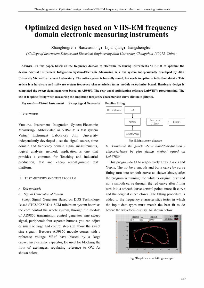
A
Zh
Optd
( Colleg
Abstract—In
design. Virtua
University Vir
article is a ha
completed the
use of B-spline
Key words—
I. FOREWORD
VIRTUAL InMeasuring,Virtual Insindependentldomain and logical analprovides a production, platform.
II.TEST ME
A. Test methoa.Signal Ge
Swept SigBased STC89the core conof AD9850 signal, periphor small or lsine signal .reference vocapacitance cflow of excshown below
hangbingran etc
timizeddomain
Zhge of Instrum
n this paper, b
al Instrument
rtual Instrume
ardware and s
e sweep signal
e fitting when m
—Virtual Instr
D
nstrument InAbbreviatedtrument Laly developed frequency d
lysis, networcommon fofast and
ETHODS AND T
ods enerator of Snal Generato9C58RD + S
ntrol the wholtransmission herals four selarge and con. Because Aoltage VReceramic capachanges, reg
w.
c:Optimized d
d desin electhangbingrenent Science a
based on the
Integration S
ent Laboratory
software system
generator base
measuring the
rument Swe
ntegration Syd as VIIS-EMaboratory J
, set the sigdomain signark applicatioor Teaching cheap reco
TEST PROGRAM
Sweep or Based on SCM minimumle system, thcontrol gen
eparate buttontrol step siz
AD9850 moduf have bia
acitor, Be usegulating refer
design based on
gn bastronic n;Baoxiaoand Electrical
frequency dom
System-Electro
y. The entire sy
m frequency c
ed on AD9850
amplitude-fre
eep Signal Gen
ystem-ElectroM a test sysilin Univer
gnal source, tl measuremeon is one
and industonfigurable
M
DDS Technom system boa
hrough the mnerates sine sns, you can a
ze about the sule comes w
ased by a d for blockinrence to OV
n VIIS-EM freq
sed onmeasu
odong;Lijil Engineering
main of electr
onic Measurin
ystem is basica
characteristics
0. The rear pan
equency chara
nerator B-sp
onic stem rsity time ents, that trial test
ology. ard as
module sweep adjust swept
with a large
ng the V. As
4*1
b.chaLab
TY-afittithe not turnandaddthe befo
quency domain e
n VIISuring anqiang;Jg Jilin Univer
ronic measurin
ng is a test s
ally sound, but
tester module
nel optimizatio
cteristic curve
pline fitting
125
Keyboard
F
Eliminate taracteristics bVIEW This program axis, The not ing turn into program is ra smooth cu
n into a smood the original ded to the fre
input data fore the wavef
electronic meas
-EM finstru
Jiangshenghrsity, Changc
ng instruments
ystem indepen
t needs to optim
e to optimize
on software La
eliminate glitc
AD9850
5M Crystal
SCM
Fig.1Main syste
he glitch abby plus fit
do fit to respbe a smooth smooth curv
running, the wurve through oth curve con
curve closerequency charatypes must mform display.
Fig.2B-spline c
suring instrume
frequeumentshui chun 130012,
s VIIS-EM to
ndently develo
mize individua
board. Hardw
abVIEW progr
ches.
Low pass filter
em diagram
bout amplitutting method
pectively arraand burrs cu
ve as shownwhite is origthe red curve
ntrol points mr. The fitting acteristics tesmatch the b. As shown be
curve fitting ex
ents
187
ency s
China)
o optimize the
oped by Jilin
al details. This
ware design is
ramming. The
Export
ude-frequencyd based on
ay X-axis andurve by curve above, afterinal burr ande after fitting
more fit curveprocedure is
ster in whichest fit to doelow
xample
7
y n
d e r d g e s h o
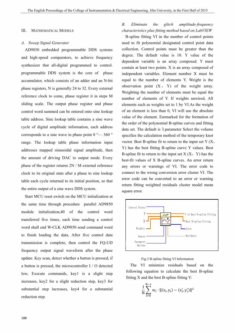
The English Proceedings of the College of Instrumentation & Electrical Engineering, Jilin University, in the First Half of 2015
188
III. MATHEMATICAL MODELS
A. Sweep Signal Generator
AD9850 embedded programmable DDS systems
and high-speed comparators, to achieve frequency
synthesizer that all-digital programmed to control.
programmable DDS system is the core of phase
accumulator, which consists of an adder and an N-bit
phase registers, N is generally 24 to 32. Every external
reference clock to come, phase register it in steps M
sliding scale. The output phase register and phase
control word summed can be entered onto sine lookup
table address. Sine lookup table contains a sine wave
cycle of digital amplitude information, each address
corresponds to a sine wave in phase point 0 °— 360 °
range. The lookup table phase information input
addresses mapped sinusoidal signal amplitude, then
the amount of driving DAC to output mode. Every
phase of the register returns 2N / M external reference
clock to its original state after a phase to sine lookup
table each cycle returned to its initial position, so that
the entire output of a sine wave DDS system.
Start MCU reset switch on the MCU initialization at
the same time through procedure parallel AD9850
module initialization,40 of the control word
transferred five times, each time sending a control
word shall end W-CLK AD9850 send command word
to finish loading the data, After five control data
transmission is complete, then control the FQ-UD
frequency output signal waveform after the phase
update. Key scan, detect whether a button is pressed, if
a button is pressed, the microcontroller I / O detected
low, Execute commands, key1 is a slight step
increases, key2 for a slight reduction step, key3 for
substantial step increases, key4 for a substantial
reduction step.
B. Eliminate the glitch amplitude-frequency characteristics plus fitting method based on LabVIEW
B-spline fitting VI in the number of control points used to fit polynomial designated control point data collection. Control points must be greater than the degree. The default value is 10. Y value of the dependent variable is an array composed. Y must contain at least two points. X is an array composed of independent variables. Element number X must be equal to the number of elements Y. Weight is the observation point (X , Y) of the weight array. Weighting the number of elements must be equal the number of elements of Y. If weights unwired, All elements such as weights set to 1 by VI.As the weight of an element is less than 0, VI will use the absolute value of the element. Earmarked for the formation of the order of the polynomial B-spline curves and fitting data set. The default is 3.parameter Select the volume specifies the calculation method of the temporary knot vector. Best B-spline fit to return to the input set Y (X, Y) has the best fitting B-spline curve Y values. Best B-spline fit to return to the input set X (X,Y) has the best-fit values of X B-spline curves. An error return any errors or warnings of VI. The error code to connect to the wrong conversion error cluster VI. The error code can be converted to an error or warning return fitting weighted residuals cluster model mean square error.
Control Points
Y
X
Weights Error
Residuals
Parameter Options
Degree
Best B-spline Fitting
Y of Best B-spline Fitting
Fig.3 B-spline fitting VI Information The VI minimize residuals based on the
following equation to calculate the best B-spline fitting X and the best B-spline fitting Y: 1N w ∙ ‖ x , y − x , y ‖

A
B
Zh
= 1NIV. SYSTEM T
A. Experim
Set frequen
Actual freq
Relative er
B.Test Resua.Sweep Sig
When issu
hangbingran etc
w ∙ xTEST RESULT
mental Data:
ncy 10
quency 100
rror 0.0
Ste
Ac
Rel
ults gnal Generat
uing fixed fre
c:Optimized d
− x yS
00 500
0.02 500.0
02% 0.002%
epping set
tual step
lative error
Fig.4 A
Fig.5
tor equency sine
design based on
− y;
Table 1 S
1K
01 1.00K
% 0.000%
Table 2
10
10.5
5.20
Amplitude-frequ
Amplitude-freq
wave of sw
n VIIS-EM freq
System frequenc
10K
10.00K
0.000%
sweep stepper
0
52
0%
quency characte
quency characte
weep
signhigherro
quency domain e
cy test data
100K
100.01K
0.01%
r test data
20
20.34
1.70%
ristic curve bef
eristic curve aft
nal generatorher precisionor is relativel
electronic meas
1M
1.0001M 5
0.01%
Company:
30
30.90
3.00%
fore optimizatio
ter optimization
r, the relative n. Setpoint anly large swee
suring instrume
Comp
5M
5.0005M
0.01%
Hz
on
n
e error is lessnd the actualep stepper, l
ents
189
any:Hz
10M
10.002M
0.02%
s than 0.05%,value of the
ess than 6%,
9
, e ,

The English Proceedings of the College of Instrumentation & Electrical Engineering, Jilin University, in the First Half of 2015
190
but due to the step value itself is small, the absolute value of the error is not real. b . Plus fitting method amplitude-frequency
characteristics eliminate glitches based on LabVIEW Use based on B-spline fitting eliminates the original
amplitude-frequency characteristic curve of glitches, make smooth curves, eliminating the reading errors due to burrs.
V .CONCLUSION
Sweep signal generator design based on the AD9850 and software based LabVIEW B spline curve fitting to eliminate frequency glitches by hardware ,Basically completed the optimization of the design of electronic measuring instruments frequency domain based VIIS-EM.
Through testing, signal accuracy higher sweep signal generator, test equipment to meet the needs, but has not yet been integrated into the frequency characteristics tester module on the board. Optimization software eliminates the original glitch amplitude-frequency characteristic curve, improved reading accuracy.
Currently, the frequency characteristics tester module also has some measurement error in the use of the process,That is the measured value and the actual value of the offset certain influence the accuracy of the test results, the optimization work remains to be improved.
References
[1] Wangjiali, Sunlu .Frequency Synthesizer[M].Xi'an
University of Electronic Science and Technology
Press,2009(1):124-136.
[2] Wangbing. Development and trend of modern frequency
synthesis technology[M]. Electronic Warfare
Technology,2009(3):77-80.
[3] Dongjungang,Caizhenjiang. Based on DDS technology
Intelligent Signal Generator[J]. Microcomputer Information,
2007.
[4] Fanxiuyun,Zhanghemin.Sweep Signal Generator Based on
DDS[J].Shanxi Electronic Technology,2002 fifth
[5] National Instruments Corporation. The measurement and
automation catalog[Z]. User manual, 1996.
[6] Linzhengshen.Virtual Instrument Technology and Its
Development[J].Modern Metrology,1997,(4):10-14.
[7] Hanjiuqiang.The study of virtual Instrument Software
Development Platform[J].Xi'an Jiaotong University,
1997,31(9): 6-9.
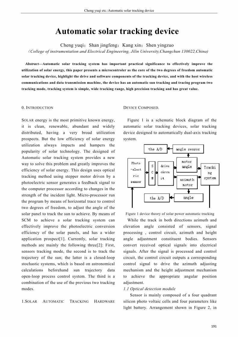
Cheng yuqi etc.:Automatic solar tracking device
191
Automatic solar tracking device
Cheng yuqi;Shan jingfeng;Kang xin;Shen yingzuo (College of instrumentation and Electrical Engineering, Jilin University,Changchun 130022,China)
Abstract—Automatic solar tracking system has important practical significance to effectively improve the
utilization of solar energy, this paper presents a microcontroler as the core of the two degrees of freedom automatic
solar tracking device, highlight the drive and software components of the tracking device, and with the host wireless
communications and data transmission machine, the device has an automatic sun tracking and tracing program two
tracking mode, tracking system is simple, wide tracking range, high precision tracking and has great value.
0. INTRODUCTION
SOLAR energy is the most primitive known energy, it is clean, renewable, abundant and widely distributed, having a very broad utilization prospects. But the low efficiency of solar energy utilization always impacts and hampers the popularity of solar technology. The designed of Automatic solar tracking system provides a new way to solve this problem and greatly improves the efficiency of solar energy. This design uses optical tracking method using stepper motor driven by a photoelectric sensor generates a feedback signal to the computer processor according to changes in the strength of the incident light. Micro-processor run the program by means of horizontal trace to control two degrees of freedom, to adjust the angle of the solar panel to track the sun to achieve. By means of SCM to achieve a solar tracking system can effectively improve the photoelectric conversion efficiency of the solar panels, and has a wider application prospect[1]. Currently, solar tracking methods are mainly the following three[2]: First, sensors tracking mode, the second is to track the trajectory of the sun; the latter is a closed-loop stochastic systems, which is based on astronomical calculations beforehand sun trajectory data open-loop process control system. The third is a combination of the use of the previous two tracking modes.
1.SOLAR AUTOMATIC TRACKING HARDWARE
DEVICE COMPOSED.
Figure 1 is a schematic block diagram of the automatic solar tracking devices, solar tracking device designed to automatically dual-axis tracking system.
Figure 1 device theory of solar power automatic tracking While the track in both directions azimuth and
elevation angle consisted of sensors, signal processing , control circuit, azimuth and height angle adjustment constituent bodies. Sensors convert received optical signals into electrical signals. After the signal is processed and control circuit, the control circuit outputs a corresponding control signal to drive the azimuth adjusting mechanism and the height adjustment mechanism to achieve the appropriate angular position adjustment. 1.1 Optical detection module
Sensor is mainly composed of a four quadrant silicon photo voltaic cells and four parameters like light battery. Arrangement shown in Figure 2, in
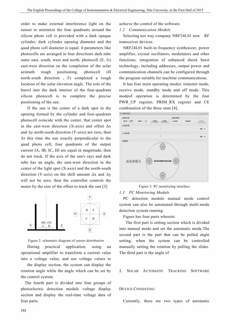
The English Proceedings of the College of Instrumentation & Electrical Engineering, Jilin University, in the First Half of 2015
192
order to make external interference light on the sensor to minimize the four quadrants around the silicon photo cell is provided with a dark opaque cylinder; dark cylinder opening diameter and the quad photo cell diameter is equal. 4 parameters like photocells are arranged in four directions dark tube outer east, south, west and north; photocell (E, G) east-west direction on the completion of the solar azimuth rough positioning, photocell (H north-south direction , F) completed a rough location of the solar elevation angle. The role of the barrel into the dark interior of the four-quadrant silicon photocell is to complete the precise positioning of the sun.
If the sun is the center of a dark spot in the opening formed by the cylinder and four-quadrant photocell coincide with the center, that center spot in the east-west direction (X-axis) and offset Δx and Δy north-south direction (Y-axis) are zero, then At this time the sun exactly perpendicular to the quad photo cell, four quadrants of the output current IA, IB, IC, ID are equal in magnitude, then do not track. If the axis of the sun's rays and dark tube has an angle, the east-west direction in the center of the light spot (X-axis) and the north-south direction (Y-axis) on the shift amount Δx and Δy will not be zero, then the controller controls the motor by the size of the offset to track the sun [3]
Figure 2. schematic diagram of sensor distribution
During practical application, using an operational amplifier to transform a current value into a voltage value, and use voltage values to
achieve the control of the software. 1.2 Communication Module
Selecting nor way company NRF24L01 new RF transceiver devices.
NRF24L01 built-in frequency synthesizer, power amplifier, crystal oscillators, modulators and other functions, integration of enhanced shock burst technology, including addresses, output power and communication channels can be configured through the program suitable for machine communications.
It has four main operating modes: transmit mode, receive mode, standby mode and off mode. This modeof operation is determined by the four PWR_UP register, PRIM_RX register and CE combination of the three state [4].
Figure 3. PC monitoring interface
1.3 PC Monitoring Module PC detection module manual mode control
system can also be automated through multi-mode detection system running.
Figure has four parts wherein: The first part is setting section which is divided
into manual mode and set the automatic mode.The second part is the part that can be pulled angle setting, when the system can be controlled manually setting the rotation by pulling the slider. The third part is the angle of
the display section, the system can display the rotation angle while the angle which can be set by the control system.
The fourth part is divided into four groups of photoelectric detection module voltage display section and display the real-time voltage data of four parts.
2. SOLAR AUTOMATIC TRACKING SOFTWARE
DEVICE CONSISTING
Currently, there are two types of automatic
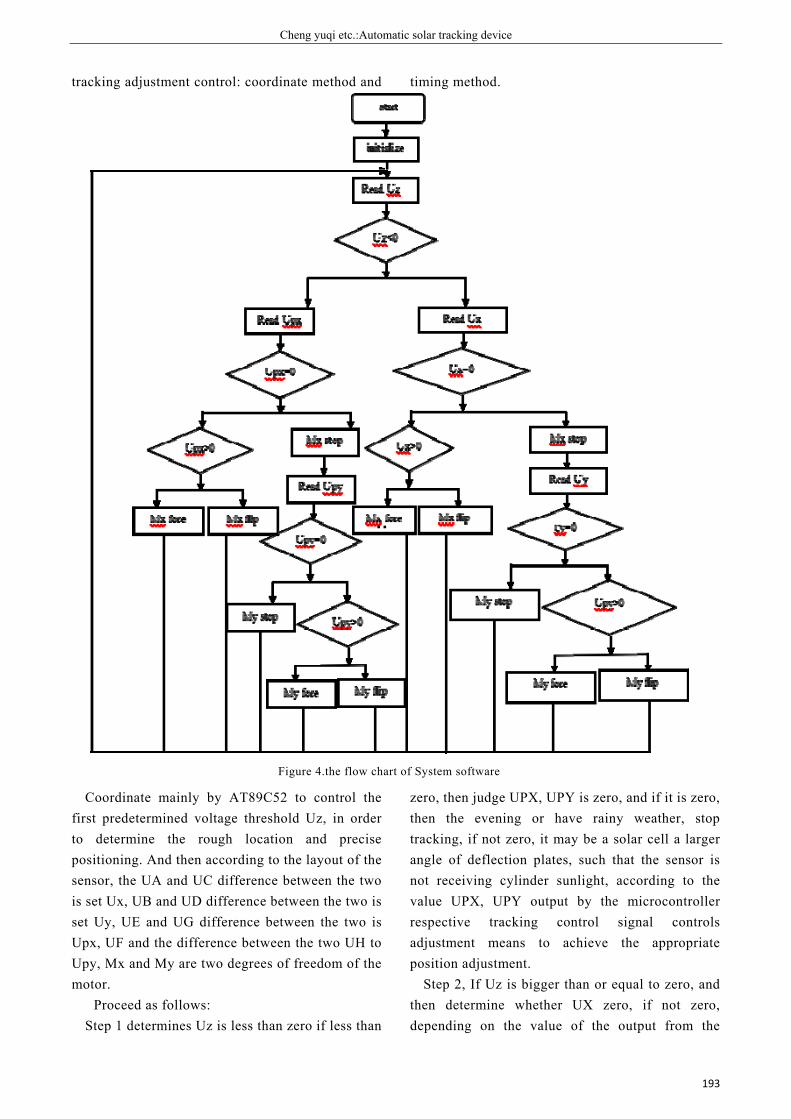
Cheng yuqi etc.:Automatic solar tracking device
193
tracking adjustment control: coordinate method and timing method.
Figure 4.the flow chart of System software
Coordinate mainly by AT89C52 to control the first predetermined voltage threshold Uz, in order to determine the rough location and precise positioning. And then according to the layout of the sensor, the UA and UC difference between the two is set Ux, UB and UD difference between the two is set Uy, UE and UG difference between the two is Upx, UF and the difference between the two UH to Upy, Mx and My are two degrees of freedom of the motor.
Proceed as follows: Step 1 determines Uz is less than zero if less than
zero, then judge UPX, UPY is zero, and if it is zero, then the evening or have rainy weather, stop tracking, if not zero, it may be a solar cell a larger angle of deflection plates, such that the sensor is not receiving cylinder sunlight, according to the value UPX, UPY output by the microcontroller respective tracking control signal controls adjustment means to achieve the appropriate position adjustment.
Step 2, If Uz is bigger than or equal to zero, and then determine whether UX zero, if not zero, depending on the value of the output from the

The English Proceedings of the College of Instrumentation & Electrical Engineering, Jilin University, in the First Half of 2015
194
micro controller UX tracking control signal corresponding to the azimuth adjustment mechanism to achieve the appropriate position adjustment, if UX is zero, UY then determine whether zero, if not zero, depending on the value of the output from the micro controller UY tracking control signal corresponding to the height adjustment mechanism to achieve the appropriate angular position adjustment, if UY zero, then stop tracking [5].
Timing method is based on the local latitude and longitude parameters and time information, solar declination, hour angle calculated elevation angle and azimuth of the sun; then stepping motors are controlled by a micro controller, changing the orientation of the panel through a transmission mechanism to achieve automatic, accurately tracking the purpose of the sun. This first count the rotation angle of the panel at different times, then drive control tracking method, although there is an error, but because of the offline computing, time control ,the position of the panel followed the sun, running manipulation is more convenient.
As we all know, the sun goes down every day seemingly unchanged .In fact, the position of sunshine and the north-south movement throughout the year are quietly changing. Solar elevation angle also changes along with the place where the solar declination varies. Usually for the convenient of easily tracking adjustment control, setting the sunrise and sunset angles are 0, when midday sun elevation angle maximum. By the position of the sun elevation angle and azimuth A h determined by the solar elevation angle h Ref. [7] obtained the formula provided by:
tcoscossinsinsinsinh += djdj (3) Azimuth a regarded by the following formula:
( )( )ddj coscosh/sinsinsinhcos -=A
(4) Where is the solar declination for the local
latitude, t when the angle of the sun. Summer solstice sun azimuth is the maximum
value of the year, the winter solstice is the angle of the minimum height of the sun in one year. These two special days by solar elevation angle and
azimuth, we can clearly know the year the sun's rays to the illumination device coverage . System works program stored in eprom. The use of device location determined from the date of the day declination angle δ, and then determine the sunrise and sunset time of day with the local latitude, self-control procedures to determine whether the regulation time after sunrise sunset before [8-10]. According to the formula (3-4) and the movement of the sun, the solar panel can be calculated to be the angle of rotation per minute. Due to the stepper motor step angle is a fixed value, tracking routines in the software design should take full account of the results of the step angle relationship. Theoretically long as the regulation of solar panels solar elevation angle and azimuth can be maintained and sun vertical, photo voltaic conversion for optimal results.
3 SIMULATION AND EXPERIMENT
With the spotlight instead of sunlight, solar automatic tracking system to detect whether the tracking light. The experimental results for the in-mode controlling panel center coordinate method in real time alignment light, and can transfer data to the PC, and can be rotated by a manual control means. In timed mode method, no external light source, automatic solar tracking device to automatically follow the sun in real time to locate the rotation angle.
4 CONCLUSIONS
In this study, a more detailed description of the AT89C51 micro controller based on automatic solar tracking adjusted to control system hardware and software design.
Determined from the date of first use of the declination angle δ day, then use the local latitude to determine sunrise and sunset time of day control procedures to determine whether the regulation time after sunrise before sunset, as conditions are met, according to the time of day of sunshine, and a mechanical adjustment device to control the tracking system, automatic time-adjustment control work throughout the day. Under sunny light strong

Cheng yuqi etc.:Automatic solar tracking device
195
enough, but the wind does not affect the safety of the device's case, the system will adjust the amount depending on the day according to the trajectory and the trajectory generated by the optical tracking system, a reasonable time-tracking. In thunderstorms, cloudy or inadequate lighting conditions, due to the photoelectric detection circuit does not generate a control signal, trajectory generation optical tracking system to adjust the amount of zero track system based solely on the amount of correction as the day movement to calculate the trajectory and stored procedures to track . The system by calculating the solar elevation angle, day and night in order to determine, if it doesn’t meet the operating conditions of the step, the stepper motor stop thereby reducing power consumption. The device has a simple structure, high reliability, strong anti-interference ability and economic and practical advantages, having good application prospects.
Reference
[1] Zhang shanwen,Zhang jianfeng,Chen sidong. The sun's
rays two-axis tracking device of mechanical system
design. [J]. Mechanical engineering and
automation,2010(4):91-93.
[2] Sun xiaoren,The present situation and the future of
solar energy[J].Shanxi science and technology
information institute,2005,(08):15-14.
[3] Wang baoyin,Research of the control system of two
degree of freedom the sun automatic tracking
device.[D] Hebei university of technology.2013.
[4] Li wenzhong,Duan chaoyu.Short distance wireless data
communication[M].Beijing university of aeronautics
and astronautics press,2006.
[5] Liu zhengqi. Solar energy automatic tracking device[J] .
Energy saving,2003.
[6] The China Meteorological administration.The ground
meteorological observation specification
[M].Beijing:2003:133.
[7] SPMUL A B. Derivation of the solar geometric
relationships using vector analysis[J]. Renewable
Energy,2007,32(7): 1187-205.
[8] Chiras D D. Power from the Sun: A practical guide to
solar electricity[M]New Society Publishers, 2013.
[9] Henriklund. Renewable energy strategies for
sustainable development[J]. Energy, 2007,32 (6):912-
919.
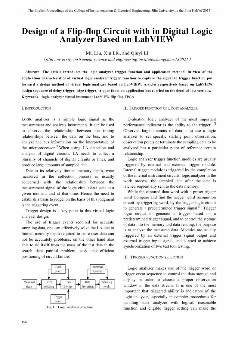
The English Proceedings of the College of Instrumentation & Electrical Engineering, Jilin University, in the First Half of 2015
196
Design of a Flip-flop Circuit with in Digital Logic Analyzer Based on LabVIEW
Mu Liu, Xin Liu, and Qiuyi Li
(jilin university instrument science and engineering institute,changchun,130021)
Abstract—The article introduces the logic analyzer trigger function and application method. In view of the
application characteristics of virtual logic analyzer trigger function to capture the signal to trigger function put
forward a design method of virtual logic analyzer based on LabVIEW. Articles respectively based on LabVIEW
design sequence of delay trigger, edge trigger, trigger function application has carried on the detailed instructions.
Keywords—logic analyzer virtual instrument LabVIEW flip-flop FPGA
I. INTRODUCTION
LOGIC analyzer is a simple logic signal as the measurement and analysis instruments. It can be used to observe the relationship between the timing relationships between the data on the bus, and to analyze the bus information on the interpretation of the microprocessor.[1]When using LA detection and analysis of digital circuits, LA needs to collect a plurality of channels of digital circuits or lines, and produce large amounts of sampled data.
Due to its relatively limited memory depth, were measured in the collection process is usually concerned with the relationship between the measurement signal of the logic circuit data state at a given moment and at that time. Hence the need to establish a basis to judge, on the basis of this judgment is the triggering event.
Trigger design is a key point in this virtual logic analyzer design.
The use of trigger events required for accurate sampling data, one can effectively solve the LA due to limited memory depth required to store user data can not be accurately problems; on the other hand also able to rid itself from the mass of the test data in the search data painful problem, easy and efficient positioning of circuit failure.
Fig 1 Logic analyzer structure
II . TRIGGER FUNCTION OF LOGIC ANALYZER
Evaluation logic analyzer of the most important performance indicator is the ability to the trigger. [2] Observed large amounts of data is to use a logic analyzer to set specific starting point observation, observation points or terminate the sampling data to be analyzed has a particular point of reference certain relationship.
Logic analyzer trigger function modules are usually triggered by internal and external trigger module. Internal trigger module is triggered by the completion of the internal instrument circuits, logic analyzer in the work process, the sampled data after the data is latched sequentially sent to the data memory.
While the captured data word with a preset trigger word Compare and find the trigger word recognition circuit by triggering word, by the trigger logic circuit to generate a predetermined trigger signal.[3] Trigger logic circuit to generate a trigger based on a predetermined trigger signal, and to control the storage of data into the memory and data reading, the purpose is to analyze the measured data. Modules are usually triggered by an external trigger signal output and external trigger input signal, and is used to achieve synchronization of two test tool testing.
III . TRIGGER FUNCTION SELECTION
Logic analyzer makes use of the trigger word or trigger event sequence to control the data storage and display in order to choose a proper observation window in the data stream. It is one of the most important that triggered ability is indicators of the logic analyzer, especially in complex procedures for handling state analyzer with logical, reasonable function and eligible trigger setting can make the
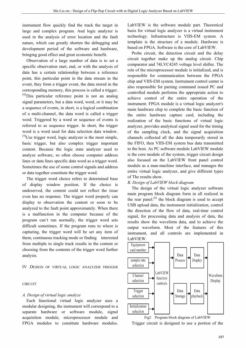
Mu Liu etc.: Design of a Flip-flop Circuit with in Digital Logic Analyzer Based on LabVIEW
197
instrument flow quickly find the track the target in large and complex program. And logic analyzer is used in the analysis of error location and the fault nature, which can greatly shorten the debugging and development period of the software and hardware, bringing good effect and great economic benefit.
Observation of a large number of data is to set a specific observation start, end, or with the analysis of data has a certain relationship between a reference point, this particular point in the data stream in the event, they form a trigger event, the data stored in the corresponding memory, this process is called a trigger. [4]This particular reference point is not an analog signal parameters, but a data word, word, or it may be a sequence of events, in short, is a logical combination of a multi-channel, the data word is called a trigger word. Triggered by a word or sequence of events is referred to as sequence trigger. In short, the trigger word is a word used for data selection data window. [5]Use trigger word, logic analyzer is the most simple, basic trigger, but also complex trigger important content. Because the logic state analyzer used to analyze software, so often choose computer address lines or data lines specific data word as a trigger word. Sometimes the use of some control signals and address or data together constitute the trigger word.
The trigger word choice refers to determined base of display window position. If the choice is undeserved, the content could not reflect the issue even has no response. The trigger word properly can display to observation the content or soon to be analyzed to the fault point approximately. When there is a malfunction in the computer because of the program can’t run normally, the trigger word sets difficult sometimes. If the program runs to where is capturing, the trigger word will be set any item of them, continuous tracking mode or finding interested from multiple to single track results in the content or choosing from the contents of the trigger word further analysis.
IV .DESIGN OF VIRTUAL LOGIC ANALYZER TRIGGER
CIRCUIT
A. Design of virtual logic analyze Each functional virtual logic analyzer uses a
modular designing, the instrument will correspond to a separate hardware or software module, signal acquisition module, microprocessor module and FPGA modules to constitute hardware modules.
LabVIEW is the software module part. Theoretical basis for virtual logic analyzer is a virtual instrument technology. Infrastructure is VIIS-EM system. A template is the structure of a module. Hardware is based on FPGA. Software is the core of LabVIEW.
Probe circuit, the detection circuit and the delay circuit together make up the analog circuit. Chip comparator and 74LVC4245 voltage level shifter. The role of the microprocessor module is initialized, and is responsible for communication between the FPGA chip and VIIS-EM system. Instrument control center is also responsible for parsing command issued PC and controlled module performs the appropriate action to achieve control of the entire operation of the instrument. FPGA module is a virtual logic analyzer's main hardware chip to complete the basic function of the entire hardware capture card, including the realization of the basic functions of virtual logic analyzer, provides analytical signal used for the timing of the sampling clock, and the signal acquisition channels collected all the data temporarily stored in the FIFO, then VIIS-EM system bus data transmitted to the host. As PC software module LabVIEW module is the core module of the system, trigger circuit design also focused on the LabVIEW front panel control module as a man-machine interface, and manages the entire virtual logic analyzer, and give different types of The results show. B. Design of LabVIEW block diagram
The design of the virtual logic analyzer software main program block diagram form in all realized in the rear panel.[6] the block diagram is used to accept USB upload data, the instrument initialization, control the direction of the flow of data, real-time control signal, for processing data and analysis of data, the results show the waveform data, and to achieve the output waveform. Most of the features of this instrument, and all controls are implemented in LabVIEW.
Fig2 Program block diagram of LabVIEW
Trigger circuit is designed to use a portion of the

The English Proceedings of the College of Instrumentation & Electrical Engineering, Jilin University, in the First Half of 2015
198
front panel three trigger modes, this part can trigger type, content and triggering series of choices. You can choose which part of the delay trigger type trigger, edge trigger, trigger sequence. When selecting a delay trigger, trigger delay long to choose what appears; when selecting edge trigger, trigger content displayed on the rising edge or falling edge trigger, then the trigger word 1 all show 0and trigger word 2 all show 1,and they are similar in the secondary trigger of a sequence triggered, indicating rising edge trigger, When the rising edge of the trigger is the opposite.
Fig3 Trigger circuit design on the front panel Trigger circuit design of the rear panel, the collected
data is first uploaded first bit machine via USB bus, call the DLL's way into LabVIEW by CLF node, the array will first enter into a simple digital filter and block diagram of integers, its filtering shaping process. Then, according to the order of the array data structure will be converted into the block diagram. First, under the FOR loop, the array will be the value to be converted to a Boolean control 1D array into a Boolean array. Then an array of controls will be indexed in accordance with the corresponding data acquisition card hardware channel eleven split open, converted to a value. Finally, the Boolean value to (0,1) conversion control, the data is converted into a final (0,1) sequence set in the order of acquisition channels.
After the trigger part of the panel programming designed in two parts, one part is integral part of the sequence is triggered and edge-triggered design section with loops and conditional statements.
Fig4 Edge triggered program chart
Fig5 Sequence trigger program chart
Virtual logic analyzer outputs the result in real time save function block diagram in the rear panel to reflect. When they find valuable waveform appears, you can quickly click on the Save button to save the complete real-time waveforms, in picture form output.
Fig6 Instantly save program chart
V. CONCLUSION
As an advanced measuring instrument, the logic analyzer has been widely applied in the field of digital systems testing. The emergence of virtual instrument
Mu Liu etc.: Design of a Flip-flop Circuit with in Digital Logic Analyzer Based on LabVIEW
199
brings a lot of convenience. Flexible, efficient use of virtual logic analyzer trigger a variety of powerful features, can easily find a hardware failure, timely access to adjust the system software structure, the hardware and software to run work more smoothly. In this paper, the trigger circuit reference design is based on a modular design LabVIEW way to make complex trigger conditions designed to simplify the logic, the circuit is designed by hardware design into software design, which improves design flexibility, reduces the complexity of the circuit extent, but also reduces the cost of the design.
References
[1] Schubert W. Logic analyzer: U.S. Patent 4,788,492[P].
1988-11-29.
[2] Shao-hua X, Xue-feng Z. Integrated Test Station Based on
Virtual Instrument[J]. Ordnance Industry Automation,
2004.
[3] Xiao-yan Y, Guang-yu Z. Design of a Flip-flop Circuit
within Digital Logic Analyzer Based on FPGA[J]. Sci-Tech
Information Development & Economy, 2006.
[4] Yan L, Min L. Implementation of Flip-flop Circuit within
Digital Logic Analyzer Based on FPGA[J]. Journal of
Dalian Nationalities University, 2004.
[5] Arshak K, Jafer E, Ibala C. Testing FPGA based digital
system using XILINX ChipScope logic
analyzer[C]//Electronics Technology, 2006. ISSE'06. 29th
International Spring Seminar on. IEEE, 2006: 355-360.
[6] Bitter R, Mohiuddin T, Nawrocki M. LabVIEW: Advanced
programming techniques[M]. CRC Press, 2006.
The English Proceedings of the College of Instrumentation & Electrical Engineering, Jilin University, in the First Half of 2015
200
The detection device about the key parameters of optical pumping magnetic sensor
Wenzhuo Shan, Pengfei Wang, Linghao Meng
(College of Instrument Science and Electrical Engineering Jilin University,Changchun 130012)
Abstract—The idea is to design a system to test the key parameters of optical pumping magnetic sensor. This detection
device includes three parts, the high-frequency oscillation circuit, the detection device of the absorption chamber and
sine-wave generator. The spectrum light is excited by the output of the high-frequency oscillation circuit. And then we could
obtain and compute the absorption ratio through the detection device of the absorption chamber. Based on parallel control
and cycle control mode of AD9850 module, the AD9850 module could generate a series of sinusoidal signal with tunable
frequency. Through the sinusoidal signal with tunable frequency, the detection device could draw resonance signal of the
optical pumping on display screen, including draw its first harmonic resonance signal and the second harmonic curve, and
store the waveforms in SD card.
I. INTRODUCTION
THE optical pumping magnetic sensor is based on the Zeeman effect and its atomic energy level, and it is a kind of magnetic measurement instrument which is combined by the optical pump technology and the magnetic resonance technology and has the advantages of high accuracy, high sensitivity. Due to high efficiency of the magnetic sensor optical pump, it has been widely used in geological exploration and development, oil collection, Bio Medical Engineering and other aspects [1]. The main factors to determine the optical pumping effect have the volume of absorption chamber, the type of inflatable gas and gas purity, so its quality will directly effect on the accuracy of the measuring instrument and the high efficiency, and even will decide whether the magnetic sensor optical pump can work normally or not. And therefore it’s crucial to measure the key parameters of optical pumping magnetic sensor detection device.
This paper adopts the optical pumping magnetic sensor is a set of apparatus for measuring its key parameters which has the feature of no zero drift, continuous recording, telemetry and other advantages, The conventional measurement devices which finish the absorption chamber first and then fix the probe determine the overall effect according to measuring value of probe. However this method has lots of problems, for instance, it need check for many times
and recreate the absorption chamber, and waste materials as well as delay the cycle of the experiment
[2]. The paper's significance lies in revising deficiencies of traditional testing method, and inventing the key parameters of magnetic sensor optical pump testing device based on microprocessor. The device can be used to measure the output voltage of the photosensitive element and absorption ratio of absorption chamber in the vacuum - inflatable equipment in real time. And it doesn’t only draw out the resonance signal curve and its first harmonic, two harmonic curves, but also has the waveform storage function. In addition, depending on absorption ratio, the absorption chamber adjusts the pressure in order to achieve a better effect of the sensor.
II. THE THEORY OF THE DETECTION DEVICE
Generally, helium chamber is non-magnetic, and in other words, magnetic moment that helium atoms are zero. When the pressure is low and gas purity is high, the high-frequency oscillation circuit will excite helium chamber. The high-frequency oscillation circuit discharges, as a result, helium will transit from steady state to the metastable state and helium chamber will be magnetic. When the helium atoms enter the measured external magnetic field, Zeeman Effect occurs and atoms split into Zeeman sublevel. And then helium chamber which is excited produces 1083nm of light and helium lamp is lit. Through lens
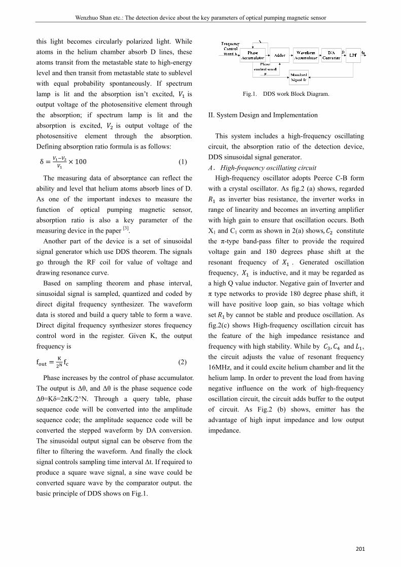
Wenzhuo Shan etc.: The detection device about the key parameters of optical pumping magnetic sensor
201
this light becomes circularly polarized light. While atoms in the helium chamber absorb D lines, these atoms transit from the metastable state to high-energy level and then transit from metastable state to sublevel with equal probability spontaneously. If spectrum lamp is lit and the absorption isn’t excited, is output voltage of the photosensitive element through the absorption; if spectrum lamp is lit and the absorption is excited, is output voltage of the photosensitive element through the absorption. Defining absorption ratio formula is as follows: δ = × 100 (1)
The measuring data of absorptance can reflect the ability and level that helium atoms absorb lines of D. As one of the important indexes to measure the function of optical pumping magnetic sensor, absorption ratio is also a key parameter of the measuring device in the paper [3].
Another part of the device is a set of sinusoidal signal generator which use DDS theorem. The signals go through the RF coil for value of voltage and drawing resonance curve.
Based on sampling theorem and phase interval, sinusoidal signal is sampled, quantized and coded by direct digital frequency synthesizer. The waveform data is stored and build a query table to form a wave. Direct digital frequency synthesizer stores frequency control word in the register. Given K, the output frequency is f = f (2)
Phase increases by the control of phase accumulator. The output is Δθ, and Δθ is the phase sequence code ∆θ=Kδ=2πK/2^N. Through a query table, phase sequence code will be converted into the amplitude sequence code; the amplitude sequence code will be converted the stepped waveform by DA conversion. The sinusoidal output signal can be observe from the filter to filtering the waveform. And finally the clock signal controls sampling time interval Δt. If required to produce a square wave signal, a sine wave could be converted square wave by the comparator output. the basic principle of DDS shows on Fig.1.
Fig.1. DDS work Block Diagram.
II. System Design and Implementation
This system includes a high-frequency oscillating circuit, the absorption ratio of the detection device, DDS sinusoidal signal generator. A. High-frequency oscillating circuit
High-frequency oscillator adopts Peerce C-B form with a crystal oscillator. As fig.2 (a) shows, regarded
as inverter bias resistance, the inverter works in range of linearity and becomes an inverting amplifier with high gain to ensure that oscillation occurs. Both X1 and C1 corm as shown in 2(a) shows, constitute the π-type band-pass filter to provide the required voltage gain and 180 degrees phase shift at the resonant frequency of . Generated oscillation frequency, is inductive, and it may be regarded as a high Q value inductor. Negative gain of Inverter and π type networks to provide 180 degree phase shift, it will have positive loop gain, so bias voltage which set by cannot be stable and produce oscillation. As fig.2(c) shows High-frequency oscillation circuit has the feature of the high impedance resistance and frequency with high stability. While by , and , the circuit adjusts the value of resonant frequency 16MHz, and it could excite helium chamber and lit the helium lamp. In order to prevent the load from having negative influence on the work of high-frequency oscillation circuit, the circuit adds buffer to the output of circuit. As Fig.2 (b) shows, emitter has the advantage of high input impedance and low output impedance.

B
The Englis
202
(a)Pea
Fig.2.
B. AbsorptiAbsorption
of helium chis vacuum. Ahelium, the aand uses higspectrum lamphotosensitivconversed, mdisplays thoscillating cchamber, as measured ancould calculastandard valchamber is q
helium lamp
optical componen
high-frequencoscillating circu
Fig.3. Op
C. DDS sinuThis devi
sinusoidal sigand loop coseries of adjusing the inamplitude osweep signal
sh Proceedings
arce C-B
(c) High-fre
High-frequency
ion ratio mean ratio measu
hamber, and iAfter that theabsorption ratgh-frequencymp. Throughve member, meanwhile A
he voltage ircuit continuthe same the
nd displayedate the absorplue, to dete
qualified or no
nthelium
chamber
cy uit
convexlens
RP oscillator
tical pumping m
usoidal signaice uses ADgnal generato
ontrol mode, ustable frequnverting op f the signall is produced
of the College
(b) Em
equency oscillat
y oscillating cir
asuring deviceuring device t means that
e helium chamtio detecting dy oscillating h the conve
current anAD collects,
V1. The ues to excite
eory, the voltad in the screption ratio coect whether ot.
x photosensitive element
Currenconv
magnetic sensor
al generator D9850 moduor, and adopts
and then it uency sinuso
amp circuil [4], 0.98MHd by MSP430
of Instrumentat
mitter follower
tor rcuit diagram
e extracts the helium chammber filled wdevice initialcircuit to li
ex lens and nd voltage , measures
high-frequee the absorptage V2 couldeen. Finally, ompared with
the absorpt
nt voltage version
Photosensitvoltage out
r block diagram
ule to builds parallel conwill generat
idal signal. Pt to adjust Hz ~ 1.96M0F149 contro
tion & Electrica
gas mber with izes ight the are and
ency tion d be
we h the tion
itive tput
m
d a ntrol te a Plus
the MHz oller
andcollresoregADgencursec
Tgenwhi
III.
Toscexcchaaxischaabsdatamoexp
Avol1.9freqAccfreqbe acc
F
al Engineering,
d then swept lect frequenonance signaion and the v
DC acquisitionerator will ves of magnondary harmo
The flow chanerator that ich is adjusta
Start
initialization
AD9850 module
initialization
Four times 8-bit control
word transfer
Whether a button is
pressed or not
Display the waveform on
the ScreenN
Fig.4. AD98
SYSTEM DES
The excitationcillation circuciting spectramber absorps of the p
amber in a strsorption ratioa shows that re to achieve
pected effect oAD9850 DDtage: 0 ~ 56MHz, sine quency signacording to staquency signareached 20H
curacy of stepFrequency -x
Jilin University
sine signal cy of steppal is detectsvoltage of phn sensor. Thdraw, store
netic sensor,onics.
art of AD985could generble shows in
Button S
Increasefrequenc
Y
display
850 DDS sine w
diagra
SIGN AND IMP
n output signuit is 21V, 16Mrum light tptance. Holdiphotosensitivraight line, th
under the dthe value of a
e the standardof optical pumS sine wave500mV and sweep signa
al test data atistics, the el is about 1%
Hz, but due p can be improx, the value
ty, in the First H
goes througping sweep s through thhotodiode is he DDS sinue and displa, its first-ha
0 DDS sine rates steppinFig.4.
Keyscan return The value of key
Decrease frequency
End
S1
e cy
Button S2
N
wave generator
am
PLEMENTATIO
nal of the hiMHz, and cato measure
ding the optive element he device willdifferent presabsorption ra
rd of helium mping [5]. e generator
frequency: al and the st
is showed error of the s
%, the accuracto AD9850
oved. of AD colle
Half of 2015
h RF coil tosignal. The
he resonanceconverted by
usoidal signalay resonancearmonics and
sweep signalng frequency
Sweep frequency by
step
Sweep frequency
initialization
Button S3
Whether to reach the stop frequency or
not
Y
system flow
ON
gh frequencyan be used for
the heliumical axis, the
and heliuml measure thesures. As theatio is 38% orchamber and
can produce0.98MHz ~
tep of sweepin Table 1
step of sweepcy of step can
module, the
ection output
o e e y l e d
l y
Y
y r
m e
m e e r d
e ~ p .
p n e
t
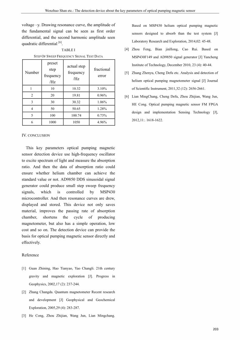
Wenzhuo Shan etc.: The detection device about the key parameters of optical pumping magnetic sensor
203
voltage –y. Drawing resonance curve, the amplitude of the fundamental signal can be seen as first order differential, and the second harmonic amplitude seen quadratic differential [6].
TABLE I
STEP OF SWEEP FREQUENCY SIGNAL TEST DATA
Number
preset step
frequency /Hz
actual step frequency
/Hz
fractional error
1 10 10.32 3.10%
2 20 19.81 0.96%
3 30 30.32 1.06%
4 50 50.65 1.28%
5 100 100.74 0.73%
6 1000 1050 4.96%
IV. CONCLUSION
This key parameters optical pumping magnetic sensor detection device use high-frequency oscillator to excite spectrum of light and measure the absorption ratio. And then the data of absorption ratio could ensure whether helium chamber can achieve the standard value or not. AD9850 DDS sinusoidal signal generator could produce small step sweep frequency signals, which is controlled by MSP430 microcontroller. And then resonance curves are drew, displayed and stored. This device not only saves material, improves the passing rate of absorption chamber, shortens the cycle of producing magnetometer, but also has a simple operation, low cost and so on. The detection device can provide the basis for optical pumping magnetic sensor directly and effectively.
Reference
[1] Guan Zhining, Hao Tianyao, Yao Changli. 21th century
gravity and magnetic exploration [J]. Progress in
Geophysics, 2002,17 (2): 237-244.
[2] Zhang Changda. Quantum magnetometer Recent research
and development [J] Geophysical and Geochemical
Exploration, 2005,29 (4): 283-287.
[3] He Cong, Zhou Zhijian, Wang Jun, Lian Mingchang.
Based on MSP430 helium optical pumping magnetic
sensors designed to absorb than the test system [J]
Laboratory Research and Exploration, 2014,02: 45-48.
[4] Zhou Feng, Bian jinHong, Cao Rui. Based on
MSP430F149 and AD9850 signal generator [J] Yancheng
Institute of Technology, December 2010, 23 (4): 40-44.
[5] Zhang Zhenyu, Cheng Defu etc. Analysis and detection of
helium optical pumping magnetometer signal [J] Journal
of Scientific Instrument, 2011,32 (12): 2656-2661.
[6] Lian MingChang, Cheng Defu, Zhou Zhijian, Wang Jun,
HE Cong. Optical pumping magnetic sensor FM FPGA
design and implementation Sensing Technology [J],
2012,11:. 1618-1622.
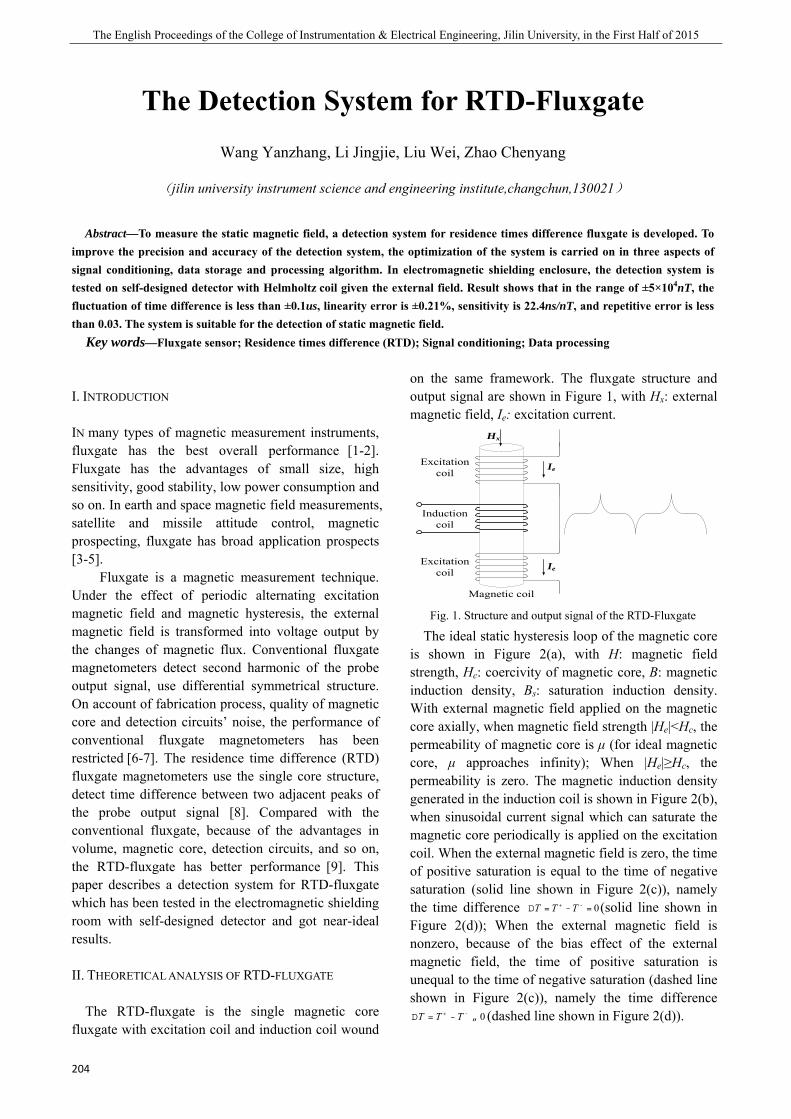
The English Proceedings of the College of Instrumentation & Electrical Engineering, Jilin University, in the First Half of 2015
204
The Detection System for RTD-Fluxgate
Wang Yanzhang, Li Jingjie, Liu Wei, Zhao Chenyang
(jilin university instrument science and engineering institute,changchun,130021)
Abstract—To measure the static magnetic field, a detection system for residence times difference fluxgate is developed. To
improve the precision and accuracy of the detection system, the optimization of the system is carried on in three aspects of signal conditioning, data storage and processing algorithm. In electromagnetic shielding enclosure, the detection system is tested on self-designed detector with Helmholtz coil given the external field. Result shows that in the range of ±5×10⁴nT, the fluctuation of time difference is less than ±0.1us, linearity error is ±0.21%, sensitivity is 22.4ns/nT, and repetitive error is less than 0.03. The system is suitable for the detection of static magnetic field.
Key words—Fluxgate sensor; Residence times difference (RTD); Signal conditioning; Data processing
I. INTRODUCTION
IN many types of magnetic measurement instruments, fluxgate has the best overall performance [1-2]. Fluxgate has the advantages of small size, high sensitivity, good stability, low power consumption and so on. In earth and space magnetic field measurements, satellite and missile attitude control, magnetic prospecting, fluxgate has broad application prospects
[3-5]. Fluxgate is a magnetic measurement technique. Under the effect of periodic alternating excitation magnetic field and magnetic hysteresis, the external magnetic field is transformed into voltage output by the changes of magnetic flux. Conventional fluxgate magnetometers detect second harmonic of the probe output signal, use differential symmetrical structure. On account of fabrication process, quality of magnetic core and detection circuits’ noise, the performance of conventional fluxgate magnetometers has been restricted [6-7]. The residence time difference (RTD) fluxgate magnetometers use the single core structure, detect time difference between two adjacent peaks of the probe output signal [8]. Compared with the conventional fluxgate, because of the advantages in volume, magnetic core, detection circuits, and so on, the RTD-fluxgate has better performance [9]. This paper describes a detection system for RTD-fluxgate which has been tested in the electromagnetic shielding room with self-designed detector and got near-ideal results.
II. THEORETICAL ANALYSIS OF RTD-FLUXGATE
The RTD-fluxgate is the single magnetic core fluxgate with excitation coil and induction coil wound
on the same framework. The fluxgate structure and output signal are shown in Figure 1, with Hx: external magnetic field, Ie: excitation current.
Ie
Hx
Ie
Magnetic coil
Excitation coil
Induction coil
Excitation coil
Fig. 1. Structure and output signal of the RTD-Fluxgate
The ideal static hysteresis loop of the magnetic core is shown in Figure 2(a), with H: magnetic field strength, Hc: coercivity of magnetic core, B: magnetic induction density, Bs: saturation induction density. With external magnetic field applied on the magnetic core axially, when magnetic field strength |He|<Hc, the permeability of magnetic core is μ (for ideal magnetic core, μ approaches infinity); When |He|≥Hc, the permeability is zero. The magnetic induction density generated in the induction coil is shown in Figure 2(b), when sinusoidal current signal which can saturate the magnetic core periodically is applied on the excitation coil. When the external magnetic field is zero, the time of positive saturation is equal to the time of negative saturation (solid line shown in Figure 2(c)), namely the time difference 0T T T+ -D = - = (solid line shown in Figure 2(d)); When the external magnetic field is nonzero, because of the bias effect of the external magnetic field, the time of positive saturation is unequal to the time of negative saturation (dashed line shown in Figure 2(c)), namely the time difference
0T T T+ -D = - „ (dashed line shown in Figure 2(d)).
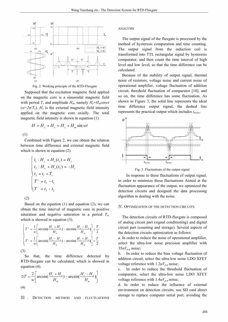
Wang Yanzhang etc.: The Detection System for RTD-Fluxgate
205
(a) (b)
t3t2
T-T+
t
e
t
+HC-HC
H+HC-HC
-BS
+BS
B
t
-BS
+BS
B
H
T+ T-
t1
(c) (d)
Hx=0Hx≠0
Fig. 2. Working principle of the RTD-Fluxgate
Supposed that the excitation magnetic field applied on the magnetic core is a sinusoidal magnetic field with period Te and amplitude Hm, namely He=Hmsinwt (w=2π/Te). Hx is the external magnetic field intensity applied on the magnetic core axially. The total magnetic field intensity is shown in equation (1).
sinx e x mH H H H H wt= + = +
(1) Combined with Figure 2, we can obtain the relation
between time difference and external magnetic field which is shown in equation (2).
1 1
2 2
3 1
2 1
3 2
: ( ): (
)
x e c
x e c
e
t H H t Ht H H t Ht t T
T t t
T t t
+
-
⎧ + =⎪
+ = -⎪⎪
= +⎨⎪ = -⎪⎪ = -⎩
(2) Based on the equation (1) and equation (2), we can
obtain the time interval of magnetic core in positive saturation and negative saturation in a period Te, which is showed in equation (3).
1 arcsin( ) arcsin( )2
1 arcsin( ) arcsin( )2
c x c x
m m
c x c x
m m
H H H H TTw H H
H H H H TTw H H
+
-
⎧ ⎡ ⎤+ -= - +⎪ ⎢ ⎥
⎪ ⎣ ⎦⎨
⎡ ⎤- +⎪ = - +⎢ ⎥⎪ ⎣ ⎦⎩
(3) So that, the time difference detected by
RTD-fluxgate can be calculated, which is showed in equation (4).
2 arcsin( ) arcsin( )c x c x
m m
H H H HTw H H⎡ ⎤+ -
D = -⎢ ⎥⎣ ⎦
(4)
Ⅲ . DETECTION METHOD AND FLUCTUATIONS
ANALYSIS
The output signal of the fluxgate is processed by the method of hysteresis comparation and time counting. The output signal from the induction coil is transformed into TTL rectangular signal by hysteresis comparator, and then count the time interval of high level and low level, so that the time difference can be calculated.
Because of the stability of output signal, thermal noise of resistors, voltage noise and current noise of operational amplifier, voltage fluctuation of addition circuit, threshold fluctuation of comparator [10], and so on, the time difference has some fluctuation. As shown in Figure 3, the solid line represents the ideal time difference output signal, the dashed line represents the practical output which includes tnoise.
t
e
ttnoise tnoise
1
Fig. 3. Fluctuations of the output signal
In response to these fluctuations of output signal, in order to minimize these fluctuations Aimed at the fluctuation appearance of the output, we optimized the detection circuits and designed the data processing algorithm in dealing with the noise.
Ⅳ. OPTIMIZATION OF THE DETECTION CIRCUITS
The detection circuits of RTD-fluxgate is composed of analog circuit part (signal conditioning) and digital circuit part (counting and storage). Several aspects of the detection circuits optimization as follows: a. In order to reduce the noise of operational amplifier, select the ultra-low noise precision amplifier with 35nVp-p noise; b. In order to reduce the bias voltage fluctuation of addition circuit, select the ultra-low noise LDO XFET voltage reference with 1.2uVp-p noise; c. In order to reduce the threshold fluctuation of comparator, select the ultra-low noise LDO XFET voltage reference with 1.4uVp-p noise; d. In order to reduce the influence of external environment on detection circuits, use SD card direct storage to replace computer serial port, avoiding the
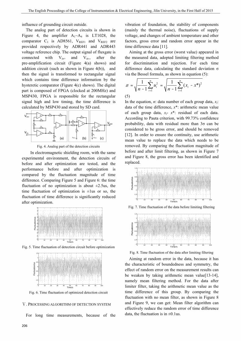
The English Proceedings of the College of Instrumentation & Electrical Engineering, Jilin University, in the First Half of 2015
206
influence of grounding circuit outside. The analog part of detection circuits is shown in
Figure 4, the amplifier A1~A4 is LT1028, the comparator C1 is AD8561, VREF1 and VREF2 are provided respectively by ADR441 and ADR443 voltage reference chip. The output signal of fluxgate is connected with Vin+ and Vin-, after the pre-amplification circuit (Figure 4(a) shows) and addition circuit (such as shown in Figure 4(b)), and then the signal is transformed to rectangular signal which contains time difference information by the hysteretic comparator (Figure 4(c) shows). The digital part is composed of FPGA (clocked at 200MHz) and MSP430, FPGA is responsible for the rectangular signal high and low timing, the time difference is calculated by MSP430 and stored by SD card.
VREF2VREF1
C1
R4
R4
R1
R2
R2
R3
R3
A2+
﹣
A1+
﹣
A3+
﹣ A4+
﹣R5
R5
R5
+﹣
R6
R5Vin+
Vin-
R6
Vout
(a) (b) (c)
Fig. 4. Analog part of the detection circuits
In electromagnetic shielding room, with the same experimental environment, the detection circuits of before and after optimization are tested, and the performance before and after optimization is compared by the fluctuation magnitude of time difference. Comparing Figure 5 and Figure 6: the time fluctuation of no optimization is about ±2.5us, the time fluctuation of optimization is ±1us or so, the fluctuation of time difference is significantly reduced after optimization.
0 10 20 30 40 50 60 70 80 90 100-5
-4
-3
-2
-1
0
1
2
3
4
5
Time/s
Fluc
tuat
ion/
us
Fig. 5. Time fluctuation of detection circuit before optimization
0 10 20 30 40 50 60 70 80 90 100-2
-1.5
-1
-0.5
0
0.5
1
1.5
Tims/s
Fluc
tuat
ion/
us
Fig. 6. Time fluctuation of optimized detection circuit
Ⅴ. PROCESSING ALGORITHM OF DETECTION SYSTEM
For long time measurements, because of the
vibration of foundation, the stability of components (mainly the thermal noise), fluctuations of supply voltage, and changes of ambient temperature and other factors, gross error and random error appear in the time difference data [11].
Aiming at the gross error (worst value) appeared in the measured data, adopted limiting filtering method for discrimination and rejection. For each time difference data, calculating the standard deviation σ via the Bessel formula, as shown in equation (5):
2 2
1 1
1 1 ( *)1 1
n n
i ii i
u x xn n
s= =
= = -- -∑ ∑
(5) In the equation, n: data number of each group data, xi: data of the time difference, x*: arithmetic mean value of each group data, xi- x*: residual of each data. According to Pauta criterion, with 99.73% confidence probability, data with residual more than 3σ can be considered to be gross error, and should be removed
[12]. In order to ensure the continuity, use arithmetic mean value to replace the data which needs to be removed. By comparing the fluctuation magnitude of before and after limit filtering, as shown in Figure 7 and Figure 8, the gross error has been identified and replaced.
0 10 20 30 40 50 60 70 80 90 100-2
-1.5
-1
-0.5
0
0.5
1
1.5
Tims/s
Fluc
tuat
ion/
us
Fig. 7. Time fluctuation of the data before limiting filtering
0 10 20 30 40 50 60 70 80 90 100-2
-1.5
-1
-0.5
0
0.5
1
1.5
Time/s
Fluc
tuat
ion/
us
Fig. 8. Time fluctuation of the data after limiting filtering
Aiming at random error in the data, because it has the characteristic of boundedness and symmetry, the effect of random error on the measurement results can be weaken by taking arithmetic mean value[13-14], namely mean filtering method. For the data after limiter filter, taking the arithmetic mean value as the time difference of this group. By comparing the fluctuation with no mean filter, as shown in Figure 8 and Figure 9, we can get: Mean filter algorithm can effectively reduce the random error of time difference data, the fluctuation is in ±0.1us.
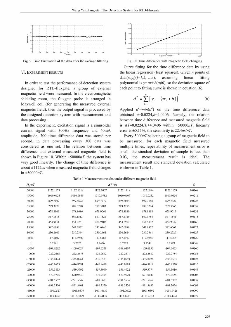
Wang Yanzhang etc.: The Detection System for RTD-Fluxgate
207
0 10 20 30 40 50 60 70 80 90 100-2
-1.5
-1
-0.5
0
0.5
1
1.5
Time/s
Fluc
tion/
us
Fig. 9. Time fluctuation of the data after the average filtering
Ⅵ. EXPERIMENT RESULTS
In order to test the performance of detection system designed for RTD-fluxgate, a group of external magnetic field were measured. In the electromagnetic shielding room, the fluxgate probe is arranged in Maxwell coil (for generating the measured external magnetic field), then the output signal is processed by the designed detection system with measurement and data processing.
In the experiment, excitation signal is a sinusoidal current signal with 300Hz frequency and 40mA amplitude. 300 time difference data was stored per second, in data processing every 300 data was considered as one set. The relation between time difference and external measured magnetic field is shown in Figure 10. Within ±50000nT, the system has very good linearity. The change of time difference is about ±1122us when measured magnetic field changes in ±50000nT.
-6 -4 -2 0 2 4 6x 10⁴
-1500
-1000
-500
0
500
1000
1500
Magnetic Field/nT
Tim
e D
iffer
ence
/us
Fig. 10. Time difference with magnetic field changing
Curve fitting for the time difference data by using the linear regression (least squares). Given n points of data(xi,yi)(i=1,2,…,n), assuming linear fitting polynomial is y=ax+b(a≠0), so the deviation square of each point to fitting curve is shown in equation (6),
( )2
2
1
n
i ii
d y ax b=
= - +⎡ ⎤⎣ ⎦∑ (6)
Applied d2=min(d2) on the time difference data obtained a=0.0224,b=4.0406. Namely, the relation between time difference and measured magnetic field is ΔT=0.0224Hx+4.0406 within ±50000nT, linearity error is ±0.11%, the sensitivity is 22.4ns/nT.
Every 5000nT selecting a group of magnetic field to be measured, for each magnetic field measured multiple times, repeatability of measurement error is small, the standard deviation of sample is less than 0.03, the measurement result is ideal. The measurement result and standard deviation calculated is shown in Table 1,
Table 1 Measurement results under different magnetic field
Hx/nT T /us S 50000 1122.1179 1122.1318 1122.1007 1122.1418 1122.0994 1122.1159 0.0168
45000 1010.0628 1010.0869 1010.0782 1010.0609 1010.0252 1010.0630 0.0211
40000 899.7107 899.6692 899.7279 899.7054 899.7168 899.7322 0.0226
35000 789.3279 789.3270 789.3183 789.3285 789.3294 789.3366 0.0059
30000 678.8909 678.8686 678.9061 678.8880 678.8898 678.9019 0.0131
25000 567.1618 567.1513 567.1521 567.1729 567.1784 567.1541 0.0115
20000 454.9151 454.9261 454.9402 454.8952 454.9092 454.9049 0.0160
15000 342.6880 342.6832 342.6946 342.6986 342.6972 342.6662 0.0122
10000 230.2609 230.2364 230.2664 230.2624 230.2661 230.2729 0.0127
5000 117.5102 117.4986 117.5285 117.5197 117.4985 117.5058 0.0120
0 3.7541 3.7625 3.7476 3.7527 3.7549 3.7529 0.0048
-5000 -109.6262 -109.6029 -109.6258 -109.6407 -109.6150 -109.6463 0.0160
-10000 -222.2665 -222.2673 -222.2642 -222.2671 -222.2587 -222.2754 0.0054
-15000 -335.0474 -335.0264 -335.0527 -335.0593 -335.0426 -335.0583 0.0123
-20000 -446.8633 -446.8591 -446.8499 -446.8688 -446.8818 -446.8570 0.0110
-25000 -559.3833 -559.3792 -559.3960 -559.4022 -559.3774 -559.3616 0.0144
-30000 -670.9705 -670.9830 -670.9474 -670.9620 -671.0049 -670.9555 0.0208
-35000 -781.5557 -781.5547 -781.5601 -781.5536 -781.5767 -781.5332 0.0139
-40000 -891.3556 -891.3401 -891.3570 -891.3520 -891.3635 -891.3654 0.0091
-45000 -1001.0527 -1001.0579 -1001.0637 -1001.0602 -1001.0392 -1001.0426 0.0099
-50000 -1113.4267 -1113.3829 -1113.4137 -1113.4471 -1113.4633 -1113.4264 0.0277
The English Proceedings of the College of Instrumentation & Electrical Engineering, Jilin University, in the First Half of 2015
208
Ⅶ. CONCLUSION
This paper describe a detection system for RTD-fluxgate which is composed of optimized detection circuit and limiting mean filter algorithm, and the system is tested by self-made fluxgate in electromagnetic shielding room. Result showed that in the range of ±5×10⁴nT, the fluctuation of time difference is less than ±0.1us, linearity error is ±0.21%, sensitivity is 22.4ns/nT, and repetitive error is less than 0.03. The system is suitable for the detection of static magnetic field.
References
[1] Zhang Xuefu, Lu Yiliang. Fluxgate Technology [M]. Beijing: National Defense Industry Press, 1995:30-49.
[2] Mao Zhenlong. Magnetic Field Measurement [M]. Beijing:
Atomic Energy Press, 1985:1-10.
[3] Guo Zhiyou, Sun Huiqing. Magnetic Sensor and its
Application [J]. Journal of Transducer Technology, 2002,
21(7):56-57.
[4] Guo Aihuang, Fu Junmei. Measurement Technology of
Magnetic Flux and its Application [J]. Journal of
Transducer Technology, 2000, 19(4):1-4.
[5] Zhao Lanxia. Research and Design on the Residence
Times Difference Fluxgate Sensor [D]. Changchun: Jilin
University, 2012.
[6] J.E.Lenz.A review of magnetic sensors [J]. Proceedings of
the IEEE, 1990, 78(6): 973-989.
[7] Wu Shujun. Research on the Digital Technology of
Residence Times Difference Fluxgate [D]. Changchun:
Jilin University, 2014.
[8] Ando B, Baglio S, Bulsara A R, et al. Residence Times
Difference Fluxgate Magnetometers[J].IEEE Sensors
Journal, 2005,5(5) :895-904.
[9] Ma Bo. The Design of Fluxgate Sensor Based on
Hysteresis Time Difference and Magnetic Measurement
Device [D]. Changchun: Jilin University, 2010.
[10] Kang Huaguang. Electronic Technology
Foundation---Analog [M]. Higher Education Press, 2005.
[11] Shi Zhiyong, Wang Huaiguang, Lv You. Design of a Three
Detectors Fluxgate Sensor [J]. Journal of Transduction
Technology, 2005, 18, (2):433-435.
[12] Lin Zhanjiang. Electronic measurement technology [M].
Publishing House of Electronics Industry, 2003.
[13] Wang Yuren. Research and Realization of the
Peak-to-average Power Ratio Reduction Algorithms in
OFDM System [D]. Shanghai: Shanghai Jiao Tong
University, 2007.
[14] Hu Guangshu. Digital Signal Processing—Theory,
Algorithm and Implementation [M]. Beijing: Tsinghua
University Press, 2003.
Wen Zihan etc:Car headlights automatic switching system
209
Car headlights automatic switching system
Weng Zihan, Hao Shuai, Jin Canlin ( College of Instrument Science and Electricial Engineering Jilin University,Changchun 130012,China )
Abstract—Automobile high beam allows the driver to see distant road at high speed in the night, but if not timely switch to
low beams when meeting, the strong light can make the vehicle lose their way, thus easily causing traffic accidents. This paper
takes the single chip processor as the core, making use of velocity sensor, illumination intensity sensor and ultrasonic ranging
sensor. Then the sensors integrate the signal and the single chip processor focus on it. The single chip processor controls
various states of lamplight and achieves automatic switching between high beam and low beam. This system can solve the
problem of long latency of manual switch and the drivers’ distraction due to frequent manual dimming in traditional manner,
thereby effectively reducing the probability of having an accident. This paper introduces the specific methods of designing
and achieving the system in software and hardware.
0 INTRODUCTION
0.1 The Background and Significance of the Research THERE are many traffic accidents caused by illegal use of the automobile high beam. With more and more new cars appearing during each year, traffic accidents caused by improper using high beam at night is rising rapidly. Most solution of the high beam light dazzling problem solutions is not perfect, and can’t solve the problem of high beam damage completely. According to the demand for the automobile high beam detection and control system in actual circumstances, it is important to ensure the cars running safely, simply and effectively. At present, except of handful luxury cars, most of the cars do not have intelligent control function of high beam. It is decided by characteristic of the automobile industry production. Every little increased cost of a car will change its sales volume, and even affect the market orientation of a car. To achieve a good results, the system must cost little and easy to promote. In a word, the trend is to develop a secure, simple, effective, low cost and easy to promote the automatic control system of high beam. 0.2 The Domestic and Overseas Research Analysis and Evaluation Now some abroad auto companies have started to take test of automatic high beam auxiliary control system, Germany Bavarian automaker developed a high beam assist system. The main component is a sensor installed in front of the rear view mirror
housing, which contains a camera. Camera image is feedback into an electronic evaluation system, it will analysis what is in front of the car to automatically control the opening and closing of the high beam. The system is implanted in the BMW 5 series, 6 series and 7 series of the company. Domestic companies also do research of automobile anti-glare Forward Lighting, Polarized light anti-glare, automatic automobile headlamps, but not yet reach the level of practical application.
To solve the problem of car headlamps glaring, there are many different solutions, but all of them have problems. We did researched on the parking cars in campus, and it haven’t install automatic switching system yet. By looking up technical data, some cars already have automatic light switch configuration, such as Changan Peugeot Citroen new DS5, Mazda CX-9, FAW Toyota new RAV4, BWM 6 series 650i, Audi upgrading A8L, Changan Ford Mondeo and brand new Benz S level. Although there is a considerable part of the car still haven’t far and near light automatic switching system, it is a trend in the future. 0.3 innovation point of this paper
The design is difference from far and near light on manual control common control system. With the development of science and technology, it is necessary to liberate drivers from the driving complex operation. The system combines the speed, ultrasonic ranging, integrated with all kinds of complicated situations in which the lights on the far and near alternately control,
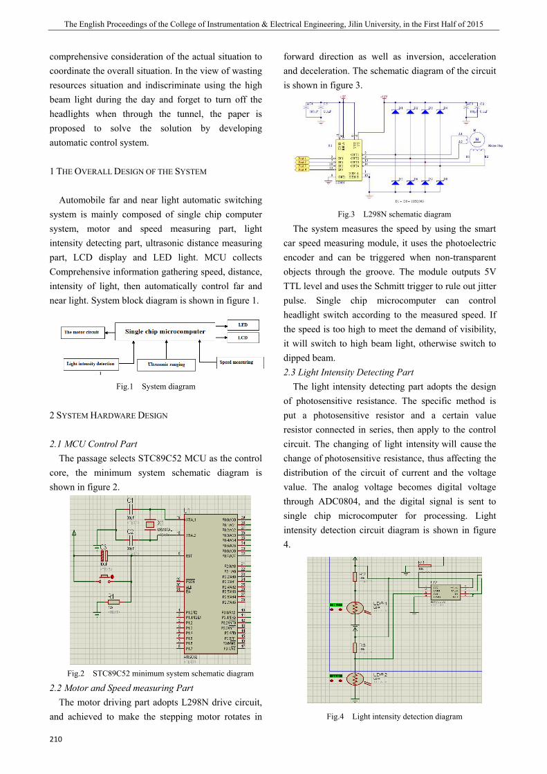
The English Proceedings of the College of Instrumentation & Electrical Engineering, Jilin University, in the First Half of 2015
210
comprehensive consideration of the actual situation to coordinate the overall situation. In the view of wasting resources situation and indiscriminate using the high beam light during the day and forget to turn off the headlights when through the tunnel, the paper is proposed to solve the solution by developing automatic control system.
1 THE OVERALL DESIGN OF THE SYSTEM
Automobile far and near light automatic switching system is mainly composed of single chip computer system, motor and speed measuring part, light intensity detecting part, ultrasonic distance measuring part, LCD display and LED light. MCU collects Comprehensive information gathering speed, distance, intensity of light, then automatically control far and near light. System block diagram is shown in figure 1.
Fig.1 System diagram
2 SYSTEM HARDWARE DESIGN
2.1 MCU Control Part The passage selects STC89C52 MCU as the control
core, the minimum system schematic diagram is shown in figure 2.
Fig.2 STC89C52 minimum system schematic diagram
2.2 Motor and Speed measuring Part The motor driving part adopts L298N drive circuit,
and achieved to make the stepping motor rotates in
forward direction as well as inversion, acceleration and deceleration. The schematic diagram of the circuit is shown in figure 3.
Fig.3 L298N schematic diagram
The system measures the speed by using the smart car speed measuring module, it uses the photoelectric encoder and can be triggered when non-transparent objects through the groove. The module outputs 5V TTL level and uses the Schmitt trigger to rule out jitter pulse. Single chip microcomputer can control headlight switch according to the measured speed. If the speed is too high to meet the demand of visibility, it will switch to high beam light, otherwise switch to dipped beam. 2.3 Light Intensity Detecting Part
The light intensity detecting part adopts the design of photosensitive resistance. The specific method is put a photosensitive resistor and a certain value resistor connected in series, then apply to the control circuit. The changing of light intensity will cause the change of photosensitive resistance, thus affecting the distribution of the circuit of current and the voltage value. The analog voltage becomes digital voltage through ADC0804, and the digital signal is sent to single chip microcomputer for processing. Light intensity detection circuit diagram is shown in figure 4.
Fig.4 Light intensity detection diagram
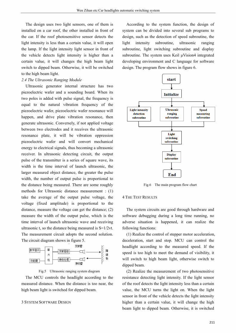
Wen Zihan etc:Car headlights automatic switching system
211
The design uses two light sensors, one of them is installed on a car roof, the other installed in front of the car. If the roof photosensitive sensor detects the light intensity is less than a certain value, it will open the lamp. If the light intensity light sensor in front of the vehicle detects light intensity is higher than a certain value, it will changes the high beam light switch to dipped beam. Otherwise, it will be switched to the high beam light. 2.4 The Ultrasonic Ranging Module
Ultrasonic generator internal structure has two piezoelectric wafer and a sounding board. When its two poles is added with pulse signal, the frequency is equal to the natural vibration frequency of the piezoelectric wafer, piezoelectric wafer resonance will happen, and drive plate vibration resonance, then generate ultrasonic. Conversely, if not applied voltage between two electrodes and it receives the ultrasonic resonance plate, it will be vibration oppression piezoelectric wafer and will convert mechanical energy to electrical signals, thus becoming a ultrasonic receiver. In ultrasonic detecting circuit, the output pulse of the transmitter is a series of square wave, its width is the time interval of launch ultrasonic, the larger measured object distance, the greater the pulse width, the number of output pulse is proportional to the distance being measured. There are some roughly methods for Ultrasonic distance measurement : (1) take the average of the output pulse voltage, the voltage (fixed amplitude) is proportional to the distance, measure the voltage can get the distance; (2) measure the width of the output pulse, which is the time interval of launch ultrasonic wave and receiving ultrasonic t, so the distance being measured is S=1/2vt. The measurement circuit adopts the second solution. The circuit diagram shows in figure 5.
Fig.5 Ultrasonic ranging system diagram
The MCU controls the headlight according to the measured distance. When the distance is too near, the high beam light is switched for dipped beam.
3 SYSTEM SOFTWARE DESIGN
According to the system function, the design of system can be divided into several sub programs to design, such as the detection of speed subroutine, the light intensity subroutine, ultrasonic ranging subroutine, light switching subroutine and display subroutine. The system uses Keil μVision4 integrated developing environment and C language for software design. The program flow shows in figure 6.
Fig.6 The main program flow chart
4 THE TEST RESULTS
The system circuits are good through hardware and software debugging during a long time running, no adverse situation is happened, it can realize the following functions:
(1) Realize the control of stepper motor acceleration, deceleration, start and stop. MCU can control the headlight according to the measured speed. If the speed is too high to meet the demand of visibility, it will switch to high beam light, otherwise switch to dipped beam.
(2) Realize the measurement of two photosensitive resistance detecting light intensity. If the light sensor of the roof detects the light intensity less than a certain value, the MCU turns the light on. When the light sensor in front of the vehicle detects the light intensity higher than a certain value, it will change the high beam light to dipped beam. Otherwise, it is switched

The English Proceedings of the College of Instrumentation & Electrical Engineering, Jilin University, in the First Half of 2015
212
to the high beam light. (3) The automatic switching of the automobile far
and near light is based on the measured distance by the ultrasonic sensor. When the cars run in the same direction, the rear car will not be able to open the high beam light if there is a car in front of it in the detection range. When the cars run in the opposite direction, the cars can’t switch on the high beam as long as in the detection range. If the two cars open near light, they will through the road peacefully.
5 CONCLUSION
The design uses STC89C52 micro-controller as the control core, realizes a car headlights automatic switching system. According to the information of measured speed, light intensity and distance, it realizes the function of controlling the headlight switching on or off through the single-chip microcomputer to reduce the possibility of high beam light using mistakenly.
Reference
[1] Zhang Mingxia.The ideas of the Internet of things
[M]. Beijing: Peking University press, 2012
[2] Du Yang. In love with microcomputer [M].
Beijing: People's Posts and Telecommunications
Press, 2013
[3] BMW night vision and high beam
assist, Internet.HTTP://car.uncars.com/2005/12-15/114252
81980- 2.html
[4] Dai Yongjiang. Laser radar [M] Beijing: Agriculture
Press, China 2002, 80-89.
[5] Qi WangZhi. The light sensitive device and its application
[M]. Beijing: Science Press, 1994, 91-93.
[6] Yu Chengbo. The sensor and detection technology
[M]. first edition. Beijing: HigherEducation Press, 2004
[7] Ma Shuhua Wang Fengwen Zhang Meijin, Microcomputer
principle and interface technology[M]. Beijing. Beijing
University of Posts and Telecommunications press, 2007
[8] Jia Zhengsong Microcomputer principle and interface
technology[J] 2009 (17): P105~107
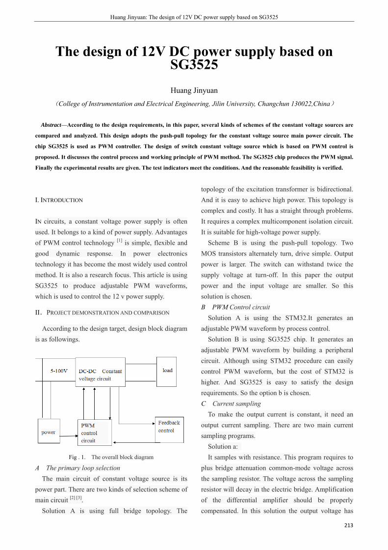
Huang Jinyuan: The design of 12V DC power supply based on SG3525
213
The design of 12V DC power supply based on SG3525
Huang Jinyuan
(College of Instrumentation and Electrical Engineering, Jilin University, Changchun 130022,China)
Abstract—According to the design requirements, in this paper, several kinds of schemes of the constant voltage sources are
compared and analyzed. This design adopts the push-pull topology for the constant voltage source main power circuit. The
chip SG3525 is used as PWM controller. The design of switch constant voltage source which is based on PWM control is
proposed. It discusses the control process and working principle of PWM method. The SG3525 chip produces the PWM signal.
Finally the experimental results are given. The test indicators meet the conditions. And the reasonable feasibility is verified.
I. INTRODUCTION
IN circuits, a constant voltage power supply is often used. It belongs to a kind of power supply. Advantages of PWM control technology [1] is simple, flexible and good dynamic response. In power electronics technology it has become the most widely used control method. It is also a research focus. This article is using SG3525 to produce adjustable PWM waveforms, which is used to control the 12 v power supply.
II.PROJECT DEMONSTRATION AND COMPARISON
According to the design target, design block diagram is as followings.
Fig . 1. The overall block diagram
A The primary loop selection The main circuit of constant voltage source is its
power part. There are two kinds of selection scheme of main circuit [2] [3].
Solution A is using full bridge topology. The
topology of the excitation transformer is bidirectional. And it is easy to achieve high power. This topology is complex and costly. It has a straight through problems. It requires a complex multicomponent isolation circuit. It is suitable for high-voltage power supply.
Scheme B is using the push-pull topology. Two MOS transistors alternately turn, drive simple. Output power is larger. The switch can withstand twice the supply voltage at turn-off. In this paper the output power and the input voltage are smaller. So this solution is chosen. B PWM Control circuit
Solution A is using the STM32.It generates an adjustable PWM waveform by process control.
Solution B is using SG3525 chip. It generates an adjustable PWM waveform by building a peripheral circuit. Although using STM32 procedure can easily control PWM waveform, but the cost of STM32 is higher. And SG3525 is easy to satisfy the design requirements. So the option b is chosen. C Current sampling
To make the output current is constant, it need an output current sampling. There are two main current sampling programs.
Solution a: It samples with resistance. This program requires to
plus bridge attenuation common-mode voltage across the sampling resistor. The voltage across the sampling resistor will decay in the electric bridge. Amplification of the differential amplifier should be properly compensated. In this solution the output voltage has

The English Proceedings of the College of Instrumentation & Electrical Engineering, Jilin University, in the First Half of 2015
214
zero drift. Solution b: It uses the Hall current transformer. Its conversion
efficiency is low, and temperature drift is large. In this problem it requires a relatively high accuracy. It needs to be temperature compensated.
Considering the design of the output current and high switching frequency, we choose solution a.
Ⅲ. THE WHOLE CIRCUIT STRUCTURE
A Power supply module After external input AC voltage is rectified and
filtered, it is converted to high voltage DC. As shown in figure 2.
Fig . 2. Power supply module
It has functions that through the high frequency blocking low frequency, and through the AC blocking the DC. D1, D2, D3, D4 constituting the rectifier bridge. It rectified AC into DC. RD3, CD2, D5FR107 compose protection circuit. It can reduce the ringing voltage. After the secondary voltage is rectified and filtered, it generates + 12V output voltage. The IC3 TOP222P needs to provide an external bias voltage during operation. At the instant of the circuit power, the IC3 TOP222P starts working properly. Through the PWM control, it can realize the regulation of the output voltage waveform. In order to improve the
stability of the IC3 TOP222P chips work, will PC817B parallel with Z1 form an external error amplifier. R1, R5 can adjust the nominal of output voltage.R3, C2 can adjust the frequency response of the loop. RD5 controls loop gain.
B PWM waveform generating circuit PWM wave produced by SG3525 is easy to control.
And its efficiency is high. The PWM waveform generation circuit as shown in figure 3.

Huang Jinyuan: The design of 12V DC power supply based on SG3525
215
Fig. 3. PWM waveform generating circuit
SG3525A pulse width modulator control circuit may control various types of switching power supply. The chip is also suitable for embedded and soft-start circuitry. It allows only one external timing capacitor.
SG3525A has the following several characteristics: It enables control of 8.0V to 35V, 5.1V 1% reduction
in the reference value, 100Hz to 400 kHz oscillator range. Dispersion oscillator synchronization pin is adjustable dead time control. Input under voltage lock limits the variety of pulse width modulation, and close pulse.
SG3525 output stage uses a push-pull circuit, and SG3525 has dual channel outputs. Its drive current for each channel is up to a maximum 500mA, which can directly drive GTR and MOSFET. Its operating frequency is up to 400 kHz, with under voltage shutdown, programmable soft-start characteristics.
The oscillation frequency is decided by the
following formula:
DCHGosc
TTf
+=
1
Type, TCHG is the charging time of capacitor CT. When CT charging, an output driver of the PWM controller operating in the conductive state. TD is the dead-time, that two output drivers are in a off-state. TCHG is proportional to the product of RT and CT.TD is proportional to the product of RD and CT. So the oscillation frequency can be calculated as
TDTosc
CRRf
)37.0(1+
=
HZfosc 37003= .
C Push pull control main circuit The circuit of the power transistor is driven by the
push-pull output shown in figure 4.

The English Proceedings of the College of Instrumentation & Electrical Engineering, Jilin University, in the First Half of 2015
216
Fig. 4. Push pull output circuit
Resistors R2 and R3 are the current limiting resistor. They used to prevent the forward base current that injection Q1 and Q2 to exceed the permissible output current of controller.
In half bridge converter applications, SG3525 can be used for upper and lower leg power MOSFET isolated drivers, as shown above. RG1 and RG3 compose the driver circuit protection aspects. It uses good performance absorption circuit. MOSFET can work in ideal switch status. It also can short the switching time and reduce the switching losses.
Power tube kept on and off lets the high-frequency transformer T3 primary produce low-voltage high-frequency alternating current. It outputs a high-frequency alternating current through the high-frequency transformer, then through fast recovery diode full bridge rectifier MBR2060 output a high DC.
Inductance T5 and E3 composition LC oscillator circuit.R11 and capacitor C8 composition filter circuit. Because the high-frequency is easy to produce interference and some parasitic coupling, it is necessary to filter out the effects of these factors through the filter circuit to increase the stability of the circuit. D The high frequency transformer design
Transformer design In this circuit, transformer design tasks as:
(1) Circuit forms: half bridge (2) Operating frequency: 50 kHz
(3)Converter maximum input voltage : DC500V (4)Converter minimum input voltage: DC300V (5)Output voltage: DC12V
Ⅳ. THE TEST RESULT
A The test conditions Voltage measurements: Using the 12E digital multi
meter produced by FLUKE. Waveform measurement: analog oscilloscope. B The display circuit
Fig. 5. The display circuit
C Circuit SG3525 pin 11 and 14 pin waveform

Huang Jinyuan: The design of 12V DC power supply based on SG3525
217
Fig. 6. Circuit SG3525 pin 11 and 14 pin waveform
D Circuit efficiency test Load R = 200 ohms. Efficiency:
%10012
·*
·=ii
O
IURU
h
TABLE I
Circuit test data
iU /V iI /mA oU /V h / %
25 2.40 1.95 31.7
40 3.22 3.54 48.6
50 3.90 4.60 54.3
60 4.70 5.80 59.6
75 6.13 7.51 61.3
90 7.32 9.15 63.5
100 8.33 10.30 63.7
The table 1 shows that when the input voltage from 25 v to 100 v, the power efficiency has been increased.
And when the Ui = 100 v, η=63.7%.
Ⅴ. CONCLUSION
The design is reasonable to choose the main loop circuit and PWM control circuit. The PWM control circuit receives signals from the feedback system. Then it generates the appropriate waveform to control the main circuit output voltage constant. The whole circuit structure is mainly composed of power supply module, PWM waveform generating circuit and push pull control circuit. It is based on the specific parameters of the circuit to design the transformer reasonably. The indicators obtained by the final test results meet the conditions. It proves that the constant power supply of the system can be well controlled by PWM waveform.
References
[1] G. C .Chen. In PWM inverter technology and application
[M]. China electric power press. 2007.7.
[2] H. G. Kang. Electronic technology foundation (simulation).
Beijing: higher education press. 2006.
[3] Z. A. Wang, J .J. Liu. Power electronic technology (fifth
edition): mechanical industry publishing house. 2011.
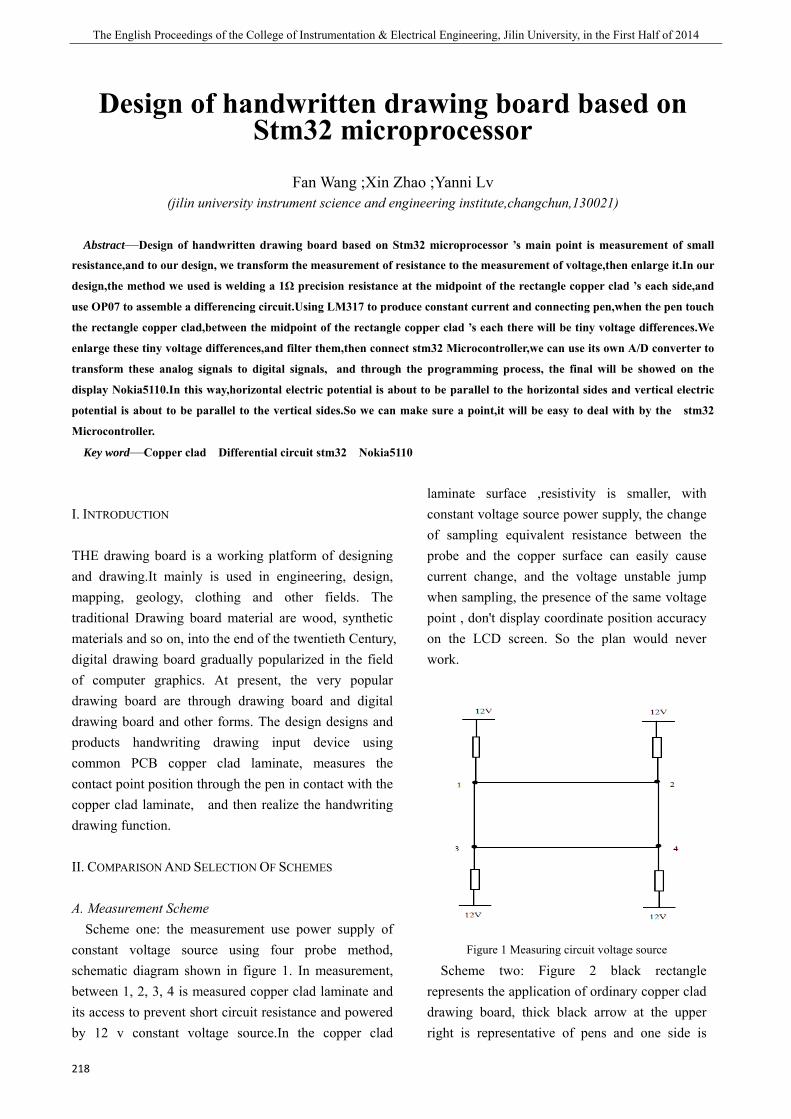
The English Proceedings of the College of Instrumentation & Electrical Engineering, Jilin University, in the First Half of 2014
218
Design of handwritten drawing board based on Stm32 microprocessor
Fan Wang ;Xin Zhao ;Yanni Lv
(jilin university instrument science and engineering institute,changchun,130021)
Abstract—Design of handwritten drawing board based on Stm32 microprocessor ’s main point is measurement of small
resistance,and to our design, we transform the measurement of resistance to the measurement of voltage,then enlarge it.In our
design,the method we used is welding a 1Ω precision resistance at the midpoint of the rectangle copper clad ’s each side,and
use OP07 to assemble a differencing circuit.Using LM317 to produce constant current and connecting pen,when the pen touch
the rectangle copper clad,between the midpoint of the rectangle copper clad ’s each there will be tiny voltage differences.We
enlarge these tiny voltage differences,and filter them,then connect stm32 Microcontroller,we can use its own A/D converter to
transform these analog signals to digital signals, and through the programming process, the final will be showed on the
display Nokia5110.In this way,horizontal electric potential is about to be parallel to the horizontal sides and vertical electric
potential is about to be parallel to the vertical sides.So we can make sure a point,it will be easy to deal with by the stm32
Microcontroller.
Key word—Copper clad Differential circuit stm32 Nokia5110
I. INTRODUCTION
THE drawing board is a working platform of designing and drawing.It mainly is used in engineering, design, mapping, geology, clothing and other fields. The traditional Drawing board material are wood, synthetic materials and so on, into the end of the twentieth Century, digital drawing board gradually popularized in the field of computer graphics. At present, the very popular drawing board are through drawing board and digital drawing board and other forms. The design designs and products handwriting drawing input device using common PCB copper clad laminate, measures the contact point position through the pen in contact with the copper clad laminate, and then realize the handwriting drawing function.
II. COMPARISON AND SELECTION OF SCHEMES
A. Measurement Scheme Scheme one: the measurement use power supply of
constant voltage source using four probe method, schematic diagram shown in figure 1. In measurement, between 1, 2, 3, 4 is measured copper clad laminate and its access to prevent short circuit resistance and powered by 12 v constant voltage source.In the copper clad
laminate surface ,resistivity is smaller, with constant voltage source power supply, the change of sampling equivalent resistance between the probe and the copper surface can easily cause current change, and the voltage unstable jump when sampling, the presence of the same voltage point , don't display coordinate position accuracy on the LCD screen. So the plan would never work.
Figure 1 Measuring circuit voltage source
Scheme two: Figure 2 black rectangle represents the application of ordinary copper clad drawing board, thick black arrow at the upper right is representative of pens and one side is
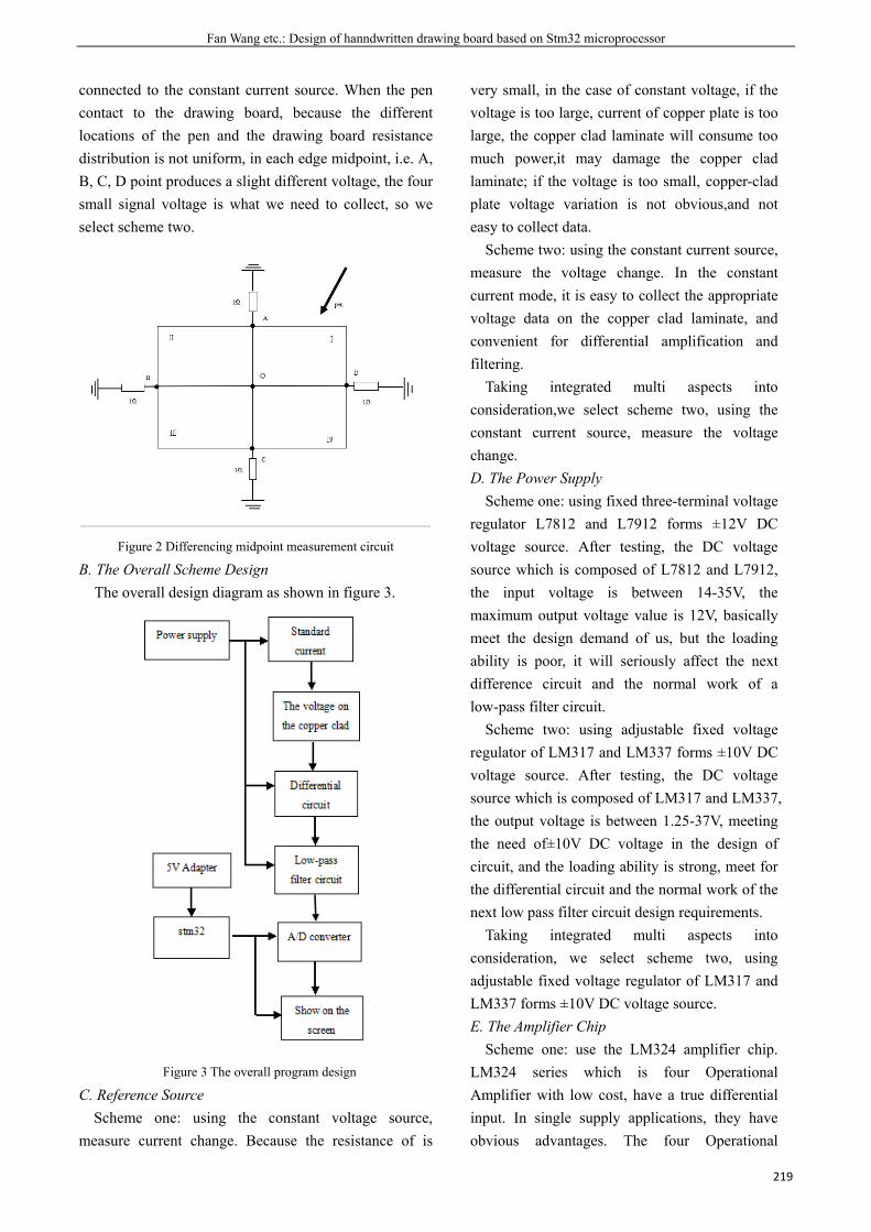
Fan Wang etc.: Design of hanndwritten drawing board based on Stm32 microprocessor
219
connected to the constant current source. When the pen contact to the drawing board, because the different locations of the pen and the drawing board resistance distribution is not uniform, in each edge midpoint, i.e. A, B, C, D point produces a slight different voltage, the four small signal voltage is what we need to collect, so we select scheme two.
Figure 2 Differencing midpoint measurement circuit
B. The Overall Scheme Design The overall design diagram as shown in figure 3.
Figure 3 The overall program design
C. Reference Source Scheme one: using the constant voltage source,
measure current change. Because the resistance of is
very small, in the case of constant voltage, if the voltage is too large, current of copper plate is too large, the copper clad laminate will consume too much power,it may damage the copper clad laminate; if the voltage is too small, copper-clad plate voltage variation is not obvious,and not easy to collect data.
Scheme two: using the constant current source, measure the voltage change. In the constant current mode, it is easy to collect the appropriate voltage data on the copper clad laminate, and convenient for differential amplification and filtering.
Taking integrated multi aspects into consideration,we select scheme two, using the constant current source, measure the voltage change. D. The Power Supply
Scheme one: using fixed three-terminal voltage regulator L7812 and L7912 forms ±12V DC voltage source. After testing, the DC voltage source which is composed of L7812 and L7912, the input voltage is between 14-35V, the maximum output voltage value is 12V, basically meet the design demand of us, but the loading ability is poor, it will seriously affect the next difference circuit and the normal work of a low-pass filter circuit.
Scheme two: using adjustable fixed voltage regulator of LM317 and LM337 forms ±10V DC voltage source. After testing, the DC voltage source which is composed of LM317 and LM337, the output voltage is between 1.25-37V, meeting the need of±10V DC voltage in the design of circuit, and the loading ability is strong, meet for the differential circuit and the normal work of the next low pass filter circuit design requirements.
Taking integrated multi aspects into consideration, we select scheme two, using adjustable fixed voltage regulator of LM317 and LM337 forms ±10V DC voltage source. E. The Amplifier Chip
Scheme one: use the LM324 amplifier chip. LM324 series which is four Operational Amplifier with low cost, have a true differential input. In single supply applications, they have obvious advantages. The four Operational
The English Proceedings of the College of Instrumentation & Electrical Engineering, Jilin University, in the First Half of 2014
220
Amplifier r can work in low to 3V or up to 32V, the quiescent current is about 1/5 MC1741 (each amplifier). But its input offset voltage is the maximum value is 7mV, obviously does not meet the design demand of us.
Scheme two: use the AD8065 amplifier chip. AD8065, with the very low working noise and very high input impedance, is single amplifier.With 5 -24V wide supply voltage range, it can be operated from a single supply and has 145MHz bandwidth. In addition, it also has a rail to rail output. But the maximum value of input offset voltage is 1.5mV, the same can not meet the design demand of us.
Scheme three: use the OP07 amplifier chip. OP07 is a low noise, The chopper stabilizing zero bipolar integrated circuit operational amplifiers (double power supply).Because the OP07 has very low input offset voltage (OP07's maximum is 25 V), so the OP07 do not require additional zero adjustment measures in many applications. OP07 also have characteristics of low input bias current (OP07 is ±2nA) and high open loop gain (OP07 is 300V/mV). The characteristic of low offset and high open loop gain makes it suitable for the measuring device of OP07 especially high gain and a weak signal amplification sensor, etc.The maximum input offset voltage is 75μV.It meets the demand of our design [3].
Taking integrated multi aspects into consideration, we select scheme three, using the OP07 amplifier chip. F. The Single Chip Microcomputer
Scheme one: use MSP430 MCU. MSP430 Series MCU is a 16 bit microcontroller, using the reduced instruction set (RISC) structure, having the rich addressing mode(7 source operand addressing, 4 destination operand addressing),27 kernel instructions and a large number of simulated instructions; a large number of registers, on-chip data memory can be in many kinds of operations; efficient lookup table processing instruction; a higher processing speed, with the 8MHz crystal driven, instruction cycle is 125ns. These characteristics ensure that produce a high efficiency of the source.
Scheme two: use 51 single chip computer. 51 MCU is general flexibility, low price, convenient use, but the word length is finite, data processing ability is very weak, the processing speed is slow,and resources is not rich, so peripheral circuit usually need to expand more, which greatly reduces the reliability of the system and increases the production cost and manufacturing difficulty.It is
difficult to meet the design requirements. Scheme three: using STM32 microcontroller.
STM32 has a very good performance: low price; many peripherals, including FSMC, TIMER, SPI, IIC, USB, CAN, IIS, SDIO, ADC, DAC, RTC, DMA and many other peripherals and function, which has a very high degree of integration; excellent real-time performance, including 84 interrupt and the 16 stage programmable priority, and all the pins can be used as an interrupt input; all the peripherals own independent clock switching ,so we can reduce power consumption by closing the corresponding peripheral clock; the development of low cost, no need of expensive emulator. Obviously,It is very suitable for our design.
Taking integrated multi aspects into consideration, chips that have fast operation speed are not needed in the design, the key is micro signal processing, so we select scheme three, using STM32 microcontroller.
Ⅲ.THE OVERALL CIRCUIT SYSTEM DESIGN
A. The Unit Circuit Design (a) Signal Acquisition
Signal acquisition diagram is shown in Figure 2, we collected A, B, C, D four different micro voltage. (b) The Difference And Amplification Of Signals
The first step of acquisition of the four voltage signals are divided into two groups, including A, C, as a group, B, D as a group, and use them as the two input ends exactly the same difference circuit, thus, two new voltage signals can be obtained at the output end of the differential circuit. After OP07 amplifier,we can gain voltage that be distinguished by stm32 microcontroller built-in A/D conversion function module, the differential circuit is shown in figure 4.
Fan Wang etc.: Design of hanndwritten drawing board based on Stm32 microprocessor
221
Figure 4 Differencing circuit diagram
(c) Low Pass Filter Of Signal The voltage signal has large noise through the
difference and amplified, so I need a low pass filter circuit to filter, and the cut-off frequency of filter is
1327Hz ( ),table voltage signals we get can be
sent to A/D conversion function module of stm32 single chip microcomputer.Low pass filter circuit is shown in figure 5.
Figure 5(Filtering circuit diagram)
(d) Signal A/D Converter A/D conversion of the drawing board use STM32
microcontroller with the A/D function module, which has 12 channels and the 0.8mV minimum resolution voltage.The voltage signal that has been filtered,, through the A/D conversion function module, is converted from analog signal to digital signal, and then handed over to the microcontroller processing.
(e) The Display Of Signal Display module use Nokia5110 display screen. It has high performance price ratio and simple interface, can be driven by only four I/O line, has fast speed which is 20 times of LCD12864, and is convenient to carry and a series of advantages. Therefore, through the MCU analysis, the digital voltage signals can be directly displayed on the screen.
Ⅳ. PROGRAM DESIGN
Handwritten drawing board use STM32 microcontroller as the control core of the whole system. After system starting, the voltage information on different positions of the pen will be read automatically, and A/D transform, finally show the corresponding data in the display [4][5], the program flow chart is shown in figure 3.
Ⅴ. THE TEST RESULTS
A. The Circuit Theory Calculation And Test Results
After measuring, when the 125mA constant current source was chosen as the reference source, per unit (0.5cm) voltage variation is about 0.008mV on the drawing board.Therefore,we dispose magnification is 300 times in the differential amplifier portion, and set the magnification of 2 times in the low pass filter section, finally voltage change can be magnified 600 times per unit, that is, 4.8mV.
With the power supply voltage of 3.3V,the A/D module of SCM has 12 channels. We can calculate the measurement accuracy for chip:
mVVV 8.00008.02/3.3 12 == Obviously, the voltage change per unit on
drawing board can be acquired by A/D acquisition module of MCU. B. The Method And Result Of Coordinate Measurement Of System
As shown in Figure 2, on the drawing board ,we set up Cartesian coordinate systemthe using O point as the origin point..The system is provided with two identical circuit in difference amplifying and filtering part, so when the pen

The English Proceedings of the College of Instrumentation & Electrical Engineering, Jilin University, in the First Half of 2014
222
contact to the drawing board, we can measure the voltage difference produced by two points A and C and voltage difference produced by two points B and D .In the two voltage difference of A/D conversion, the two numerical
value can be used to determine unique position and quadrant on the drawing board . The measurement results are shown in table 1.
Table1 Measurement results
Coordinate points (0,0) (1,1) (3,3) (-1,1) (-3,3) (-1,-1) (-3,-3) (1,-1) (3,-3)
The actual measured
voltage in the X-axis(mV) 151 155 167 144 133 145 137 156 167
The measured voltage in
the X-axis in theory(mV) 150 155 165 145 135 145 135 155 165
Error in the X-axis(mV) 1 0 2 -1 -2 0 2 1 2
The actual measured
voltage in the Y-axis(mV) 150 156 165 155 166 145 133 145 136
The measured voltage in
the Y-axis in theory(mV) 150 155 165 155 165 145 135 145 135
Error in the Y-axis(mV) 0 1 0 0 1 0 -2 0 1
The actual quadrant origin one one two two three three four four
Quadrant in theory origin one one two two three three four four
Remark:Per unit is 0.5cm in the copper clad,and the actual measured voltage of the origin is(151,150).
Results showed that potential changes in arc shaped, so in any parallel lines ,measurement data each unit is not linear, but is monotonous. So we can determine the contact point coordinates and quadrant according to the monotonicity .
VI.CONCLUSION
STM32 microcontroller as the core element, we design a handwritten drawing board. When the pen contact drawing board, the system will automatically capture each edge midpoint voltage of the drawing board, and then by the differential amplifier, low pass filtering and A/D conversion, data will be shown in the display. In addition, the design also added a button control function,so we can realize the switch between positioning of coordinates and drawing functions through the key.
References
[1] Oppenheimer,Signals and Systems (the second edition)
[M],Beijing:The Electronic Industrial Press, 2003.
[2] Baohui Zhang,Xianggen Yin,Power System Protective
Relaying[M],Beijing:China Electric Power Press,2010.
[3] Hansun Li,Basic Circuit Analysis(the fourth edition)[M],
Beijing:Higher Education Press,2006.
[4] Longhai Jin,Cong Li,C Language Program Design[M],
Beijing:Science Press,2012.
[5] Qiao He,Microcontroller Theory and Applications[M],
Beijing:ChinaRailway Press,2008.
[6] V. S. Golub. Drawing boards with guiding rules[J].
Measurement Techniques, 1960, Vol.2 (12)
[7] David Shiga. Back to the drawing board[J]. New Scientist,
2008, 200(2683).
[8] Hui-fu Zhang, Wei Kang.Design of the Data Acquisition
System Based on STM32[J]. Procedia Computer Science,
2013, Vol.17 , pp.222-228.
[9] Gordon Duff.Back to the future—and to the drawing
board[J]. The Lancet, 2011, 377(9763).
Li Hong-Yu: Implementation of Larmor frequency measurement for Groundwater Investigation
223
Implementation of Larmor frequency measurement for Groundwater Investigation
LI Hong-Yu
(College of Instrument Science and Electrical Engineering, Jilin University, Changchun 130022,China)
Abstract—The frequency meter is designed with indirect measurement method, Using the timer produces a relatively stable and accurate time, At the same time converts the signal into amplitude and waveform can be
recognized by the digital circuit pulse signal (generated by the timer), And then calculate the number of pulses
within this time interval counter and custom formulas by frequency meter, After scaling up from its 1602
LCD. This design works the final test results, An accuracy of 1 ‰, meet design goals 1% accuracy, and show
stable and can be applied to. Groundwater Investigation. Keywords—Frequency meter, indirect measurement, Groundwater Investigation
I. FOREWORD
USING NMR method of detecting groundwater in recent years developed a new technology. The method is emission of electromagnetic waves with the local Larmor frequency excitation groundwater proton. Accurately measure the local Larmor frequency becomes an important task. Range of Larmor frequencies is 1000-3000Hz[1] .Design a device that can quickly measure the Larmor frequency error is less than 1 ‰, you can give nuclear magnetic resonance analyzer provides accurate excitation frequency, for high precision detection of groundwater, there are significant [2] .
1.ORIGINATION AND PROGRAMME OF DESIGNMENT
1.1 Origination of designment The main functions of the digital frequency meter
are to measure the frequency of the periodic signal. Frequency is the number of times per unit time (1S) signal generating periodic change. If we are able to count the signal waveform in a given 1S time, and Counting results are displayed, can be read frequency of the signal.
Digital frequency meter is first generated by the internal timer is relatively stable and accurate time and the amplitude of the signal is converted into a waveform can be recognized by the digital circuit
pulse signal (generated by the timer), then by the definition of the counter and frequency meter formula to calculate the number of pulses within this time interval, will be converted by 1602 after it came out LCD. This is the basic principle of digital frequency meter [3]. 1.2Programme of Designment
A frequency measurement in many ways, but the most common is the direct measurement and indirect measurement method. Direct frequency measurement method is based on the frequency of the meaning of the measured frequency signal is applied to the input of the gate only at the gate opening time T (in 1s dollars), the pulse test (number) to a decimal counter to count.
Setting the counter value N, the frequency of the measured signal can be obtained as f = N. However, due to the opening of the shutter, the closing time and the measured frequency hopping synchronization signal is difficult, the lower the signal frequency, the fewer the number of cycles within one second. The pulse count often produce errors a pulse, so at low frequencies with a direct frequency measurement method error is relatively large, so the use of this measurement at low frequencies relative measurement error may be high, that is, in the low frequency does not meet the design requirements.
Direct frequency measurement method is simple and convenient and feasible, direct frequency measurement method disadvantage is larger error at low frequency measurements. Indirect frequency measurement
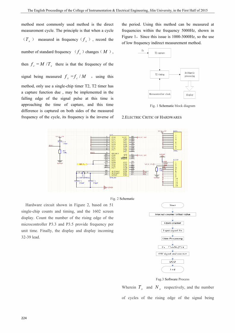
The English Proceedings of the College of Instrumentation & Electrical Engineering, Jilin University, in the First Half of 2015
224
method most commonly used method is the direct measurement cycle. The principle is that when a cycle
( xT ) measured in frequency( xf ), record the
number of standard frequency ( cf )changes(M ),
then /c xf M T= there is that the frequency of the
signal being measured /x cf f M= ,using this
method, only use a single-chip timer T2, T2 timer has a capture function due , may be implemented in the falling edge of the signal pulse at this time is approaching the time of capture, and this time difference is captured on both sides of the measured frequency of the cycle, its frequency is the inverse of
the period. Using this method can be measured at frequencies within the frequency 5000Hz, shown in Figure 1,Since this issue is 1000-3000Hz, so the use of low frequency indirect measurement method.
T2 capture
Microcontroller clock
T2 timingArithmetic processing
display
fx
Fig. 1 Schematic block diagram
2.ELECTRIC CRITIC OF HARDWARES
Fig. 2 Schematic
Hardware circuit shown in Figure 2, based on 51 single-chip counts and timing, and the 1602 screen display. Count the number of the rising edge of the microcontroller P3.3 and P3.5 provide frequency per unit time. Finally, the display and display incoming 32-39 lead.
Fag.3 Software Process
Wherein xT and xN respectively, and the number
of cycles of the rising edge of the signal being
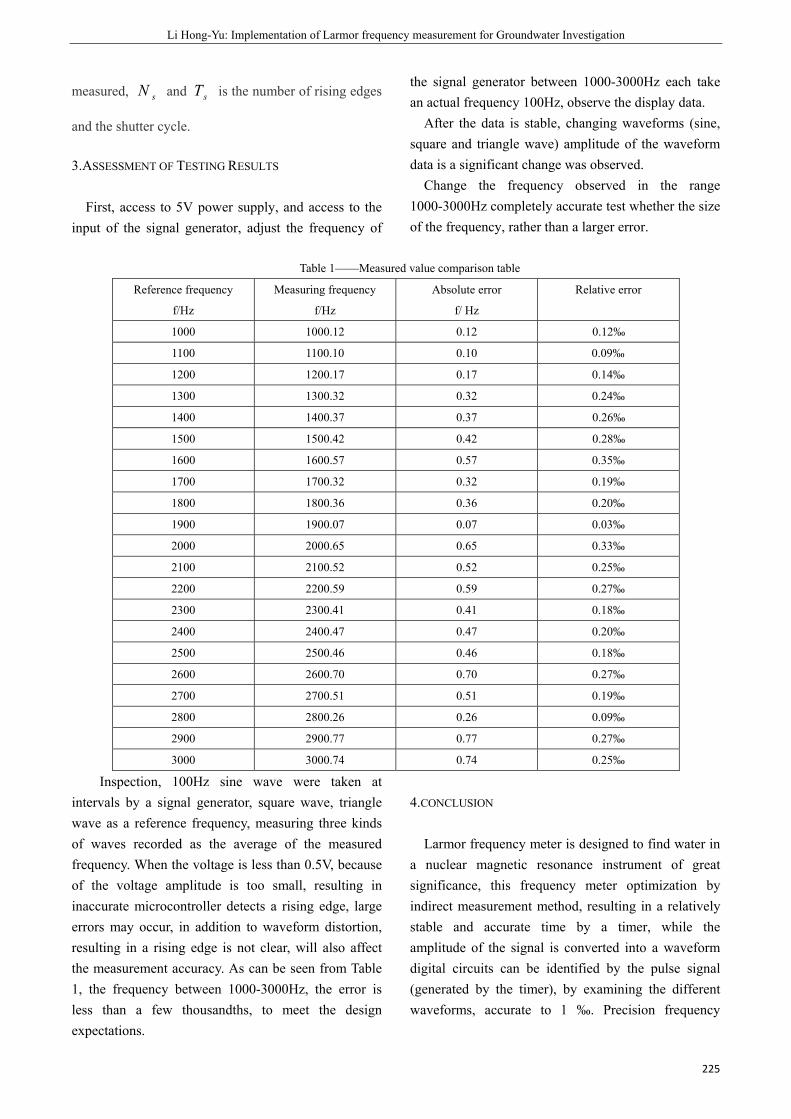
Li Hong-Yu: Implementation of Larmor frequency measurement for Groundwater Investigation
225
measured, sN and sT is the number of rising edges
and the shutter cycle.
3.ASSESSMENT OF TESTING RESULTS
First, access to 5V power supply, and access to the input of the signal generator, adjust the frequency of
the signal generator between 1000-3000Hz each take an actual frequency 100Hz, observe the display data.
After the data is stable, changing waveforms (sine, square and triangle wave) amplitude of the waveform data is a significant change was observed.
Change the frequency observed in the range 1000-3000Hz completely accurate test whether the size of the frequency, rather than a larger error.
Table 1——Measured value comparison table
Reference frequency
f/Hz
Measuring frequency
f/Hz
Absolute error
f/ Hz
Relative error
1000 1000.12 0.12 0.12‰
1100 1100.10 0.10 0.09‰
1200 1200.17 0.17 0.14‰
1300 1300.32 0.32 0.24‰
1400 1400.37 0.37 0.26‰
1500 1500.42 0.42 0.28‰
1600 1600.57 0.57 0.35‰
1700 1700.32 0.32 0.19‰
1800 1800.36 0.36 0.20‰
1900 1900.07 0.07 0.03‰
2000 2000.65 0.65 0.33‰
2100 2100.52 0.52 0.25‰
2200 2200.59 0.59 0.27‰
2300 2300.41 0.41 0.18‰
2400 2400.47 0.47 0.20‰
2500 2500.46 0.46 0.18‰
2600 2600.70 0.70 0.27‰
2700 2700.51 0.51 0.19‰
2800 2800.26 0.26 0.09‰
2900 2900.77 0.77 0.27‰
3000 3000.74 0.74 0.25‰
Inspection, 100Hz sine wave were taken at intervals by a signal generator, square wave, triangle wave as a reference frequency, measuring three kinds of waves recorded as the average of the measured frequency. When the voltage is less than 0.5V, because of the voltage amplitude is too small, resulting in inaccurate microcontroller detects a rising edge, large errors may occur, in addition to waveform distortion, resulting in a rising edge is not clear, will also affect the measurement accuracy. As can be seen from Table 1, the frequency between 1000-3000Hz, the error is less than a few thousandths, to meet the design expectations.
4.CONCLUSION
Larmor frequency meter is designed to find water in a nuclear magnetic resonance instrument of great significance, this frequency meter optimization by indirect measurement method, resulting in a relatively stable and accurate time by a timer, while the amplitude of the signal is converted into a waveform digital circuits can be identified by the pulse signal (generated by the timer), by examining the different waveforms, accurate to 1 ‰. Precision frequency

The English Proceedings of the College of Instrumentation & Electrical Engineering, Jilin University, in the First Half of 2015
226
meter in science also has a wide range of application areas.
References
[1] Jiang Yanqiu, Wang Ying Ji, paragraph clear, Wang
Zhongxing. SNMR development of high-power transmitter
water detector [J]. Journal of Jilin University (Information
Science) 2007 (03)
[2] Lin Jun Status and Development Trend of nuclear magnetic
resonance techniques [J]. Progress. Geophysics. 2010 (02)
[3] Shen Jun Asia. Meter digital frequency microcontroller
based design [J]. Shanxi Electronic Technology. 2012 (05)

Wang Chong etc.: Template for Preparation of Papers for IEEE Sponsored Conferences & Symposia
227
Research on Based on the Available Solar Mobile Power Transformer Output
Wang Chong, Ren Hang, and Song Chengzhuo
(College of Instruments Science and Electric Engineering, Jilin University, Changchun 130022)
Abstract—This article is based on the solar mobile power output can swing design. Design a microcontroller as the control
center. Use C language programming. The mobile power can be used for solar and mains power supply for charging and
powering appliances. The input and output voltage monitoring results by software modules will be displayed in the
LCD12864 display. The basic components of a control circuit, solar charging circuitry, analog to digital conversion circuitry,
DC design and LM2577 variable volt control circuit and MCU control circuit. The experimental design from the design
direction of its huge advantage there, it lives in a very easy to obtain but not deep enough resources to use as an energy source,
and this design uses and lives, with good usability.
I. INTRODUCTION
THE rapid development of mobile Internet, the emergence of a large number of all kinds of mobile terminal, digital communication products performance to intelligent mobile phone as a representative of the continuous improvement of cell volume, but the product itself can accommodate more and more small, portable digital products with lead battery energy can not meet the needs for everyday use, thereby promoting the development of mobile power supply. The current mobile digital products built-in battery mainstream use time is short, can not meet the long time outdoor use weakness, and mobile power existing can also give the number of mobile digital products charge is limited, if long-term not connected to a power supply for charging, mobile power supply will be unable to work, through the variable output charging research and production of mobile power supply on the design of a solar energy, not only can be recharged using power, can also be charging effect to complete based on solar energy, electric energy and reserve for charging electronic products, so as to achieve the effect of saving resources, but also can change the output voltage, can give different mobile equipment charging voltage for charging. The advantages of using solar energy can swing mobile power supply, this type of promotion can achieve practical, energy saving target.
II.THE OVERALL DESIGN OF THE SYSTEM
In this paper, the design of solar mobile power supply is mainly composed of variable: solar charging circuit, control circuit, LCD12864 display circuit, the boost output circuit composed of four parts. The overall system block diagram shown in figure 1.
USB enter
Solar input
The control circuit
Mobile Power Battery
LCD display circuit
Mobile power boost output
circuit
Figure1 The overall block diagram of the system
III.THE HARDWARE CIRCUIT DESIGN
A.Solar charger design The solar energy input to supply power for
the control circuit, can be accepted voltage into 5V voltage to supply power for the control circuit. When the input voltage is greater than the supply of
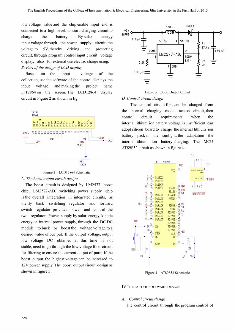
The English Proceedings of the College of Instrumentation & Electrical Engineering, Jilin University, in the First Half of 2015
228
low voltage value and the chip enable input end is connected to a high level, to start charging circuit to charge the battery; By solar energy input voltage through the power supply circuit, the voltage to 5V, thereby driving and protecting circuit, through program control input circuit voltage display, also for external use electric charge using. B. Part of the design of LCD display
Based on the input voltage of the collection, use the software of the control displays the input voltage and making the project name in 12864 on the screen. The LCD12864 display circuit in Figure 2 as shown in fig.
VSS
1V
DD
2V
O3
RS4
R/W
5E
6D
B07
DB1
8D
B29
DB3
10D
B411
DB5
12D
B613
DB7
14PS
B15
NC
16RS
T17
VO
UT
18BL
A19
BLK
20
LCD112864
GND
GND
VCC VCC
RP110KΩ
CSSID
CLK
PSB
Figure 2 LCD12864 Schematic
C. The boost output circuit design The boost circuit is designed by LM2577 boost
chip, LM2577-ADJ switching power supply chip is the overall integration in integrated circuits, as the fly back switching regulator and forward switch regulator provides power and control the two regulator. Power supply by solar energy, kinetic energy or internal power supply, through the DC DC module to buck or boost the voltage voltage to a desired value of out put. If the output voltage, output low voltage DC obtained at this time is not stable, need to go through the low voltage filter circuit for filtering to ensure the current output of pure; If the boost output, the highest voltage can be increased to 12V power supply. The boost output circuit design as shown in figure 3.
Figure 3 Boost Output Circuit
D. Control circuit design The control circuit first can be charged from
the normal charging mode access circuit, then control circuit requirements when the internal lithium ion battery voltage is insufficient, can adopt silicon board to charge the internal lithium ion battery pack in the sunlight, the adaptation the internal lithium ion battery charging. The MCU AT89S52 circuit as shown in figure 4.
VCC 40
GND20
RST9 X1 19
X2 18
PSEN29 ALE 30
P0.1/AD138
P0.2/AD237
P0.3/AD336
P0.4/AD435
P0.5/AD534
P0.6/AD633
P0.7/AD732
P0.0/AD039
P2.0/A8 21
P2.1/A9 22
P2.2/A10 23
P2.3/A11 24
P2.4/A12 25
P2.5/A13 26
P2.6/A14 27
P2.7/A15 28
P3.0/RXD10
P3.1/TXD11
P3.2/INT012
P3.3/INT113 P3.4/T0 14
P3.5/T1 15
P3.6/WR 16
P3.7/RD 17
EA31
U1 AT89S52
VCC
32
12M
20pF31
20pF33
2510u29
10K
28复复
12
34
56
78
910
30
VCC
下下下ISP
6 789
这这这 的的的52
VCC
D0D1D2D3D4D5D6D7
ABC
RD1 ADDWR1INT
CSSIDCLKPSB
ALE
对对
Figure 4 AT89S52 Schematic
IV.THE PART OF SOFTWARE DESIGN
A. Control circuit design The control circuit through the program control of
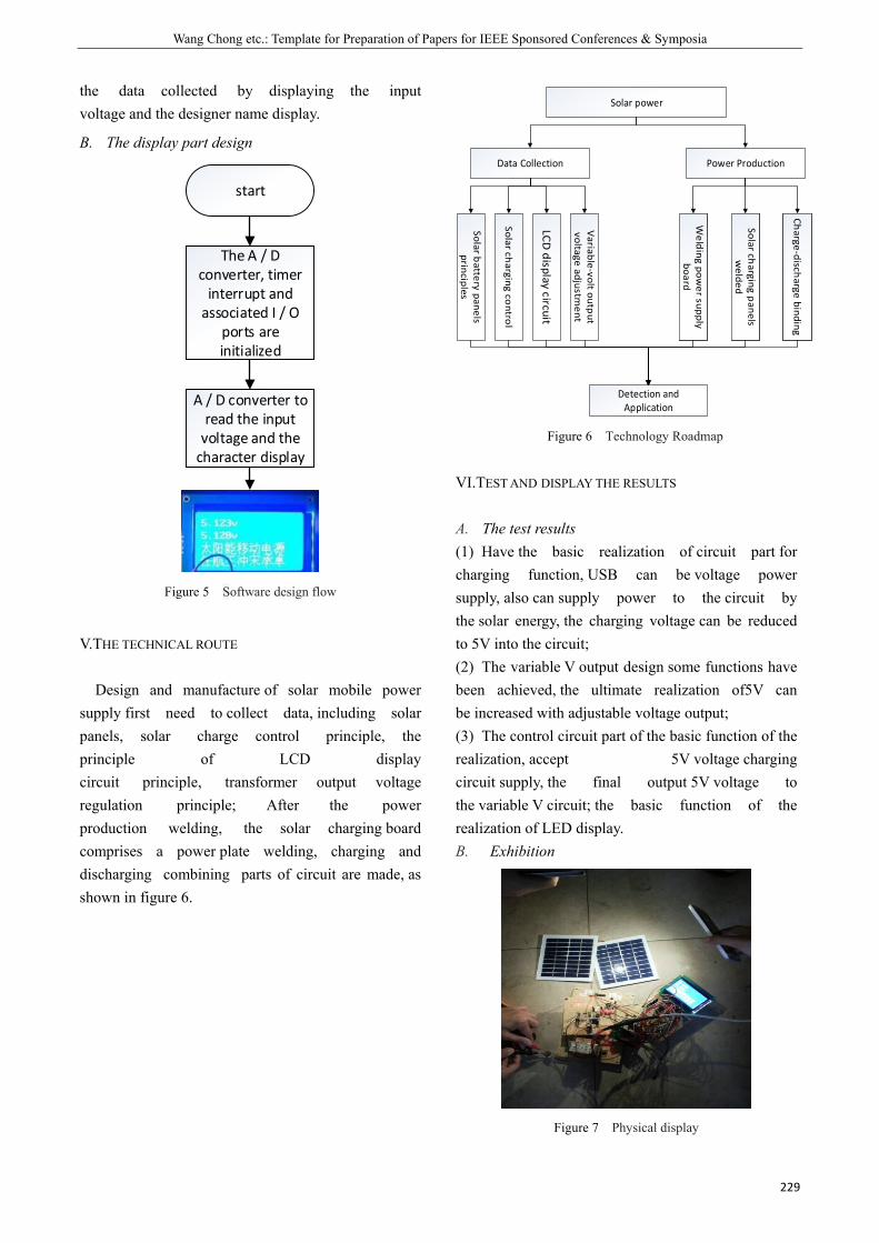
Wang Chong etc.: Template for Preparation of Papers for IEEE Sponsored Conferences & Symposia
229
the data collected by displaying the input voltage and the designer name display.
B. The display part design
start
The A / D converter, timer
interrupt and associated I / O
ports are initialized
A / D converter to read the input
voltage and the character display
Figure 5 Software design flow
V.THE TECHNICAL ROUTE
Design and manufacture of solar mobile power supply first need to collect data, including solar panels, solar charge control principle, the principle of LCD display circuit principle, transformer output voltage regulation principle; After the power production welding, the solar charging board comprises a power plate welding, charging and discharging combining parts of circuit are made, as shown in figure 6.
Solar power
Data Collection Power Production
Solar battery panels principles
Detection and Application
Solar charging control
LCD display circuit
Variable-volt output voltage adjustm
ent
Welding pow
er supply board
Solar charging panels w
elded
Charge-discharge binding
Figure 6 Technology Roadmap
VI.TEST AND DISPLAY THE RESULTS
A. The test results (1) Have the basic realization of circuit part for charging function, USB can be voltage power supply, also can supply power to the circuit by the solar energy, the charging voltage can be reduced to 5V into the circuit; (2) The variable V output design some functions have been achieved, the ultimate realization of5V can be increased with adjustable voltage output; (3) The control circuit part of the basic function of the realization, accept 5V voltage charging circuit supply, the final output 5V voltage to the variable V circuit; the basic function of the realization of LED display. B. Exhibition
Figure 7 Physical display

The English Proceedings of the College of Instrumentation & Electrical Engineering, Jilin University, in the First Half of 2015
230
VII. SUMMARY
Some features of this circuit design has been basically achieved, USB voltage power supply, also can supply power to the circuit by the solar energy, the charging voltage can be reduced to 5V into the circuit; The variable V output design some functions have been achieved, the ultimate realization of5V~12V output voltage adjustable; LED display the input voltage and the design of the name of the author. This design also exist some problems, including can not accurately measure the output voltage, the overall design of mobile power supply is not enough light. Next, improve the overall design and implementation of the output voltage measurement.
References
[1] Xie Jiakui. The electronic circuit (linear part
of [M].4 Edition). Beijing: Higher Education Press, 1999.
[2] Zhao Xiaomin. The design of switching power supply and
application [M]. Shanghai Popular Science Press, 1995 (9).
[3] Liu Yan. Research on [D]. control technology of digital
generator rectifier power. Chongqing: Chongqing
University, 2010.
[4] Zong Ping. Digital generator [J]. energy and environmental
protection,2005, 7:28-30.
[5] Liu Fengjun. Multi level inverter technology and its
application [M]. Beijing: Mechanical Industry Press, 2007.
[6] Hu Shuju, Li Jianlin, Pei Yunqing, Xu Honghua. A
portable generator with rectifier control strategy and the
realization of the [J]. electric drive, 2008, 3:35-38.
[7] Cheok A D, Kawamoto S, Matsumoto T, Obi H. High
power ac/dc and dc/ac inverter for high speed train[J].
IEEE TENCON, 2000, 423-428.
[8] Li Aiwen. Principle and design of modern
communication switching power supply. Beijing: Science
Press, 2001.
[9] Wu Bo Sheng Gehao. Zeng Yi, et al. Multiple
battery solar photovoltaic power system design and
application of [J]. power electronics
technology, 2008,42 (2); 45-47.
Qiu Shuo etc.: System design and implementation of the receiver coil stance and track record
231
System design and implementation of the receiver coil stance and track record
Qiu Shuo, Lu Yihan, and Chen Shiwen
( College of Instrumentation & Electrical Engineering, Jilin University,Changchun 130022 )
Abstract—In order to get information of the receiver coil stance and track record and read the data we get,the system is
based on Cortex-M3 platform, and use MPU9150 nine-axis stance sensor to get the data of gyroscope, magnetometer,
accelerometer and NEO-6GPS chip return data to finish the fusion of stance by quaternion algorithm.Finally we get the
pitch angle, roll angle, yaw angle and GPS information stored in the SD card and achieve measurement accuracy of 1°.
I. INTRODUCTION
AVIATION is one of the airborne geophysical electromagnetic method commonly used measurement methods,geophysical methods based on electromag-
netic induction]1[
widely used in oil and gas
exploration, ore prospecting and groundwater survey,
etc.]2[.AEM system can be divided into fixed-wing
airborne electromagnetic system and helicopter
airborne electromagnetic system]3[,and the former has
a deeper probing depth, and a higher efficiency]4[.As
the aircraft stance, speed, wind speed and other factors that cause the coil pitch yaw rotation,the system
parameters will be changed]5[
.Fixed-wing
time-domain airborne electromagnetic system using dipole - dipole mode, the transmitter coil set up in the
surrounding aircraft]6[, receiving pod connected to
sling hanging below the aircraft, the researchers need to be able to timely, rapid and accurate determination of the stance of the coil.
The project aims to study for geological exploration of the receiving coil used to gesture, track record.Current aircraft stance determination of the receiver coil design less.GPS track measured in this regard, foreign countries have get successful results
]7[,while in our country it is just a beginning.Current
research on the stance has been more thoroughly mature record, a variety of integration is very high angle sensor, gyroscope, accelerometer widely.
Above all, the project focused on the stance recorded on the receiving coil applications, flight stance, track and other detailed information on the receiving coil complete record, and then use the more friendly interface output stance information.So researchers can easily obtain information receiving coils during the geological exploration work, to always adjust the detection method based on the detection and assessment of the accuracy of the coil stance.
II.DESIGN
A.The overall design System consists of a controller data processing
module, BMP9150 stance sensor module, NEO-6GPS modules.The overall design diagram shows in Figure 1.
Figure 1 The overall block diagram
220v power adapter rectified after 5v DC voltage
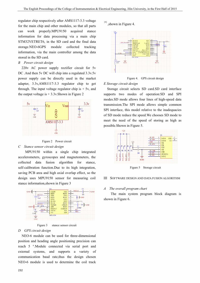
The English Proceedings of the College of Instrumentation & Electrical Engineering, Jilin University, in the First Half of 2015
232
regulator chip respectively after AMS1117-3.3 voltage for the main chip and other modules, so that all parts can work properly.MPU9150 acquired stance information for data processing via a main chip STM32VETRET6, in the SD card and the final data storage.NEO-6GPS module collected tracking information, via the main controller among the data stored in the SD card. B Power circuit design
220v AC power supply rectifier circuit for 5v DC .And then 5v DC will chip into a regulated 3.3v.5v power supply can be directly used in the market adapter, 3.3v,AMS1117-3.3 regulator chip to get through. The input voltage regulator chip is + 5v, and the output voltage is + 3.3v.Shown in Figure 2
Figure 2 Power circuit
C Stance sensor circuit design MPU9150 within a single chip integrated
accelerometers, gyroscopes and magnetometers, the collected data fusion algorithm for stance, self-calibration function.Due to its high integration, saving PCB area and high axial overlap effect, so the design uses MPU9150 sensor for measuring coil stance information,shown in Figure 3
Figure 3 stance sensor circuit
D GPS circuit design NEO-6 module can be used for three-dimensional position and heading angle positioning precision can reach 5 °.Module connected via serial port and external systems, and supports a variety of communication baud rate,thus the design chosen NEO-6 module is used to determine the coil track
]8[,shown in Figure 4.
Figure 4. GPS circuit design
E Storage circuit design Storage circuit selects SD card.SD card interface
supports two modes of operation:SD and SPI modes.SD mode allows four lines of high-speed data transmission.The SPI mode allows simple common SPI interface, this model relative to the inadequacies of SD mode reduce the speed.We chooses SD mode to meet the need of the speed of storing as high as possible.Shown in Figure 5.
Figure 5 Storage circuit
III SOFTWARE DESIGN AND DATA FUSION ALGORITHM
A The overall program chart The main system program block diagram is
shown in Figure 6.
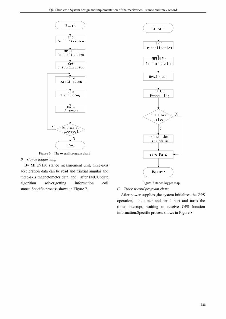
Qiu Shuo etc.: System design and implementation of the receiver coil stance and track record
233
Figure 6 The overall program chart
B stance logger map By MPU9150 stance measurement unit, three-axis
acceleration data can be read and triaxial angular and three-axis magnetometer data, and after IMUUpdate algorithm solver,getting information coil stance.Specific process shows in Figure 7.
Figure 7 stance logger map
C Track record program chart After power supplies ,the system initializes the GPS
operation, the timer and serial port and turns the timer interrupt, waiting to receive GPS location information.Specific process shows in Figure 8.
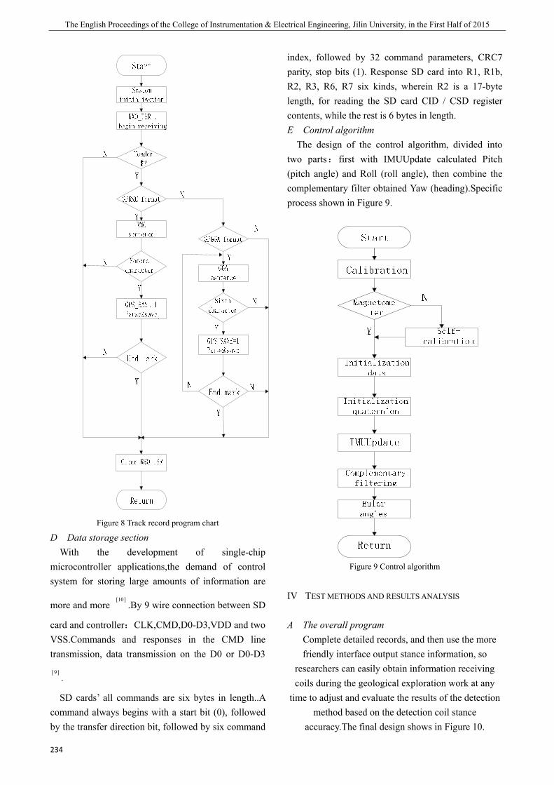
The English Proceedings of the College of Instrumentation & Electrical Engineering, Jilin University, in the First Half of 2015
234
Figure 8 Track record program chart
D Data storage section With the development of single-chip
microcontroller applications,the demand of control system for storing large amounts of information are
more and more ]10[.By 9 wire connection between SD
card and controller:CLK,CMD,D0-D3,VDD and two VSS.Commands and responses in the CMD line transmission, data transmission on the D0 or D0-D3
]9[.
SD cards’ all commands are six bytes in length..A command always begins with a start bit (0), followed by the transfer direction bit, followed by six command
index, followed by 32 command parameters, CRC7 parity, stop bits (1). Response SD card into R1, R1b, R2, R3, R6, R7 six kinds, wherein R2 is a 17-byte length, for reading the SD card CID / CSD register contents, while the rest is 6 bytes in length. E Control algorithm
The design of the control algorithm, divided into two parts: first with IMUUpdate calculated Pitch (pitch angle) and Roll (roll angle), then combine the complementary filter obtained Yaw (heading).Specific process shown in Figure 9.
Figure 9 Control algorithm
IV TEST METHODS AND RESULTS ANALYSIS
A The overall program Complete detailed records, and then use the more friendly interface output stance information, so
researchers can easily obtain information receiving coils during the geological exploration work at any
time to adjust and evaluate the results of the detection method based on the detection coil stance
accuracy.The final design shows in Figure 10.
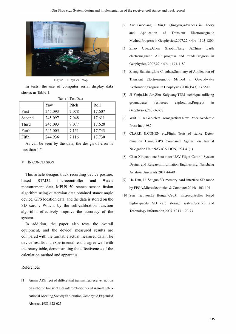
Qiu Shuo etc.: System design and implementation of the receiver coil stance and track record
235
Figure 10 Physical map
In tests, the use of computer serial display data shows in Table 1.
Table 1 Test Data
Yaw Pitch Roll First 245.093 7.078 17.607 Second 245.097 7.048 17.611 Third 245.093 7.077 17.628 Forth 245.005 7.151 17.743 Fifth 244.936 7.116 17.730
As can be seen by the data, the design of error is less than 1 °.
V IN CONCLUSION
This article designs track recording device posture, based STM32 microcontroller and 9-axis measurement data MPU9150 stance sensor fusion algorithm using quaternion data obtained stance angle device, GPS location data, and the data is stored on the SD card . Which, by the self-calibration function algorithm effectively improve the accuracy of the system.
In addition, the paper also tests the overall equipment, and the device’ measured results are compared with the turntable actual measured data. The device’results and experimental results agree well with the rotary table, demonstrating the effectiveness of the calculation method and apparatus.
References
[1] Annan AP,Effect of differential transmitter/receiver notion
on airborne transient Em interpretation.53 rd Annual Inter-
national Meeting,SocietyExploration Geophysic,Expanded
Abstract,1983:622-623
[2] Xue Guoqiang,Li Xiu,Di Qingyun,Advances in Theory
and Application of Transient Electromagnetic
Method,Progress in Geophysics,2007,22(4):1195-1200
[3] Zhao Guoze,Chen Xiaobin,Tang Ji,China Earth
electromagnetic AFP progress and trends,Progress in
Geophysics, 2007,22(4):1171-1180
[4] Zhang Baoxiang,Liu Chunhua,Summary of Application of
Transient Electromagnetic Method in Groundwater
Exploration,Progress in Geophysics,2004,19(3):537-542
[5] Ji Yanju,Lin Jun,Zhu Kaiguang,TEM technique utilizing
groundwater resources exploration,Progress in
Geophysics,2005:63-77
[6] Wait J R.Geo-elect romagretism.New York:Academic
Press Inc.,1982
[7] CLARK E.COHEN etc.Flight Tests of stance Deter-
mination Using GPS Compared Against on Inertial
Navigation Unit.NAVIGA TION,1994.41(1)
[8] Chen Xinquan, etc,Four-rotor UAV Flight Control System
Design and Research,Information Engineering, Nanchang
Aviation University,2014:44-49
[9] He Dan, Li Shuguo,SD memory card interface SD mode
by FPGA,Microelectronics & Computer,2014:103-104
[10] Sun Tianyou,Li Hongyi,C8051 microcontroller based
high-capacity SD card storage system,Science and
Technology Information,2007(31):70-73
The English Proceedings of the College of Instrumentation & Electrical Engineering, Jilin University, in the First Half of 2015
236
The design of vehicle micro traffic weather station based on 51SCM
AN Yan; SHI Jing; WEI Xin
(College of Instrumentation and Electrical Engineering, Jilin University,Changchun130061,China)
Abstract—With the continuous promotion and application of microcomputer, a new generation of communications
technology and new type sensors,the development of weather monitoring system in China will inevitably turn to the
direction of micro power, intelligent, high reliability, low cost, which will provide more reliable detailed meteorological
information for our production and life. The design of vehicle traffic micro weather station is made by using a single chip
microcomputer, which can make the station more small and concrete. Combining multiple nodes with different regions, a
wide range of real-time data is collected and uploaded to the network with application scene of the Internet of things. It
provides a new idea for data storage of the onboard Internet.
I. INTRODUCTION
IN today's society, real-time and accurate data about meteorological data like temperature, humidity, wind speed and direction can be nationwide collected as large scale as possible. But the acquisition mode is of high input and high consumption. Therefore, this research project is based on vehicle network, low cost, a wide range of meteorological data collection.
Because the meteorological cause are inseparable with civil and industrial activities, meteorological acquisition technology plays an important role in national defense construction, social progress and economic development, and along with the implementation of the national strategy of sustainable development, meteorological acquisition technology is more and more important for us; With the needs of meteorological information changing continuously, the traditional meteorological model has been unable to meet the people's needs. Therefore, the automatic meteorological data acquisition technology develops well in our country. Meteorological data acquisition system of things directly affects the practicability of data. Thus, how to realize data collection and summary widely from all over the country and all over the world and must be a very meaningful research direction in the future.
Although domestic meteorological data acquisition system has achieved greater development at present, compared with foreign development level, there is still
a big gap. Therefore, in order to improve the overall level of the meteorological cause monitoring in our country, we must focus on the development of a new generation of automatic weather station and improve the key technology of meteorological sensor and data processing.
II. SYSTEM DESIGN
The hardware system structure diagram used in this design is shown in figure 1. The hardware design of the system adopts the design idea of low power, portable, which is mainly comprised of a sensor module, a display module and a control module with 51 single chip computer as the center. The sensor module is comprised of a DHT11 temperature and humidity sensor, air pressure sensor of MS5611 and photoelectric encoder. Then, they transmit the data to the MCU, display it, and transfer data to the PC terminal via serial to USB.
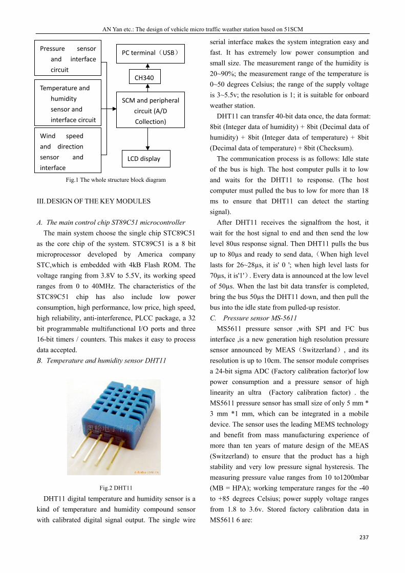
AN Yan etc.: The design of vehicle micro traffic weather station based on 51SCM
237
Fig.1 The whole structure block diagram
III. DESIGN OF THE KEY MODULES
A. The main control chip ST89C51 microcontroller The main system choose the single chip STC89C51
as the core chip of the system. STC89C51 is a 8 bit microprocessor developed by America company STC,which is embedded with 4kB Flash ROM. The voltage ranging from 3.8V to 5.5V, its working speed ranges from 0 to 40MHz. The characteristics of the STC89C51 chip has also include low power consumption, high performance, low price, high speed, high reliability, anti-interference, PLCC package, a 32 bit programmable multifunctional I/O ports and three 16-bit timers / counters. This makes it easy to process data accepted. B. Temperature and humidity sensor DHT11
Fig.2 DHT11
DHT11 digital temperature and humidity sensor is a kind of temperature and humidity compound sensor with calibrated digital signal output. The single wire
serial interface makes the system integration easy and fast. It has extremely low power consumption and small size. The measurement range of the humidity is 20~90%; the measurement range of the temperature is 0~50 degrees Celsius; the range of the supply voltage is 3~5.5v; the resolution is 1; it is suitable for onboard weather station.
DHT11 can transfer 40-bit data once, the data format: 8bit (Integer data of humidity) + 8bit (Decimal data of humidity) + 8bit (Integer data of temperature) + 8bit (Decimal data of temperature) + 8bit (Checksum).
The communication process is as follows: Idle state of the bus is high. The host computer pulls it to low and waits for the DHT11 to response. (The host computer must pulled the bus to low for more than 18 ms to ensure that DHT11 can detect the starting signal).
After DHT11 receives the signalfrom the host, it wait for the host signal to end and then send the low level 80us response signal. Then DHT11 pulls the bus up to 80µs and ready to send data,(When high level lasts for 26~28µs, it is' 0 '; when high level lasts for 70µs, it is'1'). Every data is announced at the low level of 50µs. When the last bit data transfer is completed, bring the bus 50µs the DHT11 down, and then pull the bus into the idle state from pulled-up resistor. C. Pressure sensor MS-5611
MS5611 pressure sensor ,with SPI and I²C bus interface ,is a new generation high resolution pressure sensor announced by MEAS(Switzerland), and its resolution is up to 10cm. The sensor module comprises a 24-bit sigma ADC (Factory calibration factor)of low power consumption and a pressure sensor of high linearity an ultra (Factory calibration factor) . the MS5611 pressure sensor has small size of only 5 mm * 3 mm *1 mm, which can be integrated in a mobile device. The sensor uses the leading MEMS technology and benefit from mass manufacturing experience of more than ten years of mature design of the MEAS (Switzerland) to ensure that the product has a high stability and very low pressure signal hysteresis. The measuring pressure value ranges from 10 to1200mbar (MB = HPA); working temperature ranges for the -40 to +85 degrees Celsius; power supply voltage ranges from 1.8 to 3.6v. Stored factory calibration data in MS5611 6 are:
Wind speed and direction sensor and interface
Temperature and humidity sensor and interface circuit
Pressure sensor and interface circuit
SCM and peripheral circuit (A/D Collection)
LCD display
CH340
PC terminal(USB)
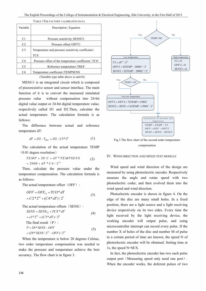
The English Proceedings of the College of Instrumentation & Electrical Engineering, Jilin University, in the First Half of 2015
238
TABLE 1THE FACTORY CALIBRATION DATA
Variable Description | Equation
C1 Pressure sensitivity |SENST1
C2 Pressure offset| OFFT1
C3 Temperature and pressure sensitivity coefficient |
TCS
C4 Pressure offset of the temperature coefficient | TCO
C5 Reference temperature |TREF
C6 Temperature coefficient |TEMPSENS (Variable type table above is unit16)
MS5611 is an integrated circuit which is composed of piezoresistive sensor and sensor interface. The main function of it is to convert the measured simulated pressure value without compensation into 24-bit digital value output or 24-bit digital temperature value, respectively called D1 and D2.Then, calculate the actual temperature. The calculation formula is as follows:
The difference between actual and reference temperature dT:
82 2 5*2REFdT D T D C= - = - (1)
The calculation of the actual temperature TEMP(0.01 degree resolution)
23
20 *2000 * 6 / 2
T E M P C dT T E M P SE N SdT C
= +
= +
(2)
Then, calculate the pressure value under the temperature compensation. The calculation formula is as follows:
The actual temperature offset(OFF):
116 7
*
2*2 ( 4* ) / 2TOFF OFF TCO dT
C C dT
= +
= + (3)
The actual temperature offsets(SENS): 1
15 8
*
1* 2 ( 3* ) / 2TSENS SENS TCS dT
c C dT
= +
= + (4)
The final result(P):
21 15
1*( 1* / 2 ) / 2
P D SENS OFFD SENS OFF= -
= - (5)
When the temperature is below 20 degrees Celsius, two order temperature compensation was needed to make the pressure and temperature achieve the best accuracy. The flow chart is in figure 3.
TEMP<20C
Low temperature
Very low temperature
TEMP<-15C
High temperature
Calculation of pressure and
temperature
2 31
2 1
2 2
2 / 22 5( 2000) / 22 5( 2000) / 2
T dTOFF TEMPSENS TEMP
=
= -
= -
2 02 02 0
TOFFSENS
=
=
=
2
2 1
2 2 7( 1500)2 11( 1500) / 2
OFF OFF TEMPSENS SENS TEMP
= + +
= + +
22
2
TEMP TEMP TOFF OFF OFFSENS SENE SENS
= -
= -
= -
Yes No
Yes No
Fig.3 The flow chart of the second-order temperature
compensation
IV. WIND DIRECTION AND SPEED TEST MODULE
Wind speed and wind direction of the design are measured by using photoelectric encoder. Respectively measure the angle and rotate speed with two photoelectric coder, and then evolved them into the wind speed and wind direction.
Photoelectric encoder is shown in figure 4. On the edge of the disc are many small holes. In a fixed position, there are a light source and a light receiving device respectively on its two sides. Every time the light received by the light receiving device, the working encoder will output pulse, and using microcontroller interrupt can record every pulse. If the number X of holes of the disc and number M of pulse in a certain period of time are known, the speed N of photoelectric encoder will be obtained. Setting time at 1s, the speed N=M/X.
In fact, the photoelectric encoder has two such pulse output port(Measuring speed only need one port). When the encoder works, the deferent pulses of two
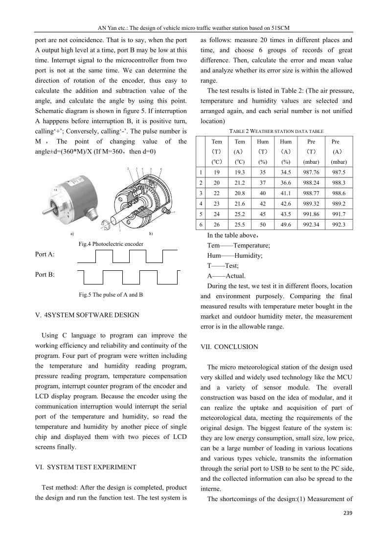
AN Yan etc.: The design of vehicle micro traffic weather station based on 51SCM
239
port are not coincidence. That is to say, when the port A output high level at a time, port B may be low at this time. Interrupt signal to the microcontroller from two port is not at the same time. We can determine the direction of rotation of the encoder, thus easy to calculate the addition and subtraction value of the angle, and calculate the angle by using this point. Schematic diagram is shown in figure 5. If interruption A happpens before interruption B, it is positive turn, calling‘+’; Conversely, calling‘-’. The pulse number is M , The point of changing value of the angle±d=(360*M)/X (If M=360,then d=0)
Fig.4 Photoelectric encoder
Port A: Port B:
Fig.5 The pulse of A and B
V. 4SYSTEM SOFTWARE DESIGN
Using C language to program can improve the working efficiency and reliability and continuity of the program. Four part of program were written including the temperature and humidity reading program, pressure reading program, temperature compensation program, interrupt counter program of the encoder and LCD display program. Because the encoder using the communication interruption would interrupt the serial port of the temperature and humidity, so read the temperature and humidity by another piece of single chip and displayed them with two pieces of LCD screens finally.
VI. SYSTEM TEST EXPERIMENT
Test method: After the design is completed, product the design and run the function test. The test system is
as follows: measure 20 times in different places and time, and choose 6 groups of records of great difference. Then, calculate the error and mean value and analyze whether its error size is within the allowed range.
The test results is listed in Table 2: (The air pressure, temperature and humidity values are selected and arranged again, and each serial number is not unified location)
TABLE 2 WEATHER STATION DATA TABLE
Tem
(T)
(oC)
Tem
(A)
(oC)
Hum
(T)
(%)
Hum
(A)
(%)
Pre
(T)
(mbar)
Pre
(A)
(mbar)
1 19 19.3 35 34.5 987.76 987.5
2 20 21.2 37 36.6 988.24 988.3
3 22 20.8 40 41.1 988.77 988.6
4 23 21.6 42 42.6 989.32 989.2
5 24 25.2 45 43.5 991.86 991.7
6 26 25.5 50 49.6 992.34 992.3
In the table above, Tem——Temperature; Hum——Humidity; T——Test; A——Actual. During the test, we test it in different floors, location
and environment purposely. Comparing the final measured results with temperature meter bought in the market and outdoor humidity meter, the measurement error is in the allowable range.
VII. CONCLUSION
The micro meteorological station of the design used very skilled and widely used technology like the MCU and a variety of sensor module. The overall construction was based on the idea of modular, and it can realize the uptake and acquisition of part of meteorological data, meeting the requirements of the original design. The biggest feature of the system is: they are low energy consumption, small size, low price, can be a large number of loading in various locations and various types vehicle, transmits the information through the serial port to USB to be sent to the PC side, and the collected information can also be spread to the interne.
The shortcomings of the design:(1) Measurement of

The English Proceedings of the College of Instrumentation & Electrical Engineering, Jilin University, in the First Half of 2015
240
temperature and humidity only achieve the single digits, and the temperature below zero cannot be measured; (2) Because the material parameters of the wind cup is not clear, the measurement error of the wind will be very big; (3) When the vane on the photoelectric coder kept swinging, angle measurement error will increase. After several experimental measurement, the data of the system can be measured and displayed stably, and it can serve customers very well.
Reference
[1] LIU Guang-wei. Temperature and humanity measurement
system design and implementation of greenhouse based on
single chip [D]. Control Engineering, Yanshan University.
2012:26-27.
[2] ZENG Yang, WEN Chun-hua, LI Yi-cong. A alarm
system of the automatic weather station data which is
based on a microcontroller[J].Jiangxi Technical Center of
Atmosphere Exploration, 2009(1):1-2.
[3] LIU Hong-bing. The Intelligent Remote Measurement
Micro Weather Station Based on Double MCU [D].
Nanjing University of Information Science & Technology,
2006:1-3.
[4] HU Yu-feng, Principles and methods of measurement of
automatic weather stations [M].Beijing: China Meteoro-
logical Press, 2004.
[5] XUE Wei-min. The contemporary meteorological cause of
China [M].Beijing: China Social Sciences Press, 1984.
[6] ZHANG Ai-chen. Modern meteorological
observation .Peking University Press, 2000,5
[7] YU Yong, DAI Jia, LIU Bo. Detailed examples of
commonly used modules and integrated system design of
C[M]. Beijing: Electronics Industry Press, 2008, 10.
[8] KANG Hua-guang. Electronic Technology Foundation
(The fifth edition of the analog part).Higher education
press, 2006.
[9] HE Qiao.Principle and application of single chip
microcomputer. Chinese Railway Press, 2008.
Zhang Bing-Ren etc.: The design of Power quality monitoring system based on LABVIEW
241
The design of Power quality monitoring system based on LABVIEW
Zhang Bing-Ren; FuYu-Ce;Fu Hua ; Liu Huan
(Jilin university instrument science and engineering institute,Changchun,130021)
Abstract —Through the virtual instrument technology for detection of power quality . With the help of the premise of the
analysis using the LABVIEW software.we design a powerful signal processing and data analysis ability of virtual instrument testing device.The device can satisfy the functions that the real-time capturing the power quality index data.Besides,real-time parameters have been collected into the device that can be accurately displayed through the different modules.
I.INTRODUCTION
LABVIEW is a kind of application development environment, which using graphical editor language program G to write the program, and the program is in the form of block diagram.What’s more,it’s the most ideal choice of developing measure or control system. All the necessary desired tools that engineers and scientists used to quickly build varies applicationsis integrate in the LABVIEW development environment.
II.COLLECTIVITY DESIGN
Power quality monitoring will be done in LABVIEW.First of all, the three-phase signal go through the signal conditioning circuit ,then,the data transport to the voltage signal that is suitable for data acquisition board (usually ±5 v to ±10 v), DAQ can change the analog signal to the digital signal that the software recognizes, further,the digital signals are transmitted into the LABVIEW software. After further analysis, the measurement task will be done.
One of the characteristics of this system is that ,it combines the power system analysis and analog electronic technology and virtual instrument technology.The system chooses the suitable sensors, making the measurement much more accurate. And taking the advantage of the knowledge of the analog electronic technology, designing a suitable signal conditional circuit.
In addition to common power quality indicators’ monitoring , it also monitors the transient disturbance the of power quality. Mainly is the voltage rising and dropping drastically in the monitoring and recording with strong practicability.
With the powerful data processing ability and logical control, software using a high-level language programming, it ensure that the system have high
reliability and high misappropriation The traditional power quality tester with MPU and
MCU as the core, but the function is relatively single. Signal processing and data analysis ability is weak, However it’s more suitable for the power quality inspection and special regular inspection. Focusing on the passive testing, they does not have comprehensive ability to show the panorama of power quality problems actively. On behalf of the trends of testing technology and virtual instrument, promoting and researching the power quality monitoring method that based on virtual instrument technology and monitoring device which is a new technology in the field of power quality monitoring and the new scheme, i believe it is the inevitable trend of current development.
III.DEVELOPMENT PLATFORM DESIGN
Labview development platform is mainly composed of power measurement module,unbalanced harmonic analysis module and phase angle module and based parameter module. .
Fig.1 The labview diagram
The module choose labview as platform, using the graphical editing language to project. When digital signal transmits into the module, then the software can
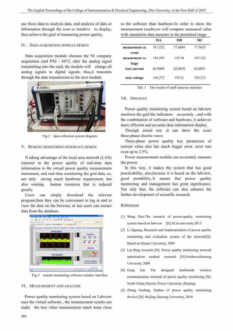
The English Proceedings of the College of Instrumentation & Electrical Engineering, Jilin University, in the First Half of 2015
242
use these data to analysis data, and analysis of data or information through the icon or intuitive to display, thus achieve the goal of measuring power quality.
IV.DATA ACQUISITION MODULE DESIGN
Data acquisition module chooses the NI company acquisition card PXI - 4472, after the analog signal transmitting into the card, the module will change all analog signals to digital signals, thus,it transmits through the data transmission to the next module.
Fig.2 data collection system diagram
V.REMOTE MONITORING INTERFACE DESIGN
If taking advantage of the local area network (LAN) transmit to the power quality of real-time data information to the virtual power quality measurement instrument, and real-time monitoring the grid data, so, not only saving much hardware requirement, but also wasting human resources that is reduced greatly.
Users can simply download the relevant program,then they can be convenient to log in and to view the data on the browser, at last users can extract data from the database.
Fig.3 remote monitoring software window interface
VI.MEASUREMENT AND ANALYSIS
Power quality monitoring system based on Labview uses the virtual software , the measurement results can make the true value measurement much more close
to the software than hardware.In order to show the measurement results,we will compare measured value with simulation data measure in the permitted range
MA MB MC
measurment current
78.1252 77.6884 77.5635
measurment voltage
156.292 155.34 155.122
true current 62.5089 62.0839 62.0851
true voltage 156.272 155.21 155.213
Tab. 1 The results of staff turnover statistics
VII.EPILOGUE
Power quality monitoring system based on labview monitors the grid the indicators accurately , and with the combination of software and hardware, it achieves more efficient and accurate data information display.
Through actual test ,it can show the exact three-phase electric wave.
Three-phase power quality key parameters of current value also has much bigger error, error rate even up to 2.5%.
Power measurement module can accurately measure the power.
In this way, it makes the system that has good practicability, also,because it is based on the labview, good portability,.It means that power quality monitoring and management has great significance. Not only that, the software can also enhance the further development of scientific research.
References
[1] Wang Duo.The research of power-quality monitoring
system based on labview [D].JiLin university.2013
[2] Li Jiguang. Research and implementation of power quality
monitoring and evaluation system of the network[D].
Based on Hunan University, 2009
[3] Liu Bing research [D]. Power quality monitoring network
optimization method. research [D].SouthwesJiaotong
University 2009
[4] Geng Jun Yue designed multimode wireless
communication terminal of power quality monitoring [D].
North China Electric Power University (Beijing)
[5] Zhang Guifang. Studies of power quality monitoring
devices [D]. Beijing Jiaotong University, 2010
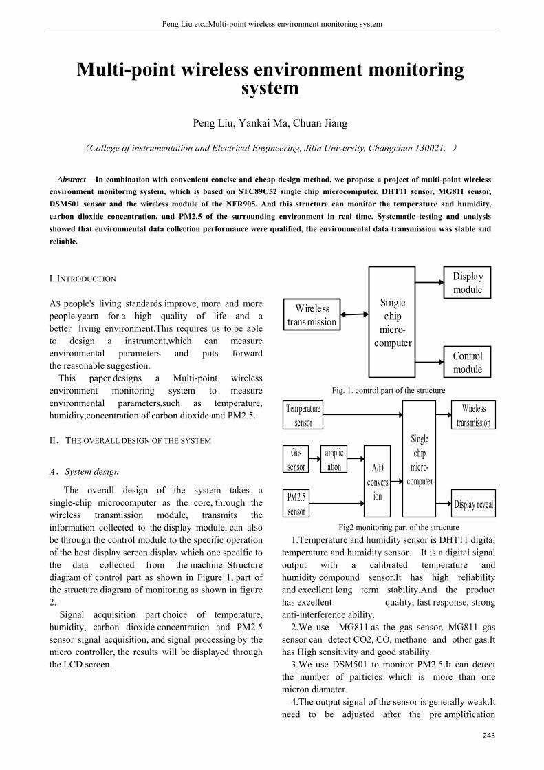
Peng Liu etc.:Multi-point wireless environment monitoring system
243
Multi-point wireless environment monitoring system
Peng Liu, Yankai Ma, Chuan Jiang
(College of instrumentation and Electrical Engineering, Jilin University, Changchun 130021, )
Abstract—In combination with convenient concise and cheap design method, we propose a project of multi-point wireless
environment monitoring system, which is based on STC89C52 single chip microcomputer, DHT11 sensor, MG811 sensor, DSM501 sensor and the wireless module of the NFR905. And this structure can monitor the temperature and humidity, carbon dioxide concentration, and PM2.5 of the surrounding environment in real time. Systematic testing and analysis showed that environmental data collection performance were qualified, the environmental data transmission was stable and reliable.
I. INTRODUCTION
AS people's living standards improve, more and more people yearn for a high quality of life and a better living environment.This requires us to be able to design a instrument,which can measure environmental parameters and puts forward the reasonable suggestion.
This paper designs a Multi-point wireless environment monitoring system to measure environmental parameters,such as temperature, humidity,concentration of carbon dioxide and PM2.5.
II.THE OVERALL DESIGN OF THE SYSTEM
A.System design
The overall design of the system takes a single-chip microcomputer as the core, through the wireless transmission module, transmits the information collected to the display module, can also be through the control module to the specific operation of the host display screen display which one specific to the data collected from the machine. Structure diagram of control part as shown in Figure 1, part of the structure diagram of monitoring as shown in figure 2.
Signal acquisition part choice of temperature, humidity, carbon dioxide concentration and PM2.5 sensor signal acquisition, and signal processing by the micro controller, the results will be displayed through the LCD screen.
Single chip
micro-computer
Wireless transmission
Display module
Control module
Fig. 1. control part of the structure
Temperature sensor
Gas sensor
PM2.5 sensor
amplication A/D
conversion
Single chip
micro-computer
Wireless transmission
Display reveal
Fig2 monitoring part of the structure 1.Temperature and humidity sensor is DHT11 digital
temperature and humidity sensor. It is a digital signal output with a calibrated temperature and humidity compound sensor.It has high reliability and excellent long term stability.And the product has excellent quality, fast response, strong anti-interference ability.
2.We use MG811 as the gas sensor. MG811 gas sensor can detect CO2, CO, methane and other gas.It has High sensitivity and good stability.
3.We use DSM501 to monitor PM2.5.It can detect the number of particles which is more than one micron diameter.
4.The output signal of the sensor is generally weak.It need to be adjusted after the pre amplification
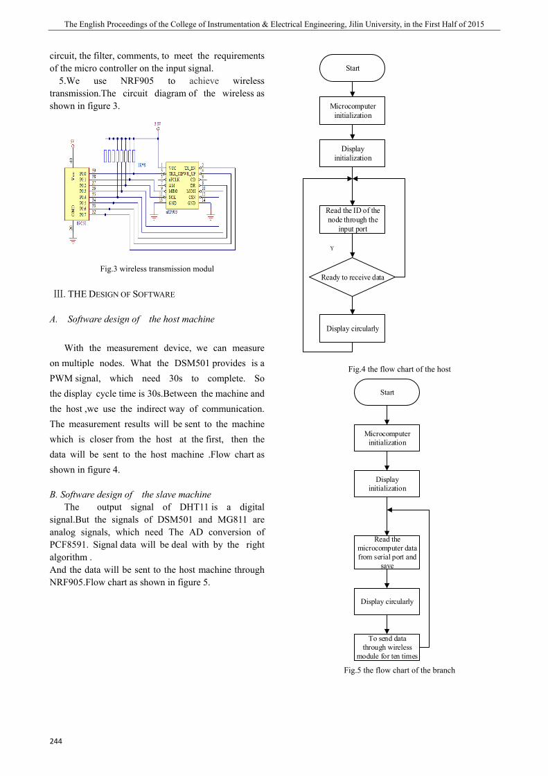
The English Proceedings of the College of Instrumentation & Electrical Engineering, Jilin University, in the First Half of 2015
244
circuit, the filter, comments, to meet the requirements of the micro controller on the input signal.
5.We use NRF905 to achieve wireless transmission.The circuit diagram of the wireless as shown in figure 3.
Fig.3 wireless transmission modul
Ⅲ. THE DESIGN OF SOFTWARE
A. Software design of the host machine
With the measurement device, we can measure on multiple nodes. What the DSM501 provides is a PWM signal, which need 30s to complete. So the display cycle time is 30s.Between the machine and the host ,we use the indirect way of communication. The measurement results will be sent to the machine which is closer from the host at the first, then the data will be sent to the host machine .Flow chart as shown in figure 4.
B. Software design of the slave machine The output signal of DHT11 is a digital signal.But the signals of DSM501 and MG811 are analog signals, which need The AD conversion of PCF8591. Signal data will be deal with by the right algorithm . And the data will be sent to the host machine through NRF905.Flow chart as shown in figure 5.
Start
Microcomputer initialization
Read the ID of the node through the
input port
Ready to receive data
Display circularly
Display initialization
Y
Fig.4 the flow chart of the host
Microcomputer initialization
Display initialization
Display circularly
To send data through wireless
module for ten times
Start
Read the microcomputer data from serial port and
save
Fig.5 the flow chart of the branch

Peng Liu etc.:Multi-point wireless environment monitoring system
245
Ⅳ.THE TEST RESULTS OF SYSTEM
We tested many groups of data at different time and in the same location data,and the results can display on the screens.The machine as shown in figure 6.
Fig.6 the system entity
We chose four groups of the experimental data,as shown in table 1.
table. 1 the test results Test
temperature
Actual temperature
Test Humidity %
Actual humidity %
Test CO2 ppm
Actual CO2 ppm
TestPM2.5 kpcs
Actual PM2.5 kpcs
1 20 20.3
23 24 370 340 9.3 9.8
2 21 21.2
26 27 415 433 10.5 10.3
3 22 22.3
30 32 768 794 14.8 15.2
4 23 23.3
34 36 1567 1634 17.3 17.5
Ⅴ.CONCLUSION
The Multi-point wireless environment monitoring system includes a host machine(the master) and two slave machines.We designed and built the main hardware, and select the appropriate data algorithm. And we Wrote a program of C. The machine can monitor the data of surrounding environment.
References
[1] Wang xuewen, Zhang zhiyong, The Principle and
Application of Sensor[M], Beihang University Press,2004.
[2] Luo longfu, Tong tiaosheng, Intelligent Detection System
and Date Fusion[M], China Machine Press,2000.
[3] Li daohua, Li ling, The Sensor Circuit Analysis and
Design[M], Wu Han University Press,2000.
[4] Han cai, Single Chip Microcomputer Priciple and System
Design[M], Tsinghua University,2002.
[5] Fu minninf, Zhen youfei, Xu xingniu, Niu luyan, The
Monitoring and Evaluation of PM2.5[J], The weather and
Disaster Reduction Research,2012,35(4):1-6.
[6] Wang yongzhi, Liu yuanyuan, The Monitoring and Alarm
Conyrol System of the Large Grain’s Temperature and
Humidity[J], Agricultural Mechanization Research, 2008
(8): 167-169.
[7] Cai xing, Zhang xiquan, Short-range Wireless
Communication Technology [J],The Modern Electronic
Technology,2004,27(3): 65-67.
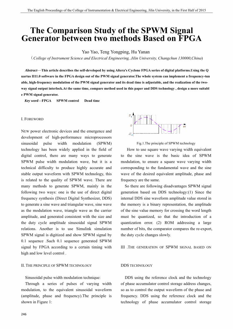
The English Proceedings of the College of Instrumentation & Electrical Engineering, Jilin University, in the First Half of 2015
246
The Comparison Study of the SPWM Signal Generator between two methods Based on FPGA
Yao Yao, Teng Yongping, Hu Yanan
(College of Instrument Science and Electrical Engineering, Jilin University, Changchun 130000,China)
Abstract—This article describes the self-developed by using Altera's Cyclone FPGA series of digital platforms.Using the Q
uartus II11.0 software in the FPGA design out of the PWM signal generator.The whole system can implement a frequency-tun
able, high-frequency modulation of the PWM signal generator and its dead time is adjustable, and the realization of the two-
way signal output interlock.At the same time, compare method used in this paper and DDS technology , design a more suitabl
e PWM signal generator.
Key word—FPGA SPWM control Dead time
I. FOREWORD
NEW power electronic devices and the emergence and development of high-performance microprocessors sinusoidal pulse width modulation (SPWM) technology has been widely applied in the field of digital control, there are many ways to generate SPWM pulse width modulation wave, but it is a technical difficulty to produce highly accurate and stable output waveform with SPWM technology, this is related to the quality of SPWM wave. There are many methods to generate SPWM, mainly in the following two ways: one is the use of direct digital frequency synthesis (Direct Digital Synthesizer, DDS) to generate a sine wave and triangular wave, sine wave as the modulation wave, triangle wave as the carrier amplitude, and generated consistent with the size and the duty cycle amplitude sinusoidal signal SPWM relations. Another is to use Simulink simulation SPWM signal is digitized and show SPWM signal by 0.1 sequence .Such 0.1 sequence generated SPWM signal by FPGA according to a certain timing with high and low level control .
II. THE PRINCIPLE OF SPWM TECHNOLOGY
Sinusoidal pulse width modulation technique: Through a series of pulses of varying width
modulation, to the equivalent sinusoidal waveform (amplitude, phase and frequency).The principle is shown in Figure 1:
Fig.1.The principle of SPWM technology How to use square wave varying width equivalent
to the sine wave is the basic idea of SPWM modulation, to ensure a square wave varying width corresponding to the fundamental wave and the sine wave of the desired equivalent amplitude, phase and frequency are the same.
So there are following disadvantages SPWM signal generation based on DDS technology:(1) Since the internal DDS sine waveform amplitude value stored in the memory is a binary representation, the amplitude of the sine value memory for crossing the word length must be quantized, so that the introduction of a quantization error. (2) ROM addressing a large number of bits, the comparator compares the re-export, the duty cycle changes slowly.
III .THE GENERATION OF SPWM SIGNAL BASED ON
DDS TECHNOLOGY
DDS using the reference clock and the technology of phase accumulator control storage address changes, so as to control the output waveform of the phase and frequency. DDS using the reference clock and the technology of phase accumulator control storage
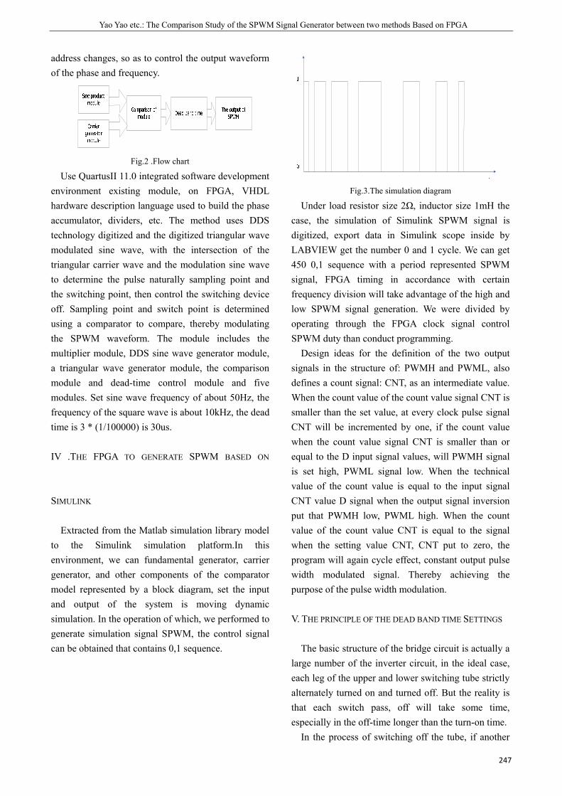
Yao Yao etc.: The Comparison Study of the SPWM Signal Generator between two methods Based on FPGA
247
address changes, so as to control the output waveform of the phase and frequency.
Fig.2 .Flow chart Use QuartusII 11.0 integrated software development
environment existing module, on FPGA, VHDL hardware description language used to build the phase accumulator, dividers, etc. The method uses DDS technology digitized and the digitized triangular wave modulated sine wave, with the intersection of the triangular carrier wave and the modulation sine wave to determine the pulse naturally sampling point and the switching point, then control the switching device off. Sampling point and switch point is determined using a comparator to compare, thereby modulating the SPWM waveform. The module includes the multiplier module, DDS sine wave generator module, a triangular wave generator module, the comparison module and dead-time control module and five modules. Set sine wave frequency of about 50Hz, the frequency of the square wave is about 10kHz, the dead time is 3 * (1/100000) is 30us.
IV .THE FPGA TO GENERATE SPWM BASED ON
SIMULINK
Extracted from the Matlab simulation library model to the Simulink simulation platform.In this environment, we can fundamental generator, carrier generator, and other components of the comparator model represented by a block diagram, set the input and output of the system is moving dynamic simulation. In the operation of which, we performed to generate simulation signal SPWM, the control signal can be obtained that contains 0,1 sequence.
Fig.3.The simulation diagram Under load resistor size 2Ω, inductor size 1mH the
case, the simulation of Simulink SPWM signal is digitized, export data in Simulink scope inside by LABVIEW get the number 0 and 1 cycle. We can get 450 0,1 sequence with a period represented SPWM signal, FPGA timing in accordance with certain frequency division will take advantage of the high and low SPWM signal generation. We were divided by operating through the FPGA clock signal control SPWM duty than conduct programming.
Design ideas for the definition of the two output signals in the structure of: PWMH and PWML, also defines a count signal: CNT, as an intermediate value. When the count value of the count value signal CNT is smaller than the set value, at every clock pulse signal CNT will be incremented by one, if the count value when the count value signal CNT is smaller than or equal to the D input signal values, will PWMH signal is set high, PWML signal low. When the technical value of the count value is equal to the input signal CNT value D signal when the output signal inversion put that PWMH low, PWML high. When the count value of the count value CNT is equal to the signal when the setting value CNT, CNT put to zero, the program will again cycle effect, constant output pulse width modulated signal. Thereby achieving the purpose of the pulse width modulation.
V. THE PRINCIPLE OF THE DEAD BAND TIME SETTINGS
The basic structure of the bridge circuit is actually a large number of the inverter circuit, in the ideal case, each leg of the upper and lower switching tube strictly alternately turned on and turned off. But the reality is that each switch pass, off will take some time, especially in the off-time longer than the turn-on time.
In the process of switching off the tube, if another
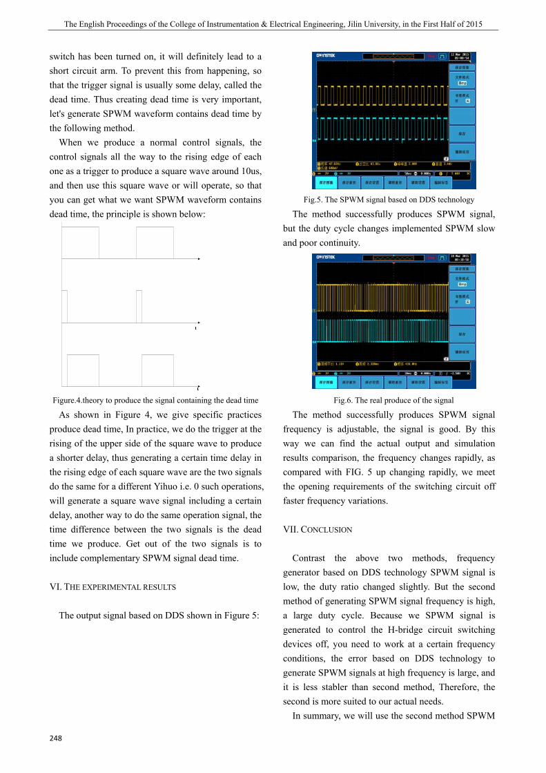
The English Proceedings of the College of Instrumentation & Electrical Engineering, Jilin University, in the First Half of 2015
248
switch has been turned on, it will definitely lead to a short circuit arm. To prevent this from happening, so that the trigger signal is usually some delay, called the dead time. Thus creating dead time is very important, let's generate SPWM waveform contains dead time by the following method.
When we produce a normal control signals, the control signals all the way to the rising edge of each one as a trigger to produce a square wave around 10us, and then use this square wave or will operate, so that you can get what we want SPWM waveform contains dead time, the principle is shown below:
Figure.4.theory to produce the signal containing the dead time
As shown in Figure 4, we give specific practices produce dead time, In practice, we do the trigger at the rising of the upper side of the square wave to produce a shorter delay, thus generating a certain time delay in the rising edge of each square wave are the two signals do the same for a different Yihuo i.e. 0 such operations, will generate a square wave signal including a certain delay, another way to do the same operation signal, the time difference between the two signals is the dead time we produce. Get out of the two signals is to include complementary SPWM signal dead time.
VI. THE EXPERIMENTAL RESULTS
The output signal based on DDS shown in Figure 5:
Fig.5. The SPWM signal based on DDS technology
The method successfully produces SPWM signal, but the duty cycle changes implemented SPWM slow and poor continuity.
Fig.6. The real produce of the signal The method successfully produces SPWM signal
frequency is adjustable, the signal is good. By this way we can find the actual output and simulation results comparison, the frequency changes rapidly, as compared with FIG. 5 up changing rapidly, we meet the opening requirements of the switching circuit off faster frequency variations.
VII. CONCLUSION
Contrast the above two methods, frequency generator based on DDS technology SPWM signal is low, the duty ratio changed slightly. But the second method of generating SPWM signal frequency is high, a large duty cycle. Because we SPWM signal is generated to control the H-bridge circuit switching devices off, you need to work at a certain frequency conditions, the error based on DDS technology to generate SPWM signals at high frequency is large, and it is less stabler than second method, Therefore, the second is more suited to our actual needs.
In summary, we will use the second method SPWM

Yao Yao etc.: The Comparison Study of the SPWM Signal Generator between two methods Based on FPGA
249
signal is generated.
References
[1] [U] K. Coffman, Practical FPGA design based on Verilog
Language, Science Press, 2004.
[2] Wang Zhaoan, Liu Jinjun, Power electronic technology
[M]. Beijing: Mechanical Industry Press, 2009.
[3] Lin Fei, Du Xin, MATLAB simulation application of
power electronics technology, Chinese Power Press.
[4] Huang Zhonglin, Huang Jing, The MATLAB practice of
power electronics technology, National Defense Industry
Press.
[5] Guangzhu Wang. Parabolic PWM for Current Control of
Voltage-Source Converters VOL,57, NO.10 OCTOBER
2010.
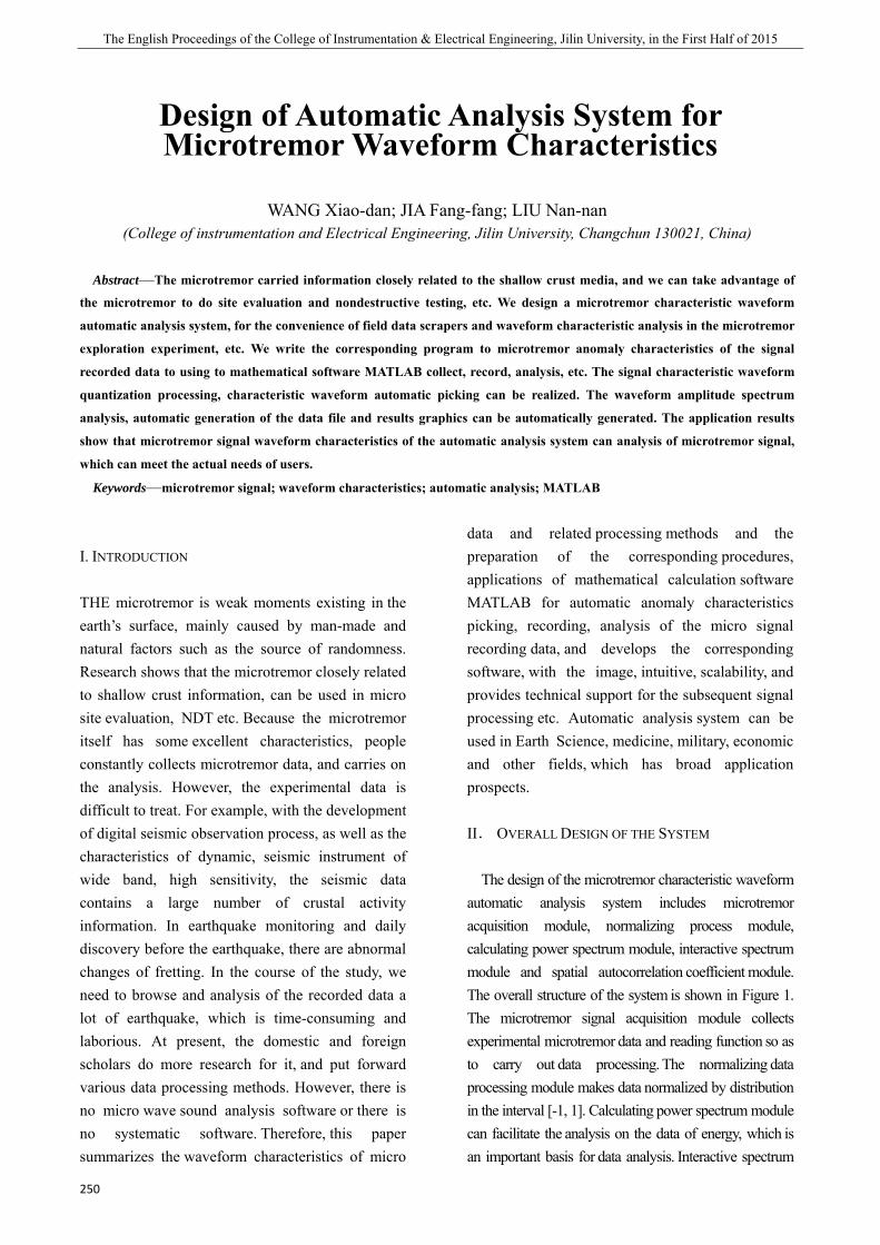
The English Proceedings of the College of Instrumentation & Electrical Engineering, Jilin University, in the First Half of 2015
250
WANG Xiao-dan; JIA Fang-fang; LIU Nan-nan
(College of instrumentation and Electrical Engineering, Jilin University, Changchun 130021, China)
Abstract—The microtremor carried information closely related to the shallow crust media, and we can take advantage of
the microtremor to do site evaluation and nondestructive testing, etc. We design a microtremor characteristic waveform
automatic analysis system, for the convenience of field data scrapers and waveform characteristic analysis in the microtremor
exploration experiment, etc. We write the corresponding program to microtremor anomaly characteristics of the signal
recorded data to using to mathematical software MATLAB collect, record, analysis, etc. The signal characteristic waveform
quantization processing, characteristic waveform automatic picking can be realized. The waveform amplitude spectrum
analysis, automatic generation of the data file and results graphics can be automatically generated. The application results
show that microtremor signal waveform characteristics of the automatic analysis system can analysis of microtremor signal,
which can meet the actual needs of users.
Keywords—microtremor signal; waveform characteristics; automatic analysis; MATLAB
I. INTRODUCTION
THE microtremor is weak moments existing in the earth’s surface, mainly caused by man-made and natural factors such as the source of randomness. Research shows that the microtremor closely related to shallow crust information, can be used in micro site evaluation, NDT etc. Because the microtremor itself has some excellent characteristics, people constantly collects microtremor data, and carries on the analysis. However, the experimental data is difficult to treat. For example, with the development of digital seismic observation process, as well as the characteristics of dynamic, seismic instrument of wide band, high sensitivity, the seismic data contains a large number of crustal activity information. In earthquake monitoring and daily discovery before the earthquake, there are abnormal changes of fretting. In the course of the study, we need to browse and analysis of the recorded data a lot of earthquake, which is time-consuming and laborious. At present, the domestic and foreign scholars do more research for it, and put forward various data processing methods. However, there is no micro wave sound analysis software or there is no systematic software. Therefore, this paper summarizes the waveform characteristics of micro
data and related processing methods and the preparation of the corresponding procedures, applications of mathematical calculation software MATLAB for automatic anomaly characteristics picking, recording, analysis of the micro signal recording data, and develops the corresponding software, with the image, intuitive, scalability, and provides technical support for the subsequent signal processing etc. Automatic analysis system can be used in Earth Science, medicine, military, economic and other fields, which has broad application prospects.
II. OVERALL DESIGN OF THE SYSTEM
The design of the microtremor characteristic waveform automatic analysis system includes microtremor acquisition module, normalizing process module, calculating power spectrum module, interactive spectrum module and spatial autocorrelation coefficient module. The overall structure of the system is shown in Figure 1. The microtremor signal acquisition module collects experimental microtremor data and reading function so as to carry out data processing. The normalizing data processing module makes data normalized by distribution in the interval [-1, 1]. Calculating power spectrum module can facilitate the analysis on the data of energy, which is an important basis for data analysis. Interactive spectrum
Design of Automatic Analysis System for Microtremor Waveform Characteristics
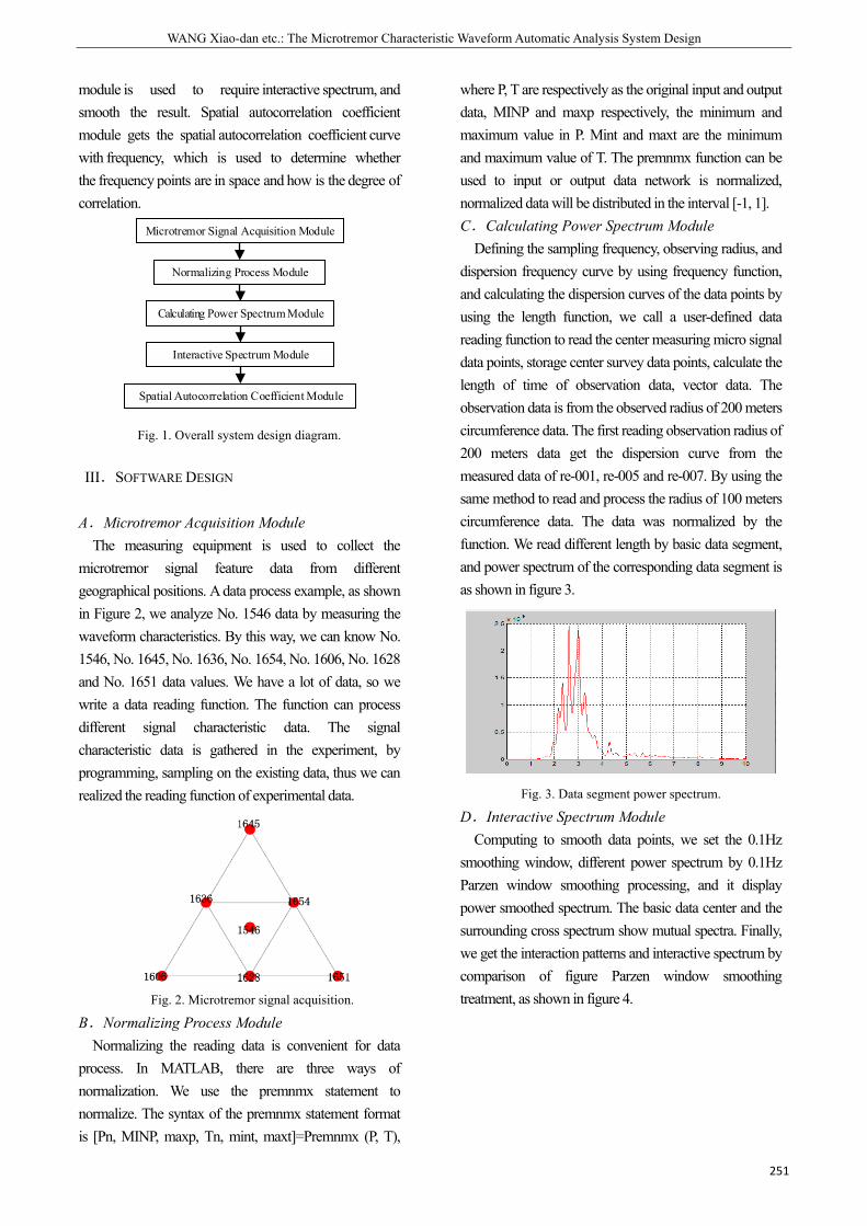
WANG Xiao-dan etc.: The Microtremor Characteristic Waveform Automatic Analysis System Design
251
module is used to require interactive spectrum, and smooth the result. Spatial autocorrelation coefficient module gets the spatial autocorrelation coefficient curve with frequency, which is used to determine whether the frequency points are in space and how is the degree of correlation.
Microtremor Signal Acquisition Module
Normalizing Process Module
Calculating Power Spectrum Module
Interactive Spectrum Module
Spatial Autocorrelation Coefficient Module
Fig. 1. Overall system design diagram.
III.SOFTWARE DESIGN
A.Microtremor Acquisition Module The measuring equipment is used to collect the
microtremor signal feature data from different geographical positions. A data process example, as shown in Figure 2, we analyze No. 1546 data by measuring the waveform characteristics. By this way, we can know No. 1546, No. 1645, No. 1636, No. 1654, No. 1606, No. 1628 and No. 1651 data values. We have a lot of data, so we write a data reading function. The function can process different signal characteristic data. The signal characteristic data is gathered in the experiment, by programming, sampling on the existing data, thus we can realized the reading function of experimental data.
Fig. 2. Microtremor signal acquisition.
B.Normalizing Process Module Normalizing the reading data is convenient for data
process. In MATLAB, there are three ways of normalization. We use the premnmx statement to normalize. The syntax of the premnmx statement format is [Pn, MINP, maxp, Tn, mint, maxt]=Premnmx (P, T),
where P, T are respectively as the original input and output data, MINP and maxp respectively, the minimum and maximum value in P. Mint and maxt are the minimum and maximum value of T. The premnmx function can be used to input or output data network is normalized, normalized data will be distributed in the interval [-1, 1]. C.Calculating Power Spectrum Module
Defining the sampling frequency, observing radius, and dispersion frequency curve by using frequency function, and calculating the dispersion curves of the data points by using the length function, we call a user-defined data reading function to read the center measuring micro signal data points, storage center survey data points, calculate the length of time of observation data, vector data. The observation data is from the observed radius of 200 meters circumference data. The first reading observation radius of 200 meters data get the dispersion curve from the measured data of re-001, re-005 and re-007. By using the same method to read and process the radius of 100 meters circumference data. The data was normalized by the function. We read different length by basic data segment, and power spectrum of the corresponding data segment is as shown in figure 3.
Fig. 3. Data segment power spectrum.
D.Interactive Spectrum Module Computing to smooth data points, we set the 0.1Hz
smoothing window, different power spectrum by 0.1Hz Parzen window smoothing processing, and it display power smoothed spectrum. The basic data center and the surrounding cross spectrum show mutual spectra. Finally, we get the interaction patterns and interactive spectrum by comparison of figure Parzen window smoothing treatment, as shown in figure 4.
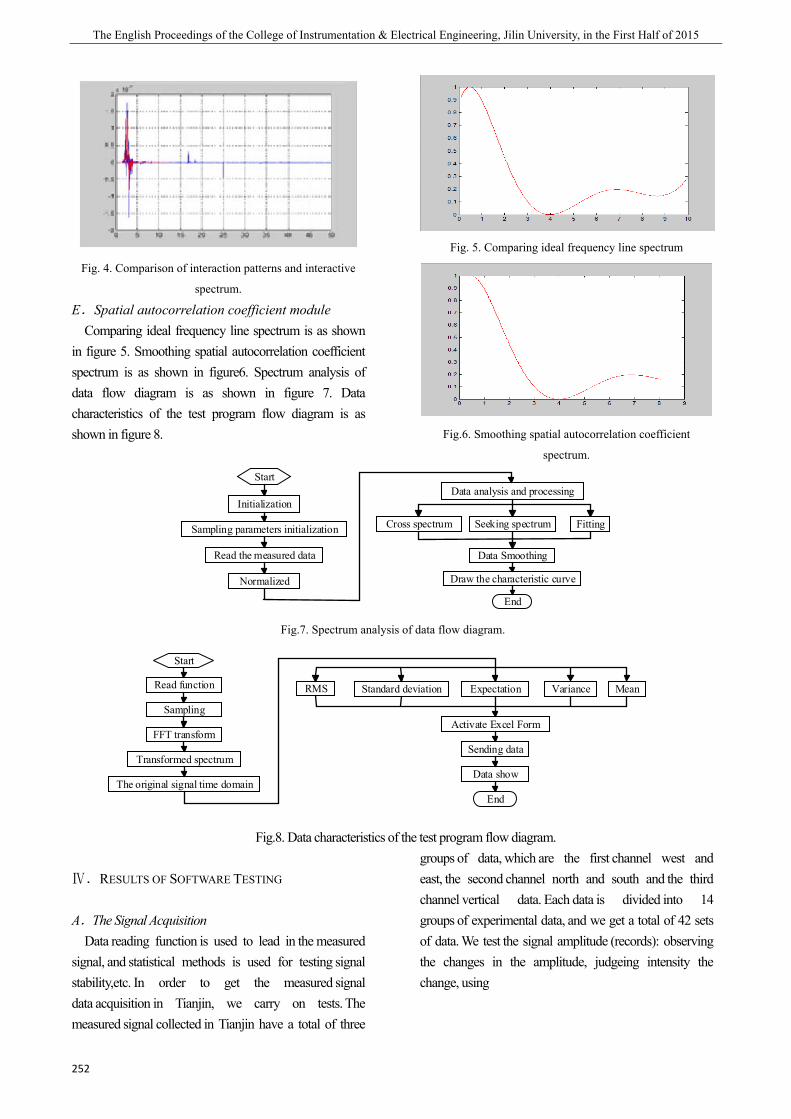
The English Proceedings of the College of Instrumentation & Electrical Engineering, Jilin University, in the First Half of 2015
252
Fig. 4. Comparison of interaction patterns and interactive
spectrum.
E.Spatial autocorrelation coefficient module Comparing ideal frequency line spectrum is as shown
in figure 5. Smoothing spatial autocorrelation coefficient spectrum is as shown in figure6. Spectrum analysis of data flow diagram is as shown in figure 7. Data characteristics of the test program flow diagram is as shown in figure 8.
Fig. 5. Comparing ideal frequency line spectrum
Fig.6. Smoothing spatial autocorrelation coefficient
spectrum.
Fig.7. Spectrum analysis of data flow diagram.
Read function
Sampling
Transformed spectrum
FFT transform
The original signal time domain
Standard deviation
Activate Excel Form
Sending data
Variance
Start
End
RMS MeanExpectation
Data show
Fig.8. Data characteristics of the test program flow diagram.
Ⅳ.RESULTS OF SOFTWARE TESTING
A.The Signal Acquisition Data reading function is used to lead in the measured
signal, and statistical methods is used for testing signal stability,etc. In order to get the measured signal data acquisition in Tianjin, we carry on tests. The measured signal collected in Tianjin have a total of three
groups of data, which are the first channel west and east, the second channel north and south and the third channel vertical data. Each data is divided into 14 groups of experimental data, and we get a total of 42 sets of data. We test the signal amplitude (records): observing the changes in the amplitude, judgeing intensity the change, using
Start
Initialization
Sampling parameters initialization
Normalized
Read the measured data
Data analysis and processing
Seeking spectrum
Data Smoothing
Draw the characteristic curve
End
Cross spectrum Fitting

WANG Xiao-dan etc.: The Microtremor Characteristic Waveform Automatic Analysis System Design
253
(1)
to the conversion formula, in which is
voltage sampling value, is obtained after
the voltage conversion value, the longitudinal coordinate conversion to the micron order by the formula.
By data acquisition module calls in fretting test signal getting from the field experiment. With the formula (1) for transformation of amplitude, the measured signal recording of measuring points are as shown in figure 9.
Fig.9.The measured signal recording of measuring points.
B.The numerical results The 20ms sampling interval, were measured on 42
sets of data sampling in Tianjin. This paper respectively measured in Tianjin to get three groups of data in the first channel west and east, second channel north and south and third channel vertical data. The root mean square value, standard deviation, variance, the expected value and mean value of the measured data are compared in table 1.We can judge non-stationary from the data comparison.
TABLE I
THE DATA CHARACTERISTIC CURVE
RMS Standard
deviation Variance Expectation Mean
Group 1
6000.07033087
252 6000.0753169578
5 36000903.8091
6698 -0.40958333 -0.40958333
First channel
West and East Group 2
3600.86028158
133 3600.8632785328
8 12966216.3506
8663 0.97030666666
6667 0.97030666666
6667 Group 3
13441.8969053
222 13441.908071895
9 180684892.613
301 0.97030666666
6667 0.97030666666
6667 Group 1
5996.111946133
09 5996.1169088223
9 35953417.9842
658 0.63926333333
3333 0.63926333333
3333 Second Channel
north and south
Group 2 3787.18205560
48 3787.1852115831
8 14342771.8268
343 0.008685 0.008685
Group 3
18365.3246218
043 18365.339904671 337285709.814
1028343 -0.890505 -0.890505
Group1
7298.26778346
376 7298.2738529964
9 53264801.2333
322 -0.42483666667 -0.42483666667
Third channel
vertical Group 2
4270.99465941
756 4270.9982185811
8 18241425.7831
236 0.00495666666
666667 0.00495666666
666667 Group 3
32416.1866803
83 32416.213691501
1 1050810910.09
306 -0.39483 -0.39483
C.The signal spectrum analysis
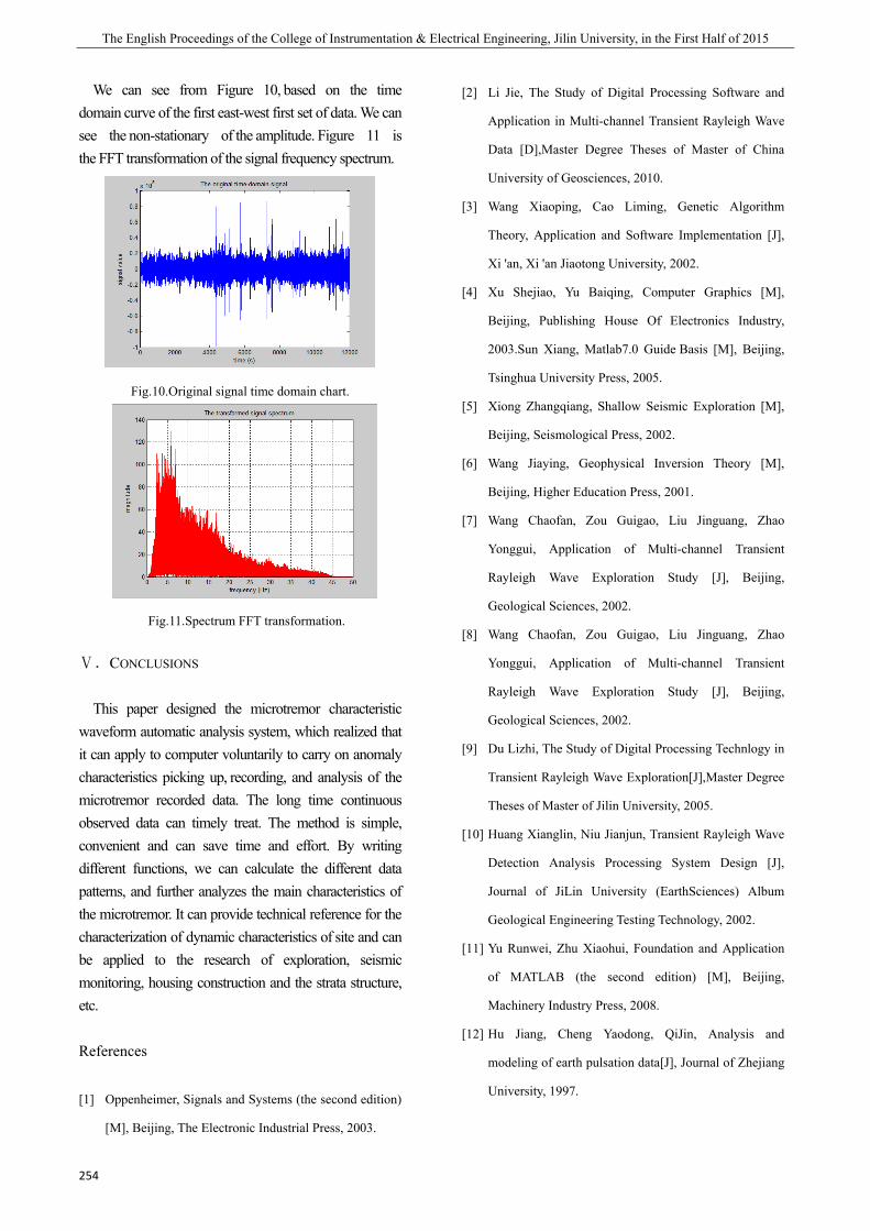
The English Proceedings of the College of Instrumentation & Electrical Engineering, Jilin University, in the First Half of 2015
254
We can see from Figure 10, based on the time domain curve of the first east-west first set of data. We can see the non-stationary of the amplitude. Figure 11 is the FFT transformation of the signal frequency spectrum.
Fig.10.Original signal time domain chart.
Fig.11.Spectrum FFT transformation.
Ⅴ.CONCLUSIONS
This paper designed the microtremor characteristic waveform automatic analysis system, which realized that it can apply to computer voluntarily to carry on anomaly characteristics picking up, recording, and analysis of the microtremor recorded data. The long time continuous observed data can timely treat. The method is simple, convenient and can save time and effort. By writing different functions, we can calculate the different data patterns, and further analyzes the main characteristics of the microtremor. It can provide technical reference for the characterization of dynamic characteristics of site and can be applied to the research of exploration, seismic monitoring, housing construction and the strata structure, etc.
References
[1] Oppenheimer, Signals and Systems (the second edition)
[M], Beijing, The Electronic Industrial Press, 2003.
[2] Li Jie, The Study of Digital Processing Software and
Application in Multi-channel Transient Rayleigh Wave
Data [D],Master Degree Theses of Master of China
University of Geosciences, 2010.
[3] Wang Xiaoping, Cao Liming, Genetic Algorithm
Theory, Application and Software Implementation [J],
Xi 'an, Xi 'an Jiaotong University, 2002.
[4] Xu Shejiao, Yu Baiqing, Computer Graphics [M],
Beijing, Publishing House Of Electronics Industry,
2003.Sun Xiang, Matlab7.0 Guide Basis [M], Beijing,
Tsinghua University Press, 2005.
[5] Xiong Zhangqiang, Shallow Seismic Exploration [M],
Beijing, Seismological Press, 2002.
[6] Wang Jiaying, Geophysical Inversion Theory [M],
Beijing, Higher Education Press, 2001.
[7] Wang Chaofan, Zou Guigao, Liu Jinguang, Zhao
Yonggui, Application of Multi-channel Transient
Rayleigh Wave Exploration Study [J], Beijing,
Geological Sciences, 2002.
[8] Wang Chaofan, Zou Guigao, Liu Jinguang, Zhao
Yonggui, Application of Multi-channel Transient
Rayleigh Wave Exploration Study [J], Beijing,
Geological Sciences, 2002.
[9] Du Lizhi, The Study of Digital Processing Technlogy in
Transient Rayleigh Wave Exploration[J],Master Degree
Theses of Master of Jilin University, 2005.
[10] Huang Xianglin, Niu Jianjun, Transient Rayleigh Wave
Detection Analysis Processing System Design [J],
Journal of JiLin University (EarthSciences) Album
Geological Engineering Testing Technology, 2002.
[11] Yu Runwei, Zhu Xiaohui, Foundation and Application
of MATLAB (the second edition) [M], Beijing,
Machinery Industry Press, 2008.
[12] Hu Jiang, Cheng Yaodong, QiJin, Analysis and
modeling of earth pulsation data[J], Journal of Zhejiang
University, 1997.
SONG Ji-bin etc.: Research of the protable multi-index oil quality analysis instrument
255
Research of the portable multi-index oil quality analysis instrument
SONG Ji-bin, WANG Tian-zi, and QIN Jia-nan
(jilin university instrument science and engineering institute,changchun,130021)
Abstract—In recent years, the production and extensive use of “gutter oil”,mainly in restaurants,caused great harm to the
health of consumers. Thus,developing and designing a portable, civilian oil quality analysis equipment is of great
importance.Detecting gutter oil based on the dielectric constant and the shading degree of cooling oil, can achieve higher
accuracy .Then using near-infrared spectrometer to verify the experimental results ,which proves that the system can
distinguish between a variety of edible oils and fats are inferior with pretty high accuracy.
Key words—oil quality; waste oil; portable;oil analysis; dielectric constant; shading degree
I. PREFACE
ACCORDING to Nutrition And Health Survey Of China Residents issued by the ministry of health, urban residents consume as high as 85.5 grams of fat per day, and more than half of that is consumed through cooking oil.However, police have dismantled several nationwide illegal cooking oil ring,which confirms the rumors that many restaurants in China use gutter oil to cook food, which exerts a serious threat to the health of consumers.
At present, the common methods to detect gutter oil include instrument analysis methods[2] ,such as near infrared spectrum, gas chromatography and liquid chromatography ; physical and chemical indexes analysis methods such as density, viscosity, water content [3] , refractive index[4], saponification value, optical activity and peroxide value [5] ; aspergillus flavus detection[6],as well as other specific gene detection method [7]. Lots of companies and organizations are also try to detect waste oil.Shanghai Key Laboratory Of Modern Optical System developed a terahertz technology to identify the gutter oil , which determine the ingredients contained within the fat by detecting resonance absorption of the oil[8], but the price is pretty expensive.STD-XG grain and oil quality detector developed by Xiamen Stan Scientific Instrument Co., Ltd tests the acid valence which is a traditional method, can get strong characteristic information (such as fatty acid content),but it is time-consuming and more complicated.
In summary,using instruments to analysis the oil may achieve higher accuracy ,but it’s complex, time-consuming and difficult,and it’s not suitable for general public using in their daily life.While considering the complex composition of gutter oil, using the traditional physical and chemical index analysis method to generate a single criterion for the identification of gutter oil is unconvincing. Therefore, we design a portable multi-index oil quality analysis instrument ,which measuring the dielectric constant and the shading degree of oil under different temperature to analyze product quality.In the PC software, we establish the BP neural network forecasting model for the determination of waste oil. Experiments show that it is a portable, low cost, high accuracy instrument.
II.TEST METHOD AND TEST PLAN
System is divided into two modules: Data acquisition module, as well as PC data processing and analysis module. Data acquisition module collects dielectric constant values of different oil as well as shading degree of oil under different temperatures.Then PC data processing and analysis module processes the raw data and extract feature information, which is imported into BP neural network afterwords to establish classification prediction model. When the model is finished,we can input the dielectric constant and shading information of a sample to the model and it could output the probability that the sample belongs to several type of oil, respectively .To further verify
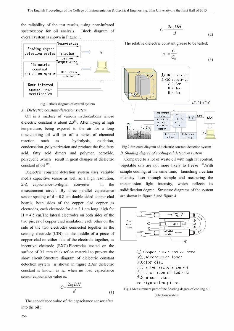
The English Proceedings of the College of Instrumentation & Electrical Engineering, Jilin University, in the First Half of 2015
256
the reliability of the test results, using near-infrared spectroscopy for oil analysis. Block diagram of overall system is shown in Figure 1.
Fig1. Block diagram of overall system
A.. Dielectric constant detection system Oil is a mixture of various hydrocarbons whose
dielectric constant is about 2.3[9]. After frying at high temperature, being exposed to the air for a long time,cooking oil will set off a series of chemical reaction such as hydrolysis, oxidation, condensation ,polymerization and produce the free fatty acid, fatty acid dimers and polymer, peroxide, polycyclic ,which result in great changes of dielectric constant of oil[10].
Dielectric constant detection system uses variable media capacitive sensor as well as a high resolution, Σ-Δ capacitance-to-digital converter in the measurement circuit .By three parallel capacitance sensor spacing of d = 0.8 cm double-sided copper-clad boards, both sides of the copper clad copper as electrodes, each electrode for d = 2.1 cm long, high for H = 4.5 cm.The lateral electrodes on both sides of the two pieces of copper clad insulation, each other on the side of the two electrodes connected together as the sensing electrode (CIN), in the middle of a piece of copper clad on either side of the electrode together, as incentive electrode (EXC).Electrodes coated on the surface of 0.1 mm thick teflon material to prevent the short circuit.Structure diagram of dielectric constant detection system is shown in figure 2.Air dielectric constant is known as ε0, when no load capacitance sensor capacitance value is:
02= DHCd
e
(1)
The capacitance value of the capacitance sensor after into the oil :
2= r DHCd
e (2)
The relative dielectric constant grease to be tested:
0r
CC
e = (3)
CI 2
Fig.2 Structure diagram of dielectric constant detection system B. Shading degree of cooling oil detection system Compared to a lot of waste oil with high fat content, vegetable oils are not more likely to freeze [11].With sample cooling, at the same time, launching a certain intensity laser through sample and measuring the transmission light intensity, which reflects its solidification degree . Structure diagrams of the system are shown in figure 3 and figure 4.
Fig.3 Measurement part of the Shading degree of cooling oil
detection system
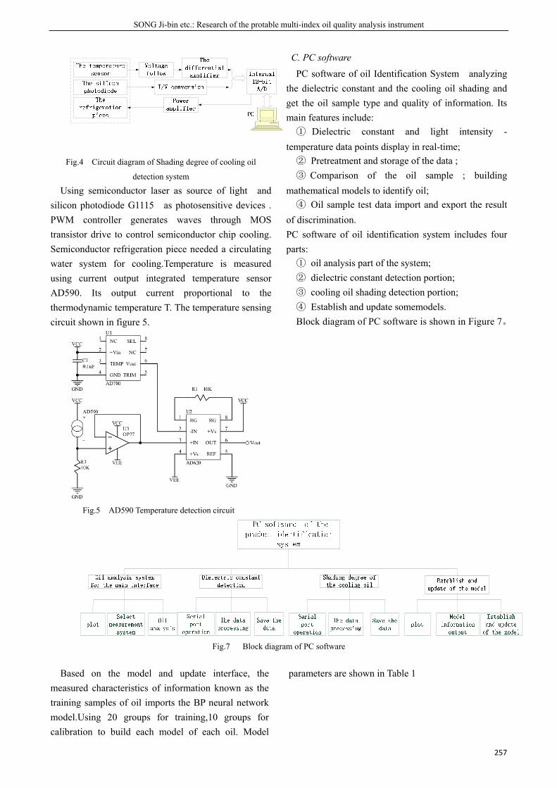
SONG Ji-bin etc.: Research of the protable multi-index oil quality analysis instrument
257
Fig.4 Circuit diagram of Shading degree of cooling oil
detection system
Using semiconductor laser as source of light and silicon photodiode G1115 as photosensitive devices . PWM controller generates waves through MOS transistor drive to control semiconductor chip cooling. Semiconductor refrigeration piece needed a circulating water system for cooling.Temperature is measured using current output integrated temperature sensor AD590. Its output current proportional to the thermodynamic temperature T. The temperature sensing circuit shown in figure 5.
C. PC software
PC software of oil Identification System analyzing the dielectric constant and the cooling oil shading and get the oil sample type and quality of information. Its main features include: ① Dielectric constant and light intensity -
temperature data points display in real-time; ② Pretreatment and storage of the data ; ③ Comparison of the oil sample ; building mathematical models to identify oil; ④ Oil sample test data import and export the result of discrimination. PC software of oil identification system includes four parts: ① oil analysis part of the system; ② dielectric constant detection portion; ③ cooling oil shading detection portion; ④ Establish and update somemodels.
Block diagram of PC software is shown in Figure 7。
Fig.5 AD590 Temperature detection circuit
Fig.7 Block diagram of PC software
Based on the model and update interface, the
measured characteristics of information known as the training samples of oil imports the BP neural network model.Using 20 groups for training,10 groups for calibration to build each model of each oil. Model
parameters are shown in Table 1
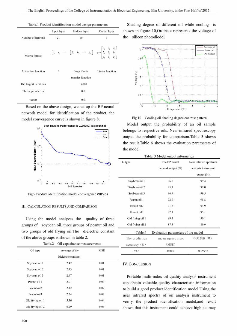
The English Proceedings of the College of Instrumentation & Electrical Engineering, Jilin University, in the First Half of 2015
258
Table.1 Product identification model design parameters
Input layer Hidden layer Output layer
Number of neurons 21 10 3
Matrix format 1 2x x⎡⎣
1 2 nh h h⎡ ⎤⎣ ⎦
1 2 3
1 2 3
1 2 3
ya a ab b bc c c
⎡ ⎤⎢ ⎥= ⎢ ⎥⎢ ⎥⎣ ⎦
Activation function / Logarithmic
transfer function
Linear function
The largest iterations 4000
The target of error 0.01
vector 0.01
Based on the above design, we set up the BP neural network model for identification of the product, the model convergence curve is shown in figure 8.
Fig.9 Product identification model convergence curves
III. CALCULATION RESULTS AND COMPARISON
Using the model analyzes the quality of three groups of soybean oil, three groups of peanut oil and two groups of old frying oil.The dielectric constant of the above groups is shown in table 2.
Table.2 Oil capacitance measurements Oil type Average of the
Dielectric constant
MSE
Soybean oil 1 2.42 0.01
Soybean oil 2 2.43 0.01
Soybean oil 3 2.47 0.01
Peanut oil 1 2.01 0.03
Peanut oil2 2.12 0.02
Peanut oil3 2.24 0.02
Old frying oil 1 5.36 0.04
Old frying oil 2 6.29 0.06
Shading degree of different oil while cooling is shown in figure 10,Ordinate represents the voltage of the silicon photodiode .
Soybean oilPeanut oil
Old frying oil
Temperature/()
Vol
tage
/(V
)
Fig.10 Cooling oil shading degree contrast pattern
Model output the probability of an oil sample belongs to respective oils. Near-infrared spectroscopy output the probability for comparison.Table 3 shows the result.Table 6 shows the evaluation parameters of the model.
Table. 3 Model output information Oil type The BP neural
network output (%)
Near infrared spectrum
analysis instrument
output (%)
Soybean oil 1 96.0 99.4
Soybean oil 2 95.1 99.0
Soybean oil 3 96.9 99.5
Peanut oil 1 92.9 95.8
Peanut oil2 91.3 94.9
Peanut oil3 92.1 95.1
Old frying oil 1 89.4 90.1
Old frying oil 2 87.3 89.9
Table.4 Evaluation parameters of the model The prediction
accuracy(%)
mean square error
(MSE)
相关系数(R)
93.3 0.015 0.09942
IV. CONCLUSION
Portable multi-index oil quality analysis instrument can obtain valuable quality characteristic information to build a good product identification model.Using the near infrared spectra of oil analysis instrument to verify the product identification model,and result shows that this instrument could achieve high acuracy

SONG Ji-bin etc.: Research of the protable multi-index oil quality analysis instrument
259
and can replace traditional single index analysis method whichl has practical guiding significance to the quality control of the cooking oil.
References
[1] YU Qing-yu , HE Ruo-ying. The Harm Of Cooking Oil To
Human Body Health[J]. Grain And Oil Food Science And
Technology.2011(04)
[2] Zhaoqing city, guangdong province,The Quality
Measurement Supervision and Inspection .Cooking oil rapid
detection method discussed in this paper.2012(20)
[3] JIAO Yun-peng . The Research Progress Of Cooking Oil
To Identify And Test[J].Modern Food Science And
Technology,2008,(04)
[4] WANG Le , LIU Yao-gang , CHEN Feng-fei, HUJian-hua.
Research Of Gutter Oil Pollution And Deterioration.Journal
Of Wu Han Institute Of Industrial.2007:1-4
[5] LIU Bo,YANG Jian-guo,ZHANG Xue-mei. The Research
Progress Of Cooking Oil Detection Index.Career And
Health.2011.1167-1169
[6] YANG Yong-chun,YANG Dong-yan,LI Hao,ZHANG
Qian,WU Shuang,DENG Ping-jian. Real-time Fluorescent
PCR Detection Of Gene Identification Of Animal Origin
Used Cooking Oil[j].2013,(18)
[7] Gutter Oil Rapid Tester Based On The THZ
Technology [J].China Metrology.2013,(01)
[8] Multi-parameter fast food safety
detector[EB/OL].http://www.foodjx.com/st86674/Product_1
000682.html; 2014/9/5
[9] Deng Zhi-yin.Fast Detection Techniques Of The Oil And
The Experiment Research Based On The Raman
Spectra[D].2014
[10] DENG Peng,CHENG Yong-qiang,XUE Wen-tong.Oil
oxidation and oxidation stability determination method.
Food Science,2005,(26)
[11] XU Xiu-li,LI Na,REN He-ling,ZHANG Feng-xia,MA
Xiao-ning,ZHONG Wei-ke.Gas chromatography analysis
to identify gutter oil acid composition [J]. Journal of
inspection and quarantine, 2012, 22 (2)
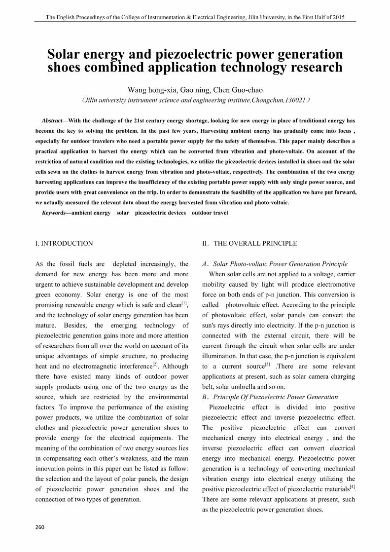
The English Proceedings of the College of Instrumentation & Electrical Engineering, Jilin University, in the First Half of 2015
260
Solar energy and piezoelectric power generation shoes combined application technology research
Wang hong-xia, Gao ning, Chen Guo-chao
(Jilin university instrument science and engineering institute,Changchun,130021)
Abstract—With the challenge of the 21st century energy shortage, looking for new energy in place of traditional energy has
become the key to solving the problem. In the past few years, Harvesting ambient energy has gradually come into focus ,
especially for outdoor travelers who need a portable power supply for the safety of themselves. This paper mainly describes a
practical application to harvest the energy which can be converted from vibration and photo-voltaic. On account of the
restriction of natural condition and the existing technologies, we utilize the piezoelectric devices installed in shoes and the solar
cells sewn on the clothes to harvest energy from vibration and photo-voltaic, respectively. The combination of the two energy
harvesting applications can improve the insufficiency of the existing portable power supply with only single power source, and
provide users with great convenience on the trip. In order to demonstrate the feasibility of the application we have put forward,
we actually measured the relevant data about the energy harvested from vibration and photo-voltaic.
Keywords—ambient energy solar piezoelectric devices outdoor travel
I. INTRODUCTION
AS the fossil fuels are depleted increasingly, the demand for new energy has been more and more urgent to achieve sustainable development and develop green economy. Solar energy is one of the most promising renewable energy which is safe and clean[1], and the technology of solar energy generation has been mature. Besides, the emerging technology of piezoelectric generation gains more and more attention of researchers from all over the world on account of its unique advantages of simple structure, no producing heat and no electromagnetic interference[2]. Although there have existed many kinds of outdoor power supply products using one of the two energy as the source, which are restricted by the environmental factors. To improve the performance of the existing power products, we utilize the combination of solar clothes and piezoelectric power generation shoes to provide energy for the electrical equipments. The meaning of the combination of two energy sources lies in compensating each other’s weakness, and the main innovation points in this paper can be listed as follow: the selection and the layout of polar panels, the design of piezoelectric power generation shoes and the connection of two types of generation.
II.THE OVERALL PRINCIPLE
A.Solar Photo-voltaic Power Generation Principle When solar cells are not applied to a voltage, carrier
mobility caused by light will produce electromotive force on both ends of p-n junction. This conversion is called photovoltaic effect. According to the principle of photovoltaic effect, solar panels can convert the sun's rays directly into electricity. If the p-n junction is connected with the external circuit, there will be current through the circuit when solar cells are under illumination. In that case, the p-n junction is equivalent to a current source[3] .There are some relevant applications at present, such as solar camera charging belt, solar umbrella and so on. B.Principle Of Piezoelectric Power Generation
Piezoelectric effect is divided into positive piezoelectric effect and inverse piezoelectric effect. The positive piezoelectric effect can convert mechanical energy into electrical energy , and the inverse piezoelectric effect can convert electrical energy into mechanical energy. Piezoelectric power generation is a technology of converting mechanical vibration energy into electrical energy utilizing the positive piezoelectric effect of piezoelectric materials[4]. There are some relevant applications at present, such as the piezoelectric power generation shoes.
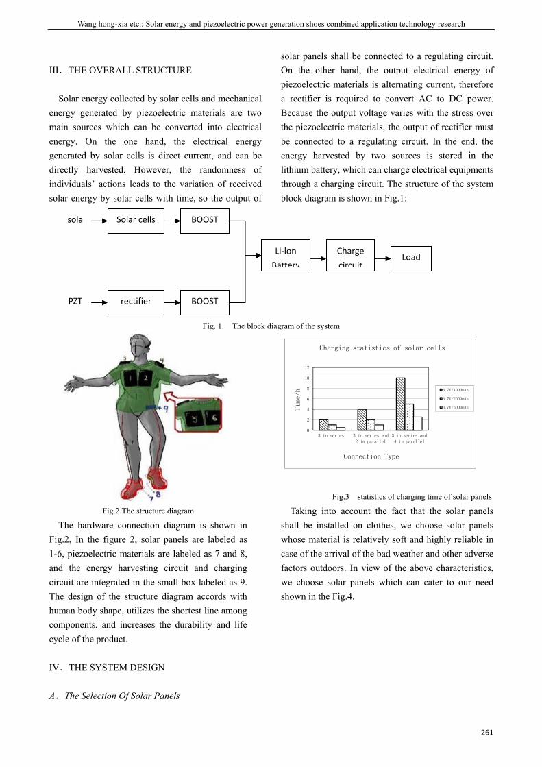
Wang hong-xia etc.: Solar energy and piezoelectric power generation shoes combined application technology research
261
III.THE OVERALL STRUCTURE
Solar energy collected by solar cells and mechanical energy generated by piezoelectric materials are two main sources which can be converted into electrical energy. On the one hand, the electrical energy generated by solar cells is direct current, and can be directly harvested. However, the randomness of individuals’ actions leads to the variation of received solar energy by solar cells with time, so the output of
solar panels shall be connected to a regulating circuit. On the other hand, the output electrical energy of piezoelectric materials is alternating current, therefore a rectifier is required to convert AC to DC power. Because the output voltage varies with the stress over the piezoelectric materials, the output of rectifier must be connected to a regulating circuit. In the end, the energy harvested by two sources is stored in the lithium battery, which can charge electrical equipments through a charging circuit. The structure of the system block diagram is shown in Fig.1:
Fig. 1. The block diagram of the system
Fig.2 The structure diagram
The hardware connection diagram is shown in Fig.2, In the figure 2, solar panels are labeled as 1-6, piezoelectric materials are labeled as 7 and 8, and the energy harvesting circuit and charging circuit are integrated in the small box labeled as 9. The design of the structure diagram accords with human body shape, utilizes the shortest line among components, and increases the durability and life cycle of the product.
IV.THE SYSTEM DESIGN
A.The Selection Of Solar Panels
0
2
4
6
8
10
12
3 in series 3 in series and
2 in parallel
3 in series and
4 in parallel
Time
/h
Connection Type
Charging statistics of solar cells
3.7V/1000mAh
3.7V/2000mAh
3.7V/5000mAh
Fig.3 statistics of charging time of solar panels Taking into account the fact that the solar panels
shall be installed on clothes, we choose solar panels whose material is relatively soft and highly reliable in case of the arrival of the bad weather and other adverse factors outdoors. In view of the above characteristics, we choose solar panels which can cater to our need shown in the Fig.4.
Solar cells BOOST
rectifier BOOST
sola
PZT
Li-lon Battery
Charge circuit
Load
The English Proceedings of the College of Instrumentation & Electrical Engineering, Jilin University, in the First Half of 2015
262
Fig.4 physical map of solar panel
The output power of solar cell is 1W, the measured data in the summer noon are as follows: the voltage of solar panel is 2 V(1.96 V to 2.06 V) , and the range of current is 550 mA- 650mA. As for the energy storing battery, we choose the li-lon battery for the purpose of economy and portability by contrast with lead accumulator which has high capacity but also large in volume. The popularity of li-lon battery has spread swiftly in recent years, especially for the use of mobile phone. The capacity of mobile phone battery on the market is commonly range from 600 to 1600 mAh, and the parameters of our solar panel can meet the requirements of the practical application. To store the electrical energy into the li-lon battery, the output voltage and current of solar panels must reach the condition of charging. So we use the parallel of two series of three solar panels to meet our need, which performs well in 1000 mAh, 2000 mAh, and 5000 mAh li-lon batteries from the Fig.3. B.The Layout of Solar Panels
From the discussion above , we have come to the conclusion that the parallel of two series of three solar panels can cater to our demands. However, the randomness of individuals’ actions will lead to the problem that all the solar panels installed in clothes can not receive enough solar energy at the same time, so it is of great necessity to design the layout of solar panels on clothes properly. The solar panels on chest and on shoulder will receive enough solar energy while the solar panels on the back can hardly receive solar energy when a person in solar clothes faces the sun, and the solar energy receiving situation is just the opposite when the person turn his back to the sun.
Considering the two situations, we decide to take solar panels labeled as 1、3、5 and solar panels labeled as 2、4、6 in Fig.2 in series,respectively, and then connect two series branches in parallel. The advantage of this design can compensate the limitation of solar panels installed on chest and on back , and provide the storage circuit with enough voltage and current. C.The Installation Design of Solar Panels
Given the convenience of installation of solar panels, we utilize the magic tape to install solar panels on clothes which can be removed anytime in case that there is something wrong with some of solar panels on clothes. The circuit connection will be achieved by the way as follows: Put some conducting material fixed on both the edge of the cathode of solar panels and in the center of cathode of solar panels separately, and connect the cathode and the anode of solar panels with the marginal and central areas, respectively. The magic tape is fixed on the remaining area, and make the areas which are connected to solar panels have the same structure in order to install solar panels on clothes and achieve the circuit connection. D.Booster Circuit
In order to reach the minimum voltage that the storage circuit requires, we need to find a proper booster circuit to step up the output voltage of two sources. But the energy from piezoelectric materials is very little, so we want to find a way to solve the problem. In the beginning, we decide to choose the triple voltage rectification shown in Fig.4 to achieve our requirements, but we finally failed to obtain an ideal output. By analyzing, we drew the conclusion that the quantity of capacities leads to the lost of energy during the transmission of electrical energy. To decrease the energy lost , we utilize the combination of rectifier shown in Fig.5 and the booster circuit shown in Fig.6, which achieve our demands in the end.
Fig.4 triple voltage rectification
Wang hong-xia etc.: Solar energy and piezoelectric power generation shoes combined application technology research
263
Fig.5 schematic circuit of rectifier
Fig.6 schematic circuit of boost chopper
E.The Structure Design of power shoes The power shoes is mainly based on the application
of PZT, therefore we need to find a best position in shoes to place PZT on. In view of the fact that the bending degree of the back section of shoes is largest, we fix the some PZT in parallel on the back section of shoes to harvest the mechanical energy as much as possible. The instant energy from piezoelectric materials is so little that we install a small box in which there is a energy harvesting circuit to accumulate the little electrical energy generated by power shoes. When the collected energy is large enough, we can take part the storage battery to charge electrical equipments. F.The Connection of Solar Clothes and Power Shoes
The initial purpose of our study is to provide electrical energy source for electrical equipments outdoors, especially for the outdoor travelers, so the connection of two energy sources is also very important. At first, we want to connect the outputs of solar clothes and power shoes in parallel to store electrical energy into the storage battery, but the wiring method is too inconvenient. Therefore, harvesting their own energy separately is our plan to achieve our aim. The input of charging circuit can be from either of the
two storage battery.
V.THE MEASURED DATA
A.The Measured Data of Solar Clothes Using the connection of the parallel of two series
branches which is described above, we have measured the actual data of the electric quantity generated from solar cells shown in Fig.7 during three time intervals in a sunny day . From the figure 7, it is easy to figure out that the charging rate between 13:00-14:00 is highest among the three time intervals, and the charging rate between 16:00-17:00 is lowest. So we can draw the conclusion that the charging rate of solar panels is proportional to the illumination intensity.
Statistics of solar battery charging
0
10
20
30
40
50
60
70
5 25 45 65 85 105
Time/min
electric quantity/%
8:00-9:00
13:00-14:00
16:00-17:00
Fig.7 statistics of solar battery charging
B.The Measured Data of Power Shoes Because the energy collected by piezoelectric
materials is so little that the output of power shoes can’t drive a load, we measured the voltage of the storage battery of power shoes to get the measured data of power shoes. The result is shown in Fig.8.
statistics of power shoes
0
2
4
6
8
10
12
14
1 2 3 4 5
time/h
voltage of battery
execise
walking
running
Fig.8 statistics of power shoes
From figure 8, we can conclude that the charging rate of exercising is highest among the three actions, and the charging rate of walking is lowest. Therefore,
The English Proceedings of the College of Instrumentation & Electrical Engineering, Jilin University, in the First Half of 2015
264
the quantity of energy stored in the battery depends on the type of actions.
VI.THE SUMMARY
According to the measured data of both solar clothes and power shoes, we can come to the conclusion that the two power sources can compensate each other’s limitation. When the solar energy is plentiful, solar clothes and power shoes can harvest energy at the same time. The power shoes will accumulate the little energy to charge electrical equipments when there is no enough solar energy. So the application we have studied in this paper can be applied to the outdoor power supply, which can ensure the safety of outdoor travelers by keeping in touch with outside world.
References
[1] Xingfu Xiong , Zhengzhi Yang, “The analysis of the
function of solar photovoltaic application products ”,J, in
Packaging Engineering,2014,35(24):35-38.
[2] Jie Jia, “The research on energy conversion and storage
characteristics of piezoelectric power generation device ”,J,
CNKI,2008.
[3] Hang Ren, Lin Ye, “The research on simulation model
design and output characteristics of solar cells”,J, in
Electronic Automation Equipment, 2009,29(10):112-115.
[4] Jian Wang, Jifeng Guo, Shuai Guo,” The overview of the
technology of piezoelectric power generation ”, in
Piezoelectrics & Acoustooptics, 2011,33(3):294-296.
BAI Yang etc.: Design and Reaearch for Comfort-Control-Algrithm Based on Somatosensory Robotic Arm
265
Design and Research for Comfort-Control-Algorithm Based on
Somatosensory Robotic Arm
BAI Yang, SHI Zhen, WANG Da-ren ( College of Instrumentation and Electrical Engineering,Jilin University,Changchun 130026,China)
Abstract— By analysing the comfort situation of human arm in somatosensory control , based on fatigue theory, we put
forward the somatosensory manipulator comfort control algorithms. Modeling for arm comfort zone , controlling robotic arm
movement in somatosensory way, through the "radial testing laboratories" and "dot point experiment" for the comfort of the
control arm movement parameter setting, we fit control the mapping function,and raise comfort control algorithms. By
grasping motion tracking and remote objects experiment, the relative error of the measured comfort control algorithms in less
than 5%, the absolute error of tip position [the end of mechanical arm] is less than 2mm, improved the comfort of
approximately 51.8% compared with conventional control algorithms , ensured the comfort of the user at the same time
meeting the accuracy ,and improved the efficiency of somatosensory control.
Keywords— comfortable level somatosensory fatigue Robotic-arm comfort-control-algorithms
0 DERECTION
SOMATOSENSORY technology is meaning through body movements without operation of any complex control equipment can be personally on the scene to human-computer interaction technology[1]. Apart from traditional key-press and touching , somatosensory technology greatly enhance the flexibility of operation, and intuition.There are more and more applications[2][3[4][5] in the field of game, mobile application, rehabilitation, virtual learning system and so on.
The somatosensory manipulator control algorithm, for the mapping between the human arm and mechanical arm posture, mainly based on geometric relations for the forward and inverse kinematics which core idea is the linear mapping[6], so that the mechanical arm completely imitate the human-arm. While the human arm structure and mechanical arm are different, physiological structure determines its mechanical joint that have no completely freedom, taking into account the efforts, energy consumption and other factors, the most difficult degree is that arm made different movements are not the same. This process leading to complete a series of actions in the
operation of the mechanical arm of the operator fatigue, low efficiency, can not long time operation[7].
In order to alleviate user’s fatigue, improving the comfort and efficiency of control , considering the influence of human arm comfort and energy consumption and other factors, put forward a mapping relationship between somatosensory manipulator based on comfort control algorithm.
1SYSTEM DESIGN
1.1 Overall design The design of the mechanical arm somatosensory
control system is divided into the overall motion capture module, the manipulator control module, the mechanical arm movements module three parts, as shown in Figure 1.
Signal acquisition
Attitude calculation
Wireless data sand
Servo drive signal
algorithm solution
Wireless data receive
shoulder joint
Elbow joint1
Wrist joints
overall motion
capture module
manipulator
control module
mechanical arm
movements module
Elbow joint2
Elbow joint3
Figure 1 The overall

The English Proceedings of the College of Instrumentation & Electrical Engineering, Jilin University, in the First Half of 2015
266
The attitude information collecting module collects human arm movements, according to the attitude computation and wireless transmission to the main controller, through the comfort control algorithm processing, realizes mapping from the arm posture to a mechanical arm, to make the mechanical arm shoulder, elbow and wrist joint servos to the target point of view, the realization of somatosensory control mechanical arm. 1.2 Design of mechanical arm system
As the time and cost reducing arm structure processing machinery consumption, use Bo steering gear Gen robot kit and assembled parts, built a five degree of freedom rigid mechanical arm, and shoulder arm to people for the origin of the coordinate system of the plane, as shown in figure 2. Analysis of somatosensory attitude used forward and inverse kinematics algorithm, collecting arm angle α, β, calculated mapped to five joints on the right side of the steering angle of the mechanical arm (1 ~ 5), realize the mechanical arm positioning.
Based on the somatosensory technology ,a small,
wearable wireless attitude monitoring module design an integrated gyroscope of MPU6050 module, 24L01 wireless transmitting module and the STM32 single-chip microcomputer in one was designed , through the network communication , the information of attitude, real-time collected after processing transfer back to the main control device. The overall design of the circuit as shown in figure 3.
1.3 Procedure of the algorithm
On the basis of the existing fatigue theory, somatosensory manipulator controlling experiments with, establish space model for the regional arms control people more comfortable. Somatosensory mechanical arm device into a lot of experimental samples, measured the comfort zone of the sample, and the theoretical calculation results comparison, combined with the establishment of comfortable space by the method of mathematics, quasi. Using the measured arm comfort zone as a feedback, make step to improve and optimization algorithm, modified action mapping relationship, the final establishment of comfort control algorithm.
2 THEORETICAL ANALYSIS AND CALCULATION
At present comfortable is a fuzzy concept,quantitative indicators there is no generally accepted, but there are still some researching results can be used for reference. According to theoretical analysis and calculation of quantitative indicators, and then analyzes the comfort conditions. 2.1 Comfort theory
There is a lot of experiments proposed joint maximum torque formula[8]that NASA researchers from the dynamic perspective on human isolated.
2angle c angle*b a torque *++=
Torque for maximum torque, angle for the joint angle, a, b and c respectively for the coefficient of least square regression fitting, based on the speed of rotation and rotation mode (such as the elbow joint stretching or bending) check coefficient table is obtained, as shown in Table 1 and table 2.
figure 3.The system hardware circuit
MCUSTM32F103
Nrf24l01
gate
LCD
Joint servo driveacquisition node 2
acquisition node 1
Mpu6050 Stm32Nrf
24l01
acquisition node 3
Figure 2 human arm model and mechanical arm structure diagram
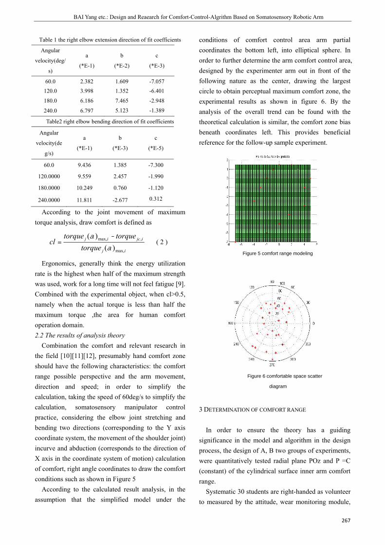
BAI Yang etc.: Design and Reaearch for Comfort-Control-Algrithm Based on Somatosensory Robotic Arm
267
Table 1 the right elbow extension direction of fit coefficients
Angular
velocity(deg/
s)
a
(*E-1)
b
(*E-2)
c
(*E-3)
60.0 2.382 1.609 -7.057 120.0 3.998 1.352 -6.401
180.0 6.186 7.465 -2.948
240.0 6.797 5.123 -1.389
Table2 right elbow bending direction of fit coefficients
Angular
velocity(de
g/s)
a
(*E-1)
b
(*E-3)
c
(*E-5)
60.0 9.436 1.385 -7.300
120.0000 9.559 2.457 -1.990
180.0000 10.249 0.760 -1.120
240.0000 11.811 -2.677 0.312
According to the joint movement of maximum torque analysis, draw comfort is defined as
ij
ijcij
torquetorquetorque
clmax,
,max,
)()(
a
a -=
( 2 )
Ergonomics, generally think the energy utilization rate is the highest when half of the maximum strength was used, work for a long time will not feel fatigue [9]. Combined with the experimental object, when cl>0.5, namely when the actual torque is less than half the maximum torque ,the area for human comfort operation domain. 2.2 The results of analysis theory
Combination the comfort and relevant research in the field [10][11][12], presumably hand comfort zone should have the following characteristics: the comfort range possible perspective and the arm movement, direction and speed; in order to simplify the calculation, taking the speed of 60deg/s to simplify the calculation, somatosensory manipulator control practice, considering the elbow joint stretching and bending two directions (corresponding to the Y axis coordinate system, the movement of the shoulder joint) incurve and abduction (corresponds to the direction of X axis in the coordinate system of motion) calculation of comfort, right angle coordinates to draw the comfort conditions such as shown in Figure 5
According to the calculated result analysis, in the assumption that the simplified model under the
conditions of comfort control area arm partial coordinates the bottom left, into elliptical sphere. In order to further determine the arm comfort control area, designed by the experimenter arm out in front of the following nature as the center, drawing the largest circle to obtain perceptual maximum comfort zone, the experimental results as shown in figure 6. By the analysis of the overall trend can be found with the theoretical calculation is similar, the comfort zone bias beneath coordinates left. This provides beneficial reference for the follow-up sample experiment.
3 DETERMINATION OF COMFORT RANGE
In order to ensure the theory has a guiding significance in the model and algorithm in the design process, the design of A, B two groups of experiments, were quantitatively tested radial plane POz and P =C (constant) of the cylindrical surface inner arm comfort range.
Systematic 30 students are right-handed as volunteer to measured by the attitude, wear monitoring module,
Figure 6 comfortable space scatter
diagram
Figure 5 comfort range modeling
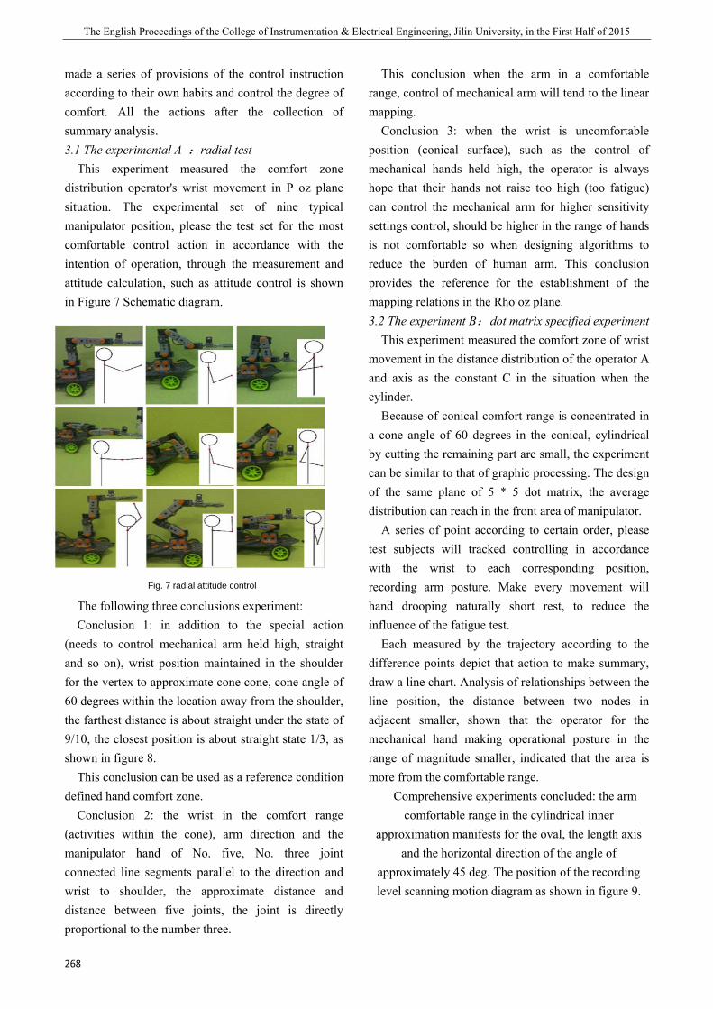
The English Proceedings of the College of Instrumentation & Electrical Engineering, Jilin University, in the First Half of 2015
268
made a series of provisions of the control instruction according to their own habits and control the degree of comfort. All the actions after the collection of summary analysis. 3.1 The experimental A :radial test
This experiment measured the comfort zone distribution operator's wrist movement in P oz plane situation. The experimental set of nine typical manipulator position, please the test set for the most comfortable control action in accordance with the intention of operation, through the measurement and attitude calculation, such as attitude control is shown in Figure 7 Schematic diagram.
The following three conclusions experiment: Conclusion 1: in addition to the special action
(needs to control mechanical arm held high, straight and so on), wrist position maintained in the shoulder for the vertex to approximate cone cone, cone angle of 60 degrees within the location away from the shoulder, the farthest distance is about straight under the state of 9/10, the closest position is about straight state 1/3, as shown in figure 8.
This conclusion can be used as a reference condition defined hand comfort zone.
Conclusion 2: the wrist in the comfort range (activities within the cone), arm direction and the manipulator hand of No. five, No. three joint connected line segments parallel to the direction and wrist to shoulder, the approximate distance and distance between five joints, the joint is directly proportional to the number three.
This conclusion when the arm in a comfortable range, control of mechanical arm will tend to the linear mapping.
Conclusion 3: when the wrist is uncomfortable position (conical surface), such as the control of mechanical hands held high, the operator is always hope that their hands not raise too high (too fatigue) can control the mechanical arm for higher sensitivity settings control, should be higher in the range of hands is not comfortable so when designing algorithms to reduce the burden of human arm. This conclusion provides the reference for the establishment of the mapping relations in the Rho oz plane. 3.2 The experiment B: dot matrix specified experiment
This experiment measured the comfort zone of wrist movement in the distance distribution of the operator A and axis as the constant C in the situation when the cylinder.
Because of conical comfort range is concentrated in a cone angle of 60 degrees in the conical, cylindrical by cutting the remaining part arc small, the experiment can be similar to that of graphic processing. The design of the same plane of 5 * 5 dot matrix, the average distribution can reach in the front area of manipulator.
A series of point according to certain order, please test subjects will tracked controlling in accordance with the wrist to each corresponding position, recording arm posture. Make every movement will hand drooping naturally short rest, to reduce the influence of the fatigue test.
Each measured by the trajectory according to the difference points depict that action to make summary, draw a line chart. Analysis of relationships between the line position, the distance between two nodes in adjacent smaller, shown that the operator for the mechanical hand making operational posture in the range of magnitude smaller, indicated that the area is more from the comfortable range.
Comprehensive experiments concluded: the arm comfortable range in the cylindrical inner
approximation manifests for the oval, the length axis and the horizontal direction of the angle of
approximately 45 deg. The position of the recording level scanning motion diagram as shown in figure 9.
Fig. 7 radial attitude control
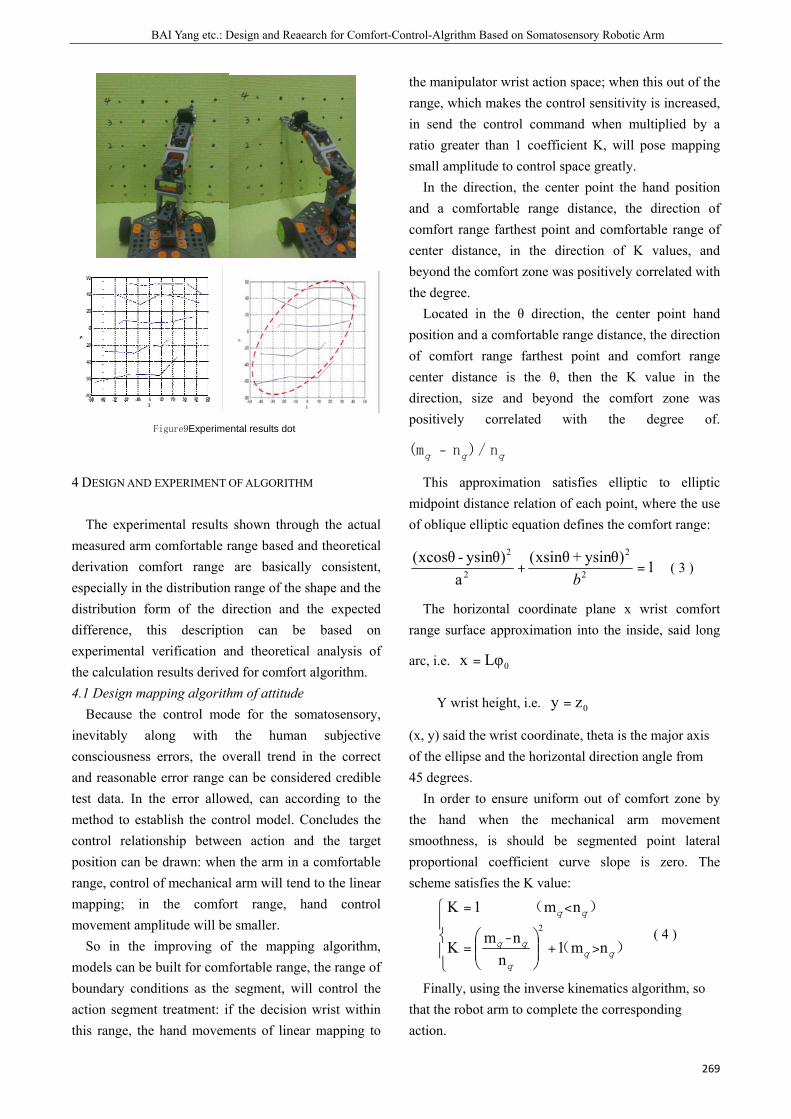
BAI Yang etc.: Design and Reaearch for Comfort-Control-Algrithm Based on Somatosensory Robotic Arm
269
4 DESIGN AND EXPERIMENT OF ALGORITHM
The experimental results shown through the actual measured arm comfortable range based and theoretical derivation comfort range are basically consistent, especially in the distribution range of the shape and the distribution form of the direction and the expected difference, this description can be based on experimental verification and theoretical analysis of the calculation results derived for comfort algorithm. 4.1 Design mapping algorithm of attitude
Because the control mode for the somatosensory, inevitably along with the human subjective consciousness errors, the overall trend in the correct and reasonable error range can be considered credible test data. In the error allowed, can according to the method to establish the control model. Concludes the control relationship between action and the target position can be drawn: when the arm in a comfortable range, control of mechanical arm will tend to the linear mapping; in the comfort range, hand control movement amplitude will be smaller.
So in the improving of the mapping algorithm, models can be built for comfortable range, the range of boundary conditions as the segment, will control the action segment treatment: if the decision wrist within this range, the hand movements of linear mapping to
the manipulator wrist action space; when this out of the range, which makes the control sensitivity is increased, in send the control command when multiplied by a ratio greater than 1 coefficient K, will pose mapping small amplitude to control space greatly.
In the direction, the center point the hand position and a comfortable range distance, the direction of comfort range farthest point and comfortable range of center distance, in the direction of K values, and beyond the comfort zone was positively correlated with the degree.
Located in the θ direction, the center point hand position and a comfortable range distance, the direction of comfort range farthest point and comfort range center distance is the θ, then the K value in the direction, size and beyond the comfort zone was positively correlated with the degree of.
qqq n/)n(m -
This approximation satisfies elliptic to elliptic midpoint distance relation of each point, where the use of oblique elliptic equation defines the comfort range:
1)ysinθ+xsinθ(a
)ysinθ-xcosθ(2
2
2
2
=+b
( 3 )
The horizontal coordinate plane x wrist comfort range surface approximation into the inside, said long
arc, i.e. 0Lφx =
Y wrist height, i.e. 0zy =
(x, y) said the wrist coordinate, theta is the major axis of the ellipse and the horizontal direction angle from 45 degrees.
In order to ensure uniform out of comfort zone by the hand when the mechanical arm movement smoothness, is should be segmented point lateral proportional coefficient curve slope is zero. The scheme satisfies the K value:
⎪⎩
⎪⎨
⎧
>+⎟⎟⎠
⎞⎜⎜⎝
⎛ -=
<=
)(
) (
qqq
nm1n
nmK
nm1K2 ( 4 )
Finally, using the inverse kinematics algorithm, so that the robot arm to complete the corresponding action.
Figure9Experimental results dot
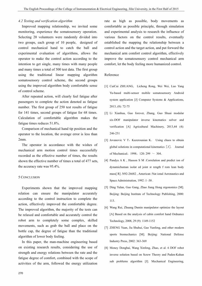
The English Proceedings of the College of Instrumentation & Electrical Engineering, Jilin University, in the First Half of 2015
270
4.2 Testing and verification algorithm Improved mapping relationship, we invited some
monitoring, experience the somatosensory operation. Selecting 20 volunteers were randomly divided into two groups, each group of 10 people, designed of control mechanical hand to catch the ball and experimental evaluation of algorithms, allows the operator to make the control action according to the intention to get single, many times with many people and many times a total of 500 test data. The first group using the traditional linear mapping algorithm somatosensory control scheme, the second groups using the improved algorithm body comfortable sense of control scheme.
After repeated action, will clearly feel fatigue after passengers to complete the action denoted as fatigue number. The first group of 250 test results of fatigue for 141 times, second groups of fatigue for 68 times. Calculation of comfortable algorithm makes the fatigue times reduces 51.8%.
Comparison of mechanical hand tip position and the operator to the location, the average error is less than 2mm.
The operator in accordance with the wishes of mechanical arm motion control times successfully recorded as the effective number of times, the results shown the effective number of times a total of 477 sets, the accuracy rate was 95.4%.
5 CONCLUSION
Experiments shown that the improved mapping relation can ensure the manipulator accurately according to the control instruction to complete the action, effectively improved the comfortable degree. The improved algorithm, the majority of the tests can be relaxed and comfortable and accurately control the robot arm to completely some complex, skilled movements, such as grab the ball and place on the bottle cap, the degree of fatigue than the traditional algorithm of lower body feeling.
In this paper, the man-machine engineering based on existing research results, considering the use of strength and energy relations between the rate and the fatigue degree of comfort, combined with the scope of activities of the arm, followed the energy utilization
rate as high as possible, body movements as comfortable as possible principle, through simulation and experimental analysis to research the influence of various factors on the control results, eventually established the mapping the relationship between a control action and the target action, and put forward the mechanical arm comfort control algorithm, effectively improve the somatosensory control mechanical arm comfort, let the body feeling more humanized control.
Reference
[1] CuiCui ZHUANG, Licheng Rong, Wei Wei, Luo Yang
Yu-based multi-sensor mobile somatosensory Android
system application [J] Computer Systems & Applications,
2013, (8): 72-75
[2] Li Xianhua, Guo forever, Zhang, Guo Shuai modular
six-DOF manipulator inverse kinematics solver and
verification [A] Agricultural Machinery, 2013,44 (4):
246-251
[3] Jovanovic V T,Kazerounian K. Using chaos to obtain
global solutions in computational kinematics[J]. Journal
of Mechanical,1998,120: 299 ~ 304.
[4] Pandya A K , Hasson S M .Correlation and predict ion of
dynamichuman isolat ed joint st rength f rom lean body
mass[ R] .N92-26682 , American :Nat ional Aeronautics and
Space Administration, 1992 :1 -30 .
[5] Ding Yulan, Guo Gang, Zhao Jiang Hong ergonomics [M].
Beijing: Beijing Institute of Technology Publishing, 2000:
113.
[6] Wang Rui, Zhuang Damin manipulator optimize the layout
[A] Based on the analysis of cabin comfort hand Ordnance
Technology, 2008, 29 (9): 1149-1152
[7] ZHENG Yuan, Jia Shuhui, Gao Yunfeng, and other modern
sports biomechanics [M]. Beijing: National Defense
Industry Press, 2002: 363-369
[8] Money Donghai, Wang Xinfeng, Zhao, et al. 6 DOF robot
inverse solution based on Screw Theory and Paden-Kahan
sub problems algorithm [J]. Mechanical Engineering,

BAI Yang etc.: Design and Reaearch for Comfort-Control-Algrithm Based on Somatosensory Robotic Arm
271
2009,45 (9): 72 to 76.
[9] Zheng Yang Shuo Fang Xing historical evolution of
information interaction studies. [J]. Journal of Wuhan
University
[10] Liao Wang Jian, Yang Bao somatosensory interaction
design and its application in three-dimensional virtual
experiment [J] Journal of Distance Education, 2013, (1):
54-59
[11] On behalf of Appleby, Qu Chang, Zhu Xiaolong, Chen
Chen in somatosensory interactive technology applications
in the field of sports rehabilitation [J] Chinese Journal of
Rehabilitation Theory and Practice, 2014, (1): 41-45
[12] Wang Junjie, Wangpei Yong, Xu Jian, Yuan literature
physical activity interventions new way: somatosensory
game of the origin, development and application [J] Xi'an
Institute of Physical Education, 2014, (2): 171-177
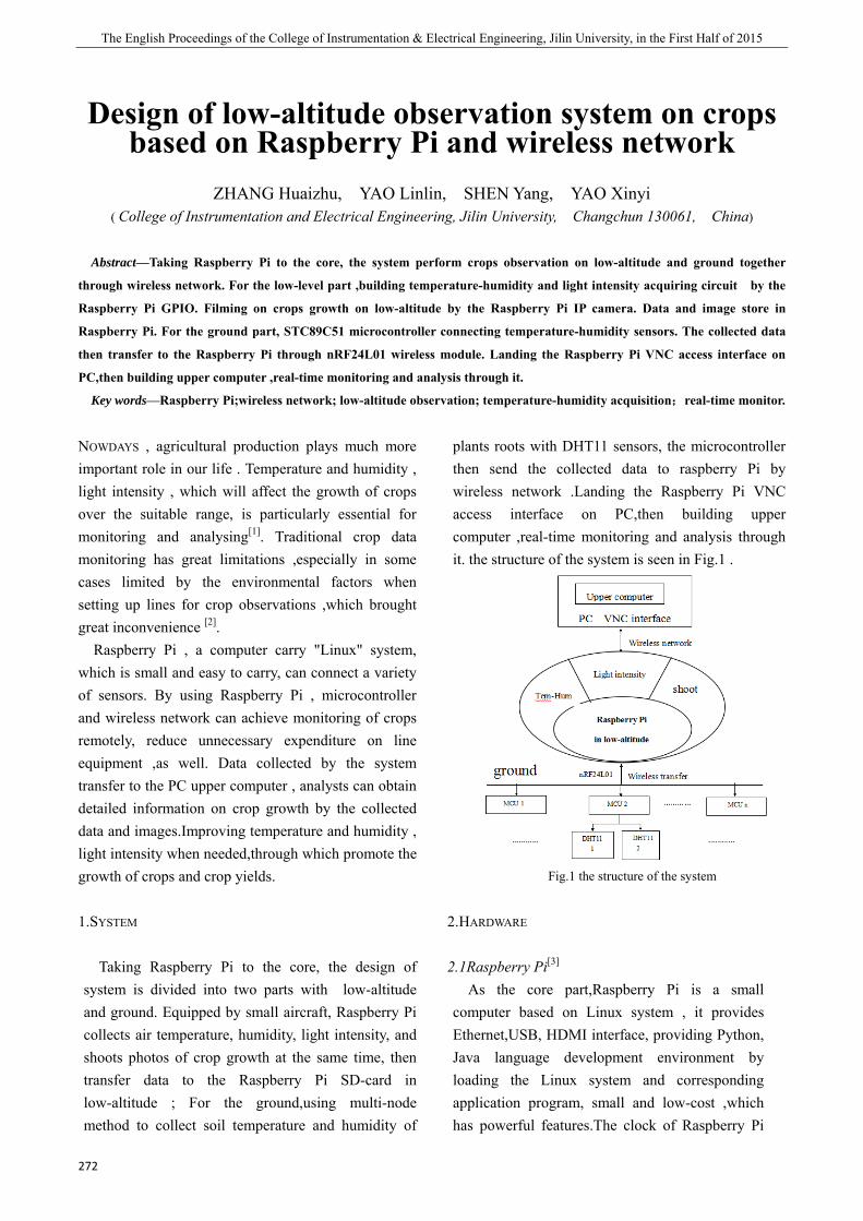
The English Proceedings of the College of Instrumentation & Electrical Engineering, Jilin University, in the First Half of 2015
272
Design of low-altitude observation system on crops based on Raspberry Pi and wireless network
ZHANG Huaizhu, YAO Linlin, SHEN Yang, YAO Xinyi
( College of Instrumentation and Electrical Engineering, Jilin University, Changchun 130061, China)
Abstract—Taking Raspberry Pi to the core, the system perform crops observation on low-altitude and ground together
through wireless network. For the low-level part ,building temperature-humidity and light intensity acquiring circuit by the
Raspberry Pi GPIO. Filming on crops growth on low-altitude by the Raspberry Pi IP camera. Data and image store in
Raspberry Pi. For the ground part, STC89C51 microcontroller connecting temperature-humidity sensors. The collected data
then transfer to the Raspberry Pi through nRF24L01 wireless module. Landing the Raspberry Pi VNC access interface on
PC,then building upper computer ,real-time monitoring and analysis through it.
Key words—Raspberry Pi;wireless network; low-altitude observation; temperature-humidity acquisition;real-time monitor.
NOWDAYS , agricultural production plays much more important role in our life . Temperature and humidity , light intensity , which will affect the growth of crops over the suitable range, is particularly essential for monitoring and analysing[1]. Traditional crop data monitoring has great limitations ,especially in some cases limited by the environmental factors when setting up lines for crop observations ,which brought great inconvenience [2]. Raspberry Pi , a computer carry "Linux" system, which is small and easy to carry, can connect a variety of sensors. By using Raspberry Pi , microcontroller and wireless network can achieve monitoring of crops remotely, reduce unnecessary expenditure on line equipment ,as well. Data collected by the system transfer to the PC upper computer , analysts can obtain detailed information on crop growth by the collected data and images.Improving temperature and humidity , light intensity when needed,through which promote the growth of crops and crop yields.
1.SYSTEM
Taking Raspberry Pi to the core, the design of system is divided into two parts with low-altitude and ground. Equipped by small aircraft, Raspberry Pi collects air temperature, humidity, light intensity, and shoots photos of crop growth at the same time, then transfer data to the Raspberry Pi SD-card in low-altitude ; For the ground,using multi-node method to collect soil temperature and humidity of
plants roots with DHT11 sensors, the microcontroller then send the collected data to raspberry Pi by wireless network .Landing the Raspberry Pi VNC access interface on PC,then building upper computer ,real-time monitoring and analysis through it. the structure of the system is seen in Fig.1 .
Fig.1 the structure of the system
2.HARDWARE
2.1Raspberry Pi[3] As the core part,Raspberry Pi is a small
computer based on Linux system , it provides Ethernet,USB, HDMI interface, providing Python, Java language development environment by loading the Linux system and corresponding application program, small and low-cost ,which has powerful features.The clock of Raspberry Pi
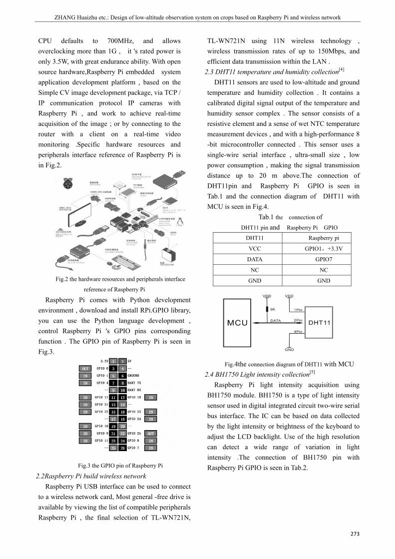
ZHANG Huaizhu etc.: Design of low-altitude observation system on crops based on Raspberry Pi and wireless network
273
CPU defaults to 700MHz, and allows overclocking more than 1G , it 's rated power is only 3.5W, with great endurance ability. With open source hardware,Raspberry Pi embedded system application development platform , based on the Simple CV image development package, via TCP / IP communication protocol IP cameras with Raspberry Pi , and work to achieve real-time acquisition of the image ; or by connecting to the router with a client on a real-time video monitoring .Specific hardware resources and peripherals interface reference of Raspberry Pi is in Fig.2.
Fig.2 the hardware resources and peripherals interface
reference of Raspberry Pi
Raspberry Pi comes with Python development environment , download and install RPi.GPIO library, you can use the Python language development , control Raspberry Pi 's GPIO pins corresponding function . The GPIO pin of Raspberry Pi is seen in Fig.3.
Fig.3 the GPIO pin of Raspberry Pi
2.2Raspberry Pi build wireless network Raspberry Pi USB interface can be used to connect
to a wireless network card, Most general -free drive is available by viewing the list of compatible peripherals Raspberry Pi , the final selection of TL-WN721N,
TL-WN721N using 11N wireless technology , wireless transmission rates of up to 150Mbps, and efficient data transmission within the LAN .
2.3 DHT11 temperature and humidity collection[4] DHT11 sensors are used to low-altitude and ground temperature and humidity collection . It contains a calibrated digital signal output of the temperature and humidity sensor complex . The sensor consists of a resistive element and a sense of wet NTC temperature measurement devices , and with a high-performance 8 -bit microcontroller connected . This sensor uses a single-wire serial interface , ultra-small size , low power consumption , making the signal transmission distance up to 20 m above.The connection of DHT11pin and Raspberry Pi GPIO is seen in Tab.1 and the connection diagram of DHT11 with MCU is seen in Fig.4.
Tab.1 the connection of DHT11 pin and Raspberry Pi GPIO
DHT11 Raspberry pi
VCC GPIO1,+3.3V
DATA GPIO7
NC NC
GND GND
Fig.4the connection diagram of DHT11 with MCU
2.4 BH1750 Light intensity collection[5] Raspberry Pi light intensity acquisition using BH1750 module. BH1750 is a type of light intensity sensor used in digital integrated circuit two-wire serial bus interface. The IC can be based on data collected by the light intensity or brightness of the keyboard to adjust the LCD backlight. Use of the high resolution can detect a wide range of variation in light intensity .The connection of BH1750 pin with Raspberry Pi GPIO is seen in Tab.2.

The English Proceedings of the College of Instrumentation & Electrical Engineering, Jilin University, in the First Half of 2015
274
Tab.2 the connection of BH1750 pin with Raspberry Pi GPIO. BH1750 Raspberry pi
GND GPIO2-3
VCC GPIO1-1
SCL GPIO1-3
SDA GPIO1-2
2.5 IP camera for crop[6] The project selected camera modules produced by OmniVision OV5647 camera can be connected directly with the Raspberry Pi control board by soft cable with a 5-megapixel image sensor , and can record 1080p 30 frames per second, full HD video , or shoot 2592 *1944 resolution images , suitable for taking pictures.
2.6 Wireless Module By nRF24L01 wireless module, ground data
transfer to Raspberry Pi . nRF24L01 is a wireless transceiver single-chip
working in the 2.4GHz to 2.5GHz ISM band. Its wireless transceiver comprising: a frequency generator , enhanced "Schock Burst" mode controller , a power amplifier , a crystal oscillator , modulator and demodulator . Set output channel selection and protocol can be set via the SPI interface. Almost single chip can be connected to a variety of complete wireless data transmission work .Specific connection diagram of nRF24L01 with MCU in Fig.5 .And the connection of nRF24L01 with Raspberry Pi GPIO is seen in Fig.6
Fig.5 the connection diagram of nRF24L01 with
MCU
Fig.6 the connection of nRF24L01 with Raspberry Pi
GPIO
3.SOFTWARE
3.1Set up the VNC interface of Raspberry Pi First, connect the Raspberry Pi computer via a network cable , use the command prompt to find Raspberry Pi Dynamic IP, initialization via putty and VNC Raspberry Pi Raspberry Pi interface and log in .Specific Raspberry Pi VNC interface in Fig.7[7].
Fig.7 Raspberry Pi VNC interface
Secondly, on the Raspberry Pi input interface LXTerminal or putty instruction Raspberry Pi static IP settings and Chinese display settings and a series of personalized settings. Finally, install the wireless card in the wireless network mode , connect aspberry Pi and PC by TPC / IP protocol .
3.1.1 Wireless LAN connection ①View mount USB devices Sudo lsusb Appear the
words RT5370 Wireless Adapter, indicates that the device is available ②test wifi signal Sudo iwlist wlan0 scan Find your wireless router ssid ③edit card configuration information Sudo nano / etc / network / interfaces Wlan0 modify
in order to achieve a static ip settings
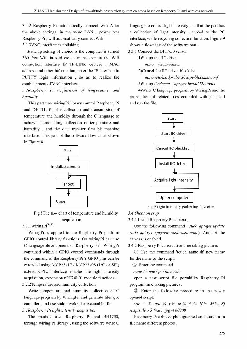
ZHANG Huaizhu etc.: Design of low-altitude observation system on crops based on Raspberry Pi and wireless network
275
3.1.2 Raspberry Pi automatically connect Wifi After the above settings, in the same LAN , power rear Raspberry Pi , will automatically connect Wifi 3.1.3VNC interface establishing
Static Ip setting of choice is the computer is turned 360 free Wifi in ssid etc , can be seen in the Wifi connection interface IP TP-LINK devices , MAC address and other information, enter the IP interface in PUTTY login information , so as to realize the establishment of VNC interface . 3.2Raspberry Pi acquisition of temperature and humidity
This part uses wiringPi library control Raspberry Pi and DHT11, for the collection and transmission of temperature and humidity through the C language to achieve a circulating collection of temperature and humidity , and the data transfer first bit machine interface. This part of the software flow chart shown in Figure 8 .
Fig.8The flow chart of temperature and humidity
acquisition 3.2.1WiringPi[8~9] WiringPi is applied to the Raspberry Pi platform GPIO control library functions. On wiringPi can use C language development of Raspberry Pi . WiringPi contained within a GPIO control commands through the command of the Raspberry Pi 's GPIO pins can be extended using MCP23x17 / MCP23x08 (I2C or SPI) extend GPIO interface enables the light intensity acquisition, expansion nRF24L01 module functions.
3.2.2Temperature and humidity collection Write temperature and humidity collection of C
language program by WiringPi, and generate files gcc compiler , and use sudo invoke the executable file.
3.3Raspberry Pi light intensity acquisition The module uses Raspberry Pi and BH1750,
through wiring Pi library , using the software write C
language to collect light intensity , so that the part has a collection of light intensity , spread to the PC interface, while recycling collection function. Figure 9 shows a flowchart of the software part .
3.3.1 Connect the BH1750 sensor 1)Set up the IIC drive nano /etc/modules 2)Cancel the IIC driver blacklist nano /etc/modprobe.d/raspi-blacklist.conf 3)Set up i2cdetect apt-get install i2c-tools 4)Write C language program by WiringPi and the
preparation of related files compiled with gcc, call and run the file.
Fig.9 Light intensity gathering flow chart 3.4 Shoot on crop 3.4.1 Install Raspberry Pi camera ,
Use the following command : sudo apt-get update sudo apt-get upgrade sudoraspi-config And set the camera is enabled.
3.4.2 Raspberry Pi consecutive time taking pictures ① Use the command 'touch name.sh' new name
for the name of the script. ② Enter the command 'nano / home / pi / name.sh' open a new script file portability Raspberry Pi
program time taking pictures . ③ Enter the following procedure in the newly
opened script: var = $ (date% y.% m.% d_% H.% M.% S)
raspistill-o $ var .jpg -t 60000 Raspberry Pi achieve photographed and stored as a
file name different photos .
Start
Initialize camera
shoot
Upper
Start
Start IIC drive
Cancel IIC blacklist
Install IIC detect
Acquire light intensity
Upper computer

The English Proceedings of the College of Instrumentation & Electrical Engineering, Jilin University, in the First Half of 2015
276
④ The modified internal controls Raspberry Pi script executiontiming . Enter 'crontab-e' command to open the bottom of the script and add the command '* / 1 * * * * / homg / pi h' Raspberry Pi achieve one minute intervals execute script 'name.sh'.
3.5Ground temperature and humidity collection[10] Ground temperature and humidity acquisition and transmission using the C programming language , programming is divided into: a few partial initialization DHT11 and nRF24L01 , collecting data DHT11 , nRF24L01 wireless transmitters and other data . First modular programming method for the preparation of the underlying drivers of each module , then the system debugging[11]. Specific software flow chart in Figure 10 .
Ground data received using nRF24L01, receiving a plurality of nodes transmit data , and stored in the memory tree Mei school . Receiving portion of the program.
Fig.10 Program flow chart
3.6The design of upper computer Using modular design ideas on designing the upper computer [11~14]. PC interface and low-level part of the ground segment includes the ground floor section can show the roots temperature and humidity. Altitude section can display altitude collect temperature, humidity , light intensity, and the picture was taken . Based on the design , the PC with the start button to directly call the Raspberry Pi internal storage of images and data , real-time display on the PC screen. . IDLE PC interface written in Python language , Python is an interpreted , object-oriented , dynamic data type -level programming language . Tkinter module ("Tk Interface" ) is a standard Python Tk GUI toolkit interface. Direct application from Tkinter import * command can be invoked to write GUI.
4.RESULT
Tab.3 the collection result of system
Low-altitude Ground
Temperature
()
Humidity
(%)
Light intensity(lux) Temperature() Humidity(%)
First
Time 9 7 40 37 48200.668 48200.668 10 8 9 0 36 35 36 36
Second
time 8 8 35 36 17551.666 16173.333 8 7 7 9 38 38 36 37
Third
Time 11 10 33 36 3587.507 4047.500 10 11 10 12 37 36 36 38
After testing, seen from Tab.3 about the experimental data , the final design data and image acquisition and transmission,and remote display and monitoring on the PC , the PC real-time display of the
current low-level timing and ground temperature, humidity, light intensity , as well as crops photographs. PC display as shown in Figure 11 .
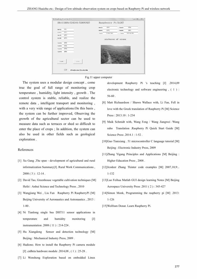
ZHANG Huaizhu etc.: Design of low-altitude observation system on crops based on Raspberry Pi and wireless network
277
Fig.11 upper computer
The system uses a modular design concept , come true the goal of full range of monitoring crop temperature , humidity, light intensity , growth . The control system is stable, reliable, and realize the remote data , intelligent transport and monitoring , with a very wide range of applications.On this basis , the system can be further improved, Observing the growth of the agricultural sector can be used to measure data such as terraces or shed so difficult to enter the place of crops ; In addition, the system can also be used in other fields such as geological exploration .
References
[1] Xu Gang ,The span - development of agricultural and rural
informatization Summary[J]. Rural Work Communications ,
2008 ( 3 ) : 12-14 .
[2] David Tao, Greenhouse vegetable cultivation techniques [M]
Hefei : Anhui Science and Technology Press , 2010
[3] Wangjiang Wei , Liu Fun Raspberry Pi RaspberryPi [M]
Beijing University of Aeronautics and Astronautics , 2013 :
1-80 .
[4] Ni Tianlong single bus DHT11 sensor applications in
temperature and humidity monitoring [J]
instrumentation .2008 ( 11 ) : 214-224 .
[5] Hu Xiangdong Sensor and detection technology [M]
Beijing : Mechanical Industry Press, 2009 .
[6] Hadiono. How to install the Raspberry Pi camera module
[J] .cnBeta hardware module .2014,08 , ( 1 ) : 25-28 .
[7] Li Wensheng Exploration based on embedded Linux
development Raspberry Pi 's teaching [J] .2014,09
electronic technology and software engineering , ( 1 ) :
56-60 .
[8] Matt Richaardson / Shawn Wallace with, Li Fan, Fell in
love with the Greek translation of Raspberry Pi [M] Science
Press : 2013.10 : 1-234
[9] Maik Schmidt with, Wang Feng / Wang Jiangwei /Wang
rubo Translation .Raspberry Pi Quick Start Guide [M]
Science Press .2014.1 : 1-52 .
[10] Guo Tianxiang . 51 microcontroller C language tutorial [M]
Beijing : Electronic Industry Press, 2009
[11] Zhang Yigang Principles and Applications [M] Beijing :
Higher Education Press , 2008 .
[12] Jcodeer Zhang Tkinter code examples [M] 2007,10,9:..
1-132
[13] Luo Feihua Matlab GUI design learning Notes [M] Beijing
Aerospace University Press .2011 ( 2 ) : 345-427
[14] Simon Monk, Programming the raspberry pi [M] .2013:
1-126
[15] Wolfram Donat. Learn Raspberry Pi.
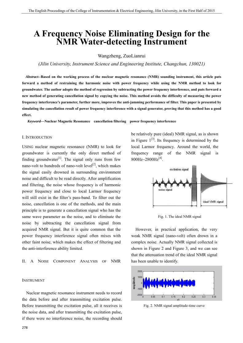
The English Proceedings of the College of Instrumentation & Electrical Engineering, Jilin University, in the First Half of 2015
278
A Frequency Noise Eliminating Design for the
NMR Water-detecting Instrument
Wangzheng, ZuoLianrui (Jilin University, Instrument Science and Engineering Institute, Changchun, 130021)
Abstract--Based on the working process of the nuclear magnetic resonance (NMR) sounding instrument, this article puts
forward a method of restraining the harmonic noise with power frequency while using the NMR method to look for
groundwater. The author adopts the method of regression by subtracting the power frequency interference, and puts forward a
new method of generating cancellation signal by copying the noise. This method avoids the difficulty of measuring the power
frequency interference’s parameter, further more, improves the anti-jamming performance of filter. This paper is presented by
simulating the cancellation result of power frequency interference with a signal generator, proving that this method has a good
effect.
Keyword—Nuclear Magnetic Resonance cancellation filtering power frequency interference
I. INTRODUCTION
USING nuclear magnetic resonance (NMR) to look for groundwater is currently the only direct method of finding groundwater[1]. The signal only runs from few nano-volt to hundreds of nano-volt level[2], which makes the signal easily drowned in surrounding environment noise and difficult to be read directly. After amplification and filtering, the noise whose frequency is of harmonic power frequency and close to local Larmor frequency will still exist in the filter’s pass-band. To filter out the noise, cancellation is one of the methods, and the main principle is to generate a cancellation signal who has the same wave parameter as the noise, and to eliminate the noise by subtracting the cancellation signal from acquired NMR signal. But it is quite common that the power frequency interference signal often mixes with other faint noise, which makes the effect of filtering and the anti-interference ability limited.
II. A NOISE COMPONENT ANALYSIS OF NMR
INSTRUMENT
Nuclear magnetic resonance instrument needs to record the data before and after transmitting excitation pulse. Before transmitting the excitation pulse, all it receives is the noise data, and after transmitting the excitation pulse, if there were no interference noise, the recording should
be relatively pure (ideal) NMR signal, as is shown in Figure 1[3]. Its frequency is determined by the local Larmor frequency. Around the world, the frequency range of the NMR signal is 800Hz~2800Hz[4].
Fig. 1. The ideal NMR signal
However, in practical application, the very
weak NMR signal (nano-volt) often drown in a complex noise. Actually NMR signal collected is shown in Figure 2 and Figure 3, and we can see that the attenuation trend of the ideal NMR signal has been unable to identify.
Fig. 2. NMR signal amplitude-time curve

Wangzheng etc.: A Frequency Noise Eliminating Design for the NMR Water-detecting Instrument
279
Fig. 3. NMR signal amplitude-frequency curve
III. THE PRINCIPLE AND WORKFLOW OF CANCELLATION
FILTERING
A. The principle of cancellation filtering
To achieve the cancellation technology, the prerequisite is that the signal, needed to be eliminated, has unchanged amplitude, frequency and phase. Power frequency noise has little-changed amplitude, frequency, phase, which can restrictively meet the prerequisite of the cancellation method[5]. Assuming that the filtered signal after amplification
)(ts is superimposed on a pure NMR signal )(tf with a
frequency noise signal )(tn ,
that )sin()()()()( aw ++=+= tUtftntfts M .
If the frequency, phase and amplitude of the noise signal
)(tn can be obtained, which can be used to generate a
same signal )(tn¢ , then put the )(tn¢ and the filtered
signal )(ts into a subtractor, finally the noise-frequency
harmonics can be filtered out . Principle of the system block diagram is shown in Figure 4.
Fig. 4. Functional block diagram of cancellation filter
The first difficulty of cancellation technology is to obtain the frequency, phase and amplitude information of a noise signal and to generate the same wave as the cancellation signal. The second one is to achieve the same phase of the cancellation signal with the noise signal, so that the subtractor is fed to get the best results.
To deal with the first difficulty spot of cancellation filtering, the traditional method is to measure the indexes of original signal by technology of electronic measurement then generate a same cancellation signal as original signal by the technology of DDS. But it’s difficult to accurately measure the phase and frequency of the power frequency noise in the actual measurement and the faint signal in power frequency noise greatly affected the measurement of phase and frequency. So, the practical application result of this method is not quite satisfying. Owing to this,the author creatively put forward a method by copying the harmonic power frequency noise to generate a cancellation signal. It makes the cancellation signal very close to the original signal. The accuracy of the cancellation process is only determined by the accuracy of ADC and DAC. It greatly reduces the error between cancellation signal and original signal and avoids the difficulties in the measurement of index of waveform.
For the problem of alignment of phase in cancellation filtering, the aspect of phase isn’t the only solution, but the faster, simpler and more accurate method with amplitude feedback, adjusting the phase of cancellation signal by observing the amplitude of the signal after canceling[6].
B. The workflow of cancellation filtering
Considering the principle of cancellation technology, it’s important to make a proper workflow of the process while using cancellation filtering in NMR signal processing. Specific process is shown in Figure 5.

The English Proceedings of the College of Instrumentation & Electrical Engineering, Jilin University, in the First Half of 2015
280
Fig. 5. Schematic diagram of cancellation filtering
The start of working process of the instrument is Pseudo launch, the instrument acquire the NMR signals, but it did not send the pulse. The signal passed by the former filter circuit is a pure noise signal. At this point, the module of noise cancellation starts the noise acquisition step, the noise signal is stored in digital form through the ADC. In phase tracking step, cancellation module will start the D/A conversion of noise waveform that it stored before, forming a cancellation signal, then puts the cancellation signal and noise signal into subtracter at the same time, and adjusts the phase of cancellation signal by judging the amplitude of output signal of subtracter. When the amplitude of output signal reaches the least value, we can believe that the phase of the cancellation signal and the noise signal has been the same. Then keep the cancellation signal’s phase unchanged, waiting for the instrument to launch pulse, then it enters the formal launch phase.
IV. RESULT AND ANALYSIS
A. Test of the ruled sinusoidal noise
According to the workflow, we generate a 1000 Hz ~ 3000 Hz frequency range of sine signal with signal generator GWINSTEK AFG-2225, as the simulation of the ideal power frequency harmonic signal. The module produce cancellation signal, then put two signals into oscilloscope GWINSTEK GDS-2202A. No relative movement between the signals can be observed. After adding the two channel signals together, we can see that the analog power frequency harmonic amplitude decreased to 10% of the original, verifying the feasibility of producing cancellation by copying waveform signal, the waveform is shown in Figure 6.
Fig. 6. Wave of signal after canceling(above)and
wave of signal before canceling(below)
B. The test of sine superposed signal
In order to make it more similar to the real situation, the author designed a test of de-noising of superposed signal synthesizing the workflow of cancellation filter. Firstly, generate sine wave in 2300Hz whose value of Vpp is 900mV by GWINSTEK AFG-2225 generator. Then start cancellation filter to acquire noise, after the acquisition, filter begin its phase track step, continuing to adjust the phase of cancellation signal until it’s same to noise’s. As Figure 7 shows, phase tracking step lasts about 600 ms. Then use the other channel of the signal generator to generate frequency sine wave in 2350Hz with 3.4 Vpp to simulate pure NMR signal, then put the above two sine signal into the adder to simulate the actual collection of NMR signal mixed with noise. Finally the cancellation filter start the formal step of de-noising as Figure 8 shows.
Fig. 7. Superposed signal in tracing(above)and
cancellation signal(below)
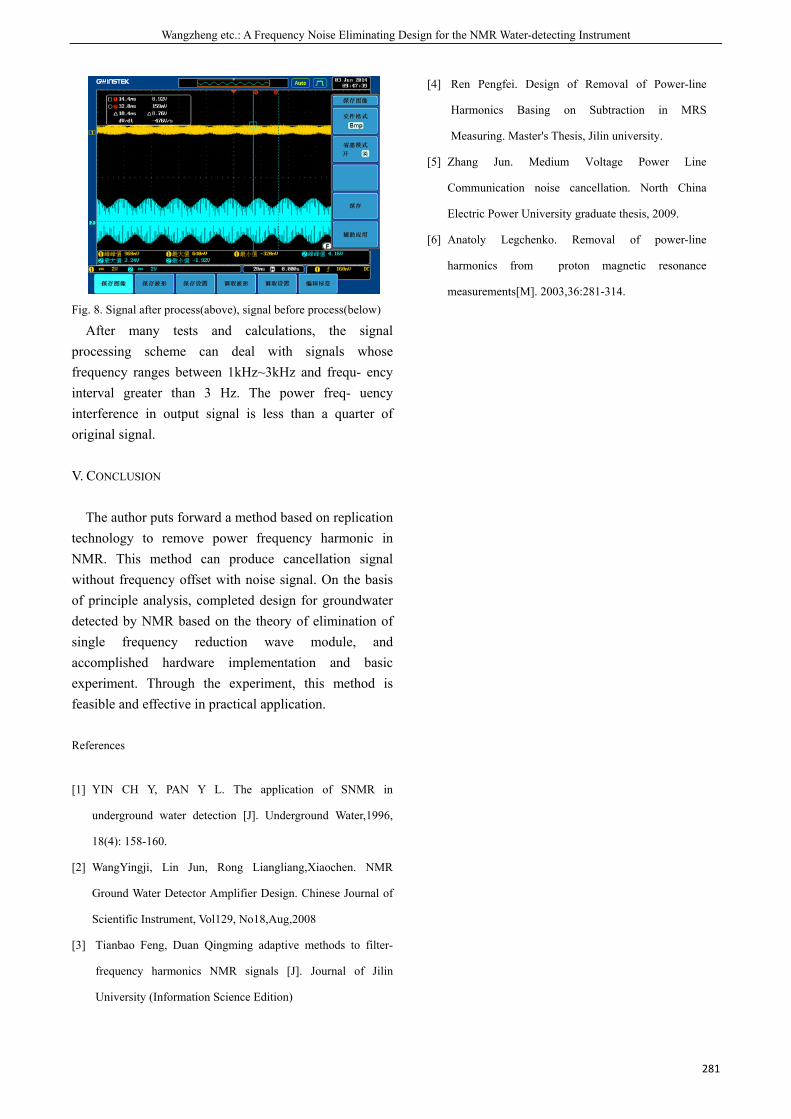
Wangzheng etc.: A Frequency Noise Eliminating Design for the NMR Water-detecting Instrument
281
Fig. 8. Signal after process(above), signal before process(below)
After many tests and calculations, the signal processing scheme can deal with signals whose frequency ranges between 1kHz~3kHz and frequ- ency interval greater than 3 Hz. The power freq- uency interference in output signal is less than a quarter of original signal.
V. CONCLUSION
The author puts forward a method based on replication technology to remove power frequency harmonic in NMR. This method can produce cancellation signal without frequency offset with noise signal. On the basis of principle analysis, completed design for groundwater detected by NMR based on the theory of elimination of single frequency reduction wave module, and accomplished hardware implementation and basic experiment. Through the experiment, this method is feasible and effective in practical application.
References
[1] YIN CH Y, PAN Y L. The application of SNMR in
underground water detection [J]. Underground Water,1996,
18(4): 158-160.
[2] WangYingji, Lin Jun, Rong Liangliang,Xiaochen. NMR
Ground Water Detector Amplifier Design. Chinese Journal of
Scientific Instrument, Vol129, No18,Aug,2008
[3] Tianbao Feng, Duan Qingming adaptive methods to filter-
frequency harmonics NMR signals [J]. Journal of Jilin
University (Information Science Edition)
[4] Ren Pengfei. Design of Removal of Power-line
Harmonics Basing on Subtraction in MRS
Measuring. Master's Thesis, Jilin university.
[5] Zhang Jun. Medium Voltage Power Line
Communication noise cancellation. North China
Electric Power University graduate thesis, 2009.
[6] Anatoly Legchenko. Removal of power-line
harmonics from proton magnetic resonance
measurements[M]. 2003,36:281-314.
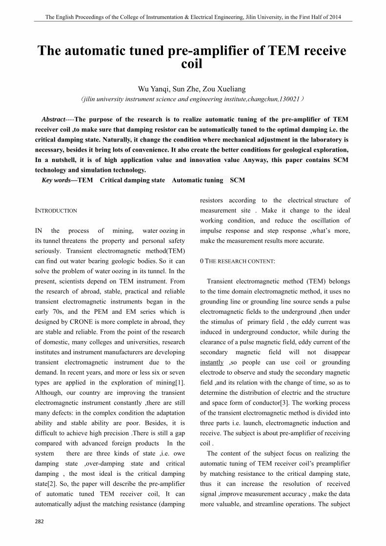
The English Proceedings of the College of Instrumentation & Electrical Engineering, Jilin University, in the First Half of 2014
282
The automatic tuned pre-amplifier of TEM receive coil
Wu Yanqi, Sun Zhe, Zou Xueliang
(jilin university instrument science and engineering institute,changchun,130021)
Abstract----The purpose of the research is to realize automatic tuning of the pre-amplifier of TEM receiver coil ,to make sure that damping resistor can be automatically tuned to the optimal damping i.e. the critical damping state. Naturally, it change the condition where mechanical adjustment in the laboratory is necessary, besides it bring lots of convenience. It also create the better conditions for geological exploration, In a nutshell, it is of high application value and innovation value Anyway, this paper contains SCM technology and simulation technology.
Key words—TEM Critical damping state Automatic tuning SCM
INTRODUCTION
IN the process of mining, water oozing in its tunnel threatens the property and personal safety seriously. Transient electromagnetic method(TEM) can find out water bearing geologic bodies. So it can solve the problem of water oozing in its tunnel. In the present, scientists depend on TEM instrument. From the research of abroad, stable, practical and reliable transient electromagnetic instruments began in the early 70s, and the PEM and EM series which is designed by CRONE is more complete in abroad, they are stable and reliable. From the point of the research of domestic, many colleges and universities, research institutes and instrument manufacturers are developing transient electromagnetic instrument due to the demand. In recent years, and more or less six or seven types are applied in the exploration of mining[1]. Although, our country are improving the transient electromagnetic instrument constantly ,there are still many defects: in the complex condition the adaptation ability and stable ability are poor. Besides, it is difficult to achieve high precision .There is still a gap compared with advanced foreign products In the system there are three kinds of state ,i.e. owe damping state ,over-damping state and critical damping , the most ideal is the critical damping state[2]. So, the paper will describe the pre-amplifier of automatic tuned TEM receiver coil, It can automatically adjust the matching resistance (damping
resistors according to the electrical structure of measurement site . Make it change to the ideal working condition, and reduce the oscillation of impulse response and step response ,what’s more, make the measurement results more accurate.
0 THE RESEARCH CONTENT:
Transient electromagnetic method (TEM) belongs to the time domain electromagnetic method, it uses no grounding line or grounding line source sends a pulse electromagnetic fields to the underground ,then under the stimulus of primary field , the eddy current was induced in underground conductor, while during the clearance of a pulse magnetic field, eddy current of the secondary magnetic field will not disappear instantly ,so people can use coil or grounding electrode to observe and study the secondary magnetic field ,and its relation with the change of time, so as to determine the distribution of electric and the structure and space form of conductor[3]. The working process of the transient electromagnetic method is divided into three parts i.e. launch, electromagnetic induction and receive. The subject is about pre-amplifier of receiving coil .
The content of the subject focus on realizing the automatic tuning of TEM receiver coil’s preamplifier by matching resistance to the critical damping state, thus it can increase the resolution of received signal ,improve measurement accuracy , make the data more valuable, and streamline operations. The subject
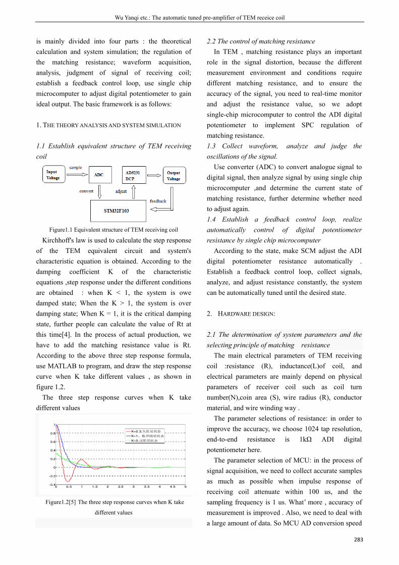
Wu Yanqi etc.: The automatic tuned pre-amplifier of TEM receice coil
283
is mainly divided into four parts : the theoretical calculation and system simulation; the regulation of the matching resistance; waveform acquisition, analysis, judgment of signal of receiving coil; establish a feedback control loop, use single chip microcomputer to adjust digital potentiometer to gain ideal output. The basic framework is as follows:
1. THE THEORY ANALYSIS AND SYSTEM SIMULATION
1.1 Establish equivalent structure of TEM receiving coil
Figure1.1 Equivalent structure of TEM receiving coil
Kirchhoff's law is used to calculate the step response of the TEM equivalent circuit and system's characteristic equation is obtained. According to the damping coefficient K of the characteristic equations ,step response under the different conditions are obtained : when K < 1, the system is owe damped state; When the K > 1, the system is over damping state; When K = 1, it is the critical damping state, further people can calculate the value of Rt at this time[4]. In the process of actual production, we have to add the matching resistance value is Rt. According to the above three step response formula, use MATLAB to program, and draw the step response curve when K take different values , as shown in figure 1.2.
The three step response curves when K take different values
Figure1.2[5] The three step response curves when K take
different values
2.2 The control of matching resistance In TEM , matching resistance plays an important
role in the signal distortion, because the different measurement environment and conditions require different matching resistance, and to ensure the accuracy of the signal, you need to real-time monitor and adjust the resistance value, so we adopt single-chip microcomputer to control the ADI digital potentiometer to implement SPC regulation of matching resistance. 1.3 Collect waveform, analyze and judge the oscillations of the signal.
Use converter (ADC) to convert analogue signal to digital signal, then analyze signal by using single chip microcomputer ,and determine the current state of matching resistance, further determine whether need to adjust again. 1.4 Establish a feedback control loop, realize automatically control of digital potentiometer resistance by single chip microcomputer
According to the state, make SCM adjust the ADI digital potentiometer resistance automatically . Establish a feedback control loop, collect signals, analyze, and adjust resistance constantly, the system can be automatically tuned until the desired state.
2. HARDWARE DESIGN:
2.1 The determination of system parameters and the selecting principle of matching resistance
The main electrical parameters of TEM receiving coil :resistance (R), inductance(L)of coil, and electrical parameters are mainly depend on physical parameters of receiver coil such as coil turn number(N),coin area (S), wire radius (R), conductor material, and wire winding way .
The parameter selections of resistance: in order to improve the accuracy, we choose 1024 tap resolution, end-to-end resistance is 1kΩ ADI digital potentiometer here.
The parameter selection of MCU: in the process of signal acquisition, we need to collect accurate samples as much as possible when impulse response of receiving coil attenuate within 100 us, and the sampling frequency is 1 us. What’ more , accuracy of measurement is improved . Also, we need to deal with a large amount of data. So MCU AD conversion speed
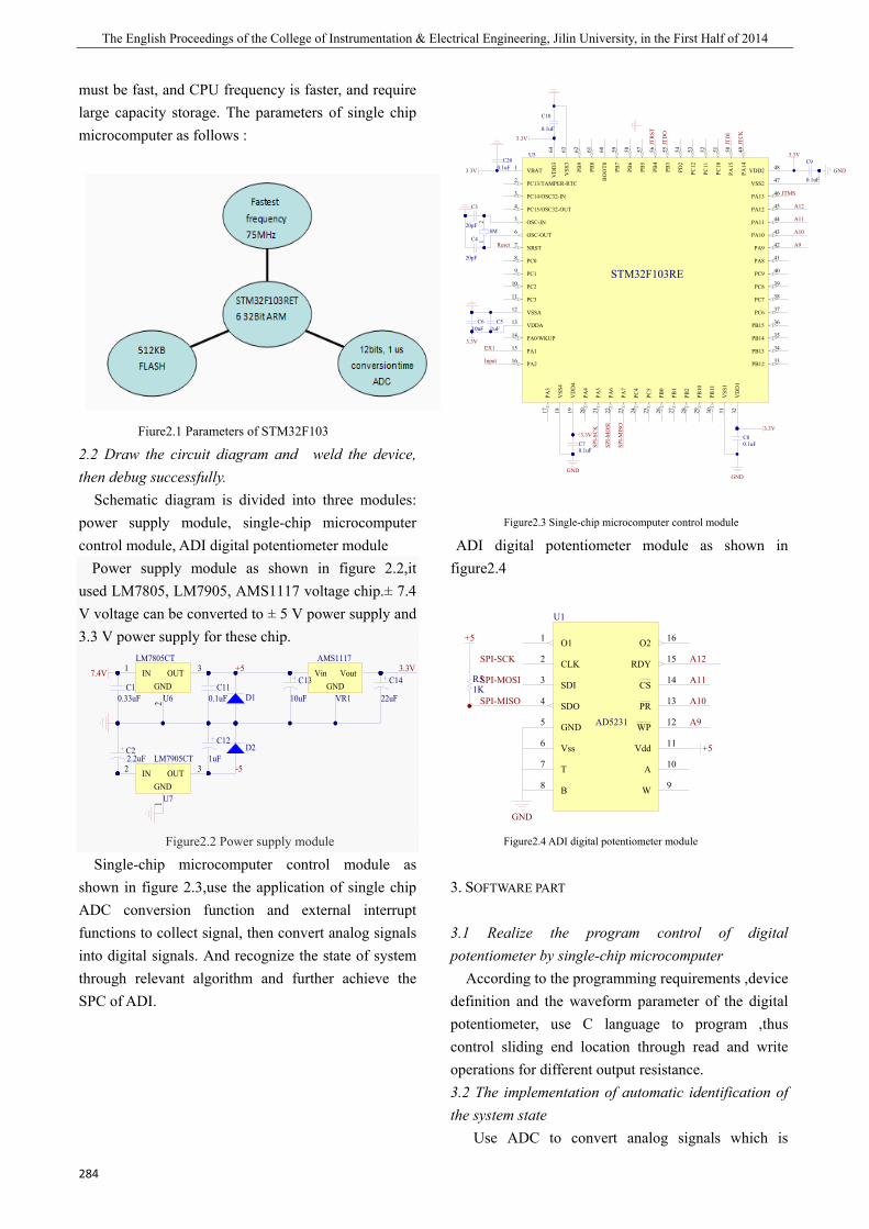
The English Proceedings of the College of Instrumentation & Electrical Engineering, Jilin University, in the First Half of 2014
284
must be fast, and CPU frequency is faster, and require large capacity storage. The parameters of single chip microcomputer as follows :
Fiure2.1 Parameters of STM32F103
2.2 Draw the circuit diagram and weld the device, then debug successfully.
Schematic diagram is divided into three modules: power supply module, single-chip microcomputer control module, ADI digital potentiometer module
Power supply module as shown in figure 2.2,it used LM7805, LM7905, AMS1117 voltage chip.± 7.4 V voltage can be converted to ± 5 V power supply and 3.3 V power supply for these chip.
IN1
2
OUT 3
GNDU6
LM7805CT
IN2
1
OUT 3
GNDU7
LM7905CT2.2uFC2
0.33uFC1
7.4V
0.1uFC11
1uF
C12
D1
D2
+5
-5
Vin VoutGND
VR1
AMS1117
10uF
C13
22uF
C143.3V
Figure2.2 Power supply module
Single-chip microcomputer control module as shown in figure 2.3,use the application of single chip ADC conversion function and external interrupt functions to collect signal, then convert analog signals into digital signals. And recognize the state of system through relevant algorithm and further achieve the SPC of ADI.
PC14/OSC32-IN3
PC15/OSC32-OUT4
OSC-IN5
OSC-OUT6
NRST7
PC08
PC19
PC210
PC311
VSSA12
VDDA13
PA0/WKUP14
PA115
PA216
PA3
17
VSS
418
VD
D4
19
PA4
20
PA5
21
PA6
22
PA7
23
PC4
24
PC5
25
PB0
26
PB1
27
PB2
28
PB10
29
PB11
30
VSS
131
VD
D1
32
PB12 33
PB13 34
PB14 35
PB15 36
PC6 37
PC7 38
PC8 39
PC9 40
PA8 41
PA9 42
PA10 43
PA11 44
PA12 45
PA13 46
VSS2 47
VDD2 48
PA14
49
PA15
50PC
1051
PC11
52PC
1253
PD2
54
PB3
55PB
456
PB5
57PB
658
PB7
59B
OO
T060
PB8
61PB
962
VSS
363
VD
D3
64
PC13/TAMPER-RTC2
VBAT1
STM32F103RE
U5
20pF
C4
20pF
C3
10nFC6
12
8M
3.3V
1uFC5
3.3V
0.1uF
C10
3.3V
GND0.1uF
C9
3.3V
0.1uFC7
GND
3.3V
0.1uFC8
GND
Reset
JTR
ST
JTD
O
JTD
I
JTC
K
JTMS
EX1
Input
0.1uFC20
3.3V
A9
A10
A11
A12
SPI-
SCK
SPI-
MIS
O
SPI-
MO
SI
Figure2.3 Single-chip microcomputer control module
ADI digital potentiometer module as shown in figure2.4
O2 16
RDY 15
CS 14
PR 13
WP 12
Vdd 11
A 10
W 9
O11
CLK2
SDI3
SDO4
GND5
Vss6
T7
B8
AD5231
U1
GND
+5
SPI-MOSI
SPI-SCK
SPI-MISO
+5
1KR5
A9
A10
A11
A12
Figure2.4 ADI digital potentiometer module
3. SOFTWARE PART
3.1 Realize the program control of digital potentiometer by single-chip microcomputer
According to the programming requirements ,device definition and the waveform parameter of the digital potentiometer, use C language to program ,thus control sliding end location through read and write operations for different output resistance. 3.2 The implementation of automatic identification of the system state
Use ADC to convert analog signals which is
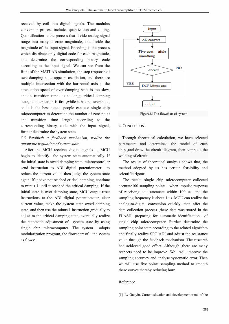
Wu Yanqi etc.: The automatic tuned pre-amplifier of TEM receice coil
285
received by coil into digital signals. The modulus conversion process includes quantization and coding. Quantification is the process that divide analog signal range into many discrete magnitude, and decide the magnitude of the input signal. Encoding is the process which distribute only digital code for each magnitude, and determine the corresponding binary code according to the input signal. We can see from the front of the MATLAB simulation, the step response of owe damping state appears oscillation, and there are multiple intersection with the horizontal axis ; the attenuation speed of over damping state is too slow, and its transition time is so long; critical damping state, its attenuation is fast ,while it has no overshoot, so it is the best state. people can use single chip microcomputer to determine the number of zero point and transition time length according to the corresponding binary code with the input signal, further determine the system state. 3.3 Establish a feedback mechanism, realize the automatic regulation of system state
After the MCU receives digital signals , MCU begin to identify the system state automatically. If the initial state is owed damping state, microcontroller send instruction to ADI digital potentiometer to reduce the current value, then judge the system state again. If it have not reached critical damping, continue to minus 1 until it reached the critical damping; If the initial state is over damping state, MCU output reset instructions to the ADI digital potentiometer, clear current value, make the system state owed damping state, and then use the minus 1 instruction gradually to adjust to the critical damping state, eventually realize the automatic adjustment of system state by using single chip microcomputer .The system adopts modularization program, the flowchart of the system as flows:
Figure3.1The flowchart of system
4. CONCLUSION
Through theoretical calculation, we have selected parameters and determined the model of each chip ,and draw the circuit diagram, then complete the welding of circuit.
The results of theoretical analysis shows that, the method adopted by us has certain feasibility and scientific rigour.
The result: single chip microcomputer collected accurate100 sampling points when impulse response of receiving coil attenuate within 100 us, and the sampling frequency is about 1 us. MCU can realize the analog-to-digital conversion quickly, then after the data collection process ,these data was stored in the FLASH, preparing for automatic identification of single chip microcomputer. Further determine the sampling point state according to the related algorithm and finally realize SPC ADI and adjust the resistance value through the feedback mechanism. The research had achieved good effect. Although ,there are many respects need to be improve. We will improve the sampling accuracy and analyse systematic error. Then we will use five points sampling method to smooth these curves thereby reducing burr.
Reference
[1] Lv Guoyin. Current situation and development trend of the

The English Proceedings of the College of Instrumentation & Electrical Engineering, Jilin University, in the First Half of 2014
286
transient electromagnetic method computing technology [J]
geophysical geochemical exploration (2007) 3 (1) -
0111-05
[2] Niu Zhilian. Time Domain Electromagnetic Method [M].
Changsha ,Central south technology university press,
2007
[3] Ji Yanju, Lin Jun, Yu Shengbao. The study of the current
response salvation of ATTEM system in the tem field
during the period of shut off [J] J. geophys. 2006,49 (6) :
1884 - a - 1890
[4] Wang Huajun, Liang Qingjiu Transient electromagnetic
acquisition interpretation software system research. Journal
of engineering geophysics [J], 2005 (6) : 425 - a – 430
[5] Tan Feiya. The development of TEM receiver coil [D]. Jilin
university, 2010
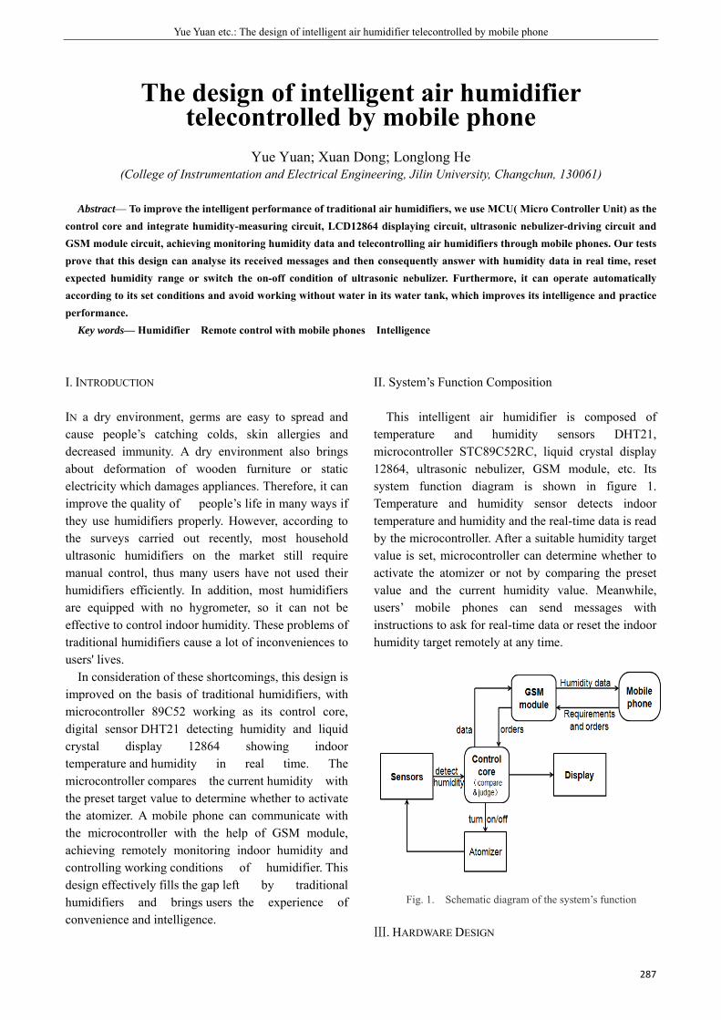
Yue Yuan etc.: The design of intelligent air humidifier telecontrolled by mobile phone
287
The design of intelligent air humidifier telecontrolled by mobile phone
Yue Yuan; Xuan Dong; Longlong He
(College of Instrumentation and Electrical Engineering, Jilin University, Changchun, 130061)
Abstract— To improve the intelligent performance of traditional air humidifiers, we use MCU( Micro Controller Unit) as the control core and integrate humidity-measuring circuit, LCD12864 displaying circuit, ultrasonic nebulizer-driving circuit and GSM module circuit, achieving monitoring humidity data and telecontrolling air humidifiers through mobile phones. Our tests prove that this design can analyse its received messages and then consequently answer with humidity data in real time, reset expected humidity range or switch the on-off condition of ultrasonic nebulizer. Furthermore, it can operate automatically according to its set conditions and avoid working without water in its water tank, which improves its intelligence and practice performance.
Key words— Humidifier Remote control with mobile phones Intelligence
I. INTRODUCTION
IN a dry environment, germs are easy to spread and cause people’s catching colds, skin allergies and decreased immunity. A dry environment also brings about deformation of wooden furniture or static electricity which damages appliances. Therefore, it can improve the quality of people’s life in many ways if they use humidifiers properly. However, according to the surveys carried out recently, most household ultrasonic humidifiers on the market still require manual control, thus many users have not used their humidifiers efficiently. In addition, most humidifiers are equipped with no hygrometer, so it can not be effective to control indoor humidity. These problems of traditional humidifiers cause a lot of inconveniences to users' lives.
In consideration of these shortcomings, this design is improved on the basis of traditional humidifiers, with microcontroller 89C52 working as its control core, digital sensor DHT21 detecting humidity and liquid crystal display 12864 showing indoor temperature and humidity in real time. The microcontroller compares the current humidity with the preset target value to determine whether to activate the atomizer. A mobile phone can communicate with the microcontroller with the help of GSM module, achieving remotely monitoring indoor humidity and controlling working conditions of humidifier. This design effectively fills the gap left by traditional humidifiers and brings users the experience of convenience and intelligence.
II. System’s Function Composition
This intelligent air humidifier is composed of temperature and humidity sensors DHT21, microcontroller STC89C52RC, liquid crystal display 12864, ultrasonic nebulizer, GSM module, etc. Its system function diagram is shown in figure 1. Temperature and humidity sensor detects indoor temperature and humidity and the real-time data is read by the microcontroller. After a suitable humidity target value is set, microcontroller can determine whether to activate the atomizer or not by comparing the preset value and the current humidity value. Meanwhile, users’ mobile phones can send messages with instructions to ask for real-time data or reset the indoor humidity target remotely at any time.
Fig. 1. Schematic diagram of the system’s function
Ⅲ. HARDWARE DESIGN
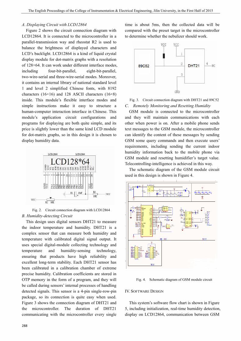
The English Proceedings of the College of Instrumentation & Electrical Engineering, Jilin University, in the First Half of 2015
288
A. Displaying Circuit with LCD12864 Figure 2 shows the circuit connection diagram with
LCD12864. It is connected to the microcontroller in a parallel-transmission way and rheostat R2 is used to balance the brightness of displayed characters and LCD’s backlight. LCD12864 is a kind of liquid crystal display module for dot-matrix graphs with a resolution of 128×64. It can work under different interface modes, including four-bit-parallel, eight-bit-parallel, two-wire-serial and three-wire-serial modes. Moreover, it contains an internal library of national standard level 1 and level 2 simplified Chinese fonts, with 8192 characters (16×16) and 128 ASCII characters (16×8) inside. This module’s flexible interface modes and simple instructions make it easy to structure a human-computer interaction interface in Chinese. This module’s application circuit configurations and programs for displaying are both quite simple, and its price is slightly lower than the same kind LCD module for dot-matrix graphs, so in this design it is chosen to display humidity data.
Fig. 2. Circuit connection diagram with LCD12864
B. Humidity-detecting Circuit This design uses digital sensors DHT21 to measure
the indoor temperature and humidity. DHT21 is a complex sensor that can measure both humidity and temperature with calibrated digital signal output. It uses special digital-module collecting technology and temperature and humidity-sensing technology, ensuring that products have high reliability and excellent long-term stability. Each DHT21 sensor has been calibrated in a calibration chamber of extreme precise humidity. Calibration coefficients are stored in OTP memory in the form of a program, and they will be called during sensors’ internal processes of handling detected signals. This sensor is a 4-pin single-row-pin package, so its connection is quite easy when used. Figure 3 shows the connection diagram of DHT21 and the microcontroller. The duration of DHT21 communicating with the microcontroller every single
time is about 5ms, then the collected data will be compared with the preset target in the microcontroller to determine whether the nebulizer should work.
Fig. 3. Circuit connection diagram with DHT21 and 89C52
C. Remotely Monitoring and Resetting Humidity GSM module is connected to the microcontroller
and they will maintain communications with each other when power is on. After a mobile phone sends text messages to the GSM module, the microcontroller can identify the content of these messages by sending GSM some query commands and then execute users’ requirements, including sending the current indoor humidity information back to the mobile phone via GSM module and resetting humidifier’s target value. Telecontrolling-intelligence is achieved in this way.
The schematic diagram of the GSM module circuit used in this design is shown in Figure 4.
Fig. 4. Schematic diagram of GSM module circuit
IV. SOFTWARE DESIGN
This system’s software flow chart is shown in Figure 5, including initialization, real-time humidity detection, display on LCD12864, communication between GSM
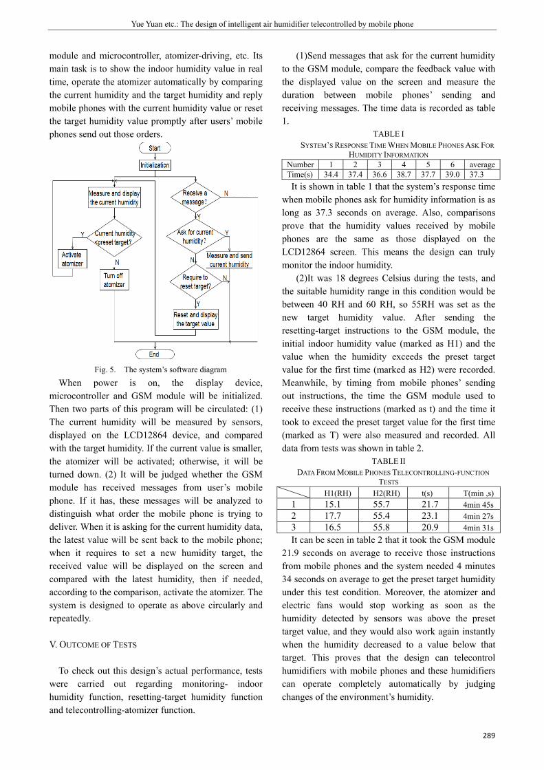
Yue Yuan etc.: The design of intelligent air humidifier telecontrolled by mobile phone
289
module and microcontroller, atomizer-driving, etc. Its main task is to show the indoor humidity value in real time, operate the atomizer automatically by comparing the current humidity and the target humidity and reply mobile phones with the current humidity value or reset the target humidity value promptly after users’ mobile phones send out those orders.
Fig. 5. The system’s software diagram
When power is on, the display device, microcontroller and GSM module will be initialized. Then two parts of this program will be circulated: (1) The current humidity will be measured by sensors, displayed on the LCD12864 device, and compared with the target humidity. If the current value is smaller, the atomizer will be activated; otherwise, it will be turned down. (2) It will be judged whether the GSM module has received messages from user’s mobile phone. If it has, these messages will be analyzed to distinguish what order the mobile phone is trying to deliver. When it is asking for the current humidity data, the latest value will be sent back to the mobile phone; when it requires to set a new humidity target, the received value will be displayed on the screen and compared with the latest humidity, then if needed, according to the comparison, activate the atomizer. The system is designed to operate as above circularly and repeatedly.
V. OUTCOME OF TESTS
To check out this design’s actual performance, tests were carried out regarding monitoring- indoor humidity function, resetting-target humidity function and telecontrolling-atomizer function.
(1)Send messages that ask for the current humidity to the GSM module, compare the feedback value with the displayed value on the screen and measure the duration between mobile phones’ sending and receiving messages. The time data is recorded as table 1.
TABLE I SYSTEM’S RESPONSE TIME WHEN MOBILE PHONES ASK FOR
HUMIDITY INFORMATION Number 1 2 3 4 5 6 averageTime(s) 34.4 37.4 36.6 38.7 37.7 39.0 37.3 It is shown in table 1 that the system’s response time
when mobile phones ask for humidity information is as long as 37.3 seconds on average. Also, comparisons prove that the humidity values received by mobile phones are the same as those displayed on the LCD12864 screen. This means the design can truly monitor the indoor humidity.
(2)It was 18 degrees Celsius during the tests, and the suitable humidity range in this condition would be between 40 RH and 60 RH, so 55RH was set as the new target humidity value. After sending the resetting-target instructions to the GSM module, the initial indoor humidity value (marked as H1) and the value when the humidity exceeds the preset target value for the first time (marked as H2) were recorded. Meanwhile, by timing from mobile phones’ sending out instructions, the time the GSM module used to receive these instructions (marked as t) and the time it took to exceed the preset target value for the first time (marked as T) were also measured and recorded. All data from tests was shown in table 2.
TABLE II DATA FROM MOBILE PHONES TELECONTROLLING-FUNCTION
TESTS H1(RH) H2(RH) t(s) T(min ,s)1 15.1 55.7 21.7 4min 45s2 17.7 55.4 23.1 4min 27s3 16.5 55.8 20.9 4min 31sIt can be seen in table 2 that it took the GSM module
21.9 seconds on average to receive those instructions from mobile phones and the system needed 4 minutes 34 seconds on average to get the preset target humidity under this test condition. Moreover, the atomizer and electric fans would stop working as soon as the humidity detected by sensors was above the preset target value, and they would also work again instantly when the humidity decreased to a value below that target. This proves that the design can telecontrol humidifiers with mobile phones and these humidifiers can operate completely automatically by judging changes of the environment’s humidity.
The English Proceedings of the College of Instrumentation & Electrical Engineering, Jilin University, in the First Half of 2015
290
Ⅵ. CONCLUSION
This design uses microcontroller STC89C52 as its control core, together with digital sensors DHT21, liquid crystal display 12864, GSM module and nebulizer, composing a humidification system which can operate automatically and respond to remote control commands. It makes people's lives more comfortable and its intelligence performance that is different from the traditional humidifiers brings people healthier and more convenient experience.
References
[1] Guo Shuai, Ning Lijia, Bao Yudong, Shi Songzhuo. The design and research of intelligent irrigation system based on mobile phones telecontrol [J]. Journal of Anhui Agricultural Sciences. 2014(18): P6054-6055.
[2] Jin Longhai, Li Cong. Programming Design with C Language[M]. Beijing: Science Press,2012.
[3] (America) Brey , B.B. The Intel Microprocessors[M]. Beijing: China Machine Press, 2010.6.
[4] He Qiao, Duan Qingming, Qiu Chunling. The Principles and Application of Microcontrollers[M]. China Railway Publishing House. 2008.1.
[5] Guo Tianxiang. C Language Courses about 51 Microcontrollers [M]. Beijing: Publishing House of Electronics Industry, 2009.1.
[6] Li Peng. The design of mobile phones-telecontrolled toy car based on MCU [J] . Charming China. 2014 (25):119.
[7] Liu Lingyun. Smart home control system [Dissertation] Master. 2014.

Zuxianda etc.: High-precision dual-mode automatic solar tracking system
291
High-precision dual-mode automatic solar tracking system
Zuxianda;daiyou;fanshuai
(jilin university instrument science and engineering institute,changchun,130021)
Abstract--In order to improve the utilization of solar energy,we propose dual-mode and dual-axis solar tracking system.The
control method combines Sensor Tracking with GPS location tracking.Using this method selects more efficient operating
mode according to weather conditions.The collected data will be transmitted to the SCM,and servo motor drive accurately to
tracking where the current position of the sun in order to achieve efficient utilization of solar energy object.
Key words-- Utilization Sensor GPS SCM Servomotor
I. FOREWORD
WITH the development and progress of society,The traditional non-renewable energy sources can not meet the needs of human development,Solar energy as a renewable clean energy will become one of the future energy essential for social development.However, the utilization of solar energy has always been the problem hindering the widespread use of solar energy,How to improve the utilization of solar energy has become an international hotspot,according to the theoretical study shows,there is a difference of 41.34 acceptance rate between the dual-axis tracking way and the traditional fixed reception way.The tracking device can be less affected by weather conditions,runs normally without manual intervention,has a simple structure and can be better able to improve the utilization of solar energy.
II. SOLAR TRACKING SYSTEM
A. Scheme Selection At present,there are two methods of control solar,
sensors to detect solar intensity and apparenting trajectory day.Besides there are two kinds of tracking methods,uniaxial and biaxial.
Single-axis tracking mode can only change the position of the angle of the rotation axis of solar panels.According to azimuth tracking the solar,and the elevation is adjusted seasonally.
Dual-axis tracking system tracks the sun from the
azimuth and the elevation two directions.Apparently,the dual-axis solar tracking system has a higher utilization than the uniaxial tracking mode.
The method of sensors detecting light intensity is through the photoelectric sensor to judge whether the sun’s ray is vertical to solar panel.Put four Photoelectric Sensors at the edge of the solar panel in order to collect the data of optical signal.After AD converting the data,driving the servo motor makes it to adjust the position of facing the sun to achieve the efficient use of solar energy.This kind of control method has a commond of higher sensitivity,less demanding on system installation,no error affected by the accumulation and low cost.However,the disadvantages of the method are stable problems of tracking,affected by the weather more serious,unable to track the sun accurately when in bad whether and influenced by external light interference seriously.
The second method is through GPS to receive real time and through longitude and latitude to determine the location of the sun every moment in order to drive the servo motor makes it to adjust the position of facing the sun.this kind of method can achieve real-time weather tracking and be used widely.But has a lower accuracy.
Based on the above program strengths and weaknesses,adopt the idea of combinating of two control methods. B. design of trajectory tracking
The position of the sun relative to Earth is
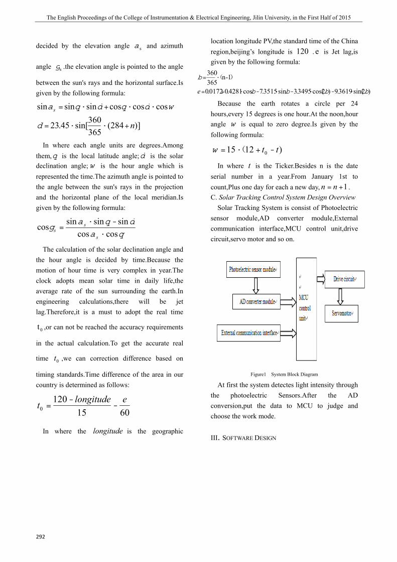
The English Proceedings of the College of Instrumentation & Electrical Engineering, Jilin University, in the First Half of 2015
292
decided by the elevation angle sa and azimuth
angle sg .the elevation angle is pointed to the angle
between the sun's rays and the horizontal surface.Is given by the following formula:
)]284(365360sin[45.23
coscoscossinsinsin
n
s
+··=
··+·=
d
wdqdqa
In where each angle units are degrees.Among them,q is the local latitude angle;d is the solar declination angle;w is the hour angle which is represented the time.The azimuth angle is pointed to the angle between the sun's rays in the projection and the horizontal plane of the local meridian.Is given by the following formula:
qa
dqag
coscossinsinsincos
·
-·=
s
ss
The calculation of the solar declination angle and the hour angle is decided by time.Because the motion of hour time is very complex in year.The clock adopts mean solar time in daily life,the average rate of the sun surrounding the earth.In engineering calculations,there will be jet lag.Therefore,it is a must to adopt the real time
0t ,or can not be reached the accuracy requirements
in the actual calculation.To get the accurate real
time 0t ,we can correction difference based on
timing standards.Time difference of the area in our country is determined as follows:
6015120
0elongitudet -
-=
In where the longitude is the geographic
location longitude PV,the standard time of the China region,beijing’s longitude is 120 . e is Jet lag,is given by the following formula:
)2sin(3619.9)2cos(3495.3sin3515.7cos4281.00172.0
1-n365360
bbbb
b
·-·-·-·+=
·=
e
)(
Because the earth rotates a circle per 24 hours,every 15 degrees is one hour.At the noon,hour angle w is equal to zero degree.Is given by the following formula:
)1215 0 tt -+·= (w
In where t is the Ticker.Besides n is the date serial number in a year.From January 1st to count,Plus one day for each a new day, 1+= nn . C. Solar Tracking Control System Design Overview
Solar Tracking System is consist of Photoelectric sensor module,AD converter module,External communication interface,MCU control unit,drive circuit,servo motor and so on.
Figure1 System Block Diagram
At first the system detectes light intensity through the photoelectric Sensors.After the AD conversion,put the data to MCU to judge and choose the work mode.
III. SOFTWARE DESIGN
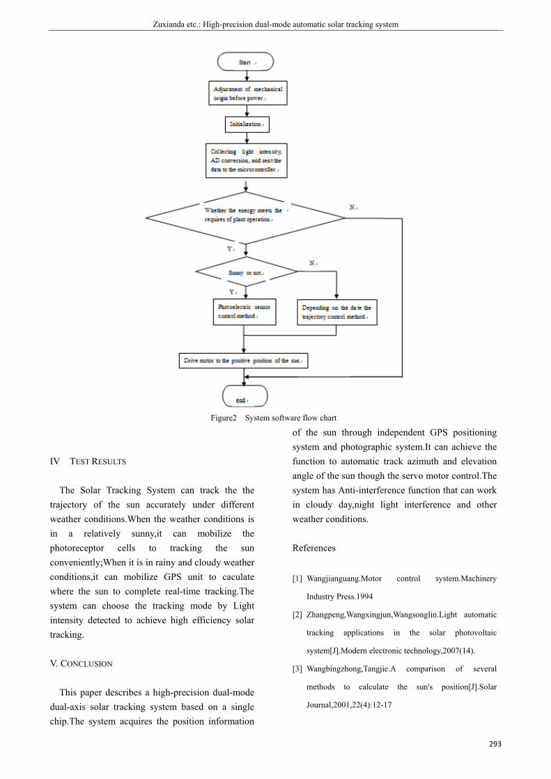
Zuxianda etc.: High-precision dual-mode automatic solar tracking system
293
Figure2 System software flow chart
IV TEST RESULTS
The Solar Tracking System can track the the trajectory of the sun accurately under different weather conditions.When the weather conditions is in a relatively sunny,it can mobilize the photoreceptor cells to tracking the sun conveniently;When it is in rainy and cloudy weather conditions,it can mobilize GPS unit to caculate where the sun to complete real-time tracking.The system can choose the tracking mode by Light intensity detected to achieve high efficiency solar tracking.
V. CONCLUSION
This paper describes a high-precision dual-mode dual-axis solar tracking system based on a single chip.The system acquires the position information
of the sun through independent GPS positioning system and photographic system.It can achieve the function to automatic track azimuth and elevation angle of the sun though the servo motor control.The system has Anti-interference function that can work in cloudy day,night light interference and other weather conditions.
References
[1] Wangjianguang.Motor control system.Machinery
Industry Press.1994
[2] Zhangpeng,Wangxingjun,Wangsonglin.Light automatic
tracking applications in the solar photovoltaic
system[J].Modern electronic technology,2007(14).
[3] Wangbingzhong,Tangjie.A comparison of several
methods to calculate the sun's position[J].Solar
Journal,2001,22(4):12-17

The English Proceedings of the College of Instrumentation & Electrical Engineering, Jilin University, in the First Half of 2015
294
[4] Wangyaonan,Lishutao.Multi-sensor information fusion
and its Applications.Control and Decision,2001,16(5):
518-521
[5] Liusiyang, Wuchunsheng, Pengyanchang. Active
dual-axis solar tracking controller[J].Renewable
Energy,2007,25
[6] Shuzhibing, Tangshisong ,Zhaolixia. Application of
high-precision dual-axis servo design of solar tracking
system.2010.8
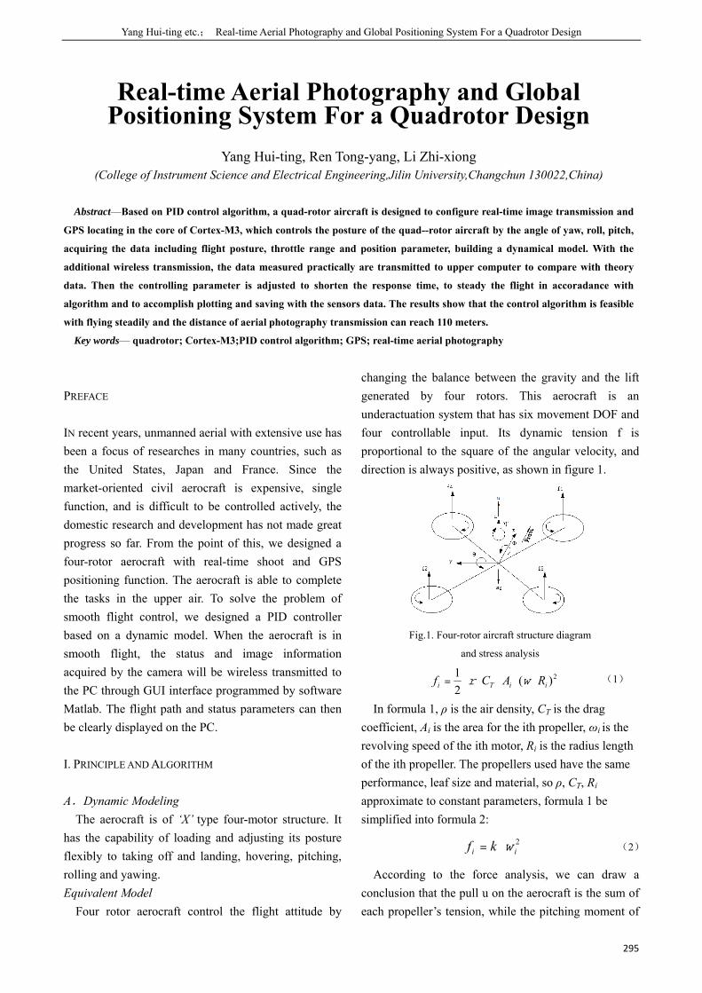
Yang Hui-ting etc.; Real-time Aerial Photography and Global Positioning System For a Quadrotor Design
295
Real-time Aerial Photography and Global Positioning System For a Quadrotor Design
Yang Hui-ting, Ren Tong-yang, Li Zhi-xiong
(College of Instrument Science and Electrical Engineering,Jilin University,Changchun 130022,China)
Abstract—Based on PID control algorithm, a quad-rotor aircraft is designed to configure real-time image transmission and
GPS locating in the core of Cortex-M3, which controls the posture of the quad--rotor aircraft by the angle of yaw, roll, pitch,
acquiring the data including flight posture, throttle range and position parameter, building a dynamical model. With the
additional wireless transmission, the data measured practically are transmitted to upper computer to compare with theory
data. Then the controlling parameter is adjusted to shorten the response time, to steady the flight in accoradance with
algorithm and to accomplish plotting and saving with the sensors data. The results show that the control algorithm is feasible
with flying steadily and the distance of aerial photography transmission can reach 110 meters. Key words— quadrotor; Cortex-M3;PID control algorithm; GPS; real-time aerial photography
PREFACE
IN recent years, unmanned aerial with extensive use has been a focus of researches in many countries, such as the United States, Japan and France. Since the market-oriented civil aerocraft is expensive, single function, and is difficult to be controlled actively, the domestic research and development has not made great progress so far. From the point of this, we designed a four-rotor aerocraft with real-time shoot and GPS positioning function. The aerocraft is able to complete the tasks in the upper air. To solve the problem of smooth flight control, we designed a PID controller based on a dynamic model. When the aerocraft is in smooth flight, the status and image information acquired by the camera will be wireless transmitted to the PC through GUI interface programmed by software Matlab. The flight path and status parameters can then be clearly displayed on the PC.
I. PRINCIPLE AND ALGORITHM
A.Dynamic Modeling The aerocraft is of ‘X’ type four-motor structure. It
has the capability of loading and adjusting its posture flexibly to taking off and landing, hovering, pitching, rolling and yawing.
Equivalent Model Four rotor aerocraft control the flight attitude by
changing the balance between the gravity and the lift generated by four rotors. This aerocraft is an underactuation system that has six movement DOF and four controllable input. Its dynamic tension f is proportional to the square of the angular velocity, and direction is always positive, as shown in figure 1.
Fig.1. Four-rotor aircraft structure diagram
and stress analysis
2)(21
iiTi RACf = wr (1)
In formula 1, ρ is the air density, CT is the drag coefficient, Ai is the area for the ith propeller, ωi is the revolving speed of the ith motor, Ri is the radius length of the ith propeller. The propellers used have the same performance, leaf size and material, so ρ, CT, Ri approximate to constant parameters, formula 1 be simplified into formula 2:
2ii kf w= (2)
According to the force analysis, we can draw a conclusion that the pull u on the aerocraft is the sum of each propeller’s tension, while the pitching moment of
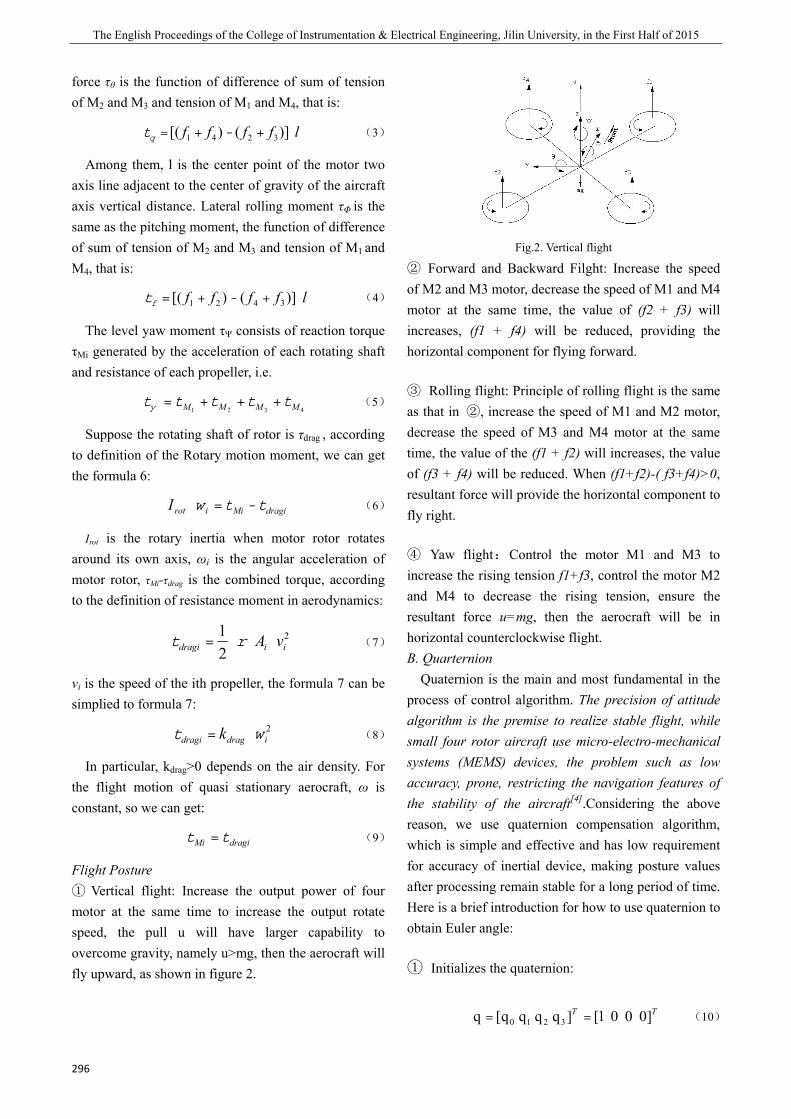
The English Proceedings of the College of Instrumentation & Electrical Engineering, Jilin University, in the First Half of 2015
296
force τθ is the function of difference of sum of tension of M2 and M3 and tension of M1 and M4, that is:
lffff +-+= )]()[( 3241qt (3)
Among them, l is the center point of the motor two axis line adjacent to the center of gravity of the aircraft axis vertical distance. Lateral rolling moment τΦ is the same as the pitching moment, the function of difference of sum of tension of M2 and M3 and tension of M1 and M4, that is:
lffff +-+= )]()[( 3421ft (4)
The level yaw moment τΨ consists of reaction torque τMi generated by the acceleration of each rotating shaft and resistance of each propeller, i.e.
4321 MMMM ttttty +++= (5)
Suppose the rotating shaft of rotor is τdrag , according to definition of the Rotary motion moment, we can get the formula 6:
dragiMiirotI ttw -=
(6)
Irot is the rotary inertia when motor rotor rotates around its own axis, ωi is the angular acceleration of motor rotor, τMi-τdrag is the combined torque, according to the definition of resistance moment in aerodynamics:
2
21
iidragi vA= rt (7)
vi is the speed of the ith propeller, the formula 7 can be simplied to formula 7:
2idragdragi k wt = (8)
In particular, kdrag>0 depends on the air density. For the flight motion of quasi stationary aerocraft, ω is constant, so we can get:
dragiMi tt =
(9)
Flight Posture ① Vertical flight: Increase the output power of four motor at the same time to increase the output rotate speed, the pull u will have larger capability to overcome gravity, namely u>mg, then the aerocraft will fly upward, as shown in figure 2.
Fig.2. Vertical flight
② Forward and Backward Filght: Increase the speed of M2 and M3 motor, decrease the speed of M1 and M4 motor at the same time, the value of (f2 + f3) will increases, (f1 + f4) will be reduced, providing the horizontal component for flying forward.
③ Rolling flight: Principle of rolling flight is the same as that in ②, increase the speed of M1 and M2 motor, decrease the speed of M3 and M4 motor at the same time, the value of the (f1 + f2) will increases, the value of (f3 + f4) will be reduced. When (f1+f2)-( f3+f4)>0, resultant force will provide the horizontal component to fly right.
④ Yaw flight:Control the motor M1 and M3 to increase the rising tension f1+f3, control the motor M2 and M4 to decrease the rising tension, ensure the resultant force u=mg, then the aerocraft will be in horizontal counterclockwise flight. B. Quarternion
Quaternion is the main and most fundamental in the process of control algorithm. The precision of attitude algorithm is the premise to realize stable flight, while small four rotor aircraft use micro-electro-mechanical systems (MEMS) devices, the problem such as low accuracy, prone, restricting the navigation features of the stability of the aircraft[4].Considering the above reason, we use quaternion compensation algorithm, which is simple and effective and has low requirement for accuracy of inertial device, making posture values after processing remain stable for a long period of time. Here is a brief introduction for how to use quaternion to obtain Euler angle:
① Initializes the quaternion:
TT ]0 0 0 1[]q q q q[q 3210 == (10)
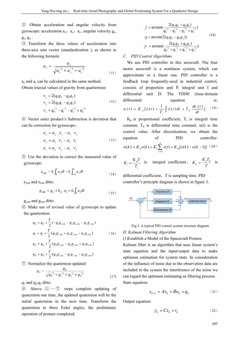
Yang Hui-ting etc.; Real-time Aerial Photography and Global Positioning System For a Quadrotor Design
297
② Obtain acceleration and angular velocity from gyroscope: acceleration ax、ay、az , angular velocity gx, gy, gz . ③ Transform the three values of acceleration into three-axis uint vector (standardization ), as shown in the following formula:
(11)
ay and az can be calculated in the same method. Obtain triaxial values of gravity from quarternion:
2^
32^
22^
12^
0
3210
2031
)(2)(2
qqqqv
qqqqvqqqqv
z
y
x
+--=
-=
-= (12)
④ Vector outer product’s Subtraction is deviation that can be correction for gyroscope.:
xyyxz
zxxzy
yzzyx
vavae
vavae
vayae
-=
-=
-=
(13)
⑤ Use the deviation to correct the measured value of gyroscope:
(14)
eyint and ezint ditto.
(15)
gyint and gzint ditto. ⑥ Make use of revised value of gyroscope to update
the quarternion.
)(2
)(2
)(2
)(2
int2int1int000
int3int2int022
int3int2int011
int3int2int100
xyz
xzy
zyx
zyx
gqgqgqTqq
gqgqgqTqq
gqgqgqTqq
gqgqgqTqq
--+=
+-+=
-++=
---+=
(16)
⑦ Normalize the quaternion updated:
(17) q1 and q2,q3 ditto. ⑧ Above ① ~ ⑦ steps complete updating of quaternion one time, the updated quaternion will be the initial quaternion in the next time. Transform the quaternion to three Euler angles, the preliminary operation of posture completed.
))(2arctan(
))(2arcsin(
))(2arctan(
2^3
2^2
2^1
2^0
3021
2031
2^3
2^2
2^1
2^0
1032
qqqqqqqq
qqqqqqqq
qqqq
+++
+=
-=
+--
+=
y
q
j
(18)
C. PID Control Algorithms We use PID controller in this aerocraft. The four
motor aerocraft is a nonlinear system, which can approximate to a linear one. PID controller is a feedback loop frequently-used in industrial control, consists of proportion unit P, integral unit I and differential unit D. The TDDE (time-domain differential equation is:
])()(1)([)( ∫ ++=dt
tdeTdtteT
teKtu di
p (19)
Kp is proportional coefficient, Ti is integral time constant, Td is differential time constant, u(t) is the control value. After discretization, we obtain the equation of PID controller:
)]1()([)()()(0
--++= ∑=
kekeKieKkeKku d
k
iip
(20)
i
pi T
TKK = is integral coefficient,
TTK
K dpd = is
differential coefficient,T is sampling time. PID controller’s principle diagram is shown in figure 3.
Fig.3. A typical PID control system structure diagram
D. Kalman Filtering Algorithm
(1)Establish a Model of the Spacecraft Posture Kalman filter is an algorithm that uses linear system’s state equation and the input/output data to make optimum estimation for system state. In consideration of the influence of noise due to the observation data are included in the system the interference of the noise we can regard the optimum estimating as filtering process. State equation:
kkkk qBuAxx ++=+1 (21)
Output equation:
kkk rCxy += (22)
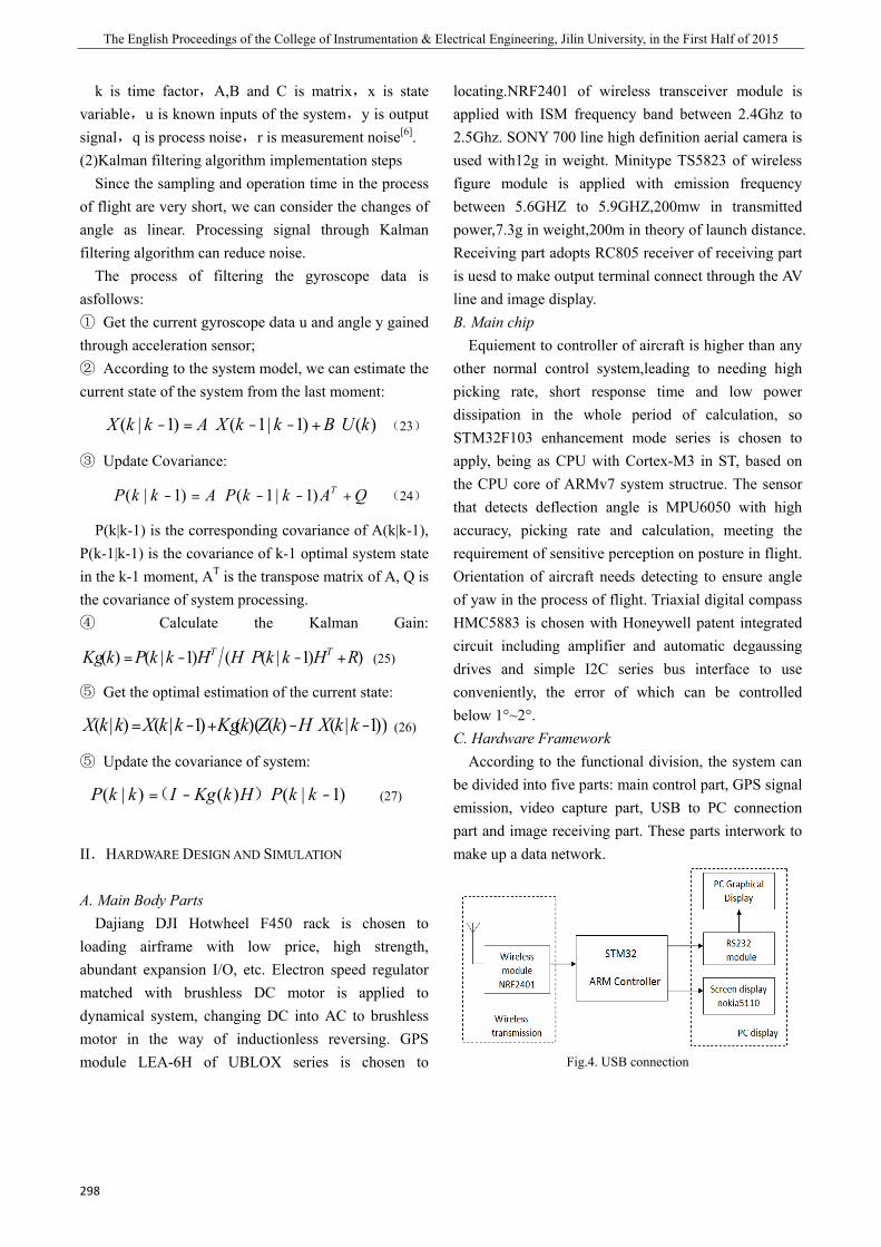
The English Proceedings of the College of Instrumentation & Electrical Engineering, Jilin University, in the First Half of 2015
298
k is time factor,A,B and C is matrix,x is state variable,u is known inputs of the system,y is output signal,q is process noise,r is measurement noise[6]. (2)Kalman filtering algorithm implementation steps
Since the sampling and operation time in the process of flight are very short, we can consider the changes of angle as linear. Processing signal through Kalman filtering algorithm can reduce noise.
The process of filtering the gyroscope data is asfollows: ① Get the current gyroscope data u and angle y gained through acceleration sensor; ② According to the system model, we can estimate the current state of the system from the last moment:
)()1|1()1|( kUBkkXAkkX +--=- (23)
③ Update Covariance:
QAkkPAkkP T +--=- )1|1()1|( (24)
P(k|k-1) is the corresponding covariance of A(k|k-1), P(k-1|k-1) is the covariance of k-1 optimal system state in the k-1 moment, AT is the transpose matrix of A, Q is the covariance of system processing. ④ Calculate the Kalman Gain:
))1|(()1|()( RHkkPHHkkPkKg TT +--= (25)
⑤ Get the optimal estimation of the current state:
))1|()()(()1|()|( --+-= kkXHkZkKgkkXkkX (26)
⑤ Update the covariance of system:
)1|()()|( --= kkPHkKgIkkP )( (27)
II.HARDWARE DESIGN AND SIMULATION
A. Main Body Parts Dajiang DJI Hotwheel F450 rack is chosen to
loading airframe with low price, high strength, abundant expansion I/O, etc. Electron speed regulator matched with brushless DC motor is applied to dynamical system, changing DC into AC to brushless motor in the way of inductionless reversing. GPS module LEA-6H of UBLOX series is chosen to
locating.NRF2401 of wireless transceiver module is applied with ISM frequency band between 2.4Ghz to 2.5Ghz. SONY 700 line high definition aerial camera is used with12g in weight. Minitype TS5823 of wireless figure module is applied with emission frequency between 5.6GHZ to 5.9GHZ,200mw in transmitted power,7.3g in weight,200m in theory of launch distance. Receiving part adopts RC805 receiver of receiving part is uesd to make output terminal connect through the AV line and image display. B. Main chip
Equiement to controller of aircraft is higher than any other normal control system,leading to needing high picking rate, short response time and low power dissipation in the whole period of calculation, so STM32F103 enhancement mode series is chosen to apply, being as CPU with Cortex-M3 in ST, based on the CPU core of ARMv7 system structrue. The sensor that detects deflection angle is MPU6050 with high accuracy, picking rate and calculation, meeting the requirement of sensitive perception on posture in flight. Orientation of aircraft needs detecting to ensure angle of yaw in the process of flight. Triaxial digital compass HMC5883 is chosen with Honeywell patent integrated circuit including amplifier and automatic degaussing drives and simple I2C series bus interface to use conveniently, the error of which can be controlled below 1°~2°. C. Hardware Framework
According to the functional division, the system can be divided into five parts: main control part, GPS signal emission, video capture part, USB to PC connection part and image receiving part. These parts interwork to make up a data network.
Fig.4. USB connection
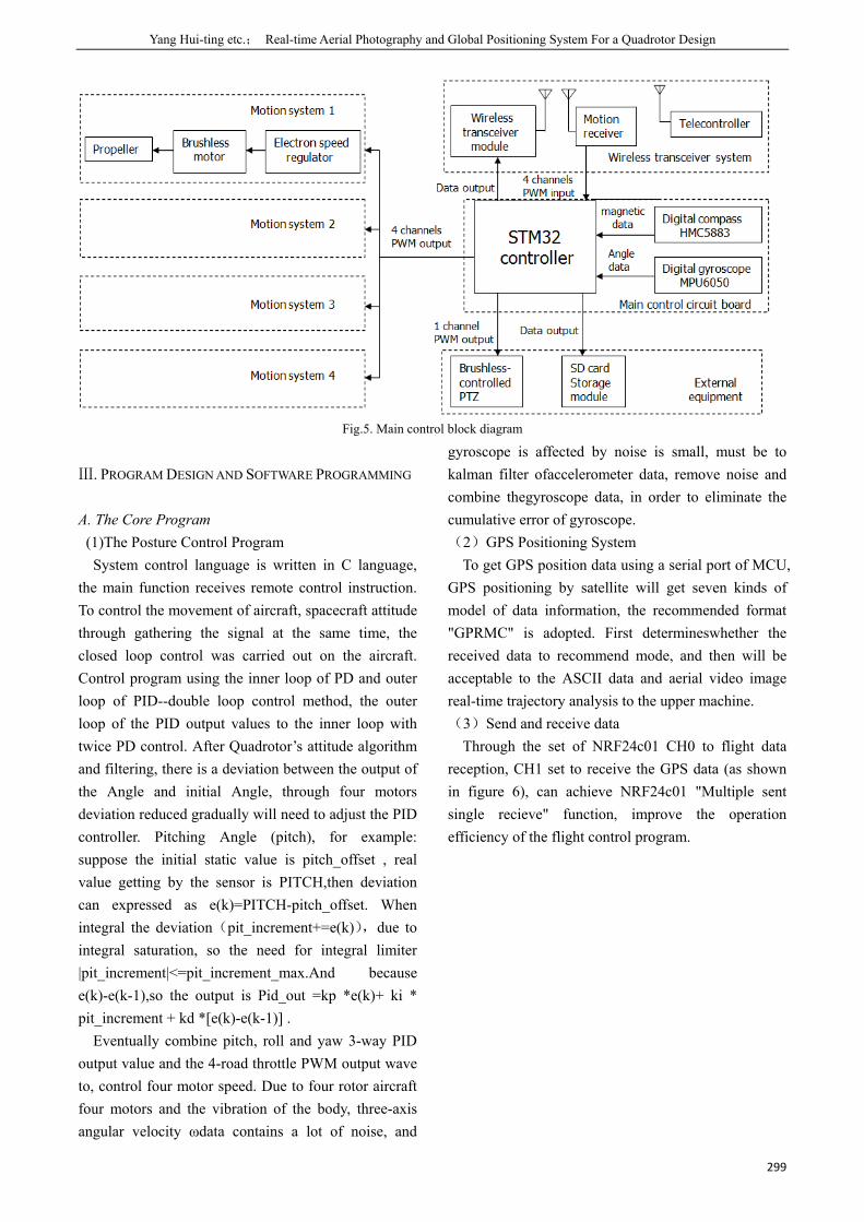
Yang Hui-ting etc.; Real-time Aerial Photography and Global Positioning System For a Quadrotor Design
299
Fig.5. Main control block diagram
Ⅲ. PROGRAM DESIGN AND SOFTWARE PROGRAMMING
A. The Core Program (1)The Posture Control Program
System control language is written in C language, the main function receives remote control instruction. To control the movement of aircraft, spacecraft attitude through gathering the signal at the same time, the closed loop control was carried out on the aircraft. Control program using the inner loop of PD and outer loop of PID--double loop control method, the outer loop of the PID output values to the inner loop with twice PD control. After Quadrotor’s attitude algorithm and filtering, there is a deviation between the output of the Angle and initial Angle, through four motors deviation reduced gradually will need to adjust the PID controller. Pitching Angle (pitch), for example: suppose the initial static value is pitch_offset , real value getting by the sensor is PITCH,then deviation can expressed as e(k)=PITCH-pitch_offset. When integral the deviation(pit_increment+=e(k)),due to integral saturation, so the need for integral limiter |pit_increment|<=pit_increment_max.And because e(k)-e(k-1),so the output is Pid_out =kp *e(k)+ ki * pit_increment + kd *[e(k)-e(k-1)] .
Eventually combine pitch, roll and yaw 3-way PID output value and the 4-road throttle PWM output wave to, control four motor speed. Due to four rotor aircraft four motors and the vibration of the body, three-axis angular velocity ωdata contains a lot of noise, and
gyroscope is affected by noise is small, must be to kalman filter ofaccelerometer data, remove noise and combine thegyroscope data, in order to eliminate the cumulative error of gyroscope. (2)GPS Positioning System
To get GPS position data using a serial port of MCU, GPS positioning by satellite will get seven kinds of model of data information, the recommended format "GPRMC" is adopted. First determineswhether the received data to recommend mode, and then will be acceptable to the ASCII data and aerial video image real-time trajectory analysis to the upper machine. (3)Send and receive data
Through the set of NRF24c01 CH0 to flight data reception, CH1 set to receive the GPS data (as shown in figure 6), can achieve NRF24c01 "Multiple sent single recieve" function, improve the operation efficiency of the flight control program.
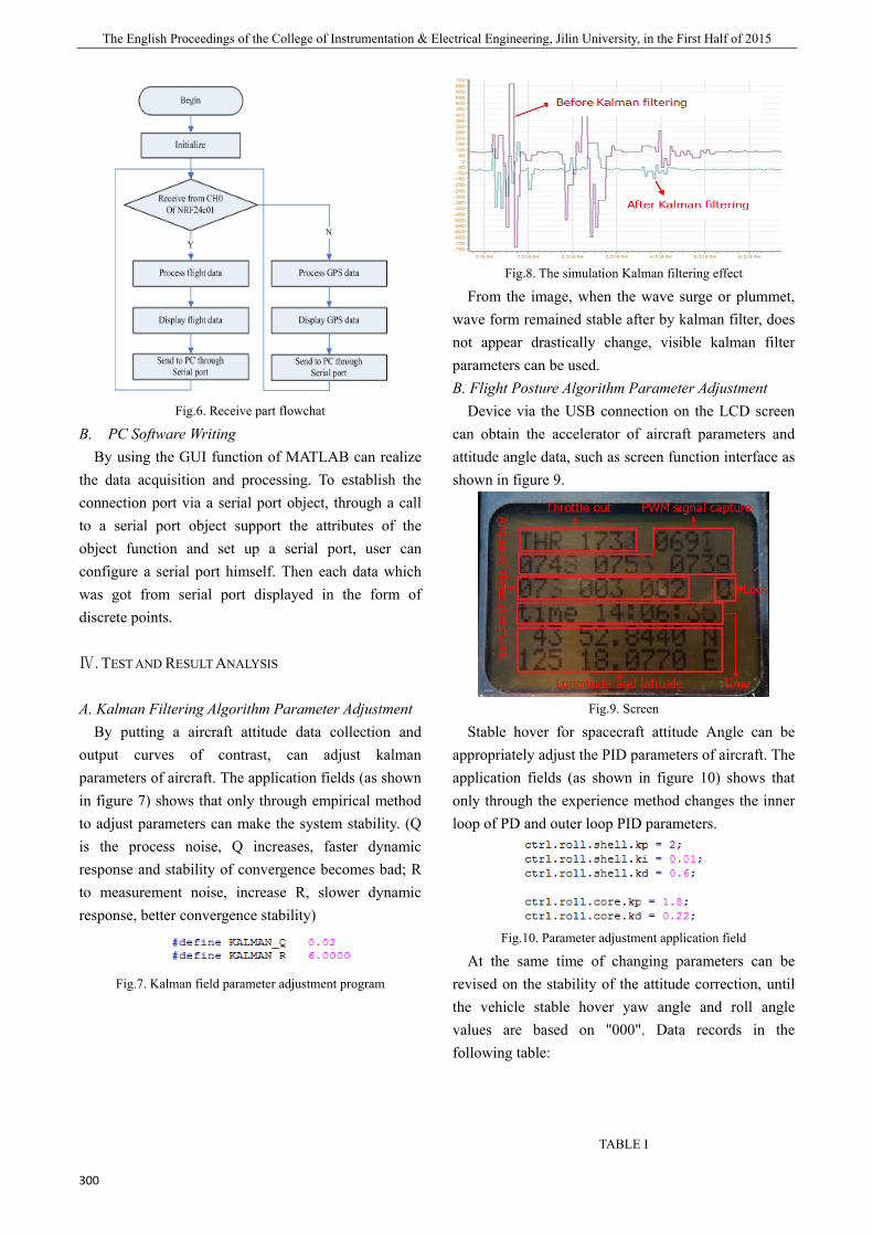
The English Proceedings of the College of Instrumentation & Electrical Engineering, Jilin University, in the First Half of 2015
300
Fig.6. Receive part flowchat
B. PC Software Writing By using the GUI function of MATLAB can realize
the data acquisition and processing. To establish the connection port via a serial port object, through a call to a serial port object support the attributes of the object function and set up a serial port, user can configure a serial port himself. Then each data which was got from serial port displayed in the form of discrete points.
Ⅳ. TEST AND RESULT ANALYSIS
A. Kalman Filtering Algorithm Parameter Adjustment By putting a aircraft attitude data collection and
output curves of contrast, can adjust kalman parameters of aircraft. The application fields (as shown in figure 7) shows that only through empirical method to adjust parameters can make the system stability. (Q is the process noise, Q increases, faster dynamic response and stability of convergence becomes bad; R to measurement noise, increase R, slower dynamic response, better convergence stability)
Fig.7. Kalman field parameter adjustment program
Fig.8. The simulation Kalman filtering effect
From the image, when the wave surge or plummet, wave form remained stable after by kalman filter, does not appear drastically change, visible kalman filter parameters can be used. B. Flight Posture Algorithm Parameter Adjustment
Device via the USB connection on the LCD screen can obtain the accelerator of aircraft parameters and attitude angle data, such as screen function interface as shown in figure 9.
Fig.9. Screen
Stable hover for spacecraft attitude Angle can be appropriately adjust the PID parameters of aircraft. The application fields (as shown in figure 10) shows that only through the experience method changes the inner loop of PD and outer loop PID parameters.
Fig.10. Parameter adjustment application field
At the same time of changing parameters can be revised on the stability of the attitude correction, until the vehicle stable hover yaw angle and roll angle values are based on "000". Data records in the following table:
TABLE I

Yang Hui-ting etc.; Real-time Aerial Photography and Global Positioning System For a Quadrotor Design
301
FLIGHT POSTURE ADJUSTMENT FORM
C. Graphical trajectory of the GPS sampling data GUI programming based on MATLAB, display the
coordinate was get from serial port, location coordinate
was obtained. Figure 11 is the result of location coordinates when aircraft approximately do hovering attitude. By the test results can be seen that the aircraft’s location are probably on the 43.8807 °north latitude and 125.3012 ° east longitude. GPS signal drift, but within the measure precision of the GPS module. GUI graphical interface for location information can be very clear and intuitive display, eliminating the steps for the complex data conversion and processing.
Fig.11. GUI perface
D. Real-time Image acquisition result Real-time image acquisition results by wireless
transmission module in the process of flight can be displayed through the TFT screen after image acquisition (as shown in figure 11). Cooperating on the STM32 control, MPU6050 module level sensor is driven by brushless motor PTZ, which makes the aircraft flying in any position, they can always keep camera horizontal, provides a convenient manipulation. The small TFT screen image compared with PC screen screenshots as shown in figure 12.
Fig.12. Fly effect
Flying screen effect from screen can be seen, the system can reflect spacecraft environment clearly and truly and have good effect, conform to the anticipated target. Experiment as a whole works as shown in figure 13.
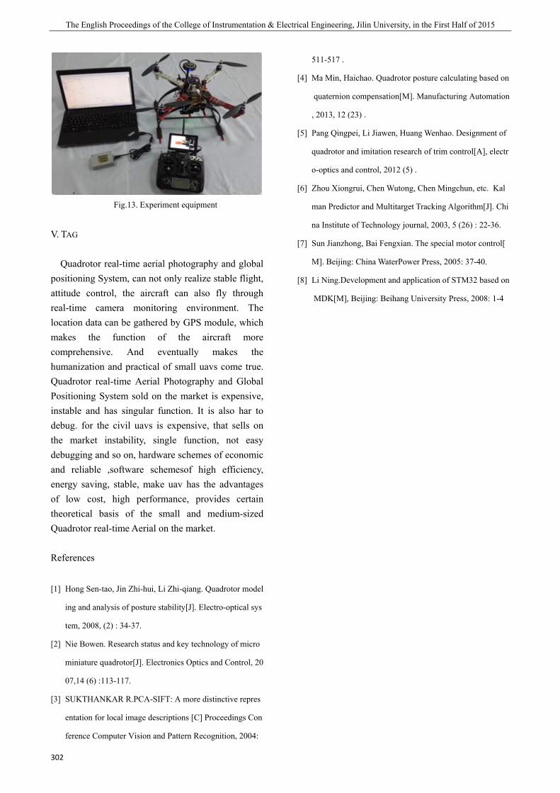
The English Proceedings of the College of Instrumentation & Electrical Engineering, Jilin University, in the First Half of 2015
302
Fig.13. Experiment equipment
V. TAG
Quadrotor real-time aerial photography and global positioning System, can not only realize stable flight, attitude control, the aircraft can also fly through real-time camera monitoring environment. The location data can be gathered by GPS module, which makes the function of the aircraft more comprehensive. And eventually makes the humanization and practical of small uavs come true. Quadrotor real-time Aerial Photography and Global Positioning System sold on the market is expensive, instable and has singular function. It is also har to debug. for the civil uavs is expensive, that sells on the market instability, single function, not easy debugging and so on, hardware schemes of economic and reliable ,software schemesof high efficiency, energy saving, stable, make uav has the advantages of low cost, high performance, provides certain theoretical basis of the small and medium-sized Quadrotor real-time Aerial on the market.
References
[1] Hong Sen-tao, Jin Zhi-hui, Li Zhi-qiang. Quadrotor model
ing and analysis of posture stability[J]. Electro-optical sys
tem, 2008, (2) : 34-37.
[2] Nie Bowen. Research status and key technology of micro
miniature quadrotor[J]. Electronics Optics and Control, 20
07,14 (6) :113-117.
[3] SUKTHANKAR R.PCA-SIFT: A more distinctive repres
entation for local image descriptions [C] Proceedings Con
ference Computer Vision and Pattern Recognition, 2004:
511-517 .
[4] Ma Min, Haichao. Quadrotor posture calculating based on
quaternion compensation[M]. Manufacturing Automation
, 2013, 12 (23) .
[5] Pang Qingpei, Li Jiawen, Huang Wenhao. Designment of
quadrotor and imitation research of trim control[A], electr
o-optics and control, 2012 (5) .
[6] Zhou Xiongrui, Chen Wutong, Chen Mingchun, etc. Kal
man Predictor and Multitarget Tracking Algorithm[J]. Chi
na Institute of Technology journal, 2003, 5 (26) : 22-36.
[7] Sun Jianzhong, Bai Fengxian. The special motor control[
M]. Beijing: China WaterPower Press, 2005: 37-40.
[8] Li Ning.Development and application of STM32 based on
MDK[M], Beijing: Beihang University Press, 2008: 1-4


![[Acronym] Proceedings - UFG](https://static.fdokumen.com/doc/165x107/631430486ebca169bd0abf4b/acronym-proceedings-ufg.jpg)