PROCEEDINGS OF SPIE
161
PROCEEDINGS OF SPIE SPIEDigitalLibrary.org/conference-proceedings-of-spie Optical Technology and Measurement for Industrial Applications Conference , "Optical Technology and Measurement for Industrial Applications Conference," Proc. SPIE 11142, Optical Technology and Measurement for Industrial Applications Conference, 1114201 (21 April 2019); doi: 10.1117/12.2535570 Event: Optics and Photonics International Congress, 2019, Yokohama, Japan Downloaded From: https://www.spiedigitallibrary.org/conference-proceedings-of-spie on 11 Feb 2022 Terms of Use: https://www.spiedigitallibrary.org/terms-of-use
-
Upload
khangminh22 -
Category
Documents
-
view
2 -
download
0
Transcript of PROCEEDINGS OF SPIE

PROCEEDINGS OF SPIE
SPIEDigitalLibrary.org/conference-proceedings-of-spie
Optical Technology andMeasurement for IndustrialApplications Conference
, "Optical Technology and Measurement for Industrial ApplicationsConference," Proc. SPIE 11142, Optical Technology and Measurement forIndustrial Applications Conference, 1114201 (21 April 2019); doi:10.1117/12.2535570
Event: Optics and Photonics International Congress, 2019, Yokohama, Japan
Downloaded From: https://www.spiedigitallibrary.org/conference-proceedings-of-spie on 11 Feb 2022 Terms of Use: https://www.spiedigitallibrary.org/terms-of-use

PROCEEDINGS OF SPIE
Volume 11142
Proceedings of SPIE, V. 11142
SPIE is an international society advancing an interdisciplinary approach to the science and application of light.
Optical Technology and Measurement for Industrial Applications Conference Takeshi Hatsuzawa Editor
22–26 April 2019 Yokohama, Japan Published by SPIE
Optical Technology and Measurement for Industrial Applications Conference, edited by Takeshi Hatsuzawa, Proc. of SPIE Vol. 11142, 1114201 · © Optics & Photonics International Congress 2019 · doi: 10.1117/12.2535570
Proc. of SPIE Vol. 11142 1114201-1Downloaded From: https://www.spiedigitallibrary.org/conference-proceedings-of-spie on 11 Feb 2022Terms of Use: https://www.spiedigitallibrary.org/terms-of-use

Contents
vii Author Index
ix Conference Committee
ORAL SESSION 1 OPTM-1-02
OPTM-1-03
Towards happy marriage between optics/photonics and AI: A mini tutorial with a historical perspective Optical frequency metrology with frequency combs and stabilized lasers
ORAL SESSION 2 OPTM-2-01
OPTM-2-02 OPTM-2-03 OPTM-2-04 OPTM-2-05
On Carrier Fringe Pattern Analysis 3D profilometry by projecting polarization pattern Self-correction of phase errors induced by projector nonlinearity in phase-shifting fringe projection profilometry High-speed 3D surface measurement of rear lamp housing by automatic digital fringe projection system Response function measurement in photovoltaic devices with sinusoidal structured illumination
ORAL SESSION 3 OPTM-3-01
OMC-3-02 OMC-3-03 OMC-3-04
Innovations in Structured Light Methods and Optical Metrology Development of Handy Type Full-color and Real-time 3D Measurement System Using Linear LED Device Accuracy estimation of a 3D reconstruction method for scanning electron microscope images Design of FPGA-based signal-processing system based on the direct phase determination method for heterodyne interferometry
Proc. of SPIE Vol. 11142 1114201-2Downloaded From: https://www.spiedigitallibrary.org/conference-proceedings-of-spie on 11 Feb 2022Terms of Use: https://www.spiedigitallibrary.org/terms-of-use

ORAL SESSION 4 OPTM-4-01
OMC-4-02 OMC-4-03
High-speed ghost imaging by deep learning Automatic rice seed imaging system for varieties classification Light-source color correlation of wide-field spectroscopic imaging for the adaption to spatial and temporal variations when using an unmanned aerial vehicle
ORAL SESSION 5 OPTM-5-01
OPTM-5-02 OPTM-5-03 OPTM-5-04 OPTM-5-05
Systematic error correction for phase detection in sinusoidal frequency modulation displacement measuring interferometer An optical angle sensor based on second harmonic generation of a mode-locked laser Machine learning for rapid adaptation to individual optical differences for noninvasive blood glucose sensor using mid-infrared Rigorous analysis of reflection spectrum of absorbing film Optical Design of Transmission Raman Spectrometer Based on the Plane Reflective Grating
ORAL SESSION 6 OPTM-6-01
OPTM-6-02 OPTM-6-03 OPTM-6-04 OPTM-6-05
Polarization camera performance optimization Snapshot imaging polarimetry based on structured interference fringes Spectroscopic Ellipsometry Study on Aluminium-Doped Zinc Oxide Thin Films Prepared via DC Magnetron Sputtering and HiPIMS Imaging ellipsometry of porous silicon Effect of oxide layer thickness on polarization mitigation
ORAL SESSION 7 OPTM-7-02
OPTM-7-03 OPTM-7-04
High-Precise Optical Shape Measurement with Full-Field Heterodyne Interferometry Optical profilometry of cylindrical openings for translucent objects Weak value amplification of skew aberration Role of the zeroth-order diffraction beam and scattering light in three-dimensional shape measurement of fine structure by detecting phase distribution based on speckle interferometry
Proc. of SPIE Vol. 11142 1114201-3Downloaded From: https://www.spiedigitallibrary.org/conference-proceedings-of-spie on 11 Feb 2022Terms of Use: https://www.spiedigitallibrary.org/terms-of-use

ORAL SESSION 8 OPTM-8-01
OPTM-8-02 OPTM-8-03 OPTM-8-04 OPTM-8-05 OPTM-8-06
Numerical Analysis of Near-Field Light Intensity of Whispering Gallery Mode on Microsphere Surface with SNOM Probe Light attenuation in the bistatic scattering measurement in the atmosphere Flyable Mirrors: Laser Scanning Vibrometry Method for Monitoring Large Engineering Structures Using Drones Fabrication of three dimensional nano-periodic structure by the Talbot lithography using multiple exposure Optical Trapping of Airborne Droplet for Laser Fabrication of 3-Dimensional Structure based on Optical Trapping Potential using Radially Polarized Beam Evaluation of influences of thin lubricant on fringe projection measurements
POSTER SESSION OPTM-P-01
OPTM-P-02 OPTM-P-03 OPTM-P-04 OPTM-P-05 OPTM-P-06 OPTM-P-07 OPTM-P-08 OPTM-P-09 OPTM-P-10 OPTM-P-11 OPTM-P-12
2D and 3D Vision Based Face Recognition System A multi-axis space coordinate system calibration method for composite line laser measuring systems using non-feature planes and multi-angle spheres Tuning focal length of vari-focal lens for color 3D object reconstruction Active optical systems with novel metal brightness amplifiers Phase analysis of light carrying optical vortex for refractive index sensing SMS and FBG interrogation for measurement of temperature and strain using OTDR Laguerre-Gaussian self-trapped beams in optical lattices Development of an Anamorphic Liquid-pressure Varifocal Lens Digital holographic analyzer of optical fiber inhomogeneity at the soldering region Design of high-FOV automatic optical inspection lens for linear sensor with different magnification Characterization of Erbium Doped Phosphate Glasses by Terahertz Time Domain Spectroscopy Performance Analysis of Structured Light Elements with Various Diffraction Patterns Research on measurement method of coincidence degree for remote micro-objects based on parallel light
Proc. of SPIE Vol. 11142 1114201-4Downloaded From: https://www.spiedigitallibrary.org/conference-proceedings-of-spie on 11 Feb 2022Terms of Use: https://www.spiedigitallibrary.org/terms-of-use

OPTM-P-13 OPTM-P-14
Detection of optical vortices using various interferometers Modeling of optical frequency domain reflectometer based on self-sweeping fiber laser
Proc. of SPIE Vol. 11142 1114201-5Downloaded From: https://www.spiedigitallibrary.org/conference-proceedings-of-spie on 11 Feb 2022Terms of Use: https://www.spiedigitallibrary.org/terms-of-use

Proc. of SPIE Vol. 11142 1114201-6Downloaded From: https://www.spiedigitallibrary.org/conference-proceedings-of-spie on 11 Feb 2022Terms of Use: https://www.spiedigitallibrary.org/terms-of-use

Authors Numbers in the index correspond to the numbers in the table of contents. Adachi, Satoru, OPTM-5-03 Aketagawa, Masato, OPTM-3-04, OPTM-5-01 Akiyama, Taiki, OPTM-6-04 Aoki, Sadao, OPTM-5-04 Arai, Yasuhiko, OPTM-7-04 Atakaramians, Shaghik, OPTM-P-10 Banerjee, Suchandra, OPTM-6-05 Banerjee, Saswatee, OPTM-5-04 Bierig, Andreas, OPTM-8-03 Buranasiri, Prathan, OPTM-6-03 Cai, Qisheng, OPTM-P-12 Chaitavon, Kosom, OPTM-4-02 Chen, Fong-Zhi, OPTM-P-09 Cheng, Pi-Ying, OPTM-P-03 Cheng, Yuan-Chieh, OPTM-P-09 Chipman, Russell, OPTM-6-05 Chou, Chun-Han, OPTM-P-11 CHU, Bohuai, OPTM-8-01 Chu, Yushi, OPTM-P-10 Dembele, Vamara, OPTM-6-02 Deng, Qiwen, OPTM-2-05 Dey, Koustav, OPTM-P-06 Fan, Desheng, OPTM-P-10 Fu, Xinghu, OPTM-P-10 Fujigaki, Motoharu, OPTM-3-02 Gao, Huiliang, OPTM-8-02 Gao, Wei, OPTM-5-02 Gavril’eva, K., OPTM-P-13 Gelloz, Bernard, OPTM-6-04, OPTM-7-03 Guo, Hongwei, OPTM-2-03 Hagen, Nathan, OPTM-2-02, OPTM-6-01, OPTM-6-05 Han, Wei, OPTM-P-12 Hassan, Saher, OPTM-8-03 Hausotte, Tino, OPTM-8-06 Hayashi, Masahiro, OPTM-8-05 Higuchi, Masato, OPTM-3-04, OPTM-5-01 Hino, Makoto, OPTM-P-07 Hoi, Cheng-Fang, OPTM-P-09 Hong, Feng-Lei, OPTM-1-03 Horprathum, Mati, OPTM-6-03 Hoshino, Tetsuya, OPTM-5-04 Huang, Min, OPTM-P-12 Huang, Ting-Ming, OPTM-P-09 Huang, Kuo-Cheng, OPTM-P-11 Iizuka, Yuki, OPTM-6-04 Ishimaru, Ichiro, OPTM-4-03, OPTM-5-03 Ismail, Mohamed, OPTM-8-03 Ismailov, Ismail, OPTM-P-08 Itoh, Masahide, OPTM-5-04 Iwaki, Junya, OPTM-5-03
Jin, Lianhua, OPTM-6-04, OPTM-7-03 Kang, Hanyue, OPTM-4-03, OPTM-5-03 Kawashima, Natsumi, OPTM-4-03, OPTM-5-03 Kemao, Qian, OPTM-2-01 Kim, Daesuk, OPTM-6-02 Kiratiratanapruk, Kantip, OPTM-4-02 Kishimoto, Takumi, OPTM-3-02 Kishore, P., OPTM-P-06 Kitazaki, Tomoya, OPTM-4-03, OPTM-5-03 Ko, Do-Kyeong, OPTM-P-05 Kofman, Jonathan, OPTM-3-01 Kondoh, Eiichi, OPTM-6-04 Kong, Xinxin, OPTM-7-02 Kumar, B., OPTM-P-06 Kumme, R., OPTM-8-03 Kuwano, Ryoichi, OPTM-P-07 Lertvanithphol, Tossaporn, OPTM-6-03 Li, HuanHuan, OPTM-P-02 Li, Shiping, OPTM-2-05 Li, Yang, OPTM-7-02 Li, Ying, OPTM-2-05 Lin, Yu-Hsuan, OPTM-P-11 Lin, Jing-Sheuan, OPTM-P-03 Lin, Bin, OPTM-P-01 Liu, Cheng-Yang, OPTM-2-04 Liu, Xinran, OPTM-3-01 Lobach, Ivan, OPTM-P-14 Lu, Xiangning, OPTM-P-12 Lv, Qunbo, OPTM-5-05 Ma, Yuzhao, OPTM-8-02 Madokoro, Shuhei, OPTM-5-02 Maeda, Yuki, OPTM-2-02 Matsukuma, Hiraku, OPTM-5-02 Mermoul, A., OPTM-P-13 Metzner, Sebastian, OPTM-8-06 Michihata, Masaki, OPTM-8-01, OPTM-8-05 Mizutani, Yasuhiro, OPTM-4-01, OPTM-8-04 Mizutani, Sora, OPTM-4-03 Morita, Sho, OPTM-P-07 Na, Youngbin, OPTM-P-05 Nakanishi, Hiroki, OPTM-8-04 Nakao, Masaru, OPTM-5-02 Nguyen, Dong, OPTM-3-04 Otani, Yukitoshi, OPTM-2-02, OPTM-6-01, OPTM-6-05, OPTM-P-07 Pei, Linlin, OPTM-5-05 Poletaev, Dmitrii, OPTM-P-08 Poolcharuansin, Phitsanu, OPTM-6-03 Porntheeraphat, Supanit, OPTM-4-02 Prasertsak, Anchalee, OPTM-4-02 Prempree, Panintorn, OPTM-4-02
Proc. of SPIE Vol. 11142 1114201-7Downloaded From: https://www.spiedigitallibrary.org/conference-proceedings-of-spie on 11 Feb 2022Terms of Use: https://www.spiedigitallibrary.org/terms-of-use

Prisyajniuk, Andrey, OPTM-P-08 Quang, Anh, OPTM-3-04 Reithmeier, Eduard, OPTM-3-03 Reuter, Tamara, OPTM-8-06 Roy, Sourabh, OPTM-P-06 Sakurai, Kenji, OPTM-5-04 Seawsakul, Kittikhun, OPTM-6-03 Sevryugin, A., OPTM-P-13 Shankar, M., OPTM-P-06 Sheroshenko, Vladislav, OPTM-P-13 Shibata, Shuhei, OPTM-2-02, OPTM-6-01 Shimizu, Yuki, OPTM-5-02 Shostka, Nataliya, OPTM-P-08 Sinthupinyo, Wasin, OPTM-4-02 Sokolenko, Bogdan, OPTM-P-08 Songsiriritthigul, Prayoon, OPTM-6-03 Sun, Jianying, OPTM-5-05 Takahashi, Satoro, OPTM-8-01, OPTM-8-05 Takamasu, Kiyoshi, OPTM-8-01, OPTM-8-05 Takaya, Yasuhiro, OPTM-4-01, OPTM-8-04 Takeda, Mitsuo, OPTM-1-02 Temniranrat, Pitchayagan, OPTM-4-02 Teng, Li-Wei, OPTM-2-04 Tkachenko, Alina, OPTM-P-14 Toeberg, Stefan, OPTM-3-03 Tokunaga, Tsuyoshi, OPTM-P-07 Trigub, Maxim, OPTM-P-04 Tsai, Hsin-Yi, OPTM-P-11 Tutsch, Rainer, OPTM-7-01 Vasnev, Nikolay, OPTM-P-04 Vlasov, Vasiliy, OPTM-P-04 Wang, Cheng-Yu, OPTM-2-04 Wang, Ruisong, OPTM-8-02 Watanabe, Norio, OPTM-5-04 Wei, Dong, OPTM-3-04, OPTM-5-01 Wei, Shuen, OPTM-P-10 Weng, Chun-Jen, OPTM-P-03 Wu, Zhou, OPTM-7-02 Xiangli, Bin, OPTM-7-02 Xiao, Gui, OPTM-P-10 Xing, Shuo, OPTM-2-03 Xiong, Xinglong, OPTM-8-02 Xu, Changda, OPTM-P-02 Yagi, Otoki, OPTM-4-01 Yamamoto, Naoyuki, OPTM-5-03 Yokei, Makoto, OPTM-8-05 Yokoyama, Kotone, OPTM-4-03 Yoshizawa, Toru, OPTM-7-03 Zhang, Zibang, OPTM-2-05 Zhang, Mengyue, OPTM-P-01 Zhang, Wenxi, OPTM-7-02 Zhang, Runan, OPTM-P-10 Zhao, Zheng, OPTM-8-01 Zhong, Jingang, OPTM-2-05 Zhou, Xiang, OPTM-P-02
Proc. of SPIE Vol. 11142 1114201-8Downloaded From: https://www.spiedigitallibrary.org/conference-proceedings-of-spie on 11 Feb 2022Terms of Use: https://www.spiedigitallibrary.org/terms-of-use

Conference Committee
Conference Chair
Takeshi Hatsuzawa, Tokyo Institute of Technology (Japan)
Conference Co-chairs
Rainer Tutsch, Technische Universität Braunschweig (Germany) Toru Yoshizawa, Tokyo University of Agriculture and Technology
(Japan)
Conference Program Committee
Masato Aketagawa, Nagaoka University of Technology (Japan) Yasuhiko Arai, Kansai University (Japan) Prathan Buranasiri, King Mongkut's Institute of Technology
Ladkrabang (Thailand) Jürgen W. Czarske, TU Dresden (Germany) Motoharu Fujigaki, University of Fukui (Japan) Amalia Martínez-García, Centro de Investigaciones en Óptica, A.C.
(Mexico) Satoshi Gonda, National Institute of Advanced Industrial Science and
Technology (Japan) Sen Han, University of Shanghai for Science and Technology (China) Feng-Lei Hong, Yokohama National University (Japan) Nathan Hagen, Utsunomiya University (Japan) Hideki Ina, Canon Inc. (Japan) Ichiro Ishimaru, Kagawa University (Japan) Lianhua Jin, University of Yamanashi (Japan) Daesuk Kim, Chonbuk National University (Korea, Republic of) Jonathan D. Kofman, University of Waterloo (Canada) Kazuhide Kamiya, Toyama Prefectural University (Japan) Qian Kemao, Nanyang Technological University (Singapore) Fumio Koyama, Tokyo Institute of Technology (Japan) Ryoichi Kuwano, Hiroshima Institute of Technology (Japan) Yu-Lung Lo, National Cheng Kung University (Taiwan) Yasuhiro Mizutani, Osaka University (Japan) Christian Rembe, Technische Universität Clausthal (Germany) Yukitoshi Otani, Utsunomiya University (Japan) Pavel Pavlicek, Palacký University Olomouc (Czech Republic) Takamasa Suzuki, Niigata University (Japan)
Proc. of SPIE Vol. 11142 1114201-9Downloaded From: https://www.spiedigitallibrary.org/conference-proceedings-of-spie on 11 Feb 2022Terms of Use: https://www.spiedigitallibrary.org/terms-of-use

Satoru Takahashi, The University of Tokyo (Japan) Toshiyuki Takatsuji, National Institute of Advanced Industrial Science
and Technology (Japan) Toshitaka Wakayama, Saitama Medical University (Japan) Wei-Chung Wang, National Tsing Hua University (Taiwan) Gao Wei, Tohoku University (Japan) Jiangtao Xi, University of Wollongong (Australia) Hayato Yoshioka, Tokyo Institute of Technology (Japan) Song Zhang, Purdue University (United States)
Proc. of SPIE Vol. 11142 1114201-10Downloaded From: https://www.spiedigitallibrary.org/conference-proceedings-of-spie on 11 Feb 2022Terms of Use: https://www.spiedigitallibrary.org/terms-of-use
I Introduction Many of recent innovations in science and technology
have been brought about by cross-disciplinary research. Understanding different fields of sciences provides new insights into one’s own field and also can spark ideas for technological innovation. The talk will explain, with examples, how this synergy of knowledge applies also to the fields of optics/photonics (OP) and AI, which, until recently, have developed independently with different disciplines of physical sciences and information sciences.
II Historical Analogy
To get a perspective of the cross-disciplinary research between OP and AI, we first refer to the historical analogy to the prior example of the successful cross-disciplinary research between OP and communication engineering (CE). The successful OP-CE integration was achieved by bidirectional technology transfer, namely (1) introduction of OP technologies (laser diodes and optical fibers) to CE, which gave birth to today’s broadband communication networks, and (2) introduction of CE (communication theory) to OP, which resulted in the establishment of holography, heterodyne interferometry, and Fourier optics. Similarly, one can envisage the following scenario for OP-AI integration; (1) introduction *[email protected]
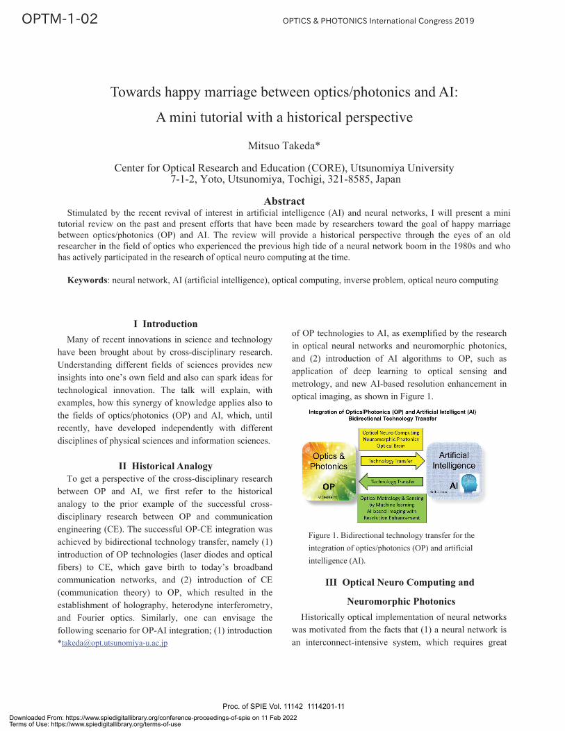
of OP technologies to AI, as exemplified by the research in optical neural networks and neuromorphic photonics, and (2) introduction of AI algorithms to OP, such as application of deep learning to optical sensing and metrology, and new AI-based resolution enhancement in optical imaging, as shown in Figure 1.
Figure 1. Bidirectional technology transfer for the integration of optics/photonics (OP) and artificial intelligence (AI).
III Optical Neuro Computing and
Neuromorphic Photonics Historically optical implementation of neural networks
was motivated from the facts that (1) a neural network is an interconnect-intensive system, which requires great
Towards happy marriage between optics/photonics and AI:
A mini tutorial with a historical perspective
Mitsuo Takeda*
Center for Optical Research and Education (CORE), Utsunomiya University 7-1-2, Yoto, Utsunomiya, Tochigi, 321-8585, Japan
Abstract
Stimulated by the recent revival of interest in artificial intelligence (AI) and neural networks, I will present a mini tutorial review on the past and present efforts that have been made by researchers toward the goal of happy marriage between optics/photonics (OP) and AI. The review will provide a historical perspective through the eyes of an old researcher in the field of optics who experienced the previous high tide of a neural network boom in the 1980s and who has actively participated in the research of optical neuro computing at the time.
Keywords: neural network, AI (artificial intelligence), optical computing, inverse problem, optical neuro computing
Proc. of SPIE Vol. 11142 1114201-11Downloaded From: https://www.spiedigitallibrary.org/conference-proceedings-of-spie on 11 Feb 2022Terms of Use: https://www.spiedigitallibrary.org/terms-of-use

many product-sum operations for synaptic weight sum calculations, and that (2) a fully parallel optical vector product-sum operation was invented making use of spatial parallelism of optical fields. In the 1980s, various optical neural networks were developed, among which are an optical Hopfield network1, an optical Associatron2, and an optoelectronic LSI neurochip3. While these were based on optical intensity-based implementation with incoherent light, associate memories using coherent complex optical neural fields inside a phase conjugate mirror resonator were also demonstrated4. The idea behind the coherent implementation was the philosophy of Haken5 “Nature computes.” The idea of performing parallel computation making use of synergetic dynamics governed by the laws of nature is still being exploited in today’s advanced research on a coherent Ising machine.6
IV AI-based Optical Metrology and Imaging Various neural network models have been proposed;
feedforward nets, feedback (Hopfield) nets, and their combinations and variants. Roughly speaking, the function of a feedforward multilayered net is to establish, through learning, the mapping relation between inputs x and outputs y in such a manner that it represents the
statistical rule G hidden in the ensemble of given data; 2( ; , ) Minimize with ( , ) as variablesE y G x w I w I
where ( , )w I are network parameters known as synaptic weights and biases. We note that this has a close formal similarity to inverse problems in optical metrology and imaging, and also to problems in optical design. As an old yet naïve researcher in optics, I am tempted to pose a question “Can neural networks represent the complex input-output relations of general optical systems that involve complicated nonlinear physical processes?” (see Figure 2) Presently I do not have an answer myself, but partial answers can be found in several examples. Robert et al.7 regarded a neural network as a regression method based on a nonlinear model, applied it to the inverse problem of scatterometry in lithography, and successfully detected a micro grating profile. Feng et al.8 applied deep learning to fringe analysis for phase detection in 3-D profilometry. Deep learning was also applied to wavefront sensing9 without recourse to interferometry, and also to resolution enhancement in microscopy.10 I will review some of these examples in my talk.
Figure 2. Elementary question posed by an old yet naïve researcher in optics.
References [1] Psaltis, D, Farhat, N., “Optical information processing based on an associative-memory model of neural nets with thresholding and feedback,” Opt. Lett. 10(2), 98-100 (1985). [2] Ishikawa, M., Mukohzak, N. Toyoda, H., Suzuki, Y., “Optical associatron: a simple model for optical associative memory,” Appl. Opt. 28(2), 291-301 (1989). [3] Ohta, J. et al., “GaAs/AlGaAs optical synaptic interconnection device for neural networks,” Opt. Lett. 14(16), 844-846 (1989). [4] Takeda, M., Kishigami, T., “Complex neural fields with a Hopfield-like energy function and an analogy to optical fields generated in phase-conjugate resonators,” J. Opt. Soc. Am. A, 9(12), 2182-2191 (1992). [5] Haken, H., [Synergetic Computers and Cognition: A Top-Down Approach to Neural Nets], Springer Verlag, Berlin Heidelberg (1991). [6] McMahon, P. L. et al., “A fully-programmable 100-spin coherent Ising machine with all-to-all connections,” Science 0.1126/science.aah5178 (2016). [7] Robert, S. et al., “Characterization of optical diffraction gratings by use of a neural method,” J. Opt. Soc. Am. A, 19(1), 24-32 (2002). [8] Feng, S. et al., “Fringe pattern analysis using deep learning,” arXiv: 1807.02757v1 [eess.IV] 8 Jul. (2018). [9] Nishizaki, Y. et al., “Deep learning wavefront sensing,” Opt. Express, 27(1) 240 -251 (2019). [10] Rivenson, Y. et al., “Deep learning microscopy,” Optica, 4(11) 1437-1443 (2017).
Proc. of SPIE Vol. 11142 1114201-12Downloaded From: https://www.spiedigitallibrary.org/conference-proceedings-of-spie on 11 Feb 2022Terms of Use: https://www.spiedigitallibrary.org/terms-of-use
I Introduction Optical frequency metrology [1] is of great interest in
relation to fundamental science and technologies that support broadband communication networks and the navigation with global positioning systems (GPS). It was demonstrated that mode-locked femtosecond lasers could be used to measure the absolute frequency of an optical frequency standard [2,3]. In recent years, erbium-doped fiber based frequency combs (fiber combs) have become widely used owing to their robustness, cost effectiveness, and user friendliness [4]. Frequency-stabilized lasers attract significant interest not only for metrology applications but also for high-resolution spectroscopy. The rapid development of research on optical frequency measurement based on femtosecond combs has stimulated the field of frequency metrology, especially research on high-performance optical frequency standards [5].
In the present paper, we report on the research background of optical frequency combs and frequency-stabilized lasers. We have started the development of a narrow-linewidth frequency comb using a compact fiber-pigtailed electro-optic modulator, the generation of a broadband visible comb using a PPLN waveguide, and Dual-comb spectroscopy using low repetition rate frequency combs. Recently, we have also started an ultra-compact frequency-stabilized laser project. These lasers
are useful for various applications, including interferometric measurement.
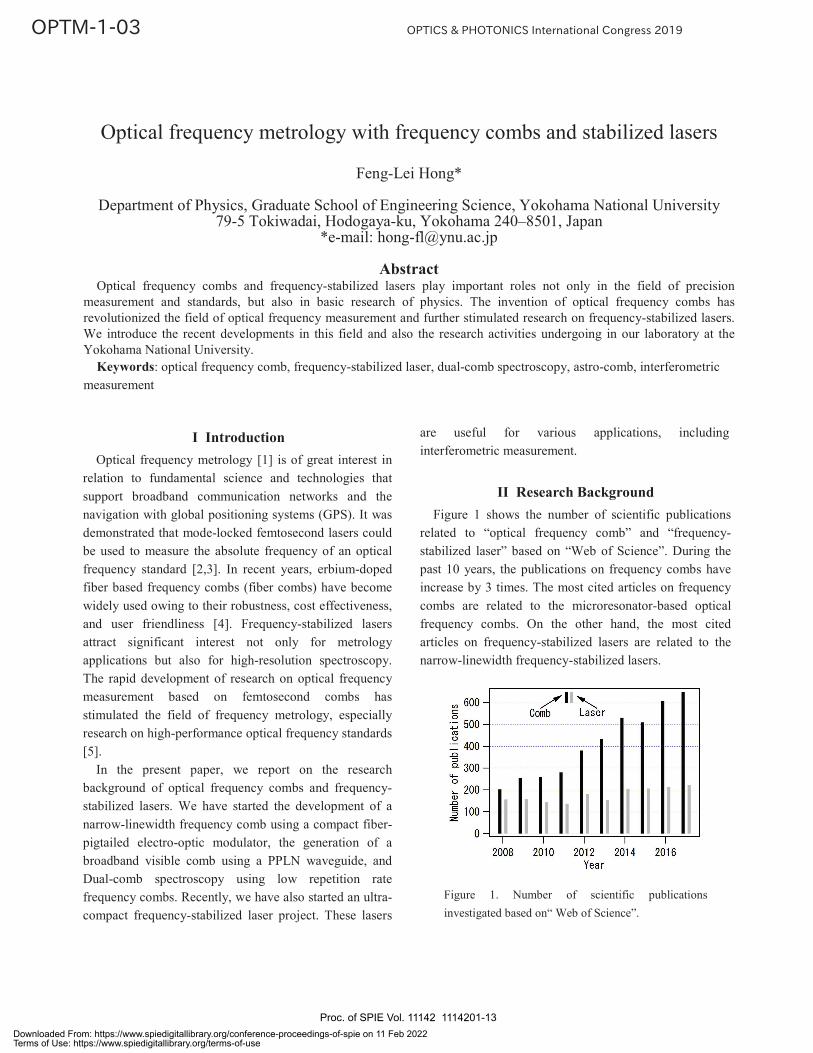
II Research Background Figure 1 shows the number of scientific publications
related to “optical frequency comb” and “frequency-stabilized laser” based on “Web of Science”. During the past 10 years, the publications on frequency combs have increase by 3 times. The most cited articles on frequency combs are related to the microresonator-based optical frequency combs. On the other hand, the most cited articles on frequency-stabilized lasers are related to the narrow-linewidth frequency-stabilized lasers.
Figure 1. Number of scientific publications investigated based on“ Web of Science”.
Optical frequency metrology with frequency combs and stabilized lasers
Feng-Lei Hong*
Department of Physics, Graduate School of Engineering Science, Yokohama National University 79-5 Tokiwadai, Hodogaya-ku, Yokohama 240–8501, Japan
*e-mail: [email protected]
Abstract Optical frequency combs and frequency-stabilized lasers play important roles not only in the field of precision
measurement and standards, but also in basic research of physics. The invention of optical frequency combs has revolutionized the field of optical frequency measurement and further stimulated research on frequency-stabilized lasers. We introduce the recent developments in this field and also the research activities undergoing in our laboratory at the Yokohama National University.
Keywords: optical frequency comb, frequency-stabilized laser, dual-comb spectroscopy, astro-comb, interferometric measurement
Proc. of SPIE Vol. 11142 1114201-13Downloaded From: https://www.spiedigitallibrary.org/conference-proceedings-of-spie on 11 Feb 2022Terms of Use: https://www.spiedigitallibrary.org/terms-of-use
III Development of Frequency Combs 1. Development of a narrow-linewidth frequency
comb using an electro-optic modulator Figure 2 shows a mode-locked Er:fiber laser using an
intra-cavity electro-optic modulator (EOM). The laser oscillator employs nonlinear polarization evolution as a mode-locking mechanism. The net dispersion of the oscillator is estimated to be 0.009 ps2, and the repetition frequency of the oscillator was about 49.2 MHz. A 15-cm-long optical bench with fiber pigtails on both ends is used for loading an EOM, a polarizer and three waveplates. The optical bench is made of Thorlabs FBC-1550-FC and FT-38X135. The insertion loss of the optical bench system was less than 2 dB. The EOM is needed for controlling the effective laser cavity length at a large servo bandwidth. We succeeded in phase-locking the mode-locked laser to an optical reference without using a high-voltage amplifier for the EOM.
Figure 2. Schematic diagram of the mode-locked Er fiber laserwith a compact optical bench containing an EOM. LD: Laser Diode, WDM: Wavelength Division Multiplexing, DCF: Dispersion Compensation Fiber, EDF: Erbium Doped Fiber, EOM: Electro-Optic Modulator, P: Polarizer, O. C.: Output Coupler, ISO: Isolator, PZT: Piezoelectric Transducer, TEC: Thermoelectric Cooler.
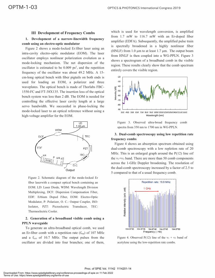
2. Generation of a broadband visible comb using a PPLN waveguide
To generate an ultra-broadband optical comb, we used an Er-fiber comb with a repetition rate (frep) of 107 MHz and a fceo of 10.7 MHz. The output pulses from the oscillator are divided into four branches; one of them,
which is used for wavelength conversion, is amplified from 1.7 mW to 116.7 mW with an Er-doped fiber amplifier (EDFA). Subsequently, the amplified pulse train is spectrally broadened in a highly nonlinear fiber (HNLF) from 1.0 μm to at least 1.7 μm. The output beam from HNLF is then coupled into a WG-PPLN. Figure 3 shows a spectrogram of a broadband comb in the visible region. These results clearly show that the comb spectrum entirely covers the visible region.
Figure 3. Observed ultra-broad frequency comb spectra from 350 nm to 1700 nm in WG-PPLN.
3. Dual-comb spectroscopy using low repetition rate frequency combs
Figure 4 shows an absorption spectrum obtained using dual-comb spectroscopy with a low repletion rate of 20 MHz. This is an enlarged graph around the P(12) line oif the 1+ 3 band. There are more than 50 comb components across the 1-GHz Doppler broadening. The resolution of the dual-comb spectroscopy increased by a factor of 2.5 to 5 compared to that of a usual frequency comb.
Figure 4. Observed P(12) line of the v1 + v3 band of acetylene using the low-repetition rate combs.
Proc. of SPIE Vol. 11142 1114201-14Downloaded From: https://www.spiedigitallibrary.org/conference-proceedings-of-spie on 11 Feb 2022Terms of Use: https://www.spiedigitallibrary.org/terms-of-use

V Development of Frequency-Stabilized Lasers 1. Ultra-compact frequency-stabilized laser Figure. 5(a) shows an image of a compact laser
module emitting at 531 nm (QDLaser, QLD0593-3220). The dimensions of the compact laser modules are 20 mm × 6 mm × 4 mm (length × width × thickness). The laser modules consist of a DFB diode laser (DFB-DL) operating in the infrared (IR) region, a semiconductor optical amplifier, and a periodically poled lithium niobate crystal for second harmonic generation (SHG), as shown in Fig. 5(b). We have demonstrated the observation of hyperfine components of iodine transitions using the low-cost coin-sized laser modules based on Doppler-free spectroscopy. Laser frequency stabilization is performed using the observed hyperfine components. We obtained a laser frequency stability of 4.3×10⁻¹² at an averaging time of 1 s.
Figure 5. (a) Picture of the compact laser module. (b) Schematic diagram of the compact laser module.DFB-LD: Distributed-Feedback Diode Laser, SOA: Semiconductor Optical Amplifier, PPLN: Periodically Poled Lithium Niobate.
2. Various frequency-stabilized lasers We have developed various frequency-stabilized lasers
in our laboratory. 1) Iodine-stabilized Nd:YAG lasers 2) 1064-nm narrow-linewidth frequency-stabilized diode
lasers 3) 1542-nm narrow-linewidth acetylene-stabilized diode
lasers 4) 1062-nm ultra-compact frequency-stabilized diode
lasers 5) 399-nm frequency-stabilized external-cavity diode
lasers
III Conclusions It is now an exciting period for researchers working on
optical frequency metrology. Rapid developments on optical clocks, frequency combs, and advanced frequency links will open up new possibilities for research ranging from fundamental physics, and astrophysics, to aspects of engineering such as space clocks and the remote sensing of the beat of our earth.
Acknowledgements The author is grateful to the group members at YNU,
including assistant Prof. K. Yoshii. The author is also grateful to H. Inaba, S. Okubo, D. Akamatsu, T. Kobayashi and other members at NMIJ, AIST. This work was supported by the Japan Society for the Promotion of Science (JSPS) KAKENHI (15H02028, 18H03886, 18H01898) and the Japan Science and Technology Agency (JST) ERATO MINOSHIMA Intelligent Optical Synthesizer (IOS) Project (JPMJER1304).
References [1] T. Udem, R. Holzwarth, and T. W. Hänsch, “Optical
frequency metrology,” Nature 416, 233–237 (2002). [2] T. Udem, J. Reichert, R. Holzwarth, and T. W. Hänsch,
“Absolute optical frequency measurement of the cesium D1 line with a mode-locked laser,” Phys. Rev. Lett. 82, 3568–3571 (1999).
[3] D. J. Jones, S. A. Diddams, J. K. Ranka, A. Stentz, R. S. Windeler, J. L. Hall, and S. T. Cundiff, “Carrier-envelope phase control of femtosecond mode-locked lasers and direct optical frequency synthesis,” Science 288, 635–639 (2000).
[4] H. Inaba, Y. Daimon, F.-L. Hong, A. Onae, K. Minoshima, T. R. Schibli, H. Matsumoto, M. Hirano, T. Okuno, M. Onishi, and M. Nakazawa, Long-term measurement of optical frequencies using a simple, robust and low-noise fiber based frequency comb,” Opt. Express 14, 5223–5231 (2006).
[5] F.-L. Hong, “Optical frequency standards for time and length applications,” Meas. Sci. Technol. 28, 012002 (2017).
Proc. of SPIE Vol. 11142 1114201-15Downloaded From: https://www.spiedigitallibrary.org/conference-proceedings-of-spie on 11 Feb 2022Terms of Use: https://www.spiedigitallibrary.org/terms-of-use

On Carrier Fringe Pattern Analysis
Qian Kemao
School of Computer Science and Engineering, Nanyang Technological University, 639798, Singapore, [email protected]
Abstract
Introducing a carrier into fringe patterns enables easy, accurate and robust phase retrieval, and thus has become one of the pillar techniques in optical metrology. The well-known carrier fringe pattern analysis methods include the Fourier transform (FT) method, the spatial phase-shifting (SPS) method, the windowed Fourier transform (WFT) method and the sampling moiré (SM) method. In this paper, the close relationships among these methods will be analyzed and revealed, resulting in a small methodology family.
Keywords: carrier fringe pattern analysis, phase extraction, Fourier transform method, spatial phase-shifting method, windowed Fourier transform method, sampling Moiré method
Proc. of SPIE Vol. 11142 1114201-16Downloaded From: https://www.spiedigitallibrary.org/conference-proceedings-of-spie on 11 Feb 2022Terms of Use: https://www.spiedigitallibrary.org/terms-of-use

I Introduction In recent years, technology is growing remarkably and
many high precision and small components are being used, increasing the need to measure 3D profilometry with high accuracy and high speed. Non-contact 3D profilometry is particularly needed in order to avoid damaging the object under measurement. Many non-contact methods have been proposed such as moiré and grating projection. [1] However, many of these methods cannot be used within a deep hole or for large step heights due to the use of a triangulation-based method. To solve this problem, it has been proposed to use instead a focusing method, in which the projection system and the imaging system are coaxial. Yoshizawa et al. presented a three-dimensional shape measurement technique using the contrast distribution. [2] However, this technique is a problem that it takes time to project 4 phase-shifted fringe patterns. [3-6]
We propose a uniaxial 3D profilometry system using linear polarization patterns and a polarization camera to enable faster profilometry measurement than conventional equipment allows.
II Background
1. Linear polarization pattern The optical layout for the system is shown in Figure 1.
The linear polarization pattern is generated from the liner polarization which is made from the linear polarizer (LP) by a spatial light modulator (SLM) and a quarter wave plate
(QWP). The optical axis of SLM is and the optical axis of QWP is 45 . SLM provides retardance spatially.
Figure 1. Optical system for 3D profilometry system
By using the Stokes approach, the emission Stokes parameters is given from the incident Stokes parameters and Mueller matrix among the optical polarization components.
(1)
where , , represent Mueller matrix of QWP, SL
3D profilometry by projecting polarization pattern
Yuuki Maeda*, Shuhei Shibata, Nathan Hagen, Yukio Otani
Center for Optical Research and Education, Utsunomiya University, 7-1-2 Yoto, Utsunomiya, Tochigi. 321-8585. Japan
Abstract
We demonstrate a uniaxial 3D profilometry system that captures a structured linear polarization pattern with a polarization camera having micropolarizers of 4 orientation angles arranged on CCD sensor. The linear polarization pattern is generated by a spatial light modulator (SLM) and a quarter wave plate (QWP) in the optical system. This system can measure 4 different fringe patterns with a phase difference of 90 degrees simultaneously, allowing for faster profilometry measurement than conventional equipment allows. We present experimental results of 3D profilometry using this system.
Keywords: profilometry, polarization camera, polarization pattern,
Proc. of SPIE Vol. 11142 1114201-17Downloaded From: https://www.spiedigitallibrary.org/conference-proceedings-of-spie on 11 Feb 2022Terms of Use: https://www.spiedigitallibrary.org/terms-of-use

M, LP and represents optical axis. From Stokes parameters , the azimuthal direction of
linear polarization is provided by retardance value of SLM. If this retardance is controlled spatially, linear polarization pattern rotated spatially is obtained.
2. Contrast distribution
The intensity detected by the CCD sensor of the polarization camera can be described as:
(2)
for the orientation angles of the linear polarizer on each pixel of the polarization camera and the modulation contrast. The contrast is calculated from the detected image by the 4-step phase shifting technique.
(3)
where , , , and represent the intensity of .
There are two methods for measuring the height from the contrast. The first method obtains the height from the contrast of a sample spatially by referring the height against contrast measured in advance. Therefore, this first method enables snapshot 3D profilometry measurement.
Wilson et al presented the best focus position equal the maximum value of contrast of a sample. [7] Therefore, the second method obtains the height from the best focus potion of a sample by measuring contrast spatially while varying the height of sample.
III Results and Discussion The result of measuring the contrast while varying the
height of the planar mirror is shown in Figure 2(a). The solid line shows the contrast fitted with a Gaussian function. As you can see, the contrast distribution is able to fit with a Gaussian function. The result of the height calculated from the contrast against the height obtained from a micrometer is shown in Figure 2(b). As you can see, the height is directly proportional to the theoretical height in the range of 4mm-10mm. In this case, the measurement is performed in the range. Measurement accuracy of the height obtained from this result is 150 μm. Therefore, measurement accuracy is not good.
The result of measuring a 1951 USAF test target as a sample using the first method are shown in Figure 3. While the measurement obtains the correct overall three-dimensional shape of the target, some errors are encountered due to the low of reflectivity. But it was confirmed that enables snapshot 3D profilometry measurement. (a)
(b)
Figure 2. Measurement result of the planar mirror
Figure 3. Measurement result of the 1951 USAF test target The result of measuring many kinds of samples using the
second method is shown in Figure 4. The position of the maximum value of the contrast is the same regardless of the kinds of samples. The measurement accuracy of each
Proc. of SPIE Vol. 11142 1114201-18Downloaded From: https://www.spiedigitallibrary.org/conference-proceedings-of-spie on 11 Feb 2022Terms of Use: https://www.spiedigitallibrary.org/terms-of-use
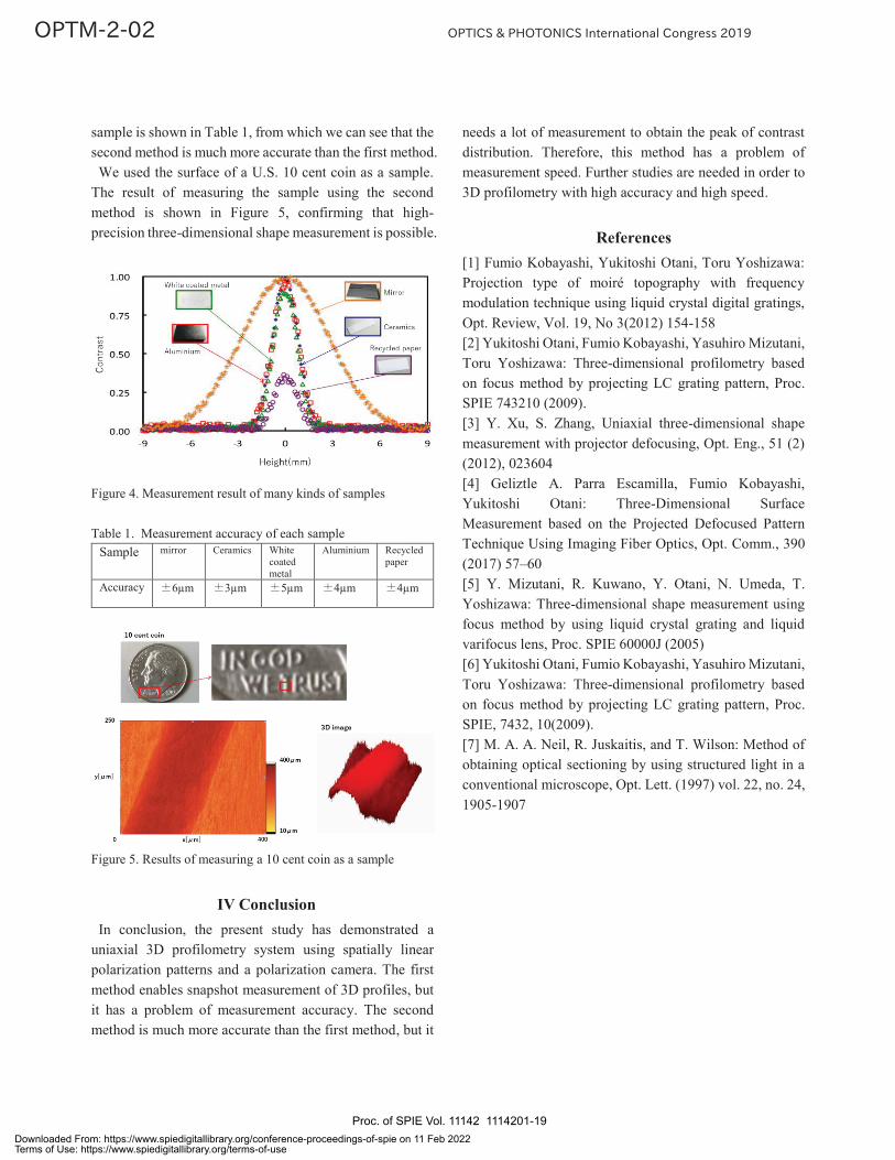
sample is shown in Table 1, from which we can see that the second method is much more accurate than the first method.
We used the surface of a U.S. 10 cent coin as a sample. The result of measuring the sample using the second method is shown in Figure 5, confirming that high-precision three-dimensional shape measurement is possible.
Figure 4. Measurement result of many kinds of samples
Table 1. Measurement accuracy of each sample Sample
mirror Ceramics White coated metal
Aluminium Recycled paper
Accuracy
6μm 3μm 5μm 4μm 4μm
Figure 5. Results of measuring a 10 cent coin as a sample
IV Conclusion In conclusion, the present study has demonstrated a
uniaxial 3D profilometry system using spatially linear polarization patterns and a polarization camera. The first method enables snapshot measurement of 3D profiles, but it has a problem of measurement accuracy. The second method is much more accurate than the first method, but it
needs a lot of measurement to obtain the peak of contrast distribution. Therefore, this method has a problem of measurement speed. Further studies are needed in order to 3D profilometry with high accuracy and high speed.
References [1] Fumio Kobayashi, Yukitoshi Otani, Toru Yoshizawa: Projection type of moiré topography with frequency modulation technique using liquid crystal digital gratings, Opt. Review, Vol. 19, No 3(2012) 154-158 [2] Yukitoshi Otani, Fumio Kobayashi, Yasuhiro Mizutani, Toru Yoshizawa: Three-dimensional profilometry based on focus method by projecting LC grating pattern, Proc. SPIE 743210 (2009). [3] Y. Xu, S. Zhang, Uniaxial three-dimensional shape measurement with projector defocusing, Opt. Eng., 51 (2) (2012), 023604 [4] Geliztle A. Parra Escamilla, Fumio Kobayashi, Yukitoshi Otani: Three-Dimensional Surface Measurement based on the Projected Defocused Pattern Technique Using Imaging Fiber Optics, Opt. Comm., 390 (2017) 57–60 [5] Y. Mizutani, R. Kuwano, Y. Otani, N. Umeda, T. Yoshizawa: Three-dimensional shape measurement using focus method by using liquid crystal grating and liquid varifocus lens, Proc. SPIE 60000J (2005) [6] Yukitoshi Otani, Fumio Kobayashi, Yasuhiro Mizutani, Toru Yoshizawa: Three-dimensional profilometry based on focus method by projecting LC grating pattern, Proc. SPIE, 7432, 10(2009). [7] M. A. A. Neil, R. Juskaitis, and T. Wilson: Method of obtaining optical sectioning by using structured light in a conventional microscope, Opt. Lett. (1997) vol. 22, no. 24, 1905-1907
Proc. of SPIE Vol. 11142 1114201-19Downloaded From: https://www.spiedigitallibrary.org/conference-proceedings-of-spie on 11 Feb 2022Terms of Use: https://www.spiedigitallibrary.org/terms-of-use
I IntroductionIn fringe projection profilometry, the projector
nonlinearity is a main factor decreasing the measurement accuracy. It makes fringes non-sinusoidal thus inducing ripple-like artifacts on the calculated phase maps and, further, on the reconstructed object shapes [1]. Many efforts have been made for solving this problem. Typically, a photometric calibration can be performed for determining the projector nonlinearity curve for compensating for the phase errors actively. Instead, the passive technique uses a look-up table of phase errors versus phase values for correcting these errors. With these methods, a calibration must be implemented in advance, so they may fail in correcting the phase errorsinduced by the time-variant projector nonlinearity [2].This paper presents a self-correction method for removing the phase errors from a single phase map or a couple of phase maps having different frequencies. This method works without a prior calibration.
II Method1. Projector nonlinearityIn phase-shifting fringe projection profilometry, a
projector is used for casting sinusoidal fringe patterns on the measured object surface, and the camera captures the deformed fringe patterns. One of the captured patterns is
( , ) ( , ) cos[ ( , ) 2 ] ( , )kI x y A x y x y k K B x y (1)
where (x, y) denote the pixel coordinates of a point on the imaging plane of the camera. A(x, y) is the modulation
and B(x, y) is the background intensity. 2 is an added phase shift with k=0, 1, …, K 1. From these patterns, the wrapped phases are estimated by [3]
1
01
0
( , ) sin(2 )( , ) arctan
( , ) cos(2 )
Kkk
Kkk
I x y k Kx y
I x y k K(2)
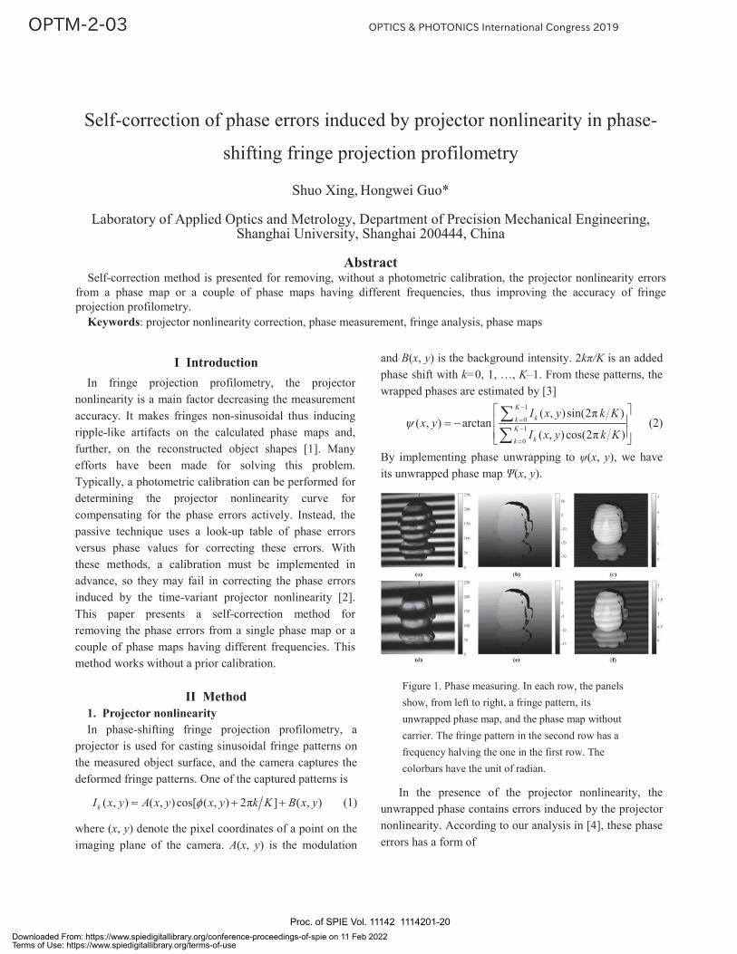
By implementing phase unwrapping to (x, y), we have its unwrapped phase map (x, y).
Figure 1. Phase measuring. In each row, the panels show, from left to right, a fringe pattern, itsunwrapped phase map, and the phase map without carrier. The fringe pattern in the second row has a frequency halving the one in the first row. The colorbars have the unit of radian.
In the presence of the projector nonlinearity, the unwrapped phase contains errors induced by the projector nonlinearity. According to our analysis in [4], these phase errors has a form of
Self-correction of phase errors induced by projector nonlinearity in phase-
shifting fringe projection profilometry
Shuo Xing, Hongwei Guo*
Laboratory of Applied Optics and Metrology, Department of Precision Mechanical Engineering,Shanghai University, Shanghai 200444, China
AbstractSelf-correction method is presented for removing, without a photometric calibration, the projector nonlinearity errors
from a phase map or a couple of phase maps having different frequencies, thus improving the accuracy of fringe projection profilometry.
Keywords: projector nonlinearity correction, phase measurement, fringe analysis, phase maps
Proc. of SPIE Vol. 11142 1114201-20Downloaded From: https://www.spiedigitallibrary.org/conference-proceedings-of-spie on 11 Feb 2022Terms of Use: https://www.spiedigitallibrary.org/terms-of-use
1 2
3
( , )= ( , ) ( , )sin[ ( , )] sin[2 ( , )]sin[3 ( , )]+
x y x y x yK x y K x y
K x y(3)
We find from Eq. (3) that the phase error induced by the projector nonlinearity depends on the number of phase shifts, having multiplied frequencies higher than the fringe frequencies. We take Fig. 1 as an example. In it, two sequences of fringe patterns having different frequencies are captured, with the number of phase shifts being three; the size of each fringe patterns is 512×512 pixels; and the projector was not calibrated. The left column shows the first frame of each pattern sequence. The middle column gives the unwrapped phase maps. By removing the carrier, the ripple-like artifacts become observable as we see on the right column.
2. Error coefficient estimation from a couple of phase maps having different frequencies
From Eq. (3), we know that if the error coefficients are determined, the phase error can be removed. In multi-frequency fringe projection profilometry, at least two phase maps having different frequencies are recovered, making it possible to determine and eliminate the error terms [5]. Here, we denote H and L as two unwrapped phase maps corresponding to the fringe frequencies fH and fL, respectively. Note that H and L are function of (x, y).For each pixel, we have a pair of equations like
1 2
1 2
sin( ) sin(2 )
sin( ) sin(2 )
H H H H
L L LL H H H
H H H
K Kf f fK Kf f f
(4)
where H is the real phase corresponding to the fringe frequency fH.
In practice, the errors may have infinite terms, but their amplitudes decline quickly as their orders become high. We reasonably truncate the error function and keep thefirst three terms. Because the equations are nonlinear, we have to solve it using an iterative algorithm in the least squares sense. Here we use the calculated phases H as the initial values of H. The error coefficients estimated from Fig. 1are ={ -0.1551, -0.0095,-0.0019 }.
3. Error coefficient estimation from a single phase map
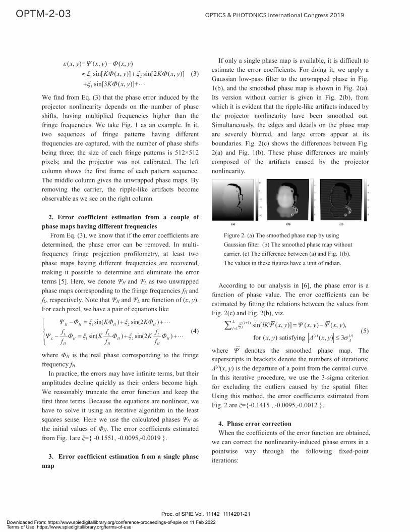
If only a single phase map is available, it is difficult to estimate the error coefficients. For doing it, we apply a Gaussian low-pass filter to the unwrapped phase in Fig. 1(b), and the smoothed phase map is shown in Fig. 2(a).Its version without carrier is given in Fig. 2(b), from which it is evident that the ripple-like artifacts induced by the projector nonlinearity have been smoothed out. Simultaneously, the edges and details on the phase map are severely blurred, and large errors appear at its boundaries. Fig. 2(c) shows the differences between Fig. 2(a) and Fig. 1(b). These phase differences are mainly composed of the artifacts caused by the projector nonlinearity.
Figure 2. (a) The smoothed phase map by using Gaussian filter. (b) The smoothed phase map without carrier. (c) The difference between (a) and Fig. 1(b). The values in these figures have a unit of radian.
According to our analysis in [6], the phase error is afunction of phase value. The error coefficients can be estimated by fitting the relations between the values from Fig. 2(c) and Fig. 2(b), viz.
( +1)1
( ) ( )
sin[ ( , )] ( , ) ( , ),
for ( , ) satisfying ( , ) 3
L ill
i i
lK x y x y x y
x y x y(5)
where denotes the smoothed phase map. The superscripts in brackets denote the numbers of iterations;
(i)(x, y) is the departure of a point from the central curve.In this iterative procedure, we use the 3-sigma criterionfor excluding the outliers caused by the spatial filter.Using this method, the error coefficients estimated from Fig. 2 are ={-0.1415 , -0.0095,-0.0012 }.
4. Phase error correctionWhen the coefficients of the error function are obtained,
we can correct the nonlinearity-induced phase errors in a pointwise way through the following fixed-point iterations:
Proc. of SPIE Vol. 11142 1114201-21Downloaded From: https://www.spiedigitallibrary.org/conference-proceedings-of-spie on 11 Feb 2022Terms of Use: https://www.spiedigitallibrary.org/terms-of-use

( 1) ( )1
( , ) ( , ) sin[ ( , )]Lj jll
x y x y lK x y (6)
Figures. 3(a) and 3(b) show the corrected phase maps using the error coefficients estimated from a couple of phase maps in Fig. 1, and from the single phase map in Fig. 2, respectively. In these results, the ripple-like artifacts induced by the projector nonlinearity have been removed.
Figure 3. (a) The phase map with its nonlinearity-induced errors having been removed from the couple of phase maps in Fig. 1. (b) The corrected phase map from the single phase map in Fig. 2. The values in these figures have a unit of radian.
III ConclusionThis paper presented a self-correction method that
allows us to remove the errors induced by the projector nonlinearity from a single phase map or from a couple of phase maps having different frequencies. This method offers some advantages over the exist ones. For example, it does not require a prior calibration, and hence it is applicable when the projector nonlinearity varies with time. Moreover, it is independent of a special model or an assumption about the projector nonlinearity, thus being more general in practical applications.
References[1] H. Guo, H. He, and M. Chen. 2004. Gamma
correction for digital fringe projection profilometry.Appl. Opt. 43, 2906–2914.
[2] B. Li, Y. Wang, J. Dai, W. Lohry, and S. Zhang. 2014. Some recent advances on superfast 3D shape measurement with digital binary defocusing techniques. Opt. Lasers Eng. 54, 236–246.
[3] J. H. Bruning, D. R. Herriott, J. E. Gallagher, D. P. Rosenfeld, A. D. White, and D. J. Brangccio. 1974 Digital wavefront measuring interferometer for testing optical surfaces and lenses. Appl. Opt. 13, 2693–2703.
[4] F. Lü, S. Xing, and H. Guo. 2017. Self-correction of projector nonlinearity in phase-shifting fringe projection profilometry. Appl. Opt. 56, 7204–7216.
[5] S. Xing and H. Guo. 2018. Correction of projector nonlinearity in multi-frequency phase-shifting fringe projection profilometry. Opt. Express. 26, 16277-16291.
[6] S. Xing and H. Guo. 2019. Directly recognizing and removing the projector nonlinearity errors from a phase map in phase-shifting fringe projection profilometry. Opt. Commun. 435, 212-220.
Proc. of SPIE Vol. 11142 1114201-22Downloaded From: https://www.spiedigitallibrary.org/conference-proceedings-of-spie on 11 Feb 2022Terms of Use: https://www.spiedigitallibrary.org/terms-of-use

I Introduction According to modern digital technology, a real-time
three-dimensional (3-D) surface system is a very significant method in many fields including machine manufacture, medical applications and automobile industry [1-13]. Fringe projection technique has become the most popular 3-D shape acquisition method. The fringe projection system classically uses a digital projector to project fringe patterns onto object surfaces, a digital camera to capture the distorted fringe patterns, and a computer to calculate the phase maps and reconstruct the 3-D shape. The primary processes for 3-D shape reconstruction contain phase-shifting calculation, phase-unwrapping calculation and phase to real dimension conversion. Three-step phase-shifting calculation is typically exercised in the fringe projection system. However, three-step phase-shifting method is less efficient and time consuming. Because monochromatic fringe patterns take a long time for capturing and calculation, we are interested in 3-D reconstruction with high-speed for fringe projection system. For this reason, the high-speed digital fringe projection system is presented for 3-D surface measurement.
*[email protected]; phone 886-2-28267020
Single-shot fringe projection measurements are insensitive to signal noises because only one image needs to be captured. The single-shot fringe projection methods can be generally classified into discrete and continuous coding processes [14-20]. The discrete coding patterns present a digital shape with the same intensity value and the shape dimension determines from the intensity of the measured object surface. The image resolution in this case is low since the discrete code occupies several pixels. The obtained 3-D data for measuring complex shape are inaccurate. The continuous coding patterns show a smooth profile where every pixel has a singular codeword on color. Therefore, the obtained 3-D data are dense surface reconstruction. The phase-shifting calculations are widely utilized since the measurement has high accuracy and high speed. We have to investigate phase-shifting algorithms in order to obtain absolute phase data for high-accuracy 3-D reconstruction.
In this study, a high-speed digital fringe projection system is proposed to measure 3-D features of the rear lamp housing. The light source used in this system is structured light with phase-shifting fringe patterns. A projector with digital light processing (DLP) is employed as light source to project fringe patterns onto object surface. The images of distorted fringe pattern are
High-speed 3D surface measurement of rear lamp housing by automatic
digital fringe projection system*
Cheng-Yang Liu*a, Cheng-Yu Wangb, Li-Wei Tengb
aDepartment of Biomedical Engineering, National Yang-Ming University, Taipei City, Taiwan bDepartment of Mechanical and Electro-Mechanical Engineering, Tamkang University, New Taipei
City, Taiwan
Abstract Digital fringe projection method is widely used in industrial applications with high-speed measurement and high
resolution. In this study, a fully automatic high-speed digital fringe projection system is presented to profile 3D surface characteristic of rear lamp housing of vehicle. The structured light with fringe pattern is used to be the light source in the measurement system and is projected by a digital light processing projector. The distorted fringe patterns from the surface of lamp housing are captured by the digital camera. The absolute phase maps are calculated by using phase-shifting and quality guided path unwrapping algorithm. A complete 3D feature of lamp housing is obtained by our system. We achieved simultaneous phase acquisition, reconstruction and 3D exhibition at a speed of 0.5 s. This system can provide a high accuracy and real-time 3D surface measurement for the automobile industry.
Keywords: lamp housing, fringe projection, structured light
Proc. of SPIE Vol. 11142 1114201-23Downloaded From: https://www.spiedigitallibrary.org/conference-proceedings-of-spie on 11 Feb 2022Terms of Use: https://www.spiedigitallibrary.org/terms-of-use

captured by a digital camera The multi-step phase-shifting and quality guided path unwrapping calculations are used to compute the value of absolute phase map. The detecting angle of the digital camera is controlled by using a motorized stage. Finally, a complete 3-D surface of the rear lamp housing is obtained by our system. We have successfully accomplished simultaneous phase calculation, 3-D reconstruction and exhibition at a speed of 0.5 s. This results can provide a high-accuracy and real-time 3-D shape measurement for automobile industry.
II Principle of the system
Figure 1 shows the schematic diagram of automatic digital fringe projection system. The automatic fringe projection system includes the following several parts: generation of multi-step phase-shifting fringe pattern, acquisition of deformed fringe pattern, calculations of wrapped and unwrapped phase, and conversion from absolute phase to real size. This system consists of a DLP projector, a digital camera, a motorized rotation stage and an industrial computer. The sinusoidal fringe patterns are generated by using a computer code and projected onto the object surface by the projector. The digital camera is used to acquire the deformed fringe patterns. The phase information is extracted from the captured patterns which has to be unwrapped for surface reconstruction. The unwrapped phase values are calculated by calibration method for the relationship between the absolute phase value and real size.
Figure 1. Schematic diagram of automatic digital fringe projection system.
The phase information is obtained from deformed fringe patterns. Multi-step phase-shifting calculations are extensively employed in optical 3-D surface measurement due to its advantageous properties. In this case, three phase-shifting algorithms are utilized to calculate the wrapped phase maps including three-step, four-step, five-step and seven-step algorithms. The three-step phase-shifting algorithm is preferable for real-time 3-D surface measurement because the minimum numbers of fringe patterns are required for calculations. The phase shift between three fringe patterns is selected as . Three fringe patterns are applied for this algorithm whose fringe intensities can be expressed as:
)3
2cos(1 III
)cos(2 III (1)
)3
2cos(3 III
where the average intensity is I ', the intensity modulation is I ", the phase information is .
The phase map can be obtained by solving Eq. (1) as:
]2
)(3[tan312
311
IIIII (2)
The seven-step phase-shifting algorithm is preferable for high-accuracy measurement because the maximum numbers of fringe patterns are required for calculations. The phase shift between seven 2. The intensities of seven fringe patterns are expressed as:
]2
3cos[1 III
]cos[2 III
]2
cos[3 III
]cos[4 III (3)
]2
cos[5 III
]cos[6 III
]2
3cos[7 III
The intensity of light source and fringe modulation for seven fringe patterns are assumed the same value. The phase can be retrieved by the following equation:
]224
33[tan624
51731
IIIIIII (4)
Proc. of SPIE Vol. 11142 1114201-24Downloaded From: https://www.spiedigitallibrary.org/conference-proceedings-of-spie on 11 Feb 2022Terms of Use: https://www.spiedigitallibrary.org/terms-of-use
In Eqs. (2) and (4), the phase value is a range of - to + . Therefore, the phase unwrapping calculation is required to obtain continuous phase information. The quality guided path algorithm is used in the unwrapping calculation. The highest quality pixels are unwrapped with the highest reliability. The lowest quality pixels with the lowest reliability are considered to prevent the error circulation in the phase map. The unwrapping path is determined by the pixel reliability. The quality guided path algorithm is suitable to calculate phase value from complex surface features. In order to obtain absolute phase value, the standard gauge block is used as references to convert the relative phase to absolute phase. Once the digital fringe projection system is calibrated, the coordinates of real sizes can be obtained from the absolute phase value. Figure 2 shows the operation interface of automatic digital fringe projection system. All algorithms and system control are programed in the MATLAB® code. The insert in the upper left corner of Fig. 2 is the function menu of our automatic system.
Figure 2. Operation interface of automatic digital fringe projection system.
III Results and Discussion For high-speed 3-D surface measurement, a structured
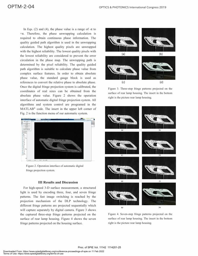
light is used by encoding three, four, and seven fringe patterns. The fast image switching is reached by the projection mechanism of the DLP technology. The different fringe patterns are projected sequentially which will capture separately by digital camera. Figure 3 shows the captured three-step fringe patterns projected on the surface of rear lamp housing. Figure 4 shows the seven fringe patterns projected on the housing surface.
Figure 3. Three-step fringe patterns projected on the surface of rear lamp housing. The insert in the bottom right is the picture rear lamp housing.
Figure 4. Seven-step fringe patterns projected on the surface of rear lamp housing. The insert in the bottom right is the picture rear lamp housing.
Proc. of SPIE Vol. 11142 1114201-25Downloaded From: https://www.spiedigitallibrary.org/conference-proceedings-of-spie on 11 Feb 2022Terms of Use: https://www.spiedigitallibrary.org/terms-of-use
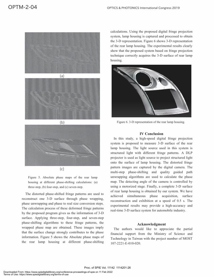
Figure 5. Absolute phase maps of the rear lamp housing at different phase-shifting calculations: (a) three-step, (b) four-step, and (c) seven-step.
The distorted phase-shifted fringe patterns are used to reconstruct one 3-D surface through phase wrapping, phase unwrapping and phase to real size conversion steps. The calculation process of these deformed fringe patterns by the proposed program gives us the information of 3-D surface. Applying three-step, four-step, and seven-step phase-shifting algorithms to these fringe patterns, the wrapped phase map are obtained. These images imply that the surface change strongly contributes to the phase information. Figure 5 shows the Absolute phase maps of the rear lamp housing at different phase-shifting
calculations. Using the proposed digital fringe projection system, lamp housing is captured and processed to obtain the 3-D representation. Figure 6 shows 3-D representation of the rear lamp housing. The experimental results clearly show that the proposed system based on fringe projection technique correctly acquires the 3-D surface of rear lamp housing.
Figure 6. 3-D representation of the rear lamp housing.
IV Conclusion
In this study, a high-speed digital fringe projection system is proposed to measure 3-D surface of the rear lamp housing. The light source used in this system is structured light with different fringe patterns. A DLP projector is used as light source to project structured light onto the surface of lamp housing. The distorted fringe pattern images are captured by the digital camera. The multi-step phase-shifting and quality guided path unwrapping algorithms are used to calculate the phase map. The detecting angle of the camera is controlled by using a motorized stage. Finally, a complete 3-D surface of rear lamp housing is obtained by our system. We have achieved simultaneous phase acquisition, surface reconstruction and exhibition at a speed of 0.5 s. The experimental results may provide a high-accuracy and real-time 3-D surface system for automobile industry.
Acknowledgment The authors would like to appreciate the partial
financial support from the Ministry of Science and Technology in Taiwan with the project number of MOST 107-2221-E-010-020.
Proc. of SPIE Vol. 11142 1114201-26Downloaded From: https://www.spiedigitallibrary.org/conference-proceedings-of-spie on 11 Feb 2022Terms of Use: https://www.spiedigitallibrary.org/terms-of-use
References [1] Gorthi, S. and Rastogi, P., “Fringe projection
techniques: whither we are?,” Opt. Lasers Eng. 48, 133-140 (2010).
[2] Zhang, S., “Recent progresses on real-time 3D shape measurement using digital fringe projection techniques,” Opt. Lasers Eng. 48, 149-158 (2010).
[3] Ma, S., Quan, C., Zhu, R. and Tay, C., “Investigation of phase error correction for digital sinusoidal phase-shifting fringe projection profilometry,” Opt. Lasers Eng. 50, 1107-1118 (2012).
[4] Zuo, C., Chen, Q., Gu, G., Feng, S., Feng, F., Li, R. and Shen, G., “High-speed three-dimensional shape measurement for dynamic scenes using bi-frequency tripolar pulse-width-modulation fringe projection,” Opt. Lasers Eng. 51, 953-960 (2013).
[5] Feng, S., Zhang, Y., Chen, Q., Zuo, C., Li, R. and Shen, G., “General solution for high dynamic range three-dimensional shape measurement using the fringe projection technique,” Opt. Lasers Eng. 59, 56-71 (2014).
[6] Nguyen, H., Nguyen, D., Wang, Z., Kieu, H. and Le, M., “Real-time, high-accuracy 3D imaging and shape measurement,” Appl. Opt. 54, A9-A17 (2015).
[7] Wang, H., Kemao, Q. and Soon, S., “Valid point detection in fringe projection profilometry,” Opt. Express 23, 7535-7549 (2015).
[8] Liu, T., Zhou, C., Si, S., Li, H. and Lei, Z., “Improved differential 3D shape retrieval,” Opt. Lasers Eng. 73, 143-149 (2015).
[9] Liu, C. and Yen, T., “Digital multi-step phase-shifting profilometry for three-dimensional ballscrew surface imaging,” Opt. Laser Technol. 79, 115-123 (2016).
[10] Dai, M., Yang, F., Liu, C. and He X., “A dual-frequency fringe projection three-dimensional shape measurement system using a DLP 3D projector,” Opt. Commun. 382, 294-301 (2017).
[11] Parra Escamill, G., Kobayashi, F. and Otani, Y., “Three-dimensional surface measurement based on the projected defocused pattern technique using imaging fiber optics,” Opt. Commun. 390, 57-60 (2017).
[12] Chen, C., Gao, N., Wang, X. and Zhang, Z., “Adaptive projection intensity adjustment for avoiding saturation in three-dimensional shape measurement,” Opt. Commun. 410, 694-702 (2018).
[13] Yu, S., Zhang, J., Yu, X., Sun, X., Wu, H. and Liu, X., “3D measurement using combined Gray code and dual-frequency phase-shifting approach,” Opt. Commun. 413, 283-290 (2018).
[14] Koninckx, T. and Van Gool, L., “Real-time range acquisition by adaptive structured light,” IEEE Trans. Pattern Anal. Mach. Intell. 28, 432-445 (2006).
[15] Chen, S., Li, Y., Guan, Q. and Xiao, G., “Real-time three-dimensional surface measurement by color encoded light projection,” Appl. Phys. Lett. 89, 111108 (2006).
[16] Qian, K., Fu, Y., Liu, Q., Seah, H. and Asundi, A., “Generalized three-dimensional windowed Fourier transform for fringe analysis,” Opt. Lett. 31, 2121-2123 (2006).
[17] Chen, S., Li, Y. and Zhang, J., “Vision processing for realtime 3-D data acquisition based on coded structured light,” IEEE Trans. Image Process. 17, 167-176 (2008).
[18] Salvi, J., Fernandez, S., Pribanic, T. and Llado X., “A state of the art in structured light patterns for surface profilometry,” Pattern Recognit. 43, 2666-2680 (2010).
[19] Flores, J., Muñoz, A., Ordoñes, S., Garcia-Torales, G. and Ferraric, J., “Color-fringe pattern profilometry using an efficient iterative algorithm,” Opt. Commun. 391, 88-93 (2017).
[20] Flores, J., Ayubi, G., Martino, M., Castillo, O. and Ferrari, J., “3D-shape of objects with straight line-motion by simultaneous projection of color coded patterns,” Opt. Commun. 414, 185-190 (2018).
Proc. of SPIE Vol. 11142 1114201-27Downloaded From: https://www.spiedigitallibrary.org/conference-proceedings-of-spie on 11 Feb 2022Terms of Use: https://www.spiedigitallibrary.org/terms-of-use
I Introduction It is important to understand the performance and
aging mechanisms in photovoltaic (PV) devices. However, commercially available method, laser beam induced current [1-4], is too slow for high-throughput measurements, because it uses a laser spot for raster scan.
This paper presents the principle and demonstration of a new measurement method which uses structured illumination instead of raster scan. When a photovoltaic device is under structured illumination, the output signal is the sum of the local current response. Particularly, if sinusoidal patterns are used for structured illumination, the output signal will be equivalent to a Fourier coefficient of the entire response function of the PV device. By changing the spatial frequency and the initial phase of the sinusoidal structured illumination, the Fourier transform of the response function can be obtained. The response function can be derived by simply applying an inverse Fourier transform. As the response function can be sparsely represented in the Fourier domain, undersampling the Fourier transform of the response function allows for significant reduction of measurements. Thus, the presented method enables fast response function measurements in PV devices. Moreover, as sinusoidal structured illumination is a kind of global illumination, the input light intensity is much
higher than that of single-point scanning by laser beam induced current method. Thus, the presented method allows the PV device to produce a much larger photocurrent with a consequent noise reduction due to an improved signal-to-noise ratio. In short, the presented method potentially enables accurate and efficient response function measurement in photovoltaic devices.
II Principle Assuming that the response function of a PV device is
presented by ,R x y , the output current I of the device
under illumination of , yP x :
, , y d dI R x y P x x y , (1)
where denotes the active area of the device and denotes the current resulted from dark noise. Our goal is to recover the response function from the output current. Specifically, we can choose an appropriate basis set for structured illumination so as to encode the spatial information of the response function into the output current. Here, we propose to use sinusoidal structured illumination, considering response function of PV devices has a sparsed representation in Fourier space. The sinusoidal intensity patterns can generated by using a spatial light modulator (such as, DMD or LCoS). Each
Response function measurement in photovoltaic devices with sinusoidal
structured illumination
Zibang Zhanga, Qiwen Denga, Jingang Zhonga*, Shiping Lia, and Ying Lib
aDepartment of Optoelectronic Engineering, Jinan University, Guangzhou 510632, China bPre-university, Jinan University, Guangzhou 510610, China
Abstract
It is important to understand the performance and aging mechanisms in photovoltaic devices. However, the commercially available method, laser beam induced current, is too slow for high-throughput measurements, because it uses a laser spot for raster scan. This paper presents the principle and demonstration of a new measurement method which uses structured illumination instead of raster scan. When a photovoltaic device is under structured illumination, the output signal is the sum of the local current response. We propose to use sinusoidal structured illumination to acquire the Fourier transform of the response function. The sinusoidal structured illumination is generated by using a spatial light modulator. As the response function has a sparse representation in Fourier domain, the presented method potentially enables accurate and efficient response function measurement in photovoltaic devices.
Keywords: photovoltaic device, reponse function measurement, sinusoidal structured illumination, Fourier transform
Proc. of SPIE Vol. 11142 1114201-28Downloaded From: https://www.spiedigitallibrary.org/conference-proceedings-of-spie on 11 Feb 2022Terms of Use: https://www.spiedigitallibrary.org/terms-of-use

sinusoidal intensity pattern , ; ,x yP x y f f is
characterized by its spatial frequency pair ,x yf f and
initial phase :
, ; , cos 2 2x y x yP x y f f a b f x f y . (2)
(5) By substituting Eq. (2) into Eq. (1), we find that the output current is mathematically the inner product of the sinusoidal intensity pattern and the response function of the PV device. As sinusoidal patterns are actually the basis of Fourier transform, it implies that the measurement is equivalent to a Fourier coefficient
,x yR f fx yR f f,x y, . However, the measurement will be affected by
the noise term . In order to eliminate the noise, we propose to use phase-shifting strategy. Specifically, four sinusoidal intensity patterns with the same spatial frequency but different initial phases are used for illumination sequentially. The phase-shifting illumination
are denoted by 0P , 2P , P , and 3 2P , respectively. And
the corresponding measurements are represented by
0 ,x yI f f , 2 ,x yI f f , ,x yI f f , and 3 2 ,x yI f f ,
respectively. With the measurements, the Fourier
coefficient corresponding to spatial frequency ,x yf f
can be derived by
0 3 2 2, , , j , ,x y x y x y x y x yR f f I f f I f f I f f I f fx yR f ,x y, . (3)
By changing the spatial frequency, the Fourier transform of the response function can be obtained. The response function can be derived by simply applying an inverse Fourier transform.
III Experiment In our experiment, we measured the response function
of a photodiode (Hamamatsu S1227-1010BR). The sinusoidal intensity patterns were shown on the computer display in turn. The patterns were projected onto the active area of the target photodiode through a thin lens. The display used (SAMSUNG LS22D300NY) was light-emitted-diode back-illuminated. The size of the display is
with the size of 21.5 inches (268.11 mm (H) × 476.64 mm (V)). The pixel size of the display is 0.24825mm (H) × 0.24825mm (V). The display operated in 1920(H) × 1080(V)-pixel mode. The display switched patterns every 0.3 seconds.
The size of the generated sinusoidal intensity pattern is 127×127 points. The display allows the patterns to be displayed in gray, red, green and blue, respectively by the screen. Using the monochrome patterns for illumination allows us to measure the response of the PV device at a different waveband. We used a spectrometer (Ocean Optics USB4000) for measurement and derived the optical spectra shown in Figure 1. According to the figure, the central wavelength of the red, green, and blue illumination patterns are 610 nm, 547.8 nm, and 450.4 nm, respectively. The figure also shows that green patterns have largest intensity, blue patterns have narrowest spectral bandwidth.
Figure 1. Example of gray sinusoidal intensity pattern (left). Red, green, and blue sinusoidal intensity patterns (top-right). The spectra of the utilized display for red, green, and blue patterns display (bottom-right).
Figure 2. Reconstructed Fourier spectra (top) and response functions (bottom) for gray, red, green, and blue (from left to right), respectively.
Proc. of SPIE Vol. 11142 1114201-29Downloaded From: https://www.spiedigitallibrary.org/conference-proceedings-of-spie on 11 Feb 2022Terms of Use: https://www.spiedigitallibrary.org/terms-of-use

As the Fourier spectra shown in Figure 2, the energy of the response function is mainly concentrated at and around the origin of the Fourier domain. It implies that the response function has a sparsed representation in the Fourier domain. As such, we can only sample the low-frequency region of the Fourier transform to reduce the number of measurements. As the results shown in Fig. 2, the square response area with fine structures is clearly reconstructed. Fig. 3 presents a 3D representation of the reconstructed response function for the photodiode under green sinusoidal structured illumination.
Figure 3. 3D representation of the measured response function of the photodiode under green sinusoidal structured illumination.
IV Conclusion We propose to use sinusoidal structured illumination generated by a spatial light modulator so as to acquire the Fourier transform of the response function. As the response function has a sparse representation in Fourier domain, the presented method potentially enables accurate and efficient response function measurement in photovoltaic devices.
References Martín. J., C. Fernández-Lorenzo, J. A. Poce-Fatou and R.
Alcántara. 2004. A versatile computer-controlled high-resolution LBIC system. Prog. Photovolt. Res. Appl 12(4):283-295.
Carstensen. J., G. Popkirov, J. Bahr and H. Föll. 2003. CELLO: An advanced LBIC measurement technique for solar cell local characterization. Solar Energy Mater. Solar Cells 76(4):599-611.
Vorasayan. P., T. R. Betts, A. N. Tiwari and R. Gottschalg. 2009. Multi-laser LBIC system for thin film PV module characterisation. Solar Energy Mater. Solar
Cells 93(6-7):917-921. Cossutta. H., K. Taretto and M. Troviano. 2014. Low-cost
system for micrometer-resolution solar cell characterization by light beam-induced current mapping. Meas. Sci. Technol 25(10):105801.
Proc. of SPIE Vol. 11142 1114201-30Downloaded From: https://www.spiedigitallibrary.org/conference-proceedings-of-spie on 11 Feb 2022Terms of Use: https://www.spiedigitallibrary.org/terms-of-use

Innovations in Structured Light Methods and Optical Metrology
Jonathan Kofman, Xinran LiuDepartment of Systems Design Engineering, University of Waterloo, 200 University Avenue W,
Waterloo, ON N2L 3G1, [email protected], [email protected]
The increasing demand for greater resolution, accuracy, and measurement speed, in three dimensional (3D) non-contact surface-shape measurement, and the challenges of real-world applications of measuring highly reflective, moving, and deforming surfaces has led to innovations in structured light methods and optical metrology, from laser based to full-field fringe projection methods.
IntroductionOptical methods have been used for non-contact three dimensional (3D) surface-shape measurement in various applications ranging from part inspection and reverse engineering in manufacturing, to human body scanning for biomedical and entertainment applications [1-4].Stereovision systems employing two or more cameras can provide high accuracy calibration and 3D point reconstruction, if the correspondences of pixels between the camera images can be accurately determined. Determination of correspondences is difficult without texture in geometry (roughness, edges, corners) or intensity.
Structured lightingStructured light methods avoid the correspondence problem by projecting a light pattern onto the object surface, capturing an image of the light pattern at an angle, and performing 3D point reconstruction using triangulation [1,2]. Single-dot projection scanning has been used for simple static part inspection, and machine vision based on laser-line projection has been useful for industrial on-line part inspection.
Structured-light techniques evolved with multiple-line projection techniques to obtain more surface-shape information by a single captured image. This permitted faster 3D surface measurement and enabled 3D surface-shape measurement by a hand-held 3D scanner without requiring sensor pose tracking or surface markers [5]. This also permitted robot-mounted-sensor applications where the sensor is moving.
Full-field optical metrologyIn response to an increasing demand for greater resolution and accuracy, and higher measurement speed, structured-light techniques evolved to full-field fringe projection methods,which compute 3D point coordinates on a surface at every camera pixel. Fringe projection phase-shifting profilometry (PSP) uses projection of multiple phase-shifted patterns, capture of corresponding images, and phase computation. Earlier methods of 3D reconstruction employed phase-to-height mapping, determined in a calibration process by computing phase at multiple positions of a known, often planar, calibration object. In addition to the high resolution, the method have the advantages of being insensitive to ambient light and handling smooth freeform surfaces without surface texture.
Proc. of SPIE Vol. 11142 1114201-31Downloaded From: https://www.spiedigitallibrary.org/conference-proceedings-of-spie on 11 Feb 2022Terms of Use: https://www.spiedigitallibrary.org/terms-of-use
Hybrid optical metrology methods combine high resolution phase computation on textureless surfaces by fringe projection, use of the calculated phase values to determine correspondences at every camera pixel for stereovision, and high-accuracy stereovision calibration and 3D reconstruction, to improve surface measurement accuracy with simpler calibration.
Challenges of real-world applications Further innovations in fringe projection methods have been necessary for the challenges of real-world applications. Novel adaptive fringe projection methods have been developed for measurement of highly reflective specular surfaces and surfaces of varying reflectivity [6,7].Fringe-projection and moiré surface-measurement methods also aim to meet the demand for higher measurement speed without loss of accuracy, for moving and deforming surfaces. In addition to high-speed hardware approaches [8], innovative techniques have been developed as an alternative, using fewer projected patterns and captured images, in order to maintain low cost. These techniques include specially encoding fringe patterns, new approaches in pixel-wise wavelength refinement for single-frame digital phase-shifting moiré, and geometric constraints[9,10] to avoid ambiguity in determining correct phase from periodic phase maps. Pixel-wise methods further permit fast processing using parallel computing for real-time applications.
References[1] Blais F. Review of 20 years of range sensor development. J Electronic Imag 2004, 13 (1),
231–240.[2] Geng J. Structured-light 3D surface imaging: a tutorial. Adv Opt Photon 2011, 3, 128–160.[3] Bakirman T, Gumusay MU, Reis HC, Selbesoglu MO, Yosmaoglu S, Yaras MC, et al.
Comparison of low cost 3D structured light scanners for face modeling. Appl Opt 2017, 56,985–992.
[4] Öberg K, Kofman J, Karlsson A, Lindström B, Sigblad G. The CAPOD system - AScandinavian CAD/CAM system for prosthetic sockets. J Prosthet Orthot 1989, 1(3), 139-148.
[5] Kofman J, Borribanbunpotkat K. Hand-held 3D scanner for surface-shape measurementwithout sensor pose tracking or surface markers, Virtual Phys Prototyp 2014, 9(2), 81-95.
[6] Zhang S, Yau ST. High dynamic range scanning technique. Opt Eng 2009, 48(3), 033604.[7] Li D, Kofman J. Adaptive fringe-pattern projection for image saturation avoidance in 3D
surface-shape measurement. Opt Express 2014, 22(8), 9887–9901.[8] Hyun J-S, Chiu GT-C, Zhang S. High-speed and high-accuracy 3D surface measurement
using a mechanical projector. Opt Express 2018, 26, 1474–1487.[9] Tao T, Chen Q, Feng S, Hu Y, Da J, Zuo C. High-precision real-time 3D shape measurement
using a bi-frequency scheme and multi-view system. Appl Opt 2017, 56(13), 3646–3653.[10] Liu X, Kofman J. High-frequency background modulation fringe patterns based on a
fringe-wavelength geometry-constraint model for 3D surface-shape measurement. Opt Express 2017, 25, 16618–16628.
AcknowledgementThis research was supported by the Natural Sciences and Engineering Research Council of Canada (NSERC); University of Waterloo; and China Scholarship Council (CSC).
Proc. of SPIE Vol. 11142 1114201-32Downloaded From: https://www.spiedigitallibrary.org/conference-proceedings-of-spie on 11 Feb 2022Terms of Use: https://www.spiedigitallibrary.org/terms-of-use
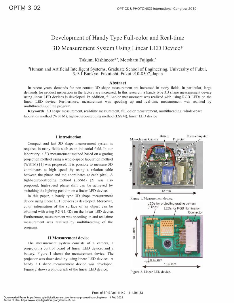
I Introduction Compact and fast 3D shape measurement system is
required in many fields such as an industrial field. In our laboratory, a 3D measurement method based on a grating projection method using a whole-space tabulation method (WSTM) [1] was proposed. It is possible to measure 3D coordinates at high speed by using a relation table between the phase and the coordinates at each pixel. A light-source-stepping method (LSSM) [2] was also proposed, high-speed phase shift can be achieved by switching the lighting position on a linear LED device.
In this paper, a handy type 3D shape measurement device using linear LED devices is developed. Moreover, color information of the surface of an object can be obtained with using RGB LEDs on the linear LED device. Furthermore, measurement was speeding up and real-time measurement was realized by multithreading of the program.
II Measurement device The measurement system consists of a camera, a
projector, a control board of linear LED device, and a battery. Figure 1 shows the measurement device. The projector was downsized by using linear LED devices. A handy 3D shape measurement device was developed. Figure 2 shows a photograph of the linear LED device.
Figure 1. Measurement device.
Figure 2. Linear LED device.
Development of Handy Type Full-color and Real-time
3D Measurement System Using Linear LED Device*
Takumi Kishimoto*a, Motoharu Fujigakia
aHuman and Artificial Intelligent Systems, Graduate School of Engineering, University of Fukui, 3-9-1 Bunkyo, Fukui-shi, Fukui 910-8507, Japan
Abstract
In recent years, demands for non-contact 3D shape measurement are increased in many fields. In particular, large demands for product inspection in the factory are increased. In this research, a handy type 3D shape measurement device using linear LED devices is developed. In addition, full-color measurement was realized with using RGB LEDs on the linear LED device. Furthermore, measurement was speeding up and real-time measurement was realized by multithreading of the program.
Keywords: 3D shape measurement, real-time measurement, full-color measurement, multithreading, whole-space tabulation method (WSTM), light-source-stepping method (LSSM), linear LED device
Proc. of SPIE Vol. 11142 1114201-33Downloaded From: https://www.spiedigitallibrary.org/conference-proceedings-of-spie on 11 Feb 2022Terms of Use: https://www.spiedigitallibrary.org/terms-of-use

Ⅲ Measurement method 1. Whole-Space Tabulation Method (WSTM) In this method, the relation table of phase and 3D
coordinates is created in advance. Therefore, it is not necessary to perform complicated calculation, and measurement can be performed at high speed.
2. Method to obtain color information Figure 2 shows the linear LED device. RGB LEDs are
illuminated for each color and images are grabbed. The luminance values of the three obtained images represent the brightness in the RGB color model. Therefore, color information was obtained by combining three images.
The obtained color information can associate with 3D coordinates because 3D coordinates are obtained for each pixel of the camera.
3. Real time measurement 3 steps of grabbing the images, analysis, and display
are necessary for 3D measurement. Conventionally, these 3 steps were sequentially performed, and the measurement time was about 720 ms.
Therefore, in order to speeding up, 3 steps are divided into threads and processed in parallel. An outline is shown in Figure 3.
In addition, OpenMP was used to speeding up for the analysis.
Figure 3. Outline of multithreading processing.
Ⅳ Measurement result
Figure 4 shows the measurement result. An object is a leopard figure of about 50 mm in height.
Figure 4. Result of full-color 3D measurement.
Ⅴ Conclusions
A handy type full color 3D measuring device was prototyped. Also, real-time measurement with full color by multithreading was realized.
Ⅵ References
[1] M. Fujigaki, Y. Morimoto, “Shape measurement with grating projection using whole-space tabulation method” (in Japanese), Journal of JSEM, 8(4), (2008) 402-408. [2] M. Fujigaki, T. Sakaguchi, Murata, Y., “Development of a compact 3D shape measurement unit using the light-source-stepping method”, Optics and Lasers in Engineering, 85, (2016) 9-17
Proc. of SPIE Vol. 11142 1114201-34Downloaded From: https://www.spiedigitallibrary.org/conference-proceedings-of-spie on 11 Feb 2022Terms of Use: https://www.spiedigitallibrary.org/terms-of-use
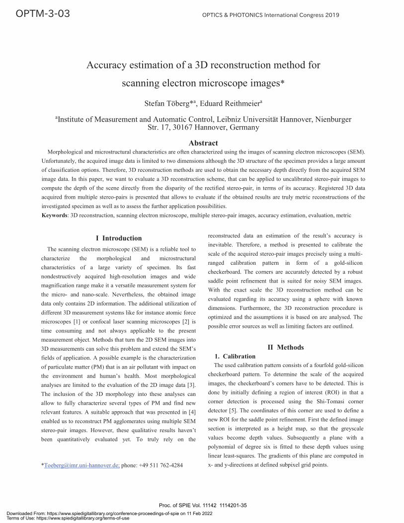
Proc. of SPIE Vol. 11142 1114201-35Downloaded From: https://www.spiedigitallibrary.org/conference-proceedings-of-spie on 11 Feb 2022Terms of Use: https://www.spiedigitallibrary.org/terms-of-use
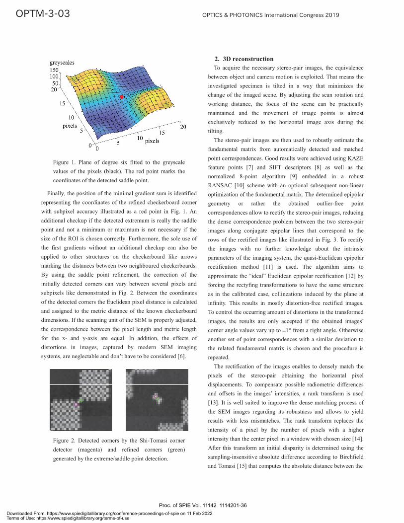
Proc. of SPIE Vol. 11142 1114201-36Downloaded From: https://www.spiedigitallibrary.org/conference-proceedings-of-spie on 11 Feb 2022Terms of Use: https://www.spiedigitallibrary.org/terms-of-use
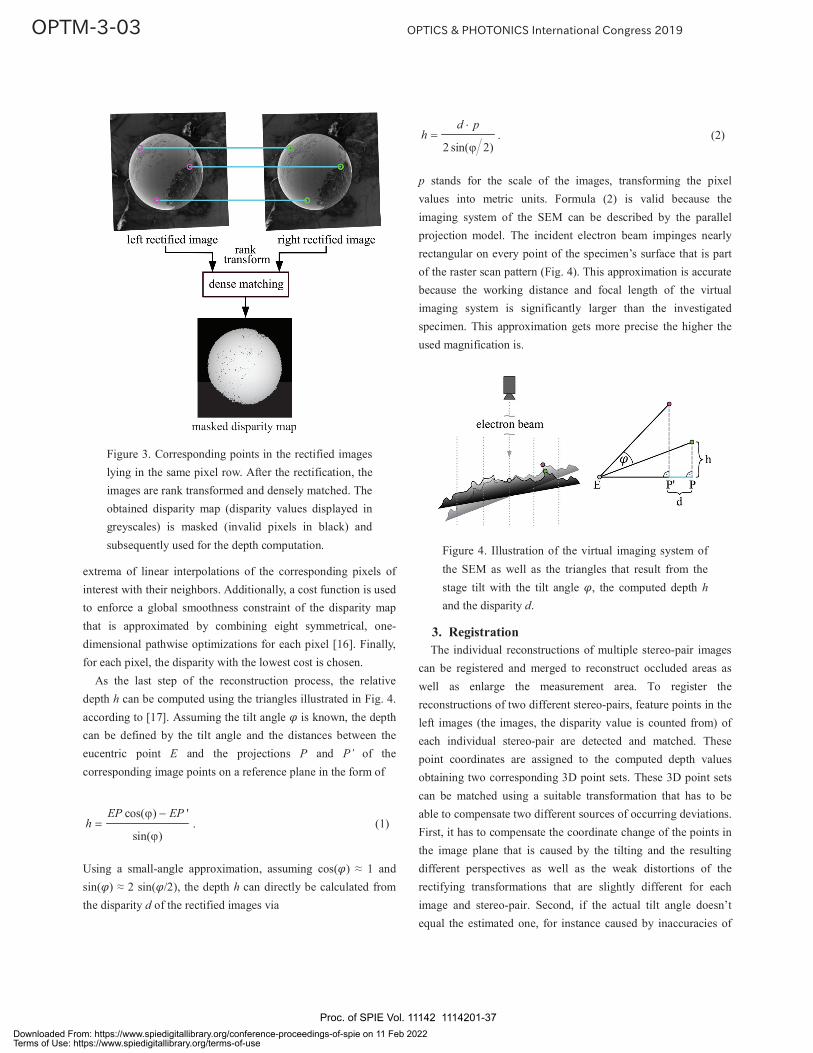
Proc. of SPIE Vol. 11142 1114201-37Downloaded From: https://www.spiedigitallibrary.org/conference-proceedings-of-spie on 11 Feb 2022Terms of Use: https://www.spiedigitallibrary.org/terms-of-use
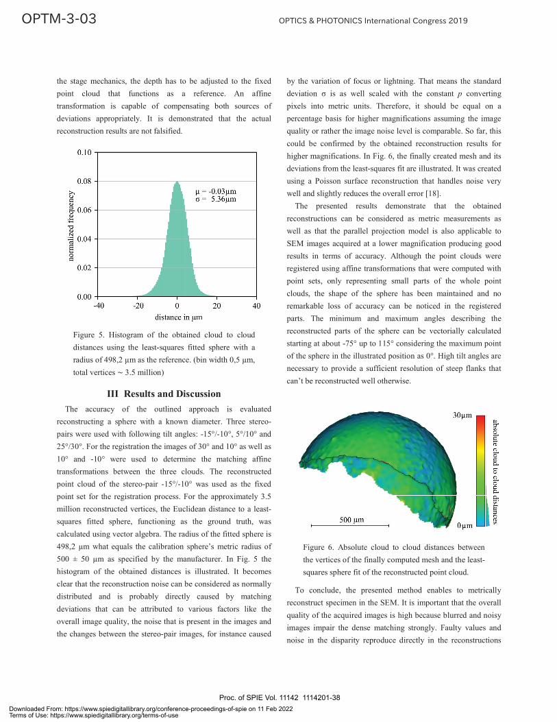
Proc. of SPIE Vol. 11142 1114201-38Downloaded From: https://www.spiedigitallibrary.org/conference-proceedings-of-spie on 11 Feb 2022Terms of Use: https://www.spiedigitallibrary.org/terms-of-use
Proc. of SPIE Vol. 11142 1114201-39Downloaded From: https://www.spiedigitallibrary.org/conference-proceedings-of-spie on 11 Feb 2022Terms of Use: https://www.spiedigitallibrary.org/terms-of-use
*[email protected]; phone 0258-47-9741
I. Introduction Recently, the signal-processing system based on the
direct phase determination method has been developed for high-speed phase measurements in heterodyne interferometry [1]. However, the system is not executed in real time, and it is, therefore, not conventional for the system to apply for industrial applications.
In this paper, we develop another FPGA-based signal-processing system for high-speed phase measurements in real time. The system provides the first experimental result with a phase-modulation frequency of 5 kHz.
II. Signal-processing system 1. System architecture The principle of the direct phase determination has
been presented in [1]. Figure 1 shows the signal-processing architecture of the method. Two 2.7 MHz sinusoidal signals (reference and measurement) from a function generator are sampled by an available ADC (analog-to-digital) device at 120 MHz. For most heterodyne interferometers, the displacement of a target alternates the measurement phase. This means that the difference in phase between the two inputs signals is varied by the displacement when the reference phase is stationary. The main program with the use of the phase-locked loop (PLL) and null method runs on a FPGA
module at 120 MHz. The host program stores data into a storage file in real time. Because the phase shift is detected at ultra-high frequency (120 MHz), the artificial periodic error appeared needs to be removed by post-processing (figure 1(c)).
The main FPGA program consists of a phase detector (multiplier), a low-pass filter (LPF), an integrator, and a phase shifter. It assumes that the reference (I1) and the measurement (I2) are given by
,sin2
cos1 tAtAI (1)
,cos2 mtBI (2)
where A with B, ∆ω and m are amplitudes of the I1 and I2 signals, the angular beat frequency, and the unknown phase of the I1 due to the displacement, respectively. 2. Phase shifter
The phase shifter drifts an any real phase of the reference signal so that it satisfies the null condition (the
phase is controlled to be the m phase). From figure 1(a), the -shifted reference signal is described as
.sin'1 ΦtAI (3)
To create the I’1 signal, the in-signal element and the quadrature element generated by a Hilbert transformer are multiplied by trigonometric functions of the phase. 3. Phase detector (multiplier)
Design of FPGA-based signal-processing system based on the direct phase
determination method for heterodyne interferometry
Thanh Dong NGUYEN, Quang Anh DUONG, Masato HIGUCHI, Dong WEI, and Masato AKETAGAWA*
Department of Mechanical Engineering, Nagaoka University of Technology, 1603-1, Kamitomioka
Nagaoka, Niigata, 940-2188, Japan
Abstract A signal-processing system based on the direct phase determination method [1] for high-speed phase measurements in
real time is presented with the use of a field programmable gate array (FPGA) device. The system running at a clock rate of 120 MHz is designed under LabVIEW environment. The system is investigated using two 2.7 MHz-sinusoidal signals from a function generator, one of which is phase-modulated. The result shows that the system can achieve the phase measurement with a modulation frequency up to 5 kHz.
Keywords: phase-locked loop, null condition, heterodyne interferometer, FPGA, signal-processing
Proc. of SPIE Vol. 11142 1114201-40Downloaded From: https://www.spiedigitallibrary.org/conference-proceedings-of-spie on 11 Feb 2022Terms of Use: https://www.spiedigitallibrary.org/terms-of-use
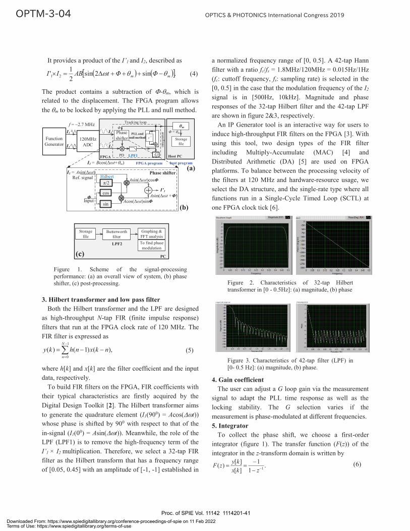
It provides a product of the I’1 and I2, described as
.sin2sin21' 21 mm ΦΦtABII (4)
The product contains a subtraction of - m, which is related to the displacement. The FPGA program allows the m to be locked by applying the PLL and null method.
I2
LPF1
Phase shifter
FPGA
I1 PLL and null method
Tracking loopf = ~2.7 MHz
120MHzADC
I1
I2
Host PC
π/2
cos
sin
Hilbert I1 = Asin(Δωt)
Asin(Δωt)cosΦ
Acos(Δωt)sinΦ Asin(Δωt +Φ)
Ref. signalPhase shifter
Input (b)
I’1Φ
(a)
Function Generator
FPGA program host program
θm
Storagefile
I2 = Bcos(Δωt+ m) PD
z–1
inte
grat
or
G
Φ Φ = m
(c)
Storagefile
Butterworthfilter
LPF2
Graphing &FFT analysisTo find phase modulation
PC Figure 1. Scheme of the signal-processing performance: (a) an overall view of system, (b) phase shifter, (c) post-processing.
3. Hilbert transformer and low pass filter Both the Hilbert transformer and the LPF are designed
as high-throughput N-tap FIR (finite impulse response) filters that run at the FPGA clock rate of 120 MHz. The FIR filter is expressed as
,)()1()(1
0
N
nnkxnhky (5)
where h[k] and x[k] are the filter coefficient and the input data, respectively.
To build FIR filters on the FPGA, FIR coefficients with their typical characteristics are firstly acquired by the Digital Design Toolkit [2]. The Hilbert transformer aims to generate the quadrature element (I1(900) = Acos( t)) whose phase is shifted by 900 with respect to that of the in-signal (I1(00) = Asin( t)). Meanwhile, the role of the LPF (LPF1) is to remove the high-frequency term of the I’1 × I2 multiplication. Therefore, we select a 32-tap FIR filter as the Hilbert transform that has a frequency range of [0.05, 0.45] with an amplitude of [-1, -1] established in
a normalized frequency range of [0, 0.5]. A 42-tap Hann filter with a ratio fc/fs = 1.8MHz/120MHz = 0.015Hz/1Hz (fc: cuttoff frequency, fs: sampling rate) is selected in the [0, 0.5] in the case that the modulation frequency of the I2 signal is in [500Hz, 10kHz]. Magnitude and phase responses of the 32-tap Hilbert filter and the 42-tap LPF are shown in figure 2&3, respectively.
An IP Generator tool is an interactive way for users to induce high-throughput FIR filters on the FPGA [3]. With using this tool, two design types of the FIR filter including Multiply-Accumulate (MAC) [4] and Distributed Arithmetic (DA) [5] are used on FPGA platforms. To balance between the processing velocity of the filters at 120 MHz and hardware-resource usage, we select the DA structure, and the single-rate type where all functions run in a Single-Cycle Timed Loop (SCTL) at one FPGA clock tick [6].
Figure 2. Characteristics of 32-tap Hilbert transformer in [0 - 0.5Hz]: (a) magnitude, (b) phase
Figure 3. Characteristics of 42-tap filter (LPF) in [0- 0.5 Hz]: (a) magnitude, (b) phase.
4. Gain coefficient The user can adjust a G loop gain via the measurement
signal to adapt the PLL time response as well as the locking stability. The G selection varies if the measurement is phase-modulated at different frequencies. 5. Integrator
To collect the phase shift, we choose a first-order integrator (figure 1). The transfer function (F(z)) of the integrator in the z-transform domain is written by
.1
1][][)( 1zkx
kyzF (6)
Proc. of SPIE Vol. 11142 1114201-41Downloaded From: https://www.spiedigitallibrary.org/conference-proceedings-of-spie on 11 Feb 2022Terms of Use: https://www.spiedigitallibrary.org/terms-of-use
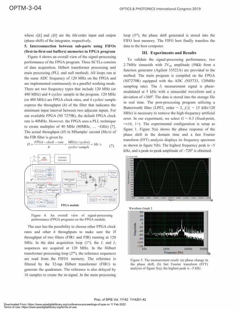
where x[k] and y[k] are the kth-order input and output (phase shift) of the integrator, respectively. 5. Interconnection between sub-parts using FIFOs (first-in-first-out buffers) memories in FPGA program
Figure 4 shows an overall view of the signal-processing performance of the FPGA program. Three SCTLs consists of data acquisition, Hilbert transformer processing and main processing (PLL and null method). All loops run at the same ADC frequency of 120 MHz on the FPGA and are implemented continuously in a parallel working mode. There are two frequency types that include 120 MHz (or 480 MHz) and 4 cycles/ sample in the program. 120 MHz (or 480 MHz) are FPGA clock rates, and 4 cycles/ sample express the throughput (h) of the filter that indicates the minimum input interval between two adjacent inputs. For our available FPGA (NI 7279R), the default FPGA clock rate is 40MHz. However, the FPGA uses a PLL technique to create multiples of 40 MHz (80MHz, … ~GHz) [7]. The actual throughput (H) in MSample/ second (Ms/s) of the FIR filter is given by
sMssamplecyclescyclessMHz
hrateclockFPGAH /
/)/(
(7)
FIFO 1(read)
FIFO in-signal(write)
FIFO quadrature(write)
FIR1 filter
Hilbert loop (480 MHz)
FIFO in-signal(read)
FIFO quadrature(read)
In put Out put
4 cycles/sampe
FIR1
Hilbert transformer processing (120 MHz)
Main processing (120MHz)AO output
AI ouput
FIFO 1(write)
Data acquisition (120 MHz)
ADC120MHz
FPGA module
AO
AI
Phase shift
1st
2nd 3rd
FIFO 2(write)
FIFO 2(read) Measurement
16-sample delay
cos
sin
FIR filter
z-1
FIFO host (write)
Filter loop (480 MHz)
In put Out put
4 cycles/sampe
FIR
Function Generator
Reference
Ref.
Mes.
32 taps
Inte
grat
or
I1
I2
Figure 4. An overall view of signal-processing performance (FPGA program) on the FPGA module.
The user has the possibility to choose other FPGA clock rates and other h throughputs to make sure the H throughput of two filters (FIR1 and FIR) running at 120 MHz. In the data acquisition loop (1st), the I1 and I2 sequences are acquired at 120 MHz. In the Hilbert transformer processing loop (2nd), the reference sequences are read from the FIFO1 memory. The reference is filtered by the 32-tap Hilbert transformer (FIR1) to generate the quadrature. The reference is also delayed by 16 samples to create the in-signal. In the main processing
loop (3rd), the phase shift generated is stored into the FIFO host memory. The FIFO host finally transfers the data to the host computer.
III. Experiments and Results To validate the signal-processing performance, two
2.7MHz sinusoids with 2Vpp amplitude (50Ω) from a function generator (Agilent 33522A) are provided to the method. The main program is compiled on the FPGA (NI7279R) equipped with the ADC (NI5733, 120MHz sampling rate). The I2 measurement signal is phase-modulated at 5 kHz with a sinusoidal waveform and a deviation of ±3600. The data is stored into the storage file in real time. The post-processing program utilizing a Butterworth filter (LPF2, order = 2, fc/fs = 15 kHz/120 MHz) is necessary to remove the high-frequency artificial error. In our experiment, we select G = 0.3 (fixed-point, <±16, 1>). The experimental configuration is setup as figure 1. Figure 5(a) shows the phase response of the phase shift in the domain time and a fast Fourier transform (FFT) analysis displays its frequency spectrum as shown in figure 5(b). The highest frequency peak is ~5 kHz, and a peak-to-peak amplitude of ~7200 is obtained.
a
b Figure 5. The measurement result: (a) phase change in the phase shift, (b) fast Fourier transform (FFT) analysis of figure 5(a); the highest peak is ~5 kHz.
Proc. of SPIE Vol. 11142 1114201-42Downloaded From: https://www.spiedigitallibrary.org/conference-proceedings-of-spie on 11 Feb 2022Terms of Use: https://www.spiedigitallibrary.org/terms-of-use

IV. Conclusion In this paper, we have designed the real-time signal-
processing system based on the direct phase determination method. The system provides the high-speed phase measurement with a modulation frequency up to 5 kHz using two 2.7 MHz sinusoidal signals. The system is capable of being used for high-speed phase measurements in industrial applications. In the future, with improving this system, we will (1) extend the phase measurement with modulation frequencies up to tens of kHz, and more than; (2) investigate the measurement resolution for heterodyne interferometers.
References [1] Dong, N. T, Anh, D. Q., Higuchi, M., Wei, D., Aketagawa, M., “Direct phase determination using phase lock loop for heterodyne displacement-measuring interferometers”, Proc. Photonic Asia Conference, 2018. [2] National Instruments, “LabVIEW Digital Design Toolkit User Manual”, February 2005, < http://www.ni.com/pdf/manuals/371353a.pdf [3] National Instruments, “Designing Ultra-High Throughput FIR Filters with no Multiplier on NI FPGA Platforms”, 23 August 2013, <http://www.ni.com/white-paper/9700/en/> [4] Anees, N. J. M., Kharate, A. B., “FPGA based implementation of MAC in Parallel Filter”, International Journal of Innovation Research in Science Engineering and Technology, 18460-18467 (2017). [5] Keerthi, M., Midasala, V., Bhavanam, S. N., Jeevan, K. R., “FPGA Implementation of Distributed Arithmetic for FIR filter”, International Journal of Innovation Research in Science Engineering and Technology 1(9) (2012). [6] National Instruments, “Single-Cycle Timed Loop FAQ for the LabVIEW FPGA Module”, 25 July 2018, < https://knowledge.ni.com/KnowledgeArticleDetails?id=kA00Z000000P8sWSAS&l=en-CA > [7] National Instruments, “NI 5731/5732/5733/5734R User Guide and Specifications”, February 2011, < http://www.ni.com/pdf/manuals/375653a.pdf>
Proc. of SPIE Vol. 11142 1114201-43Downloaded From: https://www.spiedigitallibrary.org/conference-proceedings-of-spie on 11 Feb 2022Terms of Use: https://www.spiedigitallibrary.org/terms-of-use
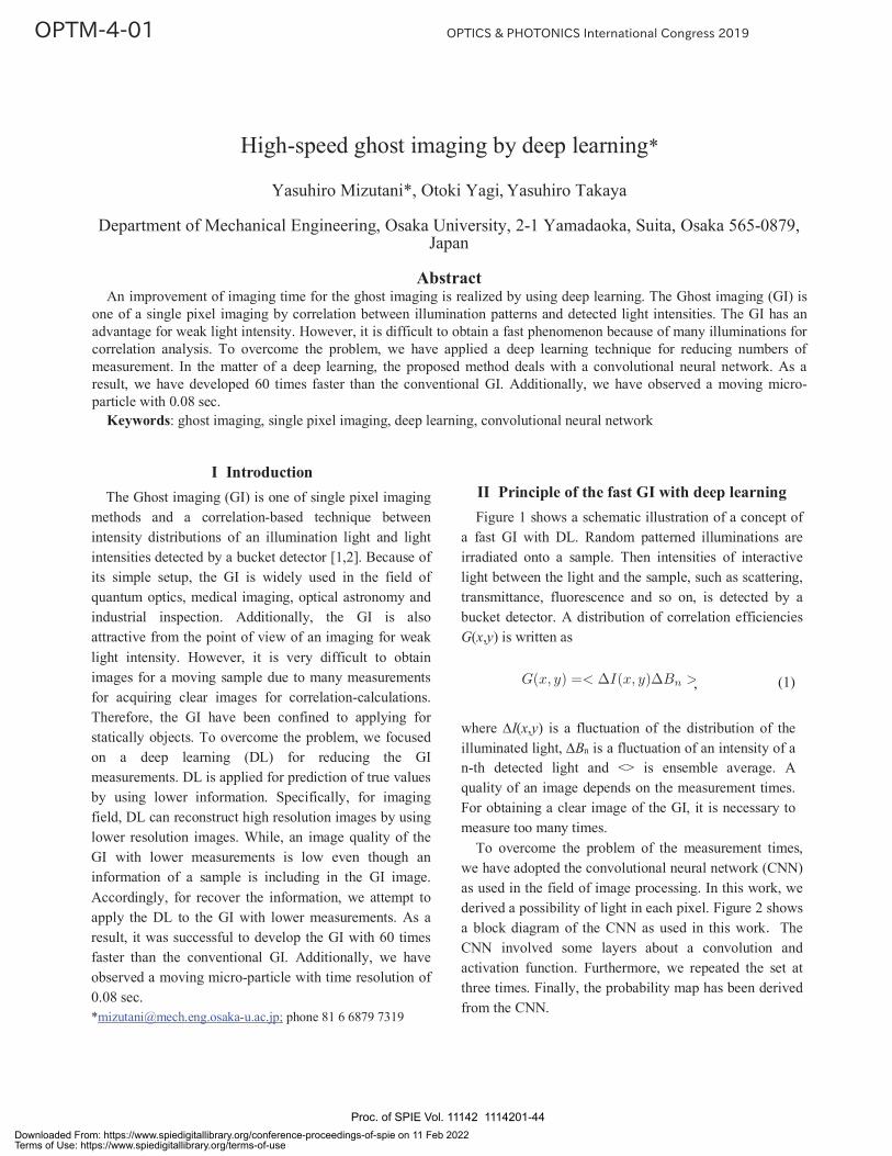
I Introduction The Ghost imaging (GI) is one of single pixel imaging
methods and a correlation-based technique between intensity distributions of an illumination light and light intensities detected by a bucket detector [1,2]. Because of its simple setup, the GI is widely used in the field of quantum optics, medical imaging, optical astronomy and industrial inspection. Additionally, the GI is also attractive from the point of view of an imaging for weak light intensity. However, it is very difficult to obtain images for a moving sample due to many measurements for acquiring clear images for correlation-calculations. Therefore, the GI have been confined to applying for statically objects. To overcome the problem, we focused on a deep learning (DL) for reducing the GI measurements. DL is applied for prediction of true values by using lower information. Specifically, for imaging field, DL can reconstruct high resolution images by using lower resolution images. While, an image quality of the GI with lower measurements is low even though an information of a sample is including in the GI image. Accordingly, for recover the information, we attempt to apply the DL to the GI with lower measurements. As a result, it was successful to develop the GI with 60 times faster than the conventional GI. Additionally, we have observed a moving micro-particle with time resolution of 0.08 sec. *[email protected]; phone 81 6 6879 7319
II Principle of the fast GI with deep learning Figure 1 shows a schematic illustration of a concept of
a fast GI with DL. Random patterned illuminations are irradiated onto a sample. Then intensities of interactive light between the light and the sample, such as scattering, transmittance, fluorescence and so on, is detected by a bucket detector. A distribution of correlation efficiencies G(x,y) is written as
, (1)
where ΔI(x,y) is a fluctuation of the distribution of the illuminated light, ΔBn is a fluctuation of an intensity of a n-th detected light and <> is ensemble average. A quality of an image depends on the measurement times. For obtaining a clear image of the GI, it is necessary to measure too many times.
To overcome the problem of the measurement times, we have adopted the convolutional neural network (CNN) as used in the field of image processing. In this work, we derived a possibility of light in each pixel. Figure 2 shows a block diagram of the CNN as used in this work The CNN involved some layers about a convolution and activation function. Furthermore, we repeated the set at three times. Finally, the probability map has been derived from the CNN.
High-speed ghost imaging by deep learning*
Yasuhiro Mizutani*, Otoki Yagi, Yasuhiro Takaya
Department of Mechanical Engineering, Osaka University, 2-1 Yamadaoka, Suita, Osaka 565-0879, Japan
Abstract
An improvement of imaging time for the ghost imaging is realized by using deep learning. The Ghost imaging (GI) is one of a single pixel imaging by correlation between illumination patterns and detected light intensities. The GI has an advantage for weak light intensity. However, it is difficult to obtain a fast phenomenon because of many illuminations for correlation analysis. To overcome the problem, we have applied a deep learning technique for reducing numbers of measurement. In the matter of a deep learning, the proposed method deals with a convolutional neural network. As a result, we have developed 60 times faster than the conventional GI. Additionally, we have observed a moving micro-particle with 0.08 sec.
Keywords: ghost imaging, single pixel imaging, deep learning, convolutional neural network
Proc. of SPIE Vol. 11142 1114201-44Downloaded From: https://www.spiedigitallibrary.org/conference-proceedings-of-spie on 11 Feb 2022Terms of Use: https://www.spiedigitallibrary.org/terms-of-use
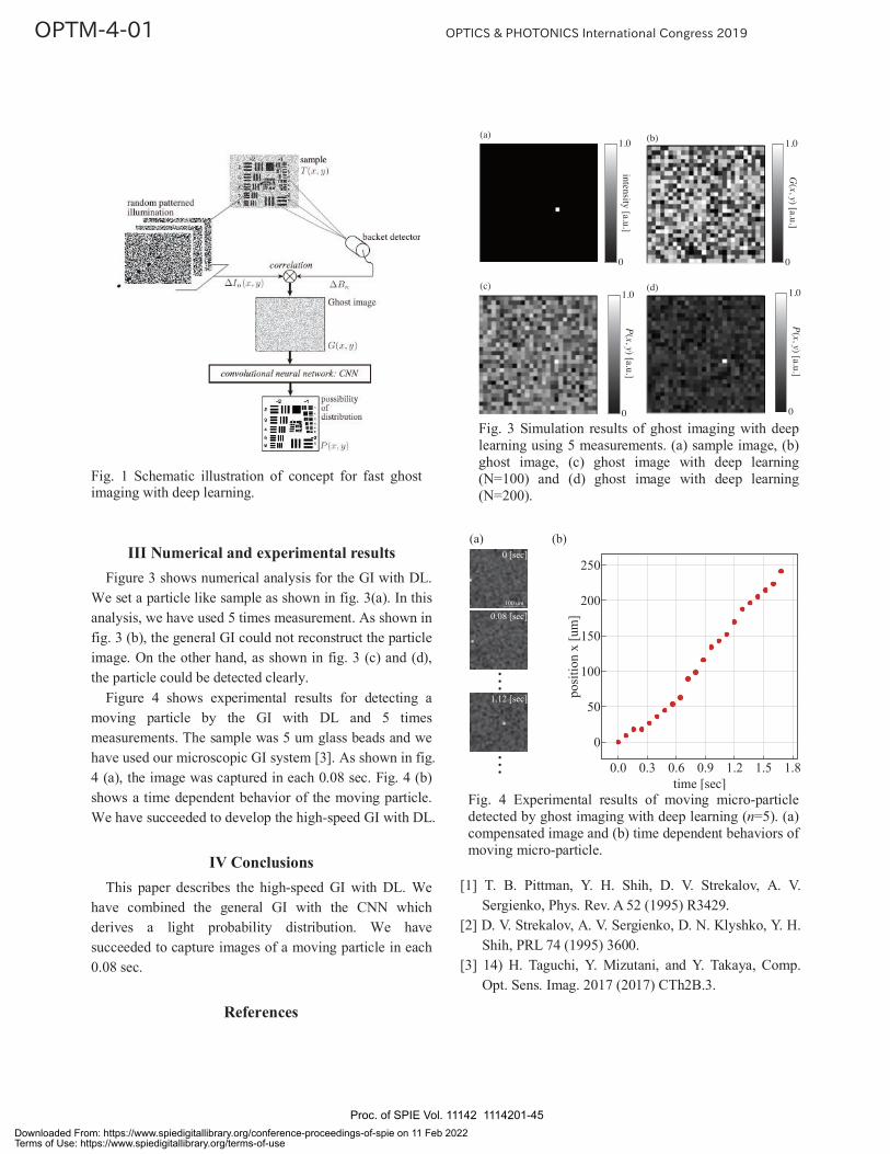
III Numerical and experimental results Figure 3 shows numerical analysis for the GI with DL.
We set a particle like sample as shown in fig. 3(a). In this analysis, we have used 5 times measurement. As shown in fig. 3 (b), the general GI could not reconstruct the particle image. On the other hand, as shown in fig. 3 (c) and (d), the particle could be detected clearly.
Figure 4 shows experimental results for detecting a moving particle by the GI with DL and 5 times measurements. The sample was 5 um glass beads and we have used our microscopic GI system [3]. As shown in fig. 4 (a), the image was captured in each 0.08 sec. Fig. 4 (b) shows a time dependent behavior of the moving particle. We have succeeded to develop the high-speed GI with DL.
IV Conclusions This paper describes the high-speed GI with DL. We
have combined the general GI with the CNN which derives a light probability distribution. We have succeeded to capture images of a moving particle in each 0.08 sec.
References
[1] T. B. Pittman, Y. H. Shih, D. V. Strekalov, A. V. Sergienko, Phys. Rev. A 52 (1995) R3429.
[2] D. V. Strekalov, A. V. Sergienko, D. N. Klyshko, Y. H. Shih, PRL 74 (1995) 3600.
[3] 14) H. Taguchi, Y. Mizutani, and Y. Takaya, Comp. Opt. Sens. Imag. 2017 (2017) CTh2B.3.
Fig. 1 Schematic illustration of concept for fast ghost imaging with deep learning.
Fig. 3 Simulation results of ghost imaging with deep learning using 5 measurements. (a) sample image, (b) ghost image, (c) ghost image with deep learning (N=100) and (d) ghost image with deep learning (N=200).
Fig. 4 Experimental results of moving micro-particle detected by ghost imaging with deep learning (n=5). (a) compensated image and (b) time dependent behaviors of moving micro-particle.
1.0
0intensity [a.u.]
(a)
1.0
0
P( x, y) [a.u.]
(c)
1.0
0
G( x, y) [a.u.]
(b)
1.0
0
P( x, y) [a.u.]
(d)
・・・
・・・
Proc. of SPIE Vol. 11142 1114201-45Downloaded From: https://www.spiedigitallibrary.org/conference-proceedings-of-spie on 11 Feb 2022Terms of Use: https://www.spiedigitallibrary.org/terms-of-use
I Introduction Purity of rice seed is one of important factor for
breeding and cultivation. The presence of foreign seed, especially weed rice, can affect productivity yields [1] and good traits of cultivating rice seed. Thailand is one of major agricultural countries which exports huge numbers of agriculture products, especially rice, every year. Currently, there are more than 114 well-known Thai rice varieties [2] that have been cultivated throughout the country. Hence, risk of mixing various species in each cultivation is high. Therefore, rice seed production company or other related organizations (eg. Rice Department) has to ensure rice seeds purity before selling them to farmer. According to Rice Department of Thailand, the foreign rice seeds are identified and removed manually by naked eye of experts based on dominant features of interested rice seeds. This process is laborious and time consuming since the experts need to examine at least 100 grams of rice (approx. 4000 seeds) per production lot. Furthermore, it is difficult to train their skills to next generation due to variation of rice seeds and degradation of rice seeds over time.
With help of current computer vision and machine learning technology, it is possible to capture high
resolution rice seed images and then identify their varieties [3]. At presence, there are many researchers working on the topic of rice seed classification and rice seed recognition system based on seed appearance [2]. However, the characteristic of rice seeds is varied with amount of water, climate and other uncontrollable factors. Thus, the developed system and its algorithm need to be updated from time-to-time and require large amount of good quality rice seed image to improve or maintain its accuracy.
In this paper, we propose simple, yet effective, automatic imaging system based on optical set-up and digital camera. This system can capture high resolution rice seed images, which are suitable for further classification.
II System Design
There are various designs of automatic rice seed imaging system [4-5]. However, it is hard to capture dominant features of rice seed unless the rice seeds do not place properly in imaging area as shown in Figure 1. Furthermore, the lighting condition is also important since color is also one of significant and necessary parameter for classification. Therefore, the proposed system has to
Automatic rice seed imaging system for varieties classification
Panintorn Prempree*a, Kosom Chaitavona, Supanit Porntheeraphata, Kantip Kiratiratanapruka, Pitchayagan Temniranrata, Wasin Sinthupinyoa, Anchalee Prasertsakb
aNational Electronics and Computer Technology Center (NECTEC), National Science and Technology Development Agency (NSTDA), Pathum thani, 12120, Thailand
bBureau of Rice Research and Development, Rice Department, Bangkok, 10900, Thailand *Email: [email protected]
Abstract
Rice seed classification is one of important process for rice breeding since mixing of foreign rice seeds can affect good traits of cultivated rice. A usual method for foreign rice seed identification is visual testing by experts, which is laborious and time consuming. In order to overcome this difficulty, there are many researches related on automatic rice seed classification using image processing and machine learning technique. However, the performance of system based on those techniques depends on number of dominant features that can be extracted from image of rice seeds and number of samples. In this paper, automatic rice seed imaging system is presented. This system can guarantee more than 90% of proper images suitable for varieties classification. Furthermore, to validate classification performance, the images of three Thai rice varieties (CNT1, PTT1 and RD51) have been captured and tested. The classification accuracy for CNT1, PTT1 and RD51 are 98%, 99% and 97% respectively.
Keywords: Agriculture, Seed classification, Autonomous system, Image processing, Optical measurement, Machine
learning
Proc. of SPIE Vol. 11142 1114201-46Downloaded From: https://www.spiedigitallibrary.org/conference-proceedings-of-spie on 11 Feb 2022Terms of Use: https://www.spiedigitallibrary.org/terms-of-use

be designed to satisfy given requirements.
Figure 1. Usuable image due to improper rice seed placing
Our designed system consists of three main parts: 1)
Imaging System 2) Rice Feeder 3) Rice seed detection algorithm,
1. Imaging system For lighting condition, ring white rice source is chosen
for uniform light distribution in small area since size of rice seed is approximately 2 x 11 x 2 mm3. However, reflected light from background can affect color of rice seed and make it difficult for segmentation and classification. Hence, circular polarizer and linear polarizer are added into system to reduce the effect of reflected light. Furthermore, high resolution image with 6000 dpi in 3840x2748 pixel2 can be obtained by combing digital camera with tele-centric lens. Thus, this resolution and lighting condition are sufficient for analyze size, shape, color or even roughness of rice seed, which are key features for rice seed classification.
2. Rice feeder Rice feeder is necessary to convey rice seeds to
imaging area. There are many methods such as conveyor [5] or bowl feeder (helical plate with vibrating motor) [4]. In our system, helical plate with vibrating motor is used since it can mostly guarantee that the rice seed will move into imaging area one at a time. However, disadvantage of this approach is the timing and the distance between each entered rice seed is random even if speed of vibration is nearly constant. Thus, optional sensor or image processing for detecting rice seed is needed.
3. Seed detection algorithm Our system is able to detect incoming rice seed
automatically based on image processing algorithm. Benefits of using image processing over adding detection sensor are less complexity in both system design and synchronization. To detect rice seed, certain areas of images is marked as region of interest (ROI) as shown in Figure 2. RGB value of pixels inside green ROI and red ROI are averaged (ie. (R+G+B)/3) and if the averaged value of green ROI is above setting threshold, then there is a rice seed ready for imaging. Then, system will stop the rice feeder and capture rice seed image. In the other hand, average value in red ROI is for controlling intensity of light.
Figure 2. ROI for rice seed detection
By integrating all following parts as shown in Figure 3, our developed system is shown in Fig. 3. The current performance of our system is fully automatic rice seed capture with speed of 10 seeds per minutes. In addition, manual operated system is possible for examining rice seed individually.
Figure 3. System overview III Result and Discussion
Proc. of SPIE Vol. 11142 1114201-47Downloaded From: https://www.spiedigitallibrary.org/conference-proceedings-of-spie on 11 Feb 2022Terms of Use: https://www.spiedigitallibrary.org/terms-of-use

To validate performance of our system, 6,000 images of three Thai rice varieties (CNT1, PTT1, RD51) have been captured.
1. Quality of captured rice seed image Example of usable images of each rice varieties is
shown in Figure 4, which is 5,421 out of 6,000 captured images (approximately 90.35%).
(a)
(b)
(c)
Figure 4. Example of captured images (a) CNT1 (b) PTT1 (c) RD51
2. Seed classification Rice seed images in obtained in previous section have
been pre-processed and trained using Support Vector Machine (SVM) algorithm. Then, 200 rice seed untrained images of CNT1, PTT1 and RD51 each are randomly sampled for classification. The classification accuracy for CNT1, PTT1 and RD51 are 98%, 99% and 97% respectively.
Table 1. Accuracy of CNT1 Model
CNT1 Other CNT1 198 2 PTT1 4 196 RD51 6 194
Table 2 Accuracy of PTT1 Model
PTT1 Other CNT1 0 200 PTT1 196 4 RD51 1 199
Table 3 Accuracy of RD51 Model
RD51 Other CNT1 0 200 PTT1 0 200 RD51 184 16
Performance of our designed automatic rice seed
imaging system is good in term of quality of captured images and classification. In addition, this system can be applied to measure rice grain embryo’s size, size measurement and glutinous rice separation, which are our previous research [6]. However, for achieving more than 90% of usable images, the capturing speed is limited to only 10 samples per, which is too slow for industrial production line but it is still acceptable for rice breeding research.
Acknowledgement
The author would like to the Rice Department of Thailand for providing funding of this project and supplying rice seed samples, and National Electronics and Computer Technology Center (NECTEC) for supplying equipment and facilities.
References [1] A.A. Aznan, I.H. Rukunudin, A.Y.M. Shakaff, R.
Ruslan, A. Zakaria and F.S.A. Saad. “The use of machine
vision technique to classify cultivated rice seed variety
and weedy rice seed variants for the seed industry”. Int.
Food Research Journal, vol 23(suppl), pp. S31-S35, 2016.
[2] B, Lurstwut. C. Pornpanomchai. “Application of
Image Processing and Computer Vision on Rice Seed
Germination Analysis.” (2016).
[3] Phan, Hong & Vo, Ta-Hoang & Tran, Thanh-Hai & Le,
Thi & Nguyen, Thuy & Hai, Vu. (2015). Comparative
Proc. of SPIE Vol. 11142 1114201-48Downloaded From: https://www.spiedigitallibrary.org/conference-proceedings-of-spie on 11 Feb 2022Terms of Use: https://www.spiedigitallibrary.org/terms-of-use

Study on Vision Based Rice Seed Varieties Identification.
10.1109/KSE.2015.46.
[4] Marschalek, Rubens & Cesar Silva, Mauricio &
Batista dos Santos, Samuel & Ricardo Manke, Johnny &
Bieging, Carlos & Porto, Geovani & Wickert, Ester & De
Andrade, Alexander. (2017). Image - Rice Grain Scanner:
A three-dimensional fully automated assessment of grain
size and quality traits. Crop Breeding and Applied
Biotechnology. 17. 89-97. 10.1590/1984-
70332017v17n1s15.
[5] I.Chatnuntawech et al, “Rice Classification Using
Spatio-Spectral Deep Convolutional Neural Network”,
arXiv:1805.11491v2
[6] K. Chaitavon et al, “Development if photonics-based physical quality assessment systems for rice seeds and grains”, IRC14-0592, 4th International Rice Congress, 27 October – 1 November 2014.
Proc. of SPIE Vol. 11142 1114201-49Downloaded From: https://www.spiedigitallibrary.org/conference-proceedings-of-spie on 11 Feb 2022Terms of Use: https://www.spiedigitallibrary.org/terms-of-use
I Introduction We aim to realize the early detection of red tides,
which result from plankton plagues, using our ultra-compact spectroscopic apparatus mounted on an unmanned aerial vehicle; i.e., a drone. The number of outbreaks of red tide in the Seto Inland Sea has gradually decreased year by year since the 1970s. However, losses of fishery dams relating to red tides amount to hundreds of millions of yen annually. The early detection of red tides would allow forestry and fishery workers to be alarmed and floating fishery cages to be removed in time. Several tens of species of plankton include chlorophyll in photosynthesis. Chlorophyll absorbs visible light and generates nutritive components, and the spectral absorbance of chlorophyll at wavelengths of visible light is thus well known. Therefore, for the monitoring of red tides, chlorophyll concentrations in oceans are evaluated from spectral absorbance data acquired by artificial satellites. However, the temporal and spatial resolutions of such data are not sufficient for rapid onsets. It is thus expected that multicopter and fixed-wing drones will be used to measure chlorophyll concentrations with high
frequency. In this case, however, light-source colors that vary from hour to hour and place to place need to be corrected temporally and spatially. We thus propose a light-source color correction method using Fresnel's equations for reflection. In this proposed method, specular light reflected from the sea surface, which has the same color as the light source, and light diffracted from within the ocean are physically separated and measured at the same moment. Employing this method, a developed one-shot spectroscopic imager [1]–[5], which is set at Brewster’s angle, detects p-polarized beams (internally reflected light) and s-polarized beams (surface and internally reflected light) separately. We obtain light-source colors as surface-reflected light analytically. Additionally, the spectral reflectance of internally diffracted light can be calculated to estimate the chlorophyll concentration.
This paper demonstrates the feasibility of correcting light-source colors and overcoming a wide range of sunlight illuminance employing near open-Nicole analysis.
Light-source color correlation of wide-field spectroscopic imaging for
the adaption to spatial and temporal variations when using an
unmanned aerial vehicle
Kotone YOKOYAMA*, Natsumi KAWASHIMA, Tomoya KITAZAKI, Sora MIZUTANI, Hanyue KANG and Ichiro ISHIMARU
Faculty of Engineering, Kagawa University, 2217-20 Hayashi, Takamatsu, Kagawa, 761-0396, Japan
e-mail: [email protected] HP: http://www.eng.kagawa-u.ac.jp/~ishimaru/index.html
Abstract Wide-area spectroscopic imaging by an unmanned aerial vehicle has been proposed for the early detection of red tides.
To ensure the accurate determination of the chlorophyll concentrations of plankton, the spectral reflectance of internally diffused light was calculated separately from changes in the light source (sunlight), due to the time and location. The proposed one-shot spectroscopic line imager was set at Brewster’s angle and p- and s-analyzers were set alternately in each pixel. In a p-polarized pixel, the internally reflected light and surface-reflected light are detected. Surface-reflected light has the color of the light source. In an s-polarized pixel, only internally diffracted light is measured. The color of the light source can thus be estimated from the difference of the two spectral intensities. Additionally, we proposed near cross-Nicole analysis to compensate for the lack of the dynamic range of two-dimensional array devices. This study demonstrated the feasibility of the proposed method for measurements taken at a lake. We were able to identify the specific absorbance peak (at a wavelength of 680 nm) from corrected spectral relative intensities.
Proc. of SPIE Vol. 11142 1114201-50Downloaded From: https://www.spiedigitallibrary.org/conference-proceedings-of-spie on 11 Feb 2022Terms of Use: https://www.spiedigitallibrary.org/terms-of-use

II Background correction with simultaneous detection of surface-reflected light for the light-source color and internally diffracted light using two polarized beams observed from Brewster’s
angle 1. Principle of light-source color correction [6][7] Figure 1 shows that we set two types of analyzer in the
apertural areas of multiple slits. Ocean surfaces are illuminated by diffused illumination because natural sunlight is diffracted and scattered in air. Furthermore, light is depolarized through the reflection of internally diffracted light from internal components.
To improve the clarity of an interferogram, we set the multiple slits on the conjugate optical objective plane [3][4]. The inclination angle of the hyperspectral camera is set as Brewster's angle and the surface reflectance of p-polarized beams is thus zero. Beams passing through p-polarization filters are internally diffracted reflections
while beams passing through s-polarization filters are the sum of light having the color of the light source, such as the color of natural sunlight, and internally diffracted reflections. We can easily separate the surface reflection and internal diffraction from these two detected beams.
However, the intensity ratio between the surface reflection and internal diffraction is around 1000. Therefore, these two types of polarized beams cannot be detected using one two-dimensional light-receiving array device because of the poor dynamic range. To solve this issue of the dynamic range, the polarization angle as an s-polarized filter is set as a small inclination angle φ according to Malus' law. In this case, the detected light ratio of surface-reflected light reduces in accordance with cosine φ. Considering the reduced ratio, we can separate surface-reflected light as light having the color of the light source and internally diffracted light.
around5 [μm]
Multi slit
Brewster's angle53[deg.]53[deg.]
Water (n=1.33)
Air (n=1.0)
Sun
Scattering
Diffracted reflection
Internal diffracted lights(depolarized lights: s+p-polarized beams)
Surface reflection(s-polarized beams)
Diffused illuminations
arou
nd5
[μm
]
Analyzer in each apertural area of multi slit
psps
Cross-Nicoletype
p
p
Near open-Nicoletype
φ
φ
φ[deg.]
Figure 1 Schematic diagram of the background correction method with the simultaneous detection of surface-reflected light
having the light-source color and internally diffracted light through the observation of two polarized beams at Brewster's angle [6][7].
2. Experimental results for identifying chlorophyll spectral absorbance (680 nm) at a lake
In this feasibility experiment, we observed the lake Saburo-ike, located near our university. A one-shot Fourier spectroscopic imager was set at Brewster’s angle
(53 degrees). The red solid line in Figure 2(a) shows the recording of internally diffracted light as a p-polarized beam. Internally reflected light and surface-reflected light were detected by an s-polarization analyzer as shown by the blue solid line. In Fig. 2(b), we discriminate the
Proc. of SPIE Vol. 11142 1114201-51Downloaded From: https://www.spiedigitallibrary.org/conference-proceedings-of-spie on 11 Feb 2022Terms of Use: https://www.spiedigitallibrary.org/terms-of-use
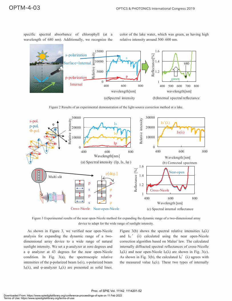
specific spectral absorbance of chlorophyll (at a wavelength of 680 nm). Additionally, we recognize the
color of the lake water, which was green, as having high relative intensity around 500–600 nm.
Refle
ctan
ce[%
]
1
1.2
1.4
1.6
400 500 600 700 800wavelength[nm]
(b)Internal spectral reflectance
0
5000
10000
15000
400 600 800
s
p
wavelength[nm]
(a)Spectral intensityRe
lativ
e in
tens
itys-polarization
p-polarization green
680 Surface+Internal
Internal
Figure 2 Results of an experimental demonstration of the light-source correction method at a lake.
1
1.2
1.4
1.6
400 600 800
Refle
ctan
ce [
%]
Wavelength [nm](c) Spectral internal reflectanceNear-open-Nicole
p
pφ
φ[deg.]
φ
Multi slit
psp
sCross-Nicole
Cross-Nicole
0
10000
20000
30000
400 600 800
Wavelength [nm](b) Corrected spectrum
Rela
tive
inte
nsity
Wavelength[nm]
0
10000
20000
30000
400 600 800
(a) Spectral intensity (Ip, Is, Iφ )
Rela
tive
inte
nsity
Ip
Is
Iφ
Near-open
Is(λ)
Is (λ)spφ
Rela
tive
inte
nsity
spφ
s-pol.p-pol.Φ-pol.
Figure 3 Experimental results of the near open-Nicole method for expanding the dynamic range of a two-dimensional array device to adapt for the wide range of sunlight intensity.
As shown in Figure 3, we verified near open-Nicole analysis for expanding the dynamic range of a two-dimensional array device to a wide range of natural sunlight intensity. We set a p-analyzer at zero degrees and a φ analyzer at 43 degrees for the near open-Nicole condition. In Fig. 3(a), the spectroscopic relative intensities of the p-polarized beam IP(λ), s-polarized beam IS(λ), and φ-analyzer Iφ(λ) are presented as solid lines.
Figure 3(b) shows the spectral relative intensities IS(λ) and IS (λ) calculated using the near open-Nicole correction algorithm based on Malus' law. The calculated internally diffracted spectral reflectances of cross-Nicolle IS(λ) and near open-Nicole IP(λ) are shown in Fig. 3(c). As shown in Fig. 3(b), the calculated IS (λ) agrees with the measured value IS(λ). These two types of internally
Proc. of SPIE Vol. 11142 1114201-52Downloaded From: https://www.spiedigitallibrary.org/conference-proceedings-of-spie on 11 Feb 2022Terms of Use: https://www.spiedigitallibrary.org/terms-of-use

diffracted reflectance are equivalent as shown in Fig. 2(c), and we thus verify the near open-Nicole method.
4. Conclusions We proposed and demonstrated a light-source color
correlation method for the wide-area visualization of plankton distributions, using an ultra-compact spectroscopic imager mounted on a drone. We were able to distinguish the specific spectral absorbance of chlorophyll (at a wavelength of 680 nm) from spectra recorded at a lake.
In future work, we will equip drones with our proposed ultra-compact one-shot spectroscopic line imager and verify the effectiveness of the imager in the high-frequency monitoring of red tides.
References [1] T.Uraki,, I.Ishimaru, ”Feasibility Demonstration of
Real-Time Measurement by One-shot Compact Fourier Spectroscopic Imaging”, Proc. of 8th Japan-France Congress on Mecatronics , pp.549-553 (2010)
[2] S. Sato, M. Fujiwara, S. Suzuki, A. Nishiyama, I. Ishimaru, “Proposal of one-shot-type spectroscopic-tomography for non-invasive medical-measurement”, Proc. of OSA-SPIE European Conferences on Biomedical Optics 2013, Vol. 8798, pp.87980I-1-8(2013)
[3] Shun Sato, Wei Qi, Natsumi Kawashima, Kosuke Nogo, Satsuki Hosono, Akira Nishiyama, Kenji Wada, and Ichiro Ishimaru, “Ultra-miniature one-shot Fourier-spectroscopic tomography,” Optical Engineering, Vol.55, pp. 025106-1 - 025106-8 (2016)
[4] Natsumi Kawashima; Kosuke Nogo; Satsuki Hosono; Akira Nishiyama; Kenji Wada; Ichiro Ishimaru, “Sensitivity improvement of one-shot Fourier spectroscopic imager for realization of noninvasive
blood glucose sensors in smartphones”, Opt. Eng. 55(11) 110506 doi: 10.1117/1.OE.55.11.110506(2016)
[5] Ichiro ISHIMARU, Natsumi KAWASHIMA, Satsuki HOSONO, “Built-in hyperspectral camera for smartphone in visible, near-infrared and middle-infrared lights region (1st. report) - Trial products of beans-size Fourier-spectroscopic line-imager and feasibility experimental results of middle infrared spectroscopic imaging – “, Proc. SPIE 9855, Next-Generation Spectroscopic Technologies IX, 985504 (2016)
[6] Satsuki HOSONO, Natsumi KAWASHIMA, Dirk Wollherr and Ichiro ISHIMARU, Built-in hyperspectral camera for smartphone in visible, near-infrared and middle-infrared lights region (3rd. report) - Spectroscopic imaging for broad-area and real-time componential analysis system against local unexpected terrorism and disasters -, Proceedings Volume 9855, Next-Generation Spectroscopic Technologies IX; 985506 (2016)
[7] Satsuki Hosono, Kengo Aizawa, Tsubasa Saito, Mizuho Okada, Kosuke Nogo, Natsumi Kawashima, Kuninao Tada, and Ichiro Ishimaru "Quantitative Evaluation of the Object Color without Influence from the Light Source Color under Unstructured Environment —A Background Correction Method Using Polarization Properties—", Light, Energy and the Environment OSA Technical Digest (online) (Optical Society of America, 2016), paper JW4A.22 ISBN: 978-0-9600380-4-6 (2016)
Proc. of SPIE Vol. 11142 1114201-53Downloaded From: https://www.spiedigitallibrary.org/conference-proceedings-of-spie on 11 Feb 2022Terms of Use: https://www.spiedigitallibrary.org/terms-of-use
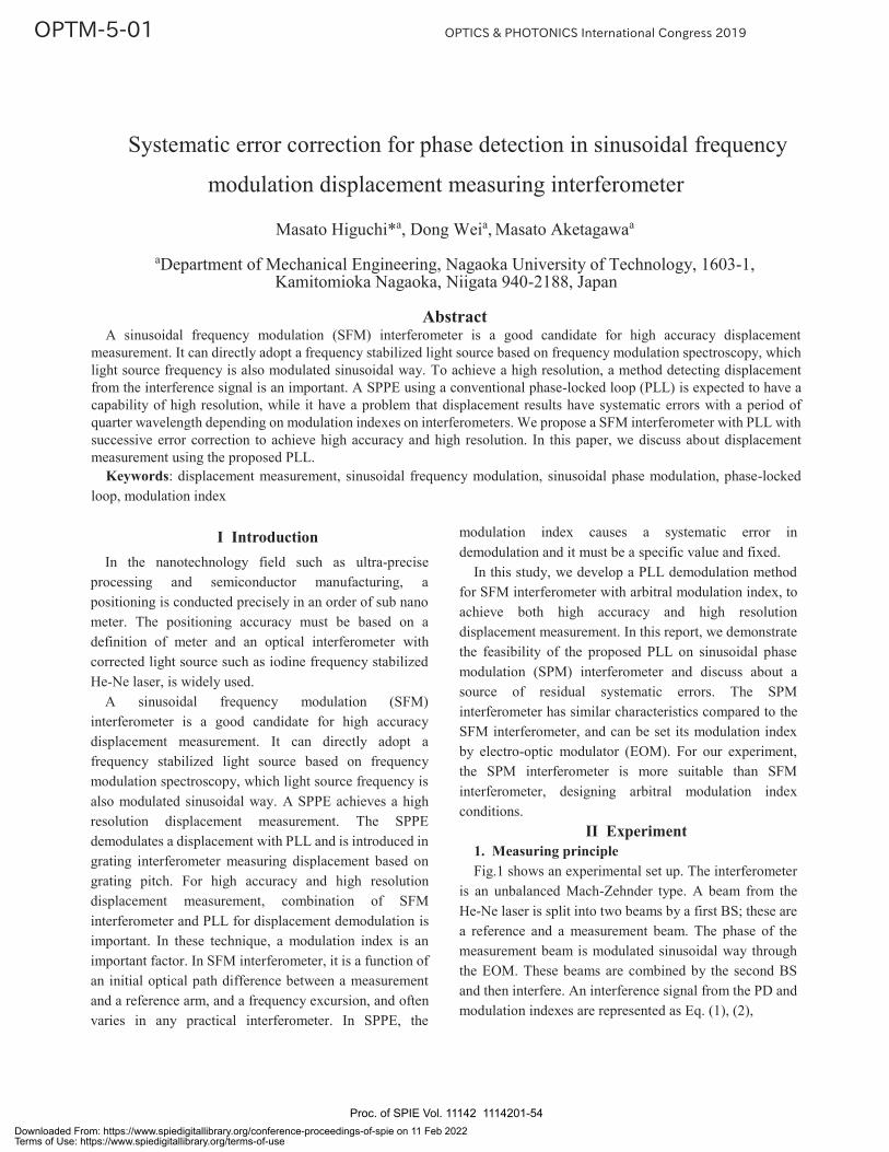
I Introduction In the nanotechnology field such as ultra-precise
processing and semiconductor manufacturing, a positioning is conducted precisely in an order of sub nano meter. The positioning accuracy must be based on a definition of meter and an optical interferometer with corrected light source such as iodine frequency stabilized He-Ne laser, is widely used.
A sinusoidal frequency modulation (SFM) interferometer is a good candidate for high accuracy displacement measurement. It can directly adopt a frequency stabilized light source based on frequency modulation spectroscopy, which light source frequency is also modulated sinusoidal way. A SPPE achieves a high resolution displacement measurement. The SPPE demodulates a displacement with PLL and is introduced in grating interferometer measuring displacement based on grating pitch. For high accuracy and high resolution displacement measurement, combination of SFM interferometer and PLL for displacement demodulation is important. In these technique, a modulation index is an important factor. In SFM interferometer, it is a function of an initial optical path difference between a measurement and a reference arm, and a frequency excursion, and often varies in any practical interferometer. In SPPE, the
modulation index causes a systematic error in demodulation and it must be a specific value and fixed.
In this study, we develop a PLL demodulation method for SFM interferometer with arbitral modulation index, to achieve both high accuracy and high resolution displacement measurement. In this report, we demonstrate the feasibility of the proposed PLL on sinusoidal phase modulation (SPM) interferometer and discuss about a source of residual systematic errors. The SPM interferometer has similar characteristics compared to the SFM interferometer, and can be set its modulation index by electro-optic modulator (EOM). For our experiment, the SPM interferometer is more suitable than SFM interferometer, designing arbitral modulation index conditions.
II Experiment 1. Measuring principle Fig.1 shows an experimental set up. The interferometer
is an unbalanced Mach-Zehnder type. A beam from the He-Ne laser is split into two beams by a first BS; these are a reference and a measurement beam. The phase of the measurement beam is modulated sinusoidal way through the EOM. These beams are combined by the second BS and then interfere. An interference signal from the PD and modulation indexes are represented as Eq. (1), (2),
Systematic error correction for phase detection in sinusoidal frequency
modulation displacement measuring interferometer
Masato Higuchi*a, Dong Weia, Masato Aketagawaa
aDepartment of Mechanical Engineering, Nagaoka University of Technology, 1603-1, Kamitomioka Nagaoka, Niigata 940-2188, Japan
Abstract
A sinusoidal frequency modulation (SFM) interferometer is a good candidate for high accuracy displacement measurement. It can directly adopt a frequency stabilized light source based on frequency modulation spectroscopy, which light source frequency is also modulated sinusoidal way. To achieve a high resolution, a method detecting displacement from the interference signal is an important. A SPPE using a conventional phase-locked loop (PLL) is expected to have a capability of high resolution, while it have a problem that displacement results have systematic errors with a period of quarter wavelength depending on modulation indexes on interferometers. We propose a SFM interferometer with PLL with successive error correction to achieve high accuracy and high resolution. In this paper, we discuss about displacement measurement using the proposed PLL.
Keywords: displacement measurement, sinusoidal frequency modulation, sinusoidal phase modulation, phase-locked loop, modulation index
Proc. of SPIE Vol. 11142 1114201-54Downloaded From: https://www.spiedigitallibrary.org/conference-proceedings-of-spie on 11 Feb 2022Terms of Use: https://www.spiedigitallibrary.org/terms-of-use
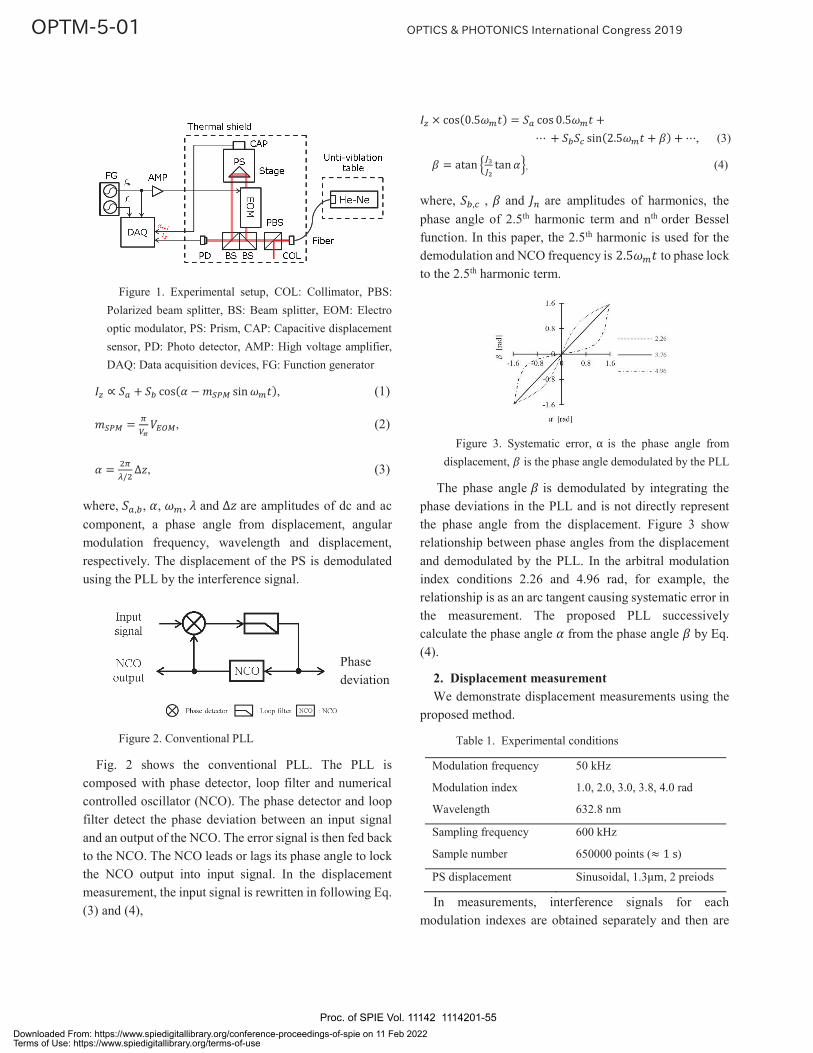
Figure 1. Experimental setup, COL: Collimator, PBS: Polarized beam splitter, BS: Beam splitter, EOM: Electro optic modulator, PS: Prism, CAP: Capacitive displacement sensor, PD: Photo detector, AMP: High voltage amplifier, DAQ: Data acquisition devices, FG: Function generator
, (1)
, (2)
, (3)
where, , , , and are amplitudes of dc and ac component, a phase angle from displacement, angular modulation frequency, wavelength and displacement, respectively. The displacement of the PS is demodulated using the PLL by the interference signal.
Figure 2. Conventional PLL
Fig. 2 shows the conventional PLL. The PLL is composed with phase detector, loop filter and numerical controlled oscillator (NCO). The phase detector and loop filter detect the phase deviation between an input signal and an output of the NCO. The error signal is then fed back to the NCO. The NCO leads or lags its phase angle to lock the NCO output into input signal. In the displacement measurement, the input signal is rewritten in following Eq. (3) and (4),
, (3)
, (4)
where, , and are amplitudes of harmonics, the phase angle of 2.5th harmonic term and nth order Bessel function. In this paper, the 2.5th harmonic is used for the demodulation and NCO frequency is to phase lock to the 2.5th harmonic term.
Figure 3. Systematic error, is the phase angle from displacement, is the phase angle demodulated by the PLL
The phase angle is demodulated by integrating the phase deviations in the PLL and is not directly represent the phase angle from the displacement. Figure 3 show relationship between phase angles from the displacement and demodulated by the PLL. In the arbitral modulation index conditions 2.26 and 4.96 rad, for example, the relationship is as an arc tangent causing systematic error in the measurement. The proposed PLL successively calculate the phase angle from the phase angle by Eq. (4).
2. Displacement measurement We demonstrate displacement measurements using the
proposed method.
Table 1. Experimental conditions
Modulation frequency 50 kHz
Modulation index 1.0, 2.0, 3.0, 3.8, 4.0 rad
Wavelength 632.8 nm
Sampling frequency 600 kHz
Sample number 650000 points ( )
PS displacement Sinusoidal, 1.3 , 2 preiods
In measurements, interference signals for each modulation indexes are obtained separately and then are
Phase deviation
Proc. of SPIE Vol. 11142 1114201-55Downloaded From: https://www.spiedigitallibrary.org/conference-proceedings-of-spie on 11 Feb 2022Terms of Use: https://www.spiedigitallibrary.org/terms-of-use
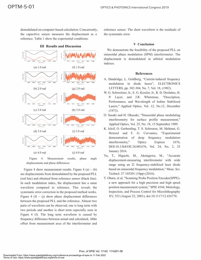
demodulated on computer-based calculation. Concurrently, the capacitive sensor measures the displacement as a reference. Table 1 show the experiential conditions.
III Results and Discussion
(a) 1.0 rad (f) 1.0 rad
(b) 2.0 rad (g) 2.0 rad
(c) 3.0 rad (h) 3.0 rad
(d) 3.8 rad (i) 3.8 rad
(e) 4.0 rad (j) 4.0 rad
Figure 4. Measurement results, phase angle displacements and phase differences
Figure 4 show measurement results. Figure 4 (a) ~ (b) are displacements from demodulated by the proposed PLL (red line) and obtained from reference sensor (black line). In each modulation index, the displacement has a same waveform compared to reference. This reveals the systematic error correction in the proposed method works. Figure 4 (f) ~ (j) show phase displacement differences between the proposed PLL and the reference. Almost two parts of waveform can be observed; one is long term with two periods and another is short term especially seen in Figure 4 (f). The long term waveform is caused by frequency difference between actual and calculated, Abbe offset from measurement axes of the interferometer and
reference sensor. The short waveform is the residuals of the systematic error.
V Conclusion We demonstrate the feasibility of the proposed PLL on
sinusoidal phase modulation (SPM) interferometer. The displacement is demodulated in arbitral modulation indexes.
References A. Dandridge, L. Goldberg, “Current-induced frequency
modulation in diode lasers”, ELECTRONICS LETTERS, pp. 302-304, No. 7, Vol. 18, (1982).
W. G. Schweitzer, Jr., E. G. Kessler, Jr., R. D. Deslattes, H. P. Layer, and J.R. Whetstone, "Description, Performance, and Wavelength of Iodine Stabilized Lasers," Applied Optics, Vol. 12, No.12, December (1973).
O. Sasaki and H. Okazaki, "Sinusoidal phase modulating interferometry for surface profile measurement," Applied Optics, Vol. 25, No. 18, 15 September 1989.
K. Isleif, O. Gerberding, T. S. Schwarze, M. Mehmet, G. Heinzel and F. G. Cervantes, "Experimental demonstration of deep frequency modulation interferometry," Optics Express 1676, DOI:10.1364/OE.24.001676, Vol. 24, No. 2, 25 January 2016.
Vu, T., Higuchi, M., Aketagawa, M., "Accurate displacement-measuring interferometer with wide range using an I2 frequency-stabilized laser diode based on sinusoidal frequency modulation," Meas. Sci. Technol. 27 105201 (10pp) (2016).
T. Ohara, et al, "Scanning Probe Position Encoder(SPPE)-a new approach for a high precision and high speed position measurement system,” SPIE 4344, Metrology, Inspection, and Process Control for Microlithography XV, 552 (August 22, 2001); doi:10.1117/12.436778.
Proc. of SPIE Vol. 11142 1114201-56Downloaded From: https://www.spiedigitallibrary.org/conference-proceedings-of-spie on 11 Feb 2022Terms of Use: https://www.spiedigitallibrary.org/terms-of-use

I Introduction Ultra-precision products such as optical instruments
and semiconductor devices are composed of parts with a variety of geometries from fundamental flat and/or spherical shapes to the complex free-form surfaces. Many of such parts are required to be manufactured in a high-precision up to sub-micrometer or even nanometer. Due to the tight tolerances in nanomanufacturing, nanometrology of the manufactured parts is of high-priority for quality control of the parts as well as for process control of nanomanufacturing [1]. Nanopositioning and the related nanometrology are therefore necessary for this purpose [2].
In this paper, a new method of angular measurement is proposed utilizing a characteristic of second harmonic generation (SHG). Both theoretical calculations and experimental demonstration are presented.
II Principle of angle measurement SHG is a non-linear optical process which is
proportional to square of light intensity. In a SHG process, the incident wave is focused onto a non-linear optical crystal. The second harmonic wave which has double frequency of the incident wave is then generated. The light intensity of the generated second harmonic wave changes with the angle between the incident wave and the
non-linear optical crystal. Here, the incident light is called a fundamental wave. Figure 1 shows a schematic diagram of generation of the second harmonic. The light intensity I2 of the second harmonic can be written as follows [3].
2 2 22 20 eff
2 12 21 2
8sinc
2k Lcd L
I In n
(1)
, where 0 and c are the magnetic permeability and light velocity in vacuum, deff is the effective non-linear coefficient, n1 and n2 are the refractive indices of the fundamental wave and the second harmonic wave, L is the optical path length in the crystal, and I1 represents the fundamental wave intensity. k( ) is called the phase mismatch and is expressed by the following equation:
1 24k n n (2)
Since the femtosecond laser has a high peak intensity I1, it is possible to obtain a second harmonic wave of high
Fundamental frequency
Second Harmonic
L
Figure 1 A schematic of second harmonic generation.
An optical angle sensor based on second harmonic generation of a mode-
locked laser Hiraku Matsukuma*, Shuhei Madokoro, Masaru Nakao, Yuki Shimizu, Wei Gao
Department of Finemechanics, Graduate School of Engineering, Tohoku University,
6-6-01 Aramaki-Aza-Aoba, Aoba-ku, Sendai, 980-8579, Japan
Abstract This paper presents an optical angle sensor using characteristics of second harmonic generation (SHG) which is a non-
linear process of electromagnetic field. In a SHG process, the fundamental wave is made incidence into a non-linear optical crystal. The second harmonic wave which has double frequency of the fundamental wave is then generated. The light intensity of the generated second harmonic wave changes with the incident angle of the fundamental wave to the non-linear optical crystal due to phase mismatch which is a factor of determining the conversion efficiency of SHG. The dependence of second harmonic generation on angular displacement is calculated theoretically for mode-locked femto second laser light source. Experiment is also carried out in order to demonstrate the theoretical calculation.
Keywords: Angle sensor, Second harmonic generation, Non-linear process, Mode-locked laser, Femto-second laser
Proc. of SPIE Vol. 11142 1114201-57Downloaded From: https://www.spiedigitallibrary.org/conference-proceedings-of-spie on 11 Feb 2022Terms of Use: https://www.spiedigitallibrary.org/terms-of-use
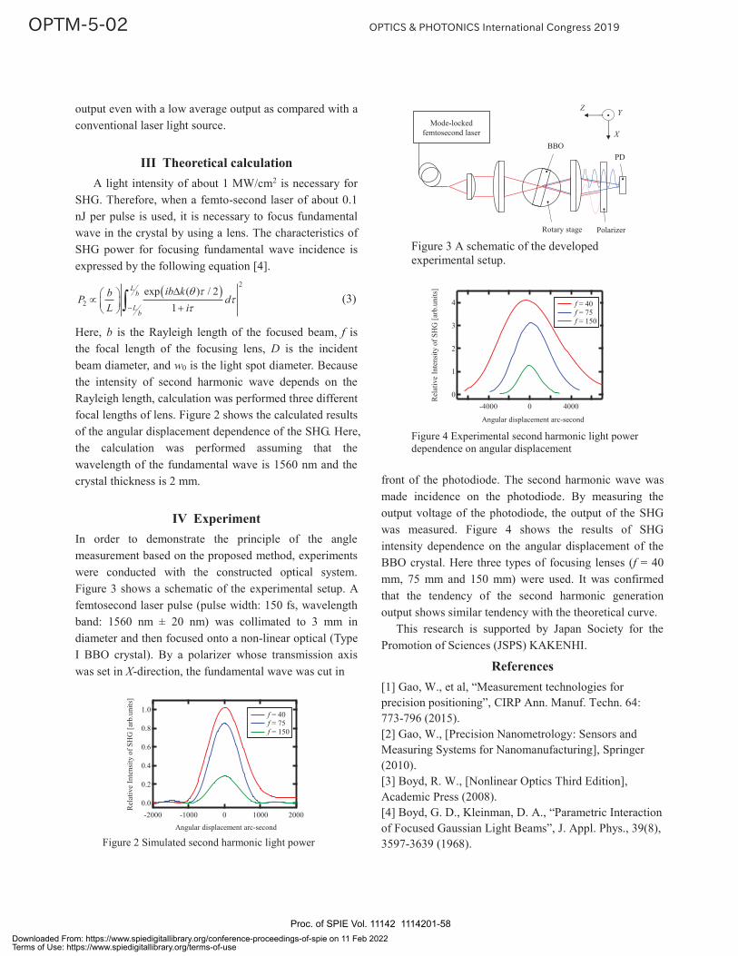
output even with a low average output as compared with a conventional laser light source.
III Theoretical calculation
A light intensity of about 1 MW/cm2 is necessary for SHG. Therefore, when a femto-second laser of about 0.1 nJ per pulse is used, it is necessary to focus fundamental wave in the crystal by using a lens. The characteristics of SHG power for focusing fundamental wave incidence is expressed by the following equation [4].
2
2exp ( ) / 2
1
Lb
Lb
ib kbP dL i
(3)
Here, b is the Rayleigh length of the focused beam, f is the focal length of the focusing lens, D is the incident beam diameter, and w0 is the light spot diameter. Because the intensity of second harmonic wave depends on the Rayleigh length, calculation was performed three different focal lengths of lens. Figure 2 shows the calculated results of the angular displacement dependence of the SHG. Here, the calculation was performed assuming that the wavelength of the fundamental wave is 1560 nm and the crystal thickness is 2 mm.
IV Experiment In order to demonstrate the principle of the angle measurement based on the proposed method, experiments were conducted with the constructed optical system. Figure 3 shows a schematic of the experimental setup. A femtosecond laser pulse (pulse width: 150 fs, wavelength band: 1560 nm ± 20 nm) was collimated to 3 mm in diameter and then focused onto a non-linear optical (Type I BBO crystal). By a polarizer whose transmission axis was set in X-direction, the fundamental wave was cut in
Angular displacement arc-second
Rel
ativ
e In
tens
ity o
f SH
G [a
rb.u
nits
]
1.0
0.8
0.6
0.4
0.2
0.0-2000 -1000 0 1000 2000
f = 40 f = 75 f = 150
Figure 2 Simulated second harmonic light power
Mode-locked femtosecond laser
BBO
Rotary stage Polarizer
PD
X
YZ
Figure 3 A schematic of the developed experimental setup.
Rel
ativ
e In
tens
ity o
f SH
G [a
rb.u
nits
]
4
3
2
1
0-4000 0 4000
f = 40 f = 75 f = 150
Angular displacement arc-second Figure 4 Experimental second harmonic light power dependence on angular displacement
front of the photodiode. The second harmonic wave was made incidence on the photodiode. By measuring the output voltage of the photodiode, the output of the SHG was measured. Figure 4 shows the results of SHG intensity dependence on the angular displacement of the BBO crystal. Here three types of focusing lenses (f = 40 mm, 75 mm and 150 mm) were used. It was confirmed that the tendency of the second harmonic generation output shows similar tendency with the theoretical curve. This research is supported by Japan Society for the Promotion of Sciences (JSPS) KAKENHI.
References [1] Gao, W., et al, “Measurement technologies for precision positioning”, CIRP Ann. Manuf. Techn. 64: 773-796 (2015). [2] Gao, W., [Precision Nanometrology: Sensors and Measuring Systems for Nanomanufacturing], Springer (2010). [3] Boyd, R. W., [Nonlinear Optics Third Edition], Academic Press (2008). [4] Boyd, G. D., Kleinman, D. A., “Parametric Interaction of Focused Gaussian Light Beams”, J. Appl. Phys., 39(8), 3597-3639 (1968).
Proc. of SPIE Vol. 11142 1114201-58Downloaded From: https://www.spiedigitallibrary.org/conference-proceedings-of-spie on 11 Feb 2022Terms of Use: https://www.spiedigitallibrary.org/terms-of-use
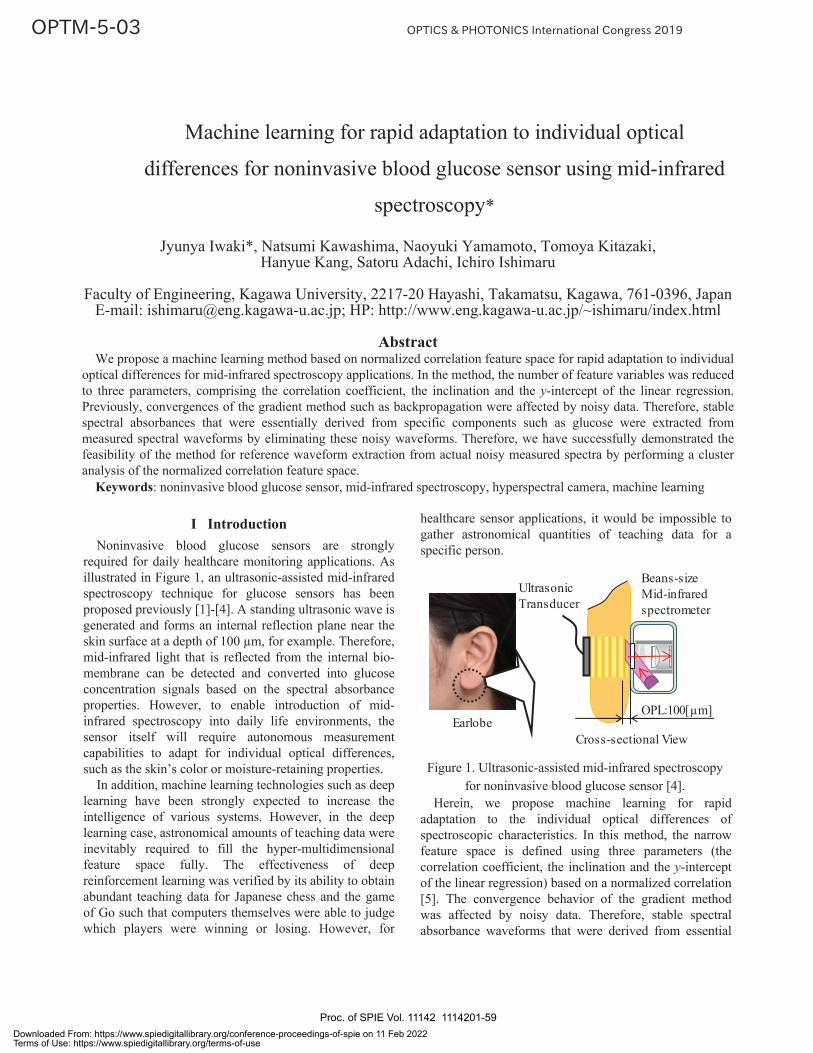
Proc. of SPIE Vol. 11142 1114201-59Downloaded From: https://www.spiedigitallibrary.org/conference-proceedings-of-spie on 11 Feb 2022Terms of Use: https://www.spiedigitallibrary.org/terms-of-use
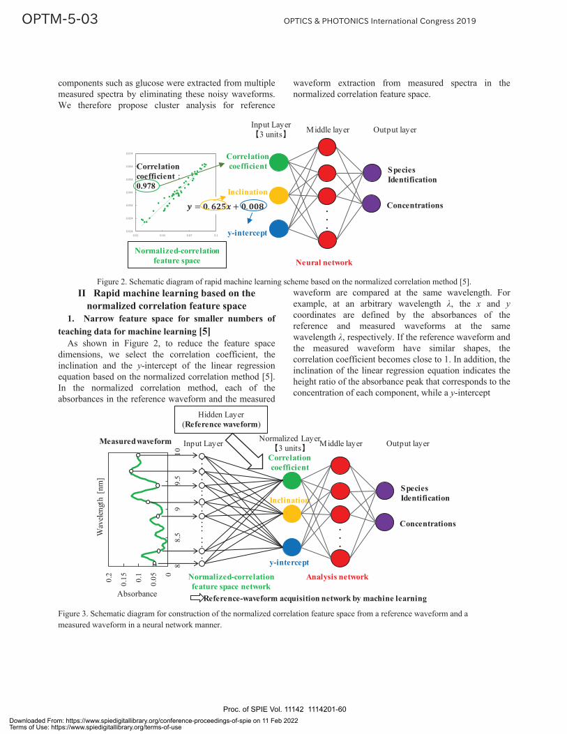
Proc. of SPIE Vol. 11142 1114201-60Downloaded From: https://www.spiedigitallibrary.org/conference-proceedings-of-spie on 11 Feb 2022Terms of Use: https://www.spiedigitallibrary.org/terms-of-use
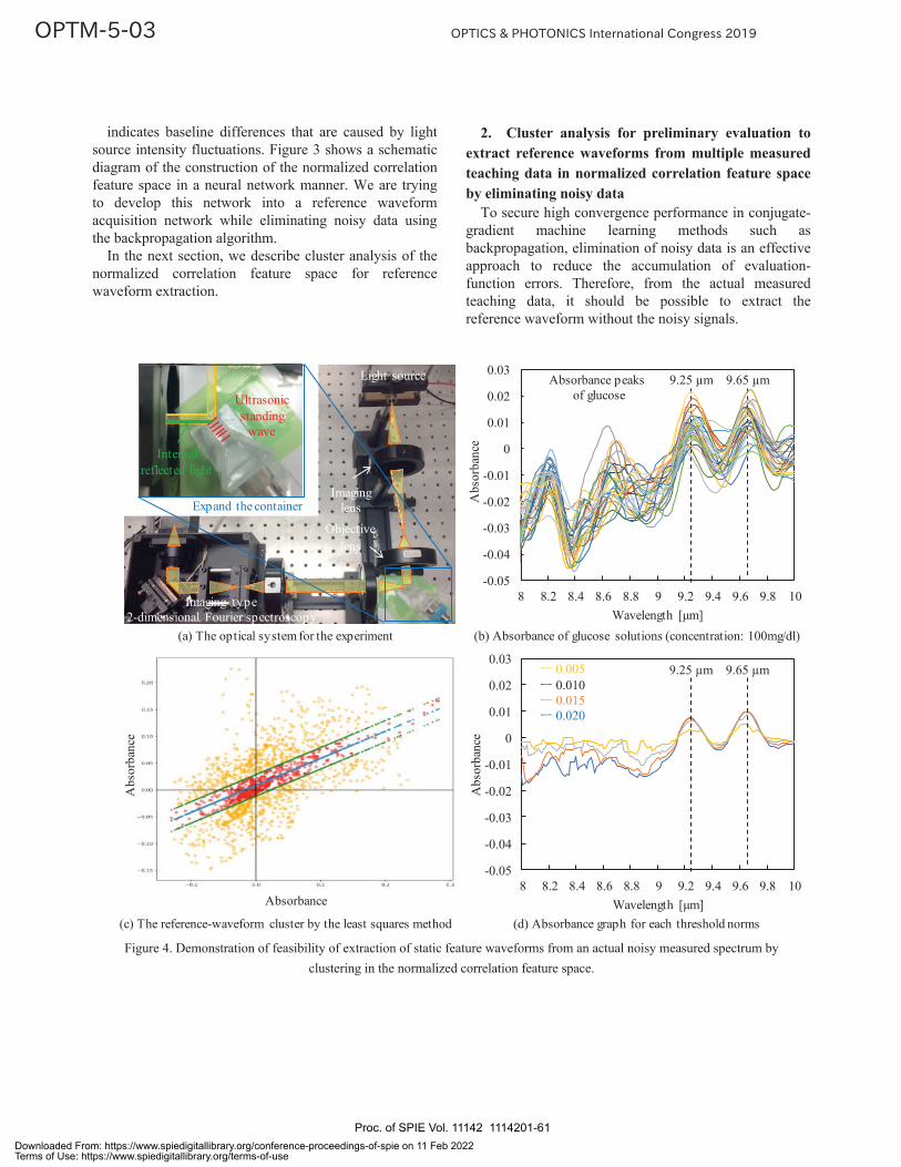
Proc. of SPIE Vol. 11142 1114201-61Downloaded From: https://www.spiedigitallibrary.org/conference-proceedings-of-spie on 11 Feb 2022Terms of Use: https://www.spiedigitallibrary.org/terms-of-use

Proc. of SPIE Vol. 11142 1114201-62Downloaded From: https://www.spiedigitallibrary.org/conference-proceedings-of-spie on 11 Feb 2022Terms of Use: https://www.spiedigitallibrary.org/terms-of-use
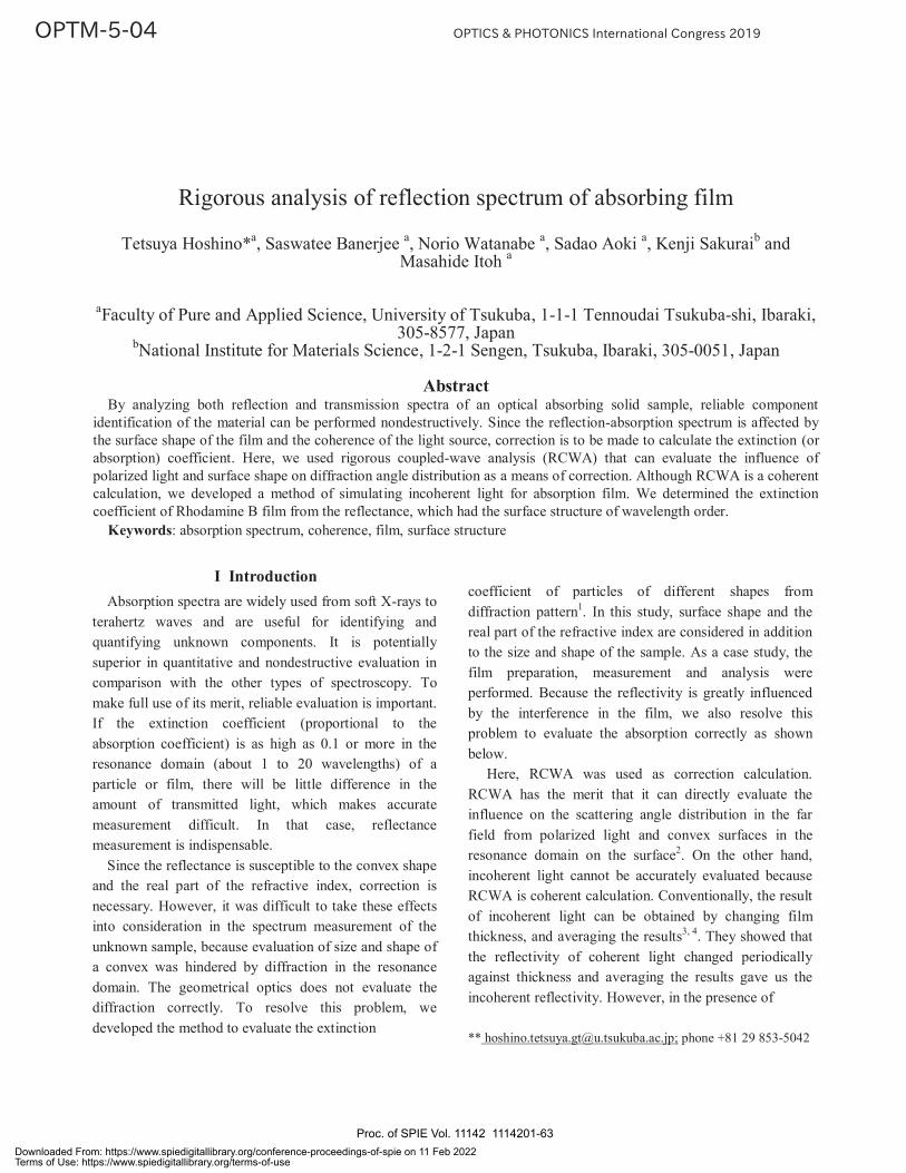
I Introduction Absorption spectra are widely used from soft X-rays to
terahertz waves and are useful for identifying and quantifying unknown components. It is potentially superior in quantitative and nondestructive evaluation in comparison with the other types of spectroscopy. To make full use of its merit, reliable evaluation is important. If the extinction coefficient (proportional to the absorption coefficient) is as high as 0.1 or more in the resonance domain (about 1 to 20 wavelengths) of a particle or film, there will be little difference in the amount of transmitted light, which makes accurate measurement difficult. In that case, reflectance measurement is indispensable.
Since the reflectance is susceptible to the convex shape and the real part of the refractive index, correction is necessary. However, it was difficult to take these effects into consideration in the spectrum measurement of the unknown sample, because evaluation of size and shape of a convex was hindered by diffraction in the resonance domain. The geometrical optics does not evaluate the diffraction correctly. To resolve this problem, we developed the method to evaluate the extinction
coefficient of particles of different shapes from diffraction pattern1. In this study, surface shape and the real part of the refractive index are considered in addition to the size and shape of the sample. As a case study, the film preparation, measurement and analysis were performed. Because the reflectivity is greatly influenced by the interference in the film, we also resolve this problem to evaluate the absorption correctly as shown below.
Here, RCWA was used as correction calculation. RCWA has the merit that it can directly evaluate the influence on the scattering angle distribution in the far field from polarized light and convex surfaces in the resonance domain on the surface2. On the other hand, incoherent light cannot be accurately evaluated because RCWA is coherent calculation. Conventionally, the result of incoherent light can be obtained by changing film thickness, and averaging the results3, 4. They showed that the reflectivity of coherent light changed periodically against thickness and averaging the results gave us the incoherent reflectivity. However, in the presence of ** [email protected]; phone +81 29 853-5042
Rigorous analysis of reflection spectrum of absorbing film
Tetsuya Hoshino*a, Saswatee Banerjee a, Norio Watanabe a, Sadao Aoki a, Kenji Sakuraib and Masahide Itoh a
aFaculty of Pure and Applied Science, University of Tsukuba, 1-1-1 Tennoudai Tsukuba-shi, Ibaraki, 305-8577, Japan
bNational Institute for Materials Science, 1-2-1 Sengen, Tsukuba, Ibaraki, 305-0051, Japan
Abstract By analyzing both reflection and transmission spectra of an optical absorbing solid sample, reliable component
identification of the material can be performed nondestructively. Since the reflection-absorption spectrum is affected by the surface shape of the film and the coherence of the light source, correction is to be made to calculate the extinction (or absorption) coefficient. Here, we used rigorous coupled-wave analysis (RCWA) that can evaluate the influence of polarized light and surface shape on diffraction angle distribution as a means of correction. Although RCWA is a coherent calculation, we developed a method of simulating incoherent light for absorption film. We determined the extinction coefficient of Rhodamine B film from the reflectance, which had the surface structure of wavelength order.
Keywords: absorption spectrum, coherence, film, surface structure
Proc. of SPIE Vol. 11142 1114201-63Downloaded From: https://www.spiedigitallibrary.org/conference-proceedings-of-spie on 11 Feb 2022Terms of Use: https://www.spiedigitallibrary.org/terms-of-use

absorption, the amount of light absorption varies with thickness, which makes this process difficult. We solved this problem by adding a transparent film to the absorbing layer and changing its film thickness. The thickness of the additional layer does not affect the absorption. By changing this thickness and averaging the reflectivity enable us to calculate the incoherent reflectivity. This calculation enables us to calculate the incoherent area and coherent area at the same time. We simulate the light control film for infrared cut glass by switching the incoherent area to coherent area as the example.
II Method
1. Simulation To simulate incoherent light’s reflectivity by coherent
simulation method RCWA, we added one clear layer 2 to absorptive layer 1 in Fig. 1. Here, d1 and d2 are thickness of each film, n0 and n1 are real part of refractive index and coefficient k is the imaginary part of refractive index. R0, R1 and R2 are the reflectivity of each boundary. Incident light enters normally the film from surface of layer 1. To check the effect of the layer, we subtract R1l (the reflectivity of layer 1 only) from R2l (the reflectivity of the two layer) according to geometrical optics. Equations (1) to (4) are the results. Here, is wavelength.
21 e .T (1)
12 / .kd (2)
2 14 2 2
1 0 0 1 2 1 2 1 0 1 0 22 2
1 2 1 0 1 2 1 2 1 0
(1 2 )(1 ) ( ){1 ( )}(1 )
l lR R
T R R R R R R T X R R R RR R T R R R R R T R . (3)
where
3 20 1 2 1 0 1 2 1 2
0 1 2 1 2 1 2 0 1 2
( 2 1) ( 2 2 2)(3 2 2 ) 2
X R R R R R R R R RR R R R R R R R R R . (4)
Eq. (3) and some simulation indicated that the following conditions were important for us to assume R2l to be R1l .
1 > / 2k d or 1 < 0.01 / 2k d . (5)
From the simulation, we found the following. As shown in Eqs. (1) and (2), T1 is dependent on coefficient k. Roughly, when Eq. (5) is satisfied, (T1)2 is almost 0 or 1 and R2l becomes same to R1l for most R0, R1 and R2. We use this relationship to estimate the real part of refractive index n. For the sample of this time, when k>0.2 or k < 0.002, R2l is almost same to R1l.
The sample is made of absorptive layer and transparent thick substrate. We inserted transparent additional layer into it in Fig. 2. The additional layer has same refractive index n1 to the absorbing layer.
2. Sample and Measurement Method Rhodamine B in ethanol was spin coated over the slide
glass and etched by focused ion beam (FIB) (see Fig. 3). From SEM and scatterometry1, we know that the thickness of the Rhodamine B film is 0.65 m. The measurement was performed at several ten m from the center of the square hole fabricated by FIB. This distance’s parameter is s.
Halogen lamp and 10 m pinhole is set left side of Fig.4, and beam spot area at the sample is about 120 m2. For the transmissive spectrum measurement, CCD is changed to optical fiber of spectrum analyzer.
III Results and Discussion From the transmissive spectrum of Fig. 6, we can
estimate the number of digits of the extinction coefficient k. From pattern of the reflective spectrum of Fig. 5, we judged the surface of the film at “120 m” to be smooth. From the reflective spectrum of the “120 m”, we know the complex refractive index. As this case shows,
Figure 1. Simulation model for the single absorptive film.
Proc. of SPIE Vol. 11142 1114201-64Downloaded From: https://www.spiedigitallibrary.org/conference-proceedings-of-spie on 11 Feb 2022Terms of Use: https://www.spiedigitallibrary.org/terms-of-use
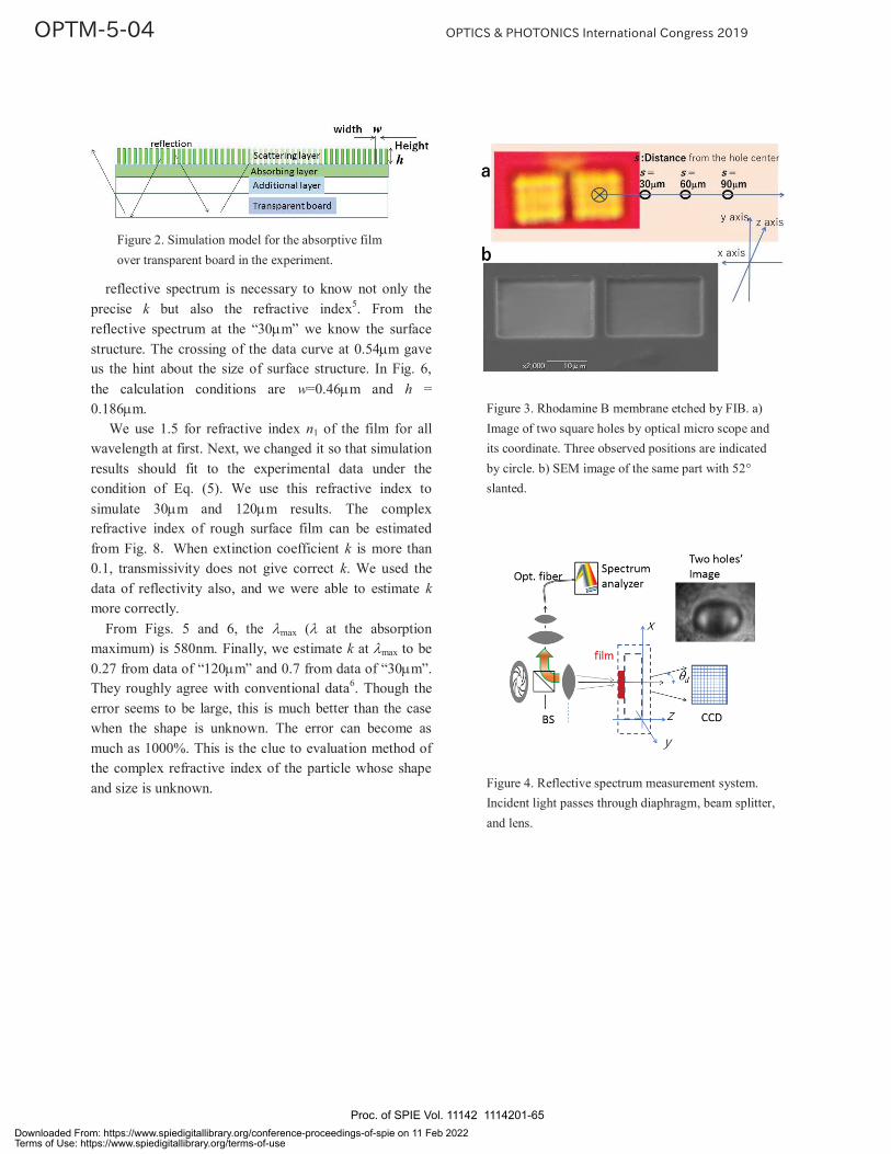
Figure 2. Simulation model for the absorptive film over transparent board in the experiment.
reflective spectrum is necessary to know not only the precise k but also the refractive index5. From the reflective spectrum at the “30 m” we know the surface structure. The crossing of the data curve at 0.54 m gave us the hint about the size of surface structure. In Fig. 6, the calculation conditions are w=0.46 m and h = 0.186 m.
We use 1.5 for refractive index n1 of the film for all wavelength at first. Next, we changed it so that simulation results should fit to the experimental data under the condition of Eq. (5). We use this refractive index to simulate 30 m and 120 m results. The complex refractive index of rough surface film can be estimated from Fig. 8 When extinction coefficient k is more than 0.1, transmissivity does not give correct k. We used the data of reflectivity also, and we were able to estimate k more correctly.
From Figs. 5 and 6, the max ( at the absorption maximum) is 580nm. Finally, we estimate k at max to be 0.27 from data of “120 m” and 0.7 from data of “30 m”. They roughly agree with conventional data6. Though the error seems to be large, this is much better than the case when the shape is unknown. The error can become as much as 1000%. This is the clue to evaluation method of the complex refractive index of the particle whose shape and size is unknown.
Figure 3. Rhodamine B membrane etched by FIB. a) Image of two square holes by optical micro scope and its coordinate. Three observed positions are indicated by circle. b) SEM image of the same part with 52° slanted.
Figure 4. Reflective spectrum measurement system. Incident light passes through diaphragm, beam splitter, and lens.
Proc. of SPIE Vol. 11142 1114201-65Downloaded From: https://www.spiedigitallibrary.org/conference-proceedings-of-spie on 11 Feb 2022Terms of Use: https://www.spiedigitallibrary.org/terms-of-use

Figure 5. Reflective absorption spectrum of Rhodamine B film whose intensity is normalized by that of a slide glass.
Figure 6. Transmissive absorption spectrum whose intensity is normalized by that of a slide glass.
Figure 7. Calculation results and the experimental result of normalized reflective absorption spectrum. The observed data is "120 m" away from the center of the hole. a) The extinction coefficient k changes for every simulation. b) The wavelength dependence of the refractive index n is considered.
Proc. of SPIE Vol. 11142 1114201-66Downloaded From: https://www.spiedigitallibrary.org/conference-proceedings-of-spie on 11 Feb 2022Terms of Use: https://www.spiedigitallibrary.org/terms-of-use
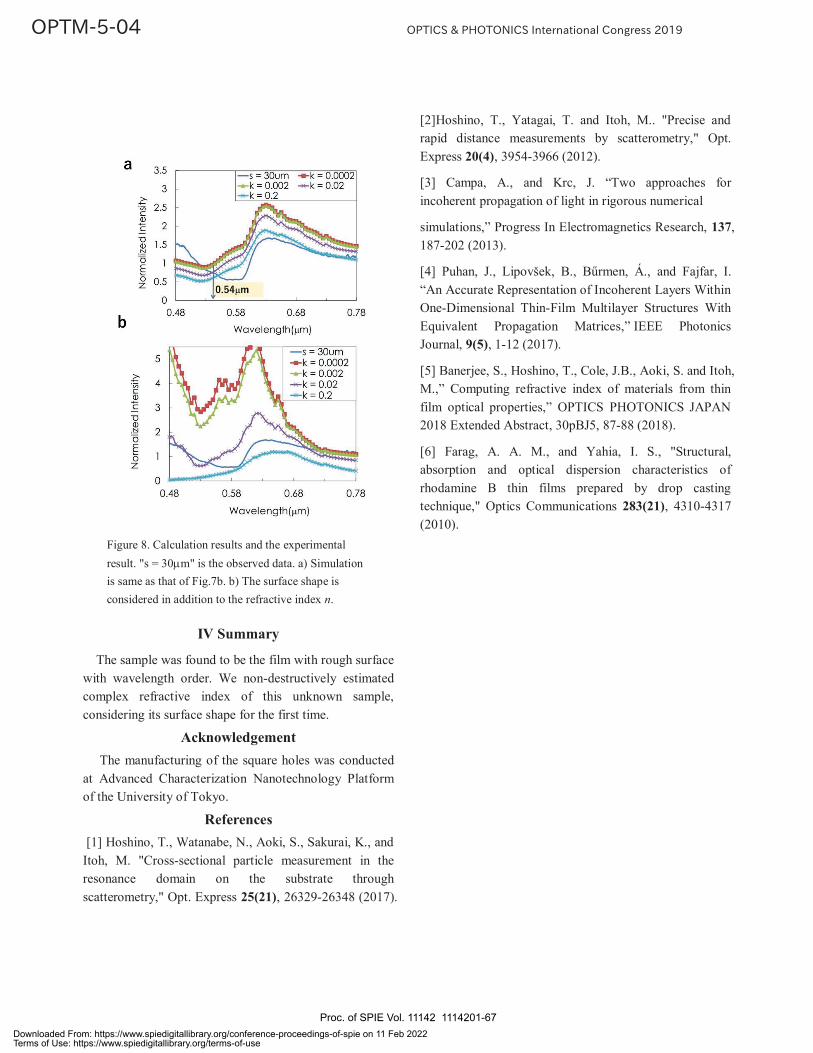
Figure 8. Calculation results and the experimental result. "s = 30 m" is the observed data. a) Simulation is same as that of Fig.7b. b) The surface shape is considered in addition to the refractive index n.
IV Summary
The sample was found to be the film with rough surface with wavelength order. We non-destructively estimated complex refractive index of this unknown sample, considering its surface shape for the first time.
Acknowledgement The manufacturing of the square holes was conducted
at Advanced Characterization Nanotechnology Platform of the University of Tokyo.
References [1] Hoshino, T., Watanabe, N., Aoki, S., Sakurai, K., and Itoh, M. "Cross-sectional particle measurement in the resonance domain on the substrate through scatterometry," Opt. Express 25(21), 26329-26348 (2017).
[2]Hoshino, T., Yatagai, T. and Itoh, M.. "Precise and rapid distance measurements by scatterometry," Opt. Express 20(4), 3954-3966 (2012).
[3] Campa, A., and Krc, J. “Two approaches for incoherent propagation of light in rigorous numerical
simulations,” Progress In Electromagnetics Research, 137, 187-202 (2013).
[4] Puhan, J., Lipovšek, B., Bűrmen, Á., and Fajfar, I. “An Accurate Representation of Incoherent Layers Within One-Dimensional Thin-Film Multilayer Structures With Equivalent Propagation Matrices,” IEEE Photonics Journal, 9(5), 1-12 (2017).
[5] Banerjee, S., Hoshino, T., Cole, J.B., Aoki, S. and Itoh, M.,” Computing refractive index of materials from thin film optical properties,” OPTICS PHOTONICS JAPAN 2018 Extended Abstract, 30pBJ5, 87-88 (2018).
[6] Farag, A. A. M., and Yahia, I. S., "Structural, absorption and optical dispersion characteristics of rhodamine B thin films prepared by drop casting technique," Optics Communications 283(21), 4310-4317 (2010).
Proc. of SPIE Vol. 11142 1114201-67Downloaded From: https://www.spiedigitallibrary.org/conference-proceedings-of-spie on 11 Feb 2022Terms of Use: https://www.spiedigitallibrary.org/terms-of-use
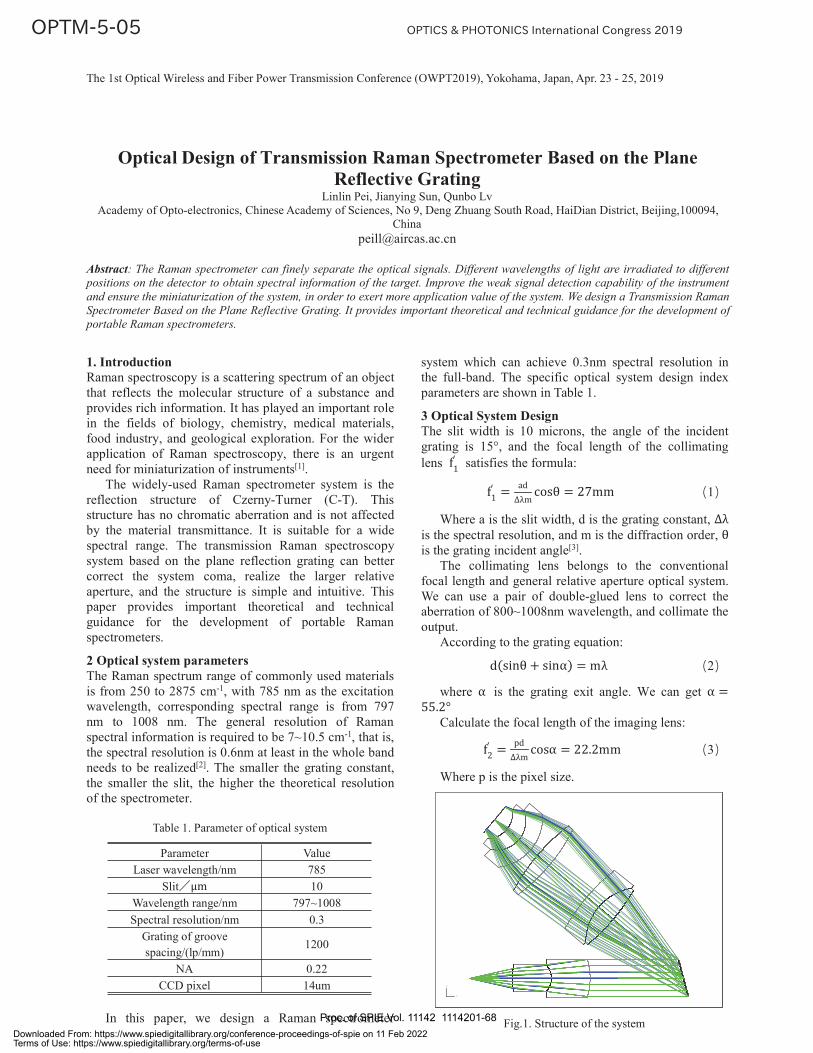
The 1st Optical Wireless and Fiber Power Transmission Conference (OWPT2019), Yokohama, Japan, Apr. 23 - 25, 2019
Optical Design of Transmission Raman Spectrometer Based on the PlaneReflective Grating
Linlin Pei, Jianying Sun, Qunbo LvAcademy of Opto-electronics, Chinese Academy of Sciences, No 9, Deng Zhuang South Road, HaiDian District, Beijing,100094,
Abstract: The Raman spectrometer can finely separate the optical signals. Different wavelengths of light are irradiated to differentpositions on the detector to obtain spectral information of the target. Improve the weak signal detection capability of the instrumentand ensure the miniaturization of the system, in order to exert more application value of the system. We design a Transmission RamanSpectrometer Based on the Plane Reflective Grating. It provides important theoretical and technical guidance for the development ofportable Raman spectrometers.
1. IntroductionRaman spectroscopy is a scattering spectrum of an objectthat reflects the molecular structure of a substance andprovides rich information. It has played an important rolein the fields of biology, chemistry, medical materials,food industry, and geological exploration. For the widerapplication of Raman spectroscopy, there is an urgentneed for miniaturization of instruments[1].
The widely-used Raman spectrometer system is thereflection structure of Czerny-Turner (C-T). Thisstructure has no chromatic aberration and is not affectedby the material transmittance. It is suitable for a widespectral range. The transmission Raman spectroscopysystem based on the plane reflection grating can bettercorrect the system coma, realize the larger relativeaperture, and the structure is simple and intuitive. Thispaper provides important theoretical and technicalguidance for the development of portable Ramanspectrometers.
2 Optical system parametersThe Raman spectrum range of commonly used materialsis from 250 to 2875 cm-1, with 785 nm as the excitationwavelength, corresponding spectral range is from 797nm to 1008 nm. The general resolution of Ramanspectral information is required to be 7~10.5 cm-1, that is,the spectral resolution is 0.6nm at least in the whole bandneeds to be realized[2]. The smaller the grating constant,the smaller the slit, the higher the theoretical resolutionof the spectrometer.
Table 1. Parameter of optical system
Parameter ValueLaser wavelength/nm 785
Slit 10Wavelength range/nm 797~1008Spectral resolution/nm 0.3Grating of groovespacing/(lp/mm)
1200
NA 0.22CCD pixel 14um
In this paper, we design a Raman spectrometer
system which can achieve 0.3nm spectral resolution inthe full-band. The specific optical system design indexparameters are shown in Table 1.
3 Optical System DesignThe slit width is 10 microns, the angle of the incidentgrating is 15°, and the focal length of the collimatinglens satisfies the formula:
1
Where a is the slit width, d is the grating constant,is the spectral resolution, and m is the diffraction order,is the grating incident angle[3].
The collimating lens belongs to the conventionalfocal length and general relative aperture optical system.We can use a pair of double-glued lens to correct theaberration of 800~1008nm wavelength, and collimate theoutput.
According to the grating equation:
2
where is the grating exit angle. We can get
Calculate the focal length of the imaging lens:
3
Where p is the pixel size.
Fig.1. Structure of the system
X
Y
Z
Proc. of SPIE Vol. 11142 1114201-68Downloaded From: https://www.spiedigitallibrary.org/conference-proceedings-of-spie on 11 Feb 2022Terms of Use: https://www.spiedigitallibrary.org/terms-of-use

The 1st Optical Wireless and Fiber Power Transmission Conference (OWPT2019), Yokohama, Japan, Apr. 23 - 25, 2019
The final optimized design optical system is shown inFig.1.
It can be seen from the basic parameters that thespectroscope imaging lens belongs to the conventionalfocal length. Since the beam entering the imaging lens isincreased after the beam is diffracted by the grating, alarge relative aperture imaging lens is required toconcentrate the beam.
Surface: IMA
20.00
OBJ: 0.0000, 0.0000 mm
IMA: 0.000, -0.014 mm
0.9000
10um.ZMXConfiguration 1 of 1
Spot Diagram
2019/1/31 Units are μm.Field : 1RMS radius : 4.781GEO radius : 7.546Scale bar : 20 Reference : Chief Ray
Fig.2. RMS of typical wavelength
The optical system image quality is evaluated by theRMS. It can be seen from the Fig.2, that the RMS of thetypical wavelength is concentrated within one pixel.
Surface: IMA
10000.
00
OBJ: 0.0000, 0.0000 mm
IMA: 0.000, 0.735 mm
0.8000 0.8003 0.9000 0.9003 1.0000 1.0003
10um.ZMXConfiguration 1 of 1
Spot Diagram
2019/1/31 Units are μm.Field : 1RMS radius : 3862.56GEO radius : 4719.54Scale bar : 1e+004 Reference : Middle
Fig.3. RMS of the full-band
The RMS of full-band is shown in Fig.3, it can beseen that the optical system has uniform dispersion.
Surface: IMA
40.00
OBJ: 0.0000, 0.0000 mm
IMA: 0.000, -0.007 mm
0.9000 0.9003
10um.ZMXConfiguration 1 of 1
Spot Diagram
2019/1/31 Units are μm.Field : 1RMS radius : 8.453GEO radius : 13.473Scale bar : 40 Reference : Middle
Fig.4. RMS of two typical wavelengths
Fig.4 is the RMS of two typical wavelengths, 900 nmand 900.3 nm. It can be seen from the Fig.4 that twowavelength information can be separated independently.
The system has a total length of 60mm, a width of60mm and a thickness of 30mm. Small size and highresolution.
8. ConclusionThis paper mainly studies the spectrometer part of theRaman spectrometer system. The whole system iscompact in structure, which can realize large relativeaperture and compensate the low diffraction efficiency ofthe grating. Compared to the structural form of C-T, thetransmission system is better able to concentrate the lightwithin one pixel.
AcknowledgmentProject supported by the National Natural ScienceFoundation of China (Grant No. 61635002).
References
[1]. Liu Yande, Ye Bing. Quantitative Analysis of OmethoateContent Based on Raman Spectroscopy[J]. ChineseJournal of Agricultural Mechanization, 2014, 35(1):88-91.
[2]. An Yan, Liu Ying, Sun Qiang, et al. Design andDevelopment of Optical System for Portable RamanSpectrometer[J]. Acta Optica Sinica, 2013, 33(3):300-306.
[3]. He Zhenlei. Design of optical system for Ramanspectrometer for medicinal adult adulteration detection[D]. 2015.
Proc. of SPIE Vol. 11142 1114201-69Downloaded From: https://www.spiedigitallibrary.org/conference-proceedings-of-spie on 11 Feb 2022Terms of Use: https://www.spiedigitallibrary.org/terms-of-use
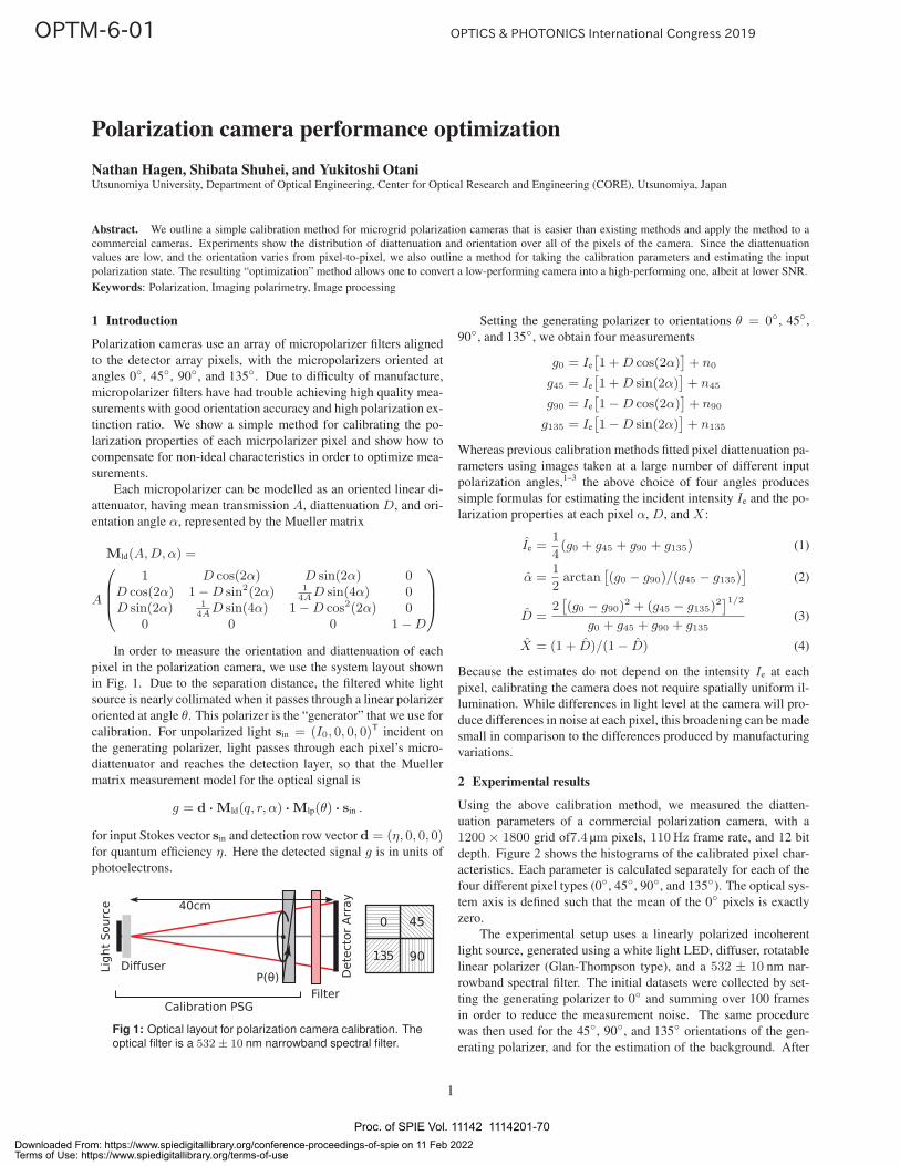
Polarization camera performance optimizationNathan Hagen, Shibata Shuhei, and Yukitoshi OtaniUtsunomiya University, Department of Optical Engineering, Center for Optical Research and Engineering (CORE), Utsunomiya, Japan
Abstract. We outline a simple calibration method for microgrid polarization cameras that is easier than existing methods and apply the method to a
commercial cameras. Experiments show the distribution of diattenuation and orientation over all of the pixels of the camera. Since the diattenuation
values are low, and the orientation varies from pixel-to-pixel, we also outline a method for taking the calibration parameters and estimating the input
polarization state. The resulting “optimization” method allows one to convert a low-performing camera into a high-performing one, albeit at lower SNR.
Keywords: Polarization, Imaging polarimetry, Image processing
1 Introduction
Polarization cameras use an array of micropolarizer filters aligned
to the detector array pixels, with the micropolarizers oriented at
angles 0◦, 45◦, 90◦, and 135◦. Due to difficulty of manufacture,
micropolarizer filters have had trouble achieving high quality mea-
surements with good orientation accuracy and high polarization ex-
tinction ratio. We show a simple method for calibrating the po-
larization properties of each micrpolarizer pixel and show how to
compensate for non-ideal characteristics in order to optimize mea-
surements.
Each micropolarizer can be modelled as an oriented linear di-
attenuator, having mean transmission A, diattenuation D, and ori-
entation angle α, represented by the Mueller matrix
Mld(A,D,α) =
A
⎛⎜⎜⎝
1 D cos(2α) D sin(2α) 0D cos(2α) 1−D sin2(2α) 1
4AD sin(4α) 0
D sin(2α) 14A
D sin(4α) 1−D cos2(2α) 00 0 0 1−D
⎞⎟⎟⎠
In order to measure the orientation and diattenuation of each
pixel in the polarization camera, we use the system layout shown
in Fig. 1. Due to the separation distance, the filtered white light
source is nearly collimated when it passes through a linear polarizer
oriented at angle θ. This polarizer is the “generator” that we use for
calibration. For unpolarized light sin = (I0, 0, 0, 0)T incident on
the generating polarizer, light passes through each pixel’s micro-
diattenuator and reaches the detection layer, so that the Mueller
matrix measurement model for the optical signal is
g = d ·Mld(q, r, α) ·Mlp(θ) · sin .
for input Stokes vector sin and detection row vector d = (η, 0, 0, 0)for quantum efficiency η. Here the detected signal g is in units of
photoelectrons.
Dete
ctor
Arr
ay
FilterP( )Lig
ht S
ourc
e
Di user135
0 45
90
Calibration PSG
40cm
Fig 1: Optical layout for polarization camera calibration. Theoptical filter is a 532± 10 nm narrowband spectral filter.
Setting the generating polarizer to orientations θ = 0◦, 45◦,
90◦, and 135◦, we obtain four measurements
g0 = Ie
[1 +D cos(2α)
]+ n0
g45 = Ie
[1 +D sin(2α)
]+ n45
g90 = Ie
[1−D cos(2α)
]+ n90
g135 = Ie
[1−D sin(2α)
]+ n135
Whereas previous calibration methods fitted pixel diattenuation pa-
rameters using images taken at a large number of different input
polarization angles,1–3 the above choice of four angles produces
simple formulas for estimating the incident intensity Ie and the po-
larization properties at each pixel α, D, and X:
Ie =1
4(g0 + g45 + g90 + g135) (1)
α =1
2arctan
[(g0 − g90)/(g45 − g135)
](2)
D =2[(g0 − g90)
2 + (g45 − g135)2]1/2
g0 + g45 + g90 + g135(3)
X = (1 + D)/(1− D) (4)
Because the estimates do not depend on the intensity Ie at each
pixel, calibrating the camera does not require spatially uniform il-
lumination. While differences in light level at the camera will pro-
duce differences in noise at each pixel, this broadening can be made
small in comparison to the differences produced by manufacturing
variations.
2 Experimental results
Using the above calibration method, we measured the diatten-
uation parameters of a commercial polarization camera, with a
1200 × 1800 grid of7.4 μm pixels, 110Hz frame rate, and 12 bit
depth. Figure 2 shows the histograms of the calibrated pixel char-
acteristics. Each parameter is calculated separately for each of the
four different pixel types (0◦, 45◦, 90◦, and 135◦). The optical sys-
tem axis is defined such that the mean of the 0◦ pixels is exactly
zero.
The experimental setup uses a linearly polarized incoherent
light source, generated using a white light LED, diffuser, rotatable
linear polarizer (Glan-Thompson type), and a 532 ± 10 nm nar-
rowband spectral filter. The initial datasets were collected by set-
ting the generating polarizer to 0◦ and summing over 100 frames
in order to reduce the measurement noise. The same procedure
was then used for the 45◦, 90◦, and 135◦ orientations of the gen-
erating polarizer, and for the estimation of the background. After
1
Proc. of SPIE Vol. 11142 1114201-70Downloaded From: https://www.spiedigitallibrary.org/conference-proceedings-of-spie on 11 Feb 2022Terms of Use: https://www.spiedigitallibrary.org/terms-of-use
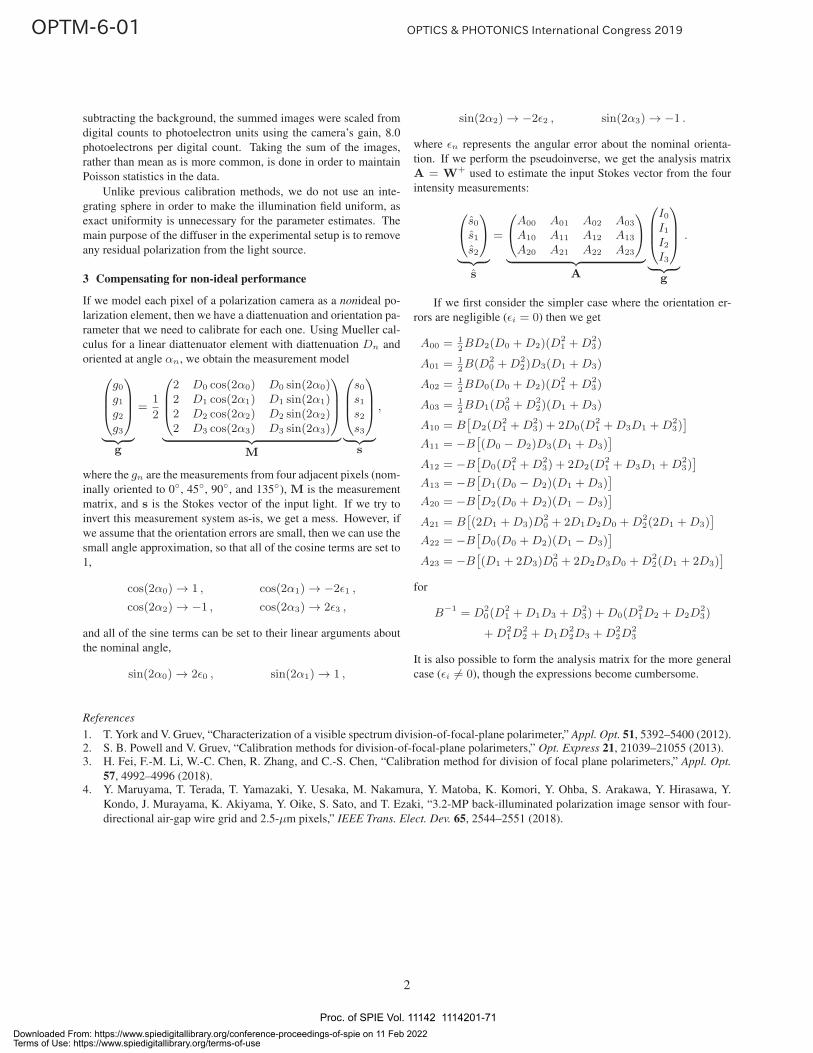
subtracting the background, the summed images were scaled from
digital counts to photoelectron units using the camera’s gain, 8.0
photoelectrons per digital count. Taking the sum of the images,
rather than mean as is more common, is done in order to maintain
Poisson statistics in the data.
Unlike previous calibration methods, we do not use an inte-
grating sphere in order to make the illumination field uniform, as
exact uniformity is unnecessary for the parameter estimates. The
main purpose of the diffuser in the experimental setup is to remove
any residual polarization from the light source.
3 Compensating for non-ideal performance
If we model each pixel of a polarization camera as a nonideal po-
larization element, then we have a diattenuation and orientation pa-
rameter that we need to calibrate for each one. Using Mueller cal-
culus for a linear diattenuator element with diattenuation Dn and
oriented at angle αn, we obtain the measurement model
⎛⎜⎜⎝g0g1g2g3
⎞⎟⎟⎠
︸ ︷︷ ︸g
=1
2
⎛⎜⎜⎝2 D0 cos(2α0) D0 sin(2α0)2 D1 cos(2α1) D1 sin(2α1)2 D2 cos(2α2) D2 sin(2α2)2 D3 cos(2α3) D3 sin(2α3)
⎞⎟⎟⎠
︸ ︷︷ ︸M
⎛⎜⎜⎝s0s1s2s3
⎞⎟⎟⎠
︸ ︷︷ ︸s
,
where the gn are the measurements from four adjacent pixels (nom-
inally oriented to 0◦, 45◦, 90◦, and 135◦), M is the measurement
matrix, and s is the Stokes vector of the input light. If we try to
invert this measurement system as-is, we get a mess. However, if
we assume that the orientation errors are small, then we can use the
small angle approximation, so that all of the cosine terms are set to
1,
cos(2α0) → 1 , cos(2α1) → −2ε1 ,
cos(2α2) → −1 , cos(2α3) → 2ε3 ,
and all of the sine terms can be set to their linear arguments about
the nominal angle,
sin(2α0) → 2ε0 , sin(2α1) → 1 ,
sin(2α2) → −2ε2 , sin(2α3) → −1 .
where εn represents the angular error about the nominal orienta-
tion. If we perform the pseudoinverse, we get the analysis matrix
A = W+ used to estimate the input Stokes vector from the four
intensity measurements:
⎛⎝s0s1s2
⎞⎠
︸ ︷︷ ︸s
=
⎛⎝A00 A01 A02 A03
A10 A11 A12 A13
A20 A21 A22 A23
⎞⎠
︸ ︷︷ ︸A
⎛⎜⎜⎝I0I1I2I3
⎞⎟⎟⎠
︸ ︷︷ ︸g
.
If we first consider the simpler case where the orientation er-
rors are negligible (εi = 0) then we get
A00 = 12BD2(D0 +D2)(D
21 +D2
3)
A01 = 12B(D2
0 +D22)D3(D1 +D3)
A02 = 12BD0(D0 +D2)(D
21 +D2
3)
A03 = 12BD1(D
20 +D2
2)(D1 +D3)
A10 = B[D2(D
21 +D2
3) + 2D0(D21 +D3D1 +D2
3)]
A11 = −B[(D0 −D2)D3(D1 +D3)
]A12 = −B
[D0(D
21 +D2
3) + 2D2(D21 +D3D1 +D2
3)]
A13 = −B[D1(D0 −D2)(D1 +D3)
]A20 = −B
[D2(D0 +D2)(D1 −D3)
]A21 = B
[(2D1 +D3)D
20 + 2D1D2D0 +D2
2(2D1 +D3)]
A22 = −B[D0(D0 +D2)(D1 −D3)
]A23 = −B
[(D1 + 2D3)D
20 + 2D2D3D0 +D2
2(D1 + 2D3)]
for
B−1 = D20(D
21 +D1D3 +D2
3) +D0(D21D2 +D2D
23)
+D21D
22 +D1D
22D3 +D2
2D23
It is also possible to form the analysis matrix for the more general
case (εi �= 0), though the expressions become cumbersome.
References1. T. York and V. Gruev, “Characterization of a visible spectrum division-of-focal-plane polarimeter,” Appl. Opt. 51, 5392–5400 (2012).2. S. B. Powell and V. Gruev, “Calibration methods for division-of-focal-plane polarimeters,” Opt. Express 21, 21039–21055 (2013).3. H. Fei, F.-M. Li, W.-C. Chen, R. Zhang, and C.-S. Chen, “Calibration method for division of focal plane polarimeters,” Appl. Opt.
57, 4992–4996 (2018).4. Y. Maruyama, T. Terada, T. Yamazaki, Y. Uesaka, M. Nakamura, Y. Matoba, K. Komori, Y. Ohba, S. Arakawa, Y. Hirasawa, Y.
Kondo, J. Murayama, K. Akiyama, Y. Oike, S. Sato, and T. Ezaki, “3.2-MP back-illuminated polarization image sensor with four-
directional air-gap wire grid and 2.5-μm pixels,” IEEE Trans. Elect. Dev. 65, 2544–2551 (2018).
2
Proc. of SPIE Vol. 11142 1114201-71Downloaded From: https://www.spiedigitallibrary.org/conference-proceedings-of-spie on 11 Feb 2022Terms of Use: https://www.spiedigitallibrary.org/terms-of-use
133.5 134.0 134.5 135.0 135.5 136.0 136.5alpha (135deg)
135mean (meas_std) (thy_std):134.884 (0.235) (0.062)
88.0 88.5 89.0 89.5 90.0 90.5 91.0alpha (90deg)
90mean (meas_std) (thy_std):89.496 (0.205) (0.060)
44.0 44.5 45.0 45.5 46.0 46.5alpha (45deg)
45mean (meas_std) (thy_std):45.196 (0.524) (0.066)
1.5 1.0 0.5 0.0 0.5 1.0 1.5alpha (0deg)
0mean (meas_std) (thy_std):0.000 (0.658) (0.068)
100000 120000 140000 160000 180000signal amplitude (Ie)
0: 122866 (10730) (175)45: 123971 (11141) (176)90: 142864 (13106) (189)135: 134204 (12521) (183)
0 deg45 deg90 deg135 deg
Ie
7.5 10.0 12.5 15.0 17.5 20.0 22.5 25.0extinction ratio (X)
X0: 12.42 (1.30) (0.13)45: 14.62 (1.51) (0.17)90: 18.18 (1.99) (0.23)135: 16.58 (1.56) (0.20)
0.80 0.82 0.84 0.86 0.88 0.90 0.92diattenuation (D)
D0: 0.8495 (0.0153) (0.0013)45: 0.8707 (0.0134) (0.0013)90: 0.8945 (0.0117) (0.0012)135: 0.8853 (0.0109) (0.0012)
Fig 2: Calibration results for a polarization camera, showing the pixel histograms for the four orientation angles α0 through α135
and the three intensity/diattenuation parameters Ie, D, and X. the detected intensity Ie is given in units of photoelectrons. Theoverlying curves are the equivalent Gaussian distributions, sharing the measured means and standard deviations.
3
Proc. of SPIE Vol. 11142 1114201-72Downloaded From: https://www.spiedigitallibrary.org/conference-proceedings-of-spie on 11 Feb 2022Terms of Use: https://www.spiedigitallibrary.org/terms-of-use
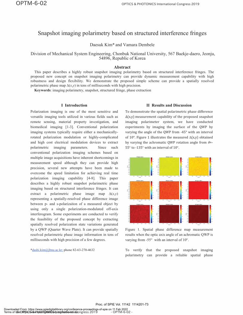
Proc. of SPIE Vol. 11142 1114201-73Downloaded From: https://www.spiedigitallibrary.org/conference-proceedings-of-spie on 11 Feb 2022Terms of Use: https://www.spiedigitallibrary.org/terms-of-use
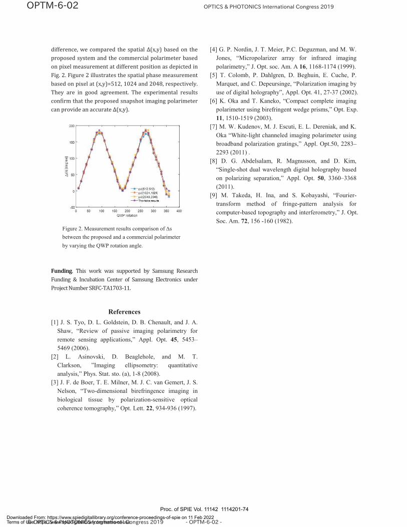
Proc. of SPIE Vol. 11142 1114201-74Downloaded From: https://www.spiedigitallibrary.org/conference-proceedings-of-spie on 11 Feb 2022Terms of Use: https://www.spiedigitallibrary.org/terms-of-use

Spectroscopic Ellipsometry Study on Aluminium-Doped Zinc Oxide Thin Films Prepared via DC Magnetron Sputtering and HiPIMS
Donyawan Chittinan1, Tossaporn Lertvanithphol2, Kittikhun Seawsakul3, Prayoon Songsiriritthigul3, Phitsanu Poolcharuansin4, Mati Horprathum2, Prathan Buranasiri1*
1Department of Physics, Faculty of Science, King Mongkut’s Institute of Technology Ladkrabang, Bangkok, 10520, Thailand 2 National Electronics and Computer Technology Center, National Science and Technology Development Agency (NSTDA), Pathum Thani 12120,
Thailand 3NANOTEC-SUT Center of Excellence on Advanced Functional Nanomaterials and School of Physics, Suranaree University of Technology, Nakhon
Ratchasima 30000, Thailand 4The Technological Plasma Research Unit, Department of Physics, Mahasarakham University, Maha Sarakham, 44150, Thailand
Author e-mail address: [email protected] Abstract: Spectroscopic ellipsometry was used to investigate the properties of aluminium-doped zinc oxide (AZO) thin films deposited on silicon (100) substrate via magnetron sputtering system. The different techniques were used to fabricate including conventional DC magnetron sputtering and high-power impulse magnetron sputtering (HiPIMS). The ellipsometric spectra of the prepared samples were performed in the range of 1.75 to 3.5 eV with 0.025 eV intervals at incident angle of 70 degree. Two different optical models based on Cauchy and Tauc-Lorentz functions were used to fit and compared. The results showed that the Tauc-Lorentz based model was better to fit and extract the properties of interest including thin film thickness and refractive index (n). In addition, the field-emission scanning electron microscopy (FE-SEM) images were used to confirm the results of thickness and ensure the using of Tauc-Lorentz model.
1. Introduction
Transparent conducting oxide (TCO) films is widely used in severally applications e.g. photovoltaics, flat panel displays, semiconductor lasers, light emitting diodes and solar cell [1]. In general, there are some materials that used as TCOs including indium-doped tin oxide (ITO), fluorine-doped tin oxide (FTO) and aluminum-doped zinc oxide (AZO). However, the AZO got more interested due to its high stability, low resistivity, high optical transmittance and low cost. The AZO thin film that could be fabricated by several techniques, such as evaporation, chemical vapor deposition, sol–gel method, pulsed laser deposition and sputtering [2]. Among these methods, direct current (DC) magnetron sputtering deposition was widely used with AZO films fabrication because of its repeatability, low temperature and large scale process. However, the good AZO films must had high homogeneity and high density. From this point, high-power impulse magnetron sputtering (HiPIMS) could be an appropriate technique to fabricate AZO. In addition, it has been shown that HiPIMS reduced the hysteresis effect which increased homogeneity and packing density of the film [3].
2. Experimental Details
AZO thin films were fabricated on silicon (100) substrates by homemade magnetron sputtering system. The 3 inches diameter of AZO material and 99.999% purity argon were used as sputtered target and sputtered gas, respectively. Prior to deposition, the system was pumped down to the base pressure of 5×10⁻⁶ Torr by rotary and turbomolecular pumps. The AZO films were prepared with different technique including conventional DC magnetron sputtering, labelled sample as “AZO-DC”, and high-power impulse magnetron sputtering (HiPIMS), labelled sample as “AZO-HiPIMS”, respectively. During deposition for 20 min, Ar flow rate and operating pressure were respectively set at 80 sccm and 4.2×10⁻³ mbar for AZO-DC while those of AZO-HiPIMS were respectively set at 100 sccm and 2.1×10⁻³ mbar. For AZO-DC sample, the DC bias power was constantly set at 100 W. For AZO-HiPIMS, the bias power was set its frequency at 100 Hz while the duty cycle was set at 400 μs. The as-deposited films were characterized by spectroscopic ellipsometer (J.A. Woollam, Inc.; VASE). The ellipsometric spectra were performed in the range of 1.75-3.5 eV with 0.025 eV intervals at 70 degree. The optical model of silicon substrate/2 nm of Si native oxide/AZO thin film/surface roughness, which the optical properties of AZO layer was defined by different function of Cauchy and Tauc-Lorentz (TL) [4], was used to fit with the measured spectra and extract the properties. In addition, the thickness results were confirmed by field-emission scanning electron microscopy (FE-SEM) images in cross-sectional view.
3. Results & Discussions
The measured ellipsometric spectra were fitted with both Cauchy and TL based optical models then compared together as shown in Fig. 1 and 2. The results showed that the TL based optical model represented the best fit with the measured Ψ and Δ spectra. This indicated that the TL based model was a suitable model for AZO thin films. From the TL model, the thickness of AZO-DC and AZO-HiPIMS were determined as 337.4 and 313.8 nm, respectively. Fig. 3(a) showed the refractive index dispersion for both samples. The results showed that the AZO-HiPIMS had higher index than the AZO-DC sample. The refractive index of AZO-DC and AZO-HiPIMS at 550 nm were 1.90 and 1.97, respectively. This i di d h h i h i ld b i d h d i f h hi fil d fi h fil
Proc. of SPIE Vol. 11142 1114201-75Downloaded From: https://www.spiedigitallibrary.org/conference-proceedings-of-spie on 11 Feb 2022Terms of Use: https://www.spiedigitallibrary.org/terms-of-use

thickness, the prepared samples were characterized by FE-SEM. The film thicknesses obtained from both techniques were in good agreement as shown in Fig 3(b).
2.0 2.5 3.0 3.50
60
120
180
2.0 2.5 3.0 3.50
20
40
60
Ψ
in d
egre
e
Δin
deg
ree
Photon energy (eV) Photon energy (eV)
(a) (b)
AZO-DC
Measured Cauchy Tauc-Lorentz
Fig. 1. Measured and fitted Ψ and Δ parameters from Cauchy and TL models for the AZO-DC sample
2.0 2.5 3.0 3.50
60
120
180
2.0 2.5 3.0 3.50
20
40
60
Ψ
in d
egre
e
Δin
deg
ree
Photon energy (eV) Photon energy (eV)
(a) (b)
AZO-HiPIMS
Measured Cauchy Tauc-Lorentz
Fig. 2. Measured and fitted Ψ and Δ parameters from Cauchy and TL models for the AZO-HiPIMS sample
0
100
200
300
400
500
2.0 2.5 3.0 3.51.80
1.95
2.10
2.25
2.40
Ref
ract
ive
inde
x, n
Thi
ckne
ss (n
m)
Photon energy (eV) AZODC
(a) (b)
AZOHiPIMS
AZO-DCAZO-HiPIMS
SEFE-SEM
Fig. 3. Comparison of (a) refractive index spectra between AZO-DC and AZO-HiPIMS and (b) thickness results from
SE and FE-SEM.
4. Conclusion
The AZO thin films were fabricated by conventional DC magnetron sputtering and HiPIMS techniques. The prepared films were characterized for their properties by SE. The optical models based on Cauchy and TL were used and compared. The results showed that the TL model was an appropriate model for AZO films. The thicknesses and refractive index spectra were extracted from the model. The HiPIMS film had higher index than the film from conventional DC. This indicated that the AZO film could be increased their density by HiPIMS technique. In addition, the thickness results from SE were compared with those from FE-SEM to ensure the extract properties. References [1] M. Mickan et al., “Room temperature deposition of homogeneous, highly transparent and conductive Al-doped ZnO films by reactive high power impulse magnetron sputtering”, Sol. Energy Mater. Sol. Cells 157, 742-749 (2016) [2] G. Xiao-Yong, C. Chao, Z. Sa, “Optical properties of aluminum-doped zinc oxide films deposited by direct-current pulse magnetron reactive sputtering”, Chin. Phys. B 23, 1-5 (2014). [3] V. Sittinger et al., “Applications of HIPIMS metal oxides” Thin Solid Films 548, 18-26 (2013) [4] H. Fujiwara, Spectroscopic Ellipsometry: Principles and Applications (John Wiley & Sons, 2007), Chap. 5. Proc. of SPIE Vol. 11142 1114201-76
Downloaded From: https://www.spiedigitallibrary.org/conference-proceedings-of-spie on 11 Feb 2022Terms of Use: https://www.spiedigitallibrary.org/terms-of-use

I Introduction The optoelectronic functions of porous silicon (PS),
particularly its photoluminescence and electro-luminescence are attractive and promising features [1, 2]. The optical properties of PS layers are determined by their nanostructures. PS nanostructures are formed by electrochemical etching of silicon substrates in hydrofluoric acid (HF). Depending on doping level and type, the formation method of PSi and resultant nanostructures are different. For n- or n+-type silicon, the PS layer is obtained by anodization of P-doped silicon chip in HF with etching-side or backside illumination. The formed n+-type PS nanostructure is sometimes not uniform. To investigate the morphology of n+-type PS, imaging ellipsometry studies has been carried on. The measurement results show that imaging ellipsometry is a powerful tool to characterize materials.
II Measurements 1. Experimental setup Figure 1 shows the configuration of the imaging
ellipsometry system [3-4] built by our group. The light from xenon lamp passes thorough an optical filter (for 530, 590, 650, 720, 780 nm, respectively), a convergence lens system, a linear Gran-Thompson polarizer, and then a compensator. The reflected light from the sample surface
*[email protected]; phone 81 55-220-8448
passes through an analyzer and an Offner imaging system (NA=0.07), and then is collected by a CMOS device (2592×1944 pixels, 12 Bit). The detection area of the CMOS device is 6.4 4.8 mm2. The incident angle is 50 . The lateral resolution of the imaging system is about5 m at the wavelength of 530 nm. The image plane of the CMOS device was carefully adjusted to receive the entire image in focus. Rotating compensator method was employed to obtain the ellipsometric parameters DEL ( ) and PSI ( ) of samples. These parameters are defined by,
,)exp()tan(s
p
rr
j (1)
where rp and rs are the Fresnel reflection coefficients of p and s polarized light, respectively. By analyzing the relationships of DEL and PSI with refractive index and film thickness of samples, we can investigate the sample morphology.
CMOS device
Offner imaging system
Polarizer
Analyzer
Compensator
Lens
Xenon Lamp & optical filter
Sample
Figure 1. Configuration of imaging ellipsometry setup
Imaging elliprometry of porous silicon
Lianhua Jin*a, Taiki Akiyamaa, Yuki Iizukaa, Eiichi Kondoha, Benard Gellozb
a Faculty of Engineering, University of Yamanashi, Yamanashi 400-8511, Japan b Faculty of Engineering, Nagoya University, 464-8601 Nagoya, Japan
Abstract
Imaging ellipsometry studies of n+-type porous silicon layers are presented. The morphology of n+-type porous silicon is discussed in accordance with two-dimensional measurement results of refractive index and thickness. The results show that imaging ellipsometry is a powerful technique for materials characterization.
Keywords: Imaging ellipsometry, Porous silicon, Material, Refractive index
Proc. of SPIE Vol. 11142 1114201-77Downloaded From: https://www.spiedigitallibrary.org/conference-proceedings-of-spie on 11 Feb 2022Terms of Use: https://www.spiedigitallibrary.org/terms-of-use
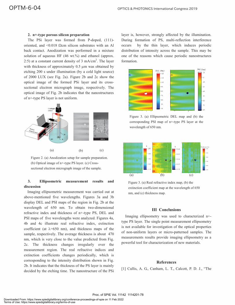
2. n+-type porous silicon preparation The PSi layer was formed from P-doped, (111)-
oriented, and <0.018 cm silicon substrates with an Al back contact. Anodization was performed in a mixture solution of aqueous HF (46 wt.%) and ethanol (approx. 2:5) at a constant current density of 3 mA/cm2. The layer with thickness of approximately 0.5 m was obtained by etching 200 s under illumination (by a cold light source) of 2000 LUX (see Fig. 2a). Figure 2b and 2c show the optical image of the formed PSi layer and its cross-sectional electron micrograph image, respectively. The optical image of Fig. 2b indicates that the nanostructures of n+-type PS layer is not uniform.
(a) (c)
Figure 2. (a) Anodization setup for sample preparation. (b) Optical image of n+-type PS layer. (c) Cross- sectional electron micrograph image of the sample.
3. Ellipsometric measurement results and discussion
Imaging ellipsometric measurement was carried out at above-mentioned five wavelengths. Figures 3a and 3b display DEL and PSI maps of the region in Fig. 2b at the wavelength of 650 nm. To obtain two-dimensional refractive index and thickness of n+-type PS, DEL and PSI maps of five wavelengths were analyzed. Figures 4a, 4b and 4c illustrate real refractive index, extinction coefficient (at =650 nm), and thickness maps of the sample, respectively. The average thickness is about 470 nm, which is very close to the value predicted from Fig. 2c. The thickness changes irregularly over the measurement region. The real refractive indices and extinction coefficients changes periodically, which is corresponding to the intensity distribution shown in Fig. 2b. It indicates that the thickness of the PS layer is mainly decided by the etching time. The nanostructure of the PSi
layer is, however, strongly affected by the illumination. During formation of PS, multi-reflection interference occurs by the thin layer, which induces periodic distribution of intensity across the sample. This may be one of the reasons which cause periodic nanostructures formation.
(a) (b)
Figure 3. (a) Ellipsometric DEL map and (b) the corresponding PSI map of n+-type PS layer at the wavelength of 650 nm.
(a) (b) (c)
Figure 3. (a) Real refractive index map, (b) the extinction coefficient map at the wavelength of 650 nm, and (c) thickness map.
III Conclusions Imaging ellipsometry was used to characterized n+-
type PS layer. The single point measurement ellipsometry is not available for investigation of the optical properties of non-uniform layers or micro-patterned samples. The measurements results provide imaging ellipsometry as a powerful tool for characterization of new materials.
References [1] Cullis, A. G., Canham, L. T., Calcott, P. D. J., “The
(b)
Si
PS
App
rox.
480
nm
(a(a(a(a(a(a(a(a(a(aa(a(a(a(a(a(a(a(a(a(a(((((( ))))))))))))))))) ) ) )))))))))
(b(b(b(b(b(b(b(b(b(bbb(bb(b(b(b(b(b((b(b(b(b(bb(((( ))))))))))))))))))))))))))
(b)(a(( ) ( )
Proc. of SPIE Vol. 11142 1114201-78Downloaded From: https://www.spiedigitallibrary.org/conference-proceedings-of-spie on 11 Feb 2022Terms of Use: https://www.spiedigitallibrary.org/terms-of-use

structural and luminescence properties of porous silicon,” J. Appl. Phys. 82, 909-965 (1997).
[2] Gelloz, B. and Koshida, N., “Electroluminescence with high and stable quantum efficiency and low threshold voltage from anodically oxidized thin porous silicon diode” J. Appl. Phys. 88, 4319-4324 (2000).
[3] Jin, L., Tanaka, T., Kondoh, E., Gelloz, B., Sano, K., Fujio, I., Kajiyama, Y., Uehara, M., “Rotatable Offner imaging system for ellipsometric measurement,” Rev. Sci. Instrum. 88, 013704 (2017).
[4] Jin, L., Tanaka, T., Kondoh, E., Gelloz, B., Uehara, M., “Extracting calibrated parameters from imaging ellipsometric measurement,” Jpn. J. Appl. Phys. 56, 116602 (2017).
Proc. of SPIE Vol. 11142 1114201-79Downloaded From: https://www.spiedigitallibrary.org/conference-proceedings-of-spie on 11 Feb 2022Terms of Use: https://www.spiedigitallibrary.org/terms-of-use

I Introduction
Reflecting surfaces are widely used in optical systems to make the whole system compact. Instruments from space telescopes to ground telescopes, remote sensing spectrometers, microlithography all use multiple fold mirrors [1]. Traditional materials for metal mirrors include aluminum, gold and silver for optical applications. Among them, aluminum (Al) coatings are common due to high reflectivity over a wavelength range. For an ideal mirror, the reflection coefficients of s and p polarizations are equal, where a metal coated mirror reflects more s polarized light than p polarized light at a non-normal angle of incidence. The difference of complex amplitude reflection coefficients creates a phase difference between s and p polarized lights. This unwanted linear retardance can deteriorate image quality [1].
Lam et al. [2] reported that polarization aberration can be balanced by using crossed fold mirrors. Gold mirrors are selected in their simulation process which in practical makes the system expensive and can be used only in infra-red region.
Bare Al mirrors react with oxygen in air, creating a *[email protected];
thin oxide layer on the top of the mirror surface. This can further increase the proper linear retardance which is excluded from geometrical transformation.
In this manuscript, we determine the naturally formed oxide layer thickness by fitting the linear retardance of aluminum mirrors with a theoretical model for the Fresnel’s reflection coefficients. We report the effect of oxide layer thickness on the cancellation of linear retardance using two different pairs of crossed fold mirrors.
II Theoretical background
We employ Polarization ray tracing (P) matrices [3] to determine the polarization cancellation and analyze the polarizing state evolution for each mirror surface. P matrix is generalized 3x3 Jones (J) matrix which is obtained by using,
1,, inqoutqq OJOP , (1)
here q represents the surface number and Oq,out and Oq,in are the exiting and incident orthogonal matrices respectively which transform the Jones matrix of mirror from local to global coordinate system. Orthogonal matrix is functions of orthogonal polarizations (s, p) and propagation vector (k),
Effect of oxide layer thickness on polarization mitigation*
Suchandra Banerjee*a, Russell Chipmanb, Nathan Hagenc, Yukitoshi Otania,c,d
aGraduate School of Engineering, Utsunomiya University, Utsunomiya, Tochigi, 321-8585, Japan, bCollege of Optical Sciences, University of Arizona, Tucson, AZ 85721, USA,
cDepartment of Optical Engineering, Utsunomiya University, Utsunomiya, Tochigi, 321-8585, Japan, dCenter for Optical Research and Education, Utsunomiya University, Utsunomiya, Tochigi,
321-8585, Japan
Abstract We analyze the influence of oxide layer thickness on polarization cancellation using crossed fold mirrors. We measure
the linear retardance of three individual aluminum coated mirrors over the visible to near infra-red region by employing a spectroscopic Mueller matrix polarimeter. By fitting the measured linear retardance data with the theoretical model described by Fresnel’s law, the native oxide layer thickness of three mirrors are determined as 4.40 nm, 5.75 nm, and 4.10 nm respectively. We perform polarization cancellation by using crossed fold mirrors. The oxide layer thickness difference of 1.35 nm between the first two mirrors limits the polarization cancellation to 0.65° of retardance at 650 nm. We show that the first and last fold mirrors having nearly same amount of oxide layer thickness reduces the residual quantity to 0.15° at 650 nm.
Keywords: Polarization, Mueller matrix polarimeter, oxide layer, crossed fold mirrors, linear retardance.
Proc. of SPIE Vol. 11142 1114201-80Downloaded From: https://www.spiedigitallibrary.org/conference-proceedings-of-spie on 11 Feb 2022Terms of Use: https://www.spiedigitallibrary.org/terms-of-use

zqzqzq
yqyqyq
xqxqxq
inq
kpskpskps
O
,1,1,
,1,1,
,1,1,
,,
zqzqzq
yqyqyq
xqxqxq
outq
kpskpskps
O
,,,
,,,
,,,
,, (2)
The propagation vectors (k) in xyz coordinate system are,
Orthogonal polarization components s and p depend on the propagation vector as,
Jones matrix in Eq. 1 is the mirror’s polarization property and can be written as,
1000000
p
s
rr
J , (5)
where, sr and pr are the apparent reflection coefficients
derived from the Fresnel’s model shown in Fig.1. It can be formed as,
where 01r and 12r are the Fresnel reflection coefficients
for medium 0 to 1 and for medium 1 to 2 respectively for
s and p polarized light. is the phase change of light
which occurs due to oxide layer thickness in this model
and it is functions of refractive index )( 1n ,
thickness )(d of oxide layer and can be represented as,
01 cos2 idn . (7)
By using Eq. (1-7), overall P matrix is determined by cascading 1st, and 2nd mirrors P matrices, shown in Eq. 8. By using singular value decomposition, P matrix is
decomposed into retardance )( RM and diattenuation
matrices )( DM as,
R12 MMDPPP . (8)
Retarder matrix is an Unitary matrix whose Eigen values
( 321 ,, ) are complexed valued. Two of the three
Eigen values denote fast and slow axes whose argument
difference is the linear retardance )( after cancellation
which is, ]arg[]arg[ 21 . (9)
III Experimental set up and results
An Axometrics Mueller matrix polarimeter is used for the measurement of polarization properties of Al mirror. Fig. 2 shows the schematic diagram of experimental set up. It consists of polarization state generator (PSG) and polarization state analyzer (PSA). The PSG comprises a polarizer (P) oriented at 0° and a rotating retarder (R1) having rotational angle . Another rotating retarder (R2) having rotational angle 5 and an analyzer (A) oriented at 0° are placed in PSA. The system uses a Xenon arc lamp white light source and retrieves the polarization parameters as a function of wavelength. The Mueller matrix polarimeter is set at reflection mode and three aluminum coated mirrors (M1, M2, and M3) are placed individually at 45° angle of incidence.
},1,0,0{1k },0,1,0{2k and }0,0,1{3k . (3)
qqqqq kkkks 11 /)( ,
qqqqinq skskp 11, /)( , and
qqqqoutq skskp /)(, .
(4)
i1201
i1201
1 errerr
rss
sss , and i
1201
i1201
1 err
errr
pp
ppp ,
(6)
Figure 1. Theoretical model of Fresnel’s law by considering oxide layer thickness on the top of Al mirror.
Figure 2. Experimental setup for measurement of polarization cancellation using two crossed fold mirrors
Proc. of SPIE Vol. 11142 1114201-81Downloaded From: https://www.spiedigitallibrary.org/conference-proceedings-of-spie on 11 Feb 2022Terms of Use: https://www.spiedigitallibrary.org/terms-of-use
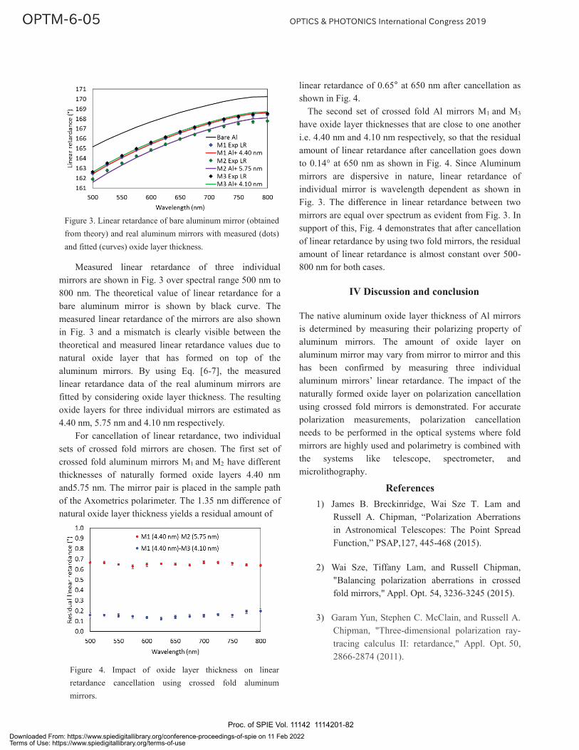
Measured linear retardance of three individual mirrors are shown in Fig. 3 over spectral range 500 nm to 800 nm. The theoretical value of linear retardance for a bare aluminum mirror is shown by black curve. The measured linear retardance of the mirrors are also shown in Fig. 3 and a mismatch is clearly visible between the theoretical and measured linear retardance values due to natural oxide layer that has formed on top of the aluminum mirrors. By using Eq. [6-7], the measured linear retardance data of the real aluminum mirrors are fitted by considering oxide layer thickness. The resulting oxide layers for three individual mirrors are estimated as 4.40 nm, 5.75 nm and 4.10 nm respectively.
For cancellation of linear retardance, two individual sets of crossed fold mirrors are chosen. The first set of crossed fold aluminum mirrors M1 and M2 have different thicknesses of naturally formed oxide layers 4.40 nm and5.75 nm. The mirror pair is placed in the sample path of the Axometrics polarimeter. The 1.35 nm difference of natural oxide layer thickness yields a residual amount of
linear retardance of 0.65° at 650 nm after cancellation as shown in Fig. 4.
The second set of crossed fold Al mirrors M1 and M3
have oxide layer thicknesses that are close to one another i.e. 4.40 nm and 4.10 nm respectively, so that the residual amount of linear retardance after cancellation goes down to 0.14° at 650 nm as shown in Fig. 4. Since Aluminum mirrors are dispersive in nature, linear retardance of individual mirror is wavelength dependent as shown in Fig. 3. The difference in linear retardance between two mirrors are equal over spectrum as evident from Fig. 3. In support of this, Fig. 4 demonstrates that after cancellation of linear retardance by using two fold mirrors, the residual amount of linear retardance is almost constant over 500-800 nm for both cases.
IV Discussion and conclusion
The native aluminum oxide layer thickness of Al mirrors is determined by measuring their polarizing property of aluminum mirrors. The amount of oxide layer on aluminum mirror may vary from mirror to mirror and this has been confirmed by measuring three individual aluminum mirrors’ linear retardance. The impact of the naturally formed oxide layer on polarization cancellation using crossed fold mirrors is demonstrated. For accurate polarization measurements, polarization cancellation needs to be performed in the optical systems where fold mirrors are highly used and polarimetry is combined with the systems like telescope, spectrometer, and microlithography.
References 1) James B. Breckinridge, Wai Sze T. Lam and
Russell A. Chipman, “Polarization Aberrations in Astronomical Telescopes: The Point Spread Function,” PSAP,127, 445-468 (2015).
2) Wai Sze, Tiffany Lam, and Russell Chipman, "Balancing polarization aberrations in crossed fold mirrors," Appl. Opt. 54, 3236-3245 (2015).
3) Garam Yun, Stephen C. McClain, and Russell A. Chipman, "Three-dimensional polarization ray-tracing calculus II: retardance," Appl. Opt. 50, 2866-2874 (2011).
Figure 4. Impact of oxide layer thickness on linear retardance cancellation using crossed fold aluminum mirrors.
Figure 3. Linear retardance of bare aluminum mirror (obtained from theory) and real aluminum mirrors with measured (dots) and fitted (curves) oxide layer thickness.
Proc. of SPIE Vol. 11142 1114201-82Downloaded From: https://www.spiedigitallibrary.org/conference-proceedings-of-spie on 11 Feb 2022Terms of Use: https://www.spiedigitallibrary.org/terms-of-use
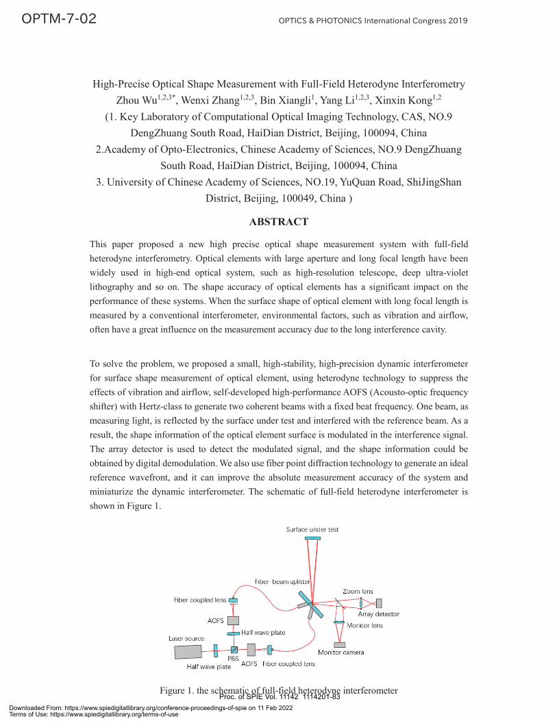
High-Precise Optical Shape Measurement with Full-Field Heterodyne Interferometry Zhou Wu1,2,3*, Wenxi Zhang1,2,3, Bin Xiangli1, Yang Li1,2,3, Xinxin Kong1,2
(1. Key Laboratory of Computational Optical Imaging Technology, CAS, NO.9 DengZhuang South Road, HaiDian District, Beijing, 100094, China
2.Academy of Opto-Electronics, Chinese Academy of Sciences, NO.9 DengZhuang South Road, HaiDian District, Beijing, 100094, China
3. University of Chinese Academy of Sciences, NO.19, YuQuan Road, ShiJingShan District, Beijing, 100049, China )
ABSTRACT
This paper proposed a new high precise optical shape measurement system with full-field heterodyne interferometry. Optical elements with large aperture and long focal length have been widely used in high-end optical system, such as high-resolution telescope, deep ultra-violet lithography and so on. The shape accuracy of optical elements has a significant impact on the performance of these systems. When the surface shape of optical element with long focal length is measured by a conventional interferometer, environmental factors, such as vibration and airflow, often have a great influence on the measurement accuracy due to the long interference cavity.
To solve the problem, we proposed a small, high-stability, high-precision dynamic interferometer for surface shape measurement of optical element, using heterodyne technology to suppress the effects of vibration and airflow, self-developed high-performance AOFS (Acousto-optic frequency shifter) with Hertz-class to generate two coherent beams with a fixed beat frequency. One beam, as measuring light, is reflected by the surface under test and interfered with the reference beam. As a result, the shape information of the optical element surface is modulated in the interference signal. The array detector is used to detect the modulated signal, and the shape information could be obtained by digital demodulation. We also use fiber point diffraction technology to generate an ideal reference wavefront, and it can improve the absolute measurement accuracy of the system and miniaturize the dynamic interferometer. The schematic of full-field heterodyne interferometer is shown in Figure 1.
Figure 1. the schematic of full-field heterodyne interferometer
Proc. of SPIE Vol. 11142 1114201-83
Downloaded From: https://www.spiedigitallibrary.org/conference-proceedings-of-spie on 11 Feb 2022Terms of Use: https://www.spiedigitallibrary.org/terms-of-use

We adopt the scheme of Hertz-class continuous heterodyne phase shifting. Compared with traditional mechanical phase shifting technology, it has the advantages of accurate phase shift, good repeatability, high stability and low process difficulty. And high accuracy is easier to achieve, especially suitable for dynamic measurement of optical lens or system with long focal length and large aperture. In dynamic interferometry, environmental vibration, airflow and detection noise usually conform to certain distribution laws. As the sampling time of the detection signal increases, the influence of the noise tends to mean value. Compared to traditional mechanical four-step phase shift or multi-step phase shift, heterodyne phase shift demodulates phase with higher precision. Through fast multicycle sampling combined with higher frequency domain analysis algorithm, vibration, laser energy fluctuation, detector shot noise, coherent noise and electronic noise can be effectively suppressed and it could further improve the measurement accuracy of the interferometer. In order to verify the feasibility of the system for high-precision measurement of optical element with long focal length, we set up an experimental device to verify the repeat measurement accuracy of the interferometer. The experimental device is shown in Figure 2.
Figure 2. experimental device of full-field heterodyne interferometer
On this basis, we carried out a dynamic test of the shape of a mirror 10 meters away for measurement of 16 times. The test results are shown in Figure 3.
Figure 3. repeated measurement results of 16 times with long interference cavity Proc. of SPIE Vol. 11142 1114201-84
Downloaded From: https://www.spiedigitallibrary.org/conference-proceedings-of-spie on 11 Feb 2022Terms of Use: https://www.spiedigitallibrary.org/terms-of-use

According to the experimental results, full-field heterodyne dynamic interferometer can measure the optical element with long focal length with high precision better than λ/1000, and verify the ability of the interferometer to suppress vibration and air turbulence. It can solve the problem of shape measurement of optical element with long focal length and realize development of miniaturized interferometer.
Proc. of SPIE Vol. 11142 1114201-85Downloaded From: https://www.spiedigitallibrary.org/conference-proceedings-of-spie on 11 Feb 2022Terms of Use: https://www.spiedigitallibrary.org/terms-of-use
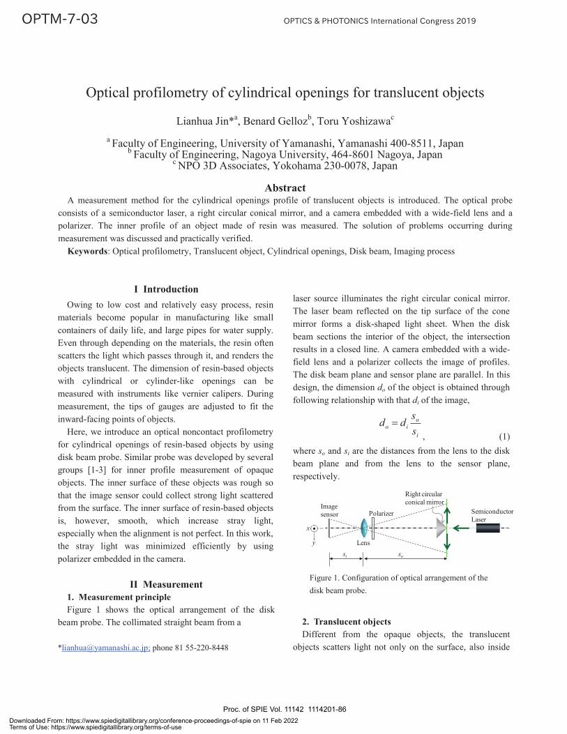
I Introduction Owing to low cost and relatively easy process, resin
materials become popular in manufacturing like small containers of daily life, and large pipes for water supply. Even through depending on the materials, the resin often scatters the light which passes through it, and renders the objects translucent. The dimension of resin-based objects with cylindrical or cylinder-like openings can be measured with instruments like vernier calipers. During measurement, the tips of gauges are adjusted to fit the inward-facing points of objects.
Here, we introduce an optical noncontact profilometry for cylindrical openings of resin-based objects by using disk beam probe. Similar probe was developed by several groups [1-3] for inner profile measurement of opaque objects. The inner surface of these objects was rough so that the image sensor could collect strong light scattered from the surface. The inner surface of resin-based objects is, however, smooth, which increase stray light, especially when the alignment is not perfect. In this work, the stray light was minimized efficiently by using polarizer embedded in the camera.
II Measurement
1. Measurement principle Figure 1 shows the optical arrangement of the disk
beam probe. The collimated straight beam from a
*[email protected]; phone 81 55-220-8448
laser source illuminates the right circular conical mirror. The laser beam reflected on the tip surface of the cone mirror forms a disk-shaped light sheet. When the disk beam sections the interior of the object, the intersection results in a closed line. A camera embedded with a wide-field lens and a polarizer collects the image of profiles. The disk beam plane and sensor plane are parallel. In this design, the dimension do of the object is obtained through following relationship with that di of the image,
i
oio s
sdd, (1)
where so and si are the distances from the lens to the disk beam plane and from the lens to the sensor plane, respectively.
y
x
si so
Semiconductor Laser
Lens
Right circular conical mirrorImage
sensor Polarizer
Figure 1. Configuration of optical arrangement of the disk beam probe.
2. Translucent objects Different from the opaque objects, the translucent
objects scatters light not only on the surface, also inside
Optical profilometry of cylindrical openings for translucent objects
Lianhua Jin*a, Benard Gellozb, Toru Yoshizawac
a Faculty of Engineering, University of Yamanashi, Yamanashi 400-8511, Japan b Faculty of Engineering, Nagoya University, 464-8601 Nagoya, Japan
c NPO 3D Associates, Yokohama 230-0078, Japan
Abstract A measurement method for the cylindrical openings profile of translucent objects is introduced. The optical probe
consists of a semiconductor laser, a right circular conical mirror, and a camera embedded with a wide-field lens and a polarizer. The inner profile of an object made of resin was measured. The solution of problems occurring during measurement was discussed and practically verified.
Keywords: Optical profilometry, Translucent object, Cylindrical openings, Disk beam, Imaging process
Proc. of SPIE Vol. 11142 1114201-86Downloaded From: https://www.spiedigitallibrary.org/conference-proceedings-of-spie on 11 Feb 2022Terms of Use: https://www.spiedigitallibrary.org/terms-of-use

the material. The light collected by the camera includes both that scattered on the surface and that scattered inside the object. When the object surface is smooth, and alignment of the probe and the object is not perfect, strong specular reflection occurs on the surface out of focus plane and consequently stray light occurs around the intersection line. Figure 2a shows scattering phenomenon, which was taken from outside the opening of the translucent objects. Figure 2b is the image collected through the probe. From Fig. 2b, we can see very clearly the stray light.
(a)
(b)
Figure 2. (a) Transmitted and (b) reflected lights by a translucent object were observed, while the disk beam illuminates it.
3. Experiment results When light is reflected by the surface, it will be
partially polarized [4]. The light reflected by the surface out of the focus plane induces stray light for the measurement probe. The stray light shown in Fig. 2b is
due to this reflection, and may be minimized by using a polarizer.
To measure the inner profile of this translucent object, we built the optical probe based on our previous work [2]. The diameter of base of the right circular cone mirror was 5.0 mm. A semiconductor laser with wavelength of 635 nm (beam size 3mm) was employed for a light source. A CCD camera (PixeLink, 1024×768 pixels, 8 Bit, 4.65 m pixel pitch,) was used to capture the intersection profiles. The inverse longitudinal magnification so/si of the lens is 13.00. A polarizer set in front of the lens is carefully adjusted until the stray light is minimized. Figure 3 shows the image collected after polarizer adjustment. From Fig. 3, we can see the stray light decreased significantly. A threshold filter is applied to Fig. 3, and the profile coordinates are obtained on the image plane (see green round in Fig. 4). Through the regression analysis of the cloud of measurement points [3], the diameter of the opening was obtained as 33.48 mm, while the results measured by the mechanical caliper was 33.55 0.09 mm.
Figure 3. The collected image with the probe developed in this work.
III Conclusions To solve problems in measurement of translucent
object, a camera embedded with a polarizer has been employed for the disk beam probe. It can minimize the stray light effectively. Same method can be applied to measurement of inner profile of the opaque objects with smooth surfaces.
Proc. of SPIE Vol. 11142 1114201-87Downloaded From: https://www.spiedigitallibrary.org/conference-proceedings-of-spie on 11 Feb 2022Terms of Use: https://www.spiedigitallibrary.org/terms-of-use
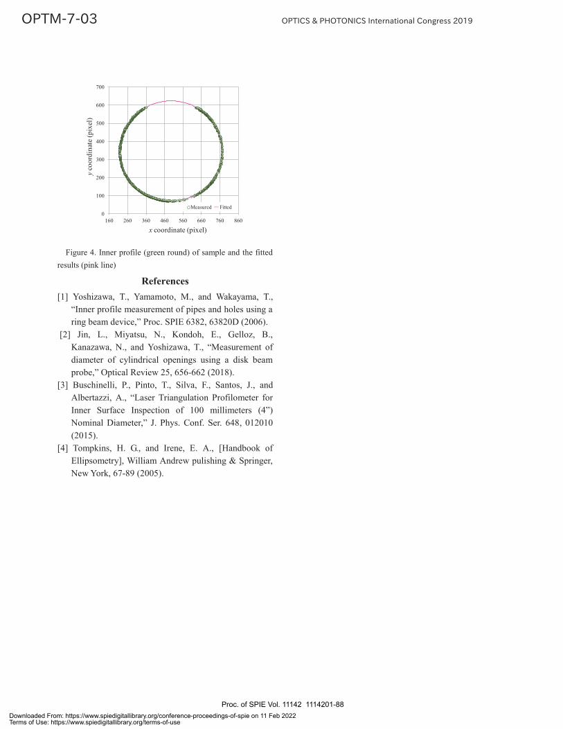
0
100
200
300
400
500
600
700
160 260 360 460 560 660 760 860
x coordinate (pixel)
yco
ordi
nate
(pix
el)
Measured Fitted
Figure 4. Inner profile (green round) of sample and the fitted results (pink line)
References [1] Yoshizawa, T., Yamamoto, M., and Wakayama, T.,
“Inner profile measurement of pipes and holes using a ring beam device,” Proc. SPIE 6382, 63820D (2006).
[2] Jin, L., Miyatsu, N., Kondoh, E., Gelloz, B., Kanazawa, N., and Yoshizawa, T., “Measurement of diameter of cylindrical openings using a disk beam probe,” Optical Review 25, 656-662 (2018).
[3] Buschinelli, P., Pinto, T., Silva, F., Santos, J., and Albertazzi, A., “Laser Triangulation Profilometer for Inner Surface Inspection of 100 millimeters (4”) Nominal Diameter,” J. Phys. Conf. Ser. 648, 012010 (2015).
[4] Tompkins, H. G., and Irene, E. A., [Handbook of Ellipsometry], William Andrew pulishing & Springer, New York, 67-89 (2005).
Proc. of SPIE Vol. 11142 1114201-88Downloaded From: https://www.spiedigitallibrary.org/conference-proceedings-of-spie on 11 Feb 2022Terms of Use: https://www.spiedigitallibrary.org/terms-of-use

Proc. of SPIE Vol. 11142 1114201-89Downloaded From: https://www.spiedigitallibrary.org/conference-proceedings-of-spie on 11 Feb 2022Terms of Use: https://www.spiedigitallibrary.org/terms-of-use

Proc. of SPIE Vol. 11142 1114201-90Downloaded From: https://www.spiedigitallibrary.org/conference-proceedings-of-spie on 11 Feb 2022Terms of Use: https://www.spiedigitallibrary.org/terms-of-use
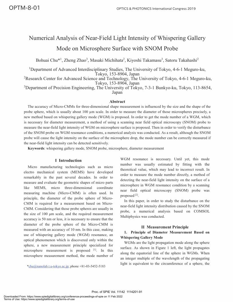
*[email protected]; phone +81-03-5452-5183
I Introduction Micro manufacturing technologies such as micro
electro mechanical system (MEMS) have developed remarkably in the past several decades. In order to measure and evaluate the geometric shapes of micro parts like MEMS, micro three-dimensional coordinate measuring machine (Micro-CMM) is often used. In principle, the diameter of the probe sphere of Micro-CMM is required for a measurement based on Micro-CMM. Considering that those probe spheres are usually in the size of 100 μm scale, and the required measurement accuracy is 50 nm or less, it is necessary to ensure that the diameter of the probe sphere of the Micro-CMM is measured with an accuracy of 10 nm. In this case, making use of whispering gallery mode (WGM) resonance, an optical phenomenon which is discovered only within the sphere, a new measurement principle specialized for microsphere measurement is proposed [1]. In this microsphere measurement method, the mode number of
WGM resonance is necessary. Until yet, this mode number was usually estimated by fitting with the theoretical value, which may lead to incorrect result. In order to measure the mode number directly, a method of detecting the near-field light intensity on the surface of a microsphere in WGM resonance condition by a scanning near field optical microscopy (SNOM) probe was proposed [2].
In this paper, in order to study the disturbance on the near-field light intensity distribution caused by the SNOM probe, a numerical analysis based on COMSOL Multiphysics was conducted.
II Measurement Principle 1. Principle of Diameter Measurement Based on
Whispering Gallery Mode WGMs are the light propagation mode along the sphere
surface. As shown in Figure 1 left, the light propagates along the equatorial line of the sphere in WGMs. When an integer multiple of the wavelength of the propagating light is equivalent to the circumference of a sphere, the
Numerical Analysis of Near-Field Light Intensity of Whispering Gallery
Mode on Microsphere Surface with SNOM Probe
Bohuai Chu*1, Zheng Zhao3, Masaki Michihata2, Kiyoshi Takamasu3, Satoru Takahashi2
1Department of Advanced Interdisciplinary Studies, The University of Tokyo, 4-6-1 Meguro-ku, Tokyo, 153-8904, Japan
2Research Center for Advanced Science and Technology, The University of Tokyo, 4-6-1 Meguro-ku, Tokyo, 153-8904, Japan
3Department of Precision Engineering, The University of Tokyo, 7-3-1 Bunkyo-ku, Tokyo, 113-8654, Japan
Abstract
The accuracy of Micro-CMMs for three-dimensional shape measurement is influenced by the size and the shape of the probe sphere, which is usually about 100 μm scale. In order to measure the diameter of those microspheres precisely, a new method based on whispering gallery mode (WGM) is proposed. In order to get the mode number of a WGM, which is necessary for diameter measurement, a method of using a scanning near field optical microscopy (SNOM) probe to measure the near-field light intensity of WGM on microsphere surface is proposed. Then in order to verify the disturbance of the SNOM probe on WGM resonance conditions, a numerical analysis was conducted. As a result, although the SNOM probe will cause the light intensity on the surface of the microsphere drop, the mode number can be correctly measured if the near-field light intensity can be detected sensitively.
Keywords: whispering gallery mode, SNOM probe, microsphere, diameter measurement
Proc. of SPIE Vol. 11142 1114201-91Downloaded From: https://www.spiedigitallibrary.org/conference-proceedings-of-spie on 11 Feb 2022Terms of Use: https://www.spiedigitallibrary.org/terms-of-use
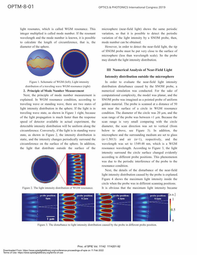
Figure 3. The disturbance to light intensity distribution caused by the probe in different probe position.
light resonates, which is called WGM resonance. This integer multiplied is called mode number. If the resonant wavelength and the mode number is known, it is possible to calculate the length of circumference, that is, the diameter of the sphere.
Figure 1. Schematic of WGM (left); Light intensity distribution of a traveling wave WGM resonance (right)
2. Principle of Mode Number Measurement Next, the principle of mode number measurement is
explained. In WGM resonance condition, according to traveling wave or standing wave, there are two states of light intensity distribution in the sphere. If the light is in traveling wave state, as shown in Figure 1 right, because of the light propagation is much faster than the response speed of detector available in actual experiment, the detectable intensity distribution will be uniform along the circumference. Conversely, if the light is in standing wave state, as shown in Figure 2, the intensity distribution is static, and the intensity changes periodically surround the circumference on the surface of the sphere. In addition, the light that distribute outside the surface of the
Figure 2. The light intensity distribution of WGM resonance.
microsphere (near-field light) shows the same periodic variation, so that it is possible to detect the periodic variation of the light intensity by a SNOM probe, then, mode number can be obtained.
However, in order to detect the near-field light, the tip of SNOM probe must be put very close to the surface of microsphere (less than wavelength scale). So the probe may disturb the light intensity distribution.
III Numerical Analysis of Near-Field Light
Intensity distribution outside the microsphere In order to evaluate the near-field light intensity
distribution disturbance caused by the SNOM probe, a numerical simulation was conducted. For the sake of computational complexity, the model was planar, and the SNOM probe was imagined as a pointed probe of uniform golden material. The probe is scanned at a distance of 50 nm near the surface of a circle in WGM resonance condition. The diameter of the circle was 20 μm, and the scan range of the probe was between ±1 μm. Because the scan range is very small comparing with the circle diameter, the scan direction was set to vertical (from below to above, see Figure 3). In addition, the microsphere and the surrounding medium are set to glass (n=1.5013) and air (n=1), respectively, and the wavelength was set to 1549.48 nm, which is a WGM resonance wavelength. According to Figure 3, the light intensity surround the circle surface changed evidently according to different probe positions. This phenomenon was due to the periodic interference of the probe to the resonance condition.
Next, the details of the disturbance of the near-field light intensity distribution caused by the probe is explaned. Figure 4 shows the maximum light intensity inside the circle when the probe was in different scanning positions. It is obvious that the maximum light intensity became
[a.u.]
Proc. of SPIE Vol. 11142 1114201-92Downloaded From: https://www.spiedigitallibrary.org/conference-proceedings-of-spie on 11 Feb 2022Terms of Use: https://www.spiedigitallibrary.org/terms-of-use

lower when the probe pointed the strong light region directly. Otherwise, when the position of the probe was between two strong light regions, the maximum light intensity became larger. According to this result, when the probe scanned the circle surface in WGM resonance condition, whether the measured distribution can show similar tendency with the no-probe case become worthy of discussion.
Figure 4. The periodic variation of maximum light intensity inside the circle according to probe position.
a Figure 5. Light intensity on the circle surface in no-probe case.
Figure 6. Light intensity on the circle surface when the probe
exists.
Figure 5 shows the light intensity distribution on the circle surface in no-probe case, and Figure 6 shows the light intensity at some sampled positions on the circle surface when the probe was pointed to that position. As the results shown in Figure 5 and Figure 6, although when the probe existed, the light intensity on the circle surface is much lower than no-probe case, whether the probe exists or not, the distribution of the light intensity is similar. This result suggested that if the light intensity on the surface of the microsphere can be detected sensitively, even if the light intensity distribution is affected by the probe, the mode number can be measured correctly.
IV Conclusion For measurement of microsphere diameter based on
whispering gallery mode, the mode number of WGM resonance is required. In order to obtain the mode number, a method of measuring the near-field light intensity distribution on the surface of microsphere by SNOM probe was suggested. In this paper, a numerical analysis of WGM resonance in a simplified circle-and-probe system was conducted, and the result showed that the SNOM probe will cause the light intensity on the surface of the microsphere drop due to the disturbance to the WGM resonance condition, but it will not change the periodic distribution of light intensity. Therefore, it is possible to measure the mode number by a SNOM probe.
V Acknowledgement This work was financially supported by Foundation for
Interaction in Science & Technology, Mizuho Foundation for the Promotion of Sciences, A-STEP from JST, and MEXT/JSPS KAKENHI (No. 18K18803, 15H05505).
References [1] Michihata, M., et al., “Measurement of Probe-stylus
Sphere Diameter for Micro-CMM Based on Spectral Fingerprint of Whispering Gallery Modes”, CIRP Annals, Vol.63, Issue 1, pp.469-472 (2014).
[2] Götzinger. S., et al., “Mapping and manipulating whispering gallery modes of a microsphere resonator with a near-field probe”, Journal of Microscopy, Vol. 202, Pt 1, pp. 117-121 (2001).
Proc. of SPIE Vol. 11142 1114201-93Downloaded From: https://www.spiedigitallibrary.org/conference-proceedings-of-spie on 11 Feb 2022Terms of Use: https://www.spiedigitallibrary.org/terms-of-use
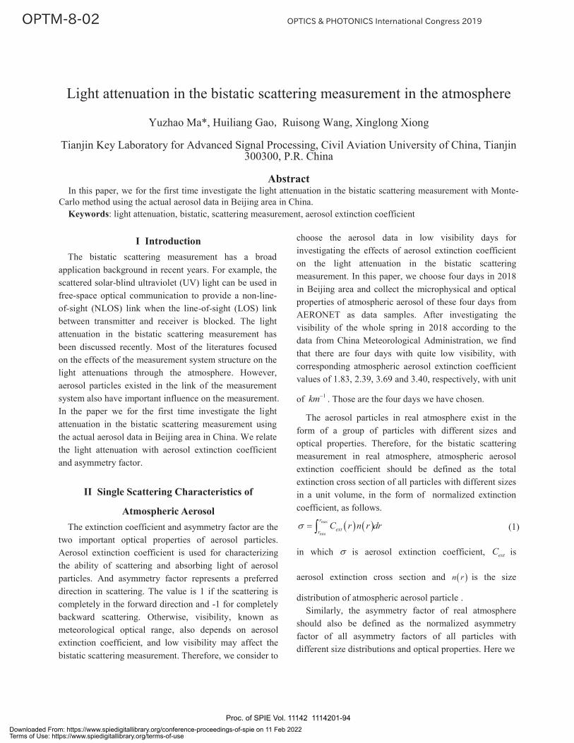
I Introduction The bistatic scattering measurement has a broad
application background in recent years. For example, the scattered solar-blind ultraviolet (UV) light can be used in free-space optical communication to provide a non-line-of-sight (NLOS) link when the line-of-sight (LOS) link between transmitter and receiver is blocked. The light attenuation in the bistatic scattering measurement has been discussed recently. Most of the literatures focused on the effects of the measurement system structure on the light attenuations through the atmosphere. However, aerosol particles existed in the link of the measurement system also have important influence on the measurement. In the paper we for the first time investigate the light attenuation in the bistatic scattering measurement using the actual aerosol data in Beijing area in China. We relate the light attenuation with aerosol extinction coefficient and asymmetry factor.
II Single Scattering Characteristics of
Atmospheric Aerosol The extinction coefficient and asymmetry factor are the
two important optical properties of aerosol particles. Aerosol extinction coefficient is used for characterizing the ability of scattering and absorbing light of aerosol particles. And asymmetry factor represents a preferred direction in scattering. The value is 1 if the scattering is completely in the forward direction and -1 for completely backward scattering. Otherwise, visibility, known as meteorological optical range, also depends on aerosol extinction coefficient, and low visibility may affect the bistatic scattering measurement. Therefore, we consider to
choose the aerosol data in low visibility days for investigating the effects of aerosol extinction coefficient on the light attenuation in the bistatic scattering measurement. In this paper, we choose four days in 2018 in Beijing area and collect the microphysical and optical properties of atmospheric aerosol of these four days from AERONET as data samples. After investigating the visibility of the whole spring in 2018 according to the data from China Meteorological Administration, we find that there are four days with quite low visibility, with corresponding atmospheric aerosol extinction coefficient values of 1.83, 2.39, 3.69 and 3.40, respectively, with unit
of 1km . Those are the four days we have chosen.
The aerosol particles in real atmosphere exist in the form of a group of particles with different sizes and optical properties. Therefore, for the bistatic scattering measurement in real atmosphere, atmospheric aerosol extinction coefficient should be defined as the total extinction cross section of all particles with different sizes in a unit volume, in the form of normalized extinction coefficient, as follows.
max
min
r
extrC r n r dr (1)
in which is aerosol extinction coefficient, extC is
aerosol extinction cross section and n r is the size
distribution of atmospheric aerosol particle . Similarly, the asymmetry factor of real atmosphere
should also be defined as the normalized asymmetry factor of all asymmetry factors of all particles with different size distributions and optical properties. Here we
Light attenuation in the bistatic scattering measurement in the atmosphere
Yuzhao Ma*, Huiliang Gao Ruisong Wang, Xinglong Xiong
Tianjin Key Laboratory for Advanced Signal Processing, Civil Aviation University of China, Tianjin 300300, P.R. China
Abstract
In this paper, we for the first time investigate the light attenuation in the bistatic scattering measurement with Monte-Carlo method using the actual aerosol data in Beijing area in China.
Keywords: light attenuation, bistatic, scattering measurement, aerosol extinction coefficient
Proc. of SPIE Vol. 11142 1114201-94Downloaded From: https://www.spiedigitallibrary.org/conference-proceedings-of-spie on 11 Feb 2022Terms of Use: https://www.spiedigitallibrary.org/terms-of-use
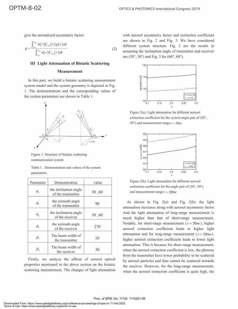
give the normalized asymmetry factor:
max
min
max
min
r
extrr
extr
n r C r g r drg
n r C r dr (2)
III Light Attenuation of Bistatic Scattering
Measurement
In this part, we build a bistatic scattering measurement system model and the system geometry is depicted in Fig. 1. The demonstrations and the corresponding values of the system parameters are shown in Table 1.
Figure 1. Structure of bistatic scattering communication system
Table 1. Demonstration and values of the system parameters.
Parameter Demonstration value
T the inclination angle of the transmitter 30 ,6060
T the azimuth angle of the transmitter 90
R the inclination angle of the receiver 30 ,6060
R the azimuth angle of the receiver 270
T The beam width of the transmitter 10
R The beam width of the receiver 30
Firstly, we analyze the effects of aerosol optical properties mentioned in the above section on the bistatic scattering measurement. The changes of light attenuation
with aerosol asymmetry factor and extinction coefficient are shown in Fig. 2 and Fig. 3. We have considered different system structure. Fig. 2 are the results in assuming the inclination angle of transmitter and receiver are (30°, 30°) and Fig. 3 for (60°, 60°).
Figure 2(a). Light attenuation for different aerosol extinction coefficient for the system angle pair of (30°, 30°) and measurement range 50r m
Figure 2(b). Light attenuation for different aerosol extinction coefficient for the angle pair of (30°, 30°) and measurement range 200r m
As shown in Fig. 2(a) and Fig. 2(b), the light attenuation increases along with aerosol asymmetry factor. And the light attenuation of long-range measurement is much higher than that of short-range measurement. Notably, for short-range measurement ( 50r m ), higher aerosol extinction coefficient leads to higher light attenuation and for long-range measurement ( 200r m ), higher aerosol extinction coefficient leads to lower light attenuation. This is because for short-range measurement, when the aerosol extinction coefficient is low, the photons from the transmitter have lower probability to be scattered by aerosol particles and thus cannot be scattered towards the receiver. However, for the long-range measurement, when the aerosol extinction coefficient is quite high, the
Proc. of SPIE Vol. 11142 1114201-95Downloaded From: https://www.spiedigitallibrary.org/conference-proceedings-of-spie on 11 Feb 2022Terms of Use: https://www.spiedigitallibrary.org/terms-of-use

photons from the transmitter may be scattered too much by aerosol particles and then be scattered away from the receiver.
In Fig. 3(a) and Fig. 3(b), we analyze the condition of another pair of the inclination angle of transmitter and receiver. In this condition, we can also obtain the conclusion proposed above. Specially, comparing Fig. 3 with Fig. 2, we find that when the inclination angles of transmitter and receiver are larger, the light attenuation of the bistatic scattering measurement system becomes lower.
Figure 3(a). Light attenuation for different aerosol extinction coefficient for the angle pair of (60°, 60°) and measurement
range 50r m
Figure 3(b). Light attenuation for different aerosol extinction coefficient for the angle pair of (60°, 60°) and measurement range 200r m
Then we investigate the light attenuation of the system for the given four days we have chosen. As shown in Fig. 4(a) and Fig. 4(b), the light attenuation of the system increases along with the measurement range. Similarly with the conclusion we obtained above, when the measurement range is shorter than 150 m , the higher aerosol extinction coefficient leads to lower light attenuation and for the measurement range longer than 150 m , the higher aerosol extinction coefficient leads to higher light attenuation.
Figure 2(a). Light attenuation for the given four days for the angle pair of (30°, 30°)
Figure 2(b). Light attenuation for the given four days for the angle pair of (60°, 60°)
In conclusion, in the bistatic scattering measurement system, an increase of atmospheric asymmetry factor and measurement range strengthens the light attenuation. And specially, for short-range measurement, higher aerosol extinction coefficient can reduce the light attenuation and for long-range measurement, the light attenuation will definitely increase with aerosol extinction coefficient.
References Ding, H., Chen, G., Majumdar, A. K., Sadler, B. M. and
Xu, Z. Y. 2009. Modeling of non-line-of-sight ultraviolet scattering channels for communication. IEEE Journal on Selected Areas in Communications 27(9):1535-1544.
Drost, R. J., Moore, T. J. and Sadler, B. M. 2011. UV communications channel modeling incorporating multiple scattering interactions. Journal of the Optical Society of America Optics Image Science 28(4):686.
Xu, C., Zhang, H. and Cheng, J. 2015. Effects of haze particles and fog droplets on NLOS ultraviolet communication channels. Optics Express 23(18): 23259-23269.
Proc. of SPIE Vol. 11142 1114201-96Downloaded From: https://www.spiedigitallibrary.org/conference-proceedings-of-spie on 11 Feb 2022Terms of Use: https://www.spiedigitallibrary.org/terms-of-use
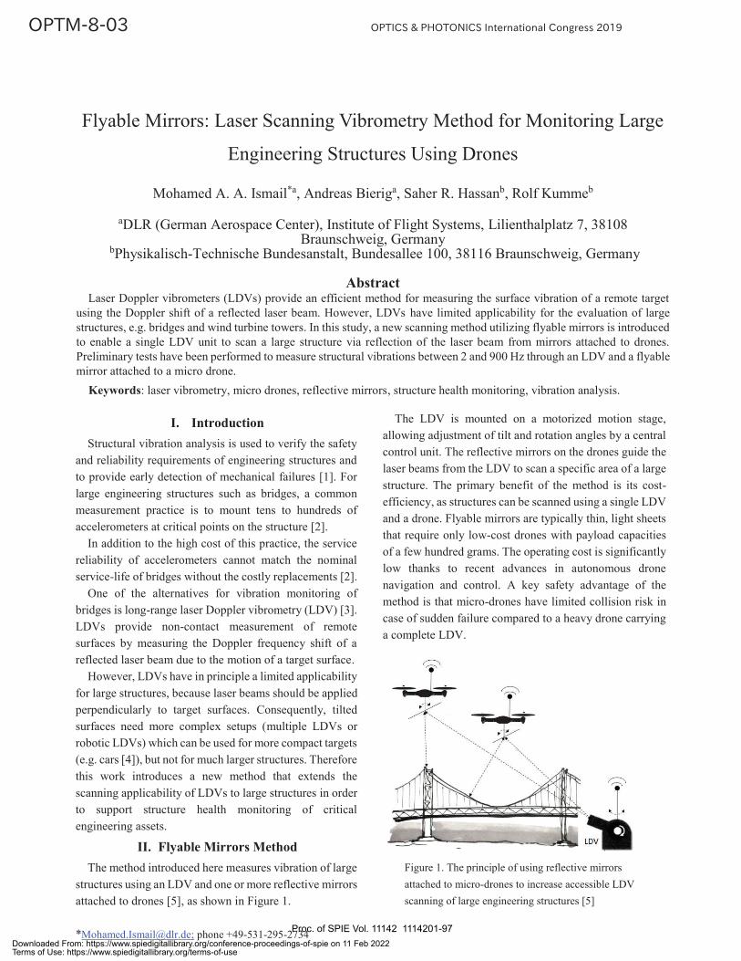
I. Introduction Structural vibration analysis is used to verify the safety
and reliability requirements of engineering structures and to provide early detection of mechanical failures [1]. For large engineering structures such as bridges, a common measurement practice is to mount tens to hundreds of accelerometers at critical points on the structure [2].
In addition to the high cost of this practice, the service reliability of accelerometers cannot match the nominal service-life of bridges without the costly replacements [2].
One of the alternatives for vibration monitoring of bridges is long-range laser Doppler vibrometry (LDV) [3]. LDVs provide non-contact measurement of remote surfaces by measuring the Doppler frequency shift of a reflected laser beam due to the motion of a target surface.
However, LDVs have in principle a limited applicability for large structures, because laser beams should be applied perpendicularly to target surfaces. Consequently, tilted surfaces need more complex setups (multiple LDVs or robotic LDVs) which can be used for more compact targets (e.g. cars [4]), but not for much larger structures. Therefore this work introduces a new method that extends the scanning applicability of LDVs to large structures in order to support structure health monitoring of critical engineering assets.
II. Flyable Mirrors Method The method introduced here measures vibration of large
structures using an LDV and one or more reflective mirrors attached to drones [5], as shown in Figure 1.
*[email protected]; phone +49-531-295-2734
The LDV is mounted on a motorized motion stage, allowing adjustment of tilt and rotation angles by a central control unit. The reflective mirrors on the drones guide the laser beams from the LDV to scan a specific area of a large structure. The primary benefit of the method is its cost-efficiency, as structures can be scanned using a single LDV and a drone. Flyable mirrors are typically thin, light sheets that require only low-cost drones with payload capacities of a few hundred grams. The operating cost is significantly low thanks to recent advances in autonomous drone navigation and control. A key safety advantage of the method is that micro-drones have limited collision risk in case of sudden failure compared to a heavy drone carrying a complete LDV.
Figure 1. The principle of using reflective mirrors attached to micro-drones to increase accessible LDV scanning of large engineering structures [5]
Flyable Mirrors: Laser Scanning Vibrometry Method for Monitoring Large
Engineering Structures Using Drones
Mohamed A. A. Ismail*a, Andreas Bieriga, Saher R. Hassanb, Rolf Kummeb
aDLR (German Aerospace Center), Institute of Flight Systems, Lilienthalplatz 7, 38108
Braunschweig, Germany bPhysikalisch-Technische Bundesanstalt, Bundesallee 100, 38116 Braunschweig, Germany
Abstract
Laser Doppler vibrometers (LDVs) provide an efficient method for measuring the surface vibration of a remote target using the Doppler shift of a reflected laser beam. However, LDVs have limited applicability for the evaluation of large structures, e.g. bridges and wind turbine towers. In this study, a new scanning method utilizing flyable mirrors is introduced to enable a single LDV unit to scan a large structure via reflection of the laser beam from mirrors attached to drones. Preliminary tests have been performed to measure structural vibrations between 2 and 900 Hz through an LDV and a flyable mirror attached to a micro drone.
Keywords: laser vibrometry, micro drones, reflective mirrors, structure health monitoring, vibration analysis.
Proc. of SPIE Vol. 11142 1114201-97Downloaded From: https://www.spiedigitallibrary.org/conference-proceedings-of-spie on 11 Feb 2022Terms of Use: https://www.spiedigitallibrary.org/terms-of-use
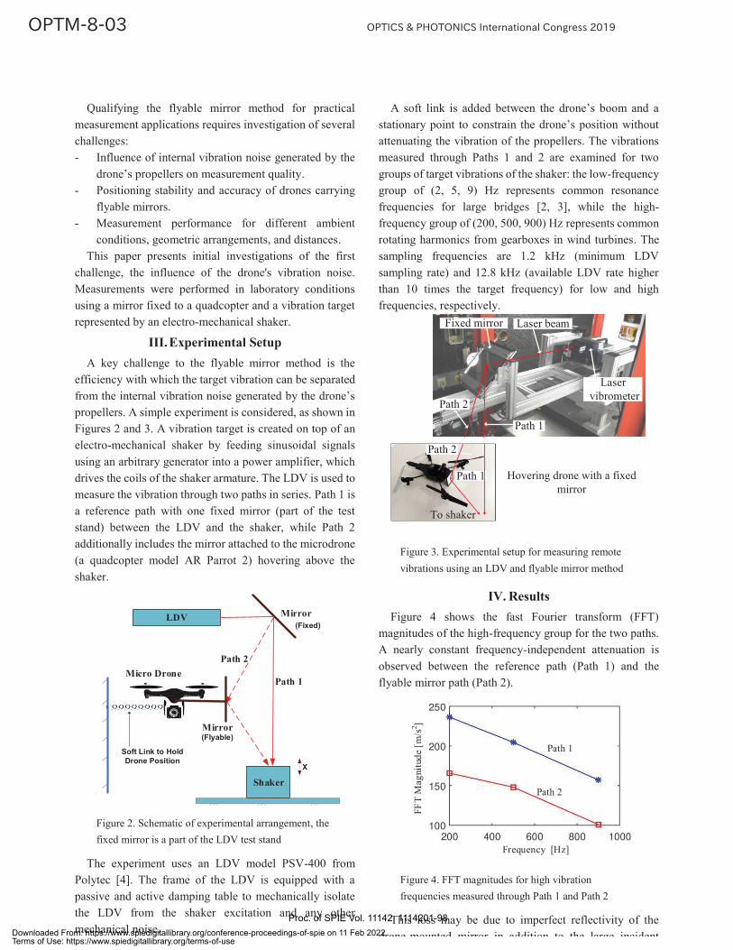
Qualifying the flyable mirror method for practical measurement applications requires investigation of several challenges: - Influence of internal vibration noise generated by the
drone’s propellers on measurement quality. - Positioning stability and accuracy of drones carrying
flyable mirrors. - Measurement performance for different ambient
conditions, geometric arrangements, and distances. This paper presents initial investigations of the first
challenge, the influence of the drone's vibration noise. Measurements were performed in laboratory conditions using a mirror fixed to a quadcopter and a vibration target represented by an electro-mechanical shaker.
III. Experimental Setup A key challenge to the flyable mirror method is the
efficiency with which the target vibration can be separated from the internal vibration noise generated by the drone’s propellers. A simple experiment is considered, as shown in Figures 2 and 3. A vibration target is created on top of an electro-mechanical shaker by feeding sinusoidal signals using an arbitrary generator into a power amplifier, which drives the coils of the shaker armature. The LDV is used to measure the vibration through two paths in series. Path 1 is a reference path with one fixed mirror (part of the test stand) between the LDV and the shaker, while Path 2 additionally includes the mirror attached to the microdrone (a quadcopter model AR Parrot 2) hovering above the shaker.
LDV Mirror
Path 1Micro Drone
Shaker
Path 2
Mirror
Soft Link to Hold Drone Position
X
(Fixed)
(Flyable)
Figure 2. Schematic of experimental arrangement, the fixed mirror is a part of the LDV test stand
The experiment uses an LDV model PSV-400 from Polytec [4]. The frame of the LDV is equipped with a passive and active damping table to mechanically isolate the LDV from the shaker excitation and any other mechanical noise.
A soft link is added between the drone’s boom and a stationary point to constrain the drone’s position without attenuating the vibration of the propellers. The vibrations measured through Paths 1 and 2 are examined for two groups of target vibrations of the shaker: the low-frequency group of (2, 5, 9) Hz represents common resonance frequencies for large bridges [2, 3], while the high-frequency group of (200, 500, 900) Hz represents common rotating harmonics from gearboxes in wind turbines. The sampling frequencies are 1.2 kHz (minimum LDV sampling rate) and 12.8 kHz (available LDV rate higher than 10 times the target frequency) for low and high frequencies, respectively.
Figure 3. Experimental setup for measuring remote vibrations using an LDV and flyable mirror method
IV. Results Figure 4 shows the fast Fourier transform (FFT)
magnitudes of the high-frequency group for the two paths. A nearly constant frequency-independent attenuation is observed between the reference path (Path 1) and the flyable mirror path (Path 2).
Frequency [Hz]
FFT
Mag
nitu
de [m
/s2 ]
Path 1
Path 2
Figure 4. FFT magnitudes for high vibration frequencies measured through Path 1 and Path 2
This loss may be due to imperfect reflectivity of the drone mounted mirror in addition to the large incident
Fixed mirror
Laser vibrometer
Path 1
Laser beam
Path 2
Hovering drone with a fixed mirror
Path 2
Path 1
To shaker
Proc. of SPIE Vol. 11142 1114201-98Downloaded From: https://www.spiedigitallibrary.org/conference-proceedings-of-spie on 11 Feb 2022Terms of Use: https://www.spiedigitallibrary.org/terms-of-use
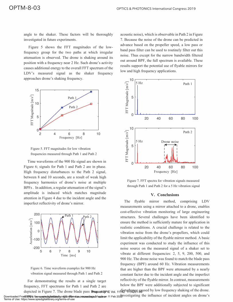
angle to the shaker. These factors will be thoroughly investigated in future experiments.
Figure 5 shows the FFT magnitudes of the low-frequency group for the two paths at which irregular attenuation is observed. The drone is shaking around its position with a frequency near 2 Hz. Such drone’s activity causes additional energy to the overall FFT spectrum of the LDV’s measured signal as the shaker frequency approaches drone’s shaking frequency.
Frequency [Hz]
FFT
Mag
nitu
de [m
/s2 ]
Path 1
Path 2
Figure 5. FFT magnitudes for low vibration frequencies measured through Path 1 and Path 2
Time waveforms of the 900 Hz signal are shown in Figure 6; signals for Path 1 and Path 2 are in phase. High frequency disturbances to the Path 2 signal, between 8 and 10 seconds, are a result of weak high frequency harmonics of drone’s noise at multiple BPFs . In addition, a regular attenuation of the signal’s amplitude is induced which matches magnitude attention in Figure 4 due to the incident angle and the imperfect reflectivity of drone’s mirror.
Time [ms]
Path 1 Path 2
Acc
eler
atio
n [m
/s2 ]
Figure 6. Time waveform examples for 900 Hz vibration signal measured through Path 1 and Path 2
For demonstrating the results at a single target frequency, FFT spectrums for Path 1 and Path 2 are depicted in Figure 7. The drone blade pass frequency (BPF) is approximately 60 Hz (as measured using
acoustic noise), which is observable in Path 2 in Figure 7. Because the noise of the drone can be predicted in advance based on the propeller speed, a low pass or band pass filter can be used to routinely filter out this noise. Thus except for the narrow bandwidth filtered out around BPF, the full spectrum is available. These results support the potential use of flyable mirrors for low and high frequency applications.
5 Hz Path 1
Path 2
5 Hz Drone noise
FFT
Mag
nitu
de [m
/s2 ]
Frequency [Hz]
FFT
Mag
nitu
de [m
/s2 ]
Figure 7. FFT spectra for vibration signals measured through Path 1 and Path 2 for a 5 Hz vibration signal
V. Conclusions The flyable mirror method, comprising LDV
measurements using a mirror attached to a drone, enables cost-effective vibration monitoring of large engineering structures. Several challenges have been identified to ensure the method is sufficiently mature for application in realistic conditions. A crucial challenge is related to the vibration noise from the drone’s propellers, which could limit the applicability of the flyable mirror method. A basic experiment was conducted to study the influence of this noise source on the measured signal of a shaker set to vibrate at different frequencies: 2, 5, 9, 200, 500, and 900 Hz. The drone noise was found to match the blade pass frequency (BPF) around 60 Hz. Vibration measurements that are higher than the BPF were attenuated by a nearly constant factor due to the incident angle and the imperfect reflectivity of the flyable mirror. In contrast, measurements below the BPF were additionally subjected to significant disturbance caused by low frequency shaking of the drone. Investigating the influence of incident angles on drone’s
Proc. of SPIE Vol. 11142 1114201-99Downloaded From: https://www.spiedigitallibrary.org/conference-proceedings-of-spie on 11 Feb 2022Terms of Use: https://www.spiedigitallibrary.org/terms-of-use

mirror and broadening the frequency range of structural vibrations are planned for future work.
References [1] Fritzen C. P., "Vibration-based structural health monitoring–concepts and applications," Key Engineering Materials. Trans Tech Publications. 293, 3-20 (2005). [2] Inaudi, D., " Overview of 40 bridge structural health monitoring projects," Proc. International Bridge Conference IBC, 09-45 (2010). [3] Miyashita, T., and Nagai, M., "Vibration-based structural health monitoring for bridges using laser Doppler vibrometers and MEMS-based technologies," Int. J. Steel Struct, 8(4), 325-331. (2008). [4] Polytec GmbH, N., “RoboVib – structural test station for automated experimental modal testing,” <https://www.polytec.com/eu/vibrometry/products/full-field-vibrometers/robovib/> (15 December 2018). [5] Ismail, M. A. A., “DE102018113244: Verfahren und Vorrichtung zum Messen von Schwingungen eines Objekts unter Verwendung einer Drohne,” German Patent Pending Application (2018).
Proc. of SPIE Vol. 11142 1114201-100Downloaded From: https://www.spiedigitallibrary.org/conference-proceedings-of-spie on 11 Feb 2022Terms of Use: https://www.spiedigitallibrary.org/terms-of-use
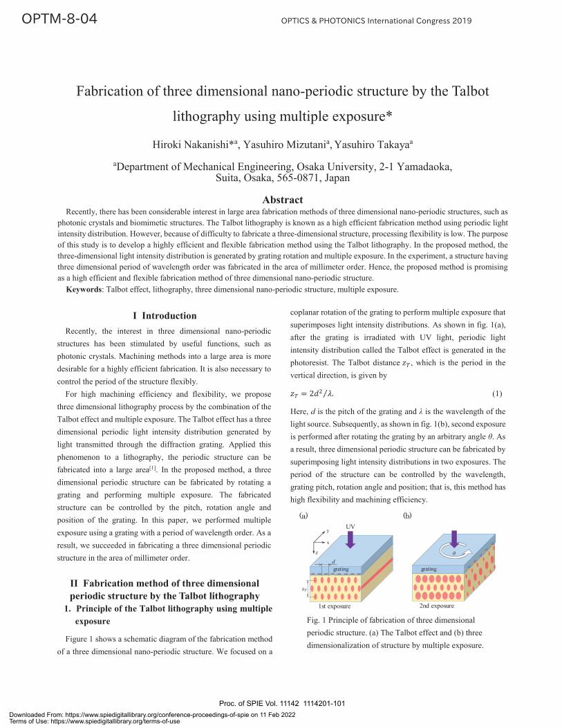
I Introduction Recently, the interest in three dimensional nano-periodic
structures has been stimulated by useful functions, such as photonic crystals. Machining methods into a large area is more desirable for a highly efficient fabrication. It is also necessary to control the period of the structure flexibly.
For high machining efficiency and flexibility, we propose three dimensional lithography process by the combination of the Talbot effect and multiple exposure. The Talbot effect has a three dimensional periodic light intensity distribution generated by light transmitted through the diffraction grating. Applied this phenomenon to a lithography, the periodic structure can be fabricated into a large area[1]. In the proposed method, a three dimensional periodic structure can be fabricated by rotating a grating and performing multiple exposure. The fabricated structure can be controlled by the pitch, rotation angle and position of the grating. In this paper, we performed multiple exposure using a grating with a period of wavelength order. As a result, we succeeded in fabricating a three dimensional periodic structure in the area of millimeter order.
II Fabrication method of three dimensional periodic structure by the Talbot lithography
1. Principle of the Talbot lithography using multiple exposure
Figure 1 shows a schematic diagram of the fabrication method of a three dimensional nano-periodic structure. We focused on a
coplanar rotation of the grating to perform multiple exposure that superimposes light intensity distributions. As shown in fig. 1(a), after the grating is irradiated with UV light, periodic light intensity distribution called the Talbot effect is generated in the photoresist. The Talbot distance , which is the period in the vertical direction, is given by = 2 ⁄ . (1)
Here, d is the pitch of the grating and λ is the wavelength of the light source. Subsequently, as shown in fig. 1(b), second exposure is performed after rotating the grating by an arbitrary angle θ. As a result, three dimensional periodic structure can be fabricated by superimposing light intensity distributions in two exposures. The period of the structure can be controlled by the wavelength, grating pitch, rotation angle and position; that is, this method has high flexibility and machining efficiency.
(a) (b)
Fig. 1 Principle of fabrication of three dimensional periodic structure. (a) The Talbot effect and (b) three dimensionalization of structure by multiple exposure.
UV
grating grating
1st exposure 2nd exposure
dθz
x
y
Fabrication of three dimensional nano-periodic structure by the Talbot
lithography using multiple exposure*
Hiroki Nakanishi*a, Yasuhiro Mizutania, Yasuhiro Takayaa
aDepartment of Mechanical Engineering, Osaka University, 2-1 Yamadaoka, Suita, Osaka, 565-0871, Japan
Abstract
Recently, there has been considerable interest in large area fabrication methods of three dimensional nano-periodic structures, such as photonic crystals and biomimetic structures. The Talbot lithography is known as a high efficient fabrication method using periodic light intensity distribution. However, because of difficulty to fabricate a three-dimensional structure, processing flexibility is low. The purpose of this study is to develop a highly efficient and flexible fabrication method using the Talbot lithography. In the proposed method, the three-dimensional light intensity distribution is generated by grating rotation and multiple exposure. In the experiment, a structure having three dimensional period of wavelength order was fabricated in the area of millimeter order. Hence, the proposed method is promising as a high efficient and flexible fabrication method of three dimensional nano-periodic structure.
Keywords: Talbot effect, lithography, three dimensional nano-periodic structure, multiple exposure.
Proc. of SPIE Vol. 11142 1114201-101Downloaded From: https://www.spiedigitallibrary.org/conference-proceedings-of-spie on 11 Feb 2022Terms of Use: https://www.spiedigitallibrary.org/terms-of-use
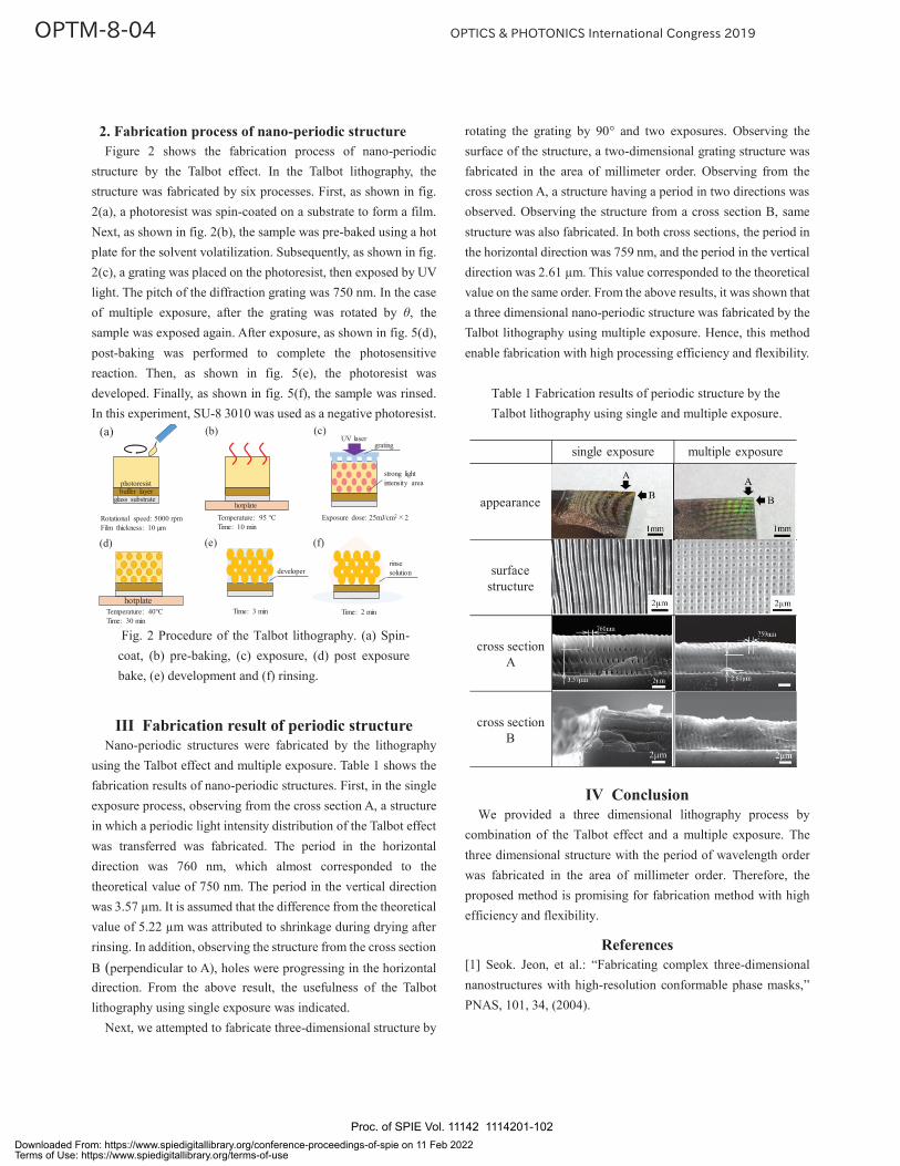
2. Fabrication process of nano-periodic structure Figure 2 shows the fabrication process of nano-periodic structure by the Talbot effect. In the Talbot lithography, the structure was fabricated by six processes. First, as shown in fig. 2(a), a photoresist was spin-coated on a substrate to form a film. Next, as shown in fig. 2(b), the sample was pre-baked using a hot plate for the solvent volatilization. Subsequently, as shown in fig. 2(c), a grating was placed on the photoresist, then exposed by UV light. The pitch of the diffraction grating was 750 nm. In the case of multiple exposure, after the grating was rotated by θ, the sample was exposed again. After exposure, as shown in fig. 5(d), post-baking was performed to complete the photosensitive reaction. Then, as shown in fig. 5(e), the photoresist was developed. Finally, as shown in fig. 5(f), the sample was rinsed. In this experiment, SU-8 3010 was used as a negative photoresist.
Fig. 2 Procedure of the Talbot lithography. (a) Spin-coat, (b) pre-baking, (c) exposure, (d) post exposure bake, (e) development and (f) rinsing.
III Fabrication result of periodic structure
Nano-periodic structures were fabricated by the lithography using the Talbot effect and multiple exposure. Table 1 shows the fabrication results of nano-periodic structures. First, in the single exposure process, observing from the cross section A, a structure in which a periodic light intensity distribution of the Talbot effect was transferred was fabricated. The period in the horizontal direction was 760 nm, which almost corresponded to the theoretical value of 750 nm. The period in the vertical direction was 3.57 μm. It is assumed that the difference from the theoretical value of 5.22 μm was attributed to shrinkage during drying after rinsing. In addition, observing the structure from the cross section B (perpendicular to A), holes were progressing in the horizontal direction. From the above result, the usefulness of the Talbot lithography using single exposure was indicated. Next, we attempted to fabricate three-dimensional structure by
rotating the grating by 90° and two exposures. Observing the surface of the structure, a two-dimensional grating structure was fabricated in the area of millimeter order. Observing from the cross section A, a structure having a period in two directions was observed. Observing the structure from a cross section B, same structure was also fabricated. In both cross sections, the period in the horizontal direction was 759 nm, and the period in the vertical direction was 2.61 μm. This value corresponded to the theoretical value on the same order. From the above results, it was shown that a three dimensional nano-periodic structure was fabricated by the Talbot lithography using multiple exposure. Hence, this method enable fabrication with high processing efficiency and flexibility.
Table 1 Fabrication results of periodic structure by the Talbot lithography using single and multiple exposure.
IV Conclusion We provided a three dimensional lithography process by
combination of the Talbot effect and a multiple exposure. The three dimensional structure with the period of wavelength order was fabricated in the area of millimeter order. Therefore, the proposed method is promising for fabrication method with high efficiency and flexibility.
References [1] Seok. Jeon, et al.: “Fabricating complex three-dimensional nanostructures with high-resolution conformable phase masks,” PNAS, 101, 34, (2004).
glass substratebuffer layerphotoresist
hotplate
UV laser
hotplate
(a) (b) (c)
(d) (e) (f)
grating
strong light intensity area
developerrinsesolution
Rotational speed: 5000 rpmFilm thickness: 10 μm
Temperature: 95 ℃Time: 10 min
Exposure dose: 25mJ/cm2 2
Temperature: 40℃Time: 30 min
Time: 3 min Time: 2 min
single exposure multiple exposure
appearance
surface structure
cross section A
cross section B
Proc. of SPIE Vol. 11142 1114201-102Downloaded From: https://www.spiedigitallibrary.org/conference-proceedings-of-spie on 11 Feb 2022Terms of Use: https://www.spiedigitallibrary.org/terms-of-use

I Introduction For manufacturing fine devices and next-generation
functional parts, there is a demand for fabrication technology of three-dimensional microstructure. For example, in order to create metamaterial expected to be applied to optical camouflage and super lens, it is necessary to construct an artificial dielectric with a metal structure of several tens of nanometers. So far several microstructural fabrication methods using focused beams such as two-photon reduction method [1] and focused ion beam [2] have been studied. However, it is difficult to process three-dimensional microstructures in range smaller than 100 nm by conventional methods. In addition, majority of conventional micro fabrication techniques using focused beam has to be conducted in liquid phase, which leads to a problem that the structures can be destroyed of deformed by
Figure.1 Confinement based on optical trapping potential
*[email protected]; phone +81-3-5452-5183
the surface tension of liquid when getting the structures out of liquid.
In this research, we propose an additive method by localizing nanoparticles based on optical trapping potential in air condition[3]. In this report, we aim to improve the optical trapping efficiency to gather the nanoparticles into focal spot by utilizing the radial polarization. The component in the direction of the optical axis of the electric field near the focal spot becomes remarkably strong[4], which is important in processing speed of the proposed three-dimensional fabrication method . II Concept of laser additive processing based on
optical trapping potential When nanoparticles are exposed to a focused beam, an optical
trapping potential would be evoked. The range of nanoparticles’ Brownian motion would be limited, and the position of nanoparticles would be confined into the central area of the optical trapping potential as shown in Fig.1. We propose the following processing method utilizing this phenomenon.
As shown in Fig.2, a volatile solvent airborne droplet containing nanoparticles is supplied near the focused beam, and the airborne droplet is localized at the valley position of the optical trapping potential by the focused beam. During or after the airborne droplet being confined by the optical trapping potential of the focused beam, the volatile solvent would
Optical Trapping of Airborne Droplet for Laser Fabrication of 3-Dimensional
Structure based on Optical Potential using Radially Polarized Beam
Makoto YOKEIa*, Masahiro HAYASHIa, Masaki MICHIHATAb, Kiyoshi TAKAMASUb
and Satoru TAKAHASHIb
aThe University of Tokyo, Department of Precision Engineering 7-3-1 Bunkyo-ku, Tokyo, 113-8654, Japan
bThe University of Tokyo, Research Center for Advanced Science and Technology, 4-6-1 Meguro-ku, Tokyo, 153-8904, Japan
Abstract
Processing technology for manufacturing fine devices and next-generation functional parts are required. In this study, by focusing on the optical trapping potential due to the electric field intensity gradient, we aimed to process three-dimensional microstructures in a range smaller than 100 nm by localizing and three-dimensionally accumulating nanoparticles without being limited by the diffraction limit. In this paper, we aim to improve the optical trapping efficiency which is important in processing speed of three-dimensional microstructure by utilizing the fact that the component in the direction of the optical axis of the electric field becomes remarkably strong near the focal point of the radially polarized focused beam.
Keywords: Additive manufacturing, Brownian motion, Nanostructures, Optical trapping, radially polarized beam
Proc. of SPIE Vol. 11142 1114201-103Downloaded From: https://www.spiedigitallibrary.org/conference-proceedings-of-spie on 11 Feb 2022Terms of Use: https://www.spiedigitallibrary.org/terms-of-use

vaporize so that only the nanoparticles would be left in the location where the airborne droplet was confined. By relatively three-dimensionally scanning the substrate and the focused beam, nanoparticles are localized at desired positions one after another, and the particles are adhered to each other by surface force such as atomic force, and finally the three-dimensional structure could be additively fabricated.
Conventionally, several energy threshold based processing techniques were proposed, which are difficult to maintain the processing energy. We proposed to use optical trapping potential, on which processing resolution is expected to easy to control although potential of Brownian motion was to be considered. By doing so, it is expected to process microstructures with as narrow as sub 100 nm structures. Moreover, since this method is not premised on processing in solution and can be processed directly in air condition, we can avoid the problem of destruction of the processed object during solution drying due to the above solution surface tension.
Figure.2 Conceptual diagram of proposed method
Airborne droplet particles trapping
experiment using radially polarized beam In order to realize three-dimensional structuring of fine
particles by the proposed method, we conduct basic experiment to verify improvement of optical trapping efficiency using radially polarized beam. In the radially polarized beam, the polarization direction is radially distributed in the cross section of the beam and the component in the direction of the optical axis of the electric field becomes remarkably strong near the focal point of the focused beam. By using this, the improvement of the optical trapping efficiency can be expected.
In this experiment, optical trapping of airborne droplet particles in air condition using a linearly polarized beam and a radially polarized beam was performed. We qualitatively examined the optical trapping efficiency improvement by radially polarized beam.
1. Experimental Setup An experimental setup for a basic experiment using a radially
polarized beam was designed and constructed as shown in Fig.3. A fiber laser (continuous wave, linearly polarized) with a wavelength of 1064 nm and a maximum output of 20 W is used as the light source. In this experiment, a radially polarized beam is generated by using a radial polarization converter. That is composed of a twisted nematic liquid crystal uniformly wrapped in an annular shape and can convert the linearly polarized beam into a beam that has a continuous radial polarization distribution. Fig.3 shows the generated radially polarized beam.
For the sample, water airborne droplet in a diameter of about 10μm were used. Also, in order to trap airborne droplet, a chamber was used to accommodate the airborne droplet particles in a fixed place.
Figure.3 Schematic diagram of the experimental setup
2. Optical trapping of airborne droplet in air condition To test the functionality of the experimental setup, optical trapping airborne droplet in air condition using linearly polarized beam was performed as shown in Fig.4(a). Fig.4(a) shows the trapped airborne droplet observed from the side observation system. The power of the laser near the focal point is about 0.5 W. The light that can be observed is the scattered light of the airborne droplet that is visible when the airborne droplet is irradiated on the laser. When the position of the lower objective lens is moved upward, the scattered light also shifts
Proc. of SPIE Vol. 11142 1114201-104Downloaded From: https://www.spiedigitallibrary.org/conference-proceedings-of-spie on 11 Feb 2022Terms of Use: https://www.spiedigitallibrary.org/terms-of-use
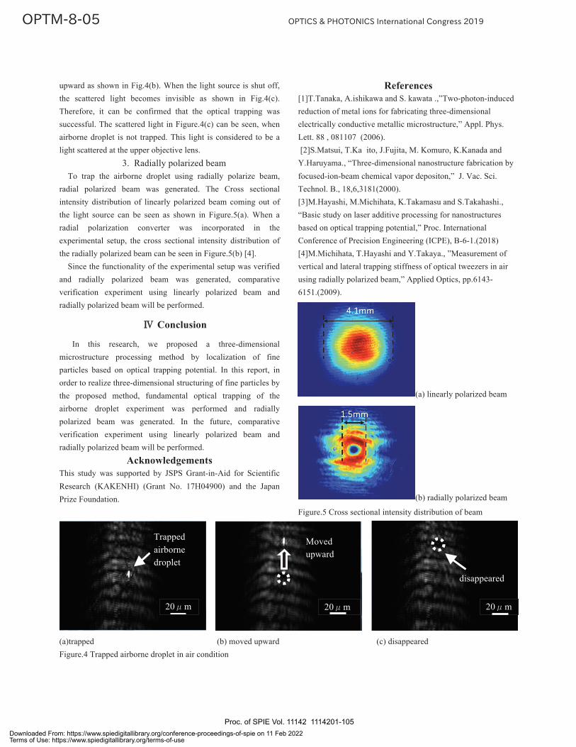
upward as shown in Fig.4(b). When the light source is shut off, the scattered light becomes invisible as shown in Fig.4(c). Therefore, it can be confirmed that the optical trapping was successful. The scattered light in Figure.4(c) can be seen, when airborne droplet is not trapped. This light is considered to be a light scattered at the upper objective lens.
3. Radially polarized beam To trap the airborne droplet using radially polarize beam,
radial polarized beam was generated. The Cross sectional intensity distribution of linearly polarized beam coming out of the light source can be seen as shown in Figure.5(a). When a radial polarization converter was incorporated in the experimental setup, the cross sectional intensity distribution of the radially polarized beam can be seen in Figure.5(b) [4].
Since the functionality of the experimental setup was verified and radially polarized beam was generated, comparative verification experiment using linearly polarized beam and radially polarized beam will be performed.
Conclusion
In this research, we proposed a three-dimensional microstructure processing method by localization of fine particles based on optical trapping potential. In this report, in order to realize three-dimensional structuring of fine particles by the proposed method, fundamental optical trapping of the airborne droplet experiment was performed and radially polarized beam was generated. In the future, comparative verification experiment using linearly polarized beam and radially polarized beam will be performed.
Acknowledgements This study was supported by JSPS Grant-in-Aid for Scientific Research (KAKENHI) (Grant No. 17H04900) and the Japan Prize Foundation.
(a)trapped (b) moved upward Figure.4 Trapped airborne droplet in air condition
References [1]T.Tanaka, A.ishikawa and S. kawata .,”Two-photon-induced reduction of metal ions for fabricating three-dimensional electrically conductive metallic microstructure,” Appl. Phys. Lett. 88 , 081107 (2006). [2]S.Matsui, T.Ka ito, J.Fujita, M. Komuro, K.Kanada and Y.Haruyama., “Three-dimensional nanostructure fabrication by focused-ion-beam chemical vapor depositon,” J. Vac. Sci. Technol. B., 18,6,3181(2000). [3]M.Hayashi, M.Michihata, K.Takamasu and S.Takahashi., “Basic study on laser additive processing for nanostructures based on optical trapping potential,” Proc. International Conference of Precision Engineering (ICPE), B-6-1.(2018) [4]M.Michihata, T.Hayashi and Y.Takaya., ”Measurement of vertical and lateral trapping stiffness of optical tweezers in air using radially polarized beam,” Applied Optics, pp.6143-6151.(2009).
(a) linearly polarized beam
(b) radially polarized beam
Figure.5 Cross sectional intensity distribution of beam (c) disappeared
Trapped airborne droplet
Moved upward
disappeared
20 m 20 m 20 m
disappeared
Proc. of SPIE Vol. 11142 1114201-105Downloaded From: https://www.spiedigitallibrary.org/conference-proceedings-of-spie on 11 Feb 2022Terms of Use: https://www.spiedigitallibrary.org/terms-of-use
*[email protected]; phone +49 (0)9131 85 20442
I Introduction Sheet bulk metal forming as a new manufacturing
process challenges optical measurement technologies. The increase in the number of small functional elements and the surface characteristics make a measurement more complex and effortful. The formed surfaces combine diffuse and direct reflecting areas. Especially optical measuring systems reach their limit with these varying surface properties [1]. In addition, lubricants like Beru-forge 152DL (BF152DL) are applied on the workpiece before the forming process. After the forming process, the expected lubricant layer thickness lies between 5 μm and 35 μm. The properties of the lubricant are a water-based basic fluidity, wax particles and a milky consistency, which makes measurement with optical measuring instruments more difficult. The paper presents a solution to measure the lubricant within the expected film thickness to evaluate the impact on the measurement result of the fringe projection system.
II Related Work Various paper already dealt with thin film measurements
with fringe projection systems. Palousek et al. [2] investi-gated the influence of matt coatings, titanium coating or chalk powder spray. They determined the measurement deviation and the variance. Mendericky et al. [3] performed
an acceptance test to evaluate the eligibility and accuracy of the fringe projection system. They therefore measured the thickness of antireflection coatings and coatings to matt the surface. Now the most common methods to measure film thicknesses are nondestructive optical methods like ellipsometric, reflectometric and interferometric measure-ments [4]. However, ellipsometry and reflectometry are only suitable for the measurement of small surfaces, as they only measure a single point at a time. A large surface leads to an increasing measurement time [5]. Interferometric 3D-profile measurements of thin layers have their preliminary application in the micro electronic industry [5, 6]. To measure film thickness on sheet bulk metal formed parts it is suitable to use the fringe projection method, as this is a fast and extensive method to measure these geometries.
III Experimental setup This chapter presents the developed fluid film thickness
standard for the optical measurement of thickness dependent thin film properties, describes the results of the focus variation measurements and finally presents the measurement setup for the fringe projection measurements.
1. Developed fluid film thickness standard The fluid film thickness standard (Figure 1) was realized
as a 30 mm x 30 mm square metal block with a height of 10 mm. To measure the film thicknesses a wedge - shape
Evaluation of influences of thin lubricant on fringe projection
measurements
Sebastian Metzner*a, Tamara Reutera, Tino Hausottea
aFriedrich-Alexander-Universität Erlangen-Nürnberg (FAU), Nägelsbachstr. 25, 91052 Erlangen, Germany
Abstract
Sheet bulk metal forming processes pose challenges for fringe projection systems, as the lubricant applied for forming could influence the measurement result. The lubricant layer has an expected film thicknesses smaller than 35 μm after the forming process. This paper presents an approach for the measurement of the lubricant layer influence on fringe projection measurements. The lubricant (Beruforge 152DL) used for the forming process and investigated in this paper has special characteristics like a water-based basic fluidity and wax particles for friction reduction as component of the liquid. A newly developed fluid film thickness standard represents the film thickness in a continuous range. This paper shows the impact on the standard deviation of the measurement results and a significant deviation of the detected surface on fluid film thickness standard with the applied lubricating film.
Keywords: fringe projection system, lubricant measurement, sheet bulk metal forming
Proc. of SPIE Vol. 11142 1114201-106Downloaded From: https://www.spiedigitallibrary.org/conference-proceedings-of-spie on 11 Feb 2022Terms of Use: https://www.spiedigitallibrary.org/terms-of-use

was milled in the middle of the standard (green). The wedge cavity covers a thickness range from 6 μm to 100 μm. The absolute heights can be determined with two planes (black) that are positioned next to the wedge and use as common reference plane. These areas have higher requirements to the surface roughness and parallelism. The principle for the measurement of thicknesses is known from DIN 32567-4:2015-06-00. Two plateaus are placed at the thin and thick end of the wedge cavity for the in- and outflow of a lubricant. The plateaus have a height of 60 μm and 5 mm. The first plateau includes a hole for the inflow, in which a medical tube with a closure is inserted, so that the lubricant can be poured in. A small drain on the thin plateau allows the extra lubricant and air to escape. Various engraved reference lines (red) ensure the repeatability of the measurements and data evaluation regarding the lateral position and orientation. An attached glass plate ensures that the lubricant does not form any bulges and thus lies within the defined thickness range. The glass is hold in place with a specially designed cover plate. This plate allows the optical measurement of the thin layers and prevents the leakage of the lubricant film from the wedge. Figure 1 shows the fluid film thickness standard with and without the cover plate.
Figure 1. CAD model of the fluid film thickness standard with and without the cover plate
The lubricant is inserted into the fluid film thickness standard with a syringe and flows through the 5 mm plateau into the wedge cavity. After the tube is closed, the liquid remains in the fluid film thickness standard as illustrated in Figure 2. It shows the fluid film thickness standard filled with the lubricant investigated in this paper BF152DL, the cover plate and the tube. In the case of optical measurements, the experimental setup only provides information about the
effects of the lubricant on the fringe projection measure-ments and not about the shape of the surface. The fringes are reflected within the semitransparent lubricant.
Figure 2. Fluid film thickness standard with cover plate filled with the lubricant BF152DL
2. Reference measurement of the empty fluid film thickness standard using focus variation method
In order to validate the wedge cavity geometry and roughness, the fluid film thickness standard was first measured with the focus variation measurement system Alicona InfiniteFocus G4. The measurement was per-formed using the 5x objective, which leads to a axial resolution specified by Alicona of approximately 332 nm and a lateral resolution of approximately 4 μm. The measuring range covers the area of the engraved reference lines as shown in Figure 3.
Figure 3. Dataset of the focus variation measurement showing the geometry of the fluid film thickness standard with engraved reference lines
Lubricant in the wedge cavity
Cover plate
Proc. of SPIE Vol. 11142 1114201-107Downloaded From: https://www.spiedigitallibrary.org/conference-proceedings-of-spie on 11 Feb 2022Terms of Use: https://www.spiedigitallibrary.org/terms-of-use

The roughness Ra on the wedge plane is 5.5 μm (cut-off wavelength 0.8 mm). Although the very smooth surface allows very accurate measurements between the reference planes and the wedge plane, the low roughness makes optical measurements more difficult. The roughness is thus a tradeoff between a high absolute accuracy and a low roughness for better detection of the surface using optical measurement systems.
3. Measurement setup with fringe projection sensors The measurement setup is part of an existing multi-
sensor setup at the Institute of Manufacturing Metrology that consists of various fringe projection sensors and a high-precision hexapod for positioning [7]. For the measurement of the standard deviation, the fringe projection system MicroCad pico 1.0 of the company LMI Technologies Inc. (formerly GFMesstechnik GmbH) was used. The measurement range of the sensor is 12.4 mm x 7.9 mm x 4.4 mm. The specified resolution is 17 μm in lateral direction and 1 μm in vertical direction. Figure 4 shows the multi-sensor measurement setup and the fluid film thickness standard placed on the hexapod of the fringe measurement system.
a) b)
Figure 4. Multi-sensor measurement setup a) and the fluid film thickness standard placed on the hexapod b).
IV Results and Discussion 1. Standard deviation of repeated measurements Repeated measurements (n = 25) are used to show the
effect on the fringe projection system with different surface properties (measurements of the fluid film thickness
standard itself and the thin lubricant). The distances of each point of the measurement to the reference planes was calculated. A direct comparison of the point cloud is not possible due to a slightly changed position of the calculated points. Therefore, the nearest neighbors of the points are calculated and the distances of the related points to the common reference plane were calculated. Figure 5 shows that the standard deviation without BF152DL in the wedge cavity is much higher than the standard deviations with the lubricant in the small thick-ness areas. This is due to a very directionally reflecting surface of the wedge. However, the standard deviations are homogeneously distributed over the entire area. The measurements with the BF152DL show an increasing standard deviation with increasing lubricant thickness. It is possible that with a higher lubricant thickness, the fringe pattern is no longer reflected on the surface. This hypo-thesis would mean that due to the initiated wax particles in the lubricant, a random reflection of the fringes lead to larger standard deviations in the measurement results.
Figure 5. Standard deviation in mm of the measurement with BF152DL and with air.
2. Comparison of absolute heights in profile This chapter describes the absolute height differences
from the reference plane to the measurement results on the
Proc. of SPIE Vol. 11142 1114201-108Downloaded From: https://www.spiedigitallibrary.org/conference-proceedings-of-spie on 11 Feb 2022Terms of Use: https://www.spiedigitallibrary.org/terms-of-use
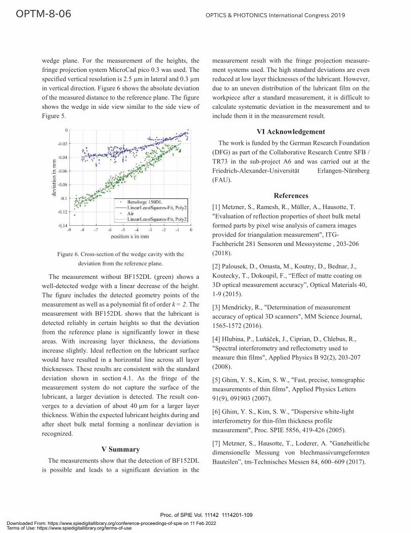
wedge plane. For the measurement of the heights, the fringe projection system MicroCad pico 0.3 was used. The specified vertical resolution is 2.5 μm in lateral and 0.3 μm in vertical direction. Figure 6 shows the absolute deviation of the measured distance to the reference plane. The figure shows the wedge in side view similar to the side view of Figure 5.
Figure 6. Cross-section of the wedge cavity with the deviation from the reference plane.
The measurement without BF152DL (green) shows a well-detected wedge with a linear decrease of the height. The figure includes the detected geometry points of the measurement as well as a polynomial fit of order k = 2. The measurement with BF152DL shows that the lubricant is detected reliably in certain heights so that the deviation from the reference plane is significantly lower in these areas. With increasing layer thickness, the deviations increase slightly. Ideal reflection on the lubricant surface would have resulted in a horizontal line across all layer thicknesses. These results are consistent with the standard deviation shown in section 4.1. As the fringe of the measurement system do not capture the surface of the lubricant, a larger deviation is detected. The result con-verges to a deviation of about 40 μm for a larger layer thickness. Within the expected lubricant heights during and after sheet bulk metal forming a nonlinear deviation is recognized.
V Summary The measurements show that the detection of BF152DL
is possible and leads to a significant deviation in the
measurement result with the fringe projection measure-ment systems used. The high standard deviations are even reduced at low layer thicknesses of the lubricant. However, due to an uneven distribution of the lubricant film on the workpiece after a standard measurement, it is difficult to calculate systematic deviation in the measurement and to include them it in the measurement result.
VI Acknowledgement The work is funded by the German Research Foundation
(DFG) as part of the Collaborative Research Centre SFB / TR73 in the sub-project A6 and was carried out at the Friedrich-Alexander-Universität Erlangen-Nürnberg (FAU).
References [1] Metzner, S., Ramesh, R., Müller, A., Hausotte, T. "Evaluation of reflection properties of sheet bulk metal formed parts by pixel wise analysis of camera images provided for triangulation measurement", ITG-Fachbericht 281 Sensoren und Messsysteme , 203-206 (2018).
[2] Palousek, D., Omasta, M., Koutny, D., Bednar, J., Koutecky, T., Dokoupil, F., “Effect of matte coating on 3D optical measurement accuracy”, Optical Materials 40, 1-9 (2015).
[3] Mendricky, R., "Determination of measurement accuracy of optical 3D scanners", MM Science Journal, 1565-1572 (2016).
[4] Hlubina, P., Luňáček, J., Ciprian, D., Chlebus, R., "Spectral interferometry and reflectometry used to measure thin films", Applied Physics B 92(2), 203-207 (2008).
[5] Ghim, Y. S., Kim, S. W., "Fast, precise, tomographic measurements of thin films", Applied Physics Letters 91(9), 091903 (2007).
[6] Ghim, Y. S., Kim, S. W., "Dispersive white-light interferometry for thin-film thickness profile measurement", Proc. SPIE 5856, 419-426 (2005).
[7] Metzner, S., Hausotte, T., Loderer, A. "Ganzheitliche dimensionelle Messung von blechmassivumgeformten Bauteilen”, tm-Technisches Messen 84, 600–609 (2017).
Proc. of SPIE Vol. 11142 1114201-109Downloaded From: https://www.spiedigitallibrary.org/conference-proceedings-of-spie on 11 Feb 2022Terms of Use: https://www.spiedigitallibrary.org/terms-of-use
I Introduction As one of the most effective ways of personal identity
verification in modern society, face recognition has important application value. Traditional 2D face recognition technology is common and mature, which can be divided into geometric features, neural network-based recognition methods, elastic model-based recognition methods and so on. Among them, face recognition method based on deep learning convolutional neural network has been greatly developed in recent years, and some deep learning network models based on a large number of face data are constructed.
3D face recognition has received wide attention due to its superiority to 2D recognition. The difference of 3D face recognition and 2D face recognition is that the data source is different. Firstly, 3D data does not change with environmental conditions such as lighting conditions, viewing angles, or makeup. Secondly, 3D data has spatial shape features, richer information than 2D image. 3D face recognition technique has become one of the research hotspots in the field of face recognition.
In this paper, we propose a 2D/3D vision based face recognition system, which combines the advantages of 2D and 3D face recognition, can recognize human faces fast and accurately against the influence from viewing angle, environment light and makeup.
II Experiment 1. 2D recognition We preprocess 494,414 image data of 10,575 people in
the CASIA-webface face database, and divide them into training set and test set to train and optimize VGG network.
Figure 1. Preprocessed face images input into neural network training
We use deep learning framework Caffe in windows10 machine with Python language, setting 16-layer network structure parameters of VGG convolutional neural network, and generates configuration file prototxt. It is trained to minimize the logistic regression loss function , and the parameters of the connection layer is optimized. Then the final caffe model of VGG is obtained.
2D and 3D Vision Based Face Recognition System
Mengyue Zhang*a, Bin Lina
aZhejiang University, Hangzhou, China
Abstract Traditional 2D face recognition algorithm is mature but easily affected by external environment such as makeup and
light. Face recognition based on 3D methods contains more information compared to 2D, and is stable under different external conditions. This paper put a lot of face data into VGG deep learning convolution neural network, and then establish 2D and 3D face databases respectively. Using Kinect v2 to obtain 2D color images and 3D point cloud information. After preprocessing of 2D images and 3D point cloud respectively, calculate the Euclidean distance by convolution neural network; Collected by weighted square sum algorithm of point cloud and those from 3D face database and calculate 3D similarity. Finally, through the weighted combination of two kinds of similarity, get the final recognition result. Combining the 2D and 3D recognition advantages, the accuracy and robustness of the system are strengthened.
Keywords: face recognition, 2D/3D fusion vision, convolutional neural network, kinect.
Proc. of SPIE Vol. 11142 1114201-110Downloaded From: https://www.spiedigitallibrary.org/conference-proceedings-of-spie on 11 Feb 2022Terms of Use: https://www.spiedigitallibrary.org/terms-of-use
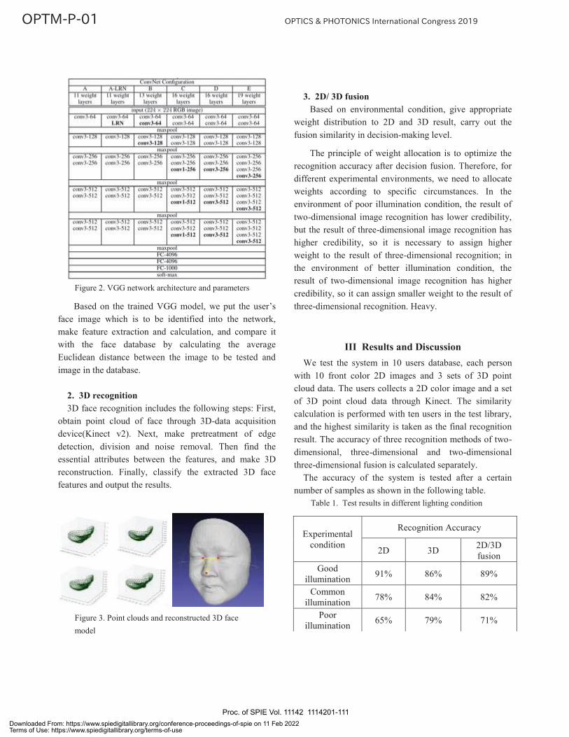
Figure 2. VGG network architecture and parameters
Based on the trained VGG model, we put the user’s face image which is to be identified into the network, make feature extraction and calculation, and compare it with the face database by calculating the average Euclidean distance between the image to be tested and image in the database.
2. 3D recognition 3D face recognition includes the following steps: First,
obtain point cloud of face through 3D-data acquisition device(Kinect v2). Next, make pretreatment of edge detection, division and noise removal. Then find the essential attributes between the features, and make 3D reconstruction. Finally, classify the extracted 3D face features and output the results.
Figure 3. Point clouds and reconstructed 3D face model
3. 2D/ 3D fusion
Based on environmental condition, give appropriate weight distribution to 2D and 3D result, carry out the fusion similarity in decision-making level.
The principle of weight allocation is to optimize the recognition accuracy after decision fusion. Therefore, for different experimental environments, we need to allocate weights according to specific circumstances. In the environment of poor illumination condition, the result of two-dimensional image recognition has lower credibility, but the result of three-dimensional image recognition has higher credibility, so it is necessary to assign higher weight to the result of three-dimensional recognition; in the environment of better illumination condition, the result of two-dimensional image recognition has higher credibility, so it can assign smaller weight to the result of three-dimensional recognition. Heavy.
III Results and Discussion We test the system in 10 users database, each person
with 10 front color 2D images and 3 sets of 3D point cloud data. The users collects a 2D color image and a set of 3D point cloud data through Kinect. The similarity calculation is performed with ten users in the test library, and the highest similarity is taken as the final recognition result. The accuracy of three recognition methods of two-dimensional, three-dimensional and two-dimensional three-dimensional fusion is calculated separately.
The accuracy of the system is tested after a certain number of samples as shown in the following table.
Table 1. Test results in different lighting condition
Experimental condition
Recognition Accuracy
2D 3D 2D/3D fusion
Good illumination 91% 86% 89%
Common illumination 78% 84% 82%
Poor illumination 65% 79% 71%
Proc. of SPIE Vol. 11142 1114201-111Downloaded From: https://www.spiedigitallibrary.org/conference-proceedings-of-spie on 11 Feb 2022Terms of Use: https://www.spiedigitallibrary.org/terms-of-use
This system use a large amount of data to train the image recognition classifier VGG convolutional neural network, and use the trained network model to classify and recognize two-dimensional color face images, combined with deep learning and artificial intelligence to efficiently and accurately measure two-dimensional faces. The idea of fusion in the decision-making layer is proposed. The two-dimensional face recognition and three-dimensional face recognition are complemented and organically combined, and the face information is fully utilized.
Due to the limitations of experimental conditions and data volume, the research in this paper is not complete enough. In order to further explore this topic, subsequent research can be carried out mainly in the following aspects:
(1) Expansion of the size of the face database: Due to the specific conditions required for 3D model
acquisition, the size of the face database established in this paper is small. Therefore, when testing the performance of the entire system, the accuracy of debugging is not high enough due to the limited sample capacity.
(2)Research on 3D point cloud matching algorithm: The 3D point cloud matching algorithm proposed in
this paper has specificity and limitations, and the acquired 3D data format is also unique. If the device that collects the 3D data changes, a new algorithm is needed for matching, and the subsequent research can be carried out in the search for the ubiquitous algorithm.
References Jia Y , Shelhamer E , Donahue J , et al. Caffe:
Convolutional Architecture for Fast Feature Embedding[J]. 2014.
Simonyan K , Zisserman A . Very Deep Convolutional Networks for Large-Scale Image Recognition[J]. Computer Science, 2014.
Paysan P, Knothe R, Amberg B, et al. A 3D Face Model for Pose and Illumination Invariant Face Recognition[C]// IEEE International Conference on Advanced Video & Signal Based Surveillance. 2009.
Xiang X, Le H A, Dou P, et al. Evaluation of a 3D-aided pose invariant 2D face recognition system[C]// IEEE
International Joint Conference on Biometrics. 2018. scenes. Transactions of the ASAE 32(2):757-763. Yi S, Wang X, Tang X. Deep Learning Face
Representation from Predicting 10,000 Classes[C]// IEEE Conference on Computer Vision & Pattern Recognition. 2014.
Zquez M A Cuevas F J. A 3D Facial Recognition System Using Structured Light Projection[C]// International Conference on Hybrid Artificial Intelligence Systems. Springer-Verlag New York Inc. 2014.
Proc. of SPIE Vol. 11142 1114201-112Downloaded From: https://www.spiedigitallibrary.org/conference-proceedings-of-spie on 11 Feb 2022Terms of Use: https://www.spiedigitallibrary.org/terms-of-use
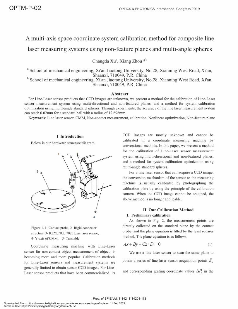
I Introduction Below is our hardware structure diagram.
Figure 1. 1- Contact probe, 2- Rigid connector structure, 3- KEYENCE 7020 Line laser sensor, 4- Y-axis of CMM, 5- Turntable
Coordinate measuring machine with Line-Laser sensor for non-contact object measurement of objects is becoming more and more popular. Calibration methods for Line-Laser sensors and measurement systems are generally limited to obtain sensor CCD images. For Line-Laser sensor products that have been commercialized, its
CCD images are mostly unknown and cannot be calibrated in a coordinate measuring machine by conventional methods. In this paper, we present a method for the calibration of Line-Laser sensor measurement system using multi-directional and non-featured planes, and a method for system calibration optimization using multi-angle standard spheres.
For a line laser sensor that can acquire a CCD image, the conversion mechanism of the sensor to the measuring machine is usually calibrated by photographing the calibration plate by using the principle of the calibration camera. When the CCD image cannot be obtained, the above method is no longer applicable.
II Our Calibration Method
1. Preliminary calibration As shown in Fig. 2, the measurement points are
directly collected on the standard plane by the contact probe, and the plane equation is fitted by the least squares method. The plane equation is as follows.
+ 0Ax By Cz D (1)
We use a line laser sensor to scan the same plane to
obtain a series of line laser sensor acquisition points nS
and corresponding grating coordinate values nP in the
A multi-axis space coordinate system calibration method for composite line
laser measuring systems using non-feature planes and multi-angle spheres
Changda Xua, Xiang Zhou *b
a School of mechanical engineering, Xi'an Jiaotong University, No.28, Xianning West Road, Xi'an, Shaanxi, 710049, P.R. China
b School of mechanical engineering, Xi'an Jiaotong University, No.28, Xianning West Road, Xi'an, Shaanxi, 710049, P.R. China
Abstract
For Line-Laser sensor products that CCD images are unknown, we present a method for the calibration of Line-Laser sensor measurement system using multi-directional and non-featured planes, and a method for system calibration optimization using multi-angle standard spheres. Through experiments, the accuracy of the line laser measurement system can reach 0.02mm for a standard ball with a radius of 12.696mm.
Keywords: Line laser sensor, CMM, Non-contact measurement, calibration, Nonlinear optimization, Non-feature plane
Proc. of SPIE Vol. 11142 1114201-113Downloaded From: https://www.spiedigitallibrary.org/conference-proceedings-of-spie on 11 Feb 2022Terms of Use: https://www.spiedigitallibrary.org/terms-of-use
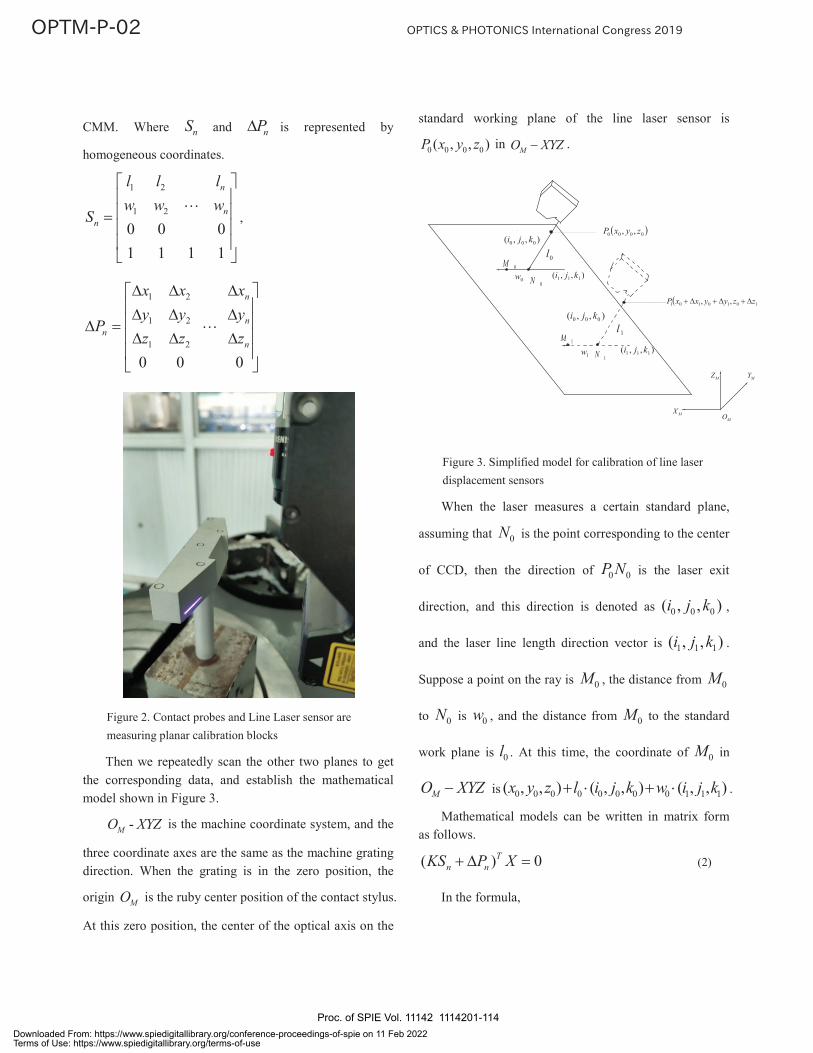
CMM. Where nS and nP is represented by
homogeneous coordinates.
1 2
1 2
0 0 01 1 1 1
n
nn
l l lw w w
S ,
1 2
1 2
1 2
0 0 0
n
nn
n
x x xy y y
Pz z z
Figure 2. Contact probes and Line Laser sensor are measuring planar calibration blocks
Then we repeatedly scan the other two planes to get the corresponding data, and establish the mathematical model shown in Figure 3.
-MO XYZ is the machine coordinate system, and the
three coordinate axes are the same as the machine grating direction. When the grating is in the zero position, the
origin MO is the ruby center position of the contact stylus.
At this zero position, the center of the optical axis on the
standard working plane of the line laser sensor is
0 0 0 0( , , )P x y z in MO XYZ .
0M0w ),,( 111 kji
0N
0l),,( 000 kji
0000 ,, zyxP
1w ),,( 111 kji
),,( 000 kji
1M
1N
1l
1010101 ,, zzyyxxP
MX
MYMZ
MO
Figure 3. Simplified model for calibration of line laser displacement sensors
When the laser measures a certain standard plane,
assuming that 0N is the point corresponding to the center
of CCD, then the direction of 0 0P N is the laser exit
direction, and this direction is denoted as 0 0 0( , , )i j k ,
and the laser line length direction vector is 1 1 1( , , )i j k .
Suppose a point on the ray is 0M , the distance from 0M
to 0N is 0w , and the distance from 0M to the standard
work plane is 0l . At this time, the coordinate of 0M in
MO XYZ is 0 0 0 0 0 0 0 0 1 1 1( , , ) ( , , ) ( , , )x y z l i j k w i j k .
Mathematical models can be written in matrix form as follows.
( ) 0Tn nKS P X (2)
In the formula,
Proc. of SPIE Vol. 11142 1114201-114Downloaded From: https://www.spiedigitallibrary.org/conference-proceedings-of-spie on 11 Feb 2022Terms of Use: https://www.spiedigitallibrary.org/terms-of-use

0 1R t
K , 0 1 2
0 1 2
0 1 2
i i iR j j j
k k k,
0
0
0
xt y
z,
1 2
1 2
0 0 01 1 1 1
n
nn
l l lw w w
S
,
1 2
1 2
1 2
0 0 0
n
nn
n
x x xy y y
Pz z z
,
AB
XCD .
Then we use the Newton iteration method to solve the equation. We select the objective function as the error distance from the measured point to the fitted plane, and optimize the value of the nonlinear optimization objective function to a minimum. Finally we can get the initial value of the calibration.
2. Optimization
Then, we bring the turntable into the overall optimization part of the system. We placed the calibrated
standard ball of radius sphereR on the turntable and
calibrated the turntable coordinate system by measuring the standard ball by the contact probe. As shown in Fig. 4, the contact probe and the line laser sensor measure the standard ball at the same angle successively, and obtain the contour data of the standard ball at the same angle. The turntable drives the standard ball to rotate, and then repeats the above measurement steps.
Finally, the equation is solved by the Levenberg-Marquardt iterative method. We select the distance from the line laser measurement point to the contact measurement sphere as the objective function, and optimize the objective function to make the distance and minimum.
Figure 4. The line laser sensor is measuring the standard ball.
III Results and Discussion Both simulation analyses and real experiments were
conducted. A Line-Laser sensor was used to measure a frosted standard ball with a radius of 12.696 mm. The radius deviation measured by the Line-Laser sensor and the deviation comparing with the center of the ball measured by the CMM were observed. The experimental results show that the radius deviation of the calibration laser sensor measurement system is less than 0.02mm, and the ball center distance deviation is less than 0.02mm. Fig 5 shows the measurement results of our standard ball. Compared with the contact probe, the results are shown in Table 1.
This method utilizing non-featured planes simplifies the calibration equipment and can reduce the fitting error when using standard ball from multiple angles for calibration. This method is different from the method of calibrating the single direction of the laser sensor. It can simultaneously calibrate the rotation matrix and translation matrix of the two-dimensional line laser sensor to the coordinate measuring machine, and optimize the global optimal calibration parameters. Finally, we can use this method to get high-precision calibration results.
Proc. of SPIE Vol. 11142 1114201-115Downloaded From: https://www.spiedigitallibrary.org/conference-proceedings-of-spie on 11 Feb 2022Terms of Use: https://www.spiedigitallibrary.org/terms-of-use
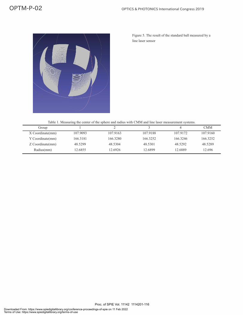
Figure 5. The result of the standard ball measured by a line laser sensor
Table 1. Measuring the center of the sphere and radius with CMM and line laser measurement systems. Group 1 2 3 4 CMM
X Coordinate(mm) 107.9093 107.9163 107.9188 107.9172 107.9160 Y Coordinate(mm) 166.3181 166.3280 166.3252 166.3246 166.3252 Z Coordinate(mm) 48.5299 48.5304 48.5301 48.5292 48.5289
Radius(mm) 12.6855 12.6926 12.6899 12.6889 12.696
Proc. of SPIE Vol. 11142 1114201-116Downloaded From: https://www.spiedigitallibrary.org/conference-proceedings-of-spie on 11 Feb 2022Terms of Use: https://www.spiedigitallibrary.org/terms-of-use
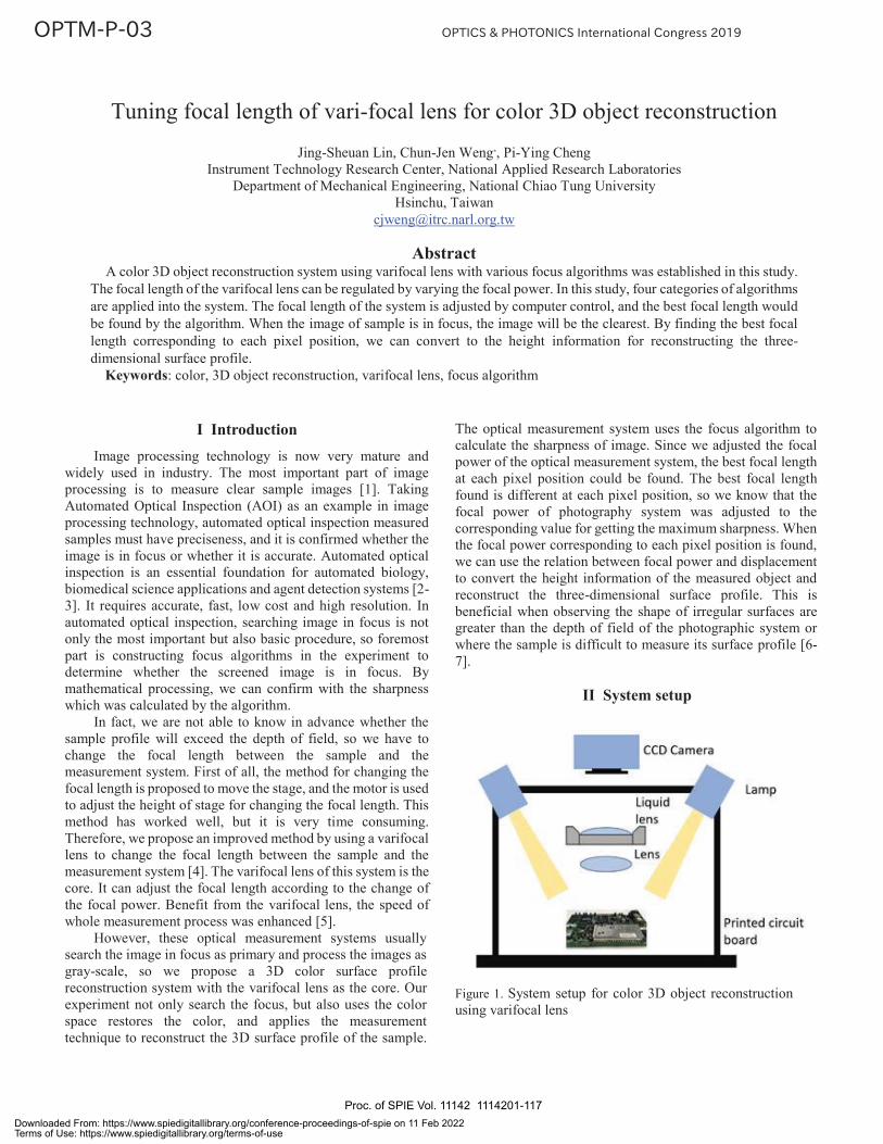
I Introduction Image processing technology is now very mature and
widely used in industry. The most important part of image processing is to measure clear sample images [1]. Taking Automated Optical Inspection (AOI) as an example in image processing technology, automated optical inspection measured samples must have preciseness, and it is confirmed whether the image is in focus or whether it is accurate. Automated optical inspection is an essential foundation for automated biology, biomedical science applications and agent detection systems [2-3]. It requires accurate, fast, low cost and high resolution. In automated optical inspection, searching image in focus is not only the most important but also basic procedure, so foremost part is constructing focus algorithms in the experiment to determine whether the screened image is in focus. By mathematical processing, we can confirm with the sharpness which was calculated by the algorithm.
In fact, we are not able to know in advance whether the sample profile will exceed the depth of field, so we have to change the focal length between the sample and the measurement system. First of all, the method for changing the focal length is proposed to move the stage, and the motor is used to adjust the height of stage for changing the focal length. This method has worked well, but it is very time consuming. Therefore, we propose an improved method by using a varifocal lens to change the focal length between the sample and the measurement system [4]. The varifocal lens of this system is the core. It can adjust the focal length according to the change of the focal power. Benefit from the varifocal lens, the speed of whole measurement process was enhanced [5].
However, these optical measurement systems usually search the image in focus as primary and process the images as gray-scale, so we propose a 3D color surface profile reconstruction system with the varifocal lens as the core. Our experiment not only search the focus, but also uses the color space restores the color, and applies the measurement technique to reconstruct the 3D surface profile of the sample.
The optical measurement system uses the focus algorithm to calculate the sharpness of image. Since we adjusted the focal power of the optical measurement system, the best focal length at each pixel position could be found. The best focal length found is different at each pixel position, so we know that the focal power of photography system was adjusted to the corresponding value for getting the maximum sharpness. When the focal power corresponding to each pixel position is found, we can use the relation between focal power and displacement to convert the height information of the measured object and reconstruct the three-dimensional surface profile. This is beneficial when observing the shape of irregular surfaces are greater than the depth of field of the photographic system or where the sample is difficult to measure its surface profile [6-7].
II System setup
Figure 1. System setup for color 3D object reconstruction using varifocal lens
Tuning focal length of vari-focal lens for color 3D object reconstruction
Jing-Sheuan Lin, Chun-Jen Weng*, Pi-Ying Cheng
Instrument Technology Research Center, National Applied Research Laboratories Department of Mechanical Engineering, National Chiao Tung University
Hsinchu, Taiwan [email protected]
Abstract
A color 3D object reconstruction system using varifocal lens with various focus algorithms was established in this study. The focal length of the varifocal lens can be regulated by varying the focal power. In this study, four categories of algorithms are applied into the system. The focal length of the system is adjusted by computer control, and the best focal length would be found by the algorithm. When the image of sample is in focus, the image will be the clearest. By finding the best focal length corresponding to each pixel position, we can convert to the height information for reconstructing the three-dimensional surface profile.
Keywords: color, 3D object reconstruction, varifocal lens, focus algorithm
Proc. of SPIE Vol. 11142 1114201-117Downloaded From: https://www.spiedigitallibrary.org/conference-proceedings-of-spie on 11 Feb 2022Terms of Use: https://www.spiedigitallibrary.org/terms-of-use
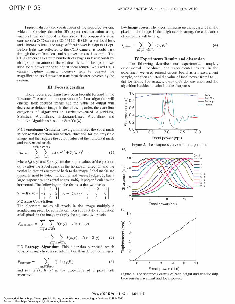
Figure 1 display the construction of the proposed system, which is showing the color 3D object reconstruction using varifocal lens developed in this study. The proposed system consists of a CCD camera (EO-1312C-HQ LE), a varifocal lens, and a biconvex lens. The range of focal power is 3 dpt to 11 dpt. Before light was reflected to the CCD camera, it would pass through the varifocal lens and biconvex lens to the sample. The CCD camera can capture hundreds of images in few seconds by change the curvature of the varifocal lens. In this system, we used focal power mode to adjust focal length. We used CCD camera capture images, biconvex lens to convert the magnification, so that we can transform the area covered by the system.
III Focus algorithm Those focus algorithms have been brought forward in the
literature. The maximum output value of a focus algorithm will emerge from focused image and the value of output will decrease as defocus image. In the following order, there are four categories of algorithms in Derivative-Based Algorithms, Statistical Algorithms, Histogram-Based Algorithms and Intuitive Algorithms based on Sun Yu [8].
F-1 Tenenbaum Gradient: The algorithm used the Sobel mask in horizontal direction and vertical direction for the grayscale image, and then square the output values of the horizontal mask and the vertical mask.
where (x, y) and (x, y) are the output values of the position (x, y) after the Sobel mask in the horizontal direction and the vertical direction are rotated back to the image. Sobel masks are typically used to detect horizontal and vertical edges, has a large response to horizontal edges, and is perpendicular to the horizontal. The following are the forms of the two masks
F-2 Auto Correlation: The algorithm makes all pixels in the image multiply a neighboring pixel for summation, then subtract the summation of all pixels in the image multiply the adjacent two pixels.
F-3 Entropy Algorithm: This algorithm supposed which focused images have more information than defocused images.
and is the probability of a pixel with intensity i.
F-4 Image power: The algorithm sums up the squares of all the pixels in the image. If the brightness is strong, the calculation of sharpness will be large.
IV Experiments Results and discussion
The following describes our experimental samples, experimental procedures, and experimental results. In the experiment we used printed circuit board as a measurement sample, and then adjusted the value of focal power from3 to 11 dpt for taking 100 images, every 0.08 dpt one shot, and the algorithm is added to calculate the sharpness.
Figure 2. The sharpness curve of four algorithms
(a)
(b)
Figure 3. The sharpness curves of each height and relationship between displacement and focal power.
6.0 6.5 7.0 7.5 8.00.0
0.2
0.4
0.6
0.8
1.0
S
harp
ness
(a.u
.)
Focal power (dpt)
Tene AutoCor Entropy Image
4 6 8 100.2
0.4
0.6
0.8
1.0
Shar
pnes
s (a
.u.)
Focal power (dpt)
(mm) 0 1 2 3 4 5.15 6.15 7.15 8.15 9.15
6 7 8 9 10 110
2
4
6
8
10
D
ispla
cem
ent (
mm
)
Focal power (dpt)
Proc. of SPIE Vol. 11142 1114201-118Downloaded From: https://www.spiedigitallibrary.org/conference-proceedings-of-spie on 11 Feb 2022Terms of Use: https://www.spiedigitallibrary.org/terms-of-use
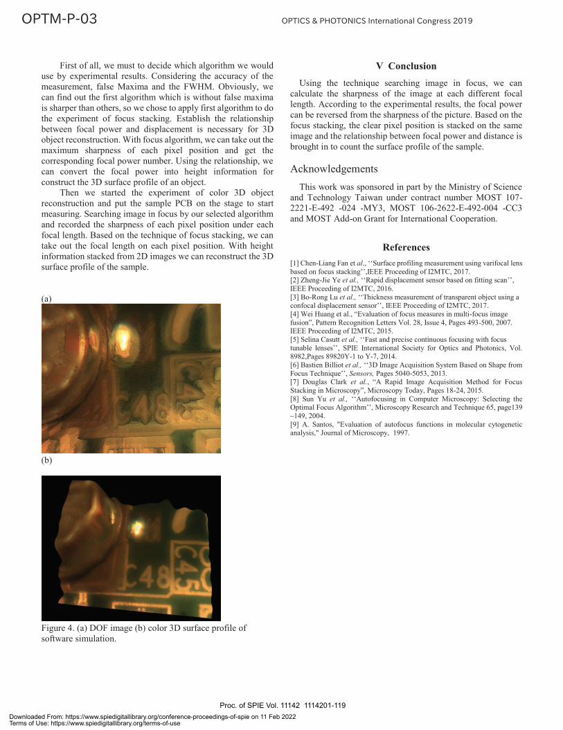
First of all, we must to decide which algorithm we would use by experimental results. Considering the accuracy of the measurement, false Maxima and the FWHM. Obviously, we can find out the first algorithm which is without false maxima is sharper than others, so we chose to apply first algorithm to do the experiment of focus stacking. Establish the relationship between focal power and displacement is necessary for 3D object reconstruction. With focus algorithm, we can take out the maximum sharpness of each pixel position and get the corresponding focal power number. Using the relationship, we can convert the focal power into height information for construct the 3D surface profile of an object.
Then we started the experiment of color 3D object reconstruction and put the sample PCB on the stage to start measuring. Searching image in focus by our selected algorithm and recorded the sharpness of each pixel position under each focal length. Based on the technique of focus stacking, we can take out the focal length on each pixel position. With height information stacked from 2D images we can reconstruct the 3D surface profile of the sample.
(a)
(b)
Figure 4. (a) DOF image (b) color 3D surface profile of software simulation.
V Conclusion Using the technique searching image in focus, we can
calculate the sharpness of the image at each different focal length. According to the experimental results, the focal power can be reversed from the sharpness of the picture. Based on the focus stacking, the clear pixel position is stacked on the same image and the relationship between focal power and distance is brought in to count the surface profile of the sample.
Acknowledgements
This work was sponsored in part by the Ministry of Science and Technology Taiwan under contract number MOST 107-2221-E-492 -024 -MY3, MOST 106-2622-E-492-004 -CC3 and MOST Add-on Grant for International Cooperation.
References [1] Chen-Liang Fan et al., ‘‘Surface profiling measurement using varifocal lens based on focus stacking’’,IEEE Proceeding of I2MTC, 2017. [2] Zheng-Jie Ye et al., ‘‘Rapid displacement sensor based on fitting scan’’, IEEE Proceeding of I2MTC, 2016. [3] Bo-Rong Lu et al., ‘‘Thickness measurement of transparent object using a confocal displacement sensor’’, IEEE Proceeding of I2MTC, 2017. [4] Wei Huang et al., “Evaluation of focus measures in multi-focus image fusion”, Pattern Recognition Letters Vol. 28, Issue 4, Pages 493-500, 2007. IEEE Proceeding of I2MTC, 2015. [5] Selina Casutt et al., ‘‘Fast and precise continuous focusing with focus tunable lenses’’, SPIE International Society for Optics and Photonics, Vol. 8982,Pages 89820Y-1 to Y-7, 2014. [6] Bastien Billiot et al., ‘‘3D Image Acquisition System Based on Shape from Focus Technique’’, Sensors, Pages 5040-5053, 2013. [7] Douglas Clark et al., “A Rapid Image Acquisition Method for Focus Stacking in Microscopy”, Microscopy Today, Pages 18-24, 2015. [8] Sun Yu et al., ‘‘Autofocusing in Computer Microscopy: Selecting the Optimal Focus Algorithm’’, Microscopy Research and Technique 65, page139 –149, 2004. [9] A. Santos, "Evaluation of autofocus functions in molecular cytogenetic analysis," Journal of Microscopy, 1997.
Proc. of SPIE Vol. 11142 1114201-119Downloaded From: https://www.spiedigitallibrary.org/conference-proceedings-of-spie on 11 Feb 2022Terms of Use: https://www.spiedigitallibrary.org/terms-of-use
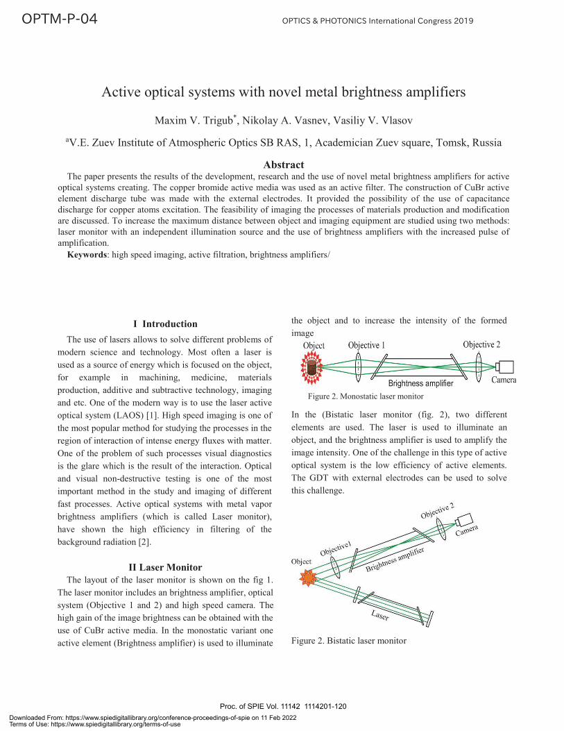
I Introduction The use of lasers allows to solve different problems of
modern science and technology. Most often a laser is used as a source of energy which is focused on the object, for example in machining, medicine, materials production, additive and subtractive technology, imaging and etc. One of the modern way is to use the laser active optical system (LAOS) [1]. High speed imaging is one of the most popular method for studying the processes in the region of interaction of intense energy fluxes with matter. One of the problem of such processes visual diagnostics is the glare which is the result of the interaction. Optical and visual non-destructive testing is one of the most important method in the study and imaging of different fast processes. Active optical systems with metal vapor brightness amplifiers (which is called Laser monitor), have shown the high efficiency in filtering of the background radiation [2].
II Laser Monitor
The layout of the laser monitor is shown on the fig 1. The laser monitor includes an brightness amplifier, optical system (Objective 1 and 2) and high speed camera. The high gain of the image brightness can be obtained with the use of CuBr active media. In the monostatic variant one active element (Brightness amplifier) is used to illuminate
the object and to increase the intensity of the formed image
Figure 2. Monostatic laser monitor
In the (Bistatic laser monitor (fig. 2), two different elements are used. The laser is used to illuminate an object, and the brightness amplifier is used to amplify the image intensity. One of the challenge in this type of active optical system is the low efficiency of active elements. The GDT with external electrodes can be used to solve this challenge.
Figure 2. Bistatic laser monitor
Active optical systems with novel metal brightness amplifiers
Maxim V. Trigub*, Nikolay A. Vasnev, Vasiliy V. Vlasov
aV.E. Zuev Institute of Atmospheric Optics SB RAS, 1, Academician Zuev square, Tomsk, Russia
Abstract The paper presents the results of the development, research and the use of novel metal brightness amplifiers for active
optical systems creating. The copper bromide active media was used as an active filter. The construction of CuBr active element discharge tube was made with the external electrodes. It provided the possibility of the use of capacitance discharge for copper atoms excitation. The feasibility of imaging the processes of materials production and modification are discussed. To increase the maximum distance between object and imaging equipment are studied using two methods: laser monitor with an independent illumination source and the use of brightness amplifiers with the increased pulse of amplification.
Keywords: high speed imaging, active filtration, brightness amplifiers/
Proc. of SPIE Vol. 11142 1114201-120Downloaded From: https://www.spiedigitallibrary.org/conference-proceedings-of-spie on 11 Feb 2022Terms of Use: https://www.spiedigitallibrary.org/terms-of-use

The high gain of the image brightness can be obtained with the use of CuBr active media. In the monostatic variant one active element (Brightness amplifier) is used to illuminate the object and to increase the intensity of the formed image. In the second variant (Bistatic laser monitor), two different elements are used. The laser is used to illuminate an object, and the brightness amplifier is used to amplify the image intensity. One of the challenge in this type of active optical system is the low efficiency of active elements. The GDT with external electrodes can be used to solve this challenge.
The construction of the GDT with external electrodes was developed in IAO SBR RAS [3]. Te construction excludes the contact of the electrodes material with a medium. The active element is made of quartz; the windows are used to output laser radiation. The electrodes are made of a metal foil wound on the outer wall of the GDT. The design allows you to change the equivalent capacity by connecting an additional capacitor ("second floor"). To excite the active medium, the capacitive barrier discharge is used in this type of GDT. It is formed by high-voltage pulse formed by a high speed commutator, for example, it can be thyratron. The use of independent heaters of containers with working substance (CuBr) and the HBr generator allows to optimize the amplifying characteristics of this medium.
III Results and Discussion The work discusses the feasibility of developing active
filters based on metal vapors for imaging processes blocked by the background glare. The system with external illumination and active filtration by the quantum filter has been created and used for test object imaging. It has been shown that the imaging method proposed in this work proves to be the most reliable to obtain the information about objects or processes in a real time mode using high PRF CuBr active media. The imaging results of different processes blocked from the observation by the intense background light are presented. The different types of active media were used as active quantum filters. For increasing spectral range of the imaging. The visualization results are shown on the fig 3.
Figure 3. The imaging of the test object in the monostatic (a) and bistatic (b) laser monitors
The external glare was created by the arc with the brightness temperature about 5000 K. The active filter allowed to describe the negative effect of this arc and make it possible to observe the object. The spatial resolution of the bistatic laser monitor is higher than the monostatic one, as it has been shown on the fig. 3. It provides by the external illumination source.
One of the feature of the active optical system is a high time resolution, It provides by the use high frequency active filters. In the work some fast processes were visualized by the laser monitor. Each frame was formed by the one pulse of amplification (about 40 ns). It has allowed to study the processes of materials production and modification.
The authors are grateful to Professor of Tomsk Polytechnic University G.S. Evtushenko for discussion of the results.
References [1] Chvykov, V. (2017). Laser active optical systems (LAOS) for
industrial applications. Paper presented at the Optics InfoBase Conference Papers, Part F43-CLEO_AT 2017 doi:10.1364/CLEO_AT.2017.ATu3C.2
[2] Trigub M.V., Evtushenko G.S., Torgaev S.N., Shiyanov D.V., Evtushenko T.G. Copper bromide vapor brightness amplifiers with 100 kHz pulse repetition frequency // Optics communications, 2016. Vol. 376, No 10, pp. 81-85
[3] Gubarev F.A., Shiyanov D.V., Sukhanov V.B., Evtushenko G.S. Capacitive-Discharge-Pumped CuBr Laser With 12 W Average Output Power // IEEE Journal of Quantum Electronics. 2013. V.49. No1. P.89–94.
Proc. of SPIE Vol. 11142 1114201-121Downloaded From: https://www.spiedigitallibrary.org/conference-proceedings-of-spie on 11 Feb 2022Terms of Use: https://www.spiedigitallibrary.org/terms-of-use
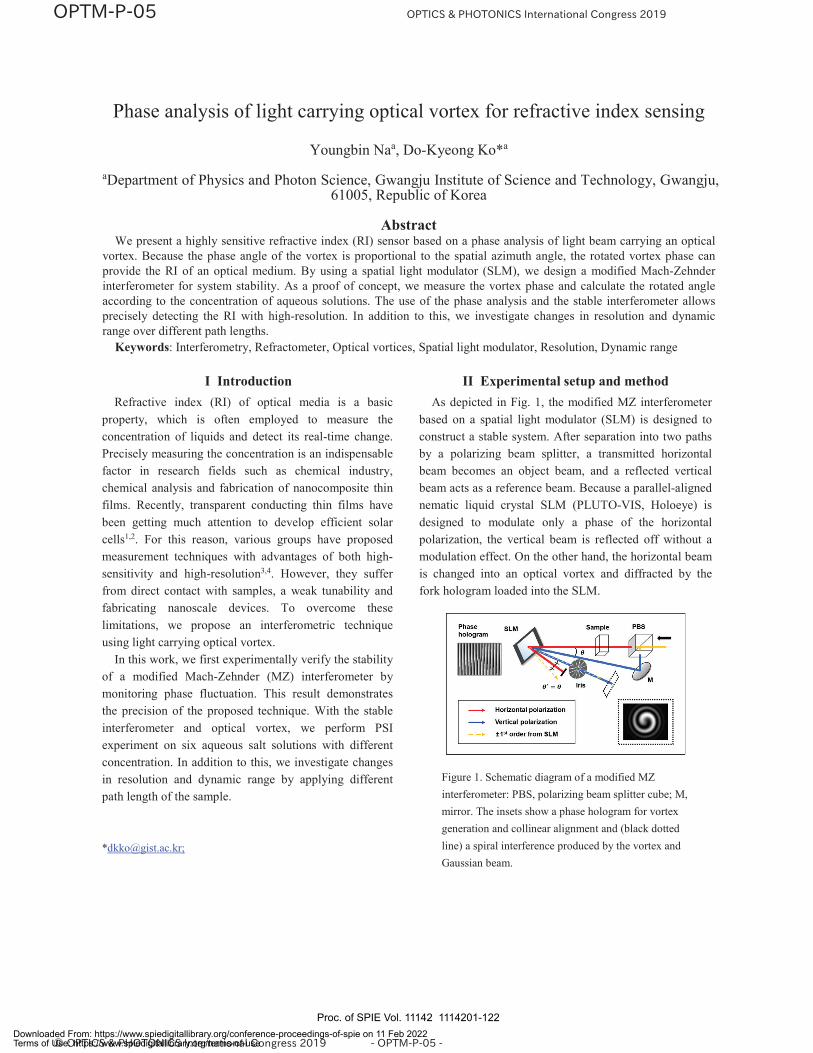
I Introduction Refractive index (RI) of optical media is a basic
property, which is often employed to measure the concentration of liquids and detect its real-time change. Precisely measuring the concentration is an indispensable factor in research fields such as chemical industry, chemical analysis and fabrication of nanocomposite thin films. Recently, transparent conducting thin films have been getting much attention to develop efficient solar cells1,2. For this reason, various groups have proposed measurement techniques with advantages of both high-sensitivity and high-resolution3,4. However, they suffer from direct contact with samples, a weak tunability and fabricating nanoscale devices. To overcome these limitations, we propose an interferometric technique using light carrying optical vortex.
In this work, we first experimentally verify the stability of a modified Mach-Zehnder (MZ) interferometer by monitoring phase fluctuation. This result demonstrates the precision of the proposed technique. With the stable interferometer and optical vortex, we perform PSI experiment on six aqueous salt solutions with different concentration. In addition to this, we investigate changes in resolution and dynamic range by applying different path length of the sample.
II Experimental setup and method As depicted in Fig. 1, the modified MZ interferometer
based on a spatial light modulator (SLM) is designed to construct a stable system. After separation into two paths by a polarizing beam splitter, a transmitted horizontal beam becomes an object beam, and a reflected vertical beam acts as a reference beam. Because a parallel-aligned nematic liquid crystal SLM (PLUTO-VIS, Holoeye) is designed to modulate only a phase of the horizontal polarization, the vertical beam is reflected off without a modulation effect. On the other hand, the horizontal beam is changed into an optical vortex and diffracted by the fork hologram loaded into the SLM.
Figure 1. Schematic diagram of a modified MZ interferometer: PBS, polarizing beam splitter cube; M, mirror. The insets show a phase hologram for vortex generation and collinear alignment and (black dotted line) a spiral interference produced by the vortex and Gaussian beam.
Phase analysis of light carrying optical vortex for refractive index sensing
Youngbin Naa, Do-Kyeong Ko*a
aDepartment of Physics and Photon Science, Gwangju Institute of Science and Technology, Gwangju, 61005, Republic of Korea
Abstract
We present a highly sensitive refractive index (RI) sensor based on a phase analysis of light beam carrying an optical vortex. Because the phase angle of the vortex is proportional to the spatial azimuth angle, the rotated vortex phase can provide the RI of an optical medium. By using a spatial light modulator (SLM), we design a modified Mach-Zehnder interferometer for system stability. As a proof of concept, we measure the vortex phase and calculate the rotated angle according to the concentration of aqueous solutions. The use of the phase analysis and the stable interferometer allows precisely detecting the RI with high-resolution. In addition to this, we investigate changes in resolution and dynamic range over different path lengths.
Keywords: Interferometry, Refractometer, Optical vortices, Spatial light modulator, Resolution, Dynamic range
Proc. of SPIE Vol. 11142 1114201-122Downloaded From: https://www.spiedigitallibrary.org/conference-proceedings-of-spie on 11 Feb 2022Terms of Use: https://www.spiedigitallibrary.org/terms-of-use

The incident vertical and horizontal beams converge at one point on the SLM. The object beam is dffracted (+1st order), with the diffraction angle of '. When we select a proper grating period, the reflected referenc beam and the diffracted object beam collinearly propagate, i.e. ' = .
III Results and Discussion 1. System stability An ordinary Michelson interferometer is additionally
used to compare the system stability. We measure vortex phases of an object beam without a sample. 20 sequential measurements are conducted with a time interval of 30 seconds. Figure 2(a) and (b) shows phase values at a randomly selected position in the retrieved phase map. While the Michelson interferometer shows unstable results, the modified MZ interferometer keeps the phase fluctuation low. Figure 2(c) depicts the statistical result of the phase fluctuation. The mean value are 0.393 and 0.0874, which demonstrates the robust stability and repeatability of the proposed system.
Figure 2. Stability test using phase fluctuation of (a) the Michelson interferometer and (b) the modified MZ interferometer and (c) statistical analysis from randomly chosen 30 positions. The each inset shows a reconstructed vortex phase and the measure position.
2. Performance of the vortex refractometer A vortex phase and its rotated angle are used to
determine the relative phase shift introduced by each concentration. We prepared six aqueous salt solutions as test samples with different concentration (%, w/w), 10.03, 10.04, 10.07, 10.10, 10.15, and 10.25, respectively. The
probing beam passes through the solution with 2 mm path length. Figure 3 shows captured spiral interference patterns for each concentration. The vortex phases are obtained by the four-step PSI5, and the relative phase shift is extracted by the following equation6:
20 ,ar b (1)
where a represents the rate at which the angle changes as its radius increases. b0 is the phase shift corresponding to the starting angle of the vortex. Fitting result of the sample with 10.25 % concentration is shown in Fig. 4(a) as an example. Here, we extracted the values along a phase minimum line, i.e. the black line. Figure 4(b) shows the values of b0 versus concentration, and the slope determines the rate of change, db0 / dC. A linear relation between n and C is estimated by the following equation:
02 rad ,nkd n d b (2)
where n is the RI of the sample and d is the path length in the medium. Thus, the relation dn / dC is given by
10 % .2
dbdndC d dC
(3)
Figure 3. Captured interferograms from the six different concentration.
The difference of 0.01 % corresponds to the RI of ~1.95×10⁻⁵ refractive index unit (RIU). The use of short wavelength and long path length can further improve the resolution as shown in the Eq. (2). From the equation, the phase fluctuation of 0.0874 measured in the stability test gives the detection limit of ~4.13×10⁻⁶ RIU, which demonstrates that the method using the vortex phase is a precise technique.
Proc. of SPIE Vol. 11142 1114201-123Downloaded From: https://www.spiedigitallibrary.org/conference-proceedings-of-spie on 11 Feb 2022Terms of Use: https://www.spiedigitallibrary.org/terms-of-use

Figure 4. (a) Fitting results of the extracted minimum points for 10.25 % and (b) calculated phase constant. The inset shows the retrieved vortex phase.
Figure 5. Performance of the proposed method at various path lengths. (a) Estimated resolution as a function of path length under different values of detection limit and (b) dynamic range as a function of path length. Our experimental condition corresponds to 2 mm path length and ~5º detection limit.
Finally, the performance of the proposed technique is displayed in Fig 5. Figure 5(a) depicts estimated resolution as a function of path length. Each color
indicates different scenarios of the detection limit. Figure 5(b) shows the dynamic range of the method. A much smaller resolution can be achieved by lowering the detection limit, potentially up to 10-6 or even 10-7 RIU. We believe that it will be realized by adopting a nearly common-path interferometer.
IV Conclusion In conclusion, we proposed and experimentally
demonstrated the vortex based interferometric method for application to the RI sensor. The rotation in the phase profile and its differential measurement were utilized to precisely detect the RI change, and experimental results verified the possibility of a high-resolution refractometer. The resolution limit of the proposed technique will be improved further, up to 10-6 or even 10-7, by using the longer path length and enhancing the system stability. However, there is a drawback in the dynamic range due to the ambiguity of the phase. Thus, we will seek to break the fundamental limit on the dynamic range.
References [1] S. Vadivel and G. Rajarajan, "Effect of Mg doping on
structural, optical and photocatalytic activity of SnO2 nanostructure thin films," J. Mater. Sci. Mater. Electron. 26, 3155-3162 (2015).
[2] X. Xu, J. Bullock, L. Schelhas, E. Stutz, J. Fonseca, M. Hettick, V. Pool, K. Tai, M. Toney, X. Fang, A. Javey, L. Wong and J. Ager, "Chemical Bath Deposition of p-Type Transparent, Highly Conducting (CuS)x:(ZnS)1–x Nanocomposite Thin Films and Fabrication of Si Heterojunction Solar Cells," Nano Lett. 16, 1925-1932 (2016).
[3] Z. Chen, L. Liu, Y. He and H. Ma, "Resolution enhancement of surface plasmon resonance sensor with spectral interrogation: resonant wavelength considerations," Appl. Opt. 55, 884-891 (2016).
[4] Z. Ding, T. Lang, Y. Wang and C. Zhao, "Surface Plasmon Resonance Refractive index sensor based on Tapered Coreless Optical Fiber Structure," J. Light. Technol. 35, 4734-4739 (2017).
[5] G. Lai and T. Yatagai, "Generalized phase-shifting interferometry," J. Opt. Soc. Am. A 8, 822-827 (1991).
[6] Y. Xu, J. Sun, W. Walasik and N. Litchinitser, "Probing metamaterials with structured light," Opt. Express 24, 26249-26254 (2016).
Proc. of SPIE Vol. 11142 1114201-124Downloaded From: https://www.spiedigitallibrary.org/conference-proceedings-of-spie on 11 Feb 2022Terms of Use: https://www.spiedigitallibrary.org/terms-of-use

SMS and FBG interrogation for measurement of temperature and strain
using OTDR
Koustav Dey*a, Sourabh Roya, M.Sai Shankara, B.Ramesh Kumarb, P.Kishorea
a Department of Physics, National Institute Of Technology, Warangal 506 004, Telangana, India
b Institute for Plasma Research, Gandhinagar 382 428, Gujrat, India
Abstract Here, we demonstrate the interrogation technique of Fiber Bragg grating (FBG) using single mode-multimode-single
mode (SMS) with the help of optical time domain reflectometer (OTDR) for temperature and strain measurement. A temperature range of 20oC-200oC and strain range of 100με- 2020με has been measured with a linearity of 0.994 with the proposed scheme. Our experimental result shows that this sensor has a temperature and strain sensitivity of 5.03pm/oC and 0.4 pm/με respectively. The proposed scheme offers low cost and better sensitivity with respect to existing methods. Keywords: FBG, OTDR, SMS, interrogation, sensor
I Introduction In the era of boom of the optical fiber sensing
technology, the multimode interference (MMI) effect has been intensively investigated with Single-mode-multimode-single-mode (SMS) fiber structure as one of the typical representatives of the underlying operation principle of MMI1. The change in temperature and strain will affect the refractive index and dimensions of the fiber core and cladding which in turn affect the interference between modes in the MMF section that causes output response changes2. Alongside FBG is a wavelength coded sensing device which needs an interrogation system for essential conversion of optical power to wavelength information3. Hence the combining sensing outputs from FBG and SMS signals are monitored using OTDR. The obtained results of strain and temperature from this proposed scheme perform better and show enhanced sensitivity with respect to existing methods.
II Experimental Details The SMS fiber structure is fabricated using a commercial fusion splicer (Fujikura-60S). A multimode fiber (50/125 μm) section is sandwiched between two step index single mode fibers (9/125 μm) axially. The OTDR (JDSU MTS 8000 series) is used to detect the event induced by the temperature and strain change on FBG.
*[email protected]; phone +91 9440218973
The OTDR measures the attenuation of reflected light or return loss and the location from where the light is being reflected within 5 km range of optical fiber network with resolution of 0.001dB. For temperature sensing, we have kept the FBG inside an oven which is again connected to the dimmer stat for controlling the temperature with time. For strain measurement, we have pasted the FBG on the simple beam cantilever using high-temperature instant adhesive. Here we have investigated the attenuation loss of an FBG of central wavelength 1528 nm, which lies in the ripple free slope region of the SMS using the interrogation technique of SMS and FBG with the help of OTDR. The power loss is a measurement of variation of temperature and strain separately and also for variation of temperature at discrete constant loads (50 gms to 1000 gms with an increment of 50 gms.) in the range 20˚C -200˚C using OTDR at constant room temperature. As the FBG peak follows the linear slope region of SMS, it is expected that the response of the OTDR also to be linear which is confirmed from the obtained results, that showing good linearity of ~0.994. Our scheme of interrogation is expected to be robust, cheap and more efficient for simultaneous measurement of temperature and strain with good sensitivity. Our experimental result shows that this sensor has a temperature and strain sensitivity of 5.03pm/oC and 0.4 pm/με respectively. From which we can measure the temperature and strain simultaneously. The
Proc. of SPIE Vol. 11142 1114201-125Downloaded From: https://www.spiedigitallibrary.org/conference-proceedings-of-spie on 11 Feb 2022Terms of Use: https://www.spiedigitallibrary.org/terms-of-use
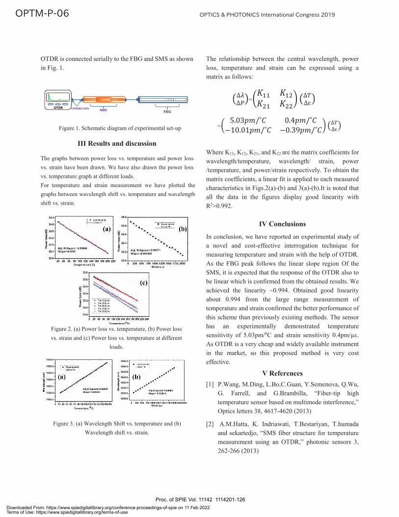
OTDR is connected serially to the FBG and SMS as shown in Fig. 1.
Figure 1. Schematic diagram of experimental set-up
III Results and discussion
The graphs between power loss vs. temperature and power loss vs. strain have been drawn. We have also drawn the power loss vs. temperature graph at different loads. For temperature and strain measurement we have plotted the graphs between wavelength shift vs. temperature and wavelength shift vs. strain.
Figure 3. (a) Wavelength Shift vs. temperature and (b) Wavelength shift vs. strain.
The relationship between the central wavelength, power loss, temperature and strain can be expressed using a matrix as follows:
=
=
Where K11, K12, K21, and K22 are the matrix coefficients for wavelength/temperature, wavelength/ strain, power /temperature, and power/strain respectively. To obtain the matrix coefficients, a linear fit is applied to each measured characteristics in Figs.2(a)-(b) and 3(a)-(b).It is noted that all the data in the figures display good linearity with R2>0.992.
IV Conclusions
In conclusion, we have reported an experimental study of a novel and cost-effective interrogation technique for measuring temperature and strain with the help of OTDR. As the FBG peak follows the linear slope region Of the SMS, it is expected that the response of the OTDR also to be linear which is confirmed from the obtained results. We achieved the linearity ~0.994. Obtained good linearity about 0.994 from the large range measurement of temperature and strain confirmed the better performance of this scheme than previously existing methods. The sensor has an experimentally demonstrated temperature sensitivity of 5.03pm/0C and strain sensitivity 0.4pm/με. As OTDR is a very cheap and widely available instrument in the market, so this proposed method is very cost effective.
V References [1] P.Wang, M.Ding, L.Bo,C.Guan, Y.Semenova, Q.Wu,
G. Farrell, and G.Brambilla, “Fiber-tip high temperature sensor based on multimode interference,” Optics letters 38, 4617-4620 (2013)
[2] A.M.Hatta, K. Indriawati, T.Bestariyan, T.humada and sekartedjo, “SMS fiber structure for temperature measurement using an OTDR,” photonic sensors 3, 262-266 (2013)
Figure 2. (a) Power loss vs. temperature, (b) Power loss vs. strain and (c) Power loss vs. temperature at different
loads.
Proc. of SPIE Vol. 11142 1114201-126Downloaded From: https://www.spiedigitallibrary.org/conference-proceedings-of-spie on 11 Feb 2022Terms of Use: https://www.spiedigitallibrary.org/terms-of-use

[3] Qiang wu,Yuliya semenova, Pengfei wang and Gerald Farrell, “High sensitivity SMS fibre structured based refractometer-analysis and experiment,” Optic express 19,7937-7944 (2011)
[4] O frazao, J P Carvalho, L A Ferreira, F M Araujo and J L santos, “Discrimination of strain and temperature using Bragg gratings in microstructured and standard optical fibers,” meas.Sci.technol. 16, 2109-2113 (2005)
VI Acknowledgement
The author is highly grateful to BRNS (RS-872-GoI-BRNS-(DAE)-SR-PHYSICS (2017-18)) for their funding’s.
Proc. of SPIE Vol. 11142 1114201-127Downloaded From: https://www.spiedigitallibrary.org/conference-proceedings-of-spie on 11 Feb 2022Terms of Use: https://www.spiedigitallibrary.org/terms-of-use

I Introduction Lenses are essential for the handling of light in optical
application systems, but their solid nature produces inflexibility in the area of adjusting focal length for different applications; either the lens or the target material must be physically moved to change the focal position. The ability to change the focal length of the lens itself would speed up focusing operation and enable system downsizing.
Energy density, which involves the relationship between laser output and spot diameter, is an essential consideration in laser-based material processing. A variety of laser processes are conducted without sharp focus, including applications in laser welding, laser-based formation and surface modification. Such processing is characterized by problems such as energy loss and difficulty in adjusting heating and cooling times as a result of laser irradiation other than in the scanning direction due to lens-related beam defocusing. Against such a background, the availability of a function to allow energy density adjustment in the processing direction on the beam irradiation plane can be considered useful as an optical element in laser processing.
The authors previously reported on a liquid pressure-
*[email protected]; phone +81-82-921-3121
controlled variable-focus lens [1, 2], and other such lenses have also been proposed [3 – 8]. However, issues remain to be addressed with these lens elements; in particular, they are unsuitable for lasers with near-infrared wavelengths and for high-power laser processing.
This paper details the study of an anamorphic liquid-pressure varifocal lens that can adjust the energy density of a laser in the three dimensions of the x-y plane and the optical (z) axis direction. To support adjustment of the spot shape on the plane, a rectangular form was adopted for the peripheral support plate used to fix the elastic film of the proposed variable-focus lens and create an anamorphic refractive surface. The results of measurement to determine the optical characteristics of the lens and deformation of the elastic film on the x and y axes are reported.
II Anamorphic liquid-pressure varifocal lens The structure of the proposed lens (Figure 1) involves
the use of a liquid-filled cavity, sealing with an elastic film and a transparent plate. The focal length is varied by changing the shape of the lens via liquid injection and discharge. Pressure on the inside of the lens causes deformation of the elastic film (the refractive surface) depending on the shape of the peripheral support plate. In
Development of an Anamorphic Liquid-pressure Varifocal Lens*
Ryoichi Kuwano*a, Makoto Hinoa, Tsuyoshi Tokunagab, Sho Moritab and Yukitoshi Otanic
aDepartment of Mechanical Systems Engineering, Hiroshima Institute of Technology, 2-1-1 Miyake, Saeki-ku, Hiroshima, 731-5193, Japan
b Department of Innovative Mechanical and Electronic Engineering, Chiba Institute of Technology, 2-17-1 Tsudanuma,Narashino, Chiba 275-0016,
cUtsunomiya University Center for Optical Research & Education (CORE), 7-1-2 Yoto Utsunomiya-city Tochigi 321-8585 Japan
AbstractThis paper details the study of an anamorphic liquid-pressure varifocal lens that can be used to adjust the energy
density of a laser in the three dimensions of the x-y plane and the optical (z) axis direction. In the study, the optical characteristics of the lens and the deformation of the elastic film on the x and y axes were determined. Measurement to establish the focal length of the lens at a circular beam spot at the focal point produced values in the range from 580 to 142 mm. The spot was characterized by an elliptical form with a varying aspect ratio before and after the focal position, and an anamorphic effect was observed. The lens is expected to be useful in laser processing of optical elements for joining dissimilar materials in the fields of engineering plastics and metals.
Proc. of SPIE Vol. 11142 1114201-128Downloaded From: https://www.spiedigitallibrary.org/conference-proceedings-of-spie on 11 Feb 2022Terms of Use: https://www.spiedigitallibrary.org/terms-of-use
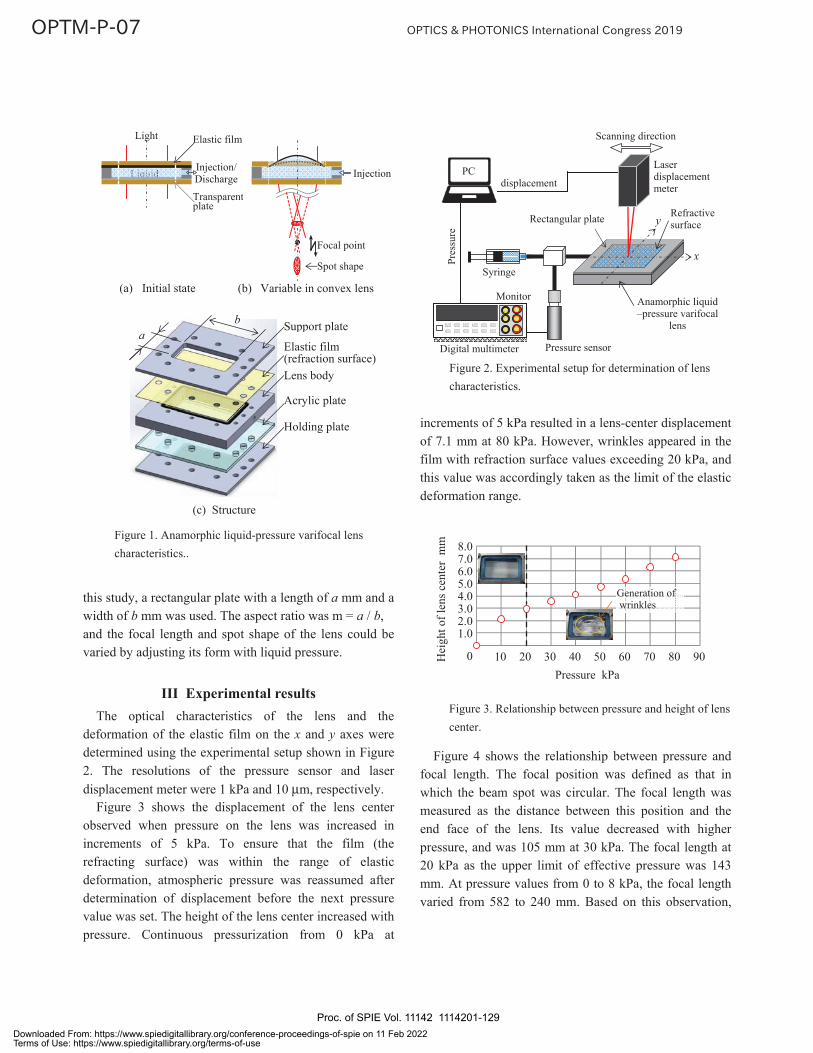
this study, a rectangular plate with a length of a mm and a width of b mm was used. The aspect ratio was m = a / b,and the focal length and spot shape of the lens could be varied by adjusting its form with liquid pressure.
III Experimental results The optical characteristics of the lens and the
deformation of the elastic film on the x and y axes were determined using the experimental setup shown in Figure 2. The resolutions of the pressure sensor and laserdisplacement meter were 1 kPa and 10 μm, respectively.
Figure 3 shows the displacement of the lens center observed when pressure on the lens was increased in increments of 5 kPa. To ensure that the film (the refracting surface) was within the range of elastic deformation, atmospheric pressure was reassumed after determination of displacement before the next pressure value was set. The height of the lens center increased with pressure. Continuous pressurization from 0 kPa at
increments of 5 kPa resulted in a lens-center displacement of 7.1 mm at 80 kPa. However, wrinkles appeared in the film with refraction surface values exceeding 20 kPa, and this value was accordingly taken as the limit of the elastic deformation range.
Figure 4 shows the relationship between pressure and focal length. The focal position was defined as that in which the beam spot was circular. The focal length was measured as the distance between this position and the end face of the lens. Its value decreased with higher pressure, and was 105 mm at 30 kPa. The focal length at 20 kPa as the upper limit of effective pressure was 143 mm. At pressure values from 0 to 8 kPa, the focal length varied from 582 to 240 mm. Based on this observation,
Light
Injection/DischargeLiquid
Elastic film
Transparentplate
Focal point
Injection
(a) Initial state (b) Variable in convex lens
Spot shape
Figure 1. Anamorphic liquid-pressure varifocal lens characteristics..
(c) Structure
Support plate
Elastic film(refraction surface) Lens body
Acrylic plate
Holding plate
ab
Figure 2. Experimental setup for determination of lens characteristics.
Digital mu timeter Pressure sensor
Syringe
displacement
Laserdisplacement meter
Scanning direction
Monitor
y
x
Anamorphic liquid –pressure varifocal
lens
PC
Refractivesurface
Figure 3. Relationship between pressure and height of lens center.
Generation of wrinkles
0Pressure kPa
1.02.03.04.05.06.07.08.0
10 20 30 40 50 60 70 80 90
Re
Proc. of SPIE Vol. 11142 1114201-129Downloaded From: https://www.spiedigitallibrary.org/conference-proceedings-of-spie on 11 Feb 2022Terms of Use: https://www.spiedigitallibrary.org/terms-of-use

the anamorphic liquid-pressure varifocal lens can be considered suitable for use with long focal ranges.
Figure 5 shows the results of measurement to determine displacement of the elastic film on the x and y axes as the pressure was changed in 10 kPa increments. The symmetry of the lens remained favorable, as shown in Fig. 5. Film deflection was proportional to liquid pressure, anddisplacement was consistent with the function of the fourth order with respect to position (x, y).
Figure 6 shows the spot shape with a pressure value of 10 kPa; (b) shows a circular spot with a diameter of 6.8 mm at a focal length of 218 mm, while (a) and (c) show the spot shape ± 100 mm from this position. Both shapes are ellipses, which indicates rotation of 90° to the focal position.
IV Conclusions This paper details the study of a lens allowing focal
position/spot shape changes with a structure incorporating liquid and an elastic film. The variable spot shape generates an anamorphic refracting surface, with the elastic film of the lens used as a rectangular peripheral support. The spot is an ellipse with different aspect ratios and 90° rotation before and after the focal point. The effective focal length of the lens exceeded 200 mm. It is considered suitable for use with optical elements in laser diode usage, such as in application with an output of several hundred W without the need for converging properties. In the future work, the authors plan to apply the lens to the task of joining dissimilar materials in the fields of engineering plastics and metals.
References [1] R. Kuwano, T. Tokunaga, Y. Otani and N. Umeda :
Opt. Rev. 12, 5(2005) : 405-408.. [2] R. Kuwano, T. Tokunaga, S. Morita, Y. Okane and Y.
Otani. MATEC Web of Conferences, 32, 07003 (2015) : p.1-p.3.
[3] M. C. King and D. H. Berry : Appl. Opt. 9, (1970):2035.
[4] S. Sato : Jpn. J. Appl. Phys. 18(1979) 1679. [5] N. Sugiura and S. Morita : Appl. Opt. 32, 22 (1993)
4181. [6] T. Kaneko, I. Kanayama, T. Itogaki, T.Hattori : JSPE
semestrial meeting spring, 3 (1996) (in Japanese). [7] D. Y. Zhang, V. Lien, Y. Berdichevsky, J. Choi and Y.
H. Lo : Appl. Phys. Lett, 82, 19(2003) 3171. [8] B. H. W. Hendriks, S. Kuiper, M. A. J. van As, and C.
J. Renders : Opt. Rev. 12, 3 (2005) 255.
Figure 4. Relationship between pressure and focal length.
Pressure kPa 0
100
200
300
400
500
600
4 8 12 16 20 24 282 6 10 14 18 22 26 30
Figure 5. Axial displacement in relation to pressure on the elastic film.
Position mm
1.01.52.02.53.03.5
-20 -10 0 10 20-25 -15 -5 5 15 25
0
30 kPa20 kPa
10 kPa
Figure 6. Lens-related spot shape variation.
(a) Before the focal position (z=-100 mm)
(b) Focal position (z=0 mm)
(c) Behind the focal position(z=+100 mm)
5 mm
Proc. of SPIE Vol. 11142 1114201-130Downloaded From: https://www.spiedigitallibrary.org/conference-proceedings-of-spie on 11 Feb 2022Terms of Use: https://www.spiedigitallibrary.org/terms-of-use
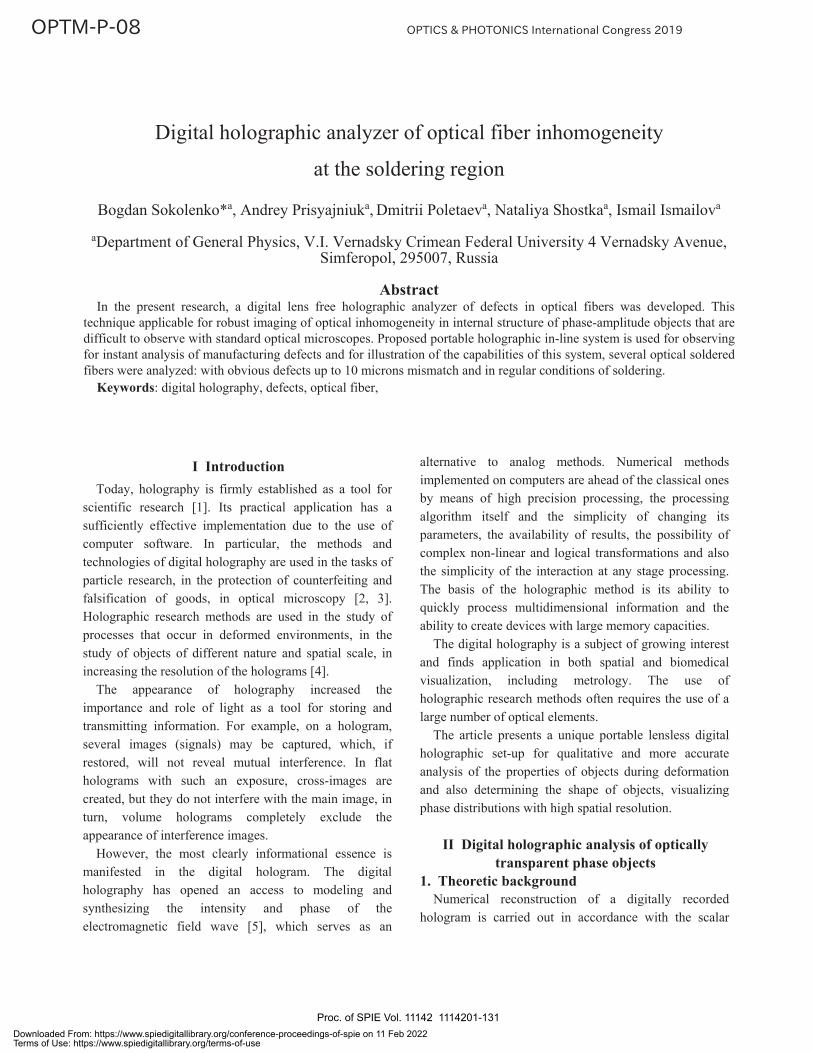
I Introduction Today, holography is firmly established as a tool for
scientific research [1]. Its practical application has a sufficiently effective implementation due to the use of computer software. In particular, the methods and technologies of digital holography are used in the tasks of particle research, in the protection of counterfeiting and falsification of goods, in optical microscopy [2, 3]. Holographic research methods are used in the study of processes that occur in deformed environments, in the study of objects of different nature and spatial scale, in increasing the resolution of the holograms [4].
The appearance of holography increased the importance and role of light as a tool for storing and transmitting information. For example, on a hologram, several images (signals) may be captured, which, if restored, will not reveal mutual interference. In flat holograms with such an exposure, cross-images are created, but they do not interfere with the main image, in turn, volume holograms completely exclude the appearance of interference images.
However, the most clearly informational essence is manifested in the digital hologram. The digital holography has opened an access to modeling and synthesizing the intensity and phase of the electromagnetic field wave [5], which serves as an
alternative to analog methods. Numerical methods implemented on computers are ahead of the classical ones by means of high precision processing, the processing algorithm itself and the simplicity of changing its parameters, the availability of results, the possibility of complex non-linear and logical transformations and also the simplicity of the interaction at any stage processing. The basis of the holographic method is its ability to quickly process multidimensional information and the ability to create devices with large memory capacities.
The digital holography is a subject of growing interest and finds application in both spatial and biomedical visualization, including metrology. The use of holographic research methods often requires the use of a large number of optical elements.
The article presents a unique portable lensless digital holographic set-up for qualitative and more accurate analysis of the properties of objects during deformation and also determining the shape of objects, visualizing phase distributions with high spatial resolution.
II Digital holographic analysis of optically
transparent phase objects 1. Theoretic background
Numerical reconstruction of a digitally recorded hologram is carried out in accordance with the scalar
Digital holographic analyzer of optical fiber inhomogeneity
at the soldering region
Bogdan Sokolenko*a, Andrey Prisyajniuka, Dmitrii Poletaeva, Nataliya Shostkaa, Ismail Ismailova
aDepartment of General Physics, V.I. Vernadsky Crimean Federal University 4 Vernadsky Avenue, Simferopol, 295007, Russia
Abstract
In the present research, a digital lens free holographic analyzer of defects in optical fibers was developed. This technique applicable for robust imaging of optical inhomogeneity in internal structure of phase-amplitude objects that are difficult to observe with standard optical microscopes. Proposed portable holographic in-line system is used for observing for instant analysis of manufacturing defects and for illustration of the capabilities of this system, several optical soldered fibers were analyzed: with obvious defects up to 10 microns mismatch and in regular conditions of soldering.
Keywords: digital holography, defects, optical fiber,
Proc. of SPIE Vol. 11142 1114201-131Downloaded From: https://www.spiedigitallibrary.org/conference-proceedings-of-spie on 11 Feb 2022Terms of Use: https://www.spiedigitallibrary.org/terms-of-use
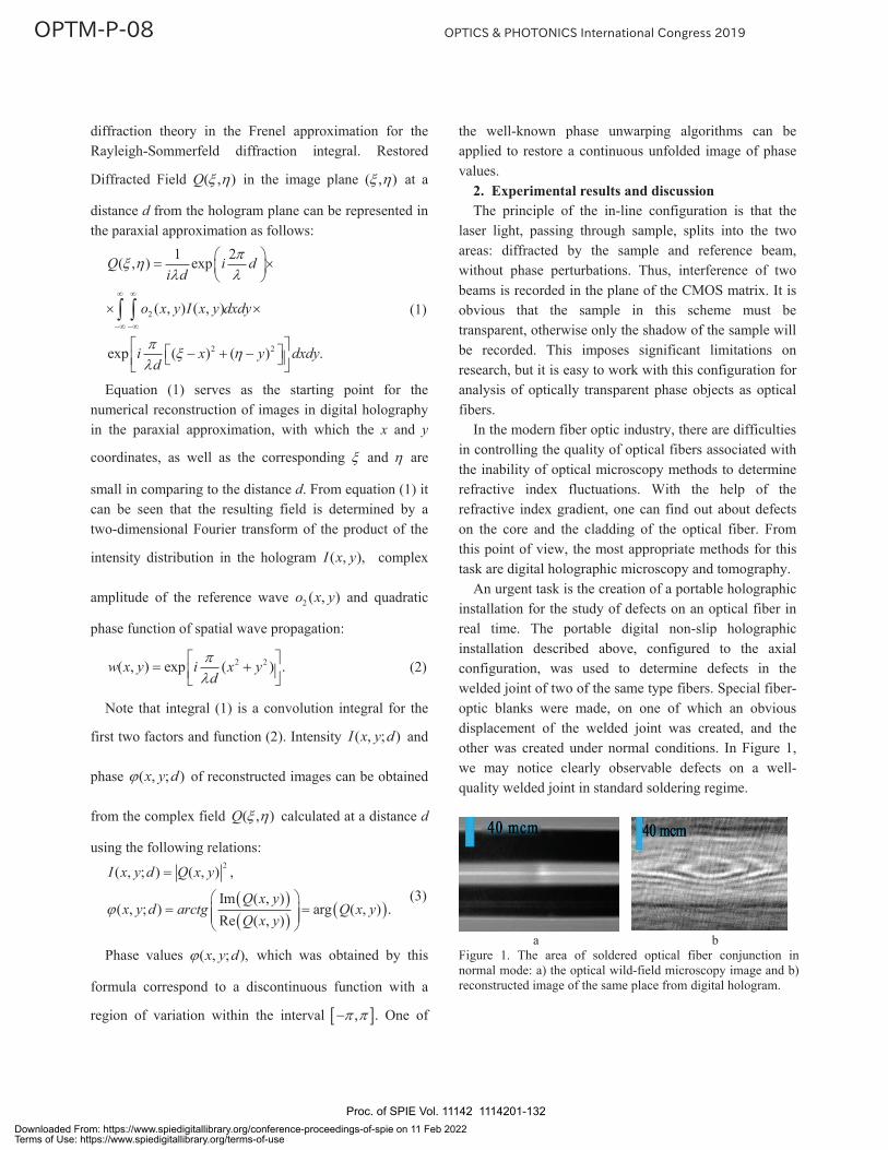
diffraction theory in the Frenel approximation for the Rayleigh-Sommerfeld diffraction integral. Restored
Diffracted Field ( , )Q in the image plane ( , ) at a
distance d from the hologram plane can be represented in the paraxial approximation as follows:
2
2 2
1 2( , ) exp
( , ) ( , )
exp ( ) ( ) .
Q i di d
o x y I x y dxdy
i x y dxdyd
(1)
Equation (1) serves as the starting point for the numerical reconstruction of images in digital holography in the paraxial approximation, with which the x and y
coordinates, as well as the corresponding and are
small in comparing to the distance d. From equation (1) it can be seen that the resulting field is determined by a two-dimensional Fourier transform of the product of the
intensity distribution in the hologram ( , ),I x y complex
amplitude of the reference wave 2 ( , )o x y and quadratic
phase function of spatial wave propagation:
2 2( , ) exp ( ) .w x y i x yd
(2)
Note that integral (1) is a convolution integral for the
first two factors and function (2). Intensity ( , ; )I x y d and
phase ( , ; )x y d of reconstructed images can be obtained
from the complex field ( , )Q calculated at a distance d
using the following relations: 2( , ; ) ( , ) ,
Im ( , )( , ; ) arg ( , ) .
Re ( , )
I x y d Q x y
Q x yx y d arctg Q x y
Q x y
(3)
Phase values ( , ; ),x y d which was obtained by this
formula correspond to a discontinuous function with a
region of variation within the interval , . One of
the well-known phase unwarping algorithms can be applied to restore a continuous unfolded image of phase values.
2. Experimental results and discussion The principle of the in-line configuration is that the
laser light, passing through sample, splits into the two areas: diffracted by the sample and reference beam, without phase perturbations. Thus, interference of two beams is recorded in the plane of the CMOS matrix. It is obvious that the sample in this scheme must be transparent, otherwise only the shadow of the sample will be recorded. This imposes significant limitations on research, but it is easy to work with this configuration for analysis of optically transparent phase objects as optical fibers.
In the modern fiber optic industry, there are difficulties in controlling the quality of optical fibers associated with the inability of optical microscopy methods to determine refractive index fluctuations. With the help of the refractive index gradient, one can find out about defects on the core and the cladding of the optical fiber. From this point of view, the most appropriate methods for this task are digital holographic microscopy and tomography.
An urgent task is the creation of a portable holographic installation for the study of defects on an optical fiber in real time. The portable digital non-slip holographic installation described above, configured to the axial configuration, was used to determine defects in the welded joint of two of the same type fibers. Special fiber-optic blanks were made, on one of which an obvious displacement of the welded joint was created, and the other was created under normal conditions. In Figure 1, we may notice clearly observable defects on a well-quality welded joint in standard soldering regime.
a b
Figure 1. The area of soldered optical fiber conjunction in normal mode: a) the optical wild-field microscopy image and b) reconstructed image of the same place from digital hologram.
Proc. of SPIE Vol. 11142 1114201-132Downloaded From: https://www.spiedigitallibrary.org/conference-proceedings-of-spie on 11 Feb 2022Terms of Use: https://www.spiedigitallibrary.org/terms-of-use

Defects of the welded joint are also observed on the welded joint without visible displacement of the fibers relative to each other in image received from microscope.
a b
Figure 2. The area of soldered optical fiber conjunction in manual mode with induced misalignment of fibers: a) the optical wild-field microscopy image and b) reconstructed image of the same place from digital hologram.
Thus, digital holographic analysis can be used for
defects imaging in welded joints of optical fibers. Depending on the goals, this technique can be broaden and adapted for inspection of phase objects and structural analysis.
III Conclusion
Digital holography is based on the fundamental principles of coherent optics, and modern achievements of electronic equipment and computer technologies. At the same time, there are broad possibilities for the study of various objects by optical methods with a resolution determined by a small wavelength of optical radiation, the characteristics of the optical system and a recording system based on multi-element radiation detectors.
For the practical use of digital holography methods, it is necessary to take into account the peculiarities of the physical process of digital holographic recording and computer reconstruction of a hologram image. Recording schemes for digital holograms, as a rule, contain a large number of optical elements that introduce unwanted corrections into the resulting image. In addition, there is a need to develop portable and easy modified systems.
In this work, a digital lensless holographic device was developed, which can investigate optical inhomogeneity in phase objects, which are transparent and onerously observable with an optical microscope.
Acknowledgments
This work was supported by the V. I. Vernadsky Crimean Federal University Development Program for
2015 – 2024 within the framework of Grant support for young researches VG18/2019.
References [1]. Hariharan, P., [Basic Of Holography]. Cambridge University Press, New York: School of Physics, 94-119 (2002). [2]. Cox, S., Rosten, E., Monypenny, J., Jovanovic-Talisman, T., Burnette, D.T., Lippincott-Schwartz, J., Jones, G.E. and Heintzmann, R.,” Bayesian localization microscopy reveals nanoscale podosome dynamics” Nature Methods 9(2), 195–200 (2012). [3]. Myung, K. K., “Principles and techniques of digital holographic microscopy” SPIE Reviews 1(1), 018005-7 (2010). [4]. Latychevskaia, T., Fink, H.-W., “Resolution enhancement in digital holography by self-extrapolation of holograms Optics Express 21(6), 2013. [5]. Schnars, U., Juptner, W. [Digital Holography], Springer-Verlag Berlin Heidelberg, New York, 101-123 (2005).
Proc. of SPIE Vol. 11142 1114201-133Downloaded From: https://www.spiedigitallibrary.org/conference-proceedings-of-spie on 11 Feb 2022Terms of Use: https://www.spiedigitallibrary.org/terms-of-use
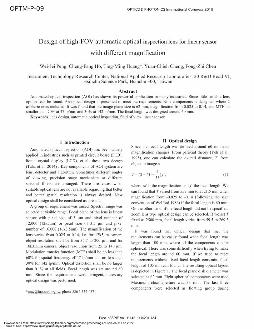
I Introduction Automated optical inspection (AOI) has been widely
applied in industries such as printed circuit board (PCB), liquid crystal display (LCD), et al. these two decays (Taha et al. 2014) . Key components of AOI system are lens, detector and algorithm. Sometimes different angles of viewing, precision stage mechanism or different spectral filters are arranged. There are cases when suitable optical lens are not available regarding that better and better spatial resolution is always desired. New optical design shall be considered as a result.
A group of requirement was raised. Spectral range was selected at visible range. Focal plane of the lens is linear sensor with pixel size of 5 m and pixel number of 12,000 (12k5 m) or pixel size of 3.5 m and pixel number of 16,000 (16k3.5 m). The magnification of the lens varies from 0.025 to 0.14, i.e. for 12k5 m camera object resolution shall be from 35.7 to 200 m, and for 16k3.5 m camera, object resolution from 25 to 140 m. Modulation transfer function (MTF) shall be no less than 60% for spatial frequency of 47 lp/mm and no less than 30% for 142 lp/mm. Optical distortion shall be no larger than 0.1% at all fields. Focal length was set around 60 mm. Since the requirements were stringent, necessary optical design was performed.
*[email protected]; phone 886 3 537-0871
II Optical design Since the focal length was defined around 60 mm and magnification changes. From paraxial theory (Yeh et al, 1995), one can calculate the overall distance, T, from object to image as
fM
MT )12( , (1)
where M is the magnification and f the focal length. We can found that T varied from 557 mm to 2521.5 mm when magnification from -0.025 to -0.14 (following the sign convention of Welford 1986) if the focal length is 60 mm. On the other hand, if the focal length did not be specified, zoom lens type optical design can be selected. If we set T fixed as 2500 mm, focal length varies from 59.5 to 269.3 mm.
It was found that optical design that met the requirements can be easily found when focal length was larger than 100 mm, where all the components can be spherical. There was some difficulty when trying to make the focal length around 60 mm. If we tried to meet requirements without fixed focal length constrain, focal length of 105 mm can found. The resulting optical layout is depicted in Figure 1. The focal plane disk diameter was selected as 62 mm. Eight spherical components were used. Maximum clear aperture was 33 mm. The last three components were selected as floating group during
Design of high-FOV automatic optical inspection lens for linear sensor
with different magnification
Wei-Jei Peng, Cheng-Fang Ho, Ting-Ming Huang*, Yuan-Chieh Cheng, Fong-Zhi Chen
Instrument Technology Research Center, National Applied Research Laboratories, 20 R&D Road VI, Hsinchu Science Park, Hsinchu 300, Taiwan
Abstract
Automated optical inspection (AOI) has shown its powerful application in many industries. Since little suitable lens options can be found. An optical design is presented to meet the requirements. Nine components is designed, where 2 aspheric ones included. It was found that the image plane size is 62 mm, magnification from 0.025 to 0.14, and MTF no smaller than 70% at 47 lp/mm and 30% at 142 lp/mm. The focal length was designed around 60 mm.
Keywords: lens design, automatic optical inspection, field of view, linear sensor
Proc. of SPIE Vol. 11142 1114201-134Downloaded From: https://www.spiedigitallibrary.org/conference-proceedings-of-spie on 11 Feb 2022Terms of Use: https://www.spiedigitallibrary.org/terms-of-use

magnification variation. As a result, the length of the lens was from 53.9 to 54.5 mm. Back focal length was from 74.3 to 86.3 mm.
Figure 1. Optical layout for the design result with focal length of 105 mm
To meet the requirements, focal length shall be around 60 mm. The design result is illustrated in Figure 2. Nine components can be found with 2 plastic and 7 glass ones. Four components were arranged in front of the stop while the other five after stop. The last five components were set as floating group when magnification varies. Two aspheric components were designed to meet the stringent requirements such as focal length, MTF and distortion. Maximum lens clear aperture was 86 mm.
Figure 2. Optical layout for the design result with focal length of 60 mm
Figure 3. Optical layout for different magnification
In Figure 2, first component was highly asphric for large FOV of 54 deg. The length of the lens was from 280.3 to 285.8 mm, while back focal length was from 60.7 to 68 mm. For different magnification, optical layout can be found in Figure 3. Position variation was shown for each case. MTF curves for magnification of 0.025 are shown in Figure 4. For other magnification factors, MTF are slightly different but all larger than 30% at 142 lp/mm. Distortion was found to be less than 0.1% for all magnification factors.
Figure 4. MTF plot for magnification of 0.025
III Conclusion An AOI lens has been designed for linear sensors with
pixel size of 5 m and pixel number of 12,000 or pixel size of 3.5 m and pixel number of 16,000. The field of view reaches 54 degrees. Magnification of the lens varies from 0.025 to 0.14. Effective focal length is 60 mm. MTF of optical design meets requirement and reaches 70% at spatial frequency of 47 lp/mm and 30% at 142 lp/mm. The distortion is controlled under 0.1%.
References Taha, E. M., Emary, E. and Moustafa, K. 2014. Automatic
Optical Inspection for PCB Manufacturing: a Survey, International Journal of Scientific & Engineering Research 5(7):1095-1102.
Welford, W. T. 1986. Aberrations of Optical Systems. Bristol and Boston: Adam Hilger.
Yeh, M. S., Shiue, S. G. aud Lu, M. H. 1995, Two-optical-componentmethod for designing zoom system," Optical Engineering, 34(6): 1826-1834.
Proc. of SPIE Vol. 11142 1114201-135Downloaded From: https://www.spiedigitallibrary.org/conference-proceedings-of-spie on 11 Feb 2022Terms of Use: https://www.spiedigitallibrary.org/terms-of-use
I Introduction Glass is the most significant high-performance materials
used for numerous technologies – including scientific research, industrial and social applications, for example, the luminescent glasses obtained by doping. The past decades have witnessed a significant benefit from these kinds of luminescence glasses in various applications such as fiber-optic communication, laser and light emitting diode (LED) lighting, mainly owing to the outstanding performance of active dopants [1]. A series of photoluminescence ions are inlaid into the host matrix in these applications. The spectroscopic features of gain materials are closely associated with their chemical state and the surrounding ligand field. This provides the possibility to improve the luminescence characteristics of active ions by changing the host matrix identified by Raman spectra, X-ray diffraction, nuclear magnetic resonance [2,3]. Recently THz-TDS has been employed to characterize a series of silicate glasses [4,5]. THz-TDS gives a direct measurement of the field amplitude and phase and enables the calculation of the absorption coefficients and refractive indices with single
measurement. But THz-TDS is less used to study active glasses.
In this paper, THz-TDS is used to characterize erbium doped phosphate glasses for the first time to our best knowledge. Material parameters derived from THz signals were strongly dependent on the glass compositions. The relationships between these parameters and optical properties, such as luminescence intensities at 1532 nm and related fluorescence lifetimes under 980 nm excitation, were further discussed and analyzed.
II Preparation of doped phosphate glasses
A set of ytterbium and erbium doped phosphate glass samples, in varying compositions P2O5-X2O3-YO with X=B, Al, Ga and Y=Zn, Mg, Ca, are listed in Table 1. They were prepared by the traditional melting-quenching method [2]. The raw materials were weighed to ~ 50 g, mixed in an agate mortar for at least 15 min, stored in an alumina crucible and put into a 500 °C electric furnace for 30 min. Then the samples were melted at 1500 °C for 60 min. All the obtained glasses were annealed around Tg for 180 min. Finally, the glasses were cut and polished
Characterization of Erbium Doped Phosphate Glasses by Terahertz Time
Domain Spectroscopy
Yushi Chua, b, Shaghik Atakaramiansb, Runan Zhanga, Desheng Fanb, Gui Xiaob, Xinghu Fub,c, Shuen Weib, Bowen Zhangb, Yuan Tianb, Zhanyu Maa, Quan Chaia, Jing Ren*a, Yanhua Luob, Jianzhong
Zhang*a, Gang-Ding Pengb
aKey Lab of In-Fiber Integrated Optics of Ministry of Education, School of Science, Harbin Engineering University, Harbin, 150001, China
bPhotonics and Optical Communications, School of Electrical Engineering and Telecommunications, University of New South Wales, Sydney 2052, NSW, Australia
cSchool of Information Science and Engineering, Yanshan University, Qinhuangdao, 066004, China
Abstract Terahertz time domain transmission spectroscopy (THz-TDS), simultaneous recording amplitude and phase information
with short pulses of terahertz radiation, stand out as an excellent method for material characterization and analysis. In this work, THz-TDS was used to characterize erbium doped phosphate glasses with different compositions. Absorption coefficients, refractive indices and related material parameters were calculated based on these THz signals, which changed with glass compositions. Furthermore, the relationship between these parameters and optical properties, such as luminescence intensities at 1532 nm and related fluorescence lifetimes under 980 nm excitation was demonstrated for the first time to our best knowledge. Results show THz-TDS provides a useful insight into active glass characterization.
Keywords: terahertz ray, time domain spectroscopy, phosphate glass, erbium doped material, near infrared emission.
Proc. of SPIE Vol. 11142 1114201-136Downloaded From: https://www.spiedigitallibrary.org/conference-proceedings-of-spie on 11 Feb 2022Terms of Use: https://www.spiedigitallibrary.org/terms-of-use
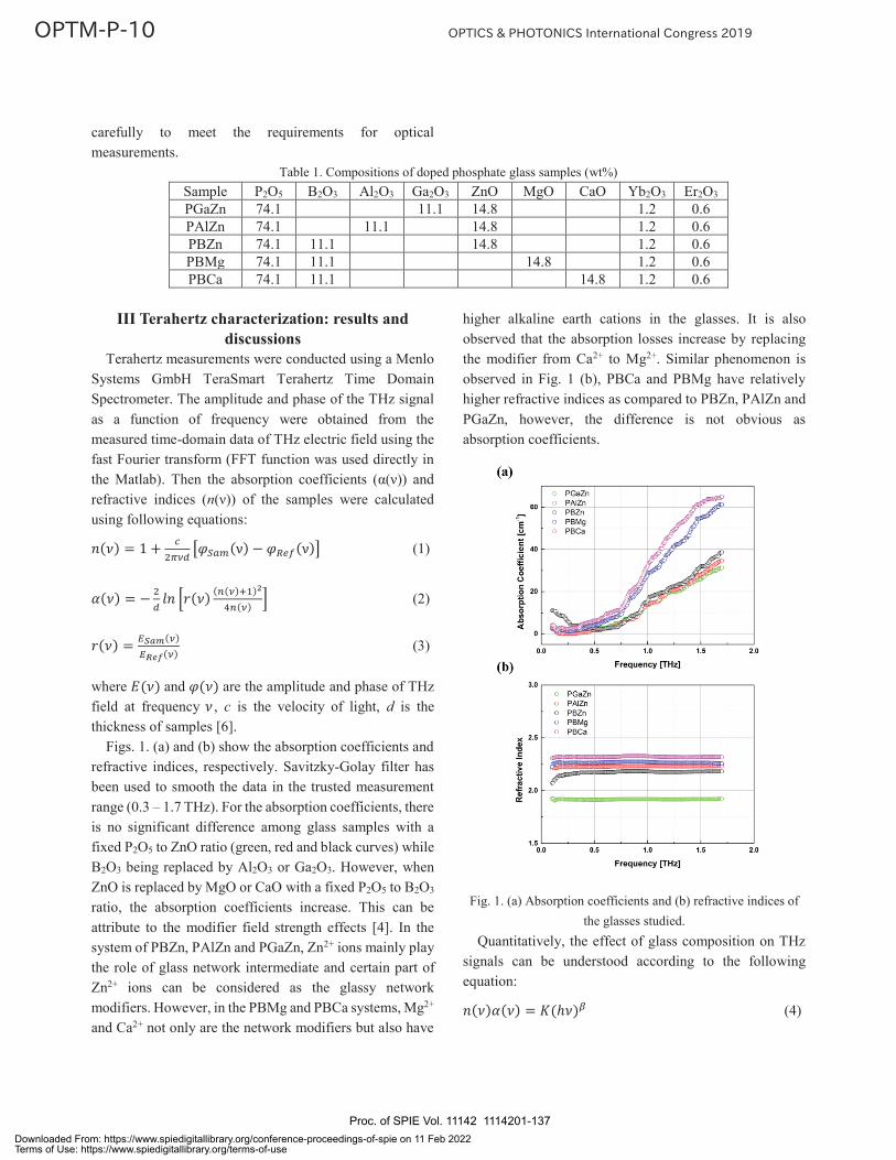
carefully to meet the requirements for optical measurements.
Table 1. Compositions of doped phosphate glass samples (wt%) Sample P2O5 B2O3 Al2O3 Ga2O3 ZnO MgO CaO Yb2O3 Er2O3 PGaZn 74.1 11.1 14.8 1.2 0.6 PAlZn 74.1 11.1 14.8 1.2 0.6 PBZn 74.1 11.1 14.8 1.2 0.6 PBMg 74.1 11.1 14.8 1.2 0.6 PBCa 74.1 11.1 14.8 1.2 0.6
III Terahertz characterization: results and discussions
Terahertz measurements were conducted using a Menlo Systems GmbH TeraSmart Terahertz Time Domain Spectrometer. The amplitude and phase of the THz signal as a function of frequency were obtained from the measured time-domain data of THz electric field using the fast Fourier transform (FFT function was used directly in the Matlab). Then the absorption coefficients (α(ν)) and refractive indices (n(ν)) of the samples were calculated using following equations:
(1)
(2)
(3)
where and are the amplitude and phase of THz field at frequency , c is the velocity of light, d is the thickness of samples [6].
Figs. 1. (a) and (b) show the absorption coefficients and refractive indices, respectively. Savitzky-Golay filter has been used to smooth the data in the trusted measurement range (0.3 – 1.7 THz). For the absorption coefficients, there is no significant difference among glass samples with a fixed P2O5 to ZnO ratio (green, red and black curves) while B2O3 being replaced by Al2O3 or Ga2O3. However, when ZnO is replaced by MgO or CaO with a fixed P2O5 to B2O3 ratio, the absorption coefficients increase. This can be attribute to the modifier field strength effects [4]. In the system of PBZn, PAlZn and PGaZn, Zn2+ ions mainly play the role of glass network intermediate and certain part of Zn2+ ions can be considered as the glassy network modifiers. However, in the PBMg and PBCa systems, Mg2+ and Ca2+ not only are the network modifiers but also have
higher alkaline earth cations in the glasses. It is also observed that the absorption losses increase by replacing the modifier from Ca2+ to Mg2+. Similar phenomenon is observed in Fig. 1 (b), PBCa and PBMg have relatively higher refractive indices as compared to PBZn, PAlZn and PGaZn, however, the difference is not obvious as absorption coefficients.
Fig. 1. (a) Absorption coefficients and (b) refractive indices of the glasses studied.
Quantitatively, the effect of glass composition on THz signals can be understood according to the following equation:
(4)
Proc. of SPIE Vol. 11142 1114201-137Downloaded From: https://www.spiedigitallibrary.org/conference-proceedings-of-spie on 11 Feb 2022Terms of Use: https://www.spiedigitallibrary.org/terms-of-use
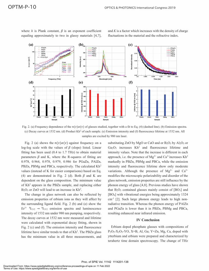
where h is Plank constant, is an exponent coefficient equaling approximately to two in glassy materials [4,7],
and K is a factor which increases with the density of charge fluctuations in the material and the refractive index.
Fig. 2. (a) Frequency dependence of the of glasses studied, together with a fit to Eq. (4) (dashed line). (b) Emission spectra.
(c) Decay curves at 1532 nm. (d) Product Kh2 of each sample. (e) Emission intensity and (f) fluorescence lifetime at 1532 nm. All samples are excited by 980 nm laser.
Fig. 2 (a) shows the against frequency on a log-log scale with the values of (slope) listed. Linear fitting has been used (0.4 to 1.7 THz) to obtain material parameters and K, where the R-squares of fitting are 0.978, 0.964, 0.978, 0.979, 0.986 for PGaZn, PAlZn, PBZn, PBMg and PBCa, respectively. The calculated Kh2 values (instead of K for easier comparisons) based on Eq. (4) are demonstrated in Fig. 2 (d). Both and K are dependent on the glass composition. The minimum value of Kh2 appears in the PBZn sample, and replacing either B2O3 or ZnO will lead to an increase in Kh2.
The change in glass network can also be reflected by emission properties of erbium ions as they will affect by the surrounding ligand field. Fig. 2 (b) and (e) show the Er3+ 4I13/2 4I15/2 emission spectra and luminescence intensity of 1532 nm under 980 nm pumping, respectively. The decay curves at 1532 nm were measured and lifetime were calculated with exponential decay fitting, shown in Fig. 2 (c) and (f). The emission intensity and fluorescence lifetime have similar trends to that of Kh2. The PBZn glass has the minimum value in all three measurements, and
substituting ZnO by MgO or CaO and or B2O3 by Al2O3 or Ga2O3 increases Kh2 and fluorescence lifetime and intensity values. Note that the increase is different in each approach, i.e. the presence of Mg2+ and Ca2+increases Kh2 markedly in PBZn, PBMg and PBCa, while the emission intensity and fluorescence lifetime show only moderate variations. Although the presence of Mg2+ and Ca2+ modifies the microscopic polarizability and disorder of the glass network, emission properties are still influence by the phonon energy of glass [4,8]. Previous studies have shown that B2O3 contained glasses mainly consist of [BO3] and [BO4] with vibrational energies being approximately 1324 cm-1 [2]. Such large phonon energy leads to high non-radiative transition. Whereas the phonon energy of PAlZn and PGaZn is lower than it in PBZn, PBMg and PBCa, resulting enhanced near infrared emission.
IV Conclusion
Erbium doped phosphate glasses with compositions of P2O5-X2O3-YO, X=B, Al, Ga; Y=Zn, Mg, Ca, doped with ytterbium and erbium were prepared and characterized by terahertz time domain spectroscopy. The change of THz
Proc. of SPIE Vol. 11142 1114201-138Downloaded From: https://www.spiedigitallibrary.org/conference-proceedings-of-spie on 11 Feb 2022Terms of Use: https://www.spiedigitallibrary.org/terms-of-use
signals depends on the glass compositions. For the absorption coefficients and refractive indices, they increase as the alkalinity of the glass rises. As for the material parameters and Kh2, they demonstrate similar trends for the emission of Er3+ and fluorescence lifetime at 1532 nm with subtle differences related to the phonon energy of the glasses. These results demonstrate that THz-TDS has great potential to be employed as a structural probe for active glass characterization. *[email protected] and [email protected]
V Acknowledgements This study was supported by the National Natural
Science Foundation of China (NSFC) (61775045, 61605030, 51872055), Natural Science Foundation of Heilongjiang Province of China (F2017006), Y. Chu. thanks for the support of China Scholarship Council (CSC No. 201706680054).
VI Reference [1] Chu, Y., Hu, Q., Zhang, Y., et al, “Topological Engineering of Photoluminescence Properties of Bismuth- or Erbium-Doped Phosphosilicate Glass of Arbitrary P2O5 to SiO2 Ratio,” Advanced Optical Materials 6(13), 1800024, (2018). [2] Chu, Y., Ren, J., Zhang, J., et al, “Ce3+/Yb3+/Er3+ triply doped bismuth borosilicate glass: a potential fiber material for broadband near-infrared fiber amplifiers,” Scientific Reports 6, 33865 (2016). [3] Uesbeck, T., Eckert, H., Youngman, R., et al, “The Structure of borophosphosilicate pure network former glasses studied by multinuclear NMR spectroscopy,” The Journal of Physical Chemistry C 121(3), 1838-1850 (2017). [4] Naftaly, M. and Miles, R. E., “Terahertz Time-Domain Spectroscopy for Material Characterization,” Proceeding of IEEE 95, 1658-1665 (2007). [5] Withayachumnankul, W., Png, G. M., Yin, X., et al, “T-ray sensing and imaging,” Proceedings of the IEEE 95, 1528-1558 (2007). [6] Jepsen, P. U., and Fischer, B. M., “Dynamic range in terahertz time-domain transmission and reflection spectroscopy,” Optics Letters 30(1), 29-31 (2005). [7] Naftaly, M. and Miles, R. E., “Terahertz time-domain spectroscopy of silicate glasses and the relationship to
material properties,” Journal of Applied Physics 102(4), 043517 (2007). [8] Chu, Y., Ren, J., Zhang, J., et al, “Effects of melting temperature and composition on spectroscopic properties of Er3+-doped bismuth glasses,” Optical Materials Express 6(1), 279-287 (2016).
Proc. of SPIE Vol. 11142 1114201-139Downloaded From: https://www.spiedigitallibrary.org/conference-proceedings-of-spie on 11 Feb 2022Terms of Use: https://www.spiedigitallibrary.org/terms-of-use

I Introduction Currently, 3D scanning technology widely used in our
life. The technology flourished from the 2010. The most people well known was Kinect. The system was published by Microsoft. It could measure the depth information and instant computing the full color model. The tech not only used in the entertainment, but also applied to medical, 3D imaging construct and health care etc. [1] The 3D scanning technology could be classified to active type and passive type. The most popular 3D scanning technology was list on the below: (reference Figure. 1)
Stereo Vision (passive type): The tech used the parallax principle, so the system usually needed two or more than two imaging from the different angle. The 3D information could be obtained by each relative positions of objects in these plane screens. [2]
Structured Light (active type): The tech usually composed of the IR light source and IR camera. The light source projected a certain pattern on the object and the IR camera will capture the reflection figure. The 3D information could be obtained by the difference between the ideal pattern and reflection pattern. [3, 4]
Time of Flight (active type): The major elements of the tech was the same with structure light, but it used the different working principle. The 3D information could be obtained by each flight time of light source. [5]
Figure. 1 3D scanning technology classification Most of the 3D scanning products was active type. In
the above popular scanning techs, the structured light technology was the only one could analysis nanometer depth information, but it still had some disadvantage of sensor calibration, environment light effects and long operation time. Therefore, people present the different
Rou-Jhen Chena, Yu-Hsuan Lina , Hsin-Yi Tsaia, Kuo-Cheng Huanga, Chun-Han Choua*
a. National Applied Research Laboratories, Instrument Technology Research Center, 20, R&D Rd. VI, Hsinchu Science Park, Hsinchu City, Taiwan, R.O.C. 30076
Abstract In the studying, we analysis the diffraction pattern noise that was design by iterative Fourier transform algorithm. 3D
scanning technology widely used in our life. Structure light was a popular technology that used in the 3D scanning. The projection pattern of structure light directly affected the system resolution. Therefore, we design the two types of diffraction pattern by iterative Fourier transform algorithm and compare the imaging quality. From the simulation result, we found the circular pattern which Signal to Noise Ratio was 1.5 times to the rectangular type and the projection pattern didn’t directly affect conversion efficiency and stray light. In the future, we could simulate the more patterns and complex patterns to find the best projection pattern for structured light.
Keywords: diffraction pattern, iterative Fourier transform algorithm, structure light, 3D scanning
Proc. of SPIE Vol. 11142 1114201-140Downloaded From: https://www.spiedigitallibrary.org/conference-proceedings-of-spie on 11 Feb 2022Terms of Use: https://www.spiedigitallibrary.org/terms-of-use

method to overcome these problems. El-laithy team presented an algorithm to reduce the environment light effects [6]. Wiedemann team change the object distance and camera exposure time to decrease the calibration time [7]. Hall-Holt team presented a special pattern to decrease the system operation time [8]. Zhang team used the color pattern and phase shift principle to increase the depth information resolution [9, 10]. In these prior art, lot of people presented the different meth to reduce the noise and operation time. In the paper, we would like to use the Iterative Fourier Transform Algorithm(IFTA) to design the different patterns grating and compare the noise which applied in the structured light system.
II Diffraction element design principle
In the paper, we used IFTA to design the three grating with the different patterns. IFTA principle was suppose a random phase and through numerical iterative processing to get the result. The calculation process showed on the below: (reference Figure. 2)
Figure. 2. IFTA diffraction grating creation process In the experiment, we used the light source with 532
nm wavelength. The simulation focal length on the 100mm. The grating was a four level diffraction element and each pitch was 3.04um. Its size was 10*10mm. The simulation structure reference Figure. 3.
Figure. 3. Experiment diagram
III Diffraction pattern simulation results In the paper, we used IFTA to design the two
diffraction elements which could project the diffraction patterns. The first projection pattern was 5*5 circular matrix. Each spot diameter was 2mm and the pitch was 2mm. (reference Figure. 4) The second projection pattern was 5*5 rectangular matrix. Each spot was 2mm and the pitch was 2mm. (reference Figure. 5)
Figure. 4. Circular pattern 5*5 matrix
Figure. 5. Rectangular pattern 5*5 matrix
From the simulation result, we compared the results of two type. Signal to Noise Ratio of circular type was
Proc. of SPIE Vol. 11142 1114201-141Downloaded From: https://www.spiedigitallibrary.org/conference-proceedings-of-spie on 11 Feb 2022Terms of Use: https://www.spiedigitallibrary.org/terms-of-use
rectangular type 1.5 times. The two type results of conversion efficiency and stray light was almost the same. (reference Table. 1.)
Table. 1. The two type simulation results
Through the simulation, we found the pattern that
would directly affect the SNR. The pattern didn’t directly affect the conversion efficiency and stray light. The simple projection pattern was more suitable for the structure light system.
IV Conclusion
In the studying, we used IFTA to design two types diffraction element. From the simulation results, we found the simpler pattern which Signal to Noise Ratio was 1.5 times to the rectangular type and the projection pattern didn’t directly affect conversion efficiency and stray light. In the future, we could simulate the more patterns and complex patterns to find the best projection pattern for structured light.
References [1]. Sarbolandi, Hamed, Damien Lefloch, and Andreas
Kolb. "Kinect range sensing: Structured-light versus Time-of-Flight Kinect." Computer vision and image understanding 139: 1-20. (2015)
[2]. Tippetts, Beau, et al. "Review of stereo vision algorithms and their suitability for resource-limited systems." Journal of Real-Time Image Processing 11.1: 5-25. (2016)
[3]. Rubinsztein-Dunlop, Halina, et al. "Roadmap on structured light." Journal of Optics 19.1: 013001. (2016)
[4]. Litchinitser, Natalia M., et al. "Structured light-matter interactions in engineered optical media (Conference Presentation)." High Contrast Metastructures VI. Vol. 10113. International Society for Optics and Photonics, 2017.
[5]. Beck, Scarlet, et al. "The impact II, a very high resolution quadrupole time-of-flight instrument for deep shotgun proteomics." Molecular & Cellular Proteomics: mcp-M114. (2015)
[6]. El-laithy, Riyad A., Jidong Huang, and Michael Yeh. "Study on the use of Microsoft Kinect for robotics applications." Position Location and Navigation Symposium (PLANS), 2012 IEEE/ION. IEEE, 2012.
[7]. Wiedemann, Matthias, et al. "Analysis and characterization of the PMD camera for application in mobile robotics." IFAC Proceedings Volumes 41.2: 13689-13694. (2008)
[8]. Hall-Holt, Olaf, and Szymon Rusinkiewicz. "Stripe boundary codes for real-time structured-light range scanning of moving objects." Computer Vision, 2001. ICCV 2001. Proceedings. Eighth IEEE International Conference on. Vol. 2. IEEE, 2001.
[9]. Zhang, Song, and Peisen Huang. "High-resolution, real-time 3D shape acquisition." null. IEEE, 2004.
[10]. Zhang, Song. "Recent progresses on real-time 3D shape measurement using digital fringe projection techniques." Optics and lasers in engineering 48.2: 149-158. (2010)
Proc. of SPIE Vol. 11142 1114201-142Downloaded From: https://www.spiedigitallibrary.org/conference-proceedings-of-spie on 11 Feb 2022Terms of Use: https://www.spiedigitallibrary.org/terms-of-use
Research on measurement method of coincidence degree for
remote micro-objects based on parallel light imaging 1,2Wei han, 1,2Min Huang, 1,2Qisheng Cai, 1,2Xiangning Lu
1.Key Laboratory of Computational Optical Imaging Technology, Chinese Academy of Sciences,2. Academy of Opto-Electronics, Chinese Academy of Sciences
Abstract A method of coincidence degree for remote micro-objects based on parallel
light imaging is proposed, which solve the problem that the existing technology can not measure the space position of micro-objects at a long distance. 1.Introduction
The long-distance measurement of the spatial position of micro-objects that the geometric size is similar to the wavelength is limited by the optical physical characteristics, the accuracy of equipment, and can not meet the accuracy requirements, even can not be measured. Especially for the measurement of the spatial position relationship of multiple micro-objects in long-distance, whether using full-wavelength beam or laser beam to measure, it will be affected by interference and diffraction. In this paper, the coincidence measurement of two micro-slits (tens of microns) with long distances (meters) is studied. 2.Basic principle of measurement
Considering the actual situation of the measurement task, the measurement principle as shown in Figure 2 is adopted: white light source 1 emits stable white light, after homogenizing plate 2, homogenizing light 3 irradiates on the first tantalum plate 4. The tantalum plate is located at the focal point of parallel light shaping device 5. The parallel light shaping device has a fixed focal length f(6), and then is coupled to another parallel light shaping device 8 through parallel light 7. This device has the same parameters and technical specifications with the former parallel light shaping device. The second tantalum sheet 10 is placed at the focus of the second parallel light shaping device 8. At this time, the equal-scale real image of the first Tantalum Sheet 4 is inverted on the surface of the second tantalum sheet 10. The position of the inverted real image and the second tantalum sheet is measured by using the detection/observation measuring device 12 with focal length f0(11) (this project is a reading microscope). Finally, the measurement results of projection coincidence degree are obtained.
Proc. of SPIE Vol. 11142 1114201-143Downloaded From: https://www.spiedigitallibrary.org/conference-proceedings-of-spie on 11 Feb 2022Terms of Use: https://www.spiedigitallibrary.org/terms-of-use

4
f f f0
1 2
3
5
6 7
8
9 11
10 12
Fig. 1 Principle of coincidence measurement 3. Measurement process and result
3.1 Determination of sampling points During the sampling process, in order to ensure that the sampled sample
can universally and reasonably represent the projection size of the micro-slit in the whole 20 *20 mm range, and have a good response system setting accuracy, sampling points are selected according to the figure 2. That is to say, it can cover the range of edges and corners, and at the same time reflect the changing trend of projection size of horizontal and vertical slits, and basically determine the accuracy distribution of the alignment results.
Figure 2 Sampling schematic diagram of Ta slit coincidence data
3.2 Focus calibration Using standard devices such as bolo plate and reading microscope to
finish focus calibration. 3.3 Coaxial calibration Using linear interval and knife-edge method of photoelectric conversion of
photodetectors to finish coaxial calibration. 3.4 Rusult The average slot width of tantalum sheet is 146.37 micron, and the
projection slot width of the collimator is 141.19 micron after fine-tuning. The average coincidence rate is 96.461%.
Proc. of SPIE Vol. 11142 1114201-144Downloaded From: https://www.spiedigitallibrary.org/conference-proceedings-of-spie on 11 Feb 2022Terms of Use: https://www.spiedigitallibrary.org/terms-of-use
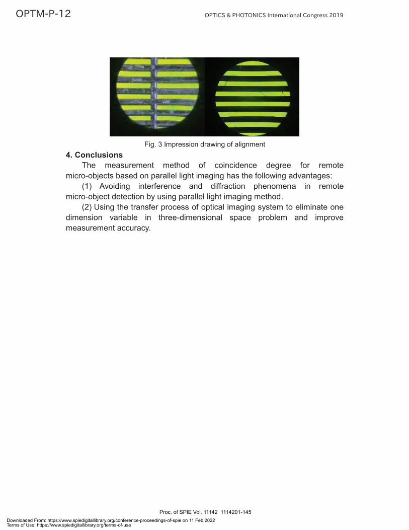
Fig. 3 Impression drawing of alignment
4. Conclusions The measurement method of coincidence degree for remote
micro-objects based on parallel light imaging has the following advantages: (1) Avoiding interference and diffraction phenomena in remote
micro-object detection by using parallel light imaging method. (2) Using the transfer process of optical imaging system to eliminate one
dimension variable in three-dimensional space problem and improve measurement accuracy.
Proc. of SPIE Vol. 11142 1114201-145
Downloaded From: https://www.spiedigitallibrary.org/conference-proceedings-of-spie on 11 Feb 2022Terms of Use: https://www.spiedigitallibrary.org/terms-of-use
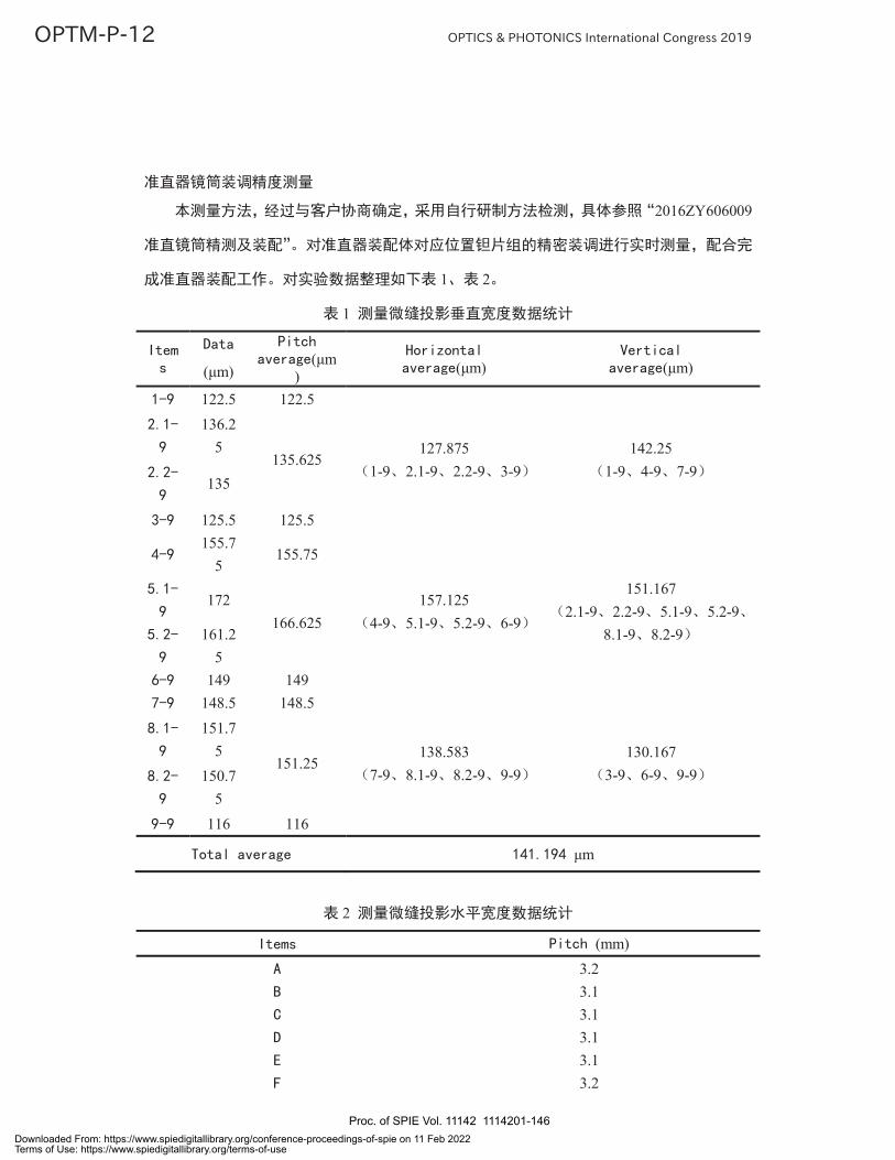
2016ZY606009
1 2
1
(μm) (μm) (μm)(μm)
122.5 122.5
127.8751-9 2.1-9 2.2-9 3-9
142.251-9 4-9 7-9
136.25
135.625135
125.5 125.5155.7
5155.75
157.1254-9 5.1-9 5.2-9 6-9
151.1672.1-9 2.2-9 5.1-9 5.2-9
8.1-9 8.2-9
172166.625
161.25
149 149148.5 148.5
138.5837-9 8.1-9 8.2-9 9-9
130.1673-9 6-9 9-9
151.75
151.25150.7
5116 116
μm
2
(mm)3.23.13.13.13.13.2
Proc. of SPIE Vol. 11142 1114201-146Downloaded From: https://www.spiedigitallibrary.org/conference-proceedings-of-spie on 11 Feb 2022Terms of Use: https://www.spiedigitallibrary.org/terms-of-use

Average=3.13μm RMS=0.002220 20mm
1
5
1 2
12
3
:
1
2
3
Pitch:
Horizontal:
Vertical:
2 1
2 3 4 5
f 6 7 8
10
8 4 10
f0 11 / 12
Proc. of SPIE Vol. 11142 1114201-147Downloaded From: https://www.spiedigitallibrary.org/conference-proceedings-of-spie on 11 Feb 2022Terms of Use: https://www.spiedigitallibrary.org/terms-of-use

2
01 01
01 01
01 01
01
02 01 02
02
02
1~2
eI Ph
1
1
P e h
2I P 2
512
1mV 10dB
yy
0x 0x x90
60
1m
3 3 9
Proc. of SPIE Vol. 11142 1114201-148Downloaded From: https://www.spiedigitallibrary.org/conference-proceedings-of-spie on 11 Feb 2022Terms of Use: https://www.spiedigitallibrary.org/terms-of-use

8
9
SAMPLE01 145.14μm SAMPLE02
147.60μm
1 20mm×20mm 141.19μm
2 172μm 116μm
3 151~157μm
4 9 9
5
3.13μm RMS=0.0022
146.37μm 141.19μm
96.461%
3. Analysis of results: The measured results of cemented sheets are SAMPLE01, with an average slit width of 145.14 um, SAMPLE02 and an average slit width of 147.60 um. Based on the measurement data in section I of the report, it is summarized as follows: 1. The average slit width of fine-tuned alignment projection is 141.19 um in the 20 mm x 20 mm slit area of tantalum sheet. 2. The maximum projection slit width is 172 microns and the minimum is 116 microns. 3. The width of projection slit in the central region is the largest, 151-157 um. The closer to the edge, the smaller the projection slit width and the lower the adjustment accuracy. 4. Data acquisition point is similar to 9 *9 mode. The horizontal and vertical analysis shows that the data change trend of three row acquisition points is large in the middle, small at both ends and larger at the lower end than at the upper end. The data change trend of three row acquisition points is large in the middle, small at both ends and larger at the left end than at the right end, indicating that the middle area of micro-slit adjustment effect is the best, followed by the third quadrant (lower left) and the first quadrant (upper right). 5. In horizontal width statistics, the consistency of horizontal width is good, the
Proc. of SPIE Vol. 11142 1114201-149Downloaded From: https://www.spiedigitallibrary.org/conference-proceedings-of-spie on 11 Feb 2022Terms of Use: https://www.spiedigitallibrary.org/terms-of-use

fluctuation of data is very small, the average value is close to the actual value, the result is 3.13 um, RMS = 0.0022. Comparing the data of cementing sheet, the average seam width of cementing sheet is 146.37 micron, and the projection seam width of the collimator is 141.19 micron, the average coincidence rate is 96.461%.
Proc. of SPIE Vol. 11142 1114201-150Downloaded From: https://www.spiedigitallibrary.org/conference-proceedings-of-spie on 11 Feb 2022Terms of Use: https://www.spiedigitallibrary.org/terms-of-use
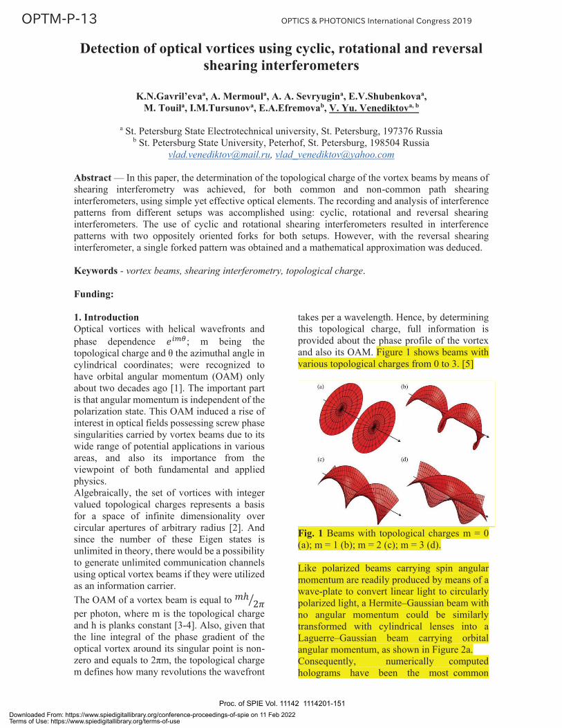
Detection of optical vortices using cyclic, rotational and reversal shearing interferometers
K.N.Gavril’evaa, A. Mermoula, A. A. Sevryugina, E.V.Shubenkovaa,M. Touila, I.M.Tursunova, E.A.Efremovab, V. Yu. Venediktova, b
a St. Petersburg State Electrotechnical university, St. Petersburg, 197376 Russiab St. Petersburg State University, Peterhof, St. Petersburg, 198504 Russia
[email protected], [email protected]
Abstract — In this paper, the determination of the topological charge of the vortex beams by means of shearing interferometry was achieved, for both common and non-common path shearing interferometers, using simple yet effective optical elements. The recording and analysis of interference patterns from different setups was accomplished using: cyclic, rotational and reversal shearing interferometers. The use of cyclic and rotational shearing interferometers resulted in interferencepatterns with two oppositely oriented forks for both setups. However, with the reversal shearing interferometer, a single forked pattern was obtained and a mathematical approximation was deduced.
Keywords - vortex beams, shearing interferometry, topological charge.
Funding:
1. IntroductionOptical vortices with helical wavefronts and phase dependence ; m being the topological charge and θ the azimuthal angle in cylindrical coordinates; were recognized to have orbital angular momentum (OAM) only about two decades ago [1]. The important part is that angular momentum is independent of the polarization state. This OAM induced a rise of interest in optical fields possessing screw phase singularities carried by vortex beams due to its wide range of potential applications in various areas, and also its importance from the viewpoint of both fundamental and applied physics.Algebraically, the set of vortices with integer valued topological charges represents a basis for a space of infinite dimensionality over circular apertures of arbitrary radius [2]. Andsince the number of these Eigen states isunlimited in theory, there would be a possibility to generate unlimited communication channels using optical vortex beams if they were utilized as an information carrier. The OAM of a vortex beam is equal to per photon, where m is the topological charge and h is planks constant [3-4]. Also, given that the line integral of the phase gradient of the optical vortex around its singular point is non-zero and equals to 2πm, the topological charge m defines how many revolutions the wavefront
takes per a wavelength. Hence, by determining this topological charge, full information is provided about the phase profile of the vortex and also its OAM. Figure 1 shows beams with various topological charges from 0 to 3. [5]
Fig. 1 Beams with topological charges m = 0 (a); m = 1 (b); m = 2 (c); m = 3 (d).
Like polarized beams carrying spin angular momentum are readily produced by means of a wave-plate to convert linear light to circularly polarized light, а Hermite–Gaussian beam with no angular momentum could be similarly transformed with cylindrical lenses into a Laguerre–Gaussian beam carrying orbital angular momentum, as shown in Figure 2a.Consequently, numerically computed holograms have been the most common
Proc. of SPIE Vol. 11142 1114201-151Downloaded From: https://www.spiedigitallibrary.org/conference-proceedings-of-spie on 11 Feb 2022Terms of Use: https://www.spiedigitallibrary.org/terms-of-use
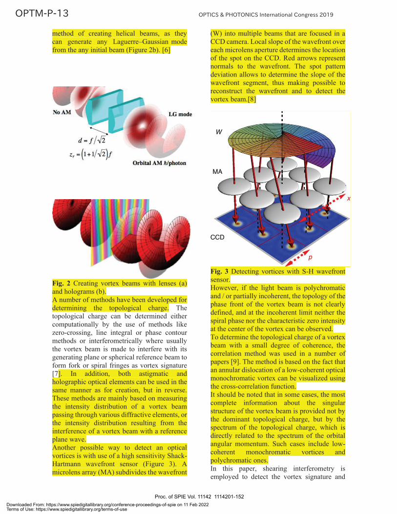
method of creating helical beams, as they can generate any Laguerre–Gaussian mode from the any initial beam (Figure 2b). [6]
Fig. 2 Creating vortex beams with lenses (a) and holograms (b).A number of methods have been developed for determining the topological charge. The topological charge can be determined either computationally by the use of methods like zero-crossing, line integral or phase contour methods or interferometrically where usually the vortex beam is made to interfere with its generating plane or spherical reference beam to form fork or spiral fringes as vortex signature[7]. In addition, both astigmatic and holographic optical elements can be used in the same manner as for creation, but in reverse.These methods are mainly based on measuring the intensity distribution of a vortex beam passing through various diffractive elements, or the intensity distribution resulting from the interference of a vortex beam with a reference plane wave.Another possible way to detect an optical vortices is with use of a high sensitivity Shack-Hartmann wavefront sensor (Figure 3). Amicrolens array (MA) subdivides the wavefront
(W) into multiple beams that are focused in a CCD camera. Local slope of the wavefront over each microlens aperture determines the location of the spot on the CCD. Red arrows represent normals to the wavefront. The spot pattern deviation allows to determine the slope of the wavefront segment, thus making possible to reconstruct the wavefront and to detect the vortex beam.[8]
Fig. 3 Detecting vortices with S-H wavefront sensor.However, if the light beam is polychromatic and / or partially incoherent, the topology of the phase front of the vortex beam is not clearly defined, and at the incoherent limit neither the spiral phase nor the characteristic zero intensity at the center of the vortex can be observed.To determine the topological charge of a vortex beam with a small degree of coherence, the correlation method was used in a number of papers [9]. The method is based on the fact that an annular dislocation of a low-coherent optical monochromatic vortex can be visualized using the cross-correlation function.It should be noted that in some cases, the most complete information about the singular structure of the vortex beam is provided not by the dominant topological charge, but by the spectrum of the topological charge, which is directly related to the spectrum of the orbital angular momentum. Such cases include low-coherent monochromatic vortices and polychromatic ones.In this paper, shearing interferometry is employed to detect the vortex signature and
Proc. of SPIE Vol. 11142 1114201-152Downloaded From: https://www.spiedigitallibrary.org/conference-proceedings-of-spie on 11 Feb 2022Terms of Use: https://www.spiedigitallibrary.org/terms-of-use

determine its topological charge as it does not require a reference beam, it can be made as a very simple and compact optical system and its fringe pattern is less affected by air currents and vibrations [2].In shearing interferometry, the amplitude of the input beam is divided into two, these two beams may or may not travel along the same optical path depending on the type of the interferometer. The first portion of the input beam is unaltered, while in the second half a significate parameter is changed either by shifting, rotating or reversing its wavefront with respect to the first half of the input beam.
2. Shearing interferometry:Shearing interferometry basically relies on the properties of interfering light. It is the process in which an interference pattern is achieved between a test wave and its displaced replica in a region where the two waves overlap [10]. The fringe formation in the region of overlap is governed by:For cyclic shearing interferometer
(1)For rotational shearing interferometer [11]
(2)For reversal shearing interferometer
(3)The fringe pattern optical path difference (OPD) relates to the phase gradient by the following relation
(4)When the shear Δx is small, small shear approximation can be applied and one can write
(5)Where k is the propagation constant. If the phase deviation represented by the phasegradient | ϕ| is small the above relation is valid even for larger shear Δx [12].
3. Experimental setups and results3.1. Common path shearing interferometry: 3.1.1. Cyclic shearing interferometerCyclic shearing interferometers have the advantage of low sensitivity to vibrations [2],they can be used both with incoherent and coherent light sources. Both properties are due to the fact that the optical path traveled by the two interfering beams is the same. In optical testing literature, there are already different arrangements of cyclic shearing
interferometers. For this research, the triangular configuration was selected.The interfering beams in this interferometer have near zero path difference since they counter propagate along the same path. However, there is a phase difference of π since one beam experiences two additional total internal reflections compared to the other [2].The Figure 4 shows the arrangement used, where an interference pattern is acquired by means of a cyclic shearing interferometer. A 5mW He-Ne laser (1) with a wavelength λ = 632.8 nm generates a Gaussian beam that passes through a collimator (2) to keep its beam radius from changing within enough propagation distances, the Collimated beam then illuminates the fork hologram displayed inthe Holoeye transmissive LC-2002 spatial light modulator (3) generated by a computer (4) [13-14] and the transmitted diffracted light passes through a lens (5) with a focal length of L1 =50cm exactly where the diaphragm (6) is located in order to allow only the first diffraction order carrying the vortex with the desirabletopological charge to proceed through the propagation path. An identical lens (7) to the first is set L2 =50 cm apart from the diaphragm for the collimation purpose. The vortex then is split into two counter-propagating identical beams using the cyclic shearing interferometerthat consists of: a beam splitter (8), mirrors (9, 10) to eventually interfere with each other. The interference of the two beams is directly recorded by the CCD camera (11).
Fig. 4. The experimental set-up for interference of vortex using cyclic shearing
interferometer.
Different results are obtained depending on the topological charge "m", Figure 5 shows the interference pattern for an optical vortex with topological charge m = 2 and 4 using cyclic shearing interferometer:
Proc. of SPIE Vol. 11142 1114201-153Downloaded From: https://www.spiedigitallibrary.org/conference-proceedings-of-spie on 11 Feb 2022Terms of Use: https://www.spiedigitallibrary.org/terms-of-use
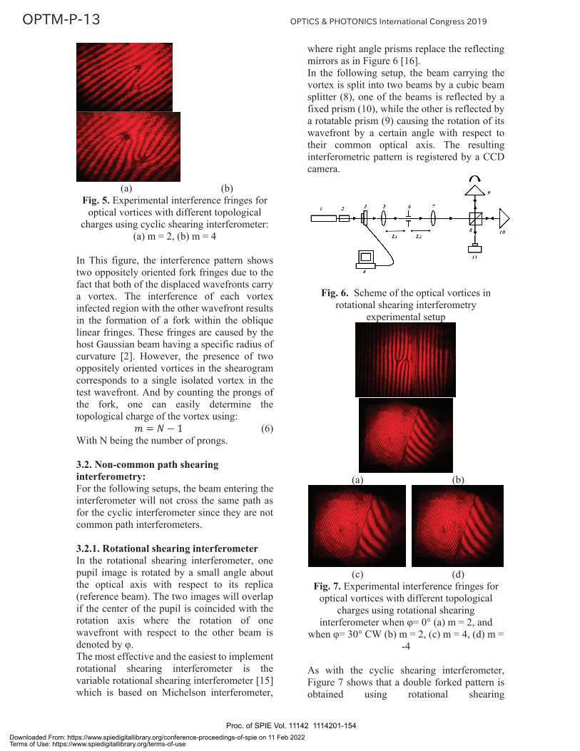
(a) (b)Fig. 5. Experimental interference fringes for
optical vortices with different topological charges using cyclic shearing interferometer:
(a) m = 2, (b) m = 4
In This figure, the interference pattern showstwo oppositely oriented fork fringes due to the fact that both of the displaced wavefronts carry a vortex. The interference of each vortex infected region with the other wavefront results in the formation of a fork within the oblique linear fringes. These fringes are caused by the host Gaussian beam having a specific radius of curvature [2]. However, the presence of two oppositely oriented vortices in the shearogramcorresponds to a single isolated vortex in the test wavefront. And by counting the prongs of the fork, one can easily determine the topological charge of the vortex using:
(6)With N being the number of prongs.
3.2. Non-common path shearing interferometry: For the following setups, the beam entering the interferometer will not cross the same path as for the cyclic interferometer since they are not common path interferometers.
3.2.1. Rotational shearing interferometer In the rotational shearing interferometer, one pupil image is rotated by a small angle about the optical axis with respect to its replica (reference beam). The two images will overlap if the center of the pupil is coincided with the rotation axis where the rotation of one wavefront with respect to the other beam is denoted by φ. The most effective and the easiest to implementrotational shearing interferometer is the variable rotational shearing interferometer [15]which is based on Michelson interferometer,
where right angle prisms replace the reflecting mirrors as in Figure 6 [16].In the following setup, the beam carrying the vortex is split into two beams by a cubic beam splitter (8), one of the beams is reflected by a fixed prism (10), while the other is reflected by a rotatable prism (9) causing the rotation of its wavefront by a certain angle with respect totheir common optical axis. The resulting interferometric pattern is registered by a CCD camera.
Fig. 6. Scheme of the optical vortices in rotational shearing interferometry
experimental setup
(a) (b)
(c) (d)Fig. 7. Experimental interference fringes for
optical vortices with different topological charges using rotational shearing
interferometer when φ= 0° (a) m = 2, and when φ= 30° CW (b) m = 2, (c) m = 4, (d) m =
-4
As with the cyclic shearing interferometer,Figure 7 shows that a double forked pattern is obtained using rotational shearing
Proc. of SPIE Vol. 11142 1114201-154Downloaded From: https://www.spiedigitallibrary.org/conference-proceedings-of-spie on 11 Feb 2022Terms of Use: https://www.spiedigitallibrary.org/terms-of-use
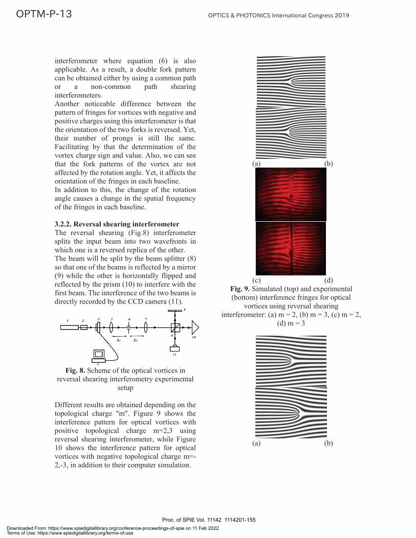
interferometer where equation (6) is also applicable. As a result, a double fork pattern can be obtained either by using a common path or a non-common path shearing interferometers. Another noticeable difference between the pattern of fringes for vortices with negative and positive charges using this interferometer is that the orientation of the two forks is reversed. Yet, their number of prongs is still the same. Facilitating by that the determination of the vortex charge sign and value. Also, we can see that the fork patterns of the vortex are not affected by the rotation angle. Yet, it affects the orientation of the fringes in each baseline. In addition to this, the change of the rotation angle causes a change in the spatial frequency of the fringes in each baseline. 3.2.2. Reversal shearing interferometer The reversal shearing (Fig.8) interferometer splits the input beam into two wavefronts in which one is a reversed replica of the other. The beam will be split by the beam splitter (8) so that one of the beams is reflected by a mirror (9) while the other is horizontally flipped and reflected by the prism (10) to interfere with the first beam. The interference of the two beams is directly recorded by the CCD camera (11).
Fig. 8. Scheme of the optical vortices in
reversal shearing interferometry experimental setup
Different results are obtained depending on the topological charge "m". Figure 9 shows the interference pattern for optical vortices with positive topological charge m=2,3 using reversal shearing interferometer, while Figure 10 shows the interference pattern for optical vortices with negative topological charge m=-2,-3, in addition to their computer simulation.
(a) (b)
(c) (d)
Fig. 9. Simulated (top) and experimental (bottom) interference fringes for optical
vortices using reversal shearing interferometer: (a) m = 2, (b) m = 3, (c) m = 2,
(d) m = 3
(a) (b)
Proc. of SPIE Vol. 11142 1114201-155Downloaded From: https://www.spiedigitallibrary.org/conference-proceedings-of-spie on 11 Feb 2022Terms of Use: https://www.spiedigitallibrary.org/terms-of-use
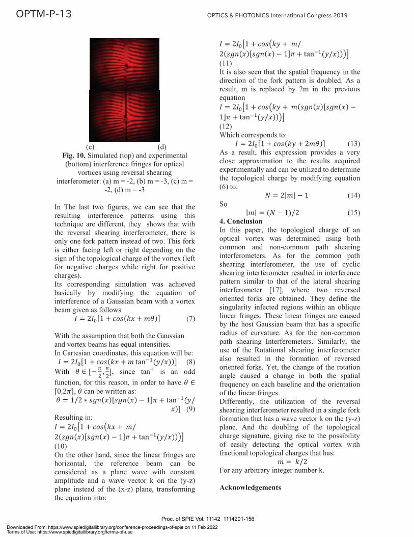
(c) (d)Fig. 10. Simulated (top) and experimental(bottom) interference fringes for optical
vortices using reversal shearing interferometer: (a) m = -2, (b) m = -3, (c) m =
-2, (d) m = -3
In The last two figures, we can see that the resulting interference patterns using this technique are different, they shows that with the reversal shearing interferometer, there is only one fork pattern instead of two. This fork is either facing left or right depending on the sign of the topological charge of the vortex (left for negative charges while right for positivecharges). Its corresponding simulation was achievedbasically by modifying the equation of interference of a Gaussian beam with a vortexbeam given as follows
(7)
With the assumption that both the Gaussian and vortex beams has equal intensities.In Cartesian coordinates, this equation will be:
(8)With , since tan-1 is an odd function, for this reason, in order to have
, can be written as:
(9)Resulting in:
(10)On the other hand, since the linear fringes are horizontal, the reference beam can be considered as a plane wave with constant amplitude and a wave vector k on the (y-z) plane instead of the (x-z) plane, transformingthe equation into:
(11)It is also seen that the spatial frequency in the direction of the fork pattern is doubled. As a result, m is replaced by 2m in the previous equation
(12)Which corresponds to:
(13)As a result, this expression provides a very close approximation to the results acquired experimentally and can be utilized to determinethe topological charge by modifying equation(6) to:
(14)So
(15)4. Conclusion In this paper, the topological charge of an optical vortex was determined using bothcommon and non-common path shearing interferometers. As for the common path shearing interferometer, the use of cyclic shearing interferometer resulted in interference pattern similar to that of the lateral shearing interferometer [17], where two reversed oriented forks are obtained. They define the singularity infected regions within an oblique linear fringes. These linear fringes are caused by the host Gaussian beam that has a specific radius of curvature. As for the non-common path shearing Interferometers. Similarly, the use of the Rotational shearing interferometer also resulted in the formation of reversed oriented forks. Yet, the change of the rotation angle caused a change in both the spatial frequency on each baseline and the orientation of the linear fringes.Differently, the utilization of the reversal shearing interferometer resulted in a single fork formation that has a wave vector k on the (y-z)plane. And the doubling of the topological charge signature, giving rise to the possibility of easily detecting the optical vortex with fractional topological charges that has:
For any arbitrary integer number k.
Acknowledgements
Proc. of SPIE Vol. 11142 1114201-156Downloaded From: https://www.spiedigitallibrary.org/conference-proceedings-of-spie on 11 Feb 2022Terms of Use: https://www.spiedigitallibrary.org/terms-of-use

Authors are grateful to the Ministry of Science and Education of Russian Federation for funding within the Project #8.1039.2017.
References [1] M. J. Padgett, Orbital angular momentum 25
years on, Optics express, Vol 25, Issue 10, PP. 11265-11275, 2017.
[2] T.D. Henning, A cyclic shearing interferometer for collimating beams with short coherence,Montana state university, 1991.
[3] S. Vyas, P. Senthilkumaran, Interferometric optical vortex array generator, Applied optics, Vol. 46, No.15, 20 May 2007.
[4] L. Allen, S. M. Barnett and M. J. Padgett, Optical
Angular Momentum, Institute of Physics Publishing, Bristol, 2003.
[5] M. J. Padgett, J. Courtial, and L. Allen, Light’s Orbital Angular Momentum, Physics Today,5, PP. 35–40, 2004.
[6] David L. Andrews. Structured Light and Its Applications: An Introduction to Phase-Structured Beams and Nanoscale Optical Forces, Optics and Lasers in Engineering,Academic Press, 2008.
[7] D. P. Ghai, S. Vyas, P. Senthilkumaran, R.S. Sirohi, Detection of phase singularity using a lateral shear interferometer, Optics and Lasers in Engineering, 46, PP. 419–423, 2008.
[8] B. Stoklasa, L. Motka, J. Rehacek, Z. Hradil &L. L. Sánchez-Soto. Wavefront sensing reveals optical coherence. Nature Communications, 5,3275, 2014.
[9] Pires H.D.L., Woudenberg J., van Exter M.P. Measurement of the orbital angular momentum spectrum of partially coherent beams. Optical Letters 35, 6. PP. 889–891, 2010.
[10] D. P. Ghai, S. Vyas, P. Senthilkumaran, R.S. Sirohi, Detection of phase singularity using a lateral shear interferometer, Optics and Lasers in Engineering, 46, PP. 419–423, 2008.
[11] D. Malacara, Optical Shop Testing, John Wiley and Sons, New York, 1978.
[12] D. P. Ghai, S. Vyas, P. Senthilkumaran and R. S. Sirohi, Shearograms of singular beams using wedge plate lateral shear interferometer, Optics and Lasers in Engineering, Vol 46, 797– 801, 2008.
[13] A. V. Carpentier, H. Michinel and J. R. Salgueiro, Making optical vortices with computer-generated holograms, Am. J. Phys. 76 (10), October 2008.
[14] V. P. Aksenov, V. Yu. Venediktov, A. A. Sevryugin, and I. M. Tursunov, Formation of optical vortices by the use of holograms with an Asymmetric fringe profile, Pleiades Publishing, Optics and Spectroscopy, Vol. 124, No. 2, pp. 273-277, 2018.
[15] C. Roddier, F. Roddier, J. Demarcq, Compact rotational shearing interferometer for astronomical application, Opt. Eng., Vol.28, No. 1, pp 66-70.
[16] F. Roddier, C. Roddier, J. Demarcq, Arotational shearing interferometer with phase-compensated roof-prisms, J. Optics (Paris). vol. 9. No 3. 145-149, 1978.
[17] D. P. Ghai, S. Vyas, P. Senthilkumaran and R. S. Sirohi, Role of lateral shear interferometers in singular optics, Photonics-2008: International conference on fiber optics and photonics, December, 2008.
Proc. of SPIE Vol. 11142 1114201-157Downloaded From: https://www.spiedigitallibrary.org/conference-proceedings-of-spie on 11 Feb 2022Terms of Use: https://www.spiedigitallibrary.org/terms-of-use
Modeling of optical frequency domain reflectometer based on self-sweeping fiber laser
Tkachenko A.Yu.a, Lobach I.A.a
aInstitute of Automation and Electrometry SB RAS
Abstract
In this work, an optical frequency domain reflectometer (OFDR) based on a self-sweeping fiber laser generating sequence of individual laser modes is simulated. The effect of a small frequency change for each mode which leads to a parasitic signal in the reflectogram is taken into account. The estimations for the achievable values of the maximum fiber length and spatial resolution in the proposed OFDR scheme – 10 meters and 14 μm, respectively – are calculated based on the modeling.
Keywords: optical frequency domain reflectometry, self-sweeping fiber laser, tunable radiation
Optical reflectometry is a key technology for monitoring optical systems as well as for distributed sensors. In the last case, the dependence of the parameters of probe radiation (intensity or optical frequency) scattered in the fiber on external physical influences (temperature or mechanical stress) is used [1]. Most of the fiber distributed sensor systems based on time domain reflectometry allows to obtain spatial resolution of the order of 1 meter. In this case, a resolution improve is limited by a significant degradation in the signal-to-noise ratio with duration decrease of probe radiation. However, sufficiently small spatial resolution is required for a number of applications. Optical frequency domain reflectometry (OFDR) is the one of approaches to reduce spatial resolution up to submillimeters scales. The principle of OFDR operation is based on the analysis of the interference between the input and scattered from the fiber signals during frequency scanning of the tunable probe radiation [2]. The interference signal obtained during frequency scanning contains information on the exact position and magnitude of the reflecting events along the fiber length through the fast Fourier transform (FFT). At the same time, the OFDR systems demonstrate high sensitivity to the reflected or scattered signal ~ -100 dB.
The key element of OFDR is tunable laser, which is rather expensive and complex device. In the work, an application a new type of tunable laser – a self-sweeping fiber laser – as a tunable source for OFDR scheme is proposed. Optical frequency is tuned due to internal processes in active medium without using external tunable elements and drivers in this laser [3]. In this case, the laser
generates a regular sequence of pulses, which consist of a single longitudinal mode of the cavity. The laser frequency stepwise changes from one pulse to another by a value ~5 MHz. The range of wavelength tuning can reach more than ~23 nm ( ~7 THz) in the spectral region of 1 μm [4]. There are other advantages of using such a source for OFDR tasks besides the scheme simplicity. In particular, strict frequency discreteness of the mode during sweeping process (one pulse corresponds to one longitudinal cavity mode) allows to obtain strictly linear frequency tuning which is required for the FFT in OFDR. The spatial resolution for OFDR can be estimated taking into account the typical characteristics of the self-sweeping fiber laser:
~14 μm,
where ~7 THz is frequency sweeping range [4]. The maximum fiber length is determined by the minimum frequency sampling, which is equal to the frequency jump between pulses ~5 MHz and is estimated to be about:
~ 20 meters.
However, there are also some limiting factors. In particular, the optical frequency of each pulse has a small chirp (i.e. is varied in time), due to the nature of the sweeping effect [3]. This effect can lead to degradation of the useful signal in the OFDR system. The simulation of the signals in OFDR with Mach–Zehnder interferometer (MZI) [5] is performed taking into account the real laser parameters to evaluate the possibility of using a self-sweeping fiber laser. For this purpose, MZI interference signal with different time delay , corresponding to position of reflection in fiber is analyzed. The time
Proc. of SPIE Vol. 11142 1114201-158Downloaded From: https://www.spiedigitallibrary.org/conference-proceedings-of-spie on 11 Feb 2022Terms of Use: https://www.spiedigitallibrary.org/terms-of-use

dependence of the center frequency within each pulse (chirp) having the form
is taking into account in the simulation. Where – chirp amplitude ( ~3-4 for ytterbium fiber laser) and – determines the pulse duration in the approximation of the pulse shape [3]. The center frequency of each pulse varied linearly from one pulse to another, which corresponds to the tuning of the sweeping laser. Then the FFT for the frequency dependence of the amplitude in interference signal is performed. In this case, the peaks of the Fourier spectrum correspond to time delay . The results for the time delay = 0.2μs are presented in Fig.1. In particular, one maximum corresponding to the time delay (black line in Fig. 1) is observed in the absence of a frequency chirp ( = 0). However, the chirp addition leads to the appearance of multiple high-order harmonics (the red line in Fig. 1). This can lead to false detections of reflections in the fiber sensor and reduce the sensitivity of the sensor system.
Figure.1. The Fourier spectra obtained in the
OFDR scheme for input pulses with (black) and without (red) frequency chirp.
The simulation for different values of the chirp
amplitude and time delay is performed (Fig. 2). The results show the chirp effect (i.e. an increase of the amplitude for parasitic peaks) is more pronounced for longer time delays. The effect is insignificant for time delays less than = 0.1 μs for real value of the chirp amplitude ( ~3). This corresponds to the maximum length of the sensor of the order of 10 meters, which is less than the estimated value based on the laser frequency discreteness.
Fig.2. The amplitude of the main (squares)
and the second (circles) peaks as a function of chirp amplitude at different time delays.
A more detailed description of the simulation and analysis of the results will be presented in the report. In addition, the possible approaches to increase the maximum fiber length will be proposed.
The study is funded by RFBR according to the research project № 18-32-00563.
References [1] Arthur H. Hartog, “An Introduction to Distributed Optical Fibre Sensors”, (CRC Press, 2018) [2] MacDonald R.I., “Frequency domain optical reflectometer,” Appl. Opt. 20, 1840-1844 (1981) [3] Lobach I.A., Kablukov.S.I., Podivilov E.V., Babin S.A., “Self-scanned single-frequency operation of a fiber laser driven by a self-induced phase grating,” Laser Physics Letters, 11, 045103 (2014) [4] Lobach I.A., Tkachenko A.Yu., Kablukov S.I., “Optimization and control of sweeping range in Yb-doped self-sweeping fiber laser,” Laser Physics Letters, 13, 045104 (2016) [5] Brian J. Soller, Dawn K. Gifford, Matthew S. Wolfe, and Mark E. Froggatt, “High resolution optical frequency domain reflectometry for characterization of components and assemblies,” Opt. Express 13, 666-674 (2005)
Proc. of SPIE Vol. 11142 1114201-159Downloaded From: https://www.spiedigitallibrary.org/conference-proceedings-of-spie on 11 Feb 2022Terms of Use: https://www.spiedigitallibrary.org/terms-of-use

Proc. of SPIE Vol. 11142 1114201-160Downloaded From: https://www.spiedigitallibrary.org/conference-proceedings-of-spie on 11 Feb 2022Terms of Use: https://www.spiedigitallibrary.org/terms-of-use