Modern Optics Drawings - SPIE
34
SPIE PRESS Bellingham, Washington USA The ISO 10110 Companion Eric Herman David M. Aikens Richard N. Youngworth Modern Optics Drawings
-
Upload
khangminh22 -
Category
Documents
-
view
1 -
download
0
Transcript of Modern Optics Drawings - SPIE

SPIE PRESS Bellingham, Washington USA
The ISO 10110 Companion
Eric HermanDavid M. Aikens
Richard N. Youngworth
Modern Optics Drawings

Library of Congress Control Number: 2021949589
Published bySPIEP.O. Box 10Bellingham, Washington 98227-0010 USAPhone: +1 360.676.3290Fax: +1 360.647.1445Email: [email protected]: www.spie.org
Copyright © 2021 Society of Photo-Optical Instrumentation Engineers (SPIE)
All rights reserved. No part of this publication may be reproduced or distributed inany form or by any means without written permission of the publisher.
The content of this book reflects the work and thought of the author. Every effort hasbeen made to publish reliable and accurate information herein, but the publisher isnot responsible for the validity of the information or for any outcomes resulting fromreliance thereon.
Printed in the United States of America.First Printing.For updates to this book, visit http://spie.org and type “PM346” in the search field.

Table of Contents
Preface xi
Acknowledgments xii
Chapter 1 Drawing Notation and Default Tolerances 1
1.1 Background 11.2 Differences between ISO and US Standards 21.3 Overview of Coded Notation 21.4 Fundamental Information 21.5 Table and Drawing Field 41.6 Indications on Drawings 61.7 Subassemblies 101.8 Non-Toleranced Data (Default Tolerances) 121.9 Discussion of Other Standards in Use 12
1.9.1 MIL-STD-34 121.9.2 ASME/ANSI Y14.18M 13
1.10 Drawing Example 14References 16
Chapter 2 Optical Materials 19
2.1 Background 192.2 Finished Part versus Raw Material 202.3 Overview of Material Properties 21
2.3.1 Refractive index 212.3.2 Stress birefringence 222.3.3 Bubbles and inclusions 222.3.4 Homogeneity 222.3.5 Striae 23
2.4 Indications on Drawings 232.4.1 Material property notation 232.4.2 Stress birefringence 232.4.3 Bubbles and inclusions 242.4.4 Homogeneity and striae 252.4.5 Material tolerance notation on ISO 10110 drawings 26
2.5 Infrared versus Visible Materials 28
v

2.6 Drawing Example 282.6.1 Material property notation 282.6.2 Stress birefringence 292.6.3 Bubbles and inclusions 292.6.4 Homogeneity and striae 30
References 31
Chapter 3 Surface Figure and Form 33
3.1 Background 333.2 Units 343.3 Indications on Drawings 34
3.3.1 General quantifiers 343.3.2 RMS quantifiers 353.3.3 Peak-to-valley quantifiers 363.3.4 Slope quantifiers 373.3.5 Zernike coefficient quantifiers 383.3.6 Table notation 40
3.4 Surface Figure 403.5 Zernike 433.6 Component or System Wavefront 443.7 Drawing Example 46References 47
Chapter 4 Surface Texture: Roughness and Waviness 49
4.1 Background 494.1.1 The language of roughness 504.1.2 Form, waviness, and roughness 504.1.3 Origin of roughness symbols in ISO 10110 51
4.2 Indications on Drawings 524.2.1 Polish grades 534.2.2 Band-limited RMS roughness and waviness notations 544.2.3 Slope tolerance notations 554.2.4 Power spectral density notations 564.2.5 Areal versions of roughness and waviness specifications 584.2.6 Table notation 594.2.7 Differences in slope using Part 5 and Part 8 59
4.3 Meaningful Surface Texture Specifications 594.3.1 Spatial bands and RMS calculations 604.3.2 Meaningful roughness and waviness specifications 614.3.3 Considerations when choosing a spatial band 61
4.4 Drawing Example 64References 65
vi Table of Contents

Chapter 5 Surface Imperfection Tolerances 67
5.1 Background 675.2 Indications on Drawings 69
5.2.1 Dimensional method drawing notation and interpretation 695.2.2 Visibility method drawing notation and interpretation 72
5.3 Meaningful Surface Imperfection Specifications 765.3.1 Cosmetic blemishes 765.3.2 Scatter and diffraction effects 77
5.4 Inspection for Surface Imperfections 785.4.1 Test method 785.4.2 Inspecting to the dimensional method 785.4.3 Inspecting to the visibility method 79
5.5 Drawing Example 79References 81
Chapter 6 Laser Damage 83
6.1 Background 836.1.1 A word of caution 84
6.2 Units 856.3 Indications on Drawings 856.4 Test Methods 866.5 Drawing Example 88References 90
Chapter 7 Surface Treatment and Coating 91
7.1 Background 917.2 Types of Optical Coatings 93
7.2.1 Reflective 937.2.2 Antireflective 947.2.3 Absorbing filters 967.2.4 Attenuator 977.2.5 Beamsplitter 977.2.6 Bandpass and band rejection filters 997.2.7 Long and short pass filters 997.2.8 Polarizer 1007.2.9 Phase changing 1007.2.10 Laser optic 101
7.3 Indications on Drawings 1017.4 Standard Coatings 1057.5 Surface Treatments 1067.6 Testing and Durability 107
7.6.1 Durability testing indications on drawings 1087.6.2 Environmental changes 1097.6.3 Adhesion and abrasion test methods 110
viiTable of Contents

7.7 Drawing Example 111References 112
Chapter 8 Centering and Tilt Tolerances 115
8.1 Background 1158.2 Datum Definitions 116
8.2.1 Datum notation 1178.2.2 Datum construction 117
8.3 Coordinate Systems 1198.4 Aspheric and Freeform Element Centration Factors 1208.5 Indications on Drawings 121
8.5.1 Datum axis 1228.5.2 Datum point 1248.5.3 Optical centering tolerance 1248.5.4 Nonoptical centering tolerance 126
8.6 Explicit versus Implicit Indication Examples 1268.7 Fabrication Explanation 1328.8 Drawing Example 138References 139
Chapter 9 Nonspherical Surfaces 141
9.1 Background 1419.2 Using ISO Standards for Nonspherical Profile Surfaces 1429.3 Defining Nominal Surfaces with ISO 10110 144
9.3.1 Equations for rotationally invariant aspheric surfaces in ISO10110-12 145
9.3.2 Formulas for rotationally variant aspheric surfaces in ISO10110-12 146
9.3.3 General surfaces in ISO 10110-19 1479.4 Indications on Drawings 148
9.4.1 Per ISO 10110-12 1489.4.2 Per ISO 10110-19 148
9.5 Drawing Examples 149References 151
Chapter 10 System Evaluation 153
10.1 Background 15310.2 Table of Generally Useful System Performance Standards 15410.3 Selection of Specific System-Performance Metrics 156
10.3.1 Finding an appropriate standard 15710.3.2 Wavefront error 15810.3.3 Resolution 15810.3.4 Distortion 16210.3.5 Transmittance 166
viii Table of Contents

10.3.6 Stray light 16810.3.7 Relative illumination 170
10.4 Indications 172References 172
Chapter 11 Environmental Testing 175
11.1 Background 17611.2 Testing Sequence and Evaluation 17611.3 Indications 17811.4 Overview of Environments 18011.5 Test Methods 181
11.5.1 Temperature and humidity 18211.5.2 Mechanical stress 18311.5.3 Atmospheric pressure and immersion 18411.5.4 Rain 18511.5.5 Dew, hoarfrost, and ice 18611.5.6 Salt mist 18711.5.7 Dust 18711.5.8 Acid atmosphere 18711.5.9 Solar weathering 18811.5.10 Mold 18911.5.11 Contamination 18911.5.12 Combined environments 190
11.6 Testing Equipment 19311.7 Notation of Environmental Test Parameters 195References 195
Chapter 12 Standards in Practice 197
12.1 System Parameters 19712.2 Optical Design and Tolerance Analysis 198
12.2.1 Optical design 19812.2.2 Optical tolerances 199
12.3 Optical Element Drawings 20012.3.1 Doublet optical element 20112.3.2 Aspheric optical element 20312.3.3 Spherical optical element 204
12.4 Optical Assembly Drawing 20612.5 Expected Deliverable 207
12.5.1 Transmitted wavefront test report 20812.5.2 Optical system transmittance test report 20812.5.3 Environmental test report 209
References 210
Epilogue: The Path Forward 213Index 215
ixTable of Contents

Preface
The purpose of this book is to provide optical engineers, fabricators, and allparties in between a better understanding of the ISO 10110 drawing standard,and how to use the standard to create modern optical drawings. The authorspresume that the reader has access to all parts of ISO 10110 and associatedstandards, and at least a basic familiarity with optics component technicaldrawings.
The world of standards is very small, and volunteer-based. Those who workon these committees are trying to do the right thing for our industry. Those fewpeople are willing to take the time to draft, edit, and review these standards.Most of the time the result of their efforts is the result of compromise, and oftenit is far from perfect. Pursuit of an international standard that reflects thediversity of opinions, applications, and needs of the community comes at a price.
The first version of ISO 10110 was published in 1995 and has been thesubject of multiple revisions, additions, and subtractions over the past 25years. Today, there are twelve parts; 1, 5, 6, 7, 8, 9, 11, 12, 14, 17, 18, and 19.Because of this international effort over the past fifteen years, the ISO 10110drawing standards have become a truly international standard reflecting theneeds of the global optics community. It is vastly better today than in 1995 or2005, and much more in harmony with US industry.
Even so, the standards can be difficult to read, more complex than wewould like, and sometimes seem unfamiliar and unfriendly. We have writtenthis book as a friendly guide to unfamiliar language, symbols, and a way ofthinking about optics tolerances and specifications. However, the book ismeant as a guide—not a replacement—for reading the standards themselves.
Additionally, there are a half-dozen other standards that are essential tousing ISO 10110, and even more that can be used to make ISO 10110 moreeffective. As a result, this book is structured in chapters by subject, rather than bypart of 10110, with related standards grouped within a chapter. Many practicalexamples are provided with a view toward a complete adoption of themethodology of standardized optics drawings including the drawing notationstandards; and the metrology, environmental, and system performance teststandards. It is the authors’ hope that the book is readable enough to be read andunderstood by the uninitiated, and that the book serves as a useful reference orguide to users of the standard as they navigate the details of full implementation.
xi

Chapter 1
Drawing Notation and DefaultTolerances
ISO 10110: Optics and Optical Instruments – Preparation of drawings foroptical elements and systems can seem complicated due to the coded tolerancesand notation required. The barrier in understanding this standard isinterpreting the coded notation. While initially challenging, this codednotation of a requirement becomes a significant and unambiguous benefitof the standard when analyzed further. The reduction of text description on aprint increases the number of qualified fabricators a designer may use for theiroptics. The ISO system of normative callouts obviates the need forinterpreting a specification and makes requirements clearer than withoutnormative callouts regardless of communication factors. All that is required isan understanding and a proficient use of the standard.
1.1 Background
ISO Technical Committee 172—Optics and photonics (ISO/TC 172) wascreated in 1978 to address the need for worldwide optics and photonicsstandards. The Technical Committee is composed of seven subcommittees,each of which is tasked with developing standards for a different aspect of theoptics and photonics community. Subcommittee SC 1, first convened in 1986,is responsible for fundamental standards for optics and photonics. The mostimportant working group within ISO/TC 172/SC 1 for optics drawings is WG2—which has been convened by various countries across Europe, the UnitedStates (US), and Asia. Within WG 2, the critical ISO 10110 series of standardswas developed and is maintained.
The purpose of a technical drawing is to convey the requirements andtolerances of a component or system as clearly and unambiguously aspossible. ISO 10110 strives to present optical components on drawings with aminimum number of notes and ambiguity. Clarity is achieved through use of alarge array of symbols and indications. When the symbols and indications are
1

1.5 Table and Drawing Field
Within an ISO 10110 drawing, it is possible to list the specifications for asingle optical component, a cemented component, or an entire opticalsubassembly. Through most of the discussions within this book, a singleoptical component is discussed for ease of explanation. These can beexpanded upon for optics drawings of various other types of opticalassemblies and systems.
ISO 10110 specifies that a drawing is broken up into three fields (Fig. 1.2):the table field, the drawing field, and the title field (or title block).
For a drawing of a simple optical component with two optical surfaces,the table field is broken into three subfields. The leftmost subfield refers to therequirements of the left surface (or surface 1), and the rightmost field refers tothe requirements of the right surface (or surface 2). The middle field refers tothe requirements of the material.
The drawing field will contain a view of the optical component and itsdimensional information, and any information not provided in the table field,such as additional notes and notations that apply to the entire component.Any datums necessary for interpretation of the centering requirement will be
Figure 1.2 Table and drawing view.
4 Chapter 1

1.8 Non-Toleranced Data (Default Tolerances)
For any optical component, there are tolerances that are applied to allspecifications. In ISO 10110, for many of the common requirements, if aspecification does not have an associated tolerance with it a set of defaulttolerances are applied. For linear or angular values, there are typically sheettolerances listed on the drawing that are applied given the number of digitsthat follow the decimal places. For optical component drawings, a list of sheettolerances may not be listed in the title block.
These dimensional values and optically required values have their ownset of default tolerances that are tabulated in ISO 10110-11. These tolerancesare listed based on the diameter ranges of the component. The diameterranges are broken up into four groups: between 2 mm and 10 mm, between10 mm and 30 mm, between 30 mm and 100 mm, and between 100 mm and300 mm. The tolerances associated for each range are very loose relative tomanufacturing capabilities and are meant to be a safeguard against missingdata. These tolerances are considered either commercial-grade or looser.15
As shown by DeGroote et al.,16 for tolerances of a diameter betweenØ 30 mm and Ø 100 mm, these tolerances may not be acceptable fordiffraction-limited or high-performance designs. It is possible to usetolerances that are looser than default tolerances, but looser tolerancesmust be explicitly listed.
If a dimension is not listed but a dash is listed instead with the associatedcode, no requirement should be applied to the given tolerance. There is nodefault tolerance for laser damage threshold or for some other less-commonspecifications. It is necessary to list the surface texture on a print, even if itonly specifies that a surface is polished or ground.
1.9 Discussion of Other Standards in Use
1.9.1 MIL-STD-344
MIL-STD-150 defines terms used in photographic lenses and how to analyzean optical system.17 Although many critical aspects of optical fabrication aredefined, and metrology methods discussed within MIL-STD-150, no singledrawing standard is provided. MIL-STD-34 was first introduced in 1960 to
(a) (b)
Figure 1.11 (a) Image plane and (b) pupil plane.
12 Chapter 1

Chapter 2
Optical Materials
In addition to the material properties (e.g., index, dispersion, manufacturer,and material type) discussed in Chapter 1, there are material tolerances thatare key to specifying optical component substrates. These additional essentialmaterial tolerances are stress birefringence, bubbles and inclusions, homoge-neity, and striae. While these material tolerances are usually thought of interms of optical glass, they can also be present in components made fromother materials. Each of these tolerances can impact the overall opticalperformance, albeit they require an understanding of the material fabricationprocess.1,2
Stress within optical materials is a mechanical stress that is typically afunction of the type of material and the annealing process, creating abirefringent effect in transmissive optical elements. This stress in the refractiveelement leads to an anisotropic optical retardation between the electric fieldcomponent directions. Stress birefringence variation with temperature cancause thermal instability in both the refractive and reflective optical elements.3
This is especially true for optics made from plastics and some crystal materials.During the melting and annealing processes multiple types of imperfec-
tions can arise. Pockets of air and small contaminants, typically tolerancedtogether and referred to as bubbles and inclusions, are produced from the rawmaterials in the melting and thermal cycling processes. These imperfections inthe optical material lead to scattering effects within the optical material.4 Inthe melting and annealing cycles, both occurring over a thermal cyclingprocess, variations of refractive index continuity are created. The variationsare known as striae or homogeneity. The distinction between these two typesof refractive index variations is attributed to the range length through theoptical material.5,6
2.1 Background
Preparation of an optical material may lead to imperfections in the blankoptic and subsequently the final component. Each of the stress birefringence,
19

melting process of the glass. This results in a gradual variation of theconsistency of the refractive index over the optical path length. Inhomogeneityleads to slowly varying optical path variations (i.e., gradient index effects)over the entire optical component rather than just a small region. Increases inthe size of the optical component may increase the possibility of appreciableinhomogeneity across an optical component.
2.3.5 Striae
Striae are variations in refractive index over a short scale.6 Unlikehomogeneity, striae may be found in different regions across the optic andvary with propagation direction. Striae are caused by not allowing thematerial to become homogenous during the melting process. Striae usuallyappear as swirl patterns in the optic. Most common optical glasses areextremely free of striae, but more exotic or rarely melted glasses such as filterglass or plastics can exhibit significant striae in some directions.
2.4 Indications on Drawings
There are a few parameters between ISO 12123 and ISO 10110-18 that do notoverlap with their overall notation. When following ISO 12123, the notationrequired for a raw material may not require an optical drawing. In contrast,the purpose of the ISO 10110 series is to create optical drawings. A largerdescription of the differences between ISO 10110-18 and ISO 12123 isdiscussed in Sec. 2.4.5.
2.4.1 Material property notation
As discussed in Chapter 1, basic material information such as manufacturerand glass type, international glass code, index and Abbe number, or materialchemical composition (e.g., MgF2) is listed within the material section of theprint. There are no specified drawing symbols or qualifiers for these terms.The tolerance of index and Abbe number are typically listed explicitly asvalues without an associated notation code.
2.4.2 Stress birefringence
The drawing symbol for stress birefringence is 0/. The quantifier added afterthe 0/ is the amount of stress birefringence, in retardation versus distancetraveled, allowed in a part in units of nm/cm. Calculation of stressbirefringence is found by analyzing the optical path difference between thetwo orthogonal axes. Additionally, determining the amount of stress withinthe optic leads to a calculation of the stress birefringence
23Optical Materials

Specifying bubble and inclusion tolerances using ISO 10110-18 requiresthe quantity and maximum grade of bubbles or inclusions allowed in theoptical component. This coded notation leaves this tolerance as a gradesystem that can be calculated for the area of each bubble or inclusion. Incontrast, the ISO 12123 specification for bubbles and inclusions hasindependent preceding notations for both the number of bubbles or inclusionsand their size. The grade notation for the number of bubbles is IN and thegrade notation for the size of the bubbles is IC. If, for example, the bubble andinclusion indication for a finished component was 1/ 10�0.1, the samespecification for the raw material could also be written as 01/ IN010;IC10.
Lastly, specifying homogeneity and striae is consistent between thefinished optical component and the raw material. Both specifications use thesame preceding code of NH and SW for homogeneity and striae, respectively.
2.5 Infrared versus Visible Materials
Infrared optical components may differ from visible-light-based systemsbecause of the material properties required for the different wavebands.17,18
Tolerances that might be considered loose for a visible optical componentmay be considered normal or tight for an infrared component.
There are certain additional specifications that should be considered whenmaking a drawing for an infrared optical component. As many infraredmaterials do not transmit through the visible wavelength region, specifyingthe refractive index a ne or nd wavelength is impractical. Considering thevarious wavebands that infrared components may be used (short-wavelengthinfrared, long-wavelength infrared, etc.), specifying the reference wavelengthsfor the refractive index and dispersion calculation is crucial.19
2.6 Drawing Example
An example print is shown below in Figure 2.2 to clarify effective use of ISO10110-18. Along with explaining the notation on this drawing, the specifica-tions given can also be applied to the raw material as well.
2.6.1 Material property notation
The glass information on this print is listed as both the glass vendor and type(light blue). This print allows two different vendors to provide the substratematerial. In addition to the glass vendors and types, the refractive index(purple) and Abbe number (green) are listed. Additionally, tolerances on therefractive index and Abbe number are listed as well. The tolerances for therefractive index and dispersion for the raw material could instead be given perISO 12123 as NP50 and AN5, respectively.
28 Chapter 2

Chapter 3
Surface Figure and Form
Surface figure and form tolerances are low spatial frequency errors in anoptical surface that directly contribute to the wavefront error on an opticalsurface. For surfaces sufficiently near the stop or a pupil conjugate, theseerrors are scaled and applied to the wavefront error of the system. Surfacesthat are nearer than other surfaces to the object or an image conjugate willhave the illuminated region affecting the wavefront. Such field lens andflattener types of optics can also have slope requirements depending on therequired field flatness, distortion, and piston. These types of form errors arecritical in defining the expected tolerances on an optical surface and may drivethe tolerance budget for the entire optical system. Surface figure errors can bemeasured using numerous methods such as profilometry and interferometry.Data is assessed using different performance metrics such as power,irregularity, wavefront error [root mean square (RMS), peak-to-valley (PV),or robust peak-to-valley (PVr)]. Data can be analyzed in other various waysincluding decomposition into Zernike polynomials. In general, the measure-ment of precision optics’ surface figure errors is often performed with aninterferometer. Because there are multiple ways to describe the surface figureerror for an optical surface there are many ways to describe the surface figuretolerances with ISO 10110.
3.1 Background
Much has been written about surface figure and how it can be measured.1–3
For an ISO 10110 drawing, the notation for surface figure is specified in ISO10110-5.4 Along with measuring an optical surface, ISO 10110-14 is in placeto specify an entire optical element or system figure wavefront deformation.5
In conjunction with ISO 10110-5 and ISO 10110-14, the ISO 14999 series canbe used to interpret the descriptions of each quantifier, as well as the methodsfor measuring said deformations.6
Since it is possible to measure the surface figure error in multiple ways,there are many different types of quantifiers available in ISO 10110-5.
33
notation with Zernike terms is the additional space it provides on adrawing.
3.3.6 Table notation
Rather than describe the surface form tolerance across the entire surface, it ispossible to list the surface deviations in a table rather than in the surface formindicator, 3/. When describing the surface form deviation with a table, thedeviation quantifier value is listed in a separate column of the reference table.Either a Cartesian or polar coordinate system is necessary because it ispossible to have deviation tolerances at varying locations across the surface.This indication lists where on the surface a slope or position deviation occursas a point cloud of data for the surface figure.
3.4 Surface Figure
ISO 14999-4 is often used in conjunction with ISO 10110-5 to assist indescribing the surface figure and provide a description of measurementtechniques.
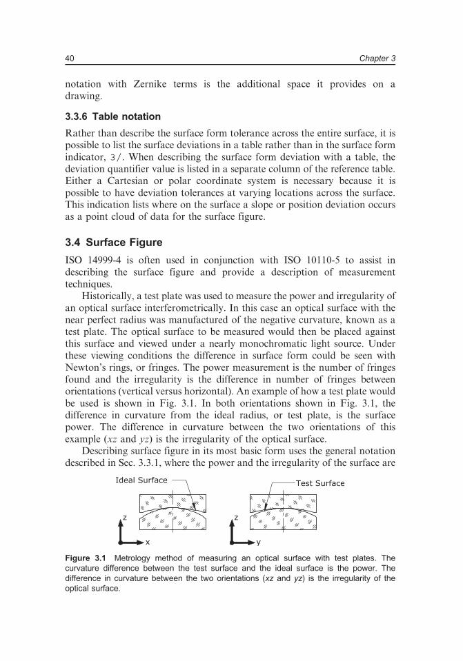
Historically, a test plate was used to measure the power and irregularity ofan optical surface interferometrically. In this case an optical surface with thenear perfect radius was manufactured of the negative curvature, known as atest plate. The optical surface to be measured would then be placed againstthis surface and viewed under a nearly monochromatic light source. Underthese viewing conditions the difference in surface form could be seen withNewton’s rings, or fringes. The power measurement is the number of fringesfound and the irregularity is the difference in number of fringes betweenorientations (vertical versus horizontal). An example of how a test plate wouldbe used is shown in Fig. 3.1. In both orientations shown in Fig. 3.1, thedifference in curvature from the ideal radius, or test plate, is the surfacepower. The difference in curvature between the two orientations of thisexample (xz and yz) is the irregularity of the optical surface.
Describing surface figure in its most basic form uses the general notationdescribed in Sec. 3.3.1, where the power and the irregularity of the surface are
Figure 3.1 Metrology method of measuring an optical surface with test plates. Thecurvature difference between the test surface and the ideal surface is the power. Thedifference in curvature between the two orientations (xz and yz) is the irregularity of theoptical surface.
40 Chapter 3

References
1. D. Malacara, Optical Shop Testing, 3rd ed., Wiley (Hoboken, NewJersey: 2007).
2. W. J. Smith, Modern Optical Engineering, 3rd ed., McGraw–Hill(New York: 2000).
3. E. P. Goodwin and J. C. Wyant, Field Guide to Interferometric OpticalTesting, SPIE (Bellingham, Washington: 2006).
4. International Organization for Standardization (ISO), Preparation ofDrawings for Optical Elements and Systems—Part 5: Surface FormTolerances, ISO 10110-5 (Geneva: 2015).
5. ISO, Preparation of Drawings for Optical Elements and Systems—Part 14:Wavefront Deformation Tolerance, ISO 10110-14 (Geneva: 2018).
6. ISO, Optics and Photonics—Interferometric Measurement of OpticalElements and Optical Systems, ISO 14999 (Geneva: 2019).
7. C. J. Evans, “Robust estimation of PV for optical surface specificationand testing,” Proc. Opt. Soc. Am. Front. Opt., 2008, OWA4 (2008).
Figure 3.12 Example drawing with a spherical surface on the left surface having powerand irregularity,and an aspheric surface on the right surface having power and RMSiirregularity tolerance; along with a sag table.
47Surface Figure and Form

Chapter 4
Surface Texture: Roughnessand Waviness
Surface roughness tolerances are requirements for the level of smoothness ofthe polish of an optical surface, typically expressed as a maximum allowedRMS surface height error and evaluated with a profilometer. The advent ofhighly deterministic small-tool polishing has led to increased importance ofspatial frequencies lower than traditional roughness scale-lengths but higherthan those more easily controlled using surface form tolerances described inChapter 3. To cover this need, the standard includes notation to control suchmid-spatial frequency errors with more rigor.
ISO 10110-8 provides the notations for a variety of tolerancing methods ofvarying complexity and sophistication.1 The simplest form of surface texturetolerance is a simple polishing grade based on a standard level of RMSroughness. If the standard polish grades are not suitable, any level of RMSroughness tolerance can be defined. Moreover, the scale-lengths over whichthe RMS roughness requirement is to be evaluated can be customized. Thissame tolerance methodology can be used to specify deliberately roughsurfaces, such as the ground edge of a lens, using both upper and lowerbounds on the roughness. In addition to these fairly conventional notations,the standard provides for more complex tolerances often used to control mid-spatial frequency surface form errors, or waviness, based on peak slope, RMSslope, and even a power spectral density (PSD). The most recent edition of thestandard adds the areal (2D) versions of these notations.
4.1 Background
Tolerances on surface texture are not unique to the optics industry. Indeed,specifying the smoothness of a bearing surface is quite old. Today, the studyof friction, wear, and lubrication is referred to as tribology; and is greatlyconcerned with characterizing the texture of a surface. Leonardo da Vinci(1452–1519) is considered by some to be the first tribologist.2 His notebooks
49
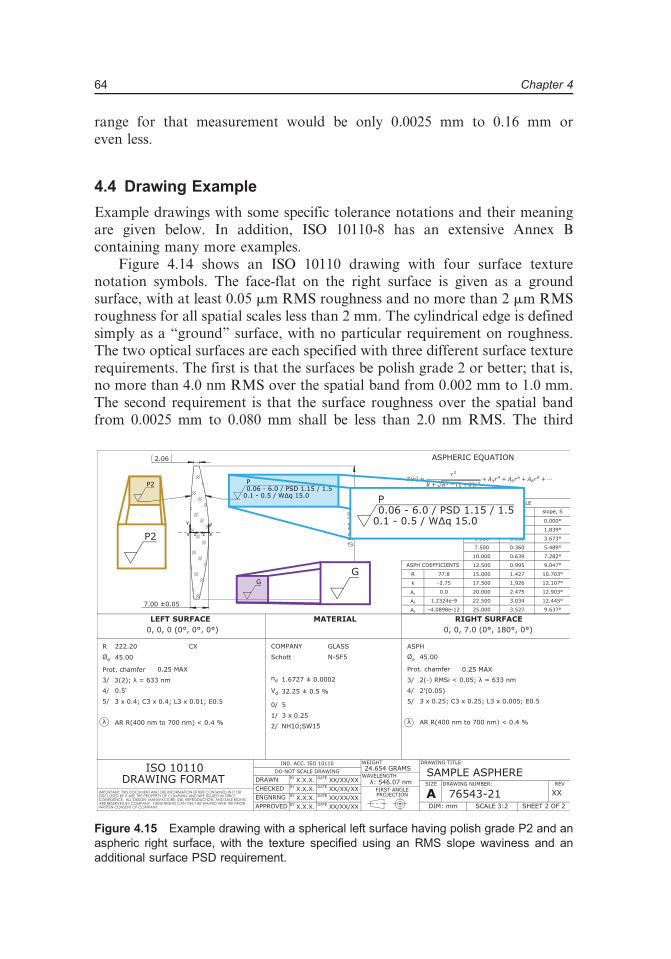
range for that measurement would be only 0.0025 mm to 0.16 mm oreven less.
4.4 Drawing Example
Example drawings with some specific tolerance notations and their meaningare given below. In addition, ISO 10110-8 has an extensive Annex Bcontaining many more examples.
Figure 4.14 shows an ISO 10110 drawing with four surface texturenotation symbols. The face-flat on the right surface is given as a groundsurface, with at least 0.05 mm RMS roughness and no more than 2 mm RMSroughness for all spatial scales less than 2 mm. The cylindrical edge is definedsimply as a “ground” surface, with no particular requirement on roughness.The two optical surfaces are each specified with three different surface texturerequirements. The first is that the surfaces be polish grade 2 or better; that is,no more than 4.0 nm RMS over the spatial band from 0.002 mm to 1.0 mm.The second requirement is that the surface roughness over the spatial bandfrom 0.0025 mm to 0.080 mm shall be less than 2.0 nm RMS. The third
Figure 4.15 Example drawing with a spherical left surface having polish grade P2 and anaspheric right surface, with the texture specified using an RMS slope waviness and anadditional surface PSD requirement.
64 Chapter 4

Chapter 5
Surface ImperfectionTolerances
Surface imperfections are localized flaws, such as scratches and digs, on thesurface of an optical element. Surface imperfections that are not localized—i.e., cover the entire surface—are considered texture and are toleranced usingthe notation given in Chapter 4. Typically, when considering surfaceimperfections we include other features such as edge chips and coatingimperfections. The ISO 10110 standard includes two methods of indicatingsurface imperfections. The first method is analogous to the scratch and digvisibility standard found in US MIL-PRF-13830B and the related visibilitymethod described in ANSI/OEOSC OP1.002. The second method isanalogous to the withdrawn DIN 3140’s dimensional specification.
5.1 Background
Surface imperfection specifications are among the most misunderstood andmisapplied standards in the world of optical engineering.1–3 Mostindications fail to even reference a standard, trusting instead that themanufacturer will interpret the notation in the intended manner with nofurther guidance than 60-40 scratch and dig or 5/ 4 � 0.1. The long andcomplex history of these specifications combined with their frequentcitation as cause for rejection requires more attention from the opticalengineer in preparing a surface quality tolerance. In the event that oneshould attempt to develop a meaningful surface quality specification fromexisting standards, one is often confronted with bad options: a standardthat is expensive to implement, is often misinterpreted, or might not fit therequired application.
The surface imperfection notation for optical surfaces, often referred to as“scratch and dig,” is found today in Section 3.5 of MIL-PRF-13830B,4 anactive standard supported by the US military. It is based on MIL-O-13830A,first released as a military standard in the US in 1954 and revised once in
67

Figure 5.3 Example for dimensional method for surface imperfection specification.
Figure 5.4 Example of visibility method for surface imperfection specification.
80 Chapter 5

Chapter 6
Laser Damage
Laser damage is a major concern if an optical element or optical systeminvolves high-power or high-energy lasers. The concern with optics in thesesystems is that a flaw in the optic may cause light to scatter or be absorbedand subsequently cause damage. Designation of a laser-induced damagethreshold (LIDT) for these optical elements is intended to convey the messageto a fabricator that additional care must be taken when manufacturing thesetypes of optical elements or systems.
6.1 Background
For an ISO 10110 drawing, the notation for laser damage threshold is specifiedin ISO 10110-17.1 Additional resources for understanding laser-damagethresholds and methods for evaluating laser-damage results are listed in theISO 21254 series.2–5 It is necessary to use the four parts of the ISO 21254 serieswith ISO 10110-17 to understanding laser-damage threshold specifications,testing conditions, and evaluation techniques.
High-power or high-energy laser light passing through an optical systemmay induce damage to the optical system or optical components. This is dueto the laser power density or energy density—depending on the pulseduration, duty cycle, and type of laser. Laser damage will create irreversibledamage due to ageing, microdamage, and induced defects.3 The laser induceddamage threshold is defined as the highest quantity of laser radiation incidenton the component for which the extrapolated probability of damage is zero.2
Due to the statistical nature of this extrapolation, the LIDT should not beconsidered the level below which damage will not occur; more that it is thelevel of laser radiation below which damage probability is less than the criticalrisk level.6
Laser damage for optics is typically a higher concern for optical surfacesrather than the bulk optical material. This is due to imperfections in thepolishing of the optical surface or imperfections in coatings causing localizedabsorption. Typically, an optical element or system that will be used for high
83

6/ Fth;l;teff
where:Fth ¼ threshold linear power density (W·cm–1).
The distinction for a pulsed laser to be a long pulse refers to when thethermal transit distance is on the same order as the test spot. This distinction isshown in Eq. (6.1). The approximate equality between the parameters isintended to show that if these terms are on the same order of magnitude, along pulse should be considered.
ð2DteffÞð1∕2Þ � dðT ,ef f Þ (6.1)where:D ¼ thermal diffusivity,teff ¼ effective pulse duration (seconds), anddT, eff ¼ test spot diameter.
In the case that the time of the pulse is greater than 0.25 s, the laserdamage is considered CW. For these types of lasers, the effective pulseduration is not specified. Instead, teff becomes the exposure duration of theCW laser test.
6.4 Test Methods
ISO 10110-17 references ISO 11254-1 and -2, both of which have beenwithdrawn.9,10 A schematic of the testing configuration described in ISO11254 is shown in Fig. 6.1.
Laser damage may be performed in one of two different methods,depending on the type of laser in question and information needed. Damagetesting may be done in a 1-on-1 test where a single shot occurs on a singleunexposed part of the optical component in question. The other test
Figure 6.1 Basic approach to damage testing.
86 Chapter 6

Chapter 7
Surface Treatment and Coating
Surface treatments and coatings are applied to an optical surface at the end ofthe component fabrication process. Optical coatings involve the addition ofmaterial on the polished optical surface while surface treatments are generallyapplied to the edges of the components. The type of optical coating dependson the functional purpose of the optical element in the application. In ISOstandards, the ISO 9211 series and ISO 10110-9 work in conjunction with eachother to provide detailed descriptions of optical coatings, as well as theirnotation for drawings.1–9 ISO 10110-9 contains notation methods forspecifying the optical coating on a drawing. While it is certainly possible touse this notation for the specification of a coating, a very detailed descriptionof optical coatings and test methods is provided in the ISO 9211 series. Opticalcoatings are used to alter the transmission, reflection, or absorption propertiesof an optical element’s surfaces. Further, these key properties of the surfacemay be described by wavelength regions, angles of incidence, phase, orpolarization. Optical coatings are ubiquitous and a key factor for manyoptical drawings.
7.1 Background
Much has been written about the design, fabrication, and functionality ofoptical coatings without consideration for the rest of an optical system.10–13
An optical coating is typically the only aspect of the optical fabricationprocess where additional material is deposited or added to an opticalsurface.14 These optical coatings may be as simple as a single layer of anadditional material or as complex as a multi-layer stack-up of variousmaterials.11 Many optical coatings are interference coatings wherein reflectedor transmitted light from various layers produce different wavelength, angle,and polarization dependent constructive and destructive interference. Thus, acommon function for optical coatings is to alter the transmission, reflection,or absorption for an optical element or system.
91

7.4 Standard Coatings
As the ISO standards for optical coatings continue to evolve, three of the ISO9211 standards (Parts 5, 6, and 7 for antireflective, reflective, and beamsplittercoatings respectively) specify standard optical coatings that may be used.Antireflective coatings are simply identified as a single layer (U), double layer(V), multilayer broadband (W), and other (X). The first three coatings [U, V,and W] are basic types of antireflective coatings that are named based on theirreflectance curve shape. The U and V coatings are specified for a singlewavelength. The W multilayer broadband coating is meant for a range ofwavelengths. The reflectance designations for these three types of coatings arelisted in Table 7.4. Lastly, an X coating type is a multilayer coating that doesnot have reflectance properties as described by U, V, or W coatings.
The coatings described for reflective surfaces are based on the metallicmaterial that should be used. These specifications are shown in Table 7.5.
340 407.5 497.5302.5
352.5 397.5
87.5%
5.0% 5.0%0%
20%
40%
60%
80%
100%
300 320 340 360 380 400 420 440 460 480 500
Tran
smis
sion
Wavelength (nm)
Figure 7.13 Notation for a graphic representation of a bandpass filter where thetransmission band and rejection band are noted by the wavelength and transmissionpercentage (coating data for figure courtesy of Edmund Optics, Inc.).
Table 7.4 Coded notation for antireflective coatings associatedwith ISO 9211-5.5
Coating Type Refractive Index Wavelength Reflection
U 1.45 to 1.5 l ≤2%1.5 to 1.7 l ≤1.5%≥1.7 l ≤1%
V – l ≤0.2%W – l1 to l2
where l2l1≥ 1.57
≤0.5%
105Surface Treatment and Coating
Chapter 8
Centering and Tilt Tolerances
Optical centering is the alignment of optical surfaces or elements with respectto a datum or datum system. The datum may either be a point, an axis, asurface, or a cylinder. The method of describing optical centering is unlikeother sections of ISO 10110 because optical centering relies heavily onmechanical engineering methods and geometrical dimensioning and toleran-cing (GD&T). ISO 10110-6 specifies surface tilts, surface decenters, runouts,and beam deviations that can be used to tolerance the centering of an opticalsurface, an optical element, or a subsystem.1
8.1 Background
Centering tolerances for an optical element are applied near the final stages offabrication.2 The process of centering relates the surface normal of the opticalsurfaces to a datum, which is frequently an axis defined by a cylindricalsurface (in many cases, the outer diameter). Throughout the remainder of thischapter, all outer diameter surfaces will be referenced as a cylindrical edgesurface. The centering tolerances of optical surfaces reference datums ordatum systems by a tilt, or a tilt and a decenter. There are multiple ways todescribe the surface tilt and/or decenter because of the different methods bywhich optical surfaces are manufactured and tested. Although referred to ascentering, it is most often specified in the form of a tilt angle of the surfacenormal with respect to some reference axis, or a datum axis. The definition ofthe datum or datum system is critical to the centering tolerance and how thetolerance should be interpreted. An understanding of each of the differentdatum reference methods and the intended use of the optic are key to how thecentering tolerance should be assigned.3,4 The centering of an optical elementis one of the most important aspects of the fabrication process to ensure thatsystem alignment tolerances can be met.5
The method of centering an optical surface—and subsequently defining atolerance with an ISO 10110-6 callout—depends on the type of surface orsurfaces, and how the element will be mounted in the final assembly.
115

Freeform optical surfaces may also be designed where the surfacedefinition uses Zernike coefficients, other mathematical functions, or evenpoint cloud data. The more-complex methods create additional challenges foroptical centering. These types of surfaces may require multiple surface tilts buta decenter tolerance must also be present. When working with these types ofsurfaces, the coordinate system in place is critical to ensure the types ofdecenters and tilts are properly represented. Use of explicit datum systems isencouraged. Implicit centering tolerances may not be enough of a descriptor iftheir fiducials or datums are not clearly understood. As freeform opticalsurfaces become more prevalent, their use may not solely be in two-surfaceoptical elements.8 In these cases, the full Cartesian coordinate including originsis necessary to ensure metrology is possible for each of the centering tolerances.
8.5 Indications on Drawings
The drawing symbol for centering is 4/. The quantifiers following thedrawing symbol are different depending on the centering tolerance method.There are multiple methods to quantify the type of centering tolerance. Assuch, it is possible to define the datum and centering tolerances of an opticalelement differently with the same intended result. Subsequently, it might bebeneficial to take a tolerance quantifier method and then convert it to aanother method based on metrology methods.9 The quantifier for a centeringtolerance also requires an understanding of the associated datum(s).Abbreviated indications are allowed in which the datum(s) are implied insome specific cases. Where two surface tilts are indicated without an explicitdatum, the sole datum is the cylindrical edge and the datum axis is thecylindrical axis. Where only one surface tilt is indicated without explicitdatums, the datum is the axis connecting the center of curvature andmechanical center of the unspecified surface.
As with other tolerance parameters in ISO 10110, if a dash (–) is presentthen no tolerance is associated. This is necessary to understand as definingcentering tolerance in a tabular format may require no tolerance to achievethe necessary centering method.
(a) (b)
Figure 8.7 Cylinder optical element with tilt present in both the yz- and xz-orientations.
121Centering and Tilt Tolerances
Chapter 9
Nonspherical Surfaces
The advantages of nonspherical (that is, rotationally invariant aspheric)profiles for optical surfaces to correct aberrations in optical systems have beenknown since the early days of geometrical optics and optical design.1,2 Morerecently freeform surfaces (that is, rotationally varying surfaces or surfaceswith bilateral or no symmetry) have been used in ophthalmic and nonimagingapplications.3 As fabrication and metrology methods have advanced, thesesurfaces have been increasingly used in imaging applications.4 Due to the needfor standards to cover drawing notations for many different types of aspheresand general surfaces, two parts of ISO 10110, Parts 12 and 19,5,6 are dedicatedto the specification of the theoretical (nominal) aspheric and general surfaces,respectively, in drawings. Additionally, other parts of ISO 10110 have beenwritten (and revised) to support these types of surfaces; notably Parts 5, 6, 8,and 14. In this chapter, we provide background to using ISO 10110-12 andISO 10110-19 to create drawings for numerous types of nonspherical surfaces.Development and a summary of descriptions in these standards can be studiedindependently of this book in the article by Schuhmann4 and the freeformpaper by Youngworth et al.7
9.1 Background
Optical systems have long incorporated various nonspherical surfaces,including rotationally variant and rotationally invariant surfaces. The criticalfactor for deciding when to use an asphere (here, we use this term inter-changeably with a nonspherical rotationally invariant surface) or freeform(here, we use this term interchangeably with a nonspherical, rotationallyvarying surface) ultimately is a balance between the functional requirements ofthe optical assembly and the additional expense incurred. Exceptions are casesfor the following:
• Inclusion of the nonspherical profile surface renders the overall systemsimpler,
• The surface is required for performance with all given constraints, or
141

Figure 9.2 Example asphere using ISO 10110-12.
Figure 9.3 Example asymmetric lens requiring ISO 10110-12.
150 Chapter 9

Chapter 10
System Evaluation
Although not covered in the ISO 10110 series, understanding how to evaluatea complete optical system is important when creating component specifica-tions. Such considerations are especially crucial when determining tolerancesfor an optical design. Optical components may be manufactured for a varietyof systems with different applications, and therefore benefit from differentrequirements and specifications. The same factors are true for systemevaluation metrics. Optical system metrics may vary from basic opticalproperties (such as focal length or field of view) to complex measurements ofimage quality [such as the modulation transfer function (MTF)]. Along withfundamental optical system metrics, additional aspects of the complete systemmay drive requirements—such as stray light, eye relief, or system transmit-tance. Understanding the stray light (unwanted radiation), for example, maydrive mechanical aspects of the system design and influence the optical systemfunctionality even more than, for example, surface form or other conventionaloptical tolerances in some applications.
There are many different ISO standards that can be used to evaluate anoptical systems performance. As this book is intended as a guide to thespecification and tolerancing of optical components using the ISO 10110series on drawing notation and not per se about system evaluation, only basicdescriptions are provided here to introduce some of the key optical systemfunctional metrics and their evaluation.
10.1 Background
The functional evaluation of an optical system is ultimately the finaldetermining factor when verifying the finished optical assembly meets itsspecification. Specifying functional metrics for optical system performancemay result in confusion because of a potential difference between what isexpected from the manufacturers, and the manufacturers’ understanding orinterpretation of how they should perform the functional testing. By havingfunctional testing standards, the communication between fabricators and
153

Chapter 11
Environmental Testing
Outside of the functional testing that occurs on an optical system,considerations must be made for the operating conditions of the opticalsystem as well. Environmental conditions such as temperature and humiditycan become critical when taking the optical system out from the lab. Whilenot a direct aspect of ISO 10110, listing the environmental conditions for anoptical system can be important when specifying a final assembly. This isespecially true for systems with dielectric or metallic coatings that are exposedto the environment when used.
The ISO 9022 series is a group of test standards that define theenvironmental tests and levels at which a system or component will be tested.Most of the standards in the ISO 9022 series are for specific differentenvironmental conditions. There are also three, more rigorous ISO 9022standards that combine the individual environmental conditions that theoptical system may truly experience.
In each part, a series of conditions, termed “conditioning methods,” aredescribed. These conditioning methods are identified by a numeric “conditioncode.” To specify a test, the condition code for that test must be identified aswell as the “severity code” and the operating state of the instrument beingtested. The method of indicating an environmental test on an optics drawing isdiscussed more in Sec. 11.7.
In addition to the ISO 9022 series of standards, there is another standard(ISO 10109) that provides guidance for environmental conditions an opticalsystem may experience depending on a specific application or global location.This standard lists expected temperature ranges, humidity, pressure, and rainconditions for a series of standard environments. These standard environ-ments are based on global data collected and are meant to guide the user onwhich parts of ISO 9022 may be applicable for a given situation. Theseenvironmental conditions are in place to assist the user if temperature,humidity, and pressure are not known but the type of environment is known.The standard also includes a framework (ISO 10109, Table 9) for identifying
175
Chapter 12
Standards in Practice
We have shown in previous chapters that ISO 10110 can be a very powerfulmethod for conveying information between the optical designer and thefabricator. The coded notation may seem confusing at first, but onceunderstood, it obviates the need for significant additional communicationthroughout the fabrication process. By instituting the ISO 10110 drawingformat, it is also possible to define an entire optical system specificationand acceptance test. Starting the entire project with ISO 10110 and theassociated ISO performance standards in mind allows the designer to have aconcise set of requirements defined that can also be easily documented andcommunicated.
Users should develop an understanding of how to use standardsholistically; in other words, how to specify full optical systems and assemblies.In order to better understand how to use standards successfully for bothtolerances and for performance, in this chapter we provide a completeexample. The goal is to help users understand how to take advantage of theISO 10110 drawing notation from the beginning of an optical design, throughtolerancing, and result in finished drawings.
Along with component drawings made with the ISO 10110 drawing format,the finished optical system may require overall performance verification. Asdiscussed in chapter 10, there are many different types of performance metricsthat can be used. In this chapter, we discuss specifications for an optical systemthat must be tested for multiple parameters.
12.1 System Parameters
To begin the optical system example, basic parameters must be established forthe optical system itself. The requirements below are assumed to bereasonable for the example optical design to avoid needless complexity.
• Wavelength: Visible (400 nm to 700 nm)
• Effective focal length: 100 mm
• F/#: F/5
197

12.4 Optical Assembly Drawing
The last drawing in this example is the assembly drawing (Fig. 12.8). As this isan optical assembly without component manufacturing tolerances that mustbe defined, the tabular field is removed.
The full optical layout is shown in the drawing field with the axialspacings defined and toleranced accordingly. Each of the three opticalelements are identified by an element number. A table in the top right of thedrawing associates these element numbers with their part number anddescription, as well as the required tilt and decenter tolerances for each. Thespacing from the aperture stop to element 3, and between elements 3 and 4, isidentified as variable axial spacings. These spacings are used in the toleranceanalysis to maintain a one-time, factory-set internal focus compensationadjustment. This choice is noted with the reason for this variation in thebottom right corner. Additionally, the back-focus distance is specified as anadjustable axial separation. This spacing is used in the tolerance analysis toachieve best focus, as stated in the bottom right corner of the print. Theplacement and diameter of the aperture stop between doublet 1 and element 3is shown with tolerances. There is also a physical aperture defined at the frontof the optical system for testing purposes. This aperture is not critical to thefunctionality of the optical system but is necessary for the required testing ofthe transmitted wavefront error and transmission.
Figure 12.8 Optical system sample drawing for the entire optical assembly using the ISO10110 drawing format.
206 Chapter 12

Eric Herman is an optical design engineer with ZygoCorporation. He has over a decade of optical designexperience. He received his M.S. in Optical Sciences fromthe University of Arizona’s James C. Wyant College ofOptical Sciences. He is a Senior Member of SPIE and hasserved in a variety of volunteer experiences for both SPIEand the Optics and Electro-Optics Standards Council(OEOSC). He is currently the Chair-Elect on the Board of
Directors for OEOSC.
Dave Aikens is an optical design engineer at Savvy OpticsCorp, a company he founded in 2007. He has been workingon the standardization of optics drawings since his first jobworking with Ron Kimmel at Hughes Aircraft Company in1983. He is a graduate of the University of Rochester(B.S. 1983, M.S. 1984), a Fellow of SPIE, and the 2021recipient of the A. E. Conrady award. He currently serves asthe Chair of the Technical Advisory Group to ISO Technical
Committee TC172, responsible for standards in optics and photonics.
Richard N. Youngworth is a Fellow of SPIE and Optica. Heis the founder and Chief Engineer of Riyo LLC, an opticaldesign and engineering firm. He obtained his Ph.D. in opticsat the University of Rochester. He has authored anddelivered numerous short courses, papers, talks, and lectureson optical design and engineering. He is active in opticalstandards development and in professional society work.