Introducing Immersive Artp. 16 Wearable Display ... - SPIE
56
NOVEMBER/DECEMBER 2021 Introducing Immersive Art p. 16 Wearable Display Innovations p. 22 Whatever Happened to the Hologram? p. 28
-
Upload
khangminh22 -
Category
Documents
-
view
0 -
download
0
Transcript of Introducing Immersive Artp. 16 Wearable Display ... - SPIE

NOVEMBER/DECEMBER 2021
Introducing Immersive Art p. 16
Wearable Display Innovations p. 22
Whatever Happened to the Hologram? p. 28


NOVEMBER/DECEMBER 2021ContentsFeatures
Whatever Happened to Holograms?Popular notions of holography may be headed to the dustbin with emergence of more promising technologies
By Mark Wolverton
16
22
28The Pricey Promise of MicroLEDsThe latest in display technology may be coming to a wristband on you
By Vineeth Venugopal
From Disney to ArtechouseDigital artists use light science to create immersive works of art
By Bob Whitby
Photo credit: Refik Anadol Studio© 1
Visitors explore an installation by Refik Anadol at Artechouse, New York.

SEE YOU IN SAN FRANCISCO
Photonics WestConferences and courses 22–27 January 2022
BiOS Expo 22–23 January 2022
Photonics West Exhibition 25–27 January 2022
The Moscone CenterSan Francisco, California, USA
REGISTER TODAYspie.org/pw2022
PLAN TO
ATTEND
Get ready to enjoy real conversations, hear the latest breakthroughs, and make important connections in person.
Proof of COVID-19 vaccination and masks will be required for everyone.

SourcesRecent and notable research
12 Ultrafast Optical Imaging Gets Even Faster | Follow the Bouncing Eyeball in AR | Counting Fish with Lidar and Machine Learning | A Possible Cure for the Near-3D Visual Fatigue Hangover
CONTENTS
5 From the Editor
32 Letter from the President
33 SPIE Deadlines and Events
34 SPIE Community News
39 Puzzle
Field of ViewInsight into the photonics industry
9 Industry Updates
10 Hollywood’s Lens Migration: A technological journey
LuminariesPeople who lit the way for photonics
14 Elsa Garmire: Pioneering laser physicist with a penchant for art helped launch laser light shows
SPECIAL SECTION
SPIE Community SupportRecipients and beneficiaries in the community
S1 Next generation of optical scientists, policy makers, technicians, and engineers
ReflectionsImages from the community
40 Ascorbic Acid
14
10
TFCalc
Software Spectra, Inc.
An alphabetical list of some of TFCalc’s capabilities:
• absorption • active coatings • angle matching • animation • bandpass filter design • blackbody illuminant • color optimization • constraints • continuous optimization targets • derivative targets • detectors • dispersion formulas • electric field intensity • equivalent index • equivalent stack • gain materials • global optimization • group optimization • illuminants • layer sensitivity • local optimization • material mixtures • multiple environments • needle optimization • optical monitoring • optical density • phase shift • psi • radiation distributions • refractive index determination• reflection • sensitivity analysis• stack formula • synthesis • transmission • tunneling method • ultra-fastquantities • variable materials • yield analysis
14025 NW Harvest LanePortland, OR 97229Tel: (800) 832-2524
Web: www.sspectra.comE-mail: [email protected]
Optical Coating Design Software
BandwidthGrow your career
6 A Scientist’s Guide to Social Media: YouTube, Instagram, and TikTok
8 Telling Stories: The craft of memorable conference presentations
8
Cover photo credits: Shutterstock: Abstract button–James Weston; Retro camera–Rashoo Moon

27 February–3 March 2022San Jose Convention CenterSan Jose, California, USA
© 2021 Society of Photo-Optical Instrumentation Engineers (SPIE). All rights reserved. The articles published in Photonics Focus reflect the work and thoughts of the authors. Every effort has been made to publish reliable and accurate information herein, but the publisher is not responsible for the validity of the information or for any outcomes resulting from reliance thereon. Inclusion of articles and advertisements in this publication does not necessarily constitute endorsement by the editors or SPIE.
Editor-in-ChiefGwen Weerts
Managing EditorWilliam G. Schulz
Section EditorKaren Thomas
Graphic ArtistCarrie Binschus
ContributorsAndrea Armani
Jeff HechtAnatoly Mikhaltsov
Iain NeilEmily Haworth
William G. SchulzKaren Thomas
Vineeth VenugopalGwen WeertsBob Whitby
Mark Wolverton
2021 SPIE PresidentDavid Andrews
SPIE CEOKent Rochford
Advertising Sales:Melissa Valum (USA)
[email protected]+1 360 685 5596
Rob Fisher (UK)[email protected] +44 (0)117 905 5330
Job PostingsLacey Barnett
[email protected]+1 360 685 5551
Send change of address requests and returns to:SPIE Customer Service
1000 20th StBellingham, WA 98225-6705, USA
November/December 2021Volume 2, Number 6, ISSN 2706-8110
HEAR AND DISCUSS THE LATEST DEVELOPMENTS AT THE CONFERENCE FOR EMERGING TECHNOLOGY IN THE SEMICONDUCTOR INDUSTRY
spie.org/al22call#SPIElitho
The need to share your
research and to hear recent
advances from other experts
is as important as ever. Like
you, the staff and volunteers
of SPIE are looking forward to
gathering in person again.

PHOTONICS FOCUS NOVEMBER/DECEMBER 2021 5
FROM THE EDITOR
Into ArtIN THE PAST COUPLE OF YEARS, IMMERSIVE ART EXHIBITS have emerged as the hottest new thing on the (pop) art scene. These exhibits rely on massive projections, displays, virtual reality, animations, lasers, and other photonics darlings in the entertainer’s toolkit to create multisensory exhibits that reimag-ine the works of well-known artists, like Vincent Van Gogh.
Many people laud these immersive exhibits for making art accessible to the masses because not everyone will have the opportunity to visit the Musée d’Or-say to see Van Gogh originals. But others aren’t so sure that it’s a good idea to so drastically alter the original intentions of the artist via immersive exhibits.
Art critic Maya Philips wrote in the New York Times about her unsettling experience touring a virtual Van Gogh exhibit in July. “No matter how many times I toured the chambers, I had the itching sense that it was dishonest to expand a 2½ by 3-foot painting to fit the horizons of a 75,000-square-foot space,” she writes. “There’s a reason for the size of the original work; what the painter wanted to obscure, what parts of the world we’re allowed to see, and what we’re left to imagine.”
Art professor C. Shaw Smith at Davidson College expressed similar con-cerns in an interview for the college newspaper. He talked about the impasto of Van Gogh’s paintings, which refers to the three-dimensional buildup of paint in each brush stroke, which gives the viewer a sense of the human being who created the painting. In the immersive exhibit, this sense of the person is lost.
“In the original works, what you’re really talking about is the hand. In [the virtual exhibit], you’re talking about the eye. The immersive presentation is a way to create accessibility and the spectacle,” said Smith, but “it has very little to do with the art itself.”
The critics’ reservations project a note of caution: Just because technology enables us to do something—like animate Van Gogh’s sunflowers so that they blow in the breeze—doesn’t necessarily mean we should.
This polite discussion around the can we/should we of virtual art exhibits provides a safe and low-stakes way to grapple with a high-stakes question that is mirrored in other areas of science with more heated debate. Just look to the hot topics of modern research like gene editing, facial recognition, or the uncanny valley of humanoid AI to understand the discomfort.
Fortunately, there is much less angst in the can we/should we considerations of modern photonics research for entertainment. In this issue, we screen the photonics technologies that enable our favorite games, displays, and devices, and imagine what technologies might entertain us in the future. In commem-oration of the 50th anniversary of Dennis Gabor’s Nobel Prize for his invention of the hologram, we look critically at the 3D displays that science fiction has promised us, and marvel at what real science has actually delivered. We dis-cover the tricks and tips of cinema lens designers to recreate the softness and distortion that was lost with the advent of ultracrisp digital imaging. And we learn about microLEDs, which hold promise for AR/VR, and may soon find their way into the smartwatch on your wrist.
Optics and photonics research can continue to create novel lenses, displays, and lighting that cater endlessly to our ever-evolving entertainment needs. What will we do when we reach some critical boundary where it must be asked, “Should we?”
GWEN WEERTS, EDITOR-IN-CHIEF

PHOTONICS FOCUS NOVEMBER/DECEMBER 20216
BANDWIDTH
Can you summarize your research findings in
less than 200 words? Describe your PhD using
nothing but emojis? Dance the “Renegade” while
reciting your thesis? While these may not seem
like make-or-break skill for an optical engineer
or laser scientist, you might be surprised at just
how much social media can impact your work.
In the final segment of our series on social media, we
cover the most popular visual platforms—YouTube,
TikTok, and Instagram—to demonstrate the impact
multimedia content can have on your research, personal
branding, and science communication endeavors.
VIDEO IS EVERYWHERE. You see it on your social media feed, on skyscrapers, on the back of your airplane seat—even podcasts have visual components now. Video market expert Wyzowl reports video consumption has increased during the pandemic: People watch an average of 18 hours of online video per week, an increase of two hours per week compared to 12 months ago.
For scientists seeking a way to communicate their work to the public, video should be a top contender.
University of Chicago PhD candidate Nora Bailey emphasizes the importance of engaging the public: “Your audience [on social media] isn’t a conference in your field…the advantages really lie in community-building with other scientists—getting out of the academia bubble and helping people get excited about science in general. Any visibility for your own work is just a nice bonus.”
A Scientist’s Guide to Social Media:
YOUTUBE
With two billion monthly users, you’d be hard-pressed to find someone who has never watched or searched for a video on this platform. Typing queries into YouTube is a way people find answers to technical questions. “Many people are visual learners; they absorb information much more easily through a visual platform than through reading,” says Cory Boone, lead technical marketing engineer for Edmund Optics.
Findability is key with so many videos to choose from, and since YouTube is owned by Google, you can be sure to find an audience if you provide good meta data and descriptions for your content. Don’t be put off if you don’t get views right away though. On the SPIE YouTube channel, for example, interviews posted five—even 10—years ago still receive com-ments and questions.
Starting a YouTube channel can seem daunting at first. Bailey advises: “Just start. Don’t wait for the perfect time, the perfect video idea, the perfect filming setup. You’re going to be continually learning and improving, so just start now.”
Still not convinced you are ready to record? Use one of these simple video ideas: an introduction with information about yourself and your research; a plain-language summary of a publication; or a news-type broadcast, like Bailey’s weekly vid-eos, that offers a breakdown of important updates in your field.
Meriame Berboucha, an Imperial College London, PhD student based at SLAC National Accelerator Laboratory, began using Instagram to break the typical scientist stereotype.
“I decided to start my account because I was the only girl in my physics class when I was seventeen,” Berboucha says. “I wanted to bring awareness to more women in physics and share my enthusiasm for the subject.”
Through her Instagram feed, she normalizes conversations about being a woman of color in science and mental health,
YouTube, Instagram, YouTube, Instagram, and TikTokand TikTok

A Scientist’s Guide to Social Media:
alongside sharing her research at SLAC. Comments on her posts are filled with people thanking her for being transparent about challenges in academia, as well as complimenting her explana-tions of scientific concepts.
Berboucha recommends trying your hand at Instagram’s video-creation tools, Reels and Stories, to offer advice to a prob-lem you’ve faced during your academic career, or share how to deal with a common challenge. Videos such as these can boost your personal brand, as well as build a professional network.
“I’ve been invited to speak at schools, conferences, and on podcasts through these platforms,” Berboucha says. “I collabo-rate with members of the community I wouldn’t have connected with in my day-to-day life.”
TIKTOK
The latest buzzworthy social media platform has 689 million monthly users, and 90 percent of them access the app every day. Yes, TikTok is heavily geared toward Gen Z, but Boone said it best: We need to meet people where they are. If the goal is science communication, TikTok is a must-have tool for your outreach toolbox.
“TikTok is a great way to teach students about science in an entertaining way, and hopefully inspire the photonics profes-sionals of the future,” Boone says.
To get started, try to recreate your most popular outreach activity at home. Prop up your phone and film yourself con-ducting the experiment. Talk through the steps directly to the camera, and don’t be afraid to take a pause or restate something. Thanks to TikTok’s built-in editing, you can go back and trim the video, and even add text overlay. “Shooting and editing on TikTok is very intuitive,” Boone says.
Don’t have an outreach experiment in mind? “Put your phone in selfie mode and talk to the camera for 60 seconds about some-thing you find interesting,” Bailey says. Pair this with relevant hashtags—#ScienceFacts, #PhDLife, #Astronomy, #Lasers—to set yourself up for success.
One pitfall of social media is a fixation on the number of views. Berboucha’s advice? “It’s not about the numbers or fame—it’s about what you do with the platform. If you love what you’re posting, then you’ll find your community.”
“Just be yourself,” Bailey says.
EMILY HAWORTH is the social media manager for SPIE.
Tricks & Tips for Recording Video for Social Media Can you hear me?People may forgive poor recording quality, but will skip your video altogether if there is weak audio. Record where your device’s microphone will only pick up your voice.
Bonus Tip: Add subtitles whenever possible. YouTube, TikTok, and Instagram all have built-in captioning services.
Make it popExperiment with lighting. Put a ring light, lamp without the shade, or a window behind your recording device. Added light makes your video look more polished and professional.
Say, what?Avoid technical jargon. Language specific to your field, without proper explanation, is a surefire way to get someone to scroll past your video. Try to explain your science as if you were chatting with a friend.
Shake it offLoosen up in front of the camera. A lack of gestures or vocal inflections comes off as robotic. Try singing or doing some jumping jacks before you start recording. Remember, you are explaining your science. Have fun with it.
Follow these STEM content experts across social media. Meriame Berboucha: @girl_in_a_physics_world
Cory Boone via Edmund Optics: @EdmundOptics
Nora Bailey: @NorasGuideToTheGalaxy
FOR SCIENTISTSseeking a way to communicate THEIR WORK TO THE PUBLIC,
VIDEOSHOULD BE A TOP CONTENDER.

PHOTONICS FOCUS NOVEMBER/DECEMBER 20218
BANDWIDTH
Telling StoriesThe craft of memorable conference presentations
ANDREA MARTIN ARMANI is the Ray Irani Chair in Engineering and Materials Science and Professor of Chemical Engineering and Materials Science at the USC Viterbi School of Engineering.
With just 15 minutes available for the talk itself, use the cover slide as an at-a-glance visual summary to replace a boring and unnecessary “talk outline” slide. An effective cover slide should allow you to quickly introduce yourself, state the title of your presentation, and add a short sentence about the material you will discuss.
TELL THE STORY
In 15 minutes, you have time to tell one story—or describe one research project—clearly and completely. Therefore, before beginning to prepare your slides, choose the story you want to tell. Craft a narrative around the story’s theme. The message you want the audience to take away from your presentation should motivate the presentation arc.
Ideally, each slide will present one point or concept that feeds the presentation’s main message. These are the step-ping stones of your story arc. To further guide the audience, your slides should have visually compelling images that are easy to understand. Any text should complement the images, summarize main points, and support the ground covered.
One of the most difficult aspects of writing a presentation is figuring out where to begin. One approach is to look at who the other speakers are in your session and where you sit in the lineup. Are you the fourth person presenting on a topic, or the first and perhaps only speaker? People rarely complain about a quick review of a topic; everyone is frustrated with a talk in which they understood nothing.
If you are fourth in the lineup, you might begin your talk by quickly giving highlights from preceding speakers that set the stage for your presentation. You might answer questions such as how a colleague’s work motivated yours or the technical challenge or scientific hypothesis you set out to study. If you are the first speaker or only speaker, a good place to begin might be with a brief summation of the problem or technical challenge you set out to solve.
IT WAS APRIL 2012, and I was standing on stage in Bovard Auditorium at the University of Southern California, getting ready to run through my talk on science in the 21st century, with TEDx organizers as well as several faculty members from the USC dramatic arts program. Even as I gazed out at some 1,200 empty seats, I wasn’t worried. After all, I thought, I give talks all the time.
I might have spoken for two minutes before the TEDx people and my USC colleagues cut me off cold.
They began to explain—in excruciating detail—the numerous ways my presentation needed to be improved. I felt like I was back in grade school at the chalkboard. How-ever, guidance from these professionals transformed not only my TEDx talk but my public speaking style in general. Ever since, I have shared those lessons with my students.
While there are many different types of academic presen-tations, learning to craft a compelling 20-minute conference presentation can provide the speaker with techniques more broadly applicable. First off, this type of presentation actu-ally runs 18 minutes to leave time between speakers. And, assuming you want to leave time for questions, the presen-tation length is only about 15 minutes.
But with a timeframe set, you can focus on the purpose of a presentation and its content. What I learned from my TEDx experience is that a great presentation doesn’t just present data, it tells a story. One way to structure a presentation, then, is to think of it as a 10- to 12-page illustrated children’s storybook.
SELECTING THE FRONT COVER
Any good book has a beautiful cover, and your presentation should, too. The cover slide you choose often sits on the screen even before your talk begins, so provide the audience with an image that commands attention. Looking at your cover image, the audience ought to glean something important about you and the story you are going to tell.

PHOTONICS FOCUS NOVEMBER/DECEMBER 2021 9
REACHING THE BACK COVER
Good books have thoughtful, well-stated conclusions. Like-wise, your presentation should conclude with a summary of the main message of your research story. This is your last chance to emphasize key findings and place them in context in the field.
Don’t forget to thank the people who helped you along your journey, and remember to acknowledge any organi-zations or government agencies who financially supported your research.
COMMON TRAPS TO AVOID
While your research writes the story, it is your responsibility to develop images and to present the results in exciting ways. By making a few simple adjustments, you can improve your presentations further.• Sound: If there is a microphone, use it. Conference rooms
and convention halls rarely have optimal acoustics.• Slide formatting: Be consistent. It is very distracting
for the audience if your slides are constantly switching between different layouts, color schemes, and formats.
• Images and figures: Legibility is key! All graphs and images need to be clearly labeled and legible in order to be useful at conveying a message to your audience. This means that the text should be large enough to be read from the back of the room. A general guideline is to keep font size above 18 pt.
• Color selection: Yes, colors are important enough to get their own bullet point. Nearly 10 percent of the male population is red/green color impaired. Therefore, when plotting data or making schematics, don’t assume that red and green provide contrast. Additionally, make sure to choose colors that will work in both low and bright light and use color to emphasize important features.Finally, be excited to tell your story. A presentation is your
chance to tell the audience about your discovery. Infuse your presentation with this energy and make sure to guide them through every data set.
And how did my TEDx talk end up? Like many presenta-tions, we had some technical issues, but having my friends and significant other in the audience made the experience a lot of fun and gave me a few smiling faces to focus on amongst the sea of strangers.
Industry UpdatesM&A» ANSYS, Inc. to acquire Zemax for an undisclosed
amount. The deal is expected to close in Q4 2021.
» Ascendant Engineering Solutions LLC acquired by Leonardo DRS for an undisclosed amount effective August 5, 2021.
» PanGeo Subsea Inc. acquired by Kraken Robotics for $23M effective August 3, 2021.
» MILabs B.V. acquired by Rigaku Corp. for an undisclosed amount effective August 2, 2021.
» Cosemi Technologies, Inc. acquired by Mobix Labs, Inc. for an undisclosed amount effective August 11, 2021.
» Newport Wafer Fab Ltd. acquired by Nexperia for an undisclosed amount effective July 5, 2021.
» R.R. Floody Co., Inc. acquired by Applied Industrial Technologies for an undisclosed amount effective August 23, 2021.
» Maxim Integrated acquired by Analog Devices, Inc. for $21B effective August 26, 2021.
» Aldevron acquired by Danaher Corp. for $9.6B effective August 30, 2021.
» Parker Hannifin Corp. to acquire Meggitt PLC for $8.8B. Closing date TBA.
» Arlington Capital Partners to acquire L3Harris Electron Devices and L3 Narda Microwave – West for an undisclosed amount. After closing, the company will operate independently as Stellant Systems. Closing date TBA.
» Marvell Technology Group Ltd. to acquire Innovium, Inc. for $1.1B. Closing date TBA.
» Abcam plc to acquire BioVision, Inc. for $340M. Closing date TBA.
» Creation Technologies, Inc. to acquire IEC Electronics Corp. for $173.8M. The deal is expected to close by the end of October 2021.
» Nanox Imaging Ltd. acquired Zebra Medical Vision, Inc. for $100M on October 6, 2021.
» Nordson Corp. to acquire NDC Technologies, Inc. from Spectris plc for $180M. Closing date TBA.
» ADTRAN, Inc. to acquire ADVA AG Optical Networking for $931M. Closing date is expected in Q2 or Q3 of 2022. The combined company will be called Adtran Holdings.
Executive Updates» Kenneth Possenriede, CFO of Lockheed Martin Corp.,
has retired from the company effective August 3, 2021. He is succeeded by John Mollard who has been appointed Acting CFO. He is also VP and Treasurer.
» Aldo Pichelli, CEO of Teledyne Technologies, Inc., to retire effective October 15, 2021. Upon his retirement, former CEO Robert Mehrabian will resume the role.
PHOTONICS FOCUS NOVEMBER/DECEMBER 2021 9

FIELD OF VIEW
AFTER A CENTURY OF MAKING MOVIES, one might think that the development of new cinematographic, or cine, lenses for the motion picture industry has neared an end. However, cine lenses continue to evolve, mainly due to the arrival of new optical tech-nologies, and partly due to improvements in related technologies needed for lenses to satisfy ever-more challenging shooting situations.
Some “new” technologies of the past may be obvious today, but were revolutionary in terms of their effect on cine lens capability. For example, improvements in glass with more diverse refractive properties, and the arrival of aspherical optical sur-faces for lens elements, where the surface shape is nonspherical but still rotationally symmetrical, have allowed for higher performance but more complex optical designs.
Perhaps one of the most significant technological advances was the advent of optical coatings, which reduced reflections and maximized the overall trans-mission of lenses. Today, zoom lenses of all kinds are an established alternative, and often complement fixed focal length (prime) lenses. Many movies are shot using primes and at least one zoom lens.
An anamorphic zoom lens may house 30 lens ele-ments comprising seven cylindrical and 23 spherical surfaced lens elements. Without coatings, they would transmit about five percent of the incoming light; with coatings, the lens transmits about 80 percent of the incoming light, making the lens practical for use.
Historically, the movie camera lens and actual film have worked in concert to produce a filmic look highly desired by directors, cinematographers, and cinephiles. The filmic look is partly due to the highly visible grain structure of the various types of film stock. In comparison, images created by cameras employing digital sensors tend to have a clinical
look which is similar across different digital camera brands. This poses a dilemma, especially for cinematographers, because the look of an image is a key part of telling a story. If the look is always the same, an important part of the movie goes missing.
Of course, lighting and filtration can be used to change the sterile look of a digital image, but having the lens do this job is generally preferred. Correspondingly, recent development of modern cine lenses has partly moved away from the long-standing tradition of maximizing image sharpness to concentrate more on how to create a filmic look.
Anamorphic scope lenses with cylindrical optical surfaces produce a wide-aspect-ratio, panoramic, letter-box image. These lenses capture images that have a more filmic look than regular flat lenses. Both old and new scope lenses produce interesting residual aberrations including astigmatism, field curvature, and differential depth of field measured in two orthogonal image azimuths, which are characteristics in high demand among cinematographers. In total, these lenses contribute to a preferred organic look with digital cameras and greatly increase the cinematographer’s pallet in terms of providing a variety of image looks.
The digital camera image look has recently increased in importance because more movie productions want cost-effective equipment to be used. Correspondingly, new lens types have emerged. Some present variations of old designs, and some are brand new lenses. This activ-ity has spawned a new lens industry where a main goal is to make digital images look filmic. The word “de-tuning” has been coined
Hollywood’s Lens MigrationA technological journey
By Iain Neil
This anamorphic zoom lens houses 30 lens elements comprising seven cylindrical and 23 spherical surfaced lens elements. US Patent No. 9,239,449 B2 2016
PHOTONICS FOCUS NOVEMBER/DECEMBER 202110

to describe the changes made to many contemporary lenses. Whether this is a fad and how long it will last are open questions.
De-tuning lenses can happen in several ways, but the basic idea is to take an existing lens, like a cine lens or still-photography lens, then mess up the lens image by introducing residual aberrations. The aberrations can be used to soften the image, introduce flaring, distort the image in some way, and so on.
Introducing aberrations can be accomplished by removing lens coatings or scratching them, and/or removing, inserting, and turning around existing lens elements individually or in some combination. These kinds of actions have reached a point where almost any-thing goes and just about any resulting image look may become in vogue. It should be noted that this soft-looking image is not out of focus.
Another approach that gives a different or changing image look during the filming of a movie involves alter-nating the camera used, for example, changing from film to digital and small format to large format. A good example of this is the movie The Revenant, starring Leonardo DiCaprio, which started out shooting on film but eventually was shot entirely digitally due to the harsh weather conditions in the Canadian Rockies. Both Super 35 mm and 65 mm cameras (60 mm image circle diagonal) were used, as were different manufacturers’ lenses, some being very wide angle to get an interesting perspective.
There is a lot of marketing hype that goes along with de-tuned lenses because of demand for image-look differentiation, but one must remember that, going back to at least the 1950s, the de-tuning of anamorphic lenses was common practice. Even back in the 1920s, lenses like the vintage Cooke® Speed Panchro® lenses offered a distinctive look that is similar to some of today’s de-tuned lenses.
Hollywood’s Lens MigrationA technological journey
By Iain Neil
Cooke Optics recently developed modern Panchro lens versions of the legendary speed Panchros with the same imaging characteristic look. The lens can create a mixture of colored ghosting, flare, and sharpness combined with softness, and the trademarked Cooke Look® which provides a pleasant facial image including skin tone.
Digital-camera technology continuously changes. The progres-sion away from the smaller Super 35 mm image format with a 31.1 mm image-circle-diameter to the larger full-frame image format with a 43.3 mm image-circle-diameter affects lens size, weight, and cost, and produces a different depth of field, which affects the image look. Of course, there are also specific optical design improvements that make lenses perform better with a digital camera. These include reduced lateral color for less color fringing of the image; near-telecentric light output to maximize sensor effi-ciency of light collection; and reduced narcissus for less ghosting emanating from the sensor.
Looking ahead, lens technology may continue to shift away from clinically sharp digital images to those with an organic filmic look. Lenses will likely cover a variety of different image format sizes, with a trend towards being more compact, lighter weight, and lower cost. Whereas in the past, lens technology developed mainly on its own, future lens development may be more dependent on nonlens technology such as camera sensor development. We can also anticipate changing and probably lower-cost movie production as compared to the past.
This is a story of cine-lens technology becoming increas- ingly driven by a rapidly changing business, and aligning with marketplace-driven movie production technology.
Image captured with a Cooke Optics PANCHRO/i Classic Lens Super-35 50 mm lens.
IAIN A. NEIL is an SPIE Fellow and recipient of 12 Academy Awards for Scientific and Technical Achievement, two Emmys, and the Fuji Gold Medal for his work in motion picture cine optics. His company, ScotOptix, provides optical technology, business, and intellectual property expertise worldwide.
PHOTONICS FOCUS NOVEMBER/DECEMBER 2021 11Photo credit: Courtesy of Cooke Optics

Credits: S. Zhang, East China Normal University (top left); Trevor Vannoy (lower right)
SOURCES Following the Bouncing Eyeball in ARTHE EYES HAVE IT. They are constantly on the move when viewing scenes in augmented reality (AR).
Now, developers of AR headsets and mixed reality systems have become increasingly interested in the ability to track these eye movements with their eyewear. That’s because it improves image fidelity and contrast across the field of view without excessive demands on the power of the projection system. This in turn leads to longer battery life and greater utility of the AR system.
While different eye-tracking systems have been investigated, they are either bulky or too low resolution. Holographic optical elements (HOES) have been shown to be well suited to AR eyewear. They can be fabricated to realize complex optical functions, such as high efficiency in relatively thin films that can be deposited on either flat or curved surfaces. Two promising materials for HOES/AR eyewear are dichromated gelatin (DCG) and dry-processed Covestro photopolymers (CPP).
However, the sensing operations in AR systems require near-infrared wavelengths (NIR) in the 750 to 900-nm range. This exceeds the normal sensitivity range of DCG (350 to 550 nm) and PP materials (450 to 650 nm). It complicates the design of optical elements that have focusing power since significant aberrations result when the reconstruction wavelength differs from the construction wavelength.
The authors devised an experimental holographic input coupling lens via a photopolymer deposited on a 0.6-mm-thick glass substrate with a refractive index of 1.80 that corrects major aberrations due to the change in reconstruction wavelength. In addition, an out- coupling waveguide HOE multiplexed with five grat-ings was designed and fabricated to increase the field of view. The researchers say the result shows the potential of a holographic waveguide eye-tracking system that can be improved upon in future work.
(J. Zhao et al., Opt. Eng. 2021, doi: 10.1117/1.OE.60.8.085101)
Ultrafast Optical Imaging Gets Even FasterIF YOU BLINK, YOU’LL MISS IT—but maybe not so much anymore.
Ultrafast multidimensional optical imaging has trans-formed studies of ultrafast phenomena in physics, chemistry, and biology. A related method, compressed ultrafast pho-tography (CUP), based on compressed sensing and streak imaging, surpasses traditional pump-probe-based ultrafast imaging to capture unstable or irreversible transient scenes. CUP has high temporal resolution, high data -throughput, and single-shot acquisition, and it has been used to capture ultrafast photons, observe optical Mach cones, and detect optical chaotic dynamics.
Still, despite rapid development of ultrafast imaging in recent years, with a variety of methods for spatial or spectral resolution proposed, no ultrafast imaging technique has been able to acquire temporal-spatial-spectral (x, y, z, t, and γ) five-dimensional (5D) information simultaneously with a single snapshot.
Blink or no blink. Now, comes Shian Zhang of State Key Laboratory of Pre-
cision Spectroscopy, East China Normal University, who led an international team to develop and demonstrate a spectral- volumetric (SV) CUP system that can simultaneously capture 5D information with a single snapshot measurement. The innovative SV-CUP combines time-of-flight CUP (ToF-CUP) and hyperspectral CUP (HCUP): the ToF-CUP extracts the spatial 3D information and the HCUP records the spatial- temporal-spectral 4D information. The full complement of 5D information is retrieved by coupling ToF-CUP and HCUP according to their time-stamped relationship.
By combining computational imaging, compressed sens-ing, and image processing, Zhang says, SV-CUP provides a novel scheme for improved dimensionality in ultrafast optical imaging and promises fresh insights for research into ultrafast phenomena in physics and biochemistry.
(P. Ding et al ., Adv. Photonics 2021, doi: 10.1117/1.AP.3.4.045001)
PHOTONICS FOCUS NOVEMBER/DECEMBER 202112

Credits: S. Zhang, East China Normal University (top left); Trevor Vannoy (lower right)
Counting Fish with Lidar and Machine LearningFINDING MORE FISH than you know what to do with sounds like the kind of problem every angler might like to have. But when it comes to utilizing lidar for fisheries management, the technology can become a burden.
That’s because airborne lidar data for fish surveys often does not contain physics-based features to help identify fish. Lidar can detect fish much deeper in the water, but it can’t ID the fish rapidly as with visual aerial surveys or with camera systems.
Knowing the locations of various fish stocks, and thus the environmental strains they may be experiencing, is critical for setting fishery catch limits. So, lidar-found fish must be manually identified—a time consuming process.
Now, researchers from Montana State University report a way to reduce the time required to ID fish on lidar surveys. They applied so-called supervised learning to lidar data from fishery surveys. Supervised-learning methods map input data
to output labels through training on sample data pairs, which in turn allows supervised algorithms to minimize misclassi-fication rates.
For their study, the Montana researchers used data from a Yellowstone Lake survey to detect invasive lake trout as well as a Gulf of Mexico study that investigated the location of surface fish after the Deepwater Horizon oil spill in 2010.
Multiple experiments with those data sets demonstrated that the amount of data requiring manual inspection was decreased by 61.14 percent and 26.8 percent, respectively, a significant improvement over manual inspection. The researchers say the potential impact of the work is not limited to the fisheries application but could benefit monitoring of environmental quality and ecological restoration.
(T.C. Vannoy et al., J. Appl. Rem. Sens. 2021, doi: 10.1117/1.JRS.15.038503)
A Possible Cure for the Near-3D Visual Fatigue HangoverNEAR-EYE 3D DISPLAY TECHNOLOGY can deliver virtual- reality (VR) magic—and a headache from visual fatigue. In fact, this 3D hangover has become a bottleneck hindering the popularization of 3D-display technology as well as next- generation 3D display applications.
Existing technology for 3D VR headsets relies on a stereo-scopic display in which the screen is a virtual image of a display panel for each eye. Unfortunately, this setup generates a dis-crepancy between the convergence distance and the focusing distance for the human eye, known as a vergence accommoda-tion conflict (VAC), resulting in visual fatigue.
Now, researchers in China propose a super multiview display (SMV) system. In brief, to simulate the cone-shaped beam from a real object point, two or more light rays in the cone-shaped beam perceived by an eye under the natural situation are down
sampled. Through the optical elements in the SMV display, these sampled light rays are emitted from pixels of the display screen and converge into a real spatial light point that the eye can focus on naturally. In an SMV display, lots of overlapped light points construct a 3D image free from VAC, the researchers say.
The team’s experimental device consisted of only two OLED microdisplay/projecting lens pairs. A gating-aperture array, capa-ble of being gated sequentially, was attached to each projecting lens’s exit pupil. Through sequentially gating different segments of the projecting lens’s exit pupil and synchronously refreshing the microdisplay with the corresponding perspective view, they report experimental evidence of consistent convergence distance and focusing distance that should in turn prevent visual fatigue.
(L. Liu et al., Opt. Eng. 2021, doi: 10.1117/1.OE.608.085103)

PHOTONICS FOCUS NOVEMBER/DECEMBER 202114
LUMINARIES
ELSA GARMIREPioneering laser physicist with a penchant for art helped launch laser light shows By Jeff Hecht
just unbelievable. I could see the whole mirror upside down,” Garmire recalls.
Garmire, however, was not involved in pro-ducing the pavilion’s laser light show, which she found “ incredibly boring” because all it did with a multicolor krypton laser was draw resonant pat-terns called Lissajous curves. She wanted to push boundaries, so back at Caltech, she experimented with new optics for light shows. She invented tex-tured plastic windows and reflecting films that she combined with x-y scanning systems to diffract the blue and green beams to display fascinating and ever-changing patterns on the walls.
Garmire says her secret for the diffractors was disarmingly simple: drops of Duco cement dripped onto glass slides that solidified into a transparent mass full of air bubbles that would scatter the laser beams. After a couple of laser shows at Caltech, she talked her way into display-ing one for the opening of a new art gallery at the famed intersection of Hollywood and Vine in Los Angeles. The laser display fascinated reporters who filmed it for the evening news.
The publicity brought an inquiry from Dryer, who wanted to film the display in operation with a 16-mm camera. He was likewise entranced by the laser display at Garmire’s Caltech lab, but disappointed at how poorly film recorded the bright laser colors and effects. He decided the laser display would be far more impressive live than on film.
Having presented planetarium shows at Grif-fith Observatory in Los Angeles, Dryer thought the facility would make a great venue for laser concerts. Garmire says she thought of playing classical music, but Dryer envisioned rock music. Both were in their early thirties and ambitious. They decided to start a company named Laser Images, with Garmire as president, but the busi-ness took time to get off the ground.
THE CREATIVE CHAOS OF THE 1960s launched light shows into the world of entertainment. Lasers soon followed, but they didn’t reach the big time of entertainment until the 1970s, when planetariums became starry stages for the kinetic art of multicolored laser beams sweeping above audiences.
The technological luminary who devised the optics to bring laser beams alive was Elsa Garmire, a postdoctoral research fellow at California Insti-tute of Technology (Caltech) with a penchant for art and innovation. She teamed briefly with film student Ivan Dryer, who had run planetarium shows in Los Angeles, to bring to life laser shows for the public.
In time, Dryer would use his gift for showmanship to create laser light shows that entertained people around the world.
Garmire, on the other hand, never left her career in science. Born in 1939 in Buffalo, New York, USA, she recalls deciding to become a physicist in sixth grade. Indeed, she went on to become laser pioneer Charles Townes’ first graduate student after he joined the Massachusetts Institute of Tech-nology (MIT) physics department in 1961. Under his guidance, she used one of the first commercial ruby lasers made by Trion Instruments. But she also brought a lifelong interest in art.
Garmire arrived at Caltech in 1966 holding one of the first doctoral degrees in nonlinear optics from MIT. As a postdoc for Amnon Yariv, a professor of electrical engineering and applied physics, she was also the wife of a newly hired physics professor, the mother of two small children, and the only female technical professional working in the electrical engineering building.
Early during Garmire’s time at Caltech, a Bell Labs electrical engineer named Billy Klüver paid a visit trying to interest his old friend Yariv in a project called “Experiments in Art and Technology” (EAT). His project sought to explore how light and other technologies could help artists make dynamic or performance art come to life.
Yariv wasn’t interested, but he directed Klüver to Garmire, who tells Photonics Focus, “I got enthusiastic” when Klüver began discussing his plans to get artists and engineers to collaborate. She says she was bored with her science project at the time and wanted something else to do.
With new-found inspiration, Garmire would become part of EAT’s best-known project: an art pavilion, funded by Pepsi-Cola, that deployed new forms of dynamic art for attendees at Expo ’70, the 1970 World’s Fair in Osaka, Japan. “The pavilion became very famous in modern art,” she recalls. For the exhibit, “I designed the world’s largest hemispherical mirror—90 feet in diameter.” Made of Mylar film, it allowed people to look up and see real-image 3D reflections. “It was very successful. I went through and it was
LUMINARIES
The 90-foot, 210-degree spherical mirror made of Mylar for the Pepsi-Cola pavilion at Expo ’70, the 1970 World’s Fair in Japan.

PHOTONICS FOCUS NOVEMBER/DECEMBER 2021 15
After a year, however, Garmire had second thoughts. She says what brought her back to science was being excited by the prom-ise of an engineering idea of her own—confining light in gallium- arsenide waveguides by implanting ions to guide it through the solid. She says her experience with art had convinced her that science was a better field for women. She gave the company to Dryer in 1973 and went on to a highly successful scientific career at the University of Southern California and Dartmouth College. She is now retired in Santa Cruz, California.
Dryer first tried to interest Griffith Observatory officials in a planetarium laser show at the end of 1970, but they didn’t nibble at the concept of one red laser scanning the dome. Instead, he developed laser effects for events, including a series of rock concerts by Alice Cooper. Next, he borrowed a krypton laser for a demonstration that persuaded the observatory to try laser shows in its planetarium on four nights in late 1973 when the venue otherwise would have been closed. He bought a laser for $10,000, installed a projection system, and named the show Laserium. After just a few performances, the show drew a packed house. Performances at Griffith would continue for 28 years, making it the longest running theatrical attraction in Los Angeles.
Laserium was not the first laser light show, but it was the first to wow the public, and Dryer trademarked the name. The show spread around the world, playing in 46 cities on five continents. After a few years, shows were choreographed and the music edited at company headquarters in Van Nuys, California, but Dryer made sure a “laserist” performed each show live, giving their own touch to the light like a musician adds their own interpretation to
a composer’s music. Computerized controls later broadened the range of images the lasers could draw. Large venues required powers of up to 20 watts from mixed-gas argon-krypton lasers.
The laser show business peaked in the 1990s. By 2002, Laserium shows had been seen by more than 20 million people. But then planetariums began a shift back to presenting mostly scientific programs.
Dryer sold Laser Images in 2009 and died in 2017. He always credited Garmire for her contri-butions to the technology and business. Today, a company called Lumalaser is planning a new generation of Laserium shows.
Garmire in an undated photo using an argon-ion laser made by Coherent Radiation Laboratories (now Coherent Inc.) in Amnon Yariv’s lab at Caltech. Front right is a slowly rotating mirror to direct the light.
JEFF HECHT is an SPIE Member and freelancer who writes about science and technology.

fromfrom
DIGITAL ARTISTSDIGITAL ARTISTSSCIENCE TECHNOLOGYSCIENCE TECHNOLOGY
to createto createIMMERSIVE WORKSIMMERSIVE WORKS
OF ARTOF ART
DIGITAL ARTISTSDIGITAL ARTISTSSCIENCE TECHNOLOGYSCIENCE TECHNOLOGY
to createto createIMMERSIVE WORKSIMMERSIVE WORKS
OF ARTOF ART
seize on light-seize on light-seize on lightseize on light
From an exhibition titled “Universe of Water Particles on a Rock Where People Gather.”
PHOTONICS FOCUS NOVEMBER/DECEMBER 202116

BAREFOOT, YOU WALK UP A FLOWING RIVER toward a waterfall of light. The elements blend so that it’s difficult to separate water from light. But the water is real, your feet are getting wet.
Continuing, you wade ankle-deep through a koi pond inhabited by neon-green, light-blue, and fluorescent-orange fish. They’re almost brushing against your shins but reach down to scoop one up and it becomes a flower blossom as water trickles through your fingers. The fish seem to be aware of and attracted to your presence. They circle faster, morphing into effervescent star trails.
By Bob Whitby
Photo credit: Exhibition view of MORI Building Digital Art Museum teamLab Borderless, 2018, Odaiba, Tokyo ©teamLab. teamLab is represented by Pace Gallery.
toto

This immersive-reality experience, plus seven others, are collectively called teamLab Planets, an immer-sive art space in Tokyo, Japan, that’s setting attendance records and help-ing to redefine how people interact with art.
Immersive art is a catchphrase for work that blends digital projection technology, projection mapping, opti-cal sensors, computer programming, and artistic vision to create vast visual fields on walls, ceilings, floors, objects, or entire buildings. The sheer scope of the pieces, and the powerful technology behind them, allows art-
ists to create individual experiences for viewers, says Daniel Sauter, an artist and professor of data visualization at the Parsons School of Design.
“Definitely, making it unique to each viewer is one of the main motivators,” says Sauter of the intention behind immersive art works. “Having the viewer close that loop, and be an inherent part of it, or required part of it…to really have something at stake…. If nothing’s at stake, it’s less engaging, less immersive.”
TeamLab is a pioneer in the immersive art field. They describe themselves as an international collective of artists, programmers, architects, animators, and mathe-maticians founded in 2001. Members of the collective—they decline to say how many are in their ranks—consider optics technologies a tool, like a paint brush. They’re most interested in what these technologies enable artists to create.
“Digital technology allows artistic expression to be released from the material world, gaining the ability to change form freely,” says former teamLab member Michaela Kane. “The environments where viewers and artworks are placed together allow us to decide how to express those changes.”
It took time for technology to catch up to teamLab’s vision. Their first exhibit, in 2001, consisted of a musician playing an instrument while listeners simultaneously posted comments on the Internet that were in turn projected on a wall in the per-formance space.
PHOTONICS FOCUS NOVEMBER/DECEMBER 202118

PHOTONICS FOCUS NOVEMBER/DECEMBER 2021 19
Today, the collective operates permanent exhibition spaces in Tokyo and Shanghai, China, as well as traveling exhibits in cities throughout the world. TeamLab claims that its Tokyo location had 2.3 million visitors in 2019, the first full year it opened, setting a record for a single-artist installation.
The mix of technology and art teamLab helped create is now popping up seemingly everywhere. Exhibits projecting giant renderings of Van Gogh masterpieces such as The Starry Night which toured dozens of US cities last summer, while standalone immersive art installations are in scores of galleries, hotels, and businesses. Dedi-cated spaces for immersive art have recently opened in New York, Washington DC, Miami, Indianapolis, Los Angeles, Las Vegas, and other cities in the US.
Immersive art, it seems, has made a place for itself in the cultural landscape.Projecting a moving image onto a flat or curved surface is not a new idea, of
course. But immersive art is driven by the idea that almost any physical object can be used as a screen: a waterfall, a pond, a building’s interior or exterior, the Space Shuttle Endeavour, and so on.
An early immersive experience that blossomed into the technology for immer-sive art comes from a familiar popular culture source: The Haunted Mansion, which opened in Disneyland Park in 1969. Among the mansion’s spectral occu-pants were Madame Leota, a fortune teller in the form of a disembodied head in a crystal ball, and five singing busts called the Grim Grinning Ghosts. To create
these illusions, Disneyland “Imagi-neers” projected a film of an actor’s face on neutrally colored, feature-less busts and the inanimate objects came to life. It was Disney’s first use of what academic researchers later called “spatially augmented real-ity” and known today as projection mapping, says Frank Reifsnyder, a Walt Disney Company spokesman.
Almost 30 years later, researchers from the University of North Caro-lina (UNC) Chapel Hill created a 3D space designed so remote workers would feel as though they were in a shared room. They published their results in a 1998 paper titled “The Office of the Future.”
Ramesh Raskar and colleagues replaced standard office lighting with projectors, and used computer vision to capture real-time depth and reflec-tance information from irregular surfaces including furniture, objects, and people. With that information they were able to project images on the surfaces, render images of the sur-faces that could be transmitted over a network and displayed remotely, and interpret changes in the surfaces to enable tracking, interaction, and augmented-reality applications.
Raskar and colleagues next devel-oped what they called “shader” lamps—projectors used to “place” texture, color, or graphics on 3D tabletop-size models. An architect could, for example, add virtual color and texture details to a scale model of a building, and the details would be visible from any viewing angle without the use of a virtual-reality headset.
The UNC work provided solutions to problems inherent in projecting details on something other than a flat screen, such as how to align images from separate projectors and how to simulate depth of field. “We present new algorithms to make the process of illumination practical,” Raskar and colleagues wrote in a 2001 paper.
Deepak Bandyopadhyay and col-leagues, also from UNC, built on
IMMERSIVE ARTIS A CATCHPHRASE FOR WORK
THAT B LE N DS
dig i ta l p ro jec t ion techno logy,
p ro jec t ion mapping ,
opt ica l sensors ,
computer p rogramming ,
and a r t i s t i c v i s ion
TO CREATE VAST
VISUAL FIELDS.
From “Machine Hallucination,” an exhibition by Refik Anadol Studio©.

PHOTONICS FOCUS NOVEMBER/DECEMBER 202120
the idea of shader lamps in 2001. In addition to the Raskar team’s ideas was an optical tracker that kept virtual details applied to the objects in correct register and proportion as they were in motion. The Bandyop-adhyay team also incorporated a virtual “paintbrush” to apply colors or textures to moveable 3D objects.
“Our 3D painting system, along w ith a new intera c t ion st yle… induces a new ‘artistic style’ for augmented reality to beautify the surfaces of everyday objects or make them appear to be made of some other material,” the team wrote.
Although the foundational prob-lems with immersive light displays were solved more than 20 years ago, more recent improvements in tech-nologies, like projectors, have vastly improved the quality of the experi-ence for the viewer. Projectors are now the optical muscle behind many large immersive art installations. Technological advances have made them brighter, more colorful, longer lasting, and more energy efficient, but fundamentally they work as they always have: a light source, an image source, and optics to focus and proj-ect the results.
Of those three elements, the light source is where new technology most often comes into play, says Walter Burgess, vice president of operations for Power Technology, Inc., a laser manufacturer in Arkansas. “The projectors that we were using 10 years ago were modern, but the light source inside of it was based on 40- or 50-year-old technology, and that was a xenon light bulb.”
Projectors capable of creating today’s immersive art experiences or showing 3D movies at cinemas often use lasers as their light source. Lasers are brighter than bulbs for the same energy input, Burgess says, and they run cooler and are more efficient because the light is directional rather than radiating 360 degrees from the source. Perhaps most importantly lasers produce a wider variety of colors than lightbulbs.
Indeed, according to Burgess, “The secret here is the color gamut. And I’m refer-ring to the CIE 1931 chart [an international color standard] when I’m talking about how the human eye perceives color. And what we’re able to do with lasers is choose colors of light, wavelengths of light, that the human eye really responds well to. As a result of choosing, say, three or six primary colors, we can produce the most vivid lifelike images that are available.”
If light and technology are tools like brushes and canvas for some artists, for digital artist Refik Anadol, the input is data.
Anadol was eight years old when he first saw the sci-fi movie Blade Runner. The film’s depiction of Los Angeles as a perpetually rainy metropolis dense with people, machines, and building-sized billboards inspired him to think about how machines might one day process data.
Anadol uses data as his raw material; vast screens, rooms, or entire buildings as his canvas; and light as his paint. “My work lies at the intersection of art, architec-ture, science, and technology,” he said. “My work speculates on the question, ‘Can a machine learn, can it become conscious, and then even dream?’”
Anadol finds huge caches of data everywhere: wind speed and direction information collected at an airport, brain waves captured by neuroscientists from people remem-
PROJECTORS CAPABLE OF CREATING
TODAY’S IMMERSIVE ART EXPERIENCESO R S H OWI N G 3 D M OVI E S
AT CI N E MA S O F TE N US E
LASERS AS THEIR LIGHT SOURCE.
“Infinite Space,” an exhibition
by Refik Anadol Studio©.

bering their childhood, publicly available images of New York City, photos of space from the Hubble Space Telescope, or from telescopes at New Mexico’s Magdalena Ridge Observatory, the entire archives of the Los Angeles Philharmonic Orchestra, and so on. He runs the data through supercomputers applying machine-learning and artificial intelligence principles, teaching the machines to group and interpret the information, which he then outputs as a visual representation of cognition. The result is a phantasmagorical collage of undulating, seemingly three-dimensional shapes, forms, and colors.
Projected at scale, the work is mesmerizing. Anadol’s 2019 “Machine Hallucina-tions” exhibit at Artechouse in New York City consisted of three million historic and contemporary images of the city, depicting buildings and structures from dozens of angles and dates throughout their history. Iconic structures such as the Statue of Liberty blossomed, shifted, and aged on the walls and floor of the Artechouse in ways no human could mediate.
For the 100th anniversary of the Los Angeles Philharmonic Orchestra in 2018, Anadol fed 45 terabytes of data, including the equivalent of 40,000 hours of audio files from 16,471 performances, into his AI algorithms. For 10 nights, he projected the result on the organic, flowing, metallic skin of the Frank Gehry designed Walt Disney
Concert Hall with 42 projectors producing 50K visual resolution. In videos of the installation, the building appears to transform into a living, neural network, the conscious sum of all that has taken place within.
It’s a stretch to say Anadol’s immersive art proves machines can dream, but not by much.
“I believe that machines can dream,” Anadol said, “and show us the invisible narratives of data and the possibilities of alternative realities.”
BOB WHITBY is a freelance science writer based in Fayetteville, Arkansas.

PHOTONICS FOCUS NOVEMBER/DECEMBER 202122
“Assembly is the most signif icant challenge for microLED technology,” says John Rogers, director of the Querrey-Simpson Institute for Bioelectronics at Northwestern University. He has pioneered scalable approaches to microLED assembly, specifically for flex-ible and wearable devices.
Ioannis (John) Kymissis, department chair and the Kenneth Brayer Professor of Electrical Engineering at Columbia University, agrees: “The primary drivers for
A PIXEL USED TO BE JUST A COLORED DOT on a digital picture. In its latest avatar, the pixel is morphing into a multitalented minion capable of emitting light, recording fingerprints, sensing 3D motion, or even performing respectable calculations using integrated circuits.
To be clear, the pixel has not grown larger in size. It continues to shrink along with all the devices it decorates. But instead, the area required for emitting light within the pixel has shrunk, freeing enough real estate to onboard additional function-alities.
This remarkable transformation is mainly due to microLEDs, a display technology poised to enter adulthood after many adolescent years spent in research labs. Tech giants such as Microsoft, Google, Facebook, Intel, Apple, and Samsung are gobbling up small startups and medium-sized companies working in this space. There has been an uptick in the number of patents and scientific publications on microLEDs in the past few years: interest and activity are palpable.
The field has come a long way since 2017, when the Samsung Wall was introduced as one of the first microLED TVs. It had a whopping 146-inch display consisting of 66 million pixels that delivered an unprecedented 16K resolution. It cost around $100,000.
Four years later, microLED displays continue to be expensive, which inhibits adoption for everyday personal devices. And they’re expensive because it’s technologically challenging to arrange them into a display.
PHOTONICS FOCUS NOVEMBER/DECEMBER 202122
By Vineeth Venugopal
The PriceyPromise of MicroLEDS

PHOTONICS FOCUS NOVEMBER/DECEMBER 2021 23
Samsung’s “The Wall” MicroLED display debuted in 2017.
Photo credit: Samsung
cost are putting all the parts together—which could be hundreds of thousands of components.”
Along with his recent graduate student, Keith Behrman, Kymissis has worked extensively on microLEDs, and is a founder of Lumiode, a startup that works on a class of microdisplay elements for augmented reality (AR) applications.
“The first [mass market] applications for microLEDs will be in small displays such as smartwatches and AR glasses,” Behrman says, “and that’s because they are extremely bright.” Pausing, he adds, “In fact, per unit area, they are as bright as the surface of the Sun.” To clarify, the comparison is with the Sun as we see it in the sky, but that’s still incredible.
“AR displays need high luminance as the waveguided optics are typically lossy, reducing the effective bright-ness,” Behrman continues. It’s this high luminosity that makes microLEDs attractive for small displays such as smartwatches and wearable devices that need to convey information on a limited area, often in com-petition with ambient light.
LEDs exist on a continuum of sizes. Yole Développe-ment, a semiconductor market research firm in France, labels anything larger than 200 µm as a macroLED, and anything below 50 µm as a microLED. The inter-mediate size range—between 50 µm and 200 µm—is the domain of the miniLED.
A microLED is therefore the size of a large bacteria or a grain of pollen.
Behrman, however, puts the upper limit of microLEDs at 100 µm. “There is no consensus on the correct definition of a microLED,” he says. This confusion also extends to nomenclature. In scientific literature, they are variously referred to as microLED, µ LED, micro-LED, or micro LED.
MicroLEDs often work in the indium gallium nitride compound semiconductor family. The result is a bright blue light that can be easily converted to lower frequency colors such as red and green. This is called down conversion. “It’s much easier to down convert from higher frequencies than to up convert from lower frequencies of light. That’s another reason why gallium nitride is used in microLEDs,” Behrman says.
A single microLED is a small square of gallium nitride (GaN) attached to a substrate. The process of making these structures creates atomic-level imper-fections, leading to many incomplete or “dangling” bonds at the edges. “In these regions, electrons and
holes undergo nonradiative coupling—that is, they do not produce light when they fuse, thus wasting current. As the LED gets smaller, the ratio of the perimeter to surface area gets larger, creating more dangling bonds,” Behr-man says.
The small GaN structure is also stretched by the atomic lattice of the substrate, which causes stress that changes the frequency of the emitted light.
The net result of both effects is that the eff iciency of microLEDs saturates beyond some value of current density, which is current divided by surface area.
MicroLEDs tend to carry very large current densities. “Because the current density can be as much as 10,000 times higher, the peak lumi-nance is also higher,” Kymissis says. That’s why microLEDs are so dazzlingly bright.
“The small sizes also allow for better heat dissipation,” adds Rogers. “Inorganic materials
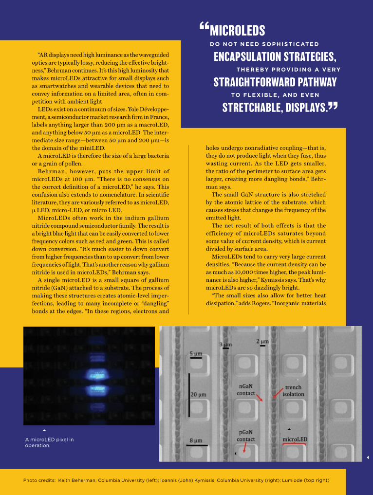
Photo credits: Keith Beherman, Columbia University (left); Ioannis (John) Kymissis, Columbia University (right); Lumiode (top right)
A microLED pixel in operation.
”
“
MICROLEDSDO NOT N E E D SOPHISTICATE D
ENCAPSULATION STRATEGIES,TH E RE BY PROVIDING A VE RY
STRAIGHTFORWARD PATHWAYTO FLE XIB LE , AN D E VE N
STRETCHABLE, DISPLAYS.

PHOTONICS FOCUS NOVEMBER/DECEMBER 2021 25
such as gallium nitride are much more chemically and thermally stable compared to organics. A pow-erful consequence is that microLEDs do not need sophisticated encapsulation strategies, thereby providing a very straightforward pathway to flexible, and even stretchable…displays,” Rogers comments.
MicroLED displays therefore consist of individual LEDs directly attached to a backplane that contains all the electronics (including transistors) that con-trol when the LED is turned on/off. However, given their small size, the sheer number of microLEDs required for a display is staggering.
A 4K display refers to a screen resolution of 3840 × 2160, or roughly 8.3 million pixels. A market report from Yole notes that making a 4K microLED display is tantamount to “assembling 25 million grains of pollen with a positioning accuracy of 1 micro- meter, without a single error.” This helps explain why assembly is so challenging. In addition, each pixel needs to switch between red, green, and blue lights.
This color-switching can be done in one of two ways. The first method is to fabricate separate microLEDs for each of the three colors of light and assemble them together on the backplane. The sec-ond is to assemble only blue LEDs on the backplane and cover them with a multicolored filter that will convert blue to the other two colors.
Like other semiconducting devices, microLEDs are made in clean rooms. They are made by the thousands on a wafer, and need to be carefully transferred to the backplane. Given that it takes millions of microLEDs to form a single display, it is impractical to transfer them one at a time.
Instead, LEDs are mounted first onto smaller transfer stamps that shuttle them in batches to the backplane. Consider a 12.5 × 12.5 mm2 transfer stamp—10,000 transfer cycles would be needed to populate a 75-inch TV panel. The process needs to be repeated three times if the colors are being assembled separately. A larger transfer stamp of size 102 × 100 mm2 would only need 170 transfer cycles for the same job.
Yole has suggested adding an “interposer” to this process. Smaller transfer stamps will print LEDs to an intermediate transfer stamp, which will then carry over to the display. It’s really the same problem as when there are more people who need to travel than there are vehicles to accommodate them. The key is efficient batching or rideshares.
Photo credits: Keith Beherman, Columbia University (left); Ioannis (John) Kymissis, Columbia University (right); Lumiode (top right)
A test sample from Lumiode showing the high luminance of a microLED element and displays integrated at the wafer scale.
A scanning electron micrograph of individual microLED pixels showing the isolation and contact features.

PHOTONICS FOCUS NOVEMBER/DECEMBER 202126
Kymissis has been working with displays where the chip-lets have a lot of space in between. Since microLEDs are very bright, the spacing does not affect the quality of the display but does allow for the transfer to be faster while allowing for more functionalities to be added to the screen. “You typically want the display to be on the order of 100 to 1,000 nits of luminance on the order of your TV or smartphone. The chiplets themselves are much brighter, so they are spread out and the rest of the display is available as a dark background to increase contrast, carry electronics, be transparent,” and so on, he says.
Smaller displays such as those used for projectors and AR/VR glasses will continue to use closely packed microLEDs. Kymissis continues “The microdisplays are much brighter— 10 to 50 million nits.”
Although transfer stamps streamline the transfer to the dis-play backplane, the microLEDS first must be moved from the growth wafer to the stamp.
That’s an area that Rogers has worked on a lot. The system that he uses for retrieving and printing the microLEDs involves, quite literally, a rubber stamp—a very high resolution, precision stamp, with tiny, raised features that match some multiple of the pitch of the LEDs on the source wafer. He explains that there are two parts to the transfer process: fabrication and undercut release of fully formed microLEDs from the source growth wafer, and physical mass transfer using stamps to target substrates. Both operations are now fully developed and refined to manufacturing standards.
Rohinni, a 25-member microLED company started in 2013, has patented a unique cartridge printer method for chiplet transfer. The process resembles traditional newspaper printing,
A passive matrix microLED display developed at Columbia University for use in miniature microscopes for animal studies.

Photo credit: Keith Behrman, Columbia University
UV curable epoxy meets NASAlow outgassing requirements
Hackensack, NJ 07601 USA+1.201.343.8983 ∙ [email protected]
www.masterbond.com
High temperature resistant• Serviceable from -60°C to 175°C
• Tg (with post cure) 135°C
Outstandingoptical clarity
Refractive index 1.52
Nanosilicareinforced
• Linear shrinkage <1%• Abrasion resistant
where a drum prealigned with LEDs is rolled on the backplane. As the surface rolls over it, the chiplet sticks to the display, held by weak forces of attraction.
ELux, a startup based in Vancouver, Canada, has perhaps the most novel technique of all. They have patented a self- assembled microLED display where the individual chiplets float in a solution and fall into the correct position with the application of magnetic fields.
It’s too early to say if any of these processes will lead to less expen-sive microLED displays. That will require them to be industrially scaled and evaluated. However, given the inherent complexity and the number of steps involved in each method, there is a chance for an error to creep in. This reduces the yield, or the number of working microLEDs that have survived the transfer process. As Kymissis points out, “Yield and quality issues are also paramount in many microLED applications, and techniques and technologies for improv-ing yield and productivity are something to keep an eye out for.”
In the life cycle of a microLED, a defect can arise as scratches or pits in the initial growth process, during etching, while transferring, or through the interconnects that power them. A 2018 Yole report analyzed the challenge of repairing dead LEDs in a 4K panel. Even if the fabrication process has a yield of 99.99 percent, that still leaves 2,500 dead pixels on the screen. This can easily take a couple of hours to find and fix during production.
And that’s assuming that the LED can be repaired at all. Typical microLEDs are encased in a protective layer and coated with an elec-trode on the top, and an elaborate backplane at the back. Most often, it’s not even clear where the defect is, let alone being able to fix it.
Unfortunately, as Behrman points out, our eyes will notice even a single dead pixel on a screen. That makes a 4K display with 99.99 percent yield undesirable.
For that reason, both Kymissis and Behrman think that micro-LEDs are likely to be adopted by microdisplays long before macro-displays. “Microdisplay applications are still emerging commercially but have been in intense development for AR/VR, automotive lighting such as active headlights, and projector applications,” Kymissis says. “Smartphones, for example, are not a good first target for microLED displays. I am confident that we will see both existing and new markets addressed through microLEDs.”
Rogers, however, is far more optimistic about the impending ubiquity. “MicroLED technology is poised to dominate all forms of displays. Particularly exciting unique applications are in transpar-ent display, flexible display, stretchable display for skin-integrated devices, and many others.”
VINEETH VENUGOPAL is a scientist and science writer who loves all things and their stories.
If your friend becomes a new Member of SPIE, you’ll get a free t-shirt
Send an email to your friend(s) suggesting they join SPIE. Copy or forward your email to our team at [email protected] and if your friend joins as a new Member by 31 November 2021 we will send you a cool SPIE t-shirt.

PHOTONICS FOCUS NOVEMBER/DECEMBER 202128 Photo credit: ASML
By Mark Wolverton
WHERE AREALL THE
HOLOGRAMS?
PHOTONICS FOCUS NOVEMBER/DECEMBER 202128
Optical trap display (OTD) vector image of a triangular prism plus a long-exposure, rotated view. This image breaks the boundary of the display aperture, which is not possible with holograms.

Closeup of silicon wafer with chip dies.
PHOTONICS FOCUS MAY/JUNE 2021 29
The elusive realm of total 3D immersion
EVERYBODY KNOWS what a hologram is. It’s Princess Leia in Star Wars: “Help me, Obi-Wan Kenobi. You’re my only hope.” It’s Captain Jean-Luc Picard in Star Trek: The Next Generation moving through an imaginary 1940s San Francisco as private eye Dixon Hill. It’s 40-foot tall ballerinas dancing in LA streets in Blade Runner: 2049.
Except that it’s not. “What people think of as holography that they see in the movies in general isn’t,” says Daniel Smalley, associate professor in the Electro-Holography Lab at Brigham Young University. “The academic definition is that to have a holographic display, you must have light diffracting from some modulation surface. That means that you have to be looking at a screen to see the image.”
Most of what the public thinks of as holography, and what’s been portrayed as such in much science fiction, is actually “a different type of display technology called a volumetric display,” Smalley explains.
In essence, a hologram is just a still image of the inter-ference pattern of different light waves diffracting from an object. Unlike the living, moving images of science fiction, they “move” only when we change our viewing angle, which is why we’re not (yet) watching holographic movies.
Although the principles of holography were first dis-covered in the late 1940s by Hungarian scientist Dennis Gabor, the concept didn’t become well-known outside a relatively small circle of specialists until after the invention of the laser in 1960. Gabor was looking for ways to improve electron microscopy techniques, not something the average citizen is much concerned with. But the laser brought holog-raphy out of the microscopic realm and into the world of visible light, making it accessible to anyone with eyesight.
When optical holograms were created for the first time in 1962, nearly simultaneously by Yuri Denisyuk in the Soviet Union and Emmett Leith and Juris Upatinieks at the University of Michigan, the possibilities seemed limitless. “The technical community responded with enthusiasm,” writes optical engineer Karl A. Stetson in a memoir. “Here was a process that gave truly three-dimensional images, complete with parallax. Many ideas were put forward for applications, 3D television, 3D movies, dazzling displays in store windows.…Little of this came to pass.”
Photo credit: Dan Smalley lab, Brigham Young University PHOTONICS FOCUS NOVEMBER/DECEMBER 2021 29

James D. Trolinger, co-founder of MetroLaser, Inc., recalled it as “an explosion in the field of optics,” writing in an SPIE conference proceedings that “during the next 50 years many applications of holography have both thrived and died…some, oversold, failed to meet expectations, while some were too complicated for general use. Others could not compete, never got accepted, or were impractical for general use.” And yet, Trolinger notes, “In many cases, as methods approached maturity or abandonment, new technology revitalized them, and this cycle continues today.”
Obviously, we still don’t live in a science-fictional world surrounded by gorgeous 3D images. The ongoing pandemic and lockdowns didn’t give rise to a brave new world of remote conferencing and working in simulated 3D spaces, only endless gazing at tiles of sullen, poorly lit faces in interminable Zoom meetings. Why? What happened to all the grand holographic dreams of yore? Is holography another obsolete technology of the past like laser-disc players and 8-track tapes, or can it still fulfill its original promise?
The answer to those questions involves both perceptions and technology. As Trolinger observes, the breakthroughs of the early ’60s “excited many people with promises of fame and glory fostering many diverse holography communities in a short time. Much like a gold rush, hundreds of people around the world became holographic gold diggers, making holograms, discovering new possibilities and phenomena…by 1970, holography was being pitched as a savior in almost every existing industry, and engineer-ing and research centers around the world looked to holography for new capabilities and solutions.”
Some of those capabilities and solutions, such as holographic metrology and interferometry, have proven extremely valuable to scientists and engi-neers, even if not broadly commercialized or known to the public. Others are ubiquitous if largely unheralded, such as the holographic security images you likely carry around on your credit cards and driver’s license.
Javid Khan, founder and director of Holoxica Ltd., noted in a presenta-tion for the 2015 International Year of Light that even if holography hasn’t yet lived up to the overblown promises of earlier decades, it never really went away. “Holography went ‘underground’ in the 1990s with the research being performed by just a handful of small companies, the military, and academic organizations,” he writes. That relatively small community is where most of the holographic action remains.
To a public used to the notion that Princess Leia is a hologram, applica-tions such as metrology, security, or data storage might be useful, but aren’t very sexy. “As far as public perception is concerned, holography was never what the public wanted,” Smalley says. It was a word attached to an image, he says, that holography was never going to be able to deliver.
Such expectations were already unrealistic for the analog holographic techniques of earlier decades that used photo-graphic emulsions to record images, but remain a problem even for digital holography. As with any other data-intensive computational task, bandwidth and data capacity are huge hurdles.
“Holography in general is a huge computational load to large displays,” explains Smalley. “If you want to make a bigger TV, you can make the pixels bigger, so the resolution doesn’t necessarily go up. But the pixel in a holographic dis-play is bound to the size of a wavelength of light, so they’re inextricably connected. If you want to make a display look bigger, you have to add more pixels. My advisor at MIT was fond of saying that you could make almost any display a holographic display, but you need a million times more pixels. So that’s just been the real issue.”
Increasing color variations and frame rate add to the demands. “So, we just don’t have the computational power sufficient to run these displays,” Smalley adds. “And when we gear up to create that hardware, we have to sit back and ask ourselves, ‘Gosh, is it really worth it’ given the amount of redundancy in a holographic image? The imagery from one view to the next is so similar, there’s so much redundancy in that pattern, you can’t help but think to yourself, is it really necessary to reproduce all this information? And so we have com-putational schemes that try to cut corners or make the sorts of trade-offs to alleviate this bandwidth require-ment rather than doing a brute force CPU strategy.”
Another reason that we’re still not seeing the ambi-tious 3D holograms of science fiction, explains Smalley, is that other imaging solutions can work almost as well for most needs. “My guess is that if we could find a really good killer application for holographic video display that couldn’t be done by a lesser technology, I think we would see this problem solved pretty quickly, if there were hundreds of millions of dollars to resolve the problem,” he says. “Absent a really compelling killer application, it’s going to be a hard slog.”
Some alternatives to holography have been around for more than 150 years. Perhaps the most enduring is “Pepper’s ghost,” popularized by Englishman John Henry Pepper beginning in the mid-19th century. For this illusion, a brightly lit figure out of the audience’s view is reflected off a clear pane of glass to create a ghostly illusion, used both for theatrical performances and by charlatans summoning “spirits from beyond.” Today, this trick of light is used in concerts, muse-ums, amusement parks, and most mundanely, in the teleprompter beloved by every speechifying politician.
Pepper’s ghost and similar tricks, however, are only “fauxlography,” not holography, says Khan. “Any vague illusion of an image floating in space is labeled a hologram, whether it’s celebrities, politicians, or a cardboard cutout in an airport. So, beware of fake holographics—remember, if there’s no diffraction, then it’s not a hologram.”
Schematic of the Smalley lab optical trap display setup.
PHOTONICS FOCUS NOVEMBER/DECEMBER 202130

Optical trap display (OTD) image of the Earth above a fingertip.
Aside from Hollywood movie magic, what will finally give us the 3D images of our dreams remains undeter-mined. It is likely to be a variety of different techniques, depending on particular requirements and available technical resources.
“It’s the volumetric displays that are going to make possible the kind of images from movies,” Smalley says. “Avatar, Star Wars, Blade Runner—all these images are going to be accomplished with things like tiny drones with lights on them, particles of dust that are being illu-minated, or plasma balls. These are the technologies that are going to make those images possible.”
It’s true, however, that some science-fictional displays are closer to actual holograms, such as the holodeck from Star Trek: The Next Generation. “That’s in my mind, at least in part, a good target for holographic technology,” says Smalley. “Because everywhere you’re looking in the holodeck, you’re looking at a surface, you’re looking at a screen. There could be a diffraction pattern.”
Smalley notes that volumetric display technology already offers compelling applications, beginning with telepresence. “Given COVID and remote work, the idea of being physically present in another space is really appealing. The thing about volumetric displays is they’re not just light displays: they are a combination of light and atoms suspended in the air in a particular way, so you literally can be physically somewhere else through these displays. You could imagine having a disembodied head in the room that can turn and look at each of the individuals in the room in turn. That can’t be achieved with a screen-based display, that kind of a sense of pres-ence is just impossible to achieve. There’s real, tangible value that people could viscerally feel, and that’s going to provide motivation to scale and develop this technology.”
Such 3D imaging capabilities could be valuable in any task dependent on accurate, real-time spatial under-standing, Smalley notes. Vascular surgery, air-traffic
control, and satellite tracking are just a few examples in which strict separation of physical objects and spatial awareness are crucial.
“Just imagine if the people performing these jobs had a volumetric display in front of them to see the complicated orbits of satellites, and they could just know viscerally that these two satellites are going to smash into each other,” Smalley says. With air traffic, he says, “if you could represent all of those aircraft as blobs in the air, they could be a physical part of the world around you, their positions, how they’re moving. I think that volumetric displays, in particular, have the potential to fundamentally change the way we interact with our digital data by making it a physical part of the world around us, make it a part of our environment. Our bodies and our minds are built to interact with the 3D world.”
Smalley’s lab is working to make such volumetric 3D images possible through an approach called optical trap technology—or, as the lab staff like to call it, the Princess Leia project. “We take a laser beam, focus it through an aberrated lens to create essentially a turbulent focus, a focus that has lots of holes in it. And we can put particles in those holes and then drag them around, like dragging around an object with a tractor beam. And then we illuminate that particle with a red, green, and blue light. We can create images in the air, volumetric images, make these sci-fi style geometries.” At the moment, such images are only about a cubic centimeter in size, but Smalley and his team are striving to scale that up to more practical dimensions—at least the eight to 10 inches of the Princess Leia image of the movie.
Other researchers are exploring digital approaches that can create and manipulate diffraction patterns in a computer—rather than on film as in analog holography—and then create images that can be illuminated not simply by a laser but any sufficiently monochromatic light source. “Digital holography, the ultimate marriage of optics and electronics, offers great promise in essentially all applications of holog-raphy,” writes Trolinger.
While we may not yet inhabit the wondrous holographic worlds of our science-fictional dreams, it’s also true that the notion that holog-raphy is a failed, obsolete technology is as much of an illusion as, well, a hologram itself.
Credits: Dan Smalley lab, Brigham Young University
MARK WOLVERTON is a freelance science writer and author based in Philadelphia.
”
OUR BODIESAND OUR MINDSARE BUILT TO
INTERACT WITH THE
3D WORLD.

LETTER FROM THE PRESIDENT
President’s Letter2021 THE END OF A YEAR WILL OFTEN FIND US IN A REFLECTIVE MODE. For a great many of us, the cautious optimism with which we may have greeted 2021 can now be only a rueful recollection. Yet again, we have been reminded—individually, cor-porately, and nationally—that none of us is in full control of our own destiny. For an organization with a membership and staff on the level of SPIE, core operations have again demanded an unprecedented level of rapid response and ingenious flexibility. Yet with hope, and the benefit of this gained experience, we trust in the emergence of a Society that is stronger and wiser in the service of each individual. May that be true for both SPIE and for society at large.
For sure, SPIE is in powerfully good shape to sustain and further its role as the international society for optics and photonics. This year, we have augmented our conference operations, extending facilities for constituents in every location to connect with each other and communicate their results around the world. Indeed, SPIE membership has grown; our financial position remains remarkably solid, with staffing levels scarcely changed; and we have awarded new educational endowments and scholarships, providing tangible support for each causeway leading towards a brighter future. The annual refreshing of positions for volunteer leadership is now introducing another group of eminently well-qualified individuals from around the world to help steer the Society forward in 2022. In wishing them well, I know SPIE is in very safe hands.
To conclude this, my last President’s Letter, I do want to take the occasion to thank all who, over many years, paved the path I have trodden. It is, of course, invidious to single out individuals—not least because there are so many who would richly deserve it. So let me simply acknowledge all whom I have met in, and through, my involvement with SPIE. I am thinking of past conferences, receptions, business trips, visits to Member groups both nationally and internationally, and numerous committees and boards whose intricate and very necessary work is far more interesting than could ever be guessed from outside. I thank all Members for their support of SPIE, adding especially heartfelt thanks to the many who have so enriched my life and career. In all my endeavours to serve the Society this year, I still cannot repay that debt, but I shall continue to try. Thank you.
DAVID ANDREWS
2021 SPIE PRESIDENT
PHOTONICS FOCUS NOVEMBER/DECEMBER 202132

SPIEDeadlines and Events
November 4–6: SPIE Advanced Biophotonics Conference 2021,
Busan, Republic of Korea
15: Call for Papers opens for SPIE Sensors + Imaging, including: Remote Sensing and Security + Defence
15: JBO Hot Topics Webinar Series: Biomedical Optics Programming: Education, Inclusion, Diversity, and Mentoring
15–19: SPIE Future Sensing Technologies Digital Forum
19: Finalists announced for 2022 PRISM Awards
30: Henri Poincaré Webinar Series, “Polarization Calibration of the Daniel K Inouye Solar Telescope (DKIST)” by Stacey Sueoka
December 1: Applications due for 2022 SPIE Outreach Grants
13–16: Advances in 3OM: Opto-Mechatronics, Opto-Mechanics, and Optical Metrology (3OM), Timisoara, Romania
29: Manuscripts due for SPIE Photonics West 2022
29: Manuscripts due for SPIE AR | VR | MR
January 2022 14: Abstracts due for Optics and Photonics
International Congress (OPIC)
22–27: SPIE Photonics West, San Francisco, California, USA
23–25: SPIE AR | VR | MR, San Francisco, California, USA
26: Manuscripts due for SPIE Medical Imaging
February 2022 2: Manuscripts due for SPIE Advanced Lithography
+ Patterning
9: Abstracts due for SPIE Optics + Photonics
9: Manuscripts due for SPIE Smart Structures + NDE
15: Applications due for SPIE Optics and Photonics Education Scholarships
20–24: SPIE Medical Imaging, San Diego, California, USA
27 Feb–3 Mar: SPIE Advanced Lithography + Patterning, San Jose, California, USA
March 2022 2: Call for Papers opens for SPIE/COS Photonics
Asia
6–10: SPIE Smart Structures + Nondestructive Evaluation, Long Beach, California, USA
9: Abstracts due for SPIE Sensors + Imaging, including: Remote Sensing and Security + Defence
9: Manuscripts due for SPIE Defense + Commercial Sensing
30: Manuscripts due for SPIE Photonics Europe
Contact us today

PHOTONICS FOCUS NOVEMBER/DECEMBER 202134
SPIE COMMUNITY NEWS
2021
SPIE Awards AnnouncedSPIE Diversity Outreach Award
SPIE FELLOW CÉLINE D’ORGEVILLE of the Australian National University (ANU) Research School of Astronomy and Astrophysics, in recognition of her leadership in diversity, inclusion, and equity activities in Australia and elsewhere in the world.
A leading expert in laser guide star adaptive optics, d’Orgeville also proactively orga-nizes and leads a range of equity, diversity, inclusion, mentoring, and cultural awareness sessions at ANU and across the globe. She is a committed organizer and speaker across a range of internal, external, and public outreach activities that enhance the profile of diversity in STEM. An active participant and leader within ANU’s Inclusion, Diversity, Equity, and Access program, she is also a member of the Astronomical Society of Austra-lia’s (ASA) Inclusion, Diversity, and Equity in Astronomy chapter steering committee, as well as that of ASA’s Women in Astronomy chapter.
The SPIE Diversity Outreach Award recognizes outstanding contributions to promot-ing diversity in the education, training, and participation of women and minorities in optics, photonics, electro-optics, and imaging technologies and applications.
SPIE Harold E. Edgerton Award in High-Speed Optics
SPIE FELLOW VLADISLAV YAKOVLEV, professor of biomedical engineering at Texas A&M University, USA, in recognition of his remarkable contributions to ultrafast laser technology, ultrafast spectroscopies, and ultrafast imaging and their applications, as well as his SPIE service and outreach.
Yakovlev’s career reflects a lifetime of pioneering work across high-speed optics. His achievements include work in optical parametric amplifiers of white-light continuum, widely adapted as broadly tunable sources of ultrashort laser pulses used for high-speed imaging and spectroscopy; using shaped optical pulses for spectroscopy and imaging, including the first experimental demonstration of coherent quantum control of molecular dynamics; and applications of ultrashort laser pulses such as cornea reshaping, broad-band coherent anti-Stokes Raman scattering, and random Raman lasing and imaging.
The SPIE Harold E. Edgerton Award in High-Speed Optics recognizes outstanding contributions to optical or photonics techniques in the application and understanding of high-speed physical phenomena.
SPIE Chandra S. Vikram Award in Optical Metrology
SPIE FELLOW KRZYSZTOF PATORSKI, professor of optics at the Warsaw University of Technology, Poland, in recognition of his seminal contributions to diffraction, inter-ferometry, moiré fields, and fringe analysis with applications in optical metrology, experimental mechanics, and biomedical engineering.
Patorski’s career-long developments in the fields of interferometry and fringe pattern analysis have found application in a variety of scientific and engineering fields including optical metrology methods such as interferometry, holography, speckle, and structured light; experimental mechanics and materials science; and bioengineering and medical imaging. His research on moiré fringes to analyze scoliosis and human posture has been implemented in commercial systems—in the medical field as well as furniture design—and his interest in biomedical engineering resulted in the development of structured illumination methods for optical sectioning and fringe analysis for phase microscopy for cancer-cell testing.
The SPIE Chandra S. Vikram Award in Optical Metrology recognizes exceptional contributions to the field of optical metrology, whether for a specific achievement, development, or invention of significance, or for lifetime achievement.
Céline d’Orgeville
Vladislav Yakovlev
Krzysztof Patorski
See the entire list of SPIE Award winners at spie.org/2021awards

PHOTONICS FOCUS NOVEMBER/DECEMBER 2021 35
SPIE President’s Doctoral Theory Key to New Discovery
SPIE COMMUNITY NEWS
MORE THAN 40 YEARS AGO, as a young doctoral stu-dent, SPIE President David Andrews of University of East Anglia, theorized that the chirality of nanoparticles could be observed through even harmonics of light. Research-ers at the University of Bath have now discovered these effects can be observed through the odd harmonics of light as well. These interactions between photonics and the twisted materials, as detailed in a new paper titled “Optical Activity in Third-Harmonic Rayleigh Scat-tering: A New Route for Measuring Chirality,” (Laser & Photonics Reviews) have implications for emerging nanotechnologies in communications, nanorobotics, next-generation bio- and nanomachinery, and ultrathin optical components.
“From a practical point of view, our results offer a straightforward, user-friendly experimental method to achieve an unprecedented understanding of the interac-tions between light and twisted materials,” says Ventsislav Valev, professor of physics at U. of Bath. “Such interactions
are at the heart of emerging nanotechnologies. To take a musical analogy, until now, scientists who study twisted molecules—such as DNA, amino acids, proteins, and sugars—and nanoparticles in water, have illuminated them at a given frequency and have either observed that same fre-quency or its noise, known as inharmonic partial overtones. Our research opens up the study of the harmonic signatures of these twisted molecules, so that we can appreciate their ‘timbre’ for the first time.”
“When I first worked up this theory, it was by done by exploiting some mathematical results which I had first derived during my PhD studies and only recently pub-lished,” notes Andrews. “At the time, no one else had yet applied them. Many decades later, it came as a sudden and enormously welcome surprise to find that Professor Valev’s team had secured some very exciting preliminary results. All credit to the experimentalists for pursuing such an elusive goal.”
Read more at spie.org/chirality-nano
Upon illumination with red light, third harmonic scattered light (in violet) reveals the twist of metal nanoparticles.
Photo credit: Ventsislav Valev and Lukas Ohnoutek

PHOTONICS FOCUS NOVEMBER/DECEMBER 202136
SPIE COMMUNITY NEWS
SPIE Adds Two New Policy StatementsPOSITION STATEMENTS APPROVED by the SPIE Board of Directors serve as guiding principles for the Society when dealing with issues of importance to the Society, SPIE Membership, and the optics and photonics community. SPIE recently added these two policy statements:
ANTIRACISMSPIE embraces the multiethnic body of voices of its commu-nities and acknowledges that each individual voice has equal value. SPIE explicitly condemns and actively denounces racially motivated violence, bias, discrimination, or exclu-sion. Understanding that some racist acts can be unconscious or unintentional, SPIE resolves to discuss and better under-stand the inequities that exist within optics and photonics, and work with members of our community to correct them. Standing up against racism is integral to the SPIE mission as a scientific society, to advance light-based research and technologies for the betterment of the human condition.
EQUITY, DIVERSITY, AND INCLUSIONOptics and photonics technology should be accessible to all, whether through study, employment, or the societal benefits achieved from advancements in this area. SPIE supports opportunity, equity, and freedom for all people regardless of identity, background, or affiliation. SPIE rec-ognizes past and current inequities within the optics and photonics community and resolves to prioritize prevention of future inequities. SPIE calls on governments, academia, and the private sector to ensure access to opportunity and advancement within their constituencies, as they benefit greatly from a diverse workforce.
Read more at spie.org/policy-positions
SPIE Journal of Applied Remote Sensing Announces New AwardTHE JOURNAL OF APPLIED REMOTE SENSING (JARS) has established the JARS Best Student Paper Award to showcase student work across interdisciplinary applications, theoretical innovation, and photo-optical instrumentation and design in remote sensing.
This award will join the existing annual JARS Best Paper Awards in the areas of interdisciplinary applications, theoretical innovation, and photo-optical instrumentation and design. The first recipient of the JARS Best Student Paper Award will be announced in 2022 for work published in 2021.
“We see that students are doing great work, and SPIE would like to encourage their research in remote sensing and applica-tions,” notes JARS Editor-in Chief Ni-Bin Chang. “This award will acknowledge their progress, as well as give students a significant achievement to highlight on their CVs.”
The award will go to the first author on a student-led research paper. To qualify, the paper must be authored by a graduate student who has completed the research in fulfillment of a dis-sertation or thesis with novel ideas, concepts, algorithms, and
methods. There are no restric-tions as to organization, nation-ality, race, creed, sex, or age, and no requirement for SPIE mem-bership. A selection committee will be appointed by Chang, and papers will be judged based on technical merit, clarity, origi-nality, potential impact on the field, and quality of the overall presentation.
L ea r n more at spie.org/2021JARSstudent
THIS YEAR, SPIE WELCOMED 99 new Senior Members from 24 countries, across academia, government, and industry. They work in a variety of disciplines ranging from nanophoton-ics, artificial intelligence and machine learning, solar energy, and translational medicine, to defense, food security, and lithography.
“SPIE Senior Members are Members honored for their scientific excellence
across the broad spectrum of optics and photonics research and applications, their active involvement with the optics community and SPIE, and significant performance that distinguishes them from their peers,” said the 2021 Senior Member Subcommittee Chair and US Army Research Laboratory Essential Research Program Manager Dimitra Stratis-Cullum. “This promotion honors their contributions not only across the
international ecosystem, but also across the full spectrum of optics and photon-ics professionals in academia, industry, and government.”
Nominations for the 2022 cohort of SPIE Senior Members will be accepted through 15 March 2022; see informa-tion and a complete list of all SPIE Senior Members at spie.org/2021 seniormembers
New SPIE Senior Members

PHOTONICS FOCUS NOVEMBER/DECEMBER 2021 37
SPIE COMMUNITY NEWS
SPIE Optics and Photonics Champion Academy
University of Birmingham students pictured in the UK Quantum Technology Hub, home to the SPIE Optics and Photonics Champion Academy.
IN SEPTEMBER, at SPIE Photonex + Vacuum Tech-nologies in Glasgow, Scotland, SPIE and University of Birmingham (UB) announced the establishment of the SPIE Optics and Photonics Champion Acad-emy fund.
A $400,000 gift from the SPIE Endowment Matching Program will be matched 100 percent by the university, creating an $800,000 fund to support a photonics-focused education program led by Professor and Principal Investigator of the UK Quantum Technology Hub Sensors and Timing, Kai Bongs, and Professor of Computational Life Sciences, Iain Styles.
The SPIE Optics and Photonics Champion Acad-emy will support UB students in a variety of ways such as expanding cross-disciplinary educational opportunities in optics and photonics; offering students hands-on support and training to become influential science communicators and advocates of optics and photonics; and by utilizing a range of stipends, awards, and activity grants, which will be supplemented with professional development and mentoring opportunities from the university’s academic leaders as well as from external experts.
“We are delighted to be able to work with SPIE to launch this unique Academy at the University
of Birmingham,” said Bongs. “This initiative will help to accelerate the growth of optics a n d p h o t o n i c s expertise, which w i l l have g re at impact far beyond the University. Our hope is to not only encourage this learning, but to also create aware-ness of the huge importance of this subject area in tackling real-world problems.”
“By equipping early-career optics and photon-ics researchers and PhD students with skills in advanced data analysis, we will help to accelerate the translation of these exciting technologies from the laboratory to their adoption in real-world appli-cations,” added Styles. “Our SPIE Champions will be able to work with experts in diverse application areas such as healthcare and climate monitoring to develop end-to-end optics-based solutions with integrated analytics for some of our most pressing challenges.”
Read more at spie.org/spiechampion

SPIE COMMUNITY NEWS
Optics Community Reconnects at SPIE Optics + Photonics THE FIRST MAJOR IN-PERSON OPTICS EVENT since early 2020—held 1– 5 August in San Diego, California, USA—offered multiple networking opportunities, a lively exhibit floor, and more than 2,100 technical presentations.
SPIE welcomed optical researchers, engineers, exhibitors, students, and industry leaders to an energetic conference, which, for most, was the first they’d attended in nearly 18 months. While presenters and attendees were also able to participate virtually, there was genuine excitement at the opportunity to connect and reconnect face-to-face in San Diego.
New Titles from SPIE PressLEVERAGE THE KNOWLEDGE provided by one of the world’s leading indepen-dent publishers of optics, photonics, and imaging information and research.
Optical Lithography: Here is Why (Second Edition): This book is written for new and experienced engineers, technology managers, and senior technicians who want to enrich their understanding of the image formation physics of a lithographic system.
Review of Optical Manufacturing: This book is suitable for beginner optical engineers learning about the optics industry and for advanced professionals stay-ing up-to-date with various subfields of optics as it summarizes some of the critical changes that have impacted optical system manufacturing from 2000 to 2020.
Field Guide to Infrared Optical Materials: This Field Guide focuses on the most common infrared crystals and types of glass used in these systems, from their manufacturing methods, through modern optical fabrication technologies, and to end-use applications.
Grant Writing from the Ground Up: A career in science relies on developing the skill to convince strangers to give you enormous sums of money. This book presents a step-by-step process to construct compelling grant proposals that rise to the top of a reviewer’s stack.
Principles of Vision-Enabled Autonomous Flight: This book provides an over-view of sensors and phenomenology from visible through infrared, extending into the radar bands and including both passive and active systems. It addresses the role of vision systems for autonomous operations and discusses the critical tasks required of a vision system.
See more SPIE Books at spie.org/SPIEBooks
Throughout the week, we heard repeat-edly from authors, attendees, and exhib-itors that they were ecstatic to be back in a convention center, seeing each other in person.
Following guidance from the US Cen-ters for Disease Control and Prevention, the State of California, and City of San Diego that Optics + Photonics could be held safely, SPIE sprang into action. Following a long foray into online-only events, SPIE proceeded to successfully host more than 1,300 attendees and 100-plus exhibitors, with an additional 1,400 registrants in attendance virtually.
“In spite of the changing circum-stances, we experienced higher than anticipated in-person and remote atten-dance,” noted SPIE CEO Kent Rochford. “More than 2,700 people registered for Optics + Photonics, and we really appreciate all those who came, visited the exhibitors, and participated in the technical program. Ultimately, the com-munity supported the event, and they were happy to be back and networking with each other. For us, that constitutes a terrific success.”
Read more at spie.org/OP21reconnect

39
Snap a photo of your completed word search + Bonus scramble, and send it to [email protected]. One winners, drawn at random, will receive a gift!
BONUS: Unscramble the circled letters to reveal the theme of this issue of Photonics Focus
THEME:
CLUES:
1. Venue for early light shows 2. Created by “Imagineers” 3. You might wear one on your wrist 4. Artistic look not generally obtainable with
digital cameras 5. A process that might include scraping off
an optical coating 6. Pioneer of rock 'n roll light shows 7. Creator of coherent, intense beams of light
8. Used on credit cards a lot 9. Surf’s up!10. 3D images floating in space, without a
display11. Skywalker’s sister12. Resulting from a different point of view13. Ready when you are for your closeup 14. Makes a connection
ANSWERS1. Laserium, 2. Madame Leota, 3. Microdisplay, 4. Filmic, 5. Detuning, 6. Garmire, 7. Townes, 8. Holography, 9. Waveguide, 10. Volumetric, 11. Princess Leia, 12. Parallax, 13. Cine Lens, 14. Interposer
D C M N K L D G E K G C R N A U A Y R M
M D A N E E T S I P B A J M A I L L I W
G I R W P J Q R H N I S W X L F H Y E B
L W C M P W B H O E T G F H N J G D K J
E G F R R F B L L A S E R I U M W N A M
G N J F O K M X L B M K R J S Q E I R S
U N S K J D H O L O G R A P H Y N V E T
W P I X E L I N D K A A P L O E M E N L
K C U D C L O S I L C F R W L S A K L C
K H R E T A W E P A J H X M N I E A O A
B K C T O W N E S L P R N A I O B R W R
D D Q U R A H W O C A W O D T R K X V R
J F B N W V O J D P R Y W A S M E Y Z I
B J C I N E L E N S A J A M D D V L B E
C L M N F G O M V O L U M E T R I C U B
Y D O G B U S Z B W L F I L M I C Y L S
L V R L K I M O E W A N I E O C E L A T
R G Q S O D E P A G X D R O Z A A I C I
E O F C Q E G B V I Z P D T E K R M I B
K F P R I N C E S S L E I A N E K E T R
PHOTONICS FOCUS NOVEMBER/DECEMBER 2021 39

A Continuum of Global Community Support

IN THE FOLLOWING PAGES, excerpted from the 2020 SPIE Annual Report,you’ll meet some of the recipients and beneficiaries of our high-impact, community-support programs. These programs range from SPIE education scholarships—a total of $298,000 going to 78 recipients in 23 countries—to our international SPIE Endowment Matching Program. Last year, that initiative contributed a transformative $2 million to fund university faculty positions, scholarships, engagement programs, and other optics and photonics research and education efforts. SPIE worked in collaboration during 2020 with such prestigious institutions as the University of Central Florida’s CREOL, The College of Optics and Photonics; Barcelona-based ICFO, the Institute of Photonic Sciences; JILA, a joint institute of the University of Colorado, Boulder and NIST; and the University of Glasgow’s Centre for Quantum Technology.
PHOTONICS FOCUS NOVEMBER/DECEMBER 2021 S1
SPECIAL SECTION: COMMUNITY SUPPORT
Beyond what’s noted in the following pages, in 2021 we’ve continued to grow the SPIE Endowment Matching Program: We established a $1 million SPIE Faculty Fellowship in Optics and Photonics that will support a faculty member at Vanderbilt’s School of Engineering, and an $800,000 fund at the Univer-sity of Birmingham that will create the SPIE Optics and Photonics Champion Academy. In addition, we announced a partnership with IBM to support quan-tum optics programs at America’s historically black colleges and universities (HBCUs). It is the annual $100,000 IBM-SPIE HBCU Faculty Accelerator Award in Quantum Optics and Photonics.
Scholarships and the Endowment Matching Program are just two of our community-support programs. Our named scholarships and fellowships provide wide-ranging opportunities in academics, industry, and government. Luke Long is pursuing his doctoral research in the physics of EUV photo-resist thanks to the Nick Cobb Memorial Scholar-ship; SPIE and Optica Arthur H. Guenther Con-gressional Fellowship recipient Michelle Solomon is honing the photonics-focused, public-policy aspect of her career; and at the University of Houston’s Biomedical Optics Lab, Fernando Zvietcovich, the SPIE-Franz Hillenkamp Postdoctoral Fellow, is developing and translating a novel biophotonics- based optical coherence elastography (OCE) method for human diagnostics and treatment.
What is more, 345 SPIE student chapters around the world provide educational and leadership opportunities for thousands of tomorrow’s stars. Altogether, the Society provides unmatched sup-port for young scientists and engineers who are pursuing their career goals in optics and photonics.
Why do we do this? Because SPIE is a community- focused Society operating globally. Integral to our mission to partner with researchers, educators, and industry to advance light-based research and tech-nologies for the betterment of the human condition is a commitment to support, nurture, and develop the next and future generations, ensuring a sus-tained and healthy optics and photonics community.
As one 2020 fellowship recipient, Fernando Zviet-covich, noted: “Receiving this prestigious fellowship from SPIE will enable me and my colleagues to, in the long term, improve people’s quality of health. I am very proud and fortunate that SPIE recognizes the value of my work by providing me with an excellent opportunity for developing translational research that constitutes a fundamental step towards my career development as young and independent investigator in the biophotonics and translational science fields.”
SPIE is both photonics- and future-focused: It’s with pleasure and pride that we introduce you to the next generation of optical scientists, policy makers, technicians, and engineers.

SPECIAL SECTION COMMUNITY SUPPORT
IN 2020, SPIE PROVIDED $5.1 MILLION in community support including scholarships and awards, outreach and advocacy programs, public policy and lobbying work, and educational resources. We are an educational, not-for-profit organization that contributes a significant percentage of revenue, every month, every year, without a separate fundraising campaign or administrative foundation. Our mission to support our community is part of the SPIE DNA.
From 2016 to 2020, SPIE has invested $23.8 million in programs supporting the optics and photonics community, spanning education and student development, direct scholarships, professional recognition and awards, career development, advocacy, and public awareness. • The SPIE Endowment Matching Program, which funds the expan-
sion of educational opportunities in optics and photonics, awarded six endowments to the following organizations: the University of Central Florida (UCF) College of Optics and Photonics (CREOL); the University of Colorado/JILA; ICFO, the Barcelona-based Institute of Photonic Sciences; the University of Glasgow; and the University of Wisconsin-River Falls (UWRF).
• SPIE awarded $298,000 in education scholarships to 78 students. Sixty percent—of the scholarship winners were from outside of the US.
• Three special-interest, named scholarships were awarded: An SPIE Early Career Professional Member at the University of Houston was selected for the SPIE-Franz Hillenkamp Postdoctoral Fellowship in Problem-Driven Biomedical Optics and Analytics; the Joe and Agnete Yaver Memorial Scholarship was awarded to an SPIE staff member; and the Nick Cobb Memorial Scholarship was awarded to a graduate student studying advanced lithography.
• Sixty-five Student Author Travel Grants to attend SPIE first quarter events were awarded through this program, jointly funded with MKS Instruments.
• SPIE Education Outreach Grants were awarded to 19 organizations, with 53 percent of the winners coming from outside of the US.
• SPIE celebrated the International Day of Light (IDL) and contrib-uted to the #Seethelight campaign. The annual SPIE IDL photo contest collected 2,000 entries, and 14 IDL Micro Grants were awarded to organizations from 10 different countries. For all of the 2020 program, SPIE maintained a strong social media presence with more than 259,550 impressions and 5,300 engagements.
Photo credit: Clare Elwell, University College, London
• A new Fellowship program was launched with the University Ottawa Joint Centre for Extreme Photonics and the International Centre for Theoretical Physics to bring early career researchers from developing countries for six months of research in the University Ottawa labs.
• SPIE sponsored the ICTP Winter College on Quantum Photonics which hosted 79 students from 27 devel-oping countries. Of the attendees, 42 percent were female.
• As part of its annual Society Awards, SPIE established the Maiman Laser Award, named after Theodore Maiman who first demonstrated a working laser. The inaugural winner was Robert L. Byer.
SPIE INVESTED $23.8 MILLION IN COMMUNITY SUPPORT FROM 2016–2020
Public Education& Awareness
$23.8 Min
5 years
Sponsorships& University
Programs
Scholarships
Student Development
EDIIndustry Advocacy
CareerDevelopment
Recognition
EducationalEndowmentMatching

SPECIAL SECTION: COMMUNITY SUPPORT
PHOTONICS FOCUS NOVEMBER/DECEMBER 2021 S3
SPIE Endowment Matching ProgramThe SPIE Endowment Matching Program, established in 2019, is a multimillion dollar, five-year, edu-cational-funding initiative designed to increase international capacity in the teaching and research of optics and photonics. SPIE supports optics and photonics education and the future of the industry by contributing up to $500,000 per award to college and university programs with optics and photonics degrees, or with other disciplines allied to the SPIE mission. In 2020, we established six endowments such that $2 million in giving from SPIE led to a transformative $5.5 million total after matching.
SPIE FUND HELPS SUPPORT SUMMER OPTICS SCHOLARS PROGRAM IN WISCONSINThe SPIE/University of Wisconsin-River Falls (UWRF) Optics Summer Research Scholars fund supports critical engagement with professional research groups, supporting a UWRF student who wishes to attend a summer research program related to optics and photonics, either at UWRF or at another institution with a substantial optics research program. With an original $50,000 in funds from SPIE, UWRF successfully raised the matching $50,000 and has created an endowment for their students’ use in perpetuity. As the endowment fund is invested and grows beyond the $100,000 minimum, UWRF will make this scholarship available to additional students each summer.
SPIE ENDOWS EARLY CAREER RESEARCHER ACCELERATOR FUND IN QUANTUM PHOTONICS WITH THE UNIVERSITY OF GLASGOWThe SPIE Early Career Researcher Accelerator Fund in Quantum Photonics, a $1 mil-lion endowment established by a $500,000 SPIE gift fully matched by the University of Glasgow, supports collaborative early-career research in quantum photonics. The fund creates two new programs at the university. An annual SPIE Early Career Researcher in Quantum Photonics Scholarship will be awarded to an outstanding University of Glasgow graduate student who is in the process of completing their studies. In addition, the pro-gram will support outgoing and incoming placements at and from the university as part of its ongoing collaboration with leading quantum-photonics research groups across the globe. Each year, the program will pair several university early-career researchers with counterparts from outside laboratories for six-month-long shared projects.
University of Glasgow Professor Daniele Faccio, center, working on laser system alignment and optimization with student Mihail Petev, left, and Niclas Westerberg, a Leverhulme Fellow in the School of Physics and Astronomy.
”We’re pleased and proud to be establishing the Early Career Researcher
Accelerator Fund in Quantum Photonics thanks to SPIE’s generous gift,
which we’re very happy to match with our own funding.
–Professor Sir Anton Muscatelli principal and vice-chancellor of the University of Glasgow
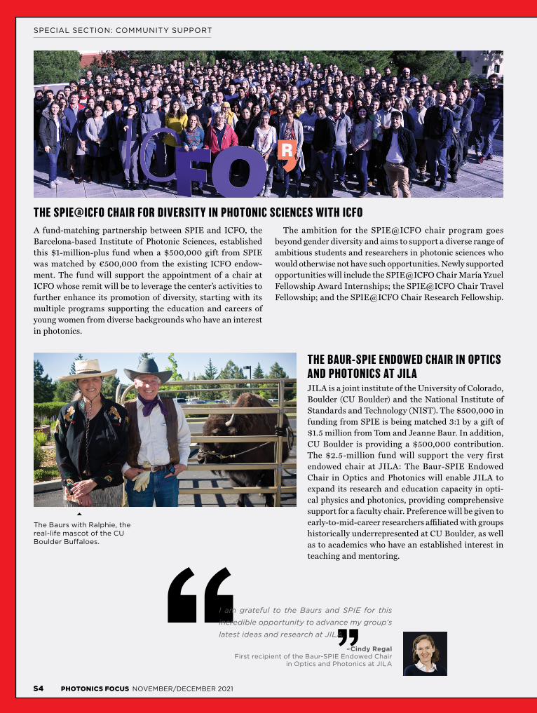
SPECIAL SECTION: COMMUNITY SUPPORT
PHOTONICS FOCUS NOVEMBER/DECEMBER 2021S4
”
THE SPIE@ICFO CHAIR FOR DIVERSITY IN PHOTONIC SCIENCES WITH ICFO
THE BAUR-SPIE ENDOWED CHAIR IN OPTICS AND PHOTONICS AT JILAJILA is a joint institute of the University of Colorado, Boulder (CU Boulder) and the National Institute of Standards and Technology (NIST). The $500,000 in funding from SPIE is being matched 3:1 by a gift of $1.5 million from Tom and Jeanne Baur. In addition, CU Boulder is providing a $500,000 contribution. The $2.5-million fund will support the very first endowed chair at JILA: The Baur-SPIE Endowed Chair in Optics and Photonics will enable JILA to expand its research and education capacity in opti-cal physics and photonics, providing comprehensive support for a faculty chair. Preference will be given to early-to-mid-career researchers affiliated with groups historically underrepresented at CU Boulder, as well as to academics who have an established interest in teaching and mentoring.
The Baurs with Ralphie, the real-life mascot of the CU Boulder Buffaloes.
A fund-matching partnership between SPIE and ICFO, the Barcelona-based Institute of Photonic Sciences, established this $1-million-plus fund when a $500,000 gift from SPIE was matched by €500,000 from the existing ICFO endow-ment. The fund will support the appointment of a chair at ICFO whose remit will be to leverage the center’s activities to further enhance its promotion of diversity, starting with its multiple programs supporting the education and careers of young women from diverse backgrounds who have an interest in photonics.
The ambition for the SPIE@ICFO chair program goes beyond gender diversity and aims to support a diverse range of ambitious students and researchers in photonic sciences who would otherwise not have such opportunities. Newly supported opportunities will include the SPIE@ICFO Chair María Yzuel Fellowship Award Internships; the SPIE@ICFO Chair Travel Fellowship; and the SPIE@ICFO Chair Research Fellowship.
I am grateful to the Baurs and SPIE for this
incredible opportunity to advance my group’s
latest ideas and research at JILA.
–Cindy Regal First recipient of the Baur-SPIE Endowed Chair
in Optics and Photonics at JILA

SPECIAL SECTION: COMMUNITY SUPPORT
PHOTONICS FOCUS NOVEMBER/DECEMBER 2021 S5
”THE SPIE-GLEBOV FAMILY OPTICS AND PHOTONICS GRADUATE SCHOLARSHIP FUND FOR THE UNIVERSITY OF CENTRAL FLORIDA COLLEGE OF OPTICS AND PHOTONICS (CREOL)This $650,000 scholarship fund, created for graduate students at University of Central Florida (UCF), CREOL, was established with a $325,000 SPIE gift that was matched in full by the college’s research foundation and the Glebov family. Leonid Glebov, a research pro-fessor, and his wife, Larissa Glebova, a retired research scientist, are longtime faculty members of UCF CREOL.
THE SOILEAU FAMILY-SPIE OPTICS AND PHOTONICS UNDERGRADUATE SCHOLARSHIP FUND FOR THE UNIVERSITY OF CENTRAL FLORIDA COLLEGE OF OPTICS AND PHOTONICS (CREOL)For this $250,000 endowment, the $125,000 in funding from SPIE was matched in full by a gift from the Soileau family in order to create scholarships for undergraduate students at CREOL, with preference given to students who are first generation—the first in their families to attend college.
I learned early that wealth does not
equal worth. My family is pleased
to partner with SPIE to support
scholarships for students studying
optics and photonics to help them
realize their worth.
–M.J. Soileau
”
We are pleased to partner with SPIE and UCF
CREOL to create an enduring scholarship for
graduate students in the exciting field of optics
and photonics. Together, we are investing in
new opportunities for talented young people,
because talent does not correlate with the
ability to pay for an education.
–Leonid Glebov

SPECIAL SECTION: COMMUNITY SUPPORT
PHOTONICS FOCUS NOVEMBER/DECEMBER 2021S6
Scholarship and Fellowship Recipients2020 TOP SCHOLARSHIP WINNERS
Jonathan Pinnell
The SPIE D.J. Lovell Scholarship was awarded to Jonathan Pinnell, University of the Witwatersrand, Johannesburg (South Africa). This is the Society’s largest and most prestigious scholarship sponsored by SPIE.
Daniel Louie
Daniel C. Louie, the University of Brit-ish Columbia (Canada), was awarded the John Kiel Scholarship which was established to honor SPIE founding member John Kiel, in recognition of his long-standing and significant con-tributions to the Society. Sponsored by SPIE, this scholarship and is awarded for the student’s potential for long-term contribution to the field of optics and optical engineering.
Gehrig Carlse
The Laser Technology, Engineering and Applications Scholarship was awarded to Gehrig Carlse, York University (Can-ada). This scholarship is awarded in rec-ognition of a student’s scholarly achieve-ment in laser technology, engineering, or applications. Funds are provided in part by SPIE.
David Lippman
The Optical Design and Engineering Scholarship was awarded to David Lip-pman, the Institute of Optics, Univer-sity of Rochester (United States). The scholarship was established in memory of Bill Price and Warren Smith, both well-respected members of SPIE’s technical community. This scholarship is awarded to a student in the field of optical design and engineering.
Yonghuan David Ren
Yonghuan David Ren, University of California, Berkeley (United States), was awarded the BACUS Scholarship. This scholarship is awarded to a stu-dent in the field of microlithography with an emphasis on optical tooling and/or semiconductor manufacturing technologies. This scholarship is spon-sored by BACUS, SPIE’s Photomask International Technical Group.
Deesha Shah
Deesha Shah, Purdue University (United States), is the recipient of the Teddi Laurin Scholarship. Photonics Media is partnering with SPIE to fund the Teddi Laurin scholarship to raise awareness of optics and photonics, and to foster growth and success in the pho-tonics industry by supporting students involved in photonics. This scholarship is in memory of Laurin Publishing and Photonics Media founder Teddi Laurin.

SPECIAL SECTION: COMMUNITY SUPPORT
PHOTONICS FOCUS NOVEMBER/DECEMBER 2021 S7
I am thrilled to have been selected as the Arthur
H. Guenther Congressional Fellow, and I look
forward to applying science-driven thinking in
service to the public while learning about poli-
cymaking and the legislative process.
–Michelle Solomon
SPIE-FRANZ HILLENKAMP POSTDOCTORAL FELLOWSHIP IN PROBLEM-DRIVEN BIOMEDICAL OPTICS AND ANALYTICS: FERNANDO ZVIETCOVICH
Photo credit: J. Adam Fenster/Univ. of Rochester
Receiving this prestigious Fellowship from SPIE
will enable me and my colleagues to, in the long
term, improve people’s quality of health. I am very
proud and fortunate that SPIE recognizes the value
of my work by providing me with an excellent
opportunity for developing translational research
that constitutes a fundamental step towards my
career development as young and independent
investigator in the biophotonics and translational
science fields.–Fernando Zvietcovich
SPIE AND OSA (NOW OPTICA) ARTHUR H. GUENTHER CONGRESSIONAL FELLOWSHIP AWARD: MICHELLE SOLOMONThe Guenther Congressional Fellowship program’s mission is to bring technical and scientific backgrounds and perspec-tives to the decision-making process in Congress and provide scientists with insight into the inner workings of the federal government. Fellows have the opportunity to participate in a multitude of policymaking functions including conducting leg-islative or oversight work, assisting in congressional hearings and debates, preparing policy briefs, and writing speeches.
Michelle Solomon, whose graduate research concentrated on ways to use light to purify chemicals used in the pharmaceutical and agrochemical industries with the goal of decreasing side effects, will serve a one-year term in Washington, DC, USA, as a special legislative assistant for a member of the US Congress or as a staff member for a congressional committee. SPIE and Optica are co-sponsors of the fellowship.
The annual award of $75,000 award supports interdisciplinary problem-driven research and provides opportunities for trans-lating new technologies into clinical practice for improving human health. Fernando Zvietcovich’s research—conducted in conjunction with Kirill Larin and Michael Twa at the University of Houston’s Biomedical Optics Lab—builds on work covered
in Larin’s lab over the past five years. Zvietcovich will work on translating a novel biophotonics-based optical coherence elastography (OCE) method, developed and designed for the noninvasive quantification of corneal spatial biomechanical properties in 3D, into the in vivo clinical use for human ocular disease diagnostics and treatment monitoring.

SPECIAL SECTION: COMMUNITY SUPPORT
PHOTONICS FOCUS NOVEMBER/DECEMBER 2021S8
JOE AND AGNETE YAVER MEMORIAL SCHOLARSHIP: ALISON WALKERThe Joe and Agnete Yaver Memorial Scholarship is intended for those seeking further education that provides “the business knowledge required to facilitate the advancement and application of optics and photonics research and technology.” The $10,000 scholarship is available to SPIE Members and staff seeking an advanced degree or certificate from an accredited program.
Alison Walker, a marketing project manager with the Society, is using this business- oriented scholarship to pursue two certification courses in project management and web design.
NICK COBB MEMORIAL SCHOLARSHIP: LUKE LONG
It is an honor to win the Nick Cobb scholarship
in recognition of my work on understanding
EUV stochastics and serves as motivation going
forward for furthering our understanding of
this challenging subject. I am excited to utilize
the support to continue my research, and to
present my results at SPIE conferences in the
coming year.–Luke Long
MICHAEL KIDGER MEMORIAL SCHOLARSHIP AWARD: BRANDON HELLMANBrandon Hellman, James C. Wyant College of Optical Sciences, University of Arizona (United States), has been awarded the 2020 Michael Kidger Memorial Scholarship in Optical Design. The scholarship, established in 1998 to honor Michael John Kidger, a well-respected educator, design software developer and member of the optical science and engineering community, is awarded to a student engaged in optical design including lens design, illumination design, and computational optical design.
Hellman received a BS in Optical Sciences and Engineering from the Wyant College of Optical Sciences as the 2015 Outstanding Senior, summa cum laude. He is currently a fifth year PhD candidate at the James C. Wyant College of Optical Sciences under the guidance of Professor Yuzuru Takashima.
In partnership with Siemens EDA, the Nick Cobb Memorial Scholarship honors the memory of Nick Cobb, an SPIE Senior Member and Chief Engineer at Mentor Graphics—now Siemens EDA—and his groundbreaking contributions enabling optical and process proximity correction for IC manufacturing. The $10,000 scholarship supports the education of a graduate student studying in a field related to advanced lithography.
Luke Long is pursuing his PhD degree in the physics department of the University of California at Berkeley. His current research interests lie in the fundamental physics of EUV photoresist, specifically in understanding the spa-tial propagation of chemistry responsible for production of lithographic patterns.

SPECIAL SECTION: COMMUNITY SUPPORT
PHOTONICS FOCUS NOVEMBER/DECEMBER 2021 S9
ADDITIONAL OPTICS AND PHOTONICS EDUCATION SCHOLARSHIP RECIPIENTS
Haralds Abolins
Md Imtiaz Alamgir
Laura Andre
Catherine Blevins
Jason Chen
Amanda Cheung
Mateus Corato-Zanarella
Xiang Dai
Petr Demchenko
Jingshan Du
Mohammadsadegh Faraji-Dana
Ashan Ariyawansa Galabada Dewage
Yunhui Gao
Gary Ge
Diana Gonzalez-Hernandez
Tengfei Hao
Mitchell Harling
Eric Hopmann
Samantha Johnson
Wesley Kendall
Kaveh Khaliji
Inki Kim
Kirill Koshelev
Natalia Kuk
Daria Kurakina
Anna Kuzikova
Kevin Kwock
Gun-Yeal Lee
Hee Ryung Lee
Cedric Lemieux-Leduc
Xuzhou Li
Peng Lin
Ronghui Lin
Anna Lisova
Egor Litvinov
Xianglei Liu
Jeanie Malone
Charles Matte-Breton
Eden McEwen
Vadim Medvedev
Vlad Medvedev
Grady Morrissey
Guzel Musina
Molly Nehring
Benjamin Nussbaum
Jose Hernan Ortiz Ocampo
Evgeniya Ponomareva
Andrey Pushkin
Rohan Ramesh
Alvaro Rodriguez Echarri
Natalie Rozman
Olga Sarmanova
Md Hosne Mobarok Shamim
Uladzislau Shapel
Aleksei Smirnov
Aneesh Sridhar
Wesley Stolte
Mohammad Taghinejad
Olivier-Michel Tardif
Lorna Tu
Jessica Williams
Zheng Xiong
Ning Xu
Elizaveta Zaloznaya
Khosro Zangeneh Kamali
Tao Zhan
Aonan Zhang
Bowen Zhang
Runzhou Zhang
Yifei Zhang
Jun Zhu
Ruixue Zhu
In 2020, SPIE awarded $298,000 in education scholarships to 78 outstanding individuals for their potential long-range contributions to optics, photonics, or other related fields. Individual scholarships typically range from $3,000 to $11,000.
SPIE Optics and Photonics Education Scholarships are open to SPIE Student Members located any-where in the world who are studying optics, photonics, or related fields.

S10
10
Student Support
Career Development
Outreach
Recognition
Equity, diversity, and inclusion
Student Development
Sponsorships& University Programs
Scholarships
CareerDevelopment
Recognition
Public Education& Awareness
EducationalEndowmentMatching
Industry Advocacy
EDI
in education scholarships went to 78 recipients from 23 countries in 2020
In the last five years, SPIE has invested over $13 million in scholarships, university programs and endowments, and student development.
Student Chapters in 54 countries, totalling
4,327 students
Buttons and 1,135 ribbons distributed
Attendees at SPIE EDI events
Women in Optics planners given away
$298,000342
Increase in Career Lab members from 2019
56%
Attendees at career advancement programs
1,200
Entries to the IDL photo contest, including 80 youth entries
IDL grants totaling more than $30,000 given to recipients in 10 countries
New SPIE Fellows
SPIE Award winners, including two new awards
Community Champions recognized for supporting the optics and photonics community
New Senior Members
IDL social media impressions
2,000
300K
14
7224
1,20074
4,700
730
4,000
InternationalDay of Light
EST. 1955
SENIOR MEMBER
EST. 1955
FELLOW
Companies recognized with Prism Awards
9
$5.1 Min 2020by SPIE
$2 million inEndowments SPIE/UWRF Optics Summer Research Scholars fund—University of Wisconsin-River Falls
SPIE Early Career Researchers in Quantum Photonics—University of Glasgow
Baur-SPIE Endowed Chair—JILA/University of Colorado
SPIE-Soileau Scholarship—CREOL/University of Central Florida
SPIE-Glebov Scholarship—CREOL/University of Central Florida
SPIE@ICFO Chair for Diversity in Photonics—Institute of Photonic Sciences, Barcelona
SPIE AT WORK IN THE COMMUNITYIn a year that tested our resilience, SPIE continued to create positive impact in the optics and photonics community. Thank you—SPIE Members, customers, and volunteers—for helping to create a brighter future by supporting programs for education, advocacy, career development, and public outreach.
SPECIAL SECTION: COMMUNITY SUPPORT
S10 PHOTONICS FOCUS NOVEMBER/DECEMBER 2021

10
Student Support
Career Development
Outreach
Recognition
Equity, diversity, and inclusion
Student Development
Sponsorships& University Programs
Scholarships
CareerDevelopment
Recognition
Public Education& Awareness
EducationalEndowmentMatching
Industry Advocacy
EDI
in education scholarships went to 78 recipients from 23 countries in 2020
In the last five years, SPIE has invested over $13 million in scholarships, university programs and endowments, and student development.
Student Chapters in 54 countries, totalling
4,327 students
Buttons and 1,135 ribbons distributed
Attendees at SPIE EDI events
Women in Optics planners given away
$298,000342
Increase in Career Lab members from 2019
56%
Attendees at career advancement programs
1,200
Entries to the IDL photo contest, including 80 youth entries
IDL grants totaling more than $30,000 given to recipients in 10 countries
New SPIE Fellows
SPIE Award winners, including two new awards
Community Champions recognized for supporting the optics and photonics community
New Senior Members
IDL social media impressions
2,000
300K
14
7224
1,20074
4,700
730
4,000
InternationalDay of Light
EST. 1955
SENIOR MEMBER
EST. 1955
FELLOW
Companies recognized with Prism Awards
9
$5.1 Min 2020by SPIE
$2 million inEndowments SPIE/UWRF Optics Summer Research Scholars fund—University of Wisconsin-River Falls
SPIE Early Career Researchers in Quantum Photonics—University of Glasgow
Baur-SPIE Endowed Chair—JILA/University of Colorado
SPIE-Soileau Scholarship—CREOL/University of Central Florida
SPIE-Glebov Scholarship—CREOL/University of Central Florida
SPIE@ICFO Chair for Diversity in Photonics—Institute of Photonic Sciences, Barcelona
SPECIAL SECTION: COMMUNITY SUPPORT
PHOTONICS FOCUS NOVEMBER/DECEMBER 2021 SS11

ReflectionsMicrocrystals of ascorbic acid showing polarized light. Image captured with a Zeiss Jenamed 2 microscope, objective 25x, and a Canon EOS 650 D camera.
Credit: Anatoly Mikhaltsov
Submit your own images of light properties and light-based technology to REFLECTIONS by mentioning @SPIEtweets or @spiephotonics . Submissions can also be sent by email to [email protected]

Proof of COVID-19 vaccination will be required at Photonics West. See details and updates at spie.org/safety
spie.org/conferences
Meet me in 2022
Experience the energy as everyone gathers at SPIE events in the coming year. Enjoy real conversations, hear the latest breakthroughs, and make important connections in person.

europium phosphors additive manufacturing
ultra high purity materials
cerium oxide polishing powder
transparent ceramics
dysprosium pellets
sputtering targets
refractory metals
glassy carbon
epitaxial crystal growth
photovoltaics
quantum dots
superconductors
InAs wafers
metamaterials
CIGS
rare earth metals
spintronics
thin �lm
osmium
zeolites
deposition slugs
organometallics
lithium niobate
borosilicate glass
© 2001-2021. American Elements is a U.S.Registered Trademark
chalcogenides
laser crystals
OLED lighting
solar energy
CVD precursors
silver nanoparticles
MOFs
copper nanoparticles
III-IV semiconductors
gallium lump
nanodispersions
nano ribbons
surface functionalized nanoparticles
anode
MOCVD
rutile
GDC
ZnS
AuNPs
YBCO
MBE grade materials
Now Invent.TM
The Next Generation of Material Science Catalogs
American Elements opens a world of possibilities so you can Now Invent!
Over 35,000 certi�ed high purity laboratory chemicals, metals, & advanced materials and a
state-of-the-art Research Center. Printable GHS-compliant Safety Data Sheets. Thousands of
new products. And much more. All on a secure multi-language "Mobile Responsive” platform.
www.americanelements.com
Nd:YAG
cermet
h-BN
InGaAs
yttrium iron garnet photonics
beamsplittersfused quartz infrared dyes
raman substrates barium �uoride
sapphire windows
perovskites
beta-barium borate scintillation Ce:YAG
indium tin oxide
CdTe
�ber optics
MgF2
1.00794Hydrogen
1 1
H
6.941Lithium
3 21
Li9.012182
Beryllium
4 22
Be
22.98976928Sodium
11 281Na
24.305Magnesium
12 282Mg
39.0983Potassium
19 2881K
40.078Calcium
20 2882Ca
85.4678Rubidium
37 28
1881Rb
87.62Strontium
38 28
1882Sr
132.9054Cesium
55 28
181881Cs
137.327Barium
56 28
181882Ba
(223)Francium
87 28
18321881
Fr(226)
Radium
88 28
18321882
Ra
44.955912Scandium
21 2892Sc
47.867Titanium
22 28
102Ti
50.9415Vanadium
23 28
112V
51.9961Chromium
24 28
131Cr
54.938045Manganese
25 28
132Mn
55.845Iron
26 28
142Fe
58.933195Cobalt
27 28
152Co
58.6934Nickel
28 28
162Ni
63.546Copper
29 28
181Cu
65.38Zinc
30 28
182Zn
88.90585Yttrium
39 28
1892Y
91.224Zirconium
40 28
18102Zr
92.90638Niobium
41 28
18121Nb
95.96Molybdenum
42 28
18131Mo
(98.0)Technetium
43 28
18132Tc
101.07Ruthenium
44 28
18151Ru
102.9055Rhodium
45 28
18161Rh
106.42Palladium
46 28
1818Pd
107.8682Silver
47 28
18181Ag
112.411Cadmium
48 28
18182Cd
138.90547Lanthanum
57 28
181892La
178.48Hafnium
72 28
1832102Hf
180.9488Tantalum
73 28
1832112Ta
183.84Tungsten
74 28
1832122W
186.207Rhenium
75 28
1832132Re
190.23Osmium
76 28
1832142Os
192.217Iridium
77 28
1832152Ir
195.084Platinum
78 28
1832171Pt
196.966569Gold
79 28
1832181Au
200.59Mercury
80 28
1832182Hg
(227)Actinium
89 28
18321892
Ac(267)
Rutherfordium
104 28
183232102
Rf(268)
Dubnium
105 28
183232112
Db(271)
Seaborgium
106 28
183232122
Sg(272)
Bohrium
107 28
183232132
Bh(270)
Hassium
108 28
183232142
Hs(276)
Meitnerium
109 28
183232152
Mt(281)
Darmstadtium
110 28
183232171
Ds(280)
Roentgenium
111 28
183232181
Rg(285)
Copernicium
112 28
183232182
Cn
4.002602Helium
2 2
He
10.811Boron
5 23
B12.0107Carbon
6 24
C14.0067
Nitrogen
7 25
N15.9994Oxygen
8 26
O18.9984032Fluorine
9 27
F20.1797Neon
10 28
Ne
26.9815386Aluminum
13 283Al
28.0855Silicon
14 284Si
30.973762Phosphorus
15 285P
32.065Sulfur
16 286S
35.453Chlorine
17 287Cl
39.948Argon
18 288Ar
69.723Gallium
31 28
183Ga
72.64Germanium
32 28
184Ge
74.9216Arsenic
33 28
185As
78.96Selenium
34 28
186Se
79.904Bromine
35 28
187Br
83.798Krypton
36 28
188Kr
114.818Indium
49 28
18183In
118.71Tin
50 28
18184Sn
121.76Antimony
51 28
18185Sb
127.6Tellurium
52 28
18186Te
126.90447Iodine
53 28
18187I
131.293Xenon
54 28
18188Xe
204.3833Thallium
81 28
1832183Tl
207.2Lead
82 28
1832184Pb
208.9804Bismuth
83 28
1832185Bi
(209)Polonium
84 28
1832186Po
(210)Astatine
85 28
1832187At
(222)Radon
86 28
1832188Rn
(284)Nihonium
113 28
183232183
(289)Flerovium
114 28
183232184
Fl(288)
Moscovium
115 28
183232185
(293)Livermorium
116 28
183232186
Lv(294)
Tennessine
117 28
183232187
(294)Oganesson
118 28
183232188
140.116Cerium
58 28
181992Ce
140.90765Praseodymium
59 28
182182Pr
144.242Neodymium
60 28
182282Nd
(145)Promethium
61 28
182382Pm
150.36Samarium
62 28
182482Sm
151.964Europium
63 28
182582Eu
157.25Gadolinium
64 28
182592Gd
158.92535Terbium
65 28
182782Tb
162.5Dysprosium
66 28
182882Dy
164.93032Holmium
67 28
182982Ho
167.259Erbium
68 28
183082Er
168.93421Thulium
69 28
183182Tm
173.054Ytterbium
70 28
183282Yb
174.9668Lutetium
71 28
183292Lu
232.03806Thorium
90 28
183218102
Th231.03588
Protactinium
91 28
18322092
Pa238.02891Uranium
92 28
18322192
U(237)
Neptunium
93 28
18322292
Np(244)
Plutonium
94 28
18322482
Pu(243)
Americium
95 28
18322582
Am(247)
Curium
96 28
18322592
Cm(247)
Berkelium
97 28
18322782
Bk(251)
Californium
98 28
18322882
Cf(252)
Einsteinium
99 28
18322982
Es(257)
Fermium
100 28
18323082
Fm(258)
Mendelevium
101 28
18323182
Md(259)
Nobelium
102 28
18323282
No(262)
Lawrencium
103 28
18323283
Lr
Nh McCn Ts Og