Electronics
161
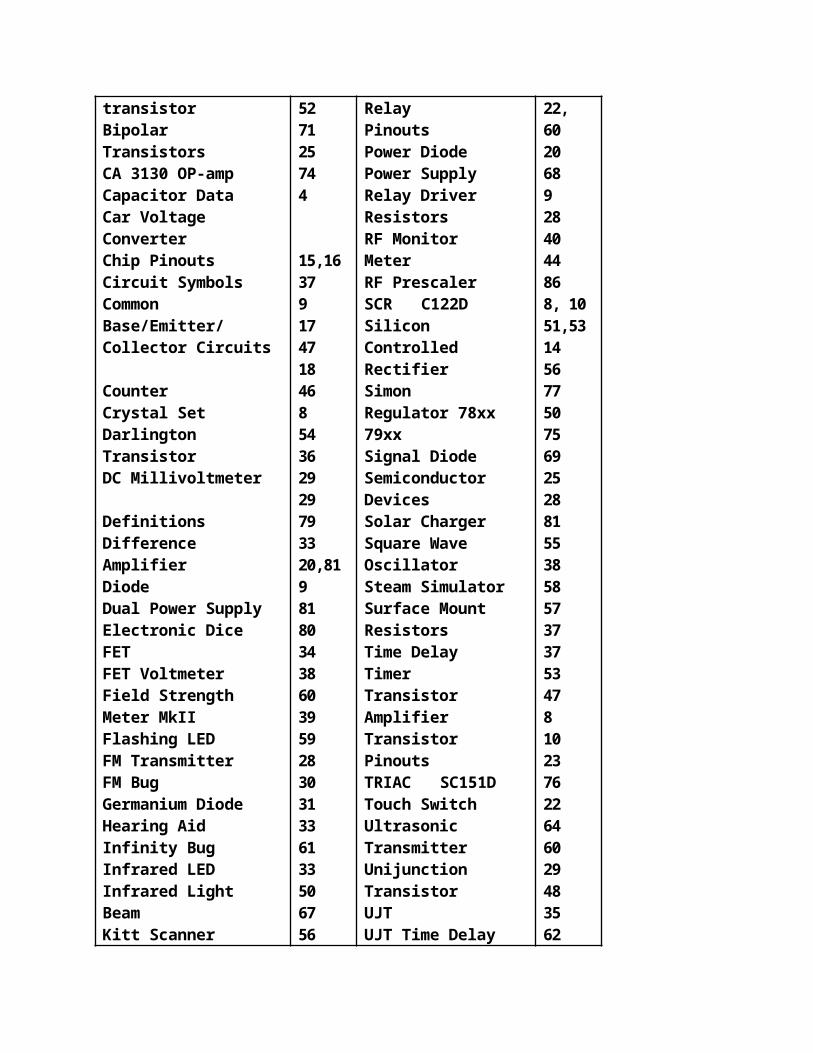
CONTENTS AC Trigger Ammeter Amplifier Arc Welder Audio Alarm Audio Mixer BC 547 NPN transistor BC557 PNP transistor BD 139 BD140 transistor Bipolar Transistors CA 3130 OP-amp Capacitor Data Car Voltage Converter Chip Pinouts Circuit Symbols Common Base/Emitter/ Collector Circuits Counter Crystal Set Darlington Transistor DC Millivoltmeter Definitions Difference Amplifier Diode 39 83 20, 21 78 59 46 19 19 21 15 52 71 25 74 4 15,16 37 9 17 47 18 46 8 54 36 29 29 79 33 20,81 9 81 Microphone Morse Code Generator MPF 102 FET Multivibrator OA 91 diode OP Amp Peak Reading VU Meter Photo Diode Photo Electric Relay Pinouts Power Diode Power Supply Relay Driver Resistors RF Monitor Meter RF Prescaler SCR C122D Silicon Controlled Rectifier Simon Regulator 78xx 79xx Signal Diode Semiconductor Devices Solar Charger Square Wave Oscillator Steam Simulator 83 21 26 21 9 42 52 34 30 74 8 22, 60 20 68 9 28 40 44 86 8, 10 51,53 14 56 77 50 75 69 25 28 81 55 38 58
-
Upload
university -
Category
Documents
-
view
0 -
download
0
Transcript of Electronics

CONTENTSAC Trigger Ammeter Amplifier Arc WelderAudio Alarm Audio MixerBC 547 NPN transistorBC557 PNP transistorBD 139 BD140 transistorBipolar Transistors CA 3130 OP-ampCapacitor DataCar Voltage Converter Chip PinoutsCircuit Symbols Common Base/Emitter/Collector Circuits Counter Crystal Set Darlington Transistor DC Millivoltmeter Definitions Difference AmplifierDiode
398320, 2178594619192115527125744
15,1637917471846854362929793320,81981
Microphone Morse Code GeneratorMPF 102 FETMultivibrator OA 91 diode OP Amp Peak Reading VU MeterPhoto Diode Photo Electric Relay Pinouts Power Diode Power Supply Relay Driver Resistors RF Monitor Meter RF Prescaler SCR C122DSilicon Controlled Rectifier SimonRegulator 78xx 79xxSignal Diode Semiconductor Devices Solar Charger Square Wave OscillatorSteam Simulator
8321262194252343074822, 6020689284044868, 1051,53145677507569252881553858
Dual Power Supply Electronic Dice FET FET Voltmeter Field Strength Meter MkIIFlashing LED FM Transmitter FM BugGermanium Diode Hearing AidInfinity BugInfrared LEDInfrared Light Beam Kitt ScannerLamp Dimmer Lamp Flasher Light Beam Relay Light Switch LEDs LED Chaser LED DiceLED Flasher LM 340 LM 386Logic GatesLogic Probe Metal Detector Metronome Microcontrollers
80343860395928303133613350675658,6257,592585
Surface Mount ResistorsTime Delay TimerTransistor AmplifierTransistor Pinouts TRIAC SC151DTouch Switch Ultrasonic Transmitter Unijunction Transistor UJT UJT Time Delay Wein Bridge Oscillator Zener Diode 1N4001 Power diode1N4148 Signal diode27MHz Links2N2646 UJT2N 3055 transistor4017 Decade counter555 Light Switch 555 Timer 7-Segment Displays 74c14 Hex Schmitt 741 OP Amp7555 CMOS 5557805 +5v
5737375347810237622646029483562445060

Regulator7905 -5v Regulator


Circuit SymbolsThe list above covers almost every symbol you will find onan electronic circuit diagram. It allows you to identify asymbol and also draw circuits. It is a handy reference andhas some symbols that have never had a symbol before, suchas a Flashing LED and electroluminescence panel. Once you have identified a symbol on a diagram you will need to refer to specification sheets to identify each lead on the actual component.

The symbol does not identify the actual pins on the device. It only shows the component in the circuit and howit is wired to the other components, such as input line, output, drive lines etc. You cannot relate the shape or size of the symbol with the component you have in your hand or on the circuit-board. Sometimes a component is drawn with each pin in the same place as on the chip etc. But this is rarely the case. Most often there is no relationship between the position of the lines on the circuit and the pins on the component.
That’s what makes reading a circuit so complex.
This is very important to remember with transistors, voltage regulators, chips and so many other components as the position of the pins on the symbol are not in the sameplaces as the pins on the component and sometimes the pinshave different functions according to the manufacturer. Sometimes the pin numbering is different according to the component, such as positive and negative regulators.
You must to refer to the manufacturer’s specification sheet to identify each pin, to be sure you have identifiedthem correctly.
Colin Mitchell
Page 8
1N4001 to 1N4007

Silicon Power RectifiersThe following are subminiature general purpose power rectifiers for low power applications
Electrical Characteristics Specifications
Maximum Full-Cycle Average
Voltage Drop
@ Forward Current = 1 A 0.8VMaximum
Reverse Current 0.03mARMS Reverse Voltage
1N4001 35v1N4002 70v1N4003 140v1N4004 280v
1N4005 420v1N4006 560v1N4007 700v
Instantaneous Voltage Drop@ forward current = 1 A 1.1vAbsolute Maximum Ratings
Peak Repetitive Reverse Voltage1N4001 50V1N4002 100V1N4003 200V
1N4004 400V
1N4005 600V
1N4006 800V
1N4007 1000V
Their value will depend on the current and the degree of smoothing required. As a general guide, if the current being drawn from a supply is high, the size of the smoothing capacitor will need to be large (around 2500uF or larger) if the hum level is to be kept down to a respectable level. It must also not be forgotten that all of these circuits are 'unregulated' i.e. as the load increases
from zero to maximum the output voltage will drop due to the transformer voltage dropping under load and losses across the diodes - and the storage capacity of smoothing capacitors.

Example
Say for example we want a power supply to give 9V at 1 A. We could use a M21 55 transformer which is rated at 1 A. If we use a bridge rectifier and the 9V tapping the output voltage will be:-
VDC= 1.41 XVAC - 1.41 X9V = 12.69V Peak ( 9V at 1A load)
Loading and Nominal Voltage
One thing to be aware of with this type of power supply circuit is the voltages given by the formulas are nominal only. Because the actual output voltage of a transformer varies according to its load, the DC output of the power supply will also vary. As well as this, there is a voltage drop across the diodes which will vary according to load. If you need a very precise voltage,the best solution is to use one of the regulated power supply circuits shown in the zener Diode and Voltage Regulator sectionsof this ebook. You will see that most regulated circuits use oneof the circuits above to produce unregulated DC, then regulate it to a consistent voltage that is independent of the load.
Page 9OA91 General purpose germanium signal diodeThe OA91 is a small signal germanium point contact diode. It is suitable for a wide range of RF detector and small signal rectifying applications.
SpecificationsIP Forward current 50mA

VR Reverse Voltage 90V Vp, Forward voltage drop
@ IP = 10mA 1.05V
@lF = 0.1mA 0.1V
Crystal Set
The crystal set consists of a tuned circuit which selects the wanted station or frequency, and a detector, which separates the information (music, speech etc.) from the radio transmission. Theaudio voltage produced is an exact replica of the sound from the radio station.
The detector diode rectifies the incoming signal, leaving a half wave radio signal which varies in amplitude with the audio signal. The fixed capacitor C2 shorts out or 'bypasses' the RF signal, leaving only the audio.

The circuit below is for a Crystal set using a readily availableFerrite rod and pre-wound aerial coil.
RF Monitor Meter
The circuit is an RF monitor meter suitable for measuring the strength of a signal from transmitters. You could use it to measurethe effectiveness of different antennas for example. It works in much the same way as the crystal set, but without the tuned circuit. The meter M, will indicate the strength of the 'carrier'. Modulation of the carrier i.e. signal on the carrier, will cause the reading

to vary. M, is not critical, and any meterof 1mA or better sensitivity will be suitable.
Page 10
1N4148 Silicon Signal Diode
The 1N4148 is a general purpose signal diode suitable for a wide range of switching and low power rectifying purposes. It is equivalent to the 1N914. Features• Low Capacitance. 4pF at 0V
• High breakdown voltage. 100V
SpecificationsCapacitance VR=0, f= 1MHz 4pF Reverse Recovery Time 4nsec
Rectification Efficiency 2.0V rms. f=100MHz
Absolute Maximum RatingsBreakdown Voltage

100V
Working Inverse Voltage 75V
DC Forward Current 300mA Maximum Total Dissipation at 25°C 500mWDiode bridges are a package of four diodes connected in a full wave bridge rectifier configuration. They can be encapsulated in plastic or steel/epoxy cases, and even DIL and surface mount packages for the smaller units. The square metal packages usually have one ACterminal marked, with the other terminal diagonally opposite it. The positive DC terminal is marked, with the negative terminal diagonally opposite it. Plastic square packages oftenhave all terminal markings embossed on the package. In-line plastic packages take up less PCB real estate while still maintaining a reasonable current capacity, and usually have their terminals marked with the AC connections being the inside two leads.
Zener DiodesZener diodes are used primarily as voltage references. They are devices which maintain an almost constant voltage across them despite various changes in circuit conditions.
Unlike conventional diodes, zener diodes are deliberately intended to be used with the anode connected to a negative potential (or 0v) and the cathode connected to the positive potential. When connected in this manner, zener diodes have a very high resistance below a certain critical voltage (called the

zener voltage). If this voltage is exceeded, the resistance of the zener drops to a very low level.
When used in this region, essentially constant voltage will be maintained across the Zener, despite quite large changes in the applied currents. This is illustrated graphically in the figure below.
It can be seen that beyond the zener voltage, the reverse voltageremains practically constant despite changes in reverse current. Because of this, Zener diodes may be used to provide a constant voltage drop, or reference voltage.The actual voltage available from a zener diode is temperature dependent.
The Basic Circuit
The Basic Voltage regulator circuit is shown below. It uses only one resistor and one zener diode. This is called a SHUNT REGULATOR. See SERIES REGULATOR below.
If the Zener diode is rated at 5.6V and the applied voltage is 8.0V, then with no load applied, the output voltage across R1 will be 5.6V and the remaining 2.4V will be dropped across Rs, Ifthe input voltage is changed to 9.0V, then the voltage across theZener will remain at 5.6V. In practice, the voltage across the Zener will rise slightly due to the 'dynamic resistance’ of the zener.
The resistor R1 represents an external load. When this load is connected, some of the current flowing through the zener will nowpass through the load. The series resistor Rs is selected so that

the minimum current passing through the zener is not less than that required for stable regulation. It is also necessary to ensure that the value of Rs is such that the current flow throughthe zener cannot exceed its specified power rating. This can be calculated by multiplying the zener voltage by the zener current.The design procedure is as follows:-
1) Specify the maximum and minimum load current, say 0mA and 10mA.
2) Specify the maximum and minimum supply voltages (say 12v) but ensure that the minimum supply voltage is always at least 1.5v higher than the zener voltage being used.
3) In the circuit shown the minimum zener current is 100µA. Thusthe maximum zener current (which occurs when there is no load connected) is 10ma plus 100µA equals 10.1mA.
4) The series resistor must conduct 10.1mA at the lowest input supply voltage, so the minimum voltage drop across Rs will be 1.5v. Thus the value of Rs will be:-
1.5v / 10.1X10-3 = 148.5 ohms
This could be changed to the nearest preferred value of 150 ohms.
5) At the maximum supply voltage (12v) the voltage across Rs is equal to
the zener current times the series resistor.

This is the maximum (worst case) zener current. To work out the resulting powerdissipation, we multiply this current by the zener voltage. In this example this
works out at:-
Any zener over this in power rating would be suitable in this circuit.
Temperature Drift in Zeners
Typical zener diodes drift in their voltage at about +0.1%/°C at the higher voltages. At lower voltages this goes negative reaching -0.04%/°C at around 3.5v.
This may be made use of in temperature sensing devices. The circuit below shows how a bridge consisting of two similar zener diodes and two resistors can indicate temperature differences when one zener is held at standard temperature and the other is subjected to the conditions to be monitored. If a 10v zener is used, it will have a temperature coefficient of +0.07%/°C giving a change of 7millivolts per degree C.
Non Standard VoltagesNon standard voltages can be obtained by connecting zener diodes in series. The diodesneed not have the same voltages since this arrangement is self equalizing.

Page 12It may also be necessary at times to provide a regulated voltage lower than that normally available from a zener diode. These voltages may be obtained by using the difference between two pairs of zeners. This is shown in the circuit below. As a bonus, the temperature compensation of this circuit is excellent, since both zeners tend to drift in the same direction, maintaining the voltage difference.
Zener Noise
Zener diodes generate noise voltages. These may vary between 10µVand 1mV depending on zener voltage and rating. This noise is easily suppressed by placing a 0.01 to 0.1µF capacitor across it.This reduces the noise voltage by a factor of at least 10.

Zener Diode as a Calibration Signal
When supplied with alternating current, the zener diode will limit both the negative and positive halves of the AC cycle. The waveform will be asymmetrical, since the zener will limit almost immediately in one direction, but will not limit until its zener voltage in the other direction.
Increased Power HandlingAlthough zeners can be paralleled for higher power operation, it is usually a better idea to use a series transistor with a zener reference. This configuration improves the power handling and also the regulation of the circuit by a factor equal to the current gain of the transistor.

The output voltage of this circuit will be equal to the zener voltage minus the base-emitter voltage of the transistor (approx. 0.7V). Output Voltage = Zener Voltage - 0.7V.
Page 13Constant Current RegulationThis simple circuit maintains a constant current (within approx 10%).
Over-voltage ProtectionThe circuit below uses the zener as a 'fuseblower'. The zener is selected so that under normal operation it is not conducting. If the circuit develops a fault and the power supply voltage rises above the zener voltage, the zener will come 'on' and draw a heavy current, blowing the fuse.

Improving temperature stabilityIf better temperature stability is required than can be obtained with a single zener, a good trick is to use an ordinary forward biased silicon diode. This makesuse of the fact that the forward voltage temperature coefficient of a silicon diode is approximately -2mV/°C. The temperature coefficient of the silicon diode and the zener diode cancel out, giving an almost temperature independent voltage reference. The use of the forward biased diode also allows 'trimming' of zeners tovoltages other than the preferred value available. A silicon diode when forward biased will have a voltage drop of 0.7v. When put in series with a zener it will increase the reference by this much. Thus a 6.2v zener plus a silicon diode will give a voltage of 6.9v.
Dual Voltage Power SupplyThe circuit below uses zener diodes to give a split or dual power supply which is ideal for running ICs such as op-amps. The power input only needs to be an unregulated single rail DC source. When selecting Rs it should be remembered thatthe zener is the sum of the voltage of the two zeners.
These two circuits show typical use of zeners in power supply circuits. The circuit below is designed to give increased currentcapacity. It will supply up to 1A with suitable heatsinking of the transistors.

Page 14
These two circuits show typical use of zeners in power supply circuits. The circuit below is designed to give increased currentcapacity. It will supply up to 1A with suitable heatsinking of the transistors.

Semiconductor DevicesThe simplest type of semiconductor device is the diode. It has two electrodes, a cathode and an anode. II is formed from a junction of P and N type silicon. As shown below, when the diode is forward biased, by applying a negative voltage to the cathode (the N type silicon) and a positive voltage to the anode (the P type silicon) the diode conducts and has a very low resistance. If the voltage connections are reversed, the diode is said to be reversed biased and has a very high resistance.

Page 15If another layer is added to the semiconductor junction, the resulting device becomes a bipolar transistor. The three layers of the device are the emitter, the collector and the base. In normal operation, the emitter to base junction is forward biased and the collector to base junction in the reverse direction.
There are two types of transistor, NPN and PNP. The names relate to the 'sandwich'structure of the two types of transistor. They are shown below. For practical purposes, the important difference between the two types of transistor is that in NPN transistors the current flows from emitter to collector. In PNP transistors the electrons flow from collector to emitter.

Bipolar Transistors Bipolar Transistors are current amplifying devices. When a small signal current is applied at the input terminal (the base) of thebipolar transistor, an amplified reproduction of this signal appears at the output terminals (the collector).
There are 3 useful way of connecting the input signal for amplification.
Common Base Mode

In this mode, the signal is introduced into the emitter-base circuit (Thus the base element is common to both the input and output circuits. In this mode, the input impedance is low (i.e. it puts a heavy load on the signal source). The output impedance is fairly high. This type of circuit gives voltage gain and slightly less than unity current gain.
Commonly used as an impedance converter.
Page 16

Common Emitter ModeIn this configuration, the signal is introduced into the base-emitter circuit. This arrangement has moderate input and output impedance. It gives both current and voltage gain. Current gain is measured by comparing the base current and the collector current and so is equivalent to HFE A very small change in base currentproduces a relatively large change in collector current. Depending on the type of transistor this will vary from 5-600.
This is the most commonly used circuit, very often found in audio amplifiers. For an explanation of HFE see definition below.

Common Collector ModeIn this configuration, the signal is introduced into the base/collector circuit and is 'extracted' from the emitter/collector circuit. The input impedance of thisarrangement is high and the output impedance is low. The voltage gain is less thanunity while the current gain is high. This configuration is used as an impedance matching device. Commonly called an emitter follower, it is also often used as a current amplifier in power supplies.
Common Collector Mode
Page 17
Darlington Pair

The Darlington Pair uses a pair of transistors coupled together as an emitter follower so that the emitter current of the first transistor flowsthrough the base/emitter junction of the second transistor. The resulting current gain of the transistor pair is found by multiplying the current gain of the transistors together. The resulting current gain is very high and the inputimpedance of such a stage is very high.
Biasing Arrangements
For linear amplification as opposed to switching applications, the 'operating point' of the transistor must be set soas to minimize distortion. The simplestof biasing arrangement is shown below. The base resistor RB is selected to provide the desired base current, whichis 27µA in the example shown. This basecurrent turns the transistor 'on' and establishes the collector current.In the circuit below (a):
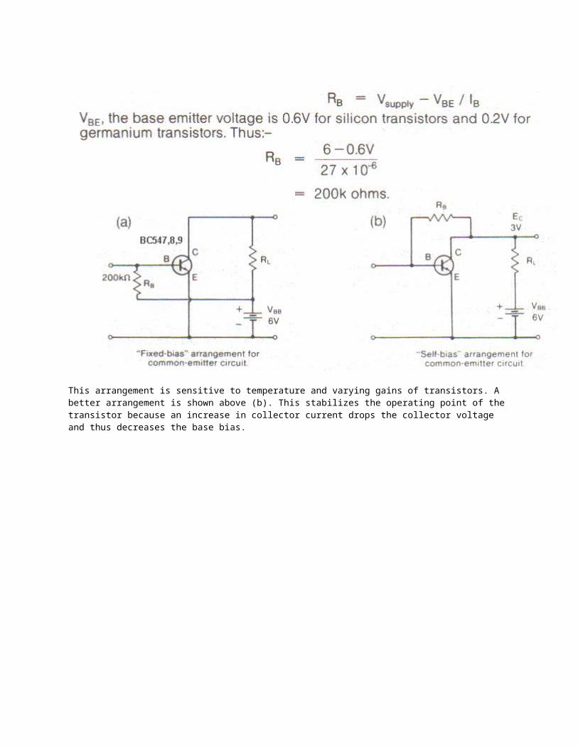
This arrangement is sensitive to temperature and varying gains of transistors. A better arrangement is shown above (b). This stabilizes the operating point of the transistor because an increase in collector current drops the collector voltage and thus decreases the base bias.

Page 18DefinitionsAlpha (a) Gain
In the common base mode, the emitter is the input electrode and the collector is the output electrode. The alpha is the ratio of the collector current lc to the emitter current IE. It is always less than 1.
Beta current gain (hFE)
In the common emitter mode, the base is the input terminal and the collector is the output terminal. The beta is the ratio of the collector current lc to the base current IB.
Gain Bandwidth Product (fhfe)
This is the frequency at which the alpha or beta (according to the type of circuit) drops to 0.707 times its 1 kHz value.

Transition Frequency (fT)
The frequency at which the small-signal forward current transfer ratio (common-emitter) falls to unity.
Breakdown voltage
This defines the voltage between two electrodes at which the current rises rapidly. The breakdown voltage may be specified with the third electrode open, shorted or biased to another electrode.
Secondary Breakdown
High voltages and currents passing through a transistor cause current to be concentrated or focused on a very small area of thetransistor chip causing localized overheating. This is important in power transistors which are often designed to minimize this effect.
Saturation Voltage (Vcesat)
For a given base current, the collector-emitter saturation voltage is the potential across this junction while the transistor is in conduction. A further increase in the bias does not increase the collector current. Saturation voltage is very important in switching and power transistors. It is usually in the order of 0.1v to 1.0v
Safe-operating-area

Power transistors are often required to work at high currents andhigh voltages simultaneously. This ability is shown in a safe operating area curve.
PTOT
The total package power dissipation
VCBO
The dc voltage between the collector terminal and the base terminal when the emitter terminal is open-circuited.
VCEO
The dc voltage between the collector terminal and the emitter terminal when the base terminal is open-circuited.
Page 19BC547-9 (BC107-9) NPN BC557-9 (BC557-9) PNP

Low frequency, general purpose small signal transistors widely used in audio, switching and television circuits. The BC547-9 series and BC557-9 series are functionally identical to the common BC107-9 series.
All have a maximum power dissipation of 500mW. They have essentially similar specifications and can generally be substituted for one another (within the PNP and NPN groups of three each). All devices are housed in standard TO-92 plastic packages.
Specifications NPN BC547
BC548 BC549
VCBO 50v
30v 30v
Vcto 45v
30v 30v
lc 100mA
100mA 100mA
Ptotl 500mW
500mW 500mW
hFE min-max at I0 2mA 110 - 800
110 - 800
200 - 800
fT typical 300MHz
300MHz 300MHz

VCEsat (max) at lc 100mA/lB 5mA 600mV
600mV 600mV
PNP BC557
BC558 BC559
VCBO 50v
30v 30v
VCEO 45v
30v 30v
lc 100mA
100mA 100mA
P,ot 500mW
500mW 500mW
hFE min-max at lc 2mA75 - 475
75 - 475 125 - 475
fT typical 150MHz
150MHz 150MHz
VCEsat (max) at lc 100mA/lB 5mA 600mV
600mV 600mV
Page 20
A Simple Amplifier

This circuit will operate on any supply from 3v to 15v. Using a 9v supply, the circuit gives a voltage gain of 46dB (200 times), frequency response within 3dB from 30Hz to 100kHz, input impedance of 1.5k ohms and an output impedance of 5.6k ohms. The base bias resistor R1 gives sufficient negative feedback to compensate for the large variation of hFE values inindividual transistors and for variations in supply voltage.
Relay driver
This simple circuit increases the sensitivity of a relay so that it will trigger at 700mV at 40uA. Any relay with an operating current of less than 60mA and operating voltage of less than 12v is suitable. The circuit's supply rail should be at least 3v higher than the operating voltage of the relay.

The circuit will work with any relay with a coil resistance higher than 180 ohms and a pull in voltage of less than 12v.
FM transmitter
This circuit, is about as simple as a transmitter can get. The coil is etched onto the printed circuit board, but can be easily substituted by 6 turns on a 4mm diameter former.

Page 21Multivibrator- Morse Code Generator
This circuit is an astable multivibrator or square-wave generator. The circuit is suitable as a morse code generator. Thefrequency of operation can be raised by making the value of the capacitors smaller. The speaker can be any general purpose 8 ohm type.
BD139/140 Driver TransistorsBD139/140 are complementary silicon driver transistors designed for audio and switching applications. They come in TO-126 plastic cases. The BD139 is an NPN device and the BD140 is PNP.
Features
• High gain (hFE40-250) • High fT (250MHz for BD139, 75MHz for BD140)
Absolute Maximum Ratings
SpecificationsDC Current gain (hFF)

Collector-Emitter Voltage (VCEO)
BD139 80V
BD140 80V
Collector-Base Voltage (VCBS)
BD139 100V
BD140 100V
Collector Current Continuous (Ic)BD139/140 1A
Total Device Dissipation (Ptot)
BD139/140 8W
@ lc = 150mA 40-250 (BD139/140)
fT(MHz)
BD139 250MHz BD140 75MHz Collector-Emitter Saturation Voltage (VCEsat)
@ lc = 500mA 0.5V
(BD139/140) IB = 50mA
Basic Amplifier

The circuit is for a low power amplifier using a BD139/140 pair in the output stage.
The amplifier has a gain of 66.It needs 10OmV input for full output, which is approximately 500mW into 8 ohms.
This completes Pages 1 to 21 of Data Book 1.
http://www.talkingelectronics.com
CONTENTSAC Trigger Ammeter Amplifier Arc WelderAudio Alarm Audio MixerBC 547 NPN transistorBC557 PNP transistorBD 139 BD140
398320, 2178594619192115
Microphone Morse Code GeneratorMPF 102 FETMultivibrator OA 91 diode OP Amp Peak Reading VU MeterPhoto Diode Photo Electric
83212621942523430748
transistorBipolar Transistors CA 3130 OP-ampCapacitor DataCar Voltage Converter Chip PinoutsCircuit Symbols Common Base/Emitter/Collector Circuits Counter Crystal Set Darlington Transistor DC Millivoltmeter Definitions Difference AmplifierDiode Dual Power Supply Electronic Dice FET FET Voltmeter Field Strength Meter MkIIFlashing LED FM Transmitter FM BugGermanium Diode Hearing AidInfinity BugInfrared LEDInfrared Light Beam Kitt Scanner
527125744
15,1637917471846854362929793320,81981803438603959283031336133506756
Relay Pinouts Power Diode Power Supply Relay Driver Resistors RF Monitor Meter RF Prescaler SCR C122DSilicon Controlled Rectifier SimonRegulator 78xx 79xxSignal Diode Semiconductor Devices Solar Charger Square Wave OscillatorSteam SimulatorSurface Mount ResistorsTime Delay TimerTransistor AmplifierTransistor Pinouts TRIAC SC151DTouch Switch Ultrasonic Transmitter Unijunction Transistor UJT UJT Time Delay
22, 6020689284044868, 1051,531456775075692528815538585737375347810237622646029483562

Lamp Dimmer Lamp Flasher Light Beam Relay Light Switch LEDs LED Chaser LED DiceLED Flasher LM 340 LM 386Logic GatesLogic Probe Metal Detector Metronome Microcontrollers
58,6257,592585
Wein Bridge Oscillator Zener Diode 1N4001 Power diode1N4148 Signal diode27MHz Links2N2646 UJT2N 3055 transistor4017 Decade counter555 Light Switch 555 Timer 7-Segment Displays 74c14 Hex Schmitt 741 OP Amp7555 CMOS 5557805 +5v Regulator7905 -5v Regulator
445060
Page 22
2N3055 Power TransistorThe 2N3055 is a medium speed NPN Silicon Power Transistor designed for general purpose switching and amplifier applications.
Features• DC current Gain (hFE) = 20-70 @ lc = 4.0A• Collector-Emitter Saturation Voltage = 1.0V @ lc = 4.0A
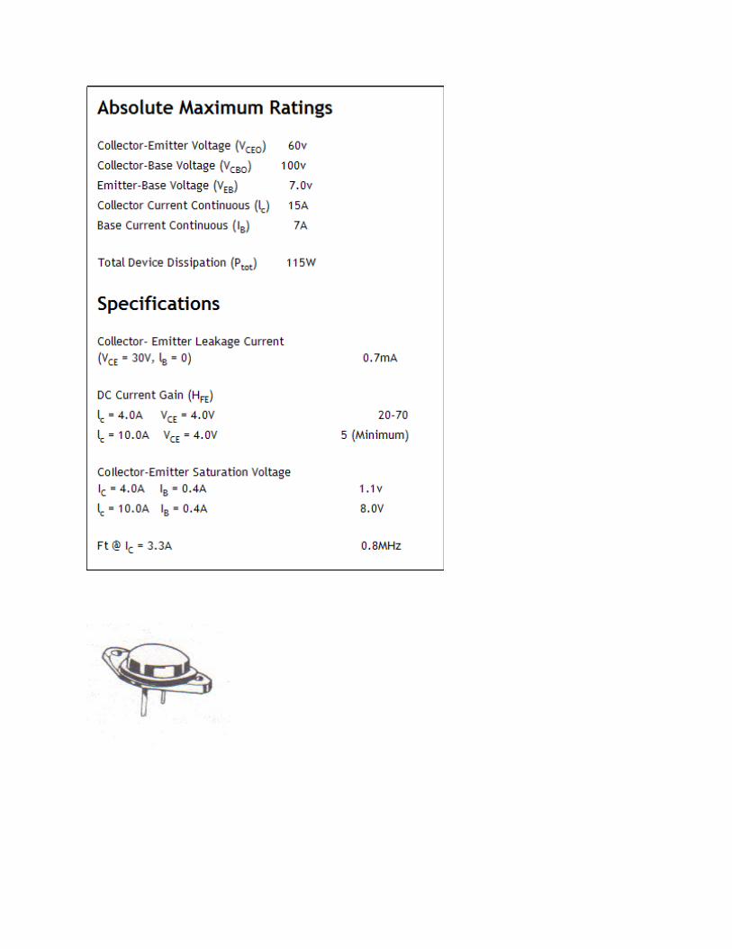

Low Ripple Regulated Power SupplyThe excellent characteristics of the 2N3055 at high currents (high hFE and low collector-emitter saturation voltage) makes it ideal as a series regulator transistor in regulated power supplies. The power supply circuit shown below can be used when high current with low ripple is required. Q, and Q2 form a high power Darlington. ZD1 and R1 provide a reference voltage at the base of Q1 The voltage output will be:- VOUT = Zener Voltage - 1.2v

Page 23Car Voltage Converter for radios and cassettesThis circuit is suitable for dropping a 12v car battery to the correct voltage to run portable cassette players/radios etc. Using a 2N3055 might seem like a bit of an overkill but they are cheap. The output voltage will be 0.7v lower than the zener voltage, due to the voltage drop across the base-emitter junctionof the 2N3055. The 10 ohm series resistor stops excessive currentbeing drawn in the case of a short. The diode (1N4001) protects the transistor in case of reverse voltage being applied.
The output will drive transistor radios, cassette players etc. Ifthe current drain is over 500mA, it is a good idea to put a heat sink on Q1. Mounting the converter in a metal box with Q1 on the lid (but insulated from it with a mica washer) will act as a goodheatsink.
2N2646 Unijunction transistorThe 2N2646 is intended for general and industrial triggering and oscillator circuits where circuit economy is of primary importance. lt is a high speed switching device with a low saturation voltage.

Absolute maximum ratings Power Dissipation 300mWRMS Emitter Current 50mAPeak Emitter Current (Capacitor discharge <10µF) 2A Emitter Reverse Voltage 30VInterbase Voltage 35V
Specifications Intrinsic Standoff Ratio (VBB = 10v) ή 0.69Interbase Resistance (VBB = 3v, Ie = 0) RBB0 6.7
Emitter Saturation Voltage (VBB = 10v, IE = 50mA) VE(sat) 2Emitter Reverse Current (VB2E = 30V IB1 = 0) IE0 .001Peak Point Emitter Current (VBB = 25v) IP 0.8Valley Point Current (VBB = 20v RB2 = 100R) IV 5Base-One Peak Pulse Voltage V0B1 8.5
Basic TheoryThe unijunction transistor (UJT) has 3 terminals: Emitter (E). Base-one (B1 and Base-two (B2). Between B, and B2 the UJT has a resistance of from 4.7k to 9.1k.In operation the UJT emitter voltage VE is lower than the emitter peak voltageVI. The emitter will be reverse biased and only a small leakage current will flow. When VE equals VI the emitter current will increase enormously. At the same time the emitter-B1 resistance will fail to a very low level.
Page 24

Basic UJT Pulse Trigger CircuitThis is a basic relaxation oscillator. C charges through R, until the emitter reaches VP at which time the UJT turns on and discharges C1 via RB1. When the emitter has dropped to approximately 2v, the emitter stops conducting and the cycle starts again.
The design of the UJT trigger is very broad.RB1 is limited to values below 100 ohms for most applications. R1 should be a value between 3k and 3M. Supply voltage can be from 10 to 35v. If the circuit is being used to trigger an SCR, RB1 must be low enough to prevent DC voltage at the gate from exceeding the maximum voltage that will not trigger the SCR. In practice, keep RB, below 50 ohms.The 2N2646 is specifically designed for SCR trigger circuits. RB2 is typically 100ohms.

Page 25UJT/SCR Time Delay Relay
This circuit provides an efficient, high power and accurate time delay circuit. The SCR should be selected to suit the application. R5 and the zener diode maintain a stable supply for the UJT.
Initially the SCR is off. The timing sequence is started by shorting out C1. C1 then charges through R1 and R2 until the UJT triggers, developing a pulse across

R4 which turns on the SCR. Holding current for the SCR is supplied by current through R5 and D2. When the SCR triggers, it pulls the voltage across the UJT to <2 volts. This discharges C1. The load this circuit will drive depends on the SCR used. A suitable type would be a C106Y. This has a maximum current ratingof 4A. This would be enough to drive a relay (even one with a lowcoil resistance), globes or an electric bell.
MetronomeThis is the simplest metronome circuit. It produces a 'click' similar to that of the traditional mechanical device. The rate isvariable from 40 to 220 beats per minute. R1 sets the high rate limit and R2 the low rate limit. Virtually any speaker is suitable. Supply voltage is from 12 to 18v. While an 8 ohm speaker is suitable in this circuit, more volume and higher efficiency can be obtained with a high impedance speaker, such asa 40 ohm unit.
Page 26
MPF102, 5, 6 Field Effect TransistorsThe MPF102-6 series are N-channel Junction-type field effect transistors.

The FET is a three terminal semiconductor device. Input voltage is applied to a GATE terminal and controls the current flowing from SOURCE to DRAIN terminals.An important feature of the FET is its very high input impedance.Since the FET makes use of a small input voltage to control a large output current, its gain is specified in terms of TRANSCONDUCTANCE. Transconductance (gfs) is equal to the change in drain current (dI0) divided by the change in gate voltage (dVG) and the formula is usually written as follows:-
gfs = 100Q(dlD/dVG) where:gfs is the transconductance in micromhosID is the drain current in DC mAVG is the gate/source voltage in DC volts.
Definitions of specifications
VGS (Gate/Source Voltage)
This is the maximum voltage which may appear between gate and source. IDSS (Drain current at zero gale voltage)This is the current which will flow in the drain/source circuit when VGS = 0. It is given for specific drain/source voltages.BVGSS (Gate/Source breakdown voltage).The voltage at which the gate junction of a JFET will enter avalanche. Vp (Gate/Source pinchoff voltage).This is the gate-to-source voltage at which the field just closesthe conduction channel. This is given for a specified value of VDS. The value of the drain current is specified (usually 1µA).

FET Type BVGSS VP IDSS gfs Ptot (mW)
MPF102 25v @ IG
1µA0.5-8.0V @ VDS 15v
2-20mA @ Vus 15v
2,000-7,500
300mW
MPF105 25v @ IG
1µA0.5-8.0V @ VDS 15v
4-16 mA @ Vus 15v
2,000-6,000
310mW
MPF106 25v @ IG
1µA0.5V-4V @ VDS 15v
4-10mA @ Vus 15v
2,500-7,000
310mW
All types are mounted in T092 plastic cases with pin connections as shown above.
Operation and Applications
The basic mode of operation of the FET amplifier is shown below. This is referred to as the common source amplifier. The gate to source circuit is the input and the drain to source circuit is the output.
When a moderate reverse or negative voltage is applied between gate and source, the gate junction becomes 'reverse biased' i.e. the voltage on the gate reduced the current flowing between the source and the drain. At a higher gate-source voltage, the drain-source current is cut to practically zero. This is referred to asthe gate-source pinchoff voltage and is listed in the specifications as VP at a drain-source current of either 1 or 10uA. In practical circuits, the DC bias is developed across R2, due to the current being through it. This then puts the source ata positive potential relative to ground. The gate is at ground potential and therefore is at a negative potential relative to the source, R, sets the input impedance of the circuit since the gate of the FET draws virtually no current at all and so is seen by the load as a very high impedance.

Page 27*NOTE
All the circuits and applications in these pages assumes the use of 'N-channel' Junction FETs, i.e. FETs in which the drain-sourcematerial is made of N-type silicon. However, these JFETs may be replaced in the circuits with P-channel JFETs if the polarity of the power supply is reversed.
Typical Design for a Common-Source Circuit
When used as an amplifier, the FET is biased to a certain part ofits response curve for lowest distortion and maximum available voltage swing. Assume that the FET has the following operating parameters
• VDs = 8V (where VDs is the voltage between drain and source)• ID = 0.5mA (where ID is the drain current)VGS = -2V (where VGS is the gate-drain voltage or bias)The power supply voltage is 22.5v

FET Applications Source Follower Circuit:
The source follower circuit is suitable where a high input impedance and low output impedance is required, but no voltage gain is needed. The figure below shows a typical source follower stage. Input impedance is set by the gate resistor RG. Output impedance is very low.

Page 28RF Preselector
The uses for the FET are not limited to audio applications. The circuit below is for an RF preselector (a tuned amplifier) for the broadcast bands. The FET is a very good device to use in thisapplication, due to its low cross modulation characteristics. Most cheaper receivers use ordinary bipolar transistors to keep costs down. The FET RF amplifier can also take higher signal levels without distortion. The preselector has a Volume Control style gain control between the FET and the emitter follower output stage. This means that only the FET has to handle high signal levels.
The tuning capacitor does not have to be exactly the same value as shown in the circuit, any capacitor covering a similar range is suitable. The aerial coil is wound on a 200mm length of ferrite rod. The main winding consists of 42 turns of 22B&S enamelled wire. The second winding consists of a further 6 turns.The preselector gives a marked improvement on the reception of weak signals and aids in the attenuation of adjacent channel interference and noise.
LDR Applications Light Beam Relay
In this circuit the LDR is held at a low resistance by light froma small globe. The circuit is actuated when the beam is broken.

The resistance of the LDR then goes high. The circuit is set up so that with the light shining on the LDR the input voltages at the two input terminals of the 741 op amp hold its output 'low'. When the LDR goes to high resistance the op amp's output goes 'high'. This turns the transistor 'on' and pulls in the relay.
Simple timer
The very high impedance of the FET makes it suitable for a wide variety of timer circuits. The circuit below gives one such example. With C1 given a value of 1µF, it will give timing periods of 40 sec, and with a value of 100µF it gives a period of35 minutes. The FET is wired as a source follower and has its gate taken to the junction of a time constant network R1-C1 When the supply is first connected, C1 is discharged, so Q1 gate is atground potential, and the source is a volt or two higher. The base of Q1 is connected to the source of Q1 via R3, so Q2 is turnedon and 12v is across R5, When the supply is connected, C1 starts to charge via R1, so the voltages on the gate of Q1 (and on the source) rise exponentially towards the 12v supply. When the voltage reaches approximately 10.5v the bias on Q1 falls to zero and Q2 switches off, the voltage across R5 falls to zero.

Page 29FET Voltmeter
The very high input impedance of the FET makes it the ideal basisof a voltmeter. The circuit below has a basic sensitivity of 22M ohms per volt. Maximum full scale sensitivity is 0.5V, and input sensitivity is a constant 11.1 M ohms on all ranges. R7,R8 R9
form a potential divider across the 12v supply. R8 is adjusted for a zero meter deflection. Any potential across the gate circuit of Q1 causes the circuit to 'unbalance'. To avoid drift, the power supply should be stabilized if possible.

555 Light Switch
The use of the 555 timer 1C with an LDR provides a high performance light switch. An LDR is a Light Dependent Resistor and is a very low cost way of detecting light.The 555 is used with its trigger and thresholds tied together to provide a Schmitt trigger with a very low input current but whichcan drive a relay taking up to 200mA of current. The trigger is activated when the light level on the LDR falls below a predetermined level. The relay energizes when the voltage on pins2 and 6 is greater than 2/3Vcc. It de-energizes when the voltage falls below 1/3VCC. This gives a hysteresis of 1/3VCC.

The 555 can supply current up to 200mA, so the relay type is not critical. Any with a coil resistance from 100-280 ohms would be suitable.
Page 30Light Sensitive Switch
This circuit makes use of the wide change of resistance of the LDR. Between positive and negative supply there is a voltage divider. The bottom section is a variable resistor RV1. The top half is formed by the LDR and a 4.7K ohm resistor in series. In low light conditions when the resistance of the LDR is very high,the bias to the Darlington pair formed by TR1 and TR2 is very low,and they do not conduct. When the light level rises, the resistance of the LDR falls. This turns the transistors 'on' and pulls in the relay.

The LDR should be an ORP12 or similar. The relay should have a pull in voltage of 9V or lower and a coil resistance of 280 ohms or higher.
Photo Electric Relay
This circuit is basically a bistable multivibrator. When the light level is low and the resistance of the ORP12 is high, transistor Q1 conducts and Q2 is off. As the level of illumination increases the resistance drops until Q1 cuts off andQ2 turns on, energizing the relay coil.

The relay should have a coil resistance of 180 ohms or higher and a pull in voltage of 9V or lower
Page 31LEDs
Features
• Low power consumption
• IC compatible
• Long life

Absolute Maximum Ratings
Red Green Yellow Amber OrangeReverse Voltage
5v 5v 5v 5v 5v
Av forward Current
20mA 30mA 30mA 30mA 30mA
Peak Forward Current
200mA 200mA 200mA 200mA 200mA
Power Dissipation
100mW 100mW 100mW 100mW 100mW

Page 32

LED Basics
LEDs are used in the 'forward biased' mode. i.e. positive on the anode and negative on the cathode. This voltage drop is stated in

the specifications (eg 1.7V for a red LED), If the LED is used ona higher voltage than this, a current limiting resistor must be used.
The following formula can be used:-
R = (E -1.7) x 1000/I
R is the resistance in ohms. E is the DC supply voltage. I is theLED current in milliamps. A common LED current is 20mA. Some calculated values are:-
For 6v use 220 ohm.For 9v use 390 ohm.For 12v use 560 ohm.For 24v use 1.2k ohm.
If a LED is reverse biased, it will break down, in a similar way to a zener diode. This occurs at 3-5V. It usually damages the diode if a high current flows.
Operating LEDs from the mains
This circuit uses a capacitor as a voltage dropping element. A 1N4148 diode is placed across the LED for rectification. As the voltage across the LED is negligible compared with the supply, capacitor current is almost exactly equal to mains voltage divided by the capacitor reactance. At 50Hz, a 0.47µF will result

in a LED current of about 16mA. Resistor Rs limits current on transients. A value of 270 ohms is adequate.
Page 33
The Flashing LEDThe Flashing LED has a chip inside the device to produce the flash-rate. Simply connect the LED to a supply voltage (4v to 10v) and the LED will flash at a rate of approx 2Hz. No external resistor is needed up to 10v. For voltages higher than 10v, the resistor should be 100 ohms for each volt above 10v. This is the only “LED” that does not need a resistor when connected to a supply as it has an internal resistor. All other LEDs MUST have a resistor in series to limit the current and prevent damage.

LED FlasherThis circuit for a LED flasher is very simple and cheap to make and will work on any voltage between 3v and 12v. As the voltage is raised the value of R1 must be increased - The speed can be changed by altering the value of C1 and C2 and/or R2 or R3. Raising the value of C1 and C2 slows the rate down. Raising the value of R2 and R3 also slows it down.

LED ChaserThis circuit acts as a LED chaser. The 4017 is driven by a 555 working as a free-running multivibrator. The speed can be changedby altering C1 or R1.
Page 34
CQY89 Light Emitting Diode - Infrared LEDThe CQY89 is an infrared LED, similar in performance to

conventional LEDs, but emitting light in the infrared region. This is visible to the human eye. Unlike conventional LEDs, infrared LEDs are usually pulsed rather than fed with continuous DC. They find wide use in alarms and in remote control equipment.
Specifications
Maximum Forward Current 130mAMaximum Reverse Voltage 5VMaximum Power Dissipation 215mWMaximum Forward Current 130mABeamwidth between half intensity directions (IF = 100mA] 40° typ.Wavelength at peak emission (lr = 100mA) (λpk) 930nm typ.
BPW34 photosensitive diodeThis device is mainly used in combination with a light source forgo/no go detection as in card readers and industrial safety devices.
Specifications
VR Forward voltage 32VTotal power dissipation 150mWSpectral sensitivity (VR =5V) 70nA/lxDark Reverse Current (VR=10; Ee=0) 2nALight Reverse Current(VR = 5; Ee= 1mW/cm2;λ = 930nm) 10µA

BPW34/CQY89 Infrared light-beam relayReceiver
The light is picked up by the photodiode a BPW34. It is wired so that a current is generated that is proportional to the light falling on it. The FET acts as a source follower and impedance matches to the next stage. The amplifier after this acts as a bandpass filter. Its output is coupled to a CMOS Schmitt trigger,followed by a rectifying circuit and a pulse stretcher. This drives a transistor and a buzzer and LED.
Page 35

Transmitter
A CMOS oscillator drives an output stage consisting of a BC547 transistor and two CQY89 infrared LEDs. Current drive is limited by the 680 ohm resistor. If greater range is required, this resistor may be reduced to a minimum of 150 ohms with a consequent increase in current consumption.
7 Segment LED DisplaysThe 7 segment display is found in many displays such as microwaves, lifts, ovens etc. It consists of 7 LEDs that have been combined into one case to make a convenient device for displaying numbers and some letters. There are basically two

different size displays. 0.3” and 0.5”. The two sizes are shown below:
0.3" and 0.5"displays
Displays come is a range of colours and brightness levels. Most come in super-bright and these are preferred so the display can be seen during the day. They are not much more expensive but give a much better illumination. All displays also come in COMMON CATHODE and COMMON ANODE. The COMMON CATHODE display has all the cathodes of the LEDs tied together and connects to the pin that goes to the 0v rail. This is the most common type of display.
Page 36The Common Cathode and Common Anode displays are wired as shown below:

The project above from JJM turns on each segment of the display to show how each letter and number is produced. The second photois a white 7-segment display.
Electronic Die
This circuit consists of three sections: an oscillator, a counter, and the display. The oscillator uses three sections of a4069 hex inverter. The 4029 is a four bit counter with the capacity to count from zero to 15. The 4511 driver/decoder takes binary output and decodes it to drive a seven segment display. The current to the 7-segmenl display is limited by seven 560 ohm resistors. The display is a common cathode type, and any 7-segment display can be used.

Page 37
Counter
This circuit uses a 7-segment display as the output of a basic counter circuit. The 7490 counts decimal pulses and converts themto a BCD code. Its output is fed to a 7475 latch. This stores theoutputs from the decade counter. The four binary outputs are taken from the 7475 to a 7447 LCD to the 7 segment LED decoder, which drives the display.
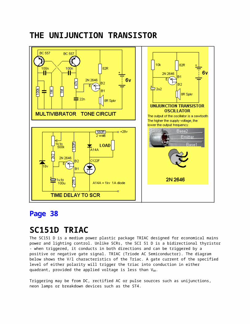
THE UNIJUNCTION TRANSISTOR
Page 38
SC151D TRIACThe SC151 D is a medium power plastic package TRIAC designed for economical mains power and lighting control. Unlike SCRs, the SCI 51 D is a bidirectional thyristor- when triggered, it conducts in both directions and can be triggered by a positive or negative gate signal. TRIAC (Triode AC Semiconductor). The diagram below shows the V/l characteristics of the Triac. A gate current of the specified level of either polarity will trigger the triac into conduction in either quadrant, provided the applied voltage is less than VB0.
Triggering may be from DC, rectified AC or pulse sources such as unijunctions, neon lamps or breakdown devices such as the ST4.

SpecificationsVoltage Rating 400VCurrent Rating 15A RMSITSM Maximum peak one cycle non rep. surge current 110AIDRM Blocking Current at 25°C 0.1mA maxdv/dt Off State, Tc = 100°C, Rated VDRM, gate O/C 250V/µS (typ.)
FIRING
IGT Max DC Gate Trigger current VD=12v, 25°C 50mAVGT Max Gate Trigger voltage VD= 12v 25°C 2.5V
Triac as a switch

This gives improved performance over a conventional switch, as there can be no arcing or contact bounce. This circuit shows a simple three position power control. In position one there is no gate connection, so power is off. In position two there is gate current during one half cycle only and load power is half wave. In position three the gate is triggered on both half cycles and the power is full on. For a simple on-off switch, just delete thediode.
Because the contacts only carry current for the few microseconds needed to trigger the triac, the actual switch can be almost any small device: reed relays, thermostats, pressure switches or program/timer switches.
Page 39Lamp dimmer/Heater controllerR1 and C1 are a phase shift network - they produce a variable delay in the waveform applied to the ST4 and hence the triac. When the voltage across C1 reaches the breakdown voltage for the ST4, C1 partially discharges into the triac gate through the ST4.This pulse triggers the triac into conduction for the remainder of the half cycle.

This easy-to-build controller is ideal for dimming lights, and controlling the output of electric heating type appliances. The light or heater element etc is placed where the 'LOAD' is marked on the circuit.
ST4 Asymmetrical AC Trigger SwitchThe ST4 is an integrated triac trigger circuit that provides widerange hysteresis-free control of voltage.It behaves like a zener diode in series with a silicon bilateral switch (a symmetrical device).The zener provides asymmetry since the switching voltage is increased in one direction by the zener breakdown voltage.
Switching voltage:VS1 14v-18v VS2 7-9v
Switching currentI S1 I S2 80µA
On-state voltages
VF1 (I = 100mA) 7-10vVF2 (I = 100mA) 1.6v maxPeak pulse voltageV0 3.5v min

Page 40
C122D/C122E Silicon Control Rectifier The C122Dand 122E are medium power plastic package SCRs designedchiefly for mains power and motor control. The SCR is a unidirectional device, (current flows through it in one direction, from anode to cathode).
The SCR is a three terminal semiconductor device. The three terminals are the anode (A), cathode (K). and the gate (G). With no voltage applied to the gate terminal, if a voltage is applied to the SCR anode and cathode terminals, (anode positive with respect to cathode) current flow is prohibited. If the supply is reversed the flow is likewise prohibited. Thus with no signal applied, the SCR appears as an open circuit as long as its diode junctions do not break down. The SCR is brought into conduction by applying a current into the gate terminal. This will cause it to conduct in the forward direction (i.e. with the anode positiveand the cathode negative). The gate voltages required vary from approximately 1.5- 6.0v. Once the SCR is turned on the gate no longer controls the circuit and the SCR only drops out of conduction when the anode-cathode voltage falls to near zero. At this instant, the current through the device falls to zero.

Specifications
C122EVDRM (Repetitive off state voltage. Max between anode and cathode) 500VIT (RMS Current through SCR) 8 AmpsIGT (Peak Positive gate current) (Tc = 25°C) 25mAVGT (Peak Positive gate voltage) (Tc = 25°C) 1.5VPG (AV) (Max Gate power) 0.5W IH Holding Current (Current below which the SCR will drop out of conduction) (Tc = 25°C) 30mAdv/dt Rate of change of on-state voltage (Max. rate of change of anode-cathode voltage which will not turn SCR on) 50V/µsec(typ.) The C122D differs only in that its VDRM is only 400v as against 500v for the C122E.
The SCRs listed above are medium power SCRs (Silicon Controlled Rectifiers) designed primarily for economical mains power and motor control. They are three terminal devices (see above). The electrodes are anode, cathode and control gate. They are unidirectional devices i.e when triggered 'on' they only conduct

in one direction. The SCR is a 'regenerative' device. It is triggered 'on' by injecting a signal into the gate. As noted earlier, once the gate has triggered the SCR 'on' it no longer controls the gate. The only way to cause the SCR to stop conducting from cathode to anode is to drop the anode cathode voltage to a level where the current flowing from anode to cathode is below the 'holding level'. This is indicated in the figure above. In practice, this is not a problem, since SCRs are normally used to control fluctuating voltages such as the AC mains. The 'drop out' of the SCR occurs as the mains voltage goesthrough zero.
Page 41
Applications
SCRs are current rather than voltage triggered devices. This means that they must be fed from a relatively low impedance source i.e. one in which the voltage won't drop down under load from the gate. In a way analogous to a relay or a solenoid, the SCR requires certain minimum anode current if it is to remain in the 'closed' or conducting state. If the anode current drops below the minimum level, the SCR reverts to the forward blocking or 'open' state. The following circuit shows a basic R-C-Diode trigger circuit giving full half wave control. On positive half cycles the capacitor C will charge to the trigger point, at a speed determined by the time constant of R and C. On the negativehalf cycle, the capacitor is reset by CR2, resetting it for tire next charging cycle, Thus the triggering current is supplied by the line voltage.
C122D, C122E, C106D SCRs Phase Control Circuit

Improved phase control circuit
The following diagram shows a circuit using a neon lamp as a breakdown device. This gives smoother control and improved performance. The neon triggers when the voltage across the two 0.1µ capacitors reaches the breakdown voltage of the lamp (60-90V). Control extends from 95% to full off.
The neon lamp phase controlled circuit shown below combines the low cost of the simple RC circuit shown before but gives improvedperformance. The circuit below gives half wave control from 95% on to full off. Full power can be easily obtained by putting a switch across the SCR. The circuit uses a neon. This gives the following improvements:
A higher impedance circuit can be used for control.
As a result, the control element (which is a 100k pot in the circuit below) can be replaced by a high impedance device such asa thermistor or light dependent resistor, for heating or light control applications.

.
This completes Pages 22 to 41 of Data Book 1
http://www.talkingelectronics.com
CONTENTSAC Trigger 39 Microphone 83

Ammeter Amplifier Arc WelderAudio Alarm Audio MixerBC 547 NPN transistorBC557 PNP transistorBD 139 BD140 transistorBipolar Transistors CA 3130 OP-ampCapacitor DataCar Voltage Converter Chip PinoutsCircuit Symbols Common Base/Emitter/Collector Circuits Counter Crystal Set Darlington Transistor DC Millivoltmeter Definitions Difference AmplifierDiode Dual Power Supply Electronic Dice FET FET Voltmeter Field Strength Meter MkII
8320, 2178594619192115527125744
15,1637917471846854362929793320,819818034386039
Morse Code GeneratorMPF 102 FETMultivibrator OA 91 diode OP Amp Peak Reading VU MeterPhoto Diode Photo Electric Relay Pinouts Power Diode Power Supply Relay Driver Resistors RF Monitor Meter RF Prescaler SCR C122DSilicon Controlled Rectifier SimonRegulator 78xx 79xxSignal Diode Semiconductor Devices Solar Charger Square Wave OscillatorSteam SimulatorSurface Mount ResistorsTime Delay TimerTransistor Amplifier
21262194252343074822, 6020689284044868, 1051,5314567750756925288155385857373753478

Flashing LED FM Transmitter FM BugGermanium Diode Hearing AidInfinity BugInfrared LEDInfrared Light Beam Kitt ScannerLamp Dimmer Lamp Flasher Light Beam Relay Light Switch LEDs LED Chaser LED DiceLED Flasher LM 340 LM 386Logic GatesLogic Probe Metal Detector Metronome Microcontrollers
5928303133613350675658,6257,592585
Transistor Pinouts TRIAC SC151DTouch Switch Ultrasonic Transmitter Unijunction Transistor UJT UJT Time Delay Wein Bridge Oscillator Zener Diode 1N4001 Power diode1N4148 Signal diode27MHz Links2N2646 UJT2N 3055 transistor4017 Decade counter555 Light Switch 555 Timer 7-Segment Displays 74c14 Hex Schmitt 741 OP Amp7555 CMOS 5557805 +5v Regulator7905 -5v Regulator
10237622646029483562445060

Page 42
OP-AMP Basics The op-amp is a very high gain DC amplifier. This is quoted in specifications as typically in the range of 20,000 to 100,000 times. The symbol for the op-amp is shown below. As can be seen, there are two inputs, the inverting and the non-inverting. If a signal is applied to the -input (inverting) with the + input (non-inverting) grounded, the polarity of the output signal will be opposite that of the input. If the signal is applied to the + input with the - input grounded, the polarity of the output signal will be the same as the input signal. For an AC signal, this means that when it is applied to the - input, the output signal will be 180° out of phase with the input. If the same signal is applied to both the + and - inputs, the two signals will cancel each other out. The op-amp responds to the differencebetween its two inputs - hence the name differential amplifier. The ability of an op-amp to cancel two equal signals at its pins is referred to as its common-mode rejection.
The most common op-amp circuit is shown below and uses two external components; 1) an input component, R1 2) a feedback component, RF. When the feedback component is between the op-amp output and the

negative input the op-amp is said to have negative feedback. Whenthe feedback component is between the op-amp output and the positive input, the circuit is said to have positive feedback.
With no feedback applied, the gain is set by the op-amp itself and is very high (at very low frequencies). This is referred to as the open loop gain. When negative feedback is applied, the gain is specified by the feedback components, and is referred to as the 'closed loop gain'.
Gain = Rf / Ri
Thus to produce an amplifier with a gain of 100, we can use an input resistor of 1k and a feedback resistor of 100k. This is shown below with the op-amp connected as an inverting amplifier. To produce a non-inverting amplifier, the signal is applied to the non-inverting input and the feedback components are left on the non-inverting side. This is shown following.
Page 43Output Offset
The steady state output of an op-amp with negative feedback is zero when the input is zero. The actual DC output (in a real op-

amp) is usually not quite zero, and this small unwanted signal isusually referred to as the output offset voltage. Most op-amps have means of nulling this out. Fig A shows the most common method, where the op-amp has special nulling pins. If these are not available, the method in Fig B can be used.
Frequency Compensation
Circuits using op-amps must be designed so that the open loop gain of the op-amp itself is greater than the closed loop gain ofthe circuit for all frequencies of operation. The gain drops as the frequency increases. This is mainly due to the large amounts of internal 'compensation' used to make sure that they do not oscillate. Frequency compensation is the shaping of the frequencyresponses of the op-amp so that it does not oscillate due to internal phase shift. This phase shift acts as a time delay. Whenthis delay is great enough so that the input signal is delayed 360° (a complete cycle), the amplifier will oscillate. This is because the 'negative feedback' signal, instead of being in opposition to the input signal will actually reinforce it. Thus the input signal keeps getting bigger and bigger - positive feedback occurs. To make sure this can't happen, the open loop

gain of the amplifier is shaped either internally (eg. internal compensation in the 741 op-amp) or externally so that at the frequency where the phase shift approaches 360°, the gain is lessthan unity.
In practice we need to be careful that we don't design a circuit which sets a closed loop gain higher than the op-amp can 'keep upwith' at high frequencies. For example, the 741 op-amp has a unity gain bandwidth of 1MHz (i.e. at 1MHz its gain is x1) and its gain rolls off from approximately DC at a rate of x10 per decade. This means that at 100Hz it will typically have a gain of10,000 times, but at 1000Hz this has dropped to 1000 times. By 10,000Hz it has dropped to 100 times. By 100kHz it has dropped toonly 10 times.
Power Supply Rejection Ratio
This is the ratio of change in input voltage to the change in supply voltage. This is the ability of an op-amp to reject power-supply-induced noise, hum and drift. Voltage changes on the supply lines are coupled into the amplifier and appear as part ofthe input signal. Because of this, the power supply hum and noiseat the output will be amplified by the gain of the op-amp. Thus if the op-amp is being used as a unity gain inverter, the hum andnoise at the output will be that at the input. If the gain is sethigh, then it will be amplified accordingly. The figures presented for power supply rejection in the data are for unity gain and will deteriorate in direct proportion to the gain of theop-amp. To give an example:-
If an op-amp has a power supply reaction of 80dB (10,000) times, then a power supply hum level of 1v will only produce a hum levelof 0.1mV at the output. However, if the op-amp is used at a gain of 1,000 times, this hum will be amplified 1,000 times as well, producing 0.1v of hum in the output signal. Also, power supply rejection will usually deteriorate at high frequencies.

Latch-up
Latch-up is the 'sticking' or 'locking-up' of the output of an op-amp when the maximum differential input voltage is exceeded. In the latch-up condition, the output is stuck at either the positive or negative maximum output voltage, and the input is ineffective in affecting the output. Most of the modern op-amps such as the 741 have eliminated this problem.
Page 44CMOS Operational amplifiersThe CA3130 is a CMOS output operational amplifier, originally designed by RCA. It is a good choice when you want the full output voltage swing to go from rail to rail.
Like the conventional op-amp, the 3130 has an inverting and a non-inverting input. These go to a pairof p-channel MOSFETs set up as a differential amplifier.
Compensation is applied between pins 1 and 8. Compared to the 741, the 3130 has about the same open loop gain and input offset voltage.
The input impedance is about a million times higher (2x10¹² ohms rather than 2x10⁶) and the input bias and offset currents are proportionately lower. Slew rate is about 20 times better, at 10V/µsec. The output of the 3130 is sensitive to capacitive loading. It works on voltages as low as 5v but will only work up to 16v total. Another similar device is the CA3140. It has a bipolar output stage and will work up to a full ±15V. Frequency compensation is internally provided. The output easily drives

capacitive loads. It has the same high slew rate and input impedance of the 3130
CA3140 High Impedance DC Voltmeter
This circuit makes use of the very high impedance of the CA3140 to produce a high performance DC voltmeter with an input impedance of 11M ohms. The instrument uses a cheap 1mA FSD movement and has a diode bridge to correct polarity. If reverse polarity is applied to the instrument, the op-amp biases the BC558 'on' and this turns a LED on.
741 Operational AmplifierThe 741 is a high performance operational amplifier with high open loop gain, internal compensation, high common mode range andexceptional temperature stability. It is short circuit proof and allows for nulling of offset voltage.
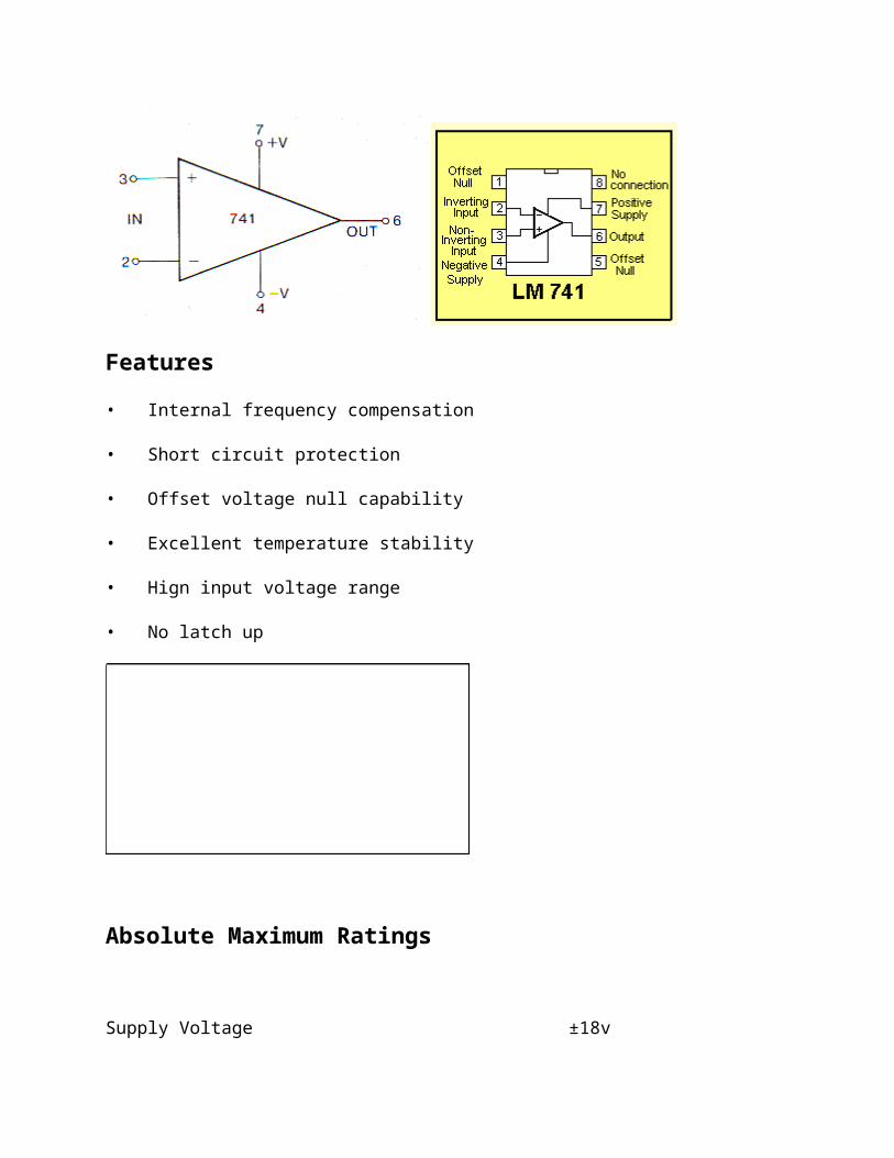
Features
• Internal frequency compensation
• Short circuit protection
• Offset voltage null capability
• Excellent temperature stability
• Hign input voltage range
• No latch up
Absolute Maximum Ratings
Supply Voltage ±18v

Internal Power Dissipation 500mW
Differential Input Voltage ±30v Input Voltage (either input) ± 15vOutput Short Circuit Duration Indefinite
Page 45Applications
The 741 is an internally compensated op-amp for unconditional stability. Its gain falls off at 6dB per octave/ 20dB per decade above DC. i.e. as the frequency doubles, the open loop gain halves.
It has a unity gain bandwidth of 1MHz i.e. at 1MHz its gain has dropped to x1.
Offset Adjustment


Page 46
Audio Mixer

Difference AmplifierThe circuit below shows a typical application for a unity gain difference amplifier- a balanced input audio amplifier. The output is the difference between the two input signals. These circuits are often used in audio when long leads must be run - say between a microphone and an audio mixer. Signals such as hum or buzz from lighting controllers (triac dimmers are renowned for their electrical 'noise' producing ability!) are picked up along the cable. The difference amplifier gets this signal equally on both inputs and cancels it out. The good 'wanted' signal will be seen as a difference at the input terminals and will be passed through.
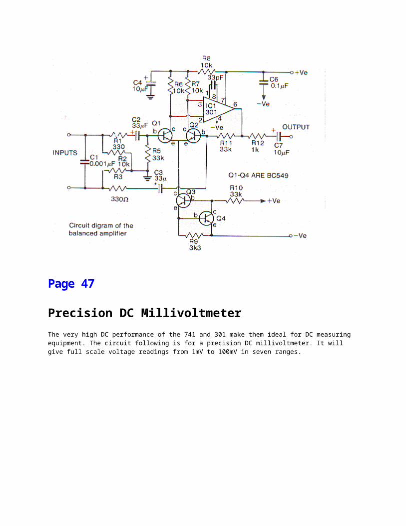
Page 47
Precision DC MillivoltmeterThe very high DC performance of the 741 and 301 make them ideal for DC measuring equipment. The circuit following is for a precision DC millivoltmeter. It will give full scale voltage readings from 1mV to 100mV in seven ranges.

Peak reading VU Meter
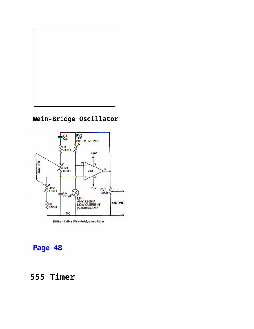
Wein-Bridge Oscillator
Page 48
555 Timer

The 555 is a highly stable device designed for generating accurate time delays or oscillations. Additional terminals are provided ' for triggering or resetting. In the time delay mode (monostable mode) the time is set by one external resistor and one capacitor. In the astable (free running) mode the frequency and duty cycle are set by two external resistors and one capacitor. The circuit can be both triggered and reset on fallingwaveforms. The output circuit can source or sink up to 200mA. TTLcircuitry can be driven directly from the output.
A dual version of this IC is available, the 556.
Features
555 Timer IC
• Timing from microseconds to hours
• Adjustable duty cycle
• Sink & source 200mA
• 4-15V operation
• Temperature stability >0.005% per°C

Absolute maximum ratings
Supply +18V
Power dissipation 600mW
Specifications
Timing Error, monostable Temperature drift 50ppm/°C
Supply Drift 0.1 %/V
Timing Error, astable Temperature Drift 150ppm/°C
Supply Drift 0.30%/V
Trigger Voltage
Vcc 15V (Itrig = 0.5µA) 5V
Vcc 5V 1.67v

Control Voltage VCC15V 10vVCC 5V 3.3v
555 Modes & uses
Free-running: astable multivibrator
When powered from a 5v supply the 555 is directly compatible withTTL. It can also run from 4-15v and can source and sink several hundred milliamps at its output.
One end of the timing capacitor is connected to ground, the otherto the positive supply via resistor(s) allowing the use of electrolytics.
The high input impedance allows the use of large resistors and small capacitors. Up to 1000:1 frequency range can be obtained from a single capacitor by changing the resistance timing element.
Astable operation
1. Output (pin 3) is high
2. Charge on capacitor is low
3. Discharge transistor not conducting
4. Capacitor starts to charge

5. When voltage across the capacitor reaches two-thirds of the supply voltage the comparator triggers. Output goes low, capacitor is discharged via R2. When the voltage on the capacitordrops to one third of the supply the comparator flips the circuitback. Then the whole sequence repeats for the next cycle.
If R2 is made large compared to R1, output is low but symmetry ofwaveform is high.
Page 49Altering the Duty CycleThe duty cycle is the 'on' time as a percentage of total cycle time. This is normally limited to 50%. By adding a diode, a duty cycle of less than 50% can be achieved.

Curing Latch-up problems
Latch-up when driving an inductive load can be avoided by adding two diodes as shown in the circuit below. This stops negative voltage from reaching pin three.
Fine Control of Timing/Frequency
Pin 5, the control pin, is primarily used for filtering when the device is used in noisy electrical environments. However, by putting a voltage on this point, it is possible to vary the timing of the device independently of the 'RC' components. This control voltage may be varied from 45% to 90% of supply voltage in the monostable mode and from 1.7V to Vcc (supply voltage) in the astable mode.
Monostable operation

1. Bringing trigger from +V to ground starts sequence.
2. Output goes positive.
3. Clamp is removed from timing capacitor which then charges to two thirds of supply voltage. The threshold comparator then flipsthe circuit over. Output goes to ground and the capacitor is rapidly discharged to ground.
Page 50
Square Wave OscillatorThis simple circuit provides square waves at five switched frequencies from 1Hz to 10kHz. It uses the 555 in the astable mode.

Timer circuit
This circuit produces a warning tone after a preset period. The delay period is controlled by C1/R1 and RV1 and can be adjusted from a few milliseconds to approximately 500 seconds. The 555 is normally "switched off". C1 discharges via R1 and RV1. When it hasdischarged, the 555 is turned 'on' via Q1 and oscillates, producing a warning tone.

Special Version of the 555ICM7555The ICM 7555 is a CMOS timer IC providing significantly improved performance over the standard 555 timer. At the same time it willact as a direct replacement for this device in most applications.Improved parameters include the low supply current, wide operating supply voltage range, low threshold, trigger and reset currents, no crowbarring of the supply current during any output transition, higher frequency performance and no requirement to decouple the control voltage for stable operation. A dual version of the 7555 is available, the 7556, with two timers sharing only V+(VCC) and V-(GND). They are both capable of sourcing and sinking sufficient current to drive TTL loads and have small enough offset to drive CMOS loads.
Features
• Low supply current (80µA typ)

• Ultra low trigger threshold. (20pA typ)
• High speed operation (500kHz guaranteed)
• Wide supply range 2v to 18v
• No crowbarring of supply during reset.
• Can be used with higher impedance timing elements than 555.
• Complete static protection.
Page 51
Absolute Maximum Ratings
Supply Voltage +18vInput Voltage
Trigger Supply + 0.3V
Threshold Supply - 0.3V

Reset control voltage Output Current 100mAPower Dissipation 200mW
LM340 and 78XX series 3 terminal regulators LM340T5, 12, 15 7805, 7812, 7815The LM340 series of positive 3 terminal regulators offer similar performance to the 78XX series. They are complete voltage regulators with outstanding ripple rejection and superior line load regulation.
Current limiting is included to limit peak output current to a safe level. Safe area protection for the output transistor is provided. If internal power dissipation is too high, thermal shutdown occurs. Although designed primarily as fixed voltage regulators, these devices can be used with external components toobtain adjustable voltages and currents.
Features

• Maximum 1A output
• Output voltage tolerance ±2%
• Load regulation 0.3%
• Thermal overload protection
• Short circuit current limit
• Output transistor safe area protected
• Continuous dissipation 15W
Basic use as a fixed regulator
The 10µF capacitor across the output is needed for stability and improves the transient response of the supply.
Page 52
Specifications @ 25°C

µA7805/ LM340T-5
µA7812/ LM340T-12
µA7815/ LM340T-15
Output voltage 5v ± .25 12v ± .6 15V ±.6
Ripple rejection 80dB 72dB 70dB
Input voltage (minimum to maintain line regulation)
7.3v 14.5v 17.5v
Dropout voltage 2.0 2.0 2.0
Peak output current 2.2A 2.2A 2.2A
Short circuit current
2.1A max 1.5A max. 1.2A max.
Load regulation (5mA to 1.5A)
12mV typ. 12mV typ. 12mV typ.
Bias current 8mA max 8mA max 8mA max
Absolute max input voltage
35v 35v 35v
Applications
Apart from the normal use as a fixed voltage regulator, the LM340/78XX can be used in a variety of ways with the addition of external circuitry.
Adjustable outputThis simple circuit gives the LM340T-5 variable output voltage according to the formula:
Vout = 5v + (5v/R1+IQ)R2

Boosting the current output of the LM340T/ 78XX seriesThis circuit supplies regulated outputs at up to 5A. At low currents Q1 is off. Only above 600mA is it biased on.
Page 53
Providing fixed higher voltages
The output voltage of the LM340T/78XX series can be increased over the standard voltage of the regulator by using a zener diodein the common to earth lead.

VOUT = VZENER + VREGULATOR
79XX three terminal negative voltage regulatorsThe 79XX series are three terminal negative regulators with fixedoutput voltages. The only external component necessary is a compensation capacitor on the output.
These are essentially similar to the 78XX series positive regulators, with current limiting and thermal overload protection.
Specifications @25°C
LM7905 LM7912 LM7915

Output Voltage -5v ±.2 -12v ±.5
-15v ± .6
Line regulation 5mV typ 5mV typ 5mV typQuiescent Current 1mA 1.5mA
typ1.5mA typ
Power dissipation 1.5W 1.5W 1.5WInput voltage maximum
-35v -35v -35v
Minimum input voltage
7v 14.5v 17.5v
Standard circuit
Page 54

The use of a pair of the regulators (positive and negative) makes an ideal dual rail supply, for powering op-amps etc. A suitable circuit is shown below.This one uses 12V regulators, but obviously the voltage can be varied by changing regulators.
This list is only some of the most common types:
DeviceVoltage Curren
tPinout
780578L0578067808781078L12781278S12CT
+5v+5v+6v+8v+10v+12v+12v+12v
1A100mA1A1A1A100mA1A2A
TO-220 positiveTO-92 positiveTO-220 positiveTO-220 positive

78187824790579L0579067908791279L12791579187924LM317TLM337SPLM123kLM117K
+18v+24v-5v-5v-6v-8v-12v-12v-15v-18v-24v+1.2V to +37V-1.2V to -37V+5v+1.2V to +37V
1A1A1A100mA1A1A1A100mA1A1A1A1.5A1.5A3A3A
TO-220 positiveTO-92 positiveTO-220 positiveTO-3 positiveTO-220 positiveTO-220 positiveTO-220 negativeTO-92 negativeTO-220 negativeTO-220 negativeTO-220 negativeTO-92 negativeTO-220 negativeTO-220 negativeTO-220 negativeTO-220 adjustableTO-220 adjustableTO-3 positiveTO-3 positive

Page 55


Page 56

The above tables are called TRUTH TABLES. They give all the possible outcomes for a particular gate. The inputs are labeled A and B as shown above and the output is the result of the inputs at HIGH or LOW level.

A HIGH is “1” and a LOW is “0.”
Page 57
4001 Metal Detector
4001 is used in this circuit as two different types of oscillator. IC1a and IC1b with R1, RV1 and C2 form one oscillator. RV1 varies its frequency slightly. lCld, C4, C5 and L1
(search coil) form the second oscillator. IC18 acts as a mixer, combining the two oscillators and producing an output which is the difference between the two. This is amplified by TR1 and fed to a magnetic earpiece.
Ultrasonic Transmitter
The 4001 forms a complete 40kHz oscillator and driver for an ultrasonic transmitter. The oscillator frequency can be adjusted by means of RV1. Two gates act as square wave oscillators which then drive the other two gates in push-pull. These drive the transducer in push-pull to get the maximum.

Page 58
CMOS Logic Probe
The logic probe is an essential instrument for testing digital circuitry. This one uses only one 4001 IC, 3 LEDs and a handful of passive components. Power is obtained from the circuit to be tested. The first gate acts as an inverter by strapping its two inputs together. It is biased for half supply by R1. Under quiescent conditions neither LED1 or LED2 will light. If the input goes high, gate output goes low and LED1 comes on. If the input is taken low, the output of IC1 goes high and LED2 comes on, indicating a low signal. Short pulses are 'stretched’ by IC gates 2 and 3, producing a flickering output at LED3.

Touch Switch
The near infinite input impedance of CMOS makes it ideal for use in touch and proximity circuits. Usually a touch sensitive circuit needs physical contact, while proximity circuit needs only the presence of an object such as the human body. Touch sensors rely on three features of the human body. Skin resistanceis usually a few hundred thousand ohms, the body has a capacitance to earth of around 300pF and the human body acts as an antenna, picking up 50Hz power line fields. The figure below shows a proximity switch based on human coupling of the 50Hz power line. A hand very near the plate will induce hum onto the plate and this will be passed to the circuit. The first gate is a4001 with both inputs strapped together. The hum will be squared up and used to trip the retriggerable monostable as shown. A clean output results from the instant of first proximity until a few milliseconds after release. The sensitivity depends on the size of the plate.The output of the 4013 can be connected to a relay via a transistor. It could then be used to turn on a light or other piece of electrical equipment. The 50M resistor can be made by putting 5M resistors in series.

Page 59
CMOS Lamp Flasher
This circuit uses the four CMOS NAND gates of the 4011 as an oscillator and low power driver. The first two form a low frequency oscillator. All the gates are used with their inputs connected together. In this form they act as an inverter i.e. a HIGH produces a LOW out. The very high input impedance of the gates means that high impedance values can be used in the oscillator circuit. The power consumption is also very low and the circuit will function over the normal 3-15 volts range of CMOS.

Audio Alarm
Metal DetectorThis unit uses two pairs of 4011 NAND gates as two oscillators and two 4011 buffers. The search coil oscillator has its frequency influenced by the position and proximity of metal at the search head. The reference oscillator has its frequency adjusted by the slug tuning of its coil and fine tuning by adjusting the voltage on IC2c. The two signals are digitally mixed in one section of a dual D-type flip-flop.

Page 60
4017 CMOS Decade Counter/ Divider with 10Decoded Outputs (Johnston Counter)The CD 4017 is called a COUNTER or DIVIDER or DECADE COUNTER. It is a very handy chip for producing "Running LED effects" etc.
It has 10 outputs. For normal operation, the clock enable and reset should be at ground.
Output "0" goes HIGH on the rise of the first clock cycle.
On the rise of the second clock cycle, output "0" goes LOW and output "1" goes HIGH. This process continues across the ten outputs and cycles to output "0" on the eleventh cycle.
The "Carry Out" pin goes LOW when output "5" goes HIGH and goes HIGH when output "0" goes HIGH.

In other words, "Carry Out" is HIGH for outputs 0, 1, 2, 3 and 4. It is LOW when the following outputs are active: 5, 6, 7, 8and 9.
When RESET (pin 15) is taken HIGH, the chip will make output "0" go HIGH and remain HIGH.
When "Clock Inhibit" (pin 13) is taken HIGH, the counter will FREEZE on the output that is currently HIGH.The clock signal must have a rise time faster than 5µsecs (VDD=15v).

6 LEDs on the KITT SCANNER scan back and forth similar to the lights on the front of the KITT car in the movie.

The 10 LEDs on the SCANNER turn on one-at-a-time, from left to right
LED DICE

Page 62

Logic Probe
This completes Pages 42 to 64 of Data Book 1

http://www.talkingelectronics.com
Sept 2008 Nothing is copyright. You can copy anything Colin Mitchell
topages: 63 to 85

Pages 63 to 85
Index Pages: 1 to 21 Pages: 22 to 41 Pages: 42 to 62
The pages can be printed and collated into a book for easy reference.
More circuits and projects can be found on TALKING ELECTRONICS website:http://www.talkingelectronics.com
Colin [email protected]
Tel: 0417 329 788

CONTENTSAC Trigger Ammeter Amplifier Arc WelderAudio Alarm Audio MixerBC 547 NPN transistorBC557 PNP transistorBD 139 BD140 transistorBipolar Transistors CA 3130 OP-ampCapacitor DataCar Voltage Converter Chip PinoutsCircuit Symbols Common Base/Emitter/Collector Circuits Counter Crystal Set Darlington Transistor DC Millivoltmeter Definitions Difference
398320, 2178594619192115527125744
15,16379174718468543629297933
Microphone Morse Code GeneratorMPF 102 FETMultivibrator OA 91 diode OP Amp Peak Reading VU MeterPhoto Diode Photo Electric Relay Pinouts Power Diode Power Supply Relay Driver Resistors RF Monitor Meter RF Prescaler SCR C122DSilicon Controlled Rectifier SimonRegulator 78xx 79xxSignal Diode Semiconductor Devices Solar Charger Square Wave
8321262194252343074822, 6020689284044868, 1051,5314567750756925288155

AmplifierDiode Dual Power Supply Electronic Dice FET FET Voltmeter Field Strength Meter MkIIFlashing LED FM Transmitter FM BugGermanium Diode Hearing AidInfinity BugInfrared LEDInfrared Light Beam Kitt ScannerLamp Dimmer Lamp Flasher Light Beam Relay Light Switch LEDs LED Chaser LED DiceLED Flasher LM 340 LM 386Logic GatesLogic Probe Metal Detector Metronome Microcontrollers
20,8198180343860395928303133613350675658,6257,592585
OscillatorSteam SimulatorSurface Mount ResistorsTime Delay TimerTransistor AmplifierTransistor Pinouts TRIAC SC151DTouch Switch Ultrasonic Transmitter Unijunction Transistor UJT UJT Time Delay Wein Bridge Oscillator Zener Diode 1N4001 Power diode1N4148 Signal diode27MHz Links2N2646 UJT2N 3055 transistor4017 Decade counter555 Light Switch 555 Timer 7-Segment Displays 74c14 Hex Schmitt 741 OP Amp
38585737375347810237622646029483562445060

7555 CMOS 5557805 +5v Regulator7905 -5v Regulator
Page 63
40106 OR 74C14 HEX Schmitt Trigger IC
This chip is known by a number of identities. 74C14. It is also marketed as 40106, 40014, and 74HC14. These are all CMOSchips and are characterisedby low current consumption,high input impedance and a supply voltage from 5v to 15v. (Do not substitute 7414 or 74LS14. They are TTL chips and operate on 4.5v to 5.5v and have low impedance inputs.)The 74C14 contains 6 Schmitt Trigger gates. Minimum supply voltage 5vMaximum supply voltage 15vMax current per output 10mAMaximum speed of operation

4MHzCurrent consumption approx 1uA with nothing connected to the inputs or outputs.
Here are some of the things you can do with the gates in the 40106Hex Schmitt Trigger chip:
INVERTINGIf the output is required to be the opposite of the circuit above,an inverter is added:
If a diode is added across the input resistor, thecapacitor "C" will be discharged when the input goes low, so the "Delay Time" will be instantly available when the input goes HIGH:

The following circuit produces a PULSE (a LOW pulse) when the input goes HIGH:
Page 64
To invert the output, add an inverter:
To produce a pulse after a delay, the following circuit can be used:

The following circuit produces a tone during the HIGH period. When the output of the second inverteris HIGH, it places a high on the input of the thirdinverter, via the diode. This is called "jamming" the oscillator and prevents the oscillator from operating. When the second inverter goes LOW, the oscillator will operate.
The oscillator above can be set to produce a 100Hz tone and this can activate a 2kHz oscillator to produce a 2-tone output. A "jamming diode" is needed between the third and fourth gates to allow the high-frequency oscillator to operate when the output of thelow-frequency oscillator is HIGH.
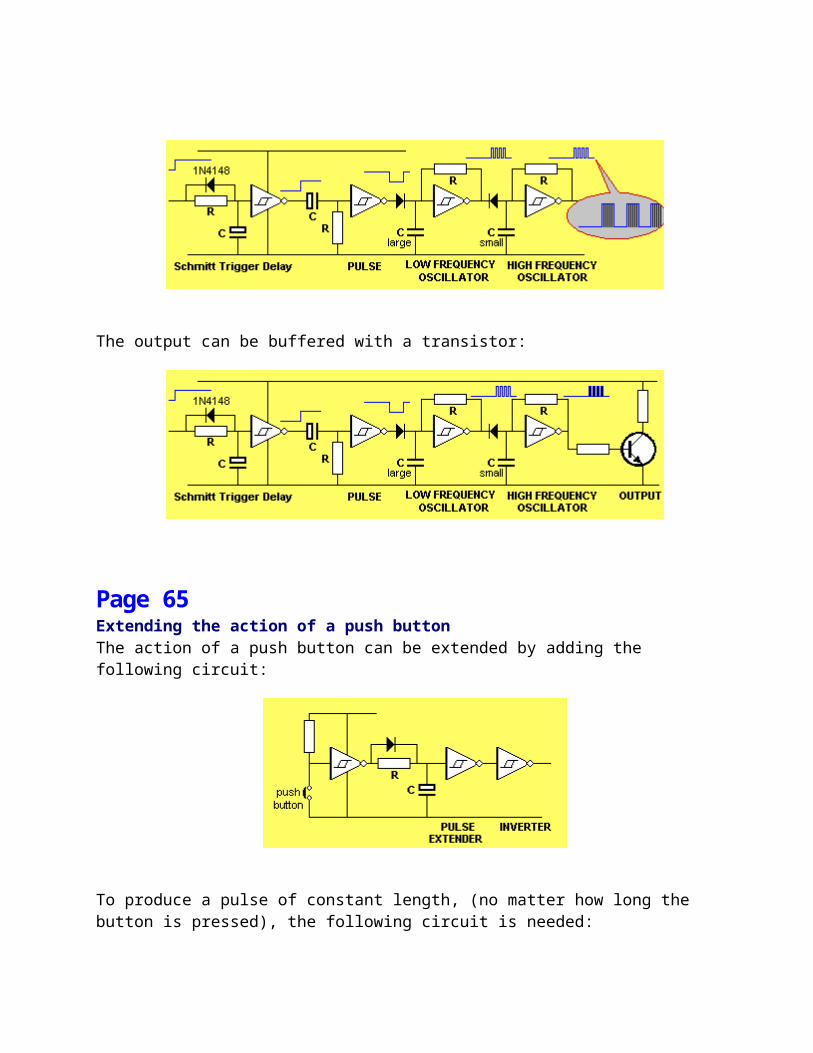
The output can be buffered with a transistor:
Page 65Extending the action of a push buttonThe action of a push button can be extended by adding the following circuit:
To produce a pulse of constant length, (no matter how long the button is pressed), the following circuit is needed:

GATINGGating is the action of preventing or allowing a signal to pass though a circuit. In the following circuit, buttons "A" and "B" are gated to allow the oscillator to produce an output.The first two inverters form an "OR-gate." When the output of the gate is HIGH it allows the oscillator to operate.
The second diode is called the gating diode. When the output of the second inverter is LOW, the capacitor is prevented from charging as the diode will not allow it to charge higher than 0.7v, and thus the oscillator does not operate.When the output of the second inverter is HIGH, the capacitor is allowed to charge and discharge and thus oscillator will produce an output. If the push buttons can be placed together, the circuitcan be simplified to:

PULSERThe 74c14 can be used to produce a 3mS pulses every second. The circuit is adjustable to a wide range of requirements.
Page 662 MINUTE TIMERSome of the features we have discussed have been incorporated into the following circuit. The relay is energized for a short time, 2 minutes after the push-button is pressed. The push-button produces a brief LOW on pin 1, no matter how long it is pushed and this produces a pulse of constant length via the three components between pin 2 and 3. This pulse is long enough to fully discharge the 100u timing electrolytic on pin 5. The 100k and electrolytic between pins 6 and 9 are designed to produce a brief pulse to energize the relay.

TRIGGER TIMER
The next design interfaces a "Normally Open" and "Normally Closed" switch to a delay circuit. The feedback diode from the output prevents the inputs re-triggering the timer (during the delay period) so thata device such as a motor, globe or voice chip can be activated for a set period of time.
ALARMIn the following circuit, the gates are used to detect the touch ofa door knob and produce an output that goes HIGH for approx 1 minute.
The output of the above circuit can be taken to an alarm. Open the reed switch contacts and connect the reed switch to the output of the Door-knob alarm.

Page 67
LM 386

300mW amplifier using LM 386
300mW amplifier using LM 386
Page 68


Page 69
A 330k SM resistor

Surface Mount ResistorsAll SM resistors conform to a 3-digit or 4-digit code. But there are a number ofcodes, according to the tolerance of the resistor. It's getting very complicated. Here is a basic 3-digit SM resistor:
The first two digits represent the two digits in theanswer. The third digit represents the number of zero's you must place after the two digits. The answer will be OHMS. For example: 334 is written 33 0 000. This is written 330,000 ohms. The comma can be replaced by the letter "k". The final answer is: 330k.222 = 22 00 = 2,200 = 2k2 473 = 47 000 = 47,000 = 47k105 = 10 00000 = 1,000,000 = 1M = one million ohmsThere is one trick you have to remember. Resistancesless than 100 ohms are written: 100, 220, 470. Theseare 10 and NO zero's = 10 ohms = 10R or 22 and no zero's = 22R or 47 and no zero's =

47R. Sometimes the resistor is marked: 10, 22 and 47 to prevent a mistake. Remember:R = ohms k = kilo ohms = 1,000 ohms M = Meg = 1,000,000 ohmsThe 3 letters (R, k and M) are put in place of the decimal point. This way you cannot make a mistake when reading a value of resistance.
THE COMPLETE RANGE OF SM RESISTOR MARKINGS:
0R1 = 0.1ohm
R22 = 0.22ohm
R33 = 0.33ohm
R47 = 0.47ohm
R68 = 0.68ohm
R82 = 0.82ohm
1R0 = 1R
1R2 = 1R2
2R2 = 2R2
3R3 = 3R3
470 = 47R
560 = 56R
680 = 68R820 = 82R101 = 100R
121 = 120R
151 = 150R
181 = 180R
221 = 220R
271 = 270R
332 = 3k3
392 = 3k9
472 = 4k7
562 = 5k6
682 = 6k8
822 = 8k2103 = 10k
123 = 12k
153 = 15k
183 = 18k
223 = 22k
273 = 27k
333 = 33k
393 = 39k
224 = 220k
274 = 270k
334 = 330k
394 = 390k
474 = 470k
564 = 560k684 = 680k
824 = 820k
105 = 1M0125 =

4R7 = 4R7
5R6 = 5R6
6R8 = 6R8
8R2 = 8R2
100 = 10R
120 = 12R
150 = 15R
180 = 18R220 = 22R
270 = 27R
330 = 33R
390 = 39R
331 = 330R
391 = 390R
471 = 470R
561 = 560R
681 = 680R
821 = 820R102 = 1k0
122 = 1k2
152 = 1k5
182 = 1k8
222 = 2k2
272 = 2k7
473 = 47k
563 = 56k
683 = 68k
823 = 82k104 = 100k
124 = 120k
154 = 150k
184 = 180k
1M2
155 = 1M5
185 = 1M8
225 = 2M2
275 = 2M7
335 = 3M3
395 = 3M9
475 = 4M7
565 = 5M6
685 = 6M8
825 = 8M2
106 = 10M0
Page 70The complete range of SM resistor markings for 4-digit
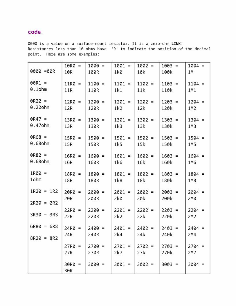
code:
0000 is a value on a surface-mount resistor. It is a zero-ohm LINK!Resistances less than 10 ohms have 'R' to indicate the position of the decimal point. Here are some examples:
0000 =00R
00R1 = 0.1ohm
0R22 = 0.22ohm
0R47 = 0.47ohm
0R68 = 0.68ohm
0R82 = 0.68ohm
1R00 = 1ohm
1R20 = 1R2
2R20 = 2R2
3R30 = 3R3
6R80 = 6R8
8R20 = 8R2
10R0 = 10R
11R0 = 11R
12R0 = 12R
13R0 = 13R
15R0 = 15R
16R0 = 16R
18R0 = 18R
20R0 = 20R
22R0 = 22R
24R0 = 24R
27R0 = 27R
30R0 = 30R
1000 = 100R
1100 = 110R
1200 = 120R
1300 = 130R
1500 = 150R
1600 = 160R
1800 = 180R
2000 = 200R
2200 = 220R
2400 = 240R
2700 = 270R
3000 =
1001 =1k0
1101 =1k1
1201 =1k2
1301 =1k3
1501 =1k5
1601 =1k6
1801 =1k8
2001 =2k0
2201 =2k2
2401 =2k4
2701 =2k7
3001 =
1002 = 10k
1102 = 11k
1202 = 12k
1302 = 13k
1502 = 15k
1602 = 16k
1802 = 18k
2002 = 20k
2202 = 22k
2402 = 24k
2702 = 27k
3002 =
1003 = 100k
1103 = 110k
1203 = 120k
1303 = 130k
1503 = 150k
1603 = 160k
1803 = 180k
2003 = 200k
2203 = 220k
2403 = 240k
2703 = 270k
3003 =
1004 = 1M
1104 = 1M1
1204 = 1M2
1304 = 1M3
1504 = 1M5
1604 = 1M6
1804 = 1M8
2004 = 2M0
2204 = 2M2
2404 = 2M4
2704 = 2M7
3004 =

33R0 = 33R
36R0 = 36R
39R0 = 39R
43R0 = 43R
47R0 = 47R
51R0 = 51R
56R0 = 56R
62R0 = 62R
68R0 = 68R
75R0 = 75R
82R0 = 82R
91R0 = 91R
300R
3300 = 330R
3600 = 360R
3900 = 390R
4300 = 430R
4700 = 470R
5100 = 510R
5600 = 560R
6200 = 620R
6800 = 680R
7500 = 750R
8200 = 820R
9100 = 910R
3k0
3301 =3k3
3601 =3k6
3901 =3k9
4301 =4k3
4701 =4k7
5101 =5k1
5601 =5k6
6201 =6k2
6801 =6k8
7501 =7k5
8201 =8k2
9101 =9k1
30k
3302 = 33k
3602 = 36k
3902 = 39k
4302 = 43k
4702 = 47k
5102 = 51k
5602 = 56k
6202 = 62k
6802 = 68k
7502 = 75k
8202 = 82k
9102 = 91k
300k
3303 = 330k
3603 = 360k
3903 = 390k
4303 = 430k
4703 = 470k
5103 = 510k
5603 = 560k
6303 = 620k
6803 = 680k
7503 = 750k
8203 = 820k
9103 = 910k
3M0
3304 = 3M3
3604 = 3M6
3904 = 3M9
4304 = 4M3
4704 = 4M7
5104 = 5M1
5604 = 5M6
6204 = 6M2
6804 = 6M8
7504 = 7M5
8204 = 8M2
9104 = 9M11005 = 10M

Three Digit Examples Four Digit Examples
330 is 33 ohms - not 330ohms
1000 is 100 ohms - not 1000ohms
221 is 220 ohms 4992 is 49 900 ohms, or49k9
683 is 68 000 ohms, or68k
1623 is 162 000 ohms, or162k
105 is 1 000 000 ohms,or 1M
0R56 or R56 is 0.56 ohms
8R2 is 8.2 ohms A new coding system has appeared on 1% types. This is known as the EIA-96 marking method. It consists of a three-character code. The first two digits signify the 3 significant digits of the resistor value, using the lookup table below. The third character - a letter - signifies the multiplier.
codevalue
code value
code value
code value
code value
code value
01 100 17 147 33 215 49 316 65 464 81 68102 102 18 150 34 221 50 324 66 475 82 69803 105 19 154 35 226 51 332 67 487 83 71504 107 20 158 36 232 52 340 68 499 84 73205 110 21 162 37 237 53 348 69 511 85 75006 113 22 165 38 243 54 357 70 523 86 76807 115 23 169 39 249 55 365 71 536 87 78708 118 24 174 40 255 56 374 72 549 88 80609 121 25 178 41 261 57 383 73 562 89 82510 124 26 182 42 237 58 392 74 576 90 84511 127 27 187 43 274 59 402 75 590 91 86612 130 28 191 44 280 60 412 76 604 92 88713 133 29 196 45 287 61 422 77 619 93 90914 137 30 200 46 294 62 432 78 634 94 93115 140 31 205 47 301 63 442 79 649 95 95316 143 32 210 48 309 64 453 80 665 96 976

Page 71The multiplier letters are as follows:
letter
mult
letter
mult
F 100000 B 10
E 10000 A 1
D 1000 X orS 0.1
C 100 Y orR
0.01
22A is a 165 ohm resistor, 68C is a 49900 ohm (49k9) and 43E a 2740000 (2M74). This marking scheme applies to 1% resistors only.
A similar arrangement can be used for 2% and 5% tolerance types. The multiplier letters are identical to 1% ones, but occur before the number code and the following code is used:
2% 5%
code
value
code
value
code
value
code
value
01 100 13 330 25 100 37 33002 110 14 360 26 110 38 36003 120 15 390 27 120 39 39004 130 16 430 28 130 40 43005 150 17 470 29 150 41 47006 160 18 510 30 160 42 51007 180 19 560 31 180 43 56008 200 20 620 32 200 44 620

09 220 21 680 33 220 45 68010 240 22 750 34 240 46 75011 270 23 820 35 270 47 82012 300 24 910 36 300 48 910
With this arrangement, C31 is 5%, 18000 ohm (18k), and D18 is 510000 ohms (510k)2% tolerance. Always check with an ohm-meter (a multimeter) to make sure.
Chip resistors come in the following styles and ratings: Style: 0402, 0603, 0805, 1206, 1210, 2010, 2512, 3616, 4022 Power Rating: 0402(1/16W), 0603(1/10W), 0805(1/8W), 1206(1/4W), 1210(1/3W), 2010(3/4W), 2512(1W), 3616(2W), 4022(3W) Tolerance: 0.1%, 0.5%, 1%, 5% Temperature Coefficient: 25ppm 50ppm 100ppm
CAPACITOR DATA
A capacitor works on the principle of having two conductive plates which are very close and are parallel to each other. When a charge is applied to one plate of the capacitor, the electrons will generate an approximately equal, but opposite charge on the other plate. Capacitors will pass ACcurrent, but will block DC current. A capacitor can also he used to smooth voltage ripple, as in DC power supplies. Capacitance is measured in Farads (F).

Capacitor Parameters
Capacitors have five parameters:Capacitance (Farads), Tolerance (%), Maximum Working Voltage (Volts)Surge Voltage (Volts) and Leakage
Because a Farad is a very large unit, most capacitors are normally measured in the ranges of pico, nano and micro farads.
Working Voltage This refers to the maximum voltage that should be placed across the capacitor under normal operatingconditions.
Surge Voltage
The maximum instantaneous voltage a capacitor can withstand. If the surge voltage is exceeded over too long a period there is a very good chance thatthe capacitor will be destroyed by the voltage punching through the insulating material inside the casing of the capacitor. If a circuit has a surging characteristic, choose a capacitor with a high rated surge voltage.
Leakage
Refers to the amount of charge that is lost when the capacitor has a voltage across its terminals. If a capacitor has a low leakage it means very little power is lost. Generally leakage is very small and is not normally a consideration for general purpose circuits.
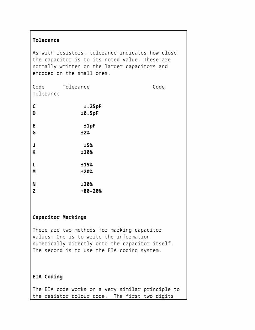
Tolerance
As with resistors, tolerance indicates how close the capacitor is to its noted value. These are normally written on the larger capacitors and encoded on the small ones.
Code Tolerance Code Tolerance
C ±.25pF D ±0.5pF
E ±1pF G ±2%
J ±5% K ±10%
L ±15% M ±20%
N ±30% Z +80-20%
Capacitor Markings
There are two methods for marking capacitor values. One is to write the information numerically directly onto the capacitor itself. The second is to use the EIA coding system.
EIA Coding
The EIA code works on a very similar principle to the resistor colour code. The first two digits

refer to the value with the third being the multiplier. The fourth character represents the tolerance.
When the EIA code is used, the value will always be in Pico-Farads (see Decimal Multipliers).
Example 103K
This expands to:
1 = 1
0 = 0
3 = x 1,000
K = 10% (sec Capacitor Tolerance for listings)
Then we combine these numbers together:
1 0 x 1 000 = 10 000pF = 0.01µF, = 10n ±10% tolerance
Example 335K
This expands to:
3 = 33 = 3E = x100,000K = ±10%
Then we combine these numbers together
3 3 x100,000 = 3,300,000pF = 3,300nF = 3.3uF10% tolerance.


Page 74