Design of ITER NBI power supply system - OSTI.GOV
114
JAERI-Tech--97-034 JAERI-Tech 97-034 JP9709026 mm Design of ITER NBI Power Supply System July 1887 Kazuhiro WATANABE, Osamu HIGA*1, Syuichi KAWASHIMA*1 Yoshihiro OHARA, Yoshikazu OKUMURA, Youichi ONO*2 Masanobu TANAKA*2 and Sei YASUTOMI*1 Japan Atomic Energy Research Institute uni o n klo 9 /
-
Upload
khangminh22 -
Category
Documents
-
view
0 -
download
0
Transcript of Design of ITER NBI power supply system - OSTI.GOV

JAERI-Tech--97-034
JAERI-Tech97-034
JP9709026
mm
Design of ITER NBI Power Supply System
July 1887
Kazuhiro WATANABE, Osamu HIGA*1, Syuichi KAWASHIMA*1 Yoshihiro OHARA, Yoshikazu OKUMURA, Youichi ONO*2Masanobu TANAKA*2 and Sei YASUTOMI*1
Japan Atomic Energy Research Instituteuni o n klo 9 /

B(fsig-n ik®.mmw$L *#) hx, &$L&L<c^- (T319-11 B AW%Rff 14)
fc *) ito
This report is issued irregularly.Inquiries about availability of the reports should be addressed to Research Information
Division, Department of Intellectual Resources, Japan Atomic Energy Research Institute, Tokai-mura, Nakagun, Ibaraki ken 319-11, Japan.
© Japan Atomic Energy Research Institute, 1997
f-n m ru m

JAERI-Tech 97-034
Design of ITER NBI Power Supply System
Kazuhiro WATANABE, Osamu HIGA* *Syuichi KAWASHIMA*1
Yoshihiro OHARA, Yoshikazu OKUMURA, Youichi ONO*2
Masanobu TANAKA*2 and Sei YASUTOMI*'
Department of Fusion Engineering Research
Naka Fusion Research Establishment
Japan Atomic Energy Research Institute
Naka-machi, Naka-gun, Ibaraki-ken
(Received July 1, 1997)
Power supply system for the ITER neutral beam injector (NBI) whose total injection power
is 1 MeV, 50 MW from three modules, has been designed. The power supply system consists
of a source power supply for negative ion production / extraction and a DC 1 MV, 45 A power
supply for negative ion acceleration. An inverter controlled multi-transformer / rectifier
system has been adopted to the acceleration power supply. An inverter frequency of 150 Hz
was selected to satisfy required specifications which are rise time of <100 ms, voltage ripple
of <10% peak to peak and cut off speed of <200 /u s. It was confirmed that the rise time, the
ripple and the cut off speed is about 50 ms, 7% and <200 /u s respectively by computation. It
was also confirmed that a surge current and an energy input to the ion source at the
breakdown can be suppressed lower than 3 kA and 10 J, which are considered to be lower
than allowable values. A 1 MV transmission line has been designed from a view point of
electric field on the inner conductors and grounded conductor.
The results from the design study indicate that all the required specification to the power
supply system can be satisfied and that R&D on the transmission line is one of the most
important subjects.
Keywords : ITER NBI, Power Supply, Inverter, DC High Voltage, Surge Current,
Energy Input, Transmission Line
* 1 Toshiba Co.*2 Hitachi Ltd.

JAERI-Tech 97-034
iter nb imumm
ma mi • its #*' • ms $-*' • #%
## mu ■ ES IE-*2 • BE i&€*2-£® m*1
( 1 9 9 7 ¥ 7 fll B-SS)
3fyjL-;H:j:6 ^ - A A#%73 ^IMeV, SOMW^ITERm ¥##¥ AWEm (NBi) #
^ t> E'-AiaiirozcAcoSEiMV. 45Attijj<nto'M%Mfrbfoi&2ti&0 <
¥¥*?¥, m&m&ALtj tWffllOOmsJar, SEV 7 -/;H0%p-ptil T\ mm&f?$200/u jfeyi^-S^OEA.Ti^lSOHzi: LZ:„
MlE^Etfl^re^SOms, 3a%##B$<Z>gEV vY&^7%p-p, $ W: m*#Mt200/,smTT*6 2^^#m-r#Z:o iZ:, T t
^ At a -m - y mm >^ f - K <
®T¥'¥E¥v^#x.^tii>3kA, lOJWTliMeil-e & 6 2 h ¥#mT & A. %\m^b
4 E > i® 2 T'^ 1MVSI*d3 =t y1'¥ KSteS#^ f#fi£ $ ft £ E AfAIS 7 T >0)g£ft£fro rt:0 2ft6NBlSz®'>xf A(7)EBt*S3¥ NBimi®UE¥^n^tT|g$-T^#¥ftHllL^lfco
9|SSie%9f : T3H-0I ^«Hr9Wfl5jlOTHT[6mJ80l-l*l #*%*2
n

JAERI-Tech 97-034
Contents
1. Introduction .............................................................................................................................. 1
2. Specifications of the Power Supply System ........................................................................ 1
2.1 Acceleration Power Supply ............................................................................................... 2
2.2 Power Supplies for Negative Ion Production and Extraction ..................................... 3
3. Design of the Power Supply System .................................................................................... 8
3.1 Circuit Diagram of the Power Supply System ............................................................ 8
3.2 The Plant Layout of the NBI Power Supply System...................................................... 8
3.3 Acceleration Power Supply ............................................................................................... 8
3.3.1 Comparison of the Circuit Diagram........................................................................ 8
3.3.2 Converter / Inverter System ................................................................................... 113.3.3 Analysis of Dynamic Property of the Power Supply............................................. 17
3.4 Power Supplies for Negative Ion Production and Extraction ..................................... 43
3.5 Power Fluctuation Compensator .................................................................................... 48
3.6 AC Harmonics, Filter Specifications, Active and Reactive Power .............................. 50
4. Design of the High Voltage Deck (HVD) and the Transmission Line.............................. 52
4.1 Original Configuration of the High Voltage Deck ........................................................ 52
4.2 Modified Configuration of the High Voltage Deck with the Water Choke
and D2 Gas Feeding System ................................................. 52
4.3 Design of DC Insulation in the Transmission Line ..................................................... 53
4.3.1 Design Concept for SFg Gas Insulation ................................................................ 53
4.3.2 Insulation Design of the Transmission Line and Electric Field Simulations ■ 56
4.4 Surge Protection System ................................................................................................... 82
4.4.1 Estimation of Stray Capacitance and Stored Energy ......................................... 82
4.4.2 Estimation of the Size of Core Snubber for the Transmission Line .................. 87
4.5 Surge Analysis .................................................................................................................. 89
4.6 Test Voltage of the Transmission Line............................................................................ 97
5. Beam Line Power Supplies........................................................................................................ 100
6. Cost Estimate and Procurement Schedule ..........................................................................101
7. Summary ................................................................................................................................... 105
Acknowledgment ............................................................................................................................106
iii

JAERI-Tech 97-034
B ^
1. (i 12. MW7 7 7 A <Dtti& .......................................................................................................... 1
2. 1 tiOi$E?@ ......................................................................................................... 22.2 %4.............................................................. 3
3. EiJgy X-fACOEIt .......................................................................................................... a
3 . 1 E®II]j£& ......................................................................................................................... 83.2 H,yX7AWl"f77 h ........................................................................................... 8
3 . 3 finiiSE ......................................................................................................................... 8
3.3.1 8
3.3.2 n y/<— 9/4 >/<— 9 ................................................................................... 11
3.3.3 i7
3.4 fil * y*.$Lt^\$&L<ntzib<F)%m ........................................................................ 43
3.5 48
3.6 ##EA............................................................................... 504 . i#SE{&f •y4rjoJ:yfl'7>X5 y y 3 > 7 t > CD Exit .................................................. 52
4.1 52
4.2 ^*-*73-? tD2JfZ&7&£1VfZ>MmiZ7y*&&mffiM...................... 52
4.3 h 7 > 7 i y 7 a > 7 f > CD\tLtfi$&$Mxit ................................................................ 53
4.3.1 sF6#%mm(om#+#±................................................................................... 53
4.3.2 l7>Xl7y3>7-f> <7>#fe*$lxtt t E^-StS ......................................... 564.4 -*t~ yjWJyXf A ...................................................................................................... 82
4.4.1 #%#*#%## & 7. Jl/ f - (7)## ..................................................... 82
4.4.2 l7>Xlr>3>7,l’>§3 7X+7 '■'Oixft ......................................... 87
4 . 5 t)-- i/##f ..................................................................................................................... 89
4.6 l7>XFr> 3> CO^EEE ................................................................................... 97
5. fcf - A 3 -f >fflEi® ............................................................................................................1006. 3 7 hl?ijKtMi£Z7'ssL-}W%m> t).......................................................................... ioi
7. ft* ....................................................................................................................................105
# #.................................................................................................................106
IV

JAERI-Tech 97-034
1. Introduction
A high power neutral beam injection (NBI) system is required for ITER to
demonstrate steady state operation by plasma current drive. The NBI system consisted of a deuterium negative ion source and beamline system are being designed in the ITER Engineering Design Activity. The system is designed to inject a powerful neutral beam of 50 MW from three beamline modules at an energy of 1 MeV for a pulse duration of > 1000 s [1].
The beam energy of the system is two times higher than the JT-60U negative ion
based neutral beam injector (JT-60U N-NBI) whose power supply capacity is 500 kV, 64 A, 10 s [2]. A DC ultra high voltage technology becomes more important to design and construct the 1 MeV system. Further, power supply system for the high power negative ion source needs special functions as follows;1) DC high voltage regulation to produce stable ion beams2) High speed switching and surge suppression to protect the ion source
accelerator and power supply from electric breakdowns in the accelerator3) DC ultra high voltage (UHV) insulation4) UHV transmission from the power supply to the ion source
These are key issues in the design study.
Based on the design concepts reported in the Design Description Document
(DDD 4.2) [3], the preliminary design study on the neutral beam injector power supply system has started in 1 September, 1995 for a period until 31 December, 1996.
In the present report, specifications and outline of the NBI power supply system are described firstly. Secondly, design studies of the beam acceleration power supply, power supplies for the negative ion production are reported. Design of
the high voltage deck, the transmission line and the surge analysis are shown thirdly. Lastly, preliminary cost estimate are given.
2. Specifications of the power supply system
Neutral Beam Injection (NBI) system for ITER is designed to inject the deuterium neutral beam of 50 MW at an energy of 1 MeV for a pulse duration of longer than 1000 s. The system consists of three injectors. Each injector produces
17 MW neutral beam from the 1 MeV, 40 A negative ion source. Table 2-1 shows the specification of the ITER NBI.
- 1 -

JAERI-Tech 97-034
Table 2-1 Specifications of the neutral beam system for ITER.
Beam energy Beam power Pulse duration
: 1 MeV: 50 MW from three modules
: > 1000 s
The power supply system for the ITER NBI system has to be designed from the view point of an ultra-high voltage technologies and high speed controlled power supply to match the ion source where electric breakdowns occur frequently.
The power supplies can supply electric power to the ion source to deliver the
rated output of the beam. Required specifications of the power supply system was investigated.
2.1 Acceleration power supply
A simplified NBI power supply system diagram is shown in Fig. 2.1-1. The system consists of the acceleration power supply based on the converter and inverter system, power supplies for the negative ion production and extraction, surge protection system for both of the ion source and power supply itself, and
transmission line to the ion source. Specifications of the acceleration power supply were designed based on the system requirement. The specifications of the acceleration power supply are shown in Table 2.1-1.
Table 2.1-1 Acceleration power supply
VoltageCurrent
RippleRising timeCut off speedPulse lengthIntermediate voltageIntermediate current
1 MV
40 A
10 % p-p< 100 ms< 200 gs10000 s > t > 1000 s
800, 600, 400, 200 kV
12 A (800 kV), 4 A (600 kV), 2 A (400 kV), 1 A (200 kV)
- 2 -

JAERI-Tech 97-034
Ripple specification was designed from the view point of beam optics. Beam trajectory was investigated by using the ion beam orbit simulation code. An
allowable beam divergence fluctuation was considered to be lower than 1 mrad. In the simulation, the extraction voltage and the D" current density at the extraction surface were kept to be 9 kV and 24 mA/crn^, respectively. The
standard operation voltage of the acceleration power supply was assumed to be
990 kV.
Figure 2.1-2 shows the beam divergence as a function of the acceleration voltage.
The ripple of 10 % p-p gives a beam divergence fluctuation of < 0.5 mrad. This ripple was confirmed to be in the permissible level.
Cut off speed of shorter than 200 ps was adopted for protection of the ion source and the power supply from the electric breakdown. Pulse length up to 10000 s
was considered in the design of the power supply.
2.2 Power supplies for negative ion production and extraction
Specifications of the power supply system for the negative ion production and extraction are listed in Table 2.2-1.
Table 2.2-1 Specifications of the ion production andextraction power supplies
a) Filament power supply Voltage : 15 V ACCurrent : three phase, 8.3 kA per phase
Pulse length : 1000 - 10000 s
b) Arc power supply Voltage : 120 V Current : 7000 A
Ripple : 3 %p-p Cut off speed : < 100 ps Pulse length : 1000 -10000 s
c) Bias power supply Voltage : ± 10 V
— 3 —

JAERI-Tech 97-034
Current : 2300 A Ripple : 3 %p-p
Pulse length : 1000 -10000 s
d) PG filter power supply
Voltage : 5 V Current : 10 kA Ripple : 3 %p-pPulse length : 1000 - 10000 s
e) Extraction power supply
Voltage : 10 kV Current : 140 A Ripple : 2 %p-pCut off speed : < 100 gs Pulse length : 1000 -10000 s
Ripple effects on the beam optics were also investigated using the beam orbit simulation code. The beam optics is strongly influenced by the negative ion current density and the extraction voltage. The D' current density depends on the arc discharge power in the plasma generator. Therefore the effects of the arc
voltage ripple and the extraction voltage ripple on the beam divergence were investigated. Results are shown in Fig. 2.2-1 and Fig. 2.2-2. Influence of
simultaneous variations of the ripples on the beam optics is shown in Fig. 2.2-3. We confirmed that the proposed specifications are permissible values.
Filament cathode and arc chamber should be protected from the arcing phenomena in the plasma generator. The arc power supply has an inverter system that can cut off the arcing current in < 100 gs. Also the extraction power
supply needs an inverter system to protect the extractor electrode from the breakdown in <100 gs.
References
[1] R.S. Hemsworth, et al., Rev. Sci. Instrum. 67, 1120 (1996).[2] M. Kuriyama, et al., J. At. Energy Soc. Japan 38, 912 (1996).(in Japanese)[3] ITER Joint Central Team, Design Description Document (DDD 4.2A)
June(1995).
- 4 -

JAERI-Tech 97-034
Converter/Inverter, Voltage-down Thyristor Switch Trans. Insulated Trans.
■™k$n
Converter
Voltage-down Trans.
Z^ower Supply^ (Control System)
I-------------------------------- ,
C|yO1 MV zd
Transmission Line
Inverte2"
i—;| t; -t r
2- T1T
/•to Tij ' r
/*- :if 1. L ■ *—2 h.•H
Insulated Trans. & Rect.
Source Power supply
:z z'/.na
HVD(Trans. & Rectifier)
40 A, D- 1 MeV, 17 MW
Fig. 2.1-1 A simplified diagram of the ITER-NBI power supply system.
%E
-9?
HIOzLUODCHI>Q
<HICD
ITER ION SOURCE ACCELERATOR
Vext = 9 kV JD- = 24 mA/cm2
‘ Gap = 86/77/68/59/50 mm
700 800 900 1000 1100 1200 1300ACCELERATION VOLTAGE (kV)
Fig. 2.1-2 Beam divergence as a function of acceleration voltage.
- 5 -

JAERI-Tech 97-034
1
E
0)
$LUoLUCDDCLU>Q
Vext-wT
Vext = 9 kV Vacc = 1000 kV JD- = 24 mA/cm2
RIPPLE ON EXTRACTION VOLTAGE (%)
Fig. 2.2-1 Beam divergence as a function of ripple on extraction voltage.
"OCOE
_Q)
§LUO
LUCDDCLU>Q
Vext = 9 kV Vacc = 1000 kV JD- = 24 mA/cm2
-15 -10RIPPLE ON JD- (%
Fig. 2.2-2 Beam divergence as a function of ripple on the arc voltage.
— 6 —

JAERI-Tech 97-034
Acceleration Extraction Arc10% p-p 2% p-p 3%p-p
Vacc vext Varc990 kV g kV (JD-=24mA/cm2)
+1%9.09KV
-1%
+1.5%v 24.4mA/cm2 3.2 mrad
X^-1.5%23.64mA/cm2 4.0 mrad
, +1.5% 3.9 mrad
-1.5% 3.4 mrad
<+1.5% 3.1 mrad
-1.5% 3.5 mrad
, +1.5% 3.0 mrad
x -1.5% 3.1 mrad
Fig. 2.2-3 Influence of simultaneous variations of ripple.
- 7 -

JAERI-Tech 97-034
3. Design of the power supply system
3.1 Circuit diagram of the power supply system
A skeleton diagram of the NBI power supply system is shown in Fig. 3.1-1. AC 72 kV is distributed to the acceleration power supply and the negative ion
production and extraction power supplies. The acceleration power supply consists of a step-down transformer, converter, inverters and transformer rectifiers. Output of the transformer rectifiers are connected in series to supply 1
MV with intermediate potentials. The power supplies for plasma production and the extraction are insulated from the ground potential by insulated transformers. One big insulated transformer was adopted in original design.
However, from the restriction of the HVD space, only transformers and rectifiers are installed in the HVD. Voltage regulation and switching are controlled at primary side of the insulated transformer by high frequency
inverter systems. Therefore, insulated multi transformers are utilized.
3.2 The plant layout of the NBI power supply system
A layout of the NBI power supply system is shown in Fig. 3.2-1. A switch gear system, transformer, converter, inverter, HV transformers and rectifiers, insulated transformers, voltage current measurement system, filter capacitors, surge blocking L-Rs and transmission lines are mounted in the NBI power
supply yard. The space for the system is 50 m x 70 m. The out put cables are connected to the HV deck through the transmission lines. All of the high voltage components are installed in the SF6 gas pressurized tanks which are connected to the ground potential. A schematic diagram of the HV transformer and rectifier is shown in Fig. 3.2-2. A SF& gas insulated rectifier tank is
mounted on the oil insulated transformer.
3.3 Acceleration power supply
3.3.1 Comparison of the circuit diagram
At the beginning of the design study, two type of the circuit system were
compared. One is the separated multi transformer type that is based on the JT- 60U N-NBI power supply system. The other is the cascade transformer type that is proposed by EU HT.
- 8 -

JAERI-Tech 97-034
Comparison between the separated multi transformer type and the cascade
transformer type is listed in Table 3.3-1. Based on the result, JA HT selected the
separated multi transformer type shown in Fig. 3.3-1.
- 9 -

Table 3.3-1 Comparison of transformer type for the acceleration powe supply
Type Separated _ . ..Multi-T ransformer T ype Evaluation Cascaded T ransformer T ype Evaluation
HVInsulation
-Development of 1 MV insulated transformer is feasible o
-Required DC 200 kV insulationhas already been developed.
-Insulation against surge voltage must be investigated.
o
Size -Transformer can be compact with gas or oil insulation o -Transformer becomes
larger due to air insulation A
Capacity -Required capacity of each transformer is the same o
-Because of increased capacity for the lower stage transformer, total capacity is three times larger than the separate type. A
Impedance -Each transformer has a same impedance o
-High cascaded impedance causes large voltage fluctuation due to load fluctuation and large power loss.
A
Cost o AQ Good (or Cheaper) ^ Not so good
JAER
I-Tech 97-034

JAERI-Tech 97-034
3.3.2 Converter/ inverter system
The NBI acceleration power supply consists of the converter and inverter system. An AC 2830 V power from the step down transformer is rectified to DC 2830 V power by thyristor switches. The DC power is converted to AC high frequency power by CTO (Gate Turn Off Thyristor) inverters. This component provides a part of the load protection(fast switching system of the HV output),
voltage regulation and voltage control. Basic configuration of the inverter controlled acceleration power supply is shown in Fig. 3.3-2.
The inverter that provides a frequency of 400 Hz, was reported in the Design Description Document (DDD4.2A). However, the frequency of the inverter should be decided by consideration of these 3 factors, i.e. the performance of the
system, the cost, and the size. The performance of the acceleration power supply
seems to be improved by increasing the frequency. On the other hand, both the
cost and the size of the inverter become larger according to higher frequency. Therefore, the inverter frequency was selected based on the comparison of these factors. Details are described as follows.
a) Design condition for the inverter frequency
The lowest frequency of the inverter system is designed to satisfy the following specifications.
Surge current limit: < 3 kA
Energy input to the ion source : < 10 J
Ripple: 10%p-p
Over voltage limit: 1100 kVb) Decision of ratings of acceleration power supply
(l)Rectifier transformer secondary voltage (Vht2)
Vht2 =- JEd1.35 1 %IX
200-ME]
100 1
= 177 kV (3.3-1)
where Ed : DC voltage (200 kV) %IX = 15 % (assumption) %IR = 5 % (assumption)
-11 -

JAERI-Tech 97-034
(2)Rectifier transformer capacity ( Pht) Pht = V2 x Vht2 x Id = 14.8 MV A (3.3-2)
where Id: DC current (59A)Single phase inverter capacity (Pinv) = 4.9 MV A
(3)Inverter Input Voltage (Vd)
Vd <VPRM x K1 = 2800 V (3.3-3)N x Ka
where Vqrm : GTO Repetitive peak off-state voltage (6000V) K1 : Deleting coefficient (0.5)K2 : DC voltage fluctuation (1.05)N : GTO series number (1)
(4)Inverter output voltage (Vinv)
Inverter output voltage is controlled by the method of pulse width modulation.
(3.3-4)= 2286 V (effective voltage)
Therefore, the primary voltage of the rectifier transformer isVhtl = 2286 V
(5) Converter capacity (Pconv)Pconv = Pinv x 3 (phases) x 5 (steps)
= 74 MW (3.3-5)
Converter rating voltage (Vconv) = Cable loss (1.01) x 2800 V=2830 V
Therefore, the converter current (Iconv) isIconv = 74 MW/2830 V = 13 kA x 2
-12-

JAERI-Tech 97-034
(6)Converter transformer secondary voltage (Vt2)
= 2720 V (3.3-6)
where Vconv = 2830 Vocmin = 15 deg
%IX = 35 % (assumption) %IR = 2 % (assumption)
(7) Converter transformer capacity (Pt) Pt = f2 x Va x Iconv = 100 MV A (3.3-7)
(8) DC filter capacitance ( refer to Fig.3.3-3 and Fig. 3.3-4 )
It is assumed that the stray capacitance C of the HV line is negligible small compared to the filter capacitance. Then, the ratings of the filter C-R are
determined based on the following specifications.
Surge current limit (Imax) : 3 kA Fault energy limit (Wmax) : 10 J
Energy input to the ion source accelerator (W) is described as follows,
W fmaxe O R dl: X Varc
(3.3-8)
Maximum breakdown current (Imax) is shown as follows,
Imax = Ed'/R' (3.3-9)
From the power supply specifications,
Wmax : Maximum input energy to the ion source (10 J) Imax : Surge current ( 3 kA )Varc : Arc voltage (100 V )Ed' : DC voltage (1000 kV )
-13-

JAERI-Tech 97-034
Therefore, resistance of R' = 340 f2
From the formula (3.3-8), the capacitance of the filter is obtained as follows,
10 J > 3000 A x C x 340 Q x 100 V
C' < 0.098 g F
Maximum C ( = 0.098 g F) is chosen because of ripple reduction.
(9) Inverter frequency
9-1) Voltage ripple at no load condition for one stage, (ed)
1ed =---- 1— r (3.3-10)
where £x : Transformer impedance ( 0.15 pu) f : Inverter frequency
Ed : DC voltage at one stage ( 200 kV )I d : DC current (59 A)C : DC filter capacitance at one stage ( 0.49 gF)
Voltage ripple e d < 0.1.Therefore, the frequency should be higher than 91 Hz.
9-2) Maximum voltage of capacitor at no load condition ( Vc max )
Vc max - *\J^T^d2 + Vco2
L' - lOexEdp 4jtfld
Vc max < HOG kVc max (3.3-11)(1100 kV)2 > lOexEd&id +
-14-

JAERI-Tech 97-034
where L' : Leakage inductance of transformer
e x : Impedance of transformer ( 0.15 pu )Edo: DC voltage of transformer and rectifier (177 x 2°kV ) f : Inverter frequency
C' : DC 1000 kV filter capacitor ( 0.098 pF)Id : DC current (59 A)Vco : DC capacitor initial voltage (1000 kV )
Therefore, the frequency should be selected to higher than 80 Hz.
We investigated the required frequency of the inverter from the ripple characteristics point of view. Table 3.3-2 shows the ripple condition for the
frequency.
Table 3.3-2 Ripple condition (where the transformer percent impedance isconstant)
Frequency Ripple
50 Hz 18%100 Hz 9%150 Hz 6%200 Hz 4.5 %
Over voltage when the load (beam) is stopped by arcing etc. is investigated. The result is shown in Table 3.3-3.
Table 3.3-3 Over voltage condition (charged voltage when the inverters turn off)
Frequency Over voltage50 Hz 1156 kV
100 Hz 1081 kV
150 Hz 1055 kV200 Hz 1041 kV
- 15-

JAERI-Tech 97-034
From these observation, a frequency of higher than 100 Hz is required to satisfy the ripple and over voltage specifications.
In addition to these investigations, we compared the 150 Hz inverter and the
400 Hz one. The inverter switching loss increases with increasing frequency. One set of inverter has 35 kW loss at the frequency of 150 Hz and 73 kW loss at 400 Hz. Table 3.3-4 shows the comparison of the 150 Hz and 400 Hz inverter
system. Required cooling water at the 400 Hz system is twice larger than that of the 150 Hz system. Volume and cost of the 400 Hz system are also higher than
that of the 150 Hz system.
Finally, the frequency of 150 Hz is selected from these investigations with consideration of the achievement of the JT-60U N-NBI power supply whose
capacity is 500 kV, 64 A.
Table 3.3-4 Comparison of 150 Hz and 400 Hz inverters
Item 150 Hz 400 HzTotal loss/lacc.ps 1.6 MW 3.3 MWCooling water/lacc.ps 2400 1/min 5000 1/minVolume 100% 120 %Cost 100 % 150%Achievement JT-60U N-NBI SVCS*
*) SVCS : Static Var Controle System
Basic configuration of converter circuit is shown in Fig 3.3-5. Thyristor switches of 6000 V, 2400 A are utilized the system. Basic configuration of the CTO
inverter is shown in Fig 3.3-6. GTO switches of 6000 V, 3000 A are adopted in the
system. Outline of one cubicle for the converter system is shown in Fig 3.3-7. Two cubicles are required for the system. Outline of one cubicle for the inverter is shown in Fig 3.3-8. Fifteen (3x5 stages) cubicles are required for the system.
-16-

JAERI-Tech 97-034
3.3.3 Analysis of dynamic property of the power supply
a) Analysis on normal condition
Computer simulations of the acceleration power supply characteristics were
done for both no load rise up stage and loading stage using an equivalent circuit model. The EMTP (Electro Magnetic Transient Program) code was utilized for the simulation.
An equivalent circuit of the converter and inverter system for the acceleration
power supply is shown in Fig. 3.3-9. Converters are turned on at t=0 sec. After
t=0.35sec the inverters are turned on with no load. The switches for the load is turned on at t=0.45 sec.
Main conditions of three analysis cases are shown in Table 3.3-5.
Table 3.3-5 Conditions of analysis
Case 1:Inverter control parameter
integral 10 msecproportional 1.1
Converter control parameterintegral 17 msec
proportional 4 DC condenser 25 mF
Case 2:
Inverter control parameterintegral 10 msecproportional 1.8
Converter control parameter integral 17 msecproportional 4
DC condenser 25 mF
Case 3:Inverter control parameter
-17-

JAERI-Tech 97-034
integral 10 msecproportional 1.1
Converter control parameterintegral 17 msecproportional 4
DC condenser 50 mF
Results of the analysis are shown in Fig 3.3-10 to Fig 3.3-12. We confirmed that the rise time is about 50 ms and that the voltage ripple is smaller than 10 %. These characteristics satisfy the required specifications.
b) Analysis on fault condition
It is important to suppress over voltage of the acceleration power supply in case of load interruption by arcing phenomena in the plasma generator etc.. Further, for designing of high voltage power supply system, a maximum voltage appearing in the operation should be clarified. Computer simulations of the
acceleration power supply were done to investigate over voltage.
An equivalent circuit for the simulation is shown in Fig. 3.3-13. This circuit is basically the same as Fig. 3.3-9. The converters are turned on at t=0sec. The
inverters are turned on at t=0.35sec, then the loading starts at t=0.45sec. After 0.7sec, the load is interrupted.
Circuit parameters for the analysis are shown in Table 3.3-6.
Table 3.3-6 Circuit parameters for the computation.
Case 1:Converter PI controller 1+0.068S/0.017S
Inverter PI controller 1+0.011S/0.01S
Dummy load 1 MD Inverter gate blocking time 50 ps
Case 2:Converter PI controller 1+0.068S/0.017S Inverter PI controller 1+0.011S/0.01S
- 18-

JAERI-Tech 97-034
Dummy load 1000 Mil Inverter gate blocking time 50 p s
Case 3:
Converter PI controller 1+0.068S/0.017S Inverter PI controller 1+0.01 IS/0.01 S Dummy load 1 MilInverter gate blocking time 100 p s
Case 4: Converter PI controller 1+0.068S/0.017S
Inverter PI controller 1+0.011S/0.01S
Dummy load 1000 MilInverter gate blocking time 100 p s
Case 5: Converter PI controller 1+0.068S/0.017S Inverter PI controller 1+0.011S/0.01S Dummy load IMil
Inverter gate blocking time 100 ms
Case 6: Converter PI controller 1+0.068S/0.017S Inverter PI controller 1+0.011S/0.01S Dummy load 1000 MilInverter gate blocking time 100 ms
Results of the analysis are shown in Fig 3.3-14 to Fig 3.3-19. Value of over voltage depends on the delay time of the inverter gate block. Fig. 3.3-20 shows the over voltage as a function of the gate block delay time. The over voltage can be suppressed lower than 1100 kV when the inverter gate block delay is 100 ps. Bleeder current does not depend on the over voltage.
-19-

•iGCB
DOO
Acceleration %iz35% Power Supply
QCB nSA '
OPTxS PTx3, CTx3 72UaimV v ( v % 72kV/100V
100 A/5 A *3 *3 “ “
Source Power Supply
3.6MVA2286Vx3xSStage----II--- 1 1649A150 Hz Inverter
5) 10 8MVAx5Stage ^ 2286VZ170kV
Insulated fZ Transformer:
kx420V/13kV A
r f
k42<>V/7.2kV p^420V/6G0V /
-3 4
S420V/420V /V20VZ420V rS420VZ420V
1
__________ -800 kV— —--- — *600 KV------ -400 kV----- *200 kV
0 V
Core Snubber
Ion SourceFig. 3.1-1 Skeleton of the NBI power supply system.
JAER
l-Tech 97-034

110
m
JAERI-Tech 97-034
Switching Converter Gear -..................
InverterTransformer
CableTransformerRectifier
TransmissionLine
Source Power Isolation Supply I Transformer
Eo i
A - A FilterConverter inverter Capacitor
Transformer
fTnl\VA\V
a\\ \\\\\ \\\V\\\\\W \\\\
TransmissionLine
TVXW
Fig. 3.2-1 Layout of the NBI power supply.
-21-

JAERI-Tech 97-034
6500 3500
Rectifier
Tran jformer
Fig. 3.2-2 A schematic diagram of the HV transformer and rectifier.
-22-

JAERI-Tech 97-034
Source PS
DC2.8 kVDC 1 MV
Converter
AccelartionPS
Inverter
Fig.3.3-1 ITER NBI power supply concept
DC 1 MV
Inverter Transformer
Rectifier Filter Stray C Ion Source
Fig. 3.3-2 Basic configuration of the inverter controlled acceleration power
supply.
-23-

JAERI-Tech 97-034
Ed = -1 MV
TOO V
Fig. 3.3-3 Equivalent circuit of breakdown.
Fig. 3.3-4 Waveform of discharge current
-24-

JAERI-Tech 97-034
I
Thyristor: SL2500(6000V-2400A)
Fig. 3.3-5 Configuration of converter.
2800 V
GTO:SG3000JX24(6000V-3000A)
Fig. 3.3-6 Configuration of inverter.
-25-

PLANEV IEW
=3 N
=] p0t0
ten
l
9000
75001000
FRONT VIEW
2500
i LTRANSFORMER
-1
RIGHT SIDE VIEWAPPROX. MASS MSOOOkg RATING: 37 MW-DC2830V
- /J kA 2CUBICLE
Fig. 3.3-7 Outline of the converter cubicle.2 cubicles are utilized for one injector.
JAE
RI-T
ech 97-034

C\5^3
% 0
1 1 1 1 t 1
0 %
PLANE V1EW
2300
» 1 11.1.1.1
t t t
FRONT VIEW
2500
RIGHT SIDE VIEW APPROX. MASS:8000kg RATING 3" MVA-AC2286V-2UOA 15CUBICLE
Fig. 3.3-8 Outline of the inverter cubicle.15 cubicles are utilized for one injector.
JAE
Rl-T
ech 97-034

4.4 MVAXJ,as*H pnCU»n OJmA ICM- SWto
HIX*&aS KlA»0*01
DC CONDENSER
;; ;;
cmnrti contih
imini ewm
CAX2—1
Fig. 3.3-9 Equivalent circuit of the acceleration power supply.
JAER
I-Tech 97-034

9T7 "_______________________________ :3-
JAERI-Tech 97-034
Z.OO-r
i .no
O .00
-1 .00
-2.00
-!- t-0.1-1 0.20
Seoonrk:0.-12
I’1(0. 2File : O-l-ftpr-Of. 10.21 .'10 T-n’<> 0Hancr. : TACO UFFFI)Vniii, Yn.ix, <lV/in = -.2F.V .21:7 1,00000.Tniii, Tn.ix, <17/in = 0.0 .09090017-1 .009990991
Fig. 3.3-10 (a) OUTPUT VOLTAGE
CASE1
—t---------1--------- 1O.F.f.
- 09:12 or,-/
o.oo
4.00
0.00
■4 .00
-0.00
-t-----0.1-1 0.20
So no nek;0.42
Fig. 3.3-10 (b)OUTPUT CURRENT
CASE1
0 .Of,
|UWM
nvMnm
-29-

1.E4
* 1.
E3
JAERI-Tech 97-034
z.hh
H.HH
-2.HU
-4 .HU-L
H.M H.ZII
SecondII.-12
I’lot -1rile : (M-flpr-yr. ih.zi.gu t.jpc u Manor. : IIVZVnin, Vn.ix, 07/in - —1UHH. -1HHH. 1UUH.Tniu, Tnax , dT/in = (1.0 .09990*11)7-1 .009990991
Fig. 3.3.10 (c) OUTPUT VOLTAGE OF CONVERTER
a-----1HHZ -lx
nn
QRj
Fig.3.3.10 (d) OUTPUT CURRENT OF CONVERTER
-30-

93" T
JAERI-Tech 97-034
2.00
1 .no
0.00
-1 .Of)
-2.00
4- -I-
(1.14 O.ZOSeconds
0.12
Plot 1File : O-l-ilpt'-'JO If..22.1!) T-jpeO Naricn : TflC; VFFODVn in, Ynax, <lY/in = -.207 .207 000000.Inin, Tnax, dT/in = 0.0 .099909974 .009990994
Fig. 3.3-11 (a) OUTPUT VOLTAGE
0.50
— 0495 3 Gy.
CASE2
0.42(1.20
-4.00 ■
Fi !<:Nani::: : TOC Yn ill, Ynax Tniii. Tnax
-00. 00. 20.
0.0 .699909974 .069990994
Fig. 3.3-11 (b) OUTPUT CURRENT
-31-

. E3
JAERI-Tech 97-034
n.m-r
2.110
o.fio r-
-2.00
-4 .OH-1-
II .1-1
• / a
--- [ -(i.Zil
Second:
I'Nil.m«.* : 16.22.10 T«nnf oN.inii!; : IIIVVnin, Ynax, dY/in - -4(100. 4(100. lllllll.Tnin, Tnax, dT/in = 0.0 .699909974 .009990994
Fig. 3.3.11 (c) OUTPUT VOLTAGE OF CONVERTER
II.Nfi
CASE2
1020 4v.
4.00
2.1111
; o .no-1
-2.HH
-4.110
IL0.1-1 11.2(1
Seconde
V
0.12
I’lni :iI'iln : (14-fli>r-9G V...22.1(1 T.jp.jHtlanc--. : THUS DC IVnin, Ynax, dY/in ^ -111(1(1(1. 4(1(1(10. 1000(1. Tnin, Tnax, dT/in = 0.0 .699909974 .06999099-1
Fig. 3.3.11 (d) OUTPUT CURRENT OF CONVERTER
0.60
CASE2
,211 22%
-32-

• El
^ |
» *■
1. E
6
JAERI-Tech 97-034
z.m-r
l.tiO
o.oo
-1.00
-2.00-*-
/'
-I- + -1-
0.14 0.20
Seconds0.12
run iI’ilo : 04-fi[>r-96 It, .42.04 Tyi'e 0 Nonce -.Tries uimiVnin, Ynax, <lV/in = -.2E7 .2E7 500000.Tnin, Tnox, <lT/in =0.0 .699909974 .069990994
Fig. 3.3-12 (a) to OUTPUT VOLTAGE
CASES
0.96
a----- 0330 35%
Fig. 3.3-12 (b) OUTPUT CURRENT
-33-

E3'T * 1
________ 1
_______________________________F3'T
JAERI-Tech 97-034
4.00-r
z.m
n.oo
-2.00
-4.B0-L
4-0.14 0 .21!
Sou olid::;
CASES
0.42
—I —
d.'if,
riot 2File : 04-flpr-96 10.42.04 Type; 0Nancr: Utl'2Ynili, Ynax, <lY/iii = -4000. 4000. 1000.Tn in , Tnax, (IT/iii = 0.0 .099909974 .009990994
1022 4v.
Fig. 3.3.12 (c) ? OUTPUT VOLTAGE OF CONVERTER
CASES
0.14
-2.00 4
riiitFile : (M- llpr- 96 M.incs : TftCK PCI Ynili, Ynax, <1V/ in Inin, Tnax, dT/in
-4000(1. 40000. 10000.0.0 .699909974 .869990994
Fig. 3.3.12(d) OUTPUT CURRENT OF CONVERTER
-34-

«.< MVAX1 ■2.2MKV/ I'JTXVIy.n-ai6 y.i*',C.y*H pnO>«n QJmA $W10
tfffkvywovxai Xixeo.35 yiR“0.01
•use
cwmit ctmoi
tlflllfl CIWT1U
Fig. 3.3-13 Equivalent circuit for the fault condition of the acceleration power supply.
JAE
RI-T
ech 97-034

• Kf,
JAERI-Tech 97-034
(i.nii- ———i-
ii.: i1 i ■ i ■ i:. I.
lUBjlIQQ
HQ
„ n.im
Fig. 3.3-14 (a)
h ,:v. • i i
Pile: : 21-M.hi 'll, 10.12. H T-if- H PintNam:;; ; TnCS VPPPII"Ai i n , Vri.tx i d V/ i n 7 ./.l./ ./IV SUMMMil.Tnin, Tn.ix, dT/iu - B.fl .HMHHIHfl/f, . H/HiUM HM1
Fig. 3.3-14 (b)
-36-

JAERI-Tech 97-034
11 .(illT
•1 .lift
n.no
—1 .on
n. 1 r, n.:i ?.
Sl.M.'I.lIli ('n.'in
-o.oox
2. flfl T
Filu : 1H.3V.32 T'„n H PlotN.incc line:; cumYnin, Vnax , d Y/ i i> = II. U.H 2.UTniii, Tn.ix, dT/in - (1.(1 .110(1(11(1(120 .(1(1(1(1(11(1(11
1.0(1-
„ 11.(111
Fia. 3.3-15 (a)
1000M £1 50 it s Load Voltage
n. u. n.32S L m . ‘; 11 H !' -
(1. Ill
1 .11(1-
-2.(111
rile : ::i n it, m. 37.3.1 t-iv n Pint 1Ham- : Tm;:; un:i;nYn in. Vna x , dY/in = .21:7 .21:7 '.,11(1111111.Tnln, Tn.ix , dT/in - 0.(1 .0001110020 .(111(10(11(1(11
11.0-1
,11! 1/
II.(, I
(IP!,!, 33/
Fig. 3.3-15 (b)
-37-

JAERI-Tech 97-034
_ (l.HD
■iMiil:-
File : 2:1 M.n, 'll, HH.zll/ili Mr" it MotN,ira:c : me:; 1.U1I)Vnin, Ynax , dY/ i n - Xti. XII. Yj .11Tnin, Tn.ix, dT/in - tt.lt .Httf1H1HH2f> .tlUHfittltltll
J It.mt
Fig. 3.3-16 (a)
-—
Man.- : Tilt::; "Hi I'Yn in, Ynax , dY/ in .XIV .XI:,' 1 XlMItMIt .Tnin, Tnax , .11/ i n - ti.lt .! IHHH 1 HttXI, . tt! ittlltl 1 (KM
Fig. 3.3-16 (b)
-38-
JAERI-Tech 97-034
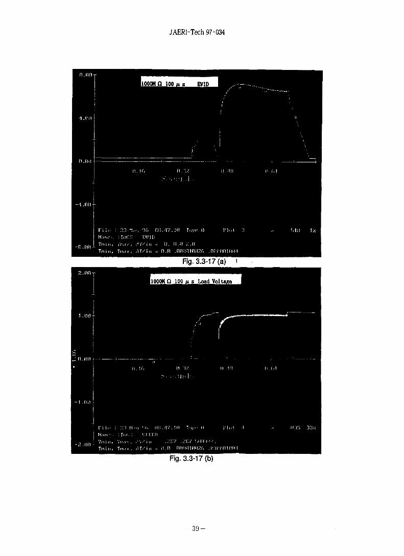
Fig. 3.3-17 (a) i
-39-

JAERI-Tech 97-034
'-I 'I 'Dili I
Till' : ?A M-.'r'Jh ZU.'III.ZI, T')|„' M PintM.mr.i iTner. liUll)Yn i n > Yri.ix , dV/in : 11. II. I) Z.UTnin, Tn.ix, .IT/in = H.fi .flFlflfHflflZr, .OflfimimiH
Fig. 3.3-18 (a)
Fig. 3.3-18 (b)
-40-

. i:r>
JAERI-Tech 97-034
Fig. 3.3-19 (a)
2.on
l.floi
„ 0.00
-1 .00 T
-2.00 ^
0 . If.
1000H £1 lOOas Load Voltage
0,3?. 'i.O.'OIii 1:
r0.10 0 .M
riot. iiFile : 21-Ha.j-30 21.00.30 Tupe 0Nance: : TOCO UFFKOVnin, Yn.xx, dY/in = - .207 .2117 L.OOI1UO.Tnin, Tn,.x, dl/in - fi.fi .000010020 .000001001
a----- 10009 37x
Fig. 3.3-19 (b)
— 41 —

JAERI-Tech 97-034
g 30
Hi 25 ^ 20 tS 15
£ 10£ 5 > Q
/ < >
• •.
• ■.
■ •r
JO •. /
y*. I 1 l A 1 ■ mill _.L .LHIIllI I ««!«»««■ ■ -■ " -I
° 10-5 0.0001 0.001 0.01 0.1 1Time (sec)
TIME DELAY OF GATE BLOCK
Fig. 3.3-20 Overvoltage as a function of the time delay of gate block.
-42-

JAERI-Tech 97-034
3.4 Power supplies for negative ion production and extraction
Specifications and dimensions of the power supplies are listed in Table 3.4-1. These data are based on the original configuration of the HVD which contains all components of the negative ion production and extraction power supplies.
Table 3.4-1 Dimensions of the power supply components in the HVD
a) Filament P/ S
b) Arc P/Sc) PG Filter P/Sd) Bias P/Se) Extraction P/Sf) Transformer Ig) Transformer IIh) Switch gears
AC15V, 8.3kA/phase, 104s120V, 7 kA, 104 s
5V, 10 kA, 104 s 10 V, 2.3 kA, 104 s
10 kV, 140 A, 104 s
3.8 MVA3.2 MVA VCB x 2
2 m w X 1.5 m d X 2.2 m h, 6 ton
4 m w X 1.5 m d x 2.2 m h, 9 ton3 m W X 1.5 m d X 2.2 m h, 4 ton1..5 m w x 1 m d X 2.2 m h, 1 ton4 m W X 2.5 m d X 2.2 m h, 15 ton
3 m W X 1.5 m d X 2.2 m h, 15 ton
3 m W X 1.5 m d X 2.2 m h, 15 ton2. 5 m w x 1.5 m d x 2.2 m h , 3 ton
Outline drawings of the filament power supply, the arc power supply, the bias
power supply, the PG filter power supply and the extraction power supply are illustrated in Fig. 3.4-1 to Fig. 3.4-5.
The NBI power supply requires cooling water for long pulse operation. Heat loads of the power supplies and quantity of cooling water for the power supplies are listed in Table 3.4-2.
Table 3.4-2 Heat load and required cooling water for power supplies
Filament power supply Arc power supply
Bias power supply PG filter power supply Extraction power supply
30 kW and 80 1/min /set : 80 kW and 100 1/min /set
: 7kW and 12 1/min /set
: 20kW and 60 1/min /set : lOOkW and 160 1/min /set
Dimensions of the power supplies in the modified HVD are shown in Table 3.4- 3. These dimensions are estimated to fabricate as rectangular boxes for each
-43-

JAERI-Tech 97-034
power supply. Total volume of the power supplies is estimated to be 38 m^. This satisfies the space of 45 m^ in the modified HVD.
Table 3.4-3 Dimensions of the power supply components in the modified HVD
a) Filament P/ S
b) Arc P/Sc) PG Filter P/Sd) Bias P/Se) Extraction P/S
AC15V, 8.3kA/phase, 104s120V, 7 kA, 104 s
5V, 10 kA, 104 s 10 V, 2.3 kA, 104 s 10 kV, 140 A, 104 s
1.5 mw x 2.4 md x 2.3 mh
2.25m w x 2.4 m d x 2.3 m h 0.75 mwxl.6mdx2mh 0.75 mwxl.6mdx2mh
2.25 m w x 2.4 m d x 2.3 m h
-44-

JAERI-Tech 97-034
6400ooCM
. 1500
2200
Fig. 3.4-1 Outline drawings of the filament power supply.
9S00
4
Fig. 3.4-2 Outline drawings of the arc power supply.
2800
,
,300
L 1600

JAERI-Tech 97-034
ooo
2200 . 200
ooo
Fig. 3.4-3 Outline drawings of the bias power supply.
c 2300ooK) . 1000
2200
Fig. 3.4-4 Outline drawings of the pG filter power supply.
— 46

JAERI-Tech 97-034
, 8100
Fig. 3.4-5 Outline drawings of the extraction power supply.
2700
I 1.30
0

JAERI-Tech 97-034
3.5 Power fluctuation compensator
At the breakdown in the accelerator, the power supply system cut off the out put rapidly. This causes the power fluctuations on the electric power line. A power fluctuation system is considered as optional equipment and is required only if occasional power steps of > 50 MW are not allowed by the utility. The compensation system absorbs the power to restrict power fluctuations under an
allowable level shown in DDD4.2C. Maximum power demand when NBI is
operating alone is listed in Table 3.5-1.
Table 3.5-1 Maximum power demand when NBI is operating alonePeak Active Power 150 MWPeak Reactive Power llOMvarPeak Power Derivative 50 MW/sActive Power Step 50 MW
To satisfy these specifications, the compensation system was designed. Power step change of one module should be lower than 16 MW (50 MW / 3). Therefore, the required capacity of the compensation system is 50 MW - 16 MW = 34 MW for one module. Electric power is absorbed by resistor with GTO switch
connected in series to the resistor. The circuit of the system is shown in Fig. 3.5- 1. When simultaneous breakdown or emergencies occur in the system, the GTO switch is turned on at the same time of the inverter cut off. Ratings of compensation system is shown in Table 3.5-2. We assumed that the frequency of the emergency is one time per 10 sec.
Table 3.5-2 Ratings of the bypass circuit
Resister: 2830V, 12 kA, 0.2360 34 MW x 100 ms = 3.4 MJ
3.4 MJ/10 s =340 kW R = 35 0(2.3 kW) IS - 148 P
GTO switch : GTO 6 kV- 6kA, IS - 4P Size : about 6mW x 3mD x 4mH
— 48 —

JAERI-Tech 97-034
GTO Inverter Rectifier
Converter
5Z.
t —
R
Trans.
< 16 MW step per module (50MW/3)
Resistor 2830 V, 12 kA, 0.236 ohm 34 MW x 100 ms = 3.4 MJ 3.4 MJ/10s = 340 kW
R= 35 ohm (2.3 kW) 1S-148P
GTO 6 kV , 6 kA 1S-4P
Size : 6 mW x 3 mD x 4 mH
Fig. 3.5-1 power flluctuation compensator.
-49-

JAERI-Tech 97-034
3.6 AC harmonics, filter specifications, active and reactive power
AC harmonics were calculated using EMTP code. Table 3.6-1 shows the harmonics at a rated out put of the power supply for one module. In the designing of harmonic filters for 12-phase rectifier (Converter), harmonics of
5th, 7th, 11th, 13th, 17th, 19th, 23th and 25th are generally considered. From the result of the simulation, total harmonics is estimated to be about 3.8 %. Receiving apparent power is 85 MVA. A capacity of the filter system for the
harmonics is estimated as follows.PF = 85 MVA x 3.8 %
= 3.2 MVA / one module
Power supply output (Pout) is calculated to be 143 MW (= ( 45 MW(Acc) + 2.7
MW (Source)) x 3 modules). Receiving active power for three modules is estimated to be 150 MW ( = 143/0.95 ) which include a loss of 7 MW. Therefore the reactive power (EIr=EIsin6) for three modules is estimated as follows.
Elr = ( El2 - EIcos62)1/2
= ( 2552 - 1502 )1/2
= 206 MVar.A phase compensator will be utilized if the reactive power is not accepted in the AC power system.
-50-

JAERI-Tech 97-034
Table 3.6-1 Harmonics computation
Harmonic No. (%)1 1002 0.409130263 0.121190034 0.071073855 0.037395786 0.061260197 0.012683958 0.026151539 0.00707094
10 0.00325311 2.2454781512 0.0142967813 2.7880996914 0.0071893915 0.0062071216 0.0074080817 0.0057770318 0.0051391919 0.0038088320 0.0046653621 0.0046653622 0.0073661723 0.9718893824 0.0127112925 0.64061461
-51-

JAERI-Tech 97-034
4. Design of the high voltage deck (HVD) and the transmission line
4.1 Original configuration of the high voltage deck
An original design of the high voltage deck, the water choke and the transmission line is shown in Fig. 4.1-1. The water choke is mounted near from the HVD tank. Dimensions of the cylindrical HVD tank are 9.4 m in length and8.3 m in diameter. Power supplies for the ion source are installed in the tank and insulated from the ground by using pressurized SF& gas of 3.5 bar. The
transmission lines are connected to the tank. Cables and intermediate potential conductors are fed through the transmission line to the ion source. Two bushings are installed in the line to reduce the gas pressure by two steps from 20 bar at the ion source to 3.5 bar at the HVD.
4.2 Modified configuration of the high voltage deck with the water choke and D2 gas feeding system
The space for the HVD is limited. A modified configuration of the HVD was designed. The layout of the system is shown in Fig. 4.2-1. The dimensions of the HVD tank are 5 m in diameter and 7.5 m in height. The tank is mounted on the wall of the building. The transmission lines are connected bottom part of the
tank. Detail configuration of the HVD tank is shown in Fig. 4.2-2.
In the original configuration, all components of the source power supplies
except for the insulated transformer are installed in the HVD. However, in the
modified configuration, only transformers and rectifiers for each power supply are mounted in the HVD. Insulated multi transformer system is utilized instead
of the single transformer. Control system such as thyristor switches and DC
switches for the power supplies are moved to the primary side of the insulated transformer in the NBI power supply yard. Since a high speed switching is required for the extraction and the arc power supplies to protect the ion source from the arcing and breakdowns, high frequency inverters are utilized for these power supplies. High speed switching of < 100 (is can be performed for the arc
and extraction power supplies by the high frequency inverter system. Switching
and voltage regulation for other power supplies are also controlled at the primary side of the insulated transformer by thyristor switches.
The water choke is installed in the HVD tank in the modified configuration. The resistivity of the cooling water is assumed to be in a range of 5 MO-cm to
-52-

JAERI-Tech 97-034
10 Mil—cm. The water choke serves as bleeder resistor for the acceleration power supply to eliminate an exclusive bleeder resistor in the power supply system. The minimum bleeder current to stabilize the high voltage out put was investigated using the EMTP. The result shows that the minimum bleeder
current can be reduced to 0.1 A with the resistor of 10 Mil. The waveform of the
simulation is shown in Fig. 4.2-3.
The water choke consists of insulator pipes made by FRP. Size of the pipes are designed to satisfy the required resistance and water flow rate. Table 4.2-1 shows the required water flow rate for the ion source and power supplies in the HVD. Table 4.2-2 shows the dimensions of the insulator pipes, dissipated power in the
water choke, leak current and temperature rise in the water choke, etc.. The dimensions of the 1 MV insulator pipes are 15 cm in diameter and 3m in length. The bleeder current is 0.24 A with 5 Mil-cm water and two pipes. In case of 10 Mfl-cm, the bleeder current becomes 0.12 A that is enough for the power supply. Leak current through the insulator pipes for the intermediate potentials are
negligible small.
A D2 gas flow controller is mounted in the HVD. The D2 gas is fed from the
ground potential to the HVD through an insulation tube with a high pressure of < 1 MPa.
4.3 Design of DC insulation in the transmission line
4.3.1 Design concept for SF& gas insulation
SF& gas insulation technologies have been investigated for gas insulated
substations (CIS) in electric power distribution networks for many years. The breakdown initiation in SF6 gas is dependent on the electric field strength. The
theoretical breakdown electric field, EBDt, is proportional to the gas pressure as
follows [1],
Ebdi = 87.8 P [kV/mm] (4.3-1)(P : gas pressure [MPa])
The DC breakdown voltage of a gap between 80/200 mm diameter coaxial cylinders was shown in Fig.4.3-1[2]. The voltage polarity effect is prominent at a pressure above 1 kg/cm2. The positive-polarity breakdown voltage is slightly
-53-

JAERI-Tech 97-034
lower than the theoretical value. However, the negative-polarity breakdown voltage is much lower than the theoretical value, especially at a higher pressure
region. The negative DC breakdown voltage at 4.0 kg/cm2 is approximately 80 percent of the AC peak breakdown voltage and lower than half of the theoretical value.
SF6 gas of 4.5 kg/cm^ pressure is used in the transmission line of the JT-60U Nl-
NEI. We adopted the same gas pressure for the transmission line of the ITER
NBI. A design value of the withstand electric field was derived based on the data in Fig.4.3-1. The gas pressure for the DC breakdown voltage shown in Fig.4.3-1 is ranged up to 4 kg/cm2. The DC negative breakdown voltage at 4.5 kg/cm2 can be extrapolated to be approximately 600 kV. The breakdown field at the surface of the inner cylinder is calculated to be 16 kV/mm.
The breakdown field is influenced by the electrode area as shown in Fig. 4.3-2. The breakdown field is reduced at a larger electrode area, because probability of breakdown initiation is increased[3], [4]. The area of the inner electrode surface, which is immersed in the high electric field, is 628cm2 in the experiment
reported in Fig. 4.3-2, while the area of the HV conductor surface immersed in the high electric field is estimated to be about 105 cm2 in the NBI transmission line of more than 10 m length. This leads to reduce the breakdown field
approximately by a factor of 0.7, which is estimated by the reduction characteristics in Fig. 4.3-2. The breakdown field is reduced to 11 kV/mm by the area effect. There is another reduction effect that depends upon metal surface
finish. The reduction factor is considered to be 0.8 by the DC breakdown experiment, in which dependence of the breakdown electric field on the
electrode surface finish was investigated^]. Finally the DC breakdown field is
estimated to be 8.8 kV/mm.
Insulation reliability can be improved by consideration of breakdown probability
distribution. The ratio of the breakdown field that corresponds to 0.1% breakdown probability to that of 50% probability is estimated to be
approximately 0.6 based of the experimental result[3]. We chose the maximum
electric field of 5 kV/mm for the design. The breakdown probability is considered to be lower than 0.1%.
Breakdown voltage is reduced by the levitation of metal particles from the
bottom of the outer conductor of the transmission line. Reduction of breakdown voltage is not dependent on the gas pressure. Withstand voltage can
not be increased by raising the gas pressure in case of the levitation of metal
— 54 —

JAERI-Tech 97-034
electric field at the bottom of the outer conductor is 2.3 kV/mm, which is
higher than the metal particle levitation electric field of 1.8 kV/mm.
As the second step, we tried to reduce the electric field at the bottom by rearrangement of the 1 MV conductor to upper position. However, the gap length between the 1 MV conductor and AG1 conductor becomes shorter. To
keep the electric field lower than 5 kV/mm, the diameter of AG1 and AG2
conductors were reduced to 100 mm. An result of the simulation is shown in Fig. 4.3-6. Each conductor position was not changed to examine the effect of the diameter on the maximum electric field El on AG1. The electric field El is about5.3 kV/mm which is increased slightly. An electric field E2 at the opposite
surface of AG1 is 1.7 kV/mm.
We investigated the effects of the position of 1 MV conductor on the electric field strength E3 at the bottom of the outer conductor. The 1 MV conductor was moved from y = -100 mm to -20 mm. The electric field variations as a function of the position of the 1 MV conductor is shown in Fig. 4.3-7. As the 1 MV conductor is moved from -100 mm to -20 mm, the maximum electric field El on
AGl decreases from 5.3 kV/mm to 5.0 kV/mm. The electric field E2 at the
opposite side of AGl increases from 1.7 kV/mm to 5 kV/mm. On the other hand, the duct-bottom electric field Eg decreases from 2.3 kV/mm to 1.7
kV/mm, which is approximately equal to the metal particle levitation electric field. The result of the simulation with the position of y = -20 mm is shown in Fig. 4.3-8.
As the final step, the electric field at the bottom of the outer conductor was
reduced by decreasing the diameter of the 1 MV conductor. An electric field simulation result with the 1 MV conductor diameter of 600 mm is shown in Fig. 4.3-9. The electric field Eg at the bottom is greatly reduced to 1.0 kV/mm. It
is approximately equal to the electric field at the bottom of the JT-60U N-NBI transmission line and lower than the metal particle levitation field with
coating.
b) Investigation of the revised design
The arrangement of the conductors in the transmission line was revised as
shown in Fig. 4.3-10 for connection of the conductors to the ion source and
remote maintenance. An electric field simulation result for the revised structure is shown in Fig. 4.3-11. The highest electric field is 5.9 kV/mm on the
-55-

JAERI-Tech 97-034
particles[5]. The electric field on the bottom is required to be lower than the particle levitation electric field to keep the insulation reliability. The levitation electric field strength can be increased by coating of the inner surface of the
transmission line as shown in Fig. 4.3-3[6]. Particles were levitated at the field of 0.5 kV/mm without coating, however, the levitation voltage was increased to 1.8 kV/mm with coating for negative DC voltage. In order to prevent the particle levitation, the surface coating should be adopted inner surface of the transmission line of the ITER NBI.
4.3.2 Insulation design of the transmission line and electric field simulations
a) Investigation of the initial design
We designed the transmission line between the HV deck and the ion source
tank in terms of high voltage insulation. The 1 MV HV conductor diameter
must be large enough to contain cables and water cooling tubes for the plasma generator and the extractor. An outer diameter of the transmission line must be
as small as possible to prevent radiation from the reactor. On the other hand, gap length between the outer and inner conductors should be designed to sustain applied high voltage.
The size of insulator spacers for inner conductors were designed. According to the data reported in ref.(7), it shows that the breakdown electric field is independent of the spacer size. A height of the spacer for the 1 MV conductor
was designed to be 350 mm that is twice longer than the spacer for the JT-60U N- NBI 500 kV transmission line.
Arrangement of the conductors in the transmission line proposed by JCT is shown in Fig. 4.3-4. The inner diameter of the outer conductor that is grounded potential is 1700 mm. The outer diameter of the 1 MV conductor (HV) is 800 mm. The outer diameter of the 800 kV (AG1), 600 kV (AG2), 400 kV (AG3), 200 kV (AG4) conductors is 180 mm, 140 mm, 80 mm and 60 mm respectively. Each conductor is located so as to reduce distortion of equipotential lines. These
conductors serve as water feeding pipe for the ion source. A center of the 1 MV conductor is placed at y = -100 mm from the center of the outer conductor.
Computer simulation of the electric field for this configuration was performed. The result is shown in Fig. 4.3-5. The highest electric field of 5 kV/mm appeared at the surface of AG1. It is just equal to the design criterion. However, the
— 56 —

JAERI-Tech 97-034
surface of AG1. It is about 20 % higher than the design criterion of 5 kV/mm. The duct bottom electric field is 1.9 kV/mm, which is also higher than the
particle levitation electric field.
To reduce the electric field at the bottom, the 1 MV conductor was moved to higher position (y = + 80 mm) in the simulation (see Fig. 4.3-12). The electric field was reduced to 1.3 kV/mm, which is lower than the particle levitation electric field. The electric field of 5.6 kV/mm on AG2 is higher than the design
criterion. The vertical position of the 1 MV conductor is considered to be a little
high.
The position of AGl conductor and 1 MV conductor were lowered to 60 mm to reduce the electric field. The result is shown in Fig. 4.3-13. The electric field on AG2 was reduced lower than 5 kV/mm. The electric field on AGl was also reduced about 10 % from the former configuration shown in Fig. 4.3-12. However, it is approximately 10 % higher than the designed value. The duct
bottom field of 1.4 kV/mm is a little higher than the field in Fig. 4.3-12.
Above simulations are 2-Dimensional simulations for the straight part of the
transmission line. Transmission line must be bent with a bending radius of 4 m as shown in Fig. 4.3-14. We investigated the electric field concentration at the
bending position using the 2-Dimensional simulation code. A model of the
transmission line is similar to a doughnut that has a radius of 4 m. A result is shown in Fig. 4.3-15. Electric fields except for the duct bottom field are almost the same as the fields at the straight position shown in Fig. 4.3-13. The bottom electric field is enhanced by approximately 10 % because of the bend (1.5 kV/mm).
— 57 —

JAERI-Tech 97-034
c) Design of a bushing for high pressure separation
SF6 gas will not be used in the ion source tank to prevent radioactive problems
by neutron irradiation. Therefore, other gas such as CO2 will be used with
higher pressure of 20 kg/cm2. In this case strong bushing, which can sustain
pressure differences from 20 kg/cm2 to 3.5 kg/cm2, is utilized. Concept of the
bushings are shown in Fig. 4.3-14. There are two steps to reduce the pressure.
An outline of the bushing is shown in Fig. 4.3-16. Material of the bushing is epoxy resin. Outer diameter of the bushing is 1950 mm and total thickness is 440 mm. Thickness of the epoxy is 150 mm. The diameter of the 1MV conductor is decreased to 600 mm to obtain enough distance of the insulator surface. Arrangement of the conductors is changed for reduction of surface electric field between conductors. This configuration was designed based on the existing post spacers. However, there is no experience for such a DC 1 MV bushing with multi conductors. A 3D electric field simulation and experimental R&Ds are
necessary to fabricate such bushing.
An electric field simulation for the conductor arrangement using the 2D code is shown in Fig. 4.3-17. The highest electric field (4.5 kV/mm) on AG1 is 20 % lower than the electric field described in Fig.4.3-12. It is 10 % lower than the designed value for gas insulation. However, for the surface insulation, further
investigation is necessary as mentioned above. The bottom electric field of 1.9 kV/mm can be reduced to 1.2 kV/mm as shown in Fig. 4.3-18 by moving the 1
MV conductor to higher position of y= 0 mm.
Following two subjects should be investigated to design the bushing.
(1) Metal particle effectsThere is a high possibility of particle attachment on the surface of the bushing which is specially installed in the vertical part of the transmission line. Metal particles reduce the withstand voltage. There are some methods to prevent such problem.(a) The surface structure of the bushing can be optimized to minimize the effect of particles. The insulation voltage with particle effect should be examined by an
electric field simulation.(b) By changing the arrangement of the transmission lines, the bushings can be
installed not in the vertical part but in the horizontal part of transmission lines.
-58-

JAERI-Tech 97-034
(2) The diameter of the 1 MV conductor for connections and fitting of inner cables and water pipesThe diameter of the 1 MV conductor is required to be 800 mm for remote
connections of all cables and water pipes. Therefore, it is necessary to reduce
conductor diameter from 800 mm to 600 mm near the bushing. This makes the transmission line structure a little complex. Fitting mechanisms of cables and pipes in the reduced conductor are also required.
References[1] T. Kawamura, et al. : "DC insulation for gas insulated switch gear", IEE Japan Technical Report, (Part II) No. 397 (1991).[2] S. Menju, et al. : "DC dielectric strength of a SF6 gas insulated system", IEEE Trans. Power Appar. & Syst., PAS-97, No.l (1978).[3] F. Endo, et al.: "Initial breakdown voltage of SF6 gas and effect of area", IEE Japan, 54-A35 (1977).
[4] F. Endo, et al.: "Dielelectric characteristics of SF6 gas for application to HVDC systems", IEEE Trans. Power Appar. & Syst., PAS-99, No.3 (1980).[5] C. M. Cooke, et al. : "Influence of particles on AC and DC electrical performance of gas insulated systems at extra high voltage", IEEE Trans. Power Appar. & Syst., PAS-96, No3 (1977).[6] F. Endo, et al.: "Control of particle motion and reliability improvement in
high-voltage DC CIS", Proc. The 11th international conference on gas discharge and their applications, 1-346 (1995).[7] F. Endo, et al.: "Particle-initiated Breakdown Characteristics and reliability improvement in SF6 gas insulation", IEEE Trans. Power Delivery, PWRD-1, No.l, 58 (1986).
— 59 —

CT>O
CO. 20u/i#t
Fig. 4.1-1 Original configuration of the HVD and water choke.
JAE
RI-T
ech 97-034

JAERI-Tech 97-034
Table 4.2-1 Required water flow rate for the ion source and power supplies in the
HVD.
Ion source (Assumption: dT=40 degC) Power supplies on HVD Total flow rate (1/min)
Part of ionsource
Heat load (kW)
Flow rate (1/min)
Heat load (kW)
Flow rate (1/min)
Arc 895 321 80 100
Fila. 47.5 17 30 80
1 MV
PGfil. 166.3 59 20 60 959
Ext 419 150 100 160
Bias 7 12
800kV AG1 1315 500 500
600kV AG2 4 500 500
400kV AG3 4 500 500
200kV AG4 4 500 500
E GRG 1 500 500
— 61 —

JAERI-Tech 97-034
Table 4.2-2 Specifications of the water choke.
(r = 5 MOhm.cm)
\Voltag\
Insulator Pipe D(cm) L(cm)
V dP R(m/s) (kg/cm2) (MOhm)
Current(A)
P(kW)
T(degC)
1MV 15 300 0.90.004(5mx2)
8.5/2 0.24 120x2 1.8x2
800 kV 6 240 2.9 0.115(5mx2)
42.4/2 0.038 15.2x2 0.4x2
600 kV 6 180 2.9 0.115(5mx2)
31.8/2 0.038 11.4x2 0.3x2
400 kV 6 120 2.9 0.115(5mx2)
21.2/2 0.038 7.6x2 0.2x2
200 kV 6 60 2.9 0.115(5mx2)
10.6/2 0.038 3.8x2 0.1x2
0
D : Diameter of pipe L : Length of pipe V : Water flow velocity dP: Pressure drop R : Resistance of water choke Current: Leak current P : Power loss in the water choke T : Temeperature rize at water choke
-62-

r Water Choke
TransmissionLine
Beamline
////////// / / /
A — A
Fig. 4.2-1 Modified HVD configuration.
JAER
I-Tech 97-034

100 300
<nA-
1000KV40CkV
Insulator 'toe
SUS Pipe
*5000 *
Fig. 4.2-2 HVD configuration with the water choke and D2 gas controller
JAER
I-Tech 97-034

JAERI-Tech 97-034
Fig. 4.2-3 Results on the simulation with bleeder current of 0.1 A.
-65-

JAERI-Tech 97-034
%W>3"o>
11m
1000
900
800
700
600
500
400
300
200
100
0
1 1 1 / /Theoretical breakdown voltage V /
\ .OM9
X// erT
peak voltage)X A.
DC (post% 1 J-------
tive polarity) px'X
n~2&
•
/
| f DC (negative polarity)
X voltage raised 20kV/min t 1 minute step upO • 30minute step up ® 1 lOminute step upA I 1 minute step up
. O 1 average breakdown voltage
SFg gas pressure (kg/cm2)
Fig. 4.3-1 Breakdown voltage of 80 - 200 mm diameters coaxial cylinder gap
(Ref .2).
max.meanmin.
■ : Bortnik A : Oppermann V : Meryu □ : CookeX : Ermel A I Endo---------- I Estimation by authors
Electrode area (cm2)
Fig. 4.3-2 Effects of electrode area on breakdown voltage (Ref. 3).
— 66 —

JAERI-Tech 97-034
E>s
2o
co«>o
insulating coat
Fig. 4.3-3 Enhancement of particle levitation field strength by electrode coating for 10 mm long aluminum particles of 0.2 mm in diameter. Insulating coat : e = 4.0 , thickness = 20 -40 (im (Ref. 6).
Fig. 4.3-4 Cross sectional view of the transmission line.
-67-

JAERI-Tech 97-034
S.lkV^.
(a; Overall Vi*w
^ w-to kv^(VoHage between
contour lines )
AV-2okv
Cbj) C lose up view of /4G1
miMilimimiliiimm
| ii 1111 i«Vj 11 iumT| t i 11 jMnrt in 111 m i i i ■ 111 * 111111
E^=iZ.3k’^/n'01 2. / kV/fmiLC) C lose up v/ew of duct bottom
Fig. 4.3-5 Electric field simulation in the transmission line . (AG1:180 mm in diameter, AG2:140 mm in diameter, HV position y —100 mm)
-68-

JAERI-Tech 97-034
(G.) over a II Vi€w
AVCvbl+aJe between con+owr I Ifies)
= £okv
aV= /OkVIwwHwLtimwiiwwwJwHMwtLtwmAwmw^iwmKluMWMiJtnrwurl*
(k) C W Up V|€Vv of/1^1
Fig. 4.3-6 Electric field simulation . (AG1, AG2 : 100 mm in diameter, HV position = -100 mm)
-69-

Duc
t-bot
tom
elec
tric
fiel
d E (k
V/m
m)
JAERI-Tech 97-034
Duct-bottom elecctric field E.
Electric field E, on AG1
Particle levitation electric field
Duct-bottom electric field of JT-60U
Electric field E„ on AG1
■ i lQ l_ _ _ _ i_ _ _ _ i_ _ _ _ i_ _ _ _ I—i—i_ _ _ _ _ _ t_ _ I_ _ _ _ i__ i_____ i_ _ _ _ I_ _ _ _ i___ i_ _ _ _ _ i_ _ _ _ I_ _ _ _ i_ _ _ i_ _ _ _ _ i_ _ _ _ I_ _ _ _ i i i II
-120 -100 -80 -60 -40 -20 0
Maximum field on HV electrode of JT-60U
HV conductor center vertical position y (mm)
Fig. 4.3-7 Relation between electric field and 1 MV HV conductor position.
-70-

1.......111111111111111»11111 • I <
JAERI-Tech 97-034
/\T = irokv
over a
AT =20 /cT
(b) Close Up view of A£rlAT = 10 kV
I I I l« M I M I I II Ml M I lu II I I I M I III I I II M I III 1 I II I I I I l l II I HI I Ml II M I l l I I II l I It I l H I I l I M l I I l I I l III I
(O Cl ore up view at duci bo+4om
Fig. 4.3-8 Electric field simulation . (AG1, AG2 : 100 mm in diameter, HV position : y= -20 mm.)
-71

I im 11
1 ill
• m il
l u I
ii 11
in n
li n
111
lulu
111 u
ntil
in il
111
JAERI-Tech 97-034
ay - sokv
aY= 2 alcsrlllllHlullltMIHlillllMlllltl Hill lllii NIINllllllKlllllmillinilHIIIIIlilHUHIlIl
|IIIIWII||l|||IH«|IIMIIIII|imillll| ...........|lfllMIHjllHllMI|mmill|MII«IIM|HHMMI
(a? overall vievv (b^) close up view off\Q-]_
AT= lok^r
Fig. 4.3-9 Electric field simulation. (HV: 600 mm in diameter, AG1, AG2 : 100 mm in diameter, HV position : y = +80 mm.)
-72-

TI LAMENT HV FEEDSARC WATER LINE
PLASUA CRIPWATER LINE PLASUA GRID EXTRACTORELECTRON SUPPRESSION GRID
BOUNDARY ENCLOSES ALL WATER LINES
WATER LINE PLASUA GRID EXTRACTOR ELECTRON SUPPRESSION GRID
PLASUA GRID
ARC WATER LINE
NBI HV LINESECTION AT CONNECTOR LEVEL
Fig. 4.3-10 Revised arrangement of the conductors in the transmission line.
JAE
RI-T
ech 97-034

JAERI-Tech 97-034
ImmiMlmiiiHiliimmiliiiimiiliHmiHlimmiil.........ilmi..It....
Overall view (AV=5"okv) cb) close up view of f\Q\ ( aV- 20Kt)
11111111 I I 111» M111 ill II111III ll III III M ll 11f III III IIImII111 Ml 11 I I 11MItl111111 III11II11« M11f m
i^kv/r*CC) C lose up view of dud botW.
(aV- 10 kv)
Fig. 4.3-11 Electric field simulation for revised configuration. (HV: 800 mm in diameter, AG1, AG2, AG3, AG4 : 100 mm in diameter, HV position : y = -50 mm, AG1 vertical position y = +160mm.)
— 74 —

JAERI-Tech 97-034
liu....iliiiimMliimmilimiiiiilniiiiiiiliiiMiMiiimiiiiilimiiiiiliiiiiiiiiliimnM
|l IIIMI I1|IIIM 111 t|ll III1I1 l|1llltl |||||| III HI I |HIIIIII I |ll III III l|t I till III pi M 111 11 j III! 11111
(W c/dse^f l/kw O'f' /krl
C AV
|iimiii<|iiiMiMi|Mimiii|MmMii(Miitiiii|iMiimi|imiMii|mimii|iiiiiiiii|imiiiii
) C up i/i’eW of 2.
Cav = SokVp
I IMI I I I I I I I I I I II I I I t I I IH HI IllI I 1 I It H11 I I I I I I I 11 I 11 I III III It I II•I I 11 I I I I I II I 11
IIIIMIIII|IIMI<m|lllllim|l<MIMII|MHMIII|IIIIIIIM|lllllim|lllllllll|IIIMIIM
T1.3
(.dj) clo5e Up w'<2W Juc-f (4|/=/okv)
Fig. 4.3-12 Electric field simulation for revised configuration. (HV: 800 mm indiameter, AG1, AG2, AGS, AG4 : 100 mm in diameter, HV position : y = -80 mm,AG1 vertical position y = +160mm.)
-75-

limM
iiilii
mM
iiliii
iHm
limum
lHim
Mili
Miu
mlim
iimlii
M....
..I
JAERI-Tech 97-034
(a) Overall view ( AV = 50 kV)
■iiiiiiil..l.l..lilimiiiiiliiiiiiiil|,.imn,..... . .
(b) Qosc up view of AG2 (AV = 20 kV)
(c) Close up view of AG1 (AV = 20 kV)
minmlmmiiiliiiilimliiitimilMiMUiiltiiimiilitiiiiiiilimiiiiiliiiiifmlimiHiil
LW*m
(d) Close up view of the duct bottom (AV = 10 kV)
Fig. 4.3-13 Electric field simulation for revised configuration. (HV: 800 mm indiameter, AG1, AG2, AG3, AG4 :100 mm in diameter, HV position : y = -60 mm,AG1 vertical position y = 0mm.)
-76-

7000130003000
T««t
Transmission Line
£5?— We t • r
I e i ■ i > 1 « d Piet
We t » r Ckeee
Lie*
1 1600
CO. 20ii/lrt
Fig. 4.3-14 Outline of the transmission line and HVD(Original configuration).
JAER
I-Tech 97-034

JAERI-Tech 97-034
II I II II I ll I III II lllli I I II I III I III I I III ill HIM I III II I llllllll I I lllllllll llllllllllllMII I lllllll I III
Co a xi'al ay is
(a) Overall view ( AV = 50 kV)
ll'MI..I«l| iliimiii»|iiiiiilt,l),n<MM|M<|M<t,j
IIIHIHI|llltNIII|lllllllll|lllllllll|l|l|t||M|tlllMIM|lll«MII |MIIIIHI|fllllflll|l fttlllll^
(b) Close up view of AG2 (AY = 20 kV)
...HilmmiiiliimiiiilmimiilMiiiimlnmiiiiliiiiniiiliiiimiilmiHinl...ml
i|niiiiiii|MiiHiii|iiinini|«mmii|i i|iiiiiiiiijiiiiiiiii|iiiiniii|
(c) Close up view of AG1 (AV = 20 kV)
...... Mlljl
(d) Close up view of the duct bottom (AV = 10 kV)
Fig. 4.3-15 Electric field simulation for bending section. Radius of curvature is 4m. (HV: 800 mm in diameter, AG1, AG2, AG3, AG4 : 100 mm in diameter, HVposition : y = -60 mm, AGl vertical position y = +160mm.)
-78-

Fig. 4.3-16 Configuration of 1 MV bushing with multi-conductor. This bushing is also utilized for pressure separatin. I
JAER
I-Tech 97-034

JAERI-Tech 97-034
li imml Imiinii
cCi) overall view (&v-iro
I....miliinmMlmiiiiiilumimlmimNlmiiimlmmiiiliiMiimli....mliimmi
&>) close up view o /
(sV- %0\<’v')
(C) clc>S€ up vkw of ducj bo-Hd>in
Fig. 4.3-17 Electric field simulation of the transmission line. (HV: 600 mm in diameter, AG1, AG2, AG3, AG4 : 100 mm in diameter, HV position : y = -150 mm, AG1 vertical position y = 0mm.)
— 80 —

JAERI-Tech 97-034
luinmifntnimfMMmnlimiimln»niiilinmmlinMm<(i..„iL
(CL) overall view kvj cb) close up i/ievv of A&] C*v= aokv)
Fig. 4.3-18 Electric field simulation of the transmission line. (HV: 600 mm in diameter, AG1, AG2, AGS, AG4 : 100 mm in diameter, HV position : y = 0 mm, AG1 vertical position y = Omm.)
-81-

JAERI-Tech 97-034
4.4 Surge protection system
Core snubbers and LR elements are utilized for protection of the ion source and power supply system from electric breakdowns in the accelerator.
Stray capacitance and stored energy of the ion source accelerator, end part of the transmission line and transmission line from the HVD were calculated. Stored energy at the accelerator gap is higher than 10 J for each stage. Energy of 142 J and 80 J are stored at corona shield of the ion source and at the end part of the
transmission line respectively. These energy are considered to be distributed to the five stage gaps at the breakdown. Therefore, inherent total stored energy for
each stage is about 60 J. From both of the voltage holding experiments reported
by F.Bottigilioni et al.,[l] and JAERI HT[2], such energy is considered to be an allowable level. Stored energy at the transmission line from the HVD is 297 J. Required core snubber for the transmission line was estimated to be 0.4 V.s. The size will be about 10 or in thickness and 2.3 m long with using FINEMET cores. Fig. 4.4-1 shows the core snubber configuration attached in the transmission line. Detail calculations are described as follows;
4.4.1 Estimation of stray capacitance and stored energy
A model of the ion source and the transmission line is shown in Fig. 4.4-2.
1) Ion source accelerator
Stray capacitance in the accelerator was calculated from the drawing. Gap lengths are 9, 8, 7, 6, 5 cm for five stage accelerator grids. Capacitance of accelerator gap and grid support are calculated as parallel plates. Relative permittivity of the ceramic insulator was assumed to be 8.
a) 0-200 kV stage
Cgap = 248 pFCsupport = 145 + 72 + 153pF Cinsulator = 96 pF
C200-E = 714 pF
b) 200-400 kV stage
C gap = 306 pF
Csupport = 84 + 53 + 131 pF Cinsulator = 96 pF
C400-200 = 670 pF
-82

JAERI-Tech 97-034
c) 400-600 kV stageCgap = 345 pF Cinsulator = 96 pF Csupport = 132 pF
C600-400 = 573 pF
d) 600-800 kV stageCgap = 478 pF Csupport = 82 pF Cinsulator = 96 pF
C800-600 = 656 pF
e) 800-1000 kV stageCgap = 341 pF Csupport = 109 pF Cinsulator = 96 pF
Cl000-800 = 546 pF
f) 200kV, 400 kV, 600 kV, 800 kV flange to groundC = 45 pF (each)
g) lOOOkV corona shield to groundC = 139 + 144pF
= 283 pF
2) End part of the transmission lineCalculation was done with these data as; length of the part is 2 m, outer conductor 1800 mm dia. 1MV conductor 800 mm, intermediate potential conductors 100 mm dia. each.
C1000-E = 80 pF/m x 2m = 160 pFC800-E = 19 pF/m x2 m x 2= 76 pF (C600-E, C400-E, C200-E are the same) C1000-800kV = 9pF/m x 2m x 2 = 36 pF C800-600kV = 13 pF/m x 2 m x 2 = 52 pF C600-400kV = 17 pF/m x 2m x 2 = 68 pF C400-200kV = 19 pF/m x 2 m x 2 = 76 pF
*(C1000-600kV, Cl000- 400kV, C1000-200kV are ignored.)
-83

JAERI-Tech 97-034
3) Transmission line between the HVD and the end partSize of the line ; length of the line is 10 m, conductor diameter ,outer is 1700 mm, 1MV conductor is 600 mm, intermediate potential conductors are 100 mm
in diameter. It was assumed that two pieces of epoxy insulator bushing (relative permittivity is 4) with 150 mm thickness will be utilized in this section.
C1000-E = 53 pF/m xlOm = 530 pF
+ 53 x 0.15x 4 x 2 = 64 pF C1000-E = 594 PF
Stray capacitance and stored energy (1/2 CV2) correspond to each part are
illustrated in Fig.4.4-2.
-84-

Resistor of secondary circuit
K-A '
Surti core 0. OSVS/ro DC 1 000 »V SpacerCross sect ion AA'FINEMET
Inductance for Bias power supply
Fig. 4.4-1 Core snubber attached in the transmissiion line.
JAER
I-Tech 97-034

JAERI-Tech 97-034
600mm53pF/mx10 = 530 pF, 53x0.15x4x2 = 64 pF
1700mm 10 m
800mn
1800mmCore Snubber for TM
= 0.42
S = 0.42 /1.35 / 2= 0.16 m2
(i70) : S= 0.16/0.71 =0.23= 0.23/0.1 = 2.3 m
L = 4px10-7x 0.23 x 3550 /1.9= 0.54 mH
45pF 45pF45pF 45pF
Fig. 4.4-2 Stray capacitance at the ion source accelerator and end part of the transmission line
— 86 —

JAERI-Tech 97-034
The stray capacitance of the MeV ion source accelerator measured with the LRC meter is shown in Table 4.4-1 as a reference.
Table 4.4-1Stray C of MeV accelerator measured by using VHP LCR meter at 1 MHz
0-200kV
200-400kV
400-600kV
600-800kV
800-1 MV
Stray C (pF)
782(10kHz)
686 625 615 567
Energy(J) 15.6 13.7 12.5 12.3 11.3
Stray C and energy at the corona-shield which is mounted top of the ion source is estimated to be 62 pF and 31 J.
4.4.2 Estimation of the size of core snubber for the transmission line
A size of the core snubber which will be installed in the transmission line was
estimated. It was assumed that the FINEMET core is adopted. This material has been utilized in MTF and JT-60U NBI power supply systems. Specifications of
the FINEMET core is shown in Table 4.4-2.
Table 4.4-2 Specifications of the magnetic coreSaturation magnetic flux : Bm - 1.35 T Relative permeability at 1 MHz pulse : 3550 Density : 7.4 t/m3
Space factor : 71 %Insulation layer : SiOa ceramic
We assumed that 1 kfi resistor is used to the secondary circuit of the core snubber for energy dissipation. Bias current is supplied to use twice of magnetic flux of the core by reset. Required volt.second of the core can be roughly
estimated as follows to prevent saturation.
V.s = CRV/205 = 0.42
Cross sectional area of the core S
-87-

JAERI-Tech 97-034
S = 0.42/1.35/2/0.71 = 0.23 m2
Size : 0.1 m thickness x 2.3 m lengthInductance of the core snubber L
L = 47txl0-7 x 0.23 x 3550 / 1.9 = 0.54 mH
References[1] F. Bottiglioni and J.P. Bussac; Energetic breakdowns and voltage hold-off between copper electrodes in vacuum, Physica 104C (1981) 248-255.[2] JA-HT; ITER task achievement report NBI R&D task(interim report) May, 1995.
-88-

JAERI-Tech 97-034
4.5 Surge analysis
Computer simulations of the electrical transients at fault conditions were
investigated by using EMTP code. An equivalent circuit for the simulation is shown in Fig. 4.5-1.
Main conditions of the analysis are described as follows.(1) The value of stray-C of transformers are estimated based on the
JT- 60 N-NBI power supply.(2) Snubber C-R : 68 £1, 0.49 g F(3) Five switches are closed at the same time.(4) Length of transmission lines from HVD to the ion source is 25m.(5) Inductance of surge blocker is 0.5mH.(6) Core snubber and surge blocking resistors are connected in series
to the transmission lines of HVD to the ion source.(7) Inductance of the earth pole is estimated to be zero.
The results of the simulation are shown in Fig 4.5-2 to Fig. 4.5-12. A surge current to the ion source accelerator from the high voltage line of 1 MV is suppressed to under 3 kA (B6/B7 current). The input energy to the accelerator from the HV side is estimated to be about 8 J by assuming that the arc voltage is
constant to be 100 V. Surge voltage at the beam line (G7) is only 30 V. About 40
kV surge voltage appears at the grounded line of the HV generator (G2). We confirmed that the surge current and energy input to the ion source from the power supply can be suppressed 3 kA and 10 J.
-89-

too
(UNIT n.flti. M?)
i i6*10
e—Wr
0.00)0.002Transformers 0.003
accelerationIon sourceFiltersRectifiers
Fig. 4.5-1 Equivalent circuit for surge analysis with EMTP.
JAE
RI-T
ech 97-034

JAERI-Tech 97-034
First of two lines of case title.Second and final line of case title, i
1$0.Seconds (x 1 E 6
Fig. 4.5-2 Surge current through the 1 MV line (B6 - B7).
First of two lines of case title. Second and final line of case title. j
1$0. i Seconds (x 1 .E-6)
Fig. 4.5-3 Surge current through the grounded line (G6 - G7).
-91-
PLO
T D
ATA
FR
OM
FIL
E : 1
2-Ju
n-96
10.18
.01 • N
OD
E N
AM
ES 4
PLO
T PO
INT
SUM
MA
RIE
S FO
LLO
W.
PLO
T D
ATA
FR
OM
FIL
E . 12
-Jun
-98 1
0.18
.01 - N
OD
E N
AM
ES 4
PLO
T PO
INT
SUM
MA
RIE
S FO
LLO
W:
-----
-----
-- <36
G7 81
9 PO
INTS
(81 %
) USE
D
------
------
B6 87
73 P
OIN
TS ( 7
%) US
ED

JAERI-Tech 97-034
First of two lines of case title.Second and final line of case title. I
1*0.Seconds (x 1 .E-6)
Fig. 4.5-4 Surge current at the final gap of the acceleratorF8 - G7).
o§
o8
X
51I
o
?
Fig. 4.5-5 Surge voltage at the grounded line of the HV transformer (G2 - earth).
-92-
PLO
T D
ATA
FR
OM
FIL
E : 1
2-Ju
n-M
10.1
* 01
- NO
DE
NA
MES
& P
LOT
POIN
T SU
MM
AR
IES
FOLL
OW
: PL
OT
DA
TA F
RO
M F
ILE
: 12-
Jun-
96 10
.18.
01 - N
OD
E N
AM
ES 4
PLO
T PO
INT
SUM
MA
RIE
S FO
LLO
W:
------
------
G2
895
POIN
TS (*
9%) U
SED
--
-----
-----
F8 G7
619
POIN
TS (6
1 %) U
SED

JAERI-Tech 97-034
Fig. 4.5-6 Surge voltage at the beamline (G7 - earth).
:...............First of twSecond a
—d lines of cid final lin
:ase title.3 of case itle.
...... ...... ...... ......
..............|..............
3i° v V :I 4< 1.0 1 8< 1.0 15 0. 1l
econds (x0.
1.E-6)200.
i
Fig. 4.5-7 Surge current from the insulated transformer (A2 - A3).
-93-
PLO
T D
ATA
FR
OM
FIL
E : 1
8-Ju
n-96
16.1
7.28
- NO
DE
NA
MES
1 P
LOT
POIN
T SU
MM
ARI
ES FO
LLO
W:
PLO
T D
ATA
FR
OM
FILE
: 12-
Jun-
98 10
.18.
01 - N
OD
E N
AM
ES &
PLO
T PO
INT
SUM
MA
RIES
FOLL
OW
:---
------
--- A2
A3 30
4 PO
INTS
(30
%) U
SED
---
------
--- G7
83
9 PO
INTS
(83
%) U
SED

JAERI-Tech 97-034
First of two lines of case title. Second and final line of case title,
1$0.
Seconds (x 1 .E-6)
Fig. 4.5-8 Surge current through the 1 MV line (82 - 83).
------------ C lRrst of two lines of case title.Second a id finat lin 3 of c ase itle. |
............1......
........[......
i
|
).op 4( i.O 8( ':°.... I....... 1: :o.econ
11ds (x
10.•E-6)
200.
Fig. 4.5-9 Surge current of 800 kV line (C2 - C3).
-94-
PLO
T D
ATA
FR
OM
FILE
: 18U
un-9
6 16.
17.2
8 - N
OD
E N
AM
ES &
PLO
T PO
INT
SUM
MA
RIE
S FO
LLO
W:
PL0T
DA
TA F
R0M
FIL
E : 1
8-JU
O-9
6 16.
17.2
8 - N
OD
E N
AM
ES &
PLO
T PO
INT
SUM
MA
RIES
FOLL
OW
:---
------
-- C2
03 13
4 PO
INTS
(13%
) USE
D
------
------
B2 83
60 P
OIN
TS ( 5
%) U
SED

JAERI-Tech 97-034
First of two lines of case title.Second and final line of case title.
no. | Seconds (x 1 .E-6)
Fig. 4.5-10 Surge current of 600 kV line (D2 - D3).
Fig. 4.5-11 Surge current of 400 kV line (E2 - E3).
-95-
PLO
T D
ATA
FR
OM
FIL
E : t8
-Jun
-96 1
6.17
.28 ■
NO
DE
NA
MES
& PL
OT
POIN
T SU
MM
AR
IES F
OLL
OW
: PL
OT
DA
TA F
RO
M F
ILE
: 18-J
un-9
6 161
7.28
- NO
DE
NA
MES
i PLO
T PO
INT
SUM
MA
RIE
S FO
LLO
W:
-----
-----
-- E2
E3 14
9 PO
INTS
(14%
) USE
D
------
------
02 D3
148
POIN
TS (1
4%) U
SED

Ver
tical
JAERI-Tech 97-034
First of two lines of case title. Second and final line of case title.
1*0 !Seconds (x 1.E-6).....
Fig. 4.5-12 Surge current of 200 kV line (F2 - F3).
-96-
PLO
T D
ATA
FR
OM
RLE
: 18-
Jun-
96 18
.17.
28 - N
OD
E N
AM
ES &
PLO
T PO
INT
SUM
MA
RIE
S FO
LLO
W:
-----
-----
-- F2 F3
165
POIN
TS (1
6 %
) USE
D

JAERI-Tech 97-034
4.6 Test voltage of the transmission line
The test voltage was investigated based on the time dependence of breakdown electric field. The time dependence of the break down electric field can be described by a simplified equation;
E (t) = El t -Vn (4.6-1)
Experimental results of the time dependence (Gas insulation without particles) [1], [2] is shown in Fig. 4.6-1. The value of n in the equation (4.6-1) is estimated
approximately 70.
ITER NBI operation timeA longest duration of 1 shot NBI operation is supposed to be 10000 s. A duty
cycle is assumed to be lshot / day and 100 days / year for 10 years. Consequently, the total operation time is 107 s.
Test voltage and timeThe rated acceleration voltage is 990 kV. The maximum operation voltage
including ripple voltage(+ 5 %) is 1040 kV. The enhancement voltage factor due
to time dependence is calculated by the equation (4.6-1) supposing the test operation time to be 30 minutes below;
E(30 min) / E(107 s) = (1800 / 107)"V74 = 1.12 (4.6-2)
The withstand electric field for 30 minutes is equivalent to 1.12 of the withstand electric field of 107 seconds according to this equation.
Finally, with the safety factor of 1.1, the test voltage is calculated to be approximately 1300 kV as shown in equation (4.6-3).
Vtest(30min) = 1040 x 1.12(V-t factor) x 1.1 (safety factor)
= 1284 kV = 1300 kV. (4.6-3)
This test is also available as a over voltage test for fault conditions, because the estimated over voltage by EMTP at the fault condition (approximately 1150 kV:1.096 / maximum operation voltage) is lower than the test voltage.
-97-

JAERI-Tech 97-034
References[1] C. M. Cooke, et al. : CIGRE SCI5, Document 15-76 (WG-03) Cokke-2-IWD (1976).[2] I. M. Bortnik: IEEE Trans. Power Appar. & Syst., PAS-93, 623 (1973).
-98-

Elec
tric
fiel
d (k
VPe
«k-/ m
m)
30-
20-
10-
Break down Withstand Voltage wave form
■ □ DC
e 0 AC (1 Hz)
A AC (normal frequency)P =0.44MPaC8]
010-3 10-:
j10-1
p = 0.3MPac<?1J I l10 102 103
Time (h)104
Fig. 4.6-1 Time dependence of breakdown electric field.
JAE
RI-T
ech 97-034

JAERI-Tech 97-034
5. Beam line power supplies
Magnetic coils, beam steering system and residual ion beam separator require power supplies. Capacities of the magnetic coils are 185 kAT x 2 sets and 430 kAT x 1 set. Required power supplies for the coils are 1000V, 1500 A and 1200 V, 1500
A, respectively. Table 5.1 shows the specifications of the coil power supplies. These power supplies are conventional thyristor-rectified DC power supplies.
Other power supplies are also conventional power supplies. All beamline power supplies are built at ground potential. Therefore, there is no special difficulty.
Table 5.1 Specifications of the coil power supplies.
Coil DC out put Transformer185 kATx2 1000 V, 1500 A 2500 kVA430 kAT 1200 V, 1500 A 3000 kVA
Rectifier DimensionsThyristor lmxlmx2m
Thyristor 1.2mxl.2mx2m
-100-

JAERI-Tech 97-034
6. Cost estimate and procurement schedule
The cost estimate is based on the latest design developed by JOT and JA HT. Total of three power supply systems for 1 MV, 50 MW DC neutral beam injection is estimated. Companies' cost estimates on some major components are taken into consideration together with our experience on the construction of
500 keV NBI system and 1 MeV Test Facility. Factory management cost (10 % of
the factory prime cost), and general management cost (10% of the total cost, including profit) are assumed. Installation cost is assumed to be 10 % of the components to be installed. Major R&D is assumed to be completed before start of construction.
Fig. 6.1 shows the result of cost estimate. The cost estimation in detail is shown
in Table 6.1. The total cost of the power supply system for the 1 MeV 50 MW
NBI is estimated to be 17.6 Billion Yen.
A procurement schedule is shown in Table 6.2. The schedule consistent with the ITER construction schedule is proposed. It is foreseen that it takes full three years to complete one system.
-101-

Fig. 6.1 Cost estimate of NBI power supply system.
Total 17,662 M¥
ODO
Manufacturing Design 120
Fabrication, Purchasing & Factory Test
Transportation Installation 1276Site Commissioning 258Documentation &Quality AssuranceSpares 1606General Management Price Including Profit
^2650-3T5
NI288
Source Power Supplies HVDSource P/S Insulated Transformer
Acceleration P/S
Transmission LineSurge Suppression System Auxiliary System Auxiliary System Power Distribution System Control SystemFactory Management
(2.6% UP from the original HVD)
JAER
l-Tech 97-034

JAERI-Tech 97-034
Table 6.1 Cost estimation of NB power supply system.
............»Nee .......lil* eft 1 eeeMft
“ae=i'H*>MM«
CeWfMTtOteMft
4AC Neutral Beam Power Supply 1 MeViSA DC iS 17M3
Mi-faaiht Dirtn ft
* FedwvTwdetl i ill
DOW 7MBA CeMln Sftff W«t U» i*aow naaAfkMor*MV JMWtH WeMrllVeDCSV I0*A WateOI/»OCMkV SftA CMMM.lt »rf WmmIM t
vein3 Bftunaak]i
i«06Veee Mfaee/i^m.wiirMODOOtMO UMM
udVA aajukUB w oee» onia 0 1-
tUV.SCMW.Stge> SU377JMVA 7»V/U01V Snte WHi
W1Z7JMW *ev UfcA nr nOOUMtaMB IV
12f Tfl mL NUMVA 2*MV WVA ftlwlWb If
MOaeSHttOUD Ml Set Ww Mtly l/m „ 0
leeelelMTnw./tMl
NUMVA 2MeV ITflkV 3T*ee« 1 Wti MUZ CW IIJMW W»V »A CW•akdOMOOD W w> (Mm IW «i* muQ *11 mU 111 22*3
&**-!- fjmam
»«*hF MO SeugeV IM* MftV imMgm3B*V M0MO SeMge,200k V ia 200*0 ley
* J *
IWMMi *w i ZVn XVu - SAerkeftfte.fteeMeg ■ »A lyee*. , ia wOMcrCrMml V*H ITOnm « VIM. 5UKXM jn * w
l7U0m**e» i 120* J.S*eilmftft«e lM*t 17000** » Uftec fcfwy. * ,a .wtlwATr«*e**al Vo*.l 1 >•»!>* ISwel. «MM)lewrAA aM>. h4 e*d u»»Ui«ri
I0K1.1 ,
DtCMhniyhe*
MOODiNPnit<h muiiftMMe./Ceer. Cewpeeeeeer BOOI/eeadleeeeetmSeemf/S MOOI/bMiJ
CeeeMt CeJ Pe**SepMf WNtAT UkA.IMVOkV 1A BOeepM -«* VmW lei.er*
»
r iiihtiwi* »1J
MekMetCMne ->See\J>01
MV «i Mi <WMrr Mi— 111
TnumtHlw 1«
ImUBiUm 7:M-WtCiM
She dweeLeieetoe JtuiftrhiMrrnave*
OeowhUiMaadOMlhTAMMM UtMkwrMeee* u
7 5C22 tetMkMTfMee*
ftllattwcewt
1CmwIMmuwi*MeeUeMIurnat wen
103-

oJ*.
Table 6.2 Procurement Schedule for ITER-NBI Power Supply SystemNBI Power Supply
300 1691 2000 2001 2002 2003 2004 2005 1 2000 , 1 200? |I 2000 L 2000 1 2010 11 2 3 4 1 2 3 4 1 2 3 1 2 2 4 1 2 3 1 2 1 2 3 4 1 2 3 4 1 2 3 4 , 1 2 i 3 at 3 2 0202 3 4 1 2
u “Jl let P
Heme
i ► 14 L
End of EDAt
i ct;pPrepare!! orvRsD 4ogal procedure
L •Jra el Bo
nCorxsnorii
1 1V1
5 cFewer Supply System #1 T _
-a lew
— m ^1 ■ ------------ - s j i, _ _CalItor Tarbar is ConeeCt Instalatton IM
WotrnUrn
n
Source Fewer Supplies *1i
l£sfxyTesA* P/SFdarrwtfP-SBWs P/SPO fpf P«CxSadan P/S
u
I
_High Voltage Peek "e-i- 3 rn
Prwsura VessdDeck S Support Insulators WWerOeks
t
IySource P/S Insulated
ij
SI
JL _ _ _ -ij
Acceleration Power Supply #1 r—s s T
VoRage-down Trsnelomw
IwtrRmJaWd Transfect VoRage-Curert Mortex System
SF8 Transmission lineSurge Suppression System
1 l_
J
Auxiliary Systems " a02 OasSipply System heUaion Qes SystemP/S Codha System
i
Auxiliary Power Supplies " c= jzZ zz ZZ za czP j
Col Power SupplyBeam Steering Pwer Supply tan Dump Poww Supply
Power Distribution Systemi=r= f
Control System C=hz bzSST c™i
I|
J I_
Power Supply System #2 i < ►
tract 0•Bn*yPower Supply System #3 IB IS
_ uJ J 1 Jl CZ =3 Z3 e: 32 zz cc 3
" Lj ; m
I PreparaiiorvflaD Cal tor Tender I FaMcallon I Factory Test 1 Instalabon j Comer* storingc c
j
J !!
1□
LtL h-
LT T T T T Ts T T “ T T T T zz2215Dj T T T T T 4 _3_ _3_ T T _4_ _2_ _3_ T
JAE
RI-T
ech 97-034

JAERI-Tech 97-034
7. Summary
The ITER NBI design task on Design of NBI Power Supplies has been
progressed. Results of the design study are summarized as follows;
1) Specifications of power supplies were determined based on the requirement
of the beam characteristics.
2) Layout of the power supply component were designed.
3) The multi transformer type was selected for the acceleration power supply.
4) Inverter frequency of 150 Hz was confirmed to satisfy the required specifications.
5) Dynamic property of the acceleration power supply was investigated using the equivalent circuit and the EMTP code.
6) Surge analysis at the fault condition was also studied with the EMTP code. Surge current and energy from the power supply to the ion source accelerator were confirmed to be smaller than 3 kA and 10 J.
7) The HVD was designed with a water choke and a gas feeding system. The size
of the water choke was investigated to serve as a bleeder resistor.
8) Transmission line was designed from a view point of electric field on the inner conductors and grounded conductor.
9) R&D on the transmission line especially on the HV bushing was confirmed to be the most important subject.
-105-

JAERI-Tech 97-034
Acknowledgment
The authors would like to express their appreciation to the other members of NBI Heating Laboratory for their valuable discussions. They are also grateful to Dr. M. Oota, the Director of Department of Fusion Engineering Research, Dr. S.
Matsuda, the Home Team Leader of Japan, Dr. S. Shimamoto, the former Director General of Naka Fusion Research Establishment and Dr. H. Kishimoto, Director General of Naka Fusion Research Establishment for their continuous
encouragement and supports. They are grateful to Dr. R. Hemsworth, Dr. E. Bowles, Dr. I. Benfatto, Dr. A. Roshal and Dr. P.L. Mondino of JCT-Naka for their valuable discussions.
-106-

(SI)
*1 *2 *5 SI»B«§
*3
m « » E # « » 12 4f
A 5 y - h ;iy m #. i$. a min, h, dH ■ * p y 7 A kg *. e. 8> •
r=i » s 1) -y h Vl/ 1, Lft i® T y ^ T A h > t
y >1/ t' y K ft E -f vy h eVft H ft t n/ mol l@Eftft#@ ujt # A y y 7 cd
v ffi ft 7 y 7 y rad 1 eV=1.60218x 10-"J4 <* ft X x 7 * T y sr 1 u= 1.66054x10-” kg
ft « » E^ <6® SI »& le <fc £ El
Wft aiCftrU-WiB'jn.
M # ft ;U •y Hz s'1 « » E ^t> — ji - h y N m-kg/s2 *y/7ha-A A
a f] , IE 15 /'• 7 A ;lz Pa N/m2 - y bttft, ft ft i? jl - A/ J N-m /< - vu bar
X *5 . ft « $ 7 -y h W J/s A' vi/ Galft a ft . ft <9 ? - D y C A-s * vi IJ - Cift a. »ff. eftD df /i/ h V W/A u y (- V y Rft ft 8 ft 7 7 7 K F C/V 7 K rad* a e t/t * - A n V/A u a remn y <r y y % -y - / y X s A/V« 9 i - /< Wb Vs 1 A= 0.1 nm= 10 l0mam* * T X 7 T Wb/m2 1 b=100 fm!=10-’'m!4 y f ? f y X 'x y ij — H Wb/A
1 bar=0.1 MPa = 10 s Pa-fe A- y -7 7 fi IS -fevt'-y 7 7$ T* $ yu — > y lm cd - sr 1 Gal=l cm/s2:-10 2m/s2
E * VI/ 7 X lx lm/m2 lCi=3.7xl0,oBq
ft W #6 ? y Viz Bq s"1 1 R=2.58xlO*C/kg
« « ft ft f U 4 Gy J/kg 1 rad = 1 cGy = IQ- Gy
16 ft 3 ft •y - /k h Sv J/kg 1 rem = 1 cSv = 10"2 Sv
Eft mm 12 4f-
10" X 9 V E10" ^ 9 P10" T 7 T10* +• A' G10“ / A" M102 + D k102 ^ 9 Y h10' r * da
10' r y d10"’ ■t y -f c10"1 i U m10“ 7-()D IX10" A / n10" b' 3 P10" 7ii| r10-" T 5 a
(&)1. ai-sit raKstt^j mss. sibItfttt© 1985^fl]ftlC <t 5„ tztil. lev 431 u©ftli CODATA © 1986^«l$| m IC-fcoAo
2. E 4 IC|1?6E, / y 1. T-vl/, 'X? f-/ufeS* hrv5»<gs®»ti:y®z’i:
3. barli, JISTI18lt(*®S^^Eh-#-li aicpboE2©at 3''j -ic^ssnri' 4 =
4. ECMfitaSSfg'STIi bar. barnUi V rdnEOWtoJ mmHgS-E2®Ax=>''J -tcAnri'io
ft * E
-h N( = 10'dyn) kgf Ibf E MPa( = 10 bar) kgf/cm2 atm mmHg(Torr) lbf/in'(psi)
1 0.101972 0.224809 i 10.1972 9.86923 7.50062 x 10' 145.038
9.80665 1 2.20462 +l 0.0980665 1 0.967841 735.559 14.2233
4.44822 0.453592 1 0.101325 1.03323 1 760 14.6959
IS 1 Pa-s(N-s/m2)=10P(tf 7 7T)(g/(cm-s)) 1.33322 x 10 ' 1.35951 x 10 ' 1.31579 x 10 ' 1 1.93368 x 10“2
ttttlS 1 m!/s= 10‘St( 7 h — 7 7 ) (cm!/s) 6.89476 x 10⁻³ 7.03070 x IQ'2 6.80460 x 10 ' 51.7149 1
J( =10'erg) kgf-m kW- h cal(lt»&) Btu ft • Ibf eV 1 cal = 4.18605 J(ltftfc)
1 0.101972 2.77778 x 10-’ 0.238889 9.47813 x 10 “ 0.737562 6.24150 x 10" = 4.184 J
9.80665 1 2.72407 x 10 “ 2.34270 9.29487 x 10 ' 7.23301 6.12082x 10" = 4.1855 J (15 ‘C)
3.6x10“ 3.67098 x 10 s 1 8.59999 x 10s 3412.13 2.65522 x 10“ 2.24694 x 10“ = 4.1868 J (SEftaE)
4.18605 0.426858 1.16279 x 10 “ 1 3.96759 x 10" 3.08747 2.61272 x 10" IPSO/,*®)1055.06 107.586 2.93072 x 10 “ 252.042 1 778.172 6.58515 x 10²' - 75 kgf-m/s
1.35582 0.138255 3.76616 x 10 ' 0.323890 1.28506 x 10 ' 1 8.46233 x 10" = 735.499 W
1.60218 x 10"'“ 1.63377 x 10 " 4.45050 x 10 2‘ 3.82743 x 10⁻²⁰ 1.51857 x 10" 1.18171 x 10-" 1
ft Bq Ci « Gy rad E c/kg R ft Sv remw 1
iR2.70270 x 10'" m 1
wioo m 1
ft3876 S 1 100
m3.7 x 10"
■i 0.01 i 2.58 x 10“
ft1 0.01 1
(B6$E12fl 26B9I6)