Design and simulation of a smart ratiometric ASIC chip for VOC monitoring
12
Sensors and Actuators B 95 (2003) 232–243 Design and simulation of a smart ratiometric ASIC chip for VOC monitoring Jesús Garc´ ıa-Guzmán a , Nicola Ulivieri b , Marina Cole a,∗ , Julian W. Gardner a a School of Engineering, University of Warwick, Coventry CV4 7AL, UK b Department of Information Engineering, Universita’ di Siena, 53100 Siena, Italy Abstract This paper reports on the design and simulation of a novel ratiometric application specific integrated circuit (ASIC) chip for the monitoring of volatile organic compounds (VOCs) or gases. The design integrates two polymeric chemoresistors in a ratiometric configuration, together with smart circuitry, into a single chip fabricated through a standard silicon CMOS process. The circuit provides automatic compensation of signal from variations in both supply voltage and ambient temperature. On-chip control of the operating temperature of the sensors is also an option. The response of the ratiometric set of polymeric chemoresistors to different concentrations of gases at different temperatures and humidities was simulated with the aid of a novel parametric Cadence model. Simulations confirm that the ratiometric configuration is less sensitive to temperature variations and that it also has a better performance in terms of humidity dependence when compared to an individual chemoresistor. These features, together with its ability to compensate for a large range in values of polymer resistance, make us believe that the circuit offers relevant smart capabilities at a very low-cost and so it can be used as the main component for the mass production of a self-calibrating, programmable, palm-top instrument. © 2003 Elsevier B.V. All rights reserved. Keywords: Smart sensor; ASIC; Resistive gas sensor; Ratiometric sensor array; Behavioural models 1. Introduction Further advances, in the field of polymer resistors for the sensing of vapours, require the development of low-cost smart devices capable of addressing the problems of both process variation and changes in environmental conditions. The use of integrated circuits capable of self-calibration and compensation within a single chip unit can provide a good solution. The adoption of a standard fabrication process al- lows the integration of smart interface circuitry and arrays of polymer-based sensors, leading to the development of novel intelligent sensor systems for gas or vapour monitoring. Some of the problems associated with conducting poly- mers, such as temperature dependence, have already been addressed through the design of four-element and five- element microbridge devices [1–3] and a significant reduc- tion in the values of temperature and humidity coefficients was achieved. In this paper we describe an application specific integrated circuit (ASIC) chip for gas monitoring that provides several smart features and incorporates a pair of polymer resistors ∗ Corresponding author. Fax: +44-1203-418922. E-mail address: [email protected] (M. Cole). URL: http://www.eng.warwick.ac.uk/srl. in a ratiometric configuration [4]. In order to perform de- tailed analyses of the behaviour of this ratiometric chip, a parametric model was developed to simulate the polymer re- sistance on exposure to a given gas at different temperatures and humidities [5]. This model is particularly useful because it permits the response of polymeric chemoresistors to be predicted before CMOS processing. Cadence software was used for the design and simulation of the ASIC chip as well as for the implementation of the model. An Alcatel 0.7 m CMOS process was chosen for the design and fabrication of the chip through the low-cost Europractice scheme. 2. Description of the design Fig. 1 shows the overall structure of the new smart gas sensor system. The main component is the ASIC chip, which performs two basic functions: (a) sensing the gas presence and concentration and (b) controlling the operating tempera- ture of the gas sensor. Within the ASIC chip, the top section corresponds to the gas sensor circuit, whereas the bottom sections correspond to temperature control and monitoring. A microcontroller unit is used for processing the inputs and outputs of the ASIC chip. Additionally, three digitally controlled potentiometers (available in the Xicor’s X9241A 0925-4005/$ – see front matter © 2003 Elsevier B.V. All rights reserved. doi:10.1016/S0925-4005(03)00432-5
-
Upload
independent -
Category
Documents
-
view
2 -
download
0
Transcript of Design and simulation of a smart ratiometric ASIC chip for VOC monitoring
Sensors and Actuators B 95 (2003) 232–243
Design and simulation of a smart ratiometricASIC chip for VOC monitoring
Jesús Garcıa-Guzmána, Nicola Ulivierib, Marina Colea,∗, Julian W. Gardneraa School of Engineering, University of Warwick, Coventry CV4 7AL, UK
b Department of Information Engineering, Universita’ di Siena, 53100 Siena, Italy
Abstract
This paper reports on the design and simulation of a novel ratiometric application specific integrated circuit (ASIC) chip for the monitoringof volatile organic compounds (VOCs) or gases. The design integrates two polymeric chemoresistors in a ratiometric configuration, togetherwith smart circuitry, into a single chip fabricated through a standard silicon CMOS process. The circuit provides automatic compensationof signal from variations in both supply voltage and ambient temperature. On-chip control of the operating temperature of the sensors isalso an option. The response of the ratiometric set of polymeric chemoresistors to different concentrations of gases at different temperaturesand humidities was simulated with the aid of a novel parametric Cadence model. Simulations confirm that the ratiometric configurationis less sensitive to temperature variations and that it also has a better performance in terms of humidity dependence when compared to anindividual chemoresistor. These features, together with its ability to compensate for a large range in values of polymer resistance, makeus believe that the circuit offers relevant smart capabilities at a very low-cost and so it can be used as the main component for the massproduction of a self-calibrating, programmable, palm-top instrument.© 2003 Elsevier B.V. All rights reserved.
Keywords:Smart sensor; ASIC; Resistive gas sensor; Ratiometric sensor array; Behavioural models
1. Introduction
Further advances, in the field of polymer resistors forthe sensing of vapours, require the development of low-costsmart devices capable of addressing the problems of bothprocess variation and changes in environmental conditions.The use of integrated circuits capable of self-calibration andcompensation within a single chip unit can provide a goodsolution. The adoption of a standard fabrication process al-lows the integration of smart interface circuitry and arrays ofpolymer-based sensors, leading to the development of novelintelligent sensor systems for gas or vapour monitoring.
Some of the problems associated with conducting poly-mers, such as temperature dependence, have already beenaddressed through the design of four-element and five-element microbridge devices[1–3] and a significant reduc-tion in the values of temperature and humidity coefficientswas achieved.
In this paper we describe an application specific integratedcircuit (ASIC) chip for gas monitoring that provides severalsmart features and incorporates a pair of polymer resistors
∗ Corresponding author. Fax:+44-1203-418922.E-mail address:[email protected] (M. Cole).URL: http://www.eng.warwick.ac.uk/srl.
in a ratiometric configuration[4]. In order to perform de-tailed analyses of the behaviour of this ratiometric chip, aparametric model was developed to simulate the polymer re-sistance on exposure to a given gas at different temperaturesand humidities[5]. This model is particularly useful becauseit permits the response of polymeric chemoresistors to bepredicted before CMOS processing. Cadence software wasused for the design and simulation of the ASIC chip as wellas for the implementation of the model. An Alcatel 0.7�mCMOS process was chosen for the design and fabrication ofthe chip through the low-cost Europractice scheme.
2. Description of the design
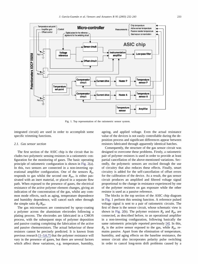
Fig. 1 shows the overall structure of the new smart gassensor system. The main component is the ASIC chip, whichperforms two basic functions: (a) sensing the gas presenceand concentration and (b) controlling the operating tempera-ture of the gas sensor. Within the ASIC chip, the top sectioncorresponds to the gas sensor circuit, whereas the bottomsections correspond to temperature control and monitoring.A microcontroller unit is used for processing the inputsand outputs of the ASIC chip. Additionally, three digitallycontrolled potentiometers (available in the Xicor’s X9241A
0925-4005/$ – see front matter © 2003 Elsevier B.V. All rights reserved.doi:10.1016/S0925-4005(03)00432-5
J. Garcıa-Guzm´an et al. / Sensors and Actuators B 95 (2003) 232–243 233
Fig. 1. Top representation of the ratiometric sensor system.
integrated circuit) are used in order to accomplish somespecific trimming functions.
2.1. Gas sensor section
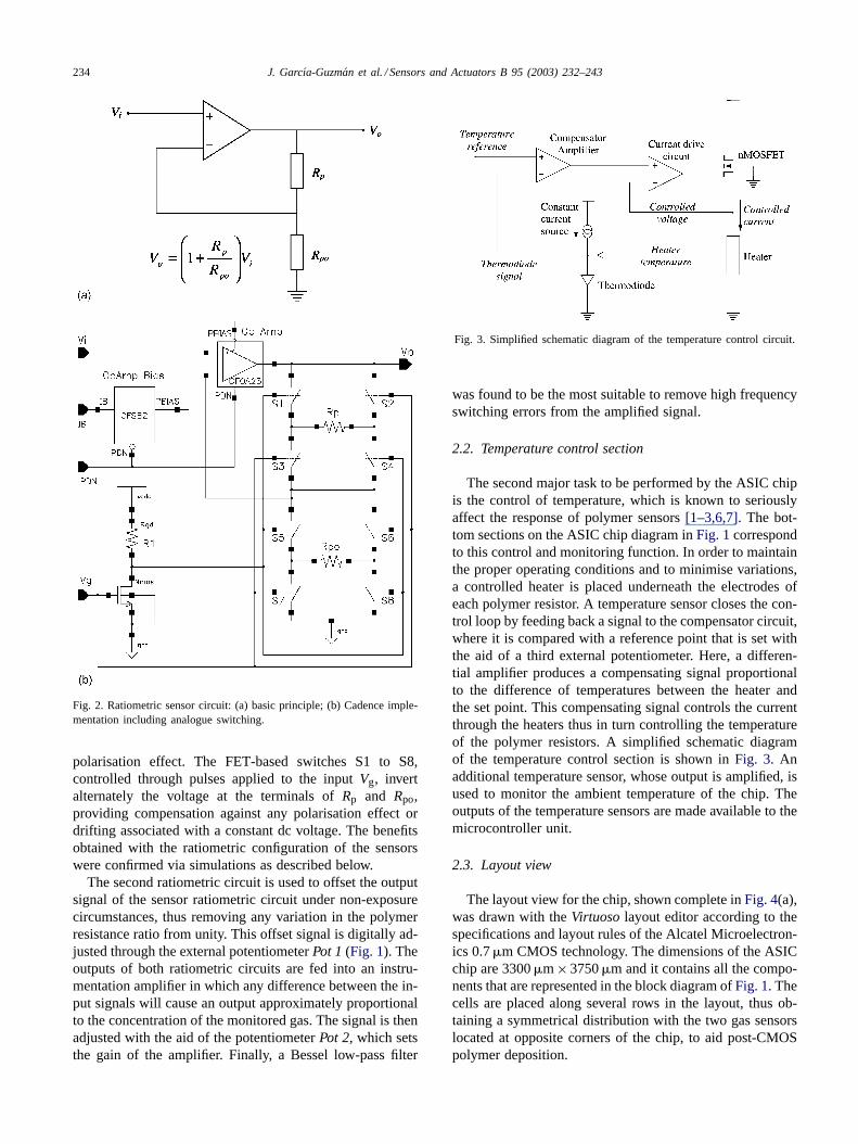
The first section of the ASIC chip is the circuit that in-cludes two polymeric sensing resistors in a ratiometric con-figuration for the monitoring of gases. The basic operatingprinciple of ratiometric configuration is shown inFig. 2(a).In this, two sensors are connected in a non-inverting op-erational amplifier configuration. One of the sensorsRp,responds to gas whilst the second oneRpo, is either pas-sivated with an inert material, or placed in a separate flowpath. When exposed to the presence of gases, the electricalresistance of the active polymer element changes, giving anindication of the concentration of the gas, whilst any com-mon mode effects, such as aging, temperature dependenceand humidity dependence, will cancel each other throughthe simple ratioRp/Rpo.
The gas microsensors are constructed by spray-coatinga polymer across the aluminium electrodes following aplating process. The electrodes are fabricated in a CMOSprocess, with the subsequent steps of polymer depositionand passive coating completing the fabrication of the activeand passive chemoresistors. The actual behaviour of theseresistors cannot be precisely predicted. It is known fromprevious research[1–3,6,7]that the polymer resistance willvary in the presence of gases, but there are several factorswhich affect these variations, e.g. temperature, humidity,
ageing, and applied voltage. Even the actual resistancevalue of the devices is not easily controllable during the de-position process and significant differences appear betweenresistors fabricated through apparently identical batches.
Consequently, the structure of the gas sensor circuit wasdesigned to overcome these problems. Firstly, a ratiometricpair of polymer resistors is used in order to provide at leastpartial cancellation of the above-mentioned variations. Sec-ondly, the polymeric sensors are excited through the useof circuitry that also reduces these effects. Finally, smartcircuitry is added for the self-cancellation of offset errorsfor the calibration of the device. As a result, the gas sensorcircuit produces an amplified and filtered voltage signalproportional to the change in resistance experienced by oneof the polymer resistors on gas exposure while the otherresistor is used as a passive reference.
The blocks in the top section of the ASIC chip diagramin Fig. 1 perform this sensing function. A reference pulsedvoltage signal is sent to a pair of ratiometric circuits. Thefirst of these is the sensor circuit, whose schematic view isshown inFig. 2(b). The polymer resistorsRp and Rpo areconnected, as described before, to an operational amplifierin a non-inverting configuration, following basically thesame ratiometric principle reported previously[4]. In this,Rp is the active sensor exposed to the gas, whileRpo re-mains passive. Apart from the elimination of temperature,humidity, and aging effects on the baseline resistance, thesensor circuit also incorporates polarity pulse switchingin order to cancel long-term drift problems caused by a
234 J. Garcıa-Guzm´an et al. / Sensors and Actuators B 95 (2003) 232–243
Fig. 2. Ratiometric sensor circuit: (a) basic principle; (b) Cadence imple-mentation including analogue switching.
polarisation effect. The FET-based switches S1 to S8,controlled through pulses applied to the inputVg, invertalternately the voltage at the terminals ofRp and Rpo,providing compensation against any polarisation effect ordrifting associated with a constant dc voltage. The benefitsobtained with the ratiometric configuration of the sensorswere confirmed via simulations as described below.
The second ratiometric circuit is used to offset the outputsignal of the sensor ratiometric circuit under non-exposurecircumstances, thus removing any variation in the polymerresistance ratio from unity. This offset signal is digitally ad-justed through the external potentiometerPot 1(Fig. 1). Theoutputs of both ratiometric circuits are fed into an instru-mentation amplifier in which any difference between the in-put signals will cause an output approximately proportionalto the concentration of the monitored gas. The signal is thenadjusted with the aid of the potentiometerPot 2, which setsthe gain of the amplifier. Finally, a Bessel low-pass filter
Fig. 3. Simplified schematic diagram of the temperature control circuit.
was found to be the most suitable to remove high frequencyswitching errors from the amplified signal.
2.2. Temperature control section
The second major task to be performed by the ASIC chipis the control of temperature, which is known to seriouslyaffect the response of polymer sensors[1–3,6,7]. The bot-tom sections on the ASIC chip diagram inFig. 1correspondto this control and monitoring function. In order to maintainthe proper operating conditions and to minimise variations,a controlled heater is placed underneath the electrodes ofeach polymer resistor. A temperature sensor closes the con-trol loop by feeding back a signal to the compensator circuit,where it is compared with a reference point that is set withthe aid of a third external potentiometer. Here, a differen-tial amplifier produces a compensating signal proportionalto the difference of temperatures between the heater andthe set point. This compensating signal controls the currentthrough the heaters thus in turn controlling the temperatureof the polymer resistors. A simplified schematic diagramof the temperature control section is shown inFig. 3. Anadditional temperature sensor, whose output is amplified, isused to monitor the ambient temperature of the chip. Theoutputs of the temperature sensors are made available to themicrocontroller unit.
2.3. Layout view
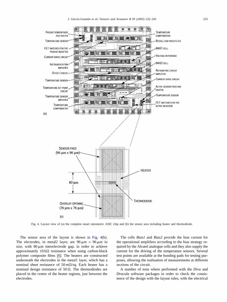
The layout view for the chip, shown complete inFig. 4(a),was drawn with theVirtuoso layout editor according to thespecifications and layout rules of the Alcatel Microelectron-ics 0.7�m CMOS technology. The dimensions of the ASICchip are 3300�m×3750�m and it contains all the compo-nents that are represented in the block diagram ofFig. 1. Thecells are placed along several rows in the layout, thus ob-taining a symmetrical distribution with the two gas sensorslocated at opposite corners of the chip, to aid post-CMOSpolymer deposition.
J. Garcıa-Guzm´an et al. / Sensors and Actuators B 95 (2003) 232–243 235
Fig. 4. Layout view of (a) the complete smart ratiometric ASIC chip and (b) the sensor area including heater and thermodiode.
The sensor area of the layout is shown inFig. 4(b).The electrodes, in metal2 layer, are 96�m × 96�m insize, with 80�m interelectrode gap, in order to achieveapproximately 10 k� resistance when using carbon-blackpolymer composite films[8]. The heaters are constructedunderneath the electrodes in the metal1 layer, which has anominal sheet resistance of 50 m�/sq. Each heater has anominal design resistance of 50�. The thermodiodes areplaced in the centre of the heater regions, just between theelectrodes.
The cellsBias1 and Bias2 provide the bias current forthe operational amplifiers according to the bias strategy re-quired by the Alcatel analogue cells and they also supply thecurrent for the driving of the temperature sensors. Severaltest points are available at the bonding pads for testing pur-poses, allowing the realisation of measurements at differentsections of the circuit.
A number of tests where performed with theDiva andDracula software packages in order to check the consis-tence of the design with the layout rules, with the electrical

236 J. Garcıa-Guzm´an et al. / Sensors and Actuators B 95 (2003) 232–243
rules and with the substrate requirements under the particu-lar CMOS process selected for the fabrication of the ASICchip. In order to obtain the openings down to metal2 layer forthe deposition of the polymers onto the sensor electrodes, itwas necessary to include some special modifications whilestill following the standard CMOS process.
3. Simulations
The Spectresimulator was used to test each part of thedesign.Fig. 5 shows the voltages obtained at the ratiomet-ric sensor circuit when assuming initially equal resistancesfor Rp andRpo and hence disregarding any variations due toexposure to reactive gases. The left plots correspond to theactual voltage waveforms at the terminals of the resistors,i.e. the differences in the corresponding positive voltages,plotted on the right, appearing at theplus and minus ter-minals of each resistor. The simulation results confirm theadvantage of using the switching circuitry in order to invertthe sign of the voltages at the chemoresistors terminals andthus providing compensation against polarisation effects.
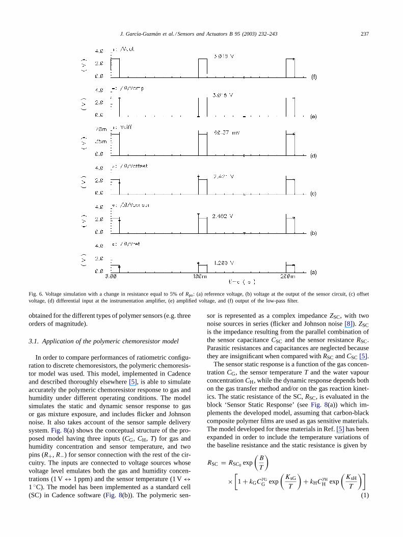
Fig. 6 shows the voltage waveforms appearing at ev-ery stage of the gas sensor section. The reference signal
Fig. 5. Simulation of sensor voltages in the circuit.
Vref (Fig. 6(a)) produced by feeding pulses to a standardbandgap cell consists of pulses that are 10 ms in width andhave an amplitude of 1.2 V. This signal produces the re-sponse that is registered at the output of the offset circuit(Fig. 6(c)), which is calibrated to the baseline signal, i.e.the sensors unexposed to gases. After calibration, exposureto gases is simulated via the change in resistanceδ appliedto the active sensor. The sensor outputVsensor (Fig. 6(b))differs from the offset signalVoffset and the difference involtage is applied to the input of the instrumentation am-plifier. This differential voltageVdiff (Fig. 6(d)) was only60.37 mV in the simulation when the change in resistanceδ was set to 0.05, i.e. 5% ofRpo. When the gain of theamplifier is set to 50, the amplitude of the signal is raised toapproximately 3 V in amplitude (Vamp, Fig. 6(e)). Finally,Vout represents the filtered signal at the output of the circuit(Fig. 6(f)).
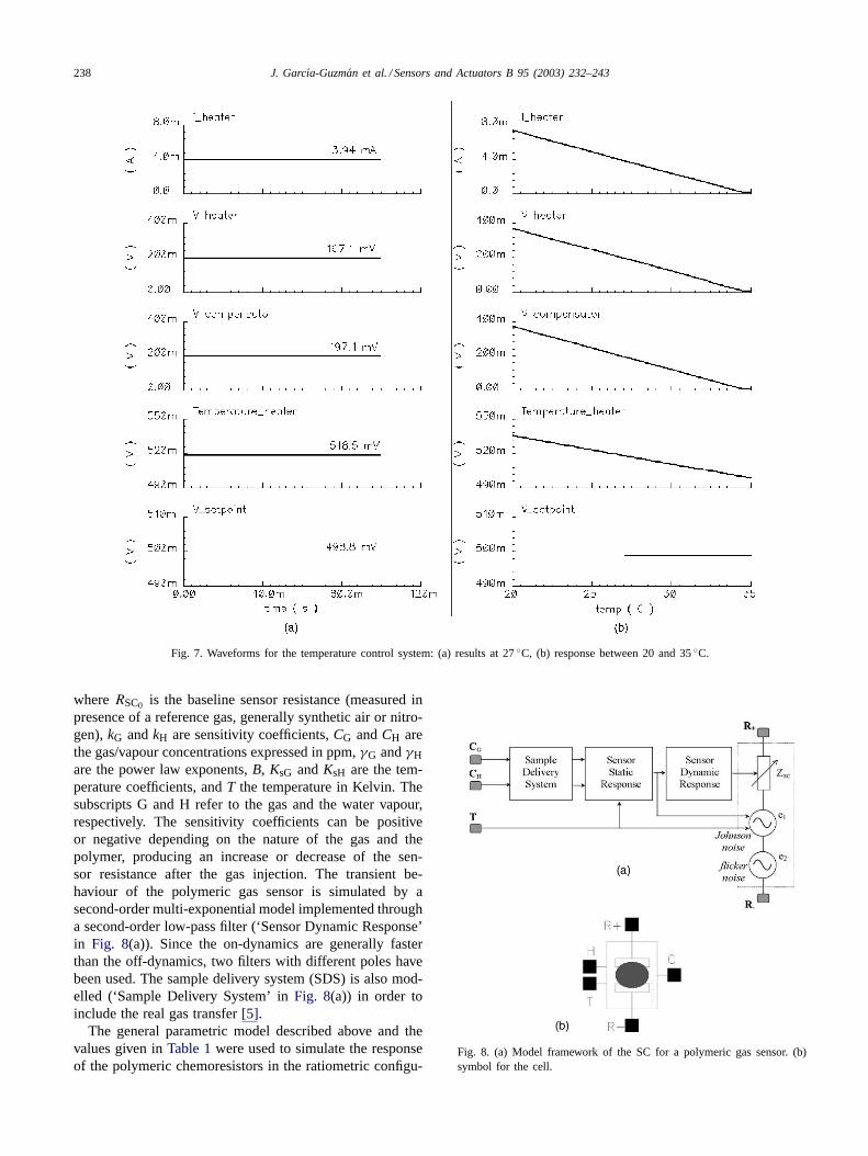
The performance of the temperature control section wasalso simulated.Fig. 7(a) shows the voltages obtained at27◦C, whereasFig. 7(b) shows the voltage waveforms re-sulting when temperature varies between 20◦C and a nom-inal setpoint at 35◦C.
Further simulations also showed that the circuit is capa-ble of dealing with the wide range in the actual resistance
J. Garcıa-Guzm´an et al. / Sensors and Actuators B 95 (2003) 232–243 237
Fig. 6. Voltage simulation with a change in resistance equal to 5% ofRpo: (a) reference voltage, (b) voltage at the output of the sensor circuit, (c) offsetvoltage, (d) differential input at the instrumentation amplifier, (e) amplified voltage, and (f) output of the low-pass filter.
obtained for the different types of polymer sensors (e.g. threeorders of magnitude).
3.1. Application of the polymeric chemoresistor model
In order to compare performances of ratiometric configu-ration to discrete chemoresistors, the polymeric chemoresis-tor model was used. This model, implemented in Cadenceand described thoroughly elsewhere[5], is able to simulateaccurately the polymeric chemoresistor response to gas andhumidity under different operating conditions. The modelsimulates the static and dynamic sensor response to gasor gas mixture exposure, and includes flicker and Johnsonnoise. It also takes account of the sensor sample deliverysystem.Fig. 8(a) shows the conceptual structure of the pro-posed model having three inputs (CG, CH, T) for gas andhumidity concentration and sensor temperature, and twopins (R+, R−) for sensor connection with the rest of the cir-cuitry. The inputs are connected to voltage sources whosevoltage level emulates both the gas and humidity concen-trations (1 V↔ 1 ppm) and the sensor temperature (1 V↔1◦C). The model has been implemented as a standard cell(SC) in Cadence software (Fig. 8(b)). The polymeric sen-
sor is represented as a complex impedanceZSC, with twonoise sources in series (flicker and Johnson noise[8]). ZSCis the impedance resulting from the parallel combination ofthe sensor capacitanceCSC and the sensor resistanceRSC.Parasitic resistances and capacitances are neglected becausethey are insignificant when compared withRSC andCSC [5].
The sensor static response is a function of the gas concen-tration CG, the sensor temperatureT and the water vapourconcentrationCH, while the dynamic response depends bothon the gas transfer method and/or on the gas reaction kinet-ics. The static resistance of the SC,RSC, is evaluated in theblock ‘Sensor Static Response’ (seeFig. 8(a)) which im-plements the developed model, assuming that carbon-blackcomposite polymer films are used as gas sensitive materials.The model developed for these materials in Ref.[5] has beenexpanded in order to include the temperature variations ofthe baseline resistance and the static resistance is given by
RSC = RSC0 exp
(B
T
)
×[1 + kGC
γGG exp
(KsG
T
)+ kHC
γHH exp
(KsH
T
)]
(1)
238 J. Garcıa-Guzm´an et al. / Sensors and Actuators B 95 (2003) 232–243
Fig. 7. Waveforms for the temperature control system: (a) results at 27◦C, (b) response between 20 and 35◦C.
whereRSC0 is the baseline sensor resistance (measured inpresence of a reference gas, generally synthetic air or nitro-gen),kG andkH are sensitivity coefficients,CG andCH arethe gas/vapour concentrations expressed in ppm,γG andγHare the power law exponents,B, KsG andKsH are the tem-perature coefficients, andT the temperature in Kelvin. Thesubscripts G and H refer to the gas and the water vapour,respectively. The sensitivity coefficients can be positiveor negative depending on the nature of the gas and thepolymer, producing an increase or decrease of the sen-sor resistance after the gas injection. The transient be-haviour of the polymeric gas sensor is simulated by asecond-order multi-exponential model implemented througha second-order low-pass filter (‘Sensor Dynamic Response’in Fig. 8(a)). Since the on-dynamics are generally fasterthan the off-dynamics, two filters with different poles havebeen used. The sample delivery system (SDS) is also mod-elled (‘Sample Delivery System’ inFig. 8(a)) in order toinclude the real gas transfer[5].
The general parametric model described above and thevalues given inTable 1were used to simulate the responseof the polymeric chemoresistors in the ratiometric configu-
Fig. 8. (a) Model framework of the SC for a polymeric gas sensor. (b)symbol for the cell.

J. Garcıa-Guzm´an et al. / Sensors and Actuators B 95 (2003) 232–243 239
Table 1Model parameters used in the simulations
Parameter used in theCadence model
Value(s)a Symbols used for Cadenceparameters in theEq. (1)
Description
Cgas 1 k CG Gas concentration (ppm)Humid 0–30 k CH Humidity concentration (ppm)Temper 40–100 T Sensor temperature (◦C)KsH 31.32 KsH Temperature coefficient for the humidity (◦C)kH −94n kH Sensitivity coefficient for the humidity (1/ppm)gammaH 1 γH Power low exponent for the humiditySlope 1 – Slope of the flicker noise (1/fslope)Vol 30 × 10−15 – Polymer volume (m3)X 300 × 10−27 – Polymer coefficient to evaluate flicker noiseSDSCt −1 – SDS control (positive→ active, negative→ inactive)w1SDSoff – – Pole for off-dynamics SDSw1SDSon – – Pole for on-dynamics SDSw2 on 10 k – Second pole on-dynamics chemical transientw2 off 4 k – Second pole off-dynamics chemical transientw1 on 10 m – First pole on-dynamics chemical transientw1 off 4 m – First pole off-dynamics chemical transientR0 9512 RSC0 Sensor baseline resistance (�)B 2 B Temperature coefficient for sensor baseline resistance (◦C)Ks 88.42 KsG Temperature coefficient for the gas (◦C)k1 3.2µ kG Sensitivity coefficient for the gas (1/ppm)gamma 1.07 γG Power low exponent for the gas
a The values of the parameters used for simulations are obtained from measurements on carbon-black polymer composite film performed at the SensorsResearch Laboratory of the University of Warwick with exception of the noise measurements which were performed by the University of Torvegata (Rome).
ration.Fig. 9 shows how the cells SCa and SCp were usedto represent the active and passive sensors.
Two passivation methods were tested in the simulations.In the first case, represented inFig. 10(a), one of the poly-meric sensors is coated with an inert material to avoid the
Fig. 9. Ratiometric sensor circuit. The sensor cell SCa emulates thebehaviour of the active polymeric sensor, while the cell SCp emulates thepassive sensor.
gas effect. In this way, the passive sensor is sensitive to tem-perature variation but it does not respond to the gas or ambi-ent humidity. The water vapour concentration is fixed to theconcentration present at the moment of the coat deposition(e.g. RH= 40% at 20◦C corresponding to 9214 ppm). Thegas flow is split in two paths to expose both sensors. Thepassivation was simulated by connecting the input ‘C’ of theSCp cell to gnd (gas concentration= 0 ppm) and the input‘H’ to a voltage source (e.g. VHp = 9214 V→ 9214 ppm).
The second method requires two separate inlets to carrythe gas under test and a reference gas to the sensors SCa andSCp (Fig. 10(b)). In this case the sensor SCp is not coated
Fig. 10. The use of the reference sensor SCp in the ASIC chip: (a) thepolymer sensor SCp is coated with an inert material to avoid the reactionwith a gas which flow over sensors SCa and SCp; (b) two separate flowpaths are used to expose the two sensors to different gases but to thesame water vapour concentration; this enables for humidity rejection.
240 J. Garcıa-Guzm´an et al. / Sensors and Actuators B 95 (2003) 232–243
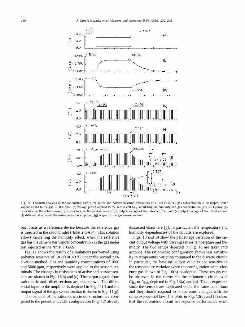
Fig. 11. Transient analysis of the ratiometric circuit for active and passive baseline resistances of 10 k� at 40◦C, gas concentration= 1000 ppm, watervapour mixed to the gas= 5000 ppm: (a) voltage pulses applied to the sensor cell SCa simulating the humidity and gas concentration (1 V↔ 1 ppm); (b)resistance of the active sensor; (c) resistance of the passive sensor; (d) output voltage of the ratiometric circuit; (e) output voltage of the offsetcircuit;(f) differential input of the instrumentation amplifier; (g) output of the gas sensor section.
but it acts as a reference device because the reference gasis injected in the second inlet (‘Inlet 2 GAS’). This solutionallows cancelling the humidity effect, when the referencegas has the same water vapour concentration as the gas undertest injected in the ‘Inlet 1 GAS’.
Fig. 11shows the results of simulations performed usingpolymer resistors of 10 k� at 40◦C under the second pas-sivation method. Gas and humidity concentrations of 1000and 5000 ppm, respectively were applied to the sensors ter-minals. The changes in resistances of active and passive sen-sors are shown inFig. 11(b) and (c). The output signals fromratiometric and offset sections are also shown. The differ-ential input to the amplifier is depicted inFig. 11(f) and theoutput signal of the gas sensor section is shown inFig. 11(g).
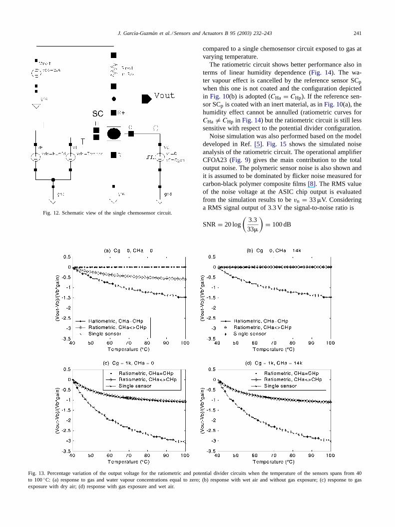
The benefits of the ratiometric circuit structure are com-pared to the potential divider configuration (Fig. 12) already
discussed elsewhere[5]. In particular, the temperature andhumidity dependencies of the circuits are explored.
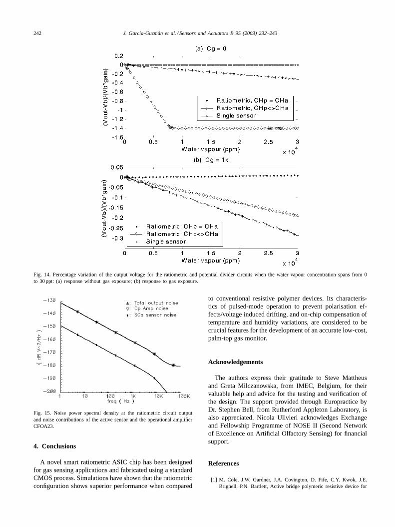
Figs. 13 and 14show the percentage variation of the cir-cuit output voltage with varying sensor temperature and hu-midity. The two setups depicted inFig. 10 are taken intoaccount. The ratiometric configuration shows less sensitiv-ity to temperature variation compared to the discrete circuit.In particular, the baseline output value is not sensitive tothe temperature variation when the configuration with refer-ence gas shown inFig. 10(b) is adopted. These results canbe observed in the curves for the ratiometric circuit withCHa = CHp, depicted inFig. 13(a) and (b). This is expected,since the sensors are fabricated under the same conditionsand they should respond to temperature changes with thesame exponential law. The plots inFig. 13(c) and (d) showthat the ratiometric circuit has superior performance when
J. Garcıa-Guzm´an et al. / Sensors and Actuators B 95 (2003) 232–243 241
Fig. 12. Schematic view of the single chemosensor circuit.
Fig. 13. Percentage variation of the output voltage for the ratiometric and potential divider circuits when the temperature of the sensors spans from40to 100◦C: (a) response to gas and water vapour concentrations equal to zero; (b) response with wet air and without gas exposure; (c) response to gasexposure with dry air; (d) response with gas exposure and wet air.
compared to a single chemosensor circuit exposed to gas atvarying temperature.
The ratiometric circuit shows better performance also interms of linear humidity dependence (Fig. 14). The wa-ter vapour effect is cancelled by the reference sensor SCpwhen this one is not coated and the configuration depictedin Fig. 10(b) is adopted (CHa = CHp). If the reference sen-sor SCp is coated with an inert material, as inFig. 10(a), thehumidity effect cannot be annulled (ratiometric curves forCHa = CHp in Fig. 14) but the ratiometric circuit is still lesssensitive with respect to the potential divider configuration.
Noise simulation was also performed based on the modeldeveloped in Ref.[5]. Fig. 15 shows the simulated noiseanalysis of the ratiometric circuit. The operational amplifierCFOA23 (Fig. 9) gives the main contribution to the totaloutput noise. The polymeric sensor noise is also shown andit is assumed to be dominated by flicker noise measured forcarbon-black polymer composite films[8]. The RMS valueof the noise voltage at the ASIC chip output is evaluatedfrom the simulation results to bevn = 33�V. Consideringa RMS signal output of 3.3 V the signal-to-noise ratio is
SNR= 20 log
(3.3
33�
)= 100 dB
242 J. Garcıa-Guzm´an et al. / Sensors and Actuators B 95 (2003) 232–243
Fig. 14. Percentage variation of the output voltage for the ratiometric and potential divider circuits when the water vapour concentration spans from 0to 30 ppt: (a) response without gas exposure; (b) response to gas exposure.
Fig. 15. Noise power spectral density at the ratiometric circuit outputand noise contributions of the active sensor and the operational amplifierCFOA23.
4. Conclusions
A novel smart ratiometric ASIC chip has been designedfor gas sensing applications and fabricated using a standardCMOS process. Simulations have shown that the ratiometricconfiguration shows superior performance when compared
to conventional resistive polymer devices. Its characteris-tics of pulsed-mode operation to prevent polarisation ef-fects/voltage induced drifting, and on-chip compensation oftemperature and humidity variations, are considered to becrucial features for the development of an accurate low-cost,palm-top gas monitor.
Acknowledgements
The authors express their gratitude to Steve Mattheusand Greta Milczanowska, from IMEC, Belgium, for theirvaluable help and advice for the testing and verification ofthe design. The support provided through Europractice byDr. Stephen Bell, from Rutherford Appleton Laboratory, isalso appreciated. Nicola Ulivieri acknowledges Exchangeand Fellowship Programme of NOSE II (Second Networkof Excellence on Artificial Olfactory Sensing) for financialsupport.
References
[1] M. Cole, J.W. Gardner, J.A. Covington, D. Fife, C.Y. Kwok, J.E.Brignell, P.N. Bartlett, Active bridge polymeric resistive device for
J. Garcıa-Guzm´an et al. / Sensors and Actuators B 95 (2003) 232–243 243
vapour sensing, Eurosensors XIV, W2P41, (Bio)chem. Sens. III(2000) 895–898.
[2] J.W. Gardner, M. Vidic, P. Ingleby, A.C. Pike, J.E. Brignell, P. Scivier,P.N. Bartlett, A.J. Duke, J.M. Elliot, Response of a poly(pyrrole)resistive micro-bridge to ethanol vapour, Sens. Actuators B 48 (1998)289–295.
[3] M. Cole, J.W. Gardner, A.W.Y. Lim, P.K. Scivier, J.E. Brignell,Polymeric resistive bridge gas sensor array driven by a standard cellCMOS current drive chip, Sens. Actuators B 58 (1999) 518–525.
[4] M. Cole, J.W. Gardner, P.N. Bartlett, Low-drift odour and vapourratiometric resistive elements for analogue CMOS smart sensors,in: J.R. Stetter, W.R. Penrose (Eds.), Proceedings of the ArtificialChemical Sensing: Olfaction and the Electronic Nose (ISOEN 2001),vol. 15, The Electrochemical Society Inc., USA, 2001, pp. 117–120.
[5] M. Cole, N. Ulivieri, J. Garcıa-Guzmán, J.W. Gardner, Paramet-ric model of a polymeric chemoresistor for use in smart sensordesign and simulation, submitted for publication.http://www.eng.warwick.ac.uk/srl.
[6] P. Bruschi, A. Nannini, B. Neri, Vapour and gas sensing by noisemeasurements on polymeric balanced bridge microstructures, Sens.Actuators B 24–25 (1995) 429–432.
[7] J.V. Hattfield, P. Neaves, P.J. Hicks, K. Persaud, P. Travers, Towardsan integrated electronic nose using conducting polymer sensors, Sens.Actuators B 18–19 (1994) 221–228.
[8] S.M. Briglin, M.S. Freund, P. Tokumaru, N.S. Lewis, Exploitationof spatiotemporal information and geometric optimisation of sig-nal/noise performance using arrays of carbon black-polymer com-posite vapor detectors, Sens. Actuators B 82 (2002) 54–74.
Biographies
Jesús Garc´ıa-Guzmángraduated in Mechanical and Electrical Engineer-ing from the Universidad Veracruzana (Veracruz, Mexico) in 1978. Hereceived his MSc degree in Higher Education, with honours, from theICEST (Mexico) in 1997 and MSc degree in Advanced Engineering,with distinction, from the University of Warwick (UK) in 1999. He is aLecturer in the Faculty of Engineering at the Universidad Veracruzana(Xalapa, Mexico). Currently he is completing work on a PhD project at
the Sensors Research Laboratory of the University of Warwick, wherehis main research interests are in the areas of analogue integrated circuitdesign, sensor interfacing and smart circuitry.
Nicola Ulivieri received his Laurea degree in Telecommunication Engi-neering at the University of Siena in 1999. He is currently a PhD studentin Information Engineering (Electronics) at the University of Siena. In2002 he spent a 6 months period at the School of Engineering of theUniversity of Warwick to develop a Cadence model for chemoresistorsgas sensors and to collaborate to an ASIC chip layout design. His mainresearch activity is related to the development of laboratory electronicnoses based on metal oxide sensors and QCM sensors. Recently, hisinterests were also devoted to integrated analogue and mixed signalelectronics design and smart sensors development.
Marina Cole (BSc, PhD, MIEEE), received his BSc degree from theUniversity of Montenegro (Yugoslavia) and the PhD from CoventryUniversity (UK). She joined the School of Engineering at Warwick Uni-versity in 1996 as a postdoctoral research assistant and in 1998 she wasappointed to a lectureship in electronic engineering. Her main research in-terests are integrated silicon-based sensors, SAW-based sensors, analogueand mixed signal ASICs, smart sensors, actuators and microsystems.
Julian W. Gardner(BSc, PhD, DSc, CEng, FIEE, SMIEEE), joined theSchool of Engineering at Warwick in 1987. His research interests aremicrosensors, microsystems technology, electronic noses, intelligent sen-sors and multivariate data processing methods. He has previously spent5 years in industry working first at AEA Technology Ltd. and later atMolins Advanced Technology Unit on Instrumentation. At Molins he de-veloped a novel opto-electronic sensor that has been packaged in the UKand US for implementation on high speed packaging machinery. In 1989he received the Esso Centenary Education Award sponsored by the RoyalSociety and Fellowship of Engineering to pursue his research interests.He has published over 300 technical papers and is an author of six booksin Nanotechnology (1991), Electronic Noses (1992), Microsensors (1994),Electronic Noses (1999), MEMS (2001) Handbook of Machine Olfaction(2003). He was an Alexander von Humboldt Fellowship in Germany in1994. He currently heads the Sensors Research Laboratory in the Centrefor Nanotechnology and Microengineering at Warwick University, wherehe is Professor of Electronic Engineering.