Dense III-V/Si Phase-Shifter Based Optical Phased Array - arXiv
20
1 Dense III-V/Si Phase-Shifter Based Optical Phased Array Weiqiang Xie*, Tin Komljenovic, Jinxi Huang, Michael L. Davenport and John E. Bowers E-mail: [email protected] Department of Electrical and Computer Engineering, University of California Santa Barbara, Santa Barbara, CA 93106, USA Abstract: High-performance integrated optical phased arrays (OPAs) are crucial for building up energy-efficient solid-state beam steering systems on a chip. This work demonstrates a first heterogeneous III-V/Si phase-shifter based OPA that utilizes III-V multiple quantum well (MQW) structures to provide superior performance. Demonstrated phase shifters have Vπ of only 0.45 V and residual amplitude modulation (RAM) of only 0.15 dB at 1550 nm for 2π phase shift with low power consumption of less than 3 nW, which are, to the best our knowledge, the state-of-the-art performance with a record low operating voltage, low power consumption, and low RAM in on-chip OPAs. Their bandwidth is >1 GHz across 200 nm wavelength range. Wavelength tuning is used to demonstrate two-dimensional beam steering with a field of view of 28°×51° in the 32-channel OPA with an emitter-array pitch of 2 μm. Side-mode suppression ratio of 16 dB is also achieved. The high-performance heterogeneous OPA paves the way for scalable and efficient on-chip beam steerers with large steering range and high beam quality. 1. Introduction Integrated optical phased arrays (OPAs) are essential for a number of applications such as light detection and ranging (LiDAR), free-space communications, and imaging and sensing [1-11]. The silicon photonics platform using mature complementary metal-oxide-semiconductor (CMOS) manufacturing is very attractive for making OPA-based systems for practical applications due to high volume capability and low cost. In on-chip OPAs, it is essential to integrate high-performance phase shifters with low drive voltage and low power consumption, low optical loss, and high bandwidth. More importantly, dense integration in OPAs is required
-
Upload
khangminh22 -
Category
Documents
-
view
0 -
download
0
Transcript of Dense III-V/Si Phase-Shifter Based Optical Phased Array - arXiv

1
Dense III-V/Si Phase-Shifter Based Optical Phased Array Weiqiang Xie*, Tin Komljenovic, Jinxi Huang, Michael L. Davenport and John E. Bowers E-mail: [email protected] Department of Electrical and Computer Engineering, University of California Santa Barbara, Santa Barbara, CA 93106, USA Abstract: High-performance integrated optical phased arrays (OPAs) are crucial for building
up energy-efficient solid-state beam steering systems on a chip. This work demonstrates a first
heterogeneous III-V/Si phase-shifter based OPA that utilizes III-V multiple quantum well
(MQW) structures to provide superior performance. Demonstrated phase shifters have Vπ of
only 0.45 V and residual amplitude modulation (RAM) of only 0.15 dB at 1550 nm for 2π phase
shift with low power consumption of less than 3 nW, which are, to the best our knowledge, the
state-of-the-art performance with a record low operating voltage, low power consumption, and
low RAM in on-chip OPAs. Their bandwidth is >1 GHz across 200 nm wavelength range.
Wavelength tuning is used to demonstrate two-dimensional beam steering with a field of view
of 28°×51° in the 32-channel OPA with an emitter-array pitch of 2 µm. Side-mode suppression
ratio of 16 dB is also achieved. The high-performance heterogeneous OPA paves the way for
scalable and efficient on-chip beam steerers with large steering range and high beam quality.
1. Introduction
Integrated optical phased arrays (OPAs) are essential for a number of applications such as light
detection and ranging (LiDAR), free-space communications, and imaging and sensing [1-11].
The silicon photonics platform using mature complementary metal-oxide-semiconductor
(CMOS) manufacturing is very attractive for making OPA-based systems for practical
applications due to high volume capability and low cost. In on-chip OPAs, it is essential to
integrate high-performance phase shifters with low drive voltage and low power consumption,
low optical loss, and high bandwidth. More importantly, dense integration in OPAs is required

2
to alleviate and overcome grating lobes and to maximize the effective aperture size towards a
diffraction-limited beam.
A variety of silicon photonics OPAs have been demonstrated, using Si thermo-optic (TO)
[3, 4, 7, 9, 10] or Si electro-optic (EO) phase shifters [5, 8, 12]. Ideally TO phase shifters have
negligible optical loss, but have limited bandwidth, typically a few kHz, which impacts beam
steering speed and consequently final device performance. In addition, high-power
consumption and thermal crosstalk limit the integration density. On the other hand, reverse-
biased PN-junction EO-type Si phase shifters are capable of high-speed operation (tens of GHz),
low power consumption (<2 µW) [11], and dense integration. However, such phase shifters
suffer from high RAM associated with 2π phase shift [11]. The limitation is inherent to the
modulation mechanism that exploits plasma dispersion effect to change real and imaginary parts
of the refractive index, which are coupled via Kramers–Kronig relations [12]. Moreover, the
modulation efficiency in Si EO modulators is generally low (i.e. a high voltage–length product
VπL typically 1-3 V⋅cm), resulting in high operation voltage or excessive lengths for a 2π phase
shift [13]. Apart from Si-based TO an EO phase shifters, an alternative choice is to implement
a heterogeneous III-V/Si for OPA phase shifters to improve device performance, since the III-
V can leverage additional modulation effects, Franz-Keldysh or quantum-confined Stark effect,
band-filling, and Pockels effects among others. In fact, such heterogeneous optical phase
shifters have already been investigated in Mach–Zehnder interferometer (MZI) based
modulators [14-19], and demonstrated low voltage operation (VπL ~ 0.05-0.2 V⋅cm) and a low
optical loss (<1 dB for a 2π phase shift) [19]. Moreover, the heterogeneous III-V/Si integration
approach could provide a promising solution for complete OPA-based systems such as LiDAR
by integrating laser sources, amplifiers, OPAs, and detectors on a single chip. The largest
remaining challenge is demonstrating such phase shifters in dense configurations necessary for
state-of-the-art OPAs. This work, to the best of our knowledge, is the first such demonstration
3
in which the pitch between neighboring phase shifters is only 4 µm, allowing for efficient and
compact OPAs.
2. Design and Fabrication
In our demonstration, we incorporate a III-V material bonded on top of Si waveguides to form
a heterogeneous III-V/Si phase-shifter array. A schematic design of the OPA is shown in Figure
1a. It comprises a 1×N (N=32 in our test device) star coupler [20], a III-V/Si phase-shifter array
with a length of 5 mm, and a 10-mm-long waveguide-grating antenna array. Note that all
components in our OPA are designed for fundamental transverse-electric (TE) mode. The
passive SOI contains a 1.0 μm buried oxide and a 500 nm Si layer on top, which is etched by
231 nm to form ridge waveguides. The star coupler is designed to couple ~95% of total power
into waveguide array in a Gaussian distribution along the array [20], which also results in a
nearly Gaussian beam profile in ψ axis suppressing the close-in side-lobes. The phase-shifter
array has a pitch of 4 µm and the details of the design can be found in Supplementary
Information (see Section S1). For the grating emitter, we adopt a surface waveguide grating
with a very shallow etch depth for a low emission strength so as to realize mm to cm scale of
effective emission length. See Supplementary Information (Section S2) for the detailed design
and characterization of the individual grating emitter. Note that the pitch of grating array,
determining the maximum steering angle range before sidelobes interfere with the main lobe,
can be different from the pitch of phase shifter array and we have both 4 µm and 2 µm grating
pitch designs. The devices were fabricated on 100 mm SOI wafer using 248 nm DUV
lithography and a III-V/Si heterogeneous integration technique [21, 22] (the fabrication details
in Supplementary Information, see Section S3). Figure 1c shows a fabricated OPA with 32
channels.

4
Figure 1. Design configuration and device fabrication. a) Schematics of a III-V/Si OPA system consisting
of a 1×N star coupler, III-V/Si phase-shifter array, and waveguide-grating array. The input light is split
into the Si waveguide array by a star coupler and then evanescently coupled to III-V/Si hybrid waveguide
through an optimized low-loss III-V/Si taper. After the phase shift, the light is coupled back into Si
waveguide layer and radiated coherently through the grating antenna array. The emitted beam direction
in free space is denoted by θ and ψ, which are defined as the emission angles in waveguide dimension
and OPA dimension respectively. b) Schematic cross-section of the III-V/Si phase shifters with locally
opened n/p contact for probing in one shifter on top. c) Optical microscope image of a fully fabricated
32-channel OPA (upper panel) and SEM images of the corresponding components of the OPA (lower
panel) taken before BCB planarization step.
3. Experimental Results
3.1. Characterization of III-V/Si Phase Shifter
The III-V/Si phase shifter was characterized using an unbalanced MZI with one arm having a
5mm heterogeneous phase shifter. The MZI comprises two 2×2 MMI couplers with 4 ports
functioning as optical input and output respectively. By applying the voltage on III-V diode,
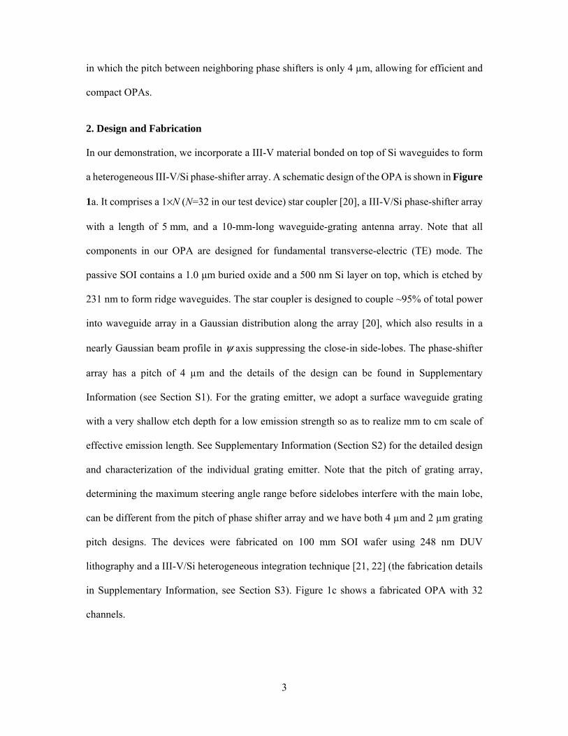
we measured the transmission between one input port and one output port. Figure 2a shows the
transmission at 1550 nm when sweeping the bias voltage. We obtained a reverse bias voltage
5
of 0.9 V for a 2π shift and an extinction ratio larger than 23 dB. It can also be seen that the peak
transmission intensity from 0 to -1V only reduces by ~0.1 dB, meaning a very low RAM within
2π phase shift. In Figure 2b, we present the bias voltage of a 2π phase shift as a function of
wavelength and the operation voltage is in a range of 0.35 V to 1.4 V over a wavelength range
of 1450 nm to 1650 nm. The absorption loss at 2π phase-shift voltage is also extracted by
measuring the bias-dependent transmission of a III-V/Si waveguide and shown in Figure 2b. It
can be seen that the loss penalty for the intensity is only ~0.15 dB for the wavelength from 1550
nm to 1650 nm, which implies a RAM of ~0.15dB. At shorter wavelengths, the loss increases
due to band-edge absorption and can be alleviated by shifting the absorption edge of III-V QWs
to even shorter wavelengths in future design. Considering the dark current of only 1-3 nA at -1
V bias (see Section S4, Supplementary Information), the power consumption of the phase
shifter is on the order of nanowatts. The demonstrated state-of-the-art performance in the III-
V/Si phase shifter with a record low operating voltage, low power consumption, and low RAM
is suitable for on-chip OPAs. In addition, we measured the frequency response of the MZI
modulator in Supplementary Information (see Section S4,) and obtain the 3dB electrical
bandwidth of 1.65 GHz limited by capacitance. Such operation speed is sufficient for OPA
applications.
Figure 2. Static characterization of III-V/Si phase shifter. a) Transmission at 1550 nm between two MZI
ports as a function of applied bias voltage on III-V diode. The inset shows the sine function fit of the
transmission with a bias from 0 to -1 V, indicating a good linearity between applied bias and phase shift.
-3 -2 -1 0
-20
-15
-10
-5
0
Tra
nsm
issi
on (
dB)
Bias voltage(V)
-1.0 -0.5 0.00.0
0.5
1.0
a b
1450 1500 1550 1600 1650
0.3
0.6
0.9
1.2
1.5 V
2π
Absorption
V
2π (
V)
Wavelength (nm)
0
2
4
6
8
Abso
rption (d
B)
6
b) Reverse bias voltage (black) and total absorption loss (blue) at a 2π phase shift for different
wavelengths in a 5mm phase shifter. Considering ~1 dB loss as maximum acceptable (which is till
superior to Si phase shifters), the bandwidth of our III-V/Si phase shifter is ~150 nm from 1500 nm to
1650 nm.
3.2. Beam Steering Measurement of OPA
We first characterized the 32-channel OPA with a 4 µm pitch for the grating array using a
Fourier imaging setup, as illustrated in Figure 3a. The phase shifters were reverse biased using
32 voltage sources controlled by a computer. The TE polarized light from a tunable laser was
coupled into the star coupler and split into 32 waveguide channels, and an IR camera was used
to acquire the far field image and to provide feedback for real-time phase optimization. The
measured I-V curves as shown in Supplementary Information (see Section S4) reveals a
uniform electrical performance among all phase shifters, which is important for the beam
characterization. Without phase alignment, the beam emitted from the grating array is not
focused due to path-length imbalance of the star coupler and accumulation of phase errors along
the length of the device. To realize beam focusing and steering, we employed the gradient
descent method to optimize the individual phases of the OPA. To implement the optimization,
a target function is defined as =− (,)/ , where P(θ,ψ) is the beam power at desired
(θ,ψ) direction and P0 is the total power inside the first grating-lobe region. Figure 3b shows
the evolution of the optimization function when steering the beam at ψ = 0. The optimization
shows a very fast convergence; after only five iterations the voltages converge and the target
function reaches 98% of the final optimized value. After phase alignment all bias voltages are
in a range of 0 to -1 V, matching with the 0.9 V operation bias voltage for a 2π phase shift at
1550 nm. In Figure 3c, we plot the beam profiles along ψ axis before and after phase
optimization and obtain a side-mode suppression ratio of 16 dB for the focused beam, with the
side-mode suppression ratio defined in a single grating-lobe region. It is also evident that for
the 4 µm pitch grating array, the maximum beam steering angle in ψ axis is ~22° in which the
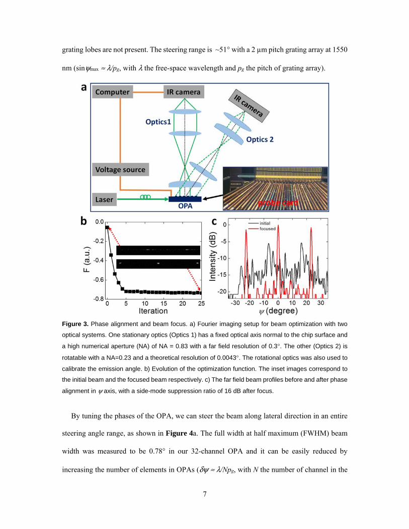
7
grating lobes are not present. The steering range is ~51° with a 2 µm pitch grating array at 1550
nm (sinψmax ≈ λ/pg, with λ the free-space wavelength and pg the pitch of grating array).
Figure 3. Phase alignment and beam focus. a) Fourier imaging setup for beam optimization with two
optical systems. One stationary optics (Optics 1) has a fixed optical axis normal to the chip surface and
a high numerical aperture (NA) of NA = 0.83 with a far field resolution of 0.3°. The other (Optics 2) is
rotatable with a NA=0.23 and a theoretical resolution of 0.0043°. The rotational optics was also used to
calibrate the emission angle. b) Evolution of the optimization function. The inset images correspond to
the initial beam and the focused beam respectively. c) The far field beam profiles before and after phase
alignment in ψ axis, with a side-mode suppression ratio of 16 dB after focus.
By tuning the phases of the OPA, we can steer the beam along lateral direction in an entire
steering angle range, as shown in Figure 4a. The full width at half maximum (FWHM) beam
width was measured to be 0.78° in our 32-channel OPA and it can be easily reduced by
increasing the number of elements in OPAs (δψ ≈ λ/Npg, with N the number of channel in the

8
OPA). Beam steering in the longitudinal direction was realized by tuning the wavelength,
according to the formula sin = ( − )/ , where neff is the effective index of the
waveguide, Λ is the grating period. Figure 4b presents the beam profiles when the beam is
steered by changing the wavelength from 1450 nm to 1650 nm with a noise floor less than -20
dB (limited by the IR camera used). The overall steering angle in θ axis is ~28° over a 200 nm
wavelength, resulting in a tuning efficiency by wavelength of 0.138°/nm. The FWHM beam
width was measured to be 0.02° at 1550 nm corresponding to a ~2.5 mm effective aperture size.
In Figure 4c, we also plot the 2D beam profiles when steering the beam in (θ, ψ) plane in the
OPA with a 4µm-pitch grating array. Note that the beam steering angle in ψ axis can be further
increased by tapering down the pitch from phase-shifter array to grating array or directly
reducing the OPA pitch. With the pitch-tapering scheme, we further demonstrated 51° steering
range in ψ axis using a 2µm-pitch grating array. In this way, however, the effective aperture
size relative to the chip size in the OPA dimension is not improved. We also tried to push the
phase shifter pitch down to 2 µm, but the yield for III-V diodes was low, mainly limited by
lithography which could be addressed by using more advanced tools. We believe that III-V/Si
OPA with pitch approaching subwavelength dimensions can eventually be pursued to realize
diffraction-limited and grating-lobe-free beams. The dimension of the III-V/Si OPA can be
scaled to thousands of elements by taking the advantage of CMOS scale processing.

9
Figure 4. Beam steering in (θ, ψ) plane. a) Measured beam profiles at 1550 nm wavelength with the
beam steering across the field of view in the ψ axis at a 2.8° increment in the OPA with a 4µm-pitch
grating array. b) Beam profiles along θ axis (ψ = 0) with the beam steering when tuning the wavelength
from 1450 nm to 1650 nm at a 10 nm increment. c) Plots of 2D beam profiles with a wavelength tuning
range from 1520 nm to 1580 nm. Note that the far-field images in both θ and ψ directions were acquired
using low-resolution Optics 1 which limits the resolvable beam width to be ~0.3°, and additionally the
plotting scale in ψ axis is about two times of that in θ. Thus the 3D-plotted beam appears Gaussian-like.
d) Beam profiles of the OPA with a 2µm-pitch grating array and the beam steering across 51° range in
the ψ axis at a 4.6° increment.
4. Conclusion
In summary, we have demonstrated a dense III-V/Si OPA system with a pitch of 4 µm
fabricated using heterogeneous wafer-bonding technology. The fabricated OPA, with III-V/Si
phase shifters, offers state-of-the-art performance in terms of drive voltage for 2π phase shift (-
0.9 V) and residual amplitude modulation (0.15 dB for 2π phase shift). Beam steering with a
steering-angle range of 28°×51° in the 32-channel OPA with a grating-array pitch of 2 µm, and
a far field beam with a side-mode suppression ratio of 16 dB were demonstrated. Finally, we

10
point out that this is a very promising approach for realizing energy-efficient and scalable III-
V/Si OPAs with lager apertures. Moreover, fully integrated OPA-based systems such as
LiDARs that also include laser sources, amplifiers and detectors can be realized on the same
heterogeneous integration platform.
Supporting Information Supporting Information is available.
Acknowledgements
The authors thank Larry Coldren and Jonathan Klamkin of UCSB, Paul Suni and James R.
Colosimo from Lockheed Martin for useful discussions, and MJ Kennedy and Alfredo Torres
for process help. This work is supported by DARPA MTO (MOABB HR0011-16-C-0106). The
views, opinions and/or findings expressed are those of the author and should not be interpreted
as representing the official views or policies of the Department of Defense or the U.S.
Government.
References
[1] K. Van Acoleyen, W. Bogaerts, J. Jagerska, N. Le Thomas, R. Houdre, R. Baets, Opt.
Lett. 2009, 34, 1477.
[2] K. Van Acoleyen, H. Rogier, R. Baets, Opt. Express 2010, 18, 13655.
[3] J. K. Doylend, M. J. R. Heck, J. T. Bovington, J. D. Peters, L. A. Coldren, J. E. Bowers,
Opt. Express 2011, 19, 21595.
[4] K. Van Acoleyen, K. Komorowska, W. Bogaerts, R. Baets, J. Lightwave Technol. 2011,
29, 3500.
[5] J. K. Doylend, M. J. R. Heck, J. T. Bovington, J. D. Peters, M. L. Davenport, L. A.
Coldren, J. E. Bowers, Opt. Lett. 2012, 37, 4257.
[6] J. Sun, E. Timurdogan, A. Yaacobi, E. S. Hosseini, M. R. Watts, Nature 2013, 493, 195.
[7] D. Kwong, A. Hosseini, J. Covey, Y. Zhang, X. C. Xu, H. Subbaraman, R. T. Chen,
Opt. Lett. 2014, 39, 941.
[8] J. C. Hulme, J. K. Doylend, M. J. R. Heck, J. D. Peters, M. L. Davenport, J. T. Bovington,
L. A. Coldren, J. E. Bowers, Opt. Express 2015, 23, 5861.

11
[9] D. N. Hutchison, J. Sun, J. K. Doylend, R. Kumar, J. Heck, W. Kim, C. T. Phare, A.
Feshali, H. S. Rong, Optica 2016, 3, 887.
[10] C. V. Poulton, A. Yaacobi, D. B. Cole, M. J. Byrd, M. Raval, D. Vermeulen, M. R.
Watts, Opt. Lett. 2017, 42, 4091.
[11] C. V. Poulton, P. Russo, E. Timurdogan, M. Whitson, M. J. Byrd, E. Hosseini, B. Moss,
Z. Su, D. Vermeulen, M. R. Watts, presented at Conference on Lasers and Electro-
Optics, San Jose, California, May, 2018.
[12] G. T. Reed, G. Mashanovich, F. Y. Gardes, D. J. Thomson, Nat. Photonics 2010, 4, 518.
[13] X. Xiao, H. Xu, X. Y. Li, Z. Y. Li, T. Chu, Y. D. Yu, J. Z. Yu, Opt. Express 2013, 21,
4116.
[14] H. W. Chen, Y. H. Kuo, J. E. Bowers, IEEE Photonic Tech. L. 2008, 20, 1920.
[15] H. W. Chen, Y. H. Kuo, J. E. Bowers, Opt. Express 2008, 16, 20571.
[16] H. W. Chen, J. D. Peters, J. E. Bowers, Opt. Express 2011, 19, 1455.
[17] Q. S. Huang, Y. C. Wu, K. Q. Ma, J. H. Zhang, W. Q. Xie, X. Fu, Y. C. Shi, K. X. Chen,
J. J. He, D. Van Thourhout, G. Roelkens, L. Liu, S. L. He, Appl. Phys. Lett. 2016, 108.
[18] T. Hiraki, T. Aihara, K. Hasebe, K. Takeda, T. Fujii, T. Kakitsuka, T. Tsuchizawa, H.
Fukuda, S. Matsuo, Nat. Photonics 2017, 11, 482.
[19] J. H. Han, F. Boeuf, J. Fujikata, S. Takahashi, S. Takagi, M. Takenaka, Nat. Photonics
2017, 11, 486.
[20] E. J. Stanton, N. Volet, T. Komljenovic, J. E. Bowers, presented at Conference on
Lasers and Electro-Optics, San Jose, California, Jun, 2017.
[21] M. A. Tran, T. Komljenovic, J. C. Hulme, M. J. Kennedy, D. J. Blumenthal, J. E.
Bowers, Opt. Express 2017, 25, 3826.
[22] M. L. Davenport, S. Skendzic, N. Volet, J. C. Hulme, M. J. R. Heck, J. E. Bowers, IEEE
J. Sel. Top. Quantum Electron. 2016, 22.

12
Supporting Information Dense III-V/Si Phase-Shifter Based Optical Phased Array Weiqiang Xie*, Tin Komljenovic, Jinxi Huang, Michael L. Davenport and John E. Bowers
S1. Design of the III-V/Si phase shifter in OPAs
On-chip OPAs can contains thousands of elements and therefore require high-performance
phase shifters providing low operating voltage and low power consumption, low optical loss,
and large bandwidth. In Si-based phase shifters, it remains hard to overcome all the trade-offs
due to an inherent low plasma-dispersion effect and considerable carrier absorption in Si [1].
In contrast, III-V phase shifters can utilize additional modulation effects, such as quantum-
confined Stark effect (QCSE), band-filling, and Pockels effects among others, which increases
the total electro-optic effect [2-6], leading to a low operating voltage. In addition, the higher
electron mobility in III-V [5] contributes to reduced carrier absorption loss and lower
resistance–capacitance time constant, allowing for low optical loss and large bandwidth. Based
on our previous findings [2-4, 7], we adopt III-V multiple quantum well (MQW) PN diodes on
Si waveguides to form a heterogeneous III-V/Si phase shifter. Compared with our previous
work on the III-V/Si modulator which had a single modulator device and aimed for very high-
speed optical modulation (a few tens of GHz), the current work focuses on the dense integration
of a large number of III-V/Si phase shifters in an OPA. In this context, there are two essential
problems to be addressed − the design of high-performing phase shifter in dense configuration
and the feasibility of fabrication. Moreover, the performance requirements for phase shifters in
OPAs is quite different from our previous applications, for instance, low residual amplitude
modulation, low power consumption and low operating voltage are more important while
bandwidth requirements can be relaxed to few GHz or less, which is still sufficient for OPA
applications that are usually limited by time-of-flight delay of the optical beam.

13
Figure S1. Schematic cross-section of the III-V/Si phase shifter array. The array pitch is Λ = 4µm, the III-V mesa width is w = 4µm, and the distance between the mesa boundary and n metal boundary is d.
Figure S2. (a) The mode loss as a function of d. The Si waveguide width is set to 600 nm. (b) The confinement factor of the mode in the QW as a function of Si waveguide width.
Figure S1 shows the cross section of the design of III-V/Si phase shifter array with a pitch
of 4 µm. For such dense heterogeneous integration, the room for the design is very limited and
all dimensions should be considered carefully. First, we chose the III-V mesa width of 2 µm so
that both the III-V process and n/p metallization can have considerable freedom for fabrication
tolerance. Second, the contact metal especially for n contact needs careful design, since when
the metal is close to the III-V/Si waveguide the mode loss due to adjacent metal absorption
becomes significant. We calculated the mode loss as changing the distance between n contact
and mesa and plot the results in Figure S2(a). It can be seen that when the distance is larger
than 200 nm the loss is less than 0.5 dB/cm. In the design, a distance of 600 nm is used to relax
the requirement for lithography and alignment. Another parameter to be considered is the width
of Si waveguide underneath the III-V, which determines the confinement factor of the mode in
QW where the modulation occurs. Figure S2(b) shows the confinement factor of the mode as a
function of waveguide width. A high confinement factor is desired to maximize the modulation
efficiency and thus a narrow waveguide is preferred. Since the loss of passive waveguide also
increases when reducing the width, we choose an appropriate width of 600 nm in the design.
III-V
SiO2Si
QW metal
p
nd
Λ
w
0.5 0.6 0.7 0.8 0.9 1.0 1.1 1.2
0.18
0.24
0.30
0.36
0.42
Con
finem
ent
fact
or
Width (μm)
a b
0.0 0.2 0.4 0.6 0.8 1.0
0
5
10
15
20
25
30
Loss
(d
B/c
m)
d (μm)

14
To lower the operating voltage for 2π phase shift, we choose a relatively long phase shifter with
a length of 5 mm. On the mask, we also include the design for the array with a pitch of 2 µm
where both the metal and III-V dimensions are scaled down by a factor of 2.
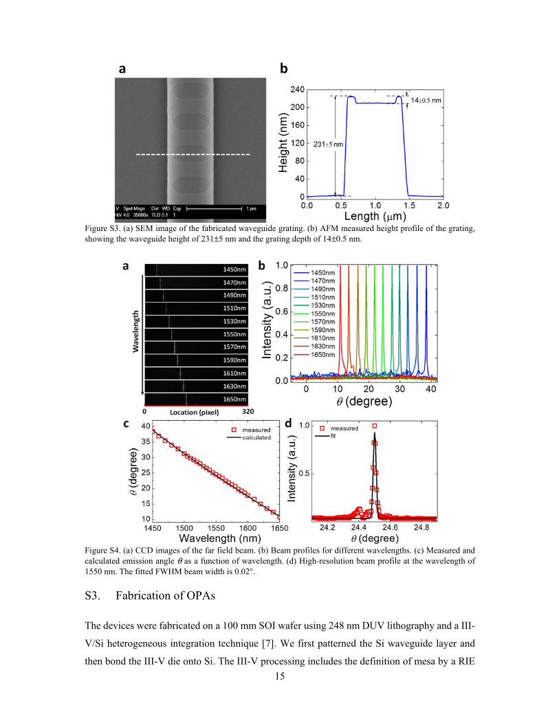
S2. Characterization of the single waveguide grating
In our OPA demonstration, we adopt a surface grating aligned on the top of the ridge waveguide
to emit light and in design the grating has a width of 800 nm and a period is 560 nm with a
uniform duty cycle of 0.5. Unlike a traditional vertical grating coupler which has an effective
emission length within tense of micrometers, our surface grating is shallow etched with an
etching depth of ~14 nm in order to have a weak radiation strength (~28 dB/cm) and hence a
long effective emission length (at least 2 mm for 14 nm etch). Note that the total length of the
grating is 10 mm on the mask in order to achieve even longer effective emission length which
can be achieved with further optimization of the grating design.
Since the radiation strength highly depends on the etching depth, we developed a dry etch
process with very low etch rate of ~12 nm/min for Si to control the etched depth accurately, as
shown in Figure S3. We characterized the far field beam of a single waveguide grating using a
Fourier imaging setup. Figure S4(a) shows the CCD images of the far field beams at different
wavelengths. It can be seen that the beam is narrow in one direction but divergent in the other
direction due to the limited aperture in lateral dimension (~800 nm). In an OPA, the beam can
be focused in this direction by aligning the phases. The emission angle of the beam can be tuned
by changing the wavelength and we obtained a tuning efficiency in longitudinal emission angle
of 0.138 ± 0.002°/nm, which is in excellent agreement with a theoretical value of 0.139°/nm.
We also use this method to tune the steering angle of the beam in one dimension in the OPA.
The FWHM beam width was measured to be 0.02° at 1550 nm by fitting a Gaussian function,
corresponding to a ~2.5 mm effective emission length. A narrower beam can be achieved by
optimizing the emission strength profile or using even weaker grating emitters and the relevant
work can be found in our recent work [8].
15
Figure S3. (a) SEM image of the fabricated waveguide grating. (b) AFM measured height profile of the grating, showing the waveguide height of 231±5 nm and the grating depth of 14±0.5 nm.
Figure S4. (a) CCD images of the far field beam. (b) Beam profiles for different wavelengths. (c) Measured and calculated emission angle θ as a function of wavelength. (d) High-resolution beam profile at the wavelength of 1550 nm. The fitted FWHM beam width is 0.02°.
S3. Fabrication of OPAs
The devices were fabricated on a 100 mm SOI wafer using 248 nm DUV lithography and a III-
V/Si heterogeneous integration technique [7]. We first patterned the Si waveguide layer and
then bond the III-V die onto Si. The III-V processing includes the definition of mesa by a RIE

16
etch, QW etch, and n-contact region etch. Finally, the n/p contact metallization and probe metal
process were performed. Due to the small feature size of the dense structure and the large
topology (> 2 µm) of the surface, we developed a triple-layer process for metal lift-off as shown
in Figure S5. In this fabrication, first a photoresist is patterned on a polymer/SiO2 bi-layer and
an undercut profile is then created by dry etching the polymer with SiO2 as a mask; lastly, a
metal layer for contact is deposited in an electron-beam evaporation system and then the lift-
off is done in a solvent. The developed process allows us to define dense metal lines with a
pitch down to 2 µm or even less and a thickness of up to 1 µm on a flat substrate.
Figure S5. The flow of the triple-layer process for metal lift-off on a flat substrate.
In Figure S6, we show the photograph of one fabricated chip diced from the 100 mm wafer.
In Figure S7, we show the cross sections of the fabricated phase shifter array, demonstrating
high quality of the process and cross-section following the designed structure. The yield for
fabricating the III-V/Si phase shifters mainly depends on the bonding quality of III-V epi on
patterned Si surface. For 32-channel OPAs, the quality is high due to small area and thus this
yield can be up to 100% as we achieved in experiment. For an even larger scale OPAs, the yield
can be improved by optimizing bonding conditions and pre-screening the surface quality of
both Si and III-V material. For smaller pitch array (2 µm), the yield was low - mainly limited
by lithography, which can be improved by using more advanced tools in future.
Polymer
ResistSiO2
Substrate
Layer deposition Lithography pattern
Etching of polymer Metal depoistion Lift-off
Etching of hard mask
metal
a b c
d e f

17
Figure S6. A set of three 32-channel and one 240-channel OPAs on the top of a US quarter coin for size comparison.
Figure S7. The cross-sectional images of the III-V/Si phase shifter array with locally opened p (a) and n (b) contact for probe metal in one shifter on top.
S4. Characterization of the phase shifters
Figure S8(a) shows the I-V curve of III-V diode in a MZI modulator and a dark current at -2 V
bias is only 3 nA, implying a power consumption at a level of nanowatts for the phase shifter.
In Figure S8(b), we show the measured frequency response of the MZI modulator and obtain a
3dB electrical bandwidth of ~1.65 GHz limited by capacitance. Such bandwidth is sufficient
for OPA applications. In Figure S9, we also show the I-V curves for a 32-channel. It can be
seen that the electrical performance of III-V diode is uniform and the dark current is in a range
of 1-3 nA at -1 V bias, which implies the power consumption on the order of nanowatts for all
phase shifters. The uniformity of the performance in return proves the reliability of the
heterostructure III-V/Si platform for large-scale integration.
18
Figure S8. (a) I-V characteristics of the phase shifter. (b) Frequency response of the MZI modulator.
Figure S9. I-V curves of the 32-channel phase shifters. The inset shows the enlarged plot around -1 V bias.
In OPAs, a low voltage–length product (VπL) is desired for phase shifter in order to relax the
requirement of the electrical driver for the OPA. One way to reduce the VπL is increasing the
confinement factor of the mode in III-V QW region as we discussed before. In Figure S10, we
plot the measured VπL at different confinement factors for the waveguide widths of 1000 nm,
800 nm, and 600 nm. It is clear that a lower VπL can be achieved at a higher confinement factor
and for 600 nm waveguide the VπL of 0.225 V⋅cm is obtained. Therefore, in our OPA with 5
mm phase shifters, the operating voltage for 2π phase shift is less than -1.0 V and the power
consumption is on the order of 1-3 nanowatts for single phase shifters, which is, to the best of
our knowledge, a record low operating voltage and low-power on-chip OPA.
0 1 2 3 4 5 6
-12
-9
-6
-3
0
Re
spon
se (
dB
)
Frequency (GHz)-5 -4 -3 -2 -1 0 1
10-9
10-7
10-5
10-3
Cur
rent
(A
)
Bias voltage (V)
a b
-5 -4 -3 -2 -1 0 1
10-11
10-9
10-7
10-5
10-3
10-1
Cu
rre
nt (
A)
Bias voltage (V)
-1.1 -1.0
2
3
(V)
10-9 (A)

19
Figure S10. VπL as a function of confinement factor for the waveguide widths of 1000 nm, 800 nm, and 600 nm. The phase shifter was reversely biased and the data were measured at 1550 nm wavelength.
S5. Characterization of the far-field beam width
The far-field beam width of the OPA in both ψ and θ directions is wavelength-dependent. In ψ
axis, the beam width is determined by δψ ≈ λ/Npg, with λ the free-space wavelength, N the
number of channel and pg the pitch of grating array. In θ axis, the beam width is related to the
effective emission length of the grating which depends on the wavelength. We show the
measured FWHM beam width at different wavelengths in Figure S11. When increasing the
wavelength, the beam width in ψ broadens, agreeing with the theoretical prediction. In θ
direction, within our measurement range the narrowest beam width was measured at 1580 nm,
which means the longest effective emission length.
Figure S11. The measured beam width in both ψ and θ directions at different wavelengths.
References
[1] G. T. Reed, G. Mashanovich, F. Y. Gardes, D. J. Thomson, Nat. Photonics 2010, 4, 518.
0.20 0.25 0.30 0.35 0.400.22
0.24
0.26
0.28
0.30
0.32
VπL
(V
⋅cm
)
Confinement factor
1560 1580 1600
0.76
0.80
0.84 δψ δθ
δψ
(de
gree
)
Wavelength (nm)
0.014
0.016
0.018
δθ (degree)
20
[2] H. W. Chen, Y. H. Kuo, J. E. Bowers, IEEE Photonic Tech. L. 2008, 20, 1920.
[3] H. W. Chen, Y. H. Kuo, J. E. Bowers, Opt. Express 2008, 16, 20571.
[4] H. W. Chen, J. D. Peters, J. E. Bowers, Opt. Express 2011, 19, 1455.
[5] T. Hiraki, T. Aihara, K. Hasebe, K. Takeda, T. Fujii, T. Kakitsuka, T. Tsuchizawa, H.
Fukuda, S. Matsuo, Nat. Photonics 2017, 11, 482.
[6] J. H. Han, F. Boeuf, J. Fujikata, S. Takahashi, S. Takagi, M. Takenaka, Nat. Photonics 2017,
11, 486.
[7] M. A. Tran, T. Komljenovic, J. C. Hulme, M. J. Kennedy, D. J. Blumenthal, J. E. Bowers,
Opt. Express 2017, 25, 3826.
[8] W. Xie, J. Huang, T. Komljenovic, L. Coldren, and J. E. Bowers, arXiv:1810.00109, 2018.