digital control board for phased array antenna beam
115
DIGITAL CONTROL BOARD FOR PHASED ARRAY ANTENNA BEAM STEERING IN ADAPTIVE COMMUNICATION APPLICATIONS A Thesis presented to the Faculty of California Polytechnic State University San Luis Obispo In Partial Fulfillment of the Requirements for the Degree Master of Science in Electrical Engineering by Mayur Bansal November 2013
-
Upload
khangminh22 -
Category
Documents
-
view
4 -
download
0
Transcript of digital control board for phased array antenna beam
DIGITAL CONTROL BOARD FOR PHASED ARRAY ANTENNA BEAM
STEERING IN ADAPTIVE COMMUNICATION APPLICATIONS
A Thesis
presented to
the Faculty of California Polytechnic State University
San Luis Obispo
In Partial Fulfillment
of the Requirements for the Degree
Master of Science in Electrical Engineering
by
Mayur Bansal
November 2013

c© 2013
Mayur Bansal
ALL RIGHTS RESERVED
ii

COMMITTEE MEMBERSHIP
TITLE: Digital Control Board for Phased Array
Antenna Beam Steering in Adaptive Com-
munication Applications
AUTHOR: Mayur Bansal
DATE SUBMITTED: November 2013
COMMITTEE CHAIR: Bryan Mealy, Ph.D.
Associate Professor
Electrical Engineering Department
COMMITTEE MEMBER: Lynne Slivovsky, Ph.D.
Professor
Electrical Engineering Department
COMMITTEE MEMBER: Dennis Derickson, Ph.D.
Department Chair
Electrical Engineering Department
iii
ABSTRACT
Digital Control Board for Phased Array Antenna Beam Steering in Adaptive
Communication Applications
Mayur Bansal
The application of adaptive communication techniques for mobile communi-
cations has attracted considerable interest in the last decade. One example of
these techniques is spatial filtering through planar antenna array beam forming.
This thesis describes the development of a digital system that adaptively
controls a phased array antenna. The radiating structure of the phased antenna
array is tetrahedral-shaped and contains four antenna elements on each of its
three faces. The overall system comprises of a digital control board with an
external computer interface, an RF control board, and the phased antenna array.
The RF controls the main lobe direction on the phased array antenna. This thesis
describes the design and implementation of the digital control board.
The digital control board‘s primary responsibilities are implementing inter-
faces between the external computer and the RF board, which results in two
operational modes: the MATLAB graphical user interface (GUI) mode and the
adaptive receive mode. The GUI mode allows users to input parameters that
provide interactive control of the phased antenna array by interfacing with an
external computer and the RF control board. The adaptive receive mode im-
plements an algorithm for an adaptive receive station. This algorithm uses a
58-point scanning technique that locates the maximum receive power direction.
Test results show that the digital control board successfully manages the RF
board control voltage with an nominal error of less than 1%, which subsequently
iv

allows for precise control of the antenna‘s active face. Additionally, testing of
the GUI demonstrated the successful interactive application of various system
control parameters.
v

ACKNOWLEDGMENTS
I would like to thank my parents, Meenakshi and Bharat, for encouraging and
allowing me to pursue my ambitions. I am also grateful to my entire family for
their continual support.
I would like to thank my advisor, Dr. Dean Arakaki, for his guidance and
support. I would also like to thanks my project partner Steve Brockhoff for his
hard work and help, which made this thesis possible.
vi
TABLE OF CONTENTS
LIST OF TABLES ix
LIST OF FIGURES x
1 INTRODUCTION 1
2 SYSTEM DESIGN 4
2.1 System Requirements . . . . . . . . . . . . . . . . . . . . . . . . . 7
2.1.1 GUI Control . . . . . . . . . . . . . . . . . . . . . . . . . . 7
2.1.2 Adaptive Receive Mode . . . . . . . . . . . . . . . . . . . 9
2.2 System Sub-blocks . . . . . . . . . . . . . . . . . . . . . . . . . . 10
2.2.1 RF Power Detector . . . . . . . . . . . . . . . . . . . . . . 10
2.2.2 Interrupt Feedback Loop . . . . . . . . . . . . . . . . . . . 10
3 RF POWER DETECTOR 12
3.1 LT-5534 . . . . . . . . . . . . . . . . . . . . . . . . . . . . . . . . 14
3.2 LT-5538 . . . . . . . . . . . . . . . . . . . . . . . . . . . . . . . . 16
3.3 Log-Amp Power Detector Analysis . . . . . . . . . . . . . . . . . 18
4 INTERRUPT FEEDBACK LOOP 19
4.1 ADC . . . . . . . . . . . . . . . . . . . . . . . . . . . . . . . . . . 20
4.2 Interrupt . . . . . . . . . . . . . . . . . . . . . . . . . . . . . . . . 23
4.3 DAC . . . . . . . . . . . . . . . . . . . . . . . . . . . . . . . . . . 24
4.4 Comparator . . . . . . . . . . . . . . . . . . . . . . . . . . . . . . 27
5 RF SYSTEM INTEGRATION 29
5.1 Phase Shifters . . . . . . . . . . . . . . . . . . . . . . . . . . . . . 29
5.2 RF Single Pole Double Throw (SPDT) Switch . . . . . . . . . . . 34
5.3 RF Single Pole Triple Throw (SP3T) Switch . . . . . . . . . . . . 35
5.4 Voltage Control Oscillator (VCO) Control Line . . . . . . . . . . 36
vii
6 PRINTED CIRCUIT BOARD DESIGN 39
6.1 Schematic . . . . . . . . . . . . . . . . . . . . . . . . . . . . . . . 39
6.2 Layout . . . . . . . . . . . . . . . . . . . . . . . . . . . . . . . . . 40
7 GRAPHICAL USER INTERFACE (GUI) CONTROL SYSTEM 42
7.1 GUI Inputs and Features . . . . . . . . . . . . . . . . . . . . . . . 43
7.1.1 Drop Down Menus . . . . . . . . . . . . . . . . . . . . . . 43
7.1.2 Edit Text . . . . . . . . . . . . . . . . . . . . . . . . . . . 47
7.1.3 Push Buttons . . . . . . . . . . . . . . . . . . . . . . . . . 49
7.1.4 Additional Figure Checkboxes . . . . . . . . . . . . . . . . 50
7.2 Communication Protocol . . . . . . . . . . . . . . . . . . . . . . . 51
7.3 Test and Results . . . . . . . . . . . . . . . . . . . . . . . . . . . 53
8 ADAPTIVE RECEIVE MODE 58
8.1 Adaptive Receive Algorithm . . . . . . . . . . . . . . . . . . . . . 58
8.2 Testing . . . . . . . . . . . . . . . . . . . . . . . . . . . . . . . . . 62
9 CONCLUSIONS AND FUTURE WORK 65
BIBLIOGRAPHY 67
APPENDICES 69
A 2013 IEEE APS Student Design Challenge: Reconfigurable Antennas 69
B Contest Proposal . . . . . . . . . . . . . . . . . . . . . . . . . . . 72
C LT 5534 Demo Board Schematic . . . . . . . . . . . . . . . . . . . 75
D LT 5538 Demo Board Schematic . . . . . . . . . . . . . . . . . . . 77
E Microcontroller Code . . . . . . . . . . . . . . . . . . . . . . . . . 79
F PCB Schematic . . . . . . . . . . . . . . . . . . . . . . . . . . . . 90
G PCB Layout . . . . . . . . . . . . . . . . . . . . . . . . . . . . . . 96
H Bill Of Materials . . . . . . . . . . . . . . . . . . . . . . . . . . . 98
I Block Diagrams . . . . . . . . . . . . . . . . . . . . . . . . . . . . 100
viii
LIST OF TABLES
2.1 16-Pin IDC Pin-out Between Digital Control Board and RF Board 6
4.1 ADC Conversion Time . . . . . . . . . . . . . . . . . . . . . . . . 22
4.2 ADC Configuration . . . . . . . . . . . . . . . . . . . . . . . . . . 23
4.3 Interrupt Configuration . . . . . . . . . . . . . . . . . . . . . . . . 23
4.4 DAC Command Codes . . . . . . . . . . . . . . . . . . . . . . . . 26
4.5 DAC Address Codes . . . . . . . . . . . . . . . . . . . . . . . . . 26
5.1 Truth Table for SPDT, VHIGH = 2V to 5V, VLOW = 0V InsertionLoss = 0.5dB, and Isolation = 22dB . . . . . . . . . . . . . . . . 34
5.2 SPDT, Antenna Mode Truth Table . . . . . . . . . . . . . . . . . 35
5.3 Truth Table for HMC245QS16 and the Active Antenna Face . . . 36
5.4 VCO Tuning Circuit Result . . . . . . . . . . . . . . . . . . . . . 38
7.1 Hexadecimal Notation for ASCII Decimal Characters to 8-bit In-tegers . . . . . . . . . . . . . . . . . . . . . . . . . . . . . . . . . 52
7.2 GUI Test Result . . . . . . . . . . . . . . . . . . . . . . . . . . . . 54
8.1 Test Data for Adaptive Receive Mode Test Procedure . . . . . . . 63
ix
LIST OF FIGURES
1.1 A Radiation Diagram with Main Lobe . . . . . . . . . . . . . . . 2
2.1 System Block Diagram . . . . . . . . . . . . . . . . . . . . . . . . 4
2.2 Tetrahedron Antenna Model . . . . . . . . . . . . . . . . . . . . . 5
2.3 Digital Control Board Block Diagram . . . . . . . . . . . . . . . . 5
2.4 IDC connector Pin Positions . . . . . . . . . . . . . . . . . . . . . 6
2.5 Screen shot of MATLAB GUI . . . . . . . . . . . . . . . . . . . . 8
2.6 Adaptive RX, Example System Configuration . . . . . . . . . . . 9
2.7 Inner Feedback Loop Block Diagram . . . . . . . . . . . . . . . . 11
3.1 DC log-amp BJT implementation . . . . . . . . . . . . . . . . . . 13
3.2 Demo Board DC748A . . . . . . . . . . . . . . . . . . . . . . . . . 14
3.3 LT-5534 log-amp Characteristics . . . . . . . . . . . . . . . . . . . 15
3.4 Demo Board DC1120A . . . . . . . . . . . . . . . . . . . . . . . . 16
3.5 LT-5538 Output characteristics . . . . . . . . . . . . . . . . . . . 17
4.1 Analog to Digital Converter Timing Diagram for Single ConversionMode . . . . . . . . . . . . . . . . . . . . . . . . . . . . . . . . . . 22
4.2 LTC2656 DAC Load Sequence . . . . . . . . . . . . . . . . . . . . 25
4.3 LM339 Schematic Diagram . . . . . . . . . . . . . . . . . . . . . . 28
5.1 JSPHS-2484+ Phase Shifter, Interpolated Data . . . . . . . . . . 30
5.2 Operational Amplifier in Non-Inverting Configuration . . . . . . . 30
5.3 LTSpice Simulation Schematic, LT6005 Non-Inverting Gain Op-Amp Circuit . . . . . . . . . . . . . . . . . . . . . . . . . . . . . . 31
5.4 LTSpice Simulation results, LT6005 Op-amp Non-Inverting GainCircuit . . . . . . . . . . . . . . . . . . . . . . . . . . . . . . . . . 32
x
5.4 LTSpice Simulation results, LT6005 Op-amp Non-Inverting GainCircuit . . . . . . . . . . . . . . . . . . . . . . . . . . . . . . . . . 33
5.5 Monte Carlo Analysis for Amplification Circuit, Expanded View . 33
5.6 AS179-92LF, SPDT, Pin-out and Block Diagram . . . . . . . . . 34
5.7 HMC245QS16 SP3T RF Switch Pin-out and Functional Diagram 35
5.8 JTOS-2700V, VCO, datasheet characteristic . . . . . . . . . . . . 37
5.9 VCO tuning Schematic, R5 is the tunable resistor . . . . . . . . . 38
6.1 PCB layout . . . . . . . . . . . . . . . . . . . . . . . . . . . . . . 41
7.1 RS-232, 9-pin D-sub connector pinout . . . . . . . . . . . . . . . 42
7.2 MATLAB GUI main screen . . . . . . . . . . . . . . . . . . . . . 43
7.3 MATLAB GUI screen with Face drop down menu . . . . . . . . . 44
7.4 MATLAB GUI Screen with Mode Drop-Down Menu . . . . . . . . 45
7.5 TRENDnet TU-S9, USB to RS-232 Converter Cable . . . . . . . 45
7.6 Device Manager screen shot with COM port highlighted . . . . . 46
7.7 MATLAB GUI screen with COM drop down menu . . . . . . . . 47
7.8 Antenna Radiation Pattern Coordinate system . . . . . . . . . . . 48
7.9 MATLAB GUI Screen Shot, θ and φ Control Variables . . . . . . 49
7.10 Phase Shifter JSPHS-2484+ Interpolated Data . . . . . . . . . . 50
7.11 Checkbox Selected Images, with θ = 30 and φ = 45 . . . . . . . 51
7.12 RS-232 Frame . . . . . . . . . . . . . . . . . . . . . . . . . . . . 51
7.13 Communication Packet Frame . . . . . . . . . . . . . . . . . . . 52
7.14 Microcontroller, MATLAB GUI Mode Flowchart . . . . . . . . . 53
7.15 Status LED’s for Mode and Face value . . . . . . . . . . . . . . . 55
7.16 GUI Test Measured Radiation Patterns . . . . . . . . . . . . . . . 56
7.16 GUI Test Measured Radiation Patterns . . . . . . . . . . . . . . . 57
8.1 Adaptive Receive scan plot . . . . . . . . . . . . . . . . . . . . . . 59
8.2 Raster Scan Pattern . . . . . . . . . . . . . . . . . . . . . . . . . 60
8.3 Adaptive Receive Flowchart . . . . . . . . . . . . . . . . . . . . . 61
8.4 ISR Flowchart . . . . . . . . . . . . . . . . . . . . . . . . . . . . . 62
xi
I.1 Schottky Diode Chip Model . . . . . . . . . . . . . . . . . . . . . 100
I.2 ATmega2560 Block Diagram . . . . . . . . . . . . . . . . . . . . . 101
I.3 Analog to Digital Converter Block Schematic . . . . . . . . . . . . 102
I.4 LTC2656 Block Diagram . . . . . . . . . . . . . . . . . . . . . . . 103
xii
CHAPTER 1
INTRODUCTION
An adaptive communication system was proposed as a contest entry to the 4th
IEEE Antenna Design Challenge, sponsored by the Antenna and Propagation
Society (AP-S). This thesis describes an adaptive communication system, which
was developed as a contest entry. The main challenge of the contest was to
develop an “antenna system with reconfigurable antenna elements that can adapt
to different propagation conditions (e.g. line-of-sight versus non-line-of-sight).”
The IEEE contest rules are shown in Appendix A. The two page proposal for the
design challenge is shown in Appendix B.
A phased adaptive antenna array was proposed for the contest entry. Adap-
tive phased array antennas can change their radiation pattern electronically or
mechanically. In electrically configurable radiation pattern antenna, elements
have a relative phase difference while the antenna elements remain stationary.
Whereas in mechanical reconfigurable radiation patterns, antenna elements are
placed relative to each other but the antenna elements are movable. A tetrahe-
dral structure with four patch antennas on each face of the antenna is developed,
as shown in Figure 2.2. Only one face is active at any given moment. A relative
phase difference in the four patch antenna changes the radiation pattern’s main
lobe direction, which is referred to as beam steering. The main lobe of an antenna
radiation pattern contains the maximum power. Figure 1.1 shows a main lobe
for a radiation pattern.
1
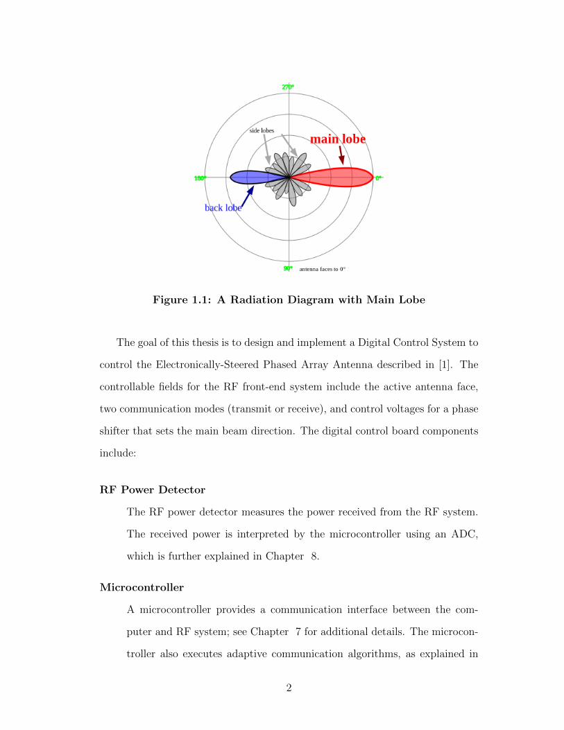
Figure 1.1: A Radiation Diagram with Main Lobe
The goal of this thesis is to design and implement a Digital Control System to
control the Electronically-Steered Phased Array Antenna described in [1]. The
controllable fields for the RF front-end system include the active antenna face,
two communication modes (transmit or receive), and control voltages for a phase
shifter that sets the main beam direction. The digital control board components
include:
RF Power Detector
The RF power detector measures the power received from the RF system.
The received power is interpreted by the microcontroller using an ADC,
which is further explained in Chapter 8.
Microcontroller
A microcontroller provides a communication interface between the com-
puter and RF system; see Chapter 7 for additional details. The microcon-
troller also executes adaptive communication algorithms, as explained in
2
Chapter 8.
Digital Peripherals
The digital peripherals include a digital-to-analog converter (DAC), a com-
parator, and an analog-to-digital converter (ADC). The ADC is an internal
peripheral of the microcontroller. The DAC output voltages control the
phase shifters (via an SPI bus) to steer the antenna beam. The ADC mea-
sures received power by sampling the RF power detector output voltage.
The comparator checks the receive power level against a reference level set
by the DAC; this level is the previously received maximum power and is
discussed further in Chapter 4. A feedback loop is implemented using an
ADC, DAC and a comparator. The feedback loop improves the time re-
quired to find the receive direction with maximum power. The feedback
loop is explained in Chapter 4.
3
CHAPTER 2
SYSTEM DESIGN
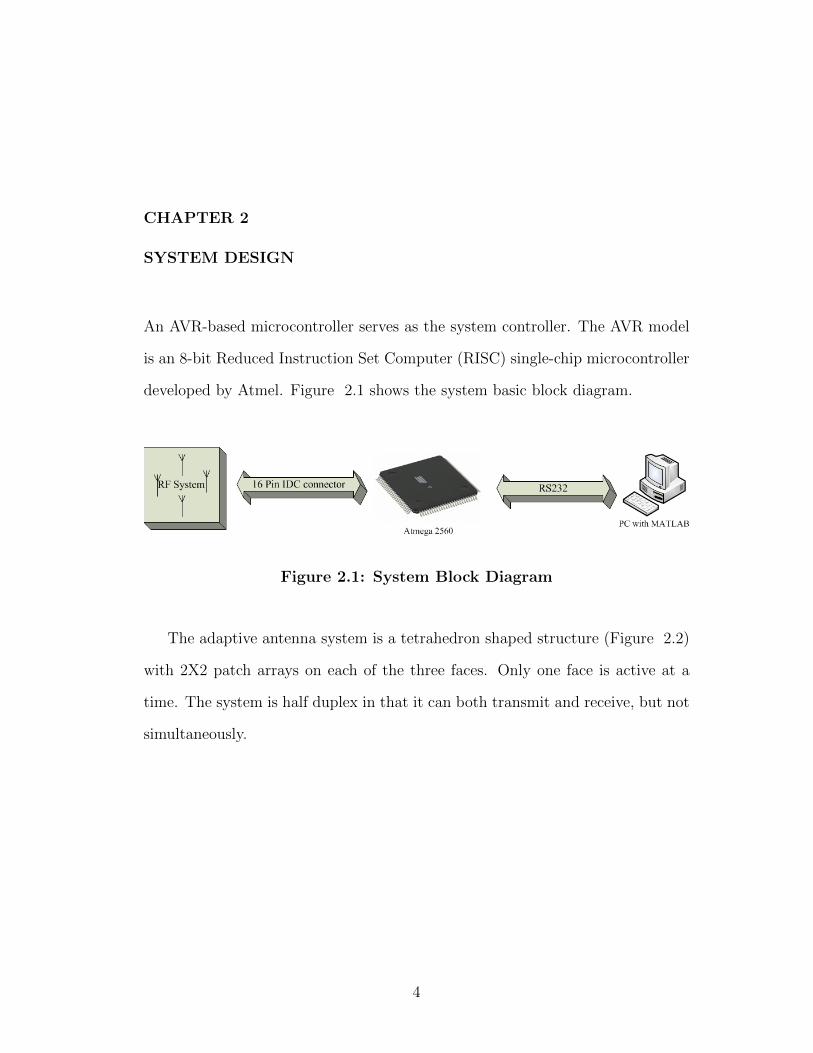
An AVR-based microcontroller serves as the system controller. The AVR model
is an 8-bit Reduced Instruction Set Computer (RISC) single-chip microcontroller
developed by Atmel. Figure 2.1 shows the system basic block diagram.
Figure 2.1: System Block Diagram
The adaptive antenna system is a tetrahedron shaped structure (Figure 2.2)
with 2X2 patch arrays on each of the three faces. Only one face is active at a
time. The system is half duplex in that it can both transmit and receive, but not
simultaneously.
4
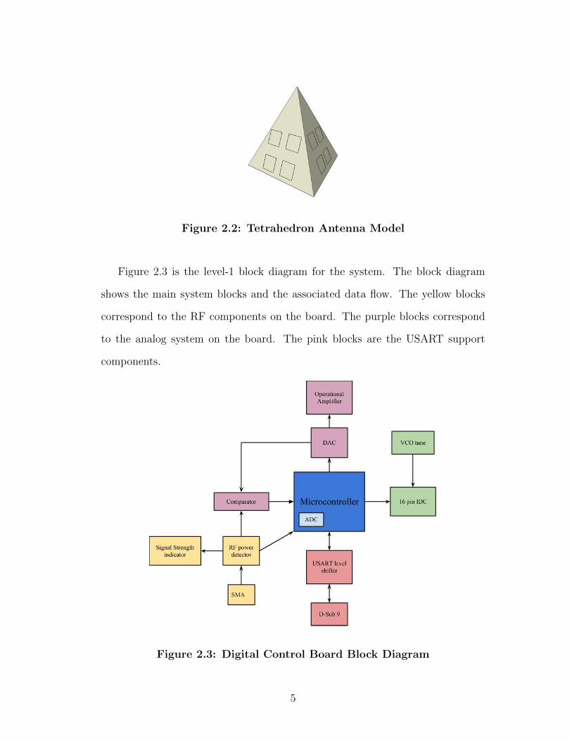
Figure 2.2: Tetrahedron Antenna Model
Figure 2.3 is the level-1 block diagram for the system. The block diagram
shows the main system blocks and the associated data flow. The yellow blocks
correspond to the RF components on the board. The purple blocks correspond
to the analog system on the board. The pink blocks are the USART support
components.
Figure 2.3: Digital Control Board Block Diagram
5
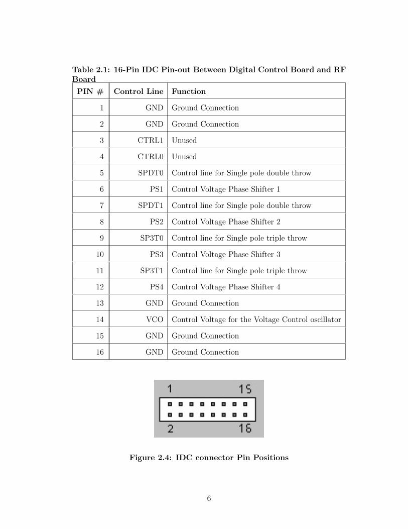
Table 2.1: 16-Pin IDC Pin-out Between Digital Control Board and RFBoard
PIN # Control Line Function
1 GND Ground Connection
2 GND Ground Connection
3 CTRL1 Unused
4 CTRL0 Unused
5 SPDT0 Control line for Single pole double throw
6 PS1 Control Voltage Phase Shifter 1
7 SPDT1 Control line for Single pole double throw
8 PS2 Control Voltage Phase Shifter 2
9 SP3T0 Control line for Single pole triple throw
10 PS3 Control Voltage Phase Shifter 3
11 SP3T1 Control line for Single pole triple throw
12 PS4 Control Voltage Phase Shifter 4
13 GND Ground Connection
14 VCO Control Voltage for the Voltage Control oscillator
15 GND Ground Connection
16 GND Ground Connection
Figure 2.4: IDC connector Pin Positions
6
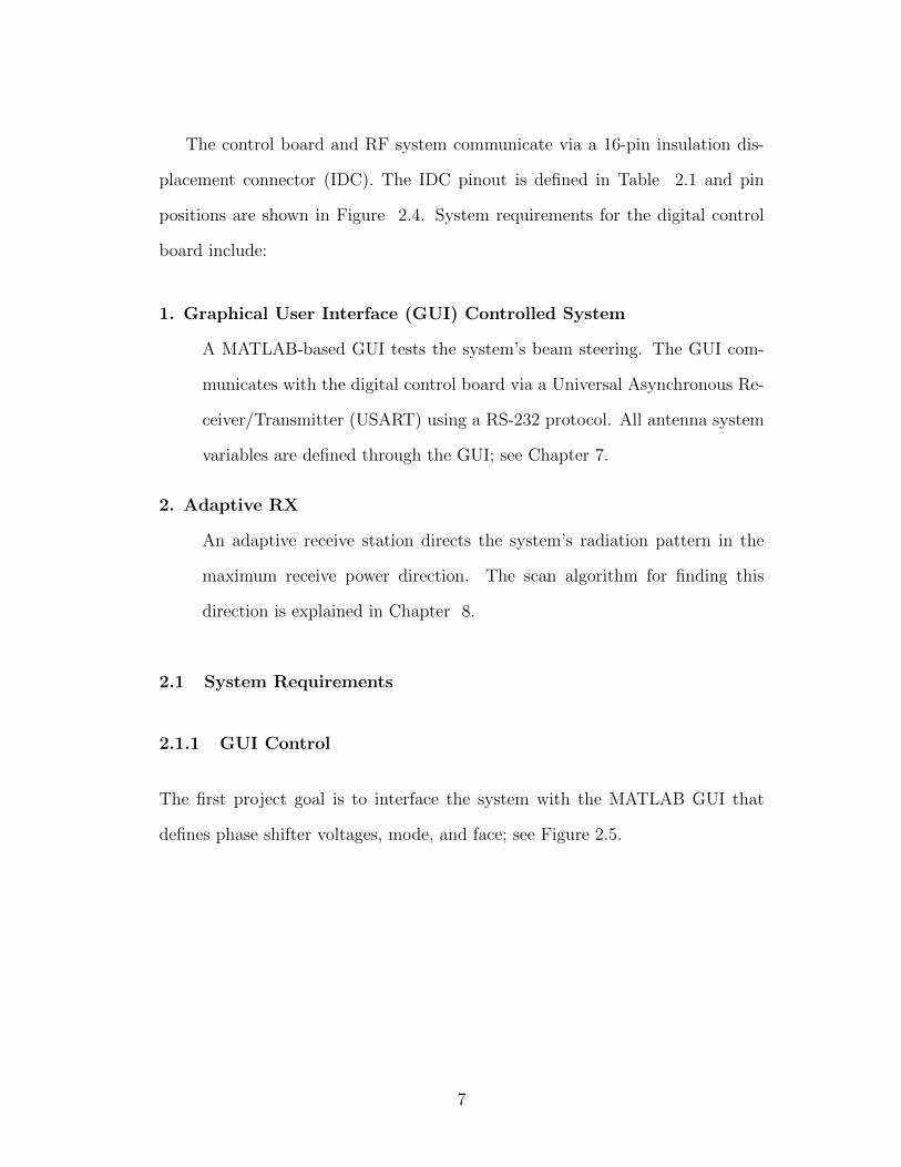
The control board and RF system communicate via a 16-pin insulation dis-
placement connector (IDC). The IDC pinout is defined in Table 2.1 and pin
positions are shown in Figure 2.4. System requirements for the digital control
board include:
1. Graphical User Interface (GUI) Controlled System
A MATLAB-based GUI tests the system’s beam steering. The GUI com-
municates with the digital control board via a Universal Asynchronous Re-
ceiver/Transmitter (USART) using a RS-232 protocol. All antenna system
variables are defined through the GUI; see Chapter 7.
2. Adaptive RX
An adaptive receive station directs the system’s radiation pattern in the
maximum receive power direction. The scan algorithm for finding this
direction is explained in Chapter 8.
2.1 System Requirements
2.1.1 GUI Control
The first project goal is to interface the system with the MATLAB GUI that
defines phase shifter voltages, mode, and face; see Figure 2.5.
7
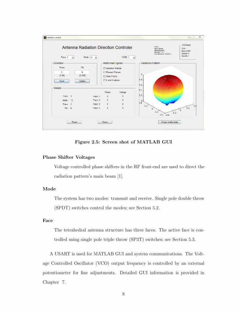
Figure 2.5: Screen shot of MATLAB GUI
Phase Shifter Voltages
Voltage controlled phase shifters in the RF front-end are used to direct the
radiation pattern’s main beam [1].
Mode
The system has two modes: transmit and receive. Single pole double throw
(SPDT) switches control the modes; see Section 5.2.
Face
The tetrahedral antenna structure has three faces. The active face is con-
trolled using single pole triple throw (SP3T) switches; see Section 5.3.
A USART is used for MATLAB GUI and system communications. The Volt-
age Controlled Oscillator (VCO) output frequency is controlled by an external
potentiometer for fine adjustments. Detailed GUI information is provided in
Chapter 7.
8
2.1.2 Adaptive Receive Mode
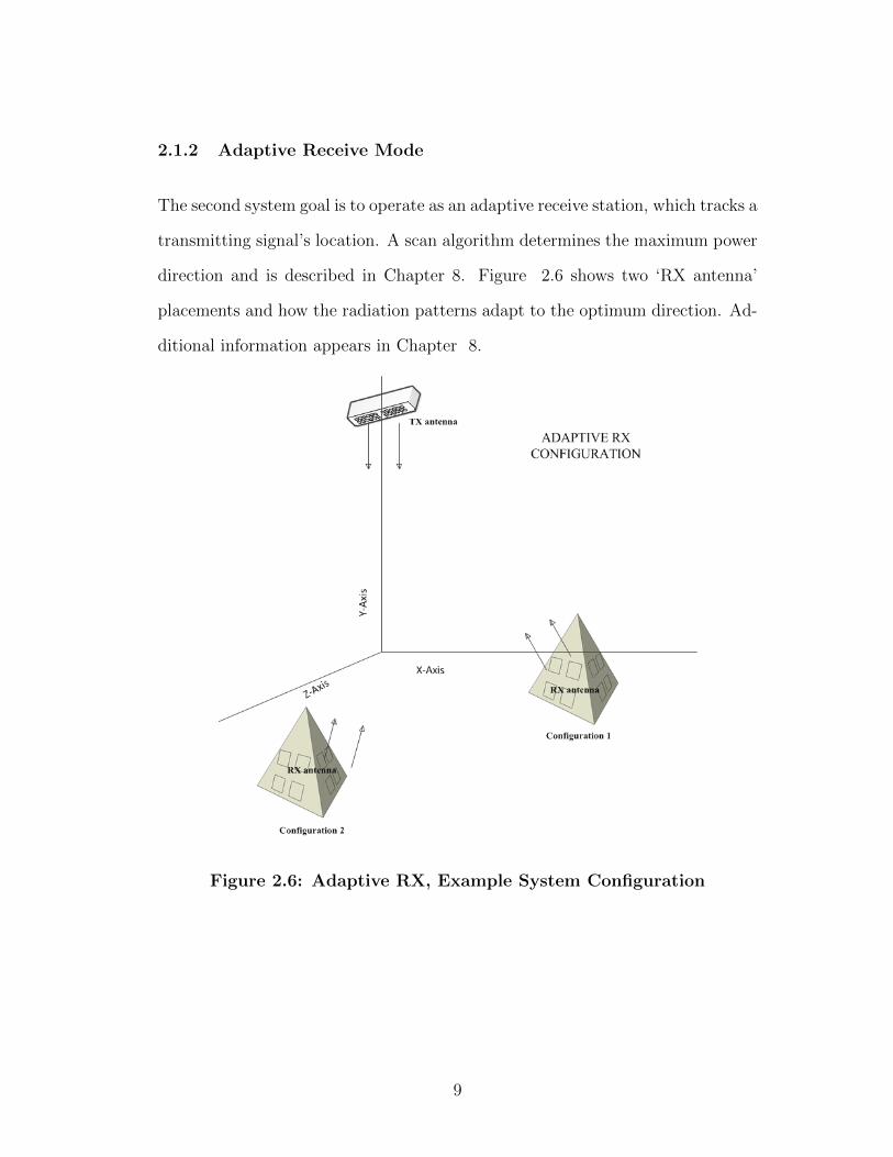
The second system goal is to operate as an adaptive receive station, which tracks a
transmitting signal’s location. A scan algorithm determines the maximum power
direction and is described in Chapter 8. Figure 2.6 shows two ‘RX antenna’
placements and how the radiation patterns adapt to the optimum direction. Ad-
ditional information appears in Chapter 8.
Figure 2.6: Adaptive RX, Example System Configuration
9
2.2 System Sub-blocks
2.2.1 RF Power Detector
The RF power detector converts the received RF power to a DC voltage. Most RF
power detectors are Schottky diode-based topologies; they exhibit an exponential
relation between input power and output voltage, Vout(V ) ∝ ePin(W ). Another
common implementation is a log-amp based topology, which exhibits a linear
relationship between input power and output voltage, Vout(V ) ∝ Pin(W ). RF
power detector information appears in Chapter 3.
2.2.2 Interrupt Feedback Loop
The block diagram of the Interrupt Feedback Loop is shown in Figure 2.7. The
Interrupt Feedback Loop improves system efficiency by reducing the number of
required ADC samples at every step. The ADC samples only when hardware
interrupts are triggered; i.e.: when a power level that exceeds the previous max-
imum is detected. When an interrupt is triggered, the received power is saved in
memory as the new maximum value. The feedback loop includes a comparator,
the RF power detector and the microcontroller. The microcontroller uses a DAC
to set the comparator’s reference level, which represents the previous maximum
received power. Interrupt feedback loop information is provided in Chapter 4.
10
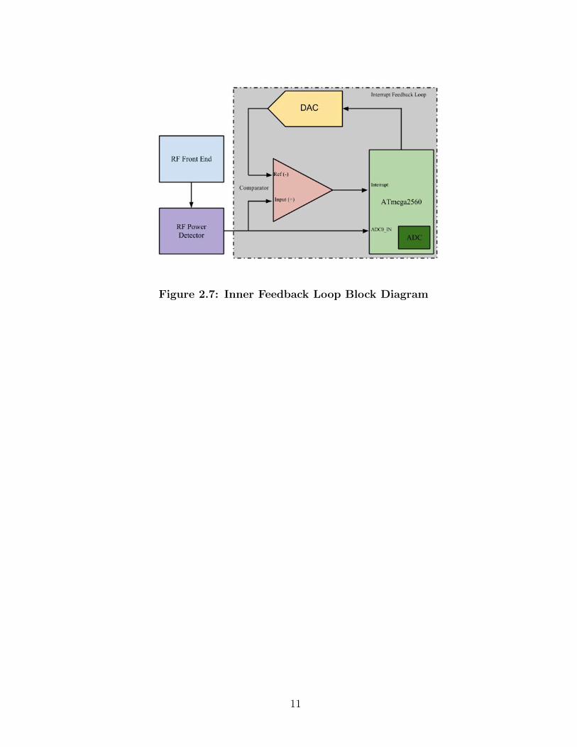
Figure 2.7: Inner Feedback Loop Block Diagram
11

CHAPTER 3
RF POWER DETECTOR
An RF power detector monitors the RF circuit’s output and develops a DC
voltage proportional to the received power in Watts [2]. Equation 3.1 shows
power in decibels relative to 1mW (dBm), commonly used by RF and wireless
engineers.
P (dBm) = 10logP (mW ) (3.1)
An operational amplifier (op-amp) with a PN junction diode as negative feed-
back is a classical implementation for a log-amp [3]. The logarithmic relationship
between diode voltage and current yields a linear relationship between input
power (dB scale) and output voltage (linear voltage scale). A bipolar junction
transistor (BJT) generates the logarithmic I vs V relation in place of a diode.
Figure 3.1 shows implementation examples for the single stage NPN and PNP
log-amp. Equation 3.2 defines RF power detector output voltage (Vout) as a
function of the input power (Iin).
Vout =kT
qlnICIS≈ kT
qlnIInIS
(3.2)
12
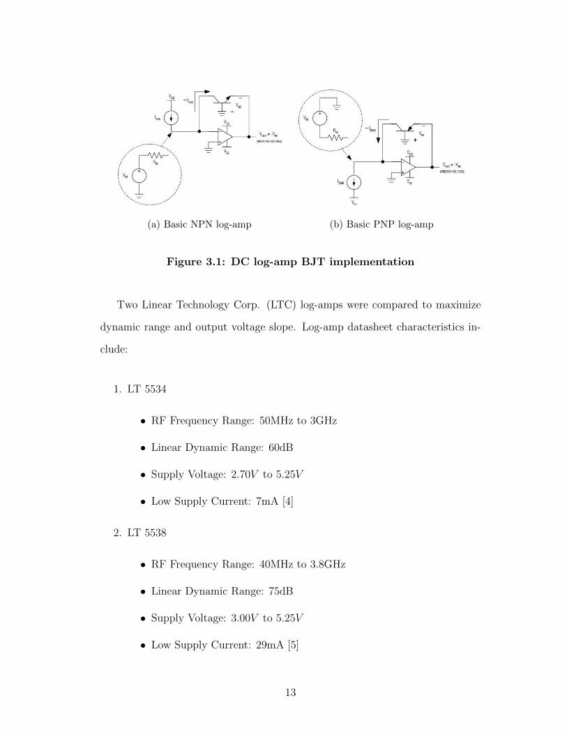
(a) Basic NPN log-amp (b) Basic PNP log-amp
Figure 3.1: DC log-amp BJT implementation
Two Linear Technology Corp. (LTC) log-amps were compared to maximize
dynamic range and output voltage slope. Log-amp datasheet characteristics in-
clude:
1. LT 5534
• RF Frequency Range: 50MHz to 3GHz
• Linear Dynamic Range: 60dB
• Supply Voltage: 2.70V to 5.25V
• Low Supply Current: 7mA [4]
2. LT 5538
• RF Frequency Range: 40MHz to 3.8GHz
• Linear Dynamic Range: 75dB
• Supply Voltage: 3.00V to 5.25V
• Low Supply Current: 29mA [5]
13
The log-amps were compared to the required dynamic range, 60dB, and
the output slope of the linear Vout(V ) vs input power(dBm) relationship, >
20mV/dB. Comparison results are shown in Section 3.3.
3.1 LT-5534
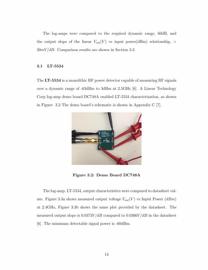
The LT-5534 is a monolithic RF power detector capable of measuring RF signals
over a dynamic range of -63dBm to 3dBm at 2.5GHz [6]. A Linear Technology
Corp log-amp demo board DC748A enabled LT-5534 characterization, as shown
in Figure 3.2 The demo board’s schematic is shown in Appendix C [7].
Figure 3.2: Demo Board DC748A
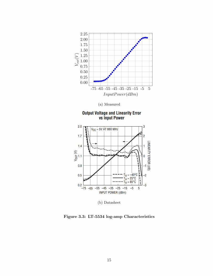
The log-amp, LT-5534, output characteristics were compared to datasheet val-
ues. Figure 3.3a shows measured output voltage Vout(V ) vs Input Power (dBm)
at 2.4GHz, Figure 3.3b shows the same plot provided by the datasheet. The
measured output slope is 0.0373V/dB compared to 0.0366V/dB in the datasheet
[6]. The minimum detectable signal power is -60dBm.
14
5-5-15-25-35-45-55-65-75
0.00
0.25
0.50
0.75
1.00
1.25
1.50
1.75
2.00
2.25
InputPower(dBm)
Vout(V
)
(a) Measured
(b) Datasheet
Figure 3.3: LT-5534 log-amp Characteristics
15
3.2 LT-5538
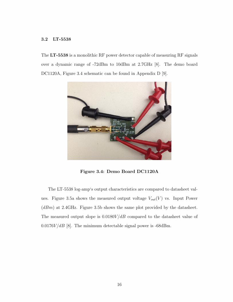
The LT-5538 is a monolithic RF power detector capable of measuring RF signals
over a dynamic range of -72dBm to 10dBm at 2.7GHz [8]. The demo board
DC1120A, Figure 3.4 schematic can be found in Appendix D [9].
Figure 3.4: Demo Board DC1120A
The LT-5538 log-amp‘s output characteristics are compared to datasheet val-
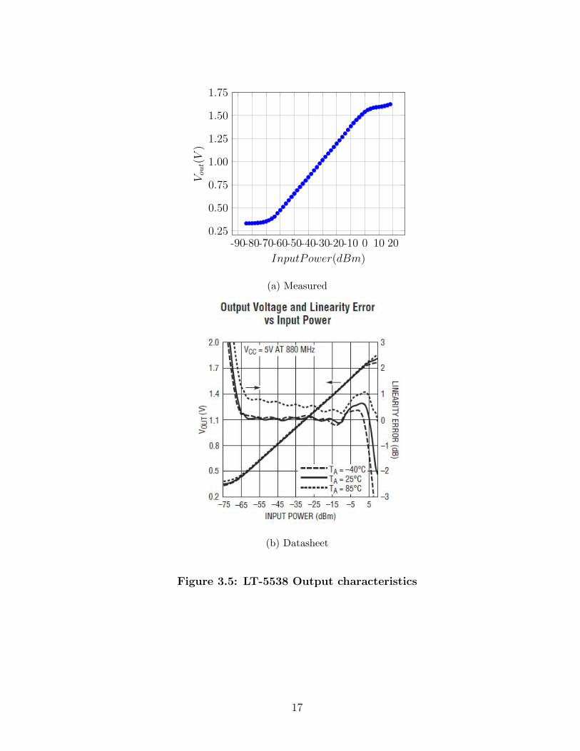
ues. Figure 3.5a shows the measured output voltage Vout(V ) vs. Input Power
(dBm) at 2.4GHz. Figure 3.5b shows the same plot provided by the datasheet.
The measured output slope is 0.0180V/dB compared to the datasheet value of
0.0176V/dB [8]. The minimum detectable signal power is -68dBm.
16
20100-10-20-30-40-50-60-70-80-900.25
0.50
0.75
1.00
1.25
1.50
1.75
InputPower(dBm)
Vout(V
)
(a) Measured
(b) Datasheet
Figure 3.5: LT-5538 Output characteristics
17

3.3 Log-Amp Power Detector Analysis
From the previous sub-sections, the LT-5534 and LT-5538 have output slopes
of 37.3mV/dB and 18.0mV/dB, respectively. For an 8-bit ADC with reference
voltage of 5V , a quantum is 19.6mV , as shown in Equation 3.3.
quanta =5V
28 − 1= 19.6mV (3.3)
Thus the LT-5534 is the best option, since the dynamic range satisfies the
required range (−60dBm to −30dBm) and the output slope is greater than one
quanta (19.6mV/dB).
18
CHAPTER 4
INTERRUPT FEEDBACK LOOP
Microcontrollers are widely used in communication applications. The AT-mega2560
AVR architecture [12], microcontroller is the main system controller for the sys-
tem. Key features include:
• Flash : 256 Kbytes (kB)
• Static Random Access Memory (SRAM): 8 kB
• Maximum Operating Frequency: 16 MHz
• Serial Peripheral Interface (SPI): 5 channels
• Analog-to-Digital Converter: 16 channels, 10-Bit Resolution
• Real Time Clock (RTC)
Flash memory stores the boot loader and firmware. The boot loader is a
program that loads the firmware, or runtime environment, for the processor fol-
lowing self-test completion. SRAM microcontroller memory used for system vari-
able declaration and firmware operation. An algorithm with multiple subroutines
requires an extensive (>128kB) flash memory (see Section 8.1 for algorithm).
Status variables are required for each algorithm branch; thus, greater than 2kB
of SRAM must be available. Many current digital peripherals use a communica-
tion protocol (SPI, CAN, I2C, USART, etc.) for intercommunication. SPI and
19
USART are the two communication buses used in this system. ADC converts the
RF peak detector DC output voltage into a digital value. A 2% output accuracy
and resolution greater than eight bits is required to capture a 0.25dBm change
in received power level. Real time clock (RTC) compatibility is preferred for sys-
tems synchronization. Figure I.2 (Appendix I) shows the microcontroller’s block
diagram.
The inner feedback loop (Figure 2.7) consists of an ADC, DAC, and a com-
parator. The DAC sets the reference input to the comparator. The peak detector
output is connected to both the positive input terminal of the comparator and
the microcontroller’s ADC input.
When the peak detector output is greater than the comparator’s reference
voltage, the comparator output changes to logic high, triggering a microcon-
troller interrupt. The microcontroller is notified that a new maximum power
has been received and is sampled by the microcontroller’s ADC. In this case, a
new reference value is set by the DAC, and microcontroller stores the face and
phase counters (see Section 8.1). This loop eliminates redundant power detector
output voltage sampling in each algorithm step. Only voltage levels greater than
the previously received maximum power are sampled. Lock time is defined as the
time required to find the optimal receive direction.
4.1 ADC
The microcontroller’s ADC samples the power detector’s output voltage. Figure
I.3 (Appendix I) shows the microcontroller’s ADC block schematic. Key features
include:
• 10-bit resolution
20
• 13µs - 260µs conversion time
• 0V − VCC ADC input voltage range, VCC = 5V
• Free running or single conversion mode
The ATmega2560 uses a 10-bit successive approximation ADC that can be
configured as either a single-ended or a differential input. A single-ended ADC
is preferable since negative voltages are not sampled. Equation 4.1 defines the
digital output for a single-ended conversion, where VIN is the voltage at the
selected input and VREF is the selected voltage reference.
ADCout = floor(VIN .1024
VREF
)(4.1)
The 10-bit ADC resolution results in a quanta of (VCC = 5V ):
quanta =VCC
2n − 1=
5V
210 − 1= 4.9mV (4.2)
The ADC is configured in single conversion mode since samples are recorded only
upon interrupt triggers. As specified in Table 4.1, the first conversion requires 25
clock cycles, while subsequent conversions require 13 clock cycles.
21
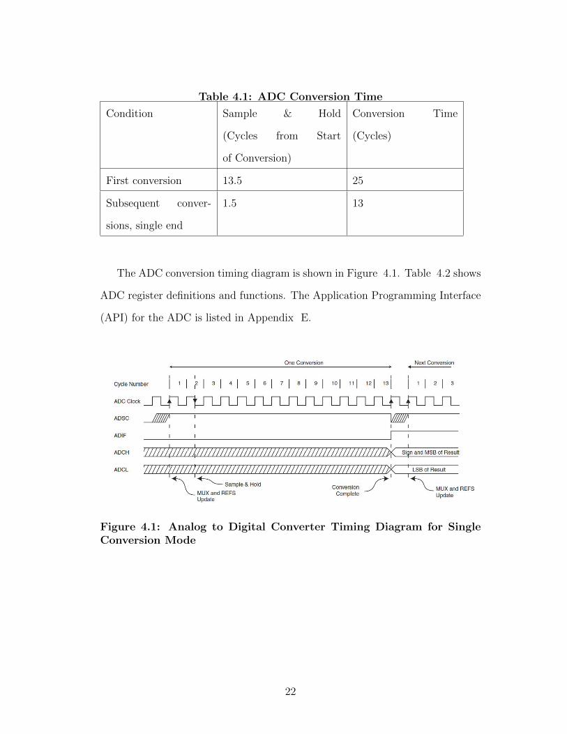
Table 4.1: ADC Conversion Time
Condition Sample & Hold
(Cycles from Start
of Conversion)
Conversion Time
(Cycles)
First conversion 13.5 25
Subsequent conver-
sions, single end
1.5 13
The ADC conversion timing diagram is shown in Figure 4.1. Table 4.2 shows
ADC register definitions and functions. The Application Programming Interface
(API) for the ADC is listed in Appendix E.
Figure 4.1: Analog to Digital Converter Timing Diagram for SingleConversion Mode
22
Table 4.2: ADC Configuration
ADC
Parameter
Microcontroller
Register and Bit(s)
Value Value Interpretation
Reference Value ADMUX(REFS1:0) b01 AVCC with external ca-
pacitor at AREF pin, 5V
ADC Clock ADCSRA(ADPS2:0) b010 XTAL/4
ADC Trigger ADCSRA(ADATE) b0 ADC auto trigger disable
ADC Input Pin ADCSRB(MUX5) +
ADMUX(MUX4:0)
b000000 ADC0
ADV value justi-
fication
ADMUX(ADLAR) b1 ADC left adjust result
ADC Interrupt ADCSRA(ADIE) b0 ADC interrupt disables
4.2 Interrupt
An external microcontroller interrupt triggers the Interrupt Service Routine (ISR)
(see Chapter 8). The interrupt configuration for the microcontroller in shown in
Table 4.3.
Table 4.3: Interrupt Configuration
Interrupt
Parameter
Microcontroller
Register and Bit(s)
Value Value Interpretation
Active Interrupt
pin
EIMSK(INT0) b1 Enable INT0
Interrupt trigger
edge
EICRA(ISC10:00) b011 Rising edge triggered
23
4.3 DAC
The LTC2565 is an Octal 12-bit rail-to-rail DAC. The DAC block diagram is
shown in Figure I.4 (Appendix I). Key features include:
• 8 individually configurable DAC units
• Synchronous or asynchronous update on each DAC
• Precision 10ppm/C Max Deviation from Reference Voltage
• Selectable Internal or External Reference
• Power-On-Reset to Zero-Scale (0V )/Mid-scale (half of reference voltage)
In the internal feedback loop, one DAC output channel is set to the compara-
tor reference input. The other four output channels are used to set the four phase
shifter’s control voltages, which are further described in Section 5.1. The DAC
has a resolution defined in Equation 4.3
DACresl =2 ∗ Vref
2bits=
2× 2.5
212= 1.2mV/quanta (4.3)
The comparator has an internal error of 6mV, or 5 quanta. The RF Power
Detector’s output slope is 37.3 mV/dBm, thus the DAC resolution with respect
to power is provided by Equation 4.4:
37.3mV
1dB× 1quanta
1.2mV≈ 31quanta/dB (4.4)
The DAC uses an SPI bus to communicate with the microcontroller. The LTC2656
24
can operate with clock speeds up to 50MHz; however, the DAC operates at a clock
speed of 4MHz. The maximum clock frequency for the SPI is one quarter the
microcontroller’s clock frequency, fosc4
. The microcontroller’s operating frequency
is 16MHz.
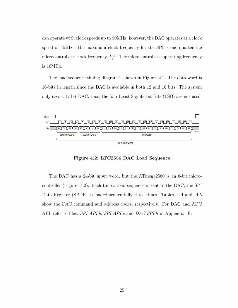
The load sequence timing diagram is shown in Figure 4.2. The data word is
16-bits in length since the DAC is available in both 12 and 16 bits. The system
only uses a 12 bit DAC: thus, the four Least Significant Bits (LSB) are not used.
Figure 4.2: LTC2656 DAC Load Sequence
The DAC has a 24-bit input word, but the ATmega2560 is an 8-bit micro-
controller (Figure 4.2). Each time a load sequence is sent to the DAC, the SPI
Data Register (SPDR) is loaded sequentially three times. Tables 4.4 and 4.5
show the DAC command and address codes, respectively. For DAC and ADC
API, refer to files: SPI API.h, SPI API.c and DAC SPI.h in Appendix E.
25
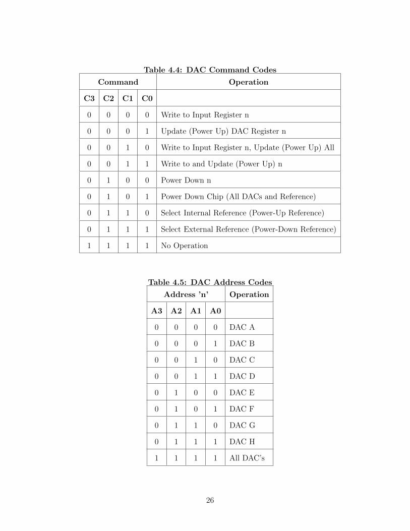
Table 4.4: DAC Command Codes
Command Operation
C3 C2 C1 C0
0 0 0 0 Write to Input Register n
0 0 0 1 Update (Power Up) DAC Register n
0 0 1 0 Write to Input Register n, Update (Power Up) All
0 0 1 1 Write to and Update (Power Up) n
0 1 0 0 Power Down n
0 1 0 1 Power Down Chip (All DACs and Reference)
0 1 1 0 Select Internal Reference (Power-Up Reference)
0 1 1 1 Select External Reference (Power-Down Reference)
1 1 1 1 No Operation
Table 4.5: DAC Address Codes
Address ’n’ Operation
A3 A2 A1 A0
0 0 0 0 DAC A
0 0 0 1 DAC B
0 0 1 0 DAC C
0 0 1 1 DAC D
0 1 0 0 DAC E
0 1 0 1 DAC F
0 1 1 0 DAC G
0 1 1 1 DAC H
1 1 1 1 All DAC’s
26
4.4 Comparator
A high-precision comparator enables voltage comparison between two signals with
difference in mV range; the voltages used in the system are ≈ 20mV apart. The
LM339 is a Low Power Low Offset Voltage Quad Comparator. Key features
include:
• Supply voltage 2 to 36 VDC
• Low input biasing current: 25nA
• Low supply current drain (0.8mA) independent of supply voltage
• Output voltage compatible with TTL, DTL, ECL, MOS and CMOS logic
systems
• Response time of 1.3µs
The simplified schematic of a single LM339 comparator is shown in Figure
4.3. The open collector comparator output requires a pull-up resistor to the 5V
rail; a 3.3kΩ resistor is used.
27
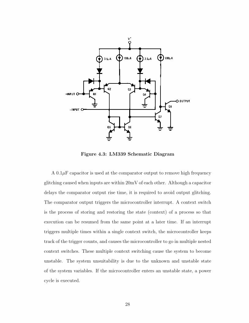
Figure 4.3: LM339 Schematic Diagram
A 0.1µF capacitor is used at the comparator output to remove high frequency
glitching caused when inputs are within 20mV of each other. Although a capacitor
delays the comparator output rise time, it is required to avoid output glitching.
The comparator output triggers the microcontroller interrupt. A context switch
is the process of storing and restoring the state (context) of a process so that
execution can be resumed from the same point at a later time. If an interrupt
triggers multiple times within a single context switch, the microcontroller keeps
track of the trigger counts, and causes the microcontroller to go in multiple nested
context switches. These multiple context switching cause the system to become
unstable. The system unsuitability is due to the unknown and unstable state
of the system variables. If the microcontroller enters an unstable state, a power
cycle is executed.
28
CHAPTER 5
RF SYSTEM INTEGRATION
This chapter describes the microcontroller control lines for the RF system. A
16-pin IDC interfaces the RF board to the digital board. The connector pinout
(Table 2.1) and control lines are described in the following subsections.
5.1 Phase Shifters
Phase shifters control the four-patch inter-element phase shift to steer the radi-
ation beam. The JSPHS-2484+ (MiniCircuits) is a 50Ω matched, 0 to 180
voltage-controlled phase shifter operating in the frequency range 2150MHz to
2484MHz. The datasheet provides voltage-to-phase data at 2150MHz, 2300MHz
and 2484MHz. Linear interpolation between 2300MHz and 2484MHz yields
voltage-to-phase data at 2400MHz as shown in Figure 5.1.
29
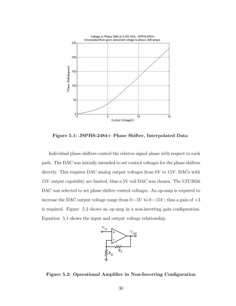
Figure 5.1: JSPHS-2484+ Phase Shifter, Interpolated Data
Individual phase shifters control the relative signal phase with respect to each
path. The DAC was initially intended to set control voltages for the phase shifters
directly. This requires DAC analog output voltages from 0V to 15V. DACs with
15V output capability are limited, thus a 5V rail DAC was chosen. The LTC2656
DAC was selected to set phase shifter control voltages. An op-amp is required to
increase the DAC output voltage range from 0−5V to 0−15V ; thus a gain of +3
is required. Figure 5.2 shows an op-amp in a non-inverting gain configuration.
Equation 5.1 shows the input and output voltage relationship.
Figure 5.2: Operational Amplifier in Non-Inverting Configuration
30
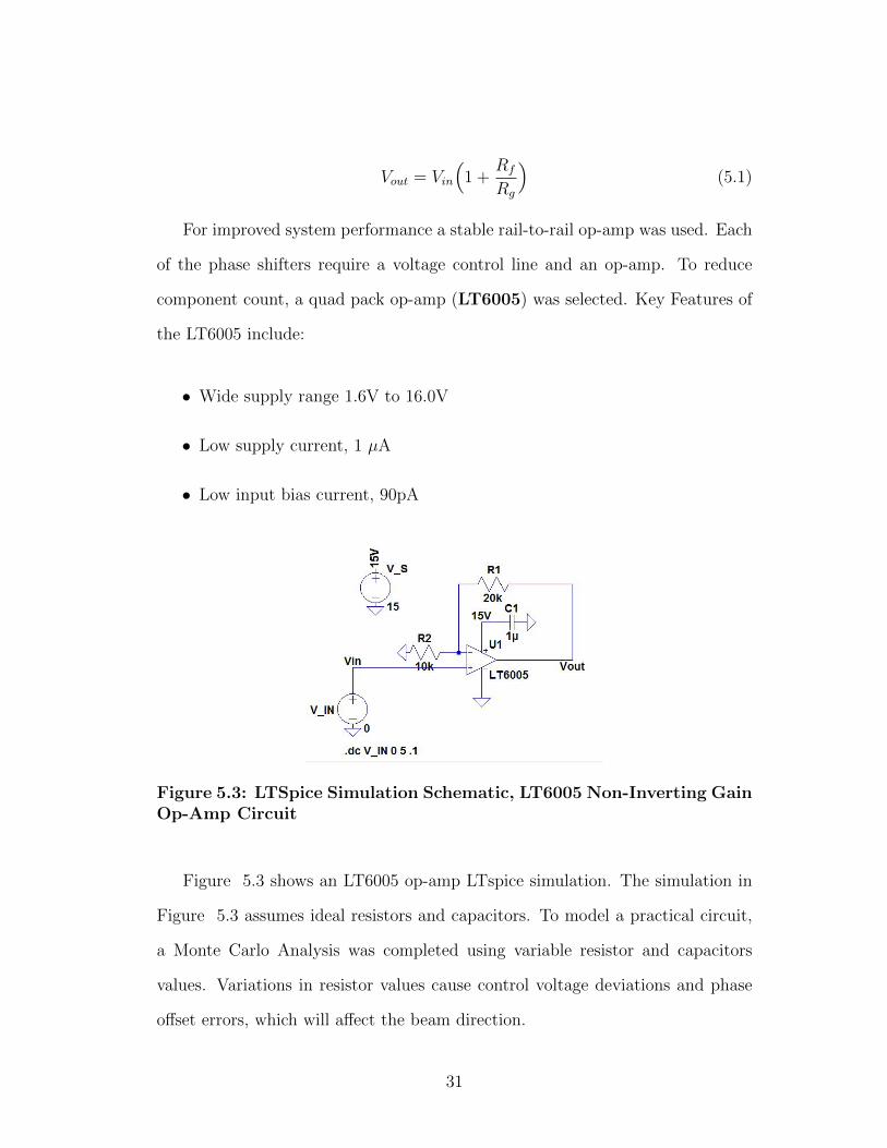
Vout = Vin
(1 +
Rf
Rg
)(5.1)
For improved system performance a stable rail-to-rail op-amp was used. Each
of the phase shifters require a voltage control line and an op-amp. To reduce
component count, a quad pack op-amp (LT6005) was selected. Key Features of
the LT6005 include:
• Wide supply range 1.6V to 16.0V
• Low supply current, 1 µA
• Low input bias current, 90pA
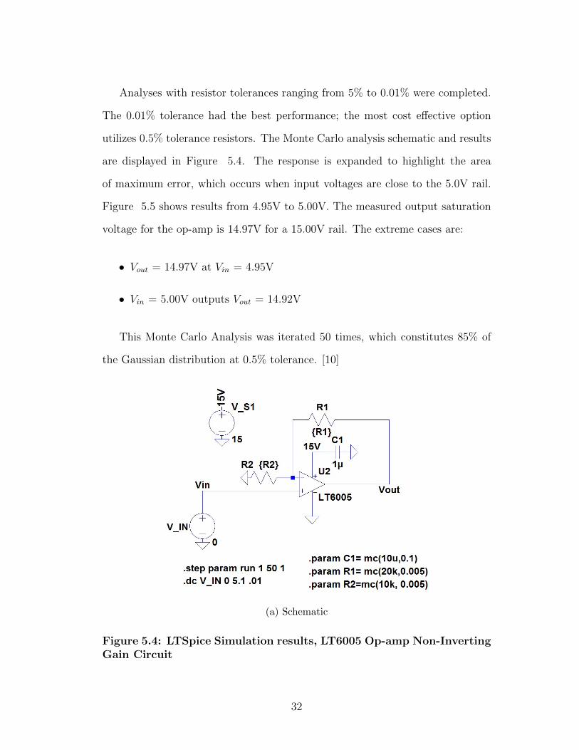
Figure 5.3: LTSpice Simulation Schematic, LT6005 Non-Inverting GainOp-Amp Circuit
Figure 5.3 shows an LT6005 op-amp LTspice simulation. The simulation in
Figure 5.3 assumes ideal resistors and capacitors. To model a practical circuit,
a Monte Carlo Analysis was completed using variable resistor and capacitors
values. Variations in resistor values cause control voltage deviations and phase
offset errors, which will affect the beam direction.
31
Analyses with resistor tolerances ranging from 5% to 0.01% were completed.
The 0.01% tolerance had the best performance; the most cost effective option
utilizes 0.5% tolerance resistors. The Monte Carlo analysis schematic and results
are displayed in Figure 5.4. The response is expanded to highlight the area
of maximum error, which occurs when input voltages are close to the 5.0V rail.
Figure 5.5 shows results from 4.95V to 5.00V. The measured output saturation
voltage for the op-amp is 14.97V for a 15.00V rail. The extreme cases are:
• Vout = 14.97V at Vin = 4.95V
• Vin = 5.00V outputs Vout = 14.92V
This Monte Carlo Analysis was iterated 50 times, which constitutes 85% of
the Gaussian distribution at 0.5% tolerance. [10]
(a) Schematic
Figure 5.4: LTSpice Simulation results, LT6005 Op-amp Non-InvertingGain Circuit
32
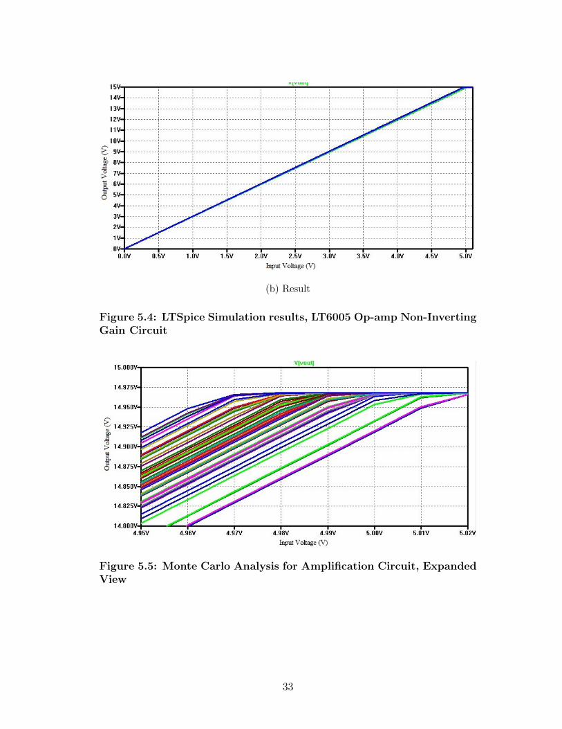
(b) Result
Figure 5.4: LTSpice Simulation results, LT6005 Op-amp Non-InvertingGain Circuit
Figure 5.5: Monte Carlo Analysis for Amplification Circuit, ExpandedView
33
5.2 RF Single Pole Double Throw (SPDT) Switch
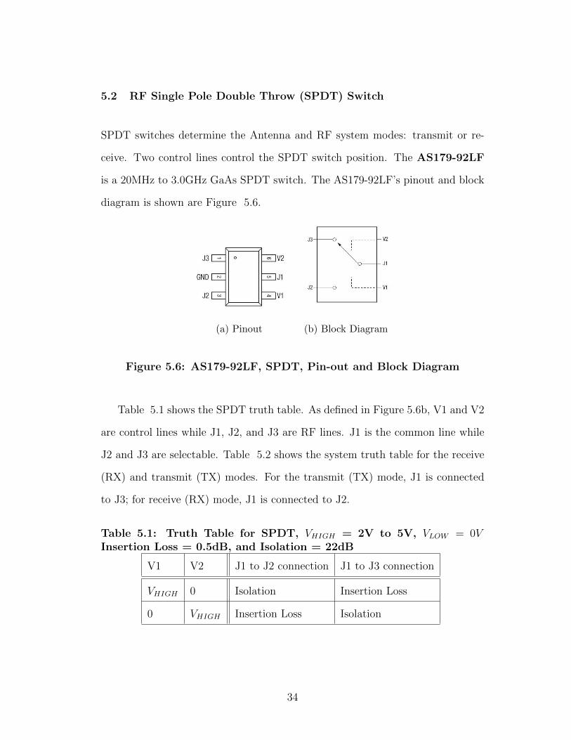
SPDT switches determine the Antenna and RF system modes: transmit or re-
ceive. Two control lines control the SPDT switch position. The AS179-92LF
is a 20MHz to 3.0GHz GaAs SPDT switch. The AS179-92LF’s pinout and block
diagram is shown are Figure 5.6.
(a) Pinout (b) Block Diagram
Figure 5.6: AS179-92LF, SPDT, Pin-out and Block Diagram
Table 5.1 shows the SPDT truth table. As defined in Figure 5.6b, V1 and V2
are control lines while J1, J2, and J3 are RF lines. J1 is the common line while
J2 and J3 are selectable. Table 5.2 shows the system truth table for the receive
(RX) and transmit (TX) modes. For the transmit (TX) mode, J1 is connected
to J3; for receive (RX) mode, J1 is connected to J2.
Table 5.1: Truth Table for SPDT, VHIGH = 2V to 5V, VLOW = 0VInsertion Loss = 0.5dB, and Isolation = 22dB
V1 V2 J1 to J2 connection J1 to J3 connection
VHIGH 0 Isolation Insertion Loss
0 VHIGH Insertion Loss Isolation
34
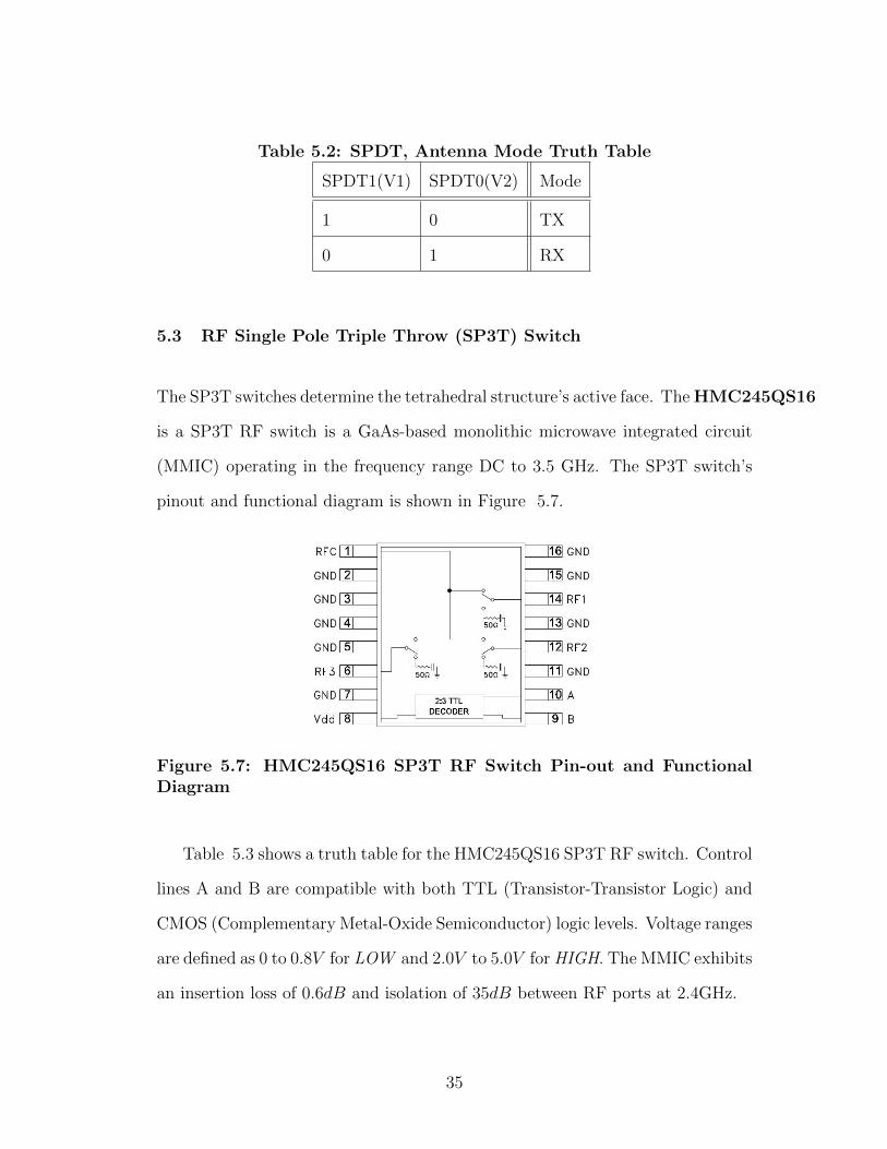
Table 5.2: SPDT, Antenna Mode Truth Table
SPDT1(V1) SPDT0(V2) Mode
1 0 TX
0 1 RX
5.3 RF Single Pole Triple Throw (SP3T) Switch
The SP3T switches determine the tetrahedral structure’s active face. The HMC245QS16
is a SP3T RF switch is a GaAs-based monolithic microwave integrated circuit
(MMIC) operating in the frequency range DC to 3.5 GHz. The SP3T switch’s
pinout and functional diagram is shown in Figure 5.7.
Figure 5.7: HMC245QS16 SP3T RF Switch Pin-out and FunctionalDiagram
Table 5.3 shows a truth table for the HMC245QS16 SP3T RF switch. Control
lines A and B are compatible with both TTL (Transistor-Transistor Logic) and
CMOS (Complementary Metal-Oxide Semiconductor) logic levels. Voltage ranges
are defined as 0 to 0.8V for LOW and 2.0V to 5.0V for HIGH. The MMIC exhibits
an insertion loss of 0.6dB and isolation of 35dB between RF ports at 2.4GHz.
35

Table 5.3: Truth Table for HMC245QS16 and the Active Antenna Face
Control Input Signal Path State
A B RF COM to: Active Face
Low Low RF1 1
High Low RF2 2
Low High RF3 3
High High All Off All Off
5.4 Voltage Control Oscillator (VCO) Control Line
The JTOS-2700V is a linearly tunable voltage controlled oscillator (VCO) for
the frequency range 2050 to 2700 MHz. VCO Frequency Tuning and output
power data are shown in Figure 5.8.
36
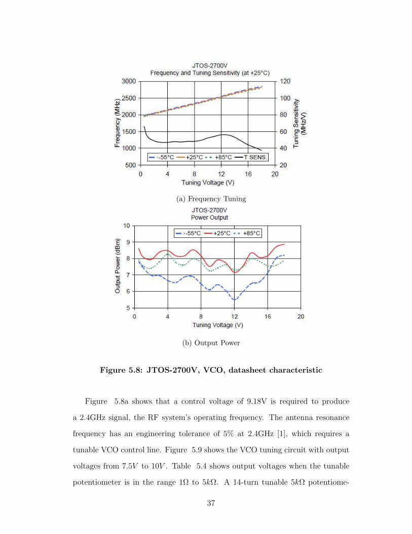
(a) Frequency Tuning
(b) Output Power
Figure 5.8: JTOS-2700V, VCO, datasheet characteristic
Figure 5.8a shows that a control voltage of 9.18V is required to produce
a 2.4GHz signal, the RF system’s operating frequency. The antenna resonance
frequency has an engineering tolerance of 5% at 2.4GHz [1], which requires a
tunable VCO control line. Figure 5.9 shows the VCO tuning circuit with output
voltages from 7.5V to 10V . Table 5.4 shows output voltages when the tunable
potentiometer is in the range 1Ω to 5kΩ. A 14-turn tunable 5kΩ potentiome-
37

ter provides fine adjustment for the VCO output frequency. High tolerance 1%
resistors are used for R1 through R4.
Figure 5.9: VCO tuning Schematic, R5 is the tunable resistor
Table 5.4: VCO Tuning Circuit Result
Potentiometer resistance (Ω) VCO control voltage (V)
1 7.50
1k 8.18
2k 8.75
3k 9.23
4k 9.64
5k 10
38

CHAPTER 6
PRINTED CIRCUIT BOARD DESIGN
CadSoft EAGLE PCB Design Software was used to design the printed circuit
board (PCB) schematic and layout. PCB schematic and layout can be found in
Appendices F and G, respectively.
6.1 Schematic
The schematic was created to add the maximum testability in the PCB. The
following are some of the key testability features added to the PCB design:
• Zero ohm resistors to isolate power supplies and ICs
• Zero ohm resistors to isolate outputs and inputs for testability
• DIP switch and header pins to set SPDT and SP3T control signal manually
and LEDs to show the status
• Test points at most microcontroller input/outputs (I/Os)
• LED Display Driver(LM3914) to show the received power RF power detec-
tor.
• LEDs to check the power statuses
• On broad ISP programmer pinout
39
The ICs used required 5V and 15V power rails. To avoid the need for two
power supplies, a 20V AC to DC wall transformer was used with power regulators.
A barrel connector was used to connect the 20V power supply to the board. ON
Semi’s NCP1117ST50T3G was used to achieve 5V rail and Texas Instrument part
LM3480 was used to achieve 15V rail. Linear Technology LT1761 was used to
set the 2.5V DAC reference voltage.
6.2 Layout
A two-layer PCB was chosen for the layout. A full copper pour on the top and
bottom layers was used as the ground. The advantage of large group plane is
its low inductance and resistance. Routing the signals and power lines in the
group pour helps maintain a good signal value by creating capacitance between
the signal or power and the ground signal. A section of copper pour was cut out
from the full copper pour to act as analog ground. The full ground plane and
analog ground plane were connected via 22nH inductor, which prevents the high
frequency switching ground plane currents from affecting the analog voltages.
The analog plane was used under the DAC and the Amplifier. The layout was
designed so that traces would have a minimal number of vias.
40
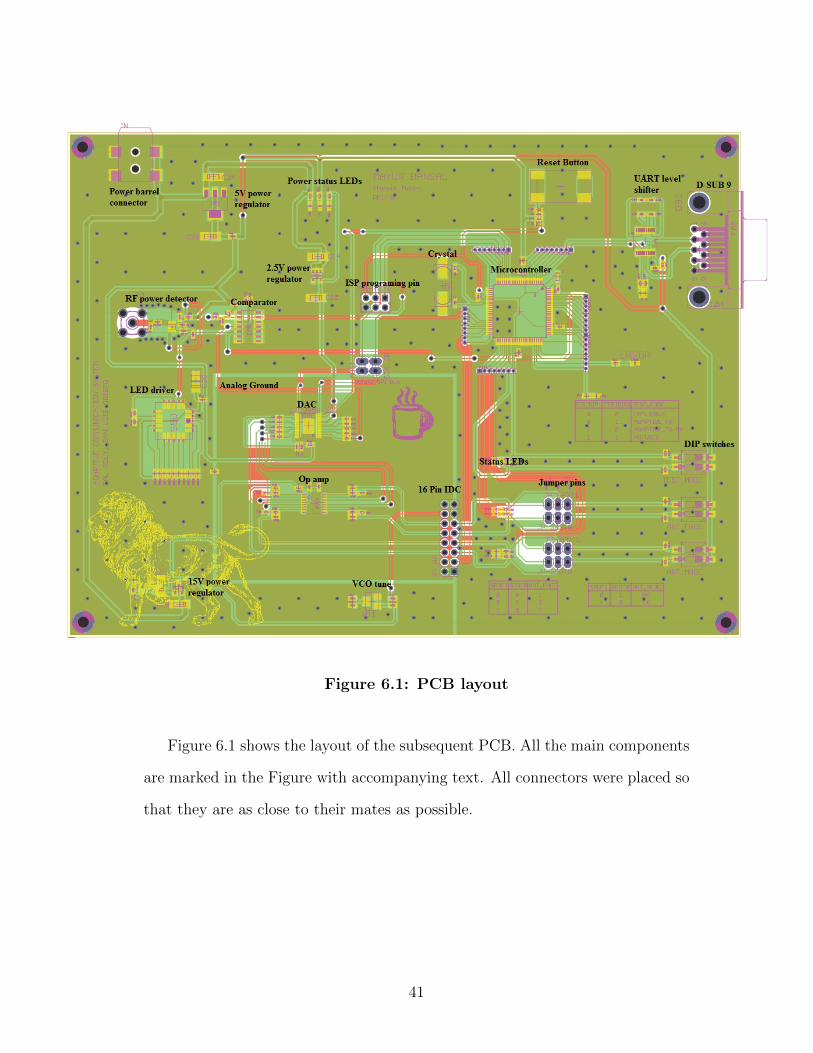
Figure 6.1: PCB layout
Figure 6.1 shows the layout of the subsequent PCB. All the main components
are marked in the Figure with accompanying text. All connectors were placed so
that they are as close to their mates as possible.
41
CHAPTER 7
GRAPHICAL USER INTERFACE (GUI) CONTROL SYSTEM
The MATLAB GUI is designed to test system functionality. The GUI configures
all system variables for beam steering and can be set to transmit or receive mode.
MATLAB uses RS-232, a serial protocol, to communicate between the computer
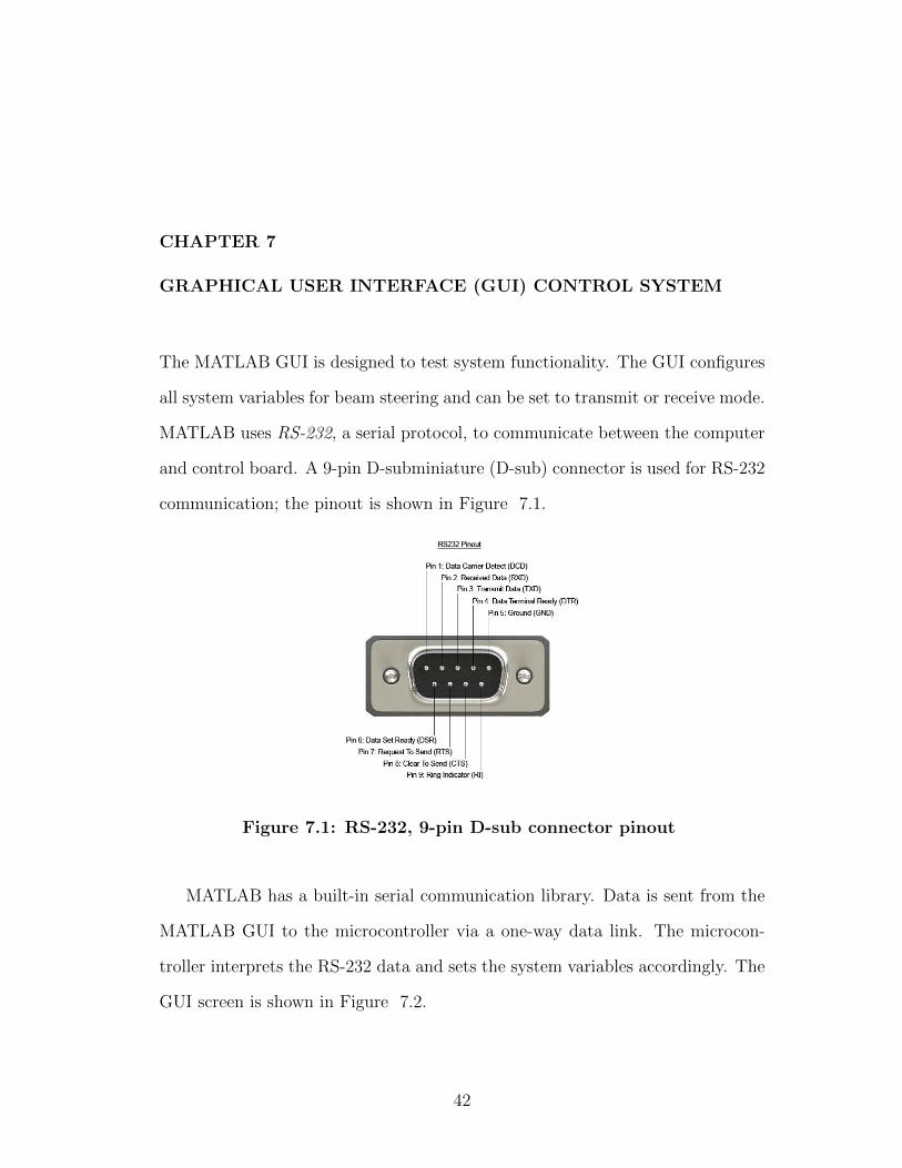
and control board. A 9-pin D-subminiature (D-sub) connector is used for RS-232
communication; the pinout is shown in Figure 7.1.
Figure 7.1: RS-232, 9-pin D-sub connector pinout
MATLAB has a built-in serial communication library. Data is sent from the
MATLAB GUI to the microcontroller via a one-way data link. The microcon-
troller interprets the RS-232 data and sets the system variables accordingly. The
GUI screen is shown in Figure 7.2.
42
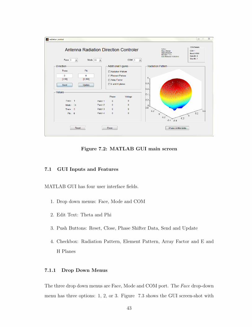
Figure 7.2: MATLAB GUI main screen
7.1 GUI Inputs and Features
MATLAB GUI has four user interface fields.
1. Drop down menus: Face, Mode and COM
2. Edit Text: Theta and Phi
3. Push Buttons: Reset, Close, Phase Shifter Data, Send and Update
4. Checkbox: Radiation Pattern, Element Pattern, Array Factor and E and
H Planes
7.1.1 Drop Down Menus
The three drop down menus are Face, Mode and COM port. The Face drop-down
menu has three options: 1, 2, or 3. Figure 7.3 shows the GUI screen-shot with
43
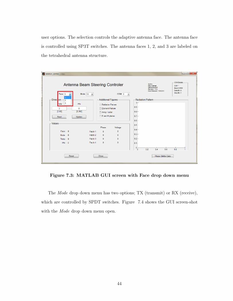
user options. The selection controls the adaptive antenna face. The antenna face
is controlled using SP3T switches. The antenna faces 1, 2, and 3 are labeled on
the tetrahedral antenna structure.
Figure 7.3: MATLAB GUI screen with Face drop down menu
The Mode drop down menu has two options; TX (transmit) or RX (receive),
which are controlled by SPDT switches. Figure 7.4 shows the GUI screen-shot
with the Mode drop down menu open.
44
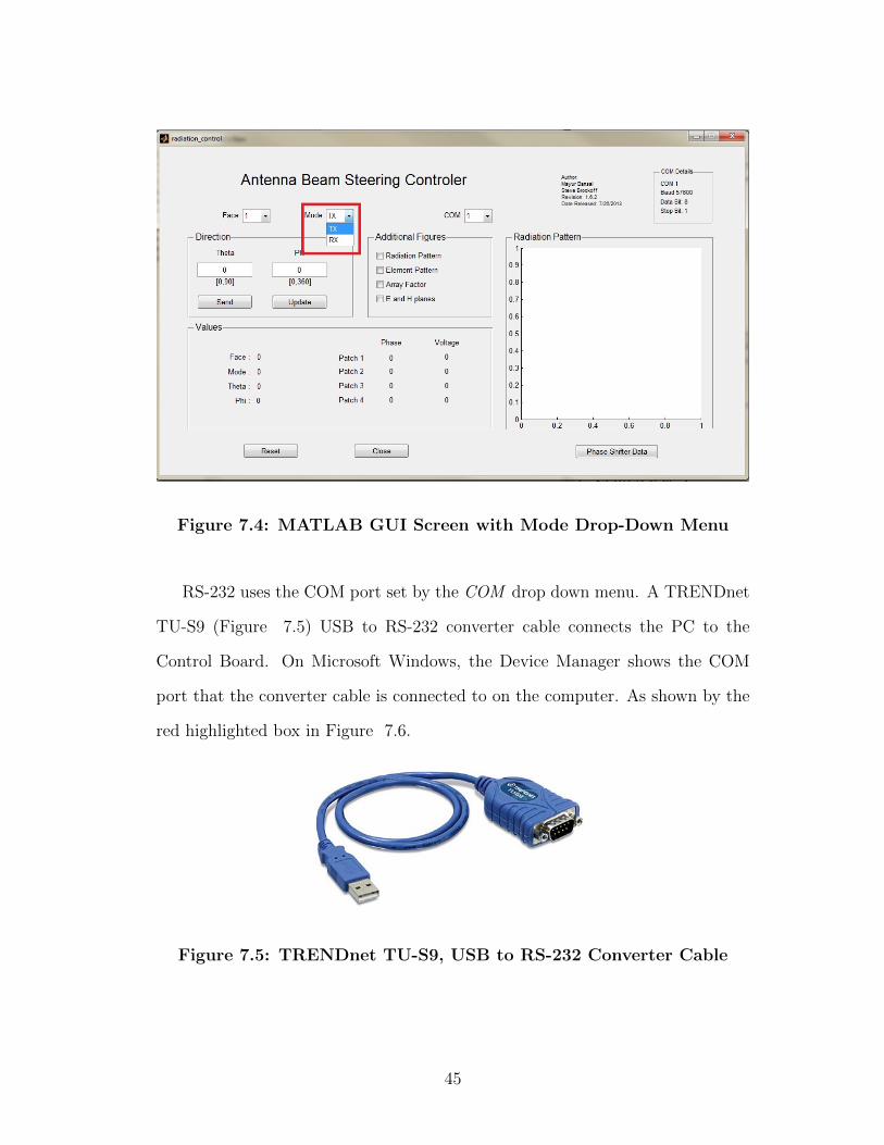
Figure 7.4: MATLAB GUI Screen with Mode Drop-Down Menu
RS-232 uses the COM port set by the COM drop down menu. A TRENDnet
TU-S9 (Figure 7.5) USB to RS-232 converter cable connects the PC to the
Control Board. On Microsoft Windows, the Device Manager shows the COM
port that the converter cable is connected to on the computer. As shown by the
red highlighted box in Figure 7.6.
Figure 7.5: TRENDnet TU-S9, USB to RS-232 Converter Cable
45
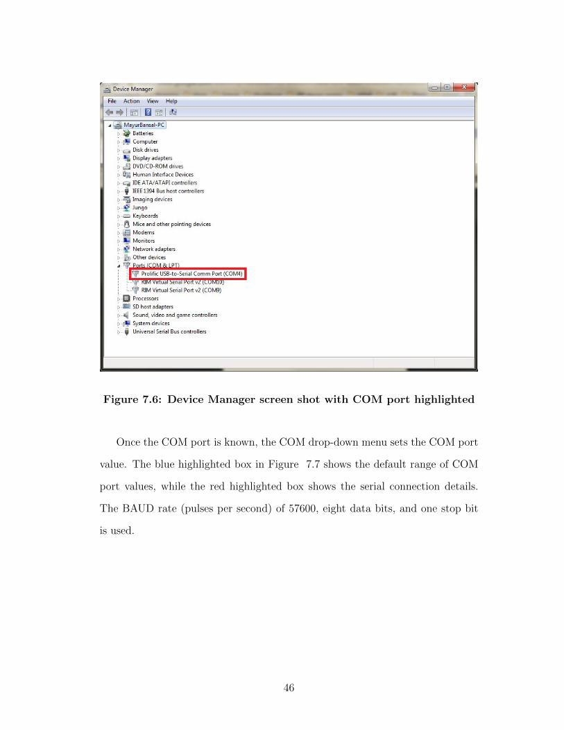
Figure 7.6: Device Manager screen shot with COM port highlighted
Once the COM port is known, the COM drop-down menu sets the COM port
value. The blue highlighted box in Figure 7.7 shows the default range of COM
port values, while the red highlighted box shows the serial connection details.
The BAUD rate (pulses per second) of 57600, eight data bits, and one stop bit
is used.
46
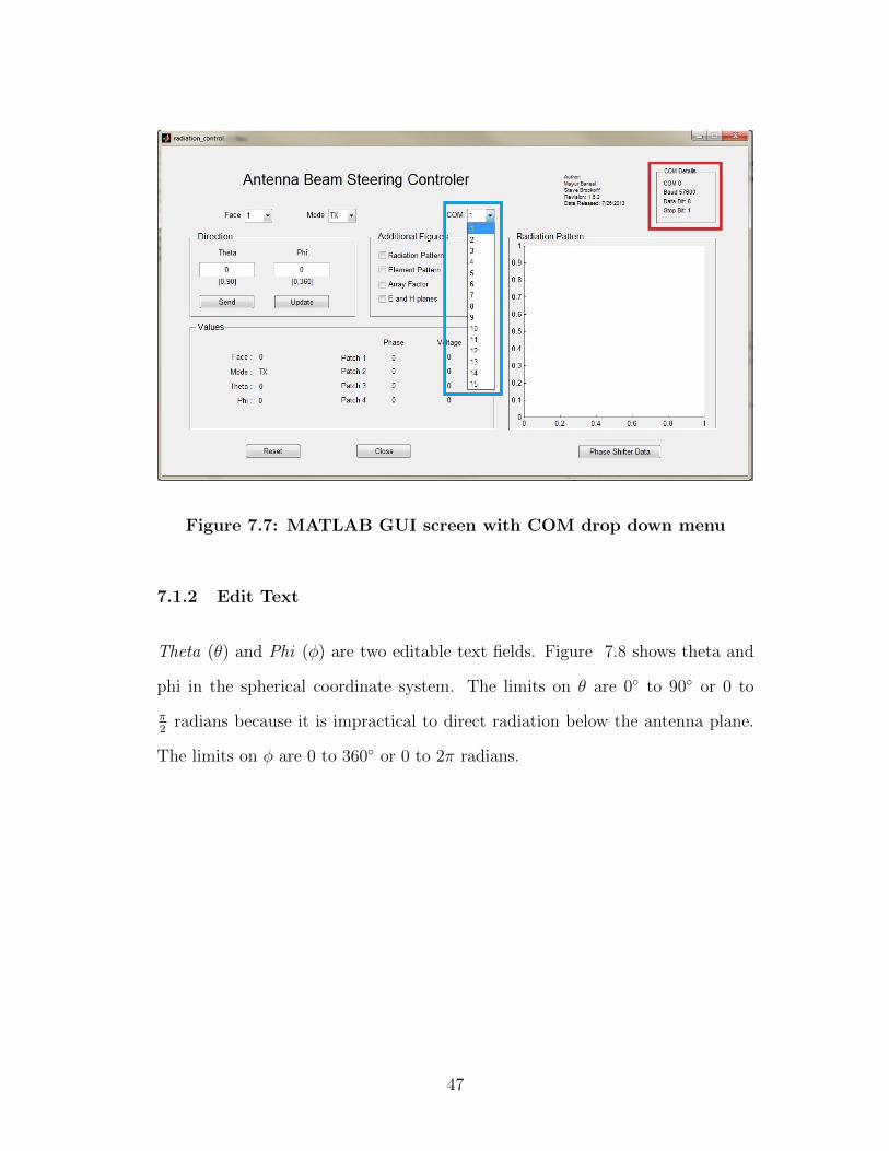
Figure 7.7: MATLAB GUI screen with COM drop down menu
7.1.2 Edit Text
Theta (θ) and Phi (φ) are two editable text fields. Figure 7.8 shows theta and
phi in the spherical coordinate system. The limits on θ are 0 to 90 or 0 to
π2
radians because it is impractical to direct radiation below the antenna plane.
The limits on φ are 0 to 360 or 0 to 2π radians.
47
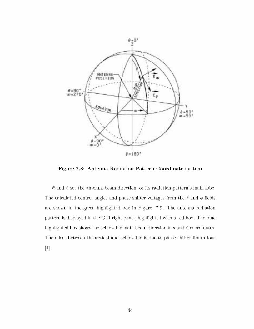
Figure 7.8: Antenna Radiation Pattern Coordinate system
θ and φ set the antenna beam direction, or its radiation pattern’s main lobe.
The calculated control angles and phase shifter voltages from the θ and φ fields
are shown in the green highlighted box in Figure 7.9. The antenna radiation
pattern is displayed in the GUI right panel, highlighted with a red box. The blue
highlighted box shows the achievable main beam direction in θ and φ coordinates.
The offset between theoretical and achievable is due to phase shifter limitations
[1].
48
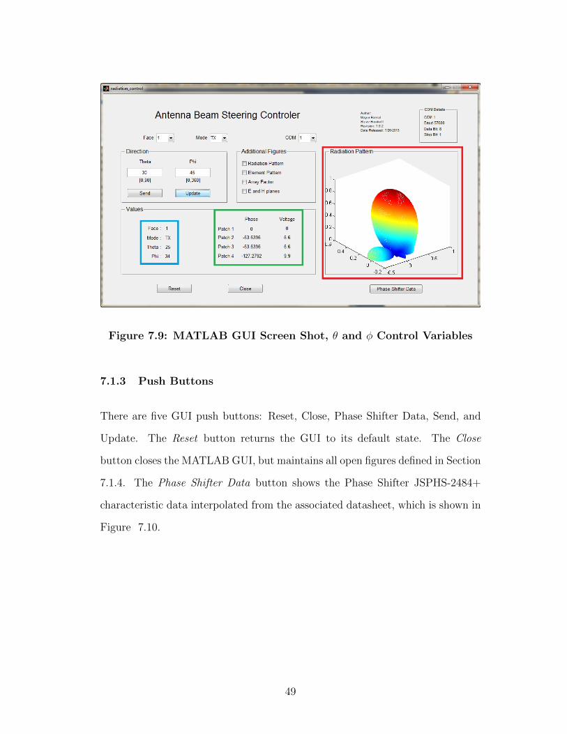
Figure 7.9: MATLAB GUI Screen Shot, θ and φ Control Variables
7.1.3 Push Buttons
There are five GUI push buttons: Reset, Close, Phase Shifter Data, Send, and
Update. The Reset button returns the GUI to its default state. The Close
button closes the MATLAB GUI, but maintains all open figures defined in Section
7.1.4. The Phase Shifter Data button shows the Phase Shifter JSPHS-2484+
characteristic data interpolated from the associated datasheet, which is shown in
Figure 7.10.
49
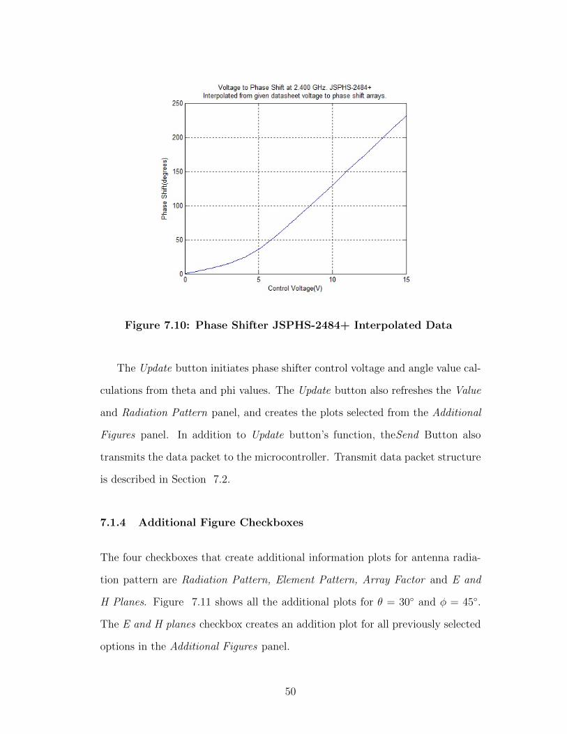
Figure 7.10: Phase Shifter JSPHS-2484+ Interpolated Data
The Update button initiates phase shifter control voltage and angle value cal-
culations from theta and phi values. The Update button also refreshes the Value
and Radiation Pattern panel, and creates the plots selected from the Additional
Figures panel. In addition to Update button’s function, theSend Button also
transmits the data packet to the microcontroller. Transmit data packet structure
is described in Section 7.2.
7.1.4 Additional Figure Checkboxes
The four checkboxes that create additional information plots for antenna radia-
tion pattern are Radiation Pattern, Element Pattern, Array Factor and E and
H Planes. Figure 7.11 shows all the additional plots for θ = 30 and φ = 45.
The E and H planes checkbox creates an addition plot for all previously selected
options in the Additional Figures panel.
50
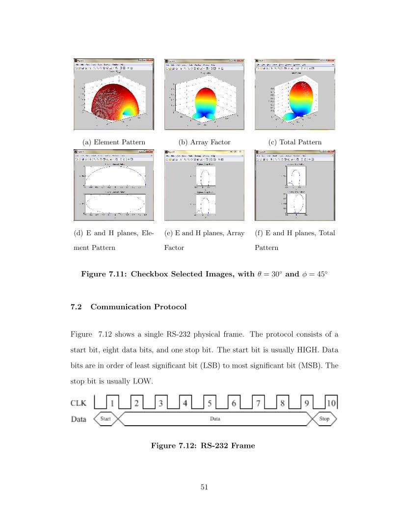
(a) Element Pattern (b) Array Factor (c) Total Pattern
(d) E and H planes, Ele-
ment Pattern
(e) E and H planes, Array
Factor
(f) E and H planes, Total
Pattern
Figure 7.11: Checkbox Selected Images, with θ = 30 and φ = 45
7.2 Communication Protocol
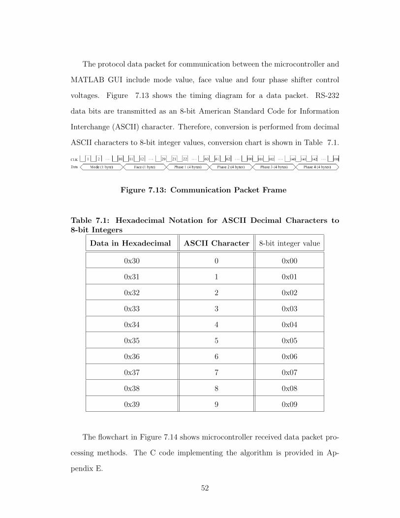
Figure 7.12 shows a single RS-232 physical frame. The protocol consists of a
start bit, eight data bits, and one stop bit. The start bit is usually HIGH. Data
bits are in order of least significant bit (LSB) to most significant bit (MSB). The
stop bit is usually LOW.
Figure 7.12: RS-232 Frame
51
The protocol data packet for communication between the microcontroller and
MATLAB GUI include mode value, face value and four phase shifter control
voltages. Figure 7.13 shows the timing diagram for a data packet. RS-232
data bits are transmitted as an 8-bit American Standard Code for Information
Interchange (ASCII) character. Therefore, conversion is performed from decimal
ASCII characters to 8-bit integer values, conversion chart is shown in Table 7.1.
Figure 7.13: Communication Packet Frame
Table 7.1: Hexadecimal Notation for ASCII Decimal Characters to8-bit Integers
Data in Hexadecimal ASCII Character 8-bit integer value
0x30 0 0x00
0x31 1 0x01
0x32 2 0x02
0x33 3 0x03
0x34 4 0x04
0x35 5 0x05
0x36 6 0x06
0x37 7 0x07
0x38 8 0x08
0x39 9 0x09
The flowchart in Figure 7.14 shows microcontroller received data packet pro-
cessing methods. The C code implementing the algorithm is provided in Ap-
pendix E.
52
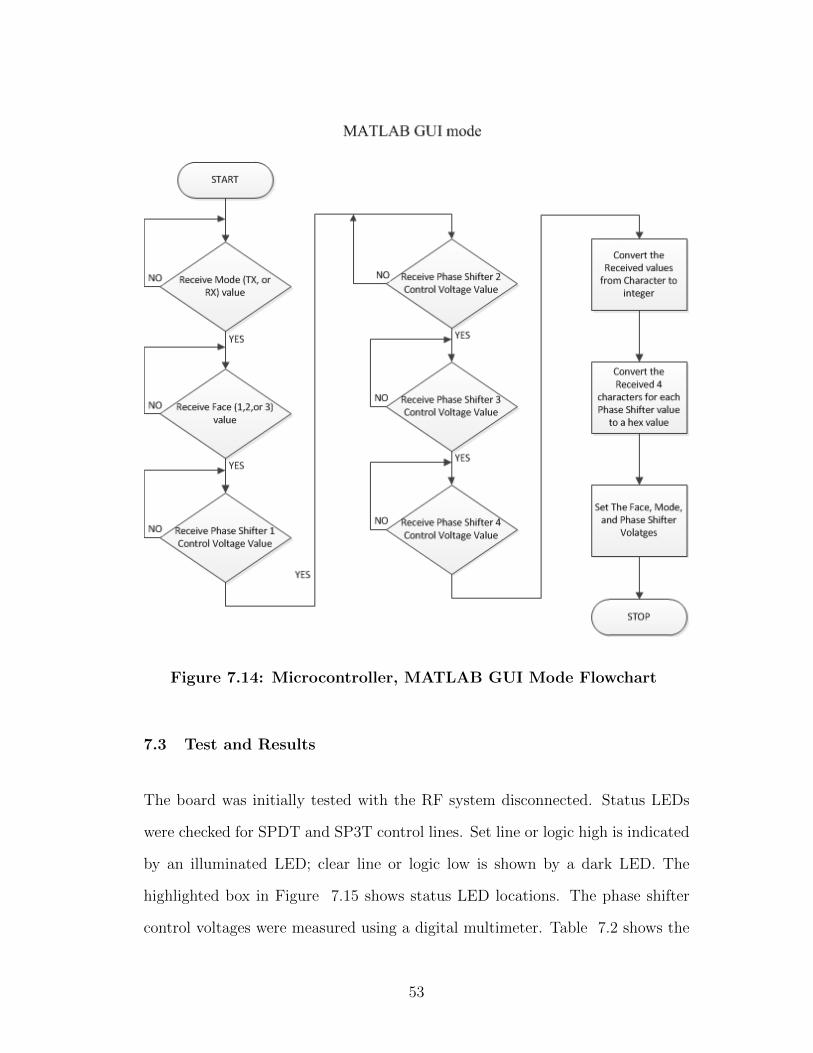
Figure 7.14: Microcontroller, MATLAB GUI Mode Flowchart
7.3 Test and Results
The board was initially tested with the RF system disconnected. Status LEDs
were checked for SPDT and SP3T control lines. Set line or logic high is indicated
by an illuminated LED; clear line or logic low is shown by a dark LED. The
highlighted box in Figure 7.15 shows status LED locations. The phase shifter
control voltages were measured using a digital multimeter. Table 7.2 shows the
53
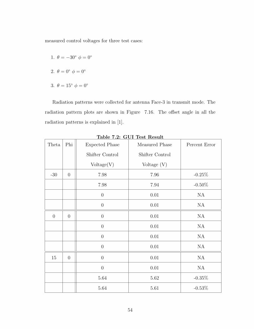
measured control voltages for three test cases:
1. θ = −30 φ = 0
2. θ = 0 φ = 0
3. θ = 15 φ = 0
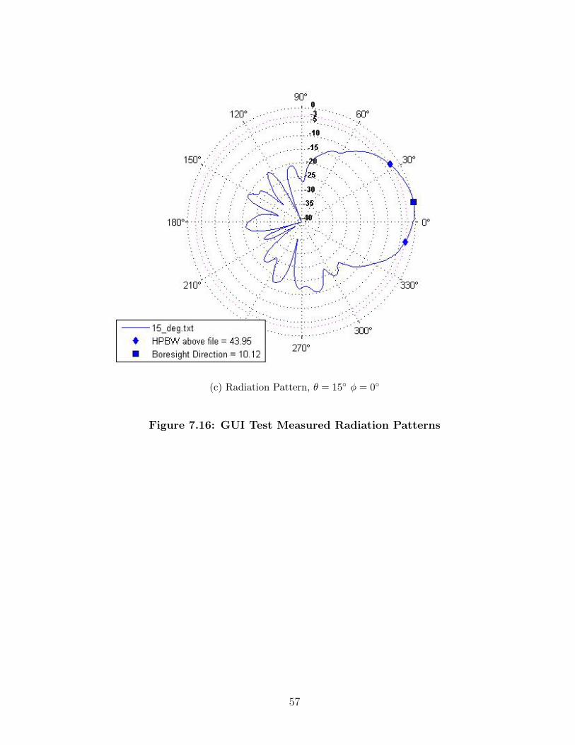
Radiation patterns were collected for antenna Face-3 in transmit mode. The
radiation pattern plots are shown in Figure 7.16. The offset angle in all the
radiation patterns is explained in [1].
Table 7.2: GUI Test Result
Theta Phi Expected Phase
Shifter Control
Voltage(V)
Measured Phase
Shifter Control
Voltage (V)
Percent Error
-30 0 7.98 7.96 -0.25%
7.98 7.94 -0.50%
0 0.01 NA
0 0.01 NA
0 0 0 0.01 NA
0 0.01 NA
0 0.01 NA
0 0.01 NA
15 0 0 0.01 NA
0 0.01 NA
5.64 5.62 -0.35%
5.64 5.61 -0.53%
54
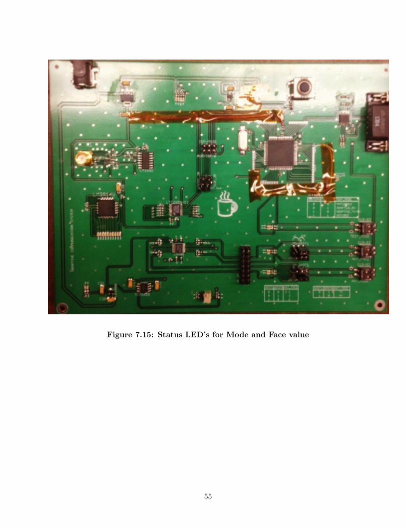
Figure 7.15: Status LED’s for Mode and Face value
55
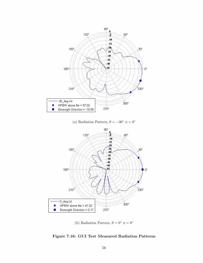
(a) Radiation Pattern, θ = −30 φ = 0
(b) Radiation Pattern, θ = 0 φ = 0
Figure 7.16: GUI Test Measured Radiation Patterns
56
(c) Radiation Pattern, θ = 15 φ = 0
Figure 7.16: GUI Test Measured Radiation Patterns
57
CHAPTER 8
ADAPTIVE RECEIVE MODE
In receive mode, an adaptive antenna performs a scan to determine the maximum
receive power direction. This mode to used to maintain a lock on a receiving signal
from a transmitting antenna.
8.1 Adaptive Receive Algorithm
For the search algorithm, a 58-point scan on each antenna face is performed.
Figure 8.1 shows the location of the points used in the the adaptive receive scan.
The points are scanned using a raster scan technique, which is a line-by-line
rectangular sweep as shown in Figure 8.2. Power is received for each scan point.
If the received power at the current point is greater than the power received at any
previous point, the new maximum is stored. This continues until the scanning is
complete. Following scan completion, the beam is reset to the maximum power
direction. The scan direction is maintained until the receive power level decreases
below -50dBm. This level is chosen because the RF system has a noise floor of
-60dBm.
58
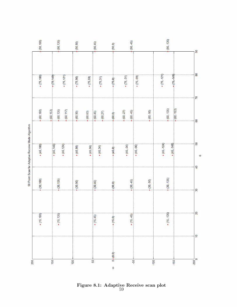
Figure 8.1: Adaptive Receive scan plot59
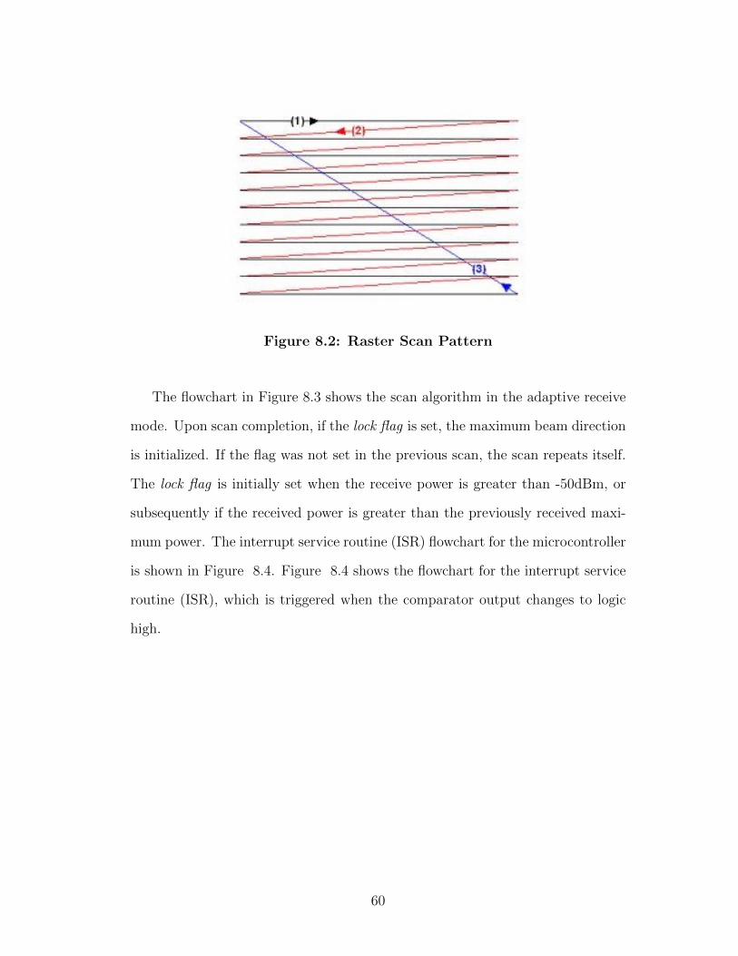
Figure 8.2: Raster Scan Pattern
The flowchart in Figure 8.3 shows the scan algorithm in the adaptive receive
mode. Upon scan completion, if the lock flag is set, the maximum beam direction
is initialized. If the flag was not set in the previous scan, the scan repeats itself.
The lock flag is initially set when the receive power is greater than -50dBm, or
subsequently if the received power is greater than the previously received maxi-
mum power. The interrupt service routine (ISR) flowchart for the microcontroller
is shown in Figure 8.4. Figure 8.4 shows the flowchart for the interrupt service
routine (ISR), which is triggered when the comparator output changes to logic
high.
60
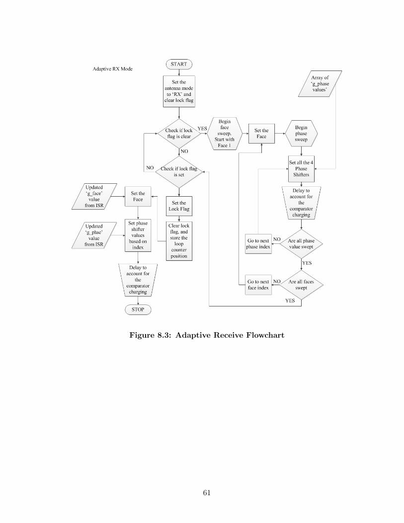
Figure 8.3: Adaptive Receive Flowchart
61
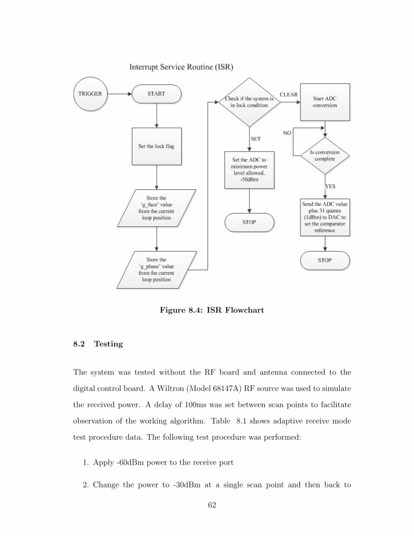
Figure 8.4: ISR Flowchart
8.2 Testing
The system was tested without the RF board and antenna connected to the
digital control board. A Wiltron (Model 68147A) RF source was used to simulate
the received power. A delay of 100ms was set between scan points to facilitate
observation of the working algorithm. Table 8.1 shows adaptive receive mode
test procedure data. The following test procedure was performed:
1. Apply -60dBm power to the receive port
2. Change the power to -30dBm at a single scan point and then back to
62
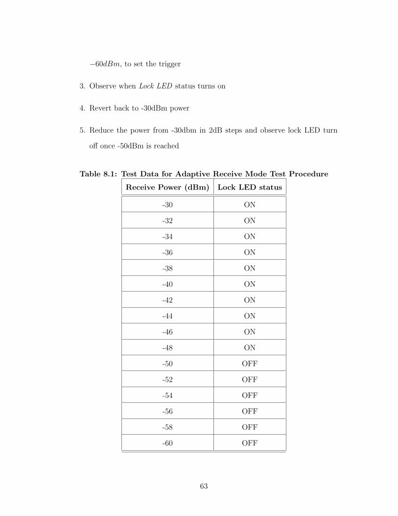
−60dBm, to set the trigger
3. Observe when Lock LED status turns on
4. Revert back to -30dBm power
5. Reduce the power from -30dbm in 2dB steps and observe lock LED turn
off once -50dBm is reached
Table 8.1: Test Data for Adaptive Receive Mode Test Procedure
Receive Power (dBm) Lock LED status
-30 ON
-32 ON
-34 ON
-36 ON
-38 ON
-40 ON
-42 ON
-44 ON
-46 ON
-48 ON
-50 OFF
-52 OFF
-54 OFF
-56 OFF
-58 OFF
-60 OFF
63

The data in Table 8.1 proves that system operates in the specification, main-
taining lock for power level greater than -50dBm. The complete system test was
not performed due to RF PCB manufacturing problems [1].
64
CHAPTER 9
CONCLUSIONS AND FUTURE WORK
The system shows a successful implementation of the digital control board for
beam steering and adaptive communications. The digital control board con-
trols the antenna face and mode as described in [1]. Each sub-block of the dig-
ital controlled board was tested in order to verify that specifications were met.
The MATLAB graphical user interface successfully controlled the digital control
board. An adaptive communication system was implemented to demonstrate
a working example. The system autonomously locked to the maximum receive
power using the 58-point scan, for the power levels above -50dBm.
The RF power detector used a logarithmic amplifier-based design, which pro-
vides a linear relation between input power and output voltage. The RF power
detector has a slope of 37.3mV/dB with a minimum detectable power of −60dBm
and maximum detectable power of 0dBm.
An ATmega2560 is used as the microcontroller for the system. The built-in
ADC was used to measure the receive power. The microcontroller is also used
to communicate with MATLAB, which allows it to set the output voltages for
the phase shifters as well as the control signals that set the antenna face and
the mode. The microcontroller can be configured in MATLAB GUI mode or the
adaptive receive mode.
The system successfully controls the SP3T and SPDT switches, which control
65
active antenna face and mode selection, respectively. The system also successfully
sends control voltages to the phase shifter within 0.53% of expected values. The
control board demonstrates a working bench test for an adaptive receive station.
The PCB design shows improved performance with a separate analog and
digital plane and reduces the noise on the analog signal. The digital control
board was designed for in system test and debugging. The digital control board
has features for future expandability.
Future work:
• Re-test the digital control board with a fully operational RF board
• Develop a half duplex adaptive receive and transmit communication system
• Digital communication (16-QAM, APSK, LTE, etc.) implementation on
the control board
66

BIBLIOGRAPHY
[1] S. Brockhoff, “Electronically-Steered Tetrahedral-Structured Phased Array
2.4 GHz Transceiver Design Applied to Adaptive Communications,” Mas-
ter’s thesis, California Polytechnic State University, 2013.
[2] Louis E. Frenzel, “Design FAQ: RF Detector for Wire-
less Devices.” http : //www.analog.com/static/imported −
files/faqs/201551981DetectorFAQ.pdf .
[3] “Integrated DC Logarithmic Amplifiers,” Dallas Semiconductor, Maxim En-
gineering Journal, vol. 56, 2005.
[4] “LT5534 - 50MHz to 3GHz RF Power Detector with 60dB Dynamic Range.”
http : //www.linear.com/product/LT5534.
[5] “LT5538 - 40MHz to 3.8GHz RF Power Detector with 75dB Dynamic
Range.” http://www.linear.com/product/LT5538.
[6] “LT5534 Datasheet.” http : //cds.linear.com/docs/en/datasheet/5534fc.pdf .
[7] “LT5534 Demo Board.” http : //www.linear.com/demo?demoboard =
partnumber = 5534categoryid = 0companionboard = softwareid =.
[8] “LT5538 Datasheet.” http : //cds.linear.com/docs/en/datasheet/5538f.pdf .
[9] “LT5538 Demo Board.” http : //www.linear.com/demo?demoboard =
partnumber = 5538categoryid = 0companionboard = softwareid =.
67

[10] Morris R. Driels and Young S. Shin, “DETERMINING THE NUMBER
OF ITERATIONS FOR MONTE CARLO SIMULATIONS OF WEAPON
EFFECTIVENESS,” Tech. Rep. NPS-MAE-04-005, Naval Postgraduate
School, MONTEREY, CALIFORNIA, April 2004.
68

APPENDICES
A 2013 IEEE APS Student Design Challenge: Reconfigurable Anten-
nas
69

2013IEEEAP‐SStudentDesignChallenge:ReconfigurableAntennas
Travel to the 2013 IEEE Antennas and Propagation Symposium Win $1500, $750, $250
Join the 4th IEEE AP‐S Antenna Design Challenge! Build an antenna system with reconfigurable antenna elements that can adapt to different propagation conditions (e.g. line‐of‐sight versus non‐line‐of‐sight). The top three teams will receive up to $2,500 (US dollars) in travel funds to attend the IEEE Antennas and Propagation Symposium in Orlando, FL, USA, July 7‐13, 2013 to demonstrate their working systems. From these top teams, first, second, and third place winners will be announced at the 2013 IEEE AP‐S Awards Banquet and will receive cash awards of $1500, $750, and $250, respectively.
Important deadlines are November 30, 2012 and April 26, 2013. See below for details.
Goals and Specifications:
1. Design an antenna system with reconfigurable antenna elements that can adapt to different propagation conditions in order to achieve the best link performance. The performance can be shown in terms of received power or higher level system metric such as symbol error rate.
2. The antenna system should be used to teach how antennas work. Such a system might be used in college undergraduate or graduate courses, and in pre‐college (‘High School’) physics courses.
3. The system must be safe and durable, easily reproducible by others, inexpensive, and portable so that it can be demonstrated at the Symposium.
4. The system must operate at 2.4 GHz, have its own source (i.e. no commercial signal generator can be used), and fit on a table top (roughly 24”x 40”) or two closely spaced tables. Readily available software (e.g., student versions of C, Matlab, Visual Basic, LabView) or free software packages may be used. All software must be included in the budget.
5. The total cost for reproduction of the system must be less than $1,500. The use of a laptop computer is allowed and does not have to be included in the $1,500 limit.
Eligibility:
The team should consist of 2 to 5 persons, with a majority of undergraduate students. Each team should be advised by a professional mentor who is a member of the AP Society. No student or mentor should be involved in more than one team.
The Application and Review Process:
1. All applicants must submit a preliminary design by November 16, 2012. It must include:
a. A proposal limited to two pages and in 12‐pt Times New Roman font that includes
i. A detailed description of the system to be built.

ii. The steps that will be taken to ensure the accuracy of the system.
iii. A bill of materials (up to $1,500). b. A letter from a professional mentor such as a professor or engineer in industry indicating agreement to supervise the project. The mentor must be an IEEE AP‐S member and must verify that all members of the team are graduate and/or undergraduate students at a university, college, or technical school. The proposal and letter must be integrated into a single pdf file named TeamName.pdf. The proposal should precede the letter.
2. The Design Contest Committee will assess each preliminary design based on creativity, likelihood of achieving the design goals, educational value, and quality of written materials. Six semi‐finalist teams will be selected by November 30, 2012 and will receive $1,500 each to build and test their designs.
3. Each of the six semi‐finalist teams must submit its final design by April 26, 2013. It must be accompanied by a video demonstration of its working system, and a final report in pdf format using the template available at the AP‐S web‐site. Submission instructions for the video demonstration will be provided later. The report must be limited to 10 pages and include:
a. A detailed description of the system (including schematic and other diagrams).
b. A list of parts and materials required, including where to obtain them and costs.
c. Photos of the final system (including a scale to show how large it is).
d. Assembly and operating instructions for the system.
e. A set of measurements obtained using the system with an example test antenna.
f. Biographies (100 words or less each) and photos of all design team members.
g. All software necessary to build and/or operate the system in a separate file(s).
4. The Design Contest Committee will assess each semi‐finalist’s design based on creativity, completeness of the description, functionality of the system as determined by the video, educational value, and quality of written materials. Three finalist teams will be selected by May 10, 2013 and will receive stipends of up to $2,500 per team to travel to and attend the IEEE AP‐S Symposium. The stipend is intended to cover equipment shipping costs and all of the expenses for one team representative; however, it may be divided among multiple team members.
5. The finalists will be expected to demonstrate their working systems during the Symposium and attend the Awards Ceremony at the banquet. Power supplies will be made available at the Symposium. Each team is responsible for bringing all other necessary equipment for a successful demonstration.
6. The Design Contest Committee will judge the final demonstrations and select the first, second, and third prize winners to receive $1,500, $750 and $250, respectively. The prize winners will be announced at the AP Awards Banquet.
7. After the Symposium, the finalists will be required to revise the final report for publication in the IEEE AP Magazine under the Education Column.
How to Submit Materials:
Send all materials to [email protected] with the subject line “2013 IEEE AP‐S Design Contest Submission.” Questions may be sent to the same address. All submitted materials must be in pdf format according to the guidelines above.

B Contest Proposal
72

IEEE Antenna Design Contest
By: Steve Brockhoff, Mayur Bansal
Objective
We plan to build an electrically reconfigurable antenna system
to demonstrate line-of-sight and non-line-of-sight
transmission. The physical structures of both transmit and
receive antenna systems will be a triangular-based pyramidal
structure. Each face of the structure has three probe-fed
triangular microstrip patch antennas See Figure 1 for the
general structure.
This structure has two levels of precision. The face and patch
antenna arrangement creates a three dimensional phased array
in which array elements are phase-controlled to direct a beam to
three-dimensional sectors. Two elements on one face could be
activated and one on another to optimize beam-steering to maximize signal reception.
Transmit and receive antenna systems are completely isolated and are identical, both capable of
transmitting and receiving. Two-way communication enables transmission beam directing to
maximize receive antenna reception.
Preliminary Design
The 2.4 GHz signal is generated using an Analog Devices integrated synthesizer (CC2500).
Three 2.4GHz amplifiers amplify signals for transmission and after reception. Three 2.4 GHz
bandpass filters suppress out-of-band power by at least 10dB. Each bandpass filter will be a
cascaded combination of Chebyshev low-pass and high-pass filters with cutoff frequencies of
2.35GHz and 2.45GHz, respectively. Amplifier placement before the filters minimizes noise-
figure.
The signal is applied to a distribution network, which includes four phase-shifters controlled by
an Arduino microcontroller, see Fig. 2. The Arduino controls the antenna and active face by
controlling RF switches in order coarsely scan for the optimal transmit direction. Multiple faces
can be active at one time. The design utilizes three phase-shifters to control three patch antennas
on three
Figure 1: Triangular-based
pyramidal structure.
Figure 2: System Block Diagram
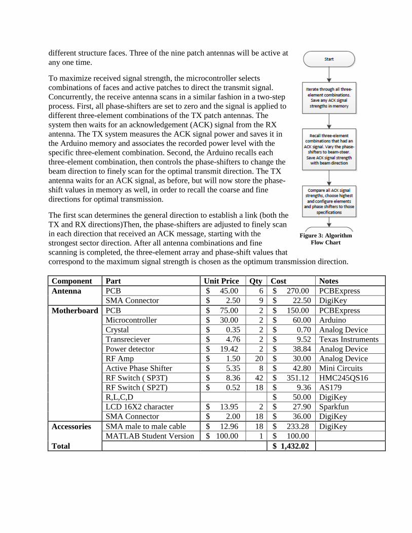
different structure faces. Three of the nine patch antennas will be active at
any one time.
To maximize received signal strength, the microcontroller selects
combinations of faces and active patches to direct the transmit signal.
Concurrently, the receive antenna scans in a similar fashion in a two-step
process. First, all phase-shifters are set to zero and the signal is applied to
different three-element combinations of the TX patch antennas. The
system then waits for an acknowledgement (ACK) signal from the RX
antenna. The TX system measures the ACK signal power and saves it in
the Arduino memory and associates the recorded power level with the
specific three-element combination. Second, the Arduino recalls each
three-element combination, then controls the phase-shifters to change the
beam direction to finely scan for the optimal transmit direction. The TX
antenna waits for an ACK signal, as before, but will now store the phase-
shift values in memory as well, in order to recall the coarse and fine
directions for optimal transmission.
The first scan determines the general direction to establish a link (both the
TX and RX directions)Then, the phase-shifters are adjusted to finely scan
in each direction that received an ACK message, starting with the
strongest sector direction. After all antenna combinations and fine
scanning is completed, the three-element array and phase-shift values that
correspond to the maximum signal strength is chosen as the optimum transmission direction.
Component Part Unit Price Qty Cost Notes
Antenna PCB $ 45.00 6 $ 270.00 PCBExpress
SMA Connector $ 2.50 9 $ 22.50 DigiKey
Motherboard PCB $ 75.00 2 $ 150.00 PCBExpress
Microcontroller $ 30.00 2 $ 60.00 Arduino
Crystal $ 0.35 2 $ 0.70 Analog Device
Transreciever $ 4.76 2 $ 9.52 Texas Instruments
Power detector $ 19.42 2 $ 38.84 Analog Device
RF Amp $ 1.50 20 $ 30.00 Analog Device
Active Phase Shifter $ 5.35 8 $ 42.80 Mini Circuits
RF Switch ( SP3T) $ 8.36 42 $ 351.12 HMC245QS16
RF Switch ( SP2T) $ 0.52 18 $ 9.36 AS179
R,L,C,D $ 50.00 DigiKey
LCD 16X2 character $ 13.95 2 $ 27.90 Sparkfun
SMA Connector $ 2.00 18 $ 36.00 DigiKey
Accessories SMA male to male cable $ 12.96 18 $ 233.28 DigiKey
MATLAB Student Version $ 100.00 1 $ 100.00
Total $ 1,432.02
Figure 3: Algorithm
Flow Chart

C LT 5534 Demo Board Schematic
75
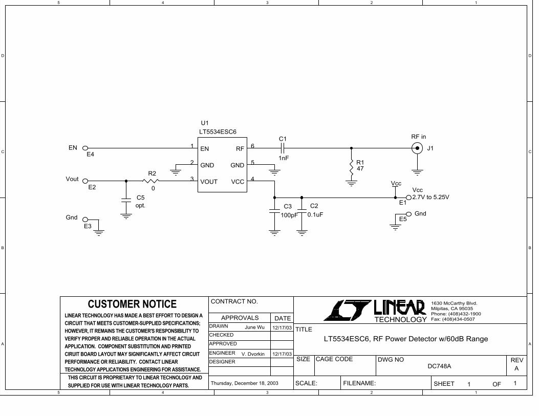
5
5
4
4
3
3
2
2
1
1
D D
C C
B B
A A
EN
Gnd
RF in
Vout
Vcc
Gnd
2.7V to 5.25V
ADC748A
Thursday, December 18, 2003 1 1
June Wu 12/17/03
V. Dvorkin 12/17/03
LT5534ESC6, RF Power Detector w/60dB Range
SIZE
SCALE:
CAGE CODE DWG NO REV
SHEET OFFILENAME:
TITLE
CONTRACT NO.
APPROVALS DATEDRAWN
CHECKED
APPROVED
ENGINEER
DESIGNER
TECHNOLOGY
1630 McCarthy Blvd.Milpitas, CA 95035Phone: (408)432-1900Fax: (408)434-0507
THIS CIRCUIT IS PROPRIETARY TO LINEAR TECHNOLOGY ANDSUPPLIED FOR USE WITH LINEAR TECHNOLOGY PARTS.
LINEAR TECHNOLOGY HAS MADE A BEST EFFORT TO DESIGN ACIRCUIT THAT MEETS CUSTOMER-SUPPLIED SPECIFICATIONS;HOWEVER, IT REMAINS THE CUSTOMER'S RESPONSIBILITY TOVERIFY PROPER AND RELIABLE OPERATION IN THE ACTUALAPPLICATION. COMPONENT SUBSTITUTION AND PRINTEDCIRUIT BOARD LAYOUT MAY SIGNIFICANTLY AFFECT CIRCUITPERFORMANCE OR RELIABILITY. CONTACT LINEARTECHNOLOGY APPLICATIONS ENGINEERING FOR ASSISTANCE.
CUSTOMER NOTICE
Vcc
C20.1uF
R2
0
R147
C3100pF
C1
1nFJ1
E2
E4
E3
E1
U1LT5534ESC6
1
2
3
5
4
6EN
GND
VOUT
GND
VCC
RF
E5
C5opt.

D LT 5538 Demo Board Schematic
77
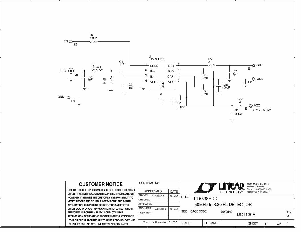
5
5
4
4
3
3
2
2
1
1
D D
C C
B B
A A
4.75V - 5.25V
3
50MHz to 3.8GHz DETECTOR
DC1120A
Thursday, November 15, 2007 1 1
A. Karpova 6/12/06
D.Stuetzle 6/12/06
LT5538EDD
SIZE
SCALE:
CAGE CODE DWG NO REV
SHEET OFFILENAME:
TITLE
CONTRACT NO.
APPROVALS DATEDRAWN
CHECKED
APPROVED
ENGINEER
DESIGNER
TECHNOLOGY
1630 McCarthy Blvd.Milpitas, CA 95035Phone: (408)432-1900Fax: (408)434-0507
THIS CIRCUIT IS PROPRIETARY TO LINEAR TECHNOLOGY ANDSUPPLIED FOR USE WITH LINEAR TECHNOLOGY PARTS.
LINEAR TECHNOLOGY HAS MADE A BEST EFFORT TO DESIGN ACIRCUIT THAT MEETS CUSTOMER-SUPPLIED SPECIFICATIONS;HOWEVER, IT REMAINS THE CUSTOMER'S RESPONSIBILITY TOVERIFY PROPER AND RELIABLE OPERATION IN THE ACTUALAPPLICATION. COMPONENT SUBSTITUTION AND PRINTEDCIRUIT BOARD LAYOUT MAY SIGNIFICANTLY AFFECT CIRCUITPERFORMANCE OR RELIABILITY. CONTACT LINEARTECHNOLOGY APPLICATIONS ENGINEERING FOR ASSISTANCE.
CUSTOMER NOTICE
VCC
C6DNI
E6GND
E1VCC
C10.1uF
C51nF
E5EN
C71pF
C10100pF
R50C4
1nF
E2GND
C9DNI
C2100pF
E4OUT
J1RF in
U1LT5538EDD
1
2
3
4 5
6
7
8
9
ENBL
IN+
IN-
VEE VCC
CAP-
CAP+
OUT
GN
D
R44.99K
C81pF R1
56
L11.5 nH

E Microcontroller Code
79
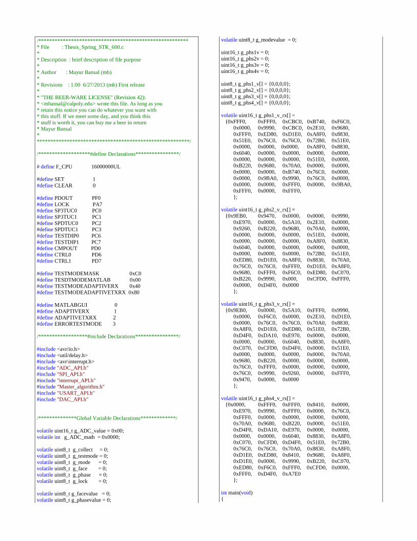
/******************************************************* * File : Thesis_Spring_STK_600.c
*
* Description : brief description of file purpose
*
* Author : Mayur Bansal (mb) *
* Revisions : 1.00 6/27/2013 (mb) First release
* * "THE BEER-WARE LICENSE" (Revision 42):
* <[email protected]> wrote this file. As long as you
* retain this notice you can do whatever you want with * this stuff. If we meet some day, and you think this
* stuff is worth it, you can buy me a beer in return
* Mayur Bansal *
********************************************************/
/*******************#define Declarations****************/
# define F_CPU 16000000UL
#define SET 1
#define CLEAR 0
#define PDOUT PF0
#define LOCK PA7 #define SP3TUC0 PC0
#define SP3TUC1 PC1
#define SPDTUC0 PC2 #define SPDTUC1 PC3
#define TESTDIP0 PC6
#define TESTDIP1 PC7 #define CMPOUT PD0
#define CTRL0 PD6
#define CTRL1 PD7
#define TESTMODEMASK 0xC0
#define TESDTMODEMATLAB 0x00 #define TESTMODEADAPTIVERX 0x40
#define TESTMODEADAPTIVETXRX 0x80
#define MATLABGUI 0
#define ADAPTIVERX 1
#define ADAPTIVETXRX 2 #define ERRORTESTMODE 3
/******************#include Declarations****************/
#include <avr/io.h>
#include <util/delay.h> #include <avr\interrupt.h>
#include "ADC_API.h" #include "SPI_API.h"
#include "interrupt_API.h"
#include "Master_algorithm.h" #include "USART_API.h"
#include "DAC_API.h"
/**************Global Variable Declarations*************/
volatile uint16_t g_ADC_value = 0x00;
volatile int g_ADC_math = 0x0000;
volatile uint8_t g_collect = 0;
volatile uint8_t g_testmode = 0;
volatile uint8_t g_mode = 0; volatile uint8_t g_face = 0;
volatile uint8_t g_phase = 0;
volatile uint8_t g_lock = 0;
volatile uint8_t g_facevalue = 0;
volatile uint8_t g_phasevalue = 0;
volatile uint8_t g_modevalue = 0;
uint16_t g_phs1v = 0;
uint16_t g_phs2v = 0;
uint16_t g_phs3v = 0; uint16_t g_phs4v = 0;
uint8_t g_phs1_v[] = 0,0,0,0; uint8_t g_phs2_v[] = 0,0,0,0;
uint8_t g_phs3_v[] = 0,0,0,0;
uint8_t g_phs4_v[] = 0,0,0,0;
volatile uint16_t g_phs1_v_rx[] =
0xFFF0, 0xFFF0, 0xCBC0, 0xB740, 0xF6C0, 0x0000, 0x9990, 0xCBC0, 0x2E10, 0x9680,
0xFFF0, 0xED80, 0xD1E0, 0xA8F0, 0x8830,
0x51E0, 0x76C0, 0x76C0, 0x72B0, 0x51E0, 0x0000, 0x0000, 0x0000, 0xA8F0, 0x8830,
0x6040, 0x0000, 0x0000, 0x0000, 0x0000,
0x0000, 0x0000, 0x0000, 0x51E0, 0x0000, 0xB220, 0x9680, 0x70A0, 0x0000, 0x0000,
0x0000, 0x0000, 0xB740, 0x76C0, 0x0000,
0x0000, 0x9BA0, 0x9990, 0x76C0, 0x0000, 0x0000, 0x0000, 0xFFF0, 0x0000, 0x9BA0,
0xFFF0, 0x0000, 0xFFF0,
;
volatile uint16_t g_phs2_v_rx[] = 0x9EB0, 0x9470, 0x0000, 0x0000, 0x9990,
0xE970, 0x0000, 0x5A10, 0x2E10, 0x0000,
0x9260, 0xB220, 0x9680, 0x70A0, 0x0000, 0x0000, 0x0000, 0x0000, 0x51E0, 0x0000,
0x0000, 0x0000, 0x0000, 0xA8F0, 0x8830,
0x6040, 0x0000, 0x0000, 0x0000, 0x0000, 0x0000, 0x0000, 0x0000, 0x72B0, 0x51E0,
0xED80, 0xD1E0, 0xA8F0, 0x8830, 0x70A0,
0x76C0, 0x76C0, 0xFFF0, 0xD1E0, 0xA8F0, 0x9680, 0xFFF0, 0xF6C0, 0xED80, 0xC070,
0xB220, 0x9990, 0x000, 0xCFD0, 0xFFF0,
0x0000, 0xD4F0, 0x0000 ;
volatile uint16_t g_phs3_v_rx[] = 0x9EB0, 0x0000, 0x5A10, 0xFFF0, 0x9990,
0x0000, 0xF6C0, 0x0000, 0x2E10, 0xD1E0,
0x0000, 0x76C0, 0x76C0, 0x70A0, 0x8830, 0xA8F0, 0xD1E0, 0xED80, 0x51E0, 0x72B0,
0xD4F0, 0xDA10, 0xE970, 0x0000, 0x0000,
0x0000, 0x0000, 0x6040, 0x8830, 0xA8F0, 0xC070, 0xCFD0, 0xD4F0, 0x0000, 0x51E0,
0x0000, 0x0000, 0x0000, 0x0000, 0x70A0,
0x9680, 0xB220, 0x0000, 0x0000, 0x0000, 0x76C0, 0xFFF0, 0x0000, 0x0000, 0x0000,
0x76C0, 0x9990, 0x9260, 0x0000, 0xFFF0,
0x9470, 0x0000, 0x0000 ;
volatile uint16_t g_phs4_v_rx[] = 0x0000, 0xFFF0, 0xFFF0, 0x8410, 0x0000,
0xE970, 0x9990, 0xFFF0, 0x0000, 0x76C0,
0xFFF0, 0x0000, 0x0000, 0x0000, 0x0000, 0x70A0, 0x9680, 0xB220, 0x0000, 0x51E0,
0xD4F0, 0xDA10, 0xE970, 0x0000, 0x0000,
0x0000, 0x0000, 0x6040, 0x8830, 0xA8F0, 0xC070, 0xCFD0, 0xD4F0, 0x51E0, 0x72B0,
0x76C0, 0x76C0, 0x70A0, 0x8830, 0xA8F0,
0xD1E0, 0xED80, 0x8410, 0x9680, 0xA8F0, 0xD1E0, 0x0000, 0x9990, 0xB220, 0xC070,
0xED80, 0xF6C0, 0xFFF0, 0xCFD0, 0x0000,
0xFFF0, 0xD4F0, 0xA7E0 ;
int main(void)
// Set the different I/O's
// set Lock as Output
DDRA |= (1 << LOCK); // set peak detector output as input to ADC0
DDRA &= ~(1 << PDOUT);
// set the SPDT as outputs DDRC |= ( 1 << SPDTUC0) | ( 1<< SPDTUC1);
// set the SP3T as outputs
DDRC |= ( 1 << SP3TUC0) | ( 1<< SP3TUC1); // set the TESTDIP as inputs
DDRC &= ~(1 << TESTDIP0) & ~( 1 << TESTDIP1);
// set Comparator out as input DDRD &= ~(1 << CMPOUT);
// set CTRL line as GPIO for RF board for future use.
//DDRD |= (1 << CTRL0 ) | (1 << CTRL1);
/* test CODE */
// Initialize all the Peripherals required
// Initialize ADC initialize_ADC_single_conv();
set_ADC_clock();
enable_ADC(); set_ADC_trigger_source();
// Initialize SPI
SPI_MasterInit();
// Initialize USART
USART_init();
// disable the Semaphore
g_collect = 0;
// Check to see what test mode the uC should be on
// MATLAB GUI mode if ( (PINC & TESTMODEMASK) == TESDTMODEMATLAB )
SPI_MasterTransmit_DAC(set_pwrDACA,0xff,0xff);
while(1)
// receive the mode
g_mode = USART_rx();
// receive the face g_face = USART_rx();
// receive the phase 1 value g_phs1_v[1] = USART_rx();
g_phs1_v[2] = USART_rx();
g_phs1_v[3] = USART_rx(); g_phs1_v[4] = USART_rx();
// receive the phase 2 value g_phs2_v[1] = USART_rx();
g_phs2_v[2] = USART_rx();
g_phs2_v[3] = USART_rx(); g_phs2_v[4] = USART_rx();
// receive the phase 3 value g_phs3_v[1] = USART_rx();
g_phs3_v[2] = USART_rx();
g_phs3_v[3] = USART_rx(); g_phs3_v[4] = USART_rx();
// receive the phase 4 value g_phs4_v[1] = USART_rx();
g_phs4_v[2] = USART_rx();
g_phs4_v[3] = USART_rx(); g_phs4_v[4] = USART_rx();
// convert the recive characters to number value g_mode = char_to_num(g_mode);
g_face = char_to_num(g_face);
// convert the recieve character phase value to voltage
value
g_phs1v = convert_data_voltage(g_phs1_v); g_phs2v = convert_data_voltage(g_phs2_v);
g_phs3v = convert_data_voltage(g_phs3_v);
g_phs4v = convert_data_voltage(g_phs4_v);
g_phs1v = (g_phs1v << 4);
g_phs2v = (g_phs2v << 4); g_phs3v = (g_phs3v << 4);
g_phs4v = (g_phs4v << 4);
// set the system variables
set_face(g_face);
set_mode(g_mode); SPI_MasterTransmit_DAC(setDACE,(g_phs1v >> 8),
g_phs1v);
SPI_MasterTransmit_DAC(setDACF,(g_phs2v >> 8), g_phs2v);
SPI_MasterTransmit_DAC(setDACG,(g_phs3v >> 8),
g_phs3v);
SPI_MasterTransmit_DAC(setDACHpwrALL,(g_phs4v >> 8), g_phs4v);
// Adaptive RX
else if ( (PINC & TESTMODEMASK) == TESTMODEADAPTIVERX )
// set the mode to receive set_mode(RX);
// clear the semaphore g_collect = CLEAR;
// set the comparater refrence to -50dBm SPI_MasterTransmit_DAC(set_pwrDACA,(MINPWRLVL
>> 8), MINPWRLVL);
// Initialize Interrupts
enable_interrupts();
enable_int0_rising_edge();
while (1)
// semaphore check
if(g_collect == CLEAR)
// clear lock semaphore
g_lock = CLEAR;
clr_lock();
// start the face loop
for (g_facevalue = 0; g_facevalue < NUMBEROFFACES; g_facevalue++)
set_face(g_facevalue+1);
// start the phase loop
for (g_phasevalue = 0; g_phasevalue < NUMBEROFPOINTSRX; g_phasevalue++ )
SPI_MasterTransmit_DAC(setDACE,(g_phs1_v_rx[g_phasevalue
] >> 8), g_phs1_v_rx[g_phasevalue] );
SPI_MasterTransmit_DAC(setDACF,(g_phs2_v_rx[g_phasevalue] >> 8), g_phs2_v_rx[g_phasevalue] );
SPI_MasterTransmit_DAC(setDACG,(g_phs3_v_rx[g_phasevalue] >> 8), g_phs3_v_rx[g_phasevalue] );
SPI_MasterTransmit_DAC(setDACHpwrALL,(g_phs4_v_rx[g_phasevalue] >> 8), g_phs4_v_rx[g_phasevalue] );
_delay_ms(DELAYTIME*20);
if ( g_collect == SET)
// set the lock semaphore g_lock = SET;
set_lock();
// clear semaphore
g_collect = CLEAR;
// set the face and phase count
g_facevalue = g_face;
g_phasevalue = g_phase;
// set the beam direction set_face(g_face+1);
SPI_MasterTransmit_DAC(setDACE,(g_phs1_v_rx[g_phase] >> 8), g_phs1_v_rx[g_phase] );
SPI_MasterTransmit_DAC(setDACF,(g_phs2_v_rx[g_phase] >> 8), g_phs2_v_rx[g_phase] );
SPI_MasterTransmit_DAC(setDACG,(g_phs3_v_rx[g_phase] >> 8), g_phs3_v_rx[g_phase] );
SPI_MasterTransmit_DAC(setDACHpwrALL,(g_phs4_v_rx[g_phase] >> 8), g_phs4_v_rx[g_phase] );
//delay _delay_ms(DELAYTIME*20*5);
// Future work else if ( (PINC & TESTMODEMASK) ==
TESTMODEADAPTIVETXRX )
g_testmode = ERRORTESTMODE;
else
g_testmode = ERRORTESTMODE;
/*-----------------------------------------------------
* Function: ISR
* * Description: Interrupt service routine for a external
* hardware interrupt. This interrupt is
* triggered on a rising edge. The trigger * is output of the comparator.
*
* param vector address : interrupt 0 vector address *--------------------------------------------------------*/
ISR (INT0_vect)
// Set the Semaphore
g_collect = SET;
// Save the Important values
g_face = g_facevalue; // The face of Antenna used
g_phase = g_phasevalue; // The Phase index
if ( g_lock == CLEAR)
start_conversion_ADC();
while(!(ADCSRA & 0x10));
ADCSRA|=(1<<ADIF); g_ADC_value = ADC;
SPI_MasterTransmit_DAC(set_pwrDACA,(g_ADC_value
>> 8) , g_ADC_value);
else
SPI_MasterTransmit_DAC(set_pwrDACA, (MINPWRLVL
>> 8) , MINPWRLVL);
/******************************************************* * File : ADC_API.h
*
* Description : brief description of file purpose *
* Author : Mayur Bansal (mb) *
* Revisions : 1.00 6/27/2013 (mb) First release
* * "THE BEER-WARE LICENSE" (Revision 42):
* <[email protected]> wrote this file. As long as you
* retain this notice you can do whatever you want with * this stuff. If we meet some day, and you think this
* stuff is worth it, you can buy me a beer in return
* Mayur Bansal *
********************************************************/
#ifndef ADC_API_H_
#define ADC_API_H_
/*******************Function Prototypes*****************/
/*----------------------------------------------------- * Function: initialize_ADC_single_conv
*
* Description: Initialize the ADC *--------------------------------------------------------*/
void initialize_ADC_single_conv();
/*-----------------------------------------------------
* Function: enable_ADC
* * Description: enable the ADC
*--------------------------------------------------------*/
void enable_ADC();
/*-----------------------------------------------------
* Function: start_conversion_ADC *
* Description: start a single conversation of the ADC
*--------------------------------------------------------*/ void start_conversion_ADC();
/*----------------------------------------------------- * Function: set_ADC_clock
*
* Description: set the ADC clock to OSC/4 *--------------------------------------------------------*/
void set_ADC_clock();
/*-----------------------------------------------------
* Function: set_ADC_trigger_source
* * Description: set the ADC trigger to free running
*--------------------------------------------------------*/
void set_ADC_trigger_source();
#endif /* ADC_API_H_ */
/******************************************************* * File : ADC_API.c
* * Description : brief description of file purpose
*
* Author : Mayur Bansal (mb) *
* Revisions : 1.00 6/27/2013 (mb) First release
* * "THE BEER-WARE LICENSE" (Revision 42):
* <[email protected]> wrote this file. As long as you
* retain this notice you can do whatever you want with * this stuff. If we meet some day, and you think this
* stuff is worth it, you can buy me a beer in return
* Mayur Bansal *
********************************************************/
#include <avr/io.h>
#include "ADC_API.h"
/*-----------------------------------------------------
* Function: initialize_ADC_single_conv *
* Description: Initialize the ADC
*--------------------------------------------------------*/ void initialize_ADC_single_conv()
// Reference to AREF, Internal VREF turned off ADMUX &= ~(1 << REFS1);
ADMUX |= (1 << REFS0);
// // Left justified on result
ADMUX |= (1 << ADLAR);
// // Single ended input to ADCO located PORTA0
ADMUX &= ~(1 << MUX5);
ADMUX &= ~(1 << MUX4); ADMUX &= ~(1 << MUX3);
ADMUX &= ~(1 << MUX2);
ADMUX &= ~(1 << MUX0);
/*----------------------------------------------------- * Function: enable_ADC
*
* Description: enable the ADC *--------------------------------------------------------*/
void enable_ADC()
// set the ADC enable bit
ADCSRA |= (1 << ADEN);
//Auto Trigger based in ADCSRB ADCSRA |= (1 << ADATE);
/*-----------------------------------------------------
* Function: start_conversion_ADC *
* Description: start a single conversation of the ADC
*--------------------------------------------------------*/ void start_conversion_ADC()
// set the converstion bit of ADC ADCSRA |= (1 << ADSC);
/*-----------------------------------------------------
* Function: set_ADC_clock
* * Description: set the ADC clock to OSC/4
*--------------------------------------------------------*/
void set_ADC_clock()
// Setting a division factor of 4
ADCSRA &= (0 << ADPS2); ADCSRA |= (1 << ADPS1);
ADCSRA &= (0 << ADPS0);
/*-----------------------------------------------------
* Function: set_ADC_trigger_source *
* Description: set the ADC trigger to free running
*--------------------------------------------------------*/ void set_ADC_trigger_source()
// Free Running mode ADCSRB &= (0 << ADTS2);
ADCSRB &= (0 << ADTS1);
ADCSRB &= (0 << ADTS0);
/******************************************************* * File : DAC_API.h
* * Description : brief description of file purpose
*
* Author : Mayur Bansal (mb) *
* Revisions : 1.00 6/27/2013 (mb) First release
* * "THE BEER-WARE LICENSE" (Revision 42):
* <[email protected]> wrote this file. As long as you
* retain this notice you can do whatever you want with * this stuff. If we meet some day, and you think this
* stuff is worth it, you can buy me a beer in return
* Mayur Bansal *
********************************************************/
#ifndef DAC_API_H_
#define DAC_API_H_
/*
DAC Command and Address Codes
C3 | C2 | C1 | C0 |
0 | 0 | 0 | 0 | Write to Input Register n 0 | 0 | 0 | 1 | Update(Power up ) DAC Register n
0 | 0 | 1 | 0 | Write to Input Register n, Update ( Power up) All
0 | 0 | 1 | 1 | Write to and Update (power up) n 0 | 1 | 0 | 0 | Power Down n
0 | 1 | 0 | 1 | Power Down Chip ( All DACs and References)
0 | 1 | 1 | 0 | Select Internal Reference ( Power-up Reference) 0 | 1 | 1 | 1 | Select External Reference ( Power-Down Reference)
1 | 1 | 1 | 1 | No Operation
A3 | A2 | A1 | A0 |
0 | 0 | 0 | 0 | DAC A
0 | 0 | 0 | 1 | DAC B 0 | 0 | 1 | 0 | DAC C
0 | 0 | 1 | 1 | DAC D
0 | 1 | 0 | 0 | DAC E 0 | 1 | 0 | 1 | DAC F
0 | 1 | 1 | 0 | DAC G
0 | 1 | 1 | 1 | DAC H 1 | 1 | 1 | 1 | All DACs
*/
/*
24-Bit input Protocol
C3-C2-C1-C0-A3-A2-A1-A0-D15-D14-D13-D12-D11-D10-D9-D8-
D7-D6-D5-D4-D3-D2-D1-D0 Command Address Data
DAC_API_H_
*/
/*******************#define Declarations****************/
#define setDACA 0x00 #define setDACB 0x01
#define setDACC 0x02
#define setDACD 0x03 #define setDACE 0x04
#define setDACF 0x05
#define setDACG 0x06 #define setDACH 0x07
#define pwrDACA 0x10 #define pwrDACB 0x11
#define pwrDACC 0x12 #define pwrDACD 0x13
#define pwrDACE 0x14
#define pwrDACF 0x15 #define pwrDACG 0x16
#define pwrDACH 0x17
#define pwrALL 0x1F
#define setREF 0x74
#define setDACApwrALL 0x20
#define setDACBpwrALL 0x21
#define setDACCpwrALL 0x22 #define setDACDpwrALL 0x23
#define setDACEpwrALL 0x24
#define setDACFpwrALL 0x25 #define setDACGpwrALL 0x26
#define setDACHpwrALL 0x27
#define set_pwrDACA 0x30
#define set_pwrDACB 0x31
#define set_pwrDACC 0x32 #define set_pwrDACD 0x33
#define set_pwrDACE 0x34
#define set_pwrDACF 0x35 #define set_pwrDACG 0x36
#define set_pwrDACH 0x37
#endif
/******************************************************* * File : interrupt_API.h
*
* Description : brief description of file purpose *
* Author : Mayur Bansal (mb)
* * Revisions : 1.00 6/27/2013 (mb) First release
*
* "THE BEER-WARE LICENSE" (Revision 42): * <[email protected]> wrote this file. As long as you
* retain this notice you can do whatever you want with
* this stuff. If we meet some day, and you think this * stuff is worth it, you can buy me a beer in return
* Mayur Bansal
* ********************************************************/
#ifndef INTERRUPT_API_H_ #define INTERRUPT_API_H_
/*******************Function Prototypes*****************/
/*-----------------------------------------------------
* Function: enable_interrupts *
* Description: Enable all interrupts
*--------------------------------------------------------*/ void enable_interrupts ();
/*----------------------------------------------------- * Function: enable_int0_rising_edge
*
* Description: sets the interrupt on the rising edge * for INT0
*--------------------------------------------------------*/
void enable_int0_rising_edge();
#endif /* INTERRUPT_API_H_ */
/*******************************************************
* File : interrupt_API.c *
* Description : brief description of file purpose *
* Author : Mayur Bansal (mb)
* * Revisions : 1.00 6/27/2013 (mb) First release
*
* "THE BEER-WARE LICENSE" (Revision 42): * <[email protected]> wrote this file. As long as you
* retain this notice you can do whatever you want with
* this stuff. If we meet some day, and you think this * stuff is worth it, you can buy me a beer in return
* Mayur Bansal
* ********************************************************/
/******************#include Declarations****************/
#include <avr/io.h>
#include "interrupt_API.h" #include <avr\interrupt.h>
/*-----------------------------------------------------
* Function: enable_interrupts
* * Description: Enable all interrupts
*--------------------------------------------------------*/
void enable_interrupts()
sei();
/*-----------------------------------------------------
* Function: enable_int0_rising_edge *
* Description: sets the interrupt on the rising edge
* for INT0 *--------------------------------------------------------*/
void enable_int0_rising_edge()
//Trigger on rising edge of INT0
EICRA |= (1 << ISC00) | (1 << ISC01);
//Enable INT0 EIMSK |= (1 << INT0);
/*******************************************************
* File : Master_algorithm.h
* * Description : brief description of file purpose
*
* Author : Mayur Bansal (mb) *
* Revisions : 1.00 6/27/2013 (mb) First release
* * "THE BEER-WARE LICENSE" (Revision 42):
* <[email protected]> wrote this file. As long as you
* retain this notice you can do whatever you want with * this stuff. If we meet some day, and you think this
* stuff is worth it, you can buy me a beer in return
* Mayur Bansal *
********************************************************/
#ifndef MASTER_ALGORITHM_H_
#define MASTER_ALGORITHM_H_
/*******************#define Declarations****************/
#define TX_FC1 0x04 #define TX_FC2 0x05
#define TX_FC3 0x06
#define RX_FC1 0x08 #define RX_FC2 0x09
#define RX_FC3 0x0A
#define TX 0x01
#define RX 0x02
#define FC1 0x01
#define FC2 0x02 #define FC3 0x03
#define NUMBEROFMODES 2 #define NUMBEROFFACES 3
#define NUMBEROFPOINTSRX 50
#define DELAYTIME 50
#define MINPWRLVL 0x1410 // set the DAC to 0.392V appx -50dBm
power
/*******************Function Prototypes*****************/
/*-----------------------------------------------------
* Function: set_phases *
* Description: Set the control voltage for the phase
* shifters. The voltage is set as 1/3 the * value using DACs.
*
* param phase1: uint16_t: phase 1 control voltage * param phase2: uint16_t: phase 2 control voltage
* param phase3: uint16_t: phase 3 control voltage
* param phase4: uint16_t: phase 4 control voltage *--------------------------------------------------------*/
/*----------------------------------------------------- * Function: set_phases
*
* Description: Set the control voltage for the phase * shifters. The voltage is set as 1/3 the
* value using DACs.
* * param phase1: uint16_t: phase 1 control voltage
* param phase2: uint16_t: phase 2 control voltage
* param phase3: uint16_t: phase 3 control voltage * param phase4: uint16_t: phase 4 control voltage
*--------------------------------------------------------*/
void set_phases(uint16_t phase1, uint16_t phase2, uint16_t phase3, uint16_t phase4);
/*----------------------------------------------------- * Function: set_face
*
* Description: Sets the Single pole triple throw switch * control voltages. PORTC0:1
*
* param face: uint8_t: the face value FC1, FC2, or FC3 *--------------------------------------------------------*/
void set_face (uint8_t face);
/*----------------------------------------------------- * Function: set_mode
*
* Description: Sets the Single pole double throw switch * control voltages. PORTC2:3
*
* param face: uint8_t: the face value FTX, or RX *--------------------------------------------------------*/
void set_mode (uint8_t mode);
/*-----------------------------------------------------
* Function: set_lock
* * Description: Turn on the lock LED when adaptive mode is
* in lock. PORT7
*--------------------------------------------------------*/ void set_lock();
/*-----------------------------------------------------
* Function: clr_lock
* * Description: Turn off the lock LED when adaptive mode is
* in lock. PORT7
*--------------------------------------------------------*/ void clr_lock();
/*----------------------------------------------------- * Function: char_to_num
*
* Description: convert a ASCII decimal character to a * integer number in uint8_t
*
* param character: uint8_t: ASCII character *
* return uint8_t: the actual decimal value number
*--------------------------------------------------------*/ uint8_t char_to_num (uint8_t character);
/*----------------------------------------------------- * Function: convert_data_voltage
*
* Description: converts a 4 character decimal value to * interger value in uint16_t
*
* param v[]: uint8_t: array of ASCII character *
* return uint16_t: the actual decimal voltage value
*--------------------------------------------------------*/ uint16_t convert_data_voltage(uint8_t v[]);
#endif /* MASTER_ALGORITHM_H_ */
/*******************************************************
* File : Master_algorithm.c *
* Description : brief description of file purpose
* * Author : Mayur Bansal (mb)
*
* Revisions : 1.00 6/27/2013 (mb) First release *
* "THE BEER-WARE LICENSE" (Revision 42):
* <[email protected]> wrote this file. As long as you * retain this notice you can do whatever you want with
* this stuff. If we meet some day, and you think this
* stuff is worth it, you can buy me a beer in return * Mayur Bansal
*
********************************************************/
/*******************#define Declarations****************/
# define F_CPU 16000000UL
/******************#include Declarations****************/
#include <avr/io.h>
#include <util/delay.h> #include "Master_algorithm.h"
#include "SPI_API.h"
#include "DAC_API.h"
/*-----------------------------------------------------
* Function: set_phases *
* Description: Set the control voltage for the phase
* shifters. The voltage is set as 1/3 the * value using DACs.
*
* param phase1: uint16_t: phase 1 control voltage * param phase2: uint16_t: phase 2 control voltage
* param phase3: uint16_t: phase 3 control voltage * param phase4: uint16_t: phase 4 control voltage
*--------------------------------------------------------*/
void set_phases(uint16_t phase1, uint16_t phase2, uint16_t phase3, uint16_t phase4)
SPI_MasterTransmit_DAC(setDACE,(phase1 >> 8), phase1); SPI_MasterTransmit_DAC(setDACF,(phase2 >> 8), phase2);
SPI_MasterTransmit_DAC(setDACG,(phase3 >> 8), phase3);
SPI_MasterTransmit_DAC(setDACHpwrALL,(phase4 >> 8), phase4);
/*-----------------------------------------------------
* Function: set_face
* * Description: Sets the Single pole triple throw switch
* control voltages. PORTC0:1
* * param face: uint8_t: the face value FC1, FC2, or FC3
*--------------------------------------------------------*/
void set_face (uint8_t face)
if( face == FC1)
PORTC &= ~(1 << PC0);
PORTC &= ~(1 << PC1);
else if (face == FC2)
PORTC &= ~(1 << PC1); PORTC |= (1 << PC0);
else if (face == FC3)
PORTC &= ~(1 << PC0);
PORTC |= (1 << PC1);
// error mode
else
PORTC |= (1 << PC0);
PORTC |= (1 << PC1);
/*-----------------------------------------------------
* Function: set_mode *
* Description: Sets the Single pole double throw switch
* control voltages. PORTC2:3 *
* param face: uint8_t: the face value FTX, or RX
*--------------------------------------------------------*/ void set_mode (uint8_t mode)
if( mode == TX)
PORTC &= ~(1 << PC2);
PORTC |= (1 << PC3);
else if (mode == RX)
PORTC &= ~(1 << PC3);
PORTC |= (1 << PC2);
//error mode
else
PORTC |= (1 << PC2);
PORTC |= (1 << PC3);
/*-----------------------------------------------------
* Function: set_lock
* * Description: Turn on the lock LED when adaptive mode is
* in lock. PORT7
*--------------------------------------------------------*/ void set_lock()
PORTA |= (1 << PA7);
/*----------------------------------------------------- * Function: clr_lock
*
* Description: Turn off the lock LED when adaptive mode is * in lock. PORT7
*--------------------------------------------------------*/
void clr_lock()
PORTA &= (0 << PA7);
/*-----------------------------------------------------
* Function: char_to_num *
* Description: convert a ASCII decimal character to a
* integer number in uint8_t *
* param character: uint8_t: ASCII character
* * return uint8_t: the actual decimal value number
*--------------------------------------------------------*/
uint8_t char_to_num (uint8_t character)
uint8_t value = 0;
if(character == 0x20) // Decimal 0
return value;
else if (character == 0x31) // Decimal 1 return value = 0x01;
else if (character == 0x32) // Decimal 2
return value = 0x02; else if (character == 0x33) // Decimal 3
return value = 0x03;
else if (character == 0x34) // Decimal 4 return value = 0x04;

else if (character == 0x35) // Decimal 5
return value = 0x05; else if (character == 0x36) // Decimal 6
return value = 0x06;
else if (character == 0x37) // Decimal 7 return value = 0x07;
else if (character == 0x38) // Decimal 8
return value = 0x08; else if (character == 0x39) // Decimal 9
return value = 0x09;
else return value;
/*-----------------------------------------------------
* Function: convert_data_voltage
* * Description: converts a 4 character decimal value to
* interger value in uint16_t
* * param v[]: uint8_t: array of ASCII character
*
* return uint16_t: the actual decimal voltage value *--------------------------------------------------------*/
uint16_t convert_data_voltage(uint8_t v[])
// 4 temp var
uint8_t t_1, t_2, t_3, t_4;
t_1 = char_to_num(v[1]);
t_2 = char_to_num(v[2]); t_3 = char_to_num(v[3]);
t_4 = char_to_num(v[4]);
uint16_t value = 0;
// convert to voltage value value = (t_1*1000)+(t_2*100)+(t_3*10)+t_4;
return value;
/******************************************************* * File : SPI_API.h
*
* Description : brief description of file purpose *
* Author : Mayur Bansal (mb)
* * Revisions : 1.00 6/27/2013 (mb) First release
*
* "THE BEER-WARE LICENSE" (Revision 42): * <[email protected]> wrote this file. As long as you
* retain this notice you can do whatever you want with
* this stuff. If we meet some day, and you think this * stuff is worth it, you can buy me a beer in return
* Mayur Bansal
* ********************************************************/
#ifndef SPI_API_H_ #define SPI_API_H_
// PB0 -- ~SS // PB1 -- SCK
// PB2 -- MOSI
// PB3 -- MISO
/*******************#define Declarations****************/
#define SETTLING_TIME 0x05
/*******************Function Prototypes*****************/
/*-----------------------------------------------------
* Function: SPI_MasterInit *
* Description: Initialize the SPI in the master mode.
* with clock speed OSC/4 *--------------------------------------------------------*/
void SPI_MasterInit(void);
/*-----------------------------------------------------
* Function: SPI_MasterTransmit_DAC
* * Description: Send the voltage set command to DAC.
* send the packet in the protocol stated
* DAC_API.h *
* param cDataH: char: upper 8bits
* param cDataM: char: middle 8bits * param cDataL: char: lower 8bits
*
* return: uint8_t *--------------------------------------------------------*/
void SPI_MasterTransmit_DAC(char cDataH, char cDataM, char
cDataL);
#endif /* SPI_API_H_ */
/******************************************************* * File : SPI_API.c *
* Description : brief description of file purpose
* * Author : Mayur Bansal (mb)
*
* Revisions : 1.00 6/27/2013 (mb) First release *
* "THE BEER-WARE LICENSE" (Revision 42):
* <[email protected]> wrote this file. As long as you * retain this notice you can do whatever you want with
* this stuff. If we meet some day, and you think this
* stuff is worth it, you can buy me a beer in return * Mayur Bansal
*
********************************************************/
# define F_CPU 16000000UL
#include <avr/io.h>
#include <util/delay.h>
#include "SPI_API.h"
// PB0 -- ~SS
// PB1 -- SCK // PB2 -- MOSI
// PB3 -- MISO
/*-----------------------------------------------------
* Function: SPI_MasterInit
* * Description: Initialize the SPI in the master mode.
* with clock speed OSC/4
*--------------------------------------------------------*/ void SPI_MasterInit(void)
/* Set ~SS, MOSI and SCK output, all others input */ DDRB = (1<<DDB0)|(1<<DDB1)|(1<<DDB2);
/* Enable SPI, Master, set clock rate fck/4 */
SPCR = (1<<SPE)|(1<<MSTR); // MSB first
/*----------------------------------------------------- * Function: SPI_MasterTransmit_DAC
*
* Description: Send the voltage set command to DAC. * send the packet in the protocol stated
* DAC_API.h
* * param cDataH: char: upper 8bits
* param cDataM: char: middle 8bits
* param cDataL: char: lower 8bits *
* return: uint8_t
*--------------------------------------------------------*/ void SPI_MasterTransmit_DAC(char cDataH, char cDataM, char
cDataL)
PORTB &= (0 << PB0);
/* Start transmission */ SPDR = cDataH;
/* Wait for transmission complete */
while(!(SPSR & (1<<SPIF))) ;
SPDR = cDataM;
/* Wait for transmission complete */ while(!(SPSR & (1<<SPIF)))
;
SPDR = cDataL; /* Wait for transmission complete */
while(!(SPSR & (1<<SPIF)))
; PORTB |= (1 << PB0);
// wail 5mS for the DAC settling time
_delay_ms(SETTLING_TIME);
/******************************************************* * File : USART_API.h *
* Description : brief description of file purpose
* * Author : Mayur Bansal (mb)
*
* Revisions : 1.00 6/27/2013 (mb) First release *
* "THE BEER-WARE LICENSE" (Revision 42):
* <[email protected]> wrote this file. As long as you * retain this notice you can do whatever you want with
* this stuff. If we meet some day, and you think this
* stuff is worth it, you can buy me a beer in return * Mayur Bansal
*
********************************************************/
#ifndef USART_API_H_
#define USART_API_H_
/*******************#define Declarations****************/
#define F_CPU 16000000UL
#define BAUD 57600 #define MYUBRR (F_CPU/16/BAUD-1)
/*******************Function Prototypes*****************/
/*-----------------------------------------------------
* Function: USART_init *
* Description: Initializer the USART
* BAUD 57600 * Data bits: 8
* Stop bits: 1
*--------------------------------------------------------*/ void USART_init( void);
/*----------------------------------------------------- * Function: USART_tx
*
* Description: send the data on the transmit line *
* param data: uint8_t: data to be sent
*--------------------------------------------------------*/ void USART_tx( uint8_t data);
/*----------------------------------------------------- * Function: USART_rx
*
* Description: receive the data on the receive line *
* return uint8_t: data to be sent
*--------------------------------------------------------*/ uint16_t USART_rx( void);
#endif /* USART_API_H_ */
/*******************************************************
* File : USART_API.c *
* Description : brief description of file purpose
* * Author : Mayur Bansal (mb)
*
* Revisions : 1.00 6/27/2013 (mb) First release *
* "THE BEER-WARE LICENSE" (Revision 42): * <[email protected]> wrote this file. As long as you
* retain this notice you can do whatever you want with
* this stuff. If we meet some day, and you think this * stuff is worth it, you can buy me a beer in return
* Mayur Bansal
* ********************************************************/
/******************#include Declarations****************/
#include <avr/io.h>
#include "USART_API.h"
/*-----------------------------------------------------
* Function: USART_init *
* Description: Initializer the USART
* BAUD 57600 * Data bits: 8
* Stop bits: 1
*--------------------------------------------------------*/ void USART_init( void)
/* Set baud rate */ UBRR0H = (unsigned char)((unsigned int)(MYUBRR)>>8);
UBRR0L = (unsigned char)(unsigned int)(MYUBRR);
/* Enable receiver and transmitter */
UCSR0B = (1<<RXEN0)|(1<<TXEN0);
/* Set frame format: 8data, 1stop bit, parity Disable, Asynchronous
Mode */
UCSR0C = (3<<UCSZ00);
// USART_Init
/*-----------------------------------------------------
* Function: USART_tx *
* Description: send the data on the transmit line
* * param data: uint8_t: data to be sent
*--------------------------------------------------------*/
void USART_tx(uint8_t data)
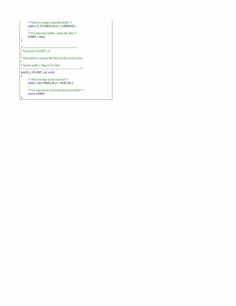
/* Wait for empty transmit buffer */
while ( !( UCSR0A & (1<<UDRE0)) ) ;
/* Put data into buffer, sends the data */
UDR0 = data;
/*----------------------------------------------------- * Function: USART_rx
*
* Description: receive the data on the receive line *
* return uint8_t: data to be sent
*--------------------------------------------------------*/ uint16_t USART_rx( void)
/* Wait for data to be received */ while ( !(UCSR0A & (1<<RXC0)) )
;
/* Get and return received data from buffer */ return UDR0;

F PCB Schematic
90
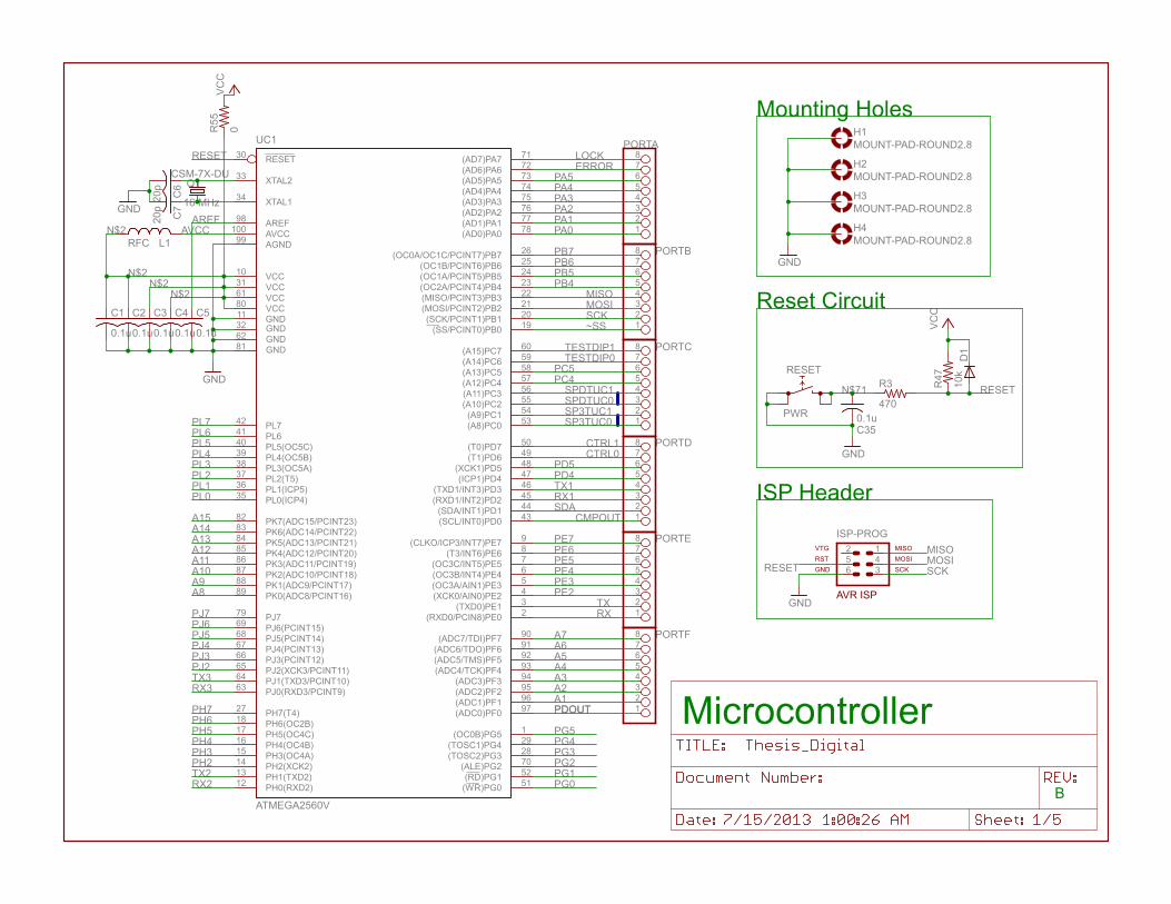
16 MHz
ATMEGA2560V
GND
GND
GND
CSM-7X-DU20
p20
p
0.1u0.1u0.1u0.1u
MOUNT-PAD-ROUND2.8
MOUNT-PAD-ROUND2.8
MOUNT-PAD-ROUND2.8
MOUNT-PAD-ROUND2.8
GND
RFC
0.1u
0.1u
GND
470
10k
PWR
0V
CC
VC
C
GNDGNDGND
VCCVCC
VCC
(A8)PC0 53(A9)PC1 54(A10)PC2 55(A11)PC3 56(A12)PC4 57(A13)PC5 58(A14)PC6 59(A15)PC7 60
(AD0)PA0 78(AD1)PA1 77(AD2)PA2 76(AD3)PA3 75(AD4)PA4 74(AD5)PA5 73(AD6)PA6 72(AD7)PA7 71
(ADC0)PF0 97(ADC1)PF1 96(ADC2)PF2 95(ADC3)PF3 94(ADC4/TCK)PF4 93(ADC5/TMS)PF5 92(ADC6/TDO)PF6 91(ADC7/TDI)PF7 90
(ALE)PG2 70
(CLKO/ICP3/INT7)PE7 9
(ICP1)PD4 47
(MISO/PCINT3)PB3 22
(MOSI/PCINT2)PB2 21
(OC0A/OC1C/PCINT7)PB7 26
(OC0B)PG5 1
(OC1A/PCINT5)PB5 24(OC1B/PCINT6)PB6 25
(OC2A/PCINT4)PB4 23
(OC3A/AIN1)PE3 5(OC3B/INT4)PE4 6(OC3C/INT5)PE5 7
(RD)PG1 52
(RXD0/PCIN8)PE0 2
(RXD1/INT2)PD2 45
(SCK/PCINT1)PB1 20
(SCL/INT0)PD0 43(SDA/INT1)PD1 44
(SS/PCINT0)PB0 19
(T0)PD7 50
(T1)PD6 49
(T3/INT6)PE6 8
(TOSC1)PG4 29
(TOSC2)PG3 28
(TXD0)PE1 3
(TXD1/INT3)PD3 46
(WR)PG0 51
(XCK0/AIN0)PE2 4
(XCK1)PD5 48
AGND99
AREF98
AVCC100
GND11326281
PH0(RXD2)12 PH1(TXD2)13 PH2(XCK2)14 PH3(OC4A)15 PH4(OC4B)16 PH5(OC4C)17 PH6(OC2B)18 PH7(T4)27
PJ0(RXD3/PCINT9)63 PJ1(TXD3/PCINT10)64 PJ2(XCK3/PCINT11)65 PJ3(PCINT12)66 PJ4(PCINT13)67 PJ5(PCINT14)68 PJ6(PCINT15)69 PJ779
PK0(ADC8/PCINT16)89 PK1(ADC9/PCINT17)88 PK2(ADC10/PCINT18)87 PK3(ADC11/PCINT19)86 PK4(ADC12/PCINT20)85 PK5(ADC13/PCINT21)84 PK6(ADC14/PCINT22)83 PK7(ADC15/PCINT23)82
PL0(ICP4)35 PL1(ICP5)36 PL2(T5)37 PL3(OC5A)38 PL4(OC5B)39 PL5(OC5C)40 PL641 PL742
RESET30
VCC10316180
XTAL134
XTAL233
UC1
ISP-PROG
3
25
1
64
Q1C
6C
7
C2 C3 C4 C5
12345678
PORTA
12345678 PORTB
12345678 PORTC
12345678 PORTD
12345678 PORTE
12345678 PORTF
H1
H2
H3
H4L1
C1
C35
R3 R47
D1
RESET
R55
AREF
RESET
RESET
RESET
PL7PL6PL5PL4PL3PL2PL1PL0
A15A14A13A12A11A10A9A8
TX3RX3
PH5PH4PH3
TX2RX2 PG0
PG1PG2
PG5
PDOUTPDOUTA1A2A3A4A5A6A7
RX
PE3PE4PE5
SDARX1TX1
PC4PC5
~SSSCK
SCK
MOSI
MOSI
MISO
MISO
PB4PB5
TESTDIP0TESTDIP1
PA1PA2PA3PA4
CTRL0CTRL1
LOCK
TXPJ7PJ6PJ5PJ4PJ3PJ2
PH7PH6
PH2
PD5PD4
PE7PE6
PE2
PG4PG3
CMPOUT
SPDTUC1SPDTUC0SP3TUC1SP3TUC0
AVCC
N$71
PA5ERROR
PB6PB7
N$2N$2
N$2
N$2 PA0
AVR ISP
MOSISCK
MISOVTGRSTGND
Microcontroller
ISP Header
B
Mounting Holes
Reset Circuit
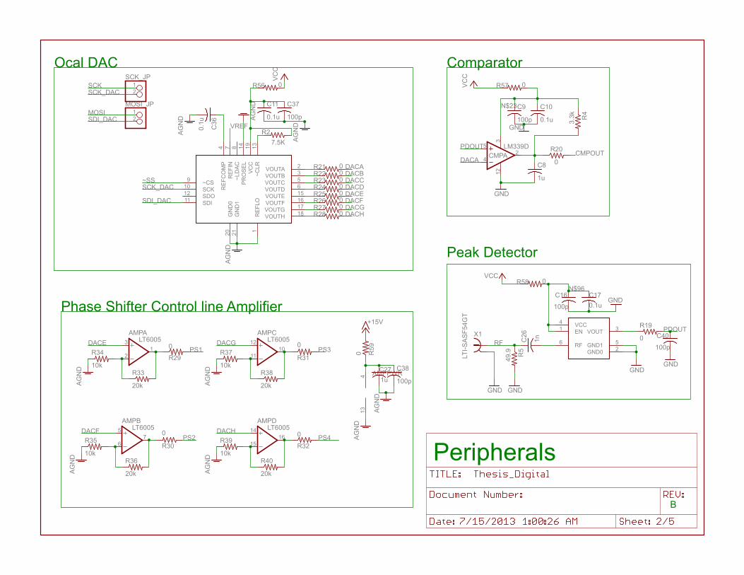
LM339D
GND
GND
GND
7.5K
1u
100p 0.1u0.1u
100p 0.1uGND
3.3k
GND
49.9
GND
+15V
1n 0
000000000
VC
C
VCC
0
0
0
0
20k
10k
10k
20k
10k
20k
10k
20k
1u
LTI-S
AS
F54G
T
0.1u
100p
100p
100p
GND
LT6005
LT6005
LT6005
LT6005
VC
C
0 0
0
0A
GN
D
AG
ND
AG
ND
AG
ND
AG
ND
AG
ND
AG
ND
AG
ND
AG
ND
AG
ND
4
52CMPA
EN1
RF6
VCC4
GND0 2GND1 5
VOUT 3
SDO12
SDI11
~CS9
SCK10
VOUTA 2
VOUTB 3
VOUTC 5
VOUTD 6
VOUTE 15
VOUTF 16
VOUTG 17
VOUTH 18GN
D1
21
REF
LO1
GN
D0
20R
EFC
OM
P4
REF
IN7
~LD
AC8
PRO
SEL
14
VCC
19
~CLR
13
312
R2
C8
C9 C10C11
C16 C17
R4
R5
SCK_JP12
MOSI_JP12
C26
R19
R20
R21R22R23R24R25R26R27R28
R29
R30
R31
R32
R33
R34
R35
R36
R37
R38
R39
R40
C27
X1
C36
C37
C38
C40AMPA3
21
AMPB5
67
AMPC12
1110
AMPD14
1516
AMPPWR413
R56 R57
R58
R59
~SS
SCK
MOSI
RF
DACADACA
DACBDACCDACDDACE
DACE
DACF
DACF
DACG
DACG
DACH
DACH
PDOUT
PDOUT
CMPOUT
SCK_DAC
SCK_DAC
SDI_DAC
SDI_DACVREF
PS1
PS2
PS3
PS4
N$23
N$96
ComparatorOcal DAC
Peak Detector
Peripherals
Phase Shifter Control line Amplifier
B
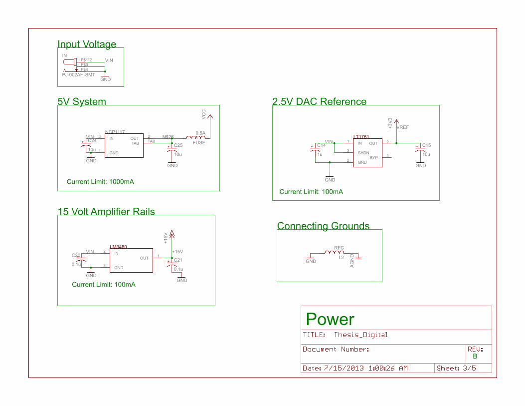
GND
GND
+3V
3
GND
+15V
0.1u0.1u
GND
10u10u
GNDGND
VC
C
PJ-002AH-SMTGND
1u 10u
GND
RFC
AG
ND
0.5A
IN1
SHDN3
OUT 5
BYP 4
GND2
IN2
GND3
OUT 1C20C21
IN3
GND1
OUT 2
TAB TAB
NCP1117
C24C25
INP$1*2P$3P$4
C14 C15
L2
FUSE
VIN
VIN
VIN
VIN
VREF
+15V
N$26 LT1761
LM3480
Power
2.5V DAC Reference5V System
15 Volt Amplifier Rails
Input Voltage
B
Current Limit: 100mA
Current Limit: 100mA
Current Limit: 1000mA
Connecting Grounds
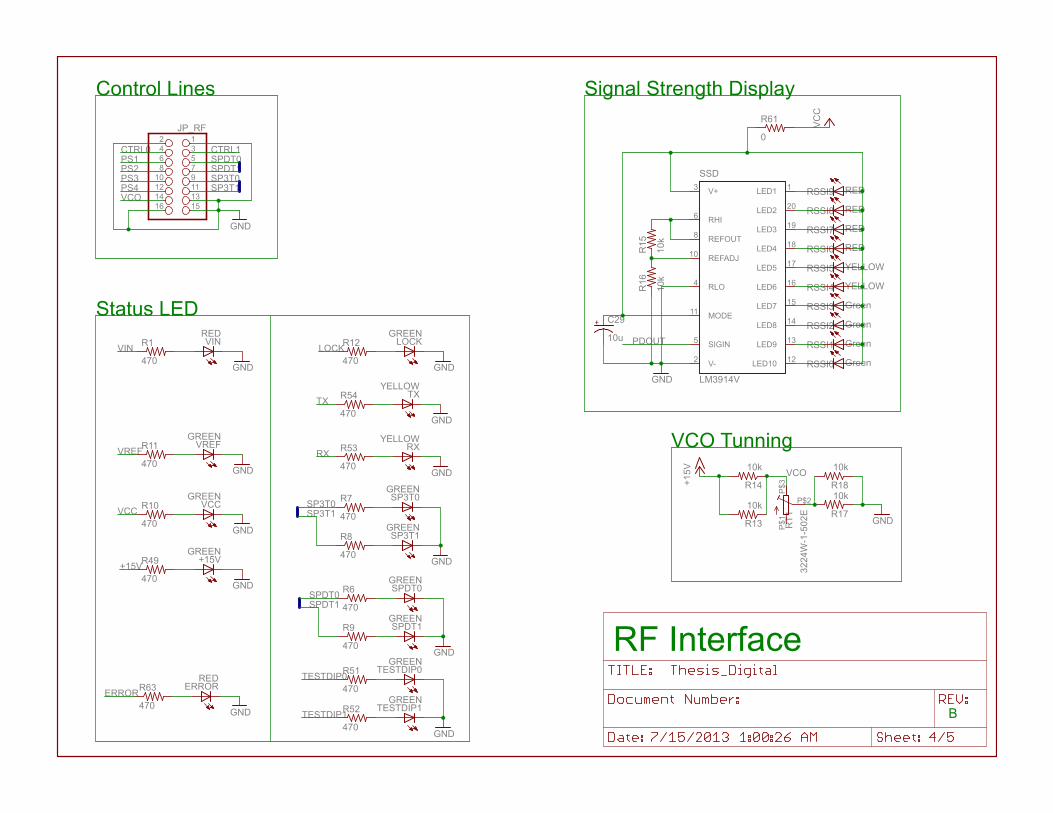
GND
RED
GND470
GREEN
470
GREEN
470GREEN
GND470
GREEN
GND470
GREEN
GND470
GREEN
GND470
GREEN
GND470
LM3914V
RED
RED
RED
RED
YELLOW
YELLOW
Green
Green
Green
Green
VC
C
GND
10k
10k
10k10k
10k 10k
3224
W-1
-502
E
+15V
GND
10u
GREEN
470GREEN
GND470
GREEN
GND470
YELLOW
GND470
YELLOW
GND470
0
RED
GND470
JP_RF12345678910111213141516
VINR1
SPDT0R6
SP3T0R7
SP3T1R8
SPDT1R9
VCCR10
VREFR11
LOCKR12
SSD
RHI6
RLO4
REFOUT8
REFADJ10
V+3
V-2
SIGIN5
LED1 1
LED2 20
LED3 19
LED4 18
LED5 17
LED6 16
LED7 15
LED8 14
LED9 13
LED10 12
MODE11
RSSI9
RSSI8
RSSI7
RSSI6
RSSI5
RSSI4
RSSI3
RSSI2
RSSI1
RSSI0
R15
R16
R13R17
R14 R18
P$1
P$3
P$2
RT1
C29
TESTDIP0R51
TESTDIP1R52
+15VR49
RXR53
TXR54
R61
ERRORR63
SPDT1
SPDT1
VCC
SP3T0
SP3T0
SP3T1
SP3T1
SPDT0
SPDT0
VREF
VIN
PS1PS2PS3PS4VCO
VCO
LOCKPDOUT
+15V
CTRL0 CTRL1
TX
RX
TESTDIP0
TESTDIP1
ERROR
Control Lines
Status LED
Signal Strength Display
VCO Tunning
RF Interface
B
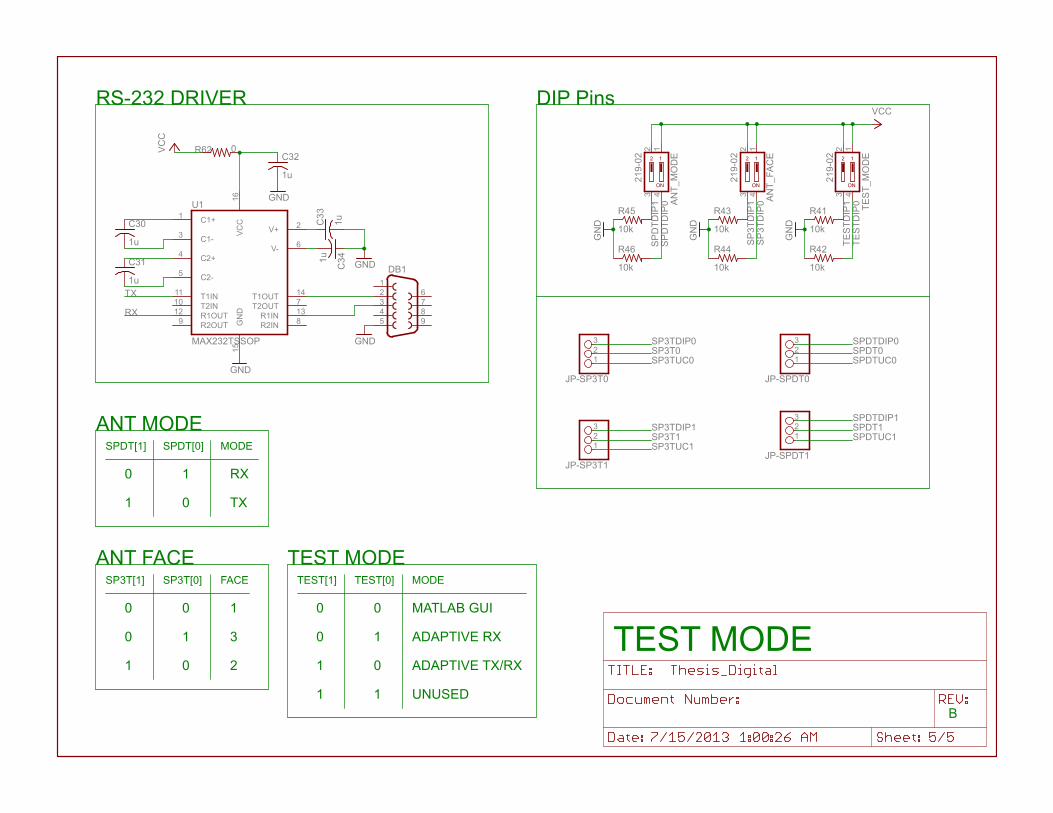
219-
02
MAX232TSSOP
1u
1u
VC
C1u
GND
GND
GND
1u1u GND
219-
02
219-
02
VCC
10k
10k
10k
10k
10k
10k
GN
D
GN
D
GN
D
0
TES
T_M
OD
E
3 412
U1C1+1
C1-3
C2+4
C2-5
T1IN11
T2IN10
R1OUT12
R2OUT9
V+ 2
V- 6
T1OUT 14
T2OUT 7
R1IN 13
R2IN 8GN
D15
VCC
16
DB11
62738495
C30
C31
C32
C33
C34
AN
T_FA
CE
3 412
AN
T_M
OD
E
3 412
R41
R42
R43
R44
R45
R46
JP-SPDT0
123
JP-SPDT1
123
JP-SP3T0
123
JP-SP3T1
123
R62
TX
RX
SP3TDIP1
SP
3TD
IP1
SP3TDIP0
SP
3TD
IP0
SPDTDIP1
SP
DTD
IP1
SPDTDIP0
SP
DTD
IP0
SP3T0SP3TUC0
SP3T1
SPDT0SPDTUC0
SPDT1SPDTUC1
SP3TUC1
TES
TDIP
0TE
STD
IP1
12
ON
12
ON
12
ON
B
TEST MODE
RS-232 DRIVER DIP Pins
ANT MODESPDT[0]SPDT[1] MODE
0
0
1
1
RX
TX
ANT FACESP3T[0]SP3T[1] FACE
0
01
1
TEST MODETEST[0]TEST[1] MODE
0
0
1
1
00 1
3
2
1 1
0 0 MATLAB GUI
ADAPTIVE RX
ADAPTIVE TX/RX
UNUSED

G PCB Layout
96
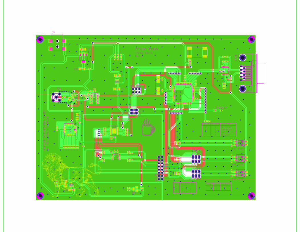

H Bill Of Materials
The complete electrical bill of materials (BOM) is presented below for the Digital
Control Board.
98
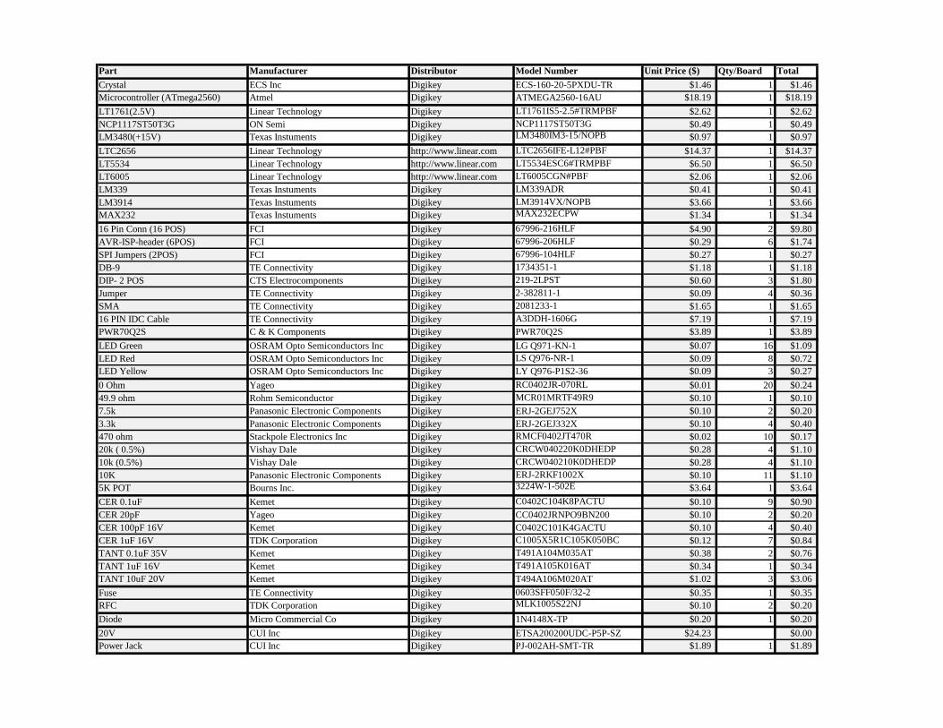
Part Manufacturer Distributor Model Number Unit Price ($) Qty/Board Total
Crystal ECS Inc Digikey ECS-160-20-5PXDU-TR $1.46 1 $1.46
Microcontroller (ATmega2560) Atmel Digikey ATMEGA2560-16AU $18.19 1 $18.19
LT1761(2.5V) Linear Technology Digikey LT1761IS5-2.5#TRMPBF $2.62 1 $2.62
NCP1117ST50T3G ON Semi Digikey NCP1117ST50T3G $0.49 1 $0.49
LM3480(+15V) Texas Instuments Digikey LM3480IM3-15/NOPB $0.97 1 $0.97
LTC2656 Linear Technology http://www.linear.com LTC2656IFE-L12#PBF $14.37 1 $14.37
LT5534 Linear Technology http://www.linear.com LT5534ESC6#TRMPBF $6.50 1 $6.50
LT6005 Linear Technology http://www.linear.com LT6005CGN#PBF $2.06 1 $2.06
LM339 Texas Instuments Digikey LM339ADR $0.41 1 $0.41
LM3914 Texas Instuments Digikey LM3914VX/NOPB $3.66 1 $3.66
MAX232 Texas Instuments Digikey MAX232ECPW $1.34 1 $1.34
16 Pin Conn (16 POS) FCI Digikey 67996-216HLF $4.90 2 $9.80
AVR-ISP-header (6POS) FCI Digikey 67996-206HLF $0.29 6 $1.74
SPI Jumpers (2POS) FCI Digikey 67996-104HLF $0.27 1 $0.27
DB-9 TE Connectivity Digikey 1734351-1 $1.18 1 $1.18
DIP- 2 POS CTS Electrocomponents Digikey 219-2LPST $0.60 3 $1.80
Jumper TE Connectivity Digikey 2-382811-1 $0.09 4 $0.36
SMA TE Connectivity Digikey 2081233-1 $1.65 1 $1.65
16 PIN IDC Cable TE Connectivity Digikey A3DDH-1606G $7.19 1 $7.19
PWR70Q2S C & K Components Digikey PWR70Q2S $3.89 1 $3.89
LED Green OSRAM Opto Semiconductors Inc Digikey LG Q971-KN-1 $0.07 16 $1.09
LED Red OSRAM Opto Semiconductors Inc Digikey LS Q976-NR-1 $0.09 8 $0.72
LED Yellow OSRAM Opto Semiconductors Inc Digikey LY Q976-P1S2-36 $0.09 3 $0.27
0 Ohm Yageo Digikey RC0402JR-070RL $0.01 20 $0.24
49.9 ohm Rohm Semiconductor Digikey MCR01MRTF49R9 $0.10 1 $0.10
7.5k Panasonic Electronic Components Digikey ERJ-2GEJ752X $0.10 2 $0.20
3.3k Panasonic Electronic Components Digikey ERJ-2GEJ332X $0.10 4 $0.40
470 ohm Stackpole Electronics Inc Digikey RMCF0402JT470R $0.02 10 $0.17
20k ( 0.5%) Vishay Dale Digikey CRCW040220K0DHEDP $0.28 4 $1.10
10k (0.5%) Vishay Dale Digikey CRCW040210K0DHEDP $0.28 4 $1.10
10K Panasonic Electronic Components Digikey ERJ-2RKF1002X $0.10 11 $1.10
5K POT Bourns Inc. Digikey 3224W-1-502E $3.64 1 $3.64
CER 0.1uF Kemet Digikey C0402C104K8PACTU $0.10 9 $0.90
CER 20pF Yageo Digikey CC0402JRNPO9BN200 $0.10 2 $0.20
CER 100pF 16V Kemet Digikey C0402C101K4GACTU $0.10 4 $0.40
CER 1uF 16V TDK Corporation Digikey C1005X5R1C105K050BC $0.12 7 $0.84
TANT 0.1uF 35V Kemet Digikey T491A104M035AT $0.38 2 $0.76
TANT 1uF 16V Kemet Digikey T491A105K016AT $0.34 1 $0.34
TANT 10uF 20V Kemet Digikey T494A106M020AT $1.02 3 $3.06
Fuse TE Connectivity Digikey 0603SFF050F/32-2 $0.35 1 $0.35
RFC TDK Corporation Digikey MLK1005S22NJ $0.10 2 $0.20
Diode Micro Commercial Co Digikey 1N4148X-TP $0.20 1 $0.20
20V CUI Inc Digikey ETSA200200UDC-P5P-SZ $24.23 $0.00
Power Jack CUI Inc Digikey PJ-002AH-SMT-TR $1.89 1 $1.89
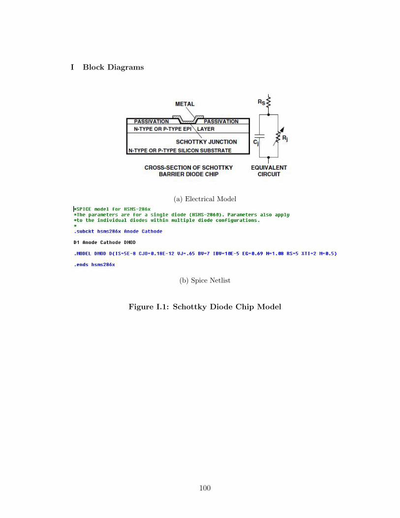
I Block Diagrams
(a) Electrical Model
(b) Spice Netlist
Figure I.1: Schottky Diode Chip Model
100
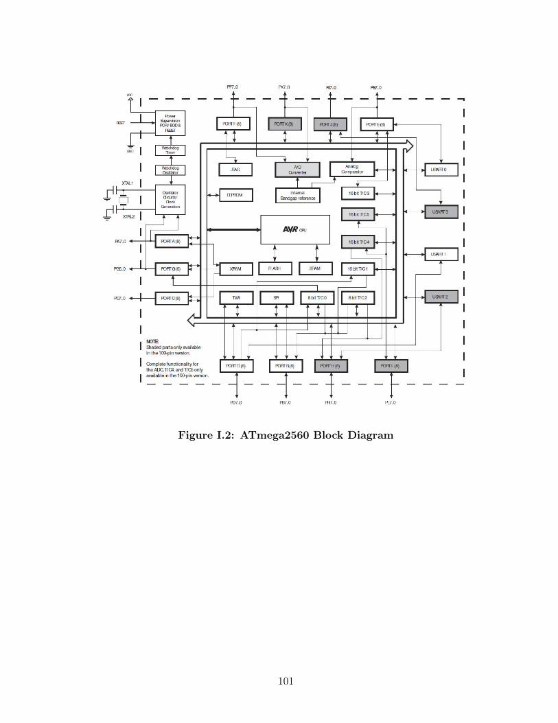
Figure I.2: ATmega2560 Block Diagram
101

Figure I.3: Analog to Digital Converter Block Schematic
102
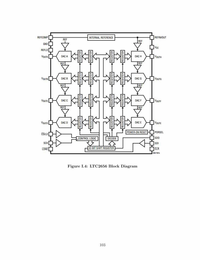
Figure I.4: LTC2656 Block Diagram
103
![Patch Antenna[1]](https://static.fdokumen.com/doc/165x107/63158e4cc32ab5e46f0d5c89/patch-antenna1.jpg)