Band Phased-Array Transmitter in 0.13- m CMOS for Radar ...
12
3060 IEEE TRANSACTIONS ON MICROWAVE THEORY AND TECHNIQUES, VOL. 61, NO. 8, AUGUST 2013 A High-Power Packaged Four-Element -Band Phased-Array Transmitter in 0.13- m CMOS for Radar and Communication Systems Donghyup Shin, Student Member, IEEE, Choul-Young Kim, Dong-Woo Kang, Member, IEEE, and Gabriel M. Rebeiz, Fellow, IEEE Abstract—This paper presents a four-element -band phased-array transmitter in 0.13- m CMOS. The design is based on the all-RF architecture and contains a 5-bit phase shifter (lowest bit is used as a trim bit), 4-bit gain control (to reduce the rms gain error), and power amplifiers capable of delivering a of 13.5 dBm per channel at 8.5–10.5 GHz. The chip can be used in the linear mode for communication systems and in the saturated mode for frequency-modulated continuous-wave radar systems, and therefore, extensive analysis is done on the phase shifter distortion versus input power. Spectral regrowth and error vector magnitude measurements indicate that the chip can sup- port at least 20-MSym/s quadrature phase-shift keying and binary phase-shift keying modulation at an output power of 5 dBm per channel. Packaging techniques based on chip-on-board and quad flat no-lead (QFN) modules have been implemented with the four-channel chip, and both show a nearest neighbor coupling of 30 dB at 8–10 GHz, limited by bond-wire coupling. The chip dimensions are 2.9 3.0 mm and it consumes 870 mW from 2- and 3-V power supplies. Index Terms—Beamforming, CMOS integrated circuits (ICs), IC packaging, phase shifters, phased arrays. I. INTRODUCTION S ILICON phased-array RF integrated circuits (RFICs), based on SiGe and CMOS technologies, have been well demonstrated at -band using the all-RF beamforming approach, in the receive, transmit, and transmit/receive modes [1]–[10]. SiGe and CMOS offer multiple RF front-ends on a single chip, together with all the necessary digital control electronics, which results in a space savings per unit cell as compared to a GaAs solution [11]. This allows for the construc- tion of compact -band phased-arrays using standard Manuscript received March 13, 2013; revised June 06, 2013; accepted June 10, 2013. Date of publication July 09, 2013; date of current version August 02, 2013. This work was supported by the U.S. Army Research Office (ARO) under Contract W911NF1010031. D. Shin and G. M. Rebeiz are with the Department of Electrical and Computer Engineering, University of California at San Diego (UCSD), La Jolla, CA 92093 USA (e-mail: [email protected]; [email protected]). C.-Y Kim was with the Department of Electrical and Computer Engineering, University of California at San Diego (UCSD), La Jolla, CA 92093 USA. He is now with the Department of Electronics Engineering, Chungnam National University, Daejeon 305-746, Korea (e-mail: [email protected]). D.-W. Kang was with the Department of Electrical and Computer Engi- neering, University of California at San Diego (UCSD), La Jolla, CA 92093 USA. He is now with the Electronics and Telecommunications Research Institute (ETRI), Daejeon 305-700, Korea (e-mail: [email protected]). Color versions of one or more of the figures in this paper are available online at http://ieeexplore.ieee.org. Digital Object Identifier 10.1109/TMTT.2013.2271488 Fig. 1. Block diagram of four-element phased-array transmitter. Fig. 2. Metal stack-up of IBM8RF 0.13- m CMOS process. printed-circuit board techniques at a great reduction in cost and increase in reliability, either using chip-on-board (CoB) or quad flat no-lead (QFN) packaging techniques [5], [10], [12]–[14]. This paper presents an -band four-element phased-array chip built using 0.13- m CMOS technology and with moder- ately high power levels from each channel 13 dBm . The chip is intended for dual operation: A radar mode at 9–9.5 GHz for frequency-modulated continuous-wave (FMCW) perimeter detection and a communication mode at 8.2–8.7 GHz for binary phase-shift keying (BPSK) and quadrature phase-shift keying (QPSK) satellite systems. The chip is therefore characterized at saturated power levels for the radar mode and at and asso- ciated backoff power levels in a communications mode where attention is placed on distortion versus power levels. The four- element chip has been packaged using CoB and using QFN so- lutions. The mutual coupling between the bond-wires are taken into account together with the passive baluns on the CMOS in- tegrated circuit (IC), and the resulting channel-to-channel cou- pling simulation is done using Ansoft HFSS [15]. A compar- ison is presented between the two solutions in terms of isola- tion between the channels and ground inductance effects. To our knowledge, this is the first demonstration of a packaged 0018-9480/$31.00 © 2013 IEEE
-
Upload
khangminh22 -
Category
Documents
-
view
2 -
download
0
Transcript of Band Phased-Array Transmitter in 0.13- m CMOS for Radar ...

3060 IEEE TRANSACTIONS ON MICROWAVE THEORY AND TECHNIQUES, VOL. 61, NO. 8, AUGUST 2013
A High-Power Packaged Four-Element -BandPhased-Array Transmitter in 0.13- m CMOSfor Radar and Communication Systems
Donghyup Shin, Student Member, IEEE, Choul-Young Kim,Dong-Woo Kang, Member, IEEE, and Gabriel M. Rebeiz, Fellow, IEEE
Abstract—This paper presents a four-element -bandphased-array transmitter in 0.13- m CMOS. The design isbased on the all-RF architecture and contains a 5-bit phase shifter(lowest bit is used as a trim bit), 4-bit gain control (to reduce therms gain error), and power amplifiers capable of delivering a
of 13.5 dBm per channel at 8.5–10.5 GHz. The chip can beused in the linear mode for communication systems and in thesaturated mode for frequency-modulated continuous-wave radarsystems, and therefore, extensive analysis is done on the phaseshifter distortion versus input power. Spectral regrowth and errorvector magnitude measurements indicate that the chip can sup-port at least 20-MSym/s quadrature phase-shift keying and binaryphase-shift keying modulation at an output power of 5 dBmper channel. Packaging techniques based on chip-on-board andquad flat no-lead (QFN) modules have been implemented with thefour-channel chip, and both show a nearest neighbor coupling of30 dB at 8–10 GHz, limited by bond-wire coupling. The chip
dimensions are 2.9 3.0 mm and it consumes 870 mW from 2-and 3-V power supplies.
Index Terms—Beamforming, CMOS integrated circuits (ICs),IC packaging, phase shifters, phased arrays.
I. INTRODUCTION
S ILICON phased-array RF integrated circuits (RFICs),based on SiGe and CMOS technologies, have been well
demonstrated at -band using the all-RF beamformingapproach, in the receive, transmit, and transmit/receive modes[1]–[10]. SiGe and CMOS offer multiple RF front-ends ona single chip, together with all the necessary digital controlelectronics, which results in a space savings per unit cell ascompared to a GaAs solution [11]. This allows for the construc-tion of compact -band phased-arrays using standard
Manuscript received March 13, 2013; revised June 06, 2013; accepted June10, 2013. Date of publication July 09, 2013; date of current version August 02,2013. This work was supported by the U.S. Army Research Office (ARO) underContract W911NF1010031.D. Shin and G.M. Rebeiz are with the Department of Electrical and Computer
Engineering, University of California at San Diego (UCSD), La Jolla, CA 92093USA (e-mail: [email protected]; [email protected]).C.-Y Kim was with the Department of Electrical and Computer Engineering,
University of California at San Diego (UCSD), La Jolla, CA 92093 USA. Heis now with the Department of Electronics Engineering, Chungnam NationalUniversity, Daejeon 305-746, Korea (e-mail: [email protected]).D.-W. Kang was with the Department of Electrical and Computer Engi-
neering, University of California at San Diego (UCSD), La Jolla, CA 92093USA. He is now with the Electronics and Telecommunications ResearchInstitute (ETRI), Daejeon 305-700, Korea (e-mail: [email protected]).Color versions of one or more of the figures in this paper are available online
at http://ieeexplore.ieee.org.Digital Object Identifier 10.1109/TMTT.2013.2271488
Fig. 1. Block diagram of four-element phased-array transmitter.
Fig. 2. Metal stack-up of IBM8RF 0.13- m CMOS process.
printed-circuit board techniques at a great reduction in cost andincrease in reliability, either using chip-on-board (CoB) or quadflat no-lead (QFN) packaging techniques [5], [10], [12]–[14].This paper presents an -band four-element phased-array
chip built using 0.13- m CMOS technology and with moder-ately high power levels from each channel 13 dBm . Thechip is intended for dual operation: A radar mode at 9–9.5 GHzfor frequency-modulated continuous-wave (FMCW) perimeterdetection and a communication mode at 8.2–8.7 GHz for binaryphase-shift keying (BPSK) and quadrature phase-shift keying(QPSK) satellite systems. The chip is therefore characterized atsaturated power levels for the radar mode and at and asso-ciated backoff power levels in a communications mode whereattention is placed on distortion versus power levels. The four-element chip has been packaged using CoB and using QFN so-lutions. The mutual coupling between the bond-wires are takeninto account together with the passive baluns on the CMOS in-tegrated circuit (IC), and the resulting channel-to-channel cou-pling simulation is done using Ansoft HFSS [15]. A compar-ison is presented between the two solutions in terms of isola-tion between the channels and ground inductance effects. Toour knowledge, this is the first demonstration of a packaged
0018-9480/$31.00 © 2013 IEEE

SHIN et al.: HIGH-POWER PACKAGED FOUR-ELEMENT -BAND PHASED-ARRAY TRANSMITTER 3061
Fig. 3. Circuit schematic of a single-channel: (a) active 1:4 divider and (b) phase shifter and PA.
phased-array transmitter chip for radar and communication sys-tems.
II. DESIGN
A. Block Diagram and Technology
Fig. 1 presents the block diagram of the four-element transmitphased-array chip. The circuit design is differential, but balunsare used at the input and output ports since single-ended portsare compatible with microstrip or coplanar waveguide (CPW)circuits on the printed circuit board (PCB). Two independentpower supplies are used on the chip. The input power dividerand buffer amplifier are driven using a 2-V supply, while theactive phase shifter and output power amplifier (PA) are drivenusing a 3-V supply. Two different 3-V power supply lines arealso used, each driving a two-element subarray so as to reducethe coupling between the elements and also to reduce the current
draw from the supply pins. The use of several supply pins, eachwith its own off-chip decoupling capacitors, isolate the differentareas of chip from the large current swings encountered in thePA circuits.The chip is built in a low-cost 0.13- m CMOS technology
with an of 100 GHz and of 0.8 dB at a bias currentdensity of 0.1 mA m (IBM8RF) and with eight metal layers(Fig. 2). Differential transmission lines are implemented in agrounded coplanar waveguide (G-CPW) configuration with di-mensions of 10/8/8/8/10 m and a simulated loss of 0.22 dB/mmat 9 GHz. Note that the IBM8RF process allows for 11 m ofoxide between the MA and the LY layer, which results in rela-tively wide and low-loss differential lines.All inductors and transmission-line connections are sim-
ulated using a 2.5-D electromagnetic solver (Sonnet [16])and have of 12–15 at 9–10 GHz depending on the design.The capacitors are implemented using the library metal–insu-lator–metal (MIM) capacitors.

3062 IEEE TRANSACTIONS ON MICROWAVE THEORY AND TECHNIQUES, VOL. 61, NO. 8, AUGUST 2013
TABLE IVECTOR MODULATOR I/Q DC CURRENT LEVEL
B. Active 1:4 Divider
An active 1:4 divider is used after the input balun and is basedon a two-stage cascode divider with inductor/resistor (LR) loadsfor wideband operation [see Fig. 3(a)]. The input stage should becapable of handling 0 dBm of input power ( 1.7 dBm afterthe balun), and is biased at 5.9 mA. The second stage feeds asource-follower amplifier with an output impedance of 54 soas to drive the low-impedance quadrature all-pass filter (QAF)network [17]. The active 1:4 divider consumes 25 mA and hasan electronic gain of 1.5 dB at 9 GHz, where the gain is definedas the power in the 54- load (differential) at the output of asource follower divided by the available power at the single-ended port from a 50- source. The simulated output power andphase versus input power is shown in Fig. 4 with an inputof 5 dBm, limitedmostly by the first-stage active divider. Still,the 1:4 divider can deliver 2 dBm at the QAF 350 mVfor an input power of 0 dBm, and with low phase distortion
2 .
C. Active Phase Shifter
The QAF is designed for a withnH fF and and provides a very wide-
band quadrature with 3 phase variation at 6–10.5 GHz,including the effect of the capacitance loading of the vectormodulator stage fF . A is chosen asa compromise between the effect of capacitive loading in thein-phase/quadrature (I/Q) network and powerconsumption in the circuit [17]. The simulatedQAF voltage gain is 1.5 dB including the capacitive load, andwith 3.6-dB error between the I and Q outputs at 9 GHz(Fig. 5). A lower amplitude error can be designed using a QAFwith , but at the expense of lower gain (or highercurrent) in the active divider.The QAF feeds a vector modulator phase shifter with inte-
grated gain control and wideband RL loads [see Fig. 3(b)]. Theswitches at the bottom select between the I and I quadrants(and Q and Q quadrants), and the gain of the I and Q paths iscontrolled using a 5-bit DAC. The requirements are a 4-bit phaseshifter, but an additional bit is used as a trim bit to improve therms phase error (if needed). The DAC currents are optimizedto take into account the interconnect parasitic effects (modeledusing Sonnet) and are listed in Table I for 0 , 22.5 , 45 , 67.5 ,and 90 . In addition, a 5-dB gain control stage is placed on top ofthe phase shifter using a current steering mode. This gain stagealso uses a 3-bit control voltage from the DAC and is employedto reduce the rms gain error in the phase shifter. This is done bycontrolling the gain by 2 dB in eight steps (0.5 dB/step) so as
Fig. 4. Simulated power gain and output power, and normalized phase versusinput power of active divider at 9.0 GHz.
Fig. 5. Simulated I/Q phase and amplitude error of the all-pass network.
to compensate for the phase shifter gain variation. Note that thisgain control method is useful for a 0–5-dB range due to currentstarving effect in the main RF path transistor.The phase shifter consumes 11.5 mA of current from a 3-V
supply and has a simulated voltage gain of 5.6 dB, an inputof 6.7 dBm, and a noise figure of 12 dB (gain values can changeby 1.5 dB versus phase state). However, since this chip willbe operated under high drive powers, it is important to studythe gain and phase distortion versus input power. The gain fol-lows the usual compression curve, but the phase starts to dis-tort at an input power of 10 dBm for 22.5 , 45 , and 67.5phase states [see Fig. 6(b)]. This is because compression beginsfor different input power levels for the I- and Q-path transcon-ductance stages. For the 22.5 state, the linearity of theQ-path transconductance stage is much smaller than the I-pathdue to the lower dc bias current ( mA, mA).As a result, the amplitude mismatch between the I/Q ac currentscombined at the load and increases at higher input powereven though the power is less than [see Fig. 6(a)], andhence, an output phase error occurs.Still, for radar operation operating at , the input power of
the active phase shifter is 2 dBm from the 1:4 active divider,and the resulting phase distortion at different phase states are15 , which can be calibrated out using the additional trim bit
in the DAC (see Section III-B).

SHIN et al.: HIGH-POWER PACKAGED FOUR-ELEMENT -BAND PHASED-ARRAY TRANSMITTER 3063
Fig. 6. Simulated: (a) and at 22.5 phase state and (b) phase versus inputpower defined at the QAF input port.
D. Power Amplifier (PA)
The PA is a two-stage cascode design with a total bias cur-rent of 53.4 mA from a 3-V supply. The bias conditions of thefirst and second stages are optimized as class A and class AB,respectively. Since this is a relatively high PA withdBm, the selection of the transistors and their layout is essen-
tial for proper operation. In this design, transistors withm and m for the first and second stages,
and the interconnects are modeled using Sonnet. The inductorsare designed with a 9- m-wide line for improved Q ( 14 at9.5 GHz) and the layout is entirely symmetrical with top andbottom inductors. The edge-to-edge separation between the firstand second stage inductors is m, which also ensures acoupling of 30 dB. Resistors with values of 250 and 900are used in parallel with 1–1.1-nH inductors for wideband oper-ation and stability at GHz. The simulated small-signalgain is 17 dB at 9.5 GHz with differential output impedance of100 .The measurements of the PA are presented here for com-
pleteness and since they do not fit in the phased-array measure-ment section. The PA was tested on an individual breakout chipwith the input and output balun losses de-embedded. Measure-ments indicate a gain of 17 dB with a 3-dB bandwidth of8.1–11.3 GHz [see Fig. 7(a)]. The measured andare 11 and 15.5 dBm, respectively, at 9.5 GHz and with a peakPAE of 19% (Figs. 7(b) and 8). Note that there is an AM to PM
Fig. 7. Measured and simulated PA: (a) gain and (b) output power, PAE, andphase distortion versus input power.
Fig. 8. Measured and simulated PA output power , , and PAE versusfrequency.
distortion of 5 and 12 at the and powers, re-spectively, and again, this can be calibrated out for radar appli-cation (see Section III-B). Finally, the measured output secondand third harmonic levels are at 32 and 60 dBc for

3064 IEEE TRANSACTIONS ON MICROWAVE THEORY AND TECHNIQUES, VOL. 61, NO. 8, AUGUST 2013
Fig. 9. Measured and simulated PA second and third harmonic componentsversus input power at 9.0 GHz.
Fig. 10. (a) Input and output baluns with wideband matching network and(b) simulated frequency response.
power levels (note that this include the output balun filteringeffect) (Fig. 9). All measurements are in good agreement withsimulations for the PA breakout, and compete well with -bandresults [18].
E. Input and Output Baluns
The input and output baluns are built using vertical mag-netic coupling between the top two metal layers (MA and E1)(Fig. 10). The baluns also act as electrostatic discharge (ESD)
Fig. 11. Microphotograph of -band four-element phased-array transmitterchip (2.9 3.0 mm ).
protection circuits since they provide a wideband short circuitto ground at low frequencies. An additional LC matching net-work ( and for the input balun, and and for theoutput balun) is used to provide very wideband input and outputimpedance matching so as to result in easy bond-wire attach-ment and PCB matching circuits. The simulated losses of theinput and output baluns are 1.7–1.8 dB at 7–11 GHz with a dif-ferential impedance of 100 . Note that the output balun alsoprovides substantial filtering at the second 5.7 dB and third33.5 dB harmonic frequencies.
F. Bias and Control
The layout is done in a symmetrical fashion and every differ-ential stage contains a top and bottom inductor for the RL loads(Fig. 11). This design was preferred over differential inductorsdue to symmetry. The chip size is 2.9 3.0 mm and consumes79 mA (2 V) and 237 mA (3 V) for a total power consumptionof 870 mW. The 3-V supply pins are at the top and bottom of thechip to reduce the infrared (IR) drop to the PAs and for addedisolation between channels 1 and 2 and 3 and 4. The planecovers most of the available chip area using the E1 metal layer,which is placed between MA and LY ground planes. High-den-sityMIM capacitors 2 fF m are used for supply decouplingand the total capacitance of 200 pF is distributed over the chiparea.The chip is controlled using a parallel interface. Each channel
stores the phase and amplitude data on a 7-bit (four for phaseand three for amplitude) register, and a 2-to-4 address decoderallocates the address to each register by an enabling clocksignal. The digital signal routing is done using M2 or M3 andare shielded by M1 and MQ ground planes to isolate the digitalswitching noise from the analog path.

SHIN et al.: HIGH-POWER PACKAGED FOUR-ELEMENT -BAND PHASED-ARRAY TRANSMITTER 3065
Fig. 12. Measured and simulated small-signal: (a) input and output reflection coefficient, (b) gain, (c) phase response, and (d) differential phase response (nor-malized to 0 ) for 16 phase states for a single channel. A VGA and trim-bit were used to reduce the rms gain and phase error. Other channels had essentially thesame response.
III. MEASUREMENTS
A. -Parameter Measurements: Small Signal
All measurements are done on-chip withground–signal–ground (GSG) probes and ashort-open-load-thru (SOLT) calibration to the probetips. The bias voltages are supplied using a dc bias probe onthe north and south side of the chip. No oscillations have beenrecorded from dc to 40 GHz, either at the RF probes or the dcprobes. The chip was biased at 2 V, 79 mA, and at 3 V, 237 mAfor all measurements below.Fig. 12 presents the measured and simulated -parameters
under small-signal conditions. The measured and is10 dB from 7.5 to 11 GHz. The measured gain peak shifted
from 9.0 to 8.7 GHz, and we believe that this is due to the trans-mission-line sections inside the 1:4 cascode divider stage (be-tween the cascode stage and RL load). The 3-dB bandwidth is7.9–9.6 GHz with a gain of 15.5 dB at 8.7 GHz, which is suit-able for both communication and radar applications. The fourchannels showed nearly identical response ( 0.5 dB), andtherefore only one channel is shown. The amplitude and phasetrim bits were used in the vector modulator in order to get a verylow rms gain and phase error, as shown in Fig. 12, and with nophase cross-overs. The phase trim is a one-bit current controlon the DAC, which results in an 11 phase step and can be usedin addition or subtraction to the standard 4-bit setting to yield
Fig. 13. Polar diagram showing measured phase and gain at 9.0 GHz.
a precise 4-bit phase response. The measured gain and phase at9.0 GHz on a polar circle is also shown (Fig. 13). Overall, ex-cept for the gain reduction, the measurements agreed well withsimulations.
B. -Parameter Measurements: Large Signal
The measured output power versus input power are shown inFig. 14(a) with a best and of 8.8 and 13.6 dBm, re-spectively, at 9.0 GHz. This is expected knowing that the outputbalun and GSG pad loss is 2 dB and the PA delivers a

3066 IEEE TRANSACTIONS ON MICROWAVE THEORY AND TECHNIQUES, VOL. 61, NO. 8, AUGUST 2013
Fig. 14. Measured: (a) output and and (b) phase versus inputpower at 9.0 GHz. VGA set at maximum gain state.
of 15.5 dBm. These values are achieved at the phase state withthe highest gain, and the average and over all phasestates are 0.7–0.8 dB lower. The measured phase distortionversus power level is shown in Figs. 14(b). Note that this overallphase distortion takes into account the 1:4 active divider, phaseshifter, and the PA AM-to-PM distortion components (as com-pared to Fig. 6, which is only for the vector modulator). Thisdistortion can be calibrated out versus input power and has vir-tually no effect on the radar operation.The measured -parameters of a single channel at–13 dBm is shown in Fig. 15. In this case and due to the
gain compression, the VGA is not used. The average gain is11.5 dB (4-dB compression from the small-signal values)
with a peak-to-peak variation of 1.5 dB versus all phase statesand an rms gain error of 0.5 dB. The rms phase error is 4 –5at 8.5–9.5 GHz, which is much lower than the 4-bit require-ment. There are also no cross-overs in the phase shifts. The chipis therefore suitable for radar applications at 8.5–9.5 GHz withvery low rms gain and phase errors, even under condi-tions.
C. Spectral Regrowth and Error Vector Magnitude (EVM)
Fig. 16 presents the measured spectral regrowth at 8.7 GHzversus different output levels for 20-MSym/s QPSK and BPSKmodulation. It is seen that an output power of up to 4–5 dBm( dB) results in very little spectral regrowth, as ex-pected. This is done at an input power of 12 dBm, and the1:4 active divider and the phase shifter both have virtually nophase distortion. At close to , the spectral regrowth is not
Fig. 15. Measured large-signal: (a) gain, (b) phase response, and (c) differentialphase response (normalized to 0 ) for 16 phase states. VGA set at maximumgain state.
acceptable for communication systems. The measured EVM is2%–2.5% up to an output power of 5 dBm, and then increasesrapidly at higher values, as expected (Fig. 17). The I/Qconstellation for a 20 MSym/s is shown and is near ideal upto 5 dBm (Fig. 18). The EVM values are 0.5%–0.6% higherthan measurements done on a PA breakout alone, indicating thatthe phase shifter and 1:4 active divider are contributing a smallamount of additional error.
D. On-Chip Coupling
The coupling between the channels was measured accordingto [19] and is 42 dB for neighboring channels at 7–11 GHz.This is due to the differential nature of the chip, and such lowlevels have been measured before on similar multi-channelchips [1], [2]. The coupling increases when the chip is placed

SHIN et al.: HIGH-POWER PACKAGED FOUR-ELEMENT -BAND PHASED-ARRAY TRANSMITTER 3067
Fig. 16. Measured output spectrum for: (a) QPSK and (b) BPSK modulationat different output power levels.
Fig. 17. Measured EVM for: (a) QPSK and (b) BPSK versus input power at8.7 GHz.
in a package due to bond-wire and ground inductance, and thisis presented in Section IV.
IV. PACKAGING
The four-element chip was packaged in a CoB implementa-tion and in a 6 6 mm QFN package with a standard 0.5-mm-pitch lead frame (Fig. 19) [13]. Both are assembled on a RogersRT5880 PCB with and mil with a large ground
Fig. 18. Measured QPSK 20-MSym/s constellation versus output power at8.7 GHz.
Fig. 19. Cross section of QFN package 6 6 mm and CoB on a RogersRT5880 substrate.
pad underneath the chip or QFN pedestal. A mold compoundof , is used inside the QFN, but theCoB implementation does not use any glop-top material over it.Bond-wires with 1-mil diameter are used to connect the CMOSchip to the board or inside the QFN package.The electromagnetic coupling environment between the four
CMOS RFIC output ports is shown in Fig. 20 for the CoB andQFN implementations. The on-chip transformers on the siliconchip, bond-wires, QFN pedestals, transmission lines, and sur-rounding vias are all placed into Ansoft HFSS and modeled to-gether. Ports 1–4 are differential on the silicon chip, while Ports5–8 are single-ended on the PC board. Note that grounded CPWlines are used around the chip to raise the ground plane to the topPCB surface and reduce the ground-plane inductance. A max-imum channel-to-channel coupling of 34 and 29 dB isachieved for the CoB and QFN implementations at 9 GHz [seeFig. 20(b)]. For the QFN implementation, and due to the rela-tively long signal and bond-wires used, two ground bond-wiresare needed between the signal ports in order to get high isolation,and this is the primary reason why a 6 6 mm QFN package isused (instead of a 5 5 mm package). The simulated insertionloss is 1.3 dB at 7.5–9.5 GHz due primarily to the balunloss. However, this is lower than the simulated loss of the balunitself, as shown in Fig. 10(b), due to the discretization of HFSSfor such a large electromagnetic problem (finer discretization isused when simulating the balun alone).The electromagnetic model also results in the at all ports
and a matching network is then placed on the PC board for a50- impedance match. However, in the QFN case, the capac-itance of the lead frame bond pad presents a near-perfect com-pensation of the bond-wire inductance at -band ( 0.7 nH),and a matching circuit is not needed on the PC board. For the

3068 IEEE TRANSACTIONS ON MICROWAVE THEORY AND TECHNIQUES, VOL. 61, NO. 8, AUGUST 2013
Fig. 20. (a) 3-D EM simulation setups of the silicon chip, baluns, and bond-wires in a package using HFSS. (b) Resulting -parameters.
CoB case, a simple capacitive matching network is used. Sim-ilar impedance matching is done at the input port (not shown).The circuit environment with a packaging effect is shown in
Fig. 21. In this case, the CMOS Cadence library models areused for all circuit components, except for the input and outputtransformers. These are now embedded in the EM transitionmodel, and an eight-port -parameter matrix is used to accountfor the baluns and the bond-wire/package coupling effects. Thismodel also takes into account the additional ground inductanceat the balun grounds, which affects the coupling between theports. A similar procedure is done on the input port, but in thiscase, it is just a two-port -matrix for impedance matching, andno coupling is present. Additionally, power supply inductanceand ground inductance are also taken due to the packaging ef-fects. Simulations on the entire chip with ground inductanceshow no packaging detrimental effect (same -parameters as
Fig. 21. Circuit environment of the packaged phased-array transmitter in-cluding silicon chip, package 3-D EM simulation, and on-board matching/dis-tribution network with bond-wire inductances.
Fig. 22. Photograph of the: (a) packaged -band phased-array transmitter ona Rogers RT5880 substrate and (b) close-in view of QFN and CoB.
Section III-A) due to the differential circuits used. Therefore,the main effect of the packaging is the electromagnetic couplingbetween the elements.The CoB and QFN implementations are shown in Fig. 22 to-
gether with the entire board. Note the grounded-CPW environ-ment around the chip with transitions to four equi-phase mi-crostrip lines. The additional loss referenced to the SMA con-nectors is 1.4 dB at 9 GHz (2 0.5 dB SMA connector lossand 0.4-dB microstrip line loss). The measured -parametersreferenced to the SMA connectors are shown in Fig. 23 for the
SHIN et al.: HIGH-POWER PACKAGED FOUR-ELEMENT -BAND PHASED-ARRAY TRANSMITTER 3069
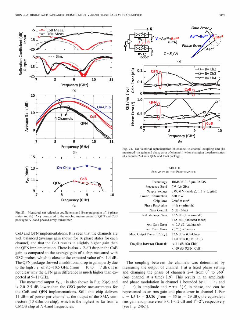
Fig. 23. Measured: (a) reflection coefficients and (b) average gain of 16 phasestates and (b) compared to the on-chip measurement of QFN and CoBpackaged -band phased-array transmitter.
CoB and QFN implementations. It is seen that the channels arewell balanced (average gain shown for 16 phase states for eachchannel) and that the CoB results in slightly higher gain thanthe QFN implementation. There is also 2-dB drop in the CoBgain as compared to the average gain of a chip measured withGSG probes, which is close to the expected value of 1.4 dB.The QFN package showed an additional drop in gain, partly dueto the high of 8.5–10.5 GHz from 10 to 7 dB . It isnot clear why the QFN gain difference is much higher than ex-pected at 9–11 GHz.The measured output is also shown in Fig. 23(c) and
is 2.0–2.5 dB lower than the GSG probe measurements forthe CoB and QFN implementations. Still, this chip delivers11 dBm of power per channel at the output of the SMA con-nectors (13 dBm on-chip), which is the highest so far from aCMOS chip at -band frequencies.
Fig. 24. (a) Vectorial representation of channel-to-channel coupling and (b)measured rms gain and phase error of channel 1 when changing the phase statesof channels 2–4 in a QFN and CoB package.
TABLE IISUMMARY OF THE PERFORMANCE
The coupling between the channels was determined bymeasuring the output of channel 1 at a fixed phase settingand changing the phase of channels 2–4 from 0 to 360(one channel at a time) [19]. This results in an amplitudeand phase modulation in channel 1 bounded by and
in amplitude and in phase, and can berepresented as an rms gain and phase error in channel 1. For
from 35 to 29 dB , the equivalentrms gain and phase error is 0.1–0.2 dB and 1 –2 , respectively[see Fig. 24(c)].

3070 IEEE TRANSACTIONS ON MICROWAVE THEORY AND TECHNIQUES, VOL. 61, NO. 8, AUGUST 2013
Fig. 24(b) presents the measured rms gain and phase errorversus frequency for channel 1 when the phase of channels 2–4are changed. Both the CoB and QFN resulted in nearly the samecoupling for channel 2 and the QFN results are shown. As ex-pected, the maximum coupling occurs between channels 1 and2, with an rms gain error of 0.2 dB and 1 at 8 GHz. Thisis equivalent to a peak coupling of from 29 to 30 dB, as ex-pected from simulations. Note that QFN channels 3 and 4 show awideband coupling characteristic of 35 dB, which may be dueto coupling and to the silicon RFIC/package/PCB groundinductance. For the CoB, channels 3 and 4 result in a widebandcoupling characteristics of 45 dB (rms gain and phase error0.05 dB and 0.5 ) showing the reduced ground and
inductance of this implementation.
V. CONCLUSION
This paper has presented a four-element high-power phased-array transmitter capable of operation in a communication ora radar mode and the measured performance is summarizedin Table II. It has been found that the vector modulator phaseshifter and the PA result in phase distortion versus power, butthese can be calibrated out in radar mode operation. For com-munication systems, it is best to operate below the outputlevel for complex constellations. The chip has been packagedusing CoB and QFN techniques, and the CoB results in higherultimate isolation between the channels 45 dB as opposed tothe QFN 35 dB . However, both result in nearly the same iso-lation between the neighboring channels ( 30 dB), which isprimarily limited by bond-wire coupling. This work shows thatcomplex phased arrays with multiple channels can be packagedin low-cost QFN packages for -band applications.
REFERENCES
[1] K. Koh and G. M. Rebeiz, “An - and -band 8-element phased-array receiver in 0.18 m SiGe BiCMOS technology,” IEEE J. Solid-State Circuits, vol. 43, no. 6, pp. 1360–1371, Jun. 2008.
[2] D.-W. Kang, K. Koh, and G. M. Rebeiz, “A -band 2-antenna 4- si-multaneous beams SiGe BiCMOS phased array receiver,” IEEE Trans.Microw. Theory Techn., vol. 58, no. 4, pp. 771–780, Apr. 2010.
[3] T. K. Thrivikraman, W. L. Kuo, and J. D. Cressler, “A two-channel,ultra-low-power, SiGe BiCMOS receiver front-end for -bandphased array radars,” in Proc. IEEE Bipolar/BiCMOS CircuitsTechnol. Meeting, Oct. 2009, pp. 43–46.
[4] J. P. Comeau, M. A. Morton, W. L. Kuo, T. Thrivikraman, J. M.Andrews, C. M. Grens, J. D. Cressler, J. Papapolymerou, and M.Mitchell, “A silicon–germanium receiver for -band transmit/receiveradar modules,” IEEE J. Solid-State Circuits, vol. 43, no. 9, pp.1889–1896, Sep. 2008.
[5] C. E. Patterson, T. K. Thrivikraman, A. M. Yepes, S. M. Begley, S.K. Bhattacharya, J. D. Cressler, and J. Papapolymerou, “A lightweightorganic -band active receiving phased array with integrated SiGeamplifiers and phase shifer,” IEEE Trans. Antennas Propag., vol. 59,no. 1, pp. 100–109, Jan. 2011.
[6] K. Gharibdoust, N. Mousavi, M. Kalantari, M. Moezzi, and A. Medi,“A fully integrated 0.18- m CMOS transceiver chip for -bandphased array systems,” IEEE Trans. Microw. Theory Techn., vol. 60,no. 7, pp. 2192–2202, Jul. 2012.
[7] D. Carosi, A. Bettidi, A. Nanni, L. Marescialli, and A. Cetronio, “Amixed-signal -band SiGe multi-function control mmic for phasedarray radar applications,” in Proc. 39th Eur. Microw. Conf., Oct. 2009,pp. 240–243.
[8] D.-W. Kang and S. Hong, “A 4-bit CMOS phase shifter using dis-tributed active switches,” IEEE Trans. Microw. Theory Techn., vol. 55,no. 7, pp. 1476–1483, Jul. 2007.
[9] T. M. Hancock and G. M. Rebeiz, “A 12-GHz SiGe phase shifter withintegrated LNA,” IEEE Trans. Microw. Theory Techn., vol. 53, no. 3,pp. 977–983, Mar. 2005.
[10] D. Shin and G. M. Rebeiz, “A low-power high-linearity -band 4-ele-ment phased array receiver: CMOS chip and packaging,” IEEE Trans.Microw. Theory Techn., vol. 59, no. 8, pp. 2064–2072, Aug. 2011.
[11] W. H. Theunissen, D. Brocious, T. Destefano, J. Mulvey, S. Pappas, J.Thomas, P. Butterfoss, M. Briske, S. Nelson, G. Clark, M. Walker, J.Dishong, R. K. Mongia, and G. Forman, “Development of an -bandphased array antenna using multilayer circuit board architecture,” inProc. IEEE Int. ARRAY Symp., , Oct. 2010, pp. 211–218.
[12] Y. A. Atesal, B. Cetinoneri, K. Koh, and G. M. Rebeiz, “ -band8-element phased array based on single silicon chips,” in IEEE MTT-SInt. Microw. Symp. Dig., May 2010, pp. 1258–1261.
[13] D. Shin, C. Y. Kim, D. W. Kang, and G. M. Rebeiz, “A 4-element-band CMOS phased-array RFIC in a QFN package,” in IEEE
MTT-S Int. Microw. Symp. Dig., Jun. 2012, pp. 1–3.[14] K. M. Ho, D. Shin, and G. M. Rebeiz, “ -band phased array devel-
opment on teflon laminates with CMOS RFIC receivers,” in IEEE Int.Antennas Propag. Symp., Jul. 2011, pp. 565–568.
[15] Ansoft HFSS. ver. 12, Ansoft Corporation, Pittsburgh, PA, USA, 2010.[16] Sonnet. ver. 12.56.3, Sonnet Softw. Inc., Syracuse, NY, 2009.[17] K. Koh and G. M. Rebeiz, “0.13- m CMOS phase shifters for -,
-, and -band phased arrays,” IEEE J. Solid-State Circuits, vol.42, no. 11, pp. 2535–2546, Nov. 2007.
[18] B.-H. Ku, S.-H. Baek, and S. Hong, “A wideband transformer-coupledCMOS power amplifier for -band multifunction chips,” IEEE Trans.Microw. Theory Techn., vol. 59, no. 6, pp. 1599–1609, Jun. 2011.
[19] T. Yu and G.M. Rebeiz, “A 22–24 GHz 4-element CMOS phased arraywith on-chip coupling characterization,” IEEE J. Solid State Circuits,vol. 43, no. 9, pp. 2134–2143, Sep. 2008.
Donghyup Shin (S’08) received the B.S. degree inelectrical engineering from Seoul National Univer-sity, Seoul, Korea, in 2006, the M.S degree in elec-trical and computer engineering from the Universityof California at San Diego (UCSD), La Jolla, CA,USA, in 2009, and is currently working toward thePh.D. degree in electrical and computer engineeringat UCSD. His doctoral study includes analog, RF, andmillimeter-wave ICs in silicon technologies for wire-less and wired communications.
Choul-Young Kim (S’04) received the B.S. degreein electrical engineering from Chungnam NationalUniversity (CNU), Daejeon, Korea, in 2002, andthe M.S. and Ph.D. degrees in electrical engineeringfrom the Korea Advanced Institute of Science andTechnology (KAIST), Daejeon, Korea, in 2004 and2008, respectively.From March 2009 to February 2011, he was a
Postdoctoral Research Fellow with the Departmentof Electrical and Computer Engineering, Universityof California at San Diego (UCSD), La Jolla, CA.
He currently an Assistant Professor of electronics engineering with ChungnamNational University, Daejeon, Korea. His research interests include mil-limeter-wave ICs and systems for short-range radar and phased-array antennaapplications.
Dong-Woo Kang (S’04–A’08) received the B.S.,M.S., and Ph.D. degrees in electrical engineeringfrom the Korea Advanced Institute of Science andTechnology (KAIST), Daejeon, Korea, in 2001,2003, and 2007, respectively.From September 2007 to September 2010, he was
a Postdoctoral Research Fellow with the Departmentof Electrical and Computer Engineering, Universityof California at San Diego (UCSD), La Jolla, CA,USA. He is currently with the Electronics andTelecommunications Research Institute (ETRI),
Daejeon, Korea. His research interests include CMOS/SiGe integrated circuits(ICs) for microwave and millimeter-wave phased-array systems.

SHIN et al.: HIGH-POWER PACKAGED FOUR-ELEMENT -BAND PHASED-ARRAY TRANSMITTER 3071
Gabriel M. Rebeiz (S’86–M’88–SM’93–F’97) re-ceived the Ph.D. degree from the California Instituteof Technology, Pasadena, CA, USA.He is currently the Wireless Communications
Industry Chair Professor of electrical and computerengineering with the University of California at SanDiego (UCSD), La Jolla, CA, USA. From 1988 to2004, he was with The University of Michigan atAnn Arbor. From 1988 to 1996, he has contributedto planar millimeter-wave and terahertz antennas andimaging arrays, and his group has optimized dielec-
tric- lens antennas, which is the most widely used antenna at millimeter-waveand terahertz frequencies. His group also developed 6–18-, 40–50-, 77–86-, and90–110-GHz eight- and 16-element phased arrays on a single silicon chip, thefirst silicon phased-array chip with built-in-self-test capabilities, and the firstmillimeter-wave silicon passive imager chip at 85–105 GHz. His group alsodemonstrated high- RF microelectromechanical system (MEMS) tunablefilters at 1–6 GHz ( ), RF MEMS phase shifters at 1–100 GHz, andthe new angular-based RF MEMS capacitive and high-power high-reliabilityRF MEMS metal-contact switches. He is the Director of the UCSD/DefenseAdvanced Research Projects Agency (DARPA) Center on RF MEMS Relia-bility and Design Fundamentals. As a consultant, he helped develop the 24-and 77-GHz single-chip SiGe automotive radars, phased arrays operating at -to -band for defense and commercial applications (SATCOM, automotive,
point-to-point), digital beamforming systems, the RFMD RF MEMS switch,and Agilent Technologies’ RF MEMS switch. He has authored or coauthoredover 550 IEEE publications. He authored RF MEMS: Theory, Design andTechnology (Wiley, 2003). He currently leads a group of 20 Ph.D. studentsand Post-Doctoral Fellows in the area of millimeter-wave RFICs, tunable mi-crowaves circuits, RF MEMS, planar millimeter-wave antennas, and terahertzsystems. He has graduated 48 Ph.D. students and 16 Post-Doctoral Fellows.Prof. Rebeiz has been an associate editor for the IEEE TRANSACTIONS ON
MICROWAVE THEORY AND TECHNIQUES. He has been a Distinguished Lecturerfor the IEEE Microwave Theory and Techniques Society (IEEE MTT-S), IEEEAntennas and Propagation Society (IEEE AP-S), and the IEEE Solid-State Cir-cuits Society. He is a National Science Foundation (NSF) Presidential YoungInvestigator. He was a recipient of an URSI Koga Gold Medal. He was therecipient of the 2003 IEEE MTT-S Distinguished Young Engineer, the IEEEMTT-S 2000 Microwave Prize, the IEEE MTT-S 2010 Distinguished EducatorAward, the 2011 IEEE AP-S John D. Kraus Antenna Award, and the 2012 IntelSemiconductor Technology Council Outstanding Researcher in Microsystems.He was also the recipient of the 1997–1998 Eta Kappa Nu Professor of the YearAward, the 1998 College of Engineering Teaching Award, the 1998 AmocoTeaching Award given to the best undergraduate teacher at The University ofMichigan at Ann Arbor, and the 2008 Teacher of the Year Award of the JacobsSchool of Engineering, UCSD. His students have been the recipients of a totalof 20 Best Paper Awards of the IEEE MTT-S, RFIC, and AP-S conferences