Review of Recent Phased Arrays for Millimeter-Wave Wireless ...
Upload
khangminh22Category
view
4download
0
1
Scalable switched slab coupler based optical phasedarray on silicon nitride
P. Munoz, D. Pastor, L.A. Bru, G. Mico, J. Benıtez, D.J. Goodwill and E. Bernier
Abstract—A two-dimensional optical-phased array is demon-strated by using a multiple-input star coupler, compatible withFMCW LiDAR. Previous approach using a single-input designachieves two-dimensional beam-steering by relying on a tunablelaser source, taking advantage of grating coupler radiation anglewavelength dependance and variation of the waveguide refractiveindex. While implementing a convenient way to distribute powerin a single step, star coupler architecture is inefficient in terms ofemployed waveguide length and thus, optical loss and footprint.Multi-input approach partially alleviates this by condensingseveral single-input devices into one, permitting to reduce thefootprint proportionally to the employed number of inputs. Wefabricated in silicon nitride technology a proof of concept steererwith beam waist 0.36◦ ×0.175◦ addressing a field of view of 15◦
×2.8◦. A new design iteration is also reported with and 0.24◦
×0.16◦ beam waist and 15◦ ×11.2◦ field of view. Implications ofthis optical-phased array chips from a LiDAR system perspectiveare also presented.
Index Terms—photonic integrated circuit, optical phase array,LiDAR, FM-CW, silicon nitride
I. INTRODUCTION
COMPACT and functional light detection and ranging(LiDAR) system requires a working combination of laser,
beam-steering system, detector and digital signal processing(DSP) [1]. Hybrid integration in photonic integrated circuits(PIC) is a promising platform as it permits to integrateactive devices such as lasers and photo-detectors, as wellas integrated electronic circuits, along with optical waveg-uides. In this context, solid-state optical phased arrays (OPA)beam-steering have been extensively demonstrated to haveadvantages over mechanical scanners, including chip-scaledimensions, reliability, low-cost manufacturing and adaptivefield-of-view and sweep rate [2]. On the other hand, there aretwo main system level approaches to implement LiDAR: time-of-flight (ToF) and frequency-modulated continuous wave(FMCW). The former requires the use of multi-spatial-modelasers, incompatible with single-mode integrated waveguides.In FMCW, single spatial mode lasers are employed and, morespecifically at λ = 1550 nm, has advantages in terms ofsignal isolation, minimizing interference with other LiDAR,presenting better rejection to sunlight and achieving longerranges when compared to ToF.
In this paper we present and experimentally demonstratea OPA PIC architecture compatible with FMCW. The ar-
Manuscript created October, 2021; G. Mico, L.A. Bru, J. Benıtez, D.Pastor and P. Munoz are with the Photonic Research Labs, Institute forTelecommunication and Multimedia Applications and UPVfab, UniversitatPolitecnica de Valencia.
D.J. Goodwill and E. Bernier are with Huawei Canada Co., Ltd. - 303 TerryFox Drive, Ottawa, ON K2K 3J1, Canada.
Corresponding author P. Munoz, [email protected]
chitecture can randomly address a scene, by combining theoperation of a tunable laser and a switch matrix selector. Thefundamental OPA block is based on a slab coupler and awaveguide array equipped with grating couplers (SC-OPA),similar to the one proposed in [3]. Nonetheless, our SC-OPAuses a plurality of inputs to the slab coupler, that can beselected by a switch matrix. This results into a SC-OPA blockmore compact, for a given wavelength tuning range, than theone using a single input. The reduced footprint is key sinceseveral SC-OPAs are required on the same PIC, each coveringa different part of the scene, as it will be detailed later. Hence,an additional switching stage is employed to address differentSC-OPA blocks.
In the literature, several implementation of solid-state OPAscan be found, that resort to tunable lasers and switch matrices.The beam steering dimension exploiting wavelength tuningand diffraction effect on gratings is typically 0.08◦/nm onsilicon nitride and 0.14◦/nm on silicon on insulator [4], [5].Other implementations make use of strong dispersive photoniccrystals, surrounding the grating structure, and increase theangular dispersion up to 1◦/nm performing 30◦ steering rangefor a modest 20 nm laser wavelength tuning range [5].
Other groups have reported switched architectures appliedto a free-space propagation region [6], but in this case thediffraction region is large area focusing grating, instead of anOPA. The underlying input switching on this implementationallows to control horizontal scanning, while in the switchedSC-OPA we propose, the waveguide array and tunable laserdo also play a role. Furthermore, the architecture in [6] doesnot seem scalable to a large number of steering directions.
The same wavelength tuning controlled double H and Vsweep concept has been proposed also in [7]. In this case,however, a serpentine waveguide structure with embeddedgrating couplers is presented. While it results into a verycompact layout, it comes with a series of design limitations.The grating coupler separation is then limited by the serpentinewaveguide bend radius, and therefore the maximum achievablehorizontal field of view is limited. Furthermore, due to the factthe signal must sequentially pass through the entire structure,the design of the gratings is critical as they need to be veryweak, thus low perturbation structures are required.
The footprint and architecture scaling when the number ofradiating elements in the OPA increases are root concerns ofthe different proposals. Bogaerts et. [8] present a systematicanalysis of footprint and scaling where pure structures suchas serpentine, tree structure or slab couplers can be conve-niently combined to reduce their size while maintaining theperformance. In [8] an approximation is also presented inwhich a set of evenly spaced OPA units of smaller size are
arX
iv:2
203.
1695
6v1
[ph
ysic
s.op
tics]
31
Mar
202
2

2
combined by means of a distribution network without phasechanges (minimum size) to achieve a greater total equivalentarea. However this comes at the expense of some penaltiesin terms of main to secondary lobe ratio, and the emissiondirections allowed are discrete.
Our paper is structured as follows. Next section presentsthe rationale behind our work, from the specification to thetechnology selection and proposed architecture. In section III,two of our multi-input SC-OPA designs are elaborated. Sec-tion IV provides the results of the technology validationand building block performance. Next, section V reports onthe experimental setup, methods and test results of the twoaforementioned designs. The connection between the PIC andLiDAR system level implications is developed in section VI.Finally the conclusion is given in section VII.
II. SPECIFICATION, TECHNOLOGY AND ARCHITECTURE
A. Specification
The purpose of our research was to determine the bestcombination of a scalable chip architecture and photonicintegration technology, incorporating an OPA, that ultimatelywould lead to meet a set of specifications. The sought OPAscanner should cover a 2D scene spanning a field of view(FOV) of ±15◦ in both the horizontal (H) and vertical (V)directions, with a resolution of 0.1◦. Additionally, the scannershould feature random access to parts of the scene, with thelower power consuming approach. From a system perspective,the resulting architecture should be compatible with FMCWLiDAR. Last but not least, when resorting to off-chip devices,they should be state of the art, and co-integrable with the OPAin the mid-term.
One on-chip key block, as in many other proposals in the lit-erature, is the grating coupler (GC) as radiating element. Theseradiate light on different directions for different wavelengths.Thus, with a tunable laser (TL), one of the two dimensions inthe FOV, in our case V, can be addressed. Consequently, thephased-array is constructed, in the H dimension, by placinga number of ideally identical GCs, NGC , spaced dGC fromeach other. The scan in H can then resorts to differentmechanisms that have implications in the power distributionnetwork to the GCs. We soon discarded architectures based onmeander or serpentine waveguides such as [7] mainly for tworeasons: footprint when increasing NGC and beam quality inH, due to the difficulties in precisely setting in a wavelengthindependent manner the relative power and phase in suchdistribution network. This naturally lead to a layout basedon a slab coupler. Next, the optical length from each tap tothe corresponding GC, ∆L, can be either equalized or setto a controlled difference. The first approach ideally sets thelight in all GCs with the same optical phase, and then oneshould resort to tuning individually each path from the slabcoupler to the GCs. Once more this does not scale up well withNGC , more when considering power consuming tuners such asthermo-optic phase shifters, which furthermore have a limitedoperating speed of a few tens of kHz (that is ultimate relatedto the system frame rate for a given number of points in theacquired scene). An architecture with path length increment
∆L 6= 0 such as the one proposed in [3] scans in both H andV with the TL. However, bringing upfront the requirement touse state of the start devices, e.g. a TL with wavelength scanrange, ∆λTL in the optical C-band of 35 nm, results in verylong path length increments.
In summary, all the above points to a large number ofelements / area OPA with a considerable number of opticalpaths and anticipated long lengths.
B. Technology
Thus, among the most common monolithic photonic inte-gration technologies, we selected silicon nitride that featuresthe lowest propagation loss. Among the platforms available[9], we employed the technology by Ligentec [10]. Once thetechnology is selected, there are several additional implicationsfor the blocks used to construct the OPA.
Firstly we considered the GC implementation in suchplatform. As reported in [11]–[13], long and weak GCs arerequired, constructed with waveguides having a lateral etch.Our simulations, confirmed experimentally as we describe laterin the paper, indicated that the GC divergence was in the rangeof 0.08◦/nm. For ∆λTL that results into a FOVV =2.8◦, farfrom the target set above. The conclusion at this point leadsto a switched architecture, in which OPAs having GCs withdifferent period are used, as we will show later on. Each wouldcover a given part of the FOV in V, and we term them verticalblocks (VB).
Secondly, increasing the FOV in H is accomplished byplacing the GCs close enough. The GC relative spacing needsto follow dGC = 1.9λ to ultimately meet the 30◦ FOVH set atthe start. The angular separation of the OPA diffraction ordersin H is inversely proportional to dGC . This is totally analogthe the concept of free spectral range (FSR) in an arrayedwaveguide grating (AWG), as described in [14]. Thus, oneconcern when aiming at increasing FOVH was the opticalcoupling of long closely spaced GCs running in parallel, thatwe investigated by means of test structures as we show lateron.
Thirdly, and as a consequence of the first remark above,stitching VBs by placing different GC design OPAs hasfootprint implications: the larger the footprint for each OPAis, the lower number of VBs in a given chip area will be. TheOPA radiating elements block footprint is bounded to the GClength, LGC , times the (NGC − 1)dGC . However we cannotneglect the footprint of the distribution network, that is thearray of waveguides from the slab coupler to the GC set. Thesehave a relative length increment of ∆L as introduced above.In the simplest case, in which one of the diffraction ordersin H is shifted the full FOVH by sweeping the wavelengthof the TL an amount of ∆λ, the length increment needsto satisfy ∆L = λ2/(ng∆λ), where ng is the waveguidegroup index. As shown in Fig. 1(a), a single line would bedrawn by the steerer through a complete H FOV and theVB FOV. It is possible to have more than one diffractionorder scanning in H within the same VB FOV. In that case,∆L = λ2/(ng(∆λ/Ncycles)), where Ncycles is the numberof diffraction orders drawing lines within the VB FOV. For

3
𝐿𝐺𝐶𝑁𝐺𝐶 − 1 𝑑𝐺𝐶
Multi-input
HV
Single input
HV
(a) (b)
Output array plane
GC plane
Starcoupler
123
8(…)
Single input
Multipleinputs (P)
12
3
8 23
8
Array waveguides(𝑁𝐺𝐶 )
Fig. 1. (a) Single-input star coupler OPA, for which there is a single diagonal scanned field line that replicates for different orders in V. (b) Multi-input starcoupler OPA, same device with multiple inputs, providing a P times denser scanned field.
the single input SC-OPA being now described, the number oflines drawn is equal to cycles Nlines = Ncycles. As example,with Nlines = 2, and the laser swept the same ∆λ than before,a first diffraction order would draw a line covering the full HFOV and half of the VB FOV, and a second diffraction orderwould then come into the block to cover the second half of theVB FOV, with a new line spanning the complete H FOV, asdepicted in Fig. 1(b). In conclusion, populating the VB withmore lines, so as to increase the resolution in V, results intoan increased footprint (large ∆L). With ∆λ=35 nm, 0.1◦ Vbeam width and 2.8◦ VB FOV densely populated results intoNlines = 28 = 2.8◦ /0.1◦, which leads to ∆L=915.24 µm. Inconnection with the H direction, the beam width requirementis 0.1◦ as well. This is related to (NGC − 1)dGC = 1 mmand FOV H is inversely proportional to dGC as mentionedabove. For the FOV H of 30◦, dGC = 1.9λ = 2.94 µm. ThenNGC ' 340, so the length difference between the shortestand longest waveguide would be approximately 31 cm. Thisis just for a single OPA covering a VB FOV of just 2.8◦.Placing some of these in parallel within the typical fabricationreticle of lithography steppers, it’s extremely challenging if notimpossible.
C. Architecture
Faced to this roadblock, in fourth place we explored anadditional degree of freedom within the SC-OPA device. Allthe above refers to a device using a single input to the SC.The SC far-field phase for light coming from different SCinputs can differ by a constant amount. It can be designedand controlled so as to span a range of 2π for P inputs.Consider then a SC-OPA with P inputs, whose positionsare engineered in such a way that the SC far-field phase ata given wavelength, for two adjacent inputs, differs 2π/P .For a fixed (not scanning) wavelength, the spot produced inthe scene, will be shifted in H an amount FOVH/P when
switching between consecutive inputs, while staying in thesame V position within the VB. This is depicted in Fig. 1(b).When sweeping, the trajectories will not overlap, but interlaceamong them as shown as well in the same picture. However,the most remarkable outcome is that for the multi-input SC-OPA, the length increment can be re-written as:
∆L =λ2
ng∆λNcycles
. (1)
with Ncycles = Nlines/P . As numerical example to comparewith the previously presented, consider a multi-input SC-OPAwith P=14 to draw the same 28 lines (Ncycles = 2 diffractionorders). Then the required ∆L for the same TL tuning range of35 nm would be 65.37 µm. For each input, 2 lines are drawnin the FOV. The H position shift due the the SC relative phasefor the inputs, ensures the next 2 lines for the next input donot overlap in the FOV. When considering the ultimate targetof H beam width and FOV, the length difference between theshortest and longest waveguide would be now reduced by thesame factor P , that is 2.2 cm, comparatively a less dauntingchallenge.
Last but not least, the slab coupler (SC) element featurepower distribution with ideally equalized phase at the startof all the paths to the GCs. For silicon nitride, as comparedto very low index contrast silica on silicon technology, thearrangement of the SC outputs is done as in [15].
In summary, the proposed switched architecture, with inter-laced scene scan, features smaller footprint for the OPA, ascompared with a single input device. Details on the footprintadvantage, including the switching matrices, are elaborated insection V.
III. DESIGN AND FABRICATION
As indicated in the previous section, we resorted to thesilicon nitride AN800 platform by Ligentec, whose details

4
can be found in [10]. In short, a 0.8 µm thick silicon nitrideembedded in silica is the guiding layer. Besides this basicfunction, a heater module and a deep trench module wereused as well. In our designs, the basic waveguide is ofWwg = 0.8 µm width.
A. Grating couplers
With this waveguide cross-section, we firstly addressed thedesign of the long GCs. We resorted to a single etch step forthe silicon nitride layer, thus the gratings were patterned as lat-eral corrugations of a regular waveguide. This way, the GC pe-riod is comprised of two sections of different widths, Wa,b =Wwg±∆wGC . In order to cover several VBs as outlined in theprevious section, GCs with different period length, ΛGC weredesigned as well. A design of experiments (DoE) from previ-ous building block (BB) development runs comprised gratingsof periods of [842.39, 872.23, 904.32, 938.85, 976.07] nm fortarget angles from -5.0◦ to +5.0◦ in steps of 2.5◦ (with0◦ being normal to the chip plane). The lateral etch wasin [15, 30, 45, 60] nm. Uniform and apodized versions ofthese GCs were explored. The apodization profile (etch-depthvariation along the GC length) is numerically determined forthe near field to have Gaussian shape with minimum truncationthat guarantee a given Main to Secondary Lobe Ratio (MSLR)in the vertical direction, while maximizing energy transferfrom the waveguide to free-space.
B. Slab coupler
Secondly, the design of the slab coupler was faced followingthe findings in [15]. The authors therein demonstrated im-proved AWG imaging performance by placing the waveguidesat the output of the SC at a constant distance over the tangentline to the SC circle, rather than at a constant angle overthat circle as traditionally done with low index (silica onsilicon) integration technologies. For our multi-input SC, wedetermined the location of the input waveguides by iterativesimulation of the expected far-field horizontal pointing angleas follows: 1) we set the focal length (SC length) and outputwaveguide (OW) separation as described in [15] that minimizethe non-linear phase distortion along the NGC outputs whenlateral inputs on the SC are employed; 2) for each input waveg-uide, its proper position along the input arc is determinedsimulating the amplitude and phase profiles projected over theoutput waveguides, and from these values the expected far-field beam pointing angle. In a short number of fast iterationsthe positions of the P input waveguides are determined topoint towards the desired horizontal FOV angles. In our casem,these are P directions separated FOVH /P. Steps 1 and 2 can berepeated modifying the focal Length, the number of OWs andOW separation, in order to adjust key features in the far-field,such as the beam width and the Main to Secondary Lobe Ratio(MSLR). Both are related with the shape and the overall SCfar-field truncation to be allowed [14].
C. Switch unit cell
In third place we designed the unit switch cell, based ona balanced Mach-Zehnder Inteferometer (MZI). This builds
upon a previously designed 2x2 MMI available in the processdesign kit (PDK) for the AN800 Ligentec technology. Twothermo-optic heaters were used, one per MZI arm. Anticipat-ing to the well-know thermal cross-talk effect for neighboringheaters, we did also use the deep trench module. Our switchcell layout has three of these trenches, one placed in thesymmetry axis of the MZI, between the two arms, and twoother at the opposite side of each arm.
D. Optical phased arrayWith regards to the OPA design combining the BBs above,
we have previously reported as proof-of-concept (PoC) [16]a single VB multi-input SC-OPA with no switching on-chip,some of its characteristics reproduced hereby for completenessand ease of comparison with the new design reported in thepresent paper. The previous design was for a H×V FOV of15◦ ×2.8◦, using a TL with ∆λTL = 35 nm, and a beamsize is 0.36◦ ×0.18◦. The GC separation was dGC = 6 µm.together with the NGC = 39 GC emitters, and apodized GCsof LGC = 1 mm. These result into an OPA aperture of (H×V)234 µm x 1 mm. Last but not least, the design features 2horizontal lines within the VB FOV per device input, that isNlines = 16 and P = 8 and therefore by using Eq. 1, ∆L =65.4 µm. We labeled this design as SC0.
In this paper we additionally report on a new designiteration, labeled SC1, with some of the features changed,and fabricated in a different run than SC0. The H emissionarea was doubled by increasing the number of emitters to 78,while keeping dGC = 6 µm, with the purpose of reducingthe beam width in H. We kept the same target H×V FOV of15◦ ×2.8◦. The V resolution was set to 0.23◦, which thenrequires Nlines = 12 and P = 12, so ∆L = 32.7 µm.However, we just laid out 8 of the 12 inputs, aiming at amore compact switch matrix stage (with number of lines apower of 2). Consequently, and as shown later, parts of theFOV are not covered, but there is not a fundamental limitationas we demonstrated and show hereby for the SC0 design. Inaddition, one aspect was to keep the longest path differenceequal in both the SC0 and SC1 designs, which is met byhalving ∆L while doubling NGC . The motivation behind wasto investigate the addition of more radiators, in terms of thephase distortions added, but with the same path length. Phaseerrors stem from non-uniform fabrication of the waveguides,mainly due to variations in waveguide material compositionand waveguide thickness (deposition effects) and waveguidesidewall roughness (lithography and etching effects). Designimprovements such as waveguide up/down taper in the straightsections of the waveguides are common place, such as in[7]. Large scale OPAs in silicon nitride are also reportedwith 4×4 mm2 [17] and 4x3 mm2 [18] showing the currenttechnology limits for phase coherence on waveguide arrays.Four SC1 OPA designs, each with GCs having a differentperiod, were include within the same chip, together with theswitching matrix stages to select individual inputs among theones for each OPA, and to switch among VBs. The layout isshown in Fig. 6(a) later on.
In conclusion, two SC-OPA designs are considered, termedSC0 and SC1. They differ in the number of radiating elements
5
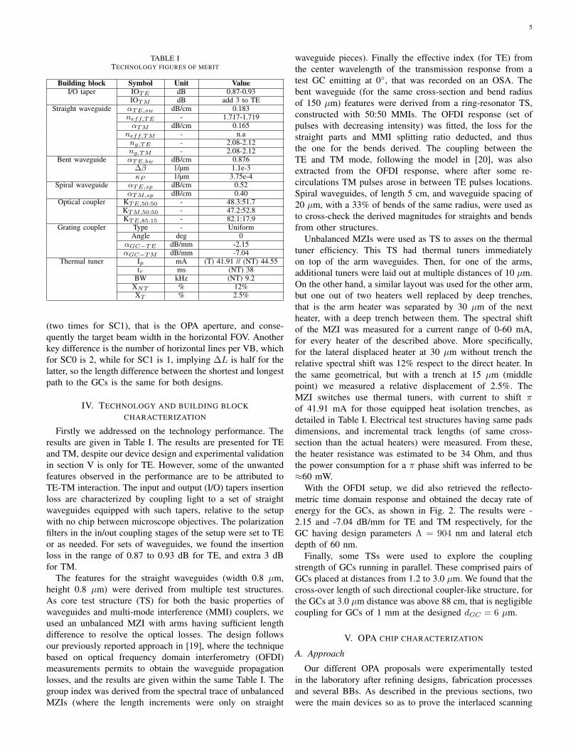
TABLE ITECHNOLOGY FIGURES OF MERIT
Building block Symbol Unit ValueI/O taper IOTE dB 0.87-0.93
IOTM dB add 3 to TEStraight waveguide αTE,sw dB/cm 0.183
neff,TE - 1.717-1.719αTM dB/cm 0.165
neff,TM - n.ang,TE - 2.08-2.12ng,TM - 2.08-2.12
Bent waveguide αTE,bw dB/cm 0.876∆β 1/µm 1.1e-3κP 1/µm 3.75e-4
Spiral waveguide αTE,sp dB/cm 0.52αTM,sp dB/cm 0.40
Optical coupler KTE,50:50 - 48.3:51.7KTM,50:50 - 47.2:52.8KTE,85:15 - 82.1:17.9
Grating coupler Type - UniformAngle deg 0
αGC−TE dB/mm -2.15αGC−TM dB/mm -7.04
Thermal tuner Ip mA (T) 41.91 // (NT) 44.55tr ms (NT) 38
BW kHz (NT) 9.2XNT % 12%XT % 2.5%
(two times for SC1), that is the OPA aperture, and conse-quently the target beam width in the horizontal FOV. Anotherkey difference is the number of horizontal lines per VB, whichfor SC0 is 2, while for SC1 is 1, implying ∆L is half for thelatter, so the length difference between the shortest and longestpath to the GCs is the same for both designs.
IV. TECHNOLOGY AND BUILDING BLOCKCHARACTERIZATION
Firstly we addressed on the technology performance. Theresults are given in Table I. The results are presented for TEand TM, despite our device design and experimental validationin section V is only for TE. However, some of the unwantedfeatures observed in the performance are to be attributed toTE-TM interaction. The input and output (I/O) tapers insertionloss are characterized by coupling light to a set of straightwaveguides equipped with such tapers, relative to the setupwith no chip between microscope objectives. The polarizationfilters in the in/out coupling stages of the setup were set to TEor as needed. For sets of waveguides, we found the insertionloss in the range of 0.87 to 0.93 dB for TE, and extra 3 dBfor TM.
The features for the straight waveguides (width 0.8 µm,height 0.8 µm) were derived from multiple test structures.As core test structure (TS) for both the basic properties ofwaveguides and multi-mode interference (MMI) couplers, weused an unbalanced MZI with arms having sufficient lengthdifference to resolve the optical losses. The design followsour previously reported approach in [19], where the techniquebased on optical frequency domain interferometry (OFDI)measurements permits to obtain the waveguide propagationlosses, and the results are given within the same Table I. Thegroup index was derived from the spectral trace of unbalancedMZIs (where the length increments were only on straight
waveguide pieces). Finally the effective index (for TE) fromthe center wavelength of the transmission response from atest GC emitting at 0◦, that was recorded on an OSA. Thebent waveguide (for the same cross-section and bend radiusof 150 µm) features were derived from a ring-resonator TS,constructed with 50:50 MMIs. The OFDI response (set ofpulses with decreasing intensity) was fitted, the loss for thestraight parts and MMI splitting ratio deducted, and thusthe one for the bends derived. The coupling between theTE and TM mode, following the model in [20], was alsoextracted from the OFDI response, where after some re-circulations TM pulses arose in between TE pulses locations.Spiral waveguides, of length 5 cm, and waveguide spacing of20 µm, with a 33% of bends of the same radius, were used asto cross-check the derived magnitudes for straights and bendsfrom other structures.
Unbalanced MZIs were used as TS to asses on the thermaltuner efficiency. This TS had thermal tuners immediatelyon top of the arm waveguides. Then, for one of the arms,additional tuners were laid out at multiple distances of 10 µm.On the other hand, a similar layout was used for the other arm,but one out of two heaters well replaced by deep trenches,that is the arm heater was separated by 30 µm of the nextheater, with a deep trench between them. The spectral shiftof the MZI was measured for a current range of 0-60 mA,for every heater of the described above. More specifically,for the lateral displaced heater at 30 µm without trench therelative spectral shift was 12% respect to the direct heater. Inthe same geometrical, but with a trench at 15 µm (middlepoint) we measured a relative displacement of 2.5%. TheMZI switches use thermal tuners, with current to shift πof 41.91 mA for those equipped heat isolation trenches, asdetailed in Table I. Electrical test structures having same padsdimensions, and incremental track lengths (of same cross-section than the actual heaters) were measured. From these,the heater resistance was estimated to be 34 Ohm, and thusthe power consumption for a π phase shift was inferred to be≈60 mW.
With the OFDI setup, we did also retrieved the reflecto-metric time domain response and obtained the decay rate ofenergy for the GCs, as shown in Fig. 2. The results were -2.15 and -7.04 dB/mm for TE and TM respectively, for theGC having design parameters Λ = 904 nm and lateral etchdepth of 60 nm.
Finally, some TSs were used to explore the couplingstrength of GCs running in parallel. These comprised pairs ofGCs placed at distances from 1.2 to 3.0 µm. We found that thecross-over length of such directional coupler-like structure, forthe GCs at 3.0 µm distance was above 88 cm, that is negligiblecoupling for GCs of 1 mm at the designed dGC = 6 µm.
V. OPA CHIP CHARACTERIZATION
A. Approach
Our different OPA proposals were experimentally testedin the laboratory after refining designs, fabrication processesand several BBs. As described in the previous sections, twowere the main devices so as to prove the interlaced scanning

6
TE mode TM mode
Linear fit2.15 dB/mm
Fig. 2. (top panel) TE and TM mode OFDI reflectometry traces for gratingcouplers. (bottom panel) zoom-in view in the grating location for the TEmode.
Fig. 3. OPA chip characterization setup
patterns: designs SC0 and SC1. For this, we assemble theexperimental setup shown in Fig. 3.
We performed edge coupling by using microscope objec-tives as mechanism for feeding light into the PIC. In orderto control the input polarization, polarization controllers areemployed previous to the microscope objectives, filtering TMmode and letting TE mode be coupled. In the case of designSC0, as the scan is performed with a purely passive method(we directly access the SC input ports), the PIC is depositedon top of a copper chuck which holds the die through avacuum channel. For the SC1 design, the scanning patternis accomplished by controlling the switching matrix to selectthe operating VB and the corresponding input to the SC. Thus,this PIC was assembled in an aluminium PCB, where wire-bond connectors link the DC pads contained in the PIC withthe pads contained in the PCB. Moreover, as heat dissipation
is crucial in this case, the PCB is fixed on top of an aluminiumchuck and a heat radiator. To control the temperature changeshappening in real time in the PIC, a ceramic thermistor isalso included and routed to the PCB terminals. The thermalmanagement is performed by means of a thermal electriccontroller (TEC), which maintains a constant temperaturethrough the characterization process using a Peltier cell. Inother hand, a proper arrangement must be done to capturethe light beam generated by the OPA. We employed a infra-red (IR) CCD 2D array placed 14 cm over the PIC forthe acquisition of the beam profiles with enough definition(≈10 pixels along the main beam). This distance is justslightly larger than the far-field distance for the aperturesconsidered, but via simulations we confirmed this have nosubstantial effects. Next, in a second arrangement, and inorder to capture the complete FOV, we resorted to a mirrorand projection screen. For this, a 90◦ gold protected mirror(96 % reflectance) is allocated above the PIC (4cm) and aviewing screen is mounted and adjusted in height to collectthe beam reflected. At the other end of the setup, the InGaAsCCD array (Hamamatsu C12741-03, 14 bit resolution, 42 dBdynamic range), is mounted with an IR objective and preparedto capture the viewing screen. Processing includes dark framesubtraction to eliminate laboratory ambient light, and gammacorrection. After the adjustment and characterization of thissetup, the area covered with the InGaAs camera was 22.5◦ H x17◦ V. The difference between the horizontal and vertical axisis due to the detector array of the InGaAs camera (640x512pixels). This range is enough to properly capture the scanningpatterns created by designs SC0 and SC1.
In the case of design SC1, the switching matrix mustbe electrically powered up. For this, two FFSD 40-pin flatcables are connected to both sides of the PCB and to aninterconnection 40 points electrical box, where several DClines can be easily switched to activate different heaters fromthe switching matrix. Finally, the electrical interconnectionbox is connected through an interface to a couple of 10-channel, 300 mA current sources provided by LuzWaveLabs.This current sources are especially designed for PIC testing,able to provided 16 bits of resolution, high stability andexcellent noise performance. For their control, several Pythonand MATLAB scripts were generated.
The primary objective then is to capture the scanning patternof the OPAs using the experimental setup previously described.In the case of SC0, it contains a single VB where the multi-input SC has 8 inputs which were accessed individually fromthe chip facet. For the SC1 design, the 4 VBs can be selectedby a 2x4 switching matrix followed by a 2x8 for each of theVBs. Thus, the first task to generate the OPA scanning patternis to calibrate the different switching matrices. It is worthmentioning that the tuning of each phase shifter containedin the MZIs (just one of the two arms was tuned) was doneby performing a current sweep of 0-60 mA, range in whicha π phase shift is seen. This information was obtained byprevious BB individual characterization. For each VB lightis edge coupled to the upper 2x2 MZI of its correspondingswitching matrix. Note that in both designs, SC0 and SC1, thenot needed MZI inputs at all stages of the switching matrix

7
OPA
1 mm
8 inputs
Star coupler
39 array waveguides
200 mm
Fig. 4. Multi-input star coupler fabricated device microscope picture.
are routed independently to the die facets on purpose, so theycan be employed in the switching matrix calibration phase.In short, once light is applied to one of the sparse 2x2 MZIinput we can observed using the camera both radiated spots,and tuning the phase shifter light can be redirected to just oneof the spots (i.e. one inputs of the SC). This step is repeated forthe each sparse 2x2 MZI input. This task has been developedmanually. Nevertheless, the process can be easily adapted tobe performed through image recognition and automated edgecoupling.
After the experimental setup preparation and the switchingmatrix calibration, the OPA interlaced scanning patterns canbe properly tested. In the case of design SC0, light is edgecoupled to the desired VB through the outer 2x2 MZI fromthe switching matrix. Similarly, in the case of design SC1,light is edge coupled to the VB selector, located in the leftlower part of the die (see Fig. 6). Next, the 90º gold mirroris positioned and adjusted on top of the die. After this, theOPA beam is visible in the viewing screen allowing a finetuning and maximization of the edge coupling by using atuneable laser and a manual polarization controller. Once TECcontroller is set to a temperature of 25◦ and the ambient lightcompensation frames are captured each stage of the switchingmatrix is properly set to drive light to the first input of the SC,generating a light beam in the viewing screen and capturingthe video frames as wavelength is swept using the tuneablelaser. The process is repeated adjusting the switching matrixto drive each SC input and restarting the wavelength swept.Once the VB has been completed, the electrical connectionsfrom the interconnection box need to be arranged to feed thenext VB. In the case of design SC1, the VB selector is properlymodified. Similarly, the switching matrix of the VB is preparedto drive light to the first input of the SC and the measurementis repeated as previously described. After the recording of theinterlaced scan patterns generated by the OPAs, the videos areprocessed and results are extracted using our own MATLABroutines.
B. Experimental results
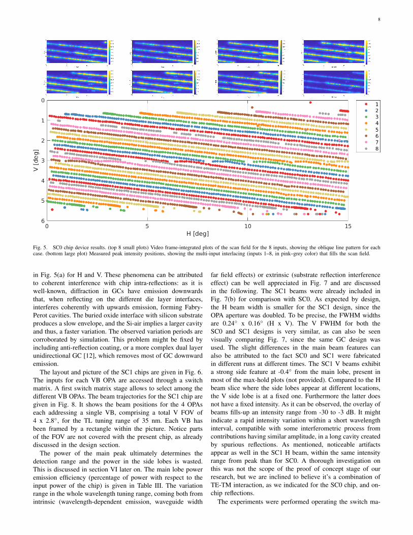
We firstly expand the results for our SC0 chip, previouslyreported in [16]. A picture of the SC0 chips is given in Fig. 4.Light from the TL is horizontally coupled to each of the 8inputs, which are routed to the chip facet. The TL scan rangewas in this case 50 nm (1525 to 1575 nm), larger than the35 nm to cover the FOV. The overall capture strategy entailsvideo recordings, and allows each video frame to be linked toa given wavelength of the sweep. The projection of the OPAspots on the screen was then recorded, and each video wasoff-line processed. After capturing videos for each input, wefirst integrate by collapsing all the frames into one image byholding the maxima. This gives a clear representation of thebeam trace as it is represented in Fig. 5(a). At the beginningof the scan, the beam is placed in the upper left corner. Aswavelength is swept, as it is observed the beam traces theexpected diagonal path composed by the faster movementin H due to linear incremental phase changing in the array,combined with V one because of the GC dispersion. Thenext OPA diffraction order lobe appears in the field when15◦ in H are steered, repeats the travel twice, and ends atthe bottom. Same dynamics are observed for every input, butprogressively displaced a fraction in the V dimension. Thisoffset corresponds exactly to a 2π/8 phase jump, so that allthe input traces in the same order interlace homogeneouslythe space between two orders of the same input, as expected,to fill the entire scan field. In fact, there are observed twogroups of 8 lines for ∆λ = 35 nm, covering the 2.8◦ intendedfor the vertical block. This result can be better observed inFig. 5(b). There is observed some no ideal behaviour though.Along their trajectories, which are not exactly linear, beamwidths vary and significant intensity fading is observed.
Individual frame captured beams are fitted to a 2D Gaussianmodel, so the H and V widths are retrieved by computingits full width at half maximum (FWHM). We observed beamquality was degraded when capturing from the projectionscreen, as compared with direct beams captured with the IRcam on top of the chip. The beams from the projection screenexhibited glitches and peaks, we attributed to stray photonsboth from the screen and other light sources in the lab. Thesedegrading artifacts were not observed for the IR cam on top ofthe chip. Consequently, we acquired beams following the sameTL scan and video record procedure directly seen from thechip in the IR cam, at the cost of a reduced FOV. In Fig. 7(a),all beam frame slices are represented together for H and V, atleft and right, respectively. The beam width is estimated fromthe Gaussian fittings (excluding frames with beams havingpeak intensity below 20% of the IR cam dynamic range)and matches with the design, 0.36◦ ×0.175◦. The averagebeam wander is below one beam width though. For H, weobserve the presence of a region at -1◦ from the beam centerswhere artifacts in between -10 and -30 dB from the peakmaximum appear. By observing Fig. 5(a) at 1◦ from the beamtrail, the presence of the side artifact is present in a smallpart of the FOV. This might be attributed to TE-TM modeinteraction in the waveguides, similar to what [21] reports forAWGs. The peak intensity fluctuations can also be observed
8
Fig. 5. SC0 chip device results. (top 8 small plots) Video frame-integrated plots of the scan field for the 8 inputs, showing the oblique line pattern for eachcase. (bottom large plot) Measured peak intensity positions, showing the multi-input interlacing (inputs 1–8, in pink–grey color) that fills the scan field.
in Fig. 5(a) for H and V. These phenomena can be attributedto coherent interference with chip intra-reflections: as it iswell-known, diffraction in GCs have emission downwardsthat, when reflecting on the different die layer interfaces,interferes coherently with upwards emission, forming Fabry-Perot cavities. The buried oxide interface with silicon substrateproduces a slow envelope, and the Si-air implies a larger cavityand thus, a faster variation. The observed variation periods arecorroborated by simulation. This problem might be fixed byincluding anti-reflection coating, or a more complex dual layerunidirectional GC [12], which removes most of GC downwardemission.
The layout and picture of the SC1 chips are given in Fig. 6.The inputs for each VB OPA are accessed through a switchmatrix. A first switch matrix stage allows to select among thedifferent VB OPAs. The beam trajectories for the SC1 chip aregiven in Fig. 8. It shows the beam positions for the 4 OPAseach addressing a single VB, comprising a total V FOV of4 x 2.8◦, for the TL tuning range of 35 nm. Each VB hasbeen framed by a rectangle within the picture. Notice partsof the FOV are not covered with the present chip, as alreadydiscussed in the design section.
The power of the main peak ultimately determines thedetection range and the power in the side lobes is wasted.This is discussed in section VI later on. The main lobe poweremission efficiency (percentage of power with respect to theinput power of the chip) is given in Table III. The variationrange in the whole wavelength tuning range, coming both fromintrinsic (wavelength-dependent emission, waveguide width
far field effects) or extrinsic (substrate reflection interferenceeffect) can be well appreciated in Fig. 7 and are discussedin the following. The SC1 beams were already included inFig. 7(b) for comparison with SC0. As expected by design,the H beam width is smaller for the SC1 design, since theOPA aperture was doubled. To be precise, the FWHM widthsare 0.24◦ x 0.16◦ (H x V). The V FWHM for both theSC0 and SC1 designs is very similar, as can also be seenvisually comparing Fig. 7, since the same GC design wasused. The slight differences in the main beam features canalso be attributed to the fact SC0 and SC1 were fabricatedin different runs at different times. The SC1 V beams exhibita strong side feature at -0.4◦ from the main lobe, present inmost of the max-hold plots (not provided). Compared to the Hbeam slice where the side lobes appear at different locations,the V side lobe is at a fixed one. Furthermore the latter doesnot have a fixed intensity. As it can be observed, the overlay ofbeams fills-up an intensity range from -30 to -3 dB. It mightindicate a rapid intensity variation within a short wavelengthinterval, compatible with some interferometric process fromcontributions having similar amplitude, in a long cavity createdby spurious reflections. As mentioned, noticeable artifactsappear as well in the SC1 H beam, within the same intensityrange from peak than for SC0. A thorough investigation onthis was not the scope of the proof of concept stage of ourresearch, but we are inclined to believe it’s a combination ofTE-TM interaction, as we indicated for the SC0 chip, and on-chip reflections.
The experiments were performed operating the switch ma-

9
Fig. 6. SC1 chip layout (top), color legend: purple (waveguides), green(grating couplers), brown (metal tracks). Picture of the PCB mounted chip(bottom).
trix and the tunable laser. After calibration, the switch matrixbias current required for every state were be stored, and weobserved fully reproducible matrix configuration along theexperiments. For the results shown, the TL was continuouslytuned for every matrix selected SC-OPA input. However therearchitecture can sport further scanning schemes, some of themwe outline hereby.
• Random access: the TL wavelength range and switchmatrix state can be arbitrary. Thus, parts of the scene canbe accessed, i.e. addressing those areas in the FOV wheretargets have been identified (e.g. fast moving targets)while neglecting others (static or slower moving targets).
• Adjustable resolution: since the switch matrix state can bearbitrary, two adjacent SC inputs could be enabled at thesame time. Two spots would be created simultaneously(i.e. two of the lines shown in the trajectories figuresscanning parallel in time), which would represent andeffective reduction of the spatial resolution. Time wise,with respect of LiDAR system integration time (seesection ahead) the scan rate could be halved to preservethe same SNR, owing to the fact the optical power in thissituation would is split in two beams, instead of one.
• Object framing: two far inputs, e.g. input 1 and 8 couldbe enabled simultaneously. This way, an outline of alarge object, duly identified by processing algorithms ina regular higher resolution spatial scan.
Fig. 7. Beam frame H (left) and V (right) slices for the SC0 (top) and SC1(bottom) chips.
Fig. 8. SC1 chip device results. Measured peak intensity positions, showingthe multi-input interlacing (inputs 1–8, in pink–grey color).
In summary, the architecture allows for addressing partsof the scene randomly, with different spatial resolutions.Considerations on the laser and switch matrix set and resettimes should be addressed, but are out the scope of this paper.
In terms of footprint, the switch matrix (SM) stage, in itsmost simple structure without resorting to special layouts forthe MZIs, scales in length as the number of required stages.
10
That is, if P is the number of inputs to one of our SC-OPAs,the SW stage length will be LSM = LMZI log2(P ), and theheight (or width) will be WSM = WMZIP/2. Thus, the totalarea , where the factor 1/2 stems from the tree-like structure.In our design, this amounts for 5.14x0.4 mm2 (see Fig. 6),which is 2 mm2 area. On other hand, the SC-OPA withoutswitching, that gives the same scene line density, has to scanP times faster for a wavelength sweep ∆λTL. Consequently,the path length increment between adjacent paths from theSC to the grating couplers, ∆L , must be multiplied by afactor P . In general, if we consider a rectangular layout for thearray of waveguides between the SC and the grating couplers,the footprint scales ∝ ∆L2. Thus, a length increase factor ofP for ∆L results into an increase of P 2 in the used area.In our design, the area used by the arrayed waveguides isapproximately 1 mm2 (see Figs. 4 and 6). Hence, resorting to anon-switched version of the SC-OPA would result into 64 mm2
of area used, as compared to our SC-OPA with P = 8. Inconclusion, the switched architecture presents a footprint ratioadvantage, as compared to the non-switched one, of (1+2)/64approximately. This ratio is enlarged for larger P , since the1 mm2 corresponds to the OPA, and 2 mm2 to the SM 2x8.
VI. LIDAR SYSTEM PERSPECTIVE
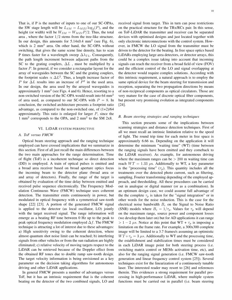
A. ToF versus FMCW
Optical beam steering approach and the ranging techniqueemployed can have crossed implications that we summarize inthis section. First of all just recall the main differences betweenthe two main approaches for the range determination. Timeof flight (ToF) is a incoherent technique so direct detection(DD) is employed. A train of optical pulses is emitted anda broad area receiver based on broad aperture optics focusthe incoming beam to the detector plane (broad area orand array of detectors). Finally, the range of the target isobtained by evaluation of the time delay between emitted andreceived pulse sequence electronically. The Frequency Mod-ulation Continuous Wave (FMCW) technique uses coherentdetection. The transmitter emits continuously in power, butmodulated in optical frequency with a symmetrical saw-toothshape [22] [23]. A portion of the generated FMCW signalis applied to the detector (as local oscillator, LO) jointlywith the target received signal. The range information willemerge as a beating RF tone between 0 Hz up to the peak topeak optical frequency modulation employed ∆f . The FMCWtechnique is attracting a lot of interest due to these advantages:a) High sensitivity owing to the coherent detection, wherealmost quantum shot noise limit can be reached; b) interferingsignals from other vehicles or from the sun radiation are highlyeliminated; c) relative velocity of moving targets respect to theLiDAR can be retrieved because of the Doppler effect fromthe obtained RF tones due to double ramp saw-tooth design.The target velocity information is being envisioned as a keyparameter on the decision taking algorithms for autonomousdriving and other LiDAR applications.
In general FMCW presents a number of advantages versusToF, but it has an intrinsic requirement that is the coherentbeating on the detector of the two combined signals, LO and
received signal from target. This in turn can pose restrictionson the practical structure for the TRx/RCx pair. In this sense,on ToF-LiDAR the transmitter and receiver can be separateddevices with optimised designs and just located together withonly electronic interconnections with the control system. How-ever, in FMCW the LO signal from the transmitter must bedriven to the detector for the beating. In free space optics basedLiDARs employing large area detectors, or detector arrays, thiscould be a complex issue taking into account that incomingsignals can reach the receiver from a broad field of view (FOV)and the efficient control of the LO and signal overlapping atthe detector would require complex solutions. According withthis intrinsic requirement, a natural approach is to employ thesame optical device for the beam steering for transmission andreception, separating the two propagation directions by meansof non-reciprocal components as optical circulators. Those arevery mature for the case of discrete optical fiber components,but present very promising evolution as integrated components[24].
B. Beam steering strategies and ranging techniques
This section presents some of the implications betweenscanning strategies and distance detection techniques. First ofall we must recall an intrinsic limitation relative to the speedof light. The round trip time for each meter in free space isapproximately 6.66 ns. Depending on the application it willdetermine the minimum ”waiting time” (WT) (time betweenthe ranging signals have been emitted and they comeback tothe LiDAR receiver). As example, for autonomous drivingwhere the maximum ranges can be > 200 m waiting time canreach WT = 1.33 µs. Additionally to WT, a key parameteris the ”processing time” (τp). This quantity includes all thetreatments over the detected photo current, such as filtering,sampling, Fourier transforming depending of the employed ap-proach, and thresholding. All these procedures can be carriedout in analogue or digital manner (or as a combination). Inan optimum design case, we could assume full advantage ofthe the complete τp is taken for the ”signal integration” or inother words for the noise reduction. This is the case for theelectrical noise bandwidth Be on the Signal to Noise Ratio(SNR) models where Be = 1/τp. Values for τp will dependon the maximum range, source power and component losses(we develop them later on) but for AD applications it can range> 1− 2 µs. Notice at this point that WT + τp is imposing alimitation on the frame rate. For example, a 300x300 completeimage will be limited to a 3.7 frames/s assuming an optimisticWT+τp = 3 µs. Additionally to WT and the processing time,the establishment and stabilization times must be consideredin each LiDAR image point for both steering process (i.e.switching matrix control or MEMs activation time, etc), andalso for the ranging signal generation (i.e. FMCW saw-toothgeneration and linear frequency control system [25]). Severaltechniques exist for the linearization of a continuously tunablelaser. The interested reader may resort to [26] and referencestherein. This evidences a strong requirement for parallel pro-cessing in high-performance LiDAR, where multiple systemfunctions must be carried out in parallel (i.e. beam steering

11
along with proper FMCW frequency generation) in order toshorten the total per point time.
After the previous general considerations we can concludethe beam steering approach and the signals employed for theranging/speed determination, including their optimum rela-tionships, will determine the final LiDAR features. Thus, wededicate the rest of the section to explore these relations forthe proposed architecture, assuming the use of FMCW rangingsignals.
A classical approach is the point to point switching. Itimplies a sequence of steps: 1) Beam steering and stabilizationtime. It encompass two actions, the wavelength tuning toperform both the H and V steering into the Vertical Block(VB) and the switching matrix to select the proper VB, 2)The FMCW generation consisting in the saw-tooth frequencymodulation with ∆f excursion and 2T period. The theoreticallimit for the spatial ranging resolution is only related with ∆fas ∆R = c/2∆f with c the speed of light. As a reference, inautonomous driving resolutions below 15 cm are demanded,that correspond with ∆f > 1 GHz. The coarse wavelengthtuning for beam steering, and the fine linear optical frequencysweep, are carried out and optimised in a separated way,resulting in greater time consumption for the entire process.Furthermore, there is a unavoidable cross-relationship betweenFMCW signals and wavelength tuning steering systems, whichis the beam deviation according to the frequency modulationof the saw-tooth signal itself. In these cases, it must be ensuredthat the angle variation induced by FMCW signal is smallerthan the desired beam divergence (or alternatively image pointseparation). As previously described vertical dispersion onGC was (∂θ/∂λ)V =0.08◦/nm but horizontal dispersion dueto the delay line section previous the OPA is (∂φ/∂λ)H =NlinesFOVH/P∆λ, being for Nlines = 4 and P = 1 a valueof (4x15◦/35nm)=1.71◦/nm.
Notice that in this case, the maximum FMCW frequencyexcursion ∆f is 7.2GHz (case when H beam deflection equalsthe desired H divergence of 0.1 degree). It is important tonote that this maximum feasible excursion decreases as thenumber of lines into the VB increases. For example for P = 1and Nlines = 28 (compatible with the vertical density of 0.1degrees along 2.8◦), the maximum ∆f is 1 GHz (close toa range resolution of 15 cm as previously indicated). In thissense, the proposed switched architecture once again playsto our advantage by decoupling the Nlines concept from theNcycles through the product Nlines = P ×Ncycles, increasingthe possible FMCW excursion by a factor × P.
An alternative approach employs the laser sweep to ac-complish both the beam steering and the FMCW rangingprocess simultaneously, in a continuous way [27]. Fig. 9.shows schematically the steering trajectories inside a verticalblock and their optical frequency correspondence, to illustratethe connection between steering and FMCW process and theirinterdependence. In order to simplify the representation, and tomake easier the explanation, we take an specific combinationsof P = 4 (number of input ports to the OPA slab coupler(SC)), and Ncycles = 8 (the number of drawn lines along theVB when one complete wavelength scan is accomplished).Notice that 32 oblique lines will fill in full the vertical block
Line 1
t
𝑃𝑃 = 4,𝑁𝑁𝑐𝑐𝑐𝑐𝑐𝑐𝑐𝑐𝑐𝑐𝑐𝑐 = 8∆𝑓𝑓(𝑡𝑡)
𝐹𝐹
𝑇𝑇
𝑁𝑁𝑐𝑐𝑐𝑐𝑐𝑐𝑐𝑐𝑐𝑐𝑐𝑐Line 2
Line 8
Line 7
Port 1
t
∆𝑓𝑓(𝑡𝑡)
𝐹𝐹𝑇𝑇
Port 1 Port 2 Port 3 Port 4
Positive & negative slopes each port
(c)
(a) (b)
Fig. 9. Steering trajectories inside a Vertical Block and their optical frequencycorrespondence. a) Interleaved trajectories. Lines of port 1 are indicated. b)Single ramp per input port. c) Double ramp for relative velocity determination
field, leading to 2.8/32 = 0.088 vertical interline space.Different colors are employed for each SC input, showing theline steering interleaving into the VB, and their correspondentfrequency variation. In the standard FMCW technique, bothpositive and negative frequency slopes must be employed,in order to retrieve the magnitude, and the direction of thetarget, relative velocity without ambiguity. To achieve this, twoconsecutive frequency scans with positive and negative slopesmust be completed per each input port as depicted in Fig. 9(c).We define the TV B as the available time to scan a completeVB. The frame time will be Tframe = TV BNV B , the time toscan all the lines at each SC input will be Tport = TV B/Pand finally T in Fig. 9 T = TV B/2P the single ramp time. Asexplained up to this point, the single point classical FMCWapproach has been expanded into a continuum swept extendedto a certain frequency range (F) that is shared along thewhole set of image points covered in each SC port input.In practice, this continuous swept is effectively sliced afterdetection by the signal processor in a set of ”time beams”,according with the specified angular resolution and/or beamdivergence (div). This way, the number of ”time beams” intothe single time ramp T can be formulated as MFMCW =γ(NcyclesFOVH)/div, with FOVH the horizontal field ofview and γ an over-slicing parameter γ >= 1. Once MFMCW
is set, the effective optical frequency excursion is obtainedas ∆feff = F/MFMCW , and from this the expected rangeresolution ∆R = c/2∆feff together with the maximum RFtones that should be detected and processed RFtone = ∆feff .Table II summarises the relevant system results for a frame rateequal to 10 Hz, NV B = 10 (FOVV = 2.8o×NV B) leading toTV B = 10 ms, F = 35 nm × (100GHz/0.8nm), FOVH = 30o
and beam divergence div = 0.1◦.
Notice that linearized frequency sweep must be accom-plished along the whole range F during the time T (seeTable II), which is a challenge for the tunable source as thenumber of ports (P) increase. Probably the future availabilityof rapidly tunable hybrid integrated laser sources in ranges ofsome tens of nanometers [28], [29] will determine the viabilityof the FMCW continuous scanning technique in applicationswith a wide FOV and fast full image rates.
12
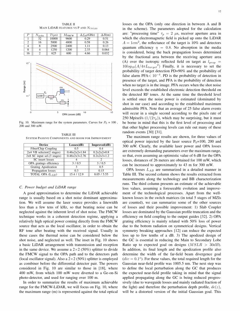
TABLE IIMAIN LIDAR FEATURES VS P AND NCYCLES
P Ncycles T (µs) MFMCW ∆feff(GHz) ∆R(m)1 32 10000 9600 0.29 0.512 16 5000 4800 0.58 0.264 8 2500 2400 1.11 0.138 4 1250 1200 2.33 0.064
16 2 625 600 4.66 0.032
Laser50%
OPA
A B
50%
OPA Losses (dB)
Rang
e (m
)
Fig. 10. Maximum range for the system parameters. Curves for P0 = 100 ,200 and 300 mW.
TABLE IIISYSTEM PASSIVE COMPONENTS AND ROOM FOR IMPROVEMENT
Device Losses(dB) Improved(dB)Fiber/Chip Coupling 0.5 0.4
2x4 VB selector(2 stages) 0.46x2x2=1.84 0.2x2x2=0.82x8 SC input sel.(3 stages) 0.46x2x3=2.76 0.2x2x3=1.2
SC insert losses 4 2OPA gratings efficiency 3 / 0.5 3 / 0.5
Grating Apodization 3 0.5Propagation losses 0.3 0.15
TOTAL OPA (LAB) 15.4 / 12.9 8.05 / 5.55
C. Power budget and LiDAR range
A good approximation to determine the LiDAR achievablerange is usually based on a shot noise dominant approxima-tion. We will assume the laser source provides a linewidthless than a few tens of kHz, so that beating noise can beneglected against the inherent level of shot noise. The FMCWtechnique works in a coherent detection regime, applying arelatively high optical power coming directly from the FMCWsource that acts as the local oscillator, in order to obtain theRF tone after beating with the received signal. Usually inthese cases the thermal noise can be considered below theshot noise, and neglected as well. The inset in Fig. 10 showsa basic LiDAR arrangement with transmission and receptionin the same device. We assume a 2×2 (50%) splitter to dividethe FMCW signal to the OPA path and to the detectors path(local oscillator signal). Also a 2×2 (50%) splitter is employedas combiner before the differential detector pair. The powersconsidered in Fig. 10 are similar to those in [18], where400 mW, from which 100 mW were diverted to a Ge-on-Siphoto-detector, and used for ranging over 100 m.
In order to summarize the results of maximum achievablerange for the FMCW-LiDAR, we will focus on Fig. 10, wherethe maximum range (m) is represented against the total optical
losses on the OPA (only one direction in between A and Bin the scheme). The parameters adopted for the calculationare: ”processing time” τp = 2 µs, receiver aperture area inwhich the electromagnetic field is picked up onto the LiDARA = 1cm2, the reflectance of the target is 10% and detectorsquantum efficiency η = 0.8. No absorption in the mediais considered, being the back propagation losses determinedby the fractional area between the receiving aperture area(A) over the isotropic reflected field on target as lprop =10log10(A/4πLtarget
2) Finally, it is necessary to set theprobability of target detection PD=90% and the probability offalse alarm PFA< 10−4. PD is the probability of detection inpresence of the target, and PFA is the probability of detectionwhen no target is in the image. PFA occurs when the shot noiselevel exceeds the established electronic detection threshold onthe detected RF tones. At the same time the threshold levelis settled once the noise power is estimated (dominated byshot in our case) and according to the established maximumadmissible PFA. Note that an average of 25 false alarm eventswill occur in a single second according to the pixels rate of250 Mpixel/s (1/(2τp)), which may be surprising, but it mustbe borne in mind that this is the first level of processing andthat other higher processing levels can rule out many of theserandom events [30] [31].
The maximum range results are shown, for three values ofoptical power injected by the laser source P0=100, 200 and300 mW. Clearly, the available laser power and OPA lossesare extremely demanding parameters over the maximum range,so that, even assuming an optimistic value of 6 dB for the OPAlosses, distances of 26 meters are obtained for 100 mW, whichcan be increased to approximately to 43 m for 300 mW.
OPA losses LAB are summarized in a detailed manner inTable III. The second column shows the results extracted frommeasurements along the technology and BB characterizationruns. The third column presents an estimate of the achievableloss values, assuming a foreseeable evolution and improve-ment of the technological processes. Apart from the well-known losses in the switch matrices (in total 5 stages of MZIsare counted), we can summarize some of the other sourcesof losses and their possible improvement: 1) Slab Couplerlosses are dominated by the Gaussian profile truncation and theefficiency on field coupling to the output guides [32]. 2) OPAgrating efficiency is mainly related with 50% loss of powerdue to the bottom radiation on symmetrical designs. Verticalsymmetry breaking approaches [12] can reduce the expectedloss up to few tenths of a dB. 3) The apodized design ofthe GC is essential in reducing the Main to Secondary LobeRatio up to expected goal on designs (MSLR > 30dB).In addition, its final length and the apodization profile alsodetermine the width of the far-field beam divergence goal(div = 0.1o). For these values, the total required length for theGaussian near-field profile was 1005.5 nm. The next step wasto define the local perturbation along the GC that producesthe expected near-field profile taking in mind that the signalapplied propagating along the GC is being reduced progres-sively (due to waveguide losses and mainly radiated fraction ofthe light) and therefore the perturbation depth profile, de(z),will be a distorted version of the initial Gaussian goal. This

13
can be easily done by recursive numerical calculations upto obtain the optimum de(z). Notice that, once MSLR anddiv are set, for a given maximum achievable perturbationdepth (demax) the optimum design provides a maximum ratioof total radiated power respect to the applied one (value onTable II as grating apodization). In our design demax was set to115 nm that corresponds with a maximum αGC−TE=8 dB/mmlocal power decaying due grating radiation, leading to a totalgrating apodization losses of 2.34 dB when the completeprofile is evaluated. This grating apodization losses can bereduced by increasing the maximum achievable αGC−TEthrough increasing demax and/or the mode profile overlappingwith the waveguide perturbed cross-section. Moreover, longerdevices allow the reduction of the angular divergence (div)but also the losses. As an example, a 2 mm long GC withequivalent apodization profile and same demax as designedwould result into a 0.83 dB losses. 4) Propagation lossmeasured was 0.183 dB/cm and reports [33] show results asgood as 0.055 dB/cm, considering interconnection waveguidesrepresent a total length of 1.5 cm.
Starting from the indicated base system, it is interesting tohave simple relationships that allow for evaluating the impacton the maximum achievable range by simple calculations.More specifically, each dB increase or decrease in OPA lossesaffects the range by a factor ×0.81 or ×(1/0.81) respectively,while in optical power P0 each dB impacts by a factor ×1.11or ×(1/1.11). Finally, a ×2 increase in the OPA aperture Aresults in a ×1.358 range increase, while in the case of theprocess time T a factor ×2 produces an improvement in therange of ×1.433.
D. Switch matrix cross-talk impactThe MZI based limited extinction for the 1xP SM preceed-
ing the SC-OPA, can lead to the emission of P-1 spuriousbeams evenly spaced in the horizontal FOV by FOVH /P, withintensities -20 dB (worst case, and the closest to the mainradiated beam). -23 dB for 2 beams, -26 dB for 4 beams, andso on.
In transmit / receive mode, the optical signals (main beamand spurious) go through the OPA and SM twice, hencethe cross-talk ratio is a factor of x2. In the worst case, thecross-talk of a spurious to the main beam would then be -40 dB. Considering this worst case, two different ranging anddetection scenarios may arise:
1) Same distance to target than to spurious direction. Inthat case, after beating with the LO FMCW signal, twoRF tones of the same frequency are obtained, whichadd in photocurrent. The amplitude for the interferer inphotocurrent will be 100 times lower (beat term squareroot,
√104) thus with negligible effect over the main
beam signal.2) Spurious beam comes from an object located closer or
further from the main beam target. In this case, afterthe detector, there are 2 RF tones, main and spurious,but with different RF frequency. Thus, they can bedistinguished and separated by processing the receivedsignals. Even though, their value will be very low asexplained in the following.
Laser
OPAs
1x8 Vertical Block selector
1x8 SC Inputselector
Incremental Path lengtharea Grating
Array
𝑙𝑙𝑖𝑖𝑖𝑖𝑖𝑖𝑖𝑖𝑖𝑖
(1)
(2)
(3)
Fig. 11. Optical amplification. Three OA locations are considered. linter arethe one pass losses in between the OA and the reciber input.
The worst case of the two outlined in the last point above,would be when the spurious beam comes from an objectcloser (Lsp) and with reflectivity higher, to the main beamtarget (ρsp). The power ratio between spurious and main beamcan be written as: Xt(dB) = −40 + 10 log10(ρsp/ρmain) +20 log10(Lmain/Lsp). The first term accounts for the differentreflectivity, and the second from the different range (seepropagation loss equation in the manuscript).
As numerical example, for ρsp/ρmain=10 andLmain/Lsp=10, Xt = −10 dB (10 in natural units). Inthat case, the spurious would be detected with an amplitudelevel of
√(10)=3.16 but a frequency 10 times lower.
In conclusion, simple mechanisms could be established forthe processing of the detected signal, that would allow todiscard tones below a given threshold from the main beamtone. In any case, those resulting from a SM with cross-talk-20 dB, can be neglected.
E. Power amplification
We consider here the benefits of using optical amplifiers(OA) embedded into the specific points of the LiDAR ar-chitecture. We begin placing the OA just before the signalinput port of the differential detector in the typically calledpre-amplifier configuration (case on Fig. 11 location (1)). Ascan be envisioned this approach results into the addition ofa new noise term coming from beating noise between thelocal oscillator (LO) and the amplified spontaneous emis-sion noise (ASE) from OA. This noise term is given byσ2LO−ASE = 2η2e2PLONBe where η is the detectors
quantum efficiency, e is the electron charge, PLO is the LOpower at the detector input, Be the electrical bandwidth andN = nsp(G − 1) with nsp the OA population inversionfactor and G the gain. On the other hand, the shot noiseterm is σ2
shot = 2e(ηe/hν)PLOBe and comparing the twoexpressions we have σ2
LO−ASE/σ2shot = ηnsp(G − 1). We
can see that pre-amplier configuration leads to a dominant LO-ASE term approximately G times the shot noise, preventingany hypothetical benefit assumed from optical gain.
Lets consider now a more general configuration wherethe OA is located far from the detector input, so that acertain quantity of optical losses are in between (case on

14
Fig. 11 locations (2) and (3))). We employ linter < 1 toinsert this into the formulation, so the noise ratio remainsas σ2
LO−ASE/σ2shot = ηnsp(G − 1)linter. We can define
a signal to noise ratio at the receiver output in the two cases:a) limited by shot noise (no OA): SNR0 = S0/σ
2shot and b)
Employing OA:SNR = S0Gm/(σ2
shot + σ2LO−ASE) and
finally the ratio between them that provides the net gainbenefit: Gnet = SNR/SNR0 = Gm/(1+ηnsp(G−1)linter).Notice that we have assumed in this generalised approachthat the OA can be localised in different places along theLiDAR architecture, where the signal bi-directionality mustme guaranty (cases 2 and 3). In these cases the optical gainis assumed equal in the two directions, and the double passbenefit over the signal is taken into account by the m = 2parameter on the formulas.
We will illustrate the OA net gain benefits in three differentlocations along the LiDAR architecture. For all the cases wetake a modest gain G=4 (6 dB), NF = 2nsp and η = 0.8. 1)AO just before detectors (location (1) in Fig. 11) so linter = 1(no intermediate losses) and the net gain is Gnet = 0.81 (-1dB). 2) The amplifier is in position (2) in Fig. 11, in betweenthe ideal 2×2 splitter acting as duplexor and the OPAs. In thiscase linter = 1/2 (3dB) and just evaluating the net gain withm = 2 we obtain Gnet = 6.66 (+8.23dB). 3) 8 amplifiers arelocated at each output of the Vertical Block switching matrixwhere the switching matrix is supposed to have in total 3 dBexcess losses. In this case we apply linter = 1/4 and the netgain is Gnet = 13.33 (+11.24 dB). Notice that each 2 dBobtained in Gnet must be counted as an effective reduction of1 dB in the OPA losses, leading to an increase of ×(1/0.81)in range. In the previous cases of positions 2 and 3, the rangeincrease should be ×2.34 and ×3.27.
In summary, amplification on chip is anticipated as a must.Furthermore, a distributed set of amplifiers with modest gainare outlined as the optimum in terms of signal to noise ratio.
VII. CONCLUSION
A fully passive two-dimensional OPA based on wavelengthsweeping and consisting of a multi-input star coupler hasbeen proposed and demonstrated in silicon nitride technology.Existing slab coupler OPA permits to distribute optical powerbetween the numerous radiating elements in a single stepand creating a Gaussian profile in the H direction. Our novelproposal uses P inputs at the entrance of the slab coupler,that allows to relax the up-scaling problem with the starcoupler approach, permitting to reduce both footprint andoptical power losses in a P factor with respect to the single-input approach. Expanded results for a previously reportedproof-of-concept device have been reported, featuring a H×VFOV of 15◦ ×2.8◦, and a beam size of 0.36◦ ×0.175◦, forwavelength sweep of ∆λ = 35 nm, as expected by design.A new design incorporating on-chip switch matrix stages toselect among four different vertical blocks, features H×VFOV of 15◦ ×11.2◦, and a beam size of 0.24◦ ×0.167◦.The architecture can be operated as progressive scene scanner,but it can also feature random scene access with selectableresolution.
From a LiDAR system perspective, we have shown theproposed OPA is compatible with FMCW LiDAR, takingadvantage of the tunable laser wavelength sweep. Moreoverthe switched architecture has the ability to reduce by a Pfactor the horizontal angular dispersion, for a given linedensity, which in turn reduces the impact of the FMCWsignals on the steering deviation. Additionally, the relationshipbetween FMCW frequency tuning in continuous mode with theinterlaced steering trajectories has been described in detail,as well as the implication of the double slope use for thetarget relative speed determination. Dependency relationshipsbetween the steering architecture parameters P and Ncyclesand system parameters of interest, such as the number ofFMCW points, the equivalent per point frequency excursionand the range resolution have been discussed.
The power balance and distance limitations have been de-scribed, providing quick-use scaling rules that can be quicklyused for the evaluation of maximum-range with respect tolosses. A breakdown of the current losses and paths for im-provements have been provided for the proposed architectureand technology. Finally the use of optical gain inside theLiDAR structure is theoretically evaluated, in what we believemay represent a path of disruptive change toward a newgeneration of LiDAR systems that will build upon hybridphotonic integration.
ACKNOWLEDGMENT
We acknowledge Ligentec, the silicon nitride technologyplatform company responsible for the fabrication of the chipmeasured in this work. Equipment and infrastructure fundingby GVA/IDIFEDER/2018/031.
REFERENCES
[1] Y. Zhu, S. Zeng, and L. Zhu, “Optical beam steering by usingtunable, narrow-linewidth butt-coupled hybrid lasers in a silicon nitridephotonics platform,” Photon. Res., vol. 8, no. 3, pp. 375–380, Mar2020. [Online]. Available: http://www.osapublishing.org/prj/abstract.cfm?URI=prj-8-3-375
[2] Y. Guo, Y. Guo, C. Li, H. Zhang, X. Zhou, and L. Zhang,“Integrated optical phased arrays for beam forming and steering,”Applied Sciences, vol. 11, no. 9, 2021. [Online]. Available: https://www.mdpi.com/2076-3417/11/9/4017
[3] K. Van Acoleyen, W. Bogaerts, and R. Baets, “Two-dimensional dis-persive off-chip beam scanner fabricated on silicon-on-insulator,” IEEEPhotonics Technology Letters, vol. 23, no. 17, pp. 1270–1272, Sep. 2011.
[4] C. R. Doerr, L. Chen, Y.-K. Chen, and L. L. Buhl, “Wide bandwidthsilicon nitride grating coupler,” IEEE Photonics Technology Letters,vol. 22, no. 19, pp. 1461–1463, 2010.
[5] H. Ito, Y. Kusunoki, J. Maeda, D. Akiyama, N. Kodama, H. Abe,R. Tetsuya, and T. Baba, “Wide beam steering by slow-light waveguidegratings and a prism lens,” Optica, vol. 7, no. 1, pp. 47–52, 2020.
[6] C. Doerr, L. Chen, L. Chen, and D. Ton, “Linear 2d beam steering with alarge focusing grating via focal point movement and wavelength,” IEEEPhotonics Technology Letters, vol. 33, no. 17, pp. 935–938, 2021.
[7] N. Dostart, B. Zhang, A. Khilo, M. Brand, K. Al Qubaisi, D. Onural,D. Feldkhun, K. H. Wagner, and M. A. Popovic, “Serpentine opticalphased arrays for scalable integrated photonic lidar beam steering,”Optica, vol. 7, no. 6, pp. 726–733, 2020.
[8] W. Bogaerts, S. Dwivedi, R. Jansen, X. Rottenberg, and M. S. Dahlem,“A 2d pixelated optical beam scanner controlled by the laser wave-length,” IEEE Journal of Selected Topics in Quantum Electronics,vol. 27, no. 1, pp. 1–12, 2020.

15
[9] P. Munoz, G. Mico, L. A. Bru, D. Pastor, D. Perez, J. D. Domenech,J. Fernandez, R. Banos, B. Gargallo, R. Alemany, A. M. Sanchez, J. M.Cirera, R. Mas, and C. Domınguez, “Silicon nitride photonic integra-tion platforms for visible, near-infrared and mid-infrared applications,”Sensors, vol. 17, no. 9, p. 2088, 2017.
[10] P. Munoz, P. W. L. van Dijk, D. Geuzebroek, M. Geiselmann,C. Domınguez, A. Stassen, J. D. Domenech, M. Zervas, A. Leinse,C. G. H. Roeloffzen, B. Gargallo, R. Banos, J. Fernandez, G. M.Cabanes, L. A. Bru, and D. Pastor, “Foundry developments towardsilicon nitride photonics from visible to the mid-infrared,” IEEE Journalof Selected Topics in Quantum Electronics, vol. 25, no. 5, pp. 1–13, Sep.2019.
[11] T. Kim, P. Bhargava, C. V. Poulton, J. Notaros, A. Yaacobi, E. Timur-dogan, C. Baiocco, N. Fahrenkopf, S. Kruger, T. Ngai et al., “A single-chip optical phased array in a wafer-scale silicon photonics/cmos 3d-integration platform,” IEEE Journal of Solid-State Circuits, vol. 54,no. 11, pp. 3061–3074, 2019.
[12] M. Raval, C. V. Poulton, and M. R. Watts, “Unidirectional waveguidegrating antennas with uniform emission for optical phased arrays,” Opt.Lett., vol. 42, no. 13, pp. 2563–2566, Jul 2017. [Online]. Available:http://ol.osa.org/abstract.cfm?URI=ol-42-13-2563
[13] C. V. Poulton, A. Yaacobi, Z. Su, M. J. Byrd, and M. R.Watts, “Optical phased array with small spot size, high steeringrange and grouped cascaded phase shifters,” in Advanced Photonics2016 (IPR, NOMA, Sensors, Networks, SPPCom, SOF). OpticalSociety of America, 2016, p. IW1B.2. [Online]. Available: http://www.osapublishing.org/abstract.cfm?URI=IPRSN-2016-IW1B.2
[14] P. Munoz, D. Pastor, and J. Capmany, “Modeling and design of arrayedwaveguide gratings,” Journal of Lightwave Technology, vol. 20, no. 4,pp. 661–674, April 2002.
[15] J. Zou, Z. Le, J. Hu, and J.-J. He, “Performance improvementfor silicon-based arrayed waveguide grating router,” Opt. Express,vol. 25, no. 9, pp. 9963–9973, May 2017. [Online]. Available:http://www.opticsexpress.org/abstract.cfm?URI=oe-25-9-9963
[16] P. Munoz, D. Pastor, J. Benıtez, G. Mico, L. A. Bru, D. J.Goodwill, and E. Bernier, “Optical-phased array beam-steeringusing multi-input slab coupler in silicon nitride waveguides,” inOptical Fiber Communication Conference (OFC) 2021. OpticalSociety of America, 2021, p. W1D.4. [Online]. Available: http://www.osapublishing.org/abstract.cfm?URI=OFC-2021-W1D.4
[17] C. V. Poulton, M. J. Byrd, M. Raval, Z. Su, N. Li, E. Timurdogan,D. Coolbaugh, D. Vermeulen, and M. R. Watts, “Large-scale siliconnitride nanophotonic phased arrays at infrared and visible wavelengths,”Opt. Lett., vol. 42, no. 1, pp. 21–24, Jan 2017. [Online]. Available:http://opg.optica.org/ol/abstract.cfm?URI=ol-42-1-21
[18] Y. Li, B. Chen, Q. Na, Q. Xie, M. Tao, L. Zhang, Z. Zhi, Y. Li, X. Liu,X. Luo, G. Lo, F. Gao, X. Li, and J. Song, “Wide-steering-angle high-resolution optical phased array,” Photon. Res., vol. 9, no. 12, pp. 2511–2518, Dec 2021.
[19] L. A. Bru, D. Pastor, and P. Munoz, “On the characterization ofintegrated power splitters and waveguide losses using optical frequencydomain interferometry,” in 21st European Conference on IntegratedOptics (ECIO), Ghent, 24–26 April 2019, p. W.Po1.25.
[20] F. Morichetti, A. Melloni, and M. Martinelli, “Effects of polarizationrotation in optical ring-resonator-based devices,” Journal of lightwavetechnology, vol. 24, no. 1, p. 573, 2006.
[21] E. Kleijn, P. J. Williams, N. D. Whitbread, M. J. Wale, M. K.Smit, and X. J. Leijtens, “Sidelobes in the response of arrayedwaveguide gratings caused by polarization rotation,” Opt. Express,vol. 20, no. 20, pp. 22 660–22 668, Sep 2012. [Online]. Available:http://www.osapublishing.org/oe/abstract.cfm?URI=oe-20-20-22660
[22] C. V. Poulton, A. Yaacobi, D. B. Cole, M. J. Byrd, M. Raval,D. Vermeulen, and M. R. Watts, “Coherent solid-state lidar with siliconphotonic optical phased arrays,” Optics letters, vol. 42, no. 20, pp. 4091–4094, 2017.
[23] D. Pierrottet, F. Amzajerdian, L. Petway, B. Barnes, G. Lockard, andM. Rubio, “Linear fmcw laser radar for precision range and vectorvelocity measurements,” MRS Online Proceedings Library (OPL), vol.1076, 2008.
[24] L. Bi, J. Hu, P. Jiang, D. H. Kim, G. F. Dionne, L. C. Kimerling, andC. Ross, “On-chip optical isolation in monolithically integrated non-reciprocal optical resonators,” Nature Photonics, vol. 5, no. 12, pp. 758–762, 2011.
[25] C. J. Karlsson and F. A. Olsson, “Linearization of the frequency sweepof a frequency-modulated continuous-wave semiconductor laser radarand the resulting ranging performance,” Applied optics, vol. 38, no. 15,pp. 3376–3386, 1999.
[26] X. Zhang, J. Pouls, and M. C. Wu, “Laser frequency sweeplinearization by iterative learning pre-distortion for fmcw lidar,” Opt.Express, vol. 27, no. 7, pp. 9965–9974, Apr 2019. [Online]. Available:http://opg.optica.org/oe/abstract.cfm?URI=oe-27-7-9965
[27] M. Okano and C. Chong, “Swept source lidar: simultaneous fmcwranging and nonmechanical beam steering with a wideband sweptsource,” Opt. Express, vol. 28, no. 16, pp. 23 898–23 915, Aug2020. [Online]. Available: http://www.opticsexpress.org/abstract.cfm?URI=oe-28-16-23898
[28] K.-J. Boller, A. van Rees, Y. Fan, J. Mak, R. E. M. Lammerink,C. A. A. Franken, P. J. M. van der Slot, D. A. I. Marpaung, C. Fallnich,J. P. Epping, R. M. Oldenbeuving, D. Geskus, R. Dekker, I. Visscher,R. Grootjans, C. G. H. Roeloffzen, M. Hoekman, E. J. Klein, A. Leinse,and R. G. Heideman, “Hybrid integrated semiconductor lasers withsilicon nitride feedback circuits,” Photonics, vol. 7, no. 1, 2020.[Online]. Available: https://www.mdpi.com/2304-6732/7/1/4
[29] M. A. Tran, D. Huang, and J. E. Bowers, “Tutorial on narrow linewidthtunable semiconductor lasers using si/iii-v heterogeneous integration,”APL Photonics, vol. 4, no. 11, p. 111101, 2019. [Online]. Available:https://doi.org/10.1063/1.5124254
[30] M. A. Richards, J. Scheer, W. A. Holm, and W. L. Melvin, “Principlesof modern radar,” 2010.
[31] M. I. Skolnik, Introduction to radar systems. McGraw-hill Singapore,2001.
[32] P. Munoz, D. Pastor, J. Capmany, and S. Sales, “Analytical and numericalanalysis of phase and amplitude errors in the performance of arrayedwaveguide gratings,” IEEE Journal of Selected Topics in QuantumElectronics, vol. 8, no. 6, pp. 1130–1141, Nov 2002.
[33] M. H. P. Pfeiffer, C. Herkommer, J. Liu, T. Morais, M. Zervas,M. Geiselmann, and T. J. Kippenberg, “Photonic damascene process forlow-loss, high-confinement silicon nitride waveguides,” IEEE Journal ofselected topics in quantum electronics, vol. 24, no. 4, pp. 1–11, 2018.
16
Pascual Munoz (S’98, M’04, SM’13) was born inValencia, Spain on February 7th, 1975. He receivedthe Ingeniero de Telecomunicacion degree from Uni-versitat Politecnica de Valencia (UPV) in 1998. In1999 he served as 1st Lieutenant in the SpanishAirforce, while working as IT consultant for AIMEInstituto Tecnologico. He received a Ph.D. degree inphotonics from UPV in 2003. He is currently FullProfessor at the Departamento de Comunicaciones,and researcher at the Institute for Telecommunica-tions and Multimedia Applications (ITEAM), both
at UPV. Dr. Munoz runs a consolidated research line, started in 2005, onprototyping Photonic Integrated Circuits (PICs) in a technology agnosticfashion, where PICs are designed in the best suited technology (Silicon-On-Insulator, Indium Phosphide, Silica on Silicon, Silicon Nitride amongst other)for each application. He has been involved in several European Commissionfunded projects, being coordinator for integration on InP within the NoEIST-EPIXNET. He has published over 50 papers in international refereedjournals and over 80 conference contributions. He is a member of theTechnical Programme Committees of the European Conference on OpticalCommunications (ECOC) and the European Conference on Integrated Optics(ECIO). Dr. Munoz received the VPI Speed Up Photonics Award in 2002 forinnovative Fourier optics AWG with multimode interference (MMI) couplersmodeling, by Virtual Photonics Incorporated and IEEE CommunicationsMagazine. He was also granted the IEEE/LEOS Graduate Student FellowshipProgram in 2002. He received the extraordinary doctorate prize from UPV in2006. From his research line, he co-founded the UPV spin-off company VLCPhotonics in 2011, where the PIC design know-how, expertise and tools havebeen transferred, and he served as CEO from 2011 to 2013. Dr. Munoz is aSenior Member of the IEEE and a Senior Member of the OSA.
Daniel Pastor was born in Elda, Spain, in 1969.His research career at photonics technologies startedat 1993 when joined the Optical CommunicationGroup as researcher and the Communication Depart-ment at Universitat Politecnica de Valencia (UPV)as lecturer and PhD student. From 1994 to 1998 hewas a lecturer at the Telecommunications Engineer-ing Faculty and he became an Associate Professorin 1999. He obtained a PhD in Electrical Engi-neering and Telecommunications by the UniversitatPolitecnica de Valencia, Spain in 1996, with Thesis
topic “Redes de Difraccion sobre Fibra Optica para Procesado de SenalesFotonicas”. He is co-author of more than 225 papers in journals and inter-national conferences in the fields of Optical Delay Line Filters, Fiber BraggGratings, Microwave Photonics, WDM and SCM lightwave systems, OpticalFiber Sensors, Silicon Nitride integrated devices for telecom and sensing,and advanced characterization techniques as Optical Frequency DomainReflectrometry. His current technical interests include Photonic IntegratedCircuits for telecom, LiDAR and chemical and bio-sensing applications.
Luis A. Bru was born in Elche, Spain, in 1988.He received the B.Sc degree in Physics in 2012,and the M.Sc degree in Advanced Physics (specialtyon Photonics) in 2013, both at the Universitat deValencia (UV), Valencia, Spain. He is currentlya post-doc researcher at Photonics Research Labs(PRL), Universitat Politecnica de Valencia (UPV),where he has been enrolled from 2015 to date. In2022, he received a Ph.D. degree in Photonics, whereOptical Frequency Domain Interferometry (OFDI)technique is explored in the context of photonic
integrated circuits. With more than 25 co-authored publications in scientificjournals and conferences, he has been involved in research projects includingPIC topics such as silicon nitride integrated devices, integrated LiDAR, orhybrid photonic integration. Beyond, his research interests expand also toquantum mechanics and quantum information, having kept a collaborationwith nonlinear and quantum optics research group at UV from 2013 to 2017.
Gloria Mico graduated with a Bachelor of Physicsin 2011 at the University of Valencia (UV). Sheobtained her M.Sc. in Photonics from the Poly-technic University of Catalonia in 2013, developingher Master thesis on biophotonics at Institute ofPhotonics Sciences (ICFO). During 2015-2020 shedeveloped her Ph.D. thesis focused on the designand characterization of photonic integrated spectro-scopic sensors and their applications at PhotonicsResearch Lab (PRL) at the Universitat Politecnica deValencia (UPV). Since 2019, she has been working
on projects for private companies related to LIDAR technology. Nowadays,she is working at UPVfab as facility manager.
Jesus Benıtez obtained his Bachelor’s degree inTelecommunications Engineering from the Univer-sitat Politecnica de Valencia (UPV) in 2015. Inthe same year, he joined the Photonics ResearchLabs (PRL) from UPV as a P.hD. student. During2015-2019, he developed his P.hD. in MicrowavePhotonics applied to Low Coherence Interferometry.From 2019-2021 he has been collaborating in privatefunded projects related to photonic integrated cir-cuits (PIC) as a post-doctoral researcher. Currently,he is performing lab operations, testing and system
validation in iPronics Programmable Photonics. His interests cover PICcharacterization and microwave photonics.
Dominic Goodwill received the Ph.D.degree inphysics from Heriot-Watt University, Edinburgh,U.K., in 1991.He has been a Senior Principal En-gineering the Advanced Photonics Team of HuaweiCanada since 2012. He is focused on data centerand transport applications of silicon photonics, andoptical technologies for 5G wireless networks. From2004 to 2011, he was an applications software archi-tect for Nortel and Genband corporations, creating IPtelevision solutions, and real-time serverapplicationsdeployed to millions of consumers. From 1997 to
2004,he led Nortel’s optical interconnects technology team, creating free-space optics and a world-first 10GigE DWDM photonic switched Metronetwork. He led the fiber optics standard for the Infiniband trade association.He was chair for IEEE Optical Interconnects conference, and a programcommittee member for Optical Fiber Communication conference. Previously,at Heriot-Watt University and University of Colorado, he researched III-Vsemiconductors and polymers for optical computing and interconnect. He hasmore than40 issued patents
PLACEPHOTOHERE
Eric Bernier
Copyright © 2022 FDOKUMEN


![Optical-packet-switched interconnect for supercomputer applications [Invited]](https://static.fdokumen.com/doc/165x107/633648acb5f91cb18a0bc31d/optical-packet-switched-interconnect-for-supercomputer-applications-invited.jpg)