DART-SD800 Datasheet | Variscite
33
DART-SD800 Datasheet Rev 1.2 Document Name DTS-008074 Page 1 of 33 Confidential DART-SD800 Datasheet
-
Upload
khangminh22 -
Category
Documents
-
view
0 -
download
0
Transcript of DART-SD800 Datasheet | Variscite

DART-SD800 Datasheet
Rev 1.2 Document Name DTS-008074
Page 1 of 33 Confidential
DART-SD800
Datasheet

DART-SD800 Datasheet
Rev 1.2 Document Name DTS-008074
Page 2 of 33 Confidential
Revision By Date Description Approved by
1.0 Leonid S. 29/10/2014 Initial
1.1 Leonid S. 11/12/2014 1) Pin out changed
2) Block diagram corrected
1.2 Leonid S. 20/01/2015 1) Electrical specifications
added
2) Boot section added
3) USB_VBUS_PROT pin
description added
Table 0-1of Changes

DART-SD800 Datasheet
Rev 1.2 Document Name DTS-008074
Page 3 of 33 Confidential
Table of Contents
List of Tables ............................................................................................................ 3
List of Figures .......................................................................................................... 4
1.1. General Information .................................................................................................. 5
1.2. Feature summary....................................................................................................... 5
1.3. Definitions, Acronyms and Abbreviations ............................................................... 5
2. Detailed Design Description ............................................................................. 7
2.1. SOM's Connectors .................................................................................................... 7
2.2. SOM's I/F exported to the edge connector. ............................................................. 18 2.2.1. Display ports .................................................................................................................. 18 2.2.2. MIPI CSI2 Camera ports ................................................................................................ 20 2.2.3. Digital Audio I2S port .................................................................................................... 21 2.2.4. USB ports........................................................................................................................ 21
2.2.4.1. USB_VBUS_PROT pin description .................................................................................... 22 2.2.5. SD Card port .................................................................................................................. 22 2.2.6. Audio Ports ..................................................................................................................... 24 2.2.7. PMIC GPIO ports ........................................................................................................... 25 2.2.8. BLSP ports ...................................................................................................................... 25 2.2.9. JTAG port ....................................................................................................................... 26 2.2.10. BOOT configuration .................................................................................................. 27 2.2.11. Power ......................................................................................................................... 28 2.2.12. Wi-Fi & Bluetooth ..................................................................................................... 30
3. Electrical specifications .................................................................................. 31
3.1. Absolute maximum ratings ..................................................................................... 31
3.2. Operating conditions ............................................................................................... 31
3.3. Power supplies output ratings ................................................................................. 31
3.4. Digital IO characteristics ........................................................................................ 32
4. Mechanical ...................................................................................................... 33
4.1. The SOM board mounting to the Carrier board ...................................................... 33
4.2. Drawings of mounting the SOM board. .................................................................. 33
List of Tables
TABLE 0-1OF CHANGES ............................................................................................................................. 2 TABLE 2-1 SOM CONNECTORS PIN OUT. ................................................................................................. 17 TABLE 2-2 MIPI DSI0 PORT SIGNALS...................................................................................................... 18 TABLE 2-3 MIPI DSI1 PORT SIGNALS...................................................................................................... 18 TABLE 2-4 HDMI PORT SIGNALS. ........................................................................................................... 19 TABLE 2-6 MIPI CSI2 CAMERA PORT 0 SIGNALS. ................................................................................... 20 TABLE 2-7 MIPI CSI2 CAMERA PORT 1 SIGNALS. ................................................................................... 20 TABLE 2-9 DEDICATED I2C FOR CAMERA CONTROL SIGNALS. ................................................................ 21 TABLE 2-10 DIGITAL AUDIO I2S PORT SIGNALS. ..................................................................................... 21 TABLE 2-11 USB2.0 PORT 1 SIGNALS. ..................................................................................................... 21 TABLE 2-12 USB2.0 PORT 2 SIGNALS (OTG COMPATIBLE). .................................................................... 22 TABLE 2-13 USB3.0 SUPER SPEED PORT SIGNALS. ................................................................................. 22

DART-SD800 Datasheet
Rev 1.2 Document Name DTS-008074
Page 4 of 33 Confidential
TABLE 2-14 HSIC BUS SIGNALS. ............................................................................................................. 22 TABLE 2-15 SD CARD SIGNALS. .............................................................................................................. 23 TABLE 2-16 AUDIO SIGNALS. .................................................................................................................. 24 TABLE 2-17 PMIC GPIO SIGNALS. ......................................................................................................... 25 TABLE 2-17 BLSP SIGNALS..................................................................................................................... 26 TABLE 2-18 JTAG SIGNALS. ................................................................................................................... 27 TABLE 2-19 POWER PINS. ........................................................................................................................ 30 TABLE 3-1 ABSOLUTE MAXIMUM RATINGS. ............................................................................................ 31 TABLE 3-2 OPERATING CONDITIONS. ...................................................................................................... 31 TABLE 3-2 POWER SUPPLIES OUTPUT RATINGS. ....................................................................................... 32 TABLE 3-3 DIGITAL IO CHARACTERISTICS. ............................................................................................. 32
List of Figures
FIGURE 2-1 SOM BLOCK DIAGRAM .......................................................................................................... 7 FIGURE 2-2 SOM J1 CONNECTOR ............................................................................................................. 8 FIGURE 2-3 SOM J2 CONNECTOR ............................................................................................................. 9 FIGURE 2-4 SOM J3 CONNECTOR ........................................................................................................... 10 FIGURE 3-1 SOM MECHANICAL VIEW .................................................................................................... 33

DART-SD800 Datasheet
Rev 1.2 Document Name DTS-008074
Page 5 of 33 Confidential
1.1. General Information
The DART-SD800 is a high performance System-on-Module. It provides an ideal
building block that easily integrates with a wide range of target markets requiring rich
multimedia functionality, powerful graphics and video capabilities, as well as high-
processing power. Highly compact, cost effective and with low power consumption
makes it to be the best choice for a high end products.
Supporting products:
• DART-SD800CustomBoard – evaluation board
Carrier -Board, compatible with – DART-SD800
Schematics
• O.S support
Android
Contact Variscite support services for further information:
mailto:[email protected].
1.2. Feature summary
TBD
1.3. Definitions, Acronyms and Abbreviations
List of terms, acronyms and abbreviations with their associated meanings shown below
are used in this document
SOM System On a Module
USB Universal Serial Bus
LCD Liquid Crystal Display
FFC Flexible Flat Cable
HDMI High Definition Multimedia Interface
OTG On The Go USB interface
MMC/SD Multi Media Card /Secure Digital card
ESD Electro Static Discharge
I2S Inter-IC Sound
I2C Inter-Integrated Circuit bus
PCI Express Peripheral Component Interconnect Express
MIPI Mobile Industry Processor Interface
DMIC Digital Microphone

DART-SD800 Datasheet
Rev 1.2 Document Name DTS-008074
Page 6 of 33 Confidential
DSI Display Serial Interface
CSI Camera Serial Interface
SPI Serial Peripheral Interface
PHY Physical Layer
EMAC Ethernet Media Access Controller
PMIC Power Management IC
LVDS Low Voltage Differential Signaling
SoC System On Chip
UART Universal asynchronous receiver/transmitter
SATA Serial Advanced Technology Attachment
MPP Multipurpose pins
Table 0 List of terms, acronyms and abbreviations
The following attributes are used to describe each Pin in the upcoming Signal/Pin-out
Tables:
• I – In
• O – Out
• DS – Differential Signal
• A – Analog
• Power – Power Pin

DART-SD800 Datasheet
Rev 1.2 Document Name DTS-008074
Page 7 of 33 Confidential
2. Detailed Design Description
Figure 2-1 SOM Block Diagram
2.1. SOM's Connectors
The SOM will have three Molex DF40C-80DP-0.4V(51) connectors.
The initial pin out is described in the following table; location might change according to design
developments.

DART-SD800 Datasheet
Rev 1.2 Document Name DTS-008074
Page 8 of 33 Confidential
Figure 2-2 SOM J1 Connector
SD800-J1
J1DF40C-80DP-0_4V_51
VBAT1
VBAT3
VBAT5
VBAT7
VBAT9
VBAT11
VBAT13
VBAT15
VBAT17
VBAT19
USB_CHRGR_IN21
USB_CHRGR_IN23
USB_CHRGR_IN25
USB_CHRGR_IN27
USB_CHRGR_IN29
USB_CHRGR_IN31
USB_CHRGR_IN33
USB_CHRGR_IN35
USB_CHRGR_IN37
USB_CHRGR_IN39
VREG_OTG41
VREG_OTG43
VREG_OTG45
VREG_OTG47
VPH_PWR49
VPH_PWR51
VPH_PWR53
VPH_PWR55
DGND57
MIPI_DSI0_CLK_P59
MIPI_DSI0_CLK_N61
DGND63
MIPI_DSI0_LN3_P65
MIPI_DSI0_LN3_N67
MIPI_DSI0_LN2_P69
MIPI_DSI0_LN2_N71
MIPI_DSI0_LN1_P73
MIPI_DSI0_LN1_N75
MIPI_DSI0_LN0_P77
MIPI_DSI0_LN0_N79
CAM_MCLK12
DGND4
CAM_MCLK06
DGND8
BACKLIGHT_PWM10
DGND12
HSIC_DATA14
HSIC_STROBE16
DGND18
BAT_THERM20
BAT_ID22
DGND24
DGND26
DGND28
DGND30
DGND32
DGND34
DGND36
DGND38
BLSP8_040
BLSP8_142
BLSP8_244
BLSP8_346
JTAG_PS_HOLD48
VREG_L21_2P9550
VREG_L21_2P9552
VREG_L17_2P8554
VREG_L18_2P8556
DGND58
MIPI_DSI1_CLK_P60
MIPI_DSI1_CLK_N62
DGND64
MIPI_DSI1_LN3_P66
MIPI_DSI1_LN3_N68
MIPI_DSI1_LN2_P70
MIPI_DSI1_LN2_N72
MIPI_DSI1_LN1_P74
MIPI_DSI1_LN1_N76
MIPI_DSI1_LN0_P78
MIPI_DSI1_LN0_N80

DART-SD800 Datasheet
Rev 1.2 Document Name DTS-008074
Page 9 of 33 Confidential
Figure 2-3 SOM J2 Connector
SD800-J2
J2DF40C-80DP-0_4V_51
MIPI_CSI0_LN4_N1
MIPI_CSI0_LN4_P3
MIPI_CSI0_LN3_N5
MIPI_CSI0_LN3_P7
MIPI_CSI0_LN2_N9
MIPI_CSI0_LN2_P11
MIPI_CSI0_LN1_N13
MIPI_CSI0_LN1_P15
MIPI_CSI0_LN0_N17
MIPI_CSI0_LN0_P19
DGND21
BLSP10_023
BLSP10_125
BLSP10_227
BLSP10_329
DGND31
PM8941_GPIO_3233
PM8941_GPIO_1735
PM8941_GPIO_2937
PM8941_GPIO_1339
PM8941_GPIO_0841
DGND43
HDMI_TCLK_M45
HDMI_TCLK_P47
DGND49
HDMI_TX0_M51
HDMI_TX0_P53
HDMI_TX1_M55
HDMI_TX1_P57
HDMI_TX2_M59
HDMI_TX2_P61
DGND63
KEY_VOLP_N65
HDMI_DDC_DATA67
DGND69
HDMI_DDC_CLK71
DGND73
HDMI_CEC75
HDMI_HPLUG_DET77
MSM_RESOUT_N79
USB_HS1_DP2
USB_HS1_DM4
DGND6
USB_SS_RX0_M8
USB_SS_RX0_P10
DGND12
USB_SS_TX0_M14
USB_SS_TX0_P16
DGND18
USB_HS2_DM20
USB_HS2_DP22
DGND24
MIPI_CSI1_LN4_N26
MIPI_CSI1_LN4_P28
MIPI_CSI1_LN3_N30
MIPI_CSI1_LN3_P32
MIPI_CSI1_LN2_N34
MIPI_CSI1_LN2_P36
MIPI_CSI1_LN1_N38
MIPI_CSI1_LN1_P40
MIPI_CSI1_LN0_N42
MIPI_CSI1_LN0_P44
DGND46
USB_HS2_VBUS48
USB_HS2_ID50
VCC_S1V852
VCC_S1V854
VCC_S1V856
VCC_S1V858
CCI_I2C1_SCL60
CCI_I2C1_SDA62
CCI_I2C0_SCL64
CCI_I2C0_SDA66
VRTC68
USB_HS1_VBUS70
USB_HS2_VBUS_PROT72
PM_RESIN_N74
KYPD_ON_N76
CBL_ON_N78
DGND80

DART-SD800 Datasheet
Rev 1.2 Document Name DTS-008074
Page 10 of 33 Confidential
Figure 2-4 SOM J3 Connector
SD800-J3
J3DF40C-80DP-0_4V_51
LINE_OUT11
LINE_OUT23
LINE_OUT35
LINE_OUT47
DGND9
BLSP2_311
BLSP2_213
BLSP2_115
BLSP2_017
DGND19
MI2S_1_D121
MI2S_1_D023
MI2S_1_WS25
MI2S_1_SCLK27
MI2S_1_MCLK29
DGND31
BLSP6_333
BLSP6_235
BLSP6_137
BLSP6_039
DGND41
SD_CARD_DET_N43
DGND45
SDC2_CLK47
DGND49
SDC2_CMD51
SDC2_DATA_353
SDC2_DATA_255
SDC2_DATA_157
SDC2_DATA_059
DGND61
BLSP3_063
BLSP3_165
BLSP3_267
BLSP3_369
DGND71
BLSP1_073
BLSP1_175
BLSP1_277
BLSP1_379
DMIC0_CLK2
DMIC0_DATA4
DMIC1_CLK6
DMIC1_DATA8
DMIC2_CLK10
DMIC2_DATA12
MIC2_INP14
MIC2_INN16
MIC4_INP18
MIC4_INN20
MBHC_HSDET22
HPH_LP24
HPH_RM26
HPH_REF28
DGND30
BLSP12_332
BLSP12_234
BLSP12_136
BLSP12_038
DGND40
JTAG_TCK42
JTAG_TDI44
JTAG_TRST_N46
JTAG_TMS48
JTAG_SRST_N50
JTAG_TDO52
DGND54
VCC_3V356
VCC_3V358
VCC_3V360
VCC_3V362
BLSP9_364
BLSP9_266
BLSP9_168
BLSP9_070
DGND72
BOOT_USB74
BOOT_CFG276
BOOT_CFG178
BOOT_CFG080

DART-SD800 Datasheet
Rev 1.2 Document Name DTS-008074
Page 11 of 33 Confidential
Pin# Pin Name Description Ball
J1.1 VBAT Main battery supply in (3.2V to 4.5V) PM8941.214
J1.2 CAM_MCLK1 MIPI CSI2 Camera interface 1 ref clock output A7
J1.3 VBAT Main battery supply in (3.2V to 4.5V) PM8941.214
J1.4 DGND Digital Ground
J1.5 VBAT Main battery supply in (3.2V to 4.5V) PM8941.214
J1.6 CAM_MCLK0 MIPI CSI2 Camera interface 0 ref clock output C7
J1.7 VBAT Main battery supply in (3.2V to 4.5V) PM8941.214
J1.8 DGND Digital Ground
J1.9 VBAT Main battery supply in (3.2V to 4.5V) PM8941.214
J1.10 BACKLIGHT_PWM PWM signal provided by PMIC PM8941.146
J1.11 VBAT Main battery supply in (3.2V to 4.5V) PM8941.214
J1.12 DGND Digital Ground
J1.13 VBAT Main battery supply in (3.2V to 4.5V) PM8941.214
J1.14 HSIC_DATA HSIC interface data line C9
J1.15 VBAT Main battery supply in (3.2V to 4.5V) PM8941.214
J1.16 HSIC_STROBE HSIC interface strobe line F10
J1.17 VBAT Main battery supply in (3.2V to 4.5V) PM8941.214
J1.18 DGND Digital Ground
J1.19 VBAT Main battery supply in (3.2V to 4.5V) PM8941.214
J1.20 BAT_THERM Battery thermistor connection PM8941.221
J1.21 USB_CHRGR_IN Charger input power supply
J1.22 BAT_ID Battery ID connection PM8941.227
J1.23 USB_CHRGR_IN Charger input power supply PM8941.172
J1.24 DGND Digital Ground
J1.25 USB_CHRGR_IN Charger input power supply PM8941.172
J1.26 DGND Digital Ground
J1.27 USB_CHRGR_IN Charger input power supply PM8941.172
J1.28 DGND Digital Ground
J1.29 USB_CHRGR_IN Charger input power supply PM8941.172
J1.30 DGND Digital Ground
J1.31 USB_CHRGR_IN Charger input power supply PM8941.172
J1.32 DGND Digital Ground
J1.33 USB_CHRGR_IN Charger input power supply PM8941.172
J1.34 DGND Digital Ground
J1.35 USB_CHRGR_IN Charger input power supply PM8941.172
J1.36 DGND Digital Ground
J1.37 USB_CHRGR_IN Charger input power supply PM8941.172
J1.38 DGND Digital Ground
J1.39 USB_CHRGR_IN Charger input power supply PM8941.172

DART-SD800 Datasheet
Rev 1.2 Document Name DTS-008074
Page 12 of 33 Confidential
Pin# Pin Name Description Ball
J1.40 BLSP8_0 Low Speed Peripheral Interface 8 bit 0 C17
J1.41 VREG_OTG 5V power supply output PM8941.8
J1.42 BLSP8_1 Low Speed Peripheral Interface 8 bit 1 A15
J1.43 VREG_OTG 5V power supply output PM8941.8
J1.44 BLSP8_2 Low Speed Peripheral Interface 8 bit 2 B14
J1.45 VREG_OTG 5V power supply output PM8941.8
J1.46 BLSP8_3 Low Speed Peripheral Interface 8 bit 3 D16
J1.47 VREG_OTG 5V power supply output PM8941.8
J1.48 JTAG_PS_HOLD JTAG PS hold signal input to the SOM
J1.49 VPH_PWR Peripheral power output. Battery voltage PM8941.198
J1.50 VREG_L21_2P95 2.95V SD card power supply PM8941.89
J1.51 VPH_PWR Peripheral power output. Battery voltage PM8941.198
J1.52 VREG_L21_2P95 2.95V SD card power supply PM8941.89
J1.53 VPH_PWR Peripheral power output. Battery voltage PM8941.198
J1.54 VREG_L17_2P85 2.85V power supply for CSI camera PM8941.151
J1.55 VPH_PWR Peripheral power output. Battery voltage PM8941.198
J1.56 VREG_L18_2P85 2.85V power supply for CSI camera PM8941.6
J1.57 DGND Digital Ground
J1.58 DGND Digital Ground
J1.59 MIPI_DSI0_CLK_P MIPI DSI0 clock line Positive out BG7
J1.60 MIPI_DSI1_CLK_P MIPI DSI1 clock line Positive out AY6
J1.61 MIPI_DSI0_CLK_N MIPI DSI0 clock line Negative out BH8
J1.62 MIPI_DSI1_CLK_N MIPI DSI1 clock line Negative out BA5
J1.63 DGND Digital Ground
J1.64 DGND Digital Ground
J1.65 MIPI_DSI0_LN3_P MIPI DSI0 3 line Positive out BE5
J1.66 MIPI_DSI1_LN3_P MIPI DSI1 3 line Positive out AW3
J1.67 MIPI_DSI0_LN3_N MIPI DSI0 3 line Negative out BF6
J1.68 MIPI_DSI1_LN3_N MIPI DSI1 3 line Negative out AY4
J1.69 MIPI_DSI0_LN2_P MIPI DSI0 2 line Positive out BG5
J1.70 MIPI_DSI1_LN2_P MIPI DSI1 2 line Positive out BA3
J1.71 MIPI_DSI0_LN2_N MIPI DSI0 2 line Negative out BH4
J1.72 MIPI_DSI1_LN2_N MIPI DSI1 2 line Negative out BB2
J1.73 MIPI_DSI0_LN1_P MIPI DSI0 1 line Positive out BH6
J1.74 MIPI_DSI1_LN1_P MIPI DSI1 1 line Positive out BA7
J1.75 MIPI_DSI0_LN1_N MIPI DSI0 1 line Negative out BJ7
J1.76 MIPI_DSI1_LN1_N MIPI DSI1 1 line Negative out BB6
J1.77 MIPI_DSI0_LN0_P MIPI DSI0 0 line Positive out BF8
J1.78 MIPI_DSI1_LN0_P MIPI DSI1 0 line Positive out BC7

DART-SD800 Datasheet
Rev 1.2 Document Name DTS-008074
Page 13 of 33 Confidential
Pin# Pin Name Description Ball
J1.79 MIPI_DSI0_LN0_N MIPI DSI0 0 line Negative out BE9
J1.80 MIPI_DSI1_LN0_N MIPI DSI1 0 line Negative out BD6
J2.1 MIPI_CSI0_LN4_N MIPI CSI2 Camera interface 0 line 4 Negative U1
J2.2 USB_HS1_DP USB interface 1 data Positive line F4
J2.3 MIPI_CSI0_LN4_P MIPI CSI2 Camera interface 0 line 4 Positive U3
J2.4 USB_HS1_DM USB interface 1 data Negative line G3
J2.5 MIPI_CSI0_LN3_N MIPI CSI2 Camera interface 0 line 3 Negative T6
J2.6 DGND Digital Ground
J2.7 MIPI_CSI0_LN3_P MIPI CSI2 Camera interface 0 line 3 Positive U5
J2.8 USB_SS_RX0_M Super Speed USB interface RX Negative line G7
J2.9 MIPI_CSI0_LN2_N MIPI CSI2 Camera interface 0 line 2 Negative V6
J2.10 USB_SS_RX0_P Super Speed USB interface RX Positive line H6
J2.11 MIPI_CSI0_LN2_P MIPI CSI2 Camera interface 0 line 2 Positive W5
J2.12 DGND Digital Ground
J2.13 MIPI_CSI0_LN1_N MIPI CSI2 Camera interface 0 line 1 Negative V2
J2.14 USB_SS_TX0_M Super Speed USB interface TX Negative line J7
J2.15 MIPI_CSI0_LN1_P MIPI CSI2 Camera interface 0 line 1 Positive V4
J2.16 USB_SS_TX0_P Super Speed USB interface TX Positive line K6
J2.17 MIPI_CSI0_LN0_N MIPI CSI2 Camera interface 0 line 0 Negative W3
J2.18 DGND Digital Ground
J2.19 MIPI_CSI0_LN0_P MIPI CSI2 Camera interface 0 line 0 Positive Y4
J2.20 USB_HS2_DM USB interface 2 data Negative line N7
J2.21 DGND Digital Ground
J2.22 USB_HS2_DP USB interface 2 data Positive line P6
J2.23 BLSP10_0 Low Speed Peripheral Interface 10 bit 0 A23
J2.24 DGND Digital Ground
J2.25 BLSP10_1 Low Speed Peripheral Interface 10 bit 1 C23
J2.26 MIPI_CSI1_LN4_N MIPI CSI2 Camera interface 1 line 4 Negative W7
J2.27 BLSP10_2 Low Speed Peripheral Interface 10 bit 2 D22
J2.28 MIPI_CSI1_LN4_P MIPI CSI2 Camera interface 1 line 4 Positive Y6
J2.29 BLSP10_3 Low Speed Peripheral Interface 10 bit 3 B22
J2.30 MIPI_CSI1_LN3_N MIPI CSI2 Camera interface 1 line 3 Negative AA5
J2.31 DGND Digital Ground
J2.32 MIPI_CSI1_LN3_P MIPI CSI2 Camera interface 1 line 3 Positive AA7
J2.33 PM8941_GPIO_32 PMIC GPIO 32 PM8941.166
J2.34 MIPI_CSI1_LN2_N MIPI CSI2 Camera interface 1 line 2 Negative AA1
J2.35 PM8941_GPIO_17 PMIC GPIO 17 PM8941.165
J2.36 MIPI_CSI1_LN2_P MIPI CSI2 Camera interface 1 line 2 Positive AA3
J2.37 PM8941_GPIO_29 PMIC GPIO 29 PM8941.159

DART-SD800 Datasheet
Rev 1.2 Document Name DTS-008074
Page 14 of 33 Confidential
Pin# Pin Name Description Ball
J2.38 MIPI_CSI1_LN1_N MIPI CSI2 Camera interface 1 line 1 Negative AB2
J2.39 PM8941_GPIO_13 PMIC GPIO 13 PM8941.157
J2.40 MIPI_CSI1_LN1_P MIPI CSI2 Camera interface 1 line 1 Positive AB4
J2.41 PM8941_GPIO_08 PMIC GPIO 08 PM8941.94
J2.42 MIPI_CSI1_LN0_N MIPI CSI2 Camera interface 1 line 0 Negative AB6
J2.43 DGND Digital Ground
J2.44 MIPI_CSI1_LN0_P MIPI CSI2 Camera interface 1 line 0 Positive AC5
J2.45 HDMI_TCLK_M HDMI interface Clock line Negative output AH6
J2.46 DGND Digital Ground
J2.47 HDMI_TCLK_P HDMI interface Clock line Positive output AJ5
J2.48 USB_HS2_VBUS USB interface 2 VBUS input line N1
J2.49 DGND Digital Ground
J2.50 USB_HS_ID USB interface ID line R7
J2.51 HDMI_TX0_M HDMI interface 0 line Negative output AJ7
J2.52 VCC_S1V8 1.8V power supply output
J2.53 HDMI_TX0_P HDMI interface 0 line Positive output AK6
J2.54 VCC_S1V8 1.8V power supply output
J2.55 HDMI_TX1_M HDMI interface 1 line Negative output AL5
J2.56 VCC_S1V8 1.8V power supply output
J2.57 HDMI_TX1_P HDMI interface 1 line Positive output AL7
J2.58 VCC_S1V8 1.8V power supply output
J2.59 HDMI_TX2_M HDMI interface 2 line Negative output AM6
J2.60 CCI_I2C1_SCL Camera 1 I2C interface clock line D10
J2.61 HDMI_TX2_P HDMI interface 2 line Positive output AN5
J2.62 CCI_I2C1_SDA Camera 1 I2C interface data line G15
J2.63 DGND Digital Ground
J2.64 CCI_I2C0_SCL Camera 0 I2C interface clock line E11
J2.65 KEY_VOLP_N Volume UP key PM8941.61
J2.66 CCI_I2C0_SDA Camera 0 I2C interface data line F12
J2.67 HDMI_DDC_DATA HDMI interface DDC data line AM2
J2.68 VRTC RTC clock battery supply in PM8941.63
J2.69 DGND Digital Ground
J2.70 USB_HS1_VBUS USB interface 1 VBUS input D6
J2.71 HDMI_DDC_CLK HDMI interface DDC clock line AM4
J2.72 USB_VBUS_PROT USB interface VBUS output line protected from overvoltage E7
J2.73 DGND Digital Ground
J2.74 PM_RESIN_N Reset In signal PM8941.163
J2.75 HDMI_CEC HDMI interface CEC line AN3
J2.76 KYPD_ON_N

DART-SD800 Datasheet
Rev 1.2 Document Name DTS-008074
Page 15 of 33 Confidential
Pin# Pin Name Description Ball
J2.77 HDMI_HPLUG_DET HDMI interface hot plug detect line AP4
J2.78 CBL_ON_N
J2.79 MSM_RESOUT_N
J2.80 DGND Digital Ground
J3.1 LINE_OUT1 Line out 1 output WCD9320.80
J3.2 DMIC0_CLK Digital microphone 0 clock output WCD9320.36
J3.3 LINE_OUT2 Line out 2 output WCD9320.69
J3.4 DMIC0_DATA Digital microphone 0 data input WCD9320.42
J3.5 LINE_OUT3 Line out 3 output WCD9320.75
J3.6 DMIC1_CLK Digital microphone 1 clock output WCD9320.11
J3.7 LINE_OUT4 Line out 4 output WCD9320.70
J3.8 DMIC1_DATA Digital microphone 1 data input WCD9320.17
J3.9 DGND Digital Ground
J3.10 DMIC2_CLK Digital microphone 2 clock output WCD9320.23
J3.11 BLSP2_3 Low Speed Peripheral Interface 2 bit 3 (used for DEBUG UART) C29
J3.12 DMIC2_DATA Digital microphone 2 data input WCD9320.30
J3.13 BLSP2_2 Low Speed Peripheral Interface 2 bit 2 (used for DEBUG UART) D30
J3.14 MIC2_INP MiC2 input positive WCD9320.50
J3.15 BLSP2_1 Low Speed Peripheral Interface 2 bit 1 (used for DEBUG UART) C31
J3.16 MIC2_INN MiC2 input negative WCD9320.68
J3.17 BLSP2_0 Low Speed Peripheral Interface 2 bit 0 (used for DEBUG UART) E31
J3.18 MIC4_INP MiC4 input positive WCD9320.62
J3.19 DGND Digital Ground
J3.20 MIC4_INN MiC4 input negative WCD9320.56
J3.21 MI2S_1_D1 I2S digital audio interface D1 line H48
J3.22 MBHC_HSDET Headset detect line WCD9320.31
J3.23 MI2S_1_D0 I2S digital audio interface D0 line H46
J3.24 HPH_LP Headset left positive WCD9320.77
J3.25 MI2S_1_WS I2S digital audio interface WS line F48
J3.26 HPH_RM Headset right negative WCD9320.82
J3.27 MI2S_1_SCLK I2S digital audio interface Clock line G47
J3.28 HPH_REF Headset Reference ground WCD9320.65
J3.29 MI2S_1_MCLK I2S digital audio interface Master Clock line D48
J3.30 DGND Digital Ground
J3.31 DGND Digital Ground
J3.32 BLSP12_3 Low Speed Peripheral Interface 12 bit 3 C41
J3.33 BLSP6_3 Low Speed Peripheral Interface 6 bit 3 A11
J3.34 BLSP12_2 Low Speed Peripheral Interface 12 bit 2 D42
J3.35 BLSP6_2 Low Speed Peripheral Interface 6 bit 2 E15

DART-SD800 Datasheet
Rev 1.2 Document Name DTS-008074
Page 16 of 33 Confidential
Pin# Pin Name Description Ball
J3.36 BLSP12_1 Low Speed Peripheral Interface 12 bit 1 E47
J3.37 BLSP6_1 Low Speed Peripheral Interface 6 bit 1 F16
J3.38 BLSP12_0 Low Speed Peripheral Interface 12 bit 0 H44
J3.39 BLSP6_0 Low Speed Peripheral Interface 6 bit 0 G17
J3.40 DGND Digital Ground
J3.41 DGND Digital Ground
J3.42 JTAG_TCK JTAG interface TCK pin AG45
J3.43 SD_CARD_DET_N SD card detect line active low D38
J3.44 JTAG_TDI JTAG interface TDI pin AL45
J3.45 DGND Digital Ground
J3.46 JTAG_TRST_N JTAG interface TRST pin AJ45
J3.47 SDC2_CLK External SD card clock output T48
J3.48 JTAG_TMS JTAG interface TMS pin AK44
J3.49 DGND Digital Ground
J3.50 JTAG_SRST_N JTAG interface SRST pin AM44
J3.51 SDC2_CMD External SD card Command line U45
J3.52 JTAG_TDO JTAG interface TDO pin AP46
J3.53 SDC2_DATA_3 External SD card Data 3 line R47
J3.54 DGND Digital Ground
J3.55 SDC2_DATA_2 External SD card Data 2 line P46
J3.56 VCC_3V3 3.3V power supply output
J3.57 SDC2_DATA_1 External SD card Data 1 line V46
J3.58 VCC_3V3 3.3V power supply output
J3.59 SDC2_DATA_0 External SD card Data 0 line T50
J3.60 VCC_3V3 3.3V power supply output
J3.61 DGND Digital Ground
J3.62 VCC_3V3 3.3V power supply output
J3.63 BLSP3_0 Low Speed Peripheral Interface 3 bit 0 BE11
J3.64 BLSP9_3 Low Speed Peripheral Interface 9 bit 3 AA49
J3.65 BLSP3_1 Low Speed Peripheral Interface 3 bit 1 BH10
J3.66 BLSP9_2 Low Speed Peripheral Interface 9 bit 2 AC49
J3.67 BLSP3_2 Low Speed Peripheral Interface 3 bit 2 BE13
J3.68 BLSP9_1 Low Speed Peripheral Interface 9 bit 1 AE47
J3.69 BLSP3_3 Low Speed Peripheral Interface 3 bit 3 BG11
J3.70 BLSP9_0 Low Speed Peripheral Interface 9 bit 0 AH50
J3.71 DGND Digital Ground
J3.72 DGND Digital Ground
J3.73 BLSP1_0 Low Speed Peripheral Interface 1 bit 0 BG13
J3.74 BOOT_USB USB Boot configuration option AR47

DART-SD800 Datasheet
Rev 1.2 Document Name DTS-008074
Page 17 of 33 Confidential
Pin# Pin Name Description Ball
J3.75 BLSP1_1 Low Speed Peripheral Interface 1 bit 1 BF12
J3.76 BOOT_CFG2 Boot configuration bit 2 AW47
J3.77 BLSP1_2 Low Speed Peripheral Interface 1 bit 2 BF14
J3.78 BOOT_CFG1 Boot configuration bit 1 BG19
J3.79 BLSP1_3 Low Speed Peripheral Interface 1 bit 3 BH12
J3.80 BOOT_CFG0 Boot configuration bit 0 BF20
Table 2-1 SOM connectors pin out.

DART-SD800 Datasheet
Rev 1.2 Document Name DTS-008074
Page 18 of 33 Confidential
2.2. SOM's I/F exported to the edge connector.
2.2.1. Display ports
The SOM exposes following Display interfaces:
• 4 Lane MIPI DSI port 0
• 4 Lane MIPI DSI port 1
• Enhanced Display port
• HDMI port
With the following capabilities:
• Up to three concurrent displays; two panels + external
• HDMI v1. 4
• Example combinations
• (2560 × 2048) + (1080p external)
• (2048 × 1536) + (1920 × 1200) + (1080p external)
• (2048 × 1536) + (4 k × 2 k external)
• Color depth – 24-bit pp; TFT, LTPS, CSTN, OLED panels
Pin# Pin Name Description Ball#
J1.79 MIPI_DSI0_LN0_N MIPI DSI0 0 line Negative out BE9
J1.77 MIPI_DSI0_LN0_P MIPI DSI0 0 line Positive out BF8
J1.75 MIPI_DSI0_LN1_N MIPI DSI0 1 line Negative out BJ7
J1.73 MIPI_DSI0_LN1_P MIPI DSI0 1 line Positive out BH6
J1.71 MIPI_DSI0_LN2_N MIPI DSI0 2 line Negative out BH4
J1.69 MIPI_DSI0_LN2_P MIPI DSI0 2 line Positive out BG5
J1.67 MIPI_DSI0_LN3_N MIPI DSI0 3 line Negative out BF6
J1.65 MIPI_DSI0_LN3_P MIPI DSI0 3 line Positive out BE5
J1.61 MIPI_DSI0_CLK_N MIPI DSI0 clock line Negative out BH8
J1.59 MIPI_DSI0_CLK_P MIPI DSI0 clock line Positive out BG7
Table 2-2 MIPI DSI0 port signals.
Pin# Pin Name Description Ball#
J1.80 MIPI_DSI1_LN0_N MIPI DSI1 0 line Negative out BD6
J1.78 MIPI_DSI1_LN0_P MIPI DSI1 0 line Positive out BC7
J1.76 MIPI_DSI1_LN1_N MIPI DSI1 1 line Negative out BB6
J1.74 MIPI_DSI1_LN1_P MIPI DSI1 1 line Positive out BA7
J1.72 MIPI_DSI1_LN2_N MIPI DSI1 2 line Negative out BB2
J1.70 MIPI_DSI1_LN2_P MIPI DSI1 2 line Positive out BA3
J1.68 MIPI_DSI1_LN3_N MIPI DSI1 3 line Negative out AY4
J1.66 MIPI_DSI1_LN3_P MIPI DSI1 3 line Positive out AW3
J1.62 MIPI_DSI1_CLK_N MIPI DSI1 clock line Negative out BA5
J1.60 MIPI_DSI1_CLK_P MIPI DSI1 clock line Positive out AY6
Table 2-3 MIPI DSI1 port signals.
DART-SD800 Datasheet
Rev 1.2 Document Name DTS-008074
Page 19 of 33 Confidential
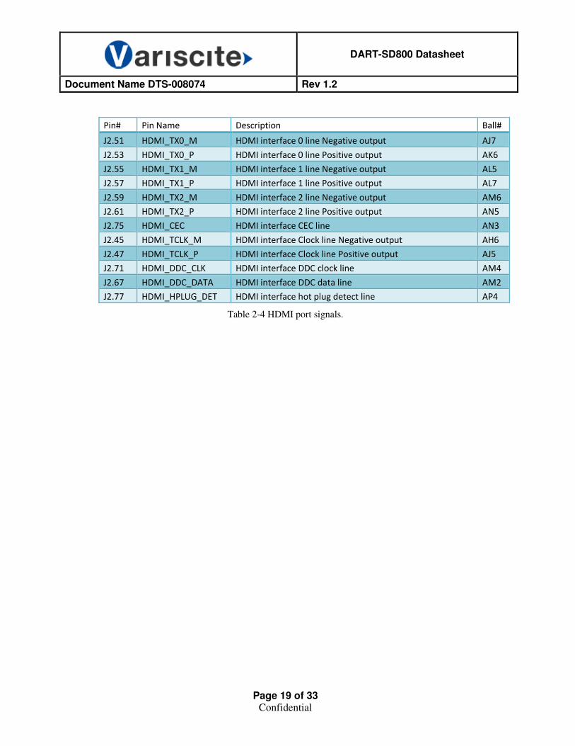
Pin# Pin Name Description Ball#
J2.51 HDMI_TX0_M HDMI interface 0 line Negative output AJ7
J2.53 HDMI_TX0_P HDMI interface 0 line Positive output AK6
J2.55 HDMI_TX1_M HDMI interface 1 line Negative output AL5
J2.57 HDMI_TX1_P HDMI interface 1 line Positive output AL7
J2.59 HDMI_TX2_M HDMI interface 2 line Negative output AM6
J2.61 HDMI_TX2_P HDMI interface 2 line Positive output AN5
J2.75 HDMI_CEC HDMI interface CEC line AN3
J2.45 HDMI_TCLK_M HDMI interface Clock line Negative output AH6
J2.47 HDMI_TCLK_P HDMI interface Clock line Positive output AJ5
J2.71 HDMI_DDC_CLK HDMI interface DDC clock line AM4
J2.67 HDMI_DDC_DATA HDMI interface DDC data line AM2
J2.77 HDMI_HPLUG_DET HDMI interface hot plug detect line AP4
Table 2-4 HDMI port signals.

DART-SD800 Datasheet
Rev 1.2 Document Name DTS-008074
Page 20 of 33 Confidential
2.2.2. MIPI CSI2 Camera ports
The SOM exposes 2 four lanes MIPI CSI2 camera interface ports with following
capabilities:
• Two 4-lane at 4 + 4 lanes; 1.5 Gbps per lane
• 2D performance - 32 MP at 15 fps; 16 MP at 30 fps
• Pixel manipulations, camera modes, image effects, and post- processing techniques,
including defective pixel correction
• VFE raw dump of CSI data at line rate to LPDDR3
• SMIA++ support
• I2C controls
Pin# Pin Name Description Ball#
J2.17 MIPI_CSI0_LN0_N MIPI CSI2 Camera interface 0 line 0 Negative W3
J2.19 MIPI_CSI0_LN0_P MIPI CSI2 Camera interface 0 line 0 Positive Y4
J2.13 MIPI_CSI0_LN1_N MIPI CSI2 Camera interface 0 line 1 Negative V2
J2.15 MIPI_CSI0_LN1_P MIPI CSI2 Camera interface 0 line 1 Positive V4
J2.9 MIPI_CSI0_LN2_N MIPI CSI2 Camera interface 0 line 2 Negative V6
J2.11 MIPI_CSI0_LN2_P MIPI CSI2 Camera interface 0 line 2 Positive W5
J2.5 MIPI_CSI0_LN3_N MIPI CSI2 Camera interface 0 line 3 Negative T6
J2.7 MIPI_CSI0_LN3_P MIPI CSI2 Camera interface 0 line 3 Positive U5
J2.1 MIPI_CSI0_LN4_N MIPI CSI2 Camera interface 0 line 4 Negative U1
J2.3 MIPI_CSI0_LN4_P MIPI CSI2 Camera interface 0 line 4 Positive U3
J1.6 CAM_MCLK0 MIPI CSI2 Camera interface 0 ref clock output C7
Table 2-5 MIPI CSI2 Camera port 0 signals.
Pin# Pin Name Description Ball#
J2.42 MIPI_CSI1_LN0_N MIPI CSI2 Camera interface 1 line 0 Negative AB6
J2.44 MIPI_CSI1_LN0_P MIPI CSI2 Camera interface 1 line 0 Positive AC5
J2.38 MIPI_CSI1_LN1_N MIPI CSI2 Camera interface 1 line 1 Negative AB2
J2.40 MIPI_CSI1_LN1_P MIPI CSI2 Camera interface 1 line 1 Positive AB4
J2.34 MIPI_CSI1_LN2_N MIPI CSI2 Camera interface 1 line 2 Negative AA1
J2.36 MIPI_CSI1_LN2_P MIPI CSI2 Camera interface 1 line 2 Positive AA3
J2.30 MIPI_CSI1_LN3_N MIPI CSI2 Camera interface 1 line 3 Negative AA5
J2.32 MIPI_CSI1_LN3_P MIPI CSI2 Camera interface 1 line 3 Positive AA7
J2.26 MIPI_CSI1_LN4_N MIPI CSI2 Camera interface 1 line 4 Negative W7
J2.28 MIPI_CSI1_LN4_P MIPI CSI2 Camera interface 1 line 4 Positive Y6
J1.2 CAM_MCLK1 MIPI CSI2 Camera interface 1 ref clock output A7
Table 2-6 MIPI CSI2 Camera port 1 signals.

DART-SD800 Datasheet
Rev 1.2 Document Name DTS-008074
Page 21 of 33 Confidential
In addition to the signal lines the SOM exposes two dedicated I2C channels for camera
control.
Pin# Pin Name Description Ball#
J1.54 CCI_I2C0_SCL Camera 0 I2C interface clock line E11
J1.56 CCI_I2C0_SDA Camera 0 I2C interface data line F12
J1.50 CCI_I2C1_SCL Camera 1 I2C interface clock line D10
J1.52 CCI_I2C1_SDA Camera 1 I2C interface data line G15
Table 2-7 Dedicated I2C for camera control signals.
2.2.3. Digital Audio I2S port
Pin# Pin Name Description Ball#
J3.27 MI2S_1_SCLK I2S digital audio interface Clock line G47
J3.23 MI2S_1_D0 I2S digital audio interface D0 line H46
J3.21 MI2S_1_D1 I2S digital audio interface D1 line H48
J3.29 MI2S_1_MCLK I2S digital audio interface Master Clock line D48
J3.25 MI2S_1_WS I2S digital audio interface WS line F48
Table 2-8 Digital Audio I2S port signals.
2.2.4. USB ports
The SOM exposes the following USB interfaces:
• Two USB – one USB 2.0 high-speed and one USB 3.0 super-speed/USB 2.0
high-speed compliant, one OTG compatible
• One HSIC port - Dual-voltage (1.2/1.8)
Pin# Pin Name Description Ball#
J2.4 USB_HS1_DM USB interface 1 data Negative line G3
J2.2 USB_HS1_DP USB interface 1 data Positive line F4
J2.70 USB_HS1_VBUS USB interface 1 VBUS input D6
J2.72 USB_VBUS_PROT
USB interface VBUS output line protected from
overvoltage E7
J2.50 USB_HS_ID USB interface ID line R7
Table 2-9 USB2.0 port 1 signals.

DART-SD800 Datasheet
Rev 1.2 Document Name DTS-008074
Page 22 of 33 Confidential
Pin# Pin Name Description Ball#
J2.20 USB_HS2_DM USB interface 2 data Negative line N7
J2.22 USB_HS2_DP USB interface 2 data Positive line P6
J2.50 USB_HS_ID USB interface ID line R7
J2.48 USB_HS2_VBUS USB interface 2 VBUS input line N1
Table 2-10 USB2.0 port 2 signals (OTG compatible).
Pin# Pin Name Description Ball#
J2.8 USB_SS_RX0_M Super Speed USB interface RX Negative line G7
J2.10 USB_SS_RX0_P Super Speed USB interface RX Positive line H6
J2.14 USB_SS_TX0_M Super Speed USB interface TX Negative line J7
J2.16 USB_SS_TX0_P Super Speed USB interface TX Positive line K6
Table 2-11 USB3.0 Super Speed port signals.
Pin# Pin Name Description Ball#
J1.14 HSIC_DATA HSIC interface data line C9
J1.16 HSIC_STROBE HSIC interface strobe line F10
Table 2-12 HSIC bus signals.
2.2.4.1. USB_VBUS_PROT pin description
On the SOM the charger is disconnected from the USB port and it can be used in two
ways: As a standalone charger or as a charger that is connected to USB1 port. The
maximum allowable voltage of USB_HS1_VBUS pin is lower than maximum
operating voltage of the charger. So the pin USB_HS1_VBUS pin should be protected
from high voltages. The solution is to use USB_VBUS_PROT pin. There is
overvoltage protection circuit on SOM, its input connected to USB_CHRGR_IN power
and output is enabled only when the voltage on USB_CHRGR_IN pins is in acceptable
for USB_HS1_VBUS. So in systems that are using OTG port for charging the OTG
connector Pin #1 should be connected to USB_CHRGR_IN pins and
USB_VBUS_PROT pin should be connected to USB_HS1_VBUS pin of the SOM.
2.2.5. SD Card port
The SOM exposes one SD Card interface for connecting external memory device or
SD card jack.
Pin# Pin Name Description Ball#
J3.47 SDC2_CLK External SD card clock output T48
J3.51 SDC2_CMD External SD card Command line U45

DART-SD800 Datasheet
Rev 1.2 Document Name DTS-008074
Page 23 of 33 Confidential
Pin# Pin Name Description Ball#
J3.59 SDC2_DATA_0 External SD card Data 0 line T50
J3.57 SDC2_DATA_1 External SD card Data 1 line V46
J3.55 SDC2_DATA_2 External SD card Data 2 line P46
J3.53 SDC2_DATA_3 External SD card Data 3 line R47
J3.43 SD_CARD_DET_N SD card detect line active low D38
Table 2-13 SD Card signals.

DART-SD800 Datasheet
Rev 1.2 Document Name DTS-008074
Page 24 of 33 Confidential
2.2.6. Audio Ports
The SOM has onboard Audio codec based on WCD9320 chip.
The following features are exposed:
• 2 analog pre-biased, single ended microphones.
Microphones support DC measurements (bypass Tx front-end)
Programmable input gain: 0, 6, 12, and 18 dB
Cap less (DC-coupled, legacy mode not supported); fixed Z regardless of gain
IEC ESD protection both inputs
• One single-ended input for multi-button headset control
• Four single-ended line outputs; 600 O; ground referenced, 1 Vrms output
• Class-H differential earpiece output, 10.67Ω to 32Ω, 125 mW into 32Ω; 150 mW into
16 or 10.67Ω
• Six Digital Microphones; three clock lines; nine supported frequencies
Pin# Pin Name Description Ball#
J3.6 DMIC1_CLK Digital microphone 1 clock output WCD9320.11
J3.8 DMIC1_DATA Digital microphone 1 data input WCD9320.17
J3.10 DMIC2_CLK Digital microphone 2 clock output WCD9320.23
J3.12 DMIC2_DATA Digital microphone 2 data input WCD9320.30
J3.22 MBHC_HSDET Headset detect line WCD9320.31
J3.2 DMIC0_CLK Digital microphone 0 clock output WCD9320.36
J3.4 DMIC0_DATA Digital microphone 0 data input WCD9320.42
J3.14 MIC2_INP MiC2 input positive WCD9320.50
J3.20 MIC4_INN MiC4 input negative WCD9320.56
J3.18 MIC4_INP MiC4 input positive WCD9320.62
J3.28 HPH_REF
Headset Reference ground (should be
connected to DGND near headset connector) WCD9320.65
J3.16 MIC2_INN MiC2 input negative WCD9320.68
J3.3 LINE_OUT2 Line out 2 output WCD9320.69
J3.7 LINE_OUT4 Line out 4 output WCD9320.70
J3.5 LINE_OUT3 Line out 3 output WCD9320.75
J3.24 HPH_LP Headset left positive WCD9320.77
J3.1 LINE_OUT1 Line out 1 output WCD9320.80
J3.26 HPH_RM Headset right negative WCD9320.82
Table 2-14 Audio signals.

DART-SD800 Datasheet
Rev 1.2 Document Name DTS-008074
Page 25 of 33 Confidential
2.2.7. PMIC GPIO ports
The SOM exposes 7 PMIC GPIO ports to use as GPIO/PWM/CLOCK sources.
Pin# Pin Name Description Ball#
J2.39 PM8941_GPIO_13 PMIC GPIO 13 PM8941.157
J2.37 PM8941_GPIO_29 PMIC GPIO 29 PM8941.159
J2.35 PM8941_GPIO_17 PMIC GPIO 17 PM8941.165
J2.33 PM8941_GPIO_32 PMIC GPIO 32 PM8941.166
J2.65 KEY_VOLP_N Volume UP key PM8941.61
J2.41 PM8941_GPIO_08 PMIC GPIO 08 PM8941.94
Table 2-15 PMIC GPIO signals.
2.2.8. BLSP ports
The SOM exposes 8 BLSP ports each 4 bit width. Each bit can be configured to one of
the following features: Option Configuration BLSP bit 3 BLSP bit 2 BLSP bit 1 BLSP bit 0
BLSP1 GPIO pins BLSP2 GPIO pins BLSP3 GPIO pins BLSP6 GPIO pins BLSP8 GPIO pins BLSP10 GPIO pins BLSP11 GPIO pins BLSP12 GPIO pins
GPIO_0 GPIO_4 GPIO_8 GPIO_27 GPIO_45 GPIO_53 GPIO_81 GPIO_85
GPIO_1 GPIO_5 GPIO_9 GPIO_28 GPIO_46 GPIO_54 GPIO_82 GPIO_86
GPIO_2 GPIO_6 GPIO_10 GPIO_29 GPIO_47 GPIO_55 GPIO_83 GPIO_87
GPIO_3 GPIO_7 GPIO_11 GPIO_30 GPIO_48 GPIO_56 GPIO_84 GPIO_88
1 4-pin UART UART_TX DO 4-pin UART transmit data
UART_RX DI 4-pin UART receive data
UART_CTS_N DI 4-pin UART clear-to-send
UART_RFR_N DO 4-pin UART ready-for-receive
2 2-pin UART + 2-pin I2C
UART_TX DO 2-pin UART transmit data
UART_RX DI 2-pin UART receive data
I2C_SDA B I2C serial data
I2C_SCL B I2C serial clock
3 2-pin UART + 2-GPIOs
UART_TX DO 2-pin UART transmit data
UART_RX DI 2-pin UART receive data
GPIO_XX B Configurable I/O
GPIO_XX B Configurable I/O
4 4-pin SPI SPI_DATA_MOSI B 4-pin SPI master out/slave in
SPI_DATA_MISO B 4-pin SPI master in/slave out
SPI_CS_N B 4-pin SPI chip select
SPI_CLK B 4-pin SPI clock
5 2-pin UIM + 2-pin I2C
UIM_DATA B UIM data
UIM_CLK DO UIM clock
I2C_SDA B I2C serial data
I2C_SCL B I2C serial clock
6 2-pin UIM + 2 GPIO
UIM_DATA B UIM data
UIM_CLK DO UIM clock
GPIO_XX B Configurable I/O
GPIO_XX B Configurable I/O
7 2-pin I2C + 2 GPIOs
GPIO_XX B Configurable I/O
GPIO_XX B Configurable I/O
I2C_SDA B I2C serial data
I2C_SCL B I2C serial clock
8 4 GPIOs GPIO_XX B Configurable I/O
GPIO_XX B Configurable I/O
GPIO_XX B Configurable I/O
GPIO_XX B Configurable I/O

DART-SD800 Datasheet
Rev 1.2 Document Name DTS-008074
Page 26 of 33 Confidential
Pin# Pin Name Description Ball#
J3.73 BLSP1_0 Low Speed Peripheral Interface 1 bit 0 BG13
J3.75 BLSP1_1 Low Speed Peripheral Interface 1 bit 1 BF12
J3.77 BLSP1_2 Low Speed Peripheral Interface 1 bit 2 BF14
J3.79 BLSP1_3 Low Speed Peripheral Interface 1 bit 3 BH12
J2.23 BLSP10_0 Low Speed Peripheral Interface 10 bit 0 A23
J2.25 BLSP10_1 Low Speed Peripheral Interface 10 bit 1 C23
J2.27 BLSP10_2 Low Speed Peripheral Interface 10 bit 2 D22
J2.29 BLSP10_3 Low Speed Peripheral Interface 10 bit 3 B22
J3.38 BLSP12_0 Low Speed Peripheral Interface 12 bit 0 H44
J3.36 BLSP12_1 Low Speed Peripheral Interface 12 bit 1 E47
J3.34 BLSP12_2 Low Speed Peripheral Interface 12 bit 2 D42
J3.32 BLSP12_3 Low Speed Peripheral Interface 12 bit 3 C41
J3.17 BLSP2_0 Low Speed Peripheral Interface 2 bit 0 (used for DEBUG UART) E31
J3.15 BLSP2_1 Low Speed Peripheral Interface 2 bit 1 (used for DEBUG UART) C31
J3.13 BLSP2_2 Low Speed Peripheral Interface 2 bit 2 (used for DEBUG UART) D30
J3.11 BLSP2_3 Low Speed Peripheral Interface 2 bit 3 (used for DEBUG UART) C29
J3.63 BLSP3_0 Low Speed Peripheral Interface 3 bit 0 BE11
J3.65 BLSP3_1 Low Speed Peripheral Interface 3 bit 1 BH10
J3.67 BLSP3_2 Low Speed Peripheral Interface 3 bit 2 BE13
J3.69 BLSP3_3 Low Speed Peripheral Interface 3 bit 3 BG11
J3.39 BLSP6_0 Low Speed Peripheral Interface 6 bit 0 G17
J3.37 BLSP6_1 Low Speed Peripheral Interface 6 bit 1 F16
J3.35 BLSP6_2 Low Speed Peripheral Interface 6 bit 2 E15
J3.33 BLSP6_3 Low Speed Peripheral Interface 6 bit 3 A11
J1.40 BLSP8_0 Low Speed Peripheral Interface 8 bit 0 C17
J1.42 BLSP8_1 Low Speed Peripheral Interface 8 bit 1 A15
J1.44 BLSP8_2 Low Speed Peripheral Interface 8 bit 2 B14
J1.46 BLSP8_3 Low Speed Peripheral Interface 8 bit 3 D16
J3.70 BLSP9_0 Low Speed Peripheral Interface 9 bit 0 AH50
J3.68 BLSP9_1 Low Speed Peripheral Interface 9 bit 1 AE47
J3.66 BLSP9_2 Low Speed Peripheral Interface 9 bit 2 AC49
J3.64 BLSP9_3 Low Speed Peripheral Interface 9 bit 3 AA49
Table 2-16 BLSP signals.
2.2.9. JTAG port
Pin# Pin Name Description Ball#
J3.50 JTAG_SRST_N JTAG interface SRST pin AM44

DART-SD800 Datasheet
Rev 1.2 Document Name DTS-008074
Page 27 of 33 Confidential
Pin# Pin Name Description Ball#
J3.42 JTAG_TCK JTAG interface TCK pin AG45
J3.44 JTAG_TDI JTAG interface TDI pin AL45
J3.52 JTAG_TDO JTAG interface TDO pin AP46
J3.48 JTAG_TMS JTAG interface TMS pin AK44
J3.46 JTAG_TRST_N JTAG interface TRST pin AJ45
J1.48 JTAG_PS_HOLD JTAG PS hold signal input to the SOM
Table 2-17 JTAG signals.
2.2.10. BOOT configuration
Normally the SOM gets its software code from on-SOM eMMC storage chip.
The boot process consists of SBL > LK boot loader > Android kernel.
The SBL part is preprogrammed by Variscite and customer does not have an access to
burning software or source code. The SBL code is programmed via USB or JTAG.
The programming mode is set by tying BOOT_USB pin to 1.8V.
The customer can use this pin as GPO only, or assure that this pin will be 0V on reset.
The LK boot loader have two parts: one is fast boot SW to re-flash the board and the
second is normal Android boot process. The board is preprogrammed with the running
LK boot loader by Variscite. The customer can change the LK boot loader and
reprogram it into the eMMC storage chip via fast boot. The fast boot mode is set by
tying the PM_RESIN_N pin to 0V. The customer can change this behavior, but the
initial programming should be done by tying PM_RESIN_N to 0V.
The pins BOOT_CFG0, BOOT_CFG1, BOOT_CFG2 are reserved to other boot
modes and should be used as GPO only.

DART-SD800 Datasheet
Rev 1.2 Document Name DTS-008074
Page 28 of 33 Confidential
2.2.11. Power
The SOM exposes battery connection and USB compatible charger.
Charger features:
• Fully integrated up to +28 V (integrated OVP FET)
• Supported battery technologies Lithium-ion, lithium-ion polymer
• Supported charging modes: Trickle, constant current and constant voltage modes.
More automated for less software interaction
• Integrated Battery MOSFET
• Charging current up to 2500mA
Pin# Pin Name Description Ball#
J1.4 DGND Digital Ground
J1.8 DGND Digital Ground
J1.12 DGND Digital Ground
J1.18 DGND Digital Ground
J1.24 DGND Digital Ground
J1.26 DGND Digital Ground
J1.28 DGND Digital Ground
J1.30 DGND Digital Ground
J1.32 DGND Digital Ground
J1.34 DGND Digital Ground
J1.36 DGND Digital Ground
J1.38 DGND Digital Ground
J1.57 DGND Digital Ground
J1.58 DGND Digital Ground
J1.63 DGND Digital Ground
J1.64 DGND Digital Ground
J2.6 DGND Digital Ground
J2.12 DGND Digital Ground
J2.18 DGND Digital Ground
J2.21 DGND Digital Ground
J2.24 DGND Digital Ground
J2.31 DGND Digital Ground
J2.43 DGND Digital Ground
J2.46 DGND Digital Ground
J2.49 DGND Digital Ground
J2.63 DGND Digital Ground
J2.69 DGND Digital Ground
J2.73 DGND Digital Ground
J2.80 DGND Digital Ground
J3.9 DGND Digital Ground

DART-SD800 Datasheet
Rev 1.2 Document Name DTS-008074
Page 29 of 33 Confidential
Pin# Pin Name Description Ball#
J3.19 DGND Digital Ground
J3.30 DGND Digital Ground
J3.31 DGND Digital Ground
J3.40 DGND Digital Ground
J3.41 DGND Digital Ground
J3.45 DGND Digital Ground
J3.49 DGND Digital Ground
J3.54 DGND Digital Ground
J3.61 DGND Digital Ground
J3.71 DGND Digital Ground
J3.72 DGND Digital Ground
J1.23 USB_CHRGR_IN Charger input power supply PM8941.172
J1.25 USB_CHRGR_IN Charger input power supply PM8941.172
J1.27 USB_CHRGR_IN Charger input power supply PM8941.172
J1.29 USB_CHRGR_IN Charger input power supply PM8941.172
J1.31 USB_CHRGR_IN Charger input power supply PM8941.172
J1.33 USB_CHRGR_IN Charger input power supply PM8941.172
J1.35 USB_CHRGR_IN Charger input power supply PM8941.172
J1.37 USB_CHRGR_IN Charger input power supply PM8941.172
J1.39 USB_CHRGR_IN Charger input power supply PM8941.172
J1.21 USB_CHRGR_IN Charger input power supply PM8941.172
J1.23 USB_CHRGR_IN Charger input power supply PM8941.172
J1.25 USB_CHRGR_IN Charger input power supply PM8941.172
J1.27 USB_CHRGR_IN Charger input power supply PM8941.172
J1.29 USB_CHRGR_IN Charger input power supply PM8941.172
J1.31 USB_CHRGR_IN Charger input power supply PM8941.172
J1.33 USB_CHRGR_IN Charger input power supply PM8941.172
J1.35 USB_CHRGR_IN Charger input power supply PM8941.172
J1.37 USB_CHRGR_IN Charger input power supply PM8941.172
J1.39 USB_CHRGR_IN Charger input power supply PM8941.172
J1.1 VBAT Main battery supply in (3.2V to 4.5V) PM8941.214
J1.3 VBAT Main battery supply in (3.2V to 4.5V) PM8941.214
J1.5 VBAT Main battery supply in (3.2V to 4.5V) PM8941.214
J1.7 VBAT Main battery supply in (3.2V to 4.5V) PM8941.214
J1.9 VBAT Main battery supply in (3.2V to 4.5V) PM8941.214
J1.11 VBAT Main battery supply in (3.2V to 4.5V) PM8941.214
J1.13 VBAT Main battery supply in (3.2V to 4.5V) PM8941.214
J1.15 VBAT Main battery supply in (3.2V to 4.5V) PM8941.214
J1.17 VBAT Main battery supply in (3.2V to 4.5V) PM8941.214

DART-SD800 Datasheet
Rev 1.2 Document Name DTS-008074
Page 30 of 33 Confidential
Pin# Pin Name Description Ball#
J1.19 VBAT Main battery supply in (3.2V to 4.5V) PM8941.214
J2.52 VCC_S1V8 1.8V power supply output
J2.54 VCC_S1V8 1.8V power supply output
J2.56 VCC_S1V8 1.8V power supply output
J2.58 VCC_S1V8 1.8V power supply output
J1.54 VREG_L17_2P85 2.80V power supply for CSI camera PM8941.151
J1.56 VREG_L18_2P85 2.85V power supply for CSI camera PM8941.6
J1.50 VREG_L21_2P95 2.95V SD card power supply PM8941.89
J1.52 VREG_L21_2P95 2.95V SD card power supply PM8941.89
J3.56 VCC_3V3 3.3V power supply output
J3.58 VCC_3V3 3.3V power supply output
J3.60 VCC_3V3 3.3V power supply output
J3.62 VCC_3V3 3.3V power supply output
J1.41 VREG_OTG 5V power supply output PM8941.8
J1.43 VREG_OTG 5V power supply output PM8941.8
J1.45 VREG_OTG 5V power supply output PM8941.8
J1.47 VREG_OTG 5V power supply output PM8941.8
J1.49 VPH_PWR Peripheral power output. Battery voltage PM8941.198
J1.51 VPH_PWR Peripheral power output. Battery voltage PM8941.198
J1.53 VPH_PWR Peripheral power output. Battery voltage PM8941.198
J1.55 VPH_PWR Peripheral power output. Battery voltage PM8941.198
J2.68 VRTC RTC clock battery supply in PM8941.63
Table 2-18 Power pins.
2.2.12. Wi-Fi & Bluetooth
The SOM include QCA6234 Integrated Dual-Band 802.11 a/b/g/n WLAN + Bluetooth 4.0,
Class 1.5 Module optimized for low-power.
The QCA6234 integrates the complete transmit/receive RF paths including baluns, switches,
and reference oscillator. The device is also pre-calibrated, eliminating the need for customer
production calibration.
Near zero power consumption in idle and stand-by enables users to leave WLAN and BT
"always on."

DART-SD800 Datasheet
Rev 1.2 Document Name DTS-008074
Page 31 of 33 Confidential
3. Electrical specifications
3.1. Absolute maximum ratings
Parameter Min Max Unit
VBAT Battery supply input voltage -0.5 6.0 V
VCHRG Charger supply input voltage -2 30 V
VPH_PWR VPH supply input voltage -0.5 6.0 V
VRTC RTC supply input voltage -0.5 3.5 V
USB_HS1_VBUS USB1 VBUS input voltage -0.5 6.0 V
USB_HS2_VBUS USB2 VBUS input voltage -0.5 6.0 V
Table 3-1 Absolute maximum ratings.
3.2. Operating conditions
Parameter Min Typ Max Unit
VBAT Battery supply input voltage 3.2 3.6 4.5 V
VCHRG Charger supply input voltage 4.35 5.0 10 V
VPH_PWR VPH supply input voltage 3.2 3.6 4.5 V
VRTC RTC supply input voltage 2.0 3.0 3.3 V
USB_HS1_VBUS USB1 VBUS input voltage 2.0 5.0 5.25 V
USB_HS2_VBUS USB2 VBUS input voltage 2.0 5.0 5.25 V
Table 3-2 Operating conditions.
3.3. Power supplies output ratings
Parameter Min Typ Max Unit
VPH_PWR VPH supply output voltage
Charger not connected
VBAT1 4.2 V
VPH_PWR VPH supply output voltage
Charger not connected
VCHRG1 – 4.2 V
VPH_PWR VPH supply output current – – 1000 mA
VCC_3V3 3.3V buck power supply voltage VBAT1 3.3 – V
VCC_3V3 3.3V buck power supply current – 500 mA
VREG_OTG 5V boost power supply voltage – 5.0 – V
VREG_OTG 5V boost power supply current – – 550 mA
VREG_L17_2P85 2.80V L17 LDO voltage 2.7 2.80 3.3 V
VREG_L17_2P85 2.80V L17 LDO current – – 300 mA

DART-SD800 Datasheet
Rev 1.2 Document Name DTS-008074
Page 32 of 33 Confidential
VREG_L18_2P85 2.85V L18 LDO voltage 2.4 2.85 3.3 V
VREG_L18_2P85 2.85V L18 LDO current – – 300 mA
VREG_L21_2P95 2.95V L21 LDO voltage 2.75 2.95 3.00 V
VREG_L21_2P95 2. 95V L21 LDO current – – 600 mA
VCC_S1V8 1.8V buck power supply voltage – 1.8 – V
VCC_S1V8 1.8V buck power supply current – – 500 mA
Table 3-3 Power supplies output ratings.
3.4. Digital IO characteristics
Parameter Comments Min Max Unit
VIH High-level input voltage CMOS/Schmitt 1.17 2.1 V
VIL Low-level input voltage CMOS/Schmitt -0.3 0.63 V
VSHYS Schmitt hysteresis voltage 100 – mV
IIH Input high leakage current No pull-down – 1 µA
IIL Input low leakage current No pull-up -1 – µA
IIHPD Input high leakage current With pull-down 5 30 µA
IILPU Input low leakage current With pull-up -30 5 µA
VOH High-level output voltage CMOS, at rated drive strength 2.25 1.8 V
VOL Low-level output voltage CMOS, at rated drive strength 0 0.45 V
IOZH Tri-state leakage current Logic high out, no pull-down – 1 µA
IOZL Tri-state leakage current Logic low out, no pull-up -1 – µA
IOZHPD Tri-state leakage current Logic high out with pull-down 5
(390k)
30
(55k) µA
Ω
IOZLPU Tri-state leakage current Logic low out with pull-up -30
(55k)
-5
(390k) µA
Ω
IOZHKP Tri-state leakage current Logic high out with keeper -15
(30k)
-3
(150k) µA
Ω
IOZLKP Tri-state leakage current Logic low out with keeper 3
(150k)
15
(30k)
µA
Ω
CIN Input capacitance – 2 pF
Table 3-4 Digital IO characteristics.

DART-SD800 Datasheet
Rev 1.2 Document Name DTS-008074
Page 33 of 33 Confidential
4. Mechanical
4.1. The SOM board mounting to the Carrier board
The SOM has 4 mounting holes for mounting it to the carrier board. The holes plated inside and connected to GND.
4.2. Drawings of mounting the SOM board.
Figure 4-1 SOM Mechanical view