CY14C064PA, CY14B064PA, CY14E064PA, 64-Kbit (8 K × 8 ...
45
www.infineon.com Please note that Cypress is an Infineon Technologies Company. The document following this cover page is marked as “Cypress” document as this is the company that originally developed the product. Please note that Infineon will continue to offer the product to new and existing customers as part of the Infineon product portfolio. Continuity of document content The fact that Infineon offers the following product as part of the Infineon product portfolio does not lead to any changes to this document. Future revisions will occur when appropriate, and any changes will be set out on the document history page. Continuity of ordering part numbers Infineon continues to support existing part numbers. Please continue to use the ordering part numbers listed in the datasheet for ordering.
-
Upload
khangminh22 -
Category
Documents
-
view
2 -
download
0
Transcript of CY14C064PA, CY14B064PA, CY14E064PA, 64-Kbit (8 K × 8 ...

www.infineon.com
Please note that Cypress is an Infineon Technologies Company.The document following this cover page is marked as “Cypress” document as this is the company that originally developed the product. Please note that Infineon will continue to offer the product to new and existing customers as part of the Infineon product portfolio.
Continuity of document contentThe fact that Infineon offers the following product as part of the Infineon product portfolio does not lead to any changes to this document. Future revisions will occur when appropriate, and any changes will be set out on the document history page.
Continuity of ordering part numbersInfineon continues to support existing part numbers. Please continue to use the ordering part numbers listed in the datasheet for ordering.
CY14C064PACY14B064PACY14E064PA
64-Kbit (8 K × 8) SPI nvSRAM with Real Time Clock
Cypress Semiconductor Corporation • 198 Champion Court • San Jose, CA 95134-1709 • 408-943-2600Document Number: 001-68249 Rev. *H Revised January 16, 2018
64-Kbit (8 K × 8) SPI nvSRAM with Real Time Clock
Features
■ 64-Kbit nonvolatile static random access memory (nvSRAM) ❐ Internally organized as 8 K × 8 ❐ STORE to QuantumTrap nonvolatile elements initiated
automatically on power-down (AutoStore) or by using SPIinstruction (Software STORE) or HSB pin (HardwareSTORE)
❐ RECALL to SRAM initiated on power-up (Power Up RECALL)or by SPI instruction (Software RECALL)
❐ Automatic STORE on power-down with a small capacitor■ High reliability
❐ Infinite read, write, and RECALL cycles❐ 1 million STORE cycles to QuantumTrap❐ Data retention: 20 years at 85C
■ Real time clock (RTC)❐ Full-featured RTC❐ Watchdog timer❐ Clock alarm with programmable interrupts❐ Backup power fail indication❐ Square wave output with programmable frequency (1 Hz,
512 Hz, 4096 Hz, 32.768 kHz)❐ Capacitor or battery backup for RTC❐ Backup current of 0.45 A (typical)
■ 40 MHz, and 104 MHz High-speed serial peripheral interface(SPI)❐ 40 MHz clock rate SPI write and read with zero cycle delay❐ 104 MHz clock rate SPI write and read (with special fast read
instructions) ❐ Supports SPI mode 0 (0,0) and mode 3 (1,1)
■ SPI access to special functions❐ Nonvolatile STORE/RECALL ❐ 8-byte serial number❐ Manufacturer ID and Product ID❐ Sleep mode
■ Write protection❐ Hardware protection using Write Protect (WP) pin❐ Software protection using Write Disable instruction❐ Software block protection for 1/4, 1/2, or entire array
■ Low power consumption❐ Average active current of 3 mA at 40 MHz operation❐ Average standby mode current of 250 A ❐ Sleep mode current of 8 A
■ Industry standard configurations❐ Operating voltages:
• CY14C064PA : VCC = 2.4 V to 2.6 V • CY14B064PA : VCC = 2.7 V to 3.6 V • CY14E064PA : VCC = 4.5 V to 5.5 V
❐ Industrial temperature❐ 16-pin small outline integrated circuit (SOIC) package❐ Restriction of hazardous substances (RoHS) compliant
Overview
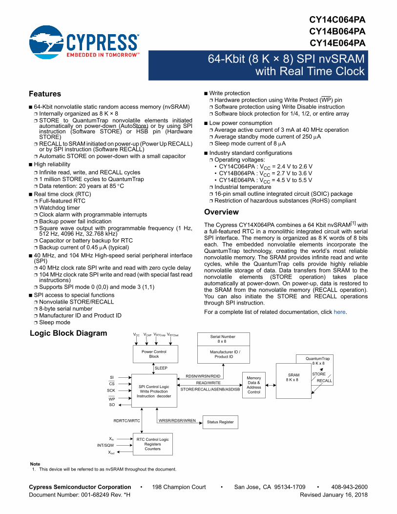
The Cypress CY14X064PA combines a 64 Kbit nvSRAM[1] witha full-featured RTC in a monolithic integrated circuit with serialSPI interface. The memory is organized as 8 K words of 8 bitseach. The embedded nonvolatile elements incorporate theQuantumTrap technology, creating the world’s most reliablenonvolatile memory. The SRAM provides infinite read and writecycles, while the QuantumTrap cells provide highly reliablenonvolatile storage of data. Data transfers from SRAM to thenonvolatile elements (STORE operation) takes placeautomatically at power-down. On power-up, data is restored tothe SRAM from the nonvolatile memory (RECALL operation).You can also initiate the STORE and RECALL operationsthrough SPI instruction.
For a complete list of related documentation, click here.
Note1. This device will be referred to as nvSRAM throughout the document.
Memory Data &
Address Control
Manufacturer ID /Product ID
SPI Control LogicWrite Protection
Instruction decoder
Power Control Block
RDSN/WRSN/RDID
Serial Number8 x 8
QuantumTrap8 K x 8
SRAM8 K x 8
STORESICS
SCK
WP
VCC VCAP
RECALL
RTC Control LogicRegistersCounters
INT/SQW
Xin
Xout
VRTCcap
READ/WRITE
Status RegisterWRSR/RDSR/WREN
STORE/RECALL/ASENB/ASDISB
RDRTC/WRTC
VRTCbat
SO
SLEEP
Logic Block Diagram
Document Number: 001-68249 Rev. *H Page 2 of 44
CY14C064PACY14B064PACY14E064PA
Contents
Pinout ................................................................................ 3Pin Definitions .................................................................. 3Device Operation .............................................................. 4
SRAM Write ................................................................. 4SRAM Read ................................................................ 4STORE Operation ....................................................... 4AutoStore Operation .................................................... 4Software STORE Operation ........................................ 5Hardware STORE and HSB pin Operation ................. 5RECALL Operation ...................................................... 5Hardware RECALL (Power Up) ................................... 5Software RECALL ....................................................... 5Disabling and Enabling AutoStore ............................... 5
Serial Peripheral Interface ............................................... 6SPI Overview ............................................................... 6
SPI Modes ......................................................................... 7SPI Operating Features .................................................... 8
Power-Up .................................................................... 8Power Down ................................................................ 8Active Power and Standby Power Modes ................... 8
SPI Functional Description .............................................. 9Status Register ............................................................... 10
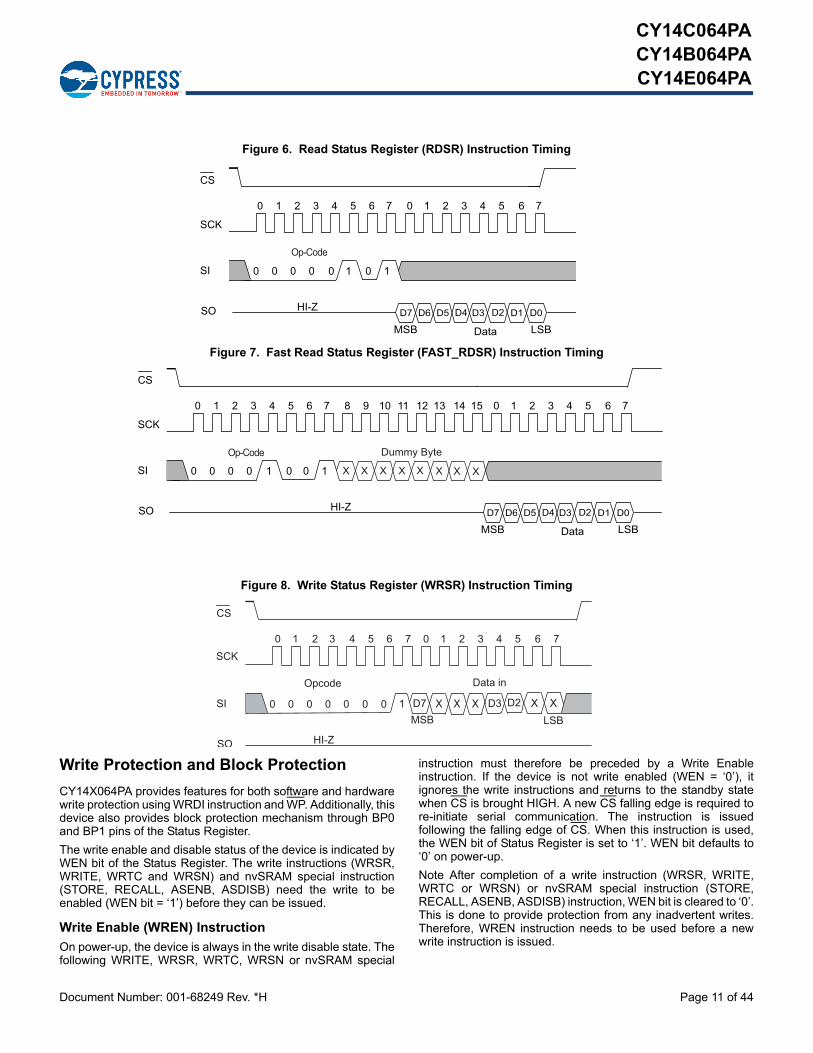
Read Status Register (RDSR) Instruction ................. 10Fast Read Status Register (FAST_RDSR) Instruction ......................................... 10Write Status Register (WRSR) Instruction ................ 10
Write Protection and Block Protection ......................... 11Write Enable (WREN) Instruction .............................. 11Write Disable (WRDI) Instruction .............................. 12Block Protection ........................................................ 12Hardware Write Protection (WP Pin) ......................... 12
Memory Access .............................................................. 12Read Sequence (READ) Instruction .......................... 12Fast Read Sequence (FAST_READ) Instruction ...... 12Write Sequence (WRITE) Instruction ........................ 13
RTC Access .....................................................................15READ RTC (RDRTC) Instruction .............................. 15Fast Read Sequence (FAST_RDRTC) Instruction .... 15WRITE RTC (WRTC) Instruction ............................... 16
nvSRAM Special Instructions ........................................ 17Software STORE (STORE) Instruction ..................... 17Software RECALL (RECALL) Instruction .................. 17AutoStore Enable (ASENB) Instruction ..................... 17AutoStore Disable (ASDISB) Instruction ................... 17
Special Instructions .......................................................17SLEEP Instruction ..................................................... 17
Serial Number ................................................................. 18WRSN (Serial Number Write) Instruction .................. 18RDSN (Serial Number Read) Instruction ................... 19FAST_RDSN (Fast Serial Number Read) Instruction ...................... 19
Device ID ......................................................................... 20
RDID (Device ID Read) Instruction ........................... 20FAST_RDID (Fast Device ID Read) Instruction ........ 21HOLD Pin Operation ................................................. 21
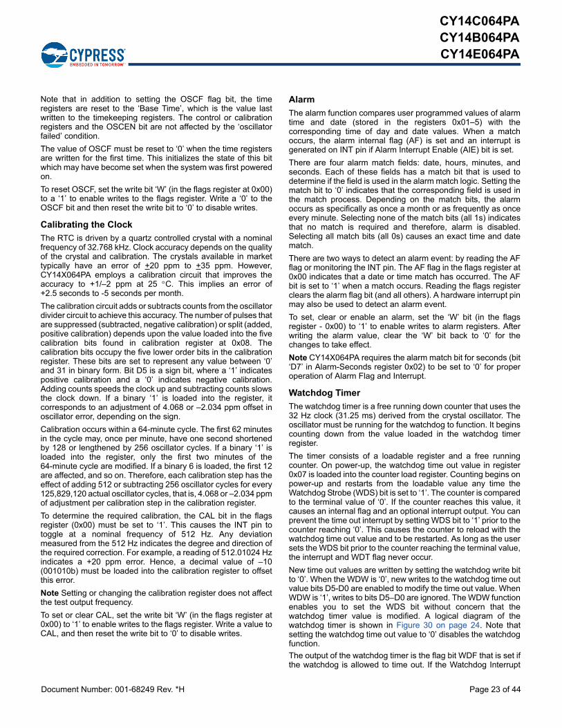
Real Time Clock Operation ............................................ 22nvTIME Operation ..................................................... 22Clock Operations ....................................................... 22Reading the Clock ..................................................... 22Setting the Clock ....................................................... 22Backup Power ........................................................... 22Stopping and Starting the Oscillator .......................... 22Calibrating the Clock ................................................. 23Alarm ......................................................................... 23Watchdog Timer ........................................................ 23Programmable Square Wave Generator ................... 24Power Monitor ........................................................... 24Backup Power Monitor .............................................. 24Interrupts ................................................................... 24Interrupt Register ....................................................... 24Flags Register ........................................................... 25RTC External Components ....................................... 26
PCB Design Considerations for RTC ............................ 27Layout requirements .................................................. 27
Maximum Ratings ........................................................... 32Operating Range ............................................................. 32DC Electrical Characteristics ........................................ 32Data Retention and Endurance ..................................... 33Capacitance .................................................................... 33Thermal Resistance ........................................................ 33AC Test Loads and Waveforms ..................................... 34AC Test Conditions ........................................................ 34RTC Characteristics ....................................................... 35AC Switching Characteristics ....................................... 35Switching Waveforms .................................................... 36AutoStore or Power-Up RECALL .................................. 37Switching Waveforms .................................................... 37Software Controlled STORE/RECALL Cycles .............. 38Switching Waveforms .................................................... 38Hardware STORE Cycle ................................................. 39Switching Waveforms .................................................... 39Ordering Information ...................................................... 40
Ordering Code Definitions ......................................... 40Package Diagram ............................................................ 41Acronyms ........................................................................ 42Document Conventions ................................................. 42
Units of Measure ....................................................... 42Document History Page ................................................. 43Sales, Solutions, and Legal Information ...................... 44
Worldwide Sales and Design Support ....................... 44Products .................................................................... 44PSoC® Solutions ...................................................... 44Cypress Developer Community ................................. 44Technical Support ..................................................... 44
Document Number: 001-68249 Rev. *H Page 3 of 44
CY14C064PACY14B064PACY14E064PA
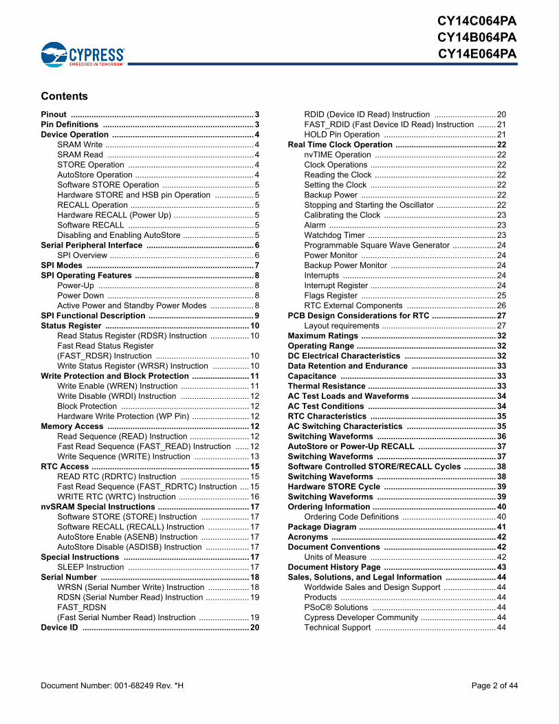
PinoutFigure 1. 16-pin SOIC pinout
INT/SQW
WP
VCAP
1
2
3
4
5
6
7
8 9
10
11
12
13
NC 16
15
14
VCC
SO
SI
SCK
CS
HSB
HOLD
Top View
not to scale
VRTCbat
Xout
Xin
VRTCcap
VSS
Pin Definitions
Pin Name I/O Type Description
CS Input Chip select: Activates the device when pulled LOW. Driving this pin HIGH puts the device in low powerstandby mode.
SCK Input Serial clock: Runs at speeds up to a maximum of fSCK. Serial input is latched at the rising edge of thisclock. Serial output is driven at the falling edge of the clock.
SI Input Serial input: Pin for input of all SPI instructions and data.
SO Output Serial output: Pin for output of data through SPI.
WP Input Write Protect: Implements hardware write protection in SPI.
HOLD Input HOLD pin: Suspends Serial Operation.
HSB Input/Output Hardware STORE Busy: Output: Indicates busy status of nvSRAM when LOW. After each Hardwareand Software STORE operation HSB is driven HIGH for a short time (tHHHD) with standard output highcurrent and then a weak internal pull-up resistor keeps this pin HIGH (external pull-up resistorconnection optional).Input: Hardware STORE implemented by pulling this pin LOW externally.
VCAP Power supply AutoStore capacitor. Supplies power to the nvSRAM during power loss to STORE data from the SRAMto nonvolatile elements. If AutoStore is not needed, this pin must be left as No Connect. It must neverbe connected to ground.
VRTCcap[2] Power supply Capacitor backup for RTC: Left unconnected if VRTCbat is used.
VRTCbat[2] Power supply Battery backup for RTC: Left unconnected if VRTCcap is used.
Xout[2] Output Crystal output connection
Xin[2] Input Crystal input connection
INT/SQW[2] Output Interrupt output/calibration/square wave. Programmable to respond to the clock alarm, the watchdog
timer, and the power monitor. Also programmable to either active HIGH (push or pull) or LOW (opendrain). In calibration mode, a 512 Hz square wave is driven out. In the square wave mode, you mayselect a frequency of 1 Hz, 512 Hz, 4,096 Hz, or 32,768 Hz to be used as a continuous output.
NC No connect No connect. This pin is not connected to the die.
VSS Power supply Ground
VCC Power supply Power supply
Note2. Left unconnected if RTC feature is not used.
Document Number: 001-68249 Rev. *H Page 4 of 44
CY14C064PACY14B064PACY14E064PA
Device Operation
CY14X064PA is a 64-Kbit serial (SPI) nvSRAM memory withintegrated RTC and SPI interface. All the reads and writes tonvSRAM happen to the SRAM, which gives nvSRAM the uniquecapability to handle infinite writes to the memory. The data inSRAM is secured by a STORE sequence that transfers the datain parallel to the nonvolatile QuantumTrap cells. A smallcapacitor (VCAP) is used to AutoStore the SRAM data innonvolatile cells when power goes down providing power-downdata security. The QuantumTrap nonvolatile elements built in thereliable SONOS technology make nvSRAM the ideal choice forsecure data storage.
In CY14X064PA, the 64-Kbit memory array is organized as 8 Kwords × 8 bits. The memory can be accessed through a standardSPI interface that enables very high clock speeds up to 40 MHzwith zero cycle delay read and write cycles. This nvSRAM chipalso supports 104 MHz SPI access speed with a specialinstruction for read operation. CY14X064PA supports SPImodes 0 and 3 (CPOL, CPHA = 0, 0 and 1, 1) and operates asSPI slave. The device is enabled using the Chip Select (CS) pinand accessed through Serial Input (SI), Serial Output (SO), andSerial Clock (SCK) pins.
CY14X064PA provides the feature for hardware and softwarewrite protection through the WP pin and WRDI instruction.CY14X064PA also provides mechanisms for block writeprotection (1/4, 1/2, or full array) using BP0 and BP1 pins in theStatus Register. Further, the HOLD pin is used to suspend anyserial communication without resetting the serial sequence.
CY14X064PA uses the standard SPI opcodes for memoryaccess. In addition to the general SPI instructions for read andwrite, CY14X064PA provides four special instructions that allowaccess to four nvSRAM specific functions: STORE, RECALL,AutoStore Disable (ASDISB), and AutoStore Enable (ASENB).
The major benefit of nvSRAM over serial EEPROMs is that allreads and writes to nvSRAM are performed at the speed of SPIbus with zero cycle delay. Therefore, no wait time is requiredafter any of the memory accesses. The STORE and RECALLoperations need finite time to complete and all memory accessesare inhibited during this time. While a STORE or RECALLoperation is in progress, the busy status of the device is indicatedby the Hardware STORE Busy (HSB) pin and also reflected onthe RDY bit of the Status Register.
SRAM Write
All writes to nvSRAM are carried out on the SRAM and do notuse up any endurance cycles of the nonvolatile memory. Thisallows you to perform infinite write operations. A write cycle isperformed through the WRITE instruction. The WRITEinstruction is issued through the SI pin of the nvSRAM andconsists of the WRITE opcode, two bytes of address, and onebyte of data. Write to nvSRAM is done at SPI bus speed with zerocycle delay.
CY14X064PA allows burst mode writes to be performed throughSPI. This enables write operations on consecutive addresseswithout issuing a new WRITE instruction. When the last addressin memory is reached in burst mode, the address rolls over to0x0000 and the device continues to write.
The SPI write cycle sequence is defined in the Memory Accesssection of SPI Protocol Description.
SRAM Read
A read cycle is performed at the SPI bus speed. The data is readout with zero cycle delay after the READ instruction is executed.READ instruction can be used upto 40 MHz clock speed. TheREAD instruction is issued through the SI pin of the nvSRAM andconsists of the READ opcode and two bytes of address. The datais read out on the SO pin.
Speed higher than 40 MHz (up to 104 MHz) requiresFAST_READ instruction. The FAST_READ instruction is issuedthrough the SI pin of the nvSRAM and consists of theFAST_READ opcode, two bytes of address, and one dummybyte. The data is read out on the SO pin.
CY14X064PA enables burst mode reads to be performedthrough SPI. This enables reads on consecutive addresseswithout issuing a new READ instruction. When the last addressin memory is reached in burst mode read, the address rolls overto 0x0000 and the device continues to read.
The SPI read cycle sequence is defined in the Memory Accesssection of SPI Protocol Description.
STORE Operation
STORE operation transfers the data from the SRAM to thenonvolatile QuantumTrap cells. The CY14X064PA STOREs datato the nonvolatile cells using one of the three STORE operations:AutoStore, activated on device power-down; Software STORE,activated by a STORE instruction; and Hardware STORE,activated by the HSB. During the STORE cycle, an erase of theprevious nonvolatile data is first performed, followed by aprogram of the nonvolatile elements. After a STORE cycle isinitiated, read/write to CY14X064PA is inhibited until the cycle iscompleted.
The HSB signal or the RDY bit in the Status Register can bemonitored by the system to detect if a STORE or SoftwareRECALL cycle is in progress. The busy status of nvSRAM isindicated by HSB being pulled LOW or RDY bit being set to ‘1’.To avoid unnecessary nonvolatile STOREs, AutoStore andHardware STORE operations are ignored unless at least onewrite operation has taken place since the most recent STORE orRECALL cycle. However, software initiated STORE cycles areperformed regardless of whether a write operation has takenplace.
AutoStore Operation
The AutoStore operation is a unique feature of nvSRAM whichautomatically stores the SRAM data to QuantumTrap cellsduring power-down. This STORE makes use of an externalcapacitor (VCAP) and enables the device to safely STORE thedata in the nonvolatile memory when power goes down.
During normal operation, the device draws current from VCC tocharge the capacitor connected to the VCAP pin. When thevoltage on the VCC pin drops below VSWITCH during power-down,the device inhibits all memory accesses to nvSRAM andautomatically performs a conditional STORE operation using thecharge from the VCAP capacitor. The AutoStore operation is notinitiated if no write cycle has been performed since last RECALL.
Note If a capacitor is not connected to VCAP pin, AutoStore mustbe disabled by issuing the AutoStore Disable instruction(AutoStore Disable (ASDISB) Instruction on page 17). IfAutoStore is enabled without a capacitor on the VCAP pin, thedevice attempts an AutoStore operation without sufficient charge
Document Number: 001-68249 Rev. *H Page 5 of 44
CY14C064PACY14B064PACY14E064PA
to complete the Store. This will corrupt the data stored innvSRAM, Status Register as well as the serial number and it willunlock the SNL bit. To resume normal functionality, the WRSRinstruction must be issued to update the nonvolatile bits BP0,BP1, and WPEN in the Status Register.
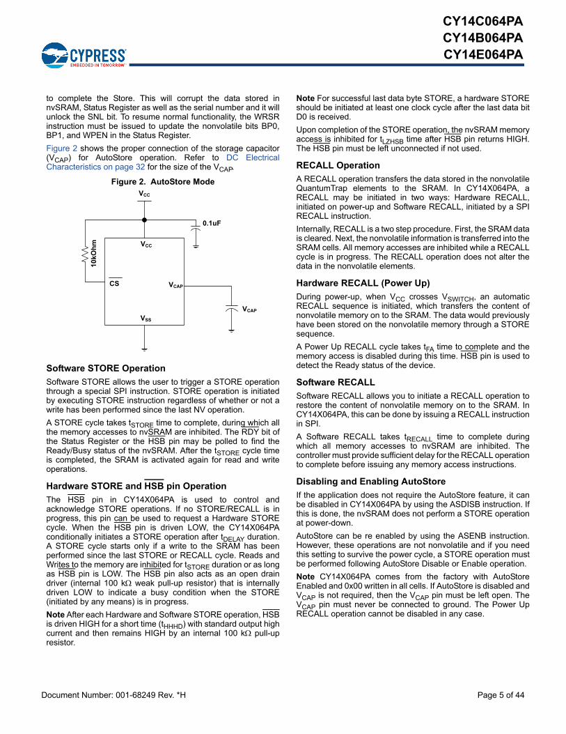
Figure 2 shows the proper connection of the storage capacitor(VCAP) for AutoStore operation. Refer to DC ElectricalCharacteristics on page 32 for the size of the VCAP.
Figure 2. AutoStore Mode
Software STORE Operation
Software STORE allows the user to trigger a STORE operationthrough a special SPI instruction. STORE operation is initiatedby executing STORE instruction regardless of whether or not awrite has been performed since the last NV operation.
A STORE cycle takes tSTORE time to complete, during which allthe memory accesses to nvSRAM are inhibited. The RDY bit ofthe Status Register or the HSB pin may be polled to find theReady/Busy status of the nvSRAM. After the tSTORE cycle timeis completed, the SRAM is activated again for read and writeoperations.
Hardware STORE and HSB pin Operation
The HSB pin in CY14X064PA is used to control andacknowledge STORE operations. If no STORE/RECALL is inprogress, this pin can be used to request a Hardware STOREcycle. When the HSB pin is driven LOW, the CY14X064PAconditionally initiates a STORE operation after tDELAY duration.A STORE cycle starts only if a write to the SRAM has beenperformed since the last STORE or RECALL cycle. Reads andWrites to the memory are inhibited for tSTORE duration or as longas HSB pin is LOW. The HSB pin also acts as an open draindriver (internal 100 k weak pull-up resistor) that is internallydriven LOW to indicate a busy condition when the STORE(initiated by any means) is in progress.
Note After each Hardware and Software STORE operation, HSBis driven HIGH for a short time (tHHHD) with standard output highcurrent and then remains HIGH by an internal 100 k pull-upresistor.
Note For successful last data byte STORE, a hardware STOREshould be initiated at least one clock cycle after the last data bitD0 is received.
Upon completion of the STORE operation, the nvSRAM memoryaccess is inhibited for tLZHSB time after HSB pin returns HIGH.The HSB pin must be left unconnected if not used.
RECALL Operation
A RECALL operation transfers the data stored in the nonvolatileQuantumTrap elements to the SRAM. In CY14X064PA, aRECALL may be initiated in two ways: Hardware RECALL,initiated on power-up and Software RECALL, initiated by a SPIRECALL instruction.
Internally, RECALL is a two step procedure. First, the SRAM datais cleared. Next, the nonvolatile information is transferred into theSRAM cells. All memory accesses are inhibited while a RECALLcycle is in progress. The RECALL operation does not alter thedata in the nonvolatile elements.
Hardware RECALL (Power Up)
During power-up, when VCC crosses VSWITCH, an automaticRECALL sequence is initiated, which transfers the content ofnonvolatile memory on to the SRAM. The data would previouslyhave been stored on the nonvolatile memory through a STOREsequence.
A Power Up RECALL cycle takes tFA time to complete and thememory access is disabled during this time. HSB pin is used todetect the Ready status of the device.
Software RECALL
Software RECALL allows you to initiate a RECALL operation torestore the content of nonvolatile memory on to the SRAM. InCY14X064PA, this can be done by issuing a RECALL instructionin SPI.
A Software RECALL takes tRECALL time to complete duringwhich all memory accesses to nvSRAM are inhibited. Thecontroller must provide sufficient delay for the RECALL operationto complete before issuing any memory access instructions.
Disabling and Enabling AutoStore
If the application does not require the AutoStore feature, it canbe disabled in CY14X064PA by using the ASDISB instruction. Ifthis is done, the nvSRAM does not perform a STORE operationat power-down.
AutoStore can be re enabled by using the ASENB instruction.However, these operations are not nonvolatile and if you needthis setting to survive the power cycle, a STORE operation mustbe performed following AutoStore Disable or Enable operation.
Note CY14X064PA comes from the factory with AutoStoreEnabled and 0x00 written in all cells. If AutoStore is disabled andVCAP is not required, then the VCAP pin must be left open. TheVCAP pin must never be connected to ground. The Power UpRECALL operation cannot be disabled in any case.
0.1uF
VCC
10kOhm
VCAP
CS VCAP
VSS
VCC

Document Number: 001-68249 Rev. *H Page 6 of 44
CY14C064PACY14B064PACY14E064PA
Serial Peripheral Interface
SPI Overview
The SPI is a four-pin interface with Chip Select (CS), Serial Input(SI), Serial Output (SO), and Serial Clock (SCK) pins.CY14X064PA provides serial access to nvSRAM through SPIinterface. The SPI bus on CY14X064PA can run at speeds up to104 MHz except RDRTC and READ instruction.
The SPI is a synchronous serial interface which uses clock anddata pins for memory access and supports multiple devices onthe data bus. A device on SPI bus is activated using the CS pin.
The relationship between chip select, clock, and data is dictatedby the SPI mode. CY14X064PA supports SPI modes 0 and 3. Inboth these modes, data is clocked into the nvSRAM on the risingedge of SCK starting from the first rising edge after CS goesactive.
The SPI protocol is controlled by opcodes. These opcodesspecify the commands from the bus master to the slave device.After CS is activated the first byte transferred from the busmaster is the opcode. Following the opcode, any addresses anddata are then transferred. The CS must go inactive after anoperation is complete and before a new opcode can be issued.
The commonly used terms used in SPI protocol are given below:
SPI Master
The SPI master device controls the operations on a SPI bus. ASPI bus may have only one master with one or more slavedevices. All the slaves share the same SPI bus lines and themaster may select any of the slave devices using the CS pin. Allthe operations must be initiated by the master activating a slavedevice by pulling the CS pin of the slave LOW. The master alsogenerates the SCK and all the data transmission on SI and SOlines are synchronized with this clock.
SPI Slave
The SPI slave device is activated by the master through the ChipSelect line. A slave device gets the SCK as an input from the SPImaster and all the communication is synchronized with thisclock. SPI slave never initiates a communication on the SPI busand acts on the instruction from the master.
CY14X064PA operates as a slave device and may share the SPIbus with multiple CY14X064PA devices or other SPI devices.
Chip Select (CS)
For selecting any slave device, the master needs to pull downthe corresponding CS pin. Any instruction can be issued to aslave device only while the CS pin is LOW.
The CY14X064PA is selected when the CS pin is LOW. Whenthe device is not selected, data through the SI pin is ignored andthe serial output pin (SO) remains in a high-impedance state.
Note A new instruction must begin with the falling edge of CS.Therefore, only one opcode can be issued for each active ChipSelect cycle.
Serial Clock (SCK)
Serial clock is generated by the SPI master and thecommunication is synchronized with this clock after CS goesLOW.
CY14X064PA allows SPI modes 0 and 3 for datacommunication. In both these modes, the inputs are latched bythe slave device on the rising edge of SCK and outputs areissued on the falling edge. Therefore, the first rising edge of SCKsignifies the arrival of the first bit (MSB) of SPI instruction on theSI pin. Further, all data inputs and outputs are synchronized withSCK.
Data Transmission SI/SO
SPI data bus consists of two lines, SI and SO, for serial datacommunication. The SI is also referred to as Master Out SlaveIn (MOSI) and SO is referred to as Master In Slave Out (MISO).The master issues instructions to the slave through the SI pin,while the slave responds through the SO pin. Multiple slavedevices may share the SI and SO lines as described earlier.
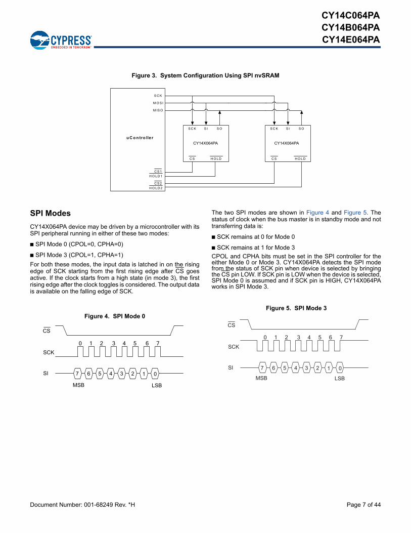
CY14X064PA has two separate pins for SI and SO, which canbe connected with the master as shown in Figure 3 on page 7.
Most Significant Bit (MSB)
The SPI protocol requires that the first bit to be transmitted is theMost Significant Bit (MSB). This is valid for both address anddata transmission.
The 64-Kbit serial nvSRAM requires a 2-byte address for anyread or write operation. However, since the address is only13 bits, it implies that the first three bits which are fed in areignored by the device. Although these three bits are ‘don’t care’,Cypress recommends that these bits are treated as 0s to enableseamless transition to higher memory densities.
Serial Opcode
After the slave device is selected with CS going LOW, the firstbyte received is treated as the opcode for the intended operation.
CY14X064PA uses the standard opcodes for memory accesses.In addition to the memory accesses, CY14X064PA providesadditional opcodes for the nvSRAM specific functions: STORE,RECALL, AutoStore Enable, and AutoStore Disable. Refer toTable 1 on page 9 for details on opcodes.
Invalid Opcode
If an invalid opcode is received, the opcode is ignored and thedevice ignores any additional serial data on the SI pin until thenext falling edge of CS and the SO pin remains tri-stated.
Status Register
CY14X064PA has an 8-bit Status Register. The bits in the StatusRegister are used to configure the SPI bus. These bits aredescribed in the Table 3 on page 10.
Document Number: 001-68249 Rev. *H Page 7 of 44
CY14C064PACY14B064PACY14E064PA
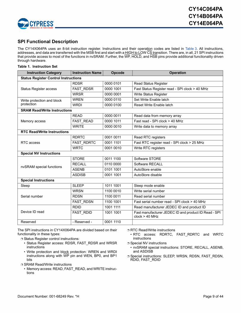
SPI Modes
CY14X064PA device may be driven by a microcontroller with itsSPI peripheral running in either of these two modes:
■ SPI Mode 0 (CPOL=0, CPHA=0)
■ SPI Mode 3 (CPOL=1, CPHA=1)
For both these modes, the input data is latched in on the risingedge of SCK starting from the first rising edge after CS goesactive. If the clock starts from a high state (in mode 3), the firstrising edge after the clock toggles is considered. The output datais available on the falling edge of SCK.
The two SPI modes are shown in Figure 4 and Figure 5. Thestatus of clock when the bus master is in standby mode and nottransferring data is:
■ SCK remains at 0 for Mode 0
■ SCK remains at 1 for Mode 3
CPOL and CPHA bits must be set in the SPI controller for theeither Mode 0 or Mode 3. CY14X064PA detects the SPI modefrom the status of SCK pin when device is selected by bringingthe CS pin LOW. If SCK pin is LOW when the device is selected,SPI Mode 0 is assumed and if SCK pin is HIGH, CY14X064PAworks in SPI Mode 3.
Figure 3. System Configuration Using SPI nvSRAM
CY14X064PA CY14X064PAuCon tro lle r
S C K
M O S I
M IS O
S I S O OSISKCS S C K
C S H O L D H O L DC S
C S 1
C S 2
H O L D 1
H O L D 2
Figure 4. SPI Mode 0
LSBMSB
7 6 5 4 3 2 1 0
CS
SCK
SI
0 1 2 3 4 5 6 7
Figure 5. SPI Mode 3
CS
SCK
SI 7 6 5 4 3 2 1 0
LSBMSB
0 1 2 3 4 5 6 7

Document Number: 001-68249 Rev. *H Page 8 of 44
CY14C064PACY14B064PACY14E064PA
SPI Operating Features
Power-Up
Power-up is defined as the condition when the power supply isturned on and VCC crosses Vswitch voltage.
As described earlier, at power-up nvSRAM performs a Power-UpRECALL operation for tFA duration during which, all memoryaccesses are disabled. The HSB pin can be probed to check theReady/Busy status of nvSRAM after power-up.
The following are the device status after power-up.
■ Selected (Active power mode) if CS pin is LOW
■ Deselected (Standby power mode) if CS pin is HIGH
■ Not in the Hold condition
■ Status Register state:❐ Write Enable (WEN) bit is reset to ‘0’.❐ WPEN, BP1, BP0 unchanged from previous STORE
operation.
The WPEN, BP1, and BP0 bits of the Status Register are nonvol-atile bits and remain unchanged from the previous STOREoperation.
Power Down
At power-down (continuous decay of VCC), when VCC drops fromthe normal operating voltage and below the VSWITCH thresholdvoltage, the device stops responding to any instruction sent to it.If a write cycle is in progress and the last data bit D0 has beenreceived when the power goes down, it is allowed tDELAY time tocomplete the write. After this, all memory accesses are inhibitedand a conditional AutoStore operation is performed (AutoStore isnot performed if no writes have happened since the last RECALLcycle). This feature prevents inadvertent writes to nvSRAM fromhappening during power-down. However, to avoid the possibilityof inadvertent writes during power-down, ensure that the deviceis deselected and is in standby power mode and the CS followsthe voltage applied on VCC.
Active Power and Standby Power Modes
When CS is LOW, the device is selected and is in the activepower mode. The device consumes ICC current, as specified inDC Electrical Characteristics on page 32. When CS is HIGH, thedevice is deselected and the device goes into the standby powermode after tSB time if a STORE or RECALL cycle is not inprogress. If a STORE/RECALL cycle is in progress, the devicegoes into the standby power mode after the STORE/RECALLcycle is completed. In the standby power mode the current drawnby the device drops to ISB.
Document Number: 001-68249 Rev. *H Page 9 of 44
CY14C064PACY14B064PACY14E064PA
SPI Functional Description
The CY14X064PA uses an 8-bit instruction register. Instructions and their operation codes are listed in Table 3. All instructions,addresses, and data are transferred with the MSB first and start with a HIGH to LOW CS transition. There are, in all, 21 SPI instructionsthat provide access to most of the functions in nvSRAM. Further, the WP, HOLD, and HSB pins provide additional functionality driventhrough hardware.
The SPI instructions in CY14X064PA are divided based on theirfunctionality in these types:
❐ Status Register control instructions:• Status Register access: RDSR, FAST_RDSR and WRSR
instructions • Write protection and block protection: WREN and WRDI
instructions along with WP pin and WEN, BP0, and BP1bits
❐ SRAM Read/Write instructions• Memory access: READ, FAST_READ, and WRITE instruc-
tions
❐ RTC Read/Write instructions• RTC access: RDRTC, FAST_RDRTC and WRTC
instructions ❐ Special NV instructions
• nvSRAM special instructions: STORE, RECALL, ASENB,and ASDISB
❐ Special instructions: SLEEP, WRSN, RDSN, FAST_RDSN,RDID, FAST_RDID
Table 1. Instruction Set
Instruction Category Instruction Name Opcode Operation
Status Register Control Instructions
Status Register access
RDSR 0000 0101 Read Status Register
FAST_RDSR 0000 1001 Fast Status Register read - SPI clock > 40 MHz
WRSR 0000 0001 Write Status Register
Write protection and block protection
WREN 0000 0110 Set Write Enable latch
WRDI 0000 0100 Reset Write Enable latch
SRAM Read/Write Instructions
Memory access
READ 0000 0011 Read data from memory array
FAST_READ 0000 1011 Fast read - SPI clock > 40 MHz
WRITE 0000 0010 Write data to memory array
RTC Read/Write Instructions
RTC access
RDRTC 0001 0011 Read RTC registers
FAST_RDRTC 0001 1101 Fast RTC register read - SPI clock > 25 MHz
WRTC 0001 0010 Write RTC registers
Special NV Instructions
nvSRAM special functions
STORE 0011 1100 Software STORE
RECALL 0110 0000 Software RECALL
ASENB 0101 1001 AutoStore enable
ASDISB 0001 1001 AutoStore disable
Special Instructions
Sleep SLEEP 1011 1001 Sleep mode enable
Serial number
WRSN 1100 0010 Write serial number
RDSN 1100 0011 Read serial number
FAST_RDSN 1100 1001 Fast serial number read - SPI clock > 40 MHz
Device ID readRDID 1001 1111 Read manufacturer JEDEC ID and product ID
FAST_RDID 1001 1001 Fast manufacturer JEDEC ID and product ID Read - SPI clock > 40 MHz
Reserved - Reserved - 0001 1110
Document Number: 001-68249 Rev. *H Page 10 of 44
CY14C064PACY14B064PACY14E064PA
Status Register
The Status Register bits are listed in Table 2. The Status Registerconsists of a Ready bit (RDY) and data protection bits BP1, BP0,WEN, and WPEN. The RDY bit can be polled to check theReady/Busy status while a nvSRAM STORE or SoftwareRECALL cycle is in progress. The Status Register can bemodified by WRSR instruction and read by RDSR orFAST_RDSR instruction. However, only the WPEN, BP1, andBP0 bits of the Status Register can be modified by using theWRSR instruction. The WRSR instruction has no effect on WEN
and RDY bits. The default value shipped from the factory forWEN, BP0, BP1, bits 4 -5, SNL and WPEN is ‘0’.
SNL (bit 6) of the Status Register is used to lock the serialnumber written using the WRSN instruction. The serial numbercan be written using the WRSN instruction multiple times whilethis bit is still '0'. When set to '1', this bit prevents any modificationto the serial number. This bit is factory programmed to '0' and canonly be written to once. After this bit is set to '1', it can never becleared to '0'.
Read Status Register (RDSR) Instruction
The Read Status Register instruction provides access to theStatus Register at SPI frequency up to 40 MHz. This instructionis used to probe the Write Enable status of the device or theReady status of the device. RDY bit is set by the device to ‘1’whenever a STORE or Software RECALL cycle is in progress.The block protection and WPEN bits indicate the extent ofprotection employed.
This instruction is issued after the falling edge of CS using theopcode for RDSR.
Fast Read Status Register (FAST_RDSR) Instruction
The FAST_RDSR instruction allows you to read the StatusRegister at SPI frequency above 40 MHz and up to 104 MHz(max).This instruction is used to probe the Write Enable statusof the device or the Ready status of the device. RDY bit is set bythe device to ‘1’ whenever a STORE or Software RECALL cycleis in progress. The block protection and WPEN bits indicate theextent of protection employed.
This instruction is issued after the falling edge of CS using theopcode for RDSR followed by a dummy byte.
Write Status Register (WRSR) Instruction
The WRSR instruction enables the user to write to the StatusRegister. However, this instruction cannot be used to modify bit0 (RDY), bit 1 (WEN) and bits 4-5. The BP0 and BP1 bits can beused to select one of four levels of block protection. Further,WPEN bit must be set to ‘1’ to enable the use of Write Protect(WP) pin.
WRSR instruction is a write instruction and needs writes to beenabled (WEN bit set to ‘1’) using the WREN instruction beforeit is issued. The instruction is issued after the falling edge of CSusing the opcode for WRSR followed by eight bits of data to bestored in the Status Register. WRSR instruction can be used tomodify only bits 2, 3, 6 and 7 of the Status Register.
Note In CY14X064PA, the values written to Status Register aresaved to nonvolatile memory only after a STORE operation. IfAutoStore is disabled, any modifications to the Status Registermust be secured by performing a Software STORE operation.
Table 2. Status Register Format
Bit 7 Bit 6 Bit 5 Bit 4 Bit 3 Bit 2 Bit 1 Bit 0
WPEN (0) SNL (0) X (0) X (0) BP1 (0) BP0 (0) WEN (0) RDY
Table 3. Status Register Bit Definition
Bit Definition Description
Bit 0 (RDY) Ready Read only bit indicates the ready status of device to perform a memory access. This bit is set to ‘1’ by the device while a STORE or Software RECALL cycle is in progress.
Bit 1 (WEN) Write Enable WEN indicates if the device is write enabled. This bit defaults to 0 (disabled) on power-up.WEN = '1' --> Write enabled WEN = '0' --> Write disabled
Bit 2 (BP0) Block Protect bit ‘0’ Used for block protection. For details see Table 4 on page 12.
Bit 3 (BP1) Block Protect bit ‘1’ Used for block protection. For details see Table 4 on page 12.
Bit 4-5 Don’t care These bits are non-writable and always return ‘0’ upon read.
Bit 6 (SNL) Serial Number Lock Set to '1' for locking serial number
Bit 7(WPEN) Write Protect Enable bit Used for enabling the function of Write Protect Pin (WP). For details see Table 5 on page 12.
Document Number: 001-68249 Rev. *H Page 11 of 44
CY14C064PACY14B064PACY14E064PA
Write Protection and Block Protection
CY14X064PA provides features for both software and hardwarewrite protection using WRDI instruction and WP. Additionally, thisdevice also provides block protection mechanism through BP0and BP1 pins of the Status Register.
The write enable and disable status of the device is indicated byWEN bit of the Status Register. The write instructions (WRSR,WRITE, WRTC and WRSN) and nvSRAM special instruction(STORE, RECALL, ASENB, ASDISB) need the write to beenabled (WEN bit = ‘1’) before they can be issued.
Write Enable (WREN) Instruction
On power-up, the device is always in the write disable state. Thefollowing WRITE, WRSR, WRTC, WRSN or nvSRAM special
instruction must therefore be preceded by a Write Enableinstruction. If the device is not write enabled (WEN = ‘0’), itignores the write instructions and returns to the standby statewhen CS is brought HIGH. A new CS falling edge is required tore-initiate serial communication. The instruction is issuedfollowing the falling edge of CS. When this instruction is used,the WEN bit of Status Register is set to ‘1’. WEN bit defaults to‘0’ on power-up.
Note After completion of a write instruction (WRSR, WRITE,WRTC or WRSN) or nvSRAM special instruction (STORE,RECALL, ASENB, ASDISB) instruction, WEN bit is cleared to ‘0’.This is done to provide protection from any inadvertent writes.Therefore, WREN instruction needs to be used before a newwrite instruction is issued.
Figure 6. Read Status Register (RDSR) Instruction Timing
Figure 7. Fast Read Status Register (FAST_RDSR) Instruction Timing
CS
SCK
SO
0 1 2 3 4 5 6 7
SI 0 0 0 0 0 1 0 01
HI-Z
0 1 2 3 4 5 6 7
Data LSBD0D1D2D3D4D5D6
MSBD7
Op-Code
CS
SCK
SO
0 1 2 3 4 5 6 7
SI 0 0 0 0 1 0 0 1
HI-Z
8 9 10 11 12 13 14 15
0
Data LSBD0D1D2D3D4D5D6
MSBD7
XXXXXXXX
Dummy Byte
0 1 2 3 4 5 6 7
Op-Code
Figure 8. Write Status Register (WRSR) Instruction Timing
CS
SCK
SO
0 1 2 3 4 5 6 7
SI 0 0 0 0 0 0 0 1MSB LSB
D2D3D7
HI-Z
0 1 2 3 4 5 6 7
Opcode Data in
XXX XX

Document Number: 001-68249 Rev. *H Page 12 of 44
CY14C064PACY14B064PACY14E064PA
Write Disable (WRDI) Instruction
Write Disable instruction disables the write by clearing the WENbit to ‘0’ to protect the device against inadvertent writes. Thisinstruction is issued following the falling edge of CS followed byopcode for WRDI instruction. The WEN bit is cleared on therising edge of CS following a WRDI instruction.
Block Protection
Block protection is provided using the BP0 and BP1 pins of theStatus Register. These bits can be set using WRSR instructionand probed using the RDSR instruction. The nvSRAM is dividedinto four array segments. One-quarter, one-half, or all of thememory segments can be protected. Any data within theprotected segment is read only. Table 4 shows the function ofBlock Protect bits.
Hardware Write Protection (WP Pin)
The write protect pin (WP) is used to provide hardware writeprotection. WP pin enables all normal read and write operationswhen held HIGH. When the WP pin is brought LOW and WPENbit is ‘1’, all write operations to the Status Register are inhibited.The hardware write protection function is blocked when theWPEN bit is ‘0’. This allows you to install the device in a systemwith the WP pin tied to ground, and still write to the StatusRegister.
WP pin can be used along with WPEN and Block Protect bits(BP1 and BP0) of the Status Register to inhibit writes to memory.When WP pin is LOW and WPEN is set to ‘1’, any modificationsto Status Register are disabled. Therefore, the memory isprotected by setting the BP0 and BP1 bits and the WP pin inhibitsany modification of the Status Register bits, providing hardwarewrite protection.
Note WP going LOW when CS is still LOW has no effect on anyof the ongoing write operations to the Status Register.
Table 5 summarizes all the protection features provided in theCY14X064PA.
Memory Access
All memory accesses are done using the READ and WRITEinstructions. These instructions cannot be used while a STOREor RECALL cycle is in progress. A STORE cycle in progress isindicated by the RDY bit of the Status Register and the HSB pin.
Read Sequence (READ) Instruction
The read operations on this device are performed by giving theinstruction on the SI pin and reading the output on SO pin. Thefollowing sequence needs to be followed for a read operation:After the CS line is pulled LOW to select a device, the readopcode is transmitted through the SI line followed by two bytesof address (A12–A0). The most significant address bits(A15–A13) are don’t cares. After the last address bit istransmitted on the SI pin, the data (D7–D0) at the specificaddress is shifted out on the SO line on the falling edge of SCKstarting with D7. Any other data on SI line after the last addressbit is ignored.
CY14X064PA allows reads to be performed in bursts throughSPI which can be used to read consecutive addresses withoutissuing a new READ instruction. If only one byte is to be read,the CS line must be driven HIGH after one byte of data comesout. However, the read sequence may be continued by holdingthe CS line LOW and the address is automatically incrementedand data continues to shift out on SO pin. When the last datamemory address (0x1FFF) is reached, the address rolls over to0x0000 and the device continues to read.
Fast Read Sequence (FAST_READ) Instruction
The FAST_READ instruction allows you to read memory at SPIfrequency above 40 MHz and up to 104 MHz (Max). The hostsystem must first select the device by driving CS LOW, theFAST_READ instruction is then written to SI, followed by 2address byte (A12–A0) and then a dummy byte. The mostsignificant address bits (A15–A13) are don’t cares.
From the subsequent falling edge of the SCK, the data of thespecific address is shifted out serially on the SO line starting withMSB. The first byte specified can be at any location. The device
Figure 9. WREN Instruction
Figure 10. WRDI Instruction
Table 4. Block Write Protect Bits
LevelStatus Register Bits
Array Addresses ProtectedBP1 BP0
0 0 0 None
1 (1/4) 0 1 0x1800-0x1FFF
2 (1/2) 1 0 0x1000-0x1FFF
3 (All) 1 1 0x0000-0x1FFF
0 0 0 0 0 1 1 0
CS
SCK
SI
SOHI-Z
0 1 2 3 4 5 6 7
0 0 0 0 0 1 0 0
CS
SCK
SI
SOHI-Z
0 1 2 3 4 5 6 7
Table 5. Write Protection Operation
WPEN WP WEN Protected Blocks
Unprotected Blocks
Status Register
X X 0 Protected Protected Protected
0 X 1 Protected Writable Writable
1 LOW 1 Protected Writable Protected
1 HIGH 1 Protected Writable Writable

Document Number: 001-68249 Rev. *H Page 13 of 44
CY14C064PACY14B064PACY14E064PA
automatically increments to the next higher address after eachbyte of data is output. The entire memory array can therefore beread with a single FAST_READ instruction. When the highestaddress in the memory array is reached, address counter rollsover to start address 0x0000 and thus allowing the readsequence to continue indefinitely. The FAST_READ instructionis terminated by driving CS HIGH at any time during data output.
Note FAST_READ instruction operates up to maximum of104 MHz SPI frequency.
Write Sequence (WRITE) Instruction
The write operations on this device are performed through the SIpin. To perform a write operation, if the device is write disabled,then the device must first be write enabled through the WRENinstruction. When the writes are enabled (WEN = ‘1’), WRITEinstruction is issued after the falling edge of CS. A WRITEinstruction constitutes transmitting the WRITE opcode on SI linefollowed by two bytes of address (A12–A0) and the data (D7–D0)which is to be written. The most significant address bits(A15–A13) are don’t cares.
CY14X064PA enables writes to be performed in bursts throughSPI which can be used to write consecutive addresses withoutissuing a new WRITE instruction. If only one byte is to be written,the CS line must be driven HIGH after the D0 (LSB of data) istransmitted. However, if more bytes are to be written, CS linemust be held LOW and address is incremented automatically.The following bytes on the SI line are treated as data bytes andwritten in the successive addresses. When the last data memoryaddress (0x1FFF) is reached, the address rolls over to 0x0000and the device continues to write. The WEN bit is reset to ‘0’ oncompletion of a WRITE sequence.
Note When a burst write reaches a protected block address, itcontinues the address increment into the protected space butdoes not write any data to the protected memory. If the addressroll over takes the burst write to unprotected space, it resumeswrites. The same operation is true if a burst write is initiatedwithin a write protected block.
Figure 11. Read Instruction Timing
Figure 12. Burst Mode Read Instruction Timing
~ ~
CS
SCK
SO
0 1 2 3 4 5 6 7 0 7654321 12 13 14 15 0 1 2 3 4 5 6 7
MSB LSBData
SI
~ ~
Op-Code
0 0 0 0 0 0 1 X X X A12 A11 A91 A10 A8 A3 A1 A2 A0
13-bit Address
MSB LSB
D0D1D2D3D4D5D6D7HI-Z
CS
SCK
SO
LSB
SI
Op-Code 13-bit Address
MSB LSB
~ ~~ ~
~ ~
0 1 2 3 4 5 6 7 0 7654321 12 13 14 15 0 1 2 3 4 5 6 7 0 1 2 3 4 5 6 7
~ ~
0 7
0 0 0 0 0 0 1 1 X X X A12 A11 A10 A9 A8 A3 A2 A1 A0
D0D1D2D3D4D5D6D7
Data Byte 1 Data Byte N
MSB LSBMSB
D0D1D2D3D4D5D6D7 D0D7HI-Z

Document Number: 001-68249 Rev. *H Page 14 of 44
CY14C064PACY14B064PACY14E064PA
Figure 13. Fast Read Instruction Timing
Figure 14. Write Instruction Timing
Figure 15. Burst Mode Write Instruction Timing
~ ~
CS
SCK
SO
0 1 2 3 4 5 6 7 0 7654321 12 13 14 15 16 17 18 19 20 21 22 23
Data
SI
~ ~
Op-Code0 0 0 0 1 0 1 X X A12 A11 A91 A10 A8 A3 A1A2 A0
13-bit Address
BSLBSM
MSB LSB
D0D1D2D3D4D5D6D7
0 1 2 3 4 5 6 7
XXXXXXXX
Dummy Byte
HI-Z
X
~ ~
CS
SCK
SO
0 1 2 3 4 5 6 7 0 7654321 12 13 14 15 0 1 2 3 4 5 6 7
MSB LSBDataD0D1D2D3D4D5D6D7SI
~ ~
Op-Code
0 0 0 0 0 0 1 X X X A11 A90 A10 A8 A3 A1A2 A0
13-bit Address
MSB LSB
HI-Z
A12
~ ~
CS
SCK
SO
MSB LSBSI
Op-Code 13-bit Address
MSB LSB~ ~ ~ ~
0 1 2 3 4 5 6 7 0 76 5 4321 12 13 14 15 0 1 2 3 4 5 6 7 0 1 2 3 4 5 6 7
~ ~
0 7
0 0 0 0 0 0 1 0 X X X A12 A11A10 A9 A8 A3 A2 A1 A0
HI-Z
Data Byte 1 Data Byte N
D0D1D2D3D4D5D6D7D0D1D2D3D4D5D6D7 D0D7

Document Number: 001-68249 Rev. *H Page 15 of 44
CY14C064PACY14B064PACY14E064PA
RTC Access
CY14X064PA uses 16 registers for RTC. These registers can beread out or written to by accessing all 16 registers in burst modeor accessing each register, one at a time. The RDRTC,FAST_RDRTC, and WRTC instructions are used to access theRTC.
All the RTC registers can be read in burst mode by issuing theRDRTC and FAST_RDRTC instruction and reading all 16 byteswithout bringing the CS pin HIGH. The ‘R’ bit must be set whilereading the RTC timekeeping registers to ensure that transitionalvalues of time are not read.
Writes to the RTC register are performed using the WRTCinstruction. Writing RTC timekeeping registers and controlregisters, except for the flags register needs the ‘W’ bit of theflags register to be set to ‘1’. The internal counters are updatedwith the new date and time setting when the ‘W’ bit is cleared to‘0’. All the RTC registers can also be written in burst mode usingthe WRTC instruction.
READ RTC (RDRTC) Instruction
Read RTC (RDRTC) instruction allows you to read the contentsof RTC registers at SPI frequency upto 25 MHz. Reading theRTC registers through the SO pin requires the followingsequence: After the CS line is pulled LOW to select a device, theRDRTC opcode is transmitted through the SI line followed byeight address bits for selecting the register. Any data on the SIline after the address bits is ignored. The data (D7-D0) at thespecified address is then shifted out onto the SO line. RDRTCalso allows burst mode read operation. When reading multiplebytes from RTC registers, the address rolls over to 0x00 after thelast RTC register address (0x0F) is reached.
The ‘R’ bit in RTC flags register must be set to ‘1’ before readingRTC time keeping registers to avoid reading transitional data.Modifying the RTC flag registers requires a Write RTC cycle. TheR bit must be cleared to '0' after completion of the read operation.
The easiest way to read RTC registers is to perform RDRTC inburst mode. The read may start from the first RTC register (0x00)and the CS must be held LOW to allow the data from all 16 RTCregisters to be transmitted through the SO pin.
Note RDRTC instruction operates at a maximum clockfrequency of 25 MHz. The opcode cycles, address cycles anddata out cycles need to run at 25 MHz for the instruction to workproperly.
Fast Read Sequence (FAST_RDRTC) Instruction
The FAST_RDRTC instruction allows you to read memory at aSPI frequency above 25 MHz and up to 104 MHz (Max). The hostsystem must first select the device by driving CS LOW, theFAST_READ instruction is then written to SI, followed by 8 bitaddress and a dummy byte.
From the subsequent falling edge of the SCK, the data of thespecific address is shifted out serially on the SO line starting withMSB. The first byte specified can be at any location. The deviceautomatically increments to the next higher address after eachbyte of data is output. The entire memory array can therefore beread with a single FAST_RDRTC instruction. When the highestaddress (0x0F) in the memory array is reached, the addresscounter rolls over to start address 0x00 and thus allowing theread sequence to continue indefinitely. The FAST_RDRTCinstruction is terminated by driving CS HIGH at any time duringdata output.
Note FAST_READ instruction operates up to Max of 104 MHzSPI frequency.
Figure 16. Read RTC (RDRTC) Instruction Timing
CS
SCK
SO
0 1 2 3 4 5 6 7 0 321 4 5 6 7 0 1 2 3 4 5 6 7
MSB LSBData
SI
Op-Code
0 0 0 1 0 0 1 0 0 0 01 A3 A1A2 A0MSB LSB
D0D1D2D3D4D5D6D7 HI-Z

Document Number: 001-68249 Rev. *H Page 16 of 44
CY14C064PACY14B064PACY14E064PA
Figure 17. Fast RTC Read (FAST_RDRTC) Instruction Timing
WRITE RTC (WRTC) Instruction
WRITE RTC (WRTC) instruction allows you to modify thecontents of RTC registers. The WRTC instruction requires theWEN bit to be set to '1' before it can be issued. If WEN bit is '0',a WREN instruction needs to be issued before using WRTC.Writing RTC registers requires the following sequence: After theCS line is pulled LOW to select a device, WRTC opcode istransmitted through the SI line followed by eight address bitsidentifying the register which is to be written to and one or more
bytes of data. WRTC allows burst mode write operation. Whenwriting more than one registers in burst mode, the address rollsover to 0x00 after the last RTC address (0x0F) is reached.
Note that writing to RTC timekeeping and control registersrequire the W bit to be set to '1'. The values in these RTCregisters take effect only after the ‘W’ bit is cleared to '0'. WriteEnable bit (WEN) is automatically cleared to ‘0’ after completionof the WRTC instruction.
CS
SCK
SO
0 1 2 3 4 5 6 7 0 321 4 5 6 7 8 9 10 11 12 13 14 15
SI
Op-Code
0 0 0 1 1 1 0 0 0 0 01 A3 A1A2 A0MSB LSB
MSB LSBData
D0D1D2D3D4D5D6D7
XXXXXXXX
16 17 18 19 20 21 22 23
Dummy Byte
HI-Z
Figure 18. Write RTC (WRTC) Instruction Timing
CS
SCK
SO
0 1 2 3 4 5 6 7 0 321 4 5 6 7 0 1 2 3 4 5 6 7
SI
Op-Code
0 0 0 1 0 0 1 0 0 0 00 A3 A1A2 A0
4-bit Address
MSB LSB MSB LSBData
HI-Z
D0D1D2D3D4D5D6D7
Document Number: 001-68249 Rev. *H Page 17 of 44
CY14C064PACY14B064PACY14E064PA
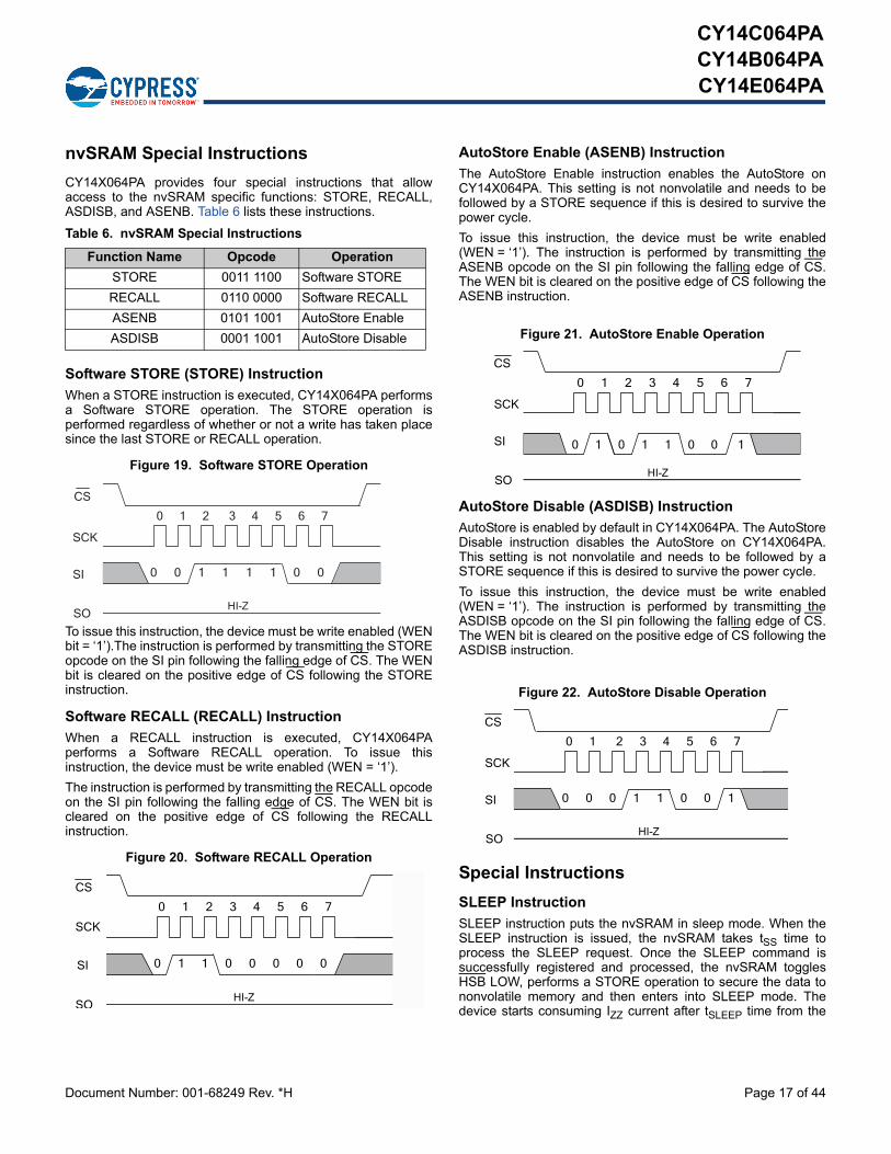
nvSRAM Special Instructions
CY14X064PA provides four special instructions that allowaccess to the nvSRAM specific functions: STORE, RECALL,ASDISB, and ASENB. Table 6 lists these instructions.
Software STORE (STORE) Instruction
When a STORE instruction is executed, CY14X064PA performsa Software STORE operation. The STORE operation isperformed regardless of whether or not a write has taken placesince the last STORE or RECALL operation.
To issue this instruction, the device must be write enabled (WENbit = ‘1’).The instruction is performed by transmitting the STOREopcode on the SI pin following the falling edge of CS. The WENbit is cleared on the positive edge of CS following the STOREinstruction.
Software RECALL (RECALL) Instruction
When a RECALL instruction is executed, CY14X064PAperforms a Software RECALL operation. To issue thisinstruction, the device must be write enabled (WEN = ‘1’).
The instruction is performed by transmitting the RECALL opcodeon the SI pin following the falling edge of CS. The WEN bit iscleared on the positive edge of CS following the RECALLinstruction.
AutoStore Enable (ASENB) Instruction
The AutoStore Enable instruction enables the AutoStore onCY14X064PA. This setting is not nonvolatile and needs to befollowed by a STORE sequence if this is desired to survive thepower cycle.
To issue this instruction, the device must be write enabled(WEN = ‘1’). The instruction is performed by transmitting theASENB opcode on the SI pin following the falling edge of CS.The WEN bit is cleared on the positive edge of CS following theASENB instruction.
AutoStore Disable (ASDISB) Instruction
AutoStore is enabled by default in CY14X064PA. The AutoStoreDisable instruction disables the AutoStore on CY14X064PA.This setting is not nonvolatile and needs to be followed by aSTORE sequence if this is desired to survive the power cycle.
To issue this instruction, the device must be write enabled(WEN = ‘1’). The instruction is performed by transmitting theASDISB opcode on the SI pin following the falling edge of CS.The WEN bit is cleared on the positive edge of CS following theASDISB instruction.
.
Special Instructions
SLEEP Instruction
SLEEP instruction puts the nvSRAM in sleep mode. When theSLEEP instruction is issued, the nvSRAM takes tSS time toprocess the SLEEP request. Once the SLEEP command issuccessfully registered and processed, the nvSRAM togglesHSB LOW, performs a STORE operation to secure the data tononvolatile memory and then enters into SLEEP mode. Thedevice starts consuming IZZ current after tSLEEP time from the
Table 6. nvSRAM Special Instructions
Function Name Opcode Operation
STORE 0011 1100 Software STORE
RECALL 0110 0000 Software RECALL
ASENB 0101 1001 AutoStore Enable
ASDISB 0001 1001 AutoStore Disable
Figure 19. Software STORE Operation
Figure 20. Software RECALL Operation
0 0 1 1 1 1 0 0
CS
SCK
SI
SOHI-Z
0 1 2 3 4 5 6 7
0 1 1 0 0 0 0 0
CS
SCK
SI
0 1 2 3 4 5 6 7
SOHI-Z
Figure 21. AutoStore Enable Operation
Figure 22. AutoStore Disable Operation
0 1 0 1 1 0 0 1
CS
SCK
SI
SOHI-Z
0 1 2 3 4 5 6 7
0 0 0 1 1 0 0 1
CS
SCK
SI
SOHI-Z
0 1 2 3 4 5 6 7

Document Number: 001-68249 Rev. *H Page 18 of 44
CY14C064PACY14B064PACY14E064PA
instance when SLEEP instruction is registered. The device is notaccessible for normal operations after SLEEP instruction isissued. Once in sleep mode, the SCK and SI pins are ignoredand SO will be Hi-Z but device continues to monitor the CS pin.
To wake the nvSRAM from the sleep mode, the device must beselected by toggling the CS pin from HIGH to LOW. The devicewakes up and is accessible for normal operations after tWAKEduration after a falling edge of CS pin is detected.
Note Whenever nvSRAM enters into sleep mode, it initiatesnonvolatile STORE cycle which results in an endurance cycle persleep command execution. A STORE cycle starts only if a writeto the SRAM has been performed since the last STORE orRECALL cycle.
Serial Number
The serial number is an 8-byte programmable memory spaceprovided to you to uniquely identify this device. It typicallyconsists of a two byte Customer ID, followed by five bytes ofunique serial number and one byte of CRC check. However,nvSRAM does not calculate the CRC and it is up to the systemdesigner to utilize the eight byte memory space in whatevermanner desired. The default value for eight byte locations are setto ‘0x00’.
WRSN (Serial Number Write) Instruction
The serial number can be written using the WRSN instruction. Towrite serial number the write must be enabled using the WRENinstruction. The WRSN instruction can be used in burst mode towrite all the 8 bytes of serial number.
The serial number is locked using the SNL bit of the StatusRegister. Once this bit is set to '1', no modification to the serialnumber is possible. After the SNL bit is set to '1', using the WRSNinstruction has no effect on the serial number.
A STORE operation (AutoStore or Software STORE) is requiredto store the serial number in nonvolatile memory. If AutoStore isdisabled, you must perform a Software STORE operation tosecure and lock the serial number. If SNL bit is set to ‘1’ and isnot stored (AutoStore disabled), the SNL bit and serial numberdefaults to ‘0’ at the next power cycle. If SNL bit is set to ‘1’ andis stored, the SNL bit can never be cleared to ‘0’. This instructionrequires the WEN bit to be set before it can be executed. TheWEN bit is reset to '0' after completion of this instruction.
Figure 23. Sleep Mode Entry
1 0 1 1 1 0 0 1
CS
SCK
SI
SOHI-Z
0 1 2 3 4 5 6 7
tSLEEP
Figure 24. WRSN Instruction
~ ~
CS
SCK
SO
0 1 2 3 4 5 6 7 0 7654321 56 57 58 59 60 61 62 63
LSBD0D1D2D3D4D5D6D7SI
Op-Code
1 1 0 0 0 0 1 0
8-Byte Serial NumberMSB
HI-Z
D7 D6 D5 D4 D3 D2 D1 D0
~ ~
Byte - 8 Byte - 1

Document Number: 001-68249 Rev. *H Page 19 of 44
CY14C064PACY14B064PACY14E064PA
RDSN (Serial Number Read) Instruction
The serial number is read using RDSN instruction at SPI frequency upto 40 MHz. A serial number read may be performed in burstmode to read all the eight bytes at once. After the last byte of serial number is read, the device does not loop back. RDSN instructioncan be issued by shifting the op-code for RDSN in through the SI pin of nvSRAM after CS goes LOW. This is followed by nvSRAMshifting out the eight bytes of serial number through the SO pin.
FAST_RDSN (Fast Serial Number Read) Instruction
The FAST_RDSN instruction is used to read serial number at SPI frequency above 40 MHz and up to 104 MHz (max). A serial numberread may be performed in burst mode to read all the eight bytes at once. After the last byte of serial number is read, the device doesnot loop back. FAST_RDSN instruction can be issued by shifting the op-code for FAST_RDSN in through the SI pin of nvSRAMfollowed by dummy byte after CS goes LOW. This is followed by nvSRAM shifting out the eight bytes of serial number through the SOpin.
Figure 25. RDSN Instruction
CS
SCK
SO
0 1 2 3 4 5 6 7
SI
Op-Code
1 1 0 0 0 0 1 1
~ ~ LSBD0D1D2D3D4D5D6D7
8-Byte Serial NumberMSBD7 D6 D5 D4 D3 D2 D1 D0
Byte - 8 Byte - 1
0 7654321 56 57 58 59 60 61 62 63
~ ~
HI-Z
Figure 26. FAST_RDSN Instruction
CS
SCK
SO
0 1 2 3 4 5 6 7
SI
Op-Code
1 1 0 0 1 0 0 1
~ ~ LSBD0D1D2D3D4D5D6D7
8-Byte Serial NumberMSBD7 D6 D5 D4 D3 D2 D1 D0
Byte - 8 Byte - 1
0 7654321 56 57 58 59 60 61 62 63
~ ~
XXXXXXXX
Dummy Byte
8 9 10 11 12 13 14 15
HI-Z
Document Number: 001-68249 Rev. *H Page 20 of 44
CY14C064PACY14B064PACY14E064PA
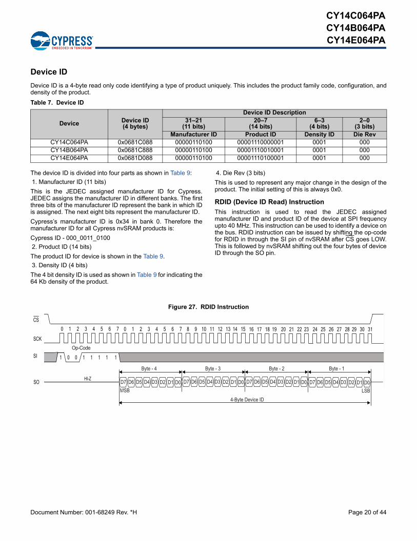
Device ID
Device ID is a 4-byte read only code identifying a type of product uniquely. This includes the product family code, configuration, anddensity of the product.
The device ID is divided into four parts as shown in Table 9:
1. Manufacturer ID (11 bits)
This is the JEDEC assigned manufacturer ID for Cypress.JEDEC assigns the manufacturer ID in different banks. The firstthree bits of the manufacturer ID represent the bank in which IDis assigned. The next eight bits represent the manufacturer ID.
Cypress’s manufacturer ID is 0x34 in bank 0. Therefore themanufacturer ID for all Cypress nvSRAM products is:
Cypress ID - 000_0011_0100
2. Product ID (14 bits)
The product ID for device is shown in the Table 9.
3. Density ID (4 bits)
The 4 bit density ID is used as shown in Table 9 for indicating the64 Kb density of the product.
4. Die Rev (3 bits)
This is used to represent any major change in the design of theproduct. The initial setting of this is always 0x0.
RDID (Device ID Read) Instruction
This instruction is used to read the JEDEC assignedmanufacturer ID and product ID of the device at SPI frequencyupto 40 MHz. This instruction can be used to identify a device onthe bus. RDID instruction can be issued by shifting the op-codefor RDID in through the SI pin of nvSRAM after CS goes LOW.This is followed by nvSRAM shifting out the four bytes of deviceID through the SO pin.
Table 7. Device ID
Device Device ID(4 bytes)
Device ID Description31–21
(11 bits)20–7
(14 bits)6–3
(4 bits)2–0
(3 bits)Manufacturer ID Product ID Density ID Die Rev
CY14C064PA 0x0681C088 00000110100 00001110000001 0001 000CY14B064PA 0x0681C888 00000110100 00001110010001 0001 000CY14E064PA 0x0681D088 00000110100 00001110100001 0001 000
Figure 27. RDID Instruction
1 0 0 1 1 1 1 1
CS
SCK
SI
SOHI-Z
0 1 2 3 4 5 6 7 8 9 10 11 12 13 14 15 24 25 26 27 28 29 30 3116 17 18 19 20 21 22 230 1 2 3 4 5 6 7
MSB
4-Byte Device ID
D0D1D2D3D4D5D6D7 D0D1D2D3D4D5D6D7 D0D1D2D3D4D5D6D7LSBD0D1D2D3D4D5D6D7
Byte - 4 Byte - 3 Byte - 2 Byte - 1
Op-Code
Document Number: 001-68249 Rev. *H Page 21 of 44
CY14C064PACY14B064PACY14E064PA
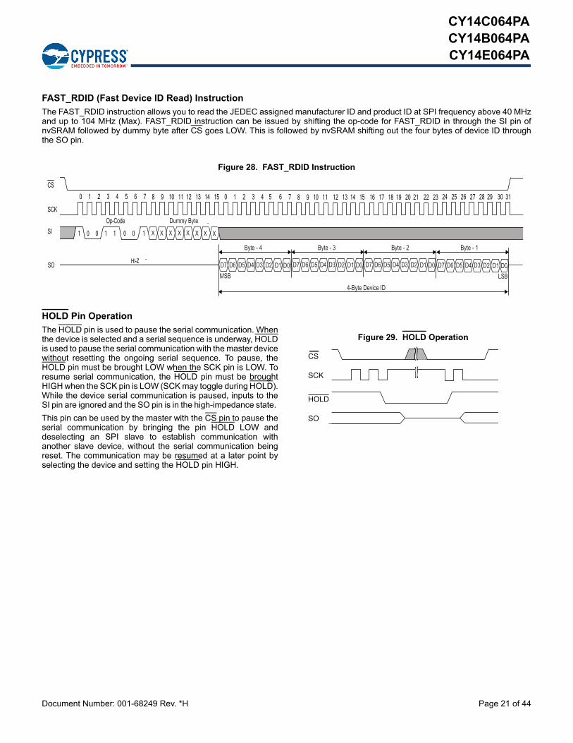
FAST_RDID (Fast Device ID Read) Instruction
The FAST_RDID instruction allows you to read the JEDEC assigned manufacturer ID and product ID at SPI frequency above 40 MHzand up to 104 MHz (Max). FAST_RDID instruction can be issued by shifting the op-code for FAST_RDID in through the SI pin ofnvSRAM followed by dummy byte after CS goes LOW. This is followed by nvSRAM shifting out the four bytes of device ID throughthe SO pin.
HOLD Pin Operation
The HOLD pin is used to pause the serial communication. Whenthe device is selected and a serial sequence is underway, HOLDis used to pause the serial communication with the master devicewithout resetting the ongoing serial sequence. To pause, theHOLD pin must be brought LOW when the SCK pin is LOW. Toresume serial communication, the HOLD pin must be broughtHIGH when the SCK pin is LOW (SCK may toggle during HOLD).While the device serial communication is paused, inputs to theSI pin are ignored and the SO pin is in the high-impedance state.
This pin can be used by the master with the CS pin to pause theserial communication by bringing the pin HOLD LOW anddeselecting an SPI slave to establish communication withanother slave device, without the serial communication beingreset. The communication may be resumed at a later point byselecting the device and setting the HOLD pin HIGH.
Figure 28. FAST_RDID Instruction
1 0 0 1 1 0 0 1
CS
SCK
SI
SOHI-Z
0 1 2 3 4 5 6 7 0 1 2 3 4 5 6 7 16 17 18 19 20 21 22 23 8 9 10 11 12 13 14 158 9 10 11 12 13 14 15
MSB
4-Byte Device ID
D0D1D2D3D4D5D6D7 D0D1D2D3D4D5D6D7 D0D1D2D3D4D5D6D7LSBD0D1D2D3D4D5D6D7
Byte - 4 Byte - 3 Byte - 2 Byte - 1
XXXXXXXX
Dummy Byte
24 25 26 27 28 29 30 31
Op-Code
Figure 29. HOLD Operation
~ ~~ ~
CS
SCK
HOLD
SO

Document Number: 001-68249 Rev. *H Page 22 of 44
CY14C064PACY14B064PACY14E064PA
Real Time Clock Operation
nvTIME Operation
The CY14X064PA offers internal registers that contain clock,alarm, watchdog, interrupt, and control functions. The RTCregisters occupy a separate address space from nvSRAM andare accessible through the Read RTC register and Write RTCregister sequence on register addresses 0x00 to 0x0F. Internaldouble buffering of the time keeping registers preventsaccessing transitional internal clock data during a read or writeoperation. Double buffering also circumvents disrupting normaltiming counts or the clock accuracy of the internal clock whenaccessing clock data. Clock and alarm registers store data inBCD format.
Clock Operations
The clock registers maintain time up to 9,999 years inone-second increments. The time can be set to any calendartime and the clock automatically keeps track of days of the weekand month, leap years, and century transitions. There are eightregisters dedicated to the clock functions, which are used to settime with a write cycle and to read time with a read cycle. Theseregisters contain the time of day in BCD format. Bits defined as‘0’ are currently not used and are reserved for future use byCypress.
Reading the Clock
The double buffered RTC register structure reduces the chanceof reading incorrect data from the clock. Internal updates to theCY14X064PA time keeping registers are stopped when the readbit ‘R’ (in the flags register at 0x00) is set to ‘1’ before readingclock data to prevent reading of data in transition. Stopping theregister updates does not affect clock accuracy.
When a read sequence of RTC device is initiated, the update ofthe user timekeeping registers stops and does not restart until a‘0’ is written to the read bit ‘R’ (in the flags register at 0x00). Afterthe end of read sequence, all the RTC registers aresimultaneously updated within 20 ms.
Setting the Clock
A write access to the RTC device stops updates to the timekeeping registers and enables the time to be set when the writebit ‘W’ (in the flags register at 0x00) is set to ‘1’. The correct day,date, and time is then written into the registers and must be in 24hour BCD format. The time written is referred to as the “BaseTime”. This value is stored in nonvolatile registers and used inthe calculation of the current time. When the write bit ‘W’ iscleared by writing ‘0’ to it, the values of timekeeping registers aretransferred to the actual clock counters after which the clockresumes normal operation.
If the time written to the timekeeping registers is not in the correctBCD format, each invalid nibble of the RTC registers continuecounting to 0xF before rolling over to 0x0 after which RTCresumes normal operation.
Note After ‘W’ bit is set to ‘0’, values written into the timekeeping,alarm, calibration, and interrupt registers are transferred to theRTC time keeping counters in tRTCp time. These counter valuesmust be saved to nonvolatile memory either by initiating aSoftware/Hardware STORE or AutoStore operation. Whileworking in AutoStore disabled mode, perform a STORE
operation after tRTCp time while writing into the RTC registers forthe modifications to be correctly recorded.
Backup Power
The RTC in the CY14X064PA is intended for permanentlypowered operation. The VRTCcap or VRTCbat pin is connecteddepending on whether a capacitor or battery is chosen for theapplication. When the primary power, VCC, fails and drops belowVSWITCH the device switches to the backup power supply.
The clock oscillator uses very little current, which maximizes thebackup time available from the backup source. Regardless of theclock operation with the primary source removed, the data storedin the nvSRAM is secure, having been stored in the nonvolatileelements when power was lost.
During backup operation, the CY14X064PA consumes a 0.45 µA(Typ) at room temperature. The user must choose capacitor orbattery values according to the application.
Note: If a battery is applied to VRTCbat pin prior to VCC, the chipwill draw high IBAK current. This occurs even if the oscillator isdisabled. In order to maximize battery life, VCC must be appliedbefore a battery is applied to VRTCbat pin.
Backup time values based on maximum current specificationsare shown in the following Table 8. Nominal backup times areapproximately two times longer.
Using a capacitor has the obvious advantage of recharging thebackup source each time the system is powered up. If a batteryis used, a 3-V lithium is recommended and the CY14X064PAsources current only from the battery when the primary power isremoved. However, the battery is not recharged at any time bythe CY14X064PA. The battery capacity must be chosen for totalanticipated cumulative down time required over the life of thesystem.
Stopping and Starting the Oscillator
The OSCEN bit in the calibration register at 0x08 controls theenable and disable of the oscillator. This bit is nonvolatile and isshipped to customers in the “enabled” (set to ‘0’) state. Topreserve the battery life when the system is in storage, OSCENmust be set to ‘1’. This turns off the oscillator circuit, extendingthe battery life. If the OSCEN bit goes from disabled to enabled,it takes approximately one second (two seconds maximum) forthe oscillator to start.
While system power is off, if the voltage on the backup supply(VRTCcap or VRTCbat) falls below their respective minimum level,the oscillator may fail.The CY14X064PA has the ability to detectoscillator failure when system power is restored. This is recordedin the Oscillator Fail Flag (OSCF) of the flags register at theaddress 0x00. When the device is powered on (VCC goes aboveVSWITCH) the OSCEN bit is checked for the ‘enabled’ status. Ifthe OSCEN bit is enabled and the oscillator is not active withinthe first 5 ms, the OSCF bit is set to ‘1’. The system must checkfor this condition and then write ‘0’ to clear the flag.
Table 8. RTC Backup Time
Capacitor Value Backup Time(CY14B064PA)
0.1F 60 hours
0.47F 12 days
1.0F 25 days
Document Number: 001-68249 Rev. *H Page 23 of 44
CY14C064PACY14B064PACY14E064PA
Note that in addition to setting the OSCF flag bit, the timeregisters are reset to the ‘Base Time’, which is the value lastwritten to the timekeeping registers. The control or calibrationregisters and the OSCEN bit are not affected by the ‘oscillatorfailed’ condition.
The value of OSCF must be reset to ‘0’ when the time registersare written for the first time. This initializes the state of this bitwhich may have become set when the system was first poweredon.
To reset OSCF, set the write bit ‘W’ (in the flags register at 0x00)to a ‘1’ to enable writes to the flags register. Write a ‘0’ to theOSCF bit and then reset the write bit to ‘0’ to disable writes.
Calibrating the Clock
The RTC is driven by a quartz controlled crystal with a nominalfrequency of 32.768 kHz. Clock accuracy depends on the qualityof the crystal and calibration. The crystals available in markettypically have an error of +20 ppm to +35 ppm. However,CY14X064PA employs a calibration circuit that improves theaccuracy to +1/–2 ppm at 25 C. This implies an error of+2.5 seconds to -5 seconds per month.
The calibration circuit adds or subtracts counts from the oscillatordivider circuit to achieve this accuracy. The number of pulses thatare suppressed (subtracted, negative calibration) or split (added,positive calibration) depends upon the value loaded into the fivecalibration bits found in calibration register at 0x08. Thecalibration bits occupy the five lower order bits in the calibrationregister. These bits are set to represent any value between ‘0’and 31 in binary form. Bit D5 is a sign bit, where a ‘1’ indicatespositive calibration and a ‘0’ indicates negative calibration.Adding counts speeds the clock up and subtracting counts slowsthe clock down. If a binary ‘1’ is loaded into the register, itcorresponds to an adjustment of 4.068 or –2.034 ppm offset inoscillator error, depending on the sign.
Calibration occurs within a 64-minute cycle. The first 62 minutesin the cycle may, once per minute, have one second shortenedby 128 or lengthened by 256 oscillator cycles. If a binary ‘1’ isloaded into the register, only the first two minutes of the64-minute cycle are modified. If a binary 6 is loaded, the first 12are affected, and so on. Therefore, each calibration step has theeffect of adding 512 or subtracting 256 oscillator cycles for every125,829,120 actual oscillator cycles, that is, 4.068 or –2.034 ppmof adjustment per calibration step in the calibration register.
To determine the required calibration, the CAL bit in the flagsregister (0x00) must be set to ‘1’. This causes the INT pin totoggle at a nominal frequency of 512 Hz. Any deviationmeasured from the 512 Hz indicates the degree and direction ofthe required correction. For example, a reading of 512.01024 Hzindicates a +20 ppm error. Hence, a decimal value of –10(001010b) must be loaded into the calibration register to offsetthis error.
Note Setting or changing the calibration register does not affectthe test output frequency.
To set or clear CAL, set the write bit ‘W’ (in the flags register at0x00) to ‘1’ to enable writes to the flags register. Write a value toCAL, and then reset the write bit to ‘0’ to disable writes.
Alarm
The alarm function compares user programmed values of alarmtime and date (stored in the registers 0x01–5) with thecorresponding time of day and date values. When a matchoccurs, the alarm internal flag (AF) is set and an interrupt isgenerated on INT pin if Alarm Interrupt Enable (AIE) bit is set.
There are four alarm match fields: date, hours, minutes, andseconds. Each of these fields has a match bit that is used todetermine if the field is used in the alarm match logic. Setting thematch bit to ‘0’ indicates that the corresponding field is used inthe match process. Depending on the match bits, the alarmoccurs as specifically as once a month or as frequently as onceevery minute. Selecting none of the match bits (all 1s) indicatesthat no match is required and therefore, alarm is disabled.Selecting all match bits (all 0s) causes an exact time and datematch.
There are two ways to detect an alarm event: by reading the AFflag or monitoring the INT pin. The AF flag in the flags register at0x00 indicates that a date or time match has occurred. The AFbit is set to ‘1’ when a match occurs. Reading the flags registerclears the alarm flag bit (and all others). A hardware interrupt pinmay also be used to detect an alarm event.
To set, clear or enable an alarm, set the ‘W’ bit (in the flagsregister - 0x00) to ‘1’ to enable writes to alarm registers. Afterwriting the alarm value, clear the ‘W’ bit back to ‘0’ for thechanges to take effect.
Note CY14X064PA requires the alarm match bit for seconds (bit‘D7’ in Alarm-Seconds register 0x02) to be set to ‘0’ for properoperation of Alarm Flag and Interrupt.
Watchdog Timer
The watchdog timer is a free running down counter that uses the32 Hz clock (31.25 ms) derived from the crystal oscillator. Theoscillator must be running for the watchdog to function. It beginscounting down from the value loaded in the watchdog timerregister.
The timer consists of a loadable register and a free runningcounter. On power-up, the watchdog time out value in register0x07 is loaded into the counter load register. Counting begins onpower-up and restarts from the loadable value any time theWatchdog Strobe (WDS) bit is set to ‘1’. The counter is comparedto the terminal value of ‘0’. If the counter reaches this value, itcauses an internal flag and an optional interrupt output. You canprevent the time out interrupt by setting WDS bit to ‘1’ prior to thecounter reaching ‘0’. This causes the counter to reload with thewatchdog time out value and to be restarted. As long as the usersets the WDS bit prior to the counter reaching the terminal value,the interrupt and WDT flag never occur.
New time out values are written by setting the watchdog write bitto ‘0’. When the WDW is ‘0’, new writes to the watchdog time outvalue bits D5-D0 are enabled to modify the time out value. WhenWDW is ‘1’, writes to bits D5–D0 are ignored. The WDW functionenables you to set the WDS bit without concern that thewatchdog timer value is modified. A logical diagram of thewatchdog timer is shown in Figure 30 on page 24. Note thatsetting the watchdog time out value to ‘0’ disables the watchdogfunction.
The output of the watchdog timer is the flag bit WDF that is set ifthe watchdog is allowed to time out. If the Watchdog Interrupt
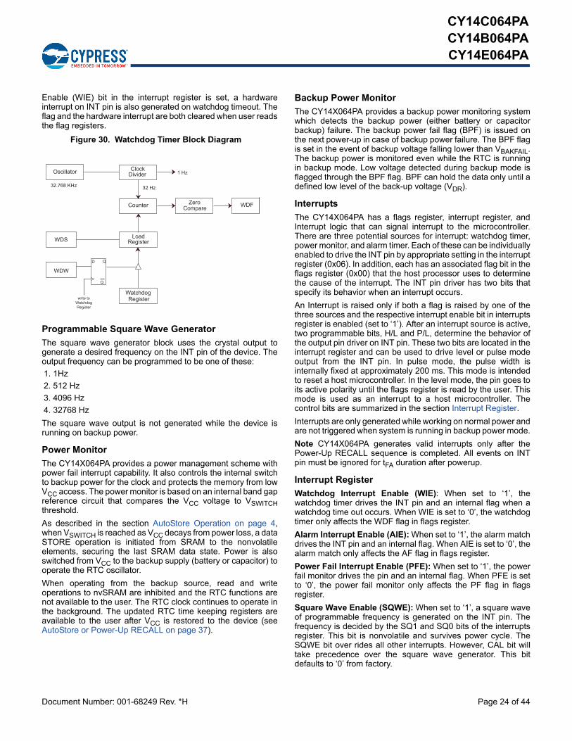
Document Number: 001-68249 Rev. *H Page 24 of 44
CY14C064PACY14B064PACY14E064PA
Enable (WIE) bit in the interrupt register is set, a hardwareinterrupt on INT pin is also generated on watchdog timeout. Theflag and the hardware interrupt are both cleared when user readsthe flag registers.
Programmable Square Wave Generator
The square wave generator block uses the crystal output togenerate a desired frequency on the INT pin of the device. Theoutput frequency can be programmed to be one of these:
1. 1Hz
2. 512 Hz
3. 4096 Hz
4. 32768 Hz
The square wave output is not generated while the device isrunning on backup power.
Power Monitor
The CY14X064PA provides a power management scheme withpower fail interrupt capability. It also controls the internal switchto backup power for the clock and protects the memory from lowVCC access. The power monitor is based on an internal band gapreference circuit that compares the VCC voltage to VSWITCHthreshold.
As described in the section AutoStore Operation on page 4,when VSWITCH is reached as VCC decays from power loss, a dataSTORE operation is initiated from SRAM to the nonvolatileelements, securing the last SRAM data state. Power is alsoswitched from VCC to the backup supply (battery or capacitor) tooperate the RTC oscillator.
When operating from the backup source, read and writeoperations to nvSRAM are inhibited and the RTC functions arenot available to the user. The RTC clock continues to operate inthe background. The updated RTC time keeping registers areavailable to the user after VCC is restored to the device (seeAutoStore or Power-Up RECALL on page 37).
Backup Power Monitor
The CY14X064PA provides a backup power monitoring systemwhich detects the backup power (either battery or capacitorbackup) failure. The backup power fail flag (BPF) is issued onthe next power-up in case of backup power failure. The BPF flagis set in the event of backup voltage falling lower than VBAKFAIL.The backup power is monitored even while the RTC is runningin backup mode. Low voltage detected during backup mode isflagged through the BPF flag. BPF can hold the data only until adefined low level of the back-up voltage (VDR).
Interrupts
The CY14X064PA has a flags register, interrupt register, andInterrupt logic that can signal interrupt to the microcontroller.There are three potential sources for interrupt: watchdog timer,power monitor, and alarm timer. Each of these can be individuallyenabled to drive the INT pin by appropriate setting in the interruptregister (0x06). In addition, each has an associated flag bit in theflags register (0x00) that the host processor uses to determinethe cause of the interrupt. The INT pin driver has two bits thatspecify its behavior when an interrupt occurs.
An Interrupt is raised only if both a flag is raised by one of thethree sources and the respective interrupt enable bit in interruptsregister is enabled (set to ‘1’). After an interrupt source is active,two programmable bits, H/L and P/L, determine the behavior ofthe output pin driver on INT pin. These two bits are located in theinterrupt register and can be used to drive level or pulse modeoutput from the INT pin. In pulse mode, the pulse width isinternally fixed at approximately 200 ms. This mode is intendedto reset a host microcontroller. In the level mode, the pin goes toits active polarity until the flags register is read by the user. Thismode is used as an interrupt to a host microcontroller. Thecontrol bits are summarized in the section Interrupt Register.
Interrupts are only generated while working on normal power andare not triggered when system is running in backup power mode.
Note CY14X064PA generates valid interrupts only after thePower-Up RECALL sequence is completed. All events on INTpin must be ignored for tFA duration after powerup.
Interrupt Register
Watchdog Interrupt Enable (WIE): When set to ‘1’, thewatchdog timer drives the INT pin and an internal flag when awatchdog time out occurs. When WIE is set to ‘0’, the watchdogtimer only affects the WDF flag in flags register.
Alarm Interrupt Enable (AIE): When set to ‘1’, the alarm matchdrives the INT pin and an internal flag. When AIE is set to ‘0’, thealarm match only affects the AF flag in flags register.
Power Fail Interrupt Enable (PFE): When set to ‘1’, the powerfail monitor drives the pin and an internal flag. When PFE is setto ‘0’, the power fail monitor only affects the PF flag in flagsregister.
Square Wave Enable (SQWE): When set to ‘1’, a square waveof programmable frequency is generated on the INT pin. Thefrequency is decided by the SQ1 and SQ0 bits of the interruptsregister. This bit is nonvolatile and survives power cycle. TheSQWE bit over rides all other interrupts. However, CAL bit willtake precedence over the square wave generator. This bitdefaults to ‘0’ from factory.
Figure 30. Watchdog Timer Block Diagram
1 HzOscillator ClockDivider
Counter ZeroCompare WDF
WDS LoadRegister
WDW
D Q
Q
WatchdogRegisterwrite to
WatchdogRegister
32 Hz32.768 KHz
Document Number: 001-68249 Rev. *H Page 25 of 44
CY14C064PACY14B064PACY14E064PA
High/Low (H/L): When set to a ‘1’, the INT pin is active HIGHand the driver mode is push pull. The INT pin drives HIGH onlywhen VCC is greater than VSWITCH. When set to a ‘0’, the INT pinis active LOW and the drive mode is open drain. The INT pinmust be pulled up to Vcc by a 10 k resistor while using theinterrupt in active LOW mode.
Pulse/Level (P/L): When set to a ‘1’ and an interrupt occurs, theINT pin is driven for approximately 200 ms. When P/L is set to a‘0’, the INT pin is driven HIGH or LOW (determined by H/L) untilthe flags register is read.
SQ1 and SQ0. These bits are used together to fix the frequencyof square wave on INT pin output when SQWE bit is set to ‘1’.These bits are nonvolatile and survive power cycle. The outputfrequency is decided as per the following table.
When an enabled interrupt source activates the INT pin, anexternal host reads the flag registers to determine the cause.Remember that all flag are cleared when the register is read. If
the INT pin is programmed for Level mode, then the conditionclears and the INT pin returns to its inactive state. If the pin isprogrammed for pulse mode, then reading the flag also clearsthe flag and the pin. The pulse does not complete its specifiedduration if the flags register is read. If the INT pin is used as ahost reset, the flags register is not read during a reset.
This summary table shows the state of the INT pin.
Flags Register
The flags register has three flag bits: WDF, AF, and PF, whichcan be used to generate an interrupt. These flag are set by thewatchdog timeout, alarm match, or power fail monitorrespectively. The processor can either poll this register or enableinterrupts to be informed when a flag is set. These flags areautomatically reset after the register is read. The flags register isautomatically loaded with the value 0x00 on power-up (exceptfor the OSCF bit. See Stopping and Starting the Oscillator onpage 22).
Table 9. SQW Output Selection
SQ1 SQ0 Frequency Comment
0 0 1 Hz 1 Hz signal
0 1 512 Hz Useful for calibration
1 0 4096 Hz 4 kHz clock output
1 1 32768 Hz Oscillator output frequency
Table 10. State of the INT pin
CAL SQWE WIE/AIE/PFE INT Pin Output
1 X X 512 Hz
0 1 X Square Wave Output
0 0 1 Alarm
0 0 0 HI-Z
Figure 31. Interrupt Block Diagram
WDF - Watchdog timer flagWIE - Watchdog interrupt
PF - Power fail flagPFE - Power fail enable
AF - Alarm fagAIE - Alarm interrupt enableP/L - Pulse levelH/L - High/Low
enable
PinDriver
WIE
WDF
WatchdogTimer
PFE
PF
AIE
AF
ClockAlarm
P/L
H/L
VCC
VSS
INT
SQWE
CAL
Mux
512 HzClock
SquareWave
PriorityEncoder
WIE/PIE/AIE
HI-Z Control
SEL Line
PowerMonitor
SQWE - Square wave enable
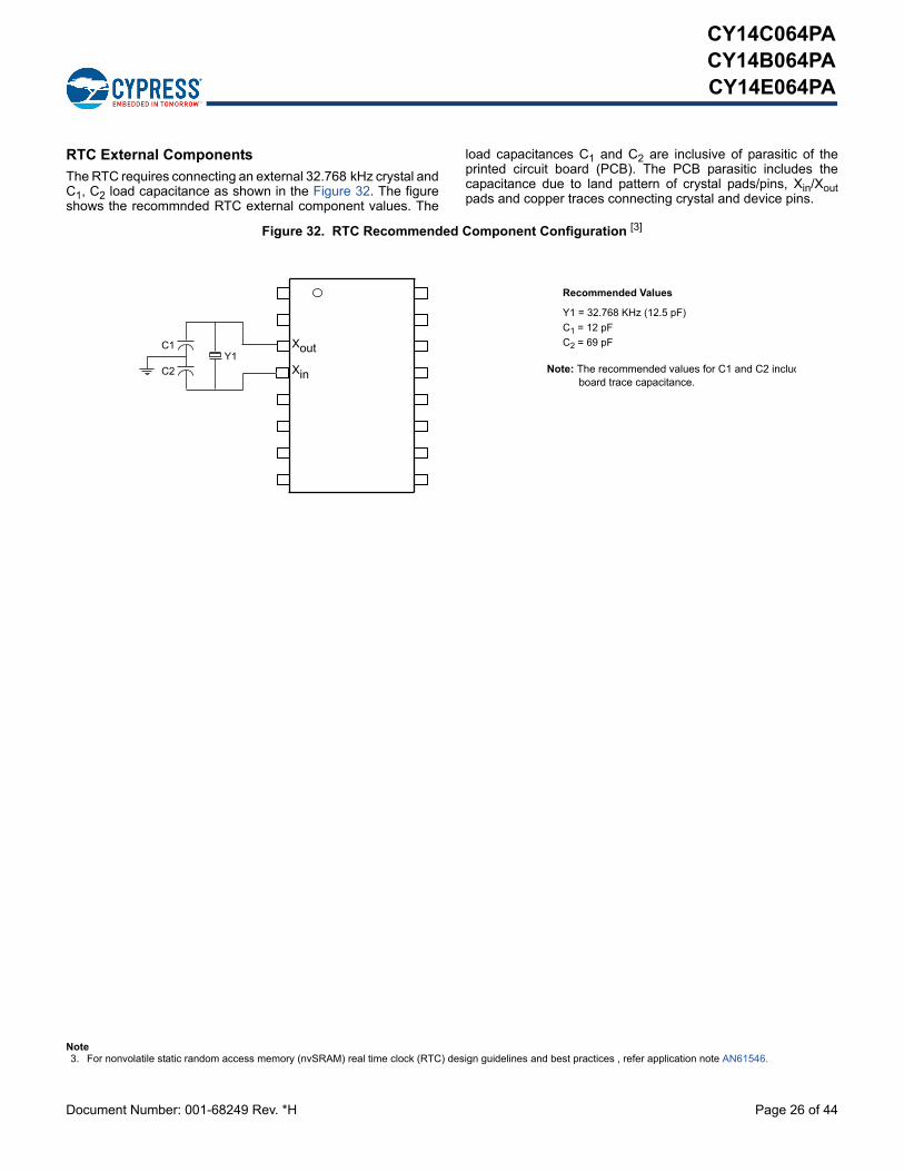
Document Number: 001-68249 Rev. *H Page 26 of 44
CY14C064PACY14B064PACY14E064PA
RTC External Components
The RTC requires connecting an external 32.768 kHz crystal andC1, C2 load capacitance as shown in the Figure 32. The figureshows the recommnded RTC external component values. The
load capacitances C1 and C2 are inclusive of parasitic of theprinted circuit board (PCB). The PCB parasitic includes thecapacitance due to land pattern of crystal pads/pins, Xin/Xoutpads and copper traces connecting crystal and device pins.
Figure 32. RTC Recommended Component Configuration [3]
Recommended Values
Y1 = 32.768 KHz (12.5 pF)
C1 = 12 pF
C2 = 69 pFXout
XinY1
C2
C1
Note: The recommended values for C1 and C2 includboard trace capacitance.
Note3. For nonvolatile static random access memory (nvSRAM) real time clock (RTC) design guidelines and best practices , refer application note AN61546.

Document Number: 001-68249 Rev. *H Page 27 of 44
CY14C064PACY14B064PACY14E064PA
PCB Design Considerations for RTC
RTC crystal oscillator is a low current circuit with high impedancenodes on their crystal pins. Due to lower timekeeping current ofRTC, the crystal connections are very sensitive to noise on theboard. Hence it is necessary to isolate the RTC circuit from othersignals on the board.
It is also critical to minimize the stray capacitance on the PCB.Stray capacitances add to the overall crystal load capacitanceand therefore cause oscillation frequency errors. Properbypassing and careful layout are required to achieve theoptimum RTC performance.
Layout requirements
The board layout must adhere to (but not limited to) the followingguidelines during routing RTC circuitry. Following these guide-lines help you achieve optimum performance from the RTCdesign.
■ It is important to place the crystal as close as possible to theXin and Xout pins. Keep the trace lengths between the crystaland RTC equal in length and as short as possible to reduce theprobability of noise coupling by reducing the length of theantenna.
■ Keep Xin and Xout trace width lesser than 8 mils. Wider tracewidth leads to larger trace capacitance. The larger these bondpads and traces are, the more likely it is that noise can couplefrom adjacent signals.
■ Shield the Xin and Xout signals by providing a guard ring aroundthe crystal circuitry. This guard ring prevents noise couplingfrom neighboring signals.
■ Take care while routing any other high speed signal in thevicinity of RTC traces. The more the crystal is isolated fromother signals on the board, the less likely it is that noise iscoupled into the crystal. Maintain a minimum of 200 milseparation between the Xin, Xout traces and any other highspeed signal on the board.
■ No signals should run underneath crystal components on thesame PCB layer.
■ Create an isolated solid copper plane on adjacent PCB layerand underneath the crystal circuitry to prevent unwanted noisecoupled from traces routed on the other signal layers of thePCB. The local plane should be separated by at least 40 milsfrom the neighboring plane on the same PCB layer. The solidplane should be in the vicinity of RTC components only and itsperimeter should be kept equal to the guard ring perimeter.Figure 33 shows the recommended layout for RTC circuit.
Figure 33. Recommended Layout for RTC
Isolated ground plane on
Guard ring - Top (Component)
Via: Via connects to isolated ground plane on L2
Via: Via connects to system groundplane on L2
layer 2 : L2
layer: L1
System ground
Top component layer: L1
Ground plane layer: L2
C1
Y1
C2

Document Number: 001-68249 Rev. *H Page 28 of 44
CY14C064PACY14B064PACY14E064PA
Table 11. RTC Register Map [4, 5]
RegisterBCD Format Data
Function/RangeD7 D6 D5 D4 D3 D2 D1 D0
0x0F 10s years Years Years: 00–99
0x0E 0 0 0 10s months
Months Months: 01–12
0x0D 0 0 10s day of month Day of month Day of month: 01–31
0x0C 0 0 0 0 0 Day of week Day of week: 01–07
0x0B 0 0 10s hours Hours Hours: 00–23
0x0A 0 10s minutes Minutes Minutes: 00–59
0x09 0 10s seconds Seconds Seconds: 00–59
0x08 OSCEN (0)
0 Cal sign (0)
Calibration (00000) Calibration values [6]
0x07 WDS (0) WDW (0) WDT (000000) Watchdog [6]
0x06 WIE (0) AIE (0) PFE (0) SQWE (0)
H/L (1) P/L (0) SQ1 (0) SQ0 (0) Interrupts [6]
0x05 M (1) 0 10s alarm date Alarm day Alarm, day of month: 01–31
0x04 M (1) 0 10s alarm hours Alarm hours Alarm, hours: 00–23
0x03 M (1) 10s alarm minutes Alarm minutes Alarm, minutes: 00–59
0x02 M (1) 10s alarm seconds Alarm seconds Alarm, seconds: 00–59
0x01 10s centuries Centuries Centuries: 00–99
0x00 WDF AF PF OSCF[7] BPF[7] CAL (0) W (0) R (0) Flags [6]
Notes4. ( ) designates values shipped from the factory.5. The unused bits of RTC registers are reserved for future use and should be set to ‘0’.6. This is a binary value, not a BCD value.7. When user resets OSCF and BPF flag bits, the flags register will be updated after tRTCp time.
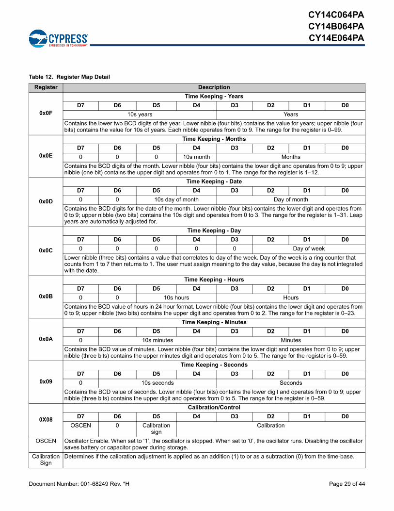
Document Number: 001-68249 Rev. *H Page 29 of 44
CY14C064PACY14B064PACY14E064PA
Table 12. Register Map Detail
Register Description
0x0F
Time Keeping - Years
D7 D6 D5 D4 D3 D2 D1 D0
10s years Years
Contains the lower two BCD digits of the year. Lower nibble (four bits) contains the value for years; upper nibble (four bits) contains the value for 10s of years. Each nibble operates from 0 to 9. The range for the register is 0–99.
0x0E
Time Keeping - Months
D7 D6 D5 D4 D3 D2 D1 D0
0 0 0 10s month Months
Contains the BCD digits of the month. Lower nibble (four bits) contains the lower digit and operates from 0 to 9; upper nibble (one bit) contains the upper digit and operates from 0 to 1. The range for the register is 1–12.
0x0D
Time Keeping - Date
D7 D6 D5 D4 D3 D2 D1 D0
0 0 10s day of month Day of month
Contains the BCD digits for the date of the month. Lower nibble (four bits) contains the lower digit and operates from 0 to 9; upper nibble (two bits) contains the 10s digit and operates from 0 to 3. The range for the register is 1–31. Leap years are automatically adjusted for.
0x0C
Time Keeping - Day
D7 D6 D5 D4 D3 D2 D1 D0
0 0 0 0 0 Day of week
Lower nibble (three bits) contains a value that correlates to day of the week. Day of the week is a ring counter that counts from 1 to 7 then returns to 1. The user must assign meaning to the day value, because the day is not integrated with the date.
0x0B
Time Keeping - Hours
D7 D6 D5 D4 D3 D2 D1 D0
0 0 10s hours Hours
Contains the BCD value of hours in 24 hour format. Lower nibble (four bits) contains the lower digit and operates from 0 to 9; upper nibble (two bits) contains the upper digit and operates from 0 to 2. The range for the register is 0–23.
0x0A
Time Keeping - Minutes
D7 D6 D5 D4 D3 D2 D1 D0
0 10s minutes Minutes
Contains the BCD value of minutes. Lower nibble (four bits) contains the lower digit and operates from 0 to 9; upper nibble (three bits) contains the upper minutes digit and operates from 0 to 5. The range for the register is 0–59.
0x09
Time Keeping - Seconds
D7 D6 D5 D4 D3 D2 D1 D0
0 10s seconds Seconds
Contains the BCD value of seconds. Lower nibble (four bits) contains the lower digit and operates from 0 to 9; upper nibble (three bits) contains the upper digit and operates from 0 to 5. The range for the register is 0–59.
0X08
Calibration/Control
D7 D6 D5 D4 D3 D2 D1 D0
OSCEN 0 Calibration sign
Calibration
OSCEN Oscillator Enable. When set to ‘1’, the oscillator is stopped. When set to ‘0’, the oscillator runs. Disabling the oscillator saves battery or capacitor power during storage.
Calibration Sign
Determines if the calibration adjustment is applied as an addition (1) to or as a subtraction (0) from the time-base.

Document Number: 001-68249 Rev. *H Page 30 of 44
CY14C064PACY14B064PACY14E064PA
Calibration These five bits control the calibration of the clock.
0x07
Watchdog Timer
D7 D6 D5 D4 D3 D2 D1 D0
WDS WDW WDT
WDS Watchdog Strobe. Setting this bit to ‘1’ reloads and restarts the watchdog timer. Setting the bit to ‘0’ has no effect. The bit is cleared automatically after the watchdog timer is reset. The WDS bit is write only. Reading it always returns a ‘0’.
WDW Watchdog Write Enable. Setting this bit to ‘1’ disables any WRITE to the watchdog timeout value (D5–D0). This enables the user to set the watchdog strobe bit without disturbing the timeout value. Setting this bit to ‘0’ allows bits D5–D0 to be written to the watchdog register when the next write cycle is complete. This function is explained in more detail in Watchdog Timer on page 23.
WDT Watchdog Timeout Selection. The watchdog timer interval is selected by the 6-bit value in this register. It represents a multiplier of the 32 Hz count (31.25 ms). The range of timeout value is 31.25 ms (a setting of 1) to 2 seconds (setting of 3 Fh). Setting the watchdog timer register to 0 disables the timer. These bits can be written only if the WDW bit was set to ‘0’ on a previous cycle.
0x06
Interrupt Status/Control
D7 D6 D5 D4 D3 D2 D1 D0
WIE AIE PFE SQWE H/L P/L SQ1 SQ0
WIE Watchdog Interrupt Enable. When set to ‘1’ and a watchdog timeout occurs, the watchdog timer drives the INT pin and the WDF flag. When set to ‘0’, the watchdog timeout affects only the WDF flag.
AIE Alarm Interrupt Enable. When set to ‘1’, the alarm match drives the INT pin and the AF flag. When set to ‘0’, the alarm match only affects the AF flag.
PFE Power Fail Enable. When set to ‘1’, the alarm match drives the INT pin and the PF flag. When set to ‘0’, the power fail monitor affects only the PF flag.
SQWE Square Wave Enable. When set to ‘1’, a square wave is driven on the INT pin with frequency programmed using SQ1 and SQ0 bits. The square wave output takes precedence over interrupt logic. If the SQWE bit is set to ‘1’. when an enabled interrupt source becomes active, only the corresponding flag is raised and the INT pin continues to drive the square wave.
H/L High/Low. When set to ‘1’, the INT pin is driven active HIGH. When set to ‘0’, the INT pin is open drain, active LOW.
P/L Pulse/Level. When set to ‘1’, the INT pin is driven active (determined by H/L) by an interrupt source for approximately 200 ms. When set to ‘0’, the INT pin is driven to an active level (as set by H/L) until the flags register is read.
SQ1, SQ0 SQ1, SQ0. These bits are used to decide the frequency of the Square wave on the INT pin output when SQWE bit is set to ‘1’. The following is the frequency output for each combination of (SQ1, SQ0): (0, 0) - 1 Hz (0, 1) - 512 Hz (1, 0) - 4096 Hz (1, 1) - 32768 Hz
0x05
Alarm - Day
D7 D6 D5 D4 D3 D2 D1 D0
M 0 10s alarm date Alarm date
Contains the alarm value for the date of the month and the mask bit to select or deselect the date value.
M Match. When this bit is set to ‘0’, the date value is used in the alarm match. Setting this bit to ‘1’ causes the match circuit to ignore the date value.
0x04
Alarm - Hours
D7 D6 D5 D4 D3 D2 D1 D0
M 0 10s alarm hours Alarm hours
Contains the alarm value for the hours and the mask bit to select or deselect the hours value.
M Match. When this bit is set to ‘0’, the hours value is used in the alarm match. Setting this bit to ‘1’ causes the match circuit to ignore the hours value.
Table 12. Register Map Detail (continued)
Register Description

Document Number: 001-68249 Rev. *H Page 31 of 44
CY14C064PACY14B064PACY14E064PA
0x03
Alarm - Minutes
D7 D6 D5 D4 D3 D2 D1 D0
M 10s alarm minutes Alarm minutes
Contains the alarm value for the minutes and the mask bit to select or deselect the minutes value.
M Match. When this bit is set to ‘0’, the minutes value is used in the alarm match. Setting this bit to ‘1’ causes the match circuit to ignore the minutes value.
0x02
Alarm - Seconds
D7 D6 D5 D4 D3 D2 D1 D0
M 10s alarm seconds Alarm seconds
Contains the alarm value for the seconds and the mask bit to select or deselect the seconds’ value.
M Match. When this bit is set to ‘0’, the seconds value is used in the alarm match. Setting this bit to ‘1’ causes the match circuit to ignore the seconds value.
0x01
Time Keeping - Centuries
D7 D6 D5 D4 D3 D2 D1 D0
10s centuries Centuries
Contains the BCD value of centuries. Lower nibble contains the lower digit and operates from 0 to 9; upper nibble contains the upper digit and operates from 0 to 9. The range for the register is 0-99 centuries.
0x00
Flags
D7 D6 D5 D4 D3 D2 D1 D0
WDF AF PF OSCF BPF CAL W R
WDF Watchdog Timer Flag. This read only bit is set to ‘1’ when the watchdog timer is allowed to reach 0 without being reset by the user. It is cleared to ‘0’ when the flags register is read or on power-up
AF Alarm Flag. This read only bit is set to ‘1’ when the time and date match the values stored in the alarm registers with the match bits = ‘0’. It is cleared when the flags register is read or on power-up.
PF Power Fail Flag. This read only bit is set to ‘1’ when power falls below the power fail threshold VSWITCH. It is cleared when the flags register is read.
OSCF Oscillator Fail Flag. Set to ‘1’ on power-up if the oscillator is enabled and not running in the first 5 ms of operation. This indicates that RTC backup power failed and clock value is no longer valid. This bit survives power cycle and is never cleared internally by the chip. The user must check for this condition and write '0' to clear this flag. When user resets OSCF flag bit, the bit will be updated after tRTCp time.
BPF Backup Power Fail Flag. Set to ‘1’ on power-up if the backup power (battery or capacitor) failed. The backup power fail condition is determined by the voltage falling below their respective minimum specified voltage. BPF can hold the data only until a defined low level of the back-up voltage (VDR). User must reset this bit to clear this flag. When user resets BPF flag bit, the bit will be updated after tRTCp time.
CAL Calibration Mode. When set to ‘1’, a 512 Hz square wave is output on the INT pin. When set to ‘0’, the INT pin resumes normal operation. This bit takes priority than SQ0/SQ1 and other functions. This bit defaults to ‘0’ (disabled) on power-up.
W Write Enable: Setting the ‘W’ bit to ‘1’ freezes updates of the RTC registers. The user can then write to RTC registers, alarm registers, calibration register, interrupt register and flags register. Setting the ‘W’ bit to ‘0’ causes the contents of the RTC registers to be transferred to the time keeping counters if the time has changed. This transfer process takes tRTCp time to complete. This bit defaults to 0 on power-up.
R Read Enable: Setting ‘R’ bit to ‘1’, stops clock updates to user RTC registers so that clock updates are not seen during the reading process. Set ‘R’ bit to ‘0’ to resume clock updates to the holding register. Setting this bit does not require ‘W’ bit to be set to ‘1’. This bit defaults to ‘0’ on power-up.
Table 12. Register Map Detail (continued)
Register Description

Document Number: 001-68249 Rev. *H Page 32 of 44
CY14C064PACY14B064PACY14E064PA
Maximum Ratings
Exceeding maximum ratings may shorten the useful life of thedevice. These user guidelines are not tested.
Storage temperature ................................ –65 C to +150 C
Maximum accumulated storage timeAt 150 C ambient temperature ...................... 1000 hAt 85 C ambient temperature .................... 20 Years
Maximum junction temperature ................................. 150 C
Supply voltage on VCC relative to VSS CY14C064PA: ...................................–0.5 V to +3.1 VCY14B064PA: ...................................–0.5 V to +4.1 VCY14E064PA: ...................................–0.5 V to +7.0 V
DC voltage applied to outputs in High Z state .................................... –0.5 V to VCC + 0.5 V
Input voltage ....................................... –0.5 V to VCC + 0.5 V
Transient voltage (< 20 ns) on any pin to ground potential ................. –2.0 V to VCC + 2.0 V
Package power dissipation capability (TA = 25 °C) ................................................. 1.0 W
Surface mount lead soldering temperature (3 seconds) ......................................... +260 C
DC output current (1 output at a time, 1s duration) .... 15 mA
Static discharge voltage (per MIL-STD-883, Method 3015) .......................... > 2001 V
Latch-up current .................................................... > 140 mA
Operating Range
Device Range Ambient Temperature VCC
CY14C064PA Industrial –40 C to +85 C 2.4 V to 2.6 VCY14B064PA 2.7 V to 3.6 VCY14E064PA 4.5 V to 5.5 V
DC Electrical Characteristics
Over the Operating RangeParameter Description Test Conditions Min Typ [8] Max Unit
VCC Power supply CY14C064PA 2.4 2.5 2.6 V
CY14B064PA 2.7 3.0 3.6 V
CY14E064PA 4.5 5.0 5.5 V
ICC1 Average VCC current fSCK = 40 MHz; Values obtained without output loads (IOUT = 0 mA)
CY14C064PA – – 3 mA
CY14B064PA
CY14E064PA – – 4 mA
fSCK = 104 MHz; Values obtained without output loads (IOUT = 0 mA)
– – 10 mA
ICC2 Average VCC current during STORE
All inputs don’t care, VCC = max Average current for duration tSTORE
– – 3 mA
ICC3 Average VCC current fSCK = 1 MHz; VCC = VCC(Typ), 25 °C
All inputs cycling at CMOS levels.Values obtained without output loads (IOUT = 0 mA)
– – 1 mA
ICC4 Average VCAP current during AutoStore cycle
All inputs don't care. Average current for duration tSTORE
– – 3 mA
ISB VCC standby current CS > (VCC – 0.2 V). VIN < 0.2 V or > (VCC – 0.2 V). ‘W’ bit set to ‘0’. Standby current level after nonvolatile cycle is complete. Inputs are static. fSCK = 0 MHz.
– – 250 A
IZZ Sleep mode current tSLEEP time after SLEEP instruction is registered. All inputs are static and configured at CMOS logic level.
– – 8 A
IIX[9] Input leakage current (except
HSB)–1 – +1 A
Input leakage current (for HSB) –100 – +1 A
IOZ Off state output leakage current –1 – +1 A
Notes8. Typical values are at 25 °C, VCC = VCC(Typ). Not 100% tested.9. The HSB pin has IOUT = -2 µA for VOH of 2.4 V when both active HIGH and LOW drivers are disabled. When they are enabled standard VOH and VOL are valid. This
parameter is characterized but not tested.
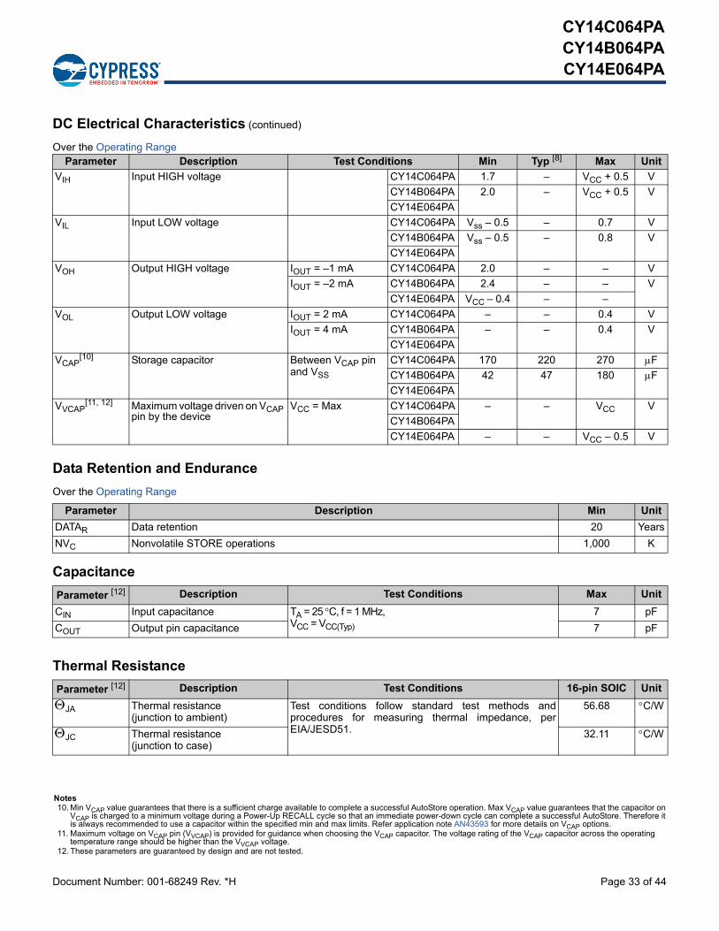
Document Number: 001-68249 Rev. *H Page 33 of 44
CY14C064PACY14B064PACY14E064PA
VIH Input HIGH voltage CY14C064PA 1.7 – VCC + 0.5 V
CY14B064PA 2.0 – VCC + 0.5 V
CY14E064PA
VIL Input LOW voltage CY14C064PA Vss – 0.5 – 0.7 V
CY14B064PA Vss – 0.5 – 0.8 V
CY14E064PA
VOH Output HIGH voltage IOUT = –1 mA CY14C064PA 2.0 – – V
IOUT = –2 mA CY14B064PA 2.4 – – V
CY14E064PA VCC – 0.4 – –
VOL Output LOW voltage IOUT = 2 mA CY14C064PA – – 0.4 V
IOUT = 4 mA CY14B064PA – – 0.4 V
CY14E064PA
VCAP[10] Storage capacitor Between VCAP pin
and VSS CY14C064PA 170 220 270 F
CY14B064PA 42 47 180 F
CY14E064PA
VVCAP[11, 12] Maximum voltage driven on VCAP
pin by the deviceVCC = Max CY14C064PA – – VCC V
CY14B064PA
CY14E064PA – – VCC – 0.5 V
DC Electrical Characteristics (continued)
Over the Operating RangeParameter Description Test Conditions Min Typ [8] Max Unit
Data Retention and Endurance
Over the Operating Range
Parameter Description Min Unit
DATAR Data retention 20 Years
NVC Nonvolatile STORE operations 1,000 K
Capacitance
Parameter [12] Description Test Conditions Max Unit
CIN Input capacitance TA = 25 C, f = 1 MHz, VCC = VCC(Typ)
7 pF
COUT Output pin capacitance 7 pF
Thermal Resistance
Parameter [12] Description Test Conditions 16-pin SOIC Unit
JA Thermal resistance (junction to ambient)
Test conditions follow standard test methods andprocedures for measuring thermal impedance, perEIA/JESD51.
56.68 C/W
JC Thermal resistance (junction to case)
32.11 C/W
Notes10. Min VCAP value guarantees that there is a sufficient charge available to complete a successful AutoStore operation. Max VCAP value guarantees that the capacitor on
VCAP is charged to a minimum voltage during a Power-Up RECALL cycle so that an immediate power-down cycle can complete a successful AutoStore. Therefore it is always recommended to use a capacitor within the specified min and max limits. Refer application note AN43593 for more details on VCAP options.
11. Maximum voltage on VCAP pin (VVCAP) is provided for guidance when choosing the VCAP capacitor. The voltage rating of the VCAP capacitor across the operating temperature range should be higher than the VVCAP voltage.
12. These parameters are guaranteed by design and are not tested.
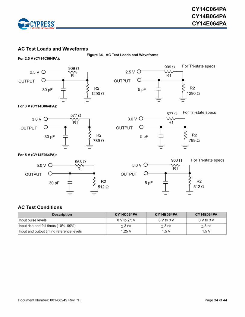
Document Number: 001-68249 Rev. *H Page 34 of 44
CY14C064PACY14B064PACY14E064PA
AC Test Loads and WaveformsFigure 34. AC Test Loads and Waveforms
For 2.5 V (CY14C064PA):
For 3 V (CY14B064PA):
For 5 V (CY14E064PA):
2.5 V
OUTPUT
5 pF
R1
R21290
2.5 V
OUTPUT
30 pF
R1
R21290
909 909 For Tri-state specs
3.0 V
OUTPUT
5 pF
R1
R2789
3.0 V
OUTPUT
30 pF
R1
R2789
577 577 For Tri-state specs
5.0 V
OUTPUT
5 pF
R1
R2512
5.0 V
OUTPUT
30 pF
R1
R2512
963 963 For Tri-state specs
AC Test Conditions
Description CY14C064PA CY14B064PA CY14E064PA
Input pulse levels 0 V to 2.5 V 0 V to 3 V 0 V to 3 V
Input rise and fall times (10%–90%) < 3 ns < 3 ns < 3 ns
Input and output timing reference levels 1.25 V 1.5 V 1.5 V

Document Number: 001-68249 Rev. *H Page 35 of 44
CY14C064PACY14B064PACY14E064PA
RTC Characteristics
Over the Operating Range
Parameter Description Min Typ[13] Max Units
VRTCbat RTC battery pin voltage 1.8 3.0 3.6 V
IBAK[14] RTC backup current
(Refer Figure 32 for the recommended external componets for RTC)
TA (Min) – – 0.45 µA
25 °C – 0.45 – µA
TA (Max) – – 0.60 µA
VRTCcap[15] RTC capacitor pin voltage TA (Min) 1.6 – 3.6 V
25 °C 1.5 3.0 3.6 V
TA (Max) 1.4 – 3.6 V
tOCS RTC oscillator time to start – 1 2 sec
VBAKFAIL Backup failure threshold 1.8 – 2.2 V
VDR BPF flag retention voltage 1.6 – – V
tRTCp RTC processing time from end of ‘W’ bit set to ‘0’ – – 1 ms
RBKCHG RTC backup capacitor charge current limiting resistor 350 – 850
AC Switching Characteristics
Over the Operating Range
Parameter [16]
Description25 MHz (RDRTC Instruction) [17] 40 MHz 104 MHz
UnitCypress Parameter
Alt. Parameter Min Max Min Max Min Max
fSCK fSCK Clock frequency, SCK – 25 – 40 – 104 MHz
tCL[18] tWL Clock pulse width LOW 18 – 11 – 4.5 – ns
tCH[18] tWH Clock pulse width HIGH 18 – 11 – 4.5 – ns
tCS tCE CS HIGH time 20 – 20 – 20 – ns
tCSS tCES CS setup time 10 – 10 – 5 – ns
tCSH tCEH CS hold time 10 – 10 – 5 – ns
tSD tSU Data in setup time 5 – 5 – 4 – ns
tHD tH Data in hold time 5 – 5 – 3 – ns
tHH tHD HOLD hold time 5 – 5 – 3 – ns
tSH tCD HOLD setup time 5 – 5 – 3 – ns
tCO tV Output valid – 15 – 9 – 8 ns
tHHZ[18] tHZ HOLD to output high Z – 15 – 15 – 8 ns
tHLZ[18] tLZ HOLD to output low Z – 15 – 15 – 8 ns
tOH tHO Output hold time 0 – 0 0 – ns
tHZCS[18] tDIS Output disable time – 25 – 20 – 8 ns
Notes13. Typical values are at 25 °C, VCC = VCC(Typ). Not 100% tested.14. Current drawn from either VRTCcap or VRTCbat when VCC < VSWITCH.15. If VRTCcap > 0.5 V or if no capacitor is connected to VRTCcap pin, the oscillator will start in tOCS time. If a backup capacitor is connected and VRTCcap < 0.5 V, the
capacitor must be allowed to charge to 0.5 V for oscillator to start.16. Test conditions assume signal transition time of 3 ns or less, timing reference levels of VCC/2, input pulse levels of 0 to VCC(typ), and output loading of the specified
IOL/IOH and load capacitance shown in Figure 34.17. Applicable for RTC opcode cycles, address cycles and data out cycles.18. These parameters are guaranteed by design and are not tested.
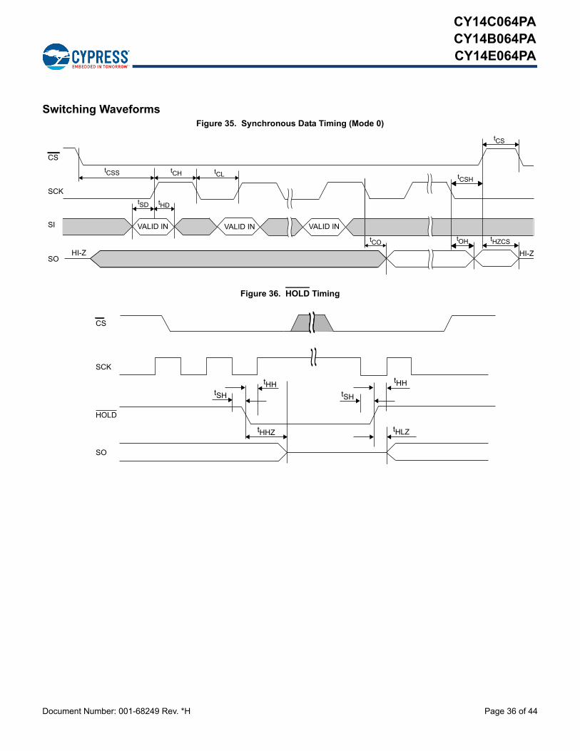
Document Number: 001-68249 Rev. *H Page 36 of 44
CY14C064PACY14B064PACY14E064PA
Switching WaveformsFigure 35. Synchronous Data Timing (Mode 0)
Figure 36. HOLD Timing
HI-Z
VALID IN
HI-Z
CS
SCK
SI
SO
tCLtCHtCSS
tSD tHD
tCO tOH
tCS
tCSH
tHZCS
VALID IN VALID IN
CS
SCK
HOLD
SO
tSH
tHHZ tHLZ
tHHtSH
tHH
~ ~~ ~
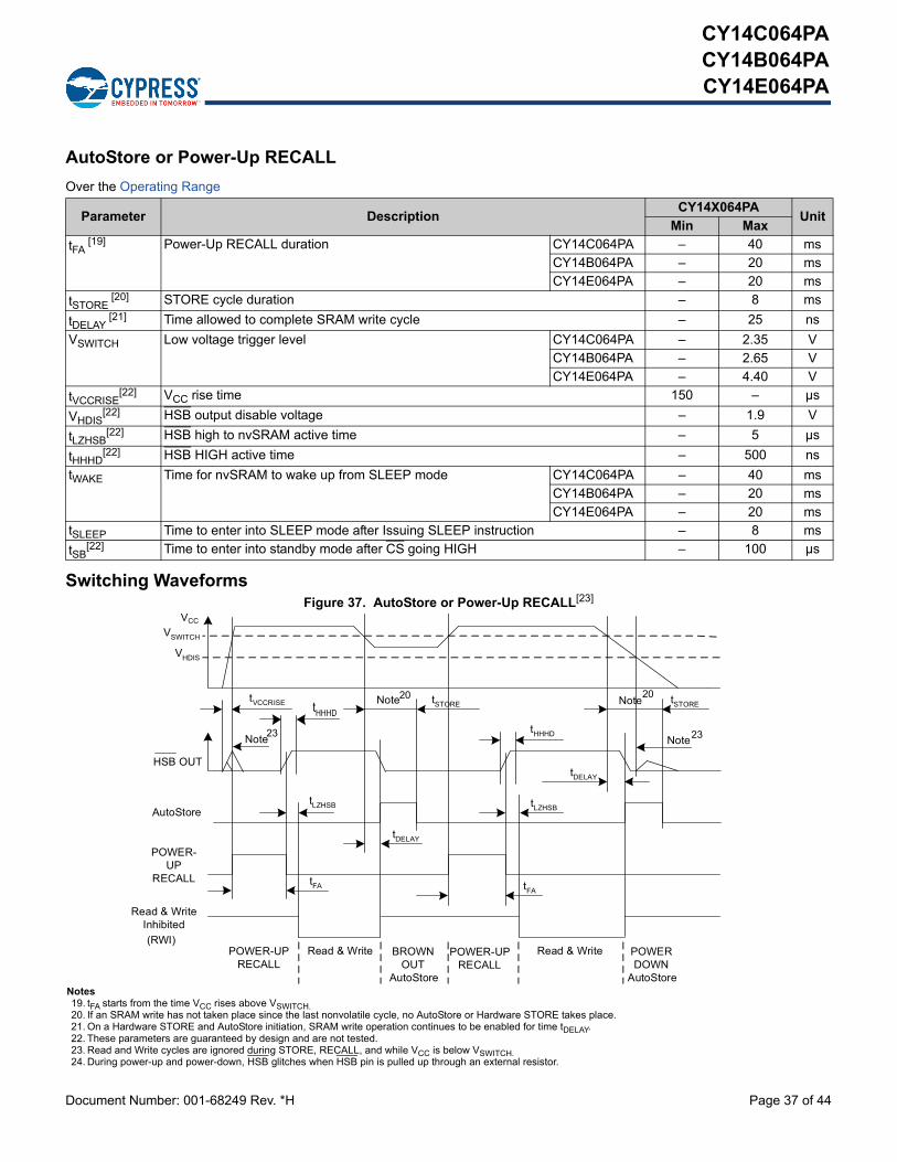
Document Number: 001-68249 Rev. *H Page 37 of 44
CY14C064PACY14B064PACY14E064PA
AutoStore or Power-Up RECALL
Over the Operating Range
Parameter DescriptionCY14X064PA
UnitMin Max
tFA [19] Power-Up RECALL duration CY14C064PA – 40 ms
CY14B064PA – 20 ms
CY14E064PA – 20 ms
tSTORE [20] STORE cycle duration – 8 ms
tDELAY [21] Time allowed to complete SRAM write cycle – 25 ns
VSWITCH Low voltage trigger level CY14C064PA – 2.35 V
CY14B064PA – 2.65 V
CY14E064PA – 4.40 V
tVCCRISE[22] VCC rise time 150 – µs
VHDIS[22] HSB output disable voltage – 1.9 V
tLZHSB[22] HSB high to nvSRAM active time – 5 µs
tHHHD[22] HSB HIGH active time – 500 ns
tWAKE Time for nvSRAM to wake up from SLEEP mode CY14C064PA – 40 ms
CY14B064PA – 20 ms
CY14E064PA – 20 ms
tSLEEP Time to enter into SLEEP mode after Issuing SLEEP instruction – 8 ms
tSB[22] Time to enter into standby mode after CS going HIGH – 100 µs
Switching WaveformsFigure 37. AutoStore or Power-Up RECALL[23]
VSWITCH
VHDIS
tVCCRISE tSTORE tSTOREtHHHD
tHHHD
tDELAY
tDELAY
tLZHSB tLZHSB
tFAtFA
HSB OUT
AutoStore
POWER-UP
RECALL
Read & WriteInhibited(RWI)
POWER-UPRECALL
Read & Write BROWNOUT
AutoStore
POWER-UPRECALL
Read & Write POWERDOWN
AutoStore
Note Note
NoteNote
VCC
23 23
20 20
Notes19. tFA starts from the time VCC rises above VSWITCH.20. If an SRAM write has not taken place since the last nonvolatile cycle, no AutoStore or Hardware STORE takes place.21. On a Hardware STORE and AutoStore initiation, SRAM write operation continues to be enabled for time tDELAY. 22. These parameters are guaranteed by design and are not tested.23. Read and Write cycles are ignored during STORE, RECALL, and while VCC is below VSWITCH.24. During power-up and power-down, HSB glitches when HSB pin is pulled up through an external resistor.

Document Number: 001-68249 Rev. *H Page 38 of 44
CY14C064PACY14B064PACY14E064PA
Software Controlled STORE/RECALL Cycles
Over the Operating Range
Parameter DescriptionCY14X064PA
UnitMin Max
tRECALL RECALL duration – 600 µs
tSS [25, 26] Soft sequence processing time – 500 µs
Switching Waveforms
Figure 38. Software STORE Cycle Figure 39. Software RECALL Cycle
Figure 40. AutoStore Enable Cycle Figure 41. AutoStore Disable Cycle
0 0 1 1 1 1 0 0
CS
SCK
SI
RWIHI-Z
0 1 2 3 4 5 6 7
RDY
tSTORE
0 1 1 0 0 0 0 0
CS
SCK
SI
0 1 2 3 4 5 6 7
RWIHI-Z
RDY
tRECALL
0 1 0 1 1 0 0 1
CS
SCK
SI
0 1 2 3 4 5 6 7
RWIHI-Z
RDY
tSS
0 0 0 1 1 0 0 1
SCK
SI
0 1 2 3 4 5 6 7
RWIHI-Z
RDY
CS
tSS
Notes25. This is the amount of time it takes to take action on a soft sequence command. Vcc power must remain HIGH to effectively register command.26. Commands such as STORE and RECALL lock out I/O until operation is complete which further increases this time. See the specific command.
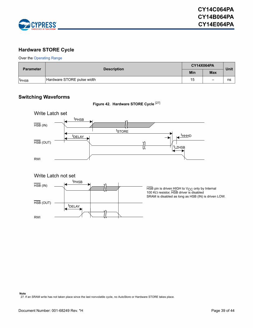
Document Number: 001-68249 Rev. *H Page 39 of 44
CY14C064PACY14B064PACY14E064PA
Hardware STORE Cycle
Over the Operating Range
Parameter DescriptionCY14X064PA
UnitMin Max
tPHSB Hardware STORE pulse width 15 – ns
Switching WaveformsFigure 42. Hardware STORE Cycle [27]
~ ~
HSB (IN)
HSB (OUT)
RWI
HSB (IN)
HSB (OUT)
RWI
tHHHD
tSTORE
tPHSB
tDELAY
tLZHSB
tDELAY
tPHSB
HSB pin is driven HIGH to VCC only by Internal 100 K resistor, HSB driver is disabledSRAM is disabled as long as HSB (IN) is driven LOW.
Write Latch not set
Write Latch set
~ ~~ ~
~ ~
Note27. If an SRAM write has not taken place since the last nonvolatile cycle, no AutoStore or Hardware STORE takes place.
Document Number: 001-68249 Rev. *H Page 40 of 44
CY14C064PACY14B064PACY14E064PA
Ordering Code Definitions
Ordering Information
Ordering Code Package Diagram Package Type Operating Range
CY14B064PA-SFXIT 51-85022 16-pin SOIC, 40 MHz Industrial
CY14B064PA-SFXI
All the above parts are Pb-free.
Option:T - Tape and ReelBlank - Std.
P - Serial (SPI) nvSRAM with RTC
Density:
064 - 64 Kb
Cypress
CY 14 B 064 P A - 104 SF X I T
14 - nvSRAM
Package:
SF - 16-pin SOIC
Temperature:I - Industrial (-40 to 85 °C)
Die revision:Blank - No Rev
A - 1st Rev
Voltage:C - 2.5 VB - 3.0 VE - 5.0 V
Pb-free
Frequency:Blank - 40 MHz104 - 104 MHz

Document Number: 001-68249 Rev. *H Page 41 of 44
CY14C064PACY14B064PACY14E064PA
Package DiagramFigure 43. 16-pin SOIC (0.413 × 0.299 × 0.0932 Inches) Package Outline, 51-85022
51-85022 *E
Document Number: 001-68249 Rev. *H Page 42 of 44
CY14C064PACY14B064PACY14E064PA
Acronyms Document Conventions
Units of MeasureAcronym Description
BCD Binary Coded Decimal
CPHA Clock Phase
CPOL Clock Polarity
CMOS Complementary Metal Oxide Semiconductor
CRC Cyclic Redundancy Check
EEPROM Electrically Erasable Programmable Read-Only Memory
EIA Electronic Industries Alliance
I/O Input/Output
JEDEC Joint Electron Devices Engineering Council
LSB Least Significant Bit
MSB Most Significant Bit
nvSRAM Non-volatile Static Random Access Memory
OSCF Oscillator Fail Flag
OSCF Oscillator Fail Flag
RWI Read and Write Inhibit
RTC Real Time Clock
RoHS Restriction of Hazardous Substances
SNL Serial Number Lock
SPI Serial Peripheral Interface
SONOS Silicon-Oxide-Nitride-Oxide Semiconductor
SOIC Small Outline Integrated Circuit
SRAM Static Random Access Memory
Symbol Unit of Measure
°C degree Celsius
F farad
Hz hertz
kHz kilohertz
k kilohm
MHz megahertz
A microampere
mA milliampere
F microfarad
s microsecond
ms millisecond
ns nanosecond
ohm
% percent
pF picofarad
ppm parts per million
sec second
V volt
W watt

Document Number: 001-68249 Rev. *H Page 43 of 44
CY14C064PACY14B064PACY14E064PA
Document History Page
Document Title: CY14C064PA, CY14B064PA, CY14E064PA, 64-Kbit (8 K × 8) SPI nvSRAM with Real Time ClockDocument Number: 001-68249
Rev. ECN Orig. of Change
Submission Date Description of Change
** 3202424 GVCH 03/22/2011 New data sheet.
*A 3248510 GVCH 05/04/2011 Changed status from Preliminary to Final.
*B 3386955 GVCH 09/28/2011 Updated Pin Definitions (Added Note 2 and referred the same note in VRTCcap, VRTCbat, Xout, Xin and INT/SQW parameters).Updated SPI Operating Features (Updated Power-Up (description)).Updated Special Instructions (Updated SLEEP Instruction (description), updated Figure 23).Updated Device ID (Updated Table 7 (Added Device ID (4 bytes) column)).Updated Real Time Clock Operation (Added Note 3 and referred the same note in Figure ).Updated DC Electrical Characteristics (Changed maximum value of ICC2 parameter from 2 mA to 3 mA, added Note 10 and referred the same note in VCAP parameter).Updated RTC Characteristics.Updated AC Switching Characteristics (Added Note 16 and referred the same note in Parameters column).Updated Package Diagram.
*C 3683851 GVCH 07/24/2012 Updated DC Electrical Characteristics (Added VVCAP parameter and its details, added Note 11 and referred the same note in VVCAP parameter, also referred Note 12 in VVCAP parameter).
*D 3762423 GVCH 10/01/2012 Updated Maximum Ratings (Removed “Ambient temperature with power applied” and included “Maximum junction temperature”).
*E 3985113 GVCH 04/29/2013 Updated RTC Characteristics:Changed maximum value of VBAKFAIL parameter from 2 V to 2.2 V.
Updated Package Diagram:spec 51-85022 – Changed revision from *D to *E.
*F 4042118 GVCH 06/27/2013 Updated Real Time Clock Operation:Updated Backup Power (Added Note).Added RTC External Components.Moved Figure 32 from Flags Register section to RTC External Components section.
Added PCB Design Considerations for RTC.
*G 4567905 GVCH 11/12/2014 Added related documentation hyperlink in page 1.
*H 6033841 GVCH 01/16/2018 Updated to the new template.Completing the Sunset review.
Document Number: 001-68249 Rev. *H Revised January 16, 2018 Page 44 of 44
© Cypress Semiconductor Corporation, 2011-2018. This document is the property of Cypress Semiconductor Corporation and its subsidiaries, including Spansion LLC (“Cypress”). This document,including any software or firmware included or referenced in this document (“Software”), is owned by Cypress under the intellectual property laws and treaties of the United States and other countriesworldwide. Cypress reserves all rights under such laws and treaties and does not, except as specifically stated in this paragraph, grant any license under its patents, copyrights, trademarks, or otherintellectual property rights. If the Software is not accompanied by a license agreement and you do not otherwise have a written agreement with Cypress governing the use of the Software, then Cypresshereby grants you a personal, non-exclusive, nontransferable license (without the right to sublicense) (1) under its copyright rights in the Software (a) for Software provided in source code form, tomodify and reproduce the Software solely for use with Cypress hardware products, only internally within your organization, and (b) to distribute the Software in binary code form externally to end users(either directly or indirectly through resellers and distributors), solely for use on Cypress hardware product units, and (2) under those claims of Cypress's patents that are infringed by the Software (asprovided by Cypress, unmodified) to make, use, distribute, and import the Software solely for use with Cypress hardware products. Any other use, reproduction, modification, translation, or compilationof the Software is prohibited.
TO THE EXTENT PERMITTED BY APPLICABLE LAW, CYPRESS MAKES NO WARRANTY OF ANY KIND, EXPRESS OR IMPLIED, WITH REGARD TO THIS DOCUMENT OR ANY SOFTWAREOR ACCOMPANYING HARDWARE, INCLUDING, BUT NOT LIMITED TO, THE IMPLIED WARRANTIES OF MERCHANTABILITY AND FITNESS FOR A PARTICULAR PURPOSE. No computingdevice can be absolutely secure. Therefore, despite security measures implemented in Cypress hardware or software products, Cypress does not assume any liability arising out of any security breach,such as unauthorized access to or use of a Cypress product. In addition, the products described in these materials may contain design defects or errors known as errata which may cause the productto deviate from published specifications. To the extent permitted by applicable law, Cypress reserves the right to make changes to this document without further notice. Cypress does not assume anyliability arising out of the application or use of any product or circuit described in this document. Any information provided in this document, including any sample design information or programmingcode, is provided only for reference purposes. It is the responsibility of the user of this document to properly design, program, and test the functionality and safety of any application made of thisinformation and any resulting product. Cypress products are not designed, intended, or authorized for use as critical components in systems designed or intended for the operation of weapons, weaponssystems, nuclear installations, life-support devices or systems, other medical devices or systems (including resuscitation equipment and surgical implants), pollution control or hazardous substancesmanagement, or other uses where the failure of the device or system could cause personal injury, death, or property damage (“Unintended Uses”). A critical component is any component of a deviceor system whose failure to perform can be reasonably expected to cause the failure of the device or system, or to affect its safety or effectiveness. Cypress is not liable, in whole or in part, and youshall and hereby do release Cypress from any claim, damage, or other liability arising from or related to all Unintended Uses of Cypress products. You shall indemnify and hold Cypress harmless fromand against all claims, costs, damages, and other liabilities, including claims for personal injury or death, arising from or related to any Unintended Uses of Cypress products.
Cypress, the Cypress logo, Spansion, the Spansion logo, and combinations thereof, WICED, PSoC, CapSense, EZ-USB, F-RAM, and Traveo are trademarks or registered trademarks of Cypress inthe United States and other countries. For a more complete list of Cypress trademarks, visit cypress.com. Other names and brands may be claimed as property of their respective owners.
CY14C064PACY14B064PACY14E064PA
Sales, Solutions, and Legal Information
Worldwide Sales and Design Support
Cypress maintains a worldwide network of offices, solution centers, manufacturer’s representatives, and distributors. To find the office closest to you, visit us at Cypress Locations.
Products
Arm® Cortex® Microcontrollers cypress.com/arm
Automotive cypress.com/automotive
Clocks & Buffers cypress.com/clocks
Interface cypress.com/interface
Internet of Things cypress.com/iot
Memory cypress.com/memory
Microcontrollers cypress.com/mcu
PSoC cypress.com/psoc
Power Management ICs cypress.com/pmic
Touch Sensing cypress.com/touch
USB Controllers cypress.com/usb
Wireless Connectivity cypress.com/wireless
PSoC® Solutions
PSoC 1 | PSoC 3 | PSoC 4 | PSoC 5LP | PSoC 6 MCU
Cypress Developer Community
Community | Projects | Video | Blogs | Training | Components
Technical Support
cypress.com/support


![kstu bdkbZ ][ktkSyh vafre es|k lwph d{kk 6ls 8 fo"k; %& xf.kr foKku](https://static.fdokumen.com/doc/165x107/63205239eb38487f6b0f93e3/kstu-bdkbz-ktksyh-vafre-esk-lwph-dkk-6ls-8-fok-xfkr-fokku.jpg)