B140XTT01.1 - Product Specification
33
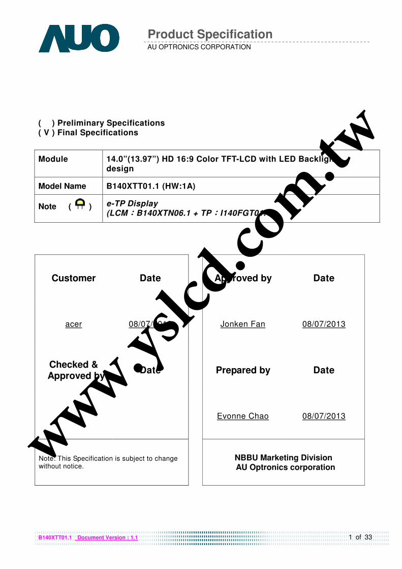
1 of 33 AU OPTRONICS CORPORATION Product Specification B140XTT01.1 Document Version : 1.1 ( V ) Preliminary Specifications ( V ) Final Specifications Module 14.0”(13.97”) HD 16:9 Color TFT-LCD with LED Backlight design Model Name B140XTT01.1 (HW:1A) Note ( ) e-TP Display (LCM:B140XTN06.1 + TP:I140FGT01.1) Customer Date acer 08/07/2013 Checked & Approved by Date Note: This Specification is subject to change without notice. Approved by Date Jonken Fan 08/07/2013 Prepared by Date Evonne Chao 08/07/2013 NBBU Marketing Division AU Optronics corporation www.yslcd.com.tw
-
Upload
khangminh22 -
Category
Documents
-
view
5 -
download
0
Transcript of B140XTT01.1 - Product Specification
1 of 33
AU OPTRONICS CORPORATION
Product Specification
B140XTT01.1 Document Version : 1.1
( V ) Preliminary Specifications ( V ) Final Specifications
Module 14.0”(13.97”) HD 16:9 Color TFT-LCD with LED Backlight design
Model Name B140XTT01.1 (HW:1A)
Note ( ) e-TP Display (LCM::::B140XTN06.1 + TP::::I140FGT01.1)
Customer Date
acer 08/07/2013
Checked & Approved by
Date
Note: This Specification is subject to change without notice.
Approved by Date
Jonken Fan 08/07/2013
Prepared by Date
Evonne Chao 08/07/2013
NBBU Marketing Division AU Optronics corporation
www.yslcd.com.tw
2 of 33
AU OPTRONICS CORPORATION
Product Specification
B140XTT01.1 Document Version : 1.1
Contents
1. Handling Precautions....................................................................................... 4
2. General Description.......................................................................................... 5
2.1 General Specification......................................................................................................... 5
2.2 General Touch Specification .............................................................................................. 7
2.3 Optical Characteristics....................................................................................................... 8
3. Functional Block Diagram.............................................................................. 13
4. Absolute Maximum Ratings ......................................................................... 13
4.1 Absolute Ratings of TFT LCD Module ............................................................................. 13
4.2 Absolute Ratings of Touch Sensor................................................................................... 13
4.3 Absolute Ratings of Environment..................................................................................... 13
5. Electrical Characteristics............................................................................... 15
5.1 TFT LCD Module ............................................................................................................. 15
5.2 Backlight Unit................................................................................................................... 18
5.3 Touch Sensor Power Consumption.................................................................................. 19
6. Signal Interface Characteristic ...................................................................... 20
6.1 Pixel Format Image.......................................................................................................... 20
6.3 Integration Interface Requirement ................................................................................... 21
7. Panel Reliability Test...................................................................................... 27
7.1 Vibration Test ................................................................................................................... 27
7.2 Shock Test ....................................................................................................................... 27
7.3 Reliability Test .................................................................................................................. 27
8. Mechanical Characteristics ........................................................................... 28
8.1 Total Solution Outline Dimension..................................................................................... 28
9. Shipping and Package ................................................................................... 30
9.1 Shipping Label Format..................................................................................................... 30
9.2 Shipping Package of Palletizing Sequence ..................................................................... 30
www.yslcd.com.tw
3 of 33
AU OPTRONICS CORPORATION
Product Specification
B140XTT01.1 Document Version : 1.1
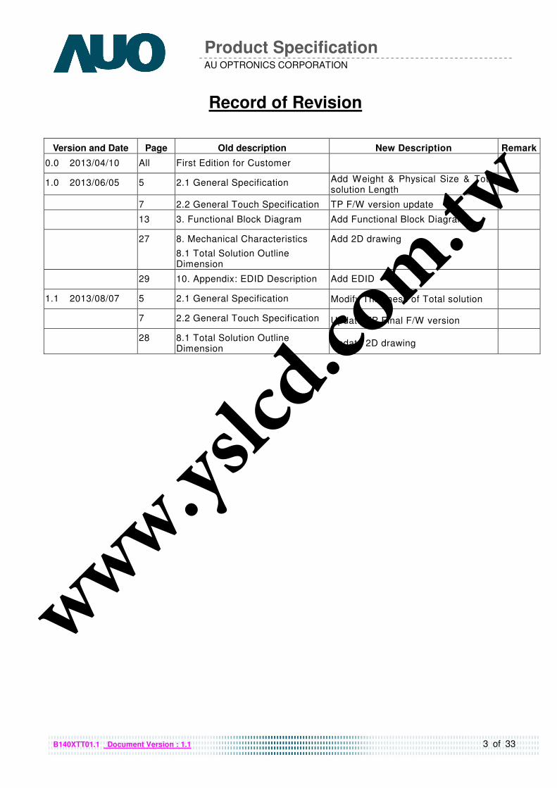
Record of Revision
Version and Date Page Old description New Description Remark
0.0 2013/04/10 All First Edition for Customer
1.0 2013/06/05 5 2.1 General Specification Add Weight & Physical Size & Total solution Length
7 2.2 General Touch Specification TP F/W version update
13 3. Functional Block Diagram Add Functional Block Diagram
27 8. Mechanical Characteristics
8.1 Total Solution Outline Dimension
Add 2D drawing
29 10. Appendix: EDID Description Add EDID
1.1 2013/08/07 5 2.1 General Specification Modify Thickness of Total solution
7 2.2 General Touch Specification Update TP Final F/W version
28 8.1 Total Solution Outline Dimension
Update 2D drawing
www.yslcd.com.tw
4 of 33
AU OPTRONICS CORPORATION
Product Specification
B140XTT01.1 Document Version : 1.1
1. Handling Precautions 1) Since front polarizer is easily damaged, pay attention not to scratch it.
2) Be sure to turn off power supply when inserting or disconnecting from input
connector.
3) Wipe off water drop immediately. Long contact with water may cause discoloration
or spots.
4) When the panel surface is soiled, wipe it with absorbent cotton or other soft cloth.
5) Since the panel is made of glass, it may break or crack if dropped or bumped on
hard surface.
6) Since CMOS LSI is used in this module, take care of static electricity and insure
human earth when handling.
7) Do not open nor modify the Module Assembly.
8) Do not press the reflector sheet at the back of the module to any directions.
9) At the insertion or removal of the Signal Interface Connector, be sure not to rotate
nor tilt the Interface Connector of the TFT Module.
10) After installation of the TFT Module into an enclosure (Notebook PC Bezel, for
example), do not twist nor bend the TFT Module even momentary. At designing the
enclosure, it should be taken into consideration that no bending/twisting forces are
applied to the TFT Module from outside. Otherwise the TFT Module may be
damaged.
11)Small amount of materials having no flammability grade is used in the LCD module.
The LCD module should be supplied by power complied with requirements of
Limited Power Source (IEC60950 or UL1950), or be applied exemption.
12)Disconnecting power supply before handling LCD modules, it can prevent electric
shock, DO NOT TOUCH the electrode parts, cables, connectors and LED circuit
part of TFT module that a LED light bar build in as a light source of back light unit. It
can prevent electrostatic breakdown.
www.yslcd.com.tw
5 of 33
AU OPTRONICS CORPORATION
Product Specification
B140XTT01.1 Document Version : 1.1
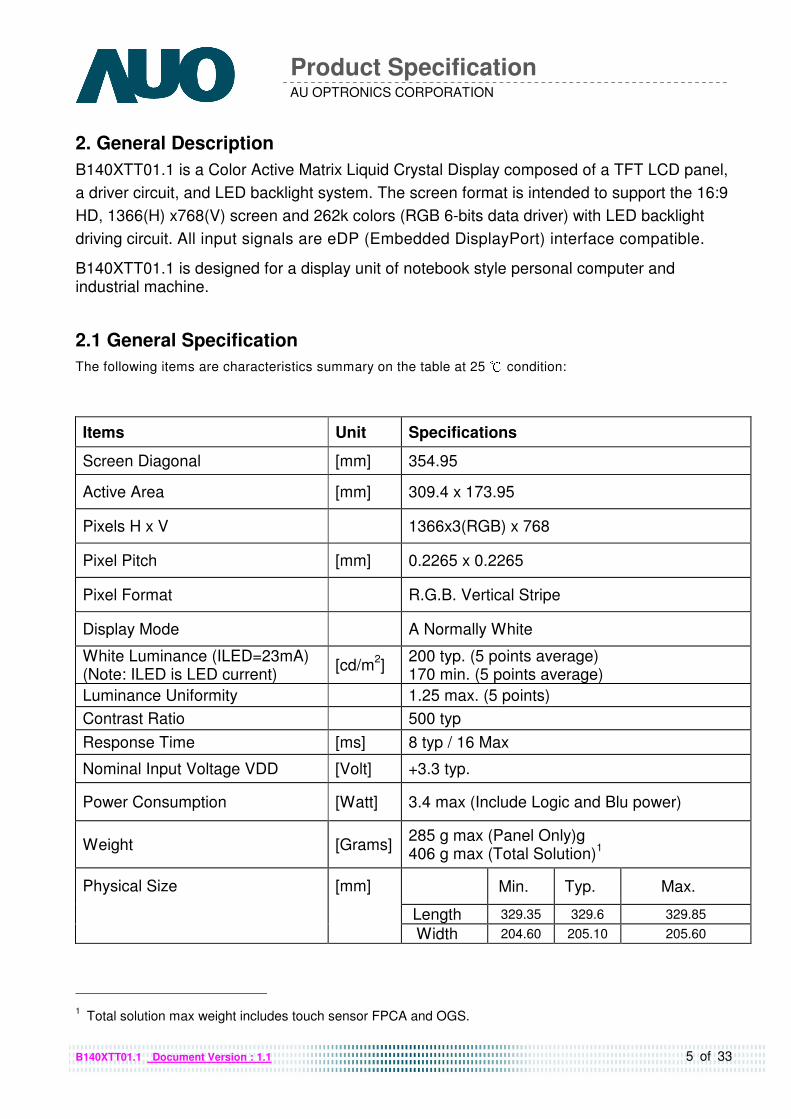
2. General Description
B140XTT01.1 is a Color Active Matrix Liquid Crystal Display composed of a TFT LCD panel,
a driver circuit, and LED backlight system. The screen format is intended to support the 16:9
HD, 1366(H) x768(V) screen and 262k colors (RGB 6-bits data driver) with LED backlight
driving circuit. All input signals are eDP (Embedded DisplayPort) interface compatible.
B140XTT01.1 is designed for a display unit of notebook style personal computer and industrial machine.
2.1 General Specification
The following items are characteristics summary on the table at 25 ℃ condition:
Items Unit Specifications
Screen Diagonal [mm] 354.95
Active Area [mm] 309.4 x 173.95
Pixels H x V 1366x3(RGB) x 768
Pixel Pitch [mm] 0.2265 x 0.2265
Pixel Format R.G.B. Vertical Stripe
Display Mode A Normally White
White Luminance (ILED=23mA) (Note: ILED is LED current)
[cd/m2]
200 typ. (5 points average) 170 min. (5 points average)
Luminance Uniformity 1.25 max. (5 points)
Contrast Ratio 500 typ
Response Time [ms] 8 typ / 16 Max
Nominal Input Voltage VDD [Volt] +3.3 typ.
Power Consumption [Watt] 3.4 max (Include Logic and Blu power)
Weight [Grams] 285 g max (Panel Only)g 406 g max (Total Solution)
1
Min. Typ. Max.
Length 329.35 329.6 329.85
Physical Size [mm]
Width 204.60 205.10 205.60
1 Total solution max weight includes touch sensor FPCA and OGS.
www.yslcd.com.tw
6 of 33
AU OPTRONICS CORPORATION
Product Specification
B140XTT01.1 Document Version : 1.1
Thickness - - 3.0 (Panel Side) 3.0 (PCBA Side)
Min. Typ. Max.
Length 329.33 329.58 329.83
Width 204.60 205.10 205.60
(206.94 with FPCA) Total solution [Note: OGS Touch module]
[mm]
Thickness - - 3.95 (Panel Side) 3.8 (PCBA Side)
5.3 (Total)
Electrical Interface 1 Lane eDP 1.2
Glass Thickness [mm] 0.4
Surface Treatment Glare, Hardness 3H
Support Color 262K colors ( RGB 6-bit )
Temperature Range Operating Storage (Non-Operating)
[oC]
[oC]
-20 to +60 -20 to +60
RoHS Compliance RoHS Compliance
www.yslcd.com.tw
7 of 33
AU OPTRONICS CORPORATION
Product Specification
B140XTT01.1 Document Version : 1.1
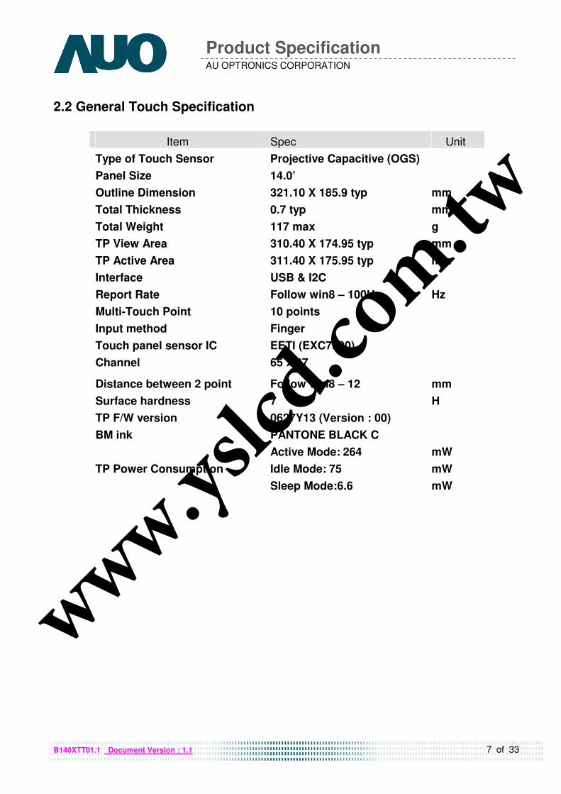
2.2 General Touch Specification
Item Spec Unit
Type of Touch Sensor Projective Capacitive (OGS)
Panel Size 14.0’
Outline Dimension 321.10 X 185.9 typ mm
Total Thickness 0.7 typ mm
Total Weight 117 max g
TP View Area 310.40 X 174.95 typ mm
TP Active Area 311.40 X 175.95 typ mm
Interface USB & I2C
Report Rate Follow win8 – 100Hz Hz
Multi-Touch Point 10 points
Input method Finger
Touch panel sensor IC EETI (EXC7900)
Channel 65 x 37
Distance between 2 point Follow win8 – 12 mm
Surface hardness 7 H
TP F/W version 0627Y13 (Version : 00)
BM ink PANTONE BLACK C
Active Mode: 264 mW
Idle Mode: 75 mW TP Power Consumption
Sleep Mode:6.6 mW
www.yslcd.com.tw
8 of 33
AU OPTRONICS CORPORATION
Product Specification
B140XTT01.1 Document Version : 1.1
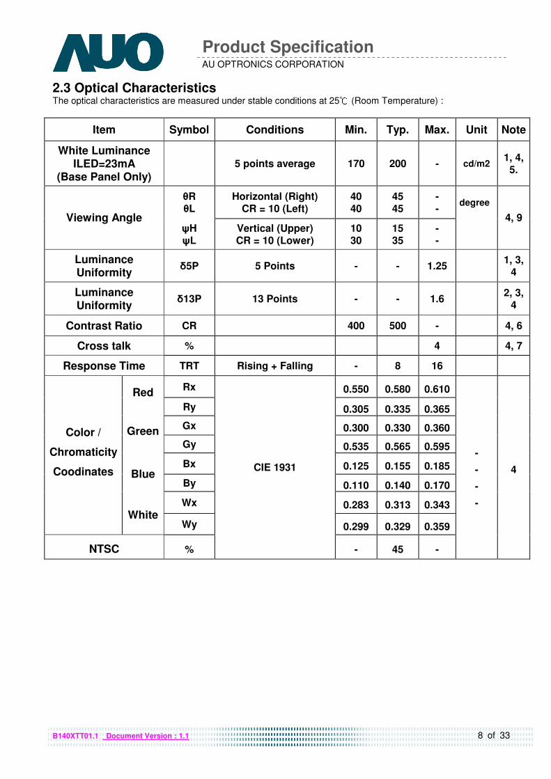
2.3 Optical Characteristics The optical characteristics are measured under stable conditions at 25℃ (Room Temperature) :
Item Symbol Conditions Min. Typ. Max. Unit Note
White Luminance ILED=23mA
(Base Panel Only)
5 points average 170 200 - cd/m2 1, 4, 5.
θR θL
Horizontal (Right) CR = 10 (Left)
40 40
45 45
- -
degree
Viewing Angle ψH ψL
Vertical (Upper) CR = 10 (Lower)
10 30
15 35
- -
4, 9
Luminance Uniformity
δ5P 5 Points - - 1.25 1, 3,
4
Luminance Uniformity
δ13P 13 Points - - 1.6 2, 3,
4
Contrast Ratio CR 400 500 - 4, 6
Cross talk % 4 4, 7
Response Time TRT Rising + Falling - 8 16
Rx 0.550 0.580 0.610 Red
Ry 0.305 0.335 0.365
Gx 0.300 0.330 0.360 Green Gy 0.535 0.565 0.595
Bx 0.125 0.155 0.185 Blue
By 0.110 0.140 0.170
Wx 0.283 0.313 0.343
Color /
Chromaticity
Coodinates
White Wy 0.299 0.329 0.359
NTSC %
CIE 1931
- 45 -
-
-
-
-
4
www.yslcd.com.tw
9 of 33
AU OPTRONICS CORPORATION
Product Specification
B140XTT01.1 Document Version : 1.1
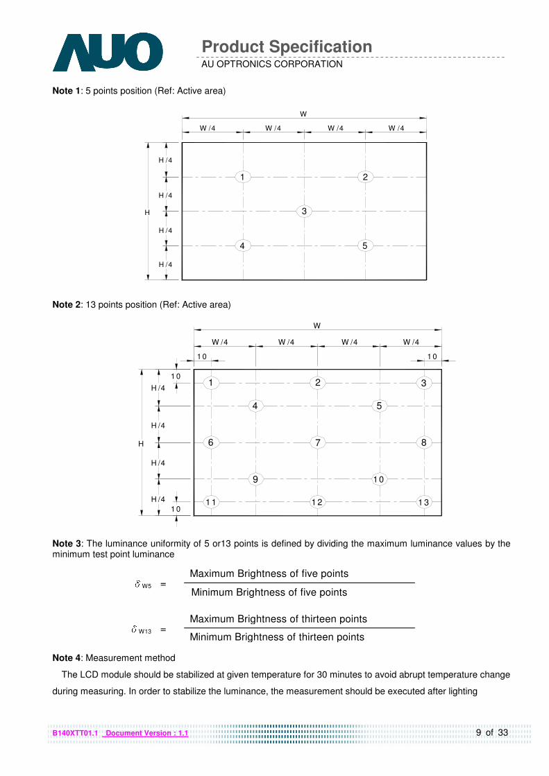
Note 1: 5 points position (Ref: Active area)
1 2
3
4 5
H /4
H /4
H /4
H /4
H
W
W /4 W /4 W /4 W /4
Note 2: 13 points position (Ref: Active area)
W /4
W
W /4
H
H /4
H /4
H /4
H /4
7
9 1 0
W /4
1
8
W /4
1 0
1 0
1 0
1 0
2 3
1 31 2
4 5
6
1 1
Note 3: The luminance uniformity of 5 or13 points is defined by dividing the maximum luminance values by the minimum test point luminance
Note 4: Measurement method
The LCD module should be stabilized at given temperature for 30 minutes to avoid abrupt temperature change
during measuring. In order to stabilize the luminance, the measurement should be executed after lighting
δW13 = Maximum Brightness of thirteen points Minimum Brightness of thirteen points
Maximum Brightness of five points δW5 = Minimum Brightness of five points www.yslcd.com.tw
10 of 33
AU OPTRONICS CORPORATION
Product Specification
B140XTT01.1 Document Version : 1.1
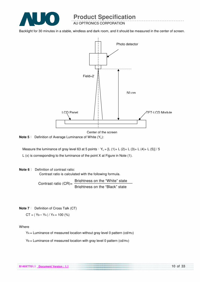
Backlight for 30 minutes in a stable, windless and dark room, and it should be measured in the center of screen.
Note 5: Definition of Average Luminance of White (YL):
Measure the luminance of gray level 63 at 5 points,YL = [L (1)+ L (2)+ L (3)+ L (4)+ L (5)] / 5
L (x) is corresponding to the luminance of the point X at Figure in Note (1).
Note 6: Definition of contrast ratio:
Contrast ratio is calculated with the following formula.
Note 7: Definition of Cross Talk (CT)
CT = | YB – YA | / YA × 100 (%)
Where
YA = Luminance of measured location without gray level 0 pattern (cd/m2)
YB = Luminance of measured location with gray level 0 pattern (cd/m2)
Center of the screen
TFT-LCD Module
50 cm
Photo detector
LCD Panel
Field=2°
Contrast ratio (CR)= Brightness on the “White” state
Brightness on the “Black” state
www.yslcd.com.tw
11 of 33
AU OPTRONICS CORPORATION
Product Specification
B140XTT01.1 Document Version : 1.1
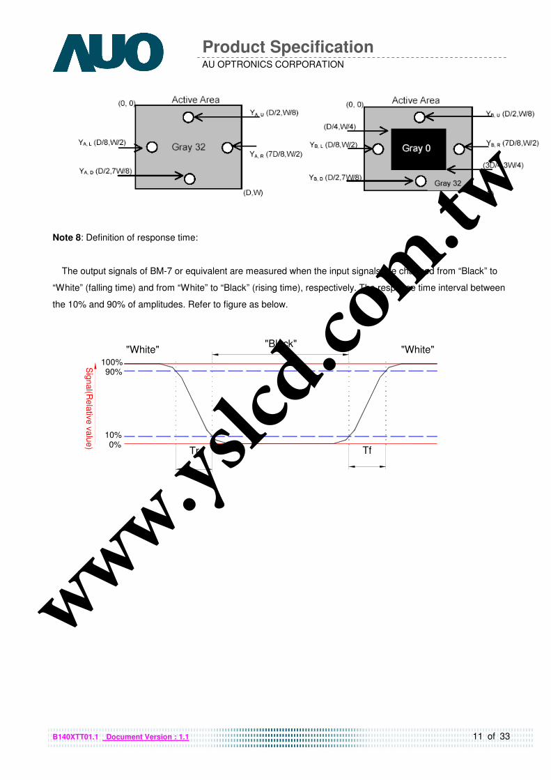
Note 8: Definition of response time:
The output signals of BM-7 or equivalent are measured when the input signals are changed from “Black” to
“White” (falling time) and from “White” to “Black” (rising time), respectively. The response time interval between
the 10% and 90% of amplitudes. Refer to figure as below.
Sig
nal (R
ela
tive v
alu
e)
"Black"
Tr Tf
"White""White"
0%10%
90%100%
www.yslcd.com.tw
12 of 33
AU OPTRONICS CORPORATION
Product Specification
B140XTT01.1 Document Version : 1.1
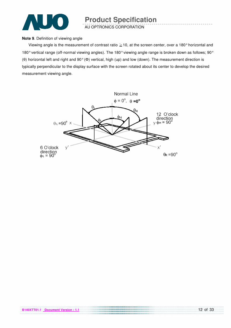
Note 9. Definition of viewing angle
Viewing angle is the measurement of contrast ratio ≧10, at the screen center, over a 180° horizontal and
180° vertical range (off-normal viewing angles). The 180° viewing angle range is broken down as follows; 90°
(θ) horizontal left and right and 90° (Φ) vertical, high (up) and low (down). The measurement direction is
typically perpendicular to the display surface with the screen rotated about its center to develop the desired
measurement viewing angle.
www.yslcd.com.tw
13 of 33
AU OPTRONICS CORPORATION
Product Specification
B140XTT01.1 Document Version : 1.1
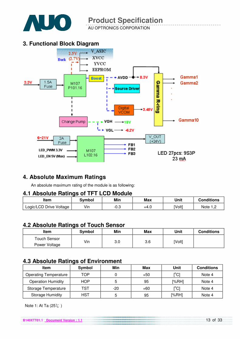
3. Functional Block Diagram
4. Absolute Maximum Ratings
An absolute maximum rating of the module is as following:
4.1 Absolute Ratings of TFT LCD Module Item Symbol Min Max Unit Conditions
Logic/LCD Drive Voltage Vin -0.3 +4.0 [Volt] Note 1,2
4.2 Absolute Ratings of Touch Sensor Item Symbol Min Max Unit Conditions
Touch Sensor
Power Voltage Vin 3.0 3.6 [Volt]
4.3 Absolute Ratings of Environment Item Symbol Min Max Unit Conditions
Operating Temperature TOP 0 +50 [oC] Note 4
Operation Humidity HOP 5 95 [%RH] Note 4
Storage Temperature TST -20 +60 [oC] Note 4
Storage Humidity HST 5 95 [%RH] Note 4
Note 1: At Ta (25℃ )
www.yslcd.com.tw
14 of 33
AU OPTRONICS CORPORATION
Product Specification
B140XTT01.1 Document Version : 1.1
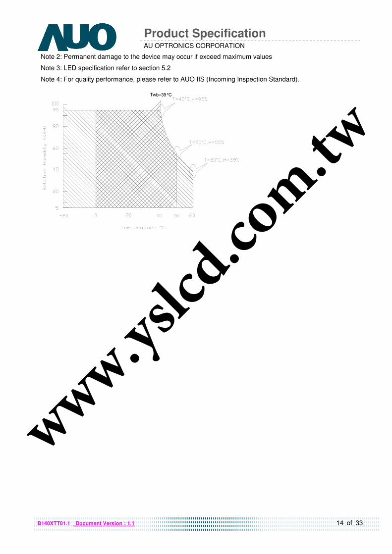
Note 2: Permanent damage to the device may occur if exceed maximum values
Note 3: LED specification refer to section 5.2
Note 4: For quality performance, please refer to AUO IIS (Incoming Inspection Standard).
Twb=39°C
www.yslcd.com.tw
15 of 33
AU OPTRONICS CORPORATION
Product Specification
B140XTT01.1 Document Version : 1.1
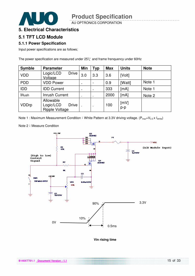
5. Electrical Characteristics
5.1 TFT LCD Module
5.1.1 Power Specification
Input power specifications are as follows;
The power specification are measured under 25℃ and frame frenquency under 60Hz
Symble Parameter Min Typ Max Units Note
VDD Logic/LCD Drive Voltage
3.0 3.3 3.6 [Volt]
PDD VDD Power - - 0.9 [Watt] Note 1
IDD IDD Current - - 333 [mA] Note 1
IRush Inrush Current - - 2000 [mA] Note 2
VDDrp Allowable Logic/LCD Drive Ripple Voltage
- - 100 [mV] p-p
Note 1 : Maximum Measurement Condition:White Pattern at 3.3V driving voltage. (Pmax=V3.3 x Iwhite)
Note 2:Measure Condition
90%
10%
Vin rising time
0V
3.3V
0.5ms www.yslcd.com.tw
16 of 33
AU OPTRONICS CORPORATION
Product Specification
B140XTT01.1 Document Version : 1.1
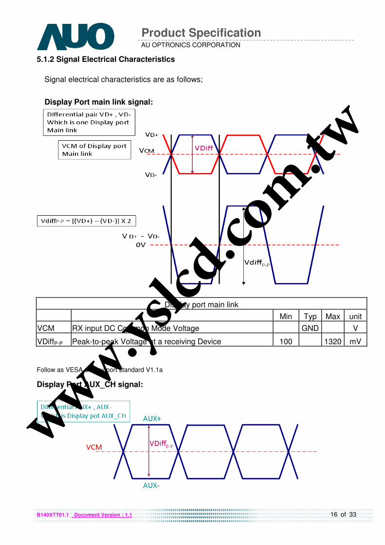
5.1.2 Signal Electrical Characteristics
Signal electrical characteristics are as follows;
Display Port main link signal:
Display port main link
Min Typ Max unit
VCM RX input DC Common Mode Voltage GND V
VDiffP-P Peak-to-peak Voltage at a receiving Device 100 1320 mV
Follow as VESA display port standard V1.1a
Display Port AUX_CH signal:
www.yslcd.com.tw
17 of 33
AU OPTRONICS CORPORATION
Product Specification
B140XTT01.1 Document Version : 1.1
Display port AUX_CH
Min Typ Max unit
VCM AUX DC Common Mode Voltage
GND/0.15 V
VDiffP-P AUX Peak-to-peak Voltage at a receiving Device 400 600 800 V
Follow as VESA display port standard V1.1a.
Display Port VHPD signal:
Display port VHPD
Min Typ Max unit
VHPD HPD Voltage 0 2.5 2.5 V Follow as VESA display port standard V1.1a.
www.yslcd.com.tw
18 of 33
AU OPTRONICS CORPORATION
Product Specification
B140XTT01.1 Document Version : 1.1
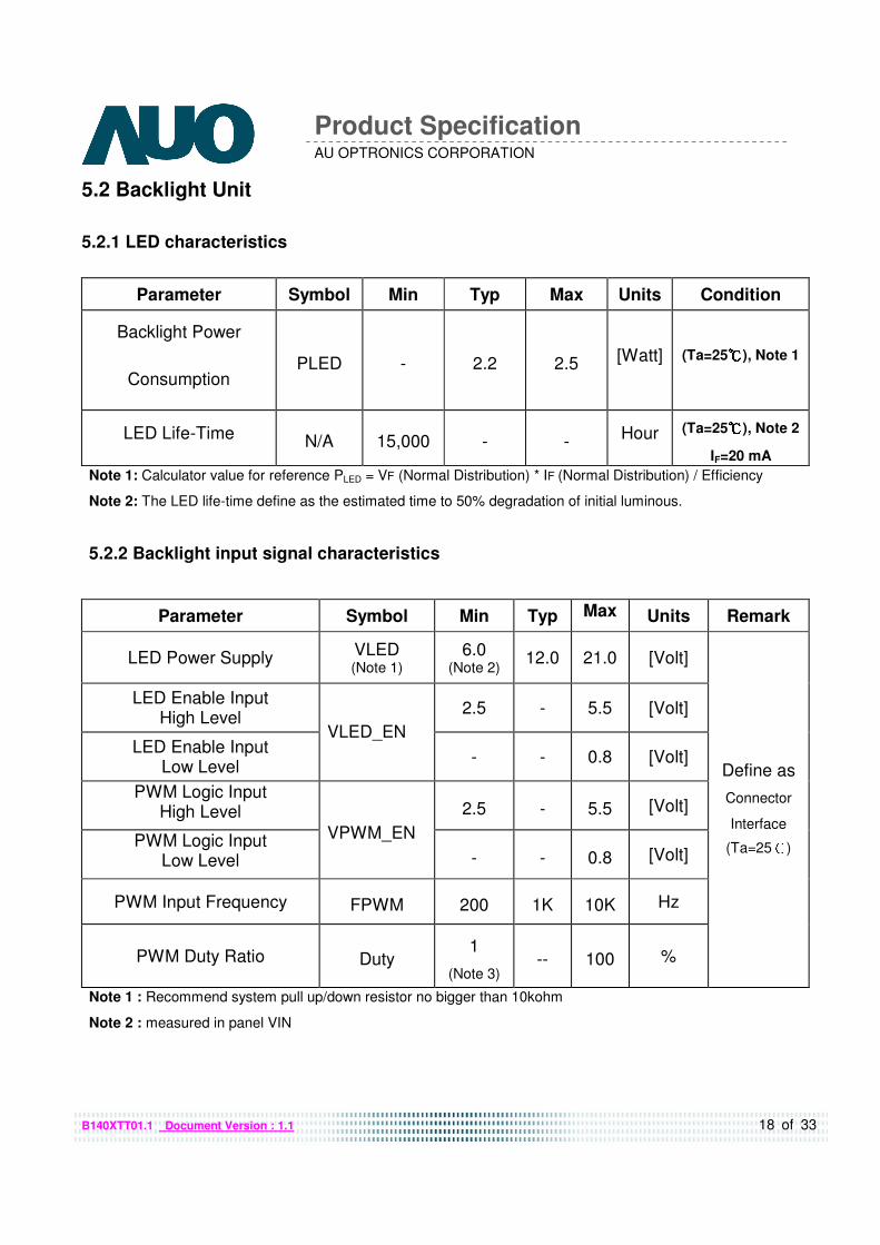
5.2 Backlight Unit
5.2.1 LED characteristics
Parameter Symbol Min Typ Max Units Condition
Backlight Power
Consumption PLED - 2.2 2.5 [Watt] (Ta=25℃℃℃℃), Note 1
LED Life-Time N/A 15,000 - - Hour (Ta=25℃℃℃℃), Note 2
IF=20 mA
Note 1: Calculator value for reference PLED = VF (Normal Distribution) * IF (Normal Distribution) / Efficiency
Note 2: The LED life-time define as the estimated time to 50% degradation of initial luminous.
5.2.2 Backlight input signal characteristics
Parameter Symbol Min Typ Max
Units Remark
LED Power Supply VLED (Note 1)
6.0 (Note 2)
12.0 21.0 [Volt]
LED Enable Input High Level
2.5 - 5.5 [Volt]
LED Enable Input Low Level
VLED_EN
- - 0.8 [Volt]
PWM Logic Input High Level
2.5 - 5.5 [Volt]
PWM Logic Input Low Level
VPWM_EN
- - 0.8 [Volt]
PWM Input Frequency FPWM 200 1K 10K Hz
PWM Duty Ratio Duty 1
(Note 3) -- 100 %
Define as
Connector
Interface
(Ta=25℃)
Note 1 : Recommend system pull up/down resistor no bigger than 10kohm
Note 2 : measured in panel VIN www.yslcd.com.tw
19 of 33
AU OPTRONICS CORPORATION
Product Specification
B140XTT01.1 Document Version : 1.1
Note 3 : If the PWM duty ratio(min) is set between 5% to 1%,the PWM input frequency should be set below 1KHz .
The brightness-duty characteristic might not be able to keep in it’s linearity if the dimming control is
operated in 1% to 5% range.
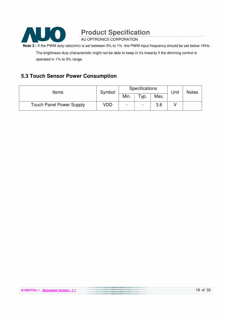
5.3 Touch Sensor Power Consumption
Specifications Items Symbol
Min. Typ. Max. Unit Notes
Touch Panel Power Supply VDD - - 3.6 V
www.yslcd.com.tw
20 of 33
AU OPTRONICS CORPORATION
Product Specification
B140XTT01.1 Document Version : 1.1
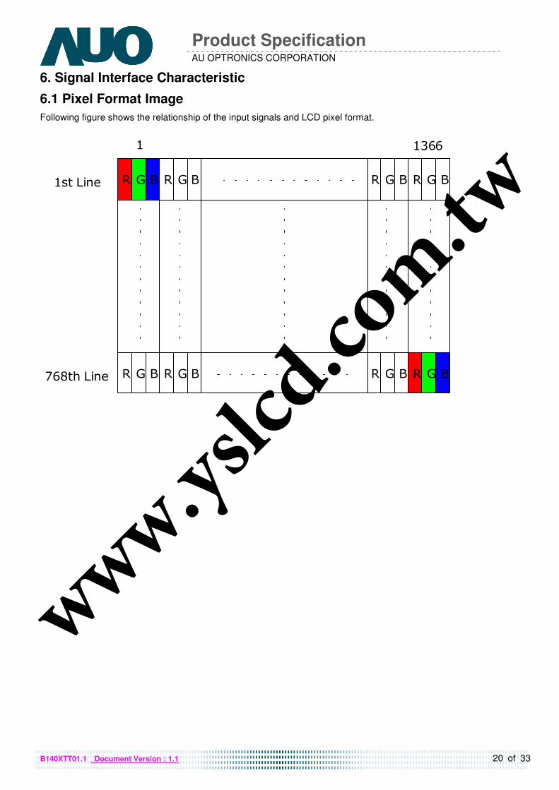
6. Signal Interface Characteristic
6.1 Pixel Format Image
Following figure shows the relationship of the input signals and LCD pixel format.
R G B R G B
R G B R G B
R G B R G B
R G B R G B
1 1366
1st Line
768th Line
www.yslcd.com.tw
21 of 33
AU OPTRONICS CORPORATION
Product Specification
B140XTT01.1 Document Version : 1.1
6.3 Integration Interface Requirement
6.3.1 Connector Description
Physical interface is described as for the connector on module.
These connectors are capable of accommodating the following signals and will be following components.
Connector Name / Designation For Signal Connector
Manufacturer STM or Compatible
Type / Part Number MSAK24025P40 or Compatible
Mating Housing/Part Number PK24025P40 or Compatible
6.3.2 Pin Assignment (with Touch Sensor Pin Assignment)
PIN NO Symbol Function 1 DCR_EN DCR enable function 2 H_GND High Speed Ground 3 NC No connect 4 NC No connect 5 H_GND High Speed Ground 6 Lane0_N Comp Signal Link Lane 0 7 Lane0_P True Signal Link Lane 0 8 H_GND High Speed Ground 9 AUX_CH_P True Signal Auxiliary Ch. 10 AUX_CH_N Comp Signal Auxiliary Ch. 11 H_GND High Speed Ground 12 LCD_VCC LCD logic and driver power 13 LCD_VCC LCD logic and driver power 14 LCD_Self_Test LCD Panel Self Test Enable 15 LCD_GND LCD logic and driver ground 16 LCD_GND LCD logic and driver ground 17 HPD HPD signal pin 18 BL_GND Backlight ground 19 BL_GND Backlight ground 20 BL_GND Backlight ground 21 BL_GND Backlight ground 22 BL_Enable Backlight On / Off 23 BL_PWM_DIM System PWM signal Input 24 NC No connect 25 NC No connect 26 NC No connect 27 BL_PWR Backlight power 28 BL_PWR Backlight power 29 BL_PWR Backlight power 30 CM_EN CM enable function 31 TP_D- USB Data- for Touch 32 TP_D+ USB Data+ for Touch 33 GND Ground–Shield 34 VTSP Touch panel power supply (3.3V) 35 VTSP Touch panel power supply (3.3V) 36 NC/TP_EN (10pin CNT)
NC (8pin CNT) No Connection (Reserve for Touch function enable)
37 TP_CLK I2C Clock for Touch 38 TP_Data I2C Data for Touch 39 INT Interrupt for Touch 40 RST Reset for Touch
www.yslcd.com.tw
22 of 33
AU OPTRONICS CORPORATION
Product Specification
B140XTT01.1 Document Version : 1.1
Note1: Start from right side. Note2: Input signals shall be low or High-impedance state when VDD is off. Internal circuit of eDP inputs are as following.
Pin 40
Connector
Pin 1
www.yslcd.com.tw
23 of 33
AU OPTRONICS CORPORATION
Product Specification
B140XTT01.1 Document Version : 1.1
6.4 Interface Timing
6.4.1 Timing Characteristics Basically, interface timings should match the 1366x768 /60Hz manufacturing guide line timing.
Parameter Symbol Min. Typ. Max. Unit
Frame Rate - - 60 - Hz
Clock frequency 1/ TClock 66.9 72 80 MHz
Period TV 788 824 768+A
Active TVD 768 Vertical
Section
Blanking TVB 20 56 A
TLine
Period TH 1416 1456 1366+B
Active THD 1366 Horizontal
Section
Blanking THB 50 90 B
TClock
Note : 1. DE mode only
2. The maximum clock frequency = (1366+B)*(768+A)*60 < 80MHz
6.4.2 Timing diagram
LineLine
Pixel
7Invalid Data
Pixel
Pixel
M-3
2
Tdisp(h)
Pixel
1
PixelPixel
Invalid Data
6 M-2
M-1
RGB Data
X
Pixel
DE
Pixel
Pixel
CLK
N
3
LineLine
32
Tdisp(v)
Pixel
RGB Data
(Odd)
RGB Data
(Even)
Line
8 M
Pixel
M pixel
M-4
Invalid Data
Th
Tv
Pixel
N
Tclk
Pixel
M-5
Invalid Data4
Pixel
5
Invalid Data12
Pixel
Invalid Data
1
DE
4
Pixel
119
Line
N Line
Tblk(h)
10
Pixel Pixel
Y
Tblk(v)
M-1
Pixel
Pixel
M
Pixel
M-3
M-2
Pixel
Pixel
Pixel
1
4
Pixel
3
Pixel
2M-4
Pixel
Pixel
M-5
M-6
Pixel
M-7
Pixel
Th
www.yslcd.com.tw
24 of 33
AU OPTRONICS CORPORATION
Product Specification
B140XTT01.1 Document Version : 1.1
6.4 Power ON/OFF Sequence Power on/off sequence is as follows. Interface signals and LED on/off sequence are also shown in the chart. Signals from any system shall be Hi-Z state or low level when VDD is off Display Port panel power sequence:
Display Port AUX_CH transaction only:
www.yslcd.com.tw
25 of 33
AU OPTRONICS CORPORATION
Product Specification
B140XTT01.1 Document Version : 1.1
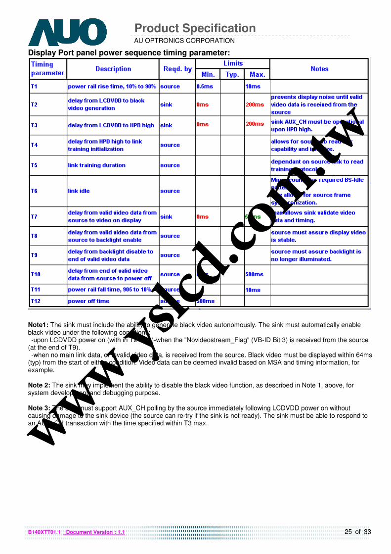
Display Port panel power sequence timing parameter:
Note1: The sink must include the ability to generate black video autonomously. The sink must automatically enable black video under the following conditions: -upon LCDVDD power on (with in T2 max)-when the "Novideostream_Flag" (VB-ID Bit 3) is received from the source (at the end of T9). -when no main link data, or invalid video data, is received from the source. Black video must be displayed within 64ms (typ) from the start of either condition. Video data can be deemed invalid based on MSA and timing information, for example. Note 2: The sink may implement the ability to disable the black video function, as described in Note 1, above, for system development and debugging purpose. Note 3: The sink must support AUX_CH polling by the source immediately following LCDVDD power on without causing damage to the sink device (the source can re-try if the sink is not ready). The sink must be able to respond to an AUX_CH transaction with the time specified within T3 max.
www.yslcd.com.tw
26 of 33
AU OPTRONICS CORPORATION
Product Specification
B140XTT01.1 Document Version : 1.1
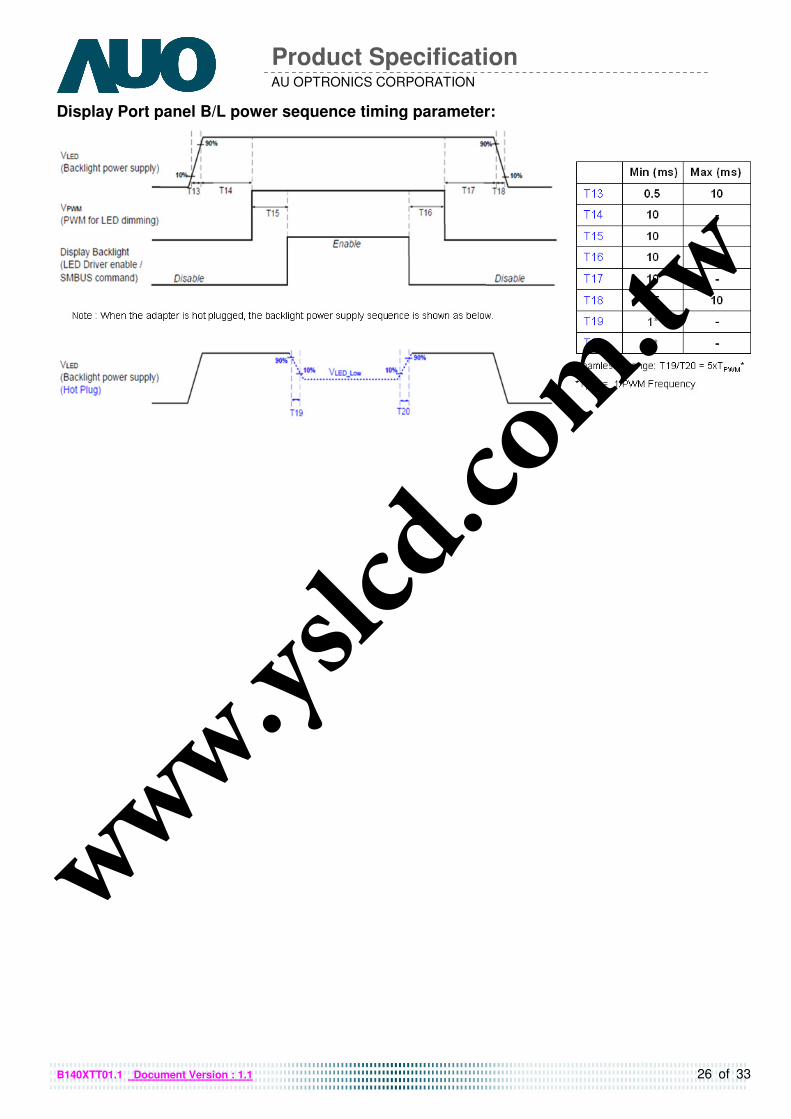
Display Port panel B/L power sequence timing parameter:
www.yslcd.com.tw
27 of 33
AU OPTRONICS CORPORATION
Product Specification
B140XTT01.1 Document Version : 1.1
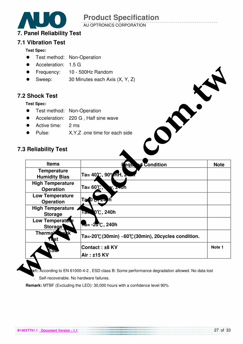
7. Panel Reliability Test
7.1 Vibration Test
Test Spec:
� Test method: Non-Operation
� Acceleration: 1.5 G
� Frequency: 10 - 500Hz Random
� Sweep: 30 Minutes each Axis (X, Y, Z)
7.2 Shock Test
Test Spec:
� Test method: Non-Operation
� Acceleration: 220 G , Half sine wave
� Active time: 2 ms
� Pulse: X,Y,Z .one time for each side
7.3 Reliability Test
Items Required Condition Note
Temperature
Humidity Bias Ta= 40℃℃℃℃, 90%RH, 240h
High Temperature
Operation Ta= 60℃℃℃℃, Dry, 240h
Low Temperature
Operation Ta=0℃℃℃℃, 240h
High Temperature
Storage Ta= 60℃℃℃℃, 240h
Low Temperature
Storage Ta= -20℃℃℃℃, 240h
Thermal Shock
Test Ta=-20℃℃℃℃(30min) ~60℃℃℃℃(30min), 20cycles condition.
ESD Contact : ±8 KV
Air : ±15 KV
Note 1
Note1: According to EN 61000-4-2 , ESD class B: Some performance degradation allowed. No data lost
. Self-recoverable. No hardware failures.
Remark: MTBF (Excluding the LED): 30,000 hours with a confidence level 90%
www.yslcd.com.tw
28 of 33 B140XTT01.1 Document Version : 1.1
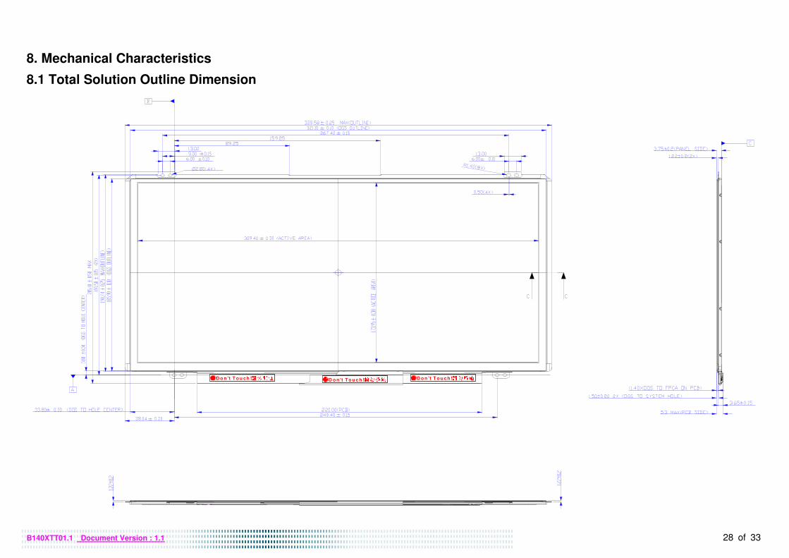
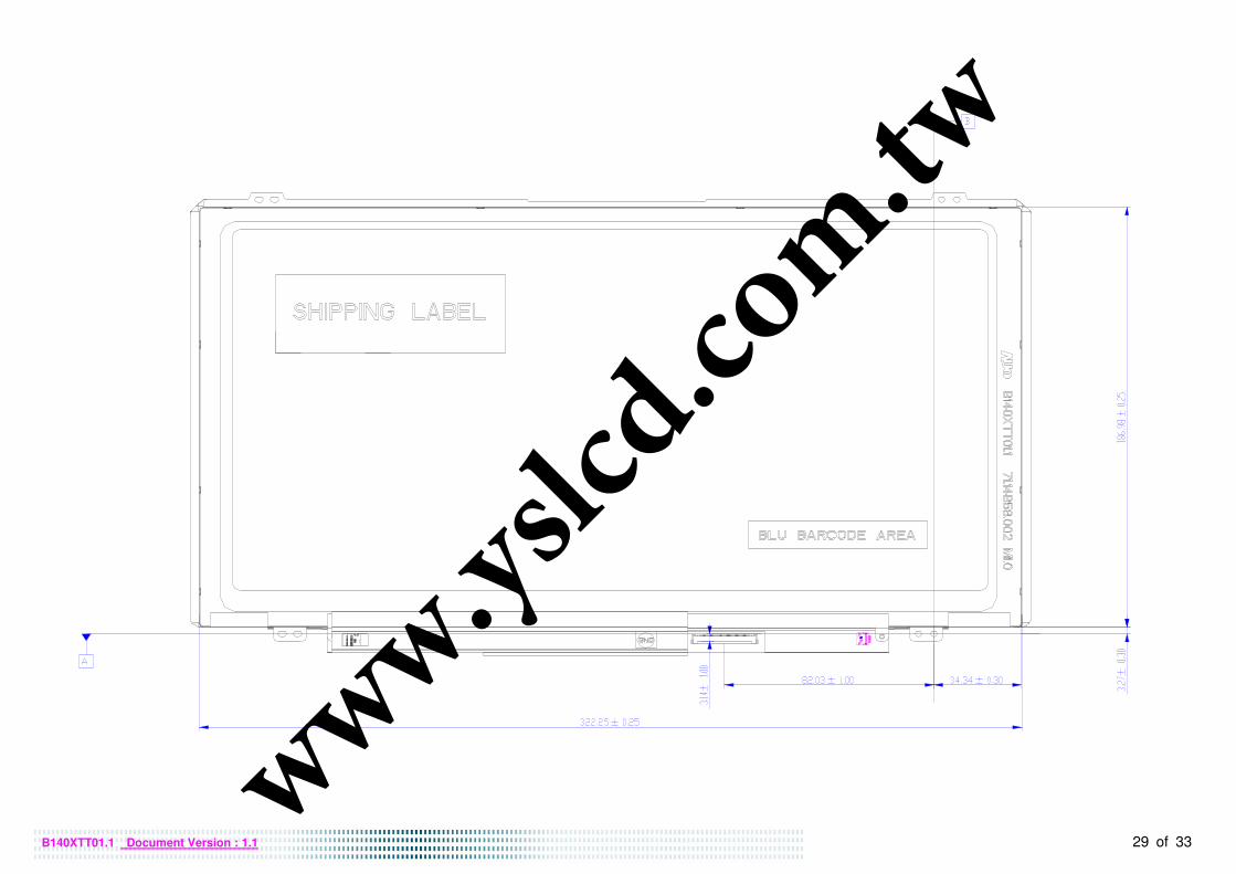
8. Mechanical Characteristics
8.1 Total Solution Outline Dimension
D o n 't T o u c h !請請請請勿觸碰 D o n 't T o u c h !請請請請勿觸碰 D o n 't T o u c h!請請請請勿觸碰 ww
w.ysl
cd.co
m.tw
29 of 33 B140XTT01.1 Document Version : 1.1
www.
yslcd
.com.
tw
30 of 33 B140XTT01.1 Document Version : 1.1
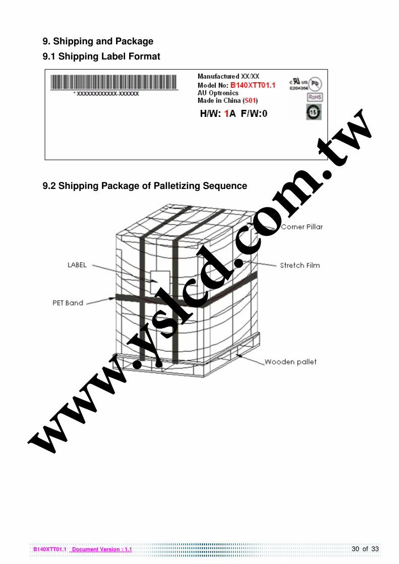
9. Shipping and Package
9.1 Shipping Label Format
9.2 Shipping Package of Palletizing Sequence
www.yslcd.com.tw
31 of 33 B140XTT01.1 Document Version : 1.1
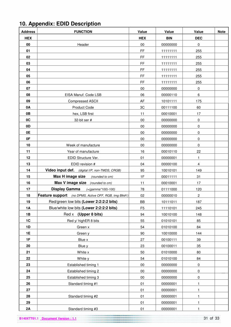
10. Appendix: EDID Description
Address FUNCTION Value Value Value Note
HEX HEX BIN DEC
00 Header 00 00000000 0
01 FF 11111111 255
02 FF 11111111 255
03 FF 11111111 255
04 FF 11111111 255
05 FF 11111111 255
06 FF 11111111 255
07 00 00000000 0
08 EISA Manuf. Code LSB 06 00000110 6
09 Compressed ASCII AF 10101111 175
0A Product Code 3C 00111100 60
0B hex, LSB first 11 00010001 17
0C 32-bit ser # 00 00000000 0
0D 00 00000000 0
0E 00 00000000 0
0F 00 00000000 0
10 Week of manufacture 00 00000000 0
11 Year of manufacture 16 00010110 22
12 EDID Structure Ver. 01 00000001 1
13 EDID revision # 04 00000100 4
14 Video input def. (digital I/P, non-TMDS, CRGB) 95 10010101 149
15 Max H image size (rounded to cm) 1F 00011111 31
16 Max V image size (rounded to cm) 11 00010001 17
17 Display Gamma (=(gamma*100)-100) 78 01111000 120
18 Feature support (no DPMS, Active OFF, RGB, tmg Blk#1) 02 00000010 2
19 Red/green low bits (Lower 2:2:2:2 bits) BB 10111011 187
1A Blue/white low bits (Lower 2:2:2:2 bits) F5 11110101 245
1B Red x (Upper 8 bits) 94 10010100 148
1C Red y/ highER 8 bits 55 01010101 85
1D Green x 54 01010100 84
1E Green y 90 10010000 144
1F Blue x 27 00100111 39
20 Blue y 23 00100011 35
21 White x 50 01010000 80
22 White y 54 01010100 84
23 Established timing 1 00 00000000 0
24 Established timing 2 00 00000000 0
25 Established timing 3 00 00000000 0
26 Standard timing #1 01 00000001 1
27 01 00000001 1
28 Standard timing #2 01 00000001 1
29 01 00000001 1
2A Standard timing #3 01 00000001 1
www.yslcd.com.tw
32 of 33 B140XTT01.1 Document Version : 1.1
2B 01 00000001 1
2C Standard timing #4 01 00000001 1
2D 01 00000001 1
2E Standard timing #5 01 00000001 1
2F 01 00000001 1
30 Standard timing #6 01 00000001 1
31 01 00000001 1
32 Standard timing #7 01 00000001 1
33 01 00000001 1
34 Standard timing #8 01 00000001 1
35 01 00000001 1
36 Pixel Clock/10000 LSB CE 11001110 206
37 Pixel Clock/10000 USB 1D 00011101 29
38 Horz active Lower 8bits 56 01010110 86
39 Horz blanking Lower 8bits D2 11010010 210
3A HorzAct:HorzBlnk Upper 4:4 bits 50 01010000 80
3B Vertical Active Lower 8bits 00 00000000 0
3C Vertical Blanking Lower 8bits 26 00100110 38
3D Vert Act : Vertical Blanking (upper 4:4 bit) 30 00110000 48
3E HorzSync. Offset 10 00010000 16
3F HorzSync.Width 10 00010000 16
40 VertSync.Offset : VertSync.Width 3E 00111110 62
41 Horz&Vert Sync Offset/Width Upper 2bits 00 00000000 0
42 Horizontal Image Size Lower 8bits 35 00110101 53
43 Vertical Image Size Lower 8bits AD 10101101 173
44 Horizontal & Vertical Image Size (upper 4:4 bits) 10 00010000 16
45 Horizontal Border (zero for internal LCD) 00 00000000 0
46 Vertical Border (zero for internal LCD) 00 00000000 0
47 Signal (non-intr, norm, no stero, sep sync, neg pol) 18 00011000 24
48 Detailed timing/monitor 00 00000000 0
49 descriptor #2 00 00000000 0
4A 00 00000000 0
4B 0F 00001111 15
4C 00 00000000 0
4D 00 00000000 0
4E 00 00000000 0
4F 00 00000000 0
50 00 00000000 0
51 00 00000000 0
52 00 00000000 0
53 00 00000000 0
54 00 00000000 0
55 00 00000000 0
56 00 00000000 0
57 00 00000000 0
58 00 00000000 0
59 20 00100000 32
www.yslcd.com.tw
33 of 33 B140XTT01.1 Document Version : 1.1
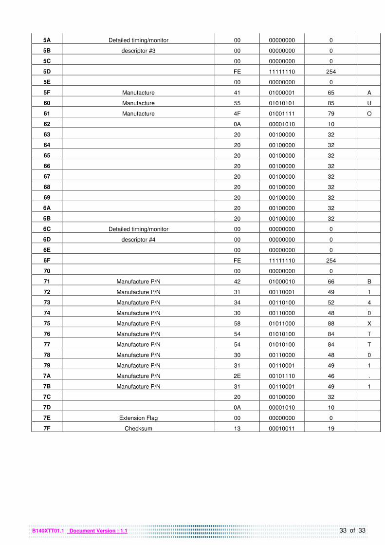
5A Detailed timing/monitor 00 00000000 0
5B descriptor #3 00 00000000 0
5C 00 00000000 0
5D FE 11111110 254
5E 00 00000000 0
5F Manufacture 41 01000001 65 A
60 Manufacture 55 01010101 85 U
61 Manufacture 4F 01001111 79 O
62 0A 00001010 10
63 20 00100000 32
64 20 00100000 32
65 20 00100000 32
66 20 00100000 32
67 20 00100000 32
68 20 00100000 32
69 20 00100000 32
6A 20 00100000 32
6B 20 00100000 32
6C Detailed timing/monitor 00 00000000 0
6D descriptor #4 00 00000000 0
6E 00 00000000 0
6F FE 11111110 254
70 00 00000000 0
71 Manufacture P/N 42 01000010 66 B
72 Manufacture P/N 31 00110001 49 1
73 Manufacture P/N 34 00110100 52 4
74 Manufacture P/N 30 00110000 48 0
75 Manufacture P/N 58 01011000 88 X
76 Manufacture P/N 54 01010100 84 T
77 Manufacture P/N 54 01010100 84 T
78 Manufacture P/N 30 00110000 48 0
79 Manufacture P/N 31 00110001 49 1
7A Manufacture P/N 2E 00101110 46 .
7B Manufacture P/N 31 00110001 49 1
7C 20 00100000 32
7D 0A 00001010 10
7E Extension Flag 00 00000000 0
7F Checksum 13 00010011 19
www.yslcd.com.tw