C-ONE PCMCIA / JEIDA SRAM CARD Product Specification
25
C-ONE PCMCIA / JEIDA SRAM CARD MSR-B9-001.8 1/24 0402V8 股份有限公司 C-ONE TECHNOLOGY CORPORATION PCMCIA / JEIDA SRAM CARD Product Specification July, 2006
-
Upload
khangminh22 -
Category
Documents
-
view
1 -
download
0
Transcript of C-ONE PCMCIA / JEIDA SRAM CARD Product Specification
C-ONE PCMCIA / JEIDA SRAM CARD
MSR-B9-001.8 1/24 0402V8
股 份 有 限 公 司
C-ONE TECHNOLOGY CORPORATION
PCMCIA / JEIDA SRAM CARD
Product Specification
July, 2006
C-ONE PCMCIA / JEIDA SRAM CARD
MSR-B9-001.8 2/24 0402V8
Contents 1. FEATURES .........................................................................................................................................................................1
2. GENERAL DESCRIPTION..............................................................................................................................................1
3. PRODUCT NUMBER DEFINITION...............................................................................................................................2
4. PRODUCT LIST........................................................................................................................... 錯誤! 尚未定義書籤。
5. PIN CONFIGURATION....................................................................................................................................................4
6. PIN DESCRIPTION...........................................................................................................................................................5
7. BLOCK DIAGRAM ...........................................................................................................................................................6
8. RECOMMENDED OPERATING CONDITIONS........................................................................................................12
9. FUNCTION TABLE.........................................................................................................................................................13
10. DC ELECTRICAL CHARACTERISTICS....................................................................................................................15
11. AC ELECTRICAL CHARACTERISTICS ( COMMON MEMORY ) ......................................................................16
12. TIMING DIAGRAM ( COMMON MEMORY )...........................................................................................................17
13. AC ELECTRICAL CHARACTERISTICS ( ATTRIBUTE MEMORY ) ..................................................................19
14. TIMING DIAGRAM ( ATTRIBUTE MEMORY ).......................................................................................................20
15. MAIN BATTERY SPECIFICATIONS ..........................................................................................................................21
16. POWER-UP / POWER-DOWN CHARACTERISTICS...............................................................................................22
17. OUTLINE DIMENSIONS (UNIT: MM)........................................................................................................................23

C-ONE PCMCIA / JEIDA SRAM CARD
MSR-B9-001.8 1/24 0402V8
Features
PCMCIA / JEIDA standard Dual back-up battery design
256K bytes ~ 8M bytes memory capacity Both BR2325 and CR2025 used as main battery
Byte (x8) / word (x16) data bus selectable Battery voltage detection function
Fast access time : 150ns (maximum) Built-in write protect switch
Attribute memory : 8K byte E2PROM or no attribute memory
Battery case lock system
Connector type : 2-piece,2-row,68 pins
Single +5V operating voltage Credit card size : 54.0 x 85.6 x 3.3 (mm)
General Description
C-ONE's high performance SRAM cards conform to the PCMCIA / JEIDA international standard and consist of multiple very low power consumption CMOS SRAM ICs , decoder IC and power control IC mounted on a very thin printed circuit board using surface mounting technology.
With the dual back-up battery design , each SRAM card contains a replaceable but non-rechargeable 3V lithium battery (main battery) and an on-board rechargeable but non-replaceable battery (auxiliary battery) for data retention. This design allows replacement of main battery without data loss for 20 minutes approximately. Digital signals on the BVD1*/BVD2* pins were used to alarm the user whether the main battery should be replaced to prevent the stored data from loss. With the flexible and user-friendly design , both BR2325 and CR2025 can be used as main battery. There is battery case lock system to prevent battery dropping from the card. Also , with the write-protect switch design , data will not be written into the card by accident.
Memory card attribute information represents various attribute information of a card and is stored at EVEN address of an attribute memory space which is enabled by asserting REG* signal. Regarding to the attribute information format , please refer to the PCMCIA 2.0 or JEIDA 4.1 specification.
With the flexible design of this series cards , they provide 8K bytes E2PROM available for attribute memory or there is no attribute memory.
C-ONE PCMCIA / JEIDA SRAM CARD
MSR-B9-001.8 2/24 0402V8
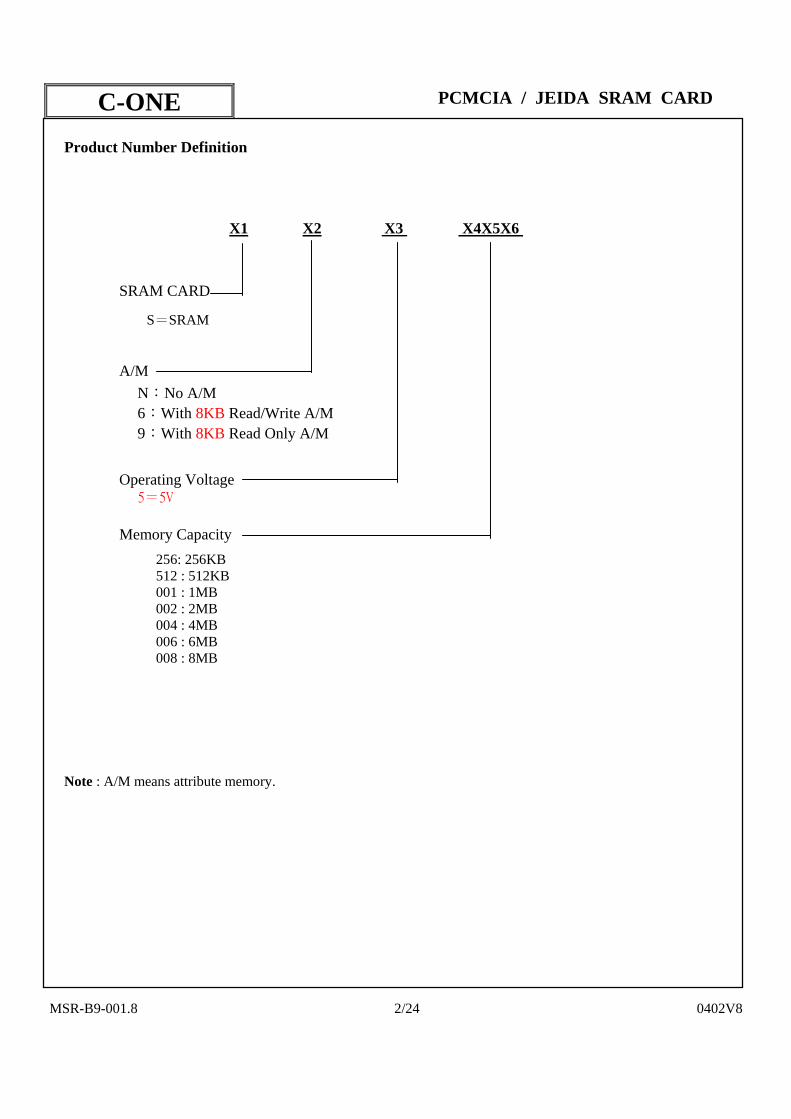
Product Number Definition
X1 X2 X3 X4X5X6
SRAM CARD
S=SRAM
A/M N:No A/M 6:With 8KB Read/Write A/M 9:With 8KB Read Only A/M
Operating Voltage 5=5V
Memory Capacity 256: 256KB 512 : 512KB 001 : 1MB 002 : 2MB 004 : 4MB 006 : 6MB 008 : 8MB
Note : A/M means attribute memory.
C-ONE PCMCIA / JEIDA SRAM CARD
MSR-B9-001.8 3/24 0402V8
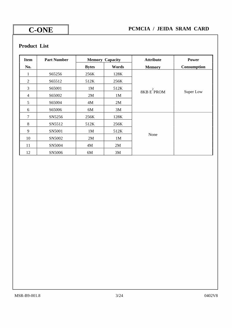
Product List
Item Part Number Memory Capacity Attribute Power
No. Bytes Words Memory Consumption
1 S65256 256K 128K
2 S65512 512K 256K
3 S65001 1M 512K
4 S65002 2M 1M
5 S65004 4M 2M
6 S65006 6M 3M
8KB E2PROM Super Low
7 SN5256 256K 128K
8 SN5512 512K 256K
9 SN5001 1M 512K
10 SN5002 2M 1M
11 SN5004 4M 2M
12 SN5006 6M 3M
None
C-ONE PCMCIA / JEIDA SRAM CARD
MSR-B9-001.8 4/24 0402V8
Pin Configuration
17 16 15 14 13 12 11 10 9 8 7 6 5 4 3 2 1 Pin No. VCC
BUSY*
WE*
A14
A13
A8
A9
A11
OE*
A10
CE1 *
D7
D6
D5
D4
D3
GND
Pin Name
34 33 32 31 30 29 28 27 26 25 24 23 22 21 20 19 18 Pin No. GND
WP
D2
D1
D0
A0
A1
A2
A3
A4
A5
A6
A7
A12
A15
A16
NC
Pin Name
51 50 49 48 47 46 45 44 43 42 41 40 39 38 37 36 35 Pin No. VCC
A21
A20
A19
A18
A17
NC
NC
NC
CE2 *
D15
D14
D13
D12
D11
CD1 *
GND
Pin Name
68 67 66 65 64 63 62 61 60 59 58 57 56 55 54 53 52 Pin No. GND
CD2 *
D10
D9
D8
BVD1 *
BVD2 *
REG*
NC
NC
NC
NC
NC
NC
NC
A22
NC
Pin Name
Table 2 Note : * mean low active
256KB series : A18,A19,A20,A21,A22 = NC
512KB series : A19,A20,A21,A22 = NC
1MB series : A20,A21,A22 = NC
2MB series : A21,A22 = NC
4MB series : A22 = NC
S65256 ~ S65006 series : pin16 = BUSY* , pin61 = REG*
SN5256 ~ SN5006 series : pin16 = NC , pin61 = NC

C-ONE PCMCIA / JEIDA SRAM CARD
MSR-B9-001.8 5/24 0402V8
Pin Description
Symbol Function I/O
A0 - A22 Addresses I D0 - D15 Data Inputs/Outputs I/O
CE1*/CE2* Card Enable I OE* Output Enable I WE* Write Enable I REG* Attribute Memory Enable I WP Write-protect Detect O
BVD1*/BVD2* Battery Voltage Detect O
BUSY* Busy Output (Open drain) O
CD1*/CD2* Card Detect (tied to GND internally) O VCC +5 Volt Power Supply - GND Ground - NC No Connection -
Table 3

C-ONE PCMCIA / JEIDA SRAM CARD
MSR-B9-001.8 6/24 0402V8
Block Diagram (6MB series SRAM card)
A0A21
CE1*CE2*WE*
OE*REG*WP
CEx*x=0, 2, 4, 6
A1-A20
VCC
BVD1*
BVD2*
Write protect switch
mainbattery
auxiliarybattery
D8-D15D0-D7
BUSY*
Note : A0,A21,A22 are chip decoding address pins.
Figure 1
DecoderInput
&Buffer
Common memory1MB SRAM x4
D0-D7WE*OE*A0-A19
Common memory1MB SRAM x4
D8-D15WE*OE*A0-A19
D0-D7
Data BusBuffer
D8-D15 CEy* y=1, 3, 5, 7
Power controller&
Voltage detector
Optional Attribute memoryCE*WE* 2KB EEPROMOE* BUSY*A0-A10 D0-D7
A22

C-ONE PCMCIA / JEIDA SRAM CARD
MSR-B9-001.8 7/24 0402V8
Block Diagram
(4MB series SRAM card)
A0A20
CE1*CE2*WE*
OE*REG*WP
CEx*x=0, 2, 4, 6
A1-A19
VCC
BVD1*
BVD2*
Write protect switch
mainbattery
auxiliarybattery
D8-D15D0-D7
BUSY*
Note : A0,A20,A21 are chip decoding address pins.
Figure 2
DecoderInput
&Buffer
Common memory512KB SRAM x4
D0-D7WE*OE*A0-A18
Common memory512KB SRAM x4
D8-D15WE*OE*A0-A18
D0-D7
Data BusBuffer
D8-D15 CEy* y=1, 3, 5, 7
Power controller&
Voltage detector
Optional Attribute memoryCE*WE* 2KB EEPROMOE* BUSY*A0-A10 D0-D7
A21
C-ONE PCMCIA / JEIDA SRAM CARD
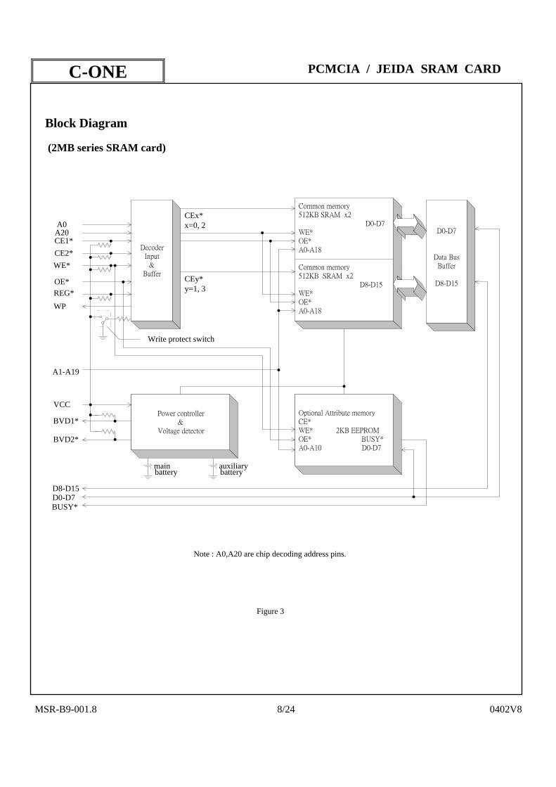
MSR-B9-001.8 8/24 0402V8
Block Diagram
(2MB series SRAM card)
A0
CE1*CE2*WE*
OE*REG*WP
CEx*x=0, 2
A1-A19
VCC
BVD1*
BVD2*
Write protect switch
mainbattery
auxiliarybattery
D8-D15D0-D7
BUSY*
Note : A0,A20 are chip decoding address pins.
Figure 3
DecoderInput
&Buffer
Common memory512KB SRAM x2
D0-D7WE*OE*A0-A18
Common memory512KB SRAM x2
D8-D15WE*OE*A0-A18
D0-D7
Data BusBuffer
D8-D15 CEy* y=1, 3
Power controller&
Voltage detector
Optional Attribute memoryCE*WE* 2KB EEPROMOE* BUSY*A0-A10 D0-D7
A20

C-ONE PCMCIA / JEIDA SRAM CARD
MSR-B9-001.8 9/24 0402V8
Block Diagram
(1MB series SRAM card)
A0
CE1*CE2*WE*
OE*REG*WP
CEx*x=0,
A1-A19
VCC
BVD1*
BVD2*
Write protect switch
mainbattery
auxiliarybattery
D8-D15D0-D7
BUSY*
Note : A0 is chip decoding address pin.
Figure 4
DecoderInput
&Buffer
Common memory512KB SRAM x1
D0-D7WE*OE*A0-A18
Common memory512KB SRAM x1
D8-D15WE*OE*A0-A18
D0-D7
Data BusBuffer
D8-D15 CEy* y=1,
Power controller&
Voltage detector
Optional Attribute memoryCE*WE* 2KB EEPROMOE* BUSY*A0-A10 D0-D7

C-ONE PCMCIA / JEIDA SRAM CARD
MSR-B9-001.8 10/24 0402V8
Block Diagram
(512KB series SRAM card)
A0A18
CE1*CE2*WE*
OE*REG*WP
CEx*x=0, 2
A1-A17
VCC
BVD1*
BVD2*
Write protect switch
mainbattery
auxiliarybattery
D8-D15D0-D7
BUSY*
Note : A0,A18 are chip decoding address pins.
Figure 5
DecoderInput
&Buffer
Common memory128KB SRAM x2 D0-D7
WE*OE*A0-A16
Common memory128KB SRAM x2
D8-D15WE*OE*A0-A16
D0-D7
Data BusBuffer
D8-D15 CEy* y=1, 3
Power controller&
Voltage detector
Optional Attribute memoryCE*WE* 2KB EEPROMOE* BUSY*A0-A10 D0-D7

C-ONE PCMCIA / JEIDA SRAM CARD
MSR-B9-001.8 11/24 0402V8
Block Diagram
(256KB series SRAM card)
A0
CE1*CE2*WE*
OE*REG*WP
CEx*x=0
A1-A17
VCC
BVD1*
BVD2*
Write protect switch
mainbattery
auxiliarybattery
D8-D15D0-D7
BUSY*
Note : A0 is chip decoding address pin.
Figure 6
DecoderInput
&Buffer
Common memory128KB SRAM x1
D0-D7WE*OE*A0-A16
Common memory128KB SRAM x1
D8-D15WE*OE*A0-A16
D0-D7
Data BusBuffer
D8-D15 CEy* y=1
Power controller&
Voltage detector
Optional Attribute memoryCE*WE* 2KB EEPROMOE* BUSY*A0-A10 D0-D7

C-ONE PCMCIA / JEIDA SRAM CARD
MSR-B9-001.8 12/24 0402V8
Pin Location
Figure 9 Bottom View (Connector Side)
Recommended Operating Conditions
Parameter Symbol Min. Max. Unit Supply Voltage VCC 4.5 5.5 V Input High Voltage VIH 0.7VCC VCC + 0.3 V Input Low Voltage VIL - 0.3 0.8 V Battery Voltage VBAT 2.37 V Operating Temperature ( Commercial ) TOPR 0 60 ℃ Operating Temperature ( Industrial ) TOPR -40 85 ℃ Relative Humidity (non-condensing) HUM 95 %
Table 4 Absolute Maximum Ratings *
Parameter Symbol Value Unit Supply Voltage VCC -0.5 to + 6.0 V Input Voltage VIN -0.5 to VCC + 0.3 (6V max.) V Output Voltage VOUT -0.5 to + 6.0 V Operating Temperature ( Commercial ) TOPR -10 to + 70 ℃ Storage Temperature ( Commercial ) TSTR -20 to + 70 ℃ Operating Temperature ( Industrial ) TOPR -40 to + 85 ℃ Storage Temperature( Industrial ) TSTR -40 to + 85 ℃ Relative Humidity (non-condensing) HUM 95 (maximum) %
Table 5 *Comments
Stress above those listed under " Absolute Maximum Ratings " may cause permanent damage to the products. These are stress rating only. Functional operation of these products at these or any other conditions above those indicated in the operational sections of this specification is not implied. Exposure to absolute maximum rating conditions for extended periods may affect product reliability.

C-ONE PCMCIA / JEIDA SRAM CARD
MSR-B9-001.8 13/24 0402V8
Function Table ( Write is NOT protected )
Function REG* CE2* CE1* A0 OE* WE* WP D15 - D8 D7 - D0 Read C/M (x8) H H L L L H L High - Z Even Byte Data OutRead C/M (x8) H H L H L H L High - Z Odd Byte Data OutRead C/M (x8) H L H X L H L Odd Byte Data Out High - Z Read C/M (x16) H L L X L H L Odd Byte Data Out Even Byte Data OutWrite C/M (x8) H H L L H L L X Even Byte Data In Write C/M (x8) H H L H H L L X Odd Byte Data In Write C/M (x8) H L H X H L L Odd Byte Data In X Write C/M (x16) H L L X H L L Odd Byte Data In Even Byte Data In Standby X H H X X X L High - Z High - Z Output Disable X X X X H H L High - Z High - Z Read A/M (x8) L H L L L H L High - Z Even Byte Data OutRead A/M (x8) L H L H L H L High - Z Data Out (invalid) Read A/M (x8) L L H X L H L Data Out (invalid) High - Z Read A/M (x16) L L L X L H L Data Out (invalid) Even Byte Data OutWrite A/M (x8) L H L L H L L X Even Byte Data In Write A/M (x8) L H L H H L L X X Write A/M (x8) L L H X H L L X X Write A/M (x16) L L L X H L L X Even Byte Data In
Table 6 Function Table
( Write is protected ) Function REG* CE2* CE1* A0 OE* WE* WP D15 - D8 D7 - D0
Read C/M (x8) H H L L L H H High - Z Even Byte Data OutRead C/M (x8) H H L H L H H High - Z Odd Byte Data OutRead C/M (x8) H L H X L H H Odd Byte Data Out High - Z Read C/M (x16) H L L X L H H Odd Byte Data Out Even Byte Data OutWrite C/M (x8) H H L L H L H X X Write C/M (x8) H H L H H L H X X Write C/M (x8) H L H X H L H X X Write C/M (x16) H L L X H L H X X Standby X H H X X X H High - Z High - Z Output Disable X X X X H H H High - Z High - Z Read A/M (x8) L H L L L H H High - Z Even Byte Data OutRead A/M (x8) L H L H L H H High - Z Data Out (invalid) Read A/M (x8) L L H X L H H Data Out (invalid) High - Z Read A/M (x16) L L L X L H H Data Out (invalid) Even Byte Data OutWrite A/M (x8) L H L L H L H X X Write A/M (x8) L H L H H L H X X Write A/M (x8) L L H X H L H X X Write A/M (x16) L L L X H L H X X
Table 7 Definition : C/M = Common Memory, A/M = Attribute Memory
L = VIL; H = VIH; X = don't care can be either VIH or VIL

C-ONE PCMCIA / JEIDA SRAM CARD
MSR-B9-001.8 14/24 0402V8
Common Memory Address Configuration Using 8-bit Data Bus (CE2*=VIH,CE1*=VIL)
A22 to A0 D15 -- D8 D7 -- D0 00 0000 0000 0000 0000 0000 High - Z Address 0 00 0000 0000 0000 0000 0001 High - Z Address 1 00 0000 0000 0000 0000 0010 High - Z Address 2
↓ ↓ ↓ 11 1111 1111 1111 1111 1101 High - Z Address 8388605 11 1111 1111 1111 1111 1110 High - Z Address 8388606 11 1111 1111 1111 1111 1111 High - Z Address 8388607
Table 8
Common Memory Address Configuration Using 8-bit Data Bus (CE2*=VIL,CE1*=VIH)
A22 to A0 D15 -- D8 D7 -- D0 00 0000 0000 0000 0000 000X Address 1 High - Z 00 0000 0000 0000 0000 001X Address 3 High - Z 00 0000 0000 0000 0000 010X Address 5 High - Z
↓ ↓ ↓ 11 1111 1111 1111 1111 101X Address 8388603 High - Z 11 1111 1111 1111 1111 110X Address 8388605 High - Z 11 1111 1111 1111 1111 111X Address 8388607 High - Z
Table 9
Common Memory Address Configuration Using 16-bit Data Bus (CE2*=VIL,CE1*=VIL)
A22 to A0 D15 -- D8 D7 -- D0 00 0000 0000 0000 0000 000X Address 1 Address 0 00 0000 0000 0000 0000 001X Address 3 Address 2 00 0000 0000 0000 0000 010X Address 5 Address 4
↓ ↓ ↓ 11 1111 1111 1111 1111 101X Address 8388603 Address 8388602 11 1111 1111 1111 1111 110X Address 8388605 Address 8388604 11 1111 1111 1111 1111 111X Address 8388607 Address 8388606
Table 10
The above tables are examples for 8M bytes /4M words SRAM cards.
Definition : L = VIL; H = VIH; X = don't care , can be either VIH or VIL.
C-ONE PCMCIA / JEIDA SRAM CARD
MSR-B9-001.8 15/24 0402V8
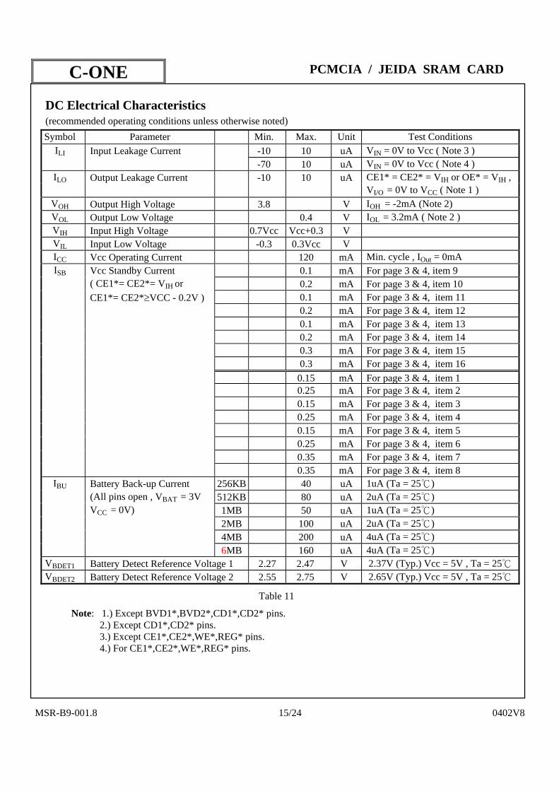
DC Electrical Characteristics (recommended operating conditions unless otherwise noted) Symbol Parameter Min. Max. Unit Test Conditions
ILI Input Leakage Current -10 10 uA VIN = 0V to Vcc ( Note 3 ) -70 10 uA VIN = 0V to Vcc ( Note 4 )
ILO Output Leakage Current -10 10 uA CE1* = CE2* = VIH or OE* = VIH , VI/O = 0V to VCC ( Note 1 )
VOH Output High Voltage 3.8 V IOH = -2mA (Note 2) VOL Output Low Voltage 0.4 V IOL = 3.2mA ( Note 2 ) VIH Input High Voltage 0.7Vcc Vcc+0.3 V
VIL Input Low Voltage -0.3 0.3Vcc V
ICC Vcc Operating Current 120 mA Min. cycle , IOut = 0mA ISB Vcc Standby Current 0.1 mA For page 3 & 4, item 9 ( CE1*= CE2*= VIH or 0.2 mA For page 3 & 4, item 10 CE1*= CE2*≥VCC - 0.2V ) 0.1 mA For page 3 & 4, item 11 0.2 mA For page 3 & 4, item 12 0.1 mA For page 3 & 4, item 13 0.2 mA For page 3 & 4, item 14 0.3 mA For page 3 & 4, item 15 0.3 mA For page 3 & 4, item 16 0.15 mA For page 3 & 4, item 1 0.25 mA For page 3 & 4, item 2 0.15 mA For page 3 & 4, item 3 0.25 mA For page 3 & 4, item 4 0.15 mA For page 3 & 4, item 5 0.25 mA For page 3 & 4, item 6 0.35 mA For page 3 & 4, item 7 0.35 mA For page 3 & 4, item 8
IBU Battery Back-up Current 256KB 40 uA 1uA (Ta = 25℃) (All pins open , VBAT = 3V 512KB 80 uA 2uA (Ta = 25℃) VCC = 0V) 1MB 50 uA 1uA (Ta = 25℃) 2MB 100 uA 2uA (Ta = 25℃) 4MB 200 uA 4uA (Ta = 25℃) 6MB 160 uA 4uA (Ta = 25℃)
VBDET1 Battery Detect Reference Voltage 1 2.27 2.47 V 2.37V (Typ.) Vcc = 5V , Ta = 25℃VBDET2 Battery Detect Reference Voltage 2 2.55 2.75 V 2.65V (Typ.) Vcc = 5V , Ta = 25℃
Table 11
Note: 1.) Except BVD1*,BVD2*,CD1*,CD2* pins. 2.) Except CD1*,CD2* pins. 3.) Except CE1*,CE2*,WE*,REG* pins. 4.) For CE1*,CE2*,WE*,REG* pins.
C-ONE PCMCIA / JEIDA SRAM CARD
MSR-B9-001.8 16/24 0402V8
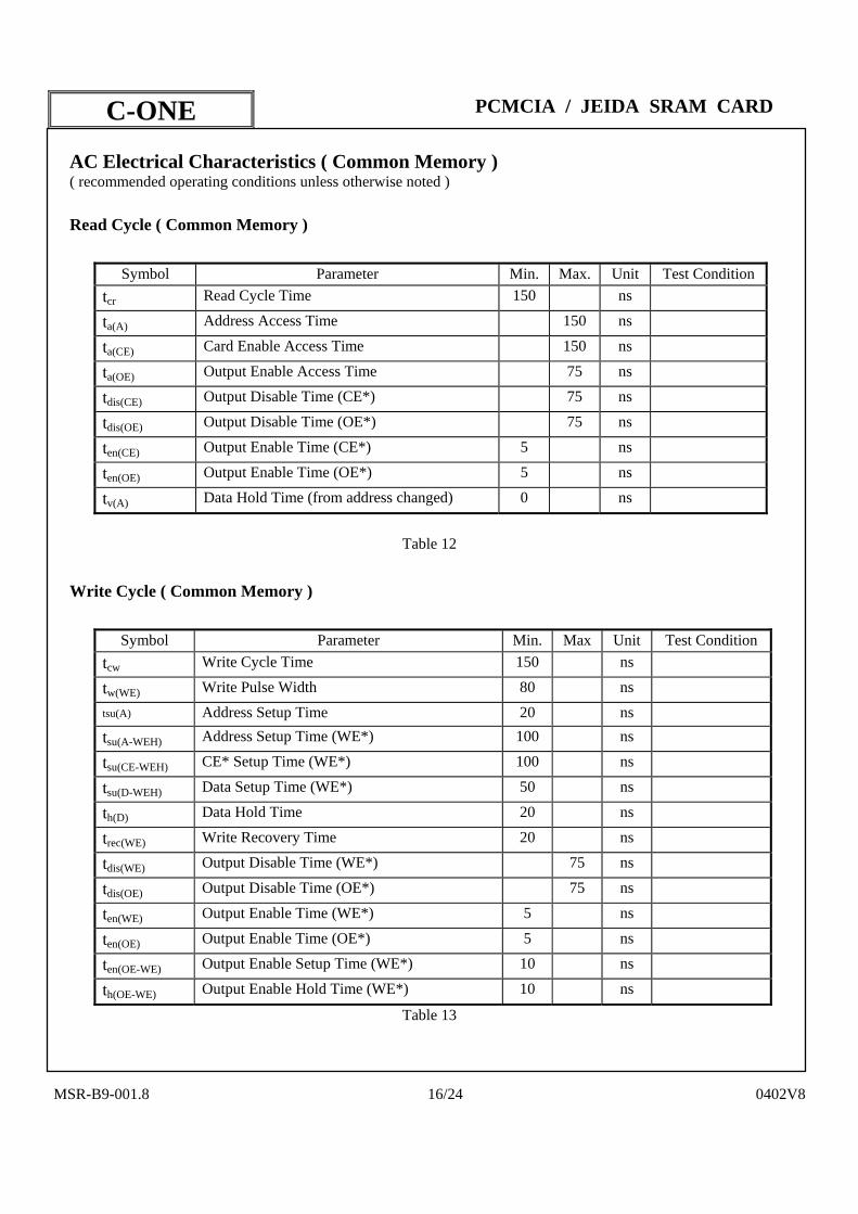
AC Electrical Characteristics ( Common Memory ) ( recommended operating conditions unless otherwise noted )
Read Cycle ( Common Memory )
Symbol Parameter Min. Max. Unit Test Conditiontcr Read Cycle Time 150 ns
ta(A) Address Access Time 150 ns
ta(CE) Card Enable Access Time 150 ns
ta(OE) Output Enable Access Time 75 ns
tdis(CE) Output Disable Time (CE*) 75 ns
tdis(OE) Output Disable Time (OE*) 75 ns
ten(CE) Output Enable Time (CE*) 5 ns
ten(OE) Output Enable Time (OE*) 5 ns
tv(A) Data Hold Time (from address changed) 0 ns
Table 12
Write Cycle ( Common Memory )
Symbol Parameter Min. Max Unit Test Conditiontcw Write Cycle Time 150 ns
tw(WE) Write Pulse Width 80 ns
tsu(A) Address Setup Time 20 ns
tsu(A-WEH) Address Setup Time (WE*) 100 ns
tsu(CE-WEH) CE* Setup Time (WE*) 100 ns
tsu(D-WEH) Data Setup Time (WE*) 50 ns
th(D) Data Hold Time 20 ns
trec(WE) Write Recovery Time 20 ns
tdis(WE) Output Disable Time (WE*) 75 ns
tdis(OE) Output Disable Time (OE*) 75 ns
ten(WE) Output Enable Time (WE*) 5 ns
ten(OE) Output Enable Time (OE*) 5 ns
ten(OE-WE) Output Enable Setup Time (WE*) 10 ns
th(OE-WE) Output Enable Hold Time (WE*) 10 ns
Table 13
C-ONE PCMCIA / JEIDA SRAM CARD
MSR-B9-001.8 17/24 0402V8
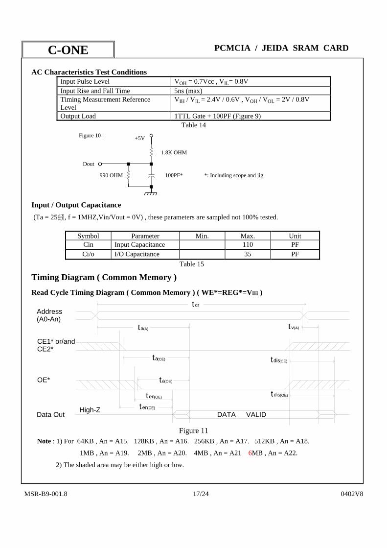
AC Characteristics Test Conditions Input Pulse Level VOH = 0.7Vcc , VIL= 0.8V Input Rise and Fall Time 5ns (max) Timing Measurement Reference Level
VIH / VIL = 2.4V / 0.6V , VOH / VOL = 2V / 0.8V
Output Load 1TTL Gate + 100PF (Figure 9) Table 14
+5V
1.8K OHM
100PF*990 OHM
Dout
*: Including scope and jig
Figure 10 :
Input / Output Capacitance (Ta = 25蚓, f = 1MHZ,Vin/Vout = 0V) , these parameters are sampled not 100% tested.
Symbol Parameter Min. Max. Unit Cin Input Capacitance 110 PF Ci/o I/O Capacitance 35 PF
Table 15
Timing Diagram ( Common Memory )
Read Cycle Timing Diagram ( Common Memory ) ( WE*=REG*=VIH )
Addresstcr
t
t
t
tt
t
DATA VALID
t
t
High-ZData Out
OE*
CE2*CE1* or/and
(A0-An)
en(CE)
en(OE)
a(OE)
a(CE)
a(A) v(A)
dis(CE)
dis(OE)
Figure 11
Note : 1) For 64KB , An = A15. 128KB , An = A16. 256KB , An = A17. 512KB , An = A18.
1MB , An = A19. 2MB , An = A20. 4MB , An = A21 6MB , An = A22.
2) The shaded area may be either high or low.

C-ONE PCMCIA / JEIDA SRAM CARD
MSR-B9-001.8 18/24 0402V8
Write Cycle Timing Diagram ( Common Memory ) ( REG*=VIH , WE* controlled ) t CW
t
Address
OE*
CE2*CE1* or/and
(A0-An)
t
tt
tt rec
th
t t h
DATA INPUT VALIDHigh-Z
ttdist dis
High-Zt en
WE*
Data In
Data Out
su(CE-WEH)
su(A-WEH)
su(OE-WE)
w(WE)su(A)
su(D-WEH)
(OE)(WE)
(OE)
en(WE)
(D)
(OE-WE)
(WE)
Figure 12
Write Cycle Timing Diagram ( Common Memory ) ( CE* controlled , OE*=REG*=Vih) t CW
tsu
Address
CE2*CE1* or/and
(A0-An)
tsu th
DATA INPUT VALIDHigh-Z
WE*
Data In
t
t rec
su(A)(CE-WEH)
(WE)
(D)(D-WEH)
Figure 13 Note : 1) For 64KB , An = A15. 128KB , An = A16. 256KB , An = A17. 512KB , An = A18.
1MB , An = A19. 2MB , An = A20. 4MB , An = A21 6MB , An = A22.
2) The shaded area may be either high or low.

C-ONE PCMCIA / JEIDA SRAM CARD
MSR-B9-001.8 19/24 0402V8
AC Electrical Characteristics ( Attribute Memory ) ( recommended operating conditions unless otherwise noted )
Read Cycle ( Attribute Memory )
Symbol Parameter Min. Max Unit Test Condition tcr Read Cycle Time 300 ns
ta(A) Address Access Time 300 ns
ta(CE) Card Select Access Time 300 ns
ta(OE) Output Enable Access Time 150 ns
tdis(CE) Output Disable Time (from CE*) 100 ns
tdis(OE) Output Disable Time (from OE*) 100 ns
ten(CE) Output Enable Time (from CE*) 5 ns
ten(OE) Output Enable Time (from OE*) 5 ns
tv(A) Data Hold Time (from address changed) 0 ns
Table 16
Write Cycle ( Attribute Memory )
Symbol Parameter Min. Max. Unit Test Condition tCW Write Cycle Time 1 ms
tAS Address Setup Time 30 ns
tAH Address Hold Time 50 ns
tWP Write Pulse Width 120 ns
tCS Card Enable Time to WE* 15 ns
tCH Card Enable Hold Time from WE* High 0 ns
tDS Data Setup Time 70 ns
tDH Data Hold Time 30 ns
tOES OE* Setup Time 30 ns
tOEH OE* Hold Time 30 ns
tDB Delay from WE* high to BUSY* Asserted 50 ns
Table 17
C-ONE PCMCIA / JEIDA SRAM CARD
MSR-B9-001.8 20/24 0402V8
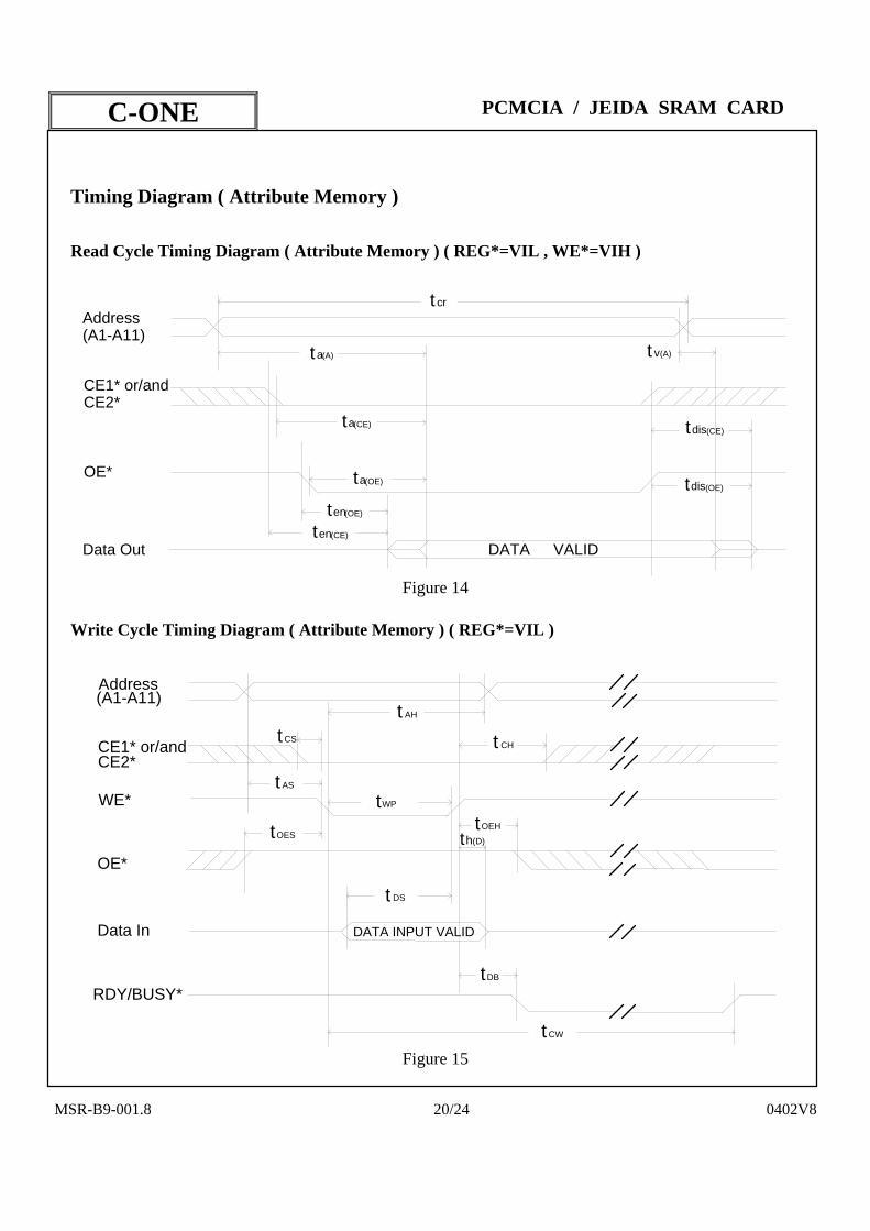
Timing Diagram ( Attribute Memory )
Read Cycle Timing Diagram ( Attribute Memory ) ( REG*=VIL , WE*=VIH )
Addresstcr
t
t
t
tt
t
DATA VALID
t
t
Data Out
OE*
CE2*CE1* or/and
(A1-A11)
en(CE)
en(OE)
a(OE)
a(CE)
a(A)
dis(OE)
dis(CE)
v(A)
Figure 14
Write Cycle Timing Diagram ( Attribute Memory ) ( REG*=VIL )
Address
OE*
CE2*CE1* or/and
DATA INPUT VALID
WE*
Data In
(A1-A11)t AH
t AS
tWP
tOEH
ttOES
t DS
t CW
RDY/BUSY*
h(D)
tDB
t CS t CH
Figure 15

C-ONE PCMCIA / JEIDA SRAM CARD
MSR-B9-001.8 21/24 0402V8
Battery Voltage Detection BVD1*/BVD2* pins are used to monitor the voltage of the main battery which should be maintained at 2.65V or greater for data retention. The following table described the main battery status by reading the signals on BVD1*/BVD2* pins.
BVD1* BVD2* Main Battery Comments H H VBAT ≥ 2.65V Data retention is OK. Battery is operational H L 2.37V < VBAT < 2.65V Data retention is OK. But battery should be replaced.L L VBAT < 2.37V Data integrity is not guaranteed. Battery must be replaced.
Table 18 Note : if the main battery is removed , BVD1* and BVD2* pins will not function Main Battery Specifications
3V Lithium battery Recommended parts (Please refer to the table below) Diameter Thickness Brand Model No. Diameter Thickness Brand Model No.23.0mm 2.5mm RAYOVAC BR2325 20.0mm 2.5mm TOSHIBA CR2025
FDK CR2325 FDK CR2025 PANASONIC BR2325 PANASONIC CR2025
Approximate Battery Life Time Under Battery Back-up Only
( Ta=25°C, Humidity=60% R.H. ) *battery life unit : year Product Part No. Battery Life Product Part No. Battery Life
SA5256 6 / 4.5 SN5256 6 / 4.5SA5512 4 / 3 SN5512 4 / 3 SA5001 6 / 4.5 SN5001 6 / 4.5SA5002 4 / 3 SN5002 4 / 3SA5004 2.5 / 2 SN5004 2.5 / 2SA5006 2.5 / 2 SN5006 2.5 / 2
Table 19
*For battery life , the numbers on the left-hand side of slash denote using 2325 series batteries. The numbers on the right-hand side of slash denote using 2025 series batteries. Card Detection CD1* , CD2* pins are used to detect the insertion of the card into the system. When the memory card has been correctly inserted , CD1* and CD2* are detected by the system . The recommended circuit in the system side is shown in figure below.
VCC
CD1*
CD2*
VCC
(A)
(B)
Figure 16

C-ONE PCMCIA / JEIDA SRAM CARD
MSR-B9-001.8 22/24 0402V8
Power-up / Power-down Characteristics Symbol Parameter Min. Max. Unit Condition Note
Vi(CE) CE* Signal Level 0 ViMAX V 0V ≤ VCC < 2.0 1 VCC-0.1 ViMAX V 2.0 ≤ VCC < VIH VIH ViMAX V VIH ≤ VCC
tsu(VCC) CE* Setup Time 20 ms 10ms (Typ.)
trec(VCC) CE* Recovery Time 1 us
tpr VCC Rising Time 0.1 300 ms 10% → 90% (VCC+5%) 1 tpf VCC Falling Time 3.0 300 ms 90% (VCC-5%) → 10% 1
Table20 Note:
1.) ViMAX means absolute maximum voltage for input.
2.) For the period 0V ≤ VCC< 2.0V , power supply voltage is low , so 0V~ ViMAX is permitted , because the logic for the system interface IC may not be determined.
3.) The Tpr and Tpfare defined as " linear waveform " in the period of 10% to 90%. Even if the waveform is not " linear waveform " , its rising and falling time must meet this specification.
Power-up Timing Diagram
tpr
Vih
tSU(VCC)
2VCE1*,CE2*
VCC
Figure 17
Power-down Timing Diagram
tpf
Vih
trec(VCC)
2VCE1*,CE2*
VCC

C-ONE PCMCIA / JEIDA SRAM CARD
MSR-B9-001.8 23/24 0402V8
Figure 18
Outline Dimensions (Unit: mm)