GaAs-based resonant tunneling diode (RTD) epitaxy on Si for ...

arX
iv:1
202.
6224
v2 [
cond
-mat
.mtr
l-sc
i] 8
Jun
201
2
Application of hydrogenation to low-temperature cleaning of the Si(001)surface in the processes of molecular-beam epitaxy: Investigation by STM,RHEED and HRTEM
L. V. Arapkina,a) L. A. Krylova, K. V. Chizh, V. A. Chapnin, O. V. Uvarov, and V. A. Yuryevb)
A.M.Prokhorov General Physics Institute of the Russian Academy of Sciences, 38 Vavilov Street, Moscow, 119991,
Russia
(Dated: 28 February 2012)
Structural properties of the clean Si(001) surface obtained as a result of low-temperature (470–650) pre-growth annealings of silicon wafers in a molecular-beam epitaxy chamber have been investigated. To decreasethe cleaning temperature, a silicon surface was hydrogenated in the process of a preliminary chemical treat-ment in HF and NH4F aqueous solutions. It has been shown that smooth surfaces composed by wide terracesseparated by monoatomic steps can be obtained by dehydrogenation at the temperatures ? 600, whereasclean surfaces obtained at the temperatures < 600 are rough. It has been found that there exists a de-pendence of structural properties of clean surfaces on the temperature of hydrogen thermal desorption andthe process of the preliminary chemical treatment. The frequency of detachment/attachment of Si dimersfrom/to the steps and effect of the Ehrlich-Schwoebel barrier on ad-dimer migration across steps have beenfound to be the most probable factors determining a degree of the resultant surface roughness.
PACS numbers: 68.47.Fg, 68.35.Bs, 68.43.Vx, 68.37.Ef, 61.14.Hg
I. INTRODUCTION
Reduction of temperatures of technological processesis one of important requirements of silicon VLSImanufacturing.1 Presently, removal of a SiO2 protectionlayer, formed in the process of wet chemical etching,with the use of thermal treatments at temperatures of? 800 is a main method of pre-growth cleaning of Sisurfaces before molecular-beam epitaxy (MBE) and theRCA method2,3 is most frequently used for formationof a thin (∼ 1 nm thick) film of silicon dioxide.4 Ap-plication of Si(001) surface hydrogenation instead of itsoxidation at the final stage of wet etching may enablethe reduction of the surface cleaning temperature downto 500–650.5,6 In this article, an issue of possibility ofreduction of Si(001) wafer cleaning temperature beforeMBE, directly in the ultra-high vacuum (UHV) deposi-tion chamber, is investigated by means of three compli-mentary techniques: combination of the scanning tunnel-ing microscopy (STM) and the reflected high-energy elec-tron diffraction (RHEED) allows us to reveal and studythe Si(001) surface morphology whereas the high resolu-tion transmission electron microscopy (HRTEM) is usedfor examination of epitaxial layers and interfaces formedas a result of Si deposition on the dehydrogenated Si(001)surfaces.Studies of properties of hydrogenated Si(001) and
Si(111) surfaces have been carried out for a long time.Initially these surfaces were explored using diffraction
a)Electronic mail: [email protected])Also at Technopark of GPI RAS, Moscow, 119991,Russia; Electronic mail: [email protected];http://www.gpi.ru/eng/staff s.php?eng=1&id=125
methods, the method of thermal desorption and the sur-face IR spectroscopy.3,6–12 Results of these researches en-abled the determination of types of hydrides which formon surfaces of differently oriented Si wafers depending oncomposition of etchants as well as the temperature rangein which their desorption is possible.
With the development of the STM techniques, it hasbecome possible to conduct researches of structural prop-erties of hydrogenated and clean surfaces at a qualita-tively new level.13–15 In the vast majority of the works,the hydrogenation of the (2 × 1)-reconstructed Si(001)surface purified of the silicon dioxide film was carriedout under UHV using a source of atomic hydrogen. Astructure of surfaces obtained in such a way differs sig-nificantly from the structure of surfaces forming as a re-sult of wet etching without hydrogenation. Annealingat high temperatures for SiO2 removal results in forma-tion of surfaces with wide terraces and monoatomic stepsand facilitates the desorption of foreign atoms.16,17 STMstudies have shown that Si(001) surfaces hydrogenated asa result of wet etching are composed by narrow terraceswith monoatomic steps.18–21 Impossibility of desorptionof some impurities, e.g., carbon, by a subsequent low-temperature treatment is a disadvantage of the surfacecleaning method based on its hydrogenation during wetetching.
Short dipping of a Si wafer in an aqueous solution ofthe hydrofluoric acid with pH varying from 2 to 7 is themost well-known method of the surface hydrogenation. Anumber of Si hydrides, the most prevalent of which aresilicon monohydride and dihydride, form as a result ofreaction of hydrogen with the Si surface.14,21–23 A frac-tion of dihydride on the surface rises as pH of the HFsolutions increases.9,10 In some modes of Si(001) etching,formation of the 111 facets is observed, on which every

2
Si atom located on the (001) plane is bonded to two hy-drogen atoms (dihydride) whereas each atom situated onthe (111) plane is bonded to a single atom of hydrogen(monohydride).8,11 The temperature of thermal desorp-tion of hydrogen atoms depends on a type of the hydride.According to Ref. 6, a characteristic temperature rangeof the monohydride thermal desorption is from 540 to620, that of the dihydride desorption is from 440 to540.In the current article, the data of exploration by means
of STM and RHEED of the structure of Si(001) surfacesobtained as a result of the low-temperature dehydrogena-tion of silicon substrates after wet chemical etching withsurface termination by hydrogen atoms are presented.Results of investigation of surface structure of Si epitaxiallayers grown on such surfaces as well as data of HRTEMstudies of Si-epilayer/Si-substrate interfaces are also setforth.
II. EXPERIMENTAL TECHNIQUES AND SAMPLEPREPARATION PROCEDURES
The investigations were carried out using the RiberEVA32 MBE vessel equipped with the Staib InstrumentsRH20 RHEED tool and coupled with the GPI-300 UHVSTM.1,24,25 8×8mm2 samples were cut from commercialCZ Si:B wafers (the orientation was (100), ρ = 12Ωcm).During the preliminary chemical treatment, at final
phase of RCA wet etching, the samples were processed invarious aqueous solutions on the basis of the hydrofluoricacid. The following etchants were used: (1) 5% HF solu-tion, pH = 2; (2) buffered NH4F+HF solution, pH = 4;(3) concentrated NH4F solution, pH = 7. The chemicalprocessing was completed by sample rinsing in deionizedwater for 1 min.The thermal treatment in UHV was performed in
two stages: (i) preliminary annealing lasted 2 hours at300—this process completed the preliminary treatmentof samples; (ii) final annealing was carried out at highertemperature in the range from 470 to 650. The dura-tion of the second stage of annealing was determined bya form of RHEED patterns.The process temperature was monitored by the IS12-Si
infrared pyrometer. The pressure in the MBE chamberdid not exceed 8×10⁻¹⁰Torr during annealing. The rateof sample heating from 300 to the preset temperatureof final annealing was∼ 0,24/c; the sample cooling ratewas ∼ 0,4/c.The STM images were taken in the constant current
mode at room temperature.Si epitaxial films were deposited on the clean Si(001)
surface by UHV MBE. Conditions in the MBE cham-ber during Si deposition were similar to those duringGe/Si(001) MBE described in Refs. 1, 25. The rate ofSi deposition was ∼ 0.25 A/c, the sample cooling rate af-ter growth was ∼ 0.4/c.The Carl Zeiss Libra-200 FE HR HRTEM was used
for investigation of structural properties of Si epitaxiallayers and their interfaces with Si substrates.
Additional experimental details and description of theexperimental instruments can be found in Ref. 1.
III. EXPLORATION BY STM AND RHEED
A. Hydrogenated Si(001)
A study of silicon surfaces terminated by hydrogen(Si:H) carried out by means of STM and RHEED hasshown that their structure depends on a kind of thepreliminary chemical treatment used for hydrogenation.If solutions containing NH4F are used Si:H surfaces aremore rough in comparison with those prepared in solu-tions of dilute HF; the higher the concentration of am-monium fluoride, the rougher the surface forms. Sur-face roughening is a consequence of formation of sur-face islands composed by terraces and monoatomic steps.Height and area of the islands are determined by condi-tions of the preliminary chemical treatment. Differencein surface roughness may be qualitatively estimated fromthe RHEED patterns. Irrespective of a kind of the solu-tion used for the surface termination, RHEED patternsalways correspond to the unreconstructed 1 × 1 surface(Fig. 1).
Diffraction patterns of the samples prepared in so-lutions with pH = 2 consist of broad streaks of mainreflexes (Fig. 1a), whereas beams of main reflexes haveshapes corresponding to well developed roughness on themonoatomic scale (3D reflexes) for the samples processedin solutions with pH = 7 (Fig. 1b).
Effect of NH4F concentration on the roughness of resul-tant surfaces consists in selective etching of surfaces andappearance of the 111 facets during sample treatmentin solutions containing ammonium fluoride. However, itis demonstrated in the literature that formation of suchfacets is suppressed if intense release of hydrogen bub-bles is eliminated.26 STM study of the Si:H surfaces hasshown a slight increase in the spread of height of adjacentsteps on the surfaces with the growth of etchant pH—itis within the height of two monoatomic steps. We havefailed to recognize a type of the Si:H surface reconstruc-tion: it is difficult to be determined because the hydridesmay fill the surface irregularly. Another circumstancecomplicating the recognition of a type of the Si:H surfacereconstruction is that hydrogen atoms situated close toone another but bonded to different silicon atoms “devi-ate” from an “ideal” position asymmetrically and non-uniformly around the surface. This results in differenceof the local density of states (LDOS) in the vicinity of aSi atom from LDOS in the vicinity of another Si atom,therefore atomic resolution cannot be reached in the STMimages of such surfaces.22,23
3
FIG. 1. RHEED patterns of the Si:H surfaces obtained as a result of treatment in solutions of varying acidity (azimuth is [110],E = 10 keV): (a) pH = 2; (b) pH = 7.
B. Effect of surface dehydrogenation
Exploration of the Si(001) surface cleaned of hydro-gen atoms by thermal desorption allows one to mark outtwo characteristic ranges of the treatment temperature—below and above 600—in which physical processes re-sult in formation of different surface structures.
1. Annealing at T ? 600
If the cleaning temperatures are higher than 600enhancement of NH4F content in solutions during thepreliminary etching causes an increase of the resultantsurface roughness; with the growth of the NH4F con-centration longer annealing is required for obtaining asmoother surface. Smooth surfaces with wide terracesand monoatomic steps form as a result of processing insolutions with pH = 2 followed by annealing at the tem-peratures above 600 or as a result of etching in solu-tions with pH > 2 and annealing at the temperatures? 650. Fig. 2 shows STM images of the clean Si(001)surface subjected to difference chemical treatments andannealed at 650.
The c(4× 4) structure arises on the surface due to an-nealing at 650. Previously this structure was identifiedby us as 2× 2,27 however further survey have shown thisstructure to be nothing else but the β-modification ofthe c(4 × 4) reconstruction.28,29 One can find a detaileddescription of the Si(001)-c(4× 4) structure in Ref. 1.
Reflexes corresponding to the c(4×4) surface structureare much weaker in the RHEED patterns of the sam-ples processed in the solutions with pH = 7 than in thediffraction patterns of the samples treated in the solu-tions with pH = 2. STM images show that c(4×4) recon-structed surfaces are always composed by wide terracesand monoatomic steps. A relation between processes ofthe c(4×4) structure formation and obtaining of smoothsurfaces is difficult to be ascertained because it is hardto establish if there is a contribution of carbon to theseprocesses: according to existing notions it can take partin formation of the c(4 × 4) structure.30,31 It is obvious
however that Si atoms (which are known to be paired inad-dimers) can freely migrate along the surface and thec(4×4) structure forms on the 2×1 reconstructed surface.Evidence of this fact has been found in data on evolutionof the diffraction patterns during heat treatments: thec(4× 4) structure appears during sample exposure at thetemperatures from 610 to 650 but it does not arise incourse of rapid heating of samples in the interval from300 to 800.Differences in the structure of the formed clean sur-
faces are also observed in the samples dehydrogenatedby annealing at 610 (Fig. 3). The c(4 × 4) structureis observed on the samples treated in the solutions withpH = 2 and annealed for 10 min. Further prolongationof annealing may cause occurrence of SiC islands on thesurface (although we have never met SiC on our sam-ples this circumstance should be taken into account).When hydrogenated in the solutions with pH = 7, theclean surface becomes rougher, it is composed by islandsformed by short narrow terraces and monoatomic steps.Diffraction patterns correspond to the 2 × 1 reconstruc-tion; they are characterized by weaker 3D reflexes on themain beams than those shown in Fig. 1b.
2. Annealing at T < 600
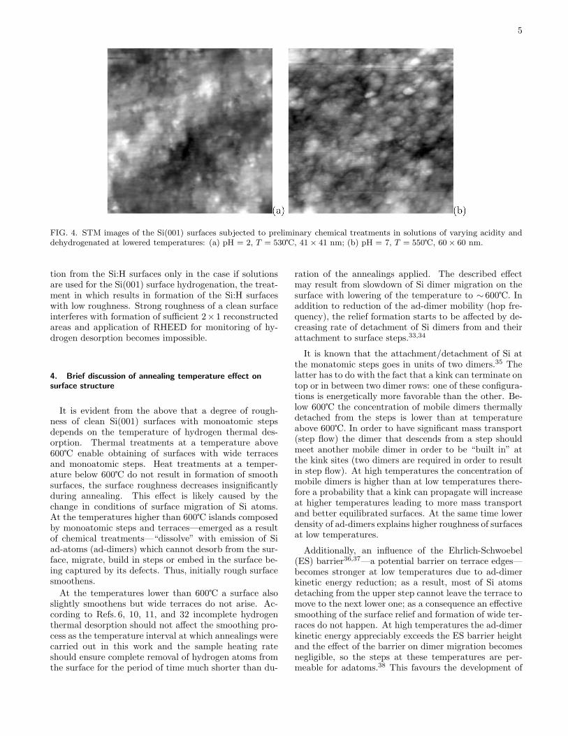
Annealings at the temperatures below 600 resultin formation of clean surfaces with the roughness onmonoatomic scale for any type of the preliminary chem-ical treatment. However the structures of the resultantsurfaces are different for different chemical treatments.Hydrogenation in solutions with greater pH results information of rougher surfaces. STM images of samplesannealed at the temperatures below 600 after differentchemical treatments are presented in Fig. 4.The minimum temperature at which surface cleaning
takes place is 470 (annealing duration is 35 min) for thesamples treated in the solutions with pH = 2 and 550(annealing duration is also 35 min) for the samples pro-cessed in the solutions with pH = 7. Diffraction patternscorrespond to the 2× 1 structure for the former process;for the latter processing they resemble the 1× 1 patterns

4
FIG. 2. STM images of the Si(001) surfaces subjected to preliminary chemical treatments in solutions of varying acidity anddehydrogenated as a result of annealing at T = 650: (a) pH = 2, annealing for 8 min, 57× 57 nm; (b) pH = 7, annealing for5 min, 40× 40 nm.
FIG. 3. STM images of the Si(001) surfaces subjected to preliminary chemical treatments in solutions of varying acidity anddehydrogenated by annealing at T = 610 for 10 min: (a) pH = 2, 41× 41 nm; (b) pH = 7, 87× 76 nm.
of the original surface terminated by hydrogen atoms butwith narrower stripes and less pronounced 3D reflexes onthe main beams (the ½ reflexes are always weak when theprocessing temperature is less than 600 but in the caseof etching at pH = 7 they are usually invisible to theeye and can be registered only with a camera at a longexposure).
3. Dynamics of RHEED patterns during sample heating
A study of evolution of the diffraction patterns duringsample heating from 300 to 800 has shown that origi-nal patterns correspond to the 1× 1 structure, i. e., theyare composed only by the main beams. 3D reflexes areobserved on the main beams; the brightness of the 3D
reflexes depends on the preliminary chemical treatment.The most intense 3D reflexes are observed after the treat-ment in the solutions containing NH4F. A temperature atwhich the ½ beams (which correspond to 2× 1 or c(4× 4)structure) arise in the [110] azimuth in electron diffrac-tion patterns depends on the initial chemical treatment.If the samples are etched in dilute HF the ½ reflexes ap-pear in the range from 420 to 470; they arise in therange from 560 to 660 or do not appear at all if thesamples are hydrogenated in the solutions with pH = 4or 7. The cause of the difference in the temperatures atwhich the ½ reflexes appear lies in the strong dependenceof the original Si:H surface roughness on the compositionof the solutions used for the surface termination.
It can be concluded that RHEED can be applied asa method for monitoring of hydrogen thermal desorp-
5
FIG. 4. STM images of the Si(001) surfaces subjected to preliminary chemical treatments in solutions of varying acidity anddehydrogenated at lowered temperatures: (a) pH = 2, T = 530, 41× 41 nm; (b) pH = 7, T = 550, 60× 60 nm.
tion from the Si:H surfaces only in the case if solutionsare used for the Si(001) surface hydrogenation, the treat-ment in which results in formation of the Si:H surfaceswith low roughness. Strong roughness of a clean surfaceinterferes with formation of sufficient 2× 1 reconstructedareas and application of RHEED for monitoring of hy-drogen desorption becomes impossible.
4. Brief discussion of annealing temperature effect onsurface structure
It is evident from the above that a degree of rough-ness of clean Si(001) surfaces with monoatomic stepsdepends on the temperature of hydrogen thermal des-orption. Thermal treatments at a temperature above600 enable obtaining of surfaces with wide terracesand monoatomic steps. Heat treatments at a temper-ature below 600 do not result in formation of smoothsurfaces, the surface roughness decreases insignificantlyduring annealing. This effect is likely caused by thechange in conditions of surface migration of Si atoms.At the temperatures higher than 600 islands composedby monoatomic steps and terraces—emerged as a resultof chemical treatments—“dissolve” with emission of Siad-atoms (ad-dimers) which cannot desorb from the sur-face, migrate, build in steps or embed in the surface be-ing captured by its defects. Thus, initially rough surfacesmoothens.
At the temperatures lower than 600 a surface alsoslightly smoothens but wide terraces do not arise. Ac-cording to Refs. 6, 10, 11, and 32 incomplete hydrogenthermal desorption should not affect the smoothing pro-cess as the temperature interval at which annealings werecarried out in this work and the sample heating rateshould ensure complete removal of hydrogen atoms fromthe surface for the period of time much shorter than du-
ration of the annealings applied. The described effectmay result from slowdown of Si dimer migration on thesurface with lowering of the temperature to ∼ 600. Inaddition to reduction of the ad-dimer mobility (hop fre-quency), the relief formation starts to be affected by de-creasing rate of detachment of Si dimers from and theirattachment to surface steps.33,34
It is known that the attachment/detachment of Si atthe monatomic steps goes in units of two dimers.35 Thelatter has to do with the fact that a kink can terminate ontop or in between two dimer rows: one of these configura-tions is energetically more favorable than the other. Be-low 600 the concentration of mobile dimers thermallydetached from the steps is lower than at temperatureabove 600. In order to have significant mass transport(step flow) the dimer that descends from a step shouldmeet another mobile dimer in order to be “built in” atthe kink sites (two dimers are required in order to resultin step flow). At high temperatures the concentration ofmobile dimers is higher than at low temperatures there-fore a probability that a kink can propagate will increaseat higher temperatures leading to more mass transportand better equilibrated surfaces. At the same time lowerdensity of ad-dimers explains higher roughness of surfacesat low temperatures.
Additionally, an influence of the Ehrlich-Schwoebel(ES) barrier36,37—a potential barrier on terrace edges—becomes stronger at low temperatures due to ad-dimerkinetic energy reduction; as a result, most of Si atomsdetaching from the upper step cannot leave the terrace tomove to the next lower one; as a consequence an effectivesmoothing of the surface relief and formation of wide ter-races do not happen. At high temperatures the ad-dimerkinetic energy appreciably exceeds the ES barrier heightand the effect of the barrier on dimer migration becomesnegligible, so the steps at these temperatures are per-meable for adatoms.38 This favours the development of

6
FIG. 5. STM images of 50 nm thick Si/Si(001) films grown by MBE at different temperatures: (a) 610, 41×41 nm; (b) 550,60× 60 nm; (c) 470, 60× 60 nm.
FIG. 6. HRTEM micrographs of a 50 nm thick Si epitaxial film grown at 610 on Si(001) after its preliminary chemicaltreatment in the solution with pH = 2 followed by dehydrogenation at 610 for 10 min; the figure 1 indicates an epi-Si/substrate interface region; a scale bar corresponds to 20 (a) or 10 (b),(c) nm; panel (c) is magnified from (b); a spottytriangle in the left upper corner of the image (a) is an epoxy.
smooth surfaces with wide terraces.
C. TEM study of epi-Si/Si-substrate interfaces
Usually, Si epitaxial layers with wide terraces andmonoatomic steps on the surface are obtained by MBEon Si(001) if deposited in the temperature range from500 to 600.39,40 Fig. 5 presents STM images of sur-faces of Si epitaxial layers grown at different depositiontemperatures on the Si(001) surface cleaned of hydro-gen atoms. The obtained surfaces are seen to be com-posed by terrases separated by monoatomic steps. Bylowering the growth temperature, reduction of the widthof the terraces is observed but their structure is differ-ent from that of the dehydrogenated surfaces. This al-lows us to assume that effect of mobility (hop rate) re-duction of migrating Si dimers on smoothing of dehy-drogenated surfaces in this temperature interval is notas significant as an impact of two other factors (reduc-tion of detachment/attachment rate of Si dimers from/tosteps and Ehrlich-Schwoebel potential barrier) as a resultof which appreciable smoothing of the dehydrogenatedrough Si(001) surfaces does not happen during anneal-
ing at the temperatures below 600 in the absence of anexternal source of Si atoms.
Change of surface structural properties at the tem-peratures of ∼ 600 was reported by us previously inthe articles on the study of the clean Si(001) surfaceobtained after removal of the SiO2 protection film byshort high-temperature annealings.24,27,41 During sam-ple cooling from the annealing temperature of ∼ 925,a reversible phase transition occurs in the range from550 to 600 which is manifested as a change of the sur-face reconstruction: 2 × 1 ←→ c(8 × 8). This transi-tion was explained by slowdown of Si ad-dimer migrationon the surface with the decrease in the sample temper-ature. Changes in the surface structural properties inthis temperature interval were also observed in the studyof Ge quantum dot nucleation on the Ge/Si(001) wet-ting layer and hut-cluster array formation.1,25,42,43 Thetemperature of ∼ 600 is a frontier between modes ofpreferential growth of huts and domes on the Ge/Si(001)wetting layer that is likely connected with changes in Gead-dimer migration process on the wetting layer surfaceat this temperature which also may be connected withthe effect of the ES barrier on Ge dimer migration on thewetting layer at low temperatures and absence of such

7
FIG. 7. HRTEM micrographs of a 50 nm thick Si epitaxial film grown at 550 on Si(001) after its preliminary chemicaltreatment in the solution with pH = 2 followed by annealing at 550 for 30 min; the figure 1 indicates an epi-Si/substrateinterface region, 2 shows a Si substrate and 3 denotes an epitaxial layer; a scale bar corresponds to 20 (a),(c) or 50 (b) nm.
FIG. 8. HRTEM micrographs of a 50 nm thick Si epitaxial film grown at 470 on Si(001) after its preliminary chemicaltreatment in the solution with pH = 2 followed by annealing at 470 for 18 min; the numerical 1 indicates an epi-Si/substrateinterface region, 2 denotes a Si substrate and 3 marks an epitaxial layer; a scale bar corresponds to 100 (a) or 10 (b),(c) nm;epoxy is seen in left upper corner of the image (a) and lower part of the image (c).
effect at high temperatures.43
A study of Si substrates subjected to the describedabove treatments with Si epitaxial films grown on theirsurfaces (Fig. 5) performed by means of high resolutionTEM allowed us to evaluate the quality of interfaces be-tween substrates and epilayers. We have succeeded to vi-sualize the interfaces between epilayers grown at differenttemperatures and surfaces exposed to different chemicaltreatments and various annealings and found interfacesformed on surfaces chemically treated at pH = 2 to beperfect.
Fig. 6 demonstrates HRTEM images of a 50 nm thickepilayer grown at 610 on the surface hydrogenatedin the solution with pH = 2 and exposed to annealingat 610 for 10 minutes for the hydrogen removal (seeFig. 3a). An interface region is indicated by arrows andmarked by the figure 1. It is visualized as a dark or lightline depending on the imaging conditions. Fig. 6b andespecially panel (c), which is magnified from (b), demon-strate a perfect atomic structure of the near-interface re-gion and absence of extended structural defects. The
observed contrast supposedly results from stress arisingaround the interface because of the presence of residualhydrogen or probably minor amount of carbon (some car-bon may come on the surface from chemical reagents orMBE vessel atmosphere—CO is the main after hydrogenresidual gas in this chamber, a minor amount of hydro-carbons is also present in the chamber—or even from thebulk of a Czochralsky grown substrate); a slight excessof vacancies also might explain the contrast. However,a good epitaxial interface is formed as a result of thisprocess.
A lower temperature of growth and dehydrogenationdoes not result in significant worsening of the interface.Fig. 7 shows a film deposited at 550 on the surfacetreated at 550 for 30 minutes after hydrogenation in theetchant with pH = 2. The epi-Si/substrate interface inthis sample is also epitaxial; its structure is also perfect,it does not contain extended defects. However it looksmore pronounced (Fig. 7c) than the interface obtained atthe higher temperature, maybe because of rougher ini-tial surface and higher concentration of point defects and

8
such residual impurities as hydrogen or carbon.We succeeded to lower the temperature of epitaxial
growth and surface annealing to 470 and obtain a per-fect defectless interface. Fig. 8 represents micrographsof an epilayer grown at this temperature on the surfacetreated at 470 for 18 minutes after etching at pH = 2.A perfect interface (Fig. 8b) and epitaxial layer (Fig. 8c)confirm our assumption that preparation of clean Si(001)surfaces suitable for further growth of perfect epitaxiallayers is possible at temperatures as low as 470.1
IV. CONCLUSION
We can conclude now that a method of hydrogena-tion of a Si(001) surface is applicable for low-temperaturecleaning of Si substrates in UHV MBE vessels. Varyinga type of the preliminary chemical treatment and a tem-perature of the dehydrogenation process, clean surfaceswith monoatomic roughness but different width of ter-races separated by monoatomic steps can be obtained.Low-temperature cleaning of Si(001) surfaces may findnumerous applications. In particular, Si surface cleaningby annealing at a temperature lower than 600 may beused in processes requiring preservation of a created inadvance relief on the Si(001) surface.Perfect Si epitaxial films and epi-Si/Si-substrate in-
terfaces can be formed at the temperatures as low as470 on clean Si(001) surfaces prepared by hydrogena-tion in HF aqueous solution with pH = 2 followedby low-temperature dehydrogenation at the temperatureof 470. This result makes it possible to form low-temperature buffer layers in the process of MBE growthof Ge/Si(001) heterostructures compatible with the stan-dard CMOS cycle of microelectronic device fabrication.
ACKNOWLEDGMENTS
We appreciate financial and technological support ofthis research: it was financed by the Ministry of Ed-ucation and Science of the Russian Federation underthe State Contracts No.Π2367, No. 14.740.11.0069 andNo. 16.513.11.3046; the study was performed using theequipment of the Center of Collective Use of ScientificEquipment of GPI RAS.
1V. A. Yuryev and L. V. Arapkina, Nanoscale Res. Lett. 6, 522(2011), arXiv:1104.2848.
2W. Kern and D. Puotinen, RCA Review 31, 187 (1970).3K. A. Reinhardt and W. Kern, eds., Handbook of silicon wafer
cleaning technology, 2nd ed. (William Andrew Inc., Norwich, NY,USA, 2008).
4A. Ishizaha and Y. Shiraki, J. Electrochem. Soc. 133, 666 (1986).5T. K. Nguyen-Duc, V. L. Thanh, V. Yam, P. Boucaud, D. Bouch-ier, O. G. Schmidt, and J. Derrien, Thin Solid Films 508, 207(2006).
6V. L. Thanh, D. Bouchier, and G. J. Hincelin, J. Appl. Phys.87, 3700 (2000).
7P. Dumas and Y. J. Chabal, J. Vac. Sci. Technol. A 10, 2160(1992).
8G. S. Higashi, Y. J. Chabal, G. W. Trucks, and K. Raghavachari,Appl. Phys. Lett. 56, 656 (1990).
9M. Niwano, Surf. Sci. 427–428, 199 (1999).10M. Niwano, T. Miura, Y. Kimura, R. Tajima, and N. Mijamoto,J. Appl. Phys. 79, 3708 (1996).
11P. Dumas, Y. J. Chabal, and P. Jakob, Surf. Sci. 269–270, 867(1992).
12C. Mazzara, J. Jupille, W.-Q. Zheng, M. Tanguy, A. Tadjeddine,and P. Dumas, Surf. Sci. 427–428, 208 (1999).
13K. Oura, V. G. Lifshits, A. A. Saranin, A. V. Zotov, andM. Katayama, Surf. Sci. Rep. 35, 1 (1999).
14J. J. Boland, Phys. Rev. Lett. 65, 3325 (1990).15X. R. Qin and P. R. Norton, Phys. Rev. B 53, 11100 (1996).16X. R. Qin and M. G. Lagally, Phys. Rev. B 59, 7293 (1999).17K. Sagisaka and D. Fujita, Phys. Rev. B 77, 205301 (2008).18K. Endo, K. Arima, T. Kataoka, Y. Oshikane, H. Inoue, andY. Mori, Appl. Phys. Lett. 73, 1853 (1998).
19K. Arima, K. Endo, T. Kataoka, Y. Oshikane, H. Inoue, andY. Mori, Appl. Phys. Lett. 76, 463 (2000).
20K. Arima, K. Endo, T. Kataoka, Y. Oshikane, H. Inoue, andY. Mori, Surf. Sci. 446, 128 (2000).
21I. T. Clark, B. S. Aldinger, A. Gupta, and M. A. Hines, J. Phys.Chem. C 147, 423 (2010).
22Y. Morita and H. Tokumoto, Appl. Phys. Lett. 67, 2654 (1995).23J. E. Northrup, Phys. Rev. B 44, 1419 (1991).24L. V. Arapkina, V. A. Yuryev, K. V. Chizh, V. M. Shevlyuga,M. S. Storojevyh, and L. A. Krylova, Nanoscale Res. Lett. 6,218 (2011), arXiv:1009.3909.
25L. V. Arapkina and V. A. Yuryev, Phys. Usp. 53, 279(2010), arXiv:0907.4770; Nanoscale Res. Lett. 6, 345 (2011),arXiv:1009.3831.
26B. S. Aldinger, A. Gupta, I. T. Clark, and M. A. Hinesa, J.Appl. Phys. 107, 103520 (2010).
27L. V. Arapkina, V. A. Yuryev, V. M. Shevlyuga, and K. V.Chizh, JETP Lett. 92, 310 (2010), arXiv:1007.0329.
28R. I. G. Uhrberg, J. E. Northrup, D. K. Biegelsen, R. D.Bringans, and L.-E. Swartz, Phys. Rev. B 46, 10251 (1992).
29S. T. Jemander, H. M. Zhang, R. I. G. Uhrberg, and G. V.Hansson, Mat. Sci. Eng. B 89, 415 (2002).
30K. Miki, K. Sakamoto, and T. Sakamoto, Appl. Phys. Lett. 71,3266 (1997).
31T. J. Kim, S. H. Oh, J. K. Kim, D. K. Kim, C. H. Moon, andS. T. Kang, J. Korean Phys. Soc. 42, 779 (1997).
32I. Goldfarb, J. H. G. Owen, D. R. Bowler, C. M. Goringe, P. T.Hayden, K. Miki, D. G. Pettifor, and G. A. D. Briggs, J. Vac.Sci. Technol. A 16, 1938 (1998).
33N. Kitamura, B. S. Swartzentruber, M. G. Lagally, and M. B.Webb, Phys. Rev. B 48, 5704 (1993).
34C. Pearson, B. Borovsky, M. Krueger, R. Curtis, and E. Gans,Phys. Rev. Lett. 74, 2710 (1995).
35H. J. W. Zandvliet, H. B. Elswijk, and E. J. van Loenen, Surf.Sci. 272, 264 (1992).
36R. L. Schwoebel and E. J. Shipsey, J. Appl. Phys. 37, 3682(1966).
37A. Saul, J.-J. Metois, and A. Ranguis, Phys. Rev. B 65, 075409(2002).
38S. Tanaka, N. C. Bartelt, C. C. Umbach, R. M. Tromp, andJ. M. Blakely, Phys. Rev. Lett. 78, 3342 (1997).
39G. G. Jernigan, P. E. Thompson, and M. E. Twigg, Mat. Sci.Eng. B 89, 133 (2002).
40J. Myslivec»
ek, C. Schelling, G. Springholz, F. Schaffler,
B. Voigtlander, and P. Smilauer, Mat. Sci. Eng. B 89, 410 (2002).41L. V. Arapkina, V. M. Shevlyuga, and V. A. Yuryev, JETP Lett.87, 215 (2008), arXiv:0908.1346.
42L. V. Arapkina, L. A. Krylova, V. A. Chapnin, K. V. Chizh,and V. A. Yuryev, in Proc. XV Int. Symp. on Nanophysics and
Nanoelectronics, Vol. 2 (Inst. Microstruct. Phys. RAS, NizhniNovgorod, Russia, 2011) p. 543.
43V. A. Yuryev and L. V. Arapkina, J. Appl. Phys. 111, 094307(2012), arXiv:1105.6012.
Copyright © 2022 FDOKUMEN