An ultrahigh vacuum complementary metal oxide silicon compatible nonlithographic system to fabricate...
28
Recent Patents on Nanotechnology 2008, 2, 41-68 41 1872-2105/08 $100.00+.00 © 2008 Bentham Science Publishers Ltd. Nanostructured p-Type Semiconducting Transparent Oxides: Promising Materials for Nano-Active Devices and the Emerging Field of “Transparent Nanoelectronics” Arghya Banerjee *,1 and Kalyan K. Chattopadhyay 2 1 Nevada Nanotechnology Center, Department of Electrical Engineering and Computer Science, University of Nevada, Las Vegas, Nevada-89154, USA, 2 Thin Film and Nanoscience Laboratory, Department of Physics, Jadavpur University, Kolkata-700032, India Received: December 26, 2007; Accepted: January 9, 2008; Revised: January 9, 2008 Abstract: Transparent conducting oxides (TCO) with p-type semiconductivity have recently gained renewed interest for the fabrication of all-oxide transparent junctions, having potential applications in the emerging field of ‘Transparent’ or ‘Invisible Electronics’. This kind of transparent junctions can be used as a “functional” window, which will transmit visible portion of solar radiation, but generates electricity by the absorption of the UV part. Therefore, these devices can be used as UV shield as well as UV cells. In this report, a brief review on the research activities on various p-TCO materials is furnished along-with the fabrication of different transparent p-n homojunction, heterojunction and field-effect transistors. Also the reason behind the difficulties in obtaining p-TCO materials and possible solutions are discussed in details. Considerable attention is given in describing the various patent generations on the field of p-TCO materials as well as transparent p-n junction diodes and light emitting devices. Also, most importantly, a detailed review and patenting activities on the nanocrystalline p-TCO materials and transparent nano-active device fabrication are furnished with considerable attention. And finally, a systematic description on the fabrication and characterization of nanocrystalline, p- type transparent conducting CuAlO 2 thin film, deposited by cost-effective low-temperature DC sputtering technique, by our group, is furnished in details. These p-TCO micro/nano-materials have wide range of applications in the field of optoelectronics, nanoelectronics, space sciences, field-emission displays, thermoelectric converters and sensing devices. Keywords: P-type transparent conducting oxide (p-TCO), nanocrystalline p-TCO, transparent p-n junction, transparent field effect transistor (TFET), nano-active device, transparent nanoelectronics, delafossite structure, nonstoichiometry, p-type doping, p-CuAlO 2 nanoparticles, direct current (DC) sputtering, low-temperature deposition, quantum confinement effect, photoluminescence, p-type ZnO. 1. INTRODUCTION 1.1. P-type Transparent Conducting Oxide Amongst various oxide materials, the most important oxide based materials that create overwhelming interest within materials scientists is the fundamental aspects and applications of semiconducting transparent films: more popularly known as “Transparent Conducting Oxides” (TCO), which are widely used for a long time in opto- electronics industries as well as in research fields [1-61]. The characteristics of such films are high room-temperature electrical conductivity (~ 10 3 S cm -1 or more) and high optical transparency (more than 80 %) in the visible region. The electronic band gap of a TCO is higher than 3.1 eV (corresponding to the energy of a 400 nm blue photon). So visible photons (having energy between 2.1 to 3.1 eV) cannot excite electrons from valence band (VB) to the conduction band (CB) and hence are transmitted through it, whereas they have enough energy to excite electrons from donor level to CB (for n-type TCO) or holes from acceptor level to VB (for p-type TCO). And these acceptor or donor levels are created in the TCOs by introducing non-stoichio- *Address correspondence to this author at the Nevada Nanotechnology Center, Department of Electrical Engineering and Computer Science, University of Nevada, Las Vegas, Nevada-89154, USA; Tel: +1 702 895 3777; Fax: +1 702 895 4075; E-mail: [email protected] metry and (or) appropriate dopants in a controlled manner. A schematic representation of the bandgap designing for transparent conductors is shown in Fig. (1). Although the TCOs have vast range of applications, very little work has been done on the active device fabrication using TCOs [62, 63]. This is because most of the well- known and widely used TCOs are n-type semiconductors (n- TCO), whereas their p-type counterpart (p-TCO), which are essential for junctional devices, were surprisingly missing in thin film form for a long time. Only in the last decade Sato et al. [64] and Kawazoe et al. [65] reported the p-type conductivity in a transparent thin film of binary nickel oxide (p-Ni 1-x O) and delafossite copper aluminum oxide (p- CuAlO 2+x ) [64] respectively. Thereafter, syntheses of a large number of p-TCO thin films with wide range of electro- optical properties have been reported in the last few years. Amongst this new group of TCOs, the most important is the delafossite structured p-TCO thin films in the form of A I B III O 2+x (A I : Cu + , Ag + , B III : Trivalent cations) and their doped versions [66-75]. Besides delafossite p-TCO thin films, some important non-delafossite p-TCO thin films have also been reported having very good electro-optical properties. These films include Cu 2 Sc 2 O 4 [76], spinel oxide films of the form A II B III 2 O 4 (A II : Ni 2+ , B III : Co 3+ ) [77-78], layered oxychalcogenide films of the form (Ln III O)M I C h (Ln III : La +3 , Pr +3 , Nd +3 , Sm +3 , Gd +3 , Y +3 , M I : Cu + , Ag + , C h : S - 2 , Se -2 ) [79-89], mixed oxide films of the form In 2 O 3 -Ag 2 O Not For Distribution
Transcript of An ultrahigh vacuum complementary metal oxide silicon compatible nonlithographic system to fabricate...
Recent Patents on Nanotechnology 2008, 2, 41-68 41
1872-2105/08 $100.00+.00 © 2008 Bentham Science Publishers Ltd.
Nanostructured p-Type Semiconducting Transparent Oxides: Promising Materials for Nano-Active Devices and the Emerging Field of “Transparent Nanoelectronics”
Arghya Banerjee*,1
and Kalyan K. Chattopadhyay2
1Nevada Nanotechnology Center, Department of Electrical Engineering and Computer Science, University of Nevada,
Las Vegas, Nevada-89154, USA, 2Thin Film and Nanoscience Laboratory, Department of Physics, Jadavpur University,
Kolkata-700032, India
Received: December 26, 2007; Accepted: January 9, 2008; Revised: January 9, 2008
Abstract: Transparent conducting oxides (TCO) with p-type semiconductivity have recently gained renewed interest for
the fabrication of all-oxide transparent junctions, having potential applications in the emerging field of ‘Transparent’ or
‘Invisible Electronics’. This kind of transparent junctions can be used as a “functional” window, which will transmit
visible portion of solar radiation, but generates electricity by the absorption of the UV part. Therefore, these devices can
be used as UV shield as well as UV cells. In this report, a brief review on the research activities on various p-TCO
materials is furnished along-with the fabrication of different transparent p-n homojunction, heterojunction and field-effect
transistors. Also the reason behind the difficulties in obtaining p-TCO materials and possible solutions are discussed in
details. Considerable attention is given in describing the various patent generations on the field of p-TCO materials as
well as transparent p-n junction diodes and light emitting devices. Also, most importantly, a detailed review and patenting
activities on the nanocrystalline p-TCO materials and transparent nano-active device fabrication are furnished with
considerable attention. And finally, a systematic description on the fabrication and characterization of nanocrystalline, p-
type transparent conducting CuAlO2 thin film, deposited by cost-effective low-temperature DC sputtering technique, by
our group, is furnished in details. These p-TCO micro/nano-materials have wide range of applications in the field of
optoelectronics, nanoelectronics, space sciences, field-emission displays, thermoelectric converters and sensing devices.
Keywords: P-type transparent conducting oxide (p-TCO), nanocrystalline p-TCO, transparent p-n junction, transparent field effect transistor (TFET), nano-active device, transparent nanoelectronics, delafossite structure, nonstoichiometry, p-type doping, p-CuAlO2 nanoparticles, direct current (DC) sputtering, low-temperature deposition, quantum confinement effect, photoluminescence, p-type ZnO.
1. INTRODUCTION
1.1. P-type Transparent Conducting Oxide
Amongst various oxide materials, the most important oxide based materials that create overwhelming interest within materials scientists is the fundamental aspects and applications of semiconducting transparent films: more popularly known as “Transparent Conducting Oxides” (TCO), which are widely used for a long time in opto-electronics industries as well as in research fields [1-61]. The characteristics of such films are high room-temperature electrical conductivity (~ 10
3 S cm
-1 or more) and high
optical transparency (more than 80 %) in the visible region. The electronic band gap of a TCO is higher than 3.1 eV (corresponding to the energy of a 400 nm blue photon). So visible photons (having energy between 2.1 to 3.1 eV) cannot excite electrons from valence band (VB) to the conduction band (CB) and hence are transmitted through it, whereas they have enough energy to excite electrons from donor level to CB (for n-type TCO) or holes from acceptor level to VB (for p-type TCO). And these acceptor or donor levels are created in the TCOs by introducing non-stoichio-
*Address correspondence to this author at the Nevada Nanotechnology
Center, Department of Electrical Engineering and Computer Science, University of Nevada, Las Vegas, Nevada-89154, USA; Tel: +1 702 895
3777; Fax: +1 702 895 4075; E-mail: [email protected]
metry and (or) appropriate dopants in a controlled manner. A schematic representation of the bandgap designing for transparent conductors is shown in Fig. (1).
Although the TCOs have vast range of applications, very little work has been done on the active device fabrication using TCOs [62, 63]. This is because most of the well-known and widely used TCOs are n-type semiconductors (n-TCO), whereas their p-type counterpart (p-TCO), which are essential for junctional devices, were surprisingly missing in thin film form for a long time. Only in the last decade Sato et al. [64] and Kawazoe et al. [65] reported the p-type conductivity in a transparent thin film of binary nickel oxide (p-Ni1-xO) and delafossite copper aluminum oxide (p-CuAlO2+x) [64] respectively. Thereafter, syntheses of a large number of p-TCO thin films with wide range of electro-optical properties have been reported in the last few years. Amongst this new group of TCOs, the most important is the delafossite structured p-TCO thin films in the form of A
IB
IIIO2+x (A
I: Cu
+, Ag
+, B
III: Trivalent cations) and their
doped versions [66-75]. Besides delafossite p-TCO thin films, some important non-delafossite p-TCO thin films have also been reported having very good electro-optical properties. These films include Cu2Sc2O4 [76], spinel oxide films of the form A
IIB
III2O4 (A
II: Ni
2+, B
III: Co
3+) [77-78],
layered oxychalcogenide films of the form (LnIII
O)MIC
h
(LnIII
: La+3
, Pr+3
, Nd+3
, Sm+3
, Gd+3
, Y+3
, MI: Cu
+, Ag
+, C
h: S
-
2, Se
-2) [79-89], mixed oxide films of the form In2O3-Ag2O
Not For Distribution
42 Recent Patents on Nanotechnology 2008, Vol. 2, No. 1 Banerjee and Chattopadhyay
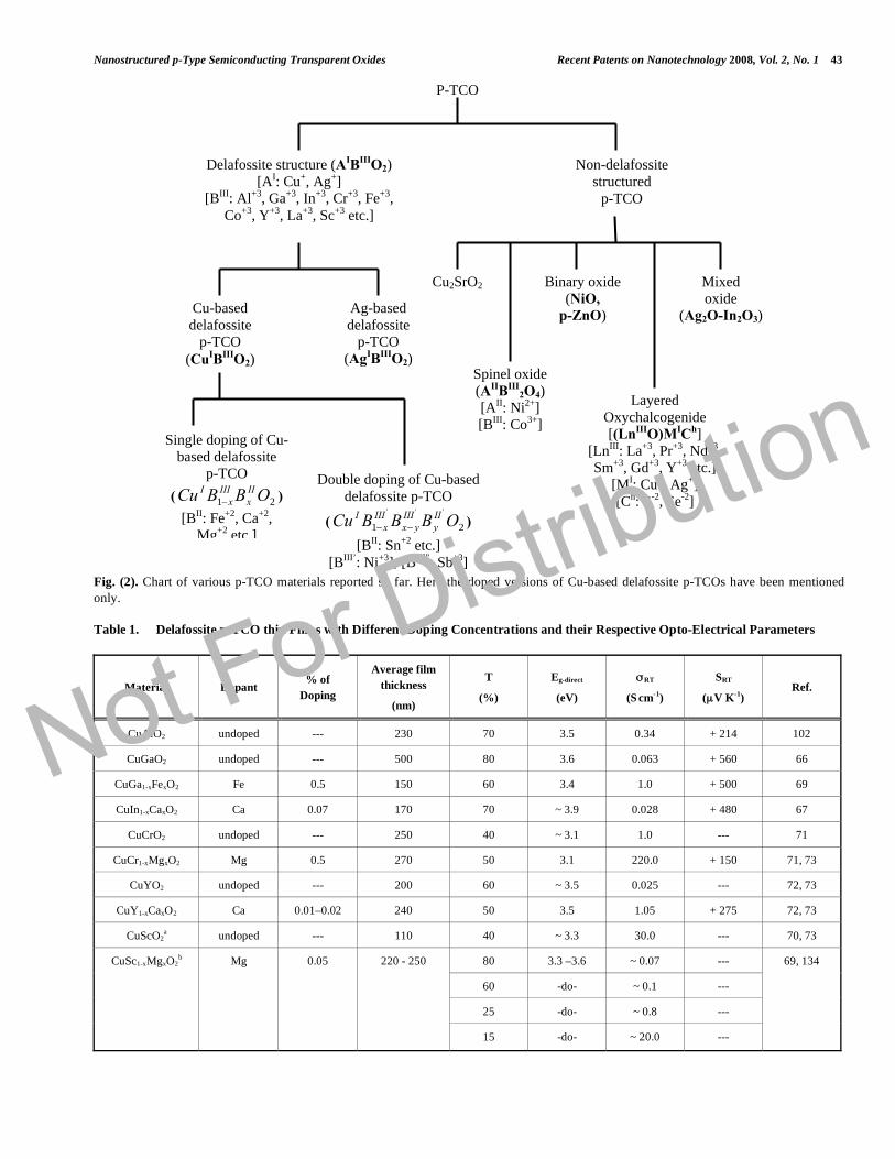
[90], binary oxide films like Ni1-xO [64] and p-ZnO etc. [91-101]. A chart of various groups of p-TCO thin films, repor-ted so far, has been shown in Fig. (2). Also the electrical and optical properties of various delafossite and non-delafossite p-TCO thin films are furnished in Table 1 and Table 2 respectively. The deposition techniques involved in the syntheses of these p-TCO thin films include pulsed laser deposition (PLD) [66-67, 76, 101-105], sputtering [64, 69-71, 74, 78-81, 84, 90, 104, 106-117], chemical vapor deposition (CVD) [96, 118-120], Reactive Solid Phase Epitaxy [121-123], Molecular beam epitaxy [98], Thermal co-evaporation [69, 72], Electron-beam evaporation [124-125], Rapid thermal annealing [126], sol-gel synthesis [110-111, 127, 128], hydrothermal process [69, 129-130], spray pyrolyses [131], spin coating [77] etc. Deposition parameters of different p-TCO thin films grown by various techniques are tabulated in Table 3 to Table 7. It is noteworthy in this context that there are reports on the fabrication of non-oxide p-type transparent semiconductors like BaCu2S2, BaCuSF [132-134] etc. Although these materials cannot be classified as p-TCO, but still they have scientific importance in the field of transparent active device fabrication.
1.2. Transparent Electronics
The importance of this new group of p-TCOs lies in the fact that the transparent junction with both types of TCOs can be fabricated as a ‘functional’ window, which would absorb the UV part of the solar radiation to generate electricity, yet transmits the visible potion of it. This has opened up a new field in opto-electronics device technology, which is called “Transparent Electronics” or “Invisible
Electronics” [53, 135]. The first report of a semi-transparent all-oxide p-i-n heterojunction diode of the form p-NiO/i-NiO/i-ZnO/n-ZnO was published in 1993 by Sato co-authors [64] in 1993. They observed only 20 % transmittance of the diode in the visible region. Although this low transmittance was not favorable for superior device applications, but still this report was an important milestone in the field of “Transparent Electronics” and in the development of p-TCO technology. Thereafter, a large number of groups reported the fabrication of all-TCO p-n and p-i-n heterojunction [72, 136-145] and homojunction [68, 146-148] transparent diodes as well as transparent field effect transistors (TFET) [53, 149-155] on glass and various transparent substrates. A schematic diagram of an all-TCO diode and a TFET are shown in Fig. (3a) and Fig. (3b) respectively. For all-TCO diodes, the visible transparency of the device varies from less than 20 % to more than 80 % whereas the turn-on voltage ranges from 2.5 to 0.4 V. For heterojunctions, the efficiency of the diode deteriorates due to lattice mismatch whereas homojunction diodes are favored as the lattice matching seems to be natural, which improves the diode efficiency. In TFETs, the maximum transparency of the device had been reported to be 80 % with on-off ratio ranging from 10
4 to 10
7. Various parameters of deferent all-
transparent diodes are furnished in Table 8 whereas deposition routes and various parameters of different TFETs are furnished in Table 9.
1.3. Nanocrystalline p-TCO
After the pioneering works of Efros and Efros [156] and Brus [157] on the size-quantization effect in semiconductor
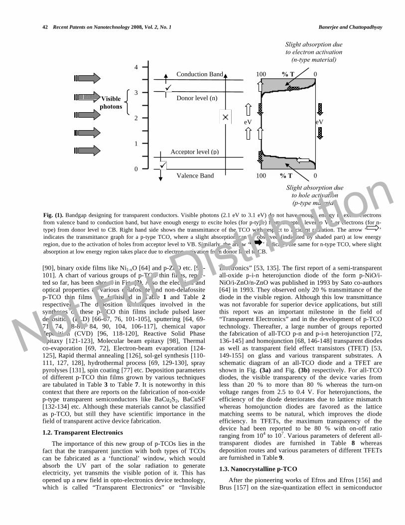
Fig. (1). Bandgap designing for transparent conductors. Visible photons (2.1 eV to 3.1 eV) do not have enough energy to excite electrons
from valence band to conduction band, but have enough energy to excite holes (for p-type) from acceptor level to VB or electrons (for n-
type) from donor level to CB. Right hand side shows the transmittance of the TCO with respect to incident radiation. The arrow ‘ ’
indicates the transmittance graph for a p-type TCO, where a slight absorption can be observed (indicated by shaded part) at low energy
region, due to the activation of holes from acceptor level to VB. Similarly, the arrow ‘ ’ indicates the same for n-type TCO, where slight
absorption at low energy region takes place due to electron activation from donor level to CB.
Visible photons
0
1
2
3
4
eV
% T100 0
100 % T 0
eV
Conduction Band
Valence Band
Donor level (n)
Acceptor level (p)
Slight absorption due to electron activation
(n-type material)
Slight absorption due to hole activation (p-type material)
Not For Distribution
Nanostructured p-Type Semiconducting Transparent Oxides Recent Patents on Nanotechnology 2008, Vol. 2, No. 1 43
Fig. (2). Chart of various p-TCO materials reported so far. Here the doped versions of Cu-based delafossite p-TCOs have been mentioned
only.
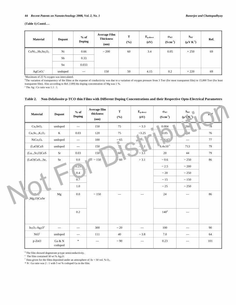
Table 1. Delafossite p-TCO thin Films with Different Doping Concentrations and their Respective Opto-Electrical Parameters
Material Dopant % of
Doping
Average film
thickness
(nm)
T
(%)
Eg-direct
(eV)
RT
(S cm-1)
SRT
(μV K-1) Ref.
CuAlO2 undoped --- 230 70 3.5 0.34 + 214 102
CuGaO2 undoped --- 500 80 3.6 0.063 + 560 66
CuGa1-xFexO2 Fe 0.5 150 60 3.4 1.0 + 500 69
CuIn1-xCaxO2 Ca 0.07 170 70 ~ 3.9 0.028 + 480 67
CuCrO2 undoped --- 250 40 ~ 3.1 1.0 --- 71
CuCr1-xMgxO2 Mg 0.5 270 50 3.1 220.0 + 150 71, 73
CuYO2 undoped --- 200 60 ~ 3.5 0.025 --- 72, 73
CuY1-xCaxO2 Ca 0.01–0.02 240 50 3.5 1.05 + 275 72, 73
CuScO2a undoped --- 110 40 ~ 3.3 30.0 --- 70, 73
80 3.3 –3.6 ~ 0.07 ---
60 -do- ~ 0.1 ---
25 -do- ~ 0.8 ---
CuSc1-xMgxO2b Mg 0.05 220 - 250
15 -do- ~ 20.0 ---
69, 134
P-TCO
Delafossite structure (AIBIIIO2)
[AI: Cu+, Ag+]
[BIII: Al+3, Ga+3, In+3, Cr+3, Fe+3,
Co+3, Y+3, La+3, Sc+3 etc.]
Non-delafossite
structured
p-TCO
Cu-based
delafossite
p-TCO
(CuIBIIIO2)
Ag-based
delafossite
p-TCO
(AgIBIIIO2)
Cu2SrO2
Spinel oxide
(AIIBIII2O4)
[AII: Ni2+]
[BIII: Co3+]
Binary oxide
(NiO, p-ZnO)
Layered
Oxychalcogenide
[(LnIIIO)MICh]
[LnIII: La+3, Pr+3, Nd+3,
Sm+3, Gd+3, Y+3 etc.]
[MI: Cu+, Ag+]
[Ch: S-2, Se-2]
Single doping of Cu-
based delafossite
p-TCO
( 21 OBBCu IIx
IIIx
I− )
[BII: Fe+2, Ca+2,
Mg+2 etc.]
Double doping of Cu-based
delafossite p-TCO
( 21
'''
OBBBCu IIy
IIIyx
IIIx
I−− )
[BII: Sn+2 etc.]
[BIII’: Ni+3]; [BIII”: Sb+3]
Mixed
oxide
(Ag2O-In2O3)
Not For Distribution
44 Recent Patents on Nanotechnology 2008, Vol. 2, No. 1 Banerjee and Chattopadhyay
(Table 1) Contd….
Material Dopant % of
Doping
Average Film
Thickness
(nm)
T
(%)
Eg-direct
(eV)
RT
(S cm-1)
SRT
(μV K-1) Ref.
Ni 0.66
Sb 0.33
CuNi1-xSbxSnyO2
Sn 0.033
~ 200 60 3.4 0.05 + 250 69
AgCoO2c undoped --- 150 50 4.15 0.2 + 220 69
aMaximum of 25 % oxygen was intercalated. bThe variation of transparency of the films at the expense of conductivity was due to a variation of oxygen pressure from 3 Torr (for most transparent film) to 15,000 Torr (for least
transparent film). Also according to Ref. [189] the doping concentration of Mg was 1 %. c The Ag : Co ratio was 1.1 : 1.
Table 2. Non-Delafossite p-TCO thin Films with Different Doping Concentrations and their Respective Opto-Electrical Parameters
Material Dopant % of
Doping
Average film
thickness
(nm)
T
(%)
Eg-direct
(eV)
RT
(S cm-1)
SRT
(μV K-1) Ref
Cu2SrO2 undoped --- 150 75 ~ 3.3 0.004 260 78
Cu2Sr1-xKxO2 K 0.03 120 75 ~3.25 0.05 260 76
NiCo2O4 undoped --- 100 ~ 65 --- ~ 16.67 --- 77
(LaO)CuS undoped --- 150 70 ~ 3.1 6.4x10⁻⁵ 713 79
(La1-xSrxO)CuS Sr 0.03 150 60 ~ 3.1 20 44 79
0.0 ~ 0.6 ~ 250
0.25 ~ 2.5 ~ 200
0.4 ~ 20 ~ 250
0.7 ~ 15 ~ 150
(LaO)CuS1-xSex Se
1.0
~ 150 ~ 60 > 3.1
~ 25 ~ 250
86
0.0 24 --- (La1-
xMgxO)CuSe
Mg
0.2
~ 150 --- ---
140d ---
86
In2O3-Ag2Oe --- --- 300 ~ 20 --- 100 --- 90
NiOf undoped --- 111 40 ~ 3.8 7.0 --- 64
p-ZnO Ga & N
codoped
* --- ~ 90 --- 0.23 --- 101
d The film showed degenerate p-type semiconductivity. e The film contained 50 wt % Ag2O. f Data given for the films deposited under an atmosphere of Ar + 50 vol. % O2.
* N : Ga ratio was 2 : 1 with 5 wt % codoped Ga in the film.
Not For Distribution
Nanostructured p-Type Semiconducting Transparent Oxides Recent Patents on Nanotechnology 2008, Vol. 2, No. 1 45
Table 3. Deposition Parameters of Different p-TCO Films Grown by PLD Technique
CuAlO2 CuGaO2 CuInO2: Ca CuScO2 Cu2SrO2: K ZnO: N
Laser KrF (248 nm) KrF (248 nm) KrF (248 nm) KrF KrF (248 nm) ArF
Laser frequency (Hz) 20 20 20 1 2 1
Laser power (J cm-2 pulse-1) 5 6 3.5 1.1 2.5 0.5
Base pressure (Pa) 1 x 10⁻⁷ 6 x 10⁻⁶ 1 x 10⁻⁷ --- 1 x 10⁻⁶ 1 x 10⁻⁶
O2 pressure (Pa) 1.3 9 1 1.5 7 x 10⁻⁴ #
Target
CuAlO2
Pellet
CuGaO2
pellet
CuInO2: Ca
pellet
Cu2Sc2O5
pellet
Cu2Sr0.97K0.03O2
pellet
ZnO: Ga
pellet
Substrate -Al2O3 (001) -Al2O3 (001) -Al2O3 (001) -Al2O3 (1120) SiO2 SiO2
Substrate-target distance (mm) 25 25 25 40 40 ---
Substrate Temperature (OC) 690 700 450 900 300 400
Deposition time (min) --- --- --- --- 180 ---
Post annealing time (min) 180 none none none 120 ---
Post annealing temp (OC) 690 none none none 300 ---
Reference 103, 102 103, 66 67 105 103, 76 101
#The deposition atmosphere was N2 or N2O.
Table 4. Different Deposition Parameters of p-TCO Films Synthesized by R.F. Magnetron Sputtering Technique
Material CuAlO2 CuGaO2: Fe CuCrO2:Mg CuNi2/3Sb1/3O2:Sn AgCoO2 NiCo2O4 (LaO)CuS NiO In2O3-Ag2O
R.F. power
(W)
65 80 90 80 80 200 110 50 40
Electrode
distance
(mm)
40 30 38 --- 30 --- 35 -- ---
Base
pressure
(Pa)
--- --- 9.3 x 10⁻⁴ --- --- 1.33x10⁻⁴ --- -- ---
Sputtering
pressure
(Pa)
4.53
(O2
press)
13.33
(Ar : O2
= 4 : 1)
1.33
(Ar press)
13.33
(Ar:O2= 4:1 / 9:1)
53.33
(Ar:O2=
4:1)
1.33
13
(Ar : H2S =19
: 1)
0.8
(O2press)
0.25
(Ar + O2)
Target CuAlO2
pellet
CuGa0.5Fe0.5O2
Pellet
CuCr1-xMgO2
pellet
CuNi0.67Sb0.3 -
- Sn 0.03O2
pellet
AgCoO2
pellet
Co-Ni
alloys
(LaO)CuS
: Sr
pellet
NiO
pellet
In2O3-Ag2O
pellet
Substrate
-Al2O3
(001)
fused
silica
fused
quartz
SiO2,
YSZ(100),
Al2O3(001)
SiO2,
Al2O3
Quartz,
sapphire,
Si
SiO2
SiO2
SiO2
Substrate
temp. (OC)
ambient 100 °C 450-750 500 °C 400 °C ambient ambient 200 ambient
Post-
annealing
time (min)
90 90 2.5 (RTA in
Ar)
180 --- --- 120 none 60
Not For Distribution
46 Recent Patents on Nanotechnology 2008, Vol. 2, No. 1 Banerjee and Chattopadhyay
(Table 4) Contd….
Material CuAlO2 CuGaO2: Fe CuCrO2:Mg CuNi2/3Sb1/3O2:Sn AgCoO2 NiCo2O4 (LaO)CuS NiO In2O3-Ag2O
Post-
annealing
temp. (OC)
1050g 800 °C
(N2 atmos.)
600-900 900 °C
(in air)***
--- --- 800** none 500
Reference 104 69 71 69, 74 69 78 79 64 90
* Ex situ in a Lindberg box furnace containing small amount of CuAlO2 powder.
** Ex situ in an evacuated silica tube containing small amount of (LaO)CuS powder.
*** Also for some cases RTA in air at 900 OC was performed.
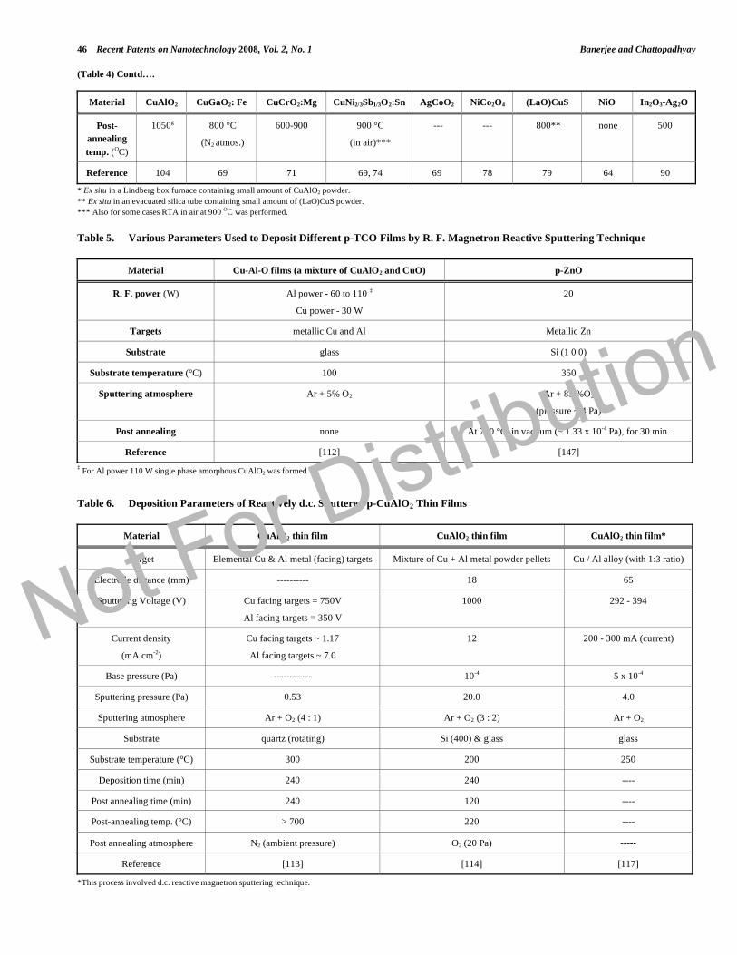
Table 5. Various Parameters Used to Deposit Different p-TCO Films by R. F. Magnetron Reactive Sputtering Technique
Material Cu-Al-O films (a mixture of CuAlO2 and CuO) p-ZnO
R. F. power (W) Al power - 60 to 110 ‡
Cu power - 30 W
20
Targets metallic Cu and Al Metallic Zn
Substrate glass Si (1 0 0)
Substrate temperature (°C) 100 350
Sputtering atmosphere Ar + 5% O2 Ar + 83 %O2
(pressure ~ 4 Pa)
Post annealing none At 750 °C, in vacuum (~ 1.33 x 10⁻⁴ Pa), for 30 min.
Reference [112] [147]
‡ For Al power 110 W single phase amorphous CuAlO2 was formed
Table 6. Deposition Parameters of Reactively d.c. Sputtered p-CuAlO2 Thin Films
Material CuAlO2 thin film CuAlO2 thin film CuAlO2 thin film*
Target Elemental Cu & Al metal (facing) targets Mixture of Cu + Al metal powder pellets Cu / Al alloy (with 1:3 ratio)
Electrode distance (mm) ---------- 18 65
Sputtering Voltage (V) Cu facing targets = 750V
Al facing targets = 350 V
1000
292 - 394
Current density
(mA cm-2)
Cu facing targets ~ 1.17
Al facing targets ~ 7.0
12
200 - 300 mA (current)
Base pressure (Pa) ------------ 10-4 5 x 10⁻⁴
Sputtering pressure (Pa) 0.53 20.0 4.0
Sputtering atmosphere Ar + O2 (4 : 1) Ar + O2 (3 : 2) Ar + O2
Substrate quartz (rotating) Si (400) & glass glass
Substrate temperature (°C) 300 200 250
Deposition time (min) 240 240 ----
Post annealing time (min) 240 120 ----
Post-annealing temp. (°C) > 700 220 ----
Post annealing atmosphere N2 (ambient pressure) O2 (20 Pa) -----
Reference [113] [114] [117]
*This process involved d.c. reactive magnetron sputtering technique.
Not For Distribution
Nanostructured p-Type Semiconducting Transparent Oxides Recent Patents on Nanotechnology 2008, Vol. 2, No. 1 47
Table 7. Deposition Parameters for Various Co-Evaporation Techniques for the Deposition of p-TCOs
Material CuYO2 : Ca* CuGaO2 BaCuSF
Reactants Elemental Cu, Y, Ca metals Cu, Ga metals Cu metal, BaF2
Base pressure (Pa) 9.33 x 10⁻⁵ 9.33 x 10⁻⁵ ---
Reactant gas O2 O2 H2S
Deposition pressure (Pa) 0.02 0.02 ---
Substrate Glass, MgO (100), Si SiO2 SiO2, MgO
Substrate temperature (°C) 80 - 650 100 200
Post annealing time (min) 3 (RTA) 90 180
Post annealing temp. (°C) 600 800 350
Post annealing atmosphere O2 N2 H2S
Reference 72 69 134
* 1-2 % Ca doping in Y - sites
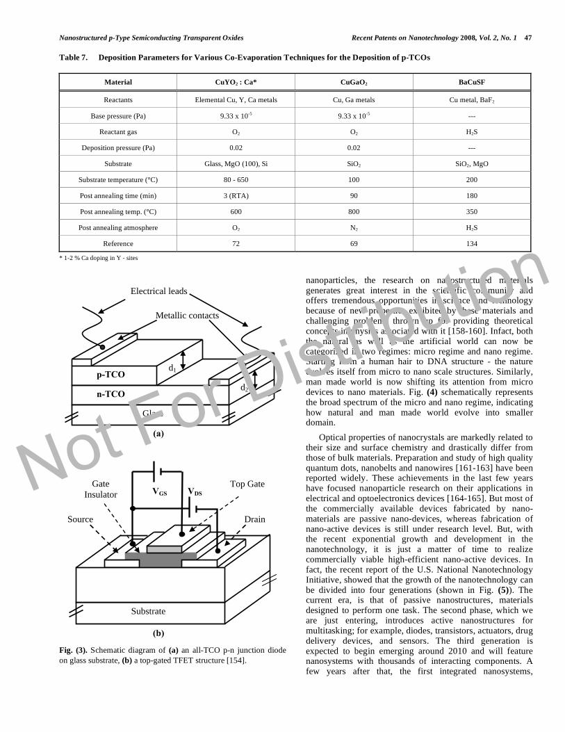
Fig. (3). Schematic diagram of (a) an all-TCO p-n junction diode
on glass substrate, (b) a top-gated TFET structure [154].
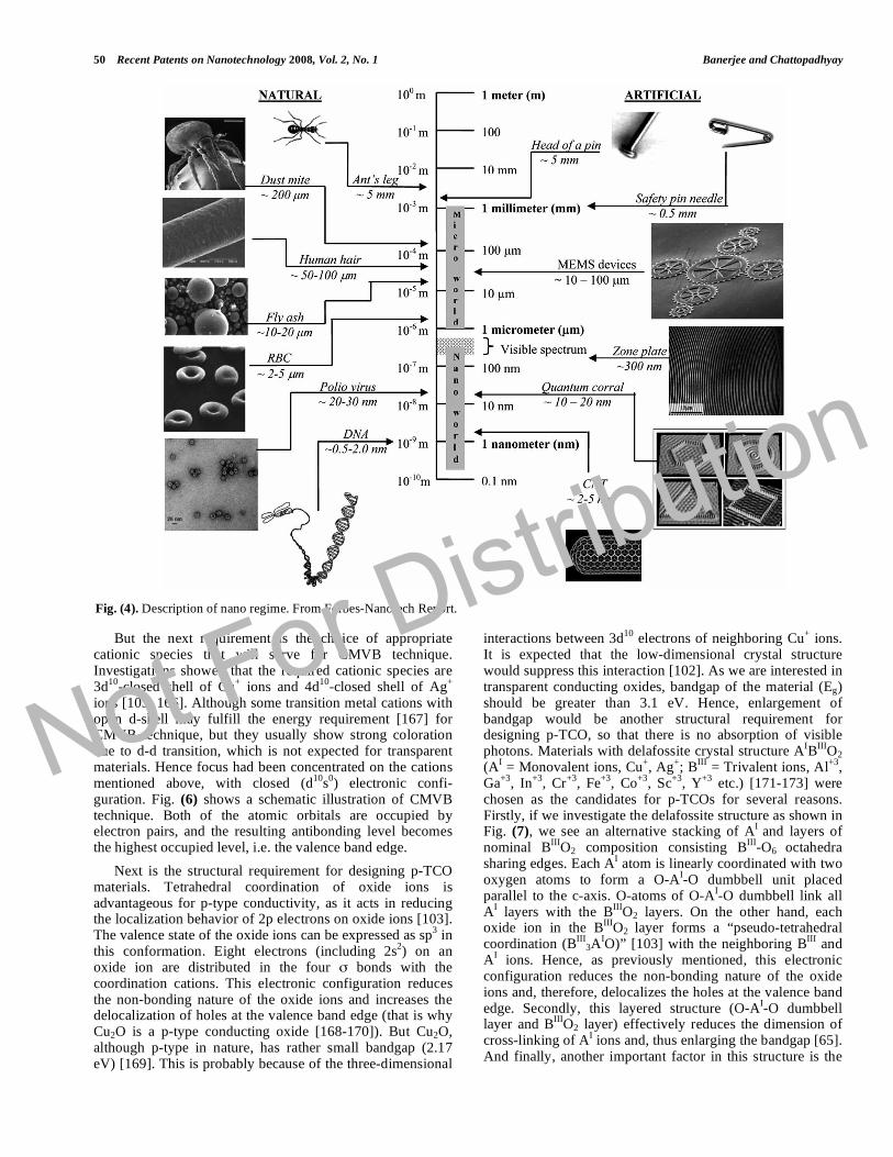
nanoparticles, the research on nanostructured materials generates great interest in the scientific community and offers tremendous opportunities in science and technology because of new properties exhibited by these materials and challenging problems thrown up for providing theoretical concepts in physics associated with it [158-160]. Infact, both the natural as well as the artificial world can now be categorized in two regimes: micro regime and nano regime. Starting from a human hair to DNA structure - the nature evolves itself from micro to nano scale structures. Similarly, man made world is now shifting its attention from micro devices to nano materials. Fig. (4) schematically represents the broad spectrum of the micro and nano regime, indicating how natural and man made world evolve into smaller domain.
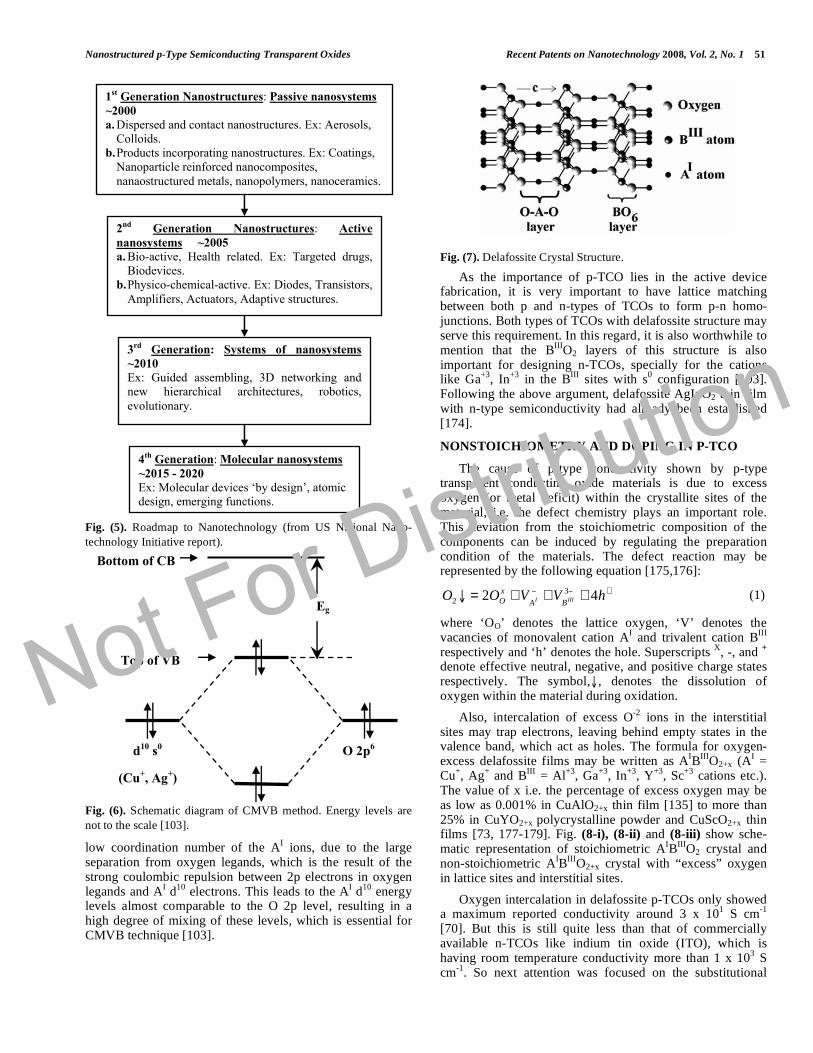
Optical properties of nanocrystals are markedly related to their size and surface chemistry and drastically differ from those of bulk materials. Preparation and study of high quality quantum dots, nanobelts and nanowires [161-163] have been reported widely. These achievements in the last few years have focused nanoparticle research on their applications in electrical and optoelectronics devices [164-165]. But most of the commercially available devices fabricated by nano-materials are passive nano-devices, whereas fabrication of nano-active devices is still under research level. But, with the recent exponential growth and development in the nanotechnology, it is just a matter of time to realize commercially viable high-efficient nano-active devices. In fact, the recent report of the U.S. National Nanotechnology Initiative, showed that the growth of the nanotechnology can be divided into four generations (shown in Fig. (5)). The current era, is that of passive nanostructures, materials designed to perform one task. The second phase, which we are just entering, introduces active nanostructures for multitasking; for example, diodes, transistors, actuators, drug delivery devices, and sensors. The third generation is expected to begin emerging around 2010 and will feature nanosystems with thousands of interacting components. A few years after that, the first integrated nanosystems,
Glass
n-TCO
p-TCO
Electrical leads
Metallic contacts
d1
d2
Source Drain
Active channel
Substrate
Gate
Insulator
Top Gate VGS VDS
(a)
(b)
Not For Distribution
48 Recent Patents on Nanotechnology 2008, Vol. 2, No. 1 Banerjee and Chattopadhyay
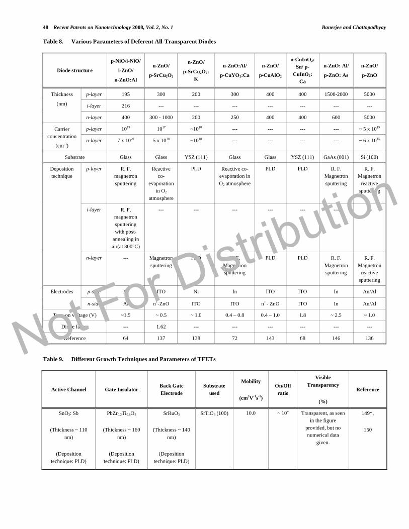
Table 8. Various Parameters of Deferent All-Transparent Diodes
Diode structure
p-NiO/i-NiO/
i-ZnO/
n-ZnO:Al
n-ZnO/
p-SrCu2O2
n-ZnO/
p-SrCu2O2:
K
n-ZnO:Al/
p-CuYO2:Ca
n-ZnO/
p-CuAlO2
n-CuInO2:
Sn/ p-
CuInO2:
Ca
n-ZnO: Al/
p-ZnO: As
n-ZnO/
p-ZnO
p-layer 195 300 200 300 400 400 1500-2000 5000
i-layer 216 --- --- --- --- --- --- ---
Thickness
(nm)
n-layer 400 300 - 1000 200 250 400 400 600 5000
p-layer 1019 1017 ~1018 --- --- --- --- ~ 5 x 10¹⁵ Carrier
concentration
(cm-3) n-layer 7 x 10²⁰ 5 x 10¹⁸ ~1018 --- --- --- --- ~ 6 x 10¹⁵
Substrate Glass Glass YSZ (111) Glass Glass YSZ (111) GaAs (001) Si (100)
p-layer R. F.
magnetron
sputtering
Reactive
co-
evaporation
in O2
atmosphere
PLD Reactive co-
evaporation in
O2 atmosphere
PLD PLD R. F.
Magnetron
sputtering
R. F.
Magnetron
reactive
sputtering
i-layer R. F.
magnetron
sputtering
with post-
annealing in
air(at 300°C)
--- --- --- --- --- --- ---
Deposition
technique
n-layer --- Magnetron
sputtering
PLD R. F.
Magnetron
sputtering
PLD PLD R. F.
Magnetron
sputtering
R. F.
Magnetron
reactive
sputtering
p-side Al ITO Ni In ITO ITO In Au/Al Electrodes
n-side Al n+-ZnO ITO ITO n+ - ZnO ITO In Au/Al
Turn-on voltage (V) ~1.5 ~ 0.5 ~ 1.0 0.4 – 0.8 0.4 – 1.0 1.8 ~ 2.5 ~ 1.0
Diode factor --- 1.62 --- --- --- --- --- ---
Reference 64 137 138 72 143 68 146 136
Table 9. Different Growth Techniques and Parameters of TFETs
Active Channel Gate Insulator Back Gate
Electrode
Substrate
used
Mobility
(cm2V-1s-1)
On/Off
ratio
Visible
Transparency
(%)
Reference
SnO2: Sb
(Thickness ~ 110
nm)
(Deposition
technique: PLD)
PbZr0.2Ti0.8O3
(Thickness ~ 160
nm)
(Deposition
technique: PLD)
SrRuO3
(Thickness ~ 140
nm)
(Deposition
technique: PLD)
SrTiO3 (100)
10.0 ~ 104 Transparent, as seen
in the figure
provided, but no
numerical data
given.
149*,
150
Not For Distribution
Nanostructured p-Type Semiconducting Transparent Oxides Recent Patents on Nanotechnology 2008, Vol. 2, No. 1 49
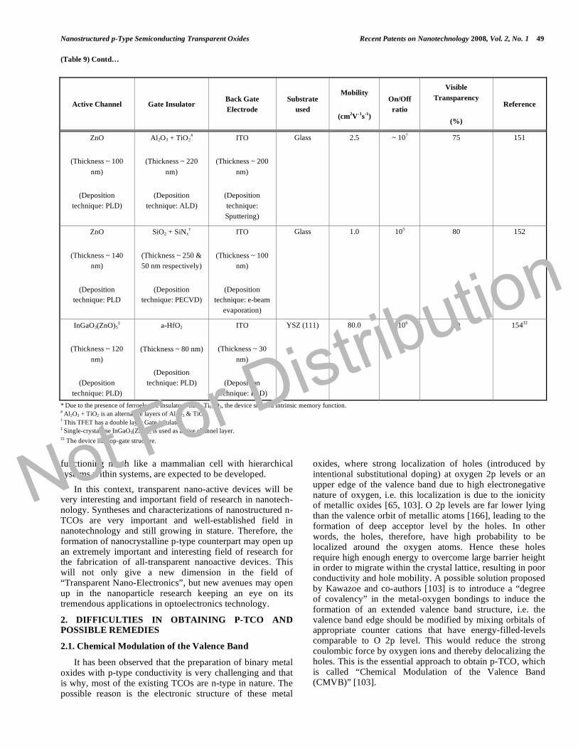
(Table 9) Contd…
Active Channel Gate Insulator Back Gate
Electrode
Substrate
used
Mobility
(cm2V-1s-1)
On/Off
ratio
Visible
Transparency
(%)
Reference
ZnO
(Thickness ~ 100
nm)
(Deposition
technique: PLD)
Al2O3 + TiO2#
(Thickness ~ 220
nm)
(Deposition
technique: ALD)
ITO
(Thickness ~ 200
nm)
(Deposition
technique:
Sputtering)
Glass 2.5 ~ 107 75 151
ZnO
(Thickness ~ 140
nm)
(Deposition
technique: PLD
SiO2 + SiNx†
(Thickness ~ 250 &
50 nm respectively)
(Deposition
technique: PECVD)
ITO
(Thickness ~ 100
nm)
(Deposition
technique: e-beam
evaporation)
Glass 1.0 105 80 152
InGaO3(ZnO)5‡
(Thickness ~ 120
nm)
(Deposition
technique: PLD)
a-HfO2
(Thickness ~ 80 nm)
(Deposition
technique: PLD)
ITO
(Thickness ~ 30
nm)
(Deposition
technique: PLD)
YSZ (111) 80.0 ~ 106 80 154‡‡
* Due to the presence of ferroelectric insulator PbZr0.2Ti0.8O3, the device showed intrinsic memory function. # Al2O3 + TiO2 is an alternative layers of Al2O3 & TiO2. † This TFET has a double layer Gate insulator. ‡ Single-crystalline InGaO3(ZnO)5 is used as active channel layer. ‡‡ The device has top-gate structure.
functioning much like a mammalian cell with hierarchical systems within systems, are expected to be developed.
In this context, transparent nano-active devices will be very interesting and important field of research in nanotech-nology. Syntheses and characterizations of nanostructured n-TCOs are very important and well-established field in nanotechnology and still growing in stature. Therefore, the formation of nanocrystalline p-type counterpart may open up an extremely important and interesting field of research for the fabrication of all-transparent nanoactive devices. This will not only give a new dimension in the field of “Transparent Nano-Electronics”, but new avenues may open up in the nanoparticle research keeping an eye on its tremendous applications in optoelectronics technology.
2. DIFFICULTIES IN OBTAINING P-TCO AND POSSIBLE REMEDIES
2.1. Chemical Modulation of the Valence Band
It has been observed that the preparation of binary metal oxides with p-type conductivity is very challenging and that is why, most of the existing TCOs are n-type in nature. The possible reason is the electronic structure of these metal
oxides, where strong localization of holes (introduced by intentional substitutional doping) at oxygen 2p levels or an upper edge of the valence band due to high electronegative nature of oxygen, i.e. this localization is due to the ionicity of metallic oxides [65, 103]. O 2p levels are far lower lying than the valence orbit of metallic atoms [166], leading to the formation of deep acceptor level by the holes. In other words, the holes, therefore, have high probability to be localized around the oxygen atoms. Hence these holes require high enough energy to overcome large barrier height in order to migrate within the crystal lattice, resulting in poor conductivity and hole mobility. A possible solution proposed by Kawazoe and co-authors [103] is to introduce a “degree of covalency” in the metal-oxygen bondings to induce the formation of an extended valence band structure, i.e. the valence band edge should be modified by mixing orbitals of appropriate counter cations that have energy-filled-levels comparable to O 2p level. This would reduce the strong coulombic force by oxygen ions and thereby delocalizing the holes. This is the essential approach to obtain p-TCO, which is called “Chemical Modulation of the Valence Band (CMVB)” [103].
Not For Distribution
50 Recent Patents on Nanotechnology 2008, Vol. 2, No. 1 Banerjee and Chattopadhyay
But the next requirement is the choice of appropriate cationic species that will serve for CMVB technique. Investigations showed that the required cationic species are 3d
10-closed shell of Cu
+ ions and 4d
10-closed shell of Ag
+
ions [103, 166]. Although some transition metal cations with open d-shell may fulfill the energy requirement [167] for CMVB technique, but they usually show strong coloration due to d-d transition, which is not expected for transparent materials. Hence focus had been concentrated on the cations mentioned above, with closed (d
10s
0) electronic confi-
guration. Fig. (6) shows a schematic illustration of CMVB technique. Both of the atomic orbitals are occupied by electron pairs, and the resulting antibonding level becomes the highest occupied level, i.e. the valence band edge.
Next is the structural requirement for designing p-TCO materials. Tetrahedral coordination of oxide ions is advantageous for p-type conductivity, as it acts in reducing the localization behavior of 2p electrons on oxide ions [103]. The valence state of the oxide ions can be expressed as sp
3 in
this conformation. Eight electrons (including 2s2) on an
oxide ion are distributed in the four bonds with the coordination cations. This electronic configuration reduces the non-bonding nature of the oxide ions and increases the delocalization of holes at the valence band edge (that is why Cu2O is a p-type conducting oxide [168-170]). But Cu2O, although p-type in nature, has rather small bandgap (2.17 eV) [169]. This is probably because of the three-dimensional
interactions between 3d10
electrons of neighboring Cu+ ions.
It is expected that the low-dimensional crystal structure would suppress this interaction [102]. As we are interested in transparent conducting oxides, bandgap of the material (Eg) should be greater than 3.1 eV. Hence, enlargement of bandgap would be another structural requirement for designing p-TCO, so that there is no absorption of visible photons. Materials with delafossite crystal structure A
IB
IIIO2
(AI = Monovalent ions, Cu
+, Ag
+; B
III = Trivalent ions, Al
+3,
Ga+3
, In+3
, Cr+3
, Fe+3
, Co+3
, Sc+3
, Y+3
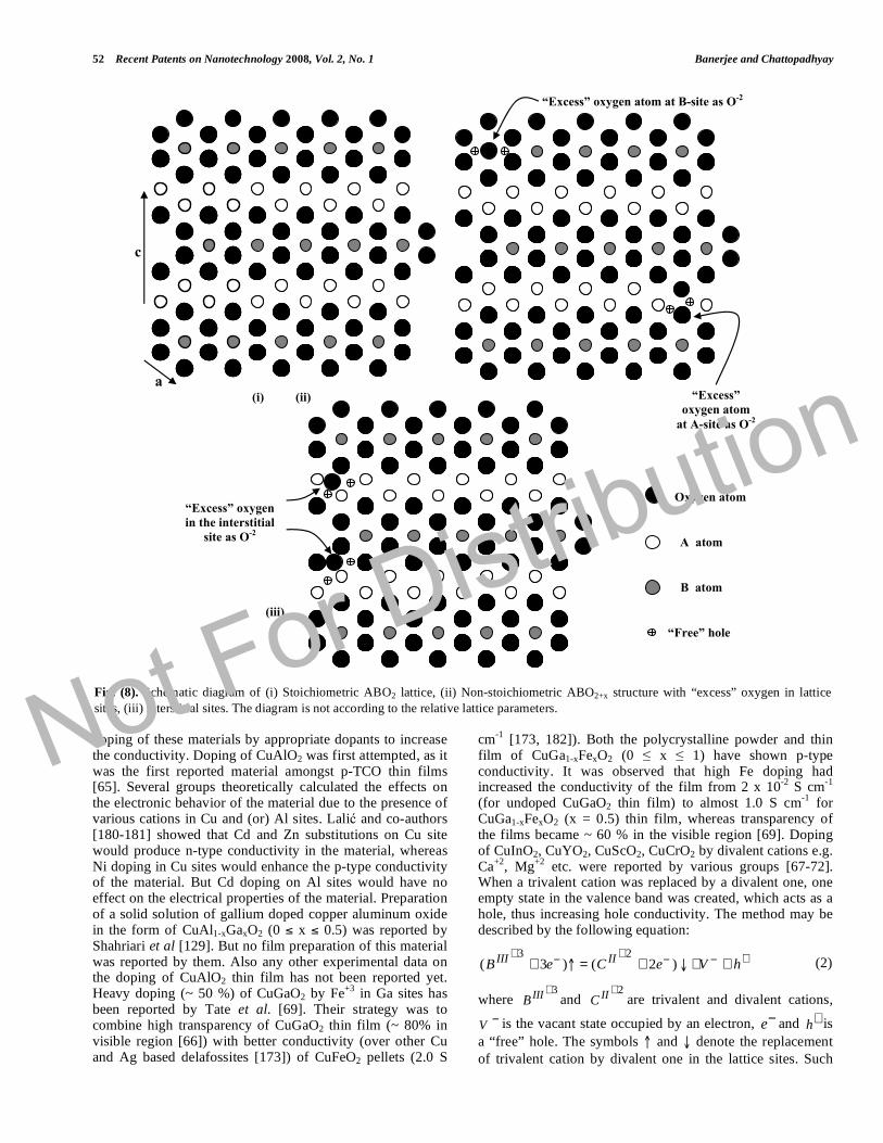
etc.) [171-173] were chosen as the candidates for p-TCOs for several reasons. Firstly, if we investigate the delafossite structure as shown in Fig. (7), we see an alternative stacking of A
I and layers of
nominal BIII
O2 composition consisting BIII
-O6 octahedra sharing edges. Each A
I atom is linearly coordinated with two
oxygen atoms to form a O-AI-O dumbbell unit placed
parallel to the c-axis. O-atoms of O-AI-O dumbbell link all
AI layers with the B
IIIO2 layers. On the other hand, each
oxide ion in the BIII
O2 layer forms a “pseudo-tetrahedral coordination (B
III3A
IO)” [103] with the neighboring B
III and
AI ions. Hence, as previously mentioned, this electronic
configuration reduces the non-bonding nature of the oxide ions and, therefore, delocalizes the holes at the valence band edge. Secondly, this layered structure (O-A
I-O dumbbell
layer and BIII
O2 layer) effectively reduces the dimension of cross-linking of A
I ions and, thus enlarging the bandgap [65].
And finally, another important factor in this structure is the
Fig. (4). Description of nano regime. From Forbes-Nanotech Report.
Not For Distribution
Nanostructured p-Type Semiconducting Transparent Oxides Recent Patents on Nanotechnology 2008, Vol. 2, No. 1 51
Fig. (5). Roadmap to Nanotechnology (from US National Nano-
technology Initiative report).
Fig. (6). Schematic diagram of CMVB method. Energy levels are
not to the scale [103].
low coordination number of the AI ions, due to the large
separation from oxygen legands, which is the result of the strong coulombic repulsion between 2p electrons in oxygen legands and A
I d
10 electrons. This leads to the A
I d
10 energy
levels almost comparable to the O 2p level, resulting in a high degree of mixing of these levels, which is essential for CMVB technique [103].
Fig. (7). Delafossite Crystal Structure.
As the importance of p-TCO lies in the active device fabrication, it is very important to have lattice matching between both p and n-types of TCOs to form p-n homo-junctions. Both types of TCOs with delafossite structure may serve this requirement. In this regard, it is also worthwhile to mention that the B
IIIO2 layers of this structure is also
important for designing n-TCOs, specially for the cations like Ga
+3, In
+3 in the B
III sites with s
0 configuration [103].
Following the above argument, delafossite AgInO2 thin film with n-type semiconductivity had already been established [174].
NONSTOICHIOMETRY AND DOPING IN P-TCO
The cause of p-type conductivity shown by p-type transparent conducting oxide materials is due to excess oxygen (or metal deficit) within the crystallite sites of the material, i.e. the defect chemistry plays an important role. This deviation from the stoichiometric composition of the components can be induced by regulating the preparation condition of the materials. The defect reaction may be represented by the following equation [175,176]:
O O V V hO
x
A BI III2
32 4= + + ++ (1)
where ‘OO’ denotes the lattice oxygen, ‘V’ denotes the vacancies of monovalent cation A
I and trivalent cation B
III
respectively and ‘h’ denotes the hole. Superscripts X, -, and
+ denote effective neutral, negative, and positive charge states respectively. The symbol, , denotes the dissolution of oxygen within the material during oxidation.
Also, intercalation of excess O-2
ions in the interstitial sites may trap electrons, leaving behind empty states in the valence band, which act as holes. The formula for oxygen-excess delafossite films may be written as A
IB
IIIO2+x (A
I =
Cu+, Ag
+ and B
III = Al
+3, Ga
+3, In
+3, Y
+3, Sc
+3 cations etc.).
The value of x i.e. the percentage of excess oxygen may be as low as 0.001% in CuAlO2+x thin film [135] to more than 25% in CuYO2+x polycrystalline powder and CuScO2+x thin films [73, 177-179]. Fig. (8-i), (8-ii) and (8-iii) show sche-matic representation of stoichiometric A
IB
IIIO2 crystal and
non-stoichiometric AIB
IIIO2+x crystal with “excess” oxygen
in lattice sites and interstitial sites.
Oxygen intercalation in delafossite p-TCOs only showed a maximum reported conductivity around 3 x 10
1 S cm
-1
[70]. But this is still quite less than that of commercially available n-TCOs like indium tin oxide (ITO), which is having room temperature conductivity more than 1 x 10
3 S
cm-1
. So next attention was focused on the substitutional
1st Generation Nanostructures: Passive nanosystems ~2000 a. Dispersed and contact nanostructures. Ex: Aerosols,
Colloids. b. Products incorporating nanostructures. Ex: Coatings,
Nanoparticle reinforced nanocomposites, nanaostructured metals, nanopolymers, nanoceramics.
2nd Generation Nanostructures: Active nanosystems ~2005 a. Bio-active, Health related. Ex: Targeted drugs,
Biodevices. b. Physico-chemical-active. Ex: Diodes, Transistors,
Amplifiers, Actuators, Adaptive structures.
3rd Generation: Systems of nanosystems ~2010 Ex: Guided assembling, 3D networking and new hierarchical architectures, robotics, evolutionary.
4th Generation: Molecular nanosystems ~2015 - 2020 Ex: Molecular devices ‘by design’, atomic design, emerging functions.
Bottom of CB
Top of VB
d10 s0
(Cu+, Ag+)
O 2p6
Eg
Not For Distribution
52 Recent Patents on Nanotechnology 2008, Vol. 2, No. 1 Banerjee and Chattopadhyay
doping of these materials by appropriate dopants to increase the conductivity. Doping of CuAlO2 was first attempted, as it was the first reported material amongst p-TCO thin films [65]. Several groups theoretically calculated the effects on the electronic behavior of the material due to the presence of various cations in Cu and (or) Al sites. Lali and co-authors [180-181] showed that Cd and Zn substitutions on Cu site would produce n-type conductivity in the material, whereas Ni doping in Cu sites would enhance the p-type conductivity of the material. But Cd doping on Al sites would have no effect on the electrical properties of the material. Preparation of a solid solution of gallium doped copper aluminum oxide in the form of CuAl1-xGaxO2 (0 x 0.5) was reported by Shahriari et al [129]. But no film preparation of this material was reported by them. Also any other experimental data on the doping of CuAlO2 thin film has not been reported yet. Heavy doping (~ 50 %) of CuGaO2 by Fe
+3 in Ga sites has
been reported by Tate et al. [69]. Their strategy was to combine high transparency of CuGaO2 thin film (~ 80% in visible region [66]) with better conductivity (over other Cu and Ag based delafossites [173]) of CuFeO2 pellets (2.0 S
cm-1
[173, 182]). Both the polycrystalline powder and thin film of CuGa1-xFexO2 (0 x 1) have shown p-type conductivity. It was observed that high Fe doping had increased the conductivity of the film from 2 x 10
-2 S cm
-1
(for undoped CuGaO2 thin film) to almost 1.0 S cm-1
for CuGa1-xFexO2 (x = 0.5) thin film, whereas transparency of the films became ~ 60 % in the visible region [69]. Doping of CuInO2, CuYO2, CuScO2, CuCrO2 by divalent cations e.g. Ca
+2, Mg
+2 etc. were reported by various groups [67-72].
When a trivalent cation was replaced by a divalent one, one empty state in the valence band was created, which acts as a hole, thus increasing hole conductivity. The method may be described by the following equation:
( ) ( )B e C e V hIII II+ ++
+ = + + +3 2
3 2 (2)
where BIII +3and C II +2
are trivalent and divalent cations,
V is the vacant state occupied by an electron, e and +h is
a “free” hole. The symbols and denote the replacement
of trivalent cation by divalent one in the lattice sites. Such
Fig. (8). Schematic diagram of (i) Stoichiometric ABO2 lattice, (ii) Non-stoichiometric ABO2+x structure with “excess” oxygen in lattice
sites, (iii) interstitial sites. The diagram is not according to the relative lattice parameters.
c
a
“Excess” oxygen atom at B-site as O-2
“Excess” oxygen atom
at A-site as O-2
Oxygen atom
A atom
B atom
“Free” hole
“Excess” oxygen in the interstitial
site as O-2
(i) (ii)
(iii)
Not For Distribution
Nanostructured p-Type Semiconducting Transparent Oxides Recent Patents on Nanotechnology 2008, Vol. 2, No. 1 53
doped delafossite films like CuCr1-xMgxO2 (x = 0.05), CuY1-
xCaxO2 (x = 0.01 - 0.02), CuSc1-xMgxO2 (x= 0.05) showed
better hole conductivity over the corres-ponding undoped
films [71]. Some Ag based delafossite materials like
AgMIII
O2 (MIII
= Sc+3
, Cr+3
, Ga+3
etc.) with 5% Mg doping at
MIII
sites was reported by Nagrajan et al. [73]. The
conductivities of these sintered powders were very low (~
10-5
-10-4
S cm-1
) and also no film preparation of these
materials were reported anywhere so far.
There are also reports in the literature about the double substitution of trivalent M
III sites by divalent and pentavalent
cations e.g. CuFe1-xVxO2 (x = 0.5), CuNi1-xSbxO2, CuZn1-
xSbxO2, CuCo1-xSbxO2, CuMg1-xSbxO2, CuMn1-xSbxO2 (x = 0.33), AgNi1-xSbxO2, AgZn1-xSbxO2 (x = 0.33) etc., but all in the form of sintered powder [74, 183]. Also triple substitution of trivalent cation had been reported by Tate and co-authors [69, 74] in the form of CuNi1-xSbxSnyO2 (x = 0.3, y = 0.033). Thin film of this material showed an average of 60 % transmittance with a room temperature conductivity of 5 x 10
-2 S cm
-1. The exact electronic structure and conduc-
tion mechanism of these types of materials are yet to be explored completely.
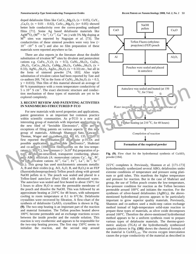
3. RECENT REVIEW AND PATENTING ACTIVITIES IN NANO/MICRO-STRUCTURED P-TCO
For new materials with novel properties and applications, patent generation is an important but common practice within scientific communities. As p-TCO is a new and interesting group of materials with important applications in the new filed of “Invisible Electronics”, there are no exceptions of filing patents on various aspects of this new group of materials. Although Shannon, Sato, Kawazoe, Thomas, Wager and co-authors [53, 64, 65, 135, 171-173] first reported the formation of delafossite p-TCOs and possible applications in “Invisible Electronics”, Shahriari and co-authors [184] first filed patents on the low-tempe-rature (< 500°C), low-pressure (< 3x10
8 Pa) preparation of p-
type, delafossite-structured, transparent conducting, phase-pure ABO2 materials (A: monovalent cations Cu
+, Ag
+, Pt
+,
Pd+, B: trivalent cations Al
+3, Ga
+3, Fe
+3, La
+3, In
+3, Sc
+3
etc.). This group has used stoichiometric amounts metallic A, B and their oxides (e.g. AO, A2O, B, and B2O3) in an FEP (fluoro(ethylenepropylene)) Teflon pouch along with ground NaOH pellets in it. The pouch was sealed and placed in a Teflon-lined autoclave (Parr) filled with deionized water. The autoclave was sealed and first heated to about 150°C for 5 hours to allow H2O to enter the permeable membrane of the pouch and dissolve the NaOH. This was followed by an approximate heating at 210°C for 48 hours, with subsequent cooling to room temperature at 0.1 to 6°C/hr. Delafossite crystallites were recovered by filtration. A flow-chart of the synthesis of delafossite CuAlO2 crystallites is shown in Fig. (9). The two-step heating is an important part of the reaction and material formation. The Teflon pouches heated above 100°C become permeable and an exchange reactions occurs between the inside powder and the outside solution. This reaction is very exothermic and appears to be responsible for the two-step heating process. The first step 150°C seems to initialize the reaction, and the second step around
Fig. (9). Flow chart for the hydrothermal synthesis of CuAlO2
powder [184].
215°C completes it. Previously, Shannon et al. [171-173] hydrothermally synthesized several ABO2 delafossites under extreme conditions of temperature and pressure using plati-num or gold tubes. This manifests the higher temperature and pressure for reaction. But in the case of Shahriari and group, the use of Teflon pouch creates the low-temperature, low-pressure condition for reaction as the Teflon becomes permeable around 100°C and initiates the reaction. For the syntheses of silver-based delafossites (AgBO2), the above-mentioned hydrothermal process appears to be particularly important to grow superior quality materials. Previously, Shannon and co-authors used a multi-step cation exchange method instead of high-temperature solid-state reaction to prepare these types of materials, as silver oxide decomposes around 160°C. Therefore the above-mentioned hydrothermal method appears to be a uniform synthesis route to prepare various types of delafossite materials. The thermo-gravi-metric analysis (TGA) of the hydrothermally synthesized samples (shown in Fig. (10)) shows the chemical formula of the material is CuAlO2.185. The excess oxygen intercalation causes the p-type conductivity of the material as described in
Teflon Fluoro-(ethylene-propylene) (FEP) pouch
CuO Cu2O
Al Al2O3
NaOH pellets
Pouches were sealed and placed in autoclave
Autoclave was sealed and heated (at 150 OC, for 5 hrs)
Further heating (at 210 OC, for 48 hours)
Water insertion through the permeable membrane of Teflon-initiation of reaction
Formation of the required powder
Completion of reaction
Not For Distribution
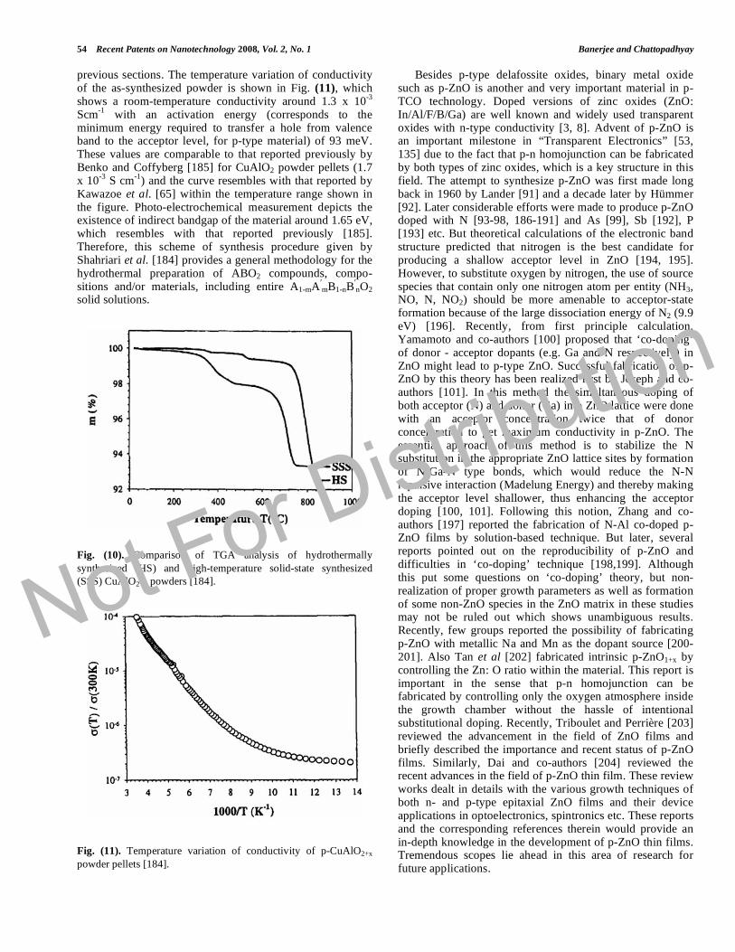
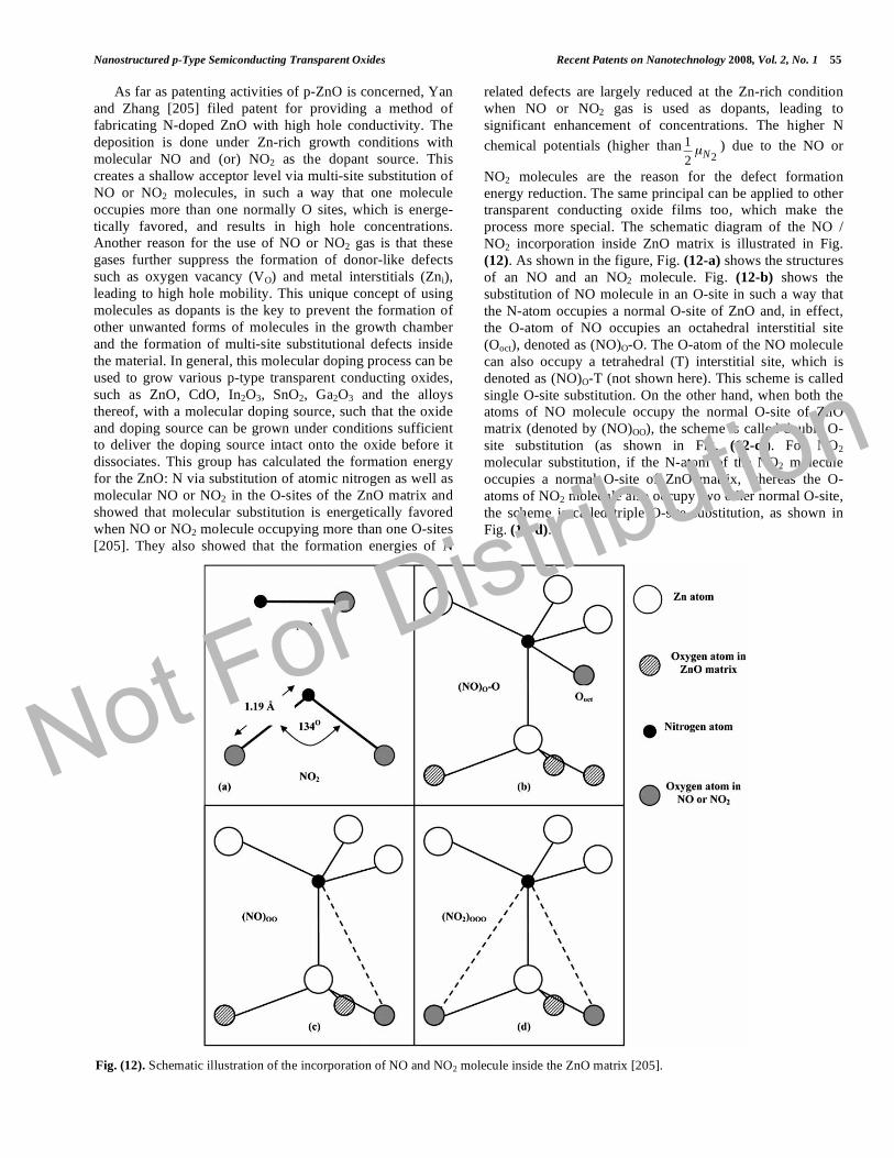
54 Recent Patents on Nanotechnology 2008, Vol. 2, No. 1 Banerjee and Chattopadhyay
previous sections. The temperature variation of conductivity of the as-synthesized powder is shown in Fig. (11), which shows a room-temperature conductivity around 1.3 x 10
-3
Scm-1
with an activation energy (corresponds to the minimum energy required to transfer a hole from valence band to the acceptor level, for p-type material) of 93 meV. These values are comparable to that reported previously by Benko and Coffyberg [185] for CuAlO2 powder pellets (1.7 x 10
-3 S cm
-1) and the curve resembles with that reported by
Kawazoe et al. [65] within the temperature range shown in the figure. Photo-electrochemical measurement depicts the existence of indirect bandgap of the material around 1.65 eV, which resembles with that reported previously [185]. Therefore, this scheme of synthesis procedure given by Shahriari et al. [184] provides a general methodology for the hydrothermal preparation of ABO2 compounds, compo-sitions and/or materials, including entire A1-mA mB1-nB nO2 solid solutions.
Fig. (10). Comparison of TGA analysis of hydrothermally
synthesized (HS) and high-temperature solid-state synthesized
(SSS) CuAlO2+x powders [184].
Fig. (11). Temperature variation of conductivity of p-CuAlO2+x
powder pellets [184].
Besides p-type delafossite oxides, binary metal oxide such as p-ZnO is another and very important material in p-TCO technology. Doped versions of zinc oxides (ZnO: In/Al/F/B/Ga) are well known and widely used transparent oxides with n-type conductivity [3, 8]. Advent of p-ZnO is an important milestone in “Transparent Electronics” [53, 135] due to the fact that p-n homojunction can be fabricated by both types of zinc oxides, which is a key structure in this field. The attempt to synthesize p-ZnO was first made long back in 1960 by Lander [91] and a decade later by Hümmer [92]. Later considerable efforts were made to produce p-ZnO doped with N [93-98, 186-191] and As [99], Sb [192], P [193] etc. But theoretical calculations of the electronic band structure predicted that nitrogen is the best candidate for producing a shallow acceptor level in ZnO [194, 195]. However, to substitute oxygen by nitrogen, the use of source species that contain only one nitrogen atom per entity (NH3, NO, N, NO2) should be more amenable to acceptor-state formation because of the large dissociation energy of N2 (9.9 eV) [196]. Recently, from first principle calculation, Yamamoto and co-authors [100] proposed that ‘co-doping’ of donor - acceptor dopants (e.g. Ga and N respectively) in ZnO might lead to p-type ZnO. Successful fabrication of p-ZnO by this theory has been realized first by Joseph and co-authors [101]. In this method the simultaneous doping of both acceptor (N) and donor (Ga) into ZnO lattice were done with an acceptor concentration twice that of donor concentration to get maximum conductivity in p-ZnO. The essential approach of this method is to stabilize the N substitution in the appropriate ZnO lattice sites by formation of N-Ga-N type bonds, which would reduce the N-N
repulsive interaction (Madelung Energy) and thereby making the acceptor level shallower, thus enhancing the acceptor doping [100, 101]. Following this notion, Zhang and co-authors [197] reported the fabrication of N-Al co-doped p-ZnO films by solution-based technique. But later, several reports pointed out on the reproducibility of p-ZnO and difficulties in ‘co-doping’ technique [198,199]. Although this put some questions on ‘co-doping’ theory, but non-realization of proper growth parameters as well as formation of some non-ZnO species in the ZnO matrix in these studies may not be ruled out which shows unambiguous results. Recently, few groups reported the possibility of fabricating p-ZnO with metallic Na and Mn as the dopant source [200-201]. Also Tan et al [202] fabricated intrinsic p-ZnO1+x by controlling the Zn: O ratio within the material. This report is important in the sense that p-n homojunction can be fabricated by controlling only the oxygen atmosphere inside the growth chamber without the hassle of intentional substitutional doping. Recently, Triboulet and Perrière [203] reviewed the advancement in the field of ZnO films and briefly described the importance and recent status of p-ZnO films. Similarly, Dai and co-authors [204] reviewed the recent advances in the field of p-ZnO thin film. These review works dealt in details with the various growth techniques of both n- and p-type epitaxial ZnO films and their device applications in optoelectronics, spintronics etc. These reports and the corresponding references therein would provide an in-depth knowledge in the development of p-ZnO thin films. Tremendous scopes lie ahead in this area of research for future applications.
Not For Distribution
Nanostructured p-Type Semiconducting Transparent Oxides Recent Patents on Nanotechnology 2008, Vol. 2, No. 1 55
As far as patenting activities of p-ZnO is concerned, Yan
and Zhang [205] filed patent for providing a method of
fabricating N-doped ZnO with high hole conductivity. The
deposition is done under Zn-rich growth conditions with
molecular NO and (or) NO2 as the dopant source. This
creates a shallow acceptor level via multi-site substitution of
NO or NO2 molecules, in such a way that one molecule
occupies more than one normally O sites, which is energe-
tically favored, and results in high hole concentrations.
Another reason for the use of NO or NO2 gas is that these
gases further suppress the formation of donor-like defects
such as oxygen vacancy (VO) and metal interstitials (Zni),
leading to high hole mobility. This unique concept of using
molecules as dopants is the key to prevent the formation of
other unwanted forms of molecules in the growth chamber
and the formation of multi-site substitutional defects inside
the material. In general, this molecular doping process can be
used to grow various p-type transparent conducting oxides,
such as ZnO, CdO, In2O3, SnO2, Ga2O3 and the alloys
thereof, with a molecular doping source, such that the oxide
and doping source can be grown under conditions sufficient
to deliver the doping source intact onto the oxide before it
dissociates. This group has calculated the formation energy
for the ZnO: N via substitution of atomic nitrogen as well as
molecular NO or NO2 in the O-sites of the ZnO matrix and
showed that molecular substitution is energetically favored
when NO or NO2 molecule occupying more than one O-sites
[205]. They also showed that the formation energies of N
related defects are largely reduced at the Zn-rich condition
when NO or NO2 gas is used as dopants, leading to
significant enhancement of concentrations. The higher N
chemical potentials (higher than 1
2 2μN
) due to the NO or
NO2 molecules are the reason for the defect formation
energy reduction. The same principal can be applied to other
transparent conducting oxide films too, which make the
process more special. The schematic diagram of the NO /
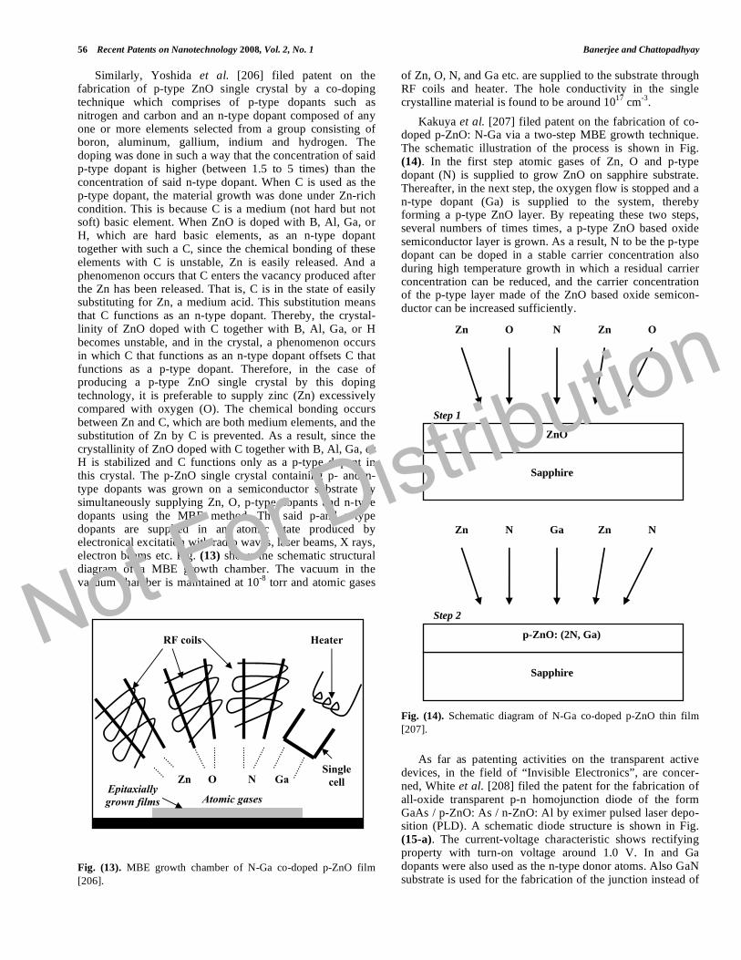
NO2 incorporation inside ZnO matrix is illustrated in Fig.
(12). As shown in the figure, Fig. (12-a) shows the structures
of an NO and an NO2 molecule. Fig. (12-b) shows the
substitution of NO molecule in an O-site in such a way that
the N-atom occupies a normal O-site of ZnO and, in effect,
the O-atom of NO occupies an octahedral interstitial site
(Ooct), denoted as (NO)O-O. The O-atom of the NO molecule
can also occupy a tetrahedral (T) interstitial site, which is
denoted as (NO)O-T (not shown here). This scheme is called
single O-site substitution. On the other hand, when both the
atoms of NO molecule occupy the normal O-site of ZnO
matrix (denoted by (NO)OO), the scheme is called double O-
site substitution (as shown in Fig. (12-c)). For NO2
molecular substitution, if the N-atom of the NO2 molecule
occupies a normal O-site of ZnO matrix, whereas the O-
atoms of NO2 molecule also occupy two other normal O-site,
the scheme is called triple O-site substitution, as shown in
Fig. (12-d).
Fig. (12). Schematic illustration of the incorporation of NO and NO2 molecule inside the ZnO matrix [205].
Not For Distribution
56 Recent Patents on Nanotechnology 2008, Vol. 2, No. 1 Banerjee and Chattopadhyay
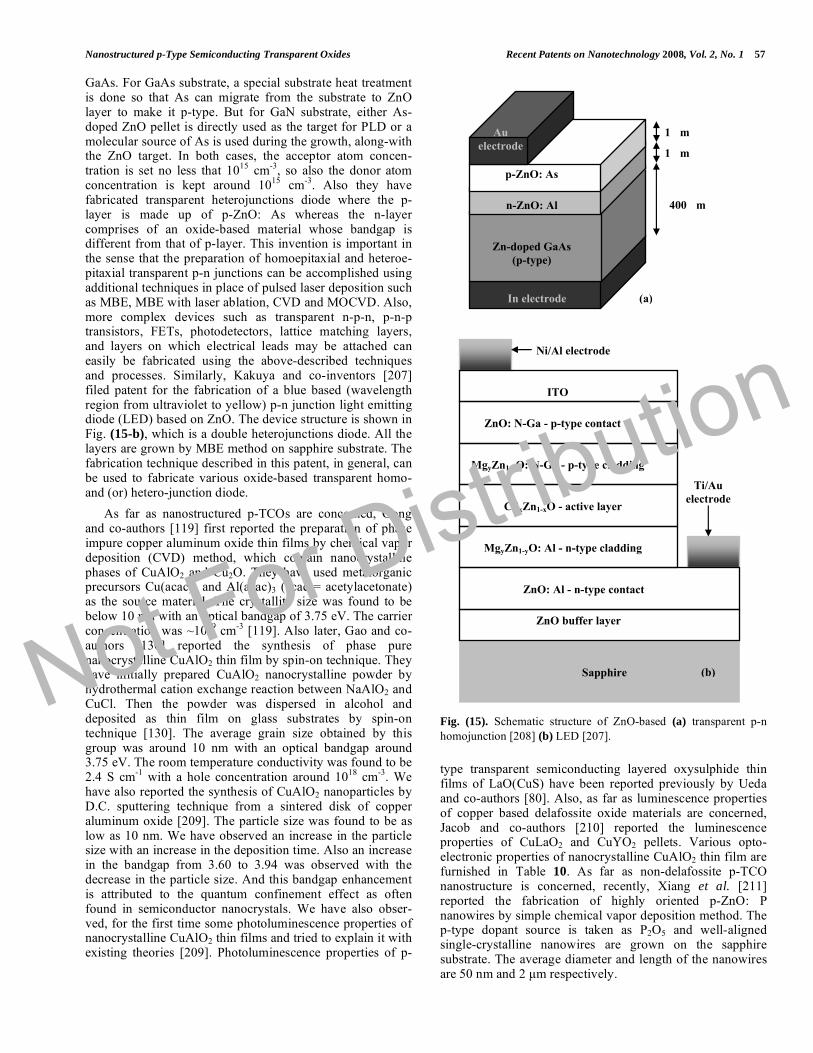
Similarly, Yoshida et al. [206] filed patent on the fabrication of p-type ZnO single crystal by a co-doping technique which comprises of p-type dopants such as nitrogen and carbon and an n-type dopant composed of any one or more elements selected from a group consisting of boron, aluminum, gallium, indium and hydrogen. The doping was done in such a way that the concentration of said p-type dopant is higher (between 1.5 to 5 times) than the concentration of said n-type dopant. When C is used as the p-type dopant, the material growth was done under Zn-rich condition. This is because C is a medium (not hard but not soft) basic element. When ZnO is doped with B, Al, Ga, or H, which are hard basic elements, as an n-type dopant together with such a C, since the chemical bonding of these elements with C is unstable, Zn is easily released. And a phenomenon occurs that C enters the vacancy produced after the Zn has been released. That is, C is in the state of easily substituting for Zn, a medium acid. This substitution means that C functions as an n-type dopant. Thereby, the crystal-linity of ZnO doped with C together with B, Al, Ga, or H becomes unstable, and in the crystal, a phenomenon occurs in which C that functions as an n-type dopant offsets C that functions as a p-type dopant. Therefore, in the case of producing a p-type ZnO single crystal by this doping technology, it is preferable to supply zinc (Zn) excessively compared with oxygen (O). The chemical bonding occurs between Zn and C, which are both medium elements, and the substitution of Zn by C is prevented. As a result, since the crystallinity of ZnO doped with C together with B, Al, Ga, or H is stabilized and C functions only as a p-type dopant in this crystal. The p-ZnO single crystal containing p- and n-type dopants was grown on a semiconductor substrate by simultaneously supplying Zn, O, p-type dopants and n-type dopants using the MBE method. The said p-and n-type dopants are supplied in an atomic state produced by electronical excitation with radio waves, laser beams, X rays, electron beams etc. Fig. (13) shows the schematic structural diagram of a MBE growth chamber. The vacuum in the vacuum chamber is maintained at 10
-8 torr and atomic gases
Fig. (13). MBE growth chamber of N-Ga co-doped p-ZnO film
[206].
of Zn, O, N, and Ga etc. are supplied to the substrate through RF coils and heater. The hole conductivity in the single crystalline material is found to be around 10
17 cm
-3.
Kakuya et al. [207] filed patent on the fabrication of co-doped p-ZnO: N-Ga via a two-step MBE growth technique. The schematic illustration of the process is shown in Fig. (14). In the first step atomic gases of Zn, O and p-type dopant (N) is supplied to grow ZnO on sapphire substrate. Thereafter, in the next step, the oxygen flow is stopped and a n-type dopant (Ga) is supplied to the system, thereby forming a p-type ZnO layer. By repeating these two steps, several numbers of times times, a p-type ZnO based oxide semiconductor layer is grown. As a result, N to be the p-type dopant can be doped in a stable carrier concentration also during high temperature growth in which a residual carrier concentration can be reduced, and the carrier concentration of the p-type layer made of the ZnO based oxide semicon-ductor can be increased sufficiently.
Fig. (14). Schematic diagram of N-Ga co-doped p-ZnO thin film
[207].
As far as patenting activities on the transparent active devices, in the field of “Invisible Electronics”, are concer-ned, White et al. [208] filed the patent for the fabrication of all-oxide transparent p-n homojunction diode of the form GaAs / p-ZnO: As / n-ZnO: Al by eximer pulsed laser depo-sition (PLD). A schematic diode structure is shown in Fig. (15-a). The current-voltage characteristic shows rectifying property with turn-on voltage around 1.0 V. In and Ga dopants were also used as the n-type donor atoms. Also GaN substrate is used for the fabrication of the junction instead of
Zn O N Ga
Atomic gases
RF coils Heater
Single cell Epitaxially
grown films
Zn Zn O O N
ZnO
Sapphire
Zn Zn N N Ga
p-ZnO: (2N, Ga)
Sapphire
Step 1
Step 2 Not For Distribution
Nanostructured p-Type Semiconducting Transparent Oxides Recent Patents on Nanotechnology 2008, Vol. 2, No. 1 57
GaAs. For GaAs substrate, a special substrate heat treatment is done so that As can migrate from the substrate to ZnO layer to make it p-type. But for GaN substrate, either As-doped ZnO pellet is directly used as the target for PLD or a molecular source of As is used during the growth, along-with the ZnO target. In both cases, the acceptor atom concen-tration is set no less that 10
15 cm
-3, so also the donor atom
concentration is kept around 1015
cm-3
. Also they have fabricated transparent heterojunctions diode where the p-layer is made up of p-ZnO: As whereas the n-layer comprises of an oxide-based material whose bandgap is different from that of p-layer. This invention is important in the sense that the preparation of homoepitaxial and heteroe-pitaxial transparent p-n junctions can be accomplished using additional techniques in place of pulsed laser deposition such as MBE, MBE with laser ablation, CVD and MOCVD. Also, more complex devices such as transparent n-p-n, p-n-p transistors, FETs, photodetectors, lattice matching layers, and layers on which electrical leads may be attached can easily be fabricated using the above-described techniques and processes. Similarly, Kakuya and co-inventors [207] filed patent for the fabrication of a blue based (wavelength region from ultraviolet to yellow) p-n junction light emitting diode (LED) based on ZnO. The device structure is shown in Fig. (15-b), which is a double heterojunctions diode. All the layers are grown by MBE method on sapphire substrate. The fabrication technique described in this patent, in general, can be used to fabricate various oxide-based transparent homo- and (or) hetero-junction diode.
As far as nanostructured p-TCOs are concerned, Gong and co-authors [119] first reported the preparation of phase impure copper aluminum oxide thin films by chemical vapor deposition (CVD) method, which contain nanocrystalline phases of CuAlO2 and Cu2O. They have used metalorganic precursors Cu(acac)2 and Al(acac)3 (acac = acetylacetonate) as the source material. The crystallite size was found to be below 10 nm with an optical bandgap of 3.75 eV. The carrier concentration was ~10
19 cm
-3 [119]. Also later, Gao and co-
authors [130] reported the synthesis of phase pure nanocrystalline CuAlO2 thin film by spin-on technique. They have initially prepared CuAlO2 nanocrystalline powder by hydrothermal cation exchange reaction between NaAlO2 and CuCl. Then the powder was dispersed in alcohol and deposited as thin film on glass substrates by spin-on technique [130]. The average grain size obtained by this group was around 10 nm with an optical bandgap around 3.75 eV. The room temperature conductivity was found to be 2.4 S cm
-1 with a hole concentration around 10
18 cm
-3. We
have also reported the synthesis of CuAlO2 nanoparticles by D.C. sputtering technique from a sintered disk of copper aluminum oxide [209]. The particle size was found to be as low as 10 nm. We have observed an increase in the particle size with an increase in the deposition time. Also an increase in the bandgap from 3.60 to 3.94 was observed with the decrease in the particle size. And this bandgap enhancement is attributed to the quantum confinement effect as often found in semiconductor nanocrystals. We have also obser-ved, for the first time some photoluminescence properties of nanocrystalline CuAlO2 thin films and tried to explain it with existing theories [209]. Photoluminescence properties of p-
Fig. (15). Schematic structure of ZnO-based (a) transparent p-n
homojunction [208] (b) LED [207].
type transparent semiconducting layered oxysulphide thin films of LaO(CuS) have been reported previously by Ueda and co-authors [80]. Also, as far as luminescence properties of copper based delafossite oxide materials are concerned, Jacob and co-authors [210] reported the luminescence properties of CuLaO2 and CuYO2 pellets. Various opto-electronic properties of nanocrystalline CuAlO2 thin film are furnished in Table 10. As far as non-delafossite p-TCO nanostructure is concerned, recently, Xiang et al. [211] reported the fabrication of highly oriented p-ZnO: P nanowires by simple chemical vapor deposition method. The p-type dopant source is taken as P2O5 and well-aligned single-crystalline nanowires are grown on the sapphire substrate. The average diameter and length of the nanowires are 50 nm and 2 μm respectively.
Sapphire
ZnO buffer layer
ZnO: Al - n-type contact
MgyZn1-yO: Al - n-type cladding
CdxZn1-xO - active layer
MgyZn1-yO: N-Ga - p-type cladding
ZnO: N-Ga - p-type contact
ITO
Ni/Al electrode
Ti/Au electrode
In electrode
Zn-doped GaAs (p-type)
n-ZnO: Al
p-ZnO: As
Au electrode
400 m
1 m
1 m
(a)
(b)Not For Distribution
58 Recent Patents on Nanotechnology 2008, Vol. 2, No. 1 Banerjee and Chattopadhyay
4. FABRICATION OF p-CuAlO2 NANO-PARTICLES BY LOW-COST D.C. SPUTTERING TECHNIQUE
Nanostructured p-CuAlO2 thin films have been synthesized by D.C. sputtering technique by reducing the deposition time and substrate temperature during deposition. Effect of deposition time on crystal quality, particle size, strain, bandgap etc of the film has been investigated. Also photoluminescence properties of this nanocrystalline material have been reported here.
4.1. Fabrication
Polycrystalline CuAlO2 powder was first synthesized by mixing Cu2O and Al2O3 powders (both 99.99 %) with Cu / Al atomic ratio 1 : 1 for 1 hr. Then the mixture was then air-annealed at 1100
oC for 24 hours to form the CuAlO2 powder.
The sintered body was then reground and pressed into pellet by hydrostatic pressure and was placed in aluminum holder by some appropriate arrangement, which was used as the target for sputtering.
The sputtering unit was evacuated by standard rotary-diffusion arrangement upto a base pressure of 10
-6 mbar and
the target was then pre-sputtered for 10 min to remove contamination, if any, from the surface and then the shutter was displaced to expose the substrates in the sputtering plasma. Films were deposited on ultrasonically cleaned glass and Si substrates, which were placed on the lower electrode and connected to the ground of the power supply. The electrode distance was taken as 1.5 cm. Ar and O2 (3 : 2 vol. ratio) were taken as sputtering gases. Details of the deposition conditions were described elsewhere [209]. Most importantly, the deposition times (td) of the films were kept at very low values, which range from 3 min to 45 min and also the substrate temperature was kept at ambient condition (373 K). This is because, generally at higher substrate temperature, the particles tend to coalesce to form bigger clusters, which is unwanted for the formation of nano-structured films. The variation in the deposition time is done to observe the changes in the nanostructure and optical
properties of the films. Also no post-annealing of the films was performed.
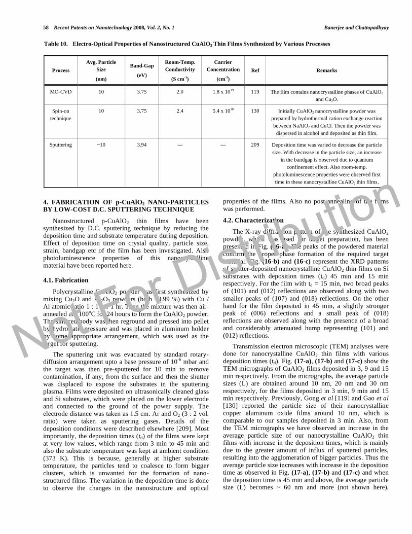
4.2. Characterization
The X-ray diffraction pattern of the synthesized CuAlO2 powder, which was used for target preparation, has been presented in Fig. (16-a). The peaks of the powdered material confirm the proper phase formation of the required target material. Fig. (16-b) and (16-c) represent the XRD patterns of sputter-deposited nanocrystalline CuAlO2 thin films on Si substrates with deposition times (td) 45 min and 15 min respectively. For the film with td = 15 min, two broad peaks of (101) and (012) reflections are observed along with two smaller peaks of (107) and (018) reflections. On the other hand for the film deposited in 45 min, a slightly stronger peak of (006) reflections and a small peak of (018) reflections are observed along with the presence of a broad and considerably attenuated hump representing (101) and (012) reflections.
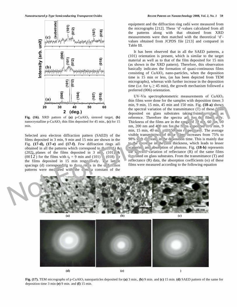
Transmission electron microscopic (TEM) analyses were done for nanocrystalline CuAlO2 thin films with various deposition times (td). Fig. (17-a), (17-b) and (17-c) show the TEM micrographs of CuAlO2 films deposited in 3, 9 and 15 min respectively. From the micrographs, the average particle sizes (L) are obtained around 10 nm, 20 nm and 30 nm respectively, for the films deposited in 3 min, 9 min and 15 min respectively. Previously, Gong et al [119] and Gao et al [130] reported the particle size of their nanocrystalline copper aluminum oxide films around 10 nm, which is comparable to our samples deposited in 3 min. Also, from the TEM micrographs we have observed an increase in the average particle size of our nanocrystalline CuAlO2 thin films with increase in the deposition times, which is mainly due to the greater amount of influx of sputtered particles, resulting into the agglomeration of bigger particles. Thus the average particle size increases with increase in the deposition time as observed in Fig. (17-a), (17-b) and (17-c) and when the deposition time is 45 min and above, the average particle size (L) becomes ~ 60 nm and more (not shown here).
Table 10. Electro-Optical Properties of Nanostructured CuAlO2 Thin Films Synthesized by Various Processes
Process
Avg. Particle
Size
(nm)
Band-Gap
(eV)
Room-Temp.
Conductivity
(S cm-1)
Carrier
Concentration
(cm-3)
Ref Remarks
MO-CVD 10 3.75 2.0 1.8 x 10¹⁹ 119 The film contains nanocrystalline phases of CuAlO2
and Cu2O.
Spin-on
technique
10 3.75 2.4 5.4 x 10¹⁸ 130 Initially CuAlO2 nanocrystalline powder was
prepared by hydrothermal cation exchange reaction
between NaAlO2 and CuCl. Then the powder was
dispersed in alcohol and deposited as thin film.
Sputtering ~10 3.94 --- --- 209 Deposition time was varied to decrease the particle
size. With decrease in the particle size, an increase
in the bandgap is observed due to quantum
confinement effect. Also room-temp.
photoluminescence properties were observed first
time in these nanocrystalline CuAlO2 thin films.
Not For Distribution
Nanostructured p-Type Semiconducting Transparent Oxides Recent Patents on Nanotechnology 2008, Vol. 2, No. 1 59
Fig. (16). XRD pattern of (a) p-CuAlO2 sintered target, (b) nanocrystalline p-CuAlO2 thin film deposited for 45 min., (c) for 15
min.
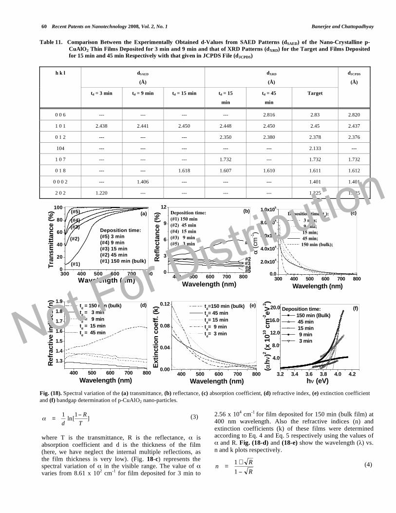
Selected area electron diffraction pattern (SAED) of the films deposited in 3 min, 9 min and 15 min are shown in the Fig. (17-d), (17-e) and (17-f). Few diffraction rings are obtained in all the patterns which correspond to the (101) & (202) planes of the films deposited in 3 min, (101) & (00 21 ) for the films with td = 9 min and (101) & (018) for the films deposited in 15 min respectively. The lattice spacings (d) corresponding to these rings in the diffraction patterns were measured with the camera constant of the
equipment and the diffraction ring radii were measured from the micrographs [212]. These ‘d’-values calculated from all the patterns along with that obtained from XRD measurements were then matched with the theoretical ‘d’-values obtained from JCPDS file [213] and compared in Table 11.
It has been observed that in all the SAED patterns, a (101) orientation is present, which is similar to the target material as well as to that of the film deposited for 15 min (as shown in the XRD pattern). Therefore, this observation basically indicates the formation of quasi-continuous films consisting of CuAlO2 nano-particles, when the deposition time is 15 min or less, (as has been depicted from TEM micrographs), whereas with further increase in the deposition time (i.e. for td 45 min), the growth mechanism followed a preferred (006) orientation.
UV-Vis spectrophotometric measurements of CuAlO2 thin films were done for the samples with deposition times 3 min, 9 min, 15 min, 45 min and 150 min. Fig. (18-a) shows the spectral variation of the transmittance (T) of these films deposited on glass substrates taking similar glass as reference. Therefore the spectra are for the films only. Thickness of the films are in the range of 30 nm, 60 nm, 90 nm, 200 nm and 400 nm for the films deposited in 3 min, 9 min, 15 min, 45 min and 150 min respectively. The average visible transmittance of these films increases from 75% to 98% with decrease in the deposition time. This is mainly due to the decrease in the film thickness, which leads to lesser scattering and absorption of photons. Fig. (18-b) represents the spectral variation of reflectance (R) of the same films deposited on glass substrates. From the transmittance (T) and reflectance (R) data, the absorption coefficients ( ) of these films were measured according to the following equation
Fig. (17). TEM micrographs of p-CuAlO2 nanoparticles deposited for (a) 3 min., (b) 9 min. and (c) 15 min. (d) SAED pattern of the same for
deposition time 3 min (e) 9 min. and (f) 15 min.
20 30 40 50 60
(a) (018
)
(107
)
(104
)(0
12)
(101
)(0
06)
2 (deg.)
Inte
nsity
(arb
. uni
t)(c)
(b)
(018
)
(012
)(1
01)(0
06)
(018
)
(107
)
(012
)(1
01)
(sub
stra
te)
40 nm 40 nm
(a) (b) (c)
(d) (e) (f)
40 nm Not For Distribution
60 Recent Patents on Nanotechnology 2008, Vol. 2, No. 1 Banerjee and Chattopadhyay
]1
[ln1
T
R
d= (3)
where T is the transmittance, R is the reflectance, is absorption coefficient and d is the thickness of the film (here, we have neglect the internal multiple reflections, as the film thickness is very low). (Fig. 18-c) represents the spectral variation of in the visible range. The value of varies from 8.61 x 10
2 cm
-1 for film deposited for 3 min to
2.56 x 104 cm
-1 for film deposited for 150 min (bulk film) at
400 nm wavelength. Also the refractive indices (n) and extinction coefficients (k) of these films were determined according to Eq. 4 and Eq. 5 respectively using the values of
and R. Fig. (18-d) and (18-e) show the wavelength ( ) vs. n and k plots respectively.
R
Rn
+=
1
1 (4)
Table 11. Comparison Between the Experimentally Obtained d-Values from SAED Patterns (dSAED) of the Nano-Crystalline p-CuAlO2 Thin Films Deposited for 3 min and 9 min and that of XRD Patterns (dXRD) for the Target and Films Deposited for 15 min and 45 min Respectively with that given in JCPDS File (dJCPDS)
dSAED
(Å)
dXRD
(Å)
h k l
td = 3 min td = 9 min td = 15 min td = 15
min
td = 45
min
Target
dJCPDS
(Å)
0 0 6 --- --- --- --- 2.816 2.83 2.820
1 0 1 2.438 2.441 2.450 2.448 2.450 2.45 2.437
0 1 2 --- --- --- 2.350 2.380 2.378 2.376
104 --- --- --- --- --- 2.133 ---
1 0 7 --- --- --- 1.732 --- 1.732 1.732
0 1 8 --- --- 1.618 1.607 1.610 1.611 1.612
0 0 0 2 --- 1.406 --- --- --- 1.401 1.401
2 0 2 1.220 --- --- --- --- 1.225 1.225
Fig. (18). Spectral variation of the (a) transmittance, (b) reflectance, (c) absorption coefficient, (d) refractive index, (e) extinction coefficient
and (f) bandgap determination of p-CuAlO2 nano-particles.
400 500 600 700 8000
3
6
9
12(b)
#5#4#3#2
#1
Deposition time:(#1) 150 min(#2) 45 min(#4) 15 min(#3) 9 min(#5) 3 min
Ref
lect
ance
(%)
Wavelength (nm)
400 500 600 700 800
1.3
1.4
1.5
1.6
1.7
1.8
1.9(d)
Ref
ract
ive
indi
ces
(n)
Wavelength (nm)
td = 150 min (bulk) td = 3 min td = 9 min td = 15 min td = 45 min
400 500 600 700 8000.00
0.04
0.08
0.12 (e)
Extin
ctio
n co
eff.
(k)
Wavelength (nm)
td=150 min (bulk) td= 45 min td= 15 min td= 9 min td= 3 min
3.2 3.4 3.6 3.8 4.0 4.2
(f)20.0
16.0
12.0
8.0
4.0
(αhν
)2 (x 1
010 c
m-2eV
2)
hν (eV)
Deposition time: 150 min (Bulk) 45 min 15 min 9 min 3 min
300 400 500 600 700 8000
20
40
60
80
100(a)(#5)
(#4)(#3)
(#2)
(#1)
Deposition time:(#5) 3 min(#4) 9 min(#3) 15 min(#2) 45 min(#1) 150 min (bulk)
Tran
smitt
ance
(%)
Wavelength (nm) 300 400 500 600 700 8000.0
2.0x10⁴
4.0x10⁴
6.0x10⁴
8.0x10⁴
1.0x10⁵
(c)
α (c
m-1)
Wavelength (nm)
Deposition time (td): 3 min; 9 min; 15 min; 45 min; 150 min (bulk);
Not For Distribution
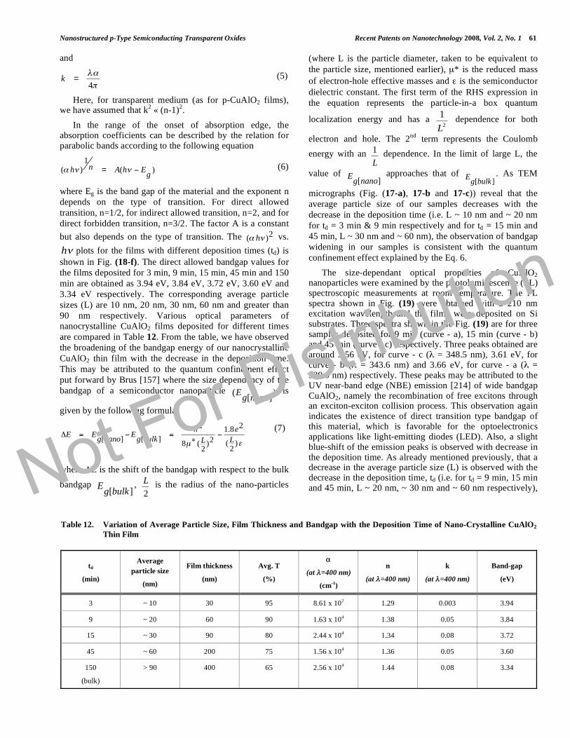
Nanostructured p-Type Semiconducting Transparent Oxides Recent Patents on Nanotechnology 2008, Vol. 2, No. 1 61
and
4=k (5)
Here, for transparent medium (as for p-CuAlO2 films), we have assumed that k
2 « (n-1)
2.
In the range of the onset of absorption edge, the absorption coefficients can be described by the relation for parabolic bands according to the following equation
)(1
)(g
EhAnh = (6)
where Eg is the band gap of the material and the exponent n
depends on the type of transition. For direct allowed
transition, n=1/2, for indirect allowed transition, n=2, and for
direct forbidden transition, n=3/2. The factor A is a constant
but also depends on the type of transition. The 2)( h vs.
h plots for the films with different deposition times (td) is
shown in Fig. (18-f). The direct allowed bandgap values for
the films deposited for 3 min, 9 min, 15 min, 45 min and 150
min are obtained as 3.94 eV, 3.84 eV, 3.72 eV, 3.60 eV and
3.34 eV respectively. The corresponding average particle
sizes (L) are 10 nm, 20 nm, 30 nm, 60 nm and greater than
90 nm respectively. Various optical parameters of
nanocrystalline CuAlO2 films deposited for different times
are compared in Table 12. From the table, we have observed
the broadening of the bandgap energy of our nanocrystalline
CuAlO2 thin film with the decrease in the deposition time.
This may be attributed to the quantum confinement effect
put forward by Brus [157] where the size dependency of the
bandgap of a semiconductor nanoparticle )][
(nanog
E is
given by the following formula:
μ )2
(
28.1
2)2
(8
2
][][ L
e
L
h
bulkgE
nanogEE ==
(7)
where E is the shift of the bandgap with respect to the bulk
bandgap ][bulkg
E , 2
L is the radius of the nano-particles
(where L is the particle diameter, taken to be equivalent to
the particle size, mentioned earlier), μ* is the reduced mass
of electron-hole effective masses and is the semiconductor
dielectric constant. The first term of the RHS expression in
the equation represents the particle-in-a box quantum
localization energy and has a 2
1
L dependence for both
electron and hole. The 2nd
term represents the Coulomb
energy with an L
1 dependence. In the limit of large L, the
value of ][nanog
E approaches that of ][bulkg
E . As TEM
micrographs (Fig. (17-a), 17-b and 17-c)) reveal that the
average particle size of our samples decreases with the
decrease in the deposition time (i.e. L ~ 10 nm and ~ 20 nm
for td = 3 min & 9 min respectively and for td = 15 min and
45 min, L ~ 30 nm and ~ 60 nm), the observation of bandgap
widening in our samples is consistent with the quantum
confinement effect explained by the Eq. 6.
The size-dependant optical properties of CuAlO2 nanoparticles were examined by the photoluminescence (PL) spectroscopic measurements at room temperature. The PL spectra shown in Fig. (19) were obtained with a 210 nm excitation wavelength and the films were deposited on Si substrates. Three spectra shown in the Fig. (19) are for three samples deposited for 9 min (curve - a), 15 min (curve - b) and 45 min (curve - c) respectively. Three peaks obtained are around 3.56 eV, for curve - c ( = 348.5 nm), 3.61 eV, for curve - b ( = 343.6 nm) and 3.66 eV, for curve - a ( = 339.0 nm) respectively. These peaks may be attributed to the UV near-band edge (NBE) emission [214] of wide bandgap CuAlO2, namely the recombination of free excitons through an exciton-exciton collision process. This observation again indicates the existence of direct transition type bandgap of this material, which is favorable for the optoelectronics applications like light-emitting diodes (LED). Also, a slight blue-shift of the emission peaks is observed with decrease in the deposition time. As already mentioned previously, that a decrease in the average particle size (L) is observed with the decrease in the deposition time, td (i.e. for td = 9 min, 15 min and 45 min, L ~ 20 nm, ~ 30 nm and ~ 60 nm respectively),
Table 12. Variation of Average Particle Size, Film Thickness and Bandgap with the Deposition Time of Nano-Crystalline CuAlO2 Thin Film
td
(min)
Average
particle size
(nm)
Film thickness
(nm)
Avg. T
(%)
(at =400 nm)
(cm-1)
n
(at =400 nm)
k
(at =400 nm)
Band-gap
(eV)
3 ~ 10 30 95 8.61 x 10² 1.29 0.003 3.94
9 ~ 20 60 90 1.63 x 10⁴ 1.38 0.05 3.84
15 ~ 30 90 80 2.44 x 10⁴ 1.34 0.08 3.72
45 ~ 60 200 75 1.56 x 10⁴ 1.36 0.05 3.60
150
(bulk)
> 90 400 65 2.56 x 10⁴ 1.44 0.08 3.34
Not For Distribution
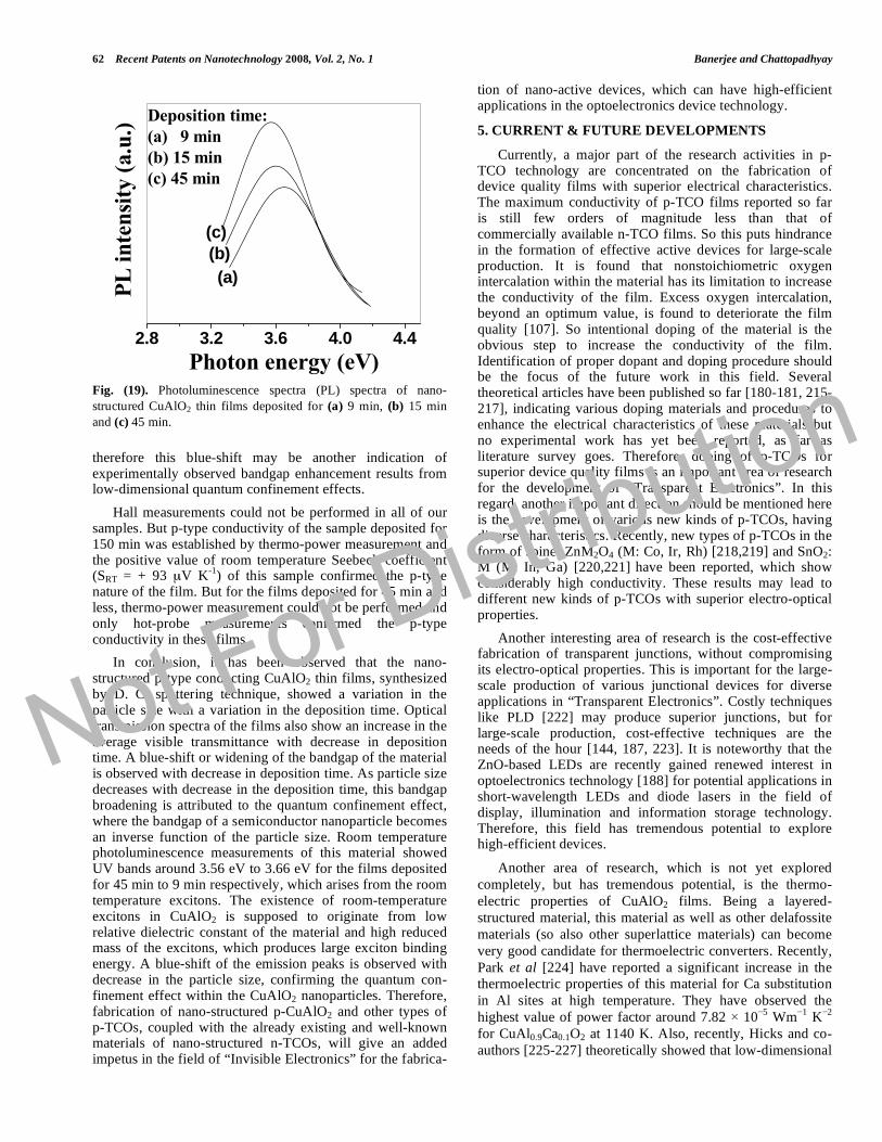
62 Recent Patents on Nanotechnology 2008, Vol. 2, No. 1 Banerjee and Chattopadhyay
Fig. (19). Photoluminescence spectra (PL) spectra of nano-
structured CuAlO2 thin films deposited for (a) 9 min, (b) 15 min
and (c) 45 min.
therefore this blue-shift may be another indication of experimentally observed bandgap enhancement results from low-dimensional quantum confinement effects.
Hall measurements could not be performed in all of our samples. But p-type conductivity of the sample deposited for 150 min was established by thermo-power measurement and the positive value of room temperature Seebeck coefficient (SRT = + 93 μV K
-1) of this sample confirmed the p-type
nature of the film. But for the films deposited for 45 min and less, thermo-power measurement could not be performed and only hot-probe measurements confirmed the p-type conductivity in these films.
In conclusion, it has been observed that the nano-structured p-type conducting CuAlO2 thin films, synthesized by D. C. sputtering technique, showed a variation in the particle size with a variation in the deposition time. Optical transmission spectra of the films also show an increase in the average visible transmittance with decrease in deposition time. A blue-shift or widening of the bandgap of the material is observed with decrease in deposition time. As particle size decreases with decrease in the deposition time, this bandgap broadening is attributed to the quantum confinement effect, where the bandgap of a semiconductor nanoparticle becomes an inverse function of the particle size. Room temperature photoluminescence measurements of this material showed UV bands around 3.56 eV to 3.66 eV for the films deposited for 45 min to 9 min respectively, which arises from the room temperature excitons. The existence of room-temperature excitons in CuAlO2 is supposed to originate from low relative dielectric constant of the material and high reduced mass of the excitons, which produces large exciton binding energy. A blue-shift of the emission peaks is observed with decrease in the particle size, confirming the quantum con-finement effect within the CuAlO2 nanoparticles. Therefore, fabrication of nano-structured p-CuAlO2 and other types of p-TCOs, coupled with the already existing and well-known materials of nano-structured n-TCOs, will give an added impetus in the field of “Invisible Electronics” for the fabrica-
tion of nano-active devices, which can have high-efficient applications in the optoelectronics device technology.
5. CURRENT & FUTURE DEVELOPMENTS
Currently, a major part of the research activities in p-TCO technology are concentrated on the fabrication of device quality films with superior electrical characteristics. The maximum conductivity of p-TCO films reported so far is still few orders of magnitude less than that of commercially available n-TCO films. So this puts hindrance in the formation of effective active devices for large-scale production. It is found that nonstoichiometric oxygen intercalation within the material has its limitation to increase the conductivity of the film. Excess oxygen intercalation, beyond an optimum value, is found to deteriorate the film quality [107]. So intentional doping of the material is the obvious step to increase the conductivity of the film. Identification of proper dopant and doping procedure should be the focus of the future work in this field. Several theoretical articles have been published so far [180-181, 215-217], indicating various doping materials and procedures to enhance the electrical characteristics of these materials but no experimental work has yet been reported, as far as literature survey goes. Therefore, doping of p-TCOs for superior device quality films is an important area of research for the development of “Transparent Electronics”. In this regard, another important direction should be mentioned here is the development of various new kinds of p-TCOs, having diverse characteristics. Recently, new types of p-TCOs in the form of spinel ZnM2O4 (M: Co, Ir, Rh) [218,219] and SnO2: M (M: In, Ga) [220,221] have been reported, which show considerably high conductivity. These results may lead to different new kinds of p-TCOs with superior electro-optical properties.
Another interesting area of research is the cost-effective fabrication of transparent junctions, without compromising its electro-optical properties. This is important for the large-scale production of various junctional devices for diverse applications in “Transparent Electronics”. Costly techniques like PLD [222] may produce superior junctions, but for large-scale production, cost-effective techniques are the needs of the hour [144, 187, 223]. It is noteworthy that the ZnO-based LEDs are recently gained renewed interest in optoelectronics technology [188] for potential applications in short-wavelength LEDs and diode lasers in the field of display, illumination and information storage technology. Therefore, this field has tremendous potential to explore high-efficient devices.
Another area of research, which is not yet explored
completely, but has tremendous potential, is the thermo-
electric properties of CuAlO2 films. Being a layered-
structured material, this material as well as other delafossite
materials (so also other superlattice materials) can become
very good candidate for thermoelectric converters. Recently,
Park et al [224] have reported a significant increase in the
thermoelectric properties of this material for Ca substitution
in Al sites at high temperature. They have observed the
highest value of power factor around 7.82 105 Wm
1 K
2
for CuAl0.9Ca0.1O2 at 1140 K. Also, recently, Hicks and co-
authors [225-227] theoretically showed that low-dimensional
2.8 3.2 3.6 4.0 4.4
(c)(b)(a)PL
inte
nsity
(a.u
.)
Photon energy (eV)
Deposition time:(a) 9 min(b) 15 min(c) 45 min
Not For Distribution
Nanostructured p-Type Semiconducting Transparent Oxides Recent Patents on Nanotechnology 2008, Vol. 2, No. 1 63
materials (such as quantum wires, quantum dots of different
thermoelectric materials) can have superior thermoelectric
properties over the corresponding bulk materials. This is
assumed to be due to the confinement of the electrons and
phonons inside the low-dimensional environment of the
nanostructures, which manifests the superior Figure-of-merit
( ,2 TS
ZT = also called dimensionless Figure-of-merit,
where S is the Seebeck Coefficient, is the electrical
conductivity, is the thermal conductivity and T is the
temperature [228]) of these nanomaterials. Therefore, nano-
structured p-CuAlO2 and similar p-TCOs may provide new
and high-efficient thermoelectric materials and, hence, if
proper studies can be done on the thermoelectric properties
of these types of superlattice and nanostructured materials,
new horizon may open up in the field of thermoelectric
converters.
Also keeping an eye in the tremendous progress in nanotechnology, fabrication and characterization of nano-structured p-CuAlO2 as well as other p-TCO thin films may become an important field of work, because of new and interesting properties exhibited by these nano-materials [209, 211]. Proper fabrication procedure to get reproducible nano-materials is the most important future work. Also in-depth studies of the photoluminescence properties of p-CuAlO2 and similar types of p-TCO nano-particles will be another area of research, which is needed to be explored properly. Fabrication of nano-structured p-TCOs, coupled with the already existing and well-known materials of nano-structured n-TCOs, will give an added impetus in the field of “Invisible Electronics” for the fabrication of nano-active devices, which can have high-efficient applications in the optoelectronics device technology.
Field-emission property of CuAlO2 thin films is a completely new area of research, which has tremendous opportunities [229,230]. This material showed very low turn-on field comparable to most of the carbonaceous low-threshold field-emitters like carbon naotube (CNT), diamond like carbon (DLC), diamond, amorphous carbon (a:C), silicon carbide (SiC) nanorods etc. So these types of p-TCO materials may become promising alternative to the existing materials in the field of FED technology. But, proper emission mechanism in these materials is not very clear till date and very good scopes are there to properly investigate the emission mechanism so that the material properties can be tuned accordingly to get better field-emission properties of these films.
Also recent study showed that p-CuAlO2 can become a good candidate for ozone sensors. Zheng and co-authors [231] reported that CuAlO2 has a selective and reversible response to ozone gas at room temperature. All existing commercial semiconductor ozone sensors are of n-type [232-235]. This study demonstrated the feasibility of developing an inexpensive p-type transparent ozone sensor. Hence, transparent p-n junction ozone sensors may be fabricated using the p-CuAlO2 and existing n-TCO such as In2O3.
Photocatalytic hydrogen evolution over delafossite CuAlO2 is another interesting report published recently by Koriche et al. [236]. This group proposed a new photoche-
mical system for water reduction based on p-CuAlO2 and S2
as hole scavenger. They have used co-precipitation method, a new synthetic route, to synthesis CuAlO2, which increased the surface to volume ratio and delivered a highest H2 production. This report is very interesting and shows newer applications of delafossite p-CuAlO2 and similar p-TCO materials.
Also, recently Kizaki and co-authors [237] proposed a material-designing procedure to get CuAlO2-based dilute magnetic semiconductors. Ab-initio calculations showed that Fe- and Mn-doped CuAlO2-based dilute magnetic semicon-ductors possess high-Curie-temperature ferromagnetic characteristics. Being a natural p-type transparent semicon-ductor without intentional doping, CuAlO2 can easily be used for the host of dilute magnetic semiconductors. Also, most importantly, the delafossite structure of CuAlO2 has the advantage of possessing two cation-sites, Cu
+1 and Al
+3 sites,
for possible magnetic ion substitution. O-Cu-O dumbbell-sites in delafossite CuAlO2 can be partially replaced with magnetic ions. Due to this coordination one can realize new ferromagnetic dilute magnetic semiconductors from the standpoint of the hybridization of orbitals between 3d orbitals with the impurities and 2p orbitals with the oxygen in CuAlO2. Similarly, Diet et al. [201] recently showed that Mn-doped p-type ZnO can become a good candidate for magnetic semiconductors having potential application in spintronics.
Therefore, it will not be an exaggeration to say that next decade will see the renaissance of micro/nano-structured p-TCO materials and various new, interesting and novel technological applications with these materials are on the verge of exploration.
ACKNOWLEDGEMENT
The authors wish to gratefully acknowledge the financial assistance of the Department of Science and Technology, Govt. of India, during the execution of the work.
REFERENCES
[1] Badekar K. (Leipzig) Ann Phys 1907; 22: 749. [2] Lampert CM. Heat mirror coatings for energy conserving windows.
Sol Energy Mater 1981; 6: 1-41. [3] Chopra KL, Major S, Pandya DK. Transparent conductors.A status
review. Thin Solid Films 1883; 102: 1-46. [4] Hamberg I, Granqvist CG. Evaporated Sn-doped In2O3 films: basic
optical properties and applications to energy-efficient windows. J Appl Phys 1986; 60: R123-R160.
[5] Holland L. Vacuum Deposition of Thin Films, Wiley. New York. 1958; 492-495.
[6] Cachet H, Gamard A, Campet G, Jousseaume B, Toupance T. Tin dioxide thin films prepared from a new alkoxyfluorotin complex
including a covalent Sn---F bond. Thin Solid Films 2001; 388: 41-49.
[7] Wendt R, Ellmer K. Desorption of Zn from a growing ZnO:Al-film deposited by magnetron sputtering. Surf. Coat Technol 1997; 93:
27-31. [8] Hartnagel HL, Dawar AL, Jain AK, Jagadish C. Semiconducting
transparent thin films. IOP Publishing Ltd. Bristol and Philadelphia 1995.
[9] Ginley DS, Bright C. Transparent conducting oxides. MRS Bulletin 2000; p.15.
[10] Cava RJ, Philips JM, Kwo J, et al. GaInO3: A new transparent conducting oxide. Appl Phys Lett 1994; 64: 2071-2072.
[11] Philips JM, Cava RJ, Thomas GA, et al. Zinc-indium-oxide: A high conductivity transparent conducting oxide. Appl Phys Lett 1995;
67: 2246-2248.
Not For Distribution
64 Recent Patents on Nanotechnology 2008, Vol. 2, No. 1 Banerjee and Chattopadhyay
[12] Freeman AJ, Poeppelmeier KR, Mason TO, Chang RPH, Marks TJ.
Chemical and thin-film strategies for new transparent conducting oxides. MRS Bulletin 2000; p.45.
[13] Gordon RG. Criteria for choosing transparent conductors. MRS Bulletin 2000; p.52.
[14] Mochel, J. M.: US2564706 (1947). [15] Sinclair WR, Peters FG, Stillinger DW, Koonce SE. Devitrification
of tin oxide films (doped and undoped) prepared by reactive sputtering. J Electrochem Soc 1965; 112: 1096-1100.
[16] Lytle, W. O., Junge, A. E.: US2566346 (1951). [17] Gordon, R. G.: US4146657 (1979).
[18] Banerjee AN, Kundoo S, Saha P, Chattopadhyay KK. Synthesis and characterization of nano-crystalline fluorine-doped tin oxide thin
films by sol-gel method. J Sol-Gel Sci Technol 2003; 28: 105-110. [19] Banerjee AN, Maity R, Kundoo S, Chattopadhyay KK. Poole -
Frenkel effect in nanocrystalline SnO2: F thin films prepared by sol-gel-dip-coating technique. Phys Stat Solidi A 2004; 201: 983-989.
[20] Major S, Banerjee A, Chopra KL. Annealing studies of undoped and indium-doped films of zinc oxide. Thin Solid Films 1984; 122:
31-43. [21] Minami T, Nanto H, Takata S. Highly conductive and transparent
aluminum doped zinc oxide thin films prepared by RF magnetron sputtering. Jpn J Appl Phys Part 2 Lett 1984; 23: L280-L282.
[22] Hu J, Gordon RG. Textured fluorine-doped ZnO films by atmospheric pressure chemical vapor deposition and their use in
amorphous silicon solar cells. Sol Cells 1991; 30: 437-450. [23] Vijayakumar, P.S., Blaker, K.A., Welting, R.D., Wong, B., Halani,
A. T., Park, C.: US4751149 (1988). [24] Choi BH, Im HB, Song JS, Yoon KH. Optical and electrical
properties of Ga2O3-doped ZnO films prepared by r.f. sputtering. Thin Solid Films 1990; 193: 712-720.
[25] Hu J, Gordon RG. Atmospheric pressure chemical vapor deposition of gallium doped zinc oxide thin films from diethyl zinc, water, and
triethyl gallium. J Appl Phys 1992; 72: 5381-5392. [26] Mochel, J. M.: US2564707 (1951).
[27] Holland L, Siddall G. Vacuum, Springer Vol. III, 1955. [28] Avaritsiotis JN, Howson RP. Composition and conductivity of
fluorine-doped conducting indium oxide films prepared by reactive ion plating. Thin Solid Films 1981; 77: 351-357.
[29] Groth R. Untersuchungen an halbleitenden Indiumoxydschichten. Phys Stat Solidi 1966; 14: 69-75.
[30] Nozik, A. J.: US3811953 (1974). [31] Haacke G, Mealmaker WE, Siegel LA. Sputter deposition and
characterization of Cd2SnO4 films. Thin Solid Films 1978; 55: 67-81.
[32] Vossen JL. RCA Rev 1971; 32: 269-271. [33] Enoki H, Nakayama T, Echigoya J. The electrical and optical
properties of the ZnO-SnO2 thin films prepared by RF magnetron sputtering. Phys Stat Solidi A 1992; 129: 181-191.
[34] Minami T, Sonohara H, Takata S, Sato H. Highly transparent and conductive zinc-stannate thin films prepared by RF magnetron
sputtering. Jpn J Appl Phys Part 2 Lett 1994; 33: L1693-L1696. [35] Cava RJ, Hou SY, Krajewski JJ, et al. Transparent conducting thin
films of GaInO3. Appl Phys Lett 1994; 65: 115-117. [36] Otabe T, Ueda K, Kudoh A, Hosono H, Kawazoe H. n-type
electrical conduction in transparent thin films of delafossite-type AgInO2. Appl Phys Lett 1998; 72: 1036-1038.
[37] Dali SE, Jayachandran M, Chockalingam MJ. New transparent electronic conductor, MgIn2O4 spinel. J Mater Sc Lett 1999; 18:
915-917. [38] Edwards DD, Mason TO, Goutenoire F, Poeppelmeier KR. A new
transparent conducting oxide in the Ga2O3-In2O3-SnO2 system. Appl Phys Lett 1997; 70: 1706-1708.
[39] Minami T, Takata S, Kakumu T, Sonohara H. New transparent conducting MgIn2O4-Zn2In2O5 thin films prepared by magnetron
sputtering. Thin Solid Films 1995; 270: 22-26. [40] Minami T, Kakumu T, Shimokawa K, Takata S. New transparent
conducting ZnO-In2O3-SnO2 thin films prepared by magnetron sputtering. Thin Solid Films 1998; 317: 318-321.
[41] Omata T, Ueda N, Ueda K, Kawazoe H. New ultraviolet-transport electroconductive oxide, ZnGa2O4 spinel. Appl Phys Lett 1994; 64:
1077-1078. [42] Kammler DR, Mason TO, Young DL, Coutts TJ. Thin films of the
spinel Cd1 + xIn2-2xSnxO4 transparent conducting oxide solution. J Appl Phys 2001; 90: 3263-3268.
[43] Minami T. New n-Type Transparent Conducting Oxides. MRS Bull
2000; p.38. [44] Lewis BG, Paine DC. Applications and processing of transparent
conducting oxides. MRS Bull 2000; p. 22. [45] Granqvist CG, Azens A, Hjelm A, et al. Recent advances in
electrochromics for smart windows applications. Sol. Energy 1998; 63: 199.
[46] Kammler DR, Edwards DD, Ingram BJ, et al. Photovoltaics for the 21stCentury,edited by Kapur VK, McConnel RD, Carlson D,
Ceasan GP, Rohatgi A. The Electrochem Soc Proc 99-11, Pennington NJ 1999; p. 68.
[47] Lee SH, Hwang KH, Joo SK. In electrochromic materials (2nd Interntional Symposium), edited by Ho KC, McArthur DA. The
Electrochem Soc Proc 94-2 Pennington NJ 1994; p. 290. [48] Lugg PS, Bommarito S, Bailey J, et al. Solid State Ionic Devices.
The Electrochem Soc Proc 99-13 Pennington NJ1999; p. 284. [49] Nakato Y, Kai KI, Kawabe K. Improvement of characteristics of
new-type solar cells, having a “transparent conductor/thin Si02 layer with ultrafine metal particles as conductive channels/n-Si” junction.
Sol Energy Mater Sol Cells 1995; 37: 323-335. [50] Emons TT, Li J, Nazar LF. Synthesis and characterization of
mesoporous indium tin oxide possessing an electronically conductive framework. J Am Chem Soc 2002; 124: 8516-8517.
[51] Hutchins, M.G., McMeeking, G.D.: Biosensor Patent No. 9027607.2 (1990).
[52] He Y, Kanicki J. High-efficiency organic polymer light-emitting heterostructure devices on flexible plastic substrates. Appl Phys
Lett 2000; 76: 661-663. [53] Wager JF. Transparent electronics. Science 2003; 300: 1245-1246.
[54] Garnich F, Yu PC, Lampert CM. Hydrated manganese oxide as a counter-electrode material for an electrochromic optical switching
device. Solar Energy Materials 1990; 20: 265-275. [55] Grivas C, Mallis S, Boutsikaris L, Gill DS, Vainos NA, Chandler
PJ. Growth and performance of pulsed laser deposited indium oxide thin-film holographic recorders. Laser Phys 1998; 8: 326-330.
[56] Moschovis K, Gagaoudakis E, Chatzitheodoridis E, et al. Study of the ambient optical recording dynamics on sputtered indium oxide
thin films. Appl Phys A 1998; 66: 651-654. [57] Moller S, Perlov C, Jackson W, Taussig C, Forest SR, A.
polymer/semiconductor write-once read-many-times memory. Nature 2003; 426: 166-168.
[58] Hayes RA, Feenstra BJ. Video-speed electronic paper based on electrowetting. Nature 2003; 425: 383-385.
[59] Cornia RL, Fenn JB, Memarian H, Ringer R. Proc. 41st Annual Technical Conference, Soc. of Vacuum Coaters, Boston 1998; p.
452. [60] Cairns DR, Witte RP, Sparacin DK, et al. Strain-dependent
electrical resistance of tin-doped indium oxide on polymer substrates. Appl Phys Lett 2000; 76: 1425-1427.
[61] Banerjee AN, Ghosh CK, Chattopadhyay KK, et al. Low-temperature deposition of ZnO thin films on PET and glass
substrates by DC-sputtering technique. Thin Solid Films 2006; 496: 112-116.
[62] Seager, CH, McIntyre DC, Warren WL, Tuttle BA. Charge trapping and device behavior in ferroelectric memories. Appl Phys Lett
1996; 68: 2660-2662. [63] Prince MWJ, Gross-Holtz KO, Muller G, et al. A ferroelectric
transparent thin-film transistor. Appl Phys Lett 1996; 68: 3650-3652.
[64] Sato H, Minami T, Takata S, Yamada T. Transparent conducting p-type NiO thin films prepared by magnetron sputtering. Thin Solid
Films 1993; 236: 27-31. [65] Kawazoe H, Yasukawa M, Hyodo H, Kurita M, Yanagi H, Hosono
H. P-type electrical conduction in transparent thin films of CuAlO2 Nature 1997; 389: 939-942.
[66] Ueda K, Hase T, Yanagi H, et al. Epitaxial growth of transparent p-type conducting CuGaO2 thin films on sapphire (001) substrates by
pulsed laser deposition. J Appl Phys 2001; 89: 1790-1793. [67] Yanagi H, Hase T, Ibuki S, Ueda K, Hosono H. Bipolarity in
electrical conduction of transparent oxide semiconductor CuInO2 with delafossite structure. Appl Phys Lett 2001; 78: 1583-1585.
[68] Yanagi H, Ueda K, Ohta H, Orita M, Hirano M, Hosono H. Fabrication of all oxide transparent p-n homojunction using bipolar
CuInO2 semiconducting oxide with delafossite structure. Solid State Comm 2001; 121: 15-17.
Not For Distribution
Nanostructured p-Type Semiconducting Transparent Oxides Recent Patents on Nanotechnology 2008, Vol. 2, No. 1 65
[69] Tate J, Jayaraj MK, Draeseke AD, et al. p-Type oxides for use in
transparent diodes. Thin Solid Films 2002; 411: 119-124. [70] Duan N, Sleight AW, Jayaraj MK, Tate J. Transparent p-type
conducting CuScO2 + x films. Appl Phys Lett 2000; 77: 1325-1326. [71] Nagrajan R, Draeseke AD, Sleight AW, Tate J. p-type conductivity
in CuCr1-xMgxO2 films and powders. J Appl Phys 2001; 89: 8022-8025.
[72] Jayaraj MK, Draeseke AD, Tate J, Sleight AW. p-Type transparent thin films of CuY1 xCaxO2. Thin Solid Films 2001; 397: 244-248.
[73] Nagrajan R, Duan N, Jayaraj MK, et al. p-Type conductivity in the delafossite structure. Int. J Inorg Mater 2001; 3: 265-270.
[74] Nagrajan R, Uma S, Jayaraj MK, Tate J, Sleight AW. Solid State Science. Solid State Science 2002; 4: 787-792.
[75] Kandpal HC, Seshadri R. First-principles electronic structure of the delafossites ABO2 (A=Cu, Ag, Au; B=Al, Ga, Sc, In, Y): evolution
of d10-d10 interactions. Solid State Sciences 2002; 4: 1045-1052. [76] Kudo A, Yanagi H, Hosono H, Kawazoe H. SrCu2O2: A p-type
conductive oxide with wide band gap. Appl Phys Lett 1998; 73: 220-222.
[77] Windisch Jr. CF, Ferris KM, Exarhos GJ. Synthesis and characterization of transparent conducting oxide cobalt-nickel
spinel films. J Vac Sci Technol A 2001; 19: 1647-1651. [78] Windisch Jr. CF, Engelhard MH, Stewart DC. Infrared transparent
spinel films with p-type conductivity. Thin Solid Films 2001; 398-399: 45.
[79] Hiramatsu H, Ueda K, Ohta H, Orita M, Hirano M, Hosono H. Preparation of transparent p-type (La1 xSrxO)CuS thin films by r.f.
sputtering technique. Thin Solid Films 2002; 411: 125-128. [80] Ueda K, Inoue S, Hirose S, Kawazoe H, Hosono H. Transparent p-
type semiconductor: LaCuOS layered oxysulfide. Appl Phys Lett 2000; 77: 2701-2703.
[81] Ueda K, Inoue S, Hosono H, Sarukura N, Hirano M. Room-temperature excitons in wide-gap layered-oxysulfide
semiconductor: LaCuOS. Appl Phys Lett 2001; 78: 2333-2335. [82] Ueda K, Hosono H. Band gap engineering, band edge emission, and
p-type conductivity in wide-gap LaCuOS1-xSex oxychalcogenides. J Appl Phys 2002; 91: 4768-4770.
[83] Takase K, Koyano M, Shimizu T, et al. Electrical resistivity and photoluminescence spectrum of layered oxysulfide (LaO)CuS.
Solid State Comm 2002; 123: 531-534. [84] Hiramatsu H, Orita M, Hirano M, Ueda K, Hosono H. Electrical
conductivity control in transparent p-type (LaO)CuS thin films prepared by rf sputtering. J Appl Phys 2002; 91: 9177-9181.
[85] Hiramatsu H, Ueda K, Takafuji K, et al. Intrinsic excitonic photoluminescence and band-gap engineering of wide-gap p-type
oxychalcogenide epitaxial films of LnCuOCh (Ln = La, Pr, and Nd; Ch = S or Se) semiconductor alloys. J Appl Phys 2003; 94: 5805-
5808. [86] Hiramatsu H, Ueda K, Ohta H, Hirano M, Kamiya T, Hosono H,
Degenerate p-type conductivity in wide-gap LaCuOS1-xSex (x = 0-1) epitaxial films. Appl Phys Lett 2003; 82: 1048-1050.
[87] Ueda K, Hiramatsu H, Ohta H, Hirano M, Kamiya T, Hosono H, Single-atomic-layered quantum wells built in wide-gap
semiconductors LnCuOCh (Ln = lanthanide, Ch = chalcogen). Phys Rev B 2004; 69: 155305.
[88] Zhu WJ, Huang YZ, Dong C, Zhao ZX. Synthesis and crystal structure of new rare-earth copper oxyselenides: RCuSeO (R=La,
Sm, Gd and Y). Mater Res Bull 1994; 29: 143-147. [89] Palazzi M, Carcaly C, Flahaut J. Un nouveau conducteur ionique
(LaO)AgS . J Solid State Chem 1980; 35: 150-155. [90] Minami T, Shimokawa K, Miyata T. P-type transparent conducting
In2O3-Ag2O thin films prepared by rf magnetron sputtering. J Vac Sci Technol A 1998; 16: 1218-1221.
[91] Lander JJ. Reactions of lithium as a donor and an acceptor in ZnO.
J Phys Chem Solids 1960; 15: 324-334.
[92] Hümmer K. Interband magnetoreflection of ZnO. Phys Stat Solidi
B 1973; 56: 249-260.
[93] Sato Y, Sato S. Preparation and some properties of nitrogen-mixed
ZnO thin films. Thin Solid Films 1996; 281-282: 445-448.
[94] Minegishi K, Koiwai Y, Kikuchi Y, Yano K, Kasuga M, Shimizu
A. Growth of p-type Zinc oxide films by chemical vapor deposition.
Jpn. J Appl Phys 1997; 36: L1453-L1455.
[95] Guo XL, Tabata H, Kawai T. Epitaxial growth and optoelectronic
properties of nitrogen-doped ZnO films on (1120) Al2O3 substrate.
J. Cryst. Growth, 2001; 237-239: 544-547.
[96] Wang J, Du G, Zhao B, et al. Epitaxial growth of NH3-doped ZnO
thin films on (0224) oriented sapphire substrates. J Cryst Growth
2003; 255: 293-297.
[97] Look DC, Reynolds DC, Litton CW, Jones RL, Eason DB,
Cantwell G. Characterization of homoepitaxial p-type ZnO grown
by molecular beam epitaxy. Appl Phys Lett 2002; 81: 1830-1832.
[98] Ashrafi ABMA, Suemune I, Kumano H, Tanaka S. Nitrogen-Doped
p-Type ZnO Layers Prepared with H2O Vapor-Assisted
Metalorganic Molecular-Beam Epitaxy. Jpn. J Appl Phys 2002; 41:
L1281-L1284.
[99] Ryu YR, Zhu S, Look DC, Wrobel JM, Joeng HM, White HW. Synthesis of p-type ZnO films. J. Cryst. Growth 2000; 216: 330-
334. [100] Yamamoto T, Yoshida HK. Solution using a codoping method to
Unipolarity for the fabrication of p-Type ZnO. Jpn J Appl Phys 1999; 38: L166-L169.
[101] Joseph M, Tabata H, Kawai T. P-Type electrical conduction in ZnO thin films by Ga and N codoping. Jpn J Appl Phys 1999; 38:
L1205-L1207. [102] Yanagi H, Inoue S, Ueda K, Kawazoe H, Hosono H, Hamada N.
Electronic structure and optoelectronic properties of transparent p-type conducting CuAlO2. J Appl Phys 2000; 88: 4159-4163.
[103] Kawazoe H, Yanagi H, Ueda K, Hosono H. Transparent p-Type conducting oxides: design and fabrication of p-n heterojunctions.
MRS Bull 2000; pp. 28. [104] Stauber RE, Perkins JD, Parilla PA, Ginley DS, Thin film growth of
transparent p-type CuAlO2. Electrochem Solid State Lett 1999; 2: 654-656.
[105] Kakehi Y, Nakao S, Satoh K, Yotsuya T. Properties of copper-scandium oxide thin films prepared by pulsed laser deposition. Thin
Solid Films 2003; 445: 294-298. [106] Banerjee AN, Kundoo S, Chattopadhyay KK. Synthesis and
characterization of p-type transparent conducting CuAlO2 thin film by DC sputtering. Thin Solid Films 2003; 440: 5-10.
[107] Banerjee AN, Maity R, Ghosh PK, Chattopadhyay KK. Thermoelectric properties and electrical characteristics of sputter-
deposited p-CuAlO2 thin films. Thin Solid Films 2005; 474: 261-266.
[108] Banerjee AN, Chattopadhyay KK. Low-threshold field emission from transparent p-type conducting CuAlO2 thin film prepared by
dc sputtering. Appl Surf Sci 2004; 225: 243-249. [109] Banerjee AN, Ghosh CK, Chattopadhyay KK. Effect of excess
oxygen on the electrical properties of transparent p-type conducting CuAlO2+x thin films. Sol. Energy Mater Sol Cells 2005; 89: 75-83.
[110] Banerjee AN, Chattopadhyay KK. P-Type transparent semiconducting delafossite CuAlO2+x thin film: promising material
for optoelectronic devices and field-emission displays. in materials science research trends. Ed Olivante MB Nova Science Publishers
NY, USA (in press). [111] Banerjee AN, Chattopadhyay KK. Recent Developments in the
emerging field of crystalline P-Type transparent conducting oxide thin films. Progress in Crystal Growth and Characterization of
Materials 2005; 50: 52-105. [112] Ong CH, Gong H. Effects of aluminum on the properties of p-type
Cu-Al-O transparent oxide semiconductor prepared by reactive co-sputtering. Thin Solid Films 2003; 445: 299-303.
[113] Tsuboi N, Takahashi Y, Kobayashi S, Shimizu H, Kato K, Kaneko F. Delafossite CuAlO2 films prepared by reactive sputtering using
Cu and Al targets. J Phys Chem Solids 2003; 64: 1671-1674. [114] Banerjee AN, Maity R, Chattopadhyay KK. Preparation of p-type
transparent conducting CuAlO2 thin films by reactive DC sputtering. Materials Letters 2003; 58: 10-13.
[115] Banerjee AN, Ghosh CK, Das S, Chattopahyay KK. Electro-optical characteristics and field-emission properties of reactive DC-
sputtered p-CuAlO2+x thin films. Physica B 2005; 370: 264-276. [116] Banerjee AN, Chattopadhyay KK. Reactive-Sputtered Wide-
Bandgap p-Type semiconducting spinel AB2O4 and delafossite ABO2 thin films for ‘transparent electronics’, in reactive rputter
deposition. Eds Mahieu S Depla D Springer NY, USA (accepted for publication).
[117] Reddy AS, Reddy PS, Uthanna S, Rao GM. Characterization of CuAlO2 films prepared by dc reactive magnetron sputtering. J
Mater Sci Mater Electron 2006; 17: 615-620.
Not For Distribution
66 Recent Patents on Nanotechnology 2008, Vol. 2, No. 1 Banerjee and Chattopadhyay
[118] Wang Y, Gong H. High-Conductivity p-type transparent copper
aluminum oxide film prepared by plasma-enhanced MOCVD. Chemical vapor deposition 2000; 6: 285-288.
[119] Gong H, Wang Y, Luo Y. Nanocrystalline p-type transparent Cu-Al-O semiconductor prepared by chemical-vapor deposition with
Cu(acac)2 and Al(acac)3 precursors. Appl Phys Lett 2000; 76: 3959-3961.
[120] Wang Y, Gong H, Zhu F, Liu L, Huang L, Huan ACH. Optical and electrical properties of p-type transparent conducting Cu-Al-O thin
films prepared by plasma enhanced chemical vapor deposition. Materials Science and Engineering B 2001; 85: 131-134.
[121] Ohta H, Nomura K, Orita M, et al. Single-crystalline films of the homologous series in GaO3(ZnO)m Grown by reactive solid-phase
epitaxy. Adv Funct Mater 2003; 13: 139-144. [122] Ohta H, Nomura K, Orita M, et al. Novel film growth technique of
single crystalline In2O3(ZnO)m (m=integer) homologous compound. Thin Solid Films 2002; 411: 147151.
[123] Hiramatsu H, Ueda K, Ohta H, Orita M, Hirano M, Hosono H. Heteroepitaxial growth of a wide-gap p-type semiconductor,
LaCuOS. Appl Phys Lett 2002; 81: 598-600. [124] Bobeico E, Varsano F, Minarini C, F. Roca, P-type strontium-
copper mixed oxide deposited by e-beam evaporation. Thin Solid Films 2003; 444: 70-74.
[125] Kim DS, Choi SY. Wet-oxidation effect on p-type transparent conducting CuAlO2 thin film. Phys Stat Solidi A 2005, 202: R167-
R169. [126] Shy JH, Tseng BH. Characterization of CuAlO2 thin film prepared
by rapid thermal annealing of an Al2O3/Cu2O/sapphire structure. J Phys. Chem. Solids 2005; 66: 2123-2126.
[127] Tonooka K, Shimokawa K, Nishimura O. Properties of copper-aluminum oxide films prepared by solution methods. Thin Solid
Films 2002; 411: 129-133. [128] Ohashi M, Iida Y, Morikawa H. Preparation of CuAlO2 Films by
Wet Chemical Synthesis. J Am Cerem Soc 2002; 85: 270-272. [129] Shahriari DY, Barnabè A, Mason TO, Poeppelmeier KR. A high-
yield hydrothermal preparation of CuAlO2. Inorg Chem 2001; 40: 5734-5735.
[130] Gao S, Zhao Y, Gou P, Chen N, Xie Y. Preparation of CuAlO2 nanocrystalline transparent thin films with high conductivity.
Nanotechnology 2003; 14: 538-541. [131] Bouzidi C, Bouzouita H, Timoumi A, Rezig B. Fabrication and
characterization of CuAlO2 transparent thin films prepared by spray technique. Mater Sci Engg B 2005; 118: 259-263.
[132] Park S, Keszlor DA, Valencia MM, Hoffman RL, Bender JP, Wager JF. Transparent p-type conducting BaCu2S2 films. Appl Phys
Lett 2002; 80: 4393-4394. [133] Wu WJ, Huang YZ, Wu F, Dong C, Chen H, Zhao ZX. Synthesis
and crystal structure of barium copper fluochalcogenides:[BaCuFQ (Q=S,Se)]. Mater Res Bull 1994; 29: 505-508.
[134] Yanagi H, Park S, Draeseke AD, Keszler DA, Tate J. P-type conductivity in transparent oxides and sulfide fluorides. J Solid
State Chem 2003; 175: 34-38. [135] Thomas G. Materials science: Invisible circuits. Nature 1997; 389:
907-908. [136] Kudo A, Yanagi H, Ueda K, Hosono H, Kawazoe H, Yano Y.
Fabrication of transparent p-n heterojunction thin film diodes based entirely on oxide semiconductors. Appl Phys Lett 1999; 75: 2851-
2853. [137] Ohta H, Kawamura K, Orita M, Sarukura N, Hirano M, Hosono H.
Characterisation of reactively sputtered silicon oxide for thin-film transistor fabrication. Electron Lett 2000; 36: 984-985.
[138] Ohta H, Kawamura K, Orita M, Hirano M, Sarukura N, Hosono H. Current injection emission from a transparent p-n junction
composed of p-SrCu2O2/n-ZnO. Appl Phys Lett 2000; 77: 475-547. [139] Ohta H, Orita M, Hirano M. Fabrication and characterization of
ultraviolet-emitting diodes composed of transparent p-n heterojunction, p-SrCu2O2 and n-ZnO. J Appl Phys 2001; 89: 5720-
5725. [140] Hosono H, Ohta H, Hayashi K, Orita M, Hirano M. Near-UV
emitting diodes based on a transparent p-n junction composed of heteroepitaxially grown p-SrCu2O2 and n-ZnO. J Cryst Growth
2002; 237-239: 496-502. [141] Hoffman RL, Wager JF, Jayaraj MK, Tate J. Electrical
characterization of transparent p-i-n heterojunction diode. J Appl Phys 2001; 90: 5763-5767.
[142] Jayaraj MK, Draeseke AD, Tate J, Hoffman RL, Wager JF.
Transparent heterojunction thin film diode. Mat Res Soc Proc 2001; 666: F4.1-F4.5.
[143] Tonooka K, Bando H, Aiura Y. Photovoltaic effect observed in transparent p-n heterojunctions based on oxide semiconductors.
Thin Solid Films 2003; 445: 327-334. [144] Banerjee AN, Nandy S, Ghosh CK, Chattopadhyay KK. Fabrication
and characterization of all-oxide heterojunction p-CuAlO2+x/ n-Zn1-
xAlxO transparent diode for potential application in “invisible
electronics”. Thin Solid Films 2007; 515: 7324-7330. [145] Banerjee AN, Chattopadhyay KK. Electro-optical properties of all-
oxide p-CuAlO2 / n-ZnO: All transparent heterojunction thin film diode fabricated on glass substrate. Central European J Phys (in
press). [146] Hwang DK, Bang KH, Jeong MC, Myoung JM. Effects of RF
power variation on properties of ZnO thin films and electrical properties of p-n homojunction. J Cryst Growth 2003; 254: 449-
455. [147] Tüzemen S, Xiong G, Wilkinson J, Mischuck B, Ucer KB,
Williams RT, Production and properties of p-n junctions in reactively sputtered ZnO. Physica B 2003; 308-310: 1197-1200.
[148] Aoki T, Hatanaka Y, Look DC. ZnO diode fabricated by excimer-laser doping. Appl Phys Lett 2000; 76: 3257-3258.
[149] Prins MWJ, Grosse-Holz KO, Müller G. et al. A ferroelectric transparent thin-film transistor. Appl Phys Lett 1996; 68: 3650-
3652. [150] Prins MWJ, Zinnemers SE, Cillessen JFM, Giesbers JB. Depletion
layer thin film transistors with a ferroelectric insulator. Appl Phys Lett 1997; 70: 458-460.
[151] Hoffman RL, Norris BJ, Wager JF. ZnO-based transparent thin film transistors. Appl Phys Lett 2003; 82: 733-735.
[152] Masuda S, Kitamura K, Okumura Y, Miyatake S, Tabata H, Kawai T. Transparent thin film transistors using ZnO as an active channel
layer and their electrical properties. J Appl Phys 2003; 93: 1624-1630.
[153] Carcia PF, McLean RS, Reilly MH, Nunes G Jr.. Transparent ZnO thin-film transistor fabricated by rf magnetron sputtering. Appl
Phys Lett 2003; 82: 1117-1119. [154] Nomura K, Ohta H, Ueda K, Kamiya T, Hirano M, Hosono H.
Thin-film transistor fabricated in single-crystalline transparent oxide semiconductor. Science 2003; 300: 1269-1272.
[155] Ohta H, Nomura K, Hiramatsu H, et al. Frontier of transparent oxide semiconductors. Solid-State Electronics 2003; 47: 2261-2267.
[156] Efros AL, Efros AL. Absorption of light in a semiconductor sphere. Sov Phys Semicond 1982; 16: 772-775.
[157] Brus LE. Electron-electron and electron-hole interactions in small semiconductor crystallites: The size dependence of the lowest
excited electronic state. J Chem Phys 1984; 80: 4403-4409. [158] Cox AJ, Louderback JG, Bloomfield LA. Experimental observation
of magnetism in rhodium clusters. Phys Rev Lett 1993; 71: 923-926.
[159] Alivisatos AP. Semiconductor Clusters, Nanocrystals and Quantum Dots. Science 1996; 271: 933-937.
[160] Heath JR. The chemistry of size and order on a nanometer scale. Science 1995; 270: 1315-1316.
[161] Lorke A, Kotthaus JP. Coupling of quantum dots on GaAs. Phys Rev Lett 1990; 64: 2559-2562.
[162] Li Q, Wang C. Fabrication of wurtzite ZnS nanobelts via simple thermal evaporation. Appl Phys Lett 2003; 83: 359-361.
[163] Demel T, Heitmann D, Grambow P, Ploog K. One-dimensional plasmons in AlGaAs/GaAs quantum wires. Phys Rev Lett 1991; 66:
2657-2562. [164] Klein DL, Roth R, Lim AKL, Alivisatos AP, McEuen PL. A single-
electron transistor made from a cadmium selenide nanocrystal. Nature 1997; 389: 699-700.
[165] Feldheim DL, Keating CD. Self-assembly of single electron transistors and related devices. Chem Soc Rev 1998; 27: 1-12.
[166] DeVault D. A method of teaching the electronic structure of the atom. J Chem Educ 1944; 21: 526-534.
[167] Bailar JC Jr., Emeléus HJ, Sir Ronald N, Trotman-Dickenson AF. Comprehensive inorganic chemistry; Pergamon: New York, NY,
1973. [168] Leung YK, Khan AK, Kos JF, Koffyberg FP. Proc. Nat. Conf. Solar
Energy; Solar Energy Society of Canada Montreal 1981; pp. 124. [169] Dahl JP, Switendick AC. Energy bands in cuprous oxide. J. Phys.
Chem Solids 1966; 27: 931-942.
Not For Distribution
Nanostructured p-Type Semiconducting Transparent Oxides Recent Patents on Nanotechnology 2008, Vol. 2, No. 1 67
[170] Hayashi M, Katsuki K. Absorption spectrum of cuprous oxide. J
Phys Soc Jpn 1950; 5: 380B-381. [171] Shannon RD, Rogers DB, Prewitt CT. Chemistry of noble metal
oxides. I. Syntheses and properties of ABO2 delafossite compounds. Inorg Chem 1971; 10: 713-718.
[172] Prewitt CT, Shannon RD, Rogers DB. Chemistry of noble metal oxides. II. Crystal structures of platinum cobalt dioxide, palladium
cobalt dioxide, copper iron dioxide, and silver iron dioxide. Inorg Chem 1971; 10: 719-723.
[173] Rogers DB, Shannon RD, Prewitt CT, Gilson JL. Chemistry of noble metal oxides. III. Electrical transport properties and crystal
chemistry of ABO2 compounds with the delafossite structure. Inorg Chem 1971; 10: 723-727.
[174] Otabe T, Ueda K, Kudoh A, Hosono H, Kawazoe H. n-type electrical conduction in transparent thin films of delafossite-type
AgInO2. Appl Phys Lett 1998; 72: 1036-1038. [175] Kofstad P. Nonstoichiometry, diffusion, and electrical conductivity
in binary metal oxides; Wiley-Interscience 1972; pp.19. [176] Koumoto K, Koduka H, Seo WS. Thermoelectric properties of
single crystal CuAlO2 with a layered structure. J Mater Chem 2001; 11: 251-253.
[177] Cava RJ, Peck WF Jr., Krajewski JJ, Cheong SW, Hwang HY. Electrochemical and high pressure superoxygenation of YCuO2+x
and LaCuO2+x delafossites. J Mater Res 1994; 9: 314-317. [178] Cava RJ, Zandbergen HW, Ramirez AP, et al. LaCuO25+x and
YCuO2.5+x Delafossites: Materials with Triangular Cu2+ Planes. J Solid State Chem 1993; 104: 437-452.
[179] Jayaraj MK, Draeseke A, Tate J, Duan N, Sleight AW. Proceedings of the MRS Workshop on Transparent Conductive Oxide, Denever,
CO 19-20 June, 2000. [180] Lali MV, Filho JM, Carbonari AW, Saxena RN, Moralles M.
Influence of Cd impurity on the electronic properties of CuAlO2 delafossite: first-principles calculations. J Phys Condens Matter
2002; 14: 5517-5528. [181] Lali MV, Filho JM, Carbonari AW, Saxena RN. Changes induced
by the presence of Zn or Ni impurity at Cu sites in CuAlO2 delafossite. Solid State Comm 2003; 125: 175-178.
[182] Benko FA, Koffyberg FP. Opto-electronic properties of p- and n-type delafossite, CuFeO2. J Phys Chem Solids 1987; 48: 431-434.
[183] Cava RJ, Peck WF Jr., Krajewski JJ, Cheong SW, Hwang HY. Electrochemical and high pressure superoxygenation of YCuO2+x
and LaCuO2+x delafossites. J Mater Res 1994; 9: 314-317. [184] Shahriari, D.Y., Barnabé, A, Mason, T.O., Poeppelmeier, K.R.:
US20056979435 (2005). [185] Benko FA, Coffyberg FP. Opto-electronic properties of CuAlO2. J
Phys Chem Solids 1984; 45: 57-59. [186] Lee C, Lim J. Effects of the annealing temperature on the electrical
properties of p-Type ZnO films grown on (0001) sapphire substrates by using atomic layer epitaxy. Journal of the Korean
Physical Society 2006; 49: 913-917. [187] Bian JM, Li XM, Zhang CY, Yu WD, Gao XD. p-type ZnO films
by monodoping of nitrogen and ZnO-based p-n homojunctions. Applied Physics Letters 2004; 85: 4070-4072.
[188] Tsukazaki A, Ohtomo A, Onuma T, et al. Repeated temperature modulation epitaxy for p-type doping and light-emitting diode
based on ZnO. Nature Materials 2005; 4: 42-46. [189] Yan Y, Zhang SB, Pantelides ST. Control of doping by impurity
chemical potentials: Predictions for p-Type ZnO. Phys Rev Lett 2001; 86: 5723-5726.
[190] Liang HW, Lu YM, Shen DZ, Liu YC, Yan JF, Shan CX, Li BH, Zhang ZZ, Zhang JY, Fan XW. P-type ZnO thin films prepared by
plasma molecular beam epitaxy using radical NO. phys. stat. sol. (a), 2005; 202: 1060-1065
[191] Zeng YJ, Ye ZZ, Lu YF, et al. Investigation on ultraviolet photoconductivity in p-type ZnO thin films. Chemical Physics
Letters 2007; 441: 115-118. [192] Aoki T, Shimizu Y, Miyake A, Nakamura A, Nakanishi Y,
Hatanaka Y. p-Type ZnO Layer Formation by Excimer Laser Doping. phys stat sol B) 2002; 229: 911-914.
[193] Kim KK, Kim HS, Hwang DK, Lim JH, Park SJ. Realization of p-type ZnO thin films via phosphorus doping and thermal activation
of the dopant. Appl Phys Lett 2003; 83: 63-65. [194] Kasuga M, Ogawa S. Electronic properties of vapor-grown
heteroepitaxial ZnO film on sapphire. Jpn J Appl Phys 1983; 22: 794-794.
[195] Park CH, Zhang SB, Wei SH. Origin of p-type doping difficulty in
ZnO: The impurity perspective. Phys Rev B 2002; 66: 073202-1 - 073202-1.
[196] Yan Y, Zhang SB, Pantelides ST. Control of doping by impurity chemical potentials: Predictions for p-Type ZnO. Phys Rev Lett
2001; 86: 5723-5726. [197] Tamura K, Makino T, Tsukazaki A, et al. Donor-acceptor pair
luminescence in nitrogen-doped ZnO films grown on lattice-matched ScAlMgO4 (0001) substrates. Solid State Comm 2003;
127: 265-269. [198] Nakahara K, Takasu H, Fons P, et al. Interactions between gallium
and nitrogen dopants in ZnO films grown by radical-source molecular-beam epitaxy. Appl Phys Lett 2001; 79: 4139-4141.
[199] Tsukazaki A, Saito H, Tamura K, et al. Systematic examination of carrier polarity in composition spread ZnO thin films codoped with
Ga and N. Appl Phys Lett 2002; 81: 235-237. [200] Yang LL, Ye ZZ, Zhu LP, Zeng YJ, Lu YF, Zhao BH. Fabrication
of p-Type ZnO thin films via DC reactive magnetron sputtering by using Na as the dopant source. Journal of Electronic Materials
2007; 36: 498-501. [201] Dietl T, Ohno H, Matsukura F, Cibert J, Ferrand D. Zener Model
Description of ferromagnetism in zinc-blende magnetic semiconductors. Science 2000; 287: 1019-1022.
[202] Tan ST, Chen BJ, Sun XW, Yu MB, Zhang XH, Chua SJ. Realization of intrinsic p-type ZnO thin films by metal organic
chemical vapor deposition. Journal of Electronic Materials 2005; 34: 1172-1176.
[203] Triboulet R, Perrière J. Epitaxial growth of ZnO films. Progress in Crystal Growth and Characterization of Materials 2003; 65-138.
[204] Dai LP, Deng H, Mao FY, Zang JD. The recent advances of research on p -type ZnO thin film. J Mater Sci Mater Electron (DOI
10.1007/s10854-007-9398-y). [205] Yan, Y., Zhang, S.: US20056908782 (2005).
[206] Hiroshi, Y., Tetsuya, Y.: US20036527858 (2003). [207] Kakuya, I., Paul, F., Koji, M., Akimasa, Y., Shigeru, N., Ken, N.:
US20036638846 (2003). [208] White, H.W., Zhu, S., Ryu Y.: US20067033435 (2006).
[209] Banerjee AN, Chattopadhyay KK. Size-dependent optical properties of sputter-deposited nanocrystalline P-type transparent
CuAlO2 thin films J Appl Phys 2005; 97: 084308-1 - 084308-1. [210] Jacob A, Parent C, Boutinaud P, et al. Luminescent properties of
delafossite-type oxides LaCuO2 and YCuO2. Solid State Comm 1997; 103: 529-532.
[211] Xiang B, Wang P, Zhang X, et al. Rational synthesis of p-Type zinc oxide nanowire arrays using simple chemical vapor deposition.
Nano Lett 2007; 7: 323-328. [212] Hirsch P, Howie A, Nicholson RB, Pashley DW, Whelan MJ.
Electron microscopy in thin crystals; Robert E. Krieger Publishing Co.: Huntington, NY, 1977.
[213] Powder Diffraction File; Joint Committee on Powder Diffraction Standards, ASTM; Philadelphia, PA, 1967; Card # 35-1401.
[214] Willardson, RK, Beer AC. Semiconductors and Semimetals; Vol. 8, Academic Press: New York and London, 1971.
[215] Yoshida HK, Koyanagi T, Funashima H, Harima H, Yanase A. Engineering of nested Fermi surface and transparent conducting p-
type Delafossite CuAlO2: possible lattice instability or transparent superconductivity?. Solid State Comm 2003; 126: 135-139.
[216] Koyanagi T, Harima H, Yanase A, Yoshida HK. Materials design of p-type transparent conducting oxides of delafossite CuAlO2 by
super-cell FLAPW method. J Phys Chem Solids 2003; 64: 1443-1446.
[217] Lali MV, Filho MJ. Correlation between the EFG values measured at the Cd impurity in a group of Cu-based delafossites and the
semiconducting properties of the latter. Hyperfine Interactions 2004 ; 158 : 89-93.
[218] Mizoguchi H, Hirano M, Fujitsu S, Takeuchi T, Ueda K, Hosono H. ZnRh2O4: A p-type semiconducting oxide with a valence band
composed of a low spin state of Rh3+ in a 4d6 configuration. Appl Phys Lett 2002 ; 80 : 1207-1209.
[219] Dekkers M, Rijnders G, Blank DHA. ZnIr2O4, a p-type transparent oxide semiconductor in the class of spinel zinc-d6-transition metal
oxide. Appl Phys Lett 2007 ; 90 : 021903-1 - 021903-3. [220] Ji Z, He Z, Song Y, Liu K, Ye Z. Fabrication and characterization
of indium-doped p-type SnO2 thin films. J Cryst Growth 2003 ; 259: 282-285.
Not For Distribution
68 Recent Patents on Nanotechnology 2008, Vol. 2, No. 1 Banerjee and Chattopadhyay
[221] Huang Y, Ji Z, Chen C. Preparation and characterization of p-type
transparent conducting tin-gallium oxide films. Appl Surf Sci 2007; 253: 4819-4822.
[222] Tonooka K, Kikuchi N. Preparation of transparent CuCrO2:Mg/ZnO p-n junctions by pulsed laser deposition. Thin Solid Films 2006;
515: 2415-2418. [223] Banerjee AN, Chattopadhyay KK. Electro-optical properties of all-
oxide p-CuAlO2/n-ZnO: Al transparent heterojunction thin film diode fabricated on glass substrate. Central european J Phys (in
press). [224] Park K, Ko KY, Seo WS. Effect of partial substitution of Ca for Al
on the microstructure and high-temperature thermoelectric properties of CuAlO2. Mater Sci Engg B 2006; 129: 1-7.
[225] Hicks LD, Dresselhaus MS. Effect of quantum-well structures on the thermoelectric figure of merit. Phys Rev B 1993; 47: 12727-
12731. [226] Hicks LD, Herman TC, Dresselhaus MS. Use of quantum-well
superlattices to obtain a high figure of merit from nonconventional thermoelectric materials. Appl Phys Lett 1993; 63: 3230-3232.
[227] Hicks LD, Dresselhaus MS. Thermoelectric figure of merit of a one-dimensional conductor Phys Rev B 47 (1993) 16631-16634.
[228] Goldsmith JH. Thermoelectric Refrigeration, Plenum, New York, 1964.
[229] Banerjee AN, Ghosh CK, Das S, Chattopadhyay KK. Electro-optical characteristics and field-emission properties of reactive D.
C. Sputtered p-CuAlO2+x Thin Films. Physica B 2005; 370: 264-
276. [230] Banerjee AN, Chattopadhyay KK. Low-threshold field-emission
from transparent P-Type conducting CuAlO2 thin film prepared by D. C. sputtering. Appl Surf Sci 2004; 225: 243-249.
[231] Zheng XG, Taniguchi K, Takahashi A, Liu Y, Xu CN, Room temperature sensing of ozone by transparent p-type semiconductor
CuAlO2. Appl Phys Lett 2004; 85: 1728-1729. [232] Sauter D, Weimar U, Noetzel G, Mitrovics J, Gopel W.
Development of modular ozone sensor system for application in practical use. Sens Actuators B 2000; 69: 1-9.
[233] Kim SR, Hong HK, Kwon CH, Yun DH, Lee K, Sung YK. Ozone sensing properties of In2O3-based semiconductor thick films. Sens
Actuators B 2000; 66: 59-62. [234] Gagaoudakis E, Bender M, Douloufakis E, et al. The influence of
deposition parameters on room temperature ozone sensing properties of InOx films. Sens Actuators B 2001; 80: 155-161.
[235] Bender M, Gagaoudakis E, Douloufakis E, et al. Production and characterization of zinc oxide thin films for room temperature
ozone sensing. Thin Solid Films 2002; 418: 45-50. [236] Koriche N, Bouguelia A, Aider A, Trari M. Photocatalytic
hydrogen evolution over delafossite CuAlO2. International Journal of Hydrogen Energy 2005; 30: 693-699.
[237] Kizaki H, Sato K, Yanase A, Katayama-Yoshida H. Ab initio calculations of CuAlO2-based dilute magnetic semiconductor.
Physica B 2006; 376-377: 812-815.
Not For Distribution