FPGA prototyping of an amba-based windows-compatible SoC
10
FPGA Prototyping of an AMBA-Based Windows-Compatible SoC Kan Huang, Junlin Lu, Jiufeng Pang, Yansong Zheng, Hao Li, Dong Tong, Xu Cheng Microprocessor Research and Development Center of Peking University Beijing, China {huangkan, lujunlin, pangjiufeng, zhengyansong, lihao, tongdong, chengxu} @mprc.pku.edu.cn ABSTRACT For the increasing market of smart phones, mobile internet devices, and ultra-mobile PCs, mainstream vendors propose two approaches: one is based on ARM SoC, and the other is based on power-efficient x86 processor. However, either approach has its own limitation. The ARM-based approach lacks application software while the x86-based approach does not support flexible SoC extension. To overcome the limitations, we propose the PKUnity86 SoC architecture, which is based on AMBA bus architecture to support fast IP integration. Furthermore, it contains a reduced AMD Geode GX2 processor and several specific designs to support Microsoft Windows and exploit the massive PC software resources. This paper presents two FPGA prototypes of PKUnity86: P86- Core and P86-Min. For P86-Core, which is to verify the core of PKUnity86, we change the RTL code of the reduced Geode GX2 to make it FPGA-synthesizable and implement it on a Xilinx Virtex-4 LX200 FPGA device. We connect the FPGA board to a Geode SP4GX22 motherboard so that we can do full-system emulation. For P86-Min, which is to verify the minimum set of PKUnity86, we implement the RTL code on two Xilinx Virtex-4 LX200 FPGA devices and emulate the full system on a single FPGA board. In addition, we adopt a hardware-software co- development methodology and employ various debug tools to facilitate building P86-Min. Both prototypes reach its own compatibility goal: P86-Core supports Windows XP and previous versions and P86-Min supports Windows 98 and previous versions. The evaluation results show that PKUnity86 achieves Windows compatibility with small hardware overheads and no performance loss. Categories and Subject Descriptors C.5.3 [Computer System Implementation]: Microcomputers – Portable devices General Terms Design, Measurement, Verification Keywords x86, AMBA, Microsoft Windows, FPGA 1. INTRODUCTION During the past few years, the market of smart phones, mobile internet devices (MIDs), and ultra-mobile PCs (UMPCs) has received much attention[1]. Users hope these products can provide high performance, multiple functionalities, and low power consumption. To meet this multi-objective requirement, mainstream processor vendors propose two approaches[2] . One approach is building the system based on an embedded System-on-a-Chip (SoC), such as Nvidia Tegra, Freescale i.MX515, and Qualcomm SnapDragon. These SoCs contain a low-power ARM processor for basic tasks and attach some dedicated circuitries for specific tasks, such as video decoding and data encryption. Moreover, to reduce project time and cost, these SoC designs are based on the Intellectual Property (IP) reuse methodology[3]. These ARM-based SoCs have advantages in terms of power, cost, and scalability, but they have less software resources than personal computer (PC) systems. As application complexity keeps increasing, this disadvantage will become a serious limitation. The other approach is building PC-like systems using a power- efficient processor such as Intel Atom, VIA C7. The biggest advantage of this approach is that it can provide PC-like user experience and exploit the massive PC software resources. However, PC processor vendors do not provide public on-chip bus protocol and IP resources for SoC extension. The system can be extended by adding on-board peripherals, but it will increase cost and power consumption. To combine the advantages of the two approaches, we propose the PKUnity86 SoC architecture. PKUnity86 contains an x86- compatible processor, AMD Geode GX2[4], and is built based on the most popular on-chip bus architecture, AMBA[5]. The design goal of PKUnity86 is twofold: in hardware aspect, PKUnity86 keeps the scalability of AMBA-based SoCs to support fast IP integration and reuse the abundant IP resources[6]; in software aspect, PKUnity86 is compatible with the most popular desktop operating system (OS), Microsoft Windows, to exploit the massive PC software resources. However, since many differences, such as address space, resource allocation, and cache coherence maintenance, exist between AMBA-based SoC and PC system, we have to implement several specific designs in both hardware and firmware to bridge this gap. Permission to make digital or hard copies of all or part of this work for personal or classroom use is granted without fee provided that copies are not made or distributed for profit or commercial advantage and that copies bear this notice and the full citation on the first page. To copy otherwise, or republish, to post on servers or to redistribute to lists, requires prior specific permission and/or a fee. FPGA’10, Feb 21–23, 2010, Monterey, California, USA. Copyright 2010 ACM 978-1-60558-911-4/10/02…$10.00. 13
-
Upload
independent -
Category
Documents
-
view
1 -
download
0
Transcript of FPGA prototyping of an amba-based windows-compatible SoC

FPGA Prototyping of an AMBA-Based Windows-Compatible SoC
Kan Huang, Junlin Lu, Jiufeng Pang, Yansong Zheng, Hao Li, Dong Tong, Xu Cheng Microprocessor Research and Development Center of Peking University
Beijing, China {huangkan, lujunlin, pangjiufeng, zhengyansong, lihao, tongdong, chengxu}
@mprc.pku.edu.cn
ABSTRACT For the increasing market of smart phones, mobile internet devices, and ultra-mobile PCs, mainstream vendors propose two approaches: one is based on ARM SoC, and the other is based on power-efficient x86 processor. However, either approach has its own limitation. The ARM-based approach lacks application software while the x86-based approach does not support flexible SoC extension. To overcome the limitations, we propose the PKUnity86 SoC architecture, which is based on AMBA bus architecture to support fast IP integration. Furthermore, it contains a reduced AMD Geode GX2 processor and several specific designs to support Microsoft Windows and exploit the massive PC software resources.
This paper presents two FPGA prototypes of PKUnity86: P86-Core and P86-Min. For P86-Core, which is to verify the core of PKUnity86, we change the RTL code of the reduced Geode GX2 to make it FPGA-synthesizable and implement it on a Xilinx Virtex-4 LX200 FPGA device. We connect the FPGA board to a Geode SP4GX22 motherboard so that we can do full-system emulation. For P86-Min, which is to verify the minimum set of PKUnity86, we implement the RTL code on two Xilinx Virtex-4 LX200 FPGA devices and emulate the full system on a single FPGA board. In addition, we adopt a hardware-software co-development methodology and employ various debug tools to facilitate building P86-Min. Both prototypes reach its own compatibility goal: P86-Core supports Windows XP and previous versions and P86-Min supports Windows 98 and previous versions. The evaluation results show that PKUnity86 achieves Windows compatibility with small hardware overheads and no performance loss.
Categories and Subject Descriptors C.5.3 [Computer System Implementation]: Microcomputers – Portable devices
General Terms Design, Measurement, Verification
Keywords x86, AMBA, Microsoft Windows, FPGA
1. INTRODUCTION During the past few years, the market of smart phones, mobile internet devices (MIDs), and ultra-mobile PCs (UMPCs) has received much attention[1]. Users hope these products can provide high performance, multiple functionalities, and low power consumption. To meet this multi-objective requirement, mainstream processor vendors propose two approaches[2] .
One approach is building the system based on an embedded System-on-a-Chip (SoC), such as Nvidia Tegra, Freescale i.MX515, and Qualcomm SnapDragon. These SoCs contain a low-power ARM processor for basic tasks and attach some dedicated circuitries for specific tasks, such as video decoding and data encryption. Moreover, to reduce project time and cost, these SoC designs are based on the Intellectual Property (IP) reuse methodology[3]. These ARM-based SoCs have advantages in terms of power, cost, and scalability, but they have less software resources than personal computer (PC) systems. As application complexity keeps increasing, this disadvantage will become a serious limitation.
The other approach is building PC-like systems using a power-efficient processor such as Intel Atom, VIA C7. The biggest advantage of this approach is that it can provide PC-like user experience and exploit the massive PC software resources. However, PC processor vendors do not provide public on-chip bus protocol and IP resources for SoC extension. The system can be extended by adding on-board peripherals, but it will increase cost and power consumption.
To combine the advantages of the two approaches, we propose the PKUnity86 SoC architecture. PKUnity86 contains an x86-compatible processor, AMD Geode GX2[4], and is built based on the most popular on-chip bus architecture, AMBA[5]. The design goal of PKUnity86 is twofold: in hardware aspect, PKUnity86 keeps the scalability of AMBA-based SoCs to support fast IP integration and reuse the abundant IP resources[6]; in software aspect, PKUnity86 is compatible with the most popular desktop operating system (OS), Microsoft Windows, to exploit the massive PC software resources. However, since many differences, such as address space, resource allocation, and cache coherence maintenance, exist between AMBA-based SoC and PC system, we have to implement several specific designs in both hardware and firmware to bridge this gap.
Permission to make digital or hard copies of all or part of this work for personal or classroom use is granted without fee provided that copies are not made or distributed for profit or commercial advantage and that copies bear this notice and the full citation on the first page. To copy otherwise, or republish, to post on servers or to redistribute to lists, requires prior specific permission and/or a fee. FPGA’10, Feb 21–23, 2010, Monterey, California, USA. Copyright 2010 ACM 978-1-60558-911-4/10/02…$10.00.
13

In this paper, we present two full-system FPGA prototypes of PKUnity86 project: P86-Core and P86-Min. P86-Core is to verify the modifications of the core, the reduced Geode GX2, from IC style to FPGA style while P86-Min is to verify the minimum set of PKUnity86, which supports legacy Windows such as Windows 3.1, Windows 95, and Windows 98. All modules in both prototypes run at 33MHz except the DDR SDRAM controller, which runs at 16.7MHz.
We make the following contributions in this paper:
First, we disclose the challenges for an AMBA-based SoC to achieve Windows compatibility and propose the PKUnity86 architecture to meet the challenges.
Second, we demonstrate that PKUnity86 is compatible with Windows by successfully running Windows on the P86-Min prototype.
Third, we share our experience in building complex full-system prototypes, including modifying RTL and BIOS, building low-cost emulation platform, using the high-level co-development methodology, and employing various debug tools.
Fourth, we show that PKUnity86 achieves Windows compatibility with small hardware overheads and no performance loss.
The remainder of the paper is organized as follows. Section 2 introduces related work. Section 3 describes the challenges of implementing a Windows-compatible SoC based on AMBA bus architecture. Section 4 introduces the architecture of PKUnity86 SoC. Section 5 and Section 6 present the prototype work of P86-Core and P86-Min, respectively. Section 7 shows the evaluation results and Section 8 concludes.
2. RELATED WORK Mainstream processor vendors have proposed several x86-based SoCs such as AMD Geode SC1100[7] and Intel EP80579[8] in recent years. They integrate processor, northbridge, and southbridge into a single chip. Because these SoCs have the same architecture as PC systems, they are compatible with Microsoft Windows naturally. However, these SoC designs cannot directly integrate IP modules in the market because they are not based on popular on-chip bus protocol. In contrast, PKUnity86 is as scalable as other ARM SoCs since it based on AMBA buses.
Since there are abundant IP products using AMBA interface, several non-ARM processors support AMBA to enhance their scalability. Leon3[9] and C68000[10] use AMBA bus interface directly while Renesas’s SuperH RISC[11] and Tensilica’s Diamond[12] can connect to AMBA bus through a bridge module. All above are RISC processors and they have similar architecture to ARM processor. In contrast, x86 is a legacy CISC ISA that differs greatly from ARM ISA. To the best of our knowledge, our work is the first to connect a CISC processor to AMBA architecture.
Several research groups attempt to prototype commercial x86 processors on FPGA to meet the demand of performance evaluation and fast design space exploration. Wunderlich and Hoe[13] prototype Intel Itanium, Lu et al.[14] prototype Intel Pentium, and Wang et al.[15] prototype Intel Atom. All of them prototype the standalone processor, and they compose the full system by plugging the FPGA device into the processor socket on
PC motherboard through a pin-adapter. Compared with their work, we prototype a full SoC so that it can run Windows without external chipsets. In addition, we not only implement a commercial processor on FPGA, we also demonstrate the feasibility of a brand-new architecture.
3. THE DESIGN CHALLENGES AMBA bus architecture is designed for ARM-based SoC systems, which differ greatly from x86-based PC systems. Thus, there are several challenges in connecting an x86 CPU to AMBA bus architecture to compose a Windows-compatible system. The challenges involve six aspects:
Address space: The x86 architecture defines three address spaces: memory address space, I/O address space and Model Specific Register (MSR) address space[16], but AMBA is based on an unified memory space. It is necessary to map the three address spaces of x86 instructions to the unified address space of AMBA bus.
Memory, I/O, and interrupt allocation: Unlike embedded systems, PC systems conform to an unified resource allocation in memory address space, I/O address space, and interrupt number[17] to keep software compatibility. As a result, PKUnity86 must also conform to the unified resource allocation of PC systems to achieve software compatibility.
Special bus cycles: When certain instructions have been executed or certain conditions have occurred internally, x86 processors generate special bus cycles to inform the chipsets to take corresponding actions[16]. Since PKUnity86 incorporate the functionalities of chipsets, PKUnity86 must be able to respond to special bus cycles properly.
External float point unit (FPU) exception: For x86 processors before 80486, FPU is external to the CPU chip. Although 80486 and subsequent processors put FPU into the CPU chip, the exception handling mechanism[18] of external FPU has been inherited for software compatibility. PKUnity86 must support this legacy mechanism to maintain software compatibility.
Cache coherence: Microsoft Windows leaves the cache coherence management to hardware. Unfortunately, AMBA bus does not support hardware management for cache coherence. Thus, it is necessary add extra logic in PKUnity86 to manage cache coherence by hardware.
Compatibility of OS-related modules: The design of the timer, the real-time clock, and the interrupt controller are closely related to OS kernel. Since Windows is unmodifiable, these modules in PKUnity86 have to be compatible with Microsoft Windows. Unfortunately, we cannot find any AMBA IP of these modules that are compatible with Windows, so we have to design them for PKUnity86.
Device drivers of non-legacy devices: In PC systems, peripheral buses such as PCI and PCI-Express specify the way of device enumeration, which has a close relationship with the device drivers in Windows. Since AMBA bus does not specify any mechanism for device enumeration, Windows cannot identify AMBA device information and drive the devices by itself. We have to develop special device drivers for AMBA devices. The device driver issue only exists for non-legacy devices such as USB controller and Ethernet controller. Since legacy devices such
14
as PS/2 and UART are controlled through the legacy I/O ports, the drivers for these devices in Windows can work properly.
In current version of PKUnity86 SoC, we have implemented the solutions to all these challenges except the device driver problem, which will be solved in the future.
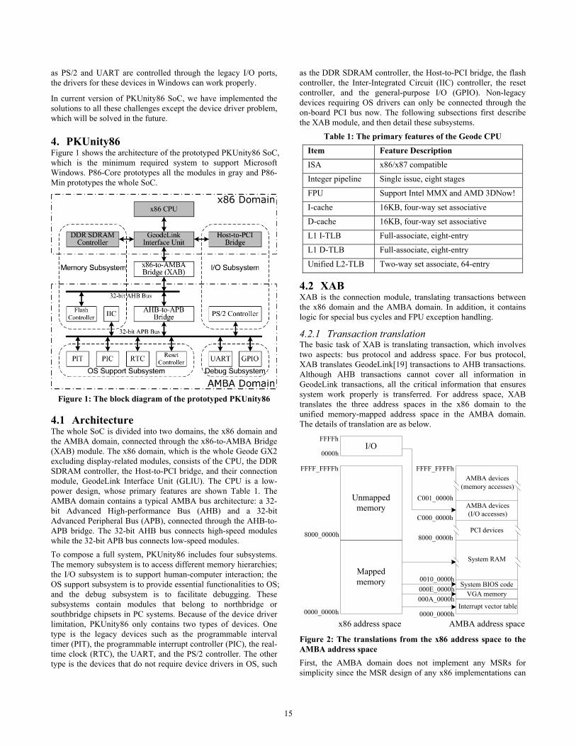
4. PKUnity86 Figure 1 shows the architecture of the prototyped PKUnity86 SoC, which is the minimum required system to support Microsoft Windows. P86-Core prototypes all the modules in gray and P86-Min prototypes the whole SoC.
Figure 1: The block diagram of the prototyped PKUnity86
4.1 Architecture The whole SoC is divided into two domains, the x86 domain and the AMBA domain, connected through the x86-to-AMBA Bridge (XAB) module. The x86 domain, which is the whole Geode GX2 excluding display-related modules, consists of the CPU, the DDR SDRAM controller, the Host-to-PCI bridge, and their connection module, GeodeLink Interface Unit (GLIU). The CPU is a low-power design, whose primary features are shown Table 1. The AMBA domain contains a typical AMBA bus architecture: a 32-bit Advanced High-performance Bus (AHB) and a 32-bit Advanced Peripheral Bus (APB), connected through the AHB-to-APB bridge. The 32-bit AHB bus connects high-speed modules while the 32-bit APB bus connects low-speed modules. To compose a full system, PKUnity86 includes four subsystems. The memory subsystem is to access different memory hierarchies; the I/O subsystem is to support human-computer interaction; the OS support subsystem is to provide essential functionalities to OS; and the debug subsystem is to facilitate debugging. These subsystems contain modules that belong to northbridge or southbridge chipsets in PC systems. Because of the device driver limitation, PKUnity86 only contains two types of devices. One type is the legacy devices such as the programmable interval timer (PIT), the programmable interrupt controller (PIC), the real-time clock (RTC), the UART, and the PS/2 controller. The other type is the devices that do not require device drivers in OS, such
as the DDR SDRAM controller, the Host-to-PCI bridge, the flash controller, the Inter-Integrated Circuit (IIC) controller, the reset controller, and the general-purpose I/O (GPIO). Non-legacy devices requiring OS drivers can only be connected through the on-board PCI bus now. The following subsections first describe the XAB module, and then detail these subsystems.
Table 1: The primary features of the Geode CPU
Item Feature Description
ISA x86/x87 compatible
Integer pipeline Single issue, eight stages
FPU Support Intel MMX and AMD 3DNow!
I-cache 16KB, four-way set associative
D-cache 16KB, four-way set associative
L1 I-TLB Full-associate, eight-entry
L1 D-TLB Full-associate, eight-entry
Unified L2-TLB Two-way set associate, 64-entry
4.2 XAB XAB is the connection module, translating transactions between the x86 domain and the AMBA domain. In addition, it contains logic for special bus cycles and FPU exception handling.
4.2.1 Transaction translation The basic task of XAB is translating transaction, which involves two aspects: bus protocol and address space. For bus protocol, XAB translates GeodeLink[19] transactions to AHB transactions. Although AHB transactions cannot cover all information in GeodeLink transactions, all the critical information that ensures system work properly is transferred. For address space, XAB translates the three address spaces in the x86 domain to the unified memory-mapped address space in the AMBA domain. The details of translation are as below.
I/O0000h
FFFFh
FFFF_FFFFh
0000_0000h
8000_0000h
System RAM
000A_0000h Interrupt vector table
VGA memorySystem BIOS code
000E_0000h0010_0000h
8000_0000h
0000_0000h
C000_0000h
PCI devices
C001_0000h
AMBA devices (memory accesses)
FFFF_FFFFh
AMBA devices(I/O accesses)
x86 address space AMBA address space
Mappedmemory
Unmapped memory
Figure 2: The translations from the x86 address space to the AMBA address space First, the AMBA domain does not implement any MSRs for simplicity since the MSR design of any x86 implementations can
15

be arbitrary. XAB ignores all MSR write transactions. When receiving MSR read transactions, XAB returns a safe value to avoid system crash. Second, as shown in Figure 2, the I/O address space and the memory address space in x86 ISA are mapped to the unified memory-mapped address space of AMBA bus. Interrupt vector table, BIOS code, legacy VGA memory, and system RAM are in the lowest 2GB space to be compatible with PC. The upper 1GB space is allocated to PCI devices. AMBA devices occupy the highest 1GB space. The 64KB I/O address space in x86 ISA is directly mapped to the memory region C000_0000h – C000_FFFFh. PKUnity86 only maps the lowest 2GB memory because 2GB memory is big enough for mobile applications.
4.2.2 Special bus cycles handling When CPU generates special bus cycles, GLIU will forward corresponding messages to XAB. XAB must take corresponding actions according to the messages. The ways how XAB handles different types of special bus cycles are listed as below:
SHUTDOWN: X86 processors generate a SHUTDOWN cycle when it experiences a triple fault condition or internal processor errors. XAB informs the power manager to reset the entire system when receiving a SHUTDOWN cycle.
HALT: X86 processors generate a HALT cycle when a HLT instruction is executed. XAB ignores it directly because no modules in PKUnity86 need to know this message.
WBINVD: X86 processors generate a WBINVD cycle to indicate that the modified lines in L1 data cache have already been written back and the modified lines in external caches should be written back. Since PKUnity86 does not contain external cache, XAB ignores the WBINVD cycle directly.
INTA: X86 processors generate an INTA special cycle to read the interrupt vector number when receiving an interrupt request from the interrupt controller. To be compatible with this interrupt handling mechanism, XAB has a direct connection to the interrupt controller to get the interrupt vector number. When receiving a INTA cycle, XAB pass the interrupt vector number to the CPU. Then, the CPU jumps to the corresponding interrupt service entry.
4.2.3 External FPU exceptions support When a FPU exception occurs, Windows requires a series of interactions between CPU and interrupt controller to handle the exception properly. In PKUnity86, XAB provide supports for these interactions as below: First, when a FPU exception occurs, CPU outputs the active FERR# signal XAB. Next, XAB generates an interrupt request to the interrupt controller. After CPU completes handling the exception, XAB receives an I/O write with the port F0h. Then, XAB deasserts the IGNNE# input signal of CPU to let CPU continue executing from the exception point.
4.3 Memory subsystem The memory subsystem should provide interfaces to access main memory, BIOS flash, and hard disks. To access the main memory, PKUnity86 reuses the DDR SDRAM controller from Geode GX2. An IIC controller is integrated to read the Serial Presence Detect (SPD) information of DDR Dual Inline Memory Module (DIMM). To access the BIOS flash, a flash controller is connected to the AHB bus. Because the prototyped PKUnity86 does not provide direct interfaces to hard disks, the prototype system requires an
off-chip hard disk controller. Furthermore, there are several important design considerations for the memory subsystem. First, as mentioned in Section 3, the memory subsystem must maintain cache coherence by hardware. When DMA transactions access the main memory, the data in the cache might be inconsistent with the data in the main memory. PKUnity86 reuses the GLIU module in Geode GX2 to maintain cache coherence. When the memory accesses from devices go through GLIU, GLIU decides whether to issue a snoop request to the processor cache. If no coherence issue occurs, GLIU route the transactions to the memory controller. Otherwise, GLIU store these transactions temporarily until all coherence issues are solved. Second, the bus protocol between the memory controller and the CPU should support two features to attain high performance. One feature is supporting multiple outstanding transfers, which protects the memory-level parallelism[20] of processor. The other feature is supporting unaligned accesses. Because x86 is a CISC ISA, whose instruction length is variant, many instruction fetches are unaligned. If the bus does not support unaligned accesses, every unaligned access must be split into multiple aligned accesses and hence the performance degrades significantly. Thus, because GeodeLink supports the two features above but AHB does not, we choose the memory controller with the GeodeLink interface. In the future, we will consider updating memory controller IPs with Advanced eXtensible Interface (AXI), which is the only bus protocol in AMBA family that supports the two features above. Third, the memory subsystem should support BIOS shadowing, which is a common technique to speed up BIOS execution. To support BIOS shadowing, PKUnity86 has two memory accessing modes, the normal mode and the shadowing mode. In the normal mode, all read requests to the shadowing memory region are routed to the flash controller while all write requests to this region are routed to the DDR SDRAM controller. Thus, the processor can copy the instructions and the data in BIOS to the DDR SDRAM. In the shadowing mode, both read and write requests to the shadowing memory region are routed to the DDR SDRAM controller so that shadowed BIOS program can execute in the DDR SDRAM.
4.4 I/O subsystem The I/O subsystem contains a PS/2 controller and a Host-to-PCI bridge. The PS/2 controller is connected on the 32-bit APB bus to support keyboard and mouse inputs. The Host-to-PCI bridge is reused from Geode GX2 for on-board functional extension. For the Host-to-PCI bridge, we choose the GeodeLink interface rather than the AHB interface because the GeodeLink can avoid unnecessary address translation. Because AMBA architecture does not provide I/O address space, XAB must translate the I/O address to AMBA memory address, and then Host-to-PCI bridge translates AMBA memory address to PCI I/O address when CPU issues I/O transactions to PCI devices. Since GeodeLink connection can transfer the I/O address directly, using a GeodeLink connection can avoid translating address twice.
4.5 OS support subsystem As mentioned in Section 3, PKUnity86 must make the software interface of timer, interrupt controller and real-time clock compatible with Microsoft Windows. Table 2 lists the reference
16

designs of these OS-related modules. In PKUnity86, all these modules use the APB bus interface so that they can be reused in other AMBA-based SoCs. Since Windows accesses these modules through I/O transactions, XAB translates these I/O transactions to the corresponding AMBA transactions, and then the APB bus route the bus transactions to the corresponding modules.
Table 2: Reference design of OS support modules
Module name Reference design
Programmable Interval Timer Intel 82C54[21]
Programmable Interrupt Controller Intel 8259A[22]
Real-time Clock (RTC) Motorola MC146818A[23]
4.6 Debug subsystem To support both local debug and remote debug, the debug subsystem consists of the GPIO module and the UART module. The outputs of GPIO are connected to Light Emitting Diodes (LEDs) on the PCB board to indicate the current running status. The UART module is for the remote debug feature in GDB and WinDBG tools. We choose an UART IP that has a compatible program interface with Intel 8251[24] to reuse the standard device driver. Besides the above two debug facilities, the CPU has an EJTAG interface to support advanced debugging.
5. P86-Core P86-Core prototypes the x86 domain, which is the whole Geode GX2 excluding display-related modules. Similar to other x86 processors[15], the original RTL design of Geode GX2 contains circuitries that are not suitable for FPGA implementation, such as gated clocks, custom RAMs, and custom ROMs. We modify the RTL code to make it FPGA-synthesizable. Verifying the RTL modification for FPGA implementation is the main purpose of P86-Core. Since P86-Core has similar architecture and BIOS program to Geode GX2, it has the same OS compatibility, supporting Windows XP and previous versions. In this section, we will first describe the emulation platform and the workflow of building P86-Core, and then detail the modifications of the RTL design and the BIOS program.
5.1 Emulation Platform As shown in Figure 3, the P86-Core emulation platform consists of two boards, a Geode SP4GX22 motherboard and a FPGA board. The Geode SP4GX22 motherboard provides the southbridge chipset CS5535[25] and other peripheral interfaces such as IDE socket and USB connector to compose a full computer system. The FPGA board contains a DDR socket, four PCI slots, and two Xilinx Virtex-4 LX200 FPGA device to emulate the x86 domain of PKUnity86. Since both DDR and PCI are industrial standard interfaces that many FPGA boards have, we reuse an existed FPGA board to save the project cost. In addition, a low pin count (LPC) card is plugged on the motherboard to connect the PS/2 keyboard and mouse.
In previous work[14, 15], it is challenging to replace the processor with the FPGA device because the processor communicates with the chipset via the front side bus (FSB). Since FPGA devices and the processor are not pin-compatible, they design a special pin-adapter. For P86-Core, since the connection between the
processor and the chipset is the standard PCI bus, the replacement is simple. We plug out the Geode GX2 chip from the motherboard and use a PCI-to-PCI connector to connect the emulation FPGA device to the southbridge chipset. Besides the PCI connection, several sideband signals such as clock and reset are wired directly between the two boards.
In addition, since the DDR DIMM is moved to the FPGA board, the BIOS program cannot get the DIMM’s SPD information, which is essential to set the DDR SDRAM controller properly. To solve this problem, we choose a DDR DIMM that is the same as the one on the FPGA board and plugged it into the DIMM socket on the motherboard to provide the SPD information. This method avoids modifications of the board and the BIOS program.
Figure 3: The emulation platform of P86-Core
5.2 Workflow
Modificationsfor FPGA
Original RTL
FPGA implementation
Full system emulation
Geode BIOS
Modifications for FPGARTL simulation
P86-Core BIOS
FPGA-synthesizable RTL
Bitstream
Figure 4: The workflow of building P86-Core
17

Figure 4 shows the overall workflow of building the P86-Core prototype. First, we modify the RTL code to make the design FPGA-synthesizable, and then we verify the modifications. Since the modifications are small, we only do module-level equivalence check and system-level connectivity test in RTL simulation using Synopsys VCS 2006.06 simulator. For module-level equivalence check, we traverse all the possible input sequences for each modified module to make sure that the modified modules have equal behavior as the original designs. For system-level connectivity test, we write some assembly programs to test whether the basic interactions between modules are correct. After the RTL code become FPGA-synthesizable and verified, we use Xilinx ISE Design Suite 10.1 to synthesis, place, and route the design and generate the final bitstream file. Meanwhile, we modify the Geode GX2 BIOS to match with the design changes for FPGA. After both the bitstream file and the BIOS are ready, we could run Windows on the emulation platform.
5.3 RTL Modification To make the design FPGA-synthesizable, first, we replace the custom circuits such as RAMs, ROMs, and Phase-Locked Loops (PLLs) with corresponding FPGA primitives. Next, we convert the clock-gating logic to clock-enabling counterparts, because the clock-gating logic will cause failure in timing convergence for FPGA implementations. The details of these two jobs can refer to Wang et al.’s work[15]. Last, because we find that the design requires more resources than a Xilinx Virtex-4 LX200 device can provide, we remove several unused modules such as Built-in Self Test (BIST) circuits to make the whole design fit in a FPGA device. Moreover, the DDR SDRAM controller has to be modified to meet the requirement of FPGA synthesis because the interface logics of DDR SDRAM controller are special. According to the JEDEC DDR specification[26], there are four key requirements about the I/O logic. First, the working clocks of DDR SDRAM devices are three pairs of differential clocks (CLK and CLK_N). Second, the data signals (DQ) and the data mask signals (DM) are transferred at double data rate. Third, DDR SDRAM devices capture the write data using the data strobe signals (DQS), which have a 90-degree phase shift relative to the data signals. Fourth, the data and the data strobe signals returned from DDR SDRAM devices are phase-aligned, so controller should delay the data strobe signals by one-quarter clock cycle to capture the data properly. These four requirements complicate the clock structure of the original DDR SDRAM controller. Since FPGA device does not support complex clock logic, the original DDR SDRAM controller must be modified for FPGA. As shown in Figure 5, we modify I/O logic of DDR SDRAM controller using FPGA primitives. All clocks are derived from the Digital Clock Manager (DCM) [27] module in place of the original clock tree so that the clock delays to all flip-flops are as close as possible. To generate high-quality differential clocks, we replace the non-synthesizable differential pads with the FPGA primitives OBUFDS[27]. For write data output logic, we output the working clock as the DQS signals and generate the write data (FF_W) with an inverted double-frequency clock (CLK_W). Therefore, the data (DQ) and the data mask (DM) are at double data rate and have a 90-degree phase shift relative to the DQS signals. For read data capture logic, since the frequency of the working clock on FPGA, 16.7MHz, is much lower than the
normal frequency, the valid data window is large enough to tolerate on-board skews. Thus, we use a pair of phase-delayed differential clocks, CLK_RP and CLK_RN, to capture the returned data instead of using the DQS signals. The write and read timings of the modified logic are shown in Figure 6.
DCM
CLK90
CLK2X_180
CLK270
CLK
DQS
FF_WD Q
FF_RNQ D
FF_RPQ D
OBUFDSCLK_N
DQ/DM
CLK_RP
CLK_RN
CLK_W
CLK0
Figure 5: The interface logic of the modified DDR SDRAM controller
Figure 6: The write and read timing of the modified DDR SDRAM controller
5.4 BIOS Modification The BIOS program should also be modified to match with the RTL changes. The BIOS modifications are twofold. First, since the frequency of the DDR SDRAM controller, 16.7MHz, is out of the working frequency range of the Delay-Locked Loop (DLL) module on DIMMs, the DLL module cannot work correctly. Thus, we disable the DLL module on DIMMs by setting the related functional register of the DDR SDRAM controller. Second, since P86-Core is only part of Geode GX2, the configuration of the unimplemented modules such as the display controller, the clock manager, and the BIST module, may lead to uncertain results. Thus, we remove or disable these configurations in the BIOS program.
6. P86-Min After P86-Core, we build P86-Min to prototype both the minimum set of PKUnity86 and the PKUnity86 BIOS on a single-board emulation platform. We design the PKUnity86 BIOS because our final products cannot use the Geode BIOS for business reasons. Since both the RTL and the BIOS are new designs, it is challenging to build P86-Min. Therefore, we add a
18

hardware-software co-development stage in our workflow and employ various debug tools at different development stages to facilitate building P86-Min. The goal of P86-Min is to support legacy Windows such as Windows 3.1, Windows 95 and Windows 98. Recent Windows that have higher hardware requirements such as Windows 2000 and Windows XP, will be supported in the future.
6.1 Emulation Platform Since PKUnity86 includes the functionalities of CPU, northbridge, and southbridge, we can prototype it on an single FPGA board without PC motherboard. As shown in Figure 7, P86-Min uses the same type of the FPGA board as P86-Core. The FPGA board contains all the standard I/O interfaces required in PKUnity86 such as DDR slots, PCI slots, BIOS flash, PS/2, and UART. In addition, a IDE card and a video card are plugged in the PCI slots.
Figure 7: The emulation platform of P86-Min
6.2 Workflow Figure 8 shows the overall workflow of building the P86-Min prototype, which consist of three stages: the high-level hardware-software co-development stage, the RTL development stage, and the FPGA implementation stage. At the high-level hardware-software co-development stage, we first develop the draft C++ models of PKUnity86 and the draft PKUnity86 BIOS. Then, we merge both the C++ models and the BIOS program into a x86-based full-system simulator, and test whether Windows could run correctly based on them. We keep revising the models and the BIOS program until we successfully run Windows in the Bochs simulator. After that, the BIOS program implements all the core functionalities for Windows compatibility and our BIOS designers can add extra functionalities based on the core BIOS. At the RTL development stage, we develop the RTL code by referring to the final C++ models and merge the x86 domain RTL, which has been verified in P86-Core. At the FPGA implementation stage, we implement the RTL design on the FPGA devices. Owing to the limitation of FPGA resources, we have to implement the whole design into two separate FPGA devices. One device only implements the processor while the other device implements the rest parts. Finally, we could run
Windows using the bitstream files and the BIOS code on the emulation platform.
FPGA implementation
High-level HW/SW co-development
RTL development
Bitstream
Core PKUnity86 BIOS
Draft PKUnity86 BIOS
Draft PKUnity86C++ models
Final PKUnity86C++ models
PKUnity86 RTL
x86 domainRTL
Full system emulation
Final PKUnity86 BIOS
BIOS improvement
Figure 8: The workflow of building P86-Min
6.3 High-level Co-development We build the high-level hardware-software co-development platform using Bochs simulator[28]. Bochs is an x86 full-system simulator that is capable of running off-the-shelf Microsoft Windows and many desktop applications. To build the high-level model of PKUnity86, we reuse the x86 processor model and the memory model in Bochs, create the high-level model of XAB and modify several device models in Bochs such as the keyboard, the mouse, the timer, the interrupt controller, the real-time clock. All these models are written in C++. Since each model only implements the software interface and the basic behaviors, it takes less time than the RTL design. After the high-level models are ready, we can develop the PKUnity86 BIOS in the simulator. We gain the several benefits from the high-level co-development platform. First, the co-development platform allows quick design modifications to reduce iteration cycle length. Because the public documents of Windows do not cover all detailed requirements about hardware and BIOS, we have to repeatedly test and modify our designs to get the final design. High-level models in the simulator are easier to debug than RTL design on FPGA. Second, since Bochs is an open-source simulator, both the device model and the BIOS in Bochs are good reference designs, which provide much concrete information for PKUnity86. Third, the co-development platform allows the BIOS development to be parallel with the RTL development. In traditional flow, most BIOS developing jobs cannot start until hardware design is ready. Since the behavioral model has the same software interface as the final design, BIOS developers can test the BIOS program in the full-system simulator before the detailed hardware design is ready.
6.4 Debug Support Compared with P86-Core, P86-Min involves massive debug tasks because of the significant architecture changes. As shown in
19
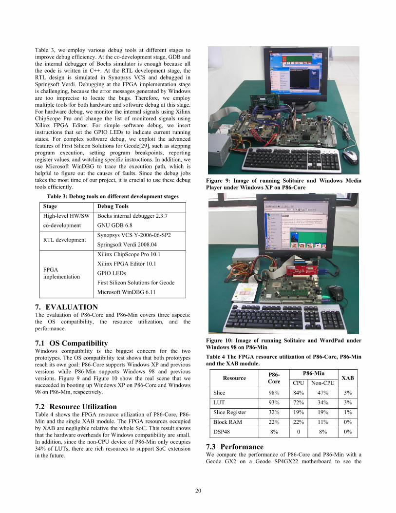
Table 3, we employ various debug tools at different stages to improve debug efficiency. At the co-development stage, GDB and the internal debugger of Bochs simulator is enough because all the code is written in C++. At the RTL development stage, the RTL design is simulated in Synopsys VCS and debugged in Springsoft Verdi. Debugging at the FPGA implementation stage is challenging, because the error messages generated by Windows are too imprecise to locate the bugs. Therefore, we employ multiple tools for both hardware and software debug at this stage. For hardware debug, we monitor the internal signals using Xilinx ChipScope Pro and change the list of monitored signals using Xilinx FPGA Editor. For simple software debug, we insert instructions that set the GPIO LEDs to indicate current running states. For complex software debug, we exploit the advanced features of First Silicon Solutions for Geode[29], such as stepping program execution, setting program breakpoints, reporting register values, and watching specific instructions. In addition, we use Microsoft WinDBG to trace the execution path, which is helpful to figure out the causes of faults. Since the debug jobs takes the most time of our project, it is crucial to use these debug tools efficiently.
Table 3: Debug tools on different development stages
Stage Debug Tools
High-level HW/SW co-development
Bochs internal debugger 2.3.7 GNU GDB 6.8
RTL development Synopsys VCS Y-2006-06-SP2 Springsoft Verdi 2008.04
FPGA implementation
Xilinx ChipScope Pro 10.1 Xilinx FPGA Editor 10.1 GPIO LEDs First Silicon Solutions for Geode Microsoft WinDBG 6.11
7. EVALUATION The evaluation of P86-Core and P86-Min covers three aspects: the OS compatibility, the resource utilization, and the performance.
7.1 OS Compatibility Windows compatibility is the biggest concern for the two prototypes. The OS compatibility test shows that both prototypes reach its own goal: P86-Core supports Windows XP and previous versions while P86-Min supports Windows 98 and previous versions. Figure 9 and Figure 10 show the real scene that we succeeded in booting up Windows XP on P86-Core and Windows 98 on P86-Min, respectively.
7.2 Resource Utilization Table 4 shows the FPGA resource utilization of P86-Core, P86-Min and the single XAB module. The FPGA resources occupied by XAB are negligible relative the whole SoC. This result shows that the hardware overheads for Windows compatibility are small. In addition, since the non-CPU device of P86-Min only occupies 34% of LUTs, there are rich resources to support SoC extension in the future.
Figure 9: Image of running Solitaire and Windows Media Player under Windows XP on P86-Core
Figure 10: Image of running Solitaire and WordPad under Windows 98 on P86-Min Table 4 The FPGA resource utilization of P86-Core, P86-Min and the XAB module.
P86-Min Resource P86-
Core CPU Non-CPU XAB
Slice 98% 84% 47% 3%
LUT 93% 72% 34% 3%
Slice Register 32% 19% 19% 1%
Block RAM 22% 22% 11% 0%
DSP48 8% 0 8% 0%
7.3 Performance We compare the performance of P86-Core and P86-Min with a Geode GX2 on a Geode SP4GX22 motherboard to see the
20

performance impacts of the architectural changes. All the three platforms run at 33MHz. We run three benchmarks, Dhrystone 2.1, STREAM 5.8[30], and HDBench 1.1[31], under Windows 98 to evaluate the performance of CPU, memory, and disk, respectively. In addition, we compare the booting up time of Windows 98 for overall performance. To eliminate the non-deterministic of the real system, we run each benchmark for 5 times and take the average. As shown in Figure 11, three platforms have similar CPU performance and memory performance, and P86-Min has better disk performance and booting up speed than Geode GX2 and P86-Core. This result is as expected because the most performance-related part of PKUnity86 is the x86 domain, which have no architectural changes. The different hard disk controller results in the performance enhancement of P86-Min. The hard disk controller on P86-Min has a larger data buffer than the one integrated in CS5535. The results show that the architectural changes do not degrade the system performance.
0
0.2
0.4
0.6
0.8
1
1.2
Dhrystone STREAM HDBench Win98
Geode GX2 P86-Core P86-Min
Figure 11 The normalized benchmark grades and OS booting up time of Geode GX2, P86-Core, and P86-Min
8. CONCLUSIONS AND FUTURE WORK PKUnity86 is the first AMBA-based and Windows-compatible SoC. It can both support flexible SoC extension by reusing the abundant AMBA IP resources and exploit the massive PC software resources. This paper presents two FPGA prototypes of PKUnity86: P86-Core and P86-Min. P86-Core prototypes the core of PKUnity86 while P86-Min prototypes the minimum set of PKUnity86. By successfully running Windows on them, we demonstrate that the gap between ARM-based SoC and PC system can be resolved by specific hardware and software designs. Furthermore, the evaluation results show that PKUnity86 achieves Windows compatibility with small hardware overheads and no performance loss. In the future, we will improve PKUnity86 to support recent Windows such as Windows XP, Windows Vista, and Windows 7.
9. ACKNOWLEDGMENTS We wish to thank AMD for transferring the x86 processor technique. Special thanks go to former AMD CEO Hector Ruiz and AMD senior vice president Karen Guo for their concerns and supports for this research. We also appreciate the help of AMD colleagues Rich McCloskey, Don Zhao, Thomas Lukas, and Jennifer Yuan. In addition, we thank all the teachers and students in Microprocessor Research and Development Center of Peking University who have helped this research.
REFERENCES [1] Aaron Weiss, “Ultra-mobile PCs: slow but small and
specialized computers are a surprise hit for the industry,” netWorker, 12(2), p. 22-30, 2008.
[2] Brad Smith, “ARM and Intel Battle over the Mobile Chip's Future,” Computer, 41(5), p. 15-18, 2008.
[3] Michael Keating and Pierre Bricaud, “Reuse methodology manual: for system-on-a-chip designs (3rd Edition)”: Springer Publishing Company, Incorporated, 2007.
[4] AMD Inc., “AMD Geode™ GX Processors Data Book,” 2005. [5] “AMBA overview”. http://www.arm.com/products/solutions/
AMBAHomePage.html [6] Power.org, Embedded Bus Architecture Report
http://www.power.org/resources/downloads/ Embedded_Bus_Arch_Report_1.0.pdf, 2008.
[7] AMD Inc., “AMD Geode™ SC1100 Processor Data Book,” 2004.
[8] Intel Corp., The embedded processor for an embedded world, 2008.
[9] Aeroflex Gaisler AB., “LEON3 multiprocessing CPU core,” 2008.
[10] CAST Inc., “CAST C68000-AHB 32-bit Microprocessor Core”.
[11] “SuperH RISC engine Family”. http://www.renesas.com/ [12] “Easy Integration with Standard System Interfaces”.
http://www.tensilica.com/products/diamond-controllers/amba-bridges.htm
[13] Roland E. Wunderlich and James C. Hoe. “In-system FPGA prototyping of an Itanium microarchitecture,” In ICCD '04: Proceedings of IEEE International Conference on Computer Design. San Jose, CA, United states, 2004.
[14] Shih, Peter Yiannacouras, Rolf Kassa, et al. “An FPGA-based Pentium in a complete desktop system,” In FPGA '07: Proceedings of the 2007 ACM/SIGDA 15th international symposium on Field programmable gate arrays. Monterey, California, USA, 2007.
[15] Perry Wang, Jamison Collins, Christopher Weaver, et al. “Intel Atom processor core made FPGA-synthesizable,” In FPGA '09: Proceedings of the ACM/SIGDA international symposium on Field programmable gate arrays. Monterey, California, USA, 2009.
[16] Intel Corp., “Pentium® Processor Family Developer’s Manual,” p. 6-32, 1997.
[17] Intel Corp. and Microsoft Corp., “PC 2001 System Design Guide,” 2000.
[18] Intel Corp., “Software and Hardware Considerations for FPU Exception Handlers for Intel Architecture Processors,” 1997.
[19] AMD Inc., “AMD GeodeLink™ Architecture - Processor Architecture Facilitates Integration, Efficiency, Performance,” Editor. Vol., 2003.
[20] Yuan Chou, Brian Fahs, and Santosh Abraham. “Microarchitecture optimizations for exploiting memory-level parallelism,” In ISCA '04: Proceedings of 31st Annual
21

International Symposium on Computer Architecture. Munich, Germany, 2004.
[21] Intel Corp., 82C54 CHMOS Programmable Interval Timer, 1994.
[22] Intel Corp., 8259A Programmable Interrupt Controller, 1988. [23] Motorola Inc., “Real-time Clock Plus RAM,” 1984. [24] Intel Corp., “8251A Programmable Communication
Interface,” 1986. [25] AMD Inc., AMD Geode™ CS5535 Companion Device Data
Book, 2005. [26] JEDEC Solid State Technology Association, JEDEC
Standard - Double Data Rate (DDR) SDRAM Specification, 2003.
[27] Xilinx Inc., Virtex-4 FPGA User Guide, 2008. [28] “Bochs IA-32 Emulator Project”.
http://bochs.sourceforge.net/ [29] First Silicon Solutions, Technical Data for System Navigator
OE for AMD Geode GX2 Processors [30] J. D. McCalpin., “Memory bandwidth and machine balance
in high performance computers,” IEEE Computer Society Technical Committee on Computer Architecture (TCCA) Newsletter, 1995.
[31] “HDBench”. http://www.hdbench.net/
22