IMPROVING REUSABILITY IN SOC PROJECT VERIFICATION ...
59
i Mohamed Mohamed IMPROVING REUSABILITY IN SOC PROJECT VERIFICATION FLOW Faculty of Information Technology and Communication Sciences Master of Science Thesis June 2019 brought to you by CORE View metadata, citation and similar papers at core.ac.uk provided by Trepo - Institutional Repository of Tampere University
-
Upload
khangminh22 -
Category
Documents
-
view
0 -
download
0
Transcript of IMPROVING REUSABILITY IN SOC PROJECT VERIFICATION ...
i
Mohamed Mohamed
IMPROVING REUSABILITY IN SOC PROJECT VERIFICATION FLOW
Faculty of Information Technology and Communication Sciences Master of Science Thesis
June 2019
brought to you by COREView metadata, citation and similar papers at core.ac.uk
provided by Trepo - Institutional Repository of Tampere University

ABSTRACT
Mohamed Mohamed: Improving Reusability in SoC Project Verification Flow. Master of Science Thesis Tampere University Master’s Degree Programme in Information Technology June 2019
This main target of the thesis is to increase the level of reuse done in SoC verification projects. The verification takes the biggest amount of time in the project duration. This thesis contains 3 main parts. The first one intro-duces the reuse in SoC and explains its different dimensions as a literature study. This work is done as a background for the next two phases.
During the second part of this work, a practical example for verification reuse was implemented as a part of a SoC project. The reuse was applied vertically, where an IP-level testbench was altered to become reusable, then it was reused in a subsystem-level testbench. Additionally, analysis was done in order to know how much effort was re-used in the project. Results show that 85% of the code was saved when the reuse was applied.
Regarding the third part of the thesis, several interviews were conducted with SoC verification experts who work at Nokia with a range of experience in the field from 7 to 20 years. These interviews were done in order to collect some information about how to improve the reusability in SoC project verification flow. The point from these inter-views is to get knowledge from hands-on-experience. The interviewees agreed on the importance for applying the reuse in every verification project from the beginning of the project. They also agreed on maintaining the hierarchical level of reuse, which means IP-level TB would be a sub-environment of subsys-tem-level TB and subsystem-level is a sub-environment of SoC-level TB. Moreover, some ideas about the future work are introduced here. Those are proposed according to the knowledge gained from the research and from the interviews with the experts.
Keywords: System on Chip, reuse, functional verification, IP, subsystem, Systemverilog, UVM, testbench, DUT.
i
PREFACE
I would like to have this opportunity to show my gratitude to everyone who has helped,
encouraged, or accompanied me during the journey of doing my master’s degree.
First of all, I can't thank my work colleague Miika Jokinen enough, not only for mentoring
me very well during this work, but also, for being supportive by answering any technical
question.
My appreciation to my supervisor, Prof. Timo Hämäläinen for being flexible to support
this work. I would like to thank Antti Rautakoura for his fruitful review on thesis, it really
improved the content and added some strength to the work. Moreover, he was involved
in finding me a topic for the thesis.
I would also like to thank my team lead Janne Helkala for supporting me to get this work
done ASAP and for helping in choosing the topic. Moreover, I want to thank my line
manager Sakari Patrikainen for encouraging me to get this thesis done, for helping in
finding an internal supervision for the work and for being flexible with managing my time
between the thesis and the work. I would like to thank my colleague Anuj Rawat for
helping me getting the practical part of this work done quickly, it was easy to work with
him. Additionally, I want to thank all of my colleagues who contributed in the interviews
section, they facilitated the process of the interviews a lot by being flexibly available.
A special and sincere gratitude for my beloved family who never stopped encouraging
me, my mother, my father, and my sister. Additionally, my partner who has been with me
during the stressful times between working and writing the thesis simultaneously. Last
but not least, my extended family who always wish me nice wishes.
I would show deep gratitude to all my friends around different countries who always
support me. Lastly yet importantly, I would like to thank my first supervisor at home (in
Egypt) Dr. Ahmed Shalaby, who always encouraged and helped us to have better oppor-
tunities to learn and to put hands-on experience through practical projects given the lim-
ited resources.
Tampere, Finland, 4.6.2019
Mohamed Khalifa Mohamed.
CONTENTS 1. INTRODUCTION .................................................................................................... 1
2. INTRODUCTION TO SOC FLOW ......................................................................... 3
2.1 Abstraction layers of SoC design ................................................................... 5
2.2 SoC development flow ................................................................................... 7
2.3 SoC verification flow ..................................................................................... 8
2.3.1 Verification goals ............................................................................. 8
2.3.2 Verification management ................................................................. 9
2.3.3 Simulation ...................................................................................... 11
2.4 SoC economics ............................................................................................. 12
3. REUSE IN SOC ...................................................................................................... 14
3.1 General reuse paradigms. ............................................................................. 14
3.1.1 Horizontal reuse. ............................................................................ 15
3.1.2 Vertical reuse. ................................................................................ 16
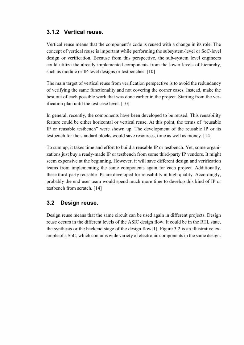
3.2 Design reuse. ................................................................................................ 16
3.2.1 IP definition.................................................................................... 17
3.2.2 IP integration in a SoC design........................................................ 18
3.2.3 Special considerations for IP reuse. ............................................... 19
3.3 VERIFICATION REUSE ............................................................................ 20
3.3.1 Importance of verification reuse .................................................... 20
3.3.2 Universal Verification Methodology. ............................................ 21
3.3.3 VIP definition, requirements, and importance. .............................. 22
3.3.4 IP-level verification environment reuse. ........................................ 24
3.4 Documentation. ............................................................................................ 27
3.5 Cost of reuse. ................................................................................................ 28
4. IMPLEMENTATION ............................................................................................. 29
4.1 Introduction. ................................................................................................. 29
4.2 Main phases of reuse. ................................................................................... 30
4.3 Testbench evolution towards reusability. ..................................................... 30
4.3.1 Structure of tut_ip’s old TB. .......................................................... 30
4.3.2 Testbench development.................................................................. 32
4.4 Reusable environment’s services. ................................................................ 35
4.5 Integration steps. .......................................................................................... 36
4.6 Special considerations. ................................................................................. 38
5. REUSABILITY LEVERAGE FOR IDEAL SOC PROJECT FLOW.................... 39
5.1 Analysis for the outcome of the reuse. ......................................................... 39
5.2 Reasons for IP-level TB integration. ............................................................ 39
5.3 Integration results and analysis. ................................................................... 40
6. CONDUCTING INTERVIEWS AND FUTURE WORK ..................................... 42
6.1 Interviews procedures. ................................................................................. 42
6.2 Interviews’ questions and answers. .............................................................. 42
6.3 Future work. ................................................................................................. 46

iii
7. CONCLUSION ....................................................................................................... 47
8. REFERENCES ........................................................................................................ 48
LIST OF FIGURES
Figure 2.1. An example of a SoC components. ................................................................. 3
Figure 2.2. Shows the difference between a modern and an old cell phone in terms
of the effect of the large-scale integration[33].......................................... 4
Figure 2.3. Digital design levels of abstraction. [37][36][35] ........................................ 6
Figure 2.4. SoC flow stages starting from customer requirements till chip
fabrication [10]. ........................................................................................ 8
Figure 2.5. An example to illustrate the verification management flow. ........................ 11
Figure 2.6. Shows break-even volume point where the cost of FPGA and ASIC are
alike. ........................................................................................................ 13
Figure 3.1. Component A is horizontally reused in different chips. ............................... 14
Figure 3.2. An illustrative figure of connected IPs and peripherals in a SoC [11]. ...... 17
Figure 3.3. A simple graph illustrates a comparison among the different flavors of
IPs. ........................................................................................................... 18
Figure 3.4. An example for UVM testbench architecture. [2] ........................................ 22
Figure 3.5. Block level verification environment [30]. ................................................... 26
Figure 3.6. Top verification environment reuses block-level environment [30]. ........... 26
Figure 4.1. General architecture for IP-level testbench (tut_ip). ................................... 29
Figure 4.2. High level view for the new TB architecture. ............................................... 32
Figure 4.3. An example for environment configurations setting function in tut_ip’s
base test. .................................................................................................. 33
Figure 4.4. New edition of tut_ip’s TB after the modifications. ..................................... 34
Figure 4.5. Sample code for setting the environment configurations. ............................ 37
Figure 4.6. An example for constructing the reused environment inside another
environment. ............................................................................................ 37
v
ABBREVIATIONS
ADC Analog to digital converter
API Application program interface
ASIC Application specific integrated circuit
AXI Advanced extensible interface
BFM Bus functional model
CPU Central processing unit
DAC Digital to analog converter
DMA Direct memory access
DUT Design under test
EDA Electronic design automation
FPGA Field programmable gate array
FSM Finite state machine
GLS Gate level simulation
GPIO General purpose input/output
HDL Hardware description language
I/O Input/output
I/P Input
IC Integrated circuit
IP Intellectual property
O/P Output
OOP Object oriented programming
PCB Printed circuit board
PLL Phase locked loop
RAL Register abstraction layer
RAM Random access memory
RTL Register transfer logic
SoC System on chip
SPI Serial peripheral interface
SVA Systemverilog assertions
TB Testbench
UPF Unified power format
UVM Universal verification methodology
VHDL Very high speed integrated circuit hardware description language
VIP Verification intellectual property
VLSI Very large scale integration

1
1. INTRODUCTION
Complex digital electronic systems have become ubiquitous. They can be seen every-
where as smart hand watches, computers, smart TVs, smart phones, video games, etc. On
reality, digital systems have invaded the lives of most of the people. Availability of digital
systems everywhere drove the need for making them as small as possible, power efficient
and having lots of functionalities. Accordingly, technology has evolved through the re-
cent years in order to integrate complex digital systems on a tiny chip, and those chips
are called system on chips (SoCs). [49]
SoCs are growing in complexity and getting involved in lots of applications, in accord-
ance, their design as well as their verification are getting more challenging [49]. There-
fore, applying concepts such as reusability have become essential in the SoC industry in
order to accelerate the project time line and to optimize the project’s resources [49]. How-
ever, the reusability sometimes is not applied properly for the sake of the project. This
work studies the theoretical concepts of reusability in SoC design and verification with
emphasis on the latter. Then, it seeks for identifying the possible issues that can slow
down the project flow from reusability perspective. Besides, it gives some practical guide-
lines collected from industry experts, who work at Nokia for applying the reusability in
ideal SoC verification projects.
This thesis work is done at Nokia, SoC department in Tampere, Finland. Thesis work was
done in three phases. For the first phase, a literature review in the area of SoC design and
verification reuse was conducted. For the second phase, a part of a project was imple-
mented as an example for applying reuse in that SoC verification project. The third phase
of the thesis is documenting some interviews were conducted with verification experts.
Those interviews were done in order to collect information from years of hands-on-expe-
rience and those kinds of information are hard to collect from scientific papers as they are
industry related, which means that most of the work done in the companies is not pub-
lished in international conferences or books.
The thesis is organized as follows. Chapter 2 introduces the general SoC project flow in
an organization. It also emphasizes on the details of the SoC verification flow. Addition-
ally, it discusses the economics of the SoC organizations. Chapter 3 gives an introduction
to the meaning of reusability in general, the reusability metrics, and how did it start to be
applied in SoC projects with emphasis on verification reuse. It discusses the concepts
applied for design reuse and mentions the different general reuse paradigms. Besides, it
introduces the reusability in SoC verification projects and how to empower the reusability
in SoC verification. Moreover, it gives some information based on research about the

economics of reuse. Chapter 4 illustrates a documentation for a project that is conducted
at Nokia, which is considered as a case study for applying reusability in SoC verification.
Chapter 4 is considered as the core and the practical implementation of this work. In
chapter 5, an analysis for the work that has been done in chapter 4 is conducted in order
to show the benefits of the work. Furthermore, interviews for verification experts were
documented in questions and answers. At the end of that chapter, some improvement
ideas are introduced for the future work based on the conducted research, the work expe-
rience gained from implementing this work, and the interviews done with the experts.
Chapter 6 gives a conclusion for this thesis.

3
2. INTRODUCTION TO SOC FLOW
SoC is basically an electronic chip, which contains complex electronic systems. An elec-
tronic system is a group of electronic components where they are interacted altogether to
form a unified entity in order to perform a dedicated functionality. This system could be
a smart phone or an application specific system such as a Bluetooth chip inside a mobile
phone. Typical SoC design contains embedded processors, memory blocks, hardware ac-
celerators, analog blocks such as analog to digital converters, digital to analog converters
(ADCs and DACs) and a phase locked loop (PLL), communication protocols, inputs and
outputs (I/Os) and other electronic components as shown in Figure 2.1. An example of a
SoC components. A SoC subsystem is a group of individual electronic blocks, which are
combined to form a specific functionality. The subsystem should be configurable. SoC
can have integrated complex subsystems together on the same integrated circuit (IC).
Very large scale integration (VLSI) is the process of making the IC by integrating multi-
ple electronic systems on the same chip. A SoC product creation requires engineers from
different and interdisciplinary backgrounds. For example, the same SoC project has dig-
ital designers, analog and mixed-signal designers, software engineers, embedded systems
engineers and hardware verification engineers. Having this variety of fields in the same
project, it is recommended for the engineers to have a background in different fields.
[31][1]
Figure 2.1. An example of a SoC components.

There are two approaches to implement a SoC. The first one is on a field programmable
gate array (FPGA). The second one is on Application Specific Integrated Circuit (ASIC).
FPGA is a reconfigurable chip that could implement an application, then it could be re-
configured to perform another application. Regarding ASIC design, the IC is designed
for a task, then it is fabricated, and its hardware could not be modified after fabrication.
Both FPGA and ASIC design have their advantages and disadvantages. At the beginning
of an IC project, the system architects decide whether they will use FPGAs or ASICs
according to the project resources. Those decisions are based on some metrics such as:
the cost of the product, the area, the performance, and the power consumption. [32] [34]
There are multiple benefits to have large system on a single chip. An example for con-
ventional systems could be the discrete electronic chips that are connected on a Printed
Circuit Board (PCB). The cost of the product is relatively reduced as there are no multiple
chips for each subsystem to be assembled. Moreover, the inter-component latency among
the connected blocks in the chip is relatively low. Additionally, the operating frequency
for the system could be higher comparing to the conventional systems used before the
SoC. Two pictures for different version of a phone with similar functionality are shown
in Figure 2.2. The lower one is more modern than the upper one. This comparison is to
show that large scale integration leads to much fewer components used on the same board.
[33]
Figure 2.2. Shows the difference between a modern and an old cell phone in terms of
the effect of the large-scale integration[33].

5
2.1 Abstraction layers of SoC design
In IC area, abstraction means the amount of information that is hidden within an entity.
Understanding the importance of each abstraction layer as well as the differences among
them is important. The upper levels of abstraction are hiding more implementation details
than the lower levels of abstraction. According to the increasing complexity of the digital
systems, many abstraction layers are generally used through the design cycle. Those main
levels of abstraction in digital design flow are:
1- Specification and architecture level.
2- Algorithm level.
3- Register Transfer Level (RTL).
4- Gate level.
5- Transistor level. [38][34]
The specification level explains the main functionality of the chip. It defines its inputs
and outputs. The architecture level specifies the main resources and the major connections
of the chip. It also defines its expected performance. [38][34]
At the algorithm level of abstraction, the functionality of the system is implemented in a
high-level language. No details regarding the design are mentioned in this abstraction
layer. Usually considerations for timing and performance are taken into account at this
level. The implemented algorithm is usually used for verification purposes as a reference
model against the synthesized design. [38][34]
In RTL, the logic functionality of the system with bit-level accuracy is described in a
hardware description language (HDL). There are two widely used HDLs in this level of
abstraction; VHDL and Verilog. The RTL designers implements the design in the form
of finite state machines and logic description. RTL implementation has to be synthesiza-
ble. A synthesizable code means that the synthesis tool can translate it into real logic
gates, registers or memories. However, RTL implementation is technology independent.
In some cases, RTL implementation is technology depended if the HDL code instantiates
some technology specific logic blocks such as memories or interfaces. [38][34]
Gate level abstraction layer describes the design in real logic gates. These logic gates are
generated through a synthesis tool. The synthesis tool takes 3 inputs, the RTL code, the
design constraints and the technology files. Therefore, this level of abstraction is technol-
ogy dependent. [38][34]
Transistor level is the lowest abstraction layer of the VLSI design. It shows how the gates
are physically implemented on the transistor level. This level comes after the layout pro-
cess of the gate level design. [38] [34]

In digital systems, there are Electronic Design Automation (EDA) tools that are respon-
sible for automating the whole process starting from RTL till physical implementation to
the transistor level. [38][34]
Figure 2.3. Digital design levels of abstraction. [37][36][35]

7
2.2 SoC development flow
SoC product cycle starts from the customer requirements. The customer could be either
from the same organization or external. The specification could be documented after the
customer requirements are collected. The architect then decides how the design will be
implemented, so that it meets the specification. Design initial specification may evolve
during the development process. Accordingly, the implementation and the verification
engineers should be ready for these changes in the specification. [38]
Design entry into a digital system would be using, either RTL code or schematic design
via connecting ready to use logic blocks. After that comes the logic synthesis step. In this
step, a logic synthesis tool takes the HDL code as an input to generate a netlist. The netlist
is the interpretation of the logic components and how they are connected. Then, the
backend part of the process comes, where the design is placed and routed on the silicon
die. EDA tools play an important role in the process. They estimate the chip area, the
timing and the power consumption. After that, the design is either fabricated if the taken
approach is ASIC or executed on FPGA if the design approach is FPGA. Then the design
is tested before it is delivered to the customer. [38]
According to Figure 2.4. SoC flow stages starting from customer requirements till chip
fabrication [10], there is one critical phase in the SoC flow that was not mentioned earlier,
which is the functional verification. Functional verification is a major challenge in SoC
flow. Design might not proceed from frontend to backend until it is functionally verified.
Functional verification has many detailed steps will be discussed later in this chapter.
However, the main roles for functional verification are: to ensure that RTL is working
according to specification of the design and to ensure that the designers did not miss any
corner case, while implementing the functionality. Detection of wrong or missing func-
tionality is a challenging task in nowadays complex systems. Therefore, verification en-
gineers are part and parcel of the SoC development team. [10]
After chip fabrication, samples of the chip are sent to the design company and the product
is packaged and tested with real life scenarios and applications. Some companies fabricate
their own chips. Usually, the corner cases that are missed at the functional verification
stage, should be discovered by the testing environment. Then, a feedback is sent to the
designers to make the fixes, then the chip is refabricated, and this happens occasionally.
Those bugs that are found at this stage cost a lot of money as well as time. To avoid this,
extra effort and techniques should be done at the functional verification stage. [10]

Figure 2.4. SoC flow stages starting from customer requirements till chip fabrication
[10].
2.3 SoC verification flow
2.3.1 Verification goals
Verification is an essential stage of the SoC project and takes most of its time [12]. Hence,
verification needs to have a strategy to illustrate how the verification goals will be met.
Functional verification is done independently of the design development. And it is pre-
ferred that it is done simultaneously with the design. Verification engineers work in the
project is recommended to start from the first day just like the design engineers.
Strategic goals of the verification project are:
To ensure that the design matches the specification.
To give high predictability for the verification activities through the pro-
ject, hence, the project schedules could be met.
To provide clear and practical verification cycles.
In order to obtain a specification matching design, it is essential for the verification engi-
neers to understand the design features. Therefore, there should be a link between the
9
verification activities through the test plan and the design features. Accordingly, verifi-
cation management for the project should be considered to address those goals. [14]
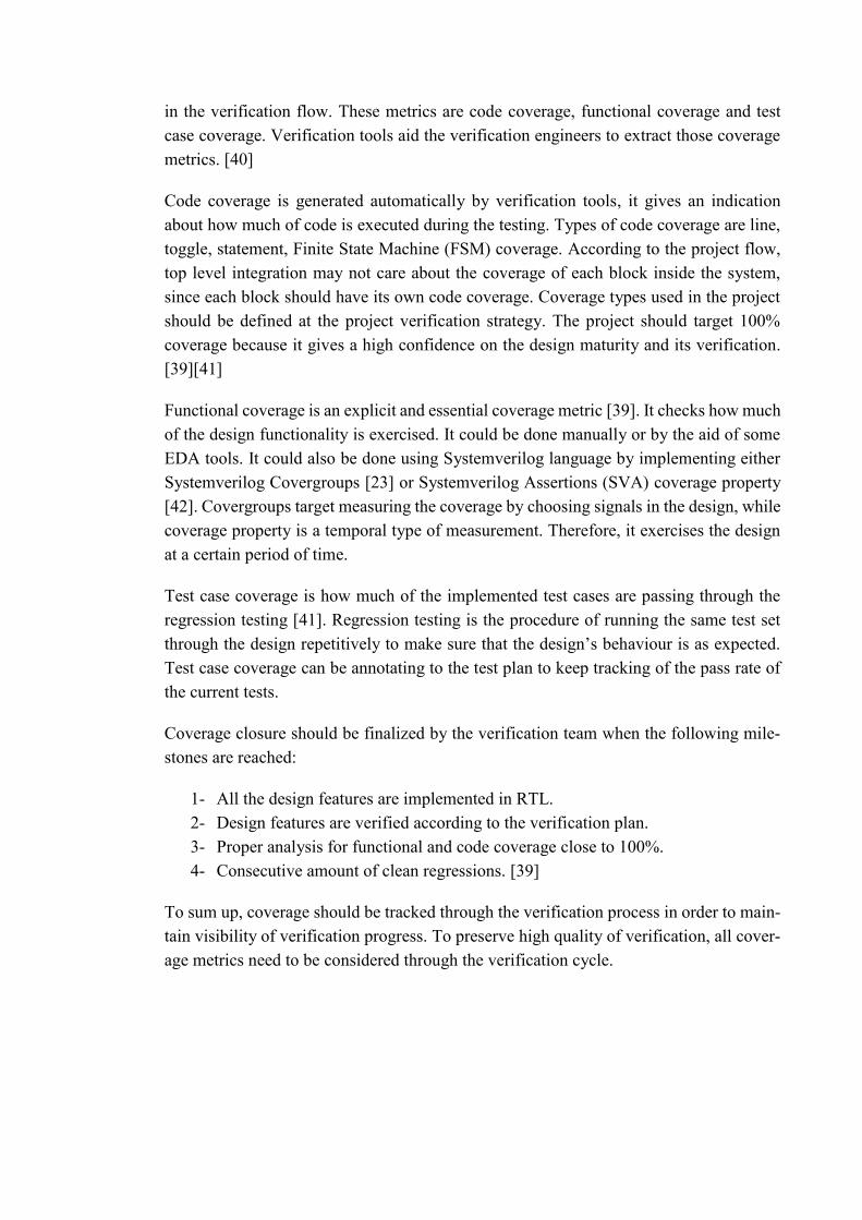
2.3.2 Verification management
Verification management is providing a structure for the verification flow starting from
the planning, until the verification results. Design features consist of the design require-
ments and the characteristics. Those features are linked with the verification coverage
metrics. The verification flow loop could be closed according to some good coverage
results corresponding to the verification plan. According to this way, the verification flow
could give an indication about the verification status. A visual example for verification
management flow is shown in Figure 2.5. [39]
2.3.2.1 Feature collection
Feature collection is the first step in the verification flow. The design requirements are
collected to form the verification plan. Feature collection could be interpreted as a hier-
archical task. Design features are typically more detailed than the design requirements,
hence, one requirement could be linked to multiple features. For quality assurance pur-
poses, design requirements should be linked with relevant test cases for each feature. [39]
2.3.2.2 Verification plan
Verification plan is considered as the essential working document in verification man-
agement flow. Typically, verification plan is a document, which contains the design fea-
tures. Moreover, verification plan should have the test cases with their description. There
should be a category division in terms of verification solution for each feature according
to its category so that the plan becomes clear and organized. For example: simulation,
formal verification, and emulation. Those divisions give an intuition about the verifica-
tion status and coverage. This process basically forms a feedback loop for verification
flow. This loop is named back annotation. Basically, block level features are verified at
their block level testbench, while top level features are verified at their top level testbench
as well. However, it is important to understand that sometimes, block level features could
be transferred to top level. Moreover, some block level features are combined together to
form some features that are observable only on top level. [39][40] [43]
2.3.2.3 Verification plan back annotation
Typical verification tools generate simulation logs, coverage reports, and waveforms.
Back annotation is done by verification management tool, since it takes those logs and
coverage reports as inputs. Then, the back annotation tool generates information that
could be inserted to an excel spread sheet. [43]
2.3.2.4 Coverage
Coverage is essential for function verification since it gives annotation about the state and
the maturity of the design. Coverage has different metrics and each of them are important
in the verification flow. These metrics are code coverage, functional coverage and test
case coverage. Verification tools aid the verification engineers to extract those coverage
metrics. [40]
Code coverage is generated automatically by verification tools, it gives an indication
about how much of code is executed during the testing. Types of code coverage are line,
toggle, statement, Finite State Machine (FSM) coverage. According to the project flow,
top level integration may not care about the coverage of each block inside the system,
since each block should have its own code coverage. Coverage types used in the project
should be defined at the project verification strategy. The project should target 100%
coverage because it gives a high confidence on the design maturity and its verification.
[39][41]
Functional coverage is an explicit and essential coverage metric [39]. It checks how much
of the design functionality is exercised. It could be done manually or by the aid of some
EDA tools. It could also be done using Systemverilog language by implementing either
Systemverilog Covergroups [23] or Systemverilog Assertions (SVA) coverage property
[42]. Covergroups target measuring the coverage by choosing signals in the design, while
coverage property is a temporal type of measurement. Therefore, it exercises the design
at a certain period of time.
Test case coverage is how much of the implemented test cases are passing through the
regression testing [41]. Regression testing is the procedure of running the same test set
through the design repetitively to make sure that the design’s behaviour is as expected.
Test case coverage can be annotating to the test plan to keep tracking of the pass rate of
the current tests.
Coverage closure should be finalized by the verification team when the following mile-
stones are reached:
1- All the design features are implemented in RTL.
2- Design features are verified according to the verification plan.
3- Proper analysis for functional and code coverage close to 100%.
4- Consecutive amount of clean regressions. [39]
To sum up, coverage should be tracked through the verification process in order to main-
tain visibility of verification progress. To preserve high quality of verification, all cover-
age metrics need to be considered through the verification cycle.
11
Figure 2.5. An example to illustrate the verification management flow.
2.3.3 Simulation
Design simulation is an essential step in the verification flow. Usually, the simulation
tools abstract the design model, in accordance, the testbench and the verification method-
ology could be used regardless the design model approach. [10]
2.3.3.1 RTL Simulation
The simulation configurations are usually a combination or design models such as
memory model or processor model and a real RTL design. Therefore, there is a probabil-
ity of risk that the design’s behaviour on silicon would be different from simulation. Gate-
level simulation and Power Aware RTL simulation are used to give more realistic results
than just the RTL simulation. [10]
2.3.3.2 Power aware RTL Simulation
Power reduction techniques are used in complex SoCs to achieve the power requirements
specified by the product. It is important for verification to ensure that power structures
like isolation cells do not affect the functionality. Unified Power Format (UPF) enables
verification with power structures to decide the power consumption. Simulator could sim-
ulate the DUT with UPF so that functionality of the design with power structures could
be verified. [44]
2.3.3.3 Gate Level Simulation
Gate Level Simulation (GLS) is used to verify Static Timing Analysis (STA) constraints
and synthesis results. According to the complexity of GLS, not all the tests could be cov-
ered as in RTL simulation. Therefore, the test sets that run on GLS level should be chosen
carefully. Asynchronous clock domain crossing data paths are good candidates for run-
ning GLS. [38]
2.3.3.4 Gate Level Power Aware Simulation
Power aware gate level implementation could be covered in GLS. Netlist includes syn-
thesized power specific cells. Therefore, netlist could be combined with UPF power re-
quirements. [44]
2.4 SoC economics
There are numerous advantages of designing a SoC. Systems are smaller, faster, consum-
ing less power and are portable. They are more secure than discrete components on a
board, since reverse-engineering a chip is much more difficult. On the other side, the
number of transistors per chip is increasing according to Moore’s law, hence, chips are
getting more complex. Accordingly, semiconductor fabrication has become advanced as
processes are becoming more precise and demanding. For example, millions of dollars
can be consumed for making the mask sets used in chip manufacturing. [46]
As discussed earlier that SoC products could be delivered on two forms: ASIC and FPGA.
When talking about cost analysis of a SoC project, then there is a need to discuss the cost
trade-off between ASIC and FPGA.
FPGAs have limited resources and technology limitations. On the other hand, FPGAs are
relatively cheap in some cases and they have faster time to market than ASICs. In another
meaning, FPGAs have the least non-recurring cost. If the product is targeting high volume
production, then ASICs are cheaper after certain number of chips are productized. Be-
cause in ASICs the most expensive part is to get the first chip fabricated and tested. Once
it is done, the design cost will be divided on the number of the chips. Figure 2.6 illustrates
the break-even volume point where the decision can be made whether the system is
cheaper to be implemented on ASIC or on FPGA. [34][38]

13
Figure 2.6. Shows break-even volume point where the cost of FPGA and ASIC are
alike.
In SoC companies there are different categories of costs such as fixed costs, variable costs
and time to market costs. Fixed costs are the initial costs of the project that will have to
be spent regardless of the technology used [16]. Those costs contain the productive as
well as the non-productive work that is done during the product cycle such as: technical
and non-technical trainings for engineers. EDA tools and hardware related facilities are
also considered as fixed costs. Furthermore, the costs of the project’s employees and their
productivity are part of the fixed costs. While variable costs depend on the amount of the
sold products and they proportionally correlated to them [16]. Regarding time to market
cost, it could be interpreted as the profit loss before the product is available at the market
[47]. If the product delivery is late, there could be penalties on the company. Moreover,
the amount of sold products could be decreased comparing to other competitors, either in
those products or in the future products as the company’s reputation will be affected.
Hence, this aspect is critical at any product development.

3. REUSE IN SOC
In the last few decades, the amount of the transistors on chip have increased from one up
to millions since the first IC was invented [17]. Therefore, the VLSI community has been
growing very fast [7]. Accordingly, not only design reuse, but also, verification reuse
come as effective solutions for the VLSI companies to accelerate the product develop-
ment time [1]. The purpose of that is to follow the pace of the fast competition in the
VLSI market and to maintain a scalable direction towards boosting the VLSI products
[1].
3.1 General reuse paradigms.
Reusability is a general method that could be employed either in SoC design or verifica-
tion. It allows the utilization of various design intellectual properties (IPs) as well as their
testbenches in multiple IPs, systems or electronic chips. The same concept of design reuse
implies while talking about the verification and this concept is known as “create once,
use in many places”. [12]
The concept of reuse is considered as one of the important practices that does not only
enhance the quality of SoC design and verification but also, decrease the time to market.
There are some reusability dimensions to be considered when applying the reuse in any
SoC project. [12]
One of the widely used dimensions for not only design reuse, but also, for verification
reuse is the horizontal reuse. Horizontal reuse is indicated when the reusable component
is used multiple times at the same level of hierarchy. A simple illustrative example is
shown in Figure 3.1. Component A is horizontally reused in different chips., where one
unique unit could be employed in many other places at the same level of hierarchy. For
example, reusable component A is used in multiple chips. [10]
Component A
Component B Component CComponent A
Component A
Component A
Chip X Chip Y
Figure 3.1. Component A is horizontally reused in different chips.
15
Another reusability dimension that is widely used, especially, in the same project is
named vertical reuse. It means that the reusable component could be employed across the
higher levels of hierarchy. This paradigm, as well as horizontal reuse leverage what has
been done in the project and helps in optimizing the project resources. Those reuse di-
mensions are explained in detail in 3.1.1 and 3.1.2. [10]
3.1.1 Horizontal reuse.
Horizontal reuse basically means that the code is reused without changing the role of the
component [29]. There are various perspectives for the concept of horizontal reuse.
Therefore, there are different levels of complexities to be manipulated. SoC engineers
usually employ the horizontal reuse in different scopes [10] [29]. Those scopes are as the
following:
Reuse through components.
Reuse through multiple chips.
Reuse through different organizations.
Regarding the reusability across the units, it is done within the same chip. It has the most
limited scope among the others. This implies that the functionality of this component
should be well understood by the team that uses it. [10]
For the second reusability scope, where the component is reused across multiple chips.
And that indicates that the scope is extended to the whole organization use. In this case,
there are different teams working on various chips using the same component. Accord-
ingly, a good convention for reusability in the organization is a possible solution for
avoiding any possible conflicts. For example, those conflicts could happen due to the
functional requirements or the project schedules. [10]
Concerning the reusability through different organization, which is considered as the wid-
est and the most generic scope for reusability. In this case, the reusable component is
designed to be generic in order to support the intended interfaces or communication pro-
tocols. This kind of component is called third party IP. [10]
EDA vendors support a wide variety of IPs. Additionally, there are many business models
around the world based on supporting reusable IPs to SoC organizations. These IP ven-
dors support their customers with high quality, well documented and easy to utilize prod-
ucts. [10]
To conclude, the concept of horizontal reuse could save time, in accordance, money.
However, it has its own challenges that the team leads, engineers and IP vendors need to
consider carefully before applying it.
3.1.2 Vertical reuse.
Vertical reuse means that the component’s code is reused with a change in its role. The
concept of vertical reuse is important while performing the subsystem-level or SoC-level
design or verification. Because from this perspective, the sub-system level engineers
could utilize the already implemented components from the lower levels of hierarchy,
such as module or IP-level designs or testbenches. [10]
The main target of vertical reuse from verification perspective is to avoid the redundancy
of verifying the same functionality and not covering the corner cases. Instead, make the
best out of each possible work that was done earlier in the project. Starting from the ver-
ification plan until the test case level. [10]
In general, recently, the components have been developed to be reused. This reusability
feature could be either horizontal or vertical reuse. At this point, the terms of “reusable
IP or reusable testbench” were shown up. The development of the reusable IP or its
testbench for the standard blocks would save resources, time as well as money. [14]
To sum up, it takes time and effort to build a reusable IP or testbench. Yet, some organi-
zations just buy a ready-made IP or testbench from some third-party IP vendors. It might
seem expensive at the beginning. However, it will save different design and verification
teams from implementing the same components again for each project. Additionally,
these third-party reusable IPs are developed for reusability in high quality. Accordingly,
probably the end user team would spend much more time to develop this kind of IP or
testbench from scratch. [14]
3.2 Design reuse.
Design reuse means that the same circuit can be used again in different projects. Design
reuse occurs in the different levels of the ASIC design flow. It could be in the RTL state,
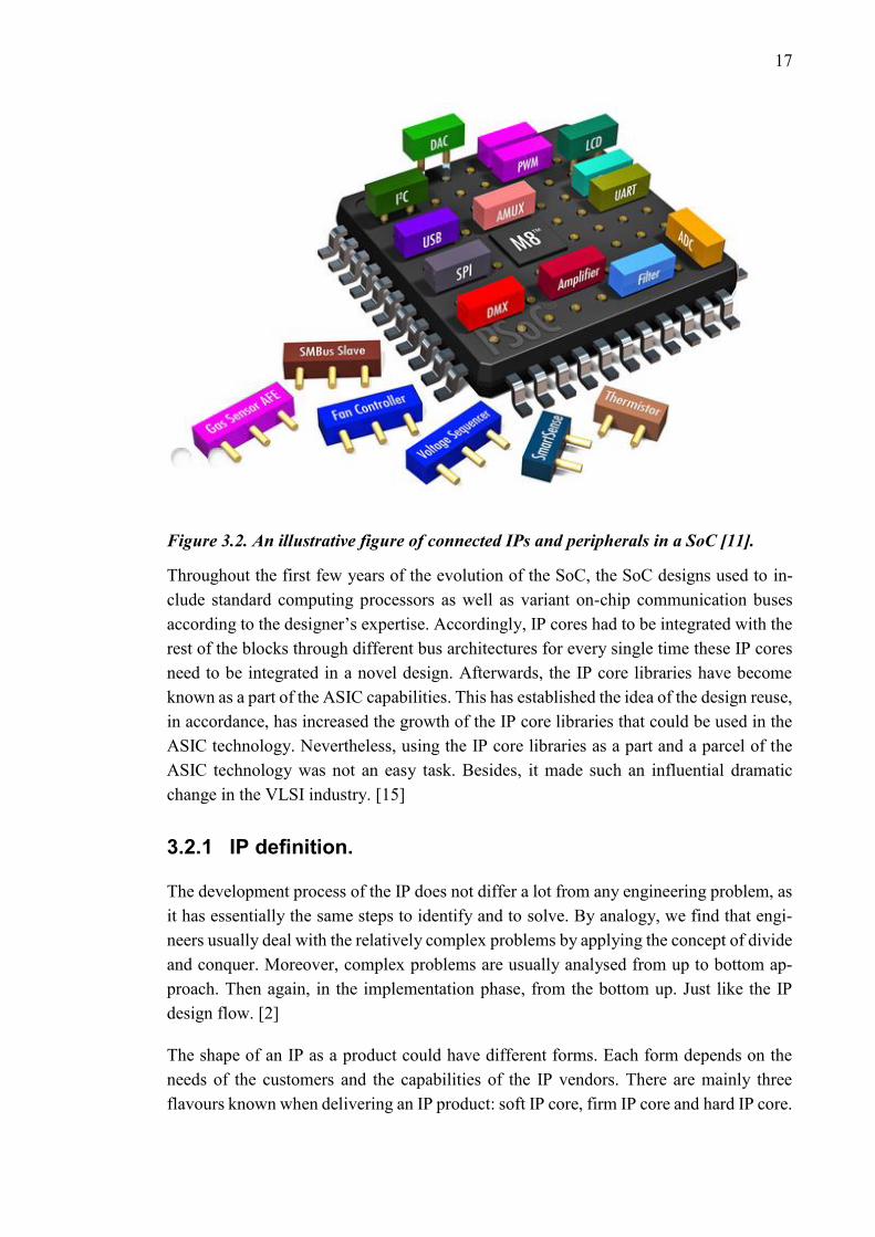
the synthesis or the backend stage of the design flow[1]. Figure 3.2 is an illustrative ex-
ample of a SoC, which contains wide variety of electronic components in the same design.
17
Figure 3.2. An illustrative figure of connected IPs and peripherals in a SoC [11].
Throughout the first few years of the evolution of the SoC, the SoC designs used to in-
clude standard computing processors as well as variant on-chip communication buses
according to the designer’s expertise. Accordingly, IP cores had to be integrated with the
rest of the blocks through different bus architectures for every single time these IP cores
need to be integrated in a novel design. Afterwards, the IP core libraries have become
known as a part of the ASIC capabilities. This has established the idea of the design reuse,
in accordance, has increased the growth of the IP core libraries that could be used in the
ASIC technology. Nevertheless, using the IP core libraries as a part and a parcel of the
ASIC technology was not an easy task. Besides, it made such an influential dramatic
change in the VLSI industry. [15]
3.2.1 IP definition.
The development process of the IP does not differ a lot from any engineering problem, as
it has essentially the same steps to identify and to solve. By analogy, we find that engi-
neers usually deal with the relatively complex problems by applying the concept of divide
and conquer. Moreover, complex problems are usually analysed from up to bottom ap-
proach. Then again, in the implementation phase, from the bottom up. Just like the IP
design flow. [2]
The shape of an IP as a product could have different forms. Each form depends on the
needs of the customers and the capabilities of the IP vendors. There are mainly three
flavours known when delivering an IP product: soft IP core, firm IP core and hard IP core.

Each one has a form and there are some trade-offs among them that are explained below
and in Figure 3.3. [6]
Soft IP cores are like a white-box design, which means that the customer
of the IP has a full accessibility of the RTL of the design. This gives a
strong advantage for the user for the reusability and flexibility in order to
adjust the design or adding extra functionality to the IP. However, there is
not absolute guarantee that the timing or the power metrics will be very
accurate.
Firm IP cores provide a generic design that has flexible parameters to set.
This gives the users of this IP the advantage for optimizing the IP accord-
ing to the application’s needs. This type of IP gives a compromise between
the soft and the hard IP. It has some flexibility that gives the designer more
control on the performance of the design than the soft IP. However, it
makes it more portable than the hard IP.
Hard IP cores are well optimized designs, that are delivered in a fixed lay-
out form for a dedicated application, which explains the definition of a
black-box circuit. Hard IP has the highest performance comparing to the
other types of IPs, which give it a strong advantage. Yet, it costs more.
Figure 3.3. A simple graph illustrates a comparison among the different flavors of
IPs.
3.2.2 IP integration in a SoC design.
The SoC project usually consists of a variety of different blocks. For instance: micropro-
cessor cores, software drivers, bus interfaces, clock generators, communication protocols,
application specific IPs, memories and memory controllers. According to this collection
19
of hardware and software components, reusability plays a significant role here in the pro-
cess of integrating those components into one chip. Hence, at this stage of the project, the
top-level integration team’s role starts to become significant. Especially, when they de-
cide to select the blocks that have the reuse capabilities. [9] [6]
There are several factors that play a role in choosing which collection of the IPs will be
used. Those factors are: documentation quality, well-done verification environment for
each block and the usability of the block. As long as the SoC components are designed
for reusability and are well documented, the integration process will be just as simple as
possible. [9][6]
Even though the components could have a very optimized performance, low area and
low power consumption, it would be very difficult to integrate them because they were
not designed for easier reuse. They are just designed as some standalone blocks as if they
will be isolated. [9][6]
3.2.3 Special considerations for IP reuse.
The cycle of an IP core design is as challenging as the ASIC design. The IP designers
must perform the same steps they used to do in the custom designs. IP is usually integrated
among and adopted by standard products. Conducting an IP design flow in order to be-
come reusable properly in an SoC design, requires a dedicated well studied methodology.
This is due to the strong need for a ready marvellous amount of IP cores to be used directly
in SoC projects without spending time on them. [6]
The process of hardware IP reuse has many challenges and it is not as straight forward as
the case in its counterpart (software reuse). This is because of many aspects: firstly, the
IP must be homogenous with the other IPs on the same chip. Secondly, hardware tech-
nology changes according to Moore’s law [7]. Thirdly, many IPs could have the same
functionality with different flavours in the performance, area, or power consumption. [2]
Establishing the concept of IP reuse in an organization needs to be well studied and needs
more time to be invested in it. Because this will lead the organization to save much time,
hence, money in their future, if they just inherit the concept of reusability in their projects.
The process of reusability needs to be taken carefully into account in the organizations.
Hence, the VLSI organizations should also have their skilful engineers to cover the whole
IP development cycle. These skills include specification writing, RTL design, logic syn-
thesis and layout design. [6]
The purpose of spending time to develop reusable IPs is to increase the productivity of
the ready to use IPs. That is because the customers of the IP vendors don’t have time to
solve the design issues. Moreover, they don’t have the resources or the expertise to handle
each single IP. To sum up, this is the point of the whole idea of the reusable IP develop-
ment, is to consume time, hence, money and to increase the productivity of the SoCs. [6]
3.3 VERIFICATION REUSE
SoC verification is mainly divided into different levels of hierarchy: module level verifi-
cation, IP-level verification, subsystem-level and system-level verification. [10]
Regarding the lower levels of hierarchy such as module and IP verification, the concen-
tration is mainly on ensuring that all the functionality of this module or IP is working as
specifications. While for the higher level of abstractions such as subsystem or system-
level verification, the focus is on maintaining correct interaction among the blocks and
ensuring the proper connectivity among the connected units. [10]
Different directions for verification reuse could be considered from the increasing level
of integration complexity perspective, for example [22]:
1- Code reuse from module or IP level to subsystem or SoC-level in the same project.
2- Code reuse from one project to another project in the future that is based on the
first-generation project, but with extra features.
3- From one project to totally different projects with different possible variants.
Each direction of those verification reuse paths, could be applied using different ap-
proaches. Firstly, an original code could be copied as it is and pasted as a new independent
component. Secondly, an original code could be modified to add or to remove new fea-
tures. There is a possibility to combine those paths and approaches for reuse. [22]
Initiative for spending effort on verification reuse should be started from the management
in the first place. Then a combination of managing version control system as well as pro-
jects’ schedules have to be taken into consideration. [22]
Generally, the verification environment for any component either on the IP-level or the
system-level, share the same essential components that must exist in any verification en-
vironment. Those basic verification components are usually: the stimulus components,
the transactions’ components, the scoreboard components, the monitor components and
the checking components. [12]
3.3.1 Importance of verification reuse
Verification reuse means that the same verification component or verification environ-
ment is utilized again either in the same project or in another project. Verification reuse
involves reusing the code for the possible verification components such as monitors,
scoreboards, test cases, assertions, bus-functional models (BFMs), scripts and coverage
analysis. [19]

21
Verification reuse comes as one important paradigm to solve this bottle neck in the VLSI
development process. This is because verification reuse does not only accelerate the prod-
uct development cycle, but also, enhances the quality of verifying the complex SoCs.
[12][22]
Typically, verification reuse significantly decreases the verification environment’s con-
struction effort. Additionally, it has other benefits such as:
1- Improving the verification quality, hence, the product quality.
2- Reducing the project’s human resources needs.
3- Decreasing the communication protocols knowledge threshold needed for verifi-
cation engineers compared to the knowledge needed in case of no verification
reuse is applied. [19]
Verification reuse has become an important element in the verification flow. This is in
order to leverage the verification effort that has been exerted previously in the earlier
projects. Verification reuse has to be one task for the system level verification engineers
to take care of. The more components need to be reused, the more effort and special con-
sideration should be exerted. Knowing before that the verification takes the biggest
amount of the SoC project development’s time and effort. Verification reuse has become
strongly recommended in every SoC project. [12] [22]
3.3.2 Universal Verification Methodology.
Verification languages such as: e, Vera and System Verilog are powerful tools to build a
verification environment. However, building a verification environment from scratch in
every project is cumbersome and not efficient. This is because there are always parts of
the environment that could be reused in the future projects. Nonetheless, there is no stand-
ard way to make this code reuse efficient. Verification components of any verification
environment are written differently via different verification engineers; therefore, those
components might not be compatible. [24]
Verification methodologies were introduced not only to identify a common platform for
testbench design, but also, to enable the reuse capabilities in those platforms. Verification
methodologies consist of some guidelines for building verification environments. Those
guidelines enable building the testbenches in an organized way so that most of the com-
ponents could be reused. Additionally, those methodologies provide some libraries for
common functionalities. [26]
Universal Verification Methodology (UVM) was introduced and standardized in 2011 as
a platform for enabling reuse in building verification environments. UVM is a class li-
brary implemented in System Verilog. UVM is composed of different verification com-
ponents, which are hierarchically built. UVM has an advantage of having a structured

testbench, which enables the reusability of the testbench’s verification components. Even
the verification environment for simple DUT could be integrated as an agent to build a
testbench for a subsystem testbench, which could be integrated to build the SoC level
verification environment. [10][20][25]
UVM testbench architecture includes user-defined components, which are inherited from
base classes from UVM library. Every verification component is constructed in build
phase by using the UVM factory method. An example for this architecture is shown in
Figure 3.4. This architecture contains a UVM environment, which contains agents that
work as interfaces, monitors, drivers, coverage collector, sequencers and a scoreboard.
[2]
Figure 3.4. An example for UVM testbench architecture. [2]
3.3.3 VIP definition, requirements, and importance.
Verification IP (VIP) consists of verification components that are used in the testbench
for a specific design. Mostly, VIP is made for checking the standard communication pro-
tocols and interfaces to enable the verification engineer to ensure its correctness.
By analogy, we could notice that VIP is inherited from the same concept of design IP. As
mentioned earlier VLSI systems have become more of multiple components that are in-
tegrated into a single SoC. This SoC contains standard components, such as microproces-
sors and communication protocols. Likewise, VIP is a part of the testbench intended for

23
accelerating the process of verifying the whole SoC. VIPs are used to facilitate the veri-
fication of those standard IPs in the system. Additionally, a VIP is a reusable component
in a testbench just like the design IP in a SoC design.
Internal verification teams in a SoC organization support ready-to-use VIPs for various
SoC projects. In addition, similar to commercial standard IPs, VIP could be delivered by
some third-party vendors.
Verification components of a typical testbench that could be altered to cope with the re-
usability requirements are shown in Figure 3.4: Bus functional models (BFMs), monitors,
scoreboards and functional coverage collection components. [19]
BFM is an essential component in a testbench. BFM is responsible for the signal level
interface between the testbench and the DUT signal. BFM is basically driving the DUT
signals with the data as shown in the agent in Figure 3.4. It contains a sequence driver
that passes the data generated from the testbench's data generator. In order to reuse it, it
has to be self-contained, which means that it does not depend on the project. The stimulus
should be interacted with the DUT through some common drivers. Accordingly, the ver-
ification component has become more reusable as well as the VIP. [19][22]
A monitor is defined as a verification component that simply observes the interaction
through the interface. It is a key component in any testbench structure. It has to be inde-
pendent and self-contained. Each monitor could be only responsible for a single interface.
Monitors exist by default in the IP-level testbench, this IP is usually integrated with other
IPs to establish the subsystem, which establishes the SoC. Therefore, it is important for
the monitors to be reused in order to be able to observe the interfaces of the modules or
IPs. [19] [22]
Scoreboard is the verification component, which checks the correctness of the data, pre-
dicts and stores it. Unlike the monitor, it checks the data, not the protocols. This detach-
ment of those tasks is practical for reusability purposes. Additionally, it makes verifica-
tion simpler to implement. [19] [23]
Functional or feature coverage collection component gives an information about which
design features are tested. This element is an important to give the verification engineer
an indication about the verification status of the project. It has to be independent in order
to facilitate reusability. It could be reused in the subsystem-level testbench from the IP or
module-level testbench. [19]
Having a reusable VIP requires some prerequisites that are recommended for better veri-
fication components reuse [19]. Those requirements are:
1- Having the capability to be integrated with different environments.
2- Having the ability to be instantiated multiple times, either independently or within
a verification environment.
3- Having the capability to be configured differently for each instance.
4- Being reusable at various levels of integration.
5- Having a clear documentation.
Verification of SoCs takes around 70% of the effort exerted in a SoC product cycle. Hav-
ing this large portion of the product resources belong to verification, it makes it visible
that verification reuse is almost as important as design reuse or even more important.
Therefore, verification reuse has become an efficient solution to reduce the time to market
and to increase the number of produced SoCs. Hence, VIP is taken into use inside SoC
projects to enable reusability of complex IPs. [18]
Recently, commercial VIPs have become generic in order to enable the reuse capabilities
in the IPs. They are providing high configurability, high level of verification quality by
having: random stimulus generators, temporal checking, functional coverage aspects and
reusable stimulus scenarios. [18]
Recent modern design IPs have the ability to target the complex functionality of the de-
sign, the generic configurations, the performance and area trade-off and, more interest-
ingly, the continual design adjustments through the product cycle. Basically, the notion
of having a thoroughly reconfigurable VIP is inherited from the concept of the configu-
rable design IP as mentioned earlier. Accordingly, this emphasizes leveraging the config-
urable design IP capabilities. [18]
To conclude, practical reuse of design IPs needs a methodology and defined requirements
for VIP vendors to deal with the verification challenges that are associated with the con-
stant changes in the IP cores. VIPs play an important role in leveraging the capabilities
of the widely configurable design IPs. Moreover, having reusable VIPs does not only help
in enhancing the verification quality of the IPs, but also, eases the subsystem or system-
level integration and verification. [18]
3.3.4 IP-level verification environment reuse.
The purpose of the IP level test plan is to cover all of the design specification. In addition,
to cover all the corner cases. A corner case is a situation that occurs outside the ordinary
working conditions. While the purpose of the system level test plan is to verify that all
the internal IPs are properly connected. Besides, to assure that the interfaces between
them are working according to their specification. Moreover, to check behaviour of the
system with different clock domains. Another purpose, is to ensure that the use cases for
the customer are working correctly and matching the architecture specifications. [29][14]
25
In many projects, the specification writing, and the implementation of the IPs are done
concurrently. Hence, the integration of the IPs to create the subsystem occurs in almost
the same time. Here comes the problem from verification point of view. Given limited
resources to the organization, one question shows up. Should there be two complex veri-
fication environments, one for the IP and another for the subsystem? [14]
The increasing demand for having IP-level testbench cannot be missed, while on the sys-
tem or the subsystem-level, it cannot be skipped either. However, verifying standalone
IPs cost less effort, time and money than verifying multiple connected IPs. Having this
fact, the vertical reuse comes out to play a significant role to solve this dilemma. It main-
tains a well-structured IP-level testbench with high coverage scope. While having the
needed system or subsystem-level testbench that is built based on reusing verification
components from the other testbenches. [14]
Vertical reuse emphasizes on building of the basic verification components so that they
could be used in either the IP-level or the sub-system level testbenches. It stresses on the
efficient use of the available resources. Moreover, there have to be properly written guide-
lines for developing each component in order to leverage it in any project. For example,
the names of the global variables have to be chosen carefully, the global defines, the ge-
neric parameters and the component names. [29][14]
When developing a verification component, there are some aspects that should be con-
sidered. Basically, the verification component could be composed of two main divisions,
active components and passive components [29]. The passive components are: the score-
boards, the monitors, the assertions and the coverage. The active components include the
stimulus agents and the drivers. In this essence, we can conclude that the passive compo-
nents don’t affect the path or the generation of the stimuli. [29] [14] [30]
In the following figures Figure 3.5 and Figure 3.6, an illustration of how a top-level ver-
ification environment could leverage the block-level’s verification environment. Block A
has its own verification environment, which is a typical verification environment that has
its passive and active verification components to verify block A. Then, in the top-level
design, block A’s environment could be reused in order to facilitate the top-level verifi-
cation. Input stimulus for block A is driven from top-level verification environment
through block A’s reused verification environment. Block A’s environment is used in
passive mode, which means that the scoreboards, the monitors, the interfaces and the
coverage collectors are enabled. Hence, all the passive components are reused in order to
support the top-level verification as a part of its verification environment.

Figure 3.5. Block level verification environment [30].
Figure 3.6. Top verification environment reuses block-level environment [30].
27
3.4 Documentation.
There is no doubt that a good documentation for any kind of component or project is
something advantageous for any VLSI organization. However, when we take reusability
into consideration, the good documentation is a key element for any reusable component.
When the end user needs to utilize the reusable component and leverage the reusability
feature of this component. There is no way to understand how to use it or how it behaves,
but a well written document explains what is needed to use it. It is also important to ex-
plain the configurations of the reusable component. [10]
There are some elementary requirements that must exist in any document to ease the use
of the reusable component as a fundamental requirement [10]. Those are:
Explanation for the primary functionality.
Operation modes, and possible configurations.
Constraints and limitations.
Release notes.
Having those documentation requirements, when the end user of the reusable components
aims to use such component, there is a need to know what the component exactly does
and what is the purpose of it. For example, in case it is a commercial IP, the fundamental
functionality for it could be written in the glossary. Nevertheless, in case this IP would
be used internally in the same corporation, this glossary could be replaced with a readme
file. This readme file is widely used in any project, but the point here is to put useful
explanations about the basic functionality of the IP. An example for a read me file could
be found in an open source project as in [13][13]. [10]
Furthermore, there should be clear usage steps (usage notes) about how to instantiate this
component into the testbench and how to configure its parameters. Besides, there should
be some details regarding any usage limitations so that the end user of the component
does not get confused about how to leverage this reusable IP. [10]
For the modes of operations and constraints point, the end user has the right to know this
information to know how to control this block and what are the different combinations of
the parameters that could be used. [10]
Regarding the end user, it facilitates the use of this reusable IP into various oriented pur-
poses. The idea of having such a clear descriptive release note might not sound tempting
to some people outside the industry. While, in fact, it is something that is quite important.
That is because the release notes help the end user of the component to have a background
about what are the newest modifications that are done to a particular release. [10]
An expected problem in any project occurs when there is an issue in one release, then
after checking the release note, the engineers figure out that there is a feature has not yet

been added in this component. The main purpose of having the release notes is to explain
the differences between each new release and the earlier ones and what are the reasons
for creating this new release. [10]
To sum up, not only by intuition, but also by practical issues. We easily can assure having
a reliable reusable component if it has proper documentation done according to the early
mentioned basic requirements. Additionally, it reduces the encumbrance from the reusa-
ble component developers to support the end users of those components.
3.5 Cost of reuse.
Verification as well as design reuse have various benefits, which have been discussed
earlier in this chapter. However, there has to be a price to be paid in order to leverage the
reusability inside a SoC project.
First of all, building a reusable verification or design component require a significant
effort in building it. However, this effort helps the engineer who uses the reusable com-
ponent during the time of the project. Second of all, there has to be an extra effort exerted
in building the reusable designs and the verification environments. For instance, packag-
ing the environment, its configurations, and its interfaces. In those cases, the optimization
in time and effort is only leveraged by the verification engineer who uses or integrates
those verification environments. To sum up, the total cost is optimized when reuse is
taken into consideration. [29]
29
4. IMPLEMENTATION
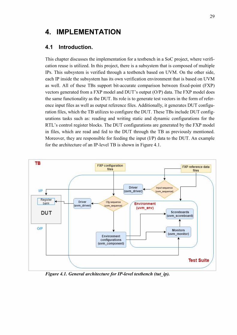
4.1 Introduction.
This chapter discusses the implementation for a testbench in a SoC project, where verifi-
cation reuse is utilized. In this project, there is a subsystem that is composed of multiple
IPs. This subsystem is verified through a testbench based on UVM. On the other side,
each IP inside the subsystem has its own verification environment that is based on UVM
as well. All of these TBs support bit-accurate comparison between fixed-point (FXP)
vectors generated from a FXP model and DUT’s output (O/P) data. The FXP model does
the same functionality as the DUT. Its role is to generate test vectors in the form of refer-
ence input files as well as output reference files. Additionally, it generates DUT configu-
ration files, which the TB utilizes to configure the DUT. These TBs include DUT config-
urations tasks such as: reading and writing static and dynamic configurations for the
RTL’s control register blocks. The DUT configurations are generated by the FXP model
in files, which are read and fed to the DUT through the TB as previously mentioned.
Moreover, they are responsible for feeding the input (I/P) data to the DUT. An example
for the architecture of an IP-level TB is shown in Figure 4.1.
Figure 4.1. General architecture for IP-level testbench (tut_ip).
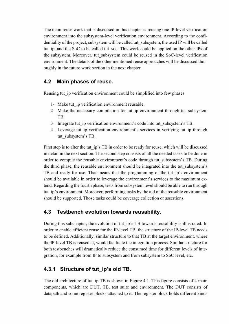
The main reuse work that is discussed in this chapter is reusing one IP-level verification
environment into the subsystem-level verification environment. According to the confi-
dentiality of the project, subsystem will be called tut_subsystem, the used IP will be called
tut_ip, and the SoC to be called tut_soc. This work could be applied on the other IPs of
the subsystem. Moreover, tut_subsystem could be reused in the SoC-level verification
environment. The details of the other mentioned reuse approaches will be discussed thor-
oughly in the future work section in the next chapter.
4.2 Main phases of reuse.
Reusing tut_ip verification environment could be simplified into few phases.
1- Make tut_ip verification environment reusable.
2- Make the necessary compilation for tut_ip environment through tut_subsystem
TB.
3- Integrate tut_ip verification environment’s code into tut_subsystem’s TB.
4- Leverage tut_ip verification environment’s services in verifying tut_ip through
tut_subsystem’s TB.
First step is to alter the tut_ip’s TB in order to be ready for reuse, which will be discussed
in detail in the next section. The second step consists of all the needed tasks to be done in
order to compile the reusable environment’s code through tut_subsystem’s TB. During
the third phase, the reusable environment should be integrated into the tut_subsystem’s
TB and ready for use. That means that the programming of the tut_ip’s environment
should be available in order to leverage the environment’s services to the maximum ex-
tend. Regarding the fourth phase, tests from subsystem level should be able to run through
tut_ip’s environment. Moreover, performing tasks by the aid of the reusable environment
should be supported. Those tasks could be coverage collection or assertions.
4.3 Testbench evolution towards reusability.
During this subchapter, the evolution of tut_ip’s TB towards reusability is illustrated. In
order to enable efficient reuse for the IP-level TB, the structure of the IP-level TB needs
to be defined. Additionally, similar structure to that TB at the target environment, where
the IP-level TB is reused at, would facilitate the integration process. Similar structure for
both testbenches will dramatically reduce the consumed time for different levels of inte-
gration, for example from IP to subsystem and from subsystem to SoC level, etc.
4.3.1 Structure of tut_ip’s old TB.
The old architecture of tut_ip TB is shown in Figure 4.1. This figure consists of 4 main
components, which are DUT, TB, test suite and environment. The DUT consists of
datapath and some register blocks attached to it. The register block holds different kinds
31
of registers with different functionalities, such as: configuration and status registers. The
registers in the register block of the DUT are configured through the FXP configuration
files shown in Figure 4.1. General architecture for IP-level testbench (tut_ip).. These con-
figuration files are generated from the FXP model. Each file contains information that
concerns a dedicated register, or a set of registers. The input data for the DUT is coming
through FXP reference files that are generated also by the FXP model. Regarding the
output data from the DUT, it is compared in the TB to the reference data generated by
FXP model.
The environment is a UVM component, which is inherited from uvm_env [28] base class.
It is a container class, which contains the monitors, the scoreboards and some other agents
and connects them together. In the environment, those verification components are cre-
ated and constructed. A monitor inside the environment is responsible for sampling the
DUT’s output data and passing the contained information to the evaluation component.
The monitor is a passive element, which means that it does not drive any signal, but only
to extract the signal’s information. Monitor is inherited from uvm_monitor base class
[28]. The scoreboard is the evaluation component for the correctness of the functionality
of the design. A scoreboard in the environment has two main inputs. The former is the
reference data, which is read from the reference file. This reference file contains the ex-
pected values for the output of the DUT. The latter is the information that is delivered by
the monitor, which contain the DUT’s output values. Then the comparison is done be-
tween the DUT’s output value and the reference expected value. Scoreboard is an inher-
ited class from uvm_scoreboard base class [28].
The test suite in this project has the biggest role in the functionality of the testbench as
shown in Figure 4.1. General architecture for IP-level testbench (tut_ip).. It contains the
environment, the environment configurations, the drivers, the sequences and other TB
tasks. The environment configurations class is the component, which configures the en-
vironment’s components such as the scoreboards and the monitors, for example it decides
the widths of the scoreboards and the number of them. The width of the scoreboard means
the width of the RTL signals that are being compared against the reference model values.
Environment configurations class is only responsible for the TB’s configurations. The
input sequence class in Figure 4.1 is extended from uvm_object base class [28]. This input
sequence reads the reference input data from the FXP reference files and passes them to
the driver. The driver is the verification component, which interacts with the DUT and
drives the input interface of the DUT on the signal-level. Driver is inherited from
uvm_driver base class [28]. The cfg sequence is a reading sequence, which is responsible
for reading the register configurations from the FXP configuration files. There are two
types of DUT configurations: static and dynamic configurations. The static RTL config-
urations are written at the beginning of the simulations once, while the dynamic RTL
configurations are written depending on some delay values. Those configurations are
written to the DUT’s registers through a driver component as shown in Figure 4.1. There
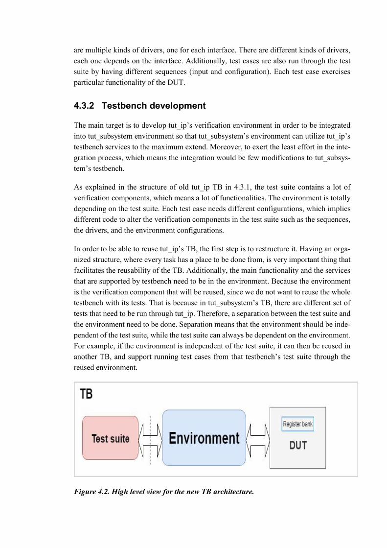
are multiple kinds of drivers, one for each interface. There are different kinds of drivers,
each one depends on the interface. Additionally, test cases are also run through the test
suite by having different sequences (input and configuration). Each test case exercises
particular functionality of the DUT.
4.3.2 Testbench development
The main target is to develop tut_ip’s verification environment in order to be integrated
into tut_subsystem environment so that tut_subsystem’s environment can utilize tut_ip’s
testbench services to the maximum extend. Moreover, to exert the least effort in the inte-
gration process, which means the integration would be few modifications to tut_subsys-
tem’s testbench.
As explained in the structure of old tut_ip TB in 4.3.1, the test suite contains a lot of
verification components, which means a lot of functionalities. The environment is totally
depending on the test suite. Each test case needs different configurations, which implies
different code to alter the verification components in the test suite such as the sequences,
the drivers, and the environment configurations.
In order to be able to reuse tut_ip’s TB, the first step is to restructure it. Having an orga-
nized structure, where every task has a place to be done from, is very important thing that
facilitates the reusability of the TB. Additionally, the main functionality and the services
that are supported by testbench need to be in the environment. Because the environment
is the verification component that will be reused, since we do not want to reuse the whole
testbench with its tests. That is because in tut_subsystem’s TB, there are different set of
tests that need to be run through tut_ip. Therefore, a separation between the test suite and
the environment need to be done. Separation means that the environment should be inde-
pendent of the test suite, while the test suite can always be dependent on the environment.
For example, if the environment is independent of the test suite, it can then be reused in
another TB, and support running test cases from that testbench’s test suite through the
reused environment.
Figure 4.2. High level view for the new TB architecture.
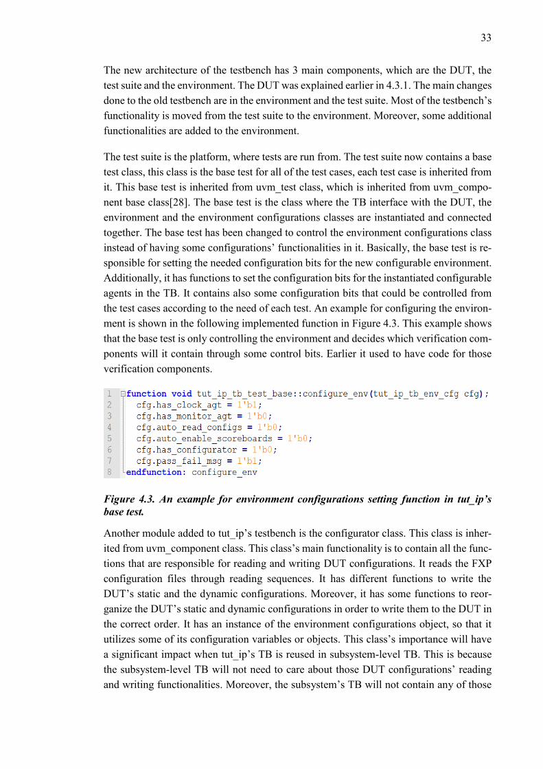
33
The new architecture of the testbench has 3 main components, which are the DUT, the
test suite and the environment. The DUT was explained earlier in 4.3.1. The main changes
done to the old testbench are in the environment and the test suite. Most of the testbench’s
functionality is moved from the test suite to the environment. Moreover, some additional
functionalities are added to the environment.
The test suite is the platform, where tests are run from. The test suite now contains a base
test class, this class is the base test for all of the test cases, each test case is inherited from
it. This base test is inherited from uvm_test class, which is inherited from uvm_compo-
nent base class[28]. The base test is the class where the TB interface with the DUT, the
environment and the environment configurations classes are instantiated and connected
together. The base test has been changed to control the environment configurations class
instead of having some configurations’ functionalities in it. Basically, the base test is re-
sponsible for setting the needed configuration bits for the new configurable environment.
Additionally, it has functions to set the configuration bits for the instantiated configurable
agents in the TB. It contains also some configuration bits that could be controlled from
the test cases according to the need of each test. An example for configuring the environ-
ment is shown in the following implemented function in Figure 4.3. This example shows
that the base test is only controlling the environment and decides which verification com-
ponents will it contain through some control bits. Earlier it used to have code for those
verification components.
Figure 4.3. An example for environment configurations setting function in tut_ip’s
base test.
Another module added to tut_ip’s testbench is the configurator class. This class is inher-
ited from uvm_component class. This class’s main functionality is to contain all the func-
tions that are responsible for reading and writing DUT configurations. It reads the FXP
configuration files through reading sequences. It has different functions to write the
DUT’s static and the dynamic configurations. Moreover, it has some functions to reor-
ganize the DUT’s static and dynamic configurations in order to write them to the DUT in
the correct order. It has an instance of the environment configurations object, so that it
utilizes some of its configuration variables or objects. This class’s importance will have
a significant impact when tut_ip’s TB is reused in subsystem-level TB. This is because
the subsystem-level TB will not need to care about those DUT configurations’ reading
and writing functionalities. Moreover, the subsystem’s TB will not contain any of those

reading sequences, since the configurator of the reused environment has already its own
sequences.
Environment configurations class is where all the environment’s needed configurations
are done. The environment contains many agents such as scoreboards, VIPs and monitors.
Those agents are being created and configured in the environment configurations class.
Furthermore, this class contains all of the configuration bits and functions for the TB
environment. Those configuration bits and functions would play an important role in re-
using the environment in two different approaches. For the first, when tut_ip’s testbench
is used to verify tut_ip, then those configuration bits and functions are being set and used
from the base test of the TB. For the latter, when tut_ip’s environment is being reused in
tut_subsystem’s TB, then they are being set and used from tut_subsystem’s base test.
Figure 4.4. New edition of tut_ip’s TB after the modifications.
35
Testbench environment is developed in a way that all the main verification components
are wrapped inside it. It is considered as the core block of the TB. This is because the
target is to reuse the TB environment of tut_ip. Testbench environment class’s main func-
tionality is to construct all the verification components that need to be utilized in the TB.
Additionally, the objects construction is dependent on the configuration bits of the envi-
ronment configurations. Therefore, the structure of the TB is more organized and opti-
mized, since only the needed activated components are used depending on their corre-
sponding configuration bit. On the other hand, earlier the TB was not structured, and the
configurability of the components were not high. Currently, most of the components are
controlled through some configuration bits come from upper levels of hierarchy such as
the base test of tut_ip’s TB or tut_subsystem’s TB.
In Figure 4.4, the new developed version of tut_ip’s TB is shown. As seen from the figure
that test suite and the environment could be easily separated from each other and the
environment’s functionality is not dependent on the test suite. Accordingly, the target to
reuse the environment as an independent component in a different TB is achieved. More-
over, some features are added to the new TB. For example, the scoreboards are developed
to be reconfigurable. Their construction, their number, their width could be configured.
The components that are modified or added to the new version of the TB are having a
green shadow in the figure, so that it differentiates it from Figure 4.1.
4.4 Reusable environment’s services.
Tut_ip’s TB is developed so that it supports tut_subsystem’s TB with some services to
decrease the verification effort from the subsystem-level. Services are the functional and
structural features, which form the reusable part of the TB. The services, which tut_ip’s
environment support are required by tut_subsystem’s verification strategy. Moreover,
some services of any reusable IP-level environment could be supported as customized
services for a particular IP. The services that are supported by tut_ip’s environment are
in the following list.
1- A makefile, which is responsible for compiling the reusable part of tut_ip’s TB.
2- Support for passive scoreboarding, which means that the scoreboards will be ac-
tive and visible in the simulations of tut_subsystem, without having to give exter-
nal commands.
3- Support for reading DUT’s static and dynamic configurations from FXP configu-
ration files.
4- Support for writing DUT’s static and dynamic configurations to the configuration
registers.

5- Feature coverage collection and other selected types of coverage.
The services supported by tut_ip’s TB are needed for tut_subsystem verification for some
reasons. First of all, if tut_ip verification engineers want to add more code into the make-
file, then, tut_subsystem verification engineers don’t need to worry about it, as they are
reusing it. Without the supported makefile, tut_subsystem verification engineers can com-
pile the reusable part themselves, and when there are any changes needed in the compi-
lation, they need to contact tut_ip engineers to ask them about those changes and there
will be a loop of extra communication, which can be optimized by having the makefile
support. Second of all, in points number 3 and 4, the DUT configuration files and the
registers could be changed during the project. Therefore, tut_subsystem engineers will
need to know about those changed and modify the corresponding functions for reading
and writing the DUT configurations accordingly. On the other hand, if those services are
already supported by tut_ip’s TB, then tut_subsystem engineers do not need to worry
about the design changes. Services number 1, 3 and 4 are project specific points. Regard-
ing the other services, they are not only supported in this project, but also, they could be
general services at any reusable verification environment. And those general services rea-
soning will be discussed in 5.2.
4.5 Integration steps.
According to this project, tut_subsystem testbench is developed using UVM. Therefore,
reusable tut_ip testbench should be also implemented using the same version of UVM.
Steps for integration after the TB is developed to be reusable should be straight forward.
This is because the integration effort is decreased a lot. And this is one of the important
outcomes of reusability. In this part of the chapter, the steps for integrating tut_ip’s envi-
ronment into tut_subsystem’s environment are explained with some code examples.
1- tut_ip’s environment should be directly utilized in tut_subsystem’s verification
environment through the version control system [48], which is used in the project.
2- Compile reusable modules and packages of tut_ip’s TB through through calling
developed makefile.
3- Environment configurations setting.
a. Package tut_ip_tb_env_pkg, which includes all the Systemverilog files of
the environment, needs to be imported into tut_subsystem_tb_env_pkg.
b. An object of tut_ip_cfg type needs to be constructed during build-phase
and following parameters set as shown in Figure 4.5.

37
4- UVM Register Abstraction Layer (RAL) [20] configuration for tut_ip. In this
case, we just assign the path of tut_ip’s RAL from tut_subsystem to the tut_ip’s
RAL in tut_subsystem base test. This could have been assigned in tut_subsystem’s
environment configurations, however, tut_subsystem will be integrated into
tut_soc’s TB, so RAL comes from the SoC level down to subsystem and IP levels.
5- Environment instantiation.
a. tut_ip_tb_environment is constructed in tut_subsystem_tb_env's build
phase and its configuration is passed through UVM_CONFIG_DB [20] as
the following example in Figure 4.6.
6- Reading registers’ configurations.
a. To read the configurations, path to the vectors needs first to be assigned in
build phase, before reading tut_ip’s configurations.
b. After that, call a read_tut_ip_configurations() function in the environ-
ment’s configurator-object.
c. This function call is done inside the body of read_tut_ip_configurations()
in tut_subsystem’s configurator.
7- Writing registers’ configurations.
a. tut_subsystem environment’s configurator object needs to be utilized to
the maximum extent. It has a function write_static_configurations, which
will write all the registers and memories that need to be initialized before
dynamic operation.
b. It is called inside write_static_configurations() function in tut_subsys-
tem_configurator.
c. For the dynamic configurations, they are also done in the same way as the
static ones.
8- Scoreboarding.
Figure 4.5. Sample code for setting the environment configurations.
Figure 4.6. An example for constructing the reused environment inside another environ-
ment.

a. It is possible to automatically select the scoreboards by setting configura-
tion variable inside tut_ip_env_cfg object from tut_subsystem test base.
b. There are special cases to be considered while integrating tut_subsystem
into tut_soc TB. Those will be discussed in the next section 4.6.
4.6 Special considerations.
Integration steps should be fluent if the integrated environment is reusable and having
similar structure to the target environment. However, there are always some implemen-
tation details we come to know after doing the practical work. Some of the special con-
siderations are general and known by the experienced engineers. Other cases are project
specific. Here, we are going to discuss all of the cases that need to be considered carefully
while integration.
1- In UVM build phase [20], objects are constructed top-down style, which means
that objects in tut_subsystem’s environment are constructed before tut_ip’s envi-
ronment. Therefore, considerations must be taken regarding handles' assignments
accordingly. Make sure that tut_subsystem objects are being constructed in build
phase before tut_ip objects, since tut_subsystem is higher in the hierarchy.
2- tut_subsystem’s configurator is the main configurator that is responsible for read-
ing and writing the configurations. Accordingly, any IP related operations have to
be implemented inside tut_subsystem’s configurator. Hence, a handle from the
tut_ip_environment have to be used from tut_subsystem’s configurator. Accord-
ingly, it needs to be initialized in tut_subsystem_tb_env in the build phase.
3- In read_configurations function at tut_ip's testbench, all the configurations are
read (static and dynamic).
After integration was done, different test cases exercising different datapaths over
tut_subsystem are run to make sure that nothing is broken after the integration. Addition-
ally, a regression was run in order to have confidence about the new integrated environ-
ment.
A practical issue appeared only after running the regression test over the subsystem. This
issue is project specific issue. A special test case was failing after the integration, that test
uses two different test vectors in the same simulation sequentially. So, after debugging, it
was figured out that the second vector configurations’ were not written, because the reg-
isters already contain data. The solution developed for this issue was to reset the registers
just before reading the configurations of the second test vector.
39
5. REUSABILITY LEVERAGE FOR IDEAL SOC
PROJECT FLOW
In this chapter, the added value of reusing the IP-level TB into the subsystem-level TB is
discussed. Additionally, it includes some interviews done with verification experts to get
information and guidelines based on hands-on-experience. Finally, some improvement
ideas are proposed for the future work.
5.1 Analysis for the outcome of the reuse.
5.2 Reasons for IP-level TB integration.
During chapter 4, a practical example for applying reusability in a SoC project was illus-
trated. This work includes two phases. For the first phase, tut_ip’s TB was modified and
developed into reusability. Regarding the second phase, tut_ip’s TB was integrated into
tut_subsystem’s TB. Basically, subsystem-level TB can handle the services that are sup-
ported by the IP-level TB. However, it will need extra effort for the subsystem-level ver-
ification engineers to implement those services. Those services for the IPs are extra work
for the subsystem, because subsystem verification should focus more on testing the whole
subsystem’s customer requirements and the proper connectivity among its own IPs. Typ-
ically, when reuse is applied such as in this project, the subsystem-level TB asks some
services from IP-level’s verification environment. Each service of those has a reason for
it.
During the project cycle, design changes many times and some features are being added
to the design. Accordingly, the TB needs to be modified in correspondence to those design
updates. The changes that could happen to the design, can include registers changes,
which will reflect to the register tests in the TB. They can also include changes to the
design interfaces, or memory addition, which will also need modifications to the TB.
Usually, IP-level TB is being updated according to the design changes faster than subsys-
tem-level TB. That is because subsystem-level design verification lags some time, since
it waits for its top-level integration, then its verification is started at this point.
Most of the required services asked from reusable TBs are project specific and some are
general for any reusable TB as mentioned in 4.4. The general services are usually bene-
ficial and needed for the target TB are as in the following list.
1- Support for passive scoreboarding.
2- Support for driving the interfaces.
3- Coverage collection with all its types.
4- DUT wrapper up-to-date to be bound.
5- APIs for supporting design configurations with all of its types.

6- Assertions.
5.3 Integration results and analysis.
After IP-level TB integration is done into subsystem-level TB, with the supported ser-
vices, time and effort will be optimized for subsystem-level verification engineers to
modify the TB after each design change. Additionally, effort is generally optimized, since
the TB changes need to be done only in IP-level TB instead of implementing them in two
TBs.
In order to get tut_ip’s environment integrated into tut_subsystem’s TB, only few lines
of code were added, and few files were touched. In the project’s coding style, each file
can contain only class. The total number of lines that are added to the TB during the
integration phase are 64 lines of code, which means the amount of code is reduced with
85%. Total effort for a verification engineer, who has experience in functional verification
field, and has deep understanding for UVM verification environments would be around
two working days. This effort is focused on adjusting the makefile and having a quick
glance on the environment and adding the needed code in order to get IP-level environ-
ment integrated into subsystem-level’s TB. The files that have been modified are in the
following list.
1- Tut_subsystem_environment, which has the implementation for the environment
class.
2- Tut_subsystem_environment_configurations, which has the environment-specific
needed configurations.
3- Tut_subsystem_base_test, which has the base test class that works as a base class
for the test cases and controls the environment.
4- Tut_subsystem_environment_pkg, which has a list of all the files that the subsys-
tem verification environment has.
5- Tut_subsystem_makefile, which is responsible for compiling the TB.
In order to have the current services that are supported currently by the integrated reusable
tut_ip’s environment, the subsystem-level verification engineers need to develop those
services themselves to tut_subsystem’s TB. After the integration, the files and the pieces
of code inside tut_subsystem’s TB that are related to tut_ip are totally removed.
An analysis for the work that was done for running tests through tut_ip from tut_subsys-
tem’s TB without support from the IP-level environment. First of all, the makefile just
had to include those tut_ip related files and that was the least amount of code that was
served. On the other hand, tut_subsystem’s TB used to have extra files and APIs as in the
following list.
41
1- Reading sequence class, for reading the dynamic and the static configuration from
the FXP dump files.
2- Having reading and writing APIs for the static and the dynamic configurations to the
DUT’s configuration registers.
3- Connecting monitors and scoreboards into tut_ip’s DUT in multiple places in the
design, in order to have better visibility for the data flow for debugging purposes.
4- Having APIs for connecting the input data dump files, which are generated by the
FXP model into some points of the design for the scoreboards, which needs
knowledge about the IP and having some communication time with the designers.
5- Having drivers to drive the input stimuli data from the dump files into the DUT’s
input.
After careful studying to the amount of effort that was saved after integration, the amount
of code that are removed from tut_subsystem’s TB after the integration are 534 lines of
code. This amount of code wouldn’t have been written if reuse was utilized from the
beginning of the project.
The lines of code that were added during the building of tut_subsystem’s TB in order to
support tut_ip verification is not the only thing that was optimized. During the project
cycle, which lasts at least few months up to few years, some design features could be
added at that time, in accordance, RTL changes are done. Therefore, TB will be updated
according to the new features of the design. Moreover, extra communication between
tut_subsystem’s verification engineers and tut_ip designers need to be done in order to
develop the TB according to the new requirements.
6. CONDUCTING INTERVIEWS AND FUTURE
WORK
6.1 Interviews procedures.
Seven SoC verification experts, who work at Nokia were interviewed, as a part of support
to this work, on a voluntary basis. The average experience for each interviewee is from 7
to 20 years in the VLSI industry and at least 5 years of experience in SoC verification.
Four of the interviewees are working as verification team leaders and the others are work-
ing as SoC verification specialists. Most of them started their career as ASIC designers
and worked extensively in the whole ASIC flow, then they switched to functional verifi-
cation area, except two engineers started their career as a SoC verification engineers and
they have from 7 to 15 years of experience.
The interviews had similar structure. Each interview lasted for one hour. Each interview
starts by asking the interviewee to introduce himself and to talk about his expertise in the
field of SoC verification and how much he applied reusability in the projects he worked
in. A set of prepared questions were being sent to the interviewees before the interviews,
and discussions about the answers for those questions were being conducted during the
interview time. And at the end of each interview, the interviewee was being asked to give
extra recommendations that may not had been covered during the interviews. Interviews
were recorded so that the interviewer can process each interview carefully after it was
done and came up with some points as answer for each question.
The information gathered during the interviews were helpful and they give inspiration
about how things could be done better from reusability perspective. Unfortunately, those
kinds of information are usually gained during years of experience and they cannot be
easily found in books. Furthermore, not all the details about the answered questions can
be published here at this work, since they contain some confidential information about
internal projects at Nokia. However, the interviewer made sure to come up with general
and non-confidential answer for each question from each interviewee. The main questions
that are asked in each interview and their answers are in 6.2.
6.2 Interviews’ questions and answers.
1- What are some guidelines for ideal verification project flow in terms of reusabil-
ity?
The hierarchical UVM testbench should be considered. The starting should be from IP-
level TB, subsystem-level, then SoC-level (top-level). All the experts said that the flow
should always go in that order. Whenever the work is started in IP-level TB, it should go
by bringing the requirements from subsystem-level TB. Because the requirements are
43
different for each IP. Because in IP-level, the main priority of the verification is to ran-
domize, to get all the corner cases covered, and to get 100% coverage. Complexity starts
to increase (simulation time becomes roughly 10x), when shifting to the upper verifica-
tion layers (subsystem and SoC). In subsystem, it should be assumed that every IP is
tested, and one just needs to cover some directed scenarios and ensure that everything is
working together. Subsystem-level and top-level TBs should be able to disable the ran-
domization for the IPs and use some directed methods. One expert said: “They are two
different worlds”.
The interviewees also emphasized that when reuse for IP-level TB is done to subsystem-
level TB and subsystem-level is reused in top-level, there is no need for the upper levels
to debug extra stuff. If the TB is built properly, where everything that is required from
the TB exists in the environment and encapsulated in classes and methods, and the envi-
ronment is independent from the test suite, then the reuse should be straight forward for
that environment. “The IP-level environments would be sub-environments from subsys-
tem environment and the subsystem-level environments would be sub-environments from
the top-level environment.” One expert mentioned that the biggest mistake a verification
engineer can do is to have lots of functionalities in the base test and not to have them
structured and encapsulated inside classes and methods in the environment. The environ-
ment has to be built properly from the beginning, reuse would be much easier after that.
If everything is agreed beforehand and the needed services are known, the integration
should be straight forward.
Experts agreed on that, the proper starting for the project plays significant role in the
future of the project. They agreed that top-level has the authority to drive the lower veri-
fication environments, since top-level requires services from lower level verification en-
vironments, which somehow defines the structure of the lower levels TBs. That is because
complexity grows exponentially in the upper levels of the hierarchy. If something is
simply done in IP-level, it would be much harder in top-level. There has to be strong
management decision in applying reusability from the first day of the project. Everything
is recommended to be unified, such as: makefiles structures, environments structure. It
wouldn’t hurt if every engineer asks one question before creating any component in the
TB, will this component be used anywhere else? One expert said: “Leave the door opened
for future opportunities of reuse”.
Other technical details were gathered from the verification experts as well as the general
guidelines. The following instructions are collection of recommendations from the ex-
perts to be considered in any SoC verification project.
1- Maintaining version control hierarchy for easier usage. Means clear hierarchy for
common stuff, IP environment, subsystem environments and top-level environ-
ments.
2- Having a unified coding style.

a. Use Systemverilog packages to gather stuff to their own “lockers”.
b. No absolute register addresses anywhere.
c. Clear API methods towards top environment.
d. Separate local and public methods clearly.
3- When dealing with register accesses, it is recommended to consider the following:
a. Use RAL.
b. Top path for RTL to be passed through method.
c. Register model instance through method.
d. Register accesses centralized to software model classes.
4- UVM reusable environment compilation.
a. Common makefile style for each reusable environment.
b. Needed parameters can be overridden from top makefile
5- Top-level TB reuse.
a. Use Systemverilog interfaces and bind modules to reuse.
b. Top-level DUT path to internal signals as parameter.
6- Clear documentation for the TBs of the project.
a. An existence for common guidelines for TB building into reusability in
any organization.
b. For TBs, at least a figure explaining the TB structure should exist.
2- Is it always worth it to spend time on making the verification components reusa-
ble?
All the verification experts agreed that it is really worth it to start from the beginning of
the project by building the TBs properly, which make them easy to be reused. One expert
mentioned a special story about a project he worked on and they didn’t have a TB for a
relatively simple IP. That happened due to the lack of resources and time. Then, the sub-
system-level verification team decided that they will test this IP on the subsystem-level
and it went quite well. However, he mentioned that this was just a special case, and this
should not be generalized, because it is not always the proper way to go.
3- What’s the best time to decide on applying reusability?
Every interviewee agreed on that the best time to decide on reusing the TBs is at the
beginning of the project. They said that one can just start at the beginning of the project
to build things the proper way. Maybe one doesn’t need that much of reusable APIs at the
beginning, but later, one will need to use it according to the needed services that come
from the top-level. One expert said: “It really saves time and effort to do that at the be-
ginning of the project.”
4- In IP-level TBs, is it important for the verification engineer to know about the
subsystem, where this IP-level TB is reused?
Most of the answers were that it would be needed to gather requirements from known
subsystems and top-level before coding. On the other hand, if the TB is testing some
45
standard, then, one doesn’t need to go and ask around, all one needs is studying the stand-
ard. The essence of the IP is that it can be used in multiple places. For widely used VIPs,
one builds the basic services that are needed in any project. Even in commercial VIPs,
there is a feedback loop from the customers in order to add some services to the built
VIPs. One of the interviewees said, “The VIP owner needs to understand that the VIP
will be integrated in many different projects, so he needs to be ready for extra communi-
cation with different teams.” To sum up, it is always very important for the verification
engineers, who are doing the TB to know about the surrounding environment.
5- What are the needed skill-set for the verification engineer to be able to apply re-
usability?
Some experts said that it comes with experience. It would be good to work in IP, subsys-
tem top-level to gain the understanding. As a junior, it is totally recommended to start
SoC verification career in IP-level TB, then when one moves to another project, it would
be better to get involved in subsystem-level verification team. One given advice from an
interviewee who said: “It would be also a good practice, if one is working on IP-level TB,
and then one gets involved in integrating it into subsystem, at this point one will join the
subsystem’s team and be more aware with the subsystem’s TB, so one would get better
understanding for the verification flow in different levels of the SoC.”.
On the other hand, practically, sometimes it is quite difficult to move engineers from IP-
level TB development to subsystem-level, because it depends on the resources of the pro-
ject such as the headcounts, the money and the time. Here, the talking is from perspective
of the learning. One expert said, “I myself have always been in top-level verification. If
one starts verification career in top-level verification team, might feel overwhelmed.”
All the experts mentioned that the awareness with Systemverilog language and UVM is
absolutely needed. In order to be able to apply reusability, a strong knowledge in object-
oriented programming (OOP) is a must. Moreover, practicing and getting encountered to
different UVM environments gets the verification engineer more confidence.
One expert mentioned something interesting and out of the SoC flow scope, but from his
point of view it really gives nice and efficient ideas in the area of reusability. He recom-
mended getting involved in the software community’s progress about reusability. He said
that one can achieve that by reading blogs, watching seminars in international confer-
ences, reading scientific papers about reusability in software engineering. His perspective
is that the software community is ahead more that the SoC community in optimizing the
reusability of the project. He said, “Although the domain is totally different, UVM envi-
ronments are also written in software language.” Additionally, there are thousands of us-
ers who write about that in the blogs, while in SoC, most of the work done in this area is
organization specific and confidential.

One expert said that one needs to have management skills as well as to the technical skills.
There are people sometimes asking many questions about one’s VIP, so one needs to be
able manage that. One needs to have good communication skills, because communication
with different people from different teams will always happen if one’s VIP is used in
different projects.
Some of the interviewees said that information sharing sessions in the organizations are
beneficial for the SoC verification community. Some informal sessions are good idea to
bring up some ideas about the verification techniques and how each team utilized the
reusability. Even a couple of slides about any project and introduce it to everyone since
no one has time for reading a whole verification plan document.
6.3 Future work.
First action point to be applied after having some research work and after interviewing
some experts in the SoC verification field is to start any project by following a unified
and agreed guidelines for TB building and for driving the reusability. On tut_subsystem,
each IP-level TB in the future will be altered in order to be reused in it just like what was
done in tut_ip’s TB.
Something that needs to be considered as reusability or portability, is to go beyond the
SoC-level verification. For prototyping on FPGAs, the UVM sequences, for example,
cannot be reused, because they are not portable. Even for ASICs, pre-silicon verification
is done on FPGAs before sending the design to be fabricated, and the APIs are not reused
from UVM to C. An approach that can be successfully applied in all of the projects is to
use C configuration functions instead of pure UVM functions. It would benefit the testing
in many levels and would serve as a reference for software layer as well. Testbenches can
be still using UVM, but the configuration functions could be written in C code.

47
7. CONCLUSION
The target of this work was to study the importance of applying reusability in SoC veri-
fication projects. Moreover, it demonstrated how to leverage reusability as a tool in the
SoC verification projects flow.
In this work, a literature study about SoC flow was conducted with emphasis on SoC
functional verification. Additionally, a research about the concept of reusability in general
and its importance was conducted. Then, a case study as a part of a project was imple-
mented as a practical example for applying reuse in SoC verification projects. After that,
an analysis for the implemented case study was done in order to show the importance of
the work. At the end, interviews with SoC verification experts were done and docu-
mented. Those interviews were done in order to collect information for improving the
reusability in the SoC projects. Those interviews gave additional insights for how the
projects should be organized, since those recommendations were given out of years of
experience in multiple SoC projects.
During this work, some points were collected to be considered in order to leverage the
reusability in SoC verification project flow as following. First of all, planning the project
from the beginning and exerting time and effort on utilizing the reuse in the project, will
pay-off during the project time line and the work will be more organized. Second of all,
maintaining the hierarchical structure when applying reuse bottom-up style (from IP-level
till top-level) is the proper way to apply reuse. Third of all, having a clear and a continuous
communication between the engineers for each layer (IP, subsystem and top-level) is es-
sential for maintaining the success of the project. Fourth of all, having simple and reada-
ble documentation for TBs and IPs is a significant key when applying the reuse. Finally
yet importantly, junior verification engineers need to have OOP skills in order to be able
to utilize reusability. Besides, awareness with Systemverilog language and verification
methodologies and -of course- experienced mentors for guidance through the project.
8. REFERENCES
[1] Saleh R, Wilton S, Mirabbasi S, Hu A, Greenstreet M, Lemieux G, Pande PP,
Grecu C, Ivanov A. System-on-chip: Reuse and integration. Proceedings of the
IEEE. 2006 Jun;94(6):1050-69.
[2] Graphics M. Verification Academy UVM Cookbook. Analysis Components and
Techniques,[Reference Date: 11 April 2016] https://verificationacademy.
com/cookbook/uvm.
[3] Savage W, Chilton J, Camposano R. IP Reuse in the System on a Chip Era. InSys-
tem Synthesis, 2000. Proceedings. The 13th International Symposium on 2000
(pp. 2-7). IEEE.
[4] INTEL. Intel FPGA IP Portfolio [Internet]. 2018 [cited 2 November 2018]. Avail-
able from: https://www.intel.com/content/www/us/en/products/programmable/in-
tellectual-property.html
[5] OpenCores.org, Opencores IP Components [Internet]. 2018 [cited 2 November
2018]. Available from: https://opencores.org/
[6] Bricaud P. Reuse methodology manual: for system-on-a-chip designs. Springer
Science & Business Media; 2012 Dec 6.
[7] Schaller RR. Moore's law: past, present and future. IEEE spectrum. 1997
Jun;34(6):52-9.
[8] Reutter A, Rosenstiel W. An efficient reuse system for digital circuit design. In-
Design, Automation and Test in Europe Conference and Exhibition 1999. Pro-
ceedings 1999 (pp. 38-43). IEEE.
[9] Bricaud PJ. IP reuse creation for system-on-a-chip design. InCustom Integrated
Circuits, 1999. Proceedings of the IEEE 1999 1999 (pp. 395-401). IEEE.
[10] Wile B, Goss J, Roesner W. Comprehensive functional verification: The complete
industry cycle. Morgan Kaufmann; 2005 Jun 9.
[11] A. D. day, “Psoc” [Internet]. 2012 [cited 9 November 2018]. Available from:
https://armdeveloperday3rd.files.wordpress.com/2012/11/psoc.png.
[12] Wang R, Zhan W, Jiang G, Gao M, Zhang S. Reuse issues in SoC verification
platform. InComputer Supported Cooperative Work in Design, 2004. Proceedings.
The 8th International Conference on 2004 May 26 (Vol. 2, pp. 685-688). IEEE.
49
[13] OpenCores.org, Generic AHB master stub [Internet]. 2018 [cited 12 November
2018]. Available from: https://opencores.org/projects/ahb_master
[14] Bamford N, Bangalore RK, Chapman E, Chavez H, Dasari R, Lin Y, Jimenez E.
Challenges in system on chip verification. InMicroprocessor Test and Verifica-
tion, 2006. MTV'06. Seventh International Workshop on 2006 Dec 4 (pp. 52-60).
IEEE.
[15] Einspruch N, editor. Application specific integrated circuit (ASIC) technology.
Academic Press; 2012 Dec 2.
[16] Smith MJ. Application-specific integrated circuits. Reading, MA: Addison-Wes-
ley; 1997 Jun 20.
[17] Present I. Cramming more components onto integrated circuits. Readings in com-
puter architecture. 2000;56.
[18] Sean Smith. IP reuse requires a verification strategy [Internet]. 2005 [cited 14 De-
cember 2018]. Available from: https://www.eetimes.com/docu-
ment.asp?doc_id=1217972
[19] Steve Ye. Best Practices for a Reusable Verification Environment [Internet]. 2004
[cited 17 December 2018]. Available from: https://www.eetimes.com/docu-
ment.asp?doc_id=1150682
[20] Accellera Systems Initiative. UVM (Standard Universal Verification Methodol-
ogy).
[21] Ron Wilson. What's with verification IP? [Internet]. 2005 [cited 24 December
2018]. Available from: https://www.eetimes.com/document.asp?doc_id=1152824
[22] Peter Spyra. Simple techniques for making verification reusable [Internet]. 2003
[cited 24 December 2018]. Available from: https://www.eetimes.com/docu-
ment.asp?doc_id=1201869
[23] Salemi R. The UVM primer: a step-by-step introduction to the universal verifica-
tion methodology. Boston Light Press; 2013.
[24] J. Bergeron, Writing Testbenches: Functional Verification of HDL Models, Sec-
ond Edition, Springer, 2003, 182 p.
[25] M. Bartley, Migrating to UVM: how and why! 2010. Available (accessed on
18.01.2019): https://www.testandverification.com/wp-content/uploads/mike_bart-
ley_snug_reading_2010.pdf

[26] Thomas L. Anderson, UVM: Extending Standardization from Language to Meth-
odology, [Internet]. 2010 [cited 18 January 2018]. Available from:
http://chipdesignmag.com/display.php?articleId=4556
[27] Accellera, Verification Intellectual Property (VIP) Recommended Practices, 2009
[28] Accellera, Universal Verification Methodology (UVM) 1.2 Class Reference, 2014
[29] Mark Litterick. Vertical & Horizontal Reuse of UVM Environments, [Internet].
2015 [cited 25 January 2018]. Available from: https://www.verilab.com/files/veri-
lab_dvcon_eu2015_2_reuse.pdf
[30] Litterick M, Munich V. Pragmatic Verification Reuse in a Vertical World.
DVCON. 2013.
[31] Rashinkar P, Paterson P, Singh L. System-on-a-chip verification: methodology
and techniques. Springer Science & Business Media; 2007 May 8.
[32] IBM. IBM Global Business Services. The perfect product launch. [Internet].
[2006]. [cited 1 February 2018]. Available from: http://www-935.ibm.com/ser-
vices/at/bcs/pdf/scm-perfect-prod-launch.pdf
[33] Blau J. Talk Is Cheap. IEEE Spectrum. 2006 Oct;43(10):14-5.
[34] Kuon I, Rose J. Measuring the gap between FPGAs and ASICs. IEEE Transac-
tions on computer-aided design of integrated circuits and systems. 2007
Feb;26(2):203-15.
[35] W. Zhang. Adder gate level schematic. [Internet]. [2001]. [cited 4 February 2018].
Available from: http://esd.cs.ucr.edu/labs/tutorial/adder_sch.jpg
[36] Raymond. Modelsim wave view. [Internet]. [2010]. [cited 4 February 2018].
Available from: https://fftonde3.files.word-
press.com/2010/07/wave_20100713_result.jpg
[37] B. Mehta. Adder transistor level layout. [Internet]. [2001]. [cited 4 February
2018]. Available from: http://pages.cs.wisc.edu/~bsmehta/555/project/layout_ful-
ladder.png
[38] Kaeslin H. Digital integrated circuit design: from VLSI architectures to CMOS
fabrication. Cambridge University Press; 2008 Apr 28.
[39] Dilip Prajapati. SoC Functional verification flow. [Internet]. [2017]. [cited 11
March 2019]. Available from: https://www.edn.com/design/integrated-circuit-de-
sign/4459168/SoC-Functional-verification-flow
51
[40] Leonard Drucker. Functional coverage metrics -- the next frontier. [Internet].
[2008]. [cited 11 March 2019]. Available from: https://www.eetimes.com/docu-
ment.asp?doc_id=1277755#
[41] Abrahams M, Barkley J. Rtl verification strategies. InWescon/98. Conference
Proceedings (Cat. No. 98CH36265) 1998 Sep 15 (pp. 130-134). IEEE.
[42] Michael Smith. Using SystemVerilog Assertions in RTL Code. [Internet]. [2015].
[cited 11 March 2019]. Available from: https://www.design-reuse.com/arti-
cles/10907/using-systemverilog-assertions-in-rtl-code.html
[43] Kishan Kalavadiya, Janak Patel. Smart Tracking of SoC Verification Progress Us-
ing Synopsys' Hierarchical Verification Plan (HVP). [Internet]. [2017]. [cited 11
March 2019]. Available from: https://www.design-reuse.com/arti-
cles/42844/smart-tracking-of-soc-verification-synopsys-hierarchical-verification-
plan.html
[44] Divyeshkumar Vora, Challenges with Power Aware Simulation and Verification-
Methodologies2015. Available (accessed on 12.03.2019): https://www.testandver-
ification.com/wp-content/uploads/banners/ARM%20-%20Divyeshku-
mar%20Vora.pdf
[45] Progyna Khondkar, Get To Know The Gate-Level Power Aware Simulation. [In-
ternet]. [2017]. [cited 12 March 2019]. Available from: https://semiengineer-
ing.com/get-to-know-the-gate-level-power-aware-simulation/
[46] Darren Hobbs, Understanding Custom Chip Design Economics For IoT And In-
dustry 4.0. [Internet]. [2018]. [cited 12 March 2019]. Available from:
https://anysilicon.com/understanding-custom-chip-design-economics-iot-industry-
4-0/
[47] Rick Mosher, FPGA Prototyping to Structured ASIC Production to Reduce Cost,
Risk & TTM. [Internet]. [2018]. [cited 12 March 2019]. Available from:
https://www.design-reuse.com/articles/13550/fpga-prototyping-to-structured-asic-
production-to-reduce-cost-risk-ttm.html
[48] Defaix F, Doyle M, Wetmore R, inventors; MKS Inc, assignee. Version control
system for software development. United States patent US 7,680,932. 2010 Mar
16.
[49] Jain RP. Modern digital electronics. Tata McGraw-Hill Education; 2003 Jun 1.