ADA494632.pdf - Defense Technical Information Center
279
AFRL-RY-HS-TR-2008-0026 Volume I ______________________________________________________________________________ PROCEEDINGS OF THE 2008 ANTENNA APPLICATIONS SYMPOSIUM Volume I of II Daniel Schaubert et al. University of Massachusetts at Amherst Electrical and Computer Engineering 100 Natural Resources Road Amherst MA 01003 Final Report 20 December 2008 APPROVED FOR PUBLIC RELEASE; DISTRIBUTION UNLIMITED AIR FORCE RESEARCH LABORATORY Sensors Directorate Electromagnetics Technology Division 80 Scott Drive Hanscom AFB MA 01731-2909
-
Upload
khangminh22 -
Category
Documents
-
view
0 -
download
0
Transcript of ADA494632.pdf - Defense Technical Information Center

AFRL-RY-HS-TR-2008-0026 Volume I ______________________________________________________________________________ PROCEEDINGS OF THE 2008 ANTENNA APPLICATIONS SYMPOSIUM Volume I of II Daniel Schaubert et al. University of Massachusetts at Amherst Electrical and Computer Engineering 100 Natural Resources Road Amherst MA 01003 Final Report 20 December 2008
APPROVED FOR PUBLIC RELEASE; DISTRIBUTION UNLIMITED AIR FORCE RESEARCH LABORATORY
Sensors Directorate Electromagnetics Technology Division 80 Scott Drive Hanscom AFB MA 01731-2909


REPORT DOCUMENTATION PAGE
i
Form Approved OMB No. 0704-0188
Public reporting burden for this collection of information is estimated to average 1 hour per response, including the time for reviewing instructions, searching existing data sources, gathering and maintaining the data needed, and completing and reviewing this collection of information. Send comments regarding this burden estimate or any other aspect of this collection of information, including suggestions for reducing this burden to Department of Defense, Washington Headquarters Services, Directorate for Information Operations and Reports (0704-0188), 1215 Jefferson Davis Highway, Suite 1204, Arlington, VA 22202-4302. Respondents should be aware that notwithstanding any other provision of law, no person shall be subject to any penalty for failing to comply with a collection of information if it does not display a currently valid OMB control number. PLEASE DO NOT RETURN YOUR FORM TO THE ABOVE ADDRESS.
1. REPORT DATE (DD-MM-YYYY) 20-12-2008
2. REPORT TYPE FINAL REPORT
3. DATES COVERED (From - To) 16 Sep 2008 – 18 Sep 2008
4. TITLE AND SUBTITLE 5a. CONTRACT NUMBER F33615-02-D-1283 5b. GRANT NUMBER
Proceedings of the 2008 Antenna Applications Symposium, Volume I
5c. PROGRAM ELEMENT NUMBER
6. AUTHOR(S) 5d. PROJECT NUMBER
5e. TASK NUMBER Daniel Schaubert et al. 5f. WORK UNIT NUMBER
7. PERFORMING ORGANIZATION NAME(S) AND ADDRESS(ES) University of Massachusetts Amherst Electrical and Computer Engineering 100 Natural Resources Road Amherst, MA 01003
8. PERFORMING ORGANIZATION REPORT
10. SPONSOR/MONITOR’S ACRONYM(S) AFRL-RY-HS
9. SPONSORING / MONITORING AGENCY NAME(S) AND ADDRESS(ES) Electromagnetics Technology Division Sensors Directorate Air Force Research Laboratory 80 Scott Drive Hanscom AFB MA 01731-2909
11. SPONSOR/MONITOR’S REPORT NUMBER(S) AFRL-RY-HS-TR-2008-0026
12. DISTRIBUTION / AVAILABILITY STATEMENT APPROVED FOR PUBLIC RELEASE; DISTRIBUTION UNLIMITED
13. SUPPLEMENTARY NOTES Volume I contains pages 1 – 269 Public Affairs release Number 66ABW-2009-0055 Volume II contains pages 270 – 524
14. ABSTRACT The Proceedings of the 2008 Antenna Applications Symposium is a collection of state-of-the art papers relating to antenna arrays, millimeter wave antennas, simulation and measurement of antennas, integrated antennas, and antenna bandwidth and radiation improvements.
15. SUBJECT TERMS Antennas, phased arrays, digital beamforming, millimeter waves, antenna measurements, airborne antenna applications, Vivaldi antennas, waveguide antenna arrays, broadband arrays, electrically small antennas 16. SECURITY CLASSIFICATION OF:
17.LIMITATIONOF ABSTRACT
18.NUMBER OF PAGES
19a. NAME OF RESPONSIBLE PERSON David D. Curtis
a. REPORT Unclassified
b. ABSTRACT Unclassified
c. THIS PAGE Unclassified
UU
279 19b. TELEPHONE NUMBER (include area code)
N/A
Standard Form 298 (Rev. 8-98) Prescribed by ANSI Std. Z39.18

ii

Table of Contents
2008 ANTENNA APPLICATIONS SYMPOSIUM (Volumes I and II) 16-18 September 2008, Monticello, Illinois
Advances in the Development of Electronically Scanned Arrays of Balanced Antipodal Vivaldi Antennas M.W. Elsallal, D.H. Schaubert, and J.B. West
1
Comparison of the Broadband Properties of Arrays Having Time-Delayed Four- and Eight-Element Polyomino Subarrays R.J. Mailloux, S.G. Santarelli, T.M. Roberts and D. Luu
17
Broadband Array Antenna M. Stasiowski and D. Schaubert
42
Stripline Fed Low Profile Radiating Elements for Use in Integrated Arrays M.J. Buckley, L.M. Paulsen, J.D. Wolf and J.B. West
60
Antenna Element Pattern Reconfigurability in Adaptive Arrays T.L. Roach and J.T. Bernhard
86
-Coaxial Phased Arrays for Ka-Band Communications D. Filipovic, G.Potvin, D. Fontaine, Y. Saito, J-M. Rollin, Z. Popovic, M. Lukic, K. Vanhille and C. Nichols
104
Phased Array for Multi-Direction Secure Communication M.P. Daly and J.T. Bernhard
116
A Wideband, Dual-Polarized, Differentially-Fed Cavity-Backed Slot Antenna R.C. Paryani, P.F. Wahid and N. Behdad
132
Miniaturized Microstrip Patch Antennas for Dual Band GPS Operation S.S. Holland and D.H. Schaubert
143
On the Use of Spiral Antennas for Electronic Attack M.J. Radway, W.N. Kefauver and D.S. Filipovic
154
iii

A Class of Electrically Small Spherical Antennas with Near-Minimum Q J.J. Adams and J.T. Bernhard
165
Metamaterials and Their RF Properties J.S. Derov, E.E. Crisman and A.J. Drehman
176
Scan Impedance for an Infinite Dipole Array: Accurate Theory Model Versus Numerical Software S.N. Makarov, A. Puzella and V. Iyer
190
Novel Hybrid Tolerance Analysis Method with Application to the Low Cost Manufacture of Edge Slot Waveguide Arrays B.J. Herting, M.W. Elsallal, J.C. Mather and J.B. West
222
Design of Coplanar Waveguide Fed Tapered-Slot Antenna Arrays for High-Power Space Distributed Amplifier Applications A. Rivera-Albino and R.A. Rodriguez-Solis
233
Efficient Global Optimization for Antenna Design H.L. Southall, T.H. O’Donnell and B. Kaanta
250
Helicopter Mounted Radar Installed Characterisation Assessments: Theoretical Predictions and Measurements C. McCartney
270
The RF Cuttlefish: Overview of Biologically Inspired Concepts for Smart Skins and Reconfigurable Antennas G.H. Huff, S. Goldberger and S.A. Long
291
Investigation of the Null Steering Capability of Yagi-Uda Arrays with Variable Reactive Loads D.F. Kelley and T.J. Destan
306
Non-Foster Matching of Electrically-Small Antennas to Transmitters S.E. Sussman-Fort and R.M. Rudish.
326
Using Series Resonators in Parallel to Achieve Broadband Performance in Inductively Loaded Antennas P.E. Mayes, P.W. Klock and S. Barot
343
iv

Design and Limitations of Ku/Ka Band Compact Feeds Employing Dielectric Loaded Corrugated Horns J.P. Creticos and D.H. Schaubert
363
A Tunable Dielectric Patch Antenna E.M.A. Oliveira, S.N. Makarov, C. Dill and R. Ludwig
388
Investigation of a Reconfigurable Stacked Patch with Beamsteering Capabilities J.E. Ruyle and J.T. Bernhard
410
A Structurally-Functionalizable Archimedean Spiral Aperchassis G.H. Huff
426
Evaluation of Human Body Interaction for the Enhancement of a Broadband Body-Borne Radio Geolocation System A. Lalezari, F. Lalezari, B. Jeong and D. Filipovic
436
Investigation of Ground Plane Slot Designs for Isolation of Cosited Microstrip Antennas K.C. Kerby and J.T. Bernhard
454
A New Radio Direction Finder for Wildlife Research II T.A. Borrowman, S.J. Franke and G.W. Swenson, Jr.
463
Pillbox Antenna with a Dipole Feed W.R. Pickles and M.G. Parent
472
The State-of-the-Art in Small Wideband Antennas S.R. Best
492
v

Identifiers for Proceedings of Symposia
The USAF Antenna Research and Development Program
Year Symp. No. Identifier
1951 First _______________ 1952 Second ADB870006 1953 Third ADB283180 1954 Fourth AD63139 1955 Fifth AD90397 1956 Sixth AD114702 1957 Seventh AD138500 1958 Eighth AD301151 1959 Ninth AD314721 1960 Tenth AD244388 (Vol. 1) AD319613 (Vol. 2) 1961 Eleventh AD669109 (Vol. 1) AD326549 (Vol. 2) 1962 Twelfth AD287185 (Vol. 1) AD334484 (Vol. 2) 1963 Thirteenth AD421483 1964 Fourteenth AD609104 1965 Fifteenth AD474238L 1966 Sixteenth AD800524L 1967 Seventeenth AD822894L 1968 Eighteenth AD846427L 1969 Nineteenth AD860812L 1970 Twentieth AD875973L 1971 Twenty-First AD888641L 1972 Twenty-Second AD904360L 1973 Twenty-Third AD914238L
vi

Antenna Applications Symposium
Year Symposium Technical Report # Identifier
1977 First None ADA 955413 1978 Second None ADA 955416 1979 Third _____________ ADA 077167 1980 Fourth _____________ ADA 205907 1981 Fifth _____________ ADA 205816 1982 Sixth _____________ ADA 129356 1983 Seventh _____________ ADA 142003; 142754 1984 Eighth 85-14 ADA 153257; 153258 1985 Ninth 85-242 ADA 166754; 165535 1986 Tenth 87-10 ADA 181537; 181536 1987 Eleventh 88-160 ADA 206705; 206704 1988 Twelfth 89-121 ADA 213815; 211396 1989 Thirteenth 90-42 ADA 26022; 226021 1990 Fourteenth 91-156 ADA 37056; 237057 1991 Fifteenth 92-42 ADA 253681; 253682 1992 Sixteenth 93-119 ADA 268167; 266916 1993 Seventeenth 94-20 ADA 277202; 277203 1994 Eighteenth 95-47 ADA 293258; 293259 1995 Nineteenth 96-100 ADA 309715; 309723 1996 Twentieth 97-189 ADA 341737 1997 Twenty First 1998-143 ADA 355120 1998 Twenty Second 1999-86 ADA 364798 1999 Twenty Third 2000-008 (I) (II) ADA 386476; 386477 2000 Twenty Fourth 2002-001 Vol I & II ADA 405537; 405538 2001 Twenty Fifth 2002-002 Vol I & II ADA 405328; 405327 2002 Twenty Sixth 2005-001 Vol I & II ADA 427799; 427800 2003 Twenty Seventh 2005-005 Vol I & II ADA 429122 2004 Twenty Eighth 2005-016 Vol I & II ADA431338; 431339 2005 Twenty Ninth 2005-039 Vol I & II ADM001873 2006 Thirtieth 2006-0047 Vol I & II ADA464059 2007 Thirty First 2007-0037 Vol I & II ADA475327, 475333
vii

viii
2008 Author Index
Adams, J.J. 165 Barot, S. 343 Behdad, N. 132 Bernhard, J.T. 86, 116, 165, 410, 454 Best, S.R. 492 Borrowman, T.A. 463 Buckley, M.J. 60 Creticos, J.P. 363 Crisman, E.E. 176 Daly, M.P. 116 Derov, J.S. 176 Destan, T.J. 306 Dill, C. 388 Drehman, A.J. 176 Elsallal, M.W. 1, 222 Filipovic, D. 104, 154, 436 Fontaine, D. 104 Franke, S.J. 463 Goldberger, S. 291 Herting, B.J. 222 Holland, S.S. 143 Huff, G.H. 291, 426 Iyer, V. 190 Jeong, B. 436 Kaanta, B. 250 Kefauver, W.N. 154 Kelley, D.F. 306 Kerby, K.C. 454 Klock, P.W. 343 Lalezari, A. 436 Lalezari, F. 436 Long, S.A. 291 Ludwig, R. 388 Lukic, M. 104 Luu D. 17 Mailloux, R.J. 17 Makarov, S.N. 190, 388 Mather, J.C. 222 Mayes, P.E. 343 McCartney, C. 270 Nichols, C. 104 O'Donnell, T.H. 250 Oliveira, E.M.A. 388 Parent, M.G. 472 Paryani, R.C. 132 Paulsen, L.M. 60 Pickles, W.R. 472 Popovic, Z. 104
Potvin, G. 104 Puzella, A. 190 Radway, M.J. 154 Rivera-Albino, A. 233 Roach, T.L. 86 Roberts, T.M. 17 Rodriguez-Solis, R.A. 233 Rollin, J-M. 104 Rudish, R.M. 326 Ruyle, J.E. 410 Saito, Y. 104 Santarelli, S.G. 17 Schaubert, D.H. 1, 42, 143, 363 Southall, H.L. 250 Stasiowski, M. 42 Sussman-Fort, S.E. 326 Swenson, Jr., G.W. 463 Vanhille, K. 104 Wahid, P.F. 132 West, J.B. 1, 60, 222 Wolf, J.D. 60

Advances in the Development of Electronically Scanned Arrays of Balanced Antipodal Vivaldi Antenna
M. W. Elsallal(1) D. H. Schaubert(2) and J. B. West(1)
(1) Advanced Technology Center Rockwell Collins, Inc. Cedar Rapids, IA 52489
waelsall @ rockwellcollins.com and jbwest @rockwellcollins.com
(2) Center for Advanced Sensor and Communications Antennas Department of Electrical and Computer Engineering University of Massachusetts, Amherst, MA 01003
schaubert @ecs.umass.edu
Abstract: Last year, significant design improvements to the modular, electrically short, Doubly-mirrored Balanced Antipodal Vivaldi Antenna (DmBAVA) were discussed. Metallic crosswalls and poles were inserted between the adjacent elements. Also, three magnetic slots were strategically placed on the radiator. The new array shows a half decade bandwidth (5:1) of operation. In this paper, further manufacturing and performance enhancing techniques are introduced. The manufacturing enhancing technique is to eliminate the magnetic slots on the outer conductors of the radiator. This increases the real-estate area at the outer conductors to easily insert vias in the substrate. Those vias suppress the H-plane resonance. Radiation patterns of this antenna in a finite array are shown. The performance enhancing techniques are to insert another magnetic slot in the embedded conductor and modify the traditional shape of the flared section of the radiator to improve the impedance match over the desired frequency band. A 16 by infinite array of this antenna was measured in a parallel plate waveguide simulator. The simulated active reflection coefficient shows evidences of over one-half decade bandwidth (6.2:1) operation. The paper also introduces an evolutionary design that exhibits a future research avenue. The Balanced Antipodal Asymmetric Vivaldi Antenna (BA2VA) resembles basic construction of BAVA except the profiles of the outer conductors are altered. This eliminates the necessity of mirroring and metallic crosswalls for wide scanning applications. A low profile of BA2VA is modeled to operate over 3:1 bandwidth. The design is being built and will tested soon.
1. Introduction
Conventional Balanced Antipodal Vivaldi Antennas (cBAVA) are typically fabricated using industry-standard printed circuit board technologies. Two substrate boards are
1

etched with trilateral antipodal slotlines and are laminated. The metallization consists of an embedded conductor (forming a stripline feed) and two outer conductors (forming the stripline’s ground plane) [1]. In isolation, the cBAVA radiating element is wideband. However, when it is placed in a planar array, two impedance anomalies limit the array’s operating bandwidth to less than 1.4:1 [2]. This paper shows that an experienced designer can strategically determine antenna dimensions and then morph the antenna geometry by aid of computational analyses to achieve the required impedance match. Using “mirrored” structures and an improved element design, high performance phased arrays of BAVA presented in [3] can now operate over 6.2:1 bandwidth. When cBAVA configuration is used in single polarized (SP) planar arrays, metallic crosswalls are needed to suppress the impedance ripples at wide E-plane scan angles [4]. The presence of metallic walls might be considered a caveat for weight-limited applications. This paper offers a solution to this problem. The shape of the outer conductors of the BAVA is modified such that those metallic crosswalls are not needed. Preliminary results show potential of 3:1 bandwidth operation over wide scan angles. All variations of the proposed elements in this paper are modular because they are not connected electrically or mechanically to their neighbors. Modularity permits elements to be fabricated, tested, inserted and removed individually or in a small subarray, which eases field maintenance. The presented elements are also excellent procurement for arrays with volume limitations because each element occupies a half wavelength (λhigh-frequency/2) cube (i.e. width, length and depth). This results in more than 50% reduction in the array profile compared to traditional Vivaldi arrays [5].
2. Advancement in DmBAVA with Magnetic Slots (DmBAVA-MAS)
Last year, when magnetic slots and metallic posts are inserted in the DmBAVA array, the new array, called DmBAVA-MAS, shows a 5:1 bandwidth in planar phased array scanning to 45°, and up to 5.4:1 bandwidth in a scan-limited application [3]. In this section, two new techniques are introduced to ease the manufacturing of the radiating element and improve the performance of the array. A finite array analysis is also discussed.
2

a. Manufacturing and Performance Enhancement Technique: Selective Insertion of Magnetic Slots into DmBAVA-MAS
The surface current distributions on DmBAVA-MAS radiating element are examined. There are four strong currents around the edge of the magnetic slots in the center fin, and only a strong current on the edge of the outer fins, see figure 1.
Figure 1: Surface current distributions for the DmBAVA-MAS in an infinite array at 5 GHz. The profile in the middle of the substrate (right hand side) is the embedded fin conductor. The two profiles (on the left hand side) are the outer conductors. Metallic crosswalls and poles are inserted in the unit cell. There should be vias around the frame-line of the magnetic slots in the outer conductor. However, they are not shown for clarity. Design parameters are listed in [3]. Because there are only small currents around the magnetic slots placed on the outer fins, the magnetic slots in that section of the radiating element are not necessary. In other words, a magnetic slot in the embedded conductor should be sufficient. This may be more cost-effective manufacturing approach because now the vias will not be restricted to the frame-line of the magnetic slots on the outer fins. To improve the scan-bandwidth of the DmBAVA-MAS, another magnetic slot is inserted in the embedded fin. The new design of the radiating element is depicted in figure 2. This evolution has led to a bandwidth of 5.4:1 at broadside, and up to 5:1 bandwidth in E plane < 60°. Comparing the H plane performance of the new design with the old design shown in reference [3], the H plane scan impedance has been improved such that scanning < 45° maintains a 3:1 VSWR. All of the results were developed for antennas fed with a 50Ω stripline cricuit, and were evaluated in PBFDTD [7]. Some of the key results were validated in Ansys HFSS [8] and CST MWS [9].
3

[a]
[b]
Figure 2: Active VSWR in the optimized DmBAVA-MAS array. [a] E plane scan performance. [b] H plane scan performance. Array spacing is 2.00 cm, and element depth is 2.43 cm. An 80 mils Rogers Duriod 5880 (εr=2.2) is used. Vias are inserted in the substrate. Grating lobe is at 7.5 GHz.
4

b. Finite Array Analysis of DmBAVA-MAS
In this section, the unit cell presented in figure 2 is modeled in a finite 10 x 10 elements array. The radiation patterns are examined for broadside and scanning up to 45° in E and H planes. Figures 3 and 4 depict the performance of the finite array. Key results are summarized as follows:
• The surface current around the magnetic slot on the center fin of the DmBAVA-MAS shown in figure 2 does not excite a cross-polarized (Cx-Pol) component. Therefore, a drop in the array’s gain is not expected. The radiation patterns of the finite array confirm that the Cx-Pol is at least -40 dB in all scan volumes.
• The DmBAVA-MAS array has 15 dB of Cx-Pol improvement when is
compared to the cBAVAm array using the same design parameters, see Appendix G in reference [10].
• The figures show no grating lobe problems in all scan volumes. The central elements’ mismatch efficiency of the DmBAVA-MAS in the finite array agrees reasonably with that computed based on the unit cell analysis in infinite array study. It follows the same trends except at 1.75 GHz, where the finite array has a poor match.
5

[a]
[b]
[c] [f]
[d]
[e] [g]
Figure 3: Normalized radiation pattern of 10x10 SP-DmBAVA-MAS elements on an infinite ground plane at broadside. The E plane of the array is along φ=90o. Normalized radiation patterns at: [a] Freq = 3 GHz. [b] Freq = 4 GHz. [c] Freq = 5 GHz. [d] Freq = 6 GHz. [e] Freq = 7 GHz. [f] Array gain. [g] Mismatch efficiency of central DmBAVA element in infinite and finite array. The cut plane is (φ=90o, θ). Solid line is the Co-pol, Eθ component. The dashed line Cx-pol is the Eφ component which is less than -40dB. Design parameters are the same as the element in Figure 2.
6

E45o H45o
[a]
[b]
[c]
[d]
[e]
Figure 4: Normalized radiation pattern of 10x10 SP-DmBAVA-MAS elements on an infinite ground plane for E- and H- plane scan at 45°. The E plane of the array is along φ=90o. [a] Freq = 3 GHz. [b] Freq = 4 GHz. [c] Freq = 5 GHz. [d] Freq = 6 GHz. [e] Freq = 7 GHz. The cut plane is (φ=90o, θ) for E plane and (φ=0o, θ) for H plane. Solid line is the Co-pol, Eθ component. The dashed line Cx-pol is the Eφ component which is less than -40dB.
7
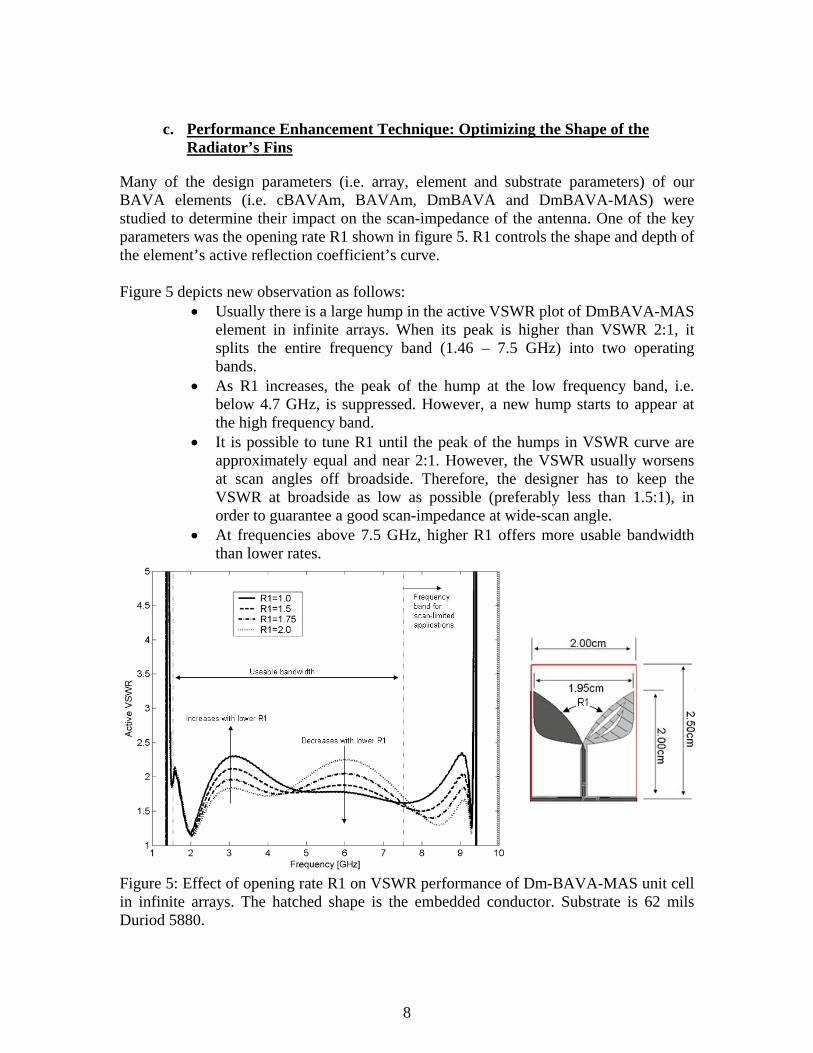
c. Performance Enhancement Technique: Optimizing the Shape of the Radiator’s Fins
Many of the design parameters (i.e. array, element and substrate parameters) of our BAVA elements (i.e. cBAVAm, BAVAm, DmBAVA and DmBAVA-MAS) were studied to determine their impact on the scan-impedance of the antenna. One of the key parameters was the opening rate R1 shown in figure 5. R1 controls the shape and depth of the element’s active reflection coefficient’s curve. Figure 5 depicts new observation as follows:
• Usually there is a large hump in the active VSWR plot of DmBAVA-MAS element in infinite arrays. When its peak is higher than VSWR 2:1, it splits the entire frequency band (1.46 – 7.5 GHz) into two operating bands.
• As R1 increases, the peak of the hump at the low frequency band, i.e. below 4.7 GHz, is suppressed. However, a new hump starts to appear at the high frequency band.
• It is possible to tune R1 until the peak of the humps in VSWR curve are approximately equal and near 2:1. However, the VSWR usually worsens at scan angles off broadside. Therefore, the designer has to keep the VSWR at broadside as low as possible (preferably less than 1.5:1), in order to guarantee a good scan-impedance at wide-scan angle.
• At frequencies above 7.5 GHz, higher R1 offers more usable bandwidth than lower rates.
Figure 5: Effect of opening rate R1 on VSWR performance of Dm-BAVA-MAS unit cell in infinite arrays. The hatched shape is the embedded conductor. Substrate is 62 mils Duriod 5880.
8

The flared conductors of the BAVA, figure 6a, seem to serve as a single-stage impedance transformer for the traveling wave from the radiating element into the free space. Some performance improvement may be achieved by modifying the shape of the flared conductors to mimic a multiple-stage impedance transformer. This is possible by splitting the curve of the flared conductors into two exponential curves, where each is controlled by a unique opening rate, R1a and R1b as is shown in figure 6b. The values of those rates are optimized to achieve best response in the impedance match. Figure 6c depicts the broadside active VSWR results for the two design approaches shown in figure 6a and figure 6b. In this design, having two stages opening rates offers better control on the active VSWR between 4.5 GHz – 7 GHz. This technique is attractive for wide-band phased array applications, but may not be as good for scan-limited arrays.
[a] [b]
[c]
Figure 6: Affect of modifying the shape of the flare in DmBAVA-MAS in infinite arrays. [a] Traditional design with a single-stage opening rate, R1. [b] Evolved design with two stages opening rates, R1a and R1b. [c] Active VSWR performance for the antennas with different thickness of Duriod 5880 (εr=2.2) substrates. Hatched shape is the embedded conductor. Grating lobe is at 7.5 GHz.
9

d. Measurement Verification of DmBAVA-MAS Performance
The experimental setup and measurement procedure in parallel plate waveguide simulator applied in reference [3] has been used in this paper. A BAVA array with magnetic slot elements was fabricated using two 31 mil Rogers Duriod 5880 substrates. The antenna’s key design parameters are shown in figure 7. The overall dimensions of the radiating element are about 2 cm wide by 2.25 cm deep.
Figure 7: AutoCAD layout for waveguide simulator element. All units are in inches. The hatched shape is the embedded conductor. Substrate thickness is 62 mils. The solid black shape is the profile of the outer conductors. The substrate is counter-bored at the bottom to solder the element to an SMA connector. There was a mistake in the drawing that was sent to the fabrication shop. The vertical segment, Cr1, of the triline section was made 0.5cm longer than it should be. Thus, the total depth of the built antenna becomes 2.75cm instead. This caused a disagreement between the original simulated and the measured data as is depicted in figure 8. When the simulated model is modified to reconcile the fabricated antenna (i.e. with longer Cr1), the results agrees well as is shown in figure 9.
10

Figure 8: Simulated active reflection coefficient of DmBAVA-MAS with two different lengths of Cr1. The original design has a 6.2:1 operation at broadside.
Figure 9: Simulated vs. measured active input impedance of DmBAVA-MAS with Cr1=1.5cm, i.e. the wrong design.
11

3. High Performance Arrays of Balanced Antipodal Asymmetric Vivaldi Antenna (BA2VA)
In section 3.3.2 of reference [10], it is concluded that Anomaly #1 in BAVA antenna is caused by the mutual coupling and interaction with neighboring elements in the array. This mutual coupling drives a strong current on the triline section of BAVA which radiates as a Monopole Antenna overpowering the radiation from the flared-arms [11]. The solution was to perturb the mutual couplings by adding metallic crosswalls between the neighboring elements which led to the doubly-mirroring technique [6]. In this section, a second approach to move Anomaly #1 outside the intended frequency band of operation is discussed. It was found that changing the profile of the BAVA’s triline segment will move the frequency at which Anomaly #1 may occur. Since the embedded conductor (i.e. stripline feed) controls the characteristic impedance of the antenna, it can’t be altered. However, the shapes of the BAVA’s outer conductors are changed to resemble that is depicted in figure 10. Basically, the new outer conductors have a continuous sheet of metal connecting the outer flared arms with the ground plane of the array.
Figure 10: Transformation from BAVA (left-hand side) into BA2VA (right-hand side). The hatched conductor is the embedded stripline feed. Vias are not shown for clarity. This new BAVA design is called a Balanced Antipodal Asymmetric Vivaldi Antenna (BA2VA). In figure 11, Anomaly #1 that used to be at 7.3 GHz in cBAVA has moved to 10.53 GHz in the BA2VA structure, which is beyond the grating lobe frequency. Figure 12 depicts the scan VSWR of the new antenna, and shows that the array has approximately an octave bandwidth for scan volume < 45o and VSWR <3:1.
12

. [a]
[b] [c]
Figure 11: Performance of BA2VA. [a] Active reflection coefficient. [b] Smith chart of cBAVA. [c] Smith chart of BA2VA. Design parameters: R1=1.5 cm-1, R2=-5.2 cm-1, R3=-10 cm-1, Cr1=0.5 cm, Cr2=1.0 cm, D=1.5 cm, A=B=1.51 cm, Ha=1.26 cm, εr=3.0, t=90 mil, Fw=0.153 cm.
13

Figure 12: Active VSWR performance of the BA2VA antenna in infinite array. Design parameters are listed in the caption of figure 11. The advantage in using BA2VA is that it is self-sufficient to move Anomaly #1 outside the intended frequency band of operation (i.e. does not require metallic crosswalls). This feature reduces the weight of the array. A second array was designed to operate over 3:1 bandwidth, Figure 13. This array is now being built.
Figure 13: Active VSWR for single polarized infinite array of BA2VA elements. Key design parameters: D=0.625 cm, A=B=0.75 cm, εr=2.2, t=62 mil.
14

4. Summary
Two enhancement techniques for the performance of the BAVA arrays have been explored through numerical simulations. Single Polarized DmBAVA-MAS finite x infinite array has been fabricated and measured in an H plane parallel plate waveguide simulator. The array confirmed high performance capabilities being electrically short (~ λHighest-Frequency/2) and is broadband (5:1). A new element design is also introduced, which is Balanced Antipodal Asymmetric Vivaldi Antenna (BA2VA). It appears to be capable of more than an octave bandwidth and wide scanning.
Acknowledgment
The authors thank the Advanced Technology Center of Rockwell Collins and the Center for Advanced Sensor and Communications Antennas (CASCA) of UMass (under contract FA8718-06-C-0047) for providing financial support and access to computational resources and Chris Merola and Gene Losik for building the antennas. These contributions are greatly appreciated.
References
1. J. D. Langley et al, “Balanced Antipodal Vivaldi Antenna for Wide Bandwidth Phased Arrays,” IEE Proceeding of Microwave and Antenna Propagations, Vol. 143, No. 2 Apr 1996, pp. 97-102
2. M.W. Elsallal and D. H. Schaubert, “Parameter study of single isolated element and infinite arrays of balanced antipodal Vivaldi antennas,” 2004 Antenna Applications Symposium, Allerton Park, Monticello, Illinois, pp. 45 – 69, 15-17 September, 2004. Monticello, IL.
3. M.W. Elsallal and D. H. Schaubert, “High Performance Phased Arrays of Doubly Mirrored Balanced Antipodal Vivaldi Antenna (DmBAVA): Current Development and Future Considerations,” 2007 Antenna Applications Symposium, Allerton Park, Monticello, Illinois, pp. 148 – 159, 18-20 September, 2007. Monticello, IL.
4. M.W. Elsallal and D. H. Schaubert, “On the Performance Trade-Offs Associated with Modular Element of Single- and Dual-Polarized DmBAVA,” 2006 Antenna Applications Symposium, pp. 166 – 187, 20-22 September, 2006. Monticello, IL.
5. D. Schaubert, M.W. Elsallal, S. Kasturi, A. Boryssenkol, M. N. Vouvakis and G. Paraschos, “Wide Bandwidth Arrays of Vivaldi Antennas,” IET Wideband, Multiband, Antennas and Arrays for Civil or Defense Applications. Mar. 13, 2008. London, UK.
15

6. M.W. Elsallal and D. H. Schaubert, “Reduced-Height Array of BAVA with Greater Than Octave Bandwidth,” Antenna Applications Symposium, pp. 226 – 242, 21-23 September, 2005. Monticello, IL.
7. Periodic Boundary FDTD (PBFDTD) Program, written by Henrik Holter. Stockholm, Sweden.
8. Ansys HFSS, version 11, www.ansoft.com.
9. MWS CST, version 2006B, www.cst.de
10. M.W. Elsallal, “Doubly-mirrored Balanced Antipodal Vivaldi Antenna (DmBAVA) for High Performance Arrays of Electrically Short, Modular Elements,” Ph.D. Dissertation Thesis, Department of Electrical and Computer Engineering, University of Massachusetts, Amherst. February 2008.
11. D. Schaubert, S. Kasturi, M.W. Elsallal and W Cappellen, “Wide bandwidth Vivaldi Antenna Arrays – Some Recent Developments,” EuCAP 2006. Nov 06 – 10, 2006. Nice, France.
16

COMPARISON OF THE BROADBAND PROPERTIES OF
ARRAYS HAVING TIME-DELAYED FOUR- AND EIGHT-
ELEMENT POLYOMINO SUBARRAYS
R. J. Mailloux, University of Massachusetts, Amherst and Air Force Research
Laboratory, Sensors Directorate, Hanscom AFB, MA
S. G. Santarelli, Air Force Research Laboratory, Sensors Directorate, Hanscom AFB,
MA
T. M. Roberts, Air Force Research Laboratory, Sensors Directorate, Hanscom AFB, MA
D. Luu, Air Force Research Laboratory, Sensors Directorate, Hanscom AFB, MA
Abstract
Arrays of time-delayed polyomino subarrays have been shown to have no
quantization lobes and low peak sidelobes for large to very large arrays. This paper
presents new results that describe the practical excitation and modeled behavior of
tetromino and octomino subarrays for wide band application. The paper shows that
equal length printed circuit power dividers can be readily implemented to excite
sections of tetromino and several types of octomino subarray based arrays. In
addition, the paper explores broadband properties and shows the following: a. the
array behavior is established by principal and diagonal plane scan data since there
are no extraordinary peak sidelobes that occur at any other scan angles. b. a
frequency scaling relationship exists between tetromino and octomino subarrays
that allows approximate bandwidth and even peak sidelobe comparison. This
relationship aids in generalizing the array behavior to estimate performance across
frequency ranges. c. Since there are no quantization lobes, the polyomino subarrays
allow sidelobes to be suppressed for arrays of up to 10:1 bandwidth, but constrained
by the gain reduction limits of the rectangular subarray. The resulting arrays are as
efficient as the rectangular subarrays, but with substantially reduced sidelobes.
1.0 Introduction
With the advent of larger arrays and requirements for increased bandwidth, there has
come a need for introducing time delay for wide angle scanning. Cost issues have
generally decreed that time delay be incorporated at the subarray level and phase shifters
at the element level to scan the subarray patterns. Rectangular subarrays are commonly
used for convenience, but these result in a fully periodic grid that radiates a series of
quantization lobes, which can cause pattern ambiguities and/or increased noise. There
have been techniques that reduce these effects by tailoring the subarray patterns [1, 2], or
by randomizing the subarray size or using random subarray shapes [3-6]. These
17

approaches do suppress or eliminate the quantization lobes, but using oddly shaped or
different size subarrays impacts the system cost and complexity. The intention of this
work has been to achieve a degree of subarray randomization using only one kind and
size of subarray in the array and to choose the subarray so that it can be fed by standard
“lossless” microwave power dividers. A degree of randomization is introduced by
rotating the subarrays, and the resulting irregular placement of subarray feed points is
readily addressed within the corporate power divider network.
Specifically, we have investigated the use of irregular polyomino subarrays in broadband
and limited-field-of-view array antennas [7, 8]. An N-element polyomino is a figure made
of N contiguous squares and named correspondingly such that a domino has two squares,
a tetromino four, and an octomino eight. There are a total of 369 octominos (and double
that amount if one considers the mirror-image figures to be different; however, usual
practice does not make that distinction). For practical reasons, we have restricted our
choice to those polyominos of order 2n, where n = 2, 4, 8 etc., and we use only one type
of polyomino (and its mirror image) in an array to simplify the power distribution and
array organization. Our goal has been to develop useful criteria for evaluating the
engineering potential of these structures.
This paper presents new results that further confirm the low sidelobe characteristics of
octomino-based arrays. In addition, it offers new criteria for determining the number of
elements in the subarray subject to bandwidth constraints and explores the operation of
these systems with ultra-wideband signals.
2.0 General Behavior of Arrays of Rotated Polyomino Subarrays
Figure 1 illustrates the use of rectangular and polyomino subarrays as time-delayed
subarrays. The array has phase shifters at each element and time delay at the subarray
input ports. The phase shifts serve to scan the subarray patterns to the desired beam
direction at center frequency, while the time delay collimates the beam over a relatively
wide frequency band. Figure 1b shows the rotation of an L-tetromino and L-octomino
subarray. A group of three-dimensional patterns shown in Figure 2 corresponds to an
array of 64 x 64 elements at f/f0 = 1.3 and u0 = v0 = 0.5, where f is the frequency of
operation, f0 is the center frequency of the array, u0 = sin0cos0, v0 = sin0cos0, and θ0
and 0 define the direction of scan. The array has a 40-dB Taylor taper, and therefore has
low side lobes at broadside and/or center frequency. All element patterns are assumed to
have a cosθ angular dependence. The left pattern in Figure 2 is that of an array with time
delay at every element. This pattern exhibits the design sidelobes of -40 dB with a pattern
gain of 37.3 dB as determined by integration. The center pattern corresponds to an array
in which the individual elements are grouped into 512 rectangular subarrays (two
elements in the elevation plane and four in the azimuth plane). This pattern has a gain of
37.03dB (approximately a 0.3-dB loss due to phase error compared to the left pattern)
and has five quantization lobes. The largest of these lobes is 11.45 dB below the gain at
18

broadside. The right pattern is produced by an array of 512 L-octominos and radiates a
main beam with a 36.83-dB gain (only 0.2 dB less than the array of rectangular
subarrays). This pattern has no quantization lobes and has sidelobes that are all at least
26.6 dB below the broadside gain.
These data are typical of results that have been presented previously to describe this
work. In general, the various polyomino-based arrays have been found to have nearly the
same gain but much smaller sidelobes than arrays of periodic, rectangular subarrays. Note
that these residual side lobes are not suppressed quantization lobes, since quantization
lobe size remains constant relative to the main bean as array size is changed. Rather, we
find that the residual side lobes of the polyomino-based arrays are reduced as the inverse
of the array area. Our experience with arrays of up to 128 elements on a side indicates
that the peak sidelobes continue to decrease by 5 to 6 dB with each quadrupling of array
area.
This paper presents illustrative results for L-octominos and L-tetrominos. These two
subarray sizes exhibit similar behavior but do so over a scaled frequency bandwidth.
Most of the data presented in this paper is recorded for the array at broadside or at the
diagonal plane scan angle u0 = v0 = 0.5. To resolve, at least partially, the issue of whether
or not there might be large spurious sidelobes for other selected scan angles that might
arise due to the repetitive rotations, Figure 3 shows the peak sidelobe of an array of 32 x
32 elements as the scan angle is varied throughout a quarter space with u0 and v0 varying
from 0 to 0.9. Apart from a small region near u and v both zero, where the sidelobe level
becomes essentially the -40 dB of the Taylor pattern, the peak sidelobe rises to a level
about 18-20 dB below the main beam peak, and its value is seen to be relatively constant
across the whole hemispherical quadrant 0 ≤ u0, v0 ≤ 0.9. There appear to be no
extraneous sidelobe peaks in the quarter hemisphere, and by symmetry, nowhere else.
Notice also that this array has roughly 6 dB higher peak sidelobes than the array of Figure
2 whose area is larger by a factor of four, indicating the aforementioned inverse
relationship with array size.
3.0 Estimates of System Bandwidth:
A uniformly illuminated linear array with time delay at the subarray input and phase shift
at the elements to scan the beam to the direction cosine u0 has its bandwidth limited by
the shape of the subarray pattern, which is a periodic sinc (p-sinc) function of the form
19

0
0
0
0
sin[ ( )]
( )
sin[ ( )]
x
x
dM ru u
f ud
M ru u
. (1)
Here, θ is the scan angle, u = sinθ (for this one-dimensional case), M is the number of
elements in the linear subarray, and dx is the inter-element spacing. The spacing dx will be
taken here as one-half wavelength at the highest operating frequency. The operating
frequency offset is r = f/f0. The amplitude of the primary quantization lobe (p = -1)
samples this voltage pattern at 1 0 , xu u where D Md
rD
. Figure 4a shows the
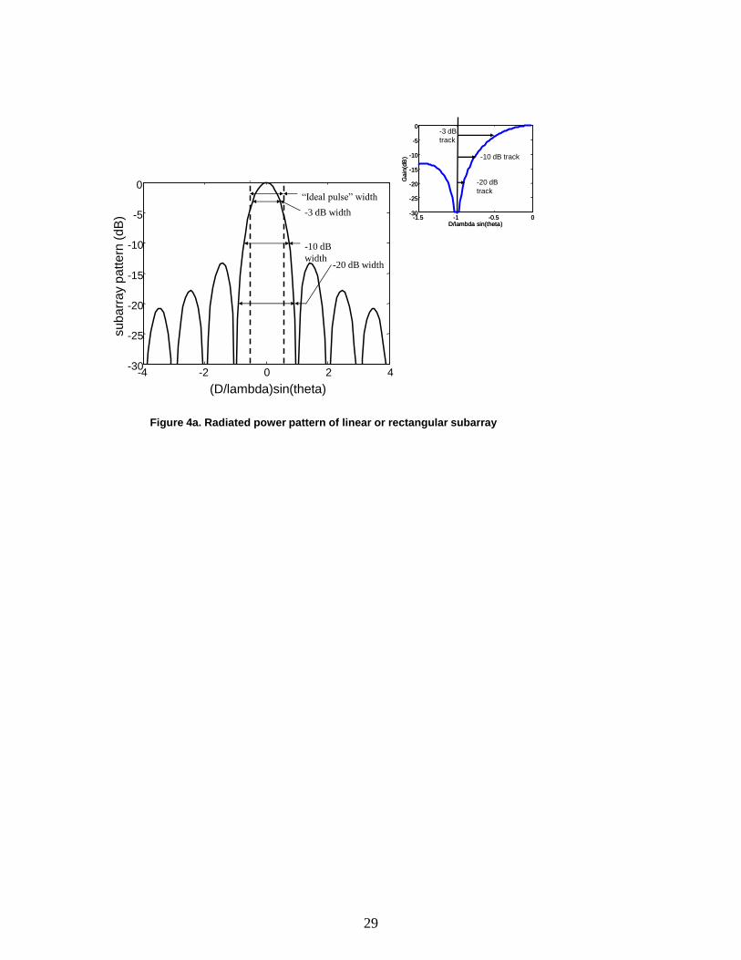
power pattern computed from the equation above, and the inset shows an expanded view
of the path of the quantization lobe across the pattern as frequency is changed. The short
horizontal arrow indicated for quantization lobe suppression of -20 dB indicates the
extremely narrow bandwidth for suppression at that level, while two other marked arrows
indicate greater bandwidth for -10 and -3 dB suppression. Figure 4b relates the fractional
bandwidth parameter 0
0
sinf
f
to subarray lengths D for various quantization lobe levels
on the p-sinc power curve. The levels chosen for comparison are the -3dB level, which is
that point at which the subarray gain (and thus the array gain) will fall by -3 dB, and
other levels at which the quantization lobe will rise to -10 and -20 dB below the beam
peak. This set of curves also includes data for the “ideal” flat-topped subarray pattern that
is often used to represent ideal conditions, but is an unachievable standard, since it has
infinitely steep slopes and a constant pass band over the desired frequency range. Notice
that it is very close to the uniform subarray gain constraint curve.
In order to estimate system bandwidth, it is imperative to define the bandwidth issues to
address. The performance of an array of time-delayed rectangular subarrays is dominated
by the levels of the various quantization lobes, which pose a severe bandwidth restriction.
As we have shown, however, the polyomino subarrays have no quantization lobes, and
for very large arrays they have peak sidelobes that are far smaller than the quantization
lobes of rectangular subarrays. For these, it is no longer the sidelobe level that ultimately
limits bandwidth, but rather the 3dB (or other selected) gain limit. Figure 4b will be
useful in choosing bandwidth limits for an array of rectangular subarrays using either
criterion. Therefore, we test the polyomino subarray-based arrays against these
bandwidth limits to compare with the rectangular subarray-based performance. Most of
the results in this paper were obtained for diagonal planes; thus, the above numerical
guidelines are conservative and predict more loss than we actually computed during our
analysis.
20

For example, an array of eight-element subarrays arranged in 2 x 4 rectangular groups
and scanned in the plane of the longer rectangle side would behave like a linear array
with four element subarrays. Using half-wave spacing at the highest frequency, the
dimension D/λ is 2. If we select a quantization lobe level of -10 dB at a 45-degree scan
angle, the parameter 0
0
sinf
f
is about 0.4 and the fractional bandwidth
0
f
f
is about 0.6.
The ratio r = fmax/f0 at the high frequency is 1.3, and we will use this value for several
Figures throughout the paper.
Figure 5 illustrates performance characteristics of both rectangular and L-octomino
subarray architectures for various array sizes. The largest arrays contain 128 elements in
each dimension, which corresponds to over 16,000 elements grouped into 2,048
subarrays. Figure 5a shows that the two gain curves are nearly coincident, and that there
is no gain penalty for using L-octomino subarrays in place of rectangular subarrays.
Figure 5b shows that for the same size array, the largest sidelobe of the L-octomino
subarray architecture is between 10 and 20 dB below those of the rectangular subarray
architecture, reaching a minimum of -32 dB below the main-beam gain at broadside for
the array of 128 x 128 elements.
The bandwidth limits of four-element rectangular (square) subarrays can be estimated
using the p-sinc pattern of Figure 4a. This is done by evaluating the p-sinc pattern at
1 0
1
u ur D
,the quantization lobe nearest to the main beam, at the highest frequency
(we use r1 to indicate this frequency for the initial subarray). The expression valid at this
quantization lobe is:
0 1 0
0 1 0
sin[ ( / )( 1) ]
sin[ ( / )(( 1) / )]
x
x x
M d r u
M d r u Md
. (2)
If we choose to force this quantization lobe to have the same level for a subarray of M2
elements in length, we can equate the above expression to the same expression evaluated
at some new higher frequency ratio r2 for the new subarray architecture with M2 elements
along its long axis. This results in the following expression for the new frequency ratio r2
in very simple terms (using the definition 02
2
r
).
12 1
2
( 1) 1M
r rM
. (3)
21

For r1 < 2, this expression is valid for both the high and low frequency limits. For r1 > 2,
it is only useful at the high frequency end of the band, because if one chooses a
symmetric bandpass this result can lead to low-end negative frequencies.
Relating the octomino M1 = 4 with r1 = 1.3 to the tetromino M2 = 2, we find that r2 = 1.6,
and the low frequency limit (based on r1 = 0.7 for the chosen octomino low frequency
limit) is r2 = 0.4.
A simpler relationship, shows that for any two subarray sizes, the frequency offset is
scaled by the ratio of subarray sizes, so that if one writes a frequency offset as δ1 = r1 - 1,
then the frequency offset δ2 = r2 - 1 becomes 12 1
2
M
M ,
or in general, the bandwidths are scaled by the subarray size ratio.
Using the scaled value of r = 1.6, Figures 6a and 6b show the gain and peak sidelobe
levels for arrays of rectangular four-element subarrays (i.e., square, 2 x 2-element
subarrays) and L-tetromino subarrays. These results are similar to the previous octomino
results in Figures 5a and 5b for r = 1.3. The gains for any given number of elements are
higher for the tetromino array of Figure 6a than the octomino array of 5a because the
tetromino array is evaluated at a higher frequency and the area gain is commensurably
larger. The sidelobe ratios of Figures 5b and 6b are 27dB and 25dB for a 64-by-64
element array, which is the largest array size common to both figures. If we define the
term “suppression” to be the difference (in dB) between the quantization lobe of the
rectangular subarray architecture and the largest sidelobe of the polyomino subarray
architecture for the largest array size, then the L-octomino suppression is 15.6 dB (Fig.
5b) and the L-tetromino suppression is 17.0 dB (Fig. 6b). This shows that if the
rectangular subarrays are frequency scaled according to the above relations, then the
primary quantization lobes are nearly equal, and the corresponding irregular subarrays,
although separately built of quasi-random subarray locations, will have very similar peak
sidelobes at their scaled frequency offset. Furthermore, the loss in gain due to the
subarray pattern for the tetromino case is only about 0.5 dB.
4.0 Wideband and Ultra-Wideband Properties of Octomino and Tetromino
Subarrays
In our previous publications, we have shown scanning arrays of L-octomino and L-
tetromino subarrays where f/f0 ranges between 0.7 and 1.3, a ratio slightly less than 2:1.
There is a growing interest in determining whether these configurations would be useful
over a much broader frequency range, and so we will test this capability with an array of
octomino subarrays over the range r = f/f0 between 0.1818 and 1.818, a ratio of 10:1.
This specific ratio was chosen to provide a symmetric bandpass region about r = 1.
22

At the high end of the band (r = 1.818), we choose the elements to be spaced one-half
wavelength and scanned to 45 degrees at the angle u = v = 0.5. The array size is 64 x 64
elements grouped into 512 rectangular or L-octomino subarrays. As in Figure 1, the
subarrays are scanned by phase shifters, and time delay is provided at the subarray
(approximate) phase center. At the high frequency, both arrays are operating at reduced
gain. The aperture gain of the 64 x 64-element array reduced by taper loss (2.28dB) and
scan loss (assumed to be cosθ at 45 degrees) is approximately 37.3 dB. Figure 7 shows
three curves of array gain as a function of array size as the size is varied from 32
elements in each dimension to 64 elements. The upper curve is for the array with time
delay at every element (i.e., no subarrays). The gain for this case, computed by
integration, is 37.29 dB for an array size of the 64 x 64 elements. Note that this is the
same value as computed above using taper and scan losses. The two other curves of
Figure 7 show the integrated gain for the rectangular and L-octomino subarray
architectures. The gain of the array of rectangular subarrays is 1.43 dB below the time-
delayed array, and the gain for the L-octomino array is another 0.37 dB less. This
additional loss for the two subarray cases is due to the subarray patterns themselves, since
the main beam is time-delayed to be at the desired scan angle, but the subarray patterns
“squint” so that their maxima are no longer directed at the main beam.
Figure 8 shows far-field patterns of a 64 x 64-element array when both rectangular and L-
octomino subarray architectures are implemented. The rectangular patterns are shown on
the left, and the L-octomino patterns are shown on the right. The top patterns in each
column provide a 3-D view of u-v space, whereas the bottom patterns are projections of
the 3-D patterns along the line u = v. The array of rectangular subarrays produces a main
beam and 5 quantization lobes in real space. The main beam gain is approximately 5 dB
below the area gain (shown at 0 dB in the figures). The largest quantization lobe is only 6
dB below the main beam, and the others are all only 15 dB below the main beam or
higher. The array of L-octominos produces a main beam with gain reduced by an
additional 0.37 dB (when compared to the rectangular case); however, the largest side
lobe is below -20 dB.
Figure 9 shows the level of the largest sidelobe for the L-octomino architecture and the
largest quantization lobe for the rectangular architecture as a function of array size for r =
1.818. For the 64 x 64 array, these values are -5.74 dB for the rectangular case and -21.05
dB for the L-octomino case – a 15.3 dB suppression advantage. Note that this curve is
very similar to that of Figure 5b, which also shows approximately 15.6 dB peak-sidelobe
suppression compared to the rectangular case. The array of Figure 5b is an entirely
different array of 128 x 128 elements operating at a different frequency (r = 1.3), but
scanned to the same angle. This illustrates that for a given subarray type, the suppression
is nearly independent of offset frequency; thus, changing the frequency changes the
quantization lobe levels of the rectangular subarray architecture, but the sidelobe
reduction ratio (i.e., max rectangular quantization lobe – max L-octomino side lobe) is
relatively constant.
23

Figure 10 shows the radiation patterns of the rectangular and L-octomino-based arrays at
r = 0.1818 (one-tenth of the frequency shown in Figure 8). Since the elements are spaced
only 0.05 apart, neither array has any quantization lobes. The pattern of the rectangular
case has side lobes as given by the array taper (about -40 dB), and has no quantization
lobes because at this close spacing the quantization lobes are in imaginary space.
The pattern of the L-octomino case exhibits an added lobe at about -35dB because of the
error that results from the time delay that randomizes the element phase errors.
Figures 11 through 13 present data for L-tetrominos for a very wide operating band in
which the high frequency is 1.905 times the base frequency. This ratio was chosen to
make a 20:1 passband symmetric about r = 1. Figure 11 shows again that the tetromino
subarrays have only slightly less gain than the four-element square subarrays, and Figure
12 shows that the sidelobe suppression for an array of 32 x 32 elements is about 12.7 dB,
as it is for the r = 1.3 case of Figure 6b. Comparing the 64 x 64-element arrays, the
suppression is 16.7dB in Figure 12, and 17dB in Figure 6b. This confirms that the
tetromino arrays can possess maximum side lobes near -30 db for a 64 x 64-element array
(Figure 13), and that the suppression (the difference between the rectangular array
quantization lobe and the polyomino peak sidelobe) is nearly constant over a very wide
frequency band.
5.0 Conclusion
This paper has presented data relating to octomino and tetromino subarrays in a phased
array with time delay at the subarrays and phase shift at the element level. We have
quantified the advantages of these subarrays relative to rectangular subarrays and have
compared the bandwidth properties of the tetromino and octomino subarrays.
Suppression of the quantization lobes is relatively constant even as bandwidth ratios vary
from 2:1 to 20:1. There is very little loss of gain due to using polyomino subarrays as
compared with rectangular subarrays, and the sidelobe suppression is both predictable
and significant.
With arrays of size 32 x 32 elements, one obtains about 10-11 dB sidelobe suppression
for a tetromino subarray architecture and about 13 dB suppression for an octomino
subarray architecture, regardless of the frequency of operation (within the design band).
For 64 x 64-element arrays, one obtains about 15 dB suppression by using octomino
subarrays and 17 dB suppression by using tetromino subarrays (again, for any frequency
tested).
The bandwidth of large polyomino subarrayed systems is primarily limited by reduced
gain at the high frequency, and not by any sidelobe condition.
24

6.0 References
[1] S.P. Skobelev,” Methods of constructing optimum phased-array antennas for limited
field of view,” IEEE Antennas and Propagation Magazine, Vol 40, No. 2, April 1998,
pp. 39-49
[2] S.M. Duffy, D.D. Santiago and J.S. Herd,“Design of overlapped subarrays using an
RFIC beamformer,” 2007 IEEE AP-S International Symposium, June 10-15 2007, paper
#207.9
[3] V. Pierro, G. Galdi, G. Castaldi, I.M. Pinto, L.B. Felson, “Radiation properties of
planar antenna arrays based on certain categories of aperiodic tilings,” IEEE Trans. AP-
53 No. 2, Feb 2005, pp. 635-664
[4] K.C. Kirby, J.T. Bernhard, “Sidelobe level and wideband behavior of arrays of
random subarrays,” IEEE Trans AP-54, No. 8, Aug 2006, pp. 2253-2262
[5] R.L. Haupt, “Optimized weighting of uniform subarrays of unequal sizes,” IEEE
Trans. Antennas Propag., Vol 53, pp. 1207-1210, April 2007
[6] H. Wang , D-G Fang and Y.L. Chow, “Grating lobe reduction in a phased array of
limited scanning,” IEEE Trans. Antennas Propag., Vol 56, pp. 1581-1586, June 2008
[7] R.J. Mailloux, S.G. Santarelli, T.M. Roberts, “Wideband arrays using irregular
(polyomino) shaped subarrays,” Electronics Letters, 31Aug 2006, Vol 42, No 18, pp.
1019-1020
[8] R.J. Mailloux, S.G. Santarelli, T.M. Roberts, B.C. Kaanta, “Sidelobe and Gain
Characteristics of Large Arrays with Polyomino Subarrays,” Antenna Applications
Symposium, Monticello, IL, Sept. 2007
7.0 Acknowledgements
This work was supported in part by the Air Force Office of Scientific Research under Dr.
A. Nachman, and in part by the Center for Advanced Sensor and Communications
Antennas, Department of Electrical and Computer Engineering, University of
Massachusetts, Amherst, MA 01003. The work was performed at the Air Force Research
Laboratory, Sensors Directorate, Hanscom AFB, MA 01731-2909.
25

Phase shifters
Input time delay
1a. Subarray for time delay 1b. Rectangular and Polyomino Subarrays
Figure 1: Subarrays for Time Delayed Arrays
Rectangular
subarrays
with time delay
Time delay input
Phase shifters at elements
L-octomino
subarrays with
time delay
Four rotations of the L - OctominoRectangular
subarray
Four rotations of the L -Tetromino Subarray
Four rotations of the L - Octomino SubarrayRectangular
subarrayFour rotations of the L - OctominoRectangular
subarray
Four rotations of the L -Tetromino Subarray
Four rotations of the L -Rectangular
26

Figure 2: 64 x 64 array, f/f0 =1.3
Time delay at every
element
Time delay at
rectangular subarray
inputs
Time delay at L-
octomino subarray
inputs
27

3-D mesh pattern
2-D Projected pattern
Figure 3: Peak sidelobe level vs scan angle for a 32 x 32 element array of L-
octomino subarrays (r =1.3)
00.2
0.40.6
0.81
0
0.5
1-60
-50
-40
-30
-20
-10
0
Peak sidelobes for any scan angle in u,v
0 0.2 0.4 0.6 0.8 100.51
-60
-50
-40
-30
-20
-10
0
Peak sidelobes for any scan angle in u,v
28
-1.5 -1 -0.5 0-30
-25
-20
-15
-10
-5
0
D/lambda sin(theta)
Gain
(dB
)
-1.5 -1 -0.5 0-30
-25
-20
-15
-10
-5
0
D/lambda sin(theta)
Gain
(dB
)
(D/lambda)sin(theta)
subarr
ay p
attern
(dB
)
-4 -2 0 2 4-30
-25
-20
-15
-10
-5
0“Ideal pulse” width
-3 dB width
-10 dB
width-20 dB width
Figure 4a. Radiated power pattern of linear or rectangular subarray
-20 dB
track
-10 dB track
-3 dB
track
29

Figure 4b . Bandwidth factor for linear or rectangular subarrays vs. subarray length
0 2 4 6 8 100
0.2
0.4
0.6
0.8
1
1.2
1.4
1.6
1.8
D/λ0
“Ideal” subarray
-3 dB (gain constraint)
-10 dB (sidelobe constraint)
-20 dB (sidelobe constraint)
0
0
sinf
f
30

Figure 5a. Gain for arrays of Rectangular and L-octomino subarrays (r = 1.3)
L-Octomino
subarrays
Rectangular
subarrays
0 50 100 1500
10
20
30
40
50
Number of Elements on Each Side
Gain
(dB
)
RECTANGULAR
L-OCTOMINO
31
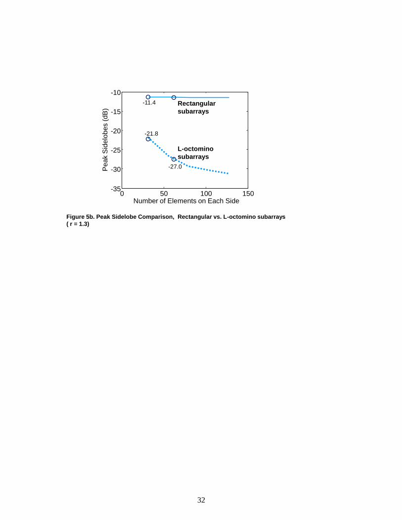
Figure 5b. Peak Sidelobe Comparison, Rectangular vs. L-octomino subarrays
( r = 1.3)
0 50 100 150-35
-30
-25
-20
-15
-10
Number of Elements on Each Side
Peak S
idelo
bes (
dB
)Rectangular
subarrays
L-octomino
subarrays
-11.4
-21.8
-27.0
32

Figure 6a. Gain for arrays of Rectangular and L-tetromino subarrays (r = 1.6)
0 20 40 60 8020
25
30
35
40
Number of Elements on Each Side
Gain
(dB
)
Rectangular
subarrays
L-tetromino
subarrays
33

0 20 40 60 80-35
-30
-25
-20
-15
-10
Number of elements on Each Side
Peak S
idelo
bes (
dB
) -12.6-12.6
-25.2
-29.6
Figure 6b. Peak sidelobe comparison
Rectangular vs. L-tetromino subarrays (r = 1.6)
Rectangular
subarrays
L-octomino
subarrays
34

30 40 50 60 7028
30
32
34
36
38
Number of Elements on Each Side
Gain
(dB
)
Fig. 7. Gain comparison: time delay at each element vs. rectangular vs. L-
octomino subarrays (r = 1.818, 10:1 bandwidth)
Time delay at
elements
Time delay at rectangular
subarrays
Time delay at L-
octomino
subarrays
35

Figure 8. 64 x 64 Arrays at r = 1.818 (Lower patterns are projections along
the line u = v.)
uv
AM
PL
ITU
DE
[d
B]
uv
AM
PL
ITU
DE
[d
B]
uv
AM
PL
ITU
DE
[d
B]
uv
AM
PL
ITU
DE
[d
B]
RECTANGULAR L-OCTOMINO
36

30 40 50 60 70-25
-20
-15
-10
-5
Number of Elements on Each Side
Peak S
idelo
bes (
dB
)
Figure 9. Peak Sidelobe Comparison, Rectangular
vs. L-octomino subarrays (r = 1.818)
L-octomino
subarrays
Rectangular
subarrays-5.74
-21.1
-5.74
-16.59
37

Figure 10. 64 x 64 element array, rectangular and L-octomino
subarrays, r = 0.1818
uv
AM
PL
ITU
DE
[d
B]
RECTANGULAR L-OCTOMINO
u
v
38

0 20 40 60 8020
25
30
35
40
Number of Elements on Each Side
Gain
(dB
)
Figure 11. Gain for arrays of Rectangular and L-
tetromino subarrays (r = 1.905).
Rectangular
subarrays
L-Tetromino
subarrays
39

L-tetromino
subarrays
Figure 12. Peak Sidelobe Comparison,
Rectangular vs. L-tetromino subarrays (r = 1.905)
Rectangular
subarrays
-10.87 -10.88
-23.56
-27.61
0 20 40 60 80-30
-25
-20
-15
-10
Number of Elements on Each Side
Peak S
idelo
bes (
dB
)
40

Figure 13. 64 x 64 element array,
rectangular and L-tetromino subarrays
(r=1.905)
uv
AM
PL
ITU
DE
[d
B]
RECTANGULAR L-tetromino
uv
41

BROADBAND ARRAY ANTENNA
Mike Stasiowski Cobham Defense Electronic Systems
Nurad Division 3310 Carlins Park Drive Baltimore, MD 21215
Dan Schaubert Antennas and Propagation Laboratory Electrical and Computer Engineering
100 Natural Resources Road University of Massachusetts
Amherst, MA 01003
Abstract: The continued convergence of radar, electronic warfare and communication applications require advances in broad band phased array antennas, including both performance improvements and development of manufacturing technology. Nurad and the University of Massachusetts collaborated to design and fabricate 3:1 and 9:1 bandwidth arrays. The first array designed and tested was a 3:1 band phased array. Using lessons learned from that antenna, a 9:1 band array antenna was designed. The results showed that acceptable electrical performance is readily available and that the manufacturing of the array was vastly more complex than originally expected. This presentation discusses the electromagnetic simulation results and compares them to the measured data, while focusing on manufacturing issues and advancements.
1 BACKGROUND
1.1 Design Baseline: University of Massachusetts Antenna Several arrays with bandwidths up to 5:1 have been designed by the University of Massachusetts. The dual-polarized array in Figure 1 is a frequency-scaled prototype for an early design of the Square Kilometer Array radio telescope. Numerical simulations predicted this array to operate with VSWR<2 from 1-5 GHz and scanning to 450 in any plane. The 144-element array (8x9x2) in Figure 1 was extensively tested [1] and its performance was quite good, even in such a small array.
42

VSWR of Central Element
Broadside Beam
1 2 3 4 5 6 71
1.5
2
2.5
3
3.5
4
4.5
5
5.5
6
Frequency (GHz)
VS
WR
Figure 1. Dual-polarized Vivaldi array designed for Square Kilometer Array radio telescope. VSWR for broadside beam is computed from measured coupling coefficients in 8x9x2 array. The low-frequency performance is affected by truncation - the array is only 2 wavelengths square at 2 GHz.
Based on prior experience with single- and dual-polarized Vivaldi arrays and on the reported results of others, e.g., [2], the 9:1 bandwidth array was designed using the Vivaldi element. The Vivaldi element is very attractive for phased array applications because it can the fed directly from stripline or microstripline, the balun is an integral part of the antenna structure. The Vivaldi elements of the completed array operate over the same frequency range as the array in [2] but our elements are shorter than the design presented in [2], 45mm compared to approximately 62mm.
1.2 Notch & Horn Antennas Single element notch and horn antennas have been used in a variety of military applications, most notably Electronic Counter Measure (ECM) systems that require moderate to wide bandwidth, wide angular coverage, specific polarization control, and high power handling capability. Several examples are shown in Figure 2.
Nurad offers high power horn antenna designs with characteristics such as broad frequency ranges to cover 3:1 bandwidths, lensed apertures to provide beamwidth and pattern control and unique machined/angled apertures to solve difficult installation problems. Also available are special horn designs with bandwidths up to 9:1. These offer the clear advantage of using one antenna to cover larger frequencies instead of having several antennas covering the same frequencies. Nurad currently offers existing horn antennas from 100 MHz to 96 GHz for various applications with linear, circular, dual linear, and simultaneous circular polarizations
43

Nurad also offers extended bandwidth horns to meet special customer requirements. Phase and amplitude tracking characteristics can be incorporated and matched sets can be provided for specific applications.
Horn antenna’s featured rugged construction and a lightweight, moisture sealed design make them well suited for extreme conditions of airborne platforms. Typical applications include ECM and other direction finding systems for both airborne and shipboard systems.
Figure 2: Legacy ECM Antennas
A common feature of all of these single element antennas is radiation pattern coverage of a defined (and usually wide) angular sector. The purpose of the research reported here is to develop an array antenna with that covers the same angular sector with a narrow and electronically steerable beam.
2 DESIGN & MODELING
2.1 Design Goals (3:1) Nurad has threshold and objective design goals for the antenna array. The threshold is a 3:1 band width array. This array was designed not to push state of the art, but to start the process of understanding the manufacturing processes involved as well as working through the design process using the CAD resources available and creating a stepping stone design to the objective 9:1 bandwidth array.
44

Table 1. 3:1 Array Threshold Design Goals
Frequency 6-18 GHz VSWR 2.5:1 max Gain 10log(N)+ge Weight Minimize
Size 16 x 8 elements (no depth requirement)
Power 5 W per element Target Environment Airborne Military
Table 2. 9:1 Array Objective Design Goals
Frequency 2-18 GHz VSWR 2.5:1 max Gain 10log(N)+ge Weight Minimize Size 128 x 64 elements 2.2” thick Power 5 W per element Target Environment Airborne Military
2.2 CAD Tool The arrays were designed by using efficient computer simulations to estimate the performance of candidate element geometries. The candidate elements were modified based on design curves developed at the University of Massachusetts [3] [4] [5] until satisfactory performance was achieved. Each array design requires numerous computer simulations of the array performance to optimize the element geometry, so the infinite array approximation was used. This approximation greatly reduces computation time but fails to capture truncation effects. Nevertheless, infinite array approximations have previously been shown to yield reasonably good predictions of performance for elements that are located at least two wavelengths from the array edge.
Several commercial and proprietary electromagnetic simulators can be used for the infinite array analysis. The finite-difference, time-domain (FDTD) solver for periodic boundary conditions, PB-FDTD [6], is particularly well-suited for wide-band array design. This simulator combines the efficiencies of the FDTD algorithm and unit cell modeling, and it provides a rigorous solution for beam steering in the principal planes. The input impedance of a coarse-resolution model for the 9:1 dual-polarized array can be analyzed over the frequency range of interest at a single scan angle in about 30 minutes on a typical desktop computer. Once a reasonably good design is achieved, a fine-resolution model can be evaluated to verify and tune the performance.
45

2.3 Egg Crate The chosen design is an “egg crate” design where the boards cross at the edge of each element. A conceptual sketch is shown in Figure 3. This differs from the cross design in that the phase center of the orthogonal elements are offset from one another; however, the fabrication methods are simplified considerably over the cross design. In addition, this type of design builds on the legacy of other University of Masachusetts antenna designs so the particular characteristics are well understood.
16 mm
7.5 mm
7.5 mm
1 mm
Requires electrical connection at all intersections.
Figure 3. Egg Crate Design
2.4 Notches The elements were designed in rows and columns for ease of assembly and positional accuracy. Since these boards would interfere with each other as they cross, notches were cut into the boards as shown in Figure 4.
46

Figure 4. Notching of Elements
2.5 Notch Element Cross Section (3:1 & 9:1) The 3:1 notch element has a cross section as shown in Figure 5. The stripline-fed Vivaldi antenna element design is reasonably standard for the required 3:1 bandwidth. The element spacing in the array was chosen to be 0.45 wavelengths at the highest frequency of operation, 18 GHz [7]. Vivaldi antenna arrays exhibit several impedance anomalies when the element spacing exceeds 0.5 wavelengths, and scan performance usually degrades for element spacing greater than 0.45 wavelengths. The desired scan range of the array was 60°.
Arlon AD-250, εr=2.5, was initially selected for the substrate material because it is relatively low cost and has low loss. This was later changed due to manufacturing problems that are described below. The element design utilized a stripline assembly to minimize radiated effects from the transmission line and was fabricated by using two 0.020” boards, total thickness = 1mm. Element depth was not critical and was adjusted for good electrical performance. The stripline design has plated through holes or vias to keep the outer circuit layers at the same potential and suppress parallel-plate and waveguide modes in the dielectric region. Figure 5 is a diagram of the final element showing the feed line placement and approximate location of the vias. The image is not to scale, but is representative of the final configuration.
47

y = 3.2
z
y
z=0 z=-12.3z=-13.0
z=-16.0
y = 3.75
Substrate of orthogonal antenna
Vias outline circuit features spaced approx 2 mm
Connectors, mounting parts, etc, left of this line.
50-Ohm, w ~ 0.7mm
Figure 5. 3:1 Notch Element Cross Section
2.6 Predicted Results Initial modeling of the array showed good performance over the design band. The method used for evaluation was active array impedance and VSWR plots. VSWR of the array at broadside angle is less than 1.5 over most of the design band. At 45° incidence angle, both E and H-plane VSWR is also excellent and no anomalous behavior is observed. Figure 6 shows the VSWR plots for broadside and 45° beam pointing angles. Note that all of the simulation results are based on an infinite array simulation so truncation effects are not included in the VSWR simulations. Since the simulation was of an infinite array, no pattern performance was predicted.
48

SWR for Broadside Beam (Z0=50)
SWR 450 E-Plane Beam
SWR 450 H-Plane Beam
Figure 6. Predicted Infinite Array Results
49

2.7 Active VSWR Finite Array (3:1) Active VSWR predictions for a finite array were not run. This is due to computational limitations. The very small feed lines of the array would require very small meshing to accurately simulate combined with the electrically large array, ~7.2 lambda at 18 GHz, would create a long simulation time. The intent of the array was to demonstrate capability and was intended as a sub-array into a larger array. Therefore, Nurad felt that little was to be gained by simulating the finite array active VSWR.
2.8 Active VSWR Infinite Array (9:1) The 3:1 array was relatively easy to design, and its fabrication and testing provided valuable lessons that were incorporated into that design of an array covering 2-18 GHz. The electrical design of this array was more challenging than the previous array because of the bandwidth requirement. The antenna element resembles the one for the 3:1 design, except it is much longer to operate at the lower frequencies, Figure 7.
45 mm
7.5 mm
Figure 7. Sketch of 9:1 bandwidth array element. This sketch is approximately to scale. Actual feed
line was fabricated with radius bend instead of square corner
This element was designed by using full-wave, infinite-array simulations. The predicted VSWR of the element in a large (infinite) array is shown in Figure 8. The predicted VSWR for broadside angle is mostly below 1.5 and the VSWR at 450 scan is below 2:1 except for a small excursion near 5 GHz.
50

Figure 8. Predicted VSWR of array designed for 2-18 GHz for three scan angles. Computed at 50-
Ohm transmission line that feeds antenna
The element is fed by stripline comprised of two 0.010” Duroid 5880, εr=2.2, substrates, total element thickness is 0.5 mm. Element spacing is 7.5 mm, the same as the 3:1 array. Vias spaced approximately 2mm outline the element similar to Figure 5.
51

3 FABRICATION & MEASUREMENTS
3.1 Cross Section Views, Material & Technology A view of the CAD design is shown in Figure 9. The boards were notched to allow the orthogonal array apertures to be at the same plane. The design requires the elements to be soldered at the board joints. Due to the frequency range and the resultant spacing of the elements, soldering of the individual elements would be extremely difficult and time consuming. Nurad used edge plating of the slots to allow better soldering between the two circuit boards at the adjacent elements. As it turned out, the contact provided by the edge plating was sufficient to eliminate the need for soldering along the joint. This is only applicable for the lab unit, and would require some type of mechanical attachment on a flight unit.
Figure 9. CAD Model of Element
3.2 Connectors Because the array was to be extensively tested – impedance, coupling, radiation patterns – each element of the array was connectorized. Due to the large number of radiating elements and subsequent number of connectors, simple press-on connections were highly desirable. Simple connection to the circuit board was also required. Based on element size and the space available, SMPM connectors were the best choice. There are many different SMPM connector styles that could have been used for this application; however, the primary drivers were ease of installation and connector location tolerance. Radial misalignment due to tolerance buildup of up to 16 connectors was a concern; therefore a mechanism for alignment of the connectors to the board was important. The selected connector is shown in Figure 10. This type of connector was chosen due to the captive center conductor as well as the connector body protrusion through the board which allows the connector location to be controlled by the circuit board fabrication.
52

Figure 10. Connector Type
3.3 8 x 16 Array A photo of the competed 3:1 array is shown in Figure 11. The radiating direction is up in the picture, with the connectors placed on the bottom. The array was fabricated using two layers of 0.020” thick material laminated together.
Figure 11. Completed 3:1 Array
3.4 Assembly Scheme Notches allowing the orthogonal boards to nest together were cut into each stick. These notch lengths are arbitrary and worked out best from a mechanical layout perspective to be different lengths. For the 3:1 band array, 16 of the short boards and 8 of the long boards would be required to fully populate the array. Figure 12 shows an example of each of the board types. Note that each edge of the notches was plated allowing contact with the orthogonal board.
53
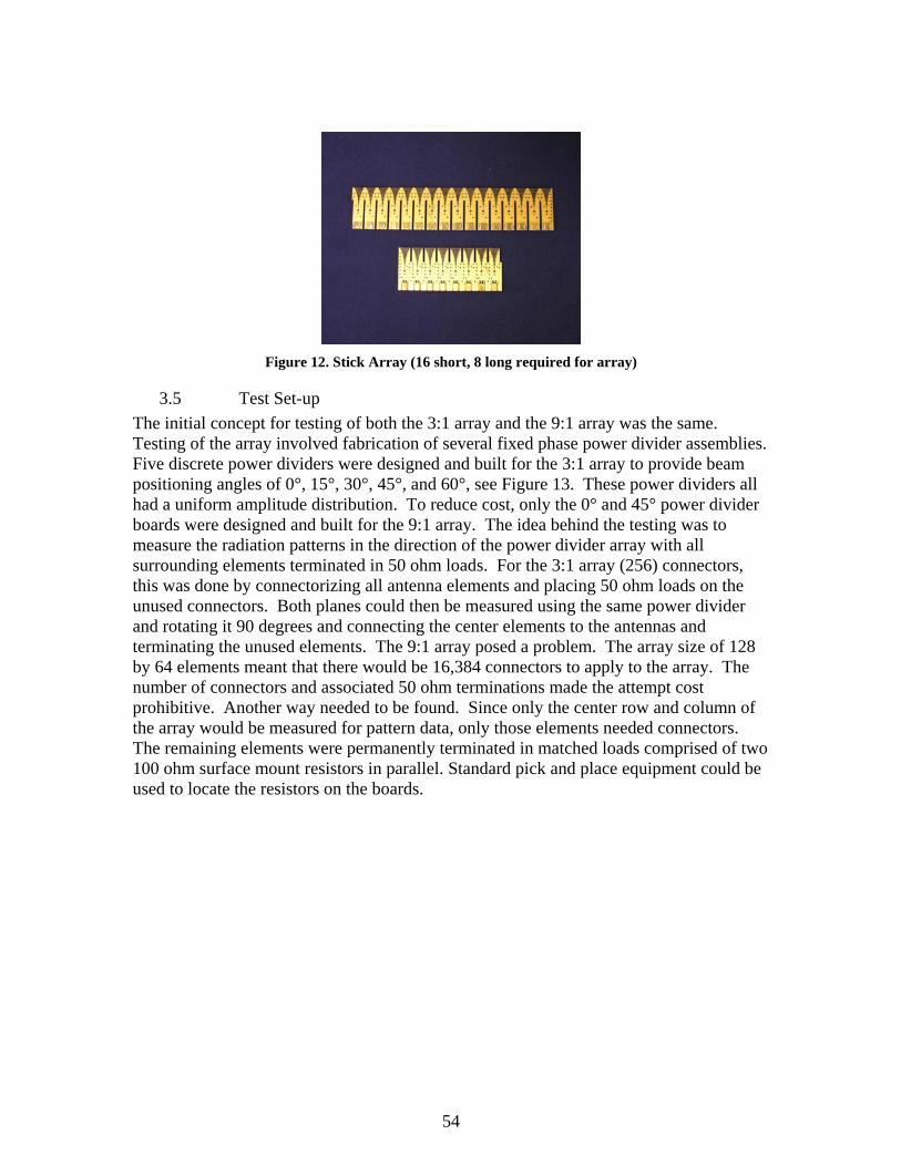
Figure 12. Stick Array (16 short, 8 long required for array)
3.5 Test Set-up The initial concept for testing of both the 3:1 array and the 9:1 array was the same. Testing of the array involved fabrication of several fixed phase power divider assemblies. Five discrete power dividers were designed and built for the 3:1 array to provide beam positioning angles of 0°, 15°, 30°, 45°, and 60°, see Figure 13. These power dividers all had a uniform amplitude distribution. To reduce cost, only the 0° and 45° power divider boards were designed and built for the 9:1 array. The idea behind the testing was to measure the radiation patterns in the direction of the power divider array with all surrounding elements terminated in 50 ohm loads. For the 3:1 array (256) connectors, this was done by connectorizing all antenna elements and placing 50 ohm loads on the unused connectors. Both planes could then be measured using the same power divider and rotating it 90 degrees and connecting the center elements to the antennas and terminating the unused elements. The 9:1 array posed a problem. The array size of 128 by 64 elements meant that there would be 16,384 connectors to apply to the array. The number of connectors and associated 50 ohm terminations made the attempt cost prohibitive. Another way needed to be found. Since only the center row and column of the array would be measured for pattern data, only those elements needed connectors. The remaining elements were permanently terminated in matched loads comprised of two 100 ohm surface mount resistors in parallel. Standard pick and place equipment could be used to locate the resistors on the boards.
54
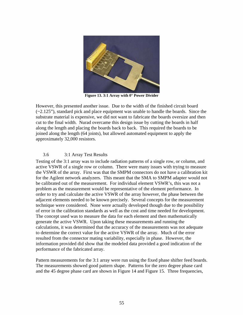
Figure 13. 3:1 Array with 0° Power Divider
However, this presented another issue. Due to the width of the finished circuit board (~2.125”), standard pick and place equipment was unable to handle the boards. Since the substrate material is expensive, we did not want to fabricate the boards oversize and then cut to the final width. Nurad overcame this design issue by cutting the boards in half along the length and placing the boards back to back. This required the boards to be joined along the length (64 joints), but allowed automated equipment to apply the approximately 32,000 resistors.
3.6 3:1 Array Test Results Testing of the 3:1 array was to include radiation patterns of a single row, or column, and active VSWR of a single row or column. There were many issues with trying to measure the VSWR of the array. First was that the SMPM connectors do not have a calibration kit for the Agilent network analyzers. This meant that the SMA to SMPM adapter would not be calibrated out of the measurement. For individual element VSWR’s, this was not a problem as the measurement would be representative of the element performance. In order to try and calculate the active VSWR of the array however, the phase between the adjacent elements needed to be known precisely. Several concepts for the measurement technique were considered. None were actually developed though due to the possibility of error in the calibration standards as well as the cost and time needed for development. The concept used was to measure the data for each element and then mathematically generate the active VSWR. Upon taking these measurements and running the calculations, it was determined that the accuracy of the measurements was not adequate to determine the correct value for the active VSWR of the array. Much of the error resulted from the connector mating variability, especially in phase. However, the information provided did show that the modeled data provided a good indication of the performance of the fabricated array. Pattern measurements for the 3:1 array were run using the fixed phase shifter feed boards. The measurements showed good pattern shape. Patterns for the zero degree phase card and the 45 degree phase card are shown in Figure 14 and Figure 15. Three frequencies,
55

6, 11 and 18 GHz are overlaid on each pattern. The gain of the patterns is not compensated for the loss of the power divider network. Based on the measurements of the power divider, the power lost in the divider assembly is 5.9 dB at 6 GHz, 12.6 dB at 11 GHz and 16.4 dB at 18 GHz. These values track within the measurement error of the theoretical loss of the divider. Therefore, to determine the gain of the array, without the power divider, the peak gain of the assembly should be added to the loss of the power divider.
Figure 14. 0° Card Patterns
56

Figure 15. 45° Card Patterns
3.7 Fabrication of the 9:1 Array The 9:1 array was intended to be built upon the success of the 3:1 array. The manufacturing processes and materials were initially intended to be the same for both. However, as the 3:1 array was being designed and built it was realized that a variety of issues would make it difficult to build them the same. Due to the increased frequency band, the antenna boards needed to be thinner than on the 3:1 array. A positive of using the thinner board was a reduction in the material cost for the antenna array; however, the
57

thinner boards caused several issues. Two 0.010” thick boards are sandwiched together to make the final antenna board. The connector mounts on the top surface of one of the boards, which is halfway through the laminated assembly. The method of fabrication requires the pocket to be machined after lamination. The pocket is only 0.010” deep and the copper cannot be milled off of the board, making depth control critical. Unfortunately, the board flexes due to the thickness causing the pocket milling to be very difficult. In addition, the thin boards change dimensionally due to the heating and cooling required during processing. This caused other issues with the placement of the plated through holes. This dimensional change is random in nature and even changes in different areas of the same board. This challenge was overcome by the incorporation of targets etched onto the board during fabrication. These targets were then used to scale the locations for the plated through holes rather than using the CAD file to determine the locations. The end result is that each board is very slightly different from all others due to the unique shrinkage of the material used for fabrication. However, while the resolution to the problem is a great engineering solution, the customized nature of each board has a considerable cost impact.
Nurad worked all of the issues out for the fabrication of the 9:1 antenna array. The manufacturing process was proven by fabrication of one of each of the different board types required for fabrication. However, due to the cost of fabrication and the large number of boards required for the 9:1 array the development effort was placed on hold.
4 CONCLUSION Two different broadband phased array antennas were designed and built. The 3:1 array was characterized as both individual radiating elements as well as patterns using fixed power divider assemblies. The 9:1 array CAD design was straightforward and based on the successful measurement to prediction correlation of the 3:1 array provides confidence the measurement of the larger antenna would also be successful. A number of challenges were identified and overcome in the design, layout, material selection and fabrication of the antenna array.
References
[1] H. Holter, T-H. Chio and D.H. Schaubert, “Experimental Results of 144-Element Dual-Polarized Endfire Tapered-Slot Phased Arrays,” IEEE Trans. Antennas and Propagat., vol. 48, pp. 1707-1718, November 2000.
[2] N. Schuneman, J. Irion and R. Hodges, “Decade Bandwidth Tapered Notch Antenna Array Element,” Proc. 2001 Antenna Applications Symposium, pp. 280-294, September 2001, Monticello, IL.
[3] J. Shin and D.H. Schaubert, “A parameter study of stripline-fed vivaldi notch-antenna arrays”, IEEE Trans. Antennas & Propagat., vol.47, pp. 879-886, May 1999.
58

[4] Tan-Huat Chio and D.H. Schaubert, “Parameter study and design of wide-band widescan dual-polarized tapered slot antenna arrays”, IEEE Trans. Antennas & Propagat., vol.48, pp. 879-885, June 2000.
[5] S. Kasturi and D.H. Schaubert, “Effect of Dielectric Permittivity on Infinite Arrays od Single-Polarized Vivaldi Antennas,” IEEE Trans. Antennas & Propagat., vol. 54, pp. 351-358, February 2006.
[6] H. Holter and H. Steyskal, “Infinite Phased-Array Analysis Using FDTD Periodic Conditions – Pulse Scanning in Oblique Directions,” IEEE Trans. Antennas & Propagat., vol. 47, pp. 1508-1524, October 1999
[7] C. A. Balanis, “Modern Antenna Handbook”, Chap 12, Wiley, 2008
59
Stripline Fed Low Profile Radiating Elements for Use in Integrated Arrays
Michael J. Buckley, Lee M. Paulsen, Jeremiah D. Wolf, and James B. West Abstract – Stripline fed aperture coupled low profile planar radiating elements for use in integrated arrays are discussed. Four different radiating element designs are presented: 1) a relatively loose grid radiating element with less than – 20 dB return loss over a frequency band from 15.2 to 18.2 GHz at array normal, 2) a wide scan radiating element with 1D scan of less than 2.1 :1 VSWR from 0 to 70 degrees in the E plane over a frequency band from 15.4 to 18.2 GHz and 2D scan that rolls off as n <=1.25 (gain = cos^n(theta) ) from 0 to 70 degrees from 14.6 to 17.2 GHz, 3) a broad band radiating element with less than – 20 dB return loss over a frequency band from 12.2 to 18.2 GHz at array normal and 4) a metamaterial loaded wideband and wide scan radiating element with 2D scan to 70 degrees (half conical scan angle) over a frequency band from 12 to 18 GHz. The radiating elements are fed with either a 50 ohm stripline feed or an 80 ohm stripline feed. The 80 ohm stripline feed radiating elements have reduced packaging complexity and cost. The planar radiating element substrates are made of PTFE composite material (Rogers 6002 or Arlon CLTE, dk = 2.94). Three of the designs include a novel metamaterial (nonuniformly arranged throughout the unit cell). Measured results are available for the loose grid radiating element array.
I. Introduction There is significant interest in deploying synthetic aperture radars on UAV’s. The antenna for a SAR system on a UAV must be relatively broadband, low profile, environmentally hardened, and offer easy connectivity to T/R modules. Depending on the SAR system, the antenna may be a gimbaled array, a 1D scanned array, or a 2D scanned array. A printed circuit board planar antenna meets the packaging requirements; however planar radiating elements typically have narrow bandwidth and/or scan volume. In this paper, we discuss relatively broadband and/or wide scan stripline fed aperture coupled low profile planar radiating elements. Stripline is used for the feed transmission line in order to eliminate back radiation from the feed network, to allow a multilayer PCB architecture that includes the RF manifold distribution network, and to permit easy integration of the T/R modules. The PCB radiating element stack consists of Arlon CLTE or equivalently Rogers 6002 (dk ~ 2.94). The use of Arlon CLTE or Rogers 6002 reduces manufacturing costs incurred by using nonstandard PCB materials such as foams, eliminates water absorption problems caused by foams, and allows a novel 3-D metamaterial consisting of 2 planar pieces and a metallic via to be built into the patch substrate. In addition, all designs have a top layer of Arlon CLTE or Rogers 6002 covering the top layer of metallization. This top layer of dielectric material eliminates the salt fog problem caused by the exposure of PCB metallization to the environment. The first design presented in this paper is a relatively loose grid radiating element with less than -20 dB return loss at array normal scan over a frequency band of 15.2 to 18.2 GHz. The loose grid radiating element is designed to be operated in a gimbaled antenna
60

system. The second design is a wide scan radiating element that operates in two modes: a 1D wide scan E plane radiating mode with less than 2.1:1 VSWR from 0 to 70 degrees (half conical angle) from 15.4 to 18.2 GHz and a 2D wide scan radiating mode that rolls off better than n = 1.25 (gain = cos^n(theta) ) up to theta = 70 degrees (half conical angle) from 14.6 to 17.2 GHz. The third design is a broadband radiating element with less than -20 dB return loss at array normal scan from 12.2 GHz to 18.2 GHz. The fourth design is a metamaterial loaded wideband and wide scan radiating element with 2D scan to 70 degrees (half conical scan angle) over a frequency band from 12 to 18 GHz.
II. Loose Grid Radiating Element A cross sectional view of the loose grid radiating element is shown in figure 1.
The loose grid radiating element consists of a stripline feed layer, a slot in the ground plane, two layers of radiating dipoles, and an environmental protection layer. Using a 20 mil core of Rogers 6002 or Arlon CLTE eliminates the common problem of salt fog etching away the top layer of metal in a planar radiating element. The stripline feed layer is shown in figure 2.
61

In order to reduce cost and complexity, part of the RF manifold is included in the stripline feed layer. In order to include part of the RF manifold in the stripline feed layer, the stripline feed impedance is 80 ohms. For a 2 x 20 mil core Rogers 6002 stripline, 80 ohms corresponds to 10 mil stripline width. This is a reasonable width for a printed circuit board shop to manufacture. Note that a 50 ohm stripline corresponds to a 28 mil stripline width. A 28 mil stripline width radiating element feed would preclude manifold circuitry in the feed layer. In addition, the stripline feed for the radiating element does not have a matching circuit. The radiating element, slot and radiating dipoles, are tuned to match the 80 ohm stripline feed. The slot in the ground plane is shaped to reduce the footprint of the resonant slot circuit. By combining part of the RF manifold with the stripline feed layer, we eliminated one PCB layer. A section of the slotted ground plane layer is shown in figure 3.
62

The slots are designed such that all slot dimensions, lines and gaps can be easily manufactured in a standard PCB manufacturing process. Two layers of dipoles are used to couple the electromagnetic energy from the slots to free space. Dipoles are used rather than patches because, as noted in [1], dipoles have greater bandwidth and scan capability. All dipole dimensions and the minimum dipole separation are chosen such that the dipoles can be easily manufactured in a standard PCB manufacturing process. Recently, in a series of papers, Llombart et al [2, 3, and 4] discussed the use of dipole type radiating elements in a 1-D scanning array. In 1984, Pozar and Schaubert analyzed the properties of infinite phased arrays of dipoles [5]. A 2 x 2 section of the two layers of dipoles is shown below in figure 4.
63

The radiating element was designed using Ansoft HFSS. The radiating element’s return loss at array normal is shown in figure 5.
64

The performance was checked using the time domain module in CST Microwave Studio. A comparison of a preliminary version of the loose grid radiating element using HFSS and CST Microwave Studio (modeling done by Mr. Jeremiah Wolf) is shown in figure 6.
The CST mesh for the CST Volume Refinement + Stripline case is shown in figure 7.
65
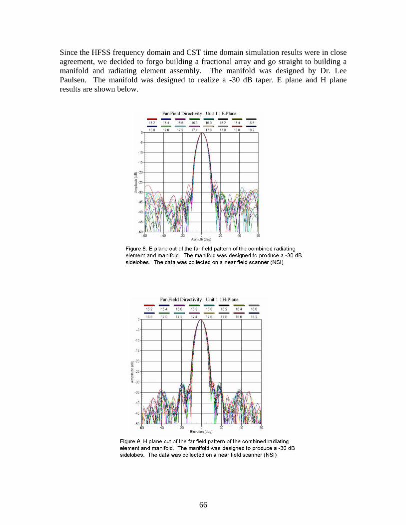
Since the HFSS frequency domain and CST time domain simulation results were in close agreement, we decided to forgo building a fractional array and go straight to building a manifold and radiating element assembly. The manifold was designed by Dr. Lee Paulsen. The manifold was designed to realize a -30 dB taper. E plane and H plane results are shown below.
66

The measured results indicate that the loose grid radiating element worked over at least a 15.2 GHz – 18.2 GHz frequency band.
II. Wide Scan Radiating Element
A cross sectional view of the wide scan radiating element is shown in figure 10.
A single portion of the novel metamaterial is shown in figure 11.
67

The wide scan radiating element consists of an 80 ohm stripline feed layer, a slot in the ground plane, two layers of radiating dipoles, a single layer of 3D metamaterial, and a 10 mil environmental protection layer. Using a 10 mil core of Rogers 6002 or Arlon CLTE eliminates the common problem of salt fog etching away the top layer of metal in a planar radiating element. A view of the stripline feed and ground plane is shown in figure 12.
The slot is symmetric. In conjunction with the symmetric dipole and metamaterial arrangement in the unit cell, the cross polar radiation is
zero at array normal and in the E plane scan.
Note 80 ohm feed rather than 50 ohm feed. The 80 ohm stripline is much easier to package since the width of an 80 ohm stripline in 2 x 20 mil Arlon CLTE cores is 10 mils and the width of a 50 ohm stripline in 2 x 20 mil Arlon CLTE cores is 28 mils
Fig. 12. The 80 ohm stripline feed and the slot in the ground plane of the wide scan radiating element is shown.
Two layers of dipoles and a layer of metamaterial are used to couple the electromagnetic energy from the slots to free space. The combination of dipoles and 3D metamaterial offers greater bandwidth and scan capability than dipoles alone. A four element section of dipoles and metamaterial is shown below.
68

The wide scan radiating element performance at array normal is shown in figures 14 and 15. Three cases are shown: 1) radiating element with no metamaterial, 2) radiating element with 2D metamaterial and no via, and 3) radiating element with 3D metamaterial.
69

The wide scan radiating element performance at theta = 70, phi = 0 degrees (E plane scan) is shown in figures 16 and 17. Three cases are shown: 1) radiating element with No metamaterial, 2) radiating element with 2D metamaterial and no via, and 3) radiating element with 3D metamaterial.
70

The wide scan radiating element performance at theta = 70, phi = 63.4 degrees is shown in figures 18 and 19. For this array grid geometry, 63.4 degrees is the angle at which the TM0 surface wave is excited at the lowest possible frequency. Three cases are shown: 1) radiating element with no metamaterial, 2) radiating element with 2D metamaterial and no via, and 3) radiating element with 3D metamaterial. The metamaterial does not noticeably change the frequency at which the surface wave impacts the structure.
71

The wide scan radiating element performance at theta = 70, phi = 90 degrees (H plane scan) is shown in figures 20 and 21. For this array grid geometry, 90 degrees is the angle at which the TE1 surface wave is excited at the lowest possible frequency. Three cases are shown: 1) radiating element with no metamaterial, 2) radiating element with 2D metamaterial and no via, and 3) radiating element with 3D metamaterial. The metamaterial does not noticeably change the frequency at which the surface wave impacts the structure.
72

Ansoft HFSS simulations show that the wide scan radiating element operates in two modes: a 1D wide scan E plane radiating mode with less than 2:1 VSWR from 0 to 70 degrees (half conical angle) from 15.4 to 18.2 GHz and a 2d wide scan radiating mode that rolls off better than n = 1.25 (gain = cos^n(theta) ) up to theta = 70 degrees (half conical angle) from 14.6 to 17.2 GHz.
III. Broadband Radiating Element A cross sectional view of the wide scan radiating element is shown in figure 22.
73

The broadband radiating element consists of a 50 ohm stripline feed layer, a slot in the ground plane, three layers of radiating dipoles, a single layer of 3D metamaterial, and a 20 mil environmental protection layer. Using a 20 mil core of Rogers 6002 or Arlon CLTE eliminates the common problem of salt fog etching away the top layer of metal in a planar radiating element. A view of the stripline feed and ground plane is shown in figure 23.
74

Three layers of dipoles and a layer of metamaterial are used to couple the electromagnetic energy from the slots to free space. The combination of dipoles and 3D metamaterial offers greater bandwidth and scan capability than dipoles alone. A unit cell of dipoles and metamaterial is shown below.
The wideband radiating element’s performance at array normal is shown in figures 25 and 26. Three cases are shown: 1) radiating element with no metamaterial, radiating element with 2D metamaterial and no vias, and 3) radiating element with 3D metamaterial.
75

Ansoft HFSS simulations show that the wide band radiating element with metamaterial has less than -20 dB return loss over a frequency band of 12.2 GHz to 18.2 GHz.
IV. Metamaterial Loaded Wide Band and Wide Scan Radiating Element A cross sectional view of a radiating element with simultaneous wide scan and wide band is shown in figure 27.
76

The metamaterial loaded wideband and wide scan radiating element consists of a 50 ohm stripline feed layer, a slot in the ground plane, three layers of dipoles, a single layer of 3D metamaterial, and a 10 mil environmental protection layer. A view of the unit cell of the stripline feed and ground plane is shown in figure 28. In order to minimize the radiating element density, the radiating element grid is an equilateral triangular grid.
Three layers of dipoles and a layer of metamaterial are used to couple the electromagnetic energy from the slots to free space. The combination of three layers of dipoles and a layer of 3D metamaterial has greater bandwidth and scan capability than dipoles alone. A four element section of dipoles and metamaterial is shown below.
77

The metamaterial loaded wideband and wide scan radiating element performance at array normal for the metamaterial and nonmetamaterial case is shown in figures 30 and 31.
78

79

The metamaterial loaded wideband and wide scan radiating element performance at phi = 0, theta = 50, 60, and 70 degrees (E plane scan) is shown in figures 32 and 33.
80

The metamaterial loaded wideband and wide scan radiating element performance at phi = 59.88 degrees, theta = 50, 60, and 70 degrees is shown in figures 34 and 35. For this array grid geometry, phi = 59.88 degrees is the angle at which the TM0 surface wave is excited at the lowest possible frequency.
81

The metamaterial loaded wideband and wide scan radiating element performance at phi = 90 degrees, theta = 50, 60, and 70 degrees is shown in figures 36 and 37 (H plane scan). For this array grid geometry, 90 degrees is the angle at which the TE1 surface wave is excited at the lowest possible frequency.
82

The metamaterial loaded wideband and wide scan radiating element performance at phi = 30.11 degrees, theta = 50, 60, and 70 degrees is shown in figures 38 and 39. Recall that phi = 59.88 degrees is the angle at which the TM0 surface wave is excited and note that 90 – 59.88 ~ 30.11.
83

V. Summary
Four stripline fed aperture coupled low profile planar radiating elements were investigated: 1) a relatively loose grid radiating element with less than – 20 dB return loss over a frequency band from 15.2 GHz to 18.2 GHz at array normal, 2) a wide scan radiating element with 1D scan of less than 2.1:1 VSWR from 0 to 70 degrees in the E plane over a frequency band from 15.4 GHz to 18.2 GHz and a 2D scan that rolled off as
84

n < = 1.25 (gain = cos^n(theta) ) from 0 to 70 degrees from 14.6 to 17.2 GHz, 3) a broad band radiating element with less than -20 dB return loss over a frequency band from 12.2 to 18.2 GHz at array normal and 4) a metamaterial loaded wideband and wide scan radiating element operating from 12 to 18 GHz and capable of 2D scan out to 70 degrees half conical scan angle. All four radiating elements have a simple feed structure and salt fog protection for the PCB metal surfaces. All radiating elements were made of PTFE composite material (Rogers 6002 or Arlon CLTE) which eliminated water absorption problems and construction problems caused by using foam. Three of the radiating elements used a novel 3D metamaterial to improve performance.
References
[1] Ben A. Munk, Frequency Selective Surfaces: Theory and Design, pp. 26-63, New York: John Wiley and Sons, 2000. [2] N. Llombart, A. Neto, G. Gerini, and P. de Maagt, “Planar circularly symmetric EBG structures for reducing surface waves in printed antennas,” IEEE Trans. Antennas Propag., vol. 53, no. 10, pp.3210-3218, Oct. 2005. [3] A. Neto, N Llombart, G. Gerini, and P. de Maagt, “On the optimal radiation bandwidth of printed slot antennas surrounded by EBGs,” IEEE Trans. Antennas Propag., vol. 54, no. 4, pp.1074-1083, Apr. 2006. [4] N. Llombart, A. Neto, G. Gerini, and P. de Maagt, “1-D Scanning Arrays on Dense Dielectrics Using PCS-EBG Technology,” IEEE Trans. Antennas Propag., vol. 55, no. 1, pp.26-35, Jan. 2007. [5] D. Pozar, and D. Schaubert, “Scan Blindness in Infinite Phased Arrays of Printed Dipoles,” IEEE Trans. Antennas Propag., vol. 32, no. 6, pp.602-612, June 1984.
85

Antenna Element Pattern Reconfigurability in Adaptive Arrays
T. L. Roach* and J. T. Bernhard Electromagnetics Laboratory, Department of Electrical and Computer Engineering
University of Illinois at Urbana-Champaign, Urbana, IL 61801 http://antennas.ece.uiuc.edu; e-mail: tlroach, [email protected]
Abstract: A phased array composed of individually pattern reconfigurable elements possesses an added degree of freedom that may enhance or expand array performance. However, when configured in an array with relatively small element spacing, it is difficult for the elements to maintain their individual pattern characteristics due to the effects of mutual coupling. This paper explores a scenario that utilizes pattern reconfigurable antennas with beam tilts in an adaptive array setting. The work adopts a technique used for adaptive arrays which allows for relatively large element spacing while maintaining good output signal-to-interference-plus-noise ratio (SINR). In a pattern variability setting, the paper investigates the feasibility of the technique with a focus on minimizing the effects of mutual coupling on the pattern characteristics. Preliminary results demonstrate the functional benefits pattern reconfigurable antennas offer with a variety of element pattern choices. 1. Introduction
Pattern reconfigurable antennas, as discussed in [1] along with a variety of other reconfigurable antenna types, possess an added degree of freedom that may enhance or expand system performance. Prior investigations, for example, [2-6] have begun to examine the capabilities of pattern reconfigurable antennas with beam tilts. However, questions still remain about the capabilities and limitation of these antennas in phased arrays. One particular system wherein the inclusion of pattern reconfigurable antennas offers the potential to increase functionality is adaptive arrays.
Adaptive antenna systems date back before the 1950’s. Early advances in this field were well documented in a special issue published by the AP-S Transactions in March of 1964 [7] and subsequently another special issue followed up in September of 1976 [8]. In general, an adaptive array antenna system controls its pattern in response to the signal environment [9]. Such systems look to automatically sense and suppress the presence of interference noise sources (friendly or hostile) while simultaneously enhance desired signal reception without prior knowledge of the signal/interference environment. Therefore, they offer more flexibility, reliability, and improved reception performance
86

compared to that of conventional arrays [10]. The authors in [11] have come up with a methodology applied to adaptive arrays which allows for relatively large spacing between antenna elements while maintaining good performance.
As discussed in [6], one of the key requirements for reconfigurable antennas is to maintain their pattern and/or frequency characteristics over the parameter of reconfiguration. In an array setting composed of closely spaced elements, mutual coupling usually diminishes element performance away from their single-element behavior—an effect typically predicated upon the antenna’s highly resonant nature. Therefore, larger elemental spacing could reduce mutual coupling effects and could increase performance of these devices in arrays. However, in adaptive arrays larger elemental spacing introduces “grating nulls,” spurious nulls that degrade overall system performance. The work presented by the authors in [11, 12] discusses the circumstances behind grating nulls and how to mitigate them with a small number of antenna elements with unequal element patterns. The present work focuses on the antenna physical layer and explores adaptive arrays as one application in which pattern variability can increase functionality in small package scenarios. A system package containing an adaptive array composed of a small number of pattern reconfigurable antenna elements could provide major benefits in situations requiring a small footprint (minimal size and low weight), a necessity in the Network Centric Warfare model. The aim is to ultimately to create the methodology that specifies the “elements” of reconfigurability which can accomplish this task. This paper proceeds as follows. Section 2 discusses some example pattern reconfigurable designs and then briefly investigates mutual coupling effects of these elements in a small array setting. Section 3 presents a number of fundamental concepts behind adaptive arrays and highlights the key elements behind the adopted adaptive array technique used in this work. The next section lays out the methodological framework used in determining the results. Section 5 then displays these results, which includes graphical plots for select adaptive array scenarios that incorporate model antennas with beam tilts. Finally, Section 6 contains the conclusion. 2. Example designs and mutual coupling effects
Since the current work centers on a small number of pattern reconfigurable elements in a linear array with relatively large elemental spacing, it is instructive to evaluate the effects of mutual coupling for some example pattern reconfigurable designs. As mentioned, these antenna types operate under highly resonant conditions and as a result their performance can suffer in an array setting with large amounts of mutual coupling, an effect primarily due to element proximity. First, this section highlights two pattern reconfigurable antennas designed by past researchers in the Electromagnetics Lab at the University of Illinois at Urbana-
87

Champaign. The first one is a broadside-to-endfire reconfigurable antenna (BERA) and the second one is reconfigurable microstrip parasitic array (RMPA). Each is detailed briefly, a more in depth discussion and analysis of the antennas can be sought in [6, 13] and [4, 5], respectively. Next, using Ansoft’s HFSS [14] simulation software, graphical plots will display coupling characteristics for a uniform equally spaced two element linear array for both antenna designs with element spacing as the varying parameter of interest. 2.1 BERA
The BERA operates as a bi-state, linearly polarized pattern reconfiguring device capable of switching its radiation patterns between a broadside (BS) state and an endfire (EF) state over a common impedance bandwidth. The broadside and endfire patterns are produced through switching elements located on the antenna structure. Figure 1 displays a layout of the antenna’s design, including the location of the two switches.
(a) Broadside: xz – plane ( = 0°) elevation cut
(b) Broadside: yz – plane ( = 90°) elevation cut
dBidBi
-35.0 90°
0°
-90°
180°
-20.0
-5.0
10.0
-35.0 90°
0°
-90°
180°
-20.0
-5.0
10.0
(c) Endfire: xz – plane ( = 0°) elevation cut
(d) Endfire: yz – plane ( = 90°) elevation cut
EθEφ
dBidBi
-35.0 90°
0°
-90°
180°
-20.0
-5.0
10.0
-35.0 90°
0°
-90°
180°
-20.0
-5.0
10.0
SMAProbe Feed
In- Line Open/Short
Circuit
xz
y
Switch #1
Switch #2
x, y
Via to Ground Substrate
Figure 1. Reconfigurable antenna’s physical layout including switch position [13].
Figure 2. Radiation pattern of the reconfigurable antenna in the elevation planes
for the two configuration states: (a) and (b) Broadside mode, (c) and (d) Endfire mode [6].
In order to attain pattern reconfigurablity, the inline switching elements alter the current distributions to produce the desired far-field pattern. In reference to Figure 1, with switch
88

#1 closed and switch #2 open, the antenna operates in endfire mode. Conversely, with switch #1 open and switch #2 closed, the antenna operates in broadside mode. In this work, the switching elements are hardwired for proof of concept, [6] presents a detailed analysis and experimental results on RF MEMS switch integration. Figure 2 show the resulting measured radiation patterns for both configuration states in the Eθ and Eφ polarizations. From these plots, the broadside/endfire characteristics of the antenna’s patterns discern themselves within the antenna’s primary polarization and plane of interest: Eθ in the φ = 0° plane.
2.2 RMPA The RMPA, in its single element form, consists of three parallel conducting strips (a probe fed center strip and two parasitics on both sides) set on a grounded dielectric substrate [4]. Each parasitic strip contains two gaps near the ends for switch placement. Figure 3 illustrates a physical layout of the antenna structure, including the location of the gaps for the switches. The linearly polarized antenna is capable of reconfiguring its radiation pattern in the y-z plane (the H-plane) in three different modes: RD, DD, and DR-modes, where R and D stand for “reflector” and “director,” respectively, in reference to the configuration of the two outer parasitic elements. Changing the electrical length of the parasitic elements via the switches permits the beam tilts.
x y
zParasitic element
Switching elements
Bias network
Driven element
Parasitic element
-35
90°
45°
0°
-45°
-90°
-135°
180°
135°
-30-25-20-15-10-50 dB
RMPA in DD modeRMPA in DR modeRMPA in RD mode
Figure 3. Layout of the Reconfigurable Microstrip Parasitic Array (RMPA). The
antenna is capable of reconfiguring its radiation pattern in the y-z plane by means of the
switching elements as indicated [5].
Figure 4. Normalized radiation patterns for the co-polar field (in dB) produced by a single
RMPA element. The curves represent the DD mode (broadside), DR mode (-25 tilt), and RD
mode (+25 tilt).
89

The antenna operates similar to that of a Yagi-Uda antenna [15]. Leaving all gaps on the parasitic structure open configures the antenna in broadside mode (DD). Closing the two gaps on the left parasitic element in conjunction with opening the two gaps on the right parasitic element produces a tilted pattern toward the positive y axis (RD mode). Conversely, opening the two gaps on the left parasitic element while closing the two gaps on the right parasitic element provides a tilted pattern toward the negative y axis (DR mode). All three pattern modes operate over a common impedance bandwidth. Figure 4 shows a polar plot of the radiation patterns produced by the RMPA. The data traces represent the normalized magnitude co-polar electric field versus elevation angle (θ) for each of the three modes: a broadside pattern (DD mode), +25° tilted pattern (RD mode), and a -25° tilted pattern (DR mode). These particular radiation patterns transpire using HFSS, utilizing design parameters indicated in [4]. 2.3 Coupling Effects In order to illustrate the effects of mutual coupling on the two model antennas, each is placed in a uniform, linear, equally spaced array composed of two elements spaced a distance d2 apart. Since the transmission coefficients, i.e., Sij (i ≠ j) parameters, give a good indication of the amount of mutual coupling between array elements, HFSS is used to simulate the two element array and calculate S21 for a range of element spacing: 0.5λ0 ≤ d2 ≤ 2.0λ0. Where λ0 is the free space wavelength at an operational frequency of 5.8 GHz. Note, both antenna designs have been scaled from their nominal base frequency design to operate at the Wi-Fi band of 5.8 GHz. Despite the scaling, the overall operational behavior of each individual antenna remains the same. Figure 5 displays the S21 results. As seen in Figure 5, the simulation results detail the spacing effects for the two element array for all reconfigurable modes. Mutual coupling plays more of a significant role for smaller element spacing, as S21 varies more between successive data points— showing the highest values in some cases. At the smallest spacing, the RMPA in DD mode illustrates the highest coupling while its other mode of configuration, DR, displays the least. Note, the RMPA in RD mode is not shown because it matches that of the RD mode due to symmetry. Nevertheless, as the spacing increases the curves stabilize and decrease, indicating more isolation between the elements and as a result the antenna’s operating characteristics will tend to more closely match their single element behavior. Note, the objective here is not to say that these two designs represent all pattern reconfigurable antenna types, but rather demonstrate some general spacing effects and give an indication of a target spacing for future analysis.
90

d2 (λ0)0.5 0.6 0.7 0.8 0.9 1.0 1.1 1.2 1.3 1.4 1.5 1.6 1.7 1.8 1.9 2.0
S 21 (
dB)
-40
-35
-30
-25
-20
-15
-10
BERA_BS ModeBERA_EF ModeRMPA_DD ModeRMPA_DR Mode
Figure 5. S21 (dB) versus element separation d2 (λ0) for a two element array composed of identical pattern reconfigurable elements. The curves are plotted at the center
frequency of operation of 5.8 GHz. 3. Adaptive Array Fundamentals 3.1 Overview As mentioned, an adaptive antenna system controls its pattern in response to the signal environment. A performance index (PI) gauges the system’s ability to accomplish this task of enhancing the desired signal and rejecting the undesired interference signals (e.g., jammers). Some example PI’s include: signal-to-interference plus noise ratio (SINR), mean square error, output noise power, minimal signal distortion, etc [10]. These PI’s, as opposed to conventional antenna characteristics, lead to more convenient forms of feedback for control of the array pattern [9]. In this work, the PI of interest is the SINR. Figure 6 illustrates a general layout of a linear N-element adaptive array, including the geometrical layout and its principal components. These components consist of the antenna or sensor array, the beam former, and the adaptive processor. Suppose a desired and interference signal impinges upon on the array (shown in Figure 6). First the signal processor collects two forms of data (1) the signal information from each antenna before entering the beam former and (2) the output s(t) which feeds back into the signal processor. Then, the processor’s job is to distinguish between the desired and interference
91

signals using either a priori or learned knowledge about the signals. Next, the adaptive control algorithm adjusts each antenna’s complex weight which determines how the radiation pattern receives the desired and interference signals. In effect, the array output s(t) changes via this form of feedback and controls until the system reaches steady state. Various factors affect the performance of an adaptive array; these include array topology, and the antenna elements themselves [9]. For the physical arrangement of a linear array, these factors pertain to the number of elements and elemental spacing. An N-element array has N -1 degrees of freedom to null out the interfering signals and element location determines array resolution and interferometer effects. In terms of the antenna element, its individual pattern, along with the complex weights within the beam former and the aforementioned element spacing, dictate overall beam pattern sensitivity. These dynamic factors determine how well the specified requirements can be met for a given signal environment [10]. Since the individual element pattern play a major role in adaptive array performance, this work focuses on exploring scenarios that utilize pattern reconfigurable antennas with beam tilts in such a setting. 3.2 Analytical relationships Before detailing the methodology in which this study bases itself upon, some general adaptive array relationships necessitate an introduction. These analytical concepts outline the framework used in future calculations. In reference to Figure 6, assume a single desired and interference signal incident on the N-element array, both continuous wave and time harmonic in nature. Also, the spacing between element 1 (the zero-phase, reference element) and element N is given by dN (in wavelengths). Then the summation of the desired, interference, and thermal noise vectors, generate the total signal vector X [9], respectfully, given as d i nX X X X= + + . Thus, thus the array output yields
1
( ) ( )N
jjj
s t w x t W X=
= =∑ , (1)
where W is the weight vector. The adaptive processing unit takes on the task of computing the weight vector via an inversion of the covariance matrix, i.e., 1W S−= Φ , where Φ (given by the expectation of the total signal vector and its complex conjugate) is the covariance matrix and S is the reference correlation vector.
92

Figure 6. Adaptive array block diagram illustrating the geometrical layout and the primary system components: antenna array, beam former, and adaptive processor.
The array signal vector ( )U θ contains the element pattern and phase shift information for each antenna element, it is given by
1
2
2 sin
12 sin
2
2 sin
( )
( )( )
( ) N
j d
j d
j d
N
f e
f eU
f e
π θλ
π θλ
π θλ
θ
θθ
θ
⎛ ⎞⎜ ⎟⎜ ⎟⎜ ⎟= ⎜ ⎟⎜ ⎟⎜ ⎟⎜ ⎟⎝ ⎠
. (2)
93

Moreover, it can be evaluated in the two ways: (a) as the desired signal vector ( )d dU U θ θ= = , where dθ is the angle of arrival of the desired signal, and (b) as the
interference signal vector ( )i iU U θ θ= = , where iθ is the angle of arrival of the interference signal. Note, ( )Nf θ is the amplitude pattern function of the Nth element. Additionally, for the PI of interest, SINR is given by the ratio of the received signal power in the desired signal to that of the power in the interference and noise signal. The author in [9] presents it in terms of the array signal vectors:
2*
*1 *
Td iT
d d d Ti i i
U USINR U U
U Uξ
ξ −
⎡ ⎤⎢ ⎥= −⎢ ⎥+⎣ ⎦
. (3)
In (3), dξ translates to the desired signal-to-noise ratio (SNR) and iξ translates to the interference signal-to-noise ratio (INR) per element, assumed equal for each element [9]. Finally, the array voltage pattern, another parameter of significance is given by the dot product of the weight vector and the array signal vector, i.e., ( ) ( )Tp W Uθ θ= . (4) 3.3 Applied Technique The work presented in this paper adopts a technique realized by R. T. Compton [11], in which he derives a set of conditions required for the Nth + 1 element in an N-element linear adaptive array. Given a set of signal parameters, the conditions yield maximum SINR. The additional auxiliary element’s purpose is to enhance SINR performance compared to that of the original N-element array. In fact, the auxiliary element functions to mitigate an undesirable effect in the SINR that occurs due to the arrangement of element pattern types and elemental spacing: grating nulls. Grating nulls, as discussed by Ishide and Compton [12], occur when the desired and interference signal vectors are parallel, i.e., d iU kU= , where k is a constant. Effectively, the two signal vectors are electrically indistinguishable and a weight vector chosen to null the interference signal will also null the desired signal. Two types exist: (a) Conventional grating nulls (CGN), which can arise for equal element patterns and (b) Sign reversal grating nulls (SRGN), which can take place for unequal element patterns. CGN occurrence parallels that of grating lobes in a standard array and SRGNs occur when an element’s pattern changes its sign between dθ and iθ . Since this work focuses on a small number of antenna elements, a two element array with the addition of a third auxiliary element is evaluated as part of the initial investigation. Figure 7 clarifies the grating null
94

process in a cause and effect type relationship for this particular array topology. For a two element array, the grating null condition simplifies into the following form,
1 1
2 2
( ) ( )( ) ( )
id
id
f ff fθ θθ θ
= ± (5)
and
0 02 2
2 2sin sin idj d j de e
π πθ θλ λ= ± . (6) The “+” sign in (5) and (6) correspond to CGNs and the “-” sign correspond to SRGNs; both relationships must be satisfied for grating nulls to occur. 4. Methodology This section outlines the steps taken in the analysis which explores the functional benefits of utilizing pattern variability adaptive arrays. As a first step in the investigation, consider the elements patterns to be in functional form—those resembling tilted dipole patterns [11, 12]. They are given by ( ) ( )j n jf cosθ θ θ= − , (7) where the main beam maximum resides at n jθ with 0n jθ = corresponding to broadside. The basic constituents of the analysis involve evaluating the N = 2 array performance for a select number of beam tilts and then determine the third element (auxiliary element) parameters 3 3( , )n dθ that improve SINR performance. For this study, a pool of potential beam tilts, chosen from -60° to +60° in 15° increments—forming a 1 2 , n nθ θ pair—represent the reconfigurations in a conceivable pattern reconfigurable antenna. Selecting from this pool along with a set 2( , )d dθ in (5) and (6) determine what type of grating nulls exist and where they are located in terms of
iθ . Utilizing these parameters further, the next step in the methodology involves finding the third element properties, 3 3( , )n dθ . They can be found using the following relations given in [11]: *
3 3( ) ( ) Ti id df f U Uθ θ = (8)
and
0 0
2 2sin sin3 3 *3 3( ) ( )
j d j d id Ti id df e f e U U
π πθ θλ λθ θ π− = − . (9)
95

Figure 7. Example flow chart diagram illustrating the grating null process.
A Mathematica® software program is used to calculate and display the results, which include two key figures of merit for a given scenario: (1) The SINR vs. interferer incident angle iθ and (2) the voltage radiation pattern, p(θ) vs. spatial angle θ , both on a dB scale. Note, all cases assume a signal environment encompassing strong interferers (i.e.,
iξ = 40 dB with dξ = 0 dB).
96

5. Results
5.1 Conventional Grating Nulls Recall CGNs particularly arise for equal element patterns. Consider the plot illustrated in Figure 8, it shows a broader interpretation to (5) and (6) [12]. In this case, d2 equals 2λ0 and the θi-θd axes scale from -90° to +90°; a favorable distance since it satisfies the goal of having a larger spacing between antenna elements. A number of n-curves present themselves in the graphic, six within the spatial range. Along these curves a grating null takes place. Thus, for a particular θd intersecting with an n-curve gives the corresponding grating null located at θi. No doubt the number of n-curves depends on d2. As d2 increases, more curves come into the spatial region of interest, thus increasing the opportunity for more grating nulls to occur.
Figure 8. Plot illustrating when CG Ns occur for an element spacing of 2λ0. The intersection of a specified θd and an n-curve results in a grating null at θi.
Even within the constraints of this initial investigation, a host of scenarios still present themselves. Thus, Table 1 displays the case results for a few example scenarios. In the table, the first three columns represent the specified parameter data (θd, d2, and the θ n1 = θn2 pair). The fourth column corresponds to the resulting interferer incident angle at which a grating null occurs (i.e., θi = θCGN) and the last two columns list the parameters
97

required of the third antenna element to mitigate the grating null and improve SINR performance, θn3 and d3. Referring to Table 1 once again, the resultant third element parameters in the last two rows warrant further discussion. In one case d3 does not equal 4λ0, i.e., all three elements not being equally spaced. And in the other case, a no solution (NS) result exist for the third element parameters under the given signal characteristics. The required beam tilt for grating null mitigation is not within the visible range. These types of events do happen for various scenarios and thus require further detailed analysis in order to enhance the possibility of integrating pattern variability in adaptive arrays.
Table 1. Calculated CGN results based on specified parameters for select cases.
θd (°) d2 (λ0) θn1 = θn2 (°) pair θi = θCGN (°) θn3 (°) d3 (λ0)
-60 -16.5 4.0
-45 36.9 4.0
-30 -18.1 3.5 -15 2.0
-15
47.8
NS - Figure 9 provides the results of the data in the first row of Table 1 in graphical form (i.e., θd = 15°, d2 = 2λ0, θ n1 = θn2 = -60°, θCGN = 47.8°, θn3 = -16.5°, and d3 = 4λ0). The plot on the left depicts the SINR (dB) as function of interferer incident angle θi while the plot on the right shows the array voltage pattern (dB) as function of spatial angle θ. Within each plot, two curves represent the “pre” and “post” conditions, i.e., before the addition of the third element and after the addition of the third element, respectively. It is important to recognize here that the SINR varies with θi and the voltage pattern is plotted for one particular θi, θi = θCGN. Recall, the pattern depends on the element weights which change as the signal environment changes The SINR plot details how, with only two antenna elements in the array, adaptive array performance degrades due to the presence of grating nulls. With the addition of the third element (i.e., the appropriate beam tilt and element spacing) SINR performance improves at the target grating null location (i.e., θi = 47.8°). Not only is the SINR maximized at θi = 47.8°, but it improves at other grating null locations as well. The SINR results correlate with the pre- and post-voltage pattern plots. Since the voltage patterns are plotted for the target grating null, the pattern values suffer in the pre-pattern case (indicated by the low dB values). After mitigating the grating null, the overall values in the post-pattern curve increase substantially. Note, a null still exist in the post-pattern at θ = 47.8°, an expected result since the interferer is coming from that direction. Altogether, the results show how adaptive array performance improves with the inclusion of pattern variability.
98

Figure 9. Resulting SINR (left) and voltage pattern plot (right) in a CGN scenario with the following parameters: θd = 15°, d2 = 2λ0, θ n1 = θn2 = -60°, θCGN = 47.8°, θn3 = -16.5°, and d3 = 4λ0. The dashed grey curve represents the 2-element array and the solid black
curve represents the addition of the third element. SINR and pattern performance (at θi = 47.8°) improves with the addition of the beam tilted third element.
5.2 Sign Reversal Grating Nulls This section presents the SRGN results in a parallel fashion to the preceding section on CGNs. Figure 10 shows another interpretation to (5) and (6), this time for SRGNs. For the same element spacing, a total of seven n curves characterize the plot, as compared to six in the CGN plot. In this case, the n = 0 curve qualifies. Since SRGNs take place for unequal antenna element patterns, they occur less frequently than CGNs. In addition to the n curves (solid), two auxiliary curves (dotted) overlay the plot. These curves represent a specific two element beam-tilt scenario, θ n1, θn2 = 60°, 0° for this plot. A SRGN occurs at the intersection of an auxiliary curve and an n curves. The intersection point specifies θ d and the grating null location θi required to produce the grating null. The auxiliary curves represent a specific θ n1, θn2 configuration, in this case 60°, 0°. Even though the auxiliary curves for only one θ n1, θn2 pair is shown in Figure 10, the behavior of the curves tend to follow a trend as the beam tilt angle changes. Due to the nature of the cosine functions used in (6), the auxiliary curves exhibit a sharp discontinuity. Although this raises a cause for concern, it does give useful insight into potential SRGN behavior. Nevertheless, as the separation between θn1 and θ n2 increases, the curves change in form and shift along the horizontal axis. The closer they come together, the gap between the discontinuity line and the smoother line closes. On the other hand, when both θn1 and θ n2 shift their beam tilts by the same amount, the auxiliary curves tend to maintain their shape and shift along the horizontal axis.
99

Figure 10. Plot illustrating when SRG N’s occur for an element spacing of 2 λ0. The intersection of an auxiliary curve and an n curve specifies θd and the grating null at θi.
For SRGNs, Table 2 shows the case results for several different θ n1, θn2 pairs, the format parallels Table 1. Alike Table 1, NS results still occur when determining the third element parameters for select cases. However, d3 typically equals 4λ0 for non-NS results. Similar to Figure10, Figure 11 illustrates the results for a SRGN scenario in graphical form wherein the SINR and voltage pattern plots are displayed. The data curves in the plot result from the parameters listed in the last row of Table 2 (i.e., θd = 0°, d2 = 2λ0, θ n1 = 60°, θn2 = 0°, θSRGN = -47.6°, θn3 = -18.6°, and d3 = 4λ0). Unlike CGNs only one SRGN occurs for a set θ n1, θn2 pair. As expected, the grating null degrades performance in the pre-SINR curve (dashed-gray). Adding the element with a beam tilt at -18.6° and a spacing of 4λ0 maximizes SINR at θi = -47.6°, dictated by the post-SINR curve (solid-black). Once more, performance improves not just at the grating null location but overall. A few interesting characteristics lie within the pattern plots as well. In the pre-pattern curve, two distinct nulls stand out:
100

one at θ = θi = -47.6° and the other in the desired signal direction, θ = θd. As discussed before, the null at θ = -47.6° is expected because of the interferer. However, with the appropriate third element parameters, the null at broadside is alleviated and the post-pattern in that direction reaches its maximum value. In reality, this in effect maximizes the SINR at θi = θSRGN.
Table 2. Calculated SRGN results based on specified parameters for select cases.
θd (°) d2 (λ0) θn1 = θn2 (°) pair θi = θSRGN (°) θn3 (°) d3 (λ0)
-60 -45, 15 62.1 -54.2 4.0
-60 60, -45 -6.7 NS -
-45 30, -45 -73.2 -58.2 4.0
0
2.0
60, 0 48.6 -18.6 4.0
Figure 11. Resulting SINR (left) and voltage pattern plot (right) in a SRGN scenario with the following parameters: θd = 0°, d2 = 2λ0, θ n1 = 60°, θn2 = 0°, θSRGN = -47.6°, θn3 = -18.6°, and d3 = 4λ0. The dashed gray curve represents the 2 element array and the solid
black curve represents the addition of the 3rd element. Clearly, SINR and pattern performance improves with pattern variability.
6 Conclusion In summary, this work has explored one aspect of the functional benefits of utilizing radiation reconfigurable antennas with beam tilts in an adaptive array setting. The focus of the work revolves around using these elements in small array configurations with
101

relatively large spacing between antenna elements, thereby reducing mutual coupling effects. Employing an adaptive array technique which allows for relatively large spacing, numerous graphical results demonstrated how performance degradation due to grating nulls can be alleviated. Since the technique is contingent upon having pattern variability, a select group of ideal antenna elements with a discrete number of beam tilts were used in the study. Overall, this stage of the investigation has given much desirable insight into the adaptive array process and the needed elements of reconfigurablity. At this point in the research many directions for future work present themselves. These include gaining more insight into the physical layer aspects of adaptive arrays—with the antenna element’s beam tilt in mind. Furthermore, the use of ideal (dipole-like) radiation patterns serve as a testing benchmark but do not represent practical antenna elements. For that reason, we plan to include practical reconfigurable antenna elements patterns into the study in the future, illustrating the impact pattern variability can have in adaptive arrays. 7 Acknowledgments This work is sponsored in part by the Vodafone-Illinois Graduate Fellowship, a GEM Fellowship, and the IMGIP Graduate Fellowship Program of Illinois. The authors would like to thank Dr. Kathleen Melde with the University of Arizona for her support and insight into this topic. 8 References 1. J.T. Bernhard, Reconfigurable Antennas, Morgan and Claypool Publishers, 2007. 2. J. -C. Chiao, S.-Y. Cheng, J. J. L. Chang, I. M. Chio, Y. Kang, and J. Hayasaka,
“MEMS reconfigurable antennas,” Int. J. of RF and Microwave Computer-Aided Eng., vol. 11, pp. 301 – 309, September 2001.
3. K. Hietpas, G. H. Huff, and J. T. Bernhard, “Investigation of phased array
beamsteering using reconfigurable antennas,” in Proc. IASTED Int. Conf. on Antennas, Radar, and Wave Propagation, July 2004, pp. 41 – 44.
4. S. Zhang, G. H. Huff., J. Feng, and J. T. Bernhard., “A pattern reconfigurable
microstrip parasitic array,” IEEE Trans. Antennas Propagat., vol. 52, pp. 2773-2776, Oct. 2004.
5. S. Zhang, G. H. Huff, G. Cung, and J. T. Bernhard (2005), Three variations of a
pattern-reconfigurable microstrip parasitic array, Microwave Opt. Technol. Lett., vol. 45, pp. 369 – 372, June 2005.
102

6. G. H. Huff., and J. T. Bernhard., “Integration of packaged RF MEMS switches with radiation pattern reconfigurable square spiral microstrip antennas,” IEEE Trans. Antennas Propagat., vol. 54, pp. 464-469, February 2006.
7. IEEE Trans. Antennas Propagat. (Special Issue on Adaptive Antennas), vol. AP-
12, September 1964. 8. IEEE Trans. Antennas Propagat. (Special Issue on Active and Adaptive
Antennas), vol. AP-24, March 1976. 9. R. T. Compton, Jr., Adaptive Arrays – Concepts and Performance, Englewood
Cliffs, NJ: Prentice-Hall, 1988. 10. R. A. Monzingo and T.W. Miller, Introduction to Adaptive Arrays, John Wiley &
Sons Inc., 1980. 11. R. T. Compton, Jr., “A method of choosing element patterns in an adaptive
arrays,” IEEE Trans. Antennas Propagat., vol. 30, pp. 489-493, May 1982. 12. A. Ishide, and R. T. Compton, Jr., “On grating nulls in adaptive arrays,” IEEE
Trans. Antennas Propagat., vol. 28, pp. 467-475, July 1980. 13. G. H. Huff and J. T. Bernhard, “Analysis of a radiation and frequency
reconfigurable microstrip antenna,” in Proc. 2004 Antenna App. Symp., Monticello, IL, 2004, pp. 175-191.
14. Ansoft Corporation, Pittsburgh, PA, Ansoft HFSS, Version 10.3 15. C. A. Balanis, Antenna Theory: Analysis and Design, 2nd ed., John Wiley &
Sons, Inc., New York, 1997.
103

-COAXIAL PHASED ARRAYS FOR KA-BAND
COMMUNICATIONS
Abstract: Micromachined components constituting new multi-layer, integrated, Ka-
band phased array are designed and demonstrated in this paper. Eleven strata two-
level rectangular -coaxial lines (RCLs), Wilkinson and Gysel power dividers and
power combining networks, wideband cavity-backed slotted patch antennas and
various interconnects including the delay lines are monolithically and in a hybrid
manner integrated in a final brick type phased array. The design of the structures
is compatible with a sequential surface micromachining process able to form high
aspect ratio air-recta coax lines and components. In our earlier work, we showed a
high level of sub-system integration on a single 6” wafer with a component yield in
the excess of 99%. Excellent performance with ultra-low line and component losses,
high antenna radiation efficiencies and good pattern, amplitude and phase controls
are obtained. The results of the research presented here, are step closer to the
integration of various three-dimensional micro electromagnetic radio frequency
systems (3-D MERFS) in future military systems.
1. Introduction
The development of RF MEMS components over the past decade have contributed to
the advancement of enabling fabrication technologies for future high-performance
millimeter and sub-millimeter electromagnetic systems. Among these, a special place
belongs to the techniques aimed at building -coaxial lines and related components [1-4].
Though circular coaxial lines are desired (lowest loss), the micromachining fabrication is
limited to the manufacturing of rectangular coaxial lines (RCLs). Low loss, wide single
TEM and non-dispersive mode bandwidth, sharp turns, and possibilities for seamless
single/multi-level integration with other passive and active components are just a few
appealing properties associated with RCLs.
A number of surface micromachined patch antennas have been demonstrated in the
past. In [5], Q-band micro-patch antennas were implemented on high resistivity silicon
substrate using the surface micromachining technology composed of conventional thick
photoresist lithography and copper metal plating process. An air-filled elevated
D. Filipovic1, G. Potvin
2, D. Fontaine
2, Y.Saito
1, J-M. Rollin
3, Z. Popovic
1, M. Lukic
1,
K. Vanhille3, C. Nichols
3
1University of Colorado, Boulder 80309-0425
2BAE Systems, Nashua, NH 03060
3Nuvotronics LLC, Blacksburg, VA 24060
104

microstrip antenna resonating at 25GHz based on surface micromachining technology is
fabricated and characterized in [6]. The fabrication process used is a combination of the
epoxy-core conductor technique, laser machining and electroplating bonding. The patch
is fed by a vertical epoxy-core metal-coated micromachined probe and supported by
several posts. In [7], a 60GHz 2x1 patch array antenna is designed and fabricated using
micromachining technology fully compatible with commercial CMOS process. The
antenna is supported with a feeding post and two additional supporting metal posts
located at the virtual ground of the patch. Antenna elements separated by 0.8 are fed by
a corporate CPW based network.
In this paper we demonstrate the latest advances in the development of fully integrated
Ka-band phased arrays, built using the PolyStrata™ process [8,9] developed on a
DARPA-MTO funded 3-D MERFS program. The complete horizontal (tile) and vertical
(stack) integration of multi-level RCLs and components are used to create this 3-D array
topology. Process integrated resistors, Wilkinson and Gysel power dividers and
respective combiner networks, and wideband cavity-backed patch elements are also
demonstrated. Electromagnetic and electro-thermal analysis and design on a component
and sub-system level are presented. The component yields above 99%, almost negligible
roughness and strata misalignments effects, and excellent agreement between the theory
and measurements are testaments of the fast approaching maturity, and the potential
future capabilities the 3d MERFS technology and the PolyStrata process offer to the
future military systems.
2. Fabrication Steps
The basic steps in this process are outlined in Fig. 1, while the picture of a portion of
the wafer is shown in Fig. 2.
Fig. 1 Simplified sketch of the steps undertaken in the sequential building process (left to
right, top to bottom). The end result is a non-uniform air-polymer recta-coax comprised
of 5 structural layers (extension to more than 5 layers is also possible).
105

As seen, the five level recta-coax structures are built up layer by layer by depositing a
uniform copper stratum (layer 1), and sequence of strata comprised of photo-resist and
copper (layers 2, 4, and 5). For this 5-layer process, the polymer support is a part of the
3rd
layer. Once the structure is built, the photoresist is chemically removed through the
holes in the top and side walls of the device. These openings are referred to as release
holes. A single reticle of a 6” wafer built using the same process, however with 10 strata,
is shown Fig. 2. Three prototypes of the designed antenna with the launch are in the top
right corner. Also shown are 90deg hybrid couplers, cavity resonators as well as several
recta-coax lines and calibration standards.
Fig. 2 Photograph of a single reticle on a 6” wafer.
3. Phased Array Configuration
Phased arrays are commonly configured either using vertical stacking, so called brick
configuration, or by connecting various components and sub-systems in the same
horizontal layer(s), so called tile configuration. We have already demonstrated that
monolithically integrated Ka-band phased arrays are feasible using the developed surface
micromachining technology. As an example, the picture of a 36GHz tile phased array
built using the PolyStrata process is shown in Fig. 3. There are three distinct regions: 4x4
antenna array, 16x16 Butler matrix with phase compensation network feeding into the
antennas, and the region aimed for MMIC integration and active control. These are
located from left to right respectively. The shown phased array is built from 10 copper
strata with thicknesses varying between 50 and 100m. Dielectric supports are included
on two different vertical locations and are placed underneath the central conductor. Low
line losses of 0.16dB/cm, coupler output misbalances below 0.1dB and 2º, excellent
106

antenna match, and overall yield in excess of 99% are demonstrated at the operating
frequency. This was the first demonstration of a fully integrated antenna array -
beamformer built with micron-scale rectangular coaxial lines.
Fig. 3 -coaxial Ka-band phased array operating at 36 GHz. Cavity-backed patch antenna
elements are fed with a recta-coax 16x16 Butler matrix.
Shown in Fig. 4 is a new concept (for this program and for the demonstration of the
PolyStrata™ technology capabilities) of the Ka-band phased array. As seen, a brick
rather than a tile configuration is adopted, with both vertical (stack) and horizontal (tile)
integration. Top and middle layers are fully built in PolyStrata, while the bottom layer
has high-frequency mounting sockets for commercial off-the shelf (COTS) phase shifters,
amplifiers, etc.
(a)
(b)
Fig. 4 New concept of the Ka-band phased array. (a) 4x4 antenna array (left), power
combining network (center), and surface mount phasers (right) are shown. The direction
of the beam scanning is depicted. (b) 3-D stack configuration.
107

The antenna array die is on the top, and is comprised of 16 antenna elements shown in
Fig. 5. The antenna array is composed of 4 linear 4x1 sub-arrays. The four patches in
each horizontal row are corporate fed using either Wilkinson dividers or lossless splitters,
while the phase shifting is introduced along the vertical direction (columns). The patch
array and combining network are built from 11 copper layers (often referred to as strata)
with thickness varying from 50 to 100μm. During the fabrication process, a photo-resist
is removed through 250 x 100 μm2 release holes periodically distributed on the side walls
of the recta-coax and cavity and 250 x 250 μm2 holes horizontally distributed on strata 1
and 6. The size and distribution of the release holes are optimized for the best
performance (lowest coupling).The inner conductor of the coax is mechanically secured
with 20μm thick dielectric straps periodically placed on strata 2 and 4. The dielectric
constant and tanδ are 2.85 and 0.045, respectively.
The antenna is a cavity-backed patch having two pair of slits for increased bandwidth
of about 8%. A cavity-backed patch antenna with single pair of slits has bandwidth of
about 4.5% [10]. Also noticeable is that the divider’s tee-junctions and right-angled
corners are compensated (by chamfering) to minimize the parasitic effects of
discontinuities. The middle layer is the power dividing/combining network comprised of
resistive 3-port components – Wilkinson power dividers. Finally, the bottom layer is used
for the active control, including phase shifters, low-noise amplifiers and other devices
needed for beam scanning.
(a)
108

(b)
(c)
Fig. 5 Drawing of the 4x4 cavity backed patch array with a recta-coax combining
network. Cavity backed patch array (a), Upper dividers (b), and lower dividers (c). For
clarity, layer 6 is removed in Fig. 2 (c).
109

4. Performance of Array Components
The most important array components in the top two levels are antennas and dividers,
and their performance will be discussed in this section. A drawing of a designed antenna
and the return loss for all 16 elements are shown in Fig. 6. As seen, there are total of 4
slits on the surface of the patch. This modification of an antenna from [10] introduces an
additional loop around the center of the Smith chart, thus effectively increasing the
antenna bandwidth. The pattern is consistent over the whole bandwidth. Antenna has gain
of about 6.5dBi and efficiency of over 97%. The electro-thermal and dielectric
breakdown analysis are conducted and it was shown that the thermal effects associated
with the crystallization of the polymer are the dominating failure mechanism.
(a)
(b)
Fig. 6 Cavity-backed patch antenna (a), and return loss of 16 antenna elements phased for
a broadside beam (b). The unit cell size is 0.5x0.5mm2.
110

The integration of resistors, needed to dissipate the misbalances at the dividers’ outputs,
is extremely difficult in any micromachining process. Commonly, and particularly at
lower frequencies, special fixtures, typically referred as sockets, are designed and
component resistors are either soldered or attached using epoxy solutions. Here, we
demonstrate a monolithically integrated resistor within the structure of a Wilkinson
power divider. Shown in Fig. 7 (a) is a model of designed recta-coax divider. As seen,
and owing due to the extremely low coupling between the neighboring lines, this
component occupies a much smaller surface area then their microstrip counterpart. The
S-parameters shown in Fig. 7 (b), demonstrate excellent performance around designed
frequency of 30GHz. The losses are about 0.2dB, while the return losses at all ports are
better than 30dB over the overlapping bandwidth with patch antennas. The isolation is
greater than 25dB.
(a)
(b)
Fig. 7 Wilkinson power divider (top), and its S-parameters (bottom). The 100 resistor is
embedded between the two polymer straps. The periodicity of the release holes grid at the
top/bottom is 0.5mm. Output ports are configured as in figure to accommodate easier
individual component testing.
111

5. Array Performance
The return loss of the 4x4 cavity backed patch array with the power combining network
(only for the upper dividers) is computed using Ansoft HFSS [11] as shown in Fig. 8. To
reduce the computational time dielectric straps and release holes in the cavities, patches,
dividers, and strata 1 and 6 are removed. For the comparison purposes, the result from a
circuit model is also plotted in the same figure. As seen, 10 dB return loss bandwidth of
the full wave FEM simulation is about 2.1GHz, while for the circuit model the bandwidth
is about 2.8GHz.
Fig. 8 Simulated return loss of the 4x4 cavity backed patch array with the combining
network. A 3-D model used for the full wave simulation model is depicted on the left.
Shown in Fig. 9 is a combined circuit-full wave model of the complete phased array
and the computed return loss of the multi-layer coaxial phased array with different inter-
element phase shifts. Since the full-wave FEM simulation of the whole array structure is
computationally expensive, the circuit model is developed as follows: first, S-parameters
of each section of the phased array including the cavity backed patch array, coaxial
dividers, bend corner, and vertical transition are computed with HFSS and extracted in
appropriate circuit simulator file formats. Then, each port of the phased-array multiport
model is connected as shown in Fig. 9 (a). Finally, the structure is simulated within a
circuit based simulator. For the phase shifter, TriQuint’s 30GHz 5-bit phase shifter (TGP
2100-EPU) is used. As seen from Fig. 9 (b) and (c), the 10dB return loss bandwidth of
more than 11GHz is obtained. Note that the maximum power combining network loss is
about 8.4dB at 30GHz. Of that, more than 6dB are the losses in the phase shifter, thus
leaving about 2dB losses in the stack-and-tile recta-coax beamformer.
112

(a)
(b) (c)
Fig. 9 The computed return loss of a multi-layer coaxial phased array from Fig. 4. (a)
Schematic of a circuit model. Computed return loss with inter-element phase shifts from
0° to 45° (b) and from 56.25° to 112.5°.(c)
The FEM computed radiation patterns of the 4x4 cavity-backed patch array (all
elements in-phase) are shown in Fig. 10. The array with no release holes and straps is
simulated above an infinite ground plane (no radiation into the lower half space). As
seen, the maximum gain of 18.26dBi is obtained. It is also observed that the E-plane
cross-polarization radiation is negligible while the cross-polarization levels in the H-
plane are below -16dB. Shown in Fig. 11 is the radiation pattern for the E-plane scanning
with different inter-element phase shifts. The maximum gain and the degree of a beam
steering at the maximum gain for ±45° and ±90° inter-element phase shifts are 18.18dBi
and ±12°and 17.76dBi and ±25°, respectively.
113

Fig. 10 Simulated radiation pattern of the 4x4 array at 30GHz for E-plane (x-z) (left) and
H-plane (y-z) (right). Note that the inter-element phase shift is 0°.
Fig. 11 Simulated radiation pattern for the E-plane scanning with different inter-element
phase shifts (±45° and ±90°). E-plane co-pol is shown in the figure.
6. Summary
The latest advances in the development of fully integrated Ka-band phased arrays, built
wiith the PolyStrata™ process are demonstrated in this paper. The horizontal (tile) and
vertical (stack) integrations of multi-level RCLs and components are used to create this
3-D array topology. Process integrated resistors, power dividers and respective combiner
networks, and wideband cavity-backed patch elements are also demonstrated. Results
presented here reveal the new capabilities the 3d MERFS technology and the PolyStrata
process offer to the future military systems.
114

7. Acknowledgments
This work was supported by the DARPA-MTO’s 3-D Micro Electromagnetic Radio
Frequency Systems (3-D MERFS) program. Authors acknowledge Dr. S. Rondineau
from the University of Colorado at Boulder, Mr. D. Sherrer and micro-fabrication team
from Nuvotronics, and Dr. W. Wilkins and her team from Mayo Foundation for their
contributions to this work.
Distribution Statement "A" (Approved for Public Release, Distribution Unlimited). DARPA case
#11995, 8/11/08.
8. References
[1] R. Chen, “Micro-fabrication techniques,” Wireless Design and Development, pp. 16-
20, Dec. 2004.
[2] J.-B. Yoon, et.all, “3-D construction of monolithic passive components for RF and
microwave ICs using thick-metal surface micromachining technology,” IEEE Trans.
Microwave Theory Tech., vol. 51, no. 1, pp. 279-288, Jan. 2003.
[3] I. Jeong, et.all, “High-performance air-gap transmission lines and inductors for mm-
wave applications,” IEEE Trans. Microwave Theory Tech., vol. 50, no.12, pp. 2850-
2855, Dec. 2002.
[4] I. Llamas-Garro, P. Hall, “A low loss wideband suspended coaxial transmission line,”
Microw. Opt. Technol. Lett., vol. 43, pp. 93–95, Oct. 2004.
[5] M.L. Ha, et.all, “Q-band Micro-patch Antennas implemented on a High Resistivity
Silicon substrate using the Surface Micromachining Technology,” Proc. IEEE
International Microwave Symposium, Fort Worth, TX, pp.1189-1192, June 2004.
[6] B. Pan, et.all, “A High Performance Surface-Micromachined Elevated Patch
Antenna,” Proc. IEEE-APS/URSI Symp., Washington, DC, pp. 397-400, July 2005.
[7] J.G. Kim, et.all, “60-GHz CPW-Fed Post-Supported Patch Antenna Using
Micromachining Technology,” IEEE Microw. Wireless Components Letters, pp. 635-
637, Oct. 2005.
[8] D. Sherrer, J. Fisher, “Coaxial waveguide microstructures and the method of
formation thereof,” U.S. Patent Application Publication No. US 2004/0 263 290A1,
Dec. 30, 2004.
[9] D. S. Filipovic, et.all, “Modeling, design, fabrication, and performance of rectangular
μ- coaxial lines and components,” 2006 Proc. IEEE MTT-S Microwave Symposium
Digest, pp. 1393–1396, San Francisco, CA, June 2006.
[10] M. Lukic, D.S. Filipovic, “Surface-micromachined dual Ka-band cavity backed
patch antenna” IEEE Trans. Antennas Propag., vol. 55, pp. 2107-2110, July 2007.
[11] Ansoft Inc., High Frequency Structure Simulation (HFSS), Ver. 11, [Online]
Available: http://www.ansoft.com
115

PHASED ARRAY FOR MULTI-DIRECTION SECURE
COMMUNICATION
M.P. Daly and J.T. Bernhard
Electromagnetics Laboratory
University of Illinois at Urbana-Champaign
Urbana, IL 61801
[email protected], [email protected]
Abstract: A digital modulation technique, which we will call directional
modulation, is presented. Directional modulation uses the array elements to
modulate a continuous wave (CW) signal rather than implement modulation in the
transmitter hardware. By switching an array of reconfigurable elements, arbitrary
amplitudes and phases of radiation patterns can be achieved. Because this signal is
direction-dependent, the technique offers security as the signal will become
distorted off the desired direction, and it makes possible sending independent data
in multiple directions. When using an array with driven elements, the necessary
configurations can be predicted from simple calculations instead of having to test all
possible combinations experimentally or rely on complex simulation software. The
experimental methods and results of different modulation schemes are presented.
1. Introduction
In a conventional phased array, information bits are converted into a baseband IQ
modulation. The baseband signal is then upconverted by mixing with a carrier frequency,
and the RF signal goes through a feeding network, phase shifters, amplifiers, and finally
the antenna elements. Using constructive interference, a phased array improves the gain
of a radiated signal in the direction of the receiver while suppressing radiation in
undesired directions. But even though a phased array may have many elements, it can
only transmit one stream of data at a time. This signal is radiated in other directions than
the intended one, with a decrease in gain according to the sidelobe levels. However, a
sufficiently sensitive receiver in some other undesired direction can still decode the same
signal from the array.
Time-modulated arrays make use of an additional dimension, time, in the design of high
performance arrays. In these arrays, elements are usually switched on and off in a
116

periodic manner for such goals mimicking an amplitude taper [1] or rotating the phase
center of the array to move sidelobes out of the pass band [2], [3].
Instead of switching elements simply for radiation pattern synthesis, several groups have
proposed sending information by modulating the array elements. These techniques can
be used to deliver frequency shift keying [4], pulse-position modulation [5], or amplitude
and phase-based modulations [6]. In [4]–[6], the element modulation not only produces
the array pattern but also conveys the information.
The modulations produced in [4]-[6] have a spatial component, hence the name
directional modulation. They appear distorted to receivers not in the intended transmit
direction, making demodulation more difficult or even impossible. Directional
modulation can be accomplished using reconfigurable elements, phase shifters, or
dynamic attenuation, with data speeds dependent on the switching speeds of these
devices. At minimum, the elements need only be driven by a CW signal. A block
diagram illustrating the differences between conventional array transmission and
directional modulation, in this case using reconfigurable elements, is shown in Figure 1.
Information
fc
InformationBaseband IQ
Modulation
fc
∆Φ
∆Φ
∆Φ
Figure 1: Simplified model of traditional array in transmit mode (left) and one implementation of a
directional modulation transmitter using reconfigurable elements (right)
Recently, a parasitic array was demonstrated that could generate modulated signals that
were directionally-dependent [6]. The parasitic array consisted of a single driven planar
dipole surrounded by switched parasitic elements. The switches on the parasitics were
used to alter the amplitude and phase of the radiated signal for a given direction. This
117

array was successful in obtaining quadrature amplitude modulation (QAM) but there was
no easy way to determine the switch combination that would synthesize a given
constellation point. Because it was a parasitic array, there was no way given to
accurately predict the magnitude and phase of radiated fields from a specific switch
combination of the 90 switches in the array, short of running a time-consuming
electromagnetic simulation.
However, when an array is composed entirely of driven elements, it will be shown in this
work that the total radiated field can be predicted without complex simulations if the
active element patterns are known. An active element pattern is an element’s radiation
pattern while operating in the array rather than the isolated element. It takes into account
mutual coupling effects. Because Maxwell’s equations are linear, the total pattern of the
array is a superposition of the active element patterns multiplied by phase offsets for their
positions in the array. Using this method, the same benefits of multi-directional
communications and secure, directionally-dependent modulation can be realized, and an
array can be designed with more intuition and less complexity. Basic mathematics
behind directional modulation will be presented first, followed by a description of the
experimental setup. Finally, the results of several different modulation tests will be
presented, with comparisons between calculated and measured data.
2. Mathematical Theory
The array factor for a linear, uniformly spaced array can be defined as [7]:
n
1
j2 (n 1)dsin( )A( ) H ( )exp
N
n
π ϕϕ ϕ
λ=
− =
∑ (1)
where Hn(φ) is the complex active element radiation pattern of element n, d is the inter-
element spacing, N is the number of elements in the array, and λ is the wavelength. The
total pattern including phase information is then given by A(φ). If the amplitude or phase
of each element can be manipulated, then the amplitude and phase of a signal in direction
φ from the array can be controlled. In fact, there are N degrees of freedom for controlling
the transmitted signal in one direction. If instead it is desired to specify magnitude and
phase in N different directions, the required weightings and phase shifts can be solved by
means of a simple linear system of equations:
( )( )
( )
( ) ( ) ( )
( ) ( ) ( )
( ) ( ) ( )
1 1 1
2 2 2
2 0 sin 2 1 sin 2 ( 1) sin
1 1 2 1 11
2 0 sin 2 1 sin 2 ( 1) sin
21 2 2 2 2
2 0 sin 2 1 sin 2
1 2
N N
d d N dj j j
N
d d N dj j j
N
d dN j j j
N N N N
H e H e H eA
A H e H e H e
A
H e H e H e
π ϕ π ϕ π ϕλ λ λ
π ϕ π ϕ π ϕλ λ λ
π ϕ π ϕ πλ λ
ϕ θ ϕϕϕ ϕ θ ϕ
ϕϕ θ ϕ
⋅ ⋅ ⋅ ⋅ ⋅ − ⋅
⋅ ⋅ ⋅ ⋅ ⋅ − ⋅
⋅ ⋅ ⋅ ⋅
⋅ ⋅ ⋅
⋅ ⋅ ⋅ =
⋅ ⋅ ⋅
⋯
⋯
⋮ ⋮ ⋱ ⋮
⋯
1
2
( 1) sin NN d N
x
x
xϕλ
⋅ − ⋅
⋅
⋮
(2)
118

The vector [x1 … xN]T is a vector of complex weights, which could correspond to phase
shifts and changes in amplitude weighting of elements. When solving (2), it is assumed
the elements have full freedom to change their phase and weighting. Often, this is
impractical and optimization methods are needed to find the best solution using only
phase shifters, for example.
In this work, directional modulation is implemented using driven elements which
generate constellation points according to (2). The equation (2) can easily be generalized
to any arbitrarily-spaced array by changing the phase terms, but this work will focus on a
four-element linear array with uniform spacing. The array in this work has
reconfigurable elements and does not have phase shifters or variable attenuators. Each
element can reconfigure between two pattern states, so it would be more accurate to write
(2) in the following manner:
( )( )
( )
( ) ( ) ( )
( ) ( ) ( )
( ) ( ) ( )
1 1 1
2 2 2
2 0 sin 2 1 sin 2 ( 1) sin
1 1 11
2 0 sin 2 1 sin 2 ( 1) sin
22 2 2
2 0 sin 2 1 sin 2 ( 1) sN N
d d N dj j j
d d N dj j j
d d N dN j j j
N N N
f e f e f eA
A f e f e f e
A
f e f e f e
π ϕ π ϕ π ϕλ λ λ
π ϕ π ϕ π ϕλ λ λ
π ϕ π ϕ πλ λ
ϕ ϕ ϕϕϕ ϕ ϕ ϕ
ϕϕ ϕ ϕ
⋅ ⋅ ⋅ ⋅ ⋅ − ⋅
⋅ ⋅ ⋅ ⋅ ⋅ − ⋅
⋅ ⋅ ⋅ ⋅ ⋅ − ⋅
⋅ ⋅ ⋅
⋅ ⋅ ⋅ =
⋅ ⋅ ⋅
⋯
⋯
⋮ ⋮ ⋱ ⋮
⋯
1
2
1,
2,
in,N
N
i
i
N i
H
H
Hϕλ
⋅
⋮
(3)
11,iH indicates the entire active element pattern of element 1 where i1 can either be a 0 or a
1 representing the two states, broadside and endfire, of the element. f(φi) is a selector
function whose product with the element pattern produces the value of the radiation
pattern at φi, as shown in (4):
( ) ( ), ,n nn k m m n kH f Hϕ ϕ= (4)
In the four-element array discussed in this work, there are only 16 possible transmitted
signals for a given direction, so optimization methods for obtaining desired signals are
less practical than simply calculating all possible values once the array matrix and the H
vector in (3) are known. But (3) serves to illustrate that this type of an array has easily
calculable constellation points once the element patterns are known. Instead of having to
calculate all possible combinations of switches which is exponential in complexity, only
the active element patterns have to be simulated or measured, which is linear in
complexity.
3. Experimental Setup
3.1 Reconfigurable Antenna Array
119

The array used in all subsequent experiments is a 4 element linear array with half-
wavelength spacing shown in Figure 2. The elements are reconfigurable square spiral
microstrip antennas outlined in [8]. The array was created initially to assess
beamsteering capabilities using reconfigurable elements [9]. This array uses ideal
switches (copper tape) rather than RF MEMS to switch between two modes. The switch
locations are highlighted on the first element in Figure 2.
Figure 2: Reconfigurable 4x1 array [9]. All elements in broadside mode (top) and endfire mode
(bottom) .
To reconfigure an element to broadside, the top switch location shown in Figure 2 is
closed and the bottom is opened. To achieve endfire radiation, the top switch is open and
the bottom is closed. The impedance match for each element was measured for both
modes, and all elements have a VSWR of less than 2 at the operating frequency of 6.9
GHz. This is illustrated in Figure 3. The mode (broadside or endfire) of an element’s
neighbors had no significant effect on the measured impedance or radiation pattern of the
element.
120

Figure 3: Measured VSWR of array elements
3.2 Active Element Pattern Measurement
In order to accurately predict the constellation points for a given configuration, the active
element patterns of each element must be known. As mentioned earlier, the active
element patterns are radiations patterns of the individual elements when operating in the
array. These patterns were taken by terminating all the other elements with matched
loads. Figure 4 shows the broadside and endfire patterns of each element for vertical
polarization only (from Figure 2, the array was rotated in φ and the vertical polarization
was measured). The endfire patterns have nulls at approximately 0° (array broadside)
and the broadside patterns have maxima closer to 25°. The horizontal polarization has a
maximum closer to 0° in broadside mode, but for this application, the broadside
maximum does not have to be exactly at 0°.
121

Figure 4: Individual element patterns (θ=90° plane). Vertical (z direction) polarization only (see
Figure 2). Elements 1&2 on top row, 3&4 on bottom row.
It is interesting to note that while the magnitude of the broadside and endfire patterns are
very different, the relative phases of the elements are approximately the same. Figure 5
shows the phases of each element pattern in both modes. Figure 5 does not include the
relative phase difference due to element position in the array.
122

-180 -120 -60 0 60 120 180-180
-120
-60
0
60
120
180
Transmit Angle [deg]
Phase Angle [deg]
Elt 1
Elt 2
Elt 3
Elt 4
-180 -120 -60 0 60 120 180
-180
-120
-60
0
60
120
180
Transmit Angle [deg]
Phase Angle [deg]
Elt 1
Elt 2
Elt 3
Elt 4
Figure 5: Phase of elements 1-4 in broadside mode (left) and endfire mode (right)
4. Experimental Results
4.1 Prediction of the Array Pattern from Active Element Patterns
This section will demonstrate the accuracy of predicting the total pattern from individual
element patterns. Figure 6 shows the radiation patterns when all 4 elements are driven in
either broadside or endfire mode. The magnitudes are duplicated again in Figures 7 and
8, which also shown the phases.
Figure 6: Combined pattern with all elements in either broadside mode or endfire mode. Vertical
polarization only (see Figure 2) in the θ=90° plane.
123

Figures 7 shows the predicted and measured patterns when all of the elements are in
broadside mode and Figure 8 shows the same measurements when all of the elements are
in endfire mode. The predicted values are calculated from simply adding up the
individual element patterns taken in broadside or endfire mode. As can be seen, the
predicted magnitude and phase agree well with the measured data. As a side note,
because the switches were hard-wired, the array had to be removed from the testing
apparatus to switch elements between broadside and endfire. Care was taken to stabilize
the testing apparatus so the position of the array in space was preserved. The phase is
especially sensitive at this frequency as a change in relative position of 1 mm means a
phase change of almost 10°. The largest deviations between measured and predicted
occurred when the signal strength was very low, which was likely due to system noise.
-180 -120 -60 0 60 120 1800
0.1
0.2
0.3
0.4
0.5
0.6
0.7
0.8
0.9
1
Angle [deg]
Magnitude
Predicted
Measured
-180 -120 -60 0 60 120 180
-180
-120
-60
0
60
120
180
Angle [deg]
Phase Angle [deg]
Predicted
Measured
Figure 7: Predicted and measured pattern magnitude and phase when all elements are in broadside
mode
-180 -120 -60 0 60 120 1800
0.1
0.2
0.3
0.4
0.5
0.6
0.7
0.8
0.9
1
Angle [deg]
Magnitude
Predicted
Measured
-180 -120 -60 0 60 120 180
-180
-120
-60
0
60
120
180
Angle [deg]
Phase Angle [deg]
Predicted
Measured
Figure 8: Predicted and measured pattern magnitude and phase when all elements in endfire mode
4.2 BPSK Example
124

The next example will illustrate BPSK communication. An angle was selected (-36°
from broadside) where two sets of switch combinations produced two signals that were
about the same magnitude and about 180° out of phase. The normalized complex
constellation points are plotted in Figure 9, where they are normalized to the right point.
If we let BBEE denote elements 1 and 2 in broadside mode and elements 3 and 4 in
endfire mode, then the two modes that generated this BPSK constellation were EEEE and
EEBE.
-3 0 3-3
0
3
I
Q
-38°
-27°
Figure 9: Calculated BPSK demonstration showing modulation beamwidth. Large circles are BPSK
constellation points at -36° from broadside. Arrows go in increasing angle from -38° to -27° from
broadside.
Another important illustration contained in this example is the concept of modulation
beamwidth. Modulation beamwidth is defined as the range of angles through which a
constellation can be demodulated without error by a receiver using a hard decision
MMSE decoding scheme and no error-correction coding. For BPSK, this would mean
deciding a symbol was a “1” when it is in the +I region in Figure 9 or a “0” when it falls
in -I region. The path shown from -38° to -27° is what the constellation would look like
to a receiver at each of those transmit angles. All points have amplitudes normalized to
the same amount. At each angle, the constellation is rotated so one point falls on the
positive x axis. Thus when toggling between these two modes of transmit, a receiver at
125

-27° would see two symbols with a phase difference of about 100°. It is then more
difficult with the presence of noise and interference to demodulate the signal at -27° and
beyond. The transmission has added security because it is spatially distorted toward
directions not of interest. The modulation beamwidth is about 11°, which is the range of
consecutive angles where the two BPSK points fall in opposite sides of the decision
region. This is much smaller than the 54° first null beamwidth measured from this array
when all elements are in broadside mode. Of course, a tradeoff is that gain is sacrificed
to achieve security. Also, there may be other angles at which the modulation points are
again in their correct sections for demodulation. These angles can be limited by using a
higher order modulation scheme or by increasing the size of the array.
4.3 QPSK Example
The next example is a QPSK transmission at 34° from broadside. The four modes used
to generate these signals were BEBE, BBEE, BEEE, and BBBE. All four had
approximately the same signal amplitude and all shared a 90° phase difference in the
patterns at the desired direction. The normalized constellation is shown in Figure 10.
-2 0 2-2
0
2
I
Q
Figure 10: Calculated QPSK at +34° from broadside (large points). Arrows point in direction of
increasing angle. Angles from 30° to 38° shown.
126

Once again, the progressive distortion of this constellation is shown by the lines and
arrows for transmit angles moving off of the desired angle. There is a tradeoff between
security and gain when using directional modulation. When using the antenna elements
to create the modulation, power is wasted transmitting to other directions and the array
gain will not be optimal. Figure 11 shows the radiation patterns for all four modes, and
the transmit angle is delineated by an arrow. The electric field is anywhere from 6 to 12
dB less than the maximum pattern for the four modes, but without phase shifters this was
the only means of obtaining the phase changes required for QPSK. Only limited beam
steering can be accomplished by reconfigurable elements alone, and better performance
can be achieved by either using more reconfigurable elements or phase shifters in the
array. Of course, this reconfigurable array has limited beam steering (without phase
shifters) when used in the conventional way as well.
-180 -120 -60 0 60 120 180-50
-45
-40
-35
-30
-25
-20
-15
-10
-5
0
Angle [deg]
Magnitude [dB]
QPSK
Figure 11: Measured radiation pattern magnitude at which QPSK is occurring relative to the
mainlobes for all 4 QPSK points
Figure 12 shows the predicted improvement gained by using 1-bit phase shifters when
transmitting QPSK at 34° from broadside. An optimization was carried out using a
genetic algorithm that tested possible antenna modes and phase shifter combinations. Its
127

cost function had the goals of achieving a 90° phase differences between the four
symbols in the transmit direction while maintaining uniform amplitude, maximizing the
amplitude in the transmit direction, and minimizing the same phase differences
transmitted in other directions. The third goal means that it is undesired to achieve a
180° difference between two of the symbols simply by toggling all phase shifters,
because that will send the same phase difference out in all directions. The resulting best
modes were found to be BBEB, BBEE, EEBB, and BBBB, with phases given in Table 1.
QPSK Point Elt. 1 Phase Elt. 2 Phase Elt. 3 Phase Elt. 4 Phase
45° 180° 0° 0° 0°
135° 0° 0° 180° 180°
225° 0° 180° 180° 0°
315° 180° 180° 0° 180°
Table 1: Respective phase shifts for each of the 4 QPSK symbols
The constellation in Figure 12 exhibits good amplitude and phase agreement for QPSK.
The signal magnitude relative to other directions is still not at a peak but is no longer -12
dB down like in Figure 11. The signal power in the transmit direction increased
approximately 3 dB by use of 1-bit phase shifters. Clearly, when an array has more ways
to reconfigure, it can more easily achieve desired modulations while maximizing
amplitude.
-180 -120 -60 0 60 120 180-40
-35
-30
-25
-20
-15
-10
-5
0
Angle [deg]
Magnitude [dB]
-2 0 2-2
0
2
I
Q
QPSK
Figure 12: Calculated patterns of array using 1 bit phase shifters transmitting QPSK at 34° (left) and
constellation diagram at transmit angle (right)
4.4 QAM Example
128

The final example shows a pseudo-QAM constellation with both calculated and measured
points. It is “pseudo-QAM” because it does not exactly conform to any specific QAM
constellation but serves to show that even with only 16 possible modes, a good diversity
of phases and amplitudes can be achieved in some directions. It also serves to show how
the measured constellation points compare with the predicted points. Besides taking full
patterns for BBBB and EEEE modes, patterns were also measured for BEBE and BEEB
modes shown in Figures 13 and 14. Even when intermixing the elements in broadside
and endfire configurations, the radiations patterns of these modes were accurately
predicted by the superposition of broadside and endfire active element patterns. Thus,
the mutual coupling effects of the neighboring elements were approximately the same
whether those neighboring elements were in broadside or endfire mode.
-180 -120 -60 0 60 120 1800
0.1
0.2
0.3
0.4
0.5
0.6
0.7
0.8
0.9
1
Angle [deg]
Magnitude
Predicted
Measured
-180 -120 -60 0 60 120 180
-180
-120
-60
0
60
120
180
Angle [deg]
Phase Angle [deg]
Predicted
Measured
Figure 13: Predicted and measured patterns for BEBE mode
-180 -120 -60 0 60 120 1800
0.1
0.2
0.3
0.4
0.5
0.6
0.7
0.8
0.9
1
Angle [deg]
Magnitude
Predicted
Measured
-180 -120 -60 0 60 120 180
-180
-120
-60
0
60
120
180
Angle [deg]
Phase Angle [deg]
Predicted
Measured
Figure 14: Predicted and measured values for BEEB mode
Figure 15 shows all 16 combinations at +27° from broadside. The constellation is
normalized so one of the sixteen modes falls at the coordinate (I,Q)=(1,1). The four
crosses show the measured results at +27° from the four measured modes. The
129

amplitudes and phases of these calculated points agree well with their measured
counterparts. Even with an array only capable of 16 modes, the signals are spread out in
amplitude and phase showing how higher order PSK and QAM modulations are possible
even with simple arrays. Additional elements or phase shifters provide more freedom to
adjust individual constellation points to achieve higher order modulations.
-2 -1 0 1 2-2
-1
0
1
2
I
Q
Figure 15: "QAM" constellation at +27° from broadside. All 16 calculated switch combinations
shown (dots) and 4 measured (crosses)
5. Conclusion
Directional modulation with a reconfigurable array of driven elements has been
demonstrated. It was shown that using solely element patterns, constellation diagrams
could be accurately predicted without measuring each combination or using an
electromagnetic solver. Instead of having to measure all possible switch combinations,
only each element need be measured in both of its modes. This takes the problem
complexity from exponential to linear. Also, the security of this technique was
demonstrated by showing how the constellations become distorted away from the
intended angle of transmission. By increasing the number of elements or the degrees of
freedom in changing their patterns, more difficult tasks such as independent
communications in multiple directions can be achieved.
130

6. References
[1] W. H. Kummer, A. Villeneuve, T. Fong, and F. Terrio , “Ultra-low sidelobes from
time-modulated arrays,” IEEE Trans. Antennas Propag., vol. 11, pp. 633–639, 1963.
[2] B. L. Lewis and J. B. Evans, “A new technique for reducing radar response to signals
entering antenna sidelobes,” IEEE Trans. Antennas Propag., vol. 31, pp. 993–996,
1983.
[3] S. Yang, Y. B. Gan, P. K. Tan, “Linear antenna arrays with bidirectional phase center
motion,” IEEE Trans. Antennas Propag., vol. 53, pp. 1829–1835, May 2005.
[4] E. Baghdady, “Directional signal modulation by means of switched spaced antennas,”
IEEE Trans. Communications, vol. 38, pp. 399–403, Apr. 1990.
[5] C. M. Elam and D. A. Leavy. Secure communication using array transmitter. U.S.
Patent 6,275,679, Aug. 14, 2001.
[6] A. Babakhani, D. B. Rutledge, and A. Hajimiri, “A near-field modulation technique
using antenna reflector switching,” IEEE International Solid State Circuits
Conference, pp. 188–189, 605, Feb. 2008.
[7] C.A. Balanis, Antenna Theory: Analysis and Design, 3rd ed., Hoboken, NJ: John
Wiley & Sons, 2005, ch.6.
[8] G.H. Huff and J.T. Bernhard, “Integration of packaged RF MEMS switches with
radiation pattern reconfigurable square spiral microstrip antennas”, IEEE Trans.
Antennas and Propag., vol 54., Feb. 2006, pp. 464-469.
[9] K. Hietpas, “Beam steering in phased arrays using a pattern-reconfigurable antenna,”
M.S. Thesis, University of Illinois at Urbana-Champaign, Urbana, IL, 2004.
131

A WIDEBAND, DUAL-POLARIZED, DIFFERENTIALLY-FED CAVITY-BACKED SLOT ANTENNA
Rajesh C. Paryani, Parveen F. Wahid, and Nader Behdad School of Electrical Engineering and Computer Science University of Central Florida, Orlando, FL 32816-2362
[email protected], [email protected], [email protected] Abstract - A new technique for designing wideband dual-polarized cavity-backed slot antennas is presented. The proposed structure is in the form of a double-resonant, dual-polarized slot antenna backed by a shallow cavity with a depth of approximately λ0/10, where λ0 is the wavelength in free space. The presence of the cavity behind the slot reduces the possibility of surface wave propagation in the antenna substrate when the element is used in an array environment. Moreover, the dual-polarized nature of this radiating element may be exploited to synthesize any desired polarization (vertical, horizontal, RHCP, or LHCP). The double-resonant behavior observed in this antenna is utilized to enhance its bandwidth compared to a typical cavity-backed slot antenna. A prototype of the proposed antenna is fabricated and tested. Measurement results indicate that a bandwidth of 20%, an average gain of 4.8 dB, and a differential isolation of 30 dB can easily be achieved using this technique. The principles of operation along with the measurement results of the fabricated prototype are presented and discussed in this paper. 1. INTRODUCTION
The past several decades have seen an ever-growing proliferation of wireless communications systems and increased congestion in the electromagnetic spectrum, with each year seemingly further crowding the frequency bands allocated to various wireless applications. Reliable communications systems have been required to develop at the same rapid pace to accommodate the additional demands associated with this growth. Pushing the capabilities of systems beyond what has been achieved so far requires the development of new technologies and techniques, which translates to additional challenges that must be overcome by design engineers. Wideband systems are finding increasingly popular deployment, as the capability to process more data and the demand to do so grows, seemingly without bounds. Topping the list of design challenges are antennas needed to satisfy these requirements. To increase the capacity and/or the reliability of wireless communications systems, new technologies such as receiver diversity (both spatial and polarization) or multiple input multiple output (MIMO) communications have been developed. For the same bandwidth and frequency of operation, using two orthogonal polarizations allows for doubling the transmission capacity. This is commonly utilized in Direct Broadcast Satellite (DBS) services, where different television channels or data streams are broadcasted on the same channel with different polarizations. In other situations two orthogonal polarizations can be used to
132

allow diversity schemes when a channel is found to be insufficiently performing. Moreover, wideband dual-polarized antennas are frequently used in polarimetric and other radar applications. Therefore, the need for the development of highly reliable low-profile and low-cost wideband antennas, with the capability to operate under arbitrary polarization, is now felt more than ever.
The current state of the art in the design of wideband dual-polarized antennas seems to be dominated by microstrip antennas including dual-polarized single patches of various shapes [1]-[2], or various dual-polarized stacked patches [3]. Microstrip antennas are generally narrow-band radiators that are susceptible to surface wave propagation, especially when used in array environments. Methods such as aperture coupling have been used to increase the bandwidth of dual-polarized or circular-polarized microstrip antennas. These designs often exhibit an asymmetry which causes the axial ratio to deteriorate rapidly off the center frequency (resulting in poor polarization purity bandwidth) or rely on multiple layers of coupling, and therefore involve complex design procedures. Moreover, while these designs offer an improved bandwidth, they are still as susceptible to surface wave propagation in the substrate of the antenna as any other microstrip patch antenna.
Cavity-backed slot antennas have also been investigated as candidates for designing wideband dual-polarized antennas [4]-[6] with unidirectional radiation patterns. Single probe feed designs achieve good polarization purity and maintain compactness; however they remain very narrow band. The use of strip or microstrip line feeds [6] has also been reported, but these designs have bandwidths of less than 10%. Larger bandwidths have been reported [4]-[5] using four probe designs. The slot lengths, however, in these designs are on the order of a wavelength, which is not suitable for most modern applications where a compact design is critical. In addition, an electrically large antenna will not be an ideal choice for use in an array environment. The use of other aperture shapes such as the T slot or U slot have also been investigated as circular-polarized radiators. However, these structures lack the symmetry required to maintain polarization purity beyond a very narrow band.
In this paper, we propose a wideband, dual-polarized, differentially-fed cavity-backed slot antenna (DFCBSA). The antenna is backed by a shallow cavity which prevents the propagation of surface waves and creates a unidirectional radiation pattern. The antenna aperture is composed of two orthogonal wide slots, forming a cross at the center of the cavity. A dual differential feeding scheme is used to feed the crossed-slot and prevent coupling between the orthogonal modes. The antenna is designed with a simple and inexpensive, yet robust, fabrication process in mind. This makes it widely suitable for a multitude of applications which require wideband polarization diversity, dual-polarization, or circular polarization. Examples include electronically steerable array applications, automotive radars, on the move (OTM) communications, or satellite telemetry and tracking to name a few. 2. PRINCIPLES OF OPERATION
133

Figure 1(a) presents a perspective view of the wideband dual-polarized differentially-fed CBSA. The antenna consists of a wide crossed slot situated on top of a shallow cavity. Four microstrip lines are printed on top of a second substrate located above the cavity and are used to feed the slots. A detailed view of the antenna stackup as well as the relative locations of the feeding elements with respect to the radiating elements are shown in Figures 1(b)-(c). The four microstrip line feeds are connected to four feeding coaxial cables located behind the cavity using four vias that extend from the microstrip layer on the top to the bottom of the cavity, where they are connected to the center conductors of their respective coaxial cables as shown in Figure 1(c).
Figure 1: Detailed geometry of the DFCBSA. (a) 3-D perspective view of the antenna geometry. (b) Top view illustrating the relative locations of the feeds. (c) Cross sectional side view including the four feeding cables.
It is also possible to use a different feeding arrangement in which the microstrip lines are placed below the slot layer. This design will have the advantage of isolating the feeding structure from the outside world. Moreover, in this topology, the antenna aperture will not be covered with a dielectric substrate that can support surface waves. However, this design is more difficult to fabricate. Therefore, in this study the simpler design is adopted mainly to show a proof of concept demonstration. In the present form, the antenna aperture, which also serves as the microstrip ground plane, can be directly connected to the cavity walls. This facilitates the fabrication of the antenna and the tuning of the feed network after the antenna is fabricated. In [7], Behdad showed that a wide radiating slot can demonstrate a double-resonant behavior if it is fed with an off center microstrip line. The second resonance is caused by a fictitious short circuit created by that portion of the microstrip line without any ground plane [7]. Thus, by changing the location of the microstrip line, the frequencies of the two resonances can be adjusted and either a wideband or a dual-band response can be obtained. The use of an open circuited microstrip stub also provides a degree of flexibility in matching the input impedance of the antenna to that of its feeding transmission line. To ensure that the antenna is fed in a balanced fashion and undesired modes are not excited, a differential feeding scheme is employed, whereby each slot is fed on either end of the junction with equal amplitude and 180˚ phase difference. This feeding scheme creates an aperture field distribution similar to that shown in Figure 2. Figure 2(a) shows the aperture electric field distribution at the first resonance, when the antenna is differentially excited at ports 1 and 3. As a
134

result of the 180˚ phase difference between ports 1 and 3, the electric field distribution is anti-symmetric along Slot A and hence this slot does not significantly contribute to the far-field radiation. However, the field distribution along Slot B is symmetric and resembles that of a half wavelength slot. Therefore, when ports 1 and 3 are differentially excited, the effective magnetic current over the aperture would be directed along the x-hat direction. This way, the far-field radiation would be vertically polarized (directed along the y-hat direction at boresight). On the other hand, if ports 2 and 4 are differentially excited, while ports 1 and 3 are matched, Slot B will have an anti-symmetric field distribution and the radiation in the far field will mainly come from Slot A. In this case the radiated field will be horizontally polarized in the far-field x-hat direction).
Figure 2: Aperture electric field distribution. (a) First resonance. (b) Second resonance.
x
y
(a)x
y
(b)
1
2
3
4
Slot A
Slot B
Slot A
Slot B1
2
3
4
A half sinusoidal distribution is observed across the length of the radiating slot. In order to maintain reliable wideband performance the excited aperture field distribution should be consistent over the entire impedance bandwidth of the antenna. The electric field distribution over the aperture, at the second resonance, is shown in Figure 2(b). The excited electric field distributions in the radiating slot are indeed seen to be consistent, indicating that a uniform radiation characteristic can be expected over a wide bandwidth. Quadrature feeding may be employed to achieve circular polarization, resulting in feeding the 4 ports of the antenna with equal amplitudes and phases of 0˚, 90˚, 180˚, and 270˚. This way, the two orthogonal apertures are excited with the desired modes and a phase separation of 90˚.
3. DESIGN AND SIMULATION
A prototype antenna similar to the one shown in Figure 1 is designed and simulated using the commercial electromagnetic simulation software CST Microwave Studio. The primary parameters that affect the performance and frequency response of the antenna are the location of the microstrip feed lines, Lf, the length of the open
135

circuited microstrip stubs, Lm, and the width of the radiating slots, Ws. The slot length, Ls, and the feed locations Lf are the two main parameters that determine the resonant frequencies of the antenna. Ls mainly affects the center frequency of operation of the antenna and Lf determines the separation between the two resonant frequencies. The distance measured from the edge of the slot to the feed point, Lf, also determines the location of the vias. A study on the effect of adjusting the feed locations, Lf, on the resonant frequencies of the antenna is given in Figure 3. The results presented in this figure are obtained using full-wave EM simulations. At each feed location, the length of the open circuited microstrip lines, Lm, is changed to achieve a good simultaneous impedance match at both resonant frequencies.
Figure 3: Effect of changing the feed location, Lf.
It is observed that as Lf increases, the separation between the two resonant frequencies increases. This is attributed to shortening the resonant length of the second mode and increasing the loading effect of the microstrip feeds at the first mode as described in [7]. A detailed description of the double-resonant nature of wide, microstrip-fed slot antennas along with a parametric study on the effect of changing these variables (Lf, Lm, Ws, ...) are also presented in [7] and will not be repeated here. Once the two resonances are obtained at the desired frequencies, the antenna is impedance matched by tuning the length of the open circuited microstrip stubs, Lm. The reactive impedance introduced by the stub will compensate the reactive part of the input impedance of the antenna. The physical dimensions of the antenna are determined simultaneously, with each slot having the same length and width, and each of the four feeds remaining identical. In order to achieve a wide bandwidth, a low dielectric constant material (Rogers RT/duroid® 5880) is chosen for the cavity and the antenna substrate. The time domain (FIT based) solver of CST Microwave Studio is used to perform the full-wave simulations and the 4 port S-parameter results are further processed with CST's integrated circuit simulation package to introduce the required 180˚ phase differences needed for the proposed differential feeding scheme. The dimensions of the X-band prototype are presented in Table 1.
136

Parameter Value (mm)
Parameter Value (mm)
Ls 14.0 Lm 0.0 Ws 3.1 hc 3.175 L’
c 0.1 ha 0.508 Lf 3.5 Table 1: Dimensions of the X-band prototype
Figure 4: Dual differential feeding scheme
1 32 4
1800
1800
DP1
DP2
A block diagram of the dual differential feeding scheme is shown in Figure 4. Differential port 1 (DP1) is obtained by feeding ports 1 and 3 with the same magnitude and 180˚ phase shift. Similarly, differential port 2 (DP2) is obtained by feeding ports 2 and 4 with the same magnitude and 180˚ phase shift. Simulation results indicate that each differential port achieves a 22% impedance bandwidth (D-S11 < -10 dB). In addition, the isolation between the two differential ports (D-S21) is predicted to be better than 40 dB.
4. FABRICATION AND MEASUREMENT RESULTS
A prototype antenna is fabricated using the fabrication facilities at the Antennas, RF and Microwave, Integrated systems (ARMI) lab of the University of Central Florida. To create the cavity, a section of the 125 mil thick RT/duroid® 5880 (from Rogers Corp.) substrate is used and the walls of the substrate are metalized. The crossed slot and microstrip feeds are fabricated using standard UV photolithography on a 20 mil thick RT/duroid® 5880 substrate with a dielectric constant, εr=2.2 and loss tangent, tan(δ)=0.0009. The antenna is placed on top of the cavity, aligned with respect to the cavity walls, and the ground plane of the aperture is connected to the side walls of the cavity forming the top wall of the cavity. Holes are drilled through the entire assembly to introduce the feed vias. The outer conductors of the feeding coaxial cables are connected to the cavity bottom and the inner conductors are extended up and used as the vias connecting to the microstrip lines. Care is taken to ensure that the lengths of all four coaxial cables are the same. This is needed to ensure that the antenna is fed differentially with a phase shift of 180˚ between ports 1 and 3 or ports 2 and 4. The assembled antenna is shown in Figure 5.
137
Figure 5: Assembleed X-band DFCBBSA prototype
The Stwo-premairequisoftwisolat
S parameterport Vector ining ports aired 180˚ p
ware. The mtion between
rs of the fab Network Aare terminate
phase shifts measured inpn the two dif
bricated antenalyzer. Eaced with matc are added put reflectionfferential por
nna are chach two port ched loads. T in Agilentn coefficienrts are plotte
aracterized u combinatioThen, in thet Advanced nt for each ed in Figure
using an Agion is measur post proces Design Sydifferential 6.
ilent N5230Ared while thssing step, thystem (ADSport and th
A he he S) he
F
It is o(D−Sdifferand misolatalignmindicintenreson
observed thaS11 < −10 drential ports measured retion, are attrment of the ate an acceded to serve
nance is obse
at an impedadB, D−S22 is maintainesults, especributed to th double sideeptable perfe as a proof oerved, which
Figure 6: Measur
ance bandwi< −10 dB)
ed at about cially the dhe fabricatioed antenna sformance anof concept foh is centered
red reflection an
idth of 21.4%). In additi30 dB. The
difference beon tolerancesubstrate, etcnd isolationor the propod at 10 GHz
nd isolation of ann X-band prototy
ype antenna.
% is obtaineion, the iso discrepancieetween the s such as thc. Nevertheln levels. Thosed design. z, as expecte
ed for both Dolation betwes between tmeasured a
he photomasess, the meahe prototype It can be seeed. In additi
DP1 and DPween the tw
the simulateand predictesk resolutionasured resulte antenna ien that a duaon, there is
P2 wo ed ed n, ts is al a
138

high degree of isolation between the two differential ports over the entire matched bandwidth. Other radiation parameters of the antenna including its radiation patterns, gain, and radiation efficiency are measured in the anechoic chamber of the University of Central Florida. In order to achieve the required differential feeding for the radiation pattern measurements, a 3 dB Wilkinson power divider was designed and fabricated. One of the output ports of the power divider uses a meandered microstrip line to introduce the 180˚ phase difference required for differential feeding. The coaxial cables which protrude from the bottom of the fabricated prototype and the power divider circuit are electrically large as seen in Figure 7. Thus, care is taken to reduce the effects of their presence in the pattern measurement. The assembly containing the power dividing circuit, connecting cables, and the antenna feeding cables, are placed inside a fixture covered with microwave absorbing material.
Figure 7: X-Band DFCBSA prototype including power divider.
The measured radiation patterns are plotted in Figures 8 - 13. The far-field patterns are presented for several frequencies to illustrate the wideband radiation characteristics are consistent across the operational range of the antenna. The observed hemispherical radiation patterns are consistent throughout the wide operational bandwidth.
Figure 8: E-plane radiation pattern at 9.7 GHz.
Figure 9: H-plane radiation pattern at 9.7 GHz.
139

A slight degradation in the pattern measurements at higher frequencies is attributed to the narrow response of the 3 dB Wilkinson power divider used in the radiation pattern measurements, which has a center frequency near the first resonance of the antenna. At the next stage a wideband differential feed (such as coplanar striplines) should be used to prevent this from affecting the performance of the antenna. The results for both differential ports were confirmed to be consistent in order to verify the feasibility of using the antenna in a dual-polarized configuration; however, they are omitted here for the sake of brevity. The full radiation characteristics of the prototype DFCBSA will be presented at the Antenna Applications Symposium.
Figure 10: E-plane radiation pattern at 10.4 GHz.
Figure 11: H-plane radiation pattern at 10.4 GHz.
Figure 12: E-plane radiation pattern at 10.53 GHz.
Figure 13: H-plane radiation pattern at 10.53 GHz.
To measure the gain of the antenna, an X-band standard gain horn is used as the reference. The measured and modeled gain, directivity, and calculated radiation efficiency are shown in Figure 14. It is seen that the antenna radiates efficiently at above 90% throughout the operational range of the antenna, and achieves an average gain of nearly 4.8 dBi.
140

Figure 14: Predicted and measured gain, radiation efficiency, and directivity.
5. CONCLUSION A new technique for designing wideband dual-polarized differentially-fed cavity-backed slot antennas was presented in this paper. The design has been validated in the X-band, and achieves a wideband operation with a hemispherical pattern and a uniform gain over its operational range. The proposed antenna will be an ideal candidate for a variety of applications which require wideband dual-polarized or circular polarized radiation. 6. REFERENCES [1] A. Adrian and D. H. Schaubert, “Dual aperture-coupled microstrip antenna for dual or circular polarization,” Electron. Lett., vol. 23, pp. 1226–1228, Nov. 1987. [2] S. D. Targonski and D. M. Pozar, “Design of wideband circularly polarized aperture-coupled microstrip antennas,” IEEE Trans. Antennas Propag., vol. 41, pp. 214–220, Feb. 1993. [3] D. M. Pozar and S. M. Duffy, “A dual-band circularly polarized aperture-coupled stacked microstrip antenna for global positioning satellite,” IEEE Trans. Antennas Propag., vol. 45, pp. 1618–1625, Nov. 1997. [4] C. A. Lindberg, “A shallow-cavity uhf crossed-slot antenna,” IEEE Trans. Antennas Propag., vol. 17, pp. 558–563, Sep. 1969. [5] H. E. King and J. L. Wong, “A shallow ridged-cavity crossed-slot antenna for the 240- to 400-mhz frequency range,” IEEE Trans. Antennas Propag., vol. 23, pp. 687–689, Sep. 1975.
141

[6] H. H. Chung,W. Foy, and S. Y. Peng, “Msat-x phased array crossed-slot element design,” in IEEE Antennas and Propagation Symp. Dig., Jun. 1987, pp. 356–359. [7] N. Behdad and K. Sarabandi, “A wide-band slot antenna design employing a fictitious short circuit concept,” IEEE Trans. Antennas Propag., vol. 53, pp. 475–482, Jan. 2005.
142

Miniaturized Microstrip Patch Antennas for Dual Band GPS Operation
S.S. Holland and D.H. Schaubert
Center for Advanced Sensor and Communication Antennas
Department of Electrical and Computer Engineering University of Massachusetts, Amherst, MA 01003
[email protected] and [email protected]
Three miniature microstrip patch antennas are presented for use with dual band GPS systems. The designs are stacked patch structures that allow for simultaneous operation at both the L1 (1575MHz) and L2 (1227MHz) bands used in GPS systems. Miniaturization is achieved via the use of Rogers TMM10 dielectric (єr = 9.2), slots cut into the patch layers, and backing cavities. The antennas are fed using “L” shaped feed probes that proximity couple to the patches, which enhances the impedance match at both bands. All of the designs achieved a 2:1 VSWR bandwidth greater than 5MHz at each band. A slot loaded antenna achieves gain bandwidths of 15MHz and 28MHz at L2 and L1 respectively, with a total size of 36×36×6.5mm, and a cavity backed antenna achieves gain bandwidths of 11MHz and 23MHz at L2 and L1 respectively, while occupying a volume of 34×34×7mm, and is recessed in a ground plane. 1. Introduction Personal communication devices have been incorporating increasing functionality into a very limited space, where the inclusion of the required antennas tends to involve significant performance tradeoffs, typically in gain and bandwidth. GPS systems present a specific set of performance challenges: hemispherical coverage to allow communication with a minimum of 4 satellites, circular polarization with low axial ratio to maximize signal and to suppress multipath, dual band operation with a frequency ratio of 1.28:1, wide bandwidths at both bands, and gain typically above isotropic. These performance specifications vastly limit the applicable family of miniaturization methods commonly used for patch antennas. Many methods used to increase impedance bandwidth, such as “U” slot patches [1], “E” shaped patches [2], and some fractal designs, are unsuitable since their radiation patterns are not preserved over the extent of their impedance bandwidths, and are limited to linear polarization operation. Due to the very narrow bandwidth achievable with a single feed for a circularly polarized patch, two feeds are required where each feed excites an orthogonal patch mode. This complicates the design of both the antenna and feed network. Here we present two methods to reduce the microstrip antenna size: loading the patch with slots and loading the patch via a backing cavity. Both of these modifications successfully reduce patch size and, by retaining two-axis rotational symmetry, allow high purity circular polarization over a wide bandwidth.
143

The antennas were designed to meet the performance specifications in Table 1 while occupying the smallest volume possible. The gain flatness bandwidth is defined by a maximum 2dB ripple over each band, and corresponds to the acceptable channel bandwidth. The 3dB axial ratio specification maximizes SNR by maximizing signal reception and suppressing multipath. Table 1. Goal design specifications for dual band GPS antenna.
2:1 VSWR
Bandwidth
Gain Flatness
Bandwidth (2dB
allowable ripple)
Maximum Axial Ratio
L1 (1575MHz),
L2 (1227MHz) 5MHz 20MHz (30MHz goal) 3dB
Emphasis is placed on the definition of bandwidth at a VSWR level of 2:1, a metric often not met, or ignored, in small antenna design. This bandwidth definition is retained in these designs to provide a more meaningful bandwidth for the antenna designer, as well as to minimize the noise figure of the antenna. Recent GPS antenna miniaturization work by Zhou et al using a 31mm×31mm×12.8mm stacked patch design [3], 38mm×38mm×20mm stacked patch design [4], and 33mm×14mm (diameter × height) circular stacked patch configuration [5] relies on sacrificing impedance match to VSWRs of 3:1 or 5:1 to increase impedance bandwidth. This tradeoff decreases the gain over the impedance bandwidth and increases the noise figure of the antenna. All simulation results are computed using Ansoft HFSS, using PEC surfaces for the patch elements and an infinite PEC ground plane. 2. Miniaturized Design Using TMM10 All of the designs in this paper use Rogers TMM10 (єr = 9.2) substrate, so first it is instructive to begin with an optimized design on TMM10. Figure 1 shows the stacked patch geometry, which allows L1 to be tuned on the top patch, and L2 on the bottom patch. Each patch is square and provides CP operation when fed along each orthogonal main axis. In addition, clearance holes in the lower patch allow the “L” shaped probes to be fed through, with the horizontal sections of the probes placed between the two patch layers. This probe placement allows the following degrees of freedom: probe location along main axis, separation between probe and patch layers, size of the clearance hole, and the length and width of the horizontal probe section. Both L1 and L2 bands achieve good impedance matching as a result. The total volume of this design is 41.5×41.5×6.5mm.
144

1.2 1.22 1.24 1.26 1.28-40
-30
-20
-10
0
10
Frequency [GHz]
Rea
lized
Gai
n [d
B]
Gain over L2 Band
1.5 1.55 1.6 1.65 1.7-40
-30
-20
-10
0
10
Frequency [GHz]
Rea
lized
Gai
n [d
B]
Gain over L1 Band
RHCP
LHCP
19 MHzBandwidth
33 MHzBandwidth
Figure 2 shows the antenna has 2:1 VSWR impedance bandwidths of 8MHz and 16MHz at L2 and L1 respectively. The gain flatness bandwidth is 19MHz at L2, and 33MHz at L1.
Figure 1 - Circularly polarized GPS prototype antenna on TMM10 dielectric material. The top patch is 29.6mm×29.6mm in size, and the lower patch is 40×40mm. The overall volume is 41.5×41.5×6.5mm
1.2 1.3 1.4 1.5 1.6 1.7-50
-45
-40
-35
-30
-25
-20
-15
-10
-5
0
Frequency [GHz]
[dB
]
S11
S21
8MHzBandwidth
16MHzBandwidth
(a) (b)
Figure 2 – Simulated (a) Return Loss results and (b) Realized Gain for the 41.5×41.5×6.5mm antenna on TMM10 dielectric. This antenna meets the impedance and gain bandwidth specifications of Table 1, and achieves a small size. To provide further miniaturization, slot and cavity loading is used. 3. Slot Loaded Microstrip Patch Antenna Placing slots along each of the main axes of the antenna redirects the patch currents (which for the fundamental mode flow straight across the patch) onto a longer resonant path, decreasing the resonant frequency. CP operation is retained by placing the four slots symmetrically on the patch. The performance trends, Figure 3, show that both resonant frequency and bandwidth decrease as slot length (or width) is increased, with the decrease in bandwidth resulting from the reduction in electrical size of the structure as the resonant frequency decreases. The addition of slots can provide the same low frequency tuning as that of much higher permittivity dielectric substrates, while avoiding the fabrication difficulties and wider permittivity variations of such materials.
145
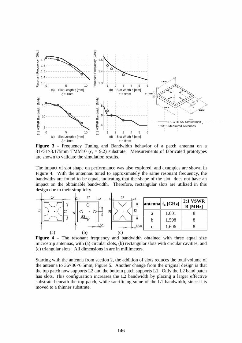
1 2 3 4 5 61.3
1.4
1.5
Res
onan
t F
requ
ency
[G
Hz]
(b) Slot Width ζ [mm]τ = 9mm
1 2 3 4 5 6
4
6
8
2:1
VS
WR
Ban
dwid
th [
MH
z]
(d) Slot Width ζ [mm]τ = 9mm
0 5 101.3
1.4
1.5
1.6
1.7
(a) Slot Length τ [mm]ζ = 1mm
Res
onan
t F
requ
ency
[G
Hz]
0 5 10
5
10
15
(c) Slot Length τ [mm]ζ = 1mm
2:1
VS
WR
Ban
dwid
th [
MH
z]
PEC HFSS Simulations
Measured Antennas
Figure 3 - Frequency Tuning and Bandwidth behavior of a patch antenna on a 31×31×3.175mm TMM10 (єr = 9.2) substrate. Measurements of fabricated prototypes are shown to validate the simulation results. The impact of slot shape on performance was also explored, and examples are shown in Figure 4. With the antennas tuned to approximately the same resonant frequency, the bandwiths are found to be equal, indicating that the shape of the slot does not have an impact on the obtainable bandwidth. Therefore, rectangular slots are utilized in this design due to their simplicity.
(a) (b) (c) Figure 4 – The resonant frequency and bandwidth obtained with three equal size microstrip antennas, with (a) circular slots, (b) rectangular slots with circular cavities, and (c) triangular slots. All dimensions in are in millimeters. Starting with the antenna from section 2, the addition of slots reduces the total volume of the antenna to 36×36×6.5mm, Figure 5. Another change from the original design is that the top patch now supports L2 and the bottom patch supports L1. Only the L2 band patch has slots. This configuration increases the L2 bandwidth by placing a larger effective substrate beneath the top patch, while sacrificing some of the L1 bandwidth, since it is moved to a thinner substrate.
antenna fo [GHz] 2:1 VSWR B [MHz]
a 1.601 8
b 1.598 8
c 1.606 8
146

1.22 1.23 1.24 1.25 1.26-40
-30
-20
-10
0
10L2 Band
Frequency [GHz]
Rea
lized
Gai
n [d
B]
RHCP
LHCP
1.55 1.56 1.57 1.58 1.59-40
-30
-20
-10
0
10L1 Band
Frequency [GHz]
Rea
lized
Gai
n [d
B]15 MHz
Bandwidth28 MHz
Bandwidth
Figure 5 – Dimensioned drawing for the optimized slotted, stacked patch antenna. All dimensions are in millimeters. Horizontal “L” probes are 4×1mm.
1.2 1.25 1.3 1.35 1.4 1.45 1.5 1.55 1.6 1.65 1.7-40
-35
-30
-25
-20
-15
-10
-5
0Scattering Parameters for the Slotted L-probe Antenna
Frequency [GHz]
[dB
]
S11
S21
6MHz Bandwidth At L2
10MHz BandwidthAt L1
>20dB Isolation
(a) (b)
Figure 6 – (a) Return Loss and (b) Realized Gain performance of the slot-loaded, stacked patch GPS antenna on TMM10 dielectric. Figure 6 shows the antenna has 6MHz and 10MHz 2:1 VSWR bandwidth at L2 and L1 respectively, and a realized gain flatness bandwidth of 15MHz at L2 and 28MHz at L1, with a gain greater than 3dB over each band. The L2 realized gain bandwidth falls short of the goal of 20MHz, but can be increased by increasing dielectric layer thicknesses, and/or compromising more of the L1 bandwidth, as achieved when placing the L1 patch on the bottom layer. The slot loading provides a convenient means of adjusting the resonant frequency of the patch, since it only requires cutting out part of the patch. This design is one of the smallest GPS antennas developed for this project, while approaching the electrical performance goals. 4. Cavity Loaded Microstrip Patch Antenna The introduction of a backing cavity has many benefits. Electrically, the backing cavity loads the radiating edges of the patch similar to that of lumped capacitor elements, and provides a means of tuning the resonant frequency. It provides electrical isolation
147

between the antenna and its surroundings, and also suppresses the excitation of surface waves [6]. Mechanically, the cavity allows the antenna to be recess mounted in a ground plane, making the aperture of the cavity flush with the ground plane, resulting in a low profile design. For applications where substrate thickness is increased to improve bandwidth, the cavity alleviates the impact of substrate truncation on the resonant frequency. For a traditional patch antenna, when the substrate size is much larger than the patch size, the resonant frequency decreases with substrate thickness, as theory predicts, Figure 7. However, when the substrate size is close to the patch size, α < 35mm, the frequency actually increases with substrate thickness, as more of the fields fringe out the sides of the dielectric and into the air – reducing the effective permittivity of the substrate. In contrast, if the substrate is clad in metal to form a cavity, Figure 8, the capacitive loading of the vertical walls reduces the resonant frequency of the antenna as the substrate size approaches the patch size. The capacitive loading of the walls decreases as substrate size α increases, and the two resonant frequency trends in Figure 8 converge when the substrate is sufficiently large. Loading the patch antenna with a cavity allows the area occupied by the antenna to be minimized, while retaining the low resonant frequency tuning.
40 50 60 70 80 90 100
1.3
1.4
1.5
1.6
1.7
Sub Size α [mm]
Res
onan
t F
requ
ency
[G
Hz]
t = 1mm
t = 7mmt = 11mm
Figure 7 – The change in patch resonant frequency due to substrate truncation shown for various substrate sizes α and thicknesses t. The substrate material is TMM10 (εr = 9.2). Figure 9 shows a cavity backed patch antenna with four 7mm long slots cut into the patch (to further reduce its size) and also the impact of cavity depth on resonant frequency and bandwidth. The capacitive loading of the walls is analogous to a parallel plate capacitor between the patch and ground. Just as increasing the area of the plates of a capacitor increases capacitance, increasing the depth of the cavity (which increases the vertical wall area) also increases capacitive loading on the patch, decreasing the resonant frequency. Increasing the separation between the walls of the cavity and the patch reduces the capacitance, once again similar to a parallel plate capacitor’s inverse relationship between capacitance and plate separation.
Patch size
148

α=27.5mm
α=28.5mm
α=30mm
α=31mm
40 50 60 70 80 90 1001.2
1.3
1.4
1.5
1.6
1.7
Sub Size α [mm]t = 7mm
Res
onan
t F
requ
ency
[G
Hz]
Without Cavity Backing
With Cavity Backing
Figure 8 – The change in patch resonant frequency due to substrate truncation when the substrate is clad with metal walls (shown in gray) to form a cavity backing over various substrate sizes α and thickness t = 7mm. The same antenna without cavity backing from Figure 7 is shown for comparison.
2 4 6 8 101.1
1.2
1.3
1.4
1.5
1.6
Cavity Depth t [mm]
Res
onan
t F
requ
ency
[G
Hz]
Resonant Frequency Vs. Cavity Depth
2 4 6 8 100.2
0.3
0.4
0.5
0.6
0.7
Cavity Depth t [mm]
% 2
:1 V
SW
R B
andw
idth
Fractional Bandwidth Vs. Cavity Depth
Figure 9 - Variation in resonant frequency and bandwidth of patch antenna for various cavity sizes α and depths t. Substrate material is TMM10 (εr = 9.2).
149

1.2 1.22 1.24 1.26-40
-30
-20
-10
0
10
Frequency [GHz]
Rea
lized
CP
Gai
n [d
B]
L2 Band
1.52 1.54 1.56 1.58 1.6 1.62-40
-30
-20
-10
0
10
Frequency [GHz]
Rea
lized
CP
Gai
n [d
B]
L1 Band
RHCP
LHCP
11 Mhz Bandwidth
23 MhzBandwidth
Figure 9 also shows the correlation between the volume of the antenna structure and the bandwidth obtained. As the cavity depth t increases, the overall electrical volume of the antenna is increased, resulting in a lower Q and, therefore, a larger bandwidth. Building on the design in Section 3, the antenna is now placed in a recessed cavity, shown in Figure 10. The cavity reduces the size of the antenna to 34×34×7mm, further approaching the goal volume.
Figure 10 - Dimensioned drawing for the optimized cavity backed dual band, CP, stacked-patch GPS antenna. Horizontal “L” probes are 2.93×1mm. All dimensions are in millimeters.
1.2 1.22 1.24 1.26 1.28 1.3-40
-35
-30
-25
-20
-15
-10
-5
0
Frequency [GHz]
[dB
]
L2 Band
1.5 1.55 1.6 1.65-40
-35
-30
-25
-20
-15
-10
-5
0
Frequency [GHz]
[dB
]
L1 Band
S11
S21S11
S21
5 MHz Bandwidth
8MHzBandwidth
(a) (b) Figure 11 – (a) Return Loss and (b) Realized Gain for the optimized cavity backed CP, dual frequency antenna. Figure 11 shows that the antenna has a 5MHz 2:1 VSWR bandwidth at L2, and an 8MHz 2:1 VSWR bandwidth at L1, which meets the impedance bandwidths required in Table 1. The gain flatness bandwidth at L2 is 11MHz, which is approximately half of the desired bandwidth. This gain flatness bandwidth can be increased with a larger cavity size (depth or length). At L1, the gain flatness bandwidth is 23MHz, meeting the requirement. The cavity allows further antenna size reduction and provides a recessed mounting platform, making it the smallest antenna in both volume and profile.
150

5. Comparison with Fundamental Q Limit The Q of an antenna is defined as [7]
2
2
ee m
f
mm e
f
WW W
PQ
WW W
P
ω
ω
>
= >
(1)
where eW and mW are the time averaged stored electric and magnetic energies,
respectively, and fP is the power dissipated in radiation. The fractional matched VSWR bandwidth is given by [8]
( ) upper lowerv o
o o o
f f fFBW
f f
ω ωωω
+ −−− ∆= = = (2)
where fupper and flower are the highest and lowest frequencies of the VSWR s:1 bandwidth, centered on fo. The relationship between FBWV and Q is then given as [9]
2 1
( ) 1( ) 2
oV o
sQ where
FBW s
βω βω
−≈ = ≤ (3)
The theoretical lower bound on the Q for an antenna fully enclosed by a sphere of radius “a” is derived using an exact method by McLean [10].
3
1 1
( )Q
ka ka= + (4)
The lower bound on Q is useful for comparison since it provides an upper bound on the obtainable bandwidth for an antenna of a given size. Figure 12 shows the bandwidths of the three antennas presented in this paper, as well as two designs of Zhou [3], [5]. None the antennas come very close to the limit, which can be attributed to the planar structures only occupying a fraction of the enclosing sphere. The antennas are compared first by considering their half power bandwidths, Figure 12a, where the largest fractional bandwidth is achieved by the L1 band of Zhou’s 33×14mm antenna. However, when the bandwidths are compared at a level of VSWR 2:1, Figure 12b, only the L1 band of Zhou’s 31×31×12.8mm antenna has an impedance match of VSWR 2:1. This emphasizes the difference between the antennas presented in this paper and many designs found in literature. Many designs in the literature achieve the gain bandwidths required for GPS, but they achieve their large gain bandwidths via a poor impedance match at the L1, L2 bands, since the Bode-Fano criteria indicates that the 3dB bandwidth can be
151

0.5
0.6 Optimized High Permittivity L-probe L1Optimized Cavity-Backed Antenna L2
Optimized Cavity-Backed Antenna L1
34X34X7mm Cavity-Backed Antenna L234X34X7mm Cavity-Backed Antenna L1
0.7
0.8ChuOptimized Slot Loaded L2
Optimized Slot Loaded L1
36X36X6.5mm Slot Loaded Antenna L2
36X36X6.5mm Slot Loaded Antenna L1
0.6
0.7Optimized Slot Loaded L1
Optimized High Permittivity L-probe L2
Optimized High Permittivity L-probe L1
41.5X41.5X6.5mm Antenna L2
41.5X41.5X6.5mm Antenna L1
34X34X7mm Cavity-Backed Antenna L2
0.2
0.3
0.4Optimized Cavity-Backed Antenna L1
Zhou 31X31X12.8mm L2
Zhou 31X31X12.8mm L1
Zhou 33X14mm L2Zhou 33X14mm L1
broadened at the expense of a good impedance match. In GPS systems, noise considerations often require a good impedance match at both bands.
1 2 3 4 50.1
0.2
0.3
0.4
0.5
0.6
0.7
0.8
0.9
(b) 3dB % bandwidth
ka
ka versus 3dB Fractional Bandwidth
0.4 0.6 0.8 10.1
0.2
0.3
0.4
0.5
0.6
0.7
0.8
0.9
(a) 2:1 VSWR % Bandwidth
ka
ka versus VSWR 2:1 Fractional Bandwidth
Figure 12 - Comparison of miniature microstrip antenna bandwidths with the theoretical minimum Q limit derived by McLean (equation 4). 6. Conclusion Three miniaturized GPS antennas have been presented, showcasing three effective methods for decreasing the volume of a dual band GPS microstrip patch antenna. Use of high permittivity dielectric material and the stacked patch geometry serve as a starting point for the designs, and the addition of slots and a backing cavity each further reduce antenna size. Two designs presented achieve 2:1 VSWR bandwidths of 5MHz a both L1 and L2 bands in a volume smaller than 36×36×7mm. The cavity backed design achieved the smallest size, at 34×34×7mm, and is recessed for very low profile. 7. Acknowledgements This work was funded in part by the Center for Advanced Sensor and Communication Antennas at the University of Massachusetts under US Air Force contract FA8718-06-C-0047 and in part by M/A-COM, Inc., Lowell, MA.
0.9McLean/Collin
ChuMcLean Q Limit36X36X6.5mm Slot Loaded Antenna L2
[3]
[5]
152

8. References [1] Lee, K.F., Luk, K.M., Tong, K.F., Shum, S.M., Huynh, T., and Lee, R.Q.:
“Experimental and simulation studies of coaxially fed U-slot rectangular patch antenna”. IEE Proc -Microw Antennas Propag.. Vol 144, No. 5, October 1997.
[2] Salonen, P.; Jaehoon Kim; Rahmat-Samii, Y., "Dual-band E-shaped patch
wearable textile antenna," Antennas and Propagation Society International Symposium, 2005 IEEE , vol.1A, no., pp. 466-469 Vol. 1A, 3-8 July 2005.
[3] Zhou, Y.; Chen, C.-C.; Volakis, J. L., "Dual Band Proximity-Fed Stacked Patch
Antenna for Tri-Band GPS Applications," Antennas and Propagation, IEEE Transactions on, vol.55, no.1, pp.220-223, Jan. 2007.
[4] Yijun Zhou; Kiziltas, G.; Koulouridis, S.; Volakis, J.L., "A miniature four-arm
antenna for tri-band GPS applications," Antennas and Propagation Society International Symposium, 2005 IEEE , vol.3A, no., pp. 872-875 vol. 3A, 3-8 July 2005.
[5] Yijun Zhou,; Chi-Chih Chen,; Volakis, John L., "Tri-band miniature GPS Array
with a single-fed CP antenna element," Antennas and Propagation International Symposium, 2007 IEEE , vol., no., pp.3049-3052, 9-15 June 2007.
[6] Aberle, J.T., "On the use of metallized cavities backing microstrip antennas,"
Antennas and Propagation Society International Symposium, 1991. AP-S. Digest , vol., no., pp.60-63 vol.1, 24-28 Jun 1991.
[7] R. F. Harrington, Time-Harmonic Electromagnetic Fields (IEEE: Wiley-
Interscience, New York, 2001). [8] Best, S.R. “A Study of the Performance properties of small antennas,” 2007
Antenna Applications Symposium, Allerton Park, Monticello, Illinois, pp. 193-211, 18-20 September, 2007.
[9] Yaghjian, A.D.; Best, S.R., "Impedance, bandwidth, and Q of antennas,"
Antennas and Propagation, IEEE Transactions on , vol.53, no.4, pp. 1298-1324, April 2005.
[10] McLean, J. S., "A re-examination of the fundamental limits on the radiation Q of
electrically small antennas," Antennas and Propagation, IEEE Transactions on , vol.44, no.5, pp.672-, May 1996.
153

ON THE USE OF SPIRAL ANTENNAS FOR ELECTRONICATTACK
Matthew J. Radway, W. Neill Kefauver, and Dejan S. FilipovicDepartment of Electrical and Computer Engineering
University of Colorado, Boulder, CO 80309-0425radway, kefauver, [email protected]
Abstract: Spiral antennas are attractive for electronic warfare applications due totheir inherently broadband pattern and impedance characteristics. However, for uni-directional radiation an absorbing cavity is frequently used to preserve the broadbandcharacteristics of the spiral. The absorbing nature of the cavity becomes undesirablewhen the spiral is coupled with a high-powered exciter. A reflecting cavity design ismore desirable from a power-dissipation standpoint, but will degrade the broadbandperformance of the spiral due to the interference of the direct and reflected fields.This paper considers the performance of spiral antennas with multiple arms backedby infinite PEC and PMC planes. It is shown that spirals with multiple arms are lesssusceptible to the deteriorating effects to the far field that a reflective backing intro-duces. Results for frequencies both above and below the mode 1 cutoff frequency areshown, and the numerical models are validated by measurement.
1 IntroductionPlanar spiral antennas have long been used in electronic warfare applications due to theirbroadband pattern and impedance characteristics. The use of RF-absorbing cavity materialto dissipate the inherent unwanted back lobe limits these antennas to receiving-mode appli-cations unless care is taken to remove the excess heat that is generated. Nonetheless, thereis interest in the use of spiral antennas in the exciter mode for electronic attack. Since thethermal management of an absorbing cavity in this situation is a potentially troublesomeand costly task, it is desirable to replace the absorbing cavity with one that is reflective toRF energy. However, the resulting interference from this undesired back lobe inevitablycauses degradation of the broadband pattern and impedance characteristics of the spiral.
The purpose of this paper is to explore the far field performance characteristics of theplanar spiral in the presence of infinite planar PEC and PMC surfaces. This includes exten-sion from the commonly-used two-arm spiral to spirals with three and four arms. Perfor-mances in terms of co-polarized broadside (boresight) gain and axial ratio at θ = 30 frombroadside are considered. It is shown that the three- and four-arm spirals have importantfar-field performance advantages over the more common two-arm spiral.
This paper is organized as follows. First, the characteristics required for a success-ful electronic attack antenna are reviewed. Second, the theory of spiral modes is brieflyreviewed since it forms a basis for discussion of spiral antennas. Then, the far field per-formance of 15 cm diameter spirals excited in the broadside mode of operation (mode 1
154

cutoff f0 ≈ 640 MHz) in the presence of a PEC backing plane with three and four arms iscompared to the performance of the corresponding two-arm spiral. This is followed by asimilar study for the case of a PMC plane. Finally, the numerical models are validated withmeasurements.
2 Antenna Requirements for Electronic Attack (EA)Traditional EA missions typically involve jamming or some other form of active control ofthe electromagnetic spectrum; therefore, a good EA antenna would exhibit (among othercharacteristics)
1. high power handling,
2. high gain,
3. low cross-polarization,
4. polarization agility,
5. stable phase center,
6. broad pattern bandwidth,
7. broad impedance bandwidth.
The planar spiral antenna can fulfill the last five of these requirements; however, the firsttwo represent a more difficult challenge. For example, common EA applications call fortransmitting powers on the order of a few kilowatts. By contrast, commercially availablespiral antennas are typically rated to only a few tens of watts in the transmitting mode,which practically limits their application to the receiving portions of EA systems. Elimi-nation of the absorbing cavity is a particularly attractive approach to the design of spiralantennas for EA because it could conceivably improve the first two points simultaneously.
3 Spiral Mode TheoryIn 1961, Cheo, Rumsey, and Welch [1] published one of the first and most successful treat-ments of the equiangular spiral antenna as a boundary-value problem. While the structurethat they considered did not correspond to a physically-realizable antenna, it was suffi-ciently idealized that a solution to the problem in terms of spherical modes was able to befound. The structure was excited at the center by a source having a φ dependence of ejnφ.Due to the azimuthal symmetry of the structure the field was assumed to share this depen-dence on φ. By application of the method of stationary phase, the far field in the upperhalf-space for a spiral with growth rate α was computed to be [1, 2]
FE ≈ (θ − jφ)A(θ)e−jψ(θ) e−jkr
r(1)
where k is the wavenumber of the medium, θ and φ are unit vectors in the spherical coor-dinate system (r, θ, φ) with
A(θ) =cot θ(tan[θ/2])|n|e|n|/α tan−1(α cos θ)
√1 + α2 cos2 θ
(any n 6= 0) (2)
155

and
ψ(θ) = nφ+ tan−1(α cos θ)
+n
2αln(1 + α2 cos2 θ) (n/α < 0) (3)
= −nφ− tan−1(α cos θ)
− n
2αln(1 + α2 cos2 θ) (n/α > 0) (4)
In the terminology of [3], n = integer is the mode number and the resulting field constitutesa mode of the spiral antenna. Such a mode will have the following features:
1. For any constant elevation θ the phase advances linearly by 2πn as the azimuth φ isswept from 0 to 2π.
2. The far field is circularly polarized with the sense of polarization dependent on thesign of n.
3. All modes with n 6= ±1 have nulls at broadside.
4. The far field has zero magnitude in the plane of the spiral.
Additionally, it has been noted [4] that each mode radiates from a region on the spiralwith circumference C = |n|λ. Despite being strictly applicable only to the infinite-armedspiral of infinite spatial extent, it turned out that these modes were sufficient to accuratelydescribe the operation of spirals that possess a finite number of arms [3] provided that thearms are excited with equal amplitude and with a phase ejn2πk/K . Here K is the number ofarms and k = (0, 1, . . . , K−1) is the arm number. Today the operation of spiral antennas isoften described in terms of this so-called spiral mode theory. In this paper the performanceof spiral antennas will be described in terms of these spiral modes.
4 Effects of a PEC PlaneThere is a trade-off between placing a spiral too close to the ground plane, where the mainimpact on spiral performance is on the input impedance, and placing it too far away, whereinterference of the direct and reflected fields degrades the far-field performance. A studywas performed to examine the effect of this distance on the far field (Fig. 1), where thedistance to the PEC plane was varied from 0.2 cm to 5.08 cm (2 inches). Distances greaterthan 5.08 cm were not considered due to the particular application of the antenna.
4.1 Broadside Co-polarized Gain
It was found that increasing the distance from the spiral to the ground plane (Fig. 1(a))results in improved gain, especially at the low end of the frequency spectrum. The three-and four-arm spirals exhibit improved co-polarized gain relative to the two-arm spiral inthe frequency range of 300 MHz to 900 MHz, a range that is approximately centered aboutthe mode 1 cutoff frequency. This improvement for the three- and four-arm spirals canbe attributed to the fact that the first cross-polarized mode for the three- and four-armed
156

spirals is -2 and -3 respectively. Since (2) vanishes as θ goes to zero, these modes have anull at broadside and produce no cross-polarization contamination there. More gain is thusavailable to the co-polarized mode. For the range of distances and frequencies studied itappears that maximizing the distance to the PEC plane is the optimal solution.
4.2 Axial Ratio (AR) at θ = 30
Since the three- and four-arm spirals have no cross-polarization at broadside, the AR wasevaluated at θ = 30 for the purpose of comparison with the two-arm spiral. It was foundthat increasing the distance to the PEC plane (Fig. 1(b)) also generally improved the AR foreach antenna studied. It can be seen that the AR for the two-arm spiral degrades quickly asthe frequency lowers toward the mode 1 cutoff, and as mode -1 contamination becomes sig-nificant. By contrast, at low frequencies the three- and four-arm spirals are not electricallylarge enough to radiate their respective cross-polarized modes (-2 and -3) efficiently. As aresult the ARs for three- and four- arm spirals remain low as frequency decreases. As fre-quency increases, first the three-arm and later the four-arm spirals will become electricallylarge enough to radiate their respective contaminating modes, therefore degrading AR. Forthe range of distances and frequencies studied it appears that maximizing the distance tothe PEC plane is the optimal solution.
5 Effects of a PMC PlaneRecently several researchers ( [5] and others) have investigated the use of high-impedancesurfaces for use as shallow reflecting cavities for spiral antennas. These surfaces are typ-ically operated near parallel resonance, resulting in zero reflection phase. An especiallypopular structure for this application is the so-called ”mushroom surface” [6], which con-sists of an array of square patches above a ground plane. The patches are connected to theground plane by way of posts connected to the center of each patch. The posts are typicallyrealized using standard PCB plated through-hole technology. The intent of such a surfaceis to simulate the action of a PMC plane, albeit over a narrow range of frequencies andangles of incidence.
Analysis and design of these structures typically use an equivalent transmission-linemodel that neglects coupling between the antenna and the impedance surface [6,7]. There-fore it may be desirable to place the surface far enough away from the antenna structureso that antenna-to-surface coupling is minimized, yet close enough to realize some benefitfrom the concept. A study of the effects of placing an ideal PMC surface below the spiralstructure was performed over the range of distances 0.2 cm to 5.08 cm. The results aresummarized in the following, but generally speaking the placement of a PMC plane closeto the spiral improves the performance of the spiral as expected by image theory.
5.1 Broadside Co-polarized Gain
From Fig. 2(a) it is apparent that although placing the PMC plane close to the spiral surfaceis the ideal configuration, moving the PMC plane away from the spiral surface results ina gradual degradation of the broadside gain . Two-, three-, and four-arm spirals perform
157

almost identically in this situation. When d ≈ λ/4, the gain exhibits a deep null, and the3-dB beamwidth jumps to the maximum value of 360.
5.2 Axial Ratio at θ = 30
The sensitivity to PMC plane distance is greater for AR. For AR less than 3 dB the distancemust be less than 0.4 cm near 2000 MHz (Fig. 2(b)). It can be concluded that for practicalspiral antenna applications this distance represents an approximate limit for the distancethat an artificial impedance surface approximating a PMC plane can be placed from thesurface of this spiral antenna to achieve tolerable performance.
6 Experimental Model ValidationIn order to validate the preceding numerical analysis, two spiral antennas were produced:one with two arms and four turns, the other with three arms and three turns. To accomo-date the available measurement facility, the antennas were scaled down in size by a factorof three, and built using standard printed circuit board fabrication technology on RogersRT/Duroid 6002 (εr = 2.94) material with a thickness of 20 mils (508 µm). The antennaswere fed at the center with a bundle of phase-matched 0.086 inch (approximately 2.18 mm)diameter semi-rigid coaxial cables.
6.1 Measurements
For the purpose of validation, absorber-backed two-arm and three-arm spirals were experi-mentally studied. The measured parameters are plotted against those predicted by HFSS aswell as FEKO using surface equivalence principle (SEP). The two-arm spiral was measuredover the frequency range of 1.2-12 GHz. The realized co-polarized gain of the two-arm spi-ral antenna is shown in Fig. 4(a), and the realized cross-polarized gain of the same spiral isshown in Fig. 4(b), and good mutual agreement was observed.
The three-arm spiral was measured over a narrower frequency range of 3.6-6.1 GHz.The realized co-polarized gain of the three-arm spiral antenna is shown in Fig. 5(a), andthe realized cross-polarized gain of the same spiral is shown in Fig. 5(b), and good mutualagreement was observed. In the case of the three-arm spiral, it should be noted that thedifference between the co-polarized and cross-polarized components is better than 35 dB.
7 ConclusionThis paper has presented a comparison of the performance characteristics of two-, three-,and four-arm spiral antennas. It was found that the three- and four-arm spirals outperformthe two-arm spiral in the far field when operated below cutoff. At frequencies below themode 1 cutoff the two-arm spiral was shown to have a high axial ratio that makes it anunlikely candidate for practical antenna applications in this region. On the other hand, thethree- and four-arm spirals retain their far-field performance characteristics in a robust way,even down to frequencies far below mode 1 cutoff.
Multiarm spiral antennas were shown to have a higher degree of immunity from thecontaminating effects of PEC and PMC planes placed in the near-field. This is important
158

from the standpoint of predicting what will be the installed performance of the antenna. Inthe case of the PMC plane it was found that for an antenna to have satisfactory far-fieldperformance the PMC must be located rather close to the plane of the spiral. For thesereasons the added expense of the hybrid beamformers for three- and four-arm spirals maybe justified in applications requiring a high level of gain purity and a low level of modalcontamination.
AcknowledgmentsThe authors acknowledge the support of the Office of Naval Research, United States Navy,under grant #N00014-07-1-1161, administered by Dr. Peter Craig. The authors would alsolike to thank Mr. Tim May for providing advice toward the fabrication of the test articles.
References[1] R.-S. Cheo, V. H. Rumsey, and W. J. Welch, “A solution to the frequency-independent
antenna problem,” IRE Transactions on Antennas and Propagation, vol. 9, no. 6, pp.527–534, November 1961.
[2] V. H. Rumsey, Frequency Independent Antennas. New York, New York: AcademicPress, Inc., 1966.
[3] R. Sivan-Sussman, “Various modes of the equiangular spiral antenna,” IEEE Trans.Antennas Propagat., vol. 11, no. 5, pp. 533–539, Sep 1963.
[4] R. G. Corzine and J. A. Mosko, Four-Arm Spiral Antennas. Norwood, Massachusetts:Artech House, Inc., 1990.
[5] J. Bell and M. Iskander, “A low-profile archimedean spiral antenna using an EBGground plane,” IEEE Antennas Wireless Propagat. Lett., vol. 3, no. 1, pp. 223–226,2004.
[6] D. Sievenpiper, L. Zhang, and E. Yablonovitch, “High-impedance electromagneticground planes,” in 1999 IEEE MTT-S International Microwave Symposium Digest,vol. 4, June 1999, pp. 1529–1532.
[7] S. A. Tretyakov and C. R. Simovski, “Dynamic model of artificial reactive impedancesurfaces,” J. of Electromagn. Waves and Appl., vol. 17, no. 1, pp. 131–145, 2003.
159

(a) Co-polarized gain.
(b) Axial ratio.
Figure 1: Co-polarized broadside gain and average axial ratio at 30 off of broadside forspiral antennas above a PEC plane. The arrows indicate the direction of increasing PECplane separation.
160

(a) Co-polarized gain.
(b) Axial ratio.
Figure 2: Co-polarized broadside gain and axial ratio versus frequency. Deep nulls in thegain appear when the separation from the PMC plane is λ/4. The arrow indicates thedirection of increasing separation from the PMC plane.
161

(a) Two-arm spiral.
(b) Three-arm spiral.
Figure 3: Photographs of the spiral radiating elements prior to assembly.
162

(a) Co-polarized gain.
(b) Cross-polarized gain.
Figure 4: Comparison of simulated and measured results for realized co- and cross-polarized gain versus frequency for the two-arm spiral antenna.
163

(a) Co-polarized gain.
(b) Cross-polarized gain.
Figure 5: Comparison of simulated and measured results for realized co- and cross-polarized gain versus frequency for the three-arm spiral antenna.
164

A CLASS OF ELECTRICALLY SMALL SPHERICAL ANTENNAS WITH NEAR-MINIMUM Q
Jacob J. Adams and Jennifer T. Bernhard
Electromagnetics Laboratory University of Illinois at Urbana-Champaign, Urbana, IL 61801
http://antennas.ece.uiuc.edu; E-mail: [email protected] Abstract: We theoretically describe and experimentally demonstrate a new class of electrically small spherical antennas with near minimum radiation Q. The antenna operates by exciting the TM10 spherical mode and minimizing excitation of higher order modes. The antenna compares favorably to existing electrically small antennas and can be easily designed for any frequency or with any electrical size. Methods for matching the antenna as well as measured results are presented. 1. Fundamental Limitations of Electrically Small Antennas One of the key parameters for electrically small antennas is the radiation quality factor (Q). The Q of an antenna represents the ratio of the energy stored per cycle to the power radiated and is typically defined as
0 max2rad
WQ
Pω
= (1)
Radiation Q is critical for a singly resonant antenna, because the antenna’s bandwidth is inversely proportional to Q [1]. Thus, a low Q antenna is desirable. However, Q has been shown to be constrained by the electrical size of the antenna. In 1948, Chu published his well-known work investigating the fundamental limitations of antennas [2]. He showed that the radiation Q of an antenna has a lower limit determined by the electrical size of a sphere of radius a which circumscribes the antenna [2], [3].
3
1 1( )ChuQ
ka ka≈ + (2)
We will refer to this as the Chu limit. An antenna that approaches Chu’s limit has been sought after for decades. It has been taken as a rule of thumb that an antenna that most fully occupies a spherical volume exhibits the lowest Q. Foltz and McLean showed mathematically that the minimum Q is achievable with an antenna occupying a spherical volume rather than a dipole or planar structure [4]. In agreement with these principles,
165

Best introduced a spherical wire antenna with among the lowest Q to date at approximately 1.5×QChu [5], [6]. However in [6], the antenna was found to be tunable to 50 Ω only for certain electrical sizes. In this paper, we describe a spherical antenna that offers similar Q performance to the spherical helix and the added advantage of tunability. Our design approach is unusual in that a low Q current distribution is described mathematically and the structure of the antenna is manipulated to achieve it. 2. A TM10 Antenna In our discussion of Q, it should be noted that Chu’s limit may be overly optimistic. As observed by Chu himself, the model does not consider energy stored within the circumscribing sphere. This energy would increase the Q, so the actual bound must be higher than Chu calculated. Thal recently addressed this shortcoming by deriving a modal circuit model which also includes internal stored energy [7]. The new model results in a higher limit on the minimum Q. To simplify the mathematics, Thal considered only currents on a spherical surface. In his model, the lowest possible Q for currents on a spherical surface is obtained by exciting the TM10 spherical mode while minimizing excitation of higher order modes which primarily store energy. The TM10 mode can be excited by a surface current distribution of the form [7]
sin( )Jθ θ= (3)
The primary challenge is engineering such a current distribution. An antenna structure supporting this distribution was introduced in [8]. In order to approximate the desired distribution, several wires are placed along the constant-φ lines of a sphere. The sphere is bisected by a ground plane along / 2θ π= . In this configuration, the φ-directed wires are electrically short and produce a current distribution that is triangular in θ. To achieve the required full sinusoidal variation described above, the electrical length of the wires is increased by winding them in a helical fashion about the constant-φ lines. A symmetric feed structure is required in order to provide equal excitation to the arms. A conducting trace suspended above the ground plane contacts all of the arms at their base. The trace is fed in the center by a probe from behind the ground plane. Figure 1 shows the proposed structure using four arms.
166

p
2rhb w
x
y
z
feed pointfeed trace
substrate
helical wire coils
helix core
Figure 1: A four arm TM10 antenna. The pitch, p, is measured on the outer radius of the arm coils. The arm coils have radius rh and their centerline follows a circle of radius b from the center of the structure. The width of the trace is wt.
3. Properties of the Antenna The antenna described in the previous section was simulated in using Ansoft’s HFSS. In the electrically small region, the antenna exhibits some notable properties. A typical plot of the input impedance of the antenna is shown in Figure 2a. The first resonance of the antenna occurs when the physical length of wire on each arm is on the order of a half wavelength. Thus the pitch of the coils acts as the primary tuning mechanism by changing the electrical length of the arms. Decreasing the pitch lowers the resonant frequency. An antiresonance also appears in the electrically small region, slightly higher in frequency than the resonance. When placed on an infinite ground plane, the antenna exhibits an electric monopole radiation pattern typical of most electrically small antennas. It is nearly omnidirectional in φ (variation of less than 0.4 dB for the four arm design), and it features a null at θ = 0 and peak directivity of 9.4 dB along the direction of the ground plane (θ = 90°). The maximum cross polarization ratio is less than -40 dB.
167

(a)
(b)
Figure 2: Typical properties of the TM10 antenna. (a) shows the input impedance behavior of the antenna in the electrically small region. (b) shows the Q/QChu for the same antenna. The operating region or “low Q region” exists between the first resonance and the first antiresonance. 3.1 Behavior of the Quality Factor The antenna’s bandwidth performance will be discussed in terms of the ratio Q/QChu. This figure of merit clearly compares the TM10 antenna’s performance to the optimum, and performance can be fairly compared across different ka values. In all Q calculations, the input impedance is used to find Q using [1]
22
000 0 0
0 0
( )( ) ( ) ( )
2 ( )X
Q R XR
ωωω ω ωω ω ω ω
⎡ ⎤∂ ∂⎡ ⎤= + +⎢ ⎥⎢ ⎥∂ ∂⎣ ⎦ ⎣ ⎦ (4)
168

Figure 3: Q/QChu ratio of several TM10 antennas compared to existing designs from [9]. The Thal limit for currents on a spherical surface [7] is also shown. Figure 2b shows the Q/QChu ratio for the same antenna whose impedance characteristics are shown. After the first resonance, the steep Q/QChu curve flattens and reaches a minimum value. Then just before the subsequent antiresonance, the Q/QChu value begins rising again. We refer to this flat region where the Q/QChu minimum occurs as the “low Q region” indicating that the Q is low relative to the electrical size. Operation anywhere in this region is desirable. 3.2 Comparison to lower bound The purpose of this study is to maximize performance (as measured by Q) with a realizable electrically small antenna. As discussed earlier, Thal has shown that the real achievable Q is higher than Chu’s limit when the currents are constrained to a spherical surface. Still, we will use the Chu limit as a basis for comparison but also present Thal’s limit for a more realistic assessment of antenna performance. Illustrating the excellent performance of our design, Figure 3 shows the Q/QChu ratio for the TM10 antenna with 4 arms and 8 arms and with two different pitches. Also shown in the plot are the Thal limit and several other designs from [9], the spherical helix, spherical cap monopole, and top loaded dipole. With 8 arms, the TM10 antenna closely
169

approaches the Thal limit, achieving nearly optimal Q and maximizing bandwidth. In addition to approaching the lower bound, the antenna exhibits Q lower than or equal to that of the comparison designs. Finally, it can also been seen in Figure 3 that the operating frequency of the TM10 antenna can be moved by increasing and decreasing the pitch of the wires. The small pitch and large pitch designs shown here are given only as examples. An even smaller or larger pitch could be used to tune the operating frequency lower or higher, respectively. 4. Impedance Matching Even if the antenna is operating in the low Q region, it still must be matched to the system impedance to achieve maximum bandwidth (the Q discussed in this work represents the Q when matched). As seen in Figure 2, the resistance at resonance is very small (~ 4Ω) and changes little when the geometric parameters are changed. However, at the antiresonance, the resistance can be varied greatly. The primary factor in determining the antiresonant resistance (Rar) is the electrical size of the structure. Figure 4 shows how Rar varies as the antenna is tuned via pitch changes for a four arm antenna. The total size of the structure stays constant but the resonant frequency changes, so ka at antiresonance changes. When the antenna is tuned for very small electrical sizes, Rar becomes very large.
Figure 4: Antiresonant resistance (Rar) versus electrical size (at antiresonance) of a four arm TM10 antenna with a .050” substrate (εr = 1) and a trace width of 2 mm. As the antenna is tuned to smaller electrical sizes by lengthening the wire and changing the pitch, Rar increases rapidly.
170

(a) (b) Figure 5: (a) Impedance of a four arm TM10 antenna (ka = .47 - .62) on a .050” substrate with varying permittivity. Increasing the permittivity decreases Rar. Trace width is 2 mm, p = 3 mm, b = 21 mm, rh = 2.5 mm. (b) Impedance of a four arm TM10 antenna (ka = .47 − .60) with a .050” substrate (εr = 2.94). Decreasing the trace width increases Rar. Other dimensions are: p = 2.85 mm, b = 21 mm, rh = 2.5 mm. 4.1 Tuning via Parallel Capacitance The parallel capacitance between the feed trace and the ground can also be adjusted to change Rar. As the capacitance is decreased, Rar increases. Shunt capacitance could be added with lumped capacitors, but they would incur losses and add complexity. Considering the configuration of the TM10 antenna, a significant source of parallel capacitance is already present between the feed trace and the ground plane. This capacitance can be adjusted by changing the substrate permittivity or the feed trace width. As the dielectric constant of the substrate is increased, so is the capacitance. Figure 5a shows the impedance of the antenna for three different substrates. As εr increases, Rar at for all ka values decreases. The impedance loop closes noticeably as the permittivity is decreased and the antiresonant frequency will be shifted lower. Other than the frequency shift, the Q/QChu ratio is not significantly affected by the changing permittivity. The substrate permittivity provides a coarse tuning option while the width of the feed trace allows finer control of the impedance. Figure 5b shows the effect of changing the trace width. The increased capacitance of a wider feed line decreases Rar, as expected. The impedance change achieved with the trace width is much finer than what can be
171

achieved with the substrate permittivity. The change in antiresonant frequency is also smaller. 5. Measurements A four arm version of the antenna was constructed and is shown in Figure 6. The antenna was tuned so that it was near 50 Ω at 1.03 GHz (ka = .52). The feed trace was laid out on a .050” Duroid 6002 (εr = 2.94) board which was 30.7 x 23.1 cm (1.06 x .801 λ0). It should be noted that at sizes below 1.25 λ, the ground plane no longer acts as an infinite ground and can affect the impedance, Q, and radiation pattern of the antenna. The other dimensions (refer to Figure 1) were: b = 21 mm, rh = 2.5 mm, p = 2.85 mm, w = 2.5 mm. The arms were constructed using a plastic ring (εr ≈ 4) as the core around which the wire was wrapped. The entire antenna, from the ground plane to the outer radius of the helix, fits into a sphere of radius 24 mm. Simulated and measured input impedance of the antenna are shown in Figure 7. The measured half power bandwidth is 9.5% and the 2:1 VSWR bandwidth is 3.4%. The measured bandwidths result in a Q of 21.1 (computed using half power bandwidth) or 20.8 (computed using 2:1 VSWR bandwidth) [1]. The Chu limit for at this electrical size is 8.9, so the constructed antenna has Q of slightly around 2.35 × the Chu limit. The tested design had four arms, but if more arms are added, the Q can more closely approach the limit. The simulated Q at the operation point was 19.4, so the measured antenna has slightly smaller bandwidth than expected. This can be attributed to imperfections in the antenna’s construction. In particular, the antenna’s arms are not coiled perfectly and are slightly out of line with each other. Antenna efficiency was measured to be 89% using a Wheeler cap [10] while simulations showed 92% efficiency. The finite ground plane causes the ideal current distribution given in equation 3 to be disrupted as image theory is no longer applicable. The radiation pattern and the Q differ noticeably from those of the antenna on an infinite ground. As seen in Figure 8, a sizeable lobe of back radiation appears, and the angle of maximum radiation is shifted from to . In the azimuthal pattern, the co-polar component remains nearly omnidirectional with a maximum variation of 1.3 dB. However, the cross-polarization is significant in this plane, and at a few angles it is larger than the co-polarization.
90θ = o 43θ = o
172
Figure 6: A photograph of the constructed antenna.
-60
-40
-20
0
20
40
60
80
0.90 0.95 1.00 1.05 1.10 1.15 1.20
freq [GHz]
Z [Ω
]
R (meas)
X (meas)
R (sim)
X (sim)
Figure 7: Simulated and measured input impedance of TM10 antenna (ka = 0.48).
173

-20
0°
90°18
0°
270°
-15 -10 -5 0
-30
270°0°
90°
180°
-20
-10
0
(a) (b) Figure 8: Normalized radiation patterns of the constructed antenna at 1.04 GHz. The co-polar component is shown with a solid line and cross-polar with a dotted line. Patterns were taken along (a) θ = 0 and (b) φ = 0.
6. Conclusion We have introduced a new class of electrically small antennas operating in the TM10 mode to minimize Q. These antennas exhibit excellent Q performance, approaching the lower bound derived by Thal [7] as the number of arms is increased. They also exhibit Q comparable to some of the best existing designs from [9]. As an added advantage, they are can be tuned to operate in the TM10 mode at any frequency and for any electrical size in the electrically small region via changes in coil pitch. They can also be matched to 50Ω without an external matching network using several tuning mechanisms introduced in this work. A prototype antenna has been constructed and matched well to the simulated results. In future work, further measurements will be performed to investigate the behavior of the antenna at different electrical sizes. The impedance changes due to self capacitance will be also be explored and a circuit model of the antenna will be developed. Finally, ground plane effects on the Q and radiation pattern of the antenna will be further studied.
174

Acknowledgments This work is supported under a National Science Foundation Graduate Research Fellowship. The dielectric substrate materials for this work were provided by Rogers Corp. References [1] A. D. Yaghjian and S. R. Best, “Impedance, bandwidth, and Q of antennas,” IEEE Trans. Antennas Propag., vol. 53, no. 4, pp. 1298–1324, April 2005. [2] L. J. Chu, “Physical limitations of omni-directional antennas,” J. Appl. Phys., vol. 19, no. 12, pp. 1163–1175, Dec. 1948. [3] J. S. McLean, “A re-examination of the fundamental limits on the radiation Q of electrically small antennas,” IEEE Trans. Antennas Propag., vol. 44, no. 5, pp. 672–676, May 1996. [4] H. D. Foltz and J. S. McLean, “Limits on the radiation Q of electrically small antennas restricted to oblong bounding regions,” in Proc. 1999 IEEE Antennas and Propagation Int. Symp., pp. 2702–2705. [5] S. R. Best, “The radiation properties of electrically small folded spherical helix antennas,” IEEE Trans. Antennas Propag., vol. 52, no. 4, pp. 953–960, April 2004. [6] S. R. Best, “Low Q electrically small linear and elliptically polarized spherical dipole antennas,” IEEE Trans. Antennas Propag., vol. 53, no. 3, pp. 1047–1053, March 2005. [7] H. L. Thal, “New radiation Q limits for spherical wire antennas,” IEEE Trans. Antennas Propag., vol. 54, no. 10, pp. 2757–2763, Oct. 2006. [8] J. J. Adams and J. T. Bernhard, “A low Q electrically small spherical antenna,” in Proc. 2008 Antennas and Propagation Int. Symp., 2008. [9] S. R. Best, “A study of the performance properties of small antennas,” in Proc. 2007 Antenna Appl. Symp., pp. 193–219. [10] W. E. McKinzie, “A modified Wheeler cap method for measuring antenna efficiency,” in Proc. 1997 IEEE Antennas and Propagation Int. Symp., pp. 542–545.
175

METAMATERIALS AND THEIR RF PROPERTIES
J. S. Derov, E. E. Crisman, and A. J. Drehman Air Force Research Laboratory
Sensors Directorate 80 Scott Drive
Hanscom AFB, MA 01731 [email protected]
Abstract:
The emerging field of electromagnetic metamaterials has matured to the point where they are receiving serious consideration for use in antenna and other RF applications. Here, we present background on how metamaterials science and technology has evolved and on what benefits metamaterials promise for antenna applications and transmission lines, especially in the GHz to THz frequency range. The important issues of bandwidth and dispersion, THz applications, energy loss within the metamaterial, polarization effects, and potential antenna gain are discussed.
1. Background “Metamaterials” have recently provoked great interest within the science and engineering community. To see why this seems to be the case, we start with a definition often used to describe the field: “Metamaterials are a new class of ordered or disordered composites (including nanostructures) that exhibit exceptional properties not readily observed in nature. Those properties arise from qualitatively new response functions that: (1) are not observed in the constituent materials; (2) result from artificially fabricated, extrinsic inclusions and inhomogeneities, often of low dimensionality.” The key word describing metamaterials is composites. The RF community is familiar with composites such as artificial dielectrics, frequency selective surfaces, and electromagnetic band gap (EGB) materials (also known as photonic crystals (PC’s), especially in the optics community). The first DARPA “MetaMaterials” program emphasized magnetic properties for power generation and RF electronics. Development of magnetic composite materials made up 87% of the DARPA Phase I program. Nano-ferrites were used to develop high power density and high-temperature-resistant magnets. Table 1 lists magnets, their power density, and operating temperatures for the power density. The goal of program was to develop magnets with a power density (BH) equal to 30 MG-Oe at operating temperatures up to 500ºC. These magnets were designed to be used in power generators and as magnetic bearings for engines such as that shown in Figure 1-c). Nano-ferrite technology will impact RF components as well: high field, thin film magnets for biasing circulators and isolators can be used to reduce the size of transmit/receive modules. Figure 1-a) shows hysteresis curves for magnetically soft and magnetically hard nano-ferrites, and the improved hysteresis curve that results from
176

combining those two components. A SEM of a nano-composite ferrite is presented in Figure 1-b).
Magnetic properties and maximum operating temperature Top at 25-500ºC sintered SM-Co magnets
Table 1: State of the industry for high power density magnets and their operating temperatures prior to the DARPA Metamaterials program.
Figure 1- a) Hysteresis curves for individual soft and hard nano-ferrites and for the combination of the two. b) SEM picture of a nano-ferrite composite and c) a turbine engine’s generator and starter that would be integrated into the engine using metamaterial ferrite magnets.
(b)
(c)
(a)
177

The use of metamaterial composites is not limited to applications only for electrical/ electromagnetic properties. Mechanical, acoustical, and thermal properties can be tailored with metamaterials as well. However, those applications are not within the scope of this presentation. To describe the electromagnetic properties of metamaterials, we divide them into two qualitative areas; “right-handed,” or positive index of refraction media (PIM); and “left-handed,” or negative index of refraction (NIM) materials. Both “handed” and PIM/ NIM terminologies will be used interchangeably throughout this text when referring to specific media. To see how metamaterial composites can be designed to affect electromagnetic properties of the medium one starts with Maxwell’s equations and the constitutive equations relating the electric and magnetic fields of one medium to those of another. Figure 2 presents Maxwell’s equations relating permittivity (ε) and permeability (μ), and equations for index of refraction and impedance (where the values of ε and μ are relative to vacuum). Those relationships hold from DC to lightwave frequencies. The index of refraction is inversely proportional to the phase velocity, which is the more commonly used term in RF transmission line analysis.
tBE
tDH
∂∂
=×∇
∂∂
=×∇HBED
με
==
tHE
tEH
∂∂
=×∇
∂∂
=×∇
μ
ε
Isotropic, Continuous, Homogeneous, Media, Charge Free
Constitutive eq.tBE
tDH
∂∂
=×∇
∂∂
=×∇HBED
με
==
tHE
tEH
∂∂
=×∇
∂∂
=×∇
μ
ε
Isotropic, Continuous, Homogeneous, Media, Charge Free
Constitutive eq.
εμ
=Z
Impedance
εμ=n
Index
εμ
=Z
Impedance
εμ
=Z
Impedance
εμ=n
Index
εμ=n
Index
Figure 2. Maxwell’s equations for a charge-free space and the constitutive equations for permittivity (ε) and permeability (μ). In the most general case, both ε and μ will be tensors. For bulk media, the index of refraction and impedance determine the reflection and transmission characteristics of a wave that traverses the boundary between two media. For circuit applications, the phase velocity and impedance are more useful parameters.
178

Figure 3. (a) graphical representation of ε,μ space and the propagation behavior of a wave in each quadrant thereof; b) representative values of permittivity for dielectrics, artificial dielectrics, ferroelectrics, and representative values of permeability for ferrites and meta-ferrites (ferrite-based magneto-dielectrics) The cyan-shaded area indicates the possible design space for meta-ferrites. In Figure 3 (a) we illustrate how a wave behaves as ε and μ vary between positive and negative values. In the upper right quadrant, in which ε > 0 and μ > 0, the index √(εμ) and impedance √(μ/ε) are both positive and real. A wave will propagate through such a medium. For example, this quadrant defines how an electromagnetic wave propagates through common dielectrics like teflon or quartz. For the upper left and lower right quadrants, in which either ε < 0 or μ < 0 (but not both), the index √(-εμ) and impedance √(μ/-ε) are imaginary; a wave entering such a medium decays exponentially. For example, a plasma is a medium in which ε < 0 above the plasma frequency; and an EM wave entering such a medium is attenuated to nearly zero after propagating a wavelength or so. In the lower left quadrant, where ε < 0 and μ < 0, the index becomes -√(εμ) while the impedance is still √(μ/ε): therefore both are real-valued! In that (third) quadrant, a wave can propagate through the medium, but its properties define a left-handed coordinate space. Media having ε < 0 and μ < 0 simultaneously are therefore known as left-handed, or negative index media (NIM). A plot of |μ| versus |ε|, where |μ| and |ε| are between 1 and 104
, is presented in Figure 3(b). The characteristics of dielectrics, artificial dielectrics and ferroelectrics reside along the |ε| axis, where |μ| = 1. The refractive index (n) varies between 1 and 100; impedance (Z) varies between 1 and 0.01. The area defined by 10 < n < 100 and 0.1 < Z < 10 is a design space for meta-ferrites. Figure 3(b) also indicates how the value of μ approaches ‘one’ as frequency increases. Artificial dielectric composites were studied for the design of metallic delay dielectrics and lenses [1]. Kock[2] discussed the behavior of field distributions in artificial dielectrics and how the inclusions affect the fields within such a media. Figure 4 shows the field distributions for a metal sphere and a disk. As illustrated in the Figure, the electric and magnetic field lines are
e,m Space
(-,+)
(+,-)
(+,+)
(-,-)
μ
ε
e,m Spacee,m Space
(-,+)
(+,-)
(+,+)
(-,-)
μ
ε
|µ| 10 0
10 1
10 2
10 3
10
10 0 10 1 10 2 10 3 10 4
4|ε|
Ferro-electrics
Teflon
n = 100
n = 10
Ζ = 0.1
Ζ = 10
ΖArtificialDielectric = 1
Ferrites
250 MHz 1. 2GHz 5GHz
META
(a) (b)
179

both perturbed by the sphere, while only the electric field lines are perturbed by the disk for transverse electromagnetic (TEM) plane waves.
dddddddddddddddddddddddddddddddd
Figure 4: E- and H-field distributions in the vicinity of a metallic disk and a metallic sphere. Both the electric and magnetic field lines are perturbed at the surface of the sphere, whereas the disk perturbs only the electric field lines. Since both the fields are perturbed by the sphere, both ε and μ are affected by a spherical inclusion in the medium, whereas only ε is affected in the case of the metallic disk inclusion. Generally, artificial dielectrics are ordered periodic arrays; their designs are based on guided wave theory, the parameters for which are given in in Figure 5. For high frequencies, the permeability always assumed to be ‘one’. Artificial dielectrics can, however, have ε < 1 in certain directions within the medium as determined by the periodicity relationship between the spacings d and a defined in Figure 5.
An Array of Posts Guided wave conditions are:λ da <<>d
Figure 5. Periodic array that is based on the above guided wave conditions.
E
k H
a
d
For an index n < 1 the conditions required are:
and
and2
λ λ<<a2
.2λ
<d
180

Figure 6. an artificial dielectric waveguide lens, circa 1956. Though artificial dielectrics have certainly been studied prior to metamaterials, they fit the definition for metamaterials. Figure 6 shows examples of an artificial dielectric concave lens. Three things should be noted about the waveguide lens in Figure 6: (1) the lens is concave; (2) it is a converging lens; and (3) its index of refraction is less than one. Photonic crystals (PCs) and photonic/electromagnetic-band-gap (P/EGB) media were developed from diffraction theory for electron transport in solids [3-6]. Briefly (referring to the band structure for a simple periodic lattice illustrated in Figure 7), the lattice forms a periodic potential, as diagrammed in Figure 7(b). There are two solutions for the wave function that due to the periodic potential -- an odd solution |ψ(-)|2 and an even solution |ψ(+)|2 shown in Figure 7(b). The odd and even wave functions have different energies at the edges of the first Brillouin zone (k = ±π/a), resulting in an energy bandgap between the two zones. In photonic crystal analysis, the photon momentum (p=h/λ, where h is Planck’s constant and λ is wavelength) is substituted for the electron momentum (p = hk/√(4πm)), and the bandgap energy is defined as E=hν, where ν is the photon energy. In this way a periodic lattice made up of dielectric or metallic inclusions can define energy bands, and concomitant bandgaps, in the crystal. The energy bands and gaps determine which frequencies, ν = E/h, can propagate through the crystal. Photonic crystals that are designed for specific gap energies are referred to as PGB or EGB media. Frequency selective surfaces (FSSs) are based on periodic inclusions (usually metallic) in single layer media [7,9]. The periodic inclusions define the pass-bands and stop-bands for electromagnetic waves propagating through the surface. These types of media are similar to artificial dielectrics, since their index and impedance are based on ε.
181

d
(a) (b)
g
(c)
Figure 7. (a) the first and second energy bands for a square lattice having bandgap energy Eg; (b) the periodic potential used to describe the square lattice, and the odd and even solutions to the wave equation. (c) the periodic structure of a one dimensional lattice for a photonic crystal with dielectric inclusions. 2. Negative Index Media
The concept of left-handed, or negative index, metamaterials is based on Veselago’s seminal 1968 paper [9] that developed Maxwell’s equations for materials described by the lower left quadrant of Figure 3(a), the quadrant in which where both ε and μ are negative. Veselago’s analysis defined specific properties for the medium, one of which is negative refraction -- that is, a ray moving from a positive refractive PIM to a NIM would refract at the interface to the same side of the normal to the interface as the incident ray (negative values of refraction angle in Snell’s Law). Moreover, Veselago showed that the phase velocity and group velocity in a negative index medium must be anti-parallel. Furthermore, he predicted that any medium in which both ε and μ are simultaneously less than zero would be frequency dispersive, would have reverse Doppler and Cerenkov effects (e.g., Cerenkov absorption, rather than emission), and would under certain conditions be able to focus a point source object on one side of a flat slab of NIM to an image point on the other side of the slab (the conditions are that n = -1 exactly, and that the distance from the source to the plate must less than the thickness of the plate). The relation between phase velocity and group velocity within a NIM is depicted in Figure 8(a); refraction of a ray at the interface between a PIM and a NIM is depicted in Figure 8(b).
182

NIM
Figure 8. (a) propagating wave with its energy flow, S anti-parallel to its phase velocity –vp; (b) reflection and refraction of an incident ray at a PIM/NIM interface. The Veselago flat lens, and basic lens cross-sections for NIM media are shown in Figure 9(a) and 9(b), respectively.
Figure 9. (a) focusing of an object at point X by a flat plate of thickness 2X; (b) converging rays produced by a NIM concave lens; and (c) diverging rays produced by a NIM convex lens.
After Pendry published seminal papers on effective medium models, one predicting negative permittivity of a wire grids [10], and the other predicting negative permeability of split ring resonators [11], Shelby et al. [12] constructed an array of resonators and wire posts and experimentally demonstrated the propagation of a wave through a medium with ε < 0 and μ < 0. The constructs for Pendry’s papers are presented in Figures 10 and 11, respectively.
n = -1
45.0°
30.0°
20.0°
2.000 4.000
2.000
x
PIM NIM PIM
2x = d
d > xConvex lens
Concave lens
NIM NIM
(a) (b)
(c)
-vp
S
Phase velocity is anti-parallel to energy flow.n1sin(θi) = -n2sin(θT)
θTθi
n1 -n2
PIM
θi
(a) (b)
183

Wire mesh can have a negative ε region
imaginary
Figure 10. Pendry’s effective media model of the wire grid assuming a charge density (neff) and an effective mass (meff) that includes the geometry of the wires and spacing. The model predicts the permittivity as function of frequency and grid parameters. The real and imaginary parts of the permittivity are plotted.
Figure 11. Pendry’s model for a split ring resonator calculations and a plot of the real and imaginary parts of the permeability as a function of frequency. A picture and a diagram of the NIM specimen constructed by Shelby et al [13] for their negative refraction experiment is shown in Figure 12. Shelby’s experiment demonstrated for the very first time that a polarized TEM plane wave entering the NIM perpendicular to the base of the wedge refracts at the exit face to the same side of the normal as the incident wave. No wave was observed on the opposite side of the normal at the exit interface.
a
r
2
2
arnneff
π= )/ln(
2 22
0 ranermeff ππμ
=
eff
effp m
en
0
22
εω = )(
12
p
peff iγωωω
ωε
+−=
Effective Media Model
eff real
Metallic loops can have a negative µ regime
real
imaginary
ωωω
ωωμiF
o
F
+−−= 22
21)(
184

Figure 12. photograph of the split-ring-resonator (SRR) and post NIM of the type used by Shelby et al. The incident microwave beam was TEM polarized, as shown (diagram at right) with the E-field parallel to the posts and the M-field threading the rings. For a few years some researchers were not convinced that Shelby et al., and others who also employed waveguide techniques, had thoroughly demonstrated the existence of negative refraction (the beam modes is selected by the waveguide configuration) . However, in 2005, Derov et al. [14] used free-space measurement techniques to verify Snell’s Law behavior for a NIM having post and ring structure; they measured refraction angle as a function of incident angle over a range of at least ± 30º off normal incidence to the flat face. 3. Progress in Negative Refraction Since the first demonstration was reported in 2001, NIMs have been demonstrated in a variety of media and for a variety of applications. Transmission lines were designed and demonstrated, using lumped element circuit theory [15-19], wherein the phase and group velocities were opposite to one another. In keeping with the nomenclature used in the literature, with traditional transmission lines (T-lines), a RHTL circuit is equivalent to a positive index material, and can be modeled as a high pass filter with inductances in series with the legs of the T-line and capacitances between the legs. A LHTL circuit is equivalent to a negative index metamaterial, and is modeled as capacitances in series with the legs of the line and inductors across the T-line legs. The equivalent circuits for RH, LH and combined RH-LH (CRLH) transmission lines are shown in Figure 13 (a). The dispersion relations for RHTL, LHTL and CRLH-TL circuits are shown in Figure 13(b). The dispersion for a RLH-TL leaky wave antenna and a diagram of its circuit are shown in Figure 13(c).
-+N
N
PosSplit
H
Ek
H
E
k
Linearl
Not observed
y Polarized TEM Wave
185

aRHTL LHTLa
For the ‘leaky wave’ antenna, scan angle measurements as a function of frequency and radiation pattern are shown in Figure 14 (b). The scan angle measurements show that the left-handed radiation behavior of the antenna occurs between 3 and 4 GHz, and the right-handed radiation behavior occurs between 4 and 6 GHz. The scan angle appears significantly larger for the left-handed frequency span than for the right-handed frequency span. Radiation pattern measurement were made at 3.4, 3.9 and 4.3 GHz; the beam angles were -20º, 0º, and 20º degrees, respectively. Combinations of right handed index and left handed transmission line circuit elements have been used to make filters, delay lines, and flat lenses.
b b bRHTL LHTL
CRLH TL RHLH TL
a b
(a) (b)
dAntenna Dispersion dRHLH Leaky Wave Antenna (c)
Figure 13. (a) Equivalent circuit model homogenous RHTL, LHTL, and CRLH-TL (b) dispersion diagrams for RHTL, LHTL, CRLH-TL circuits, c) CRLH Leaky Wave Antenna dispersion diagram, showing guided and radiation regions and scanning operation
186

Figure 14. measured (a) scan angle versus frequency, and (b) radiation patterns at 3.4, 3.9 and 4.3 GHz for a leaky wave antenna.
Yet another demonstration of NIM behavior was performed using ordered arrays of Yttrium Iron Garnet (YIG) magnetic-dielectric spheres [20-22]. YIG spheres have the ability to perturb both the electric and magnetic fields; by using an external magnetic field, the amount of perturbation can be controlled.
(a) (b) (c) Figure 15. (a) measured results, S11 and S21 at 2.3 GHz as a function magnetic field, (b) measurement setup, waveguide and biasing electromagnet, (c) magneto-dielectric sphere array in a Styrofoam matrix. External magnetic bias field was also required for the YIG spheres to operate in the GHz frequency range. Figure 15(b) shows the waveguide and electromagnet setup used in the measurements of the YIG composite. The reflection (S11) and transmission (S21) response for the YIG array at 2.3GHz as a function of magnetic field was measured, and is shown in Figure 15(a). The reflection and transmission response shows a passband at 2.3 GHz for an applied magnetic field between 40 and 50 kA/m, indicating which is consistent with a negative refractive index in the YIG composite. To have magneto-dielectric composites like the YIG sphere/Styrofoam array to operate at higher frequencies would require higher magnetic bias fields. In contrast,
187

composites like SRR/posts require no bias field, and they can be designed to operate at frequencies as high as the THz range. Conclusion: We have reviewed the current status of negative index of refraction metamaterials for GHz to THz frequencies. Based on results achieved to date and improvements that one can reasonably expect, metamaterials do indeed offer antenna designers new and unique properties that should lead to size and weight reductions and to increased antenna efficiency. This work was supported by the Air Force Office of Scientific Research. References 1. J. Brown, Microwave Lenses , Wiley & Sons 2. E. W. Kock, Bell. Sys. Tech. J., Vol. 27, p. 58, 1948 3. C. Kittel, Introduction to Solid State Physics, 4th ed., Wiley & Sons, 1971, pp 296-298 4. D. R. Smith, R. Dalichaouch, N. Kroll, S. Schultz, S. L. McCall and P. M. Platzman,
“Photonic band structure and defects in one and two dimensions,” J. Opt. Soc. Am. B, Vol. 10, No. 2, p. 314, Feb. 1993,
5. Eli Yablonovitch, “Inhibited Spontaneous Emission in Solid-State Physics and Electronics”, Phys. Rev. Lett., Vol. 58, No. 20, p. 2059, May 1987
6. K. M. Leung and Y. F. Liu, “Full Wave Calculation of Photonic Band Gap Structures in Face-Centered-Cubic Dielectric Media”, Phys. Rev. Lett., Vol. 65, No. 21, p. 2646, Nov. 1990
7. Raj Mittra, Chi H. Chan and Tom Cwik, “Techniques for Analyzing Frequency Selective Surfaces-A Review”, Proceedings IEEE, Vol. 76, No. 12, p. 1593, Dec. 1988
8. E. A. Parker, “The Gentleman’s Guide to Frequency selective Surfaces”, Presented at the 17th Q.M.W. Antenna Symposium, London, April 1991, www. Kent.edu.uk
9. V. G. Veselago, “The Electromagnetics of Substances with Simultaneously Negative Values of ε and μ”, Soviet Physics USPEK, Vol. 10, No. 4, p. 509, Jan-Feb 1968
10. J. Pendry et al., Phys Rev Lett, Vol.76, No. 25, 17 June 1996, pp 4773-4776 11. J. Pendry et al., IEEE Trans. MTT, Vol. 47, No. 11, Nov. 1999 12. R. A. Shelby, D. R. Smith, S. C. Nemat-Nassar and S. Schultz, “Microwave Transmission
Through a Two Dimensional, Isotropic, Left-Handed Metamaterial”, Appl. Phys Lett. 78, 489, 2001
13. R. A. Shelby Science, Vol. 292, 6 April 2001 14. J. A. Derov, B. W. Turchinetz, E. E. Crisman, A. J. Drehman, S. R. Best, and R. M. Wing,
IEEE Microwave and Wireless Components Lett. Vol. 15, No. 9, pp. 567-569 Sept. 2005 15. C. Caloz, and T Itoh, “Array Factor Approach of Leaky-Wave Antennas and Application to
1-D/2-D Composite Right/Left-Handed (CRLH) Structures”, IEEE Microwave and Wireless Components Lett, Vol. 14, No. 6, p. 274, JUNE 2004
16. S. Lim, C. Caloz, and T. Itoh, “Metamaterial-Based Electronically Controlled Transmission-Line Structure as a Novel Leaky-Wave Antenna With Tunable Radiation Angle and Beamwidth”, IEEE Trans MTT, Vol. 52, No. 12, p. 2678 Dec. 2004
188

17. A, Lai, C. Caloz and T Itoh, “Composite Right/Left Handed Transmission Line Metamaterials”, IEEE Microwave Magazine 1527-3342, p. 34, Sept. 2004
18. I. A. Ibraheem, J. Schoebel, and M. Koch “Group delay in coplanar waveguide left-handed media”, Proceedings of Metamaterials 2007, Rome, 22-24 October 2007, 455
19. A. Grbic, and G. V. Eleftheriades, “Negative Refraction, Growing Evanescent Waves, and Sub-Diffraction Imaging in Loaded Transmission-Line Metamaterials”. IEEE TRANS MTT, Vol. 51, No. 12, p. 2297, Dec 2003
20. C. L. Holloway, P. Kabos, M. A. Mohamed, E. F. Kuester, M. D. Janezic, and J. Baker-Jarvis, “Realization of a Controllable MetaFilm (“Smart Surface") Composed of Resonant Magnetodielectric Particles: Measurements and Theory”, IEEE Trans on Ant and Prop, Special Issue on Artificial Magnetic Conductors, Soft/Hard Surface, and other Complex Surfaces, Jan 2004
21. R. Shore and A Yaghjian, “Traveling Waves on Two- and Three-Dimensional Periodic Arrays of Lossless Scatterers”, Radio Science, Vol. 42, RS6S21, doi:10.1029/2007RS003647
22. C. L. Holloway, E. F. Kuester, J. Baker-Jarvis, and P. Kabos, “A Double Negative (DNG) Composite Medium Composed of Magnetodielectric Spherical Particles Embedded in a Matrix”, IEEE Trans Ant and Prop, Vol. 51, No. 10, p. 2596, Oct. 2003
189

Scan Impedance for An Infinite Dipole Array: Accurate Theory Model Versus Numerical Software
Sergey N.Makarov1, Angelo Puzella2, and Vishwanth Iyer1
1ECE Department , Worcester Polytechnic Institute, 100 Institute Rd., Worcester, MA 01609
2Raytheon Company, Sudbury, MA 01776
Abstract: Theoretical model of VanKoughnett and Yen for an infinite planar dipole array has been revised and extended to the case of a finite feeding gap/finite dipole spacing. The model has then been compared with Ansoft HFSS v.11 and CST Microwave Studio 2008 numerical antenna array simulators. The agreement between three approaches for the infinite dipole array is generally very good in all scan planes, with the exception of minor accountable differences. This confirms both the new analytical model and the numerical simulation data. Keywords: Infinite arrays, Integral equations, Floquet ports.
Introduction
An infinite planar array of dipoles is the standard and perhaps the oldest array setup [1]-[3]. In a recent paper [4], we have compared the scan impedance model based on the sinusoidal current distribution [1], [2] with the Ansoft HFSS v. 10 periodic solver. We found a very significant disagreement between two solutions in D-(45 deg) and H-(90 deg) scan planes. In a comment to the paper, Ref. [5], it was correctly suggested that one reason for the disagreement is the limitations of the sinusoidal array current model. The authors of Ref. [5] have compared the sinusoidal current model with another numerical solver - the well-established PMM (Periodic Method of Moments) code from OSU and found a qualitatively similar disagreement. On the other hand, the most obvious next step, namely, a direct comparison between the Ansoft HFSS periodic solution and the PMM code, was not performed. This still leaves the question about the accuracy of Ansoft's periodic array solver open.
190

Since the sinusoidal current model has its own severe limitations, it is desired to establish and test a more accurate analytical solution, which could be used to independently evaluate numerical antenna software with periodic boundary conditions. About half a year ago, Dr. H. Steyskal pointed our attention to an early paper of A. VanKoughnett and J. Yen from 1967 [6], where a full-wave analytical model for a planar array of cylindrical dipoles has been developed based on Pocklington integral equation [7]-[9]. A very appealing and elegant approach has been used there. It replaces a collinear dipole array in echelon by one infinitely long dipole with multiple periodic feeds. The gaps are treated as extra feeds with a priori unknown voltages. This approach allowed authors to employ an analytical model for an infinitely long cylindrical dipole that has been a subject of extensive research in the past [10]-[26]. As a result, the solution to coupled Pocklington equations was obtained in an explicit form, as a simple Fourier series with the known coefficients. VanKoughnett and Yen's model originally considers delta-gap feeds and infinitesimally small dipole gaps, which leads to an infinite array susceptance. In the present study, we intend to extend VanKoughnett and Yen's model for cylindrical dipoles to the case of dipole feeds (gaps) of finite width. This makes it possible to avoid field singularities, and thus compare the model with numerical software packages, which use lumped or discrete ports of finite widths. We further intend to compare the obtained full-wave analytical solution with Ansoft HFSS v. 11 results. The comparison shall be done for three scan planes, and for all scan angles from zenith. A similar comparison is to be performed for another leading software package - CST Microwave Studio 2008. We intend to carefully describe VanKoughnett and Yen's model and document MATLAB scripts which implement the present solution. When following this plan, we will simultaneously evaluate the analytical model itself, since it is not free of certain limitations and assumptions of its own.
1. A TM field and Pocklington equation
1.1. A TM to x field Maxwell’s equations for a time-harmonic field in a uniform medium, written in the phasor form, read
Jj
H
E
EHj
JHEj
r
r
r
rr
rrr
⋅−∇=
=⋅∇
=⋅∇
×−∇=
−×∇=
ωρ
ρεωµωε
0
0
0
0
(1)
191

Here, HErr
, are the electric and magnetic fields, respectively; Jr
is the impressed current
density [A/m2], and ρ is the density of electric charges. A solution to Eqs. (1) in terms of
electric potential ϕ and magnetic vector potential, Ar
, and the associated Lorentz gauge have the form [7]
Aj
rdrrr
rrjkrdrJ
rr
rrjkA
AH
AjE
r
rrrr
rrrrr
rr
rrr
rr
rr
⋅−∇=
′′′−
′−−=′′
′−′−−
=
×∇=
∇−−=
∫∫∫∫∫∫
ϕεωµ
ρπε
ϕπ
µ
µϕω
00
00
0
)(4
)exp(,)(
4
)exp( (2)
If electric currents are all parallel to the x-axis (see Fig. 1) then the magnetic vector potential, A
r, is parallel to the x-axis too according to Eqs. (2). Eqs. (2) then give
[ ] [ ] [ ]
+
∂∂
=∂∂−−=
∂∂
−=
===
xx
xxx
zyxx
Akx
A
j
c
xAjE
x
Aj
zyxHzyxHHzyxAAzyxJJ
22
220
00 ,
),,(),,,(,0,0,0),,,(,0,0),,,(
ωϕωϕµωε
rrr
(3)
where 000 /1 εµ=c . The solution to Eqs. (3) is still a TM to x field (no x-directed
magnetic field). However, it is a true 3D field ( 0, ≠zy EE ), but not a simpler 2D TM to x
field with 0== zy EE , which often occurs in other problems of interest.
Fig. 1. Single dipole configuration – an infinite dipole.
192

Namely, both components of the electric field may exist in the yz-plane. In particular, any axisymmetric straight dipole antenna – a dipole of a fixed cross-section and of any length – could be described by Eqs. (3) exactly, including both near- and far-fields. The same is valid for a horizontal dipole with a ground plane; the ground plane is to be replaced by an image dipole with the opposite (PEC) or the same (PMC) current direction. The last relation in Eqs. (3) will give us an integral MoM equation - the celebrated Pocklington integral equation [8],[7]. In this context, however, the Pocklington equation will be eventually applied not to a single dipole, but rather to an infinite 2D planar array of such dipoles. 1.2. Pocklington equation According to Eqs. (3)
xx Akxj
cE
+
∂∂= 2
2
220
ω (4)
The electric current only flows on the surface of the metal conductor, whose cross-section forms a fixed contour C schematically shown in Fig. 1. From Eqs. (2), and for a uniform current density on the contour, one has
Cxxx L
CrrxIJzyxJ
rr
rrjkzdydxdzyxA
))(()(,),,(
4
)exp(),,(
2
0
′−′=
′′′
′−′−−
′′′= ∫ ∫∫+∞
∞− ℜ
rr
rr
rrδ
πµ (5)
Here, )(xI ′ is the total current in the antenna at x′ in Amperes, CL is the contour length.
In the last equation (5), vectors rr ′rr, relate to the yz-plane only. By substitution of the
expression for the current density into the above integral, Eq. (5) yields
∫∫ ′′−
′−−=′−′−′=
+∞
∞− CCx ld
rr
rrjk
LxxGdxxxGxIxA rr
rr
πµ
4
)exp(1)(,)()()( 0 (6)
for observation points on the dipole surface, where neither xA nor xJ depend on y or z
(the symmetry condition), but both depend on x. Hence from Eqs. (3), the standard 1D Pocklington equation is obtained in the form
∫+∞
∞−
′′−′
+
∂∂= xdxxGxIkxjk
ZxEx )()()( 2
2
20 (7)
Eq. (7) is an exact solution to Maxwell’s equations, but only for the current uniformly distributed through the surface contour. It allows us to find the current on the antenna once the excitation field, xE , is known in the antenna feed (or feeds). The uniform
193

current distribution is a valid assumption for the cylindrical shape, but not for other shapes (a thick printed dipole with sharp edges, etc.). The Pocklington equation still remains a good approximation though, for the total current on the antenna. The function )(xG (Green's function to the present problem) is to be treated as a magnetic vector potential of a piece of the antenna of unit length carrying total current of 1A at the distance x from that piece. At large distances from the radiating element,
x
xjkdl
Lx
xjkxG
CC ππ 4
)exp(1
4
)exp()(
−=
−→ ∫ (8a)
irrespectively of its cross-sectional shape and its radius.
2. An infinite cylindrical dipole - first step to array solution
2.1. Solution to Pocklington equation The infinite cylindrical dipole antenna attracted attention in 40s [10]-[12] and was very extensively studied in 60s [14]-[26], including such remarkable names as Stratton and Chu [10], Hallen [12], [13], Schelkunoff [11], Keller [20], King and Wu [18],[22],[24],[26], etc. An interest to this problem was recently regained [27]-[31], in view of different modern applications. For a cylindrical dipole of radius a, one has from Eq. (6) ( ϕ ′=′ adld )
ϕϕϕπ
ϕϕπ
π
′−′−+
−′−+−= ∫ d
ax
axjkxG
2
022
22
))cos(1(24
))cos(1(2exp(
2
1)( (8b)
Again, this result does not depend on the observation angle ϕ on the surface, which is simply eliminated by a change in variables. Eq. (7) is then conveniently solved with the help of 1D spatial Fourier transform. Here, it is introduced in the form [3]
∫∫+∞
∞−
+∞
∞−
−=+= xxxxx dkxjkkfzfdzxjkzfkf )exp()(~
)(,)exp()(2
1)(
~
π (9)
where )(~
xkf is the Fourier transform or simply the spectrum of )(xf . Note that other
definitions may differ by a factor of π2 . Applying the Fourier transform to Eq. (7), using integration by parts, and the convolution theorem (a factor of π2 appears there due to convention (9)), we obtain
194

( ) )(~
)(~2
)(~ 220
xxxxx kGkIkkjk
ZkE −=
π (10a)
Hence, the antenna current distribution becomes
( ) ∫+∞
∞−
−=−
= xxx
xx
xxx dkxjkkIxI
kGkkZ
kEjkkI )exp()(
~)(,
)(~
1
2
)(~
)(~
220π
(10b)
One must emphasize that Eq. (10b) is the exact solution to Pocklington integral equation, which does not involve the Method of Moment (MoM) approach [9] and the associated antenna body discretization. 2.2. Feed models If there were only one antenna feed (an infinitesimally short voltage gap) in the middle at x=0 (an infinite dipole), with the voltage phasor, 0V , then
πδ
2)(
~),()( 0
0
VkExVxE xxx
−=−= (11a)
For a finite gap with the width of g2 - see Fig. 1 - and for the uniform field in the gap,
−=Π−=
ππgkV
kEgxVxE xxxx sinc
2)(
~),2/()( 0
0 (11b)
where gxggx <=Π for )2/(1)2/( is a rectangular function that is normalized to give a
delta-function at 0→g . For a non-uniform electric field in the gap (the "square root" model) [16],[19],[25],
( )gkJV
kExgVxE xxxx 002/122
0 2)(
~,)(/)(
ππ −
=−−= − (11c)
where 0J is the Bessel function of zeroth order. For the magnetic frill generator, the feed
model may be found in Refs. [29],[30]. In order to find the antenna admittance or impedance, the (ideally constant) current in the gap should be evaluated at the end of the finite gap or at its center. 2.3. Integration Next, we introduce dimensionless variables aXxaKk x == ,/ and use the symmetry
properties of the integrals, )(~
)(~
xx kGkG −= , which are valid for the single antenna feed.
This gives the solution for the antenna current in the form
195

( ) [ ]∫ ∫+∞ +∞
=−
=0 0
220
)()cos(1
)(~
,)(
~)(
)cos()(~
)( dXXaGKXKGdKKGKka
KXKE
Z
jkaXI x
ππ (12)
The spatial Fourier transform, )(~
KG , corresponding to Eq. (9) can be expressed analytically for the circular dipole (8b). It was perhaps first done in Ref. [12] (see also related results in Refs. [17]-[26]),
( ) 22)2(00 ),()(
8
1)(
~KkaqqHqJ
jKG −==
π (13a)
where )2(
0H is the Hankel function of second kind and order 0. However, it is still very
difficult to evaluate integral (12) either analytically [19],[20],[26] or numerically [23], [25]. A straightforward implementation of Eq. (12) in MATLAB will fail, even though both Bessel and Hankel functions are just built in MATLAB functions besselj.m and besselh.m . The reason becomes clear if we take a closer look at the modulus and phase of the major part of the integrand in Eq. (12) for the current
( ) ( ) ( ) )()()(
122)2(
022
022 KkaHKkaJKka −−−
(13b)
in the complex plane of dimensionless Fourier variable, K, as shown in Fig. 2 at 1=ka . For the MATLAB implementation of mulivalued functions in Eq. (13b), the integrand has two branch cuts at the real axis, starting with kaK ≥ . One possible closed integration
contour on the complex plane, which was used in Miller's paper [23], is shown in Fig. 3. We integrate upwards along the imaginary axis to jkaK = , and then integrate parallel to the real axis. The integral for the portion returning to the real axis will eventually vanish at large distances from the origin [23], and it is thus not critical. There are no poles within the contour and the integrand is an analytical function. Therefore, according to Cauchy's theorem, the original integral (12) for the current will be equal to the sum of integrals 1, 2, and 3, or just to the sum of integrals 1 and 2 at large distances from the origin. Eqs. (12) and (13) are implemented in MATLAB script circ1.m for arbitrary ka and
ag / ratios. For an infinitely long thin hollow cylinder, these equations employ total antenna current, which is the sum of the current on the outer and inner surface, respectively [20],[26]. The goal of this script is to find antenna input admittance that is just (hopefully uniform) electric current in the gap.
196

Fig. 2. The modulus and the phase of the major part of the integrand (Eq. (13b)) in the complex plane of dimensionless Fourier variable, K, at 1=ka .
Fig. 3. A closed integration contour. The integral over the closed contour must be equal to zero so that the original integral in Eq. (12) over the real axis is equal to the sum of integrals 1, 2, and 3.
197
On the other hand, Eqs. (12), (13) may be easily modified to separate the current on the outer surface of a hollow metal cylinder ([19], p. 182). The admittance found only with this current [19],[23],[25] is implemented in the script circ2.m . One can see from Table 1 that the antenna conductance remains the same in both cases, but the susceptance is lower for the second model. We believe that the first model is directly applicable to the current on a solid cylinder as it uses the total current. This model has been employed by T. T. Wu and R.W.P. King and the others [22],[26],[6], and will be also used here. Table 1. Antenna input admittance in mS for 05.0/ =ag obtained using different models. The corresponding values obtained in Ref. [25] are marked bold.
Method 01.0=ka 04.0=ka 08.0=ka Chen and Keller [20]; orig. Eq. (22):
constant gap field; total current; script circ1.m
1.92 + j1.09
2.72 + j2.66
3.40 + j4.38
Chen and Keller [20]; orig. Eq. (22): square-root gap field; total current;
script circ1.m
1.92 + j1.12
2.72 + j2.78
3.40 + j4.63
Miller [23], orig. Eq. (1): constant gap field; outer current;
script circ2.m
1.92 + j0.95 1.92 + j0.95
2.72 + j2.09 2.72 + j2.09
3.40 + j3.25 3.40 + j3.25
Miller [23], orig. Eq. (1): square-root gap field [16],[25]; outer
current; script circ2.m
1.92 + j0.96 1.92 + j0.97
2.72 + j2.15 2.72 + j2.17
3.40 + j3.37 3.40 + j3.41
2.4. Infinite dipole antenna as an infinite TM transmission line Also of interest is the current distribution along the infinite dipole that is shown in Fig. 4 for zero gap thickness and for 08.0=ka . Here, a nice analytical result is available [26]. That analytical formula is programmed in the MATLAB script circ3.m . One can recognize a transmission-line TM (but not TEM!) traveling wave that rather slowly (logarithmically) decays due to radiation. In that way, the half wave dipole antenna is to be treated as a half wave transmission line resonator, just like a half wave microstrip resonator, which is the patch antenna, or a quarter wave microstrip resonator, which is the PIFA antenna. According to Shen, Wu, and King [26]: "The foregoing discussion seems to support the following picture of a dipole antenna. An outgoing traveling wave of current is generated along the dipole antenna when it is driven by a time-harmonic source. It travels along the two arms of the dipole with a speed almost equal to the speed of light, and decays slowly…, as a result of radiation. It is reflected at the ends of the dipole… . After it is reflected, the current wave travels in the opposite direction with the same speed and decays in the same manner as before. The current distribution on the antenna is just the result of the superposition of the outgoing current wave and all the reflected waves. This description of the current along a dipole antenna is analogous to
198

that for a lossless transmission line…" As a comment, we note that the "transmission-line" point of view [12],[26] seems to be very well understood by students studying dipole antennas. Other antenna types, e.g. a helix, where the reduction of the phase velocity as compared with the velocity of light is approximately equal to the pitch of winding divided by the circumference [32], can be treated in a similar way. Unfortunately, this viewpoint is often skipped in some more modern antenna textbooks including [33], [34]. At the end of this section we also list three MATLAB scripts for dipole current and admittance used above: circ3.m, circ1.m, and circ2.m.
Fig. 4. Real (red) and imaginary (blue) parts of the current distribution along the infinite dipole at 08.0=ka . An approximate analytical formula from Ref. [26] is used.
Script circ3.m (current distribution for the infinite dipole; see Fig. 4 above)
clear all % Current wave of an infinite cylindrical dipole with a zero-thickness gap: % L.-C. Shen, T. T. Wu, and R. W. P. King, "A simple formula of current in % dipole antennas," IEEE Trans. Antennas Prop., vol. AP-16, no. 5, pp. 542- % 547, Sep. 1968. const.epsilon = 8.85418782e-012; % ANSOFT HFSS value const.mu = 1.25663706e-006; % ANSOFT HFSS value const.eta = sqrt(const.mu/const.epsilon); % Free-space impedance ka = 0.08; % ka of the problem % Analytical current M = 200; dZ = 0.01/ka; Z = dZ/2:dZ:M*dZ; gamma = 0.57721566; % Euler's constant CW = log(1/ka) - gamma; for m = 1:length(Z) kz = Z(m); Y(m) = 1e3*j/const.eta*exp(-j*kz)*log(1 - 2*pi*j/...
199

(2*CW + log(kz + sqrt(kz^2 + exp(-2*gamma))) + gamma + j*3/2*pi)); end hold on; grid on; plot(Z, real(Y), 'r', 'LineWidth', 2); plot(Z, imag(Y), 'b', 'LineWidth', 2); xlabel('\itkz'); ylabel('Dipole current, mA/V');
Script circ1.m (dipole admittance; total current) clear all % Admittance of an infinite cylindrical dipole with a con stant field in the gap: % Y. M. Chen and J. B. Keller, "Current on and input impe dance of a cylindrical % antenna," J. Research NBS (D-Radio Prop.), vol. 66D, no . 1, pp. 15-21, Jan.Feb.1962. % Replace sinc(K*gtd/pi) by besselj(0, K*gtd) for Wait/Hurd/Jacobsen feed model. const.ep silon = 8.85418782e-012; % ANSOFT HFSS value const.mu = 1.25663706e-006; % ANSOFT HFSS value const.et a = sqrt(const.mu/const.epsilon); % Free-space impedance ka = 0.08; % ka of the problem gtd = 0.05; % gap-to-diameter ratio % First integral (upwards along the imaginary axis) M = 100 0; dK = ka/M; K = dK/2:dK:ka; K = j*K; dK = j*dK; root = sqrt(ka^2 - K.^2); GJ = 1/(8*pi*j)*besselj(0,root).*besselh(0,2,root); % Green's function (K-space) temp = cos(K*gtd).*sinc(K*gtd/pi)./(GJ.*root.^2); % Integrand of IDFT Y1 = dK*(-j*ka/(2*pi^2*const.eta))*sum(temp); % First integral % Second integral (parallel to the real axis) LK = 200 00*ka; M = 200000; dK = LK/M; K = [dK/2:dK:LK] + j*ka; root = sqrt(ka^2 - K.^2); GJ = 1/(8*pi*j)*besselj(0,root).*besselh(0,2,root); % Green's function (K-space) temp = cos(K*gtd).*sinc(K*gtd/pi)./(GJ.*root.^2); % Integrand of IDFT temp(fin d(isnan(temp))) = 0; temp(find(isinf(temp))) = 0; Y2 = dK*(-j*ka/(2*pi^2*const.eta))*sum(temp); % Second integral Admittan ce = 1e3*(Y1 + Y2) % Admittance in mS
Script circ2.m (dipole admittance; outer current)
clear all % Admittance of an infinite cylindrical dipole with a con stant field in the gap: % E. K Miller, "Admittance dependence of the infinite cyl indrical antenna % upon exciting gap thickness," Radio Science, vol. 2, no . 12, pp. 1431-1435, Dec.1967. % Replace sinc(K*gtd/pi) by besselj(0, K*gtd) for Wait/Hu rd/Jacobsen feed model. const.ep silon = 8.85418782e-012; % ANSOFT HFSS value const.mu = 1.25663706e-006; % ANSOFT HFSS value const.et a = sqrt(const.mu/const.epsilon); % Free-space impedance ka = 0.08; % ka of the problem gtd = 0.05; % gap-to-diameter ratio % First integral (upwards along the imaginary axis) M = 100 0; dK = ka/M; K = dK/2:dK:ka; K = j*K; dK = j*dK; root = sqrt(ka^2 - K.^2); temp = -besselh(1, 2, root)./(besselh(0, 2, root).*root) ... .*sinc(K*gtd/pi).*cos(K*gtd);
200

Y1 = dK*(2*j*ka/const.eta)*sum(temp); % Second integral (parallel to the real axis) LK = 20 000*ka; M = 200000; dK = LK/M; K = [dK/2:dK:LK] + j*ka; root = sqrt(ka^2 - K.^2); temp = -besselh(1, 2, root)./(besselh(0, 2, root).*root) ... .*sinc(K*gtd/pi).*cos(K*gtd); temp(find(isnan(temp))) = 0; temp(find(isinf(temp))) = 0; Y2 = dK*(2*j*ka/const.eta)*sum(temp); Admittance = 1e3*(Y1 + Y2) % Admittance in mS
3. Collinear and planar array 3.1. Collinear array as an infinite dipole antenna with multiple feeds It is now time to turn to the array case. The idea of Ref. [6] is to treat an infinite collinear 1D array as one infinitely long dipole with multiple feeds - see Fig. 5. A gap between two array elements is to be considered as another feed, since it possesses some nonzero gap voltage. This voltage is indeed not necessarily equal to the feed voltage. For simplicity, we will assume that the feed and the gap have the same width; a more general case can be considered in a similar fashion – see below in this section.
Fig. 5. A collinear dipole array with feeding gaps equal to spacing gaps. The feed voltage, gap voltage, and the current for the m-th array element are given by
,...2,1,0),exp( 00 ±±=−= mmdjkVV xxm (14a)
201

,...2,1,0),2/)12(exp(' 00 ±±=+−= mmdjkVV xxm (14b)
,...2,1,0),exp()( 0 ±±=−−= mxjkxxII xmm (14c)
where )(xI is a periodic function of x with the period xd . Eq. (14c) is Floquet theorem.
The phase progression factors 00, yx kk are expressed in terms of scanning angles 00, ϕθ
in spherical coordinates (the elevation angle is measured from zenith) in the form
00000000 sinsin,cossin ϕθϕθ kkkk yx == (14d)
Next, we denote by )(xI S a solution for the periodic current component when the gaps
are shorted out and the feeds are acting as voltage sources. When the feeds are shorted out, but the gaps are acting as voltage sources with a certain complex voltage amplitude
0V ′ that is different from 0V , a solution for the periodic current component is denoted by
)(xI S′ . If the feed and the gap have the same width, one simply has
)2/()/()( 00 xSS dxIVVxI −′=′ (15a)
Otherwise, )(xI S′ is still expressed through )(xI S shifted by 2/xdx − , but )(xI S is now
calculated for a different feed width. In every case, the total periodic current )(xI should be a weighted sum of these two solutions [6]:
)2/(')()( 000 xSS dxIVxIVxIV −+= (15b)
The total periodic current must vanish everywhere in the gap. Can we satisfy that condition by properly choosing the constant 0V ′ ? The answer is yes, but only if )(xI S is a
constant function in the feed. A review of three gap voltage distributions from Eq. (11) has shown that the square-root field model from Eq. (11c) very closely follows this (in fact physical) assumption. If )(xI S is constant within the feed, we can simply choose any
point within the gap to satisfy Eq. (15b). If we choose the gap center, 2/xdx ±= , as an
observation point, then
)0(
)2/(' 00
S
xS
I
dIVV −= (16)
The above discussion constitutes the critical piece of the model. Two assumptions are made: one of a constant current in the feed (gap), and another - of the same (to within a constant) field distribution within the feed and the gap, respectively. The following study will show how well can these assumptions be justified.
202

3.2.Excitation to a collinear array From previous subsection, the array current (15b) and (14c) is completely defined through the short-circuit current, namely, its periodic component SI , on an infinite
conductor with excitation voltages (14a). The corresponding excitation field is given by
∑∑−∞=
−∞=
+∞=
−∞=
−−−
=−−−=m
mxxxxx
m
mxxxx mdkkj
VkEmdxmdjkVzE ))(exp(
2)(
~,)()exp()( 0
000 π
δ
(17a) for an infinitely thin gap, or by
∑+∞=
−∞=
−−
−=
m
mxxx
xxx mdkkj
gkVkE ))(exp(sinc
2)(
~0
0
ππ (17b)
for a gap with the constant field, or etc. Generally (cf. Eqs. (11))
∑+∞=
−∞=−−
−=
m
mxxxxxx mdkkjkF
VkE ))(exp()(
2)(
~0
0
π (18a)
with the "feed" function F given by
)(,sinc,1)( 0 gkJgk
kF xx
x
=π
(18b)
for three different feed models described by Eqs. (11). From Eq. (18a) one obtains using the summation formula for δ-functions (see [3], p. 485)
∑+∞=
−∞=
−−−
=m
mxxx
xxx dx
mkkkF
d
VkE
πδ 2)()(
~0
0 (19)
3.3. Solution to a collinear array In contrast to the single antenna feed (the infinite dipole antenna), the excitation field given by Eq. (19) is no longer a symmetric function of xk unless 00 =xk (scanning at
zenith). Therefore, instead of Eq. (12) we should use its full "asymmetric" version. For the total (aperiodic) current SI on the short-circuited array it has the form
( )∫+∞
∞− −−
= dKKGKka
jKXKE
Z
jkaXI xS
)(~
)(
)exp()(~
2)(
220π
(20a)
)exp()()( 0 XjakXIXI xS
S −= (20b)
203

In terms of the periodic component of the short-circuit array current, SI , Eq. (20a) is to
be rewritten in the form
( )∫+∞
∞− −−−
= dKKGKka
XakKjKE
Z
jkaXI xx
S)(
~)(
))(exp()(~
2)(
22
0
0π (20c)
Then, substitution of array excitation (19) into this integral gives
( )
+=−=
=
−= ∑
+∞=
−∞=
xxmmm
m
m m
mmm
mm
xxS
d
mkaKKkaq
KF
qHqJq
CCX
d
amj
adZ
kaVXI
π
π
2,
,)(
)()(1,
2exp
)/(
4)(
0222
)2(00
2
0
0
(20d)
Eq. (20d) solves the problem for the collinear array. It becomes identical to the base solution of VanKoughnett and Yen [6] for the δ-gap feed given by their Eqs. (13), (14a), by letting the gap function, F, be equal to one. The total periodic array current, I, is to be found from Eq. (15b) and (16) after SI is known. A very inviting part of this solution is
that the integration in the complex plane is no longer necessary. To find the array current, we only need to find a sum. Thus, the array case in fact appears to be simpler than a single-feed infinite dipole, due to periodicity! Eq. (20d) produces a finite unique solution for every finite gap width. Fig. 6 and Table 2 illustrate the solution (Eqs. (14c), (15b), (16), (20d)) for total current in the collinear array of half-wave dipoles at different scan angles and for
01.0 and 08.0=ka . The solution is obtained in the script array1.m . [36]. To simplify the use of Eqs. (15), (16), this and the following scripts only allow for certain discrete values of ag / , in order to have an integer number of gap half-widths, g, per unit cell. Fig 6 presents a distribution of the periodic current component, )(xI , for the half-lambda unit cell collinear array in echelon (no ground plane) at two different scan angles from zenith - 0deg and 37deg, respectively. The feed field is that of the square-root model. Array parameters are given by 61.0/,08.0,2/ === agkad x λ .
From Fig. 6a, one can see that the current in the gaps for zero scan angle is virtually zero once Eq. (16) has been applied. This is a due to the square-root feed model; the model of a uniform field in the feed/gap will give a larger error. For non-zero scan angles (Fig. 6b) the current in the gaps attains small, but visible nonzero values. Fortunately, the error in the gap current is polar. The average current in the gap is still very close to zero: Fig. 6c illustrates this fact by replacing every current value within the gap(s) by the average gap current. Since it is the average gap current that irradiates the surrounding structure, we
204

Fig. 6. Distribution of a periodic current component, )(xI , for the half-lambda unit-cell collinear array in echelon (no ground plane) at two different scan angles from zenith - 0 deg and 37 deg, respectively. Array parameters: 61.0/,08.0,2/ === agkad x λ . a) – scan angle 0 deg, exact
solution; b) – scan angle 37 deg, exact solution; c) – scan angle 37 deg, averaged gap current is used through the gap.
205

may guess looking at Fig. 6 that the present model should be a close approximation to reality, at least for relatively narrow feeds and gaps. Interestingly enough, the present results for a wide gap where )1(/ Oag = and for the constant gap field are in quite good agreement with those for the delta gap feed model from Ref. [6] - see Table 2. However, we were unable to replicate results of Ref. [6] exactly, in the limit of vanishingly small voltage gap width, as those results involved a visual singularity extraction from the short-circuit current SI - see Ref. [6], pp. 752-753.
Table 2. Scan impedance (Ohm) for the collinear array at 2/,01.0 λ== xdka .
Method
0sin 0 =θ
4.0sin 0 =θ
6.0sin 0 =θ
Ref. [6] - see Fig. 4; delta gap feed 175 + j90
132 + j66
85 + j41
Present, square-root gap field, 23.1/ =ag
182 + j97
133 + j71
85 + j44
3.3. Solution for a planar array and the ground plane effect Here, we will not repeat in detail a solution for the planar array and for the array above a ground plane [6]. The planar array with or without the ground plane - see Fig.7 - is a linear combination of collinear arrays; the 1D Pocklington equation (7) remains valid in this case too.
Fig. 7. A planar dipole array with feeding gaps equal to spacing gaps. Therefore, the only component to be modified in Eq. (20d) is the Hankel function
)()2(0 mqH of the second kind, which is physically responsible for radiated outgoing waves
and for the interaction by means of such waves. According to Ref. [6],
206

( )∑+∞−
−∞=
+×−→
n
nymyym andqHdjnkqH 2)2(
00)2(
0 /1)exp()( (21)
which corresponds to the contribution of all collinear subarrays in a planar array into the current on one subarray. When only a term at 0=n is retained, Eq. (21) is indeed reduced to Eq. (20d). The effect of the PEC ground plane separated by h is accounted for by a further addition of imaginary sources at the double separation distance, that is [6]
( ) ( )
+−
+
×−→ ∑+∞−
−∞=
22)2(0
2)2(0
0)2(
0
/)/2(/1
)exp()(
andahqHandqH
djnkqH
ymym
n
nyym
(22)
Hence, the analytical planar array solution is complete. Eq. (22) is programmed in the script array2.m , which is an extension of the previous MATLAB script to the case of a planar array above a metal ground plane. Scan impedance at zenith at 4/,2/,01.0 λλ === hdka x , and 23.1/ =ag appears to be 196
+j 17 Ω. It is again in a good agreement with the value of 191 +j 12 Ω reported in Ref. [6] for the same parameters, but for the delta gap feed. Fig. 8 illustrates full array current from Eq. (14c) for the central cell in a planar dipole array above a ground plane at three different scan angles: 0, 45, and 90 deg in the D-plane ( deg450 =ϕ ). The array
parameters read 04.0=ka , 23.1/,4/,2/ ==== aghdd yx λλ .
Analyzing Fig. 8, we may reveal two major limitations of the sinusoidal current array model [2],[1],[4]. First, the current distribution is not really sinusoidal at any scan angles from zenith, and it is in addition asymmetric for nonzero scan angles from zenith. Second, and more important, the phase of the complex current is not constant through the dipole length; it changes with position along the dipole and with the scan angle. Whilst the first limitation may still be defeated by incorporating different current distributions into the non full-wave array model [4], the changing current phase is vital for observing disagreements. Both those limitations indicate that the sinusoidal current distribution [2],[1],[4] is not a really good assumption for any scan angles.
207
Fig. 8. Total array current – a distribution for the central cell in a planar dipole array above a ground plane at three different scan angles: 0, 45, and 90 deg in the D-plane (deg450 =ϕ ).
Array parameters: 23.1/,4/,2/,04.0 ===== aghddka yx λλ .
208

Script array2.m (scan impedance and current distribution for the planar dipole array above a ground plane) clear all % 2D Planar array above a ground plane separated by h % Current distribution and scan impedance const.epsilon = 8.85418782e-012; % ANSOFT HFSS value const.mu = 1.25663706e-006; % ANSOFT HFSS value const.c = 1/sqrt(const.epsilon*const.mu); const.eta = sqrt(const.mu/const.epsilon); f = 10*1e9; lambda = const.c/f; k = 2*pi/lambda; dx = lambda/2; dy = lambda/2; h = lambda/4; ka = 0.04; a = ka/k; % define ka here P = 64; % must be even g = dx/P; gtd = g/a % gap-to-diameter ratio X = [-dx/2:g:dx/2]/a; % observation points on antenna surface kx0 = k*sin(pi/4)*cos(pi/4); % phase progression factor ky0 = k*sin(pi/4)*sin(pi/4); % phase progression factor Is = zeros(size(X)); % short-circuit current M = [-1000:1000]; % outer summation N = M; % inner summation Km = a*(kx0 + 2*M*pi/dx); % vector (for outer summation) temp = ka^2 - Km.^2; % vector (for outer summation) root = sign(temp).*sqrt(temp); % vector (for outer summation) BESSELJ = besselj(0, root); % vector (for outer summation) F = besselj(0, Km*gtd); % square root gap field root1 = sqrt(1 + (N*dy/a).^2); % vector (for inner summation) root2 = sqrt((2*h/a)^2 + (N*dy/a).^2); % vector (for inner summation) BESSELH = j*zeros(1, length(M)); for n = 1:length(N) BESSELH = BESSELH + exp(-j*(N(n))*ky0*dy)*... (besselh(0, 2, root*root1(n)) - besselh(0, 2, root*root2(n))); end Cm = F./(temp.*BESSELJ.*BESSELH); for p = 1:length(X) EXP = exp(-j*2*pi*M*a/dx*X(p)); Is(p) = 1e3*(4*ka/(const.eta*dx/a))*sum(EXP.*Cm); % Is in mA/V end V0_prime= -Is(end)/(Is(P/2+1)); %center zero current temp = 1:P/2; I(temp) = Is(temp) + V0_prime*Is(temp+P/2); %total periodic current I in mA/V temp = P/2+1:P+1; I(temp) = Is(temp) + V0_prime*Is(temp-P/2); %total periodic current I in mA/V temp = [1 2 P P+1]; I(temp)=mean(I(temp));%averaged current in the gap Im = I.*exp(-j*kx0*X*a); %total current Im in mA/V Zs = 1e3/Im(P/2+1) %scan impedance (Ohm) ARG = X*a/lambda; plot(ARG, real(Im), 'r', 'LineWidth', 2); grid on; hold on; plot(ARG, imag(Im), 'b', 'LineWidth', 2); xlabel(texlabel('distance along unit cell/lambda')); ylabel('full array current, mA/V'); for n = [2 P/2 P/2+2 P] % Feed/gap lines line([ARG(n) ARG(n)],[min(imag(I)) max(real(I))], 'LineStyle', ':'); end
209

4. Comparison with numerical solutions
4.1. Theory model The next step is to compare the obtained analytical solution with the numerical ones. Since the theory model discussed above has a number of variations, we need to specify a set of assumptions used for comparison. The major one is that the square-root feed model given by Eqs. (11c) and (18b) is used as being presumably more accurate compared to the constant gap field - see script array2.m .
4.2. Geometry model in Ansoft HFSS v. 11 Table 3 below summarizes the geometry and numerical data used for comparison. The periodic BCs in Ansoft are discussed elsewhere [4]. Table 3. A set of parameters for the planar array. The lumped port feed is given on a planar face centered between two dipole wings. Center frequency, 100 =f GHz
Wavelength, 0.300 =λ mm
Unit cell size, 00 5.05.0 λλ ×
Unit cell height H , 075.0 λ ; PEC ground plane is at 4/0λ
Dipole ka, 0.04 and 0.08 (radius a of 0.382 or 0.191mm) Gap parameter, g 0.5a or 1.0a ( ag / =0.5 or 1.0)
Total dipole length (from end to end), gl 25.0 0 −= λ
Feed length (included into dipole length), g2
PML thickness (when used), 025.0 λ
Final meshes, tetrahedra, 11,000 to 45,000 tetrahedra Iterative convergence good in all cases; 9 to 18 refinement passes Sweep for all periodic boundaries over scan angle 0θ from 0 to 90 deg
over scan angle 0ϕ from 0 to 90 deg
We have used the Floquet wave port at the top boundary. The Floquet port expands the radiated field into a full set of Floquet modes (plane waves) that are sufficient to describe any outgoing field from a unit cell at different scan angles [4]. When the unit cell size does not exceed 2/0λ , only one Floquet mode can propagate in the vertical direction; the
other plane waves are evanescent and very quickly decay with increasing z. Therefore, the number of modes reaching the Floquet port located at the very top of the unit cell can be really small; we have used eight modes for dual polarization, which in fact correspond to only four terms (four modes) in the Floquet series for single polarization (11) [4].
210

Under presence of the Floquet port, the antenna impedance cannot be calculated from the self-impedance of the antenna lumped port. We must use the self-reflection coefficient,
11S , of the antenna port, which is found when all other modes of the Floquet port are terminated into matched loads, e.g. exactly into impedance of free space. Antenna’s impedance is then obtained in the form
)exp(,1
150 111111
11
11 SjSSS
SZ ∠=
−+
Ω= (23)
Instead of the Floquet port, we have also used the anisotropic PML box as a termination condition at the top of the unit cell box. The PML box creates solutions that are undistinguishable from those with the Floquet port for the E-plane scan, at any scan angles and for all geometries. In the D- and H-planes, the same is valid for the scan angles from zenith up to 60 deg. At larger scan angles and only there, some deviations may occur; this effect has been known as the PML jitter. 4.3. Geometry model in CST Microwave Studio 2008 The array geometry exactly follows Table 3. A frequency-selective surface example fss_ring_resonator available in the reference tutorial manual has been used as a base model (frequency-domain or F-solver) to properly setup periodic BCs in CST. According to the reference manual, the combination of the finite integration technique and a frequency-domain approach is used in the F-solver. The method is thus similar to a low-order FEM. The structure is terminated by periodic boundaries and by two Floquet waveports (top and bottom) with a large number of modes (Floquet modes) being equal to 20. The second port becomes redundant if the ground plane is used. The number of adaptive mesh refinement steps was 13 (other settings are default). The final tetrahedral meshes included about 28,000 tetrahedra. Increasing the number of refinement steps to 18 did not significantly change results. Again, in the presence of Floquet ports, the Z-parameters of the antenna cannot be output directly; they were extracted from the S-parameters of the discrete antenna port – see Eq. (23). A discrete (or lumped) port to the dipole was introduced; the feed line was centered in the middle of the dipole cross-section. The discrete port implies a lumped current source perfectly electrically connected to the dipole ends by a wire passing through the feed gap (see the CST manual). Such a port assembly may numerically create an excess series inductance, which might be important at larger feed lengths. This effect can be seen for an isolated dipole antenna with a wide feed, using comparison with another (FEM or MoM) numerical solver, or with the analytical solution [37]. In the present study, we suggest to calibrate the discrete port using the data for the scan reactance in the E-plane at θ=90deg, where port reactance must be exactly zero. Table 4 shows the excess series inductance estimated in such a way.
211

Table 4. Excess series reactance ][Ω∆X at θ=90deg in the E-plane at different values of the feed parameters.
Parameter
04.0=ka 08.0=ka
5.0/ =ag 20 39 0.1/ =ag 37 73
The reactance appears to be a nearly linear function of both ka and ag / ; fitting the data yields a simple approximation
][915 Ω≈∆ kgX (24) which has been used in the present study. 4.4. E-plane scan The scan impedance data was obtained for four distinct dipoles - 08.0,04.0=ka and
0.1,5.0/ =ag . Fig. 9 shows the results for three such configurations; the fourth one is similar. Thick curves indicate the analytical solution obtained with the script array3.m [36]. Ansoft's solution is given by crosses; the CST solution is given by thin curves. The agreement between theory and numerical simulations is nearly perfect, both quantitatively and qualitatively. Very interestingly, the Ansoft's and CST resistance data is identical. Theory's resistance deviates in less than 5% from the numerical data. 4.5. D-plane (45 deg plane) scan Another set of data is presented in Fig. 10, but for the D-plane scan. A minor disagreement is observed for a more narrow feeding gap with 5.0/ =ag at 04.0=ka . All three solutions again agree quite well, in three scan planes, and for all scan angles. 4.6. H-plane scan Fig. 11 gives the results for the H-plane scan. This is the most difficult case for comparison since the solution may vary by a few orders of magnitude. And yet the agreement between three solutions is very good for scan angles less than 60 deg. At large scan angles all three solutions may deviate from each other. Note that in Fig. 11c two numerical solutions are almost identical.
212

Fig. 9. Scan impedance in the E-plane for three different array setups (a λ/2 unit cell); dipole radius and the gap between dipoles (dipole length) are varied. Thick curves - theory model (MATLAB script array3.m [36]); crosses - Ansoft HFSS v.11 solution with parameters from Table 3; thin curves - CST solution with parameters from Table 3. Scan resistance is marked red; reactance - blue. In Fig. 9c), theory reactance and CST reactance nearly coincide.
213

Fig. 10. Scan impedance in the D-plane for three different array setups (a λ/2 unit cell); dipole radius and the gap between dipoles (dipole length) are varied. Thick curves - theory model (MATLAB script array3.m [36]); crosses - Ansoft HFSS v.11 solution with parameters from Table 3; thin curves - CST solution with parameters from Table 3. Scan resistance is marked red; reactance - blue.
214

Fig. 11. Scan impedance in the H-plane for three different array setups labeled in the figure (a λ/2 unit cell); the dipole radius and the gap between dipoles (dipole length) are varied. Thick curves - theory model (MATLAB script array3.m [36]); crosses - Ansoft HFSS v.11 solution with parameters from Table 3; thin curves - CST solution with parameters from Table 3. Scan resistance is marked red; reactance - blue.
215

4.7. Impedance error The impedance error percentage between Ansoft HFSS, CST MWS, and VanKoughnett and Yen's solution is given in Table 5 that follows. The averaged over scan angles error, E, was found according to
( )deg900
analytical
numericalanalytical
,50max−∈
Ω
−=
θZ
ZZE (24)
Note that the error in Table 5 is significantly reduced in all planes (in average to 5% or less) if we consider scan angles up to 60 deg. For most cases, three approaches are very close to each other and none of them may perhaps be preferred. Both CST MWS and Ansoft HFSS are generally designed to simulate models as they would be measured in a laboratory. Table 5. Averaged impedance error percentage between numerical solvers Ansoft HFSS and CST MWS, and VanKoughnett and Yen's solution; indexes denote scan planes. The CST MWS results have been post-processed as described in Section 4.3 to account for the estimated series inductance of the lumped port. The Ansoft HFSS results did not require any post-processing operations.
Parameter
04.0=ka
08.0=ka
5.0/ =ag
%13
%1.7
%0.5
ANSOFT
ANSOFT
ANSOFT
=
=
=
H
D
E
E
E
E
%5.5
%5.3
%5.2
CST
CST
CST
=
=
=
H
D
E
E
E
E
%13
%11
%5.6
ANSOFT
ANSOFT
ANSOFT
=
=
=
H
D
E
E
E
E
%14
%12
%8.4
CST
CST
CST
=
=
=
H
D
E
E
E
E
0.1/ =ag
%10
%5.3
%8.3
ANSOFT
ANSOFT
ANSOFT
=
=
=
H
D
E
E
E
E
%2.7
%4.2
%7.1
CST
CST
CST
=
=
=
H
D
E
E
E
E
%6.8
%8.4
%5.5
ANSOFT
ANSOFT
ANSOFT
=
=
=
H
D
E
E
E
E
%10
%7.3
%7.1
CST
CST
CST
=
=
=
H
D
E
E
E
E
From the modeling point of view, a concern is related to one particular case from Table 5, namely to 5.0/,08.0 == agka , where we have the largest deviation. In this case (a thick dipole and a narrow gap), the two numerical solvers may actually agree better with each other than with the analytical model. It occurs in the D-plane, and in the H-plane, above the 50-60 deg scan. We think that the numerical solution in this case might be more accurate than the analytical model as it takes into account possible angular asymmetry of the antenna current on thick antennas that is not covered by Pocklington equation. Fig. 12 gives an
216
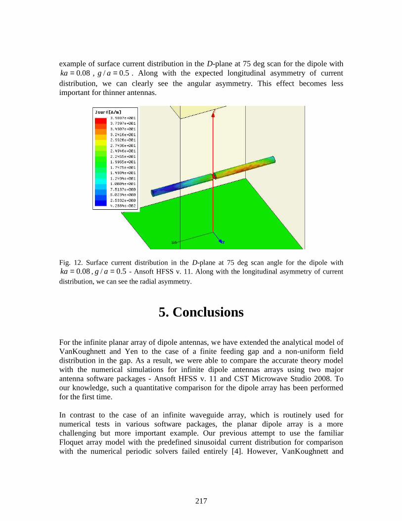
example of surface current distribution in the D-plane at 75 deg scan for the dipole with 08.0=ka , 5.0/ =ag . Along with the expected longitudinal asymmetry of current
distribution, we can clearly see the angular asymmetry. This effect becomes less important for thinner antennas.
Fig. 12. Surface current distribution in the D-plane at 75 deg scan angle for the dipole with 08.0=ka , 5.0/ =ag - Ansoft HFSS v. 11. Along with the longitudinal asymmetry of current
distribution, we can see the radial asymmetry.
5. Conclusions For the infinite planar array of dipole antennas, we have extended the analytical model of VanKoughnett and Yen to the case of a finite feeding gap and a non-uniform field distribution in the gap. As a result, we were able to compare the accurate theory model with the numerical simulations for infinite dipole antennas arrays using two major antenna software packages - Ansoft HFSS v. 11 and CST Microwave Studio 2008. To our knowledge, such a quantitative comparison for the dipole array has been performed for the first time. In contrast to the case of an infinite waveguide array, which is routinely used for numerical tests in various software packages, the planar dipole array is a more challenging but more important example. Our previous attempt to use the familiar Floquet array model with the predefined sinusoidal current distribution for comparison with the numerical periodic solvers failed entirely [4]. However, VanKoughnett and
217

Yen’s model discussed above did give a perfect agreement between theory and simulations in the E-plane, and a very good agreement in other scan planes. For that reason, it perhaps deserves to be considered in array-related textbooks, along with the sinusoidal current model. The results obtained simultaneously prove that the numerical simulation data is accurate and reliable. One interesting extension of the present model may include capacitively-loaded broadband dipole arrays [38]. Yet another extension is related to finite arrays, where the FFT method can be used instead of analytical integration when solving MoM equations with the help of spatial Fourier transform. Several people have been instrumental in allowing this work to be completed. Authors are thankful to Dr. H. Steyskal for his continuous interest and support of this work, and for critical comments, and to Dr. R. C. Hansen for his interest and important comments. We would like to thank especially Mr. Robert Helsby of Ansoft Corporation/ANSYS for his encouragement and patience throughout different stages of this research. We are thankful to Mr. Mark Jones, now with Ansoft Corporation/ANSYS, for valuable insight, time and resources invested into this project. We are grateful to Mr. Frederick Beihold, CST of America, for numerous and extensive test and validation results related to the present study, and useful discussions, and to Dr. David Johns, CST of America, for the support. This paper has been completed when one of the authors (SNM) was on sabbatical leave with Lawrence Livermore National Laboratory, Livermore, CA.
References
[1] A. A. Oliner and R. G. Malech, “Mutual coupling in infinite scanning arrays,” in Microwave Scanning Antennas, Vol. II, R.C. Hansen, ed., Academic Press, 1966, Chapter 3, pp. 195-335.
[2] R. C. Hansen, Phased Array Antennas, Wiley, New York, 1998. [3] A. K. Bhattacharyya, Phased Array Antennas: Floquet Analysis, Synthesis, and
Active Array Systems, Wiley, New York, 2006. [4] S. Makarov and A. Puzella, “Scan impedance for an infinite dipole array: Hansen’s
formulas vs. Ansoft HFSS simulations,” IEEE Antennas and Propagation Magazine, vol. 49, no. 4, Aug. 2007, pp. 143-156.
218

[5] M. Jones and S. Ortiz, Comments on “Scan impedance for an infinite dipole array: Hansen’s formulas compared with Ansoft HFSS simulations,” IEEE Antennas and Propagation Magazine, vol. 50, no. 2, April 2008.
[6] A. L. VanKoughnett and J. L. Yen, “Properties of a cylindrical antenna in an
infinite planar or collinear array,” IEEE Trans. Antennas Prop., vol. AP-15, no. 6, Nov. 1967, pp. 750-757.
[7] S. A. Schelkunoff, Advanced Antenna Theory, Wiley, New York, 1952. [8] H. C. Pocklington, "Electrical oscillations in wires," Camb. Phil. Soc. Proc., v. 9,
Oct. 25, 1897, pp. 324-332. [9] R. F. Harrington, Field Computation by Moment Methods, Wiley-IEEE Press,
Piscataway, NJ, 1993. [10] J. A. Stratton and L. J. Chu, "Steady-state solutions of electromagnetic field
problems. I. Forced oscillations of a cylindrical conductor," J. Appl. Phys., vol. 12, 1941, pp. 231-235.
[11] S. A. Schelkunoff, "Theory of antennas of arbitrary size and shape," Proc. IRE, vol.
29, 1941, pp. 493-521. [12] E. Hallen, "Properties of a long antenna," J. Appl. Phys., vol. 19, 1948, pp. 1140-
1147. [13] E. Hallen, "Exact treatment of antenna current wave reflection at the end of a
tube-shaped cylindrical antenna," IEEE Trans. Antennas Prop., vol. 4, no. 3, July 1956, pp. 479-491.
[14] L. A. Vainshtein, "Waves of current in a thin cylindrical conductor," I. Current and
impedance of a transmitting antenna," Soviet. Phys. Tech. Physics, vol. 4, 1959, pp. 601-615.
[15] L. A. Vainshtein, "Waves of current in a thin cylindrical conductor," II. The current
in a passive oscillator and the radiation of a transmitting antenna, ," Soviet. Phys. Tech. Physics, vol. 4, 1959, pp. 617-626.
[16] J. R. Wait, Electromagnetic Radiation from Cylinder Structures, Pergamon Press,
1959. [17] R. H. Duncan and F. A. Hinchey, "Cylindrical antenna theory," J. Research NBS (D-
Radio Prop.), vol. 64D, 1960, pp. 569-584.
219

[18] T. T. Wu, "Theory of the dipole antenna and the two-wire transmission line," J. Math. Phys., vol. 2, 1961, pp. 550-574.
[19] R. H. Duncan, "Theory of the infinite cylindrical antenna including the feedpoint
singularity in antenna current," J. Research NBS (D-Radio Prop.), vol. 66D, no. 2, 1962, pp. 181-188.
[20] Y. M. Chen and J. B. Keller, "Current on and input impedance of a cylindrical
antenna," J. Research NBS (D-Radio Prop.), vol. 66D, no. 1, Jan.-Feb. 1962, pp. 15-21.
[21] R. L. Fante, "On the admittance of the infinite cylindrical antenna," Radio Science,
vol. 1, no. 9, Sep. 1966, pp. 1041-1044. [22] R. W. P. King and T. T. Wu, "The imperfectly conducting cylindrical transmitting
antenna," IEEE Trans. Antennas Prop., vol. AP-14, no. 5, Sep. 1966, pp. 524-534. [23] E. K. Miller, "Admittance dependence of the infinite cylindrical antenna upon
exciting gap thickness," Radio Science, vol. 2, no. 12, Dec. 1967, pp. 1431-1435. [24] R. W. P. King, "The linear antenna - eighty years of progress," Proceedings of the
IEEE, vol. 55, no. 1, Jan. 1967, pp. 2-16. [25] R. A. Hurd and J. Jacobsen, "Admittance of an infinite cylindrical antenna with
realistic gap feed," Electronics Letters, vol. 4, no. 19, Sep. 1968, pp. 420-421. [26] L.-C. Shen, T. T. Wu, and R. W. P. King, "A simple formula of current in dipole
antennas," IEEE Trans. Antennas Prop., vol. AP-16, no. 5, Sep. 1968, pp. 542-547.
[27] D. Wu, T. Hirano, N. Inagaki, and N. Kikuma, "Numerical analysis of a cylindrical
antenna with finite gap excitation based on realistic modeling," Electronics and Communications in Japan, Part 1, vol. 84, no. 3, April 1999, pp. 609-619.
[28] H. J. Eom, J. K. Park, and Y. H. Cho, "A circular cylindrical dipole antenna,"
Microwave and Optical Technology Lett., vol. 31, no. 4, Nov. 2001, pp. 322-324. [29] G. Fikioris, J. Lionas, and C. G. Lioutas, "The use of the frill generator in thin-wire
integral equations," IEEE Trans. Antennas Prop., vol. AP-51, no. 8, Aug. 2003, pp. 1847-1854.
[30] G. Fikioris and C. A. Valagiannopoulos, "Input admittances arising from explicit
solutions to integral equations for infinte-length dipole antennas," Progress in Electromagnetic Research, PIER 55, 2005, pp. 285-306.
220

[31] G. W. Hanson, "Current on an infinitely-long carbon nanotube antenna excited by
a gap generator," IEEE Trans. Antennas Prop., vol. 54, no. 1, Jan. 2006, pp. 76-81.
[32] R. Collin, Field Theory of Guided Waves, IEEE Press, New York, 1991, second
ed. [33] C. A. Balanis, Advanced Engineering Electromagnetics, Wiley, New York, 1989. [34] C. A. Balanis, Antenna Theory. Analysis and Design, Wiley, New York, 2005,
third ed. [35] A. Ishimary, Electromagnetic Wave Propagation, Radiation, and Scattering,
Prentice Hall, Upper Saddle River, NJ, 1991. [36] MATLAB scripts circ1.m, circ2.m, circ3.m, array1.m, array2m,
array3.m used in this study are available from http://ece.wpi.edu/ant/01MATLABAntennaArray
[37] Chen-To Tai and S. A. Long, “Dipoles and monopoles,” in: Antenna Engineering Handbook, John L. Volakis, Ed., Mc Graw Hill, 2007, fourth edition, pp. 4-3 to 4-32.
[38] Ben A. Munk, "A wide band, low profile array of end-loaded dipoles with
dielectric slab compensation," 2006 Antenna Applications Sym., Allerton Park, Monticello, IL, 2006, pp. 149-165.
221

Novel Hybrid Tolerance Analysis Method with Application to the Low Cost Manufacture of Edge Slot Waveguide Arrays
B. J. Herting, M. W. Elsallal, J. C. Mather and J. B. West
400 Collins Rd. NE. M/S: 108-102
Advanced Technology Center Rockwell Collins, Inc.
Cedar Rapids, IA 52498
Abstract: Edge slot waveguide antenna arrays have been extensively employed in surveillance radar applications, such as the Airborne Warning and Control System (AWACS), where large volume coverage at a relatively low cost can be achieved via phase shifter electronic scanning in elevation and 360° mechanical scanning in azimuth. One of the requirements typically set forth in such applications is an extremely low side lobe level (SLL). In the edge slot array, this requires accurate dimensional tolerance control of the slot parameters: (1) width, (2) tilt angle, (3) depth, and (4) location. Modern manufacturing processes are capable of achieving extremely accurate dimensional tolerances, and it is tempting to simply specify the tightest slot tolerances possible. However, over specifying the necessary slot tolerances can artificially increase cost to the point where the 1D electronically scanned antenna (ESA) edge slot waveguide array is not economically feasible in an application that could have otherwise benefited from its performance advantages. It is the job of the engineer to determine the appropriate slot tolerances required to provide the desired performance and production yield while maintaining the lowest production cost. To this end, a Monte Carlo based tolerance analysis method was developed that utilizes a standard shunt admittance transmission line model for the edge slot waveguide. The shunt admittances are derived by interpolating between a three dimensional dataset generated in Ansoft HFSS™. This hybrid tolerance analysis method provides an efficient and accurate means of determining the effects of slot dimensional tolerances on the SLL and input impedance of the edge slot waveguide array. It is the purpose of this paper to describe the tolerance analysis method in detail and illustrate its use in the low cost design and manufacture of 1D ESA edge slot waveguide arrays.
1 INTRODUCTION Large antenna arrays act as high gain spatial filters and are often employed in advanced communication and radar systems to provide increased throughput and/or range via improved signal to noise performance. In radar and on the move (OTM) or dynamic communication systems, it is necessary to scan the main beam of the antenna. Edge slot waveguide antenna arrays have been extensively studied for their value in such systems as they are capable of high power, high efficiency electronic scanning along one axis.
222

When combined with mechanical scanning in the second axis, large volume coverage is achievable at a low cost.
The cost of edge slot waveguide antenna arrays is a strong function of the mechanical tolerances placed on the slot radiators. Over constraining the slot tolerances can lead to decreased yield and/or the inclusion of additional fabrication steps. Under constraining the slot tolerances can lead to reduced antenna performance. Realizing the lowest possible cost while meeting the antenna performance specifications requires a detailed understanding of the effect of the waveguide edge slot radiator dimensions of tilt angle (φ), depth (δ), width (w), and location (l) as shown in Figure 1-1.
Figure 1-1. Waveguide edge slot radiator dimensions of interest in tolerance analysis
A statistically significant analysis is required to determine the effect of slot mechanical tolerances on the performance of edge slot waveguide antenna arrays. Performing such an analysis requires an efficient and accurate methodology. A novel hybrid Monte Carlo based analysis technique was developed to address this need. The technique utilizes a shunt admittance transmission line model for the edge slot waveguide antenna in conjunction with admittance data derived from full wave electromagnetic simulations in Ansoft HFSS™ [1]. A detailed description of this tolerance analysis method, as well as an illustration of its use for the low cost design and manufacture of a circular 24” diameter 1D electronically scanned antenna (ESA) edge slot waveguide array is presented herein.
2 TOLERANCE ANALYSIS METHOD
A flow chart of the tolerance analysis method is given in Figure 2-1. Once the user provides all necessary inputs, the physical locations of the slots are determined such that grating lobe free operation is achieved at the specified operating frequency while
l1
l2
l3
δ
φ
w
223

considering the physical constraints of the waveguide and aperture dimensions. Next the Taylor amplitude taper coefficients are determined for the specified SLL and n [2]. The ideal normalized slot conductances are determined from the amplitude taper coefficients using equation 2-1.
2
20
1
n nn N
ii
G agY a
=
= =
∑ (2-1)
th
0
voltage proportional Taylor amplitude taper coefficient of the n slot total number of radiating slots in a given waveguide characteristic admittance of the waveguide
naNY
=
==
Design equations derived from the analysis of incremental conductance models in Ansoft HFSS™ are used to calculate the slot tilt and depth given the desired normalized conductance [3]. The desired normalized conductances are subsequently used in the shunt admittance circuit model of the edge slot waveguide array to determine the normalized input impedance of each waveguide stick and the individual slot excitations (magnitude and phase). Further detail on the shunt admittance circuit model is found in section 2.1. The slot excitations are used to determine the array far field radiation pattern from which the maximum SLL is determined. The input impedance of each waveguide stick is used in equation 2-2 to determine the insertion loss of the array due to input impedance mismatch, or the reflection insertion loss. The calculation of the reflection insertion loss assumes that all reflected power is dissipated, which is a good approximation if there is good isolation from port to port in the feeding structure. The reflection insertion loss and maximum SLL are recorded.
( )2
101
110log
M i i
reflectioni TOTAL
PIL
P=
⎛ ⎞⎛ ⎞− Γ⎜ ⎟⎜ ⎟= ⎜ ⎟⎜ ⎟⎜ ⎟⎜ ⎟⎝ ⎠⎝ ⎠∑ (2-2)
, 0
, 0
th
th,
excitation power of the waveguide sticktotal excitation power for the entire array
input impedance of the waveguide sticknumber of waveguide sticks or rows
in ii
in i
i
TOTAL
in i
Z ZZ Z
P iP
Z iM
−Γ =
+
=
=
=
=
0
in the arraycharacteristic impedance of the waveguideZ =
Now that the baseline ideal slot conductance results have been established, the slot admittances for the nominal slot dimensions are obtained via interpolation of a 3D dataset containing the slot admittance as a function of tilt, depth and width. Further detail on the
224

generation of this dataset is given in section 2.2. Since the nominal slot dimensions should yield admittances very close to the ideal conductances, the results of this step serve to validate the 3D dataset and interpolation function.
Figure 2-1. Tolerance analysis method flow chart
A series of iterations in which some or all of the slot dimensions are changed now commences. The first 80 of these iterations is performed in an effort to ascertain the performance effect, in isolation, of each of the four slot dimensions outlined in Figure 1-1. For this analysis, each slot is perturbed equally in tilt, depth, width and position. The perturbation of each slot dimension is chosen to be ±3σ, where σ is the standard deviation of a zero mean Gaussian or normal distribution. Upon completion of these 80 iterations, the dimensions of each slot are randomly perturbed based on a zero mean Gaussian distribution with a standard deviation of σ. For each of the perturbed slot iterations, the maximum SLL and reflection insertion loss of the edge slot antenna array are determined and recorded.
225
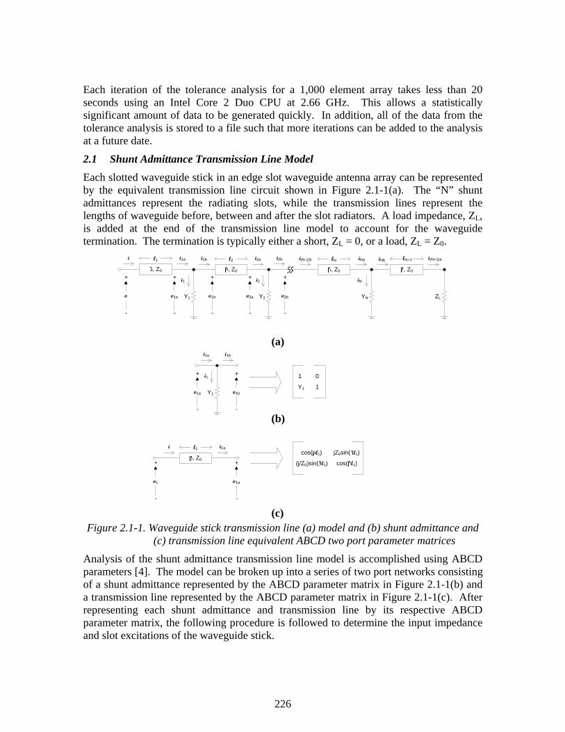
Each iteration of the tolerance analysis for a 1,000 element array takes less than 20 seconds using an Intel Core 2 Duo CPU at 2.66 GHz. This allows a statistically significant amount of data to be generated quickly. In addition, all of the data from the tolerance analysis is stored to a file such that more iterations can be added to the analysis at a future date.
2.1 Shunt Admittance Transmission Line Model Each slotted waveguide stick in an edge slot waveguide antenna array can be represented by the equivalent transmission line circuit shown in Figure 2.1-1(a). The “N” shunt admittances represent the radiating slots, while the transmission lines represent the lengths of waveguide before, between and after the slot radiators. A load impedance, ZL, is added at the end of the transmission line model to account for the waveguide termination. The termination is typically either a short, ZL = 0, or a load, ZL = Z0.
l2
Y1 Y2
i i1a
i1
i1b i2a
i2
i(N-1)b lN
YN
iN
iNa iNb
, Z0
lN+1
ZL
i(N+1)a
cos( l1) jZ0sin( l1)
cos( l1)(j/Z0)sin( l1)
Y1
i1a i1b
i1
l1i i1a
1 0
1Y1
, Z0, Z0
, Z0
l1
, Z0
i2b
v
+
-
v1a
+
-
v1b
+
-
v2b
+
-
v2a
+
-
v1a
+
-
v1b
+
-
v1
+
-
v1a
+
-
Figure 2.1-1. Waveguide stick transmission line (a) model and (b) shunt admittance and (c) transmission line equivalent ABCD two port parameter matrices
Analysis of the shunt admittance transmission line model is accomplished using ABCD parameters [4]. The model can be broken up into a series of two port networks consisting of a shunt admittance represented by the ABCD parameter matrix in Figure 2.1-1(b) and a transmission line represented by the ABCD parameter matrix in Figure 2.1-1(c). After representing each shunt admittance and transmission line by its respective ABCD parameter matrix, the following procedure is followed to determine the input impedance and slot excitations of the waveguide stick.
(a)
(b)
(c)
226

1. Reduce the series of ABCD parameter matrices that represent the transmission line model in Figure 2.1-1(a) to an equivalent single ABCD parameter matrix.
2. Calculate the input impedance, Zin, of the waveguide stick using the equivalent ABCD parameter matrix and the load impedance of the waveguide stick termination in equation 2.1-1.
Lin
L
AZ BZCZ D
+=
+ (2.1-1)
3. Set the voltage, v, at the input of the transmission line model in Figure 2.1-1(a) to one and solve for the current, i, using equation 2.1-2.
in
vi Z= (2.1-2)
4. Solve for v1a and i1a using equation 2.1-3, which involves the ABCD matrix of the first transmission line in Figure 2.1-1(a).
( ) ( )( ) ( )
11 0 1
1
1 1 10
cos sin
sin cosa
a
jZv vji iZ
β β
β β
−⎡ ⎤⎡ ⎤ ⎡ ⎤⎢ ⎥=⎢ ⎥ ⎢ ⎥⎢ ⎥ ⎣ ⎦⎣ ⎦ ⎣ ⎦
(2.1-3)
5. Solve for v1b and i1b using equation 2.1-4, which involves the equivalent ABCD matrix of the series combination of the first transmission line and the first shunt admittance in Figure 2.1-1(a).
( ) ( )( ) ( )
11
1 0 11
1 1 1 10
cos sin1 01 sin cos
b
b
jZv vji Y iZ
β β
β β
−− ⎡ ⎤⎡ ⎤ ⎡ ⎤ ⎡ ⎤⎢ ⎥=⎢ ⎥ ⎢ ⎥ ⎢ ⎥⎢ ⎥ ⎣ ⎦⎣ ⎦⎣ ⎦ ⎣ ⎦
(2.1-4)
6. Calculate the power in shunt admittance Y1 by employing Kirchoff’s current law and solving equation 2.1-5.
( )1 1 1 11 Re2 a a bP v i i ∗⎡ ⎤= −⎣ ⎦ (2.1-5)
7. The magnitude ( )na and phase ( )nθ of the thn slot excitation corresponding to shunt admittance Y1 are determined using equations 2.1-6a and 2.1-6b respectively.
1na P= (2.1-6a)
( )1argn avθ = (2.1-6b)
8. Solve for the remaining slot excitations of the waveguide stick by calculating the subsequent voltages and currents in the transmission line model of Figure 2.1-1(a) and repeating steps 6 and 7.
227

2.2 Full Wave EM Model
A 3D dataset of slot admittance versus slot tilt (φ), depth (δ), and width (w) was generated using an incremental conductance edge slot waveguide model in Ansoft HFSS™. The incremental conductance model utilizes a single waveguide stick with a series of 15 identical edge slots spaced one half wavelength apart as shown in figure 2.2-1. The admittance of one of the identical edge slots in the waveguide stick is determined using equation 2.2-1.
inslot
YGN
= (2.2-1)
input admittance of the slotted waveguide stick de-embedded to the first slot total number of radiating slots in a given waveguide
inYN
==
Figure 2.2-1. Incremental conductance simulation model
The incremental conductance method has traditionally been performed empirically, but the simulation model used here has clear advantages over empirical analysis. First, the simulation model is more efficient, in terms of time and money, in generating the significant amount of admittance data necessary to perform an accurate interpolation. Second, the simulation model is able to account for the effects of a cross polarization choke that is often present in the array. Finally, mutual coupling from surrounding waveguides is accounted for using master-slave boundary conditions that effectively place the slotted waveguide stick in an infinite array of identical, uniformly excited slotted waveguides.
3 APPLICATION The low cost manufacture of a circular 24” diameter 1D ESA edge slot waveguide array is analyzed using the tolerance analysis method. A Taylor amplitude taper of (30 dB,⎯n = 4) is employed to realize a desired SLL of 25 dB. The four slot parameters are investigated to determine their individual and combined tolerance effect on the SLL and reflection insertion loss of this edge slot waveguide array.
3.1 Slot Tilt Angle The slot tilt angle was found to have the most significant effect on the performance of the edge slot waveguide array. The SLL results for a standard deviation (σ) of 1° and 2° are
Master BC
Slave BC Feed Wave Port
Cx-Pol Suppression Choke
228

shown in Figure 3.1-1(a) and (b) respectively. The first pass in the tolerance analysis tests the ideal slot conductances and yields a SLL of -28.5 dB. The next 81 passes test the nominal and ±3σ points for all combinations of the four slot parameters. From Figures 3.1-1(a) and (b), it would appear that an increased tilt on all the slots degrades the SLL more than a shallower tilt. This may indeed be the case, but it should be noted that all angles below 5° were automatically set to 5° due to limitations in the 3D admittance dataset. Consequently, the shallower, -3σ, results are likely optimistic. Analysis of the remaining 118 iterations placed zero mean random variations with standard deviations of 1° and 2° on the nominal slot tilts. The 1° standard deviation resulted in a worst case SLL of 26.7 dB, while the 2° standard deviation resulted in a 26 dB worst case SLL. The reflection insertion loss is a non-factor as it is less than 0.005 dB and 0.01 dB for the 1° and 2° standard deviations respectively.
(a) (b)
Figure 3.1-1. Slot tilt angle tolerance analysis results: (a) σ = 1° and (b) σ = 2°
3.2 Slot Depth The slot depth was found to have a much reduced effect compared to the slot tilt on the performance of the edge slot waveguide array. The SLL results for a standard deviation (σ) of 1 mil and 2 mils are shown in Figure 3.2-1(a) and (b) respectively. The first pass in the tolerance analysis tests the ideal slot conductances and yields a SLL of -28.5 dB. The next 81 passes test the nominal and ±3σ points for all combinations of the four slot parameters. From Figure 3.2-1(a), it appears as though increasing the slot depths will serve to improve the SLL performance of the array, but it comes at the expense of nearly 0.025 dB of reflection insertion loss. Analysis of the remaining 118 iterations placed zero mean random variations with standard deviations of 1 mil and 2 mils on the nominal slot depths. The 1 mil standard deviation resulted in a worst case SLL of 27.3 dB, while the 2 mil standard deviation resulted in a 27.1 dB worst case SLL. The reflection insertion loss is again a non-factor as it is less than 0.003 dB and 0.004 dB for the 1 mil and 2 mil standard deviations respectively.
0 -3σ
+3σ
0 -3σ
+3σ
229

(a) (b)
Figure 3.2-1. Slot depth tolerance analysis results: (a) σ = 1 mil and (b) σ = 2 mil
3.3 Slot Width The slot width was found to have minimal effect on the performance of the edge slot waveguide array. The SLL results for a standard deviation (σ) of 1 mil is shown in Figure 3.3-1. The first pass in the tolerance analysis tests the ideal slot conductances and yields a SLL of -28.5 dB. The next 81 passes test the nominal and ±3σ points for all combinations of the four slot parameters. From Figure 3.3-1, it appears as though increasing the slot width will serve to improve the SLL performance of the array, and this is with little to no sacrifice in reflection insertion loss. Analysis of the remaining 118 iterations placed zero mean random variations with standard deviation of 1 mil on the nominal slot widths. The 1 mil standard deviation resulted in a worst case SLL of 26.5 dB, but this occurred at a single isolated point and all other iterations showed a SLL of around 27.7 dB. The reflection insertion loss is again a non-factor as it is less than 0.002 for the 1 mil standard deviation.
Figure 3.3-1. Slot width tolerance analysis results: σ = 1 mil
0 -3σ
+3σ
0 -3σ
+3σ
0 -3σ
+3σ
230

3.4 Slot Position
The slot position was found to have minimal effect on the performance of the edge slot waveguide array. The SLL results for a standard deviation (σ) of 1 mil and 2 mils are shown in Figure 3.4-1(a) and (b) respectively. The first pass in the tolerance analysis tests the ideal slot conductances and yields a SLL of -28.5 dB. The next 81 passes test the nominal and ±3σ points for all combinations of the four slot parameters. Analysis of the remaining 118 iterations placed zero mean random variations with standard deviations of 1 mil and 2 mils on the nominal slot positions. The 1 mil and 2 mil standard deviations both resulted in a worst case SLL of 27.7 dB. The reflection insertion loss is again a non-factor as it is less than 0.002 dB for both the 1 mil and 2 mil standard deviations.
(a) (b)
Figure 3.4-1. Slot position tolerance analysis results: (a) σ = 1 mil and (b) σ = 2 mil
3.5 Combined Slot Parameters A tolerance analysis in which all of the slot parameters were varied by a standard deviation (σ) was conducted for the two test cases shown in Figures 3.5-1(a) and (b). As expected, the results are very similar to that of the slot tilt in section 3.1. This suggests that the tilt tolerance dominates the overall effects on the array performance. The first pass in the tolerance analysis tests the ideal slot conductances and yields a SLL of -28.5 dB. The next 81 passes test the nominal and ±3σ points for all combinations of the four slot parameters. Analysis of the remaining 118 iterations placed zero mean random variations with standard deviations of σ on all the slot parameters. With slot tilt, depth, width and position standard deviations of (1°, 1 mil, 1 mil, 1mil) and (2°, 2 mil, 1 mil, 2 mil), the worst case SLL was 26.7 dB and 25.2 dB respectively. The reflection insertion loss is again a non-factor as it is less than 0.005 dB and 0.01 dB for the (1°, 1 mil, 1 mil, 1mil) and (2°, 2 mil, 1 mil, 2 mil) cases respectively.
231

(a) (b)
Figure 3.4-1. Slot tolerance analysis results: (a) σ = (1,1,1,1) and (b) σ = (2,2,1,2)
4 CONCLUSIONS AND FUTURE WORK A novel hybrid Monte Carlo based tolerance analysis technique for edge slot waveguide antenna arrays was presented in detail. The key advantage of the technique lies in the efficiency of analyzing the effect of edge slot parameter tolerances on antenna array SLL and input impedance or reflection insertion loss. A single iteration of the Monte Carlo tolerance analysis for a 1,000 element array takes less than 20 seconds using an Intel Core 2 Duo CPU at 2.66 GHz.
The efficiency of the hybrid Monte Carlo tolerance analysis method makes it a useful engineering tool in selecting the lowest cost manufacturing processes for an edge slot waveguide antenna array. Analysis of a circular 24” diameter 1D ESA edge slot waveguide array indicated that the slot tilt had the most profound effect on the antenna array performance. Therefore, special attention should be paid to select a manufacturing method that is able to hold tighter tolerances on the slot tilt.
Future work is possible to expand the capabilities of the hybrid Monte Carlo tolerance analysis. First, the current program only analyzes circular arrays and it would be a simple matter to add rectangular planar array capability. Second, an analysis of systematic slot tolerance errors could be added. Finally, due to the fact that the full wave EM model in Ansoft HFSS™ accounts for mutual coupling from other waveguides, it may be possible to extend this technique to broad wall, shunt slot arrays.
5 REFERENCES [1] Ansoft Corporation; www. ansoft.com [2] R. J. Mailloux, Phased Array Antenna Handbook, 2nd ed. Boston: Artech House,
2005, pp. 153 – 155. [3] M. W. ElSallal, B. J. Herting and J. B. West, “Planar edge slot waveguide antenna
array design using COTS EM tools,”in Antenna Applications Symposium, Monticello, IL, 2007, pp. 76 – 89.
[4] D. M. Pozar, Microwave Engineering, 2nd ed. New York: John Wiley & Sons, Inc., 1998, pp. 206 – 209.
Tilt: σ = 1° Depth: σ = 1 mil Width: σ = 1 mil Position: σ = 1 mil
Tilt: σ = 2° Depth: σ = 2 mil Width: σ = 1 mil Position: σ = 2 mil
232

DESIGN OF COPLANAR WAVEGUIDE FED TAPERED-SLOT ANTENNA ARRAYS FOR HIGH-POWER SPACE
DISTRIBUTED AMPLIFIER APPLICATIONS
Rivera-Albino, A., Rodríguez-Solís, R. A. Department of Electrical and Computer Engineering
University of Puerto Rico at Mayagüez Mayagüez, PR 00681-9042
Abstract— Coplanar waveguide fed tapered-slot antenna arrays are designed for a
high-power space-distributed solid-state amplifier application at X-band. The amplifier is designed using a tray configuration inside an over-moded waveguide. The waveguide operates in its TE30 mode, which allows the placing of 3, 6 or 9 trays, positioned for optimal power generation. Each tray has four class-E amplifiers, and the input and output to each of the amplifiers are tapered-slot antennas. The input antennas are matched to 50 Ω, and the output antennas are matched to 24 Ω, which is the optimum class-E impedance, for the transistor device used, for maximum output power. This work shows the tapered-slot design for the desired impedance based on the tray position in the over-moded waveguide. The two center antennas and the two edge antennas on each tray are kept the same to simplify the Design of Experiments analysis. In addition it was found that although the center frequency of operation is shifted upwards, the antenna behavior for 3, 6 and 9 trays does not change significantly and the same antenna design can be used for all the trays. The antennas were simulated, built and tested for an input impedance of 65 Ω, and simulated for 24 Ω and 50 Ω. The bandwidth for the antennas was 310 MHz, 180 MHz and 300 MHz, respectively, which is sufficient for the intended application. 1. INTRODUCTION
High-power amplifiers are a fundamental component in communications and radar systems. Since solid-state devices provide smaller amounts of power as the frequency increases, it is necessary to either use vacuum tubes or appropriately combine several solid-state devices to obtain the desired power output. Power combining can be divided into transmission line combining and spatial combining. Transmission line combining alternatives, such as corporate feeds, become more inefficient as the number of devices combined increases, because of increased losses due to longer transmission lines. In a parallel connection, as the number of devices increases, it is more difficult to provide an equal share of the biasing current to each device. Therefore, for a large number of devices, spatial combining becomes a viable alternative, even though the excitation amplitude and phase distribution may not be uniform across the active devices. The main
233

advantage of spatial power combining is that it eliminates the need for complex and lossy feed lines. In addition, the losses remain constant as the number of devices increases [1]. We are currently working on the design of a space-distributed power amplifier as an alternative for a X-band solid-state meteorological radar. The work follows the one presented in [1-5], but we operate the devices in class-E mode to provide a higher efficiency. In addition, the waveguide housing the amplifier trays is designed to operate in the TE30 mode. This gives us three maximum power regions in the guide, allowing the placing of more trays, and, thus, increasing the maximum power the amplifier can provide. The increased size of the waveguide also helps improve the thermal management in the amplifier. Figure 1 shows the proposed power amplifier design.
Fig. 1: Proposed power amplifier design
We use tapered slot antennas (TSA) as the radiating elements. They are well suited for this application since they produce endfire radiation. The slots are fed through coplanar waveguide (CPW) since this makes possible the placing of the devices in the same plane of the antenna, and avoids the use of via-holes to connect the device source to ground. We are using several devices from TriQuint Semiconductor for the amplifier design, which have optimum class-E impedance in the order of 24 Ω. Therefore, two different TSAs are designed for the input and output ports of the amplifier; one with a 50 Ω impedance for the input, and one with 24 Ω for the output. Due to the limitations of our
234

fabrication facilities, it is not possible to fabricate CPW lines of 50 and 24 Ω for the connections between the amplifier and the antennas in-house. Therefore, we tested our design procedure for a 65 Ω impedance. We analyzed three trays and performed a Design of Experiments (DOE) to understand the behavior of the TSAs with each change of the design parameters.
2. BACKGROUND 2.1 Tapered Slot Antennas The characteristics of the TSA have made them an interesting research theme since their introduction by Lewis [6] in 1974. Its main advantages are its wideband performance, endfire radiation, symmetric beam, and relatively easy construction. These advantages have converted TSA as an excellent alternative for applications where an implementation with MMIC (Monolithic Microwave Integrated Circuits) is needed [2-5], as well as applications where a wideband array is needed [7-8]. In order to improve these characteristics, different types of slot tapers have been investigated, such as linear, constant width (CWSA), bunny ear [9], and exponential (Vivaldi) [9, 10]. In the case of the Vivaldi, bandwidths of 6:1 have been achieved [9] and antennas as short as one free-space wavelength have been studied [10]. One of the most critical parameters in the design of the TSA is the substrate. Holter, et. al., [11], performed detailed analysis about the substrate effects in TSAs. They showed that the permittivity cannot be very high (greater than 9.8) since the slot mode wavelength, λ’, will be much smaller than the free-space wavelength and, therefore, the fields will be closely confined near the slot, reducing the radiation efficiency [12]. In addition, the slot has to be wide (λ’>>0.6 λo) for radiation to occur [10]. Consequently, a tradeoff between size and radiation efficiency has to be done. If the main goal is a large efficiency, a thick dielectric with a low permittivity is required. On the other hand, if a short antenna is required, a thin dielectric with a high permittivity must be used. Also, when the thickness is increased the gain is increased [11]. Several authors have investigated the effects of physical parameters, such as opening rate, antenna height, and tapered length, on the antenna performance. Research shows that larger opening rates affect negatively the VSWR, although they do not affect the highest and lowest operating frequencies [6-7]. In addition, as the antenna height is decreased, the beamwidth in the E plane is shortened [13]. Finally, a larger antenna has better performance at lower frequencies, but the construction becomes more complicated [7]. Two types of feeding mechanisms have also been studied for TSAs: microstrip and CPW. CPW lines provide larger bandwidth than microstrip [14, 15]. Currently, there is no theory to calculate slot impedance or slot normalized wavelength. However, experimental results have been published when permittivity is greater than 9.0
235

[16] and when permittivity is less than 9.8 [17-18]. One important aspect is that the wavelength and the characteristic impedance of the slot increase when the slot width is increased [10]. When TSAs are used in the design of an array, results show that the antenna performance can change dramatically from its isolated performance. Schaubert, et. al. in dealing with TSA arrays, used a tapered length shorter than one wavelength[19]. In terms of the element spacing, it can be as small as 0.1 wavelengths at the lowest frequency [20] and that it should be less than ½ free-space wavelengths at the highest frequency to avoid grating lobes [14].
2.2 TSA in Power Amplifier Applications Tapered slot antennas fit nicely in the design of a spatially combined power amplifier because they are broadband, they produce end-fire radiation and their construction is relatively easy. The end-fire characteristic simplifies the implementation with the Class-E modules since they can be placed in the same plane as the antenna, and, as consequence, the connection between the antennas and the modules is easier. The construction is relatively easy, and, since they have several design parameters (more degrees of freedom), there are more options to find the desired frequency of operation and the desired input impedance. Several authors [1-5] have used TSAs in a X-band waveguide to design broadband spatial power combiners. In some designs four identical trays, where each tray consists of two input and two output TSAs are used [1]. However, the work is extended to add four [2], and six trays [3] with four input and output TSAs. In those cases, the antennas’ dimensions have to be adjusted to fit in an X-band waveguide, which limit the slot width of the antenna. Therefore, a numerical method [5] was used to obtain the desired input impedance for each design.
3. DESIGN PROCEDURE
3.1 Antenna geometry The first step was to design four TSAs in each tray. The Vivaldi antennas were used in this analysis and the curve was modeled with (1).
2−Δ×=
Wfeed lL e (1)
236

WfeedincreFig. 2
3.2 S The sa reqantenRT/D
3.3 F We sCPWline i
4. T 4.1 DThe mHowethinntoo wHFSScore more
d is the widases, and l i2.
Substrate sel
substrate waquirement in nna length. Duroid 6006)
Feed type
selected CPWW gives a bro
s that the sub
TSA WITH 65
Design main goal oever, with th
nest aperture wide to fit inS to simulateIntel Xeon than three t
dth at which is the positio
lection
s selected tothis applica Therefore, ) with a thick
W to make oader bandwbstrate does
Ω INPUT IM
of the researhe available possible is
n the space e the antennprocessors,
trays for thos
the antennaon in the ant
Fig. 2: Propo
o obtain a shation, we can
a relativelykness of 0.63
the placing width than mi
not require
MPEDANCE
rch is to desequipment 0.1 mm widavailable, e
nas in severawith 4 to 3se antennas.
a starts to optenna length
osed tray confi
ort antenna. n then sacrify high perm35 mm was
of the solidicrostrip. Anbackside pro
sign 24 Ω ato build the
de. In this suven with 0.
al workstatio2 GB of RA Therefore, w
pen, ∆ is theh. The tray c
iguration
Since a widfice bandwidmittivity (εr=used for the
d state devinother advanocessing.
and 50 Ω intransmissio
ubstrate, 24 1 mm wide ons. These wAM. This alwe focused
e rate at whconfiguration
deband operdth in order =6.15) substdesign.
ices simplerntage of this
nput impedanon lines and
and 50 Ω Cslots. We u
workstations llowed us toour work in
hich the curvn is shown i
ration was noto reduce thtrate (Roger
. In addition transmissio
nce antennaantennas, th
CPW lines arused Ansoft’
have 2 duao simulate nthe design o
ve in
ot he rs
n, on
s. he re ’s l-
no of
237

65 Ω input impedance antennas, and applied the obtained knowledge in the design of the 24 Ω and 50 Ω antennas. The CPW lines have 65 Ω impedance, as well as the antenna input impedance, and the port impedance. The slot width at the open end of the antennas was limited by the inner dimension of the waveguide, b, (in this case b=10.1mm, as shown in Fig. 2). To increase the input impedance of the center antennas, their open end is wider than the open end of the edge antennas. The radius of the open-circuit circle at the feed end was analyzed to obtain the best VSWR. The best value was around 0.3 mm; as the radius is increased, the VSWR at mid-band frequencies increases.
4.2 Design of Experiment (DOE) A Design of Experiments was applied to the 65 Ω antennas to determine how the performance of the antenna changes with changes in the design parameters. To limit the size of our problem, we kept the trays identical; that is, the antenna dimensions are the same for each tray. In this way, 4 variables are left: 1) the length of the center antennas (Lantc), 2) the length of the edge antennas (Lante), 3) the feed point of the edge antennas (L2e), and 4) the feed point of the center antennas (L2c). The results of the DOE were analyzed to obtain the effects of each variable. The results of this analysis are shown in figures 3 and 4.
Fig. 3: Significance of the effects of the design parameters in the edge antennas input impedance.
Significant parameters and interactions are displayed with a square.
238

Fig. 4: Significance of the effects of the design parameters in the center antennas input impedance.
Significant parameters and interactions are displayed with a square. From these results, the major effects in the impedance can be established as follows:
1. Increasing the distance where the center antennas are fed, the resistance of the edge antennas decreases.
2. Increasing where the edge antennas are fed, the resistance of the edge antennas increases.
3. Increasing the length of the edge antennas increases the resistance of the edge and the center antennas.
4. Increasing the length of the center antennas increases the resistance of the center antennas.
4.3 Best performance with three trays From the DOE, the configuration with the larger bandwidth was selected. Dimensions are shown in Table 1. Figure 5 and 6 show real and imaginary parts of the impedance. Note that, in Fig. 7, all the antennas have a VSWR smaller than two from 9.90 to 10.21 GHz. This gives 310 MHz of bandwidth, which is adequate for the power amplifier application. In this range, the real part is near 65 Ω and the imaginary part is close to zero.
239

Fi
Fi
g. 5: Input res
ig. 6: Input rea
sistance for th
actance for th
he 65 Ω antennd
he 65 Ω antennd
nas. All the 12displayed.
nas. All the 12displayed.
2 antennas (4 i
2 antennas (4 i
in each of the
in each of the
3 trays) are
3 trays) are
240

Fig. 7: VSWR for the 65 Ω antennas. All the 12 antennas (4 in each of the 3 trays) are displayed.
4.4 Measured results We built and tested the three-trays configuration to validate the simulated results. The trays were built by wet etching, and placed inside the waveguide. The antenna feed lines were connected to a SMA connector through a wire bond, and both ends of the waveguide were terminated with waveguide terminations. To simplify the connections, we only measured the impedance of the edge antennas on each tray, and terminated the center antenna feed lines with 65 Ω resistors. Figure 8 shows the VSWR for an edge tray antenna. The measured results are similar to the simulation, although the VSWR is higher in the middle of the bandwidth. The difference is mostly due to the effect of the wire bonding between the antenna feed and the SMA connector.
4.5 Six and nine trays Once the behavior of the three-trays system was analyzed, six and nine-trays were simulated in order to see how coupling affects the additional trays. Simulations show that the additional trays shift the frequency range upwards. However, we still have good performance around 10 GHz. Figures Fig. 7 and Fig. 8 show the VSWR for simulations with 6 and 9 trays, respectively. In both cases, the bandwidth is approximately 300 MHz. Comparing the performance of the three, six and nine-trays configurations, we find that
1
1.5
2
2.5
3
3.5
4
4.5
5
5.5
9.6 9.7 9.8 9.9 10 10.1 10.2 10.3 10.4 10.5 10.6
VSW
R
Frequency (GHz)
241

the pincre
Fig. 8and s
Fig. 9
performance ased.
8: VSWR for asimulated (ligh
9: VSWR for tare placed
of the ant
an edge antenht line) is due
the six trays cod at the 0.9 po
tennas does
na on an edgeto the wire bo
onfiguration. wer points for
not change
e tray. The difond from the a
The results for each of the E
e much as
fference betweantenna feed t
or all 24 antenE-field maxim
the number
een the measuto the input SM
nnas are displama in the waveg
rs of trays i
red (dark lineMA connector
ayed. The trayguide.
is
e) r.
ys
242

Fig. tray
Tab
A
A
TR
10: VSWR foys are placed
ble 1: Dimensi
CENTER ANTENNAS
EDGE ANTENNAS
RANSMISSION LINES
or the nine traat the maximu
ions for the 3, Simu
TOTAL LE(MM
FEED POPOSITION
FEED WIDTGROWTH R
(MM-1
TOTAL LE(MM
FEED POPOSITION
FEED WIDTGROWTH R
(MM-1
SLOT WIDTSEPARAT
BETWEEN (MM
ays configuratium and the ha
w
6 and 9 Traysulations for th
ENGTH )
OINT N (MM) TH (MM) RATE, Δ
1) ENGTH )
OINT N (MM) TH (MM) RATE, Δ
1) TH (MM) TION SLOTS )
ion. The resulalf power poinwaveguide.
s Simulations he 50 Ω and 24
A24 OHMS
33
1.7
0.12
0.096
33.5
1.7
0.08
0.096
0.0025
0.395
lts for all 36 annts for each of
for the 65 Ω A4 Ω Antennas.
ANTENNA IMP50 OHM
33
2
0.10
0.105
34
2.2
0.06
0.103
0.06
0.28
ntennas are df the E-field m
Antennas, and.
PEDANCES MS 6
5
3
isplayed. The
maxima in the
d the 3-Trays
65 OHMS
33
1.9
0.10
0.090
33
2.1
0.1
0.91
0.1
0.2
243

5. INPUT ANTENNAS- 50 Ω INPUT IMPEDANCE The results obtained with the simulation of the 65 Ω antennas showed that the behavior of the antennas did not change much going from 3 to 9 trays. Therefore, we concentrated our efforts in the design of the 50 Ω antennas, using the 3-tray configuration. The final design dimensions are shown in Table 1. Figures 11Fig. 11, 12 and 13 show the simulated results for the input impedance and VSWR. A 300 MHz bandwidth was obtained for this case.
Fig. 11: Input resistance for the 50 Ω antennas. The results for all 12 antennas are displayed.
Fig. 12: Input reactance for the 50 Ω antennas. The results for all 12 antennas are displayed.
0
50
100
150
200
250
300
9.4 9.6 9.8 10 10.2 10.4 10.6
Impe
dance (Ohm
s)
Frequency (GHz)
‐200‐150‐100‐50050
100150200250300350
9.4 9.6 9.8 10 10.2 10.4 10.6
Impe
danc
e(O
hms)
Frequency (GHz)
244

6. O The fampliand tapproprese
Fig
Fig. 13: VS
OUTPUT ANT
final step wifier. Figurethe reactancoximately 18ents the dime
g. 14: Input res
1
2
3
4
5
6
7
8
9
10
VSW
R
SWR for the 5
TENNAS - 24
as to designes 14 and 15e is close to80 MHz. Thensions for th
sistance for th
9.4 9.
50 Ω antennas
Ω INPUT IMP
n the 24 Ω i5 show the io 0 Ω. VSWhis is still aphese antenna
he 24 Ω antenn
.6 9.8
s. The results
PEDANCES
impedance ainput resistanWR, shown ppropriate foas.
nas. The resul
10
Frequency(G
for all 12 ante
antennas fornce of the ain Fig. 16,
or our ampli
lts for all the 1
10.2
GHz)
ennas are disp
r the output antennas is cpresents a bifier applica
12 antennas ar
10.4
played.
of the poweclose to 24 Ωbandwidth o
ation. Table
re displayed.
10.6
er Ω of 1
245

Fig
g. 15: Input re
Fig. 16: VSW
actance for th
WR for the 24
he 24 Ω antenn
Ω antennas. T
nas. The resul
The results fo
lts for all the 1
r all the 12 an
12 antennas ar
ntennas are di
re displayed.
splayed.
246

7. CONCLUSIONS In this work, we analyzed the performance of TSAs inside an over-moded waveguide for a high-power, solid-state, spatially distributed amplifier at X-band. The results show that the design of the trays can be kept the same for 3, and 9-trays configurations, with an acceptable performance for all the antennas. Inside a tray, the center antennas are slightly shorter than the edge antennas. The measurements of the 65 Ω antennas serve to validate the simulations, and provide the foundation for the design of the 50 Ω and 24 Ω antennas. These antennas were simulated for the 3-trays configuration, showing that an appropriate bandwidth can be obtained for this design. These results will be used in the design of the class-E amplifiers to be used in the spatially-distributed amplifier. ACKNOWLEDGMENTS
This work was sponsored by the NSF Engineering Research Center for Collaborative Adaptive Sensing of the Atmosphere (CASA). The authors wish to express their gratitude to the computer system administrator of the Electrical Engineering Department at the University of Puerto Rico at Mayaguez, Pablo Rebollo, for providing the computing resources to complete the simulation process.
8. REFERENCES [1] Harvey, J.; Brown, E.R.; Rutledge, D.B.; York, R.A., "Spatial power combining for high-power transmitters," Microwave Magazine, IEEE, vol.1, no.4, pp.48-59, Dec 2000. [2] Nai-Shuo Cheng; Alexanian, A.; Case, M.G.; Rensch, D.B.; York, R.A., "40-W CW broad-band spatial power combiner using dense finline arrays," Microwave Theory and Techniques, IEEE Transactions on , vol.47, no.7, pp.1070-1076, Jul 1999. [3] Nai-Shuo Cheng; Thai-Phuong Dao; Case, M.G.; Rensch, D.B.; York, R.A., "A 60-watt X-band spatially combined solid-state amplifier," Microwave Symposium Digest, 1999 IEEE MTT-S International, vol.2, no., pp.539-542 vol.2, 1999. [4] Nai-Shuo Cheng; Pengcheng Jia; Rensch, D.B.; York, R.A., "A 120-W X-band spatially combined solid-state amplifier," Microwave Theory and Techniques, IEEE Transactions on , vol.47, no.12, pp.2557-2561, Dec 1999.
[5] Pengcheng Jia; Lee-Yin Chen; Nai-Shuo Cheng; York, R.A., "Design of waveguide finline arrays for spatial power combining," Microwave Theory and Techniques, IEEE Transactions on , vol.49, no.4, pp.609-614, Apr 2001.
[6] Lewis, L.; Fassett, M.; Hunt, J., "A broadband stripline array element," Antennas and Propagation Society International Symposium, 1974, vol.12, no., pp. 335-337, Jun 1974
247

[7] Tan-Huat Chio; Schaubert, D.H., "Parameter study and design of wide-band wide scan dual-polarized tapered slot antenna arrays," Antennas and Propagation, IEEE Transactions on, vol.48, no.6, pp.879-886, Jun 2000.
[8] D. H. Schaubert and T.-H. Chio, “Wideband Vivaldi arrays for large aperture antennas,” in Proc. NFRA Conf. Perspectives on Radio Astronomy, Technologies for Large Antenna Arrays Dwingeloo, Netherlands, Sept. 1999.
[9] R.C. Mailloux, Phased Array Antenna Handbook, Second Edition. Artech House, Norwood, MA, pp. 248-251, 2005.
[10] Prasad, S.N.; Mahapatra, S., "A Novel MIC Slot-Line Antenna," European Microwave Conference, 1979. 9th, vol., no., pp.120-124, Oct. 1979.
[11] Schaubert, D.; Kollberg, E.; Korzeniowski, T.; Thungren, T.; Johansson, J.; Yngvesson, K., "Endfire tapered slot antennas on dielectric substrates," Antennas and Propagation, IEEE Transactions on, vol.33, no.12, pp. 1392-1400, Dec 1985.
[12] Cohn, S.B., "Slot Line on a Dielectric Substrate," Microwave Theory and Techniques, IEEE Transactions on, vol.17, no.10, pp. 768-778, Oct 1969.
[13] Janaswamy, R.; Schaubert, D., "Analysis of the tapered slot antenna," Antennas and Propagation, IEEE Transactions on, vol.35, no.9, pp. 1058-1065, Sep 1987.
[14] Nesic, A., "Endfire slotline antennas excited by a coplanar waveguide," Antennas and Propagation Society International Symposium, 1991. AP-S. Digest, vol., no., pp.700-702 vol.2, 24-28 Jun 1991.
[15] Wu, X.-D.; Chang, K., "Coplanar waveguide feed linear tapered slot antenna," Antennas and Propagation Society International Symposium, 1993. AP-S. Digest, vol., no., pp.364-367 vol.1, 28 Jun- 2 Jul 1993.
[16] Garg, R.; Gupta, K.C., "Expressions for Wavelength and Impedance of a Slotline (Letters)," Microwave Theory and Techniques, IEEE Transactions on, vol.24, no.8, pp. 532-532, Aug 1976.
[17] Janaswamy, R.; Schaubert, H.D., "Dispersion Characteristics for Wide Slotlines on Low-Permittivity Substrates (Short Paper)," Microwave Theory and Techniques, IEEE Transactions on , vol.33, no.8, pp. 723-726, Aug 1985
[18] Janaswamy, R.; Schaubert, D.H., "Characteristic Impedance of a Wide Slotline on Low-Permittivity Substrates (Short Paper)," Microwave Theory and Techniques, IEEE Transactions on, vol.34, no.8, pp. 900-902, Aug 1986.
248

[19] Schaubert, D.H.; Boryssenko, A.O.; van Ardenne, A.; Bij de Vaate, J.G.; Craeye, C., "The square kilometer array (SKA) antenna," Phased Array Systems and Technology, 2003. IEEE International Symposium on , vol., no., pp. 351-358, 14-17 Oct. 2003
[20] Holter, H.; Tan-Huat Chio; Schaubert, D.H., "Experimental results of 144-element dual-polarized endfire tapered-slot phased arrays," Antennas and Propagation, IEEE Transactions on, vol.48, no.11, pp.1707-1718, Nov 2000.
249

EFFICIENT GLOBAL OPTIMIZATION FOR ANTENNA DESIGN
Hugh L. Southallac , Terry H. O’Donnellab, Lt Bryan Kaantaa
a Air Force Research Laboratory, 80 Scott Drive, Hanscom AFB, MA USA 01730-2909 b On-site Consultant from ARCON Corporation, 260 Bear Hill Road, Waltham, MA 02451
c On-site Contractor from Vistronix, Inc, 8401 Greensboro Drive, McLean, VA 22102
ABSTRACT Efficient Global Optimization (EGO) is a competent evolutionary algorithm suited for problems with limited design parameters and expensive cost functions [1,2]. We have previously applied EGO successfully to optimize both operating frequency and element separation distance of a two-element parasitic superdirective array (PSA) [2]. However, the question has arisen as to how EGO compares to a traditional genetic algorithm, in both number of cost function evaluations for a “good” solution and the ability to predict global minima. In this paper we compare EGO optimization results for the two-element PSA to equivalent results obtained using both simple (textbook) and enhanced genetic algorithm (GA) optimizations. These results indicate that EGO is consistently able to achieve a better solution than the GA for a limited number of function evaluations. However, EGO sometimes terminates before the global minimum is found while the enhanced GA was able to consistently find the global minimum; however, the GA required far more cost function evaluations than EGO. Keywords: Efficient Global Optimization, EGO, evolutionary optimization, antenna optimization, DACE, Genetic Algorithms (GAs) 1. INTRODUCTION Many different evolutionary algorithm optimization techniques have been applied to the design and optimization of electromagnetics problems. These have ranged from simple genetic algorithms [3,4] to more complex competent genetic algorithms and genetic programming techniques [5,6,7]. Successful applications have been demonstrated in a wide variety of military and other government antenna systems [6,8,9]. However, many of the evolutionary methodologies applied to date require a large number of evaluations of the objective (or cost) function. This can prove prohibitive for complex computational electromagnetics problems, in which each proposed solution takes significant resources. In this paper we present the EGO algorithm and compare it with a GA. Like GAs, EGO performs both global and local searches simultaneously in order to fully explore the function space and avoid becoming trapped in local minima. Unlike the GA, EGO creates a model of the cost function response surface, the DACE (Design and Analysis of Computer Experiments) [1,2] predictor, which uses very simple and inexpensive
250

calculations. This response surface model is refined throughout the search and used to predict areas of the function space which warrant further exploration, either because they are close to known good areas (i.e. local search) or because they have been insufficiently explored and therefore exhibit high uncertainty (i.e. global search). During each iteration only a single sample point is evaluated using the expensive black-box function. Unlike the GA algorithm, where most of the computational time is spent evaluating numerous proposed solutions (using expensive cost function evaluations), the EGO algorithm spends significant computational time (using inexpensive calculations) refining the response surface model. After we briefly introduce EGO in Section 2, we describe the GA technique in Section 3. We then present the parasitic superdirective array (PSA) design problem in Section 4 [9]. In Section 5 we optimize a PSA using the EGO and compare the results to the both the known global minimum determined using exhaustive search and the GA results. 2. EFFICIENT GLOBAL OPTIMIZATION (EGO) In many engineering computer simulation problems optimization is required to find the “best” value of a particular input variable (variables if multidimensional) based on the evaluation of an objective (or cost) function. In modern computer simulations the evaluation of the objective function can be extremely expensive in either time or cost or both. These so-called “expensive black-box functions” as described in the paper, “Efficient Global Optimization of Expensive Black-Box Functions” by Jones, et al, [1] can require a significant resources. For example, automotive crash simulations described in [1] can take up to 20 hours. For computational electromagnetics (antenna) simulations, such as those obtained with the High Frequency Structure Simulator (HFSS) by Ansoft Corporation [11], computations can take even longer.
2.1 EGO: A Balance Between Local and Global Search We use the efficient global optimization approach presented by Jones, et al, [1] and begin by fitting a response surface to data obtained by evaluating the objective function at just a few data points. The goal is then to find the global minimum in this response surface with only a minimum of additional function evaluations. We can fit the response surface and exploit it for global optimization by using a stochastic process which is calibrated using sample data points in a way that captures how the function typically behaves [1]. One behavior might be how much the function tends to change as we change an input variable by certain amounts. Using the response surface fit, one can develop figures of merit for selecting the location of new data points. Using the stochastic approach and figures of merit can be a very powerful, effective, and efficient method to select new data points. The EGO algorithm begins with the selection of an initial set of data (sample) points which are evaluated using the expensive cost function. The initial data set is used to validate the model using a cross validation technique [1]. The following steps are performed iteratively until convergence is reached:
251

(1) Determine the correlation parameters using maximum likelihood. (2) Select the next data point to evaluate using the expensive cost function. (3) Determine convergence based on a parameter called expected improvement.
2.2 The DACE Stochastic Process Model The model used to fit the response surface is called the DACE stochastic process model originally described in the paper “Design and Analysis of Computer Experiments,” by Sacks, et al [12]. We sample the response surface at n samples and represent the surface by y which is a function of the vector x which has k independent parameters. For the initial n samples, the n-vector y and k-vector x are:
[ ] 1
)()2()1( ... xnnyyy=y (1a)
[ ] 1
)()(2
)(1
)( ... xki
kiii xxx=x for i=1,2, …,n (1b)
If the problem is one dimensional, i.e. k=1, we have only a single input variable, x, which is sampled at n points. The initial number of data points is typically chosen to be about 10 times the dimensionality (11k-1 has been suggested). For multi-dimensional problems, space-filling techniques such as the Latin hypercube [12] can be used.
The primary emphasis in DACE modeling is on estimating correlation parameters which describe how a function typically behaves. We will show that the correlation parameters along with a predictor (Equation 5) allow quantitative evaluation of the response surface and accurate determination of global minima. The DACE model assumes that the regression term is a constant, μ, as shown below:
niyy iii ,...,2,1)()( )()()( =+== xx εμ (2)
The measurement error term, )( )(ixε , is assumed to be normally distributed with zero mean and standard deviation σ, ),0( 2σN . The error terms are assumed to be correlated from one measurement (data point) to another. The correlation is assumed to be high when data points )(ix and )( jx are close and lower when they are farther apart. The correlation is therefore related to the distance between corresponding data points. We use a weighted distance formula, not a simple Euclidean distance, as shown below:
∑=
−=k
h
pjh
ihh
ji hxxd1
)()()()( ),( θxx . (3)
252

The correlation between the errors at )(ix and )( jx is calculated using the weighted distance as shown below:
[ ] [ ].),(exp)(),( )()()()( jiji dCorr xxxx −=εε (4)
The correlation parameter θh in Equation 3 measures the importance or activity of input variable )(i
hx . The correlation parameter ph in the exponent is related to the smoothness of the function in input variable direction h, where 2=hp corresponds to smooth functions while values of ph near 1 correspond to less smooth functions [1,13]. Equations 2, 3 and 4 represent the DACE stochastic process model. It is a stochastic model since the error term
)( )(ixε is a stochastic process, i.e. one of a set of correlated random variables indexed by the k-dimensional space x. The DACE predictor, which is the best linear unbiased predictor (BLUP) of y(x*), where x* is an arbitrary point in the function space where the value of the response surface is unknown, is given by:
)ˆ(ˆˆ*)(ˆ 1(*) μμ 1yRrx −′+== −yy , (the DACE predictor) (5)
where R is the n x n ‘error correlation matrix’ whose (i, j) entry is given by the correlation in Equation 4. The ith element of rnx1 is given by: [ ] niCorr i K,2,1,)(*),( )( =xx εε . The DACE predictor interpolates the data, i.e. it gives the actual values of y(x) at sample points x. This calculation, which gives an approximation to the response surface, is inexpensive to perform (unlike a call to the expensive black-box function).
2.3 Estimation of the Correlation Parameters The first step in implementing the EGO algorithm [1] is to estimate correlation parameters θh and ph for h = 1,2,…,k. The parameters are estimated by selecting values of θh and ph that maximize the likelihood of the sample and are therefore tuned to the n data points. Let y be the n-vector of measured (i.e. evaluated) function values and 1 an n-vector of ones. The sample likelihood function is given by [1]:
L(μ, σ2) = ⎥⎦
⎤⎢⎣
⎡ −′−−
−
2
1
21222 2)()(exp
)det()()2(1
σμμ
σπ1yR1y
Rnn (6)
The dependence of the likelihood function on the correlation parameters comes from the error correlation matrix R. If we had values for the correlation parameters we could calculate R and find closed form expressions for estimates of μ and σ which would maximize the likelihood function (the maximum likelihood estimates):
253

)()(ˆ
1
1
1R1yR1
−
−
′′
=μ (7)
and
n)ˆ()ˆ(ˆ
12 μμσ 1yR1y −′−=
−
(8)
Using these values for μ and σ in Equation 6 for the sample likelihood function gives a “concentrated likelihood function,” which depends on correlation parameters θh and ph. This concentrated likelihood function is then maximized with respect to the correlation parameters θh and ph. The Nelder-Meade downhill simplex technique [15] is used.
2.4 Selecting the Next Point to Evaluate The second (and key) step in implementing the EGO algorithm [1] is the selection of the next data point for the evaluation of the cost function. Jones, et al, [1] introduce a figure of merit called expected improvement which automatically balances local and global search and is the heart of the EGO algorithm. The expected improvement is calculated using the general formula of the mean squared error of the DACE predictor (the standard error of prediction) given in [1]:
( )⎥⎥⎦
⎤
⎢⎢⎣
⎡
′′−
+′−= −
−−
1R1rR1rRrx 1
21122 11*)( σs (9)
The prediction error is reduced by the second term in the brackets since x* is correlated with the sample (data) points. The increase in prediction error by the third term in the brackets represents the fact that we are not using an exact value for μ but are estimating it from the data. The prediction error is zero (no uncertainty) at the sample data points. We define a new random variable Y(x) which is normally distributed with mean ŷ(x) and variance s2(x), i.e. ),ˆ( 2syN . Y(x) models the uncertainty in the function’s value at an arbitrary point x, as illustrated in Figure 1 (we will now use x instead of x*). Let
]min[ )()2()1(min
nyyyf K= be the current best (minimum) function value. Formally, the improvement at any arbitrary point x is given by:
)0,max()( min YfI −=x (10)
254

Since I(x) is a random variable (because Y(x) is a random variable), we take the expected value of I(x) and call it the expected improvement. The expected improvement can be expressed in closed form [1]:
[ ] ⎥⎦⎤
⎢⎣⎡ −
Φ+⎥⎦⎤
⎢⎣⎡ −
−=s
yfss
yfyfIEˆˆ
)ˆ()( minminmin ϕx (11)
where φ(z) is the normal probability density function and Φ(z) is the normal probability distribution function. Since we have a closed form expression, we can use Equations 5 and 9 for ŷ(x) and s(x) to evaluate E[I(x)] at a large number of sample points and find the value of x where the expected improvement is maximized. We then evaluate the objective function at that value of x to obtain the new sample point.
Figure 1: (a) The uncertainty in the value of the function at x* is represented by the random variable )*),(ˆ( 2syNY x= . s is the standard error of prediction. (b) Detail showing the improvement at x*
which is, of course, also a random variable. Formally, )0,max()( min YfI −=x . [1]
y(x)
fmin
00
x
s = standard error of prediction
ŷ(x) = DACE predictor
y(x) Y = N(ŷ,s2)
x*
ŷ
sampled points
(a) (b)
y(x)
fmin
00
x
s = standard error of prediction
ŷ(x) = DACE predictor
y(x) Y = N(ŷ,s2)
x*
ŷ
sampled points
(a) (b)
255
2.5 Convergence The third (and final) step of the EGO algorithm is to implement a stopping rule (or convergence criterion). The expected improvement provides a simple but very effective criterion. If the absolute value of the expected improvement, | E[I(x)] |, at the selected sample point, x, is less than 1% of fmin (the best current function value), then STOP. One could choose a factor less than 1% and we have experimented with decreasing this stopping criterion to 0.005% to obtain better accuracy; however, this increases the number of expensive function calls. An alternate stopping criterion is the total number of iterations of the algorithm. Using the total number of iterations as a secondary stopping criterion prevents the algorithm from running extensively (trying to refine the response surface), while allowing it to drill deeper into the minima than would otherwise occur with a larger expected improvement stopping criterion. If the stopping criterion is not met, we add the selected point, x, as a new sample point and increase n by one. The algorithm returns to step one and estimates correlation parameters using the new data set including all previous sample points and the new data point x. The algorithm iterates until the convergence criterion is met.
3. GA OPTIMIZATION The GA is a search technique which encodes parameter values as “chromosomes.” The strategy is “survival of the fittest” where the more fit chromosomes have lower cost. The expensive cost function is used to evaluate the cost of each chromosome. The parameters in our problem are continuous valued so we use a continuous parameter GA [16]. This means that the computer uses its internal precision and associated round-off error to define the accuracy of the parameters rather than using a binary representation. Each chromosome contains the two continuous parameters, i.e. two genes: the element separation, with limits of 5 to 60 mm; and the operating frequency, with limits of 800 to 900 MHz. This is the function space of the problem. The separation distance for the antenna design problem that we are considering is shown in Figure 2(a). The operating frequency is just the frequency of the rf source that drives one of the array elements. We seek the combination of both separation and frequency which gives maximum end-fire directivity. We use the Latin hypercube technique to establish an initial population of Nipop chromosomes which samples the function space [1,2]. There is a trade-off between the number of initial samples and the number of generations required for the algorithm to converge to an acceptable answer. A larger initial population means that the function space will be sampled better initially and the GA should have a better start at finding a global minimum. We rank the Nipop initial chromosomes from lower cost to higher cost using the expensive cost function. The bottom half (the poorer performers with higher cost) are discarded which leaves Npop=Nipop/2 chromosomes for all generations to come [16]. The
256

rationale for a larger initial population is simple. Once the cost (response) surface has been adequately sampled (explored) the algorithm can work with a subset of the best samples to exploit the response surface. However, a larger Nipop means more evaluations using the expensive cost function. For each successive generation, we take the top Npop/2 chromosomes (the top half performers with the lower cost) as a mating pool and discard the bottom Npop/2 chromosomes (the bottom half performers with higher cost). 3.1 Steps in the GA The first step in the algorithm pairs up the Npop/2 parents in the mating pool to form half this number of pairs. Each pair is mated to yield a pair of children. The parents plus the children are the Npop chromosomes of the next generation. We use a technique called weighted random pairing to pair up the parent chromosomes. This procedure is described well by Haupt and Haupt [16, page 38]. In the second, each pair of parents is mated using a technique where the genes (parameters) of the two parents are swapped and/or combined to form two offspring (children). Hopefully, some of the children will be better performers (have lower cost) than the parents. The simplest methods randomly choose one or more points within the two chromosomes as crossover points. The parameters within these points are then swapped between the two parents [16]. For our problem, with two parameters in each chromosome, the parents are represented as:
Parent1 = [pm1 pm2] “the Mom” (12) Parent2 = [pd1 pd2] “the Dad” (13) For two parameters, the crossover point can only be at parameter 1 or 2. For example if the crossover point is randomly selected to be at parameter 1 then the two children are:
Offspring1 = [pm1 pd2] “the first child” (14)
Offspring2 = [pd1 pm2] “the second child” (15) Note that the second parameter has been swapped and that parameters are only swapped up and down to avoid mixing units, i.e. mm and MHz. There is one critical problem in using the simple point crossover method in continuous parameter GAs: no new information is introduced. The continuous parameter value that was randomly selected in the initial population is propagated to the next generation, only in different combinations, i.e. in different chromosomes. To remedy this critical problem a blending method is used to
257

combine parameter values from the two parents into new parameter values in the offspring. A random crossover point is chosen as in the discussion above. Assuming that the crossover point is at parameter 1, the parameters at the crossover point are blended to form two new parameter values: pnew1 = pm1 – β[pm1 – pd1] (16)
pnew2 = pd1 + β[pm1 – pd1] (17) where β is a random variable between 0 and 1. Finally, we complete the crossover, i.e. the second parameter is swapped:
Offspring1 = [pnew1 pd2] “the first child” (18) Offspring2 = [pnew2 pm2] “the second child (19) The third (and final) step in the GA is a mutation operation which is employed to force the algorithm to explore new areas of the response surface and is one of the keys in assuring that the GA will seek a global minimum rather than a local one. It is an effective way to kick the algorithm out of local minima. After the mating process we randomly select a fraction of the total number of genes in the parents plus the children and then change those genes to a random value within the appropriate range. We do not mutate the number one ranked chromosome. The number of genes mutated in each generation is: Nmut = (2δ/100) (Npop – 1), (20) where the mutation rate, δ, is in percent. In [16], mutation rates between 1 and 20% are recommended; however, for our problem we have found higher mutation rates to be necessary. If both genes are selected for mutation within the chromosome we mutate both by selecting a random value of each parameter within the limits of each parameter. For example, for parameter 1 we would select a new value for that parameter using p1mut = (60 – 5) rand + 5, (21) where rand is a random number between 0 and 1. This gives a random value between 5 and 60 mm for p1mut . 3.2 Stopping Criteria The GA goes through successive generations producing better and better (lower and lower cost) chromosomes. Unlike EGO which has a natural stopping criterion (expected improvement), there is no natural stopping criterion for a GA. In practice then, when do you stop and declare convergence? There is no good answer [16]. We implemented four different criteria for the simple, textbook GA. If any one of the four conditions is satisfied we stop the GA and declare that the number one chromosome is the best design, i.e. the two parameters in that chromosome are the “optimal” antenna design for maximum end-fire directivity. The four criteria are:
258

1. Limit of 100 total number of generations. 2. No change in cost associated with the number one chromosome after 1/5 of the
limit on the total number of generations, i.e. 20 generations (stagnation). 3. 7/8 of the genes in the mating pool are identical (lack of diversity). 4. Number of cost function calls exceeds 500 (the GA has become entirely too
expensive to use at this point and becomes irrelevant). Although 1 and 4 do not indicate convergence, they stop the algorithm (let’s just quit). 3.3 Enhanced Genetic Algorithm In addition to the textbook genetic algorithm presented in [16] and described above, we developed an enhanced robust genetic algorithm (ERGA) by incorporating a number of additional techniques into the previously described textbook GA. These techniques were selected to promote genetic diversity and avoid premature convergence. The resulting algorithm is “robust” in that, once properly tailored to the type of function space, the algorithm consistently finds the global minimum [17]. In particular, the techniques in ERGA include:
• Normalizing the input range of each parameter to 0 – 1 (for ease in implementing subsequent techniques)
• Varying the mutation rate (increasing or decreasing) as the algorithm progresses • Varying the mutation type, from the replacement of a gene with a totally random
value as described for the textbook GA, to offsetting the current value of the gene by a random amount
• Varying the range of the random amount (the sigma) of the offset mutation values as the algorithm progresses (usually from higher to lower)
• Setting a minimum solution granularity, i.e. a point at which two proposed chromosomes are declared identical
• Maintaining population diversity by never allowing duplicate chromosomes within the population (within the specified solution granularity)
• Employing tournament selection (i.e. comparing two random parents and the best one is selected), rather than the textbook weighted random cost parent selection
• Not mutating and/or re-simulating a fixed percentage of kept parents (not just the number one chromosome), but maintaining them as competitive members for inclusion in future generations (multiple elitism rather than single elitism)
Depending on the characteristics of the function space, we may wish to have more genetic inheritance during portions of the algorithm and more mutation at other times. We may also wish to change the type of mutation from totally random value replacement (to accomplish global exploration) to offset values around the current parameters (to accomplish local search) as the algorithm progresses. For example, in the initial generations, we want to balance the genetic inheritance associated with recombination with a certain amount of random global search (using either gene replacement with new random
259

values or offset mutation with high sigma values) to ensure a wide amount of global exploration. However, unless the function space is very “spiky”, we expect to have one or more chromosomes within the bowl of the global minima after a low number of generations. At this point, we want less global exploration and more local search to find the bottom of the bowl. This can be accomplished by either reducing high mutation rates (if there are good genetic “building blocks” or schema within our chromosomes that can combine effectively) or alternatively by increasing to a higher amount of mutation with a tight sigma offset (if our chromosomes do not have well correlated schema, which turned out to be the case for the PSA optimization). In either case, for a relatively smooth function space, we want to accomplish a rapid local exploration around the best performers during the algorithm “end-game” to find the global minimum. The technique of defining a minimum solution granularity prevents the algorithm from spending expensive function evaluations computing essentially the same result for the same input point. While the CPGA uses its internal precision and associated round-off error to define the accuracy of the parameters, this is a mixed blessing, as this high amount of numerical precision can create chromosomes which are numerically “different” but which essentially represent the same function space point! This high amount of numerical precision can lead to a condition where the population appears to be numerically diverse, but essentially all chromosomes represent the same function space point, as the numerical variations only exist within in the high-precision gene digits. Besides eliminating wasted function calls from evaluating the same input point multiple times, defining a minimum solution granularity also allows the algorithm to determine whether a point already exists in the population (within that predetermined solution granularity). In the ERGA, we do not duplicate members of the population (either preexisting parents or newly created children) but rather check to determine that new potential members (after recombination and mutation) are unique prior to their addition into the population. Since a diverse population is automatically maintained by the ERGA algorithm, population diversity is not a useful stopping criteria for terminating the ERGA. Only total number of generations; total number of function calls; and stagnation are used. Just as variations in population size and mutation rate affect the ability of the textbook CPGA to converge to good solutions, variations in the parameters in the ERGA also affect its ability to quickly and robustly converge to the global minimum. A certain amount of trial-and-error exploration was performed to find a good set of parameters for the function space being optimized. One would expect this set of parameters to perform robustly on similar function spaces, for example the optimization of a parasitic superdirective array consisting of different antenna elements. Determining whether this is correct will be an area of future research (see Section 6).
260

4. PARASITIC SUPERDIRECTIVE ARRAYS (PSA) Superdirectivity in linear periodic arrays is a phenomenon where, as the spacing between elements decreases, the maximum endfire directivity of the array may approach N2 (N = the number of elements in the array). However, achieving superdirectivity requires driving the individual elements with precise magnitudes and phases to achieve a desired relationship between the currents in the elements. Very small two-element superdirective arrays have been demonstrated to be computationally and experimentally feasible using monopole and electrically-small elements [18]. But while achieving the required current relationships has been shown to be possible, it is neither practical nor inexpensive to accomplish in practice. O’Donnell and Yaghjian [19] demonstrated an alternative method for obtaining almost equivalent superdirectivity in two-element arrays by feeding only one element and shorting the second “parasitic” element (Figure 2a). As shown in Figure 2b, the superdirectivity of this parasitic array (blue curve) approaches that of the fully-driven superdirective array (red curve) for only a limited range of element separations. Outside of this optimal range of separations, the directivity decreases significantly. Upon further investigation, it was discovered that increased parasitic superdirectivity was possible at many other element separations outside this limited range (green curve), but only if the operating frequency of the array were shifted. The reasons for this shift stem from a tradeoff between creating equal current distributions throughout both antenna elements while remaining close to the resonant frequency of a single element. A full discussion of this tradeoff can be found in [20].
Spacing (λ)
(a) (b)
Driven
Shorted
Spacing (λ)
(a) (b)
Spacing (λ)
(a) (b)
Driven
Shorted
Figure 2: (a) Two electrically small antennas in a parasitic superdirective array configuration. (b) A comparison of the driven superdirective gain achievable with these elements with the array at element resonance (red curve); the parasitic gain if the array is kept at element resonances (i.e. not frequency shifted) (blue curve); and the parasitic gain possible if the array frequency is optimized for each separation (green curve). [19]
261

The deviation of the superdirective frequencies to obtain optimal superdirective gain was shown to vary as a function of the element separation and other elemental properties, such as the antenna’s electrical height and quality factor (Q). In general, there was no closed-form solution for determining either the best separation or frequency shift (from resonance) to optimize the end-fire gain of a particular parasitic array. For the optimized results presented in [18, 19], an exhaustive search of the relevant function space of possible element spacings and frequency shifts was performed to determine the best possible superdirective endfire gain. This was feasible because the antennas being modeled consisted of thin-wire configurations in free space over an infinite ground plane, which could be quickly and efficiently simulated using the Numerical Electromagnetics Code 4 (NEC4) [21]. Further research into parasitic superdirective arrays immersed in various dielectric media has required more sophisticated electromagnetic simulation software, such as Ansoft Corporation’s HFSS [11], which take significantly longer computational time. An exhaustive search of the parasitic array trade-off space between separation and frequency shift is non-trivial. 5. COMPARISON OF EGO AND GA OPTIMIZATION We employed the EGO algorithm described in Section 2 to the problem of optimizing the directivity of a two-element PSA. We applied the EGO algorithm to a design problem with known results – the optimization of both the separation and frequency of a thin-wire parasitic array in free-space on an infinite ground plane. Since this configuration has been extensively researched [20], we have “ground truth.” Our goal was to test the EGO algorithm on this limited parameter problem to determine if the algorithm could predict the optimal element separation and frequency shift and whether it could find this optimum each time.
5.1 The Test131 Parasitic Superdirective Array and Function Space In Figure 3a, we show the Test131 antenna, which is a moderately small (height = 0.146λ at resonance) planar element with the antenna quality factor Q = 4. The full tradeoff space between element separation and operating frequency is shown in Figure 3b. At a separation of 8.9 mm and a frequency of 849 MHz, the array produces a reflector lobe having a directivity of 10.262 dB, which is the best possible directivity (the red dot in Fig 3b). A less powerful director lobe occurs at a separation of 14mm and frequency 834 MHz, with a maximum gain of 10.154 dB (the green dot). There is, therefore, a local minimum very close to the global minimum. The upper valley region near the global minimum (red dot) has a very flat floor in that valley region. For example, along the valley for separations from 8 to 10 mm the directivity changes by less than 0.05% while the separation changes by 25% and the frequency changes by 1%. This makes it extremely difficult for any optimization algorithm to refine estimates in that region and obtain precise values for separation and frequency which give the maximum directivity.
262

5.2 EGO Results The results using the EGO algorithm were reported in [2]. We followed the criterion discussed in Section 2.2 and chose 21 sample points, selected using the Latin hypercube technique [1, 2]. A set of 15 test runs using EGO was used to obtain average performance. The average predicted value for the maximum directivity of the Test131 parasitic superdirective array using EGO is 10.233 dB. This compares quite well with the actual 10.262 dB. Both the maximum expected value and the total number of iterations (71) were used as stopping criteria. As discussed in Section 2.5, using the total number of iterations as a secondary stopping criterion prevents the algorithm from running extensively, while allowing it to drill deeper into the minima than would occur with a larger expected improvement stopping criterion.
(a) (b)
Figure 3: (a) Sample configuration of a Test131 parasitic array, with elements separated by 20 mm. (b) The full simulated function space of the possible directivities of the Test131 parasitic array, for element separations ranging from 5mm to 60mm, and operating frequencies from 800 to 900MHz. [2]
263

5.3 Textbook GA Results
The simple, textbook GA [16] has two adjustable variables, Nipop and δ. There are parameters in the four stopping criteria; however, these were fixed as discussed in Section 3.2. The baseline case is Nipop=24 and δ=50%. We ran the GA for three values of Nipop (24, 32 and 40) and five values of δ (30, 40, 50, 60 and 70%). The average results are shown in Table 1 for 30 individual test runs for each combination of Nipop and δ. Note that positive values of directivity are shown. The GA (and EGO) seeks minima so we minimize the negative of the directivity to obtain maximum directivity. That is why the values of directivity are shown as negative numbers in Table 4 for ERGA. δ (%) 30 40 50 60 70 Nipop = 24 Calls 189 280 376 431 389 Directivity 10.214 10.231 10.245 10.246 10.249 Nipop = 32 Calls 237 421 474 442 460 Directivity 10.232 10.235 10.246 10.244 10.248 Nipop = 40 Calls 358 458 463 493 497 Directivity 10.233 10.243 10.242 10.244 10.245
Table 1 Average (over 30 test runs) results for the GA at convergence as a function of the initial population and the mutation rate, δ. The average number of calls to the expensive cost function is represented by Calls. The average predicted directivity is represented by Directivity. From Table 1, there are observations that can be made for all three values of Nipop. As stated earlier, we used higher mutation rates than those discussed in [16]. For the lowest δ of 30%, lack of diversity causes the simple GA to stop prematurely with a smaller average value of directivity. There is a very gradual increase in the average value of directivity as δ is increased from 30% to 70%; however the increase is small (3%, 0.2% and 0.1% for Nipop= 24, 32 and 40 respectively) and there is a very large price to be paid, i.e. an increase in the number of expensive function calls (165%, 94% and 39% for Nipop=24, 32 and 40 respectively). There are also some very clear observations that can be made concerning the increase in the initial population. The average number of expensive cost function calls increases significantly with no significant increase in directivity. For the baseline δ the directivity actually decreased from 10.245 to 10.242 at the higher value of 40 for Nipop. For larger values of Nipop, the stopping criterion of 500 total cost function calls was by far the most predominant stopping criterion as discussed below. To see how the four different stopping criteria were used in the test runs of the textbook GA we have prepared Table 2. Stopping criterion #1 (Limit of 100 total generations) was never used. For Nipop > 24, note the obvious transition from stopping criterion #3 (Lack of
264

diversity) to stopping criterion #4 (Limit of 500 function calls) as δ is increased from 30% to 70%. δ (%) 30 40 50 60 70 Nipop = 24 Stagnation 0 7 11 13 26 Diversity 30 17 7 0 0 500 Calls 0 6 12 17 4 Nipop =32 Stagnation 4 5 10 15 12 Diversity 23 10 0 0 0 500 Calls 3 15 20 15 18 Nipop = 40 Stagnation 6 6 7 6 1 Diversity 18 6 0 0 0 500 Calls 6 18 23 24 29
Table 2 Distribution of the number of each stopping criterion used for the textbook GA for the three initial populations and five mutation rates, δ. Stagnation represents criterion #2 (no change in cost associated with the number one chromosome after 20 generations); Diversity represents criterion #3 (7/8 of the genes in the mating pool are identical); and 500 Calls represents criterion #4 (Number of cost function calls exceeds 500). Criterion #1 (Limit of 100 total generations) was never used.
5.4 Comparison of EGO and Textbook GA Results A direct comparison of the GA with EGO can be made by simply stopping the GA after 71 cost function calls and comparing the results. The EGO algorithm had an average predicted directivity of 10.233 dB after 71 cost function evaluations (Calls). As shown in Table 3, the predicted directivity for the GA is less in all cases and is considerably less in most cases. δ (%) 30 40 50 60 70 Nipop = 24 Directivity 10.203 10.200 10.198 10.191 10.205 Nipop = 32 Directivity 10.209 10.197 10.186 10.204 10.191 Nipop = 40 Directivity 10.189 10.189 10.189 10.171 10.177
Table 3 Average predicted directivity for the textbook GA at 71 cost function calls. Another comparison can be made by considering the converged values of predicted directivity for the GA shown in Table 1. Consider the baseline case in Table 1. The GA
265

gives a slightly higher predicted directivity of 10.245 compared with 10.233 for EGO (and both are close to the global minimum of 10.262). This is an increase of about 1.2%; however, the GA requires 376 function calls compared with only 71 for EGO, an increase of 430%. Again, this is a very large price to pay for expensive cost functions. 5.5 ERGA Results For ERGA, the results, shown in Table 4, are presented differently. We allowed the algorithm to proceed for 100 iterations for all test runs, but recorded the directivity for the other stopping criteria (numbers of “Calls” or expensive function evaluations, and stagnation after 20 iterations) as those criteria were encountered. In Table 4, each row represents the average scores for 15 runs, for those particular parameter conditions. Unlike the textbook GA, ERGA was able to consistently find the global function minimum of 10.262 within 100 iterations once a good set of algorithm parameters was found. There was a range of parameter values for which the ERGA behaved robustly, i.e. it would always converge to the global minimum. The goal then became to see how to best tune the algorithm parameters for speed of convergence, to efficiently reach that minimum using the least numbers of function calls.
GA Parameters Average Scores (of 15 runs)
Pop Size
% Mate
% Keep
Initial δ Rate δ Incr
Final δ
Initial δ Sigma 25 Iters 50 Iters
100 Iters 71 Calls
300 Calls
500 Calls Stag
16 50 25 50 1.01 90 0.6 -10.248 -10.261 -10.262 -10.204 -10.247 -10.259 -10.26016 50 25 60 1.01 90 0.6 -10.250 -10.260 -10.262 -10.192 -10.248 -10.258 -10.25816 50 25 40 1.01 90 0.5 -10.244 -10.259 -10.262 -10.204 -10.241 -10.253 -10.26024 25 25 50 1.01 90 0.6 -10.254 -10.261 -10.262 -10.175 -10.247 -10.254 -10.25724 25 15 50 1.01 90 0.6 -10.256 -10.261 -10.262 -10.182 -10.247 -10.255 -10.26024 20 20 50 1.01 90 0.6 -10.256 -10.261 -10.262 -10.181 -10.238 -10.256 -10.25916 50 25 40 1.01 90 0.4 -10.249 -10.260 -10.262 -10.191 -10.247 -10.256 -10.25616 50 25 50 1.02 100 0.6 -10.253 -10.259 -10.262 -10.202 -10.249 -10.258 -10.26016 50 25 60 1.02 100 0.6 -10.251 -10.259 -10.262 -10.217 -10.249 -10.258 -10.25916 50 25 60 1.02 100 0.5 -10.250 -10.260 -10.262 -10.194 -10.250 -10.258 -10.256
Table 4: ERGA Results Because this function space has a very flat and curved “bowl” around the global minimum, there is essentially no single-parameter inheritance between good parents once the algorithm has achieved the bowl. Once in the bowl, both a change in frequency and a change in separation are required to move from one good point to a better point; thus mating two “good” parents while blending only one of the genes does not result in a better design (higher directivity). A lower mutation rate in the early generations of the
266

algorithm allows for more inheritance and a more rapid location of the “bowl”. After that we need to transition to a higher mutation rate with a narrow sigma, to allow the algorithm to randomly bounce around in the bowl. A high mutation rate with a small sigma increases the chances that both parameters will vary simultaneously by a small amount, which is essential for traversing the relatively-flat valley to the global minimum. In Table 4, we present runs with initial mutation rates varying from 40 to 60%. Only offset mutation was used in these runs; we did not utilize random value replacement mutation since the results were not as satisfactory. For the runs in Table 4, after each generation is processed, the current mutation rate is multiplied by the “δ Increase” until the “Final δ” is reached. Note that for some runs, the final mutation rate is 100%; however, since we are performing offset mutation, even 100% mutation causes only small perturbations around the blended parent values. The amount of allowable offset is determined by the “Initial δ Sigma” and the amount that the sigma is decreased per generation. For all the results in Table 4, the “δ Sigma” was decreased by 4% (of the current value) each generation, until a final δ sigma of 0.05 was reached. The results in Table 4 demonstrate that ERGA consistently found the global minimum of -10.262 after 100 iterations. The number of function calls, however, exceeds 500 which may make it undesirable for very expensive black-box functions. Comparing the average directivity for ERGA in Table 4 after 71 function calls to the EGO results, we see that even the ERGA is not able to match the EGO results. 6. CONCLUSIONS We have compared the performance of two types of optimization techniques: the efficient global optimization algorithm (EGO) and the genetic algorithm (GA). For the cost function in the current PSA problem the EGO algorithm was able to find a design very close to the global optimum with far fewer function calls than the GA. The question remains whether this is valid for other cost functions and associated response surfaces. We intend to investigate this by applying the algorithms to other types of antenna elements used in the PSA.
ACKNOWLEDGMENTS
The authors thank Dr. Arje Nachman and the Air Force Office of Scientific Research for funding in-house evolutionary and intelligent antenna research within the Air Force Research Laboratory, sensors Directorate, Electromagnetics Technology Division, Hanscom AFB.
267

REFERENCES 1. Jones, D.R., Schonlau, M. and Welch, W.J. (1998), “Efficient Global Optimization of
Expensive Black-Box Functions,” Journal of Global Optimization, 13, pp. 455-492. 2. O’Donnell, T.H., Southall, H.L. and Kaanta, B., “Efficient Global Optimization of a
Limited Parameter Antenna Design,” Proceedings of SPIE, Evolutionary and Bio-Inspired Computation: Theory and Applications II, 17-18 Mar 2008, Orlando, FL.
3. Haupt, R.L., “An Introduction to Genetic Algorithms for Electromagnetics,” IEEE Antennas and Propagation Magazine, Vol. 37, Issue 2, April 1995, pp 7-15.
4. Altshuler, E., and Linden, D., “Wire-Antenna Designs Using Genetic Algorithms”, IEEE Antennas and Propagation Magazine, Vol. 39, No. 2, April 1997.
5. Boat, A., Michielssen, E., and Mittra, R., “Design of Electrically Loaded Wire Antennas Using Genetic Algorithms,” IEEE Trans on Antenna. & Propagation, Vol. 44, No 5, May 1996, pp. 687 – 695.
6. Lohn, J.D., Linden, D.S., Hornby, G.S., Kraus, W.F., Rodriguez-Arroyo, A., and Seufert, S.E., “Evolutionary Design of an X-band Antenna for NASA’s Space Technology Mission,” Proceedings of the 2003 NASA/DoD Conference on Evolvable Hardware (EH’03), 9-11 July 2003, pp. 155-163.
7. O’Donnell, T.H., “Genetic Programming Techniques for Thin Wire Antennas,” 2007 Evolutionary and Bio-Inspired Computation: Theory and Applications, SPIE Defense and Security Symposium, Orlando, FL, April 2007.
8. Santarelli, S., Yu, T., Goldberg, D., Altshuler, E., O’Donnell, T., Southall, H., Mailloux, R. (2006), “Military Antenna Design Using Simple and Competent Genetic Algorithms,” Journal of Mathematical and Computer Modeling, 43 (2006) 990 - 1022.
9. O’Donnell, T.H., Santarelli, S., Altshuler, E., “Genetic Design and Optimization of Military Antennas,” 2006 Modeling and Simulation Conference, SPIE Defense and Security Symposium, Orlando, FL, April 2006.
10. O’Donnell, T., Yaghjian, A., “Electrically Small Superdirective Arrays Using Parasitic Elements,” Proceedings of the 2006 IEEE APS International Symposium, Albuquerque, NM, July 2006.
11. Ansoft Corporation, “Addressing High Performance Design,” Microwave Journal, http://www.mwjournal.com/Journal/, Northbrook, IL, Sept 15, 2005.
12. Sacks, J., Welch, W.J., Mitchell, T.J. and Wynn, H.P. (1989), “Design and Analysis of Computer Experiments (with discussion),” Statistical Science, 4, pp. 409-435.
13. Press, W.H., et al, Numerical Recipes in C, Second Edition (1994), p 315. 14. Parzen, E. (1963), “A New Approach to the Synthesis of Optimal Smoothing and
Prediction Systems,” in R. Bellman, (ed.), Mathematical Optimization Techniques, pp. 75-108, University of California Press, Berkeley, CA.
15. Lagarias, J.C., Reeds, J.A., Wright, M.H., Wright, P.E., “Convergence Properties of the Nelder-Mead Simplex Method in Low Dimensions,” SIAM Journal of Optimization, 9(1): p.112-147, 1998.
16. Haupt, R.L. and Haupt, S.E. Practical Genetic Algorithms, John Wiley and Sons, Incorporated, 1998.
268

17. D. E. Goldberg, The Design of Innovation: Lessons from and for Competent Genetic Algorithms, Kluwer Academic Publishers, Boston, MA. 2002.
18. Altshuler, E.E., O’Donnell, T.H., Yaghjian, A.D., and Best, S.R., “A Monopole Superdirective Array,” IEEE Transactions on Antennas and Propagation,, Vol. 53, No 8, pp 2653 – 2661, Aug 2005.
19. Yaghjian, A.D., O'Donnell, T.H., Altshuler, E.E., and Best, S.R., "Electrically Small Superdirective Linear Arrays," Digest, URSI Radio Science, Wash DC, July 2005.
20. O’Donnell, T., Yaghjian, A., Altshuler, E., “Frequency Optimization of Parasitic Superdirective Two Element Arrays,” Proceedings of the 2007 IEEE APS International Symposium, Honolulu, Hawaii, June 2007.
21. Burke, G.J., Poggio, A.J., “Numerical Electromagnetics Code (NEC) – Method of Moments,” Rep. UCID18834, Lawrence Livermore Lab., Jan. 1981.
269