20000628 032 P - Defense Technical Information Center
203
ft-Ho tfoöH !., _ PW-C-? PROCEEDINGS OF SPIE ^jf SPIE—The International Society for Optical Engineering Terahertz Spectroscopy and Applications Mark S. Sherwin Chair/Editor 25-26 January 1999 San Jose, California Sponsored by SPIE—The International Society for Optical Engineering U.S. Army Research Office DARPA—Defense Advanced Research Projects Agency DISTRIBUTION STATEMENT A Approved for Public Release Distribution Unlimited DTXC QUALITY mgZMZMD % 20000628 032 P Volume 3617 Ws?o fetr-'x^ - '-<--^ux.Cjj 4
-
Upload
khangminh22 -
Category
Documents
-
view
1 -
download
0
Transcript of 20000628 032 P - Defense Technical Information Center

ft-Ho tfoöH !., _ PW-C-?
PROCEEDINGS OF SPIE ^jf SPIE—The International Society for Optical Engineering
Terahertz Spectroscopy and Applications
Mark S. Sherwin Chair/Editor
25-26 January 1999 San Jose, California
Sponsored by SPIE—The International Society for Optical Engineering U.S. Army Research Office DARPA—Defense Advanced Research Projects Agency
DISTRIBUTION STATEMENT A Approved for Public Release
Distribution Unlimited
DTXC QUALITY mgZMZMD %
20000628 032
P Volume 3617
Ws?o fetr-'x^- '-<--^ux.Cjj 4

REPORT DOCUMENTATION PAGE Form Approved
OMB NO. 0704-0188
Public Reporting burden for this collection of information is estimated to average 1 hour per response, including the time for reviewing instructions, searching existing data sources, gathering and maintaining the data needed, and completing and reviewing the collection of information. Send comment regarding this burden estimates or any other aspect of this collection of information, including suggestions for reducing this burden, to Washington Headquarters Services, Directorate for information Operations and Reports, 1215 Jefferson Davis Highway, Suite 1204, Arlington, VA 22202-4302, and to the Office of Management and Budget, Paperwork Reduction Project (0704-0188,) Washington, DC 20503.
1. AGENCY USE ONLY ( Leave Blank) REPORT DATE January 2000
4. TITLE AND SUBTITLE
Terahertz Spectroscopy and Applications
6. AUTHOR(S)
Mark S. Sherwin, principal investigator 7. PERFORMING ORGANIZATION NAME(S) AND ADDRESS(ES)
International Society for Optical Engineering Bellingham, WA 98227
9. SPONSORING / MONITORING AGENCY NAME(S) AND ADDRESS(ES)
U. S. Army Research Office P.O. Box 12211 Research Triangle Park, NC 27709-2211
3. REPORT TYPE AND DATES COVERED Final Report
5. FUNDING NUMBERS
DAAD19-99-1-0019
PERFORMING ORGANIZATION REPORT NUMBER
10. SPONSORING / MONITORING AGENCY REPORT NUMBER
ARO 40041.1-PH-CF
11. SUPPLEMENTARY NOTES The views, opinions and/or findings contained in this report are those of the author(s) and should not be construed as an official
Department of the Army position, policy or decision, unless so designated by other documentation.
12 a. DISTRIBUTION / AVAILABILITY STATEMENT
Approved for public release; distribution unlimited.
12 b. DISTRIBUTION CODE
13. ABSTRACT (Maximum 200 words)
NO ABSTRACT AVAILABLE
14. SUBJECT TERMS
17. SECURITY CLASSIFICATION OR REPORT
UNCLASSIFIED
18. SECURITY CLASSIFICATION ON THIS PAGE
UNCLASSIFIED
19. SECURITY CLASSIFICATION OF ABSTRACT
UNCLASSIFIED
15. NUMBER OF PAGES
16. PRICE CODE
20. LIMITATION OF ABSTRACT
UL
NSN 7540-01-280-5500 Standard Form 298 (Rev.2-89) Prescribed by ANSI Std. 239-18
298-102

x PROCEEDINGS OF SPIE SPIE—The International Society for Optical Engineering
Terahertz Spectroscopy and Applications
Mark S. Sherwin Chair/Editor
25-26 January 1999 San Jose, California
Sponsored by SPIE—The International Society for Optical Engineering U.S. Army Research Office DARPA—Defense Advanced Research Projects Agency
Published by SPIE—The International Society for Optical Engineering
Volume 3617
SPIE is an international technical society dedicated to advancing engineering and scientific applications of optical, photonic, imaging, electronic, and optoelectronic technologies.

The papers appearing in this book comprise the proceedings of the meeting mentioned on the cover and title page. They reflect the authors' opinions, views, and/or findings, and are published as presented and without change, in the interests of timely dissemination. Their inclusion in this publication does not necessarily constitute endorsement by the editors or by SPIE; nor should they be construed as official Department of the Army position, policy, or decision, unless so designated by other documentation.
Please use the following format to cite material from this book: Author(s), "Title of paper," in Terahertz Spectroscopy and Applications, Mark S. Sherwin,
Editor, Proceedings of SPIE Vol. 3617, page numbers (1999).
ISSN 0277-786X ISBN 0-8194-3087-0
Published by SPIE—The International Society for Optical Engineering P.O. Box 10, Bellingham, Washington 98227-0010 USA Telephone 360/676-3290 (Pacific Time) • Fax 360/647-1445
Copyright °1999, The Society of Photo-Optical Instrumentation Engineers.
Copying of material in this book for internal or personal use, or for the internal or personal use of specific cl ients, beyond the fai r use provisions granted by the U .S. Copyright Law is authorized by SPIE subject to payment of copying fees. The Transactional Reporting Service base fee for this volume is $10.00 per article (or portion thereof), which should be paid directly to the Copyright Clearance Center (CCC), 222 Rosewood Drive, Danvers, MA 01923. Payment may also be made electronically through CCC Online at http://www.directory.net/copyright/. Other copying for republication, resale, advertising or promotion, or any form of systematic or multiple reproduction of any material in this book is prohibited except with permission in writing from the publisher. The CCC fee code is 0277-786X/99/S 10.00.
Printed in the United States of America.

Contents
vii Conference Committee
SESSION 1 COHERENT FREQUENCY-DOMAIN THz SPECTROSCOPY: SYSTEMS AND APPLICATIONS
2 THz spectroscopy of the atmosphere (Invited Paper) [361 7-01] H. M. Pickett, Jet Propulsion Lab.
7 Photomixer transceiver (Invited Paper) [361 7-02] S. Verghese, K. A. Mclntosh, S. Calawa, W. F. DiNatale, E. K. Duerr, L. H. Mahoney, MIT Lincoln Lab.
14 Two-frequency MOPA diode laser system for difference-frequency generation of coherent THz waves [361 7-03] S. Matsuura, P. Chen, G. A. Blake, California Institute of Technology; J. C. Pearson, H. M. Pickett, Jet Propulsion Lab.
SESSION 2 COHERENT TIME-DOMAIN THz SPECTROSCOPY
24 THz spectroscopy of polar liquids (Invited Paper) [361 7-04] I. H. Libon, M. Hempel, S. Seitz, N. E. Hecker, J. Feldmann, A. Hayd, G. Zundel, Ludwig-Maximilians Univ. München (Germany); D. Mittleman, Rice Univ.; M. Koch, Univ. of Braunschweig (Germany) ■>
30 Evidence of frequency-dependent THz beam polarization in time-domain spectroscopy [3617-05] F. Garet, L. Duvillaret, J.-L. Coutaz, Univ. of Savoy (France)
38 Noise analysis in THz time-domain spectroscopy and accuracy enhancement of optical constant determination [361 7-06] L. Duvillaret, F. Garet, J.-L. Coutaz, Univ. of Savoy (France)
49 Carrier dynamics and THz radiation in biased semiconductor structures [361 7-07] Z. S. Piao, M. Tani, K. Sakai, Communications Research Lab. (Japan)
SESSION 3 DIRECT DETECTORS OF THz RADIATION
58 Quantum well-based tunable antenna-coupled intersubband terahertz (TACIT) detectors at 1.8-2.4 THz [361 7-09] C. Cates, J. B. Williams, M. S. Sherwin, K. D. Maranowski, A. C. Gossard, Univ. of California/Santa Barbara
67 Novel method for fabricating 3D helical THz antennas directly on semiconductor substrates [3617-10] R. N. Dean Jr., SY Technology, Inc.; P. C. Nordine, Containerless Research, Inc.; C. G. Christodoulou, Univ. of New Mexico

SESSION 4 THz MIXER RECEIVERS AND SOURCES
80 Hot-electron superconductive mixers for THz frequencies (Invited Paper) [361 7-11] W. R. McGrath, B. S. Karasik, A. Skalare, R. A. Wyss, B. Bumble, H. G. LeDuc, Jet Propulsion Lab.
89 Sideband generators for submillimeter-wave applications [361 7-1 3] D. S. Kurtz, R. M. Weikle, T. W. Crowe, j. L. Hesler, Univ. of Virginia
SESSION 5 THz IMAGING, ELECTRO-OPTICS, AND OPTICAL COMMUNICATION
98 All-optical THz imaging (Invited Paper) [361 7-14] Q. Chen, Z. Jiang, X.-C. Zhang, Rensselaer Polytechnic Institute
106 Coherent terahertz mixing spectroscopy of asymmetric quantum well intersubband transitions [3617-16] M. Y. Su, Univ. of California/Santa Barbara; C. Phillips, Imperial College of Science, Technology and Medicine (UK); C. Kadow, J. Ko, L. A. Coldren, A. C. Gossard, M. S. Sherwin, Univ. of California/Santa Barbara
112 Narrowband and wideband coherent THz source generation using three-wave difference frequency mixing and cross-Reststrahlen band dispersion compensation in ultrahigh-purity lll-V semiconductor crystals [361 7-1 7] G. S. Herman, Science Applications International Corp.; N. P. Barnes, NASA Langley Research Ctr.; N. Peyghambarian, Optical Sciences Ctr./Univ. of Arizona
SESSION 6 THz CARRIER DYNAMICS IN SEMICONDUCTORS
126 Linewidth of THz intersubband transitions in GaAs/AlGaAs quantum wells [361 7-20] J. B. Williams, M. S. Sherwin, K. D. Maranowski, C. Kadow, A. C. Gossard, Univ. of California/Santa Barbara
1 33 Terahertz excitation, transport, and spectroscopy of an AFM-defined quantum dot [361 7-21] N. Qureshi, S. J. Allen, Univ. of California/Santa Barbara; I. Kamiya, Y. Nakamura, H. Sakaki, Japan Science and Technology Corp.
137 Direct observation of intraband carrier relaxation phenomena in semiconductors with a picosecond free-electron laser [361 7-28] A. P. Mitchell, A. H. Chin, J. Kono, Stanford Univ.
SESSION 7 THz QUASI-OPTICAL ARRAYS AND ULTRA-NONLINEAR PHENOMENA
148 Terahertz harmonic generation from Bloch-oscillating superlattices in quasi-optical arrays (Invited Paper) [361 7-22] M. C. Wanke, J. S. Scott, S. J. Allen, K. D. Maranowski, A. C. Gossard, Univ. of California/ Santa Barbara
1 59 Subharmonic generation in a driven asymmetric quantum well [361 7-23] B. Birnir, A. A. Batista, M. S. Sherwin, Univ. of California/Santa Barbara

164 Characterization of photoconducting materials using variable-length picosecond terahertz pulses [361 7-24] B. Cole, F. A. Hegmann, J. B. Williams, M. S. Sherwin, Univ. of California/Santa Barbara; J. W. Beeman, E. E. Haller, Lawrence Berkeley National Lab.
SESSION 8 NEW THz SOURCES
1 76 Open confocal resonators with quasi-optical arrays to measure THz dynamics of quantum tunneling devices [361 7-25] J. S. Scott, M. C. Wanke, S. J. Allen, K. D. Maranowski, A. C. Gossard, Univ. of California/Santa Barbara; D. H. Chow, Hughes Research Lab.
181 Actively mode-locked THz p-Ge hot-hole lasers with electric pulse-separation control and gain control [361 7-26] R. C. Strijbos, A. V. Muravjov, S. H. Withers, CREOL/Univ. of Central Florida; S. G. Pavlov, V. N. Shastin, Institute for Physics of Microstructures (Russia); R. E. Peale, CREOL/Univ. of Central Florida
1 92 Coherent tunable FIR source (Invited Paper) [361 7-27] J. E. Walsh, J. H. Brownell, J. C. Swartz, Dartmouth College; M. F. Kimmitt, Essex Univ. (UK)
197 Addendum 198 Author Index

Conference Committee
Conference Chair
Mark S. Sherwin, University of California/Santa Barbara
Cochairs
William R. McGrath, Jet Propulsion Laboratory Xi-Cheng Zhang, Rensselaer Polytechnic Institute
Session Chairs
1 Coherent Frequency-Domain THz Spectroscopy: Systems and Applications Paul L. Richards, University of California/Berkeley
2 Coherent Time-Domain THz Spectroscopy Xi-Cheng Zhang, Rensselaer Polytechnic Institute
3 Direct Detectors of THz Radiation Robert E. Peale, CREOL/University of Central Florida
4 THz Mixer Receivers and Sources Herbert M. Pickett, Jet Propulsion Laboratory
5 THz Imaging, Electro-optics, and Optical Communication Roland Kersting, Technical University of Vienna (Austria)
6 THz Carrier Dynamics in Semiconductors John E. Walsh, Dartmouth College
7 THz Quasi-Optical Arrays and Ultra-Nonlinear Phenomena Kerry J. Vahala, California Institute of Technology
8 New THz Sources Simon Verghese, MIT Lincoln Laboratory

SESSION 1
Coherent Frequency-Domain THz Spectroscopy: Systems and Applications
Invited Paper
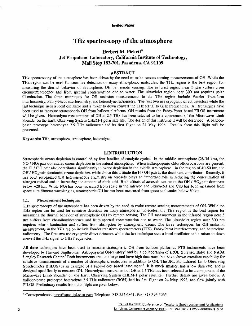
THz spectroscopy of the atmosphere
Herbert M. Pickett3
Jet Propulsion Laboratory, California Institute of Technology, Mail Stop 183-701, Pasadena, CA 91109
ABSTRACT THz spectroscopy of the atmosphere has been driven by the need to make remote sensing measurements of OH. While the THz region can be used for sensitive detection on many atmospheric molecules, the THz region is the best region for measuring the diurnal behavior of stratospheric OH by remote sensing. The infrared region near 3 urn suffers from chemiluminescence and from spectral contamination due to water. The ultraviolet region near 300 nm requires solar illumination. The three techniques for OH emission measurements in the THz region include Fourier Transform interferometry, Fabry-Perot interferometry, and heterodyne radiometry. The first two use cryogenic direct detectors while the last technique uses a local oscillator and a mixer to down convert the THz signal to GHz frequencies. All techniques have been used to measure stratospheric OH from balloon platforms. OH results from the Fabry-Perot based FILOS instrument will be given. Heterodyne measurement of OH at 2.5 THz has been selected to be a component of the Microwave Limb Sounder on the Earth Observing System CHEM-1 polar satellite. The design of this instrument will be described. A balloon- based prototype heterodyne 2.5 THz radiometer had its first flight on 24 May 1998. Results form this flight will be presented.
Keywords: THz, atmosphere, stratosphere, heterodyne
1.INTRODUCTION Stratospheric ozone depletion is controlled by four families of catalytic cycles. In the middle stratosphere (28-35 km), the NO / N02 pair dominates ozone depletion in the natural atmosphere. When anthropogenic chlorofluorocarbons are present, the Cl / CIO pair also contributes significantly to ozone depletion in the middle stratosphere. In the region of 40-60 km, the OH / H02 pair dominates ozone depletion, while above this altitude the H / OH pair is the dominant contributor. Recently, it has been recognized that heterogeneous chemistry on aerosols plays an important role in reducing the concentration of nitrogen radical and in increasing the amount of nitric acid. Both effects of aerosols can make the OH / H02 pair dominant below -28 km. While N02 has been measured from space in the infrared and ultraviolet and CIO has been measured from space at millimeter wavelengths, stratospheric OH has not been measured from space at altitudes below 50 km.
1.1. Measurement techniques THz spectroscopy of the atmosphere has been driven by the need to make remote sensing measurements of OH. While the THz region can be used for sensitive detection on many atmospheric molecules, the THz region is the best region for measuring the diurnal behavior of stratospheric OH by remote sensing. The OH measurement in the infrared region near 3 |xm suffers from chemiluminescence and from spectral contamination due to water. The ultraviolet region near 300 nm requires solar illumination and suffers from absorption by atmospheric ozone. The three techniques for OH emission measurements in the THz region include Fourier transform spectrometers (FTS), Fabry-Perot interferometry, and heterodyne radiometry. The first two use cryogenic direct detectors while the last technique uses a local oscillator and a mixer to down convert the THz signal to GHz frequencies.
All three techniques have been used to measure stratospheric OH from balloon platforms. FTS instruments have been developed by Harvard Smithsonian Astrophysical Observatory1 and by a collaboration of IROE (Firenze, Italy) and NASA Langley Research Center.2 Both instruments are quite large and have high data rates, but have shown excellent capability for sensitive measurements of a number of stratospheric molecules in addition to OH. The JPL Far Infrared Limb Observing Spectrometer (FILOS) is an example of a Fabry-Perot based instrument.3 It is much smaller, has a low data rate, and is designed specifically to measure OH. Heterodyne measurement of OH at 2.5 THz has been selected to be a component of the Microwave Limb Sounder on the Earth Observing System CHEM-1 polar satellite. Further details are given below. A balloon-based prototype heterodyne 2.5 THz radiometer (BOH) had its first flight on 24 May 1998, and flew jointly with FILOS. Preliminary results from this flight are given below.
' Correspondence: [email protected]; Telephone: 818 354 6861; Fax: 818 393 5065
Part of the SPIE Conference on Terahertz Spectroscopy and Applications San Jose, California • January 1999 SPIE Vol. 3617 • 0277-786X/99/$10.00

The FILOS instrument has been part of a total of 14 balloon flights. The modest requirements of FILOS have allowed it to fly with either of the FTS instruments as well as the new the new BOH instrument. In effect, the FILOS instrument can serve as a transfer standard between different instruments that could not otherwise be compared. A detailed discussion of the results of these comparison flights will be part of a future paper, but initial comparisons show excellent agreement between FILOS and the FTS derived profiles of OH. An earlier paper has shown that the FILOS-measured OH profiles and diurnal behavior are consistent with simple photochemical models the utilize measured ozone and water profiles.4
2.EOS MLS 2.5 THz OH CHANNEL Heterodyne measurement of OH at 2.5 THz has been selected to be a key component of the Microwave Limb Sounder on the Earth Observing System CHEM-1 polar satellite. The requirements of this channel are to obtain monthly global maps with 5° latitude resolution and 3 km height resolution from 18 to 60 km. Projected sensitivity for high altitude (45-60 km) OH will allow daily maps, but more integration is required to obtain maps down to 18 km. It is not practical to look lower than 18 km because the water and dry air continua attenuate the OH signal for tangent heights below this altitude. As can be seen from Figure 1, OH has a very string gradient in volume mixing ratio, dropping below the parts-per-trillion level at 20 km. The projected sensitivity is also shown based on a Tsys= 30 000 K (SSB) using two OH polarizations. This sensitivity is possible in part because of the limb sounding geometry and in part because the line shape is resolved.
Measurement Precision February ON 3 km resolution
OH 60 c i i ii mil i i i i mil :—i i i mil 1—i i i um
10_" 10" Mixing ratio
Figure 1: EOS-MLS OH Sensitivity

The steep gradient of concentration means that extremely accurate pointing information is required. In fact, to obtain the sensitivity needed for the monthly maps pointing accuracy of 100 m is needed. Fortunately, nature placed an oxygen emission line within 8 GHz of the OH lines, and this emission line will be used to register the scan on the atmosphere. Temperature profiles will be measured by the lower frequency channels and will be used to calculate radiance of the THz oxygen line with respect to scan angle. Comparison of the offset between calculation and observation then establishes to pointing offset.
At first, the OH radiometer was to share the main 1600 x 800 cm main antenna, but the high frequency drove antenna requirements. In addition, the THz channel imposed constraints on system test and calibration because the THz channel performance can only be adequately measured in a vacuum, while the other four radiometers can be tested in air. The THz channel has a separate antenna and scanning system as shown in Figure 2. However, it still shares the same filter bank and data system. The antenna is a 22.8 cm offset Gregorian telescope with a 26.4 x 37.3 cm elliptical scanning mirror in front of the telescope. The scan mirror can be directed toward the limb, to a cold view above the atmosphere, or at an ambient temperature load.
EOS MLS
Figure 2: EOS-MLS Modules
The radiometer consists of a laser local oscillator, a quasi-optical diplexer, and two mixers that are oriented to receive horizontal and vertical polarizations from the atmosphere. The atmospheric radiance is not expected to be significantly polarized and the two mixer signals are only used to improve the S/N and provide some redundancy. The local oscillator is a methanol laser pumped by a C02 laser. The laser is being provided by DeMaria Electro Optics Systems. It will have 20 mW output power for 120 W input at 28 V. Currently we are pursuing two mixer approaches. The first is a whisker-contacted

waveguide mixer being developed by Rutherford Appleton Lab5 and the second is a membrane-supported planar waveguide mixer developed at the Jet Propulsion Lab.6
3.FIRST BALLOON HETERODYNE OH MEASUREMENTS A balloon-based prototype heterodyne 2.5 THz radiometer had its first flight on 24 May 1998 from Ft. Sumner, NM. The purpose of this balloon instrument is to provide early real-world use of selected components that will be used on the flight instruments, to obtain early views of stratospheric OH using the frequencies and techniques that will be used in flight, and to gain operational experience with a balloon instrument that can be used for sub-orbital validation after launch. The balloon instrument included a JPL waveguide mixer, a prototype laser LO, and a brassboard filter bank. The second LO frequencies were nearly the same at specified for EOS MLS except that a correction for the 56 MHz spacecraft Doppler shift was not included. The mixer, laser LO, and the filter bank worked well during the flight, but a coolant pump failed causing the thermal control to be much worse than desired. Fortunately, for a period of 40 min midway through the flight, the thermal drift was small enough to lock the laser and take data. Results for this flight are given in Figure 3. The solid line is the calculated OH emission after fitting the limb scans to the data. The fitted profile of OH is quite similar to values previously obtained from Ft. Sumner.
Balloon OH obs = 36.9 km, tan = 31.3 km
180
11 13 15 17 19 21 23
Channel
25
Figure 3: OH Stratospheric Emission from Balloon
4.CONCLUSIONS AND FUTURE PROSPECTS Heterodyne techniques in the Terahertz region will provide significant improvement in our capability to measure OH in the stratosphere. Our balloon instrument has demonstrated the basic capability for such measurements. We plan to fly the balloon instrument again in September 1999 so that the sensitivity can be verified. We also plan to fly FILOS on the same payload so that the OH measured by the two techniques can be compared. Of course, the real insight into stratospheric OH chemistry will come in 2002 when EOS-MLS is launched. The design lifetime of all the CHEM-1 instruments is 5 years, and we expect that a great deal will be learned about the stratosphere and upper troposphere during that observational period.

Present improvements in THz mixer and local oscillator technology will enable improved sensitivity for OH and will extend heterodyne techniques to other molecules in the stratosphere. With a frequency-agile high-sensitivity THz heterodyne receiver, instruments could be developed for space that can respond quickly to changing needs in atmospheric chemistry while retaining superb detection capabilities.
ACKNOWLEDGEMENTS This work was carried out under contract between California Institute of Technology and the National Aeronautics and Space Administration. I also thank T. L. Crawford and J. C. Pearson for assistance with the May 1998 balloon flight. I also thank the members of the Microwave Limb Sounder team who have helped with the THz channel on EOS or have provided components for BOH.
REFERENCES 1. W. A. Traub, D. G. Johnson, and K. V. Chance, "Stratospheric Hydroperoxyl Measurements," Science, vol. 247, 446-
449 (1990). 2. B. Carli, M. Carlotti, B. M. Dinelli, F. Mencarglia, and J. H. Park, "The Mixing Ratio of the Stratospheric Hydroxyl
Radical from Far Infrared Emission Measurements," J. Geophys. Res., vol. 94, 11049-11058 (1989). 3. H. M. Pickett, and D. B. Peterson, "Far-IR Fabry-Perot Spectrometer for OH Measurements," SP1E Optical Methods in
Atmospheric Chemistry, vol. 1715, 451-456 (1992). 4 . H. M. Pickett, and D. B. Peterson, "Comparison of Measured Stratospheric OH with Prediction," J. Geophys. Res., vol.
101. 16789-16796 (1996). 5. B. N. Ellison, B. J. Maddison, C. M. Mann, D. N. Matheson, M. L. Oldfield, S. Marazita, T. W. Crowe, P. Maaskant,
and W. M. Kelly, "First Results for a 2.5 THz Schottky Diode Waveguide Mixer," Proc. of the 7th Intl. Symposium on Space THz Tech., Charlottesville, VA, 494-502 (1996).
6. P. H. Siegel, R. P. Smith, M. Gaidis, S. C. Martin, and J. Podosek, "2.5 THz GaAs Monolithic Membrane-Diode Mixer," Proc. of the 9th Int'l Symposium on Space THz Tech., Pasadena, CA, 147-159 (1998).

Invited Paper
The photomixer transceiver
S. Verghese, K. A. Mclntosh, S. Calawa, W. F. Dinatale, E. K. Duerr, and L. H. Mahoney
Lincoln Laboratory, Massachusetts Institute of Technology, Lexington, MA 02420-9108, USA
ABSTRACT Two low-temperature-grown GaAs photomixers were used to construct a transmit-and-receive module that is fre- quency agile over the band 25 GHz to 2 THz, or 6.3 octaves. The photomixer transmitter emits the THz difference frequency of two detuned diode lasers. The photomixer receiver then linearly detects the THz wave by homodyne down conversion. The concept was demonstrated using microwave and quasioptical photomixers. Compared to time-domain photoconductive sampling, the photomixer transceiver offers improved frequency resolution, spectral brightness, system size, and cost.
Keywords: photomixers, gallium arsenide, submillimeter waves
1. INTRODUCTION
Continuous spectral coverage of the wavelength band 30-1000 jum is usually achieved with black-body sources and Fourier-transform spectrometers (FTS). Measurements that require coherent, constant-wave (cw) illumination typ- ically rely on microwave tubes, molecular-gas lasers, or harmonic up conversion of fundamental sources. A tunable coherent solid-state source would enable high-resolution molecular spectroscopy to be performed with much simpler instrumentation than is currently available. Also, recent advances in terahertz receivers based on superconducting bolometers have created a compelling need for a tunable local oscillator (LO) with output power > 1 ^W from roughly 0.5-3 THz.1"3
Photomixers are compact, all-solid-state sources that use a pair of single-frequency tunable diode lasers to generate a THz difference frequency by photoconductive mixing in low-temperature-grown (LTG) GaAs.4,5 Typical output power levels range from 1 to 0.1 fiW from 1 to 2 THz, respectively. At MIT Lincoln Laboratory, photomixers are being optimized for use with cryogenic terahertz receivers. Recently, a demonstration of a 630-GHz photomixer LO coupled to a superconductor-insulator-superconductor receiver resulted in a double-sideband noise temperature of 331 K.6 A schematic diagram of this experiment is shown in Fig. la. At other institutions, photomixers are being used as sources to perform high-resolution (~ 1 MHz) transmission spectroscopy of molecular gases. Figure lb shows a typical arrangement in which the output of a photomixer passes through a gas cell and is then detected by a liquid-helium-cooled bolometer. Such configurations using photomixers have been used to measure fine structure in the rotational spectra of molecules such as sulfur dioxide7 (S02) and acetonitryl8 (CH3CN).
In the time domain, photoconductive sampling has been used by many groups for terahertz spectroscopy in free space and on transmission lines. These systems consist of two fast photoconductive switches that are excited by a mode-locked laser and are coupled to each other via antennas or transmission line. Until recently, there had not been a demonstration of photoconductive sampling for detection of cw THz waves using photomixers. This paper describes a photomixer transceiver that performs photoconductive sampling in the frequency domain. For spectroscopy applications that require narrow linewidth (< 1 MHz), this technique can offer significant improvement in frequency resolution and spectral brightness over time-domain sampling. Furthermore, the system is coherent, widely tunable, and can be compact—using inexpensive laser diodes that are fiber coupled to the photomixer- transmitter and receiver chips.
Corresponding author: S. Verghese ([email protected])
Part of the SPIE Conference on Terahertz Spectroscopy and Applications San Jose, California • January 1999 SPIE Vol. 3617 • 0277-786X/99/$10.00

sky signal Q1 superconducting
heterodyne receiver
(b)
photomixer source gas ce|| He-cooled bolometer
Figure 1. (a) Schematic of a photomixer transmitter used as a frequency-agile local oscillator for a heterodyne detector, (b) Schematic of a photomixer transmitter used for gas spectroscopy.
2. MICROWAVE EXPERIMENT
Figure 2a is a diagram of the experimental setup that was used to test the concept at microwave frequencies. The combined light (A « 850 nm) from a pair of distributed-Bragg-reflector laser diodes is split in half and fiber coupled to each photomixer. Each LTG-GaAs photomixer comprises a 20 x 20-/xm active region with 0.2-/mi-wide interdigitated electrodes with gap spacings of 0.6 /mi for the transmitter and of 0.4 pm for the receiver. The photomixers used epitaxial layers of LTG GaAs grown by molecular-beam epitaxy on GaAs substrates and had photocarrier lifetimes of 0.2-0.3 ps.9 The transmitter is dc biased through a broadband bias tee and therefore develops an ac current across the electrodes when the photoconductance is modulated at the difference (beat) frequency of the two laser beams. Some of the resulting microwave power is launched onto a coplanar waveguide which transitions into a 50-fi coaxial line that is connected in similar fashion to the receiver, which is unbiased. At the receiver end, the optical beating periodically raises the photoconductance such that a small amount of unipolar current flows out through the bias tee and into the dc current amplifier. This action is equivalent to homodyne detection of the rf electric field. Figure 2b(i) shows that the homodyne signal scales approximately linearly with the dc-bias voltage—or incident electric field—while the transmitted power 2b(iii) measured with a spectrum analyzer scales quadratically in voltage.
In contrast to a photoconductive switch driven with a pulsed laser, the photomixer rf impedance is relatively high during cw illumination Zt = Vt/It « 10- 30 kQ. Here Vt is the dc voltage across the transmitter that generates a dc photocurrent It when illuminated by two lasers. In the limit of mismatched impedances, the dc current measured at the receiver is proportional to the transmitted rf voltage.10 The phase of the rf voltage is measured by dithering the difference in path length of the two arms with a short delay line. Then, the receiver is a linear detector of the transmitted wave in the same sense that time-domain sampling performs a linear detection of the transmitted voltage pulse. Contrast this with the power measured by a direct detector (such as in a scalar spectrum analyzer). In that case, the measured signal is proportional to the magnitude squared of the transmitted voltage and all phase information is lost. The symbols in Fig. 2b result from a calculation of the homodyne-detected signal using as input parameters the transmitter bias voltage and the dc photoconductances of the transmitter and receiver. Agreement between theory and measurement is close, in part because there are no free-space beams and associated coupling losses.11
3. SUBMILLIMETER-WAVE EXPERIMENT
Two antenna-coupled photomixers were used to test a quasioptical version of the photomixer transceiver (Fig. 3a) at terahertz frequencies. Such an implementation, for example, could be used for measuring the transmission of trace

cw Microwaves
^ Q) „r
0)1,0)2 (Oi,C02
1 3 5 7 10 Transmitter Voltage (V)
(b)
Figure 2. (a) Schematic of the microwave measurement system. Two laser diodes are combined and coupled via optical fiber to two photomixers. The photomixers are connected via 50-Q coaxial line, separated by an isolator. The transmitter is dc biased and a dc current amplifier measures the homodyne-detected current, (b) (i) Measured homodyne signal as a function of the dc-voltage bias on the transmitter chip. The symbols show the calculated homodyne signal, (ii) Measured dc photocurrent. Note how its shape tracks the homodyne signal, (iii) Measured rf power from the transmitter using a spectrum analyzer (not shown).
gases through an air column. Planar log-spiral antennas were patterned in Ti/Au films by optical lithography on the LTG-GaAs surface. Electron-beam lithography was used to define an 8 x 8-fim active area with 0.2-/mi-wide electrodes at the drive point of the antenna. The electrodes were separated by 0.8-/zm gaps for the transmitter chip and by 1.5-^m gaps for the receiver. The photomixers were mounted on silicon-hyperhemisphere lenses so that they opposed each other, separated by 6 cm. The emitted radiation from two tunable cw Ti:sapphire lasers was combined with a beam splitter. Half of the combined beam passed through a variable delay line and was coupled into a fiber that was pigtailed to the receiver. The other half passed through a chopper before entering a fiber that was coupled to the transmitter. Each photomixer was pumped by approximately 35 mW of optical power and the transmitter was dc biased at 15 V resulting in a dc photocurrent of 300//A.
Figure 3b shows the homodyne signal amplitude as a function of frequency. The signal is relatively flat to 600 GHz and then rolls off until it is detectable with a signal-to-noise ratio of ~ 3 at 2 THz.12 With higher-power photomixers optimized for high-frequency operation, this upper frequency should extend beyond 2 THz.5 At low frequencies (< 1 THz), the ratio of the signal to the background noise was high and the measurement was dominated by multiplicative noise from the lasers. Residual intensity noise on the laser was a few percent, caused by the fluctuations on the Ar pump laser. The current source driving the diode lasers used for the microwave experiment described above contributes relative intensity noise < 10-4 in a 200-kHz noise bandwidth. A second noise contribution arises from frequency jitter of the lasers. Since this system is highly coherent, standing waves are always present. Standing waves provide a mechanism for converting frequency jitter to amplitude noise on the detected homodyne signal. Most of these effects could be mitigated by using Gaussian reimaging optics and stabilized lasers.

3- •a o! il
I ui ■D 0) o
a
iooo F
100
10
1
1 10 100 1000 Frequency (GHz)
(b)
Figure 3. (a) Schematic of the quasioptical implementation. Two cw Ti:sapphire lasers were used since their tuning range exceeded that of the available diode lasers. A pair of tunable diode lasers was used previously (unpublished) with this setup, (b) Homodyne signal plotted versus the difference frequency between the two lasers. Between the microwave and quasioptical systems, the photomixer transceivers covered over three orders of magnitude in frequency.
4. PHASE-SENSITIVE TRANSMISSION MEASUREMENT
An important capability of the photomixer transceiver is the measurement of amplitude and phase of the transmitted electric field. This allows measurement of the real and imaginary components of the linear response of a medium (e.g. t\ + iei) or of a device (e.g. complex S-parameters). A transmission measurement through an inductive-mesh filter13 was performed to demonstrate this capability. Figure 4 shows the amplitude and phase of the electric-field transmission coefficient |"r(u))|expi0(u;) as a function of detuning frequency between the two lasers. The amplitude \T\ was determined by dithering the offset in zero-path difference and obtaining the ratio of the fringe amplitudes with the sample in and out of the beam. The inset in Figure 4a shows the fringe pattern with the mesh in the beam (i) and out of the beam (ii). The phase <j> = u(di - d,2)/c was determined by measuring the change in path between zeroes in the fringe pattern. For high frequencies, where noise is an issue, these quantities are better estimated by Fourier transforming the fringe patterns to extract phase and amplitude values.
An approximate theory for a two-dimensional inductive mesh was derived by Lee et al.14 The theory assumes a transmission-line model in which the incident wave experiences a normalized shunt admittance of value 2Y. Then, the complex transmittance for the electric field is simply T(W) = 1/(1 + Y(w)). The expression for Y was phenomeno- logically developed from numerical simulations
y(w) = (_,-)(/?-I) a + ±(2.)
lncsc(ff) (1)
where ß = (1 — 0.415/a)/(a/A), 5 = (a — c)/2, a = 318 ^m is the pitch of the mesh, and (a — c) = 25 pm is the width of the wires that form the mesh.13 The solid lines in Fig. 4a and 4b show curves that were calculated using equation
10

0) 0) n £
c o ■35 (0
E (0 c a
90
75
60
(a)
_\» I I 1 1
mesh
■ 111 45 •s II 1 1 - 30 • ^
:HW 15
0 I, I 1 1
0.0 0.2 0.4 0.6 0.8 Frequency (THz)
(b)
1.0
Figure 4. (a) Measured transmission coefficient for the propagating electric field incident on a wire-grid mesh. The solid line shows a theoretical calculation of the transmission. (Inset) Measured fringe pattern at 100 GHz for the mesh in (i) and out (ii) of the beam, (b) Measured phase delay incurred by the wave from propagating through the mesh. The solid line is calculated.
(1). The general trends in the calculated curves are reproduced by the transceiver measurements. The signal-to- noise ratio in these data was high and the values were reproducible. The scatter between points was systematic and presumably resulted from standing waves in the present quasioptical system.
5. DISCUSSION
It is instructive to compare some of the features of the photomixer transceiver to more established techniques for terahertz spectroscopy.
Fourier-transform infrared (FTIR) spectrometers are often used for infrared analysis of gases with resolving power X/SX w 104 or higher. For the far-infrared and submillimeter bands, an equivalent resolving power demands long travel for the scanning mirror. For example, resolving a 1-THz feature with 100-MHz resolution (X/8X ~ 104) requires a mirror travel of 1.5 m. For a typical spectrometer designed for high resolving power, the maximum available power in this band is 2 x 10_11W.15 Such low power requires a liquid-helium-cooled detector. This is in contrast to ~ 10~6 W available from a photomixer in a band that is less than 1 MHz wide. Already, researchers have used photomixers with bolometers to perform gas spectroscopy with resolution (X/5X ~ 106) that would require > 100 m of mirror travel in a FTIR spectrometer.7,8 The photomixer transceiver should offer an equivalent capability, but with the size and cost advantages of a compact, room-temperature system.
In time-domain sampling, a train of wide-bandwidth pulses with low duty cycle (~ 10~4) carries the THz radiation. The peak pulse power is relatively high and the receiver switch acts like an ultrafast boxcar integrator with high signal-to-noise ratio. However,the power available in a 1-MHz band is reduced by a factor as large as the duty cycle (typically ~ 10~4) compared to that available in an equivalent photomixing experiment.16 Furthermore, without continuous tuning of the laser cavity length, the minimum frequency resolution is the free spectral range of the laser
11

cavity (typically ~ 80 MHz for mode-locked Ti:sapphire lasers). In frequency-domain sampling with photomixers, it is the homodyne action of the receiver that restricts the noise bandwidth in the same fashion as for a lock-in amplifier. Hence, there is a tremendous reduction in noise bandwidth compared to using a direct detector such as a bolometer and the photomixer receiver does not need cooling to enhance its sensitivity.
6. CONCLUSIONS AND FUTURE WORK
In summary, a technique has been demonstrated at microwave (0.1-26.5 GHz) and submillimeter-wave frequencies (25 GHz-2 THz) for photoconductive sampling in the frequency domain using photomixers and cw lasers. With more optimized photomixers,18 the upper frequency range is expected to exceed 3 THz.
Many of the applications that have been suggested for time-domain systems (e.g. T-ray imaging and other linear spectroscopy) could in principle be performed with the photomixer transceiver.17 The system described in this paper is being upgraded to use higher efficiency photomixers with resonant antennas. The laser system will be improved by using diode seed lasers that drive a semiconductor optical amplifier. If there were interest in THz point-to-point communications in space, such a system could be studied using the photomixer transceiver by encoding sideband information on the THz carrier either by bias modulation of the photomixer or by phase-modulation of the optical pump lasers. The extreme frequency agility of the photomixer transceiver makes it interesting to study aggressive frequency-hopping schemes for low-probability-of-intercept communications.
ACKNOWLEDGMENTS
Thanks are due to N. Zamdmer for discussions on spectral brightness and to C. D. Parker for the inductive-mesh filter. This work was supported by the National Aeronautics and Space Administration, Office of Space Access and Technology, through the Center for Space Microelectronics Technology, Jet Propulsion Laboratory, California Institute of Technology.
REFERENCES
1. M. Bin, M. C. Gaidis, J. Zmuidzinas, T. G. Phillips, H. G. LeDuc, "Quasi-optical SIS mixers with normal metal tuning structures," IEEE Trans. Appl. Supercond. vol. 7, pp. 3584-3588,1997.
2. C.-Y. E. Tong, R. Blundell, D. C. Papa, J. W. Barrett, S. Paine, X. Zhang, J. A. Stern, H. G. LeDuc, "A fixed tuned low noise SIS receiver for the 600 GHz frequency band," Proc. 6th Intl. Symp. Space THz Tech., pp. 295-304, California Institute of Technology, Pasadena, CA, 1995.
3. B. S. Karasik, M. C. Gaidis, W. R. McGrath, B. Bumble, H. G. LeDuc, "A low-noise 2.5 THz superconductive Nb hot-electron mixer," IEEE Trans. Appl. Supercond., vol. 7, pp. 3580-3583,1997.
4. K. A. Mclntosh, E. R. Brown, K. B. Nichols, O. B. McMahon, W. F. DiNatale, and T. M. Lyszczarz, Appl. Phys. Lett 67, 3844 (1995).
5. S. Verghese, K. A. Mclntosh, and E. R. Brown, IEEE Trans. Microw. Theory Tech. 45, 1301 (1997). 6. S. Verghese, E. K. Duerr, K. A. Mclntosh, S. M. Duffy, S. D. Calawa, C.-Y. E. Tong, R. Kimberk, and R.
Blundell, "A photomixer local oscillator for a 630-GHz heterodyne receiver," submitted to IEEE Microw. and Guided Wave Lett, 4 January 1999.
7. A. S. Pine, R. D. Suenram, E. R. Brown, and K. A. Mclntosh, J. Mol. Spectrosco. 175, 37 (1996). 8. P. Chen, G. A. Blake, M. C. Gaidis, E. R. Brown, K. A. Mclntosh, S. Y. Chou, M. I. Nathan, and F. Williamson,
Appl. Phys. Lett. 71, 1601 (1997). 9. K. A. Mclntosh, K. B. Nichols, S. Verghese, and E. R. Brown, Appl. Phys. Lett. 70, 354 (1997).
10. S. Verghese, K. A. Mclntosh, S. Calawa, W. F. Dinatale, E. K. Duerr, K. A. Molvar, "Generation and detection of coherent terahertz waves using two photomixers," Appl. Phys. Lett. 73, pp. 3824-3826 (1998).
11. For a detailed analysis of a photomixer in a transmission line see: E. R. Brown, F. W. Smith, and K. A. Mclntosh, J. Appl. Phys. 73, 1480 (1993).
12. The signal-to-noise ratio was estimated by chopping (1.5 kHz) the optical beam coupled to the transmitter and monitoring the rms fluctuation in the signal on a lock-in amplifier with a 300-ms postdetection bandwidth.
13. Electroformed wire mesh, 80 copper lines/inch, 0.00098-inch wire width. Buckbee-Mears, St. Paul, MN 55101. 14. S.-W. Lee, G. Zarrillo, C.-L. Law, IEEE Trans. Antennas Propag. 30, 904 (1982).
12

15. See for example, the Magna series of FTIR spectrometer from Nicolet Corporation, 5225 Verona Road, Madison, WI 53711. Assumptions for the maximum power estimate are: Glow-bar color temperature 1473 K, unity emissivity, lossless spectrometer, optical throughput (etendu) 0.005 sr-cm2, resolution bandwidth 100 MHz.
16. The spectral-brightness factor is the duty cycle (10-4) if time-domain and frequency-domain sampling are per- formed with identical antennas of a given radiation resistance that is impedance-matched to the photoconductor resistance during illumination. In practical systems, an impedance match is difficult to accomplish with cw photomixing, and the realizable advantage for photomixing in spectral brightness will be closer to ~ 102.
17. M. C. Nuss, IEEE Circuits Devices Mag. 12, 25 (1996). 18. S. Verghese, K. A. Mclntosh, and E. R. Brown, Appl. Phys. Lett. 71, 2743 (1997).
13

Two-frequency MOPA diode laser system for difference frequency generation of coherent THz-waves
Shuji Matsuura*a, Pin Chena, Geoffrey A. Blake3, J. C. Pearson*5, Herbert M. Pickettb
aDiv. of Geological and Planetary Sciences, California Institute of Technology, Pasadena, CA 91125 bJet Propulsion Laboratory, California Institute of Technology, Pasadena, CA 91109
ABSTRACT
We developed a tunable, cavity-locked diode laser source at 850 nm for difference-frequency generation of coherent THz- waves. The difference frequency is synthesized by three fiber-coupled external-cavity diode lasers, where two of the lasers are locked to adjacent modes of an ultra-stable Fabry-Perot cavity and the third laser is offset-phase-locked to the second cavity-locked laser using a tunable microwave oscillator. The first cavity-locked laser and the offset-locked laser produces the difference frequency, whose value is precisely determined by sum of integer multiple of free spectral range of the Fabry- Perot cavity and the offset frequency. The difference-frequency signal is amplified to 500 mW by the master oscillator power amplifier (MOPA) technique, simultaneous two-frequency injection-seeding with a single semiconductor optical amplifier. Here we demonstrate the difference-frequency generation of THz waves with the low-temperature-grown GaAs photomixers and its application to high-resolution spectroscopy of simple molecules. An absolute frequency calibration was carried out with an accuracy of ~10*7 using CO lines in the THz region.
Keywords: terahertz, source, photomixing, diode laser, stabilization, calibration
1. INTRODUCTION
Terahertz (THz) or far-infrared frequency region lies in the gap between near-optical frequency where solid-state lasers are available and microwave frequency where electronic sources exist, and the coherent technology in this region is still in research phase. Development of the THz coherent source technology will lead to opening up a frontier in optical science.1
THz frequencies are suitable for study of low energy light-matter interactions, such as phonon interactions in solids, rotational transitions in molecules, vibration-rotation-tunneling behavior in weakly bound clusters, and electronic fine structure in atoms. Spectroscopic observation and coherent control of these physical processes by the THz field are attractive subjects in fundamental physics, and these fundamentals are applicable to broad area in science and engineering, such as astronomy, remote sensing, and bio-medical sciences. In most of such THz applications, the frequency accuracy and tunability rather than the source power are critical to obtain meaningful results. For example, the local oscillator source for THz heterodyne receiver for astronomy require small source power («1 mW) but narrow line and wide tunability that it should be able to detect molecular lines from nearby interstellar clouds with the linewidth of <10"-> and to search for the highly redshifted lines from distant galaxies.
On the motivation described above, various type of THz sources, such as solid and molecular gas lasers, backward-wave oscillator, free-electron lasers, harmonic up-conversion from microwave sources, have been developed. Most of these sources can provide high power radiation but, until now, suffered from poor frequency tunability or pulsed oscillation. Difference-frequency generation (DFG), frequency down-conversion from optical sources, has been known as a promising technique to develop highly tunable coherent source in the THz region. Optical heterodyne mixing (photomixing) in ultra- fast photoconductor (photomixer) is an attractive down-conversion method at -1-2 THz range because of relatively high conversion efficiency compared with the DFG with nonlinear optical materials.2,3 Diode-laser-based systems have many advantages of compactness, low power consumption, and long lifetime. •' These properties are important to build instruments not only for satellite remote sensing and space telescope but also for laboratory spectroscopy. Although some laboratory spectroscopic studies with such THz sources have been done by several authors,^ the frequency accuracy of the THz wave has not been sufficient for high-resolution spectroscopy and heterodyne local oscillator applications.
* Correspondence: Email: [email protected]; Telephone: 626 395 3377; Fax: 626 585 1917
Part of the SPIE Conference on Terahertz Spectroscopy and Applications
14 San Jose. California • January 1999 SPIE Vol. 3617 • 0277-786X/99/S10.00

In this paper we present a method for synthesizing difference frequency with the precision necessary for the advanced spectroscopic applications. A precise difference frequency is synthesized by three external-cavity diode lasers, where two of the lasers are locked to adjacent modes of an ultra-stable Fabry-Perot cavity and the third laser is offset-phase-locked to the second cavity-locked laser using a tunable microwave oscillator. The first cavity-locked laser and the offset-locked laser produces the difference frequency, whose value is precisely determined by sum of integer multiple of free spectral range of the cavity and the offset frequency. The concept of this difference-frequency synthesis is demonstrated with constructing a diode laser system at 850 nm and generating THz wave with LTG-GaAs photomixers. The difference-frequency signal (two-frequency laser output) is amplified by the master oscillator power amplifier (MOPA) technique, simultaneous two- frequency injection-seeding with a single semiconductor optical amplifier at 850 nm, to provide sufficient power to generate THz waves efficiently by photomixing in photoconductors or nonlinear materials.
2. LASER SYSTEM DESIGN AND PERFORMANCE
2.1. Master laser system
The master oscillator for the MOPA system to synthesize a precise difference frequency consists of three external-cavity diode lasers as is depicted in Fig. 1. Each laser assembly consists of an SDL5722 852 nm, 150 mW, distributed Bragg- reflector (DBR) diode laser, a collimating lens, an external cavity comprised of a 4% partial reflector mounted on a piezoelectric transducer (PZT), a 60-dB isolator, an anamorphic prism pair to circularize the laser beam, and a focusing lens to fiber couple the beam. The partial reflector and the DBR laser chip constitute an external-cavity. The laser frequency is continuously tunable within ~5 GHz by changing the cavity length with the PZT voltage, and coarse frequency tuning spanned -700 GHz is available by changing the laser temperature. Alignment of the laser assembly is maintained by a compact aluminum rail structure. All the optical components to control and stabilize laser frequencies are implemented in polarization-maintaining (PM) single-mode fiber as is shown in Fig. 1. The fiber optics offer flexibility, compactness, insensitivity to vibration, ease of optical alignment, and eye protection. The optical fiber also serves as a spatial filter, allowing two different laser frequencies to be combined with nearly perfect spatial mode overlap. The latter is critical in the Fabry-Perot cavity alignment, in achieving equal amplification in the final MOPA amplifier, and in efficient photomixer operation. The fiber output of the #1 and #3 lasers, depicted as PI and P3, are combined together with a 3-dB directional coupler and used for the photomixing. Unfortunately, the total maximum power of the dual-frequency output from the final 3-dB fiber coupler was limited to approximately 30 mW mainly due to insertion loss of optical radiation to the fiber and coupling loss at the fiber connectors.
E£jDHf=|* PD
reference FP-cavity 3dB
LO (120MHz)-'
LO (80 MHz) -
MB'
to optical amplifier
P1
P3
PD(6GHzBW)
—®<-<J» '3dB'
LO (3-6 GHz) P3
PZT
VPZT
N ^r—J#3laser
o-JlÖdB ^ZT
Fig. 1: Schematic diagram of the master laser system that synthesize a precise difference frequency.
15

discriminator signal
4 MHz
pull-in range 160 or 240 MHz
"c3
C u
-2-10 1 Frequency [MHz]
Fig. 2: The dispersion signal of the cavity fringe used for the frequency stabilization.
Fig. 3: The spectrum of the beat note signal between the #1 and #3 lasers before (upper) and after (lower) amplification.
The #1 and #2 lasers are cross-polarized and locked to different longitudinal modes of an ultra-low-expansion (ULE) Fabry- Perot (FP) cavity by the Pound-Drever-Hall (PDH) method.9'10 The ULE cavity material has a thermal expansion coefficient at room temperature of a = -2xl0"10 "C"1, which is comparable to the stability of a quartz reference oscillator in conventional microwave sources. For the PDH method FM sidebands are generated on the two cavity-locked lasers with electro-optic phase modulators (EOM) operating at 80 MHz and 120 MHz. To verify coupling to the fundamental longitudinal cavity mode, the transmitted beam profile was monitored by a CCD-camera. The difference frequency between the two cavity-locked lasers is discretely tunable in steps of the cavity free spectral range (FSR). The phase of the beam reflected from the cavity is compared to the modulation frequency in a frequency multiplier. When the laser frequency is within the modulation frequency of the cavity resonance, the output of the frequency multiplier provides a DC frequency dispersion which crosses zero at the cavity resonance. Fig. 2 shows the dispersion curve at the mixer output obtained by sweeping the laser frequency through the cavity resonance. The central linear portion of the dispersion curve centered at the cavity is used to generate an error signal voltage, which is fed back to the PZT of the external laser cavity with a simple servo electronic circuit consisting of an integrator and an amplifier. The linear part of frequency discriminator shown in Fig. 2 is ~4 MHz, in accordance with the FSR of the cavity of 3 GHz and its finesse of 750. In the present laser system, the loop bandwidth of the PZT control circuit was limited to 3 kHz to avoid acoustic resonances in the support structure of the partial reflector with the PZT.
The third laser (#3) is locked to a beat note signal between the #2 and #3 lasers detected by a 6 GHz bandwidth photodetector and compared to tunable frequency generated by a microwave synthesizer. In order to implement a phase-lock with the same electronics as the cavity-lock, the signal was split with one arm sent through a delay line, and the resulting phase shift between the two signals was used to generate the error signal for the PZT of the #3 laser. The offset frequency is measured precisely by a microwave counter locked to a high precision reference, making any drifts or offsets in the phase lock scheme irrelevant to the system calibration. The offset frequency can be continuously tuned over 5 GHz by stepping the synthesizer frequency and tracking the PZT voltage. The maximum sweep rate of ~ 100 MHz/s is limited by the feedback loop bandwidth. The difference frequency between the #1 and #3 is determined by the sum of integral multiples of the FSR (3 GHz) of the reference cavity and the microwave offset frequency. The accuracy of the difference frequency is determined by the accuracy of the FSR measurement along with any DC offset in the electrical portions of the lock loops. The microwave offset frequency is locked to a high accuracy (~10-12) reference source and measured by a counter locked to the same reference in order to correct in real time any electrical offset in that lock loop.
In the laboratory environment there are relatively large temperature changes and the resulting changes of temperature equilibrium in the external cavity and laser themselves. The PZT voltage generally compensates for these drifts, but they were occasionally large enough to exceed the PZT error signal limit. The drift could be dramatically reduced by putting the laser rails on a temperature-controlled base plate. Once this was done, all-day-long cavity-locks of the laser have been routinely achieved without adjusting the temperature of the laser itself.
16

The overall system performance was assessed by observing a beat note between the #1 and #3 lasers with a 25 GHz bandwidth photodetector and a spectrum analyzer. The upper curve in Fig. 3 represents a 12 GHz beat spectrum for a 1-s integration time and a spectral resolution of 100 kHz. The FWHM spectral power bandwidth is approximately 800 kHz. The short-term linewidth of each laser is determined entirely by the optical feedback from the external cavity because the 3 kHz bandwidth of the lock loop circuit is much less than the laser linewidth.
2.2. Two-frequency MOPA operation
The two-frequency output of the master laser system was injection-seeded to an optical amplifier.1 * The two-frequency MOPA operation has the advantages of high power output and guarantees excellent spatial overlap of the two frequency beams, which is essential for efficient optical-heterodyne conversion.
The amplifier part of the MOPA system is shown in Fig. 4. A single traveling-wave 850 nm semiconductor tapered optical amplifier, which was the central component of a commercial external-cavity single-mode laser (SDL8630), was used. The fiber output from the master laser system was collimated, passed through a 60-dB optical isolator, and sent to a half-wave plate for fine adjustment of the polarization. The circular beam was transformed into an elliptical shape by an anamorphic prism pair in order to match its spatial mode to the amplifier 1x3 |im input facet. The master laser beam is injected into the optical amplifier chip. The amplified output beam is spatially filtered and collimated to a 3 mm diameter Gaussian beam by a telescope.
The amplifier was operated under highly saturated conditions at an injection laser power of 10 mW. The output power was relatively insensitive to both the injection power and frequencies and constant within 5% over the entire range of the difference frequency (<1.3 THz). The amplifier used in the present system was a component of a commercial external- cavity single-mode laser, and one of the amplifier chip facets was anti-reflection coated but the other facet was not. Small variations in the output power with a period of -15 GHz caused by the amplifier chip mode were observed.
Another desirable MOPA property for photomixing is that the gain for the two injected frequencies is nearly equal to each other. As expected, the output power ratio between the two frequency components was close to unity over a wide range of difference frequencies, specifically from -10 GHz - 1.3 THz. The small variations caused by the chip mode structure in the power ratio were also observed. Unbalanced amplification between the two frequencies occurred only at difference frequencies lower than 10 GHz. This behavior can be interpreted as arising from the interaction of the two frequency components driven by the refractive index change induced by the carrier density modulation at the difference frequency.11
Therefore, the lower frequency limit of the well-balanced two-frequency amplification is determined by the carrier lifetime of the amplifier. As shown in Fig. 3, the spectrum of beat signal between the amplified two frequency components was identical to that of the master laser as long as the difference frequency was greater than 10 GHz.
3. SPECTROSCOPY APPLICATIONS
As described above, the two-frequency laser system allows DFG of THz-waves in ultra-fast photoconductors or other nonlinear optical media. Here, we demonstrate the performance of the laser system with high resolution rotational spectroscopy of the simple molecules acetonitrile (CH3CN) and carbon monoxide (CO). Due to the lack of spectral analysis techniques in the THz region, spectroscopic measurements provide one of the best diagnosis of frequency and spectral purity.
LTG-GaAs photomixer
attn amp A/2
anamorphic prism
bolometer lens assembly
fm> isolator
master laser system
Fig. 4: Schematic diagram of the optical amplifier and spectroscopy setup.
17

Frequency [THz]
Fig. 5: The frequency dependence of the output power generated by the THz photomixer. The solid line represents the theoretical roll-off behavior with the slope of 12 dB/oct.
3.1. THz-wave generation
The LTG-GaAs photomixer used in the present experiment was grown on a semi-insulating GaAs substrate, and a planar log-spiral antenna with 0.2-fim interdigitated electrodes and 1.8-|im gaps in a 8 x 8 (im active area was etched on the wafer.12 The photomixer was mounted on the flat surface of a hyper-hemispherical lens made of high-resistivity silicon. Most of the generated radiation is emitted into free space through the photomixer substrate and the silicon lens. A DC bias voltage of 20 V was applied to the electrodes by a constant current supply set at 0.5 mA for a pump laser power of 30 mW. Under these conditions, the photomixer provided a maximum output power of ~0.1 u,W at 1 THz, while the 3 dB bandwidth of the generated THz-waves was approximately 700 GHz, as is shown in Fig. 5. The spectral bandwidth and the frequency roll-off behavior is roughly consistent with the carrier lifetime of the LTG-GaAs of f~200-300 fs and the photomixer RC time constant, where R = 72 Q is the radiation impedance and C = 0.5 fF is the electrode capacitance.12
The output power can be improved by increase of the pump laser power, but the laser power was kept well below the safe level (<50 mW) to prevent the photomixer from thermal damage.
3.2. Spectroscopy
The experimental setup used for spectroscopy is shown Fig. 4. The two-frequency output from the MOPA was appropriately attenuated (-30 mW) and focused onto the photomixer. The THz output beam was collimated with a combination of the silicon hyper-hemispherical lens and a Teflon lens and passed through an 8 cm long 1 inch diameter gas cell fitted with polyethylene windows. The beam transmitted through the cell was weakly focused with a Teflon lens and fed into a 4.2 K InSb hot-electron bolometer or a 1.6 K composite Si bolometer. The tone-burst modulation method was used to obtain absorption spectra of molecules.13 The advantage of the tone-burst method for THz spectroscopy as compared to traditional FM modulation is that sensitive detection with slow detectors such as silicon composite bolometers can be achieved. The injection current of the #1 cavity-locked laser was modulated with a 2 MHz tone, above the cavity- lock loop bandwidth, at a 10 kHz burst rate. A lock-in amplifier, detecting at 10 kHz, was used to demodulate the detector signal generating the traditional second derivative of molecular absorption features.
18

cd
s =3
cd
cd G W)
• i—i
CO 312 312.2 312.4 312.6 Frequency [GHz]
Fig. 6: The second-derivative absorption spectrum of CH3CN J= 16 -> 17 rotational transitions near 312 GHz. The spectrum for ordinary 12CH312CN. The inset is expanded view of the K = 0-2 lines.
Fig. 6 presents the absorption spectrum of the CH3CN Jg = 16# -» 17# rotational transitions near 312 GHz. The spectrum was taken with a sweep rate of 2 MHz/sec, and is plotted as a function of the microwave offset frequency. The data was recorded at 7 sample/sec with a lock-in amplifier. The spectrum shows the well known K-structure of a symmetric-top, with K components from K = 0-11 assigned in the spectrum. As seen in the inset of Fig. 8(a), the K = 0, 1 lines, which are separated by ~6 MHz, are clearly resolved. The gas pressure was 60 mTorr, and the observed line widths are consistent with a convolution of pressure broadened linewidths and the instrument response. The minimum detectable absorption of this system is estimated to be ~10~5, and is detector-noise-limited. The result indicates that the spectral purity, frequency control, and the output power of this system is sufficient for the laboratory spectroscopic study of molecules at THz frequencies.
3.2. Frequency calibration
For further spectroscopic measurements such as the search for unknown molecular lines and for use in astronomical observations, absolute frequency calibration of the difference frequency is necessary. Since the accuracy of the difference frequency is defined by the reference FP-cavity, the calibration must include a precise measurement of the FSR of the cavity. In principle, the difference frequency can be determined to within -10"10 °C_1, the temperature-fluctuation-limited accuracy, according to the thermal expansion coefficient of the ULE material. Well known molecular lines in the THz region, such as the rotational transitions of carbon monoxide (CO), are suitable for accurate calibration, since the frequencies of these THz molecular transitions correspond to -300 times the FSR and can be easily measured to within an accuracy of 10"7. A number of measurements and the careful use of statistics should allow the accuracy of 10"8.
Pure rotational transitions of CO were measured using the same configuration as the acetonitrile measurements, except that a composite silicon bolometer was used in these measurements. According to the conventional model for the diatomic
19

i r i r
N
00
<1
2 -
0
\
\
\ 4
-2 -
J I L J I I
100 200 300 400
Cavity order number
Fig. 7: The result of the FSR measurements by CO lines for J = 1-10. The deviation of the FSR values from their average are shown as a function of the cavity order difference.
12C160 molecule, the rotational transition lines should appear at frequencies of v= (Wj+j - Wj) I h, and Wj I h = BJ(J+1) - DJ2(J+1)2 + HJ3(J+1)3, where B = 57,635.9660 MHz, D = 0.1835053 MHz, H = 1.731xl0"7 MHz, h is Planck constant, and J is an integer.14 Absorption measurements for CO lines with J = 1-10 over the range of 230 GHz to 1267 GHz were carried out by measuring the microwave offset frequency, v0ffset, and counting the number of cavity orders between the two cavity-locked lasers. The line position was determined by fitting a parabola to the center of the 2nd derivative line profile. The cavity FSR for each CO line is simply calculated by dividing v - v0ffset by the cavity order difference, because the DC offset of the difference frequency caused by the DC offset voltage of the lock loop circuit was statistically insignificant. From this data set, the average of the FSR value for all CO line measurements was determined to be 2,996,757.48 ±0.10 kHz. Fig. 7 shows the deviation of the FSR values from their average as a function of the cavity order difference. Even if the scatter of the data around the average value is a real frequency dispersion of the cavity, the frequency dependence of the FSR over a 1.3 THz span is constant to within 1 kHz. In this approach, the frequency accuracy is limited by our ability to determine the center of the line profiles, which in turn depends on the instrumental resolution and the signal-to-noise ratio of the spectrum. The calibration accuracy can therefore be improved by increasing the source power and/or improving the detector sensitivity.
4. FUTURE DIRECTION
The photomixer used in the experiments reported here provides a maximum output power of approximately 0.1 U.W at 1 THz for a pump laser power of 30 mW. A straightforward extrapolation of the quadratic dependence of the THz-wave power on the laser power leads to the prediction that some 10 uW of power should be obtainable using the present laser system, whose maximum 850 nm power is 500 mW. However, the maximum pump laser power is currently limited to approximately 50 mW by thermal damage threshold of the photomixer.14 To solve this thermal problem, photomixers with distributed electrode structures and higher thermal conductivity substrates are being developed.12-15 We have recently designed and operated an optical/THz velocity-matched traveling-wave photomixer that can handle 1-W level pump laser power. These photomixers can be driven at the full output of the high-power laser system reported here, and will ultimately produce power levels over 1 |J.W at 1 THz.
The three laser difference-frequency generation and control method presented here is quite general and could be extended to a large number of different lasers. The absolute calibration method is also quite general and can be widely employed. This
20

frequency control technique is especially important in the >l-2 THz region, where comparison to a harmonically up- converted frequency reference may be difficult or impossible. The use of a MOPA as a two-frequency amplifier should facilitate the use of this control method with the next generation of photomixers based on nonlinear optical media such as L1NO3, GaP, GaAs, and quantum-well materials. At optical source frequencies DFG using nonlinear optical materials might be more efficient than electro-optical down-conversion with photoconductors, because the efficiency of the nonlinear optical DFG has a v4 dependence in the long wavelength limit.16 Further development of nonlinear optical materials and novel devices with large #2 at diode laser frequencies are expected in the near future, making precision difference frequency generation essential for their use as THz sources.
ACKNOWLEDGMENT
The authors thank S. Verghese and K. A. Mclntosh of MIT Lincoln Laboratory for preparing the LTG-GaAs photomixers. We also thank T. J. Crawford of Jet Propulsion Laboratory for his technical support. Portions of this work performed at the Jet Propulsion Laboratory California Institute of Technology were done under contract with the National Aeronautics and Space Administration (NASA). G. A. Blake acknowledges additional support from NASA and from the National Science Foundation.
REFERENCES
1. R. Datla, E. Grossman, and M.K. Hobish, eds. Metrology Issues in Terahertz Physics and Technology, NIST vol. 5701, 103 pp., 1995.
2. E.R. Brown, F.W. Smith, and K.A. Mclntosh, "Coherent Millimeter-Wave Generation by Heterodyne Conversion in Low-Temperature-Grown GaAs Photoconductors," J. Appl. Phys., vol. 73, pp. 1480-1484, 1993.
3. E.R. Brown, K.A. Mclntosh, K.B. Nichols, and C.L. Dennis, "Photomixing up to 3.8 THz in Low-Temperature- Grown GaAs," Appl. Phys. Lett., vol. 66, pp. 285-287, 1995.
4. K.A. Mclntosh, E.R. Brown, K.B. Nichols, O.B. McMahon, W.F. DiNatale, and T.M. Lyszczarz, "Terahertz Photomixing With Diode-Lasers in Low-Temperature-Grown GaAs," Appl. Phys. Lett., vol. 67, pp. 3844-3846, 1995.
5. S. Matsuura, M. Tani, and K. Sakai, "Generation of Coherent Terahertz Radiation by Photomixing in Dipole Photoconductive Antennas," Appl. Phys. Lett., vol. 70, pp. 559-561, 1997.
6. A.S. Pine, R.D. Suenram, E.R. Brown, and K.A. Mclntosh, "A Terahertz Photomixing Spectrometer - Application to SO2 Self-Broadening," J. Mol. Spec, vol. 175, pp. 37-47, 1996.
7. P. Chen, G.A. Blake, M.C. Gaidis, E.R. Brown, K.A. Mclntosh, S.Y. Chou, M.I. Nathan, and F. Williamson, "Spectroscopic Applications and Frequency Locking of THz Photomixing with Distributed-Bragg-Reflector Diode Lasers in Low-Temperature-Grown GaAs," Appl. Phys. Lett., vol. 71, pp. 1601-1603, 1997.
8. S. Matsuura, M. Tani, H. Abe, K. Sakai, H. Ozeki, and S. Saito, "High Resolution THz Spectroscopy by a Compact Radiation Source Based on Photomixing with Diode Lasers in a Photoconductive Antenna," J. Mol Spec, vol. 187, pp. 97-101, 1998.
9. R.V. Pound, Rev. Sei. Instrum., vol. 17, pp. 490-505, 1946. 10. R.W.P. Drever, J.L. Hall, F.V. Kowalski, J. Hough, G.M. Ford, A.J. Munley, and H. Ward, "Laser Phase and
Frequency Stabilization using an Optical Resonator," Appl. Phys. B, vol. 31, pp. 97-105, 1983. 11. S. Matsuura, P. Chen, G.A. Blake, J.C. Pearson, and H.M. Pickett, "Simultaneous Amplification of Terahertz
Difference Frequencies by an Injection-Seeded Semiconductor Laser Amplifier at 850 nm," Int. J. of Infrared and Millimeter Waves, vol. 19, pp. 849-858, 1998.
12. S. Verghese, K.A. Mclntosh, and E.R. Brown, "Highly Tunable Fiber-Coupled Photomixers with Coherent Terahertz Output Power," IEEE Trans. Microwave Theory and Tech., vol. 45, pp. 1301-1309, 1997.
13. H.M. Pickett, "Determination of Collisional Linewidths and Shifts by a Convolution Method," Appl. Optics, vol. 19, 2745-2749, 1980.
14. I. Nolt, J.V. Radostitz, G. Dilonardo, K.M. Evenson, D.A. Jennings, K.R. Leopold, L.R. Zink, and A. Hinz, "Accurate Rotational Constants of CO, HC1, and HF - Spectral Standards for the 0.3 to 6 THz (10 cm"1 to 200 cm"1) Region," J. Mol. Spec, vol. 125, pp. 274-287, 1987.
15. L.Y. Lin, M.C. Wu, T. Itoh, T.A. Vang, R.E. Müller, D.L. Sivco, and A.Y. Cho, "Velocity-Matched Distributed Photodetectors with High Saturation Power and Large Bandwidth," IEEE Photon. Technol. Lett., vol. 8, pp 1376- 1378, 1996.
16. Y.R. Shen, Principles of Nonlinear Optics. New York: John Wiley and Sons, 1984.
21

SESSION 2
Coherent Time-Domain THz Spectroscopy
23

Invited Paper
THz spectroscopy of polar liquids
I.H. Libon, M. Hempel, S. Seitz, N.E. Hecker, J. Feldmann Department of Physics, Ludwig-Maximilians-University, D-80799 München, Germany
A. Hayd, G. Zundel Department of Physical Chemistry, Ludwig-Maximilians-University, D-80799 München, Germany
D. Mittleman Electrical and Computer Engineering Department, Rice University, Houston, TX , U.S.A.
M. Koch Department of Electrical Engineering, University of Braunschweig, D-38106 Braunschweig, Germany
ABSTRACT
The mesoscopic structure of water has long been a subject of discussion. We postulate that, on the mesoscopic scale, liquid water forms nm-size ice-like crystals and that this structure is responsible for absorption in the THz-frequency range. However, until the recent development of THz-time domain spectroscopy (THz-TDS), it was difficult to determine the optical constants in this frequency range with a good signal-to-noise ratio and hence to study the absorption properties of water.
Here we report on the optical properties of water in the frequency range 0.05-1.4 THz and discuss the mesoscopic structure of water. We use THz-TDS based on photoconductive dipole antennas gated by a 150 femtosecond laser pulses to generate and detect the THz-frequency pulses.
A new theoretical approach is also presented which we use to explain the absorption behavior in the measured THz frequency range. In this theory, molecular plasma oscillations of H302" complexes, that are distinctly separate from the H502
+ complexes which form an underlying crystalline lattice, are assumed to be responsible for absorption in the THz- frequency range. This model provides good agreement to our data.
Keywords: THz spectroscopy, polar liquids, water clusters, plasmon oscillations
1. INTRODUCTION
The mesoscopic structure of polar liquids is still an extremely controversial topic1"8. In order to analyze this structure, methods used for the study of solids like X-ray diffraction3 and neutron scattering have been applied, although polar liquids have no crystalline structure. Nevertheless in polar liquids, the nearest neighbors of a single molecule do arrange themselves in a manner similar to the ordering which occurs in ice, its crystalline form. Hence, polar liquids exhibit a crystal-like short range ordering, but no long range ordering.
The absorption spectrum of liquid water in the mid-infrared portion exhibits resonances associated with intramolecular vibrations such as the bending mode of the 104° bond angle at 1650 cm"1 and the O-H bond stretching mode at 3400 cm"1. Collective intermolecular oscillations occur between neighboring water molecules when hydrogen bonding or Van der Waals interactions exist to provide an attraction. These oscillations, involving many molecules, are phonon-like and therefore lower in frequency than the intramolecular vibrations. For water the broad featureless absorption in the far- infrared, i.e. in the frequency range between 0.1 and several THz is attributed to this intermolecular motion. Hence this part of the electromagnetic spectrum most closely reflects the mesoscopic structure of liquids5.
Part of the SPIE Conference on Terahertz Spectroscopy and Applications 24 San Jose. California • January 1999 SPIE Vol. 3617 • 0277-786X/99/S10.00

Due to the lack of bright sources and efficient detectors, experimental access to the THz region has remained a difficult task until recently. The optoelectronic generation of coherent, pulsed THz radiation9"10 has opened up the possibility for routine spectroscopic measurements with a very good signal to noise ratio. Although several substances have been investigated lately using this method1'2'7, many remain to be explored.
In this paper we present our experimental data on water using THz time-domain spectroscopy and compare our data to a new ab-initio theory. Unlike the Debye theory, which is often used to describe the absorption process in the far-infrared and involves fit parameters that are often difficult to attribute to a physical process, our presented theory does not have any fit parameters.
Our experimental setup is depicted in Fig 1. It uses photoconductive dipole antennas and has a useful bandwidth between 0.05 and 1.4 THz. The THz radiation is focused to form an intermediate focus. For details on this kind of setup see e.g. see ref. 12. A liquid sample cell with variable path length and high-density polyethylene (HDPE) windows is introduced at the focus of the THz beam. This window material offers excellent transparency for frequencies below 2 THz and is chemically inert. The thickness of the liquid layer between the windows is varied, and THz time-domain waveforms transmitted through the sample cell are measured for each thickness.
Scanning Optical
Delay Line Femtosecond Laser
Fig. 1: Experimental setup for THz time-domain studies.
2. EXPERIMENTAL RESULTS
Fig. 2 shows some THz transients which have been measured after propagating through the liquid cell containing water films of three different thicknesses. The waveform measured for a thin film of thickness x serves as a reference. By comparing it to others which are obtained for thicknesses of x+100 urn and x+200 (am, a(ca) - the frequency-dependent absorption coefficient of water - can be derived2. This data is presented after the ensuing theoretical discussion.
25

2
o ill
1 1 —, J_ , 1 1 ' 1 '
_
■ ---: x |iin • - f i
i i - X -r IUU|AlTl
• I I I
1 1
i I . — . x i zUUfirn
♦ i • -
- I i / ■
* _» / i \ \ 1 i \ i *, \ i s \ i *.
/
*"*^"''- i
/^^ - > \ i
/ -
- ■ *f ■ i ■
- ■ i -
■ > ; >/ -
1 1 1 I i,i.
-6-4-20246
Time delay (ps)
Fig. 2: THz waveforms obtained for liquid films of different thicknesses.
3. THEORETICAL TREATMENT
In our theory, we propose that polar liquids with strong hydrogen bonds form crystal-like clusters on a mesoscopic scale, several nanometers in length. These can be regarded as behaving similar to ionic crystals with strongly fluctuating potentials. Within these clusters there is a continuous formation and dissolution of charged complexes". The idea of mesoscopic water clusters is supported by recent x-ray studies on water and ice3, and is consistent with the description of Hayd and co-workers14 which has been very successful in describing the mid-infrared continuum absorption observed in acid solutions.
We propose that the water clusters of H502+ and H302" are responsible for absorption in the THz frequency range. These
"ions" are a short lived species, but are not due to dissociation of water molecules. The formation of these ions is independent of pH value. The H502
+ and H302" ions are illustrated in Fig. 3.
Fig. 3: Four water molecules (left side) combine to form the "ion species" H502+ and H302" (right side).
26

The main idea of our theory is that the negatively charged H302" ion groupings collectively oscillate with ksO (i.e. with a very long wavelength) in a H502
+ lattice which can be described as a damped harmonic oscillator. The THz radiation field can only couple to the negatively charged H302" ion groupings since the positively charged H502
+ is strongly bound in the lattice. The optical properties may therefore be described in close analogy with the overdamped phonon-polariton, a well- known classical model used to describe the dielectric properties of ionic crystals.
The frequency dependent dielectric function can therefore simply be written as:
coL -co +ida> e(a>) = e«
yCOT -co +idco 0)
where coL is the plasma frequency of the H302" ion groupings and cor= 0 since liquids cannot support shear forces. Given this s(co), we can derive the absorption coefficient:
, N V2<y, \e~co
where ea= 1.78, and d = 37.6 THz is the damping constant which can be derived by quantum electrodynamics (QED) calculations15.
Equation (2) predicts that the absorption is proportional to the frequency coL of the collective oscillation, which we calculate classically:
= 3.46 THz. (3)
where N H (r is the density of and MH Q_ is the mass of H302' ions, respectively. All parameters in equation 2 are
therefore fixed; there are no variables which need to be determined with a fit. The absorption spectrum for water and our theoretical prediction are shown in Fig. 4. As expected for a liquid in the THz frequency range, the spectrum exhibits no strong resonances.
27

400-
Experimental results Theoretical prediction
—, 1 , 1 , 1 1 1 r
0,0 0,2 0,4 0,6 0,8
Frequency(THz)
i 1,0 1,2 1,4
Fig. 4: Absorption coefficient of liquid water and our theoretical approach
The good agreement between theory and experiment also holds for heavy water (not shown here). The details of our theory will be published elsewhere13.
In this paper we have presented our measurements on water and compared it with a ab-initio theory for polar liquids. The theoretical predictions well represent the absorption behavior in the far-infrared frequency range. This indicates that on a mesoscopic scale water is comprised of clusters similar to ice.
4. ACKNOWLEDGEMENTS
We would like to thank S. Keiding and I. Brener for supplying us with THz antennas. The expert technical assistance of W. Stadler is gratefully acknowledged. This work was supported by the Deutsche Forschungsgemeinschaft and the European Union.
5. REFERENCES
1. L. Thrane, R.H. Jacobsen, P. Uhd Jepsen, and S.R. Keiding, "THz reflection spectroscopy of liquid water," Chem. Phys. Lett. 240, 330 (1995).
2. J.T. Kindt, and C.A. Schmuttenmaer, "Far-infrared dielectric properties of polar liquids probed by femtosecond terahertz pulse spectroscopy," J. Phys. Chem. 100, 10373 (1996).
3. G. Ruocco, F. Sette, U. Bergmann, M. Kirsch, C. Masciovecchio, V. Mazzacurati, G. Signorelli, and R. Verbeni, "Equivalence of the sound velocity in water and ice at mesoscopic wavelengths", Nature 379, 521 (1996).
4. K. Liu, J.D. Cruzan, and R.J. Saykally, "Water clusters", Science 271, 929 (1996). 5. P.L. Silvestrelli, M. Bernasconi, and M. Parrinello, Ab initio infrared spectrum of liquid water", Chem. Phys. Lett 277,
478 (1997). 6. M.E. Tuckerman, D. Marx, M.L. Klein, and M. Parrinello, "On the quantum nature of the shared proton in hydrogen
bonds", Science 275, 817 (1997).
28

7. C. Ronne, L. Thrane, P.-O. Astrand, A. Wallqvist, K.V. Mikkelsen, and S:R. Keiding, "Investigation of the temperature dependence of the dielectric relaxation in liquid water by THz reflection spectroscopy and molecular dynamics simulation", J. Chem. Phys. 107, 5319 (1997).
8. R. Vuilleumier, and D. Borgis "An extended empirical valence bond model for describing proton transfer in H+(H20)n
clusters and liquid water", Chem. Phys. Lett. 284, 71 (1998). 9. P. R. Smith, D.H. Auston, and M.C. Nuss "Subpicosecond photoconducting dipole antennas", IEEE J. Quant. Elec, 24,
255 (1988). 10. M. van Exter, and D. Grischkowsky, "Characterization of an optoelectronic terahertz beam system", IEEE Trans.
Microwave Theory and Tech., 38, 1684 (1990). 11. G. Zundel, "Hydration and intermolecular interaction", Academic Press, New York and London (1969). 12. D. M. Mittleman, R.H. Jacobsen, and M.C. Nuss, "T-ray imaging", IEEE J. Sei. Top. Quant. Elec, 2, 679 (1996). 13. I.H. Libon et ai, to be published. 14. A. Hayd, E. G. Weidemann, and G. Zundel, "Theory of ir continua with polarizable hydrogen bonds. I. Aqueous
solutions of strong acids," J. Chem. Phys., 70, 86 (1979). 15. private communication with E. G. Weidemann
29

Evidence of frequency dependent THz beam polarization in time-domain spectroscopy
Frederic Garet, Lionel Duvillaret, Jean-Louis Coutaz
Laboratory of Microwaves and Characterization (LAHC)
University of Savoy, 73376 Le Bourget-du-Lac cedex, France
ABSTRACT
THz time-domain spectroscopy is a powerful and fast technique for measuring the complex dielectric constant of materials over a wide range of frequencies. This technique can be applied to the characterization of anisotropic materials only if the polarization of the THz beam impinging on the sample is perfectly known. In this paper, we show that the polarization of the THz beam radiated by a standard THz antenna, composed of a photoconductive switch and an extended hemispherical lens, is frequency dependent. We experimentally observe that the polarization of the THz field is linear but its direction varies over more than 10 degrees in the 100 GHz - 1 THz range. This variation can be attributed to a slight misalignment of the antenna (lens and/or laser beam positions). Using a thick slide of a highly anisotropic material (LiNb03) acting as a polarization temporal separator, the incident THz pulse is divided into two pulses with orthogonal linear polarizations. By temporal windowing, we keep only one of the two linear polarizations, and thus free ourselves from the response of emitting antenna in terms of polarization. Then, a precise characterization of any anisotropic sample along one of its optical axis becomes possible.
Keywords: THz spectroscopy, polarization, anisotropic materials
1. INTRODUCTION
THz time-domain spectroscopy experiment is the most convenient technique to determine the optical constants (refractive index and absorption coefficient) of materials in the THz frequency range1"2"3'. Most of these materials are isotropic and can be characterized with unpolarized beams. On the contrary, the study of anisotropic crystals requires linearly polarized beams, which can be directly generated by the emitter or obtained with a polarizer4. In the far infrared range, the usual polarizers, such as wire grid polarizers5, are bandwidth limited as compared to the wide range of frequencies reachable in THz time-domain spectroscopy. However, it is generally assumed that THz beams, generated by photoswitches in typical THz time-domain experiments (see Fig. 1), are rather well polarized because of the dipolar behavior of the photoswitch. The THz electrical field is oriented in the direction of the dipole (vertical on Fig. 1), i.e. perpendicular to the metallic lines constituting the photoswitch. This assumption is valid if the photoswitch, the associated optical system (hemispherical lens and parabolic mirror) and the laser excitation show an axial symmetry. This requires a perfect alignment of the whole experiment, which is not entirely verified in practice. Therefore, the polarization state of the THz beam must be verified experimentally.
We show in this article that the polarization of the THz beam is strongly influenced by the lens position and its direction can vary versus the frequency. We first demonstrate in section 2 that a highly anisotropic material can act as a very large frequency bandwidth polarizer for a radiated electromagnetic pulse. Such a polarizer is used to determine the polarization of the THz beam in section 3. Experimental results are given in section 4 where we show that the polarization is frequency dependent. The causes of this dependency are studied in section 5, i.e. the influences of the laser spot position on the photoswitch and the misalignment of the lens, the latter resulting to be highly influential on the polarization behavior of the THz beam.
Part of the SPIE Conference on Terahertz Spectroscopy and Applications 30 San Jose, California • January 1999 SPIE Vol. 3617 • 0277-786X/99/$ 10.00

receiving antenna "UtfrV
transmitting . antenna j^ji^
conversion
Fig. 1. Typical setup of a THz time-domain spectroscopy experiment.
2. HIGH BANDWIDTH POLARIZER
In the millimeter wave domain, wire grid polarizers are commonly used to make linear an unknown polarization. The periodicity of the metallic wires is linked to the wave frequency and therefore such a tool can not be efficient over a wide range of frequencies. Moreover, because of the very short wavelengths of THz waves (about 100 (im), the fabrication of such a polarizer is tricky5.
In the time-domain, an anistropic sample, such as an uniaxial crystal with the optical axis lying in the sample faces, acts as time separator of polarization. Indeed, the polarization state of the incident pulse is split along the two optical axes of the anisotropic material. Any of these two components propagates with a group velocity linked to the ordinary or extraordinary refractive index of the material. After the crystal, two pulses with orthogonal polarizations are separated by a time delay proportional to the optical path difference (see Fig. 2). Thus, due to the time windowing capabilities of temporal experiments, only one of the two polarization components can be kept. The resulting field is then linearly polarized and its orientation parallel to one of the optical axis of the sample. Of course, it implies that the time delay between the two outgoing pulses is at least equal to the THz pulse duration (~ 6 ps). For this purpose, a good crystal must present a high value of the optical path difference for orthogonal light polarizations. To keep the pulse duration unchanged, this optical path difference must be frequency independent. Moreover, the dynamic range of measurement is preserved if the losses (absorption and Fresnel reflections) are weak: thus low absorption and low refractive index crystals are required.
LiNbO
40 45 30 35
time(ps)
Fig. 2. Temporal splitting of two THz pulses with orthogonal polarizations: principle and measure with a 1.1 mm-thick LiNb03 crystal.
31
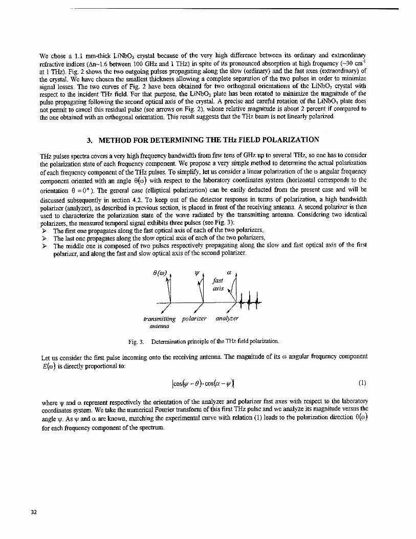
We chose a 1.1 mm-thick LiNb03 crystal because of the very high difference between its ordinary and extraordinary refractive indices (An~1.6 between 100 GHz and 1 THz) in spite of its pronounced absorption at high frequency (-30 cm"1
at 1 THz). Fig. 2 shows the two outgoing pulses propagating along the slow (ordinary) and the fast axes (extraordinary) of the crystal. We have chosen the smallest thickness allowing a complete separation of the two pulses in order to minimize signal losses. The two curves of Fig. 2 have been obtained for two orthogonal orientations of the LiNb03 crystal with respect to the incident THz field. For that purpose, the LiNb03 plate has been rotated to minimize the magnitude of the pulse propagating following the second optical axis of the crystal. A precise and careful rotation of the LiNb03 plate does not permit to cancel this residual pulse (see arrows on Fig. 2), whose relative magnitude is about 2 percent if compared to the one obtained with an orthogonal orientation. This result suggests that the THz beam is not linearly polarized.
3. METHOD FOR DETERMINING THE THz FIELD POLARIZATION
THz pulses spectra covers a very high frequency bandwidth from few tens of GHz up to several THz, so one has to consider the polarization state of each frequency component. We propose a very simple method to determine the actual polarization of each frequency component of the THz pulses. To simplify, let us consider a linear polarization of the a angular frequency component oriented with an angle 9(co) with respect to the laboratory coordinates system (horizontal corresponds to the
orientation 8 =0°). The general case (elliptical polarization) can be easily deducted from the present case and will be
discussed subsequently in section 4.2. To keep out of the detector response in terms of polarization, a high bandwidth polarizer (analyzer), as described in previous section, is placed in front of the receiving antenna. A second polarizer is then used to characterize the polarization state of the wave radiated by the transmitting antenna. Considering two identical polarizers, the measured temporal signal exhibits three pulses (see Fig. 3): > The first one propagates along the fast optical axis of each of the two polarizers, > The last one propagates along the slow optical axis of each of the two polarizers, > The middle one is composed of two pulses respectively propagating along the slow and fast optical axis of the first
polarizer, and along the fast and slow optical axis of the second polarizer.
6 (to)
7 7 transmitting polarizer analyzer
antenna
Fig. 3. Determination principle of the THz field polarization.
Let us consider the first pulse incoming onto the receiving antenna. The magnitude of its a> angular frequency component E(G>) is directly proportional to:
|cos(y-0)-cos(a-^)| (1)
where y and a represent respectively the orientation of the analyzer and polarizer fast axes with respect to the laboratory coordinates system. We take the numerical Fourier transform of this first THz pulse and we analyze its magnitude versus the angle v|/. As vy and a are known, matching the experimental curve with relation (1) leads to the polarization direction 0(ro)
for each frequency component of the spectrum.
32

4. EVIDENCE OF FREQUENCY DEPENDENT THz FIELD POLARIZATION
4.1. Experimental setup6'
The experimental setup is depicted in Fig. 4. The transmitting and receiving antennae are identical; they are composed of a LT-GaAs micron-sized photoswitch7 (gap size: 6 x 40 urn2) imbedded in a coplanar transmission line. The antennae are optoelectronically driven by 120 fs pulses (~7 mW average optical power on each photoswitch) from a self mode-locked Ti:Sa laser. An extended 10 mm-radius hemispherical high resistivity silicon lens is used to collimate the THz beam.
¥
transmitting antenna
1 receiving antenna
A
polarizer analyzer
Fig. 4. Experimental setup.
Two identical 1.1 mm-thick LiNb03 crystals are positioned in the THz beam and used as temporal polarization separators. The two LiNb03 crystals are mounted on rotation stages with 1 degree orientation accuracy.
4.2. Determination of the THz field polarization for a given frequency
We measure the first THz pulse transmitted through the two LiNb03 samples (polarizer and analyzer) for different orientations of the polarizer OF = 0 -» 190°) and for two orientations of the analyzer (a = 0° and 45°). The spectral component of the THz field magnitude at 344 GHz is represented on Fig. 5 (in dots) as well as two theoretical fits (continuous lines) calculated with relation (1).
i i i i i i i i i
f=344GHz I-
Fig. 5. THz pulse magnitude (at 344 GHz) versus analyzer orientation for two different polarizer orientations (dots represent the experimental measurements and the continuous line the theoretical model).
Let us notice that the two fits are established using only three adjustable parameters: one scaling factor for each value of a, and the polarization direction 6. Theory exactly match experimental results, and leads to the actual polarization orientation
33

6 = 77.9 ± 0.8 ° at the frequency f = 344 GHz. The criterion used to evaluate the uncertainty on 6 is twice the mean of the square difference between the magnitude of theoretical and experimental values.
In the case of an emitted wave with an elliptical polarization, the minimum of the THz field magnitude curve (see Fig. 5) is not null. The more the polarization tends towards a circular polarization, the more the relative value of this minimum increases. From our experimental results, the evaluated eccentricity e of the polarization state is greater than 0.995 (e = 0 corresponds to a circular polarization while e = 1 corresponds to a linear polarization). We have obtained similar minimum eccentricity values for all the other frequency components. Therefore, this THz beam may not be perfectly linearly polarized (e > 0.995), but its eccentricity remains sufficiently large to consider that the hypothesis of a linear polarization still holds.
4.3. Variation of the polarization orientation versus frequency
From the method presented above, we extract the polarization orientation of the THz field for every frequency of the THz pulse spectrum. Fig. 6 shows that the polarization orientation of the THz field varies with frequency over more than 10 degrees. This variation cannot be attributed to experimental uncertainties. This phenomenon could be attributed to the asymmetry of the experimental setup. Actually, a transmitting antenna, with a perfect axial symmetry, radiates a linearly polarized beam. Any asymmetry of the setup could be due to a misalignment of the different elements of the transmitting antenna (laser spot + photoswitch + lens).
0 200 400 600 800 1000
frequency (GHz)
Fig. 6. Polarization orientation of the THz wave versus frequency in the laboratory coordinates system.
5. LENS POSITIONING INFLUENCE ON THE POLARIZATION DIRECTION
We have studied the relative influences of the different parameters which are involved in the transmitting antenna misalignment, i.e. the laser beam position onto the photoswitch and the lens position with respect to the gap position. Fig. 7 shows the polarization orientation versus frequency for three different laser spot positions on the photoswitch. The distance between the two extreme positions of the laser spot (positions 1 and 3) is shorter than 40-microns gap length. Let us notice that the laser spot diameter is about 25 um. For sake of clarity, error bars have been represented just for one of the three curves. Taking the experimental uncertainties into account, the effect of the laser spot position is very weak and cannot explain the great variation of the polarization orientation as observed in Fig. 6.
34

laser spot position
12 3 • • •
100 200 300 400 500 600 700 800 900 1000
frequency (GHz)
Fig. 7. Influence of the laser spot position on the polarization orientation.
Let us consider the influence of the lens position. The variation of the polarization orientation versus frequency has been studied for four positions of the lens situated at the corners of a 350 um x 350 um square (see Fig. 8). One can notice that the relative displacement of the lens, as compared to its diameter, is only of about 2 %. Even with such a small misalignment, the influence on the polarization orientation is noticeable. For example, for frequencies between 600 and 700 GHz, the polarization orientation for two different lens positions (1 and 2), separated by 350 urn, varies over 40 degrees! Moreover, the frequency behavior of the polarization orientation highly depends on the lens position.
100 200 300 400 500 600 700 800 900 1000
frequency (GHz)
Fig. 8. Lens position influence on the polarization orientation.
The spectra associated to the THz pulses, recorded for the four lens positions, are represented in Fig. 9. For clarity, the four spectra have been artificially shifted. Let us notice that the rapid variation of the polarization orientation with frequency (for positions 3 and 4) is correlated with punctual depressions (see arrows on Fig. 9) in the associated spectra. This correlation suggests that interference effects could be at the origin of the observed phenomena. However, a nice shape spectrum (smooth with low decrease versus frequency) does not guarantee a frequency independent THz field polarization (see position 1 on Fig. 8 and 9).
35

100 3
0)
c 60
4)
10
1 1
1 1
1 II
1
4,3,
2,1 11 J ' 1 ' 1 1 ' 1 ' 1 ' 1
- c/a O P. i§N 1,1:1
t 1 , I , 1 , i, i, i, i
100 200 300 400 500 600 700 800 900 1000
frequency (GHz)
Fig. 9. Lens position influence on the spectrum of the THz pulses.
6. ANISOTROPIC MATERIALS CHARACTERIZATION
In order to study the influence of the THz beam polarization on anisotropic materials characterization, we have characterized a 1.1 mm-thick LiNb03 crystal4'8 with and without using a polarizer. The optical constants of the sample, obtained without the polarizer but with a temporal windowing excluding the residual pulses (see Fig. 2), are shown on Fig. 10. We have obtained the same optical constants with the polarizer. However, because of a noticeable attenuation of the signal (absorption and Fresnel reflections) due to the polarizer, these optical constants present more noise and are extracted on a reduced frequency range (150-1050 GHz).
7.0
6.5 a Q
ä 60
u 8 5.5
.3 5.0
4.5
_l 1 1 1 1 1 1 —1 1—1—| 1 1 1 | 1 I I | I I I | III
r - n :
o
_
: -
- n - e
f\ -
"I 1 1 1 T 1 I I I 1 I I I 1 I i i 1 i i i 1 1 1 1
200 400 600 800 1000 1200 1400 frequency (GHz)
■ i i i i i
200 400 600 800 1000 1200 1400 frequency (GHz)
Fig. 10. Ordinary and extraordinary optical constants of LiNb03.
Therefore, it seems that there is no difference between the two methods in the case of optically thick samples. Let us give a look to a simple model for moderately absorbent and optically thick materials. In this case, the optical constants of the sample are given by9:
n(co) = l -(p{a>) (2) col
.iV . .> (3) a(o))= In
36

where p(w) and <p(a>) represent respectively the modulus and phase of the complex transmission coefficient of the sample of thickness /. In the two cases, the THz signal propagating with the other refractive index is cancelled, either by the polarizer or the temporal windowing. The phase (p(a>) only depends on the refractive index (ordinary or extraordinary) that has been imposed by the temporal windowing. Thus, only the modulus of the complex transmission coefficient of the sample is affected by the polarization variation of the THz beam. Consequently, any variation of the polarization orientation with frequency will only modify the value of the absorption coefficient. The induced error on the absorption coefficient is given by:
Aa(a») = -.^ö = -^-oosn(«)) (4) / p\co) I
where €l{a) is the angle between the fast axis of the sample and the electric field polarization at angular frequency co. Moreover, this error is always positive, consequently the absorption coefficient is overestimated. As shown in section 5, Q.(co) varies over a maximum 20 degrees-range. For the 1.1 mm-thick LiNb03 sample, the maximum induced error is
A« s (2//) • (l - cos Q(CJ)) = 1 cm"1 which is within the same range of magnitude as the experimental resolution. On the other hand, for lightly absorbent samples, such an error may be significant, indeed important.
For thin samples, the problem is more complex because temporal windowing is no more possible. Thus, the phase of the complex transmission coefficient is also affected by the polarization of the THz beam. In that case, the use of a polarizer is necessary.
7. CONCLUSION
We have shown that an anisotropic material acts as a time separator of polarization, and then it can be used as a very large frequency bandwidth polarizer. We have presented a simple method to determine the polarization of the THz field emitted by standard antennae (Hertzian dipole-like antenna linked to an extended hemispherical lens) used in THz time-domain spectroscopy. We have demonstrated that the THz field polarization is frequency dependent. Moreover, this dependency is mainly due to the lens positioning. For a given frequency and two lens positions separated by only 2% of the lens diameter, the THz field polarization orientation can vary over more than 40 degrees. For the same lens position, the polarization orientation may vary over a 20 degrees-frequency range. Unfortunately, there is no evident correlation between the frequency polarization dependency and the spectrum of the associated THz pulses. Therefore, anisotropic material characterization requires a great care if no polarizer is used.
REFERENCES
1. D. Grischkowsky, S. Keiding, M. van Exter and Ch. Fattinger, 'Tar-infrared time-domain spectroscopy with terahertz beams of dielectrics and semiconductors", J. Opt. Soc. Am. B 7, pp. 2006-2015,1990.
2. D. Grischkowsky and S. Keiding, "THz time-domain spectroscopy of high Tc substrates", Appl.Phys.Lett. 57, pp. 1055-1056,1990.
3. J.E. Pedersen and S.R. Keiding, "THz time-domain spectroscopy of nonpolar liquids", IEEE J. Quantum Electron. 28, pp. 2518-2522, 1992.
4. Y. Pastol, G. Arjavalingam, J.-M. Halbout and G. V. Kopcsay, "Dielectric properties of uniaxial crystals measured with optoelectronically generated microwave transient radiation", Appl. Phys. Lett. 55, pp. 2277-2779,1989.
5. A. Sentz, M. Pyee, C. Gastaud, J. Auvray and J.P. Letur, "Construction of parallel grids acting as semitransparent flat mirrors in the far infrared", Rev. Sei. Instrum. 49, pp. 926-927, 1978.
6. F. Garet, L. Duvillaret, L. Noel, J.-M. Munier, J.-L. Coutaz and P. Febvre, "Characterisation of materials in the 50 GHz - 2.5 THz range by time-domain terahertz spectroscopy", ESA Workshop on Millimetre Wave Technology and Applications, pp. 447-452, Espoo - Finland, 1998.
7. The photoswitches have been kindly supplied by J. F. Whitaker of University of Michigan. 8. E.D. Palik, Handbook of optical constants of solids, p. 702, Academic Press, New York, 1985. 9. L. Duvillaret, F. Garet and J.-L. Coutaz, "Noise analysis in THz time-domain spectroscopy and accuracy
enhancement on complex dielectric constant determination", SPIE Photonics West, paper 3617-06, San Jose, 1999.
37

Noise analysis in THz time-domain spectroscopy and accuracy enhancement on optical constants determination
Lionel Duvillaret, Frederic Garet, Jean-Louis Coutaz
Laboratory of Microwaves and Characterization (LAHC)
University of Savoy, 73376 Le Bourget-du-Lac cedex, France
ABSTRACT
THz time-domain spectroscopy is a powerful and fast technique for measuring the optical constants of materials over a wide frequency range. In this paper, we analyze the weight of the different error terms on the optical constants determination. The different sources of noise are taken into account in a phenomenological way and the noise power can be expressed as a second order polynomial function of the complex transmission coefficient modulus p of the sample under test. Then, for given experimental conditions, the accuracy on the optical constants determination depends on p. In the case of optically thick samples, the echoes of the THz pulse, caused by multiple reflections into the sample, are temporally well separated and can be time-windowed. For each echo, p can be measured and it depends on the echo number. We demonstrate that the precision on the optical constants is greatly enhanced using the p1*1 echo, the value ofp depending on the material refractive index and absorption. Moreover, as the coefficients of the polynomial function can be easily experimentally evaluated, quantitative information on the sources of noise is deduced.
Keywords: THz spectroscopy, noise, optical constants
1. INTRODUCTION
Terahertz time-domain spectroscopy (THz-TDS) is now studied for most than ten years1. It has proved to be a powerful technique for characterizing the optical constants of materials in the GHz-THz frequency range. Numerous materials have been studied: semiconductors and dielectrics2, superconductors3, liquids4, anisotropic crystals5, organic materials6, thin films7, etc. Its main advantages over classical far-infrared methods8 are the very large frequency bandwidth and the rapidity of the measurements, which originates in the ultimate sensitivity of the coherent detection9. In addition, the measurements are performed in the time-domain, allowing time-resolved experiments1011.
We are interested in the precision of the optical constants extracted from THz-TDS measurements. This precision is limited by systematic and random errors.
Systematic errors originate in the lack of knowledge of the sample geometry (thickness, parallelism and homogeneity), parasitic reflections of the THz beam and in the validity of the extraction procedure. Usually, a precision of 1 % or even better can be achieved on the knowledge of the sample thickness. This gives a similar precision on the index of refraction. Moreover, we have proposed12 a new method for an accurate determination of the sample thickness from THz time-domain experimental data, leading to an improved determination of the optical constants. We have shown that the thickness inaccuracy leads to the main systematic error on the determination of the optical constants, and that it could be lowered down to a few tenths of percent.
In this paper, we are looking at the influence of random errors, i.e. the influence of noise. We will use a phenomenological analysis, in which the noise is deduced from a large set of measurements. We will not look at the physical origin of the noise, as already studied by van Exter and Grischkowsky9. Nevertheless, our approach leads to a better knowledge of the different sources of noise in the THz-TDS experiments. For materials with a low absorption, we propose to determine the optical constants from the different temporal echoes observed in the recorded signal. This method allows us to check the validity of our formalism, but also to reduce the incertitude due to the noise.
Part of the SPIE Conference on Terahertz Spectroscopy and Applications 38 San Jose. California » January 1999 SPIE Vol. 3617 • 0277-786X/99/$10.00

2. PRINCIPLE OF THE THz TIME-DOMAIN SPECTROSCOPY
In general, the determination of optical constants in THz-TDS follows the typical procedure: > A short laser pulse is transformed into an electrical pulse through different techniques, such as photoswitching using
semiconductor or superconductor13 circuits, optical rectification14 and surface generation at semiconductor surfaces15. An antenna radiates the electrical pulse in the free space. The frequency width of its spectrum is inversely proportional to its time duration.
> The THz radiation is focused onto a detector and its temporal shape is sampled with a delayed part of the laser pulse. The signal, in either photoconductive or electro-optic samplings, is proportional to the field of the THz radiation (and not to its intensity).
> A numerical Fourier transform allows us to derive the frequency spectrum of the signal. By putting a sample in between the antennae, one is able to determine its complex transmission coefficient in the frequency domain. The resolution of an inverse electromagnetic problem leads to the knowledge of both the refractive index and the absorption of the sample material.
3. THEORY
Let us examine the mathematical basis of the extraction procedure. We consider a sample of material, which is a homogeneous slide of thickness /, with two flat and parallel faces. We suppose that the THz beam is a plane wave at the sample location impinging at normal incidence.
3.1. Theoretical expression of the complex transmission coefficient and the optical constants
Let us write the spectral component £,(co) at angular frequency co of the electrical field of the THz beam transmitted through the sample7:
£,(»)=£;(ö))^)P(^/)S[K»)P2(»./)]P CD p=0
where £",(00) is the incident field and n=n-jK is the complex refractive index of the material. /*(©)
FP{<a)
«(co) - 1 . -•. 1 and
«(coj + l,
/(co)= . are respectively the reflection and transmission coefficients (taking into account both faces of the (ff(a>) + l)
sample), £>(co,/) = exp -7/1(00)— is the coefficient of propagation in the sample. In relation (1), the backward and
forward reflections in the sample (Fabry-Perot effect) are represented by the summation FP((o).
In the time-domain, the corresponding quantities are given by the inverse Fourier transform of relation (1). One gets:
E, (t) = E, (t) ®t(t)® p(t, /) ® ]T r(co)®-®r(co) ® p(t,l)® — ®p(t,l) (2) P=0 p times 2p times
where the convolution product is represented by ®, and any function f(t) is the inverse Fourier transform of /(co). Each term of the summation in relation (2) corresponds to a temporal echo of the directly transmitted signal (p = 0).
If the temporal echoes are enough separated to allow time-windowing, i.e. if the recorded signal drops to zero between two successive echoes, the extraction of material parameters can be done from a single echo p.
39

Therefore, it is possible to use a simplified form of relation (2):
£,(/) = £,(f)®r(r)®r(f)®---®r(f)®p(f,/)<8>---®p(r,/) (3) p times 2p+\ times
2p
which, in the frequency domain, leads to:
exp\-j(2p + l)n(a)
from which we derive the complex transmission coefficient 7,(00) of the sample for the echop:
T ( \- •£/(©) with sample _4n((ü)(n((£>)-l)2p
Its modulus pp{®) and its argument cpp(co) are:
(«(co) + l)2 {n{(0) + lj
£,(»)withoutsamPle- £(«0 + 1)*" exp[-y [(2/, + l)«(co)-1]^
(4)
(5)
P» = T, 5 2V' exp -(2;7 + l)K — [(«+l)2+K2f V c;
cp (CD)=-[(2/7 + 1)7-1] 2p arctari — 5 | - arctan c \n +K -1 V«(M + 1)+K
2
For low to moderate absorbing materials, K « n . Therefore, we obtain the following simplified expressions:
, v 4n{n-l)2p ( PpW- l...A^ 6XP
(6)
(7)
(„+l)
<?p(®) = -l2p + \)n-\]
-\p+-\al
ml
(8)
(9)
2co where a(co)= K(CO) is the energy absorption coefficient. The refractive index and the absorption of the material are
c derived from these relations (8) and (9):
1—:<P,(o>) v ' 2p + \
((n + l)2p+2
a(w)=-j pr- • In V ' (p+ 1/2)1 4r,(n-irP>{W\
(10)
(11)
3.2. Precision on the extracted optical constants (refractive index and absorption coefficient)
The complex refractive index of the sample is determined, from the experimental data pp(co) and q>p((£>), using relations
(10) and (11). Here, we are interested in the uncertainties arising from noise, i.e. from random phenomena. The errors An and Aoc are deduced by differentiating (10) and (11) versus pp (00) and cp (co):
A"(ro)s(277IRAcPp((D) (12)
40

Aa(a>) = (p+ 1/2)1
n-\ 4p n(n + l) n1 -1
An(w) + Pp(<»)
(13)
The errors App(©) and Acp?(©) are obtained from the experimental complex transmission coefficient rexp(ca) and its
noise. Let us write T^v (©) as the summation of its average value and noise:
7T(m) = r>) + r>) = p>)exp(y^ (14)
where, as previously, pp(ea) and cpp(©) represent respectively the modulus and phase of ^(co), and the superscript N
indicates noise. Considering a noise level much lower than the signal, we can easily derive from (14) the modulus p^ü
and the phase q>;xp (co) of T^ (©):
tan
Pr(»)sp>)+P>)-cos(9>)-(p>))
( exp / \\ P» • sin(<P,(">))+ P? (°>)■ SJB(<P? (©)) W' %>)-cos(cp>))+p>).cos(cp>))
(15)
(16)
The noise contribution appears mostly in the modulus of the temporal signal, because the relative uncertainty on the phase is negligible (usually, it is proportional to the spatial step of the optical delay line). Therefore, from (15) and (16), we deduce the standard deviation of both modulus and phase of rexp (co):
CTPJ,(«»),BAP,((D)S S
° „,„ (a>)=Aq>„ (©) = ( arctan2 sin^ (©)-©*(©))
. PP (»)/P" («>) + cos(cpp (©)- <p£ (©))J / V2p (©) p» ,=,_J> P» App(©)
(17)
(18)
where (%) denotes the statistical mean value of %. The term Ap/,(©) is the experimental uncertainty which is easily
obtained by calculating the standard deviation of a set of several experimental data p/"(©). Using relations (12) and (13), we get:
An(©)s c Apf,(cp)
(2/7+1)©/' p (ffl)
A<x(©)=2 ® + (w-l)2-4/7»
w(«2-l) (2/» + l)/| •Aw(©)
(19)
(20)
As the uncertainties on the optical constants n and a depend on the echo number/?, it exists optimal values of p for which the uncertainties Aw and Aoc are minimized. Unfortunately, these optimal values should be deduced numerically because no analytical expression can be derived from (19) and (20).
3.3. Standard deviation of the complex transmission coefficient modulus
In order to determine the experimental complex transmission coefficient of the sample, two measurements are performed in the time-domain: the first without sample ("reference" signal), and the second with the sample placed in the setup ("sample"
signal). Both signals are noisy and thus we write them respectively as R(t) + RN(t) and Sp(t)+S"(t), where R(t) and
Sp(t) are the signals without noise (actually the mean value), while R™(t) and S^(t) are the noise contributions. Both
41

Signals are Fourier transformed, and the experimental complex transmission coefficient Tpslf(a) corresponds to the sample
signal divided by the reference signal:
The noise contribution is much smaller than the mean values of signals; therefore we can expand relation (21) into series:
1+ p v ' i s SAa) SAn) . . S"(a)-Rv(e>)-T (CO)
" V ; R(CD) 1 + ^!M R(a>) + M»)
where rp(m)= , . is the complex transmission coefficient without noise contribution, i.e. corresponding to the
theoretical one. Thus, 7'potp(o) exhibits a mean value term rp(©) = pp(co)exp(/(pp(cü)) and a noise term
S"(a)-R"(a)-TAa) N/ . / „, .v —- j-r — = p" (co jexpl/'cp" (cajl. The root mean square (rms) value of this noise (in modulus) is then given by:
R{a)
, , , , JaJ (ca) + c4(a)-p (co)2
apj,(a.)SAp,(a.)=^_i ^ (23)
aR (co) and as (ca) are the rms noise values (in modulus) for the reference and the sample signals respectively.
Any signal recorded in a THz-TDS experiment encounters three types of noise. The first one is the noise ac(co) of the emitting antenna, which is transmitted from the emitter to the detector (thus it is multiplied by p(ca)). The second noise
ash(a) = J2(l)e A/ corresponds to the shot noise in the detector; its square is proportional to the average recorded current
(/) (directly proportional to R(co) or Sp (ca)) and to the detection bandwidth A/ . The third contribution ad (co) gathers all the other noises that are signal-independent (Johnson noise, amplification noise, thermal noise, dark current contribution...). Thus, we can write the noise power value of any recorded signal as:
a2(co) = a2rf(co) + Ti.[A(®)or5p(co)]+a2(<B)-p2(co) (24)
with T| being the scaling factor between the square of the shot noise and the reference or sample signals. From (23) and (24), having p(co) = 1 in (24) for the reference signal, we obtain:
Ap/(co)=^-p23(co) + 5-p;,(Q) + C with B = 71/\R{o}] (25)
C = a](w)/\R(cof
Therefore, it appears that the complex refractive index can be calculated from the experimental data using relations (10) and (11); the noise-limited precision is given by (19) and (20) and it depends on App(co), which is related to the sample
transmission coefficient by (25). As, in relation (25), some parameters are unknown, Ap (co) must be obtained by taking
42

the standard deviation of several data recorded with the same sample. Moreover, fitting the experimental value with relation (25) will allow us to get more information on the different noise contributions in the THz-TDS experiment.
4. EXPERIMENTAL RESULTS
4.1. Setup and experimental procedure
Our setup has been already described elsewhere7 lä. It consists of similar transmitting and receiving antennae, made of a LT-grown GaAs photoswitch associated to a silicon extended hemispherical lens. The distance between both antennae is -20 cm. The photoswitch gap is 6 um wide. The antennae are excited by a pulsed Ti:Sa laser at X - 800 nm with 82-MHz repetition rate. The laser beam average power is 7 mW and the pulse duration is about 120 fs on the antennae. The emitting antenna is biased with a 9-V battery. The detected current is amplified and transformed into a voltage by a current-voltage converter, and then it is read using a lock-in amplifier. Most of the data presented here are recorded with a lock-in time constant of 300 ms. In order to determine the noise of the different signals, each temporal signal is recorded 12 times in similar experimental conditions. Then each signal is Fourier transformed, and the average value as well as the root mean square in the frequency domain are deduced from the 12 records.
4.2. Experimental results: uncertainties on the optical constants
We used a 480 um-thick wafer of n-type doped silicon (resistivity ~ 30 Q.cm) in order to check the validity of the expressions obtained above. Fig. 1 shows a typical temporal signal transmitted by the sample together with the reference signal (recorded without the sample). The transmitted signal exhibits five pulses : the first one (echo 0) corresponds to the directly transmitted pulse, while the other ones (echoes 1 to 4) have encountered back and forth reflections in the wafer. Let us notice that the signal drops to zero between two consecutive pulses. Therefore, we can time-window the recorded data and extract the silicon parameters from each time-windowed signal, as explained above.
20 30 40 time(ps)
50 60
Fig. 1. Temporal curves recorded without (reference) and with a 480 um-thick silicon wafer.
The modulus pp of the complex transmission coefficient, calculated from the temporal curves of Fig. 1, is plotted on Fig. 2
versus frequency for p = 0 up to 4, together with its standard deviation derived from 12 records. We have only drawn the data for which the modulus pp is much greater than its standard deviation. The useful frequency bandwidth decreases
strongly with the echo number p because the signal to noise ratio (SNR) decreases as well. We observe that, for a given frequency, the ratio App/pp increases with p.
43

0.1
0.01 =-
0.001
echo 4
■ I i i t i l i t i i l i > ■ i i i i i i
250 500 750 1000 1250 frequency (GHz)
1500
Fig. 2. Modulus of the transmission coefficient versus frequency of a 480 um-thick silicon wafer for the different echoes (the standard deviation is represented by the gray area).
To check the validity of relations (19) and (20) we have plotted on Fig. 3 the standard deviation of the optical constants of silicon obtained from 12 measurements together with the uncertainties calculated using relations (19) and (20). For sake of clarity, only the data for the echoes 0 and 2 are represented. A good agreement between theory and experience is observed. Similar results are obtained for the other values of p.
0.04
0.03
< 0.02
0.01
0
I I I I I I I I I I I I I I I I I I I I I I I I I
• echo 0 - exp echo 0 - calc _
0 200 400 600 800 1000 1200 1400
frequency (GHz)
0 200 400 600 800 1000 1200 1400
frequency (GHz)
Fig. 3. Uncertainties on the optical constants of silicon. The curves are calculated with relations (19) and (20) using App (co) extracted from Fig. 2, while the dots correspond to the standard deviation of 12 measurements.
The uncertainties only due to random errors (noise) are very low. In the 100-1500 GHz frequency range, the uncertainty on the refractive index is lower than 1 %. Moreover one observes that the uncertainty is much smaller for echo 2 than for echo 0. For echo 2, the relative uncertainty on the refractive index is better than 1 %o in the 200-800 GHz frequency range! The dependency of the uncertainty with the echo number will be discussed at the end of the paper.
4.3. Experimental results: study of noise
From relation (25), we will now determine the relative weights of the different noise contributions for our THz-TDS experiment. From the experimental curves shown in Fig. 2, we can plot App versus pp for each frequency. For example,
Fig. 4 shows these experimental data for f = 250 GHz. The fit of these data using relation (25) leads to the values of the
44

noise parameters^, B and C. A is very well defined because it is extracted from the asymptote for the high values of p C
is derived from the asymptote for low pp values, and therefore its determination is less precise. Finally, the worst known value is B, as it modifies only the bend of the theoretical curve.
CL <
0.01
0.001 -
0.0001
I I I I I I I I I 1 I I I Ml 1 1—I I I II I
Fig. 4. App versus p p : experimental data (dots) and the fit (solid curve) together with its two asymptotes (straight lines) for f = 250 GHz.
Such a procedure has been repeated for all the frequencies from 100 GHz up to 550 GHz. Thus we obtained the dispersion of the values of A, B and C, which is plotted on Fig. 5. As mentioned above, A is known with a very good precision, while we are only able to determine the order of magnitude of B. A is respectively two and four orders of magnitude larger than B
and C. Therefore, as A = B + C + 2a* (CO)/|ä(CO)(2 , we deduce that the emitter noise ae (©) is dominating all the other noise
contributions. For the frequency range 100-550 GHz, A is almost constant and equal to about 10"3 from which we obtain the relative emitter noise ae (CO)/|ä(CO)| = 2.24 ± 0.07 %. This implies that the emitter noise is directly proportional to the THz
pulse magnitude. Moreover, this relative noise of 2 % is comparable to the relative long-term intensity noise of our Ti:Sa laser: indeed, the reference and the sample signals are recorded within a delay of several minutes. Therefore, the major noise contribution in this THz-TDS experiment can be attributed to the laser noise.
a 10% .g
CO Cfl 'S M A
a §. 10"4
o g •a o .S a 5 w 2 -S3 e, £8 io-6
»a o
:.*\
10°, B
'~' '.
200 300 400
frequency (GHz)
500
Fig. 5. Dependency of the noise parameters with the frequency. The solid line is proportional to y \R2 (O 1: it has been shifted downwards to bring to the fore the general frequency behavior of C.
45

The general shape of C versus frequency looks like the curve l/\R2 (CD) which is drawn as a solid line on Fig. 5. Therefore
the detector noise <3d(a>), which is given by arf(m)=-Jc R(a), is a white noise over the 100-550 GHz frequency range.
The detector noise, equal to ae (G>)^2C/A , reaches only a few percent of the emitter noise ae (co).
4.4. Experimental results: accuracy enhancement on the optical constants determination
As we know the noise parameters .4, B and C for our experimental setup, we are able to calculate Ap^ and pp versus n and
a for any value of p. Thus, we can determine the optimal value of p which minimizes the uncertainties An and Aa. For this purpose, we compute the zero of the respective derivatives of An and Aa (relations (19) and (20)) with respect to p. Fig. 6 represents the optimal value of p versus n and a/ where / is the sample thickness. We have also numerically calculate the relative gain on uncertainties when the optimal echo is considered instead of the directly transmitted THz pulse.
gain =2
Fig. 6. Optimal echo number p versus n and a/ and gain on uncertainties taking into account the optimal echo instead of echo 0.
The integer values ofp correspond to an actual THz pulse echo: they are represented by contour lines. The p=0 contour line merges in the n = 1 straight line. For weak absorption materials (small values of a/), using a high p number echo improves the data extraction if n is large. On the contrary, strongly absorbing materials are obviously better studied using the directly transmitted THz pulse (p - 0). For silicon, « = 3.4 in the sub-millimeter wavelength range and the optimal p number lies between 2 and 3 for rather high resistivity (low absorption) samples, as experimentally reported in paragraph 4.2. In this case, the inaccuracy is reduced by a factor 4.
We experimentally find again these results on Fig. 7. The uncertainties on refractive index and absorption, both calculated from relations (19) and (20) and evaluated from the standard deviation of 12 measurements, are represented versus the echo number/; and for the frequency f = 400 GHz. Indeed, we notice that the optimal echo number lies between 2 and 3 and leads to a ~ 4 times less inaccuracy on the optical constants as previously predicted. On the other hand, there is a very good agreement between the experimental data and the theoretical model. A similar agreement is obtained for other frequencies. For the calculation of the theoretical curves of Fig. 6 and 7 we have respectively taken the values 10"3, 10'5 and 10"7 for the noise parameters A, B and C.
46

810"' -
610"" -
< 410
210° -
e o
3
010
Fig. 7. Uncertainties on the optical constants (for f = 400 GHz) of a 480 um-thick silicon wafer versus the echo number. The curves are calculated with relations (19), (20) and (25) while the dots correspond to the standard deviation of 12 measurements.
5. CONCLUSION
Our study of noise and uncertainty in THz time-domain spectroscopy leads to two main results : > The noise in this experiment originates mainly from the emitter. It is proportional to the THz signal and it remains
limited to a few percents of the signal magnitude. The detector noise is a white noise and it corresponds to only a few percent of the emitter noise for the reference signal. The uncertainty on the optical constants can be well reduced when the data are extracted from the optimal echo. In many cases, the optimal echo is not the directly transmitted THz pulse, as frequently used in THz-TDS experiment. For highly resistive silicon, the uncertainty on n, due to noise, has been lowered down to 1 %o. At this level, systematic errors (sample thickness, plane wave approximation, THz pulse parasitic reflections, ...) become the main source of inaccuracy.
>
REFERENCES
2.
3.
5.
6.
8. 9.
10.
P. R. Smith, D. H. Auston and M. C. Nuss, "Subpicosecond photoconducting dipole antennas", IEEE J. Quantum Electron. 24, pp. 255-260, 1988. Ch. Fattinger and D. Grischkowsky, "Point source terahertz optics", Appl. Phys. Lett. 53, pp. 1480-1482,1988. D. Grischkowsky, S. Keiding, M. van Exter and Ch. Fattinger, "Far-infrared time-domain spectroscopy with terahertz beams of dielectrics and semiconductors", J. Opt. Soc. Am. B 7, pp. 2006-2015, 1990. J. F. Whitaker, F. Gao and Y. Liu, "Terahertz-bandwidth pulses for coherent time-domain spectroscopy" SPIE 2145 pp. 168-177,1994. J. E. Pedersen and S. Keiding, "THz time-domain spectrosocpy of nonpolar liquids", IEEEJ. Quantum Electron 28 pp. 2518-2522, 1992. Y. Pastol, G. Arjavalingam, J.-M. Halbout and G. V. Kopcsay, "Dielectric properties of uniaxial crystals measured with optoelectronically generated microwave transient radiation", Appl. Phys. Lett. 55, pp. 2277-2279,1989. Y. Pastol, G. Arjavalingam, J.-M. Halbout and G. V. Kopcsay, "Absorption and dispersion of low-loss dielectrics measured with microwave transient radiation", Electron. Lett. 25, pp. 523-524, 1989. L. Duvillaret, F. Garet and J.-L. Coutaz, "A reliable method for extraction of material parameters in THz time- domain spectroscopy" IEEEJ. Selected Topics Quantum Electron. 2, pp. 739-746, 1996. J. Houghton and S. D. Smith, Infra-red Physics, chapter 7, Oxford University Press, London, 1966. M. van Exter and D. Grischkowsky, "Characterization of an optoelectronic terahertz beam system", IEEE Trans. Microwave Theory Tech. 38, pp. 1684-1691,1990. B. I. Greene, J. F. Federici, D. R. Dykaar, A. F. J. Levi and L. Pfeiffer, "Picosecond pump and probe spectroscopy utilizing freely propagating terahertz radiation", Opt. Lett. 16, pp. 48-51, 1991.
47

11. S. S. Prabhu, S. E. Ralph, M. R. Melloch and E. S. Harmon, "Carriers dynamics of low temperature grown GaAs observed via terahertz spectroscopy", OSA Spring Topical Meeting on Ultrafast Optoelectronics, paper UTuB5-l, Incline Village, 1996.
12. L. Duvillaret, F. Garet and J.-L. Coutaz, "Highly precise determination of both optical constants and sample thickness in terahertz time-domain spectroscopy", to appear in Appl. Opt., Jan. 1999.
13. M. Hangyo, N. Wada, M. Tonouchi, M. Tani and K. Sakai, "Ultrafast optical response and terahertz radiation from high-Tc superconductor", IEICE Trans. Electron. E80-C, pp. 1282-1289, 1997.
14. X.-C. Zhang, Y. Jin and X. F. Ma, "Coherent measurement of terahertz optical rectification from electro-optic crystal", 4Rp/. Phys. Lett. 61, pp. 2764-2767,1992.
15. X.-C. Zhang, J. T. Darrow, B. B. Hu, D. H. Auston, M. T. Schmidt, P. Tham and E. S. Yang, "Optically induced electromagnetic radiation from semiconductor surfaces", Appl. Phys. Lett. 56, pp 2228-2231,1990.
16. F. Garet, L. Duvillaret, L. Noel, J.-M. Murder, J.-L. Coutaz and P. Febvre, "Characterisation of materials in the 50 GHz - 2.5 THz range by time-domain terahertz spectroscopy", ESA Workshop on Millimetre Wave Technology and Applications, pp. 447-452, Espoo - Finland, 1998.
48

Carrier dynamics and THz radiation in biased semiconductor structures
Z. S. Piao*, M. Tani, and K. Sakai
Kansai Advanced Research Center, Communications Research Laboratory, M.P.T., Iwaoka 588-2, Nishi-ku, Kobe 651-2401, Japan
ABSTRACT
When a biased semiconductor is excited by femtosecond laser pulses, it generates terahertz radiation. The rapid change in the transport photocurrent, due to the ultrafast excitation of the carrier by laser pulses and biased electric fields, generates terahertz electromagnetic pulses. The change in the photocurrent arises from two processes: acceleration of the photogenerated carriers under an electric field, and a rapid change in carrier density. These two processes contribute to the generation of the terahertz radiation. Our calculations show that the main part of the terahertz radiation results from the ultrafast change of the carrier density. We consider the terahertz radiation from biased photoconductive antennas pumped by femtosecond laser pulses. The calculations are based on the Drude- Lorentz theory of the carrier transport in semiconductors. Our calculation model includes the interaction between electrons and holes, trapping of carriers in mid-gap states, scattering of carriers, and dynamical space-charge effects. Our calculations show that the local electric field will oscillate and induce electromagnetic radiation at high carrier generation density.
1. INTRODUCTION
Since the first observation of the terahertz (THz) radiation in photoconductive antennas excited by ultrafast laser pulses,1 considerable efforts have been made both in trying to understand the mechanisms responsible for the THz generation, and in developing applications of the radiation in THz time-domain spectroscopies.2 The generation of the THz radiation has been achieved by various techniques such as ultrafast switching of photoconductive antennas,3
rapid screening of surface fields via photoexcitation of a dense electron hole plasma in semiconductors,4 rectification of optical pulses in crystals,5 carrier tunneling in coupled double-quantum well structures,6 and coherent excitation of polar optical phonons.7 Of these different methods, photoconductive antennas have proven to be the most efficient source of the THz radiation with respect to both the intensity and spectral bandwidth of the THz field. By now, many experimental and theoretical studies have been done on THz radiation in semiconductors.4'8-12 In semiconductors, two processes are known to contribute to the emission of the THz radiation in semiconductors. The first is the instantaneous polarization that arises during optical excitation when electron-hole pairs are generated in the electric field region of semiconductors as in, for example, the depletion or surface field.18-15 The second process results from the transport of the photoexcited carrier in the electric field region.16
In this paper, we present detailed calculations of the carrier dynamics and THz radiation in biased semiconductors. When a biased semiconductor is pumped by an ultrafast laser pulse, the rapid change in transport photocurrent will give rise to THz radiation. The change in photocurrent J (J — env, where e is the charge of the carriers, v the speed of the carriers, n the carrier density), arises from two processes: the acceleration of the photogenerated carrier under the electric field, endv/dt, and the rapid change of the carrier density, evdn/dt. Therefore, the THz radiation from a biased semiconductor can be divided into two parts according to its origin: one part is due to the carrier acceleration, and another part is due to the change in the carrier density. The calculations are based on the Drude- Lorentz theory of carrier transports in semiconductors. In the calculation model, we consider the THz radiation from biased photoconductive antennas pumped by femtosecond laser pulses. The model includes interaction between electrons and holes, trapping of carriers in mid-gap states, scattering of carriers, and dynamical space-charge effects. The antenna effects are not included in the calculations. The calculation results show that the THz radiation due to the ultrafast carrier density change is more prominent than the THz radiation due to the acceleration of the carrier. This result indicates that when the density of the moving carrier changes somehow, for examples, by laser pumping,
Correspondence: E-mail: [email protected]; WWW: http://www-karc.crl.go.jp/quanele/index.htral; Telephone: +81 78 969 2145; Fax: +81 78 969 2154
Part of the SPIE Conference on Terahertz Spectroscopy and Applications San Jose, California « January 1999 SPIE Vol. 3617 • 0277-786X/99/$10.00 4g

trapping in defect levels, or recombination, the charged carrier will emit electromagnetic radiation even if there is no field and consequently no acceleration. The intensity of the THz radiation resulting from carrier density change is much larger than that of the THz radiation resulting from carrier acceleration at moderate carrier generation density. The calculation also shows that there will be oscillations of local electric fields and resultant electromagnetic radiation at high carrier generation density. A photoconductive antenna is also often used as a detector of the THz pulse. In this case, the response characteristics of the detector will considerably reshape the waveform of the THz pulse emitted by the emitter. An accurate understanding of this reshaping process is necessary for the analysis of the detected THz signal in THz time-domain spectroscopies.
This paper is organized as follows. Section 2 contains a description of the calculation model, including the basic equations for the carrier dynamics and THz radiation of electrons and holes. In Sect. 3, we discuss the THz radiation and carrier dynamics. The THz radiation due to the carrier acceleration and carrier density change, dynamical screening of the bias electric field, and a brief discussion of the THz detection by a photoconductive antenna are given in this section. A summary is given in Sect. 4.
2. MODEL OF CALCULATIONS
The model we develop is for a low-temperature-grown GaAs (LT-GaAs) photoconductor. This material has attracted much interests in ultrafast photonic applications because of its short carrier lifetime, reasonably good mobility and high breakdown field.17 The carrier lifetime can be reduced to picoseconds or even subpicoseconds in an annealed low-temperature-grown material.18 Because the free-carrier trapping time in mid-gap states is much shorter than the recombination time between the electron and hole, the lifetime of the carrier is mostly determined by the carrier trapping time. In the following calculations, we will treat the carrier trapping time as being equivalent to the free carrier lifetime, and the same carrier trapping time are assumed for the electron and hole. In addition, for the sake of simplicity, the nonlinear absorption of LT-GaAs18 is neglected. These simplifications have little influence on the conclusions of this paper.
In the calculation of the carrier transport and THz radiation in a biased semiconductor, we use a simple one- dimensional Drude-Lorentz model. When a biased semiconductor is pumped by a laser pulse with photon energies greater than the band gap of the semiconductor, electrons and holes are created in the conduction band and valence band, respectively. In LT-GaAs, the carrier pumped by ultrashort laser pulse will be trapped in the mid-gap states with a time constant of the carrier trapping time. The time dependence of the carrier density is given by the following equation:
di-7^ <» where n is the density of the carrier, G is the generation rate of the carrier by the laser pulse, and rc is the carrier trapping time. The generated carriers will be accelerated in the bias electric field. The acceleration of the electron(hole) in the electric field is given by
dve,h veth qe>h „ ,„,. ~äT =—zr + ~—■fc' W at T, me<h
where ve<h is the average velocity of the carrier, qe<h is the charge of an electron(a hole), me<h is the effective mass of the electron(hole), T, is the momentum relaxation time, and E is the local electric field. The subscripts e and h represent the electron and hole, respectively. The local electric field E is smaller than the applied bias electric field, Et, due to the screening effects of the space charges,
E = Eb-—, (3) ae
where P is the polarization induced by the spatial separation of the electron and hole, e is the dielectric constant of the substrate, and a is the geometrical factor of the photoconductive material. The geometrical factor a is equal to three for an isotropic dielectric material. It is noted that both the free carrier and trapped carrier contribute to the screening of the electric field. The time dependence of the polarization P can be written as
dP P r
50

V)
'sz =3
CO
c CD
o o o x: 0-
(a) /\ z : 30 fs
K\\ V 1 ° Ps
[\\\ 5t:80fs
f\\\\ n0:1018cm"3
\ \ \ \ E ■ 20 kV/cm
1 \ \ X. ^^^
II \ \ ^\°PS
I \ \ \l^0ps\^
1 \ \0.5 ps^\^^
\_ 0.1 ps -- ~~
—■— 1 1 "•■ -I—"—1—■—1—■—1—'—
CO
c
JQ
ca
■a
c: a)
ü o o x: Q_
CD .>
.> CD a CD E
-0.5 0.0 0.5 1.0 1.5
Time (ps) 2.0 2.5 3.0
(b)
A T,: 30 fs
f V 10 ps ff| 8t: 80 fs
no 1018cm" 3
Eb : 20 kV/cm
Te: 5.0 ps
2.0 ps 1.0 ps
"" 0.5 ps
0.1 ps
1 1 . 1 ■ , , 1 ,
-0.5 0.0 0.5 1.0
Time (ps) 1.5 2.0
Figure 1. (a) Waveforms of photocurrents and (b) their time derivatives as a function of time at trapping times TC of 0.1, 0.5, 1.0, 2.0, and 5 ps. The waveform of the THz pulse is the same as that of the time derivative of the photocurrent. The time derivative of the photocurrent is shifted on the vertical axis for clarity.
where rr is the recombination time between the electron and hole. In Eq. 4, J is the density of the current contributed by the electron and hole,
J = envh. - enve, (5)
where e is the charge of a proton. The change of the current will lead to electromagnetic radiation according to Maxwell equations. In a simple Hertzian dipole theory, the far-field of the radiation ETHZ is given by
ETHZ «■ dJ
8t ■ (ß)
To simplify the following discussions, we introduce a relative speed v between the electron and hole,
v = vh-ve. (7)
Then the electric field of the radiation can be expressed as
_ dn dv ETHzccev- + en-. (8)
The first term in the right hand side of Eq. (8) represents the electromagnetic radiation due to the carrier density change, and the second term represents the electromagnetic radiation that is proportional to the acceleration of the carrier under the electric field.
3. RESULTS AND DISCUSSIONS
In the numerical calculations, we use the effective masses for the electron and hole of me = 0.067mo and mj, = 0.37mo, respectively. The momentum relaxation time T, is taken as 30 fs for both the electron and hole. The carrier generation
51
>
111 c" o «5 CO
DC N X
x : 0.1 ps 0.5 ps
x : 30 fs S
xr: 10 ps 5t: 80 fs
j«18 -3 n0: 10 cm E • 20 kV/cm b
5x10
>
o
CO DC N X
(b)
U xs: 30 fs II "V 10 ps M St: 80 fs II * ^18 -3 IAI no: 10 cm
lli Eb: 20 kV/cm
y| l||\ xc: 5.0 ps
III 1\ 20 ps j\\ |\ 1.0 ps
j\ |V———' " 0.5 ps
7 ft ^-""—' O"1 Ps
1 /
■
' 1 1 1 1
2x1028
1 , . , , ,
-0.5 0.0 0.5 1.0 1.5 2.0
Time (ps) 2.5 3.0 -0.5 0.0 0.5 1.0
Time (ps) 1.5 2.0
Figure 2. (a) Waveforms of the THz pulse proportional to the acceleration of the carrier, ndv/dt and (b) carrier density change, vdn/dt at trapping times rc of 0.1, 0.5, 1.0, 2.0, and 5.0 ps. The magnitude of the THz radiation originating from the acceleration of the carrier is much smaller than the THz radiation due to the carrier density change. The THz radiation that is proportional to the carrier density change is shifted vertically for clarity.
rate G(t) is assumed to be a Gaussian function of time t, notxp(-t2/St2), where the pulse width St equals to the half width of the excitation laser pulse at e_1 intensity. The full wave half maximun of the laser pulse equals to 2y/ln(2)8t. no represents the carrier generation density at t = 0 ps. The present calculations use a laser pulse width St of 80 fs unless specified. In semiconductors, both electrons and holes will contribute to the THz radiation. Our calculation shows that the THz radiation is inversely proportional to the mass of the carrier. In GaAs, the effective mass of a hole is approximately 5 times the effective mass of an electron. So, the contribution of the hole to the THz radiation is expected to be much smaller than that of the electron. However, the role of the hole cannot be neglected in the calculations, because the interaction between the electron and hole plays a major role in the screening of the electric field. Furthermore, when the interaction between the electron and hole is comparable to the local electric field, an oscillation of the electric field and resultant electromagnetic radiation will appear. This phenomenon will be discussed latter in detail.
Figure 1 shows the calculation results of the time-dependent photocurrent and their derivatives with respect to the time. The carrier recombination time rT is taken as 10 ps. The other values of the carrier recombination time rr longer than 10 ps give similar results. The time-dependent photocurrents at carrier trapping times TC of 0.1, 0.5, 1.0, 2.0, and 5.0 ps are shown in Fig. 1(a). Figure 1(b) shows the time derivatives of the photocurrents shown in Fig. 1(a). The waveform of the THz radiation is the same as that of the time derivative of the transient photocurrent. In Fig. 1(b), the positive peak of the THz radiation arises from the steep rising edge of the photocurrent, and the negative peak arises from the falling edge of the photocurrent. The negative peak is always smaller than the positive peak because of the finite lifetime of the carrier. As a result, the amplitude and spectral bandwidth of the THz radiation is primarily determined by the rising edge of the photocurrent. In Fig. 1, the electromagnetic radiation is mostly limited to a time scale of 2 ~ 3 ps, and the waveform does not change significantly with the change in carrier trapping time, rc. This cannot be accounted for by assuming that the main part of the electromagnetic radiation is proportional to the acceleration of the carrier. The excited carriers will be accelerated all the time as long as the local
52

1.0 1.5 Time (ps)
3.0
c
.a
LU cf o
"1 CO
CC
(b)
nn: 101scm3
j_19 -3 10 cm
10Z0cm-3
1021cm-3
-1.0 -0.5 0.0 0.5 Time (ps)
1.0 1.5
Figure 3. (a) Local electric field and (b) THz radiation at carrier generation densities n0 of 1018, 1019, 1020, and 1021 cm-3. The carrier trapping time is 0.5 ps. The other parameters are the same as in Fig. 1. For the sake of clarity, the local electric field at carrier generation density of 1021 cm-3 is shifted 5 kV/cm lower than its original value. The THz radiation is rescaled and shifted on the vertical axis.
electric field and the carrier density do not equal to zero. So, the waveform of the electromagnetic field proportional to the acceleration of the carrier will strongly depend on the carrier trapping times as shown in Fig. 2(a). The waveform of the THz radiation proportional to the carrier acceleration should be similar to the carrier decay curve. This fact contradicts to the reported experimental results,19 and is also far from the waveform of the THz radiation shown in Fig. 1(b). Figure 2(b) shows the waveform of the THz radiation proportional to the carrier density change, vdn/dt. In fact, the amplitude of the THz radiation originating from the carrier density change is much larger than that of the THz radiation that is proportional to the acceleration of the carrier. The time scale of the THz radiation originating from the carrier density change does not change much as the carrier trapping time increases. In contrast to the primary positive peak of the THz radiation proportional to the carrier density change, there is only one weak negative peak for the THz radiation proportional to the acceleration of the carrier shown in Fig. 2(b). Rodriguez et al.11 calculated the THz radiation in biased GaAs photoconductors by considering transient velocity effects. Their calculation results are similar to our calculation results for the THz radiation proportional to the carrier acceleration shown in Fig. 2(a).
Next, we will discuss the dynamical screening of the electric field by excited electrons and holes. Figure 3 shows the local electric field and THz radiation at carrier generation densities n0 of 1018, 1019, 1020, and 1021 cm-3. The calculation results show that the electric field is screened in less than 1 ps, as shown in Fig. 3(a). The screening of the electric field is contributed by free carriers as well as trapped carriers. The electric field recovers after the recombination of the electron and hole. For the recombination time is much longer than the time scale of the THz pulse, the recovery process has little effects on the carrier dynamics and THz radiation. Figure 3(a) also shows that at relatively high carrier generation density, the local electric field will oscillate. This effect can be explained by the attraction between the electron and hole and the screening of the electric field. The electron and the hole will be initially accelerated in opposite directions in the local electric field because of their opposite charges. This will induce a polarization, which will act as a restoring force for the motions of the electron and hole. As a result, when
53

.a
X I-
UU
s£ o Ü X3 CO
DC N X
1
. (a) \ xs: 30 fs
1 x0: 0.5 ps 1 xr: 10 ps
, 1 n0:1018cm'3
I \ E • 20 kV/cm
1 1 5t:150fs
l 80 fs
i | 30 fs
1 1 1 1 ' 1— -' 1
(b) xs: 30 fs
\5t:150fs xc: 0.5 ps xr: 10 ps
"ST 'E 13
ry 1018cm"3
E• 20 kV/cm b
Si
3- 03 T3 =5
Q. E < l- U- u.
I \80fs
■ -^
\30fs
■~" I ■ 1— -0.5 0.0 0.5 1.0
Time (ps) 1.5 2.0 5 10 15
Frequency (THz) 20
Figure 4. (a) Waveforms of the THz radiation and (b) the corresponding Fourier transformed spectra at pulse widths of the pumping laser St of 30, 80, and 150 fs. The carrier trapping time for emitter is 0.5 ps, and the carrier generation density is 1018 cm""3. The other parameters are the same as in Fig. 1. The THz radiation in (a) is shifted on the vertical axis for clarity.
the carrier density is high enough, the electric field may be screened to a comparable magnitude of the restoring force between the electron and hole. In this case, the electron and hole will form an oscillator, and the oscillation of the electron and hole will induce an oscillating electric field, as shown in Fig. 3(a) at carrier generation density of 1021 cm-3. Figure 3(b) shows the waveforms of the THz pulse at various carrier generation densities n0 of 1018, 1019, 1020, and 1021 cm-3. As the carrier generation density increases, the amplitude of the THz pulse increases and tends to oscillate. The condition of the oscillation of the electric field and related THz pulse is also affected by other parameters, e.g., carrier trapping time and momentum relaxation time. A detailed discussion will be given in a future paper.
Figure 4 shows the waveforms of the THz pulse for laser pulse widths St of 30, 80, and 150 fs. Fgure 4(a) shows that the THz pulse widens as the excitation laser pulse width increases. The spectral bandwidth of the THz radiation also changes considerably as the width of the laser pulse changes. The change of the momentum relaxation time r, also influences on the THz radiation. The amplitude of the THz radiation increases as the momentum relaxation time increases. This result can be understood as follows: The saturation velocity of the carrier increases as the momentum relaxation time increases. The increase of the velocity of the carrier will increase the THz radiation that is proportional to the change of the carrier density, vdn/dt.
Finally, we will compare the detected THz signal by a photoconductive antenna with the waveform of the THz radiation emitted from another photoconductive antenna. Here, we consider a photoconductive antenna with a gap width of 5 fim, and a total electrode length of 40 \im. The width of the electrode is 5/tm. The THz beam is assumed to be a Gaussian function in the lateral direction of the THz beam. We also assume that all of the wavelength components of the THz beam are focused on the antenna in their diffraction limits, respectively. The detector cannot accept equal fraction of all of the wavelength components of the THz radiation. The short-wavelength components are more tightly focused on the antenna and are more accepted by the antenna than the long-wavelength part of the
54

X3 CO
(a)
THz pulse from emitter
Detected THz signal detector substrate x: 0.1 ps
1.0 1.5 Time (ps)
2.5 3.0
Frequency (THz)
Figure 5. (a) Waveforms of the THz radiation from an emitter and the THz signal detected by another photocon- ductive antenna for carrier trapping times TC of 0.1, 0.5, and 1.0 ps. The carrier trapping time for the emitter is 0.5 ps, and the carrier generation density is 1018 cm-3. The other parameters for the emitter and detector are the same as in Fig. 1. (b) Fourier transformed spectra of the THz pulse and THz signal shown in (a). The THz radiation and its FFT amplitude are rescaled and shifted on the vertical axis.
THz radiation. Since the THz pulse from a photoconductive antenna covers a range of frequency from zero to several THz, an antenna with a finite active region is not able to accept all parts of the radiation. As a result, the detector of a photoconductive antenna acts as a filter, which tends to sense more radiation in the short-wavelength side. When a photoconductive antenna is used as a detector, the electric field of the THz radiation will act as a dynamic bias field that drives the photocurrent in the detector, which is pumped by time-delayed laser pulses in order to create photocarriers. The photocurrent Jd from the detector, which refer to as a THz signal, can be written as20
/.' Jd(r) oc / Ed(t)n(t - r)dt, (9)
where Ed(t) is the electric field entering to the antenna gap of the detector, and n(t) is the carrier density, which is obtained by solving Eq. (1). Figure 5 shows the THz radiation and respective Fourier transformed spectra from the emitter and the photocurrent from the detector for various carrier trapping times of the detector. The filtering effect of the detector and the finite lifetime of the photocarrier cause the THz signal to be considerably distorted from the waveform of the THz radiation of the emitter, as shown in Fig. 5(a). Figure 5(b) shows that the Fourier transformed spectra of the THz signal also deviate from the original spectra of the THz radiation. These deviations of the THz waveform should be taken into account in THz time-domain spectroscopies.
4. SUMMARY
With the classical Drude-Lorentz theory, we calculated the carrier dynamics and THz radiation in biased semicon- ductors. The calculation results show that the THz radiation is mostly due to the fast change of the carrier density. The contribution of the carrier acceleration to the THz radiation is smaller than the contribution of the carrier
55

density change. The electric field is screened by photogenerated carriers in the subpicosecond time scale. At high carrier generation densities, the local electric field may oscillate and emit THz radiation. In experiments, when a photoconductive antenna is used as a detector of the THz radiation, the waveform of the detected THz signal may be considerably distorted by the detector.
REFERENCES
1. D. H. Auston, K. P. Cheung, and P. R. Smith, "Picosecond photoconducting Hertzian dipoles," Appl. Phys.
Lett. 45, pp. 284-286, 1984. 2. M. C. Nuss and J. Orenstein, "Terahertz time-domain spectroscopy," in Millimeter and Submillimeter Wave
Spectroscopy of Solids, G. Grüner, ed., pp. 7-50, Springer-Verlag Berlin Heidelberg, 1998. 3. D. Grischkowsky, S. Keiding, M. van Exter, and C. Fattinger, "Far-infrared time-domain spectroscopy with
terahertz beams of dielectrics and semiconductors," J. Opt. Soc. Am. 7, pp. 2006-2015, 1990.
4. X.-C. Zhang and D. H. Auston, "Optoelectronic measurement of semiconductor surfaces and interfaces with
femtoseond optics," J. Appl. Phys. 71, pp. 326-338, 1992. 5. B. B. Hu, X.-C. Zhang, D. H. Auston, and P. R. Smith, "Free-space radiation from electro-optic crystals," Appl.
Phys. Lett. 56, pp. 506-508, 1990. 6. H. G. Roskos, M. C. Nuss, J. Shah, K. Leo, D. A. B. Miller, A. M. Fox, S. Schmitt-Rink, and K. Köhler,
"Coherent submillimeter-wave emission from charge oscillations in a double-well potential," Phys. Rev. Lett. 68,
pp. 2216-2219, 1994. 7. M. Tani, R. Fukasawa, H. Abe, S. Matsuura, K. Sakai, and S. Nakashima, "Terahertz radiation from coherent
phonons excited in semiconductors," J. Appl. Phys. 83, pp. 2473-2477, 1998. 8. X.-C. Zhang and D. H. Auston, "Optically induced THz electromagnetic radiation from planar photoconducting
structures," J. Electron. Wave Appl. 6, pp. 85-106, 1992. 9. D. R. Grischkowsky, "An ultrafast optoelectronic THz beam system," Opt. Photonics News May 1992, pp. 21-
28, 1992. 10. W. Sha, J. K. Rhee, T. B. Norris, and W. J. Schaff, "Transient carrier and field dynamics in quantum-well
parallel transport: From the ballistic to the quasi-equilibrium regime," IEEE J. Quantum Electron. QE-28, pp. 2445-2455, 1992.
11. G. Rodriguez, S. R. Caceres, and A. J. Taylor, "Modeling of terahertz radiation from biased photoconductors: transient velocity effects," Opt. Lett. 19, pp. 1994-1996, 1994.
12. P. U. Jepsen, R. H. Jacobsen, and S. R. Keiding, "Generation and detection of terahertz pulses from biased semiconductor antennas," J. Opt. Soc. Am. B 13, pp. 2424-2436, 1996.
13. E. Yablonovitch, J. P. Heritage, D. E. Aspnes, and Y. Yafet, "Virtual photoconductivity," Phys. Rev. Lett. 63, pp. 976-979, 1989.
14. B. B. Hu, X.-C. Zhang, and D. H. Auston, "Terahertz radiation induced by subband-gap femtosecond optical excitation of GaAs," Phys. Rev. Lett. 67, pp. 2709-2712, 1991.
15. A. V. Kuznetsov and C. J. Stanton, "Ultrafast optical generation of carriers in a dc electric field: Transient localization and photocurrent," Phys. Rev. B 48, pp. 10828-10845, 1993; and references therein.
16. B. B. Hu, A. S. Weling, and D. H. Auston, "dc-electric-field dependence of THz radiation induced by femtosecond optical excitation of bulk GaAs," Phys. Rev. B 49, pp. 2234-2237, 1994.
17. S. Gupta, J. F. Whitaker, and G. A. Mourou, "Ultrafast carrier dynamics in III-V semiconductors grown by molecular-beam-epitaxy at very low substrate temperature," IEEE J. Quantum Electron. 28, pp. 2464-2472, 1992; and references therein.
18. S. D. Benjamin, H. S. Loka, A. Othonos, and P. W. E. Smith, "Ultrafast dynamics of nonlinear absorption in low-temperature-grown GaAs," Appl. Phys. Lett. 68, pp. 2544-2546, 1996.
19. H. Abe, M. Tani, K. Sakai, and S. Nakashima, "Effects of the photoconductive layer property on the emission and detection of THz radiation," Reports on Topical Meeting of the Laser Society of Japan, Laser Measurement RTM-98-25, pp. 57-62, 1998.
20. M. Tani, K. Sakai, and H. Mimura, "Ultrafast photoconductive detectors based on semi-insulating GaAs and InP," Jpn. J. Appl. Phys. 36, pp. L1175-L1178, 1997.
56

SESSION 3
Direct Detectors of THz Radiation
57

Quantum well based tunable antenna-coupled intersubband Terahertz (TACIT) detectors at 1.8-2.4 THz
C. Catesa, J. B. Williams0, M. S. Sherwin0 K. D. Maranowski6 A. C. Gossard6
"Center for Terahertz Science and Technology and Physics Department, Univ. California Santa Barbara, Santa Barbara, CA, U.S.A.
^Materials Department, Univ. California Santa Barbara, Santa Barbara, CA, U.S.A.
ABSTRACT
Tunable Antenna-Coupled Intersubband Terahertz (TACIT) detectors use semiconductor quantum well heterostruc- tures to offer tunable detection of light at few-Terahertz frequencies. TACIT detectors have been predicted to have background-limited sensitivity for a 300 K blackbody background when operating in either a bolometric or non- bolometric mode. The speed of detection is expected to be 1 ns to less than 10 ps depending on the operating electron temperature and device dimensions. A planar metal antenna couples the incident Terahertz radiation from free space to the quantum well heterostructure. Electrons in the quantum well absorb the radiation, exciting them from the first to the second energy subband. The absorption frequency of the intersubband transition can be tuned by applying a voltage across the device. The quantum well heterostructure is designed so that the subbands have different electron mobilities. Absorption changes the relative number of electrons in each subband, and the effective mobility of the device changes. A current is applied to the active area of the quantum well, and the change in effec- tive mobility is detected as a change in the in-plane resistance of the device. TACIT detectors are being fabricated. Modeling and experimental progress will be discussed.
Keywords: TACIT, Terahertz detector, submillimeter wave detector, quantum well device
1. INTRODUCTION Terahertz (THz) frequencies are being used in applications ranging from deep space observation to chemical substance identification to materials characterization. Applications in the THz frequency range have historically not been as common as applications in nearby frequency ranges due to a relative lack of THz technology. Technologies for THz detectors, sources, and other enabling devices are rapidly improving. The array of THz applications will broaden as these new technologies enter the market.
In particular, there have historically not been many choices for direct detectors that are fast and sensitive and that operate between 1 and 5 THz. The potential of quantum well-based detectors in the range of 1-5 THz has not been realized. Composite bolometers and Ga:Ge photoconductors are currently the most sensitive THz detectors for low-background astrophysical applications. The response times of these devices is 1 ps at best, typically much longer. Superconducting hot-electron bolometers can have time constants of order 10 ps but are less sensitive. Both superconducting hot-electron bolometers and composite bolometers absorb radiation over a very broad band of frequencies.
We propose a tunable antenna-coupled intersubband Terahertz (TACIT) detector. Based on modeling presented in this paper and a previous paper,1 we expect it to be more sensitive than superconducting hot-electron bolometers and to have a response time variable from 1 ns to 10 ps. The TACIT detector is narrowband, absorbing Terahertz radiation only in a small band of frequencies which can be tuned by applying small DC voltages.
In the next section, semiconductor quantum well heterostructures and their energy subbands are described. The THz light is absorbed in an intersubband transition. The basic operation mechanism of the detector is explained. Section 3 presents an overview of the device structure and the fabrication processes used to make it. Tunability in operation is discussed. Then Section 4 outlines the modeling of the TACIT detector and its expected performance. TACIT detectors are predicted to have 300 K background-limited sensitivity with a time constant around 1 ns. The experiment sources for the model parameters will be discussed. TACIT detectors are currently being fabricated.
(Send correspondence to C.C.) C.C.: E-mail: [email protected] M.S.S.: E-mail: [email protected]
Part of the SPIE Conference on Terahertz Spectroscopy and Applications 58 San Jose, California » January 1999 SPIE Vol. 3617 • 0277-786X/99/$10.00

a a W I
Back gate Channel quantum quantum
well well
Substrate 85Ä V Silicon delta- doped layers
400A Surface and metal front gate
Figure 1. Schematic of one GaAs/Al0.3Ga0.7As heterostruc- ture being used for a prototype TACIT detector.
2. BACKGROUND - DETECTING MECHANISM
In the electronic structure of semiconductor materials, there is an energy gap between the valence band and the conduction band. Different materials have their valence and conduction bands at different electric potentials relative to the vacuum level. By epitaxially growing layers of different semiconductors on top of each other, heterostructures with electric potentials that vary with position along the growth direction can be created. One common such structure is a square quantum well, which is formed by sandwiching a thin layer of one material between two layers of another material with a higher conduction band edge. The electrons in the conduction band fall into the resulting potential well, and if the well is deep enough, they can get trapped in bound states of the square well. The electrons are then confined along the growth direction and form a two-dimensional electron gas. The energy of an electron in a quantum well can be broken up into two parts, the energy of the bound state in the growth direction, and the energy of unconfined motion in the two perpendicular directions.
E : Ez + kl/2m* + kl/2m*
The electrons in a bound state of the quantum well can have any momentum vector k, and so there is a subband of energy levels for each bound state.
TACIT detectors can be patterned from a variety of quantum well heterostructures. Our samples are grown in the Molecular Beam Epitaxy (MBE) facilities at UCSB. The precise control of epitaxial layer growth possible through MBE allows clean interfaces between materials to be grown, and so gives the ability to truly tailor heterostructures. One such heterostructure currently being used is shown in Fig. 1. The TACIT detector heterostructure shown in Fig. 1 has a quantum well channel for the active region, and another quantum well for a back gate. The wells are filled by electrons from the silicon delta-doping layers. The doping levels and spacings are chosen such that the channel well only has electrons in the ground subband prior to illumination. The back gate quantum well is also designed such that electrons only occupy the ground subband.
Electrons in a quantum well can absorb THz light in any polarization, but the mechanisms of absorbing light polarized perpendicular to and in the plane of the quantum well are different. Electrons are freely accelerated by oscillating electric fields in the plane of the quantum well. This process results in the heating of the electron gas in the quantum well. Electrons cannot be accelerated in the same way by oscillating electric fields perpendicular to the plane of the quantum well, for the electrons are confined in that direction. Instead, an electron can absorb a photon whose energy corresponds to the dressed energy difference between the ground and first excited subband. The electron is then said to have undergone an intersubband transition. Intersubband transitions between other pairs of subbands can also occur, subject to quantum mechanical selection rules. For a square quantum well, these transitions will occur at significantly higher frequencies since the energy difference between successive subbands increases for higher subbands. The TACIT detectors described in this paper operate by an intersubband transition from the ground subband to the first excited subband, and the other transitions can be ignored. This intersubband absorption is a resonant process and can have a narrow full-width-at-half-maximum (FWHM) linewidth, such as that shown in Fig. 2. The linewidth of a typical intersubband absorption is a few wavenumbers, or 100-200 GHz. Thus
59

0.2
/-v e 0 15 a -y O '—'
1 c e .2
0.1 u o
0.05 o U
0
-0.05 50 70 90 110
Frequency (1/cm)
Figure 2. Attenuation measured as a function of fre- quency for the heterostructure shown in Fig. 1
?"0q
-1 -0.5 0 0.5 Bias Voltage (V)
Figure 3. The frequency of peak absorp- tion can be tuned by applying a bias volt- age across the detector heterostructure.
in comparison to the tunable center frequency of order 1 THz, the detector is narrowband. The absorption is wide enough that TACIT detectors could be used for mixers, but is less broad than for many of the superconducting hot electron bolometers. This narrower absorption could improve the signal to noise ratio of applications whose desired signal is only a discreet frequency but which would pick up noise at all frequencies the detector can sense.
Each subband is a separate electrical path, which can be considered independently. Electrical current can only be conducted through a subband if there are electrons in that subband. Thus, the total current flowing in the plane of the quantum well will be the sum of the currents flowing in each of the occupied subbands in the quantum well, and the unoccupied subbands will not contribute. The total resistance of a section of the quantum well can be computed by adding inversely the parallel resistances of the occupied subbands.
The total resistance of a section of a quantum well with two subbands occupied can be written
Rt, Qp -A + i N0ep0 Niep! (1)
where Q is a geometric factor, and N0 and Ni are the number of electrons in the ground and excited subbands, Nrotai = No + Ni. In TACIT detectors, the total number of electrons in the quantum well, Nxotai, does not change during operation. The amount of THz light absorbed is dependent on the total number of electrons in the well, but is independent of the electrical properties of the subbands. Even when the subbands are electrically insulating, intersubband absorption can still be cleanly observed. In Fourier transform infrared spectroscopy (FTIR) measurements on quantum well heterostructures, an intersubband absorption peak was evident even when the electron density in the channel quantum well had been decreased to a level such that the only electrons left in the well were stuck in isolated puddles and could not be drawn out through the electrical contacts.2
The quantum well heterostructure designed for TACIT detectors has a channel quantum well whose subbands are engineered to have different electron mobilities. Many different mechanisms could be used to give the two subbands different mobilities. One of two mechanisms that are being pursued is to use the spatial distributions of the electrons' wavefunctions in the quantum well to alter their scattering profiles. The other mechanism is to use a low enough sheet density of electrons in the quantum well such that the electrons in the ground subband are localized near potential minima or impurity traps. In both cases, the current effort involves making the ground subband mobility, Ho less than the excited state mobility, Hi- In the absence of illumination, all the electrons are in the ground subband, and the device has a high resistance. If the subband mobility ratio, Hi/l^o, is large, then when electrons absorb the THz light, raising them to the excited subband, they can effectively short out transport in the lower subband. The detector would thus have a sharply dropping resistance when just a small fraction of the channel electrons are raised to the excited subband. It is also possible to make the ground subband mobility higher than the excited subband mobility (pi/^o < 1), but the resulting changes in resistance would be harder to measure.
The first mechanism for differentiating the subband mobilities takes advantage of the different spatial distributions of the two subband wavefunctions. For the heterostructure shown in Fig. 1, a spike of electrically-compensated
60

impurities could be grown in the center of the channel quantum well. Ionized impurities are used to give a larger scattering cross section than neutral ions. Two types of impurity dopants are used so that the resultant spike is electrically neutral, and should not change the quantum well potential. The ground subband is symmetric in the well, and has its maximum in the center of the well, where the impurity spike is, so the electrons in the ground subband should scatter strongly from the impurities. The first excited subband wavefunction is antisymmetric in the well, and has a node in the center of the well. The electrons in the excited subband should spend most of their time away from the impurity spike, and so should scatter far less. In this manner, the electrons in the excited subband have a much higher mobility than the electrons in the ground subband. This mechanism has been studied analytically by Hai and Studart.3
The second mechanism for differentiating the subband mobilities is a transition from localized electron states to non-localized states. If enough electrons are drained out of the quantum well, the remaining electrons in the ground subband can get trapped in 'puddles' in valleys of the potential energy. These valleys are due to fluctuations in the size of the well or due to ionized donor atoms in the delta-doping layers outside the quantum well. The electrons are said to be localized when they are trapped in such puddles and cannot travel freely from one puddle to another. They can only travel by gaining sufficient energy to hop over the potential energy barrier between puddles. Operating at a few Kelvin, there is not much thermal energy available to the electrons and these hops are infrequent. In this regime, the sample is electrically insulating. If the electron sheet density in the channel quantum well is around a few times 1 x 1010cm-2, then the ground subband is comprised of localized electron states, but the energy of the bottom of the first excited subband is above the potential fluctuations. The excited subband then has non-localized electron states and can freely carry current..
Conduction in the ground subband would be through hopping from one localized puddle to the next, and could be made very low by decreasing the electron density or lowering the temperature. When electrons absorb Terahertz light and are excited to the first excited subband, these electrons would be promoted to non-localized states, and would transport current without hopping. In this manner, the first excited subband would have a much larger mobility than the ground subband. Finkelstein et al4 have measured the mobility of electrons undergoing a similar transition from an insulating state to a metallic state in quantum well structures like those being used for TACIT detectors.
The quantum well heterostructure shown in Fig. 1 was designed to be able to use both mechanisms to make the electron mobilities of the ground and first excited subband very different. In the calculations of the expected TACIT detector performance presented in Section 4, both the impurity spike and localization mechanisms are considered together.
3. DEVICE FABRICATION AND OPERATION
A schematic of a TACIT detector is shown in Fig. 4. The TACIT detector is made from the GaAs/AlGaAs square quantum well heterostructure shown in Fig. 1. A planar metal broadband antenna couples the Terahertz radiation from free space to the active region of the detector, with the electric field polarized perpendicular to the plane of the quantum wells. Electrons in the channel quantum well absorb the radiation in an intersubband transition. The percentage of electrons in each subband changes which in turn changes the resistance of the active area. A current is sourced through metal ohmic source and drain contacts, and the change in resistance is measured as a change in voltage across the device. The two antenna leaves also serve as a front and a back gate, which are used to apply a DC voltage bias across the active region. The front antenna leaf makes a Schottky contact for the front gate, and the back antenna leaf is connected to the back gate quantum well through an ohmic contact.
From the bare heterostructure wafer, the device shown in Fig. 4 is fabricated. Starting with a piece of the heterostructure, a two-layer mesa structure is formed by successive lithography and etching. The taller mesa will be the active area of the device and is not etched at all. The lower mesa has the back gate quantum well still intact, but the channel quantum well etched away. Outside of the device, both quantum well layers were etched away for electrical isolation between devices. Then patterned metal is deposited and annealed to form ohmic source and drain contacts to the channel quantum well and an ohmic contact to the back gate well. A ramp of photoresist is formed on one side of the tall mesa, to allow the next layer of patterned metal to be deposited and reach the top of the tall mesa without a break. This last layer of metal forms the antenna and the leads out from the contacts. Once the detector is fabricated, it will be mounted on the back of a silicon lens.
In operation, bias voltages are applied between the front and back gate contacts to tune the absorption frequency, and between the gates and the channel quantum well to tune the sheet density of electrons in the channel quantum
61

Channel Quantum
Well Front Gate ntenna Leaf
Back Gate Antenna Leaf „.^^^^—i
Back Gate Current Quantum Well Vo +IAR
Figure 4. Three-dimensional view of a TACIT detector. Current is applied through the source and drain contacts. The leads to the source and drain contacts, and the front antenna leaf are deposited on top of a photoresist ramp (diagonal striped) from the wafer surface to the top of the mesa. Ohmic contacts (dotted) electrically connect the back gate antenna leaf with the back gate quantum well, and connect the source and drain contacts to the channel quantum well.
well. The intersubband absorption frequency can be tuned by applying a bias voltage between the front and back gate contacts of the device. The bias voltage tilts the quantum wells and changes the subband energy spacing. In this manner, the frequency of maximum absorption for one heterostructure could be changed by a factor of 1.6 with a bias voltage of order IV, as shown in Fig. 3. Other structures are tunable over different ranges, such as 1.2-4.2 THz demonstrated by Hopkins et. al. in a logarithmic well.5 Tuning the absorption frequency is simple and can be done while the detector is operating. TACIT detectors could then be used for a wide array of applications, including, in certain situations, to record spectra without the use of a bulky spectrometer.
Additionally, the electron density in the channel quantum well can be tuned by applying a DC voltage to the source and drain contacts to the channel relative to the front and back gates. By raising the relative potential energy of the channel quantum well with respect to the gates, electrons can be driven out of the quantum well into the gates. In this manner the sheet density of electrons in the quantum well can be tuned to give the largest difference in electron mobilities between the first two subbands. This tunability also could be used to fine-tune the impedance of the device to match the antenna. Independent control of the front gate, back gate, and channel DC voltages allow simultaneous tuning of the intersubband absorption frequency and electron sheet density.
4. DEVICE PERFORMANCE
The relevant characteristics of an incoherent detector are the sensitivity, speed, and frequency response. These characteristics can be expressed in terms of the noise equivalent power (NEP), response time, and the corner frequency fc respectively. These characteristics will be modeled for a TACIT detector operating in a non-bolometric mode. Modeling of a TACIT detector operating in a bolometric mode has been reported previously.1
In order to model the detector speed and sensitivity, we make several assumptions about the system. The detector will generally be operated at a low bias power so all the electrons are assumed to be in the ground state in the absence of illumination. We also assume that the electrons in the ground subband can be described by a thermal distribution with an electron temperature Te. The system is assumed to have an energy relaxation time Tph ■ We consider coupling the incident light to the antenna and coupling from the antenna to the device. We do not, however, include effects associated with coupling the detector to an outside sample mount or electronic circuit, such as heat diffusion or amplifier noise.
The noise equivalent power (NEP) is the root mean square amplitude of sinusoidally modulated radiation power incident on the detector required to produce a unity signal to noise ratio (S/N = 1) in a 1 Hz bandwidth. The NEP can be expressed as the ratio of the rms noise voltage, Vn (in V/Hz1' ), to the responsivity, 11 (in V/W). The
62

responsivity, fö, is the change in output voltage per unit incident power. A constant current is sourced to the device, and the change in voltage comes from variations in the source-drain resistance, RSD-
dV dRSD ft ~ 75— = IFAVADISD -75— • (2)
dPinc dPabs v ;
T)FA is the coupling efficiency from free space to the antenna, and J]AD is the coupling efficiency from the antenna to the active area of the device. ISD and RSD are the applied source-drain current and the source-drain resistance respectively. Pabs is the signal power that is absorbed in the detector active region.
The device resistance changes as electrons absorb the Terahertz radiation, raising them from the ground subband to the excited subband. In the absence of inter-valley scattering, conduction in the two subbands can be considered to occur independently6 and in parallel. The effective resistance of the active area is then the resistances of the two subbands added in parallel. Resistance is inversely proportional to mobility, so an effective mobility is useful,
*"SN™ß0 + rN™111- (3)
The total number of electrons in the channel quantum well does not change in operation, but how many are in each subband does. The differentiation in the responsivity expression, Eq. (2) can be carried through to variations in the effective mobility with incident light.
ft = TlFAnADlsDÖSD-TS aFabs
= nFAriADlsDGsD J d{1j£eff) eiVTotal dP°b>
= r)FAr)ADISDRsD ( -To*- ) \Peff dPabsJ (4)
with QSD being a geometric factor of the dimensions of the source-drain region.
A photon has a certain probability of being absorbed by an electron in the ground subband. With a sufficiently low incident power, the number of electrons will be much larger than the number of photons arriving in the intersubband relaxation time. Assuming all electrons are initially in the ground subband, the number of electrons in the excited state will then be simply the number of photons at the resonance frequency, /0, arriving in the detector within the intersubband relaxation time, Tph-
»r Fabs-ipfi
An electron in the excited subband has several ways of relaxing back to the ground subband. The excited electron can spontaneously emit a photon, or it can undergo stimulated emission. We assume, however, the detector will be looking at weak signals, so the photon density will be small, and the rate of stimulated emission will be negligible compared to other relaxation mechanisms. An excited electron can also release energy and momentum by emitting a phonon. If the electron has sufficient energy to emit a longitudinal-optical (LO) phonon, 36 meV in GaAs, it will rapidly do so, for LO phonons are strongly coupled to the electrons. A few picoseconds is a typical relaxation time constant for LO phonon emission in GaAs/AlGaAs quantum well heterostructures. If the excited electron does not have enough energy to emit a longitudinal-optical phonon, it can still emit an acoustical phonon. These acoustical phonons have no minimum energy, and are less strongly coupled to the electrons than LO phonons. For greatest sensitivity, the TACIT detector is operated such that the electrons excited to the upper subband cannot emit a LO phonon, and so have a longer lifetime in the excited state. The intersubband relaxation time constant has been measured for samples similar to the heterostructures being used for TACIT detectors.7 The time constant Tpu =lns for an electron temperature Te — 10 K, where the electrons effectively cannot emit LO phonons. For an electron temperature Te = 50 K, TPh < 10 ps. At Te = 50 K, the electrons still have an average energy far below the LO phonon energy, but the tail of the electrons' Fermi energy distribution is large enough that a small fraction of the excited electrons can emit an LO phonon. Energy relaxation by emission of a LO phonon is significantly faster than by acoustic phonons, so that even if only a small fraction of electrons have sufficient energy, emission of LO phonons becomes the dominant energy relaxation mechanism. The intersubband relaxation time, Tph, includes all
63

these phonon mechanisms. Another way for the excited electrons to deposit their energy out of the detector active area is to diffuse out into the source and drain contacts. However, in the current design, the device dimensions are larger than the mean electron diffusion length, so electron-phonon processes will dominate intersubband relaxation.
Under constant bias voltages, the total number of electrons in the channel quantum well is constant and Nr0tai = No + N\, so the population change of the excited subband is simply negative that of the population change of the ground subband,
dnefj _ 1 ( dNp dNi
dPabs Nrotal V dPabs dPabs
1 ( —Tph , Tph
NrotaiAsD \ hfo hfo
hfoNfotaiAsD
The responsivity is proportional to the change in effective mobility with varying signal power, which is in turn proportional to the changes in the relative subband populations. Combining Eqs. (4) and (5), the responsivity for low signal powers can be expressed,
K = -VFAnADhDRsv^'^ h.T>\ . (6)
po hfoNsAsD
where Nxotai = Ns is the sheet density of electrons in the channel quantum well. The responsivity is proportional to the ratio of the difference between subband mobilities to the ground subband mobility. It is also inversely proportional to the active region area and resonance frequency.
This expression of the responsivity also includes the two antenna coupling factors, T)FA from free space to the antenna, and T\AD from the antenna to the active region of the device. Using a transmission line model, TJAD is the fraction of of the power delivered through the transmission line to the active region of the device. On resonance, with / = fo, the detector active region can be modeled as a resistance in parallel with a parasitic capacitance. This resistance is not the source-drain resistance of the device, but rather is the resistance sensed by the radiation-induced Terahertz voltages between the front and back antenna leaves.
- d - 27rc m*rf2FWHM
AsD(?3-D e2AsDNsfo,c
where d is the distance between the gates and the channel quantum well and Asv is the area of the active region. FWHM is the full width at half maximum of the intersubband absorption peak (in cm-1), m* is the conduction band effective mass of the electrons, Ns is the sheet density of electrons in the channel well, and fosc the oscillator strength of the transition between the ground and first excited subbands. This expression is for a low signal power regime, where there are no saturation effects. When this resistance 'perpendicular' to the plane of the quantum wells is matched to the antenna impedance, Rant — 71Q for our log-periodic antenna, T\AD simplifies to,
_ 1 VAD~ l + (///c)2'
with a corner frequency, , _ 1 _ e2 Nsfo,c Jc
TTRXC 27r2cm*edFWHM'
The corner frequency, along with the intersubband absorption lineshape and tunable resonance frequency, specify the spectral characteristics of a TACIT detector.
Having now an expression for the responsivity, the expected noise equivalent power for a TACIT detector can be computed. Considering Johnson noise, generation-recombination noise, and fluctuations in the thermal background, the detector's NEP can be written,
a _ 4KBTeRsp 4eISDR2SD ( hfc FWHM \ 1 m
1W - TV + (1 + (27r/rph)2)*2 + ^exp [KJlkgnd] - l) c FWHM " l >
64

Sourced current ISD 0.1/iA Area A 2/im2
Source-drain resistance RSD lkfi Gate separation d 0.17/^m Resistive impedance R±, 70 n Absorption FWHM 4 cm-1
Intersubband relaxation Tph 1 ns Electron temp. Te 12K Electron sheet density 4 x 1010cm-2 Lattice temperature TL 10K Free space-antenna coupling rjpA 0.5 Oscillator strength /osc 0.9 Subband mobility ratio //i/po 300
Table 1. Parameters used in calculating TACIT detector operating characteristics.
Parameter f = 1.0 THz f = 1.8 THz f = 5.0 THz Responsivity [V/W] -2.6 x 10Y -1.2 x 10' 1.9 x 10b
NEP, 300 K bkgnd [W/Hz1/*] 1.3 x 10⁻¹⁵ 1.2 x 10~15 1.0 x 10⁻¹⁵
NEP, 77 K bkgnd [W/Hz1'2} 2.7 x 10"16 2.1 x 10⁻¹⁶ 4.4 x 10~16
NEP, 10 K bkgnd [W/Hz1'2] 3.1 xlO-17 6.6 x 10⁻¹⁷ 4.4 x 10~16
Table 2. Expected responsivities and noise equivalent powers for a TACIT detector operating at 1.0 THz, 1.8 THz, and 5.0 THZ, with thermal background noise from a 300 K, 77 K, and 10 K blackbody source. Entries in bold type indicate background-limited sensitivity.
To estimate the performance possible for a TACIT detector using the subband-dependent mobility mechanism, de- vice parameters were taken from the heterostructure design, device processing considerations, and, where applicable, from related experiments. Several factors constrain the choice of parameters. The primary constraints are to match the impedance of the detector active region to that of the antenna, and to consider signal and bias Joule-heating powers to yield an electron temperature that is consistent with the desired subband relaxation time constant.
The first constraint relates the active area ASD , gate to channel distance d, and the sheet density of electrons in the channel quantum well Ns- The corner frequency also involves the separation d and electron sheet density, and this frequency should ideally be much larger than the operation frequencies of interest. The responsivity is inversely proportional to the device active area, ASD, as shown in Eq. (6), so to get the highest sensitivity, minimizing the area must be balanced against the corner frequency and impedance-matching criteria. The second constraint limits the total power that can be considered for a given intersubband relaxation time constant, Tph- The total power absorbed, both signal power and bias Joule heating power, I"SDRSD, absorbed within the relaxation time will heat the electrons above the semiconductor lattice temperature, TL,
[Psignal + IsD RSD) Tph = Cv(Te)(Te - TL)
where Cv(Te) is the specific heat of the electrons. The resulting electron temperature must be consistent with the relaxation time used to calculate it.
The parameters used to estimate the performance of a TACIT detector are given in Table 1. The parameters are design characteristics, with the ratio of subband mobilities, Hi/ßQ, and the coupling constant T)FA taken from the literature..4'8 These parameters are all feasible to achieve. The responsivities and noise equivalent powers for such a TACIT detector under various conditions is summarized in Table 2. With these experimentally-feasible parameters, a TACIT detector operating at its resonant absorption frequency of 1.8 THz is expected to have 77 K-background- limited sensitivity and 300 K-limited performance for frequencies to and beyond 5 THz with a intersubband relaxation time constant of 1 ns.
5. CONCLUSION
Intersubband transitions in quantum wells are a unique system for making detectors for the 1-5 THz frequency range. TACIT detectors are narrowband, with an absorption peak linewidth FWHM of 100-200 GHz, measured for similar heterostructures, and are tunable by applying a moderate bias voltage. Using quantum well heterostructures designed to give a large subband mobility ratio, absorbing a low signal power is expected to dramatically change the effective
65

mobility of the device active region. This change in mobility is measured as a change in source-drain resistance of the detector. A parallel-current-path model is used to calculate the expected performance of the TACIT detectors. With a set of experimentally-feasible device parameters, TACIT detectors are expected to have background-limited sensitivity for a 300 K background, and at some frequencies, for even a 77 K background. The intrinsic speed of TACIT detectors is predicted to be limited only by the intersubband relaxation time, which is variable, and is in the range of 1 ns to less than 10 ps. This expected performance compares favorably to other detector technologies.
ACKNOWLEDGMENTS
This work has been supported by the NSF Science and Technology Center for Quantized Electronic Structures (QUEST) DMR 91-20007, NSF DMR 9623874, AFOSR91-0214, and NPSC (CC).
REFERENCES
1. C. Cates, G. Briceno, M. Sherwin, K. Maranowski, K. Campman, and A. Gossard, "A concept for a tunable antenna-coupled intersubband terahertz (tacit) detector.," Phys. E2, pp. 463-7, July 1998.
2. J. B. Williams, M. S. Sherwin, K. D. Maranowski, C. Kadow, and A. C. Gossard, "Linewidth of thz intersubband transitions in gaas/algaas quantum wells," Terahertz Spectroscopy and Applications, Proc. SPIE 3617, 1999.
3. G.-Q. Hai, N. Studart, G. Marques, F. Peeters, and P. Koenraad, "Effects of intersubband interaction on multi- subband electron transport in single and double quantum wells.," Phys. E 2, pp. 222-7, July 1998.
4. G. Finkelstein, H. Shtrikman, and I. Bar-Joseph, "Optical spectroscopy of a two-dimensional electron gas near the metal-insulator transition.," Phys. Rev. Lett. 74, pp. 976-9, Feb. 1995.
5. P. Hopkins, K. Campman, G. Bellomi, A. Gossard, M. Sundaram, E. Yuh, and E. Gwinn, "Logarithmically graded quantum well far-infrared modulator.," Appl. Phys. Lett. 64, pp. 348-50, Jan. 1994.
6. T. Ando, A. Fowler, and F. Stern, "Electronic properties of two-dimensional systems.," Rev. of Mod. Phys. 54, pp. 437-672, Apr. 1982.
7. J. Heyman, K. Unterrainer, K. Craig, B. Galdrikian, M. Sherwin, K. Campman, P. Hopkins, and A. Gossard, "Temperature and intensity dependence of intersubband relaxation rates from photovoltage and absorption.," Phys. Rev. Lett. 74, pp. 2682-5, Apr. 1995.
8. M. Nahum, P. Richards, and C. Mears, "Design analysis of a novel hot-electron microbolometer.," IEEE Trans, on Appl. Supercond. 3, pp. 2124-7, Mar. 1993.
66

A Novel Method for Fabricating 3-D Helical THz Antennas Directly on Semiconductor Substrates
Robert N. Dean, Jr.
SY Technology, Inc., Huntsville, AL 35806
Paul C. Nordine
Containerless Research, Inc., Evanston, IL 60201
Christos G. Christodoulou
University of New Mexico, Albuquerque, NM 87131-1356
ABSTRACT
The fabrication of 3-D helical antennas, designed for the low THz frequency range, will allow for the efficient transmission and reception of circularly polarized radiation. This paper presents a novel method of fabricating helical antennas, singular and arrayed, for the low THz (0. ITHz to 2.7THz) frequency range. The THz antenna structures are fabricated by using Laser Chemical Vapor Deposition (LCVD) to form fibers that can be grown into complex three-dimensional structures directly on semiconductor substrates. By focusing the laser through a diffractive optic, arrays of antennas can be fabricated at the same time. THz radiation detection devices can be realized by combining the LCVD antennas with MEMS micro-bolometers that convert received THz radiation into a change in resistance. Arrays of these antenna-bolometer pairs can be fabricated on the same substrate to realize a THz imaging device.
Keywords: THz, helical antenna, MEMS, far-infrared
1. INTRODUCTION
Micro-machined planar and whisker antennas have been used in research of the low THz frequency range for some time1'2. But in order to fully utilize the THz frequency range, new micro-machining techniques are required to realize functional components that can operate in this frequency range. A low-cost method for successfully fabricating arrays of true 3-D helical antennas for this frequency range could greatly increase the usefulness of this frequency range, due to increased antenna gain and the ability to generate circular polarized radiation patterns. Laser Chemical Vapor Deposition, (LCVD) is one micro-machining technique that can be used to fabricate complex 3-D structures, including THz helical antennas.
The LCVD process can be used to fabricate complex 3-D structures on the surface of a substrate. When combined with well- established micro-machining processes, such as gold electroplating and substrate anisotropic etching, dipole and helical antennas, singular or arrayed, can be fabricated on-chip to operate at frequencies ranging from 100GHz to over 2THz.
2. CVD PROCESS FOR FABRICATING FIBER STRUCTURES
An outstanding application of" Laser Chemical Vapor Deposition (LCVD) is in the formation of structures with extremely small diameters •••>"- • • > > . The use of high pressures is essential because it results in large convective heat transfer rates that limit the hot zone where CVD occurs to the diffraction limited laser beam focal spot.
The time required for reactant molecules to diffuse through the thermal boundary layer that surrounds the laser heated end of the lOum diameter structure is approximately 10"6 seconds when the ambient gas pressure is 1 bar. Homogeneous gas phase reactions do not occur under these conditions, even for highly unstable gases such as ethylene, acetylene, silane, germane,
Part of the SPIE Conference on Terahertz Spectroscopy and Applications San Jose, California • January 1999 SPIE Vol. 3617 • 0277-786X/99/$10.00 67

and others. Thus, high reactant pressures and high deposition temperatures may be used and very high rates of deposition are possible.
The formation of fibers by LCVD is illustrated in Figure 1. Acw laser beam is focussed onto a substrate, with intensity sufficient to achieve high temperature and initiate the deposition process. Reduced laser power may be required as the fiber begins to grow, since heat loss from the laser-heated region decreases as the fiber grows away from the substrate. The temperature gradient near the fiber tip is very large so that a constant fiber tip temperature and growth rate are achieved when the fiber length becomes a few times greater than its diameter. The point of deposition remains in the laser beam as the substrate is withdrawn.
The upper limit on pressure for LCVD is inversely proportional to the diameter of the heated object. Gas phase reactions are minimal or do not occur if the product of pressure and structure diameter is less than about lOOum bar. LCVD fiber synthesis at rates up to 1000um/s have been achieved.
Linear LCVD at a constant rate requires only a constant laser power, reactor pressure and fiber pulling rate, and location of the deposition point in the region where the laser beam is converging to its focal point. If the pulling rate is too small, the fiber tip will grow into a region where the laser beam diameter is larger and the intensity is smaller, resulting in a reduced fiber tip temperature and a growth rate that matches the fiber pulling rate. Similarly, the fiber tip will be pulled closer to the focal point and will grow faster to match a pulling rate that is too large. This intrinsic control mechanism leads to very reproducible and constant fiber growth conditions, and to the synthesis of materials with uniform properties.
The situation changes when spiral structures are formed, as illustrated in Figure 2. Here we assume that the structure is rotated about its axis, and translated along the axis at rates that yield the required spiral dimensions. On the left side of the figure, the pulling direction that results from the rotation is coincident with the laser beam axis only if the line between the point of growth and rotation is perpendicular to the beam direction. Process control is required to keep the point of deposition in the laser beam as the spiral is laser rotated. Precise control of the growth conditions is required to achieve this condition, and can be achieved by feedback control of either the laser power or rotation rate while sensing the growth point. Manual control of circular spiral growth is difficult because small variations in the growth rate cannot be avoided. For example, the natural convection rate increases as the growth point moves further from the substrate, resulting in an increased
«lß#ec
Substrate
Figure 1. LCVD Fiber Growth.
68

Figure 2. Circular Spiral Growth by LCVD.
chemical transport rate and, other conditions remaining constant, advance of the growth point to a location further from the laser focal point as shown on the right side of Figure 2. The radial distance from the rotation axis is thereby increased, causing the heated region to move off the laser beam axis. Since the motion induced by rotation is from a region of greater laser intensity to one of smaller laser intensity, the feedback is negative and the process terminates.
Figures 3 and 4 illustrate the approach used in the present work. Square spirals were created by forming each turn of the spiral from four straight segments with 90° rotation between segment growth. This approach also allowed arrays of spiral antennas to be readily grown as shown in the figure.
As previously mentioned, laser power adjustments may be required to initiate and maintain growth from a substrate. Heat loss by conduction into the substrate can require a much larger incident laser power to initiate the growth than to maintain the one-dimensional heat conduction from the tip of a growing fiber. In practice, start-up is easily achieved from a paper substrate, whose surface has a thin graphite layer (pencil lead) to promote absorption of the incident laser power. The procedure is to pull the substrate through the region where the focussed laser beam is converging to the focal spot. The paper is heated and decomposed to a carbonaceous material that serves as a low conductivity substrate to initiate LCVD. As the focal point is approached, the carbonized paper surface achieves a temperature sufficient to initiate LCVD; a fiber is formed and quickly achieves steady-state growth at the same rate at which it is pulled.
LCVD structures were formed on steel, silicon, and paper substrates. No changes in the laser beam power were required between start-up and steady-state LCVD with the paper substrates. Start up power requirements were reduced on the steel substrates by using very thin (25um thick) steel strip substrates. On silicon, the laser power requirements for start-up were reduced at short posts etched into the silicon wafer surface. Nevertheless, some uncontrolled deposition occurred during start-up on both steel and silicon. The procedure used was to observe the process and shutter the laser beam as soon as a deposit began to form. The laser intensity was then reduced and well controlled growth was obtained at the reduced laser power. Figure 5 illustrates start-up on the three substrates and shows the larger-diameter deposit formed during start-up on steel. For silicon, this effect would be avoided if the post length were approximately 4 times its diameter, but shorter posts were used in the present work, and some uncontrolled deposition occurred during start-up on the silicon posts.
The LCVD microstructure reactor is a small cube-shaped chamber mounted on a hand-tightened pivot so that a laser beam may enter through its top window for growth of fibers normal to the plane of the enclosed substrate, or through a front-wall window for growth of fibers nearly parallel to the plane of the substrate. All four walls and the top of the reactor are fitted with 1/4" thick glass windows for the entering laser beam, for camera and visual observations, and for illumination.
A microstepping motor is bolted to the base of the reactor, and its 1/4" diameter shaft protrudes through an O-ring-sealed hole up into the center of the reactor. A simple fixture is attached to the end of the stepper motor shaft to enable shock-free mounting and dismounting of LCVD microstructures. Typically, structures are grown by the LCVD process upon planar substrates whose surface is perpendicular to the axis of the stepper motor shaft.
69

The pivoting reactor and its attached stepper motor are positioned in space by a three-axis microstepping motor system, which is bolted to the surface of a large damped-mount optical table. The LCVD laser and all optics are rigidly mounted on the same table.
Thus, the system consists of four axes that were computer controlled and operated during the growth of microstructures: the orthogonal X, Y, and Z axes, and the rotary 0 axis carrying the workpiece within the reactor. The rotary pivot, whose axis is perpendicular to the 9 axis formed a fifth axis that could be manually adjusted to set a fixed angle of incidence of the laser beam relative to the substrate surface on which the structures were formed.
All stepper motors are controlled by an interactive program allowing for precise positioning and display of positions and motor velocities. Future enhancements can incorporate laser power control, gas flow rate control and gas pressure control. For this phase of the project though, software was kept simple while various experimental microstructures were built. The core routines controlling the stepper motors were written to anticipate more complete automation as patterns of microstructure growth become more refined and experience leads to best methods of automation.
The software is written in Lab View, a graphical icon-based language that is well suited for rapid prototyping of laboratory data acquisition and machine control systems. This software system runs on ordinary desktop computers.
3. SILICON SUBSTRATE MICRO-MACHINING
Due to the high thermal conductivity of silicon, 148W/mK, it would be difficult to grow carbon structures on a flat silicon wafer because the heat from the laser would quickly dissipate into the wafer through three-dimensional heat transfer. Therefore, a solution to this problem is to fabricate silicon posts on the silicon wafer to grow the antenna structures on. When the LCVD laser illuminates the tip of the post, heat flow is basically restricted to one-dimensional conductive heat transfer through the post itself, until the heat reaches the wafer. This results in the tip of the post being heated to the required temperature for the carbon fiber to grow.
The silicon posts were designed to be lOum in diameter and 40um tall. An array of 225 posts, 15 by 15, was designed to be centered in a die, 0.25in by 0.25in. The posts were spaced 300um apart, for an array designed for a frequency of ITHz. A three inch diameter, 0.5mm silicon wafer was used to produce 64 die, patterned in an 8 by 8 array. lOOum wide and lOum high scribe lines were fabricated on the periphery of the dice to aid in dicing the wafer. They formed a checkerboard pattern across the 3 in wafer.
A mask was fabricated to pattern the wafer. The 2.5in mask pattern was ten times larger that the desired wafer pattern. So a 10:1 GCA stepper was used to reduce the mask image to the desired size. The stepper pattern was replicated 64 times on the wafer to generate the pattern for the 8 by 8 array. The wafer was then developed and cleaned.
The bulk micro-machining technique, reactive ion etching, was then used to anisotropically etch away the exposed silicon around the posts and scribe lines to fabricate the desired structure. A mixture of SF6 and 02 was used to etch the silicon, where the ratio determined the etch rate. The mixture used resulted in an etch rate of approximately 4200A per minute. Therefore it took approximately 95 minutes to etch 40um into the wafer. After etching, the remaining photoresist was removed and the processed wafer was diced into 0.25in squares.
Several runs were performed while varying the SF6 and 02 ratios to obtain suitable etching characteristics; specifically, to limit horizontal etching (undercutting) to an acceptable level. The best run resulted in 42um tall posts that were approximately 6um wide at their peaks. This wafer was then diced and used to grow antennas.
70

Figure 3. LCVD of Square Spiral Arrays (Top View).
4. HELICAL THZ ANTENNA DESIGN
A helix antenna can be pictured as a conductor coiled around an imaginary cylinder as shown in the Figure 6. The conductor can be coiled in the clockwise or counterclockwise direction. The pitch angle, a, provides a measure of how tightly the helix is wound. For a given circumference, smaller values of a imply closer turn spacing.
The operation of a helical antenna can be described in terms of transmission and radiation modes. Transmission modes describe how an electromagnetic wave propagates along the helix. At low frequencies, where the wavelength is much longer than the helix circumference, regions of positive and negative charge in the current distribution are separated by many turns. Because of this separation, the electric field becomes directed mainly along the axis of the helix. At frequencies where the wavelength approaches the length of the helix circumference, higher order transmission occurs.
The radiation field pattern depends on the radiation modes excited. The are mainly two modes; the normal mode and the axial mode. The axial mode antenna is the most widely used mode. Actually, the axial mode helical antenna is the most widely used circularly polarized antenna, either in space or on the ground. For the axial mode to occur the frequency of operation must be such that the helix circumference is within the range 0.75 X and 1.33 X. The axial mode is characterized by a symmetric main lobe directed along the axis of the helix. On the other hand, for the normal mode the maximum field strength occurs in the direction perpendicular (normal) to the helix axis. The radiation resistance in this case is very low and hence the normal mode helix is not a very effective antenna. For this effort, only the axial mode helical antenna is considered.
71

Figure 4. LCVD of Spiral Structures.
\ £1 3
KiXrSj Stool
gjgUff SHcon
tB;;n;l P«p«r
Carbon
Graphite
Figure 5. Start-up of LCVD on Various Substrates.
72

D= diameter of helix C=circumference of helix= % D tan a = s/C = s/ n D
L = ViS + C length of turn a = pitch angle N= number of turns d=diameter of helix wire
Figure 6. Helical Antenna Geometry.
The input impedance of the axial mode antenna is mostly resistive and is given by • * :
J? = 140|— | Ohms.
This is an empirical formula used for calculating the impedance of a helical antenna. It does not take into account the effect of skin depth, but since no closed-form solution exists, it is a reasonable approximation. It is this impedance that can be used for matching purposes with a waveguide or bolometer. More specifically, the dimensions of the helix at ITHz (X =300|xm) are:
C=341.307um s=81.3um d=15um N=5 turns. This number is chosen to determine if a practical antenna can be fabricated (i.e.
larger than 3 turns). a= 13 degrees
5. LCVD FABRICATED ANTENNA STRUCTURES
Using the fabrication process described above, a number of antenna structures were fabricated on a variety of substrate materials. Two SEM photographs typical of the structures fabricated, are presented.
Figure 7 shows a SEM photograph of a 5-tum rectilinear helical antenna structure would around a center post. The spiral diameter was 200um, the pitch angle was 13°, the loop height was 185nm, and the "wire" diameter was ca. 18um. Assuming that the useful frequency range of operation for the axial antenna mode is derived from the antenna circumference equaling 0.75 X to 1.33 X, then the antenna would have a frequency range of 0.36THz to 0.63THz. The antenna stands approximately lmm tall, normal to the substrate surface. Although the structure could have been fabricated as a true helix, the rectilinear version demonstrates the fabrication principal.
Figure 8 shows a SEM photograph of a 5x5 array of antenna structures. Some of the antennas are dipoles and some are rectilinear helixes. The antennas are approximately 300um apart. The array of dipoles was fabricated first. Rectilinear spirals, with diameters ranging from 160um to 1.1mm, were then formed on selected posts. This experiment demonstrated that arrays of antenna structures could be fabricated on the same substrate. It also demonstrated that arrays could be fabricated with a variety of different antenna designs.
73

SPY. I i«#
Figure 7. SEM Photograph of a Rectilinear 3-D Helical Antenna Structure Designed for Approximately 0.5THz.
74

Figure 8. SEM Photograph of an Array of Various Antenna Structures.
75

Figure 9. SEM Photograph of an Antenna-Like Structure Consisting of 40um Square Spirals Around a Center Post.
Figure 9 shows a SEM photograph of a single square spiral formed around a central post that was located within 5um of the substrate rotation axis. The separation between opposite sides of the spiral was 40um and the turn height was 24um. The pitch angle was approximately 9°. The small dimensions of this spiral and its location at the substrate rotation axis resulted
76

in minimal positioning adjustments between the growth segments. In fact, it was only necessary to rotate the substrate by 90°, change the Z-axis position by 6um between segments, and make occasional changes of a few um in the X-axis position while forming the spiral. Thirty turns of the spiral were formed, with occasional viewing of the growth process, and no changes in the operating protocols from those calculated by design. This experiment demonstrated that spirals could be fabricated with diameters as small as 40um, which could be used to fabricate a helical antenna with an operational frequency range of 1.79THz to 3.17THz.
6. CONCLUSION
Spiral microstructures were formed with diameters ranging from 40um to approximately 1.1mm, which demonstrates the feasibility of LCVD fabrication of helical antennas for operation in the frequency range from 100GHz to 2.7THz. The antenna structures were fabricated on a number of substrate material: steel, paper and semiconductor grade silicon. Dipole and helical structures were demonstrated both as singular structures and in arrays. Several applications can be realized by combining these antenna structures with other THz MEMS devices, such as THz waveguides, and with devices such as bolometers and diode harmonic mixers.
One application is a high frequency spectrum analyzer. Arrays of antennas, dipole or helical, could be fabricated on the same substrate to monitor frequencies from 100GHz to over 2THz. Each antenna would have a calibrated bolometer matched to its impedance. The output voltages would represent the signal levels present at discrete frequency bands. Another application would be a high-resolution scanner chip operating in the far-infrared (FIR) frequency band. Arrays of micro helical antennas would be used, possible with FIR optical lenses, to produce such a camera.
7. ACKNOWLEDGEMENTS
This work was sponsored by the Ballistic Missile Defense Organization (BMDO) under the Phase 1 SBIR, 3-D Micromachined Antennas for Submillimeter Sensing, contract # F33615-97-C-1101.
8. REFERENCES
D. B. Rutledge, S. E. Schwartz, T. -L. Hwang, D. J. Angelakos, K. K. Mei and S. Yokota, "Antennas and Waveguides for Far-Infrared Integrated Circuits," IEEE Journal of Quatun Electronics, Vol. QE-16, No. 5, pp. 508-516, May 1980. 2 L. P. B. Katehi, G. M. Rebeiz, T. M. Weiler, R. F. Drayton, H. -J. Cheng and J. F. Whitaker, "Micromachined Circuits for Millimeter- and Sub-millimeter-Wave Applications," IEEE Antennas and Propagation Magazine. Vol 35 No 5 pp9-17 October 1993. 3 L. S. Nelson and N. L. Richardson, Mat. Res. Bull. 7, 971-76 (1972). 4 G. Leyendecker, D. Bauerle, P. Geittner and H. Lydtin, App. Phys. Lett 39, 921-23 (1981). 5 D. Bauerle, G. Leyendecker, P. Geittner and H. Lydtin, Appl. Phys. B 28,267-8 (1982). 6 W. Krauter, D. Bauerle and F. Fimberger, Appl. Phys. A 31,13-18 (1983). 7 D. Bauerle, Mat. Res. Soc. Symp. Proc. Vol. 17, 19-28 (1983). 8 D. Bauerle, in D. Bauerle, ed., Laser Processing and Diagnostics, Springer-Verlag, New York, 1984, pp. 166-182.
D. Bauerle, Springer Series in Materials Science, Vol. 1: Chemical Processing with Lasers, Springer-Verlag New York, 1986. 10 O. Lehmann and M. Stuke, Appl. Phys. A53,343 (1991). 11 Johansson, S., Schweitz, J.-Ä., Westberg, H. and Boman, M., Physics 77, 5956 (1992). 12 M. Boman, H. Westberg, S. Johansson, J.-Ä. Schweitz, Proc. 5th International Workshop on Micro Electro Mechanical
Systems, 4-7 Feb. 1992, Travemünde, Germany (IEEE, Piscataway, NJ, 1992). 13 Wallenberger, F. T., and P. C. Nordine, Mater. Let. 14,198 (1992). 14 Wallenberger, F. T. and P. C. Nordine, Science 260,66-68 (1993). 15 J. D. Krauss, Antennas, Second Edition, McGraw-hill, New York, 1988. 16 A. G Cha, "Wave Propagation on Helical Antennas," IEEE Transactions Antennas and Propagation, Vol AP-20 Sent 1972. 17 R. G. Vaughan and J. Bach Anderson, "Polarization Properties of the Axial Mode Helix Antenna," IEEE Transactions Antennas and Propagation, Vol. AP-33, Jan. 1985.
77

78

SESSION 4
THz Mixer Receivers and Sources
79

Invited Paper
Hot-electron superconductive mixers for THz frequencies
W.R. McGrath\ B.S. Karasik, A. Skalare, R. Wyss, B. Bumble, H.G. LeDuc,
Center for Space Microelectronics Technology, Jet Propulsion Laboratory, California Institute of Technology,
M/S 168-314, 4800 Oak Grove Drive, Pasadena, California 91109-8099, USA
ABSTRACT
Superconductive hot-electron bolometer (HEB) mixers have been built and tested in the frequency range from 1.1 THz to 2.5 THz. The mixer device employs diffusion as a cooling mechanism for hot electrons. The double sideband receiver noise temperature was measured to be = 2750 K at 2.5 THz; and mixer IF bandwidths as high as 9 GHz are achieved for 0.1 urn long devices. The local oscillator (LO) power dissipated in the HEB microbridge was in the range 20-100 nW. Further reductions in LO power and mixer noise can be potentially achieved by using Al microbridges. The advantages and parameters of such devices are evaluated. A distributed-temperature model has been developed to properly describe the operation of the diffusion-cooled HEB mixer. The HEB mixer is a primary candidate for ground based, airborne and spacebome heterodyne instruments at THz frequencies.
Keywords: submillimeter, heterodyne, mixer, hot electron bolometer, terahertz, superconductor, far infrared.
1. INTRODUCTION
Low noise heterodyne receivers are needed for astrophysical and earth remote-sensing observations at frequencies between about 100 GHz and 3000 GHz. SIS quasiparticle mixers provide low-noise up to about the superconductive energy gap frequency, fg ~ 750 GHz for Nb, but are unlikely to work well much above 1 THz. Receivers based on Schottky mixers have been used above 1 THz, but the noise temperature is high and the mixer requires large local oscillator (LO) power (> 1 mW). A superconducting hot-electron bolometer (HEB) mixer1'2 has attracted significant attention in recent years as an alternative to address the THz-regime applications. The performance of the HEB mixer is dependent mainly in its thermal properties and not on the frequrency of operation. It is expected to operate up to at least several 10's of THz. Theory3 predicts the HEB mixer noise temperature due to the intrinsic thermal-fluctuation noise mechanisms to be very low, so it would be most likely quantum limited at THz frequencies. Also the required LO power is independent of frequency and can be very low (less than 100 nW of absorbed power for a Nb diffusion-cooled device) for appropriate choice of transition temperature Tc
and film sheet resistance. Two different approaches have been pursued to develop a practical HEB mixer. The first device approach employs an ultrathin (< 30 A) NbN film where, due to the fast phonon escape, the mixer 3-dB IF signal bandwidth, f3db, is determined by the combination of the intrinsic electron-phonon interaction time, xep, and the phonon escape time, xes, to be f3db =3-5 GHz The other major approach, which we describe in this paper, utilizes thicker (= 100 A) low-resistivity, high quality Nb films, in which out-diffusion of electrons to normal metal contacts serves as the dominant electron cooling mechanism2. For submicron Nb device lengths, useful IF signal bandwidths up to 9 GHz are possible. HEB receivers are planned for use on the NASA Stratospheric Observatory for Infrared Astronomy (SOFIA) and the ESA Far Infrared and Submillimeter Space Telescope (FIRST).
' Electronic mail: [email protected]
80
Part of the SPIE Conference on Terahertz Spectroscopy and Applications San Jose. California • January 1999 SPIE Vol. 3617 • 0277-786X/99/$10.00

Fig.l. SEMphotoofasubmicron Nb microbridge bolometer.
2. EXPERIMENTAL DESIGN
We have successfully developed and tested quasioptical diffusion-cooled HEB mixers at 1.1 THz and 2.5 THz in heterodyne receivers. Record sensitivity and IF bandwidth were obtained demonstrating the advantages of diffusion-cooled HEB mixers at THz frequencies. These results are described here (see recent publications, references 5 and 6, for additional details).
The bolometer devices used in these experiments consist of a 0.30 um long by 0.15 um wide microbridge made of a 12 nm thick sputtered- deposited Nb film. The length of the bridge was defined by the gap between the 150 nm thick gold contact pads using a unique self-aligned fabrication process7 The surrounding mixer embedding circuit and planar antenna are fabricated from 300 nm thick gold. This process gives automatic alignment of the Nb to the gold to provide dependable electrical and thermal contact. Fig. 1 shows an SEM photo of a completed device. This fabrication process produces excellent device parameters: critical temperatures Tc in the range 4.5 K to 6.5 K, transition width < 0.3 K; and sheet resistance 10- 80 Q/sq. The critical current density at 4.2 K was as high as 1.5xl07 A/cm2.
Two different quasioptical mixer designs were developed. For 1.1 THz, the mixer consisted of double-dipole antenna with coplanar strip transmission lines located at the focus of a quartz hyperhemispherical lens5 The mixer embedding circuit for 2.5 THz employed a twin-slot antenna with coplanar waveguide transmission lines located at the second focus of an elliptical silicon lens6 (see Fig 2). The receiver test system employed either a backward wave oscillator operating at 1105 GHz as a local oscillator (LO) source, or a C02-pumped methanol-FIR laser to generate LO power at 2522 GHz. A vacuum box containing two blackbody loads with similar emissivities was used for Y-factor measurements of the receiver noise temperature (see Fig. 3). The box is connected to the LHe vacuum cryostat, allowing operation without a pressure window in the signal path. The box and cryostat are evacuated to remove the effect of atmospheric absorption which is significant above 1 THz. Thus accurate measurements of receiver noise are possible without any corrections applied. The 1.1 THz receiver used a cooled HEMT IF amplifier centered at 1.5 GHz, and the 2.5 THz receiver used a similar amplifier centered at 2.1 GHz.
3. IF BANDWIDTH
Outdifmsion of hot electrons as the cooling mechanism in our bolometers implies that the thermal relaxation time tT should vary as L2
(where L is the microbridge length) for devices shorter than about 0.5 |im8. The thermal response time can be calculated from the expression: xT = L2/(Jt2D), where D is the thermal difmsivity of the film. Thus the 3-dB IF bandwidth fsdB = l/(2itxT) should vary as L"2.
Zitex IR filter !4.2K To DC bias
Si elliptical lens
Wi -<rS bandpass detector filter diode
Fig. 3. Block diagram of 2.5 THz receiver test system.
Fig. 2. 2.5 THz Planar mixer circuit consisting of the twin-slot antenna and coplanar waveguide transmission line. To the right are the IF and dc lines with an integrated rf choke filter.
The IF bandwidth of several devices varying in length between 0.3 urn and 0.1 |j.m was measured in mixing experiments at frequencies = 500-600 GHz. As shown in Fig. 4, the bandwidth did indeed vary as L"2. The largest 3-dB bandwidth was 9 GHz for a 0.1 urn long device (the 0.08 urn device had a bandwidth over 15 GHz and could not be accurately measured with our present setup). The LO power absorbed was about 35 nW, and the receiver noise temperature was =500K. This is the largest bandwidth with low noise ever measured at submillimeter-wave frequencies for a bolometer mixer.
81

Earlier measurements also demonstrated the L" dependence, but at much lower frequencies: 4-20GHz8.
We have also recently confirmed that the IF signal bandwidth of the diffusion-cooled HEB mixer agrees with the frequency dependence of the IF impedance9. Measurements of the IF impedance were made within a 0.05 - 4 GHz frequency range. It has been demonstrated experimentally for phonon-cooled Nb1011 and NbN12
devices that the HEB impedance changes from a high differential resistance value at low frequencies to a lower ohmic resistance R at high frequencies. The crossover occurs at the frequencies related to the intrinsic electron temperature relaxation time, tT. Thus, a measurement of the HEB impedance versus frequency allows xT to be determined. The mixer bandwidth, f3dB, is then given by:
r1 =■ *3dB xT
1 + C R-RL
R + RL
(1)
where RL is the IF load (50 £2), and C is the self-heating parameter.
DC U.
VF oc 1/L2
•V
y/*
Device Length [u,m]
Fig.4. Bandwidth vs length for devices with lengths: 0.3 |xm; 0.2 urn- 0.1 urn; and 0.08 um. The solid line shows the expected L dependence.
For these measurements, a 0.3 um long device with small contact pads was mounted in a gap in the center conductor of a microstrip transmission line fabricated on 0.5 mm thick Duroid with dielectric constant 10.2. The transmission line test fixture was placed in a LHe dewar and connected through semirigid cables to an HP8510 network analyzer to measure the S21 parameter (this approach does not have the shortcomings of Sn measurements. See reference 9 for details of this technique). The rf power level for testing was greatly attenuated to avoid any influence of the test signal on the device resistive state. Calibrations were done with the HEB device in the superconductive state (Z = 0) and normal state (Z = R„). This allowed the HEB IF impedance to be de-imbedded from the microstrip test fixture9. According to theory3 the HEB impedance is given by
- , _ 1 + JC0 — z(co) = Rl±£ 1 + C
X ' 1-C, . TT 1 + JCO —
1-C
(2)
; 1 ■ ■ ■ ■ ;•" j" ■ ■ !' •' ■ j■ ■ ■ • j'''';
50 —7 ?"***}■•*«
ReZ
"■ssfcfesj
n ImZ •
SM*** **i KSfS* mi -sn ..i.... i — i.... 1—. .....!.... ....:
0.5 1 1.5 2 2.5 3 Frequency, GHz
3.5 4
Fig. 5. HEB IF impedance for a 0.3 \im long microbridge. The dashed lines are the fit with C = 0.3
Large values of the parameter C are required in order to observe a pronounced frequency dependence of the impedance. Equivalently, the device has to be biased to the operating point with a large differential resistance. In the experiment this was accomplished by heating the device to a temperature above 4.2 K. Figure 5 shows the Z(f) dependence (both real and imaginary parts) along with the fitted curves from the equation (2) above. The associated mixer bandwidth is found to be f3dB= 1.4 GHz. This quantity is in good agreement with our results discussed above and previously reported bandwidth measurements8
82

4. NOISE PERFORMANCE
The mixer antenna frequency response was measured using a Fourier Transform Spectrometer (FTS). For this measurement, the HEB device operating temperature was set to a value near Tc, and the bias voltage was adjusted to obtain a large direct-detection response in the bolometer. The detector response was corrected for the calculated frequency dependence of the beamsplitter in the spectrometer. The remaining frequency dependence is dominated by the antenna response. For the double- dipole antenna the center frequency is about 980 GHz and the rf bandwidth is 730 GHz. For the twin slot antenna, the center frequency is about 1900 GHz and the 3-dB bandwidth is approximately 1.1 THz. These results agree with the expected performance for double-dipoles13 and twin-slots14 and demonstrate that these antennas function well up to 2.5 THz.
3000
500 1000 1500 2000 2500 3000
FREQUENCY [GHz]
Fig. 6. HEB receiver (circles) and mixer (squares) noise temperature versus frequency for 3 different receivers. The mixer noise is essentially flat over a 2 THz frequency range.
Y-factor measurements give a noise temperature of 1670 KDSB for the 1.1 THz receiver5. To estimate the mixer noise, only the simplest and best measured corrections were made. Removing the IF amplifier noise of 6.3 K leaves a remaining noise temperature of = 1230 K; and if the small off- resonant antenna loss of = 0.63 dB is taken into account (the antenna center frequency is 980 GHz, while the LO was set to 1104 GHz), an upper limit of 1060 K is arrived at for the mixer noise (this "mixer noise" includes the beamsplitter loss which contributes at least another 0.5 dB. Removing this loss would imply a mixer noise of < 950 K). For the 2.5 THz receiver, a best noise temperature of 2500-3000 K was obtained for an IF near 1.4 GHz. Again, if we remove the IF system noise and correct for the off-resonant antenna (center frequency is 1900 GHz as mentioned above) of 1.5 dB, an upper limit of about 900 K is obtained for the mixer at 2522 GHz. The LO power absorbed in this device was about 80 nW, and the total mixer LO requirement is estimated to be 420 nW (this accounts for the = 7.2 dB of optical and embedding circuit losses, estimated from the FTS measurements6). These results at 2.5 THz are 5-times lower noise and 104-times lower LO power than competing technologies. Fig. 6 summarizes these results along with our previous measurements at 530 GHz and demonstrates that the HEB mixer noise is nearly independent of frequency over a range of at least 2 THz. Figure 7 shows a comparison of these results with those of competing technologies1 . Clearly the HEB receivers provide the best choice for
THz operation. 10°
3 to Q) a. E
0)
m CO Q
-SIS -Schottky, 20 K -Schottky, 300 K -NbN HEB -Nb HEB
Diffusion-cooled HEB Receivers
Frequency (GHz)
Fig. 7 . Diffusion-cooled HEB receiver performance compared to state-of-the-art heterodyne receiver performance at submillimeter frequencies.
Straightforward improvements in antenna design, device impedance match, and use of anti-reflection coatings should result in at least a factor 2 improvement in receiver noise. Thus receiver noise temperature less than about 1000 K should be possible up to 3 THz using Nb devices.
The HEB mixer fixed-tuned rf bandwidths of = 50%, discussed above, are many times larger than SIS mixers since the rf impedance of the HEB device is almost purely resistive up to frequencies over 100 THz2 The HEB thus provides a broadband resistive match to the broadband planar antennas (using spiral antennas, mixer bandwidths of several octaves should be possible. However, saturation by background radiation will become important in such broadband detectors). To take advantage of such large instantaneous rf bandwidths, a broadband tunable LO source is needed. A photomixer LO is a promising candidate technology1 •819 and would allow for the possibility of an ultra-broadband heterodyne receiver.
83

5. ADVANTAGES OF MATERIALS WITH LOWER CRITICAL TEMPERATURE FOR HEB MIXERS
Although the LO requirement for HEB mixers is lower than any competing device technology, there are nonetheless no tunable solid state sources available to pump HEB mixers at frequencies above about 1.0- 1.5 THz. An IF bandwidth of ~4 GHz is sufficient for many practical spectroscopy applications, however the unavailability of tunable THz LO sources may require much larger bandwidth for an HEB mixer. This is because a C02-pumped FIR laser may be the only option for an LO, and most often the available laser emission lines are many GHz separated from the particular spectral line of interest.
1000
LO source technology is not as well developed as mixer technology and this puts further demands for improvement of HEB mixers in terms of decreasing the LO power requirements and increasing the IF bandwidth. Also, since theoretically the HEB mixers can achieve quantum limited noise performance, it is of practical interest to find a way to achieve this limiting performance. In general, there is always a tradeoff between mixer characteristics when one attempts to optimize a particular characteristic of the mixer. The relationships between the mixer characteristics depend on the cooling mechanism dominant in the HEB device. A proper choice of the device material can create a more optimal combination of mixer parameters. In this section, we briefly evaluate several superconducting materials with the goal of achieving optimal mixer performance and show what limitations are set by the cooling mechanism. A more detailed discussion is given in reference 20.
E u
100
Klapwljk et al. Bruynseraede et al. Santhanam&Prober Gordon&Goldman Shinozaki et al. Gershenzon et al. Karasik et al. Hsu&Kapitulnik Park&Geballe Dalrymple et al. Gershenzon et al.
-Gousevetal.
s 10 r
The diffusion cooling regime can be achieved in most materials as long as the device is made sufficiently short. It is simpler to observe however with a diffusion constant D > 1 cm2/s. For smaller diffusivities, the device length needs to be less than 0.1 \im in order to provide a practical (ie: > 1 GHz) IF bandwidth. Such short device sizes are difficult to fabricate. Fortunately, there is a variety of materials where large diffusivities can be readily obtained. As seen in Fig. 8, Nb, NbC, and Al all have D > 1 cm2/s.
P**"-«^-'!
Fig. 8. The resistivity vs diffusivity data for different superconducting films. The shaded tetragonal is an extrapolation for some low-resistive Nb film (diffusivity was not measured), the oval represents the range for Nb films used at JPL.
For D=10 cm/s (a typical value for aluminum) and L = 0.1 um, the calculated diffusion time is = 1 ps which corresponds to an effective mixer bandwidth of 160 GHz. Even taking into account the difference between the theory and experiment, a bandwidth of several tens GHz should be possible.
A large range of diffusion constants gives flexibility in adjusting the mixer resistance to a desirable value. Indeed, if one tries to increase the bandwidth by using a very clean film, it may happen that the resistivity will be so low that the mixer device will be mismatched with the planar antenna impedance. Such a situation is more likely in Nb which has a higher density of electron states N£ (p"' = NEe
2D) than Al and NbC where the density of states is three times lower than in Nb (see Fig. 8) Therefore one can use cleaner films (= larger bandwidth) of these materials, while maintaining at the same time a suitable resistance for matching to rf embedding circuits.
Niobium nitride is the only material which has a short enough electron-phonon time and, therefore, is useful for fabrication of phonon-cooled HEB mixers. There is indirect evidence that the intrinsic bandwidth set by the electron-phonon relaxation time at the critical temperature of 8-9 K is ~ 10 GHz21 The corresponding relaxation time xep = 13 ps22 is very short. However, even for the thinnest NbN films used in the recent experiments22,23 the phonon escape time was 40 ps, i.e. phonons do not remove the thermal energy from the film instantly but rather exchange it with electrons. As a result, the relaxation slows down and the actual bandwidth is smaller than that implied by tep: i.e. 4 GHz instead of 10 GHz (see more details in reference 20. This situation can be adequately described by introduction of both electron and phonon temperatures different from the temperature of substrate. Any further
1000
100 P.
10
0.1
*
"
i^^hv/k^
NbN
Nb
Al i
■
i 10
Frequency, THz
Fig. 9. Theoretical noise temperature limits for different mixer materials. The dash-and-dot line is the quantum limit.
84

increase of bandwidth in NbN seems to be problematic because: (a) it is hardly possible to fabricate even thinner (<3 nm) high quality NbN films; and (b) electron diffusion still does not play a role in the relaxation since D ~ 0.2 cm2/s.
According to theory3 the best HEB mixer performance takes place when the thermal fluctuation noise dominates over the Johnson noise. This is the case of strong self-heating in the mixer device which is possible if the device has a sharp superconducting transition and large critical current density. Under these circumstances assuming that the device operates at temperature T « Tc, the single-sideband (SSB) mixer noise temperature, TM, is given by the following expression:
TM = (n+2)TC: (3)
where n is the exponent in the temperature dependence of the electron temperature relaxation time. For phonon-cooled devices it is an electron-phonon time: n = 1.6 for NbN, n = 2 for Nb, n = 3 for NbC. For diffusion cooled devices n = 0. The limits given by Eq. 3 are shown in Fig 9 (horizontal lines). One can see that the theoretical limit for Al is many times lower than that for NbN. The theory3 does not consider any quantum phenomena though the quantum noise limit will be important at THz frequencies. A simplistic empirical correction can be made by adding one quantum contribution, hv/kB, to the limit of Eq. 3. As a result the difference in TM between Al and NbN HEB mixer becomes smaller but is still significant. 1000
The theoretical values of required LO power20 are given in Fig. 10. A further reduction of the local oscillator power might be achieved in a phonon-cooled mixer by reduction of the volume. However, in the case of NbN, the large resistivity of the material requires devices with a geometry of 1/10-of-a-square to ensure a reasonable impedance-match of the device resistance to a planar antenna. Therefore, the NbN device of Fig. 10 with the dimensions 0.15 (length) x 1.5 (width) x 0.003 (thickness) urn3
is close to the optimum. In the case of diffusion-cooled mixers one has a choice of materials with lower values of critical temperature. For T2«TC
2, PLo °= Tc2, and one can see that Al
with its low Tc (= 1.6 K) requires very low LO power compared to other materials. The bandwidth does not suffer however since it is temperature independent, in contrast to that in phonon- cooled devices.
5 c
CD g o Q.
100
10
ill ■ j 1 ' j ■ i i i i i i i
_^LNbC • ^Nti
All JNbN\ j
! M i :
. . i i .
2 4 6 8 10
Operating temperature, K
Fig. 10. Local oscillator power for optimized diffusion-cooled (Nb, NbC and Al with R = 20 fi) and phonon-cooled (NbN) HEB mixers.
As can been seen from the above considerations, for a phonon-cooled HEB mixer, the IF bandwidth depends on the electron-phonon interaction time which is temperature dependent. Since a material with a relatively high Tc such as NbN is required, a wide bandwidth means higher noise temperature and higher LO power. Thus these mixer characteristics must be traded against each other to optimize the performance for this type of mixer. For a diffusion cooled HEB mixer, the IF bandwidth is independent of temperature. Relatively lower Tc materials, such as Al, can be chosen to reduce mixer noise and LO power requirements without sacrificing IF bandwidth. This type of mixer thus provides more flexibility in optimization for a particular application.
6. MIXER THEORY
Analysis of superconducting hot-electron bolometer mixer performance has usually been done using lumped model approximations24"2 that are adaptations of the theory developed for semiconductor devices27,28. The device is represented by a heat capacitance that is connected to a thermal bath via a heat conductance. This model does not accurately analyze diffusion- cooled bolometers where the electron gas has a non-uniform temperature distribution along the length of the device. We have previously developed a finite-difference time-domain simulation that models this temperature distribution. This simulation resulted in a calculated conversion efficiency within 2 dB and a calculated device roll-off frequency within 25% of experimental values measured at 530 GHz15. The simulation took into account electrothermal feedback. The calculation used a measured resistance-versus-temperature (RT) curve, but did not otherwise take into account any effects particular to superconductors, such as the coherence length. Another approach is described in reference 29, where the temperature profile is included in the model, and the film resistivity is assumed to change abruptly from zero to the normal state resistivity where the local temperature equals the critical temperature of the film. This "hot-spot" model thus does not account for the effect of
85

center of the device| I end of the device]
1— Tl T2 T3 Tn-1 Tn
1
o • • • • <
the width of the resistive transition in the device. Our model accounts for both the hot-spot and transition-edge contributions to the mixer performance.
We are now developing a frequency-domain model for a diffusion-cooled HEB that has two advantages compared to our time-domain simulation (see reference 30 for a more detailed discussion of this model). The first is that no easy general rule exists for choosing the time-step that is used in the time-domain formulation, and as a result it must be chosen small enough to result in rather lengthy calculations. The second advantage is that we expect that it will be easier to include a representation of thermal fluctuation noise in the frequency domain. We are currently working on adding the noise analysis to this model. A potential drawback is that this frequency-domain model is inherently linear, so that mixer saturation effects cannot be accurately modeled.
The temperature distribution in the diffusion-cooled hot-electron bolometer is determined by the DC and high-frequency (RF) heating, and by internal heat conduction that is proportional to the temperature in accordance with the Wiedemann-
Franz law. The one-dimensional differential equation for the steady-state temperature field in the bolometer in general has no closed-form solution. Therefore, a numerical model is used here, in which the device is discretized into a finite number of segments, each with its own temperature, resistance, heat conductance and heat capacitance; see Fig. 11. This discretization is a mathematical tool only, and the segment size does not by itself represent any physical size parameter in the device, such as the coherence length £,, or the electron-electron thermalization length. The large-signal temperature profile inside the device is calculated using an iterative finite difference method. Each device bias point is represented by the temperature of the central segment, and the temperatures of the other segments are calculated using a heat flow equation with the high-frequency RF heating and the heating due to the DC current in each and every element taken into account. The RF heating is assumed
to be uniform throughout the device, and the RF resistance of the device is assumed to be the equal to the DC normal resistance. The DC resistance of each segment is calculated using the local segment temperature and a predefined resistance- versus-temperature (RT) curve. This means that the sometimes very non-uniform distribution of DC power dissipation is included in the model. The temperature of the end element is compared to the ambient temperature, and the DC current in the simulation is then adjusted repeatedly until the two agree. Each point on the device current-voltage (IV) curve is thus uniquely represented by the device center temperature at a fixed LO power level.
It is assumed that the LO and signal frequencies sufficiently exceed the device response time, and even the superconducting gap frequency, so that the effect of the signal can be seen as a time-dependent modulation of the uniform RF heating at the intermediate (IF) frequency. It is also assumed that this modulation is so small, that all resulting effects on physical parameters can be seen as linear perturbations of those parameters (the small-signal limit). Because of the linearity, frequency domain matrix expressions can be used to describe the heat dissipation within each element, as well as the heat flow between adjacent elements. In this matrix formulation, it is also easy to include self-heating due to the mismatch between the bolometer and the IF embedding circuit. The temperature dependent heat capacity of each segment, as well as the Wiedemann-Franz heat conductance between adjacent elements, are calculated from the temperatures given by the large signal model. LO-pumped TV-curves and mixer conversion efficiency can be readily calculated using this approach. The mathematical details are given in reference 30. A future publication will discuss this model with the effects of thermal-fluctuation noise included.
OAx lAx 2Ax (n-2)Ax (n-l)Ax nAx
Fig. 11. The figure shows the discretization that is used in the large- and small- signal model. Because of the symmetry, only half of the device needs to be considered. Tamb is the temperature of the normal metal contacts to the device. The total length of the device is L=2nAx.
7. SUMMARY
HEB mixers are proving to be the best competitive choice for heterodyne detection at THz frequencies. Excellent performance of diffusion-cooledWo HEB receivers has been demonstrated at 1.1 THz and 2.5 THz with noise temperatures of 1670K and 2750K respectively. The mixer noise performance is shown to be independent of frequency from 0.5 THz to 2.5 THz. The absorbed LO power is 80 nW or less. The ultra-wide if bandwidths (up to 1 THz) of these HEB mixers
86

combined with a broadband photomixer LO would allow for the first time the possibility of a single-channel heterodyne receiver with 700 to 1000 GHz of readily-tunable frequency range. The further development of HEB mixers made from low-Tc
materials, such as Al, can demonstrate quantum limited noise performance, with =10 |J.W of required LO power dissipated in the device. These properties are particularly desirable for space-based submillimeter astronomy missions. A better understanding of how to optimize the performance of diffusion-cooled HEB mixers should be possible once a distributed- temperature theoretical model including noise is developed.
8. ACKNOWLEDGMENTS
This research was performed by the Center for Space Microelectronics Technology, Jet Propulsion Laboratory, California Institute of Technology in collaboration with Yale University with funding from the NASA Office of Space Science, and the National Science Foundation.
9. REFERENCES
1 E.M. Gershenzon, G.N. Gol'tsman, I.G. Gogidze, Y.P. Gusev, A.I. Elant'ev, B.S. Karasik, and A.D. Semenov, "Millimeter and submillimeter range mixer based on electronic heating of superconducting films in the resistive state," Sverhprovodimost' (K1AE), 3(10), 2143-2160 (1990) [Sov.Phys. Superconductivity, 3(10), 582-1597 (1990)].
2. D.E. Prober, "Superconducting terahertz mixer using a transition-edge microbolometer," Appl. Phys. Lett. 62(17), 2119- 2121 (1993).
3. B.S. Karasik and A.I. Elantiev, "Noise temperature limit of a superconducting hot-electron bolometer mixer," Appl. Phys. Lett. 68, 853-855 (1996); "Analysis of the noise performance of a hot-electron superconducting bolometer mixer," Proc. of the 6th Int. Symp. on Space Terahertz Technology, 21-23 March 1995, Caltech, Pasadena, pp. 229-246.
4. H. Ekström, E. Kollberg, P. Yagubov, G. Gol'tsman, E. Gershenzon, S. Yngvesson, "Gain and noise bandwidth of NbN hot-electron bolometric mixers," Appl. Phys. Lett. 70, 3296-3298 (1997).
5. A. Skalare, W.R. McGrath, B. Bumble, H.G. LeDuc, "Measurements with a diffusion-cooled Nb hot-electron bolometer mixer at 1100 GHz", Proc. 9th Int. Symp. on Space Terahertz Technology, 17-19 March 1998, Hilton Hotel, Pasadena, pp. 115-120.
6. B.S. Karasik, M.C. Gaidis, W.R. McGrath, B. Bumble, H.G. LeDuc, " Low noise in a diffusion-cooled hot-electron mixer at 2.5 THz", Appl. Phys. Lett. 71, 1567-1569 (1997).
7. B. Bumble and H.G. LeDuc, "Fabrication of a diffusion cooled superconducting hot electron bolometer for THz mixing applications", IEEE Trans. Appl. Supercond, Vol. AS-7, pp. 3560-3563 (1997).
8. P.J. Burke, R.J. Schoelkopf, D.E. Prober, A. Skalare, W.R. McGrath, B. Bumble, and H.G. LeDuc, "Length scaling of bandwidth and noise in hot-electron superconducting mixer," Appl. Phys. Lett. 68, 3344-3346 (1996).
9. B.S. Karasik, W.R. McGrath, "Microwave transmission technique for accurate impedance characterization of superconductive bolometric mixers", to be published in the Int. J. Infrared and Millimeter Waves, (January 1999).
10. A.I. Elantev and B.S. Karasik, "Effect of high frequency current on Nb superconductive film in the resistive state," Fiz.Nizk.Temp 15, 675-683 (1989) [Sov. J.Low Temp. Phys. 15, 379-383 (1989)].
11. H. Ekström, B.S. Karasik, E. Kollberg, K.S Yngvesson, "Superconducting bolometric mixers," IEEE Trans. Microwave and Guided Wave Letters, Vol. 4, pp. 253-255 (1994).
12. H. Ekström, B.S. Karasik, E. Kollberg, G.N. Gol'tsman, and E.M. Gershenzon, "350 GHz hot electron bolometer mixer," Proc. 6th Int. Symp. on Space Terahertz Technology, 21-23 March 1995, Caltech, Pasadena, pp. 269-283.
87

13. A. Skalare, Th. de Graauw, H. van de Stadt, "A planar dipole array antenna with an elliptical lens", Microwave and Optical Tech. Lett. 4(1), 9-12 (1991).
14. D.F. Fillipovic, S.S. Gearhart, G.M. Rebeiz, "Double-slot antennas on extended hemispherical and elliptical silicon dielectric lenses," IEEE Trans, on MTT, Vol. MTT-41, pp. 1738-1749, October 1993.
15. A. Skalare, W.R. McGrath, B. Bumble, H.G. LeDuc, P.J. Burke, A.A. Verheijen, R.J. Schoelkopf, and D.E. Prober, "Large bandwidth and low noise in a diffusion-cooled hot-electron bolometer mixer," Appl. Phys. Lett. 68, 1558-1560, (1996).
16. These data are taken from different sources: Schottky diode data are taken from the Proc. 7th Int. Symp. on Space Terahertz Technology (STT-7), University of Virginia, Charlottesville, VA, March 1996; SIS data are from STT-7; NbN HEB data are from STT-7, STT-8, Ref. 23, J. Kawamura et al., J. Appl. Phys. 80, pp. 4232-4234 (1996); Appl. Phys. Lett. 70, 1619-1621 (1997), and A.D. Semenov et al., Appl. Phys. Lett. 69, 260-262 (1996), G.W. Schwaab, 1998 SPIE Int.Symp. Astronomical Telescopes andInstrum. (communications); Nb HEB data are from Ref s. 5,6, & 15.
17. K.A. Mclntosh, E.R. Brown, K.B.Nichols, O.B. McMahon, W.F. DiNatale, T.M. Lyszczarz, Appl. Phys. Lett. 67, 3844-3846 (1995).
18. S. Verghese, K.A. Mclntosh, E.R. Brown, "Highly tunable fiber-coupled photomixers with coherent THz output power," IEEE Trans, on MTT, Vol. MTT-45, pp. 1301-1309 (1997).
19. S. Verghese, K.A. Mclntosh, E.R. Brown, "Optical and terahertz power limits in the low-temperature-grown GaAs photomixers", Appl. Phys. Lett. 71, 2743-2745 (1997).
20. B.S. Karasik, W.R. McGrath, R.A. Wyss, "Optimal choice of material for HEB superconducting mixers," to appear in IEEE Trans, on Applied Superconductivity, (June 1999).
21. Yu.P. Gousev, A.D. Semenov, G.N. Gol'tsman, A.V. Sergeev, and E.M. Gershenzon, "Electron-phonon interaction in disordered NbN films," Physica B 194-196, 1355-56 (1994).
22. S. Cherednichenko, P. Yagubov, K. II'in, G. Gol'tsman, and E. Gershenzon, "Large bandwidth of NbN phonon-cooled hot-electron bolometer mixers on sapphire substrates," Proc. 8th Int. Symp. on Space Terahertz Technol., 25-27 March 1997, Science Center Harvard University, Cambridge, MA, pp. 245-257.
23. P. Yagubov, M. Kroug, H.Merkel, E. Kollberg, G. Gol'tsman, A. Lipatov, S. Svechnikov, and E. Gershenzon, "Quasioptical NbN phonon-cooled hot electron bolometric mixers with low optimal local oscillator power," Proc. 9th Int. Symp. on Space Terahertz Technology, 17-19 March 1998, Hilton Hotel, Pasadena, pp. 131-140.
24. H. Ekström, B.S. Karasik, E.L. Kollberg, K.S. Yngvesson, "Conversion gain and noise of niobium superconducting hot-electron-mixers", IEEE Trans. Microwave Theory Tech., Vol. 43, No.4, pp. 938-947, April 1995,
25. P.J. Burke, "High frequency electron dynamics in thin film superconductors and applications to fast, sensitive THz detectors", Ph.D. dissertation, Yale Univ., New Haven, Connecticut, December 1997.
26. H.F. Merkel, E.L.Kollberg, K.S.Yngvesson, "A large signal model for phonon-cooled hot-electron bolometric mixers for THz frequency applications,, Proc. Ninth Int. Symp. on Space Terahertz Technology, Jet Propulsion Laboratory, Pasadena, CA, 17-19 March 1998, pp.81-97.
27. F. Arams, C. Allen, B. Peyton, E. Sard, "Millimeter mixing and detection in bulk InSb", Proc. IEEE, Vol.54, pp.308- 318, 1966
28. J.C. Mather, "Bolometer noise: nonequilibrium theory", Appl. Opt. 21, pp.1125 (1982)
29. D.W. Floet, J.J.A. Baselmans, J.R. Gao, T.M. Klapwijk, "Resistive behaviour of Nb diffusion-Cooled hot-electron bolometer mixers", Proc. Ninth Int. Symp. on Space Terahertz Technology, Jet Propulsion Laboratory, Pasadena, CA, 17-19 March 1998, pp.63-72
30. A. Skalare, W.R. McGrath, "A frequency-domain mixer model for diffusion-cooled hot-electron bolometers" to appear in IEEE Trans, on Applied Superconductivity, (June 1999).
88

Sideband Generators for Submillimeter-Wave Applications
David S. Kurtz, Robert M. Weikle, Thomas W. Crowe, Jeffrey L. Hesler
Dept. of Electrical Engineering, Univ. of Virginia/Charlottesville
ABSTRACT
Sideband generation is a method for producing tunable sources in the far infrared frequency range by mixing a tunable microwave source with a fixed laser source to produce tunable sidebands. A 36 element array of planar Schottky diodes was used to mix the output of a C02 pumped laser at 1.6 THz with a 1-20 GHz microwave source to generate 5.9 uW of DSB power for a conversion efficiency of 28 dB. The array produces sidebands by modulating the amplitude of the laser with a low duty cycle and no matching network which is not the optimal condition. For unmatched conditions a 180 "phase modulation by a square wave with a 50 % duty cycle will provide 4 dB SSB conversion efficiency. This can be implemented by resonating an inductor with a varactor to obtain a short circuit and then modulating away from resonance for an open circuit. A proof of principle demonstration was implemented in waveguide at 80 GHz which resulted in 9 dB conversion efficiency for sinusoidal phase modulation and about 3 GHz bandwidth. This technique will be attempted at 1.6 THz in waveguide.
Keywords: Sideband generation, laser, submillimeter-wave, quasi-optics, Schottky diodes, array, mixer
1. INTRODUCTION
Over the past several years, instrumentation needs in the remote sensing and radio astronomy communities have steadily increased the demand for local oscillator sources operating at submillimeter wavelengths1,2. Compact radar range measurements need these sources to produce signature data by using small scaled models. Tunable sources of submillimeter-wave radiation are rare. Far infrared lasers operate at discrete lines with no more than 200 MHZ of tunability, and the output of solid state sources drops off significantly as they approach 1 THz. Sideband generation can be used to obtain a tunable submillimeter-wave source by mixing a tunable microwave source with the output from a far infrared laser. Generation of tunable sidebands using a whisker-contacted Schottky diode in a corner cube mount has been demonstrated to produce 10.5 uW of output power at a drive frequency of 1.6 THz3. Comparable results were obtained by using a planar array of Schottky diodes on a quartz substrate to produce 5.9 uW double sideband power for a conversion efficiency of 28 dB4. A quasi-optical array of planar Schottky diodes allows a convenient blend of optical and microwave technology appropriate for mixing submillimeter-wave and microwave frequencies with greater power handling capabilities. The array can handle more input power if it is available, but the conversion efficiency is still relatively low. This paper considers using a Schottky varactor as a phase shifter to generate sidebands with better efficiencies. For unmatched conditions a 180 degree phase modulation by a square wave with a 50 % duty cycle will provide 4 dB single sideband conversion efficiency. This can be implemented by resonating an inductor with a varactor to obtain a short circuit and then modulating away from resonance for an open circuit. The devices can be placed across a rectangular waveguide to resonate with the post inductance or integrated in a quasi-optical array. A proof of principle was implemented in a waveguide at 80 GHz which resulted in 9 dB conversion efficiency with a bandwidth of about 3 GHz.
2. PLANAR SCHOTTKY DIODE ARRAY
Sidebands are generated in a corner cube mount by using a dihedral reflector to collect the laser's radiation and mixing with a microwave frequency in a Schottky barrier junction. The sidebands can either be separated from the central carrier for use as a local oscillator or measured by re-mixing with the same laser or a different laser. The output power is relatively low because of the power limitations of one diode and poor conversion efficiency (-30 dB). The power handling capabilities were improved by combining several devices together in a quasi-optical array. A bowtie array fabricated at the University of Virginia contained 36 planar Schottky diodes placed at the feedpoint as shown in figure 1 with a detail of the unit cell shown in figure 2. Microwave radiation is applied through the coplanar transition which is widened to accommodate an SMA connector. The laser power is
Part of the SPIE Conference on Terahertz Spectroscopy and Applications San Jose. California » January 1999 SPIE Vol. 3617 • 0277-786X/99/$10.00 go

Sideband Generator Grid with Microwave feed structure Sideband Generator
Unit Cell
20 GHz Co-Planar Stripline
Feed
Unit Cell Boundary
Metallization
Quartz Substrate
Grid Metallization
-70|jm-
Figure 1: Bowtie array on quartz substrate with planar Schottky diodes at the feed point and microwave coplanar feed.
Figure 2: Unit cell of bowtie array showing finger contacting GaAs.
T Martin-Puplett Diplexer
Spectrun Analyzer (HP 8565B)
:ias Supply
incident normal to the array and a mirror is placed behind the array for impedance tuning. Figure 3 shows a block diagram of the measurement setup. One laser was used to pump both the sideband generator and the detector. The Mach-Zehnder diplexer was used to couple half of the laser power to the sideband generator and half to the corner cube detector, while coupling all the generated sidebands to the corner cube. The laser signal and sidebands were re-mixed in the corner cube detector reproducing the microwave frequencies which were then measured on a spectrum analyzer (HP 8565B). The microwaves modulate the laser by tuning the impedance of the array from a resistive load to an open circuit. The mirror acts as a back short and provides the impedance tuning. The Gaussian spreading of the laser beam from the array to the mirror diminishes the mirror's effect. As the mirror is moved away from the array, the sideband power peaks and dips every 180° (laser's half wavelength) with the maximums shrinking and the minimums growing. The peak power as a function of mirror position is shown in figure 4. Antenna patterns were taken by placing the array in a gimble mount directly in front of the laser and measuring the video response as a function of angle as shown in figure 5. The spike at 45° is suspected to be radiation from the coplanar transition. The planar array produced 5.9 uW of double sideband power (28 dB conversion loss) at 1.8 GHz. The array, biased at 2.8 V and 7 mA, only has a 20 mV video response to the laser power compared to several volts for the microwave signal. This demonstrates the large signal nature of the microwave source and the small signal nature of the laser power. The array is capable of handling much more input laser power than
Corner Cube Detector
Mach-Zehnder Diplexer
Figure 3: Block diagram of measurement system
90

Peak Sideband Power vs. Mirror Position Antenna Map of Array
§ 0.6 o
f o.s S. 0.4
03
0.2
0.1
\ 1 . /■ . I . Simulated
1
\\
\k V*
*v.--~..
■ ——■-
Distance (mml Figure 4: Just the peaks of the normalized sideband power as a function of the mirror position with a 1 cm radius crystalline quartz substrate lens facing the laser.
m 0.4
A —!—i—i—l— •'\f\\ r- E-plane V i \--. j ^ H-planeJ
" 1 \ '•• i 1 V i i S '
/ ' j \ i / / i \" V \\\
J J |V ^J^*^-
A i \
• ! \
I I I V~i i 1 i \\ i 1 j \ i 1 1 I
Angle (deg)
Figure 5: Video response as a function of angle. In this measurement, the array faces the laser and no substrate lens is used.
a single device and could provide more output power by using a more powerful laser. The system was designed to produce sidebands in the reflected power analogous to the technique used with corner cubes. However, unlike corner cube sideband generators, power can transmit through the array. An array designed for transmissive sideband generation, analogous to a mechanical chopper, would simplify the system. Such an array could be placed at the output of the laser and directly modulate the laser beam without the need for beam splitters. Though the array has better power handling capabilities the conversion efficiency is still poor. A matching network would improve efficiency, but is difficult to implement in a quasi-optical system. A varactor used to resonate ^^ with an inductor and modulated off and on l^ ModulatinQ Sianal resonance can provide a better waveform for *""*"" sideband generation in the absence of a matching network.
3. VARACTORSIDEBAND GENERATION
3.1. Theory
Schotfky diodes used as resistive mixers for sideband generation have produced submillimeter- wave tunable sources, but with relatively low power due to poor conversion efficiencies (-30 dB). A varactor used as a phase shifter may have better efficieny. A mixer with no series resistance and a full range matching network performs better with a lower conductance duty cycle5. However, with no matching network, 50% is the optimum duty cycle6. In far infrared quasi-optical systems it is difficult to adequately control the embedding impedances, and with a resistive mixer it is impossible to obtain a 50% duty cycle because of the excessively large currents in the diode for half the time. An ideal varactor sideband generator would allow a 50% duty
filbci?
Quartz Microstrip Filter
Carrier Wave
Carrier Wave plus sidebands
Figure 6: Cross section of waveguide illustrating sideband generation using a varactor.
91

cycle without drawing any power. A varactor can be used to resonate with an inductor to obtain a short circuit. If this series circuit is shunt to a transmission line, and a low frequency square wave modulates the varactor's capacitance on and off resonance, the high frequency carrier will transmit for half the cycle and reflect for the other half thus producing sidebands similar to using a chopper. A chopper placed in front of a laser will produce an output that contains sidebands with a frequency separation equal to the frequency of the chopper. The conversion efficiency can be determined by examining the harmonic content of the square wave modulated waveform. The resultant signal is expressed as the product of the modulating square wave and a cosine wave representing the high frequency source.
s(t) = g(t)Acos(w,t)
The square wave can be represented as an infinite sum of sine waves where T/T0 represents the duty cycle.
Y ~ y, rp
To „5 To I o
The resultant signal then becomes,
rp oo rp rp
s(t) = A— cosiWi^ + ^A—sincin—^cosiinwo + wsW + cosiinwo-ws)!)] To ~[ To To
Using normalized wave impedances, the power in the incident wave and the sidebands are respectively,
r inc — " Psb = ^i*\Kf-)
The sideband power is maximized for 7/T„=0.5, to give Psb=-A2/27?. The conversion efficiency is then.
L=—=-V = -9.94rfß Pine It1
This corresponds to amplitude modulation with a square wave signal that transitions from 0 to+1. The same technique can be applied to other waveforms. A conversion efficiency of 4 dB can be obtained with a modulating square wave signal that transitions from +1 to -1 resulting in 180° phase modulation. Another 2 dB loss will result for a sine wave as the modulating signal instead of a square wave. This phase modulation can be implemented by having the resonant circuit terminate a transmission line. A low frequency signal can modulate the capacitance of a varactor to change the terminating impedance of a transmission line from an open to a short. The phase of the reflection coefficient of the high frequency carrier wave then cycles between 0° and 180°. In summary, a
Figure 7: Varactor diode suspended in WR-10 waveguide by 0.7 mil gold wire.
92

Mtfi^v^;^ ■'•■">■ '/r I*'--' * • »;■ s&%3w*V&:&&--\
B.d*V**.I.V'V¥'v;.i .-'I'.'l \*.
Directional Coupler
Power 5 | Meter HB§|f *...**.
Sideband Block
• ■* ■ ♦
Waveguide Switch
Backshort • ■• ♦
re-mixer ....
■J» -#v ■. ;.# » -'it
» * *
-;-. :'-
Figure 8: Sideband measurement system. Reflection type phase shifter.
square wave modulation with 50% duty cycle and no matching network will produce sidebands with a minimum conversion efficiency of 4 dB.
There are several other benefits to a varactor sideband generator. First, power is not coupled into the junction as in a resistive mixer. Ideally, all power is reflected with the phase of the reflection coefficient changing with the modulating frequency. When trying to match power into a device, if the impedance is off by 50% the performance would be noticeably affected. However, if the input impedance is off by 50% while implementing a short or open the effect would be negligible. Second, the parasitics limit the impedance modulation, but little effort needs to be given to tune them out, since they can be absorbed in the overall circuit resonance. The effect of the series resistance associated with the epitaxial layer can be reduced by having the circuit resonate as a short circuit during full depletion. Finally the depletion width of the varactor does not need to vary at high frequencies.
Conversion Efficiency vs. Modulation Frequency for Upper and Lower Sideband, 80 GHz Carrier.
-10
SE m
-15
-20
II M 1 1 ! ! 1
- '■ Simulated USB' Simulated LSB —«~ Measured USB —«... Measured LSB
* ! - f* r-i 4 fc .,, - _, » ..i ...
1
\ *'*" V ■V(
■♦ fc% ■-. '■v
¥- ♦. *♦.
's . '■-■ \
-25 0 12 3 4 5 6
Frequency (Ghz) Figure 9: Measured and Simulated Upper and Lower Sideband Conversion Efficiency vs. Modulation Frequency for Center Carrier at 80 GHz.
Conversion Efficiency vs. Frequency Separation for Upper and Lower Sidebands at 78.98 GHz
-5
.2 -10
u c
•§ -15
3 •20
-25
1 1 1 1 1 1 1 1 1
_
' . Measured USB"
Measured LSB —-«—
(• N •- * *_. V
%l l(
< I,
», N >^
1 2 3 4 5 6 Frequency (GHz)
Figure 10: Measured Upper and Lower Sideband Conversion Efficiency vs. Modulation Frequency for Center Carrier at 78.98 GHz
93

-10
B -15
c
a -20
-25
Conversion Efficiency vs. Modulation Frequency for Upper and Lower Sidebands, 76.7 GHz Carrier.
MINIMI f—•— Measured LSB \_
l—m— Measured USBJ
m I x
■, ^ r ,* * \
1 H 1— ... ... "1 >■.. - - m
s \ / '"* " i.
\ ' •.. •,
')
0 12 3 4 5 6 Frequency (GHz)
Figure 11: Measured and Simulated Upper and Lower Sideband Conversion Efficiency vs. Modulation Frequency for Center Carrier at 76.7 GHz.
03
O
Conversion Efficiency vs. Center Carrier Frequency for Modulation Frequency of 315 MHz.
(3 -10 c •2 -12
-14
-16
-18
-20
•■■ ■■! ■;!•:; : ■
'■•■••••■ Measured LSBV -•«-- Measured USB Simulated LSB
1 - Simulated LSB1
' ! ■
... >' - .. .
... ■;
wr~~: .,#■'■"
s ...» fi'
: A.»
\ -
* ' •<&* ■
» i'\ ■
!
-Ss » "• . : ; . jv'.. . : . . ■ ,; .;.;..: ,T ;;
71 72 73 74 75 76 77 78 79 80 81 82 83 Frequency (GHz)
Figure 12: Conversion Efficiency for Upper and Lower Sidebands versus Center Carrier Frequency.
SI 1 vs. Backshort Position for 0 V and 10 V
3.2. Proof of Principle
A planar Schottky varactor suspended in a waveguide demonstrated the proof of principle by producing sidebands around 80 GHz with 9 dB conversion efficiency, 10 |iW of output power, and about 3 GHz of bandwidth. The conversion efficiency dropped to 12 dB as the output power was increased to 2 mW. An illustration of the cross section of the waveguide block is shown in figure 6. WR-10 waveguide was used to support the 80 GHz carrier wave, and a microwave source was used to modulate a varactor suspended across the waveguide. A microstrip lowpass filter allows access for the microwave frequencies from an SMA connector while preventing loss at 80 GHz. An indium plug behind the diode in the waveguide behaves as a backshort. Along with preventing radiation from leaking out the back it provides impedance tuning which gives good results for many different values of series inductance. The varactor was suspended across the waveguide by 0.7 mil gold wires as shown in figure 7. The microstrip lowpass filter shown in the picture consists of a series of six radial stub pairs to provide a short circuit at the waveguide walls. The varactor was mounted in the waveguide by first bonding it to a brass shim with G-wax. The shim was then held in place with black-wax while the wires were bonded to the diode. Acetone was used to remove the G-wax and TCA was used to dissolve the black wax in order to remove the shim to leave the diode suspended across the waveguide channel. The system shown in figure 8 is a reflection type phase shifter. A Gunn Oscillator provided the 80 GHz carrier. A directional coupler was used to separate out the reflected wave to measure the sidebands with a pre-mixer (HP 11970 W) and a Figure 13: Comparison between measured and simulated data vs. backshort
position for S11 of waveguide block at 80 GHz with bias at 0 V and 10 V
94

Sll at 76 GHz versus Diode Bias. spectrum analyzer (HP .8562 A). The incident power was measured by using a waveguide switch to direct the incident carrier wave to a power meter (HP 437B). The conversion efficiency was determined by first measuring the sideband power on the spectrum analyzer and then reflecting the carrier wave with the waveguide switch to determine the available power. The conversion efficiency versus modulation frequency is shown in figure 9 for a carrier frequency of 80 GHz. The sideband power can be exchanged between the upper and lower sideband by changing the position of the backshort. The bandwidth shown for 80 GHz has the backshort position optimized for the lower sideband. For the same backshort position the bandwidth of the upper sideband increases with decreasing frequency as shown in figure 10 and figure 11 for a carrier frequency of 79 GHz and 76.7 GHz respectively. The conversion efficiency versus the center carrier frequency for a fixed modulation frequency is shown in figure 12. The simulations use an over simplified shunt Thevenin model which was developed from data generated by an HP 8510 network analyzer at a single frequency of 80 GHz. The model is not strictly valid for other carrier frequencies though the simulation results shown in figure 12 show reasonable agreement. Sll was measured with the diode reverse biased at 0 V and 10 V for equal increments of the backshort. The diode was modeled based on its measured C-V curve, and the post inductance and capacitance were determined from the network analyzer data. The comparison of the measured and simulated results used for modeling are shown on the Smith chart in figure 13. Since the backshort was varied in equal increments the density of the points along the circumference of the circle help determine the model as well as the position and size of the circles. S11 at 80 GHz as a function of bias is shown in figure 14. This Smith chart representation demonstrates the phase shifting capability of the circuit. The largest phase shift works the best, and for a given phase shift the results will be worse if the arc is closer to the center.
Figurel4: Smith chart graph of SI 1 as a function of bias to demonstrate the phase shift of the circuit.
4. SUMMARY
A microwave source was used to vary the capacitance of a planar Schottky varactor to modulate the phase of a millimeter-wave carrier, producing tunable sidebands in WR-10 waveguide. The conversion efficiency was 9 dB over a bandwidth of about 3 GHz. The bandwidth percentage of the center carrier would correspond to about 60 GHz of bandwidth at 1.6 THz. The difficulty in scaling this technique to higher frequencies is in obtaining an open circuit. The models developed for the 80 GHz simulations shown above were scaled and used with a model of a UVA2T14 diode. The diode was used to resonate with the backshort as an open circuit. The performance varied sharply with backshort position peaking at 14 dB conversion efficiency. This technique uses high frequency diodes in a unique way, so a new varactor design specifically for sideband generation may improve performance.
ACKNOWLEDGMENTS
This work was supported by the U.S. Army Research Office under grant DAAHO4-94-G-0112, and the U.S. Army National Ground Intelligence Center.
95

REFERENCES
1. M.A. Frerking, "The Submillimeter Mission Heterodyne Instrument," Proceedings of the 2nd Internat. Symposium on Space Terahertz Tech., pp. 17-31, Ann Arbor, MI, March 1991.
2. J.W. Waters, "Submillimeter-Wavelength Heterodyne Spectroscopy and Remote Sensing of the Upper Atmosphere," Proceedings of the IEEE, Special Issue on Terahertz Technology, vol. 80, no. 11, pp. 1679-1701, Nov. 1992.
3. E.R. Mueller, J. Waldman, "Power and Spatial Mode Measurements of Sideband Generated, Spatially Filtered, Submillimeter Radiation," IEEE Trans, on Microwave Theory Tech., vol. 42, no. 10, pp. 1891-1895, Oct 1994.
4. D.S. Kurtz, J.L. Hesler, J.B. Hacker, T.W. Crowe, D.B. Rutledge, R.M. Weikle, II, "Submillimeter-Wave Sideband Generation Using a Planar Diode Array," IEEEMTT-S International Microwave Symposium Digest,\o\.3, pp. 1903-1906, June 1998.
5. M.R. Barber, "Noise Figure and Conversion Loss of the Schottky Barrier Mixer Diode," IEEE Trans, on Microwave Theory Tech., vol. MTT-15, pp. 629-635, Nov. 1967.
6. A.J. Kelly, "Fundamental Limits on Conversion Loss of Double Sideband Resistive Mixers," IEEE Trans, on Microwave Theory Tech., vol. MTT-25, pp. 867-869, Nov. 1977.
96

SESSION 5
THz Imaging, Electro-optics, and Optical Communication
97
Invited Paper
All-optical THz imaging
Q. Chen, Zhiping Jiang, and X.-C. Zhang Physics Department, Rensselaer Polytechnic Institute, Troy, NY 12180-3590
ABSTRACT
The technique of terahertz imaging has created potential application in science, industry and medicine. In this article, we describe an all-optical THz imaging system based on the optically rectified THz generation and electro-optic sampling detection. A novel polarization modulation technique introduced in this imaging system has improved the dynamics range. The optimal working position for the electro-optic sampling geometry using the nearly zero optical bias point has been found. The theoretical analyses behind the above techniques are also included. As examples, the THz images of matnmographic phantom and the watermarks of several common currencies are presented to demonstrate the possible applications of this THz imaging system.
Keywords: THz imaging, electro-optic sampling, optical rectification, THz beam
1. INTRODUCTION
It has been found that the terahertz region of the electromagnetic spectrum is critically important in the spectroscopy of condensed matter system, gas phase analysis, and vibronic spectroscopy of polar liquids. This has become particularly evident after the development of time-domain terahertz spectroscopy (THz-TDS), which is based on optoelectronic generation and detection of sub-picosecond electrical pulse with ultrashort laser pulses and provides numerous advantages over the tradition FIR technique. The most recently developed scanning terahertz imaging system, based on THz-TDS, has shown its capability of producing chemical contrast images, such as the water content distribution of biological samples and the doping profile of semiconductor wafers [1,2]. The THz emitter and receiver used in the above system are photo- conductive dipole antennas.
In the past several years, many researches have been done on the generation of terahertz radiation by optical rectification from the nonlinear crystals such as ZnTe[3,4,5]. The ZnTe can also be used for electro-optic (EO) sampling of terahertz radiation through the Pockels effect, this EO sampling technique has led to great improvement in the detection bandwidth[6,7]. This paper describes a terahertz image system based on the optically rectified terahertz generation and electro-optic sampling detection technique. We introduce the concept of polarization modulation and the technique to find the optimal working position for the EO sampling geometry using the nearly zero optical bias point. They are particularly important for the improvement of dynamic range of the imaging system. The paper also explores potential applications of THz beams.
2. ALL-OPTICAL TERAHERTZ IMAGING SYSTEM
Fig. 1(a) schematically illustrates the all optical THz imaging system. THz beam is generated in ZnTe via optical rectification. The laser source is a commercial Tirsapphire oscillator and regenerative amplifier (Coherent Mira and Rega) producing 250 ft pulses at 830 nm with a repetition rate of 250 kHz and an average power of 600mW. The pump optical beam (500mW) going through an EO modulator and is focused by an f = 12.5 cm lens onto a 2-mm thick <110> ZnTe THz emitter. The EO modulator here can change the polarization of pump beam periodically with the modulation frequency. Such a polarization modulation in the pump beam can thus increase the dynamic range of the imaging system, which is basically due to the dependence of the THz radiation from nonlinear crystal on the polarization of pump beam. A aplanatic hyper- hemispherical silicon lens is attached to the back of ZnTe emitter to increase the coupling efficiency of THz from ZnTe to free space and the quality of THz beam for the following optics. The first two paraboloidal mirrors are used to focus the THz beam to the sample to be imaged. The last two are used to collect and focus the transmitted THz beam to the ZnTe sensor. A geometry of crossed polarization detection is used. The compensator is introduced to choose the optimum work position. The sample to be imaged is mounted on a 2D-translation stage with minimum resolution 1 //m in horizontal and vertical directions. The typical temporal THz waveform detected by this system is shown in Fig. 1(b). A fourier transformation of this waveform reveals its spectrum with peak position about 0.9 THz, as shown in Fig. 1(c).
Part of the SPIE Conference on Terahertz Spectroscopy and Applications
98 San Jose, California • January 1999 SPIE Vol. 3617 • 0277-786X/99/$10.00

Sample Probe Beam
Parabolic Mirrors
\
N> ZnTe
EO modulator
Emitter ZnTe
Compensator
(a)
4 6 8 10 Time Delay (ps)
(b)
12 1.0 1.5 2.0 Frequency (THz)
(c)
Fig. 1. (a) Schematic of experimental setup of the all optical THz imaging system, (b) a Typical THz waveform, and (c) its spectrum.
2.1 THE POLARIZATION MODULATION
The optical rectification is a second order nonlinear process, the optically rectified THz generation from ZnTe crystal strongly depends on the crystal orientation. According to the dipole approximation, in the far field, the THz electromagnetic radiation field is proportional to the second time derivative of the optically induced dielectric polarization. If we define a laboratory coordinate system (x,y,z) with x opposite to the direction of optical propagation, .y parallel to the optical table and z perpendicular to the optical table, for the normal incidence and the linearly polarized optical pump beam with polarization direction along y, the THz radiation from (1,1,0) ZnTe crystal can be expressed as
ETHZ OC P = dl4E2(0,-3sin2 0cos0,sin3 0-2sin0cos2 9)
where, 0 is the angle between the y axis and the crystallographic < 0,0,1 > direction, dXA is the nonvanishing second-order nonlinear optical coefficient, and E is the amplitude of electric field of the pump beam.
Fig. 2 shows the plots of Py , Pz and abs (/>) versus azimuthal angle 9 , which has been experimentally verified [8,9]. It
can be noticed that there are four extreme values of Py, and the four corresponding 6 also give the maximum abs (?) or the
99

total amplitude of the generated THz electric field. For the optimum orientation of (1,1,0) ZnTe sensor (namely, its
< 0,0,1 > direction is parallel to z axis of the laboratory coordinate system, and both the polarization of THz beam and probe beam are parallel to its < 1,-1,0 > direction), the maximum detected THz signal can be achieved when one rotates the ZnTe emitter to let the polarization of pump beam be parallel to the < 1,-1,1 > direction of it, which also corresponds to the first
extreme value of 0 - 55 .
Similarly, if the orientation of (1,1,0) ZnTe emitter is fixed with respect to the laboratory coordinate system, the THz radiation will also depend on the polarization direction of pump optical beam. In this case, we generally have
Py = rf14£2[-3cos2 p(cos0sin2 f?)+sin2 <p(2sm2 0cos<9-cos3 0)]
</14£2[cos2 psin<9(sin2 0-2cos2 <9) + 3sin2 0>sin0cos2 0]
where, the pump polarization angle <p is defined as the angle between the polarization direction of pump optical beam and the
y direction of the laboratory coordinate system. When the ZnTe emitter is rotated to have 0 = 55 °, the dependence of THz
radiation on q> can be decided by simply letting 6 = 55° in the above equations. The polarization of THz radiation is always
linear and its polarization direction generally depends on q> as what we can see from the above equations. But, the (1,1,0) ZnTe sensor at its optimum orientation for the EO sampling will only respond to the y component of THz radiation, which is parallel to the < 1,-1,0 > direction of the sensor. The reason is that the z component of THz radiation will not induce any phase retardation in the (1,1,0) ZnTe sensor. We can therefore experimentally verify the dependence ofP,, on q>. Fig. 3
shows the plots of calculated Py (curve) and the measured THz signal (dot) versus the pump polarization angle <p.
1.0
f0.8
N 0.6
[_ • / k Theory A : A T \ • Experiment^
£ 0.4
|0.2 '■_ \ T \ 7
'S o.o N
|-0.2
O-0.4
150 200 250 Angle 9
Fig. 2. Theoretical curves of the dependence of the THz electric
filed on the crystal orientation angle 0.
0 100 300 200 Angle (p
Fig. 3. The dependence of normalized Py and the measured THz
signal on the angle <p.
From the curve in Fig. 3, we notice that the measured THz signal will change its sign when the polarization of pump optical beam rotate 90° from the y direction of the laboratory coordinate system. Such a phenomenon suggests that it is possible to realize a polarization modulation in our all optical imaging system to improve the system dynamics range. An electro-optic modulator introduced in front of the ZnTe emitter alternatively changes the polarization direction of the pump beam 90° at the modulation frequency. The measured THz signal can thus increase 50% compared with the conventional amplitude modulation done by a mechanic chopper. The improvement of peak THz signal is clearly shown in Fig. 4. The advantage of this technique is that we can fully utilize the total laser power, which can not be realized with the use of a mechanic chopper. It should also be noticed that the measured peak THz signal will increase 100% for the (1,1,1) ZnTe emitter by this
technique.
100

4 r
7 3
I2f
\
(b)
1 (a) Amplitude 1 modulation I (b) polarization 1 modulation
\
(a) 1
Fi.inii 111»11t111111111 • 1 ■ • • i w*
4 6 8 Time delay (ps)
10 12
Fig. 4. THz waveforms by polarization modulation and amplitude modulation.
2.2 THE OPTIMUM WORKING POSITION
In the imaging system, we used the crossed polarizer electro-optic detection geometry to detect terahertz radiation transmitted the sample. The extinction ratio of the polarizer used in the system is better than 5 x 10⁵. But, once the sensor crystal (a 4- mm thick (110) ZnTe) was inserted between the two crossed polarizers for the EO sampling, the transmitted light after the second polarizer increased, and the extinction ratio dropped from 5x10 birefringence and the scattering from the ZnTe crystal.
to 300, which is due to the strain-induced
With the help of the compensator (shown in Fig. 1), the transmitted background light intensity induced by the ZnTe crystal can be reduced dramatically. This indicates that the background light is mainly produced by the residue strain-induced birefringence of ZnTe crystal. However, the compensator can not eliminate the background light completely, which suggests that the scattering light induced by ZnTe crystal has a random polarization. This scattering light also contributes to the background light. Considering the contribution from both the strain-induced birefringence and the scattering effects, the transmitted probe light in the geometry can be described by a modified equation
/ = /0t;+sin2(r0+r)J (1)
where I0 is the input light intensity, TJ the contribution by the scattering, T0 the optical bias induced by the residue birefringence of the ZnTe crystal and the intrinsic birefringence of compensator, and T the birefringence contribution induced by THz electric field. Note that Equation (1) is slightly different from the common notation [10]. We add TJ to
include the scattering contribution, and the optical phase terms T0, T are half as their counterparts in Reference 5. We define the modulation depth as:
rs r=o r=o
(2)
In the crossed polarizer electro-optic detection geometry, because the ZnTe crystal has no intrinsic birefringence except a small residue birefringence, we can reasonably assume |r0|«1, and the THz electric field is much smaller than the half
wave field, namely jrj«1, we can therefore rewrite the Equation (1) as
/*/0[7+(r0+r)2] (3)
101

The background light intensity Ib measured by a photodiode connected to a current meter, and the signal Is measured by a photodiode connected to a lock-in amplifier are given by the Equation (4) and (5), respectively
= /o(v+r02)
70(2ror+r2)
(4)
(5)
From Equation (4), we also see the transmitted light will reach its minimum /6rain , when THz beam is off (T = 0) and the
compensator is adjusted to make T0 = 0 (It can be judged by the measured THz waveform, since, according to Equation (5),
the measured signal is not proportional to T but to T2 when r0 = 0). The scattering parameter rj = lba
was estimated from the above measurement.
With Equations (4) and (5), the modulation depth can be further expressed as
,//0 =5.2x10"
h*Q ~ ^ r=o 2r0r+r 'Avo+'r-o 1 + h 2ij + T0
2+(T0+rf (6)
Fig. 5 shows the plots of measured modulation depth y (solid point) and the calculated y (solid line) versus r0. Excellent
agreement between the measured and calculated results is achieved. The changing of r0was done by rotating the
compensator. The estimation of ro was done by T0 * ■Jhlh based on Equation (4) and the assumption that the
contribution of the scattering to the background light is much smaller than that from the residue birefringence. The T was decided by the modulation depth measured in balance electro-optic detection geometry. Since the modulation depth y = T in
that geometry. We estimated T = 3.3 x 10~3.
The dynamic range of our imaging system is defined as the ratio of peak THz signal and noise floor. It is approximately proportional to the modulation depth. The reason is that the modulation depth y »Is/2Ib and the noise is proportional to the
background light intensity Ib. We can notice that there is a maximum modulation depth ( and thus largest dynamic range) in Fig. 5, which is defined as the optimal working position. The THz waveform at the optimal working point A is showed in Fig. 6. The dynamic range is better than 50,000:1, and the modulation depth is about 8%.
0.08
0.06 r
.2 0.04
0.02
• Experimental Theoretical
0.00 h . T i i i
0.00 0.02 0.04 0.06 0.08 0.1 C r0(Radian)
4 6 8 10 Time Delay (ps)
12
Fig. 5 Measured (open dots) and calculated (curve) modulation
depth versus optical bias r0 .
Fig. 6 Measured temporal THz waveform with the optical bias r0
At point A in Fig. 5.
102

Theoretically, the optimal working point can be obtained by setting the derivative of y over T0 to zero. Usually T2 « 4TJ
(measured T = 3.3 x 10⁻³ and TJ = 5.2 x KF4 ), so the maximum modulation depth or dynamic range can be reached at the optimal optical bias
*±V? (7)
and the maximum of modulation depth is
(8) / max „ /—
The transmitted background light at this optimal optical bias is given by
h * Wo (9)
The importance of the above analysis is that it actually indicates a practical procedure to find the optimal working position. One can first adjust the compensator to get the minimum background light intensity and then adjust the compensator to make the background light intensity twice as its minimum, one thus achieves the optimal working position which offers the largest modulation depth or dynamic range.
2.4 RESULTS AND DISCUSSION
In this all optical THz imaging system, we obtained the THz images of a mammographic phantom (Fig. 7). All the images shown here are the direct experimental results without any image processing treatment. The original diameter of the nylon fiber and A1203 speck is 0.54 mm, 0.4 mm, 0.32 and 0.24 mm, respectively. The thickness of the mass is 0.5 mm and 0.25 mm, respectively. The mammographic phantom is originally designed to test the performance of a mammographic system by a quantitative evaluation of the system's ability to image small structures similar to those found clinically. Objects within the phantom simulate calcifications, fibrous calcifications in ducts, and tumor or mass. The detection of these small structures is important in the early detection of breast cancer. The results clearly show the image ability of this all-optical THz imaging system.
The principle behind the formation of the above THz image is pretty simple. Fig. 8 and Fig. 9 are shown as an example to demonstrate it. We first moved the sample (Mass #2 in the phantom) to let the THz beam hit its horizontal center, then moved the sample vertically from the bottom of the scanning range to the top of it with step size lOOum, each temporal THz waveform shown in Fig. 8 was obtained by scanning the time delay at each step of vertical translation of the sample. The shift of the peak position in the THz waveform is clearly shown in the figure, which is due to the phase change of THz pulse induced by the sample. So, if the timing of the delay line is set at zero (indicated by a line in Fig. 8), the detected THz signal at this timing will definitely change as the sample moved by the 2D translation stage. An imaging showing the different intensity of the THz signal at zero timing is thus formed.
We also obtained THz images of the watermarks on several common currencies. Fig. 10 shows two temporal THz waveforms obtained from a Germany Mark. First waveform was measured when the THz beam passed through the watermark. The middle one was obtained form the THz beam passing through the bill but not through the watermark. The waveforms show small time delay (0.067 ps), which is basically due to the phase shift of the terahertz pulse induced by the different refractive indices of these two parts of the currency. The subtraction of these two waveforms is shown as the bottom one. During the whole scanning process, the timing of the optical delay line is set at the peak position of it. The above results also show that the image system is sensitive to the temporal shifts as small as 67 fe. Such a good sensitivity stems from the phase-sensitive nature of the measurement. The way we set the timing can give the highest image contrast. The results also
103

indicate that image showing changes in either refractive index or thickness with high accuracy can be easily done in such a THz image system.
(a) Nylon Fiber
(c) Speck
Fig. 7. Direct THz images of mammographic phantom.
14
10 15 20 25 30 Time Delay(ps)
2 4 6 8 10 12 14 mm
Fig. 8. THz waveforms showing the change of waveform as sample Fig. 9. THz imaging of Mass #2 in the mammographic phantom, moves vertically with a step size 100 (im.
104

1.5
I 1-° c«
0.5
0.0
at watermark off watermark Difference
hiiilruiluiililiiliiitliniliidiliinliiiil^iiliiiitii.ihuit
2 4 6 8 10 12 Time Delay (ps)
Fig. 10. Temporal THz waveforms when THz beam is focused on Fig. 11. THz images of the watermark of several common watermark and off watermark. The difference is also shown. currencies (a) 100 USA Dollar (b) 100 Chinese Yuan (c) 20 British
Pound (d) 50 Singapore Dollar (e) 100 Germany Mark (f) 10,000 Korea Won.
ACKNOWLEDGEMENTS
This work was supported by the National Science Foundation and the Army Research Office. X.-C. Zhang acknowledges additional support from Cottrell Scholar Award.
REFERENCES
[1] D.M. Mittlman, R.H. Jacobsen, and M.C. Nuss, "T-Ray Imaging," IEEE Journal of Selected Topics in Quantum Electronics, Vol. 2, No. 3, 1996
[2] B.B. Hu and M.C. Nuss, " Imaging with terahertz waves," Optics Letters, Vol. 20, No. 16, pp. 1716-1718,1995 [3] B.B. Hu, X.-C. Zhang, and D.H. Auston," Free-space radiation from electro-optic crystals," Appl. Phys. Lett. 56(6), pp.
506-508, 1990 [4] N. Matsumoto and T. Yajima," Far-infrared generation by self-beating of dye laser light," Jpn. J. Appl. Phys. 12(1), pp.
90-97,1973 [5] A. Nahata, A.S. Weling, T.F. Heinz, "A wideband coherent terahertz spectroscopy system using optical rectification
and electro-optic sampling," Appl. Phys. Lett., 69(16), pp. 2321-2323, 1996 [6] Q. Wu, M. Litz, and X.-C. Zhang," Broadband detection capability of ZnTe electro-optic field sensor,", Appl. Phys.
Lett. 68(21), pp. 32924-2926,1996 [7] A. Nahata, D.H. Auston, T.F. Heinz, and C. Wu," Coherent detection of freely propagating terahertz radiation by
electro-optic sampling," Appl. Phys. Lett., 68(2), pp. 150-152,1996 [8] A. Bonvalet, M. Joffre, J.L. Martin, and A. Migus, "Genenration of ultrabroadband femtosecond pulses in
the midinfrared by optical rectification of 15fs light pulses at 100MHz repetition rate," Appl. Phys. Lett. 67(20), pp. 2907-2909, 1995
[9] A. Rice, Y. Jin, X.F. Ma, and X.-C. Zhang, "Terahertz optical rectification from <110> zincblende crystals," Appl. Phys. Lett. 64(11), pp. 1324-1326,1994.
[10] A. Yariv," Optical Electronics," Fourth Edition, Oxford University Press, pp.328 (1991)
105

Coherent terahertz mixing spectroscopy of asymmetric quantum well intersubband transitions
M. Y. Sua, C. Phillips*5, C. KadowC, J. Koc, L. A. Coldrenc, A. C. Gossardc, M. S. Sherwina
a Physics Department and Center for Terahertz Science and Technology, University of California, Santa Barbara, CA 93106 USA
b Physics Department, Imperial College, London UK c Materials Department, University of California, Santa Barbara, CA 93106 USA
ABSTRACT
Since terahertz electric fields can couple strongly to quantum well ntersubband transitions we expect interband optical properties of a semiconductor heterostructure to change resonantly under a THz driving field. By driving the excitonic intersubband resonance of an asymmetric quantum well with intense THz electric fields from a free electron laser, we modulate the transmission of a near-infrared (NIR) laser beam at terahertz frequencies. This process manifests itself as the emission of optical sidebands on the NIR probe. In previous THz electro-optical studies in semiconductors, only even sidebands of frequency cosideband = (0MR + 2nCOmz had been observed. By breaking inversion symmetry we are able to generate a comb of even and odd sidebands. The sidebands obey both THz and near-infrared polarization selection rules and are enhanced when the NIR energy is resonant with a peak in the excitonic density of states. The ability to generate THz optical sidebands of all orders is important for the future application of THz EO effects in nonlinear spectroscopy and in ultrafast optical phase and amplitude modulation.
Keywords: terahertz, electro-optic, exciton, nonlinear spectroscopy
1. INTRODUCTION
Recent two-color experiments involving an intraband THz pump beam and an interband near-infrared (NIR) probe beam have generated strong optical sidebands in undoped square quantum well structures1'2'^. These emission lines appear at frequencies 0)sideband = coNIR +2ncoTHz where (om (coTHz) is the frequency of the NIR (THz) beam and n is an integer. However, no odd sidebands cosidrbmd = coNIR + (2n + l)coTHz havebeen observed, because in those studies the THz electric fields were polarized parallel to the quantum well plane, where intraband potentials are centro-symmetric.
The ability to generate THz optical sidebands of all orders is important for the future application of THz EO effects in nonlinear spectroscopy and in ultrafast optical phase and amplitude modulation. We have generated even and odd sidebands by breaking inversion symmetry in an asymmetric double quantum well structure and driving the intersubband resonance with THz electric fields polarized in the growth direction. The sideband generation is resonantly enhanced when coNIR lies on a peak in the excitonic density of states.
Part of the SPIE Conference on Terahertz Spectroscopy and Applications
106 San Jose, California • January 1999 SPIE Vol. 3617 • 0277-786X/99/$10.00

2. SAMPLE AND EXPERIMENT
The sample was grown by molecular-beam epitaxy on a semi-insulating GaAs substrate. It consists of an undoped asymmetric double quantum well (ADQW) consisting of 25 A and 85 A GaAs quantum wells separated by a 23 A Alo.3Gao.7As barrier. The two lowest lying electron (heavy-hole) subbands are calculated to be tunnel-split by 12 meV (3 meV). Below the quantum well is a distributed Bragg reflector (DBR) consisting of a 24-period superlattice of 663 A AlAs and 583 A Alo.3Gao.7As. Figure 1 shows the band diagram of the structure.
(a)
nni^/in
E2 EI —zr
v/1
25-period DQW 24-period DBR
H1 H2 L1 y^ l w/-*
1000 A
//1
Figure 1. Band diagram. Em correspond to the mth electron subband of the quantum well. Hn (Ln) label the heavy- (light-) hole subbands. Exciton states EmHn are formed by pairing the mth electron state Em with the nth hole state Hn.
107

reference photodiode
reference pyroelectric
Figure 2. Experimental setup.
Figure 2 illustrates the experimental setup. Our THz source was the UCSB Free-Electron Laser, which provide several kilowatts of tunable THz radiation from 0.3 THz - 4.5 THz in = 2 us pulses at 1 Hz. We focused the THz radiation onto the cleaved edge of the sample kept at = 12K. The THz beam propagated perpendicular to the growth direction. Simultaneously, = 5 mW of NIR radiation from a tunable cw Ti:sapphire laser was focused to the same spot at the edge of the sample. The NIR beam propagated parallel to the growth direction through the active ADQW region, reflected off the DBR at near- normal incidence, and returned through the ADQW region to be collected by a bundle of 18 50 jam multi- mode optical fibers. We dispersed the collected light with a 0.85 m Raman double-monochrometer and detected with a cooled GaAs PMT.
3. RESULTS
Figure 3 shows a typical sideband emission spectrum where com, = 2.5 THz. The sharp emission lines are
separated from the fundamental by exactly +1 conz and +2 coTH. The NIR intensity was = 250 W/cm^, and
the THz intensity was = 1 MW/cm^.
We studied the strength of the sideband as a function of NIR excitation energy. In Figure 4 we show results for com. = 3 THz. Superimposed on the figure is the photluminescence (PL) and photoluminescence exictation spectrum (PLE). Note that peaks in the sideband generation appear when the CO NIRis resonant with a the El HI exciton peak in the density of states.
We exaamined the power dependence of the sideband generation process. The intensity of the 1ft) sideband varied linearly with THz intensity. The linear dependence of the sideband intensity on NIR power saturated as illustrated in figure 4.
108

0 Detuning (THz)
12345678
3 es
S o «3 «3
a
I I I I I I TT i i i i i i
■ j ■ a ■ I I £ ■ I. I I ■ £ . SI . I . 12560 12640 12720 12800 Spectrometer frequency (cm1)
Figure 2. Typical sideband emission spectrum. Here, COTHz = 2.5 THz and CO NIR = 12560cm '.
S
a
C o CA
a
■ 1w sideband
12400 12500 12600 12700 12800 12900 13000 co (cm" ) NIR v '
Figure 3. Top trace: \co sideband intensity vs. coNm for com.=3ATHz. Bottom traces: photoluminesence (PL) and photoluminescence excitation (PLE) spectra of the same sample. The sideband is resonantly enhanced by the excition. Note a peak in the sideband intensity below the bandgap.
109

+1w sideband vs. NIR power 1.410" i—i—i—i—i—i—i—i—i—|—i—i—i—i—(—i—i—i—i—!—i—i—i—r
i O: d
-Or
jg 4.0 10"5
0> 2 2.0 10"5
0) 0.010°
0.00
o o '5 u'
^___
l i i i l i i i i l i i i i l i i i i I i i i i_ 0.10 0.20 0.30
NIR power (W) 0.40 0.50
Figure 4. NIR power dependence of sideband intensity. Here, (0NIR= 12620cm ' and coTH.=3ATHz.
We studied in detail the polarization selection rules for the sideband generation process. The sidebands were detectable only when the THz field was polarized parallel to the growth direction, and disappeared when the THz field was polarized in the plane of the quantum well. This is consistent with a process in which the THz field couples the dipole moment of an intersubband transition.
The emitted sideband always had the same linear and circular polarization state as the incident NIR beam. In addition, we observed sidebands even if the NIR energy was below the bandgap (see Figure 3), so the process does not require the presence of any photogenerated carriers.
4. CONCLUSION
We have designed and grown a sample, whose combination of an asymmetric double quantum well with a distributed bragg reflector allows us to resonantly modulate a NIR probe beam at THz frequencies. Similar samples will form the basis of an integrated electro-optic device currently under fabrication where the terahertz radiation is coupled with an antenae and the NIR mode is coupled with optical fiber. This will allow us to explore the possibilities of ultrahigh frequency optical modulation as well as probe the physics of semiconductor structures driven far from equilibrium at terahertz frequencies.
ACKNOWLEDGEMENTS
We gratefully thank David Enyart, Dean White, and Gerry Ramian for FEL development and operations, and S.J. Allen for stimulating discussion. This work is supported by the Office of Naval Research and the Center for Quantized Electronic Structures, an NSF Science and Technology Center.
110

REFERENCES
1. Nordstrom, K.B.; Johnsen, K.; Allen, S.J.; Jauho, A.-P.; Birnir, B.; Kono, J.; Noda, T.; Akiyama, H.; Sakaki, H. "Excitonic dynamical Franz-Keldysh effect." Physical Review Letters, vol.81, (no.2), APS, 13 July 1998. p.457-60.
2. Kono, J.; Su, M.Y.; Inoshita, T.; Noda, T.; Sherwin, M.S.; Allen, S.J., Jr.; Sakaki, H. "Resonant terahertz optical sideband generation from confined magnetoexcitons." Physical Review Letters, vol.79, (no.9), APS, 1 Sept. 1997. p. 1758-61.
3. Cerne, J.; Kono, J.; Inoshita, T.; Sherwin, M.; Sundaram, M; Gossard, A.C. "Near-infrared sideband generation induced by intense far-infrared radiation in GaAs quantum wells." Applied Physics Letters, vol.70, (no.26), AIP, 30 June 1997.
111

Narrow-Band And Wide-Band Coherent Terahertz Source Generation Using 3 Wave Difference Frequency Mixing And Cross-Reststrahlen-Band Dispersion Compensation In Ultra-High Purity III-V Semiconductor
Crystals
Gregory S. Herman Science Applications International Corporation
1 Enterprise Parkway, Suite 300, Hampton, Virginia, 23666
Norman P. Barnes NASA Langley Research Center
Hampton, Virginia, 23681
Nassar Peyghambarian Optical Sciences Center, University of Arizona
Tucson, Arizona, 85721
Abstract We discuss the Cross-Reststrahlen band phasematching technique for narrow-band three-wave interactions. In GaP, assuming a maximum practical crystal length of 100 millimeters, the calculations predict that with a source wavelength of 0.965 micrometers, a tuning range of greater than 50 GHz is possible around the perfectly phasematched 3.0 THz center frequency. When GaP is pumped with a source wavelength of 1.000 micrometers, the coherence length is at least 100 mm for a frequency range of greater than 600 GHz around the perfectly phasematched 630 GHz center frequency.
High Resistivity GaP is available in cylindrical boules that are larger than 50 millimeters in diameter and 75 millimeters in length. GaP has a bandgap cutoff wavelength in the Visible at 0.55 micrometers and a simple phonon absorption spectrum with a single fundamental absorption at approximately 27 micrometers (11 THz), which indicates a potential for high transmission in both the NIR and FTR. Any remaining FIR absorption can be attributed to free electron absorption and two phonon absorption processes. In this paper, we report new measurements of GaP regarding FIR absorption, optical damage threshold and optical quality. These measurements indicate that undoped, high-resistivity GaP single crystal can be used to generate THz waves.
Part of the SPIE Conference on Terahertz Spectroscopy and Applications
112 San Jose. California > January 1999 SPIE Vol. 3617 • 0277-786X/99/$10.00

1.0 Introduction The far-infrared band of the electromagnetic spectrum, which spans the frequencies 0.3 to 10 TeraHertz (1 millimeter to 30 micrometers), is one of the last spectral regions without a powerful, solid-state narrow- band source. Powerful, solid-state, narrow-band terahertz frequency sources would make possible compact terahertz communications systems, and high-resolution heterodyne spectrometers operating in the far- infrared, where many important molecular species have very distinct and identifiable absorption features.
In our studies, difference frequency generation (DFG) is being used in undoped, high-resistivity GaP to generate a tunable, narrow-band, FIR idler wave using near-infrared (NIR) pump and signal sources1"3. We believe that this approach towards terahertz source generation offers potentially higher oscillation frequencies and/or output powers when contrasted with other approaches towards terahertz source generation, such as those using Gunn oscillator/Varactor combinations, using intersubband lasers, or mixing near-IR lasers in various other media4"7. Ultimately, we are seeking to generate 1 mW of terahertz power, sufficient for a local oscillator in a heterodyne receiver system. This goal, together with the limitations imposed by quantum mechanics, forces the requirement that the DFG device be designed as a high-power device in the NIR.
Initially, a working model of the three-wave, nonlinear interaction is presented which predicts the generated power and frequency of the terahertz wave as a function of the incident power and frequency of the pump and signal waves and the optical properties of the nonlinear crystal. Here, we also discuss the Cross-Reststrahlen band phasematching technique as it applies to narrow-band, three-wave interactions. Following the model, materials analysis results are presented which provide measured values for the optical properties of the GaP crystal to be used as the nonlinear element in our DFG experiments. Optical layouts are given of pulsed and cw terahertz source systems.
2.0 Theory 2.1 Cross-Reststrahlen-band Dispersion-Compensated Phasematching In the following analysis we are considering a three-wave, nonlinear interaction involving a pump wave at frequency o>i, a signal wave at frequency a>2 and an idler wave at frequency a3. The pump and signal waves are incident upon a nonlinear crystal of length L and c»i > <o2
>> »3-
The energy conservation law for this interaction is well known and is given by
ha>l -ha1 = fta>i or = — w X, A,1 A3
The momentum conservation law is also well known and is given as,
M,-M2=M3 or ^—=2—2i (2)
where n, is the refractive index at the wavelength At. The three-wave, nonlinear interaction is perfectly phasematched when equations (1) and (2) are solved simultaneously.
From (2), we define the phase mismatch, Äk, which we ultimately wish to set equal to zero.
For the case of difference frequency generation in which Xx a X2 « X3, we can make a substitution corresponding to a first order Taylor series approximation of the dispersion in the region of ni .and n2.
W2=Wl+(^)^ = «1+(^)|^ (4)
Substituting (4) back into (3), we get for the phase mismatch,
113

Aifc =2*
' ,■> 1 - (Pi ~ Wl) /i.+(;L-A)— l- «l (k~k) »3 A. /n Xj
= 2*
= 2* \
"x-k (":-",)|l 1 (Aj /t,)^/, Aj^ ^J (5)
Combining (S) with (2), we find that the phase mismatch is
*>{ &-k) 2/r | A,
(6)
We examine (6) using our knowledge of the crystal's dispersion characteristics. For practical reasons, we are considering only regions of the nonlinear crystal that are weakly absorbing. In addition, the generated idler frequency ©3 is lower than the crystal's fundamental Reststrahlen frequency, while the pump and signal frequencies, ©1 and co2, are much higher and on the other side of the Reststrahlen band. Therefore, we know that across the Reststrahlen band, the dispersion is positive between the pump and idler waves, i.e.,
>»,<«,; O*,«^) (7)
We also know that above the Reststrahlen band, the dispersion is negative between the pump and signal waves, i.e.,
(A,-A,) ^ *' (8)
From equations (6) - (8), it is evident that for the case of a DFG interaction using a pump, signal, and idler wavelength of Xu X?, and X3, respectively, and using the Cross-Reststrahlen band phasematching technique,
M2 < n, < «j; (A, < Aj « A,)
so that it is possible for the dispersion across the Reststrahlen band to balance the dispersion between the pump and signal frequencies. The phasematching condition is
Or equivalently,
".+:7-(Wl-W2)="3
Wl~"3- 4» w, — W-, A,
(9)
(10)
The physical description of this is most evident by inspection of the last step of equation (5). We know that in vacuum,
j L = _L vt| A2 A^
(11)
114

where A» represents the vacuum wavelength of the beatnote envelope between the pump and signal waves of wavelengths Xi and Xa. From (5), the beatnote envelope "wave" sees an effective refractive index equal to
(12)
Therefore, the phase mismatch for the three-wave nonlinear interaction can be represented by
( &k = l7l
= 2/r
( x (X2—Xl)J\^X1 X1/ J ^J
A
(13)
The interaction is perfectly phasematched when the beatnote wave and idler wave see the same impedance within the nonlinear crystal, and therefore travel with the same velocity through the crystal.
The coherence length, lc = n/Ak, is obtained by substituting from (6) and is plotted in Figure 1 below for several different near-infrared pump wavelengths.
/. =
2|n1+^-(«,-«2)-"3 (14)
The refractive indices of the GaP crystal were calculated using a Sellmeier equation of the form below and whose coefficients are listed in Table 1. The coefficients were obtained by fitting measured refractive index data valid in the near-infrared and far-infrared regions - on both sides of the Reststrahlen band - to the Sellmeier equation8. It may be noted that the infrared absorption peak obtained by curve fitting the refractive index data corresponds very well with the measured absorption peak.
n\X) = A + BX- DX2
A2-C X2-E (15)
A B C D E GaP 2.81479 6.27677 0.09116 2.05549 762.1311
Table 1. Sellmeier Coefficients of GaP.
115

OaP
)^m, »0.965 mlcrcmrtgf» too0000
10 V
OaP »»-• > 0.986 micronwt«»
1000000'
J
y
OaP i^,' 1.000 rnkjcmnart
1000000 -
1000
10
tOO 300 300 400 500 «00 700 900 1000
Figure 1 Coherence Length versus Idler Wavelength in GaP
The pump wavelengths were (a) 0.965 micrometers, (b) 0.985 micrometers and (c) 1.000 micrometers.
116

2.2 Difference Frequency Generation For DFG, we can use an analysis similar to that of the optical parametric amplifier in which the pump is not depleted, and where we instead concentrate our effort on the newly generated idler wave rather than the amplified signal wave. For a phasematched interaction, the intensities of the signal and idler waves after traversing the crystal of length L are given by,
/2=/20cosh2(rx) /3=720sinh2(rZ)
(16)
We have defined the gain T as,
r2 = %7T2d. 'ff
ce0nxn2n^2^ MO (17)
where,
c is the speed of light So is the permittivity of free space djf is the effective nonlinear coefficient deff = d]4 = 37 pm/V «,• is the refractive index of the nonlinear crystal at c%, Xi is the free-space wavelength corresponding to c%, /M is the pump intensity incident on the nonlinear crystal, and /a>is the signal intensity incident on the nonlinear crystal
For IX « 1, equation (16) can be approximated by,
J2 = In cosh2 (TL) => 720 (1+r2Z2) /3=/20sinh2(TZ)^/20r
2Z2
The gain factor was calculated for several incident pump intensities for a pump wavelength of 1.000 micrometers and is plotted in Figure 2 below.
(18)
Sain Coefficient
\ 40MW/OT I
\ \ I \\
TJ
1 040 c
\\ ̂ N \ V
lOMW/cm 2
0.00
MNrVWKmtonglh (irfcran«)
| . lOMW/an":" 20 MW/cm*2 30 MW/cm*2 40 MW/cm*2 I
Figure 2. Gain Coefficient for DFG in GaP using a pump wavelength of 1.000 micrometers.
117

3.0 GaP Optical Properties A nonlinear crystal operating under high NIR pump power conditions in a DFG interaction involving both the NIR and FIR bands must have the following material properties, in order of importance:
High Transmission at All Interaction Wavelengths (NIR, FIR) High Damage Threshold High Optical Quality Large Nonlinear Susceptibility, (d,ff > 1 pm/V) Large Size, (h, w, 1 > 10 mm) Small Spatial Walkoff Wide Angular Acceptance Bandwidth Noncritical Phasematching Wide Spectral Acceptance Bandwidth
GaP is a cubic, III-V semiconductor crystal with a large nonlinear susceptibility (d]4 = 37 pm/V)- The band gap of GaP is in the Visible part of the spectrum (kagoS= 0.55 micrometers), therefore, a GaP crystal with good optical quality will have a high transmission in the NIR. GaP is available in cylindrical boules that are larger than 50 millimeters in diameter and 75 millimeters in length. Because GaP is isotropic, GaP has zero spatial walkoff and will enjoy all of the benefits of noncritical phasematching.
In this paper, we report new measurements of the FIR transmission, damage threshold and optical quality of undoped, high-resistivity GaP single crystal that add further evidence that GaP can be used to generate THz waves. To the author's knowledge, diese measurements are the first ever published for such ultra-high purity single crystal GaP
3.1 Transmission GaP crystal of good optical quality has very good transmission in the NIR. Almost all of the GaP samples from all of the various sources that were tested throughout the course of this project showed very good NIR transmission (a < 0.01 cm"1). The overwhelming distinction between the different samples of GaP was with respect to their FIR transmission properties.
In a FTS transmission spectra taken at low resolution (i.e., no fringes), the transmission is given by,
T_{\-Rf.e^ (19)
\-R2e-2aL
where a is the absorption per unit length of the crystal, I is the length of the crystal, and R is the normal incidence reflection coefficient. R is related to the real refractive index n by,
RAn~1)2 (2°)
(« + 1)2' By multiplying both sides of (19) by the factor exp(2aL)(l-R2exp(-2aL), expanding and using the quadratic formula with respect to the quantity exp(aL), we can solve for the absorption coefficient to obtain,
1 . a = — In L
(1-R)2 +yl(l-R)*+4R2T2
27 (21)
Given the FIR refractive index data for GaP from the Sellmeier equation above, we can calculate a using a single FIR transmission spectra and equation (21). The absorption coefficients for two different samples of high resistivity GaP were calculated and are plotted in Figure 3. The samples were taken from opposite
118

ends of the same GaP boule. As is evident, the larger the resistivity of the GaP, the better the FIR transmission This indicates the degree to which absorption by free carriers contributes to the total absorption in the FIR band, especially at the longer wavelengths.
Only Indium was found to form an Ohmic contact with the GaP crystal. We measured the resistivity of the GaP to be greater than 1012 Ohm-cm in the samples of GaP in which superior FIR transmission was measured. Samples of GaP obtained from various other sources all showed moderate resistivity on the order of 10* Ohm-cm or less and did not transmit enough in the FIR for measurement purposes.
GaP FIR Absorption Coefficient
i \/\ VV V v V« ^=x
R > 1 E 9 Ohtn-c m
R M E 12 Ohr i-cm
150
Micrometers
Figure 3. GaP FIR Absorption
3.2 Damage Threshold Optical damage experiments were carried out on GaP using a continuous-wave C02 laser operating at 10 micrometers and also using two different pulsed Nd:YAG lasers operating at 1 micrometer. One Nd:YAG laser was a single frequency laser with a 3ns-pulse width, while the other was not single frequency and had a pulse width that could vary from 10 to 50 nanoseconds. All lasers had Gaussian beam profiles, though some profiles were superior to others. In all of the damage threshold calculations, the central peak intensity was taken to be twice as the large as the average intensity read by the power meter. The crystal samples were all finely polished with very parallel faces, and in fact were the same samples whose spectra appear above.
The crystal did not damage when subjected to the CO2 laser, even at maximum power using the shortest focal length lens. Damage with the Nd:YAG lasers always occurred initially on the front face. In addition, in the tests with the 3ns single-frequency Nd:YAG laser, the damage pattern appeared as a fringe pattern similar in form to the beam exiting the crystal sample (i.e., the etalon effect), even though the incident beam had a TEMoo spatial mode. GaP is a high index material, therefore, it can act as a cavity with a Finesse of J~2. For this reason, we believe the tests with the 3ns single frequency Nd:YAG laser underestimate the real damage threshold by a factor of two. The results are summarized in Table 2 below.
119

Pulse width
Energy Peak Power Beam Diameter (cm)
Damage Threshold (MW/cm2)
'Nd:YAG 3ns 6mJ 2MW 0.6 14.1 NdrYAG 10 ns 25 mJ 2.5 MW 0.6 17.7 Nd:YAG 50 ns 50 mJ 1MW 0.6 7.1
2C02 - - 20 W 0.007 >1 1 Value is suspected low 2 Crystal not damaged
Table 2. Optical damage thresholds for various lasers and laser pulse widths.
3.3 Optical Quality To the naked eye, the GaP samples had little visible defects or scattering centers. However, further testing revealed that it was not ideal. We placed the GaP between crossed polarizers designed for use with Nd:YAG and illuminated the sample with a Nd:YAG laser whose beam had been blown up to a 15 mm diameter. If the GaP were a perfect single crystal, then the two crossed polarizers would continue to block all of the light from being transmitted. Any light that does get through indicates a region of the GaP that has a slight birefringence, thus indicating a region of internal strain. Although the strain is clearly visible, measurements of the extinction ratio of the crossed polarizer system with and without the GaP in place showed that the extinction dropped from 5000:1 to 100:1 so that although improvements could be made, the crystal is close to strain-free. Some typical strain pictures are shown in the figures below.
Figure 4. Strain in GaP.
4.0 Discussion Using the Cross-Reststrahlen band phasematching technique, in order to generate a specific idler wave frequency, the phasematching pump wave frequency is selected and the signal wave is detuned appropriately. In GaP, the calculations predict perfect phasematching using pump wavelengths of 0.965 to 1.000 micrometers to generate idler wavelengths of 100 to 500 micrometers, or equivalently, idler wave frequencies of 3.0 to 0.6 THz. In addition, assuming a maximum practical crystal length of 100 millimeters, the calculations predict a very large tuning range for a given pump wavelength.
As can be seen in the figures, when GaP is pumped with a source wavelength of 0.965 micrometers, a tuning range of greater than +/- 25 GHz is possible around the perfectly phasematched 3.0 THz center frequency. When GaP is pumped with a source wavelength of 1.000 micrometers, the coherence length is at least 100 mm for a frequency range of greater than +/- 300 GHz around the perfectly phasematched 630 GHz center frequency. Similarly, in GaAs, perfect phasematching is predicted when using pump wavelengths of 1.345 - 1.395 micrometers to generate idler wave frequencies from 2.5 - 0.9 THz, with tuning ranges of 50 GHz to 1.0 THz, respectively.
120

The presence of loss at the idler wavelength gives the interaction a non-zero threshold. We compare the calculated gain coefficient to the absorption loss, remembering to compare r to all, so that both relate to the electric field, and not the intensity.
Ua CoiflUant in M>«otp«km (cm-1)
3 0.50
^ABSORPTION
\y ^V «ph«
\ 40MW/an"2 \
GAM 10MW/on"2 -=———-—
-10MW/qw*2 20MVWcni*2 30MW/oti"2 40MW/aw»2 «t*i*2|
Figure 5 Gain Coefficient vs Absorption loss in GaP {k\ = 1.000 micrometers)
As is evident, for incident intensities in the range of 10 MW/cm2 to 40 MW/cm2, the gain coefficient and absorption are close in value. However, we believe that there are several factors that were not taken into account in the model and in the measurements that would all increase the efficiency, by either increasing the gain coefficient or by lowering the absorption
In calculating the gain coefficient, we used the value of the nonlinear coefficient in the optical region. We believe that this underestimates the far-infrared nonlinear coefficient by at least a factor of two, due to the contributions of the phonon band. In addition, we believe that the values for the GaP optical damage threshold are also low, and have received numerous assurances from others that this is the case. To decrease the far-infrared loss, we can improve the purity of the GaP to lower the free-electron absorption and we can cool the crystal to lower both the free-electron absorption and the phonon absorption.
The pulsed terahertz generation system, which will be used to validate the new concept, is depicted in Figure 6. The Nd:YAG lasers are Q-switched diode-pumped, solid-state lasers which are than amplified to provide up to 500 mJ of infrared energy with a 3ns pulse length. The 1.064 nm output is tripled to 355 run and used to pump a BBO-based optical parametric oscillator that is tunable between 400 - 2100 nm. Although elaborate, this system allows us to validate the CRB-PM technique with semiconductor crystals other than GaP, such as GaAs and ZnTe, whose phasematching wavelengths will be different
5.0 Conclusions We have proposed a novel phasematching technique for terahertz generation valid for difference frequency mixing interactions using Cross-Reststrahlen band dispersion compensation. The pump and signal sources must be in the near-infrared transmission window of the nonlinear crystal and tiie generated idler wave must be in the far-infrared transmission window, on the other side of the crystal's Reststrahlen band. The formula predicts a large tuning range around the perfectly phasematched terahertz frequency, and is easily solved for a particular crystal once accurate Sellmeier equations are obtained.
Using the new Cross-Reststrahlen band PM technique, standard DFG models predict that GaP can produce terahertz waves using near-IR pump and signal sources. Materials analysis results on samples of undoped, high resistivity GaP support this assertion and show room for improvement. Current work includes demonstrating the CRB-PM technique with both GaP and GaAs crystal using two synchronized, pulsed OPO sources. In addition, materials research efforts will be made to increase the optical damage threshold
121

and to lower the crystal's free-electron and phonon absorption. Following these tasks, a cw source will be developed using cw pump and signal sources, and a system consisting of an external cavity surrounding the GaP crystal that is frequency-locked to achieve double resonance of the pump and signal waves.
6.0 Acknowledgements Brimrose Corporation of America, located in Baltimore, Maryland, fabricated the high resistivity, GaP crystal used in our studies. The testing was performed at many different sites. FIR spectra were taken at NASA Langley Research Center (NASA-LaRC), Hampton, Virginia and corroborated with the FIR laser at the National Institute of Standards and Technology (NIST), Boulder, Colorado. Optical Damage experiments took place at NASA-LaRC, NIST and Norfolk State University (NSU), Norfolk, Virginia. Strain measurements were conducted at NASA-LaRC and corroborated at Stanford University. The strain pictures were taken at Rennsalaer Polytechnic Institute (RPI), Troy, New York. DFG experiments will take place at NSU in collaboration with NASA-LaRC. This work was performed under a program coordinated and conducted for NASA-LaRC by Science Applications International Corporation, Hampton, Virginia under contract NAS1-19570.
7.0 References 1 Herman, G., G. Bertelli, D. Whitehurst, and S. Trivedi, "Far-Infrared Optical Properties of Ultrahigh Purity, Undoped III-V and II-VI Nonlinear Crystals", Proceedings of the Advanced Solid-State Lasers Conference (1996). 2 Herman, G. and N. Barnes, "Proposed System for a 2.5 Terahertz laser", postdeadline paper, Proceedings of the OSA/1EEE Topical Conference on Nonlinear Optics, Wailea, Hawaii, (1996). 3 Herman, G., N. Barnes, and S. Sandford, "Investigations of GaP for Terahertz Wave Generation Using Quasi-phasematched Difference Frequency Mixing", Proceedings of Nonlinear Optics '98, Princeville, Hawaii, (1998). 4 Roskos, H. G, M. C. Nuss, J. Shah, K Leo, D. A. B. Miller, A. M. Fox, S. Schmitt-Rink, and K. Köhler, Phys. Rev. Lett,, 68,2216, (1992) 5 Wu, Q., and X.-C. Zhang, Appl. Phys. Lett., 70,14,1784, (1997). 6 Kawase, K., M. Sato, T. Taniuchi and H. Ito, Appl. Phys. Lett., 68,18, 2483, (1996). 7 Apollonov, V., R Bocquet, A. Boscheron, A Gribenyukov, V. Korotkova, C. Rouyer, A. Suzdal'tsev, and Y. Shakur, International journal of Millimeter Waves, 17,8,1465, (1996). 8 Palik, Edward D., Handbook of Optical Constants of Solids, Academic Press, Inc., Orlando, Florida, 1985, pp. 429 - 464.
122
Trigger In Digital
Oscilloscope
Signal In InSb Bolometer
%:
Delay/Pulse Generator GaP
Nd:YAG 355nm
OPPO 986nm
400-2100 nm
Nd:YAG 355nm
OPPO 980nm
HR 980-986 nm HT THz
>o
/
Figure 6. Pulsed DFG / Cross-Reststrahlen Band Phasematching
123

SESSION 6
THz Carrier Dynamics in Semiconductors
125

Linewidth of THz intersubband transitions in GaAs/AlGaAs quantum wells
J. B. Williams0, M. S. Sherwin0, K. D. Maranowski^, C. Kadow*, A. C. Gossard^
^Physics Dept. and Center for Terahertz Science and Technology,
University of California, Santa Barbara, CA, USA
^Materials Dept., University of California, Santa Barbara, CA, USA
ABSTRACT
Terahertz-frequency intersubband transitions in semiconductor quantum wells are of interest due to the potential for making devices which operate at THz frequencies, and the importance of many body interactions on the intersubband dynamics. We present measurements of the linear absorption linewidth of ISB transitions in a single 40 nm delta-doped GaAs/Al0 3Ga0 7As square quantum well, with a transition energy of order 10 meV (3 THz). Separate back- and front-gates allow independent control of charge density (0.1 - 3X10" cnr2) and DC bias (-0.25 to 0.5 mV/nm). The absorption linewidth is proportional to the dephasing rate of the collective excitation. In order to examine the dephasing dynamics at THz frequencies, we have begun a detailed measurement of the ISB absorption versus charge density.
Keywords: terahertz, quantum well, intersubband transitions
1. INTRODUCTION
In an n-type modulation doped GaAs/AlGaAs quantum well, confinement of electrons to the well breaks the continuum of conduction band states into subbands. Optically excited transitions between subbands are the basis of several promising new devices, such as lasers and detectors, which would operate at THz frequencies1,2. An important parameter for the operation of the devices is the linewidth of the intersubband (ISB) transition. The quantum well is also interesting in its own right as a model system for testing many-body theories. The ISB excitation of the quantum well is known to be a collective mode of the 2D electron gas, the ISB plasmon3. The absorption linewidth is proportional to the dephasing rate of the ISB plasmon. Our goal is to better understand the dephasing of the ISB plasmon at THz frequencies.
Send correspondence to J.B.W. J.B.W.: E-mail: [email protected] M.S.S.: E-mail: [email protected]
126 Part of the SPIE Conference on Terahertz Spectroscopy and Applications
San Jose. California • January 1999 SPIE Vol. 3617 • 0277-786X/99/S10.00
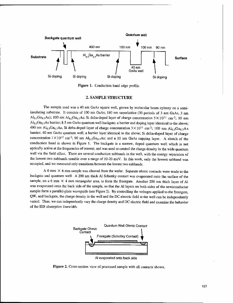
Backgate quantum well
^ 490 nm
Quantum well
100 nm * 100 nm 90 nm
Substrate AIQ3Ga07As barrier 1
/
40 nm GaAs well \
Surface
Si doping Si doping Si doping Si doping
Figure 1. Conduction band edge profile.
2. SAMPLE STRUCTURE
The sample used was a 40 nm GaAs square well, grown by molecular beam epitaxy on a semi- insulating substrate. It consists of 100 nm GaAs; 180 nm superlattice (30 periods of 3 nm GaAs, 3 nm A1o.3Gao.7As); 100 nm Al0.3Ga07As; Si delta-doped layer of charge concentration 5 X101' cm'2; 10 nm Alo.3Gao.7As barrier; 8.5 nm GaAs quantum-well backgate; a barrier and doping layer identical to the above; 490 nm Al0.3Gao 7As; Si delta-doped layer of charge concentration 3 X101' cm"2; 100 nm Al0 3Ga0 7As barrier; 40 nm GaAs quantum well; a barrier layer identical to the above; Si delta-doped layer of charge concentration 1 X1012 cm"2; 90 nm Al0.3Ga0 7As; and a 10 nm GaAs capping layer. A sketch of the conduction band is shown in Figure 1. The backgate is a narrow, doped quantum well which is not optically active at the frequencies of interest, and was used to control the charge density in the wide quantum well via the field effect. There are several conduction subbands in the well, with the energy separation of the lowest two subbands tunable over a range of 10-20 meV. In this work, only the lowest subband was occupied, and we measured only transitions between the lowest two subbands.
A 6 mm X 6 mm sample was cleaved from the wafer. Separate ohmic contacts were made to the backgate and quantum well. A 200 nm thick Al Schottky contact was evaporated onto the surface of the sample, on a 6 mm X 4 mm rectangular area, to form the frontgate. Another 200 nm thick layer of Al was evaporated onto the back side of the sample, so that the Al layers on both sides of the semiconductor sample form a parallel-plate waveguide (see Figure 2). By controlling the voltages applied to the frontgate, QW, and backgate, the charge density in the well and the DC electric field at the well can be independently varied. Thus, we can independently vary the charge density and DC electric field and examine the behavior of the ISB absorption linewidth.
Backgate Ohmic Contact
Quantum Well Ohmic Contact
Al evaporated onto back side
Figure 2. Cross-section view of processed sample with all contacts shown.
127

3. EXPERIMENTAL TECHNIQUE
The charge density in the well was measured using capacitance-voltage profiling. The frontgate and quantum well are two sheets of charge which form a parallel-plate capacitor. Using an AC technique, we measure this capacitance versus frontgate voltage, Vfg. The capacitance signal is equal to dQ/dVfg, where Q is the charge in the quantum well. This is integrated to find the charge density.
The DC electric field is not measured, but is calculated from the applied gate voltages and sample
dimensions using the following formula:
Field = • 'bg
2d„ 2d,,
where Vfg(bg) is the frontgate (backgate) voltage with respect to the quantum well voltage, and dfg(bg) is
the distance of the frontgate (backgate) from the quantum well. In addition to the applied field there is a fixed, built-in electric field whose magnitude may be found from the absorption data to be about 0.3
mV/nm.
The spectra were measured with a Fourier Transform IR spectrometer, using the edge-coupling geometry, as shown in Figure 3. Infrared light incident on the edge of the sample couples into the low-order waveguide modes, and the transmitted light was detected by a bolometer. Only the component of light with polarization parallel to the confinement direction can excite ISB transitions. Therefore, a polarizer was inserted just before the bolometer, so that only that polarization would be detected.
4. ANALYSIS AND RESULTS
Each raw spectrum, with electrons in the well, was normalized to the spectrum measured with the
well depleted by the gates. The attenuation coefficient is given by I(empty)
ct(a>) = - 1
-ln- sample length I(full)
where CO is the frequency, I(empty) is the transmitted intensity vs. frequency with the well depleted of
electrons, and I(full) is the transmitted intensity vs. frequency with the well full of electrons.
Quantum Well
Ohmic Contacts
W@m$ß IR
<+J\A
7 Al evaporated onto back side
Figure 3. Edge coupling geometry used for IR absorption measurements.
128

1.0
's ^ 0.8
c gj
15 o O c g
C Q)
<
0.6 -
0.4 -
0.2
0.0
+ i r i 4
— J? T O Data fit to lorentzian
-
65 70 75 80
Frequency (1/cm)
85
Figure 4. A typical absorption spectrum, with fit to a lorentzian lineshape function. The charge density was 1010 cm"2, DC electric field was -0.34 mV/nm, and sample temperature was 2.5 K.
A typical absorption spectrum is shown in Figure 4. The data is fit to the following Lorentzian lineshape:
a((o)- aycoAco
1 + {co-coQ)Z IT'
where Tis the linewidth (HWHM) and CO0 is the peak position. From the fit we obtain the peak position, linewidth, and area of the absorption curve.
E c o
'en
s. Q.
180
160
140
120
100
80
60
40
■ Ns = 1.3 1011cnT2
■ Ns = 1.0 1011cnT2
.Ns = 5.0 1010cmz
■ N =1.0 1010cm2
QW
_ Substrate ^\ \ Surface or QW
Substrate | rS^ Surface _
■^ bL J_ _L ± ±
-2.5 -2.0 -1.5 -1.0 -0.5 0.0
DC Electric Field (mV/nm)
0.5 1.0
Figure 5. Position of the absorption peak vs. applied DC electric field, at charge densities of 1, 5, 10, and 13 X1010 cm"2.
129

-a
c
10 4 I I -#-Ns = 1.31011cm2
-B-Ns = 1.0 1011cm'2
i 4-
8 -A-Ns = 5.0 1010cm'2 r/ ~
- ▲—A*""***^
-♦-Ns = 1.01010cm'2
LJ/ - 6
4 - ^^^B < /jt -
2 - -
0 4 I I I I I I 4 -2.5 -2.0 0.5 1.0 -1.5 -1.0 -0.5 0.0
DC Electric Field (mV/nm)
Figure 6. Linewidth vs. applied DC electric field, at charge densities of 1, 5, 10, and 13 X1010 cm"2.
The peak positions are plotted against applied DC field, for several charge densities, in Figure 5. The peak position is tunable by over a factor of two, from 75 cm-1 to over 160 cm-1. Since this is a symmetric quantum well, the peak position should be symmetric about its minimum value at zero DC field. The peak position shows the expected quadratic dependence on DC field. However, the minimum occurs at an applied field of -0.3 mV/nm, which implies that the sample has an additional fixed, built-in field of +0.3 mV/nm.
The linewidths are plotted against applied DC field, for the same set of charge densities, in Figure 6. The data shows several interesting features. First, the linewidth has a strong field dependence, dropping dramatically to a minimum at zero bias (minimum which coincides with the minimum in peak position). Second, the field dependence is greater at low charge densities than at high charge densities. Third, the linewidth data are asymmetric about zero field, saturating at 5-6 cm-1 for negative tilts (more negative frontgate) but appearing to rise higher than that for positive tilts (more positive frontgate).
5. DISCUSSION
The field dependence of the linewidth gives some interesting clues about the line-broadening mechanisms, which we will speculate about now. One candidate line-broadening mechanism is scattering from random disorder in the well. Three potential sources of random disorder are monolayer-scale roughness at the GaAs/Al0 3Ga0 7As interface, alloy disorder in the Al0 3Gao.7As barriers, and the long-range Coulomb potential of ionized impurities in the remote donor layers.
The existence of a sharp minimum in the linewidth at zero bias might be explained random disorder scattering. For example, we would expect interface roughness scattering to be strongest, and the line broadest, when the electrons are pushed near the interface of the well, as is the case when a non-zero DC field is applied (see the diagram in the inset to Figure 5). The linewidth would then be at a minimum
130

as the electrons are allowed to move away from the interfaces and spread their wavefunctions across the entire width of the well, as when the DC field is zero. Similarly, alloy disorder scattering would be strongest when the well is tilted, because the electronic wave functions would then penetrate furthest into the barriers, thus overlapping more of the Alo.3Gao.7As barrier alloy. A similar argument can be made that scattering from remote ionized impurities would lead to the same behavior.
The asymmetry of the linewidth data about the minimum also suggests that scattering from remote ionized impurities is important. This asymmetry may reflect the asymmetry in the quantum well donor layers. The sample has doping layers placed symmetrically on either side of the quantum well, but the Schottky contact on the surface of the sample takes up many electrons, leading to a higher degree of donor ionization in the layer closer to the surface. It would be expected that this remote impurity scattering is stronger when the electrons are pushed closer to the surface by application of a positive bias (see the diagram in the inset to Figure 5). Indeed, the data show that the line is broader on the positive bias side of the minimum than on the negative bias side. Another possible explanation for this asymmetry is a simple asymmetry in the interface roughness, with one interface being rougher than the other.
6. CONCLUSIONS
ISB excitations are of both technological and fundamental importance. In order to better understand the dephasing of the THz-frequency ISB plasmon in doped quantum wells, we have begun a detailed measurement of the dependence of the ISB absorption linewidth on charge density and DC electric field. The absorption peak in our sample is field-tunable from 75 cm-1 to over 160 cm-1. We find that the absorption linewidth depends strongly on the DC electric field, becoming as low as 1 cm"1 at zero DC bias. The behavior of the linewidth suggest that scattering from random disorder makes a significant contribution to the linewidth. Future work aims to distinguish between the different scattering mechanisms and to produce a model for the charge density dependence of the linewidth.
ACKNOWLEDGEMENTS
This work was funded by NSF-DMR, AFOSR, and ONR-MFEL.
131

REFERENCES
1. C. Sirtori et al., "Long wavelength infrared (A =11 pm) quantum cascade lasers", Applied Physics
Letters 69 (19) pp. 2810-2812, 1996 2. C. Cates et al., "Quantum well-based tunable antenna-coupled intersubband terahertz (TACIT) detectors
at 1.8-2.4 THz", these Proceedings 3. Ando, Fowler, and Stern, "Electronic properties of two-dimensional systems", Reviews of Modern
Physics, 54 (2) pp. 437-672, 1982
132

Terahertz Excitation, Transport and Spectroscopy of an AFM-Defined Quantum Dot
Naser Qureshi*a, S. J. Allen3, Itaru Kamiya\ Yusui Nakamurab, H. Sakakib
aPhysics Department, QUEST and Center for Terahertz Science and Technology, University of California, Santa Barbara.
bQuantum Transition Project, Japan Science and Technology Corporation.
ABSTRACT
We have investigated the terahertz photoresponse of a single semiconductor quantum dot, electrostatically defined by a sharp conducting Atomic Force Microscope (AFM) tip in contact with a resonant tunneling diode structure. The quantum dot is excited by radiation from a Free Electron Laser in experiments both at room temperature and at cryogenic temperatures. Pronounced resonant tunneling features and classical rectification at frequencies from 0.3 to 3THz are observed in the I-V curves of these devices. These results demonstrate a novel approach to achieving terahertz excitation and studying transport in quantum dots.
Keywords: terahertz, quantum dot, Schottky contact.
1. INTRODUCTION
Quantum transport devices have generated a tremendous amount of interest from a fundamental point of view1, and could potentially play an important role in practical electronics and photonics. Quantum dots, or nanoscale devices where quantum confinement is important in all three dimensions and transport is controlled by resonant tunneling, are emerging as promising candidates for terahertz devices2. Much work has been done in the past decade with quantum dots where current is influenced by RF or microwave radiation. This has shed light on processes such as photon assisted tunneling3,4, or pumping5,6 and turnsile7 effects where one or a small number of electrons are transported through the device per radiation cycle. Most of these groundbreaking works have relied on so-called planar quantum dots, where confinement barriers are typically less than 100 meV high and very low temperatures, tens of millikelvin, are needed to clearly observe resonant tunneling through distinct states in these dots. One of the primary directions of our research is to extend some of this work both to the terahertz regime, and to higher temperature devices. We have made use of vertical quantum dots, which are essentially very small resonant tunneling diodes in which tunneling barriers are typically a few hundred millivolts high.
In this paper, we demonstrate a technique where a quantum dot is created using the electric field close to an AFM tip, without the need for elaborate nanolithographic processes, and at the same time excited with intense terahertz radiation. We present results at liquid helium temperatures (room temperature quantum dots created with this technique have been presented in a previous work8,9). We then report on the response of these devices to terahertz excitation.
2. ELECTROSTATICALLY DEFINED QUANTUM DOTS
Our quantum dots are created by placing a cobalt coated atomic force microscope tip, biased to approximately IV, in contact with an undoped GaAs/AlAs quantum well structure (Fig. 1). The tip forms a Schottky barrier with the GaAs surface. In a region close to the tip, the quantum well buried below the surface is biased so that electrons can resonantly tunnel from an underlying n+ layer, through the quantum well and into the tip. Far away from the tip, the undoped quantum well remains unbiased and depleted of electrons. A small number of electrons are thus injected into the quantum well, effectively confined to a region close to the tip and a current is measured through the tip.
* Correspondence: Email: [email protected]; http://www.qi.ucsb.edu/naser: Telephone 805 893 2132.
Part of the SPIE Conference on Terahertz Spectroscopy and Applications San Jose. California • January 1999 SPIE Vol. 3617 • 0277-786X/99/$10.00 133

Both the tip and the sample are maintained at 4.5K in a clean, low pressure helium exchange gas. They are mounted on a translation stage where the tip can both approach the sample and be moved laterally over the surface of the sample. This makes it possible to measure I-V characteristics of the electrostatically defined dot as a function of position on the quantum well sample. In addition, a light pipe brings terahertz radiation from a Free Electron Laser directly to the AFM tip and the induced photocurrent is measured as a function of both d.c. bias and irradiated power.
THz radiation from FEL
V V applied
Undoped quantum well
measured current I
Fig. 1. Schematic of the experimental technique. The diagrams on the right show band structure close to and far away from the tip.
3. RESULTS
Measurements have been made on a double barrier quantum well sample. The sample consists of a highly doped n+ GaAs layer, a 2.5 run undoped GaAs layer, a 1.7nm AlAs barrier, one 5nm GaAs well, another 1.7nm AlAs barrier and a lOnm spacer layer which forms a Schottky contact with the AFM tip. Fig. 2 shows the d.c. I-V of one device at 4.5 Kelvin. The peak in the I-V corresponds to resonant tunneling through the lowest confined state within the 5nm quantum well. Although we do not resolve any features due to lateral confinement (i.e. confinement perpendicular to the tip), we estimate an effective current path - or effective contact area between tip and sample - of about 200nm from a knowledge of the current density in the sample.
The photoresponse of this device at 1.5 THz is also shown in Fig. 2 as a function of d.c. bias at a number of different irradiation powers. At low FEL power, the response follows very closely the second derivative of the d.c. I-V (Fig. 3), and the form of the response curve is found to be independent of frequency from 0.6 to 3THz. The response is therefore classical rectification. At very high FEL power the features in the response curves are washed out (not shown in Fig. 2), which indicates that we are able to apply a terahertz voltage to the device whose magnitude is comparable to the d.c. bias of about 1 volt.
It is interesting to note that additional structure is observed in the I-V of a dot in an InGaAs/AlAs material system. Using a sample similar to the one described above, but with a 5nm InGaAs quantum well, two 1.7nm AlAs barriers and a lOnm
134
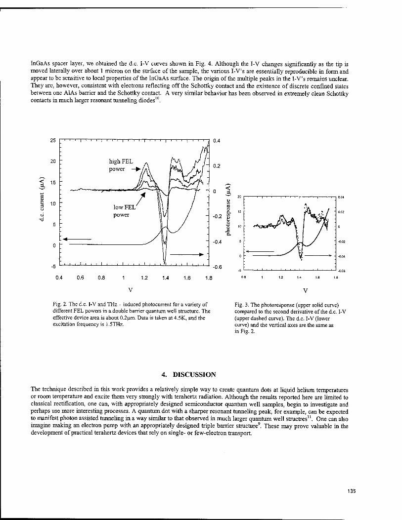
InGaAs spacer layer, we obtained the d.c. I-V curves shown in Fig. 4. Although the I-V changes significantly as the tip is moved laterally over about 1 micron on the surface of the sample, the various I-V's are essentially reproducible in form and appear to be sensitive to local properties of the InGaAs surface. The origin of the multiple peaks in the I-V's remains unclear. They are, however, consistent with electrons reflecting off the Schottky contact and the existence of discrete confined states between one AlAs barrier and the Schottky contact. A very similar behavior has been observed in extremely clean Schottky contacts in much larger resonant tunneling diodes10.
25 | ' ' '
20 "
< 15 ~
| 10
0 ~
-5
-|—i—i i | i i i | i i i | i i i J o.4
high FEL power -
* y mf*
_i—i i I—i i i I i i i_L
0.4 0.6 0.8
low FEL power
fk
1 1.2 1.4 1.6 1.8
V
Fig. 2. The d.c. I-V and THz - induced photocurrent for a variety of different FEL powers in a double barrier quantum well structure. The effective device area is about 0.2p.m. Data is taken at 4.5K, and the excitation frequency is 1.5THz.
Fig. 3. The photoresponse (upper solid curve) compared to the second derivative of the d.c. I-V (upper dashed curve). The d.c. I-V (lower curve) and the vertical axes are the same as in Fig. 2.
4. DISCUSSION
The technique described in this work provides a relatively simple way to create quantum dots at liquid helium temperatures or room temperature and excite them very strongly with terahertz radiation. Although the results reported here are limited to classical rectification, one can, with appropriately designed semiconductor quantum well samples, begin to investigate and perhaps use more interesting processes. A quantum dot with a sharper resonant tunneling peak, for example, can be expected to manifest photon assisted tunneling in a way similar to that observed in much larger quantum well structres11. One can also imagine making an electron pump with an appropriately designed triple barrier structure9. These may prove valuable in the development of practical terahertz devices that rely on single- or few-electron transport.
135

100
80 -
<
5 t! 3 o
60
40
20 -
-20
0.5 1.5 V
Fig. 4. Variations in d.c. I-V as the tip is scanned over a distance of about l^im on the surface of an InGaAs/AlAs quantum well sample. There appear to be multiple resonant tunneling peaks sensitive to local properties of the surface.
ACKNOWLEDGMENTS
We acknowledge the support of the Office of Naval Research, the Japan Science and Technology Corporation (JST), and QUEST, an NSF Science and Technology Center.
REFERENCES
1. U. Meirav, E. B. Foxman, Semiconductor Science and Technology, March 1996, vol.11, (no.3):255-84, or N. F. Johnson, J. Phys.:Condens. Matter 7, 965 (1995) provide excellent reviews.
2. C. J. G. M. Langerak et al, Appl. Phys. Lett. 67, 3453 (1995). 3. R. H. Blick, R. J. Haug, D.W. van der Weide, K. von Klitzing , and K. Eberl, Appl. Phys. Lett. 67, 3924 (1995). 4. T.H. Oosterkamp, L. P. Kouwenhoven, A. E. A. Koolen, N. C. van der Vaart, C. J. P. M. Harmans, Semicond. Sei.
Technol. 11, 1512 (1996) and references therein. 5. K. Tsukagoshi, K. Nakazato, H. Ahmed, K. Gamo, Phys. Rev. B 56, 3972 (1997). 6. M. Swikes, C. M. Marcus, K. Campman, A. C. Gossard, http://ww^\stanford.edu/group/MarcusLab/grouppubs.ht]nl 7. L. P. Kouwenhoven et al. Phys. Rev. Lett. 67, 1626, (1991). 8. N. Qureshi et al, Physica E 2, 701 (1998) 9. http://www.qi.ucsb.edu/naser/exp.htm 10. M. V. Weckwerthvan, J. P. A der Wagt, J.S. Harris, Jr, Journal of Vacuum Science & Technology B 12, 1303 (1993). H.H. Drexler et al, Appl. Phys. Lett. 67, 2816 (1995) and S. J. Allen et al. Physica B 227, 367 (1996).
136
Direct observation of intraband carrier relaxation phenomena in semiconductors with a picosecond free electron laser
A. P. Mitchell, A. H. Chin, J. Kono
Stanford Picosecond Free Electron Laser Center, W.W. Hansen Experimental Physics Laboratory, Stanford University, Stanford, California 94305, USA
ABSTRACT
We have performed time-resolved terahertz (THz) - near-infrared (NIR) two-color spectroscopy on InSb, using the Stanford picosecond free-electron laser synchronized with a femtosecond NIR Ti:Sapphire laser. The initial NIR pulse excites non- equilibrium electrons and holes, which absorb the picosecond THz pulse. The time profile of the photo-induced absorption is a sensitive probe of intraband carrier relaxation dynamics. Using these techniques we have made the first observation of time- resolved cyclotron resonance (TRCR) of photo-created electrons in InSb for time delays from a few picoseconds to several tens of nanoseconds. This TRCR data shows possible evidence of a magnetic-field-induced LO-phonon bottleneck effect. Furthermore, we have detected very unusual multi-component relaxation and photo-induced transparency under certain conditions.
Keywords: terahertz dynamics, InSb, free-electron lasers, cyclotron resonance, LO-phonon bottleneck, carrier relaxation
1. INTRODUCTION
Excitation of a semiconductor by an intense pulse of light with a photon energy greater than the fundamental energy gap results in a large density of non-equilibrium electron-hole (e-h) pairs. These non-equilibrium carriers with excess energies relax toward the band-edge through various scattering and thermalization processes before eventually recombining to luminesce.1
It immediately follows that interband photoluminescence (PL), although the most-commonly used optical technique in semiconductor spectroscopy, is unable to provide direct information on carrier relaxation dynamics. In essence, PL spectroscopy is sensitive only to radiative (or "bright") excitons with center-of-mass momentum K = k hot()n = 0 with the obvious exception of phonon-assisted processes where K = kphololl + k^,^2'3.
Intraband terahertz (THz) spectroscopy obeys its own set of selection rules— independent of whether the states involved are interband-active or not, thus providing a rare opportunity to directly probe these dark states. A wide variety of perpendicular (AK = 0) intraband transitions are allowed, so long as the parity and angular momentum selection rules are satisfied. In particular, a time-resolved observation of the Is to 2p exciton internal transition would map out the time evolution of the entire K distribution of Is excitons. Such an experiment would be a key to the successful demonstration of Bose-Einstein distribution (and eventually condensation) of excitons. However, because of the rarity of ultra-short THz sources, experimental research in this direction has not been explored.
In order to develop further these experimental techniques, we have performed picosecond time-resolved studies of THz absorption by photo-created carriers. These expereiments utilize a femtosecond mode-locked near-infrared (NIR) Titanium- Sapphire laser (X ~ 800 nm) synchronized with" the Stanford Picosecond Free Electron Laser (FEL), whose spectral range has been recently extended to the THz (5-100 THz)5.
Part of the SPIE Conference on Terahertz Spectroscopy and Applications San Jose. California • January 1999 SPIE Vol. 3617 • 0277-786X/99/S 10.00 137

In performing these experiments we have obtained some fascinating new results. This paper will attempt to delineate the techniques used, describe our results, and propose explanations for some of the interesting features of this data. We have performed picosecond time resolved photo-induced absorption (PIA) and, for the first time, time-resolved cyclotron resonance (TRCR) studies on the narrow gap III-V semiconductor InSb. We have observed very unusual relaxation dynamics in the PIA and TRCR data: 1) step-like behavior only at zero and very low magnetic fields, 2) photo-induced transparency when the NIR excitation pulse power is lower than a threshhold value, 3) extremely slow relaxation at high magnetic fields (> 3 T), and 4) apparent increase in effective mass during carrier relaxation.
2. SAMPLES
The InSb sample studied was purchased from ATRAMET, Inc. It is undoped, with a residual electron density of ~5 x 10'4
cm'3 and a 77K electron mobility of ~2 x 10⁵ cmVV-s. The sample was wedged -3° to avoid multiple-reflection interference effects, and polished it down to -150 urn. The Si and GaAs reference samples were purchased from Lattice Materials Corp. and American Xtal Technology, respectively. The Si is a 3-mm-thick high-purity (> 99.999%) single crystal. The GaAs crystal is semi-insulating, with excess arsenic. The surfaces of both reference samples were optically polished.
The NIR laser source was a Spectra Physics Tsunami Ti:Sapphire laser seeding a Positive Light Spitfire regenerative amplifier. The amplifier produces intense ultra-fast NIR pulses in a wavelength range of 750-1100 nm with pulse durations as short as -200 fs and pulse energies as high as -1 mJ. The Stanford picosecond FEL produces pulses with wavelengths extending through the MIR (3-15 |im) and THz (15-60 urn) with pulses durations as ranging from 600 fs to 2 ps and energies as high as -1 uJ.
The samples were placed in Oxford Instruments Spectramag superconducting magnet, which produces a uniform magnetic field of up to 9 T parallel to the optical path.
3. EXPERIMENTAL METHODS
The setup for the two-color spectroscopy experiments is illustrated schematically in Figure 1. The amplified output of the Ti:Sapphire laser (NIR) is directed through a computer controlled variable delay stage, after which it is then spatially overlapped with the THz using a Si Brewster plate. The two collimated beams are thus made collinear as they are focused on the sample using a parabolic mirror. The NIR pulse excites non-equilibrium carriers across the band gap which then absorb a fraction of the incident THz radiation. The transmitted THz pulse is then recollimated and directed to a Ge:Ga photoconductive detector. Any THz PIA in the Si Brewster plate was made negligible by enlarging the incident NIR spotsize.
THz probe
SI Beam Combiner
m
Ge:Ga Detector
■ ■
B Sample f
Delay z
Fig. 1 A schematic of the experimental setup used for time-resolved PIA and CR spectroscopy
138

The THz output of the FEL consists of 10 Hz "macropulses" 5 ms in duration. These "macropulses" each contain many ~1 ps duration micropulses separated by 84.6 ns, tuned to a wavelength of 42jim. The Ti:Sapphire is synchronized with the (10 Hz) macropulse output of the FEL so that we have only one NIR pulse for every THz macropulse (-60,000 micropulses). The Ti:Sapphire laser generates -200 fs pulses at a wavelength of 800 nm. This situation is illustrated schematically in Figure 2. This arrangement allows us to compare the intensity of transmitted THz before and after the NIR pump pulse (micropulse to micropulse energy fluctuations are factored out using an THz reference detector before the sample (not illustrated in Fig. 1)). The amount of photo-induced absorption (PIA) in the sample may thus be recorded as a function of time delay. For TRCR measurements we use the same setup, but now sweep the magnetic field strength at fixed time delays, thus obtaining a granular picture of the time evolution of the CR spectrum. Using a combination of the optical delay stage and electronic delays in the THz - NIR synchronization we are able to selectively attain delays from 0 to 84.6 ns with a resolution of a few picoseconds. The observed TRCR line-widths are much larger than the transform limited spectral width of the picosecond terahertz pulse, which, at 3.6 meV, corresponds to a CR line-width of only 0.6 T at the InSb band edge.
-200 fs / .
Photo-induced Absorption
PIA
THz 20-60|im 11.8 MHz
84.6 nsec
Fig. 2 Timing of NIR and THz pulses
Time
Typical time-resolved PIA measurements in the Si and GaAs reference samples are shown in Fig. 3. Here, and in the InSb data to follow, the NIR pump pulse is incident on the sample at time zero. The THz probe pulse then arrives at the sample after a delay x and is absorbed by the carriers created by the pump. In both cases PIA causes an abrupt drop in the sample transmission at x = 0 -- 65% in Si and 70% in GaAs. The relaxation curve for the absorption depends directly on the relaxation properties of the sample. For example, Si, being an indirect semiconductor, has a very long recombination lifetime well over a microsecond. As a result the absorption induced at x = 0 appears completely flat over the measured interval (i.e., < 1 ns). In the direct semiconductor GaAs, the carrier lifetime is short (1-2 ns) so the PIA signal decreases much more rapidly. One expects the direct semiconductor InSb to behave in a qualitatively similar fashion to GaAs.
With our current setup it is not possible to carry out studies of magnetic field dependent effects in the Si and GaAs reference samples. This is due to the large carrier effective masses in these materials: our THz wavelength range does not extend far enough for observation of CR at the fields (< 9 T) which our magnet is capable of generating. InSb, however, has very small carrier effective masses, which increase with increasing carrier energy due to the non-parabolicity of the conduction band. These small effective mass values allow us to perform detailed electron TRCR measurements in the magnetic field and wavelength range available to us, and should allow us to observe the effect of the non-parabolic conduction band on the CR evolution. In particular we expect that the time evolution of the CR signal will allow us to see directly the time evolution of the effective mass, carrier density, and scattering time for the photo-created non-equilibrium carriers. The Landau level structure of InSb has been well-studied6, and thus provide an ideal testing ground for this new experimental technique. In addition, the optic phonon energies in InSb are comparable to the cyclotron energy of electrons within the magnetic field
139

range available to us, making it possible to tune the coupling of electrons and phonons, which in turn drastically modifies relaxation dynamics.
0) o c CO
E w c CO
H
1.0 " MM i—>-
\
—, .■■ | i |
(a) : 0.9 -
0.8 SI; T = 300K -
0.7 XN|R = 800nm;XFlR = 46^m -
0.6 -
0.5 -
0.4 \ -
0.3 i • ■ i ■ i
200 400 600 800 1.2
1.0
0.8
0.6
0.4
0.2
GaAs; T = 1.5K XMR = 815 nm;XFlR = 46 »m,
(b)
-L J_ J_ _l_ J_ J_ -200 0 200 400 600 800 1000 1200 1400
Time Delay (psec)
Fig. 3 Photo-induced absorption in the reference Si and GaAs samples
4. EXPERIMENTAL RESULTS
4.1 Magnetic field dependent photo-induced absorption
An example of the fixed field PIA data is shown in Figure 4. The zero field PIA data displays an unusual three-component relaxation, which is not apparent in the reference sample data. Further data shows, in detail, that this step-like behavior is highly dependent on the NIR pulse power, and at very low excitation pulse power the lineshape is inverted, i.e., transmitted intensity increases (photo-induced transparency). This highly intriguing behavior, however, disappears at relatively low magnetic fields and is supplanted by a behavior similar to that of the GaAs reference sample at B = 0 T.
As magnetic field is increased further, the absorption gains a distinct two component character. The first component is a field independent rapid drop in transmittance, which recovers quickly (<100 ps) to an intermediate value. The second absorption component is an extremely slow (nearly time independent on these scales) plateau at this intermediate value. This is in complete opposition with the expected magnetic field effect. Due to the increase in the density of states induced by the magnetic field quantization of the free carrier energy spectrum, one expects a resultant increase in the optical transition probability, thereby foreshortening the carrier lifetime. However, the behavior of the second component is indicative of a
140

dramatically increased carrier lifetime (as in the Si reference sample), which is potentially the result of an LO-phonon bottleneck effect.
Specifically, the resonant polaron condition o\0 = (ot is satisfied at ~3 T, so that at higher magnetic fields the Landau level splitting exceeds the LO-phonon frequency, making Landau level transitions via LO-phonon emission highly improbable. Because the relaxation processes in III-V semiconductors are dominated by such phonon emission one expects the carrier lifetime to increase significantly, as is shown in the data. This type of relaxation bottleneck has been predicted7 and searched for8 in quantum dot structures but has not been directly verified to date. This relaxation feature has never before been observed in bulk materials as a result of the high magnetic fields (>20 T) required to achieve the resonant polaron condition in the more commonly studied GaAs (fto\0 is 36 meV in GaAs vs. 24 meV in InSb, and m* is 0.07m0 in GaAs vs. 0.014 m0 in InSb).
One expects that the magnetic field dependence of the (flat) absorption depth should be determined entirely by the CR lineshape and it is observed to have its maximum at the expected value of 5 T.
>
Q. ^8 0s
O 10 0) u c a C I (0 c to
600 800 0 200 400
Time Delay (ps) Fig. 4 Time-resolved photo-induced absorption at a range of fixed magnetic fields. The flatness of the B>3T data is explained by an LO-
phonon bottleneck effect.
4.2 Picosecond time-resolved cyclotron resonance
Typical CR data obtained at a variety of fixed time delays is shown in Figure 5. This is the first observation of picosecond TRCR (only microsecond time resolution has been achieved to date9), and it displays a few intriguing features. These traces should demonstrate directly the time evolution of the electron CR spectrum over time scales much shorter than the interband e-h recombination time (the time scale available through PL studies). All of the effects seen in this data are therefore the result of intraband processes.
141
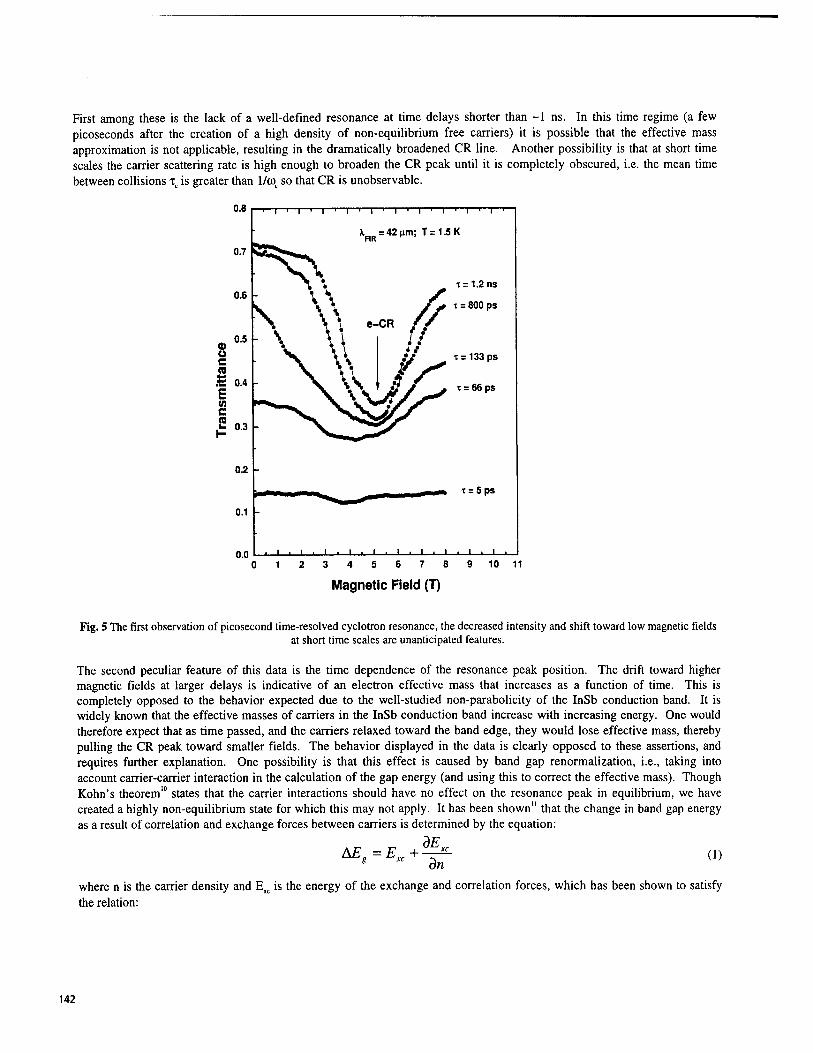
First among these is the lack of a well-defined resonance at time delays shorter than -1 ns. In this time regime (a few picoseconds after the creation of a high density of non-equilibrium free carriers) it is possible that the effective mass approximation is not applicable, resulting in the dramatically broadened CR line. Another possibility is that at short time scales the carrier scattering rate is high enough to broaden the CR peak until it is completely obscured, i.e. the mean time between collisions TC is greater than 1/oa. so that CR is unobservable.
0.8
0.2
0.1
I ■ | ' l ' I ' I ' I ' I ' I ■ I ' I
X =42 urn; T = 1.5K FIR
t = 1.2 ns
T = 800 ps
i = 133 ps
i = 66 ps
x = 5 ps
0.0 "—' 10 11
Magnetic Field (T)
Fig. 5 The first observation of picosecond time-resolved cyclotron resonance, the decreased intensity and shift toward low magnetic fields at short time scales are unanticipated features.
The second peculiar feature of this data is the time dependence of the resonance peak position. The drift toward higher magnetic fields at larger delays is indicative of an electron effective mass that increases as a function of time. This is completely opposed to the behavior expected due to the well-studied non-parabolicity of the InSb conduction band. It is widely known that the effective masses of carriers in the InSb conduction band increase with increasing energy. One would therefore expect that as time passed, and the carriers relaxed toward the band edge, they would lose effective mass, thereby pulling the CR peak toward smaller fields. The behavior displayed in the data is clearly opposed to these assertions, and requires further explanation. One possibility is that this effect is caused by band gap renormalization, i.e., taking into account carrier-carrier interaction in the calculation of the gap energy (and using this to correct the effective mass). Though Kohn's theorem10 states that the carrier interactions should have no effect on the resonance peak in equilibrium, we have created a highly non-equilibrium state for which this may not apply. It has been shown" that the change in band gap energy as a result of correlation and exchange forces between carriers is determined by the equation:
(i) A£ =£„+- dn
where n is the carrier density and E„ the relation:
is the energy of the exchange and correlation forces, which has been shown to satisfy
142

£«(1)= a + brs
c + dr + r': -Ry*
i
r, = 4701
(2)
where a = -4.8316, b = -5.0879, c = 0.0152, d=3.0426 are constants independent of any material parameters, Ry* and aB are the effective exitonic Rydberg and Bohr radius respectively, and rs is the mean interparticle distance in units of the effective Bohr radius. Thus at short time scales, when carrier densities are high, we may obtain a significant deviation of the gap energy from its equilibrium value. The resultant decrease in gap energy yields decreased electron effective masses, due to the increased kp interaction between the conduction and light hole valence band. One thus expects the electron effective mass to increase with time as the carrier density decreases and the gap energy regains its equilibrium value. The expected change in Eg and the resultant change in Band Edge effective mass are plotted in Figures 6(a) and (b). The initial carrier density (which is unattainable from the TRCR data due to its strange early time-evolution) was estimated at ~lel9 cm'3 using the incident NIR intensity. This corresponds to a 25 meV (11% change) decrease in the gap energy, which results in a 17% decrease in the band edge effective mass. These results agree qualitatively with our data, however we are still attempting to understand fully the time evolution of the carrier density.
0.0140
w 0.0136
V) w (0
0)
■o UJ
■o c a
CD
0.0132
0.0128 -
0.0124 -
1E15 1E16 1E17 1E18
Carrier Density (cm-3) 1E19
Fig. 6 (a) Band gap renormalization vs. carrier density in InSb (b) Band edge effective mass vs. gap renormalization energy
4.3 Longer time scale cyclotron resonance: electron capture by donors Measurements over nanosecond time scales are shown in Figure 7. Here the behavior is easily understood in terms of well- studied processes. As time evolves, a second CR peak appears at lower magnetic field, this peak results from transitions made by electrons bound to ionic donor sites. Specifically, this is the signature of the hydrogenic Is to 2p+ transition, and is known as impurity shifted CR (ICR)12. This ICR peak increases in time relative to the CR peak as a result of an increasing number of donor bound electrons as the carriers relax toward the band edge.
5. SUMMARY
We have performed picosecond time-resolved NIR - THz two-color pump-probe spectroscopy on bulk InSb, Si, and GaAs. The results demonstrate that this new type of spectroscopy is a powerful tool for the study of intraband carrier dynamics. Time-resolved PIA studies were carried out in all of these materials, yielding easily explainable results for Si and GaAs. The InSb sample, however, demonstrates many new effects, including a step-like relaxation behavior in zero magnetic field, and possible photo-induced transparency at low NIR excitation pulse intensity. Under magnetic fields, the PIA develops striking new features: the step-like behavior disappears and is replaced by a flat absorption profile which is indicative of a
143

dramatically increased carrier lifetime. This startling change in carrier dynamics is attributed to a magnetic field induced LO-phonon bottleneck effect. Also, the first ever picosecond and nanosecond TRCR measurements were carried out on the InSb sample, yielding further interesting results. On the picosecond time scale we observed a shift toward higher magnetic field in the time evolution of the CR peak, implying an increase in effective mass with decreasing carrier energy. Though this behavior is the opposite of what is anticipated due to the well-studied non-parabolicity of the InSb conduction band, it is explained by band gap renormalization at high carrier concentrations. Also on this picosecond time scale, we observed a dramatic broadening of the CR line at the smallest measured time scales. This behavior may be explained by either the possible invalidity of the effective mass approximation very soon after carrier creation, or a dramatically reduced mean time between collisions, resulting in an unobservably broad CR line. On the nanosecond time scale we observed the weight of the free carrier electron CR peak shifts toward a lower field ICR peak corresponding to the resonance of donor captured carriers, a well known behavior whose early time evolution had yet to be explored. These new experiments were made possible only by the use of the picosecond FEL as a source of tunable THz radiation.
>
0) u c re
X. = 42 (im FIR
T = 36 ns
x = 24 ns
T = 12 ns
i = 1.2 ns
j I i I i 1 i I i Lj_i I i I i l ■ l 01 23456789 10 11
Magnetic Field (T)
Fig. 7 Nanosecond time-scale cyclotron resonance, the impurity shifted resonance appears and begins to dominate the CR lineshape.
ACKNOWLEDGMENTS
This work is supported in part by ONR N00014-94-1-1024. The authors are grateful to Hidefumi Akiyama, Kristinn Johnsen, Glenn Solomon and Francesco Tassone for useful comments and discussions, Eric Crosson, James Haydon, Jeffery Haydon, Daniel Palanker, Teruyuki Takahashi, and Giacomo Vacca for technical support, and Profs. H. Alan Schwettman and Todd Smith for useful discussions and encouragement.
144

REFERENCES
1. For a review on various carrier relaxation processes, see, e.g., J. Shah, Ultrafast Spectroscopy of Semiconductors and Semiconductor Nanostructures (Springer-Verlag, Berlin 1996).
2. J.P. Wolfe, J.L. Lin, and D.W. Snoke, "Bose-Einstein condensation of a nearly ideal gas: excitons in Cu20", in: Bose- Einstein Condensation, edited by A. Griffin, D.W. Snoke, and S. Stringari, pp. 281-329 (Cambrige University Press, 1995).
3. M. Umlauff, J. Hoffmann, H. Kalt, W. Langbein, J.M. Hvam, M. Scholl, J. Söllner, M. Heuken, B. Jobst, and D. Hommel, "Direct observation of free-exciton thermalization in quantum-well structures," Phys. Rev. B 57, 1390 (1998).
4. R.J. Stanley, R.L. Swent, and T.I. Smith, "Synchronization of a femtosecond mode-locked Ti:sapphire laser to the Stanford SCA/FEL," Optics Commun. 115, 87 (1995).
5. H.A. Schwettman, "Challenges at PEL facilities: the Stanford Picosecond FEL Center," Nucl. Instr. and Meth. in Phys. Res. A375, 632 (1996); see also http://www.stanford.edu/group/FEL/.
6. See e.g., B.D. McCombe and R.J. Wagner, "Intraband Magneto-Optical Studies of Semiconductors in the Far-Infrared," in: Vol. 37 Advances in Electronics and Electron Physics, Edited by L. Marton, (Academic Press, New York, 1975).
7. H. Benisty, CM. Sotomayor-Torres, and C. Weisbuch, "Intrinsic mechanism for the poor luminescence properties of quantum-box systems," Phys. Rev. B 44, 10945 (1991).
8. For a review, see, e.g., T. Inoshita and H. Sakaki, "Electron-phonon interaction and the so-called phonon bottleneck effect in semiconductor quantum dots," Physica B 227, 373 (1996).
9. See, e.g., E. Otsuka, "Cyclotron resonance" in: Landau Level Spectroscopy-Vol 21A of Modern Problems in Condensed Matter Sciences, edited by G. Landwehr and E.I. Rashba, pp. 1-78 (Elsevier Science, Amsterdam 1991).
10. W. Kohn, "Cyclotron resonance and de Haas-van Alphen oscillations of an interacting electron gas" Phys Rev 123 1242 (1961).
11. See, e.g., H. Kalt, Optical Properties of III-V Semiconductors: The Influence of Multi-Valley Band Structures, Chap. 3 (Springer-Verlag, Berlin 1996)
12. See e.g., B.D. McCombe and R.J. Wagner, "Intraband Magneto-Optical Studies of Semiconductors in the Far-Infrared II," in: Vol. 38 Advances in Electronics and Electron Physics, Edited by L. Marton, (Academic Press, New York, 1975).
145

SESSION 7
THz Quasi-Optical Arrays and Ultra-Nonlinear Phenomena
147
Invited Paper
Terahertz Harmonic Generation from Bloch Oscillating Superlattices in Quasi-Optical Arrays
M.C. Wanke*0, J.S. Scott0, S.J. Allen0, K.D. Maranowski* and A.C. Gossard6
° Physics Department, Univ. of California, Santa Barbara, CA 93106 cMaterials Department, Univ. of California, Santa Barbara, CA 93106
ABSTRACT
We explored harmonic generation by Bloch oscillation in miniband superlattices driven by intense THz radiation from the UCSB free electron lasers, as a function of both THz intensity and applied DC bias. To accomplish this we intergrated /zm size superlattice mesas in a quasi-optical array which amplified a plane wave incident normal to the array and coupled it into the growth direction of the superlattice.
We were able to successfully measure both second and third harmonic generation quantitatively. The harmonics are compared to a quasi-classical picture of Bloch oscillation.
Keywords: Bloch Oscillation, Terahertz Harmonic Generation, High-field Transport
1. BASIC BLOCH OSCILLATION
In small dc electric fields, electrons in a periodic potential with typical scattering rates sense a parabolic potential to lowest order. This results in a Drude-type response for the electron motion. In contrast, in sufficiently high fields and for low enough scattering rates the electrons should oscillate. This motion, refered to as Bloch oscillation, is a direct consequence of the bandstructure of the periodic potential and the applied field. The following heuristic picture shows how this comes about.
Assuming a tight-binding approximation with an allowed band width A and potential period d, the dispersion relation connecting the electron energy, e, to its momentum, k, is given by
e(k)&~(l-coskd). (1)
and the electron velocity is simply given by
«*> = ii = s™"- <2» As Bloch pointed out,1 when a DC field is applied to this system the momentum k evolves in time according to hk = Fext = eE (where e is the electron charge and E in the applied DC field). This is easily integrated to give
k(t) = k0 + ~. (3)
The energy dispersion and velocity relations are periodic as a function of momentum, hence only k values contained in the first Brillioun zone (B.Z.) are physically distinct. Therefore we can say that when an electron with momentum k passes one edge of the B.Z. it reappears at the other edge, i.e. it Bragg reflects. In Eq. (3) we note that k evolves linearly in time, which therefore implies that the electron passes through the B.Z. periodically in time. Substituting Eq. (3) into Eq. (2), we get the following expression for the velocity of a single electron as a function of time:
, x Ad . ,
"Currenlty at Lucent Technologies/Bell Labs, Murray Hill, NJ 07970. E-mail: [email protected].
Part of the SPIE Conference on Terahertz Spectroscopy and Applications ... San Jose, California • January 1999 SPIE Vol. 3617 • 0277-786X/99/S10.00 148

Thus we can see, as originally pointed out by Zener,2 that the sinusoidal nature of the dispersion relation, e(k), results in an oscillation in real space of the electron in a D.C. field, at the so-called Bloch frequency,
UJB = sEd
(4)
This would imply that an applied DC field should give rise to an alternating current to carriers in a periodic potentials such as bulk semiconductors and superlattices.
Although in a real system a DC field may drive each electron to Bloch oscillate scattering will randomize the relative phases of the electrons resulting in no net current oscillation. As succinctly put by Leo, "For a direct observation of the oscillations, it is necessary to create a carrier ensemble with defined phase relations."3 To achieve this many experiments have utilized ultrafast optical techniques in conjuction with DC fields to examine the dynamics on time scales comparable to the scattering rates. We refer the reader to the review article by Leo for discussion of these types of measurements. Another good introduction to the general field can be found in the book edited by Grahn.4
On the other hand Bloch oscillation is no more than a normal mode of the electron system in the present of a DC field. We can impulse excite the system and watch its time evolution or we can probe it in the frequency domain. For small levels of excitation the time domain view and frequency domain view are equivalent.
Unfortunately the Stark ladder or Bloch oscillator is unstable to electric field domain formation once we apply sufficient field to execute Bloch oscillation or resolve the components of the Stark ladder in the quantum mechanical picture. The optical experiments avoid this complication by working with undoped material and create electrons with the short optical pulse. However, holes are created at the same time and excitonic effects complicate the response.
In this paper we describe an alternate approach to observing Bloch oscillation. Instead of using a DC field to establish Bloch oscillation we use strong THz fields from the UCSB free-electron lasers. If the frequency is high enough the strong AC field may be able to drive the electrons to the zone boundary and Bragg scattering without domain formation. Further, resonances may appear between the drive frequency and Bloch frequency defined by the terahertz electric field strength. Clearly, we are in a very non-linear regime and the system should be very rich in harmonics. Indeed, the harmonic content as a function of terahertz electric field and DC electric field define the response of the Bloch oscillator under these conditions.
In the next section we will present highlights of a theory for Bloch oscillation in the presence of large AC fields. Then we will explain the experiment focusing on THz harmonic generation and give a description of the samples. We follow this by a presentation of some results.
Figure 1. For fields such that eEac/hw > ir/d the electron momentum will exceed the width of the B.Z. and the electron will Bragg reflect (left). At right the velocity (solid) is shown not to follow the field (dotted). The field amplitude is the same in both.
149

1.1. AC Dynamics of Bloch Oscillators
In order to have well-defined phase, we replace the DC field with a strong high frequency AC field. Continuing with heuristic explanations, let us analyze just a single electron in a miniband driven by an AC field. Again using the acceleration theorem hk = Fext ( now Fext = eEaccosur), the momentum as a function of time can now be expressed as
(5) k = k0 + —— smut. hu
In a DC field (in the absence of scattering) an electron eventually reaches the B.Z. boundary independent of the field strength. However, in the presence of an AC field this is no longer the case. The amplitude of an electron's excursion in ik-space is now controlled by the ratio between the field strength and the driving frequency (see Fig. 1).
Although the underlying physics is the same whether the system is driven by an AC or DC field, the observables are different. Plugging Eq. (5) into Eq. (2) we find that the velocity as a function of time now becomes
v(t) Ad 2h
sin I — sin ut j
= 2^ J2n-1 (wß/w) sin [(2n- l)ut]. (6) n=l
where now the AC Bloch frequency, UB = eEn
d, is defined in the same way as in DC Bloch frequency. Thus the current no longer will follow the field as is shown graphically in the right side of fig. 1 which corresponds to the field amplitude depicted on the left. The current response generated by only an AC field consists of all the odd harmonics of the driving field and is no longer sinusoidal. Each harmonic component is weighted by a Bessel function (argumnet) of the same order as the harmonic. In the low field limit the ntn harmonic current varies as the drive field to the ntn power but in high fields, the field dependence becomes strikingly non-monotonic, as can be seen in Fig. 2 which shows the third harmonic for various values of UT.
6 8 (eE d/h(0 )
Figure 2. The third harmonic current depedence on the ac-drive field for various values of wr. Note that the peak field asymptotically approaches a value near 4 as wr —> oo. At the frequencies we used this sets a minimum field strength of 12 kV/cm to observe the peak.
The curves in Fig. 2 were generated using the results of a more rigourous calculation by Pavlovitch and Epshtein,5
who extended work of Ignatov and Romanov.6 The heuristic picture presented above corresponds to the case with
150

.5 1 1.5 2 2.5 Voltage applied to array (V)
I I I I I I I I !■ I I I
0 TT.2 0.4 0.6 0.8 1 1.2 1.4 Voltage applied to array (V)
0.8
0.7
111111111111 M j 11 n 11.
: tor » 3.0
0.6F-- :..Sfi«Wl.. Harmonic |
0.5 t- ; : Third
Harmonic u 8P 4-»
> <
0 "TT1 0.2 0.3 0.4 0.5 0.6 0.7 0.8 Voltage applied to array (V)
Figure 3. The left hand side shows contour plots of the second and third harmonic generation for three different values of ur where white is high and black is low. The upper plot of each pair depicts the second harmonic while the lower represents the third harmonic. The figures to the right show the position of the ridges projected onto the AC-DC plane, where the black circles represent the absolute peaks along a given ridge or axis.
151

u)T = oo. Although the details of the theory are not presented here, Fig. 3 shows the results of calcuation for the second and third harmonics as functions of both the applied ac and dc field strengths, again for a few different values of UJT.
Here we note a few features of Fig. 3 to which the experimental data will be compared. First, in the abscence of a DC field, only odd harmonics are generated thus the second harmonic current is zero. As already mentioned the third harmonic for this case is non-monotonic. In the presence of a DC field a "ridge" of peak harmonic current occurs in both the second and third harmonics when the AC field is slightly larger than the DC field. We also note that along each ridge there is an absolute peak. The second harmonic decays rapidly as the fields are increased above those corresponding to the absolute peak, while the third harmonic decays more gradually. For higher values of wr, the smooth nature of these ridges breaks up into series of peaks, where the peak positions along the DC axis correspond to the Wannier-stark splitting (DC bloch frequency) between states of neighboring well equals a multiple of the photon energy (photon frequency), and the locations of the peaks along the AC axis correspond to the AC bloch frequency coming into resonance with the drive frequency.
The plots to the right in fig. 3 extract some essential features from the contour plots. The lines follow the peaks in the harmonics and the circles represent where along a ridge the absolute peaks lie. From this plot we can also observe that the second harmonic always peaks at a lower DC bias for a given AC field than the third harmonic. The circle on the DC axis corresponds to the peak of the current in the unirradiated current-voltage relation, or in other words represents the onset of negative differential resistance.
2. SAMPLE DESIGN
The sample described below consists of a 50 period superlattice of 80 Ä GaAs wells separated by 20A Ga.7Al.3As barriers grown using MBE. The sample was uniformly doped at 1 • 1016/cm3. The superlattice was surrounded on both sides by an injector region, consisting of a chirped SL and a graded aluminum fraction section, all sandwiched between 4 • 1018/cm3) n+ regions. Ni/Au/Ge contacts were used to from ohmic contacts to the n+ layers.
Unit Cell
DGold D n+ GaAs ■ GaAs/AIGaAs SL D Substrate
Figure 4. The left depicts a cartoon of a unit cell from the 2nd generation arrays. In reality the mesa is encased in SiN and the airbridge is sloped as can be seen in the SEM image on the right.
To couple the electric field of free space THz radiation modes into and out of the growth direction of the superlattices, we integrated micron size mesas into a square array connected in series and parallel, with a separation between mesas much less than the wavelength of the incident or generated radiation. In addition to coupling to free space modes, this quasi-optical array concentrates the field into the superlattice, and combines the power generated by each mesa into a single beam. At THz frequencies spatial power combining becomes an important tool, as a typical device size and its concomitant power output scale inversely with frequency. The effectiveness of using quasi- optical arrays in this frequency range using the FEL was demonstrated both in this work and in a collaboration with researchers at Caltech examining Schottky diodes.7
152

Over the course of this work two different generations of antenna arrays were employed. Fig. 4 illustrates schematically the unit cell for the second set of arrays on the left and shows an SEM picture of a fabricated device on the right. The overall size of the array is 500 fim x 500 pm with a periodicity of 25 /im. The unit cell of the first generation arrays is similar to the second generation just decribed but with the mesa width equal to the width of the unit cell and the bowtie metalization is replaced by a wide dipole antenna which is also as wide as the unit cell. The older array consists of 96 elements on a side with a 20 fim periodicity yielding an overall size of roughly 2 mm x 2 mm, which is larger than the spot size of the beam. The major differences between the two generations are the bowtie shape of the connecting metallization and the arrays' overall size. For both arrays the period is much smaller than any wavelength used in the measurements.
3. MEASUREMENTS
The measurement set-up is illustrated in Fig. 5. Kilowatts of pulsed power at 22 cm-1 was provided by the UCSB free-electron laser (FEL) with 3 fis pulse widths at a rate of 1 pulse per second. We chose 22 cm-1 since it and its second and third harmonics all lie within gaps of the water vapor absorption spectrum (removing the need for purging the experiment) and also to maximize the field strength to frequency ratio (the relavant parameter for these measurements as implied in eq. 6).
Figure 5. Schematic arrangement of the optical setup: THz source (a), low-pass filters (b), variable attenuator (c), beamsplitter (d), reference detector (e), sample (f), cryostat (g), high-pass filter (h), and bolometer (i).
The input power first passes through low pass filters to reject harmonics from the FEL. These consist of a multimesh capacitive filter having a 660 GHz cutoff, a fluorogold filter and for the third harmonic measurements a filter from QMC8 with a cutoff at 55 cm-1. The intensity is controlled by using a pair of wire grid polarizers. The first attenuates the linearly polarized input beam, and the second attenuates more while returning the polarization back to its original direction. Part of the beam is split off and measured by a pyroelectric reference detector to monitor fluctuations in the beam intensity while the majority of the beam is focused onto the array. The array is kept at 77 K in an optical bath cryostat (lowering the temperature to 4 K has minimal effect).
The harmonics generated and radiated by the array are recollimated before finally being focused into an InSb Bolometer. The bolometer is magnetically tuned to extend its reponse up to 88 cm-1 with a peak response at 66 cm-1
corresponding to the third harmonic in the measurements. A Fabry-Perot interferometer placed in the collimated beam confirms the frequency of the measured power. When measuring the third harmonic a high-pass waveguide filter with a cutoff of 58 cm-1 was mounted on the bolometer to reject the fundamental and second harmonic. To measure the second harmonic a 55 cm-1 low-pass filter was used to block the third in addition to a 38 cm-1 high-pass waveguide filter to block the fundamental. The 200 ns response time of the bolometer is fast enough to observe the 1 ^s rise and fall time of the THz pulse. The harmonic response was averaged over a finite time interval during the flat part of the THz pulse which was crucial for obtaining the non-monotonic power dependences observed.
153

A de electric field was sometimes applied in addition to the THz field. This allowed measurement of the harmonic response as a function of both incident power and dc field. In addition, by measuring the current and voltage both before the FEL pulse arrived and in the presence of the THz field we could measure the effect of the THz radation on the quasi-static I-V of the superlattice. The dc voltage was pulsed twice per FEL pulse with one pulse occurring a few microseconds before and the second occurring completely within the THz pulse, with a pulse duration of 2 //s and a rise time of 10 ns. The second pulse was completely contained within the FEL pulse in the hopes that the strong AC field might prevent electric field domains from forming. In addition, comparing the bolometer response during each of these electric pulses allowed confirmation that the bolometer signal was due to harmonic generation and not blackbody radiation from sample heating.
4. DATA
Data from three samples will now be presented. All samples ( refered to as A, B and C) were processed from the same wafer doped at 1016/cm3. Sample A was processed using the first generation array while samples B and C were processed with the second generation array. The 50 times greater active area of sample A resulted in larger, cleaner signals, however, it also lead to significantly larger spatial variation of the field intensity over the array since the diameter at the 1/e point of the intensity at the focus of the THz beam was 1700/mi. This quantity was determined using a Spirocon Spotsizer. This spatial variation will smooth out features in the harmonic output which are dependent on the field amplitude.
Sample A is the only sample from which both second and third harmonic generation has currently been measured. The third harmonic response with zero applied DC bias is shown in Fig. 6, where a clearly non-monotonic dependence on the drive field is observed. The data is overlayed on the theory for the case corresponding to wr = 2. The general behavior seems to agree well, but the sharper features are not observed in the data. This could be a consequence of the non-uniform illumination of the array. It should be noted that the absolute AC field in the superlattice is not known and the two curves have been scaled in order to line up the peaks of both curves.
I ■ i i | i i i i—|—i—i—i—i—|—i—i—i—i—r -1—i—i—i—|—i—i—r —r—_
4» I T3 — 3 *T \ m :
"- //
\ • \ • \ ••
■;
< o
• 1—1 T
• / > / ** /
\ • \ • \ ••
-m
c o Z
/ / * /
• / \ / \ **Hl .*"+ i
X 1, • / z • / •o • / y
// 2 • /
Sample A] S\ i i 1 i i i i 1 1 1 1 1 l—l L—l l_JL 1 1 L__l 1 1 1 1 L_I
Amplitude of AC field (arb)
Figure 6. Third Harmonic Amplitude as a function of the THz drive amplitude with no applied bias. The dots represent data and the solid line is the theory for the case of UT = 2.
The second and third harmonic fields as functions of both the AC and DC field strength are plotted in Fig. 7, where each curve represents the harmonic output versus the DC bias at a fixed THz field strength. The arrows at the bottom indicate the peak position of each curve while the corresponding numbers indicate the relative THz field strengths. In general we note that the peak height for each curve increases with the AC field for small AC fields, and then decreases with increasing field beyond a critical value as we expected. In futher agreement with the theory, the peak hieghts in the second harmonic decay faster after the critical field than the third harmonic peaks do. Projecting the peak positions in the previous plots onto the DC-field/Ac-field plane in fig. 8, we notice very similar behaviour to
154

1.5
S E '3 o
§ 00
0.7
0.6
•£ 0.5
•I 0.4
§ 0.3
g 0.2
0.1
Second Harmonic Field Dependence
<^ AC Field at peak
Voltage applied to array (V) 40
1 1—
Third Harmonic Field Dependence
- .rföC-Ä^y^v^v ^^^m. "VJ^E^ ^> _
— •&<>V&l&lPr 00 ON *^' i ^ IO NO
o o
yy
~^—^ .
o • D ▼ ON O fS vo
y, y y y
♦ ON CN *-« c*» AC Field at peak
y y i i i i
15 30 Voltage applied to array (V)
45
Figure 7. Generated second harmonic (top) and third harmonic (bottom) for various amplitudes of the THz drive field as a function of the DC bias. The numbers show the relative drive amplitude between curves and correspond to the x-axis in Fig. 6.
155

0.25r
0.2-
-e 0.15- jo,
.©
O o.l
Peak Positions Sample A
Second Harmonic
O 0.05-
Third Harmonic
QJ—^
0.4
0.2
a
O <
0.1-
Peak Positions Sample C
Second Harmonic
10 20 30
Voltage applied to array (V) 40
(y i ' ' ' '( '''' J_ 2 4
Voltage applied to array (V)
Figure 8. Projection of peak positions extracted from the previous figures onto the DC-field/AC-field plane (left, sample A) and latter figures(right, sample C). The triangles are the extracted peaks for the second harmonic while the diamonds are for the third harmonic. Circle 1 is the absolute peak of the third harmonic for zero bias, while 2 and 3 are the absolute peaks of the second and third harmonic with an applied bias. Circle 4 represents the roll over point in the static I-V.
that presented in fig. 3, including the relative positioning of the four absolute peaks described above and the relation between the second harmonic and third harmonic ridges.
In general the second harmonic behavior of sample C as shown in Fig. 9 is similar to that observed in sample A, except for the presence of more structure in the curves as we expected. In addition, as shown in the right hand side of Fig. 8, the peak positions projected onto the DC-field/AC-field plane do not vary as smoothly suggesting that we may be in the ur > 1 regime. The number of curves in fig. 9 has intentionally been reduced for the sake of clarity. Looking closely at each curve at a bias near 2 volts, there is a feature even for high ac fields, where the peak has moved to higher biases. This feature is begininng to look like the contour plots for u>r > 1 where the peaks become fixed in bias by the Wannier-Stark splitting. This was not observed in sample A, most likely as a result of less uniform illumination in that case.
The third harmonic for Sample C was barely observable and good bias or power scans could not be obtained. Although the weakness of the third harmonic may be a result of the small array size, strong Fabry-Perot sub- strate resonances could also be responsible as these were observed to be important in more refined measurements of other samples. The plausibility of this argument is enhanced by the measured third harmonic from a different but supposedly identical array (sample B) which is shown in Fig. 10.
In summary, we were able to measure second and third harmonic currents generated by semiconductor superlat- tices driven by intense THz fields. We have shown that the measurements are in qualitative agreement with a theory for Bloch oscillation in the presence of strong AC fields.
156

-i 1 r
Second Harmonic Field Dependence Field
D 0.047
o 0.064
0 ■
0.12 0.21 0.25 0.31
-1 I 1_ -i i i L
Sample C -1 I L-
4 6 Voltage applied to array (V)
10
Figure 9. Generated second harmonic for various amplitudes of the THz drive field as a function of the DC bias. The numbers show the relative drive amplitude for each curve.
3
I <
1
•g
"i—i—i—i |—i—i i—i—r -[ 1 r _( , r
-*••
*-*»
f m mm immmmme >«•
j i_ j i i i ' -I I L. J 1_ Sample B
-i i i_
Fundamental Amplitude (arb)
Figure 10. Third harmonic output field in the absence of an applied DC bias for the second generation small arrays.
157

ACKNOWLEDGMENTS
We would like to thank ARO, ONR, and QUEST (a NSF science and technology center) for support.
REFERENCES
1. F. Bloch Z. Phys. 52, p. 555, 1928. 2. C. Zener Proc. R. Soc. A 145, p. 523, 1934. 3. K. Leo, "Interband optical investigation of bloch oscillations in semiconductor superlattices," Semicond. Sei.
Tech. 13, pp. 249-63, March 1998. 4. H. T. Grahn, ed., Semiconductor Superlattices: Growth and Electronic Properties, World Scientific, Singapore,
1995. 5. V. Pavlovich and E. Epshtein, "Conductivity of a superlattice semiconductor in strong electric fields," Sov. Phys.
Semicond. 10, pp. 1196-7, Oct. 1977. 6. A. Ignatov and R. Yu.A., "Self-induced transparency in semiconductors with superlattices," Sov. Phys. Solid
State 17(11), pp. 2216-7, 1976. 7. A. Moussessian, M. Wanke, Y. Li, J. Chiao, F. Hegmann, S. Allen, T. Crowe, and D. Rutledge, "A terahertz grid
frequency doubler," IEEE Trans. Microwave Theory Tech. 46(11), pp. 1976-1981, 1998. . 8. QMC Instruments Ltd. Department of Physics, Queen Mary and Westfield College, Mile End Road, London El
4NS.
158

Subharmonic generation in a driven asymmetric quantum well
B. Birnir a, A. A. Batista6 and M. S. Sherwin6
"Mathematics Department, UCSB, Santa Barbara, California 93106
department of Physics,UCSB, Santa Barbara, California 93106
ABSTRACT Subharmonic generation in quantum wells may have important technological applications. Potentially it can be used to produce "squeezed" states of THz radiation. Galdrikian and Birnir, Phys. Rev. Lett.29, 3308(1996), derived density matrix dynamical equations for a many-body two-level system of electrons confined in an asymmetric square well. They showed numerically that the electron current density would undergo period-doubling bifurcations and thus produce subharmonics of the laser frequency w. Their equations are averaged to second order at twice the frequency of the bare two-level system, w0. It is found that at u = 2u>n the period doubling bifurcation is similar to the one of the Duffing's equation.
Keywords: period doubling bifurcation, quantum chaos,driven quantum well
1. INTRODUCTION
Strongly driven THz intrasubband transitions in doped quantum wells have been shown to exhibit novel nonlinear phenomena. Experiments on the frequency and intensity-dependent absorption in a doped square quantum well showed the intersubband absorption peak distorting and shifting to the red as it saturates with increasing THz intensity.1 Numerical calculations by Galdrikyan and Birnir2 showed that the THz currents induced in a wide asymmetric quantum well driven by strong THz fields can exhibit a period doubling route to chaos, as well as optical bistability(hysteresis). In addition to their intrinsic scientific interest, bifurcations in quantum wells may have important technological applications. For example, it has been shown that systems which are just below the threshold for a period doubling bifurcation(PDB) may be used as parametric amplifiers, which "squeeze" quantum or classical fluctuations.3'4 Fluctuations in the intensity of thermal black-body radiation limit the performance of THz receivers viewing warm(> 100K) backgrounds. The ability to "squeeze" such fluctuations in a THz channel could lead to more efficient communication. The objective of the present paper is to understand better in the context of Galdrikian and Birnir's model, these bifurcations, possibly identifying the important parameters for subharmonic generation and chaos. This was unattainable previously. Now a more systematic and analytical approach is introduced: the method of averaging.5'6 The organization of the paper is the following: in Section II the theoretical background is given, starting with self-consistent Kohn-Sham theory and then using the density matrix dynamics, with dissipation, in the two-level approximation. In section III the results of the application of the averaging method to the equations obtained in Section II are presented, the bifurcation diagrams discussed and comparisons are made to the numerical results.
2. THEORETICAL AND EXPERIMENTAL BACKGROUND
The self-consistent Schrödinger equation for the z component of the quantum well is:
*2 J2
+ W(z) + Vo{z)]Sn(z) = Entn(z), (1) 2m* dz2
where the effective electronic mass m* in GaAs is about 1/15 the mass of a free electron. W(z) is the initial or bare quantum well shape, it is there even without the electrons. vo(z) is the self-consistent potential, both the direct and exchange-correlation parts, but in this analysis the exchange part is neglected since it represents a small correction to the direct part. The electrons are considered free in the x-y plane. If one starts from the Hartree-Fock(HF)
Further author information: (Send correspondence to A.A.B.) : E-mail: [email protected]
Part of the SPIE Conference on Terahertz Spectroscopy and Applications San Jose, California • January 1999 SPIE Vol. 3617 • 0277-786X/99/$ 10.00 15o

equations, equation [1] can be obtained by neglecting fluctuations in the amplitude of the wave function in the x-y plane.
The Coulomb potential vo(z) may be calculated from integrating Poisson's equation: V'Q(Z) = -^-n(z), where K
is the dielectric constant. Since it does not change appreciably along the GaAs/AlxGai^xAs heterostructure it can be taken as a constant. By integrating Poisson's equation twice on obtains
47re2 f* .,/•*'„ , „, 2ne2Ns Vo(z) = / dz' / dz"n0{z") + -z (2)
K J-oo J-oo K
In the electric dipole approximation, when the wavelength of light is much bigger than the thickness of the well, for the FEL experiments in the FIR A « 1mm is far bigger than the dimensions of the well, which is « 300Ä. The perturbed Hamiltonian of the Quantum well can be written as H(t) = H0 + V(t),
V(t) = eEzsin(ut) + 6v(z,t)
4-7TP2 fz Cz' Sv(z,t) = -— / dz' I dz"Sn(z",t), (3)
^ 7-00 J-oo
where
Sn{z,t) = Y,5Pi"^z)^z) (4)
here £n(z) are the eigenstates of the self-consistent Schrödinger equation of the quantum well. Consequently based on equations ( 2) and (3) the components of the perturbation potential are
47TC 6vn,m(t) = 2^ SnmjkSpjk{t), (5)
where , /oo rz fZ
dz&{z)£m(z) / dz' / dz"Cj{z")ik{z") (6)
The density matrix evolves in time according to
^ = -(t/h)[H(t),p{t)] - R[P(t) - po] (7)
[H, p)00 = 2iVi0Impio
[H,p]n = -2iVwImp10 (8)
[H,p]10 = ^wioPio + Vio(poo -Pu) + Pio(Vn - Vbo)
(9)
We are interested in the dynamics of the population difference A = p00 - pn and the coherence between the two states pio- R is the relaxation matrix, it acts on Sp as [RSp]nm = Rnm^Pnm- Roo = Rn = Ti(the energy relaxation rate) and Rio — r2(the decorrelation rate), these dissipation rates are known from the experiments of K. Craig et al.1 Written in terms of these variables the density matrix equations (7) become
A = (4/h)V10(t)Imp1(y-r1(A-A0)
pio - -iuiopio -i/fi[Vio{poo -pu) + Pio(Vn - V00)] -T2pio- (10)
Using the fact that z commutes with any function f{z,t), the following relation is obtained
ZioC = /n - /oo (11)
160

where ( = ZnzJ
m ■ This gives the equations of Galdrikian and Birnir2
A = (4/ft)Vio(t)Jmpio-ri(A-Ao)
Pio = -T2P10 - «wjoPio - i/hVio(t)(A + Cpio) (12)
Next the matrix element Vi0{t) is calculated from equations[3]:
Vio(t) = eEzw sin(wi) + 4-rre2/K(SioooSpoo(t) + S10u6pn(t) + S1001Sp10(t) + S10i06pi0(t)).
Then using the facts that Trp = Trp = 1 and S1010 = 5iooi,
V10(t) = eEz10sm(u>t) + 47re2/«[(S'ioii - S100o)Spn(t) + 2S10wReSp10(t)].
Again using equation (11) for the S matrices: S1010C = Sioii - Siooo-
Vio(t) = eEzio sin(wt) + 47re2/KSi0i0[C<fyii W + 2Rep10(t)]
Since the trace of the density matrix is unity, one obtains: Spn = - A~^Aff.
Vw(t) = eEz10sm(wt) + 8ne2/KS10io[Rep10(t) - ^(A - A0)]
The ODE system can be rewritten in dimensionless variables using the following shorthand notation: w0 = o;io,r = w0t,n = w/wo, A = eEzw/fao),^ = r,/w0,ä = 87re2/KSi0io-
A = 4Vi0(*)/mpio-7i(A-A0)
Pio = -J2P10 -iwioPio- J^io(*)(A + Cpio), (13)
where
Vio(i) = Asin(nr) + ä[RePol(t) - |(A - A0)].
The drive frequency is set at Q - 2 to obtain a parametric resonance, since the ODE system(16) is similar to a Matthieu's equation.
3. AVERAGING
The method of averaging is generally used to eliminate explicit time dependence of periodically driven ODE systems. First suppose one has a differential equation
x = ef(x,t) + e2g{x,t), x€Rn, 0 < e < 1, (14)
with f(x,t) and g(x,t) T-periodic and sufficiently well behaved(C2 is enough). One can split the function / in a part with no explicit time dependence f0(x) and an oscillating part f(x,t). f(x) = f0(x) + f{x,t). The oscillating term can be further decomposed in its Fourier components to make the averaging easier to perform. The averaging theorem6-7 states that in the limit e -> 0 equation (14) can be replaced by
i = e/o(aO + e2P/>, t)u(x, t) + g(x, *)]„, (15)
where [.]0 indicates the time average and and the function u(x,t) is defined by ut(x,t) = f(x,t) with integration constants chosen so that u has zero mean. A study of equation (15) reveals substantial information about the structure of the original system (14). The second order term of equation (15) is only necessary when important non-linear terms are not retained in the first-order averaged term.
Before proceeding to apply the averaging to our system, first the parameters Ä, ä and 7, are replaced by eA, ea and £7i respectively, where A, a and ji are of 0(1). But even if this is not the case for our experimental values one can still obtain some important qualitative information of the structure of the equations(13).Before averaging one
161

must transform equation(13) into the standard form of (14). To do this one can employ a change of coordinates to the rotating frame at the natural frequency of the system
Pio{t) = e-iTp10(t),
obtaining
A = 4cV10(t)/m(e-irpio(t))-c7i(A-Ao),
Pw = -ej2pio - ieVi0(t)(AeiT + C/»io), (16)
with
Vio(t) = Asin(fir) + a[Re{e-"pw{t)) - |(A - A0)]. (17)
Averaging the above equation to first order one obtains
A = -e7i(A-A0),
ea C2
Pio = -e72pio-Jy[A + y(A-A0)]pio. (18)
However since all the important non-linear terms vanish in the averaging procedure, one obtains no information about the desired period 2 orbits. In order to retain them the averaging must be carried out to second order. The results of averaging to second order are
A = -€7i A + e2aCA(y2 - x2),
x = -el2x - ea/2[A - C2/2(A - A0)]y + e2{-A2j//3 + AaCAx/4 + «)2/8(A - A0)(5A - A0)y
Wy/4(x2 + y2- A212) - (aQ2ßy(x2 + y2)}, (19)
y = -el2y + ea/2[A - C2/2(A - A0)]y + e2{A2x/3 - AaCAy/4 - «)2/8(A - A0)(5A - Ao)^
-a2x/4(x2 + y2 - A2/2) + K)2/2x(x2 + y2)}.
Neglecting the second-order term in e to the right of A, A = A0 after the transients decay off. Consequently we are left with a two-dimensional system, what makes the bifurcation analysis a lot simpler to perform. After these approximations, the above equations can be put in the following form
x = (a-^/2)x-by-cy{x2+y2),
y = bx- (a + 72)y + cx(i2 +y2),
(20)
where the coefficients are given by a = e2AaCA0/4, b = e2[aA0/2 + A2/3 + (aA0)2/8] and c = e2a2/4(2C2 - 1). One
then finds the following equation for the non-trivial fixed points of (20)
(6 + cr2)2=a2-722,
where r2 = x2 + y2. Then the solution is
V c
Consequently in order for non-trivial solutions to exist the conditions
-wsr^g (2i)
a2-e272
2>0 and bi^a2 e27| > Q> (22)
must be met. One then finds the bifurcation curves substituting the above inequalities by equalities. In this framework the PDB will appear as a direct pitchfork bifurcation as the parameter A is increased. Based on equation
162

IPiol
3.00
Figure 1. Bifurcation diagram of the original system, sampling the modulus of p10 vs the scaled drive amplitude A. The parameters used were A0 = 0.48, a = 1.0, C = 1-92, 71 = 0.05, 72 = 0.06.
(21) bifurcations will not occur for the linear scaling of the dissipations rates with e, the new scalings will be 7, = e27i with 7^ = 0(1) Since the equilibrium population A0 > 0 that implies the coefficient b > 0 for all values of the field strength A. As a result based on equation (21) one gets at most a supercritical PDB and only for a limited range of A forming a bubble. But that is what is found in the numerical analysis of the original equations (13) when the drive frequency is twice the bare well frequency, fi = 2, as can be seen in figure [1]. The main difference between the numerical results and the analytical ones is that the averaged equations predict a higher value of the asymmetry for the PDB to happen, but the range of the field strength A where the PDB happens in both cases are very similar.
4. CONCLUSIONS
Qualitative agreement with numerical results for the PDB was obtained, confirming that the method used here can serve as a guide to find appropriate parameters in the search for the PDB in the absorption experiments of the asymmetric square quantum well. It can also be applied to study the PDB at or near other resonance frequencies, especially for those where a period doubling route to chaos was numerically observed to occur.2
REFERENCES 1. B. G. et al.. K. Craig, "Undressing a collective intersubband excitation in a qunatum well," Phys. Rev. Lett. 76,
pp. 2382-5, 1996. 2. B. Galdrikian and B. Birnir, "Period doubling and strange attractors in quantum wells," Phys. Rev. Lett. 76,
pp. 3308-11,1996. 3. K. Wiesenfeld and B. McNamara Phys. Rev. Lett. 55, pp. 13-16, 1985. 4. M. Bocko and J. Battiato Phys. Rev. Lett. 60, pp. 1763-6. 5. F. Verhulst, Nonlinear differential equations and dynamical systems, Springer-Verlag, New York, 1996. 6. J. Guckenheimer and P. Holmes, Non-linear oscillations, dynamical systems, and bifurcations of vector fields,
Springer-Verlag, New York, 1983. 7. C. Holmes and P. Holmes, "Second order averaging and bifurcations to subharmonics in duffing's equation," J.
of Sound and Vib. 78, pp. 161-174, 1981.
163

Characterization of Photoconducting Materials Using Variable Length Picosecond Terahertz Pulses
Bryan Colea, Prank Hegmann0* Jon Williams0, Mark Sherwin0, Jeff Beeman6 and Eugene Hallerfc
a Quantum Institute and Centre for Free-Electron Laser Studies, University of California, Santa Barbara, CA 93106
^Lawrence Berkeley Laboratory, University of California, Berkeley, CA 94720
ABSTRACT
A source of high-intensity,-ultra-short terahertz pulses has been developed. The operation and performance of a terahertz pulse-slicing system for use with the UCSB free-electron lasers are discussed. Short pulses are sliced from the microsecond long output of the free-electron laser using laser-activated semiconductor switches; the pulse length may be freely varied from a few picoseconds up to four nanoseconds. The temporal response of a heavily compensated gallium-doped germanium photoconductor has been investigated. At low excitation intensity, a recombination time of 2 ±0.1 ns is found. At higher THz pulse powers non-exponential relaxation is observed; the data is well modelled using a rate equation approach and including impact-ionisation effects due to the terahertz-heated free holes.
Keywords: Time-resolved photoconductivity, hot carriers, impact ionization, gallium-doped germanium, optical switching, free-electron laser.
1. INTRODUCTION
The UCSB free-electron lasers (FELs) generate kilo-Watt intensity radiation over a wavelength range from 2.5 mm to 67 fim (120 GHz to 4.5 THz). This range spans the characteristic frequencies used to probe many interesting phenomena in sold-state systems: plasma, intersubband, cyclotron, impurity-binding energies and optical phonon energies are frequently found in this regime, in semiconductor quantum systems, for example. The UCSB FELs are ideally suited to the study of these systems under conditions of very strong driving field, leading to many new non-linear phenomena. However, the l-tc-20 ßs long FEL pulse lengths make only quasi-steady state experiments possible. Since most dynamical processes in semiconductor systems, in this energy range, occur on a timescale of a picosecond to a few nanoseconds, a source of intense picosecond-to-nanosecond length pulses GHz/THz radiation would provide a tool for the study of these processes in the time-domain. To this end, a pulse-slicing facility has been implemented for use with the UCSB FELs; this employs laser-activated semiconductor 'switches' to slice a short pulse out of the /J,S long FEL output. This pulse-slicing facility currently represents the only existing source of (variable) picosecond-to-nanosecond length, high intensity radiation for wavelengths longer than 120^m. The design and performance of the pulse-slicer will be briefly summarized in Section 2, below. We have applied this source of short pulse THz radiation to the time-domain characterization of a heavily compensation Ge:Ga photoconducting sample, to be used as a fast, sensitive detector for use with pulsed-THz experiments. The experiments focus on the behaviour of the Ge:Ga detector under high intensity pulsed excitation. The sample details and experimental results will be described in Section 3 and an empirical model for the observed saturation behaviour is discussed in Section 4
2. UCSB FEL PULSE SLICING FACILITY
2.1. Laser activated switching
The GHz or THz optical properties of intrinsic semiconductors such as silicon or GaAs can be strongly modulated by near infrared or visible light. Cross-bandgap light incident on the semiconductor will create electron-hole pairs in the material surface, so increasing the dynamical conductivity of the medium. This principle can be applied for the purpose of fast-switching of a mid- or far-infrared (FIR) beam by a near-infrared (NIR) control beam. Normally,
* Current address: Department of Physics, University of Alberta, Edmonton, Alberta, Canada T6G 2J1
Part of the SPIE Conference on Terahertz Spectroscopy and Applications 164 San Jose, California » January 1999 SPIE Vol. 3617 • 0277-786X/99/$ 10.00
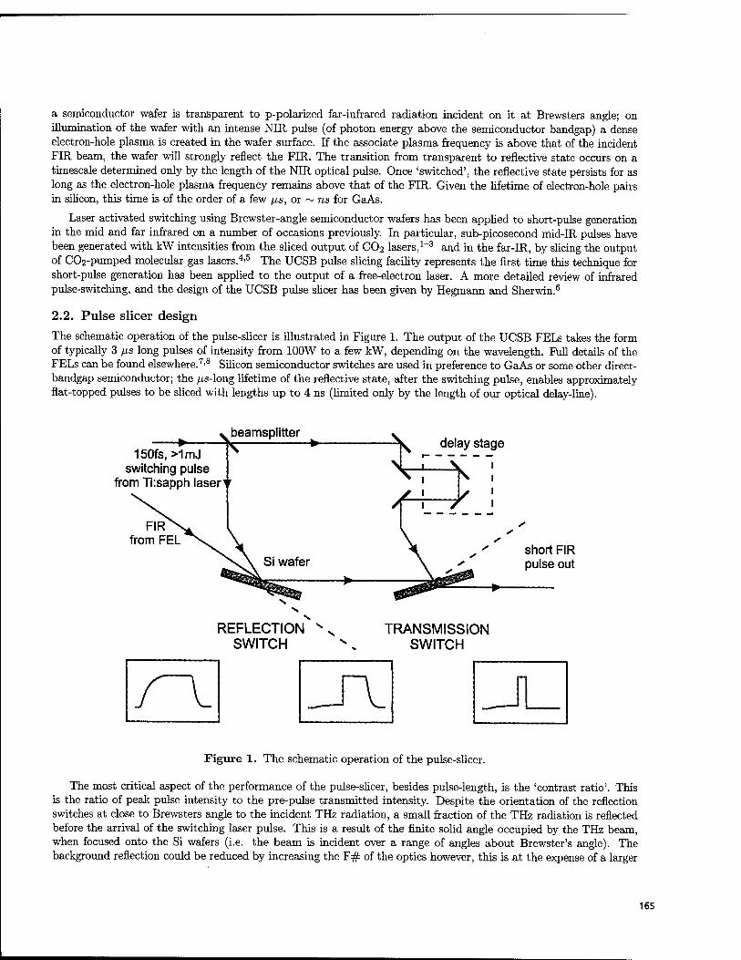
a semiconductor wafer is transparent to p-polarized far-infrared radiation incident on it at Brewsters angle; on illumination of the wafer with an intense NIR pulse (of photon energy above the semiconductor bandgap) a dense electron-hole plasma is created in the wafer surface. If the associate plasma frequency is above that of the incident FIR beam, the wafer will strongly reflect the FIR. The transition from transparent to reflective state occurs on a timescale determined only by the length of the NIR optical pulse. Once 'switched', the reflective state persists for as long as the electron-hole plasma frequency remains above that of the FIR. Given the lifetime of electron-hole pairs in silicon, this time is of the order of a few ßs, or ~ ns for GaAs.
Laser activated switching using Brewster-angle semiconductor wafers has been applied to short-pulse generation in the mid and far infrared on a number of occasions previously. In particular, sub-picosecond mid-IR pulses have been generated with kW intensities from the sliced output of C02 lasers,1"3 and in the far-IR, by slicing the output of CCVpumped molecular gas lasers.4'5 The UCSB pulse slicing facility represents the first time this technique for short-pulse generation has been applied to the output of a free-electron laser. A more detailed review of infrared pulse-switching, and the design of the UCSB pulse sheer has been given by Hegmann and Sherwin.6
2.2. Pulse slicer design
The schematic operation of the pulse-sheer is illustrated in Figure 1. The output of the UCSB FELs takes the form of typically 3 ps long pulses of intensity from 100W to a few kW, depending on the wavelength. Full details of the FELs can be found elsewhere.7,8 Silicon semiconductor switches are used in preference to GaAs or some other direct- bandgap semiconductor; the //s-long lifetime of the reflective state, after the switching pulse, enables approximately flat-topped pulses to be sliced with lengths up to 4 ns (limited only by the length of our optical delay-line).
150fs, >1mJ switching pulse
from Tksapph laser ♦
FIR from FEL
v beamsplitter \ +■
Si wafer
REFLECTION SWITCH
short FIR pulse out
TRANSMISSION SWITCH
Figure 1. The schematic operation of the pulse-sheer.
The most critical aspect of the performance of the pulse-sheer, besides pulse-length, is the 'contrast ratio'. This is the ratio of peak pulse intensity to the pre-pulse transmitted intensity. Despite the orientation of the reflection switches at close to Brewsters angle to the incident THz radiation, a small fraction of the THz radiation is reflected before the arrival of the switching laser pulse. This is a result of the finite sohd angle occupied by the THz beam, when focused onto the Si wafers (i.e. the beam is incident over a range of angles about Brewster's angle). The background reflection could be reduced by increasing the F# of the optics however, this is at the expense of a larger
165

off-axis parabloid mirror « = 2.4
mirror
lens
Si wafer
150 fs switching [is THz pulse pulse from FEL
Figure 2. Geometry of reflection switch; switching pulse is focused through a small hole in the off-axis parabloid mirror, to illuminate a 2mm diameter area on the silicon wafer.
THz spot size* on the switching wafer, so increasing the NIR pulse energy necessary for switching. Thus the overall contrast ratio is ultimately limited by the switching power available from the Ti-sapphire laser. Currently, an F# = 2.4 optical system is employed. The geometry of the reflection switch is illustrated in Figure 2. The sliced pulse is typically switched out of the full FEL pulse, approximately 1/xs after the start of the FEL pulse, once the FEL pulse has reached peak intensity. Thus, if the pulse-sheer has a contrast ratio of 104 : 1, the pre-pulse breakthrough during that first ps is equal to the total energy of a 100 ps switched pulse. If a detector with a long averaging time constant is used, this pre-pulse energy can easily swamp that of a short main pulse. This fact highlights the importance of fast THz detectors for use with the pulse-sheer. A detector with a time-constant of the order of 1 ns can more effectively resolve the main pulse energy from that due to pre-pulse breakthrough.
A single Si reflection switch will typically provide a contrast ratio of 100:1 or better. Two reflection switches are incorporated into the pulse sheer to provide a contrast ratio of at least 104 : 1. Rather less switching pulse power is required to activate the transmission switch, since even at plasma densities below that necessary for high reflectivity, the plasma is strongly attenuating. No post-switching breakthrough of the transmission switch is observed.
3. GE:GA PHOTOCONDUCTOR TEMPORAL RESPONSE
Gallium doped germanium photoconductors have traditionally been used for sensitive detection of far-infrared ra- diation with wavelengths in the region of 100 pm. In addition, photoconductivity has been extensively used as a spectroscopic probe of the electronic states in this systems.9 The far-infrared detector performance and electrical characteristics of Ge:Ga have been investigated in a number of previous studies.10'11 While the spectral responsivity of this material has been thoroughly characterized, the performance of Ge:Ga in the time-domain remain less well studied. The application of Ge:Ga detectors to far-infrared heterodyne detection has been investigated12,13; the detector bandwidth was found to increase with compensating dopant concentration. In the present work, we investi- gate the response of one of these high-bandwidth Ge:Ga samples in the time-domain, with a view to its application as a fast, sensitive THz detector for short-pulse experiments with the pulse-sheer facility. The measurements will demonstrate the importance of impact ionization effects at high THz excitation powers, giving rise to distortion in the temporal response of the photoconductivity.
TThe FEL beam is diffraction-limited.
166

3.1. Sample and measurement details
Previous characterization of the sample, for heterodyne detection applications has been reported previously14 (Sam- ple I.D. # 729-17.0 (22) ). The sample was fabricated from a phosphorous-doped germanium single crystal and subsequently 'transmutation doped'. This technique produces Ga acceptors and As or Se donors in a roughly 3:1 ratio. The sample studied here has an acceptor concentration of 1015 cm~3 and a donor concentration of 5.2 x 10¹⁴
cm~3. The DC mobility would normally be determined by temperature dependent Hall measurements, however this was not possible in the case of this, and other such heavily doped samples due to the large background conduction via hopping or tunnelling between the adjacent dopants. Since this parameter is important to make any quantitative analysis of the photoconductivity results, we have taken an estimate of the mobility based that found in less heavily doped samples, and scaled in inverse proportion to the donor density. This leads to a value of /x = 2000 cm2V~1s~l
with a large uncertainty (±1000 CTO2y-1s_1 perhaps). Low resistivity ohmic contacts were made to the sample by ion implantation.
■
101 r
f 10° r
•. - ■
+■■ -1 c 10 i—
3 -2 O 10
r
10'3 r ^ i ■ ■- 1 ■
10'
Sample bias (V)
10l
100 150 200 250 300 -1,
wavenumber (cm )
Figure 3. The spectral response of the Ge:Ga photoconductor obtain for a FTIR measurement is shown. The spectra has been normalised against that of a pyro-electric detector. The apparent double-peak nature of the Ge:Ga response is thought to be an interference artifact due to a vacuum window in the FTIR system. The THz excitation energy used in this study is indicated (arrow). The inset shows the DC I-V characteristics of the photodetector at 4.2K, in the dark. The breakdown voltage of 1.3V corresponds to an electric field of 26 V/cm.
The sample was thermally anchored, in a vacuum, to the 4.2 K plate of a 4He cryostat. Electrical connection from outside the cryostat to the sample was made by semi-rigid stainless-steel wideband co-axial cable; the sample was connected directly across one open end of the co-ax. The sample was biased by means of a 0.01-1000 MHz bandwidth 'bias-tee' outside of the cryostat. Thus the 50fi co-axial cable serves as both the load impedance for the photocurrent and source impedance of the voltage-bias. The RF output of the bias-tee was fed to a 750 MHz
167

acquisition bandwidth digital-sampling oscilloscope. An FEL laser energy of 84 cm * (120/im or 2.5 THz) was used for all measurements reported here.
3.2. Time-resolve photoconductivity results
The temporal response of the sample, for low excitation intensity, is shown in Figure 4. The photocurrent decays exponentially toward an equilibrium value, where the recombination rate is balanced by the THz photo-creation rate. The fall-time of 2.0 ± 0.1 ns is comparable with recombination times found in previous studies Ge:Sb:Cu12
and Ge:As:Se13 detectors. The slightly longer rise-time is the most likely result of hole-heating by the incident THz radiation; the effect of carrier heating will be discussed later in more detail, in relation to the saturation behaviour of the sample.
ZJ
"cö c
"co o o sz Q.
■
3.5 ns
\ 2.0 ns —»A
i
- reflection switch only
3.4 ns pulse
_i—i—i—i—i—i—■—i—i—
-
1 1 1 1 1
1 ns per div.
Figure 4. The time-domain response of the Ge:Ga photoconductor is shown for a step-excitation (reflection switch only), and for a 3.4 ns THz pulse. The aquisition bandwidth is 750 MHz. The start and end of the THz pulse are indicated by dashed lines. A slightly longer rise-time, relative to the fall-time, is evident.
Previously reported measurements, based on the frequency roll-off of the generation-recombination noise for this sample14 indicate a 3dB bandwidth of 70 MHz, corresponding to a recombination time of 2.3 ns. This is slightly above the value obtained from our time-domain measurements however, the previously reported value was obtained under bias conditions of 0.8^6r , where Ebr is the breakdown field (see figure 3-inset). The present measurements were carried out at 0.15^ and a slightly shorter recombination time is expected.
The temporal response of the sample at higher THz excitation powers is shown in Figure 5. In this case, the THz pulse length was 100 ps. As the excitation level is increase a strong deviation from exponential decay is observed. At the highest power levels, the photocurrent increases after the end of the THz pulse. Note that the traces plotted in Figure 5 are not offset; the higher sample current observed before the THz pulse is photocurrent due to the pre-pulse transmission of the pulse-sheer. For this measurement, only a single reflection switch was used, with a contrast ratio of 140:1.
168

0.05
0.04 -
Cä 0.03 -
ä 0.02 - o
8 001 I-
0.00
70
60 X
50 §■
40 |
30 §
-20 S
10
10 15 Time (ns)
Figure 5. The sample photoconductivity signals due to a 100 ps THz pulse, with the following THz excitation powers are shown: 0.4, 0.88, 2.32, 5.2, 9.2, 13.6, and 20 kW/cm2. Inset, the photoexcited hole densities after excitation (points) and the exponential fit (see text) to these points (solid) is shown as a function of excitation power. The estimated transient temperature rise of the hole is also shown (dashed).
4. RATE EQUATION MODELLING OF SATURATION BEHAVIOUR
The time-dependence of the photoexcited holes can be described using a rate-equation approach. The rate-equation description has been extensively used to model the non-linear DC electrical characteristics of doped germanium samples.15'16 The electric field dependence of the recombination and impact-ionization rates was found to be the origin of the non-linear behavior. These studies also highlighted a 'slow' component to the transient photocurrent with a time-constant of the order of a millisecond, due to space-charge effects at the sample contacts. Most recently, Monte Carlo simulations have been used to study the dynamics of the system near breakdown.17 The ns-timescale distortions of the photocurrent decay presented here have not been observed previously in germanium but similar phenomena have been reported in n-GaAs18 and (on a fis long timescale) in InP.19'20
Assuming charge neutrality in the sample (i.e. no space-charge effects), the local hole concentration, np, is described by
dnr -^■=aI.(A-D- ■np) + K-np-(A — D -np) -r ■ (D + np) (1)
where the first term on the right-hand side is due to photogeneration of free hole by the THz radiation of intensity I. The second term is due to impact ionization and the third term recombination. A and D are the acceptor and donor concentrations respectively. The above is a 'two-level' scheme i.e. the holes are either bound or free. Intermediate levels, acting as a 'charge sink', from which impact-ionization could occur, have been shown19'20 to give rise to the long-timescale photoresponse in InP; three and four-level rate-equations models were invoked to explain these results.
169
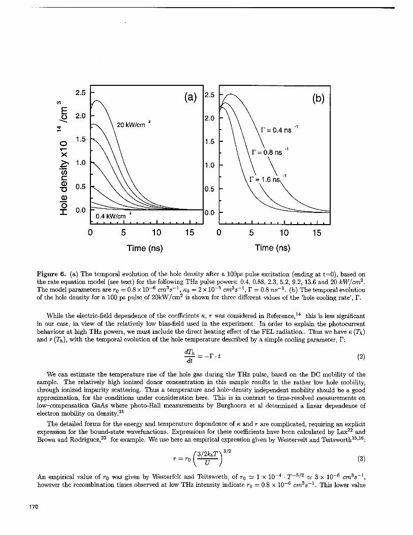
2.5 -
X >. 1 0 •+->
W c T3 0.5
0 O X 0.0
20 kW/cm
(a)
0.4 kW/cm _i i i i L_i i i i I i i_i i L
2.5 (b)
2.0
\ \r = 0.4 ns'1
1.5 \ \ T = 0.8 ns "1
1.0 \\ \ \r = 1.6 ns,1
0.5
0.0 -j—■—i—■—i ' «■■ i ■ ■ ■ . i .
0 5 10
Time (ns)
15 0 5 10 15
Time (ns)
Figure 6. (a) The temporal evolution of the hole density after a lOOps pulse excitation (ending at t=0), based on the rate equation model (see text) for the following THz pulse powers: 0.4, 0.88, 2.3, 5.2, 9.2, 13.6 and 20 kW/cm2
The model parameters are ro = 0.8 x 10 K0 ■■ r = 0.8 ns x. (b) The temporal evolution of the hole density for a 100 ps pulse of 20kW/cm2 is shown for three different values of the 'hole cooling rate', F.
While the electric-field dependence of the coefficients K, r was considered in Reference,14 this is less significant in our case, in view of the relatively low bias-field used in the experiment. In order to explain the photocurrent behaviour at high THz powers, we must include the direct heating effect of the FEL radiation.. Thus we have K (Th) and r (Th), with the temporal evolution of the hole temperature described by a simple cooling parameter, T:
dTh dt
-T-t (2)
We can estimate the temperature rise of the hole gas during the THz pulse, based on the DC mobility of the sample. The relatively high ionized donor concentration in this sample results in the rather low hole mobility, through ionized impurity scattering. Thus a temperature and hole-density independent mobility should be a good approximation, for the conditions under consideration here. This is in contrast to time-resolved measurements on low-compensation GaAs where photo-Hall measurements by Burghoorn et al determined a linear dependence of electron mobility on density.21
The detailed forms for the energy and temperature dependence of K and r are complicated, requiring an explicit expression for the bound-state wavefunctions. Expressions for these coefficients have been calculated by Lax22 and Brown and Rodriguez,23 for example. We use here an empirical expression given by Westervelt and Teitsworth15,16:
r0
{3/2kbT\3/2
V u (3)
An empirical value of r0 was given by Westerfelt and Teitsworth, of r0 ~ 1 x 10⁻⁴ • T-5/2
however the recombination times observed at low THz intensity indicate ro = 0.8 x 10 etnas' ■l
6 cm3s' t 3 x 10" _1. This lower value
170

is consistent with the recombination cross-section calculated previously14 and will be used to model the saturation behaviour of the sample. T is the lattice temperature and U represents the average energy of the holes, which is approximated for a drifted Maxwellian distribution by
U = lkbTh + ±m*vj (4)
Similarly, an empirical form for the ionization coefficient may be written
[U/B]1'2 1 K K°' 1 + f ' l + e{{B-l/2m'vl),kBTh} W
The second factor in this expression ensures that the impact ionization rate peaks for hole energies close to the acceptor binding energy, B, while the third factor describes the thermal distribution of holes. The above differs slightly from the form given by Westervelt and Teitsworth,15 where U did not include the hole thermal energy. In our measurements at relatively low bias the drift motion of the holes is not significant and the thermal energy dominates. The coefficient K0 may be estimated as KQ = v'-Kr2^ ~6x 10⁻⁶ cmPs*1, where the hole velocity needed to ionize an acceptor is v' = ^2B/m* and rB is the Bohr radius of the acceptor wavefunction. We find this estimate somewhat low to explain our data and a value of K0 = 2 x 10⁻⁵ cm3s~1 is used in the modelling.
The temporal evolution of the hole population has been modelled by numerical integration of Equations 1 and 2. The free hole density and temperature, at the end of the THz pulse represent the initial conditions; the hole density after excitation is calculated from the initial change in conductivity in the sample, due to the THz pulse, and the DC mobility. This has been plotted (data points) in the inset for Figure 5. Since the excitation occurs over a much shorter timescale than the recombination or impact ionization times, the photo-created hole population should follow an exponential approach to saturation
n°h = (A-D)(l-e-aIt)
Although the data fits an exponential form (solid line, inset to Figure 5), the pre-factor is found to be (A — D) — 2.11 x 1014 cm"3. This is a little under half the true neutral acceptor concentration (A — D) (even bearing the uncertainty in /i in mind). This low value is most easily explained in terms of large inhomogeneous broadening of the photoresponse. The excitation energy (84 cm-1) lies on the lower edge of the Ge:Ga band of responsivity (see Figure 3). Thus, only a fraction of the bound holes have excitation energies resonant with the FEL radiation, as suggested by the low pre-factor above.
The temperature increase of the free holes due to the THz radiation has been calculated as a function of FEL power (dashed line, inset to Figure 5), based on a Drude-type frequency dependence of the free-hole conductivity and assuming a uniform THz energy density over the 0.5 mm2 aspect area of the sample. Figure 6(a) shows the time-evolution of the hole density as calculated by numerical integration of the rate equations above; the initial hole populations and temperature have been chosen to correspond to the data shown in Figure 5. A hole cooling rate of T = 0.8 ns'1 is found to best fit the data. The modelled hole-density evolution at a pulse intensity of 20 kW/cm2
(the highest intensity used) for three different values of T is shown in Figure 6(b).
5. DISCUSSION
It is evident that impact ionization by the hot photocreated hole population can explain, at least qualitatively, the increase in sample conductivity after the end of the excitation pulse, at high powers. The detailed form of the hole cooling rate will depend on the hole distribution function, something we have little information on. Once the hole population has cooled to close to the lattice temperature, the population decay returns to the usual exponential decay form. We find from the rate equation modelling there is little freedom to chose the cooling parameter, in order to reproduce the data; a value of T ~ 1 ns is always requires, to within a factor of two, irrespective of the values of K0 and initial hole temperature and mobility chosen. Thus our experiment provides a limited degree of quantitative information on the hot-hole cooling rate. It is not clear whether this cooling rate is due to optical phonon emission by the high-energy tail of the hole distribution, or to acoustic phonon emission at lower energies. Studies of p-type Ge lasers indicate hole cooling on the order of tens or picoseconds, for hole populations at much higher temperatures (>100K).
171

6. CONCLUSIONS
In conclusion, we have outlined the design and performance of a pulse-slicing system used with the UCSB FELs for the generation of pico-to-nanosecond variable length, high intensity THz pulses. This short-pulse THz source has been applied to time-resolved photoconductivity measurements on a Ge:Ga sample with high compensating donor density. The measurements indicate a recombination time of 2.0 ± 0.1 ns. At high THz excitation powers we find the photocurrent continues to increase after the end of the THz pulse. This behaviour has been modelled by a rate-equation approach including impact-ionization of the acceptor-bound holes by the FEL-heated free-holes. The increased photocurrent persists for a time determined by the cooling time of the hot-hole population. The measurements suggest a characteristic cooling time close to a nanosecond.
Acknowledgments
The authors wish to acknowledge Dave Enyeart, Dean White and Jerry Ramian for their help with the operation of the UCSB FELs. This work was supported, in part, by ONR N00014-92-J-14520, NSF(MRI)-DMR-9724436 and NSERC and also by NASA, Washington, D.C. Headquarters, Order No. W17605, through the U.S. Department of Energy under Contract No. DE-AC03-76SF00098.
REFERENCES
1. C. Rolland and P. B. Corkum, "Generation of 130-fsec midinfrared pulses," J. Opt. Soc. Am. B 3, p. 1625, 1986. 2. A. Y. Elezzabi, J. Meyer, M. K. Y. Hughes, and S. R. Johnson, "Generation of 1-ps infrared pulses at 10.6um
by use of low-temperature-grown gaas as an optical semiconductor switch," Opt. Lett. 19, p. 898, 1994. 3. A. Y. Elezzabi, J. Meyer, and M. K. Y. Hughes, "600 fs 10.6um infrared pulse generation with radiation-damaged
gaas reflection switch," Appl. Phys. Lett. 66, p. 402, 1995. 4. R. E. M. D. Bekker, L. M. Claessen, and P. Wyder, "Generation of very short far-infrared pulses by cavity
dumping a molecular gas laser," J. Appl. Phys. 68, p. 3729, 1990. 5. T. E. Wilson, "A high-power far-infrared nh3 laser pumped in a three-mirror co2 laser cavity with optically-
switched cavity-dumping," Int. J. Infrared and Mm. Waves 14, p. 303, 1993. 6. F. A. Hegmann and M. S. Sherwin, "Generation of picosecond far-infrared pulses using laser-activated semicon-
ductor reflection switches," Proceedings of SPIE 2842, pp. 90-105, 1996. 7. An overview of the FEL design and performance can be found on the World Wide Web at http://sbfel3.ucsb.edu. 8. G. Ramian, "The new ucsb free-electron lasers," Nuclear Inst. and Methods in Physics A 318, pp. 225-229,
1992. 9. M. S. Skolnick, L. Eaves, R. A. Stradling, J. C. Portal, and S. Askenazy, "Far infrared photoconductivity from
majority and minority impurities in high purity si and ge," Solid State Comm. 15, pp. 1403-1408, 1974. 10. P. R. Bratt, "Impurity germanium and silicon infrared detectors," Semiconductors and Semimetals 12, 1977. 11. E. E. Haller, "Physics and design of advanced ir bolometers and photoconductors," Infrared Physics 25, p. 257,
1985. 12. G. Dodel, J. Heppner, E. Holzhauer, and E. Gornik, "Wideband heterodyne detection in the far infrared with
extrinsic ge photodetectors," J. Appl. Phys. 54(8), pp. 4254-4259, 1983. 13. F. Kohl, W. Müller, and E. Gornik, "Speed limitations of ge far-infrared photoconductive detectors," Infrared
Physics 18(5-6), pp. 697-704, 1978. 14. I. S. Park, E. E. Haller, E. N. Grossman, and D. M. Watson, "Germanium:galhum photodetectors for far infrared
heterodyne detection," Applied Optics 27(19), pp. 4143-4150, 1988. 15. R. M. Westervelt and S. W. Teitsworth, "Nonlinear transient response of extrinsic ge far-infrared photodetec-
tors," J. Appl. Phys. 57(12), pp. 5457-5469, 1985. 16. S. W. Teitsworth and R. M. Westervelt, "Subharmonic and chaotic response of periodically driven extrinsic ge
photoconductors," Phys. Rev. Lett. 56(5), pp. 516-519, 1986. 17. W. Quade, G. Huepper, and E. Schoell, "Monte carlo simulation of the nonequilibrium phase transition in p-type
ge at impurity breakdown," Phys. Rev. B 49(19), pp. 13408-13419, 1994. 18. R. E. M. D. Bekker, Time resolved far-infrared magnetospectroscopy of photo-ionised shallow donor impurities
in GaAs epitaxial layers and GaAs/AlGaAs quantum well structures. PhD thesis, Max Plank Institut fuer Festkoeperforschung, Hochfeldmagnetlabor, Grenoble, 1990.
172

19. J. M. Chamberlain, A. A. Reeder, L. M. Claessen, G. L. J. A. Rikken, and P. Wyder, "Impact excitation and bottleneck effects in the time-resolved far-infrared photoresponse of high-purity inp," Phys. Rev. B 35(5), pp. 2391-2398, 1987.
20. G. L. J. A. Rikken, P. Wyder, J. M. Chamberlain, R. T. Grimes, and L. L. Taylor, "Time-resolved recombination dynamics of photoionized hydrogenlike impurities," Phys. Rev. B 38(6), pp. 4156-4164, 1988.
21. J. Burghoorn, T. O. Klaassen, and W. T. Wenckebach, "The dynamics of shallow donor ionization in n-gaas studied with subnanosecond fir-induced photoconductivity," Semicond. Sei. Technol. 9, pp. 30-34, 1994.
22. M. Lax, "Cascade capture of electrons in solids," Phys. Rev. 119, p. 1502, 1960. 23. R. A. Brown and S. Rodriguez, "Low-temperature recombination of electrons and donors in n-type germanium
and silicon," Phys. Rev. 153(3), pp. 890-900, 1967.
173

174

SESSION 8
New THz Sources
175

Open confocal resonators with quasi-optical arrays to measure THz dynamics of quantum tunneling devices
J. S. Scott«, M. C. Wanke0, S. J. Allen0
K. D. Maranowski^, A. C. Gossardfc
D. H. Chowc
^Physics Dept. and Center for Terahertz Science and Technology,
University of California, Santa Barbara, CA, USA
^Materials Dept., University of California, Santa Barbara, CA, USA cHughes Research Laboratory, Malibu, CA, USA
ABSTRACT
A semi-confocal etalon has been used as a quasi-optical cavity to explore the dynamical conductance of Bloch-oscillating superlattices at terahertz frequencies. To maintain both DC and irradiated field uniformity and to maximize the coverage of the cavity mode with the devices of interest, the tunneling structures have been photolithographically fabricated into micron-sized mesa-isolated devices forming a quasi-optical square array interconnected by a metal grid with a period which is less than the wavelength in the semiconductor of the infrared probe radiation. At a given bias on the device array and scanning the cavity through a resonance, the loss and reactance of the tunneling devices embedded in the array is measured by detecting a change in the position and line shape of the cavity resonance. Transmission measurements of the cavity loading by the biased quasi-optical arrays at frequencies from 250GHz to 3.0THz will be presented and compared to theoretical predictions.
Keywords: terahertz, cavity, superlattice
1. INTRODUCTION
Between the established technologies of the GHz region of the spectrum and the techniques available in the mid-IR there is to date a lack of compact tunable sources of THz radiation. This technology gap is currently being filled by either single line sources or FEL's, which although capable of providing high power tunable THz radiation, are far from being considered a compact source.
Devices based on a Bloch-oscillating superlattice are predicted to have a dynamic conductance at THz frequencies that exhibits broadband gain from DC up to the Bloch frequency (o)B=eaE/h) in the absence of domain formation1. Here, 'E' is the DC electric field across a superlattice of periodicity 'a'. A superlattice with typical momentum and energy relaxation times, in addition to the broadband gain profile, should also exhibit a region of enhanced negative conductance in a narrow band region just prior to the Bloch frequency. Engineering additional losses would act to surpress the broadband gain component of the conductance while retaining the narrow band region.
Part of the SPIE Conference on Terahertz Spectroscopy and Applications
176 San Jose. California • January 1999 SPIE Vol. 3617 • 0277-786X799/$ 10.00

a(co)
0
1 1 1 1 1 1 ) 1 1 1 1 1 1 1 1 1 1 1 1 1 1 1 1 1
- ie=ip8 yv
- V4** / X^_
11 i i 11 i i i i
s'" '5- : : -i»" — V.
rco / B
'-
Gai
n I
l - * --»^^
■ i i i i i i i i i .... i ... .
0 1 2 3 4 5 6 7 Frequency (THz)
Figure 1. Narrow-band conductance from 2-3THz for a 100Ä period superlattice with Te^lps and Tp=.4ps.
The possible exploitation of this feature as a tunable source of THz radiation requires the development of experimental techniques to measure the dynamical conductance of biased superlattices. The impetus of this work is to demonstrate a technique for measuring dynamical conductivities at THz frequencies as a first step towards developing a compact tunable source of THz radiation.
2. EXPERIMENTAL TECHNIQUE
The response of biased superlattices to FIR radiation was measured by detecting the fractional change in the transmission (AT/T=(T(V)-T(0))/T(0)), through a semi-confocal cavity formed by a small area spherical mirror and a quasi-optical array (QOA) of GaAs/AlGaAs superlattice devices. THz radiation from the UCSB free-electron lasers is incident from the substrate side of the sample.
To ensure the cavity mode involved only the central region of the QOA the spherical reflector (.25" radius of curvature) has a small diameter of .5-1.3 mm. Concentric to the curved reflector is a collection cone with an opening of 2mm. This allows the confined cavity mode to be sampled by detecting any leakage around the periphery of the curved reflector while excluding all radiation that is not confined within the cavity. The transmission is then detected by an InSb hot-electron bolometer.
THz
0 50 100 150 200 Z (um)
Figure 2. QOA in confocal resonator and typical cavity resonances
177

For a given irradiation frequency, the spatial separation between the QOA and the spherical reflector is varied bringing the cavity into resonance (figure 2). Measuring the line shape changes in the cavity resonances due to a change in the applied voltages to the QOA provides a measure of both the losses and reactances of the superlattice devices embedded in the array. Since the wavelengths of the applied THz radiation are much larger than any dimension of the array, the array can be modeled using standard transmission line techniques where it is assumed that the array behaves as a conducting sheet having the impedance of a unit cell of the array. The successful modeling of the measured transmission changes then hinges on the accurate accounting of all parasitics associated with the devices in the QOA.
Demands of field uniformity across the devices, and of maximizing the irradiated area for maximum detected signal dictate a sample design where a high density of micron-size individual devices which
must be electrically interconnected and occupy an area comparable to the irradiating beam waist. This is accomplished using devices processed into a quasi-optical array. The room temperature DCIV and the form of
the completed array is shown in Figure 3.
200
100 -
Idc (mA)°
-100-
-200
0
-50 0 Voltage 50
^«i^^^^^^3$%^S^f
Figure 3. a) Room temperature QOA DCIV b) Quasi-optical array
The quasi-optical array of devices was fabricated from an MBE grown 50 period GaAs/AlGaAs superlattice with 80Ä wells and 20A barriers, giving a mini-band width of about 20meV. The superlattice is uniformly doped to nominally be 1017/cm2, while the emitter and collector are each highly doped. The array measures 2 mm2 and consists of 96 2|im x 2mm parallel mesas which are serially connected by gold sidewall interconnects and the bottom doped layer.
3. RESULTS
Measurements of the fractional change in transmission due solely to a change in the applied voltage on the array were performed at 10, 15, 20, 41, 51, 65, 71, 84 and 101 cm"1. The bias dependent cavity resonances at .45 THz are shown in figure 4. The 6 curves of AT/T have been offset for clarity without changing the vertical scaling. The large downward central peak is the measured transmission for an unbiased array. With the cavity on resonance, continuous DC field dependencies of the measured AT/T quantity are shown in figure 5 for 0.3 THz, 0.7 THz and 3.4 THz. Beyond 1 THz the curve shapes of the measured response are indistinct from the curve obtained at 3.4THz.
178

Figure 4. Spatial cavity scans of the measured unbiased transmission and the percent change in the fractional transmission due to six different applied voltages taken at .45 THz.
0
I I I I I I I I I I 11 I I I I I I I I I II 11 I I 11 I I
.3 THz
.7 THz
3.4 THz
' ' i i.. ■ ,i ■■ ■■ i i
E/Ec
nA) """" 1A ' ' r
100
50 7 QOA / DdV F i i i i i i i
0 12 3
E/Ec
Figure 5. DC field dependence of the measured fractional transmission change.
Although at this juncture the modeling of the measured transmission has yet to be completed, we can compare the curve shapes obtained to what theory predicts. Since the calculated dynamic conductivities are extremely sensitive to the energy and momentum relaxation times we can look for simultaneous similarities between the theoretical curves and the measured response for all three of the shown constant frequency curves of figure 5.
The curves shown in figure 6 are the theoretical results for the voltage dependent fractional change in the conductivity at the same three frequencies as the data in figure 5. The energy relaxation time was held at lps, while the momentum relaxation time was varied. Also shown in figure 5 is the theoretical DCTV for the extracted relaxation times.
179

T—r~i—[~i—i—i—|—i—i—i—|—i—i—r T—i—r
0
,7THz
J I I L_l L_J I I I I I I I l_l I I L
E/Ec
-l—i—
calculated DCIV
0 2 4 6 8 E/Ec
Figure 6. Theoretical DC field dependencies of the fractional dynamic conductivity at the same frequencies as the data.
4. CONCLUSIONS
A DC field across the QOA when placed in a cavity produces sizable changes in the transmission, measurable well into the THz realm, when compared to the unbiased array. This fractional change in transmission being a measure of the dynamic conductivity of the superlattice devices populating the QOA.
Clearly the crux of the experiment depends on the full transmission line modeling of the measured transmission changes. This includes a full accounting of the parasitics naturally present in the sample as well as the additional parasitics necessarily introduced in order to apply DC fields. A critical anchor point for the modeling will be the zero crossings of the measured AT/T response, where inter-frequency comparisons can be made without having to account for changes in the AC field coupling to the array as the irradiating frequency is changed.
Additionally, the role of domain formation needs to be included in any credible comparison of experiment to theory.
ACKNOWLEDGMENTS
This work was funded by AFOSR, and ONR-MFEL.
REFERENCES
1. C. Ktiterov et al., "Bragg Reflections and the High-frequency Conductivity of an Electronic Solid-state Plasma.", Soviet Physics - Solid State 13 (8) pp. 1872-1874, 1972
180

Actively mode-locked THz p-Ge hot-hole lasers with electric pulse-separation control and gain control
R. C. Strijbos,0 A. V. Muravjov,0 S. H. Withers,0 S. G. Pavlov,* V. N. Shastin,* and R. E. Peale* a Department of Physics, University of Central Florida, Orlando, FL 32816 USA
b Institute for Physics of Microstructures, Russian Academy of Sciences, GSP-105,Nizhny Novgorod 603600 Russia
ABSTRACT
Electric control of the separation between two interleaved pulse trains from a far-infrared (1.5-4 THz) p-Ge laser, which is actively mode-locked by rf gain modulation at the second harmonic of the roundtrip frequency, is demonstrated by changing the electric bias at the rf contacts. A suggested application is telemetry using pulse-separation modulation. Optimal operation of the laser on the light-to-heavy-hole transition requires strong, perfectly crossed electric and magnetic fields, but the experimental data reveal a electric-field component along the magnetic field caused by space-charge effects inside the laser crystal, even when the applied fields are perfectly orthogonal. Monte Carlo simulations together with a Poisson solver are used to discuss the various mechanisms behind these effects and to find the electric field inside the laser crystal. These calculations agree reasonably well with experimental data obtained so far, and show not only the significant impact that charging can have on the output of actively mode-locked p-Ge lasers, but also suggest that they strongly influence the average gain of p-Ge lasers in general.
Keywords: far-infrared, THz radiation, semiconductor lasers, active mode locking, hot hole transport, space charge, p- germanium
1. INTRODUCTION
To date p-Ge hot hole lasers are still the only solid-state lasers in the far-infrared region (50 — 140 cm-1 or 1.5 — 4 THz). In contrast to conventional semiconductor lasers, where the lasing transition is between the conduction and valence band, here lasing occurs between different valence subbands, and p-Ge lasers can therefore be classified as unipolar or intersubband semiconductor lasers. Population inversion occurs in a bulk laser rod of relatively lightly doped p-type germanium A^ « 1014 cm-3) at helium temperatures (T < 20 K) and is based on the largely different motion of light and heavy hot holes in strong crossed electric and magnetic fields (E « 0.3 — 3 kV/cm, B = 0.3 — 3 T). The laser is usually operated at a 1-10 Hz repetition rate, and delivers microsecond pulses of a few Watt peak power. The laser can be tuned in the whole range from 1.5 — 4 THz,1 and considerable progress has been made towards developing a continuous-wave (CW) laser for use as a local oscillator for far-infrared heterodyne spectroscopy.2 On the other hand, the broadband nature of the light-to-heavy hole band laser opens the possibility to generate picosecond, high-intensity pulses in the far infrared, a desirable feature for time-resolved (linear and non-linear) THz spectroscopy and other related applications, that is currently only available using free-electron lasers. Recently, active mode locking has been unambiguously demonstrated3-5 in the time domain, resulting in a train of FIR pulses of about 200 ps. In this contribution, our recent results on mode-locked p-Ge lasers will be presented. Harmonic mode locking is demonstrated, and the delay between the two pulses traveling in the cavity can be electrically tuned from zero to half the cavity roundtrip time. Clear experimental evidence is found for the occurrence of space charge in the laser crystal. To account for the observed phenomena, a detailed understanding of the hot hole transport underlying p-Ge lasers is necessary . Therefore, the basic features of hot hole transport in crossed fields and the pumping mechanism of p-Ge lasers are first shortly recapitulated in section 1.1 using a simple isotropic model.
1.1. Hot hole transport in crossed fields and pumping mechanism
A relatively low impurity concentration and liquid helium temperatures are required to obtain lasing in p-Ge crystals. In these conditions the emission of an optical phonon is by far the most probable scattering process (i.e. Top ~ 0.1 ps), but it requires
Part of the SPIE Conference on Terahertz Spectroscopy and Applications San Jose, California • January 1999 SPIE Vol. 3617 • 0277-786X/99/$10.00
181
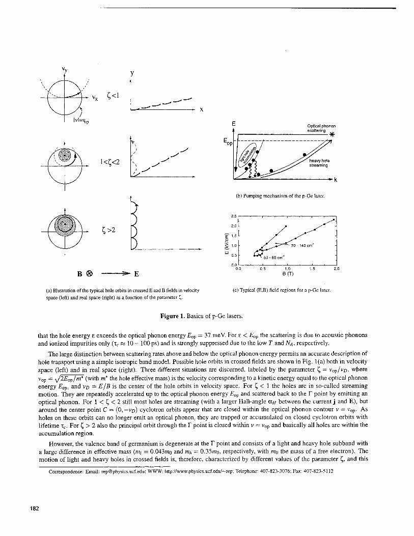
-vx C<1
1<^<2
C>2
B ®
Optical phonon scattering
(b) Pumping mechanism of the p-Ge laser.
2.5
2.0
? 15
LU 0.5
0.0
■50-60 cm"1
-^ E 1.0
B(T)
(a) Illustration of the typical hole orbits in crossed E and B fields in velocity space (left) and real space (right) as a function of the parameter £.
(c) Typical (E,B) field regions for a p-Ge laser.
Figure 1. Basics of p-Ge lasers.
that the hole energy E exceeds the optical phonon energy £op = 37 meV. For £ < Eop the scattering is due to acoustic phonons and ionized impurities only (ic « 10— lOOps) and is strongly suppressed due to the low T and Afo, respectively.
The large distinction between scattering rates above and below the optical phonon energy permits an accurate description of hole transport using a simple isotropic band model. Possible hole orbits in crossed fields are shown in Fig. 1(a) both in velocity space (left) and in real space (right). Three different situations are discerned, labeled by the parameter L, = vop/vo, where vop = y/2Eop/m* (with m* the hole effective mass) is the velocity corresponding to a kinetic energy equal to the optical phonon energy Eop, and VD = E/B is the center of the hole orbits in velocity space. For C, < 1 the holes are in so-called streaming motion. They are repeatedly accelerated up to the optical phonon energy £op and scattered back to the T point by emitting an optical phonon. For 1 < t, < 2 still most holes are streaming (with a larger Hall-angle a# between the current j and E), but around the center point C = (0,-VD) cyclotron orbits appear that are closed within the optical phonon contour v = vop. As holes on these orbits can no longer emit an optical phonon, they are trapped or accumulated on closed cyclotron orbits with lifetime ic. For C, > 2 also the principal orbit through the T point is closed within v = vop and basically all holes are within the accumulation region.
However, the valence band of germanium is degenerate at the T point and consists of a light and heavy hole subband with a large difference in effective mass (mi = 0.043mo and m/, = 0.35mo, respectively, with mo the mass of a free electron). The motion of light and heavy holes in crossed fields is, therefore, characterized by different values of the parameter £, and this
Correspondence: Email: [email protected]; WWW: http://www.physics.ucf.edu/~rep; Telephone: 407-823-3076; Fax: 407-823-5112
182

forms the basis for the pumping mechanism of the light-to-heavy hole band laser as shown in Fig. 1(b). For properly chosen E and B values, all light holes are accumulated (C,i » 2), while heavy holes are (partially) in streaming motion (£/, < 2). The upper laser level has, therefore, a much longer lifetime than the lower level. The latter is depopulated by heavy hole acceleration by the electric field, while the former is pumped by the 4% of the streaming heavy holes that end up in the light hole band after optical phonon emission. Therefore, all necessary conditions for establishing a laser on the light-to-heavy-hole transition (or Inter-Valence-(sub-)Band (IVB) transition) can be met. Fig. 1(c) shows the typical region of E and B fields, where lasing is observed experimentally, showing excellent agreement with the predictions of the above model.
1.2. gain modulation and mode locking
a) 2
0 -
- 11., 1111,,. i:, i,, 111 _ ■
• \ Ez=30 Vcm"1 • E2=20 Vcm"1 .
- E2=10 Vcm"1 - . V E2= 0 Vcm"1 .
1 \ ■v ^p
— -
■ \\ \\\—'X'/y'/' '"r
- " *vv-\\vr>^V'
— 'CTlh
°"tot -
■ ■" i ■ ■" i ■ ■ ■ ■ i ■ ■ ■ •>.. ■ ■ i ■ -
0 5 10 15 20 25 30 35 photon energy (meV)
(a) Light holes spiraling in the accu- mulation region iic beyond the opti- cal phonon energy Qo due to a small electric field EL in the direction of the magnetic field.
(b) Dependence of small-signal gain on EL,
T = 10 K, E = 1.15 kV/cm ||< lIO > B = 0.9 T ||< 112>./V,= 1.2 x 1014 cm"3, p„ = 7 x 10" cm-3, Brooks-Herring model with self-consistent screening.
Figure 2.
From Fig. 1(b) it is clear that the IVB p-Ge lasers can have a wide output spectrum (typically a width of 20-30cm_1is observed) and are, therefore, very suitable for the amplification or generation of THz pulses on a picosecond timescale. The latter requires an element in the laser cavity whose gain or loss in the far infrared can be modulated. Such an element has to operate in cryogenic conditions, however, preferably in the whole frequency range of p-Ge laser emission. Moreover, inclusion of an external element in the laser cavity is expected to cause reflections at the interfaces that might complicate mode locking. To avoid such problems it was proposed in Ref. 6 to induce active mode locking by radio-frequency (rf) gain modulation at one end of the laser crystal. This is rather similar to a method used for active mode locking of semiconductor diode lasers, where the pump current is modulated by applying an rf field in addition to the constant bias. In our case, however, not the magnitude of the pump current is changed, but rather its direction. This is achieved by applying the rf to two small additional contacts perpendicular to the main high-voltage contacts of a Voigt-configured p-Ge laser, where the applied electric and magnetic field are perpendicular to the long axis of the laser crystal. The rf field thus introduces small electric field components EL along the magnetic field, and it is easily understood why this decreases the small-signal gain significantly. As shown above (Fig. 1(a)), the magnetic field restricts the motion of accumulated light holes in the transverse plane such that their kinetic energy remains below the optical phonon energy. However, along the magnetic field they can still move freely with very high mobility, and a small EL field will turn the closed cyclotron orbits of Fig. 1(a) into spiral-like orbits as shown in Fig. 2(a). Eventually the light holes are accelerated beyond the optical phonon energy, they emit an optical phonon, and are primarily scattered into the heavy hole band. Therefore, the population inversion and the small-signal gain decrease. Clearly, this method is only effective when
183

the Ei field accelerates the light holes beyond Eov before they are scattered back to the heavy hole band anyway by interband scattering on acoustic phonons and ionized impurities.
Monte Carlo simulations show that for the usual temperatures and ionized impurity concentration, the desired effect is easily accomplished, and a small rf electric field (only a few percent of the main pumping electric field) along the magnetic field is already enough to modulate the gain by 30-50% (see Fig. 2(b)). When the gain is modulated at (a harmonic of) the roundtrip frequency, only the pulse traveling through the modulator at maximum gain is continually amplified, yielding the typical pulse-train output of an actively mode-locked laser.
2. EXPERIMENTAL SETUP
Oscillator
Counter
^
Pulse Generator
JY
_n Switch H Control
Switch
IT
U2I~~ r-| Cry stal|
-€> rf Line
0.3 W
40 W
Solid State Amp
800 W Crystal Detectors
HV Pulser
1—TYYWJ'
-©■ HV Line
■<£
20 40 Time (ns)
(b) (Attenuated) output of the pulse- forming switch
V//////tf EHV+Er(
(a) Rf setup. Thick lines denote coaxial lines. (c) The p-Ge laser crystal with applied fields and mirrors
Figure 3.
Single-crystal, Ga-doped, p-Ge (No - NA = 7 x 1013 cm-3) is cut into rectangular bars with a cross section of 7 x 5 mm2. Crystal lengths are chosen 42.1 and 84.2 mm such that the laser roundtrip frequencies match the rf frequency vlf near 452 MHz of relatively cheap ham-radio electronics or its second harmonic. The two opposite lateral 5 x L mm2 sides of the crystal are evaporated with aluminium and subsequently annealed to provide Ohmic contacts for the main high-voltage (HV) field. At the same time, small additional contacts with a length of ~ 4 mm are fabricated at one end of the crystal perpendicular to the main contacts (Fig. 3(c)). Applying a constant bias or an rf field to these contacts introduces a local, small, additional electric field EL || B, which is used to modify or modulate the small-signal gain at one end of the laser crystal. The crystal ends are polished parallel to each other within 1' accuracy and two external copper mirrors (with diameters of 7 and 5 mm) are attached to them via a 20,um thick teflon film to form an external resonator (Fig. 3(c)). The p-Ge crystals are immersed in liquid helium at 4.2 K in a cryostat (Janis 8DT), and placed between the poles of a room temperature electromagnet (Walker Scientific HF-9H), which provides magnetic fields up to 1.4 T in Voigt geometry (i.e. the magnetic field is perpendicular to axis of thejaser resonator). Electric field pulses £Hv are applied from a low duty-cycle thyratron pulser. The field orientations are EHv 11 [ 110] and B 11 [ 112]. Radiation emitted from around the smaller outcoupling mirror is collected and conducted out of the top of the cryostat using a brass light pipe. A teflon lens was used to seal the light pipe and focus the laser output radiation on a whisker-contacted Schottky-diode detector, biased using a simple homemade battery-powered current source and a Minicircuits 15542 bias-T. The diode chip (1T17(82)) was purchased from the University of Virginia and the corner cube was made by Savant-Vincent, Inc.,
184

Tampa, FL. Whiskers were formed, electrolytically sharpened, and contacted to the diode by the authors. The detector signal is boosted by a Picosecond Pulse Labs 5840 amplifier with 10 GHz bandwidth, and recorded on a Tektronix SCD5000 transient digitizer with 4.5 GHz analog bandwidth, 200 G-samples/s, and 11 bits vertical resolution (2 mV quantization steps).
Fig. 3(a) shows the rf system assembled for the experiments to produce clean sub-/js pulses which just overlap the HV pulses to prevent heating of the laser crystal by the rf. Since the impedance of the crystal between the rf contacts is low, high rf power is required, in part to overcome the unavoidable imperfect impedance match to the dynamic load. The General Radio 1362 UHF oscillator delivers about 0.3 W CW signal that is frequency stable within a few tens of kHz. A directional coupler feeds a fraction of this signal to a Stanford Model SR620 frequency counter. The main part goes to a Minicircuits Model 15542 PIN diode switch controlled by 8 V signals from a home built controller, that itself is driven by standard TTL pulses. The (attenuated) signal after the switch is plotted in Fig. 3(b) and demonstrates the sharp rise and fall and the short pulse lengths obtainable. From the switch, low duty-cycle rf bursts enter a GE MASTR II solid-state power amplifier with gain control to give up to 40 W. This is fed to a Henry Radio Model 2004A tube amplifier to give up to 800 W. A Microwave Devices 318N3 directional coupler and HP 420A crystal detectors monitor forward and reflected rf power. Power measurements were verified by direct observation of the rf voltage on a fast oscilloscope. Simple isolation capacitors were used to improve impedance match to the dynamic load and protect HV and rf systems from each other. Additionally, a bias Ui - U\ can be supplied to the small contacts from the main high voltage pulse by setting the potentials U\ and U% using two variable voltage dividers. This is a new feature compared to the set-ups described in Refs. 3,4 and turns out to be a very important parameter for controlling the output of the mode-locked p-Ge laser, as will be described in the next section.
3. RESULTS AND DISCUSSION
3.1. Active mode locking
3.1.1. 42.1 mm sample
3.5 4.0 4.5 5.0 5.5 Time (ns)
600
400-
1.-V" 5 200- 3 £ 450 452 454
Frequency (MHz) -J . 1 . I
0 6 8 10 Time (ns)
12 14 16
Figure 4. Output from the actively mode-locked 42.1 mm laser crystal. The upper inset shows a different shot with 150 ps pulses. In the lower inset the rf resonance at half the roundtrip frequency is plotted.
A summary of our first mode-lock results for the 42.1 mm sample upon applying rf during the laser pulse is given in Fig. 4. For arbitrary rf frequencies the EL field due to the rf reduces the gain in the region between the additional contacts and the laser can be brought below threshold by increasing the rf power. The forward rf power required to extinguish lasing is plotted in the lower inset of Fig. 4 versus the rf frequency. At 452.2 MHz a resonance occurs, where the laser still operates even when the full available forward rf power is applied. This frequency corresponds to half the cavity roundtrip frequency. However, since we expect the gain to be maximal at the rf nodes (EL = 0) and minimal at the rf extrema, and hence the gain to be modulated at twice the rf frequency, the condition for active mode locking that the gain is modulated at the roundtrip frequency is met.
185

Shifting the modulation frequency by more than ±0.5 MHz blocks the lasing, as expected for a mode-locked laser because circulating pulses do not remain in phase with the gain modulation. At resonance, the Schottky diode detector signal registers the mode-locked pulse train plotted in Fig. 4. The upper inset shows 150 ps pulses from a different shot. The basic pattern of pronounced, separated pulses is repeatable with only minor differences from shot to shot.
It is noted here that for the experiment of Fig. 4, a bias of about 20 V is applied to the rf contacts in addition to the rf power. Changing this bias by more than about 5 V removes the resonance observed in Fig. 4. This indicates that for this particular situation mode locking is only possible with the bias. The implications of this will be discussed in section 3.2 together with additional measurements.
3.1.2. 84.2 mm sample
a) 50 100 150
Time (ns) 200 20 40
Time (ns) 60
(a) Output of the actively mode-locked 84.2 mm long laser crystal. (b) The development of a pulse of increasing intensity and decreas- ing pulsewidth in the laser cavity is clearly reflected in the start of the pulse train.
Figure 5.
The experiments are repeated for a laser crystal that is twice as long as in the previous section. The length of L — 84.2 mm now corresponds to a roundtrip time 7 = 2* n^Ljc = 2.20 ns, where riQe = 3.925 is the refractive index of germanium, and c is the speed of light, and the roundtrip frequency is VRT — l/T = 453.6 MHz. Again this is very close to the experimentally found resonance at 453.8 MHz, where the applied rf is unable to extinguish lasing even at maximum rf power, indicative of mode-locked behavior. Figure 5 shows the output pulse train of the actively mode-locked pulse train as detected on the Schottky diode and registered at the transient digitizer. The pulses are separated by the roundtrip time T = 2.20 ns, as it results from a single pulse traveling to and fro within the resonator and partially coupled out each time it hits the outcoupling mirror. A close-up of the start of the pulse train clearly shows the shortening of the pulse in the resonator as its intensity grows.
When the constant bias to the rf field is changed by changing the potentials U\ and U2 using the voltage dividers, again the output of the actively mode-locked laser changes drastically, as can be seen in the left part of Fig. 6, where the output pulse train is plotted for different settings of the external bias (U; —1/2). At zero external bias, a train of pulses separated by the roundtrip time is observed, similar to the ones shown in Fig. 5. However, when the external bias is increased, the mode-locked pulses start to broaden and eventually split into two. A further increase of the bias causes further separation of the pulses, and the distance between these pulses can be tuned to approximately half the roundtrip time of the laser cavity.
This behavior is interpreted in the right part of Fig. 6, where the expected time dependence of the modulated gain is plotted based on the theoretically determined decrease of gain as a function of the EL field along the magnetic field direction (see Fig. 2(b)), as shown in the upper left corner of each subfigure. In each of these figures, the rf signal shown in the lower left corner is biased at a different level, and the upper right curve shows the resultant modulation of the small-signal gain in time, while the lower right bold curve shows the expected output pulse train.
At a certain bias value (set by the voltage U\ — I/2 in Fig. 3(a) between the additional contacts), the rf field is applied at the peak of the gain-versus-£/. curve [situation (C) in Fig. 6]. Hence gain modulation occurs at twice the rf frequency, and the double pulse output from harmonic mode locking is expected. Moving the bias away from the point of maximum gain, the gain
186
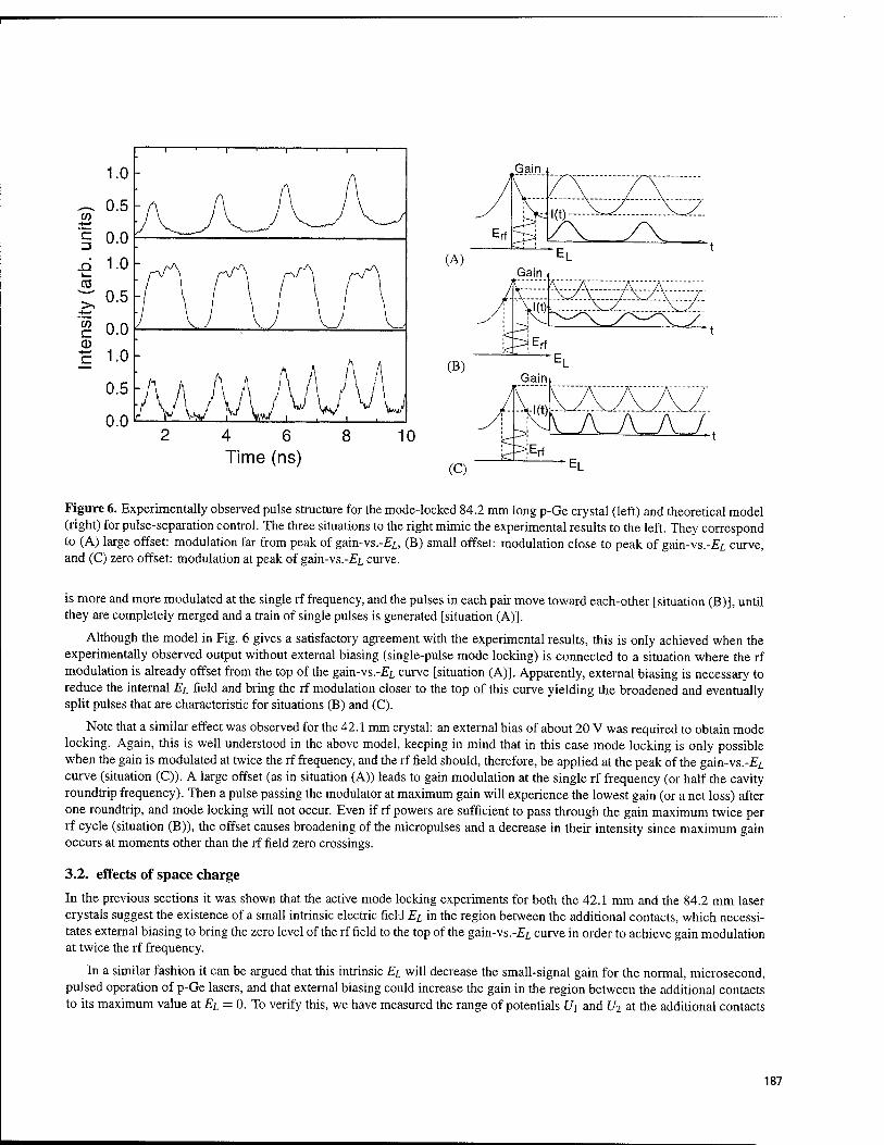
.Gain *
4 6 Time (ns)
10
Figure 6. Experimentally observed pulse structure for the mode-locked 84.2 mm long p-Ge crystal (left) and theoretical model (right) for pulse-separation control. The three situations to the right mimic the experimental results to the left. They correspond to (A) large offset: modulation far from peak of gain-vs.-£/., (B) small offset: modulation close to peak of gain-vs.-£i curve, and (C) zero offset: modulation at peak of gain-vs.-£z. curve.
is more and more modulated at the single rf frequency, and the pulses in each pair move toward each-other [situation (B)], until they are completely merged and a train of single pulses is generated [situation (A)].
Although the model in Fig. 6 gives a satisfactory agreement with the experimental results, this is only achieved when the experimentally observed output without external biasing (single-pulse mode locking) is connected to a situation where the rf modulation is already offset from the top of the gain-vs.-E/, curve [situation (A)]. Apparently, external biasing is necessary to reduce the internal EL field and bring the rf modulation closer to the top of this curve yielding the broadened and eventually split pulses that are characteristic for situations (B) and (C).
Note that a similar effect was observed for the 42.1 mm crystal: an external bias of about 20 V was required to obtain mode locking. Again, this is well understood in the above model, keeping in mind that in this case mode locking is only possible when the gain is modulated at twice the rf frequency, and the rf field should, therefore, be applied at the peak of the gain-vs.-Ei curve (situation (C)). A large offset (as in situation (A)) leads to gain modulation at the single rf frequency (or half the cavity roundtrip frequency). Then a pulse passing the modulator at maximum gain will experience the lowest gain (or a net loss) after one roundtrip, and mode locking will not occur. Even if rf powers are sufficient to pass through the gain maximum twice per rf cycle (situation (B)), the offset causes broadening of the micropulses and a decrease in their intensity since maximum gain occurs at moments other than the rf field zero crossings.
3.2. effects of space charge
In the previous sections it was shown that the active mode locking experiments for both the 42.1 mm and the 84.2 mm laser crystals suggest the existence of a small intrinsic electric field EL in the region between the additional contacts, which necessi- tates external biasing to bring the zero level of the rf field to the top of the gain-vs.-£/, curve in order to achieve gain modulation at twice the rf frequency.
In a similar fashion it can be argued that this intrinsic EL will decrease the small-signal gain for the normal, microsecond, pulsed operation of p-Ge lasers, and that external biasing could increase the gain in the region between the additional contacts to its maximum value at EL = 0. To verify this, we have measured the range of potentials U\ and [/2 at the additional contacts
187

J i ' . I i I i I i I i—L
360 380 400 420 440 460 480
(a) U1 (V)
>
I
c
<
106 i i i i ■ i i i i i i i i > i i i i > i r
HV
! JL Lasing y" •
53 - Uo—i i—oU, Jr
0 JF> V 'Bo ■ %J «/^ £ \
A6\
-53 - •* E0 E ■
10fi ■
B=1.0T, E .=1.1 kV/cm 1 appl |
l
10
■10
b)
-10 -5 0 5 Aa (degrees)
10
Figure 7. (a) Lasing domain in U\,ll2 space. The open circle indicates the operating point without bias circuit. (b)Potential Ü2 - U\ on rf contacts when laser is rotated over an angle Aa around its long axis. Solid symbols denote the value without bias (different series indicate the error), while open triangles denote the external-bias setting with strongest lasing.
for which lasing is observed. The result is plotted in Fig. 7(a). The difference Ui — U\ might not be directly proportional to the EL field in the region between the additional contacts, and EL = 0 might not exactly occur for Ui = U\, as misalignment of the rf contacts might cause an offset. But the width of this region confirms the strong dependence of the gain on Ef. changing Ü2 — U[ over ±50 V (A£jr, « ±100 V/cm) from its optimum value brings the laser below threshold. Moreover, it is found that the operating point without external bias (indicated by the open circle) lies on the border of this region and a voltage of about 15 V is necessary to move to the center of the lasing region with the highest small signal-gain. This value is in good agreement with the offsets previously found in the active mode-locking experiments.
Thus the experiments point to the existence of a intrinsic EL field in the region between the additional contacts even when the applied fields are perfectly orthogonal to each other. It is important to note that this can only occur for situations with limited symmetry along the magnetic field, since for a perfectly symmetric situation EL has to be zero by definition. And, indeed, the field orientation £HV II [110] and B || [112] used in our (and all previous3-5'7,8) active-mode-locking experiments lacks a symmetry plane perpendicular to the magnetic field in k-space. It has been argued before 910 that for such orientations a significant current ji \\ B might occur even in perfectly crossed E and B fields. We suggest that this causes charging of our rectangular laser crystal at the sides perpendicular to the magnetic field (in a similar way as the usual Hall effect, i.e. to meet the boundary condition that the current flows parallel to crystal sides), which creates the EL field observed.
Figure 8 presents the results of a Monte Carlo simulation for the component ^ of the average wavevector k along the B-direction (divided by the magnitude k = |k|) and a similar quotient VL/V for the average velocity vector, as a function of the magnetic field strength. The simulation is based on an anisotropic 'warped' band model, and simulates the hole motion in the experimental conditions.
Only the results for heavy holes are presented, since the contribution of light holes is comparatively small. The parameter £ is also indicated to characterize the hole motion to one of the three situations in Fig. 1(a). Both k.L and jL are non-zero for streaming holes (C, < 1), but increase drastically when holes start to accumulate (£ = 1) and reaches a maximum value just when the magnetic field is strong enough to trap most holes (£ = 2). Figure 9 gives a graphical illustration of this.9,10 Figure 9(a) shows the strongly elongated hole distribution of streaming holes (schematically indicated by the bold contour lines) in the anisotropic band (the outer contour is the equi-energy surface e = Eop) in the plane spanned by ks and kL, where k„ is the average wavevector of streaming holes. Because the velocity v„(k) (indicated by the arrow in Fig. 9(a)) is perpendicular to the equi-energy surface, a net positive velocity v/, will result (this is similar to well-known Sasaki-Shibuya effect11 for streaming carriers in a strong electric field). For accumulated holes the accumulation region doesn't have the symmetric spindle shape of Fig 2(a), but has a much larger volume for kL < 0 than for kL > 0. This is shown in Fig. 9(b), where we have drawn the optical
188

0 12 3 4 5
-0.10-
~ 1 f—
0.00-
-0.05-
-i-*i»*-
(a)
1 2 Magnetic field (T)
> >"J
(b)
0 1 2 3 4 5
0.10-1 ■
0.05- " ■
, . i i ■— | 1—
0.05-
0.10-
0.15-
0.20-
■
■ ■ ■
-1 1 ■-
■■■ —i—
■ ■■■■ !
■ a ■ ". ■
■ ■
■
■ - i ■ , - ■
0.0 0.5 1.0 1.5 2.0 2.5 Magnetic field (T)
3.0
Figure 8. Simulated values of &/,/£ and v/,/v as a function of magnetic field. T - 20 K, E = 1.0 kV/cm rotated over § — 30" from [110], B= LOT || [112], TV/ = 1.3 x 10¹⁴cirT3, j90 = 7 x 1013 cm"3, Brooks-Herring model with self-consistent screening.
phonon contour £ = £op (outer curve) and the border of the heavy hole accumulation curve (inner curve) in the planes ki > 0 (solid curves) and k^ < 0 (dashed curves). Therefore, although all holes move on hole orbits perpendicular to the magnetic field, there are more holes with a k^ < 0 and therefore both the average ki and current component JL in the magnetic field direction have a non-zero, negative value
(a)
-4-2024
ks(x10V) (b)
-2024
kE(x108m"1)
Figure 9. Explanation of the appearance of current component along the B-direction for EL = 0 (so-called "Parallel Hall Effect"9'10): E - 1.0 kV/cm rotated over an angle <(> from [llO], B = 1.0 T || [112] a) streaming hole distribution (bold contour lines) for § = 30" in the ks,ki plane: b) accumulation region and optical phonon contour e = £op for ki<0 (dashed lines) and kL > 0 (solid lines), (j> = 45"
Although this basically provides the explanation for the offset, one more factor has to be taken into account, and that is the inhomogeneity of the electric field in a plane perpendicular to the magnetic field. Fig. 10(a) shows the calculated E-field in a cross-section of the 42-mm crystal perpendicular to B. Current saturation is implemented by taking the conductivity <3j x E~f, where / is the saturation parameter (0 < / < 1). Near the long ends, the total electric field Etot — (E^v + E^aü) '/2 is larger and rotated over an angle (|) with respect to £HV due to the usual Hall effect. Space-charge effects significantly enlarge the affected area. This change of direction of the electric field has a strong impact on the magnitude of JL, as shown in Fig. 10(b). Here, Monte Carlo9 results for JL (normalized by the total current j) are plotted when the E-field is rotated over an angle § from the initial [llO] due to the normal Hall effect. It is clear that, due to the inhomogeneity of Etot caused by the normal Hall field, the EL field is relatively small in the central part of the sample, but quite strong in the region between the additional contacts. When
189

the gain is optimized in central part of the laser crystal (by compensating EL by a small tilt of the laser crystal over an angle a), there will still be a EL field left near the crystal long-ends, which can be reduced by applying some bias to the additional contacts, allowing a further optimization of the gain.
(a)
^ y —* - *• Ä^""=~i=^^fe|J~~r* -*' -' '' - - " s *■« i JJJftjÄ*^^' """^ ■ f^ "^^-■■^"^^-'rf "' ~ ^"wl rt ~ - "*-'-• *" "" _#—»_
■ HP —-~?--~-~~^~*~c-~>-^_ *~~v?-« ■L^XVI
\ S-asd£»*£canrv- , % ,--",»' .'" ,-*~t\}-7*~ "V»^i>^*
270 360
0 90 180 270 360
(b) angle ty to [1 -1 0] (degrees)
Figure 10. (a) Equipotential lines (each 100 V) in the sample cross-section perpendicular to the magnetic field for / = 0 (no space-charge, dash-dotted lines) and / = 0.7 (solid lines). The dotted lines indicate contour lines of the space charge (in units of e x 106 Vm~2) formed for / = 0.7. A constant Hall-angle (oc# = 45") is assumed, (b) JL/J versus the angle $ over which E is rotated ; T = 20 K, E = 1.35 kV/cm || [llO] (for <f) = 0"), B = 1.0 T || [112], N, = 1.3 x 1014 cm"3, p0 = 7 x 1013 cm"3, Brooks-Herring model with self-consistent screening.
4. CONCLUSIONS
Changing the bias to the rf modulation field of an actively mode-locked p-Ge laser yields precise control of gain modulation characteristics and allows to optimize for shortest pulses or change the time delay between two independent pulses in a laser mode locked at the second harmonic. In some cases, an external bias is required to achieve mode locking at all, to compensate deteriorating effects due to intrinsic charging of the laser crystal.
ACKNOWLEDGEMENTS
This work is supported by NSF (ECS-9531933) and AFOSR/BMDO (F49620-97-1-0434). Coauthors from IPM thank Russian Foundation for Basic Research (grants 96-02-19275,96-02-00249 G) for support of this work.
REFERENCES
1. E. Gornik and A. A. Andronov, eds., Opt. Quantum Electron., vol. 23, Chapman and Hall, London, 1991. Special Issue Far-infrared Semiconductor Lasers.
2. E. Briindermann, A. M. Linhart, H. R Röser, O. D. Dubon, W. L. Hansen, and E. E. Haller, "Miniaturization of p-Ge lasers: Progress toward continuous wave operation," Appl. Phys. Lett. 68, pp. 1359-1361, Mar. 1996.
190

3. J. N. Hovenier, A. V. Muravjov, S. G. Pavlov, V. N. Shastin, R. C. Strijbos, and W. T. Wenckebach, "Active mode locking of a p-Ge hot hole laser," Appl. Phys. Lett. 71, pp. 443-445, July 1997.
4. J. N. Hovenier, T. O. Klaassen, W. T. Wenckebach, A. V. Muravjov, S. G. Pavlov, and V. N. Shastin, "Gain of the mode locked p-ge laser in the low field refion," Appl. Phys. Lett. 72, pp. 1140-1142, Mar. 1998.
5. A. V. Muravjov, R. C. Strijbos, C. J. Fredricksen, H. Weidner, W. Trimble, A. Jamison, S. G. Pavlov, V. N. Shastin, and R. E. Peale, "Mode-locked far-infrared p-Ge laser using an offset rf electric field for gain modulation," in Proceedings of Workshop on Radiative Processes and Dephasing in Semiconductors, February 2-4, 1998, Coeur d'Alene, Idaho, D. Citron, ed., vol. 18 of OSA-TOPS, pp. 102-107, OSA, (Washington DC), 1998.
6. R. C. Strijbos, J. G. S. Lok, and W. T. Wenckebach, "A Monte Carlo simulation of mode-locked hot-hole laser operation," 7. Phys. Condens. Matter 6, pp. 7461-7468,1994.
7. R. C. Strijbos, J. H. Blok, J. N. Hovenier, R. N. Schouten, W. T. Wenckebach, A. V. Muravjov, S. G. Pavlov, and V. N. Shastin, "Active mode locking of a p-Ge light-heavy hole band laser by electrically modulating its gain: theory and experiment," in Hess et al.}1 pp. 631-633.
8. R. C. Strijbos, A. V. Muravjov, J. H. Blok, J. N. Hovenier, J. G. S. Lok, S. G. Pavlov, R. N. Schouten, V. N. Shastin, and W. T. Wenckebach, "Electrically controlled gain modulation for active mode locking of far-infrared p-Ge hot hole lasers," in Conference digest of 15th Int. Semiconductor Laser Conference, October 13-18, 1996, Haifa, Israel, pp. 61-62, 1996.
9. R. C. Strijbos, Hole transport effects in p-Ge lasers. PhD thesis, Delft University of Technology, 1997. 10. R. C. Strijbos, S. I. Schets, and W. T Wenckebach, "Appearance of a large 'Hall' current component parallel to B in p-Ge
in strong crossed E and B fields," in Hess et al.,n pp. 469-471. 11. W. Sasaki and M. Shibuya, "Experimental evidence of the anisotropy of hot electrons in «-type germanium," J. Phys. Soc.
Jpn. 11, pp. 1202-1203,1956. 12. K. Hess, J.-P. Leburton, and U. Ravaioli, eds., Hot Carriers in Semiconductors, (New York), Proceedings of the 9th Int.
Conf. on Hot Carriers in Semiconductors, July 31-August 4, 1995, Chicago, Illinois, USA, Plenum Press, 1996.
191

Invited Paper
A Coherent Tunable FIR Source
J. E. Walsh, J. H. Brownell, J. C. Swartz Department of Physics and Astronomy. Dartmouth College. Hanover. .\'ew Hampshire 0375-1
M. F. Kimmitt Department of Physics, Essex University, Colchester, UK
(January 22, 1999)
The electron beam in a scanning electron micro- scope (SEM) and a diffraction grating placed in the focal regime of the SEM have been used to generate coherent tunable radiation in the FIR region of the spectrum. A brief survey of the basic theory governing the operation of the device and a summary of recent experimental re- sults are presented.
I. INTRODUCTION
The operation of a new type of tunable, coherent, (FIR) source has been demonstrated [l]. The device which may be characterized alternatively as either a grating coupled oscillator (GCO) or a Smith-Purcell free-electron laser (SP-FEL) uses the beam in a scan- ning electron microscope (SEM) and a diffraction grating mounted in the e-beam focal region of the SEM to produce the radiation.
The device, although new, has many antecedents. Sources which use diffraction gratings driven by elec- tron beams to produce both incoherent and coherent radiation have a long history [3-9]. A brief review of the relationship of the present work to earlier devices has been presented elsewhere [2], The uniqueness of the present source is a consequence of the very bright electron beam in the SEM. Because it is bright, the beam supports collective modes of oscillation that are destabilized by the distributed feedback on the grating and coherent Smith-Purcell radiation is gen- erated.
In the present note, recent data will be summa- rized and used as a frame work for discussing theo- retical limits to device performance.
II. EXPERIMENTAL APPARATUS
Figure 1 is a schematic diagram of the SEM. When operated at suitably low current levels the machine still functions as originally intended. This mode of operation is convenient in the alignment process. To produce radiation, the beam is focussed and posi- tioned over the diffraction grating using the origi- nal system of electron-optical lenses. Typical beam
voltages range from 18 to 40 kV and 1.5 mA can be delivered to the electron beam focal region. The use- ful range of beam radii varies from an approximate minimum of 10 pm up to 35 pm.
At present only the radiation emitted normal to the grating is observed. The radiated power is de- tected with either a Si composite bolometer or (at longer wavelengths) an InSb hot electron bolome- ter. The response time of the latter detector is fast enough to allow operation in a temporally pulsed spot mode. The highest powers are observed with this technique. Wavelengths are measured with ei- ther low pass filters, a grating spectrometer or any- one of several Michelson interferometers.
Cathode Wehnelt
Anode and Aperture Alignment Coils
First Lens
Upper Scan Coils Stigmator Lower Scan Coils
Second Lens
Polyethylene Window
FIR Radiation
FIG. 1. Diagram of the SEM optical system.
192
Part of the SPIE Conference on Terahertz Spectroscopy and Applications San Jose. California • January 1999 SPIE Vol. 3617 • 0277-786X/99/S10.00

III. THEORY OF OPERATION
An electron moving above a conductor will gen- erate a surface current footprint. If the surface is ruled, the current will be modulated at the spatial frequency of the rulings. A grating wave number kg
is defined by
Kg — 2rr
I (1)
where i is the grating period. Space harmonics in the surface current pulse, with phase velocities that exceed the speed of light, satisfy radiative bound- ary conditions and produce an outgoing wave. Con- structive interference of the radiation emitted over the length of the grating occurs at wavelengths, A, which satisfy the condition:
71 U (2)
The parameters in Eq. (2) are \n\ is the order of the interference, ß is the velocity of the electron relative to the speed of light and 9 is the angle of emission. This relation is often referred to as the Smith-Purcell formula.
An elementary model for estimating the strength of the radiation can be developed by assuming that the grating is functioning as a binary on-off switch. The energy per steradian radiated by an electron moving at a height b above the grating for a distance L is given by the expression:
dE , .,1
ß3sin29 X(l-/?cos0)3 exp
4-6/^7 1 — 3 cos 9 (3)
The grating factor gn = i/n~ and hence |»v/„|2
is independent of n. In this level of approximation, the theory does not take account of the enhancement that can occur when the slot depth and width are optimized. Equation (3) is thus a theoretical lower limit. Equations (1-3) provide a framework for dis- cussing experimental results.
IV. EXPERIMENTAL RESULTS
A comparison of measured and calculated wave- lengths is shown on Fig. 2. The plot contains both results from gratings with different periods and the tuning of the radiation produced on a single grating as the beam velocity is varied. To date operation over a wavelength range that extends from 200 fim out to approximately 1 mm has been achieved.
1000-
100 100 1000
Calculated wavelength ((im)
FIG. 2. Measured vs. calculated wavelength.
A typical plot of FIR power versus beam current is shown in Fig. 3. In the low current regime the power increase is linear in the current. This is the trend that would be expected if the spatial distribu- tion of a beam of electrons is folded together with the formula for the energy lost by a single electron, Eq. (3). The resulting expression which is propor- tional to the current times the electron charge is a generalized shot noise formula. The grating is
100
0.01 1000 1 10 100
Beam current (uA) FIG. 3. Detected FIR power vs. beam current. The
solid lines are power law fits to the linear and super-linear regimes. The exponents are indicated. The detected power at threshold is 40 pW.
193

responding coherently to the passage of a single elec- tron but the contributions from individual electrons are adding incoherently.
As the current is increased, a threshold in reached beyond which power increases rapidly. On a log-log plot the dependence is super-linear with an expo- nent that is approximately four. A modest degree of variation around this exponent is observed but the trend is repeated for all the gratings tested to date. It is not presently known whether this exponent is the result of a fundamental scaling or a more acci- dental consequence of the particular parameters of the present experiments.
The vertical axis on Fig. 3 is expressed in mV pro- duced at the output of the (5< composite bolometer) detector preamplifier. Calibration is carried out at higher signal levels using lines emitted by an opti- cally pumped FIR laser. The measured responsivity is 2.5 x 10' V/W which implies that the power at the threshold point on the figure is approximately 40 pW.
The super-linear regime on a typical low power plot extends between one and two orders of magni- tude above the threshold point. Thus the power at the upper end of Fig. 3 is in the range of several nW. As the current is increased beyond about 700- 800 /iA small thermal drifts necessitate a change to the pulsed mode. At currents in the 1.5 mA range signal levels approaching 1 V have been obtained. Power is clearly still rising with current but it be- comes more difficult to pass a constant fraction of the beam current over the grating. The achievable signal level is apparently limited by beam brightness.
The data from a series of power curves using differ- ent beam voltages but a fixed waist and axial pro- file is gathered together in Table I. In these ex- periments, the beam radius at the mid point of the grating was fixed at 15 mil and the beam allowed to expand to a radius of 30 fim at a distance of ±5 mm on either side of the waist. The beam current was swept for a series of beam voltages between 22 to 35 kV. The threshold current and the power at the threshold were inferred from power versus current plots such as the one displayed in Fig. 3.
In the spontaneous emission or shot noise regime the principal variation with beam energy (in the nor- mal direction) results from the factor of ß3 and the linear variation with current. A plot of the relative power at threshold vs ß3 times the threshold cur- rent is displayed in Fig. 4. Although the data set is limited, the trend is certainly consistent with ex- pectations based on Eq. (3). The error bars on the figure represent the uncertainty inherent in choosing the exact values of the threshold current and power. It should be noted that the deviations of some of the points are slightly greater than the estimates of the
5 10 15 20 (Threshold current) x ß1 (uA)
FIG. 4. Threshold FIR power vs. threshold beam cur- rent times the relative velocity cubed.
uncertainties. A number of factors may contribute additional scatter. The most probable candidate is the difficulty in reproducing the exact beam profile over a range of voltages.
The data gathered on Table I can also provide a partial test of the gain mechanism. A detailed theory of the gain is still under development but a guide exists in the work of a number of authors who have addressed closely related systems (e.g. Ref. [10] and references therein).
The current device differs from earlier grating cou- pled sources, and most theory, in that the beam is focussed not guided. This implies that the interac- tion might not be strictly one dimensional. In spite of this potentially complicating factor however, it is still intriguing to compare the data in Table I with a generic one dimensional theory.
Gain, g, can be expressed in the form:
Oo f 1/3
where
3o 3 _ "p"
,_3
273
(4a)
(4b)
v; (kV) ?Uh) mV) /('h> (MA) r(th) ±K X 106
22 0.466 172 4.87 25 0.685 212 4.94 27 0.990 224 4.63 29 1.310 246 4.56 32 1.240 277 4.41 35 1.700 299 4.14
TABLE I. SP-FEL performance at threshold
194

2 10 -
1.5 10'6- T
. 1 .... 1
I . t. i
r : ■•••
i ; }
I 1 I
1 10'°- \ : Mean •
5 10'7- .
0- I i-i-r-i i i . 1 1 i • > ' 1
- 15 20 35 40 25 30
Beam energy (kV) FIG. 5. Normalized threshold current times relative
velocity vs. beam voltage. The mean of values on the figure is 1.46 x 10⁻⁶ and the standard deviation is 3.93 x 10⁻⁸.
and
/ = ß I\E, fd.Ab (4c)
The parameters in Eq. (4a) are: *p the (peak) beam plasma frequency, w the angular frequency, - the transit time of an electron through the resonator and 7 the relative energy of a beam electron. The filling factor, /, depends on the ratio of the work done by the beam against the axial component of the field and W the energy stored per unit length, noindent Equations (4b) and (4c) can be derived starting with Poyntings theorem in its complex form.
When expressed in terms of experimental param- eters
<A •'6
\n\L
C
where
/, N 4rr/6
aa
(5b) (/?7)3('"C3/e)
is a normalized current (in units of (,3~/)3 times 17,000 A). The factor (ß~/)~3 is a consequence of the assumed axial nature of the bunching. Values of 7:V at threshold are listed in Table I.
The filling factor contains an additional factor of ß and the product ßl^ at threshold is plotted on Fig. 5. The degree of uniformity is remarkable. Al- though it was introduced in an ad-hoc manner the simple one dimensional theory does appear to cap- ture the dependence of gain at threshold on some of the critical scaling parameters.
V. CONCLUSIONS
The major challenge in generating coherent light at shorter wavelengths is to decrease the radius of
the electron beam. In the present apparatus, the minimum achievable radius is of the order of 10-12 /mi but this is not a fundamental limit. Reduction by at least one order of magnitude should be possi- ble. If this can be achieved, operation below 100 pm wavelength will result.
Decreasing the operating wavelength can be achieved by reducing the grating period. Alterna- tively, it is possible to operate efficiently on higher order. Gratings with slot depths chosen in such a way as to enhance the emission on the 2nd or 3rd or- der have produced approximately the same amount of power as does a grating of the same period blazed for efficient first order emission.
Adequate gain must also be maintained as the op- erating wavelength is decreased. Consideration of the relationships implicit in Eq. (5a) highlight the role of beam radius in limiting the gain. As long as the beam radius is well matched to the evanescent scale length of the field above the grating the filling factor can be maintained. It follows that the primary- limit to decreasing the wavelength is beam quality. Smaller current but brighter beams will provide the equal gain at shorter wavelengths.
Support from ARO Contract DAAH04-95-1-0640. DoD/AF DURIP Contract F49620-9T-1-0287, and Vermont Photonics, Inc., is gratefully acknowledged.
[1] J. Urata, M. Goldstein. M.F. Kimmitt, A. Naumov. C. Platt and J.E. Walsh, Phys. Rev. Lett. 80, 516 (1998).
[2] J.E. Walsh, J.H. Brownell, J.C. Swartz, J. Urata, and M.F. Kimmitt, "A New Far Infrared Free Elec- tron Laser", Nucl. Instrum. Methods A, to be pub- lished.
[3], S.J. Smith and E.M. Purcell, Phys. Rev. 92, 1069 (1953).
[4] W.W. Salisbury, US Patent 2,634,372, filed October 26, 1949, granted April 7, 1953.
[5] F.S. Rusin and G. Bogomolov, Proc. IEEE 57, 720 (1969).
[6] D.E. Wortman, H. Dropkin and R.P. Leavitt, IEEE Journ. Quant. Elect. QE-17(8), 1341 (1981).
[7] K. Mizuno and S. Ono, The Ledatron, Infrared and Millimeter Waves 1: Sources of Radiation, ed. K. Button (Academic Press, Inc., 1979), Ch. 5, pp. 213- 233.
[8] V.P. Shestapolov, Diffraction Electronics (Kharkhov: 1976).
[9] E.J. Price, Appl. Phys. Lett. 61, 252 (1992). [10] L. Schacter and A. Ron, Phys. Rev. A 40, 876
(1989).
195

196

Addendum
The following papers were announced for publication in this proceedings but have been withdrawn or are unavailable.
[361 7-08] Direct detectors for THz radiation P. L Richards, Univ. of California/Berkeley
[361 7-1 5] THz optical mixing in ultrafast optical communications K. J. Vahala, R. Paiella, G. Hunziker, California Institute of Technology
[361 7-18] Plasma oscillations: emission and modulation of THz pulses R. Kersting, K. Unterrainer, G. Strasser, Technical Univ. Vienna (Austria)
[3617-19] THz time-domain spectroscopy of wide quantum wells J. N. Heyman, Macalester College; K. Unterrainer, R. Kersting, G. Strasser, Technical Univ. of Vienna (Austria)
197

Author Index
Allen, S. James, 133, 148, 176 Barnes, Norman P., 112 Batista, Adriano A., 159 Beeman, Jeffrey W., 164 Birnir, Bjorn, 159 Blake, Geoffrey A., 14 Brownell, James H., 192 Bumble, Bruce, 80 Calawa, Steve, 7 Cates, Carey, 58 Chen, Pin, 14 Chen, Qin, 98 Chin, Alan H., 137 Chow, David H., 176 Christodoulou, Christos C, 67 Coldren, Larry A., 106 Cole, Bryan, 164 Coutaz, Jean-Louis, 30, 38 Crowe, Thomas W., 89 Dean, Robert N., Jr., 67 DiNatale, William F., 7 Duerr, Erik K., 7 Duvillaret, Lionel, 30, 38 Feldmann, Jochen, 24 Garet, Frederic, 30, 38 Gossard, Arthur C, 58, 106, 126, 148, 176 Haller, Eugene E., 164 Hayd, A., 24 Hecker, Nancy E., 24 Hegmann, Frank A., 164 Hempel, M., 24 Herman, Gregory S., 112 Hesler, Jeffrey L, 89 Heyman, James N., Addendum Hunziker, Guido, Addendum Jiang, Zhiping, 98 Kadow, Christoph, 106, 126 Kamiya, Itaru, 133 Karasik, Boris S., 80 Kersting, Roland, Addendum Kimmitt, M. F., 192 Ko, Jack, 106 Koch, M., 24 Kono, Junichiro, 137 Kurtz, David S., 89 LeDuc, Henry G., 80 Libon, Imke. H., 24 Mahoney, L. H., 7 Maranowski, Kevin D., 58, 126, 148, 176 Matsuura, Shuji, 14 McGrath, William R., 80 Mclntosh, K. Alexander, 7
Mitchell, Alec P., 137 Mittleman, Daniel, 24 Muravjov, A. V., 181 Nakamura, Yusui, 133 Nordine, Paul C, 67 Paiella, Roberto, Addendum Pavlov, S. G., 181 Peale, Robert E., 181 Pearson, John C, 14 Peyghambarian, Nasser, 112 Phillips, Chris, 106 Piao, Zhi Sheng, 49 Pickett, Herbert M., 2, 14 Qureshi, Naser, 133 Richards, Paul L., Addendum Sakai, Kiyomi, 49 Sakaki, Hiroyuki, 133 ScottJeffS., 148, 176 Seitz, S., 24 Shastin, V. N., 181 Sherwin, Mark S., 58, 106, 126, 159, 164 Skalare, Anders, 80 Strasser, Gottfried, Addendum Strijbos, R. C, 181 Su, MarkY., 106 Swartz, John C, 192 Tani, Masahiko, 49 Unterrainer, Karl, Addendum Vahala, Kerry J., Addendum Verghese, Simon, 7 Walsh, John E., 192 Wanke, Michael C, 148, 176 Weikle, Robert M., 89 Williamsjon B., 58, 126, 164 Withers, S. H., 181 Wyss, Rolf A., 80 Zhang, Xi-Cheng, 98 Zundel, G., 24
198