Forest Health Monitoring Program Overview - USDA Forest Service
Upload
khangminh22Category
view
2download
0
UNIVERSITÀ DEGLI STUDI DI FIRENZE
DIPARTIMENTO DI INGEGNERIA DELL’INFORMAZIONE
CORSO DI DOTTORATO IN INGEGNERIA DELL’INFORMAZIONE
CURRICULUM: ELETTRONICA ED ELETTROMAGNETISMO
SSD ING-INF/01
CICLO XXX, 2014–2017
CandidatoPietro Giannelli
TutoriProf. Lorenzo Capineri
Ing. Giacomo Calabrese
CoordinatoreProf. Luigi Chisci
A TESTBENCH SYSTEM FOR
STRUCTURAL HEALTH MONITORING
WITH GUIDED-WAVE ULTRASOUND
Francisco de Goya (1746-1828)Capricho N°43: El sueño de la razón produce monstruos
(ca. 1796-1798)
Pietro Giannelli: A Testbench System for Structural Health Monitoringwith Guided-Wave Ultrasound, © October 2017.
Thesis submitted in partial fulfillment of the requirements for the degree ofDoctor of Philosophy in Information Engineering.

to those who care

P R E FA C E
It was fall 2013 when I joined the Ultrasound and Non-DestructiveTesting Laboratory at the University of Florence—or perhaps I shouldsay returned. At that time, a joint project with Thales Alenia SpaceItalia was about to enter its final stage.
The aim of that project was to develop a system for monitoring thestructural health of aerospace-grade composite pressure vessels.
Starting from 2010 onwards, the research team in Florence hadshaped a set of tools (devices and techniques) to fulfill the two majorrequirements: detection and localization of impacts between foreignobjects and the vessel surface, and damage assessment of the compo-site material through guided-wave ultrasound inspection.
The electronics, however, were still lacking a definitive structure—an architecture.
During the following months, it became clear that the architecturalchallenge posed by a multi-channel ultrasound system that had tointeract with several sensors attached to a voluminous object was amere afterthought of the project: all the prototype electronics wereultimately shoved into a box, and cables were run between that boxand the pressure vessel.
The shortcomings of a monolithic instrument became evident du-ring the experimental phase: a bulky box with stiff cables was a he-avy price to pay for monitoring less than a tenth of a square meter ofcarbon-fiber composite.
A question came naturally: would it be possible to perform struc-tural health monitoring without all that bulky hardware? The answerwas sensor networks.
The idea seemed extremely complex to realize right from the start,as the electronics developed for the prototype system highlighted thediversity of components needed for each sensor, and the amount ofintegration envisaged for the electronics was staggering. Indeed, in
v

order to be truly applicable to different structures, each sensor nodeneeded to be nothing less than a mixed-signal system-on-chip.
Despite those bleak predictions, the possibility of performing struc-tural health monitoring without needing bulky instrumentation andcomplex harnessing was simply too intriguing to be discarded.
And thus was born project Pandora, which would constitute thecore of my Ph.D. activity for the following years. Texas Instrumentsseemed interested in the idea and decided to fund and back the rese-arch effort.
I am really grateful for the support and encouragement receivedduring the course of my work, from the people in Florence, Milan,and Freising. Although I will not be making a list of names, I amsure they know who they are.
I also feel like I need to make an apology to my parents and re-latives, that despite my poor disposition were always there when Ineeded them the most.
My biggest, lingering regret is not having been able to do more.With hindsight, the project was simply too vast for a single person toswiftly push forward, and many times it felt like I was cutting cornersto move ahead.
I dearly hope that the work I have done has been sufficient to laydown sturdy foundations for the future of project Pandora.
Pietro GiannelliJanuary 18, 2018
vi
I N T R O D U C T I O N
Structural health monitoring, a discipline subset of non-destructivetesting and evaluation, deals with the assessment of the integrity ofobjects and components throughout their operative life, with the in-tent of increasing their safety and reliability, at the same time cuttingmaintenance costs.
The overarching aim behind the work presented in this dissertationis the development of wired sensor networks that can be deployedon structures to perform health monitoring with minimum encum-brance. This vision recognizes that the time is ripe to start workingon bringing structural health monitoring to the mass market withstand-alone products: devices to keep under control the structuralintegrity of critical components in many different application fields.
This dissertation presents the design of a modular electronic in-strument with the specific goal of creating a testbench system. Such de-vice will ease the investigation of structural health monitoring techni-ques, at the same time allowing the improvement of the hardwareand software needed to implement them, a task made possible by itsmodularity. This testbench system represents a first step towards thedevelopment of the envisaged sensor network architecture.
The foundations of the work hereby presented lie in a long stringof research activities carried out in the past years at the Ultrasoundand Non-Destructive Testing (USCND) laboratory of the Universityof Florence (Firenze, Italy), leading up to the design of a prototypehealth monitoring apparatus for space-grade composite pressure ves-sels commissioned by Thales Alenia Space Italia (Torino, Italy).
The experience maturated from said project suggested that a new,more versatile and scalable hardware was needed to ease future rese-arch efforts, including the possibility of fulfilling the vision of sensornetworks for structural health monitoring.
vii
A new project was thus started with the name Pandora, funded pri-marily by Texas Instruments inc. (Dallas, TX, United States), underwhich the current structural health monitoring research of the labora-tory converged.
structure of the dissertation
This dissertation is divided in three parts. Given the heterogeneity ofthe arguments covered in the various chapters, appropriate contextand bibliographical references on specific topics will be given in therelevant sections.
The first part
.
introduces the topic of structural health monitoring,and frames the inspection techniques, target structures, and transdu-cers that defined the context around which all the work revolved.
The second
.
and third
.
parts are specific to the testbench systemelectronics. Chapter 3
.
briefly describes the prototype SHM systempreviously developed for Thales Alenia Space Italia. The remainingchapters center on the architectural and hardware development doneunder project Pandora.
Since the work presented in this dissertation does not cover theentire design of the Pandora testbench system, which has not beenfinished yet, the components that have reached a sufficient state ofcompletion are treated in Part II
.
, while Part III
.
describes those thatwere planned.
original contributions
Within the context of designing the new testbench system, an effortwas done to improve several key aspects of structural health moni-toring with guided-wave ultrasound, and thus provide the Pandoraarchitecture with state-of-the-art tools to accomplish its purpose.
The work especially focused on the following arguments:
• Ultrasonic guided-wave transducersIn Section 2.4
.
, a multi-functional transducer for guided-waveultrasound is presented. The new design expands the functio-
viii
nality of previous interdigital transducers by adding a circularsensing element, and a resistive temperature device.
• Ultrasonic transducer driverA multichannel, multilevel class-D arbitrary waveform genera-tor for the 100 kHz–1 MHz bandwidth was designed and built(Section 4.3.1
.
), along with the relative pulse-width modulationscheme (Section 4.3.2
.
), and the FPGA core required to operatethe hardware (Section 4.3.3
.
).
• Receiver front-end electronicsSection 4.4
.
covers the development of an analog front-end withswappable voltage-mode and charge-mode amplifiers. An im-proved, fully-differential charge amplifier topology is presentedin Section 4.4.4
.
.
While some of these achievements represent ameliorations of existingtechnologies—like the work done on multi-functional transducersand the analog front-end—the ultrasound signal generation techni-que based on a multilevel class-D architecture was devised from theground up, exploring an approach different from what is generallydone in the literature with multilevel pulsers.
ix

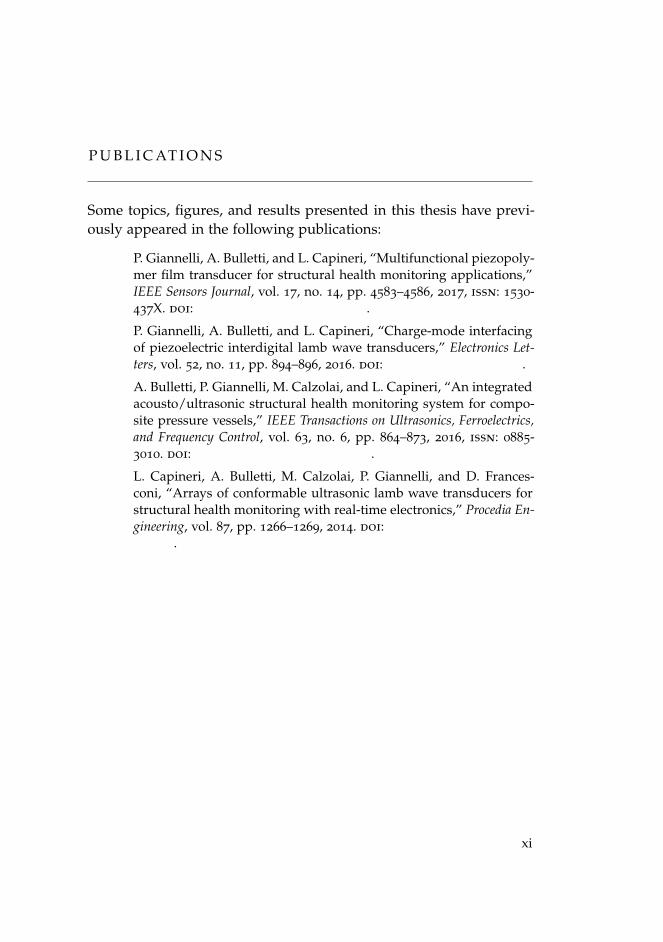
P U B L I C AT I O N S
Some topics, figures, and results presented in this thesis have previ-ously appeared in the following publications:
P. Giannelli, A. Bulletti, and L. Capineri, “Multifunctional piezopoly-mer film transducer for structural health monitoring applications,”IEEE Sensors Journal, vol. 17, no. 14, pp. 4583–4586, 2017, issn: 1530-437X. doi: 10.1109/JSEN.2017.2710425
.
.
P. Giannelli, A. Bulletti, and L. Capineri, “Charge-mode interfacingof piezoelectric interdigital lamb wave transducers,” Electronics Let-ters, vol. 52, no. 11, pp. 894–896, 2016. doi: 10.1049/el.2016.0804
.
.
A. Bulletti, P. Giannelli, M. Calzolai, and L. Capineri, “An integratedacousto/ultrasonic structural health monitoring system for compo-site pressure vessels,” IEEE Transactions on Ultrasonics, Ferroelectrics,and Frequency Control, vol. 63, no. 6, pp. 864–873, 2016, issn: 0885-3010. doi: 10.1109/TUFFC.2016.2545716
.
.
L. Capineri, A. Bulletti, M. Calzolai, P. Giannelli, and D. Frances-coni, “Arrays of conformable ultrasonic lamb wave transducers forstructural health monitoring with real-time electronics,” Procedia En-gineering, vol. 87, pp. 1266–1269, 2014. doi: 10.1016/j.proeng.2014.11.416
.
.
xi

C O N T E N T S
i structural health monitoring with guided-wave
ultrasound 1
.
1 monitoring structures 3
.
1.1 Structural Health Monitoring Tasks 3
.
1.2 Ultrasonic Guided-Wave Inspection 5
.
1.3 Current Trends in Guided-Wave SHM 7
.
1.4 Target Structures and Environments 8
.
1.5 Past Projects 10
.
2 lamb wave transducers 11
.
2.1 PVDF and Its Copolymers 12
.
2.2 Unwanted Excitation Sources 14
.
2.3 Interdigital Transducers 15
.
2.4 A Multifunctional Device 19
.
2.4.1 The Interdigital Pattern 19
.
2.4.2 The Circular Piezoelectric Element 20
.
2.4.3 The Resistive Temperature Device 23
.
2.5 Multi-Element IDT 25
.
2.6 Coupling the Transducers 27
.
2.7 PVDF-in-Flex and Other Solutions 27
.
ii a shm hardware test bench architecture 31
.
3 a prototype shm system 33
.
3.1 Overview of the Hardware 34
.
3.2 The Analog Front-End 35
.
3.2.1 Active-Mode Receiver 38
.
3.2.2 Resonant Transducer Driver 38
.
3.2.3 Duplexer Stage 40
.
3.2.4 Passive-Mode Receiver 40
.
3.3 Data Acquisition and Handling 40
.
3.4 Limitations of the Prototype SHM System 42
.
4 development of a modular shm system 43
.
xiii
xiv contents
4.1 The Pandora Architecture 43
.
4.2 Target Features of the Testbench System 46
.
4.3 Transmitting Signals 48
.
4.3.1 A Class-D Ultrasound Transducer Driver 49
.
4.3.2 Multilevel Pulse Width Encoding 59
.
4.3.3 All-Digital Waveform Generation 73
.
4.3.4 Characterization of the Waveform Generator 75
.
4.3.5 Output Feedback 90
.
4.3.6 Passive-Mode Receiver 92
.
4.3.7 T/R Switching 92
.
4.4 Receiving Signals 92
.
4.4.1 Voltage-Mode and Charge-Mode Interfacing 93
.
4.4.2 The Fully-Differential Charge Amplifier 95
.
4.4.3 The Advantage of Charge-Mode Interfacing 97
.
4.4.4 Improving the Charge Amplifier 100
.
4.4.5 Instrumentation Amplifiers Yet Again 121
.
4.4.6 The Complete Analog Front-End 125
.
iii untrodden trails 129
.
5 completing the testbench system 131
.
5.1 Acquiring the Data 131
.
5.2 A Matter of Power 132
.
5.2.1 Main Power Bus 132
.
5.2.2 Local Power Converters 133
.
5.3 Software Integration 133
.
5.4 Card Interaction and the Backplane 134
.
6 toward shm sensor networks 137
.
7 a conclusion 139
.
7.1 Transducers 139
.
7.2 Testbench System 140
.
7.2.1 Improvements Over the Former System 141
.
7.3 Future Work 142
.
7.4 Final Remarks 142
.
iv appendix 145
.
a legacy system electrical schematics 147
.

contents xv
b pandora electrical schematics 169
.
c pulse width encoder 207
.
d fpga pulse width decoder 213
.
bibliography 235
.
L I S T O F F I G U R E S
Figure 1.1 Lamb wave dispersion curves for an Al plate 7
.
Figure 1.2 Graphical representation of Lamb Waves 7
.
Figure 2.1 Interdigital transducer geometry 15
.
Figure 2.2 Lamb wave dispersion curves detail 17
.
Figure 2.3 Multifunctional IDT 19
.
Figure 2.4 IDT capacitance 20
.
Figure 2.5 Circular element capacitance 21
.
Figure 2.6 Circular element sensitivity comparison 22
.
Figure 2.7 RTD temperature curve 23
.
Figure 2.8 Strain test fixture and sample 24
.
Figure 2.9 PVDF metal coating gage factor 25
.
Figure 2.10 Multi-element IDT 26
.
Figure 2.11 IDTs bonded on a COPV 28
.
Figure 2.12 PVDF-in-flex stack-up drawing 29
.
Figure 3.1 Prototype SHM system hardware 34
.
Figure 3.2 Prototype SHM system block scheme 35
.
Figure 3.3 Prototype SHM system analog front-end 36
.
Figure 3.4 Analog front-end and signal conditioning blockscheme 37
.
Figure 3.5 Prototype SHM system instrumentation am-plifier transfer function 38
.
Figure 3.6 Prototype SHM system instrumentation am-plifier CMRR 39
.
Figure 3.7 Prototype SHM system transducer driver 39
.
Figure 4.1 Pandora wired sensor network 44
.
Figure 4.2 Pandora testbench instrument 45
.
Figure 4.3 Pandora daughter card architecture 45
.
Figure 4.4 AWPulser8 single channel power stage 50
.
Figure 4.5 Simulated reconstruction filter damping 54
.
Figure 4.6 AWPulser8 block scheme 57
.
Figure 4.7 AWPulser8 module pictures 58
.
xvi
List of Figures xvii
Figure 4.8 Basic class-D signal generation 60
.
Figure 4.9 Five-level signal generation process 62
.
Figure 4.10 Limitations of pulse width encoding 64
.
Figure 4.11 PWE band splitting of input samples 65
.
Figure 4.12 PWE band crossover encoding 68
.
Figure 4.13 PWEncoder flow chart 71
.
Figure 4.14 Waveform encoding example 72
.
Figure 4.15 AWPulser8Decoder hierarchical scheme 74
.
Figure 4.16 Ultrasound driver module test board 75
.
Figure 4.17 Low-range step response (0 to 0.8 ·HV) 77
.
Figure 4.18 Mid-range step response (0 to 1.6 ·HV) 77
.
Figure 4.19 Ultrasound driver conversion linearity plot 78
.
Figure 4.20 Tone burst test at 100 kHz, 5MHz carrier 80
.
Figure 4.21 Tone burst test at 150 kHz, 5MHz carrier 81
.
Figure 4.22 Tone burst test at 220 kHz, 5MHz carrier 82
.
Figure 4.23 Tone burst test at 330 kHz, 5MHz carrier 83
.
Figure 4.24 Tone burst test at 470 kHz, 5MHz carrier 84
.
Figure 4.25 Tone burst test at 680 kHz, 5MHz carrier 85
.
Figure 4.26 Tone burst test at 1 MHz, 5 MHz carrier 86
.
Figure 4.27 Amplitude of tone burst outputs 87
.
Figure 4.28 THD+C of test tone bursts, 5MHz carrier 88
.
Figure 4.29 SINAD of ultrasound driver, 5MHz carrier 89
.
Figure 4.30 ENOB of ultrasound driver, 5MHz carrier 90
.
Figure 4.31 Tone burst test at 470 kHz, 10MHz carrier 91
.
Figure 4.32 IDT electrode connection comparison 94
.
Figure 4.33 Differential-input charge amplifier schematic 95
.
Figure 4.34 Fully-differential charge amplifier schematic 96
.
Figure 4.35 1st gen. charge amplifier prototype scheme 97
.
Figure 4.36 Setup with IDTs taped to an Al plate 98
.
Figure 4.37 Voltage-mode and charge-mode comparison plots 99
.
Figure 4.38 2nd gen. charge amplifier schematic 101
.
Figure 4.39 Charge amplifier input network 102
.
Figure 4.40 Charge amplifier compensation components 107
.
Figure 4.41 Charge amplifier compensated loop gain 108
.
Figure 4.42 Charge amplifier simulated input impedance 109
.
Figure 4.43 Charge signal definitions 109
.
Figure 4.44 Charge source models 110
.
Figure 4.45 Direct differential-mode measurement setup 111
.
Figure 4.46 Differential-mode charge source board 111
.
Figure 4.47 2nd gen. charge amplifier DM gain 113
.
Figure 4.48 Indirect common-mode measurement setup 114
.
Figure 4.49 Direct common-mode measurement setup 116
.
Figure 4.50 Common-mode charge source board 117
.
Figure 4.51 2nd gen. charge amplifier CMRR 118
.
Figure 4.52 2nd gen. charge amplifier CM gain 119
.
Figure 4.53 Noise measurement setup 120
.
Figure 4.54 2nd gen. charge amplifier output NSD 121
.
Figure 4.55 Fully-differential instrumentation amplifier sim-plified schematic 122
.
Figure 4.56 Instrumentation amplifier common-mode me-asurement setup 123
.
Figure 4.57 Instrumentation amplifier mixed-mode measu-rement setup 124
.
Figure 4.58 Instrumentation amplifier transfer function 124
.
Figure 4.59 Instrumentation amplifier CMRR 125
.
Figure 4.60 Single channel analog front-end block scheme 126
.
Figure 4.61 Single channel analog front-end picture 127
.
Figure 5.1 Pandora daughter card architecture 131
.
Figure 5.2 Block scheme of the Pandora backplane 135
.
Figure 6.1 Depiction of a sensor node 137
.
L I S T O F TA B L E S
Table 1.1 Classification of pressure vessels 9
.
Table 2.1 Comparison of PVDF and PZT 13
.
Table 4.1 Ultrasound pulser output levels 51
.
Table 4.2 Ultrasound pulser MOSFETs characteristics 51
.
xviii

acronyms xix
A C R O N Y M S
aaf Anti-Aliasing Filter
ac Alternating Current
adc Analog-to-Digital Converter
ae Acoustic Emission
afe Analog Front-End
ansi American National Standards Institute
asic Application-Specific Integrated Circuit
awg Arbitrary Waveform Generation
bjt Bipolar Junction Transistor
cfrp Carbon Fiber Reinforced Polymer
cmos Complementary Metal-Oxide-Semiconductor
cmrr Common-Mode Rejection Ratio
cmut Capacitive Micromachined Ultrasonic Transducers
copv Composite-Overwrapped Pressure Vessel
cpv Composite Pressure Vessel
cw Continuous-Wave
dac Digital-to-Analog Converter
daq Data Acquisition
dc Direct Current
dvga Digital VGA
xx acronyms
eim Electrical Impedance Matching
emat Electromagnetic Acoustic Transducer
emi Electromagnetic Interference
enob Effective Number of Bits
esd Electrostatic Discharge
fda Fully-Differential Amplifier
fet Field-Effect Transistor
fft Fast Fourier Transform
fmc FPGA Mezzanine Card
fpga Field-Programmable Gate Array
gf Gage Factor
gpio General-Purpose Input-Output
hi-z High-Impedance
hps Hard Processor System
hv High-Voltage
i2c Inter-Integrated Circuit
idt Interdigital Transducer
ieee Institute of Electrical and Electronics Engineers
l-c Inductor-Capacitor
ldr Linear Dynamic Range
lna Low-Noise Amplifier
lsb Least Significant Bit

acronyms xxi
lvcmos-** Low-Voltage CMOS (voltage level standard)
lvds Low-Voltage Differential Signaling
lwir Long-Wavelength Infrared
mfc Macro-Fiber Composite
mm Memory-Mapped
modem Modulator-Demodulator
mosfet Metal-Oxide-Semiconductor Field-Effect Transistor
nasa National Aeronautics and Space Administration
ndt, nde Non-Destructive Testing / Evaluation
nmos N-Channel MOSFET
nsd Noise Spectral Density
pcb Printed Circuit Board
pll Phase-Locked Loop
pmos P-Channel MOSFET
pol Point-of-Load
psu Power Supply Unit
pv Pressure Vessel
pvdf Polyvinylidene fluoride
p(vdf-trfe) P(VDF-tetrafluoroethylene)
pwas Piezoelectric Wafer Active Sensor
pwe Pulse-Width Encoding
pwm Pulse-Width Modulation
xxii acronyms
pzt Lead zirconate titanate
q Quality Factor
rcl Resistance Capacitance Inductance
rms Root Mean Square
rtd Resistive Temperature Device
rtos Real-Time Operating System
shm Structural Health Monitoring
sinad Signal-to-Noise and Distortion Ratio
snr Signal-to-Noise Ratio
soc System-on-Chip
spi Serial Peripheral Interface
steps2 Sistemi e Tecnologie per l’Esplorazione Spaziale
tc Curie Temperature
thd+c Total Harmonic Distortion Plus Carrier
t/r Transmit/Receive
uart Universal Asynchronous Receiver-Transmitter
usb Universal Serial Bus
uscnd Ultrasound and Non-Destructive Testing Laboratory
vga Variable-Gain Amplifier
vita VMEbus International Trade Association

Part I
S T R U C T U R A L H E A LT H M O N I T O R I N G W I T HG U I D E D - WAV E U LT R A S O U N D


1M O N I T O R I N G S T R U C T U R E S
Structural health monitoring (SHM) is an umbrella term that groupstogether the methods adopted to evaluate the health (as in structuralintegrity and degradation) of some object in a continual fashion, wit-hout having to dismantle it (in-situ) [1
.
]. These kinds of techniques aregenerally advantageous to plan the maintenance of systems that aredifficult (or even impossible) to access, or generally expensive to takeoff-line for inspection.
Structural health monitoring is a field of study that intersects manyareas of science and engineering, both from the application and im-plementation points of view. As a natural offspring of non-destructivetesting and evaluation (NDT & E), SHM has made its way into manydiverse applications, from civil infrastructure to rotating machinery,from nuclear reactors to spacecrafts, with a vast range of techniques,from fiber optics to ultrasound, from thermal imaging to impedancemetering.
The multidisciplinarity of SHM is so vast that people coming fromthe most disparate backgrounds can give, and have given importantcontributions to the advancement of the subject. While people witha background in physics and mechanical engineering may be moreinclined to study the core topics of structural failures, and how todetect them, there still remains a large amount of work related to theinstrumentation and systems that make SHM possible, which fallsinto the domain of electronics and computer science.
1.1 structural health monitoring tasks
The main objectives that should be fulfilled by structural health mo-nitoring can be summarized in a short list of macro-tasks:
1. Detection.
3
4 monitoring structures
2. Localization.
3. Identification (diagnosis).
4. Prediction (prognosis).
The ordering of the above list is important, as each one of those tasksbuilds on top of the information provided by the previous, resultingin a rapid grow of complexity as additional functionality is built intoa SHM system. A brief description of the tasks is provided in thefollowing paragraphs.
detection The first and foremost objective of SHM is to detectwhether the integrity of the target structure is being compromised inany way, which can be done following two complementary approa-ches:
• Passive-mode is the detection of structural responses to variouskinds of uncontrolled stimuli, performed through continuouslistening for certain signals coming from the structure. For in-stance, the detection of impacts between the target structureand external objects is a form of passive-mode SHM.
• Active-mode, on the other hand, requires the direct stimulationof the target structure with the intent of identifying structu-ral changes, which may be indicators of health degradation. Inguided-wave SHM, active-mode is generally performed with apitch-catch setup: an ultrasound signal is transmitted throughthe structure, received, and subsequently analyzed.
localization Precisely identifying the position where the struc-ture has been compromised logically follows from the previous task.Localization can indeed be performed on both passive and active-mode data, obtaining two very different pieces of information: inpassive-mode, the position of a detected event is determined, while inactive-mode the position of a detected structural change is returned.
1.2 ultrasonic guided-wave inspection 5
identification and prediction The information providedby the detection and localization tasks can be merged and furtherprocessed to reach certain conclusions on the nature of the structuralchange that has occurred.
After the damage experienced by the structure has been preciselyidentified (if it was a damage at all), the expected lifetime and relia-bility of the structure can be evaluated with this new data, obtainingprognostic information.
Ideally, a complete SHM system should strive to cover all the pointslisted above.
The early design stages of a SHM system for research purposesare, however, much limited in scope, as the designer cannot reallypredict what the final requirements for identification and predictionwill amount to. A testbench system should thus provide the enablingtools to perform an unhindered research activity, even by resorting toan over-designed hardware.
1.2 ultrasonic guided-wave inspection
One of the techniques with which SHM can be performed is the so-called ultrasonic guided-wave inspection, that involves the adoption ofmechanical waves propagating along a structure, guided by its boun-daries. Various types of guided waves exist, arising from the varie-gated composition of bulk waves traveling within structures of ap-propriate geometry, along with many different methods to artificiallygenerate, and sense them.
In general, the advantage of using guided-waves arises from theirability to travel along objects, even for long distances, following theirgeometry without the need of a scanning action, and reaching placesthat may be otherwise unaccessible [2
.
].Guided-wave SHM has received considerable interest from the
scientific community, such that the production in the field has re-ached an impressive volume, prompting the publication of severalreview papers over the years [3
.
–5
.
].
6 monitoring structures
The contents of this dissertation are centered on a very specificbranch of guided-wave SHM that uses Lamb waves to inspect plate-like structures.
Lamb waves get their name from Horace Lamb, an English app-lied mathematician who formulated and published their descriptiona hundred years ago [6
.
]. The propagation of these particular flavor ofguided-waves is supported by plates of elastic material, that is, withinhomogeneous, thin solid objects having two well-defined parallel pla-nar boundaries. During the years, the original theory has been gene-ralized to encompass various kinds of plate-like structures, includingcurved shells, thin-wall pipes, multi-layered laminate structures, andso on.
The two characteristic equations of Lamb waves are reported inEquation 1.1
.
(symmetric modes), and Equation 1.2
.
(antisymmetricmodes).
tan(ph)tan(qh)
= −4κ2pq
(q2 − κ2)2
(1.1)
tan(ph)tan(qh)
= −
(q2 − κ2
)24κ2pq
(1.2)
Where the waveguide boundary is defined by its thickness t (h =
t/2), κ = ω/cp is the wavenumber, ω is the angular frequency, cpis the phase velocity of the Lamb wave mode, p2 = ω2/c2l − κ
2 andq2 = ω2/c2t − κ
2. cl and ct represent the longitudinal and transverse(shear) wave velocity in the guiding medium.
The characteristic equations 1.1
.
and 1.2
.
describe two sets of guidedmodes that are intrinsically dispersive, and can be numerically solvedfor cp to obtain a dispersion curve plot.
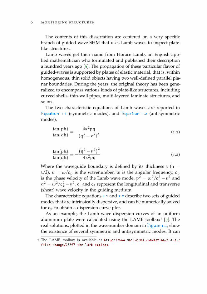
As an example, the Lamb wave dispersion curves of an uniformaluminum plate were calculated using the LAMB toolbox1 [7
.
]. Thereal solutions, plotted in the wavenumber domain in Figure 1.1
.
, showthe existence of several symmetric and antisymmetric modes. It can
1 The LAMB toolbox is available at https://www.mathworks.com/matlabcentral/
fileexchange/28367-the-lamb-toolbox
.
.
1.3 current trends in guided-wave shm 7
be observed that a cutoff wavenumber exists below which only thezeroth order modes propagate, with diverging phase velocities.
0
1000
2000
3000
4000
5000
6000
0 1 2 3 4 5 6 7 8 9 10
pha
se v
eloc
ity [
m/s
]
frequency·thickness [MHz·mm]
A0 S0
A1 S1
A2 S2
Figure 1.1: Lamb wave dispersion curves calculated for an homogeneousaluminum plate.
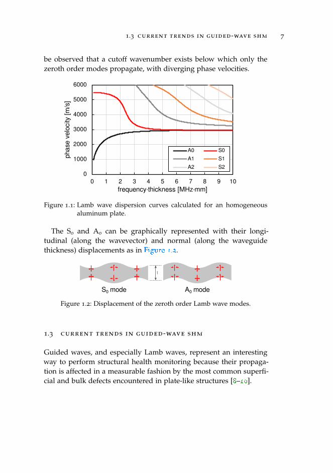
The S0 and A0 can be graphically represented with their longi-tudinal (along the wavevector) and normal (along the waveguidethickness) displacements as in Figure 1.2
.
.
S0 mode A0 mode
t
Figure 1.2: Displacement of the zeroth order Lamb wave modes.
1.3 current trends in guided-wave shm
Guided waves, and especially Lamb waves, represent an interestingway to perform structural health monitoring because their propaga-tion is affected in a measurable fashion by the most common superfi-cial and bulk defects encountered in plate-like structures [8
.
–10
.
].
8 monitoring structures
The interaction of guided waves with material defects in compo-site laminates, such as delaminations [11
.
–15
.
] and debondings [16
.
],has been studied extensively by the scientific community, with someworks focusing specifically on damage resulting from impacts withforeign bodies [17
.
, 18
.
].Guided waves can be used to perform both passive and active-
mode monitoring, as long as the transducers and electronics allowduplexed operation. Monitoring is enacted by rigging the target struc-ture with a certain amount of guided-wave transducers, either atta-ched to the surface, or embedded, thus creating what is generally cal-led a smart structure: a multi-channel electronic system is then neededto interface and operate all the transducers. Numerous SHM designsof this sort have been published [19
.
–23
.
].
On the algorithmic side, an interesting trend in guided-wave SHMis represented by the adoption of wavelet-based techniques, whichallow the simultaneous analysis of non-stationary ultrasonic signalsin both the time and frequency domains [24
.
–26
.
].So far, several works exploiting wavelet analysis have been publis-
hed on topics like active-mode damage detection [27
.
–29
.
], Lamb wavemode identification [30
.
], impact localization [31
.
], and pipe inspection[32
.
].
1.4 target structures and environments
Today, with the increasing adoption of composites as structural mate-rials in many fields of engineering, the task of assessing the health ofsuch components has become crucial to ensure the continued safetyand reliability of the most advanced designs.
Pressure vessels (PVs) are one of the engineering structures thatbenefit most from the adoption of composites. Historically, pressurevessels have been entirely made of metal until the seventies, whenNASA introduced the first composite pressure vessels (CPVs) for ci-vilian use (as part of the firefighters breathing system program). CPVswere originally developed by NASA during the Apollo program [33
.
].
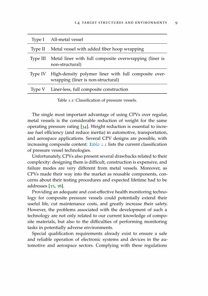
1.4 target structures and environments 9
Type I All-metal vessel
Type II Metal vessel with added fiber hoop wrapping
Type III Metal liner with full composite overwrapping (liner isnon-structural)
Type IV High-density polymer liner with full composite over-wrapping (liner is non-structural)
Type V Liner-less, full composite construction
Table 1.1: Classification of pressure vessels.
The single most important advantage of using CPVs over regular,metal vessels is the considerable reduction of weight for the sameoperating pressure rating [34
.
]. Weight reduction is essential to incre-ase fuel efficiency (and reduce inertia) in automotive, transportation,and aerospace applications. Several CPV designs are possible, withincreasing composite content: Table 1.1
.
lists the current classificationof pressure vessel technologies.
Unfortunately, CPVs also present several drawbacks related to theircomplexity: designing them is difficult, construction is expensive, andfailure modes are very different from metal vessels. Moreover, asCPVs made their way into the market as reusable components, con-cerns about their testing procedures and expected lifetime had to beaddresses [35
.
, 36
.
].Providing an adequate and cost-effective health monitoring techno-
logy for composite pressure vessels could potentially extend theiruseful life, cut maintenance costs, and greatly increase their safety.However, the problems associated with the development of such atechnology are not only related to our current knowledge of compo-site materials, but also to the difficulties of performing monitoringtasks in potentially adverse environments.
Special qualification requirements already exist to ensure a safeand reliable operation of electronic systems and devices in the au-tomotive and aerospace sectors. Complying with these regulations
10 monitoring structures
is fundamental for the SHM system itself, but unfortunately insuf-ficient to guarantee that it provides correct information at all times,as monitoring algorithms also need to be made resilient to changingenvironmental conditions [37
.
–40
.
].
1.5 past projects
The research work done at the Ultrasound and Non-Destructive Tes-ting Laboratory in the field of structural health monitoring has beenmostly oriented towards the identification of damage in carbon fiberreinforced polymers (CFRP) [41
.
–43
.
].The activities led to the design of a proof-of-concept SHM system
for spaceborne composite pressure vessels that performed impactdetection and localization (passive-mode) and damage assessment(active-mode) with Lamb waves [44
.
–47
.
]. The system is described inChapter 3
.
.
2L A M B WAV E T R A N S D U C E R S
There are a plethora of different ways to excite and receive Lambwaves on a plate-like waveguide [48
.
, ch. 3]. One of the most com-mon (even from a historical perspective) is the adoption of ultrasonictransducers with adjustable-angle wedge coupling [12
.
, 49
.
, 50
.
], whichcan also be liquid [51
.
]. Similarly bulky devices used in the field areHertzian contact transducers [52
.
].Non-contact methods have also been extensively studied, including
air coupling [7
.
, 53
.
–55
.
], electromagnetic acoustic transducers (EMATs)[56
.
–58
.
], and laser-based techniques [55
.
, 59
.
, 60
.
].Capacitive micro-machined ultrasonic transducers (CMUTs) have
also been recently applied to the generation and reception of Lambwaves [61
.
], although their usage is currently restricted to the propa-gation in silicon substrates.
In the context of this work, the most interesting transducer techno-logies are represented by low-profile devices, such as interdigitaltransducers (IDTs), which will be treated in Section 2.3
.
, piezoelectricwafer transducers [62
.
, 63
.
], and Lamb wave transducers made withmacro-fiber composite materials (MFC) [64
.
, 65
.
].
Lamb wave transducers intended for permanent installation oncomposite pressure vessels need to abide some demanding operativeconditions both related to the structure itself, and to the external en-vironment. They also need to be unobtrusive, as space is generally apremium in the applications where CPVs are adopted (transportation,automotive, and aerospace), and possibly inexpensive.
From a SHM standpoint, one of the main problems associated withpressure vessels is their inflation / deflation cycles, which result invarying degrees of mechanical deformation of the structure to whichthe ultrasonic transducers are coupled. The ability to withstand suchfatigue is indeed one of the requirements when choosing the transdu-cer technology for this specific application.
11
12 lamb wave transducers
Piezoelectric ceramics are widely adopted to make ultrasonic trans-ducers but unfortunately they fall short in resisting to continuousstress and strain due to their brittleness. The intrinsic elasticity ofpolymer-based materials, on the other hand, is the main reason thatled to the adoption of piezoelectric polymers in this work.
2.1 pvdf and its copolymers
Polyvinylidene fluoride (PVDF) is an electroactive polymer that hasbeen in use as piezoelectric material in the field of ultrasonics sincethe early 70’s, after the initial discovery of its piezoelectric propertiesin 1969 [66
.
]. PVDF and its copolymers have been the subject of exten-sive research through the years, summarized in a few review papers[67
.
–70
.
].Bulk PVDF does not present piezoelectric properties, as it natu-
rally exhibits a predominance of α-phase structure with randomlyoriented dipole moments. A two-fold process involving mechanicalstretching, to transition the crystalline structure to β-phase, and theapplication of a strong electric field, to align the dipole moments, isneeded to obtain a strong piezoelectric behavior [71
.
, 72
.
].It is useful to contextualize some of the properties of PVDF with
reference to lead zirconate titanate (PZT), a widely adopted ferroelec-tric ceramic material. Such comparison can be found multiple timesin the numerous papers cited throughout this section, but it can beboiled down to the parameters reported in Table 2.1
.
.Besides the lower dielectric constant, and the consequential hig-
her impedance with respect to piezo-ceramics, one of the main draw-backs of poled PVDF is its very poor resistance to high temperatures.
Piezoelectric materials have a characteristic temperature at whichall polarization is irreversibly lost: the Curie temperature (TC, a termborrowed from magnetism). In practice, however, the degradation inpiezoelectric performance starts well before reaching TC, for materialdepolarization is a process accelerated by heat.
Pure PVDF has a TC of around 200°C (this is an extrapolated value,as it is above the melting point), but its piezoelectric constants start

2.1 pvdf and its copolymers 13
bi-axial pvdf pzt5a3
Dielectric constant κ33 13–22 1936
κ31 13–22 1616
Coupling coefficient kt 0.1–0.15 0.48
kp 0.62
Piezoelectric coefficient [pC/N] d33 13–22 485
d32 6–10
d31 6–10 123
Maximum use temperature [°C] Tmax 90 175
Table 2.1: Comparison of the properties of a commercial poled PVDF film[73
.
] against a commercial PZT ceramic [74
.
].
to noticeably degrade at much lower temperature [75
.
]. In fact, manu-facturers suggest to never subject poled PVDF to temperatures above75–90°C.
PVDF copolymers have been developed that present increased tem-perature stability. In particular, PVDF with added trifluoroethylene,or P(VDF-TrFE), can be used at temperatures up to 100°C, albeit itspiezoelectric coefficients are not necessarily better that PVDF (perfor-mance is strongly dependent on the molar ratio and manufacturingprocess) [69
.
, 76
.
–78
.
].The development of P(VDF-TrFE) also addressed the problem of
crystalline structure, as certain molar compositions present a signifi-cant prevalence of β-phase, and therefore do not require mechanicalstretching during the manufacturing process [79
.
–81
.
].In recent years, significant research effort has been directed toward
the improvement of the piezoelectric performance of PVDF copoly-mers by merging them with other components. Works have been pu-blished about P(VDF-TrFE) composites made with graphene oxide[82
.
], zinc oxide [83
.
], lead zirconate titanate [84
.
], and barium titanate[85
.
] to name a few.
14 lamb wave transducers
The applicability of piezoelectric polymers to SHM systems opera-ting in challenging environments has been studied in a few publicati-ons [86
.
, 87
.
].
2.2 unwanted excitation sources
While PVDF films are used in structural health monitoring applicati-ons for their piezoelectric response, the material itself generates elec-trical signals also when exposed to other kinds of stimuli unrelatedto ultrasonic guided waves. These unwanted signals can, in certainscenarios, degrade the signal-to-noise ratio of the system.
The main sources of noise captured by piezoelectric sensors ori-ginate from environmental vibrations conducted by the structure towhich the sensor is coupled, its electrical cabling, or even the fluid inwhich the structure is immersed (e. g. air-coupled sound waves). Thedisruptive influence of vibrations on a guided-wave SHM system isstrictly dependent on the application: civil, industrial, and vehicularstructures are all prone to experience vibrations of different ampli-tude and spectral content.
A distinction, however, needs to be made between active and pas-sive SHM (introduced in Section 1.1
.
). In active mode, damage de-tection is performed with a defined inspection signal and timing,such that the system can be tailored to avoid the interference ofknown vibration sources. In passive mode, on the other hand, signalspertaining to the actual monitoring task may end up buried in irre-levant vibrations, making the detection process much more difficult,especially if the system is operating broadband.
Other potentially unwanted signal sources in PVDF sensors areof thermal origin, for the material also presents a strong pyroelec-tric response [71
.
]. Due to this property, and its capability to absorblong-wavelength infrared radiation (LWIR) [88
.
], PVDF has been ex-tensively used in motion detectors, imaging [89
.
, sec. 4.4], and laserbeam characterization [90
.
].Fortunately, the pyroelectric response of a PVDF film is slow and
relevant only at frequencies well below those of interest for guided-
2.3 interdigital transducers 15
wave ultrasound (see for instance the results published in [91
.
–93
.
], allobtained with PVDF films thinner than those adopted in this work).Moreover, sensor encapsulation and coupling add thermal mass toPVDF film transducers used in SHM, further increasing their thermaltime constant.
2.3 interdigital transducers
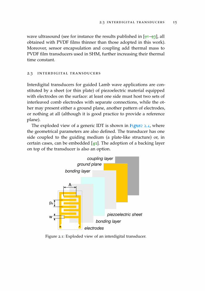
Interdigital transducers for guided Lamb wave applications are con-stituted by a sheet (or thin plate) of piezoelectric material equippedwith electrodes on the surface: at least one side must host two sets ofinterleaved comb electrodes with separate connections, while the ot-her may present either a ground plane, another pattern of electrodes,or nothing at all (although it is good practice to provide a referenceplane).
The exploded view of a generic IDT is shown in Figure 2.1
.
, wherethe geometrical parameters are also defined. The transducer has oneside coupled to the guiding medium (a plate-like structure) or, incertain cases, can be embedded [42
.
]. The adoption of a backing layeron top of the transducer is also an option.
electrodes
piezoelectric sheet
bonding layer
bonding layer
ground plane
coupling layer
A
pF
w
+ -
Figure 2.1: Exploded view of an interdigital transducer.
16 lamb wave transducers
The two sets of comb electrodes are generally assumed to operatewith 180°-out-of-phase signals (both in transmission and reception),such that the transducer provides a geometrical wavelength selecti-vity connected to the finger pitch.
Initial theoretical and practical developments of IDT transducersfor Lamb waves were published in [94
.
–97
.
], where the basics of theiroperation are explained. In brief, IDTs are geometrically designed inthe wavenumber domain to obtain a certain mode selectivity speci-fic to the dispersion curves of the guiding medium to which theyare going to be coupled. The finger pitch pF determines the peak re-sponse at the wavelength λGW = 1/pF, that in turn corresponds to aspecific set of Lamb mode frequencies supported by the target struc-ture.
The length A of the electrodes defines the in-plane collimation ofthe two Lamb wave beams emitted along the longitudinal axis ofthe IDT pattern. If the beam divergence angle γ is defined as theposition of the first local minima of the main lobe, it was shown in[98
.
] that Equation 2.1
.
well fits the divergence angle generated by asingle finger of width A. In the same work, it was also shown thatthe number of finger does not influence the divergence angle, butonly the amplitude of the lobes.
γ = sin−1
(λGW
A
)(2.1)
The effect of finger width W can be studied by performing the spatialFourier transform of the electrode pattern [96
.
, 99
.
]. In general, enlar-ging W boosts the response to the fundamental wavelength (i. e., atλGW), but its effects at shorter wavelengths need to be carefully ana-lyzed if higher-order harmonics are of interest. Aside from the acou-stical effects, finger width and length also determine the electricalcapacitance of the transducer.
Piezopolymer film IDTs conjugate the broadband response of thepiezoelectric material with the geometrical wavelength selectivity ofthe electrodes, meaning that the excitation signal can be adjusted tofollow the optimal wavelength without having to worry about mecha-nical resonances of the piezoelectric material itself [100
.
].
2.3 interdigital transducers 17
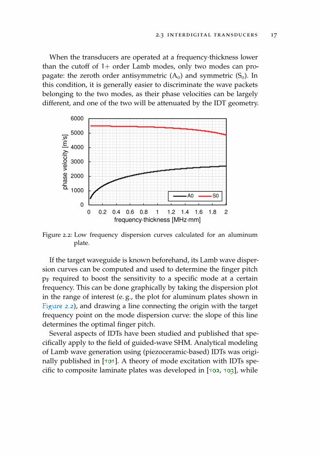
When the transducers are operated at a frequency·thickness lowerthan the cutoff of 1+ order Lamb modes, only two modes can pro-pagate: the zeroth order antisymmetric (A0) and symmetric (S0). Inthis condition, it is generally easier to discriminate the wave packetsbelonging to the two modes, as their phase velocities can be largelydifferent, and one of the two will be attenuated by the IDT geometry.
0
1000
2000
3000
4000
5000
6000
0 0.2 0.4 0.6 0.8 1 1.2 1.4 1.6 1.8 2
pha
se v
eloc
ity [
m/s
]
frequency·thickness [MHz·mm]
A0 S0
Figure 2.2: Low frequency dispersion curves calculated for an aluminumplate.
If the target waveguide is known beforehand, its Lamb wave disper-sion curves can be computed and used to determine the finger pitchpF required to boost the sensitivity to a specific mode at a certainfrequency. This can be done graphically by taking the dispersion plotin the range of interest (e. g., the plot for aluminum plates shown inFigure 2.2
.
), and drawing a line connecting the origin with the targetfrequency point on the mode dispersion curve: the slope of this linedetermines the optimal finger pitch.
Several aspects of IDTs have been studied and published that spe-cifically apply to the field of guided-wave SHM. Analytical modelingof Lamb wave generation using (piezoceramic-based) IDTs was origi-nally published in [101
.
]. A theory of mode excitation with IDTs spe-cific to composite laminate plates was developed in [102
.
, 103
.
], while
18 lamb wave transducers
a numerical analysis approach was presented in [104
.
]. Lamb wavegeneration with graded IDTs was studied in [105
.
].Though this dissertation focuses on IDTs made with piezopolymer
films, transducers based on macro-fiber composite (MFC) materialshave also been proposed [64
.
, 106
.
, 107
.
], representing one of the mostrecent developments in the field.
IDTs developed at USCND present a significant difference fromthose published by other research teams, in that they are manufactu-red via laser etching, starting from metal-coated—usually with Pt-Au,or Cr-Au alloys—poled PVDF sheets [42
.
, 99
.
]. Since PVDF is mostlytransparent to the laser beam, it does not heat up considerably du-ring the etching process, and the laser passes through the polymeretching the back side metalization as well. Therefore, the process re-sults in having an identical electrode pattern on both sides of thePVDF.
The piezoelectric polymer films used throughout the previous andcurrent research activities were purchased form Piézotech S.A.S.1 andPrecision Acoustics Ltd.2.
The improved IDT described in the following sections representsa direct continuation of a previous design [41
.
, 43
.
, 44
.
], which wasalso successfully adopted in the SHM system described in Chapter 3
.
[47
.
]. When used in active mode, those transducers were operatedwith burst signals within the 100 kHz–1 MHz range that, after beingfine-tuned to the waveguide material, was found to provide a reaso-nable trade-off between Lamb wave resolution and attenuation. The100 kHz–1 MHz bandwidth was carried over to the testbench systemdescribed later in this dissertation.
Since the thickness of the piezopolymer film is t = 110µm, and thelongitudinal wave velocity in PVDF is cl ≈ 2200m/s the fundamentalthickness-mode resonance frequency ftr can be calculated as in [108
.
]:
ftr =cl2t≈ 10MHz (2.2)
1 Piézotech S.A.S., F-68220 Hesingue, France; website: http://www.piezotech.eu
.
.2 Precision Acoustics Ltd., Dorset DT2 8QH, United Kingdom; website: https://www.acoustics.co.uk/
.
.
2.4 a multifunctional device 19
Which is well above the specified operating frequency range.
2.4 a multifunctional device
The possibility to etch an arbitrary pattern on the metal coating of thepiezopolymer film constituted an enabling technology for includingdifferent sensing elements on the same film.
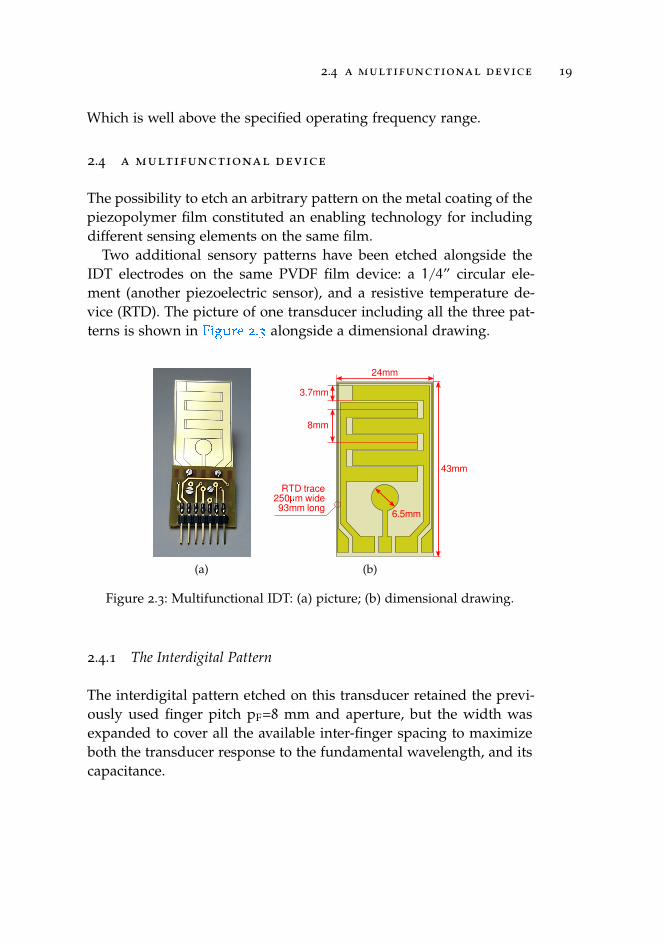
Two additional sensory patterns have been etched alongside theIDT electrodes on the same PVDF film device: a 1/4” circular ele-ment (another piezoelectric sensor), and a resistive temperature de-vice (RTD). The picture of one transducer including all the three pat-terns is shown in Figure 2.3
.
alongside a dimensional drawing.
(a)
6.5mm
43mm
24mm
3.7mm
8mm
RTD trace250 m wide93mm long
(b)
Figure 2.3: Multifunctional IDT: (a) picture; (b) dimensional drawing.
2.4.1 The Interdigital Pattern
The interdigital pattern etched on this transducer retained the previ-ously used finger pitch pF=8 mm and aperture, but the width wasexpanded to cover all the available inter-finger spacing to maximizeboth the transducer response to the fundamental wavelength, and itscapacitance.
20 lamb wave transducers
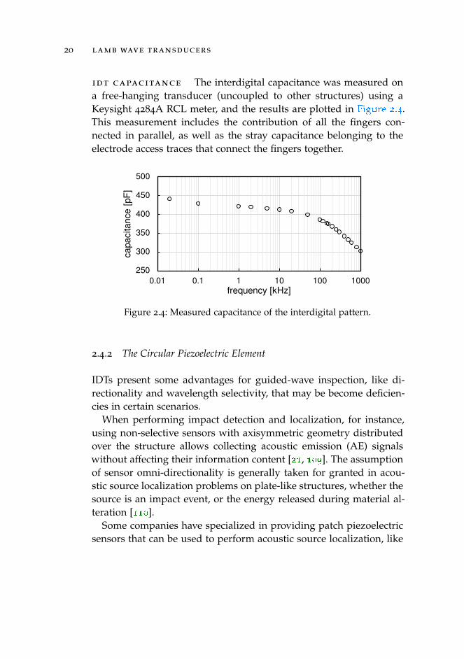
idt capacitance The interdigital capacitance was measured ona free-hanging transducer (uncoupled to other structures) using aKeysight 4284A RCL meter, and the results are plotted in Figure 2.4
.
.This measurement includes the contribution of all the fingers con-nected in parallel, as well as the stray capacitance belonging to theelectrode access traces that connect the fingers together.
250
300
350
400
450
500
0.01 0.1 1 10 100 1000
cap
acita
nce
[p
F]
frequency [kHz]
Figure 2.4: Measured capacitance of the interdigital pattern.
2.4.2 The Circular Piezoelectric Element
IDTs present some advantages for guided-wave inspection, like di-rectionality and wavelength selectivity, that may be become deficien-cies in certain scenarios.
When performing impact detection and localization, for instance,using non-selective sensors with axisymmetric geometry distributedover the structure allows collecting acoustic emission (AE) signalswithout affecting their information content [21
.
, 109
.
]. The assumptionof sensor omni-directionality is generally taken for granted in acou-stic source localization problems on plate-like structures, whether thesource is an impact event, or the energy released during material al-teration [110
.
].Some companies have specialized in providing patch piezoelectric
sensors that can be used to perform acoustic source localization, like
2.4 a multifunctional device 21
Acellent and Physik Instrumente. Specifically, the diameter of Acel-lent’s SML-SP-1/4-* PZT sensor (1/4”, or 6.35 mm) was used as refe-rence to draw the circular element of the design hereby presented.
The first experimental application of the circular element part ofthis multifunctional piezopolymer transducer was to perform impactlocalization on a carbon-fiber laminate sheet [111
.
].
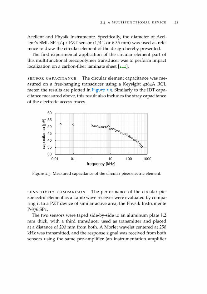
sensor capacitance The circular element capacitance was me-asured on a free-hanging transducer using a Keysight 4284A RCLmeter, the results are plotted in Figure 2.5
.
. Similarly to the IDT capa-citance measured above, this result also includes the stray capacitanceof the electrode access traces.
30
35
40
45
50
55
60
0.01 0.1 1 10 100 1000
cap
acita
nce
[p
F]
frequency [kHz]
Figure 2.5: Measured capacitance of the circular piezoelectric element.
sensitivity comparison The performance of the circular pie-zoelectric element as a Lamb wave receiver were evaluated by compa-ring it to a PZT device of similar active area, the Physik InstrumenteP-876.SP1.
The two sensors were taped side-by-side to an aluminum plate 1.2mm thick, with a third transducer used as transmitter and placedat a distance of 200 mm from both. A Morlet wavelet centered at 250kHz was transmitted, and the response signal was received from bothsensors using the same pre-amplifier (an instrumentation amplifier
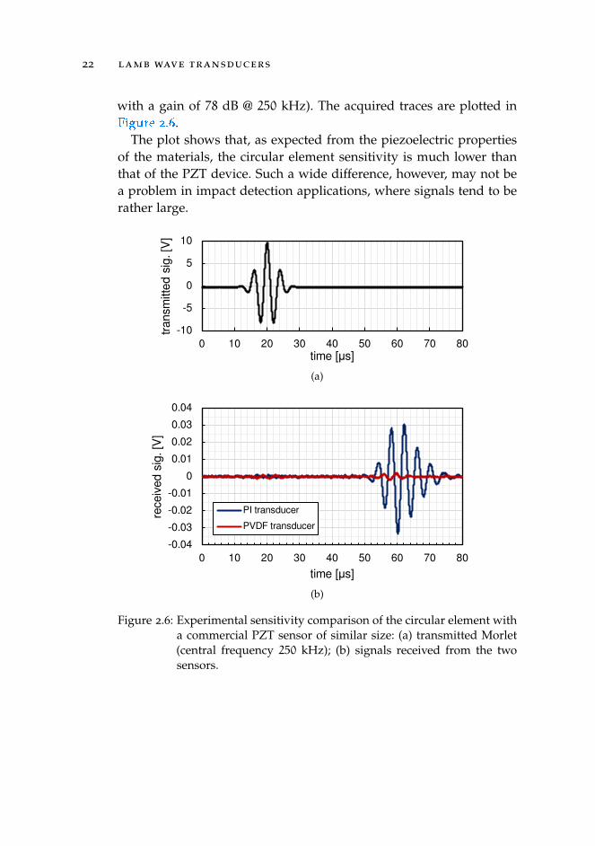
22 lamb wave transducers
with a gain of 78 dB @ 250 kHz). The acquired traces are plotted inFigure 2.6
.
.The plot shows that, as expected from the piezoelectric properties
of the materials, the circular element sensitivity is much lower thanthat of the PZT device. Such a wide difference, however, may not bea problem in impact detection applications, where signals tend to berather large.
-10
-5
0
5
10
0 10 20 30 40 50 60 70 80
tran
smitt
ed s
ig. [
V]
time [μs]
(a)
-0.04
-0.03
-0.02
-0.01
0
0.01
0.02
0.03
0.04
0 10 20 30 40 50 60 70 80
rece
ived
sig
. [V
]
time [μs]
PI transducer
PVDF transducer
(b)
Figure 2.6: Experimental sensitivity comparison of the circular element witha commercial PZT sensor of similar size: (a) transmitted Morlet(central frequency 250 kHz); (b) signals received from the twosensors.
2.4 a multifunctional device 23
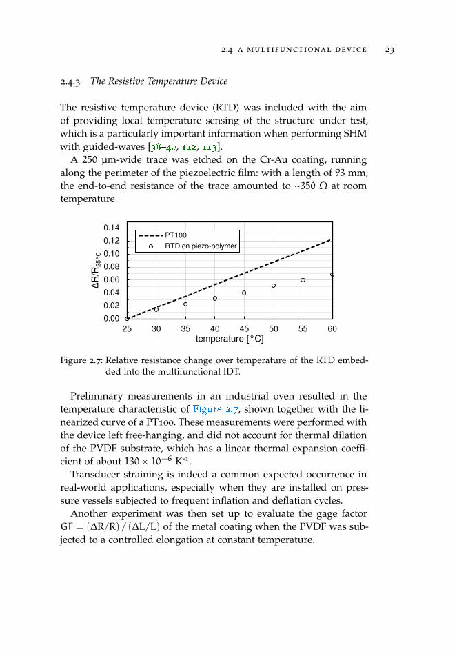
2.4.3 The Resistive Temperature Device
The resistive temperature device (RTD) was included with the aimof providing local temperature sensing of the structure under test,which is a particularly important information when performing SHMwith guided-waves [38
.
–40
.
, 112
.
, 113
.
].A 250 µm-wide trace was etched on the Cr-Au coating, running
along the perimeter of the piezoelectric film: with a length of 93 mm,the end-to-end resistance of the trace amounted to ~350 Ω at roomtemperature.
0.00
0.02
0.04
0.06
0.08
0.10
0.12
0.14
25 30 35 40 45 50 55 60
ΔR
/R2
5°
C
temperature [°C]
PT100
RTD on piezo-polymer
Figure 2.7: Relative resistance change over temperature of the RTD embed-ded into the multifunctional IDT.
Preliminary measurements in an industrial oven resulted in thetemperature characteristic of Figure 2.7
.
, shown together with the li-nearized curve of a PT100. These measurements were performed withthe device left free-hanging, and did not account for thermal dilationof the PVDF substrate, which has a linear thermal expansion coeffi-cient of about 130× 10−6 K-1.
Transducer straining is indeed a common expected occurrence inreal-world applications, especially when they are installed on pres-sure vessels subjected to frequent inflation and deflation cycles.
Another experiment was then set up to evaluate the gage factorGF = (∆R/R) / (∆L/L) of the metal coating when the PVDF was sub-jected to a controlled elongation at constant temperature.
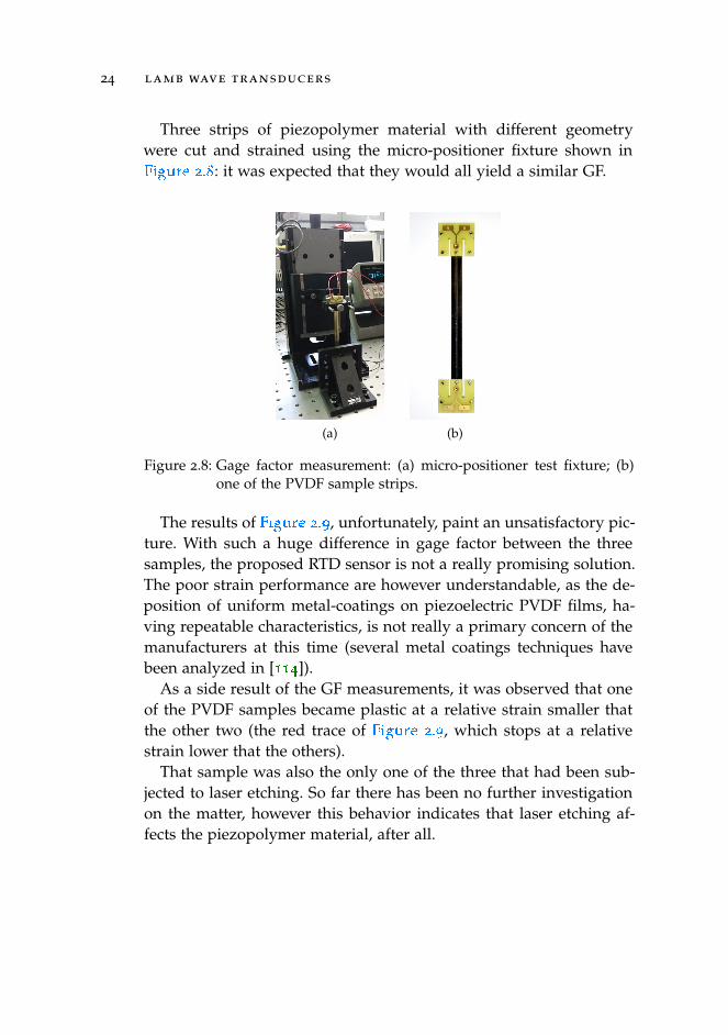
24 lamb wave transducers
Three strips of piezopolymer material with different geometrywere cut and strained using the micro-positioner fixture shown inFigure 2.8
.
: it was expected that they would all yield a similar GF.
(a) (b)
Figure 2.8: Gage factor measurement: (a) micro-positioner test fixture; (b)one of the PVDF sample strips.
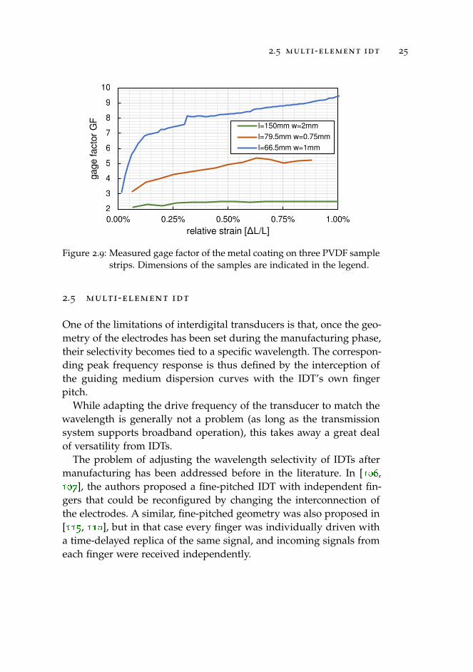
The results of Figure 2.9
.
, unfortunately, paint an unsatisfactory pic-ture. With such a huge difference in gage factor between the threesamples, the proposed RTD sensor is not a really promising solution.The poor strain performance are however understandable, as the de-position of uniform metal-coatings on piezoelectric PVDF films, ha-ving repeatable characteristics, is not really a primary concern of themanufacturers at this time (several metal coatings techniques havebeen analyzed in [114
.
]).As a side result of the GF measurements, it was observed that one
of the PVDF samples became plastic at a relative strain smaller thatthe other two (the red trace of Figure 2.9
.
, which stops at a relativestrain lower that the others).
That sample was also the only one of the three that had been sub-jected to laser etching. So far there has been no further investigationon the matter, however this behavior indicates that laser etching af-fects the piezopolymer material, after all.
2.5 multi-element idt 25
2
3
4
5
6
7
8
9
10
0.00% 0.25% 0.50% 0.75% 1.00%
gag
e fa
ctor
GF
relative strain [ΔL/L]
l=150mm w=2mm
l=79.5mm w=0.75mm
l=66.5mm w=1mm
Figure 2.9: Measured gage factor of the metal coating on three PVDF samplestrips. Dimensions of the samples are indicated in the legend.
2.5 multi-element idt
One of the limitations of interdigital transducers is that, once the geo-metry of the electrodes has been set during the manufacturing phase,their selectivity becomes tied to a specific wavelength. The correspon-ding peak frequency response is thus defined by the interception ofthe guiding medium dispersion curves with the IDT’s own fingerpitch.
While adapting the drive frequency of the transducer to match thewavelength is generally not a problem (as long as the transmissionsystem supports broadband operation), this takes away a great dealof versatility from IDTs.
The problem of adjusting the wavelength selectivity of IDTs aftermanufacturing has been addressed before in the literature. In [106
.
,107
.
], the authors proposed a fine-pitched IDT with independent fin-gers that could be reconfigured by changing the interconnection ofthe electrodes. A similar, fine-pitched geometry was also proposed in[115
.
, 116
.
], but in that case every finger was individually driven witha time-delayed replica of the same signal, and incoming signals fromeach finger were received independently.
26 lamb wave transducers
The latter approach seems more promising but requires a signifi-cant increase of complexity in the electronics and signal processingdomains. Also, individually receiving the signals from each finger isbound to result in a significant SNR degradation.
Apart from the papers specific to IDTs cited above, the generationof Lamb waves using time-delay periodic arrays has been studied in[117
.
], and a large number of relevant works have been published ontransducer arrays for ultrasound guided-waves [118
.
–122
.
].
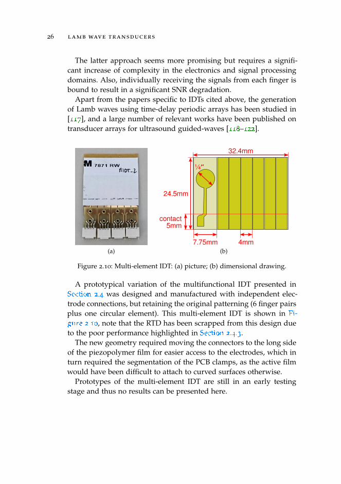
(a)4mm7.75mm
24.5mm
32.4mm
¼
contact5mm
(b)
Figure 2.10: Multi-element IDT: (a) picture; (b) dimensional drawing.
A prototypical variation of the multifunctional IDT presented inSection 2.4
.
was designed and manufactured with independent elec-trode connections, but retaining the original patterning (6 finger pairsplus one circular element). This multi-element IDT is shown in Fi-gure 2.10
.
, note that the RTD has been scrapped from this design dueto the poor performance highlighted in Section 2.4.3
.
.The new geometry required moving the connectors to the long side
of the piezopolymer film for easier access to the electrodes, which inturn required the segmentation of the PCB clamps, as the active filmwould have been difficult to attach to curved surfaces otherwise.
Prototypes of the multi-element IDT are still in an early testingstage and thus no results can be presented here.
2.6 coupling the transducers 27
2.6 coupling the transducers
A firm coupling of the transducers to the target structure surface isparamount to obtain maximum energy transfer in transmission andreception. However, the ability to attach and detach the transducersat will is arguably more important during laboratory experimentalphases.
In the latter case, using double-sided tape as coupling medium hasproven to be an acceptable solution, as long as the target surface issufficiently slick and clean (polished aluminum is a good example).Unfortunately, as the surface grows in roughness, tapes with carriersbecome incapable of maintaining a good adhesion (especially for pro-longed periods): in those circumstances, an alternative but still tempo-rary solution might be represented by transfer tapes (i. e.,carrier-lessadhesive).
The best mechanical coupling was achieved with permanent bon-ding through epoxy paste adhesive. Figure 2.11
.
shows the pictures oftwo linear IDT arrays bonded to the surface of a filament-wound com-posite pressure vessel using the Henkel Hysol EA 9394. This epoxycan be cured at room temperature, and is therefore compatible withtransducers.
The setup of Figure 2.11
.
was part of the SHM system presented inChapter 3
.
.
2.7 pvdf-in-flex and other solutions
The current transducer design and fabrication, with the electrodesetched directly on the metal coating of the PVDF film, adopts me-chanical clamping to provide the electrical interconnections betweenexternal cables and the electrodes. Two circuit boards with propercopper pad layout are riveted around one end of the piezopolymerfilm, creating pressure connections with the pads etched on the me-tal coating of the film. Connectors and wires are then soldered to thePCBs.

28 lamb wave transducers
(a) (b)
Figure 2.11: Picture of two IDT arrays bonded with epoxy paste adhesive ona COPV: (a) entire picture; (b) detail.
Although direct soldering of the lead wires on PVDF is clearly notpossible, as it would melt the film, other solutions have been success-fully used to create good electrical contacts (or the electrodes themsel-ves, if using non-coated PVDF), like conductive glues and inks [114
.
,123
.
].A different approach to building PVDF sensors that was briefly
investigated during the course of this work was completely encasingthe piezopolymer film within a flexible circuit made with standardpolyimide film.
The idea was to insert an uncoated PVDF film between two flexPCB layers having the electrodes etched on copper (like standard ci-rcuit traces), using a couple of adhesive sheets to bond together thethree layers. This stack-up is illustrated in Figure 2.12
.
.An important goal of this stack-up was retaining sensor flexibility,
which automatically ruled out the adoption of rigid epoxy paste adhe-sives such as those used in Section 2.6
.
, even though they had provedto be a good bonding agent for the permanent installation of PVDFtransducers.
Since the adhesive layer is interposed between the copper electro-des and the PVDF, it will obviously reduce the electric field applied
2.7 pvdf-in-flex and other solutions 29
Poled 110μm PVDF
Pyralux LF 0100Acrylic Adhesive
Pyralux LF 0100Acrylic Adhesive
Pyralux AC 182500R
Pyralux AC 182500R
Copper Electrodes
Copper Electrodes
Piezo-Active Film
Top Flex Circuit
Bottom Flex Circuit
Figure 2.12: Stack-up of a piezoelectric PVDF transducer embedded in a flexcircuit.
to the piezoelectric material. Therefore, the adhesive thickness andits dielectric properties need to be carefully controlled. Even so, thisdrawback may represent an acceptable trade-off when compared tothe possibility of designing an arbitrary electrode pattern directly oncopper.
Standard flex circuit assembly technologies are incompatible withPVDF, as they involve high-temperature lamination (usually above180°C). Low-temperature bonding between PVDF and a circuit board,however, was achieved successfully using an acrylic adhesive in [124
.
].
Preliminary bonding tests were performed with an acrylic-basedadhesive used for flex circuit assembly (DuPont Pyralux LF sheetadhesive3, code LF0100), which had two important advantages: itsthickness was known (25 µm), as well as its dielectric constant (3.6–4).
A non-pretreated [125
.
], bare, 110 µm thick PVDF film clipping wasclamped in a vise together with sheet adhesive and a copper-cladpolyimide sheet (DuPont Pyralux AC 182500R4), and placed for 24hours in an oven at 60°C.
Unfortunately the adhesive did not activate at this low temperature.Further tests were repeated for longer times without significantly dif-ferent outcomes.
3 http://www.dupont.com/products-and-services/electronic-electrical-materials/
flexible-rigidflex-circuit-materials/brands/pyralux-flexible-circuit/
products/pyralux-lf.html
.
4 http://www.dupont.com/products-and-services/electronic-electrical-materials/
flexible-rigidflex-circuit-materials/brands/pyralux-flexible-circuit/
products/pyralux-ac.html
.
30 lamb wave transducers
Even if a bonding solution has yet to be found, a transducer madewith the proposed stack-up could lift some of the limitations of thecurrent manufacturing process that prevent the patterning of complexelectrodes at one’s discretion.
Indeed, realizing multiple electrodes with independent connectionis fairly difficult with laser etching, as the process forces an identi-cal pattern on both sides of the PVDF film. This, combined with thenecessity of keeping wide access traces to the electrodes (the metalcoating is extremely thin, around 500 Å, and therefore more resis-tive than a PCB trace), results in significant stray capacitive loadingof the electrodes (which also happen to be piezo-active), with a non-negligible waste of PVDF surface.
With the problem of access traces solved, small transducer arrayscould be easily fabricated on a PVDF film, obtaining a transduceralready enclosed in a flex circuit, and thus easy to merge with theelectronics.
Part II
A S H M H A R D WA R E T E S T B E N C HA R C H I T E C T U R E

3A P R O T O T Y P E S H M S Y S T E M
A first prototype SHM system, integrating all the hardware needed toperform structural health monitoring for a specific application, wasdeveloped during a joint project between the Ultrasound and Non-Destructive Testing Laboratory and Thales Alenia Space Italia, fun-ded under Piedmont Region’s STEPS2
1 program [45
.
–47
.
].The purpose of the project was to monitor the status of a space-
grade, type III composite-overwrapped pressure vessel (COPV) pro-pellant tank using arrays of IDTs bonded to its exterior surface. Theoperations performed by the SHM system included impact detectionand localization (passive-mode), and structural damage assessment(active-mode).
Normally, the system would stay in passive-mode, continuously lis-tening for an impulsive signal indicating the occurrence of an impactevent. After detecting an impact, a software processed the signalsrecorded by all the transducers to triangulate the strike point coordi-nates. Although impact detection was performed in-hardware, signalprocessing and triangulation were done by an external computer.
Active mode could be enabled to perform damage inspection onthe COPV by using the arrays in a pitch-catch fashion: each IDTin turn transmitted a pre-defined square wave burst, with the othertransducers recording the received Lamb wave packets. The data thuscollected were processed and compared to a previously acquired ba-seline, creating a coarse tomographic image showing the progressionof structural damage suffered by the COPV (this task was done by anexternal computer, as well).
1 Sistemi e Tecnologie per l’Esplorazione Spaziale
34 a prototype shm system
3.1 overview of the hardware
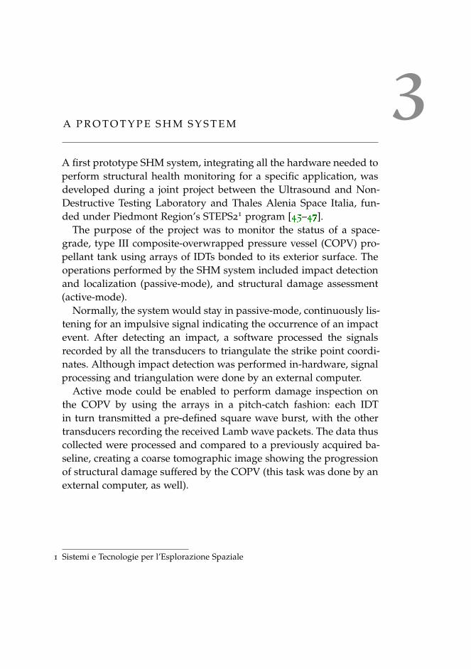
The hardware platform was a combination of custom electronics andevaluation boards stuffed inside a 4U 19” subrack enclosure (shownin Figure 3.1
.
).
Figure 3.1: Picture of the interior of the prototype SHM system hardwaresubrack enclosure.
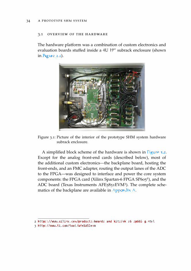
A simplified block scheme of the hardware is shown in Figure 3.2
.
.Except for the analog front-end cards (described below), most ofthe additional custom electronics—the backplane board, hosting thefront-ends, and an FMC adapter, routing the output lanes of the ADCto the FPGA—was designed to interface and power the core systemcomponents: the FPGA card (Xilinx Spartan-6 FPGA SP605
2), and theADC board (Texas Instruments AFE5851EVM3). The complete sche-matics of the backplane are available in Appendix A
.
.
2 https://www.xilinx.com/products/boards-and-kits/ek-s6-sp605-g.html
.
3 http://www.ti.com/tool/afe5851evm
.
3.2 the analog front-end 35
TI AFE5851EVMFMC Adapter
XILINX SP605
Backplane
Array of 8 Transducers Array of 8 Transducers
8-lane LVDS
Backplane Control /Drive Signal
SPI
16-channelAnalog Harness
8-channelInterconnect
8-channelInterconnect
Fro
nt-E
ndF
ront
-End
Fro
nt-E
nd
Fro
nt-E
nd16 VGAs
AFE5851 Spartan-6 LXFPGA
8 ADCs
Fro
nt-E
nd
Fro
nt-E
nd
Fro
nt-E
nd
Fro
nt-E
nd
Fro
nt-E
ndF
ront
-End
Fro
nt-E
nd
Fro
nt-E
nd
Fro
nt-E
nd
Fro
nt-E
nd
Fro
nt-E
nd
Fro
nt-E
nd
ControlLogic
PSU
1Gb
DDR3RAM
Figure 3.2: Block scheme of the prototype SHM system hardware.
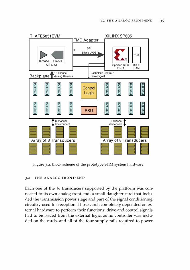
3.2 the analog front-end
Each one of the 16 transducers supported by the platform was con-nected to its own analog front-end, a small daughter card that inclu-ded the transmission power stage and part of the signal conditioningcircuitry used for reception. Those cards completely depended on ex-ternal hardware to perform their functions: drive and control signalshad to be issued from the external logic, as no controller was inclu-ded on the cards, and all of the four supply rails required to power
36 a prototype shm system
the circuits had to be provided externally. The front and rear picturesof the analog front-end (latest revision) are shown in Figure 3.3
.
, cardsize is 53×40 mm excluding the connectors.
Figure 3.3: Pictures (front and rear) of the analog front-end card developedfor the prototype SHM system. Board size is 53×40 mm.
The electronics of this front-end were designed to satisfy very spe-cific requirements, in particular for what concerns the transducer dri-ver (described in Section 3.2.2
.
), and therefore lacked the versatilityneeded to approach structural health monitoring tasks with state-of-the-art techniques.
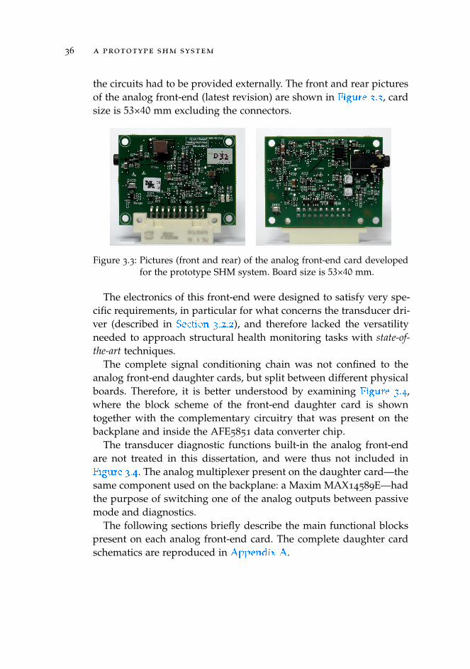
The complete signal conditioning chain was not confined to theanalog front-end daughter cards, but split between different physicalboards. Therefore, it is better understood by examining Figure 3.4
.
,where the block scheme of the front-end daughter card is showntogether with the complementary circuitry that was present on thebackplane and inside the AFE5851 data converter chip.
The transducer diagnostic functions built-in the analog front-endare not treated in this dissertation, and were thus not included inFigure 3.4
.
. The analog multiplexer present on the daughter card—thesame component used on the backplane: a Maxim MAX14589E—hadthe purpose of switching one of the analog outputs between passivemode and diagnostics.
The following sections briefly describe the main functional blockspresent on each analog front-end card. The complete daughter cardschematics are reproduced in Appendix A
.
.
3.2 the analog front-end 37
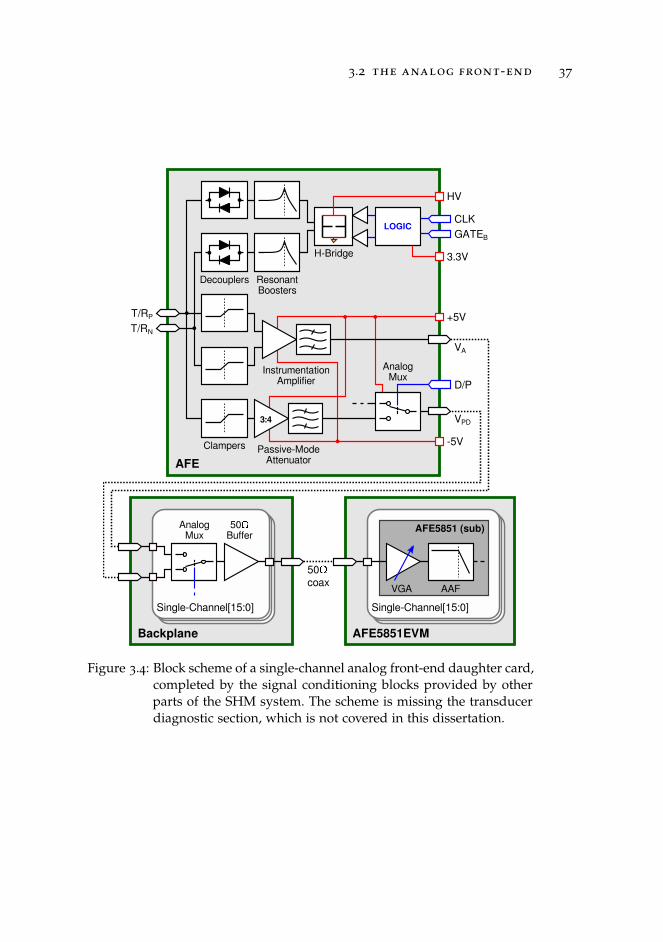
InstrumentationAmplifier
Passive-ModeAttenuator
AnalogMux
+5V
D/P
T/RPT/RN
VA
VPD
-5V
3.3V
Single-Channel[15:0]
CLK
GATEBLOGIC
3:4
HV
ResonantBoosters
H-Bridge
Decouplers
Clampers
AFE
Backplane AFE5851EVM
AnalogMux
50Buffer
Single-Channel[15:0]
50coax
AFE5851 (sub)
VGA AAF
Figure 3.4: Block scheme of a single-channel analog front-end daughter card,completed by the signal conditioning blocks provided by otherparts of the SHM system. The scheme is missing the transducerdiagnostic section, which is not covered in this dissertation.
38 a prototype shm system
3.2.1 Active-Mode Receiver
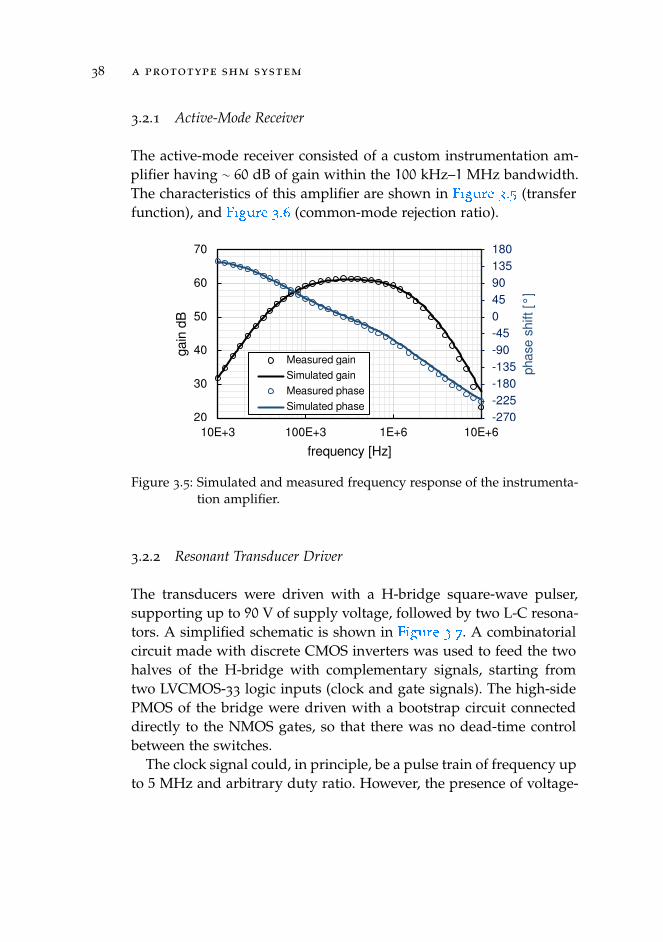
The active-mode receiver consisted of a custom instrumentation am-plifier having ∼ 60 dB of gain within the 100 kHz–1 MHz bandwidth.The characteristics of this amplifier are shown in Figure 3.5
.
(transferfunction), and Figure 3.6
.
(common-mode rejection ratio).
-270
-225
-180
-135
-90
-45
0
45
90
135
180
20
30
40
50
60
70
10E+3 100E+3 1E+6 10E+6
pha
se s
hift
[°
]
gai
n d
B
frequency [Hz]
Measured gain
Simulated gain
Measured phase
Simulated phase
Figure 3.5: Simulated and measured frequency response of the instrumenta-tion amplifier.
3.2.2 Resonant Transducer Driver
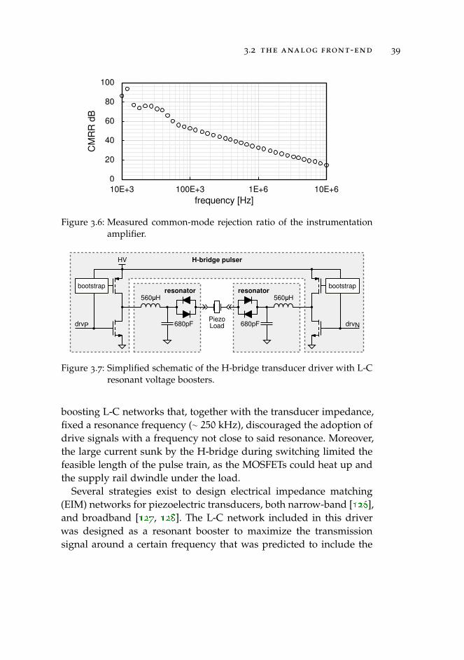
The transducers were driven with a H-bridge square-wave pulser,supporting up to 90 V of supply voltage, followed by two L-C resona-tors. A simplified schematic is shown in Figure 3.7
.
. A combinatorialcircuit made with discrete CMOS inverters was used to feed the twohalves of the H-bridge with complementary signals, starting fromtwo LVCMOS-33 logic inputs (clock and gate signals). The high-sidePMOS of the bridge were driven with a bootstrap circuit connecteddirectly to the NMOS gates, so that there was no dead-time controlbetween the switches.
The clock signal could, in principle, be a pulse train of frequency upto 5 MHz and arbitrary duty ratio. However, the presence of voltage-
3.2 the analog front-end 39
0
20
40
60
80
100
10E+3 100E+3 1E+6 10E+6
CM
RR
dB
frequency [Hz]
Figure 3.6: Measured common-mode rejection ratio of the instrumentationamplifier.
560H
680pFdrvP
HV
PiezoLoad
H-bridge pulser
resonatorbootstrap
drvN
bootstrap
560H
680pF
resonator
Figure 3.7: Simplified schematic of the H-bridge transducer driver with L-Cresonant voltage boosters.
boosting L-C networks that, together with the transducer impedance,fixed a resonance frequency (∼ 250 kHz), discouraged the adoption ofdrive signals with a frequency not close to said resonance. Moreover,the large current sunk by the H-bridge during switching limited thefeasible length of the pulse train, as the MOSFETs could heat up andthe supply rail dwindle under the load.
Several strategies exist to design electrical impedance matching(EIM) networks for piezoelectric transducers, both narrow-band [126
.
],and broadband [127
.
, 128
.
]. The L-C network included in this driverwas designed as a resonant booster to maximize the transmissionsignal around a certain frequency that was predicted to include the

40 a prototype shm system
matching point between the A0 mode wavelength of the structure,and the IDT finger pitch.
3.2.3 Duplexer Stage
Transmit / receive duplexing was implemented with a simple diodeclamp protecting the inputs of the signal conditioning electronics.This solution required the introduction of limiting resistors (3.3 kΩ)in series with the transducer connections (as the drive signal couldreach several hundred volts), thus creating a voltage divider directlyat the preamplifier inputs.
3.2.4 Passive-Mode Receiver
Given the amplitude of impact response signals, several orders ofmagnitude higher than those usually received in active-mode, thepassive-mode receiver was actually a ∼ 3 : 4 resistive divider follo-wed by an op-amp buffer (Texas Instruments OPA172). This receiverwas connected to only one of the two electrodes of the transducer, tofurther cut in half the inbound signal amplitude.
3.3 data acquisition and handling
Since the ADC (a Texas Instruments AFE5851) had 16 total inputchannels, the two analog signals coming from the daughter cards(active and passive-mode receivers) had to be multiplexed togetherbefore being routed to the data acquisition card. Therefore, only oneof the analog signals conditioned by the front-end cards could beacquired at any given time. The analog multiplexers were toggledby the system controller when switching between passive-mode andactive-mode.
The ADC had a total of 8, 12-bit sampling cores multiplexed to16 single-ended inputs. Each input channel also integrated two pro-grammable analog signal conditioning blocks (hence the denomina-tion AFE5851): A variable gain amplifier (−5 dB–31 dB, also suppor-
3.3 data acquisition and handling 41
ting time gain compensation) and a programmable anti-aliasing filter.The ADC sampled at a fixed rate of 20 MSps per channel in bothactive and passive mode—even though the stream was later down-sampled by 2 when operating in passive mode—and transmitted thedata to the FPGA over 8 LVDS (low-voltage differential signaling) la-nes.
The FPGA collected and stored the 16 time traces in a 10k (samplesper channel) circular buffer inside the system memory. In passivemode, data acquisition was performed continuously, overwriting theoldest samples over time, and the FPGA took care of interrupting therecording process as soon as an impact event was detected. In activemode, on the other hand, data acquisition was single-sequence andsynchronized with the emission of the transducer drive signal.
Interleaved sampling was used to accommodate the 16 input sig-nals to the 8 ADC cores, which operated at the actual rate of 40 MSps.The damage detection algorithm used in active mode did not haveparticularly strict inter-channel timing requirements, as each traceacquired from the transducer array was processed independently ofthe others, and only needed a repeatable timing between subsequentpitch-catch acquisitions.
Passive mode, on the other hand, assumed the time alignment ofall the 16 traces acquired during an impact event to extrapolate adifferential time-of-arrival between the transducers, which was thenused to triangulate the point of impact on the COPV surface. In thiscontext, neglecting the fixed delay affecting half the traces, arisingfrom the ADC performing interleaved sampling did result in an er-ror, which was however completely negligible in light of the overalllocalization accuracy achieved by the system.
All the signal processing tasks (damage detection and impact trian-gulation) were performed off-line on the host computer. The memorycontents stored while in passive mode (after an impact event), andthe active mode traces were collected by the host computer throughan USB-to-UART bridge. This interface was also used to configureand control the instrument.
42 a prototype shm system
3.4 limitations of the prototype shm system
While the system presented in this chapter performed fairly good inits intended application [47
.
], it was affected by a number of shortco-mings that prompted the profound revision that is the subject of thisdissertation.
In light of the shift towards a sensor network paradigm envisagedfor the future research efforts, the first and foremost problem of thissystem was its monolithic architecture. While having all the electro-nics encased into a single unit, working in unison, proved to be aviable simplification in this specific application and at this stage ofthe project, having a hardware that could potentially mimic a distri-buted SHM system will lead to exposing and tackling the issues hi-ding behind distributed SHM electronics, and the scalability of suchsystems.
Beside the architecture, several other design choices limited to va-rying degrees the usefulness of the prototype SHM system:
• The front-end cards provided a single transmission / receptionchannel per transducer, limiting their usability with the nextgeneration of multi-functional and multi-element devices des-cribed in Section 2.4
.
and Section 2.5
.
.
• The original active mode inspection procedure relied on thetransmission of only one signal at a time, and thus the electro-nics did not allow the simultaneous operation of multiple trans-ducer drivers. Moreover, the drivers included hard-wired L-Cresonant voltage boosters that fixed their frequency response.
• Only one analog signal could be acquired at any given timefrom each front-end card, and no feedback channel existed tocapture the transducer driver outputs.
• Signal conditioning, and especially the duplexer stage, was ele-mentary and could be improved.
• The electronics in general were too bulky for the functionalitiesthey provided, making their upscaling unfeasible.
4D E V E L O P M E N T O F A M O D U L A R S H M S Y S T E M
4.1 the pandora architecture
Project Pandora started with the overarching aim of developing wiredsensor networks to be deployed on composite pressure vessels (orother, plate-like composite structures). The road to get there, however,is long and steep.
The envisaged sensor node will require the integration of manydiverse functional blocks, some of them even needing different semi-conductor technologies:
• High-voltage ultrasound transducer driver.
• Low-noise analog front-end.
• Analog-to-digital converter.
• Signal processing and communications.
• Power converters.
The design requirements of these components are also strongly con-nected to the health monitoring techniques that will be implemented,and thus a sound sensor node design can only be achieved after athorough experimental phase has been completed, evaluating whichtechniques provide the best results and should be supported by thefinal sensor network.
An intermediate development step was therefore needed beforebeing able to move into sensor integration: the creation and adop-tion of a testbench system to define the paradigm and requirementsof a SHM sensor network architecture.
Such system was devised at the architectural level in a top-downfashion, but its actual design and testing was approached from the
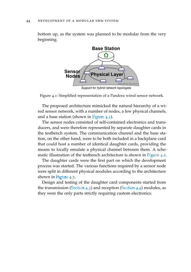
44 development of a modular shm system
bottom up, as the system was planned to be modular from the verybeginning.
Monitored Structure
Base Station
Support for hybrid network topologies
Physical LayerSensorNodes
Figure 4.1: Simplified representation of a Pandora wired sensor network.
The proposed architecture mimicked the natural hierarchy of a wi-red sensor network, with a number of nodes, a few physical channels,and a base station (shown in Figure 4.1
.
).The sensor nodes consisted of self-contained electronics and trans-
ducers, and were therefore represented by separate daughter cards inthe testbench system. The communication channel and the base sta-tion, on the other hand, were to be both included in a backplane cardthat could host a number of identical daughter cards, providing themeans to locally emulate a physical channel between them. A sche-matic illustration of the testbench architecture is shown in Figure 4.2
.
.The daughter cards were the first part on which the development
process was started. The various functions required by a sensor nodewere split in different physical modules according to the architectureshown in Figure 4.3
.
.Design and testing of the daughter card components started from
the transmission (Section 4.3
.
) and reception (Section 4.4
.
) modules, asthey were the only parts strictly requiring custom electronics.
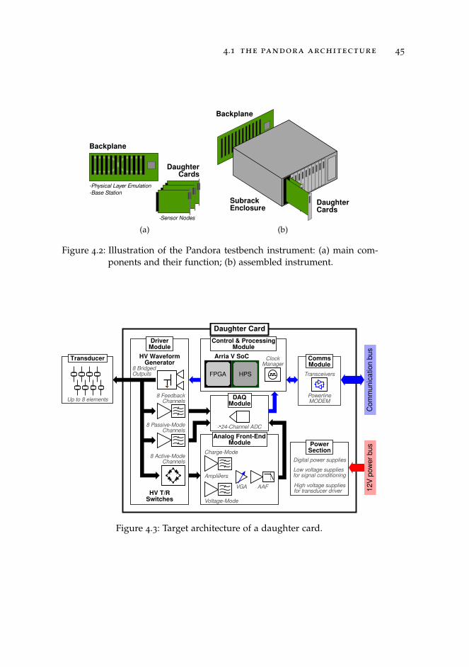
4.1 the pandora architecture 45
Backplane
DaughterCards
-Physical Layer Emulation-Base Station
-Sensor Nodes
(a)
Backplane
SubrackEnclosure
DaughterCards
(b)
Figure 4.2: Illustration of the Pandora testbench instrument: (a) main com-ponents and their function; (b) assembled instrument.
8 BridgedOutputs
Analog Front-EndModule
Charge-Mode
HV T/RSwitches Voltage-Mode
Daughter Card
HV WaveformGenerator
8 Active-ModeChannels
8 Passive-ModeChannels
8 FeedbackChannels
VGA AAF 12
V p
ow
er
bu
s
Arria V SoC
FPGA HPS
ClockManager
Control & ProcessingModule
DriverModule
24-Channel ADC
DAQModule
Digital power supplies
Low voltage suppliesfor signal conditioning
High voltage suppliesfor transducer driver
PowerSection
Transceivers
PowerlineMODEM
CommsModule
Co
mm
un
ica
tion
bu
s
Ampliers
Up to 8 elements
Transducer
Figure 4.3: Target architecture of a daughter card.
46 development of a modular shm system
The other components were temporarily covered for by develop-ment kits and evaluation modules: an Intel FPGA Arria V SoC de-velopment kit1 was used in place of the processing core, while thewhole data acquisition part was replaced by the combination of aTexas Instruments ADS52J90 evaluation module2 and its companionTSW14J56 data capture evaluation module3.
The design plans of the Pandora architecture are further expandedin Chapter 5
.
, where the parts of the testbench system still under de-velopment are fleshed out, highlighting the future work required tocomplete the platform and make it capable of stand-alone operation.
The subsequent Chapter 6
.
hints at the eventual development ofwired sensor networks for SHM, and the main challenges that will beencountered during the final stage of project Pandora.
4.2 target features of the testbench system
Since project Pandora started soon after commissioning the systemdescribed in Chapter 3
.
, with the intent of following in its tracks, theinitial target requirements of the testbench system were mostly inher-ited from the characteristics of the prototype SHM system.
The fundamental idea was that the new design had to improveupon, or at least replicate the features and performance that wereinstrumental to the previous system functioning. In particular, theessential features that needed to be included were:
• Support for active-mode with multiple transducers, each onecapable of operating half-duplex.
• Support for passive-mode with the same transducers.
Several hardware and software requirements sprung directly fromthe points listed above as results of the activities performed usingthe prototype SHM system, while others arose from the research
1 https://www.altera.com/products/boards_and_kits/dev-kits/altera/
kit-arria-v-soc.html
.
2 http://www.ti.com/tool/ads52j90evm
.
3 http://www.ti.com/tool/tsw14j56evm
.
4.2 target features of the testbench system 47
that was undertaken in the period immediately following the endof the STEPS2 project. For instance, the adoption of multi-functional/ multi-element transducers described in Chapter 2
.
was never con-templated before the beginning of project Pandora.
An important planning feature of the testbench system architecturehad to do with the envisioned role of the daughter cards. The previ-ous section has introduced them as node electronics that will handlea single transducer, interacting with other identical daughter cards toform a distributed health monitoring system. While this representedthe core idea that will be pursued, the long expected developmenttime also required a compromise solution that could allow some re-search on SHM applications to be performed before completing thewhole testbench system. To address this need, the daughter cardswere also structured to be able to interface with multiple, indepen-dent transducers and operate stand-alone during the initial phase ofthe project.
A short list of the main requirements of the testbench system, co-vering the active-mode part that is the focus of this dissertation, ispresented below:
• Transmission and reception bandwidth: 100 kHz–1 MHz.
• Support for high-impedance capacitive transducers (< 1 nF).
• Pre-amplifier voltage gain at center band: 60 dB.
• Burst-mode transmission with at least 50 V amplitude.
• 8 independent half-duplex transmission / reception channels.
• Synchronous transmission and data acquisition.
• ADC with 12 bits at 20 MSps per channel or better.
It is expected that the testbench system will see many of its currentrequirements amended in the future, following an iterative designprocess that will proceed side-by-side with the research activity ex-ploring its applications. This is the main reason behind keeping thesystem as modular as possible.
48 development of a modular shm system
4.3 transmitting signals
Ultrasonic transducer drivers capable of arbitrary waveform genera-tion (AWG) come in many forms, but are generally subdivided in twocategories: linear and switch-mode.
Many commercial power amplifiers are available to drive ultrasonictransducers and generate arbitrary waveforms. Although an exposi-tion of this subject is beside the scope of this dissertation, it shouldbe mentioned that fully-integrated, high-voltage linear amplifiers forultrasound are an emerging research topic [129
.
, 130
.
].On the switch-mode side there is a well developed market of inte-
grated multichannel pulsers manufactured by numerous companies.Those pulsers include a set of MOSFET switches connected to fixed,usually high-voltage (hundreds of volts) supply rails that are drivenwith pulse-width modulated (PWM) logic signals to re-create approx-imate waveforms at their output. Over the years, several techniqueshave been proposed to perform PWM with ever increasing quality ofthe output waveforms [131
.
–136
.
].Modulating the pulse widths is not the sole option to shape arbi-
trary signals with a pulser. In recent times, ultrasound pulsers havingmultiple switches connected to different voltage levels have started toproliferate, allowing the development and adoption of specific multi-level pulse width modulation schemes [137
.
–139
.
], a technique thatwas originally developed for power inverters [140
.
].The pulse-width modulation schemes cited above, including the
multilevel ones, are slightly different from the approach used in thecurrent work, and described in the sections that follow. The intendedapplication played an important role in distancing the proposed ul-trasound driver from other solutions, as the target bandwidth wasin the range 6 1 MHz, whereas many of the works cited were orien-ted towards high-frequency imaging. This difference opened to thepossibility of introducing a significant separation between the PWMcarrier and the baseband signal, and operate in pure class-D withoutput reconstruction filters.
4.3 transmitting signals 49
4.3.1 A Class-D Ultrasound Transducer Driver
A 8-channel transducer driver module was designed and manufactu-red following an architecture similar to common class-D amplifiersfor audio applications, only operating at ultrasound frequencies andusing a bridged, multilevel power stage.
The board itself was designed following the ANSI/VITA 57.1 stan-dard as much as possible [141
.
]: although the digital part was com-pliant with the standard, the analog section presented high-voltagesignals that required a secondary board-to-board connector (a Sam-tec QMS-PC4). The final module dimensions were 120×69mm, longerthan a standard mezzanine card.
The complete module schematics can be found in Appendix B
.
.
4.3.1.1 Multilevel Power Stage
The building blocks of the transducer driver were two commercial,multichannel ultrasound pulser chips (Hitachi HDL6V5583), and abank of L-C reconstruction filters. Overall, the pulser ICs provided16 half-bridge power stages with split supplies, plus an active clampand damper tied to ground (i. e., a three-level power stage). The dri-ver module used two such channels, followed by two reconstructionfilters, in a bridged configuration to obtain 8 copies of the five-levelpower stage shown in Figure 4.4
.
. All the pulser channels operatedwith externally provided supplies of |HV| = 48 V.
Every HDL6V5583 channel was controlled by two dedicated inputlogic signals, which were fed to an internal circuitry tasked with levelshifting and MOSFET gate driving. It was assumed that the internallogic would also take care of imposing switching dead-time, althoughno mention of such function was explicitly made in the available do-cumentation.
The truth table showing the various voltage levels that could begenerated by each bridged pulser channel (VDO,P-VDO,N in Figure 4.4
.
)is shown in Table 4.1
.
. A pulser channel receiving the H H logic inputautomatically enabled the active clamp and damper: simultaneous
4 https://www.samtec.com/products/qms-pc
.
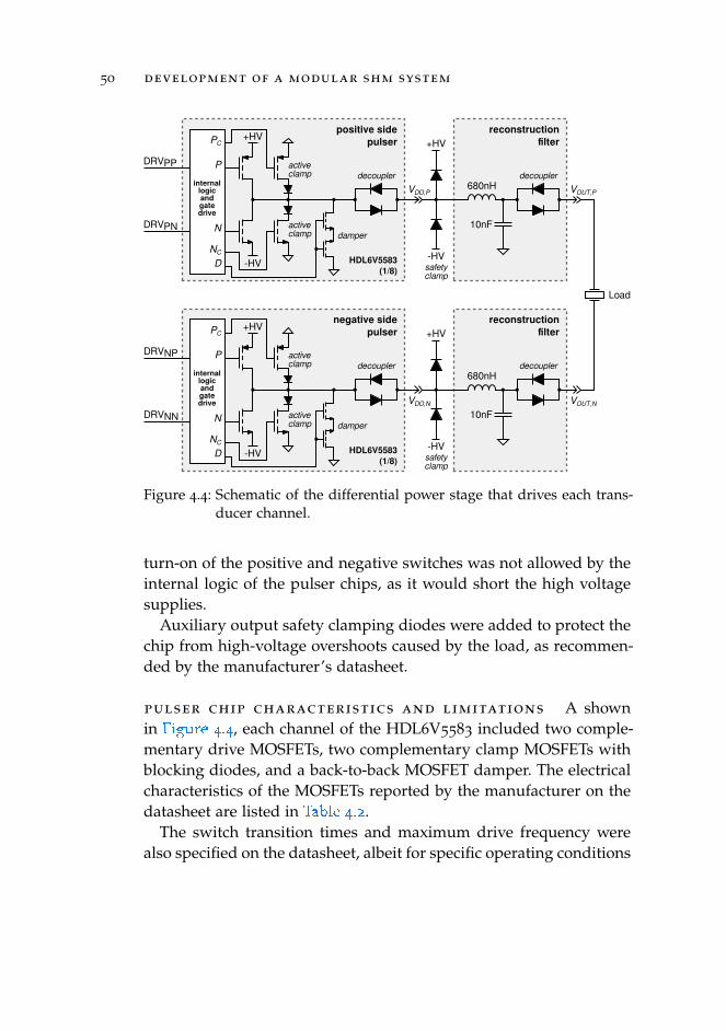
50 development of a modular shm system
+HV
-HV
decouplerinternal
logicandgatedrive
HDL6V5583(1/8)
P
N
PC
NCD
damper
activeclamp
activeclamp
+HV
-HV
680nH
10nF
DRVPP
DRVPN
+HV
-HV
Load
positive sidepulser
reconstructionfilter
DRVNP
DRVNN
negative sidepulser
VOUT,P
VOUT,N
VDO,P
VDO,N
decoupler
safetyclamp
decouplerinternal
logicandgatedrive
HDL6V5583(1/8)
P
N
PC
NCD
damper
activeclamp
activeclamp
+HV
-HV
680nH
10nF
reconstructionfilter
safetyclamp
decoupler
Figure 4.4: Schematic of the differential power stage that drives each trans-ducer channel.
turn-on of the positive and negative switches was not allowed by theinternal logic of the pulser chips, as it would short the high voltagesupplies.
Auxiliary output safety clamping diodes were added to protect thechip from high-voltage overshoots caused by the load, as recommen-ded by the manufacturer’s datasheet.
pulser chip characteristics and limitations A shownin Figure 4.4
.
, each channel of the HDL6V5583 included two comple-mentary drive MOSFETs, two complementary clamp MOSFETs withblocking diodes, and a back-to-back MOSFET damper. The electricalcharacteristics of the MOSFETs reported by the manufacturer on thedatasheet are listed in Table 4.2
.
.The switch transition times and maximum drive frequency were
also specified on the datasheet, albeit for specific operating conditions
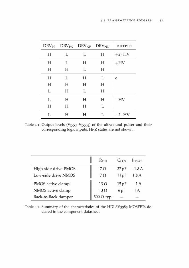
4.3 transmitting signals 51
DRVPP DRVPN DRVNP DRVNN output
H L L H +2 ·HV
H L H H +HV
H H L H
H L H L 0
H H H H
L H L H
L H H H −HV
H H H L
L H H L −2 ·HV
Table 4.1: Output levels (VDO,P-VDO,N) of the ultrasound pulser and theircorresponding logic inputs. Hi-Z states are not shown.
RON COSS ID,SAT
High-side drive PMOS 7Ω 27pF −1.8A
Low-side drive NMOS 7Ω 11pF 1.8A
PMOS active clamp 13Ω 15pF −1A
NMOS active clamp 13Ω 6pF 1A
Back-to-Back damper 500Ω typ. –– ––
Table 4.2: Summary of the characteristics of the HDL6V5583 MOSFETs de-clared in the component datasheet.
52 development of a modular shm system
that did not correspond to our application. In the absence of conclu-sive information, it was assumed that the pulser chip could operateup to a maximum of 25 MHz (at 0.5 duty ratio) with ±48 V supplyrails (which roughly correspond to half the rated supplies of the chip,±100 V), meaning that a minimum pulse width of tPW,min = 20 ns hadto be respected whenever a switch was toggled. This assumption wascarried through the design of the pulse-width modulation strategythat was eventually used to generate the output signals.
reconstruction filters The discrete reconstruction filters ofFigure 4.4
.
were designed to ensure a certain amount of carrier re-jection regardless of the electrical characteristics of the transducerload. 10 nF capacitors were chosen to dominate over the expected ca-pacitance range of the transducers described in Section 2.4
.
, becausea strong high-frequency residual of the carrier (in the tens of mega-hertz) could shock the mechanical thickness-mode resonance of thePVDF film. The inductor value of 680 nH directly followed from thechosen capacitor value to obtain a filter roll-off above ~2 MHz.
L-C reconstruction filters for class-D audio amplifiers are designedby considering the damping introduced by the load itself, which usu-ally presents a low impedance [142
.
]. When driving ultrasonic trans-ducers like those described in Section 2.4
.
, however, the load providesno damping of its own, and the reconstruction filters would end upretaining a high Q factor, with a very sharp resonant peak.
In the proposed design, damping was introduced by the powerstage itself as an average behavior resulting from the continuous tog-gling of the switches. For each pulser channel, the active clamp anddamper to ground were always closed as soon as the high-voltageswitches were opened, never leaving the output in a high-impedancestate.
The actual damping effect of the switching power stage can beeasily evaluated using a simulator that can perform periodic small-signal analysis of a switch-mode circuit, such as SIMPLIS5.
5 SIMPLIS Technologies, Inc., Portland OR, 97240-0084, United States; website: https://www.simplistechnologies.com/
.
.
4.3 transmitting signals 53
The plots of Figure 4.5
.
show a comparison between the undampedresponse of the L-C reconstruction filter (which includes the effectsof component parasitics), and the same filter connected to the pulserpower stage operating at steady state in a single-ended configuration,corresponding to half the drive circuitry shown in Figure 4.4
.
. A ca-pacitive load of 100 pF, modeling the transducer, was used in bothcases.
Both the switching frequency and the duty ratios affect the recon-struction filter damping: Figure 4.5
.
was simulated with a carrier fre-quency of 5 MHz and various duty ratios of the positive and negativedrive switches. The damper duty ratio indicated in the plot legendcorresponds to the switching period interval where both drive swit-ches remain open (i. e., the logical NOR of the two control signals),which thus becomes the duty ratio of the active clamp and damper.
As evidenced by the plots, the longer the active clamp remainsclosed (i. e., lower duty ratio of the energizing switches), the morethe reconstruction filter is damped.
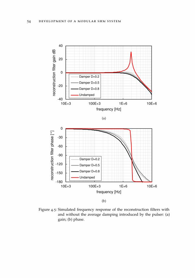
54 development of a modular shm system
-40
-20
0
20
40
10E+3 100E+3 1E+6 10E+6
reco
nstr
uctio
n fil
ter
gai
n d
B
frequency [Hz]
Damper D=0.2
Damper D=0.5
Damper D=0.8
Undamped
(a)
-180
-150
-120
-90
-60
-30
0
10E+3 100E+3 1E+6 10E+6
reco
nstr
uctio
n fil
ter
pha
se [
°]
frequency [Hz]
Damper D=0.2
Damper D=0.5
Damper D=0.8
Undamped
(b)
Figure 4.5: Simulated frequency response of the reconstruction filters withand without the average damping introduced by the pulser: (a)gain; (b) phase.
4.3 transmitting signals 55
4.3.1.2 Pulser Power Supplies
The pulser was externally supplied with split ±48 V rails, though themodule could handle up to ±100 V. The original design, which canstill be seen in the schematics of Appendix B
.
, also included somepoint-of-load (PoL) linear regulators with ±46 V outputs that weresupposed to improve the transient response to the current spikes sunkby the pulser.
In principle, supplying a switching circuit that rapidly draws largecurrents within a short time frame could be done by a bank of capaci-tors. If the total stored energy is sufficiently large, the voltage rail willdrop slowly while switching and then, as the circuit becomes idle, thepower supply will slowly replenish the charge in the capacitors.
This approach works well and has been used extensively in ultra-sound systems where the transmitter operates with low duty cycle:even though the power stage can sink significant amounts of current,it does so for a small time compared to the pulse repetition period,and thus the average current drawn from the power supply is reaso-nably small.
As the transmission system is operated for longer times (i. e., longeroutput waveforms), the capacitance required to maintain a steadypower rail must inevitably grow, and with it the recovery time (unlessthe power supply is also scaled up). Since the capacitance density perunit volume decreases with increasing voltage rating of the capacitor,this whole power supply scaling strategy may become unfeasible incertain scenarios where space is not available.
The idea of adding post-regulators to the high-voltage suppliesgoes in the direction of splitting the performance requirements be-tween the voltage boosting circuit (a somewhat slow switch-modepower supply that generates the ±48 V rails starting from the 12 Vbus), and PoL linear regulators having very fast transient response.
This architecture was attempted in the first driver module pro-totype by including some integrated, high-voltage, linear PoL regu-lators. Unfortunately it did not provide satisfactory performance im-provements, as the transient response of the regulators was slow and
56 development of a modular shm system
fixed by design. Therefore, the pulsers were eventually attached di-rectly to the external ±48 V power supplies.
Operating the driver in continuous wave (CW) was not possibleat high supply voltage due to excessive switching losses. Indeed, theHDL6V5583 datasheet specifies CW operation with ±5 V suppliesand reduced current drive. The driver module described here did notinclude adjustable regulators to step down the power rails, althoughthe introduction of such capability has been planned (see Section 5.2
.
).
4.3.1.3 Ancillary Electronics
Besides hosting the eight differential output channels, the driver mo-dule also provided a part of the signal conditioning circuitry requi-red to use the attached transducers in reception, and thus make thedesign half-duplex. The rationale behind integrating a subset of thereception chain on this card was to keep the high-voltage signals asmuch as possible confined to a dedicated section of the system: theonly high-voltage traces exiting from the driver module were thosethat link directly to the transducers, which are not planned to be tap-ped by any other daughter card circuit.
The reception components are described later in this section, and in-clude: the output feedback sense (Section 4.3.5
.
), the passive mode re-ceivers (Section 4.3.6
.
), and the transmit / receive switches (Section 4.3.7
.
).The 32 logic signals that controlled the pulser chips were sourced
directly from off-board through the FMC connector, while the moduleconfiguration was handled by a local GPIO expander (Texas Instru-ments TCA6424) interfaced via an I2C bus.
The complete block scheme of the driver module is shown in Fi-gure 4.6
.
, and pictures of the manufactured prototype are shown inFigure 4.7
.
.
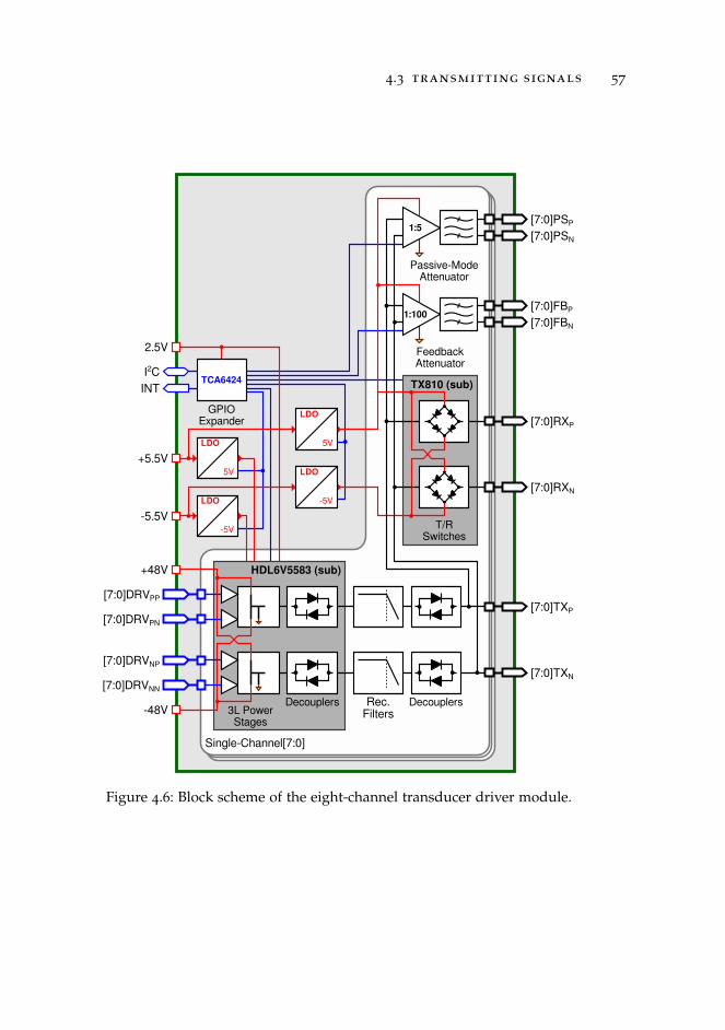
4.3 transmitting signals 57
TX810 (sub)
T/RSwitches
Decouplers Rec.Filters
Passive-ModeAttenuator
FeedbackAttenuator
LDO
5V
LDO
-5V
3L PowerStages
HDL6V5583 (sub)
Decouplers
+5.5V
-5.5V
+48V
-48V
I2C
INT
[7:0]DRVPP
[7:0]PSP
[7:0]PSN
[7:0]FBP
[7:0]FBN
[7:0]TXP
[7:0]TXN
1:100
1:5
[7:0]RXP
[7:0]RXN
Single-Channel[7:0]
LDO
5V
LDO
-5V
[7:0]DRVPN
[7:0]DRVNP
[7:0]DRVNN
TCA6424
GPIOExpander
2.5V
Figure 4.6: Block scheme of the eight-channel transducer driver module.
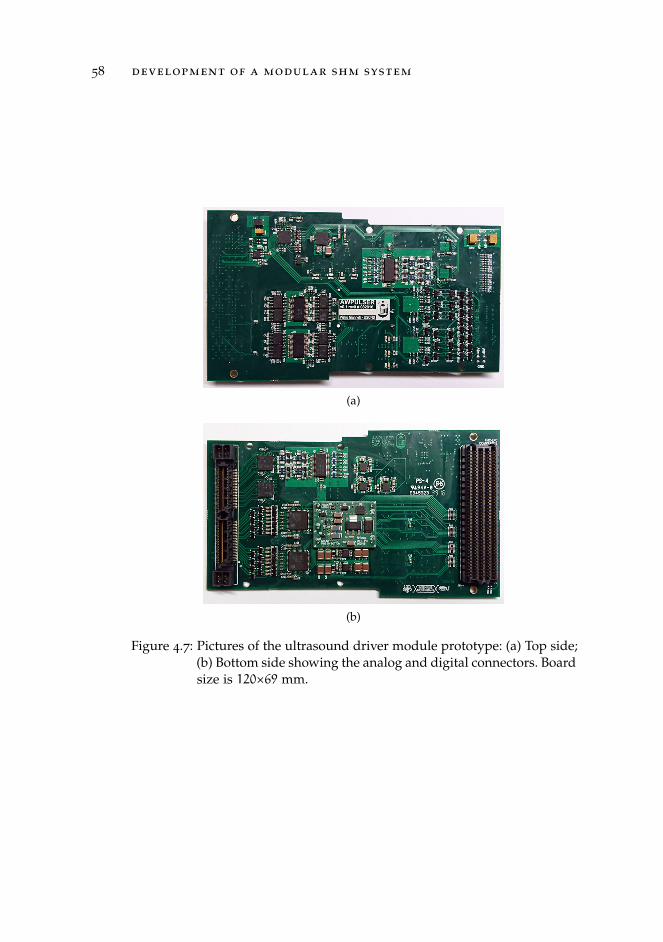
58 development of a modular shm system
(a)
(b)
Figure 4.7: Pictures of the ultrasound driver module prototype: (a) Top side;(b) Bottom side showing the analog and digital connectors. Boardsize is 120×69 mm.
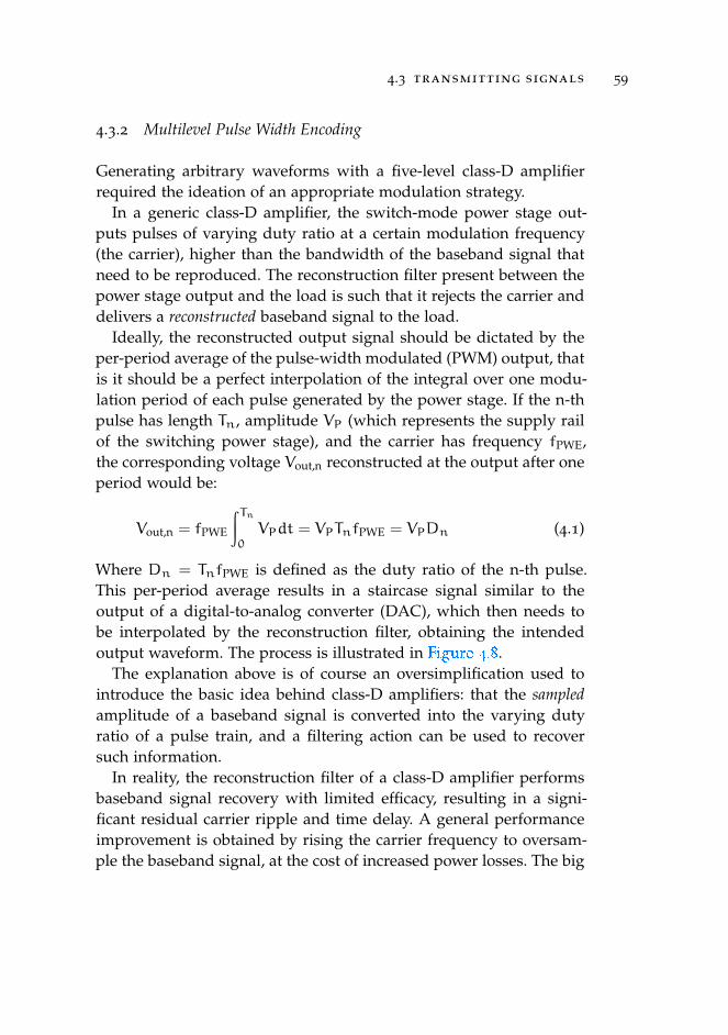
4.3 transmitting signals 59
4.3.2 Multilevel Pulse Width Encoding
Generating arbitrary waveforms with a five-level class-D amplifierrequired the ideation of an appropriate modulation strategy.
In a generic class-D amplifier, the switch-mode power stage out-puts pulses of varying duty ratio at a certain modulation frequency(the carrier), higher than the bandwidth of the baseband signal thatneed to be reproduced. The reconstruction filter present between thepower stage output and the load is such that it rejects the carrier anddelivers a reconstructed baseband signal to the load.
Ideally, the reconstructed output signal should be dictated by theper-period average of the pulse-width modulated (PWM) output, thatis it should be a perfect interpolation of the integral over one modu-lation period of each pulse generated by the power stage. If the n-thpulse has length Tn, amplitude VP (which represents the supply railof the switching power stage), and the carrier has frequency fPWE,the corresponding voltage Vout,n reconstructed at the output after oneperiod would be:
Vout,n = fPWE
∫Tn
0
VPdt = VPTnfPWE = VPDn (4.1)
Where Dn = TnfPWE is defined as the duty ratio of the n-th pulse.This per-period average results in a staircase signal similar to theoutput of a digital-to-analog converter (DAC), which then needs tobe interpolated by the reconstruction filter, obtaining the intendedoutput waveform. The process is illustrated in Figure 4.8
.
.The explanation above is of course an oversimplification used to
introduce the basic idea behind class-D amplifiers: that the sampledamplitude of a baseband signal is converted into the varying dutyratio of a pulse train, and a filtering action can be used to recoversuch information.
In reality, the reconstruction filter of a class-D amplifier performsbaseband signal recovery with limited efficacy, resulting in a signi-ficant residual carrier ripple and time delay. A general performanceimprovement is obtained by rising the carrier frequency to oversam-ple the baseband signal, at the cost of increased power losses. The big
60 development of a modular shm system
PWM
VOUT
Tn-1 Tn Tn+1
TPWE
Output
Reconstruction
Vout,n-1Vout,n
Vout,n+1
VP
0
TPWE
reconstructed signal
Figure 4.8: Basic depiction of class-D signal generation.
advantage lies, however, in the simplicity inherent to the hardware ofa class-D, where a single voltage supply is needed to generate all theintermediate levels to ground by toggling a couple of switches at asufficiently high frequency.
As long as the reconstruction filter is able to reject the carrier andpass the baseband signal, the output waveform amplitude is entirelydefined by the sequence of pulse duty ratios generated by the swit-ching power stage, and its voltage supply rail. In a multilevel PWM,the amplitude of the pulses VP is not fixed but can assume a certainset of predefined levels which, together with the duty ratio, representtwo degrees of freedom to generate the output signal.
As explained in Section 4.3.1
.
, each channel of the transducer drivermodule allowed to generate a total of 5, equally-spaced levels throughfour logic drive signals. A pulse width encoding (PWE) algorithmwas thus devised to transform arbitrary signals sampled at a fixedrate (equal to fPWE) into four pulse-width modulated logic signals.
Note that the modulated logic signals will henceforth be referredto as DRVPP, DRVPN, DRVNP, and DRVNN, while the encoded dutyratios corresponding to the n-th sample of the original waveform willbe indicated with Dn,PP, Dn,PN, Dn,NP, and Dn,NN.
4.3 transmitting signals 61
Since the encoding process was completely digital, the duty ratiosof the PWE signals had to be quantized according to a minimum dutystep δD, corresponding to an integer divisor of the PWE period, div.This divisor was also chosen to be even.
δD =1
div · fPWE=TPWE
div(4.2)
As will be shown later in Section 4.3.3
.
, the duty resolution and PWEperiod are linked together by the clock (fSYSCLK) of the hardware usedto generate the modulated output logic signals, and this imposes anabsolute limitation on the minimum achievable pulse width resolu-tion.
The proposed PWE is therefore an algorithm that takes an inputsequence of samples Sn, and converts each one of them into fourencoded words representing the duty ratios of the four logic signalsrequired to drive the pulser chips (i. e., not a floating or fixed point va-lue between 0 and 1), Figure 4.9
.
visually explains the process. The re-constructed output shown at the bottom includes a token one-periodtime delay, whose actual value depends on the reconstruction filter,and neglects all the residual carrier ripple. The various amplitudescales, intentionally omitted from Figure 4.9
.
, are determined by thehardware.
The values that these four words can assume could be, in principle,any integer number between 0 and div (representing, respectively, 0to 1 duty ratios). However, there are additional limitations arisingfrom other system constrains that need to be taken into account.
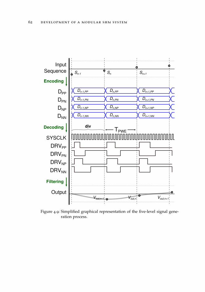
62 development of a modular shm system
DPP
DPN
SYSCLK
DNP
DNN
div
DRVPP
DRVPN
DRVNP
DRVNN
Dn-1,PP Dn,PP Dn+1,PP
TPWE
Dn-1,PN Dn,PN Dn+1,PN
Dn-1,NP Dn,NP Dn+1,NP
Dn-1,NN Dn,NN Dn+1,NN
InputSequence
Decoding
Encoding
Sn-1 Sn Sn+1
Filtering
Vout,n-1 Vout,n Vout,n+1
Output
Figure 4.9: Simplified graphical representation of the five-level signal gene-ration process.
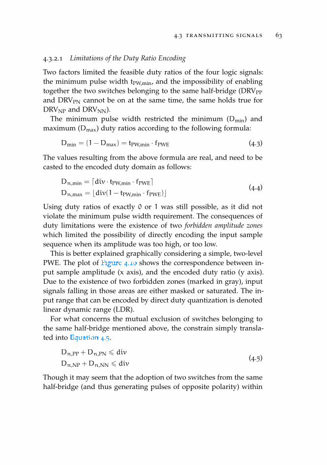
4.3 transmitting signals 63
4.3.2.1 Limitations of the Duty Ratio Encoding
Two factors limited the feasible duty ratios of the four logic signals:the minimum pulse width tPW,min, and the impossibility of enablingtogether the two switches belonging to the same half-bridge (DRVPP
and DRVPN cannot be on at the same time, the same holds true forDRVNP and DRVNN).
The minimum pulse width restricted the minimum (Dmin) andmaximum (Dmax) duty ratios according to the following formula:
Dmin = (1−Dmax) = tPW,min · fPWE (4.3)
The values resulting from the above formula are real, and need to becasted to the encoded duty domain as follows:
Dn,min = ddiv · tPW,min · fPWEeDn,max = bdiv(1− tPW,min · fPWE)c
(4.4)
Using duty ratios of exactly 0 or 1 was still possible, as it did notviolate the minimum pulse width requirement. The consequences ofduty limitations were the existence of two forbidden amplitude zoneswhich limited the possibility of directly encoding the input samplesequence when its amplitude was too high, or too low.
This is better explained graphically considering a simple, two-levelPWE. The plot of Figure 4.10
.
shows the correspondence between in-put sample amplitude (x axis), and the encoded duty ratio (y axis).Due to the existence of two forbidden zones (marked in gray), inputsignals falling in those areas are either masked or saturated. The in-put range that can be encoded by direct duty quantization is denotedlinear dynamic range (LDR).
For what concerns the mutual exclusion of switches belonging tothe same half-bridge mentioned above, the constrain simply transla-ted into Equation 4.5
.
.
Dn,PP +Dn,PN 6 div
Dn,NP +Dn,NN 6 div(4.5)
Though it may seem that the adoption of two switches from the samehalf-bridge (and thus generating pulses of opposite polarity) within
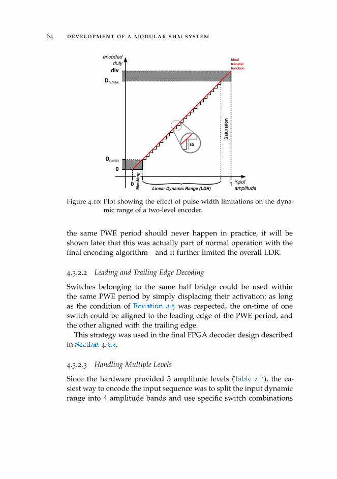
64 development of a modular shm system
encodedduty
inputamplitude
Idealtransferfunction
0
0
div
1
Dn,max
Dn,min
Saturation
Linear Dynamic Range (LDR)Masking
Figure 4.10: Plot showing the effect of pulse width limitations on the dyna-mic range of a two-level encoder.
the same PWE period should never happen in practice, it will beshown later that this was actually part of normal operation with thefinal encoding algorithm—and it further limited the overall LDR.
4.3.2.2 Leading and Trailing Edge Decoding
Switches belonging to the same half bridge could be used withinthe same PWE period by simply displacing their activation: as longas the condition of Equation 4.5
.
was respected, the on-time of oneswitch could be aligned to the leading edge of the PWE period, andthe other aligned with the trailing edge.
This strategy was used in the final FPGA decoder design describedin Section 4.3.3
.
.
4.3.2.3 Handling Multiple Levels
Since the hardware provided 5 amplitude levels (Table 4.1
.
), the ea-siest way to encode the input sequence was to split the input dynamicrange into 4 amplitude bands and use specific switch combinations
4.3 transmitting signals 65
depending on where each sample fell, as shown in Figure 4.11
.
. Theinput signal needed to be pre-scaled and limited within the ±2 am-plitude range, which corresponded to the maximum, ±2 ·HV outputvoltage span (note that this range did not account for duty ratio limi-tations: those were enforced by the encoder on its own).
sample
scaledinputrange
encoding band b
encoding band c
encoding band a
encoding band d
-2
2
1
-1
0
nn-1 n+1 n+2 n+3n-2n-3
Figure 4.11: Amplitude band splitting of the input sequence used to per-form five-level PWE.
4.3.2.4 Switching Time Constants
It has been already explained in Section 4.3.1
.
how the reconstructionfilter damping originates from the average behavior of the powerstage switches. This peculiarity results in an abrupt change of thecircuit time constants whenever any one switch stops (or starts) tog-gling at fPWE: such a change in the reconstruction filter damping willdetermine a noticeable transient of the output signal (in the form ofa spike).
Whether these transients are acceptable or not strictly depends onthe application. However, within the context of this work, it was de-cided to avoid their occurrence in order to keep the output signal assmooth as possible.
66 development of a modular shm system
In practice, this meant that all the switches had to keep togglingcontinuously at fPWE, even if that would not be strictly needed toreproduce a specific sample. The pulse width encoder was thus de-veloped to force all of the four encoded duty ratios to remain bet-ween Dn,min and Dn,max at all times, regardless of the input samplesequence.
The consequence of this was an overall compression of the usableLDR, as the power stage switches ended up introducing a baseline ofmutually-canceling average contributions to each sample being enco-ded.
The usable LDR resulting from the continuous toggling of all theswitches can be quantified by assuming that two of them are opera-ting at minimum duty ratio (e. g., PN and NP), while the other twooperate at maximum duty ratio (e. g., PP and NN). The resulting, in-tegrated output would be:
Vn,max = HVDn,PP −Dn,PN −Dn,NP +Dn,NN
div=
= HVDn,max −Dn,min −Dn,min +Dn,max
div
= HV(2− 4
Dn,min
div
) (4.6)
Since the minimum duty ratio is defined by an absolute time, andthus grows with the carrier frequency, Equation 4.6
.
shows that theLDR shrinks with increasing fPWE.
4.3.2.5 Crossing the Boundary Between Bands
Though the upper saturation of the linear dynamic range was a hardlimit that could not be infringed by the proposed encoding technique,the lower limit corresponding to the masking region of Figure 4.10
.
could be easily circumvented.Intuitively, masking regions should appear across every boundary
between the bands shown in Figure 4.11
.
, their amplitude dependingon the minimum achievable duty ratio, causing the encoded wa-veform to experience something similar to a crossover distortion when
4.3 transmitting signals 67
the input sample sequence happens to transit from one band to theother.
The solution to avoid this potential distortion problem was actu-ally already presented above, when the preservation of switchingtime constants was considered, and is based on operating switchesof opposite polarity together (i. e., use counteracting pulses withinone switching period), or alternatively distributing the duty ratio be-tween switches of equal polarity.
The principle behind this encoding approach is better explainedgraphically, using a simplified example.
With reference to Figure 4.12a
.
, assume that the n-th sample beingencoded has a value slightly above 0, but smaller than what couldbe reproduced by a single pulse of minimum duty ratio. The set ofpulse width signals shown on the left diagram represents the directconversion of the sample in a single pulse, which however happensto fall within the restricted duty region and thus cannot be genera-ted. On the right is shown the proposed alternative: both PP and NPswitches are operated close to 0.5 duty ratio, and the reconstructed,output signal results from their difference, that at this point can besmaller than the minimum duty.
Figure 4.12b
.
shows a similar concept applied to the crossover of1. In this case the sample to be encoded has a value slightly largerthan 1. Direct conversion would result, for instance, in one switchbeing operated at fully duty ratio (always on), and the other beingoperated with a duty smaller than Dn,min. The proposed alternativeis, again, to operate the two switches with close to 0.5 duty ratio.
4.3.2.6 Putting It All Together
The final PWE algorithm needed to take into account all the pointsraised above: every switch was to be kept toggling at fPWE to preservethe time constants, and some way to avoid crossover distortion hadto be implemented.
Considering for now only the positive half of the input dynamicrange, the encoder always enforced a duty ratio greater or equal thanDn,min on all the four output words. Band splitting was adjusted to ac-
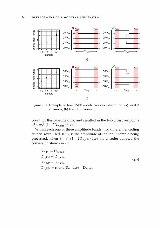
68 development of a modular shm system
sample
sca
led
inp
ut
ran
ge
-2
2
1
-1
0
nn-1 n+1n-2
DRVPP
DRVPN
DRVNP
DRVNN
TPWE
Dn,min
DRVPP
DRVPN
DRVNP
DRVNN
TPWE
Dn,min Dn,min Dn,min
(a)
sample
sca
led
inp
ut
ran
ge
-2
2
1
-1
0
nn-1 n+1n-2
DRVPP
DRVPN
DRVNP
DRVNN
TPWE
Dn,min
DRVPP
DRVPN
DRVNP
DRVNN
TPWE
Dn,min Dn,min Dn,min
(b)
Figure 4.12: Example of how PWE avoids crossover distortion: (a) level 0crossover; (b) level 1 crossover.
count for this baseline duty, and resulted in the two crossover pointsof 0 and (1− 2Dn,min/div).
Within each one of these amplitude bands, two different encodingcriteria were used. If Sn is the amplitude of the input sample beingprocessed, when Sn 6 (1 − 2Dn,min/div) the encoder adopted theconversion shown in 4.7
.
.
Dn,PP = Dn,min
Dn,PN = Dn,min
Dn,NP = Dn,min
Dn,NN = round(Sn · div) +Dn,min
(4.7)
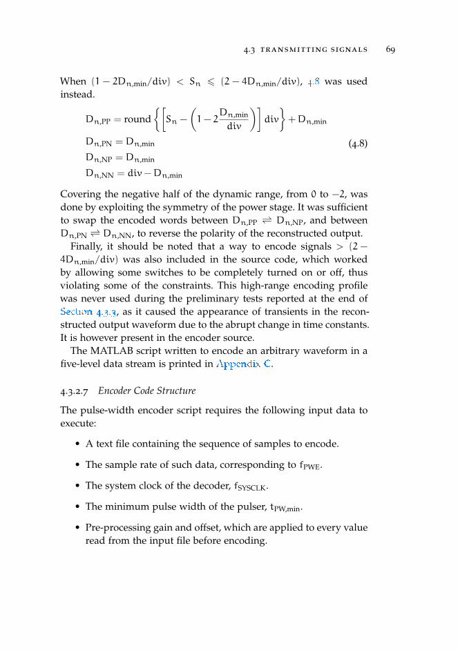
4.3 transmitting signals 69
When (1 − 2Dn,min/div) < Sn 6 (2 − 4Dn,min/div), 4.8
.
was usedinstead.
Dn,PP = round[Sn −
(1− 2
Dn,min
div
)]div
+Dn,min
Dn,PN = Dn,min
Dn,NP = Dn,min
Dn,NN = div−Dn,min
(4.8)
Covering the negative half of the dynamic range, from 0 to −2, wasdone by exploiting the symmetry of the power stage. It was sufficientto swap the encoded words between Dn,PP Dn,NP, and betweenDn,PN Dn,NN, to reverse the polarity of the reconstructed output.
Finally, it should be noted that a way to encode signals > (2 −
4Dn,min/div) was also included in the source code, which workedby allowing some switches to be completely turned on or off, thusviolating some of the constraints. This high-range encoding profilewas never used during the preliminary tests reported at the end ofSection 4.3.3
.
, as it caused the appearance of transients in the recon-structed output waveform due to the abrupt change in time constants.It is however present in the encoder source.
The MATLAB script written to encode an arbitrary waveform in afive-level data stream is printed in Appendix C
.
.
4.3.2.7 Encoder Code Structure
The pulse-width encoder script requires the following input data toexecute:
• A text file containing the sequence of samples to encode.
• The sample rate of such data, corresponding to fPWE.
• The system clock of the decoder, fSYSCLK.
• The minimum pulse width of the pulser, tPW,min.
• Pre-processing gain and offset, which are applied to every valueread from the input file before encoding.
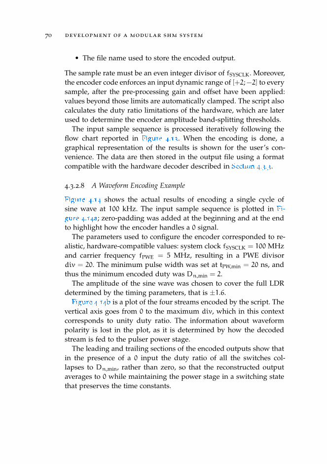
70 development of a modular shm system
• The file name used to store the encoded output.
The sample rate must be an even integer divisor of fSYSCLK. Moreover,the encoder code enforces an input dynamic range of [+2;−2] to everysample, after the pre-processing gain and offset have been applied:values beyond those limits are automatically clamped. The script alsocalculates the duty ratio limitations of the hardware, which are laterused to determine the encoder amplitude band-splitting thresholds.
The input sample sequence is processed iteratively following theflow chart reported in Figure 4.13
.
. When the encoding is done, agraphical representation of the results is shown for the user’s con-venience. The data are then stored in the output file using a formatcompatible with the hardware decoder described in Section 4.3.3
.
.
4.3.2.8 A Waveform Encoding Example
Figure 4.14
.
shows the actual results of encoding a single cycle ofsine wave at 100 kHz. The input sample sequence is plotted in Fi-gure 4.14a
.
; zero-padding was added at the beginning and at the endto highlight how the encoder handles a 0 signal.
The parameters used to configure the encoder corresponded to re-alistic, hardware-compatible values: system clock fSYSCLK = 100 MHzand carrier frequency fPWE = 5 MHz, resulting in a PWE divisordiv = 20. The minimum pulse width was set at tPW,min = 20 ns, andthus the minimum encoded duty was Dn,min = 2.
The amplitude of the sine wave was chosen to cover the full LDRdetermined by the timing parameters, that is ±1.6.
Figure 4.14b
.
is a plot of the four streams encoded by the script. Thevertical axis goes from 0 to the maximum div, which in this contextcorresponds to unity duty ratio. The information about waveformpolarity is lost in the plot, as it is determined by how the decodedstream is fed to the pulser power stage.
The leading and trailing sections of the encoded outputs show thatin the presence of a 0 input the duty ratio of all the switches col-lapses to Dn,min, rather than zero, so that the reconstructed outputaverages to 0 while maintaining the power stage in a switching statethat preserves the time constants.
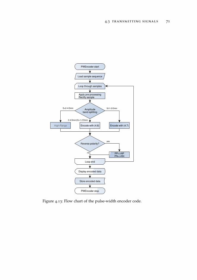
4.3 transmitting signals 71
Figure 4.13: Flow chart of the pulse-width encoder code.
72 development of a modular shm system
-2
-1
0
1
2
0 2E-6 4E-6 6E-6 8E-6 10E-6 12E-6 14E-6
sam
ple
val
ue
time [s]
(a)
0
5
10
15
20
0 2E-6 4E-6 6E-6 8E-6 10E-6 12E-6 14E-6
enco
ded
dut
y ra
tio
time [s]
PP PN NP NN
(b)
Figure 4.14: Example pulse-width encoding: (a) input sample sequence (onecycle of sine wave at 100 kHz); (b) the four encoded duty ratiostreams.
4.3 transmitting signals 73
4.3.3 All-Digital Waveform Generation
The transducer driver module connected directly to the FPGA, an In-tel FPGA Arria V ST SoC 5ASTFD5K3F40I3N, through a parallel, 32-bit LVCMOS-25 bus. With 2+ 2 bits per channel, the FPGA logic fullycontrolled each one of the possible states of the ultrasound pulserpower stage (+HV, -HV, active clamp, and Hi-Z per side). Althoughthe HDL6V5583 also provides registered digital inputs, the currentdesign uses the device in transparent latch mode, with logic-level syn-chronization ensured at the source.
A proof-of-concept, FPGA core was developed to decode the PWEdata generated with the method described in Section 4.3.2
.
, and out-put the pulse-width modulated signals needed to operate all the8 ultrasound driver channels, providing inter-channel synchroniza-tion and fixed-latency. The Verilog source code of this core, calledAWPulser8Decoder, can be found in Appendix D
.
.
The AWPulser8Decoder core allows the reproduction of eight pulse-width modulated signals with up to 512 samples per channel and8-bit duty resolution (256 duty ratio steps per sample). The decodersupports both burst mode, repeating the stored waveform sequenti-ally a fixed number of times (up to 255), and continuous wave (CW),continuously repeating the waveform until a stop command is recei-ved.
The decoder clock, which sets the absolute minimum pulse widthstep, is currently tied to the system clock (fSYSCLK = 100 MHz), eventhough the Arria V SoC FPGA fabric can handle clock rates up to 650MHz. Plans have been made to integrate a reconfigurable PLL in thedesign and provide run-time adjustment of the decoder clock.
High-resolution pulse width generation techniques going beyondthe system clock rate by using an asynchronous, tapped-delay lineapproach have been proposed in the literature [143
.
]. They were, ho-wever, not considered for this design.
The decoder core is interfaced to the FPGA embedded controller asan Avalon slave, through the system Avalon memory-mapped (MM)
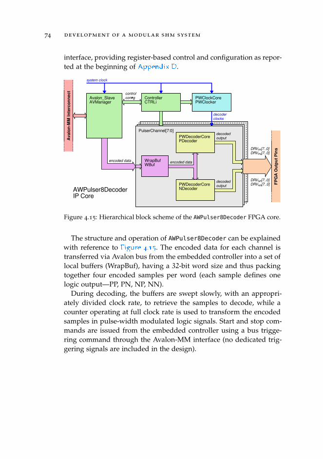
74 development of a modular shm system
interface, providing register-based control and configuration as repor-ted at the beginning of Appendix D
.
.
PWClockCorePWClocker
PulserChannel[7:0]
PWDecoderCorePDecoder
PWDecoderCoreNDecoder
WrapBufWBuf
ControllerCTRLi
Avalon_SlaveAVManager
Ava
lon
-MM
In
terc
on
ne
ct
FP
GA
Ou
tpu
t P
insDRVPP[7..0]
DRVPN[7..0]
DRVNP[7..0]DRVNN[7..0]
encoded data
system clock
encoded data
controlcong
decoderclocks
decodedoutput
decodedoutput
AWPulser8DecoderIP Core
Figure 4.15: Hierarchical block scheme of the AWPulser8Decoder FPGA core.
The structure and operation of AWPulser8Decoder can be explainedwith reference to Figure 4.15
.
. The encoded data for each channel istransferred via Avalon bus from the embedded controller into a set oflocal buffers (WrapBuf), having a 32-bit word size and thus packingtogether four encoded samples per word (each sample defines onelogic output—PP, PN, NP, NN).
During decoding, the buffers are swept slowly, with an appropri-ately divided clock rate, to retrieve the samples to decode, while acounter operating at full clock rate is used to transform the encodedsamples in pulse-width modulated logic signals. Start and stop com-mands are issued from the embedded controller using a bus trigge-ring command through the Avalon-MM interface (no dedicated trig-gering signals are included in the design).
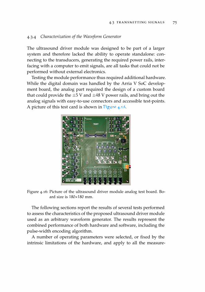
4.3 transmitting signals 75
4.3.4 Characterization of the Waveform Generator
The ultrasound driver module was designed to be part of a largersystem and therefore lacked the ability to operate standalone: con-necting to the transducers, generating the required power rails, inter-facing with a computer to emit signals, are all tasks that could not beperformed without external electronics.
Testing the module performance thus required additional hardware.While the digital domain was handled by the Arria V SoC develop-ment board, the analog part required the design of a custom boardthat could provide the ±5 V and ±48 V power rails, and bring out theanalog signals with easy-to-use connectors and accessible test-points.A picture of this test card is shown in Figure 4.16
.
.
Figure 4.16: Picture of the ultrasound driver module analog test board. Bo-ard size is 180×180 mm.
The following sections report the results of several tests performedto assess the characteristics of the proposed ultrasound driver moduleused as an arbitrary waveform generator. The results represent thecombined performance of both hardware and software, including thepulse-width encoding algorithm.
A number of operating parameters were selected, or fixed by theintrinsic limitations of the hardware, and apply to all the measure-
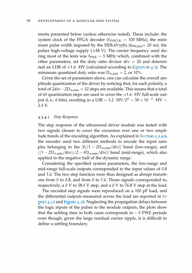
76 development of a modular shm system
ments presented below (unless otherwise noted). These include: thesystem clock of the FPGA decoder (fSYSCLK = 100 MHz), the mini-mum pulse width imposed by the HDL6V5583 (tPW,min= 20 ns), thepulser high-voltage supply (±48 V). The carrier frequency used du-ring most of the tests was fPWE = 5 MHz which, combined with theother parameters, set the duty ratio divisor div = 20 and determi-ned an LDR of ±1.6 ·HV (calculated according to Equation 4.6
.
). Theminimum quantized duty ratio was Dn,min = 2, or 10%.
Given the set of parameters above, one can calculate the overall am-plitude quantization of the driver by noticing that, for each polarity, atotal of 2div−2Dn,min = 32 steps are available. This means that a totalof 64 quantization steps are used to cover the ±1.6 ·HV full-scale out-put (i. e., 6 bits), resulting in a LSB = 3.2 ·HV/26 = 50× 10−3 ·HV =
2.4 V.
4.3.4.1 Step Response
The step response of the ultrasound driver module was tested withtwo signals chosen to cover the excursion over one or two ampli-tude bands of the encoding algorithm. As explained in Section 4.3.2.6
.
,the encoder used two different methods to encode the input sam-ples belonging to the [0; (1 − 2Dn,min/div)] band (low-range), and((1− 2Dn,min/div); (2− 4Dn,min/div)] band (mid-range), which alsoapplied to the negative half of the dynamic range.
Considering the specified system parameters, the low-range andmid-range full-scale outputs corresponded to the input values of 0.8and 1.6. The two step function were thus designed as abrupt transiti-ons from 0 to 0.8, and from 0 to 1.6. Those signals corresponded to,respectively, a 0 V to 38.4 V step, and a 0 V to 76.8 V step at the load.
The encoded step signals were reproduced on a 100 pF load, andthe differential outputs measured across the load are reported in Fi-gure 4.17
.
and Figure 4.18
.
. Neglecting the propagation delays betweenthe logic inputs of the pulser to the module outputs, the plots showthat the settling time in both cases corresponds to ∼ 4 PWE periodseven though, given the large residual carrier ripple, it is difficult todefine a settling boundary.
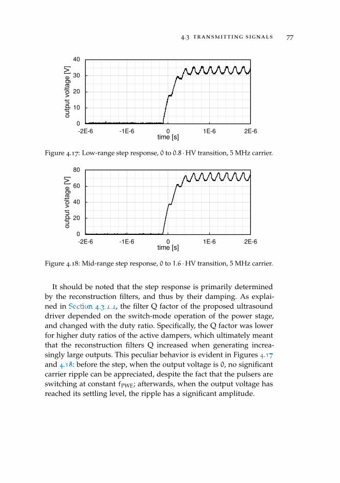
4.3 transmitting signals 77
0
10
20
30
40
-2E-6 -1E-6 0 1E-6 2E-6
outp
ut v
olta
ge
[V]
time [s]
Figure 4.17: Low-range step response, 0 to 0.8 ·HV transition, 5MHz carrier.
0
20
40
60
80
-2E-6 -1E-6 0 1E-6 2E-6
outp
ut v
olta
ge
[V]
time [s]
Figure 4.18: Mid-range step response, 0 to 1.6 ·HV transition, 5 MHz carrier.
It should be noted that the step response is primarily determinedby the reconstruction filters, and thus by their damping. As explai-ned in Section 4.3.1.1
.
, the filter Q factor of the proposed ultrasounddriver depended on the switch-mode operation of the power stage,and changed with the duty ratio. Specifically, the Q factor was lowerfor higher duty ratios of the active dampers, which ultimately meantthat the reconstruction filters Q increased when generating increa-singly large outputs. This peculiar behavior is evident in Figures 4.17
.
and 4.18
.
: before the step, when the output voltage is 0, no significantcarrier ripple can be appreciated, despite the fact that the pulsers areswitching at constant fPWE; afterwards, when the output voltage hasreached its settling level, the ripple has a significant amplitude.
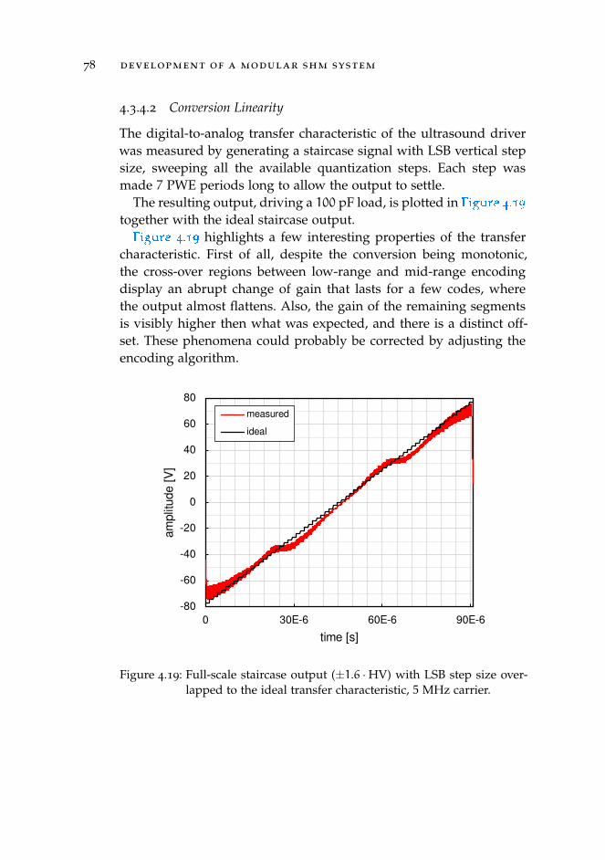
78 development of a modular shm system
4.3.4.2 Conversion Linearity
The digital-to-analog transfer characteristic of the ultrasound driverwas measured by generating a staircase signal with LSB vertical stepsize, sweeping all the available quantization steps. Each step wasmade 7 PWE periods long to allow the output to settle.
The resulting output, driving a 100 pF load, is plotted in Figure 4.19
.
together with the ideal staircase output.Figure 4.19
.
highlights a few interesting properties of the transfercharacteristic. First of all, despite the conversion being monotonic,the cross-over regions between low-range and mid-range encodingdisplay an abrupt change of gain that lasts for a few codes, wherethe output almost flattens. Also, the gain of the remaining segmentsis visibly higher then what was expected, and there is a distinct off-set. These phenomena could probably be corrected by adjusting theencoding algorithm.
-80
-60
-40
-20
0
20
40
60
80
0 30E-6 60E-6 90E-6
amp
litud
e [V
]
time [s]
measured
ideal
Figure 4.19: Full-scale staircase output (±1.6 ·HV) with LSB step size over-lapped to the ideal transfer characteristic, 5 MHz carrier.
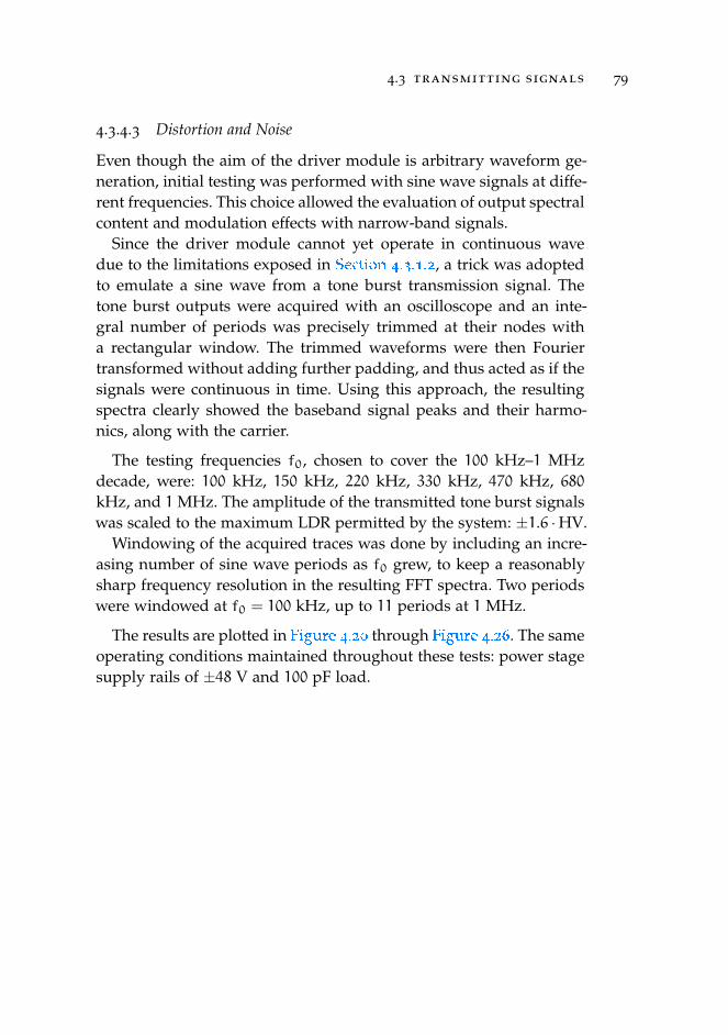
4.3 transmitting signals 79
4.3.4.3 Distortion and Noise
Even though the aim of the driver module is arbitrary waveform ge-neration, initial testing was performed with sine wave signals at diffe-rent frequencies. This choice allowed the evaluation of output spectralcontent and modulation effects with narrow-band signals.
Since the driver module cannot yet operate in continuous wavedue to the limitations exposed in Section 4.3.1.2
.
, a trick was adoptedto emulate a sine wave from a tone burst transmission signal. Thetone burst outputs were acquired with an oscilloscope and an inte-gral number of periods was precisely trimmed at their nodes witha rectangular window. The trimmed waveforms were then Fouriertransformed without adding further padding, and thus acted as if thesignals were continuous in time. Using this approach, the resultingspectra clearly showed the baseband signal peaks and their harmo-nics, along with the carrier.
The testing frequencies f0, chosen to cover the 100 kHz–1 MHzdecade, were: 100 kHz, 150 kHz, 220 kHz, 330 kHz, 470 kHz, 680kHz, and 1 MHz. The amplitude of the transmitted tone burst signalswas scaled to the maximum LDR permitted by the system: ±1.6 ·HV.
Windowing of the acquired traces was done by including an incre-asing number of sine wave periods as f0 grew, to keep a reasonablysharp frequency resolution in the resulting FFT spectra. Two periodswere windowed at f0 = 100 kHz, up to 11 periods at 1 MHz.
The results are plotted in Figure 4.20
.
through Figure 4.26
.
. The sameoperating conditions maintained throughout these tests: power stagesupply rails of ±48 V and 100 pF load.
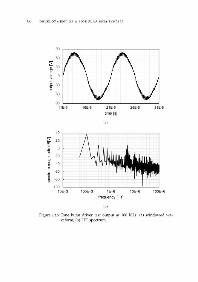
80 development of a modular shm system
-90
-60
-30
0
30
60
90
11E-6 16E-6 21E-6 26E-6 31E-6
outp
ut v
olta
ge
[V]
time [s]
(a)
-100
-80
-60
-40
-20
0
20
40
10E+3 100E+3 1E+6 10E+6 100E+6
spec
trum
mag
nitu
de
dB
[V]
frequency [Hz]
(b)
Figure 4.20: Tone burst driver test output at 100 kHz: (a) windowed wa-veform; (b) FFT spectrum.
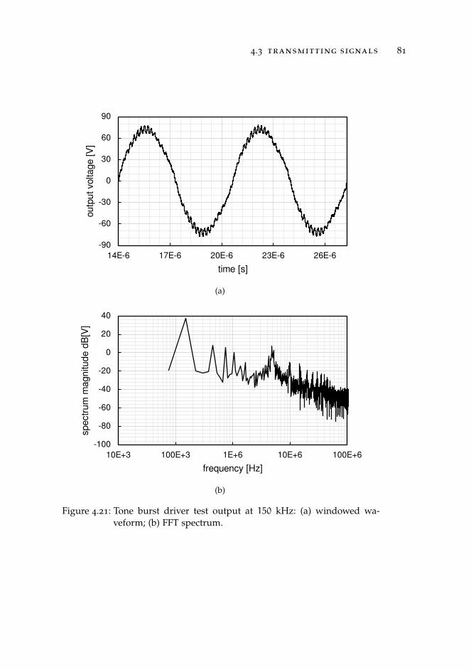
4.3 transmitting signals 81
-90
-60
-30
0
30
60
90
14E-6 17E-6 20E-6 23E-6 26E-6
outp
ut v
olta
ge
[V]
time [s]
(a)
-100
-80
-60
-40
-20
0
20
40
10E+3 100E+3 1E+6 10E+6 100E+6
spec
trum
mag
nitu
de
dB
[V]
frequency [Hz]
(b)
Figure 4.21: Tone burst driver test output at 150 kHz: (a) windowed wa-veform; (b) FFT spectrum.
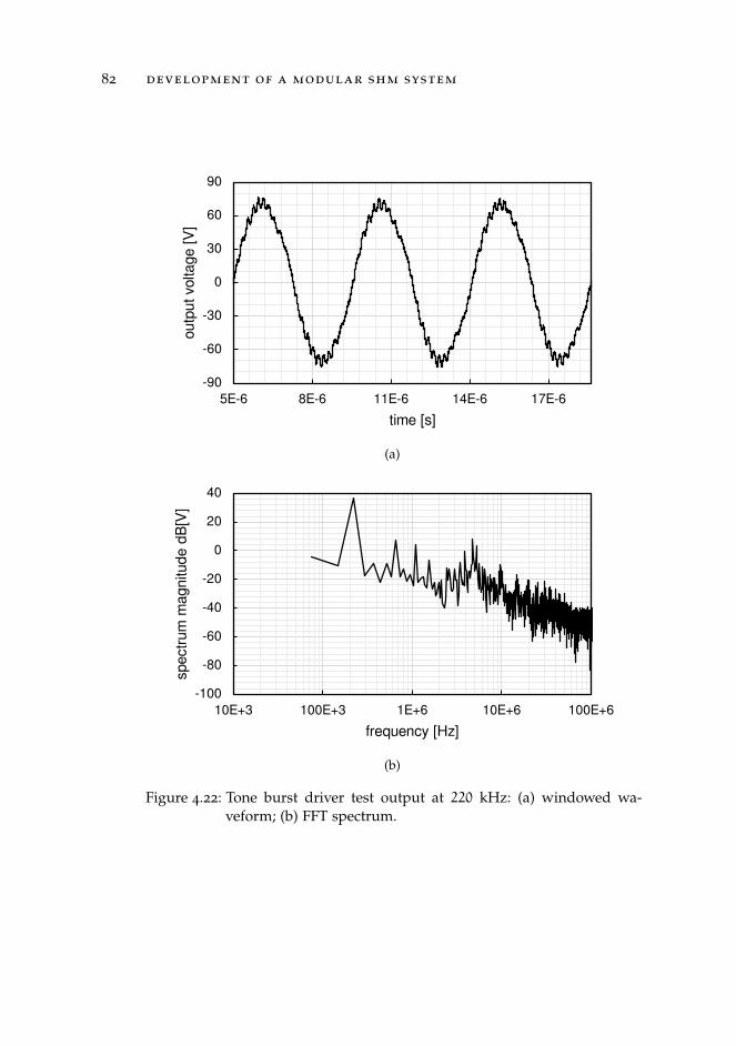
82 development of a modular shm system
-90
-60
-30
0
30
60
90
5E-6 8E-6 11E-6 14E-6 17E-6
outp
ut v
olta
ge
[V]
time [s]
(a)
-100
-80
-60
-40
-20
0
20
40
10E+3 100E+3 1E+6 10E+6 100E+6
spec
trum
mag
nitu
de
dB
[V]
frequency [Hz]
(b)
Figure 4.22: Tone burst driver test output at 220 kHz: (a) windowed wa-veform; (b) FFT spectrum.
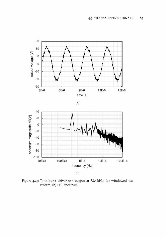
4.3 transmitting signals 83
-90
-60
-30
0
30
60
90
3E-6 6E-6 9E-6 12E-6 15E-6
outp
ut v
olta
ge
[V]
time [s]
(a)
-100
-80
-60
-40
-20
0
20
40
10E+3 100E+3 1E+6 10E+6 100E+6
spec
trum
mag
nitu
de
dB
[V]
frequency [Hz]
(b)
Figure 4.23: Tone burst driver test output at 330 kHz: (a) windowed wa-veform; (b) FFT spectrum.
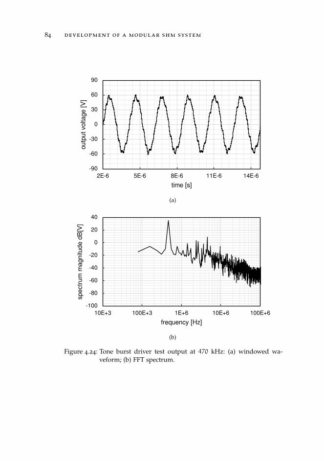
84 development of a modular shm system
-90
-60
-30
0
30
60
90
2E-6 5E-6 8E-6 11E-6 14E-6
outp
ut v
olta
ge
[V]
time [s]
(a)
-100
-80
-60
-40
-20
0
20
40
10E+3 100E+3 1E+6 10E+6 100E+6
spec
trum
mag
nitu
de
dB
[V]
frequency [Hz]
(b)
Figure 4.24: Tone burst driver test output at 470 kHz: (a) windowed wa-veform; (b) FFT spectrum.
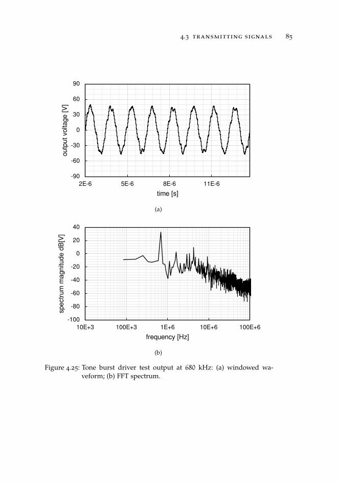
4.3 transmitting signals 85
-90
-60
-30
0
30
60
90
2E-6 5E-6 8E-6 11E-6
outp
ut v
olta
ge
[V]
time [s]
(a)
-100
-80
-60
-40
-20
0
20
40
10E+3 100E+3 1E+6 10E+6 100E+6
spec
trum
mag
nitu
de
dB
[V]
frequency [Hz]
(b)
Figure 4.25: Tone burst driver test output at 680 kHz: (a) windowed wa-veform; (b) FFT spectrum.
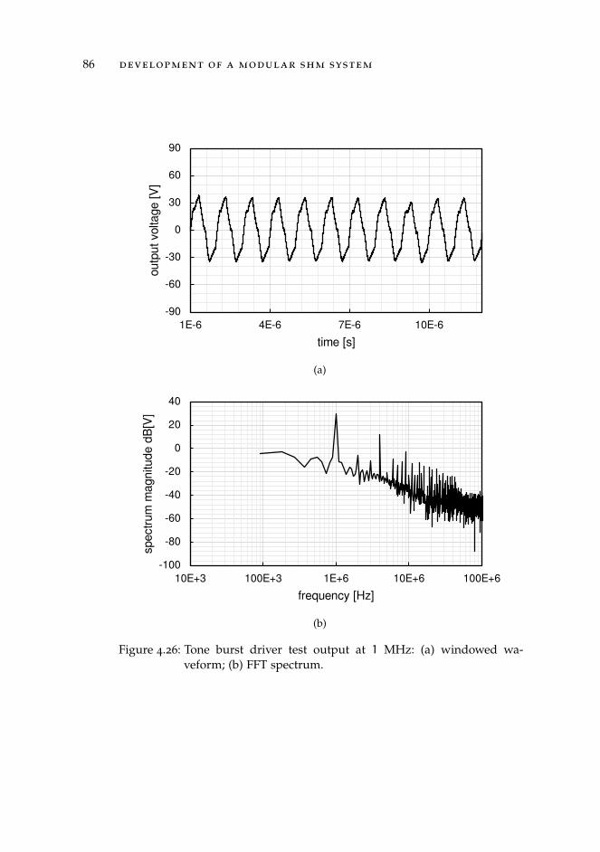
86 development of a modular shm system
-90
-60
-30
0
30
60
90
1E-6 4E-6 7E-6 10E-6
outp
ut v
olta
ge
[V]
time [s]
(a)
-100
-80
-60
-40
-20
0
20
40
10E+3 100E+3 1E+6 10E+6 100E+6
spec
trum
mag
nitu
de
dB
[V]
frequency [Hz]
(b)
Figure 4.26: Tone burst driver test output at 1 MHz: (a) windowed wa-veform; (b) FFT spectrum.
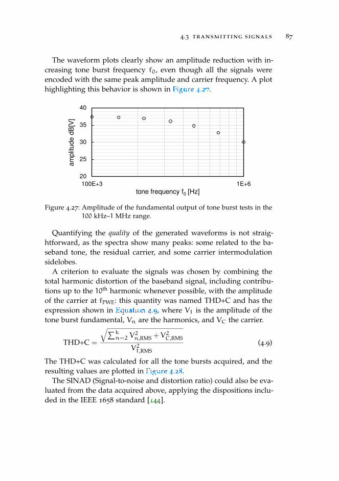
4.3 transmitting signals 87
The waveform plots clearly show an amplitude reduction with in-creasing tone burst frequency f0, even though all the signals wereencoded with the same peak amplitude and carrier frequency. A plothighlighting this behavior is shown in Figure 4.27
.
.
20
25
30
35
40
100E+3 1E+6
amp
litud
e d
B[V
]
tone frequency f0 [Hz]
Figure 4.27: Amplitude of the fundamental output of tone burst tests in the100 kHz–1 MHz range.
Quantifying the quality of the generated waveforms is not straig-htforward, as the spectra show many peaks: some related to the ba-seband tone, the residual carrier, and some carrier intermodulationsidelobes.
A criterion to evaluate the signals was chosen by combining thetotal harmonic distortion of the baseband signal, including contribu-tions up to the 10th harmonic whenever possible, with the amplitudeof the carrier at fPWE: this quantity was named THD+C and has theexpression shown in Equation 4.9
.
, where V1 is the amplitude of thetone burst fundamental, Vn are the harmonics, and VC the carrier.
THD+C =
√∑kn=2 V
2n,RMS + V
2C,RMS
V21,RMS
(4.9)
The THD+C was calculated for all the tone bursts acquired, and theresulting values are plotted in Figure 4.28
.
.The SINAD (Signal-to-noise and distortion ratio) could also be eva-
luated from the data acquired above, applying the dispositions inclu-ded in the IEEE 1658 standard [144
.
].
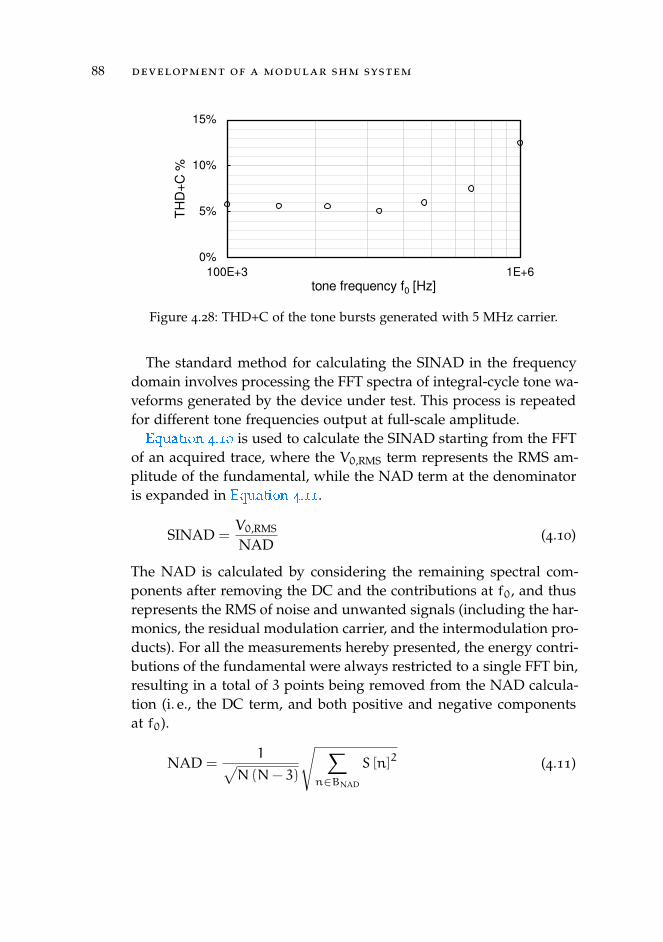
88 development of a modular shm system
0%
5%
10%
15%
100E+3 1E+6
TH
D+
C %
tone frequency f0 [Hz]
Figure 4.28: THD+C of the tone bursts generated with 5 MHz carrier.
The standard method for calculating the SINAD in the frequencydomain involves processing the FFT spectra of integral-cycle tone wa-veforms generated by the device under test. This process is repeatedfor different tone frequencies output at full-scale amplitude.
Equation 4.10
.
is used to calculate the SINAD starting from the FFTof an acquired trace, where the V0,RMS term represents the RMS am-plitude of the fundamental, while the NAD term at the denominatoris expanded in Equation 4.11
.
.
SINAD =V0,RMS
NAD(4.10)
The NAD is calculated by considering the remaining spectral com-ponents after removing the DC and the contributions at f0, and thusrepresents the RMS of noise and unwanted signals (including the har-monics, the residual modulation carrier, and the intermodulation pro-ducts). For all the measurements hereby presented, the energy contri-butions of the fundamental were always restricted to a single FFT bin,resulting in a total of 3 points being removed from the NAD calcula-tion (i. e., the DC term, and both positive and negative componentsat f0).
NAD =1√
N (N− 3)
√ ∑n∈BNAD
S [n]2 (4.11)
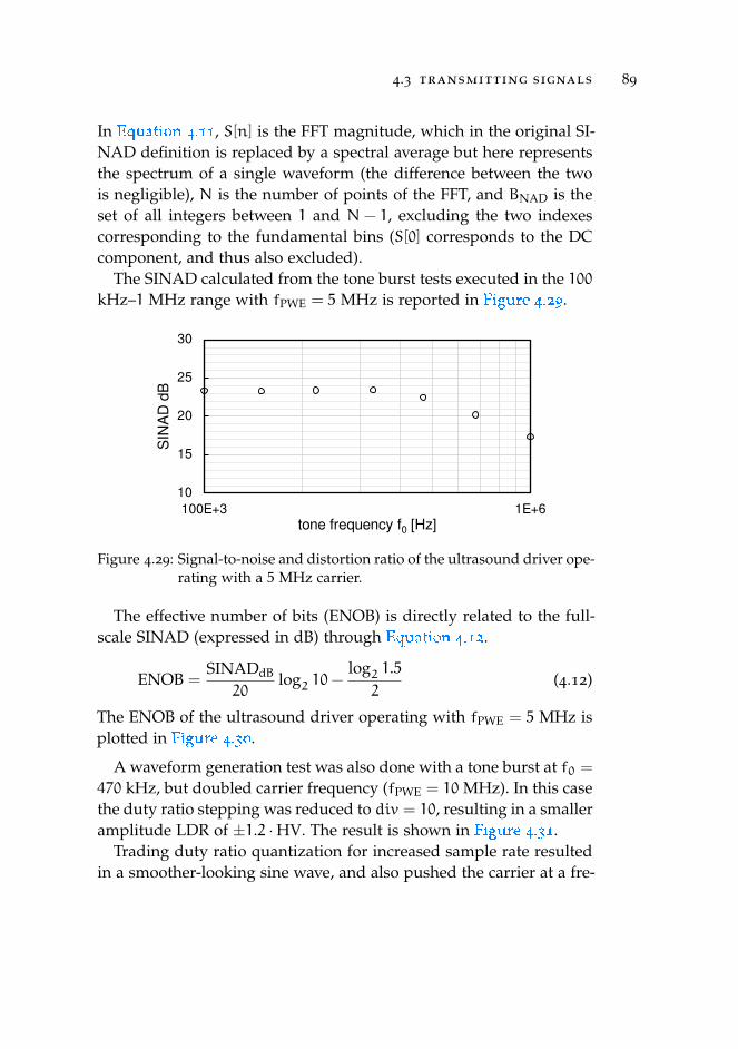
4.3 transmitting signals 89
In Equation 4.11
.
, S[n] is the FFT magnitude, which in the original SI-NAD definition is replaced by a spectral average but here representsthe spectrum of a single waveform (the difference between the twois negligible), N is the number of points of the FFT, and BNAD is theset of all integers between 1 and N − 1, excluding the two indexescorresponding to the fundamental bins (S[0] corresponds to the DCcomponent, and thus also excluded).
The SINAD calculated from the tone burst tests executed in the 100kHz–1 MHz range with fPWE = 5 MHz is reported in Figure 4.29
.
.
10
15
20
25
30
100E+3 1E+6
SIN
AD
dB
tone frequency f0 [Hz]
Figure 4.29: Signal-to-noise and distortion ratio of the ultrasound driver ope-rating with a 5 MHz carrier.
The effective number of bits (ENOB) is directly related to the full-scale SINAD (expressed in dB) through Equation 4.12
.
.
ENOB =SINADdB
20log2 10−
log2 1.52
(4.12)
The ENOB of the ultrasound driver operating with fPWE = 5 MHz isplotted in Figure 4.30
.
.
A waveform generation test was also done with a tone burst at f0 =
470 kHz, but doubled carrier frequency (fPWE = 10 MHz). In this casethe duty ratio stepping was reduced to div = 10, resulting in a smalleramplitude LDR of ±1.2 ·HV. The result is shown in Figure 4.31
.
.Trading duty ratio quantization for increased sample rate resulted
in a smoother-looking sine wave, and also pushed the carrier at a fre-
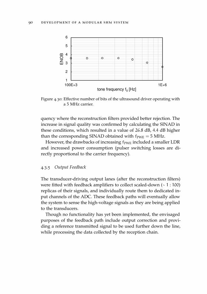
90 development of a modular shm system
1
2
3
4
5
6
100E+3 1E+6
EN
OB
tone frequency f0 [Hz]
Figure 4.30: Effective number of bits of the ultrasound driver operating witha 5 MHz carrier.
quency where the reconstruction filters provided better rejection. Theincrease in signal quality was confirmed by calculating the SINAD inthese conditions, which resulted in a value of 26.8 dB, 4.4 dB higherthan the corresponding SINAD obtained with fPWE = 5 MHz.
However, the drawbacks of increasing fPWE included a smaller LDRand increased power consumption (pulser switching losses are di-rectly proportional to the carrier frequency).
4.3.5 Output Feedback
The transducer-driving output lanes (after the reconstruction filters)were fitted with feedback amplifiers to collect scaled-down (∼ 1 : 100)replicas of their signals, and individually route them to dedicated in-put channels of the ADC. These feedback paths will eventually allowthe system to sense the high-voltage signals as they are being appliedto the transducers.
Though no functionality has yet been implemented, the envisagedpurposes of the feedback path include output correction and provi-ding a reference transmitted signal to be used further down the line,while processing the data collected by the reception chain.
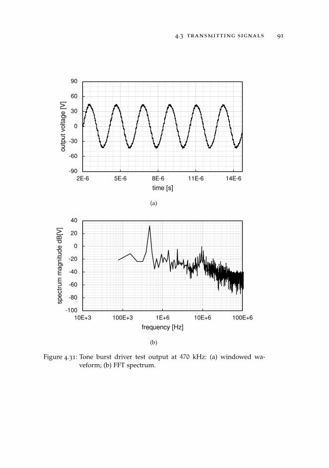
4.3 transmitting signals 91
-90
-60
-30
0
30
60
90
2E-6 5E-6 8E-6 11E-6 14E-6
outp
ut v
olta
ge
[V]
time [s]
(a)
-100
-80
-60
-40
-20
0
20
40
10E+3 100E+3 1E+6 10E+6 100E+6
spec
trum
mag
nitu
de
dB
[V]
frequency [Hz]
(b)
Figure 4.31: Tone burst driver test output at 470 kHz: (a) windowed wa-veform; (b) FFT spectrum.
92 development of a modular shm system
4.3.6 Passive-Mode Receiver
Previous experience with the system described in Chapter 3
.
sugge-sted that specific, low-gain signal conditioning channels were requi-red to perform passive-mode impact and vibration detection.
Those channels were designed similarly to the output feedback des-cribed above (using banks of Texas Instruments THS4524 fully diffe-rential amplifiers), but provided an attenuation of ∼ 1 : 5.
4.3.7 T/R Switching
Transmit / receive switching is handled by two dedicated multichan-nel chips (Texas Instruments TX810) that contain a bank of diodebridges with programmable biasing. Together with the pulser chips,these are the only devices of the entire analog signal chain that re-quire split ±5 V supplies.
The specified bandwidth of the TX810 is much wider than what isrequired by the proposed design, even at the lowest bias setting (65MHz).
4.4 receiving signals
Guided-wave ultrasound propagated over complex media like CFRPplates and shells incur in significant attenuation [145
.
] which, combi-ned with the poor sensitivity of piezopolymer film transducers dis-cussed in Chapter 2
.
, makes the task of receiving these signals parti-cularly arduous: very large gain is generally required from the pre-amplifiers, and low-noise.
Furthermore, practical considerations regarding the target operati-onal environment of SHM systems (e. g., ground vehicles, aircrafts,rotating machinery) suggest the presence of significant EMI, pushingin the direction of adopting fully-differential signal conditioning cir-cuitry.
Broadband piezoploymer transducers tend to present a large capa-citive impedance within the bandwidth of interest for the proposed
4.4 receiving signals 93
system (100 kHz–1 MHz), in the kilohm range, that needs to be takeninto account when designing the signal conditioning electronics.
As the active area of piezopolymer transducer shrinks (like thosepresented in Section 2.5
.
and Section 2.7
.
), maintaining the same filmthickness results in an inevitable increase of the source impedance, tothe point where signal extraction strategies should be reconsidered.
The topic of transducer interfacing will be explored below withexplicit reference to the IDTs presented earlier in the text, but theconclusions are generally applicable to every kind of piezoelectricsensor.
4.4.1 Voltage-Mode and Charge-Mode Interfacing
Considering a single piezoelectric sensor with two electrodes, thereare two complementary ways of detecting the charge generated by di-rect piezoelectric effect, that essentially depend on the way the sensoris electrically loaded.
• When the sensor is left open-circuit, a voltage can be detectedat its electrodes when excess charge is generated. In reality, anyvoltage-mode sense circuit will have a finite input impedance.
• If the sensor electrodes are deliberately shorted, on the otherhand, the excess charge can be detected as a current flowingthrough the short. Of course, actual charge-mode circuits have anon-zero input impedance.
When dealing with IDTs, different sensing modes benefit from diffe-rent connection of the electrodes. This is easily explained referring toFigure 4.32
.
.In Figure 4.32a
.
, all the electrodes on the bottom side of the IDTare shorted together and used as a ground plane of sorts, resultingin half the fingers being in series with the other half and, since thesignals are supposed to be equal in magnitude but opposite in phase,the resulting open-circuit voltage developed between the [+] and [-]terminals is two times that generated by a single finger. A voltage-
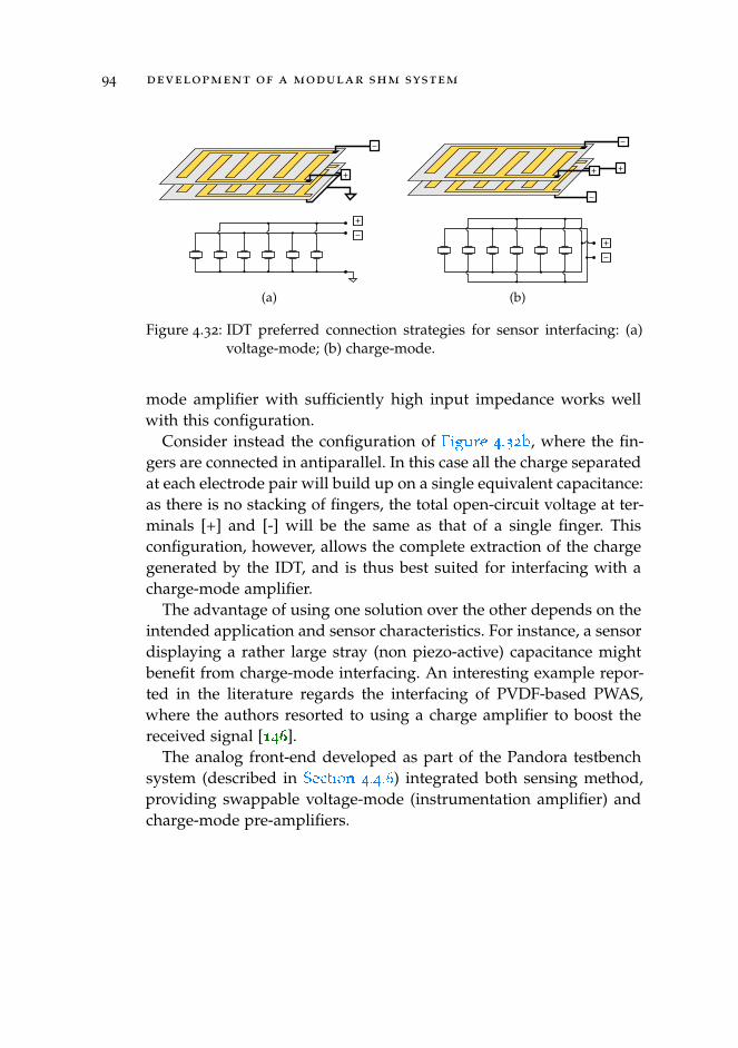
94 development of a modular shm system
(a) (b)
Figure 4.32: IDT preferred connection strategies for sensor interfacing: (a)voltage-mode; (b) charge-mode.
mode amplifier with sufficiently high input impedance works wellwith this configuration.
Consider instead the configuration of Figure 4.32b
.
, where the fin-gers are connected in antiparallel. In this case all the charge separatedat each electrode pair will build up on a single equivalent capacitance:as there is no stacking of fingers, the total open-circuit voltage at ter-minals [+] and [-] will be the same as that of a single finger. Thisconfiguration, however, allows the complete extraction of the chargegenerated by the IDT, and is thus best suited for interfacing with acharge-mode amplifier.
The advantage of using one solution over the other depends on theintended application and sensor characteristics. For instance, a sensordisplaying a rather large stray (non piezo-active) capacitance mightbenefit from charge-mode interfacing. An interesting example repor-ted in the literature regards the interfacing of PVDF-based PWAS,where the authors resorted to using a charge amplifier to boost thereceived signal [146
.
].The analog front-end developed as part of the Pandora testbench
system (described in Section 4.4.6
.
) integrated both sensing method,providing swappable voltage-mode (instrumentation amplifier) andcharge-mode pre-amplifiers.
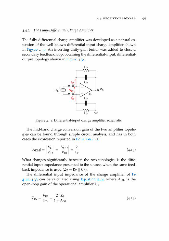
4.4 receiving signals 95
4.4.2 The Fully-Differential Charge Amplifier
The fully-differential charge amplifier was developed as a natural ex-tension of the well-known differential-input charge amplifier shownin Figure 4.33
.
. An inverting unity-gain buffer was added to close asecondary feedback loop, obtaining the differential-input, differential-output topology shown in Figure 4.34
.
.
RF
CF
RF
CF
U1
VIDVO
IID
IID
QIN
Figure 4.33: Differential-input charge amplifier schematic.
The mid-band charge conversion gain of the two amplifier topolo-gies can be found through simple circuit analysis, and has in bothcases the expression reported in Equation 4.13
.
.
|ADM| =
∣∣∣∣ VO
VID
∣∣∣∣ = ∣∣∣∣VOD
VID
∣∣∣∣ = 2
CF(4.13)
What changes significantly between the two topologies is the diffe-rential input impedance presented to the source, when the same feed-back impedance is used (ZF = RF ‖ CF).
The differential input impedance of the charge amplifier of Fi-gure 4.33
.
can be calculated using Equation 4.14
.
, where AOL is theopen-loop gain of the operational amplifier U1.
ZIN =VID
IID=
2 ·ZF
1+AOL(4.14)
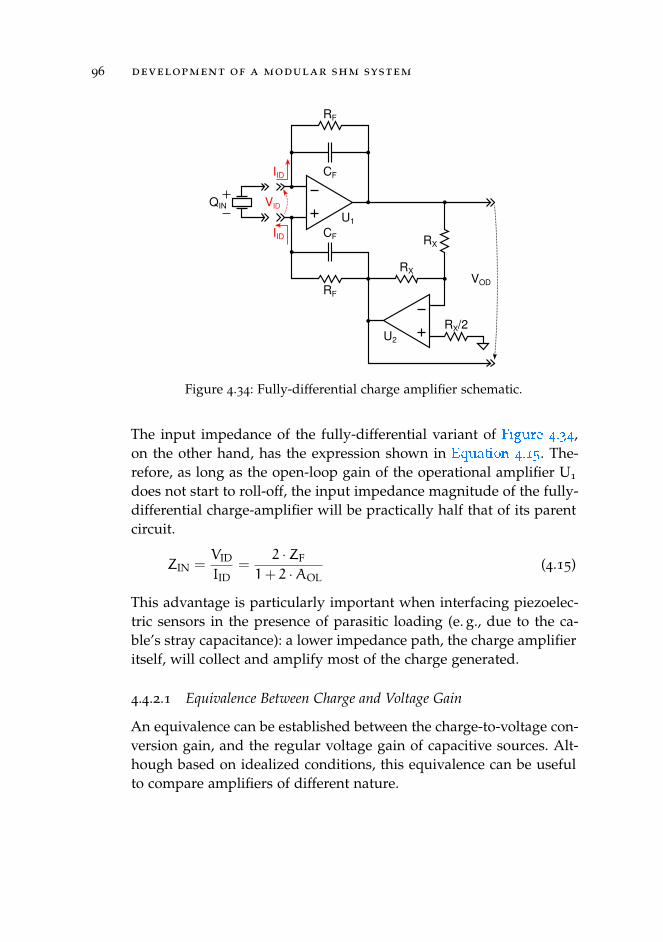
96 development of a modular shm system
RX
RX
RX/2U2
RF
CF
RF
CF
U1
VID
VOD
IID
IID
QIN
Figure 4.34: Fully-differential charge amplifier schematic.
The input impedance of the fully-differential variant of Figure 4.34
.
,on the other hand, has the expression shown in Equation 4.15
.
. The-refore, as long as the open-loop gain of the operational amplifier U1
does not start to roll-off, the input impedance magnitude of the fully-differential charge-amplifier will be practically half that of its parentcircuit.
ZIN =VID
IID=
2 ·ZF
1+ 2 ·AOL(4.15)
This advantage is particularly important when interfacing piezoelec-tric sensors in the presence of parasitic loading (e. g., due to the ca-ble’s stray capacitance): a lower impedance path, the charge amplifieritself, will collect and amplify most of the charge generated.
4.4.2.1 Equivalence Between Charge and Voltage Gain
An equivalence can be established between the charge-to-voltage con-version gain, and the regular voltage gain of capacitive sources. Alt-hough based on idealized conditions, this equivalence can be usefulto compare amplifiers of different nature.
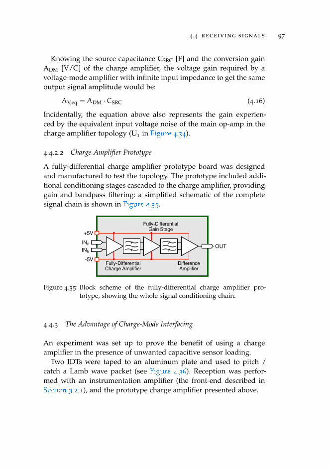
4.4 receiving signals 97
Knowing the source capacitance CSRC [F] and the conversion gainADM [V/C] of the charge amplifier, the voltage gain required by avoltage-mode amplifier with infinite input impedance to get the sameoutput signal amplitude would be:
AV,eq = ADM ·CSRC (4.16)
Incidentally, the equation above also represents the gain experien-ced by the equivalent input voltage noise of the main op-amp in thecharge amplifier topology (U1 in Figure 4.34
.
).
4.4.2.2 Charge Amplifier Prototype
A fully-differential charge amplifier prototype board was designedand manufactured to test the topology. The prototype included addi-tional conditioning stages cascaded to the charge amplifier, providinggain and bandpass filtering: a simplified schematic of the completesignal chain is shown in Figure 4.35
.
.
Fully-DifferentialCharge Amplifier
Fully-DifferentialGain Stage
DifferenceAmplifier
+5V
-5V
INP
INN
OUT
Figure 4.35: Block scheme of the fully-differential charge amplifier pro-totype, showing the whole signal conditioning chain.
4.4.3 The Advantage of Charge-Mode Interfacing
An experiment was set up to prove the benefit of using a chargeamplifier in the presence of unwanted capacitive sensor loading.
Two IDTs were taped to an aluminum plate and used to pitch /catch a Lamb wave packet (see Figure 4.36
.
). Reception was perfor-med with an instrumentation amplifier (the front-end described inSection 3.2.1
.
), and the prototype charge amplifier presented above.
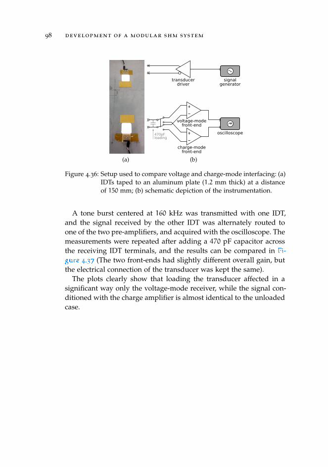
98 development of a modular shm system
(a)
voltage-modefront-end
charge-modefront-end
transducerdriver
signalgenerator
oscilloscope470pFloading
(b)
Figure 4.36: Setup used to compare voltage and charge-mode interfacing: (a)IDTs taped to an aluminum plate (1.2 mm thick) at a distanceof 150 mm; (b) schematic depiction of the instrumentation.
A tone burst centered at 160 kHz was transmitted with one IDT,and the signal received by the other IDT was alternately routed toone of the two pre-amplifiers, and acquired with the oscilloscope. Themeasurements were repeated after adding a 470 pF capacitor acrossthe receiving IDT terminals, and the results can be compared in Fi-gure 4.37
.
(The two front-ends had slightly different overall gain, butthe electrical connection of the transducer was kept the same).
The plots clearly show that loading the transducer affected in asignificant way only the voltage-mode receiver, while the signal con-ditioned with the charge amplifier is almost identical to the unloadedcase.
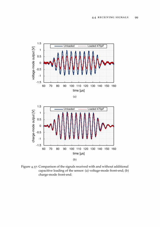
4.4 receiving signals 99
-1.5
-1
-0.5
0
0.5
1
1.5
60 70 80 90 100 110 120 130 140 150 160
volta
ge-
mod
e ou
tput
[V
]
time [μs]
Unloaded Loaded 470pF
(a)
-1.5
-1
-0.5
0
0.5
1
1.5
60 70 80 90 100 110 120 130 140 150 160
char
ge-
mod
e ou
tput
[V
]
time [μs]
Unloaded Loaded 470pF
(b)
Figure 4.37: Comparison of the signals received with and without additionalcapacitive loading of the sensor: (a) voltage-mode front-end; (b)charge-mode front-end.
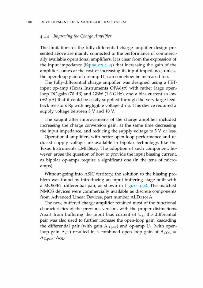
100 development of a modular shm system
4.4.4 Improving the Charge Amplifier
The limitations of the fully-differential charge amplifier design pre-sented above are mainly connected to the performance of commerci-ally available operational amplifiers. It is clear from the expression ofthe input impedance (Equation 4.15
.
) that increasing the gain of theamplifier comes at the cost of increasing its input impedance, unlessthe open-loop gain of op-amp U1 can somehow be increased too.
The fully-differential charge amplifier was designed using a FET-input op-amp (Texas Instruments OPA657) with rather large open-loop DC gain (70 dB) and GBW (1.6 GHz), and a bias current so low(±2 pA) that it could be easily supplied through the very large feed-back resistors RF with negligible voltage drop. This device required asupply voltage between 8 V and 10 V.
The sought after improvements of the charge amplifier includedincreasing the charge conversion gain, at the same time decreasingthe input impedance, and reducing the supply voltage to 5 V, or less.
Operational amplifiers with better open-loop performance and re-duced supply voltage are available in bipolar technology, like theTexas Instruments LMH6629. The adoption of such component, ho-wever, arose the question of how to provide the input biasing current,as bipolar op-amps require a significant one (in the tens of micro-amps).
Without going into ASIC territory, the solution to the biasing pro-blem was found by introducing an input buffering stage built witha MOSFET differential pair, as shown in Figure 4.38
.
. The matchedNMOS devices were commercially available as discrete componentsfrom Advanced Linear Devices, part number ALD1101A.
The new, buffered charge amplifier retained most of the functionalcharacteristics of the previous version, with the proper distinctions.Apart from buffering the input bias current of U1, the differentialpair was also used to further increase the open-loop gain: cascadingthe differential pair (with gain AD,pair) and op-amp U1 (with open-loop gain AOL) resulted in a combined open-loop gain of ACOL =
AD,pair ·AOL.
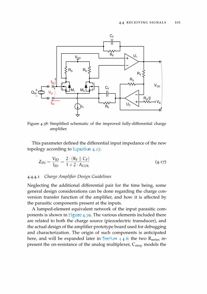
4.4 receiving signals 101
RF
VDD
VB
CF
U1
U2
RF
CF
RD RD
RX
RX
M1 M2VID
IID
IID
QIN
VOD
RX/2
IT
Figure 4.38: Simplified schematic of the improved fully-differential chargeamplifier.
This parameter defined the differential input impedance of the newtopology according to Equation 4.17
.
.
ZIN =VID
IID=2 · (RF ‖ CF)
1+ 2 ·ACOL(4.17)
4.4.4.1 Charge Amplifier Design Guidelines
Neglecting the additional differential pair for the time being, somegeneral design considerations can be done regarding the charge con-version transfer function of the amplifier, and how it is affected bythe parasitic components present at the inputs.
A lumped-element equivalent network of the input parasitic com-ponents is shown in Figure 4.39
.
. The various elements included thereare related to both the charge source (piezoelectric transducer), andthe actual design of the amplifier prototype board used for debuggingand characterization. The origin of such components is anticipatedhere, and will be expanded later in Section 4.4.6
.
: the two Rseries re-present the on-resistance of the analog multiplexer, Cstray models the
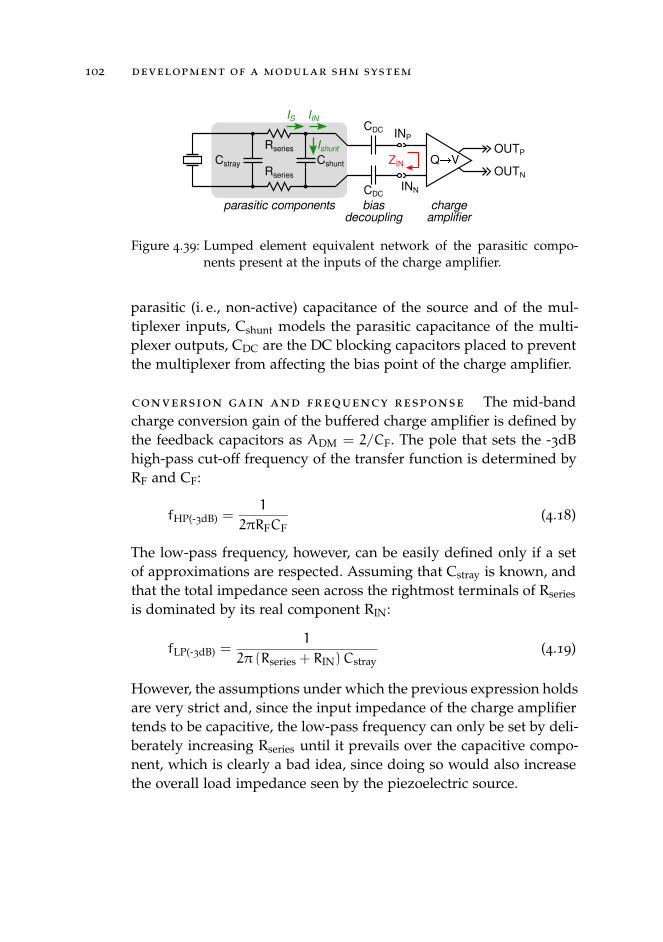
102 development of a modular shm system
OUTN
OUTP
INP
INN
QVRseries
Cshunt
CDC
CDC
RseriesCstray
parasitic components chargeamplifier
ZIN
IS IIN
Ishunt
biasdecoupling
Figure 4.39: Lumped element equivalent network of the parasitic compo-nents present at the inputs of the charge amplifier.
parasitic (i. e., non-active) capacitance of the source and of the mul-tiplexer inputs, Cshunt models the parasitic capacitance of the multi-plexer outputs, CDC are the DC blocking capacitors placed to preventthe multiplexer from affecting the bias point of the charge amplifier.
conversion gain and frequency response The mid-bandcharge conversion gain of the buffered charge amplifier is defined bythe feedback capacitors as ADM = 2/CF. The pole that sets the -3dBhigh-pass cut-off frequency of the transfer function is determined byRF and CF:
fHP(-3dB) =1
2πRFCF(4.18)
The low-pass frequency, however, can be easily defined only if a setof approximations are respected. Assuming that Cstray is known, andthat the total impedance seen across the rightmost terminals of Rseries
is dominated by its real component RIN:
fLP(-3dB) =1
2π (Rseries + RIN)Cstray(4.19)
However, the assumptions under which the previous expression holdsare very strict and, since the input impedance of the charge amplifiertends to be capacitive, the low-pass frequency can only be set by deli-berately increasing Rseries until it prevails over the capacitive compo-nent, which is clearly a bad idea, since doing so would also increasethe overall load impedance seen by the piezoelectric source.
4.4 receiving signals 103
Consider now the components Cshunt, CDC, and ZIN: they form acurrent divider where the actual signal injected into the amplifier canbe calculated with Equation 4.20
.
.
IINIS
=
sCDC2+sZINCDC
sCDC2+sZINCDC
+ sCshunt=
=1(
1+ 2CshuntCDC
)(1+ sZINCDCCshunt
CDC+2Cshunt
) (4.20)
The left-hand factor of the denominator shows that the ratio betweenCshunt and CDC determines an attenuation of the input signal, andthus CDC should be maximized.
The right-hand factor is frequency-dependent, but can be approx-imated to Equation 4.21
.
under the assumption that ZIN is behavinglike a capacitor, CIN. This assumption is reasonable when, referring toEquation 4.17
.
, CF dominates the feedback impedance and ACOL hasyet to start rolling off.
IINIS≈ 1(
1+ 2CshuntCDC
) [1+ sCDCCshunt
sCIN(CDC+2Cshunt)
] =
=1(
1+ 2CshuntCDC
)(1+ 1
CIN· CDCCshuntCDC+2Cshunt
) (4.21)
The approximate Equation 4.21
.
shows that the right-hand factor alsocontributes a broadband attenuation, in this case exacerbated by anincrease of either CDC or Cshunt, while CIN counteracts the effect. Athigher frequency, when the combined open-loop gain ACOL starts de-creasing and phase-shifting, ZIN loses its capacitive behavior, and apole is determined by CDC and Cshunt.
The conclusion is that, in the absence of significant series resis-tance between the source and the charge amplifier inputs, the high-frequency behavior of the transfer function is ultimately defined bythe open-loop gain, as acting on the other elements of the input net-work leads to unwanted collateral effects within the passband region.
104 development of a modular shm system
4.4.4.2 Additional Differential Pair
Despite the potential to increase the combined open-loop gain of thecharge amplifier, the additional FET differential pair stage had severaloperating point constraints imposed by the other circuit components,such that the final AD,pair was rather low.
The differential pair performance could have been increased byadopting common analog design techniques, such as using active lo-ads instead of resistors. This path, however, was not ventured, as thefact that this design was made with discrete components resulted inthe following circumstances:
• There is a very limited choice of off-the-shelf matched MOSFETpairs (or arrays), and obviously their geometry cannot be adjus-ted to the application requirements.
• The packages of said devices are big. Increasing the number ofMOSFETs in a discrete design leads to a significant increase incircuit board area.
• Discrete, matched MOSFETs arrays are not cheap.
• Resistors with tight tolerance and extended value range are wi-dely available as discrete components.
With reference to Figure 4.38
.
, it is observed the gate voltage ofthe differential pair corresponds to the DC voltage present at bothop-amps output terminals, and is set through VB. Since the ampli-fier outputs are the nodes that experience the largest voltage swingduring normal operation, it was advisable to keep them biased atmid-supply to reduce nonlinearities. Therefore, the FETs gate voltagewas fixed at 2.5 V.
The drain nodes of the FETs, on the other hand, are directly con-nected to the input terminals of U1, meaning that they must respectthe common-mode input range of the op-amp. The input terminalsof the LMH6629 had a large flexibility in the bias point they couldaccept, up to 3.8 V according to the datasheet.
4.4 receiving signals 105
Eventually, the operating point of the differential pair was set with2.5 V at the MOSFET gates, and a tail current IT= 15 mA (the tail ge-nerator was a discrete NPN BJT current mirror made with a NexperiaBCM61B). Using two precision (±0.1%) load resistors RD= 270 Ω, theDC drain voltage of the pair was 2.9 V, while the source terminalsrested at 110 mV. At this operating point, the small signal transcon-ductance of the two FETs was gm≈ 7 mS.
When calculating the differential pair gain AD,pair, the loading in-troduced by op-amp U1 had to be factored in. Unfortunately, theLMH6629 used in the proposed implementation did not have a speci-fied differential input resistance, nor its simulation macro-model wasdeclared accurate with regards to this characteristic: in the absence ofofficial data, simulation results were used as a best guess.
The nominal (unloaded) gain of the differential pair was AD,pair =
gmRD = 1.89, simulations performed by adding U1 as load showedthe gain decreasing to AD,pair = 1.72, or 4.7 dB.
The loading introduced by U1 had also major effects on the band-width. Usually, the frequency response of a MOSFET differential pairis determined by the Miller multiplication of the gate-drain capaci-tance [147
.
, sec. 6.6], however, given the very low gain of this imple-mentation, the frequency response was actually determined by theinput capacitance of U1. Even with such loading, simulations showedthat the differential pair bandwidth was wider than the open-loopfrequency response of the operational-amplifier.
It is worth noting that U1 could considerably affect the differentialpair frequency response also through the Miller multiplication of anycapacitance connected between its inverting input pin and the output(shown as CM in Figure 4.40
.
). Given the very large open-loop gainof the LMH6629, even a tiny, 1 pF feedback capacitance would haveresulted in several nanofarads of additional differential pair loading,and this is the reason why introducing a CM was avoided during thedesign.
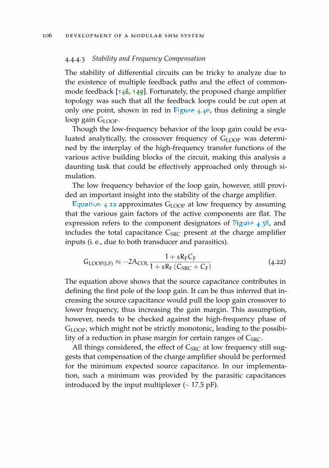
106 development of a modular shm system
4.4.4.3 Stability and Frequency Compensation
The stability of differential circuits can be tricky to analyze due tothe existence of multiple feedback paths and the effect of common-mode feedback [148
.
, 149
.
]. Fortunately, the proposed charge amplifiertopology was such that all the feedback loops could be cut open atonly one point, shown in red in Figure 4.40
.
, thus defining a singleloop gain GLOOP.
Though the low-frequency behavior of the loop gain could be eva-luated analytically, the crossover frequency of GLOOP was determi-ned by the interplay of the high-frequency transfer functions of thevarious active building blocks of the circuit, making this analysis adaunting task that could be effectively approached only through si-mulation.
The low frequency behavior of the loop gain, however, still provi-ded an important insight into the stability of the charge amplifier.
Equation 4.22
.
approximates GLOOP at low frequency by assumingthat the various gain factors of the active components are flat. Theexpression refers to the component designators of Figure 4.38
.
, andincludes the total capacitance CSRC present at the charge amplifierinputs (i. e., due to both transducer and parasitics).
GLOOP(LF) ≈ −2ACOL1+ sRFCF
1+ sRF (CSRC +CF)(4.22)
The equation above shows that the source capacitance contributes indefining the first pole of the loop gain. It can be thus inferred that in-creasing the source capacitance would pull the loop gain crossover tolower frequency, thus increasing the gain margin. This assumption,however, needs to be checked against the high-frequency phase ofGLOOP, which might not be strictly monotonic, leading to the possibi-lity of a reduction in phase margin for certain ranges of CSRC.
All things considered, the effect of CSRC at low frequency still sug-gests that compensation of the charge amplifier should be performedfor the minimum expected source capacitance. In our implementa-tion, such a minimum was provided by the parasitic capacitancesintroduced by the input multiplexer (∼ 17.5 pF).
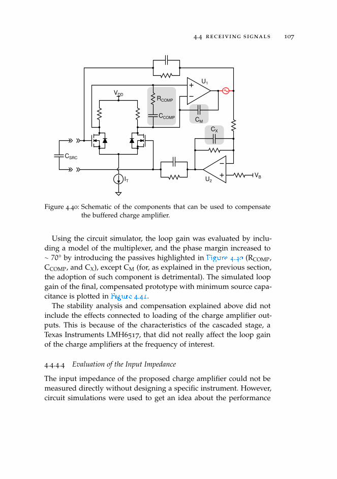
4.4 receiving signals 107
VDD
VB
U1
U2IT
RCOMP
CCOMP CM
CX
CSRC
Figure 4.40: Schematic of the components that can be used to compensatethe buffered charge amplifier.
Using the circuit simulator, the loop gain was evaluated by inclu-ding a model of the multiplexer, and the phase margin increased to∼ 70° by introducing the passives highlighted in Figure 4.40
.
(RCOMP,CCOMP, and CX), except CM (for, as explained in the previous section,the adoption of such component is detrimental). The simulated loopgain of the final, compensated prototype with minimum source capa-citance is plotted in Figure 4.41
.
.The stability analysis and compensation explained above did not
include the effects connected to loading of the charge amplifier out-puts. This is because of the characteristics of the cascaded stage, aTexas Instruments LMH6517, that did not really affect the loop gainof the charge amplifiers at the frequency of interest.
4.4.4.4 Evaluation of the Input Impedance
The input impedance of the proposed charge amplifier could not bemeasured directly without designing a specific instrument. However,circuit simulations were used to get an idea about the performance
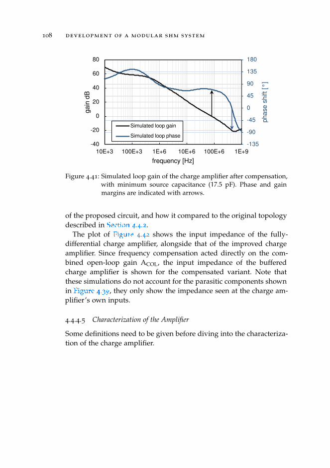
108 development of a modular shm system
-135
-90
-45
0
45
90
135
180
-40
-20
0
20
40
60
80
10E+3 100E+3 1E+6 10E+6 100E+6 1E+9
pha
se s
hift
[°
]
gai
n d
B
frequency [Hz]
Simulated loop gain
Simulated loop phase
Figure 4.41: Simulated loop gain of the charge amplifier after compensation,with minimum source capacitance (17.5 pF). Phase and gainmargins are indicated with arrows.
of the proposed circuit, and how it compared to the original topologydescribed in Section 4.4.2
.
.The plot of Figure 4.42
.
shows the input impedance of the fully-differential charge amplifier, alongside that of the improved chargeamplifier. Since frequency compensation acted directly on the com-bined open-loop gain ACOL, the input impedance of the bufferedcharge amplifier is shown for the compensated variant. Note thatthese simulations do not account for the parasitic components shownin Figure 4.39
.
, they only show the impedance seen at the charge am-plifier’s own inputs.
4.4.4.5 Characterization of the Amplifier
Some definitions need to be given before diving into the characteriza-tion of the charge amplifier.
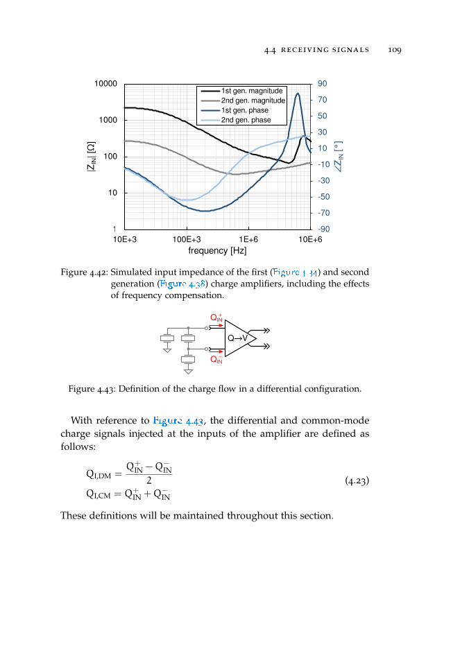
4.4 receiving signals 109
-90
-70
-50
-30
-10
10
30
50
70
90
1
10
100
1000
10000
10E+3 100E+3 1E+6 10E+6
∠Z
IN[°
]
|ZIN
| [Ω
]
frequency [Hz]
1st gen. magnitude2nd gen. magnitude1st gen. phase2nd gen. phase
Figure 4.42: Simulated input impedance of the first (Figure 4.34
.
) and secondgeneration (Figure 4.38
.
) charge amplifiers, including the effectsof frequency compensation.
QV
QIN
QIN
Figure 4.43: Definition of the charge flow in a differential configuration.
With reference to Figure 4.43
.
, the differential and common-modecharge signals injected at the inputs of the amplifier are defined asfollows:
QI,DM =Q+
IN −Q−IN
2
QI,CM = Q+IN +Q−
IN
(4.23)
These definitions will be maintained throughout this section.
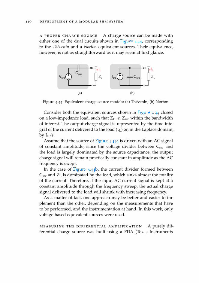
110 development of a modular shm system
a proper charge source A charge source can be made witheither one of the dual circuits shown in Figure 4.44
.
, correspondingto the Thévenin and a Norton equivalent sources. Their equivalence,however, is not as straightforward as it may seem at first glance.
CsrcVsrc ZL
IL
(a)
CsrcIsrc ZL
IL
(b)
Figure 4.44: Equivalent charge source models: (a) Thévenin; (b) Norton.
Consider both the equivalent sources shown in Figure 4.44
.
closedon a low-impedance load, such that ZL Zsrc within the bandwidthof interest. The output charge signal is represented by the time inte-gral of the current delivered to the load (iL) or, in the Laplace domain,by IL/s.
Assume that the source of Figure 4.44a
.
is driven with an AC signalof constant amplitude; since the voltage divider between Csrc andthe load is largely dominated by the source capacitance, the outputcharge signal will remain practically constant in amplitude as the ACfrequency is swept.
In the case of Figure 4.44b
.
, the current divider formed betweenCsrc and ZL is dominated by the load, which sinks almost the totalityof the current. Therefore, if the input AC current signal is kept at aconstant amplitude through the frequency sweep, the actual chargesignal delivered to the load will shrink with increasing frequency.
As a matter of fact, one approach may be better and easier to im-plement than the other, depending on the measurements that haveto be performed, and the instrumentation at hand. In this work, onlyvoltage-based equivalent sources were used.
measuring the differential amplification A purely dif-ferential charge source was built using a FDA (Texas Instruments
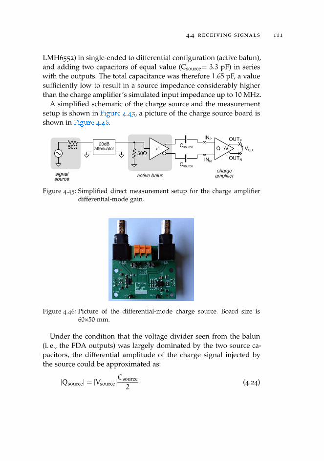
4.4 receiving signals 111
LMH6552) in single-ended to differential configuration (active balun),and adding two capacitors of equal value (Csource= 3.3 pF) in serieswith the outputs. The total capacitance was therefore 1.65 pF, a valuesufficiently low to result in a source impedance considerably higherthan the charge amplifier’s simulated input impedance up to 10MHz.
A simplified schematic of the charge source and the measurementsetup is shown in Figure 4.45
.
, a picture of the charge source board isshown in Figure 4.46
.
.
50 Csource
active balunsignalsource
50
20dBattenuator
OUTN
OUTPINP
INN
QV
chargeamplifier
Csource
x1 VOD
Figure 4.45: Simplified direct measurement setup for the charge amplifierdifferential-mode gain.
Figure 4.46: Picture of the differential-mode charge source. Board size is60×50 mm.
Under the condition that the voltage divider seen from the balun(i. e., the FDA outputs) was largely dominated by the two source ca-pacitors, the differential amplitude of the charge signal injected bythe source could be approximated as:
|Qsource| = |Vsource|Csource
2(4.24)
112 development of a modular shm system
The actual transfer function between the benchtop signal generatorand the differential outputs of the active balun was measured on itsown to extrapolate a gain / phase correction factor that was laterapplied to the charge amplifier measurements.
With the input signal thus characterized, the differential charge-to-voltage conversion transfer function could be measured, and theresult is compared with the simulation in Figure 4.47
.
.
common-mode rejection While directly measuring the diffe-rential response of the charge amplifier was a rather simple task thatcould be solved with the adoption of a special balun, measuring thecommon-mode response was another thing entirely.
To gain some perspective on the matter, one can start by looking atthe usual way differential, voltage-input amplifiers are characterized:by connecting a single-ended voltage source to the short-circuitedinputs of the amplifier, the injection of a pure common-mode signalis guaranteed, and the common-mode gain can be directly measured.
The importance of measuring the common-mode gain directly can-not be overstated. Any differential amplifier is expected to providea significant common-mode rejection ratio (CMRR) and, dependingon the circuit performance, the disparity between differential andcommon-mode gain could be many orders of magnitude. In thosesituations, trying to indirectly extrapolate the common-mode frommeasurements where both contributions are present becomes an in-surmountable task, as the resolution limits of the instrumentation willobliterate the common-mode contribution buried within the differen-tial signal.
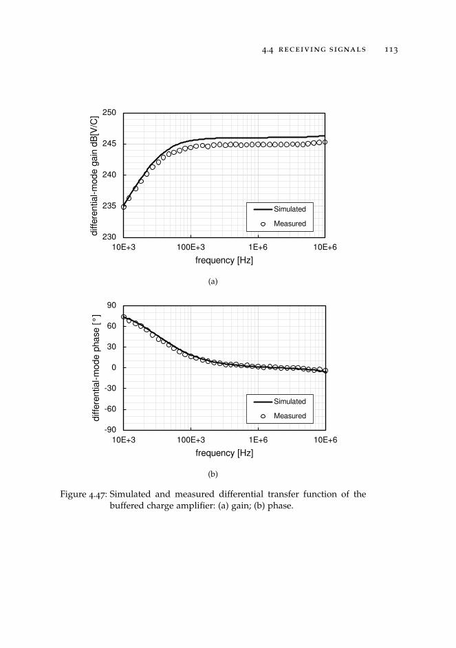
4.4 receiving signals 113
230
235
240
245
250
10E+3 100E+3 1E+6 10E+6
diff
eren
tial-
mod
e g
ain
dB
[V/C
]
frequency [Hz]
Simulated
Measured
(a)
-90
-60
-30
0
30
60
90
10E+3 100E+3 1E+6 10E+6
diff
eren
tial-
mod
e p
hase
[°
]
frequency [Hz]
Simulated
Measured
(b)
Figure 4.47: Simulated and measured differential transfer function of thebuffered charge amplifier: (a) gain; (b) phase.
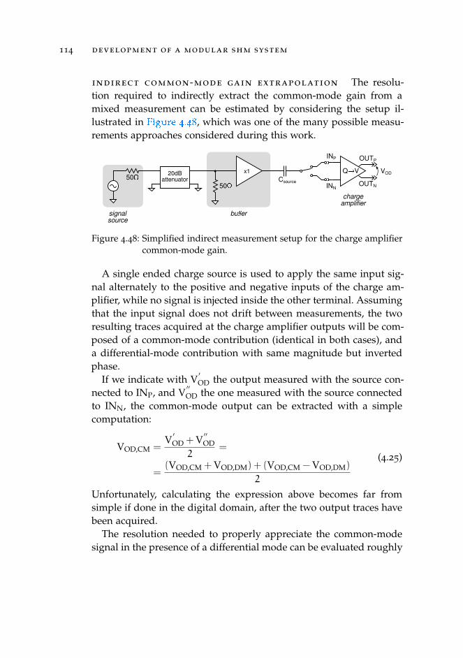
114 development of a modular shm system
indirect common-mode gain extrapolation The resolu-tion required to indirectly extract the common-mode gain from amixed measurement can be estimated by considering the setup il-lustrated in Figure 4.48
.
, which was one of the many possible measu-rements approaches considered during this work.
50 Csource
buersignalsource
50
20dBattenuator
x1
INP
INN
QV
chargeamplifier
VOD
OUTP
OUTN
Figure 4.48: Simplified indirect measurement setup for the charge amplifiercommon-mode gain.
A single ended charge source is used to apply the same input sig-nal alternately to the positive and negative inputs of the charge am-plifier, while no signal is injected inside the other terminal. Assumingthat the input signal does not drift between measurements, the tworesulting traces acquired at the charge amplifier outputs will be com-posed of a common-mode contribution (identical in both cases), anda differential-mode contribution with same magnitude but invertedphase.
If we indicate with V′OD the output measured with the source con-
nected to INP, and V′′OD the one measured with the source connected
to INN, the common-mode output can be extracted with a simplecomputation:
VOD,CM =V
′OD + V
′′OD
2=
=(VOD,CM + VOD,DM) + (VOD,CM − VOD,DM)
2
(4.25)
Unfortunately, calculating the expression above becomes far fromsimple if done in the digital domain, after the two output traces havebeen acquired.
The resolution needed to properly appreciate the common-modesignal in the presence of a differential mode can be evaluated roughly
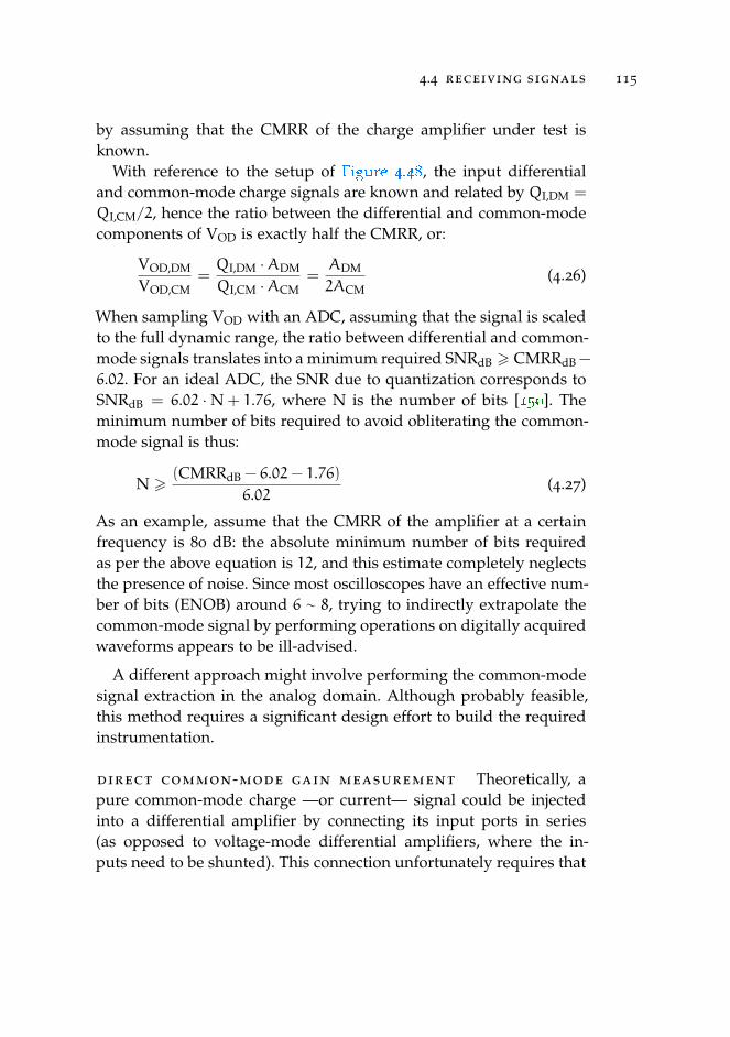
4.4 receiving signals 115
by assuming that the CMRR of the charge amplifier under test isknown.
With reference to the setup of Figure 4.48
.
, the input differentialand common-mode charge signals are known and related by QI,DM =
QI,CM/2, hence the ratio between the differential and common-modecomponents of VOD is exactly half the CMRR, or:
VOD,DM
VOD,CM=QI,DM ·ADM
QI,CM ·ACM=ADM
2ACM(4.26)
When sampling VOD with an ADC, assuming that the signal is scaledto the full dynamic range, the ratio between differential and common-mode signals translates into a minimum required SNRdB > CMRRdB −
6.02. For an ideal ADC, the SNR due to quantization corresponds toSNRdB = 6.02 ·N + 1.76, where N is the number of bits [150
.
]. Theminimum number of bits required to avoid obliterating the common-mode signal is thus:
N >(CMRRdB − 6.02− 1.76)
6.02(4.27)
As an example, assume that the CMRR of the amplifier at a certainfrequency is 80 dB: the absolute minimum number of bits requiredas per the above equation is 12, and this estimate completely neglectsthe presence of noise. Since most oscilloscopes have an effective num-ber of bits (ENOB) around 6 ∼ 8, trying to indirectly extrapolate thecommon-mode signal by performing operations on digitally acquiredwaveforms appears to be ill-advised.
A different approach might involve performing the common-modesignal extraction in the analog domain. Although probably feasible,this method requires a significant design effort to build the requiredinstrumentation.
direct common-mode gain measurement Theoretically, apure common-mode charge —or current— signal could be injectedinto a differential amplifier by connecting its input ports in series(as opposed to voltage-mode differential amplifiers, where the in-puts need to be shunted). This connection unfortunately requires that
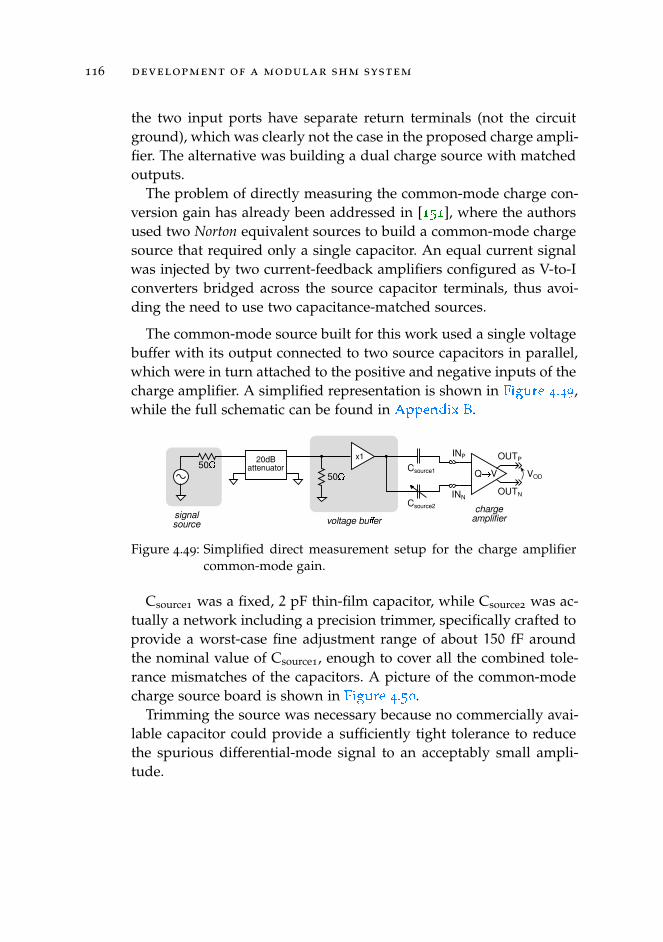
116 development of a modular shm system
the two input ports have separate return terminals (not the circuitground), which was clearly not the case in the proposed charge ampli-fier. The alternative was building a dual charge source with matchedoutputs.
The problem of directly measuring the common-mode charge con-version gain has already been addressed in [151
.
], where the authorsused two Norton equivalent sources to build a common-mode chargesource that required only a single capacitor. An equal current signalwas injected by two current-feedback amplifiers configured as V-to-Iconverters bridged across the source capacitor terminals, thus avoi-ding the need to use two capacitance-matched sources.
The common-mode source built for this work used a single voltagebuffer with its output connected to two source capacitors in parallel,which were in turn attached to the positive and negative inputs of thecharge amplifier. A simplified representation is shown in Figure 4.49
.
,while the full schematic can be found in Appendix B
.
.
50 Csource1
voltage buersignalsource
50
20dBattenuator
x1
OUTN
OUTPINP
INN
QV
chargeamplifier
Csource2
VOD
Figure 4.49: Simplified direct measurement setup for the charge amplifiercommon-mode gain.
Csource1 was a fixed, 2 pF thin-film capacitor, while Csource2 was ac-tually a network including a precision trimmer, specifically crafted toprovide a worst-case fine adjustment range of about 150 fF aroundthe nominal value of Csource1, enough to cover all the combined tole-rance mismatches of the capacitors. A picture of the common-modecharge source board is shown in Figure 4.50
.
.Trimming the source was necessary because no commercially avai-
lable capacitor could provide a sufficiently tight tolerance to reducethe spurious differential-mode signal to an acceptably small ampli-tude.
4.4 receiving signals 117
Figure 4.50: Picture of the common-mode charge source. Board size is 60×50mm.
Ideally, the trimming process should aim at a condition whereCsource1=Csource2: in that case the charge signals injected at the twoinputs of the amplifier would be identical, and no differential-modewould be present. This approach, however, fails to address the ef-fects of unbalanced input impedance of the charge amplifier itself, as thetopology is non-symmetrical and therefore a certain amount of single-ended input impedance mismatch is present. This mismatch becomeseven more significant at high frequency, where the impedance of thesource capacitors is lower.
An attempt at direct calibration of the two capacitors was doneregardless, using a high-CMRR difference amplifier specifically inclu-ded on the charge source circuit board (the schematic can be foundin Appendix B
.
). As expected, the attempt failed to provide satisfyingresults due to systematic unbalances affecting the calibration proce-dure.
In light of the previous considerations, a different calibration techni-que was pursued: one that involved the charge amplifier itself.
The idea was to trim Csource2 online, when connected to the chargeamplifier, by observing and trying to minimize the amplifier’s outputsignal, which would also take care of the intrinsic unbalance of theinput impedance.
Of course this procedure hid a perilous pitfall: the minimum out-put of the charge amplifier did not necessarily correspond to the mi-
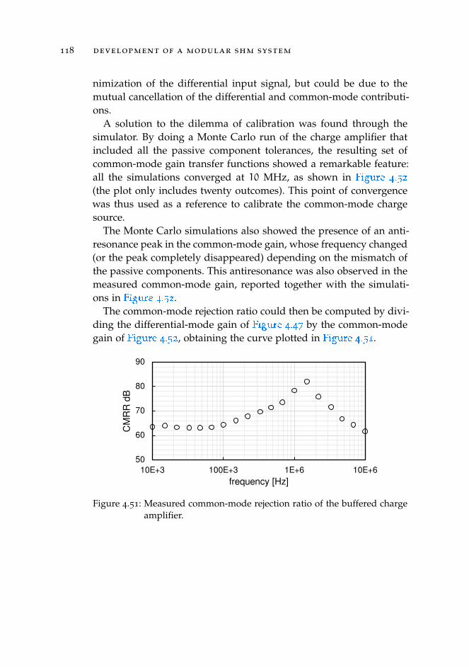
118 development of a modular shm system
nimization of the differential input signal, but could be due to themutual cancellation of the differential and common-mode contributi-ons.
A solution to the dilemma of calibration was found through thesimulator. By doing a Monte Carlo run of the charge amplifier thatincluded all the passive component tolerances, the resulting set ofcommon-mode gain transfer functions showed a remarkable feature:all the simulations converged at 10 MHz, as shown in Figure 4.52
.
(the plot only includes twenty outcomes). This point of convergencewas thus used as a reference to calibrate the common-mode chargesource.
The Monte Carlo simulations also showed the presence of an anti-resonance peak in the common-mode gain, whose frequency changed(or the peak completely disappeared) depending on the mismatch ofthe passive components. This antiresonance was also observed in themeasured common-mode gain, reported together with the simulati-ons in Figure 4.52
.
.The common-mode rejection ratio could then be computed by divi-
ding the differential-mode gain of Figure 4.47
.
by the common-modegain of Figure 4.52
.
, obtaining the curve plotted in Figure 4.51
.
.
50
60
70
80
90
10E+3 100E+3 1E+6 10E+6
CM
RR
dB
frequency [Hz]
Figure 4.51: Measured common-mode rejection ratio of the buffered chargeamplifier.
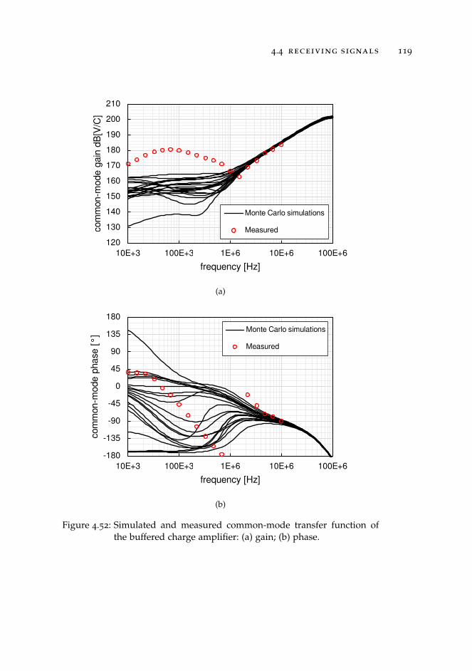
4.4 receiving signals 119
120
130
140
150
160
170
180
190
200
210
10E+3 100E+3 1E+6 10E+6 100E+6
com
mon
-mod
e g
ain
dB
[V/C
]
frequency [Hz]
Monte Carlo simulations
Measured
(a)
-180
-135
-90
-45
0
45
90
135
180
10E+3 100E+3 1E+6 10E+6 100E+6
com
mon
-mod
e p
hase
[°
]
frequency [Hz]
Monte Carlo simulations
Measured
(b)
Figure 4.52: Simulated and measured common-mode transfer function ofthe buffered charge amplifier: (a) gain; (b) phase.
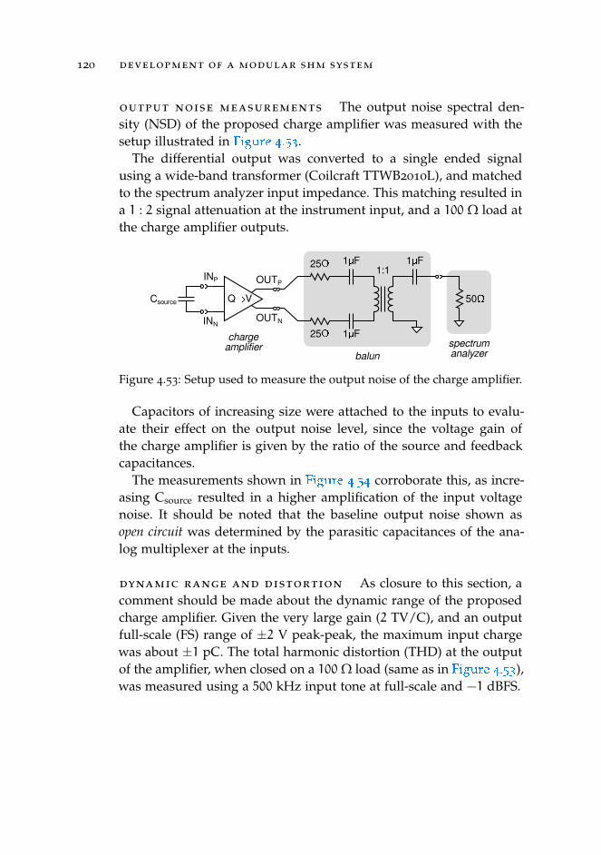
120 development of a modular shm system
output noise measurements The output noise spectral den-sity (NSD) of the proposed charge amplifier was measured with thesetup illustrated in Figure 4.53
.
.The differential output was converted to a single ended signal
using a wide-band transformer (Coilcraft TTWB2010L), and matchedto the spectrum analyzer input impedance. This matching resulted ina 1 : 2 signal attenuation at the instrument input, and a 100 Ω load atthe charge amplifier outputs.
balunspectrumanalyzer
50
OUTN
OUTPINP
INN
QV
chargeamplifier
1:1
1F25
1F 1F25
Csource
Figure 4.53: Setup used to measure the output noise of the charge amplifier.
Capacitors of increasing size were attached to the inputs to evalu-ate their effect on the output noise level, since the voltage gain ofthe charge amplifier is given by the ratio of the source and feedbackcapacitances.
The measurements shown in Figure 4.54
.
corroborate this, as incre-asing Csource resulted in a higher amplification of the input voltagenoise. It should be noted that the baseline output noise shown asopen circuit was determined by the parasitic capacitances of the ana-log multiplexer at the inputs.
dynamic range and distortion As closure to this section, acomment should be made about the dynamic range of the proposedcharge amplifier. Given the very large gain (2 TV/C), and an outputfull-scale (FS) range of ±2 V peak-peak, the maximum input chargewas about ±1 pC. The total harmonic distortion (THD) at the outputof the amplifier, when closed on a 100 Ω load (same as in Figure 4.53
.
),was measured using a 500 kHz input tone at full-scale and −1 dBFS.
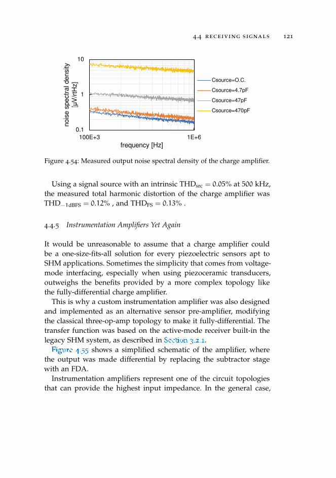
4.4 receiving signals 121
0.1
1
10
100E+3 1E+6
nois
e sp
ectr
al d
ensi
ty
[μV
/rtH
z]
frequency [Hz]
Csource=O.C.
Csource=4.7pF
Csource=47pF
Csource=470pF
Figure 4.54: Measured output noise spectral density of the charge amplifier.
Using a signal source with an intrinsic THDsrc = 0.05% at 500 kHz,the measured total harmonic distortion of the charge amplifier wasTHD−1dBFS = 0.12% , and THDFS = 0.13% .
4.4.5 Instrumentation Amplifiers Yet Again
It would be unreasonable to assume that a charge amplifier couldbe a one-size-fits-all solution for every piezoelectric sensors apt toSHM applications. Sometimes the simplicity that comes from voltage-mode interfacing, especially when using piezoceramic transducers,outweighs the benefits provided by a more complex topology likethe fully-differential charge amplifier.
This is why a custom instrumentation amplifier was also designedand implemented as an alternative sensor pre-amplifier, modifyingthe classical three-op-amp topology to make it fully-differential. Thetransfer function was based on the active-mode receiver built-in thelegacy SHM system, as described in Section 3.2.1
.
.Figure 4.55
.
shows a simplified schematic of the amplifier, wherethe output was made differential by replacing the subtractor stagewith an FDA.
Instrumentation amplifiers represent one of the circuit topologiesthat can provide the highest input impedance. In the general case,
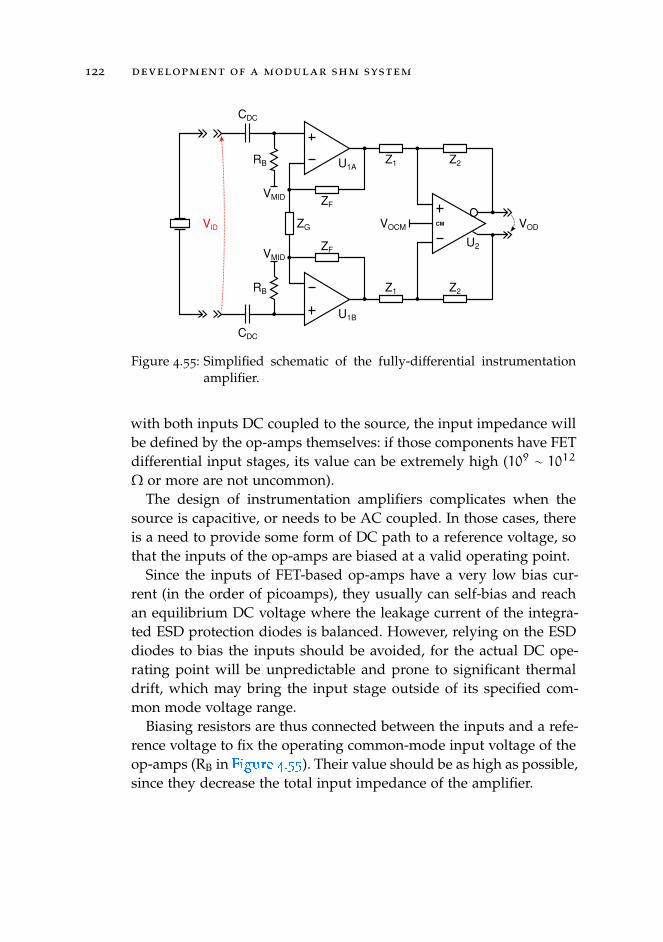
122 development of a modular shm system
U1B
ZF
ZF
U1A
VODZG CM
VMID
VMID
VOCM
Z1 Z2
Z1 Z2
RB
RB
CDC
CDC
U2
VID
Figure 4.55: Simplified schematic of the fully-differential instrumentationamplifier.
with both inputs DC coupled to the source, the input impedance willbe defined by the op-amps themselves: if those components have FETdifferential input stages, its value can be extremely high (109 ∼ 1012
Ω or more are not uncommon).The design of instrumentation amplifiers complicates when the
source is capacitive, or needs to be AC coupled. In those cases, thereis a need to provide some form of DC path to a reference voltage, sothat the inputs of the op-amps are biased at a valid operating point.
Since the inputs of FET-based op-amps have a very low bias cur-rent (in the order of picoamps), they usually can self-bias and reachan equilibrium DC voltage where the leakage current of the integra-ted ESD protection diodes is balanced. However, relying on the ESDdiodes to bias the inputs should be avoided, for the actual DC ope-rating point will be unpredictable and prone to significant thermaldrift, which may bring the input stage outside of its specified com-mon mode voltage range.
Biasing resistors are thus connected between the inputs and a refe-rence voltage to fix the operating common-mode input voltage of theop-amps (RB in Figure 4.55
.
). Their value should be as high as possible,since they decrease the total input impedance of the amplifier.
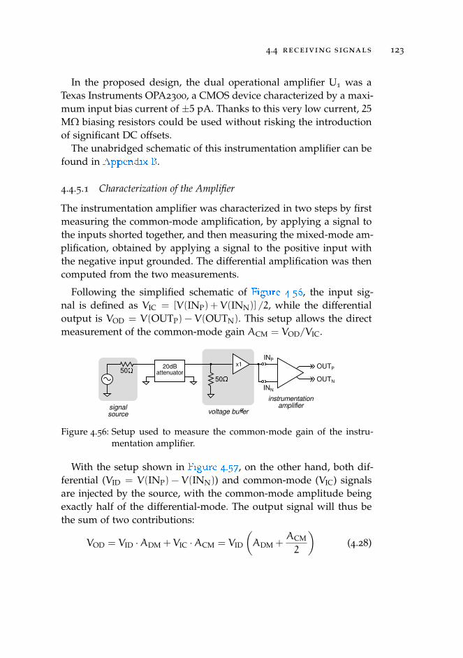
4.4 receiving signals 123
In the proposed design, the dual operational amplifier U1 was aTexas Instruments OPA2300, a CMOS device characterized by a maxi-mum input bias current of ±5 pA. Thanks to this very low current, 25MΩ biasing resistors could be used without risking the introductionof significant DC offsets.
The unabridged schematic of this instrumentation amplifier can befound in Appendix B
.
.
4.4.5.1 Characterization of the Amplifier
The instrumentation amplifier was characterized in two steps by firstmeasuring the common-mode amplification, by applying a signal tothe inputs shorted together, and then measuring the mixed-mode am-plification, obtained by applying a signal to the positive input withthe negative input grounded. The differential amplification was thencomputed from the two measurements.
Following the simplified schematic of Figure 4.56
.
, the input sig-nal is defined as VIC = [V(INP) + V(INN)] /2, while the differentialoutput is VOD = V(OUTP) − V(OUTN). This setup allows the directmeasurement of the common-mode gain ACM = VOD/VIC.
50
voltage buersignalsource
50
20dBattenuator
x1
OUTN
OUTP
INP
INN
instrumentationamplifier
Figure 4.56: Setup used to measure the common-mode gain of the instru-mentation amplifier.
With the setup shown in Figure 4.57
.
, on the other hand, both dif-ferential (VID = V(INP) − V(INN)) and common-mode (VIC) signalsare injected by the source, with the common-mode amplitude beingexactly half of the differential-mode. The output signal will thus bethe sum of two contributions:
VOD = VID ·ADM + VIC ·ACM = VID
(ADM +
ACM
2
)(4.28)
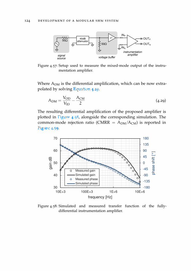
124 development of a modular shm system
50
voltage buersignalsource
50
40dBattenuator
x1
OUTN
OUTP
INP
INN
instrumentationamplifier
Figure 4.57: Setup used to measure the mixed-mode output of the instru-mentation amplifier.
Where ADM is the differential amplification, which can be now extra-polated by solving Equation 4.29
.
.
ADM =VOD
VID−ACM
2(4.29)
The resulting differential amplification of the proposed amplifier isplotted in Figure 4.58
.
, alongside the corresponding simulation. Thecommon-mode rejection ratio (CMRR = ADM/ACM) is reported inFigure 4.59
.
.
-180
-135
-90
-45
0
45
90
135
180
30
40
50
60
70
10E+3 100E+3 1E+6 10E+6
phas
e sh
ift [
°]
gain
dB
frequency [Hz]
Measured gain
Simulated gain
Measured phase
Simulated phase
Figure 4.58: Simulated and measured transfer function of the fully-differential instrumentation amplifier.
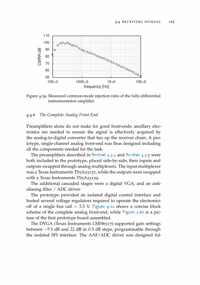
4.4 receiving signals 125
50
60
70
80
90
100
110
10E+3 100E+3 1E+6 10E+6
CM
RR
dB
frequency [Hz]
Figure 4.59: Measured common-mode rejection ratio of the fully-differentialinstrumentation amplifier.
4.4.6 The Complete Analog Front-End
Preamplifiers alone do not make for good front-ends: ancillary elec-tronics are needed to ensure the signal is effectively acquired bythe analog-to-digital converter that ties up the receiver chain. A pro-totype, single-channel analog front-end was thus designed includingall the components needed for the task.
The preamplifiers described in Section 4.4.4
.
and Section 4.4.5
.
wereboth included in the prototype, placed side-by-side, their inputs andoutputs swapped through analog multiplexers. The input multiplexerwas a Texas Instruments TS5A23157, while the outputs were swappedwith a Texas Instruments TS5A23159.
The additional cascaded stages were a digital VGA, and an anti-aliasing filter / ADC driver.
The prototype provided an isolated digital control interface andhosted several voltage regulators required to operate the electronicsoff of a single bus rail > 5.5 V. Figure 4.60
.
shows a concise blockscheme of the complete analog front-end, while Figure 4.61
.
is a pic-ture of the first prototype board assembled.
The DVGA (Texas Instruments LMH6517) supported gain settingsbetween −9.5 dB and 22 dB in 0.5 dB steps, programmable throughthe isolated SPI interface. The AAF/ADC driver was designed fol-
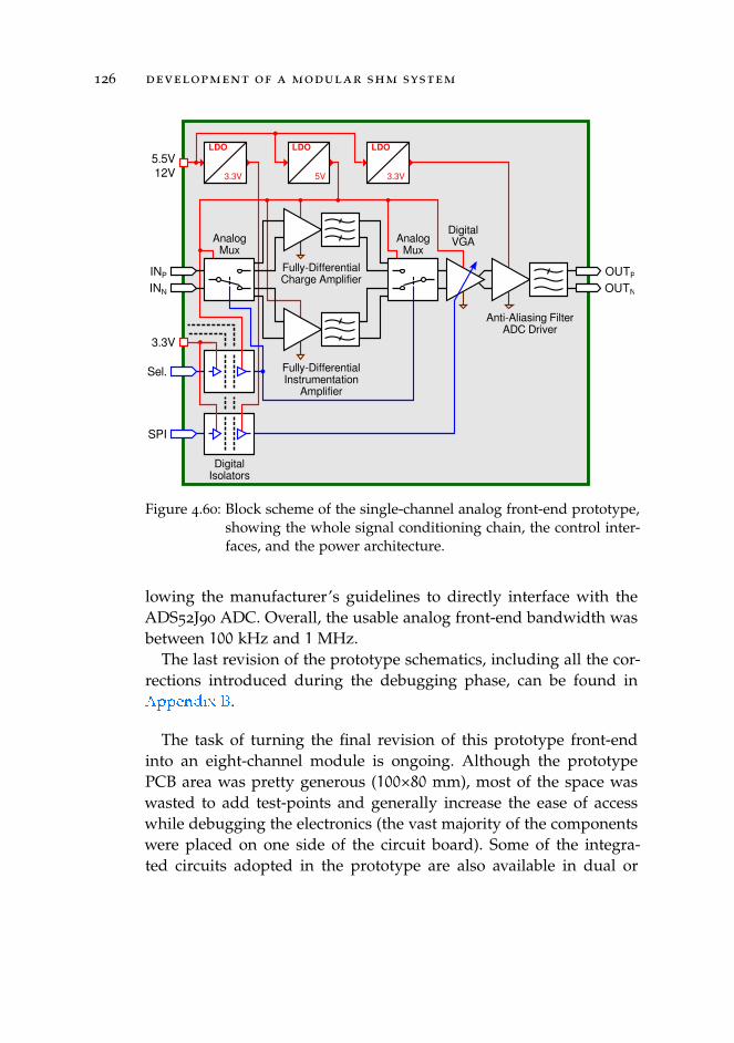
126 development of a modular shm system
LDO
5V
Fully-DifferentialCharge Amplifier
Fully-DifferentialInstrumentation
Amplifier
AnalogMux
AnalogMux
LDO
3.3V
LDO
3.3V
DigitalVGA
Anti-Aliasing FilterADC Driver
DigitalIsolators
5.5V12V
3.3V
Sel.
SPI
INP
INN
OUTP
OUTN
Figure 4.60: Block scheme of the single-channel analog front-end prototype,showing the whole signal conditioning chain, the control inter-faces, and the power architecture.
lowing the manufacturer’s guidelines to directly interface with theADS52J90 ADC. Overall, the usable analog front-end bandwidth wasbetween 100 kHz and 1 MHz.
The last revision of the prototype schematics, including all the cor-rections introduced during the debugging phase, can be found inAppendix B
.
.
The task of turning the final revision of this prototype front-endinto an eight-channel module is ongoing. Although the prototypePCB area was pretty generous (100×80 mm), most of the space waswasted to add test-points and generally increase the ease of accesswhile debugging the electronics (the vast majority of the componentswere placed on one side of the circuit board). Some of the integra-ted circuits adopted in the prototype are also available in dual or
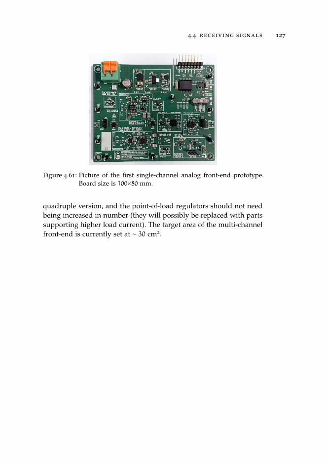
4.4 receiving signals 127
Figure 4.61: Picture of the first single-channel analog front-end prototype.Board size is 100×80 mm.
quadruple version, and the point-of-load regulators should not needbeing increased in number (they will possibly be replaced with partssupporting higher load current). The target area of the multi-channelfront-end is currently set at ∼ 30 cm2.


Part III
U N T R O D D E N T R A I L S

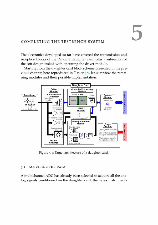
5C O M P L E T I N G T H E T E S T B E N C H S Y S T E M
The electronics developed so far have covered the transmission andreception blocks of the Pandora daughter card, plus a subsection ofthe soft design tasked with operating the driver module.
Starting from the daughter card block scheme presented in the pre-vious chapter, here reproduced in Figure 5.1
.
, let us review the remai-ning modules and their possible implementation.
8 BridgedOutputs
Analog Front-EndModule
Charge-Mode
HV T/RSwitches Voltage-Mode
Daughter Card
HV WaveformGenerator
8 Active-ModeChannels
8 Passive-ModeChannels
8 FeedbackChannels
VGA AAF 12
V p
ow
er
bu
s
Arria V SoC
FPGA HPS
ClockManager
Control & ProcessingModule
DriverModule
24-Channel ADC
DAQModule
Digital power supplies
Low voltage suppliesfor signal conditioning
High voltage suppliesfor transducer driver
PowerSection
Transceivers
PowerlineMODEM
CommsModule
Co
mm
un
ica
tion
bu
s
Ampliers
Up to 8 elements
Transducer
Figure 5.1: Target architecture of a daughter card.
5.1 acquiring the data
A multichannel ADC has already been selected to acquire all the ana-log signals conditioned on the daughter card, the Texas Instruments
132 completing the testbench system
ADS52J90: a device that includes 16 independent ADCs multiplexed2 : 1 to 32 input channels.
The ADS52J90 resolution can be set to either 10-bit, 12-bit, or 14-bit, and the supported sampling rate per channel (when operating in32-channel mode) goes from the absolute minimum of 2.5 MSps, toa maximum of 50 MSps (at 10-bit resolution), or 32.5 MSps (at 14-bitresolution).24 out of the 32 inbound channels are already assigned to sampling
the 8 active-mode signals, 8 passive-mode signals, and 8 feedback sig-nals. The remaining 8 channels are currently free and may be possiblyused to acquire the data from other sensors.
Clocking will be managed by the Texas Instruments LMK0482X, asit is currently used on both the Arria V SoC development kit and theADS52J90 evaluation module, and there is no real reason to changeit. The converter will operate at two rates: fast for sampling in active-mode (e. g., 20 MSps), and slow for passive-mode (5 MSps). The sy-stem may actually scale the clock rather than decimating the sampleddata stream to save power while in passive-mode.
Though fully integrated analog front-ends for ultrasound applica-tions do exist that provide high-performance multichannel LNAs, fil-ters, and ADCs (see, for instance, the Texas Instruments AFE58JD32),they were not considered for this testbench architecture, as it was dee-med more important to maintain a complete control over the signalchain at this stage.
5.2 a matter of power
5.2.1 Main Power Bus
A single, 12 V bus bar is planned to power all the daughter cards inparallel, and the cards themselves are supposed to internally performall the conversions needed to supply their own electronics. Since thedaughter cards require a number of different voltage rails, connectingseveral external power buses would be problematic for a couple ofreasons:
5.3 software integration 133
• Such power architecture would not be scalable.
• From the point of view of a wired sensor network, increasingthe number of wires should be avoided.
The off-line power supply unit generating the 12 V bus does not haveparticular requirements at this time, except that the specified outputvoltage range should remain within 10–14 V. The maximum power ra-ting will be decided upon completion of the daughter card hardware.
5.2.2 Local Power Converters
The initial driver module prototype, described in Section 4.3.1
.
, inclu-ded a first attempt at providing a high-performance power architec-ture for the driver power stage, which unfortunately failed at actuallyimproving the performance.
Apart from the fast transient response requirements, an importantfeature that will increase versatility during the experiments is a pro-grammable output voltage (up to the maximum ±100 V supportedby the pulser chips). Moreover, in order to allow the possibility ofdriving the transducers in continuous wave, the high-voltage powersupplies should be able to drop their output to ±5 V, or provide se-condary, low-voltage supplies that take over in those cases.
The adoption of post-regulators in the high-voltage supply chainmight still be able to improve the transient response, but the costin terms of increased system complexity will have to be carefullyconsidered, as such regulators need to be custom-designed (probablyusing discrete components, and thus bulky), and also provide outputvoltage programmability.
5.3 software integration
Firmware running on Arria V SoC HPS will be moved from thecurrent baremetal implementation to a real-time operating system(RTOS). This upgrade will ease the integration of various software
134 completing the testbench system
components and still guarantee the real-time capabilities required fora successful coordination between all the daughter cards.
One of the SHM usage scenarios where real-time operation mattersis passive-mode detection and localization. The legacy system descri-bed in Chapter 3
.
performed the passive-mode tasks with moderatesimplicity thanks to the convergence of all transducer inbound signalpaths to the same data converter. In the Pandora architecture, howe-ver, the electronics of each transducer are separate, and passive-modemonitoring becomes a distributed task that must be handled by thesoftware over a shared physical layer.
Moving away from a baremetal firmware is also an essential stepto safeguard software portability in the future, in the event of anembedded architecture update.
5.4 card interaction and the backplane
The final piece of the Pandora tesbench architecture is the backplane:the board that will connect together a collection of daughter card,allowing them to interact between each other.
The communication module design of the daughter card is strictlyconnected to the bus architecture that will be realized on the back-plane. Given the hybrid topology envisioned for the wired sensornetwork, the backplane should in principle be able to set-up arbitraryvirtual circuits between any two (or more) daughter cards by using adigital cross-bar matrix, thus mimicking an arbitrary interconnectiontopology between sensor nodes.
The daughter card communication module will include at least twoindependent transceiver, and be able to execute some form of swit-ching between them. Currently, the inter-card communication proto-col, that will eventually become the sensor network protocol, has notbeen decided.
Powerline communications will be tested on the 12 V bus bar thatsupplies all the daughter cards. In order to do so, each card will beequipped with specific powerline modems.
5.4 card interaction and the backplane 135
Aside from the emulated network infrastructure, the backplanewill also host embedded processor performing the tasks of a basestation. A block scheme is shown in Figure 5.2
.
.
Backplane
Base StationModule
Transceivers
PowerlineMODEM
EmbeddedProcessor
12V Bus Bar
Digital Crossbar
Figure 5.2: Early-stage block scheme of the planned backplane.

6T O WA R D S H M S E N S O R N E T W O R K S
While the actual development of a SHM sensor network is a long wayoff, this chapter gives an idea of what could be achievable with suchsystem.
Mixed-SignalSoC
SignalConditioning
TransducerDriver
Ultrasonic Transducer
Powerline Communication
(a) (b) (c)
Figure 6.1: A possible sensor node design with attached IDT: (a) node blockscheme; (b) node rendering; (c) rendering of a CPV equippedwith a sensor network.
A sensor network deployed on the surface of a test object will bringback the ability to perform Lamb wave tomography, improving thetechnique that was first implemented in the former SHM system [47
.
].Tomographic techniques have been explored thoroughly in the lite-rature by using transducer scanning systems [152
.
–155
.
]: in the caseof a sensor network, however, there is an added layer of complexityconnected to the fixed position of the nodes.
Having multiple transducers attached at various points on the tar-get structure could be exploited as a large-scale distributed transmis-sion array, with multiple Lamb wave sources transmitting at the sametime [156
.
].
138 toward shm sensor networks
The presence of smart sensor nodes, and a relatively dense inter-connection network, can provide some degree of redundancy to theSHM system, where failing sensor nodes will not compromise theoperation of the system at large. Of course the thickening of the in-terconnection network goes against the minimum-obstruction policythat was one of the original goals of the sensor network architecture,but it is a trade-off that should be considered nonetheless.
From the point of view of harnessing, powerline communicationsrepresent a way to achieve the minimum amount of cabling requiredto route the sensor network, albeit at the cost of reduced bandwidth.
A problem that is deeply ingrained in sensor networks that needto cooperate in the ways described above is how to achieve and main-tain inter-node synchronization. Although the topic has not been ad-dressed so far, the problem of synchronization in measurement andcontrol networks is well known, and will be approached starting fromthe provisions of the IEEE 1588 standard [157
.
].
7A C O N C L U S I O N
The word conclusion might seem a bit misplaced at this point but,having reached the end of this dissertation, it is only appropriate towrap up what has been presented so far.
The work presented in this dissertation covered multiple facets ofthe development of a testbench system intended to be a versatile re-search platform for structural health monitoring. The system was de-vised as a keystone between pure laboratory research activity, andreal-world applications where sensor network represent the most pro-mising way to implement structural health monitoring.
The design was approached by trying to follow the most logicalpath: one that starts from the target application—performing struc-tural health monitoring on composite pressure vessels with guided-wave techniques—continues through the transducers, and finisheswith the design of the instrumentation hardware.
The following sections summarize the main results achieved du-ring the research activity.
7.1 transducers
Work on the transducers started from interdigital devices made withpiezopolymer film, an existing and proven design already adopted inprior experiments and projects to generate and receive Lamb waveson plate-like structures [47
.
].Additional sensing elements were included on the piezopolymer
film, exploiting the ability of etching arbitrary patterns on the metalcoating [158
.
]: local temperature sensing was made possible througha resistive temperature device, and a circular element, modeled af-ter commercial piezoceramic devices, was introduced to allow omni-directional sensing for impact detection and localization [111
.
].
140 a conclusion
The first prototype of an interdigital transducer with independentfinger connection was presented. The new design leverages the mul-tichannel capabilities that are being built-in the Pandora testbenchsystem, and will be used as an array for Lamb wave generation.
A new manufacturing process for embedding piezopolymer trans-ducers inside flex circuits was preliminarily tested. Although the ini-tial results were quite unsatisfactory, as bonding between PVDF andpolyimide could not be achieved with standard sheet adhesive at lowtemperature, the idea has the potential to seamlessly bring togetherelectronics and piezopolymer transducers.
7.2 testbench system
The Pandora architecture was defined, along with the steps needed toprogress towards the realization of wired sensor networks for struc-tural health monitoring.
The development process started with the design of a testbench sy-stem that aimed at emulating the components of a sensor network forstructural health monitoring, and thus needed to integrate electronicsspecific to the application (ultrasonic transducer drivers and analogfront-ends).
For what concerns the transmission part, an eight-channel, five-level class-D transducer driver was designed and tested. The propo-sed transmitter can generate arbitrary signals with a bandwidth up to1 MHz and amplitude up to ±96 V using a custom multilevel codingscheme. Signal generation is handled by an FPGA core that ensureinter-channel synchronization.
The signal generation technique presented in this dissertation fol-lowed a somewhat uncommon approach at switch-mode ultrasoundsignal generation, and required the design and construction of se-veral hardware and software components from scratch. Albeit muchwork can still be done to address the various problems encounteredduring the development, what has been done so far represents a com-plete proof-of-concept of the proposed technique.
7.2 testbench system 141
After investigating the advantages brought by charge-mode interfa-cing of high-impedance piezoelectric sensors [159
.
], an improved vari-ant of the differential-input, differential-output charge amplifier wasdeveloped providing 2 TV/C of conversion gain, while maintaining< 100 Ω input impedance within the 100 kHz–1 MHz bandwidth.This amplifier only requires a single, 5 V supply rail.
The new charge amplifier was merged in a dual-role analog front-end alongside a fully-differential instrumentation amplifier: the twocircuits are swapped using analog multiplexers. The proposed analogfront-end, which is a single-channel prototype of the multichannelsignal conditioning module of the Pandora testbench system, alsoincludes a digital VGA and the anti-aliasing filter / ADC driver.
7.2.1 Improvements Over the Former System
Project Pandora started as a follow up to the prototype SHM systemdescribed in Chapter 3
.
. The testbench system design tried to bothaddress the limitations described in Section 3.4
.
, and add new featuresthat could be interesting from a research perspective.
Although still early stage, the architecture envisaged for the newsystem will lift one of the most fundamental problems of the formersystem: its lack of scalability.
The new transducers improve the versatility in transmission andreception, opening new possibilities (like separate active-mode andpassive-mode sensing, and phased array excitation) that were previ-ously precluded.
The transducer driver can handle up to eight channels and allowstrue arbitrary waveform generation over a wide bandwidth. None ofthis was possible with the previous pulser. The driver module alsoprovides separate sensing paths for passive-mode and output feed-back, all having their own connection to the data converter.
The signal conditioning electronics have been diversified with twokinds of pre-amplifiers, are now completely differential, and provideimproved T/R switching.
142 a conclusion
7.3 future work
Chapters 5
.
and 6
.
have described in which direction project Pandorawill be moving to fulfill its original plans. It would be unfair, however,to claim that the components developed and covered in this disserta-tion do not need further improvement and refinement. A succinct listof topics that would benefit from further effort is reported below.
There is a need for the general improvement of PVDF transducermanufacturing technology, especially in consideration of their envisi-oned integration with the node electronics. Expanding the PVDF-in-flex idea can represent a good starting point.
Transitioning to multi-element transducers will lead to re-thinkingboth their electrode patterns, as many geometries are now possible,and their electrical interface, including cabling and connectors, whichhave a high risk of becoming too bulky.
The ultrasound driver will need an in-depth study and impro-vement of its encoding algorithm, which is now elementary, but also,from a hardware perspective, interesting work could be done on clo-sing the feedback loop and designing a new, programmable high-voltage power architecture for the pulsers.
The receiver front-end still presents some details that need fixing,such as the biasing of the charge amplifier differential stage, whichis now sub-optimal. Putting together a multichannel circuit will bethe logical next step to add another module to the Pandora daughtercard.
7.4 final remarks
Even though the testbench system remains a work-in-progress, and awired sensor network is a long way off, most of the design effort wasdirected at those that are arguably two of the most important piecesof the whole architecture: the transmitter, and the receiver.
Using those two essential components, and of course the transdu-cers, an experimental phase can be started to evaluate and improve

7.4 final remarks 143
health monitoring techniques and algorithms, while the developmentof the remaining parts of the testbench architecture is carried out inparallel: the ability to perform some, even elementary experimenta-tion during the hardware design phase can provide invaluable feed-back to the designers.


Part IV
A P P E N D I X


AL E G A C Y S Y S T E M E L E C T R I C A L S C H E M AT I C S


B A C K P L A N E

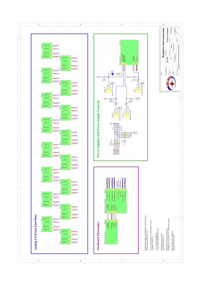
11
22
33
44
55
66
77
88
DD
CC
BB
AA
Prot
otyp
e B
ackp
lane
5/23
/201
4
Bac
kpla
ne_I
nter
conn
ectio
ns.S
chD
oc
P. G
iann
elli
L. C
apin
eri
USC
NDB
ackp
lane
Inte
rcon
nect
ions
Title
:
Org
aniz
atio
n:Pr
ojec
t:
File
nam
e:
Dat
e:
Auth
or:
Appr
oved
By:
Vers
ion:
Revi
sion
:In
itial
0.7
Shee
t:of
19
AD
DR
[0..3
]A
_CLK
A_G
ATE
A_M
OD
ED
_MO
DE
AU
XShee
t: 2
Off
-Boa
rd C
onne
ctor
s
AD
C_P
WR
HV
_PD
N
MA
IN_P
WR
HV
C[0
..3]
PN5V
_EN
Shee
t: 5
Pow
er S
ectio
n
A_CLK
A_GATE
A_MODE
D_MODE
Shee
t: 3
Slot
_1
A_CLK
A_GATE
A_MODE
D_MODE
Shee
t: 3
Slot
_16
A_CLK
A_GATE
A_MODE
D_MODE
Shee
t: 3
Slot
_2
A_CLK
A_GATE
A_MODE
D_MODE
Shee
t: 3
Slot
_3
A_CLK
A_GATE
A_MODE
D_MODE
Shee
t: 3
Slot
_4
A_CLK
A_GATE
A_MODE
D_MODE
Shee
t: 3
Slot
_5
A_CLK
A_GATE
A_MODE
D_MODE
Shee
t: 3
Slot
_6
A_CLK
A_GATE
A_MODE
D_MODE
Shee
t: 3
Slot
_7
A_CLK
A_GATE
A_MODE
D_MODE
Shee
t: 3
Slot
_8
A_CLK
A_GATE
A_MODE
D_MODE
Shee
t: 3
Slot
_9
A_CLK
A_GATE
A_MODE
D_MODE
Shee
t: 3
Slot
_10
A_CLK
A_GATE
A_MODE
D_MODE
Shee
t: 3
Slot
_11
A_CLK
A_GATE
A_MODE
D_MODE
Shee
t: 3
Slot
_12
A_CLK
A_GATE
A_MODE
D_MODE
Shee
t: 3
Slot
_13
A_CLK
A_GATE
A_MODE
D_MODE
Shee
t: 3
Slot
_14
A_CLK
A_GATE
A_MODE
D_MODE
Shee
t: 3
Slot
_15
B_CLK0
B_CLK1
B_CLK2
B_CLK3
B_CLK4
B_CLK5
B_CLK6
B_CLK7
B_CLK8
B_CLK9
B_CLK10
B_CLK11
B_CLK12
B_CLK13
B_CLK14
B_CLK15
B_GATE0
B_GATE1
B_GATE2
B_GATE3
B_GATE4
B_GATE5
B_GATE6
B_GATE7
B_GATE8
B_GATE9
B_GATE10
B_GATE11
B_GATE12
B_GATE13
B_GATE14
B_GATE15
123
AD
C_P
Hea
der 1
X3
.100
inG
ND
GN
D
100k
1%R19
8
100k
1%R2
3V3
0
R13
1
0
R13
3
100k
1%R1
12V
D1
2V4
GN
D
123
MA
IN_P
Hea
der 1
X3
.100
inG
ND
A_MODE0
A_MODE1
A_MODE2
A_MODE3
A_MODE4
A_MODE5
A_MODE6
A_MODE7
A_MODE8
A_MODE9
A_MODE10
A_MODE11
A_MODE12
A_MODE13
A_MODE14
A_MODE15
D_MODE0
D_MODE1
D_MODE2
D_MODE3
D_MODE4
D_MODE5
D_MODE6
D_MODE7
D_MODE8
D_MODE9
D_MODE10
D_MODE11
D_MODE12
D_MODE13
D_MODE14
D_MODE15
A_C
LKA
_GA
TE
AD
DR
[0..3
]
B_C
LK[0
..15]
B_G
ATE
[0..1
5]
A_M
OD
ED
_MO
DE
A_M
OD
E[0.
.15]
D_M
OD
E[0.
.15]
VH
V_E
N
AU
X
VH
V_C
TRL[
0..3
]
HV
_SW
[0..3
]
PN5V
_IN
HShee
t: 4
Mas
ter S
yste
m C
ontro
ller
D_M
OD
E[0.
.15]
A_M
OD
E[0.
.15]
B_C
LK[0
..15]
B_G
ATE
[0..1
5]
VH
V_E
N
VH
V_E
N
3V3
123
HV
_P
Hea
der 1
X3
.100
in
HV
C[0
..3]
HV
C[0
..3]
Ana
log
US-
Fron
t End
Slo
ts
Pow
er S
uppl
ies a
nd P
ower
Sup
ply
Con
trol
s
6 5431
82
7
S2
A6H
-410
1
47k
1234 5
678
R17
CA
Y16
-J4
HV
_SW
[0..3
]
3V3
GN
D
HV
_SW
0H
V_S
W1
HV
_SW
2H
V_S
W3
221 2 3 4
5678
R19
CA
Y16
-J4
Glo
bal p
ower
sup
ply
(fra
med
bric
k, u
nive
rsal
inpu
t):TD
K-L
ambd
a H
WS3
0A-1
2/A
Pow
er e
ntry
mod
ule
(w/ s
witc
h an
d 1A
fuse
):Sc
haff
ner F
N28
3-1-
0
12V
pow
er g
ood
indi
cato
r:Lu
mex
SSI
-LX
H60
0GD
12V
150
Fron
t pan
el p
ower
sw
itch:
NK
K J
WM
11B
A2A
-A
Bac
kpla
ne p
ower
goo
d in
dica
tor:
Dia
light
559
-130
1-00
7F w
/ 750Ω
ser
ies
resi
stor
Hig
h vo
ltage
act
ive
indi
cato
r:D
ialig
ht 5
59-0
203-
007F
On-
Boa
rd E
lect
roni
cs
123
AN
V_P
Hea
der 1
X3
.100
in
0
R52
3V3
100k
1%R53
GN
D
PN5V
_EN
PN5V
_EN
PIADC0P01
PIADC0P02
PIADC0P03
COAD
C0P PI
ANV0P01
PIANV0P02
PIANV0P03
COANV0P
PID101PID102COD1
PIHV0P01
PIHV0P02
PIHV0P03
COHV0P
PIMA
IN0P
01
PIMA
IN0P
02
PIMA
IN0P
03
COMAIN0P
PIR101 PIR102
COR1
PIR201 PIR202
COR2
PIR1701PIR1702PIR1703PIR1704 PIR1705PIR1706PIR170
7PIR1708
COR17
PIR1901
PIR1902
PIR1903
PIR1904
PIR1905
PIR1906
PIR1907
PIR1908
COR19
PIR5
201
PIR5
202COR52
PIR5301 PIR5302
COR53
PIR13101
PIR13102CO
R131
PIR13301
PIR13302CO
R133
PIR19801 PIR19802
COR1
98
PIS201
PIS202
PIS203
PIS204
PIS205
PIS206
PIS207
PIS208
COS2
PIANV0P01
PIR201
PIR19801
PIS205
PIS206
PIS207
PIS208
PIR101
PIADC0P01
PID101
PIHV0P01
PIMA
IN0P
01
PIR1705PIR1706PIR170
7PIR1708
PIR5302
PIADC0P02
PIR13102
PIADC0P03
PIANV0P02
PIR5
202
PIANV0P03
PID102PI
MAIN
0P02
PIR102
PIHV0P02
PIR13302
PIHV0P03
PIMA
IN0P
03
PIR1701
PIR1908
PIS201
PIR1702
PIR1907
PIS202
PIR1703
PIR1906
PIS203
PIR1704PIR1905
PIS204
PIR13101
PIR19802
PIR5
201
PIR5301
NLP\N\
5\V\0\
E\N\
PIR202PIR13301
NLVH
V0EN
NLA0
MODE
0000
150
NLA0MODE0
NLA0
MODE
0000
150
NLA0MODE1
NLA0
MODE
0000
150
NLA0MODE2
NLA0
MODE
0000
150
NLA0MODE3
NLA0
MODE
0000
150
NLA0MODE4
NLA0
MODE
0000
150
NLA0MODE5
NLA0
MODE
0000
150
NLA0MODE6
NLA0
MODE
0000
150
NLA0MODE7
NLA0
MODE
0000
150
NLA0MODE8
NLA0
MODE
0000
150
NLA0MODE9
NLA0
MODE
0000
150
NLA0MODE10
NLA0
MODE
0000
150
NLA0MODE11
NLA0
MODE
0000
150
NLA0MODE12
NLA0
MODE
0000
150
NLA0MODE13
NLA0
MODE
0000
150
NLA0MODE14
NLA0
MODE
0000
150
NLA0MODE15
NLB0
CLK0
0001
50
NLB0CLK0
NLB0
CLK0
0001
50
NLB0CLK1
NLB0
CLK0
0001
50
NLB0CLK2
NLB0
CLK0
0001
50
NLB0CLK3
NLB0
CLK0
0001
50
NLB0CLK4 NLB0
CLK0
0001
50
NLB0CLK5
NLB0
CLK0
0001
50
NLB0CLK6
NLB0
CLK0
0001
50
NLB0CLK7
NLB0
CLK0
0001
50
NLB0CLK8
NLB0
CLK0
0001
50
NLB0CLK9
NLB0
CLK0
0001
50
NLB0CLK10
NLB0
CLK0
0001
50
NLB0CLK11
NLB0
CLK0
0001
50
NLB0CLK12
NLB0
CLK0
0001
50
NLB0CLK13
NLB0
CLK0
0001
50
NLB0CLK14
NLB0
CLK0
0001
50
NLB0CLK15
NLB0
GATE
0000
150
NLB0GATE0
NLB0
GATE
0000
150
NLB0GATE1
NLB0
GATE
0000
150
NLB0GATE2
NLB0
GATE
0000
150
NLB0GATE3
NLB0
GATE
0000
150
NLB0GATE4
NLB0
GATE
0000
150
NLB0GATE5
NLB0
GATE
0000
150
NLB0GATE6
NLB0
GATE
0000
150
NLB0GATE7
NLB0
GATE
0000
150
NLB0GATE8
NLB0
GATE
0000
150
NLB0GATE9
NLB0
GATE
0000
150
NLB0GATE10
NLB0
GATE
0000
150
NLB0GATE11
NLB0
GATE
0000
150
NLB0GATE12
NLB0
GATE
0000
150
NLB0GATE13
NLB0
GATE
0000
150
NLB0GATE14
NLB0
GATE
0000
150
NLB0GATE15
NLD0
MODE
0000
150
NLD0MODE0
NLD0
MODE
0000
150
NLD0MODE1
NLD0
MODE
0000
150
NLD0MODE2
NLD0
MODE
0000
150
NLD0MODE3
NLD0
MODE
0000
150
NLD0MODE4
NLD0
MODE
0000
150NLD0MODE5
NLD0
MODE
0000
150
NLD0MODE6
NLD0
MODE
0000
150
NLD0MODE7
NLD0
MODE
0000
150
NLD0MODE8
NLD0
MODE
0000
150
NLD0MODE9
NLD0
MODE
0000
150
NLD0MODE10
NLD0
MODE
0000
150
NLD0MODE11
NLD0
MODE
0000
150
NLD0MODE12
NLD0
MODE
0000
150
NLD0MODE13
NLD0
MODE
0000
150
NLD0MODE14
NLD0
MODE
0000
150
NLD0MODE15
PIR1901
NLHV
0SW0
0003
0
NLHV
0SW0
PIR1902
NLHV
0SW0
0003
0
NLHV
0SW1
PIR1903
NLHV
0SW0
0003
0
NLHV
0SW2
PIR1904
NLHV
0SW0
0003
0
NLHV
0SW3
NLHVC000030
NLHVC000030
NLHVC000030
NLHVC000030
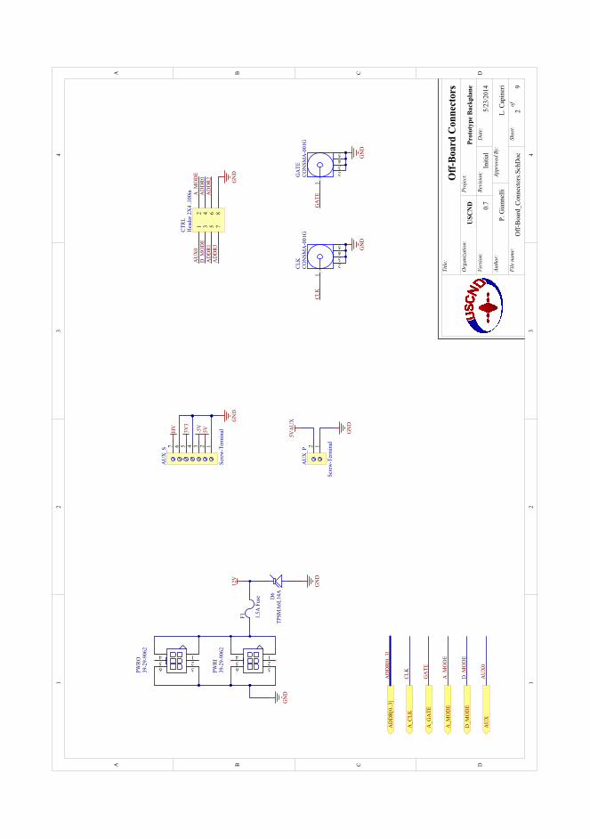
11
22
33
44
DD
CC
BB
AA
Prot
otyp
e Bac
kpla
ne
5/23
/201
4
Off-
Boar
d_Co
nnec
tors
.Sch
Doc
P. G
iann
elli
L. C
apin
eri
USC
ND
Off-
Boar
d C
onne
ctor
sTi
tle:
Org
aniza
tion:
Proj
ect:
File
nam
e:
Dat
e:
Auth
or:
Appr
oved
By:
Vers
ion:
Revi
sion:
Initi
al0.
7
Shee
t:of
29
5
1
234
CLK
CON
SMA
-001
G
5
1
234
GA
TECO
NSM
A-0
01G
12
34
56
78
CTRL
Hea
der 2
X4
.100
in
GN
DG
ND
12V
GN
D
AU
X0
A_M
OD
ED
_MO
DE
AD
DR0
AD
DR1
AD
DR2
AD
DR3
GN
D
CLK
GA
TE
D6
TPSM
A6L
14A
GN
D
F1 1.5A
Fus
e
AD
DR[
0..3
]A
DD
R[0.
.3]
A_C
LK
A_G
ATE
CLK
GA
TE
A_M
OD
E
D_M
OD
ED
_MO
DE
A_M
OD
E
AU
XA
UX
0
12A
UX
_P
Scre
w-T
erm
inal
5VA
UX
GN
D
123
456
PWRI
39-2
9-90
62123
456
PWRO
39-2
9-90
62
1234567A
UX
_S
Scre
w-T
erm
inal5V-5
V
HV
3V3
GN
D
PIAUX0P01
PIAUX0P02
COAU
X0P
PIAUX0S01
PIAUX0S02
PIAUX0S03
PIAUX0S04
PIAUX0S05
PIAUX0S06
PIAUX0S07
COAU
X0S
PICLK01
PICLK02PICLK03
PICLK04PICLK05
COCL
K
PICTRL01
PICTRL02
PICTRL03
PICTRL04
PICTRL05
PICTRL06
PICTRL07
PICTRL08
COCTRL
PID601PID602COD
6
PIF101
PIF102COF
1
PIGATE01
PIGATE02PIGATE03
PIGATE04PIGATE05
COGATE
PIPWRI01PIPWRI02PIPWRI03
PIPWRI04PIPWRI05PIPWRI06
COPWRI
PIPWRO01PIPWRO02PIPWRO03
PIPWRO04PIPWRO05PIPWRO06
COPWRO
PIAUX0S03
PIAUX0S05
PIAUX0S02
PIAUX0P02
PID602PIF101
PICTRL02
NLA0MODE
POA0MODE
PICTRL01
NLAUX0
POAUX
PICLK01
NLCL
KPOA0CLK
PICTRL03
NLD0MODE
POD0MODE
PIGATE01
NLGATE
POA0GATE
PIAUX0P01
PIAUX0S01
PIAUX0S04
PIAUX0S06
PICLK02PICLK03
PICLK04PICLK05
PICTRL08
PID601
PIGATE02PIGATE03
PIGATE04PIGATE05
PIPWRI03PIPWRI06PIPWRO03PIPWRO06PIAUX0S07
PIF102
PIPWRI01PIPWRI04PIPWRO01PIPWRO04 PIPWRI02PIPWRI05PIPWRO02PIPWRO05
PICTRL04
NLADDR000030
NLAD
DR0
POADDR000030
PICTRL05
NLADDR000030
NLAD
DR1
POADDR000030
PICTRL06
NLADDR000030
NLAD
DR2
POADDR000030
PICTRL07
NLADDR000030
NLAD
DR3
POADDR000030
POA0CLK
POA0GATE
POA0MODE
POADDR0
POADDR1
POADDR2
POADDR3
POADDR000030
POAUX
POD0MODE
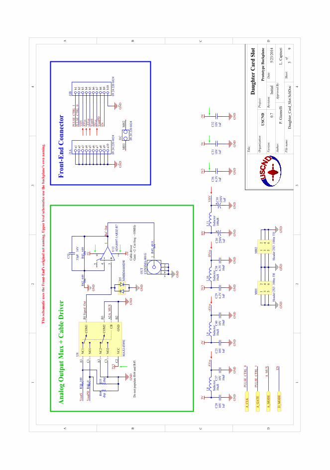
11
22
33
44
DD
CC
BB
AA
Prot
otyp
e Bac
kpla
ne
5/23
/201
4
Dau
ghte
r_Ca
rd_S
lot.S
chD
oc
P. G
iann
elli
L. C
apin
eri
USC
ND
Dau
ghte
r Car
d Sl
otTi
tle:
Org
aniza
tion:
Proj
ect:
File
nam
e:
Dat
e:
Auth
or:
Appr
oved
By:
Vers
ion:
Revi
sion:
Initi
al0.
7
Shee
t:of
39
GN
DG
ND
Vou
tPD
EN
This
sche
mat
ic u
ses t
he F
ront
-End
's or
igin
al n
et n
amin
g. U
pper
leve
l sch
emat
ics u
se th
e bac
kpla
ne's
own
nam
ing.
Vou
tS
PULS
E_CT
RL_0
PULS
E_CT
RL_1
10uH
L8 Indu
ctor
10uH
L9 Indu
ctor
10uH
L10
Indu
ctor
5V-5
V3V
3H
V
VH
VA
Vcc
-AV
cc
DV
cc
AV
cc-A
Vcc
DV
cc
GN
DG
ND
GN
D
Vou
tPD
Vou
tS
A_C
LK
A_G
ATE
A_M
OD
E
D_M
OD
EEN
PULS
E_CT
RL_0
PULS
E_CT
RL_1
A_M
UX
A_M
UX
Sign
al_O
ut
100u
H
L11
Indu
ctor
1uF
C39
250V
GN
D
VH
V
GN
D
5
1
234
OU
TCO
NSM
A-0
01G
GN
D
1uF
C36
6.3V
a1 a2 a3 a4 a5 a6 a7 a8 a9 a10
J1A
09 2
4 22
0 68
24
b1 b2 b3 b4 b5 b6 b7 b8 b9 b10
J1B
09 2
4 22
0 68
24
MH
1M
H2
J1C
09 2
4 22
0 68
24
10uF
C37
10V
10uF
C40
10V
10uF
C38
6.3V
12
34
56
MH
1
Hea
der 2
X3
.100
in T
H
12
34
56
MH
2
Hea
der 2
X3
.100
in T
H
GN
DG
ND
GN
D
1uF
C20
10V
GN
D
1uF
C21
10V
GN
DG
ND
1uF
C30
250V
GN
D
100
R39
0R4
0N
O1
C1
GN
DB2
NC1
A1
COM
1B1
VCC
C2
CBA
2
NC2
A3
NO
2C3
COM
2B3
U8
MA
X14
589E
GN
D
3V3
GN
D
1uF
C29
6.3V
Ana
log
Out
put M
ux +
Cab
le D
rive
rFr
ont-E
nd C
onne
ctor
-5V5V
1uF
C31
10V
1uF
C32
10V
3V3
5V-5
V
GN
DG
ND
26
1345
U12
AD
A48
97-1
ARJ
Z-R7
649
R43
33pFC3
3
16V
649
R42
GN
D
49.9
R45
Buf_
Out
GN
D
Gai
n: +
2. C
ut fr
eq: ~
10M
Hz
Cabl
e dr
iver
dnpR4
4dn
pR5
5
D5
MM
BD44
48D
W
Do
not p
opul
ate
R44
and
R45.
PIC2001PIC2002COC20
PIC2101PIC2102COC21
PIC2901PIC2902COC29
PIC3001 PIC3002
COC30
PIC3101PIC3102COC31
PIC3201PIC3202COC32
PIC3
301
PIC3
302
COC33
PIC3601PIC3602COC36
PIC3701PIC3702COC37
PIC3801PIC3802COC38
PIC3901 PIC3902
COC39
PIC4001PIC4002COC40
PID501PID503PID504
PID506COD5
PIJ101
PIJ102
PIJ103
PIJ104
PIJ105
PIJ106
PIJ107
PIJ108
PIJ109
PIJ1010COJ1A
PIJ1011
PIJ1012
PIJ1013
PIJ1014
PIJ1015
PIJ1016
PIJ1017
PIJ1018
PIJ1019
PIJ1020COJ1B
PIJ10MH1
PIJ10MH2
COJ1C
PIL801
PIL802
COL8
PIL901
PIL902
COL9
PIL1
001
PIL1
002
COL10
PIL1
101
PIL1
102
COL11
PIMH101
PIMH102
PIMH103
PIMH104
PIMH105
PIMH106
COMH1
PIMH201
PIMH202
PIMH203
PIMH204
PIMH205
PIMH206
COMH2
PIOU
T01
PIOUT02PIOUT03
PIOUT04PIOUT05COOUT
PIR3
901
PIR3
902COR39
PIR4
001
PIR4
002COR40
PIR4
201
PIR4
202COR42
PIR4
301
PIR4
302COR43
PIR4401 PIR4402
COR44
PIR4
501
PIR4
502
COR45
PIR5501PIR5502 COR55
PIU80A1
PIU80A2
PIU80A3
PIU80B1
PIU80B2
PIU80B3
PIU80C1
PIU8
0C2
PIU80C3COU8
PIU1201
PIU1202PIU1203
PIU1204
PIU1205
PIU1206 COU12
PIC2102PIC3202
PIL901
PIU1202
PIC4002
PIJ1015
PIL902
NL0A
Vcc
PIC2902PIC3602
PIL1
001
PIU8
0C2
PIC2002PIC3102
PIL801
PIU1206
PIU80A2
NLA0
MUX
POA0MODE
PIC3702
PIJ1014
PIL802
NLAVcc
PIC3
302
PIR4
301
PIR4
502
PIU1201
NLBuf0Out
PIC3802
PIJ1017
PIL1
002
NLDVcc
PIJ1019
NLEN
POD0MODE
PIC2001PIC2101
PIC2901PIC3002
PIC3101PIC3201
PIC3601PIC3701
PIC3801PIC3902
PIC4001
PID501PID503
PIJ101
PIJ102
PIJ103
PIJ104
PIJ105
PIJ106
PIJ107
PIJ108
PIJ109
PIJ1010
PIJ1020
PIMH101
PIMH102
PIMH103
PIMH104
PIMH105
PIMH106
PIMH201
PIMH202
PIMH203
PIMH204
PIMH205
PIMH206
PIOUT02PIOUT03
PIOUT04PIOUT05
PIR4
202
PIR4402PIR5501
PIU80A3
PIU80B2
PIU80B3
PIU80C3
PIC3001PI
L110
1
PIC3
301
PIR4
201
PIR4
302
PIU1204
PIJ10MH1
PIJ10MH2
PIOU
T01
PIR4
501
PIR3
901
PIR5502
PIU80A1
PIR4
001
PIR4401
PIU80C1
PIU1205
PIJ1012
NLPULSE0CTRL00
POA0CLK
PIJ1011
NLPULSE0CTRL01
POA0GATE
PID504PID506
PIU80B1
PIU1203
NLSignal0Out
PIC3901
PIJ1013
PIL1
102
NLVH
V
PIJ1018
PIR4
002
NLVoutPD
PIJ1016
PIR3
902
NLVoutS
POA0CLK
POA0GATE
POA0MODE
POD0MODE
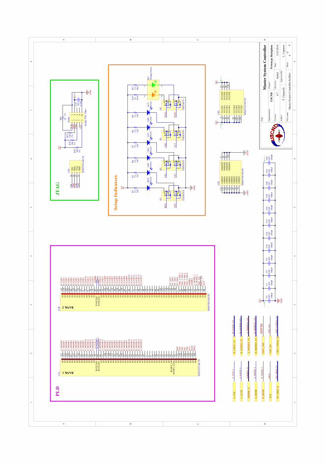
11
22
33
44
55
66
77
88
DD
CC
BB
AA
Prot
otyp
e B
ackp
lane
5/23
/201
4
Mas
ter S
yste
m C
ontro
ller.S
chD
oc
P. G
iann
elli
L. C
apin
eri
USC
ND
Mas
ter
Syst
em C
ontr
olle
rTi
tle:
Org
aniz
atio
n:Pr
ojec
t:
File
nam
e:
Dat
e:
Auth
or:
Appr
oved
By:
Vers
ion:
Revi
sion
:In
itial
0.7
Shee
t:of
49
TDI
TDO
TCK
TMS
4.7u
F
C54
10V
TDO
TDI
TCK
TMS
3V3
12
34
56
78
910
JTA
G
Hea
der 5
X4
.100
in
GN
D
10k
1%R78
1k1%
R85
10k
1%R75
10k
1%R79
3V3
3V3
3V3
A_G
ATE
_IA
_CLK
_I
GN
DG
ND
AD
DR
0A
DD
R1
AD
DR
2A
DD
R3
A_M
OD
E0A
_MO
DE1
A_M
OD
E2A
_MO
DE3
A_M
OD
E4A
_MO
DE5
A_M
OD
E6A
_MO
DE7
A_M
OD
E8A
_MO
DE9
A_M
OD
E10
A_M
OD
E11
A_M
OD
E12
A_M
OD
E13
A_M
OD
E14
A_M
OD
E15
D_M
OD
E0D
_MO
DE1
D_M
OD
E2D
_MO
DE3
D_M
OD
E4D
_MO
DE5
D_M
OD
E6D
_MO
DE7
D_M
OD
E8D
_MO
DE9
D_M
OD
E10
D_M
OD
E11
D_M
OD
E12
D_M
OD
E13
D_M
OD
E14
D_M
OD
E15
B_G
ATE
0B
_GA
TE1
B_G
ATE
2B
_GA
TE3
B_G
ATE
4B
_GA
TE5
B_G
ATE
6B
_GA
TE7
B_G
ATE
8B
_GA
TE9
B_G
ATE
10B
_GA
TE11
B_G
ATE
12B
_GA
TE13
B_G
ATE
14B
_GA
TE15
B_C
LK0
B_C
LK1
B_C
LK2
B_C
LK3
B_C
LK4
B_C
LK5
B_C
LK6
B_C
LK7
B_C
LK8
B_C
LK9
B_C
LK10
B_C
LK11
B_C
LK12
B_C
LK13
B_C
LK14
B_C
LK15
100n
F
C6
10V
100n
F
C7
10V
100n
F
C8
10V
100n
F
C9
10V
100n
F
C55
10V
100n
F
C56
10V
100n
F
C57
10V
100n
F
C61
10V
3V3
GN
D
100n
F
C58
10V
100n
F
C59
10V
100n
F
C60
10V
A_M
OD
E_I
D_M
OD
E_I
VH
V_E
N
A_C
LK
A_G
ATE
A_C
LK_I
A_G
ATE
_I
AD
DR
[0..3
]A
DD
R[0
..3]
B_C
LK[0
..15]
B_G
ATE
[0..1
5]B
_GA
TE[0
..15]
B_C
LK[0
..15]
A_M
OD
E
D_M
OD
E
A_M
OD
E_I
D_M
OD
E_I
JTA
G
A_M
OD
E[0.
.15]
D_M
OD
E[0.
.15]
D_M
OD
E[0.
.15]
A_M
OD
E[0.
.15]
VH
V_E
NV
HV
_EN
BANK 1
IO10
7
IO11
3
IO10
4
IO11
4
IO97
IO11
7
IO87
IO11
8
IO62
IO24
IO55
IO27
IO49
IO30
IO/G
CLK
018
IO/G
CLK
120
IO42
IO31
IO10
8
IO11
2
IO10
6
IO11
1
IO98
IO11
0
IO86
IO10
9
IO59
IO37
IO53
IO38
IO43
IO39
IO41
IO32
IO45
IO2
IO4
IO5
IO51
IO12
IO13
IO21
IO22
IO23
IO28
IO/D
EV_O
E60
IO/D
EV_C
LRn
61
IO29
IO13
1
IO13
0
IO13
7
IO13
2
IO13
9
IO13
8
IO14
1
IO14
0
U2A
EPM
570T
144C
5N
BANK 2
IO10
3
IO11
9
IO10
1
IO12
1
IO94
IO12
3
IO85
IO12
5
IO63
IO6
IO57
IO8
IO50
IO14
IO/G
CLK
289
IO/G
CLK
391
IO44
IO16
IO10
2
IO12
0
IO95
IO12
2
IO88
IO12
4
IO84
IO12
9
IO66
IO3
IO58
IO7
IO52
IO11
IO48
IO15
IO40
IO70
IO71
IO74
IO77
IO93
IO96
IO10
5
IO12
7
IO13
3
IO13
4
IO14
2
IO14
3
IO14
4
IO1
IO67
IO68
IO69
IO72
IO78
IO73
IO81
IO76
IO79
IO75
IO80
U2B
EPM
570T
144C
5N
TMS
33
TDI
34
TCK
35TD
O36
U2C
EPM
570T
144C
5N
VC
CIN
T19
VC
CIN
T56
VC
CIN
T90
VC
CIN
T12
6
VC
CIO
19
VC
CIO
125
VC
CIO
146
VC
CIO
164
VC
CIO
282
VC
CIO
210
0
VC
CIO
211
6
VC
CIO
213
6
U2D
EPM
570T
144C
5N
GN
DIN
T17
GN
DIN
T54
GN
DIN
T92
GN
DIN
T12
8
GN
DIO
10G
ND
IO26
GN
DIO
47G
ND
IO65
GN
DIO
83G
ND
IO99
GN
DIO
115
GN
DIO
135
U2E
EPM
570T
144C
5N
100n
F
C62
10V
AU
XA
UX
AU
X
RD
YG
reen
120
1%R3
3V3
CH
3G
reen
120
1%R5
CH
2G
reen
120
1%R6
CH
1G
reen
120
1%R7
CH
0G
reen
120
1%R8
AC
TG
reen
120
1%R9
GN
D
Q1
FDG
6301
N
Q2
FDG
6301
N
Q3
FDG
6301
N
RD
YC
H0
CH
1
CH
2
CH
3A
CT
RD
Y
CH
0C
H1
CH
2C
H3
AC
T
Q4
FDG
6301
N
PASV
DIA
G
PASV
DIA
G
1
42
3
PD Ora
nge/
Gre
en
80.6
1%R11
90.9
1%R10
VH
V_C
TRL0
VH
V_C
TRL1
VH
V_C
TRL2
VH
V_C
TRL3
VH
V_C
TRL[
0..3
]V
HV
_CTR
L[0.
.3]
PLD
Setu
p In
dica
tors
HV
_SW
[0..3
]H
V_S
W[0
..3]
HV
_SW
0H
V_S
W1
HV
_SW
2H
V_S
W3
PN5V
_IN
HPN
5V_E
N
PN5V
_EN
PIACT01 PIACT02CO
ACT
PIC601PIC602COC
6
PIC701PIC702CO
C7
PIC801PIC802CO
C8
PIC901PIC902CO
C9
PIC5401 PIC5402
COC54
PIC5501PIC5502COC55
PIC5601PIC5602COC56
PIC5701PIC5702COC57
PIC5801PIC5802COC58
PIC5901PIC5902COC59
PIC6001PIC6002COC60
PIC6101PIC6102COC61
PIC6201PIC6202COC62
PICH001 PICH002CO
CH0
PICH101 PICH102CO
CH1
PICH201 PICH202CO
CH2
PICH301 PICH302CO
CH3
PIJTAG01
PIJTAG02
PIJTAG03
PIJTAG04
PIJTAG05
PIJTAG06
PIJTAG07
PIJTAG08
PIJTAG09
PIJTAG010
COJT
AG
PIPD01PIPD02
PIPD03PIPD04
COPD
PIQ1
01
PIQ1
02
PIQ1
03
PIQ1
04
PIQ1
05
PIQ1
06
COQ1
PIQ2
01
PIQ2
02
PIQ2
03
PIQ2
04
PIQ2
05
PIQ2
06
COQ2
PIQ3
01
PIQ3
02
PIQ3
03
PIQ3
04
PIQ3
05
PIQ3
06
COQ3
PIQ4
01
PIQ4
02
PIQ4
03
PIQ4
04
PIQ4
05
PIQ4
06
COQ4
PIR301PIR302COR
3
PIR501PIR502COR
5
PIR601PIR602COR
6
PIR701PIR702CO
R7
PIR801PIR802CO
R8
PIR901PIR902CO
R9
PIR1001PIR1002COR10
PIR1101PIR1102COR11
PIR7501 PIR7502
COR75
PIR7801 PIR7802
COR78
PIR7901 PIR7902
COR79
PIR8
501
PIR8
502COR85
PIRDY01 PIRDY02CO
RDY
PIU202
PIU204
PIU205
PIU2012
PIU2013
PIU2018
PIU2020
PIU2021
PIU2022
PIU2023
PIU2024
PIU2027
PIU2028
PIU2029
PIU2030
PIU2031
PIU2032
PIU2037
PIU2038
PIU2039
PIU2041
PIU2042
PIU2043
PIU2045
PIU2049
PIU2051
PIU2053
PIU2055
PIU2059
PIU2060
PIU2061
PIU2062
PIU2086
PIU2087
PIU2097
PIU2098
PIU20104
PIU20106
PIU20107
PIU20108
PIU20109
PIU20110
PIU20111
PIU20112
PIU20113
PIU20114
PIU20117
PIU20118
PIU20130
PIU20131
PIU20132
PIU20137
PIU20138
PIU20139
PIU20140
PIU20141
COU2
A
PIU201
PIU203
PIU206
PIU207
PIU208
PIU2011
PIU2014
PIU2015
PIU2016
PIU2040
PIU2044
PIU2048
PIU2050
PIU2052
PIU2057
PIU2058
PIU2063
PIU2066
PIU2067
PIU2068
PIU2069
PIU2070
PIU2071
PIU2072
PIU2073
PIU2074
PIU2075
PIU2076
PIU2077
PIU2078
PIU2079
PIU2080
PIU2081
PIU2084
PIU2085
PIU2088
PIU2089
PIU2091
PIU2093
PIU2094
PIU2095
PIU2096
PIU20101
PIU20102
PIU20103
PIU20105
PIU20119
PIU20120
PIU20121
PIU20122
PIU20123
PIU20124
PIU20125
PIU20127
PIU20129
PIU20133
PIU20134
PIU20142
PIU20143
PIU20144
COU2
B
PIU2033
PIU2034
PIU2035
PIU2036
COU2
C
PIU209
PIU2019
PIU2025
PIU2046
PIU2056
PIU2064
PIU2082
PIU2090
PIU20100
PIU20116
PIU20126
PIU20136CO
U2D
PIU2010
PIU2017
PIU2026
PIU2047
PIU2054
PIU2065
PIU2083
PIU2092
PIU2099
PIU20115
PIU20128
PIU20135CO
U2E
PIC602PIC702
PIC802PIC902
PIC5401
PIC5502PIC5602
PIC5702PIC5802
PIC5902PIC6002
PIC6102PIC6202
PIJTAG04
PIR302PIR502
PIR602PIR702
PIR802PIR902
PIR1002PIR1102
PIR7501PIR7801
PIR7901
PIU209
PIU2019
PIU2025
PIU2046
PIU2056
PIU2064
PIU2082
PIU2090
PIU20100
PIU20116
PIU20126
PIU20136
PIU2018
NLA0CLK0I
POA0CLK
PIU2020
NLA0GATE0I
POA0GATE
PIU2081
NLA0
MODE
0IPOA0MODE
PIQ3
05
PIU20138
NLAC
T
PIU2080
NLAUX
POAUX
PIQ3
02
PIU20139
NLCH
0
PIQ2
05
PIU20132
NLCH
1PIQ2
02
PIU20137
NLCH
2
PIQ1
05
PIU20130
NLCH
3
PIU2076
NLD0
MODE
0IPOD0MODE
PIQ4
02
PIU20140
NLDI
AG
PIC601PIC701
PIC801PIC901
PIC5402
PIC5501PIC5601
PIC5701PIC5801
PIC5901PIC6001
PIC6101PIC6201
PIJTAG02
PIJTAG010
PIQ1
01
PIQ1
04
PIQ2
01
PIQ2
04
PIQ3
01
PIQ3
04
PIQ4
01
PIQ4
04
PIR8
501
PIU2010
PIU2017
PIU2026
PIU2047
PIU2054
PIU2065
PIU2083
PIU2092
PIU2099
PIU20115
PIU20128
PIU20135
PIACT01PIR901 PIACT02
PIQ3
03PICH001PIR801 PICH002
PIQ3
06
PICH101PIR701 PICH102
PIQ2
03PICH201PIR601 PICH202
PIQ2
06
PICH301PIR501 PICH302
PIQ1
03
PIJTAG06
PIJTAG07
PIJTAG08
PIPD01PIR1101
PIPD02PIR1001
PIPD03
PIQ4
03
PIPD04PI
Q406
PIQ1
06PIRDY02PIR301 PIRDY01PIU202
PIU204
PIU205
PIU2012
PIU2013
PIU2021
PIU2022
PIU2023
PIU2028
PIU2029
PIU2040
PIU2045
PIU2051
PIU2060
PIU2061
PIU2070
PIU2071
PIU2074
PIU2077
PIU2093
PIU2096
PIU20105
PIU20127
PIU20133
PIU20134
PIU2075
NLP\N\
5\V\0\
E\N\
POPN5V0INH
PIQ4
05
PIU20141
NLPA
SV
PIQ1
02
PIU20131
NLRD
Y
PIJTAG01PIR8
502
PIU2035
NLTC
K
PIJTAG09
PIR7902
PIU2034
NLTDI
PIJTAG03
PIR7502PIU2036
NLTD
O
PIJTAG05
PIR7802PIU2033
NLTM
S
PIU2079
NLVH
V0EN
POVHV0EN
PIU20107
NLA0
MODE
0000
150
NLA0MODE0
POA0MODE0000150
PIU20113
NLA0
MODE
0000
150
NLA0MODE1
POA0MODE0000150
PIU20104
NLA0
MODE
0000
150
NLA0MODE2
POA0MODE0000150
PIU20114
NLA0
MODE
0000
150
NLA0MODE3
POA0MODE0000150
PIU2097
NLA0
MODE
0000
150
NLA0MODE4
POA0MODE0000150
PIU20117
NLA0
MODE
0000
150
NLA0MODE5
POA0MODE0000150
PIU2087
NLA0
MODE
0000
150
NLA0MODE6
POA0MODE0000150
PIU20118
NLA0
MODE
0000
150
NLA0MODE7
POA0MODE0000150
PIU2062
NLA0
MODE
0000
150
NLA0MODE8
POA0MODE0000150
PIU2024
NLA0
MODE
0000
150
NLA0MODE9
POA0MODE0000150
PIU2055
NLA0
MODE
0000
150
NLA0
MODE
10
POA0MODE0000150
PIU2027
NLA0
MODE
0000
150
NLA0
MODE
11
POA0MODE0000150
PIU2049
NLA0
MODE
0000
150
NLA0
MODE
12
POA0MODE0000150
PIU2030
NLA0
MODE
0000
150
NLA0
MODE
13
POA0MODE0000150
PIU2042
NLA0
MODE
0000
150
NLA0
MODE
14
POA0MODE0000150
PIU2031
NLA0
MODE
0000
150
NLA0
MODE
15
POA0MODE0000150
PIU2089
NLAD
DR00
0030
NLADDR0
POADDR000030
PIU2091
NLAD
DR00
0030
NLADDR1
POADDR000030
PIU2078
NLAD
DR00
0030
NLADDR2
POADDR000030
PIU2073
NLAD
DR00
0030
NLADDR3
POADDR000030
PIU20103
NLB0
CLK0
0001
50
NLB0CLK0
POB0CLK0000150
PIU20119
NLB0
CLK0
0001
50
NLB0CLK1
POB0CLK0000150
PIU20101
NLB0
CLK0
0001
50
NLB0CLK2
POB0CLK0000150
PIU20121
NLB0
CLK0
0001
50
NLB0CLK3
POB0CLK0000150
PIU2094
NLB0
CLK0
0001
50
NLB0CLK4
POB0CLK0000150
PIU20123
NLB0
CLK0
0001
50
NLB0CLK5
POB0CLK0000150
PIU2085
NLB0
CLK0
0001
50
NLB0CLK6
POB0CLK0000150
PIU20125
NLB0
CLK0
0001
50
NLB0CLK7
POB0CLK0000150
PIU2063
NLB0
CLK0
0001
50
NLB0CLK8
POB0CLK0000150
PIU206
NLB0
CLK0
0001
50
NLB0CLK9
POB0CLK0000150
PIU2057
NLB0
CLK0
0001
50
NLB0CLK10
POB0CLK0000150
PIU208
NLB0
CLK0
0001
50
NLB0CLK11
POB0CLK0000150
PIU2050
NLB0
CLK0
0001
50
NLB0CLK12
POB0CLK0000150
PIU2014
NLB0
CLK0
0001
50
NLB0CLK13
POB0CLK0000150
PIU2044
NLB0
CLK0
0001
50
NLB0CLK14
POB0CLK0000150
PIU2016
NLB0
CLK0
0001
50
NLB0CLK15
POB0CLK0000150
PIU20102
NLB0
GATE
0000
150
NLB0
GATE
0
POB0GATE0000150
PIU20120
NLB0
GATE
0000
150
NLB0
GATE
1
POB0GATE0000150
PIU2095
NLB0
GATE
0000
150
NLB0
GATE
2
POB0GATE0000150
PIU20122
NLB0
GATE
0000
150
NLB0
GATE
3
POB0GATE0000150
PIU2088
NLB0
GATE
0000
150
NLB0
GATE
4
POB0GATE0000150
PIU20124
NLB0
GATE
0000
150
NLB0
GATE
5
POB0GATE0000150
PIU2084
NLB0
GATE
0000
150
NLB0
GATE
6
POB0GATE0000150
PIU20129
NLB0
GATE
0000
150
NLB0
GATE
7
POB0GATE0000150
PIU2066
NLB0
GATE
0000
150
NLB0
GATE
8
POB0GATE0000150
PIU203
NLB0
GATE
0000
150
NLB0
GATE
9
POB0GATE0000150
PIU2058
NLB0
GATE
0000
150
NLB0GATE10
POB0GATE0000150
PIU207
NLB0
GATE
0000
150
NLB0GATE11
POB0GATE0000150
PIU2052
NLB0
GATE
0000
150
NLB0GATE12
POB0GATE0000150
PIU2011
NLB0
GATE
0000
150
NLB0GATE13
POB0GATE0000150
PIU2048
NLB0
GATE
0000
150
NLB0GATE14
POB0GATE0000150
PIU2015
NLB0
GATE
0000
150
NLB0GATE15
POB0GATE0000150
PIU20108
NLD0
MODE
0000
150
NLD0MODE0
POD0MODE0000150
PIU20112
NLD0
MODE
0000
150
NLD0MODE1
POD0MODE0000150
PIU20106
NLD0
MODE
0000
150
NLD0MODE2
POD0MODE0000150
PIU20111
NLD0
MODE
0000
150
NLD0MODE3
POD0MODE0000150
PIU2098
NLD0
MODE
0000
150
NLD0MODE4
POD0MODE0000150
PIU20110
NLD0
MODE
0000
150
NLD0MODE5
POD0MODE0000150
PIU2086
NLD0
MODE
0000
150
NLD0MODE6
POD0MODE0000150
PIU20109
NLD0
MODE
0000
150
NLD0MODE7
POD0MODE0000150
PIU2059
NLD0
MODE
0000
150
NLD0MODE8
POD0MODE0000150
PIU2037
NLD0
MODE
0000
150
NLD0MODE9
POD0MODE0000150
PIU2053
NLD0
MODE
0000
150
NLD0
MODE
10
POD0MODE0000150
PIU2038
NLD0
MODE
0000
150
NLD0
MODE
11
POD0MODE0000150
PIU2043
NLD0
MODE
0000
150
NLD0
MODE
12
POD0MODE0000150
PIU2039
NLD0
MODE
0000
150
NLD0
MODE
13
POD0MODE0000150
PIU2041
NLD0
MODE
0000
150
NLD0
MODE
14
POD0MODE0000150
PIU2032
NLD0
MODE
0000
150
NLD0
MODE
15
POD0MODE0000150
PIU201
NLHV0SW000030
NLHV
0SW0
POHV0SW000030
PIU20144
NLHV0SW000030
NLHV
0SW1
POHV0SW000030
PIU20143
NLHV0SW000030
NLHV
0SW2
POHV0SW000030
PIU20142
NLHV0SW000030
NLHV
0SW3
POHV0SW000030
PIU2072
NLVHV0CTRL000030
NLVHV0CTRL0
POVHV0CTRL000030
PIU2069
NLVHV0CTRL000030
NLVHV0CTRL1
POVHV0CTRL000030
PIU2068
NLVHV0CTRL000030
NLVHV0CTRL2
POVHV0CTRL000030
PIU2067
NLVHV0CTRL000030
NLVHV0CTRL3
POVHV0CTRL000030
POA0CLK
POA0GATE
POA0MODE
POA0MODE0
POA0MODE1
POA0MODE2
POA0MODE3
POA0MODE4
POA0MODE5
POA0MODE6
POA0MODE7
POA0MODE8
POA0MODE9
POA0MODE10
POA0MODE11
POA0MODE12
POA0MODE13
POA0MODE14
POA0MODE15
POA0MODE0000150
POADDR0
POADDR1
POADDR2
POADDR3
POADDR000030
POAUX
POB0CLK0
POB0CLK1
POB0CLK2
POB0CLK3
POB0CLK4
POB0CLK5
POB0CLK6
POB0CLK7
POB0CLK8
POB0CLK9
POB0CLK10
POB0CLK11
POB0CLK12
POB0CLK13
POB0CLK14
POB0CLK15
POB0CLK0000150
POB0GATE0
POB0GATE1
POB0GATE2
POB0GATE3
POB0GATE4
POB0GATE5
POB0GATE6
POB0GATE7
POB0GATE8
POB0GATE9
POB0GATE10
POB0GATE11
POB0GATE12
POB0GATE13
POB0GATE14
POB0GATE15
POB0GATE0000150
POD0MODE
POD0MODE0
POD0MODE1
POD0MODE2
POD0MODE3
POD0MODE4
POD0MODE5
POD0MODE6
POD0MODE7
POD0MODE8
POD0MODE9
POD0MODE10
POD0MODE11
POD0MODE12
POD0MODE13
POD0MODE14
POD0MODE15
POD0MODE0000150
POHV0SW0
POHV0SW1
POHV0SW2
POHV0SW3
POHV0SW000030
POPN5V0INH
POVHV0CTRL0
POVHV0CTRL1
POVHV0CTRL2
POVHV0CTRL3
POVHV0CTRL000030
POVHV0EN
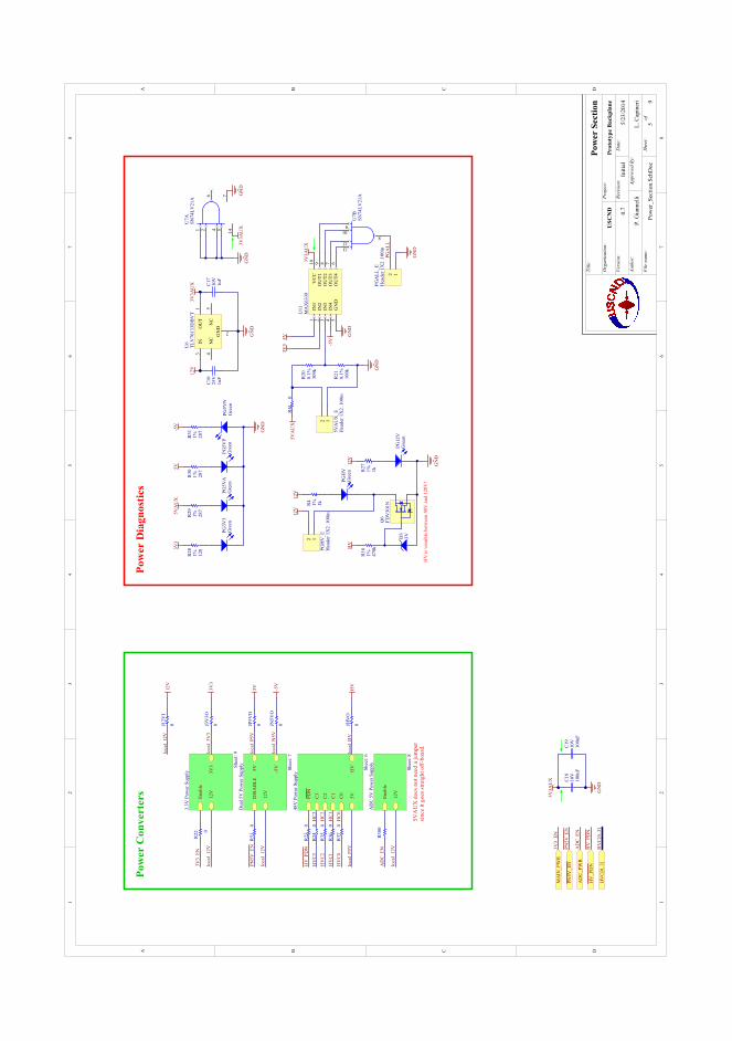
11
22
33
44
55
66
77
88
DD
CC
BB
AA
Prot
otyp
e B
ackp
lane
5/23
/201
4
Pow
er_S
ectio
n.Sc
hDoc
P. G
iann
elli
L. C
apin
eri
USC
ND
Pow
er S
ectio
nTi
tle:
Org
aniz
atio
n:Pr
ojec
t:
File
nam
e:
Dat
e:
Auth
or:
Appr
oved
By:
Vers
ion:
Revi
sion
:In
itial
0.7
Shee
t:of
59
AD
C_P
WR
AD
C_E
N
HV
_PD
N
PDN
C0
C1
C2
C3
HV
5V
Shee
t: 6
48V
Pow
er S
uppl
y
HV
_PD
N
5V -5V
12V
DIS
AB
LE
Shee
t: 7
Dua
l 5V
Pow
er S
uppl
y
Enab
le
12V
Shee
t: 8
AD
C 5
V P
ower
Sup
ply
AD
C_E
N
Enab
le
3V3
12V
Shee
t: 9
3.3V
Pow
er S
uppl
y
Pow
er D
iagn
ostic
s
PG3V
3G
reen
PG5V
AG
reen
PG5V
PG
reen
PG5V
NG
reen
GN
D
120
1%R28
287
1%R29
5V-5
V3V
35V
AU
X
1k1%R27
PG12
VG
reen
12V
287
1%R30
287
1%R31
HV
MA
IN_P
WR
3V3_
EN
3V3_
EN
HV
_PD
N
HV
C0
HV
C1
HV
C2
HV
C3
HV
C[0
..3]
HV
C[0
..3]
HV
is v
arai
ble
betw
een
40V
and
120
V!
D3
3V
470k
1%R18
Q6
FDV
301N
PGH
VG
reen
Pow
er C
onve
rter
s
12
PGH
V_E
Hea
der 1
X2
.100
in
GN
D
2
GN
DOU
T1
IN3
NC
4N
C5
U6
TLV
7013
3DB
VT
910
1213
8
U7B
SN74
LV21
A
147
1 2 4 5
6
U7A
SN74
LV21
A
IN1
1
IN2
2
IN3
3
IN4
4
GN
D5
OU
T46
OU
T37
OU
T28
OU
T19
VC
C10
U11
MA
X63
38
GN
D3V
3AU
XG
ND
3V3A
UX
12V
1k1%R4
12V
12V
GN
D
3V3A
UX
GN
D
PGA
LL
-5V5V
3V3
309k
0.1%
R20
100k
0.1%
R21
GN
D
5VA
UX
100n
F
C18
10V
100n
F
C19
10V
3V3A
UX
GN
D
1uF
C17
10V
1uF
C16
25V
12
PGA
LL_E
Hea
der 1
X2
.100
in
GN
D
0J12V
I
0J3V
3O
0JN5V
O
0JHV
O
0JP5V
O
0R
38
0R
23
0R
24
0R
35
0R
36
0R
37
0
R22
5VA
UX
doe
s no
t nee
d a
jum
per
sinc
e it
goes
stra
ight
off
-boa
rd.
loca
l_P5
V
loca
l_N
5V
loca
l_H
V
loca
l_3V
3
loca
l_12
V
loca
l_P5
V5V
loca
l_12
V
-5V
HV
loca
l_12
V
loca
l_12
V3V
3
12V
HC
0
HC
1
HC
2
HC
3
12
5VA
UX
_EH
eade
r 1X
2 .1
00in0
R41
PN5V
_EN
0R
51
PN5V
_EN
PN5V
_EN
PI5V
AUX0
E01
PI5V
AUX0
E02
CO5V
AUX0
E
PIC1601PIC1602COC16
PIC1701PIC1702COC17
PIC1801PIC1802COC18
PIC1901PIC1902COC19
PID301PID302COD3
PIJ3V3
O01PIJ
3V3O02CO
J3V3
O
PIJ1
2VI0
1PI
J12V
I02
COJ12VI PIJHVO01
PIJHVO02CO
JHVOPI
JN5V
O01
PIJN
5VO0
2COJN5VO
PIJP
5VO0
1PI
JP5V
O02COJP5VO
PIPG3V301 PIPG3V302CO
PG3V
3PIPG5VA01 PIPG5VA02
COPG5VA
PIPG5VN01PIPG5VN02COPG5VN
PIPG5VP01 PIPG5VP02COPG5VP
PIPG12V01 PIPG12V02COPG12V
PIPG
ALL0
E01
PIPG
ALL0
E02
COPG
ALL0
E
PIPGHV01 PIPGHV02COPGHV
PIPG
HV0E
01
PIPG
HV0E
02
COPGHV0E
PIQ6
01
PIQ602
PIQ603
COQ6
PIR401PIR402CO
R4
PIR1801PIR1802COR18
PIR2001PIR2002COR20
PIR2101 PIR2102
COR21
PIR2201
PIR2
202COR22
PIR2301
PIR2
302
COR23
PIR2401
PIR2
402
COR24
PIR2701PIR2702COR27
PIR2801PIR2802COR28
PIR2901PIR2902COR29
PIR3001PIR3002COR30
PIR3101PIR3102COR31
PIR3501
PIR3
502
COR35
PIR3601
PIR3
602
COR36
PIR3701
PIR3
702
COR37
PIR3801
PIR3
802COR38
PIR4
101
PIR4
102COR41
PIR5101
PIR5
102
COR51
PIU601
PIU602
PIU603
PIU604
PIU605
COU6
PIU701
PIU702
PIU704
PIU705
PIU706
PIU707
PIU7014CO
U7A
PIU708
PIU709PIU7010PIU7012PIU7013
COU7
B
PIU1101
PIU1102
PIU1103
PIU1104
PIU1105
PIU1106
PIU1107
PIU1108
PIU1109
PIU11010
COU11
PIJN
5VO0
1
PIR3102
PIU1104
PIJ3V3
O01
PIR2802
PIU1102
PIR2
202
NL3V30EN
POMAIN0PWR
PIC1702
PIC1802PIC1902
PIU601
PIU7014
PIU11010
PIJP
5VO0
1
PIR3002
PIU1101
PIR2902
PIR4
102
PIC1602
PIJ1
2VI0
2
PIPG
HV0E
02PIR402
PIR2702
PIU603
PIR3
802
NLAD
C0EN
POADC0PWR
PI5V
AUX0
E01
PIC1601PIC1701
PIC1801PIC1901
PID301PIPG3V302PIPG5VA02
PIPG5VN01PIPG5VP02 PIPG12V02
PIPG
ALL0
E01
PIQ602
PIR2102
PIU602
PIU701
PIU702
PIU704
PIU705
PIU707
PIU1105
PIR2
302
NLH\
V\0\
P\D\
N\POH\V\0\P\D\N\
PIR3701NL
HC0
PIR3601NL
HC1
PIR3501NL
HC2
PIR2401NL
HC3
PIJHVO01
PIR1802
PIJ3V3
O02NL
loca
l03V
3PIJ1
2VI0
1
NLlo
cal0
12V
PIJHVO02
NLlo
cal0
HV
PIJN
5VO0
2NLlocal0N5VPI
JP5V
O02
NLlocal0P5V
PI5V
AUX0
E02
PIR2002PI
R410
1
PID302PI
Q601
PIR1801PIPG3V301PIR2801
PIPG5VA01PIR2901
PIPG5VN02PIR3101
PIPG5VP01PIR3001
PIPG12V01PIR2701
PIPGHV01PIR401 PIPGHV02
PIPG
HV0E
01
PIQ603
PIR2001 PIR2101PIU1103
PIR2201
PIR2301
PIR3801
PIR5101
PIU604
PIU605
PIU706
PIU709
PIU1109
PIU7010
PIU1108
PIU7012
PIU1107
PIU7013PIU1106
PIR5
102
NLP\N\
5\V\0\
E\N\
POP\N\5\V\0\E\N\
PIPG
ALL0
E02
PIU708NLPGALL
PIR3
702
NLHVC000030
NLHV
C0
POHVC000030
PIR3
602
NLHVC000030
NLHV
C1
POHVC000030
PIR3
502
NLHVC000030
NLHV
C2
POHVC000030
PIR2
402
NLHVC000030
NLHV
C3
POHVC000030
POADC0PWR
POH\V\0\P\D\N\
POHVC0
POHVC1
POHVC2
POHVC3
POHVC000030
POMAIN0PWR
POP\N\5\V\0\E\N\
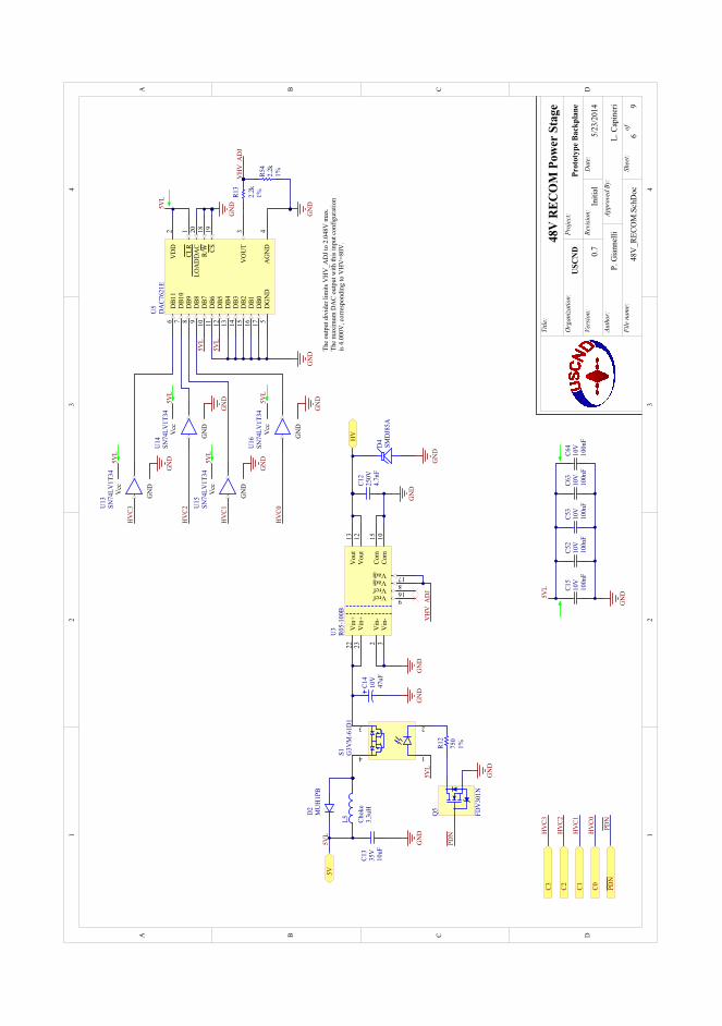
11
22
33
44
DD
CC
BB
AA
Prot
otyp
e Bac
kpla
ne
5/23
/201
4
48V
_REC
OM
.Sch
Doc
P. G
iann
elli
L. C
apin
eri
USC
ND
48V
REC
OM
Pow
er S
tage
Title
:
Org
aniza
tion:
Proj
ect:
File
nam
e:
Dat
e:
Auth
or:
Appr
oved
By:
Vers
ion:
Revi
sion:
Initi
al0.
7
Shee
t:of
69
GN
D
PDN
3.3u
H
L5 Chok
e
GN
D
PDN
PDN
10uF
C13
35V
CLR
1
VD
D2
VO
UT
3
AG
ND
4D
GN
D5
DB1
16
DB1
07
DB9
8
DB8
9
DB7
10
DB6
11
DB5
12
DB4
13
DB3
14
DB2
15
DB1
16
DB0
17
R/W
18
CS19
LOA
DD
AC
20
U5
DA
C762
1E
GN
DG
ND
GN
D
100n
F
C15
10V
GN
D
Vin
-2
Vin
-3
Vref 9
Vref 16
Vadj 17Vadj 8
Com
10Co
m15
Vou
t12
Vou
t13
Vin
+22
Vin
+23
U3
R05-
100B
GN
DG
ND
VH
V_A
DJ
C0C1C2C3
HV
C0
HV
C1
HV
C2
HV
C3
HV
C0
HV
C1
HV
C2
HV
C3
1
23
4S1 G3V
M-6
1D1
Q5
FDV
301N
GN
D
750
1%R12
2.2k
1%R13
47uF
C14
10V
4.7n
F
C12
250V
D2
MU
H1P
B
HV
5V5V
L
5VL
5VL
5VL
VH
V_A
DJ
2.2k
1%R54
The
outp
ut d
ivid
er li
mits
VH
V_A
DJ t
o 2.
048V
max
.Th
e m
axim
um D
AC
outp
ut w
ith th
is in
put c
onfig
urat
ion
is 4.
000V
, cor
resp
ondi
ng to
VH
V=8
0V.
5VL
5VL
100n
F
C52
10V
100n
F
C53
10V
100n
F
C63
10V
100n
F
C64
10VD
4SM
DJ8
5A
GN
D
Vcc
GN
D
U13
SN74
LV1T
34
GN
D5VL
Vcc
GN
D
U14
SN74
LV1T
34
GN
D5VL
Vcc
GN
D
U15
SN74
LV1T
34
GN
D5VL
Vcc
GN
D
U16
SN74
LV1T
34
GN
D5VL
PIC1201PIC1202CO
C12
PIC1301PIC1302CO
C13
PIC1401 PIC1402
COC1
4
PIC1501PIC1502CO
C15
PIC5201PIC5202CO
C52
PIC5301PIC5302CO
C53
PIC6301PIC6302CO
C63
PIC6401PIC6402CO
C64
PID201
PID202COD
2
PID401PID402COD
4
PIL501
PIL502
COL5
PIQ501
PIQ502
PIQ503
COQ5
PIR1201
PIR1202
COR1
2
PIR1
301
PIR1
302
COR1
3
PIR5401PIR5402 COR5
4
PIS101PIS102PIS103
PIS104COS1
PIU302
PIU303
PIU308PIU309
PIU3010
PIU3012
PIU3013
PIU3015
PIU3016PIU3017
PIU3022
PIU3023
COU3
PIU501
PIU502
PIU503
PIU504
PIU505
PIU506
PIU507
PIU508
PIU509
PIU5010
PIU5011
PIU5012
PIU5013
PIU5014
PIU5015
PIU5016
PIU5017
PIU5018
PIU5019
PIU5020
COU5
PIU1302
PIU1303
PIU1304
PIU1305
COU13
PIU1402
PIU1403
PIU1404
PIU1405
COU14
PIU1502
PIU1503
PIU1504
PIU1505
COU15
PIU1
602
PIU1
603
PIU1
604
PIU1
605
COU16
PIC1302
PIC1502PIC5202
PIC5302PIC6302
PIC6402
PID202
PIL501
PIS101
PIU501
PIU502
PIU5010
PIU5012
PIU1305
PIU1405
PIU1505
PIU1
605
NL5VL
PO5V
PIC1201PIC1301
PIC1402
PIC1501PIC5201
PIC5301PIC6301
PIC6401
PID401
PIQ502
PIR5401
PIU302
PIU303
PIU3010
PIU3015
PIU504
PIU505
PIU5011
PIU5013
PIU5014
PIU5015
PIU5016
PIU5017
PIU5018
PIU5019
PIU5020
PIU1303
PIU1403
PIU1503
PIU1
603
PIU1
602
NLHVC0
POC0
PIU1502
NLHVC1
POC1
PIU1402
NLHVC2
POC2
PIU1302
NLHVC3
POC3
PIC1202PID402
PIU3012
PIU3013
POHV
PIC1401PIS103
PIU3022
PIU3023
PID201 PI
L502
PIS104
PIQ503
PIR1201
PIR1202PIS102
PIR1
301
PIU503
PIU309PIU3016
PIU506
PIU1304
PIU507
PIU1404
PIU508
PIU1504
PIU509
PIU1
604
PIQ501
NLP\D\
N\POP\D\N\
PIR1
302 PIR5402
PIU308PIU3017
NLVHV0ADJ
PO5V
POC0
POC1
POC2
POC3
POHV
POP\D\N\
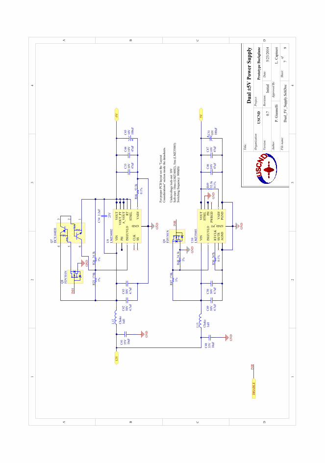
11
22
33
44
DD
CC
BB
AA
Prot
otyp
e Bac
kpla
ne
5/23
/201
4
Dua
l_5V
_Sup
ply.
SchD
oc
P. G
iann
elli
L. C
apin
eri
USC
ND
Dua
l ±5V
Pow
er S
uppl
yTi
tle:
Org
aniza
tion:
Proj
ect:
File
nam
e:
Dat
e:
Auth
or:
Appr
oved
By:
Vers
ion:
Revi
sion:
Initi
al0.
7
Shee
t:of
79
267k
0.1%
R50
GN
D
4.7u
F
C50
50V
47uF
C46
10V
4.7u
F
C49
50V
GN
D
4.7u
F
C43
50V
4.7u
F
C42
50V
1uH
L12
Chok
e
1uH
L13
Chok
e
GN
D
GN
D
10uF
C41
35V
10uF
C48
35V
5V-5V
12V
For p
rope
r PCB
layo
ut se
e th
e "L
ayou
t Co
nsid
erat
ions
" sec
tion
insid
e th
e da
tash
eets.
Und
ervo
ltage
lock
-out
: 10V
Soft-
start:
10m
s (LM
Z340
02),
5ms (
LMZ3
5003
)Sw
itchi
ng fr
eque
ncy:
800
kHz
PHVIN
INH
/UV
LO
CLK
SS
GND
VA
DJ
STSE
LRTA
_VO
UT
VO
UT_
PTV
OU
T
U9
LMZ3
4002
PH
VIN
INH
/UV
LO
RT/C
LKSS
/TR
VA
DJ
STSE
L
PWRG
D
VO
UT
PGN
D
GND_PT
AG
ND
U10
LMZ3
5003
47uF
C47
10V
GN
D52
.3k
0.1%
R49
174k
1%
R47
24.3
k
1%
R48
GN
D
52.3
k
0.1%
R46
24.3
k
1%
R26
174k
1%
R25
Q9
FDV
301N
DIS
ABL
EIN
H
INH
100u
F
C45
10V
47uF
C35
10V
47uF
C44
10V
2.2u
FC3
4 25V
1234 5 6
Q7
DCX
144E
H
GN
D
Q8
FDV
301N
INH
100u
F
C51
10V
PIC3
401
PIC3
402
COC3
4
PIC3501PIC3502CO
C35
PIC4101PIC4102CO
C41
PIC4201PIC4202CO
C42
PIC4301PIC4302CO
C43
PIC4401PIC4402CO
C44
PIC4501PIC4502CO
C45
PIC4601PIC4602CO
C46
PIC4701PIC4702CO
C47
PIC4801PIC4802CO
C48
PIC4901PIC4902CO
C49
PIC5001PIC5002CO
C50
PIC5101 PIC5102
COC5
1
PIL1201
PIL1202
COL1
2
PIL1301
PIL1302
COL1
3
PIQ701
PIQ702
PIQ703
PIQ704
PIQ705
PIQ706COQ
7
PIQ801
PIQ802
PIQ803
COQ8
PIQ901
PIQ902
PIQ903COQ
9
PIR2
501
PIR2
502COR2
5PI
R260
1PI
R260
2COR2
6
PIR4
601
PIR4
602
COR4
6
PIR4
701
PIR4
702COR4
7
PIR4
801
PIR4
802COR4
8
PIR4901 PIR4902COR4
9
PIR5
001
PIR5
002COR5
0
PIU901
PIU904
PIU905
PIU906
PIU907
PIU908
PIU909
PIU9010PIU9011PIU9012PIU9013PIU9014PIU9015
PIU9
016
PIU9
017
PIU9
018
PIU9
019
PIU9
020
PIU9
021
PIU9
022
PIU9
023
PIU9
024
PIU9
026
PIU9
027
PIU9
028
PIU9
029
PIU9
030
PIU9
031
PIU9
032
PIU9
033
PIU9
034
PIU9
036
PIU9
037
PIU9
038
PIU9039
PIU9
040
PIU9
041COU
9
PIU1001
PIU1004
PIU1005
PIU1006
PIU1007
PIU1008PIU1009
PIU10010
PIU10011
PIU10012
PIU10013
PIU10014
PIU10015
PIU10016
PIU10017
PIU10018
PIU10019
PIU10020
PIU10021
PIU10022
PIU10023
PIU10024
PIU10026
PIU10027
PIU10028
PIU10029
PIU10030
PIU10031
PIU10032
PIU10033
PIU10034
PIU10035
PIU10036
PIU10037
PIU10038
PIU10039
PIU10040
PIU10041
COU1
0
PIC3501PIC4101
PIC4201PIC4301
PIC4401PIC4501
PIC4601PIC4701
PIC4801PIC4901
PIC5001PIC5102
PIQ802
PIQ902
PIR4
602
PIR4
801
PIR5
002
PIU9010PIU9011PIU9012PIU9013PIU9014PIU9015PIU9039
PIU1001
PIU1004
PIU1005
PIU1008PIU1009PIU10016
PIU10017
PIU10018
PIU10019
PIU10020
PIU10029
PIU10030
PIU10032
PIU10033
PIU10034
PIU10037
PIU10040
PIQ801
PIQ901
NLINH
PODISABLE
PIC3
401
PIC3502PIC4402
PIC4502
PIQ701
PIR2
601
PIU901
PIU904
PIU905
PIU908
PIU909
PIU9
016
PIU9
017
PIU9
018
PIU9
019
PIU9
020
PIU9
029
PIU9
030
PIU9
032
PIU9
033
PIU9
034
PIU9
037
PIU9
040
PO05V
PIC3
402
PIC4202PIC4302
PIL1202
PIQ704
PIR2
502
PIU9
026
PIC4102
PIC4802
PIL1201
PIL1301
PO12V
PIC4602PIC4702
PIC5101PIR4901
PIU10010
PIU10011
PIU10012
PIU10013
PIU10014
PIU10015
PIU10039
PO5V
PIC4902PIC5002
PIL1302
PIR4
702
PIU10026
PIQ702
PIQ703
PIQ705
PIQ803
PIQ706
PIR2
501
PIR2
602
PIU9
027
PIQ903
PIR4
701
PIR4
802
PIU10027
PIR4
601
PIU9
036
PIR4902PIU10036
PIR5
001
PIU10031
PIU906
PIU907
PIU9
021
PIU9
022
PIU9
023
PIU9
024
PIU9
038
PIU9
041
PIU9
028
PIU9
031
PIU1006
PIU1007
PIU10021
PIU10022
PIU10023
PIU10024
PIU10038
PIU10041
PIU10028
PIU10035
PO05V
PO5V
PO12V
PODISABLE
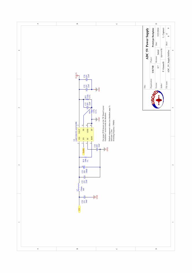
11
22
33
44
DD
CC
BB
AA
Prot
otyp
e Bac
kpla
ne
5/23
/201
4
AD
C_5V
_Sup
ply.
SchD
oc
P. G
iann
elli
L. C
apin
eri
USC
ND
AD
C 5
V P
ower
Sup
ply
Title
:
Org
aniza
tion:
Proj
ect:
File
nam
e:
Dat
e:
Auth
or:
Appr
oved
By:
Vers
ion:
Revi
sion:
Initi
al0.
7
Shee
t:of
89
VIN
1
EN3
SS5
GN
D4
FB6
RON
2
VO
UT
7
EP8
U4
LMZ1
2001
TZ-A
DJ/N
OPB
1.07
k0.
1%
R16
5.62
k0.
1%
R15
GN
D
GN
D
22uF
C22
25V
100u
F
C23
20V
22uF
C25
16V
22uF
C26
16V
GN
D
Enab
le1u
H
L7 Chok
e
GN
D
100k
1%R14
22nF
C27
50V
22nF
C28
50V
10uF
C24
35V
12V
5VA
UX
For p
rope
r PCB
layo
ut se
e th
e "P
C Bo
ard
Layo
ut
Gui
delin
es" s
ectio
n in
side
the
data
shee
t.
Def
ault
com
pone
nt v
alue
s (se
e da
tash
eet,
page
3).
Soft-
start:
2.2
ms
Switc
hing
freq
uenc
y: 3
80kH
z
PIC2201PIC2202CO
C22
PIC2301 PIC2302
COC2
3
PIC2401PIC2402CO
C24
PIC2501PIC2502CO
C25
PIC2601PIC2602CO
C26
PIC2701PIC2702CO
C27
PIC2801PIC2802CO
C28
PIL701
PIL702
COL7
PIR1401 PIR1402
COR1
4
PIR1501PIR1502CO
R15
PIR1
601
PIR1
602
COR1
6
PIU401
PIU402
PIU403
PIU404
PIU405
PIU406
PIU407
PIU408
COU4
PIC2502PIC2602
PIC2702PIR1502
PIU407
PIC2201PIC2302
PIC2401PIC2501
PIC2601
PIC2801
PIR1
601
PIU404
PIU408
PIC2202PIC2301
PIL702
PIR1401PIU401
PIC2402PIL701
PO12V
PIC2701PIR1501
PIR1
602
PIU406
PIC2802
PIU405
PIR1402PIU402
PIU403
POEnable
PO12V
POENABLE
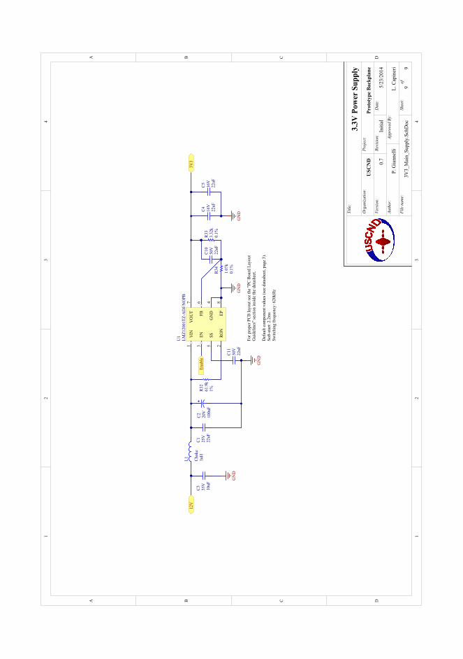
11
22
33
44
DD
CC
BB
AA
Prot
otyp
e Bac
kpla
ne
5/23
/201
4
3V3_
Mai
n_Su
pply
.Sch
Doc
P. G
iann
elli
L. C
apin
eri
USC
ND
3.3V
Pow
er S
uppl
yTi
tle:
Org
aniza
tion:
Proj
ect:
File
nam
e:
Dat
e:
Auth
or:
Appr
oved
By:
Vers
ion:
Revi
sion:
Initi
al0.
7
Shee
t:of
99
VIN
1
EN3
SS5
GN
D4
FB6
RON
2
VO
UT
7
EP8
U1
LMZ1
2001
TZ-A
DJ/N
OPB
1.07
k0.
1%
R34
3.32
k0.
1%
R33
GN
D
GN
D
22uF
C1 25V
100u
F
C2 20V
22uF
C4 16V
22uF
C5 16V
GN
D
1uH
L1 Chok
e
GN
D
61.9
k1%R3
2
22nF
C10
50V
22nF
C11
50V
Enab
le10
uF
C3 35V
3V3
12V
For p
rope
r PCB
layo
ut se
e th
e "P
C Bo
ard
Layo
ut
Gui
delin
es" s
ectio
n in
side
the
data
shee
t.
Def
ault
com
pone
nt v
alue
s (se
e da
tash
eet,
page
3).
Soft-
start:
2.2
ms
Switc
hing
freq
uenc
y: 6
20kH
z
PIC101PIC102COC
1PIC201 PIC202
COC2
PIC301PIC302COC
3
PIC401PIC402COC
4
PIC501PIC502COC
5
PIC1001PIC1002CO
C10
PIC1101PIC1102CO
C11
PIL101
PIL102
COL1
PIR3201 PIR3202
COR3
2
PIR3301PIR3302CO
R33
PIR3
401
PIR3
402
COR3
4
PIU101
PIU102
PIU103
PIU104
PIU105
PIU106
PIU107
PIU108
COU1
PIC101PIC202
PIC301PIC401
PIC501
PIC1101
PIR3
401
PIU104
PIU108
PIC102PIC201
PIL102
PIR3201PIU101
PIC302PIL101
PO12V
PIC402PIC502
PIC1002PIR3302
PIU107
PO3V3
PIC1001PIR3301
PIR3
402
PIU106
PIC1102
PIU105
PIR3202PIU102
PIU103
POEnable
PO3V3
PO12V
POENABLE


A N A L O G F R O N T- E N D

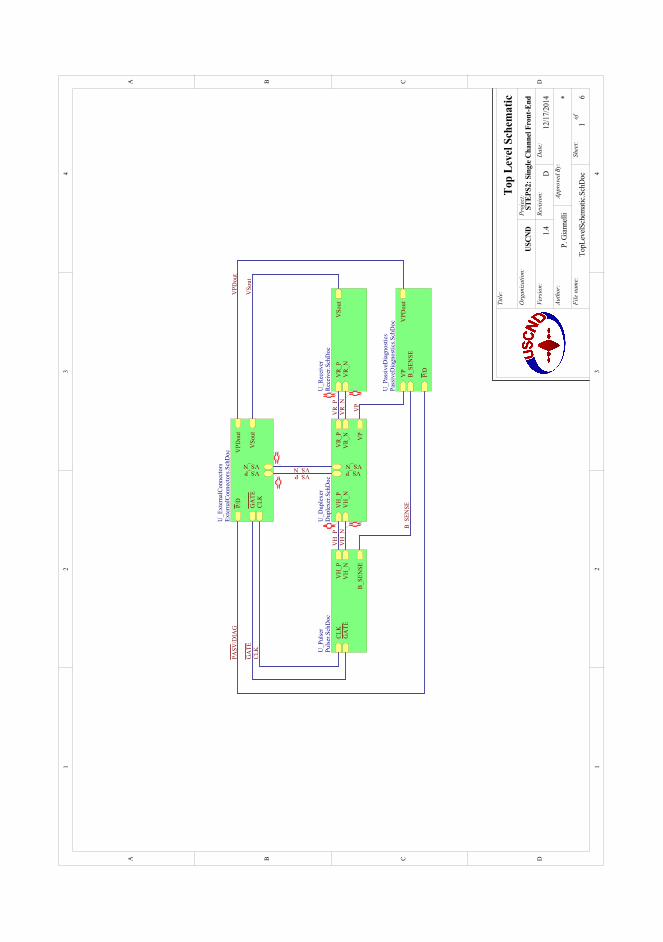
11
22
33
44
DD
CC
BB
AA
STEP
S2: S
ingl
e Cha
nnel
Fron
t-End
12/1
7/20
14
TopL
evel
Sche
mat
ic.S
chD
oc
P. G
iann
elli
*
USC
ND
Top
Leve
l Sch
emat
icTi
tle:
Org
aniz
atio
n:Pr
ojec
t:
File
nam
e:
Dat
e:
Auth
or:
Appr
oved
By:
Vers
ion:
Revi
sion
:D
1.4
Shee
t:of
16
CLK
GA
TEV
Sout
VPD
out
P/D
VS_PVS_N
U_E
xter
nalC
onne
ctor
sEx
tern
alCo
nnec
tors
.Sch
Doc
VH
_PV
H_N
VS_PVS_N
VR_
PV
R_N VP
U_D
uple
xer
Dup
lexe
r.Sch
Doc
B_SE
NSE
VP
VPD
out
P/D
U_P
assi
veD
iagn
ostic
sPa
ssiv
eDia
gnos
tics.S
chD
oc
CLK
GA
TEV
H_P
VH
_N
B_SE
NSE
U_P
ulse
rPu
lser
.Sch
Doc
VSo
utV
R_P
VR_
N
U_R
ecei
ver
Rece
iver
.Sch
Doc
PASV
/DIA
G
GA
TECL
KV
Sout
VPD
out
VP
B_SE
NSE
VH
_PV
H_N
VR_
NV
R_P
VS_NVS_P
NLB0SENSE
NLCLK
NLG\A\
T\E\
NLP\
A\S\
V\0D
IAG
NLVH
0NNL
VH0P
NLVP
NLVPDout
NLVR
0NNL
VR0P
NLVS0N NLVS0P
NLVSout
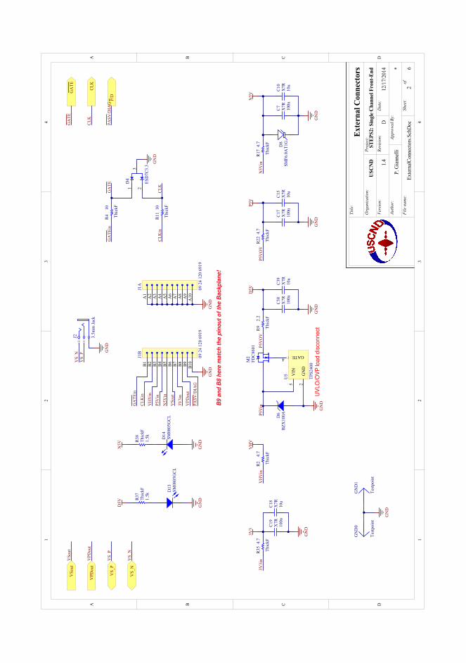
11
22
33
44
DD
CC
BB
AA
STEP
S2: S
ingl
e Cha
nnel
Fron
t-End
12/1
7/20
14
Exte
rnal
Conn
ecto
rs.S
chD
oc
P. G
iann
elli
*
USC
ND
Exte
rnal
Con
nect
ors
Title
:
Org
aniz
atio
n:Pr
ojec
t:
File
nam
e:
Dat
e:
Auth
or:
Appr
oved
By:
Vers
ion:
Revi
sion
:D
1.4
Shee
t:of
26
J2 3.5m
m Ja
ck
A1
A2
A3
A4
A5
A6
A7
A8
A9
A10
J1A
09 2
4 12
0 69
19
B1 B2 B3 B4 B5 B6 B7 B8 B9 B10
J1B
09 2
4 12
0 69
19
GN
DG
ND
CLK
GA
TEG
ATE
CLK
VSo
utV
Sout
VPD
out
VPD
out
P/D
PASV
/DIA
G
VSo
ut
VPD
out
B9
and
B8
here
mat
ch th
e pi
nout
of t
he B
ackp
lane
!
PASV
/DIA
G
GA
TEin
CLK
in
VH
Vin
3V3i
n
P5V
in
N5V
in
3V3
P5V
N5V
VH
V
D13
SM08
05G
CL
D14
SM08
05G
CL
1.5k
R37
Thic
kF1.
5k
R38
Thic
kF
GN
DG
ND
GN
DV
S_P
VS_
N
VS_
P
VS_
N
VS_
PV
S_N
10R4 Th
ickF 10
R11
Thic
kF
GA
TEin
CLK
in
GA
TE
CLK1 2
3D
4
ESD
7C3.
3
GN
D
4.7
R22
Thic
kF
4.7
R17
Thic
kF
4.7
R2 Thic
kF
4.7
R35
Thic
kFN
5Vin
100n
C17
X7R
100n
C7 X7R
100n
C19
X7R
GN
DG
ND
GN
D
10u
C18
X7R
10u
C15
X7R
10u
C10
X7R
3V3i
nV
HV
in
D5V
N5V
GN
D0
Test
poin
t
GN
D1
Test
poin
t
GN
D
D5V
2.2
R9 Thic
kFP5
Vin
100n
C38
X7R
GN
D
10u
C39
X7R
D6
BZX
100A
D8
SMF6
.0A
T1G
M2
FDC8
601
VIN
5
GN
D2
GATE4
U5
TPS2
400
GN
D
P5V
OV
P5V
OV
UVL
O/O
VP lo
ad d
isco
nnec
t
PIC701PIC702COC
7
PIC1001PIC1002COC
10
PIC1501PIC1502COC
15
PIC1701PIC1702COC
17PIC1801PIC1802
COC1
8
PIC1901PIC1902COC19
PIC3801PIC3802COC
38
PIC3901PIC3902COC
39
PID401
PID402
PID403
COD4
PID601PID602COD
6
PID801 PID802
COD8
PID1301 PID1302CO
D13
PID1401PID1402CO
D14
PIGN
D00T
P
COGN
D0
PIGN
D10T
PCOGND1
PIJ10A1
PIJ10A2
PIJ10A3
PIJ10A4
PIJ10A5
PIJ10A6
PIJ10A7
PIJ10A8
PIJ10A9
PIJ10A10COJ
1APIJ10B1
PIJ10B2
PIJ10B3
PIJ1
0B4
PIJ10B5
PIJ10B6
PIJ10B7
PIJ10B8
PIJ1
0B9
PIJ10B10
COJ1B
PIJ201
PIJ202
PIJ203COJ
2
PIM20D
PIM20G
PIM20S
COM2
PIR201
PIR202
COR2
PIR401
PIR402
COR4
PIR901
PIR902
COR9
PIR1
101
PIR1
102
COR11
PIR1
701
PIR1
702
COR1
7PI
R220
1PI
R220
2
COR22
PIR3
501
PIR3
502
COR3
5
PIR3701 PIR3702COR3
7PIR3801 PIR3802CO
R38
PIU5
02
PIU504PI
U505CO
U5
PIC1802PIC1902
PIR3
502
PIJ10B7
PIR3
501
NL3V3in
PID402
PIR1
102
NLCLK
POCLK
PIJ10B2
PIR1
101
NLCLKin
PIC3802PIC3902
PIR902
PIR3701PID401
PIR402
NLG\A\
T\E\
POG\
A\T\
E\
PIJ10B1
PIR401
NLG\A\
T\E\in
PIC701PIC1001
PIC1501PIC1701
PIC1801PIC1901
PIC3801PIC3901
PID403
PID601PID802
PID1302PID1401
PIGN
D00T
PPI
GND1
0TP
PIJ10A1
PIJ10A2
PIJ10A3
PIJ10A4
PIJ10A5
PIJ10A6
PIJ10A7
PIJ10A8
PIJ10A9
PIJ10A10
PIJ10B10
PIJ201
PIU5
02
PIC702PIC1002
PID801PI
R170
2
PIR3801
PIJ10B5
PIR1
701
NLN5Vin
PID1301PIR3702
PID1402PIR3802
PIM20G PIU504PIC1502
PIC1702
PIR2
202
PID602
PIJ1
0B4
PIM20D
PIU5
05
NLP5Vin
PIM20S
PIR901
PIR2
201
NLP5
VOV
PIJ1
0B9
NLP\
A\S\
V\0D
IAG POP\0D
PIR202
PIJ10B3
PIR201
NLVHVin
PIJ10B8
NLVP
Dout
POVPDout
PIJ202
NLVS
0NPOVS0N
PIJ203
NLVS0P
POVS0P
PIJ10B6
NLVS
out
POVSout
POCLK
POG\
A\T\
E\
POP\0D
POVPDOUT
POVS0N
POVS0P
POVSOUT
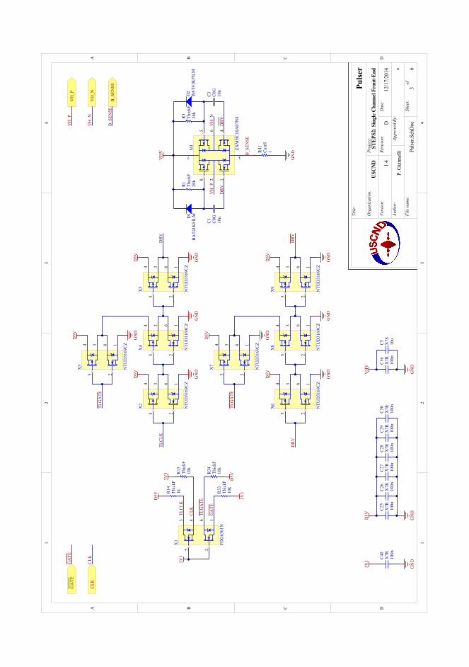
11
22
33
44
DD
CC
BB
AA
STEP
S2: S
ingl
e Cha
nnel
Fron
t-End
12/1
7/20
14
Pulse
r.Sch
Doc
P. G
iann
elli
*
USC
ND
Pulse
rTi
tle:
Org
aniz
atio
n:Pr
ojec
t:
File
nam
e:
Dat
e:
Auth
or:
Appr
oved
By:
Vers
ion:
Revi
sion
:D
1.4
Shee
t:of
36
CLK
GA
TE
12
3
45 6
7
8
M1
ZXM
HC1
0A07
N8
GN
D
VH
V
10n
C1 C0G
10n
C3 C0G
20k
R1 Thic
kF20
k
R3 Thic
kF
1R41
CurrS
DRV
DRV
D1
BAT4
1KFI
LMD
2BA
T41K
FILM
VH
_PV
H_N
VH
_P
VH
_N
VH
_P
B_SE
NSE
VH
_N
213 64
5
X2
NTU
D31
69CZ
213 64
5
X3
NTU
D31
69CZ
213 64
5
X4
NTU
D31
69CZ
213 64
5
X5
NTU
D31
69CZ
213 64
5
X7
NTU
D31
69CZ
213 64
5
X6
NTU
D31
69CZ
213 64
5
X8
NTU
D31
69CZ
213 64
5
X9
NTU
D31
69CZ
D5V
D5V
D5V
D5V
D5V
D5V
DRV
GA
TE
CLK
DRV
DRV
TLCL
K
TLG
ATE
TLG
ATE
GN
DG
ND
GN
D
GN
D
GN
D
GN
DG
ND
GN
D
213 64
5
X1
FDG
6301
N
3V3
GA
TE
CLK
10k
R33
Thic
kF10
k
R34
Thic
kF
3V3
10k
R13
Thic
kF
3V3
D5V
TLG
ATE
1kR14
Thic
kF
TLCL
K
D5V
100n
C25
X7R
100n
C26
X7R
100n
C27
X7R
100n
C28
X7R
100n
C29
X7R
100n
C30
X7R
D5V
GN
D
100n
C16
X7R
10u
C5 X7S
VH
V
GN
D
B_SE
NSE
B_SE
NSE
100n
C40
X7R
GN
D
3V3
PIC101PIC102COC1
PIC301PIC302COC3
PIC501PIC502COC
5
PIC1601PIC1602COC
16
PIC2501PIC2502COC
25
PIC2601PIC2602COC
26
PIC2701PIC2702COC
27
PIC2801PIC2802COC
28
PIC2901PIC2902COC
29
PIC3001PIC3002COC
30
PIC4001PIC4002COC
40
PID101PID102COD1
PID201PID202COD2
PIM101
PIM102
PIM103
PIM104
PIM105
PIM106
PIM107PIM108
COM1
PIR101PIR102COR1
PIR301PIR302COR
3
PIR1301 PIR1302COR13
PIR1401 PIR1402
COR14
PIR3301 PIR3302
COR33
PIR3401 PIR3402COR3
4
PIR4101PIR4102 COR4
1
PIX101
PIX102
PIX103
PIX104
PIX105
PIX106
COX1
PIX201
PIX202
PIX203
PIX204
PIX205
PIX206
COX2
PIX301
PIX302
PIX303
PIX304
PIX305
PIX306
COX3
PIX401
PIX402
PIX403
PIX404
PIX405
PIX406
COX4
PIX501
PIX502
PIX503
PIX504
PIX505
PIX506
COX5
PIX601
PIX602
PIX603
PIX604
PIX605
PIX606
COX6
PIX701
PIX702
PIX703
PIX704
PIX705
PIX706
COX7
PIX801
PIX802
PIX803
PIX804
PIX805
PIX806
COX8
PIX901
PIX902
PIX903
PIX904
PIX905
PIX906
COX9
PIC4002
PIR1301
PIR3302
PIX102
PIX105
PIM103 PIR4102
NLB0SENSE POB
0SEN
SE
PIR1302PIX104
NLCLK
POCLK
PIC2502PIC2602
PIC2702PIC2802
PIC2902PIC3002
PIR1401
PIR3402
PIX204
PIX304
PIX504
PIX604
PIX704
PIX904
PIC301PIM104
PIX903
PIX906
NLD\R\
V\PIC101
PIM101
PIX503
PIX506
PIX602
PIX605
NLDR
VPIR3301
PIX101
NLG\A\
T\E\
POG\
A\T\
E\
PIC501PIC1601
PIC2501PIC2601
PIC2701PIC2801
PIC2901PIC3001
PIC4001
PIR4101
PIX201
PIX301
PIX401
PIX501
PIX601
PIX701
PIX801
PIX901
PIC102PID101PIM108
PIR101
PIC302PID201PIM105
PIR301
PIX203
PIX206
PIX402
PIX405PIX303
PIX306
PIX404
PIX403
PIX406
PIX502
PIX505
PIX603
PIX606
PIX802
PIX805PIX703
PIX706
PIX804
PIX803
PIX806
PIX902
PIX905
PIR3401PIX106
PIX302
PIX305
PIX702
PIX705
NLT\L\
G\A\T\
E\
PIR1402PIX103
PIX202
PIX205
NLTLCLK
PIM106NL
VH0N
POVH0N
PIM102
NLVH
0PPOVH0P
PIC502PIC1602
PID102PID202
PIM107PIR102
PIR302
POB0
SENS
E
POCLK
POG\
A\T\
E\
POVH0N
POVH0P
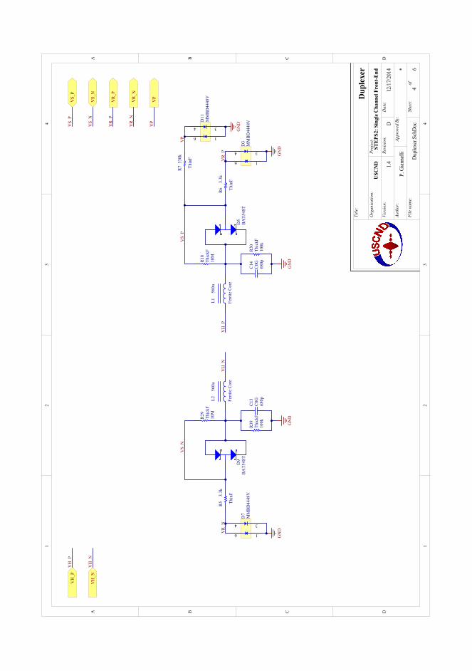
11
22
33
44
DD
CC
BB
AA
STEP
S2: S
ingl
e Cha
nnel
Fron
t-End
12/1
7/20
14
Dup
lexe
r.Sch
Doc
P. G
iann
elli
*
USC
ND
Dup
lexe
rTi
tle:
Org
aniz
atio
n:Pr
ojec
t:
File
nam
e:
Dat
e:
Auth
or:
Appr
oved
By:
Vers
ion:
Revi
sion
:D
1.4
Shee
t:of
46
D5
BAT5
4ST
VH
_P
VH
_N
VH
_P
VH
_N
VS_
P
VS_
N
VS_
P
VS_
N
560u
L1 Ferri
te C
ore
10M
R18
Thic
kF 100k
R30
Thic
kF
GN
D
VS_
PV
S_N
D9
BAT5
4ST
560u
L2 Ferri
te C
ore
10M
R29
Thic
kF
100k
R39
Thic
kF
GN
D
VH
_PV
H_N
VR_
P
VR_
N
VP
VR_
P
VR_
N
VP
330k
R7 Thin
F
VP
VR_
PV
R_N
1
34
6
D7
MM
BD44
48V
1
34
6
D3
MM
BD44
48V
1
34
6
D11
MM
BD44
48V
GN
DG
ND
GN
D
3.3k
R5 Thin
F
3.3k
R6 Thin
F
680p
C13
C0G
680p
C14
C0G
PIC1301PIC1302CO
C13
PIC1401PIC1402CO
C14
PID301PID303PID304
PID306COD3
PID501 PID502PID503
COD5
PID701PID703PID704
PID706COD7
PID901 PID902
PID903
COD9
PID1101PID1103PID1104
PID1106CO
D11
PIL101
PIL102
COL1
PIL201
PIL202COL
2
PIR501
PIR502COR5
PIR601
PIR602COR6
PIR701
PIR702
COR7
PIR1801PIR1802 COR18
PIR2901PIR2902 COR2
9
PIR3001PIR3002 COR3
0
PIR3901PIR3902 COR3
9
PIC1301PIC1401
PID301PID303
PID701PID703
PID1101PID1103
PIR3001PIR3901
PIC1302
PID901 PID902
PIL202
PIR2901
PIR3902PIC1402
PID501 PID502
PIL102
PIR1801
PIR3002
PIL201
NLVH0N
POVH0N
PIL101
NLVH
0PPOVH0P
PID1104PID1106
PIR702
NLVP
POVP
PID704PID706
PIR502
NLVR
0NPOVR0N
PID304PID306
PIR601
NLVR
0PPOVR0P
PID903
PIR501
PIR2902
NLVS
0NPOVS0N
PID503
PIR602
PIR701
PIR1802
NLVS0P
POVS0P
POVH0N
POVH0P
POVP
POVR0N
POVR0P
POVS0N
POVS0P
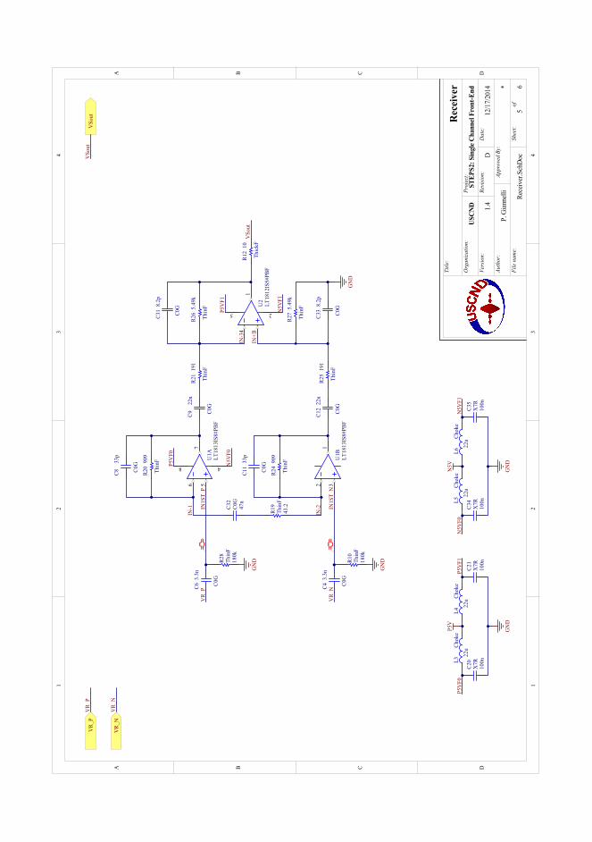
11
22
33
44
DD
CC
BB
AA
STEP
S2: S
ingl
e Cha
nnel
Fron
t-End
12/1
7/20
14
Rece
iver
.Sch
Doc
P. G
iann
elli
*
USC
ND
Rec
eive
rTi
tle:
Org
aniz
atio
n:Pr
ojec
t:
File
nam
e:
Dat
e:
Auth
or:
Appr
oved
By:
Vers
ion:
Revi
sion
:D
1.4
Shee
t:of
56
43.2
R19
Thin
F
180k
R28
Thin
F
180k
R10
Thin
F
5.49
kR2
6
Thin
F 5.49
kR2
7
Thin
F
191
R25
Thin
F191
R21
Thin
F
909
R20
Thin
F 909
R24
Thin
F33p
C8 C0G 33
pC1
1 C0G
3.3n
C4 C0G
8.2p
C31 C0
G 8.2p
C33 C0
G
47n
C32
C0G
3.3n
C6 C0G
GN
D
GN
D
GN
D
VSo
ut
100n
C20
X7R
100n
C34
X7R
P5V
GN
D
N5V
GN
D
VR_
P
VR_
N
VR_
P
VR_
N
VR_
P
VR_
N
VSo
ut
VSo
ut
22n
C9 C0G 22
nC1
2 C0G
76 5
48
U1A
LT18
13IS
8#PB
F
321
U1B
LT18
13IS
8#PB
F
1
2
34
5
U2
LT18
12IS
5#PB
F
100n
C21
X7R
100n
C35
X7R
N5V
F0N
5VF1
P5V
F0P5
VF1
22u
L4Ch
oke
22u
L3Ch
oke
22u
L5Ch
oke
22u
L6Ch
oke
P5V
F0
P5V
F1N
5VF0
N5V
F1
10R1
2
Thic
kF
IN-1
IN-2
IN-3
IN1S
T_P
IN1S
T_N
IN+3
PIC401
PIC402
COC4
PIC601
PIC602
COC6
PIC801
PIC802
COC8
PIC901
PIC902
COC9
PIC1
101
PIC1
102
COC1
1
PIC1
201
PIC1
202
COC1
2
PIC2001PIC2002COC20
PIC2101PIC2102CO
C21
PIC3101
PIC3
102
COC3
1
PIC3201PIC3202CO
C32
PIC3301
PIC3
302
COC3
3
PIC3401PIC3402CO
C34
PIC3501PIC3502CO
C35
PIL301
PIL302
COL3
PIL401
PIL402
COL4
PIL501
PIL502
COL5
PIL601
PIL602
COL6
PIR1001PIR1002 COR1
0
PIR1
201
PIR1
202
COR1
2
PIR1901 PIR1902COR1
9
PIR2
001
PIR2
002COR2
0
PIR2
101
PIR2
102COR21
PIR2
401
PIR2
402COR24
PIR2
501
PIR2
502COR25
PIR2
601
PIR2
602COR26
PIR2
701
PIR2
702COR27
PIR2801PIR2802 COR2
8PIU104
PIU105
PIU106
PIU107
PIU108 COU1A
PIU101
PIU102
PIU103
COU1B
PIU201
PIU202PIU203
PIU204
PIU205 COU2
PIC2001PIC2101
PIC3
302
PIC3401PIC3501
PIR1001
PIR2
701
PIR2801
PIC402
PIR1002PIU103
NLIN
1ST0
N
PIC602
PIR2802PIU105
NLIN
1ST0
P
PIC3301
PIR2
501
PIR2
702
PIU203
NLIN
03
PIC801
PIC3202
PIR2
002
PIU106
NLIN01
PIC1
101
PIR1902PI
R240
2
PIU102
NLIN02
PIC3101
PIR2
101
PIR2
602
PIU204
NLIN03
PIL502
PIL601
PIC3402PIL501
PIU104 NLN5
VF0
PIC3502PIL602
PIU202 NLN5VF1
PIC802
PIC901
PIR2
001 PIU107
PIC902
PIR2
102
PIC1
102
PIC1
201
PIR2
401 PIU101
PIC1
202
PIR2
502
PIC3
102
PIR1
201
PIR2
601 PIU201
PIC3201 PIR1901
PIL302
PIL401
PIC2002PIL301
PIU108NLP5VF0
PIC2102PIL402
PIU205NLP5VF1
PIC401
NLVR
0NPOVR0N
PIC601
NLVR
0PPOVR0P
PIR1
202
NLVS
out
POVS
out
POVR0N
POVR0P
POVS
OUT
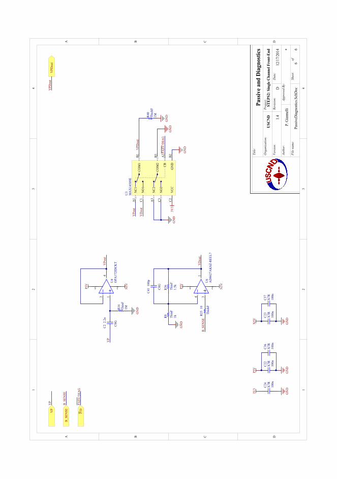
11
22
33
44
DD
CC
BB
AA
STEP
S2: S
ingl
e Cha
nnel
Fron
t-End
12/1
7/20
14
Pass
iveD
iagn
ostic
s.Sch
Doc
P. G
iann
elli
*
USC
ND
Pass
ive a
nd D
iagn
ostic
sTi
tle:
Org
aniz
atio
n:Pr
ojec
t:
File
nam
e:
Dat
e:
Auth
or:
Appr
oved
By:
Vers
ion:
Revi
sion
:D
1.4
Shee
t:of
66
P5V
GN
D
N5V
GN
D
3V3
GN
D
1MR16
Thin
F
2.2n
C2 C0G
GN
D
VD
out
P5V
N5V
VPo
ut
B_SE
NSE
B_SE
NSE
VP
VP
B_SE
NSE
VP
VPD
out
P/D
VPD
out
PASV
/DIA
G
100n
C22
X7R
100n
C23
X7R
100n
C24
X7R
NO
1C1
GN
DB2
NC1
A1
COM
1B1
VCC
C2
CBA
2
NC2
A3
NO
2C3
COM
2B3
U3
MA
X14
589E
GN
D
3V3
PASV
/DIA
G
VPD
out
VPo
ut
VD
out
1MR40
Thic
kF
GN
D
GN
DG
ND
100n
C36
X7R
100n
C37
X7R
P5V
N5V
1
2
34
5
U6
AD
8627
AK
SZ-R
EEL7
1
2
34
5
U4
OPA
172I
DCK
T
1.5k
R36
Thin
F1kR8 Th
inF
GN
D
100p
C41 C0
G
10R2
3
Thic
kF
PIC201
PIC202
COC2
PIC2201PIC2202COC
22
PIC2301PIC2302COC
23
PIC2401PIC2402COC
24
PIC3601PIC3602COC
36
PIC3701PIC3702COC
37
PIC4
101
PIC4
102
COC41
PIR801
PIR802CO
R8
PIR1601PIR1602 COR1
6
PIR2
301
PIR2
302
COR23
PIR3
601
PIR3
602COR3
6
PIR4001PIR4002 COR40
PIU30A1
PIU30A2
PIU30A3
PIU30B1
PIU3
0B2
PIU3
0B3
PIU30C1
PIU30C2
PIU30C3CO
U3
PIU401
PIU402
PIU403
PIU404
PIU405 COU4 PIU601
PIU602PIU603
PIU604
PIU605 COU6
PIC2402
PIU30C2
PIR2
301
NLB0SENSE
POB0
SENS
E
PIC2201PIC2301
PIC2401PIC3601
PIC3701
PIR802
PIR1601
PIR4001PIU30A3
PIU3
0B2
PIU3
0B3
PIU30C3
PIC2302PIC3702
PIU402 PIU602
PIC202
PIR1602PIU401
PIC4
101
PIR801
PIR3
602
PIU604
PIR2
302
PIU603
PIC2202PIC3602
PIU405 PIU605
PIU30A2
NLP\
A\S\
V\0D
IAG
POP\0D
PIC4
102
PIR3
601
PIU30C1
PIU601
NLVDout
PIC201
NLVP
POVP
PIR4002PIU30B1
NLVPDout
POVPDout
PIU30A1
PIU403
PIU404
NLVPout
POB0
SENS
E
POP\0D
POVP
POVPDOUT

BPA N D O R A E L E C T R I C A L S C H E M AT I C S


T R A N S D U C E R D R I V E R M O D U L E

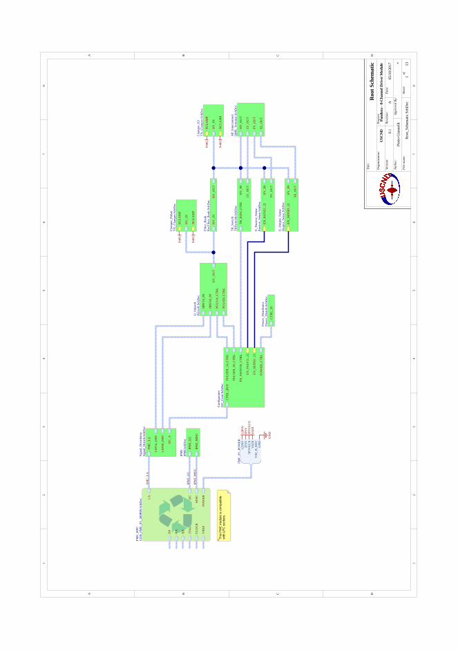
11
22
33
44
55
66
77
88
DD
CC
BB
AA
Pand
ora
- 8-C
hann
el D
rive
r M
odul
e
05/1
0/20
17
Roo
t_Sc
hem
atic
.Sch
Doc
Piet
ro G
iann
elli
*
USC
ND
Roo
t Sch
emat
icTi
tle:
Org
aniz
atio
n:Pr
ojec
t:
File
nam
e:
Dat
e:
Auth
or:
Appr
oved
By:
Vers
ion:
Revi
sion
:A
0.1
Shee
t:of
113
HV
_OU
TH
V_I
N
Filte
r_B
ank
Rec
Filte
r_B
ank.
SchD
oc
TR_B
IAS_
CTR
LH
V_I
N
LV_O
UT
TR_S
witc
hTR
Switc
h8.S
chD
oc
PULS
ER_1
4_C
TRL
PULS
ER_5
8_C
TRL
TR_S
WIT
CH
_CTR
L
POW
ER_C
TRL
CTR
L_B
US
EN_P
ASV
[1..2
]
EN_S
ENS[
1..2
]
Con
figur
ator
I2C
_Con
f.Sch
Doc
DP
LA
HA
HB
MIS
C
POW
ER
JTA
GI2
C
CLO
CK
VR
EF
FMC
_HPC
CO
N_F
MC
_P1_
400P
IN.S
chD
oc
IPM
I_I2
C
IPM
I_M
ISC
IPM
IIP
MI.S
chD
oc
USP
14_D
RV
USP
58_D
RV
FMC
_LA
I2C
_A
Sign
al_D
istri
buto
rSi
gnal
_Dis
trib.
SchD
oc
HV
_IN
PCLA
MP
NC
LAM
P
Cla
mpe
r_IO
TX_C
lam
per.S
chD
oc
LV_O
UT
SE_O
UT
PV_O
UT
HV
_OU
T
AP_
Inte
rcon
nect
QM
S_Te
rmin
al.S
chD
oc
CTR
L_IN
Pow
er_D
istri
buto
rPo
wer
_Dis
trib.
SchD
oc
HV
_IN
SE_O
UT
EN_S
ENS[
1..2
]
U_O
utpu
t_Se
nse
Out
put_
Sens
e.Sc
hDoc
HV
_IN
EN_P
ASV
[1..2
]
PV_O
UT
U_P
assi
ve_S
ense
Pass
ive_
Sens
e.Sc
hDoc
HV
_IN
PCLA
MP
NC
LAM
P
Cla
mpe
r_Pu
lser
TX_C
lam
per.S
chD
oc
DRV
14_I
N
DRV
58_I
N
PULS
14_C
TRL
PULS
58_C
TRL
HV
_OU
T
U_P
ulse
r8Pu
lser
8.Sc
hDoc
FMC
_LA
IPM
I_I2
C
IPM
I_M
ISC
12P0
V3P
3V3P
3VA
UX
GN
D
VAD
JV
IO_B
_M2C
FMC
_P1_
POW
ER12
P0V
3P3V
3P3V
AU
X
GN
DVAD
J
N48
U
P48U
N48
U
P48U
This
FM
C m
odul
e is
com
patib
le
with
LP
C s
ocke
ts.
NLFM
C0LA
NL
FMC0
LA
NLFM
C0LA
NL
FMC0
LA
NLFM
C0LA
NL
FMC0
LA
NLFM
C0LA
NL
FMC0
LA
NLFM
C0LA
NL
FMC0
LA
NLFM
C0LA
NL
FMC0
LA
NLFM
C0LA
NL
FMC0
LA
NLFM
C0LA
NL
FMC0
LA
NLFM
C0LA
NL
FMC0
LA
NLFM
C0LA
NL
FMC0
LA
NLFM
C0LA
NL
FMC0
LA
NLFM
C0LA
NL
FMC0
LA
NLFM
C0LA
NL
FMC0
LA
NLFM
C0LA
NL
FMC0
LA
NLFM
C0LA
NL
FMC0
LA
NLFM
C0LA
NL
FMC0
LA
NLFM
C0LA
NL
FMC0
LA
NLFM
C0LA
NL
FMC0
LA
NLFM
C0LA
NL
FMC0
LA
NLFM
C0LA
NL
FMC0
LA
NLFM
C0LA
NL
FMC0
LA
NLFM
C0LA
NL
FMC0
LA
NLFM
C0LA
NL
FMC0
LA
NLFM
C0LA
NL
FMC0
LA
NLFM
C0LA
NL
FMC0
LA
NLFM
C0LA
NL
FMC0
LA
NLFM
C0LA
NL
FMC0
LA
NLFM
C0LA
NL
FMC0
LA
NLFM
C0LA
NL
FMC0
LA
NLFM
C0LA
NL
FMC0
LA
NLFM
C0LA
NL
FMC0
LA
NLFM
C0LA
NL
FMC0
LA
NLFM
C0LA
NL
FMC0
LA
NLFM
C0LA
NL
FMC0
LA
NLIPMI
0I2C
NL
IPMI
0I2C
NLIP
MI0M
ISC
NLIP
MI0M
ISC
NLIP
MI0M
ISC
NLIP
MI0M
ISC
NLIP
MI0M
ISC
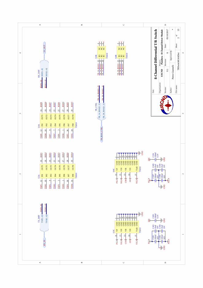
11
22
33
44
DD
CC
BB
AA
Pand
ora
- 8-C
hann
el D
river
Mod
ule
05/1
0/20
17
TRSw
itch8
.Sch
Doc
Piet
ro G
ianne
lli*
USCN
D
8-C
hann
el D
iffer
entia
l T/R
Sw
itch
Title
:
Org
aniz
atio
n:Pr
ojec
t:
File
nam
e:
Dat
e:
Auth
or:
Appr
oved
By:
Vers
ion:
Revi
sion
:A
0.1
Shee
t:of
213
IN6
1
IN5
3
IN4
7
IN3
9
IN2
10
IN1
12O
UT1
16
OU
T218
OU
T319
OU
T421
OU
T525
OU
T627
OU
T728
OU
T830
IN8
34
IN7
36
U3A
TX81
0
B322
B223
B124
NC
4
NC
5
NC
6
U4B
TX81
0
GN
D2
GN
D8
GN
D11
VB
13G
ND
14V
N15
GN
D17
GN
D20
GN
D26
GN
D29
VP
31
GN
D32
VD
33
GN
D35
Vsu
b37
U3C
TX81
0
IN6
1
IN5
3
IN4
7
IN3
9
IN2
10
IN1
12O
UT1
16
OU
T218
OU
T319
OU
T421
OU
T525
OU
T627
OU
T728
OU
T830
IN8
34
IN7
36
U4A
TX81
0
B322
B223
B124
NC
4
NC
5
NC
6
U3B
TX81
0
GN
D2
GN
D8
GN
D11
VB
13G
ND
14V
N15
GN
D17
GN
D20
GN
D26
GN
D29
VP
31
GN
D32
VD
33
GN
D35
Vsu
b37
U4C
TX81
0
P5LN
N5L
N
2D5
N5L
N
GN
DG
ND
GN
D
P5LN
N5L
N
2D5
N5L
N
GN
D
16V
C181
100n
F10
V
C183
10uF
16V
C182
100n
F10
V
C184
10uF
GN
DG
ND
P5LN
N5L
N
2D5
16V
C187
100n
F10
V
C189
10uF
16V
C188
100n
F10
V
C190
10uF
GN
DG
ND
P5LN
N5L
N
2D5
TXP1
TXP2
TXP3
TXP4
TXP5
TXP6
TXP7
TXP8
TXN
1
TXN
2
TXN
3
TXN
4TX
N5
TXN
6
TXN
7
TXN
8
RXP1
RXP2
RXP3
RXP4
RXP5
RXP6
RXP7
RXP8
RXN
1
RXN
2
RXN
3
RXN
4RX
N5
RXN
6
RXN
7
RXN
8
TR_1
4_BI
AS[
1..3
]
TR_1
4_BI
AS1
TR_1
4_BI
AS2
TR_1
4_BI
AS3
TR_5
8_BI
AS1
TR_5
8_BI
AS2
TR_5
8_BI
AS3
TR_5
8_BI
AS[
1..3
]
TR_1
4_BI
AS[
1..3
]
TR_5
8_BI
AS[
1..3
]
TR_C
TRL
TR_B
IAS_
CTRL
TXP[
1..8
]
TXN
[1..8
]
TX_D
IFF
TXP[
1..8
]
TXN
[1..8
]H
V_I
NRX
P[1.
.8]
RXN
[1..8
]
RX_D
IFF
6.3V
C185
100n
F6.
3V
C191
100n
F
LV_O
UT
RXP[
1..8
]
RXN
[1..8
]
PIC18101 PIC18102
COC1
81
PIC18201 PIC18202
COC1
82
PIC18301 PIC18302
COC1
83
PIC18401 PIC18402
COC1
84
PIC18501 PIC18502
COC1
85
PIC18701 PIC18702
COC1
87
PIC18801 PIC18802
COC1
88
PIC18901 PIC18902
COC1
89
PIC19001 PIC19002
COC1
90
PIC19101 PIC19102
COC1
91
PIU301
PIU303
PIU307
PIU309
PIU3010
PIU3012
PIU3016
PIU3018
PIU3019
PIU3021
PIU3
025
PIU3027
PIU3028
PIU3030
PIU3034
PIU3036 COU3
A
PIU304
PIU305
PIU306
PIU3022
PIU3023
PIU3
024
COU3
B
PIU302
PIU308
PIU3011
PIU3
013
PIU3014
PIU3015
PIU3
017
PIU3
020
PIU3026
PIU3029
PIU3
031
PIU3032
PIU3033
PIU3
035
PIU3
037
COU3
C
PIU401
PIU403
PIU407
PIU409
PIU4010
PIU4012
PIU4016
PIU4018
PIU4019
PIU4021
PIU4
025
PIU4027
PIU4028
PIU4030
PIU4034
PIU4036 COU4
A
PIU404
PIU405
PIU406
PIU4022
PIU4023
PIU4024
COU4
B
PIU402
PIU408
PIU4011
PIU4
013
PIU4014
PIU4015
PIU401
7
PIU402
0
PIU4026
PIU4029
PIU4
031
PIU4032
PIU4033
PIU403
5 PIU4
037
COU4
C
PIC18501 PIC19101
PIU3033
PIU4033
PIC18102 PIC18201 PIC18302 PIC18401
PIC18502 PIC18702 PIC18801
PIC18902 PIC19001 PIC19102
PIU302
PIU308
PIU3011
PIU3
013
PIU3014
PIU3
017
PIU3
020
PIU3026
PIU3029
PIU3032
PIU3
035
PIU402
PIU408
PIU4011
PIU4
013
PIU4014
PIU401
7
PIU402
0
PIU4026
PIU4029
PIU4032
PIU403
5
PIC18202 PIC18402
PIC18802 PIC19002
PIU3015
PIU3
037
PIU4015
PIU4
037
PIU304
PIU305
PIU306
PIU404
PIU405
PIU406
PIC18101 PIC18301
PIC18701 PIC18901
PIU3
031
PIU4
031
PIU4018
NLRX
N010
080
NLRXN8
POLV0OUT
PIU4021
NLRX
N010
080
NLRXN7
POLV0OUT
PIU4027
NLRX
N010
080
NLRXN6
POLV0OUT
PIU4030
NLRX
N010
080
NLRXN5
POLV0OUT
PIU3030
NLRX
N010
080
NLRX
N4
POLV0OUT
PIU3027
NLRX
N010
080
NLRX
N3
POLV0OUT
PIU3021
NLRX
N010
080
NLRX
N2
POLV0OUT
PIU3018
NLRX
N010
080
NLRX
N1
POLV0OUT
PIU4016
NLRXP010080
NLRX
P8
POLV0OUT
PIU4019
NLRXP010080
NLRX
P7
POLV0OUT
PIU4
025
NLRXP010080
NLRX
P6
POLV0OUT
PIU4028
NLRXP010080
NLRX
P5
POLV0OUT
PIU3028
NLRXP010080
NLRX
P4
POLV0OUT
PIU3
025
NLRXP010080
NLRX
P3
POLV0OUT
PIU3019
NLRXP010080
NLRX
P2
POLV0OUT
PIU3016
NLRXP010080
NLRXP1
POLV0OUT
PIU3
024
NLTR
0140
BIAS
0100
30
NLTR0140BIAS1
POTR0BIAS0CTRL
PIU3023
NLTR
0140
BIAS
0100
30
NLTR0140BIAS2
POTR0BIAS0CTRL
PIU3022
NLTR
0140
BIAS
0100
30
NLTR0140BIAS3
POTR0BIAS0CTRL
PIU4024
NLTR
0580
BIAS
0100
30
NLTR0580BIAS1
POTR0BIAS0CTRL
PIU4023
NLTR
0580
BIAS
0100
30
NLTR0580BIAS2
POTR0BIAS0CTRL
PIU4022
NLTR
0580
BIAS
0100
30
NLTR0580BIAS3
POTR0BIAS0CTRL
PIU4010
NLTX
N010
080
NLTX
N8
POHV0IN
PIU407
NLTX
N010
080
NLTX
N7
POHV0IN
PIU401
NLTX
N010
080
NLTX
N6
POHV0IN
PIU4034
NLTX
N010
080
NLTX
N5
POHV0IN
PIU3034
NLTX
N010
080
NLTX
N4
POHV0IN
PIU301
NLTX
N010
080
NLTX
N3
POHV0IN
PIU307
NLTX
N010
080
NLTX
N2
POHV0IN
PIU3010
NLTX
N010
080
NLTX
N1
POHV0IN
PIU4012
NLTXP010080
NLTXP8
POHV0IN
PIU409
NLTXP010080
NLTXP7
POHV0IN
PIU403
NLTXP010080
NLTXP6
POHV0IN
PIU4036
NLTXP010080
NLTXP5
POHV0IN
PIU3036
NLTXP010080
NLTX
P4
POHV0IN
PIU303
NLTXP010080
NLTXP3
POHV0IN
PIU309
NLTXP010080
NLTX
P2
POHV0IN
PIU3012
NLTXP010080
NLTXP1
POHV0IN
POHV0IN
POHV0IN0TXN1
POHV0IN0TXN2
POHV0IN0TXN3
POHV0IN0TXN4
POHV0IN0TXN5
POHV0IN0TXN6
POHV0IN0TXN7
POHV0IN0TXN8
POHV0IN0TXN010080
POHV0IN0TXP1
POHV0IN0TXP2
POHV0IN0TXP3
POHV0IN0TXP4
POHV0IN0TXP5
POHV0IN0TXP6
POHV0IN0TXP7
POHV0IN0TXP8
POHV0IN0TXP010080
POLV0OUT
POLV
0OUT
0RXN
1 PO
LV0O
UT0R
XN2
POLV
0OUT
0RXN
3 PO
LV0O
UT0R
XN4
POLV
0OUT
0RXN
5 PO
LV0O
UT0R
XN6
POLV
0OUT
0RXN
7 PO
LV0O
UT0R
XN8
POLV0OUT0RXN010080
POLV
0OUT
0RXP
1 PO
LV0O
UT0R
XP2
POLV
0OUT
0RXP
3 PO
LV0O
UT0R
XP4
POLV
0OUT
0RXP
5 PO
LV0O
UT0R
XP6
POLV
0OUT
0RXP
7 PO
LV0O
UT0R
XP8
POLV0OUT0RXP010080
POTR0BIAS0CTRL
POTR
0BIA
S0CT
RL0T
R014
0BIA
S1
POTR
0BIA
S0CT
RL0T
R014
0BIA
S2
POTR
0BIA
S0CT
RL0T
R014
0BIA
S3
POTR0B
IAS0CT
RL0TR0
140BIA
S01003
0 PO
TR0B
IAS0
CTRL
0TR0
580B
IAS1
PO
TR0B
IAS0
CTRL
0TR0
580B
IAS2
PO
TR0B
IAS0
CTRL
0TR0
580B
IAS3
POT
R0BIAS
0CTRL0
TR0580
BIAS01
0030
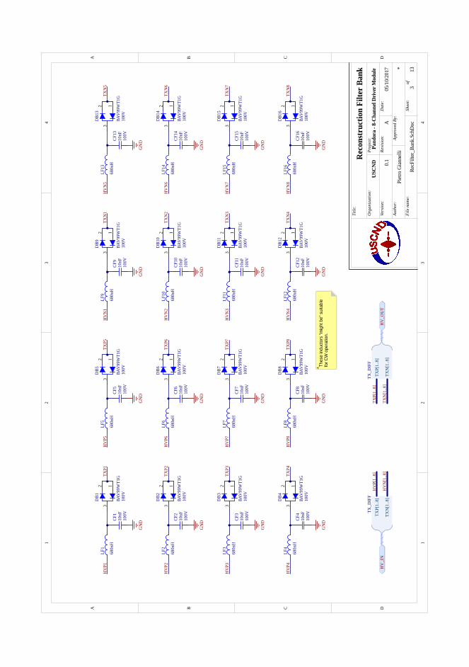
11
22
33
44
DD
CC
BB
AA
Pand
ora
- 8-C
hann
el D
river
Mod
ule
05/1
0/20
17
RecF
ilter
_Ban
k.Sc
hDoc
Piet
ro G
ianne
lli*
USCN
D
Rec
onst
ruct
ion
Filte
r Ban
kTi
tle:
Org
aniz
atio
n:Pr
ojec
t:
File
nam
e:
Dat
e:
Auth
or:
Appr
oved
By:
Vers
ion:
Revi
sion
:A
0.1
Shee
t:of
313
680n
H
LF1
HV
_OU
TTX
P[1.
.8]
TXN
[1..8
]
TX_D
IFF
100V
CF1
10nF
GN
D
HV
P[1.
.8]
HV
N[1
..8]
TXP[
1..8
]
TXN
[1..8
]
680n
H
LF2
100V
CF2
10nF
GN
D
680n
H
LF3
100V
CF3
10nF
GN
D
680n
H
LF4
100V
CF4
10nF
GN
D
680n
H
LF5
100V
CF5
10nF
GN
D
680n
H
LF6
100V
CF6
10nF
GN
D
680n
H
LF7
100V
CF7
10nF
GN
D
680n
H
LF8
100V
CF8
10nF
GN
D
680n
H
LF9
100V
CF9
10nF
GN
D
680n
H
LF10
100V
CF10
10nF
GN
D
680n
H
LF11
100V
CF11
10nF
GN
D
680n
H
LF12
100V
CF12
10nF
GN
D
680n
H
LF13
100V
CF13
10nF
GN
D
680n
H
LF14
100V
CF14
10nF
GN
D
680n
H
LF15
100V
CF15
10nF
GN
D
680n
H
LF16
100V
CF16
10nF
GN
D
HV
P1
HV
P2
HV
P3
HV
P4
HV
P5
HV
P6
HV
P7
HV
P8
HV
N1
HV
N2
HV
N3
HV
N4
HV
N5
HV
N6
HV
N7
HV
N8
TXP1
TXP2
TXP3
TXP4
TXP5
TXP6
TXP7
TXP8
TXN
1
TXN
2
TXN
3
TXN
4
TXN
5
TXN
6
TXN
7
TXN
8
HV
_IN
100V
123
DB1
BAV
99W
T1G
100V
123
DB2
BAV
99W
T1G
100V
123
DB3
BAV
99W
T1G
100V
123
DB4
BAV
99W
T1G
100V
123
DB5
BAV
99W
T1G
100V
123
DB6
BAV
99W
T1G
100V
123
DB7
BAV
99W
T1G
100V
123
DB8
BAV
99W
T1G
100V
123
DB9
BAV
99W
T1G
100V
123
DB1
0
BAV
99W
T1G
100V
123
DB1
1
BAV
99W
T1G
100V
123
DB1
2
BAV
99W
T1G
100V
123
DB1
3
BAV
99W
T1G
100V
123
DB1
4
BAV
99W
T1G
100V
123
DB1
5
BAV
99W
T1G
100V
123
DB1
6
BAV
99W
T1G
TXP[
1..8
]
TXN
[1..8
]
TX_D
IFF
Thes
e in
duct
ors
"mig
ht b
e" s
uita
ble
for C
W o
pera
tion.
PICF101 PICF102
COCF
1
PICF201 PICF202
COCF
2
PICF301 PICF302
COCF
3
PICF401 PICF402
COCF
4
PICF501 PICF502
COCF
5
PICF601 PICF602
COCF
6
PICF701 PICF702
COCF
7
PICF801 PICF802
COCF
8
PICF901 PICF902
COCF
9
PICF1001 PICF1002
COCF
10
PICF1101 PICF1102
COCF
11
PICF1201 PICF1202
COCF
12
PICF1301 PICF1302
COCF
13
PICF1401 PICF1402
COCF
14
PICF1501 PICF1502
COCF
15
PICF1601 PICF1602
COCF
16
PIDB
101
PIDB102
PIDB103 CODB1
PIDB201
PIDB
202
PIDB203 CODB2
PIDB301
PIDB302
PIDB303 CODB3 PI
DB40
1
PIDB402
PIDB
403 CO
DB4
PIDB50
1
PIDB502
PIDB503 CODB5
PIDB601
PIDB60
2
PIDB603 CODB6
PIDB701
PIDB702
PIDB703 CODB7 PI
DB80
1
PIDB802
PIDB803 CO
DB8
PIDB
901
PIDB902
PIDB903 CODB9
PIDB1001
PIDB
1002
PIDB1003 CODB
10 PIDB1101
PIDB1102
PIDB1103 CODB11 PIDB
1201
PIDB1202
PIDB
1203
CODB
12
PIDB
1301
PIDB1302
PIDB1303 CODB
13 PIDB1401
PIDB
1402
PIDB1403 CODB
14 PIDB1501
PIDB1502
PIDB1503 CODB
15 PIDB
1601
PIDB1602
PIDB
1603
CODB
16
PILF
101
PILF
102
COLF1
PILF
201
PILF
202
COLF2
PILF
301
PILF
302
COLF3
PILF
401
PILF
402
COLF4
PILF
501
PILF
502
COLF5
PILF
601
PILF
602
COLF
6
PILF
701
PILF
702
COLF7
PILF
801
PILF
802
COLF8
PILF
901
PILF
902
COLF9
PILF
1001
PI
LF10
02
COLF
10
PILF
1101
PI
LF11
02
COLF
11
PILF12
01 PIL
F1202
COLF
12
PILF
1301
PI
LF13
02
COLF
13
PILF
1401
PI
LF14
02
COLF
14
PILF
1501
PI
LF15
02
COLF
15
PILF16
01 PIL
F1602
COLF
16
PICF102 PICF202 PICF302 PICF402
PICF502 PICF602 PICF702 PICF802
PICF902 PICF1002 PICF1102 PICF1202
PICF1302 PICF1402 PICF1502 PICF1602
PICF101 PIDB103
PILF
102
PICF201 PIDB203
PILF
202
PICF301 PIDB303
PILF
302
PICF401 PI
DB40
3 PI
LF40
2
PICF501 PIDB503
PILF
502
PICF601 PIDB603
PILF
602
PICF701 PIDB703
PILF
702
PICF801 PIDB803
PILF
802
PICF901 PIDB903
PILF
902
PICF1001 PIDB1003
PILF
1002
PICF1101 PIDB1103
PILF
1102
PICF1201 PI
DB12
03
PILF12
02
PICF1301 PIDB1303
PILF
1302
PICF1401 PIDB1403
PILF
1402
PICF1501 PIDB1503
PILF
1502
PICF1601 PI
DB16
03
PILF16
02 PIL
F1601
NLHV
N010
080
NLHVN8
POHV0IN
PILF
1501
NLHV
N010
080
NLHVN7
POHV0IN
PILF
1401
NLHV
N010
080
NLHVN6
POHV0IN
PILF
1301
NLHV
N010
080
NLHVN5
POHV0IN
PILF12
01
NLHV
N010
080
NLHV
N4
POHV0IN
PILF
1101
NLHV
N010
080
NLHV
N3
POHV0IN
PILF
1001
NLHV
N010
080
NLHV
N2
POHV0IN
PILF
901
NLHV
N010
080
NLHV
N1
POHV0IN
PILF
801
NLHV
P010
080
NLHV
P8
POHV0IN
PILF
701
NLHV
P010
080
NLHV
P7
POHV0IN
PILF
601
NLHV
P010
080
NLHV
P6
POHV0IN
PILF
501
NLHV
P010
080
NLHV
P5
POHV0IN
PILF
401
NLHV
P010
080
NLHV
P4
POHV0IN
PILF
301
NLHV
P010
080
NLHV
P3
POHV0IN
PILF
201
NLHV
P010
080
NLHV
P2
POHV0IN
PILF
101
NLHV
P010
080
NLHVP1
POHV0IN
PIDB
1601
PIDB1602
NLTX
N010
080
NLTX
N8
POHV0OUT
PIDB1501
PIDB1502
NLTX
N010
080
NLTX
N7
POHV0OUT
PIDB1401
PIDB
1402
NLTX
N010
080
NLTXN6
POHV0OUT
PIDB
1301
PIDB1302
NLTX
N010
080
NLTX
N5
POHV0OUT
PIDB
1201
PIDB1202
NLTX
N010
080
NLTXN4
POHV0OUT
PIDB1101
PIDB1102
NLTX
N010
080
NLTX
N3
POHV0OUT
PIDB1001
PIDB
1002
NLTX
N010
080
NLTX
N2
POHV0OUT
PIDB
901
PIDB902
NLTX
N010
080
NLTX
N1
POHV0OUT
PIDB80
1
PIDB802
NLTXP010080
NLTXP8
POHV0OUT
PIDB701
PIDB702
NLTXP010080
NLTXP7
POHV0OUT
PIDB601
PIDB60
2
NLTXP010080
NLTXP6
POHV0OUT
PIDB50
1
PIDB502
NLTXP010080
NLTXP5
POHV0OUT
PIDB
401
PIDB402
NLTXP010080
NLTXP4
POHV0OUT
PIDB301
PIDB302
NLTXP010080
NLTXP3
POHV0OUT
PIDB201
PIDB
202
NLTXP010080
NLTXP2
POHV0OUT
PIDB
101
PIDB102
NLTXP010080
NLTXP1
POHV0OUT
POHV0IN
POHV
0IN0
TXN1
PO
HV0I
N0TX
N2
POHV
0IN0
TXN3
PO
HV0I
N0TX
N4
POHV
0IN0
TXN5
PO
HV0I
N0TX
N6
POHV
0IN0
TXN7
PO
HV0I
N0TX
N8
POHV
0IN0TXN010
080
POHV
0IN0
TXP1
PO
HV0I
N0TX
P2
POHV
0IN0
TXP3
PO
HV0I
N0TX
P4
POHV
0IN0
TXP5
PO
HV0I
N0TX
P6
POHV
0IN0
TXP7
PO
HV0I
N0TX
P8
POHV
0IN0TXP010
080
POHV0OUT
POHV
0OUT
0TXN
1 PO
HV0O
UT0T
XN2
POHV
0OUT
0TXN
3 PO
HV0O
UT0T
XN4
POHV
0OUT
0TXN
5 PO
HV0O
UT0T
XN6
POHV
0OUT
0TXN
7 PO
HV0O
UT0T
XN8
POHV0OUT0TXN010080
POHV
0OUT
0TXP
1 PO
HV0O
UT0T
XP2
POHV
0OUT
0TXP
3 PO
HV0O
UT0T
XP4
POHV
0OUT
0TXP
5 PO
HV0O
UT0T
XP6
POHV
0OUT
0TXP
7 PO
HV0O
UT0T
XP8
POHV0OUT0TXP010080
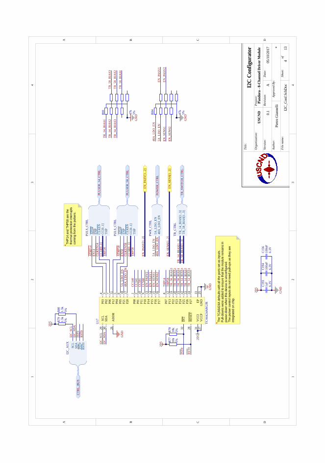
11
22
33
44
DD
CC
BB
AA
Pand
ora
- 8-C
hann
el D
river
Mod
ule
05/1
0/20
17
I2C_
Conf
.Sch
Doc
Piet
ro G
ianne
lli*
USCN
D
I2C
Con
figur
ator
Title
:
Org
aniz
atio
n:Pr
ojec
t:
File
nam
e:
Dat
e:
Auth
or:
Appr
oved
By:
Vers
ion:
Revi
sion
:A
0.1
Shee
t:of
413
TR_1
4_BI
AS[
1..3
]TR
_58_
BIA
S[1.
.3]
TR_C
TRL
P03
4
P02
3
P06
7
P12
11
P04
5
P05
6
P21
18
P20
17
P00
1
P01
2
P11
10
P10
9
P14
13
P15
14
P16
15
P17
16
P07
8
P13
12
P22
19
P23
20
P24
21
P25
22
P26
23
P27
24
GN
D25
AD
DR
26
VCC
P27
RESE
T28
SCL
29
SDA
30
VCC
I31
INT
32
EP33
U17
TCA
6424
ARG
JR
PULS
ER_1
4_CT
RL
PULS
ER_5
8_CT
RL
TR_S
WIT
CH_C
TRL
GN
D
2D5
CC14
[0..1
]
CC58
[0..1
]CC
140
CC14
1CC
581
CC58
0
GN
D
GN
D
TR_1
4_BI
AS[
1..3
]TR
_58_
BIA
S[1.
.3]
TR_5
8_BI
AS1
TR_5
8_BI
AS2
TR_5
8_BI
AS3
TR_1
4_BI
AS1
TR_1
4_BI
AS2
TR_1
4_BI
AS3
5%R81
47k
5%R79
1.5k
5%R80
1.5k
GN
D
2D5
2D5
5%R78
10k
5%R77
10k
6.3V
C193
1uF
6.3V
C194
100n
F
RST0
INT0
2D5I2C_
SCL
I2C_
SDA
I2C_
SCL
TR_5
8_BI
AS1
TR_5
8_BI
AS2
TR_5
8_BI
AS3
TR_1
4_BI
AS1
TR_1
4_BI
AS2
TR_1
4_BI
AS3
I2C_
SDA
48A
_LD
O_E
N5A
_LD
O_E
N
GN
D5%R84
47k
5A_L
DO
_EN
48A
_LD
O_E
N5A
_LD
O_E
N48
A_L
DO
_EN
PWR_
CTRL
POW
ER_C
TRL
SCL
SDA
INT0
RST0
I2C_
AU
X
CTRL
_BU
S
EN_P
ASV
1EN
_PA
SV2
EN_S
ENS1
EN_S
ENS2
EN_P
ASV
[1..2
]
EN_S
ENS[
1..2
]EN
_SEN
S[1.
.2]
EN_P
ASV
[1..2
]
EN_P
ASV
1
EN_P
ASV
2EN
_SEN
S1
EN_S
ENS2
ATH
P
CC[0
..1]
ENP
CLK
EN
THP
PULS
_CTR
L
ATH
P
CC[0
..1]
ENP
CLK
EN
THP
PULS
_CTR
L
CLK
EN58
CLK
EN14
EN14
ATH
P14
EN58
ATH
P58
6.3V
C156
100n
F
48A
_LD
O_E
N5A
_LD
O_E
N
THP1
4
THP5
8
THP5
8TH
P14
RST0
INT0
The
TCA6
424A
def
aults
with
all
the
ports
set
as
inpu
ts.
Pull-
dow
ns w
ere
adde
d to
ens
ure
that
the
mod
ule
rem
ains
in
pow
er-d
own
whe
n th
is d
evic
e is
unc
onfig
ured
.Th
e pu
lser
con
trol i
nput
s do
not
nee
d pu
ll-up
s as
they
are
in
tegr
ated
on
chip
.
THP1
4 an
d TH
P58
are
the
ther
mal
pro
tect
ion
inte
rrupt
s co
min
g fro
m th
e pu
lser
s.
PIC15601 PIC15602
COC1
56
PIC19301 PIC19302
COC1
93
PIC19401 PIC19402
COC1
94
PIR7701 PIR7702 COR77
PIR7801 PIR7802 CO
R78
PIR7901 PIR7902 COR
79
PIR8001 PIR8002 COR80
PIR8
101
PIR8
102
PIR8
103
PIR8
104
PIR8
105
PIR8
106
PIR8
107
PIR8
108
PIR8
109
PIR8
1010
COR81
PIR8
401
PIR8
402
PIR8
403
PIR8
404
PIR8
405
PIR8
406
PIR8
407
PIR8
408
PIR8
409
PIR8
4010
COR84
PIU1701
PIU1702
PIU1703
PIU1704
PIU1705
PIU1706
PIU1707
PIU1
708
PIU1709
PIU17010
PIU1
7011
PIU1
7012
PIU1
7013
PIU1
7014
PIU17015
PIU17016
PIU17017
PIU17018
PIU17019
PIU17020
PIU17021
PIU1
7022
PIU1
7023
PIU17024
PIU1
7025
PIU1
7026
PIU1
7027
PIU17028
PIU17029
PIU17030
PIU17031
PIU1
7032
PIU17033
COU17
PIC15601 PIC19301
PIC19401
PIR7702 PIR7802
PIR7902 PIR8002
PIU1
7027
PIU17031
PIR8
409
PIU17018
NL5A0LDO0EN
POPOWER0CTRL
PIR8
401
PIU17017
NL48A0LDO0EN
POPOWER0CTRL
PIU1704
NLA\T\
H\P\1\
4\
POPULSER0140CTRL
PIU1
7011
NLA\T\
H\P\5\
8\
POPULSER0580CTRL
PIU1707
NLC\L\
K\E\N\
1\4\
POPULSER0140CTRL
PIU1706
NLC\L\
K\E\N\
5\8\
POPULSER0580CTRL
PIU1703
NLE\N\
1\4\
POPULSER0140CTRL
PIU1705
NLE\N\
5\8\
POPULSER0580CTRL
PIC15602 PIC19302
PIC19402
PIR8
105
PIR8
1010
PIR8
405
PIR8
4010
PIU1
7025
PIU1
7026
PIU17033
PIR7901
PIU17029
NLI2
C0SC
L
POCTRL0BUS
PIR8001
PIU17030
NLI2C0SDA
POCTRL0BUS
PIR7801 PI
U170
32
NLI\N\
T\0
POCTRL0BUS
PIR8
108
PIR8
109
PIR8
407
PIR8
408
PIR7701
PIU17028
NLR\S\
T\0
POCTRL0BUS
PIU1
708
NLTHP14
POPULSER0140CTRL
PIU1
7012
NLTHP58
POPULSER0580CTRL
PIR8
404
PIU1
7014
NLEN
0PAS
V010
020
NLEN
0PAS
V1
POEN0PASV010020
PIR8
406
PIU1
7013
NLEN
0PAS
V010
020
NLEN
0PAS
V2
POEN0PASV010020
PIR8
403
PIU17015
NLEN
0SEN
S010
020
NLEN0SENS1
POEN0SENS010020
PIR8
402
PIU17016
NLEN
0SEN
S010
020
NLEN
0SEN
S2
POEN0SENS010020
PIR8
106
PIU17024
NLTR
0140
BIAS
0100
30
NLTR0140BIAS1
POTR0SWITCH0CTRL
PIR8
107
PIU1
7023
NLTR
0140
BIAS
0100
30
NLTR0140BIAS2
POTR0SWITCH0CTRL
PIR8
104
PIU1
7022
NLTR
0140
BIAS
0100
30
NLTR0140BIAS3
POTR0SWITCH0CTRL
PIR8
103
PIU17021
NLTR
0580
BIAS
0100
30
NLTR0580BIAS1
POTR0SWITCH0CTRL
PIR8
102
PIU17020
NLTR
0580
BIAS
0100
30
NLTR
0580
BIAS
2
POTR0SWITCH0CTRL
PIR8
101
PIU17019
NLTR
0580
BIAS
0100
30
NLTR0580BIAS3
POTR0SWITCH0CTRL
POCTRL0BUS
POCT
RL0B
US0I
\N\T
\0
POCT
RL0B
US0R
\S\T
\0
POCT
RL0B
US0S
CL
POCT
RL0B
US0S
DA
POEN0PASV1
POEN0PASV2
POEN0PASV010020
POEN0SENS1
POEN0SENS2
POEN0SENS010020
POPOWER0CTRL
POPOWER0CTRL05A0LDO0EN
POPO
WER0
CTRL
048A
0LDO
0EN
POPULSER0140CTRL
POPU
LSER
0140
CTRL
0A\T
\H\P
\ PO
PULS
ER01
40CT
RL0C
\L\K
\E\N
\ PO
PULS
ER01
40CT
RL0C
C0
POPU
LSER
0140
CTRL
0CC1
PO
PULS
ER01
40CT
RL0C
C000
010
POPU
LSER
0140
CTRL
0E\N
\P\
POPU
LSER
0140
CTRL
0THP
POPULSER0580CTRL
POPU
LSER
0580
CTRL
0A\T
\H\P
\ PO
PULS
ER05
80CT
RL0C
\L\K
\E\N
\ PO
PULS
ER05
80CT
RL0C
C0
POPU
LSER
0580
CTRL
0CC1
PO
PULS
ER05
80CT
RL0C
C000
010
POPU
LSER
0580
CTRL
0E\N
\P\
POPU
LSER
0580
CTRL
0THP
POTR0SWITCH0CTRL
POTR
0SWI
TCH0
CTRL
0TR0
140B
IAS1
PO
TR0S
WITC
H0CT
RL0T
R014
0BIA
S2
POTR
0SWI
TCH0
CTRL
0TR0
140B
IAS3
PO
TR0S
WITC
H0CT
RL0T
R014
0BIA
S010
030
POTR
0SWI
TCH0
CTRL
0TR0
580B
IAS1
PO
TR0S
WITC
H0CT
RL0T
R058
0BIA
S2
POTR
0SWI
TCH0
CTRL
0TR0
580B
IAS3
PO
TR0S
WITC
H0CT
RL0T
R058
0BIA
S010
030
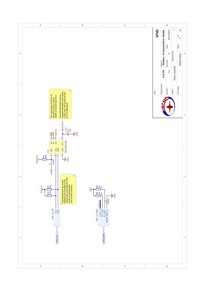
11
22
33
44
DD
CC
BB
AA
Pand
ora
- 8-C
hann
el D
river
Mod
ule
05/1
0/20
17
IPM
I.Sch
Doc
Piet
ro G
ianne
lli*
USCN
D
IPM
ITi
tle:
Org
aniz
atio
n:Pr
ojec
t:
File
nam
e:
Dat
e:
Auth
or:
Appr
oved
By:
Vers
ion:
Revi
sion
:A
0.1
Shee
t:of
513
3P3V
AU
X
A0
1
SDA
5A
23
A1
2W
P7
VSS
4
SCL
6
VCC
8
U19
24A
A64
F-I/M
S
GN
D
GA
0G
A1
GN
D
J2 Jum
per
GN
D
3P3V
AU
X
R89
DN
P
SCL
SDA
FMC_
P1_I
2C
R87
DN
PR8
5D
NP
3P3V
AU
X
IPM
I_I2
C
GA
[0..1
]PG
_C2M
PG_M
2CPR
SNT_
M2C
_L
FMC_
P1_M
ISC
GN
D5%R86
10k
5%R88
10k
3P3V
GA
[0..1
]
IPM
I_M
ISC
J3Ju
mpe
r
25V
C155
1μF
GN
D
The
conn
ectio
n of
GA0
to A
1 an
d G
A1 to
A0
is c
orre
ct.
ADD
R: b
<101
00 G
A0 G
A1>
The
IPM
I EEP
RO
M m
ust b
e pr
ogra
mm
ed b
efor
e th
e m
odul
e is
firs
t use
d. W
P sh
ould
be
tied
to V
CC
afte
rwar
ds.
Unp
opul
ated
pul
l-up
resi
stor
fo
otpr
ints
are
pro
vide
d in
the
unfo
rtuna
te e
vent
that
the
FMC
ca
rrier
is m
issi
ng th
em.
Use
2k
0603
resi
stor
s.
PIC15501 PIC15502
COC1
55
PIJ201
PIJ202
COJ2
PIJ301
PIJ302
COJ3
PIR8501 PIR8502 COR85
PIR8601 PIR8602 COR8
6
PIR8701 PIR8702 COR87
PIR8801 PIR8802 COR8
8
PIR8901 PIR8902 COR8
9
PIU1901
PIU1902
PIU1903
PIU1904
PIU1905
PIU1906
PIU1907
PIU1908
COU19
PIR8602 PIR8802
PIC15501
PIR8502 PIR8702
PIR8902
PIU1908
PIC15502
PIJ201
PIJ302
PIU1903
PIU1904
PIJ202 PIR8901 PIU1907
PIJ301
POIPMI0MISC
PIR8501 PIU1906
POIPMI0I2C
PIR8601 POIPMI0MISC
PIR8701
PIU1905
POIPMI0I2C
PIR8801 POIPMI0MISC
PIU1902
NLGA
0000
10
NLGA
0
POIPMI0MISC
PIU1901
NLGA
0000
10
NLGA1
POIPMI0MISC
POIPMI0I2C
POIP
MI0I
2C0S
CL
POIP
MI0I
2C0S
DA
POIPMI0MISC
POIPMI0MISC0GA0
POIPMI0MISC0GA1
POIP
MI0M
ISC0
GA00
0010
POIPMI0MISC0PG0C2M
POIPMI0MISC0PG0M2C
POIPMI
0MISC0
PRSNT0
M2C0L
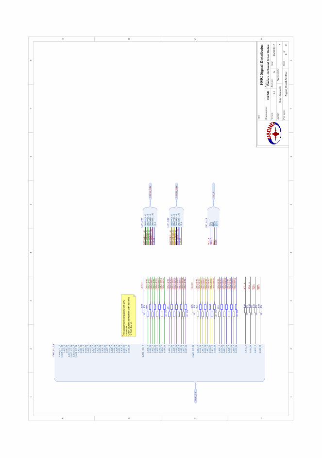
11
22
33
44
55
66
77
88
DD
CC
BB
AA
Pand
ora
- 8-C
hann
el D
rive
r M
odul
e
05/1
0/20
17
Sign
al_D
istri
b.Sc
hDoc
Piet
ro G
iann
elli
*
USC
ND
FMC
Sig
nal D
istr
ibut
orTi
tle:
Org
aniz
atio
n:Pr
ojec
t:
File
nam
e:
Dat
e:
Auth
or:
Appr
oved
By:
Vers
ion:
Revi
sion
:A
0.1
Shee
t:of
613
LA00
_CC
_NLA
00_C
C_P
LA01
_CC
_N
LA01
_CC
_P
LA02
_NLA
02_P
LA03
_NLA
03_P
LA04
_NLA
04_P
LA05
_NLA
05_P
LA06
_NLA
06_P
LA07
_NLA
07_P
LA08
_PLA
09_N
LA09
_PLA
10_N
LA10
_P
LA11
_NLA
11_P
LA12
_NLA
12_P
LA13
_NLA
13_P
LA14
_NLA
14_P
LA15
_NLA
15_P
LA16
_NLA
16_P
LA17
_CC
_P
LA25
_NLA
25_P
LA26
_NLA
26_P
LA27
_NLA
27_P
LA28
_NLA
28_P
LA29
_NLA
29_P
LA30
_NLA
30_P
LA31
_NLA
31_P
LA32
_N
LA32
_P
LA33
_N
LA33
_P
LA17
_CC
_N
LA18
_CC
_NLA
18_C
C_P
LA19
_NLA
19_P
LA20
_NLA
20_P
LA21
_NLA
21_P
LA22
_NLA
22_P
LA23
_NLA
23_P
LA24
_NLA
24_P
LA08
_N
FMC
_P1_
LA
DRV
NN
[1..4
]D
RVN
P[1.
.4]
DRV
PN[1
..4]
DRV
PP[1
..4]
CLK
LLV
_DRV
DRV
14PP
[1..4
]D
RV14
PN[1
..4]
DRV
14N
P[1.
.4]
DRV
14N
N[1
..4]
DRV
NN
[1..4
]D
RVN
P[1.
.4]
DRV
PN[1
..4]
DRV
PP[1
..4]
CLK
LLV
_DRV
DRV
58PP
[1..4
]D
RV58
PN[1
..4]
DRV
58N
P[1.
.4]
DRV
58N
N[1
..4]
USP
14_D
RV
USP
58_D
RV
FMC
_LA
DRV
14PP
1
DRV
14PP
2
DRV
14PP
3
DRV
14PP
4
DRV
14PN
1
DRV
14PN
2
DRV
14PN
3
DRV
14PN
4
DRV
14N
P1
DRV
14N
P2
DRV
14N
P3
DRV
14N
P4
DRV
14N
N1
DRV
14N
N2
DRV
14N
N3
DRV
14N
N4
DRV
58PP
1
DRV
58PP
2
DRV
58PP
3
DRV
58PP
4
DRV
58PN
1
DRV
58PN
2
DRV
58PN
3
DRV
58PN
4
DRV
58N
P1
DRV
58N
P2
DRV
58N
P3
DRV
58N
P4
DRV
58N
N1
DRV
58N
N2
DRV
58N
N3
DRV
58N
N4
SCL
SDA
INT0
RST
0
I2C
_AU
X
I2C
_A
SCL_
ASD
A_A
SCL_
A
SDA
_A
CLK
14
CLK
58
CLK
14
CLK
58
5%
R90
22
5%
R91
22
5%
R92
22
5%
R93
22
1%R94
10
1%R95
10
1%R98
10
1%R99
10
RST
0
INT0
RST
0IN
T0
1%R82
10
1%R83
10
Pin
ass
ignm
ent c
ompa
tible
with
LP
C
conn
ecto
r.C
lock
sou
rces
com
patib
le w
ith th
e A
rria
V
SoC
dev
kit.
PIR8
201
PIR8
202
COR82
PIR8
301
PIR8
302
COR83 PI
R900
1
PIR9
002
PIR9
003
PIR9
004
PIR9
005
PIR9
006
PIR9
007
PIR9
008
PIR9
009
PIR900
10
PIR90011
PIR90012
PIR90013
PIR900
14
PIR900
15
PIR90016
COR9
0
PIR9
101
PIR9
102
PIR9
103
PIR9
104
PIR9
105
PIR9
106
PIR9
107
PIR9
108
PIR9
109
PIR910
10
PIR910
11
PIR91012
PIR91013
PIR91014
PIR91015
PIR910
16
COR91
PIR9
201
PIR9
202
PIR9
203
PIR9
204
PIR9
205
PIR9
206
PIR9
207
PIR9
208
PIR9
209
PIR92010
PIR92011
PIR92012
PIR92013
PIR920
14
PIR920
15
PIR92016
COR9
2
PIR9
301
PIR9
302
PIR9
303
PIR9
304
PIR9
305
PIR9
306
PIR9
307
PIR9
308
PIR9
309
PIR930
10
PIR930
11
PIR93012
PIR93013
PIR93014
PIR930
15
PIR930
16
COR93
PIR9
401
PIR9
402
COR94
PIR9
501
PIR9
502
COR95
PIR9
801
PIR9
802
COR98
PIR9
901
PIR9
902
COR99
PIR9
401
NLCL
K14
POUSP140DRV
PIR9
501
NLCL
K58
POUSP580DRV
PIR8
201
NLI\N\
T\0
POI2C0A
POFMC0LA
POFMC0LA
POFMC0LA
POFMC0LA
POFMC0LA
POFMC0LA
POFMC0LA
POFMC0LA
POFMC0LA
POFMC0LA
POFMC0LA
POFMC0LA
POFMC0LA
POFMC0LA
POFMC0LA
POFMC0LA
POFMC0LA
POFMC0LA
POFMC0LA
POFMC0LA
POFMC0LA
POFMC0LA
POFMC0LA
POFMC0LA
POFMC0LA
POFMC0LA
POFMC0LA
POFMC0LA
POFMC0LA
POFMC0LA
PIR8
202
POFMC0LA
PIR8
302
POFMC0LA
PIR9
009
POFMC0LA
PIR900
10
POFMC0LA
PIR90011
POFMC0LA
PIR90012
POFMC0LA
PIR90013
POFMC0LA
PIR900
14
POFMC0LA
PIR900
15
POFMC0LA
PIR90016
POFMC0LA
PIR9
109
POFMC0LA
PIR910
10
POFMC0LA
PIR910
11
POFMC0LA
PIR91012
POFMC0LA
PIR91013
POFMC0LA
PIR91014
POFMC0LA
PIR91015
POFMC0LA
PIR910
16
POFMC0LA
PIR9
209
POFMC0LA
PIR92010
POFMC0LA
PIR92011
POFMC0LA
PIR92012
POFMC0LA
PIR92013
POFMC0LA
PIR920
14
POFMC0LA
PIR920
15
POFMC0LA
PIR92016
POFMC0LA
PIR9
309
POFMC0LA
PIR930
10
POFMC0LA
PIR930
11
POFMC0LA
PIR93012
POFMC0LA
PIR93013
POFMC0LA
PIR93014
POFMC0LA
PIR930
15
POFMC0LA
PIR930
16
POFMC0LA
PIR9
402
POFMC0LA
PIR9
502
POFMC0LA
PIR9
802
POFMC0LA
PIR9
902
POFMC0LA
PIR8
301
NLR\S\
T\0
POI2C0A
PIR9
801
NLSCL0A
POI2C0A
PIR9
901
NLSD
A0A
POI2C0A
PIR9
001
NLDRV14NN010040
NLDRV14NN1
POUSP140DRV
PIR9
105
NLDRV14NN010040
NLDRV14NN2
POUSP140DRV
PIR9
002
NLDRV14NN010040
NLDRV14NN3
POUSP140DRV
PIR9
102
NLDRV14NN010040
NLDRV14NN4
POUSP140DRV
PIR9
006
NLDRV14NP010040
NLDR
V14N
P1
POUSP140DRV
PIR9
106
NLDRV14NP010040
NLDR
V14N
P2
POUSP140DRV
PIR9
003
NLDRV14NP010040
NLDR
V14N
P3
POUSP140DRV
PIR9
103
NLDRV14NP010040
NLDR
V14N
P4
POUSP140DRV
PIR9
007
NLDRV14PN010040
NLDR
V14P
N1
POUSP140DRV
PIR9
107
NLDRV14PN010040
NLDR
V14P
N2
POUSP140DRV
PIR9
004
NLDRV14PN010040
NLDR
V14P
N3
POUSP140DRV
PIR9
104
NLDRV14PN010040
NLDR
V14P
N4
POUSP140DRV
PIR9
008
NLDRV14PP010040
NLDRV14PP1
POUSP140DRV
PIR9
108
NLDRV14PP010040
NLDR
V14P
P2
POUSP140DRV
PIR9
005
NLDRV14PP010040
NLDR
V14P
P3
POUSP140DRV
PIR9
101
NLDRV14PP010040
NLDR
V14P
P4
POUSP140DRV
PIR9
205
NLDRV58NN010040
NLDRV58NN1
POUSP580DRV
PIR9
201
NLDRV58NN010040
NLDRV58NN2
POUSP580DRV
PIR9
305
NLDRV58NN010040
NLDRV58NN3
POUSP580DRV
PIR9
301
NLDRV58NN010040
NLDRV58NN4
POUSP580DRV
PIR9
206
NLDRV58NP010040
NLDR
V58N
P1
POUSP580DRV
PIR9
202
NLDRV58NP010040
NLDR
V58N
P2
POUSP580DRV
PIR9
306
NLDRV58NP010040
NLDR
V58N
P3
POUSP580DRV
PIR9
302
NLDRV58NP010040
NLDR
V58N
P4
POUSP580DRV
PIR9
207
NLDRV58PN010040
NLDR
V58P
N1
POUSP580DRV
PIR9
203
NLDRV58PN010040
NLDR
V58P
N2
POUSP580DRV
PIR9
307
NLDRV58PN010040
NLDR
V58P
N3
POUSP580DRV
PIR9
303
NLDRV58PN010040
NLDR
V58P
N4
POUSP580DRV
PIR9
208
NLDRV58PP010040
NLDRV58PP1
POUSP580DRV
PIR9
204
NLDRV58PP010040
NLDR
V58P
P2
POUSP580DRV
PIR9
308
NLDRV58PP010040
NLDR
V58P
P3
POUSP580DRV
PIR9
304
NLDRV58PP010040
NLDR
V58P
P4
POUSP580DRV
POFMC0LA
POFMC0LA0LA000CC0N
POFMC0LA0LA000CC0P
POFMC0LA0LA010CC0N
POFMC0LA0LA010CC0P
POFMC0LA0LA020N
POFMC0LA0LA020P
POFMC0LA0LA030N
POFMC0LA0LA030P
POFMC0LA0LA040N
POFMC0LA0LA040P
POFMC0LA0LA050N
POFMC0LA0LA050P
POFMC0LA0LA060N
POFMC0LA0LA060P
POFMC0LA0LA070N
POFMC0LA0LA070P
POFMC0LA0LA080N
POFMC0LA0LA080P
POFMC0LA0LA090N
POFMC0LA0LA090P
POFMC0LA0LA100N
POFMC0LA0LA100P
POFMC0LA0LA110N
POFMC0LA0LA110P
POFMC0LA0LA120N
POFMC0LA0LA120P
POFMC0LA0LA130N
POFMC0LA0LA130P
POFMC0LA0LA140N
POFMC0LA0LA140P
POFMC0LA0LA150N
POFMC0LA0LA150P
POFMC0LA0LA160N
POFMC0LA0LA160P
POFMC0LA0LA170CC0N
POFMC0LA0LA170CC0P
POFMC0LA0LA180CC0N
POFMC0LA0LA180CC0P
POFMC0LA0LA190N
POFMC0LA0LA190P
POFMC0LA0LA200N
POFMC0LA0LA200P
POFMC0LA0LA210N
POFMC0LA0LA210P
POFMC0LA0LA220N
POFMC0LA0LA220P
POFMC0LA0LA230N
POFMC0LA0LA230P
POFMC0LA0LA240N
POFMC0LA0LA240P
POFMC0LA0LA250N
POFMC0LA0LA250P
POFMC0LA0LA260N
POFMC0LA0LA260P
POFMC0LA0LA270N
POFMC0LA0LA270P
POFMC0LA0LA280N
POFMC0LA0LA280P
POFMC0LA0LA290N
POFMC0LA0LA290P
POFMC0LA0LA300N
POFMC0LA0LA300P
POFMC0LA0LA310N
POFMC0LA0LA310P
POFMC0LA0LA320N
POFMC0LA0LA320P
POFMC0LA0LA330N
POFMC0LA0LA330P
POI2C0A
POI2
C0A0
I\N\
T\0
POI2
C0A0
R\S\
T\0
POI2C0A0SCL
POI2C0A0SDA
POUSP140DRV
POUS
P140
DRV0
CLK
POUS
P140
DRV0
DRVN
N1
POUS
P140
DRV0
DRVN
N2
POUS
P140
DRV0
DRVN
N3
POUS
P140
DRV0
DRVN
N4
POUSP140DRV0DRVNN010040
POUS
P140
DRV0
DRVN
P1
POUS
P140
DRV0
DRVN
P2
POUS
P140
DRV0
DRVN
P3
POUS
P140
DRV0
DRVN
P4
POUSP140DRV0DRVNP010040
POUS
P140
DRV0
DRVP
N1
POUS
P140
DRV0
DRVP
N2
POUS
P140
DRV0
DRVP
N3
POUS
P140
DRV0
DRVP
N4
POUSP140DRV0DRVPN010040
POUS
P140
DRV0
DRVP
P1
POUS
P140
DRV0
DRVP
P2
POUS
P140
DRV0
DRVP
P3
POUS
P140
DRV0
DRVP
P4
POUSP140DRV0DRVPP010040
POUSP580DRV
POUS
P580
DRV0
CLK
POUS
P580
DRV0
DRVN
N1
POUS
P580
DRV0
DRVN
N2
POUS
P580
DRV0
DRVN
N3
POUS
P580
DRV0
DRVN
N4
POUSP580DRV0DRVNN010040
POUS
P580
DRV0
DRVN
P1
POUS
P580
DRV0
DRVN
P2
POUS
P580
DRV0
DRVN
P3
POUS
P580
DRV0
DRVN
P4
POUSP580DRV0DRVNP010040
POUS
P580
DRV0
DRVP
N1
POUS
P580
DRV0
DRVP
N2
POUS
P580
DRV0
DRVP
N3
POUS
P580
DRV0
DRVP
N4
POUSP580DRV0DRVPN010040
POUS
P580
DRV0
DRVP
P1
POUS
P580
DRV0
DRVP
P2
POUS
P580
DRV0
DRVP
P3
POUS
P580
DRV0
DRVP
P4
POUSP580DRV0DRVPP010040
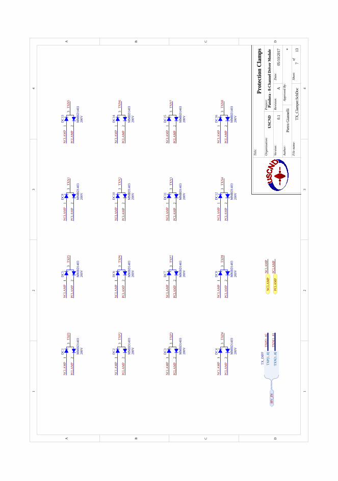
11
22
33
44
DD
CC
BB
AA
Pand
ora
- 8-C
hann
el D
river
Mod
ule
05/1
0/20
17
TX_C
lam
per.S
chDo
c
Piet
ro G
ianne
lli*
USCN
D
Prot
ectio
n C
lam
psTi
tle:
Org
aniz
atio
n:Pr
ojec
t:
File
nam
e:
Dat
e:
Auth
or:
Appr
oved
By:
Vers
ion:
Revi
sion
:A
0.1
Shee
t:of
713
200V
1 23
DC5
MM
BD14
0320
0V
1 23
DC9
MM
BD14
0320
0V
1 23
DC1
3
MM
BD14
03
200V
1 23
DC4
MM
BD14
0320
0V
1 23
DC8
MM
BD14
0320
0V
1 23
DC1
2
MM
BD14
03
200V
1 23
DC1
MM
BD14
03
200V
1 23
DC1
6
MM
BD14
03
200V
1 23
DC6
MM
BD14
0320
0V
1 23
DC1
0
MM
BD14
0320
0V
1 23
DC1
4
MM
BD14
0320
0V
1 23
DC2
MM
BD14
03
200V
1 23
DC7
MM
BD14
0320
0V
1 23
DC1
1
MM
BD14
0320
0V
1 23
DC1
5
MM
BD14
0320
0V
1 23
DC3
MM
BD14
03
TXP[
1..8
]
TXN
[1..8
]
TX_D
IFF
TXP[
1..8
]
TXN
[1..8
]H
V_I
N
TXP1
TXP2
TXP3
TXP4
TXP5
TXP6
TXP7
TXP8
TXN
1
TXN
2
TXN
3
TXN
4
TXN
5
TXN
6
TXN
7
TXN
8
PCLA
MP
NCL
AM
P
NCL
AM
P
PCLA
MP
NCL
AM
P
PCLA
MP
NCL
AM
P
PCLA
MP
NCL
AM
P
PCLA
MP
NCL
AM
P
PCLA
MP
NCL
AM
P
PCLA
MP
NCL
AM
P
PCLA
MP
NCL
AM
P
PCLA
MP
NCL
AM
P
PCLA
MP
NCL
AM
P
PCLA
MP
NCL
AM
P
PCLA
MP
NCL
AM
P
PCLA
MP
NCL
AM
P
PCLA
MP
NCL
AM
P
PCLA
MP
NCL
AM
P
PCLA
MP
NCL
AM
P
PCLA
MP
NCL
AM
P
PCLA
MP
PIDC101
PIDC102
PIDC103
CODC1
PIDC
201
PIDC202
PIDC203
CODC2
PIDC301
PIDC
302
PIDC30
3
CODC3
PIDC401
PIDC
402
PIDC403
CODC
4
PIDC501
PIDC502
PIDC503
CODC5
PIDC60
1
PIDC602
PIDC603
CODC6
PIDC701
PIDC70
2
PIDC
703
CODC7
PIDC801
PIDC80
2
PIDC803
CODC8
PIDC901
PIDC902
PIDC903
CODC9
PIDC
1001
PIDC1002
PIDC1003
CODC
10
PIDC1101
PIDC
1102
PIDC
1103
CODC11
PIDC1201
PIDC
1202
PIDC1203
CODC
12
PIDC1301
PIDC1302
PIDC1303
CODC13
PIDC
1401
PIDC1402
PIDC1403
CODC14
PIDC1501
PIDC
1502
PIDC
1503
CODC15
PIDC1601
PIDC
1602
PIDC1603
CODC16
PIDC101
PIDC
201
PIDC301
PIDC401
PIDC501
PIDC60
1
PIDC701
PIDC801
PIDC901
PIDC
1001
PIDC1101
PIDC1201
PIDC1301
PIDC
1401
PIDC1501
PIDC1601
NLNCLAMP
PONCLAMP
PIDC102
PIDC202
PIDC
302
PIDC
402
PIDC502
PIDC602
PIDC70
2
PIDC80
2
PIDC902
PIDC1002
PIDC
1102
PIDC
1202
PIDC1302
PIDC1402
PIDC
1502
PIDC
1602
NLPC
LAMP
POPCLAMP
PIDC1603
NLTXN010080
NLTX
N8
POHV0IN
PIDC
1503
NLTXN010080
NLTX
N7
POHV0IN
PIDC1403
NLTXN010080
NLTXN6
POHV0IN
PIDC1303
NLTXN010080
NLTX
N5
POHV0IN
PIDC1203
NLTXN010080
NLTX
N4
POHV0IN
PIDC
1103
NLTXN010080
NLTX
N3
POHV0IN
PIDC1003
NLTXN010080
NLTX
N2
POHV0IN
PIDC903
NLTXN010080
NLTX
N1
POHV0IN
PIDC803
NLTXP010080
NLTXP8
POHV0IN
PIDC
703
NLTXP010080
NLTX
P7
POHV0IN
PIDC603
NLTXP010080
NLTX
P6
POHV0IN
PIDC503
NLTXP010080
NLTXP5
POHV0IN
PIDC403
NLTXP010080
NLTXP4
POHV0IN
PIDC30
3
NLTXP010080
NLTXP3
POHV0IN
PIDC203
NLTXP010080
NLTXP2
POHV0IN
PIDC103
NLTXP010080
NLTXP1
POHV0IN
POHV0IN
POHV0IN0TXN1
POHV0IN0TXN2
POHV0IN0TXN3
POHV0IN0TXN4
POHV0IN0TXN5
POHV0IN0TXN6
POHV0IN0TXN7
POHV0IN0TXN8
POHV0IN0TXN010080
POHV0IN0TXP1
POHV0IN0TXP2
POHV0IN0TXP3
POHV0IN0TXP4
POHV0IN0TXP5
POHV0IN0TXP6
POHV0IN0TXP7
POHV0IN0TXP8
POHV0IN0TXP010080
PONCLAMP
POPCLAMP
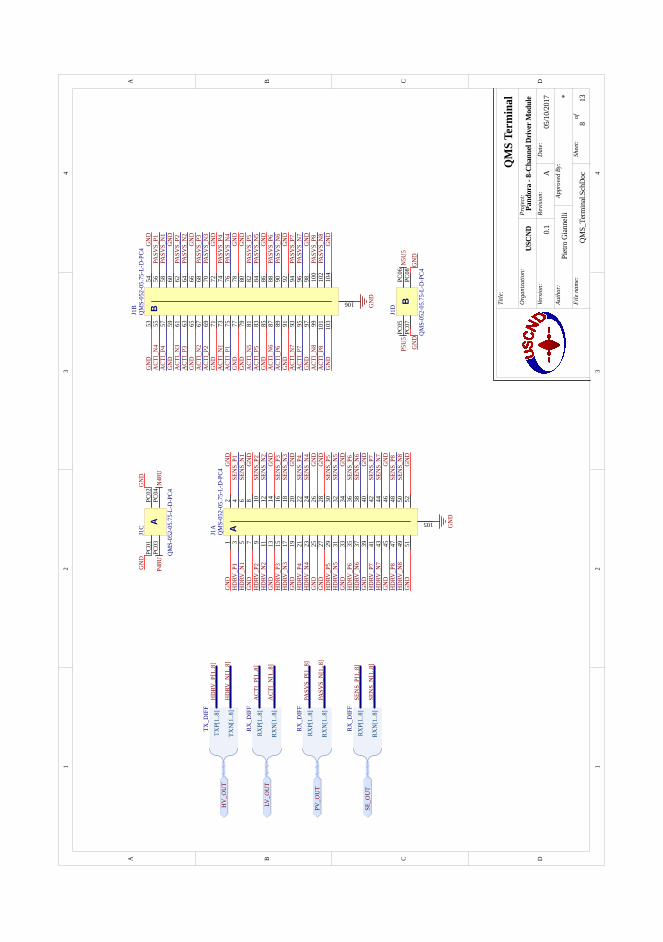
11
22
33
44
DD
CC
BB
AA
Pand
ora
- 8-C
hann
el D
river
Mod
ule
05/1
0/20
17
QMS_
Term
inal.
SchD
oc
Piet
ro G
ianne
lli*
USCN
D
QM
S Te
rmin
alTi
tle:
Org
aniz
atio
n:Pr
ojec
t:
File
nam
e:
Dat
e:
Auth
or:
Appr
oved
By:
Vers
ion:
Revi
sion
:A
0.1
Shee
t:of
813
12
34
56
78
910
1112
1314
1516
1718
1920
2122
2324
2526
2728
2930
3132
3334
3536
3738
3940
4142
4344
4546
4748
4950
5152
105
AJ1A
QM
S-05
2-05
.75-
L-D
-PC4
5354
5556
5758
5960
6162
6364
6566
6768
6970
7172
7374
7576
7778
7980
8182
8384
8586
8788
8990
9192
9394
9596
9798
9910
010
110
210
310
4
106
BJ1B
QM
S-05
2-05
.75-
L-D
-PC4
APC
01PC
02PC
03PC
04
J1C
QM
S-05
2-05
.75-
L-D
-PC4
BPC
05PC
06PC
07PC
08
J1D
QM
S-05
2-05
.75-
L-D
-PC4
RXN
[1..8
]
RXP[
1..8
]
RX_D
IFF
LV_O
UT
GN
D
GN
D
P48U
N48
U
P5U
5N
5U5
GN
D
GN
D
RXN
[1..8
]
RXP[
1..8
]
RX_D
IFF
SE_O
UT
RXN
[1..8
]
RXP[
1..8
]
RX_D
IFF
PV_O
UT
ACT
I_P[
1..8
]
ACT
I_N
[1..8
]
PASV
S_P[
1..8
]
PASV
S_N
[1..8
]
SEN
S_P[
1..8
]
SEN
S_N
[1..8
]
SEN
S_P1
SEN
S_P2
SEN
S_P3
SEN
S_P4
SEN
S_P5
SEN
S_P6
SEN
S_P7
SEN
S_P8
SEN
S_N
1
SEN
S_N
2
SEN
S_N
3
SEN
S_N
4
SEN
S_N
5
SEN
S_N
6
SEN
S_N
7
SEN
S_N
8
PASV
S_P1
PASV
S_P2
PASV
S_P3
PASV
S_P4
PASV
S_P5
PASV
S_P6
PASV
S_P7
PASV
S_P8
PASV
S_N
1
PASV
S_N
2
PASV
S_N
3
PASV
S_N
4
PASV
S_N
5
PASV
S_N
6
PASV
S_N
7
PASV
S_N
8
ACT
I_P1
ACT
I_P2
ACT
I_P3
ACT
I_P4
ACT
I_P5
ACT
I_P6
ACT
I_P7
ACT
I_P8
ACT
I_N
1
ACT
I_N
2
ACT
I_N
3
ACT
I_N
4
ACT
I_N
5
ACT
I_N
6
ACT
I_N
7
ACT
I_N
8
TXN
[1..8
]
TXP[
1..8
]
TX_D
IFF
HV
_OU
T
HD
RV_P
[1..8
]
HD
RV_N
[1..8
]H
DRV
_P1
HD
RV_P
2
HD
RV_P
3
HD
RV_P
4
HD
RV_P
5
HD
RV_P
6
HD
RV_P
7
HD
RV_P
8
HD
RV_N
1
HD
RV_N
2
HD
RV_N
3
HD
RV_N
4
HD
RV_N
5
HD
RV_N
6
HD
RV_N
7
HD
RV_N
8
GN
D
GN
D
GN
D
GN
D
GN
D
GN
D
GN
D
GN
D
GN
D
GN
D
GN
D
GN
D
GN
D
GN
D
GN
D
GN
D
GN
D
GN
D
GN
D
GN
D
GN
D
GN
D
GN
D
GN
D
GN
D
GN
D
GN
D
GN
D
GN
D
GN
D
GN
D
GN
D
GN
D
GN
D
GN
DG
ND
GN
D
GN
D
GN
D
GN
D
GN
D
GN
D
PIJ101
PIJ102
PIJ103
PIJ104
PIJ105
PIJ106
PIJ107
PIJ108
PIJ109
PIJ1010
PIJ101
1 PIJ1012
PIJ1013
PIJ1014
PIJ1015
PIJ1016
PIJ1017
PIJ1018
PIJ1019
PIJ1020
PIJ102
1 PIJ1022
PIJ102
3 PIJ1024
PIJ1025
PIJ1026
PIJ1027
PIJ1028
PIJ1029
PIJ1030
PIJ103
1 PIJ1032
PIJ103
3 PIJ1034
PIJ1035
PIJ1036
PIJ1037
PIJ1038
PIJ1039
PIJ1040
PIJ104
1 PIJ1042
PIJ104
3 PIJ1044
PIJ1045
PIJ1046
PIJ1047
PIJ1048
PIJ1049
PIJ1050
PIJ105
1 PIJ1052
PIJ10105
COJ1A
PIJ1053
PIJ1054
PIJ1
055
PIJ1
056
PIJ1057
PIJ1058
PIJ1059
PIJ1060
PIJ1061
PIJ1062
PIJ1063
PIJ1064
PIJ1
065
PIJ1
066
PIJ1067
PIJ1068
PIJ1069
PIJ1070
PIJ1071
PIJ1072
PIJ1073
PIJ1074
PIJ1
075
PIJ1
076
PIJ1077
PIJ1078
PIJ1079
PIJ1080
PIJ1081
PIJ1082
PIJ1083
PIJ1084
PIJ1
085
PIJ1
086
PIJ1087
PIJ1088
PIJ1089
PIJ1090
PIJ1091
PIJ1092
PIJ1093
PIJ1094
PIJ1
095
PIJ1
096
PIJ1
097
PIJ1
098
PIJ1099
PIJ10100
PIJ10101
PIJ10102
PIJ10103
PIJ10104
PIJ10106
COJ1B
PIJ10P
C01
PIJ10P
C02
PIJ10P
C03
PIJ1
0PC0
4
COJ1C
PIJ1
0PC0
5 PIJ10PC06
PIJ1
0PC0
7 PIJ10PC08
COJ1D
PIJ101
PIJ102
PIJ107
PIJ108
PIJ1013
PIJ1014
PIJ1019
PIJ1020
PIJ1025
PIJ1026
PIJ1027
PIJ1028
PIJ103
3 PIJ1034
PIJ1039
PIJ1040
PIJ1045
PIJ1046
PIJ105
1 PIJ1052
PIJ1053
PIJ1054
PIJ1059
PIJ1060
PIJ1
065
PIJ1
066
PIJ1071
PIJ1072
PIJ1077
PIJ1078
PIJ1079
PIJ1080
PIJ1
085
PIJ1
086
PIJ1091
PIJ1092
PIJ1
097
PIJ1
098
PIJ10103
PIJ10104
PIJ10105
PIJ10106
PIJ10P
C01
PIJ10P
C02
PIJ1
0PC0
7 PIJ10PC08
NLGN
D
PIJ10PC06
PIJ1
0PC0
4
PIJ1
0PC0
5
PIJ10P
C03
PIJ1073
NLAC
TI0N
0100
80
NLACTI0N1
POLV0OUT
PIJ1067
NLAC
TI0N
0100
80
NLACTI0N2
POLV0OUT
PIJ1061
NLAC
TI0N
0100
80
NLACTI0N3
POLV0OUT
PIJ1
055
NLAC
TI0N
0100
80
NLACTI0N4
POLV0OUT
PIJ1081
NLAC
TI0N
0100
80
NLACTI0N5
POLV0OUT
PIJ1087
NLAC
TI0N
0100
80
NLACTI0N6
POLV0OUT
PIJ1093
NLAC
TI0N
0100
80
NLACTI0N7
POLV0OUT
PIJ1099
NLAC
TI0N
0100
80
NLACTI0N8
POLV0OUT
PIJ1
075
NLAC
TI0P
0100
80
NLAC
TI0P
1
POLV0OUT
PIJ1069
NLAC
TI0P
0100
80
NLACTI0P2
POLV0OUT
PIJ1063
NLAC
TI0P
0100
80
NLAC
TI0P
3
POLV0OUT
PIJ1057
NLAC
TI0P
0100
80
NLACTI0P4
POLV0OUT
PIJ1083
NLAC
TI0P
0100
80
NLAC
TI0P
5
POLV0OUT
PIJ1089
NLAC
TI0P
0100
80
NLACTI0P6
POLV0OUT
PIJ1
095
NLAC
TI0P
0100
80
NLAC
TI0P
7
POLV0OUT
PIJ10101
NLAC
TI0P
0100
80
NLAC
TI0P
8
POLV0OUT
PIJ105
NLHD
RV0N
0100
80
NLHD
RV0N
1
POHV0OUT
PIJ101
1
NLHD
RV0N
0100
80
NLHDRV0N2
POHV0OUT
PIJ1017
NLHD
RV0N
0100
80
NLHD
RV0N
3
POHV0OUT
PIJ102
3
NLHD
RV0N
0100
80
NLHDRV0N4
POHV0OUT
PIJ103
1
NLHD
RV0N
0100
80
NLHD
RV0N
5
POHV0OUT
PIJ1037
NLHD
RV0N
0100
80
NLHDRV0N6
POHV0OUT
PIJ104
3
NLHD
RV0N
0100
80
NLHDRV0N7
POHV0OUT
PIJ1049
NLHD
RV0N
0100
80
NLHD
RV0N
8
POHV0OUT
PIJ103
NLHDRV0P010080
NLHD
RV0P
1
POHV0OUT
PIJ109
NLHDRV0P010080
NLHD
RV0P
2
POHV0OUT
PIJ1015
NLHDRV0P010080
NLHD
RV0P
3
POHV0OUT
PIJ102
1
NLHDRV0P010080
NLHD
RV0P
4
POHV0OUT
PIJ1029
NLHDRV0P010080
NLHD
RV0P
5
POHV0OUT
PIJ1035
NLHDRV0P010080
NLHD
RV0P
6
POHV0OUT
PIJ104
1
NLHDRV0P010080
NLHD
RV0P
7
POHV0OUT
PIJ1047
NLHDRV0P010080
NLHD
RV0P
8
POHV0OUT
PIJ1058
NLPA
SVS0
N010
080
NLPA
SVS0
N1
POPV0OUT
PIJ1064
NLPA
SVS0
N010
080
NLPA
SVS0
N2
POPV0OUT
PIJ1070
NLPA
SVS0
N010
080
NLPA
SVS0
N3
POPV0OUT
PIJ1
076
NLPA
SVS0
N010
080
NLPA
SVS0
N4
POPV0OUT
PIJ1084
NLPA
SVS0
N010
080
NLPA
SVS0
N5
POPV0OUT
PIJ1090
NLPA
SVS0
N010
080
NLPA
SVS0
N6
POPV0OUT
PIJ1
096
NLPA
SVS0
N010
080
NLPA
SVS0
N7
POPV0OUT
PIJ10102
NLPA
SVS0
N010
080
NLPA
SVS0
N8
POPV0OUT
PIJ1
056
NLPA
SVS0
P010
080
NLPASVS0P1
POPV0OUT
PIJ1062
NLPA
SVS0
P010
080
NLPASVS0P2
POPV0OUT
PIJ1068
NLPA
SVS0
P010
080
NLPASVS0P3
POPV0OUT
PIJ1074
NLPA
SVS0
P010
080
NLPASVS0P4
POPV0OUT
PIJ1082
NLPA
SVS0
P010
080
NLPASVS0P5
POPV0OUT
PIJ1088
NLPA
SVS0
P010
080
NLPASVS0P6
POPV0OUT
PIJ1094
NLPA
SVS0
P010
080
NLPASVS0P7
POPV0OUT
PIJ10100
NLPA
SVS0
P010
080
NLPASVS0P8
POPV0OUT
PIJ1050
NLSE
NS0N
0100
80
NLSENS0N8
POSE0OUT
PIJ1044
NLSE
NS0N
0100
80
NLSENS0N7
POSE0OUT
PIJ1038
NLSE
NS0N
0100
80
NLSENS0N6
POSE0OUT
PIJ1032
NLSE
NS0N
0100
80
NLSENS0N5
POSE0OUT
PIJ1024
NLSE
NS0N
0100
80
NLSENS0N4
POSE0OUT
PIJ1018
NLSE
NS0N
0100
80
NLSENS0N3
POSE0OUT
PIJ1012
NLSE
NS0N
0100
80
NLSENS0N2
POSE0OUT
PIJ106
NLSE
NS0N
0100
80
NLSENS0N1
POSE0OUT
PIJ1048
NLSE
NS0P
0100
80
NLSENS0P8
POSE0OUT
PIJ1042
NLSE
NS0P
0100
80
NLSENS0P7
POSE0OUT
PIJ1036
NLSE
NS0P
0100
80
NLSENS0P6
POSE0OUT
PIJ1030
NLSE
NS0P
0100
80
NLSENS0P5
POSE0OUT
PIJ1022
NLSE
NS0P
0100
80
NLSENS0P4
POSE0OUT
PIJ1016
NLSE
NS0P
0100
80
NLSENS0P3
POSE0OUT
PIJ1010
NLSE
NS0P
0100
80
NLSENS0P2
POSE0OUT
PIJ104
NLSE
NS0P
0100
80
NLSENS0P1
POSE0OUT
POHV0OUT
POHV
0OUT
0TXN
1 PO
HV0O
UT0T
XN2
POHV
0OUT
0TXN
3 PO
HV0O
UT0T
XN4
POHV
0OUT
0TXN
5 PO
HV0O
UT0T
XN6
POHV
0OUT
0TXN
7 PO
HV0O
UT0T
XN8
POHV0OUT0TXN010080
POHV
0OUT
0TXP
1 PO
HV0O
UT0T
XP2
POHV
0OUT
0TXP
3 PO
HV0O
UT0T
XP4
POHV
0OUT
0TXP
5 PO
HV0O
UT0T
XP6
POHV
0OUT
0TXP
7 PO
HV0O
UT0T
XP8
POHV0OUT0TXP010080
POLV0OUT
POLV
0OUT
0RXN
1 PO
LV0O
UT0R
XN2
POLV
0OUT
0RXN
3 PO
LV0O
UT0R
XN4
POLV
0OUT
0RXN
5 PO
LV0O
UT0R
XN6
POLV
0OUT
0RXN
7 PO
LV0O
UT0R
XN8
POLV0OUT0RXN010080
POLV
0OUT
0RXP
1 PO
LV0O
UT0R
XP2
POLV
0OUT
0RXP
3 PO
LV0O
UT0R
XP4
POLV
0OUT
0RXP
5 PO
LV0O
UT0R
XP6
POLV
0OUT
0RXP
7 PO
LV0O
UT0R
XP8
POLV0OUT0RXP010080
POPV0OUT
POPV
0OUT
0RXN
1 PO
PV0O
UT0R
XN2
POPV
0OUT
0RXN
3 PO
PV0O
UT0R
XN4
POPV
0OUT
0RXN
5 PO
PV0O
UT0R
XN6
POPV
0OUT
0RXN
7 PO
PV0O
UT0R
XN8
POPV0OUT0RXN010080
POPV
0OUT
0RXP
1 PO
PV0O
UT0R
XP2
POPV
0OUT
0RXP
3 PO
PV0O
UT0R
XP4
POPV
0OUT
0RXP
5 PO
PV0O
UT0R
XP6
POPV
0OUT
0RXP
7 PO
PV0O
UT0R
XP8
POPV0OUT0RXP010080
POSE0OUT
POSE
0OUT
0RXN
1 PO
SE0O
UT0R
XN2
POSE
0OUT
0RXN
3 PO
SE0O
UT0R
XN4
POSE
0OUT
0RXN
5 PO
SE0O
UT0R
XN6
POSE
0OUT
0RXN
7 PO
SE0O
UT0R
XN8
POSE0OUT0RXN010080
POSE
0OUT
0RXP
1 PO
SE0O
UT0R
XP2
POSE
0OUT
0RXP
3 PO
SE0O
UT0R
XP4
POSE
0OUT
0RXP
5 PO
SE0O
UT0R
XP6
POSE
0OUT
0RXP
7 PO
SE0O
UT0R
XP8
POSE0OUT0RXP010080
11
22
33
44
55
66
77
88
DD
CC
BB
AA
Pand
ora
- 8-C
hann
el D
rive
r M
odul
e
05/1
0/20
17
Out
put_
Sens
e.Sc
hDoc
Piet
ro G
iann
elli
*
USC
ND
Out
put S
ense
Am
plifi
ers
Title
:
Org
aniz
atio
n:Pr
ojec
t:
File
nam
e:
Dat
e:
Auth
or:
Appr
oved
By:
Vers
ion:
Revi
sion
:A
0.1
Shee
t:of
913
1 278
3 456
100k
100k1k1k
R1
100:
1
TXN
[1..8
]
TXP[
1..8
]
TX_D
IFF
HV
_IN
RX
P[1.
.8]
RX
N[1
..8]
RX
_DIF
F
SE_O
UT
TXP[
1..8
]
TXN
[1..8
]1 23 4
36 37
U5A
THS4
524I
DB
T
3231
6 78 9U
5BTH
S452
4ID
BT
11 1213 14
26 27
U5C
THS4
524I
DB
T
16 1718 19
21 22
U5D
THS4
524I
DB
T
VS-
5
VS-
10
VS-
15
VS-
23
VS-
24
VS3
+25
VS-
28
VS-
29
VS2
+30
VS-
33V
S-34
VS1
+35
VS-
38
VS4
+20
U5E
THS4
524I
DB
T
1 23 4
36 37
U6A
THS4
524I
DB
T
3231
6 78 9U
6BTH
S452
4ID
BT
11 1213 14
26 27
U6C
THS4
524I
DB
T
16 1718 19
21 22
U6D
THS4
524I
DB
T
VS-
5
VS-
10
VS-
15
VS-
23
VS-
24
VS3
+25
VS-
28
VS-
29
VS2
+30
VS-
33V
S-34
VS1
+35
VS-
38
VS4
+20
U6E
THS4
524I
DB
T
P5LN
GN
D
10V
C19
220n
F
GN
D
10V
C20
220n
F
GN
D
10V
C21
220n
F
GN
D
10V
C22
220n
F
GN
D
EN_S
ENS1
EN_S
ENS2
EN_S
ENS1
EN_S
ENS1
EN_S
ENS1
10V
C44
220n
F
GN
D
10V
C45
220n
F
GN
D
10V
C46
220n
F
GN
D
10V
C47
220n
F
GN
D
EN_S
ENS2
EN_S
ENS2
EN_S
ENS2
GN
D
P5LN
GN
DG
ND
16V
C25
100n
F
10V
C18
10uF
16V
C24
100n
F16
V
C23
100n
F16
V
C17
100n
F
GN
D
P5LN
16V
C50
100n
F
10V
C43
10uF
16V
C49
100n
F16
V
C48
100n
F16
V
C42
100n
F
GN
D
P5LN
1 278
3 456
100k
100k1k1k
R2
100:
1
1 278
3 456
100k
100k1k1k
R3
100:
1
1 278
3 456
100k
100k1k1k
R4
100:
1
1 278
3 456
100k
100k1k1k
R13
100:
1
1 278
3 456
100k
100k1k1k
R14
100:
1
1 278
3 456
100k
100k1k1k
R15
100:
1
1 278
3 456
100k
100k1k1k
R16
100:
1
TXP1
TXP2
TXP3
TXP4
TXP5
TXP6
TXP7
TXP8
TXN
1
TXN
2
TXN
3
TXN
4
TXN
5
TXN
6
TXN
7
TXN
8EN
_SEN
S[1.
.2]
EN_S
ENS[
1..2
]
16V
C26
1nF
16V
C27
1nF
16V
C28
1nF
16V
C29
1nF
16V
C30
1nF
16V
C31
1nF
16V
C32
1nF
16V
C33
1nF
16V
C1
1nF
16V
C2
1nF
16V
C3
1nF
16V
C4
1nF
16V
C5
1nF
16V
C6
1nF
16V
C7
1nF
16V
C8
1nF
1%R5
10 1%R6
10 1%R7
10 1%R8
10 1%R9
10 1%R10
10 1%R11
10 1%R12
10
1%R23
10 1%R24
101%R21
10 1%R22
101%R19
10 1%R20
101%R17
10 1%R18
10
RX
P[1.
.8]
RX
N[1
..8]
RX
P1
RX
P2
RX
P3
RX
P4
RX
P5
RX
P6
RX
P7
RX
P8
RX
N1
RX
N2
RX
N3
RX
N4
RX
N5
RX
N6
RX
N7
RX
N8
GN
D
P5LN
GN
D
P5LN
16V
C9
56pF
16V
C10
56pF
16V
C11
56pF
16V
C12
56pF
16V
C13
56pF
16V
C14
56pF
16V
C15
56pF
16V
C16
56pF
16V
C34
56pF
16V
C35
56pF
16V
C36
56pF
16V
C37
56pF
16V
C38
56pF
16V
C39
56pF
16V
C40
56pF
16V
C41
56pF
PIC101 PIC102 COC
1
PIC201 PIC202 COC2
PIC301 PIC302 COC
3
PIC401 PIC402 COC4
PIC501 PIC502 COC
5
PIC601 PIC602 COC6
PIC701 PIC702 COC
7
PIC801 PIC802 COC
8
PIC901 PIC902
COC9
PIC1001 PIC1002
COC1
0
PIC1101 PIC1102
COC11
PIC1201 PIC1202
COC12
PIC1301 PIC1302
COC13
PIC1401 PIC1402
COC1
4
PIC1501 PIC1502
COC15
PIC1601 PIC1602
COC1
6
PIC1701 PIC1702
COC17
PIC1801 PIC1802
COC18 PIC1901 PIC1902
COC19
PIC2001 PIC2002
COC2
0
PIC2101 PIC2102
COC21
PIC2201 PIC2202
COC22
PIC2301 PIC2302
COC2
3 PIC2401 PIC2402
COC2
4 PIC2501 PIC2502
COC2
5
PIC2601 PIC2602 CO
C26
PIC2701 PIC2702
COC2
7
PIC2801 PIC2802 CO
C28
PIC2901 PIC2902
COC2
9
PIC3001 PIC3002 CO
C30
PIC3101 PIC3102
COC31
PIC3201 PIC3202 CO
C32
PIC3301 PIC3302 COC33
PIC3401 PIC3402
COC3
4
PIC3501 PIC3502
COC3
5
PIC3601 PIC3602
COC3
6
PIC3701 PIC3702
COC3
7
PIC3801 PIC3802
COC3
8
PIC3901 PIC3902
COC3
9
PIC4001 PIC4002
COC4
0
PIC4101 PIC4102
COC41
PIC4201 PIC4202
COC42
PIC4301 PIC4302
COC43 PIC4401 PIC4402
COC4
4
PIC4501 PIC4502
COC4
5
PIC4601 PIC4602
COC4
6
PIC4701 PIC4702
COC4
7 PIC4801 PIC4802
COC48
PIC4901 PIC4902
COC49
PIC5001 PIC5002
COC5
0
PIR101
PIR102
PIR103
PIR104
PIR105
PIR106
PIR107
PIR108
COR1
PIR201
PIR202
PIR203
PIR204
PIR205
PIR206
PIR207
PIR208
COR2
PIR301
PIR302
PIR303
PIR304
PIR305
PIR306
PIR307
PIR308
COR3
PIR401
PIR402
PIR403
PIR404
PIR405
PIR406
PIR407
PIR408
COR4
PIR501
PIR502 COR
5
PIR601
PIR602 COR
6
PIR701
PIR702 COR
7
PIR801
PIR802 COR
8
PIR901
PIR902 COR
9
PIR1
001
PIR1
002 CO
R10
PIR1
101
PIR1
102 COR
11
PIR1
201
PIR1
202 CO
R12
PIR1301
PIR1302
PIR1303
PIR1304
PIR1305
PIR1
306
PIR1307
PIR1308
COR13
PIR1401
PIR1402
PIR1403
PIR1404
PIR1405
PIR1
406
PIR1407
PIR1408
COR14
PIR1501
PIR1502
PIR1503
PIR1504
PIR1505
PIR1
506
PIR1507
PIR1
508
COR15
PIR1601
PIR1602
PIR1603
PIR1604
PIR1
605
PIR1606
PIR1607
PIR1
608
COR16
PIR1
701
PIR1
702 COR1
7
PIR1
801
PIR1
802 COR1
8
PIR1
901
PIR1
902 COR1
9
PIR2
001
PIR2
002 COR2
0
PIR2
101
PIR2
102 COR21
PIR2
201
PIR2
202 COR2
2
PIR2
301
PIR2
302 COR2
3
PIR2
401
PIR2
402 COR2
4
PIU501
PIU502
PIU503
PIU504
PIU5036
PIU5
037
COU5
A
PIU506
PIU507
PIU508
PIU509
PIU5031
PIU5
032
COU5
B
PIU5011
PIU5012
PIU5013
PIU5014
PIU5026
PIU5
027
COU5
C
PIU5016
PIU5017
PIU5018
PIU5019
PIU5021
PIU5022
COU5
D
PIU505
PIU5010
PIU5015
PIU5020
PIU5023
PIU5
024
PIU5025
PIU5028
PIU5029
PIU5030
PIU5033
PIU5034
PIU5035
PIU5038
COU5
E
PIU601
PIU602
PIU603
PIU604
PIU6036
PIU6
037
COU6A
PIU606
PIU607
PIU608
PIU609
PIU6031
PIU6
032
COU6B
PIU6
011
PIU6
012
PIU6013
PIU6014
PIU6026
PIU6
027
COU6C
PIU6
016
PIU6017
PIU6018
PIU6
019
PIU6021
PIU6022
COU6D
PIU605
PIU6010
PIU6015
PIU6020
PIU6023
PIU6024
PIU6025
PIU6028
PIU6029
PIU6030
PIU6033
PIU6034
PIU6035
PIU6038
COU6E
PIC1702 PIC1802
PIC1902 PIC2002 PIC2102 PIC2202
PIC2302 PIC2402
PIC2502 PIC4202 PIC4302
PIC4402 PIC4502 PIC4602 PIC4702
PIC4802 PIC4902
PIC5002 PIU505
PIU5010
PIU5015
PIU5023
PIU5
024
PIU5028
PIU5029
PIU5033
PIU5034
PIU5038
PIU605
PIU6010
PIU6015
PIU6023
PIU6024
PIU6028
PIU6029
PIU6033
PIU6034
PIU6038
PIC101 PIC902
PIR107
PIU503
PIC102 PIR108
PIC201 PIC1001
PIR106
PIU502
PIC202 PIR105
PIC301 PIC1102
PIR207
PIU508
PIC302 PIR208
PIC401 PIC1201
PIR206
PIU507
PIC402 PIR205
PIC501 PIC1302
PIR307
PIU5013
PIC502 PIR308
PIC601 PIC1401
PIR306
PIU5012
PIC602 PIR305
PIC701 PIC1502
PIR407
PIU5018
PIC702 PIR408
PIC801 PIC1601
PIR406
PIU5017
PIC802 PIR405
PIC901
PIR102
PIR502
PIU5036
PIC1002
PIR103
PIR602
PIU5
037
PIC1101
PIR202
PIR702
PIU5031
PIC1202
PIR203
PIR802
PIU5
032
PIC1301
PIR302
PIR902
PIU5026
PIC1402
PIR303
PIR1
002
PIU5
027
PIC1501
PIR402
PIR1
102
PIU5021
PIC1602
PIR403
PIR1
202
PIU5022
PIC1901 PIU504
PIC2001 PIU509
PIC2101 PIU5014
PIC2201 PIU5019
PIC2601 PIC3402
PIR1307
PIU603
PIC2602 PIR1308
PIC2701 PIC3501
PIR1
306
PIU602
PIC2702 PIR1305
PIC2801 PIC3602
PIR1407
PIU608
PIC2802 PIR1408
PIC2901 PIC3701
PIR1
406
PIU607
PIC2902 PIR1405
PIC3001 PIC3802
PIR1507
PIU6013
PIC3002 PI
R150
8
PIC3101 PIC3901
PIR1
506
PIU6
012
PIC3102 PIR1505
PIC3201 PIC4002
PIR1607
PIU6018
PIC3202 PI
R160
8
PIC3301 PIC4101
PIR1606
PIU6017
PIC3302 PI
R160
5
PIC3401
PIR1302
PIR1
702
PIU6036
PIC3502
PIR1303
PIR1
802
PIU6
037
PIC3601
PIR1402
PIR1
902
PIU6031
PIC3702
PIR1403
PIR2
002
PIU6
032
PIC3801
PIR1502
PIR2
102
PIU6026
PIC3902
PIR1503
PIR2
202
PIU6
027
PIC4001
PIR1602
PIR2
302
PIU6021
PIC4102
PIR1603
PIR2
402
PIU6022
PIC4401 PIU604
PIC4501 PIU609
PIC4601 PIU6014
PIC4701 PI
U601
9
PIC1701 PIC1801
PIC2301 PIC2401
PIC2501 PIC4201 PIC4301
PIC4801 PIC4901
PIC5001
PIU5020
PIU5025
PIU5030
PIU5035
PIU6020
PIU6025
PIU6030
PIU6035
PIU501
PIU506
PIU5011
PIU5016
NLEN0SENS010020
NLEN
0SEN
S1
POEN0SENS010020
PIU601
PIU606
PIU6
011
PIU6
016
NLEN0SENS010020
NLEN
0SEN
S2
POEN0SENS010020
PIR1
101
NLRX
N01008
0
NLRX
N1
POSE0OUT
PIR701
NLRX
N01008
0
NLRX
N2
POSE0OUT
PIR901
NLRX
N01008
0
NLRX
N3
POSE0OUT
PIR501
NLRX
N01008
0 NL
RXN4
POSE0OUT
PIR2
301
NLRX
N01008
0
NLRX
N5
POSE0OUT
PIR1
901
NLRX
N01008
0
NLRX
N6
POSE0OUT
PIR2
101
NLRX
N01008
0
NLRX
N7
POSE0OUT
PIR1
701
NLRX
N01008
0 NL
RXN8
POSE0OUT
PIR1
201
NLRXP010080
NLRX
P1
POSE0OUT
PIR801
NLRXP010080
NLRX
P2
POSE0OUT
PIR1
001
NLRXP010080
NLRX
P3
POSE0OUT
PIR601
NLRXP010080
NLRX
P4
POSE0OUT
PIR2
401
NLRXP010080
NLRX
P5
POSE0OUT
PIR2
001
NLRXP010080
NLRX
P6
POSE0OUT
PIR2
201
NLRXP010080
NLRX
P7
POSE0OUT
PIR1
801
NLRXP010080
NLRX
P8
POSE0OUT
PIR1304
NLTXN010080
NLTX
N8
POHV0IN
PIR1504
NLTXN010080
NLTX
N7
POHV0IN
PIR1404
NLTXN010080
NLTX
N6
POHV0IN
PIR1604
NLTXN010080
NLTX
N5
POHV0IN
PIR104
NLTXN010080
NLTX
N4
POHV0IN
PIR304
NLTXN010080
NLTX
N3
POHV0IN
PIR204
NLTXN010080
NLTX
N2
POHV0IN
PIR404
NLTXN010080
NLTX
N1
POHV0IN
PIR1301
NLTXP010080
NLTX
P8
POHV0IN
PIR1501
NLTXP010080
NLTX
P7
POHV0IN
PIR1401
NLTXP010080
NLTX
P6
POHV0IN
PIR1601
NLTXP010080
NLTX
P5
POHV0IN
PIR101
NLTXP010080
NLTX
P4
POHV0IN
PIR301
NLTXP010080
NLTX
P3
POHV0IN
PIR201
NLTXP010080
NLTX
P2
POHV0IN
PIR401
NLTXP010080
NLTX
P1
POHV0IN
POEN0SENS1
POEN0SENS2
POEN0SENS010020
POHV0IN
POHV
0IN0
TXN1
PO
HV0I
N0TX
N2
POHV
0IN0
TXN3
PO
HV0I
N0TX
N4
POHV
0IN0
TXN5
PO
HV0I
N0TX
N6
POHV
0IN0
TXN7
PO
HV0I
N0TX
N8
POHV
0IN0
TXN0
1008
0 PO
HV0I
N0TX
P1
POHV
0IN0
TXP2
PO
HV0I
N0TX
P3
POHV
0IN0
TXP4
PO
HV0I
N0TX
P5
POHV
0IN0
TXP6
PO
HV0I
N0TX
P7
POHV
0IN0
TXP8
PO
HV0I
N0TX
P010
080
POSE0OUT
POSE0OUT0RXN1
POSE0OUT0RXN2
POSE0OUT0RXN3
POSE0OUT0RXN4
POSE0OUT0RXN5
POSE0OUT0RXN6
POSE0OUT0RXN7
POSE0OUT0RXN8
POSE0OUT0RXN010080
POSE0OUT0RXP1
POSE0OUT0RXP2
POSE0OUT0RXP3
POSE0OUT0RXP4
POSE0OUT0RXP5
POSE0OUT0RXP6
POSE0OUT0RXP7
POSE0OUT0RXP8
POSE0OUT0RXP010080

11
22
33
44
55
66
77
88
DD
CC
BB
AA
Pand
ora
- 8-C
hann
el D
rive
r M
odul
e
05/1
0/20
17
Pass
ive_
Sens
e.Sc
hDoc
Piet
ro G
iann
elli
*
USC
ND
Pass
ive
Sens
e A
mpl
ifier
sTi
tle:
Org
aniz
atio
n:Pr
ojec
t:
File
nam
e:
Dat
e:
Auth
or:
Appr
oved
By:
Vers
ion:
Revi
sion
:A
0.1
Shee
t:of
1013
1 23 4
36 37
U7A
THS4
524I
DB
T
3231
6 78 9U
7BTH
S452
4ID
BT
11 1213 14
26 27
U7C
THS4
524I
DB
T
16 1718 19
21 22
U7D
THS4
524I
DB
T
VS-
5
VS-
10
VS-
15
VS-
23
VS-
24
VS3
+25
VS-
28
VS-
29
VS2
+30
VS-
33V
S-34
VS1
+35
VS-
38
VS4
+20
U7E
THS4
524I
DB
T
1 23 4
36 37
U8A
THS4
524I
DB
T
3231
6 78 9U
8BTH
S452
4ID
BT
11 1213 14
26 27
U8C
THS4
524I
DB
T
16 1718 19
21 22
U8D
THS4
524I
DB
T
VS-
5
VS-
10
VS-
15
VS-
23
VS-
24
VS3
+25
VS-
28
VS-
29
VS2
+30
VS-
33V
S-34
VS1
+35
VS-
38
VS4
+20
U8E
THS4
524I
DB
T
P5LN
GN
D
10V
C64
220n
F
GN
D
10V
C65
220n
F
GN
D
10V
C66
220n
F
GN
D
10V
C67
220n
F
GN
D
EN_P
ASV
1EN
_PA
SV2
EN_P
ASV
1
EN_P
ASV
1
EN_P
ASV
1
10V
C89
220n
F
GN
D
10V
C90
220n
F
GN
D
10V
C91
220n
F
GN
D
10V
C92
220n
F
GN
D
EN_P
ASV
2
EN_P
ASV
2
EN_P
ASV
2
GN
DG
ND
P5LN
GN
DG
ND
16V
C54
100n
F10
V
C55
10uF
16V
C53
100n
F16
V
C52
100n
F16
V
C51
100n
F
GN
D
P5LN
16V
C79
100n
F10
V
C80
10uF
16V
C78
100n
F16
V
C77
100n
F16
V
C76
100n
F
GN
D
P5LN
TXN
[1..8
]
TXP[
1..8
]
TX_D
IFF
HV
_IN
EN_P
ASV
[1..2
]EN
_PA
SV[1
..2]
RX
P[1.
.8]
RX
N[1
..8]
RX
_DIF
F
PV_O
UT
TXP[
1..8
]
TXN
[1..8
]
R25
100k
R29
20k
1%R33
10 1%R34
10R
XP1
RX
N1
16V
C56
1nF
16V
C57
1nF
RX
P[1.
.8]
RX
N[1
..8]
TXP1
TXP2
TXP3
TXP4
TXN
1
TXN
2
TXN
3
TXN
4
R26
100k
R30
20k
1%R35
10 1%R36
10
16V
C58
1nF
16V
C59
1nF
R27
100k
R31
20k
1%R37
10 1%R38
10
16V
C60
1nF
16V
C61
1nF
R28
100k
R32
20k
1%R39
10 1%R40
10
16V
C62
1nF
16V
C63
1nF
R41
100k
R45
20k
1%R49
10 1%R50
10
16V
C81
1nF
16V
C82
1nF
R42
100k
R46
20k
1%R51
10 1%R52
10
16V
C83
1nF
16V
C84
1nF
R43
100k
R47
20k
1%R53
10 1%R54
10
16V
C85
1nF
16V
C86
1nF
R44
100k
R48
20k
1%R55
10 1%R56
10
16V
C87
1nF
16V
C88
1nF
C68
56pF
RX
P2
RX
P3
RX
P4R
XP5
RX
P6
RX
P7
RX
P8
RX
N2
RX
N3
RX
N4
RX
N5
RX
N6
RX
N7
RX
N8
C69
56pF
C70
56pF
C71
56pF
C72
56pF
C73
56pF
C74
56pF
C75
56pF
C99
56pF
C10
056
pF
C97
56pF
C98
56pF
C95
56pF
C96
56pF
C93
56pF
C94
56pF
TXP5
TXP6
TXP7
TXP8
TXN
5
TXN
6
TXN
7
TXN
8
123 4
D1
BA
S116
V-7P5
LN
GN
D
123 4
D3
BA
S116
V-7P5
LN
GN
D
123 4
D5
BA
S116
V-7P5
LN
GN
D
123 4
D7
BA
S116
V-7P5
LN
GN
D
123 4
D9
BA
S116
V-7P5
LN
GN
D
123 4
D11
BA
S116
V-7P5
LN
GN
D
123 4
D13
BA
S116
V-7P5
LN
GN
D
123 4
D15
BA
S116
V-7P5
LN
GN
D
123 4
D2
BA
S116
V-7P5
LN
GN
D
123 4
D4
BA
S116
V-7P5
LN
GN
D
123 4
D6
BA
S116
V-7P5
LN
GN
D
123 4
D8
BA
S116
V-7P5
LN
GN
D
123 4
D16
BA
S116
V-7P5
LN
GN
D
123 4
D14
BA
S116
V-7P5
LN
GN
D
123 4
D12
BA
S116
V-7P5
LN
GN
D
123 4
D10
BA
S116
V-7P5
LN
GN
D
PIC5101 PIC5102
COC51
PIC5201 PIC5202
COC5
2 PIC5301 PIC5302
COC53
PIC5401 PIC5402
COC5
4 PIC5501 PIC5502
COC5
5
PIC5
601
PIC5
602
COC56
PIC5
701
PIC5
702
COC57
PIC5
801
PIC5
802
COC58
PIC5
901
PIC5
902
COC59
PIC6
001
PIC6
002
COC60
PIC6
101
PIC6
102
COC61
PIC6
201
PIC6
202
COC62
PIC6
301
PIC6
302
COC63
PIC6401 PIC6402
COC64
PIC6501 PIC6502
COC65
PIC6601 PIC6602
COC66
PIC6701 PIC6702
COC67
PIC6
801
PIC6
802
COC68 PI
C690
1 PI
C690
2
COC69 PIC7
001
PIC7
002
COC7
0
PIC7
101
PIC7
102
COC71 PIC7
201
PIC7
202
COC72 PIC7
301
PIC7
302
COC73 PIC7
401
PIC7
402
COC7
4
PIC7
501
PIC7
502
COC75
PIC7601 PIC7602
COC7
6 PIC7701 PIC7702
COC7
7 PIC7801 PIC7802
COC7
8 PIC7901 PIC7902
COC7
9 PIC8001 PIC8002
COC8
0
PIC8
101
PIC8
102
COC81
PIC8
201
PIC8
202
COC82
PIC8
301
PIC8
302
COC83
PIC8
401
PIC8
402
COC84
PIC8
501
PIC8
502
COC85
PIC8
601
PIC8
602
COC86
PIC8
701
PIC8
702
COC87
PIC8
801
PIC8
802
COC88
PIC8901 PIC8902
COC8
9
PIC9001 PIC9002
COC9
0
PIC9101 PIC9102
COC91
PIC9201 PIC9202
COC9
2
PIC9301
PIC9
302
COC93 PIC9401
PIC9
402
COC9
4
PIC9501
PIC9
502
COC95 PIC9601
PIC9
602
COC9
6
PIC9701
PIC9
702
COC97
PIC9801
PIC9
802
COC98
PIC9901
PIC9
902
COC99
PIC1
0001
PIC10002
COC1
00
PID101
PID1
02
PID1
03
PID104 COD1 PID201
PID202
PID203
PID204 COD2 PID301
PID3
02
PID3
03
PID304 COD3 PID401
PID402
PID403
PID404 COD4 PID5
01
PID502
PID503
PID5
04 COD5 PID601
PID6
02
PID6
03
PID604 COD6 PID7
01
PID702
PID703
PID7
04 COD7 PID801
PID8
02
PID8
03
PID804 COD8
PID901
PID9
02
PID9
03
PID904 COD9 PID1001
PID1002
PID1003
PID1004 CO
D10
PID1101
PID1102
PID1103
PID1104 CO
D11
PID1201
PID1202
PID1203
PID1204 CO
D12
PID1301
PID1302
PID1303
PID1304 CO
D13
PID1401
PID1402
PID1403
PID1404 CO
D14
PID1501
PID1502
PID1503
PID1504 CO
D15
PID1601
PID1602
PID1603
PID1604 CO
D16
PIR2
501
PIR2
502
PIR2
503
PIR2
504
COR2
5
PIR2
601
PIR2
602
PIR2
603
PIR2
604
COR2
6
PIR2
701
PIR2
702
PIR2
703
PIR2
704
COR2
7
PIR2
801
PIR2
802
PIR2
803
PIR2
804
COR2
8
PIR2
901
PIR2
902
PIR2
903
PIR2
904
COR29
PIR3
001
PIR3
002
PIR3
003
PIR3
004
COR30
PIR3
101
PIR3
102
PIR3
103
PIR3
104
COR31
PIR3
201
PIR3
202
PIR3
203
PIR3
204
COR32
PIR3
301
PIR3
302 COR
33
PIR3
401
PIR3
402 CO
R34
PIR3
501
PIR3
502 CO
R35
PIR3
601
PIR3
602 CO
R36
PIR3
701
PIR3
702 CO
R37
PIR3
801
PIR3
802 COR
38
PIR3
901
PIR3
902 CO
R39
PIR4
001
PIR4
002 CO
R40
PIR4101
PIR4102
PIR4
103
PIR4
104
COR41
PIR4201
PIR4202
PIR4
203
PIR4
204
COR4
2
PIR4301
PIR4302
PIR4
303
PIR4
304
COR43
PIR4401
PIR4402
PIR4
403
PIR4
404
COR4
4
PIR4
501
PIR4
502
PIR4503
PIR4504
COR45
PIR4
601
PIR4
602
PIR4603
PIR4604
COR46
PIR4
701
PIR4
702
PIR4703
PIR4704
COR47
PIR4
801
PIR4
802
PIR4803
PIR4804
COR48
PIR4
901
PIR4
902 COR
49
PIR5
001
PIR5
002 CO
R50
PIR5
101
PIR5
102 CO
R51
PIR5
201
PIR5
202 CO
R52
PIR5
301
PIR5
302 CO
R53
PIR5
401
PIR5
402 COR
54
PIR5
501
PIR5
502 CO
R55
PIR5
601
PIR5
602 COR
56
PIU701
PIU702
PIU703
PIU704
PIU7036
PIU7037
COU7
A
PIU706
PIU707
PIU708
PIU709
PIU7031
PIU7032
COU7
B
PIU7011
PIU7
012
PIU7013
PIU7014
PIU7026
PIU7027
COU7
C
PIU7016
PIU7
017
PIU7018
PIU7019
PIU7021
PIU7022
COU7
D
PIU705
PIU7010
PIU7015
PIU7
020
PIU7
023
PIU7024
PIU7025
PIU7028
PIU7029
PIU7030
PIU7033
PIU7034
PIU7035
PIU7038
COU7
E
PIU801
PIU802
PIU803
PIU804
PIU8
036
PIU8037
COU8
A
PIU806
PIU807
PIU808
PIU809
PIU8031
PIU8032
COU8
B
PIU8011
PIU8
012
PIU8013
PIU8014
PIU8026
PIU8
027
COU8
C
PIU8016
PIU8
017
PIU8018
PIU8019
PIU8021
PIU8
022
COU8
D
PIU805
PIU8010
PIU8015
PIU8020
PIU8
023
PIU8024
PIU8025
PIU8028
PIU8029
PIU8030
PIU8033
PIU8034
PIU8035
PIU8038
COU8
E
PIC5102 PIC5202
PIC5302 PIC5402
PIC5502
PIC6402 PIC6502 PIC6602 PIC6702
PIC7602 PIC7702
PIC7802 PIC7902
PIC8002
PIC8902 PIC9002 PIC9102 PIC9202
PID104
PID204
PID304
PID404
PID5
04
PID604
PID7
04
PID804
PID904
PID1004
PID1104
PID1204
PID1304
PID1404
PID1504
PID1604
PIU705
PIU7010
PIU7015
PIU7
023
PIU7024
PIU7028
PIU7029
PIU7033
PIU7034
PIU7038
PIU805
PIU8010
PIU8015
PIU8
023
PIU8024
PIU8028
PIU8029
PIU8033
PIU8034
PIU8038
PIC5
601
PIR2
503
PIC5
602
PIC6
802
PID101
PID1
03
PIR2
903
PIU703
PIC5
701
PIR2
504
PIC5
702
PIC6
902
PID201
PID203
PIR2
904
PIU702
PIC5
801
PIR2
603
PIC5
802
PIC7
002
PID301
PID3
03
PIR3
003
PIU708
PIC5
901
PIR2
604
PIC5
902
PIC7
102
PID401
PID403
PIR3
004
PIU707
PIC6
001
PIR2
703
PIC6
002
PIC7
202
PID5
01
PID503
PIR3
103
PIU7013
PIC6
101
PIR2
704
PIC6
102
PIC7
302
PID601
PID6
03
PIR3
104
PIU7
012
PIC6
201
PIR2
803
PIC6
202
PIC7
402
PID7
01
PID703
PIR3
203
PIU7018
PIC6
301
PIR2
804
PIC6
302
PIC7
502
PID801
PID8
03
PIR3
204
PIU7
017
PIC6401 PIU704
PIC6501 PIU709
PIC6601 PIU7014
PIC6701 PIU7019
PIC6
801
PIR2
902
PIR3
302
PIU7036
PIC6
901
PIR2
901
PIR3
402
PIU7037
PIC7
001
PIR3
002
PIR3
502
PIU7031
PIC7
101
PIR3
001
PIR3
602
PIU7032
PIC7
201
PIR3
102
PIR3
702
PIU7026
PIC7
301
PIR3
101
PIR3
802
PIU7027
PIC7
401
PIR3
202
PIR3
902
PIU7021
PIC7
501
PIR3
201
PIR4
002
PIU7022
PIC8
101
PIR4
103
PIC8
102
PIC9
302
PID901
PID9
03
PIR4503
PIU803
PIC8
201
PIR4
104
PIC8
202
PIC9
402
PID1001
PID1003
PIR4504
PIU802
PIC8
301
PIR4
203
PIC8
302
PIC9
502
PID1101
PID1103
PIR4603
PIU808
PIC8
401
PIR4
204
PIC8
402
PIC9
602
PID1201
PID1203
PIR4604
PIU807
PIC8
501
PIR4
303
PIC8
502
PIC9
702
PID1301
PID1303
PIR4703
PIU8013
PIC8
601
PIR4
304
PIC8
602
PIC9
802
PID1401
PID1403
PIR4704
PIU8
012
PIC8
701
PIR4
403
PIC8
702
PIC9
902
PID1501
PID1503
PIR4803
PIU8018
PIC8
801
PIR4
404
PIC8
802
PIC10002
PID1601
PID1603
PIR4804
PIU8
017
PIC8901 PIU804
PIC9001 PIU809
PIC9101 PIU8014
PIC9201 PIU8019
PIC9301
PIR4
502
PIR4
902
PIU8
036
PIC9401
PIR4
501
PIR5
002
PIU8037
PIC9501
PIR4
602
PIR5
102
PIU8031
PIC9601
PIR4
601
PIR5
202
PIU8032
PIC9701
PIR4
702
PIR5
302
PIU8026
PIC9801
PIR4
701
PIR5
402
PIU8
027
PIC9901
PIR4
802
PIR5
502
PIU8021
PIC1
0001
PIR4
801
PIR5
602
PIU8
022
PIC5101 PIC5201
PIC5301 PIC5401
PIC5501 PIC7601
PIC7701 PIC7801
PIC7901 PIC8001
PID1
02
PID202
PID3
02
PID402
PID502
PID6
02
PID702
PID8
02
PID9
02
PID1002
PID1102
PID1202
PID1302
PID1402
PID1502
PID1602
PIU7
020
PIU7025
PIU7030
PIU7035
PIU8020
PIU8025
PIU8030
PIU8035
PIU701
PIU706
PIU7011
PIU7016
NLEN0PASV010020
NLEN
0PAS
V1
POEN0PASV010020
PIU801
PIU806
PIU8011
PIU8016
NLEN0PASV010020
NLEN
0PAS
V2
POEN0PASV010020
PIR4
901
NLRX
N010
080
NLRX
N8
POPV0OUT
PIR5
101
NLRX
N010
080
NLRX
N7
POPV0OUT
PIR5
301
NLRX
N010
080
NLRX
N6
POPV0OUT
PIR5
501
NLRX
N010
080
NLRX
N5
POPV0OUT
PIR3
901
NLRX
N010
080
NLRX
N4
POPV0OUT
PIR3
701
NLRX
N010
080
NLRX
N3
POPV0OUT
PIR3
501
NLRX
N010
080
NLRX
N2
POPV0OUT
PIR3
301
NLRX
N010
080
NLRX
N1
POPV0OUT
PIR5
001
NLRXP010080
NLRX
P8
POPV0OUT
PIR5
201
NLRXP010080
NLRX
P7
POPV0OUT
PIR5
401
NLRXP010080
NLRX
P6
POPV0OUT
PIR5
601
NLRXP010080
NLRX
P5
POPV0OUT
PIR4
001
NLRXP010080
NLRX
P4
POPV0OUT
PIR3
801
NLRXP010080
NLRX
P3
POPV0OUT
PIR3
601
NLRXP010080
NLRX
P2
POPV0OUT
PIR3
401
NLRXP010080
NLRX
P1
POPV0OUT
PIR4101
NLTXN010080
NLTX
N8
POHV0IN
PIR4201
NLTXN010080
NLTX
N7
POHV0IN
PIR4301
NLTXN010080
NLTX
N6
POHV0IN
PIR4401
NLTXN010080
NLTX
N5
POHV0IN
PIR2
801
NLTXN010080
NLTX
N4
POHV0IN
PIR2
701
NLTXN010080
NLTX
N3
POHV0IN
PIR2
601
NLTXN010080
NLTX
N2
POHV0IN
PIR2
501
NLTXN010080
NLTX
N1
POHV0IN
PIR4102
NLTXP010080
NLTX
P8
POHV0IN
PIR4202
NLTXP010080
NLTX
P7
POHV0IN
PIR4302
NLTXP010080
NLTX
P6
POHV0IN
PIR4402
NLTXP010080
NLTX
P5
POHV0IN
PIR2
802
NLTXP010080
NLTX
P4
POHV0IN
PIR2
702
NLTXP010080
NLTX
P3
POHV0IN
PIR2
602
NLTXP010080
NLTX
P2
POHV0IN
PIR2
502
NLTXP010080
NLTX
P1
POHV0IN
POEN0PASV1
POEN0PASV2
POEN0PASV010020
POHV0IN
POHV
0IN0
TXN1
PO
HV0I
N0TX
N2
POHV
0IN0
TXN3
PO
HV0I
N0TX
N4
POHV
0IN0
TXN5
PO
HV0I
N0TX
N6
POHV
0IN0
TXN7
PO
HV0I
N0TX
N8
POHV
0IN0
TXN0
1008
0 PO
HV0I
N0TX
P1
POHV
0IN0
TXP2
PO
HV0I
N0TX
P3
POHV
0IN0
TXP4
PO
HV0I
N0TX
P5
POHV
0IN0
TXP6
PO
HV0I
N0TX
P7
POHV
0IN0
TXP8
PO
HV0I
N0TX
P010
080
POPV0OUT
POPV0OUT0RXN1
POPV0OUT0RXN2
POPV0OUT0RXN3
POPV0OUT0RXN4
POPV0OUT0RXN5
POPV0OUT0RXN6
POPV0OUT0RXN7
POPV0OUT0RXN8
POPV0OUT0RXN010080
POPV0OUT0RXP1
POPV0OUT0RXP2
POPV0OUT0RXP3
POPV0OUT0RXP4
POPV0OUT0RXP5
POPV0OUT0RXP6
POPV0OUT0RXP7
POPV0OUT0RXP8
POPV0OUT0RXP010080
11
22
33
44
55
66
77
88
DD
CC
BB
AA
Pand
ora
- 8-C
hann
el D
rive
r M
odul
e
05/1
0/20
17
Pow
er_D
istri
b.Sc
hDoc
Piet
ro G
iann
elli
*
USC
ND
Pow
er S
ectio
nTi
tle:
Org
aniz
atio
n:Pr
ojec
t:
File
nam
e:
Dat
e:
Auth
or:
Appr
oved
By:
Vers
ion:
Revi
sion
:A
0.1
Shee
t:of
1113
CTR
L_IN
48A
_LD
O_E
N
5A_L
DO
_EN
PWR
_CTR
L48
A_L
DO
_EN
5A_L
DO
_EN
EPG
NDO
UT
1
FB2
NC
3
4
EN5
NR
/SS
6D
NC
7
IN8
9
U10
TPS7
A30
01D
RB
OU
T1
FB2
NC
34
EN5
NR
/SS
6D
NC
7
IN8
9EPG
ND
U12
TPS7
A49
01D
RB
GN
D
GN
D
5A_L
DO
_EN
5A_L
DO
_EN
OU
T1
NC
2
SEN
SE3
6P4V
24
6P4V
15
3P2V
6
GN
D7
1P6V
8
0P8V
9
0P4V
10
0P2V
11
0P1V
12
EN13
NR
14
IN15
IN16
NC
17N
C18
NC
19
OU
T20
PAD
21
U9
TPS7
A47
00R
GW
P5U
5
N5U
5GN
D
5A_L
DO
_EN
P5U
5
GN
D
25V
C10
31μ
F
GN
D
EPG
NDO
UT
1
FB2
NC
3
4
EN5
NR
/SS
6D
NC
7
IN8
9
U14
TPS7
A30
01D
RB
GN
D
5A_L
DO
_EN
N5U
5
P5LN
N5L
N
P5A
N5A
10V
C10
210
nF
10V
C10
710μF
N48
U
N46
A
GN
D
2D5
VAD
J2D
5
L1 100n
H
6.3V
C10
633
uF
GN
D
U11
SN74
LVC
1G34
DB
VT
GN
D
2D5
6.3V
C10
510
0nF
GN
D
2D5
GN
D
10V
C10
410
nF
GN
D
10V
C11
610
nF
0.5%
R69
182k
GN
D
10V
C11
710
nF
GN
D
10V
C10
110μF
10V
C11
310μF
10V
C11
810μF
N5U
5
GN
D
N5U
5
GN
D
10V
C10
810μF
GN
D
GN
D
GN
D
10V
C10
910
nF
GN
D
P5U
50.
5%
R60
180k
0.5%
R61
56k
10V
C11
010
nF
GN
D
10V
C11
110μF
GN
D
0.5%
R70
56k
0.5%
R57
182k
0.5%
R58
56k
OU
T1
FB2
4
EN5
IN8
9
GN
DEP
U15
ATP
S7A
4001
DG
NR
NC
3
NC
6
NC
7
U15
B
TPS7
A40
01D
GN
R
OU
T1
FB2
4
EN5
IN8
9
GN
DEP
U16
ATP
S7A
4001
DG
NR
NC
3
NC
6
NC
7
U16
B
TPS7
A40
01D
GN
R
GN
D
GN
D
100V
C17
14.
7μF
100V
C17
34.
7μF
100V
C17
74.
7μF
100V
C17
94.
7μF
100V
C17
510
nF
0.1%
R72
191k
0.1%
R73
4.99
k
GN
D
GN
DG
ND
48A
_EN
P48U
100V
C17
24.
7μF
100V
C17
44.
7μF
GN
D
48A
_EN
P48U
100V
C17
84.
7μF
100V
C18
04.
7μF
100V
C17
610
nF
0.1%
R74
191k
0.1%
R75
4.99
k
GN
D
GN
D
48A
_EN
P46A
P46B
10V
C13
310μF
GN
D
P5U
510
V
C13
647μF
GN
D
1J2
D5
Pin
1JGN
DPi
n
1J4
8EN
Pin
1 JN48
UPi
n
1JN
46A Pin
48A
_EN
P5U
5N
5U5
10V
C11
210
0uF
10V
C11
410
0uF
GN
DG
ND
2 1
DP4
6A
2 1
DP4
6B
21
DN
5A
2 1
DP5
A
2 1
DP5
LN 21
DN
5LN
2 1
DA
DJ
2 1
DP5
U5
21
DN
5U5
5%R63
820
GN
D
5%R64
820
GN
D
5%R59
820
5%R62
820
5%R66
820
5%R97
820
GN
DG
ND
GN
DG
ND
5%R65
220
GN
D
21
DN
46
GN
D
GN
D
GN
D5%R68
22k
5%R96
22k
5%R67
22k
Reg
ulat
ors
pow
erin
g th
e T/
R s
witc
hes
and
the
sign
al c
ondi
tioni
ng a
mpl
ifier
s.
Reg
ulat
ors
pow
erin
g th
e pu
lser
s. T
he p
ositi
ve 4
8V p
ost-r
egul
ator
s ar
e in
the
puls
er s
chem
atic
.
Ext
erna
l lin
ear r
egul
ator
(TH
pow
er m
odul
e).
The
-48V
rail
is th
e sa
me
for a
ll th
e pu
lser
s be
caus
e of
the
huge
am
ount
of q
uies
cent
cur
rent
requ
ired
to
oper
ate
this
regu
lato
r with
in it
s st
abili
ty re
gion
.
PIC10101 PIC10102 CO
C101
PIC10201 PIC10202 CO
C102
PIC10301 PIC10302
COC1
03
PIC10401 PIC10402 CO
C104
PIC10501 PIC10502
COC1
05
PIC10601 PIC10602
COC1
06
PIC10701 PIC10702 COC107
PIC10801 PIC10802
COC1
08
PIC10901 PIC10902
COC1
09
PIC11001 PIC11002
COC110
PIC11101 PIC11102
COC111
PIC11201 PIC11202
COC1
12
PIC11301 PIC11302 CO
C113
PIC11401 PIC11402 CO
C114
PIC11601 PIC11602 CO
C116
PIC11701 PIC11702 CO
C117
PIC11801 PIC11802 COC118
PIC13301 PIC13302
COC1
33
PIC13601 PIC13602
COC1
36
PIC17101 PIC17102
COC171
PIC17201 PIC17202
COC1
72
PIC17301 PIC17302
COC173
PIC17401 PIC17402
COC1
74
PIC17501 PIC17502
COC1
75
PIC17601 PIC17602
COC1
76
PIC17701 PIC17702
COC1
77
PIC17801 PIC17802
COC1
78
PIC17901 PIC17902
COC1
79
PIC18001 PIC18002
COC1
80
PIDADJ01 PIDADJ02 CO
DADJ
PIDN5A01 PIDN5A02 CODN
5A
PIDN5LN01 PIDN5LN02 CODN
5LN
PIDN5U501 PIDN5U502 CODN5U5
PIDN4601 PIDN4602 CODN
46
PIDP5A01 PIDP5A02 CO
DP5A
PIDP5LN01 PIDP5LN02 CODP5LN
PIDP5U501 PIDP5U502 CO
DP5U
5
PIDP46A01 PIDP46A02 CO
DP46
A
PIDP46B01 PIDP46B02 CO
DP46
B
PIJ2D5
01 COJ2D5
PIJ48E
N01 CO
J48E
N
PIJGND01 COJG
ND
PIJN
46A0
1 COJN46A
PIJN48U01 COJN
48U
PIL101
PIL102
COL1
PIR5701 PIR5702 COR5
7
PIR5801 PIR5802 COR5
8
PIR5901 PIR5902 COR59
PIR6001 PIR6002 COR6
0
PIR6101 PIR6102 COR61
PIR6201 PIR6202 COR6
2
PIR6301 PIR6302 COR63
PIR6401 PIR6402 COR6
4
PIR6501 PIR6502 COR6
5
PIR6601 PIR6602 COR6
6
PIR6701 PIR6702 COR67
PIR6801 PIR6802 COR68
PIR6901 PIR6902 COR6
9
PIR7001 PIR7002 COR7
0
PIR7201 PIR7202 COR72
PIR7301 PIR7302 COR73
PIR7401 PIR7402 CO
R74
PIR7501 PIR7502 CO
R75
PIR9601 PIR9602 COR9
6
PIR9701 PIR9702 COR9
7
PIU901
PIU902
PIU903
PIU904
PIU905
PIU906
PIU907
PIU908
PIU909
PIU9010
PIU9011
PIU9012
PIU9013
PIU9
014
PIU9015
PIU9016
PIU9
017
PIU9018
PIU9019
PIU9
020
PIU9021
COU9
PIU1001
PIU1002
PIU1003
PIU1004
PIU1005
PIU1006
PIU1007
PIU1008
PIU1009
COU1
0
PIU1102
PIU1103 PI
U110
4
PIU1105 COU11
PIU1
201
PIU1202
PIU1203
PIU1204
PIU1205
PIU1
206
PIU1
207
PIU1
208
PIU1209
COU1
2
PIU1
401
PIU1402
PIU1403
PIU1404
PIU1405
PIU1
406
PIU1
407
PIU1
408
PIU1409
COU1
4
PIU1501
PIU1502
PIU1504
PIU1
505
PIU1508
PIU1509
COU1
5A
PIU1
503
PIU1
506
PIU1507
COU1
5B
PIU1601
PIU1602
PIU1604
PIU1605
PIU1
608
PIU1609
COU1
6A
PIU1603
PIU1606
PIU1607
COU1
6B
PIC10501
PIC10601
PIJ2D5
01
PIL102
PIR6501
PIU1105
PIU9013
PIU1005
PIU1205
PIU1405
NL5A0LDO0EN
POCTRL0IN
PIJ48E
N01
PIU1
104
PIU1
505
PIU1605
NL48A0EN
PIU1102
NL48
A0LD
O0EN
POCTRL0IN PIC10101
PIC10201
PIC10302
PIC10502
PIC10602 PIC10701
PIC10802 PIC10902
PIC11102
PIC11202
PIC11301
PIC11401
PIC11601
PIC11801
PIC13302
PIC13602
PIC17102
PIC17202
PIC17302
PIC17402
PIC17702
PIC17802
PIC17902
PIC18002
PIDADJ01
PIDN5A02
PIDN5LN02
PIDN5U502
PIDN4602
PIDP5A01
PIDP5LN01
PIDP5U501
PIDP46A01
PIDP46B01
PIJGND01
PIR5801
PIR6101 PIR7001
PIR7301
PIR7501
PIU902
PIU906
PIU907
PIU9010
PIU9
017
PIU9018
PIU9019
PIU9021
PIU1004 PIU1009
PIU1103
PIU1204 PIU1209
PIU1404 PIU1409
PIU1504 PIU1509
PIU1604 PIU1609
PIC11702 PIC11802
PIR6902 PIR9702
PIU1
401
PIC10402 PIC10702
PIR5702 PIR6401
PIU1001
PIC10102
PIC11302
PIC11402 PIR6202
PIU1008
PIU1
408
PIJN
46A0
1
PIR6701
PIJN48U01
PIC10202 PIU1006
PIC10301 PI
U901
4
PIC10401 PIR5701 PIR5802
PIU1002
PIC10901 PI
U120
6 PIC11002
PIR6001 PIR6102
PIU1202
PIC11602 PI
U140
6 PIC11701
PIR6901 PIR7002
PIU1402
PIC17502 PIR7201 PIR7302
PIU1502
PIC17602 PIR7401 PIR7502
PIU1602
PIDADJ02 PIR6502
PIDN5A01 PIR9701
PIDN5LN01 PIR6402
PIDN5U501 PIR6201
PIDN4601 PIR6702
PIDP5A02 PIR6602
PIDP5LN02 PIR6301
PIDP5U502 PIR5902
PIDP46A02 PIR6801
PIDP46B02 PIR9601
PIU904
PIU905
PIU908
PIU909
PIU9011
PIU9012
PIU1003
PIU1007
PIU1203
PIU1
207
PIU1403
PIU1
407
PIU1
503
PIU1
506
PIU1507
PIU1603
PIU1606
PIU1607
PIC11001 PIC11101
PIR6002 PIR6601
PIU1
201
PIC13601 PIR6302
PIU901
PIU903
PIU9
020
PIC10801
PIC11201
PIC13301
PIR5901
PIU9015
PIU9016
PIU1
208
PIC17501 PIC17701
PIC17901 PIR6802
PIR7202 PIU1501
PIC17601 PIC17801
PIC18001 PIR7402
PIR9602 PIU1601
PIC17101
PIC17201
PIC17301
PIC17401
PIU1508
PIU1
608
PIL101
POCTRL0IN
POCTRL0IN05A0LDO0EN
POCT
RL0I
N048
A0LD
O0EN
11
22
33
44
55
66
77
88
DD
CC
BB
AA
Pand
ora
- 8-C
hann
el D
rive
r M
odul
e
05/1
0/20
17
Puls
er8.
SchD
oc
Piet
ro G
iann
elli
*
USC
ND8-C
hann
el D
iffer
entia
l Pul
ser
Title
:
Org
aniz
atio
n:Pr
ojec
t:
File
nam
e:
Dat
e:
Auth
or:
Appr
oved
By:
Vers
ion:
Revi
sion
:A
0.1
Shee
t:of
1213
NIN
714
NIN
816
PIN
815
PIN
150
NIN
151
NIN
21
PIN
252
HV
OU
T140
HV
OU
T238
HV
OU
T336
HV
OU
T434
NIN
33
PIN
32
PIN
44
NIN
45
NIN
510
PIN
59
PIN
611
NIN
612
HV
OU
T532
HV
OU
T630
HV
OU
T728
HV
OU
T826
PIN
713
CLK
7
CLK
EN18
U1A
HD
L6V
5583
EN17
CC
146
CC
045
FVSE
L47
THP
21AT
HP
20
NC
19U
1B
HD
L6V
5583
VFP
23
VFN
24
VFN
42
VFP
43
VPP
27
VN
N25
VN
N29
VPP
31V
NN
37
VPP
35
VPP
39
VN
N41
U1C
HD
L6V
5583
VLL
6
VD
D44
GN
D8
VSS
22G
ND
33
GN
D48
EP53
GN
D49
U1D
HD
L6V
5583
NIN
714
NIN
816
PIN
815
PIN
150
NIN
151
NIN
21
PIN
252
HV
OU
T140
HV
OU
T238
HV
OU
T336
HV
OU
T434
NIN
33
PIN
32
PIN
44
NIN
45
NIN
510
PIN
59
PIN
611
NIN
612
HV
OU
T532
HV
OU
T630
HV
OU
T728
HV
OU
T826
PIN
713
CLK
7
CLK
EN18
U2A
HD
L6V
5583
EN17
CC
146
CC
045
FVSE
L47
THP
21AT
HP
20
NC
19U
2B
HD
L6V
5583
VFP
23
VFN
24
VFN
42
VFP
43
VPP
27
VN
N25
VN
N29
VPP
31V
NN
37
VPP
35
VPP
39
VN
N41
U2C
HD
L6V
5583
VLL
6
VD
D44
GN
D8
VSS
22G
ND
33
GN
D48
EP53
GN
D49
U2D
HD
L6V
5583
HV
P1
HV
P2
HV
N1
HV
N2
HV
P3
HV
P4
HV
N3
HV
N4
DRV
PP[1
..4]
DRV
PN[1
..4]
DRV
NP[
1..4
]
DRV
NN
[1..4
]
CLK
LLV
_DRV
DRV
PP[1
..4]
DRV
PN[1
..4]
DRV
NP[
1..4
]
DRV
NN
[1..4
]
DRV
14_I
N
DRV
PP[1
..4]
DRV
PN[1
..4]
DRV
NP[
1..4
]
DRV
NN
[1..4
]
CLK
LLV
_DRV
DRV
PP[5
..8]
DRV
PN[5
..8]
DRV
NP[
5..8
]
DRV
NN
[5..8
]
DRV
58_I
N
HV
P5
HV
P6
HV
P7
HV
P8
HV
N5
HV
N6
HV
N7
HV
N8
HV
P[1.
.8]
HV
N[1
..8]
GN
DG
ND
GN
D
16V
C15
022
0nF
16V
C15
122
0nF
P5A
N5A
P5A
P5A
N5A
N5A 2D
52D
5
2D5
GN
D
2D5
2D5
GN
D
16V
C12
422
0nF
16V
C12
522
0nF
P5A
N5A
2D5
GN
D
25V
C15
21u
F25
V
C14
71u
F
25V
C16
31u
F25
V
C16
61u
F
N46
A
25V
C13
71u
F25
V
C14
01u
F
N46
A
25V
C12
61u
F25
V
C12
11u
F
N46
AN
46A
100V
C11
910
0nF
100V
C12
210
0nF
100V
C12
010
0nF
100V
C12
310
0nF
100V
C12
710
0nF
100V
C13
110
0nF
100V
C12
810
0nF
100V
C13
210
0nF
100V
C13
410
0nF
100V
C13
810
0nF
100V
C13
510
0nF
100V
C13
910
0nF
100V
C14
110
0nF
100V
C14
310
0nF
100V
C14
210
0nF
100V
C14
410
0nF
GN
D
N46
A
100V
C14
510
0nF
100V
C14
810
0nF
100V
C14
610
0nF
100V
C14
910
0nF
100V
C15
310
0nF
100V
C15
710
0nF
100V
C15
410
0nF
100V
C15
810
0nF
100V
C16
010
0nF
100V
C16
410
0nF
100V
C16
110
0nF
100V
C16
510
0nF
100V
C16
710
0nF
100V
C16
910
0nF
100V
C16
810
0nF
100V
C17
010
0nF
GN
D
N46
A
ENP
ATH
P
CC
[0..1
]
CLK
EN THP
PULS
_CTR
LEN
14
ATH
P14
CC
14[0
..1]
PULS
14_C
TRL
CLK
14
EN14
ATH
P14
CC
141
CLK
14C
LKEN
14
CC
140
THP1
4TH
P58
ENP
ATH
P
CC
[0..1
]
CLK
EN THP
PULS
_CTR
LEN
58
ATH
P58
CC
58[0
..1]
PULS
58_C
TRL
CLK
58
EN58
ATH
P58
CC
581
CLK
58C
LKEN
58
CC
580
DRV
PP1
DRV
PP2
DRV
PP3
DRV
PP4
DRV
PP5
DRV
PP6
DRV
PP7
DRV
PP8
DRV
PN1
DRV
PN2
DRV
PN3
DRV
PN4
DRV
PN5
DRV
PN6
DRV
PN7
DRV
PN8
DRV
NP1
DRV
NP2
DRV
NP3
DRV
NP4
DRV
NP5
DRV
NP6
DRV
NP7
DRV
NP8
DRV
NN
1
DRV
NN
2
DRV
NN
3
DRV
NN
4
DRV
NN
5
DRV
NN
6
DRV
NN
7
DRV
NN
8
TXP[
1..8
]
TXN
[1..8
]
TX_D
IFF
HV
_OU
T
5%R71
10k
5%R76
10k
2D5
2D5
CLK
EN58
CLK
EN14
16V
C12
922
0nF
16V
C13
022
0nF
P46A
P46A
P46A
P46B
P46B
P46B
THP1
4TH
P58
Eac
h pu
lser
driv
es b
oth
ends
of t
he p
iezo
el
emen
ts. T
here
fore
, onl
y fo
ur e
lem
ents
ca
n be
driv
en b
y a
sing
le p
ulse
r.
Ope
n-dr
ain
outp
ut.
Ope
n-dr
ain
outp
ut.
PIC11901 PIC11902
COC1
19
PIC12001 PIC12002
COC1
20
PIC12101 PIC12102
COC121
PIC12201 PIC12202
COC1
22
PIC12301 PIC12302
COC1
23 PIC12401 PIC12402
COC1
24
PIC12501 PIC12502
COC125
PIC12601 PIC12602
COC1
26
PIC12701 PIC12702
COC1
27
PIC12801 PIC12802
COC1
28
PIC12901 PIC12902
COC1
29
PIC13001 PIC13002
COC130
PIC13101 PIC13102
COC1
31
PIC13201 PIC13202
COC1
32
PIC13401 PIC13402
COC1
34
PIC13501 PIC13502
COC1
35
PIC13701 PIC13702
COC1
37
PIC13801 PIC13802
COC1
38
PIC13901 PIC13902
COC1
39
PIC14001 PIC14002
COC1
40
PIC14101 PIC14102
COC1
41
PIC14201 PIC14202
COC1
42
PIC14301 PIC14302
COC1
43
PIC14401 PIC14402
COC1
44
PIC14501 PIC14502
COC1
45
PIC14601 PIC14602
COC1
46
PIC14701 PIC14702
COC1
47
PIC14801 PIC14802
COC1
48
PIC14901 PIC14902
COC1
49 PIC15001 PIC15002
COC1
50
PIC15101 PIC15102
COC1
51
PIC15201 PIC15202
COC1
52
PIC15301 PIC15302
COC1
53
PIC15401 PIC15402
COC1
54
PIC15701 PIC15702
COC1
57
PIC15801 PIC15802
COC1
58
PIC16001 PIC16002
COC1
60
PIC16101 PIC16102
COC161
PIC16301 PIC16302
COC1
63
PIC16401 PIC16402
COC1
64
PIC16501 PIC16502
COC1
65
PIC16601 PIC16602
COC1
66
PIC16701 PIC16702
COC1
67
PIC16801 PIC16802
COC1
68
PIC16901 PIC16902
COC1
69
PIC17001 PIC17002
COC1
70
PIR7101 PIR7102 COR71
PIR7601 PIR7602 COR76
PIU101
PIU102
PIU103
PIU104
PIU105
PIU107
PIU109
PIU1
010
PIU1011
PIU1012
PIU1
013
PIU1014
PIU1015
PIU1016
PIU1018
PIU1026
PIU1028
PIU1030
PIU1
032
PIU1034
PIU1
036
PIU1038
PIU1040
PIU1050
PIU1051
PIU1
052 CO
U1A
PIU1
017
PIU1
019
PIU1
020
PIU1
021
PIU1045
PIU1046
PIU1047
COU1
B
PIU1023
PIU1024
PIU1025
PIU1
027
PIU1029
PIU1031
PIU1035
PIU1
037
PIU1039
PIU1041
PIU1042
PIU1043
COU1
C
PIU106
PIU108
PIU1022
PIU1033
PIU1
044
PIU1048
PIU1049
PIU1053
COU1
D
PIU201
PIU202
PIU203
PIU204
PIU205
PIU207
PIU209
PIU2
010
PIU2011
PIU2012
PIU2
013
PIU2014
PIU2015
PIU2016
PIU2018
PIU2026
PIU2028
PIU2030
PIU2
032
PIU2034
PIU2
036
PIU2038
PIU2040
PIU2050
PIU2051
PIU2
052 CO
U2A
PIU2017
PIU2
019
PIU2020
PIU2
021
PIU2045
PIU2046
PIU2047
COU2B
PIU2023
PIU2024
PIU2025
PIU2027
PIU2029
PIU2031
PIU2035
PIU2037
PIU2039
PIU2041
PIU2042
PIU2043
COU2C
PIU206
PIU208
PIU2022
PIU2033
PIU2044
PIU2048
PIU2
049
PIU2
053
COU2D
PIC12901 PIC13001
PIR7102 PIR7602
PIU106
PIU1047
PIU206
PIU2047
PIU1
020
NLA\T\
H\P\1\
4\ POPULS140CTRL
PIU2020
NLA\T\
H\P\5\
8\ POPULS580CTRL
PIU1018
NLC\L\
K\E\N\
1\4\
POPULS140CTRL
PIU2018
NLC\L\
K\E\N\
5\8\
POPULS580CTRL
PIU107
NLCL
K14
PODRV140IN
PIU207
NLCL
K58
PODRV580IN
PIU1
017
NLE\N\
1\4\
POPULS140CTRL
PIU2017
NLE\N\
5\8\
POPULS580CTRL
PIC11902 PIC12001 PIC12202 PIC12301
PIC12402 PIC12501
PIC12702 PIC12801
PIC12902 PIC13002
PIC13102 PIC13201 PIC13402 PIC13501
PIC13802 PIC13901 PIC14102 PIC14201
PIC14302 PIC14401 PIC14502 PIC14601
PIC14802 PIC14901
PIC15002 PIC15101
PIC15302 PIC15401 PIC15702 PIC15801
PIC16002 PIC16101 PIC16402 PIC16501
PIC16702 PIC16801 PIC16902 PIC17001
PIU108
PIU1033
PIU1048
PIU1049
PIU1053
PIU208
PIU2033
PIU2048
PIU2
049
PIU2
053
PIC12502 PIC15102
PIU1022
PIU2022
PIC12002 PIC12302
PIC12802 PIC13202
PIC13502
PIC13702 PIC13902
PIC14002 PIC14202 PIC14402
PIC14602 PIC14902
PIC15402 PIC15802
PIC16102
PIC16302 PIC16502
PIC16602 PIC16802 PIC17002
PIU1025
PIU1029
PIU1
037
PIU1041
PIU2025
PIU2029
PIU2037
PIU2041
PIC12102
PIU1043
PIC12602 PIU1023
PIC13701 PIU1042
PIC14001
PIU1024
PIC14702
PIU2043
PIC15202 PIU2023
PIC16301 PIU2042
PIC16601
PIU2024
PIU1
019
PIU2
019
PIC12401 PIC15001
PIU1
044
PIU2044
PIC11901
PIC12101
PIC12201
PIC12601
PIC12701 PIC13101
PIC13401 PIC13801
PIC14101 PIC14301
PIU1
027
PIU1031
PIU1035
PIU1039
PIC14501
PIC14701
PIC14801
PIC15201
PIC15301 PIC15701
PIC16001 PIC16401
PIC16701 PIC16901
PIU2027
PIU2031
PIU2035
PIU2039
PIR7101 PI
U102
1
NLTH
P14
POPULS140CTRL
PIR7601 PI
U202
1
NLTH
P58
POPULS580CTRL
PIU2016
PIU1016
NLDR
VNN0
5008
0 NL
DRVN
N8
NLDR
VNN0
1004
0
NLDR
VNN4
PODRV580IN
PODRV140IN
PIU2012
PIU1012
NLDR
VNN0
5008
0
NLDR
VNN7
NLDR
VNN0
1004
0
NLDR
VNN3
PODRV580IN
PODRV140IN
PIU205
PIU105
NLDR
VNN0
5008
0
NLDR
VNN6
NLDR
VNN0
1004
0
NLDR
VNN2
PODRV580IN
PODRV140IN
PIU201
PIU101
NLDR
VNN0
5008
0
NLDR
VNN5
NLDR
VNN0
1004
0
NLDR
VNN1
PODRV580IN
PODRV140IN
PIU2015
PIU1015
NLDRVNP050080
NLDRVNP8
NLDRVNP010040
NLDRVNP4
PODRV580IN
PODRV140IN
PIU2011
PIU1011
NLDRVNP050080
NLDRVNP7
NLDRVNP010040
NLDRVNP3
PODRV580IN
PODRV140IN
PIU204
PIU104
NLDRVNP050080
NLDRVNP6
NLDRVNP010040
NLDRVNP2
PODRV580IN
PODRV140IN
PIU2
052
PIU1
052
NLDRVNP050080
NLDRVNP5
NLDRVNP010040
NLDR
VNP1
PODRV580IN
PODRV140IN
PIU2014
PIU1014
NLDRVPN050080
NLDRVPN8
NLDRVPN010040
NLDRVPN4
PODRV580IN
PODRV140IN
PIU2
010
PIU1
010
NLDRVPN050080
NLDRVPN7
NLDRVPN010040
NLDRVPN3
PODRV580IN
PODRV140IN
PIU203
PIU103
NLDRVPN050080
NLDRVPN6
NLDRVPN010040
NLDRVPN2
PODRV580IN
PODRV140IN
PIU2051
PIU1051
NLDRVPN050080
NLDRVPN5
NLDRVPN010040
NLDR
VPN1
PODRV580IN
PODRV140IN
PIU2
013
PIU1
013
NLDRVPP050080
NLDR
VPP8
NLDRVPP010040
NLDR
VPP4
PODRV580IN
PODRV140IN
PIU209
PIU109
NLDRVPP050080
NLDR
VPP7
NLDRVPP010040
NLDR
VPP3
PODRV580IN
PODRV140IN
PIU202
PIU102
NLDRVPP050080
NLDR
VPP6
NLDRVPP010040
NLDR
VPP2
PODRV580IN
PODRV140IN
PIU2050
PIU1050
NLDRVPP050080
NLDR
VPP5
NLDRVPP010040
NLDR
VPP1
PODRV580IN
PODRV140IN
PIU2026
NLHV
N01008
0
NLHV
N8
POHV0OUT
PIU2030
NLHV
N01008
0
NLHV
N7
POHV0OUT
PIU2034
NLHV
N01008
0
NLHV
N6
POHV0OUT
PIU2038
NLHV
N01008
0
NLHV
N5
POHV0OUT
PIU1026
NLHV
N01008
0
NLHV
N4
POHV0OUT
PIU1030
NLHV
N01008
0
NLHV
N3
POHV0OUT
PIU1034
NLHV
N01008
0
NLHV
N2
POHV0OUT
PIU1038
NLHV
N01008
0
NLHV
N1
POHV0OUT
PIU2028
NLHVP010080
NLHV
P8
POHV0OUT
PIU2
032
NLHVP010080
NLHV
P7
POHV0OUT
PIU2
036
NLHVP010080
NLHV
P6
POHV0OUT
PIU2040
NLHVP010080
NLHV
P5
POHV0OUT
PIU1028
NLHVP010080
NLHV
P4
POHV0OUT
PIU1
032
NLHVP010080
NLHV
P3
POHV0OUT
PIU1
036
NLHVP010080
NLHV
P2
POHV0OUT
PIU1040
NLHVP010080
NLHV
P1
POHV0OUT
PODRV140IN
PODRV140IN0CLK
PODRV140IN0DRVNN1
PODRV140IN0DRVNN2
PODRV140IN0DRVNN3
PODRV140IN0DRVNN4
PODR
V140
IN0D
RVNN
0100
40
PODRV140IN0DRVNP1
PODRV140IN0DRVNP2
PODRV140IN0DRVNP3
PODRV140IN0DRVNP4
PODR
V140
IN0D
RVNP
0100
40
PODRV140IN0DRVPN1
PODRV140IN0DRVPN2
PODRV140IN0DRVPN3
PODRV140IN0DRVPN4
PODR
V140
IN0D
RVPN
0100
40
PODRV140IN0DRVPP1
PODRV140IN0DRVPP2
PODRV140IN0DRVPP3
PODRV140IN0DRVPP4
PODR
V140
IN0D
RVPP
0100
40
PODRV580IN
PODRV580IN0CLK
PODRV580IN0DRVNN1
PODRV580IN0DRVNN2
PODRV580IN0DRVNN3
PODRV580IN0DRVNN4
PODRV5
80IN0D
RVNN01
0040
PODRV580IN0DRVNP1
PODRV580IN0DRVNP2
PODRV580IN0DRVNP3
PODRV580IN0DRVNP4
PODRV5
80IN0D
RVNP01
0040
PODRV580IN0DRVPN1
PODRV580IN0DRVPN2
PODRV580IN0DRVPN3
PODRV580IN0DRVPN4
PODRV5
80IN0D
RVPN01
0040
PODRV580IN0DRVPP1
PODRV580IN0DRVPP2
PODRV580IN0DRVPP3
PODRV580IN0DRVPP4
PODRV5
80IN0D
RVPP01
0040
POHV0OUT
POHV0OUT0TXN1
POHV0OUT0TXN2
POHV0OUT0TXN3
POHV0OUT0TXN4
POHV0OUT0TXN5
POHV0OUT0TXN6
POHV0OUT0TXN7
POHV0OUT0TXN8
POHV0OUT0TXN010080
POHV0OUT0TXP1
POHV0OUT0TXP2
POHV0OUT0TXP3
POHV0OUT0TXP4
POHV0OUT0TXP5
POHV0OUT0TXP6
POHV0OUT0TXP7
POHV0OUT0TXP8
POHV0OUT0TXP010080
POPULS140CTRL
POPU
LS14
0CTR
L0A\
T\H\
P\
POPU
LS14
0CTR
L0C\
L\K\
E\N\
POPU
LS140C
TRL0
CC0
POPU
LS140C
TRL0
CC1
POPU
LS14
0CTR
L0CC
0000
10
POPULS140CTRL0E\N\P\
POPU
LS140C
TRL0
THP
POPULS580CTRL
POPU
LS58
0CTR
L0A\
T\H\
P\
POPU
LS58
0CTR
L0C\
L\K\
E\N\
PO
PULS
580C
TRL0
CC0
POPU
LS580C
TRL0
CC1
POPU
LS58
0CTR
L0CC
0000
10
POPULS580CTRL0E\N\P\
POPU
LS580C
TRL0
THP
11
22
33
44
55
66
77
88
DD
CC
BB
AA
*05
/10/
2017
11:3
5:56
CO
N_F
MC
_P1_
400P
IN.S
chD
oc
Proj
ect T
itle
Size
:
Dat
e:Fi
le:
Rev
isio
n:
Shee
tof
Tim
e:A
3
Shee
t Titl
eF
MC
P1
400
Pin
Item
:
*
Proj
ectT
itle
Proj
ectO
rgan
izat
ion
Proj
ectA
ddre
ss1
Proj
ectA
ddre
ss2
Proj
ectA
ddre
ss3
Proj
ectA
ddre
ss4
GN
DD
P1_M
2C_P
DP1
_M2C
_NG
ND
GN
DD
P2_M
2C_P
DP2
_M2C
_NG
ND
GN
DD
P3_M
2C_P
DP3
_M2C
_NG
ND
GN
DD
P4_M
2C_P
DP4
_M2C
_NG
ND
GN
DD
P5_M
2C_P
DP5
_M2C
_NG
ND
GN
DD
P1_C
2M_P
DP1
_C2M
_NG
ND
GN
DD
P2_C
2M_P
DP2
_C2M
_NG
ND
GN
DD
P3_C
2M_P
DP3
_C2M
_NG
ND
GN
DD
P4_C
2M_P
DP4
_C2M
_NG
ND
GN
DD
P5_C
2M_P
DP5
_C2M
_NG
ND
CLK
_DIR
GN
DG
ND
DP9
_M2C
_PD
P9_M
2C_N
GN
DG
ND
DP8
_M2C
_PD
P8_M
2C_N
GN
DG
ND
DP7
_M2C
_PD
P7_M
2C_N
GN
DG
ND
DP6
_M2C
_PD
P6_M
2C_N
GN
DG
ND
GB
TCLK
1_M
2C_P
GB
TCLK
1_M
2C_N
GN
DG
ND
DP9
_C2M
_PD
P9_C
2M_N
GN
DG
ND
DP8
_C2M
_PD
P8_C
2M_N
GN
DG
ND
DP7
_C2M
_PD
P7_C
2M_N
GN
DG
ND
DP6
_C2M
_PD
P6_C
2M_N
GN
DG
ND
GN
DD
P0_C
2M_P
DP0
_C2M
_NG
ND
GN
DD
P0_M
2C_P
DP0
_M2C
_NG
ND
GN
DLA
06_P
LA06
_NG
ND
GN
DLA
10_P
LA10
_NG
ND
GN
DLA
14_P
LA14
_NG
ND
GN
DLA
18_C
C_P
LA18
_CC
_NG
ND
GN
DLA
27_P
LA27
_NG
ND
GN
DSC
LSD
AG
ND
GN
DG
A0
12P0
VG
ND
12P0
VG
ND
3P3V
GN
D
PG_C
2MG
ND
GN
DG
BTC
LK0_
M2C
_PG
BTC
LK0_
M2C
_NG
ND
GN
DLA
01_C
C_P
LA01
_CC
_NG
ND
LA05
_PLA
05_N
GN
DLA
09_P
LA09
_NG
ND
LA13
_PLA
13_N
GN
DLA
17_C
C_P
LA17
_CC
_NG
ND
LA23
_PLA
23_N
GN
DLA
26_P
LA26
_NG
ND
TCK
TDI
TDO
3P3V
AU
XTM
STR
ST_L
GA
13P
3VG
ND
3P3V
GN
D3P
3V
GN
DH
A01
_CC
_PH
A01
_CC
_NG
ND
GN
DH
A05
_PH
A05
_NG
ND
HA
09_P
HA
09_N
GN
DH
A13
_PH
A13
_NG
ND
HA
16_P
HA
16_N
GN
DH
A20
_PH
A20
_NG
ND
HB
03_P
HB
03_N
GN
DH
B05
_PH
B05
_NG
ND
HB
09_P
HB
09_N
GN
DH
B13
_PH
B13
_NG
ND
HB
19_P
HB
19_N
GN
DH
B21
_PH
B21
_NG
ND
VAD
JG
ND
PG_M
2CG
ND
GN
DH
A00
_CC
_PH
A00
_CC
_NG
ND
HA
04_P
HA
04_N
GN
DH
A08
_PH
A08
_NG
ND
HA
12_P
HA
12_N
GN
DH
A15
_PH
A15
_NG
ND
HA
19_P
HA
19_N
GN
DH
B02
_PH
B02
_NG
ND
HB
04_P
HB
04_N
GN
DH
B08
_PH
B08
_NG
ND
HB
12_P
HB
12_N
GN
DH
B16
_PH
B16
_NG
ND
HB
20_P
HB
20_N
GN
DVA
DJ
GN
DC
LK1_
M2C
_PC
LK1_
M2C
_NG
ND
GN
DLA
00_C
C_P
LA00
_CC
_NG
ND
LA03
_PLA
03_N
GN
DLA
08_P
LA08
_NG
ND
LA12
_PLA
12_N
GN
DLA
16_P
LA16
_NG
ND
LA20
_PLA
20_N
GN
DLA
22_P
LA22
_NG
ND
LA25
_PLA
25_N
GN
DLA
29_P
LA29
_NG
ND
LA31
_PLA
31_N
GN
DLA
33_P
LA33
_NG
ND
VAD
JG
ND
VR
EF_A
_M2C
PRSN
T_M
2C_L
GN
DC
LK0_
M2C
_PC
LK0_
M2C
_NG
ND
LA02
_PLA
02_N
GN
DLA
04_P
LA04
_NG
ND
LA07
_PLA
07_N
GN
DLA
11_P
LA11
_NG
ND
LA15
_PLA
15_N
GN
DLA
19_P
LA19
_NG
ND
LA21
_PLA
21_N
GN
DLA
24_P
LA24
_NG
ND
LA28
_PLA
28_N
GN
DLA
30_P
LA30
_NG
ND
LA32
_PLA
32_N
GN
DVA
DJ
GNDCLK3_BIDIR_PCLK3_BIDIR_NGNDGNDHA03_PHA03_NGNDHA07_PHA07_NGNDHA11_PHA11_NGNDHA14_PHA14_NGNDHA18_PHA18_NGNDHA22_PHA22_NGNDHB01_PHB01_NGNDHB07_PHB07_NGNDHB11_PHB11_NGNDHB15_PHB15_NGNDHB18_PHB18_NGNDVIO_B_M2CGND
VREF_B_M2CGNDGNDCLK2_BIDIR_PCLK2_BIDIR_NGNDHA02_PHA02_NGNDHA06_PHA06_NGNDHA10_PHA10_NGNDHA17_CC_PHA17_CC_NGNDHA21_PHA21_NGNDHA23_PHA23_NGNDHB00_CC_PHB00_CC_NGNDHB06_CC_PHB06_CC_NGNDHB10_PHB10_NGNDHB14_PHB14_NGNDHB17_CC_PHB17_CC_NGNDVIO_B_M2C
DP1
_C2M
_ND
P1_C
2M_P
DP1
_M2C
_ND
P1_M
2C_P
DP2
_C2M
_ND
P2_C
2M_P
DP2
_M2C
_ND
P2_M
2C_P
DP3
_C2M
_ND
P3_C
2M_P
DP3
_M2C
_ND
P3_M
2C_P
DP4
_C2M
_ND
P4_C
2M_P
DP4
_M2C
_ND
P4_M
2C_P
DP5
_C2M
_ND
P5_C
2M_P
DP5
_M2C
_ND
P5_M
2C_P
DP6
_C2M
_ND
P6_C
2M_P
DP6
_M2C
_ND
P6_M
2C_P
DP7
_C2M
_ND
P7_C
2M_P
DP7
_M2C
_ND
P7_M
2C_P
DP8
_C2M
_ND
P8_C
2M_P
DP8
_M2C
_ND
P8_M
2C_P
DP9
_C2M
_ND
P9_C
2M_P
DP9
_M2C
_ND
P9_M
2C_P
DP0
_C2M
_ND
P0_C
2M_P
DP0
_M2C
_ND
P0_M
2C_P
FMC
_P1_
DP
DP
LA05
_NLA
05_P
LA06
_NLA
06_P
LA09
_NLA
09_P
LA10
_NLA
10_P
LA13
_NLA
13_P
LA14
_NLA
14_P
LA23
_NLA
23_P
LA26
_NLA
26_P
LA27
_NLA
27_P
LA02
_NLA
02_P
LA03
_NLA
03_P
LA04
_NLA
04_P
LA07
_NLA
07_P
LA08
_NLA
08_P
LA11
_NLA
11_P
LA12
_NLA
12_P
LA15
_NLA
15_P
LA16
_NLA
16_P
LA19
_NLA
19_P
LA20
_NLA
20_P
LA21
_NLA
21_P
LA22
_NLA
22_P
LA24
_NLA
24_P
LA25
_NLA
25_P
LA28
_NLA
28_P
LA29
_NLA
29_P
LA30
_NLA
30_P
LA31
_NLA
31_P
LA32
_NLA
32_P
LA33
_NLA
33_P
LA00
_CC
_NLA
00_C
C_P
LA01
_CC
_NLA
01_C
C_P
LA17
_CC
_NLA
17_C
C_P
LA18
_CC
_NLA
18_C
C_P
FMC
_P1_
LA
LA
HA
04_N
HA
04_P
HA
05_N
HA
05_P
HA
08_N
HA
08_P
HA
09_N
HA
09_P
HA
12_N
HA
12_P
HA
13_N
HA
13_P
HA
15_N
HA
15_P
HA
16_N
HA
16_P
HA
19_N
HA
19_P
HA
20_N
HA
20_P
HA
02_N
HA
02_P
HA
03_N
HA
03_P
HA
06_N
HA
06_P
HA
07_N
HA
07_P
HA
10_N
HA
10_P
HA
11_N
HA
11_P
HA
14_N
HA
14_P
HA
18_N
HA
18_P
HA
21_N
HA
21_P
HA
22_N
HA
22_P
HA
23_N
HA
23_P
HA
17_C
C_N
HA
17_C
C_P
HA
00_C
C_N
HA
00_C
C_P
HA
01_C
C_N
HA
01_C
C_P
FMC
_P1_
HA
HA
HB
02_N
HB
02_P
HB
03_N
HB
03_P
HB
04_N
HB
04_P
HB
05_N
HB
05_P
HB
08_N
HB
08_P
HB
09_N
HB
09_P
HB
12_N
HB
12_P
HB
13_N
HB
13_P
HB
16_N
HB
16_P
HB
19_N
HB
19_P
HB
20_N
HB
20_P
HB
21_N
HB
21_P
HB
01_N
HB
01_P
HB
07_N
HB
07_P
HB
10_N
HB
10_P
HB
11_N
HB
11_P
HB
14_N
HB
14_P
HB
15_N
HB
15_P
HB
18_N
HB
18_P
HB
17_C
C_N
HB
17_C
C_P
HB
06_C
C_N
HB
06_C
C_P
HB
00_C
C_N
HB
00_C
C_P
FMC
_P1_
HB
HB
PRSN
T_M
2C_L
PG_M
2CPG
_C2M
GA
[0..1
]
FMC
_P1_
MIS
C
MIS
C
3P3V
3P3V
AU
X12
P0V
VAD
JV
IO_B
_M2C
GN
D
FMC
_P1_
POW
ER
POW
ER
LA00
_CC
_NLA
00_C
C_P
LA01
_CC
_NLA
01_C
C_P
LA02
_NLA
02_P
LA03
_NLA
03_P
LA04
_NLA
04_P
LA05
_NLA
05_P
LA06
_NLA
06_P
LA07
_NLA
07_P
LA08
_NLA
08_P
LA09
_NLA
09_P
LA10
_NLA
10_P
LA11
_NLA
11_P
LA12
_NLA
12_P
LA13
_NLA
13_P
LA14
_NLA
14_P
LA15
_NLA
15_P
LA16
_NLA
16_P
LA17
_CC
_NLA
17_C
C_P
LA18
_CC
_NLA
18_C
C_P
LA19
_NLA
19_P
LA20
_NLA
20_P
LA21
_NLA
21_P
LA22
_NLA
22_P
LA23
_NLA
23_P
LA24
_NLA
24_P
LA25
_NLA
25_P
LA26
_NLA
26_P
LA27
_NLA
27_P
LA28
_NLA
28_P
LA29
_NLA
29_P
LA30
_NLA
30_P
LA31
_NLA
31_P
LA32
_NLA
32_P
LA33
_NLA
33_P
DP0
_C2M
_ND
P0_C
2M_P
DP1
_C2M
_ND
P1_C
2M_P
DP2
_C2M
_ND
P2_C
2M_P
DP3
_C2M
_ND
P3_C
2M_P
DP4
_C2M
_ND
P4_C
2M_P
DP5
_C2M
_ND
P5_C
2M_P
DP6
_C2M
_ND
P6_C
2M_P
DP7
_C2M
_ND
P7_C
2M_P
DP8
_C2M
_ND
P8_C
2M_P
DP9
_C2M
_ND
P9_C
2M_P
DP0
_M2C
_ND
P0_M
2C_P
DP1
_M2C
_ND
P1_M
2C_P
DP2
_M2C
_ND
P2_M
2C_P
DP3
_M2C
_ND
P3_M
2C_P
DP4
_M2C
_ND
P4_M
2C_P
DP5
_M2C
_ND
P5_M
2C_P
DP6
_M2C
_ND
P6_M
2C_P
DP7
_M2C
_ND
P7_M
2C_P
DP8
_M2C
_ND
P8_M
2C_P
DP9
_M2C
_ND
P9_M
2C_P
A1
A2
A3
A4
A5
A6
A7
A8
A9
A10
B1
B2
B3
B4
B5
B6
B7
B8
B9
B10
A11
A12
A13
A14
A15
A16
A17
A18
A19
A20
A21
A22
A23
A24
A25
A26
A27
A28
A29
A30
A31
A32
A33
A34
A35
A36
A37
A38
A39
A40
B11
B12
B13
B14
B15
B16
B17
B18
B19
B20
B21
B22
B23
B24
B25
B26
B27
B28
B29
B30
B31
B32
B33
B34
B35
B36
B37
B38
B39
B40
C1
C2
C3
C4
C5
C6
C7
C8
C9
C10 C11
C12
C13
C14
C15
C16
C17
C18
C19
C20
C21
C22
C23
C24
C25
C26
C27
C28
C29
C30
C31
C32
C33
C34
C35
C36
C37
C38
C39
C40
D1
D2
D3
D4
D5
D6
D7
D8
D9
D10
D11
D12
D13
D14
D15
D16
D17
D18
D19
D20
D21
D22
D23
D24
D25
D26
D27
D28
D29
D30
D31
D32
D33
D34
D35
D36
D37
D38
D39
D40
P1A
ASP
-134
488-
01
E1 E2 E3 E4 E5 E6 E7 E8 E9 E10
E11
E12
E13
E14
E15
E16
E17
E18
E19
E20
E21
E22
E23
E24
E25
E26
E27
E28
E29
E30
E31
E32
E33
E34
E35
E36
E37
E38
E39
E40
F1 F2 F3 F4 F5 F6 F7 F8 F9 F10
F11
F12
F13
F14
F15
F16
F17
F18
F19
F20
F21
F22
F23
F24
F25
F26
F27
F28
F29
F30
F31
F32
F33
F34
F35
F36
F37
F38
F39
F40
G1
G2
G3
G4
G5
G6
G7
G8
G9
G10
G11
G12
G13
G14
G15
G16
G17
G18
G19
G20
G21
G22
G23
G24
G25
G26
G27
G28
G29
G30
G31
G32
G33
G34
G35
G36
G37
G38
G39
G40
H1
H2
H3
H4
H5
H6
H7
H8
H9
H10
H11
H12
H13
H14
H15
H16
H17
H18
H19
H20
H21
H22
H23
H24
H25
H26
H27
H28
H29
H30
H31
H32
H33
H34
H35
H36
H37
H38
H39
H40
P1B
ASP
-134
488-
01
J1J2J3J4J5J6J7J8J9J10J11J12J13J14J15J16J17J18J19J20J21J22J23J24J25J26J27J28J29J30J31J32J33J34J35J36J37J38J39J40
K1K2K3K4K5K6K7K8K9
K10K11K12K13K14K15K16K17K18K19K20K21K22K23K24K25K26K27K28K29K30K31K32K33K34K35K36K37K38K39K40
P1C
ASP
-134
488-
01
TCK
TDI
TDO
TMS
TRST
_L
FMC
_P1_
JTA
G
JTA
G
HA
00_C
C_N
HA
00_C
C_P
HA
01_C
C_N
HA
01_C
C_P
HA
02_N
HA
02_P
HA
03_N
HA
03_P
HA
04_N
HA
04_P
HA
05_N
HA
05_P
HA
06_N
HA
06_P
HA
07_N
HA
07_P
HA
08_N
HA
08_P
HA
09_N
HA
09_P
HA
10_N
HA
10_P
HA
11_N
HA
11_P
HA
12_N
HA
12_P
HA
13_N
HA
13_P
HA
14_N
HA
14_P
HA
15_N
HA
15_P
HA
16_N
HA
16_P
HA
17_C
C_N
HA
17_C
C_P
HA
18_N
HA
18_P
HA
19_N
HA
19_P
HA
20_N
HA
20_P
HA
21_N
HA
21_P
HA
22_N
HA
22_P
HA
23_N
HA
23_P
HB
00_C
C_N
HB
00_C
C_P
HB
01_N
HB
01_P
HB
02_N
HB
02_P
HB
03_N
HB
03_P
HB
04_N
HB
04_P
HB
05_N
HB
05_P
HB
06_C
C_N
HB
06_C
C_P
HB
07_N
HB
07_P
HB
08_N
HB
08_P
HB
09_N
HB
09_P
HB
10_N
HB
10_P
HB
11_N
HB
11_P
HB
12_N
HB
12_P
HB
13_N
HB
13_P
HB
14_N
HB
14_P
HB
15_N
HB
15_P
HB
16_N
HB
16_P
HB
17_C
C_N
HB
17_C
C_P
HB
18_N
HB
18_P
HB
19_N
HB
19_P
HB
20_N
HB
20_P
HB
21_N
HB
21_P
PRSN
T_M
2C_L
PG_M
2CPG
_C2M
RES
0
TCK
TDI
TDO
TMS
TRST
_L
3P3V
3P3V
AU
X12
P0V
VAD
JV
IO_B
_M2C
GN
D
SCL
SDA
FMC
_P1_
I2C
I2C
SCL
SDA
CLK
2_B
IDIR
_NC
LK2_
BID
IR_P
CLK
3_B
IDIR
_NC
LK3_
BID
IR_P
CLK
0_M
2C_N
CLK
0_M
2C_P
CLK
1_M
2C_N
CLK
1_M
2C_P
CLK
_DIR
GB
TCLK
0_M
2C_N
GB
TCLK
0_M
2C_P
GB
TCLK
1_M
2C_N
GB
TCLK
1_M
2C_P
FMC
_P1_
CLO
CK
CLO
CK
CLK
0_M
2C_N
CLK
0_M
2C_P
CLK
_DIR
CLK
1_M
2C_N
CLK
1_M
2C_P
CLK
2_B
IDIR
_NC
LK2_
BID
IR_P
CLK
3_B
IDIR
_NC
LK3_
BID
IR_P
GB
TCLK
0_M
2C_N
GB
TCLK
0_M
2C_P
GB
TCLK
1_M
2C_N
GB
TCLK
1_M
2C_P
VR
EF_A
_M2C
VR
EF_B
_M2C
FMC
_P1_
VR
EF
VR
EF
VR
EF_A
_M2C
VR
EF_B
_M2C
GA
[0..1
]
PIP1
0A1
PIP10A2
PIP10A3
PIP10A4
PIP10A5
PIP1
0A6
PIP10A7
PIP10A8
PIP10A9
PIP10A10
PIP1
0A11
PIP1
0A12
PIP10A13
PIP10A14
PIP10A15
PIP1
0A16
PIP1
0A17
PIP10A18
PIP10A19
PIP10A20
PIP1
0A21
PIP1
0A22
PIP10A23
PIP10A24
PIP10A25
PIP1
0A26
PIP1
0A27
PIP10A28
PIP10A29
PIP10A30
PIP10A31
PIP1
0A32
PIP10A33
PIP10A34
PIP10A35
PIP10A36
PIP1
0A37
PIP10A38
PIP10A39
PIP10A40
PIP1
0B1
PIP10B2
PIP10B3
PIP10B4
PIP10B5
PIP1
0B6
PIP10B7
PIP10B8
PIP10B9
PIP10B10
PIP1
0B11
PIP1
0B12
PIP10B13
PIP10B14
PIP10B15
PIP1
0B16
PIP1
0B17
PIP10B18
PIP10B19
PIP10B20
PIP1
0B21
PIP1
0B22
PIP10B23
PIP10B24
PIP10B25
PIP1
0B26
PIP1
0B27
PIP10B28
PIP10B29
PIP10B30
PIP10B31
PIP1
0B32
PIP10B33
PIP10B34
PIP10B35
PIP10B36
PIP1
0B37
PIP10B38
PIP10B39
PIP10B40
PIP10C1
PIP1
0C2
PIP1
0C3
PIP10C4
PIP10C5
PIP10C6
PIP1
0C7
PIP1
0C8
PIP10C9
PIP10C10
PIP10C11
PIP1
0C12
PIP1
0C13
PIP10C14
PIP10C15
PIP10C16
PIP1
0C17
PIP1
0C18
PIP10C19
PIP10C20
PIP10C21
PIP10C22
PIP1
0C23
PIP10C24
PIP10C25
PIP10C26
PIP10C27
PIP1
0C28
PIP10C29
PIP10C30
PIP10C31
PIP10C32
PIP1
0C33
PIP1
0C34
PIP10C35
PIP10C36
PIP10C37
PIP1
0C38
PIP1
0C39
PIP10C40
PIP10D1
PIP1
0D2
PIP1
0D3
PIP10D4
PIP10D5
PIP10D6
PIP1
0D7
PIP1
0D8
PIP10D9
PIP10D10
PIP10D11
PIP1
0D12
PIP1
0D13
PIP10D14
PIP10D15
PIP10D16
PIP1
0D17
PIP1
0D18
PIP10D19
PIP10D20
PIP10D21
PIP10D22
PIP1
0D23
PIP10D24
PIP10D25
PIP10D26
PIP10D27
PIP1
0D28
PIP10D29
PIP10D30
PIP10D31
PIP10D32
PIP1
0D33
PIP1
0D34
PIP10D35
PIP10D36
PIP10D37
PIP1
0D38
PIP1
0D39
PIP10D40
COP1A
PIP10E1
PIP10E2
PIP10E3
PIP10E4
PIP10E5
PIP10E6
PIP10E7
PIP10E8
PIP10E9
PIP10E10
PIP10E11
PIP10E12
PIP10E13
PIP10E14
PIP10E15
PIP10E16
PIP10E17
PIP10E18
PIP10E19
PIP10E20
PIP10E21
PIP10E22
PIP10E23
PIP10E24
PIP10E25
PIP10E26
PIP10E27
PIP10E28
PIP10E29
PIP10E30
PIP10E31
PIP10E32
PIP10E33
PIP10E34
PIP10E35
PIP10E36
PIP10E37
PIP10E38
PIP10E39
PIP10E40
PIP10F1
PIP10F2
PIP10F3
PIP10F4
PIP10F5
PIP10F6
PIP10F7
PIP10F8
PIP10F9
PIP10F10
PIP10F11
PIP10F12
PIP10F13
PIP10F14
PIP10F15
PIP10F16
PIP10F17
PIP10F18
PIP10F19
PIP10F20
PIP10F21
PIP10F22
PIP10F23
PIP10F24
PIP10F25
PIP10F26
PIP10F27
PIP10F28
PIP10F29
PIP10F30
PIP10F31
PIP10F32
PIP10F33
PIP10F34
PIP10F35
PIP10F36
PIP10F37
PIP10F38
PIP10F39
PIP10F40
PIP10G1
PIP10G2
PIP10G3
PIP10G4
PIP10G5
PIP10G6
PIP10G7
PIP10G8
PIP10G9
PIP10G10
PIP10G11
PIP10G12
PIP10G13
PIP10G14
PIP10G15
PIP10G16
PIP10G17
PIP10G18
PIP10G19
PIP10G20
PIP10G21
PIP10G22
PIP10G23
PIP10G24
PIP10G25
PIP10G26
PIP10G27
PIP10G28
PIP10G29
PIP10G30
PIP10G31
PIP10G32
PIP10G33
PIP10G34
PIP10G35
PIP10G36
PIP10G37
PIP10G38
PIP10G39
PIP10G40
PIP10H1
PIP10H2
PIP10H3
PIP10H4
PIP10H5
PIP10H6
PIP10H7
PIP10H8
PIP10H9
PIP10H10
PIP10H11
PIP10H12
PIP10H13
PIP10H14
PIP10H15
PIP10H16
PIP10H17
PIP10H18
PIP10H19
PIP10H20
PIP10H21
PIP10H22
PIP10H23
PIP10H24
PIP10H25
PIP10H26
PIP10H27
PIP10H28
PIP10H29
PIP10H30
PIP10H31
PIP10H32
PIP10H33
PIP10H34
PIP10H35
PIP10H36
PIP10H37
PIP10H38
PIP10H39
PIP10H40
COP1B
PIP10J1 PIP10J2 PIP10J3 PIP10J4 PIP10J5 PIP10J6 PIP10J7 PIP10J8 PIP10J9 PIP10J10 PIP10J11 PIP10J12 PIP10J13 PIP10J14 PIP10J15 PIP10J16 PIP10J17 PIP10J18 PIP10J19 PIP10J20 PIP10J21 PIP10J22 PIP10J23 PIP10J24 PIP10J25 PIP10J26 PIP10J27 PIP10J28 PIP10J29 PIP10J30 PIP10J31 PIP10J32 PIP10J33 PIP10J34 PIP10J35 PIP10J36 PIP10J37 PIP10J38 PIP10J39 PIP10J40
PIP10K1 PIP10K2 PIP10K3 PIP10K4 PIP10K5 PIP10K6 PIP10K7 PIP10K8 PIP10K9 PIP10K10 PIP10K11 PIP10K12 PIP10K13 PIP10K14 PIP10K15 PIP10K16 PIP10K17 PIP10K18 PIP10K19 PIP10K20 PIP10K21 PIP10K22 PIP10K23 PIP10K24 PIP10K25 PIP10K26 PIP10K27 PIP10K28 PIP10K29 PIP10K30 PIP10K31 PIP10K32 PIP10K33 PIP10K34 PIP10K35 PIP10K36 PIP10K37 PIP10K38 PIP10K39 PIP10K40
COP1C
POCLOCK
POCL
OCK0
CLK0
0M2C
0N
POCL
OCK0
CLK0
0M2C
0P
POCL
OCK0
CLK1
0M2C
0N
POCL
OCK0
CLK1
0M2C
0P
POCLOCK0CLK20BIDIR0N
POCLOCK0CLK20BIDIR0P
POCLOCK0CLK30BIDIR0N
POCLOCK0CLK30BIDIR0P
POCL
OCK0
CLK0
DIR
POCL
OCK0
GBTC
LK00
M2C0
N PO
CLOC
K0GB
TCLK
00M2
C0P
POCL
OCK0
GBTC
LK10
M2C0
N PO
CLOC
K0GB
TCLK
10M2
C0P
PODP
PODP0DP00C2M0N
PODP0DP00C2M0P
PODP0DP00M2C0N
PODP0DP00M2C0P
PODP0DP10C2M0N
PODP0DP10C2M0P
PODP0DP10M2C0N
PODP0DP10M2C0P
PODP0DP20C2M0N
PODP0DP20C2M0P
PODP0DP20M2C0N
PODP0DP20M2C0P
PODP0DP30C2M0N
PODP0DP30C2M0P
PODP0DP30M2C0N
PODP0DP30M2C0P
PODP0DP40C2M0N
PODP0DP40C2M0P
PODP0DP40M2C0N
PODP0DP40M2C0P
PODP0DP50C2M0N
PODP0DP50C2M0P
PODP0DP50M2C0N
PODP0DP50M2C0P
PODP0DP60C2M0N
PODP0DP60C2M0P
PODP0DP60M2C0N
PODP0DP60M2C0P
PODP0DP70C2M0N
PODP0DP70C2M0P
PODP0DP70M2C0N
PODP0DP70M2C0P
PODP0DP80C2M0N
PODP0DP80C2M0P
PODP0DP80M2C0N
PODP0DP80M2C0P
PODP0DP90C2M0N
PODP0DP90C2M0P
PODP0DP90M2C0N
PODP0DP90M2C0P
POHA
POHA0HA000CC0N
POHA0HA000CC0P
POHA0HA010CC0N
POHA0HA010CC0P
POHA0HA020N
POHA0HA020P
POHA0HA030N
POHA0HA030P
POHA0HA040N
POHA0HA040P
POHA0HA050N
POHA0HA050P
POHA0HA060N
POHA0HA060P
POHA0HA070N
POHA0HA070P
POHA0HA080N
POHA0HA080P
POHA0HA090N
POHA0HA090P
POHA0HA100N
POHA0HA100P
POHA0HA110N
POHA0HA110P
POHA0HA120N
POHA0HA120P
POHA0HA130N
POHA0HA130P
POHA0HA140N
POHA0HA140P
POHA0HA150N
POHA0HA150P
POHA0HA160N
POHA0HA160P
POHA0HA170CC0N
POHA0HA170CC0P
POHA0HA180N
POHA0HA180P
POHA0HA190N
POHA0HA190P
POHA0HA200N
POHA0HA200P
POHA0HA210N
POHA0HA210P
POHA0HA220N
POHA0HA220P
POHA0HA230N
POHA0HA230P
POHB
POHB0HB000CC0N
POHB0HB000CC0P
POHB0HB010N
POHB0HB010P
POHB0HB020N
POHB0HB020P
POHB0HB030N
POHB0HB030P
POHB0HB040N
POHB0HB040P
POHB0HB050N
POHB0HB050P
POHB0HB060CC0N
POHB0HB060CC0P
POHB0HB070N
POHB0HB070P
POHB0HB080N
POHB0HB080P
POHB0HB090N
POHB0HB090P
POHB0HB100N
POHB0HB100P
POHB0HB110N
POHB0HB110P
POHB0HB120N
POHB0HB120P
POHB0HB130N
POHB0HB130P
POHB0HB140N
POHB0HB140P
POHB0HB150N
POHB0HB150P
POHB0HB160N
POHB0HB160P
POHB0HB170CC0N
POHB0HB170CC0P
POHB0HB180N
POHB0HB180P
POHB0HB190N
POHB0HB190P
POHB0HB200N
POHB0HB200P
POHB0HB210N
POHB0HB210P
POI2C
POI2C0SCL
POI2C0SDA
POJTAG
POJTAG0TCK
POJTAG0TDI
POJTAG0TDO
POJTAG0TMS
POJTAG0TRST0L
POLA
POLA0LA000CC0N
POLA0LA000CC0P
POLA0LA010CC0N
POLA0LA010CC0P
POLA0LA020N
POLA0LA020P
POLA0LA030N
POLA0LA030P
POLA0LA040N
POLA0LA040P
POLA0LA050N
POLA0LA050P
POLA0LA060N
POLA0LA060P
POLA0LA070N
POLA0LA070P
POLA0LA080N
POLA0LA080P
POLA0LA090N
POLA0LA090P
POLA0LA100N
POLA0LA100P
POLA0LA110N
POLA0LA110P
POLA0LA120N
POLA0LA120P
POLA0LA130N
POLA0LA130P
POLA0LA140N
POLA0LA140P
POLA0LA150N
POLA0LA150P
POLA0LA160N
POLA0LA160P
POLA0LA170CC0N
POLA0LA170CC0P
POLA0LA180CC0N
POLA0LA180CC0P
POLA0LA190N
POLA0LA190P
POLA0LA200N
POLA0LA200P
POLA0LA210N
POLA0LA210P
POLA0LA220N
POLA0LA220P
POLA0LA230N
POLA0LA230P
POLA0LA240N
POLA0LA240P
POLA0LA250N
POLA0LA250P
POLA0LA260N
POLA0LA260P
POLA0LA270N
POLA0LA270P
POLA0LA280N
POLA0LA280P
POLA0LA290N
POLA0LA290P
POLA0LA300N
POLA0LA300P
POLA0LA310N
POLA0LA310P
POLA0LA320N
POLA0LA320P
POLA0LA330N
POLA0LA330P
POMISC
POMISC0GA0
POMISC0GA1
POMI
SC0G
A000
010
POMISC0PG0C2M
POMISC0PG0M2C
POMI
SC0P
RSNT
0M2C
0L
POPOWER
POPOWER03P3V
POPO
WER0
3P3V
AUX
POPOWER012P0V
POPOWER0GND
POPOWER0VADJ
POPOWER0VIO0B0M2C
POVREF
POVR
EF0V
REF0
A0M2
C PO
VREF
0VRE
F0B0
M2C


S I N G L E - C H A N N E L A N A L O G F R O N T- E N DP R O T O T Y P E

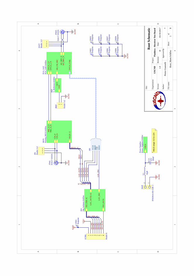
11
22
33
44
DD
CC
BB
AA
Pand
ora
- Rec
eive
r Tes
t Boa
rd
03/1
0/20
17
Root
_She
et.S
chD
oc
Piet
ro G
iann
elli
*
USC
ND
Roo
t Sch
emat
icTi
tle:
Org
aniza
tion:
Proj
ect:
File
nam
e:
Dat
e:
Auth
or:
Appr
oved
By:
Vers
ion:
Revi
sion:
D1.
0
Shee
t:of
18
TIN
_PTI
N_N
SEL[
0..1
]PRE_
O_P
PRE_
O_N
MU
XPr
eam
p_M
UX
.Sch
Doc
AD
_DRV
_PA
D_D
RV_N
DV
GA
_I_P
DV
GA
_I_N
AD
_CM
_SRC
DV
GA
_CTR
L
PGA
_AA
FPG
A_A
AF.
SchD
oc
AG
ND 25
V10
0uF
C21
L1 10μH
AG
ND
VBU
S
Pow
er S
uppl
ies
Pow
er_S
uppl
ies.S
chD
oc
123
JIN
Hea
der 1
x3
123
JOU
TH
eade
r 1x3
AG
ND
12
JREF
Hea
der 1
x2
AG
ND
CS0
MIS
O
MO
SISC
LK
SPISEL[0..1]
SEL0
SEL1
12JS
UP
FFK
DSA
1/H
1-5,
08- 2
AG
ND
ISO
_IN
[0..4
]
ISO
_OU
T0
LOC_
OU
T[0.
.4]
LOC_
IN0
ISO
Dig
_Iso
lato
rs.S
chD
oc
ISO
_IN
0IS
O_I
N1
ISO
_IN
2IS
O_I
N3
ISO
_IN
4IS
O_O
UT0
ISO_IN[0..4]
LOC_OUT[0..4]
LOC_
OU
T0LO
C_O
UT1
LOC_
OU
T4
LOC_
IN0
EXTO
UT
REF
V_R
efer
ence
.Sch
Doc
LOC_
OU
T2LO
C_O
UT3
1 2 3 4 5 6 7 8
JCTR
L
Hea
der 8
IGN
D
VIS
O
JTW
I01
4117
-XX
XX
JTW
O01
4117
-XX
XX
GN
D2
Testp
oint
GN
D3
Testp
oint
GN
D4
Testp
oint
GN
D5
Testp
oint
GN
D6
Testp
oint
GN
D8
Testp
oint
GN
D9
Testp
oint
GN
D7
Testp
oint
GN
D1
Testp
oint
AG
ND
VBU
S ra
nge:
5.5
to 1
2V.
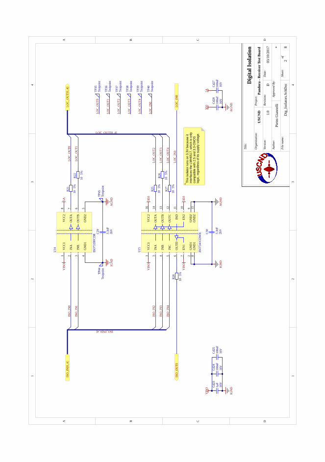
11
22
33
44
DD
CC
BB
AA
Pand
ora
- Rec
eive
r Tes
t Boa
rd
03/1
0/20
17
Dig
_Iso
lato
rs.S
chD
oc
Piet
ro G
iann
elli
*
USC
ND
Dig
ital I
sola
tion
Title
:
Org
aniza
tion:
Proj
ect:
File
nam
e:
Dat
e:
Auth
or:
Appr
oved
By:
Vers
ion:
Revi
sion:
D1.
0
Shee
t:of
28
INA
3
INB
4
INC
5
IND
11
OU
TA14
OU
TB13
OU
TC12
OU
TD6
EN1
7EN
210
VCC
11
VCC
216
GN
D1
2G
ND
29
GN
D1
8G
ND
215
U15
ISO
7341
CDW
R
16V
Cd27
100n
F16
V
Cd28
100n
F
3D3
AG
ND
16V
Cd24
100n
F16
V
Cd25
100n
F16
V
Cd23
1μF
VIS
O
IGN
D
VIS
O
VIS
O
VIS
O
5A 3D3
3D3
AG
ND
AG
ND
IGN
D
IGN
D
5%
R21
10
5%
R22
10
5%
R25
10
5%
R26
10
5%
R27
10
5%
R28
10IS
O_O
UT0
ISO
_IN
[0..4
]LO
C_O
UT[
0..4
]
LOC_
IN0
ISO
_IN
0
ISO
_IN
1
ISO
_IN
2
ISO
_IN
3
ISO
_IN
4
LOC_
OU
T0
LOC_
OU
T1
LOC_
OU
T2
LOC_
OU
T3
LOC_
OU
T4
ISO_IN[0..4]LOC_OUT[0..4]
2kV
C30
3.3n
F
2kV
C29
3.3n
F
INA
2
INB
3
OU
TA7
OU
TB6
VCC
11
VCC
28
GN
D2
5G
ND
14
U14
ISO
7320
FCD
R
5ATP35
Testp
oint
TP36
Testp
oint
TP37
Testp
oint
TP38
Testp
oint
TP39
Testp
oint
TP40
Testp
oint
LOC_
OU
T0
LOC_
OU
T1
LOC_
OU
T2
LOC_
OU
T3
LOC_
OU
T4
LOC_
IN0
LOC_
IN0
TP44
Testp
oint
TP45
Testp
oint
This
isol
ator
runs
on
3.3V
bec
ause
it
inte
rface
s th
e LM
H65
17, w
hich
is o
nly
com
patib
le w
ith 2
.5 a
nd 3
.3-C
MO
S lo
gic,
rega
rdle
ss o
f its
sup
ply
volta
ge.
PIC2
901
PIC2
902
COC2
9
PIC3
001
PIC3
002
COC3
0
PICd2301 PICd2302
COCd
23
PICd2401 PICd2402
COCd
24
PICd2501 PICd2502
COCd
25
PICd2701 PICd2702
COCd
27
PICd2801 PICd2802
COCd
28
PIR2
101
PIR2
102 CO
R21
PIR2
201
PIR2
202 COR
22
PIR2
501
PIR2
502 CO
R25
PIR2
601
PIR2
602 CO
R26
PIR2
701
PIR2
702 COR
27
PIR2
801
PIR2
802 CO
R28
PITP35
01
COTP
35
PITP
3601
COTP
36
PITP
3701
COTP
37
PITP38
01
COTP
38
PITP
3901
COTP
39
PITP40
01
COTP
40
PITP
4401
COTP
44
PITP
4501
COTP
45
PIU1
401
PIU1402
PIU1
403
PIU1404
PIU1405
PIU1406
PIU1407
PIU1408
COU1
4
PIU1501
PIU1502
PIU1503
PIU1504
PIU1
505
PIU1506
PIU1507
PIU1508
PIU1509
PIU15010
PIU15011
PIU1
5012
PIU15013
PIU15014
PIU15015
PIU15016
COU1
5
POISO0IN0
POISO0IN1
POISO0IN2
POISO0IN3
POISO0IN4
POISO0IN000040
POISO0OUT0
POLOC0IN0
POLOC0OUT0
POLOC0OUT1
POLOC0OUT2
POLOC0OUT3
POLOC0OUT4
POLO
C0OU
T000
040
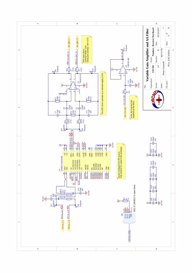
11
22
33
44
DD
CC
BB
AA
Pand
ora
- Rec
eive
r Tes
t Boa
rd
03/1
0/20
17
PGA
_AA
F.Sc
hDoc
Piet
ro G
iann
elli
*
USC
ND
Vari
able
Gai
n A
mpl
ifier
and
AA
Filt
erTi
tle:
Org
aniza
tion:
Proj
ect:
File
nam
e:
Dat
e:
Auth
or:
Appr
oved
By:
Vers
ion:
Revi
sion:
D1.
0
Shee
t:of
38
8.87
k0.
1%
R13
8.87
k0.
1%
R16
820p
F50
V
C8
VCM
_AD
3A3
AG
ND
AG
ND
AG
ND
3A3
5A
VCM_AD
A1/
SDO
/S0A
31
LATA
21
IPB-
12IP
B+11
OPB
-18
+5V
27
OPA
+24
B1/S
0B10
B2/S
1B9
B016
+5V
14
GN
D15
GN
D13
A3/
SDI/D
NA
1
MO
D1
5
B3/D
NB
8
IPA
-29
A0
25
OPA
-23
IPA
+30
A2/
CS/C
S1A
32
LATB
20
ENB
19
GN
D26
MO
D0
4
A4/
CLK
/UPA
2
B4/U
PB7
OPB
+17
PAD
33
ENA
22
A5
3
B56
GN
D28
U4
LMH
6517
SQ/N
OPB
AG
ND
AG
ND
AG
ND
3D3
AG
ND
AG
ND
AG
ND
AG
ND
AG
ND
AG
ND
AG
ND
AG
ND
1k 1%R18
100p
F10
V
C12
AG
ND
AD
_CM
_SRC
19.6
k0.
1%
R15
SCLK
CSM
OSI
MIS
O AG
ND
AG
ND
820p
F50
V
C9
9.09
k0.
1%
R12
9.09
k0.
1%
R17
AD
_DRV
_P
AD
_DRV
_N
AD
_DRV
_P
AD
_DRV
_N
DV
GA
_O_P
DV
GA
_O_N
DV
GA
_I_P
DV
GA
_I_N
DV
GA
_I_N
DV
GA
_I_P
AD
_CM
_SRC
SCLK
MO
SIM
ISO
CS0SP
I
AG
ND
1k 1%R11
3D3
MIS
OM
OSI
SCLK SD
O o
f LM
H65
17 is
ope
n-dr
ain
12
3
4 5
6
78
U5
THS4
121C
D
3D3
DV
GA
_CTR
LCS
AG
ND
3A3
AG
ND
5A
50V
C6 56pF
50V
C10
56pF
AG
ND
AG
ND
16V
Cd12
100n
F16
V
Cd9
1μF
16V
Cd10
1μF
16V
Cd11
100n
F16
V
Cd13
100n
F16
V
Cd14
100n
F
1%R14
2.2
15pF
50V
C7 15pF
50V
C11
2
34
5
1
U6
LMP2
011M
F
0.5%
R23
10 0.5%
R24
10
TP11
Testp
oint
TP6
Testp
oint
TP10
Testp
oint
TP7
Testp
oint
TP9
Testp
oint
TP5
Testp
oint
TP8
Testp
oint
Dev
ice
conf
igur
ed fo
r SPI
acc
ess.
Onl
y ch
anne
l A is
use
d in
this
pro
toty
pe.
VCM
_AD
mus
t be
0.8V
(re
quire
d by
the
ADC
)
ADC
Inpu
t spe
cs:
Com
mon
Mod
e: 0
.8V
Swin
g (p
er p
olar
ity):
CM
+/-0
.5V
The
ADC
driv
er o
pera
tes
at a
redu
ced
supp
ly (3
.3V)
.
PIC601 PIC602 COC6
PIC701 PIC702 COC7
PIC801
PIC802 COC8 PI
C901
PIC902 COC9
PIC1001 PIC1002
COC10
PIC1101 PIC1102
COC1
1
PIC1201 PIC1202
COC1
2
PICd901 PICd902
COCd
9 PICd1001 PICd1002
COCd10
PICd1101 PICd1102
COCd
11
PICd1201 PICd1202
COCd
12
PICd1301 PICd1302
COCd
13
PICd1401 PICd1402
COCd
14
PIR1101 PIR1102 COR1
1
PIR1201 PIR1202
COR1
2
PIR1
301
PIR1
302 CO
R13
PIR1401 PIR1402
PIR1403 PIR1404 PIR1405
PIR1406 PIR1407
PIR1408
COR14
PIR1501 PIR1502 COR1
5
PIR1
601
PIR1
602 COR
16
PIR1701 PIR1702 CO
R17
PIR1
801
PIR1
802 CO
R18
PIR2
301
PIR2
302 COR2
3
PIR2
401
PIR2
402 COR2
4
PITP501
COTP
5
PITP
601 COTP6
PITP701
COTP
7
PITP
801
COTP8
PITP
901
COTP
9
PITP
1001
CO
TP10
PITP
1101
CO
TP11
PIU401
PIU402
PIU403
PIU404
PIU405
PIU406
PIU407
PIU408
PIU409
PIU4010
PIU4011
PIU4012
PIU4013
PIU4
014
PIU4015
PIU4016
PIU4017
PIU4
018
PIU4019
PIU4020
PIU4
021
PIU4
022
PIU4023
PIU4024
PIU4025
PIU4
026
PIU4027
PIU4028
PIU4029
PIU4030
PIU4031
PIU4032
PIU4033
COU4
PIU501
PIU502
PIU503 PIU504
PIU505
PIU506 PIU507
PIU508
COU5
PIU601
PIU602 PIU603
PIU604
PIU605
COU6
POAD0CM0SRC
POAD0DRV0N
POAD0DRV0P
PODVGA0CTRL
PODV
GA0C
TRL0
C\S\
0\
PODV
GA0C
TRL0
MISO
PO
DVGA
0CTR
L0MO
SI
PODV
GA0C
TRL0
SCLK
PODVGA0I0N
PODVGA0I0P
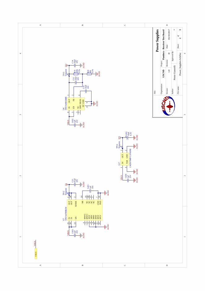
11
22
33
44
DD
CC
BB
AA
Pand
ora
- Rec
eive
r Tes
t Boa
rd
03/1
0/20
17
Pow
er_S
uppl
ies.S
chD
oc
Piet
ro G
iann
elli
*
USC
ND
Pow
er S
uppl
ies
Title
:
Org
aniza
tion:
Proj
ect:
File
nam
e:
Dat
e:
Auth
or:
Appr
oved
By:
Vers
ion:
Revi
sion:
D1.
0
Shee
t:of
48
VBU
S
OU
T1
NC
2
SEN
SE3
6P4V
24
6P4V
15
3P2V
6
GN
D7
1P6V
8
0P8V
9
0P4V
10
0P2V
11
0P1V
12
EN13
NR
14
IN15
IN16
NC
17N
C18
NC
19
OU
T20
PAD
21
U7
TPS7
A47
00RG
W
OU
T1
FB2
NC
3
4
EN5
NR/
SS6
DN
C7
IN8
9EPG
ND
U8
TPS7
A49
01D
RB
AG
ND
5A
VBU
S
VBU
S
AG
ND
3A3
VBU
S
10V
C13
47μF
AG
ND
10V
C16
10nF
0.5%
R19
100k
0.5%
R20
56k
10V
C15
10nF
10V
C14
10μF
AG
ND
AG
ND
16V
Cd15
1μF
AG
ND
25V
Cd31
1μF
25V
Cd32
1μF
AG
ND
AG
ND
IN1
OU
T3
GN
D2
TAB
4
U17
LM29
37IM
P-3.
3/N
OPB
VBU
S
25V
Cd26
1μF
AG
ND
AG
ND
AG
ND
AG
ND6.
3V
Cd33
10uF
3D3
TP12
Testp
oint
TP13
Testp
oint
TP14
Testp
oint
PIC1301 PIC1302
COC13
PIC1401 PIC1402
COC14
PIC1501 PIC1502
COC1
5
PIC1601 PIC1602
COC16
PICd1501 PICd1502
COCd
15
PICd2601 PICd2602
COCd
26
PICd3101 PICd3102
COCd
31
PICd3201 PICd3202
COCd
32
PICd3301 PICd3302 CO
Cd33
PIR1901 PIR1902 COR1
9
PIR2001 PIR2002 COR2
0
PITP
1201
COTP
12
PITP
1301
COTP
13
PITP
1401
COTP
14
PIU701
PIU702
PIU703
PIU704
PIU705
PIU706
PIU707
PIU708
PIU709
PIU7
010
PIU7011
PIU7012
PIU7013
PIU7014
PIU7015
PIU7
016
PIU7017
PIU7018
PIU7019
PIU7020
PIU7021
COU7
PIU801
PIU802
PIU803
PIU804
PIU805
PIU806
PIU807
PIU808
PIU809
COU8
PIU1701
PIU1702
PIU1703
PIU1704 COU1
7
POVBUS
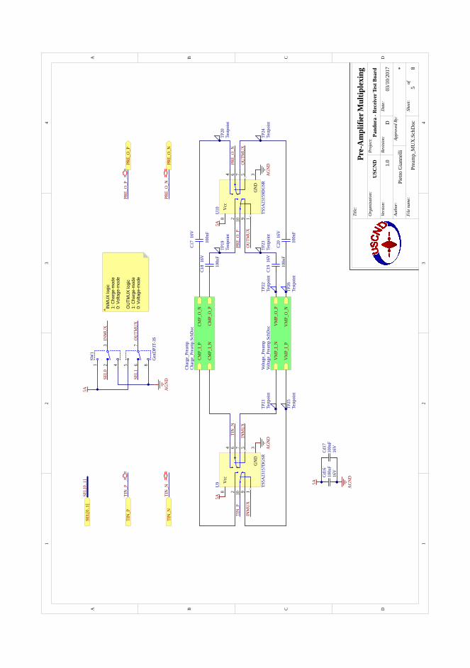
11
22
33
44
DD
CC
BB
AA
Pand
ora
- Rec
eive
r Tes
t Boa
rd
03/1
0/20
17
Prea
mp_
MU
X.S
chD
oc
Piet
ro G
iann
elli
*
USC
NDPr
e-A
mpl
ifier
Mul
tiple
Title
:
Org
aniza
tion:
Proj
ect:
File
nam
e:
Dat
e:
Auth
or:
Appr
oved
By:
Vers
ion:
Revi
sion:
D1.
0
Shee
t:of
58
5A
AG
ND
TIN
_P
TIN
_N
5A
AG
ND
TIN
_P
TIN
_N
TIN
_PTI
N_N
CMP_
O_P
CMP_
O_N
CMP_
I_P
CMP_
I_N
Char
ge_P
ream
pCh
arge
_Pre
amp.
SchD
oc
VM
P_O
_N
VM
P_O
_P
VM
P_I_
P
VM
P_I_
N
Volta
ge_P
ream
pVo
ltage
_Pre
amp.
SchD
oc
PRE_
O_P
PRE_
O_N
INM
UX
INM
UX
OU
TMU
XO
UTM
UX
SEL[
0..1
]SE
L[0.
.1] Vcc
8 2 10 9 1
GN
D35764
U9
TS5A
2315
7DG
SR
Vcc
8 2 10 9 1
GN
D35764
U10
TS5A
2315
9DG
SR
PRE_
O_P
PRE_
O_N
PRE_
O_N
PRE_
O_P
5A
AG
ND
16V
C17 10
0nF
16V
C18 10
0nF
16V
C20 10
0nF
16V
C19 10
0nF
16V
Cd17
100n
F16
V
Cd16
100n
F
1
32 4
765 8
SW1
Gen
DP3
T-3SIN
MU
X
OU
TMU
X
SEL0
SEL1
5A AG
ND
TP21
Testp
oint
TP25
Testp
oint
TP22
Testp
oint
TP26
Testp
oint
TP19
Testp
oint
TP20
Testp
oint
TP23
Testp
oint
TP24
Testp
oint
INM
UX
logi
c1:
Cha
rge-
mod
e0:
Vol
tage
-mod
e
OU
TMU
X lo
gic
1: C
harg
e-m
ode
0: V
olta
ge-m
ode
PIC1
701
PIC1
702
COC17
PIC1
801
PIC1
802
COC1
8
PIC1
901
PIC1
902
COC19
PIC2
001
PIC2
002
COC2
0
PICd1601 PICd1602
COCd
16
PICd1701 PICd1702
COCd
17
PISW101
PISW102
PISW103
PISW
104
PISW105
PISW
106
PISW
107
PISW108 COSW1
PITP19
01 COTP
19
PITP20
01 COTP
20
PITP
2101
COTP
21
PITP
2201
COTP
22
PITP
2301
CO
TP23
PI
TP24
01
COTP
24
PITP
2501
CO
TP25
PI
TP26
01
COTP
26
PIU901
PIU902
PIU903
PIU904
PIU905
PIU906
PIU907
PIU908
PIU909
PIU9010 COU
9
PIU1001
PIU1002
PIU1003
PIU1004
PIU1
005
PIU1006
PIU1007
PIU1008
PIU1
009
PIU10010 COU
10
POPRE0O0N
POPRE0O0P
POSEL0
POSEL1
POSEL000010
POTIN0N
POTIN0P
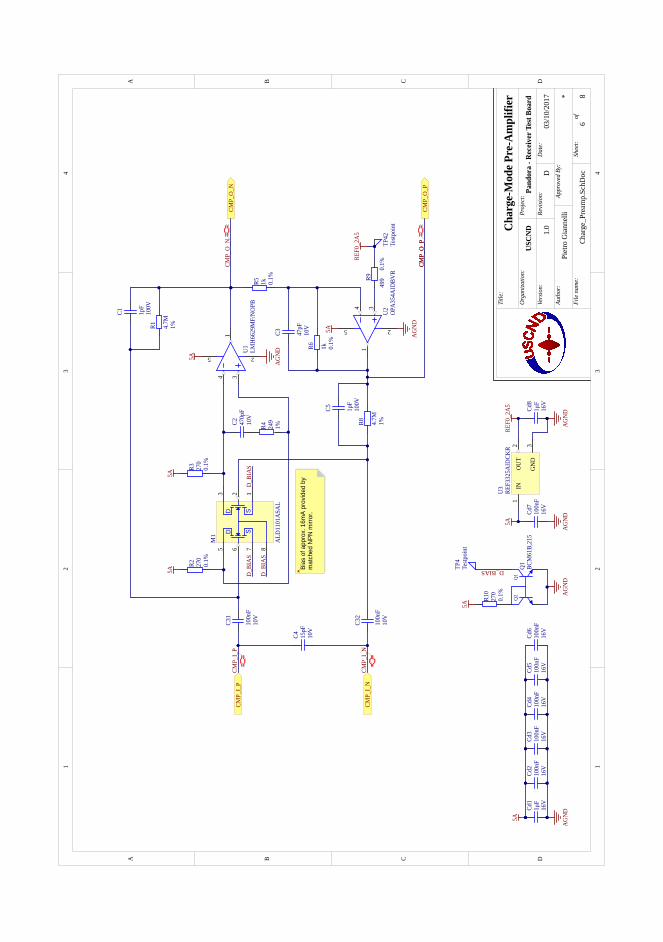
11
22
33
44
DD
CC
BB
AA
Pand
ora
- Rec
eive
r Tes
t Boa
rd
03/1
0/20
17
Char
ge_P
ream
p.Sc
hDoc
Piet
ro G
iann
elli
*
USC
NDC
harg
e-M
ode P
re-A
mpl
ifier
Title
:
Org
aniza
tion:
Proj
ect:
File
nam
e:
Dat
e:
Auth
or:
Appr
oved
By:
Vers
ion:
Revi
sion:
D1.
0
Shee
t:of
68
5A
100V
C5 1pF
CMP_
O_P
CMP_
O_N
CMP_
I_N
CMP_
I_P
REF0
_2A
5 16V
Cd8
1μF
16V
Cd7
100n
F
5A
AG
ND
AG
ND
CMP_
O_N
CMP_
O_P
CMP_
I_P
CMP_
I_N
10V
C4 15pF
16V
Cd2
100n
F16
V
Cd3
100n
F16
V
Cd1
1μF
5A
AG
ND
REF0
_2A
5
34
5
1
2
U1
LMH
6629
MF/
NO
PB
8712
6
35
D S
D S
M1
ALD
1101
ASA
L
5A
0.1%
R5 1k
0.1%
R6 1k
D_BIAS
AG
ND
100V
C1 1pF
AG
ND
5A
16V
Cd4
100n
F
10V
C3 47pF
0.1%
R2 270
0.1%
R3 270
5A5A
D_B
IAS
D_B
IAS
D_B
IAS
CMP_
O_P
16V
Cd5
100n
F16
V
Cd6
100n
F
1%R1 4.7M
1%R8 4.7M
AG
NDQ
1Q
2Q
1BC
M61
B,21
5
0.1%
R10
270
0.1%
R9
499
TP4
Testp
oint
TP42
Testp
oint
10V
C31
100n
F
10V
C32
100n
F
1
2
34
5
U2
OPA
354A
IDBV
R
IN1
OU
T2
GN
D3
U3
REF3
325A
IDCK
R
10V
C2 470p
F
1%R4 249
Bias
of a
ppro
x. 1
6mA
prov
ided
by
mat
ched
NPN
mirr
or.
PIC101
PIC102
COC1
PIC201 PIC202 COC
2
PIC301
PIC302
COC3
PIC401 PIC402
COC4
PIC501
PIC502
COC5
PIC3
101
PIC3
102
COC31
PIC3
201
PIC3
202
COC32
PICd101 PICd102
COCd1
PICd201 PICd202
COCd2
PICd301 PICd302
COCd3
PICd401 PICd402
COCd4
PICd501 PICd502
COCd5
PICd601 PICd602
COCd6
PICd701 PICd702
COCd7
PICd801 PICd802
COCd8
PIM101
PIM102
PIM103
PIM105
PIM106
PIM107
PIM108 COM1
PIQ101 PIQ102 PIQ103
PIQ104
COQ1
PIR101
PIR102 COR
1
PIR201 PIR202 COR2
PIR301 PIR302 COR
3
PIR401 PIR402 COR4
PIR501 PIR502 COR5
PIR601
PIR602 COR6
PIR801
PIR802 COR8
PIR901
PIR902 COR9
PIR1001 PIR1002 COR1
0
PITP401
COTP4
PITP
4201
COTP
42
PIU101
PIU102 PIU103
PIU104
PIU105 COU1
PIU201
PIU202 PIU203
PIU204
PIU205
COU2
PIU301
PIU302
PIU303
COU3
POCMP0I0N
POCMP0I0P
POCMP0O0N
POCMP0O0P
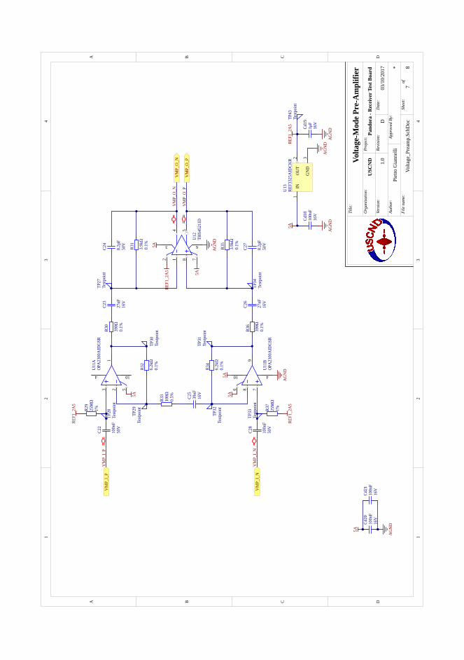
11
22
33
44
DD
CC
BB
AA
Pand
ora
- Rec
eive
r Tes
t Boa
rd
03/1
0/20
17
Volta
ge_P
ream
p.Sc
hDoc
Piet
ro G
iann
elli
*
USC
NDVo
ltage
-Mod
e Pre
-Am
plifi
erTi
tle:
Org
aniza
tion:
Proj
ect:
File
nam
e:
Dat
e:
Auth
or:
Appr
oved
By:
Vers
ion:
Revi
sion:
D1.
0
Shee
t:of
78
123
4
5
10
U11
AOP
A23
00A
IDG
SR
6 789
410
U11
BOP
A23
00A
IDG
SR
IN1
OU
T2
GN
D3
U13
REF3
325A
IDCK
RRE
F1_2
A5
5A
AG
ND
AG
ND
AG
ND
AG
ND
5A
3.9kΩ
0.1%
R31 5A
AG
ND
3.9kΩ
0.1%
R35
8.2p
F50
V
C24
8.2p
F50
V
C27
390Ω
0.1%
R30
390Ω
0.1%
R36
27nF
16V
C26
27nF
16V
C23
6.2kΩ
0.1%
R34
6.2kΩ
0.1%
R32
39nF
16V
C25
100Ω
0.5%
R33
25MΩ
1%R29
25MΩ
1%R37
100n
F50
V
C22
100n
F50
V
C28
VM
P_O
_N
VM
P_O
_P
VM
P_O
_N
VM
P_O
_P
VM
P_I_
P
VM
P_I_
NV
MP_
I_N
VM
P_I_
P
12
3
4 5
6
78
U12
THS4
521I
D5A
5A5A
5A
AG
ND
REF1
_2A
5
REF1
_2A
5
REF1
_2A
5
16V
Cd20
100n
F16
V
Cd21
100n
F
16V
Cd18
100n
F16
V
Cd19
1μF
TP32
Testp
oint
TP27
Testp
oint
TP34
Testp
oint
TP31
Testp
oint
TP30
Testp
oint
TP29
Testp
oint
TP28
Testp
oint
TP33
Testp
oint
TP43
Testp
oint
PIC2
201
PIC2
202
COC2
2
PIC2
301
PIC2
302
COC2
3
PIC2
401
PIC2
402
COC2
4
PIC2501 PIC2502 COC
25
PIC2
601
PIC2
602
COC2
6
PIC2
701
PIC2
702
COC2
7
PIC2
801
PIC2
802
COC28
PICd1801 PICd1802
COCd
18
PICd1901 PICd1902
COCd
19
PICd2001 PICd2002
COCd
20
PICd2101 PICd2102
COCd
21
PIR2901 PIR2902
COR2
9
PIR3
001
PIR3
002 CO
R30
PIR3
101
PIR3
102 CO
R31
PIR3
201
PIR3
202 CO
R32
PIR3301 PIR3302 COR3
3
PIR3
401
PIR3
402 CO
R34
PIR3
501
PIR3
502 CO
R35
PIR3
601
PIR3
602 CO
R36
PIR3701 PIR3702 CO
R37
PITP27
01
COTP
27
PITP
2801
CO
TP28
PITP
2901
COTP
29
PITP
3001
COTP
30
PITP
3101
COTP
31
PITP
3201
CO
TP32
PITP
3301
COTP
33
PITP
3401
CO
TP34
PITP
4301
COTP
43
PIU1
101
PIU1
102
PIU1103
PIU1104
PIU1105
PIU11010 COU1
1A
PIU1104
PIU1106
PIU1107
PIU1108
PIU1109
PIU11010 COU1
1B
PIU1201
PIU1
202
PIU1203 PIU1204
PIU1
205
PIU1206 PIU1207
PIU1
208
COU1
2
PIU1301
PIU1302
PIU1303
COU1
3
POVMP0I0N
POVMP0I0P
POVMP0O0N
POVMP0O0P
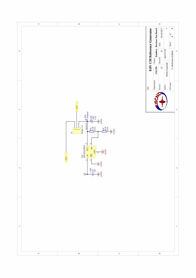
11
22
33
44
DD
CC
BB
AA
Pand
ora
- Rec
eive
r Tes
t Boa
rd
03/1
0/20
17
V_R
efer
ence
.Sch
Doc
Piet
ro G
iann
elli
*
USC
ND
0.8V
CM
Ref
eren
ce G
ener
ator
Title
:
Org
aniza
tion:
Proj
ect:
File
nam
e:
Dat
e:
Auth
or:
Appr
oved
By:
Vers
ion:
Revi
sion:
D1.
0
Shee
t:of
88
EXT
OU
T123
J4 Hea
der 1
x3
IN1
OU
T5
2
EN3
FB4
GN
D
U16
TPS7
6201
DBV
R
0.5%
R39
66.5
k
0.5%
R38
13.3
k
AG
ND
AG
ND
16V
Cd29
1μF
AG
ND
AG
ND
6.3V
Cd30
10uF
AG
ND
5ARE
F0V
8TP
41Te
stpoi
ntPICd2901 PICd2902
COCd29
PICd3001 PICd3002 CO
Cd30
PIJ401
PIJ402
PIJ403
COJ4 PIR3801 PIR3802 COR
38
PIR3901 PIR3902 COR3
9
PITP
4101
COTP
41
PIU1601
PIU1602
PIU1
603
PIU1
604
PIU1605
COU1
6
POEXT
POOUT

D I F F E R E N T I A L C H A R G E S O U R C E

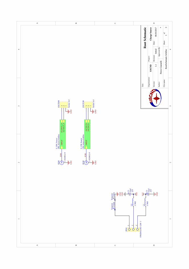
11
22
33
44
DD
CC
BB
AA
Char
ge S
ourc
e
06/1
0/20
17
Root
Sche
mati
c.Sch
Doc
Piet
ro G
ianne
lli*
USCN
D
Roo
t Sch
emat
icTi
tle:
Org
aniz
atio
n:Pr
ojec
t:
File
nam
e:
Dat
e:
Auth
or:
Appr
oved
By:
Vers
ion:
Revi
sion
:In
itial
1.1
Shee
t:of
13
L1 2.5kΩ
L2 2.5kΩ
25V
C5 33μF
25V
C3 33μF
GN
D
GN
D
VCCVEE
GN
D
GN
D
GN
D
GN
D
123
JOU
TDM
Sock
et 1
x3
123
JOU
TCM
Sock
et 1
x3
GN
D0
Testp
oint
1 2 3
JPSU
FFK
DSA
1/H
1-5,
08- 3
INPU
TO
UTP
UT1
OU
TPU
T2
U_C
M_S
ourc
eCM
_Sou
rce.
SchD
oc
INPU
TO
UTP
UT_
PO
UTP
UT_
N
U_D
M_S
ourc
eD
M_S
ourc
e.Sc
hDoc
JICM
1-16
3461
2-0
JID
M 1-16
3461
2-0
GN
D
ICM
IDM
GN
D1
Testp
oint PIC301 PIC302
COC3
PIC501 PIC502
COC5
PIGN
D001
COG
ND0
PIGN
D101
COG
ND1
PIJICM01
PIJICM02
COJI
CM PIJIDM01
PIJIDM02
COJIDM
PIJO
UTCM
01
PIJO
UTCM
02
PIJO
UTCM
03 COJO
UTCM
PIJO
UTDM
01
PIJO
UTDM
02
PIJO
UTDM
03 COJOUTDM
PIJPSU01
PIJPSU02
PIJPSU03
COJP
SU
PIL101
PIL102
COL1
PIL201
PIL202
COL2
PIC302 PIC501
PIGN
D001
PI
GND1
01
PIJICM02 PIJIDM02
PIJO
UTCM
01
PIJO
UTDM
01
PIJPSU01
PIJICM01 NLICM
PIJIDM01 NLIDM
PIJPSU03
PIL101
PIJPSU02
PIL201
PIJO
UTCM
02
PIJO
UTDM
02
PIJO
UTCM
03
PIJO
UTDM
03
PIC301 PIL102
PIC502 PIL202
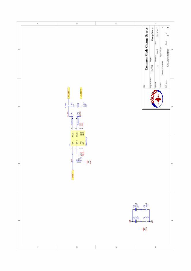
11
22
33
44
DD
CC
BB
AA
Char
ge S
ourc
e
06/1
0/20
17
CM_S
ourc
e.Sch
Doc
Piet
ro G
ianne
lli*
USCN
D
Com
mon
-Mod
e Cha
rge S
ourc
eTi
tle:
Org
aniz
atio
n:Pr
ojec
t:
File
nam
e:
Dat
e:
Auth
or:
Appr
oved
By:
Vers
ion:
Revi
sion
:In
itial
1.1
Shee
t:of
23
OU
T 1
8
GN
D2
+IN
11
-VS
6+V
S7
OU
T 2
5
GN
D3
+IN
24
U1
AD
8079
AR
GN
D0.1%
R1 50Ω
ICM
ICM
ICM
VCC VEE
25V
C2 100n
F
25V
C6 100n
F
25V
C1 1μF
25V
C4 1μF
GN
D
VCC VEE
50V
CSH
1
3.3p
FIN
PUT
OU
TPU
T1
OU
TPU
T2
50V
CSH
2
3.3p
F
TP1
Testp
oint
TP2
Testp
oint
OCM
1
OCM
2
PIC101 PIC102
COC1
PIC201 PIC202
COC2
PIC401 PIC402
COC4
PIC601 PIC602
COC6
PICS
H101
PI
CSH1
02
COCSH1
PICS
H201
PI
CSH2
02
COCSH2
PIR101 PIR102 COR
1
PITP
101 COTP1
PITP
201 COT
P2
PIU101
PIU102
PIU103
PIU104
PIU105
PIU106
PIU107
PIU108
COU1
PIC102 PIC202
PIC401 PIC601
PIR101 PIR102 PIU101
PIU102
PIU103
PIU104
NLIC
M POINPUT
PICS
H201
POOUTPUT2
PICS
H101
POOUTPUT1
PICS
H102
PITP
101
PIU108
NLOCM1
PICS
H202
PITP
201
PIU105
NLOCM2
PIC101 PIC201
PIU107
PIC402 PIC602
PIU106
POINPUT
POOUTPUT1
POOUTPUT2
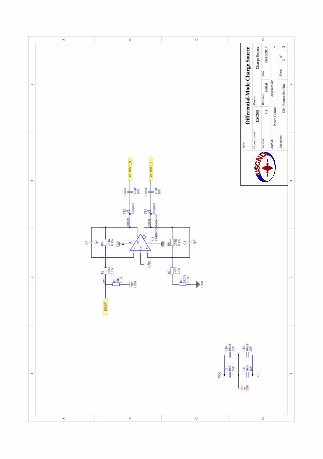
11
22
33
44
DD
CC
BB
AA
Char
ge S
ourc
e
06/1
0/20
17
DM_S
ourc
e.Sch
Doc
Piet
ro G
ianne
lli*
USCN
D
Diff
eren
tial-M
ode C
harg
e Sou
rce
Title
:
Org
aniz
atio
n:Pr
ojec
t:
File
nam
e:
Dat
e:
Auth
or:
Appr
oved
By:
Vers
ion:
Revi
sion
:In
itial
1.1
Shee
t:of
33
GN
D
CM
EN
U2
LMH
6552
MA
/NO
PB
C7 1pF
0.1%
R3 274Ω
0.1%
R2 255Ω
0.1%
R4 26.7Ω
0.1%
R7 59Ω
VCC
GN
D
VEE
50V
CSH
3
3.3p
F
50V
CSH
4
3.3p
F
C8 1pF
0.1%
R6 274Ω
0.1%
R5 255Ω
GN
D
TP3
Testp
oint
TP4
Testp
oint
25V
C10
100n
F
25V
C12
100n
F
25V
C9 10nF
25V
C11
10nF
GN
D
VCC VEE
OD
MP
OD
MN
IDM
INPU
T
OU
TPU
T_P
OU
TPU
T_N
PIC701
PIC7
02
COC7
PIC801
PIC8
02
COC8
PIC901 PIC902
COC9
PIC1001 PIC1002
COC1
0
PIC1101 PIC1102
COC11
PIC1201 PIC1202
COC1
2
PICSH3
01 PIC
SH302 COCSH3
PICSH4
01 PIC
SH402 COCS
H4
PIR201
PIR202 COR
2 PIR301
PIR3
02 COR3
PIR401 PIR402 COR4
PIR501
PIR502 COR
5 PIR601
PIR6
02 COR6
PIR701 PIR702 COR7
PITP
301
COTP3
PITP
401
COTP
4
PIU201
PIU202
PIU203 PIU204
PIU205
PIU206 PIU207
PIU208
COU2
PIC902 PIC1002
PIC1101 PIC1201
PIR402 PIR702
PIU202
PIR202
PIR701 NLIDM
POINPUT
PIR401 PIR502
PICSH4
01 POOUTPUT0P
PICSH3
01 POOUTPUT0N
PIC801
PIR501
PIR6
02
PIU208
PIC701
PIR201
PIR3
02
PIU201
PIC7
02
PICSH3
02
PIR301
PITP
301
PIU204 NLOD
MN
PIC8
02
PICSH4
02
PIR601
PITP
401
PIU205 NLODMP
PIC901 PIC1001
PIU203 PIU207
PIC1102 PIC1202
PIU206
POINPUT
POOUTPUT0N
POOUTPUT0P


C O M M O N - M O D E C H A R G E S O U R C E

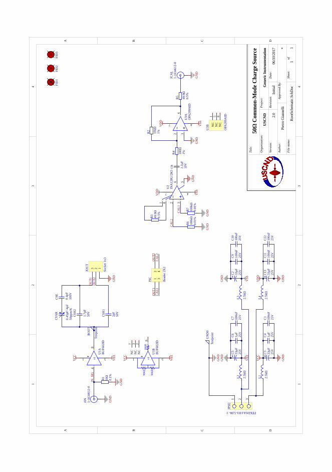
11
22
33
44
DD
CC
BB
AA
Gen
eric
Inst
rum
enta
tion
06/1
0/20
17
Root
Sche
mati
c.Sch
Doc
Piet
ro G
ianne
lli*
USCN
D
50Ω
Com
mon
-Mod
e Cha
rge S
ourc
eTi
tle:
Org
aniz
atio
n:Pr
ojec
t:
File
nam
e:
Dat
e:
Auth
or:
Appr
oved
By:
Vers
ion:
Revi
sion
:In
itial
2.0
Shee
t:of
11
VCC VEE
GN
D
L1 2.5kΩ
L2 2.5kΩ
0.1%R1 50Ω
25V
C5 33μF
25V
C3 33μF
GN
D
GN
D
VCCVEE
GN
D
25V
C4 1μF
25V
C6 1μF
IN_S
IG
50V
CSH
1
2pF
GN
D
GN
D
123
JOU
T
Sock
et 1
x3
8
1
4
5x1
U1A
BUF6
02ID
6
1 5
NC
2N
C3
NC
7
200Ω
50kΩ
50kΩ
x1
U1B
BUF6
02ID
VCC VEE
BOU
T
Testp
oint
25V
C1 100n
F
25V
C7 100n
F
GN
D0
Testp
oint
1 2 3
JPSU
FFKDSA1/H1-5,08- 3
JIN
1-16
3461
2-0
50V
CSH
2
1.7p
F
100V
CSE
0.4p
F50
ppm
/K
CVA
R
0.45
pF~4
pF
0.01
%
R7 100kΩ
0.01
%
R6 100kΩ
1 2 3
4
56
7
8U
2IN
A12
8U/2
K5
47
632
U3A
OPA
209A
ID
NC
1
NC
5
NC
8
U3B
OPA
209A
ID
0.5%
R3 49.9Ω
1%R4 100Ω
1%R2 10kΩ
10V
C8 2.2μ
F
OU
T1O
UT2
GN
DG
ND
CAL1
CAL2
GN
DG
ND
JCA
L1-
1634
612-
0
GN
D
0.5%
R5 49.9Ω
25V
C11
100n
F
25V
C9 100n
F
25V
C12
100n
F
25V
C10
100n
F
OU
T1O
UT2
CAL1
CAL2
12
34
JSC
Hea
der 2
X2
L4 2.5kΩ
L3 2.5kΩ
25V
C13
33μF
GN
D
25V
C2 33μF
GN
D
VSS
VD
D
VSS
VSS
VD
DV
DD
FID
3FI
D2
FID
1
PIBO
UT01
COBOUT
PIC101 PIC102
COC1
PIC201 PIC202
COC2
PIC301 PIC302
COC3
PIC401 PIC402
COC4
PIC501 PIC502
COC5
PIC601 PIC602
COC6
PIC701 PIC702
COC7
PIC801
PIC802
COC8
PIC901 PIC902
COC9
PIC1001 PIC1002
COC1
0
PIC1101 PIC1102
COC11
PIC1201 PIC1202
COC1
2 PIC1301 PIC1302
COC1
3
PICS
E01
PICS
E02 COCS
E
PICS
H101
PI
CSH1
02 COCSH1
PICSH2
01 PIC
SH202 CO
CSH2
PICVAR
01 PIC
VAR02
COCVAR
COFID1
COFI
D2
COFID3
PIGND0
01 CO
GND0
PIJCAL01
PIJCAL02
COJCAL
PIJIN01
PIJIN02
COJIN
PIJOUT01
PIJOUT02
PIJOUT03 COJOUT
PIJPSU01
PIJPSU02
PIJPSU03
COJP
SU
PIJS
C01
PIJSC02
PIJSC03
PIJSC04
COJSC
PIL101
PIL102
COL1
PIL201
PIL202
COL2
PIL301
PIL302
COL3
PIL401
PIL402
COL4
PIR101 PIR102 COR
1
PIR201
PIR202 COR
2 PIR301 PIR302
COR3
PIR401
PIR402 COR4
PIR501
PIR502
COR5
PIR601 PIR602 COR
6
PIR701 PIR702 COR7
PIU101 PIU104
PIU105
PIU108
COU1A
PIU101 PIU102
PIU103
PIU105
PIU106
PIU107
COU1B
PIU201
PIU202
PIU203
PIU204 PIU205
PIU206
PIU207 PIU208
COU2
PIU302
PIU303
PIU304
PIU306
PIU307 COU3A
PIU301
PIU305
PIU308
COU3B
PIJSC03
PIR702 PIU203
NLCA
L1
PIJSC04
PIR602
PIU202
NLCA
L2
PIC102
PIC201
PIC302 PIC402
PIC501 PIC601
PIC701 PIC901
PIC1001
PIC1102 PIC1202
PIC1302
PIGND0
01
PIJCAL02
PIJIN02 PIJOUT01
PIJPSU01
PIR101
PIR601 PIR701
PIU205
PIU303
PIJIN01
PIR102 PIU104
NLIN0SIG
PIU308
PIU305
PIU301
PIU107
PIU106
PIU103
PIU102
PIR302 PIU208
PIR301
PIU201
PIR202
PIR401
PIU302
PIR201
PIR501
PIU306
PIJPSU03
PIL101
PIL401
PIJPSU02
PIL201
PIL301
PIJCAL01
PIR502
PICS
E02
PICVAR
01
PIC802
PIR402
PIC801
PIU206
PIBO
UT01
PICS
H102
PICSH2
02
PICVAR
02
PIU108
PICS
E01
PICSH2
01
PIJOUT03
PIJS
C01
NLOU
T1
PICS
H101
PIJOUT02
PIJSC02
NLOU
T2
PIC101 PIC301
PIC401 PIL102
PIU101
PIC1101 PIC1201
PIC1301 PIL402
PIU207 PIU307
PIC502 PIC602
PIC702 PIL202
PIU105
PIC202 PIC902
PIC1002 PIL302
PIU204 PIU304

CP U L S E W I D T H E N C O D E R
1 %% PWEncoder for The Arbitrary Waveform Pulser
% Project Pandora - Pietro Giannelli, 2016-2017
% Encodes an arbitrary signal of finite duration into a pulse-width
% stream of arbitrary duty resolution.
6
% Changelog:
% 20161201 - Extended to half bridge (positive-negative)
% 20161202 - Low-level masking correction
% 20161212 - Added encoded stream output (16-bit word)
11 % 20161230 - Added fully differential support w/ 32-bit output
% 20170103 - Added alternate level 1 and 3 encoders
% 20170114 - Using only crossover modulations (no level 2 and 4)
% 20170315 - Added UART communications to PulserElementsSoC [removed]
% 20170330 - Added continuous modulation w/ reduced output range
16 % 20170411 - Added full-dynamic range extension - added file output
clearvars;
%% Output file name
21 output_file='Encoded stream.txt';
%% Pulser configuration parameters
awp8_sysclk = 100e6; % FPGA decoder clock
min_pw=20e-9; % Minimum pulse width
26
%% Encoder parameters
fsys=awp8_sysclk; % Decoder system clock [Hz]
fpwe=fsys/20; % Encoder source sample rate [Hz]
pwe_steps=fsys/fpwe; % Duration of a PWE period in fsys cycles
31 assert(mod(fsys,fpwe) == 0, 'System clock must be a multiple of the sample rate');
% There is also another requirement, that fsys/fpwe be an EVEN number. This
% encoder strongly relies on using 0.5 duty ratios.
assert(mod(pwe_steps,2) == 0, 'Duty quantization must be even');
assert(2*min_pw < 1/fpwe, 'Sample rate is too high for this pulser');
36 Gpre=1; % Pre-processing gain
Opre=0; % Pre-processing offset
% Note: the encoder input dynamic range is [-2;2], corresponding to an
% output of [-2HV;2HV]
41
%% Minimum and maximum duty ratios
208 pulse width encoder
Dmin=fpwe*min_pw;
Dmax=1-Dmin;
% Total number of duty steps (ignoring Dmin, Dmax saturation)
46 Dlev=uint16(pwe_steps);
% Dmin and Dmax in number of duty steps
Dqmin=uint16(ceil(min_pw*fsys));
Dqmax=Dlev-Dqmin;
% Therefore, the final value of encoded duty per switch must be an integer
51 % between Dqmin and Dqmax. 0 and Dlev are also acceptable duties.
% Note that Dqmin is used here to define the thresholds in order to
% avoid inconsistent banding caused by PW quantization errors!
actDmin=double(Dqmin)/double(Dlev);
56 % actDmin will likely be higher than Dmin.
%% Load the source stream from file
% If the source was sampled at rate different from fpwe, it must be
% resampled first!
61 instream=dlmread('CW_for_AWG.txt');
Nsamp=length(instream);
%% Encoder data structures
% Dq - Encoder output matrix
66 % Rows: encoded stream frames (one per input sample)
% Columns: corresponding switch [PP PN NP NN]
Dq=uint16(zeros(Nsamp,4));
%% Encoder core
71 for cx=1:Nsamp
Cs=Gpre*instream(cx)+Opre; % Applying pre-scaling and offset
Cframe=uint16([0 0 0 0]); % Current frame temporary storage vector
% Columns: corresponding switch [PP PN NP NN]
76
% Rectification
if Cs>=0 % The special case where the sample is 0 can be handled by both
pbias=1; % Positive bias true
else
81 Cs=-Cs; % Flip the sample
pbias=0; % Positive bias false
end
% From now on the original polarity of the sample Cs is irrelevant to
% the encoder. The output frame is properly re-assembled later to
86 % account for polarity reversal.
% Switches unused in this polarity need to operate at Dqmin
Cframe(2)=Dqmin;
Cframe(3)=Dqmin;
91
if Cs>2 % Applying upper saturation
Cs = 2;
pulse width encoder 209
end
96 % Here we apply amplitude band-splitting, and use different encoding
% levels depending on the value of Cs.
if Cs>2-4*actDmin % High-range - duty ratios beyond limits!
if (Cs>=2-1*actDmin)
Cframe(1)=Dlev;
101 Cframe(2)=0;
Cframe(3)=uint16((2-Cs)*Dlev); % Push switch 3 (NP) below Dmin
Cframe(4)=Dlev;
elseif (Cs>=2-2*actDmin)
Cframe(1)=uint16((Cs-1+actDmin)*Dlev); % Push switch 1 (PP) over Dmax
106 Cframe(2)=0;
Cframe(3)=Dqmin;
Cframe(4)=Dlev;
elseif (Cs>=2-3*actDmin)
Cframe(1)=Dqmax;
111 Cframe(2)=uint16((-Cs+2-2*actDmin)*Dlev); % Push switch 2 (PN) below
Dmin
Cframe(3)=Dqmin;
Cframe(4)=Dlev;
else
Cframe(1)=Dqmax;
116 Cframe(2)=Dqmin;
Cframe(3)=Dqmin;
Cframe(4)=uint16((Cs-1+3*actDmin)*Dlev); % Push switch 4 (NN) over
Dmax
end
121 elseif Cs>1-2*actDmin % Mid-range
Cframe(1)=uint16((Cs-(1-2*actDmin))*Dlev)+Dqmin; % This switch is adjusted
Cframe(4)=Dqmax; % This switch operates at maximum duty
else % Low-Range
126 Cframe(1)=Dqmin; % This switch operates at minimum duty
Cframe(4)=uint16(Cs*Dlev)+Dqmin; % This switch is adjusted
end
% Apply polarity reversal while writing the results to Dq
131 if pbias
Dq(cx,:)=Cframe; % No polarity reversal needed
else
Dq(cx,1)=Cframe(3); % NP->PP
Dq(cx,2)=Cframe(4); % NN->PN
136 Dq(cx,3)=Cframe(1); % PP->NP
Dq(cx,4)=Cframe(2); % PN->NN
end
end
141
%% Building the output bitstream
210 pulse width encoder
% This output bitstream is built with complementary edge decoding, since
% switches belonging to the same half-bridge are used together within
% one sample period.
146 Dlev=uint32(Dlev); % Converted to uint32 to avoid hitting the 16bit roof!
outstream=uint8(zeros(Nsamp*Dlev,4)); % There are fsys/fpwe bits per encoded
sample
for cx=1:Nsamp
% Switch PP
% Sets to 1 the correct number of clock cycles
151 % Starting from the beginning of the period
frame_start=(cx-1)*Dlev + 1;
frame_end=(cx-1)*Dlev + uint32(Dq(cx,1));
outstream( frame_start:frame_end,1 )=1;
% Switch PN
156 % Sets to 1 the correct number of clock cycles
% Starting from the ending of the period
frame_end=(cx-1)*Dlev + uint32(Dq(cx,2));
outstream( frame_start:frame_end,2 )=1;
% Switch NP
161 % Sets to 1 the correct number of clock cycles
% Starting from the ending of the period
frame_end=(cx-1)*Dlev + uint32(Dq(cx,3));
outstream( frame_start:frame_end,3 )=1;
% Switch NN
166 % Sets to 1 the correct number of clock cycles
% Starting from the ending of the period
frame_end=(cx-1)*Dlev + uint32(Dq(cx,4));
outstream( frame_start:frame_end,4 )=1;
end
171
%% Waveform plotter
figure();
sourc = subplot(3,1,1); % Plotting input sequence
176 plot(0:1/fpwe:(Nsamp-1)/fpwe,instream,'o');
ylim([-2 2]);
xlabel('time [s]');
ylabel('Amplitude');
title('Input sequence');
181
quant = subplot(3,1,2); % Plotting duty-quantized signal
plot(0:1/fpwe:(Nsamp-1)/fpwe,Dq(:,1),'o'); % PP switch
hold on
plot(0:1/fpwe:(Nsamp-1)/fpwe,-double(Dq(:,2)),'o'); % PN switch
186 plot(0:1/fpwe:(Nsamp-1)/fpwe,-double(Dq(:,3)),'o'); % NP switch
plot(0:1/fpwe:(Nsamp-1)/fpwe,Dq(:,4),'o'); % NN switch
ylim([-double(Dlev) double(Dlev)]);
xlabel('time [s]');
ylabel('Duty [on-sysclk-count]');
191 title('Encoded output');
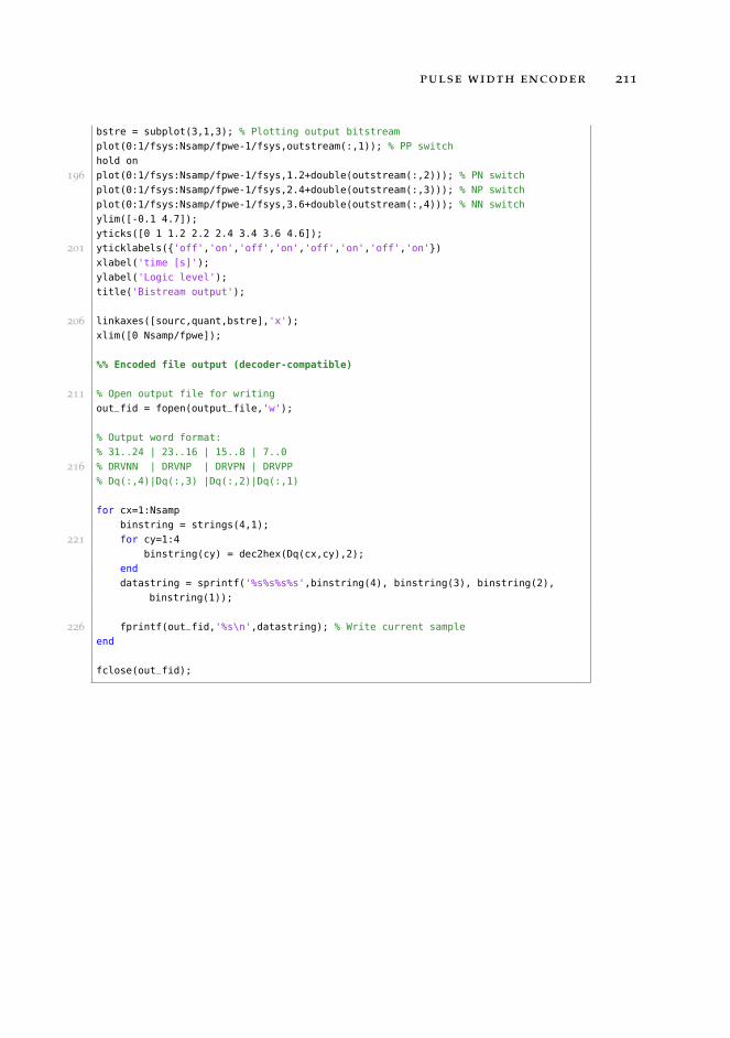
pulse width encoder 211
bstre = subplot(3,1,3); % Plotting output bitstream
plot(0:1/fsys:Nsamp/fpwe-1/fsys,outstream(:,1)); % PP switch
hold on
196 plot(0:1/fsys:Nsamp/fpwe-1/fsys,1.2+double(outstream(:,2))); % PN switch
plot(0:1/fsys:Nsamp/fpwe-1/fsys,2.4+double(outstream(:,3))); % NP switch
plot(0:1/fsys:Nsamp/fpwe-1/fsys,3.6+double(outstream(:,4))); % NN switch
ylim([-0.1 4.7]);
yticks([0 1 1.2 2.2 2.4 3.4 3.6 4.6]);
201 yticklabels('off','on','off','on','off','on','off','on')
xlabel('time [s]');
ylabel('Logic level');
title('Bistream output');
206 linkaxes([sourc,quant,bstre],'x');
xlim([0 Nsamp/fpwe]);
%% Encoded file output (decoder-compatible)
211 % Open output file for writing
out_fid = fopen(output_file,'w');
% Output word format:
% 31..24 | 23..16 | 15..8 | 7..0
216 % DRVNN | DRVNP | DRVPN | DRVPP
% Dq(:,4)|Dq(:,3) |Dq(:,2)|Dq(:,1)
for cx=1:Nsamp
binstring = strings(4,1);
221 for cy=1:4
binstring(cy) = dec2hex(Dq(cx,cy),2);
end
datastring = sprintf('%s%s%s%s',binstring(4), binstring(3), binstring(2),
binstring(1));
226 fprintf(out_fid,'%s\n',datastring); % Write current sample
end
fclose(out_fid);


DF P G A P U L S E W I D T H D E C O D E R
This appendix includes the soft design of the AWPulser8Decoder FPGAIP core.
The first table documents the register mapping that can be accessedfrom the Avalon-MM bus.
The HDL code printed afterwards was written in a mix of Verilogand SystemVerilog, and uses an Intel FPGA proprietary embeddedmemory core to implement the WrapBuf storage. The instantiationhierarchy of the various modules is presented in the following list:
• AWPulser8Decoder:
– Avalon_Slave instantiated as AVManager
– Controller instantiated as CTRLi
– PWClockCore instantiated as PWClocker
– Generates 8 PulserChannel:
* WrapBuf instantiated as WBuf
* PWDecoderCore instantiated as PDecoder
* PWDecoderCore instantiated as NDecoder

214 fpga pulse width decoder
avalon-mm register map
Add
ress
Reg
iste
rna
me
R/W
Bitm
ask
31..2
423
..16
15
..87
65
43
21
0
0x0000
Stat
usR
XX
XX
XX
XX
XC
W/B
urst
Busy
/Idl
e
0x0001
Com
man
dW
XX
XX
XX
XX
X01:S
tart
,10:S
top
0x0002
Cha
nnel
Enab
leR
/WX
XX
CH
8C
H7
CH
6C
H5
CH
4C
H3
CH
2C
H1
0x0003
PWLe
ngth
R/W
XX
XU
nsig
ned
char
(X-2
55)
0x0004
Burs
tC
ount
R/W
XX
XU
nsig
ned
char
(0:C
Wm
ode,
1-2
55:B
urst
mod
e)
0x0005
Burs
tLe
ngth
R/W
XX
(lsb
)BL
8BL
7BL
6BL
5BL
4BL
3BL
2BL
1BL
0
0x0006
PLL
Con
figN
DX
XX
XX
XX
XX
XX
0x0007
Cha
nnel
1bu
ffer
W(N
N)
(NP)
(PN
)(P
P)
0x0206
0x0207
Cha
nnel
2bu
ffer
W(N
N)
(NP)
(PN
)(P
P)
0x0406
0x0407
Cha
nnel
3bu
ffer
W(N
N)
(NP)
(PN
)(P
P)
0x0606
0x0607
Cha
nnel
4bu
ffer
W(N
N)
(NP)
(PN
)(P
P)
0x0806
0x0807
Cha
nnel
5bu
ffer
W(N
N)
(NP)
(PN
)(P
P)
0x0A06
0x0A07
Cha
nnel
6bu
ffer
W(N
N)
(NP)
(PN
)(P
P)
0x0C06
0x0C07
Cha
nnel
7bu
ffer
W(N
N)
(NP)
(PN
)(P
P)
0x0E06
0x0E07
Cha
nnel
8bu
ffer
W(N
N)
(NP)
(PN
)(P
P)
0x1006
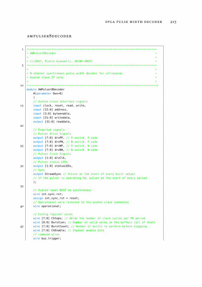
fpga pulse width decoder 215
awpulser8decoder
1 /******************************************************************************
* AWPulser8Decoder *
* *
* (c)2017, Pietro Giannelli, USCND-UNIFI *5 *******************************************************************************
* *
* 8-channel synchronous pulse-width decoder for ultrasound. *
* Avalon slave IP core. *
* *10 *******************************************************************************/
module AWPulser8Decoder
#(parameter Dws=8)
(
// Avalon slave interface signals
15 input clock, reset, read, write,
input [15:0] address,
input [3:0] byteenable,
input [31:0] writedata,
output [31:0] readdata,
20
// Exported signals
// Pulser Drive Signals
output [7:0] drvPP, // P-switch, P-side
output [7:0] drvPN, // N-switch, P-side
25 output [7:0] drvNP, // P-switch, N-side
output [7:0] drvNN, // N-switch, N-side
// Pulser Clock Signals
output [1:0] drvClk,
// Pulser status LEDs
30 output [1:0] statusLEDs,
// Sync
output StreamSync // Pulses at the start of every burst output
// If the pulser is operating CW, pulses at the start of every period
);
35
// Avalon reset MUST be synchronous
wire int_sync_rst;
assign int_sync_rst = reset;
// Operational wire rerouted to the avalon slave submodule
40 wire operational;
// Config register wires
wire [7:0] CSteps; // Holds the number of clock cycles per PW period
wire [8:0] BurstLen; // Number of valid words in the buffers (all of them)
45 wire [7:0] BurstCount; // Number of bursts to perform before stopping
wire [7:0] ChEnable; // Channel enable bits
// command wires
wire bus_trigger;
216 fpga pulse width decoder
wire bus_stop;
50 // Avalon slave module
Avalon_Slave AVManager(
.clock(clock),
.read(read),
.write(write),
55 .address(address),
.byteenable(byteenable), // Currently unimplemented
.writedata(writedata),
.readdata(readdata),
60 .bus_trigger(bus_trigger),
.bus_stop(bus_stop),
.csteps(CSteps),
.burstlen(BurstLen),
.burstcount(BurstCount),
65 .chenable(ChEnable),
.status(statusLEDs),
.operational(operational),
.rst(int_sync_rst)
);
70
// Pulser clocking is disabled
assign drvClk = 2’b11;
// Clock resync signal
wire ctrl_pwclk_rst;
75
// This register is pulsed to terminate the decoders
// (otherwise they will keep decoding the last feed samples).
// IMPORTANT: Need to count CSteps number of cycles AFTER ctrl_pwclk_rst is
asserted
// before asserting terminate. This ensures that the current samples are fully
decoded.
80 reg terminate;
wire [7:0]SSyncP; // Collects the sample syncs to generate the terminate
signal
wire [7:0]SSyncN; // Collects the sample syncs to generate the terminate
signal
wire GSync; // Global sample sync
85 assign GSync = | SSyncP, SSyncN; // Reduce all these syncs
reg termwaitcnt; // Waiting for counter done
reg [7:0]termcd; // Count-up register
90 always @(posedge clock)
begin
if (int_sync_rst)
begin
terminate <= 1’b0;
95 termwaitcnt <= 1’b0;
fpga pulse width decoder 217
termcd <= 8’h00;
end
if (terminate)
terminate <= 1’b0; // De-assert terminate after 1 cycle
100 else if (operational && GSync) // When operational captures GSync
begin
termcd <= 8’h00;
terminate <= 1’b0;
termwaitcnt <= 1’b1;
105 end
else if (termwaitcnt) // If it is counting
begin
if (termcd < CSteps) // Counting not done
begin
110 // Count-up
termcd <= termcd + 8’h01;
end
else // Counting done
begin
115 termcd <= 8’h00; // Reset counter
if (~operational)
begin
terminate <= 1’b1; // Kill the decoder when not operational
termwaitcnt <= 1’b0;
120 end
end
end
else
begin
125 terminate <= 1’b0;
termwaitcnt <= 1’b0;
end
end
130 // Sync signal coming out of the clock gen
wire MainSync;
// Instantiation of the PWD sync generator (one feeds all)
PWClockCore #(.Dws(Dws)) PWClocker(
.Sync(MainSync),
135 .CSteps(CSteps),
.SysClk(clock),
.Rst(int_sync_rst || ctrl_pwclk_rst)
);
140 // Tapeout signal to each channel
wire [7:0] tapeout;
// Restart signal to all channels
wire restart;
// Rollback signal from each channel
145 wire [7:0] rollback;
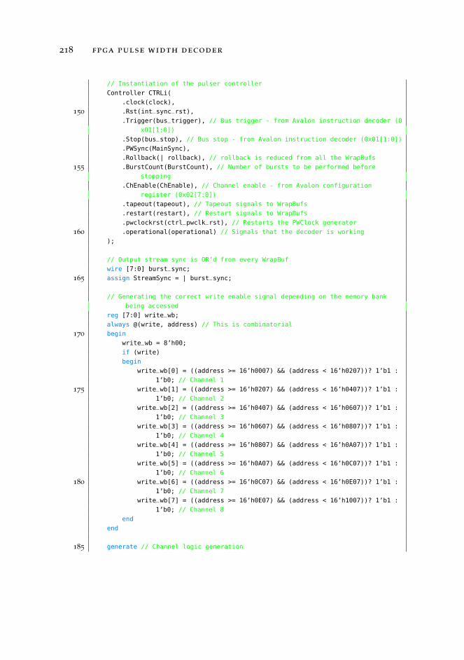
218 fpga pulse width decoder
// Instantiation of the pulser controller
Controller CTRLi(
.clock(clock),
150 .Rst(int_sync_rst),
.Trigger(bus_trigger), // Bus trigger - from Avalon instruction decoder (0
x01[1:0])
.Stop(bus_stop), // Bus stop - from Avalon instruction decoder (0x01[1:0])
.PWSync(MainSync),
.Rollback(| rollback), // rollback is reduced from all the WrapBufs
155 .BurstCount(BurstCount), // Number of bursts to be performed before
stopping
.ChEnable(ChEnable), // Channel enable - from Avalon configuration
register (0x02[7:0])
.tapeout(tapeout), // Tapeout signals to WrapBufs
.restart(restart), // Restart signals to WrapBufs
.pwclockrst(ctrl_pwclk_rst), // Restarts the PWClock generator
160 .operational(operational) // Signals that the decoder is working
);
// Output stream sync is OR’d from every WrapBuf
wire [7:0] burst_sync;
165 assign StreamSync = | burst_sync;
// Generating the correct write enable signal depending on the memory bank
being accessed
reg [7:0] write_wb;
always @(write, address) // This is combinatorial
170 begin
write_wb = 8’h00;
if (write)
begin
write_wb[0] = ((address >= 16’h0007) && (address < 16’h0207))? 1’b1 :
1’b0; // Channel 1
175 write_wb[1] = ((address >= 16’h0207) && (address < 16’h0407))? 1’b1 :
1’b0; // Channel 2
write_wb[2] = ((address >= 16’h0407) && (address < 16’h0607))? 1’b1 :
1’b0; // Channel 3
write_wb[3] = ((address >= 16’h0607) && (address < 16’h0807))? 1’b1 :
1’b0; // Channel 4
write_wb[4] = ((address >= 16’h0807) && (address < 16’h0A07))? 1’b1 :
1’b0; // Channel 5
write_wb[5] = ((address >= 16’h0A07) && (address < 16’h0C07))? 1’b1 :
1’b0; // Channel 6
180 write_wb[6] = ((address >= 16’h0C07) && (address < 16’h0E07))? 1’b1 :
1’b0; // Channel 7
write_wb[7] = ((address >= 16’h0E07) && (address < 16’h1007))? 1’b1 :
1’b0; // Channel 8
end
end
185 generate // Channel logic generation
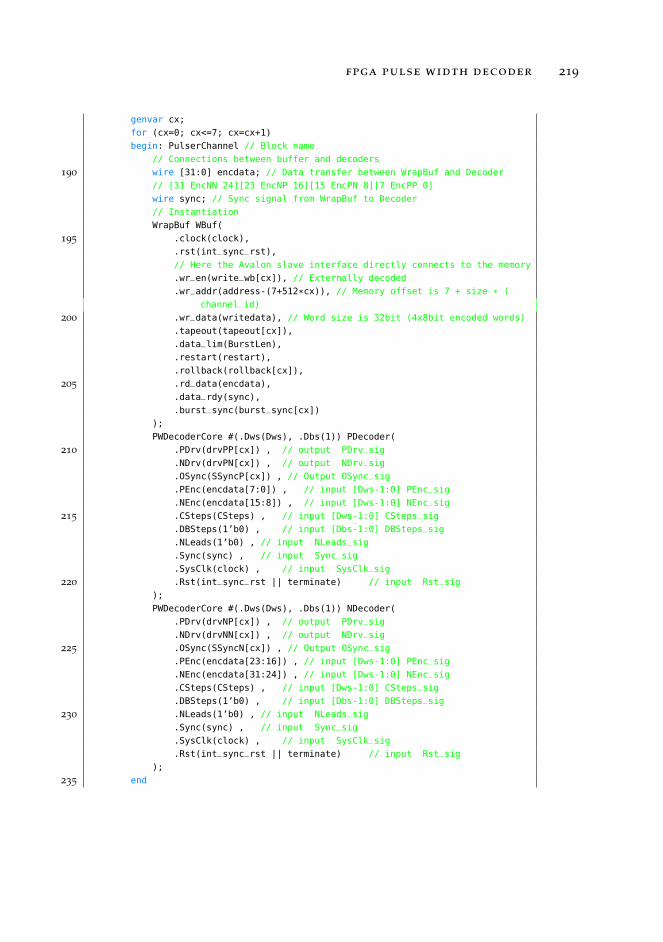
fpga pulse width decoder 219
genvar cx;
for (cx=0; cx<=7; cx=cx+1)
begin: PulserChannel // Block name
// Connections between buffer and decoders
190 wire [31:0] encdata; // Data transfer between WrapBuf and Decoder
// [31 EncNN 24][23 EncNP 16][15 EncPN 8][7 EncPP 0]
wire sync; // Sync signal from WrapBuf to Decoder
// Instantiation
WrapBuf WBuf(
195 .clock(clock),
.rst(int_sync_rst),
// Here the Avalon slave interface directly connects to the memory
.wr_en(write_wb[cx]), // Externally decoded
.wr_addr(address-(7+512*cx)), // Memory offset is 7 + size * (
channel_id)
200 .wr_data(writedata), // Word size is 32bit (4x8bit encoded words)
.tapeout(tapeout[cx]),
.data_lim(BurstLen),
.restart(restart),
.rollback(rollback[cx]),
205 .rd_data(encdata),
.data_rdy(sync),
.burst_sync(burst_sync[cx])
);
PWDecoderCore #(.Dws(Dws), .Dbs(1)) PDecoder(
210 .PDrv(drvPP[cx]) , // output PDrv_sig
.NDrv(drvPN[cx]) , // output NDrv_sig
.OSync(SSyncP[cx]) , // Output OSync_sig
.PEnc(encdata[7:0]) , // input [Dws-1:0] PEnc_sig
.NEnc(encdata[15:8]) , // input [Dws-1:0] NEnc_sig
215 .CSteps(CSteps) , // input [Dws-1:0] CSteps_sig
.DBSteps(1’b0) , // input [Dbs-1:0] DBSteps_sig
.NLeads(1’b0) , // input NLeads_sig
.Sync(sync) , // input Sync_sig
.SysClk(clock) , // input SysClk_sig
220 .Rst(int_sync_rst || terminate) // input Rst_sig
);
PWDecoderCore #(.Dws(Dws), .Dbs(1)) NDecoder(
.PDrv(drvNP[cx]) , // output PDrv_sig
.NDrv(drvNN[cx]) , // output NDrv_sig
225 .OSync(SSyncN[cx]) , // Output OSync_sig
.PEnc(encdata[23:16]) , // input [Dws-1:0] PEnc_sig
.NEnc(encdata[31:24]) , // input [Dws-1:0] NEnc_sig
.CSteps(CSteps) , // input [Dws-1:0] CSteps_sig
.DBSteps(1’b0) , // input [Dbs-1:0] DBSteps_sig
230 .NLeads(1’b0) , // input NLeads_sig
.Sync(sync) , // input Sync_sig
.SysClk(clock) , // input SysClk_sig
.Rst(int_sync_rst || terminate) // input Rst_sig
);
235 end
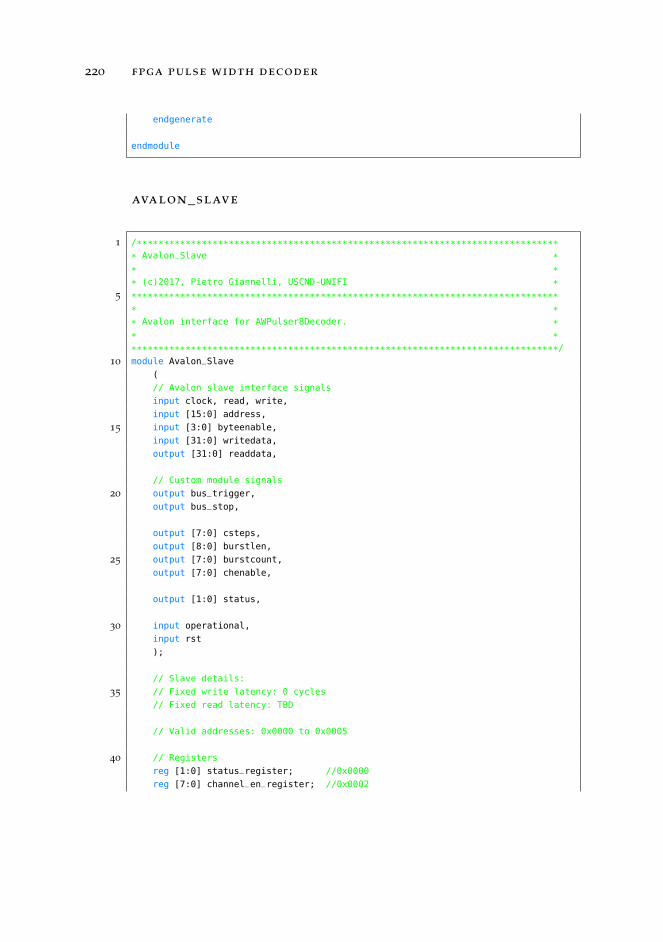
220 fpga pulse width decoder
endgenerate
endmodule
avalon_slave
1 /******************************************************************************
* Avalon_Slave *
* *
* (c)2017, Pietro Giannelli, USCND-UNIFI *5 *******************************************************************************
* *
* Avalon interface for AWPulser8Decoder. *
* *
*******************************************************************************/
10 module Avalon_Slave
(
// Avalon slave interface signals
input clock, read, write,
input [15:0] address,
15 input [3:0] byteenable,
input [31:0] writedata,
output [31:0] readdata,
// Custom module signals
20 output bus_trigger,
output bus_stop,
output [7:0] csteps,
output [8:0] burstlen,
25 output [7:0] burstcount,
output [7:0] chenable,
output [1:0] status,
30 input operational,
input rst
);
// Slave details:
35 // Fixed write latency: 0 cycles
// Fixed read latency: TBD
// Valid addresses: 0x0000 to 0x0005
40 // Registers
reg [1:0] status_register; //0x0000
reg [7:0] channel_en_register; //0x0002
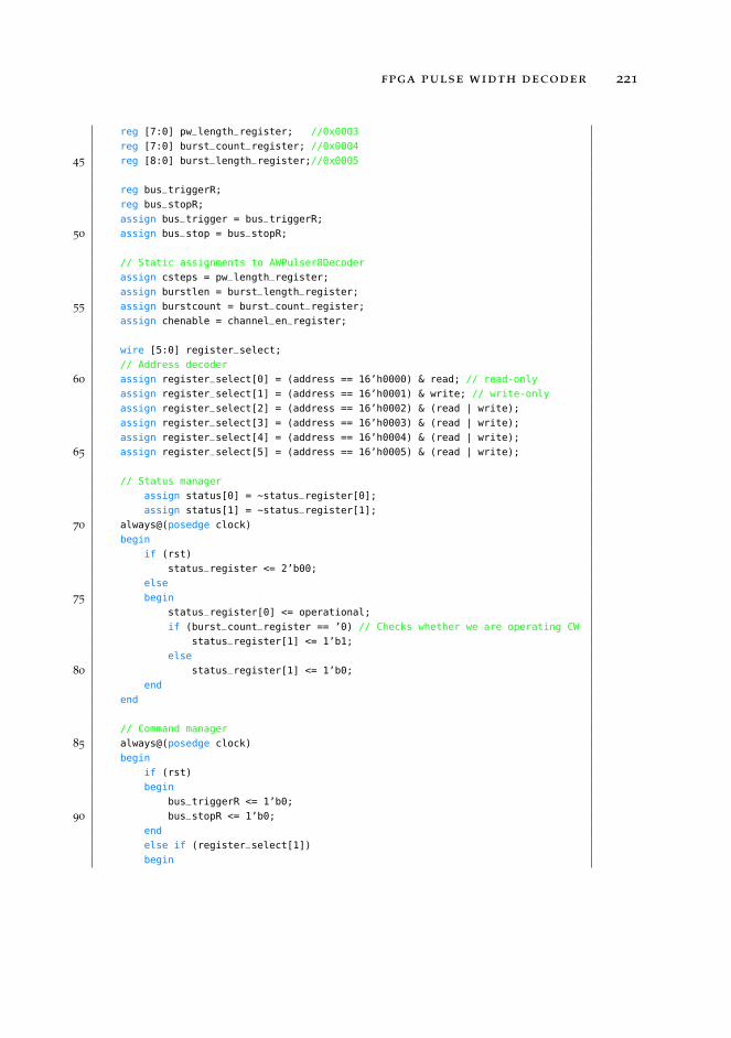
fpga pulse width decoder 221
reg [7:0] pw_length_register; //0x0003
reg [7:0] burst_count_register; //0x0004
45 reg [8:0] burst_length_register;//0x0005
reg bus_triggerR;
reg bus_stopR;
assign bus_trigger = bus_triggerR;
50 assign bus_stop = bus_stopR;
// Static assignments to AWPulser8Decoder
assign csteps = pw_length_register;
assign burstlen = burst_length_register;
55 assign burstcount = burst_count_register;
assign chenable = channel_en_register;
wire [5:0] register_select;
// Address decoder
60 assign register_select[0] = (address == 16’h0000) & read; // read-only
assign register_select[1] = (address == 16’h0001) & write; // write-only
assign register_select[2] = (address == 16’h0002) & (read | write);
assign register_select[3] = (address == 16’h0003) & (read | write);
assign register_select[4] = (address == 16’h0004) & (read | write);
65 assign register_select[5] = (address == 16’h0005) & (read | write);
// Status manager
assign status[0] = ~status_register[0];
assign status[1] = ~status_register[1];
70 always@(posedge clock)
begin
if (rst)
status_register <= 2’b00;
else
75 begin
status_register[0] <= operational;
if (burst_count_register == ’0) // Checks whether we are operating CW
status_register[1] <= 1’b1;
else
80 status_register[1] <= 1’b0;
end
end
// Command manager
85 always@(posedge clock)
begin
if (rst)
begin
bus_triggerR <= 1’b0;
90 bus_stopR <= 1’b0;
end
else if (register_select[1])
begin
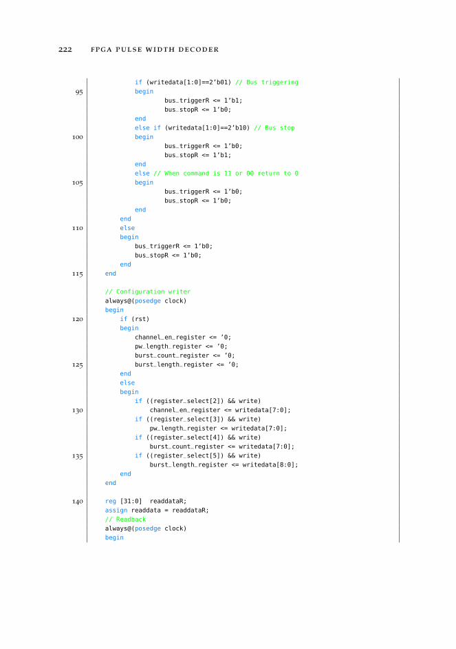
222 fpga pulse width decoder
if (writedata[1:0]==2’b01) // Bus triggering
95 begin
bus_triggerR <= 1’b1;
bus_stopR <= 1’b0;
end
else if (writedata[1:0]==2’b10) // Bus stop
100 begin
bus_triggerR <= 1’b0;
bus_stopR <= 1’b1;
end
else // When command is 11 or 00 return to 0
105 begin
bus_triggerR <= 1’b0;
bus_stopR <= 1’b0;
end
end
110 else
begin
bus_triggerR <= 1’b0;
bus_stopR <= 1’b0;
end
115 end
// Configuration writer
always@(posedge clock)
begin
120 if (rst)
begin
channel_en_register <= ’0;
pw_length_register <= ’0;
burst_count_register <= ’0;
125 burst_length_register <= ’0;
end
else
begin
if ((register_select[2]) && write)
130 channel_en_register <= writedata[7:0];
if ((register_select[3]) && write)
pw_length_register <= writedata[7:0];
if ((register_select[4]) && write)
burst_count_register <= writedata[7:0];
135 if ((register_select[5]) && write)
burst_length_register <= writedata[8:0];
end
end
140 reg [31:0] readdataR;
assign readdata = readdataR;
// Readback
always@(posedge clock)
begin
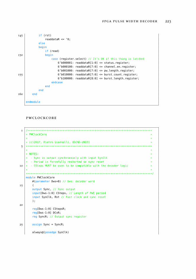
fpga pulse width decoder 223
145 if (rst)
readdataR <= ’0;
else
begin
if (read)
150 begin
case (register_select) // It’s OK if this thing is latched
6’b000001: readdataR[1:0] <= status_register;
6’b000100: readdataR[7:0] <= channel_en_register;
6’b001000: readdataR[7:0] <= pw_length_register;
155 6’b010000: readdataR[7:0] <= burst_count_register;
6’b100000: readdataR[8:0] <= burst_length_register;
endcase
end
end
160 end
endmodule
pwclockcore
1 /******************************************************************************
* PWClockCore *
* *
* (c)2017, Pietro Giannelli, USCND-UNIFI *5 *******************************************************************************
* *
* NOTES: *
* - Sync is output synchronously with input SysClk *
* - Period is forcefully restarted on sync reset *10 * - CSteps MUST be even to be compatible with the decoder logic *
* *
*******************************************************************************/
module PWClockCore
#(parameter Dws=8) // Dws: decoder word
15 (
output Sync, // Sync output
input[Dws-1:0] CSteps, // Length of PWE period
input SysClk, Rst // Fast clock and sync reset
);
20
reg[Dws-1:0] CStepsR;
reg[Dws-1:0] DCxR;
reg SyncR; // Output sync register
25 assign Sync = SyncR;
always@(posedge SysClk)
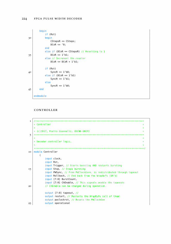
224 fpga pulse width decoder
begin
if (Rst)
30 begin
CStepsR <= CSteps;
DCxR <= ’0;
end
else if (DCxR == CStepsR) // Resetting to 1
35 DCxR <= 1’b1;
else // Increment the counter
DCxR <= DCxR + 1’b1;
if (Rst)
40 SyncR <= 1’b0;
else if (DCxR == 1’b1)
SyncR <= 1’b1;
else
SyncR <= 1’b0;
45 end
endmodule
controller
1 /******************************************************************************
* Controller *
* *
* (c)2017, Pietro Giannelli, USCND-UNIFI *5 *******************************************************************************
* *
* Decoder controller logic. *
* *
*******************************************************************************/
10 module Controller
(
input clock,
input Rst,
input Trigger, // Starts bursting AND restarts bursting
15 input Stop, // Stops bursting
input PWSync, // From PWClockCore, is redistributed through tapeout
input Rollback, // Fed back from the WrapBufs (OR’d)
input [7:0] BurstCount,
input [7:0] ChEnable, // This signals enable the tapeouts
20 // ChEnable can be changed during operation.
output [7:0] tapeout, //
output restart, // Restarts the WrapBufs (all of them)
output pwclockrst, // Resets the PWClockGen
25 output operational
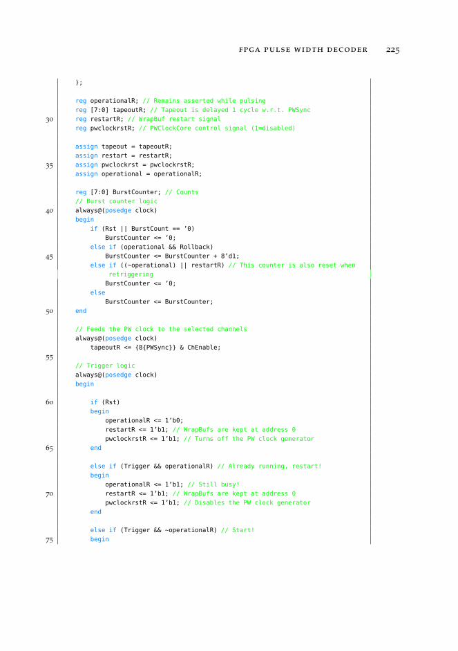
fpga pulse width decoder 225
);
reg operationalR; // Remains asserted while pulsing
reg [7:0] tapeoutR; // Tapeout is delayed 1 cycle w.r.t. PWSync
30 reg restartR; // WrapBuf restart signal
reg pwclockrstR; // PWClockCore control signal (1=disabled)
assign tapeout = tapeoutR;
assign restart = restartR;
35 assign pwclockrst = pwclockrstR;
assign operational = operationalR;
reg [7:0] BurstCounter; // Counts
// Burst counter logic
40 always@(posedge clock)
begin
if (Rst || BurstCount == ’0)
BurstCounter <= ’0;
else if (operational && Rollback)
45 BurstCounter <= BurstCounter + 8’d1;
else if ((~operational) || restartR) // This counter is also reset when
retriggering
BurstCounter <= ’0;
else
BurstCounter <= BurstCounter;
50 end
// Feeds the PW clock to the selected channels
always@(posedge clock)
tapeoutR <= 8PWSync & ChEnable;
55
// Trigger logic
always@(posedge clock)
begin
60 if (Rst)
begin
operationalR <= 1’b0;
restartR <= 1’b1; // WrapBufs are kept at address 0
pwclockrstR <= 1’b1; // Turns off the PW clock generator
65 end
else if (Trigger && operationalR) // Already running, restart!
begin
operationalR <= 1’b1; // Still busy!
70 restartR <= 1’b1; // WrapBufs are kept at address 0
pwclockrstR <= 1’b1; // Disables the PW clock generator
end
else if (Trigger && ~operationalR) // Start!
75 begin
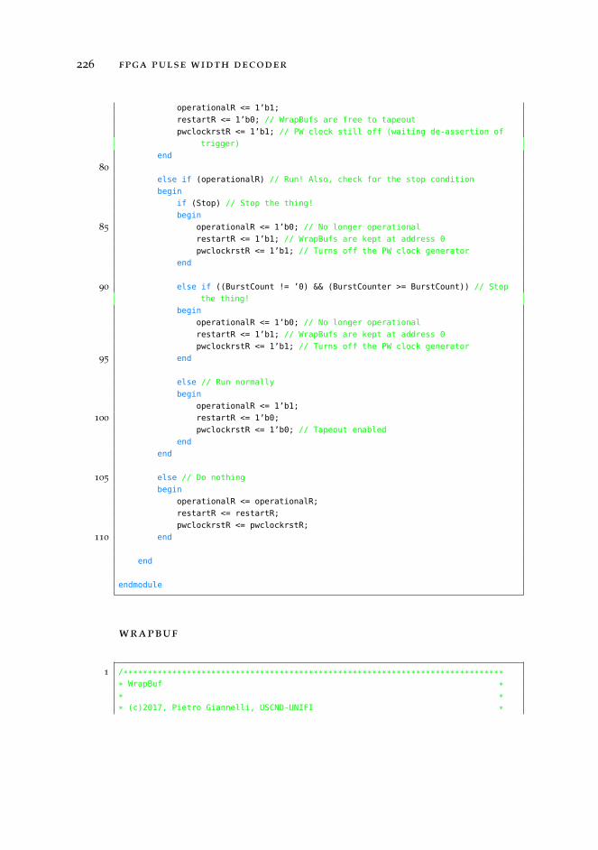
226 fpga pulse width decoder
operationalR <= 1’b1;
restartR <= 1’b0; // WrapBufs are free to tapeout
pwclockrstR <= 1’b1; // PW clock still off (waiting de-assertion of
trigger)
end
80
else if (operationalR) // Run! Also, check for the stop condition
begin
if (Stop) // Stop the thing!
begin
85 operationalR <= 1’b0; // No longer operational
restartR <= 1’b1; // WrapBufs are kept at address 0
pwclockrstR <= 1’b1; // Turns off the PW clock generator
end
90 else if ((BurstCount != ’0) && (BurstCounter >= BurstCount)) // Stop
the thing!
begin
operationalR <= 1’b0; // No longer operational
restartR <= 1’b1; // WrapBufs are kept at address 0
pwclockrstR <= 1’b1; // Turns off the PW clock generator
95 end
else // Run normally
begin
operationalR <= 1’b1;
100 restartR <= 1’b0;
pwclockrstR <= 1’b0; // Tapeout enabled
end
end
105 else // Do nothing
begin
operationalR <= operationalR;
restartR <= restartR;
pwclockrstR <= pwclockrstR;
110 end
end
endmodule
wrapbuf
1 /******************************************************************************
* WrapBuf *
* *
* (c)2017, Pietro Giannelli, USCND-UNIFI *
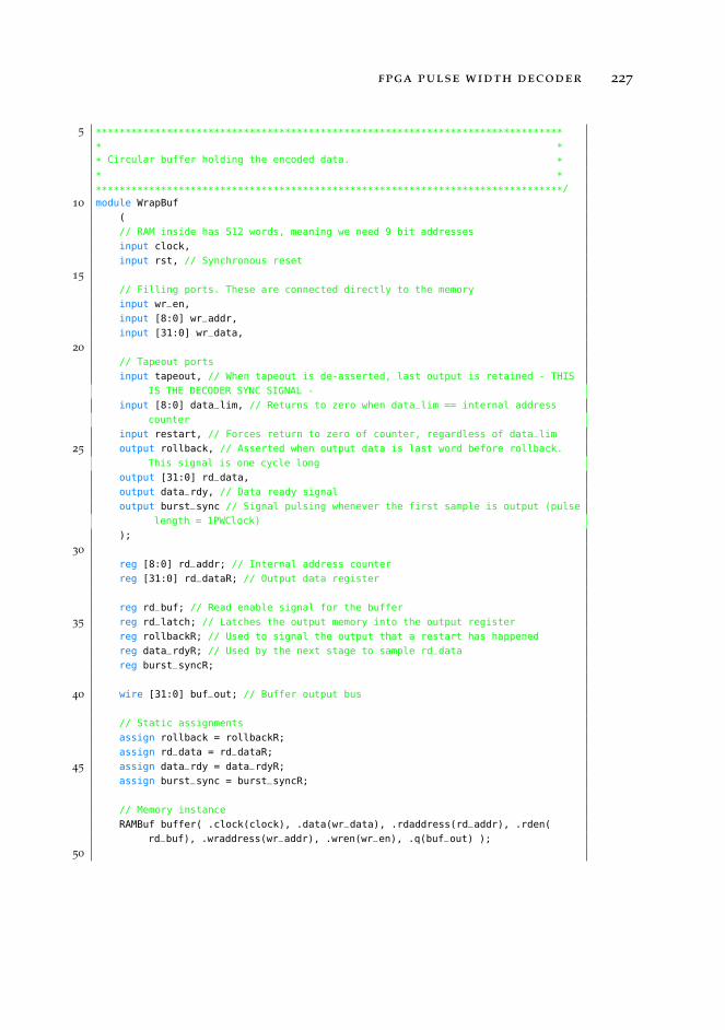
fpga pulse width decoder 227
5 *******************************************************************************
* *
* Circular buffer holding the encoded data. *
* *
*******************************************************************************/
10 module WrapBuf
(
// RAM inside has 512 words, meaning we need 9 bit addresses
input clock,
input rst, // Synchronous reset
15
// Filling ports. These are connected directly to the memory
input wr_en,
input [8:0] wr_addr,
input [31:0] wr_data,
20
// Tapeout ports
input tapeout, // When tapeout is de-asserted, last output is retained - THIS
IS THE DECODER SYNC SIGNAL -
input [8:0] data_lim, // Returns to zero when data_lim == internal address
counter
input restart, // Forces return to zero of counter, regardless of data_lim
25 output rollback, // Asserted when output data is last word before rollback.
This signal is one cycle long
output [31:0] rd_data,
output data_rdy, // Data ready signal
output burst_sync // Signal pulsing whenever the first sample is output (pulse
length = 1PWClock)
);
30
reg [8:0] rd_addr; // Internal address counter
reg [31:0] rd_dataR; // Output data register
reg rd_buf; // Read enable signal for the buffer
35 reg rd_latch; // Latches the output memory into the output register
reg rollbackR; // Used to signal the output that a restart has happened
reg data_rdyR; // Used by the next stage to sample rd_data
reg burst_syncR;
40 wire [31:0] buf_out; // Buffer output bus
// Static assignments
assign rollback = rollbackR;
assign rd_data = rd_dataR;
45 assign data_rdy = data_rdyR;
assign burst_sync = burst_syncR;
// Memory instance
RAMBuf buffer( .clock(clock), .data(wr_data), .rdaddress(rd_addr), .rden(
rd_buf), .wraddress(wr_addr), .wren(wr_en), .q(buf_out) );
50
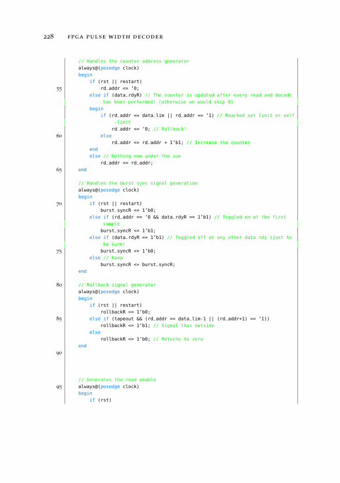
228 fpga pulse width decoder
// Handles the counter address generator
always@(posedge clock)
begin
if (rst || restart)
55 rd_addr <= ’0;
else if (data_rdyR) // The counter is updated after every read and decode
has been performed! (otherwise we would skip 0)
begin
if (rd_addr == data_lim || rd_addr == ’1) // Reached set limit or self
-limit
rd_addr <= ’0; // Rollback!
60 else
rd_addr <= rd_addr + 1’b1; // Increase the counter
end
else // Nothing new under the sun
rd_addr <= rd_addr;
65 end
// Handles the burst sync signal generation
always@(posedge clock)
begin
70 if (rst || restart)
burst_syncR <= 1’b0;
else if (rd_addr == ’0 && data_rdyR == 1’b1) // Toggled on at the first
sample
burst_syncR <= 1’b1;
else if (data_rdyR == 1’b1) // Toggled off at any other data_rdy (just to
be sure)
75 burst_syncR <= 1’b0;
else // Keep
burst_syncR <= burst_syncR;
end
80 // Rollback signal generator
always@(posedge clock)
begin
if (rst || restart)
rollbackR <= 1’b0;
85 else if (tapeout && (rd_addr == data_lim-1 || (rd_addr+1) == ’1))
rollbackR <= 1’b1; // Signal this outside
else
rollbackR <= 1’b0; // Returns to zero
end
90
// Generates the read enable
95 always@(posedge clock)
begin
if (rst)
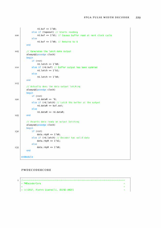
fpga pulse width decoder 229
rd_buf <= 1’b0;
else if (tapeout) // Starts reading
100 rd_buf <= 1’b1; // Causes buffer read at next clock cycle
else
rd_buf <= 1’b0; // Returns to 0
end
105 // Generates the latch data output
always@(posedge clock)
begin
if (rst)
rd_latch <= 1’b0;
110 else if (rd_buf) // Buffer output has been updated
rd_latch <= 1’b1;
else
rd_latch <= 1’b0;
end
115
// Actually does the data output latching
always@(posedge clock)
begin
if (rst)
120 rd_dataR <= ’0;
else if (rd_latch) // Latch the buffer at the output
rd_dataR <= buf_out;
else
rd_dataR <= rd_dataR;
125 end
// Asserts data ready on output latching
always@(posedge clock)
begin
130 if (rst)
data_rdyR <= 1’b0;
else if (rd_latch) // Decoder has valid data
data_rdyR <= 1’b1;
else
135 data_rdyR <= 1’b0;
end
endmodule
pwdecodercore
1 /******************************************************************************
* PWDecoderCore *
* *
* (c)2017, Pietro Giannelli, USCND-UNIFI *
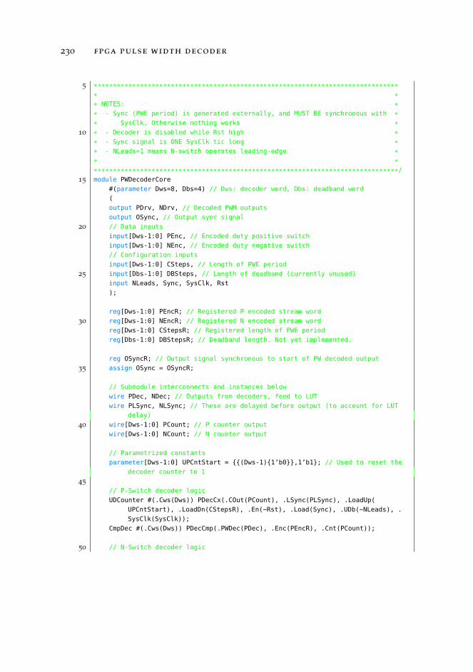
230 fpga pulse width decoder
5 *******************************************************************************
* *
* NOTES: *
* - Sync (PWE period) is generated externally, and MUST BE synchronous with *
* SysClk. Otherwise nothing works *10 * - Decoder is disabled while Rst high *
* - Sync signal is ONE SysClk tic long *
* - NLeads=1 means N-switch operates leading-edge *
* *
*******************************************************************************/
15 module PWDecoderCore
#(parameter Dws=8, Dbs=4) // Dws: decoder word, Dbs: deadband word
(
output PDrv, NDrv, // Decoded PWM outputs
output OSync, // Output sync signal
20 // Data inputs
input[Dws-1:0] PEnc, // Encoded duty positive switch
input[Dws-1:0] NEnc, // Encoded duty negative switch
// Configuration inputs
input[Dws-1:0] CSteps, // Length of PWE period
25 input[Dbs-1:0] DBSteps, // Length of deadband (currently unused)
input NLeads, Sync, SysClk, Rst
);
reg[Dws-1:0] PEncR; // Registered P encoded stream word
30 reg[Dws-1:0] NEncR; // Registered N encoded stream word
reg[Dws-1:0] CStepsR; // Registered length of PWE period
reg[Dbs-1:0] DBStepsR; // Deadband length. Not yet implemented.
reg OSyncR; // Output signal synchronous to start of PW decoded output
35 assign OSync = OSyncR;
// Submodule interconnects and instances below
wire PDec, NDec; // Outputs from decoders, feed to LUT
wire PLSync, NLSync; // These are delayed before output (to account for LUT
delay)
40 wire[Dws-1:0] PCount; // P counter output
wire[Dws-1:0] NCount; // N counter output
// Parametrized constants
parameter[Dws-1:0] UPCntStart = (Dws-1)1’b0,1’b1; // Used to reset the
decoder counter to 1
45
// P-Switch decoder logic
UDCounter #(.Cws(Dws)) PDecCx(.COut(PCount), .LSync(PLSync), .LoadUp(
UPCntStart), .LoadDn(CStepsR), .En(~Rst), .Load(Sync), .UDb(~NLeads), .
SysClk(SysClk));
CmpDec #(.Cws(Dws)) PDecCmp(.PWDec(PDec), .Enc(PEncR), .Cnt(PCount));
50 // N-Switch decoder logic
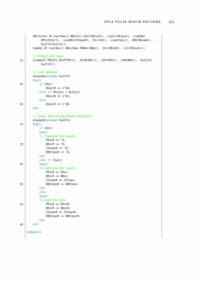
fpga pulse width decoder 231
UDCounter #(.Cws(Dws)) NDecCx(.COut(NCount), .LSync(NLSync), .LoadUp(
UPCntStart), .LoadDn(CStepsR), .En(~Rst), .Load(Sync), .UDb(NLeads), .
SysClk(SysClk));
CmpDec #(.Cws(Dws)) NDecCmp(.PWDec(NDec), .Enc(NEncR), .Cnt(NCount));
// Output LUT logic
55 ClampLUT PDLUT(.OutP(PDrv), .OutN(NDrv), .InP(PDec), .InN(NDec), .SysClk(
SysClk));
// Sync delayer
always@(posedge SysClk)
begin
60 if (Rst)
OSyncR <= 1’b0;
else if (PLSync | NLSync)
OSyncR <= 1’b1;
else
65 OSyncR <= 1’b0;
end
// Input and configuration registers
always@(posedge SysClk)
70 begin
if (Rst)
begin
// Clearing the inputs
PEncR <= ’0;
75 NEncR <= ’0;
CStepsR <= ’0;
DBStepsR <= ’0;
end
else if (Sync)
80 begin
// Latching the inputs
PEncR <= PEnc;
NEncR <= NEnc;
CStepsR <= CSteps;
85 DBStepsR <= DBSteps;
end
else
begin
// Keep the data
90 PEncR <= PEncR;
NEncR <= NEncR;
CStepsR <= CStepsR;
DBStepsR <= DBStepsR;
end
95 end
endmodule
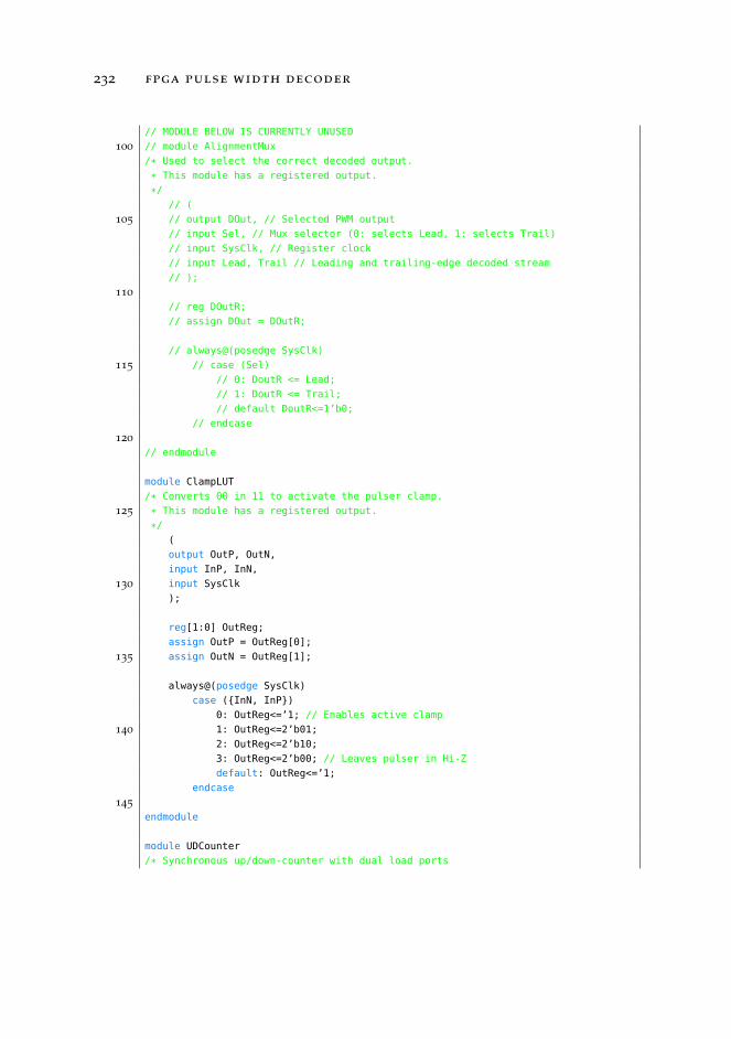
232 fpga pulse width decoder
// MODULE BELOW IS CURRENTLY UNUSED
100 // module AlignmentMux
/* Used to select the correct decoded output.
* This module has a registered output.
*/
// (
105 // output DOut, // Selected PWM output
// input Sel, // Mux selector (0: selects Lead, 1: selects Trail)
// input SysClk, // Register clock
// input Lead, Trail // Leading and trailing-edge decoded stream
// );
110
// reg DOutR;
// assign DOut = DOutR;
// always@(posedge SysClk)
115 // case (Sel)
// 0: DoutR <= Lead;
// 1: DoutR <= Trail;
// default DoutR<=1’b0;
// endcase
120
// endmodule
module ClampLUT
/* Converts 00 in 11 to activate the pulser clamp.
125 * This module has a registered output.
*/
(
output OutP, OutN,
input InP, InN,
130 input SysClk
);
reg[1:0] OutReg;
assign OutP = OutReg[0];
135 assign OutN = OutReg[1];
always@(posedge SysClk)
case (InN, InP)
0: OutReg<=’1; // Enables active clamp
140 1: OutReg<=2’b01;
2: OutReg<=2’b10;
3: OutReg<=2’b00; // Leaves pulser in Hi-Z
default: OutReg<=’1;
endcase
145
endmodule
module UDCounter
/* Synchronous up/down-counter with dual load ports
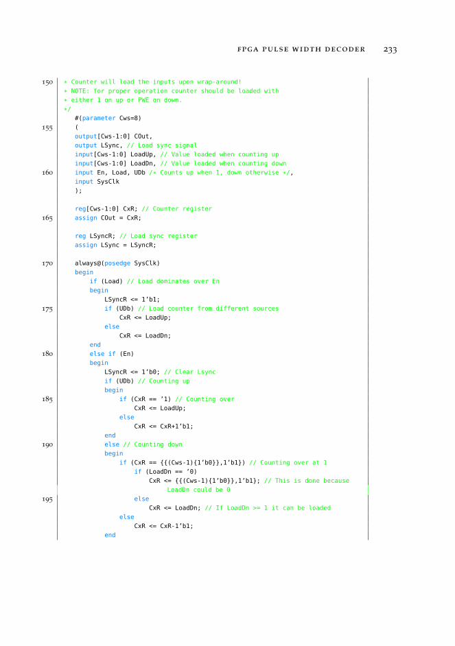
fpga pulse width decoder 233
150 * Counter will load the inputs upon wrap-around!
* NOTE: for proper operation counter should be loaded with
* either 1 on up or PWE on down.
*/
#(parameter Cws=8)
155 (
output[Cws-1:0] COut,
output LSync, // Load sync signal
input[Cws-1:0] LoadUp, // Value loaded when counting up
input[Cws-1:0] LoadDn, // Value loaded when counting down
160 input En, Load, UDb /* Counts up when 1, down otherwise */,
input SysClk
);
reg[Cws-1:0] CxR; // Counter register
165 assign COut = CxR;
reg LSyncR; // Load sync register
assign LSync = LSyncR;
170 always@(posedge SysClk)
begin
if (Load) // Load dominates over En
begin
LSyncR <= 1’b1;
175 if (UDb) // Load counter from different sources
CxR <= LoadUp;
else
CxR <= LoadDn;
end
180 else if (En)
begin
LSyncR <= 1’b0; // Clear Lsync
if (UDb) // Counting up
begin
185 if (CxR == ’1) // Counting over
CxR <= LoadUp;
else
CxR <= CxR+1’b1;
end
190 else // Counting down
begin
if (CxR == (Cws-1)1’b0,1’b1) // Counting over at 1
if (LoadDn == ’0)
CxR <= (Cws-1)1’b0,1’b1; // This is done because
LoadDn could be 0
195 else
CxR <= LoadDn; // If LoadDn >= 1 it can be loaded
else
CxR <= CxR-1’b1;
end
234 fpga pulse width decoder
200 end
else // Retain current state
begin
CxR <= CxR;
LSyncR <= 1’b0; // Clear Lsync
205 end
end
endmodule
210 module CmpDec
/* Pulse width decoder
* Assumptions: UpCounter starts from 1 and DnCounter
* starts from PWE. Leading or trailing output is decided by
* the direction of the counter.
215 * This module is purely combinatorial, expecting registers
* in parent module.
*/
#(parameter Cws=8)
(
220 output PWDec,
input[Cws-1:0] Enc, // Encoded word
input[Cws-1:0] Cnt // Input form counter
);
225 reg PWDecR;
assign PWDec = PWDecR;
always@(Enc, Cnt)
if (Cnt<=Enc)
230 PWDecR = 1’b1;
else
PWDecR = 1’b0;
endmodule
B I B L I O G R A P H Y
[1] C. R. Farrar and K. Worden, “An introduction to structuralhealth monitoring,” Philosophical Transactions of the Royal So-ciety of London A: Mathematical, Physical and Engineering Scien-ces, vol. 365, no. 1851, pp. 303–315, 2007. doi: 10.1098/rsta.2006.1928
.
.
[2] J. L. Rose, “A baseline and vision of ultrasonic guidedwave inspection potential,” Journal of Pressure Vessel Technology,vol. 124, no. 3, pp. 273–282, 2002. doi: 10.1115/1.1491272
.
.
[3] Z. Su, L. Ye, and Y. Lu, “Guided lamb waves for identificationof damage in composite structures: A review,” Journal of Soundand Vibration, vol. 295, no. 3, pp. 753–780, 2006, issn: 0022-460X.doi: 10.1016/j.jsv.2006.01.020
.
.
[4] A. Raghavan and C. E. Cesnik, “Review of guided-wave struc-tural health monitoring,” Shock and Vibration Digest, vol. 39,no. 2, pp. 91–116, 2007. doi: 10.1177/0583102406075428
.
.
[5] M. Mitra and S. Gopalakrishnan, “Guided wave based struc-tural health monitoring: A review,” Smart Materials and Struc-tures, vol. 25, no. 5, p. 053 001, 2016. doi: 10.1088/0964-1726/25/5/053001
.
.
[6] H. Lamb, “On waves in an elastic plate,” Proceedings of theRoyal Society of London A: Mathematical, Physical and EngineeringSciences, vol. 93, no. 648, pp. 114–128, 1917, issn: 0950-1207.doi: 10.1098/rspa.1917.0008
.
.
[7] J. L. Prego Borges, “Lamb: A simulation tool for air-coupledlamb wave based ultrasonic NDE systems,” PhD thesis, Uni-versitat Politècnica de Catalunya. Departament d’EnginyeriaElectrònica, Oct. 25, 2010, isbn: 9788469404225. [Online]. Avai-lable: http://hdl.handle.net/2117/93688
.
.
236 bibliography
[8] D. N. Alleyne and P. Cawley, “The interaction of lamb wa-ves with defects,” IEEE Transactions on Ultrasonics, Ferroelec-trics, and Frequency Control, vol. 39, no. 3, pp. 381–397, 1992,issn: 0885-3010. doi: 10.1109/58.143172
.
.
[9] B. Kim and Y. Roh, “Simple expressions of the reflection andtransmission coefficients of fundamental lamb waves by a rec-tangular notch,” Ultrasonics, vol. 51, no. 6, pp. 734–744, 2011,issn: 0041-624X. doi: 10.1016/j.ultras.2011.03.001
.
.
[10] O. Diligent, T. Grahn, A. Boström, P. Cawley, and M. J. S. Lowe,“The low-frequency reflection and scattering of the s0 lambmode from a circular through-thickness hole in a plate: Finiteelement, analytical and experimental studies,” The Journal ofthe Acoustical Society of America, vol. 112, no. 6, pp. 2589–2601,2002. doi: 10.1121/1.1512292
.
.
[11] N. Guo and P. Cawley, “The interaction of lamb waves withdelaminations in composite laminates,” The Journal of the Acou-stical Society of America, vol. 94, no. 4, pp. 2240–2246, 1993. doi:10.1121/1.407495
.
.
[12] K. S. Tan, N. Guo, B. S. Wong, and C. G. Tui, “Experimentalevaluation of delaminations in composite plates by the use oflamb waves,” Composites Science and Technology, vol. 53, no. 1,pp. 77–84, 1995, issn: 0266-3538. doi: 10.1016/0266-3538(94)00076-X
.
.
[13] C.-T. Ng and M. Veidt, “Scattering of the fundamental anti-symmetric lamb wave at delaminations in composite lamina-tes,” The Journal of the Acoustical Society of America, vol. 129,no. 3, pp. 1288–1296, 2011. doi: 10.1121/1.3533741
.
.
[14] C. Ramadas, K. Balasubramaniam, M. Joshi, and C. V. Krish-namurthy, “Interaction of the primary anti-symmetric lambmode (a0) with symmetric delaminations: Numerical and ex-perimental studies,” Smart Materials and Structures, vol. 18,no. 8, p. 085 011, 2009. doi: 10.1088/0964-1726/18/8/085011
.
.

bibliography 237
[15] B. I. S. Murat, P. Khalili, and P. Fromme, “Scattering of guidedwaves at delaminations in composite plates,” The Journal of theAcoustical Society of America, vol. 139, no. 6, pp. 3044–3052, 2016.doi: 10.1121/1.4953016
.
.
[16] S. Mustapha, L. Ye, D. Wang, and Y. Lu, “Assessment ofdebonding in sandwich CF/EP composite beams using a0
lamb wave at low frequency,” Composite Structures, vol. 93,no. 2, pp. 483–491, 2011, issn: 0263-8223. doi: 10 . 1016 / j .
compstruct.2010.08.032
.
.
[17] N. Toyama and J. Takatsubo, “Lamb wave method for quick in-spection of impact-induced delamination in composite lamina-tes,” Composites Science and Technology, vol. 64, no. 9, pp. 1293–1300, 2004, issn: 0266-3538. doi: 10 . 1016 / j . compscitech .
2003.10.011
.
.
[18] P. Ochôa, V. Infante, J. M. Silva, and R. M. Groves, “Detectionof multiple low-energy impact damage in composite platesusing lamb wave techniques,” Composites Part B: Engineering,vol. 80, no. Supplement C, pp. 291–298, 2015, issn: 1359-8368.doi: 10.1016/j.compositesb.2015.06.010
.
.
[19] S. S. Kessler, S. M. Spearing, and M. J. Atalla, “In-situ damagedetection of composites structures using lamb wave methods,”in Proceedings of the First European Workshop on Structural HealthMonitoring, 2002, pp. 10–12.
[20] D. C. Price, D. A. Scott, G. C. Edwards, et al., “An integratedhealth monitoring system for an ageless aerospace vehicle,”in Structural Health Monitoring 2003, F.-K. Chang, Ed. Lancas-ter, PA: DEStech Publications, 2003, pp. 310–318, isbn: 978-1-932078-20-6.
[21] J. Haywood, P. T. Coverley, W. J. Staszewski, and K. Wor-den, “An automatic impact monitor for a composite panel em-ploying smart sensor technology,” Smart Materials and Structu-res, vol. 14, no. 1, p. 265, 2005. doi: 10.1088/0964-1726/14/1/027
.
.
238 bibliography
[22] X. P. Qing, S. J. Beard, A. Kumar, H.-L. Chan, and R. Ikegami,“Advances in the development of built-in diagnostic systemfor filament wound composite structures,” Composites Scienceand Technology, vol. 66, no. 11, pp. 1694–1702, 2006, issn: 0266-3538. doi: 10.1016/j.compscitech.2005.11.007
.
.
[23] M. R. Pearson, M. J. Eaton, C. A. Featherston, K. M. Holford,and R. Pullin, “Impact damage detection and assessment incomposite panels using macro fibre composites transducers,”Journal of Physics: Conference Series, vol. 305, no. 1, p. 012 049,2011. doi: 10.1088/1742-6596/305/1/012049
.
.
[24] A. Abbate, J. Koay, J. Frankel, S. C. Schroeder, and P. Das, “Sig-nal detection and noise suppression using a wavelet transformsignal processor: Application to ultrasonic flaw detection,”IEEE Transactions on Ultrasonics, Ferroelectrics, and FrequencyControl, vol. 44, no. 1, pp. 14–26, Jan. 1997, issn: 0885-3010.doi: 10.1109/58.585186
.
.
[25] W.-X. Yang, J. B. Hull, and M. D. Seymour, “A contributionto the applicability of complex wavelet analysis of ultrasonicsignals,” NDT & E International, vol. 37, no. 6, pp. 497–504,2004. doi: 10.1016/j.ndteint.2003.12.003
.
.
[26] M. M. R. Taha, A. Noureldin, J. L. Lucero, and T. J. Baca, “Wa-velet transform for structural health monitoring: A compen-dium of uses and features,” Structural Health Monitoring, vol. 5,no. 3, pp. 267–295, 2006. doi: 10.1177/1475921706067741
.
.
[27] H. Sohn, G. Park, J. R. Wait, N. P. Limback, and C. R. Farrar,“Wavelet-based active sensing for delamination detection incomposite structures,” Smart Materials and Structures, vol. 13,no. 1, p. 153, 2004. doi: 10.1088/0964-1726/13/1/017
.
.
[28] X. Chen, X. Li, S. Wang, Z. Yang, B. Chen, and Z. He, “Compo-site damage detection based on redundant second-generationwavelet transform and fractal dimension tomography algo-rithm of lamb wave,” IEEE Transactions on Instrumentation andMeasurement, vol. 62, no. 5, pp. 1354–1363, 2013, issn: 0018-9456. doi: 10.1109/TIM.2012.2224277
.
.
bibliography 239
[29] A. Bagheri, K. Li, and P. Rizzo, “Reference-free damage de-tection by means of wavelet transform and empirical modedecomposition applied to lamb waves,” Journal of IntelligentMaterial Systems and Structures, vol. 24, no. 2, pp. 194–208, 2013.doi: 10.1177/1045389X12460433
.
.
[30] S. Wang, S. Huang, Q. Wang, Y. Zhang, and W. Zhao, “Modeidentification of broadband lamb wave signal with squeezedwavelet transform,” Applied Acoustics, vol. 125, no. Supple-ment C, pp. 91–101, 2017, issn: 0003-682X. doi: 10.1016/j.apacoust.2017.04.014
.
.
[31] L. Gaul and S. Hurlebaus, “Identification of the impact loca-tion on a plate using wavelets,” Mechanical Systems and SignalProcessing, vol. 12, no. 6, pp. 783–795, 1998, issn: 0888-3270.doi: 10.1006/mssp.1998.0163
.
.
[32] M. H. S. Siqueira, C. E. N. Gatts, R. R. Da Silva, and J. M. A. Re-bello, “The use of ultrasonic guided waves and wavelets analy-sis in pipe inspection,” Ultrasonics, vol. 41, no. 10, pp. 785–797,2004. doi: 10.1016/j.ultras.2004.02.013
.
.
[33] W. B. Wood, “NASA firefighters breathing system program re-port,” National Aeronautics and Space Administration, John-son Space Center, Huston, TX, Tech. Rep., 1977. [Online]. Avai-lable: https://ntrs.nasa.gov/archive/nasa/casi.ntrs.nasa.gov/19770017828.pdf
.
.
[34] P. B. McLaughlan, S. C. Forth, and L. Grimes-Ledesma, “Com-posite overwrapped pressure vessels: A primer,” National Ae-ronautics and Space Administration, Johnson Space Center,Huston, TX, Tech. Rep., 2011. eprint: https://ston.jsc.nasa.gov/collections/trs/_techrep/SP-2011-573.pdf
.
.
[35] M. J. Hinton and P. D. Soden, “Predicting failure in compositelaminates: The background to the exercise,” Composites Scienceand Technology, vol. 58, no. 7, pp. 1001–1010, 1998, issn: 0266-3538. doi: 10.1016/S0266-3538(98)00074-8
.
.

240 bibliography
[36] A. R. Bunsell, “Composite pressure vessels supply an ans-wer to transport problems,” Reinforced Plastics, vol. 50, no. 2,pp. 38–41, 2006, issn: 0034-3617. doi: 10.1016/S0034-3617(06)70914-6
.
.
[37] S. S. Kessler, “Certifying a structural health monitoring sy-stem: Characterizing durability, reliability and longevity,” inProceedings of the 1st International Forum on Integrated SystemsHealth Engineering and Management in Aerospace, Napa, CA,2005, pp. 7–10.
[38] G. Konstantinidis, P. D. Wilcox, and B. W. Drinkwater, “Aninvestigation into the temperature stability of a guided wavestructural health monitoring system using permanently atta-ched sensors,” IEEE Sensors Journal, vol. 7, no. 5, pp. 905–912,2007, issn: 1530-437X. doi: 10.1109/JSEN.2007.894908
.
.
[39] F. Lanza di Scalea and S. Salamone, “Temperature effects inultrasonic lamb wave structural health monitoring systems,”The Journal of the Acoustical Society of America, vol. 124, no. 1,pp. 161–174, 2008. doi: 10.1121/1.2932071
.
.
[40] A. Raghavan and C. E. S. Cesnik, “Effects of elevated tem-perature on guided-wave structural health monitoring,” Jour-nal of Intelligent Material Systems and Structures, vol. 19, no. 12,pp. 1383–1398, 2008. doi: 10.1177/1045389X07086691
.
.
[41] F. Bellan, A. Bulletti, L. Capineri, L. Masotti, F. Guasti, and E.Rosi, “Acoustic guided waves interdigital transducers for nondestructive testing of carbon-epoxy composites for spacecraftstructures,” in Sensors and Microsystems. Proceedings of the 9thItalian Conference, (Feb. 8, 2004), C. Di Natale, A. D’Amico, G.Martinelli, M. C. Carotta, and V. Guidi, Eds., Ferrara: WorldScientific Publishing, 2005, pp. 246–250, isbn: 9812563865. doi:10.1142/9789812701770_0042
.
.
[42] F. Bellan, A. Bulletti, L. Capineri, L. Masotti, G. G. Yaralioglu,F. L. Degertekin, B. T. Khuri-Yakub, F. Guasti, and E. Rosi, “Anew design and manufacturing process for embedded lambwaves interdigital transducers based on piezopolymer film,”
bibliography 241
Sensors and Actuators A: Physical, vol. 123, no. Supplement C,pp. 379–387, 2005, Eurosensors XVIII 2004, issn: 0924-4247.doi: 10.1016/j.sna.2005.05.013
.
.
[43] A. Bulletti and L. Capineri, “Interdigital piezopolymer trans-ducers for time of flight measurements with ultrasonic lambwaves on carbon-epoxy composites under pure bendingstress,” Journal of Sensors, vol. 2015, p. 259 621, 2015. doi: 10.1155/2015/259621
.
.
[44] L. Capineri, A. Bulletti, M. Calzolai, and D. Francesconi, “Pie-zopolymer interdigital transducers for a structural health mo-nitoring system,” in Sensors and Microsystems. Proceedings of the17th National Conference, (Feb. 5, 2013), C. Di Natale, V. Fer-rari, A. Ponzoni, G. Sberveglieri, and M. Ferrari, Eds., Brescia:Springer International Publishing, 2014, pp. 9–12, isbn: 978-3-319-00684-0. doi: 10.1007/978-3-319-00684-0_2
.
.
[45] L. Capineri, A. Bulletti, M. Calzolai, and D. Francesconi, “Areal-time electronic system for automated impact detection onaircraft structures using piezoelectric transducers,” ProcediaEngineering, vol. 87, no. Supplement C, pp. 1243–1246, 2014,issn: 1877-7058. doi: 10.1016/j.proeng.2014.11.408
.
.
[46] L. Capineri, A. Bulletti, M. Calzolai, P. Giannelli, and D. Fran-cesconi, “Arrays of conformable ultrasonic lamb wave trans-ducers for structural health monitoring with real-time electro-nics,” Procedia Engineering, vol. 87, pp. 1266–1269, 2014. doi:10.1016/j.proeng.2014.11.416
.
.
[47] A. Bulletti, P. Giannelli, M. Calzolai, and L. Capineri, “An in-tegrated acousto/ultrasonic structural health monitoring sy-stem for composite pressure vessels,” IEEE Transactions onUltrasonics, Ferroelectrics, and Frequency Control, vol. 63, no. 6,pp. 864–873, 2016, issn: 0885-3010. doi: 10.1109/TUFFC.2016.2545716
.
.
[48] Z. Su and L. Ye, Identification of Damage Using Lamb Wa-ves, From Fundamentals to Applications. London: Springer, 2009,isbn: 978-1-84882-783-7. doi: 10.1007/978-1-84882-784-4
.
.
242 bibliography
[49] N. Bourasseau, E. Moulin, C. Delebarre, and P. Bonniau, “Ra-dome health monitoring with lamb waves: Experimental ap-proach,” NDT & E International, vol. 33, no. 6, pp. 393–400,2000, issn: 0963-8695. doi: 10.1016/S0963-8695(00)00007-4
.
.
[50] J. Prager and C. Hoever, “Flaw detection using a selective lambmode excitation with phased array transducers,” in 2010 IEEEInternational Ultrasonics Symposium, 2010, pp. 1156–1159. doi:10.1109/ULTSYM.2010.5935498
.
.
[51] X. Jia, “Modal analysis of lamb wave generation in elastic pla-tes by liquid wedge transducers,” The Journal of the Acousti-cal Society of America, vol. 101, no. 2, pp. 834–842, 1997. doi:10.1121/1.418041
.
.
[52] F. L. Degertakin and B. Khuri-Yakub, “Lamb wave excitationby hertzian contacts with applications in NDE,” IEEE Transacti-ons on Ultrasonics, Ferroelectrics, and Frequency Control, vol. 44,no. 4, pp. 769–779, 1997, issn: 0885-3010. doi: 10.1109/58.655191
.
.
[53] M. Castaings and P. Cawley, “The generation, propagation,and detection of lamb waves in plates using air-coupled ul-trasonic transducers,” The Journal of the Acoustical Society ofAmerica, vol. 100, no. 5, pp. 3070–3077, 1996. doi: 10.1121/1.417193
.
.
[54] M. Castaings and B. Hosten, “Lamb and sh waves generatedand detected by air-coupled ultrasonic transducers in com-posite material plates,” NDT & E International, vol. 34, no. 4,pp. 249–258, 2001, issn: 0963-8695. doi: 10 . 1016 / S0963 -
8695(00)00065-7
.
.
[55] M. S. Harb and F. G. Yuan, “Non-contact ultrasonic techniquefor lamb wave characterization in composite plates,” Ultraso-nics, vol. 64, no. Supplement C, pp. 162–169, 2016, issn: 0041-624X. doi: 10.1016/j.ultras.2015.08.011
.
.
[56] Z. Guo, J. D. Achenbach, and S. Krishnaswamy, “EMAT gene-ration and laser detection of single lamb wave modes,” Ultra-
bibliography 243
sonics, vol. 35, no. 6, pp. 423–429, 1997, issn: 0041-624X. doi:10.1016/S0041-624X(97)00024-3
.
.
[57] R. Murayama and K. Mizutani, “Conventional electromagneticacoustic transducer development for optimum lamb wave mo-des,” Ultrasonics, vol. 40, no. 1, pp. 491–495, 2002, issn: 0041-624X. doi: 10.1016/S0041-624X(02)00164-6
.
.
[58] P. D. Wilcox, M. J. S. Lowe, and P. Cawley, “The excitationand detection of lamb waves with planar coil electromagneticacoustic transducers,” IEEE Transactions on Ultrasonics, Ferroe-lectrics, and Frequency Control, vol. 52, no. 12, pp. 2370–2383,2005, issn: 0885-3010. doi: 10.1109/TUFFC.2005.1563281
.
.
[59] S. G. Pierce, B. Culshaw, W. R. Philp, F. Lecuyer, and R. Far-low, “Broadband lamb wave measurements in aluminium andcarbon/glass fibre reinforced composite materials using non-contacting laser generation and detection,” Ultrasonics, vol. 35,no. 2, pp. 105–114, 1997, issn: 0041-624X. doi: 10.1016/S0041-624X(96)00107-2
.
.
[60] H. Kim, K. Jhang, M. Shin, and J. Kim, “A noncontact NDEmethod using a laser generated focused-lamb wave with en-hanced defect-detection ability and spatial resolution,” NDT& E International, vol. 39, no. 4, pp. 312–319, 2006, issn: 0963-8695. doi: 10.1016/j.ndteint.2005.09.001
.
.
[61] M. H. Badi, G. G. Yaralioglu, A. S. Ergun, S. T. Hansen, E. J.Wong, and B. T. Khuri-Yakub, “Capacitive micromachined ul-trasonic lamb wave transducers using rectangular membra-nes,” IEEE Transactions on Ultrasonics, Ferroelectrics, and Fre-quency Control, vol. 50, no. 9, pp. 1191–1203, 2003, issn: 0885-3010. doi: 10.1109/TUFFC.2003.1235330
.
.
[62] V. Giurgiutiu, “Tuned lamb wave excitation and detectionwith piezoelectric wafer active sensors for structural healthmonitoring,” Journal of Intelligent Material Systems and Struc-tures, vol. 16, no. 4, pp. 291–305, 2005. doi: 10 . 1177 /
1045389X05050106
.
.
244 bibliography
[63] S. von Ende and R. Lammering, “Investigation on piezoelectri-cally induced lamb wave generation and propagation,” SmartMaterials and Structures, vol. 16, no. 5, p. 1802, 2007. doi: 10.1088/0964-1726/16/5/035
.
.
[64] M. Manka, M. Rosiek, A. Martowicz, T. Stepinski, and T. Uhl,“Lamb wave transducers made of piezoelectric macro-fibercomposite,” Structural Control and Health Monitoring, vol. 20,no. 8, pp. 1138–1158, 2013, issn: 1545-2263. doi: 10.1002/stc.1523
.
.
[65] M. Collet, M. Ruzzene, and K. A. Cunefare, “Generation oflamb waves through surface mounted macro-fiber compositetransducers,” Smart Materials and Structures, vol. 20, no. 2,p. 025 020, 2011. doi: 10.1088/0964-1726/20/2/025020
.
.
[66] H. Kawai, “The piezoelectricity of poly (vinylidene fluoride),”Japanese Journal of Applied Physics, vol. 8, no. 7, pp. 975–976,1969. doi: 10.1143/JJAP.8.975
.
.
[67] E. Fukada, “History and recent progress in piezoelectric poly-mers,” IEEE Transactions on Ultrasonics, Ferroelectrics, and Fre-quency Control, vol. 47, no. 6, pp. 1277–1290, 2000, issn: 0885-3010. doi: 10.1109/58.883516
.
.
[68] Q. X. Chen and P. A. Payne, “Industrial applications of piezoe-lectric polymer transducers,” Measurement Science and Techno-logy, vol. 6, no. 3, p. 249, 1995. doi: 10.1088/0957-0233/6/3/001
.
.
[69] K. S. Ramadan, D. Sameoto, and S. Evoy, “A review of pie-zoelectric polymers as functional materials for electromechani-cal transducers,” Smart Materials and Structures, vol. 23, no. 3,p. 033 001, 2014. doi: 10.1088/0964-1726/23/3/033001
.
.
[70] L. F. Brown, “Design considerations for piezoelectric polymerultrasound transducers,” IEEE Transactions on Ultrasonics, Fer-roelectrics, and Frequency Control, vol. 47, no. 6, pp. 1377–1396,2000, issn: 0885-3010. doi: 10.1109/58.883527
.
.
bibliography 245
[71] Y. Wada and R. Hayakawa, “Piezoelectricity and pyroelectri-city of polymers,” Japanese Journal of Applied Physics, vol. 15,no. 11, p. 2041, 1976. doi: 10.1143/JJAP.15.2041
.
.
[72] N. Murayama and H. Obara, “Piezoelectric polymers and theirapplications,” Japanese Journal of Applied Physics, vol. 22, no. S3,p. 3, 1983. doi: 10.7567/JJAPS.22S3.3
.
.
[73] Piézotech S.A.S., Piezoelectric films technical information, Hésin-gue, France, 2010. [Online]. Available: http://www.piezotech.eu/export/sites/piezotech/.content/medias/downloads/
Documentation/Piezotech- piezoelectric- films- leaflet.
.
.
[74] Megatron AG, Data sheet PZT 500 series, Liestal, Switzer-land, 2016. [Online]. Available: http://www.megatron.ch/infocenter/PZT500_series_Megatron_2016.pdf
.
.
[75] T. R. Dargaville, M. C. Celina, J. M. Elliott, P. M. Chaplya,G. D. Jones, D. M. Mowery, R. A. Assink, R. L. Clough, andJ. W. Martin, “Characterization, performance and optimizationof PVDF as a piezoelectric film for advanced space mirrorconcepts,” Sandia National Laboratories, Albuquerque, NewMexico, Tech. Rep., 2005. eprint: http://prod.sandia.gov/techlib/access-control.cgi/2005/056846.pdf
.
.
[76] P.-H. Ducrot, I. Dufour, and C. Ayela, “Optimization of PVDF-TrFE processing conditions for the fabrication of organicMEMS resonators,” Scientific Reports, vol. 6, p. 19 426, 2016.doi: 10.1038/srep19426
.
.
[77] P. Martins, A. C. Lopes, and S. Lanceros-Mendez, “Electro-active phases of poly(vinylidene fluoride): Determination, pro-cessing and applications,” Progress in Polymer Science, vol. 39,no. 4, pp. 683–706, 2014, Topical issue on Electroactive Poly-mers, issn: 0079-6700. doi: 10.1016/j.progpolymsci.2013.07.006
.
.
[78] J.-H. Bae and S.-H. Chang, “Characterization of an electro-active polymer (PVDF-TrFE) film-type sensor for health moni-toring of composite structures,” Composite Structures, vol. 131,
246 bibliography
no. Supplement C, pp. 1090–1098, 2015, issn: 0263-8223. doi:10.1016/j.compstruct.2015.06.075
.
.
[79] K. Tashiro, “Crystal structure and phase transition of PVDFand related copolymers,” in Ferroelectric Polymers: Chemistry:Physics, and Applications, H. S. Nalwa, Ed. New York, NY: Mar-cel Dekker, inc., 1995, ch. 2, pp. 63–182, isbn: 9780824794682.
[80] E. Bellet-Amalric and J. Legrand, “Crystalline structures andphase transition of the ferroelectric P(VDF-TrFE) copolymers,a neutron diffraction study,” The European Physical Journal B -Condensed Matter and Complex Systems, vol. 3, no. 2, pp. 225–236, 1998, issn: 1434-6036. doi: 10.1007/s100510050307
.
.
[81] A. Aliane, M. Benwadih, B. Bouthinon, R. Coppard, F. D.-D.Santos, and A. Daami, “Impact of crystallization onferro-, piezo- and pyro-electric characteristics in thin filmP(VDF–TrFE),” Organic Electronics, vol. 25, no. Supplement C,pp. 92–98, 2015, issn: 1566-1199. doi: 10.1016/j.orgel.2015.06.007
.
.
[82] M. Wojtas, D. V. Karpinsky, M. V. Silibin, S. A. Gavrilov,A. V. Sysa, and K. N. Nekludov, “Dielectric properties of grap-hene oxide doped P(VDF-TrFE) films,” Polymer Testing, vol. 60,no. Supplement C, pp. 326–332, 2017, issn: 0142-9418. doi: 10.1016/j.polymertesting.2017.04.003
.
.
[83] J. S. Dodds, F. N. Meyers, and K. J. Loh, “Piezoelectric charac-terization of PVDF-TrFE thin films enhanced with ZnO nano-particles,” IEEE Sensors Journal, vol. 12, no. 6, pp. 1889–1890,2012, issn: 1530-437X. doi: 10.1109/JSEN.2011.2182043
.
.
[84] M. Dietze and M. Es-Souni, “Structural and functional proper-ties of screen-printed PZT–PVDF-TrFE composites,” Sensorsand Actuators A: Physical, vol. 143, no. 2, pp. 329–334, 2008,issn: 0924-4247. doi: 10.1016/j.sna.2007.11.016
.
.
[85] S. Dalle Vacche, F. Oliveira, Y. Leterrier, V. Michaud, D. Dam-janovic, and J.-A. E. Månson, “The effect of processing con-ditions on the morphology, thermomechanical, dielectric, andpiezoelectric properties of P(VDF-TrFE)/BaTiO3 composites,”
bibliography 247
Journal of Materials Science, vol. 47, no. 11, pp. 4763–4774, 2012,issn: 1573-4803. doi: 10.1007/s10853-012-6362-x
.
.
[86] M. Laurenti, D. Perrone, A. Verna, C. F. Pirri, and A. Chiolerio,“Development of a flexible lead-free piezoelectric transducerfor health monitoring in the space environment,” Micromachi-nes, vol. 6, no. 11, pp. 1729–1744, 2015, issn: 2072-666X. doi:10.3390/mi6111453
.
.
[87] E. Guzman, J. Cugnoni, T. Gmür, P. Bonhôte, and A. Schorde-ret, “Survivability of integrated PVDF film sensors to accelera-ted ageing conditions in aeronautical/aerospace structures,”Smart Materials and Structures, vol. 22, no. 6, p. 065 020, 2013.doi: 10.1088/0964-1726/22/6/065020
.
.
[88] E. Bormashenko, R. Pogreb, Y. Socol, M. H. Itzhaq, V. Streltsov,S. Sutovski, A. Sheshnev, and Y. Bormashenko, “Polyvinyli-dene fluoride—piezoelectric polymer for integrated infraredoptics applications,” Optical Materials, vol. 27, no. 3, pp. 429–434, 2004, issn: 0925-3467. doi: 10.1016/j.optmat.2004.04.015
.
.
[89] G. Harsányi, Polymer films in sensor applications. Lancaster, PA:Technomic, 1995, isbn: 9781566762014.
[90] M. Mazzoni, L. Capineri, and L. Masotti, “A large-area pvdfpyroelectric sensor for co 2 laser beam alignment,” IEEE Sen-sors Journal, vol. 7, no. 8, pp. 1159–1164, 2007, issn: 1530-437X.doi: 10.1109/JSEN.2007.901026
.
.
[91] N. Fujitsuka, J. Sakata, Y. Miyachi, K. Mizuno, K. Ohtsuka, Y.Taga, and O. Tabata, “Monolithic pyroelectric infrared imagesensor using PVDF thin film,” Sensors and Actuators A: Physical,vol. 66, no. 1, pp. 237–243, 1998, issn: 0924-4247. doi: 10.1016/S0924-4247(98)00050-8
.
.
[92] L. Capineri, L. Masotti, and M. Mazzoni, “Pyroelectric PVDFsensor modeling of the temporal voltage response to arbitra-rily modulated radiation,” IEEE Transactions on Ultrasonics, Fer-roelectrics, and Frequency Control, vol. 47, no. 6, pp. 1406–1412,2000, issn: 0885-3010. doi: 10.1109/58.883529
.
.
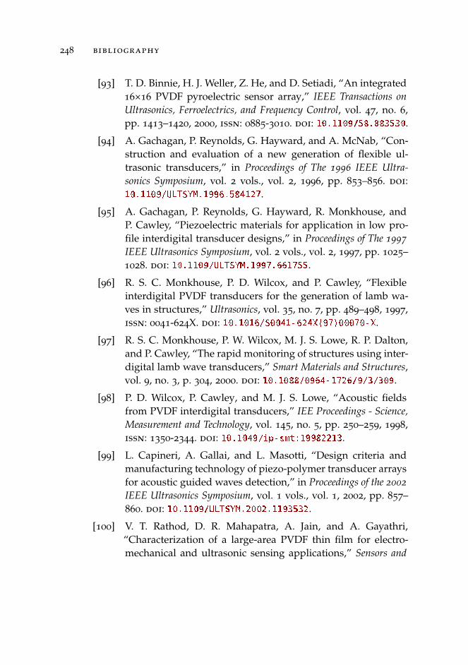
248 bibliography
[93] T. D. Binnie, H. J. Weller, Z. He, and D. Setiadi, “An integrated16×16 PVDF pyroelectric sensor array,” IEEE Transactions onUltrasonics, Ferroelectrics, and Frequency Control, vol. 47, no. 6,pp. 1413–1420, 2000, issn: 0885-3010. doi: 10.1109/58.883530
.
.
[94] A. Gachagan, P. Reynolds, G. Hayward, and A. McNab, “Con-struction and evaluation of a new generation of flexible ul-trasonic transducers,” in Proceedings of The 1996 IEEE Ultra-sonics Symposium, vol. 2 vols., vol. 2, 1996, pp. 853–856. doi:10.1109/ULTSYM.1996.584127
.
.
[95] A. Gachagan, P. Reynolds, G. Hayward, R. Monkhouse, andP. Cawley, “Piezoelectric materials for application in low pro-file interdigital transducer designs,” in Proceedings of The 1997IEEE Ultrasonics Symposium, vol. 2 vols., vol. 2, 1997, pp. 1025–1028. doi: 10.1109/ULTSYM.1997.661755
.
.
[96] R. S. C. Monkhouse, P. D. Wilcox, and P. Cawley, “Flexibleinterdigital PVDF transducers for the generation of lamb wa-ves in structures,” Ultrasonics, vol. 35, no. 7, pp. 489–498, 1997,issn: 0041-624X. doi: 10.1016/S0041-624X(97)00070-X
.
.
[97] R. S. C. Monkhouse, P. W. Wilcox, M. J. S. Lowe, R. P. Dalton,and P. Cawley, “The rapid monitoring of structures using inter-digital lamb wave transducers,” Smart Materials and Structures,vol. 9, no. 3, p. 304, 2000. doi: 10.1088/0964-1726/9/3/309
.
.
[98] P. D. Wilcox, P. Cawley, and M. J. S. Lowe, “Acoustic fieldsfrom PVDF interdigital transducers,” IEE Proceedings - Science,Measurement and Technology, vol. 145, no. 5, pp. 250–259, 1998,issn: 1350-2344. doi: 10.1049/ip-smt:19982213
.
.
[99] L. Capineri, A. Gallai, and L. Masotti, “Design criteria andmanufacturing technology of piezo-polymer transducer arraysfor acoustic guided waves detection,” in Proceedings of the 2002IEEE Ultrasonics Symposium, vol. 1 vols., vol. 1, 2002, pp. 857–860. doi: 10.1109/ULTSYM.2002.1193532
.
.
[100] V. T. Rathod, D. R. Mahapatra, A. Jain, and A. Gayathri,“Characterization of a large-area PVDF thin film for electro-mechanical and ultrasonic sensing applications,” Sensors and
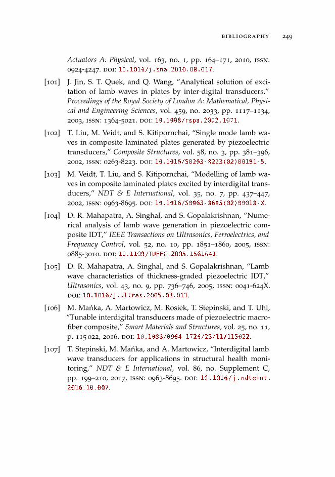
bibliography 249
Actuators A: Physical, vol. 163, no. 1, pp. 164–171, 2010, issn:0924-4247. doi: 10.1016/j.sna.2010.08.017
.
.
[101] J. Jin, S. T. Quek, and Q. Wang, “Analytical solution of exci-tation of lamb waves in plates by inter-digital transducers,”Proceedings of the Royal Society of London A: Mathematical, Physi-cal and Engineering Sciences, vol. 459, no. 2033, pp. 1117–1134,2003, issn: 1364-5021. doi: 10.1098/rspa.2002.1071
.
.
[102] T. Liu, M. Veidt, and S. Kitipornchai, “Single mode lamb wa-ves in composite laminated plates generated by piezoelectrictransducers,” Composite Structures, vol. 58, no. 3, pp. 381–396,2002, issn: 0263-8223. doi: 10.1016/S0263-8223(02)00191-5
.
.
[103] M. Veidt, T. Liu, and S. Kitipornchai, “Modelling of lamb wa-ves in composite laminated plates excited by interdigital trans-ducers,” NDT & E International, vol. 35, no. 7, pp. 437–447,2002, issn: 0963-8695. doi: 10.1016/S0963-8695(02)00018-X
.
.
[104] D. R. Mahapatra, A. Singhal, and S. Gopalakrishnan, “Nume-rical analysis of lamb wave generation in piezoelectric com-posite IDT,” IEEE Transactions on Ultrasonics, Ferroelectrics, andFrequency Control, vol. 52, no. 10, pp. 1851–1860, 2005, issn:0885-3010. doi: 10.1109/TUFFC.2005.1561641
.
.
[105] D. R. Mahapatra, A. Singhal, and S. Gopalakrishnan, “Lambwave characteristics of thickness-graded piezoelectric IDT,”Ultrasonics, vol. 43, no. 9, pp. 736–746, 2005, issn: 0041-624X.doi: 10.1016/j.ultras.2005.03.011
.
.
[106] M. Manka, A. Martowicz, M. Rosiek, T. Stepinski, and T. Uhl,“Tunable interdigital transducers made of piezoelectric macro-fiber composite,” Smart Materials and Structures, vol. 25, no. 11,p. 115 022, 2016. doi: 10.1088/0964-1726/25/11/115022
.
.
[107] T. Stepinski, M. Manka, and A. Martowicz, “Interdigital lambwave transducers for applications in structural health moni-toring,” NDT & E International, vol. 86, no. Supplement C,pp. 199–210, 2017, issn: 0963-8695. doi: 10.1016/j.ndteint.2016.10.007
.
.
250 bibliography
[108] Q. Zhou, S. Lau, D. Wu, and K. K. Shung, “Piezoelectric filmsfor high frequency ultrasonic transducers in biomedical appli-cations,” Progress in Materials Science, vol. 56, no. 2, pp. 139–174, 2011, issn: 0079-6425. doi: 10.1016/j.pmatsci.2010.09.001
.
.
[109] A. Perelli, L. D. Marchi, A. Marzani, and N. Speciale, “Acou-stic emission localization in plates with dispersion and rever-berations using sparse pzt sensors in passive mode,” SmartMaterials and Structures, vol. 21, no. 2, p. 025 010, 2012. doi:10.1088/0964-1726/21/2/025010
.
.
[110] T. Kundu, “Acoustic source localization,” Ultrasonics, vol. 54,no. 1, pp. 25–38, 2014, issn: 0041-624X. doi: 10.1016/j.ultras.2013.06.009
.
.
[111] E. Marino Merlo, A. Bulletti, P. Giannelli, M. Calzolai, andL. Capineri, “A novel differential time-of-arrival estimationtechnique for impact localization on carbon fiber laminatesheets,” Sensors, vol. 17, no. 10, p. 2270, 2017, issn: 1424-8220.doi: 10.3390/s17102270
.
.
[112] T. Clarke, P. Cawley, P. D. Wilcox, and A. J. Croxford, “Eva-luation of the damage detection capability of a sparse-arrayguided-wave SHM system applied to a complex structureunder varying thermal conditions,” IEEE Transactions on Ul-trasonics, Ferroelectrics, and Frequency Control, vol. 56, no. 12,pp. 2666–2678, 2009, issn: 0885-3010. doi: 10 . 1109 / TUFFC .
2009.1357
.
.
[113] M. A. Torres Arredondo and C.-P. Fritzen, “Ultrasonic guidedwave dispersive characteristics in composite structures undervariable temperature and operational conditions,” in Procee-dings of the 6th European Workshop in Structural Health Monito-ring, EWSHM 2012, Dresden, Germany, 2012.
[114] L. Seminara, L. Pinna, M. Valle, et al., “Piezoelectric polymertransducer arrays for flexible tactile sensors,” IEEE SensorsJournal, vol. 13, no. 10, pp. 4022–4029, 2013, issn: 1530-437X.doi: 10.1109/JSEN.2013.2268690
.
.
bibliography 251
[115] B. Ren and C. J. Lissenden, “PVDF multielement lamb wavesensor for structural health monitoring,” IEEE Transactions onUltrasonics, Ferroelectrics, and Frequency Control, vol. 63, no. 1,pp. 178–185, 2016, issn: 0885-3010. doi: 10.1109/TUFFC.2015.2496423
.
.
[116] B. Ren, H. Cho, and C. J. Lissenden, “A guided wave sen-sor enabling simultaneous wavenumber-frequency analysisfor both lamb and shear-horizontal waves,” Sensors, vol. 17,no. 3, p. 488, 2017, issn: 1424-8220. doi: 10.3390/s17030488
.
.
[117] W. Zhu and J. L. Rose, “Lamb wave generation and receptionwith time-delay periodic linear arrays: A BEM simulation andexperimental study,” IEEE Transactions on Ultrasonics, Ferroe-lectrics, and Frequency Control, vol. 46, no. 3, pp. 654–664, 1999,issn: 0885-3010. doi: 10.1109/58.764852
.
.
[118] C. Adams, S. Harput, D. Cowell, T. M. Carpenter, D. M. Cha-rutz, and S. Freear, “An adaptive array excitation schemefor the unidirectional enhancement of guided waves,” IEEETransactions on Ultrasonics, Ferroelectrics, and Frequency Control,vol. 64, no. 2, pp. 441–451, 2017, issn: 0885-3010. doi: 10.1109/TUFFC.2016.2628100
.
.
[119] B. Ren and C. J. Lissenden, “Phased array transducers forultrasonic guided wave mode control and identification foraircraft structural health monitoring,” Materials Evaluation,vol. 73, no. 8, 2015.
[120] A. Velichko and P. D. Wilcox, “Guided wave arrays for highresolution inspection,” The Journal of the Acoustical Society ofAmerica, vol. 123, no. 1, pp. 186–196, 2008. doi: 10.1121/1.2804699
.
.
[121] S.-C. Wooh and Y. Shi, “Synthetic phase tuning of guidedwaves,” IEEE Transactions on Ultrasonics, Ferroelectrics, and Fre-quency Control, vol. 48, no. 1, pp. 209–223, 2001, issn: 0885-3010.doi: 10.1109/58.896134
.
.
252 bibliography
[122] J. Li and J. L. Rose, “Implementing guided wave mode cont-rol by use of a phased transducer array,” IEEE Transactions onUltrasonics, Ferroelectrics, and Frequency Control, vol. 48, no. 3,pp. 761–768, 2001, issn: 0885-3010. doi: 10.1109/58.920708
.
.
[123] P. Fromme, P. D. Wilcox, M. J. S. Lowe, and P. Cawley, “On thedevelopment and testing of a guided ultrasonic wave array forstructural integrity monitoring,” IEEE Transactions on Ultraso-nics, Ferroelectrics, and Frequency Control, vol. 53, no. 4, pp. 777–785, 2006, issn: 0885-3010. doi: 10.1109/TUFFC.2006.1621505
.
.
[124] S. Webster and T. Binnie, “PVDF sensors with low-temperature bonding techniques,” Sensors and Actuators A:Physical, vol. 49, no. 1-2, pp. 61–65, 1995. doi: 10.1016/0924-4247(95)01010-X
.
.
[125] D. M. Brewis, I. Mathieson, and M. Wolfensberger, “Treatmentof low energy surfaces for adhesive bonding,” InternationalJournal of Adhesion and Adhesives, vol. 15, no. 2, pp. 87–90, 1995,issn: 0143-7496. doi: 10.1016/0143-7496(95)98742-5
.
.
[126] M. Garcia-Rodriguez, J. Garcia-Alvarez, Y. Yañez, M. J. Garcia-Hernandez, J. Salazar, A. Turo, and J. A. Chavez, “Low costmatching network for ultrasonic transducers,” Physics Procedia,vol. 3, no. 1, pp. 1025–1031, 2010, International Congress onUltrasonics, Santiago de Chile, January 2009, issn: 1875-3892.doi: 10.1016/j.phpro.2010.01.132
.
.
[127] L. Capineri, L. Masotti, M. Rinieri, and S. Rocchi, “Ultraso-nic transducers as a black-box: Equivalent circuit synthesisand matching network design,” IEEE Transactions on Ultraso-nics, Ferroelectrics, and Frequency Control, vol. 40, no. 6, pp. 694–703, 1993, issn: 0885-3010. doi: 10.1109/58.248213
.
.
[128] H. Huang and D. Paramo, “Broadband electrical impedancematching for piezoelectric ultrasound transducers,” IEEE Tran-sactions on Ultrasonics, Ferroelectrics, and Frequency Control,vol. 58, no. 12, pp. 2699–2707, 2011, issn: 0885-3010. doi: 10.1109/TUFFC.2011.2132
.
.
bibliography 253
[129] D. Bianchi, F. Quaglia, A. Mazzanti, and F. Svelto, “High-voltage integrated class-b amplifier for ultrasound transdu-cers,” in Proceedings of 2013 International Conference on IC De-sign Technology (ICICDT), 2013, pp. 105–108. doi: 10 . 1109 /
ICICDT.2013.6563314
.
.
[130] K. Sun, Z. Gao, P. Gui, R. Wang, I. Oguzman, X. Xu, K. Va-santh, Q. Zhou, and K. K. Shung, “A 180-vpp integrated linearamplifier for ultrasonic imaging applications in a high-voltageCMOS SOI technology,” IEEE Transactions on Circuits and Sys-tems II: Express Briefs, vol. 62, no. 2, pp. 149–153, 2015, issn:1549-7747. doi: 10.1109/TCSII.2014.2387687
.
.
[131] W. Qiu, Y. Yu, F. K. Tsang, and L. Sun, “A multifunctional,reconfigurable pulse generator for high-frequency ultrasoundimaging,” IEEE Transactions on Ultrasonics, Ferroelectrics, andFrequency Control, vol. 59, no. 7, pp. 1558–1567, 2012, issn: 0885-3010. doi: 10.1109/TUFFC.2012.2355
.
.
[132] P. R. Smith, D. M. J. Cowell, and S. Freear, “Width-modulatedsquare-wave pulses for ultrasound applications,” IEEE Tran-sactions on Ultrasonics, Ferroelectrics, and Frequency Control,vol. 60, no. 11, pp. 2244–2256, 2013, issn: 0885-3010. doi: 10.1109/TUFFC.2013.6644730
.
.
[133] D. Cowell, P. Smith, S. Harput, J. McLaughlan, and S. Freear,“Non-linear harmonic reduction pulse width modulation(HRPWM) for the arbitrary control of transducer-integratedswitched excitation electronics,” in 2014 IEEE International Ul-trasonics Symposium (IUS), 2014, pp. 807–810. doi: 10.1109/ULTSYM.2014.0198
.
.
[134] D. M. J. Cowell, S. Harput, and S. Freear, “Arbitrary waveformgeneration based on phase and amplitude synthesis for swit-ched mode excitation of ultrasound imaging arrays,” in 2015IEEE International Ultrasonics Symposium (IUS), 2015, pp. 1–4.doi: 10.1109/ULTSYM.2015.0280
.
.
254 bibliography
[135] B. H. Kim, S. Lee, and K. Kim, “A feasibility study for ar-bitrary waveform generation using on-off pulses and modi-fied pwm waveforms in the front-end circuit integrated withtransducers,” in 2015 IEEE International Ultrasonics Symposium(IUS), 2015, pp. 1–4. doi: 10.1109/ULTSYM.2015.0543
.
.
[136] D. M. J. Cowell, T. Carpenter, P. Smith, C. Adams, S. Har-put, and S. Freear, “Performance of switched mode arbitraryexcitation using harmonic reduction pulse width modulation(hrpwm) in array imaging applications,” in 2016 IEEE Interna-tional Ultrasonics Symposium (IUS), 2016, pp. 1–4. doi: 10.1109/ULTSYM.2016.7728816
.
.
[137] D. M. J. Cowell, P. R. Smith, and S. Freear, “Phase-inversion-based selective harmonic elimination (PI-SHE) in multi-levelswitched-mode tone- and frequency- modulated excitation,”IEEE Transactions on Ultrasonics, Ferroelectrics, and FrequencyControl, vol. 60, no. 6, pp. 1084–1097, 2013, issn: 0885-3010.doi: 10.1109/TUFFC.2013.2672
.
.
[138] K. Chen, H.-S. Lee, A. P. Chandrakasan, and C. G. Sodini, “Ul-trasonic imaging transceiver design for CMUT: A three-level30-vpp pulse-shaping pulser with improved efficiency and anoise-optimized receiver,” IEEE Journal of Solid-State Circuits,vol. 48, no. 11, pp. 2734–2745, 2013, issn: 0018-9200. doi: 10.1109/JSSC.2013.2274895
.
.
[139] M. Terenzi, D. Ghisu, F. Quaglia, E. Boni, M. Diaz Mendez,M. Valle, and D. D. Caviglia, “Flexible hardware architecturefor the generation of ultrasound pulses in medical imaging,”in 2016 IEEE International Ultrasonics Symposium (IUS), 2016,pp. 1–4. doi: 10.1109/ULTSYM.2016.7728595
.
.
[140] P. M. Bhagwat and V. R. Stefanovic, “Generalized structureof a multilevel pwm inverter,” IEEE Transactions on IndustryApplications, vol. IA-19, no. 6, pp. 1057–1069, 1983, issn: 0093-9994. doi: 10.1109/TIA.1983.4504335
.
.
[141] ANSI/VITA 57.1-2008 (r2010), FPGA mezzanine card (FMC) stan-dard, VITA Standards Organization, 2010.
bibliography 255
[142] Y. B. Quek, Class-D LC filter design, Texas Instruments Inc.,2015. [Online]. Available: http : / / www . ti . com / lit / an /
sloa119b/sloa119b.pdf
.
.
[143] B.-H. Gwee, J. S. Chang, and H. Li, “A micropower low-distortion digital pulsewidth modulator for a digital class damplifier,” IEEE Transactions on Circuits and Systems II: Analogand Digital Signal Processing, vol. 49, no. 4, pp. 245–256, 2002,issn: 1057-7130. doi: 10.1109/TCSII.2002.801407
.
.
[144] IEEE Std 1658-2011, IEEE standard for terminology and test met-hods of digital-to-analog converter devices, IEEE, 2012. doi: 10.1109/IEEESTD.2012.6152113
.
.
[145] K. Ono and A. Gallego, “Attenuation of lamb waves in CFRPplates,” Journal of Acoustic Emission, vol. 30, pp. 109–124, 2012.
[146] B. Lin and V. Giurgiutiu, “Modeling and testing of PZT andPVDF piezoelectric wafer active sensors,” Smart Materials andStructures, vol. 15, no. 4, p. 1085, 2006. doi: 10.1088/0964-1726/15/4/022
.
.
[147] B. Razavi, Design of Analog CMOS Integrated Circuits, Secondedition, ser. Irwin Electronics & Computer Enginering. NewYork: McGraw-Hill Education, 2016, isbn: 9780072524932.
[148] P. J. Hurst and S. H. Lewis, “Determination of stability usingreturn ratios in balanced fully differential feedback circuits,”IEEE Transactions on Circuits and Systems II: Analog and DigitalSignal Processing, vol. 42, no. 12, pp. 805–817, 1995, issn: 1057-7130. doi: 10.1109/82.476178
.
.
[149] A. Tauro, C. Marzocca, C. T. Francesco, and A. D. Giando-menico, “Common mode stability in fully differential voltagefeedback CMOS amplifiers,” in Proceedings of the 10th IEEE In-ternational Conference on Electronics, Circuits and Systems, 2003.,Vol. 1 vols., vol. 1, Dec. 2003, pp. 288–291. doi: 10.1109/ICECS.2003.1302033
.
.
256 bibliography
[150] R. H. Walden, “Analog-to-digital converter survey and analy-sis,” IEEE Journal on Selected Areas in Communications, vol. 17,no. 4, pp. 539–550, 1999, issn: 0733-8716. doi: 10.1109/49.761034
.
.
[151] M. Massarotto, A. Carlosena, and A. J. Lopez-Martin, “Two-stage differential charge and transresistance amplifiers,” IEEETransactions on Instrumentation and Measurement, vol. 57, no. 2,pp. 309–320, 2008. doi: 10.1109/TIM.2007.909498
.
.
[152] J. C. P. McKeon and M. K. Hinders, “Parallel projection andcrosshole lamb wave contact scanning tomography,” The Jour-nal of the Acoustical Society of America, vol. 106, no. 5, pp. 2568–2577, 1999. doi: 10.1121/1.428088
.
.
[153] E. V. Malyarenko and M. K. Hinders, “Ultrasonic lamb wavediffraction tomography,” Ultrasonics, vol. 39, no. 4, pp. 269–281, 2001, issn: 0041-624X. doi: 10 . 1016 / S0041 - 624X(01 )
00055-5
.
.
[154] K. R. Leonard, E. V. Malyarenko, and M. K. Hinders, “Ultra-sonic lamb wave tomography,” Inverse Problems, vol. 18, no. 6,p. 1795, 2002. doi: 10.1088/0266-5611/18/6/322
.
.
[155] K. R. Leonard and M. K. Hinders, “Multi-mode lamb wavetomography with arrival time sorting,” The Journal of the Acou-stical Society of America, vol. 117, no. 4, pp. 2028–2038, 2005.doi: 10.1121/1.1867792
.
.
[156] L. D. Marchi, A. Marzani, J. Moll, P. Kudela, M. Radzienski,and W. Ostachowicz, “A pulse coding and decoding strategyto perform lamb wave inspections using simultaneously multi-ple actuators,” Mechanical Systems and Signal Processing, vol. 91,no. Supplement C, pp. 111–121, 2017, issn: 0888-3270. doi: 10.1016/j.ymssp.2016.12.014
.
.
[157] IEEE Std 1588-2008 (revision of IEEE Std 1588-2002), IEEE stan-dard for a precision clock synchronization protocol for networkedmeasurement and control systems, IEEE, 2008. doi: 10 . 1109 /
IEEESTD.2008.4579760
.
.

bibliography 257
[158] P. Giannelli, A. Bulletti, and L. Capineri, “Multifunctional pie-zopolymer film transducer for structural health monitoringapplications,” IEEE Sensors Journal, 2017. doi: 10.1109/JSEN.2017.2710425
.
.
[159] P. Giannelli, A. Bulletti, and L. Capineri, “Charge-mode in-terfacing of piezoelectric interdigital lamb wave transducers,”Electronics Letters, vol. 52, no. 11, pp. 894–896, 2016. doi: 10.1049/el.2016.0804
.
.


Project Pandora was fundedby Texas Instruments Inc.
colophon
This document was typeset using the typographical look-and-feelclassicthesis developed by André Miede (https://bitbucket.org/amiede/classicthesis/
.
).
Final version as of January 18, 2018.

A Testbench System for Structural Health Monitoring with Guided-Wave Ultrasound
Pietro Giannelli
PRINTED VERSION (JAN. 18, 2018) ERRATA
Page 16, second paragraph. Equation λGW=1/pF should read λGW=pF.
Page 18, last paragraph and eq. 2.2. Missing spaces between values and units.
Page 40, last paragraph. The gain range is unclearly formatted, it should be -5dB to 31dB.
Page 56, section 4.3.1.3, second paragraph. Ending is not properly justified.
Page 102, second paragraph and subsequent equations. -3dB is not properly formatted.
Page 115, second line after eq. 4.27. 80dB is not properly formatted.
January 31, 2018 Pietro Giannelli
Copyright © 2022 FDOKUMEN