Directional Characteristics of Wireless Power Transfer via ...
Upload
independentCategory
view
0download
0
Accepted Manuscript
A 30 W 800 MHz Complimentary LDMOS Power Amplifier for Wireless Ap-
plication
Sagar Mukherjee, Swarnil Roy, Chandan Kumar Sarkar
PII: S0749-6036(14)00145-1
DOI: http://dx.doi.org/10.1016/j.spmi.2014.05.001
Reference: YSPMI 3254
To appear in: Superlattices and Microstructures
Received Date: 3 December 2013
Revised Date: 30 April 2014
Accepted Date: 3 May 2014
Please cite this article as: S. Mukherjee, S. Roy, C.K. Sarkar, A 30 W 800 MHz Complimentary LDMOS Power
Amplifier for Wireless Application, Superlattices and Microstructures (2014), doi: http://dx.doi.org/10.1016/j.spmi.
2014.05.001
This is a PDF file of an unedited manuscript that has been accepted for publication. As a service to our customers
we are providing this early version of the manuscript. The manuscript will undergo copyediting, typesetting, and
review of the resulting proof before it is published in its final form. Please note that during the production process
errors may be discovered which could affect the content, and all legal disclaimers that apply to the journal pertain.

A 30 W 800 MHz Complimentary LDMOS Power Amplifier for Wireless
Application
Sagar Mukherjee,Swarnil Roy,Chandan Kumar Sarkar
Department of Electronics and Telecommunication Engineering,
Jadavpur University, Kolkata, West Bengal, India
ABSTRACT
This work presents the design of an optimized power amplifier using Complementary
LDMOS (CLDMOS) with 5µm Gate Length. Final results show that the high performance
CLDMOS amplifier has been achieved using the optimization of various device parameters
and the circuit bias conditions. Optimization of the drift length and the drift area doping in
device parameters have been done for both P type LDMOS (PLDMOS) and N type LDMOS
(NLDMOS) for various Analog/RF applications. And these optimizations yields CLDMOS
Power Amplifier with 36 dB gain, 800 MHz bandwidth and 46.4% efficiency. Comparing
with existing structure a good improvement of gain and bandwidth has been observed.
Index Terms— Complementary LDMOS (CLDMOS), Power Amplifier, Optimization,
Device Parameter, Gain, Bandwidth, Drain Efficiency, Power Added Efficiency (PAE).
INTRODUCTION
A rapid development of wireless and mobile technology demands a rising need of
high performance power amplifier with low cost for the frequency range of 900 MHz to 2.7
GHz, which is the frequency band, used by GSM, CDMA and other wireless systems [1].
Now a day this bandwidth is also useful for NFC and Cordless telephony application which
lies in the frequency band known as ISM Band[2]. For these applications, wide band gap
compound GaN type semiconductor HEMT are popular due to their high mobility, high gain
and power handling capability [3].But high production cost of these devices make them
unsuitable for large scale production [4]. Conventional MOSFET does not have problems
related to cost. However, the conventional MOSFET is having issues related to the mobility
and power handling capability which make it incapable as power amplifier in the high
frequency domain [5]. Conventional MOSFETs show some reliability issues with parameters
like on-resistance, breakdown voltage and other important parameters required for power
devices. From the aspect of the cost, the gain, the power handling capability, the breakdown
voltage and the on-resistance LDMOS is the best choice over HEMT and also MOSFET [6].

For a weak signal(-10 to -70 dBm) in wireless network [7], a high gain amplifier is required
which makes LDMOS a suitable choice as it is having a high breakdown potential, low on-
resistance and high gain due to its structural uniqueness. Due to its structural advantage it can
handle high power which makes it very useful for the application as Power Amplifier. A
significant development is observed using LDMOS transistor in last few years, in terms of
output power, Gain bandwidth, linearity, efficiency [6][8]. Different stages of amplifier for
driver application is designed using high efficiency LDMOS which were introduced for the
need of high bandwidth of the present day mobile communication systems [9]. On the other
hand, LDMOS can be fabricated using a low cost reliable fabrication method [10] unlike
HEMT, which proves the significance of LDMOS technology as an innate choice for wireless
systems over other existing technology in the market. Amplifiers designed using
complementary MOS structure has an inbuilt high gain property [11]. Using the same
property of complementary structure a CLDMOS power amplifier is designed in which
various device and circuit parameters optimizations are done. Through the proper impedance
matching and proper biasing and also at the same time optimization of the drift region doping
& the drift region length is done to achieve 800 MHz bandwidth, 30W power handling
capacity, 36 dB Gain and 46.4% efficiency.
DEVICE STRUCTURE
Unlike conventional MOSFETS, LDMOS has a drift region which helps to achieve
the high current handling capability, high on-resistance and large breakdown voltage[12].
Increasing the drift region length increases the breakdown voltage and on-resistance. But
increasing the length also reduces the overall gain of the circuit. Thus careful optimization
of drift length is required for optimized gain performance.
Fig. 1: Device Structure of NLDMOS of channel length=2 µm , gate length =5 µm, oxide thickness=0.05 µm

Fig. 2: Device structure of PLDMOS of channel length=2 µm , gate length =5 µm, oxide thickness=0.05 µm
For the design of single stage complimentary push pull power amplifier, NLDMOS and
PLDMOS are used. Fig.1 & 2 shows the proposed structure of NLDMOS and PLDMOS
respectively. According to the basic structure of PLDMOS and NLDMOS [13], it is seen that
the region between the gate and the drain can be divided into two regions which are named as
the channel region and the drift region. Low doping and long drift region increase the
breakdown voltage. The channel region behaves like a normal channel of conventional MOS.
The gate voltage has a negligible effect on the drift region. Fig. 3-5 provides the current
voltage characteristics of these devices.
All the simulations are performed using a 2-D device simulator [14].For the purpose of
device simulation, parallel field mobility model is used which considers Caughey and
Thomas expressions to model the mobility [15]. And both for NLDMOS and PLDMOS this
model can be used [14]. Also, the Shockley–Read–Hall recombination is incorporated for the
modeling of recombination. Impact ionization is modeled with the introduction of
Selberherr’s impact ionization model. PLDMOS is also having the same structure like
NLDMOS and it also has same models mentioned above for NLDMOS. In this paper
NLDMOS & PLDMOS with breakdown voltage of 24V and 22V respectively, are
considered. As expected NLDMOS has higher breakdown voltage[16].

Fig. 3: Drain current Vs. drain voltage of NLDMOS for gate to source voltage of 10V
Fig. 4: Drain current Vs. drain voltage of PLDMOS for gate to source voltage of -10V
For this proposed structure the channel & gate lengths are 2µm & 5µm respectively, the
oxide thickness is 0.05 µm. In order to achieve an optimization in the performance of the
power amplifier using the LDMOS, these two device parameter are varied. Using this
PLDMOS and NLDMOS, we can design a CLDMOS which can behave as a push pull power
amplifier. In the next few sections, the design and optimization of these devices as well as the
power amplifier are described.

Fig. 5: Drain current Vs. gate voltage of PLDMOS & NLDMOS for drain to source voltage of 2V and 10V
DESIGN AND OPTIMIZATION OF POWER AMPLIFIER
Just like a conventional CMOS amplifier PLDMOS and NLDMOS are connected in
complimentary configuration to design a power amplifier. As the two LDMOS are connected
in complimentary configuration, it is named as CLDMOS. Here a single stage power
amplifier is designed and simulated; but same is also applicable for two stage configuration.
For the optimization of the performance of the Power amplifier, the variation of main device
parameters like the drift region length and the doping of drift region are done. For the
parametric analysis, a drift region length sweep of 1.5µm to 4µm is used and doping density
sweep is 1016 cm-3 to 1018 cm-3. For each sweep ac analysis of the amplifier is done and from
that the gain and the bandwidth are derived. From the results, the optimum value of drift
length and the doping is obtained which is used to design the NLDMOS and PLDMOS.
After the device optimization, the circuit optimization is done to find a suitable Q
point. And to achieve proper Q-point for the amplifier parametric analysis of dc bias voltage
is done. Then the proper impedance matching is achieved through S parameter analysis.
Ideally the source impedance should be the complex conjugate of input impedance of the
amplifier for proper matching. Through S-parameter analysis of the circuit the matching
circuit is designed as shown in Fig. 6. It consist a series combination of resistance and
capacitance. This optimized CLDMOS is used in the next section for simulation and
analysis.

Fig. 6: Schematic diagram of CLDMOS power amplifier with matching network at the input
RESULT AND DISCUSSION
Performance optimization of CLDMOS power amplifier is obtained through several
AC and DC analysis of the circuit. At the time of simulation, the parametric variation of
drift length and doping concentration is done. Drift length of 1.5 µm, 2 µm, 2.5 µm, 3 µm,
3.5 µm, 4 µm and drift region doping concentration of 1016, 3016, 5016, 7016, 1017, 5017, 1018
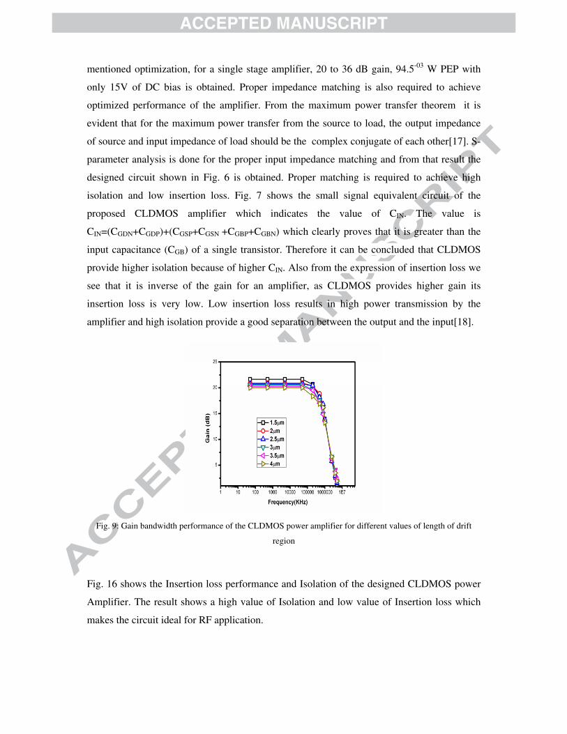
cm-3 are used. Gain bandwidth performance of power amplifier is shown in the following Fig.
8 & 9. From these two graphs, it is evident that the effect of changing the doping
concentration on the frequency response of the power amplifier is more prominent than that
of changing the drift length. Low on-resistance and high on current are the two main device
criteria for a LDMOS based Power Amplifier. Low doping concentration in the drift region
reduces the number of immobile charges. Thus the scattering effect of mobile carrier is also
reduced, increasing the overall current and as a result a high on current is observed. This high
current flow delivers the high power at output introducing a high gain. Likewise small drift
length reduces the transit time, hence the chance of recombination. That reduces the channel
resistance which decreases the on-resistance of the driver LDMOS. At the time of reducing
the channel resistance during optimization, the breakdown voltage is another parameter of
concern. Optimization of drift length is required between the on-resistance and the
breakdown voltage because a large reduction of drift length will not give the desired
breakdown voltage.
Optimized values of the drift length and doping concentration are achieved from the
simulated Gain frequency performance of the power amplifier. The drift length of 1.5 µm and

doping concentration of 1016 cm-3 are the optimized value for the proposed Power Amplifier
structure.
Fig. 7: Small signal equivalent circuit of proposed CLDMOS
Fig. 8: Gain bandwidth performance of the CLDMOS power amplifier for different values of doping
concentration of drift region
Around 20 to 36 dB gain is observed using only a single stage amplifier for wireless receiver
with an input power range of -57.5 dB to -30 dB. Fig. 10 shows that within -40dBm to-
10dBm input power range it provides necessary gain which is in between 20 to 36 dB. This
input power range is taken as input range for ISM band[7]. In this range, with an increase in
input power the variation of dc bias point increases which shifts the operating region from its
optimum value which decreases the gain of the circuit. Fig. 11 shows the Gain response of
the power amplifier for different biasing voltages. 20 to 21 dB gain is achieved by a variation
of DC bias voltage range 5.8 V to 6.2 V. For other biasing voltages gain is less than that. The
DC point 5.85 V has been taken as the optimized value to set the Q point properly. For
faithful amplification, the amplitude range of 0 to 1.5V is used (Fig. 12). Using all the above
mentioned optimization, for a single stage amplifier, 20 to 36 dB gain, 94.5-03 W PEP with
only 15V of DC bias is obtained. Proper impedance matching is also required to achieve
optimized performance of the amplifier. From the maximum power transfer theorem it is
evident that for the maximum power transfer from the source to load, the output impedance
of source and input impedance of load should be the complex conjugate of each other[17]. S-
parameter analysis is done for the proper input impedance matching and from that result the
designed circuit shown in Fig. 6 is obtained. Proper matching is required to achieve high
isolation and low insertion loss. Fig. 7 shows the small signal equivalent circuit of the
proposed CLDMOS amplifier which indicates the value of CIN. The value is
CIN=(CGDN+CGDP)+(CGSP+CGSN +CGBP+CGBN) which clearly proves that it is greater than the
input capacitance (CGB) of a single transistor. Therefore it can be concluded that CLDMOS
provide higher isolation because of higher CIN. Also from the expression of insertion loss we
see that it is inverse of the gain for an amplifier, as CLDMOS provides higher gain its
insertion loss is very low. Low insertion loss results in high power transmission by the
amplifier and high isolation provide a good separation between the output and the input[18].
Fig. 9: Gain bandwidth performance of the CLDMOS power amplifier for different values of length of drift
region
Fig. 16 shows the Insertion loss performance and Isolation of the designed CLDMOS power
Amplifier. The result shows a high value of Isolation and low value of Insertion loss which
makes the circuit ideal for RF application.

Fig. 10: Study of gain vs. input power of power amplifier for the desired range of input power.
1 dB compression point is around -41dBm with a sufficiently high Power Added Efficiency
(PAE) of 28.5% and drain efficiency of 46.4% is achieved [19]. Fig. 13 shows that in the
range of -55 dB to -41 dB the amplifier performance is linear as the 1 dB compression point
is located at -41dB. This High value of 1dB compression point makes the circuit performance
linear for a large range. On the other hand, another parameter of linearity IIP3 [20] is having
a high value of 0 dBm which makes the amplifier performance linear also beyond the target
range of -10 to -40 dBm. The result of IIP3 is shown in Fig. 14. Fig. 15 shows the two types
of efficiency studies for the amplifier. Here it is observed that the PAE is less than the drain
efficiency as expected. From Fig.15 it is seen that the peak value of PAE is 28.5% and it is
achieved in the desired range of the amplifier. Fig 15 also shows the drain efficiency study of
the proposed circuit. It shows a constant efficiency throughout the output range with a peak
value of 46.4%.
Fig. 11: Study of gain variation with shift in DC bias point for the CLDMOS power amplifier

Fig. 12: Study of gain saturation of CLDMOS power amplifier with increase in input amplitude
Fig. 14: Measurment of IIP3 as the meausre of linearity for the power amplifier
Fig. 13: Study of input power vs output power and measurment of 1dB compression point of CLDMOS power
amplifier

CONCLUSION:
In this work, a CLDMOS based power amplifier is designed and optimized to achieve a 20 to
36 dB gain, 94.5-03 W PEP for 15V supply voltage. The drain efficiency of the power
amplifier is 46.4% and PAE is 28.5%. The amplifier is having a bandwidth of 800MHz and a
gain of 36dB.An improvement of 20.4dB gain and 680 MHz bandwidth with 15V supply is
observed over the existing structure which provides 15.6 dB gain and 120MHz bandwidth for
28V supply[21].The performance of the amplifier is linear for the input range of -10 dBm to -
40 dBm. In this range the linearity of the circuit is observed from 0dBm IIP3 point and -41dB
1dB compression point. Average Isolation of the circuit is 22 dB and average Insertion Loss
is 5dB which makes the circuit ideal for the application of Wireless Network.
Fig. 15: Output power vs. PAE & efficiency for the power amplifier
Fig. 16: Frequency vs. insertion loss and isolation for the power amplifier

ACKNOWLEDGEMENT
The authors want to thank the All India Council of Technical Education (AICTE), Govt. of
India for funding the TCAD tools.
REFERENCES
[1] S. C. Cripps, “RF Power Amplifier for Wireless Communications”, Second Edition,
Norwood, Artech House 1999.
[2] J. Leong Tham , C.Hull , A. Ali, F. Carr, R. Chu, J. Walley, and I. Koullias “A direct-
conversion transceiver chip set for 900 MHz (ISM band) spread-spectrum digital cordless
telephone,” IEEE International Symposium on Circuits and Systems, pp.85-88 vol.4, 12-15
May 1996 .
[3] S. A. Smerzi, G. Girlando, T. Copani, and G. Palmisano, “A Ku-band monolithic receiver
for DVB-S applications” IEEE Communications Magazine, vol.42, no.8, pp.132,139, Aug.
2004.
[4] B. J. Baliga, “Fundamentals Of Power Semiconductor Devices”, First Edition New York,
Springer, 2008.
[5] F. Larsen, M. Ismail, "The design of high performance low cost BiCMOS op-amps in a
predominantly CMOS technology", IEEE International Symposium on Circuits and Systems,
1995, vol.3, no., pp.1720-1723 ,30 Apr-3 May, 1995.
[6] N. Dye, and H. Granberg, “Radio Frequency Transistors, Principles and Practical
Applications”,Second Edition, Newnes ,2001.
[7]Datasheet of cisco Aironet 1400 series Wireless bridge.
[8] S. J C H. Theeuwen, J.H. Qureshi, "LDMOS Technology for RF Power Amplifiers,"
IEEE Transactions on Microwave Theory and Techniques, vol.60, no.6, pp.1755-1763, June
2012
[9] M. P van der Heijden, H.C. de Graaff, L. C N De Vreede, J.R. Gajadharsing, and J.N.
Burghartz, , "Theory and design of an ultra-linear square-law approximated LDMOS power
amplifier in class-AB operation," IEEE Transactions on Microwave Theory and
Techniques, vol.50, no.9, pp.2176-2184, Sep 2002.
[10] T. Efland, T. Keller, S. Keller, and J. Rodriguez, "Optimized complementary 40 V
power LDMOS-FETs use existing fabrication steps in submicron CMOS technology", IEDM
'94. Technical Digest, pp.399-402, 11-14 Dec. 1994.

[11] B. Razavi, “Design of Analog CMOS Integrated Circuits”, First Edition New Delhi,
Tata McGraw-Hill 2002.
[12]S. C.Sun, J.D.Plummer, , "Modeling of the on-resistance of LDMOS, VDMOS, and
VMOS power transistors," , IEEE Transactions on Electron Devices , vol.27, no.2, pp.356-
367, Feb 1980.
[13] C.W Tang,and K.Y Tong, “A compact large signal model of LDMOS”, Solid-State
Electronics, Volume 46, Issue 12, December 2002, Pages 2111-2115.
[14] Atlas Manuals, Silvaco Inc., Santa Clara, CA, 2012.
[15] D.M. Caughey, R.E. Thomas, , "Carrier mobilities in silicon empirically related to
doping and field," Proceedings of the IEEE , vol.55, no.12, pp.2192-2193, Dec. 1967
[16] S. Malobabic, J.A. Salcedo, J.-J. Hajjar, and J.J. Liou, "Analysis of Safe Operating Area
of NLDMOS and PLDMOS Transistors Subject to Transient Stresses," IEEE Transactions
on Electron Devices, vol.57, no.10, pp.2655-2663, Oct. 2010.
[17] D. M. Pozar “Microwave Engineering”, Third Edition, Delhi, Wiley India,2008.
[18] H. Chih-Min, H. Chung-Yu,C. Chun-Hsue, C. Da-Chiang, H. Chih-Fang,G. Jeng, C.
Ching-Yu, "Design of an RF Transmit/Receive Switch Using LDMOSFETs With High
Power Capability and Low Insertion Loss," IEEE Transactions on Electron Devices, vol.58,
no.6, pp.1722-1727, June 2011.
[19]R. Bagger, C.D. Shih, Y. Yu, J.Sjöström, and P. Andersson, "RF LDMOS Power
Amplifier Integrated Circuit for W-CDMA/TD-SCDMA applications," 36th European
Microwave Conference, 10-15 Sept. 2006, pp.1343-1346,
[20]T. H. Lee,” The Design of CMOS Radio-Frequency Integrated Circuits”, Second Edition,
Chembridge, Chembridge University Press, 2004
[21] F.J. Ortega-Gonzalez, "High Power Wideband Class-E Power Amplifier," Microwave
and Wireless Components Letters, IEEE , vol.20, no.10, pp.569-571, Oct. 2010
List Of Figures
Figure 1. Device structure of NLDMOS of channel length=2 µm , gate length =5 µm, oxide thickness=.05 µm
Figure 2. Device structure of PLDMOS of channel length=2 µm , gate length =5 µm, oxide thickness=.05 µm
Figure 3. Drain current Vs. drain voltage of NLDMOS for gate to source voltage of 10V

Figure 4. Drain current Vs. drain voltage of PLDMOS for gate to source voltage of -10V Figure 5. Drain current Vs. gate voltage of PLDMOS & NLDMOS for drain to source voltage of 2V and 10V
Figure 6. Schematic diagram of CLDMOS power amplifier with matching network at the Input
Figure 7. Small signal equivalent circuit of proposed CLDMOS
Figure 8. Gain bandwidth Performance of the CLDMOS power amplifier for different values of doping concentration of drift region
Figure 9. Gain bandwidth performance of the CLDMOS power amplifier for different values of length of drift region
Figure 10. Study of gain vs. input power of power amplifier for the desired range of input power.
Figure 11. Study of gain variation with shift in DC bias point for the CLDMOS power amplifier
Figure 12. Study of gain saturation of CLDMOS power Amplifier with increase in input amplitude
Figure 13. Study of input power vs output power and measurment of 1dB compression point of CLDMOS power amplifier
Figure 14. Measurment of IIP3 as the meausre of Linearity for the power amplifier
Figure 15. Output power vs. PAE & efficiency for the power amplifier
Figure 16. Frequency vs. insertion loss and isolation for the power amplifier
Figure:1

Figure:2
Figure:3

Figure:4
Figure:5

Figure:6
Figure:7

Figure:8

Figure:9
.
Figure:10

Figure:11
Figure:12

Figure:14
Figure:13

Figure:15
Figure:16

Highlight for Review
1. Optimization of LDMOS 2. Complementary LDMOS Power Amplifier 3. CLDMOS Power Amplifier for ISM Band 4. CLDMOS Power Amplifier with High Gain and High Linearity
Copyright © 2022 FDOKUMEN