design of integra ted power amplifier circuits for biotelemetry ...
165
DESIGN OF INTEGRATED POWER AMPLIFIER CIRCUITS FOR BIOTELEMETRY APPLICATIONS
-
Upload
khangminh22 -
Category
Documents
-
view
0 -
download
0
Transcript of design of integra ted power amplifier circuits for biotelemetry ...

DESIGN OF INTEGRA TED POWER
AMPLIFIER CIRCUITS FOR
BIOTELEMETRY APPLICATIONS

DESIGN OF INTEGRATED POWER AMPLIFIER
CIRCUITS FOR BIOTELEMETRY APPLICATIONS
By
Munir M. EL-Desouki
Bachelor's of Applied Science
King Fahd University of Petroleum
and Minerals, June 2002
A THESIS
SUBMITTED TO THE SCHOOL OF GRADUATE
STUDIES IN PARTIAL FULFILLMENT OF THE
REQUIREMENTS FOR THE DEGREE OF
MASTER'S OF APPLIED SCIENCE
McMaster University
Hamilton, Ontario, Canada
© Copyright by Munir M. El-Desouki, January 2006

MASTER OF APPLIED SCIENCE (2006)
(Electrical and Computer Engineering)
McMaster University
Hamilton, Ontario
TITLE:
AUTHOR:
SUPERVISORS:
NUMBER OF PAGES:
Design of Integrated Power Amplifier Circuits for
Biotelemetry Applications
Munir M. El-Desouki, B.A.Sc. (King Fahd University of
Petroleum and Minerals)
Prof. M. Jamal Deen and Dr. Yaser M. Haddara
XXV, 139
ii

Abstract
Over the past few decades, wireless communication systems have experienced rapid
advances that demand continuous improvements in wireless transceiver architecture,
efficiency and power capabilities. Since the most power consuming block in a transceiver
is the power amplifier, it is considered one of the most challenging blocks to design, and
thus, it has attracted considerable research interests. However, very little work has
addressed low-power designs since most previous research work focused on higher
power applications. Short-range transceivers are increasingly gaining interest with the
emerging low-power wireless applications that have very strict requirements on the size,
weight and power consumption of the system.
This thesis deals with designing fully-integrated RF power amplifiers with low
output power levels as a first step to improving the efficiency of RF transceivers in a 0.18
J.Lm standard CMOS technology. Two switch-mode power amplifiers, one operating at a
frequency of 650 MHz and the other at a frequency of 2.4 GHz, are presented in this
work using a class-E output stage with a class-F driver stage. The work presented here
represents the first use of class-E power amplifiers for low-power applications. The
measurement results of the 650 MHz design show a maximum drain efficiency of 15 %
and a maximum gain of 11.5 dB. When operated from a 0.65 V supply, the power
amplifier delivers an output power of 750 J.LW with a maximum power-added efficiency
(PAE) of 10 %. As for the 2.4 GHz design, three layouts were fabricated. The first two
designs have a filtered and a non-filtered output to show the effects of using on-chip
filtering in low-power designs. Special attention was given to optimize the layout and
minimize the parasitic effects. Measurement results show a maximum drain efficiency of
38 % and a maximum gain of 17 dB. When operating from a 1.2 V supply, the power
amplifier delivers an output power of9 mW with a PAE of33 %. The supply voltage can
go down to 0.6 V with an output power of2 mW and a PAE of25 %. The improvements
in the layout show an increase in drain efficiency from 8 % to 35 %. The third design
iii

uses a 2 ~m thick top-metal layer of low-resistivity, with the same circuit component
values as the first two designs. Measurement results show a maximum drain efficiency of
53 % and a maximum gain of 22 dB. When operating from a 1.2 V supply, the power
amplifier delivers an output power of 14.5 mW with a PAE of 51 %. The supply voltage
can go down to 0.6 V with an output power of3.5 mW and a PAE of43 %.
Also, a novel mode-locking power amplifier design is presented in two fully
integrated, differential superharmonic injection-locked power amplifiers (ILP A)
operating at a frequency of 2.4 GHz and at a frequency of 400 MHz. Measurement results
of the 2.4 GHz design and the 400 MHz design show that the fabricated power amplifiers
have a maximum gain of 31 dB from only one stage that occupies a chip area of only 0.6
mm2 and 0.9 mm2 respectively, with all components fully integrated.
Finally, two fully-integrated, single block baseband direct-modulation
transmitters operating at a frequency of 2.4 GHz and at a frequency of 400 MHz are also
presented in this work. Measurement results of the 2.4 GHz transmitter show a drain
efficiency of 27 %. When operating from a 1.5 V supply, the transmitter delivers an
output power of 8 dBm with a low phase noise of -122 dBc/Hz at a 1 MHz offset.
iv

Acknowledgements ·
I would like to start by expressing my sincere gratitude to the Almighty, where in His
name, the most gracious, the most merciful, all good things start. I will next list a number
of people who I am thankful to; and I apologize to those I forgot or could not mention.
I would like to express my sincere gratitude to my senior supervisor Prof. M.
Jamal Deen, for giving me the opportunity to work on these projects and for his
continuous support and guidance throughout my work. It is indeed an honor to have the
opportunity to follow into the footsteps of such a great mentor. I have learned, and I
continue to learn so much from him and I hope that my future achievements meet and
exceed the expectations of being one of his students.
I would also like to express my deep appreciation to my co-supervisor.Prof. Yaser
M. Haddara for his continuous support and guidance. My personal relationship with Dr.
Haddara ranks of a higher importance to me than the academic one. In a country with
almost no family, it is very valuable to me to know that I can obtain brotherly advice
from him at any time.
Also, I would like to thank Prof. Peter M. Smith and Prof. Mohamed Bakr for
taking the time to review my thesis and for being in my committee.
I would next like to thank my team members. I am referring to them as team
members because without their support, I would still be stuck at my first design up until
today. To mention a number of them, Kareem Shoukri, Sasan Naseh, Rizwan Murji,
Nabeel Jafferali, Wai Ngan, Ahmed Fakhr, Ehab El-Badry, Hamed Jafari, Samer Rizk,
Tarek Sadek and recently Mohammed Waleed Shinwari, who is also one of my best
friends from Saudi Arabia and continues to suffer from my never ending complaints. I
would especially like to thank Juan-Carlos Ranuarez who has always supported my work,
even after graduating and leaving McMaster University. I would also like to thank Dr.
Ognian Marinov for keeping his door always open for advice and support.
v

I would also like to thank other faculty members at McMaster University, such as
Dr. Chin-Hung Chen, Dr. Nicola Nicolici, Dr. Steve Hranilovic, Prof. James P. Reilly
and Dr. Rafik 0. Loutfy. Also, not forgetting the administrative staff at the ECE
department, especially Cheryl Gies, Terry Greenlay, Cosmin Coroiu and Helen Jachna.
Next I would like to thank the Canadian Microelectronics Corporation (CMC) for
providing me with the means of fabricating my designs. I am also very grateful to my
employer, King Abdulaziz City for Science & Technology (KACST) for providing me
with this great opportunity by funding my graduate studies. In particular, I would like to
thank Dr. Mansour Alghamdi, Dr. Mohammad Alkanhal, Dr. Fayez Alhargan, Soud
Albatal and Saad Aldosary. I would especially like to thank Dr. Daham Alani, who had
always been like a second father to me. I would also like to thank Nuha Nasser at the
Saudi Arabian Cultural Bureau in Canada.
At King Fahd University of Petroleum and Minerals (KFUPM), I would like to
thank my mentors Prof. Muhammad Abuelma'atti and Dr. Mohammad Alsunaidi.
I would also like to thank my dearest friends, many of which I was blessed with
for more than 16 years, especially Ismail Alani, Fahd Bahadailah, Khalid Al-Najar,
Osama Boshnaq, Adel Bedair, Hisham Al-Rowaihi, Mishaal Adib, Teeba Alkhudairi who
always makes me feel that I am not the only one with too much to do, Najla Attallah and
many others. In Canada, I would like to thank my close friend Jodie Ellenor for always
showing me that there is still hope for this world, and my close friend Lyndsey Huvers
for ramping up the early stages of my research by keeping me up all night after returning
home noisily very late. I would also like to express my sincere gratitude to my friends
Zina Alani and Khaldoon Mogharbil for always making me feel that my family is close
by.
A group member that I purposely left out, some one who has been involved in all
the phases of my work with continuous support, a very dear friend that is more than a
sister to me. Thank you Samar Abdelsayed for being the great person that you are.
Finally, I would like to express my deepest acknowledgements to my dear family,
Prof. Mahmoud El-Desouki, Dr. Mayadah Al-Homsi, Dr. Majid El-Desouki and
Mohannad El-Desouki, who continuously raise my measure of success, by showing me
what it really means.
vi

Table of Contents
ABSTRACT .................................................................................................................. iii
ACKNOWLEDGEMENTS ........................................................................................... v
TABLE OF CONTENTS ............................................................................................ vii
LIST OF FIGURES ...................................................................................................... xi
LIST OF TABLES ...................................................................................................... xxi
LIST OF SYMBOLS AND ACRONYMS ................................................................ xxii
IN'TRODUCTION ......................................................................................................... 1
1.1 Why CMOS? ............................................................................................................. 3
1.2 Biomedical Systems ................................................................................................... 4
1.3 RF CMOS Transceivers ............................................................................................. 8
1.4 Motivation ............................................................................................................... 1 0
1.5 Thesis Organization ................................................................................................. 13
IN'TRODUCTION TO CMOS RF POWER AMPLIFIERS ••••••••••••••••••••••••••••••••••••• 15
2.1 Simple Power Amplifier .......................................................................................... 15
2.2 Important Characteristics ofPower Amplifiers ......................................................... 16
2.2.1 PowerGain ....................................................................................................... 16
2.2.2 Efficiency ......................................................................................................... 18
vii
2.2.3 Linearity ........................................................................................................... 18
2.2.3.1 Gain Compression (AM-AM Conversion) ...................................... 19
2.2.3.2 AM-PM Conversion ....................................................................... 19
2.2.3.3 Inter-Modulation Distortion (IMD) ................................................. 19
2.3 Design Considerations ............................................................................................. 20
2.3.1 Conjugate Match and Load Line Match ............................................................. 20
2.3.2 Effect of the Transistor Knee-Voltage ............................................................... 21
2.3.3 Substrate Doping and Leakage .......................................................................... 22
2.3.4 Breakdown Voltage .......................................................................................... 22
2.3.5 Temperature Considerations .............................................................................. 23
2.3.6 On-chip Integration ........................................................................................... 24
2.3.7 Amplifier Stability ............................................................................................ 25
2.3.8 Ground Inductance ............................................................................................ 25
2.3.9 Low Output Power Design ................................................................................ 26
2.4 Summary ................................................................................................................. 28
POWER AMPLIFIER CLASSES OF OPERATION ................................................ 29
3.1 Current-Mode Power Amplifiers .............................................................................. 29
3.1.1 Class-A Power Amplifiers ................................................................................. 36
3.1.2. Class-B Power Amplifiers ................................................................................ 37
3.1.3. Class-AB Power Amplifiers ............................................................................. 37
3.1.4. Class-C Power Amplifiers ................................................................................ 37
3.2 Switch-Mode Power Amplifiers ............................................................................... 38
3.2.1 Class-D Power Amplifiers ................................................................................. 38
3.2.2 Class-E Power Amplifiers ................................................................................. 39
viii

3.2.3 Class-F Power Amplifiers ................................................................................. 46
3.2.4 Class-S Power Amplifiers ................................................................................. 47
3.3 Lock-Mode Power Amplifiers .................................................................................. 48
3.4 Power Amplifier Figure-of-Merit (FoM) ................................................................. .49
3.5 Summary ................................................................................................................. 49
DIRECT -MODULATION TRA.NSMITTERS ........................................................... Sl
4.1 Differential Cross-Coupled Negative-gm Voltage-Controlled Oscillator ................... 52
4.2 Superharmonic Injection-Locking ................................................... , ........................ 55
4.3 Transmitter Figure-of-Merit (FoM) .......................................................................... 55
4.4 Summary ................................................................................................................. 56
SWITCH-MODE POWER AMPLIFIERS- MEASUREMENT RESULTS ........... 57
5.1 First Power Amplifier Design ................................................................................. ,59
5.1.1 Schematic Simulation Results ........................................................................... 65
5.1.2 Layout .............................................................................................................. 67
5.1.3 Refined Circuit Simulation Results ................................................................... 68
5.1.4 Measurement Results ........................................................................................ 70
5.2 Second Power Amplifier Design .............................................................................. 76
5.2.1 Schematic Simulation Results ........................................................................... 76
5.2.2 Layout .............................................................................................................. 78
5.2.3 Refined Circuit Simulation Results ................................................................... 79
5.2.4 Measurement Results ........................................................................................ 80
5.3 Comparison and Summary ....................................................................................... 90
ix

LOCK-MODE POWER AMPLIFIERS - MEASUREMENT RESUL TS ................ 92
6.1 First Power Amplifier Design .................................................................................. 94
6.1.1 Schematic Simulation Results ........................................................................... 95
6.1.2 Layout .............................................................................................................. 98
6.1.3 Measurement Results ........................................................................................ 99
6.2 Second Power Amplifier Design ............................................................................ 1 06
6.2.1 Schematic Simulation Results ......................................................................... 1 06
6.2.2 Layout ............................................................................................................ 1 07
6.2.3 Measurement Results ...................................................................................... 107
6.3 Comparison and Summary ..................................................................................... 112
DIRECT-MODULATION TRANSMITTERS- MEASUREMENT RESULTS ... 114
7.1 First Transmitter Design ........................................................................................ 116
7.1.1 Schematic Simulation Setup ............................................................................ 116
7 .1.2 Measurement Results ...................................................................................... 117
7.2 Second Transmitter Design .................................................................................... 120
7.3 Comparison and Summary ..................................................................................... 124
CONCLUSIONS AND FUTURE WORK ................................................................ 126
8.1 Contributions and Summary ................................................................................... 126
8.2 Future Work .......................................................................................................... 130
REFERENCES .......................................................................................................... 135
X

List of Figures
Figure 1.1: Flying and crawling microrobot models for wireless sensor networks [1] ....... 2
Figure1.2: First integration of different technologies as a SoC with standard CMOS,
reproduced from [6] ....................................................................................... 3
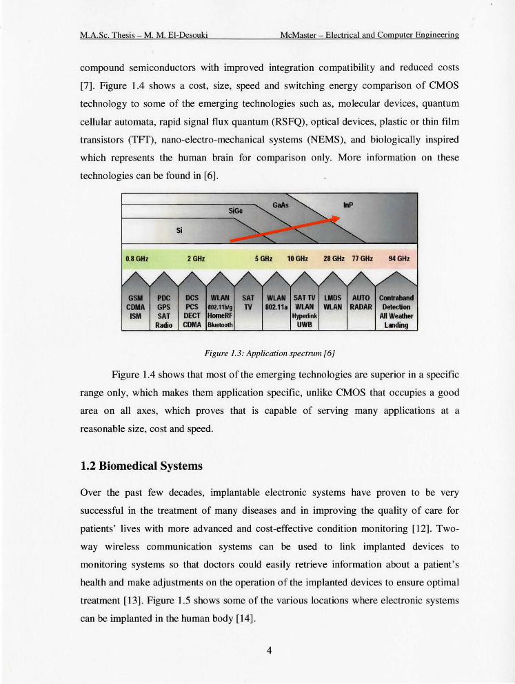
Figure 1.3: Application spectrum [6] ............................................................................... 4
Figure 1.4: A comparison between emerging technologies and CMOS [6] ....................... 5
Figure 1.5: Some applications of implantable electronic systems [14] .............................. 5
Figure 1.6: Swallowable camera system [15] ................................................................... 8
Figure 1.7: Screen shot of the Norika user interface [16] .................................................. 9
Figure 1.8: Block diagram of a typical RF transceiver, reproduced from [17] ................... 9
Figure 1.9: An example of an RF transmitter circuit [18] ............................................... 10
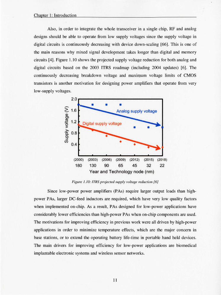
Figure 1.10: ITRS projected supply voltage reduction [6] .............................................. 11
Figure 1.11: ITRS projected FoM for PAs and VCOs for future technology nodes [6] ... 13
Figure 2.1 Simple power amplifier ................................................................................. 16
Figure 2.2 The basic parameters of a simple power amplifier ......................................... 17
Figure 2.3 Simple two-stage power amplifier ................................................................. 17
Figure 2.4 The effect of gain compression on the output power ...................................... 19
Figure 2.5 Third order IMD components ........................................................................ 20
Figure 2.6 Third order intercept points ........................................................................... 20
Figure 2.7 Optimal load line .......................................................................................... 21
Figure 2.8 The effects of ground inductance on the performance of a power amplifier,
reproduced from [3] ..................................................................................... 26
xi

Figure 2.9 The effect of using a fmite RFC on low output power amplifiers ................... 27
Figure 2.10 The effect of the output filter on low output power amplifiers ..................... 27
Figure 3.1 Basic single-stage current-mode power amplifier .......................................... 31
Figure 3.2 (a) The effect of the gate biasing point on the conduction angle (a). (b) The
equivalent drain current ............................................................................... 32
Figure 3.3 Harmonic components as a function of the conduction angle (a) ................... 33
Figure 3.4 The effect of the conduction angle (a) on the normalized output power, drain
efficiency and difference between the fundamental current and the third order
harmonic component ................................................................................... 34
Figure 3.5 The effect of the conduction angle (a) on the DC power, output power and
drain efficiency ............................................................................................ 35
Figure 3.6 Third order harmonic peaking ....................................................................... 36
Figure 3.7 A method to increase efficiency .................................................................... 36
Figure 3.8 Drain current of a class-A power amplifier .................................................... 37
Figure 3.9 Drain current of a class-B power amplifier .................................................... 37
Figure 3.10 Basic schematic of a class-D power amplifier ............................................ .39
Figure 3.11 Basic schematic of a class-E power amplifier ............................................. .40
Figure 3.12 The equivalent circuit of a class-E amplifier ............................................... .41
Figure 3.13 The drain voltage waveform of an ideal class-E amplifier .......................... .41
Figure 3.14 The output waveform of a class-E power amplifier .................................... .42
Figure 3.15 The effects of adjusting the output network components of a class-E
amplifier [30] .............................................................................................. 46
Figure 3.16 Basic schematic of a class-F power amplifier ............................................. .47
Figure 3.17 An example of a class-S power amplifier ................................................... .4 7
Figure 3.18 Differential class-E power amplifier with mode-locking, reproduced from
[34] ............................................................................................................. 48
xii

Figure 3.19 Comparison between the proposed FoM and the ITRS FoM for published
works [60] ................................................................................................... 50
Figure 4.1 (a) Basic block diagram of a direct-modulation transmitter, (b) simplified
transmitter, (c) single block transmitter [51] ................................................ 52
Figure 4.2 A frequency selective LC-tank showing the parallel output resistance ........... 53
Figure 4.3 Negative resistance of a cross coupled NMOS pair ....................................... 53
Figure 4.4 (a) Complementary negative-gm cross coupled pair, (b) complete oscillator .. 54
Figure 4.5 Schematic of a direct-modulation transmitter ................................................ 54
Figure 5.1 Schematic of the complete two-stage power amplifier ................................... 59
Figure 5.2 Output power as a function of (a) the supply voltage for a fixed output load of
50 n, (b) the output load for a fixed supply voltage of 1.2 v ........................ 60
Figure 5.3 Schematic of a basic class-E power amplifier [56] ........................................ 61
Figure 5.4 Schematic of designed 900 MHz switch-mode power amplifier [53] ............. 64
Figure 5.5 Schematic of900 MHz switch-mode power amplifier simulation setup ......... 65
Figure 5.6 Simulated drain voltage of the class-E power amplifier ................................. 66
Figure 5.7 Simulated output power, PAE and drain efficiency as a function of the input
power .......................................................................................................... 66
Figure 5.8 Screen capture of the 900 MHz power amplifier layout ................................. 67
Figure 5.9 Screen capture of the InterConnect application interface ............................... 69
Figure 5.10 Photomicrograph of the fabricated 900 MHz power amplifier [53] .............. 70
Figure 5.11 Setup used in measuring the 900 MHz power amplifier ............................... 71
Figure 5.12 Comparison between the measured and simulated output power and drain
efficiency of the filtered output, as a function of the operating frequency, at a
supply voltage of0.7 v ................................................................................ 71
xiii
Figure 5.13 Measured output power, PAE and drain efficiency (TJ) of the non-filtered
output, at an input frequency of 650 MHz, as a function of the supply voltage
[53] ............................................................................................................. 72
Figure 5.14 Measured output power of the non-filtered output at an input frequency of
650 MHz, as a function of the input power for various supply voltages [53] 72
Figure 5.15 Measured power gain of the non-filtered output at an input frequency of650
MHz, as a function of the input power for various supply voltages [53] ....... 73
Figure 5.16 Measured drain efficiency of the non-filtered output at an input frequency of
650 MHz, as a function of the input power for various supply voltages [53] 74
Figure 5.17 Measured P AE of the non-filtered output at an input frequency of 650 MHz,
as a function of the input power for various supply voltages [53] ................. 74
Figure 5.18 Comparison between the measured drain efficiency of the filtered and the
non-filtered outputs as a function of the input frequency, at a supply voltage
of0.7 V [53] ................................................................................................ 75
Figure 5.19 Comparison between the measured output power of the filtered and the non
filtered outputs as a function of the input frequency, at a supply voltage of 0. 7
v [53] .......................................................................................................... 75
Figure 5.20 Comparison between the harmonic content of the filtered and the non-filtered
outputs, at a supply voltage of0.7 V. The filtered output drops below the non
filtered output at the fundamenta~ second and third harmonics by 7, 6 and 12
dB respectively [53] .................................................................................... 75
Figure 5.21 Schematic of designed 2.4 GHz switch-mode power amplifier [54, 55] ....... 76
Figure 5.22 Schematic of designed 2.4 GHz switch-mode power amplifier simulation
setup ............................................................................................................ 77
Figure 5.23 Simulated output power, P AE and drain efficiency as a function of the input
power .......................................................................................................... 77
Figure 5.24 Screen capture of the first 2.4 GHz power amplifier layout ......................... 78
xiv
Figure 5.25 Screen capture of the (a) improved layout design and (b) thick-top metal
design .......................................................................................................... 79
Figure 5.26 Photomicrograph of (a) the frrst fabricated 2.4 GHz design, (b) the improved
layout and (c) the thick-metal design [54-56] ............................................... 80
Figure 5.27 Comparison between the measured output power of the non-filtered output of
the first design, the improved design and the design that uses a thick top
metal layer at a supply voltage of 0.8 V, as a function of the input frequency
[56] ............................................................................................................. 81
Figure 5.28 Comparison between the measured drain efficiency of the non-filtered output
of the first design, the improved design and the design that uses a thick top
metal layer at a supply voltage of 0.8 V, as a function of the input frequency
[56] ............................................................................................................. 81
Figure 5.29 Comparison between the measured and simulated output power and drain
efficiency of the filtered output in the first design, as a function of the
operating frequency, at a supply voltage of 0.8 V [54] ................................. 82
Figure 5.30 Comparison between the measured and simulated output power and drain
efficiency of the non-filtered output in the improved design, as a function of
the operating frequency, at a supply voltage of0.8 V [54] ........................... 82
Figure 5.31 Comparison between the measured and simulated output power and drain
efficiency of the third design, as a function of the operating frequency, at a
supply voltage of 0.8 V [56] ........................................................................ 83
Figure 5.32 Measured output power, PAE and drain efficiency (rt) of the non-filtered
output in the second design at a frequency of 2.4 GHz, as a function of the
supply voltage [55] ...................................................................................... 83
Figure 5.33 Measured output power, PAE and drain efficiency (T\) of the filtered output in
the second design at a frequency of 2.4 GHz, as a function of the supply
voltage [55] ................................................................................................. 84
XV

Figure 5.34 Comparison between the measured output power of the filtered and the non
filtered outputs in the second design, at a supply voltage of 1.2 V as a
function of the operating frequency [55] ...................................................... 84
Figure 5.35 Comparison between the harmonic content of the filtered and the non-filtered
outputs in the second design, at a supply voltage of 1.2 V and an input
frequency of2.4 GHz [55] ........................................................................... 85
Figure 5.36 Measured output power of the non-filtered output in the second design, at a
supply voltage of 0.6, 0.9 and 1.4 V at a frequency of 2.4 GHz, as a function
of the input power [55] ................................................................................ 86
Figure 5.37 Measured PAE of the non-filtered output in the second design, at a supply
voltage of 0.6, 0.9 and 1.4 V at a frequency of 2.4 GHz, as a function of the
input power [55] .......................................................................................... 86
Figure 5.38 Measured output power, PAE and drain efficiency (rl) of the third design at
an input frequency of2.4 GHz, as a function of the supply voltage [56] ....... 87
Figure 5.39 Measured output power, PAE and drain efficiency (T}) of the third design at a
supply voltage of0.8 V, as a function of the input frequency [56] ................ 88
Figure 5.40 Comparison between the simulated and measured power gain of the third
design, at a supply voltage of 0.8 V and operating frequency 2.4 GHz as a
function of the input power [56] .................................................................. 88
Figure 5.41 Measured output power of the third design, as a function of the input power
at an operating frequency of2.4 GHz for various supply voltages [56] ........ 89
Figure 5.42 Measured P AE of the third design, as a function of the input power at an
operating frequency of 2.4 GHz for various supply voltages [56] ................. 89
Figure 5.43 Measured harmonic content of the output signal in the third design, at a
supply voltage of0.8 V and an input frequency of2.4 GHz [56] .................. 90
Figure 6.1 Basic schematic of the lock-mode power amplifier [57] ................................ 94
Figure 6.2 Schematic of designed 400 MHz lock-mode power amplifier simulation setup
.................................................................................................................... 96
xvi
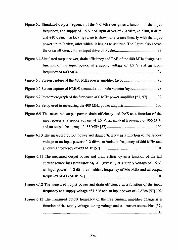
Figure 6.3 Simulated output frequency of the 400 MHz design as a function of the input
frequency, at a supply of 1.5 V and input drives of -10 dBm, -5 dBm, 0 dBm
and +10 dBm. The locking range is shown to increase linearly with the input
power up to 0 dBm, after which, it begins to saturate. The figure also shows
the drain efficiency for an input drive ofO dBm ........................................... 97
Figure 6.4 Simulated output power, drain efficiency and PAE of the 400 MHz design as a
function of the input power, at a supply voltage of 1.5 V and an input
frequency of 800 MHz ................................................................................. 97
Figure 6.5 Screen capture of the 400 MHz power amplifier layout ................................. 98
Figure 6.6 Screen capture of NMOS accumulation-mode varactor layout ....................... 98
Figure 6.7 Photomicrograph of the fabricated 400 MHz power amplifier [51, 57] .......... 99
Figure 6.8 Setup used in measuring the 400 MHz power amplifier ............................... lOO
Figure 6.9 The measured output power, drain efficiency and PAE as a function of the
input power at a supply voltage of 1.5 V, an incident frequency of 866 MHz
and an output frequency of 433 MHz [57] ................................................. 100
Figure 6.10 The measured output power and drain efficiency as a function of the supply
voltage at an input power of -2 dBm, an incident frequency of 866 MHz and
an output frequency of 433 MHz [57] ........................................................ 101
Figure 6.11 The measured output power and drain efficiency as a function of the tail
current source bias (transistor Mt; in Figure 6.1) at a supply voltage of 1.5 V,
an input power of -2 dBm, an incident frequency of 866 MHz and an output
frequency of 433 MHz [57] ....................................................................... 101
Figure 6.12 The measured output power and drain efficiency as a function of the input
frequency at a supply voltage of 1.5 V and an input power of -2 dBm [57] 102
Figure 6.13 The measured output frequency of the free running amplifier design as a
function of the supply voltage, tuning voltage and tail current source bias [57]
.................................................................................................................. 103
xvii

Figure 6.14 The measured output spectrum taken from a single-ended output after loss
compensation, at a supply voltage of 1.5 V for both the free running mode
and the locked mode with an input power of -10 dBm [57] ........................ 103
Figure 6.15 The measured phase noise in free running mode, with a 0.9 V gate bias
applied to transistor Ms, and in locking mode, with an input power of -20
dBm, at a supply voltage of 1.5 V [57] ...................................................... 104
Figure 6.16 The measured phase noise in the locking-mode, with an input power of -20
dBm and an input power of -40 dBm, at a supply voltage of 1.5 V [57] ..... 105
Figure 6.17 The measured phase noise in free-running mode with no RF input applied,
for various gate bias voltages applied to transistor M5, at a supply voltage of
1.5 v [57] .................................................................................................. 106
Figure 6.18 Simulated drain efficiency and output frequency of the 2.4 GHz design as a
function of the incident frequency, at a supply voltage of 1.5 V and an input
drive of 0 dBm .......................................................................................... 107
Figure 6.19 Screen capture ofthe 2.4 GHz power amplifier layout.. ............................. 107
Figure 6.20 Photomicrograph of the fabricated 2.4 GHz power amplifier [51, 57] ........ 108
Figure 6.21 The measured output power, drain efficiency and PAE as a function of the
input power at a supply voltage of 1.5 V, an incident frequency of 4.8 GHz
and an output frequency of 2.4 GHz [57] ................................................... 108
Figure 6.22 The measured output power and drain efficiency as a function of the supply
voltage at an input power of -2 dBm, an incident frequency of 4.8 GHz and
an output frequency of2.4 GHz [57] ......................................................... 109
Figure 6.23 The measured output power and drain efficiency as a function of the tail
current source bias (transistor M6 in Figure 6.1) at a supply voltage of 1.5 V,
an input power of -2 dBm, an incident frequency of 4.8 GHz and an output
frequency of2.4 GHz [57] ......................................................................... 109
Figure 6.24 The measured output power and drain efficiency as a function of the input
frequency at a supply voltage of 1.5 V and an input power of-2 dBm [57] 110
xviii

Figure 6.25 The measured output frequency of the free-running amplifier as a function of
the supply voltage, tuning voltage and tail current source bias [51, 57] ...... 110
Figure 6.26 The measured output spectrum taken from a single-ended output after loss
compensation, at a supply voltage of 1.5 V for both the free-running mode
and the locked-mode with an input power of -10 dBm [57] ........................ 111
Figure 6.27 The measured phase noise in free-running mode, with a 0.9 V gate bias
applied to transistor Ms, and in locking mode with an input power of -10
dBm, at a supply voltage of 1.5 V [57] ...................................................... 112
Figure 7.1 Basic schematic of the direct-modulation transmitter .................................. 116
Figure 7.2 Basic schematic of the direct-modulation transmitter simulation setup ........ 117
Figure 7.3 Setup used in measuring the 400 MHz direct-modulation transmitter .......... 118
Figure 7.4 The measured output power and drain efficiency of the 400 MHz design as a
function of the supply voltage. The figure also shows the spectrum of the
output signal [51] ...................................................................................... 119
Figure 7.5 The measured output power and drain efficiency of the 400 MHz design as a
function of the tail current source bias (transistor M5 in Figure 7.1), at a
supply voltage of 1.5 V [51] ...................................................................... 119
Figure 7.6 The measured output frequency of oscillation of the 400 MHz design as a
function of the supply voltage, tuning voltage, modulation voltage and tail
current source bias [51] ............................................................................. 120
Figure 7.7 The measured output power and drain efficiency of the 2.4 GHz design as a
function of the supply voltage. The figure also shows the spectrum of the
output signal [51] ...................................................................................... 120
Figure 7.8 The measured output power and drain efficiency of the 2.4 GHz design as a
function of the tail current source bias (transistor M5 in Figure 7.1) and the
tuning voltage applied to the varactors, at a supply voltage of 1.5 V [51] ... 121
xix

Figure 7.9 The Measured phase noise of the 2.4 GHz design for various tail current
source control voltages applied to transistor M5, at a supply voltage of 1.5 V
[51] ........................................................................................................... 122
Figure 7.10 The Measured phase noise of the 2.4 GHz design for various gate bias
voltages applied to the transconductance transistor, which was not used in this
design, at a supply voltage of 1.5 V [51] .................................................... 123
Figure 7.1 1 The Measured output spectrum of the 2.4 GHz design, FS K modulated at 1
Mbit/s and± 190kHz frequency deviation, at a supply voltage of 1.5 V [51]
.................................................................................................................. 123
Figure 7.12 Bluetooth data spectrum emission mask [51] ............................................. 124
Figure 8.1 Photomicrograph of the six circuits that were fabricated to investigate the
cause of phase noise fluctuations ............................................................... 131
Figure 8.2 PLL transmitter block diagram .................................................................... l32
Figure 8.3Photomicrograph of the designed PLL transmitter ........................................ 132
Figure 8.4 Photomicrograph of (a) the class-E PVCO transmitter design (b) the class-E
PLL transmitter ......................................................................................... 133
Figure 8.5 Conventiona12.4 GHz transmitter, photomicrograph and circuit schematic.l34
XX

List of Tables
Table 1.1: Performance comparison between the M2A and the Norika pills [16] .............. 8
Table 1.2: Power consumption of the building blocks in Figure 1.9 [ 18] ........................ 1 0
Table 3.1: Summary of the class-E ideal design equations ............................................. 44
Table 3.2: Comparison between different power amplifier classes ................................. 50
Table 5.1: Performance comparison between the presented power amplifier designs ...... 91
Table 6.1: Performance comparison between the presented lock-mode power amplifier
designs ...................................................................................................... 113
Table 7.1: Performance comparison between the presented VCPO designs [51] ........... 125
Table 8.1: Performance comparison between state-of-the-art CMOS power amplifier
designs ...................................................................................................... 129
Table 8.2: Performance comparison between state-of-the-art voltage-controlled power
oscillators .................................................................................................. 129
xxi

List of Symbols and Acronyms
Symbols
{J) Frequency in radians
gm Transconductance
Ioc DC current
/pk Peak current
Iq Quiescent current
Poe DC power
pin Input power
Pout Output power
Q Quality factor
QL Loaded quality factor
Rs Source resistance
RL Load resistance
T Temperature
Tr Room temperature
Voc DC voltage
Vos Drain to source voltage
Vgs Gate to source voltage
Vknee Knee voltage
VT Threshold voltage
W/L Width over length ratio
a Conduction angle
'1 Drain efficiency
fl Mobility
Acronyms
AC Alternating current
xxii

ACPR
AM
CDMA
CMOS
CP
DAC
DCS
DECT
DWN
E-D RAM
EER
ESD
FoM
PRAM
FSK
FPGA
G
GaAs
GFSK
GPS
GSM
IIP3
ILFD
ILO
ILPA
IMD
InP
ISM
ITRS
LAN
LMDS
Adjacent channel power ratio
Amplitude modulation
Code-division multiple access
Complementary metal oxide semiconductor
Compression point
Digital to analog converter
Defense communications system
Digital enhanced cordless telecommunications
Down
Enhanced dynamic random access memory
Envelope elimination and restoration
Electrostatic discharge
Figure-of-merit
Ferroelectric random access memory
Frequency-shift keying
Field programmable gate-array
Power gain
Gallium arsenide
Gaussian frequency-shift keying
Global positioning system
Global system for mobile communications
Third-order input intercept point
Injection-locked frequency divider
Injection-locked oscillator
Injection-locked power amplifier
Inter-modulation distortion
Indium phosphide
Industrial-scientific-medical
Intemacional technology roadmap for semiconductors
Local area network
Local multipoint distribution system
xxiii

LNA
LO
MEMS
MICS
MIM
MOSFET
NEMS
NMOS
OIP3
OOK
PA
PAE
PCS
PDC
PFD
PLL
PM
PMOS
PUF
PWM
REF
RF
RFC
RSFQ
SiGe
SiP
SoC
Low-noise amplifier
Local oscillator
Micro-electro-mechanical systems
Medical implantable communication systems
Metal-insulator-metal
Metal-oxide semiconductor field effect transistor
N ano-electro-mechanical systems
N-type metal-oxide semiconductor
Third-order output intercept point
On-off keying
Power amplifier
Power-added efficiency
Personal communication services
Personal digital cellular
Phase frequency detector
Phase-locked loop
Power management
P-type metal-oxide semiconductor
Power utilization factor
Pulse-width modulation
Reference
Radio frequency
Radio frequency choke
Rapid signal flux quantum
Silicon germanium
System-in-a-package
System-on-a-chip
S-parameters Scattering parameters
SRAM Static random access memory
TFT Thin-ftlm transistors
UWB Ultra-wide band
xxiv

vco VCPO
WBAN
X tal
Voltage-controlled oscillator
Voltage-controlled power oscillator
Wireless body area networks
Crystal
XXV

Chapter 1: Introduction
Chapter 1
INTRODUCTION
The rapid advances in wireless communication systems over the past decades demand
continuous improvements in wireless transceiver architecture, efficiency and power
capabilities. Since the most power consuming block in a transceiver is the power
amplifier, it is considered one of the most challenging blocks and thus, it has attracted a
lot of research interests in the recent past. However, very little work has addressed low
power designs since most previous research work focused on higher-power applications
such as wireless LAN and Bluetooth. Short-range transceivers are increasingly gaining
interest with the emerging low-power wireless applications such as, wireless body area
networks (WBAN), wireless sensor networks, smart dusts, biotelemetry and even
synthetic insects.
Figure 1.1 shows models of flying and crawling microrobots developed by the
University of California [1]. These synthetic insects that could fly or crawl act as smart
dust motes (nodes) that can sense and communicate. The crawling microrobot can lift
more than 130 times its own weight while consuming only tens ofmicrowatts. The flying
microrobot has a wing span of 10-25 mm and consumes less than 10 mW of power
provided by solar cells [1]. Such motes are expected to communicate with each other
within a wireless sensor network of smart dusts using a transmitted power of 1-3 mW to
cover an indoor range of less than 10 meters [2]. Designing power amplifiers for such
low transmit power levels is very challenging and not yet thoroughly researched, as
compared to high power amplifiers used in traditional transceivers.
Although RF circuits contain fewer devices than digital circuits, RF circuit design
is more challenging because second-order effects, non-linearities, noise, mismatch,
distortion and parasitic elements must be carefully considered to obtain the required time
1

M.A.Sc. Thesis- M. M. El-Desouki McMaster- Electrical and Computer Engineering
and amplitude precision [3, 4]. Another reason why RF circuit design is considered more
challenging is the lack of automation and synthesis tools, unlike digital circuits, which
have well developed tools [4].
Figure 1.1: Flying and crawling micro robot models for wireless sensor networks [ 1]
For biomedical applications, especially biomedical implantable electronic circuits,
RF designers are faced with even more challenges such as electromagnetic radiation
exposure safety limits, size and weight of the implantable devices, power supply and
power consumption issues and whether the power should be externally supplied through
inductive coupling or internally from a battery. Also, due to restrictions on the amount of
power transmitted into or out of the human body, there is great need for improving the
efficiency of implantable transceivers, even with low-power designs [65].
The choice of technology used depends mainly on the required performance of the
targeted market or standard, the level of integration required and most importantly the
cost [5]. Traditionally, a mixture of different compound semiconductors was used for
designing efficient RF power amplifiers that were connected to the digital circuitry,
which is usually implemented in standard CMOS technology, to create a whole system
in-a-package (SiP). However, deep sub-micron CMOS has become a very attractive
technology for RF circuit design [7].
2

Chapter 1: Introduction
1.1 Why CMOS?
The main advantages of using current CMOS (180 nm and below) technology in building
RF circuits are the high level of integration and cheap cost. Using CMOS in transceiver
circuits produces fully integrated system-on-a-chip (SoC) designs at reduced costs, rather
than the multiple-die SiP [3, 4, 7]. This furthermore enabled designers to increase system
compatibility by developing single chips that could operate at more than one wireless
communication standard [1]. Figurel.2 shows the first integration of different
technologies as a SoC with a standard CMOS process [6]. Previous designs used
compound semiconductors such as SiGe and GaAs instead of standard CMOS for circuits
that operate at high-frequencies or transmit high-power levels. However, recent research
[8-10] work proved that CMOS designs can fulfill the power requirements of many
wireless standards because the maximum operating frequency of MOSFET transistors is
continuously increasing with device down-scaling [ 4]. Future predictions indicate that
silicon based technologies will gain even more importance due to their high level of
integration [3, 5] .
Logic I SRAM I Flash
E-DRAM
CMOS RF
FPGA I FRAM
MEMS I Chemical Sensors
1998 1999 2000 2001 2002 2003 2004 2005 2006 2007 2008 2009 2010 2011 2012
Figurel .2: First integration of different technologies as a SoC with standard CMOS, reproducedfrom [6]
In short-range or biomedical applications, the transmitted power is fairly low and
the operating frequency is limited to one of the industrial-scientific-medical (ISM) bands.
Usually in biomedical applications, the frequency of the signals transmitted through the
human body must be low to minimize the attenuation losses in the body layers and to
remain within the safety restrictions [11]. Since both the transmitted power and operating
frequency are low, standard CMOS technology becomes a good candidate to be used in
biomedical applications. Figure 1.3 shows the application spectrum of some common
wireless applications and the corresponding suitable technology. This makes CMOS
technology very attractive because its performance is now comparable to traditional
3
M.A.Sc. Thesis- M. M. El-Desouki McMaster- Electrical and Computer Engineering
compound semiconductors with improved integration compatibility and reduced costs
[7]. Figure 1.4 shows a cost, size, speed and switching energy comparison of CMOS
technology to some of the emerging technologies such as, molecular devices, quantum
cellular automata, rapid signal flux quantum (RSFQ), optical devices, plastic or thin film
transistors (TFf), nano-electro-mechanical systems (NEMS), and biologically inspired
which represents the human brain for comparison only. More information on these
technologies can be found in [6] .
Si
O.BGHz 2 GHz
GSM POC COMA GPS
ISM SAT Radio
WLAN SAT TV LMDS AUTO 802.11a WLAN WLAN RADAR
Hyperlink UWB
Figure 1.3: Application spectrum [6]
Figure 1.4 shows that most of the emerging technologies are superior in a specific
range only, which makes them application specific, unlike CMOS that occupies a good
area on all axes, which proves that is capable of serving many applications at a
reasonable size, cost and speed.
1.2 Biomedical Systems
Over the past few decades, implantable electronic systems have proven to be very
successful in the treatment of many diseases and in improving the quality of care for
patients' lives with more advanced and cost-effective condition monitoring [12]. Two
way wireless communication systems can be used to link implanted devices to
monitoring systems so that doctors could easily retrieve information about a patient's
health and make adjustments on the operation of the implanted devices to ensure optimal
treatment [13]. Figure 1.5 shows some of the various locations where electronic systems
can be implanted in the human body [14].
4

Chapter 1: Introduction
~ ctl C) -c.R--...... -Ill 0 0 ...... C) -10 0
...J
Log [Energy] (J/op)
Figure 1.4: A comparison between emerging technologies and CMOS [6]
Cochlear implant
Shoulder implant"
External force actuators
External trigger mechanisms
External trigger mechanisms
External force actuators
........ Eye implant
....... Heart implant
Pump for blood or other ····· liquids in the body
......... Artificial lung/air pump
Artificial bladder
System to close/ ···· open bladder
External control system Nerve motion detector
............. Nerve simulator
............. Dropped foot implant
Figure 1.5: Some applications of implantable electronic systems [ 14]
5
-12.0
-13.8
-15.6
-17.4
-19.2
-21.0
-22.8
-24.6

M.A.Sc. Thesis - M. M. El-Desouki McMaster- Electrical and Computer Engineering
First generation implantable medical devices used low-frequency inductive links
as a means of communication. These systems operated in the hundreds of kilohertz range
with data rates lower than 30 kB/sec and over a very short range, which often requires
direct contact with the skin. Recent applications that require higher data rates use one of
the industrial- scientific- medical (ISM) bands such as the 433 MHz band, the 915 MHz
band and the 2.45 GHz band [12]. A 402- 405 MHz medical implant communications
service (MICS) band has been recently allocated specifically for implantable medical
devices. The MICS band allows for 10 channels of 300 kHz each and a transmission
range of2 meters with a maximum output power of25 JlW [12-14].
The 25 Jl W transmitted power constraint set by the MICS standard applies to the
signal outside of the human body, whereas the signal transmitted from the implant should
be much higher in order to compensate for losses in the antenna, the matching networks
and the body layers. The human body is a partially conductive medium composed of
many layers that have different characteristics (dielectric value and conductivity), which
is why the human body is not an ideal medium for transmitting RF signals [13]. Other
than the fact that the body layers themselves are lossy and these losses increase with
frequency, which limits the data rate of the system [11], the different characteristics of
each layer cause reflections of the RF signals at the interfaces between the layers [13].
Losses due to the body layers and antenna matching can be more than 40 dB [12], which
pose a major challenge for designers.
Biomedical implantable electronic systems can either be powered internally by a
battery, or externally using inductive coupling. In both cases there is a scarcity in
available power. Also, the impedance of implantable batteries is typically 500 n for a
new battery and goes up to 20 kQ as the battery is discharged [14]. This sets a limit on
the peak current that can be drawn from the battery, which should typically be lower than
10 rnA. To reduce the average power in an implanted system, low duty-cycling is used
[12], which allows for sending out the data in short bursts keeping the transceiver off for
most of the time. Even if the system has a low data rate, the data can be buffered and sent
out in groups following a specific duty-cycle. A transceiver should consume less than a
few micro-watts in off mode, which should be just enough to "sniff-out" a wakeup signal.
The sniffmg operation should be immune to noise that could wakeup the system
6

Chapter 1: Introduction
erroneously. An on-off keyed modulation scheme is a good choice for the wakeup signal
since it does not require a local oscillator or receiver synthesizer [12]. Using low duty
cycling could also help reduce the interference with external systems since it reduces the
transmission window [15]. Using direct-conversion, which requires less building blocks
in the transceiver design, can also help to reduce power consumption in implantable
systems. Choosing a constant envelope modulation scheme also reduces power [15] since
it allows for the use of non-linear power amplifiers. Constant envelope schemes are also
more power efficient since they do not require a high receiver signal-to-noise ratio [14].
A recommended modulation scheme is frequency-shift-keying (FSK) since it provides a
good compromise between efficiency, complexity and data rate [12].
In order to reduce the cost of implantable electronic systems, it is recommended
to have all components fully-integrated, which also has the benefit of increasing system
reliability [12]. Implantable components are more expensive, since they need to pass
more tests and qualifications to ensure reliable operation when implanted in the human
body. Also, the competition in developing and marketing such components is very low,
since most companies fear legal actions in case of device failure [14]. Another challenge
faced in designing implantable systems is the placement of the device, since surgeons
place the device where it is clinically feasible and convenient for the patient. Therefore,
the implanted system should be able to adjust its operation depending on the depth and
transmission angles. The antenna should also be capable of automatic tuning to
compensate for impedance changes with movement and random placement [12-15].
Figure 1.6 shows how state-of-the-art transceivers can be used to capture images
from areas that are not accessible using endoscopes inside the human body [15]. The
captured images are wirelessly transmitted to an external receiver to be analyzed by
physicians. These devices should be small enough to swallow and flow easily into the
small intestine. The power consumption in these devices should be very low in order to
last long enough to go through the digestive system, which is typically 6-10 hours.
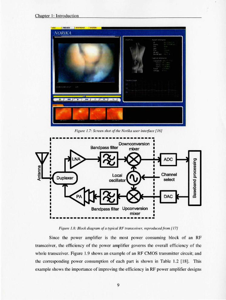
There are currently two camera pills available in the market, the Norika from RF
Systems Labs and the M2A from Given Imaging. Table 1.1 shows a comparison
summary between the important aspects of each pill and Figure 1. 7 shows a screen
capture of the user interface of the Norika pill [16]. Since the Norika pill is not battery
7

M.A.Sc. Thesis- M. M. El-Desouki McMaster- Electrical and Computer Engineering
powered, there is enough free space to store tissue samples from inside the body and
carry medicine that can be sprayed onto infected areas. Temperature measurements and
laser therapy are also options that can be added to the Norika pill [16].
Camera pill with ultra-low power RF transmitter
Receiver& recording devices
Figure 1.6: Swallowable camera system [ 15]
Table 1.1: Performance comparison between the M2A and the Norikapills [16]
M2A Norika Dimension 11 mm x 26 mm 9 mm x 23 mm
Frame rate 2 images I second 30 images I second
Power source Internal battery External coupling
Price US$ 450 I each US$ 100 I each
1.3 RF CMOS Transceivers
The main blocks of a typical RF transceiver are low-noise amplifiers (LNA), mixers,
voltage-controlled-oscillators (VCO), filters, power amplifiers (PA) and power
management circuits (PM), which are usually off-chip, transmit/receive switches, and
distributed amplifiers. Figure 1.8 shows a simplified block diagram of the basic building
blocks in a typical RF wireless transceiver [17]. The total area of an RF transceiver is
mainly determined by the number of embedded passive elements [4].
8
Chapter 1: Introduction
Figure 1. 7: Screen shot of the Norika user interface [ 16]
~----------------------------. 1 Downconversion 1 Bandpass filter mixer ......... : I I
tU I c::: I c::: I~-... -...._ ~ ~ ...... ~ ..
I I
Bandpass filter Upconversion I mixer :
·-----------------------------
ADC
Figure 1.8: Block diagram of a typical RF transceiver, reproduced from [ 17]
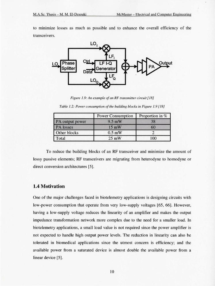
Since the power amplifier is the most power consuming block of an RF
transceiver, the efficiency of the power amplifier governs the overall efficiency of the
whole transceiver. Figure 1.9 shows an example of an RF CMOS transmitter circuit; and
the corresponding power consumption of each part is shown in Table 1.2 [18]. This
example shows the importance of improving the efficiency in RF power amplifier designs
9
M.A.Sc. Thesis- M. M. EI-Desouki McMaster- Electrical and Computer Engineering
to minimize losses as much as possible and to enhance the overall efficiency of the
transceivers.
Phase Splitter
Figure 1.9: An example of an RF transmitter circuit [ 18]
Table 1.2: Power consumption of the building blocks in Figure 1.9 [18]
Power Consumption Proportion in % PA output power 9.5mW 38 PA losses 15mW 60 Other blocks 0.5mW 2 Total 25mW 100
To reduce the building blocks of an RF transceiver and minimize the amount of
lossy passive elements; RF transceivers are migrating from heterodyne to homodyne or
direct conversion architectures [5].
1.4 Motivation
One of the major challenges faced in biotelemetry applications is designing circuits with
low-power consumption that operate from very low-supply voltages [65, 66]. However,
having a low-supply voltage reduces the linearity of an amplifier and makes the output
impedance transformation network more complex due to the need for a smaller load. In
biotelemetry applications, a small load value is not required since the power amplifier is
not expected to handle high output power levels. The reduction in linearity can also be
tolerated in biomedical applications since the utmost concern is efficiency; and the
available power from a saturated device is almost double the available power from a
linear device [5].
10
Chapter 1: Introduction
Also, in order to integrate the whole transceiver in a single chip, RF and analog
designs should be able to operate from low supply voltages since the supply voltage in
digital circuits is continuously decreasing with device down-scaling [66]. This is one of
the main reasons why mixed signal development takes longer than digital and memory
circuits [ 4] . Figure 1.10 shows the projected supply voltage reduction for both analog and
digital circuits based on the 2003 ITRS roadmap (including 2004 updates) [6]. The
continuously decreasing breakdown voltage and maximum voltage limits of CMOS
transistors is another motivation for designing power amplifiers that operate from very
low-supply voltages.
~ 1.6 <D C)
.s 1.2 0 > >-c.. 0.8 a. ::::::1
(/) 0.4
(2000) (2003) (2006) (2009) (2012) (2015) (2018)
180 130 90 65 45 32 22
Year and Technology node (nm)
Figure 1.10: 1TRS projected supply voltage reduction [6]
Since low-power power amplifiers (PAs) require larger output loads than high
power PAs, larger DC-feed inductors are required, which have very low quality factors
when implemented on-chip. As a result, PAs designed for low-power applications have
considerably lower efficiencies than high-power PAs when on-chip components are used.
The motivations for improving efficiency in previous work were all driven by high-power
applications in order to minimize temperature effects, which are the major concern in
base stations, or to extend the operating battery life-time in portable hand held devices.
The main drivers for improving efficiency for low-power applications are biomedical
implantable electronic systems and wireless sensor networks.
11

M.A.Sc. Thesis - M. M. El-Desouki McMaster -Electrical and Computer Engineering
The objective of this thesis is to improve the efficiencies of power amplifiers
targeted for low-power operation and thus, improve the overall efficiency of the
transceiver. Such amplifiers can be suitable for biomedical applications that operate from
very low-supply voltages or short-range applications that do not require large output
power levels such as wireless sensor networks. Previous research [2, 18] focused on
using linear classes for low-power applications since they require a lower input drive,
they allow for the use of variable envelope modulation schemes and they have a lower
harmonic content in the output signal, which eliminates the need for output filtering.
To obtain maximum efficiency, this work was limited to constant envelope
modulation schemes to allow for the use of non-linear, switch-mode power amplifiers.
Using a non-linear amplifier has an added advantage of operating from very low-supply
voltages since maintaining high linearity is no longer a design goal. A non-linear class-E
topology was adopted in this work, which to the authors knowledge, represents the first
use of this topology in low-power applications. The major drawback of using such an
amplifier is the need for an output filter, that will degrade the efficiency when
implemented on-chip. The results of this work show that the degraded efficiency after
using an on-chip filter is still higher than the efficiency of a linear class power amplifier.
Also, since the circuit is to transmit a signal from inside the human body, the higher order
harmonics will be greatly attenuated by the body tissues [11], which would eliminate the
need for an on-chip filter.
A novel mode-locking power amplifier is proposed in this work that uses a
superharmonic injection-locked VCO as a non-linear power amplifier. This topology can
be used as a good alternative for low-power or low-frequency applications, since it
minimizes the number of large size, low-Q inductors required in the design, reducing the
total area of the circuit, which makes it suitable for minuscule transmitter designs.
Some ideas on improving transmitter efficiency and minimizing the number of
building blocks of a transmitter are presented using a high-efficiency cross-coupled
differential negative-gm VCO as a direct baseband modulation transmitter. Some ideas to
further improve the efficiency of this transmitter are proposed as part of the future work
by using a class-E power VCO instead of the negative-gm VCO. The main disadvantage
of using a VCO as a direct-FM transmitter is the inaccuracy in the oscillation frequency,
12

Chapter 1: Introduction
which may vary with temperature or locking to external interference. Using a high
efficiency phase-locked-loop (PLL) with an external crystal reference can solve this
problem. As part of the proposed future work, a PLL transmitter is also presented as an
efficient transmitter for low-power applications. Finally, a basic conventional transmitter
design is proposed as part of the future work, to be compared to the direct baseband
modulation transmitter presented in this work.
Figure 1.11 shows the projected figure-of-merit (FoM) of power amplifiers and
voltage-controlled oscillators for future technologies [6]. The major improvements in the
FoM of power amplifiers are mainly due to the improvements in the cut-off frequency of
CMOS transistors and the improvement in the quality factor of on-chip inductors .
.r 140 3.0 0
- - - - PA worst case , ...--X ---- PA best case 2.5 0
N"' 100 -.-vco $; - 2.0 < N ()
I 0 <.!) 1.5 ;:::::::; ...... X 60 -~ 1.0 .=:
X -~ 0.5 ...... Q_ 20 0 ~ 0.0
l::l 0 -
LL (2003) (2006) (2009) (2012) (2015) (2018)
130 90 65 45 32 22 Year and Technology node (nm)
Figure 1.11: 1TRS projected FoMfor PAs and VCOsfor future technology nodes [6]
1.5 Thesis Organization
A brief introduction to CMOS RF power amplifiers is presented in chapter 2. This
chapter starts by explaining a simple power amplifier, and then some of the important
characteristics of power amplifiers are presented, followed by the main practical design
considerations related to power amplifiers. Some practical challenges faced when dealing
with low-power designs, are also presented.
Chapter 3 explains the different existing power amplifier topologies, which are
divided into three main groups, current-mode classes, switch-mode classes and lock-
13

M.A.Sc. Thesis - M. M. El-Desouki McMaster- Electrical and Computer Engineering
mode classes. A FoM suitable to compare power amplifiers is also proposed in this
chapter.
Chapter 4 explains the concept of using a power oscillator as a transmitter. It
starts by explaining the basic differential cross-coupled negative-gm voltage-controlled
oscillator. After that, the concept of superharmonic injection-locking is presented. The
chapter ends by presenting a FoM that is proposed to compare power oscillators.
Chapter 5 shows the design, simulations and measurement results of the
implemented switch-mode power amplifier circuits. A 900 MHz class-E design is
presented here, followed by three 2.4 GHz class-E designs.
In Chapter 6, two novel mode-locking power amplifier designs operating at 400
MHz and 2.4 GHz are presented. The chapter starts with the circuit design, then the
simulation results are shown, followed by the layout and finally, the measurement results
are shown at the end of the chapter.
Chapter 7 shows the implemented direct-modulation transmitter circuits. Two
CMOS cross-coupled negative-gm voltage controlled oscillators operating at 400 MHz
and 2.4 GHz used as single-block direct-modulation transmitters, are presented in this
chapter.
Finally, chapter 8 will conclude with a summary of this work and a comparison to
previous published works. Future work and areas for improvement will also be given in
this chapter.
14

Chapter 2: Introduction to CMOS RF Power Amplifiers
Chapter 2
INTRODUCTION TO CMOS RF POWER
AMPLIFIERS
The main goal of a power amplifier is to provide adequate power gain to an input signal,
to be able to drive a transmission antenna with minimum loss in the amplifier itself. This
chapter explains some of the basic information related to power amplifier designs.
Section 2.1 shows a simple power amplifier, explaining how it functions. Section 2.2
presents the important characteristics and defmitions of power amplifiers. Some of the
most important practical design considerations related to power amplifiers are discussed
in Section 2.3. Finally, the chapter's summary is presented in Section 2.4.
2.1 Simple Power Amplifier
A simple power amplifier is illustrated in Figure 2.1. It consists of an input impedance
matching network that matches the input impedance of the power amplifier to the source
impedance, an amplifying stage that boosts the signal and an output impedance matching
network that matches or transforms the output load to the desired output impedance
value. The DC biasing is applied at the input and output ports of the amplifying stage.
Inductor RFC is a large inductor that is usually referred to as the RF-choke. It emulates a
DC current source that could sustain negative and positive voltages acting like an AC
block to prevent feedback or oscillation through the DC supply.
What makes a power amplifier different from any other amplifier, such as a
voltage amplifier (operational amplifier) or current amplifier (operational trans
conductance amplifier), is the way the input and output impedances are matched. A
typical voltage amplifier provides a very high (ideally infmite) input impedance and a
15

M.A.Sc. Thesis - M. M. El-Desouki McMaster- Electrical and Computer Engineering
very low (ideally zero) output impedance to allow for maximum voltage transfer. On the
other hand, a typical current amplifier provides a very low input impedance and a very
high output impedance. The input of a power amplifier is matched to satisfy the
maximum power transfer theorem, having at best cases a 50% power transfer from the
source to the amplifier's input. The output matching network of a power amplifier is
matched differently, as will be shown in Chapter 3.
Input matching
+ Biasing
Output matching
Figure 2.1 Simple power amplifier
Power amplifiers can be divided into narrowband designs and broadband designs.
In most communication systems, narrowband power amplifiers are used since they are
usually more efficient [19]. However, some intended narrowband designs may become
wide band due to the low quality factors of the passive components used.
2.2 Important Characteristics of Power Amplifiers
Since the signal transmitted through an antenna is characterized in terms of its power
level, most of the defmitions and characteristics that are related to power amplifiers deal
in terms of power. Figure 2.2 shows the basic parameters of a simple power amplifier and
this figure will be used to clarify the basic definitions explained in the following
subsections.
2.2.1 Power Gain
The power gain of a power amplifier can be defined as the output power delivered to the
output load divided by the input power available from the input source or previous stage.
Based on Figure 2.2, the power gain can be expressed as:
16

Chapter 2: Introduction to CMOS RF Power Amplifiers
where G is the power gain, Pout is the output power and Pin is the input power.
P1n
DC Supply
Poe
Power amplifier
Figure 2.2 The basic parameters of a simple power amplifier
(2.1)
To increase the overall power gain of a power amplifier, which in tum decreases
the required input drive, a multistage configuration can be used. Figure 2.3 shows a
simple two stage power amplifier. The inter-stage matching network is used to guarantee
maximum power transfer between the two stages. In a multistage configuration, care
should be taken to avoid stability problems that could arise due to feedback from one
stage to the other.
Input matching
+ Biasing
DC Supply
Inter-stage matching
+ Biasing
DC Supply
Figure 2.3 Simple two-stage power amplifier
Output matching
Another important parameter is the power utilization factor (PUF), which is a
measure of the output power capability of a power amplifier. It also gives an indication
17

M.A.Sc. Thesis - M. M. El-Desouki McMaster- Electrical and Computer Engineering
for the electrical stress that the active device is being exposed to since it is defmed as the
output power per active device normalized for a 1 V peak drain voltage and a 1 A peak
drain current [20].
2.2.2 Efficiency
Power amplifier efficiency can be expressed as drain efficiency (1]) or power-added
efficiency (P AE). Based on Figure 2.2, the drain efficiency can be expressed as:
p 7] = ____QJg_ '
Pvc (2.2)
where 11 is the drain efficiency, Pout is the output power and Poe is the DC power. The
P AE however, includes the power gain, since it is defined as the ratio between the output
power minus the input power to the DC power. This is a more practical measure of the
power amplifier's efficiency since it measures how much power the amplifier adds to the
input signal efficiently. Based on Figure 2.2, the P AE can be expressed as:
PAE = pout- ~n = P,ut x(1-_!_) = 7JX(1-_!_). Pvc Pvc G G
(2.3)
It is important to note that the maximum efficiency of the power amplifier is
achieved when it is delivering its maximum output power, which is ideally equal to the
DC power.
2.2.3 Linearity
This is an important characteristic of power amplifiers since there is a tradeoff between
linearity and efficiency. Non-linearities in power amplifiers are due to the non-linearities
of the active components used. Spectrally efficient modulation techniques usually
produce non-constant envelope signals. When applying these signals to a non-linear
power amplifier, the signals will suffer amplitude-modulation (AM) to phase-modulation
(PM) conversion and spectral growth, which will lead to adjacent channel interference.
Spectral growth is measured by the adjacent channel power ratio (ACPR), which is the
ratio of the power in the channel to the power in the adjacent channel [1].
18

Chapter 2: Introduction to CMOS RF Power Amplifiers
2.2.3.1 Gain Compression (AM-AM Conversion)
Gain compression occurs when the output and input power levels no longer share a linear
power relationship. A common measure used to quantify this effect is the 1 dB gain
compression point, which defines the point at which the power gain drops by 1 dB below
what is expected. This effect is shown in Figure 2.4.
-E cc :E. ....
CD
§ a. :; ~ 0
,' I ~~-----'····· ,.
# • 11 • • •
,.-'
Input Power {dBm)
Figure 2.4 The effect of gain compression on the output power
2.2.3.2 AM-PM Conversion
The AM-PM conversion is a result of a phase shift in the power amplifier caused by the
amplitude of the signal. This is also a result of the active element's non-linearities such as
the drain-source capacitance [19].
2.2.3.3 Inter-Modulation Distortion (IMD)
Harmonic distortion results in higher frequency components appearing at integer
multiples of the output signal's frequency. Inter-modulation distortion is generated by
multiple inputs and is also caused by non-linearities of the amplifier and active elements.
The IMD products of (n+m)th order can be give by:
(2.4)
An example of the third order IMD components is shown in Figure 2.5. An often
used measure for the linearity of a system uses the IIP3 and OIP3, which are the 3rd order
input and output intercept points respectively. This is a measure of how fast the power of
19

M.A.Sc. Thesis - M. M. El-Desouki McMaster -Electrical and Computer Engineering
the 3rd order component reaches the power of the fundamental signal, as shown in Figure
2.6.
Figure 2.5 Third order !MD components
~ 3rdorder O/P3 -·········-··-·····-····-·······;.c intercept point ,,.
•'' , , , , - .
Input Power (dBm) I/P3
Figure 2.6 Third order intercept points
2.3 Design Considerations
2.3.1 Conjugate Match and Load Line Match
Conjugate matching is done by setting the value of the load impedance equal to the value
of the generators impedance in magnitude and opposite in phase. This is done to deliver
maximum output power to the load, which is required since the amplifier achieves
maximum efficiency when operating at its maximum power. In practice the maximum
output power an amplifier can deliver is limited to the maximum power rating of the
transistor and the value of the supply voltage or DC headroom available to the transistor.
To account for this limitation, a lower output loading resistance (RL) is used, which is
20

Chapter 2: Introduction to CMOS RF Power Amplifiers
referred to as the load-line match optimal resistance (Ropt). This represents a compromise
in extracting maximum power and operating within the specified limits. An output
matching network can be used to transform the actual output load value to the desired
optimal load value. If RL drops below Ropt. then current clipping of the output will occur,
whereas if RL is too high, voltage clipping will occur, as shown in Figure 2.7 [3]. The
value of Ropt can be expressed as:
R - Vmax opt --
1-, max
(2.5)
where Ymax is the maximum drain voltage and /max is the maximum drain current, as
shown in Figure 2. 7. This improves the output power, however it could cause reflections
in the rest of the system that are a fraction of the matching degree between the output
load or the antenna and the system. An isolator or balanced amplifier could be used to
solve the reverse termination mismatch caused by the power amplifier [3].
3.0 ' Optimal , Current clipping
2.5 ......
g ...... ' ...... ' - 2.0 c:: ......
~ Voltage clipping ' 1.5 ...... :::J -(J --- ...... ' ...... c:: 1.0 ·~ ----c 0.5 - -
0.0 0.0 0.5 1.0 1.5 2.0 2.5 3.0
Drain Voltage (V)
Figure 2. 7 Optimal load line
2.3.2 Effect of the Transistor Knee-Voltage
The knee-voltage (Y~rnee). which is also known as the pinch-off voltage, is the voltage
point that divides the saturation and linear regions of a transistor. It is defmed as the point
at which the drain current reaches 95 %of /max. The optimum load resistance in this case
is [3]:
21

M.A.Sc. Thesis - M. M. El-Desouki McMaster- Electrical and Computer Engineering
R = Vmax -Vknee opt J '
max (2.6)
This effect is very obvious in deep submicron CMOS transistors where the knee
voltage could reach up to 50 % of the supply voltage. Both saturation and linear regions
should be considered in the matching stage, especially for deep submicron transistors [3].
2.3.3 Substrate Doping and Leakage
Highly doped substrates, which have a low-resistivity, could cause integration problems
with other parts of the transceiver affecting their stability since it is easier for feedback or
substrate leakage to occur. Also losses in CMOS substrates could reduce the quality
factors of the passive elements used in impedance matching. To avoid this problem, the
passive elements could be integrated off-chip, usually with the antenna. However, having
a fully-integrated design has many benefits, some of which were previously mentioned in
Chapter 1, such as lower cost and higher reliability. Some attempts to remove the
substrate beneath the on-chip inductors were done to avoid affecting their quality factors
[3].
2.3.4 Breakdown Voltage
The breakdown voltage is an important effect that should be taken into account when
designing power amplifiers. The drain voltage amplitude levels of some amplifiers are
normally twice as high as the supply voltage, whereas the drain voltage amplitude levels
of some other types of power amplifiers can reach up to triple the supply voltage. For this
reason, transistors used in power amplifier designs are sometimes operated at a supply
voltage that is less than the nominal supply voltage specified by the manufacturer.
There are several types of breakdown voltage that must be considered in power
amplifiers. The breakdown mechanism may be immediately destructive, as in the case of
oxide breakdown, or may lead to destruction of the device due to overheating, as in the
case of the other types of breakdown [23, 24]. Oxide breakdown is a destructive
breakdown mechanism that occurs if the gate voltage exceeds a certain value, the gate
oxide insulation will break down, resulting in a permanent short circuit through the oxide.
The voltage at which this breakdown occurs depends on the thickness of the oxide layer
22

Chapter 2: Introduction to CMOS RF Power Amplifiers
and how defective the insulator is. This sideeffect is important in high power amplifiers
and in ultra-thin oxide devices. Oxide breakdown could also occur due to static charges
from handling the device with bare hands. For this reason, electrostatic discharge (ESD)
pads are added to the device's input terminals [23-25].
Another form of breakdown is known as channel breakdown, which is a result of
a breakdown in the reverse biased PN diodes that are between the substrate and the
source or the substrate and the drain. In long-channel devices, a high electric field,
normally in the pinch-off region, could give the carriers moving in the channel enough
energy to impact a silicon atom and ionize it, which could free an electron and produce
an electron-hole pair. This is known as impact-ionization. The released electron could
impact-ionize other silicon atoms producing more electron-hole pairs, leading to a
phenomenon known as the avalanche effect, which results in an unexpected increase in
current flow, thus resulting in channel breakdown. Carriers that are energized by the
electric field in this manner are also referred to as hot-carriers. These carriers increase the
drain to source current and also the drain to substrate currents. However, a small amount
of carriers could obtain sufficient energy to penetrate through the gate oxide and may end
up trapped in it. This will slowly degrade the quality of the oxide with time, which is
known as device aging [23, 24].
In short-channel devices, the drain to substrate depletion region could extend to
the source to substrate depletion region and the barrier between the source and drain will
be lowered, resulting in electrons punching through the barrier. This is known as punch
through or Zener breakdown. Channel breakdown is not immediately destructive;
however, it may lead to over heating due to the unexpected increase in current flow,
which may lead to permanently damaging the device [23].
2.3.5 Temperature Considerations
Dissipated power, or losses in power amplifiers are converted into heat causing an
increase in the internal temperature of the active and passive devices in the circuit, in
addition to layout interconnections and wirings. The increase in junction temperature can
be obtained by multiplying the dissipated power by the thermal resistance (°C/W). Thus,
23
M.A.Sc. Thesis - M. M. El-Desouki McMaster -Electrical and Computer Engineering
the maximum junction temperature sets a limit on the maximum dissipated power in the
device to ensure safe operation.
The characteristics of the MOSFET device are strongly affected by temperature
variations. The most temperature dependent parameters are the effective mobility and the
threshold voltage, both of which result in variations in the drain-source current. The
following equations show the temperature dependence of these parameters [25]:
,u(T) ~ ,u(T,>(~ r, (2.7)
Vr(T) = Vr(T,)-k4(T -T,), (2.8)
where ~is the mobility, VT is the threshold voltage, Tis the absolute temperature, Tr is
the room temperature, k3 is a constant with values ranging from 1.2 to 2.0 and k4 is in the
range of0.5 mV/K to 3 mV/K. By substituting Equations 2.7 and 2.8 in the 1-V equation
of a MOSFET device, the current-temperature dependence could be obtained [23].
2.3.6 On-chip Integration
As previously discussed, one of the main advantages of using CMOS technology is the
ability to integrate a full transceiver on the same chip. It is desirable to minimize off-chip
components as much as possible to produce smaller and more compact transceivers and
increase the reliability of the system. However, this introduces complications in standard
CMOS fabrication processes. Some of these complications were previously mentioned.
Other reasons are the limitations in the sizes of on-chip passive components. Large
inductors require large area and introduce coupling effects and losses. Small capacitors
may be dominated by stray capacitance leading to unstable operation. An on-chip RFC
will have a practical value of less than 10 nH, which does not represent a good RFC
except for very high operating frequencies. Using a non-ideal RFC requires modifications
to the power amplifier's circuit design equations, to account for the RFC as part of the
output load.
24

Chapter 2: Introduction to CMOS RF Power Amplifiers
2.3. 7 Amplifier Stability
There are two main categories of instability in power amplifiers, which are bias circuit
low-frequency instability and RF instability. Bias oscillations can be prevented by low
pass filtering the bias signals. RF oscillations are mainly due to mismatches in the design
or component values of the matching networks and usually occur at frequencies close to
or within the band of interest [3].
The power amplifier should be unconditionally stable over the widest range of
frequencies and biasing conditions. However, verifying the stability of a power amplifier
is very difficult. A number of simulation techniques can be used to test the stability of a
power amplifier. Small signal scattering parameter methods (S-parameters) can be used
to test the stability of a power amplifier, however, they assume linear circuit operation. If
S-parameters are to be used in testing the stability of a non-linear power amplifier, the
circuit can be linearized by changing the biasing conditions.
Another more effective method to test the stability of a power amplifier is through
transient simulations by applying a sharp pulse to each critical RF node and bias point of
the circuit under various biasing conditions, without applying an RF input. The response
of the circuit to the pulse will give an indication of the stability of the amplifier. If the
stability cannot be improved by changing the values of the matching network
components, resistors might need to be added to various locations of the circuit to
introduce losses on potential feedback paths. Improving the amplifier stability in this way
will usually sacrifice the performance of the power amplifier in the band of interest.
2.3.8 Ground Inductance
The effects of finite ground or source inductance through the bond wires that connect the
on-chip pads to the package pins, also known as ground bounce, are usually not included
in the ideal analysis of power amplifier designs. However, ground bounce was found to
have strong effects on the gain, efficiency and harmonic contents of a power amplifier.
Ground inductance can be reduced by using multiple ground pads in parallel; however,
this will greatly increase the chip die area [3]. An example of how ground inductance can
affect the performance of a power amplifier is shown in Figure 2.8 [3]. Nine ground pads
were used in parallel to improve the performance of the power amplifier.
25
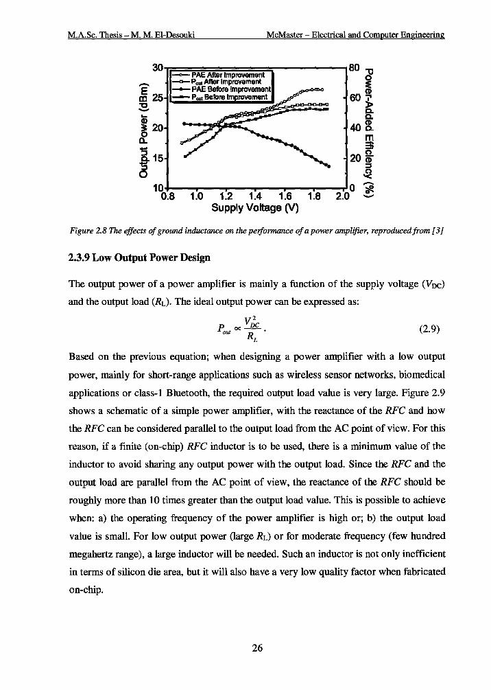
M.A.Sc. Thesis- M. M. El-Desouki McMaster -Electrical and Computer Engineering
30u=::::::::::::;::;::;:;::=.~==.=r------, 80 -c - PAE After improvement o -~ 25
-a-- Pou1 After Improvement :e - PAE Before Improvement (I) -Pout Before lm rovement 60 i'
~ :s
120 0.
40& ~ -~15 20 g. ::::J 8 ~ -10+---~----~--~----.----r----~o ~
0.8 1.0 1.2 1.4 1.6 1.8 2.0 -Supply Voltage (V)
Figure 2.8 The effects of ground inductance on the peiformance of a power amplifier, reproduced from [ 31
2.3.9 Low Output Power Design
The output power of a power amplifier is mainly a function of the supply voltage (Voc)
and the output load (RL). The ideal output power can be expressed as:
p oc v;c out R
L
(2.9)
Based on the previous equation; when designing a power amplifier with a low output
power, mainly for short-range applications such as wireless sensor networks, biomedical
applications or class-1 Bluetooth, the required output load value is very large. Figure 2.9
shows a schematic of a simple power amplifier, with the reactance of the RFC and how
the RFC can be considered parallel to the output load from the AC point of view. For this
reason, if a finite (on-chip) RFC inductor is to be used, there is a minimum value of the
inductor to avoid sharing any output power with the output load. Since the RFC and the
output load are parallel from the AC point of view, the reactance of the RFC should be
roughly more than 10 times greater than the output load value. This is possible to achieve
when: a) the operating frequency of the power amplifier is high or; b) the output load
value is small. For low output power (large RL) or for moderate frequency (few hundred
megahertz range), a large inductor will be needed. Such an inductor is not only inefficient
in terms of silicon die area, but it will also have a very low quality factor when fabricated
on-chip.
26

Chapter 2: Introduction to CMOS RF Power Amplifiers
r-····-···-·····-·····-·····-·····-···· D
0
M: Input
""L- matching I - + I
Biasing
-····-····-····-·····-·····-·····-···
Output matching
,-------------------1 :
: Power : : amplifier 1
1 Pm
~ I o I I I I I I I 1------------------~
Figure 2. 9 The effect of using a finite RFC on low output power amplifiers
Another challenge in low output power amplifier design, arises with the need for
an on-chip filter. As shown in Figure 2.10, having an output filter also places an inductor
(Lr) in the path of the output load, which will result in sharing the output power with the
load. To increase the efficiency, the reactance of the output filter's inductor should be
very small compared to the output load (since the inductor is in series with the load).
However, having a good band-pass filter, with a narrow bandwidth, requires a high-Q
filter. The filter's loaded quality factor (QL) reduces as the reactance of the inductor drops
compared to the series parasitic resistance, which in this case; is added to the output load
resistance. For this reason, there is a trade-off between having a good filter and having
high efficiency. This trade-off is more apparent when the output load value is large and
the filter is fabricated on-chip, since the inductor used as part of the filter should be even
larger, which will again have a low-Q when fabricated on-chip.
Input matching
+ Biasing
Figure 2.10 The effect of the output filter on low output power amplifiers
27

M.A.Sc. Thesis- M. M. El-Desouki McMaster -Electrical and Computer Engineering
For these two mentioned reasons, efficiency of low-power amplifiers is generally lower
than high-power amplifiers, especially when all components are fabricated on-chip.
These claims were neither clearly investigated nor published in previous works and will
be verified further in the results presented in this work.
2.4Summary
In this chapter, a basic introduction t{} CMOS RF power amplifiers was given starting
from a simple power amplifier, where the most important definitions and characteristics
of power amplifiers, were presented.
The chapter also explained some of the most important practical design
considerations related to power amplifiers. These design considerations will give a
practical insight to the challenges faced in RF power amplifier design. The design
considerations discussed, were based on the challenges faced throughout completing this
work, in addition to the challenges collected from the literature.
28

Chapter 3: Power Amplifier Classes of Operation
Chapter 3
POWER AMPLIFIER CLASSES OF
OPERATION
Power amplifiers are categorized based on their historical appearance, hence the
alphabetical classification. The main classes of operation can be divided into two parts,
which are the current-mode and the switch-mode, also known as linear-mode and non
linear-mode respectively. In this work, a third category of power amplifiers is added,
which is referred to as lock-mode. Classes A, B, AB and Care considered current-mode
power amplifiers, whereas classes D, E, F and S are mainly considered switch-mode
amplifiers.
The current-mode power amplifiers are explained in Section 3.1 of this chapter,
followed by the switch-mode power amplifiers in Section 3.2 and the mode-locking
power amplifiers in Section 3.3. Section 3.4 presents a new proposed figure-of-merit
(FoM) that can be used to compare power amplifier designs. Finally, the chapter's
summary is presented in Section 3.5.
3.1 Current-Mode Power Amplifiers
In current-mode power amplifiers, the active device operates as a current-source. These
classes usually provide higher linearity than switch-mode power amplifiers since there is
a direct amplitude relationship between the input and output signals, hence they are also
referred to as linear power amplifiers. Current-mode power amplifiers are distinguished
by the fraction of the RF-cycle for which the transistor conducts, which is known as the
conduction angle. The difference between the various existing current-mode classes is
basically in the biasing and impedance matching network.
29
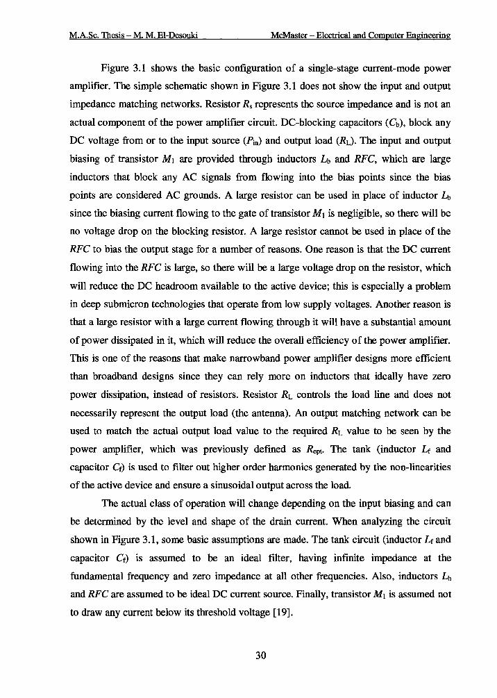
M.A.Sc. Thesis - M. M. El-Desouki McMaster -Electrical and Computer Engineering
Figure 3.1 shows the basic configuration of a single-stage current-mode power
amplifier. The simple schematic shown in Figure 3.1 does not show the input and output
impedance matching networks. Resistor Rs represents the source impedance and is not an
actual component of the power amplifier circuit. DC-blocking capacitors ( Cb), block any
DC voltage from or to the input source (Pin) and output load (RL). The input and output
biasing of transistor M1 are provided through inductors Lb and RFC, which are large
inductors that block any AC signals from flowing into the bias points since the bias
points are considered AC grounds. A large resistor can be used in place of inductor 4
since the biasing current flowing to the gate of transistor M1 is negligible, so there will be
no voltage drop on the blocking resistor. A large resistor cannot be used in place of the
RFC to bias the output stage for a number of reasons. One reason is that the DC current
flowing into the RFC is large, so there will be a large voltage drop on the resistor, which
will reduce the DC headroom available to the active device; this is especially a problem
in deep submicron technologies that operate from low supply voltages. Another reason is
that a large resistor with a large current flowing through it will have a substantial amount
of power dissipated in it, which will reduce the overall efficiency of the power amplifier.
This is one of the reasons that make narrowband power amplifier designs more efficient
than broadband designs since they can rely more on inductors that ideally have zero
power dissipation, instead of resistors. Resistor RL controls the load line and does not
necessarily represent the output load (the antenna). An output matching network can be
used to match the actual output load value to the required RL value to be seen by the
power amplifier, which was previously defmed as Ropt· The tank (inductor Lr and
capacitor Cf) is used to filter out higher order harmonics generated by the non-linearities
of the active device and ensure a sinusoidal output across the load.
The actual class of operation will change depending on the input biasing and can
be determined by the level and shape of the drain current. When analyzing the circuit
shown in Figure 3.1, some basic assumptions are made. The tank circuit (inductor Lr and
capacitor Cf) is assumed to be an ideal filter, having infmite impedance at the
fundamental frequency and zero impedance at all other frequencies. Also, inductors Lb
and RFC are assumed to be ideal DC current source. Finally, transistor M1 is assumed not
to draw any current below its threshold voltage [19].
30

Chapter 3: Power Amplifier Classes of Operation
Input Bias
Figure 3.1 Basic single-stage current-mode power amplifier
To obtain the current drawn from the DC supply (/d) in terms of the conduction
angle (a), a relationship between the biasing point and the conduction angle needs to be
considered. Figure 3.2 (a) shows the effect of the conduction angle for two different cases
and the resulting drain current is shown in Figure 3.2 (b). The figure shows the gate
voltage value that exceeds the required threshold voltage to turn on the transistor. The
corresponding current waveform for the class-A power amplifier is a full cycle sinusoidal
waveform, whereas the class-B drain current waveform is a half sinusoidal signal.
Looking at the conduction angle of a class-A amplifier, which conducts for the
entire 360° of the cycle; and comparing it to a class-B amplifier that conducts for only
half the cycle, as shown in Figure 3.2, the following relations could be obtained [26]:
(3.1)
where /pk is the peak drain current, lq is the quiescent bias current and:
a _ Iq _ cos(-)---, Ipk- /max -lq.
2 Ipk (3.2)
31

M.A.Sc. Thesis- M. M. El-Desouki McMaster -Electrical and Computer Engineering
Gate Voltage (V)
-1.0
{a)
Angle 9=mt
Drain CUrrent (I}
-1.0
(b)
Figure 3.2 (a) The effect of the gate biasing point on the conduction angle (a). (b) The equivalent drain
current
Equation 3.1 represents a positive portion of a cosine wave with peak Imax
superimposed upon a DC bias current Iq that could be negative and less than I max, positive
and greater than I max or zero. From Equation 3.2, lq could be expressed as:
I =[max cos(a/2) . q cos(a/2) -1
(3.3)
By substituting (3.3) into (3.1) the RF drain current waveform can be expressed
as:
id(O) = [max I [cos(O)-cos(a/2)]. 1-cos(a 2)
Using Fourier analysis, the DC current can be obtained from Equation (3.4) as:
id (8) =ide + Ln~l in cos(n8),
Ide =-1
f12 1
max I [cos(8)-cos(a/2)]d8, 27C !a/21-cos(a 2)
=>Ide = I max 2sin(a/2)- acos(a/2), 27t 1- cos(a/2)
the harmonic frequency components can be expressed as:
1 f.12 I r ] In=- max I Lcos(O)-cos(a/2) cosn8.d8, 7C af21- cos( a 2)
32
(3.4)
(3.5)
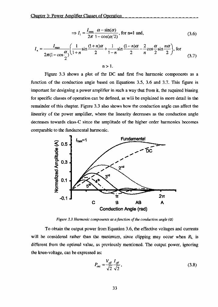
Chapter 3: Power Amplifier Classes of Operation
I _ /max a- sin( a) ~ _
1 d
:::::::> 1 - , 10r n- an , 2tc 1- cos(a/2)
1 I max ( 1 . (1 + n )a 1 . (1- n )a = --sm +--sm..;__--=--
n 2tc(l- cos a) 1 + n 2 1 - n 2 2
n > 1.
2 a . na) -cos-sm- for n 2 2 '
(3.6)
(3.7)
Figure 3.3 shows a plot of the DC and first five harmonic components as a
function of the conduction angle based on Equations 3.5, 3.6 and 3.7. This figure is
important for designing a power amplifier in such a way that from it, the required biasing
for specific classes of operation can be defined, as will be explained in more detail in the
remainder of this chapter. Figure 3.3 also shows how the conduction angle can affect the
linearity of the power amplifier, where the linearity decreases as the conduction angle
decreases towards class-C since the amplitude of the higher order harmonics becomes
comparable to the fundamental harmonic.
-~ 0.5 CD
"t:J :e 0.. E 0.3 < ~ ~ 0.1 0 z
-0.1 c B AB
Conduction Angle {rad)
Figure 3.3 Harmonic components as afunction of the conduction angle (a)
To obtain the output power from Equation 3.6, the effective voltages and currents
will be considered rather than the maximum, since clipping may occur when RL is
different from the optimal value, as previously mentioned. The output power, ignoring
the knee-voltage, can be expressed as:
(3.8)
33

M.A.Sc. Thesis - M. M. El-Desouki McMaster- Electrical and Computer Engineering
pout= _!_cv: /max a -sin( a) . 2 eft 27C 1-cos(a/2)
(3.9)
Only It was considered as the effective current assuming that the load tuning
network will pass only the fundamental frequency and block out other harmonics. The
drain efficiency could be obtained from Equations 2.2, 3.5 and 3.9 as:
veff a-sina 1ldrain = 2Vvv 2sin (a/2)- a cos (a/2) '
(3.10)
where the DC power is expressed as:
Pvc =Vvvlvc· (3.11)
Figure 3.4 shows the effect of the conduction angle on the output power, drain
efficiency and linearity expressed as the difference between the fundamental current and
the third order harmonic normalized to the maximum value. The output power and drain
efficiency are calculated using unity values for Yeff, Yoo and /max. The figure only gives a
theoretical upper limit to the drain efficiency; however, the practical values will be lower.
Figure 3.4 shows a clear trade-off between the output power and efficiency as a function
of the conduction angle and also between the linearity and efficiency. The higher the
conduction angle, the higher the output power and the better the linearity of the power
amplifier since clipping of the input signal is reduced, however, the efficiency is lower.
1.0 ,..~~~~;;::------,--=:;;::::;!il~~-:-~ Fundamental-
0
Third harmonic
n Conduction Angle (rad)
2n
100
80 c iiJ :r
60 ~ Q. CD
40 ::l
~ -"#. 20 -0
Figure 3.4 The effect of the conduction angle (a) on the normalized output power, drain efficiency and
difference between the fundamental current and the third order harmonic component
34

Chapter 3: Power Amplifier Classes of Operation
The trade-off between the efficiency and output power is not so clear from the
definition of efficiency itself, expressed in Equation 3.10. This is due to the fact that both
the denominator and the numerator, in the defmition of the drain efficiency, are
dependent on the conduction angle. However, it is clear from evaluating hand /c1c, hence,
Pout and Poe, that the denominator is a stronger function of the conduction angle, which is
why the efficiency is a decreasing function of the conduction angle, as shown in Figure
3.5.
""" ~ ~ 0.8 o.. ~ t-+---lCiass C;......--• -gD.. .e- (.) 0.6 ::sO 0~ i= 0.4 ·- co cae §~ 0.2 z
-Pout
~ 20 .e..
o.o ................................................................ - 0 2TT o 1T
Conduction Angle (rad)
Figure 3.5 The effect of the conduction angle (a) on the DC power, output power and drain efficiency
A way to maximize the drain efficiency is to try to reduce the value of Poe
without changing the conduction angle, hence keeping Pout constant. This could be done
by using the output harmonic tuning circuit that was shown in Figure 3.1. By shorting out
the even harmonics and peaking the odd ones, for large input signals, the output
waveform will tend to look more like a square wave. This is known as harmonic peaking
and is shown in Figure 3.6. If the drain current and the drain voltage do not overlap, then
the DC power dissipation will be equal to zero, resulting in a maximum efficiency. This
is the basic idea of class-F amplifiers. The concept is shown in Figure 3.7.
35

M.A.Sc. Thesis- M M. El-Desouki McMaster- Electrical and Computer Engineering
1.0 Overall waveform
,/
-1.0 Phase Angle (degrees)
Figure 3.6 Third order harmonic peaking
~~~L .. Jt L ~ L '· it ~ L ~ L. Jt ..
Figure 3. 7 A method to increase efficiency
3.1.1 Class-A Power Amplifiers
This class has a conduction angle of 360°, as shown in Figure 3.8. From Equation 3.10,
and assuming that the Yeff is equal to the full supply voltage, the drain efficiency of a
class-A power amplifier is 50%. This is the maximum theoretical efficiency, ignoring the
transistor knee-voltage, the losses in on-chip components, and assuming that the
transistor is delivering its maximum power, which is usually not the case.
36

Chapter 3: Power Amplifier Classes of Operation
_1.0 ::::::.. 1: ~ 8 0.0 .,_--~~---1----ill,__ ____ ..... c ·~
c -1.0
Figure 3.8 Drain current of a class-A power amplifier
3.1.2. Class-B Power Amplifiers
This class has a conduction angle of 180°, as shown in Figure 3.9. An output filter is
important in this class to filter out the harmonics. From Equation 3.10, the maximum
drain efficiency of class-B is found to be 78.5 %.
Figure 3.9 Drain current of a class-B power amplifier
3.1.3. Class-AB Power Amplifiers
This class has a conduction angle that is between 180° and 360°, which leads to a
maximum drain efficiency that lies between 50 % and 78.5 %. Most practical class-B
amplifiers tend to become class-AB amplifiers due to non-linearities in the active devices
that make it difficult to ensure that the conduction angle is exactly 180°.
3.1.4. Class-C Power Amplifiers
This class has a conduction angle that is less than 180°, which makes the drain efficiency
very high and ideally could reach 100 %. This class is highly non-linear and has an ideal
output power of zero since the output power is inversely proportional to the efficiency in
linear classes. The exact efficiency could be obtained from Equation 3.10 by using the
exact conduction angle.
37

M.A.Sc. Thesis - M M. El-Desouki McMaster- Electrical and Computer Engineering
3.2 Switch-Mode Power Amplifiers
The active device in switch-mode power amplifiers operates as a low-resistance (ideally
zero resistance) active switch. These classes usually provide higher efficiency than
current-mode power amplifiers; however the linearity is usually sacrificed since there is
no direct amplitude relationship between the input and output signals, hence they are also
referred to as non-linear power amplifiers. The concept of not having an amplitude
relationship between the input and output signals may be confusing to designers who are
not familiar with non-linear power amplifiers, since this defies the idea of
"amplification". The concept is to generate an output signal that can follow the input
signal in phase and frequency, while having a higher power level. However, such
amplifiers are only suitable for constant envelope modulation schemes, such as frequency
modulation (FM) and FSK.. Non-linear power amplifiers, due to their high efficiencies,
were found attractive even for variable envelope modulation schemes, such as amplitude
modulation (AM); however, in order to maintain the envelope information certain
linearization techniques must be used. An example of a linearization technique used with
non-linear power amplifiers is envelope elimination and restoration (EER), which
extracts the envelope information from the input signal and restores it to the output signal
after it has been efficiently amplified.
The following subsections explain the most common switch-mode power
amplifiers with emphasis on class-E power amplifiers.
3.2.1 Class-D Power Amplifiers
This class of power amplifiers uses two transistors operating as switches, as shown in
Figure 3.10. It is basically a CMOS inverter that generates an output square waveform,
which follows the input signal's phase and frequency. Since the output waveform is
square shaped, the output is associated with a filter that passes only the fundamental
sinusoidal waveform. The efficiency is affected by the switching time and the on
resistance of the transistor. This class suffers high non-linearity and has no direct power
control since the input signal provides only timing information. This class has an
advantage of very low, ideally zero, power dissipation and high power capabilities [19].
38

Chapter 3: Power Amplifier Classes of Operation
Figure 3.10 Basic schematic of a class-D power amplifier
3.2.2 Class-E Power Amplifiers
Class-E power amplifiers were first presented by N. 0. Sokal and A. D. Sokal in 1975
[29] and have recently gained more attraction with the expiry of their patent. This class
has an ideal efficiency of 100 %. It has a similar configuration as class-D but uses only
one transistor that is also operating as a switch, as shown in Figure 3.11. The pull-up
network, which was a PMOS device in class-D power amplifiers, is removed in class-E
power amplifiers to improve the efficiency by avoiding the power loss in the PMOS
device. To provide the high signal, in place of the PMOS device, an RFC inductor (Lt) is
used together with a parallel capacitor, C1• The basic criteria to operate a class-E power
amplifier are as follows [27]:
1) The voltage across the switch (active device, M1) at off-mode should not rise until
after the transistor turns off.
2) The voltage across the switch should go back to zero immediately before turn-on.
3) The slope of the switch voltage should be zero at turn on (soft-switching).
4) An amplifier with these three criteria is called an "optimum class-E" amplifier,
whereas if one of them is missing, it is called a "suboptimum class-E" amplifier
[27].
39
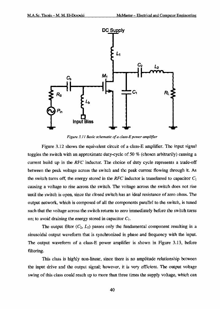
M.A.Sc. Thesis - M. M. El-Desouki McMaster- Electrical and Computer Engineering
Figure 3.11 Basic schematic of a class-E power amplifier
Figure 3.12 shows the equivalent circuit of a class-E amplifier. The input signal
toggles the switch with an approximate duty-cycle of 50% (chosen arbitrarily) causing a
current build up in the RFC inductor. The choice of duty cycle represents a trade-off
between the peak voltage across the switch and the peak current flowing through it. As
the switch turns off, the energy stored in the RFC inductor is transferred to capacitor Ct
causing a voltage to rise across the switch. The voltage across the switch does not rise
until the switch is open, since the closed switch has an ideal resistance of zero ohms. The
output network, which is composed of all the components parallel to the switch, is tuned
such that the voltage across the switch returns to zero immediately before the switch turns
on; to avoid draining the energy stored in capacitor Ct.
The output filter ( C2, ~) passes only the fundamental component resulting in a
sinusoidal output waveform that is synchronized in phase and frequency with the input.
The output waveform of a class-E power amplifier is shown in Figure 3.13, before
filtering.
This class is highly non-linear, since there is no amplitude relationship between
the input drive and the output signal; however, it is very efficient. The output voltage
swing of this class could reach up to more than three times the supply voltage, which can
40
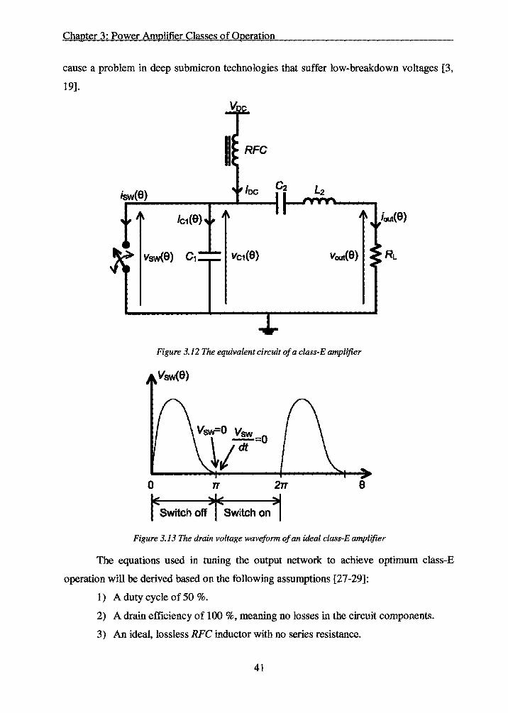
-
Chapter 3: Power Amplifier Classes of Operation
cause a problem in deep submicron technologies that suffer low-breakdown voltages [3,
19].
isw(9)
iout(9)
vout(9)
Figure 3.12 The equivalent circuit of a class-E amplifier
Vsw=O Vsw
~~-;;t=O
0 TT 2rr e
~Switch off f Switch on 1 Figure 3.13 The drain voltage waveform of an ideal class-E amplifier
The equations used in tuning the output network to achieve optimum class-E
operation will be derived based on the following assumptions [27-29]:
1) A duty cycle of 50 %.
2) A drain efficiency of 100 %, meaning no losses in the circuit components.
3) An ideal, lossless RFC inductor with no series resistance.
41

M.A.Sc. Thesis - M. M. El-Desouki McMaster- Electrical and Computer Engineering
4) An ideal output filter, with an infmite Q, that passes only the fundamental
harmonic, generating a pure sinusoidal waveform at the output load.
5) An ideal active device operating as a switch, with no output capacitance, zero
on-resistance and infmite off-resistance.
Based on these assumptions, the output voltage and current waveforms, which are
pure sinusoidal, can be expressed as:
where cp is defined in Figure 3.14.
8
Switch off
Figure 3.14 The output waveform of a class-E power amplifier
Based on Figure 3.12, when the switch is off (open):
• -[ vout ·co ) let- De --sm +rp , RL
. - ~ . ..r dvct - ,.,/! d -let - UJL-1 -- ' {J)- 2,!f an v ct - v sw ' d()
oC,v~ ~ f ic,.dB~ f[Inc- ~: sin(0+9J)].do
oCt v sw = I DC()+ vout [cos(()+ rp) -cos ffJ]' RL
42
(3.12)
(3.13)
(3.14)

Chapter 3: Power Amplifier Classes of Operation
I e v r ] Vsw =_Q£_+ out lcos(O+f}')-COSI}',
o£1 o£IRL (3.15)
however, when the switch is on (closed), for (rr<OS2rr), Vsw=O, based on the assumptions.
At optimum operation, Vsw(rr)=O, which gives:
also, dv sw I = 0, which gives: dO e=7l
by dividing 3.17 by 3.16,
which gives:
1li R COSf}'= DC L'
2Vout
-I R sinf}'= DC L
vout
-2 tanf}'=-,
1C
. -2 Slflf}'= ~ .
1C2 +4
When assuming an efficiency of 100 %, (Pout= Poe= IocVnc):
IV _Vo~t
DC DC---, 2RL
(3.16)
(3.17)
(3.18)
(3.19)
(3.20)
(3.21)
so by substituting Equations 3.16 and 3.19 in 3.21, the DC current can be expressed as:
I - 8VDC DC- RL(1C2 +4)' (3.22)
and the output power is obtained as:
P = 8Vic • out RL(1C2 +4)
(3.23)
Since the RFC has no voltage drop on it (no series resistance), the DC average value of
Vsw is equal to Voc, which gives:
1 f 8 1 7lJ{I e v } VDC =- .t vsw(8).d8=- _Qf_+ out [cos(O+f}')-cos(O)] dO' 21C 21C 0 o£1 o£1RL
43

M.A.Sc. Thesis- M. M. El-Desouki McMaster- Electrical and Computer Engineering
(3.24)
by substituting Equation 3.22 in Equation 3.24, the parallel capacitor C1 can be expressed
as:
The filter components (capacitor Cz and inductor Lz) can be expressed as:
1 C2=-2-,
OJI.z
Lz = QLRL' OJ
(3.25)
(3.26)
(3.27)
where QL is the loaded quality factor of the filter, which was previously explained in
Section 2.3.9 and is a design parameter that is chosen as a trade-off between the
bandwidth of the output filter and the drain efficiency. Higher values of QL deliver lower
output harmonics and a more sinusoidal output signal; however the efficiency will be
reduced. Table 3.1 shows a summary of the ideal class-E design equations.
Table 3.1: Summary of the class-E ideal design equations
Output load RL = 0.577 v;c pour
(3.28)
C,= 0.1837
Parallel capacitance OJRL
(3.29)
1 Filter capacitance c =-- (3.30)
2 OJ2Lz
Filter inductance Lz = QLRL (3.31) OJ
When considering the on-resistance of the active device, the drain efficiency can
be obtained based on the following analysis, where when the switch is on (closed):
(3.32)
44

Chapter 3: Power Amplifier Classes of Operation
where is is the current that flows through the switch due to its non-zero on-resistance.
From Equation 3.28:
i =I - Vour sin(O+m) s DC R ., ' L
p =Ron (3/2 + ~utJ r_on 2 DC R • L
Pvc= ~ut + pr on= pout+ Ron (3I~c +pout J • - 2 RL
Pvc = l +Ron (3I~c +-1-J, ~ut 2 pout RL
v ( -2 J V2
using I = _-.!!!!!.... and P = __!!fl!_ DC R ~ out 2R'
L v7r+4 L
1 TJdrain"" R
1 + 1.4 ____E!_
RL
(3.33)
(3.34)
In order to reduce the effect of the transistor's on-resistance, a large device must
be used. However, as the size of the active device increases, the input and output
capacitances also increase. Three points must be considered in this case: a) the active
device must be able to operate properly as a switch at the desired frequency, b) the output
capacitance of the active device must not exceed the required value of the parallel
capacitance (Ct) and finally, c) the input power required to drive the active device should
remain low enough to achieve the desired gain. The last point indicates that the size of
the active device should be optimized to achieve peak power-added efficiency, rather
than peak drain efficiency.
Finally, when considering all the non-idealities that exist in the circuit, such as the
non-linear output capacitance of the active device, the fmite RFC, the non-zero on-
45

M.A.Sc. Thesis- M. M. El-Desouki McMaster -Electrical and Computer Engineering
resistance of the active device and the finite Q of the output filter, the output waveforms
of the circuit can be fine tuned through simulations to ensure optimum class-E operation
as previously shown in Figure 3.13. Figure 3.15 shows how the component values affect
the shape of the output waveform [30].
~~.L2
0 ~----------~Tirire
Figure 3.15 The effects of adjusting the output network components of a class-E amplifier [ 30]
3.2.3 Class-F Power Amplifiers
The theory of class-F power amplifiers was previously explained at the end of section
3.1. Figure 3.16 shows the basic schematic of a class-F power amplifier. Shown in Figure
3.16, there are three tuning networks, where one peaks the 1st harmonic, the second peaks
the 3rd -order harmonic and the third shorts out the znd -order harmonic, in order to achieve
3rd-harmonic peaking. In this case, a linear-amplifier with an exact class-B conduction
angle can not be used, since its 3rd-order harmonic component is zero, as previously
shown in Figure 3.3. To overcome this problem, either the conduction angle must be
slightly changed, or clipping should be introduced, which is why the transistor is operated
as a switch and class-F is considered a switch-mode power amplifier.
A practical problem in designing class-F power amplifiers is the difficulty in
guaranteeing that the on-chip harmonic peaking networks are accurately tuned. This also
makes the design prone to layout parasitics. Also, the number of inductors required
makes the design very inefficient in terms of silicon die area.
46

Chapter 3: Power Amplifier Classes of Operation
1st-order hannonic peaking
,.-------~ c1
3rd-order harmonic peaking
r···-···-···~
I ~~'-'lii'r"+---
La l I -----~.J .
!L2 . 2nd-order /1 . harmonic :. •••••••••
attenuation
Figure 3.16 Basic schematic of a class-F power amplifier
3.2.4 Class-S Power Amplifiers
---.... • . . . • I I
cJ I I I I I I I I
········-"
This class is similar to class-D, or any non-linear class, except for the pulse-width
modulator (PWM) at the input, as shown in Figure 3.17. Using a PWM at the input is a
method to maintain linearity by conserving the amplitude information. It requires fast
transistors since the modulator could cause very short pulses to be generated. The
disadvantages of this class are due to difficulties in generating the PWM at high
frequencies.
Pulse-Width Modulator Rs ._ ____ __,
Input Bias
Figure 3.17 An example of a class-S power amplifier
47
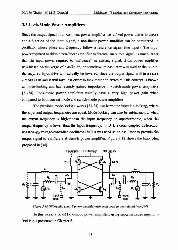
M.A.Sc. Thesis- M. M. El-Desouki McMaster- Electrical and Computer Engineering
3.3 Lock-Mode Power Amplifiers
Since the output signal of a non-linear power amplifier has a fixed power that is in theory
not a function of the input signal, a non-linear power amplifier can be considered an
oscillator whose phase and frequency follow a reference signal (the input). The input
power required to drive a non-linear amplifier to "create" an output signal; is much larger
than the input power required to "influence" an existing signal. If the power amplifier
was biased on the verge of oscillation, or somehow an oscillator was used at the output;
the required input drive will actually be lowered, since the output signal will in a sense
already exist and it will take less effort to lock it than to create it. This concept is known
as mode-locking and has recently gained importance in switch-mode power amplifiers
[31-34]. Lock-mode power amplifiers usually have a very high power gain when
compared to both current-mode and switch-mode power amplifiers.
The previous mode-locking works [31-34] use harmonic injection-locking, where
the input and output frequencies are equaL Mode-locking can also be subharmonic, when
the output frequency is higher than the input frequency or superharmonic, when the
output frequency is lower than the input frequency. In [34], a cross-coupled differential
negative-gm voltage-controlled-oscillator (VCO) was used as an oscillator to provide the
output signal to a differential class-E power amplifier. Figure 3.18 shows the basic idea
proposed in [34].
~1 Bias
!~ Bias
I~
Figure 3.18 Differential class-E power amplifier with mode-locking, reproduced from [34]
In this work, a novel lock-mode power amplifier, using superharmonic injection
locking is presented in Chapter 6.
48
Chapter 3: Power Amplifier Classes of Operation
3.4 Power Amplifier Figure-of-Merit (FoM)
Having a FoM is common in circuit design in order to be able to compare the true
advancements and improvements from one design to another. No standard FoM is
decided on for comparing power amplifiers; however, one has been suggested in the 2003
ITRS [6]. Although the power-added efficiency is widely used as a FoM for comparing
power amplifiers, it is insufficient since it lacks important measures, such as the
frequency of operation.
The FoM proposed in the 2003 ITRS [6] does not take a measure of linearity into
account, since linearity is not a common goal of the three power amplifier categories that
were previously explained. The ITRS FoM can be expressed as follows [6]:
FoMITRS =P,imwxGx~HzxPAE, (3.31)
this FoM can be expressed in logarithmic form as:
FoMITRS =10log.P,j{mw+10logG+20log~Hz +20logPAE. (3.32)
The problem with the FoM proposed in Equation 3.32 is that the output power and the
gain are repeated in the P AE. In this work, the following FoM is proposed, which shows
a more reasonable comparison between the designs existing in the literature [60]:
FoMproposed =10logpoimw+10logG+20log~Hz -lOlogPv;{mW. (3.33)
Equation 3.33 takes into account the drain efficiency, the power-added efficiency and the
operating frequency. Figure 3.19 shows the evaluation of both Equations 3.32 and 3.33
for a number of power amplifier designs available in the literature [60]. Figure 3.19 also
shows that both FoM' s increase as the output power increases, which proves the claim
maid in Chapter 2 that high power amplifiers have higher efficiencies than low power
amplifiers.
3.5 Summary
In this chapter, the most common power amplifier circuits were explained, with emphasis
on class-E power amplifiers.
49

M.A.Sc. Thesis- M. M. El-Desouki McMaster- Electrical and Computer Engineering
The discussed power amplifier classes were categorized into three groups, which
are current-mode power amplifiers, switch-mode power amplifiers and lock-mode power
amplifiers. Table 3.2 shows a summary of the basic power amplifier classes comparing
them in terms of maximum efficiency, linearity and gain. A new FoM was also proposed
in this chapter to be used for comparing power amplifier circuits. This chapter gives some
theoretical background that will be needed to understand and analyze the results that are
presented in this work.
280
260
m- 24o ~ ~ 0 u. 220
200
180
0
A FoMproposed D FoMITRS
~ Fully on-chip
5 1o _____ 1s _____ 2_o _____ 2_5-4•~ Pout(dBm)
30 35
Figure 3.19 Comparison between the proposed FoM and the JTRS FoMfor published works [60]
Table 3.2: Comparison between different power amplifier classes
Category Maximum Efficiency Linearity Gain A <50% Good
AB <50% -78.5% Fair Current-Mode Moderate
B 78.5% Fair
c 78.5%-100% Poor
D 100% Poor E 100% Poor
Switch-Mode 100% Low F
(infinite harmonic ~g) Fair
s 100% Good
Lock-Mode 100% Poor High
(depends on class used) (depends on class used)
50

Chapter 4: Direct-Modulation Transmitters
Chapter4
DIRECT -MODULATION TRANSMITTERS
With the emerging low-power wireless applications such as, wireless body area networks
(WBAN), smart dusts and biomedical implantable electronic systems, short-range
transceivers are increasingly gaining interest. Since these applications have very strict
size, weight and power consumption requirements, having a simple design with minimal
building blocks becomes an attractive approach [51].
Figure 4.1 (a) shows the basic block diagram of a direct-modulation transmitter
[51]. The digital-to-analog (DAC) converter converts the digital information to an analog
signal, after which, it is up-converted by the mixer to the carrier by multiplying the
analog signal by the RF signal that is generated by the local-oscillator. The signal then
goes through a band-pass filter that removes any images or harmonics generated by the
mixer, after which, its power is boosted by the power amplifier. Figure 4.1 (b) shows a
first step to reducing the number of building blocks in the transmitter by using a VCO to
perform direct-FM modulation applied to the varactors. By further simplifying and
removing the DAC, direct-FSK/GFSK can be applied. Figure 4.1 (c) shows how a single
block can be used to perform direct-FSK/GFSK by using a voltage-controlled power
oscillator (VCPO).
The basic differential cross-coupled negative-gm VCO architecture is explained in
Section 4.1 of this chapter, and Section 4.2 explains how this topology can be used for
super-harmonic injection-locking. Section 4.3 presents a new proposed FoM that can be
used to compare VCPO's. Finally, the chapter's summary is presented in Section 4.4.
51

M.A.Sc. Thesis- M. M. El-Desouki
Local oscillator (a)
McMaster- Electrical and Computer Engineering
Figure 4.1 (a) Basic block diagram of a direct-modulation transmitter, (b) simplified transmitter, (c) single
block transmitter [51]
4.1 Differential Cross-Coupled Negative-gm Voltage-Controlled
Oscillator
In order to have a circuit oscillate, there must be some sort of feedback system that
provides gain to compensate for any signal loss. Also, to ensure that the oscillation occurs
at a specific frequency, a frequency selective network should be available in the feedback
path. Figure 4.2 shows an example of such a frequency selective network, where the
resonance frequency is equal tol/(2.1l'.JLC). The figure shows the parallel resistance of the
tank, which is a fictitious component that resembles the losses of the tank. In order to
have a frequency of oscillation that can be voltage controlled, the capacitor in the tank
can be replaced with a voltage-controlled varactor.
52

Chapter 4: Direct-Modulation Transmitters
.. I I
c Rpi .. I I ......
Figure 4.2 A frequency selective LC-tank showing the parallel output resistance
A negative resistance can be added in parallel to Rp in Figure 4.2 to cancel it out
and ensure continuous oscillation. This is the concept of the negative-gm VCO, where two
cross-coupled transistors can be used to provide a negative resistance, as shown in Figure
4.3. When assuming that the transconductance (gm) is equal for both transistors Mt and
Mz, rin is found to be equal to -2/gm.
~ Vrn ~+ lin r ~t 11
+ + V2 v1 - -
Figure 4.3 Negative resistance of a cross coupled NMOS pair
A pair of PMOS devices can also be used to provide the negative resistance
shown in Figure 4.3. When both the NMOS pair and PMOS pair are used at the same
time, as shown in Figure 4.4 (a), they can provide double the gain from the same current.
In this case, the negative resistance provided will be equal to -2/(gm_NMos+gm_PMos).
Figure 4.4 (b) shows how the LC-tank is added and where the outputs are taken
differentially.
The value of the negative resistance is usually 2-3 times the value of Rp for the
LC-tank shown in Figure 4.2 to guarantee that the circuit will oscillate. However, in case
of power oscillators, the circuit is to deliver a certain amount of power to the output,
which is why the circuit is designed to have a higher gain so that the excess power can be
delivered to the load. In order to use the topology shown in Figure 4.4 (b) as a direct
modulation transmitter, the capacitors in the tank must be replaced by varactors and the
active devices must be designed for high power operation. Figure 4.5 shows the
53

M.A.Sc. Thesis- M. M. El-Desouki McMaster- Electrical and Computer Engineering
schematic of the direct-modulation transmitter. The figure does not show any necessary
output matching networks or DC-blocking capacitors. Capacitors Cv are voltage
controlled varactors that can be MOS varactors or junction varactors. Transistor Ms acts
as a tail current source that controls the current in flow the circuit to allow for output
power control.
DC Supply DC Supply
Output- Output+
(a) (b)
Figure 4.4 (a) Complementary negative-gm cross coupled pair, (b) complete oscillator
RF output+
Vee
Figure 4.5 Schematic of a direct-modulation transmitter
54

Chapter 4: Direct-Modulation Transmitters
4.2 Superharmonic Injection-Locking
Injection-locking is common in oscillator design as an undesirable effect that occurs as a
result of fabricating the power amplifier on the same chip with the local oscillator. The
oscillator's frequency tracks the high power signals of the power amplifier that are
coupled through the substrate or fed-back through the supply. This is also known as LO
pull, or local-oscillator pull. Chapter 3 explained how mode-locking can be used to
increase the gain of power amplifier designs and a cross-coupled negative-gm oscillator
was used as an example for harmonic mode-locking.
The topology shown in Figure 4.5 can be used as a frequency divider, since the
frequency of oscillation at the drain of the tail current source is double the frequency of
the output signal. This is due to the fact that each transistor of the NMOS pair conducts
for half the output cycle. This sort of frequency division can be considered
superharmonic injection-locking, since the input frequency is double that of the output
frequency.
When injecting a signal using transistor Ms, the frequency at the drain of the tail
current source will follow the injected signal, as long as it is within the tuning range of
the LC-tank. In this case, the signal at the output will be a result of multiplying the odd
harmonics from the switching operation of the cross-coupled pair by the 2nd harmonic
injected signal. This will result in enhancing the fundamental signal by all the odd
harmonics that down-convert to the fundamental. When the circuit is to be used as a
frequency divider, transistor M5 will no longer be operating as a current source, so it
should not be designed with a long channel; rather, it should be designed for RF
operation with a small input drive.
4.3 Transmitter Figure-of-Merit (FoM)
The well established FoM used in VCO design is not suitable for comparing voltage
controlled power oscillators. An important measure in VCPO's is the output power,
which as it increases, causes the DC power to increase. In this work, a modified FoM is
proposed in Equation 4.1 that takes the output power into account [51]:
55

M.A.Sc. Thesis - M. M. El-Desouki McMaster- Electrical and Computer Engineering
FoM =10logP,ur1 -lOlogPvcl +20log mo -L(Lim)-20logQ (4.1) !'1mW l'1mW Lim '
where Pout is the RF output power and Pdc is the DC power consumption of the oscillator
normalized to 1 mW. Parameter mo is the angular frequency of oscillation of the
oscillator, Lim is the offset frequency at which the phase noise L(Lim) is measured and Q
is the quality-factor of the inductor used in the tank circuit. The phase noise of an
oscillator is defmed as short-term fluctuations that occur randomly in the phase of the
signal.
Since Equation 4.1 has both the output power and the DC power, the drain
efficiency is taken into account. There is no meaning for power-added efficiency in the
design explained in Section 4.1 since there is no RF power gain. The amount of power
required to drive the varactors by the modulation source is negligible, hence, the power
gain can be considered infmite. In such a case, the power-added efficiency will be exactly
equal to the drain efficiency.
4.4Summary
This chapter showed how a single block transmitter can be designed using a power
voltage-controlled oscillator to achieve direct-modulation. The circuit uses a differential
CMOS cross-coupled negative-gm architecture, which was briefly explained, followed by
a simple introduction to how injection-locking occurs in this topology.
A new FoM was also proposed in this chapter, to be used for comparing power
voltage-controlled oscillator circuits.
56
Chapter 5: Switch-Mode Power Amplifiers- Measurement Results
Chapter 5
SWITCH-MODE POWER AMPLIFIERS -
MEASUREMENT RESULTS
This chapter describes the design, simulation and measurement results of the four
implemented switch-mode power amplifier circuits. All designs were fabricated and fully
integrated in a standard mixed-signal CMOS 0.18 J.UI1 technology with 6 metal layers
provided by Taiwan Semiconductor Manufacturing Company (TSMC) through the
Canadian Microelectronics Corporation (CMC). Initially, two designs are presented, one
operating at 900 MHz and the other at 2.4 GHz. After that, the 2.4 GHz design is
presented two more times based on improvements in the layout and the fabrication
process. All four circuits share a very similar architecture, which uses a class-E power
amplifier as the output stage.
Section 5.1 presents the designed 900 MHz switch-mode power amplifier circuit,
where the schematic simulation results are shown, then some layout considerations and
techniques are discussed and finally, the measurement results are presented. Section 5.2
presents the designed 2.4 GHz switch-mode power amplifier circuit, in less design detail
since the architecture is very similar to the 900 MHz design. This section shows the
measurement results of three fabricated circuits. Finally, Section 5.3 presents the
chapter's summary and compares the four designs presented in this chapter based on the
FoM proposed in Chapter 3.
This work focuses on designing power amplifiers suitable for applications that
require low supply voltage operation. Having a low supply voltage reduces the linearity
of the amplifier and makes the output impedance transformation network more complex
due to the need for a smaller load. In biotelemetry applications, a small load value is not
57

M.A.Sc. Thesis- M. M. El-Desouki McMaster -Electrical and Computer Engineering
required since the power amplifier is not expected to handle high power levels. The
reduction in linearity could also be tolerated if a constant envelope modulation scheme
was used, since the amplitude of the signal does not carry any information [56]. Also,
using a non-linear power amplifier has the advantage of higher efficiency than a linear
power amplifier. However, in this case a good output filter is required, which is why non
linear amplifiers were usually avoided in traditional designs for low-power applications
[2, 37, 38, 52]. Non-linear classes were also avoided in low-power applications since they
require a large input drive [2, 52]. In this work, using a class-E amplifier was feasible
since the circuit is to transmit a signal from inside the human body, where the body tissue
will greatly attenuate higher order harmonics [11, 53-56]. To the author's knowledge, this
work [53-56] represents the first use of a class-E power amplifier in low-voltage, low
power applications.
Since the active device in a class-E power amplifier operates as a switch, class-E
power amplifiers are more efficient when driven by a square wave. For this reason, class
F was used as a driver stage in this work. Figure 5.1 shows the basic schematic of the
designed two-stage switch-mode power amplifier. The figure shows that the circuit can
be divided into four parts, the class-E output stage, the class-F driver stage, the output
filter and the inter-stage biasing network. The class-F driver stage is not exactly the same
as the one explained in Chapter 3. Shown in Figure 5.1, the class-F driver stage has two
harmonic peaking networks, where the frrst peaks the fundamental harmonic and the
second peaks the third order harmonic. The circuit has two RF outputs to test the effects
of using an on-chip filter. During measurements, only one of the RF outputs was loaded
at a time. The circuit will be explained in further detail in the following sections.
58

Chapter 5: Switch-Mode Power Amplifiers -Measurement Results
Class-F
~--···
/'L1 . . . . . . . .
\ M1
~ RF Input\ +Bias ·· ....
Voc
Bias
Class-E
L··.\~/ 3 \ RF Output 1
. . . . . . . . : 04····-----[4-·-
t-....-..,.:~i'~ ~ ~ .. ·-~ i' ••••. . •. -·-·RF / -·--f-- Output 2
C3! / Output
.· .. / Filter
Figure 5.1 Schematic of the complete two-stage power amplifier
5.1 First Power Amplifier Design
The design procedure starts first with designing the output stage, which is a class-E
power amplifier and will be described in the following.
Even though the nominal supply voltage of the technology used is 1.8 V, a full
supply voltage should not be used since the junction breakdown of this technology is 4 V,
and the drain voltage of a class-E power amplifier can reach more than 3 times the supply
voltage. In practice, the drain-source voltage of the transistor is the actual supply voltage
that should be considered. Assuming a supply voltage of 1.2 V, from Equation 3.28, the
output power is found to be equal to 0.83/RL, which indicates that an 83 Q load is
required to deliver 10 mW of output power, assuming 100% efficiency. Since the output
power levels targeted required output load values that were close to 50 0, the output load
value was chosen to be fixed at 50 Q to avoid the need for an output impedance
transformation network. The output transformation network can greatly reduce the
efficiency of the power amplifier, as in [58], where the power dissipated in the impedance
transformation network was 1.5 times the power dissipated in the active devices [55].
59
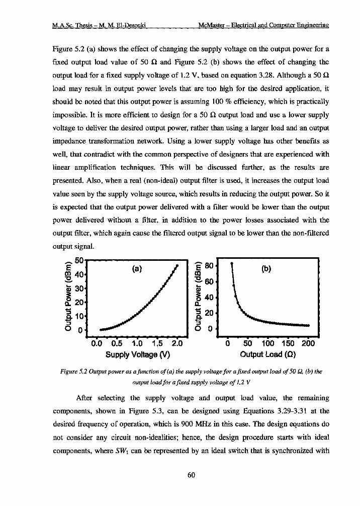
M.A.Sc. Thesis- M M El-Desouki McMaster -Electrical and Computer Engineering
Figure 5.2 (a) shows the effect of changing the supply voltage on the output power for a
ftxed output load value of 50 Q and Figure 5.2 (b) shows the effect of changing the
output load for a fixed supply voltage of 1.2 V, based on equation 3.28. Although a 50 Q
load may result in output power levels that are too high for the desired application, it
should be noted that this output power is assuming 100% efficiency, which is practically
impossible. It is more efficient to design for a 50 Q output load and use a lower supply
voltage to deliver the desired output power, rather than using a larger load and an output
impedance transformation network. Using a lower supply voltage has other benefits as
well, that contradict with the common perspective of designers that are experienced with
linear amplification techniques. This will be discussed further, as the results are
presented. Also, when a real (non-ideal) output filter is used, it increases the output load
value seen by the supply voltage source, which results in reducing the output power. So it
is expected that the output power delivered with a filter would be lower than the output
power delivered without a filter, in addition to the power losses associated with the
output ftlter, which again cause the filtered output signal to be lower than the non-filtered
output signal.
-.e. 10 ::l
0 0
0.0 0.5 1.0 1,5 2.0 Supply Voltage (V}
eao m ~60 ~ ~ 40 c. '$ 20 ~ 0 0
0 50 100 150 200 Output Load (Q}
Figure 5. 2 Output power as a function of (a) the supply voltage for a fixed output load of 50 Q, (b) the
output loadforafixed supply voltage of 1.2 V
After selecting the supply voltage and output load value, the remaining
components, shown in Figure 5.3, can be designed using Equations 3.29-3.31 at the
desired frequency of operation, which is 900 MHz in this case. The design equations do
not consider any circuit non-idealities; hence, the design procedure starts with ideal
components, where SW1 can be represented by an ideal switch that is synchronized with
60

Chapter 5: Switch-Mode Power Amplifiers- Measurement Results
the frequency of the input signal Capacitor C1 is calculated to be 650 tF. In order to
calculate the value of inductor ~. the loaded quality-factor QL must be chosen. As
previously explained, QL represents a design trade-off between having high efficiency
and good filtering. S~ce the main focus of this work was to achieve high efficiency, QL
was selected to be as low as possible, which leads to inductor~ having a value of 17.7
nH. Capacitor C2 can then be calculated from Equation 3.30 to have the value of 1.77 pF.
Figure 5.3 Schematic of a basic class-E power amplifier [56]
The next step in designing the output stage will be to replace the RFC inductor
(LI) with a practical value that can be fabricated on-chip. As mentioned in Chapter 3,
having a fmite drain inductor will cause the efficiency to drop, even if the inductor was
ideal, since it will share the output power with RL. This does not mean that the larger the
value of inductor L1 the better, since large inductors have very low quality factors when
fabricated on-chip in a CMOS process and they also take up a large portion of the silicon
die area. The low quality factor of the drain inductor directly affects the efficiency of the
power amplifier. Therefore, a trade-off arises between having a small on-chip inductor
with a reasonable quality-factor at the desired frequency of operation, which also saves
silicon die area; and having a large enough inductor compared to the output load value
used. This is another reason why choosing an RL value of 50 n and reducing the supply
voltage to achieve the desired output power is more efficient than using a large output
61

M.A.Sc. Thesis - M. M. El-Desouki McMaster -Electrical and Computer Engineering
load with a high supply. As the value of inductor L 1 begins to decrease, the efficiency
also drops due to another reason as well, which is the fact that the class-E equation no
Longer hold and the circuit is no longer tuned to achieve optimum class-E operation.
Hence, during the optimization process of the drain inductor, the class-E components
should continuously be retuned to achieve optimum class-E operation based on the
technique previously described in Figure 3.15. Finally, after finding the suitable value for
inductor L1, it should then be replaced with a non-ideal inductor, using the available RF
spiral inductor models, which will cause a high drop in efficiency due to the inductor's
low quality factor. The other circuit components must be tuned one more time, also the
exact inductor value might not be available within the existing models, which will require
using the closest one. The value used for inductor L 1 in this circuit was 17.7 nH, which
has a peak quality factor of 6 at 1 GHz. By this point, the drain efficiency has already
gone down far below its theoretical 100 %. The output filter's components are next
replaced by their equivalent RF models, where capacitor C2 is represented by an RF
metal-insulator-metal (MIM) capacitor model provided by the foundry.
The remaining components of the output stage, shown in Figure 5.3, are the
parallel capacitor (CI) and the switch (SW1). As the switch is replaced by an actual
device, which is the RF transistor, three points must be considered: a) a RF transistor has
a finite on-resistance, which has a direct effect on the efficiency (Equation 3.34), b) a RF
transistor has a parallel output capacitance that will set a limit on its maximum frequency
of operation and may in fact be greater than the desired value of capacitor C1; and c) a RF
transistor requires a certain amount of input power to drive it in proper switch-mode
operation. There are two ways to reduce the on-resistance of a transistor, one is by
increasing Vgs (the input drive or biasing), and the other is by using a larger device
(higher WIL ratio), where the latter is more effective. On the other hand, to reduce the
output capacitance of the transistor (below C1) and reduce the input drive requirement; a
small ratio of WIL is needed. In higher power amplifiers, the value of capacitor C1 is
usually large, so the output capacitance of the transistor can be absorbed in capacitor C1
and the value of C1 can be reduced, leaving only the input drive to consider. In low
power designs, the small value of capacitor C1 sets a limit on how large the transistor can
be, hence, setting a limit on how low the on-resistance can be. As a result, the efficiency
62
Chapter 5: Switch-Mode Power Amplifiers- Measurement Results
goes down. When designing the size of the transistor that represents SW1, the PAE is
what should be maximized, taking the gain into account. After replacing SW1 with the
designed transistor, the remaining circuit parameters must be retuned again to ensure
optimum class-E operation. The active device should be biased close to threshold to
achieve a 50 % duty-cycle. The designed NMOS device has a total width of 650 f.lm
using 130 fingers and a length of 0.18 f.lm. A multi-fmger configuration was used to
reduce the input gate resistance, which reduces the minimum input drive required to
achieve proper switching. A multi-finger configuration can also help spread the high
currents flowing into the device to prevent over-heating. The output capacitance of the
transistor had the required value of 650 tF for capacitor Ct. so an actual MIM-capacitor
was not used.
One stage alone cannot provide adequate gain to achieve the required P AE;
especially since class-E requires a large input drive to achieve proper switching, so the
P AE will drop. For this reason, a driver stage is required to increase the gain, which
therefore increases the P AE. Since the driver stage itself will consume DC power to
provide gain, there will be a trade-off between increasing the gain and reducing the
overall efficiency of the two-stage power amplifier, which is why the P AE should be
maximized when designing the driver stage. The output load seen by the driver stage is
the input impedance of the class-E active transistor, which is large (capacitive) compared
to the 50 Q output load seen by the output stage. For this reason, the first stage does not
consume as much power as the second stage, which relaxes its efficiency constraints. The
DC power consumed by the first stage was 15 %of the total power drawn from the DC
supply. Figure 5.4 shows the designed two-stage 900 MHz switch-mode power amplifier
[53]. Using a 2.3 nH inductor for both inductors L1 and L2, capacitor C1. which is tuned to
peak the fundamental harmonic, and capacitor C2, which is tuned to peak the third-order
harmonic, are determined to be 11.5 pF and 2.8 pF respectively. The values of capacitors
C1 and C2 are then fme tuned in simulations to achieve harmonic peaking at the exact
frequency of operation.
63

M.A.Sc. Thesis - M. M. El-Desouki
Class-F
x.--·-... ..-------.
/L1 . . . . . . . ' . . . ' ' ' ' ' ' ' ' ' ' ' ' ' ' \ M1 .
pid RF Input\ +Bias ·· ....
' ' ' ' '
Voc
.... -·· . .
,/ . . . . . . . . . ' . ' . . . ' . ' . . l M2 . . . '
McMaster -Electrical and Computer Engineering
.. Class-E
L· ........ /
3 \ . . ' . . ' ' ' ' '
RF Output 1
: 04·---··-··[4·· ~--~:'~~ ~
• '!~ r- -.... _.:;::t--1 I : •••• • •• ·"RF I : ···--f··· -1,_ ; Output 2
-rc3/ e / Output
•• :/ Filter ____ ,,
Figure 5.4 Schematic of designed 900 MHz switch-mode power amplifier [53]
Transistor M1 was designed to achieve maximum global PAE (over both stages)
since it will control the gain of the first stage, hence the total circuit gain, and the amount
of power delivered to the second stage, which will control the efficiency of the output
stage. Transistor M1 is an NMOS device that has a total width of 42.5 J.tm using l7
fingers and a length of0.18 J.tm. As mentioned in Chapter 3, the active device in a class-F
power amplifier can operate in current-mode or switch-mode. If the active device is to
operate in switch-mode, it should be overdriven with a high input that will generate
enough harmonics at the output that can allow for harmonic peaking. Since the topology
used does not have a filter that attenuates the second order harmonics, this approach is
not desirable. Rather, the active device was operated in current-mode, where it was
biased in such a way as to ensure that the third-order harmonics exist with low second
order harmonics, which is the class-AB region, as previously shown in Figure 3.3.
Figure 5.1 previously showed an inter-stage biasing network, composed of a De
blocking capacitor and a large biasing resistor that provide gate biasing for transistor M2.
The biasing network was removed from this design to simplify it, since a large De
blocking capacitor was needed at this frequency of operation. The biasing was obtained
from the DC voltage available at the drain of transistor M1. which is the supply voltage
64
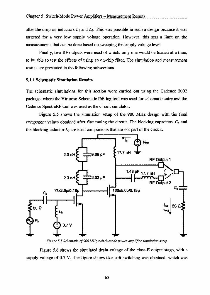
Chapter 5: Switch-Mode Power Amplifiers- Measurement Results
after the drop on inductors L1 and ~. This was possible in such a design because it was
targeted for a very low supply voltage operation. However, this sets a limit on the
measurements that can be done based on sweeping the supply voltage level.
Finally, two RF outputs were used of which, only one would be loaded at a time,
to be able to test the effects of using an on-chip filter. The simulation and measurement
results are presented in the following subsections.
5.1.1 Schematic Simulation Results
The schematic simulations for this section were carried out using the Cadence 2002
package, where the Virtuoso Schematic Editing tool was used for schematic entry and the
Cadence SpectreRF tool was used as the circuit simulator.
Figure 5.5 shows the simulation setup of the 900 MHz design with the fmal
component values obtained after fine tuning the circuit. The blocking capacitors Cb and
the blocking inductor Lb are ideal components that are not part of the circuit.
17.7 nH
Figure 5.5 Schematic of 900 MHz switch-mode power amplifier simulation setup
Figure 5.6 shows the simulated drain voltage of the class-E output stage, with a
supply voltage of 0.7 V. The figure shows that soft-switching was obtained, which was
65 I
I\

M.A.Sc. Thesis- M. M. El-Desouki McMaster- Electrical and Computer Engineering
due to accurately tuning the circuit at optimum class-E operation. When loading the
ftltered output (RF output 2 on Figure 5.5), the power amplifier delivers an output power
of 5.7 dBm, while consuming a DC power of 10 mW from a supply voltage of 0.7 V.
This results in a drain efficiency of 37 %. The peak simulated power gain is 20 dB;
however the peak P AE occurs at an input drive of -8 dBm, which corresponds to a power
gain of 13 dB. The peak PAE achieved is 34.8 %.
~1.2
& s 0.8 ~ c -~ 0.4 c
0.0 .---~~.--.--~~-.--r-~~
995.2 995.6 996.0 996.4 996.8 997.2 Time (ns)
Figure 5.6 Simulated drain voltage of the class-E power amplifier
Figure 5. 7 shows the simulated output power, P AE and drain efficiency as a
function of the input power at a supply voltage of 0.7 V. The point at which the PAE
efficiency peaks is the 1 dB gain compression point of the amplifier, since it is when the
amplifier is delivering its maximum output power.
6.------------------------.60
s5 III ~4 ..... ~ 0 3 a.. :;2
~1 0 -10 ~
0 .. -P-.--.-~-.~~.-~-.--~.-~ " -20 -15 -10 -5 0 5
Input Power (dBm)
Figure 5.7 Simulated output power, PAE and drain efficiency as afunction of the input power
66

Chapter 5: Switch-Mode Power Amplifiers- Measurement Results
When loading the non-filtered output (RF output 1 on Figure 5.5), the power
amplifier delivers an output power of 7.7 dBm, while consuming a DC power of 13.8
m W from a supply voltage of 0. 7 V. This results in a drain efficiency of 43 %, which is a
5 % increase compared to the filtered output. As mentioned earlier in this chapter, the
fllter causes the output load to increase from the DC supply point of view; this explains
why both the RF output power and the DC supply power consumption are higher for the
non-ftltered output. The peak simulated power gain is 23 dB; however the peak PAE
occurs at a power gain of 13 dB, with a peak PAE value of 41 %.
5.1.2 Layout
The layout design was done using the Virtuoso Layout Editor tool available in the
Cadence 2002 package. Figure 5.8 shows a screen capture of the 900 MHz design layout
highlighting the output filter. The core two-stage amplifier occupies an area of 1 mm2 and
the output filter occupies an area of0.36 mm2•
Figure 5.8 Screen capture of the 900 MHz power amplifier layout
The inductors were laid using the top metal layer since it has the least sheet
resistance and is the farthest away from the substrate, hence; has the least parasitic
capacitance. The tool provides a parasitic extraction function, which can be used for post-
67

M.A.Sc. Thesis - M. M. El-Desouki McMaster -Electrical and Computer Engineering
layout simulations. However, only the layout parasitic capacitances can be accounted for,
so the layout was optimized to reduce only the effects of the parasitic capacitances on the
performance of the power amplifier. The resulting interconnections appear very long and
are mostly 5-10 Jtm wide using various metal layers.
5.1.3 Refined Circuit Simulation Results
Due to only accounting for the layout parasitic capacitances, a large discrepancy was
observed between the measured and simulated results. Also, when the chip was submitted
for fabrication, it went through a different fabrication process that has a top-metal layer
with half the thickness of the intended process (1 Jim instead of 2 Jtm). This resulted in a
large drop in efficiency since the quality factor of all the inductors decreased by a factor
of two. The simulated drain efficiency and output power of the non-filtered output
decreased from 43 % and 7.7 dBm to 29 % and 5.8 dBm respectively, whereas the
simulated drain efficiency and output power of the filtered output dropped from 37 % and
5.7 dBm to 22 % and 3.5 dBm respectively. The filtered output suffered a larger drop
since the output signal goes through one more inductor before it reaches the load.
There is a direct trade-off between parasitic capacitance, inductance and
resistance of the interconnections. The parasitics of the interconnections were
characterized based on the approach in [59], which models every interconnection with a
lumped element circuit model. The interconnection models are then added to the circuit
schematic in the simulator and the effects of the layout parasitics can be carefully
accounted for. Generally, minimizing the resistive losses is the major concern in power
amplifier designs. However, in the case of tuned amplifiers such as class-E and class-F,
the parasitic inductance and capacitance can significantly effect the tuning, if not
carefully taken into account [54]. Figure 5.9 shows a screen capture of the InterConnect
application interface that was designed to calculate the interconnection equivalent circuit
component values. The figure also shows the equivalent circuit model used to represent
the interconnections. The InterConnect program takes layout information regarding the
interconnections' width, length and metal layer used, and produces the value of the
capacitance, resistance and inductance of the interconnection parasitics.
68

Chapter 5: Switch-Mode Power Amplifiers- Measurement Results
InterConnect f8J W (um) 1
L (um) 1
Metal Layer .--::::1
[email protected] 2004
0.078
Rs in Ohm Ls in nH Csub in fF
0.03642857
Figure 5.9 Screen capture of the InterConnect application inteiface
Using the equivalent circuit shown in Figure 5.9 is sufficient for low-frequency
applications (below 10 GHz), after which, the lumped element model no longer holds
[59]. Also, since every interconnection is characterized separately, issues such as
interconnection overlap capacitance, cross-talk and antenna effects are not accounted for;
however they can be avoided by carefully placing the components on the layout. In this
design, the probing pads used were laid out using all metal layers (1-6) connected in
parallel. The extracted pad capacitance was equal to 350 fF, which bad a great effect on
the gain of the circuit. Using all six metal layers is a requirement from the foundry only if
the design is to be bounded and packaged. Using less metal layers can help reduce the
parasitic capacitance of the pads.
After characterizing the effects of the layout interconnections on the 900 MHz
design, the simulated drain efficiency and output power of the non-filtered output
dropped from 29 % and 5.8 dBm to 11.7 % and -0.24 dBm respectively, whereas the
simulated drain efficiency and output power of the filtered output dropped from 22 % and
3.5 dBm to 4.8% and -4.8 dBm respectively. The frequency tuning also shifted due to the
parasitic effects of the layout interconnections and pads.
69

M.A.Sc. Thesis- M. M. EI-Desouki McMaster- Electrical and Computer Engineering
5.1.4 Measurement Results
Figure 5.10 shows a photomicrograph of the fabricated circuit that occupies an area of 1
mm2 including the pads. The on-chip filter adds another 0.36 mm2 to the area of the
circuit [53] .
Figure 5.10 Photomicrograph of the fabricated 900 MHz power amplifier [53]
The chip was probed on-wafer using a ground-signal-ground configuration for the
RF signals and a single pad for DC connections. An Agilent-4422B signal generator was
used to provide the RF input and an Agilent-E4440A spectrum analyzer was used to
measure the output power delivered to a 50 n output load. An HP-4145B semiconductor
parameter analyzer was used to provide the biasing and to measure the DC power. Figure
5.11 shows a sketch of the measurement setup. An 11-tip probe set, which is a
combination of two RF and five DC probes, was used to provide the RF and DC input
and output signals.
Figure 5.12 shows a comparison between the measured and simulated output
power and drain efficiency of the filtered output, as a function of the operating (input)
frequency at a supply voltage of 0.7 V. The figure shows a very good match between the
measurement and simulation results due to accurately taking the parasitics into account.
The mismatch increases at higher frequencies since in this design, the transistors were not
laid out to follow the accurate RF model used in simulation, which was not available at
that time. The RF model was characterized only for transistors with a channel width of
2.5 f..I.ITI, however, a transistor with a width of 5 flm was used in this design.
70

Chapter 5: Switch-Mode Power Amplifiers- Measurement Results
Signal Generator Agilent-44228
Spectrum analyzer Agilent-E4440A
t
'
t . -
(//}--------# ---
: ___________ ,
Semiconductor Parameter Analyzer
HP4145B
Figure 5.11 Setup used in measuring the 900 MHz power amplifier
-E !g 0 -.... Q)
~ -10 0.. -:::l .e--20 ::I 0
-30
• 11 measured ·-- 11 simulated
• • • 400 600 800
Frequency (MHz)
12 ~ :r m
8 ~ (D" ::I
4~ -*' -0
,,'
, , ,
' ' • I I I
• • • , , , ,
Figure 5.12 Comparison between the measured and simulated output power and drain efficiency of the
filtered output, as a function of the operating frequency, at a supply voltage of0.7 V
Figure 5.13 shows the measured output power, PAE and drain efficiency of the
non-filtered output at an input frequency of 650 MHz, as a function of the supply voltage
[53]. The P AE was calculated at a constant input drive of -7 dBm. The circuit has a
71
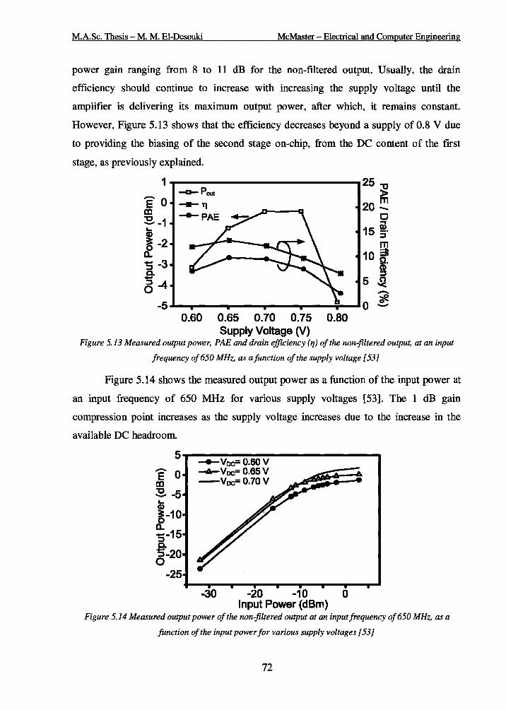
M.A.Sc. Thesis - M. M. El-Desouki McMaster- Electrical and Computer Engineering
power gain ranging from 8 to 11 dB for the non-filtered output. Usually, the drain
efficiency should continue to increase with increasing the supply voltage until the
amplifier is delivering its maximum output power, after which, it remains constant.
However, Figure 5.13 shows that the efficiency decreases beyond a supply of 0.8 V due
to providing the biasing of the second stage on-chip, from the DC content of the frrst
stage, as previously explained.
0.60 0.65 0.70 0.75 0.80 Supply Voltage (V)
Figure 5.13 Measured output power, PAE and drain efficiency (rt) of the non-filtered output, at an input
frequency of650 MHz, as a function of the supply voltage [53]
Figure 5.14 shows the measured output power as a function of the input power at
an input frequency of 650 MHz for various supply voltages [53]. The l dB gain
compression point increases as the supply voltage increases due to the increase in the
available DC headroom.
5.-----------------------~ -voc=o.eov E 0 --.6.-Voc= 0.65 v CD -Voc= 0.70 V :s -5 tD S:-10 ~ :;-15 .a:::J-20 0
-25
-30 -20 -10 0 Input Power (dBm)
Figure 5.14 Measured output power of the non-filtered output at an input frequency of650 MHz, as a
function of the input power for various supply voltages [53]
72

Chapter 5: Switch-Mode Power Amplifiers- Measurement Results
Figure 5.15 shows the measured power gain as a function of the input power at an
input frequency of 650 MHz for various supply voltages [53]. The figure shows how
using a lower supply voltage, which reduces the 1 dB gain compression point, can help
reduce the input power required to drive the transistor in switch-mode. This is clarified in
Figure 5.16, which shows the measured drain efficiency as a function of the input power
at an input frequency of 650 MHz for various supply voltages [53]. When using a supply
voltage of 0.7 V, a larger input drive is required than that for a supply voltage of 0.65 V
to achieve peak efficiency. Having a high gain compression point is therefore not desired
in this work, in addition to the fact that the amplifier is designed for constant envelope
modulation schemes, which do not require a high gain compression point. Since both the
drain efficiency and the power gain peak for a supply voltage of 0.65 V, it is expected
that the power-added efficiency will also peak at a supply voltage of 0.65, as shown in
Figure 5.17, which shows the measured power-added efficiency of the non-filtered output
at an input frequency of 650 MHz as a function of the input power, for various supply
voltages [53].
-30 -20 -10 0 Input Power {dBm)
Figure 5.15 Measured power gain of the non-filtered output at an input frequency of 650 MHz, as a
function of the input power for various supply voltages [53 I
Figures 5.18 and 5.19 show a comparison between the measured drain efficiency
and output power of the filtered and the non-filtered outputs of the power amplifier as a
function of the input frequency, at a supply voltage of0.7 V [53]. Due to the losses in the
on-chip filter, the output power drops by 7 dB, which results in a 9 %drop in efficiency.
73
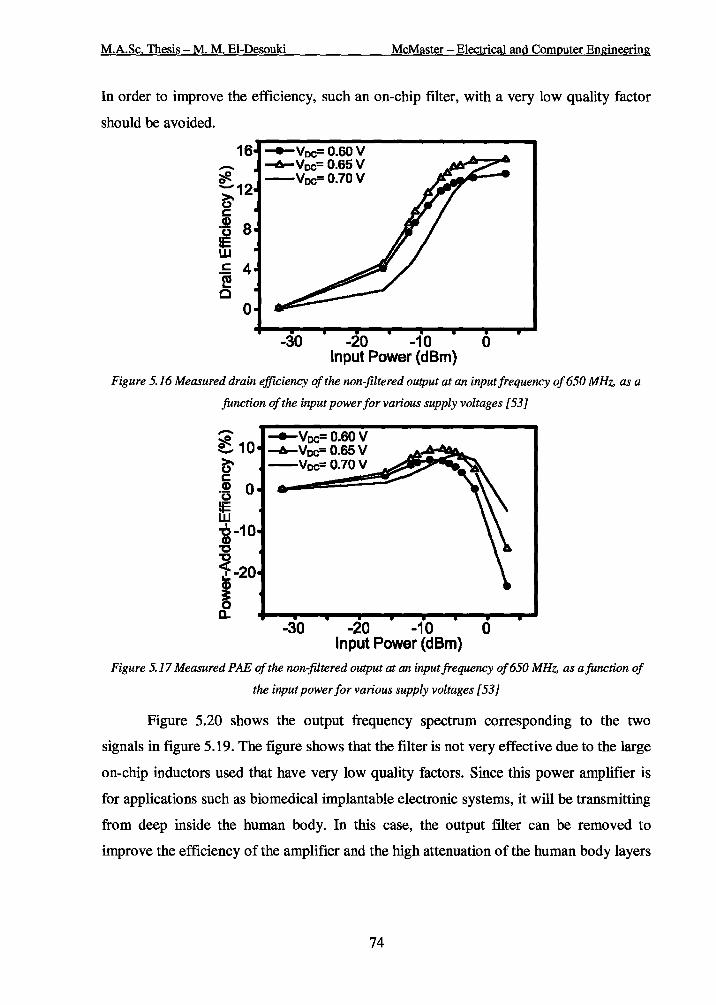
M.A.Sc. Thesis - M. M. El-Desouki McMaster- Electrical and Computer Engineering
In order to improve the efficiency, such an on-chip filter, with a very low quality factor
should be avoided.
16 ...,._Voc= 0.60 V ....._Voc=0.65V -Voc=0.70V
0
-30 -20 -10 Input Power (dBm)
0
Figure 5.16 Measured drain efficiency of the non-filtered output at an input frequency of 650 MHz, as a
function of the input power for various supply voltages [53 1
-~10 (;
-8 0 ~ -6-10 CD
"C "C
~-20 .... CD
~ a..
...,._Voc= 0.60 V
........ voc=o.asv -Voc=0.70V
-30 -20 -10 0 Input Power (dBm)
Figure 5.17 Measured PAE of the non-filtered output at an input frequency of 650 MHz, as a junction of
the input power for various supply voltages [53 1
Figure 5.20 shows the output frequency spectrum corresponding to the two
signals in figure 5.19. The figure shows that the filter is not very effective due to the large
on-chip inductors used that have very low quality factors. Since this power amplifier is
for applications such as biomedical implantable electronic systems, it will be transmitting
from deep inside the human body. In this case, the output filter can be removed to
improve the efficiency of the amplifier and the high attenuation of the human body layers
74

Chapter 5: Switch-Mode Power Amplifiers- Measurement Results
can act as a low-pass filter, since the body tissue attenuation increases with frequency
[11].
16 - Non-Filtered -a- Filtered
0 500 1 000 1500 2000 2500 Frequency (MHz)
Figure 5.18 Comparison between the measured drain efficiency of the filtered and the non-filtered outputs
as a function of the input frequency, at a supply voltage of 0.7 V [53]
10 -Non-Filtered
- -a- Filtered
~ 0 ~ ... CD ~ -1
a..
i-20 0
-30 ._~--~--~-.~~~p-.-~~
0 500 1000 1500 2000 2500 Frequency (MHz)
Figure 5.19 Comparison between the measured output power of the filtered and the non-filtered outputs as
a function of the input frequency, at a supply voltage of0.7 V [53]
1.0 1 Frequency {GHz)
Figure 5.20 Comparison between the harmonic content of the filtered and the non-filtered outputs, at a
supply voltage of 0. 7 V. The filtered output drops below the non-filtered output at the fundamental, second
and third harmonics by 7, 6 and 12 dB respectively [53]
75

M.A.Sc. Thesis - M. M. El-Desouki McMaster- Electrical and Computer Engineering
5.2 Second Power Amplifier Design
This design follows the same design procedure of the 900 MHz design, where the same
topology was used, with minor modifications. Figure 5.21 shows the schematic of the 2.4
GHz switch-mode power amplifier designed [54, 55]. Capacitor C1 can be calculated as
explained in the previous section to be equal to 212 fF, which is too low to be accurately
represented by a MIM-capacitor. Instead, the layout parasitics can be used to provide
such a low capacitance. Since the frequency of operation in this design is higher than the
previous one, using a smaller DC-feed inductor (LJ) was possible. Both inductors L3 and
4 were represented by 6 nH inductors. Unlike the 900 MHz design, a biasing network
was added to provide the gate biasing of the second stage allowing for unrestricted DC
sweeps in measurements. A large biasing resistor was used instead of a blocking inductor
since the resistor is smaller and will be more area efficient when fabricated on-chip.
Class-F
~-·~···
i/L1 ! ,._________.
. ' \ M1
~ RF Input\ +Bias ·· ....
Voc
---Bias
.. Class-E
L·· ....... /
3 \ . . . . . . ' . .
RF Output 1
\ C4······-··[4·· . ......_......:r~ . \ ~ - ---~
I : ···-- •••• ·"RF j_ j ··-f··· Output 2
~i • / Output
--~/ Filter •' .. •
Figure 5.21 Schematic of designed 2.4 GHz switch-mode power amplifier [54, 55]
5.2.1 Schematic Simulation Results
The schematic simulations followed the same procedure explained in the previous
section; however, the Cadence 2003 package was used from here on. Figure 5.22 shows
the schematic circuit of the 2.4 GHz design illustrating the simulation setup and showing
76

Chapter 5: Switch-Mode Power Amplifiers- Measurement Results
the component values. When loading the filtered output (RF output 2 on Figure 5.22), the
power amplifier delivers an output power of 6.3 dBm, while consuming a DC power of
10.4 mW from a supply voltage of0.8 V. This results in a drain efficiency of 41 %. When
loading the non-filtered output (RF output 1 on Figure 5.22), the power amplifier delivers
an output power of 8 dBm, while consuming a DC power of 12.4 mW from a supply
voltage of 0.8 V. This results in a drain efficiency of 51 %, which is a 10 % increase
compared to the filtered output.
Voc
RF0utput1
A. 721 fF 6 nH \ ...... ~
l---1~2_j_ 125x2.51J/0.181J cb
Figure 5.22 Schematic of designed 2.4 GHz switch-mode power amplifier simulation setup
Figure 5.23 shows the simulated output power, PAE and drain efficiency of the
non-filtered output as a function of the input drive at a supply voltage of 0.8 V and an
input frequency of 2.4 GHz.
-10 E ttl :2.5 ... ~ ~ 0 -.e. -5 ::s 0 -10
-30 -20 -10 0 Input Power (dBm)
10
""C
60~ 0 ..,
40~ m
20~ CD ::s
0~ '#. -
Figure 5.23 Simulated output power, PAE and drain efficiency as a function of the input power
77

M.A.Sc. Thesis- M. M. EI-Desouki McMaster- Electrical and Computer Engineering
5.2.2 Layout
The layout follows the same procedure of the 900 MHz design; however the 2.4 GHz
design was fabricated three times. The first fabrication suffered the same problems of the
previous design, where only the layout parasitic capacitances were taken into account
during layout optimization and the design was fabricated in a process with a top metal
layer with half the thjckness intended. Figure 5.24 shows a screen capture of the first
fabricated 2.4 GHz layout. The core two-stage amplifier o.ccupies an area of 1.1 mm2.
Figure 5.24 Screen capture of the first 2.4 GHz power amplifier layout
The layout was improved based on the approach explained in the previous
section, by characterizing the layout parasitics. When comparing the improved layout,
shown in Figure 5.25 (a), to that first design, shown in Figure 5.24, the improvements in
metal widths is obvious. All major interconnections and inductors were laid out using the
top metal layer to minimize the parasitic capacitive and resistive effects. The three top
metal layers were connected in parallel to provide ground and DC-supply with minimum
resistive losses and only the top metal layer was used for RF pads to minimize
capacitance [54]. The improved layout occupies the same area as the first design. Figure
5.24 (b) shows a screen capture of the third layout, whlch uses the intended process that
has a 2 J..lffi truck top metal layer. The filter was not implemented in thls design to save
78

Chapter 5: Switch-Mode Power Amplifiers- Measurement Results
space and since the human body layers will be depended on to provide high frequency
ftltering to improve efficiency, as previously mentioned. The third layout occupies an
area of0.7 mm2•
Figure 5.25 Screen capture of the (a) improved layout design and (b) thick-top metal design
5.2.3 Refined Circuit Simulation Results
Due to the drop in the quality factor of the inductors used, the re-simulated drain
efficiency and output power of the non-filtered output dropped from 51 %and 8 dBm to
46% and 7.2 dBm respectively, whereas the simulated drain efficiency and output power
of the filtered output dropped from 41 %and 6.3 dBm to 29% and 5 dBm respectively.
After characterizing the effects of the layout interconnections on the first 2.4 GHz
design, the simulated drain efficiency and output power of the non-filtered output
dropped from 46 % and 7.2 dBm to 10 % and -1.5 dBm respectively, whereas the
simulated drain efficiency and output power of the filtered output dropped from 29 % and
5 dBm to 10 %and -1.7 dBm respectively. The efficiency of both the filtered and non
ftltered outputs drops to the same level since the non-filtered output was routed through a
very long connection that went through a number of vias to move between layers. The
refined simulations of the third design, which uses the thick top metal inductors and that
takes advantage of the layout improvements, achieve the original simulation results that
were initially targeted, this will be further verified in the following subsection.
79

M.A.Sc. Thesis- M. M. El-Desouki McMaster- Electrical and Computer Engineering
5.2.4 Measurement Results
Figure 5.26 shows a photomicrograph of (a) the first fabricated 2.4 GHz power amplifier,
(b) the improved layout and (c) the thick-metal design [54-56]. The third layout is smaller
since the output filter was removed; hence, only three inductors and less RF pads for the
output, were needed.
(c) Figure 5.26 Photomicrograph of(a) the first fabricated 2.4 GHz design, (b) the improved layout and (c) the
thick-metal design [54-56]
The same measurement setup previously explained, shown in Figure 5.11, was
used to measure the three 2.4 GHz designs. Figures 5.27 and 5.28 show a comparison
between the measured output power and the measured drain efficiency, respectively, of
the non-filtered output in the three designs at a very low supply voltage of 0.8 V, as a
function of the input frequency [56]. The input drive was fixed at -1.7 dBm during this
sweep.
80

Chapter 5: Switch-Mode Power Amplifiers- Measurement Results
15.---~~~--------------~ -x- Rrst design
-15
-o- Improved layout -e- Thick metaii.JI ..,..._.__
0.5 1.5 2.5 3.5 Frequency (GHz)
Figure 5.27 Comparison between the measured output power of the non-filtered output of the first design,
the improved design and the design that uses a thick top metal layer at a supply voltage of0.8 V. as a
function of the input frequency [56]
Improving the layout, following the method described in the previous section,
resulted in an 8 dB increase in output power from the first design to the improved design.
This corresponded to a 27 % increase in drain efficiency. Shown in Figures 5.27 and
5.28, the frequency tuning was improved to deliver peak output power and drain
efficiency at exactly 2.4 GHz. Increasing the thickness of the top-metal layer resulted in
an increase of 2.5 dB in output power, which corresponded to an increase of 20 % in
drain efficiency. This was not only due to having inductors with double the quality factor,
but it was also due to having interconnections with half the resistivity (when the top
metal layer was used) without increasing parasitic capacitance.
-~50 -
0.5 1.5 2.5 3.5 Frequency (GHz)
Figure 5.28 Comparison between the measured drain efficiency of the non-filtered output of the first
design, the improved design and the design that uses a thick top metal layer at a supply voltage of0.8 V. as
a function of the input frequency [56]
81

M.A.Sc. Thesis- M. M. El-Desouki McMaster- Electrical and Computer Engineering
Figure 5.29 shows a comparison between the simulated and measured output
power and drain efficiency for the filtered output in the frrst design as a function of the
input frequency, at a supply voltage of0.8 V [54].
10.---------------------~20
- • 11measured -- 11 simulated ffi 0
~ ~ ... ~--~II&..._~ .... CD
§-10 ~
x Pout measured -Pout simulated
l-20 ··~ ..... - -:.....
c 1sm s·
m 10~
ar ::::J
5~ ~ -::::J ... ......._
0 -~----~ -30+------.-----....------... 0
2.0 2.5 3.0 3.5 Frequency (GHz)
Figure 5.29 Comparison between the measured and simulated output power and drain efficiency of the
filtered output in the first design, as a function of the operating frequency, at a supply voltage ofO.B V [54]
Figure 5.30 shows a comparison between the simulated and measured output
power and drain efficiency for the non-filtered output in the second design as a function
of the input frequency at a supply voltage of0.8 V [54]. The good match obtained is due
to carefully modeling all the components of the layout, including the on-chip
interconnections.
• 11measured x Pout measured -- 11 simulated -Pout simulated . ~
A A.,./ A A
---- • ·~
. . . . . 2.35 2.45 2.55
Frequency (GHz)
•
)j
c OJ 60 -· ::::J
m ::II
40 ~-::::J n
20~ ':le 0 -
Figure 5.30 Comparison between the measured and simulated output power and drain efficiency of the
non-filtered output in the improved design, as a function of the operating frequency, at a supply voltage of
0.8 V[54]
82

Chapter 5: Switch-Mode Power Amplifiers- Measurement Results
Figure 5.31 shows a comparison between the measured and simulated output
power and drain efficiency of the third design, with the thick top metal layer, as a
function of the operating frequency, at a supply voltage of 0.8 V. The input power used
for this sweep, and the previous two, was fixed at -1.7 dBm. Figures 5.32 and 5.33 show
the measured output power, PAE and drain efficiency of the non-filtered and the filtered
outputs respectively in the second design at 2.4 GHz, as a function of the supply voltages.
The P AE was calculated at a constant input signal of -1.7 dBm. The circuit has a small
signal power gain ranging from 14 to 17 dB for the non-filtered output, and 9 to 10 dB
for the filtered output. Due to the losses in the on-chip filter, the output power drops by 3
dB, which results in a 13 %drop in efficiency [55]. The output power is shown to be a
strong function of the supply voltage, as anticipated by Equation 3.28.
18~------------~~----~ - • 11 measured :»c Pout measured ~ 12 -· 11 simulated -Pout simulated
~ .... I 6 ~ - 0 5. '5-6 0
2.2 2.6 3.0 3.4 Frequency (GHz)
Figure 5.31 Comparison between the measured and simulated output power and drain efficiency of the
third design, as a function of the operating frequency, at a supply voltage of0.8 V [56]
-E10 Ill "C -s I ~6 '5 ~4 0
0.6 0.8 1.0 1.2 1.4 Supply Voltage M
Figure 5.32 Measured output power, PAE and drain efficiency (rf) of the non-filtered output in the second
design at a frequency of2.4 GHz, as a function of the supply voltage [55]
83

M.A.Sc. Thesis- M. M. El-Desouki McMaster - Electrical and Computer Engineering
In Figures 5.32 and 5.33, the supply voltage was varied between 0.6 and 1.4 V in
the measurements; however, this circuit is not designed to operate with a supply above
1.3 V or the active devices will suffer from breakdown due to the high drain voltage in
class-E power amplifiers [55].
0.6 0.8 1.0 1.2 1.4 Supply Voltage (V)
"'C
40~ 0 m 30::;-m
20~ ~-
10~ -~ -Figure 5.33 Measured output power, PAE and drain efficiency (rt) of the filtered output in the second
design at a frequency of 2.4 GHz, as a function of the supply voltage [55]
Figure 5.34 shows a comparison between the filtered and non-filtered output
power levels of the second design, as a function of the operating frequency for a supply
voltage of 1.2 V [55]. The drop in output power at 2.4 GHz, results in an 8 % drop in
efficiency.
0.5 1.5 2.5 3.5 4.5 Frequency (GHz)
Figure 5.34 Comparison between the measured output power of the filtered and the non-filtered outputs in
the second design, at a supply voltage of 1.2 Vas a function of the operating frequency [55]
Figure 5.35 compares the output spectrum corresponding to the signals shown in
Figure 5.34 [55]. The filtered output drops below the non-filtered output at the
84

Chapter 5: Switch-Mode Power Amplifiers- Measurement Results
fundamental, second and third harmonics by 2, 9 and 14 dB respectively. It can be seen
that the filter is not very effective due to the low-Q inductors used. However, the high
frequency harmonics will be greatly attenuated when transmitted from inside the human
body, so the filter can be removed in order to improve the efficiency, which is the utmost
concern in biomedical implantable electronic systems. Since the expected non-filtered
output signal of a class-E power amplifier is a half sinusoidal waveform, the odd
harmonics are expected to have a higher value than the even harmonics, and this can be
seen in Figure 5.35 [55].
20 -E ~ 0 -L.. CD ~-20 ~ -~-40 g ~
0-60
• -a- • Non-Filtered -.-Filtered
g
' D I I
II I 1 1 11r I I r" JIL• ol 111 • I I 1"'11 11 1• ........ l········ ~ .. ···--r'T"1"'l!:.~-ul;!!~~...,.... "'_,..,. ..,\Jl'tJ(r-·- I r"-j]j//1! 1 , I~ i , , 1(1[1 !1 1\jlll I' 1\ "lid 111111 : 11111'1''' 'I Ill! l) ill I I I! liillli!! I~ 1'1111 d' I I 'II''' I
1 I I I I I 1 I I I I I I r I I I I ' ' / I 1 ~ I I 1 1 1 1 1 1 1 I 1 I I I
2 3 4 5 6 Frequency (GHz)
7 8
Figure 5.35 Comparison between the harmonic content of the filtered and the non-filtered outputs in the
second design, at a supply voltage of 1.2 V and an input frequency of2.4 GHz [55]
Figure 5.36 shows the measured output power of the non-filtered output in the
second design, at an input frequency of at 2.4 GHz as a function of the input power for
various supply voltages [55]. The 1 dB gain compression point increases as the supply
voltage increases. Having a high compression point is not desirable in non-linear power
amplifiers since an amplifier is most efficient when it is delivering its maximum output
power, which occurs at the compression point. This effect is more apparent in Figure
5.37, which shows the measured PAE of the non-filtered output in the second design, at
an input frequency of 2.4 GHz, as a function of the input power for various supply
voltages. A larger input drive is required to achieve peak PAE for a higher supply voltage
due to the shift in the compression point. Increasing the supply voltage also results in
having a higher drain voltage across the active device, which requires a larger gate
voltage to keep the device operating in the linear region as a switch. This explains the
85

M.A.Sc. Thesis - M. M. El-Desouki McMaster- Electrical and Computer Engineering
jump in output power, which can be seen in Figure 5.36 for the case of a supply voltage
of 1.4 V as the input power exceeds -24 dBm. Before that point, the device is not
operating in the linear region and is not switching properly; hence, the circuit is not
operating as a class-E power amplifier.
~Voc=0.6V
--a-Voc = 0.9 V -Voc=1.4V
-20 ................ -..-........... - ................ --t -30 -20 -10 0 10
Input Power (dBm) Figure 5.36 Measured output power of the non-filtered output in the second design, at a supply voltage of
0.6, 0.9 and 1.4 Vat a frequency of2.4 GHz, as a function of the input power [55]
~Voo=0.6V
-a-Vec = 0.9 V -Voc=1.4V
-30 -20 -10 0 Input Power (dBm)
Figure 5.37 Measured PAE of the non-filtered output in the second design, at a supply voltage of0.6, 0.9
and 1.4 Vat a frequency of2.4 GHz, as a function of the input power [55]
Figure 5.38 shows the measured output power, PAE and drain efficiency of the
third design, with the thick top metal layer, for an input frequency of 2.4 GHz and an
input drive of -1.7 dBm, as a function of the supply voltage [56]. The efficiency slightly
increases with the supply voltage to the point at which the power amplifier is delivering
its maximum output power; after that it does not increase since both the DC power and
output power are increasing together. As the output power increases, the gain also
86
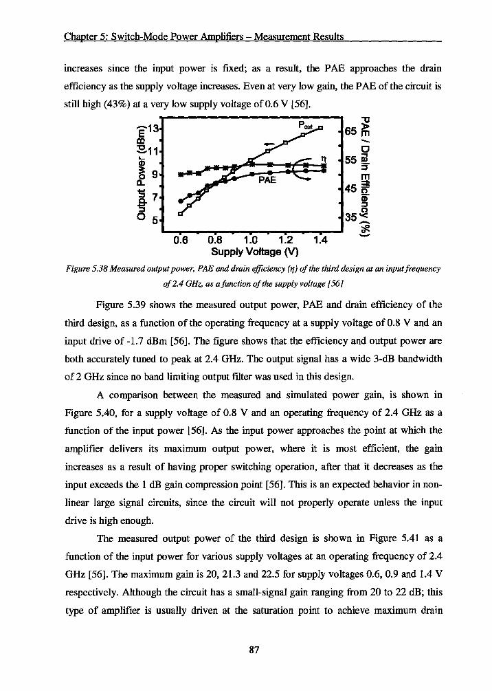
Chapter 5: Switch-Mode Power Amplifiers- Measurement Results
increases since the input power is fixed; as a result, the PAE approaches the drain
efficiency as the supply voltage increases. Even at very low gain, the P AE of the circuit is
still high (43%) at a very low supply voltage of0.6 V [56].
'E1a a:l ~11 L. CD
~ 9 a. -5_7 '5 0 5
0.6 0.8 1.0 1.2 1.4 Supply Voltage (V)
"'0 65 f!i1 -0 55 i!!.
:::J m
45 ~ ar :::J
35~ -?/.. -Figure 5.38 Measured output power, PAE and drain efficiency (1'/) of the third design at an input frequency
of 2.4 GHz, as a function of the supply voltage [56]
Figure 5.39 shows the measured· output power, PAE and drain efficiency of the
third design, as a function of the operating frequency at a supply voltage of 0.8 V and an
input drive of -1.7 dBm [56]. The figure shows that the efficiency and output power are
both accurately tuned to peak at 2.4 GHz. The output signal has a wide 3-dB bandwidth
of 2 GHz since no band limiting output filter was used in this design.
A comparison between the measured and simulated power gain, is shown in
Figure 5.40, for a supply voltage of 0.8 V and an operating frequency of 2.4 GHz as a
function of the input power [56]. As the input power approaches the point at which the
amplifier delivers its maximum output power, where it is most efficient, the gain
increases as a result of having proper switching operation, after that it decreases as the
input exceeds the 1 dB gain compression point [56]. This is an expected behavior in non
linear large signal circuits, since the circuit will not properly operate unless the input
drive is high enough.
The measured output power of the third design is shown in Figure 5.41 as a
function of the input power for various supply voltages at an operating frequency of 2.4
GHz [56]. The maximum gain is 20, 21.3 and 22.5 for supply voltages 0.6, 0.9 and 1.4 V
respectively. Although the circuit has a small-signal gain ranging from 20 to 22 dB; this
type of amplifier is usually driven at the saturation point to achieve maximum drain
87
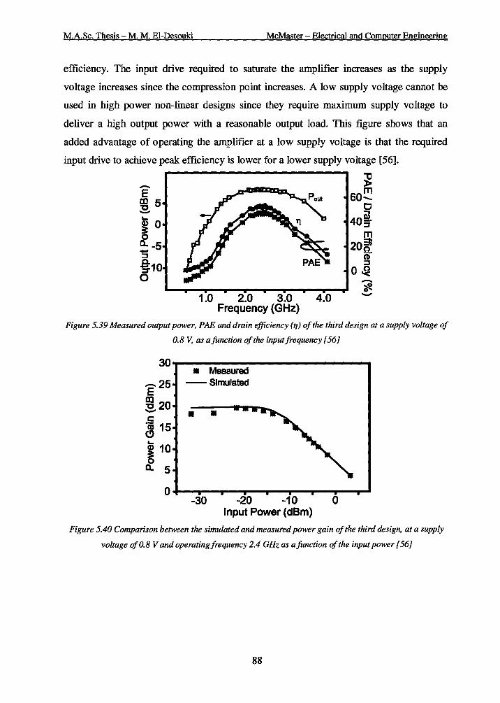
M.A.Sc. Thesis - M. M. El-Desouki McMaster- Electrical and Computer Engineering
efficiency. The input drive required to saturate the amplifier increases as the supply
voltage increases since the compression point increases. A low supply voltage cannot be
used in high power non-linear designs since they require maximum supply voltage to
deliver a high output power with a reasonable output load. This figure shows that an
added advantage of operating the amplifier at a low supply voltage is that the required
input drive to achieve peak efficiency is lower for a lower supply voltage [56].
-E ID 5 "C -... I o 0 0.. -5 -::;, ~10 0
1.0 2.0 3.0 Frequency (GHz)
~ 60~
0
40~· m
20~ (6" ::;,
0~ -~ -Figure 5.39 Measured output power, P AE and drain efficiency ( rf) of the third design at a supply voltage of
0.8 V, as a function of the input frequency [56]
30~-----------------------. • Measured
e 25 - Simulated
!g 20 -c • • ~ 15 ... i 10 0 0.. 5
-30 -20 -10 0 Input Power (dBm)
Figure 5.40 Comparison between the simulated and measured power gain of the third design, at a supply
voltage of0.8 V and operating frequency 2.4 GHz as a function of the input power [56]
88

Chapter 5: Switch-Mode Power Amplifiers- Measurement Results
-voc=0.6V --a--Voc = 0.9 V -Vee= 1.4 V J~~~:Ht-G
-30 -20 -10 0 10 Input Power (dBm)
Figure 5.41 Measured output power of the third design, as a function of the input power at an operating
frequency of2.4 GHzfor various supply voltages [56]
To have the active device in a class-E circuit operating as a switch, it should be
operating in the linear region with a very low on-resistance. Increasing the supply voltage
causes Vos to increase, which will require a larger Vas to operate in the linear region.
Below a certain input power, the active device will not be properly switching and the
circuit will not operate as a class-E power amplifier, causing a drop in the output power.
At very low supply voltages, the input drive starting from -32 dBm is large enough to
properly switch the device. However, the minimum required input power to keep the
device in switch mode increases as the supply voltage increases, as can be seen from
Figure 5.41. This causes a sudden jump in the output power as the input power increases
beyond the minimum required drive. This effect is more apparent in Figure 5.42, where
for input drive levels below -15 dBm, the amplifier has its highest P AE for the lowest
supply voltage [56].
~60'.---------------------------~ ::...... _._Vcc=0.6V -a-Vec= 0.9 V -Vcc=1.4V
-30 -20 -10 0 Input Power (dBm)
Figure 5.42 Measured PAE of the third design, as a function of the input power at an operating frequency
of 2.4 GHzfor various supply voltages [56]
89

M.A.Sc. Thesis - M. M. El-Desouki McMaster - Electrical and Computer Engineering
Figure 5.43 shows the measured spectrum of the output waveform in the third
design, for an input drive with an operating frequency of 2.4 GHz and a power level of -
1.7 dBm at a supply voltage of 0.8 V [56]. Although there is significant power in the
higher order harmonics, the human body layers will greatly attenuate them, as previously
mentioned. This figure also shows that the third order harmonic is higher than the second,
proving that the desired half sinusoidal output waveform of a class-E power amplifier;
was achieved.
-ffi 0 :E.. .... G)
~ -20 ~ :; ~ -40 0
-60 2 4 6 8 10 12 14
Frequency (GHz) Figure 5.43 Measured harmonic content of the output signal in the third design, at a supply voltage of 0.8
V and an input frequency of2.4 GHz [56]
5.3 Comparison and Summary
This chapter presented the simulation and measurement results of the designed switch
mode power amplifiers. Four circuits, sharing a common topology that uses a class-E
output stage and a class-F driver stage, were discussed.
The work presented in this chapter proves the feasibility of using class-E power
amplifiers for low-power applications, where they were previously not considered
suitable for such applications. This work [53-56] represents the first use of class-E power
amplifiers for low-power applications. Although all the designs are fully-integrated, the
obtained results greatly outperform all previously published works targeting low-power
applications, as will be shown in Chapter 8. The thick top metal layer circuit presented in
this chapter can operate with supply voltages ranging from 0.6 V to 1.4 V while
maintaining high efficiency values above 50 %. The low supply voltage helped in
90
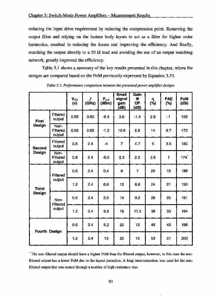
Chapter 5: Switch-Mode Power Amplifiers- Measurement Results
reducing the input drive requirement by reducing the compression point. Removing the
output filter and relying on the human body layers to act as a filter for higher order
harmonics, resulted in reducing the losses and improving the efficiency. And fmally,
matching the output directly to a 50 Q load and avoiding the use of an output matching
network, greatly improved the efficiency.
Table 5.1 shows a summary of the key results presented in this chapter, where the
designs are compared based on the FoM previously expressed by Equation 3.33.
Table 5.1: Peiformance comparison between the presented power amplifier designs
Small Gain Vee f Pout signal @ 11 PAE FoM (v) (GHz) (dBm) gain CP (%) {%) {dB)
{dB) {dB)
Filtered 0.65 0.65 -8.4 3.6 -1.4 2.6 -1 159 First output
Design Non-Filtered 0.65 0.65 -1.2 10.6 5.8 14 9.7 173 output
Filtered 0.8 2.4 -4 7 4.7 5 3.5 180 Second output
Design Non- . Filtered 0.8 2.4 -6.5 2.3 2.2 2.6 1 174 output
0.6 2.4 0.4 9 7 20 16 188 Filtered output
1.2 2.4 6.8 12 8.6 24 21 190 Third
Design
Non-0.6 2.4 2.5 14 9.2 28 25 191
Filtered output
1.2 2.4 9.5 16 11.2 36 33 194
0.6 2.4 5.2 20 12 46 43 196
Fourth Design
1.2 2.4 13 22 15 53 51 200
• The non-filtered output should have a higher FoM than the filtered output, however, in this case the non
filtered output has a lower FoM due to the layout parasitics. A long interconnection was used for the non
filtered output that was routed through a number of high resistance vias.
91
M.A.Sc. Thesis - M. M. El-Desouki McMaster- Electrical and Computer Engineering
Chapter 6
LOCK-MODE POWER AMPLIFIERS-
MEASUREMENT RESULTS
This chapter describes the design, simulation and measurement results of the two
implemented lock-mode power amplifier circuits. All designs were fabricated and fully
integrated in a standard mixed-signal CMOS 0.18 fllTI technology with 6 metal layers,
with a 2 fllTI thick top-metal layer, provided by Taiwan Semiconductor Manufacturing
Company (TSMC) through the Canadian Microelectronics Corporation (CMC). The two
designs share a very similar architecture; however, each design was optimized to operate
at a different frequency, to be able to test the effectiveness of the novel approach
proposed. The first design was optimized to operate at frequencies ranging between 400-
440 MHz, aiming for the 405 MHz MICS band, and the 433 MHz ISM band and the
second design was optimized to operate at 2.4 GHz targeting the 2.4 GHz ISM band.
Section 6.1 presents the designed 400 MHz lock-mode power amplifier circuit,
where the schematic simulation results are shown, then some layout considerations and
techniques are discussed and fmally, the measurement results are presented. Section 6.2
presents the designed 2.4 GHz lock-mode power amplifier circuit. Finally, Section 6.3
presents the chapter's summary and compares the two designs presented in this chapter
based on the FoM proposed in Chapter 3.
Chapter 3 explained why power amplifiers targeting low output power
applications have reasonably lower efficiencies than higher output power designs when
fully-integrated, due to the need for larger inductors that have very low quality factors.
The efficiency drops even further for low frequency operation, again due to the need for
larger inductors. The large inductors required for such low-power designs not only
92
Chapter 6: Lock-Mode Power Amplifiers- Measurement Results
impact efficiency due to high losses, but also impact the total chip area. Differential
designs require more of these large lossy on-chip inductors and suffer more both in
efficiency and total area [57].
Traditional power amplifier designs for low-power applications use current-mode
amplifiers [2, 52], such as class-A or class-AB to avoid output filters that degrade the
efficiency, as previously mentioned. Current-mode power amplifiers are also favored for
their higher linearity. Using switch-mode power amplifiers can achieve higher efficiency
values, but on-chip filtering again requires the use of very high-Q inductors, which are
not available in standard CMOS technology, especially at the relatively low frequencies
of a few hundreds of megahertz [53-56]. In this chapter, a fully-integrated differential
superharmonic injection-locked frequency divider {ll.-FD) is proposed to operate as a
lock-mode power amplifier for low-power, short-range applications. ILFDs are based on
injection-locked oscillators (ILOs), which are free running oscillators that can lock to the
phase and frequency of an injected signal [61]. To the author's knowledge, this work [56]
represents the first use of a superharmonic injection-locked oscillator as a power
amplifier circuit. The main advantage of the proposed approach is that it can achieve a
very high power gain from a single stage that is very efficient in terms of silicon die area.
Figure 6.1 shows the basic schematic of the proposed lock-mode power amplifier
[57]. The architecture itself has been previously explained in chapter 4, where it was
presented as a direct-modulation transmitter. In Figure 6.1, this topology is used as a
normal differential power amplifier stage, meaning that the transmitter system will still
require all the stages that are prior to a power amplifier.
In this design the incident frequency is divided by two. It could be argued that this
presents an obstacle to practical application since it requires doubling the operating
frequency of the previous RF stages. However, since the input power required to achieve
mode-locking is very small, as will be shown in the following sections, the input drive is
greatly reduced compared to a traditional power amplifier. This allows a doubling of the
operating frequency of the previous stage without increasing the power consumption in
that stage. Increasing the operating frequency from 433 MHz to 866 MHz, or from 2.4
GHz to 4.8 GHz, also leads to smaller chip area and higher inductor quality factors for
the previous RF stages [57].
93
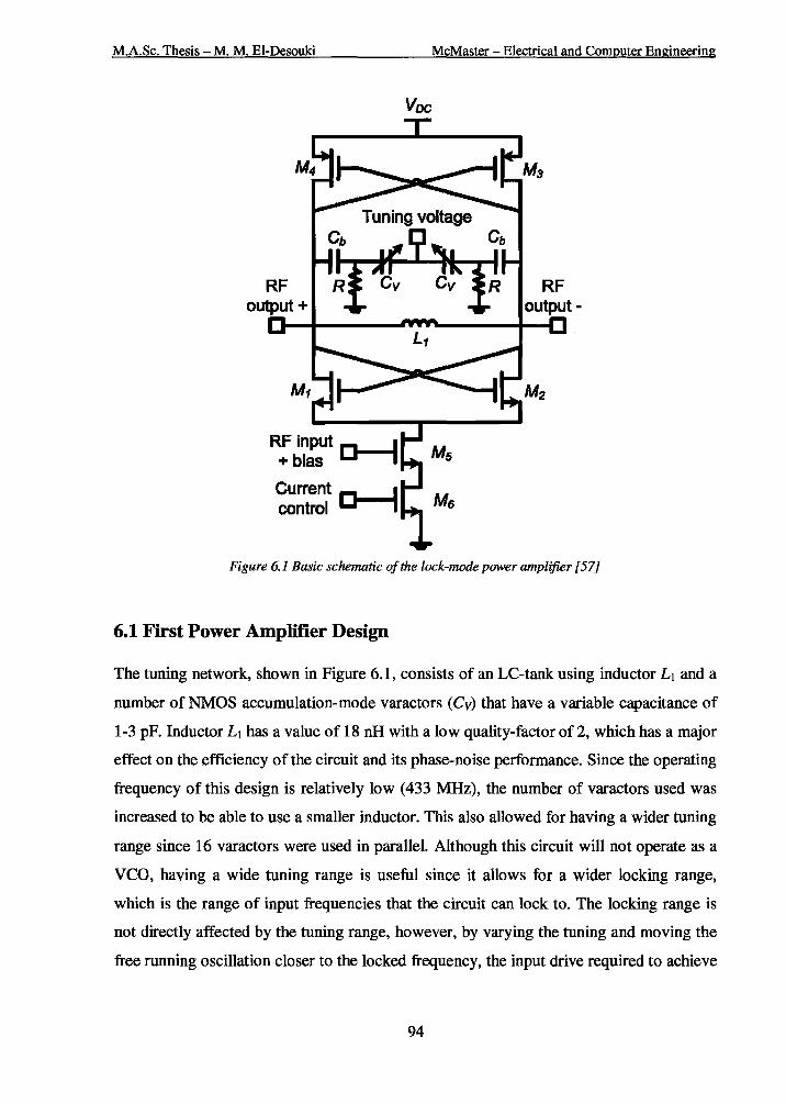
M.A.Sc. Thesis- M. M. El-Desouki
RF
RF input ~"'"~...._____ +bias~
Current ,..,_____J control .......---,
McMaster -Electrical and Computer Engineering
Voc
RF
Figure 6.1 Basic schematic of the lock-mode power amplifier [57]
6.1 First Power Amplifier Design
The tuning network, shown in Figure 6.1, consists of an LC-tank using inductor L1 and a
number of NMOS accumulation-mode varactors (Cv) that have a variable capacitance of
1-3 pF. Inductor L 1 has a value of 18 nH with a low quality-factor of 2, which has a major
effect on the efficiency of the circuit and its phase-noise performance. Since the operating
frequency of this design is relatively low (433 MHz), the number of varactors used was
increased to be able to use a smaller inductor. This also allowed for having a wider tuning
range since 16 varactors were used in parallel. Although this circuit will not operate as a
VCO, having a wide tuning range is useful since it allows for a wider locking range,
which is the range of input frequencies that the circuit can lock to. The locking range is
not directly affected by the tuning range, however, by varying the tuning and moving the
free running oscillation closer to the locked frequency, the input drive required to achieve
94

Chapter 6: Lock-Mode Power Amplifiers- Measurement Results
locking is reduced, which will increase the gain. In order to reduce the input power
required to achieve mode-locking, the circuit should be tuned as close as possible to half
the frequency of the incident signal, since it will require a larger drive to lock or pull the
output frequency when it is further away.
Capacitors Cb act as DC-blocking capacitors with a value of 12 pF each and
resistors R, each of 50 k.Q, provide a DC ground for biasing of the varactors. Each of the
RF outputs goes to the 50 Q load of the measurement equipment directly without a
buffer, which will be replaced by the differential transmission antenna in the final system.
Transistors M1-M4 form the cross-coupled negative-gm differential pair. The NMOS
devices have a total width of 200 J.lm using 80 fmgers and a length of 0.18 J.lm, while the
PMOS devices have double the number of fingers to compensate for their lower mobility.
The sizes of these transistors are chosen based on a trade-off between the required output
power, operating frequency and achievable efficiency. This design was optimized for an
operating frequency of 433 MHz and a differential output load of 100 n. Transistor M5
has a total width of 250 J.lm using 100 fmgers and a length of 0.18 J.lm. It is used as a
transconductance amplifier, with the output current following the input voltage signal. It
acts as the input stage where the locking signal is applied. The biasing of transistor M5 is
chosen to optimize the P AE since it has an affect on both the power gain and the drain
efficiency. Transistor M 6 acts as a current source that can be controlled in order to vary
the transmitted power. This is a long channel device that has a total width of 1.25 mm
using 500 fingers and a length of 1 J.lm.
6.1.1 Schematic Simulation Results
The schematic simulations for this section were carried out using the Cadence 2003
package, where the Virtuoso Schematic Editing tool was used for schematic entry and the
Cadence SpectreRF tool was used as the circuit simulator.
Figure 6.2 shows the simulation setup of the 400 MHz design. The blocking
capacitors Cb and the blocking inductor Lb are ideal components that are not part of the
circuit. Figure 6.3 shows the simulated output frequency of the 400 MHz design as a
function of the input frequency for various input drives at a supply voltage of 1.5 V. The
output power was not shown on the figure since it is roughly constant at 8 dBm. The
95

M.A.Sc. Thesis - M. M. El-Desouki McMaster -Electrical and Computer Engineering
circuit is defined to be locked when the output frequency is exactly half the input
frequency. At an input power of 0 dBm, the figure shows that the power amplifier is
locked to the input signal for a range from 690 MHz to 940 MHz, which corresponds to a
locking range of 125 MHz or 31 %. The high locking range is due to using a large input
drive of 0 dBm, where the figure shows that the locking range decreases linearly with the
input power. The points below 670 MHz and higher than 980 MHz are when the
amplifier is not locked, which shows that their equivalent output frequency is not related
to the input frequency. The drain efficiency is also shown in Figure 6.3. The drain
efficiency peaks when the input frequency is close to double the free-running frequency.
In this case; the circuit was tuned to be as close as possible to 433 MHz, which explains
the increase in efficiency at that point.
160x2.5J,J /0.18J,J
17.7 nH
Current
~ !Vcs Figure 6.2 Schematic of designed 400 MHz lock-mode power amplifier simulation setup
96

Chapter 6: Lock-Mode Power Amplifiers- Measurement Results
SOOP--------------------------.60 -o- Prn=+10 dBm
'N475 -•-Ptn=OdBm ~
450 -&- Prn=-5 dBm __._ Ptn=-1 0 dBm
g425 ~ i400 ~
LL 'S 375 Q. 8350
325
600 700 800 900 1000 Input Frequency (MHz)
50 0 m
40 s· ~
30 i· :;::,
20 ~ -'#. 10 -
Figure 6.3 Simulated output frequency of the 400 MHz design as a function of the input frequency, at a
supply of 1.5 V and input drives of -10 dBm, -5 dBm, 0 dBm and+ 10 dBm. The locking range is shown to
increase linearly with the input power up to 0 dBm, after which, it begins to saturate. The figure also shows
the drain efficiency for an input drive of 0 dBm
Figure 6.4 shows the simulated output power, drain efficiency and P AE of the 400
MHz design as a function of the input power for an input frequency of 800 MHz, an
output frequency of 400 MHz and a supply voltage of 1.5 V. The PAE overlaps with the
drain efficiency at small input power levels since the gain is very high, after which, the
P AE beings to drop as the gain decreases. As the input power increases to the large signal
operation region, the input stage moves from being a transconductance stage to operating
as a switch, which slightly increases the efficiency with less output power capabilities.
-15 -10 -5 0 5 Input Power {dBm)
Figure 6.4 Simulated output power, drain efficiency and PAE of the 400 MHz design as a junction of the
input power, at a supply voltage of 1.5 Vand an input frequency of BOO MHz
97

M.A.Sc. Thesis- M. M. El-Desouki McMaster- Electrical and Computer Engineering
6.1.2 Layout
The layout design was done using the Virtuoso Layout Editor tool available in the
Cadence 2003 package. Figure 6.5 shows a screen capture of the 400 MHz power
amplifier layout. The amplifier occupies an area of 0.9 mm2, which is very small for a
fully-integrated design at this frequency. In comparison, the design in [36] occupies an
area of 0.9 mm2 but requires three off-chip capacitors and one 26 nH off-chip inductor.
Figure 6.5 Screen capture of the 400 MHz power amplifier layout
Figure 6.6 shows a screen capture of the varactor layout. Since the varactor used
is an NMOS accumulation-mode varactor, it is laid out in anN-well with the source and
drain shorted acting as one terminal, and the gate being the second terminal. The NMOS
varactor uses 150 parallel transistors, each with a length and width of 0.5 ).lm and 2 ).lm
respectively. The stacked transistors in this design, which have a source that is not
connected to ground, were laid out in a deep-n-well layer to isolate the substrate of the
transistor. In this way, the body can be shorted to the source of the transistor, following
the RF model provided by the foundry.
Source/ Drain Gate
Figure 6.6 Screen capture of NMOS accumulation-mode varactor layout
98

Chapter 6: Lock-Mode Power Amplifiers- Measurement Results
6.1.3 Measurement Results
Figure 6.7 shows a photomicrograph of the fabricated circuit that occupies an area of 0.9
mm2 including the pads [51, 57] . Obviously the inductor is the most area consuming
component on the layout, which makes this design attractive since it depends on only one
inductor.
Figure 6.7 Photomicrograph of the fabricated 400 MHz power amplifier [51 , 57]
The chip was probed on-wafer using a ground-signal-ground configuration for the
RF signals and a single pad for DC connections. The layout considerations mentioned in
the previous chapter were adopted in this design. Measurements were performed by
connecting one side of the differential output to the instrument and dummy-loading the
other side with a 50 Q load. An HP-4145B semiconductor parameter analyzer was used
to provide the biasing and to measure the DC power. The output signal was measured
using an Agilent-E4440A spectrum analyzer and the input was provided by an Anritsu
MG394A signal generator. Figure 6.8 shows a sketch of the measurement setup.
Figure 6.9 shows the measured output power, drain efficiency and P AE of the 400
MHz design as a function of the input power [57]. The sweep was done over the range
where the power amplifier is locked and the output frequency is exactly half the incident
frequency. The circuit has a very high small signal-gain of 30 dB from only one stage.
However, the circuit reaches its gain compression point very fast due to the stacked
nature of the topology used. Such a topology is considered a non-linear power amplifier
design and should only be used with constant envelope modulation schemes, unless a
linearity improvement technique is used. The figure shows a similar behavior to the
simulation results shown in Figure 6.4; however the efficiency dropped considerably,
although the output power is relatively similar. This can be explained due to the over
99
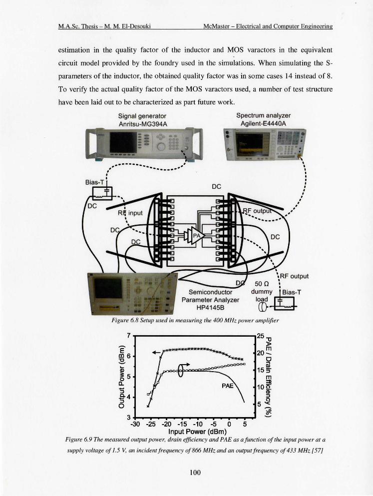
M.A.Sc. Thesis- M. M. El-Desouki McMaster- Electrical and Computer Engineering
estimation in the quality factor of the inductor and MOS varactors in the equivalent
circuit model provided by the foundry used in the simulations. When simulating the S
parameters of the inductor, the obtained quality factor was in some cases 14 instead of 8.
To verify the actual quality factor of the MOS varactors used, a number of test structure
have been laid out to be characterized as part future work.
Bias-T
Signal generator Anritsu-MG394A
Spectrum analyzer Agilent-E4440A ""=""" _ _ ...__
#--------- , ~ ---------·# ' ' I
I I • I
DC
##
son I
• I
• • I I
I I , , ,
Semiconductor Parameter Analyzer
HP41458
dummyl+:r load (I}
Figure 6.8 Setup used in measuring the 400 MHz power amplifier
7~----------------------~25~
'E al6 '0 -.... Q)
~5 a.. -:::J
.9-4 :::J 0
3+-~--~~~-r--~~--~~ -30 -25 -20 -15 -10 -5 0 5
Input Power (dBm)
)> m
20-0 iiJ
15 :r m
10~ cs· ::::J
5~ ~ -
Figure 6.9 The measured output power, drain efficiency and PAE as a function of the input power at a
supply voltage of 1.5 V, an incident frequency of 866 MHz and an output frequency of 433 MHz [57]
100

Chapter 6: Lock-Mode Power Amplifiers- Measurement Results
Figure 6.10 shows the measured output power and drain efficiency as a function
of the supply voltage. The sweep was done for an input power of -2 dBm however; the
trend is the same for lower input power levels that satisfy locking. The drain efficiency is
a weak function of the supply voltage since the amplifier is delivering its maximum
output power. However, the output power is a strong function of the supply voltage since
transistor M6 was biased with a gate voltage of 1.5 V, which drives the circuit into the
voltage limited regime, as shown in Figure 6.11. In the current limited region, for gate
bias voltages below 1 V, the output power is limited by the tail current source. This can
help stabilize the output power against fluctuations in the supply voltage in the case of
battery operated devices, for example. The efficiency is lower in the current limited
region since the amplifier is not delivering its maximum output power.
14 20
- 18 0 E 12 ~I a:l I I 16 iiJ :E.1o
...,.. I ::I ....
14 ~ ; 8 ~ 12 i
i: ::I 10~ -8 '#. 0 2 -
0 6
1.3 1.5 1.7 1.9 2.1 Supply Voltage M
Figure 6.10 The measured output power and drain efficiency as a function of the supply voltage at an input
power of -2 dBm, an incident frequency of 866 MHz and an output frequency of 433 MHz [57]
89-----------------------~20 ;[7 :&a .... CD
~ 5 0.. :; 4
!a 0
2
Voltage limited region
~8 1~ 12 1A 1~ 1~ Tail Current Source Bias (V)
-14 '#. -Figure 6.11 The measured output power and drain efficiency as a function of the tail current source bias
(transistor M6 in Figure 6.1) at a supply voltage of 1.5 V, an input power of -2 dBm, an incident frequency
of 866 MHz and an output frequency of 433 MHz [57]
101

M.A.Sc. Thesis - M. M. El-Desouki McMaster -Electrical and Computer Engineering
Figure 6.12 shows the measured drain efficiency and output frequency of the 400
MHz design as a function of the incident frequency [57]. The figure shows a locking
range of 200 MHz for the output signal and a peak drain efficiency of 16 %. The points
below an input frequency of 600 MHz and above 1020 MHz are where the power
amplifier loses track and is no longer locked to the input. An input power of -2 dBm was
used in Figure 6.12, even though this is not the point of peak PAE, however, the figure
shows how the tracking range can be extended with a higher input drive. In a practical
system, the circuit should be tuned as close as possible to the expected frequency of
operation to allow for high gain, as previously shown in Figure 6.9. In this case, a high
tuning range is not needed since the only change in the input frequency will be due to the
modulation scheme used, which is a very small change [57].
30~----------------------~
600 700 800 900 1000 Input Frequency (MHz)
Figure 6.12 The measured output power and drain efficiency as a function of the input frequency at a
supply voltage of 1.5 V and an input power of -2 dBm [57]
Figure 6.13 shows the real tuning range of the circuit in free-running mode, where
during the sweep of one bias voltage, the other two were kept constant at 1.5 V, except
for the tuning voltage, which was kept constant at 0.5 V [57]. No RF input was applied
and transistor M5 was biased in the triode region with a gate voltage of 1.5 V. The
voltages were swept over the ranges for which the circuit oscillates. The output frequency
is a strong function of the tail current source bias in the current limited regime; however,
it is hardly affected by the tail current bias in the voltage limited regime. The supply
voltage was kept constant at 1.5 V as the tail current bias was varied. In the case of the
supply voltage sweep, the tail current bias was kept constant at a value of 1.5 V to keep
102

Chapter 6: Lock-Mode Power Amplifiers- Measurement Results
the circuit operating in the voltage limited regime to able to see the effect of varying the
supply voltage, since its effect on the oscillation frequency is negligible in the current
limited regime. The figure shows that the output frequency is mostly affected by the
tuning voltage, which gives a tuning range of 17 % [57].
'N440 :I:
~420 (')' 55400 ::a
~380 LL -~360 0 340
0.0 0.5 1.0 1.5 2.0 Voltage (V)
Figure 6.13 The measured output frequency of the free running amplifier design as afunction of the supply
voltage, tuning voltage and tail current source bias [57]
Figure 6.14 shows the measured output spectrum of the 400 MHz design, taken
from a single-ended output, for the free-running mode and the locked mode with an input
signal of -10 dBm and 866 MHz [57]. Even though the harmonics are lower for the
locked operation mode, an output filter may be needed to filter out the third order
harmonic. However, no filter was implemented in this design since the filtering will be
done by the high frequency attenuation of the human body layers, as mentioned in the
previous chapter.
20.-------------------------
e rg 0 -._ Cl)
~20 a..·
~ :;-40 0
-60
------Locked (Pm=-10 dBm)
----- Free running
0~ 1~ 1~ 2~ Frequency (GHz)
Figure 6.14 The measured output spectrum taken from a single-ended output after loss compensation, at a
supply voltage of 1.5 V for both the free running mode and the locked mode with an input power of -10
dBm[57]
103
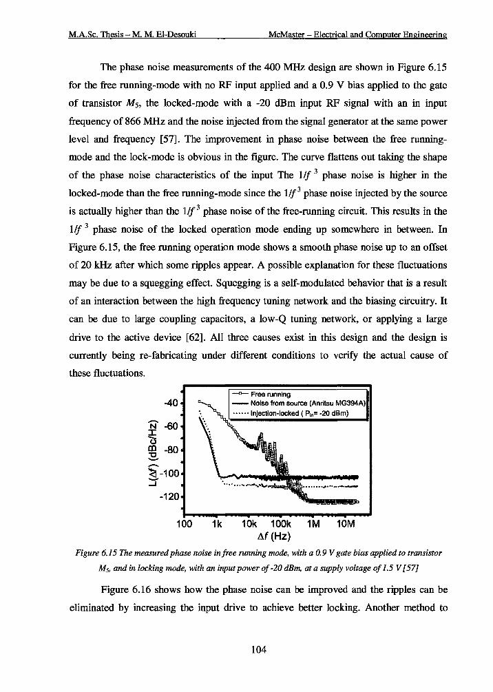
M.A.Sc. Thesis - M. M. El-Desouki McMaster- Electrical and Computer Engineering
The phase noise measurements of the 400 MHz design are shown in Figure 6.15
for the free running-mode with no RF input applied and a 0.9 V bias applied to the gate
of transistor Ms, the locked-mode with a -20 dBm input RF signal with an in input
frequency of 866 MHz and the noise injected from the signal generator at the same power
level and frequency [57]. The improvement in phase noise between the free running
mode and the lock-mode is obvious in the figure. The curve flattens out taking the shape
of the phase noise characteristics of the input The 1/f 3 phase noise is higher in the
locked-mode than the free running-mode since the 1/f3 phase noise injected by the source
is actually higher than the 1/f 3 phase noise of the free-running circuit. This results in the
1/f 3 phase noise of the locked operation mode ending up somewhere in between. In
Figure 6.15, the free running operation mode shows a smooth phase noise up to an offset
of 20 kHz after which some ripples appear. A possible explanation for these fluctuations
may be due to a squegging effect. Squegging is a self-modulated behavior that is a result
of an interaction between the high frequency tuning network and the biasing circuitry. It
can be due to large coupling capacitors, a low-Q tuning network, or applying a large
drive to the active device [62]. All three causes exist in this design and the design is
currently being re-fabricating under different conditions to verify the actual cause of
these fluctuations.
-40
'N -60 J: 0 m -80 "0 --~ -100 -.....J
-120
100 1k 10k 100k 1M 10M tJ.f (Hz)
Figure 6.15 The measured phase noise in free running mode, with a 0.9 V gate bias applied to transistor
M5, and in locking mode, with an input power of -20 dBm, at a supply voltage of 1.5 V [57]
Figure 6.16 shows how the phase noise can be improved and the ripples can be
eliminated by increasing the input drive to achieve better locking. Another method to
104

Chapter 6: Lock-Mode Power Amplifiers- Measurement Results
improve the phase noise of the circuit is by properly choosing the gate biasing of
transistor Ms not only to achieve peak P AE, but also to meet the specific phase noise
requirements. Figure 6.17 shows the effect of the gate biasing of transistor M5 on the
phase noise performance of the circuit in the free-running mode [57]. These effects are
discussed in more detail in Chapter 7 [51], where it will be shown that the phase noise is
low when the circuit is well defmed to be operating in the current limited mode or in the
voltage limited mode. At some point in between, the circuit is going through a transition
from one mode to the other at which both modes can be competing, causing an increase
in phase noise. An important point to note from this figure is that such bias points should
be avoided to improve the phase noise performance of the circuit and it is not enough to
aim for peak P AE when choosing the gate bias of the input stage. This effect is also
observed on the tail current source, which should either be biased in weak inversion or
biased with a high gate voltage, such that the device enters the triode mode to avoid
transitional bias points [57].
-40 -Pin= -40 dBm
- -60 N -Pin= -20 dBm
:::c ~ -80 "C -~-100 ........ -'
-120
100 1k 10k 100k 1M 10M Af (Hz)
Figure 6.16 The measured phase noise in the locking-mode, with an input power of -20 dBm and an input
power of -40 dBm, at a supply voltage of 1.5 V [57]
105

M.A.Sc. Thesis- M. M. El-Desouki
-40
-N -60 J:
0 Ill "0 -80 --':a :::r -100
-120
1k 10k
McMaster- Electrical and Computer Engineering
x xx Gate blas=O. 75V Gate bias=O. 80V
o a o Gate bias= 1. 5V
100k 1M 10M Af (Hz)
Figure 6.17 The measured phase noise in free-running mode with no RF input applied, for various gate
bias voltages applied to transistor Ms. at a supply voltage of 1.5 V [57]
6.2 Second Power Amplifier Design
The 2.4 GHz design has the same architecture of Figure 6.1; however only two varactors
were used. Inductor Lt in this design has a value of 2.3 nH with a quality-factor of 8. In
transistors M1-M4, the NMOS devices have a total width of 175 J.tm using 70 fingers and a
length of 0.18 J.tm, while the PMOS devices have double the number of fmgers.
Transistors M5 and M6 have the same aspect ratios of the 400 MHz design.
6.2.1 Schematic Simulation Results
This design uses the same simulation setup previously shown in Figure 6.2. Figure 6.18
shows the simulated drain efficiency and output frequency of the 2.4 GHz design as a
function of the incident frequency. The output power was not shown on the figure since it
is roughly constant in the range of 6.5 dBm to 7.5 dBm. The figure shows that the power
amplifier is locked to the input signal for a range from 4.1 GHz to 4.9 GHz, which
corresponds to an output locking range of 400 MHz or 16 %. The circuit was tuned to be
as close as possible to 2.4 GHz, which explains the increase in efficiency at that point.
106

Chapter 6: Lock-Mode Power Amplifiers- Measurement Results
-~50 -
4.0 4.2 4.4 4.6 4.8 5.0 5.2 Input Frequency (GHz)
Figure 6.18 Simulated drain efficiency and output frequency of the 2.4 GHz design as a function of the
incident frequency, at a supply voltage of 1.5 V and an input drive ofO dBm
6.2.2 Layout
Figure 6.19 shows a screen capture of the 2.4 GHz power amplifier layout. The amplifier
occupies an area of0.6 mm2.
Figure 6.19 Screen capture of the 2.4 GHz power amplifier layout
6.2.3 Measurement Results
Figure 6.20 shows a photomicrograph of the fabricated circuit that occupies an area of 0.6
mm2 including the pads [51, 57].
107

M.A.Sc. Thesis- M. M. EI-Desouki McMaster- Electrical and Computer Engineering
Figure 6.20 Photomicrograph of the fabricated 2.4 GHz power amplifier [51 , 57]
Figure 6.21 shows the measured output power, drain efficiency and P AE of the
2.4 GHz design as a function of the input power [57]. The sweep was done over the range
where the power amplifier is locked and the output frequency is exactly half the incident
frequency. The circuit has a very high small-signal gain of31.3 dB from only stage and it
reaches its gain compression point immediately, unlike the 400 MHz design. Again, this
circuit is considered a non-linear PA design and should only be used with constant
envelope modulation schemes. However, unlike other non-linear power amplifiers such
as class-E, the required input drive is very low, which allows the circuit to achieve very
high gain from a very small die area.
10~------------------------~ 35 "'0 >
30m -25 ~
:;-20m
:I;
15 ~-::J
10~ -56r---r--~--~--~--~--~
';:{~!. 5~
-25 -20 -15 -10 -5 0 5 Input Power (dBm)
Figure 6.21 The measured output power, drain efficiency and PAE as a function of the input power at a
supply voltage of 1.5 V, an incident frequency of4.8 GHz and an output frequency of2.4 GHz [57]
108
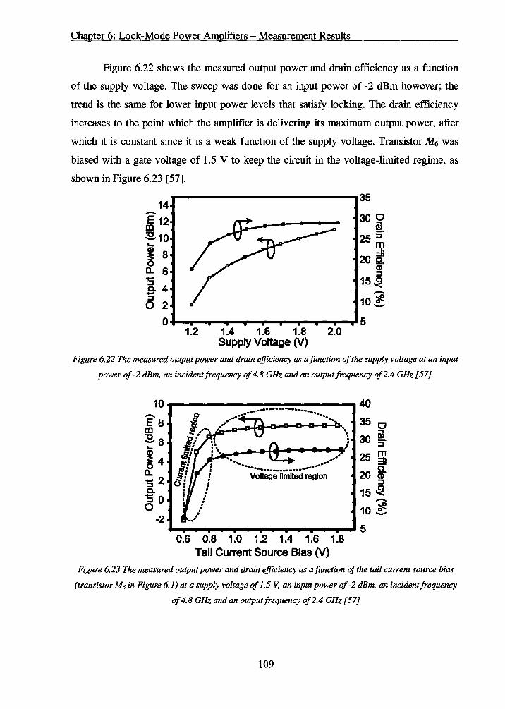
Chapter 6: Lock-Mode Power Amplifiers- Measurement Results
Figure 6.22 shows the measured output power and drain efficiency as a function
of the supply voltage. The sweep was done for an input power of -2 dBm however; the
trend is the same for lower input power levels that satisfy locking. The drain efficiency
increases to the point which the amplifier is delivering its maximum output power, after
which it is constant since it is a weak function of the supply voltage. Transistor M6 was
biased with a gate voltage of 1.5 V to keep the circuit in the voltage-limited regime, as
shown in Figure 6.23 [57].
14 p-----------------------~35
1.2 1.4 1.6 1.8 Supply Voltage (V)
2.0
-10 ~ -Figure 6.22 The measured output power and drain efficiency as a function of the supply voltage at an input
power of -2 dBm, an incident frequency of4.8 GHz and an output frequency of2.4 GHz [57]
-E 8 a:! :Sa ~ ~4 ll. -g2 c. ao
-2
.. .. ..-·· ............................. Voltage limited region
0.6 0.8 1.0 1.2 1.4 1.6 1.8 Tail Current Source Bias (V)
Figure 6.23 The measured output power and drain efficiency as a function of the tail current source bias
(transistor M6 in Figure 6.1) at a supply voltage of 1.5 V, an input power of-2 dBm, an incident frequency
of4.8 GHz and an output frequency of2.4 GHz [57]
109

M.A.Sc. Thesis - M. M. El-Desouki McMaster- Electrical and Computer Engineering
Figure 6.24 shows the measured drain efficiency and output frequency of the 2.4
GHz design as a function of the incident frequency [57]. The figure shows a locking
range of 178 MHz for the output signal and a peak drain efficiency of 27 %. The
efficiency is higher due to the increase in the Q-factor of the LC tank. The free-running
tuning range of the circuit is shown in Figure 6.25 [51, 57], where during the sweep of
one bias voltage; the other two were kept constant at 1.5 V, except for the tuning voltage,
which was kept constant at 0.5 V. No RF input was applied and transistor M5 was biased
with 1.5 V. Figure 6.25 shows that the output frequency is mostly affected by the tuning
voltage, which gives a tuning range of9 %.
35~--------------------~ - 2.55~ ~~ e - c ~~ 2~~ ~ ; ~~ 2M~ m g r::: 15 2.40~ ~ -C10 Q
2.35~ 5+--9--.--.--~-P~~~~--.-~ ~
4.7 4.8 4.9 5.0 5.1 Input Frequency (GHz)
Figure 6. 24 The measured output power and drain efficiency as a function of the input frequency at a
supply voltage of 1.5 V and an input power of -2 dBm [57]
2.55 ..... -------------.
....._Supply voltage -c-Tuning voltage __._Tall current source bias
Figure 6.25 The measured output frequency of the free-running amplifier as a function of the supply
voltage, tuning voltage and tail current source bias [51, 57]
110

Chapter 6: Lock-Mode Power Amplifiers- Measurement Results
Figure 6.26 shows the measured output spectrum of the 2.4 GHz design for the
free-running mode and the locked-mode with an input signal of -10 dBm and 4.8 GHz
[57]. Even though the output was not measured differentially and no output filter was
used, the higher order harmonics are more than 27 dB below the fundamental.
20
- ~Locked (Ptn=-10 dBm) E - Free running CD 0 "'C -.... CD
~ 0.. -20 ..... ::::J .e-c5 -40
2 4 6 8 10 12 14 Frequency (GHz)
Figure 6.26 The measured output spectrum taken from a single-ended output after loss compensation, at a
supply voltage of 1.5 Vfor both the free-running mode and the locked-mode with an input power of -10
dBm[57]
The phase noise measurements of the 2.4 GHz design are shown in Figure 6.27
[57]. The figure shows the phase noise of the free-running mode with no RF input applied
and a 0.9 V bias applied to the gate of transistor M5 compared to the locked-mode with a
-10 dBm input RF signal with an in input frequency of 4.8 GHz. The figure also shows
the noise injected from the signal generator at the same power level and frequency. The
injection-locking improves the phase noise performance of the circuit making it suitable
to be used as an output stage. The same gate biasing effects of transistor M5, previously
shown in Figure 6.17, were also observed in this design and will be further explained in
Chapter 7 [51].
111

M.A.Sc. Thesis- M. M. El-Desouki McMaster- Electrical and Computer Engineering
-40
-~ -60
-Free running •........ -Injection-locked ( P~n= -10 dBm)
•••• ---Noise from source Anritsu MG394A
~~--------------~--~ \ ... 0 fg -80 --~ -100 -...J
-120
100 1k 10k 100k 1M 10M !J.f (Hz)
Figure 6.27 The measured phase noise in free-running mode, with a 0.9 V gate bias applied to transistor
M5, and in locking mode with an input power of -10 dBm, at a supply voltage of 1.5 V [57]
6.3 Comparison and Summary
This chapter presented the simulation and measurement results of a novel lock-mode
power amplifier design. Two circuits, sharing a common topology that uses a cross
coupled negative-gm voltage-controlled oscillator, were discussed.
The work presented in this chapter tested the feasibility of using a superharmonic
injection-locked oscillator as a power amplifier [57]. This topology allows for on-chip
integration in a very small area while maintaining good performance and providing very
high power gain (30 dB) from a single stage. The two designed circuits were tested in a
standard CMOS 0.18 J.Lm process targeting the 2.4 GHz ISM band, the 433 MHz ISM
band and the 405 MHz MICS band. The phase noise characteristics of the two designs
were also presented and some recommendations were given to reduce the phase noise.
This work contributes considerably to the reduction of transmitter die area
targeting more compact, miniscule designs that are suitable for emerging low-power
applications such as wireless body area networks and biomedical implantable electronic
circuits. Table 6.1 shows a summary of the key results presented in this chapter, where
the designs are compared based on the FoM previously expressed by Equation 3.33.
112
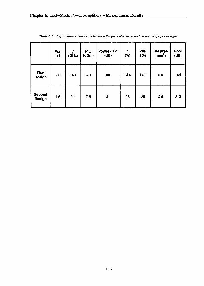
Chapter 6: Lock-Mode Power Amplifiers- Measurement Results
Table 6.1: Performance comparison between the presented lock-mode power amplifier designs
Voc f Pout Power gain 11 PAE Die area FoM (v) (GHz) (dBm) (dB) (%) (%) (mm2
) (dB)
First 1.5 0.433 6.3 30 14.5 14.5 0.9 194 Design
Second 1.5 2.4 7.6 31 25 25 0.6 213 Design
113

M.A.Sc. Thesis - M. M. El-Desouki McMaster - Electrical and Computer Engineering
Chapter 7
DIRECT-MODULATION TRANSMITTERS-
MEASUREMENT RESULTS
This chapter describes the design, simulation and measurement results of the two direct
modulation transmitter circuits implemented. All designs were fabricated and fully
integrated in a standard mixed-signal CMOS 0.18 J.LII1 technology with 6 metal layers,
with a 2 !J.m thick top-metal layer, provided by Taiwan Semiconductor Manufacturing
Company (TSMC) through the Canadian Microelectronics Corporation (CMC). The two
designs share a very similar architecture; however, each design was optimized to operate
at a different frequency, to be able to test the transmitter proposed at multiple bands such
as the 405 MHz MICS band, the 433 MHz ISM band and the 2.4 GHz ISM band.
Section 7.1 presents the designed 400 MHz direct-modulation transmitter circuit,
where the schematic simulation setup is shown, followed by the measurement setup and
the measurement results. Section 7.2 presents the designed 2.4 GHz direct-modulation
transmitter circuit. Finally, Section 7.3 presents the chapter's summary and compares the
two designs presented in this chapter based on the FoM proposed in Chapter 4.
The two transmitters described in this chapter show the feasibility of using a
CMOS voltage-controlled power oscillator (VCPO) for fully-integrated single-block
direct-modulation with comparable performance to other technologies. The concept of
how a VCPO can be used as a single block transmitter was previously explained in
Chapter 4. The main drawback of the architectures shown in Figure 4.1 is the frequency
drift since the VCO or VCPO are used in open-loop. The architecture can be improved by
implementing a phase-locked loop (PLL), which will stabilize the frequency against any
drift that might occur with temperature variations, for example. This will be further
114

Chapter 7: Direct-Modulation Transmitters- Measurement Results
explained in Chapter 8 as future work. In implantable biomedical electronic systems,
using an open-loop architecture is feasible since the receiver is external and sufficiently
powered, so the complexity can be increased on the receiver side to track any change in
the transmitted signal [51].
Figure 7.1 shows the basic schematic of the proposed single stage direct
modulation transmitter, which was previously explained in chapter 4. There are two sets
ofMOS varactors shown in Figure 7.1, where each can be controlled separately. The first
control-voltage is used to tune the frequency of oscillation, which represents the carrier
frequency in this topology, while the second input is used for modulation by inputting the
digital baseband information directly to the MOS varactors. Having two separate inputs
can only be done if the frequency is low enough to allow for the number of MOS
varactors required, which is not always the case.
Since the main architecture of this topology is very similar to the topology
presented in Chapter 6, which was used as a mode-locking power amplifier; both ideas
can be tested on the same design by changing the simulation and measurement setup.
Overlapping two circuit ideas together usually involves some sort of compromise in their
performance to meet the requirements of both designs. This slightly degraded the
performance of the transmitter; however, the concept was proven. This chapter will focus
more on the measurement results, since the layout and schematic design were previously
shown in Chapter 6.
115
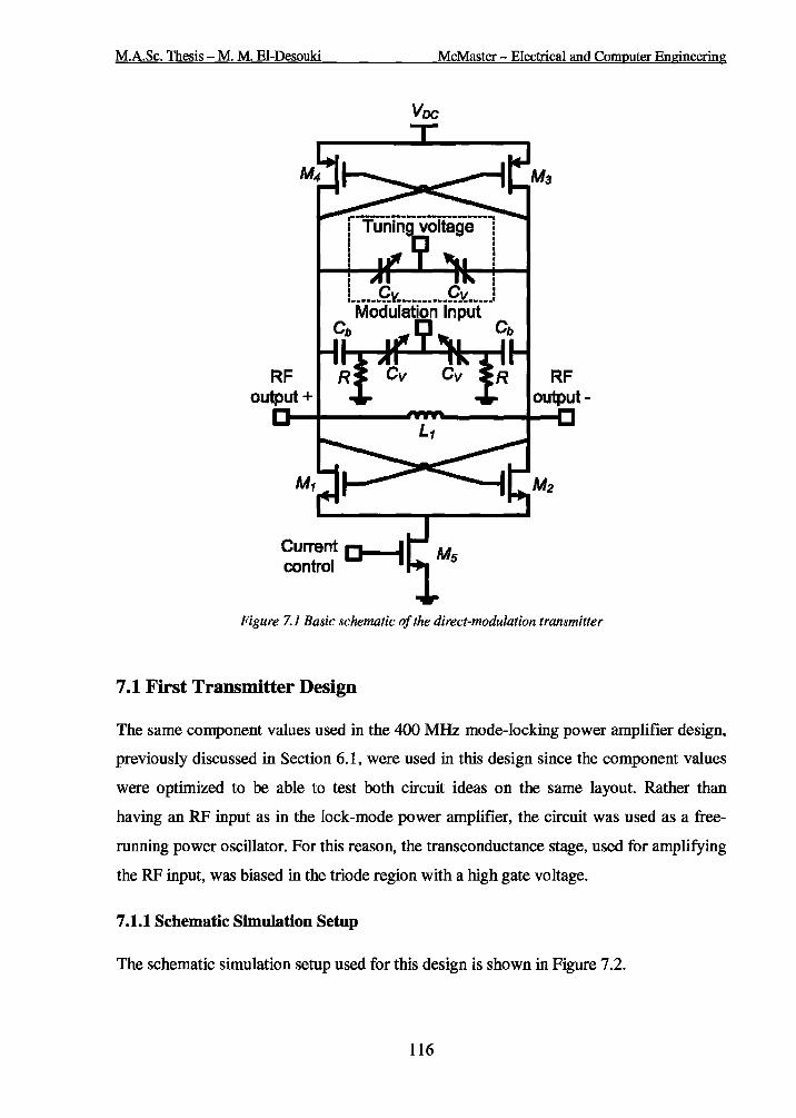
M.A.Sc. Thesis - M. M. El-Desouki McMaster - Electrical and Computer Engineering
Voc
.-------------------. 1 Tunin voltage i I : I :
I
RF
Figure 7.1 Basic schematic of the direct-modulation transmitter
7.1 First Transmitter Design
The same component values used in the 400 MHz mode-locking power amplifier design,
previously discussed in Section 6.1, were used in this design since the component values
were optimized to be able to test both circuit ideas on the same layout. Rather than
having an RF input as in the lock-mode power amplifier, the circuit was used as a free
running power oscillator. For this reason, the transconductance stage, used for amplifying
the RF input, was biased in the triode region with a high gate voltage.
7.1.1 Schematic Simulation Setup
The schematic simulation setup used for this design is shown in Figure 7.2.
116
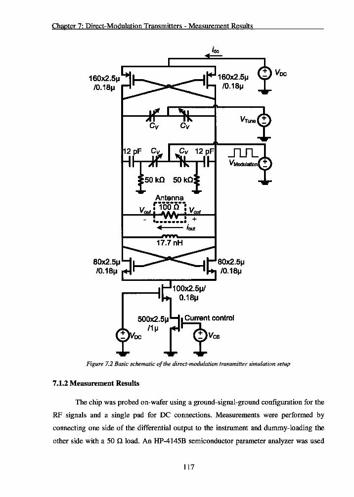
Chapter 7: Direct-Modulation Transmitters - Measurement Results
160x2.5J,I /0.18J,I
80x2.5J,I /0.18J,I
Cv Cv
Antenna r·------• 100 n : v.
17.7 nH
80x2.5J,I /0.18J,I
I Cu~t control
Vcs
Figure 7.2 Basic schematic of the direct-modulation transmitter simulation setup
7 .1.2 Measurement Results
The chip was probed on-wafer using a ground-signal-ground configuration for the
RF signals and a single pad for DC connections. Measurements were performed by
connecting one side of the differential output to the instrument and dummy-loading the
other side with a SO Q load. An HP-414SB semiconductor parameter analyzer was used
117
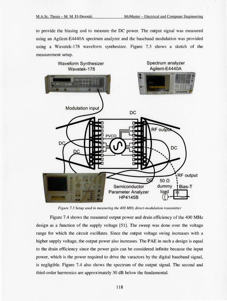
M.A.Sc. Thesis- M. M. EI-Desouki McMaster- Electrical and Computer Engineering
to provide the biasing and to measure the DC power. The output signal was measured
using an Agilent-E4440A spectrum analyzer and the baseband modulation was provided
using a Wavetek-178 waveform synthesizer. Figure 7.3 shows a sketch of the
measurement setup.
Waveform Synthesizer Wavetek-178
DC
l \ '
Spectrum analyzer Agilent-E4440A
~--........ --
~ ---' ltla
son •
Parameter Analyzer HP41458
dummyl!:r load (I}
Figure 7.3 Setup used in measuring the 400 MHz direct-modulation transmitter
Figure 7.4 shows the measured output power and drain efficiency of the 400 MHz
design as a function of the supply voltage [51]. The sweep was done over the voltage
range for which the circuit oscillates. Since the output voltage swing increases with a
higher supply voltage, the output power also increases. The P AE in such a design is equal
to the drain efficiency since the power gain can be considered infmite because the input
power, which is the power required to drive the varactors by the digital baseband signal,
is negligible. Figure 7.4 also shows the spectrum of the output signal. The second and
third-order harmonics are approximately 30 dB below the fundamental.
118
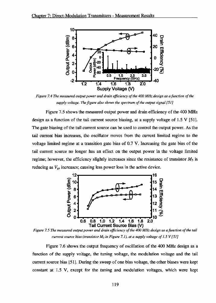
Chapter 7: Direct-Modulation Transmitters - Measurement Results
40 c DJ 5"
20m 31 0
0 CD" ::::J
~ -20~ -
Figure 7.4 The measured output power and drain efficiency of the 400 MHz design as a function of the
supply voltage. The figure also shows the spectrum of the output signal [51]
Figure 7.5 shows the measured output power and drain efficiency of the 400 MHz
design as a function of the tail current source biasing, at a supply voltage of 1.5 V [51].
The gate biasing of the tail current source can be used to control the output power. As the
tail current bias increases, the oscillator moves from the current limited regime to the
voltage limited regime at a transition gate bias of 0.7 V. Increasing the gate bias of the
tail current source no longer has an effect on the output power in the voltage limited
regime; however, the efficiency slightly increases since the resistance of transistor M5 is
reducing as Vgs increases; causing less power loss in the active device.
12~----------------------~16
0.6 0.8 1.0 1.2 1.4 1.6 1.8 Tail Current Source Bias (V)
Figure 7.5 The measured output power and drain efficiency of the 400 MHz design as a function of the tail
current source bias (transistor M5 in Figure 7.1), at a supply voltage of 1.5 V [51]
Figure 7.6 shows the output frequency of oscillation of the 400 MHz design as a
function of the supply voltage, the tuning voltage, the modulation voltage and the tail
current source bias [51]. During the sweep of one bias voltage, the other biases were kept
constant at 1.5 V, except for the tuning and modulation voltages, which were kept
119

M.A.Sc. Thesis - M M. El-Desouki McMaster - Electrical and Computer Engineering
constant at 0.5 V. Based on the modulation voltage signal only, the circuit has a tuning
range of 16 %, due to the large number of varactors used. The circuit can be tuned to
operate in both the 433 MHz ISM band and the European 405 MHz MICS band.
N'440 ::I: 6420 (; fi5400 ::::J
~ 380 L1. -g_360 :; 0 340
Figure 7.6 The measured output frequency of oscillation of the 400 MHz design as a function of the supply
voltage, tuning voltage, modulation voltage and tail current source bias [51]
7.2 Second Transmitter Design
This design was previously explained; however, having a separate tuning input was not
possible since only two MOS varactors were used. This section will go directly into the
measurement results since the design; simulations and layout were previously covered.
Figure 7. 7 shows the measured output power and drain efficiency as a function of
the supply voltage [51]. The figure also shows the output spectrum where the harmonics
are shown to be 30 dB below the fundamental.
14~----------------------~35 'E12 m :9.-10 ... ;a 0 Q.6 :; .&4 :::J 02
c 30i»
:::J
m 25~
g 20~ ~ -
0+-~-r~~~~~-r~~~~15 1 .4 1 1
Supply Voltage M Figure 7. 7 The measured output power and drain efficiency of the 2.4 GHz design as a function of the
supply voltage. The figure also shows the spectrum of the output signal [51]
120

Chapter 7: Direct-Modulation Transmitters- Measurement Results
Figure 7.8 shows the measured output power and drain efficiency of the 2.4 GHz
design as a function of the tail current source biasing and the tuning voltage applied to the
varactors at a supply voltage of 1.5 V [51]. The output power slightly drops as the
varactor tuning voltage increases since the quality-factor of the varactors goes down,
which results in a drop in efficiency.
40 -E 10 c ca Ql :E. 30-·
5 ::::J ... ~ CD 35
~ 0 :::-~ 30 209. a. CD ..... 6 ~ 26 ::::J ::I ~ .8--5 4 20 10-::::J
2 15 ~ 0 0.0 0.6 1.0 1.6 2.0 --10 Tuning Voltage (V) 0
0.8 1.0 1.2 1.4 1.6 1.8 2.0 Tail Current Source Bias (V}
Figure 7.8 The measured output power and drain efficiency of the 2.4 GHz design as a function of the tail
current source bias (transistor M5 in Figure 7.1) and the tuning voltage applied to the varactors, at a
supply voltage of 1.5 V [51]
The phase noise measurements of the 2.4 GHz design are shown in Figures 7.9
and 7.10 [51]. The phase noise is shown in Figure 7.9 for various control voltages applied
to the gate of the tail current source (transistor Ms in Figure 7.1). The phase noise
generally decreases as the circuit goes more into the voltage limited regime. Since the
frequency of oscillation of the circuit in the current limited mode is very sensitive to the
value of the biasing current, as previously shown in Fig 6.25, the slow random
fluctuations in the tail current cause the frequency to drift, resulting in phase noise. Low
frequency noise and flicker noise generated by the tail current source both up-convert
into 1/f 3 phase noise causing modulation of the biasing current and the amplitude of the
output signal. The 1/f 2 phase noise also reduces in the voltage limited mode since the
current source is the main contributor of 1/f 2 due to the down-conversion of white
channel noise at the current source where the frequency is double the output frequency
[63]. The phase noise is not shown in Figures 7.9 and 7.10 for higher voltage levels since
they have the same trend.
121

M.A.Sc. Thesis- M. M. El-Desouki McMaster- Electrical and Computer Engineering
-40
- -60 N J: ()
-80 Ill "C -~-100 -....J
-120
-140
• ·• Control voltage= 0.55 V -Control voltage = 0.60 V a ·a Control voltage = 0. 75 V
1--~~--....:-::.:·- Control voltage = 1.05 V
1k 10k 100k 1M 10M t:lf (Hz)
Figure Z9 The Measured phase noise of the 2.4 GHz design for various tail cu"ent source control voltages
applied to transistor M"' at a supply voltage of 1.5 V [51]
In Figure 7.9, the curve of 0.6 V control voltage stands out with an increase in the
llf 3 phase noise. When looking carefully at the curves, the phase noise is low for both
biasing points before and after the 0.6 V curve. At low biases such as 0.55 V, the circuit
is well defmed to be operating in the current limited mode, while at high voltages of
above 0.7 V, the current source looses its effect and the circuit is operating in the voltage
limited regime. At some point in between, the circuit is going through a transition from
one mode to the other at which, both modes can be competing; causing an increase in
phase noise. This effect was also tested on the transconductance transistor, although it
was not used as part of this design, the phase noise result is shown in Figure 7.10, where
the same behavior is observed. An important point to note from both Figures 7.9 and 7.10
is that such bias points should be avoided to improve the phase noise performance of the
circuit and the tail current source should either be biased in weak inversion or biased with
a high gate voltage, such that the device enters the triode mode. The 2.4 GHz design has a
phase noise of -90 dBc/Hz at a 50 kHz offset and a phase noise of -122 dBc/Hz at a 1
MHz offset with a gate biasing voltage of 1.5 V applied to both the transconductance
transistor and the tail current source transistor [51].
122
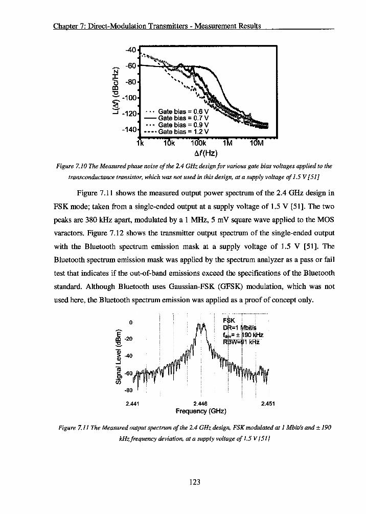
Chapter 7: Direct-Modulation Transmitters- Measurement Results
-40
• • • Gate bias = 0.6 V -Gate bias= 0.7 V • • • Gate bias = 0.9 V
-140 ---·Gate bias= 1.2 V
1k 1 k 100k 1 ~f(Hz)
10M
Figure 7.10 The Measured phase noise of the 2.4 GHz design for various gate bias voltages applied to the
transconductance transistor, which was not used in this design, at a supply voltage of 1.5 V [51]
Figure 7.11 shows the measured output power spectrum of the 2.4 GHz design in
FSK mode; taken from a single-ended output at a supply voltage of 1.5 V [51]. The two
peaks are 380kHz apart, modulated by a 1 MHz, 5 mV square wave applied to the MOS
varactors. Figure 7.12 shows the transmitter output spectrum of the single-ended output
with the Bluetooth spectrum emission mask at a supply voltage of 1.5 V [51]. The
Bluetooth spectrum emission mask was applied by the spectrum analyzer as a pass or fail
test that indicates if the out-of-band emissions exceed the specifications of the Bluetooth
standard. Although Bluetooth uses Gaussian-FSK (GFSK) modulation, which was not
used here, the Bluetooth spectrum emission was applied as a proof of concept only.
2.441 2.446 Frequency (GHz)
2.451
Figure 7.11 The Measured output spectrum of the 2.4 GHz design, FSK modulated at 1 Mbitls and ± 190
kHzfrequency deviation, at a supply voltage of 1.5 V [51]
123

M.A.Sc. Thesis- M. M. El-Desouki
2.397
McMaster- Electrical and Computer Engineering
2.446 Frequency (GHz}
2.497
Figure 7.12 Bluetooth data spectrum emission mask [51]
7.3 Comparison and Summary
This chapter presented the measurement results of a direct-modulation transmitter design.
Two circuits, sharing a common topology that uses a cross-coupled negative-gm voltage
controlled oscillator, were discussed.
The work presented in this chapter demonstrates the feasibility of performing
direct-modulation using a voltage controlled power oscillator as a single-block short
range transmitter in standard CMOS technology. Two circuits were designed and tested
targeting the 2.4 GHz ISM band, the 433 MHz ISM band and the 405 MHz MICS band.
This work contributes considerably to the reduction of transmitter die area and
power consumption, leading to simpler and more efficient designs that are suitable for
emerging low-power applications such as wireless body area networks. Table 7.1 shows a
summary of the key results presented in this chapter, where the designs are compared
based on the FoM previously expressed by Equation 4.1 [51].
124
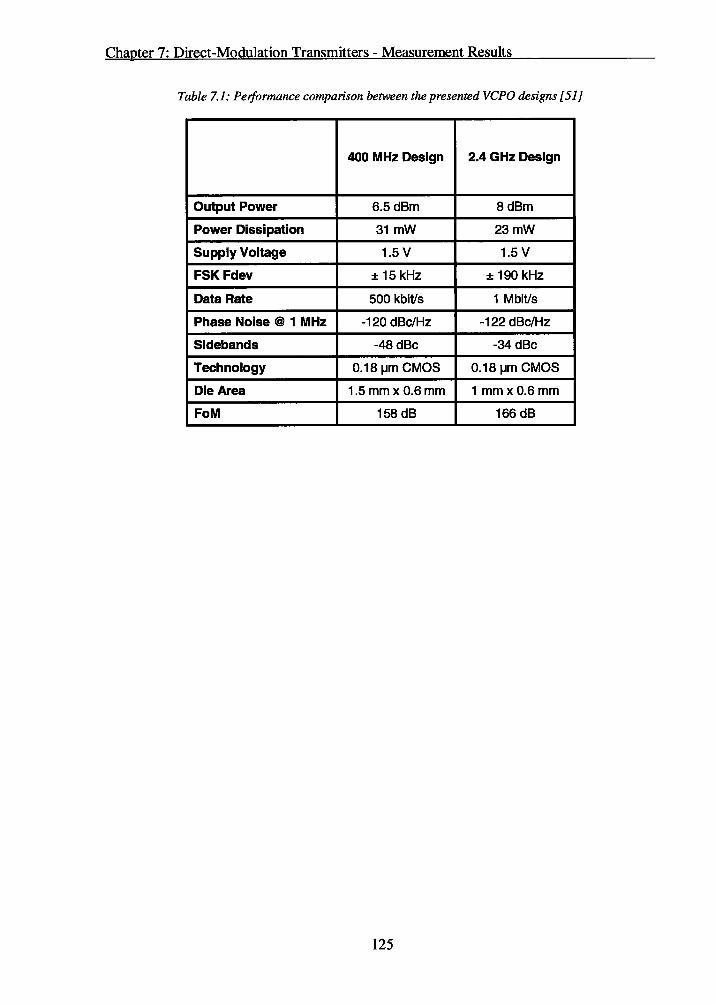
Chapter 7: Direct-Modulation Transmitters- Measurement Results
Table 7.1: Peiformance comparison between the presented VCPO designs [51]
400 MHz Design 2.4 GHz Design
Output Power 6.5dBm 8dBm
Power Dissipation 31 mW 23mW
Supply Voltage 1.5 v 1.5 v FSKFdev ±15kHz ±190kHz
Data Rate 500 kbit/s 1 Mbit/s
Phase Noise @ 1 MHz -120 dBc/Hz -122 dBc/Hz
Sidebands -48 dBc -34 dBc
Technology 0.18 IJm CMOS 0.18 IJm CMOS
Die Area 1.5 mmx 0.6mm 1 mm x 0.6 mm
FoM 158 dB 166 dB
125

M.A.Sc. Thesis- M. M. El-Desouki McMaster - Electrical and Computer Engineering
Chapter 8
CONCLUSIONS AND FUTURE WORK
This thesis studied the design of integrated power amplifier circuits for biotelemetry
applications in CMOS technology. The objective of this work is to improve the efficiency
of RF low-power transceivers that are suitable for biomedical applications and operate
from very low-supply voltages; or short-range applications that do not require large
output power levels, such as wireless sensor networks. Since the power amplifier is the
most power consuming block of an RF transceiver, this work focused on improving the
efficiency of power amplifiers with low output power levels; and thus improving the
global efficiency of the transceiver. After designing efficient power amplifiers suitable
for low output power applications, the next step was to try some non-conventional
techniques to simplify the RF transceiver and improve its efficiency. This was presented
by testing the feasibility of using a voltage controlled power oscillator as a single-block
direct-modulation transmitter.
8.1 Contributions and Summary
This work started by examining the challenges met in designing power amplifiers with
low output power levels and clearly explaining these challenges, since low-power
amplifiers were not thoroughly researched in previous publications.
The first use of a class-E (switch-mode) power amplifier for low-power
applications was presented in this work, where traditionally, current-mode power
amplifiers were used. The four class-E layouts presented in this work showed the
feasibility of using class-E power amplifiers for low-power applications. The effects of
the on-chip layout parasitics on low-power amplifier designs were also discussed, and a
126

Chapter 8: Conclusions
program that was designed to calculate the component values used in the equivalent
circuit of the parasitic layout interconnections, was also presented. The effects of using
an on-chip filter were also presented, showing how the efficiency of the power amplifier
can be improved by avoiding the on-chip filter and depending on the human body layers
for filtering higher order harmonics. The effects of the resistive losses on the
interconnections were also presented, showing how the results can be improved by
increasing the metal thickness and inductor quality factor. The measurement results of the
thick top-metal layer class-E power amplifier presented show a maximum drain
efficiency of 53 % and a maximum gain of 22 dB, at a frequency of 2.4 GHz. When
operating from a 1.2 V supply, the PA delivers an output power of 14.5 mW with a PAE
of 51 %. The supply voltage can go down to 0.6 V with an output power of 3.5 m Wand a
PAEof43 %.
Furthermore, this work presented a novel power amplifier design, using
superharmonic injection-locking that allows for very high gain from a single stage. The
two mode-locking circuits targeted the 2.4 GHz ISM band, the 433 MHz ISM band and
the 405 MHz MICS band. The phase noise characteristics of the two designs were also
presented and some recommendations were given to reduce the phase noise. The mode
locking designs contribute considerably to the reduction of transmitter die area. The
measurement results of the 2.4 GHz design show that the fabricated ILP A has a
maximum gain of 31 dB from only one stage, an output power of 7.6 dBm from a 1.5 V
supply voltage and a DC current of 15 rnA. The chip area is only 0.6 mm2 with all
components fully integrated.
Finally, this work also demonstrated the feasibility of performing direct
modulation using a voltage-controlled power oscillator as a single-block short-range
transmitter in standard CMOS technology. Two circuits were designed and tested
targeting the 2.4 GHz ISM band, the 433 MHz ISM band and the 405 MHz MICS band.
Some important recommendations were also given on the phase noise performance of
these designs, where the effect of the tail current source gate biasing was discussed. This
work contributes considerably to the reduction of transmitter die area and power
consumption. The measurement results of the 2.4 GHz transmitter show a drain
efficiency of 27 %. When operating from a 1.5 V supply, the transmitter delivers an
127
M.A.Sc. Thesis - M M. El-Desouki McMaster- Electrical and Computer Engineering
output power of 8 dBm with a low phase noise of -122 dBc/Hz at a 1 MHz offset. The
chip areas of the two fabricated transmitters are only 0.6 mm2 and 0.9 mm2 for the 2.4
GHz design and the 433 MHz design respectively, with all components fully integrated.
Table 8.1 shows a performance comparison between state-of-the-art CMOS
power amplifier designs based on the FoM proposed in Chapter 3. Only the non-filtered
outputs are shown in the table. The thick top-metal layer class-E power amplifier design
(design number 4) outperforms all previous published power amplifiers targeting low
output power applications in terms of PAE. No class-E designs, other than those
presented in this work, are shown in the table, since this work represents the first use of a
class-E power amplifier in low power applications. The 2.4 GHz ILO design (design
number 6) shows a power gain that is significantly higher than all other works, which is
why it has a very high FoM.
Table 8.2 shows a performance comparison between state-of-the-art voltage
controlled power oscillators based on the FoM proposed in Chapter 4. This work shows
that the CMOS VCPO can achieve comparable performance to other technologies while
providing a high level of integration and low-cost.
The work presented in this thesis has been published in three conferences. Three
journal papers were also submitted based on the work presented in this thesis and two
more journal papers are current work in progress.
128

Chapter 8: Conclusions
Table 8.1: Performance comparison between state-of-the-art CMOS power amplifier designs
FoM =10logpo;{mw+l0logG+20log'i(Hz -lOlogPv;(mW
Gain Design Voc PA f Pout @ PAE Integration FoM Num. {v} class {GHz} {dBm} CP {o/o} {dB}
{dB}
1 0.65 E 0.65 -1.2 5.8 9.7 Fully 173 On-chip
2 0.8 E 2.4 -6.5 2.2 1 Fully 174 On-chip
Ref. [36] 3.0 AB 0.43 13 16.5 29 Off-chip 184 components
Ref. [2] 1.2 AB 1.92 4 6 26 Off-chip 187 components
Ref. [37] 1.8 AB 2.45 3.5 13 14 Fully 192 On-chip
Ref. [64] 1.2 c 0.43 4 ---- 15 Off-chip ----components
5 1.5 ILO 0.43 6.3 30 14.5 Fully 194 On-chip
3 1.2 E 2.4 9.5 11.2 33 Fully 194
On-chip
Ref. [38] 1.8 AB 2.4 9 19 16 Off-chip 199 components
4 1.2 E 2.4 13 15 51 Fully 200 On-chip
Ref. [52] 1.4 AB 2.45 5.4 19.5 28.5 Fully 202 On-chip
6 1.5 ILO 2.4 7.6 31 25 Fully 213 On-chip
Table 8.2: Performance comparison between state-of-the-art voltage-controlled power oscillators
P,,/ P. r/ (i). FoM =lOlog o/lmW-lOlog v1lmw+20log L\~ -L(L\w)-20logQ
Design f Pout Drain FoM Tech. efficiency Num. {GHz) {dBm} {o/o} {dB}
Ref. [36] GaN FET 3.0 34 23 147
Ref. [2] 0.6 (Jm GaAs 3.2 3 38 158 MESFET
7 CMOS 0.43 6.5 14 158 0.18 (Jm
8 CMOS 2.4 8 27 166 0.18 (Jm
129

M.A.Sc. Thesis - M. M. El-Desouki McMaster- Electrical and Computer Engineering
8.2 Future Work
A number of areas for future research and improvements were identified in this work,
some of which are currently being considered.
As for the presented class-E power amplifier, it will be useful to implement a
method that can dynamically control the output power level. This has a number of uses,
one which can help improve the linearity of the amplifier by dynamically changing the
supply voltage to follow the change in amplitude of the input signal, which is known as
envelope elimination and restoration (EER). However, since linearity is not a major
concern in this work, there are other more important benefits to have dynamic power
control. One benefit is to allow for turning off the power amplifier when the transceiver is
in receive mode. This will require the use of an efficient switch, such as a PMOS
transistor. The challenge comes when needing to operate the power amplifier in burst
mode, such that it turns on fast enough, transmits a chunk of data, and then turns off.
Burst-mode may be a good technique to use in low-power applications where the devices
spend a majority of their time in standby.
Regarding the injection-locked power amplifier, measuring the MOS varactors
and determining their exact quality factor will help in confirming the source of
discrepancy between the measured and the simulated results, in addition to designing an
LC-tank with a higher quality factor. This is currently being tested using two different
approaches. The first is to test a better layout of the MOS varactor with wider metal
interconnections between the multi-fingers. And the second, is by trying to improve the
quality factor of the inductors used. A novel technique is currently being studied by
placing the laid-out inductor in a deep-n-well, isolating its substrate from the substrate of
the chip. This can help reduce the losses in the substrate network, since the area beneath
the inductor is no longer grounded. It can also help in reducing substrate leakage and
improving the noise performance of the design. Further, laying out an inductor in this
manner can also help in having a placement independent inductor layout, since the
equivalent circuit of the inductor is normally extracted from an S-parameters test
structure that places four grounding pads very close to the inductor, which are usually not
there when the inductor is actually laid out in the circuit. As for the phase noise of the
circuit, the squegging effects that were noticed on the phase noise are areas worthy of
130

Chapter 8: Conclusions
future research. The circuit has been laid out six times, as shown in Figure 8.1, each time
changing one of the possible factors that might be affecting the phase noise. The tests that
will be carried out investigate the effect of changing the filtering capacitors applied to the
DC supply, using a MOS varactor with a higher quality factor, using smaller De
blocking capacitors and finally, using an inductor with a higher quality factor.
Figure 8.1 Photomicrograph of the six circuits that were fabricated to investigate the cause of phase noise
fluctuations
As for the direct-modulation transmitter, in addition to the previous improvements
mentioned on phase noise and the quality factor of the LC-tank, the following future
research is recommended. First, since the main drawback of this design is the instability
of the output frequency, mainly as a function of temperature, the temperature effects on
the oscillation frequency, the output power, the drain efficiency and the phase noise
should be considered. The design will be tested under various temperatures to quantify
the effects of temperature on the circuit's performance.
As an improvement to the open-loop direct-modulation transmitter, a phase
locked loop (PLL) power transmitter is currently being researched. By adding the digital
circuitry required to implement the PLL, the output frequency will be stabilized against
any drifts, at a small expense of power consumption. Figure 8.2 shows a block level
schematic of the PLL transmitter, highlighting the the phase-locked loop.
131

M.A.Sc. Thesis- M. M. EI-Desouki McMaster- Electrical and Computer Engineering
Xtall .JUUL
s
--·· .......... REF
Charg Pump
Voc
Loop Filter
UP ......... I"':': ~
l PFD ............ ~ .... -1
~V~C~O~_JD~W~N~.,I~ ~ ~~
I ~
Prescaler + 128
•
I
Figure 8.2 PLL transmitter block diagram
Figure 8.3 shows a photomicrograph of the PLL transmitter, with a zoomed-in
image on the PLL. The circuit occupies an area of 0.7 mm2, proving that adding the PLL
does not take too much extra die area, and the measurements completed show a drop in
efficiency of only 3 %.
Figure 8.3Photomicrograph of the designed PLL transmitter
132
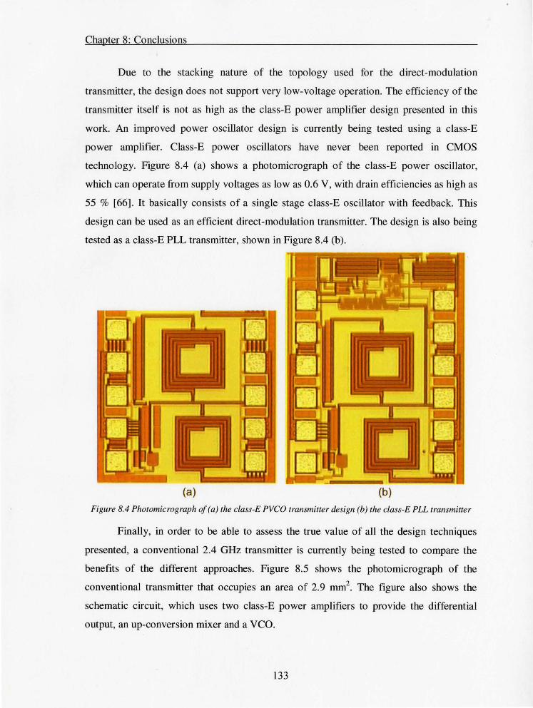
Chapter 8: Conclusions
Due to the stacking nature of the topology used for the direct-modulation
transmitter, the design does not support very low-voltage operation. The efficiency of the
transmitter itself is not as high as the class-E power amplifier design presented in this
work. An improved power oscillator design is currently being tested using a class-E
power amplifier. Class-E power oscillators have never been reported in CMOS
technology. Figure 8.4 (a) shows a photomicrograph of the class-E power oscillator,
which can operate from supply voltages as low as 0.6 V, with drain efficiencies as high as
55 % [66]. It basically consists of a single stage class-E oscillator with feedback. This
design can be used as an efficient direct-modulation transmitter. The design is also being
tested as a class-E PLL transmitter, shown in Figure 8.4 (b).
(a) (b)
Figure 8.4 Photomicrograph of(a) the class-E PVCO transmitter design (b) the class-E PLL transmitter
Finally, in order to be able to assess the true value of all the design techniques
presented, a conventional 2.4 GHz transmitter is currently being tested to compare the
benefits of the different approaches. Figure 8.5 shows the photomicrograph of the
conventional transmitter that occupies an area of 2.9 mrn2. The figure also shows the
schematic circuit, which uses two class-E power amplifiers to provide the differential
output, an up-conversion mixer and a VCO.
133

M.A.Sc. Thesis- M. M. El-Desouki McMaster- Electrical and Computer Engineering
Figure 8.5 Conventional2.4 GHz transmitter, photomicrograph and circuit schematic
134

References
References
[1] B. Warneke, M. Last, B. Liebowitz, K.S.J. Pister, "Smart dust: communicating with a cubic
millimeter computer," IEEE Com. Soc., vol. 34, (1), pp. 44-51, Jan. 2001.
[2] Y.H. Chee, J. Rabaey, A.M. Niknejad, "A class AlB low power amplifier for wireless sensor
networks," Int. Sym. Cir. and Sys., vol. 4, pp. 409-12, May 2004.
[3] M. Hella, M. Ismail, RF CMOS Power Amplifiers: Theory, Design and Implementation. Kluwer
Academic Publishers, Boston, 2002.
[4] D. Edenfeld, A. B. Kahng, M. Rodgers, Y. Zorian, "2003 Technology roadmap for
semiconductors," IEEE Com. Soc., vol. 37, (1), pp. 47-56, Jan. 2004.
[5] H. S. Bennett, R. Brederlow, J. Costa, M. Huang, A. A. Immorlica, J. E. Mueller, M. Racanelli, C.
E. Weitzel, Bin Zhao, "RF and AMS," IEEE Cir. Dev. Mag., vol. 20, (6), pp. 38-51, Nov.-Dec.
2004.
[6] 2003 International technology roadmap for semiconductors, International SEMATECH, Austin,
TX [Online]. Available: http://public.itrs.net/Files/2003ITRS/Home2003.htm
[7] Svein Anders Tunheim, ''Implementation of CMOS low cost and low power RF-ICs," Wireless
Sys. Design Conf. Exp., San Jose CA, February 25-28, 2002.
[8] I. Aoki, S. Kee, D. Rutledge, A. Hajimiri, "Fully integrated CMOS power amplifier design using
the distributed active-transformer architecture," IEEE J. Solid-State Cir., vol. 37, (3), pp. 371-
383,2002.
[9] I. Aoki, S. D. Kee, D. B. Rutledge, A. Hajimiri, "A fully-integrated 1.8-V, 2.8-W, 1.9-GHz,
CMOS power amplifier," IEEE Radio Frequncy Int. Cir. Sym., pp. 199-202,2003.
[10] Tsai King-Chun, P. R. Gray, "A 1.9-GHz, 1-W CMOS class-E power amplifier for wireless
communications," IEEE J. Solid-State Cir., vol. 34, (7), pp. 962-970, 1999.
[11] P. Gajsek, W.D. Hurt, J.M Ziriax and P.A Mason, ''Parametric dependence of SAR on
permittivity values in a man model," IEEE Trans. Biomed. Eng., vol. 48, (10), pp. 1169-1177, Oct.
2001.
[12] P. Bradley, ''The ultra-low-power wireless medical device revolution," Medical Electronics
Manufacturing [Online]. Available: http://www .devicelink.com/mem/archive/05/04/004.html
[13] H. Higgins, ''From the inside-out: designing in-body antennas for implanted medical devices,"
Electronic Component News [Online]. Available:
http://www.reed-electronics.com/ecnmag/article/CA482585
[14] A. Sivard, P. Bradley, P. Chadwick and H. Higgins, ''The challenge of designing in-body
communications," Embedded Systems Programming [Online]. Available:
135

M.A.Sc. Thesis- M. M. El-Desouki McMaster- Electrical and Computer Engineering
http://www.embedded.com/show Article.jhtml?articleiD=51200651
[15] F. Pelletier, ''Wireless tech allies with low-power gear," EETimes [Online]. Available:
http://www .eetimes.cornlshow Article.jhtml ?articleiD=26806906
[16] RF System Lab [Online]. Available: http://www.rfnorika.cornleng/movie/movie_Ol.html
[17] Wai Ngan, Effects of channel length fluctuation on the performance of RF oscillators, Master
Thesis, Dept. of Electrical and Computer Engineering, McMaster University, Hamilton, Ont., Oct.
2004.
[18] T. Melly, A.-S. Porret, C.C. Enz and E. Vittoz, "A 1.2 V, 433 MHz, 10 dBm, 38% global
efficiency FSK transmitter integrated in a standard digital CMOS process," Proc. IEEE Custom
Int. Cir. Conf., pp. 179-182, May 2000.
[19] C. Fallesen, "Design techniques for sub-micron RF power amplifiers," Phd Thesis, Technical
University of Denmark, May 2001.
[20] F. H. Raab, F.H., P. Asbeck, S. Cripps, P. B. Kenington, Z. B. Popovic, N. Pothecary, J. F. Sevic
and N. 0. Sokal, ''Power amplifiers and transmitters for RF and microwave," IEEE Trans.
Microwave Theory Tech., vol. 50, (3), pp. 814-826, March 2002.
[21] Per Asbeck, "Linearisation of RF power amplifiers," Phd Thesis, Technical University of
Denmark, May 2001.
[22] R. Gupta, B. M. Ballweber and D. J. Allstot, "Design and optimization of CMOS RF power
amplifiers," IEEE J. Solid-State Cir., vol. 36, (2), pp. 166-175, Feb. 2001.
[23] Donald A. Neamen, Semiconductor Physics and Devices. 3'd edition, McGmw-Hill Higher
Education, New York, 2003.
[24] Yannis Tsividis, Operation and Modeling of the MOS Transistor. 2nd edition, Oxford University
Press, New York, 1999.
[25] Phillip E. Allen and Douglas R. Holberg, CMOS Analog Circuit Design. 2nd edition, Oxford
University Press, New York, 2002.
[26] Steve C. Cripps, RF Power Amplifiers for Wireless Communications, Artech House Publishers,
MA,1999.
[27] F. Raab, "Idealized operation of the class-E tuned power amplifier," IEEE Trans. Cir. Sys., vol.
24, (12), pp. 725-735, Dec 1977.
[28] T. Suetsugu and M. K. Kazimierczuk, ''Comparison of class-E amplifier with nonlinear and linear
shunt capacitance," IEEE Trans. Cir. Sys., vol. 50, (8), pp. 1089-1097, Aug. 2003.
[29] N. 0. Sokal and A. D. Sokal, ''Class-E a new class of high-efficiency tuned single-ended
switching power amplifiers," IEEE J. Solid-State Cir., vol. 10, (3), pp. 168-176, June 1975.
[30] N. 0. Sokal, "Class-E RF power amplifiers," Jan. 2001, available online:
www.netway.com/-stevec/hamlsokal2corrected.pdf.
[31] K.-C. Tsai and P. R. Gmy, "A 1.9-GHz, 1-W class-E power amplifier for wireless
communications," IEEE J. Solid-State Cir., vol. 34, (7), pp. 962-970, July 1999.
136
References
[32] K. L. R Mertens and M.S. J. Steyaert, "A 700-MHz 1-W fully differential CMOS class-E power
amplifier," IEEE J. Solid-State Cir., vol. 37, (2), pp. 137-141, Feb. 2002.
[33] Z. Xu and E. I. El-Masry, ''Design and optimization of CMOS class-E power amplifier," Int. Syrn.
Cir. and Sys., vol1, pp. 325-328, May 2003.
[34] P. Hedari and Y. Zhang, "A novel high frequency, high-efficiency, differential class-E power
amplifier in 0.18 !Jlil CMOS," Int. Syrn. Low Power Elec. and Design, pp. 455-458, Aug. 2003.
[35] T. Sowlati and D. M. W. Leenaerts, "A 2.4-GHz 0.18 !Jlil CMOS self biased cascode power
amplifier," IEEE J. Solid-State Cir., vol. 28, (8), pp. 1318-1324, Aug. 2003.
[36] S. J. Yoo, H. J. Ahn, M.M. Hella, and M. Ismail, ''The design of 433 MHz class AB CMOS power
amplifier," Southwest Syrn. Mixed-Signal Design, pp. 36-40, Feb. 2000.
[37] P.B. Khannur, "A CMOS power amplifier with power control and T/R switch for 2.45-GHz
Bluetooth/ISM band applications," IEEE Radio Frequency Integ. Cir. Sym., pp. 145-148, June
2003.
[38] K. Yamamoto, T. Heima, A. Furukawa, M. Ono, Y. Hashizume, H. Komurasaki, S. Maeda, H.
Sato and N. Kato, "A 2.4-GHz-band 1.8-V operation single-chip Si-CMOS T/R-MMIC front-end
with a low insertion loss switch," IEEE J. Solid-State Cir., vol. 36, (8), pp. 1186-97, Aug. 2001.
[39] C. C. Ho, C. W. Kuo, C. C. Hsiao andY. J. Chan, "A fully integrated class-E CMOS amplifier
with a class-F driver stage," IEEE Radio Frequency Integ. Cir. Syrn., pp. 211-214, June 2003.
[40] S. L. Wong, H. Bhimnathwala, S. Luo, B. Halali and S. Navid, "A 1 W 830 MHz monolithic
BiCMOS power amplifier," IEEE Int. Solid-State Cir. Conf., pp. 52-53, Feb. 1996.
[41] D. Su and W. McFarland, "A 2.5-V, 1-W monolithic CMOS RF power amplifier," IEEE Custom
Integ. Cir. Proc., pp. 189-192, May 1997.
[42] P. Asbeck and C. Fallesen, "A 29 dBm 1.9 GHz class B power amplifier in a digital CMOS
process," IEEE Int. Conf. Cir. and Sys., vol. 1, pp. 474-477, Dec. 1997.
[43] D. Heo, A. Sutono, E. Chen, Y. Suh and J. Laskar, "A 1.9-GHz DECT CMOS power amplifier
with fully integrated multilayer LTCC passives," IEEE Microwave Wireless Components Lett.,
vol. 11, (6), pp. 249-251, June 2001.
[44] C. Fallesen and P. Asbeck, "A 1 W 0.35 !Jlil CMOS power amplifier for GSM-1800 with 45%
PAE," IEEE Proc. Solid-State Cir. Conf., pp. 158-159, Feb. 2001.
[45] Y. C. Chen, Y. Yong Kyu, J. Laskar and M. Allen, "A 2.4 GHz integrated CMOS power amplifier
with micromachined inductors," IEEE MIT-S Int. Microwave Syrn., vol. 1, pp. 523-526, May
2001.
[46] D. Heo, A. Sutono, E. Chen, E. Gebara, S. Yoo, Y. Suh, J. Laskar, E. Dalton and E. M. Tentzeris,
"A high efficiency 0.25 11m CMOS PA with LTCC multi-layer high-Q integrated passives for 2.4
GHz ISM band," IEEE MIT-S Int. Microwave Syrn., vol. 2, pp. 915-918, May 2001.
[47] F. Fortes and M. J. do Rosario, "A second harmonic class-F power amplifier in standard CMOS
technology," IEEE Trans. Microwave Theory Tech., vol. 49, (6), pp. 1216-1220, June 2001.
137

M.A.Sc. Thesis- M. M. El-Desouki McMaster - Electrical and Computer Engineering
[48] A. Komijani and A. Hajimiri, "A 24GHz, +14.5dBm fully-integrated power amplifier in 0.18 JUll
CMOS," IEEE Proc. Custom Integ. Cir. Conf., pp. 561-564, Oct. 2004.
[49] H. Chao-Chih, K. Chin-Wei and C. Yi-Jen, ''Integrated CMOS power amplifier and down
converter for 2.4 GHz Bluetooth applications," IEEE Radio and Wireless Conf., pp. 29-32, Aug.
2001.
[50] E. Cijvat and H. Sjoland, "A fully integrated 2.45 GHz 0.25 JUI1 CMOS power amplifier," IEEE
Proc. Electronics Circ. and Sys., vol. 3, pp. 1094-1097, Dec. 2003.
[51] M. M. El-Desouki, M. J. Deen andY. M. Haddara, "Feasibility study of using a CMOS power
VCO as a single-block RF modulator/transmitter for short-range biomedical applications," IEEE
Trans. Microwave Theory Tech., 7 pages (submitted Sep. 2005).
[52] S. M. Abdelsayed, M. J. Deen and N. K. Nikolova, "A fully integrated low power CMOS power
amplifier for biomedical applications," 3Sh European Microwave Conf., pp. 1715-1718, Oct.
2005.
[53] M. M. El-Desouki, M. J. Deen and Y. M. Haddara, "A 0.65V CMOS power amplifier for
biotelemetry applications," IEEE Canadian Conf. Electrical Computer Eng., pp. 1220-1223, May
2005.
[54] M. M. El-Desouki, M. J. Deen andY. M. Haddara, "A class-E low-power amplifier for short
range applications," J. Vacuum Sci. Tech., 4 pages (submitted June 2005).
[55] M. M. El-Desouki, M. J. Deen andY. M. Haddara, "A low-power CMOS class-E power amplifier
for biotelemetry applications," 3Sh European Microwave Conf., pp. 441-444, Oct. 2005.
[56] M. M. El-Desouki, M. J. Deen andY. M. Haddara, "A high-efficiency, low-voltage CMOS class
E power amplifier for biotelemetry applications," IEEE Trans. Microwave Theory Tech., 7 pages
(submitted Aug. 2005).
[57] M. M. El-Desouki, M. J. Deen andY. M. Haddara, ''Novel monolithic CMOS power amplifiers
using super-harmonic injection-locking for short range applications," work in progress, 2006.
[58] T. Sowlati, C.A.T. Salama, J. Sitch, G. Rabjohn and D. Smith, ''Low voltage, high efficiency
class E GaAs power amplifiers for mobile communications," Tech. Dig. Gallium Arsenide Integ.
Cir. Sym, pp. 171-4, Oct. 1994.
[59] S. M. Abdelsayed, M. J. Deen and N. K. Nikolova, ''Parasitics-aware layout design of a low
power fully-integrated CMOS power amplifier," J. Vacuum Sci. Tech. A, 4 pages, in press 2006.
[60] M. M. El-Desouki, S.M. Abdelsayed, M. J. Deen, Y. M. Haddara and N. K. Nikolova, "A
comparison between different power amplification techniques for low-power applications," work
in progress, 2006.
[61] S.Verma, H. R. Rategh and T. H. Lee, "A unified model for injection-locked frequency dividers,"
IEEE J. Solid-State Cir., vol. 38, (6), pp. 1015-27, June 2003.
[62] K. K. Clarke and D. T. Hess, Communication Circuits: Analysis and Design. Addison-Wesley
Publishing Company, Philippines, 1971.
138

References
[63] S. Levantino, C. Samori, A. Bonfanti, S. L. J. Gierkink, A. L. Lacaita and V. Boccuzzi,
"Frequency dependence on bias current in 5 GHz CMOS VCOs: impact on tuning range and
flicker noise upconversion," IEEE J. Solid-State Cir., (8), pp. 1003-1011, Aug. 2002.
[64] T. Melly, A. -S. Porret, C. C. Enz, M. Kayal and E. Vittoz, "A 1.2V, 430MHz, 4dBm power
amplifier and a 250 ~-tW front-end, using a standard digital CMOS process," Proc. Int. Sym. Low
Power Electronics Design, pp. 233-237, Aug. 1999.
[65] M. J. Deen, R. Murji, A. Fakhr, N. Jafferali and W. L. Ngan, "Low power CMOS integrated
circuits for radio-frequency applications", lEE Proc. Cir. Dev. Sys., vol. 152, (5), pp. 502-508,
Oct. 2005.
[66] M. J. Deen, S. Naseh, 0. Marinov and M. H. Kazemeini, "Very low-voltage operation capability
of complementary metal-oxide-semiconductor ring oscillators and logic gates," J. Vac. Sci.
Techno!. A, vol. 24, (3), May/June 2006.
139