Ultra Wide-‐band Power Amplifier - San Jose State University
30
Ultra Wideband Power Amplifier Chengcheng Xu May 28, 2011 San Jose State University College of Engineering Electrical Engineering Department EE172 Microwave Professor: Dr. Ray Kwok
-
Upload
khangminh22 -
Category
Documents
-
view
3 -
download
0
Transcript of Ultra Wide-‐band Power Amplifier - San Jose State University
Ultra Wide-‐band Power Amplifier
Chengcheng Xu May 28, 2011
San Jose State University College of Engineering
Electrical Engineering Department EE172 Microwave
Professor: Dr. Ray Kwok
2
Abstract:
In today’s world, amplifiers are used in many applications. The input signal
is being amplified by the amplifier to achieve a certain output power or voltage.
Most of us are familiar with DC amplifiers; in the realm of radio frequency, many of
the common electronic components have different effects and characteristic. So the
process of designing a microwave amplifier is different than the design process of a
DC amplifier.
Microwave amplifiers are most used to amplify a small amplitude high
frequency signal to large amplitude. It can be used for transmitting signal through a
microwave antenna, or used to amplify a weak signal received from the antenna.
Sometimes the transmitting signal might not be a single frequency, some
applications requires the amplifier to amplify signals across a wide range of
frequencies. In this paper, the design process of a 2GHz(1.5GHz – 3.5GHz)
bandwidth 20dB gain power amplifier will be described.
This was a two stages amplifier. For the first stage amplifier a transistor
from Avago technologies was used, the part number is ATF-‐54143 pHEMT. This
transistor has high gain, high linearity, and low noise, it is often used in LNA for
WLAN, WLL/RLL and MMDS application. The second stage amplifier used a RFMD
FPD2250 pHEMT. With the two amplifiers, the final gain is minimum 20dB with the
power gain slightly below 30dBm
3
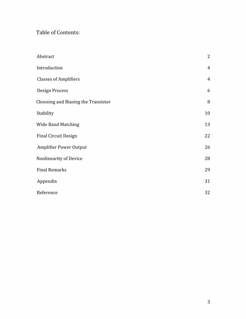
Table of Contents:
Abstract 2
Introduction 4
Classes of Amplifiers 4
Design Process 6
Choosing and Biasing the Transistor 8
Stability 10
Wide Band Matching 13
Final Circuit Design 22
Amplifier Power Output 26
Nonlinearity of Device 28
Final Remarks 29
Appendix 31
Reference 32

4
Introduction:
Microwave amplifiers are used to amplify a small amplitude high frequency
signal to a signal with higher amplitude. Sometimes the application requires the
amplifier to not only amplify signal of one frequency, in stead a range of frequency.
This amplifier will provide 20dB gain from 1.5GHz to 3.5GHz; the first stage of
amplifier used a transistor from Avago technologies ATF-‐54143 pHEMT, second
stage used a transistor from RFMD FPD2250 pHEMT.
Classes of Amplifiers:
There are different classes of amplifier, they are rated by their efficiency,
linearity and more. The amplifiers are classified to the following classes, A, AB, B,
and C class amplifier. When a signal is fed into the amplifier, the amplification is
determined by the mode the transistor is biased in. If the transistor I-‐V curve is
mostly linear, then the output signal gain will be linear. When the transistor has
poor linearity, then the gain of the amplifier will be non-‐linear.
A class A amplifier will operate in a small
portion of the transistor’s I-‐V curve and will have
continuous current flow for each RF cycle. Class
A amplifier has poor efficiency when converting
DC power to high frequency output power. The
power that is not converted to RF power will be Figure 1: Class A amplifier
5
dissipated as heat. Although class A amplifier has poor efficiency, it does provide
great output to input linearity among all the classes of amplifiers. Figure 1 shows an
example of what a class A amplifier out and input looks like.
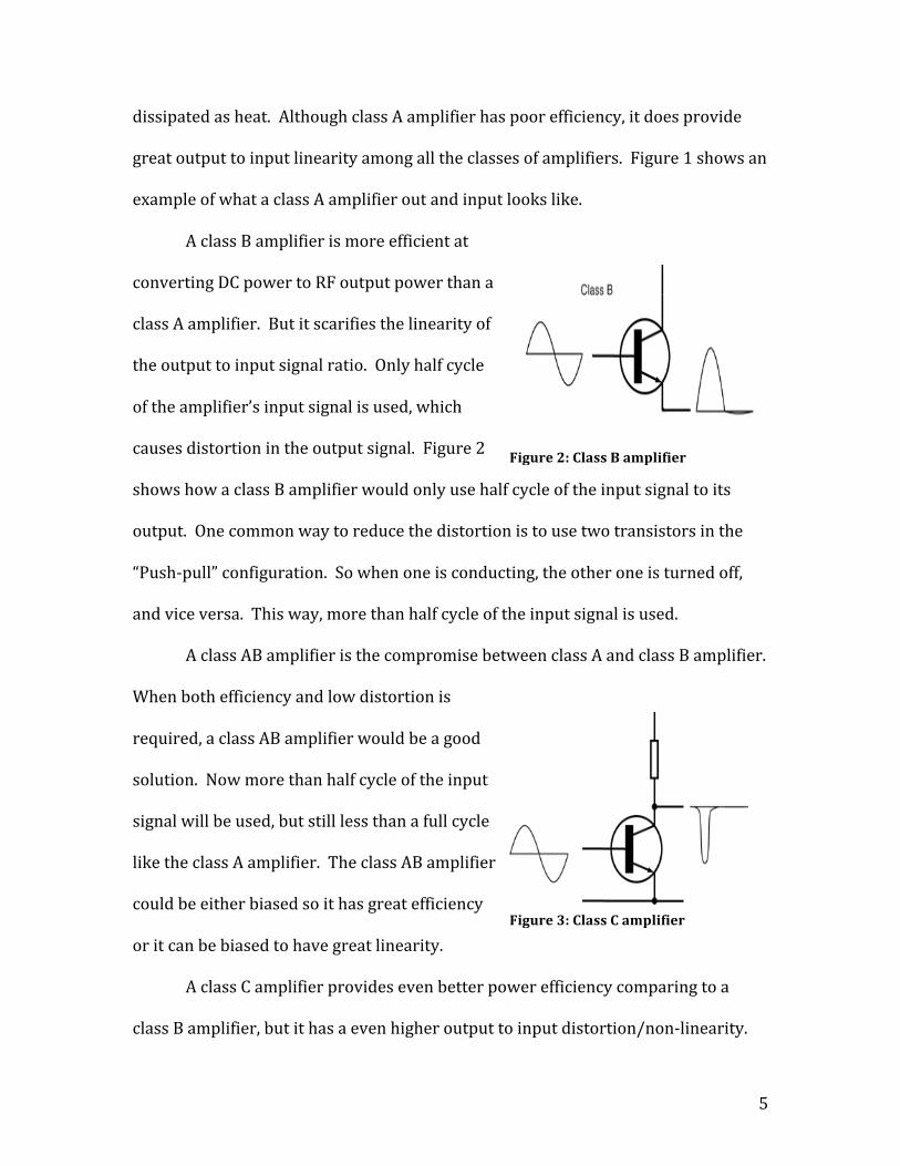
A class B amplifier is more efficient at
converting DC power to RF output power than a
class A amplifier. But it scarifies the linearity of
the output to input signal ratio. Only half cycle
of the amplifier’s input signal is used, which
causes distortion in the output signal. Figure 2
shows how a class B amplifier would only use half cycle of the input signal to its
output. One common way to reduce the distortion is to use two transistors in the
“Push-‐pull” configuration. So when one is conducting, the other one is turned off,
and vice versa. This way, more than half cycle of the input signal is used.
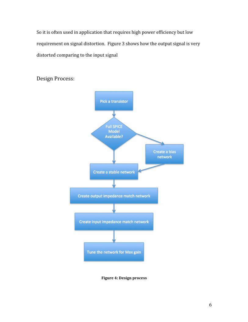
A class AB amplifier is the compromise between class A and class B amplifier.
When both efficiency and low distortion is
required, a class AB amplifier would be a good
solution. Now more than half cycle of the input
signal will be used, but still less than a full cycle
like the class A amplifier. The class AB amplifier
could be either biased so it has great efficiency
or it can be biased to have great linearity.
A class C amplifier provides even better power efficiency comparing to a
class B amplifier, but it has a even higher output to input distortion/non-‐linearity.
Figure 2: Class B amplifier
Figure 3: Class C amplifier
6
So it is often used in application that requires high power efficiency but low
requirement on signal distortion. Figure 3 shows how the output signal is very
distorted comparing to the input signal
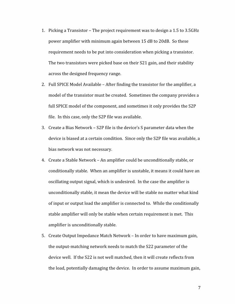
Design Process:
Figure 4: Design process
7
1. Picking a Transistor – The project requirement was to design a 1.5 to 3.5GHz
power amplifier with minimum again between 15 dB to 20dB. So these
requirement needs to be put into consideration when picking a transistor.
The two transistors were picked base on their S21 gain, and their stability
across the designed frequency range.
2. Full SPICE Model Available – After finding the transistor for the amplifier, a
model of the transistor must be created. Sometimes the company provides a
full SPICE model of the component, and sometimes it only provides the S2P
file. In this case, only the S2P file was available.
3. Create a Bias Network – S2P file is the device’s S parameter data when the
device is biased at a certain condition. Since only the S2P file was available, a
bias network was not necessary.
4. Create a Stable Network – An amplifier could be unconditionally stable, or
conditionally stable. When an amplifier is unstable, it means it could have an
oscillating output signal, which is undesired. In the case the amplifier is
unconditionally stable, it mean the device will be stable no matter what kind
of input or output load the amplifier is connected to. While the conditionally
stable amplifier will only be stable when certain requirement is met. This
amplifier is unconditionally stable.
5. Create Output Impedance Match Network – In order to have maximum gain,
the output-‐matching network needs to match the S22 parameter of the
device well. If the S22 is not well matched, then it will create reflects from
the load, potentially damaging the device. In order to assume maximum gain,
8
the output-‐matching network is usually created first, then the input matching
network.
6. Create Input Impedance Match Network – The input impedance matching
network is created after the output impedance matching network. The input
impedance must match the S11 parameter of the device, because if S11 is not
well matched, then not all the input power will be delivered to the device
itself.
Choosing and Biasing the Transistor:
When choosing the transistor for the amplifier certain criteria must be put
into consideration, frequency range, gain, 1dB compression point, etc. Also, one
must choose a good biasing point for the transistor so it will provide the desire gain.
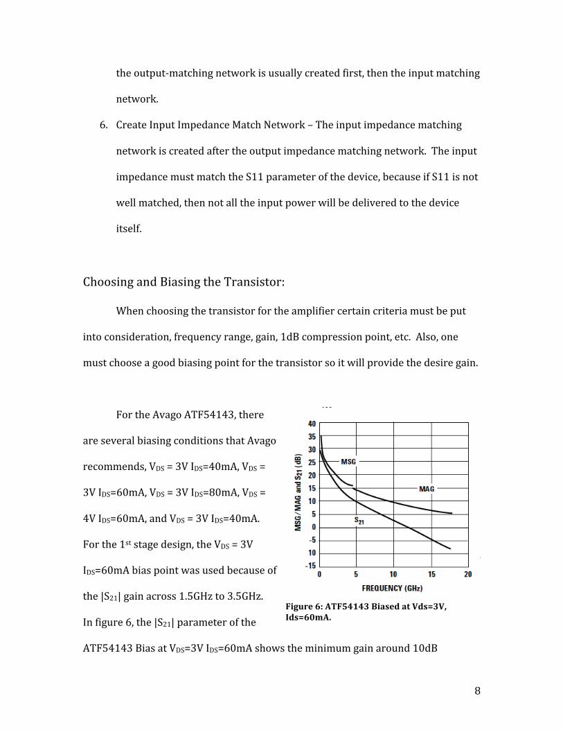
For the Avago ATF54143, there
are several biasing conditions that Avago
recommends, VDS = 3V IDS=40mA, VDS =
3V IDS=60mA, VDS = 3V IDS=80mA, VDS =
4V IDS=60mA, and VDS = 3V IDS=40mA.
For the 1st stage design, the VDS = 3V
IDS=60mA bias point was used because of
the |S21| gain across 1.5GHz to 3.5GHz.
In figure 6, the |S21| parameter of the
ATF54143 Bias at VDS=3V IDS=60mA shows the minimum gain around 10dB
Figure 5: I -‐ V curve of the ATF54143 Figure 6: ATF54143 Biased at Vds=3V, Ids=60mA.
9
between 1.5GHz to 3.5GHz. Since Avago provides the S2P file for the bias point
VDS=3V IDS=60mA in Microwave Office, there is no need to import the S2P file into
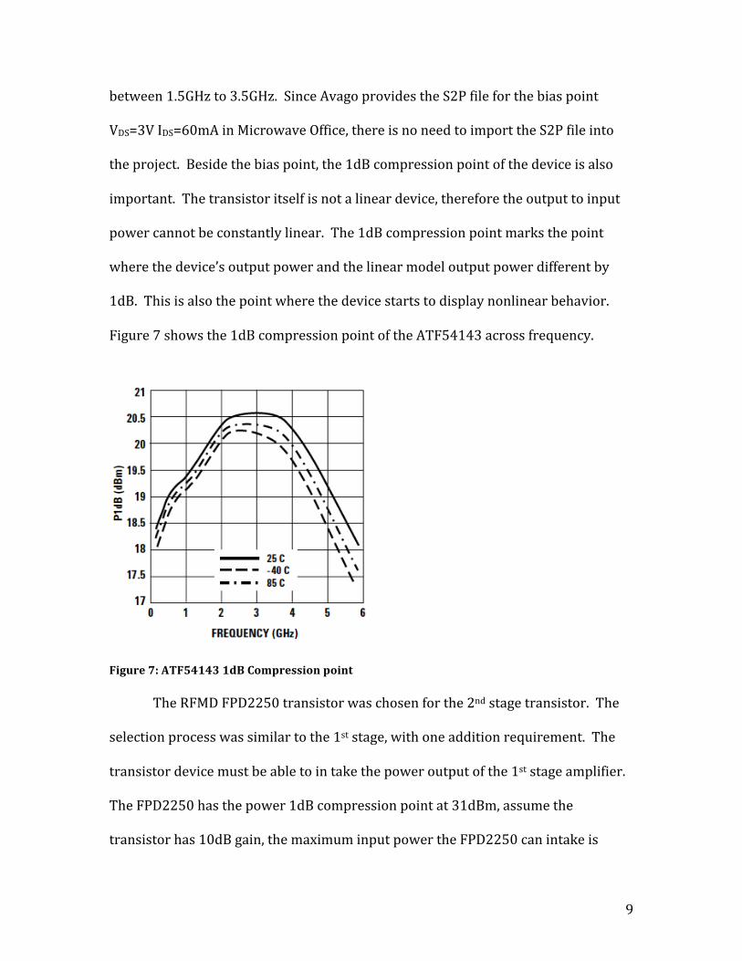
the project. Beside the bias point, the 1dB compression point of the device is also
important. The transistor itself is not a linear device, therefore the output to input
power cannot be constantly linear. The 1dB compression point marks the point
where the device’s output power and the linear model output power different by
1dB. This is also the point where the device starts to display nonlinear behavior.
Figure 7 shows the 1dB compression point of the ATF54143 across frequency.
Figure 7: ATF54143 1dB Compression point
The RFMD FPD2250 transistor was chosen for the 2nd stage transistor. The
selection process was similar to the 1st stage, with one addition requirement. The
transistor device must be able to in take the power output of the 1st stage amplifier.
The FPD2250 has the power 1dB compression point at 31dBm, assume the
transistor has 10dB gain, the maximum input power the FPD2250 can intake is
10
21dBm, which will be above the output power of the 1st stage transistor. RFMD only
provided the S2P file for one biasing point, VDS=5V IDS=300mA.
Stability:
As previously described, stability for an amplifier is crucial. No matter how
good the gain, how wide the bandwidth, or how good the linearity; the device is
unusable if it is not a stable device. In order to not cause an oscillating output, often
a stabilizing network needs to be created. In Microwave office, there are two ways
to test the stability of a device, 1. The K () and B1 () parameter of the device. 2. The
SCIR1 () and SCIR2 () parameter of the device. For the first method, in order for the
device to be unconditionally stable, K needs to be larger than 1, and B1 needs to be
no less than 0. For the second method, the SCIR will create a dash line circle and a
solid line circle. Base the position of the dash-‐line circle relative to the solid line
circle, either the inside or outside of the solid circle will be the stable region. The
goal is to be inside the stable region of the device across the desired frequency.
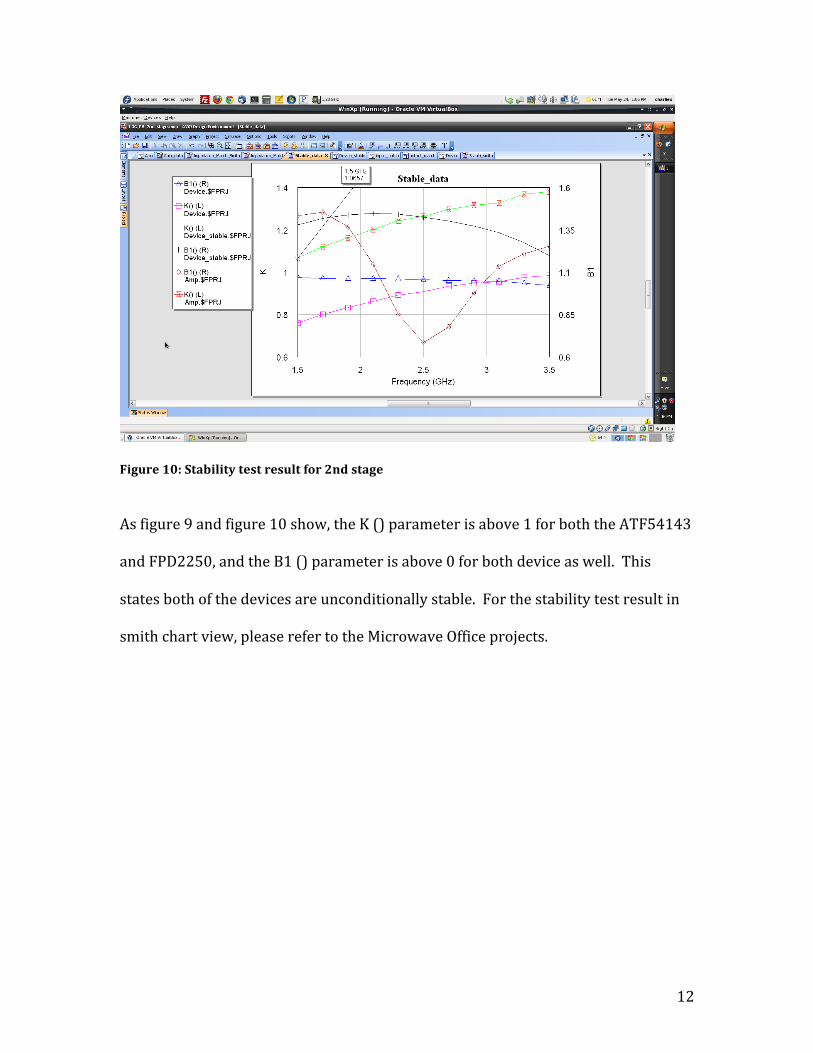
After reading a training module from AWR Corp and Besser Associate, a
general stabilization circuit looks like figure 8. After the stabilization circuit is
created for both the ATF54143 and FPD2250, the circuits need to be tuned so the
devices are stable. After tuning the stabilization circuits, the stability test result
looks like figure 9 and figure 10.

11
Figure 8: Stabilizing Circuit
Figure 9: Stability test result for 1st stage
12
Figure 10: Stability test result for 2nd stage
As figure 9 and figure 10 show, the K () parameter is above 1 for both the ATF54143
and FPD2250, and the B1 () parameter is above 0 for both device as well. This
states both of the devices are unconditionally stable. For the stability test result in
smith chart view, please refer to the Microwave Office projects.
13
Wide Band Matching:
For this amplifier, the specified frequency range is 1.5GHz to 2.5GHz. Unlike
single frequency amplifiers, the impedance of the devices must be matched across
the range of frequency. In a lot of the time, it is hard to have a perfect match across
the full frequency range, but there are methods to achieve near perfect impedance
match.
The first goal of the amplifier is to have a wide frequency range, the gain of
the amplifier is not as important as the frequency range. This means maximum gain
is not needed meaning G < Gmax. Referring to table 1, for G < Gmax, there are many
choices of matching options.
Application/Goal Source Γs Load Γ L Gmax Γ*in Γ*out
G<Gmax Many choice
Many choice
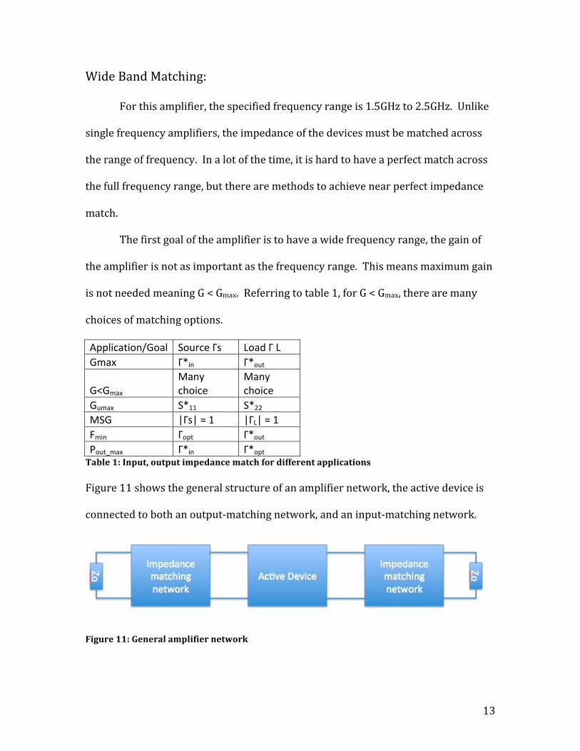
Gumax S*11 S*22 MSG |Γs| = 1 |ΓL| = 1 Fmin Γopt Γ*out Pout_max Γ*in Γ*opt Table 1: Input, output impedance match for different applications Figure 11 shows the general structure of an amplifier network, the active device is
connected to both an output-‐matching network, and an input-‐matching network.
Figure 11: General amplifier network
14
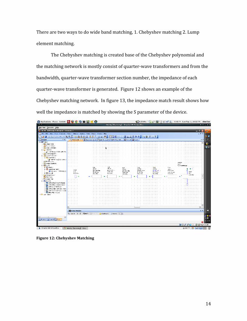
There are two ways to do wide band matching, 1. Chebyshev matching 2. Lump
element matching.
The Chebyshev matching is created base of the Chebyshev polynomial and
the matching network is mostly consist of quarter-‐wave transformers and from the
bandwidth, quarter-‐wave transformer section number, the impedance of each
quarter-‐wave transformer is generated. Figure 12 shows an example of the
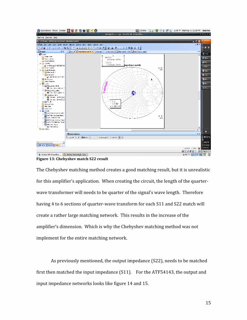
Chebyshev matching network. In figure 13, the impedance match result shows how
well the impedance is matched by showing the S parameter of the device.
Figure 12: Chebyshev Matching
15
Figure 13: Chebyshev match S22 result The Chebyshev matching method creates a good matching result, but it is unrealistic
for this amplifier’s application. When creating the circuit, the length of the quarter-‐
wave transformer will needs to be quarter of the signal’s wave length. Therefore
having 4 to 6 sections of quarter-‐wave transform for each S11 and S22 match will
create a rather large matching network. This results in the increase of the
amplifier’s dimension. Which is why the Chebyshev matching method was not
implement for the entire matching network.
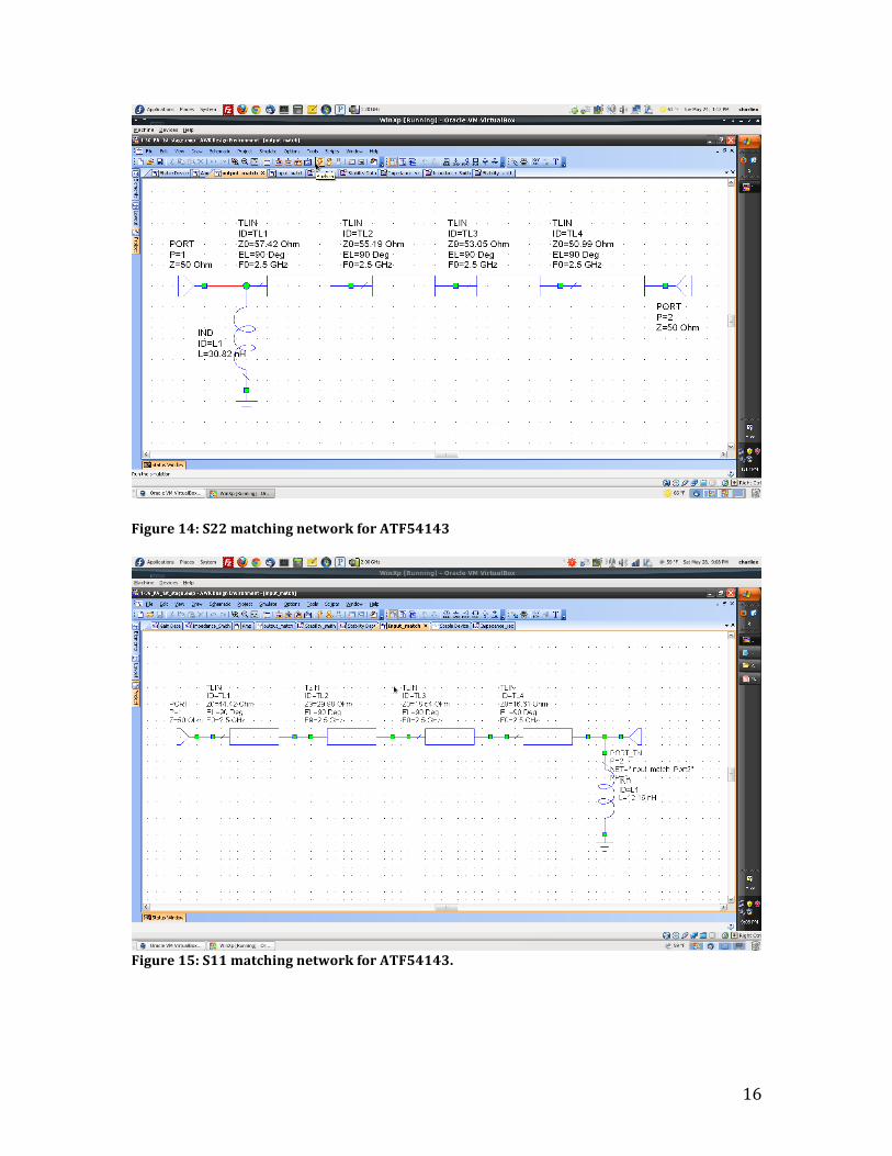
As previously mentioned, the output impedance (S22), needs to be matched
first then matched the input impedance (S11). For the ATF54143, the output and
input impedance networks looks like figure 14 and 15.
16
Figure 14: S22 matching network for ATF54143
Figure 15: S11 matching network for ATF54143.
17
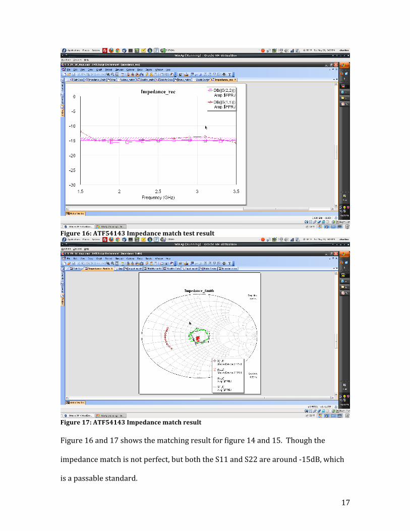
Figure 16: ATF54143 Impedance match test result
Figure 17: ATF54143 Impedance match result Figure 16 and 17 shows the matching result for figure 14 and 15. Though the
impedance match is not perfect, but both the S11 and S22 are around -‐15dB, which
is a passable standard.
18
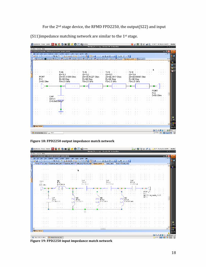
For the 2nd stage device, the RFMD FPD2250, the output(S22) and input
(S11)impedance matching network are similar to the 1st stage.
Figure 18: FPD2250 output impedance match network
Figure 19: FPD2250 input impedance match network
19
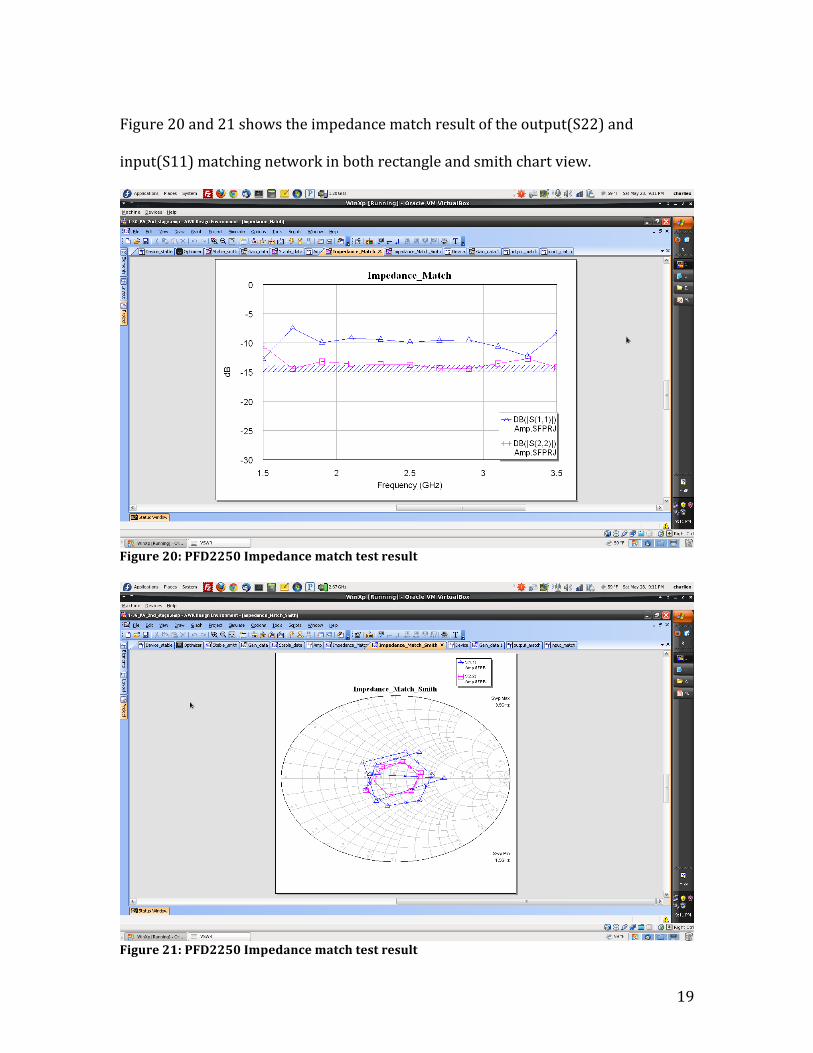
Figure 20 and 21 shows the impedance match result of the output(S22) and
input(S11) matching network in both rectangle and smith chart view.
Figure 20: PFD2250 Impedance match test result
Figure 21: PFD2250 Impedance match test result
20
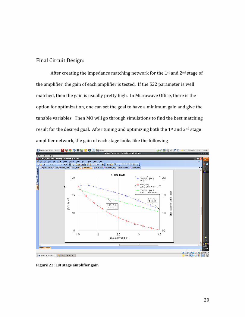
Final Circuit Design:
After creating the impedance matching network for the 1st and 2nd stage of
the amplifier, the gain of each amplifier is tested. If the S22 parameter is well
matched, then the gain is usually pretty high. In Microwave Office, there is the
option for optimization, one can set the goal to have a minimum gain and give the
tunable variables. Then MO will go through simulations to find the best matching
result for the desired goal. After tuning and optimizing both the 1st and 2nd stage
amplifier network, the gain of each stage looks like the following
Figure 22: 1st stage amplifier gain
21
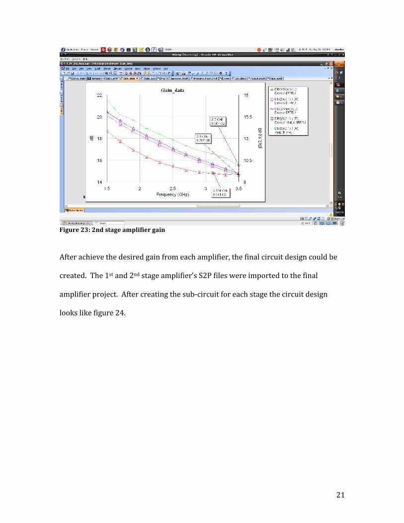
Figure 23: 2nd stage amplifier gain
After achieve the desired gain from each amplifier, the final circuit design could be
created. The 1st and 2nd stage amplifier’s S2P files were imported to the final
amplifier project. After creating the sub-‐circuit for each stage the circuit design
looks like figure 24.
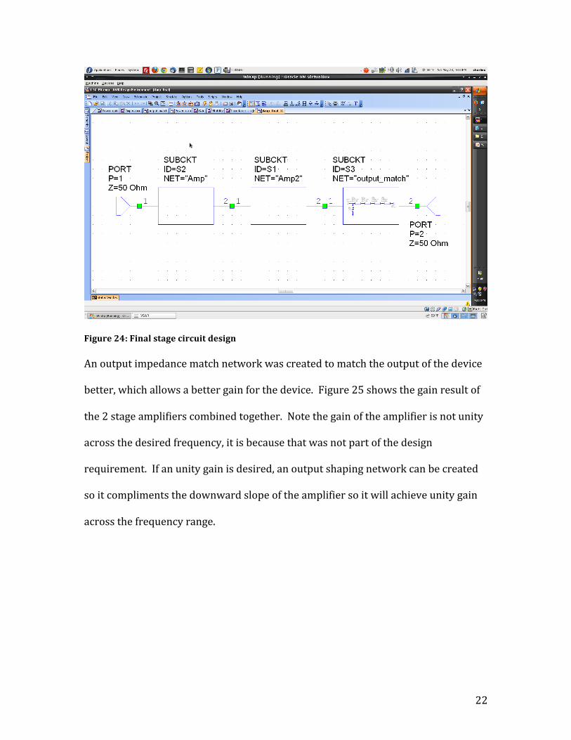
22
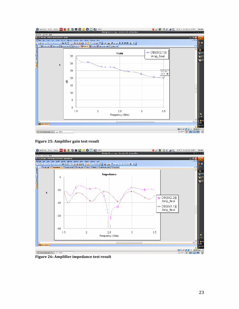
Figure 24: Final stage circuit design An output impedance match network was created to match the output of the device
better, which allows a better gain for the device. Figure 25 shows the gain result of
the 2 stage amplifiers combined together. Note the gain of the amplifier is not unity
across the desired frequency, it is because that was not part of the design
requirement. If an unity gain is desired, an output shaping network can be created
so it compliments the downward slope of the amplifier so it will achieve unity gain
across the frequency range.
23
Figure 25: Amplifier gain test result
Figure 26: Amplifier impedance test result
24
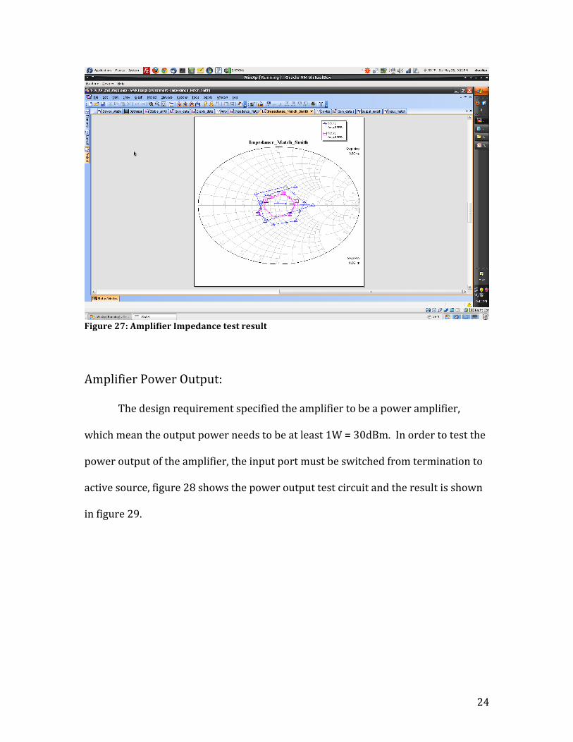
Figure 27: Amplifier Impedance test result Amplifier Power Output:
The design requirement specified the amplifier to be a power amplifier,
which mean the output power needs to be at least 1W = 30dBm. In order to test the
power output of the amplifier, the input port must be switched from termination to
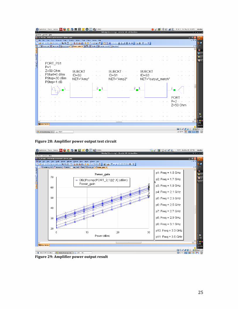
active source, figure 28 shows the power output test circuit and the result is shown
in figure 29.
25
Figure 28: Amplifier power output test circuit
Figure 29: Amplifier power output result
26
From figure 29, the power output of the amplifier can be observed. Note how the
power gain of the device is linear across different level of input power. This is
because the S2P file is not the complete model of the device, but only the linear
region of the device, which cause the gain to be linear. In real world the amplifier
will display nonlinear property at the device’s P1dB compression point and it will be
eventually drive into saturation.
Nonlinearity of Devices:
In the previous section, the power output graph shows a linear power gain of
the device, but the real device will not function like the test result. This is the result
of not having the full SPICE model of the device. By only having the S2P file of the
device, only a linear model can be created. It is because the S2P file is being tested
across the linear region of the device rather than the whole device-‐operating region.
There is another way of finding the nonlinearity of the device, which is to read the
data sheet provided by the company.
From the Avago ATF54143 data sheet, the output power 1dB gain
compression point is at 20.4dBm, 36.2 dBm output 3rd order intercept point (IP3),
and 0.5dB noise figure. From the RFMD FPD2250 datasheet, the output power 1dB
gain compression point is at 31dBm, 44dBm IP3, and 0.9dB noise figure. With the
datasheet information, the nonlinearity points of the final amplifier can be
calculated. With the gain of the 1st stage amplifier at 9.7dB, this means the
maximum input power of the 1st stage amplifier equals to 20.4dBm – 9.7dB =
10.8dBm. The Gain of the 2nd stage amplifier is 9.8dB with the 1dB compression

27
point at 31dBm, that means the maximum input power of the 2nd stage amplifier is
31dBm – 9.8dB = 21.2dBm. Since the 1st stage amplifier output power will never
surpass the maximum input power of the 2nd stage amplifier, the maximum input
pout of the amplifier is 10.8dBm with the maximum output power at 20.4dBm +
9.8dB = 31.2dBm.
Final Remarks:
This project has been a very educating experience. Through out the project
there were many times of frustration because what my calculation show does not
match up with the simulated result of the software. I had to tune the circuits
individually in order to get what I wanted; with out the knowledge I learned from
class and the research I did on my own, I would never been able to finish the project.
This project is different comparing to the other projects from the past. In the past,
the specification is to create a single frequency power amplifier. My project is more
challenging in the sense that the amplifier needs to have a 2GHz bandwidth. The
bandwidth was the part where I spent the most among of time, because I tried out
the Chebyshev matching method first and eventually realized the downside of using
it, then I switched to the lump element matching.
Here are some aspects of the project I wish I could have more time to work on:
1. Find the full device model of both devices and create the bias network.
2. Create an output-‐shaping network so the gain is unity across the frequency
range.

28
3. Create a better matching network so the devices are better matched, so the
user do not need to worry about reflection.
Here at the end I want to thank Dr. Kwok’s help for this project as well so others
who helped me throughout the project.
29
Appendix:
A. Avago ATF54143 Datasheet – Please see attached file, filename: AV02-‐
0488EN.pdf
B. FRMD PFD2250SOT89 Datasheet -‐
http://www.rfmd.com/CS/Documents/FPD2250SOT89DS.pdf
C. Chebyshev matching calculation – Please see attached file, filename:
Chebyshev_match.xls

30
Reference:
1. Inder Bahl, Prakash Bhartia, Microwave Solid State Circuit Design, John Wiley
& Sons Ltd. New York 1988
2. Besser Associates, RF/MW Circuit Design: Linear/Nonlinear Theory and
Applications (5 Day short course), Besser Associates 2000
3. Pozar, David M., Microwave Engineering, 3rd Edition, John Wiley & Sons, Inc.,
New Jersey, 2005
4. A.M. Niknejad, EECS142 Laboratory #3, University of California Berkeley
Wireless Research Center, Berkeley 2008
5. J. Patrick Donohoe,
http://www.ece.msstate.edu/~donohoe/ece4333notes5.pdf , Mississippi
State University, Department of Electrical and computer engineering
6. www.awr.tv