` EV173A-J-00A - Monolithic Power Systems
12
` EV173A-J-00A Universal Input, Non-Isolated Off-Line Regulator With Improved EMI Performance Evaluation Board EV173A-J-00A Rev.1.0 www.MonolithicPower.com 1 10/30/2019 MPS Proprietary Information. Patent Protected. Unauthorized Photocopy and Duplication Prohibited. © 2019 MPS. All Rights Reserved. DESCRIPTION The EV173A-J-00A Evaluation Board is designed to demonstrate the capabilities of MP173A. The MP173A is a primary-side constant voltage regulator, which provides accurate constant voltage (CV) regulation without Opto-coupler. It supports Buck, Buck-Boost, Boost and Flyback topologies. The EV173A-J-00A Evaluation Board is designed as Buck application. EV173A-J-00A typically outputs 3W with a 12V/250mA load from 85VAC to 265VAC input. The EV173A-J-00A has excellent efficiency and meets IEC61000-4-5 surge immunity and EN55022 conducted EMI requirements. Most of all, the radiation performance gets improved compared with MP173. MP173A features various protections, including thermal shutdown (TSD), VCC under-voltage lockout (UVLO), over-load protection (OLP), short-circuit protection (SCP), and open loop protection. MP173AGJ is available in TSOT23-5 package. ELECTRICAL SPECIFICATION Parameter Symbol Value Units Input Voltage VIN 85 to 265 VAC Output Voltage VOUT 12 V Output Current IOUT 0.25 (1) A Output Power POUT 3 W Efficiency (full load) η >75 % FEATURES Primary-Side non-isolated Constant Voltage (CV) Control < 30mW No-load power consumption Up to 3W output power Good EMI Performance Limited Maximum Frequency Multiple Protections: SCP, OCP, OTP, OLD and VCC UVLO Low Cost and Simple External circuit APPLICATIONS Home Appliance, white goods and consumer electronics Industrial Controls Standby Power All MPS parts are lead-free, halogen free, and adhere to the RoHS directive. For MPS green status, please visit MPS website under Quality Assurance. “MPS” and “The Future of Analog IC Technology” are Registered Trademarks of Monolithic Power Systems, Inc. Warning: Although this board is designed to satisfy safety requirements, the engineering prototype has not been agency approved. Therefore, all testing should be performed using an isolation transformer to provide the AC input to the prototype board. Note 1): When TA=80°C, it is recommended to output 12V/0.22A under high line input (265VAC), taken the ILIMIT tolerance into consideration.
-
Upload
khangminh22 -
Category
Documents
-
view
0 -
download
0
Transcript of ` EV173A-J-00A - Monolithic Power Systems

` EV173A-J-00A Universal Input,
Non-Isolated Off-Line Regulator With Improved EMI Performance
Evaluation Board
EV173A-J-00A Rev.1.0 www.MonolithicPower.com 1 10/30/2019 MPS Proprietary Information. Patent Protected. Unauthorized Photocopy and Duplication Prohibited. © 2019 MPS. All Rights Reserved.
DESCRIPTION The EV173A-J-00A Evaluation Board is designed to demonstrate the capabilities of MP173A. The MP173A is a primary-side constant voltage regulator, which provides accurate constant voltage (CV) regulation without Opto-coupler. It supports Buck, Buck-Boost, Boost and Flyback topologies.
The EV173A-J-00A Evaluation Board is designed as Buck application. EV173A-J-00A typically outputs 3W with a 12V/250mA load from 85VAC to 265VAC input.
The EV173A-J-00A has excellent efficiency and meets IEC61000-4-5 surge immunity and EN55022 conducted EMI requirements. Most of all, the radiation performance gets improved compared with MP173. MP173A features various protections, including thermal shutdown (TSD), VCC under-voltage lockout (UVLO), over-load protection (OLP), short-circuit protection (SCP), and open loop protection.
MP173AGJ is available in TSOT23-5 package.
ELECTRICAL SPECIFICATION Parameter Symbol Value Units
Input Voltage VIN 85 to 265 VAC
Output Voltage VOUT 12 V
Output Current IOUT 0.25(1) A
Output Power POUT 3 W
Efficiency (full load) η >75 %
FEATURES
Primary-Side non-isolated Constant Voltage (CV) Control
< 30mW No-load power consumption Up to 3W output power Good EMI Performance Limited Maximum Frequency Multiple Protections: SCP, OCP, OTP, OLD
and VCC UVLO Low Cost and Simple External circuit
APPLICATIONS Home Appliance, white goods and
consumer electronics Industrial Controls Standby Power
All MPS parts are lead-free, halogen free, and adhere to the RoHS directive. For MPS green status, please visit MPS website under Quality Assurance. “MPS” and “The Future of Analog IC Technology” are Registered Trademarks of Monolithic Power Systems, Inc.
Warning: Although this board is designed to satisfy safety requirements, the engineering prototype has not been agency approved. Therefore, all testing should be performed using an isolation transformer to provide the AC input to the prototype board.
Note 1): When TA=80°C, it is recommended to output 12V/0.22A under high line input (265VAC), taken the ILIMIT tolerance into consideration.
EV173A-J-00A – UNIVERSAL INPUT, NON-ISOLATED OFF-LINE REGULATOR
EV173A-J-00A Rev.1.0 www.MonolithicPower.com 2 10/30/2019 MPS Proprietary Information. Patent Protected. Unauthorized Photocopy and Duplication Prohibited. © 2019 MPS. All Rights Reserved.
EV173A-J-00A EVALUATION BOARD
TOP VIEW
BOTTOM VIEW
(L x W x H) 68mm x 28mm x 17mm
Board Number MPS IC Number
EV173A-J-00A MP173AGJ
EV173A-J-00A – UNIVERSAL INPUT, NON-ISOLATED OFF-LINE REGULATOR
EV173A-J-00A Rev.1.0 www.MonolithicPower.com 3 10/30/2019 MPS Proprietary Information. Patent Protected. Unauthorized Photocopy and Duplication Prohibited. © 2019 MPS. All Rights Reserved.
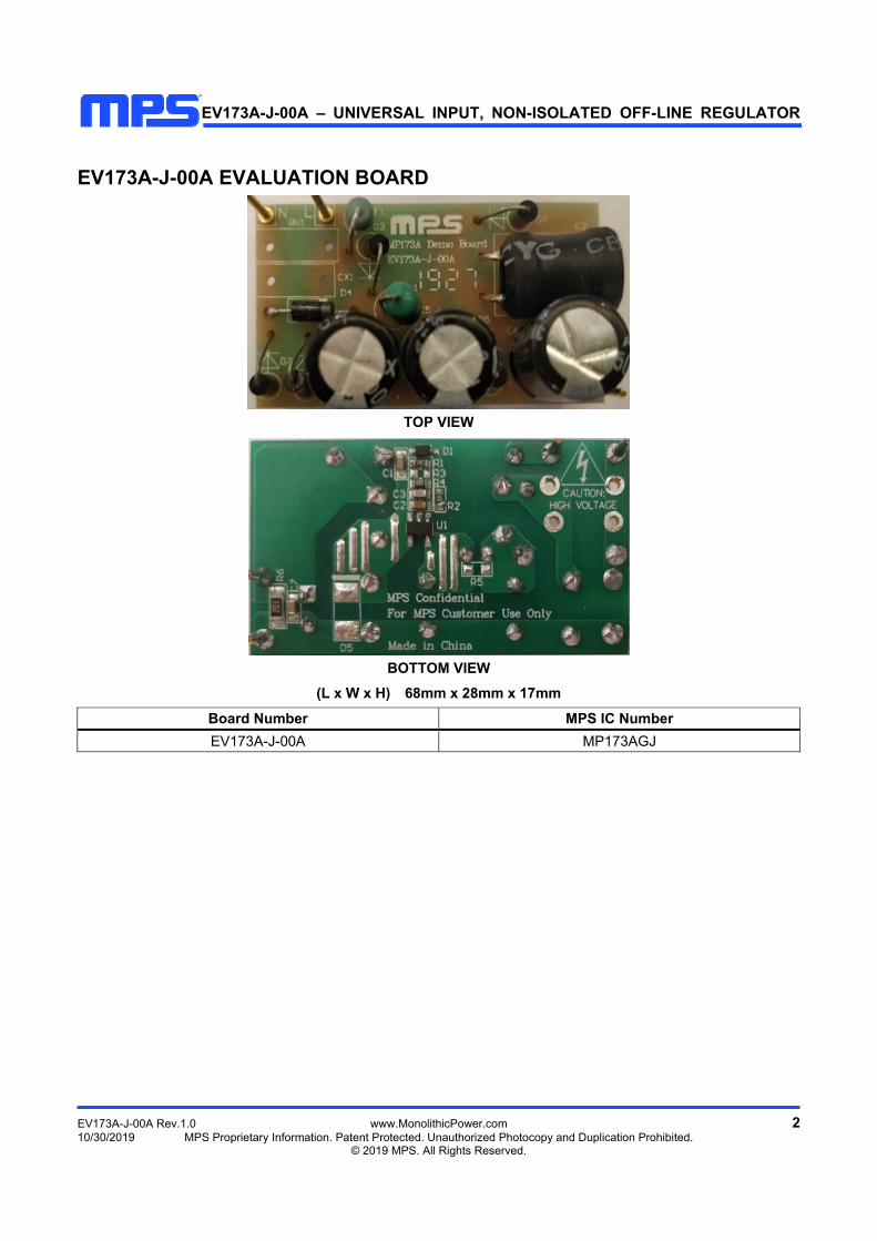
EVALUATION BOARD SCHEMATIC
Figure 1: Schematic
L
N
10uF/400VC4
10uF/400VC5
1mHL1
D3
1N4007
D6
1N4007
D5
STTH1R06
C6
GND
VOUT
GND
470nF C1
19.1K
R1
4.99K
R4
NC
R3
2.2uF
C2
10/1W F1
1uF
C7
1nF
C3
85~265VAC
12V/250mA
D4
1N4007
D7
1N4007 20K
R6
D2
1N4007 1N4148WS
D1
20K
R2
NCR5
1.2mH L2
NC CX1
NC RV1
Drain5
Source4
Vcc 1
FB 2
Source 3
U1
MP173A
100uF/35V
EV173A-J-00A – UNIVERSAL INPUT, NON-ISOLATED OFF-LINE REGULATOR
EV173A-J-00A Rev.1.0 www.MonolithicPower.com 4 10/30/2019 MPS Proprietary Information. Patent Protected. Unauthorized Photocopy and Duplication Prohibited. © 2019 MPS. All Rights Reserved.
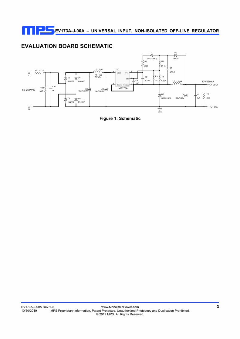
PCB LAYOUT (SINGLE-SIDED)
Figure 2: Top Layer
Figure 3: Bottom Layer
EV173A-J-00A – UNIVERSAL INPUT, NON-ISOLATED OFF-LINE REGULATOR
EV173A-J-00A Rev.1.0 www.MonolithicPower.com 5 10/30/2019 MPS Proprietary Information. Patent Protected. Unauthorized Photocopy and Duplication Prohibited. © 2019 MPS. All Rights Reserved.
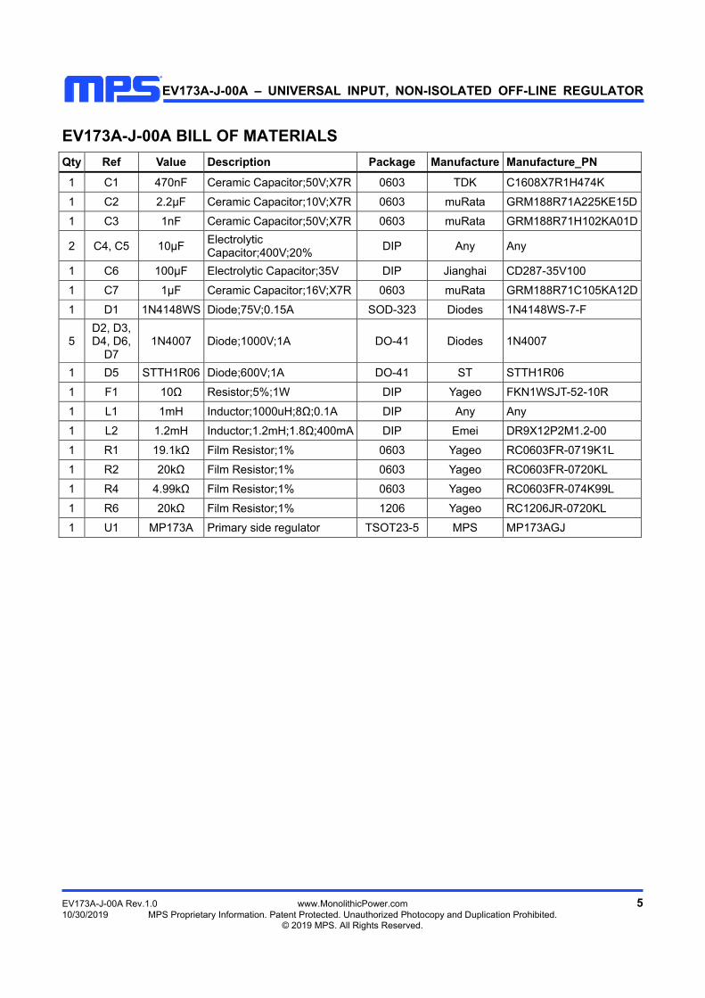
EV173A-J-00A BILL OF MATERIALS
Qty Ref Value Description Package Manufacture Manufacture_PN
1 C1 470nF Ceramic Capacitor;50V;X7R 0603 TDK C1608X7R1H474K
1 C2 2.2μF Ceramic Capacitor;10V;X7R 0603 muRata GRM188R71A225KE15D
1 C3 1nF Ceramic Capacitor;50V;X7R 0603 muRata GRM188R71H102KA01D
2 C4, C5 10μF Electrolytic Capacitor;400V;20%
DIP Any Any
1 C6 100μF Electrolytic Capacitor;35V DIP Jianghai CD287-35V100
1 C7 1μF Ceramic Capacitor;16V;X7R 0603 muRata GRM188R71C105KA12D
1 D1 1N4148WS Diode;75V;0.15A SOD-323 Diodes 1N4148WS-7-F
5 D2, D3, D4, D6,
D7 1N4007 Diode;1000V;1A DO-41 Diodes 1N4007
1 D5 STTH1R06 Diode;600V;1A DO-41 ST STTH1R06
1 F1 10Ω Resistor;5%;1W DIP Yageo FKN1WSJT-52-10R
1 L1 1mH Inductor;1000uH;8Ω;0.1A DIP Any Any
1 L2 1.2mH Inductor;1.2mH;1.8Ω;400mA DIP Emei DR9X12P2M1.2-00
1 R1 19.1kΩ Film Resistor;1% 0603 Yageo RC0603FR-0719K1L
1 R2 20kΩ Film Resistor;1% 0603 Yageo RC0603FR-0720KL
1 R4 4.99kΩ Film Resistor;1% 0603 Yageo RC0603FR-074K99L
1 R6 20kΩ Film Resistor;1% 1206 Yageo RC1206JR-0720KL
1 U1 MP173A Primary side regulator TSOT23-5 MPS MP173AGJ
EV173A-J-00A – UNIVERSAL INPUT, NON-ISOLATED OFF-LINE REGULATOR
EV173A-J-00A Rev.1.0 www.MonolithicPower.com 6 10/30/2019 MPS Proprietary Information. Patent Protected. Unauthorized Photocopy and Duplication Prohibited. © 2019 MPS. All Rights Reserved.
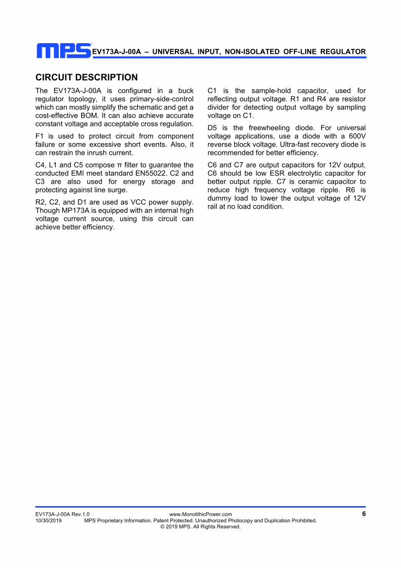
CIRCUIT DESCRIPTION The EV173A-J-00A is configured in a buck regulator topology, it uses primary-side-control which can mostly simplify the schematic and get a cost-effective BOM. It can also achieve accurate constant voltage and acceptable cross regulation.
F1 is used to protect circuit from component failure or some excessive short events. Also, it can restrain the inrush current.
C4, L1 and C5 compose π filter to guarantee the conducted EMI meet standard EN55022. C2 and C3 are also used for energy storage and protecting against line surge.
R2, C2, and D1 are used as VCC power supply. Though MP173A is equipped with an internal high voltage current source, using this circuit can achieve better efficiency.
C1 is the sample-hold capacitor, used for reflecting output voltage. R1 and R4 are resistor divider for detecting output voltage by sampling voltage on C1.
D5 is the freewheeling diode. For universal voltage applications, use a diode with a 600V reverse block voltage. Ultra-fast recovery diode is recommended for better efficiency.
C6 and C7 are output capacitors for 12V output. C6 should be low ESR electrolytic capacitor for better output ripple. C7 is ceramic capacitor to reduce high frequency voltage ripple. R6 is dummy load to lower the output voltage of 12V rail at no load condition.
EV173A-J-00A – UNIVERSAL INPUT, NON-ISOLATED OFF-LINE REGULATOR
EV173A-J-00A Rev.1.0 www.MonolithicPower.com 7 10/30/2019 MPS Proprietary Information. Patent Protected. Unauthorized Photocopy and Duplication Prohibited. © 2019 MPS. All Rights Reserved.
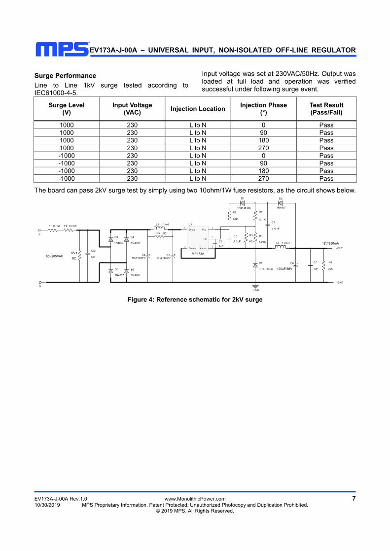
Surge Performance
Line to Line 1kV surge tested according to IEC61000-4-5.
Input voltage was set at 230VAC/50Hz. Output was loaded at full load and operation was verified successful under following surge event.
Surge Level (V)
Input Voltage (VAC)
Injection LocationInjection Phase
(°) Test Result (Pass/Fail)
1000 230 L to N 0 Pass 1000 230 L to N 90 Pass 1000 230 L to N 180 Pass 1000 230 L to N 270 Pass -1000 230 L to N 0 Pass -1000 230 L to N 90 Pass -1000 230 L to N 180 Pass -1000 230 L to N 270 Pass
The board can pass 2kV surge test by simply using two 10ohm/1W fuse resistors, as the circuit shows below.
Figure 4: Reference schematic for 2kV surge
L
N
10uF/400 V C 4 10uF/400V
C5
1mHL 1
D3
1N4007
D6
1N4007
D5
STTH 1R06
C6
GND
VOUT
GND
470 nF
C119.1K
R1
4.99K
R4
NC
R3
2.2uF
C2
10/1WF2
1 uF C7
1nF
C3
85~265VAC
12V/250mA
D 41 N4007
D7 1 N4007
20K
R6
D2 1 N4007 1N4148 WS
D1
20K
R2
NCR5
1.2 mHL2
NC
CX1 NC RV 1
Drain5
Source4
Vcc1
FB2
Source3
U1
MP173A
10/ 1WF1
100uF/35V
EV173A-J-00A – UNIVERSAL INPUT, NON-ISOLATED OFF-LINE REGULATOR
EV173A-J-00A Rev.1.0 www.MonolithicPower.com 8 10/30/2019 MPS Proprietary Information. Patent Protected. Unauthorized Photocopy and Duplication Prohibited. © 2019 MPS. All Rights Reserved.
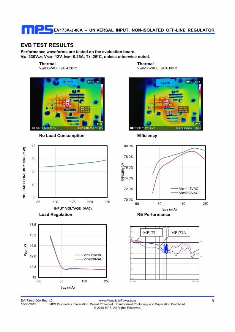
EVB TEST RESULTS Performance waveforms are tested on the evaluation board. VIN=230VAC, VOUT=12V, IOUT=0.25A, TA=26C, unless otherwise noted.
Thermal VIN=85VAC, FS=34.2kHz
Thermal VIN=265VAC, FS=36.0kHz
No Load Consumption Efficiency
0
10
20
30
40
85 130 175 220 265
NO
LO
AD
CO
NS
UM
PT
ION
(m
W)
INPUT VOLTAGE (VAC)
70.0%
72.0%
74.0%
76.0%
78.0%
80.0%
-50 50 150 250
EFF
ICIE
NC
Y
IOUT (mA)
Vin=115VACVin=230VAC
Load Regulation RE Performance
12
12.3
12.6
12.9
13.2
13.5
-50 50 150 250
VO
UT
(V)
IOUT (mA)
Vin=115VACVin=230VAC
61.0°C 72.3°C
MP173 MP173A

EV173A-J-00A – UNIVERSAL INPUT, NON-ISOLATED OFF-LINE REGULATOR
EV173A-J-00A Rev.1.0 www.MonolithicPower.com 9 10/30/2019 MPS Proprietary Information. Patent Protected. Unauthorized Photocopy and Duplication Prohibited. © 2019 MPS. All Rights Reserved.
EVB TEST RESULTS (continued) Performance waveforms are tested on the evaluation board. VIN=230VAC, VOUT=12V, IOUT=0.25A, TA=26C, unless otherwise noted.
CE Performance-L Line CE Performance-N Line
150 kHz 30 MHz
6
S
T
1 MHz 10 MHz
0
10
20
30
40
50
60
70
80
90
100
110
120
EN55022A
EN55022Q
150 kHz 30 MHz
1 MHz 10 MHz
0
10
20
30
40
50
60
70
80
90
100
110
120
EN55022A
EN55022Q

EV173A-J-00A – UNIVERSAL INPUT, NON-ISOLATED OFF-LINE REGULATOR
EV173A-J-00A Rev.1.0 www.MonolithicPower.com 10 10/30/2019 MPS Proprietary Information. Patent Protected. Unauthorized Photocopy and Duplication Prohibited. © 2019 MPS. All Rights Reserved.
EVB TEST RESULTS (continued) Performance waveforms are tested on the evaluation board. VIN=230VAC, VOUT=12V, IOUT=0.25A, TA=26C, unless otherwise noted.
Steady State Output Ripple
CH1: VDS
CH4: IL
CH2: VOUT_RIPPLE
Start-Up Start-Up VIN=265VAC, L=680μH, COUT=1000uF
CH1: VDS
CH2: VOUT
CH4: IL
CH1: VDS
CH2: VOUT
CH4: IL
Load Transient 25%-50% Load
Load Transient 50%-75% Load
CH2: VOUT_RIPPLE
CH4: IOUT
CH2: VOUT_RIPPLE
CH4: IOUT
EV173A-J-00A – UNIVERSAL INPUT, NON-ISOLATED OFF-LINE REGULATOR
EV173A-J-00A Rev.1.0 www.MonolithicPower.com 11 10/30/2019 MPS Proprietary Information. Patent Protected. Unauthorized Photocopy and Duplication Prohibited. © 2019 MPS. All Rights Reserved.
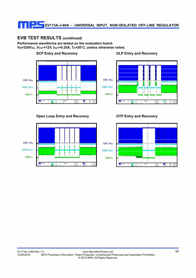
EVB TEST RESULTS (continued) Performance waveforms are tested on the evaluation board. VIN=230VAC, VOUT=12V, IOUT=0.25A, TA=26C, unless otherwise noted.
SCP Entry and Recovery
OLP Entry and Recovery
CH1: VDS
CH2: VOUT
CH4: IL
CH1: VDS
CH2: VOUT
CH4: IL
Open Loop Entry and Recovery OTP Entry and Recovery
CH1: VDS
CH2: VOUT
CH4: IL
CH1: VDS
CH2: VOUT
CH4: IL

EV173A-J-00A – UNIVERSAL INPUT, NON-ISOLATED OFF-LINE REGULATOR
NOTICE: The information in this document is subject to change without notice. Please contact MPS for current specifications. Users should warrant and guarantee that third party Intellectual Property rights are not infringed upon when integrating MPS products into any application. MPS will not assume any legal responsibility for any said applications.
EV173A-J-00A Rev.1.0 www.MonolithicPower.com 12 10/30/2019 MPS Proprietary Information. Patent Protected. Unauthorized Photocopy and Duplication Prohibited. © 2019 MPS. All Rights Reserved.
QUICK START GUIDE
1. Preset Power Supply to 85VAC VIN 265VAC.
2. Turn Power Supply off.
3. Connect the Line and Neutral terminals of the power supply output to L and N port.
4. Connect Different Load to Corresponding Outputs :
a. Positive (+): 12V OUT
b. Negative (–): GND
5. Turn Power Supply on after making connections.


![E=F9;mklge]j ZYjge]l]j L`ak lae] alÌk h]jkgfYd2 ^jge [gfkme]j lg [g%[j]Ylgj](https://static.fdokumen.com/doc/165x107/631789cb7451843eec0ab6f2/ef9mklgej-zyjgelj-lak-lae-alik-hjkgfyd2-jge-gfkmej-lg-gjylgj.jpg)