TP3040 TP3040A PCM Monolithic Filter
10
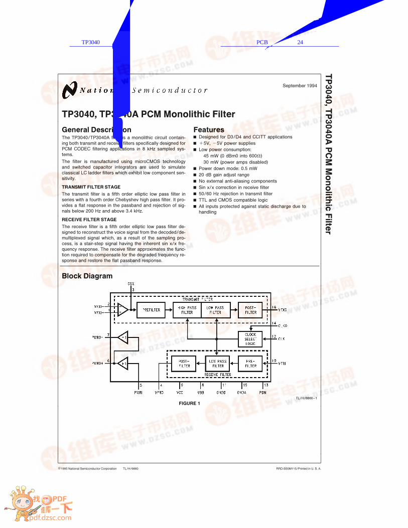
TL/H/6660 TP3040, TP3040A PCM Monolithic Filter September 1994 TP3040, TP3040A PCM Monolithic Filter General Description The TP3040/TP3040A filter is a monolithic circuit contain- ing both transmit and receive filters specifically designed for PCM CODEC filtering applications in 8 kHz sampled sys- tems. The filter is manufactured using microCMOS technology and switched capacitor integrators are used to simulate classical LC ladder filters which exhibit low component sen- sitivity. TRANSMIT FILTER STAGE The transmit filter is a fifth order elliptic low pass filter in series with a fourth order Chebyshev high pass filter. It pro- vides a flat response in the passband and rejection of sig- nals below 200 Hz and above 3.4 kHz. RECEIVE FILTER STAGE The receive filter is a fifth order elliptic low pass filter de- signed to reconstruct the voice signal from the decoded/de- multiplexed signal which, as a result of the sampling pro- cess, is a stair-step signal having the inherent sin x/x fre- quency response. The receive filter approximates the func- tion required to compensate for the degraded frequency re- sponse and restore the flat passband response. Features Y Designed for D3/D4 and CCITT applications Y a5V, b5V power supplies Y Low power consumption: 45 mW (0 dBm0 into 600X) 30 mW (power amps disabled) Y Power down mode: 0.5 mW Y 20 dB gain adjust range Y No external anti-aliasing components Y Sin x/x correction in receive filter Y 50/60 Hz rejection in transmit filter Y TTL and CMOS compatible logic Y All inputs protected against static discharge due to handling Block Diagram TL/H/6660 – 1 FIGURE 1 C1995 National Semiconductor Corporation RRD-B30M115/Printed in U. S. A. 查询TP3040供应商 捷多邦,专业PCB打样工厂,24小时加急出货
-
Upload
khangminh22 -
Category
Documents
-
view
1 -
download
0
Transcript of TP3040 TP3040A PCM Monolithic Filter
TL/H/6660
TP3040,TP3040A
PC
MM
onolith
icFilte
rSeptember 1994
TP3040, TP3040A PCM Monolithic Filter
General DescriptionThe TP3040/TP3040A filter is a monolithic circuit contain-
ing both transmit and receive filters specifically designed for
PCM CODEC filtering applications in 8 kHz sampled sys-
tems.
The filter is manufactured using microCMOS technology
and switched capacitor integrators are used to simulate
classical LC ladder filters which exhibit low component sen-
sitivity.
TRANSMIT FILTER STAGE
The transmit filter is a fifth order elliptic low pass filter in
series with a fourth order Chebyshev high pass filter. It pro-
vides a flat response in the passband and rejection of sig-
nals below 200 Hz and above 3.4 kHz.
RECEIVE FILTER STAGE
The receive filter is a fifth order elliptic low pass filter de-
signed to reconstruct the voice signal from the decoded/de-
multiplexed signal which, as a result of the sampling pro-
cess, is a stair-step signal having the inherent sin x/x fre-
quency response. The receive filter approximates the func-
tion required to compensate for the degraded frequency re-
sponse and restore the flat passband response.
FeaturesY Designed for D3/D4 and CCITT applicationsY a5V, b5V power suppliesY Low power consumption:
45 mW (0 dBm0 into 600X)
30 mW (power amps disabled)Y Power down mode: 0.5 mWY 20 dB gain adjust rangeY No external anti-aliasing componentsY Sin x/x correction in receive filterY 50/60 Hz rejection in transmit filterY TTL and CMOS compatible logicY All inputs protected against static discharge due to
handling
Block Diagram
TL/H/6660–1
FIGURE 1
C1995 National Semiconductor Corporation RRD-B30M115/Printed in U. S. A.
查询TP3040供应商 捷多邦,专业PCB打样工厂,24小时加急出货
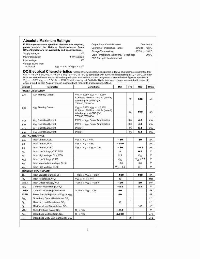
Absolute Maximum RatingsIf Military/Aerospace specified devices are required,
please contact the National Semiconductor Sales
Office/Distributors for availability and specifications.
Supply Voltages g7V
Power Dissipation 1 W/Package
Input Voltage g7V
Voltage at Any Input
or Output VCC a 0.3V to VBBV b 0.3V
Output Short-Circuit Duration Continuous
Operating Temperature Range b25§C to a125§CStorage Temperature b65§C to a150§CLead Temperature (Soldering, 10 seconds) 300§CESD Rating to be determined
DC Electrical Characteristics Unless otherwise noted, limits printed in BOLD characters are guaranteed for
VCC e a5.0V g5%, VBB e b5.0V g5%; TA e 0§C to 70§C by correlation with 100% electrical testing at TA e 25§C. All other
limits are assured by correlation with other production tests and/or product design and characterization. Typicals specified at
VCC e a5.0V, VBB e b5.0V, TA e 25§C. Clock frequency is 2.048 MHz. Digital interface voltages measured with respect to
digital ground, GNDD. Analog voltages measured with respect to analog ground, GNDA.
Symbol Parameter Conditions Min Typ Max Units
POWER DISSIPATION
ICC0 VCC Standby Current VCC e 5.25V, VBB e b5.25V,
CLK0 and PWRI e b5.25V (Note 6)50 100 mA
All other pins at GND (0V)
TP3040, TP3040A
IBB0 VBB Standby Current VCC e 5.25V, VBB e b5.25V,
CLK0 and PWRI e b5.25V (Note 6)50 100 mA
All other pins at GND (0V)
TP3040, TP3040A
ICC1 VCC Operating Current PWRI e VBB, Power Amp Inactive 3.0 4.0 mA
IBB1 VBB Operating Current PWRI e VBB, Power Amp Inactive 3.0 4.0 mA
ICC2 VCC Operating Current (Note 1) 4.6 6.4 mA
IBB2 VBB Operating Current (Note 1) 4.6 6.4 mA
DIGITAL INTERFACE
IINC Input Current, CLK VBB s VIN s VCC b10 10 mA
IINP Input Current, PDN VBB s VIN s VCC b100 mA
IIN0 Input Current, CLK0 VBB s VIN s VCC b 0.5V b10 b0.1 mA
VIL Input Low Voltage, CLK, PDN 0 0.8 V
VIH Input High Voltage, CLK, PDN 2.2 VCC V
VIL0 Input Low Voltage, CLK0 VBB VBBa0.5 V
VII0 Input Intermediate Voltage, CLK0 b0.8 0.8 V
VIH0 Input High Voltage, CLK0 VCCb0.5 VCC V
TRANSMIT INPUT OP AMP
IBxI Input Leakage Current, VFxI b3.2V s VIN s a3.2V b100 100 nA
RIxI Input Resistance, VFxI VBB s VFxI s VCC 10 MX
VOSxI Input Offset Voltage, VFxI b2.5V s VIN s a2.5V b20 20 mV
VCM Common-Mode Range, VFxI b2.5 2.5 V
CMRR Common-Mode Rejection Ratio b2.5V s VIN s 2.5V 60 dB
PSRR Power Supply Rejection of VCC or VBB 60 dB
ROL Open Loop Output Resistance, GSx 1 kX
RL Minimum Load Resistance, GSx 10 kX
CL Maximum Load Capacitance, GSx 100 pF
VOxI Output Voltage Swing, GSx RL t 10k g2.5 V
AVOL Open Loop Voltage Gain, GSx RL t 10k 5,000 V/V
Fc Open Loop Unity Gain Bandwidth, GSx 2 MHz
2
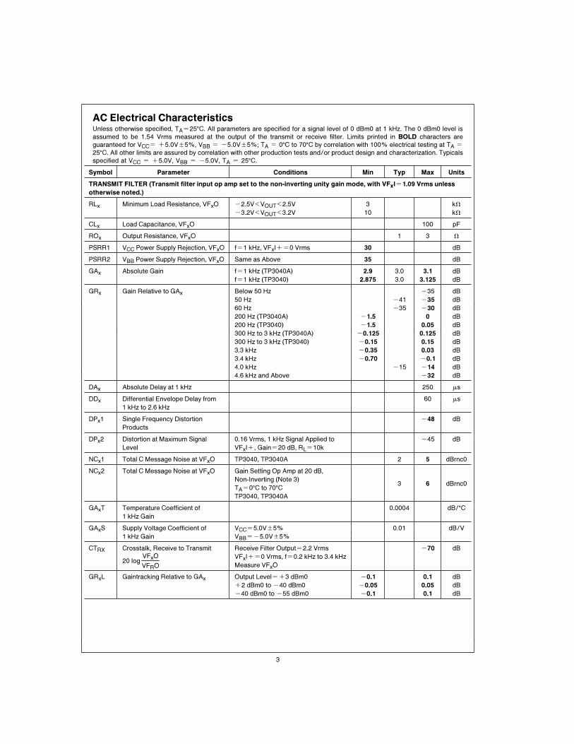
AC Electrical CharacteristicsUnless otherwise specified, TAe25§C. All parameters are specified for a signal level of 0 dBm0 at 1 kHz. The 0 dBm0 level is
assumed to be 1.54 Vrms measured at the output of the transmit or receive filter. Limits printed in BOLD characters are
guaranteed for VCCe a5.0Vg5%, VBB e b5.0Vg5%; TA e 0§C to 70§C by correlation with 100% electrical testing at TA e
25§C. All other limits are assured by correlation with other production tests and/or product design and characterization. Typicals
specified at VCC e a5.0V, VBB e b5.0V, TA e 25§C.
Symbol Parameter Conditions Min Typ Max Units
TRANSMIT FILTER (Transmit filter input op amp set to the non-inverting unity gain mode, with VFxIe1.09 Vrms unless
otherwise noted.)
RLx Minimum Load Resistance, VFxO b2.5VkVOUTk2.5V 3 kXb3.2VkVOUTk3.2V 10 kX
CLx Load Capacitance, VFxO 100 pF
ROx Output Resistance, VFxO 1 3 X
PSRR1 VCC Power Supply Rejection, VFxO fe1 kHz, VFxIae0 Vrms 30 dB
PSRR2 VBB Power Supply Rejection, VFxO Same as Above 35 dB
GAx Absolute Gain fe1 kHz (TP3040A) 2.9 3.0 3.1 dB
fe1 kHz (TP3040) 2.875 3.0 3.125 dB
GRx Gain Relative to GAx Below 50 Hz b35 dB
50 Hz b41 b35 dB
60 Hz b35 b30 dB
200 Hz (TP3040A) b1.5 0 dB
200 Hz (TP3040) b1.5 0.05 dB
300 Hz to 3 kHz (TP3040A) b0.125 0.125 dB
300 Hz to 3 kHz (TP3040) b0.15 0.15 dB
3.3 kHz b0.35 0.03 dB
3.4 kHz b0.70 b0.1 dB
4.0 kHz b15 b14 dB
4.6 kHz and Above b32 dB
DAx Absolute Delay at 1 kHz 250 ms
DDx Differential Envelope Delay from 60 ms
1 kHz to 2.6 kHz
DPx1 Single Frequency Distortion b48 dB
Products
DPx2 Distortion at Maximum Signal 0.16 Vrms, 1 kHz Signal Applied to b45 dB
Level VFxIa, Gaine20 dB, RLe10k
NCx1 Total C Message Noise at VFxO TP3040, TP3040A 2 5 dBrnc0
NCx2 Total C Message Noise at VFxO Gain Setting Op Amp at 20 dB,
Non-Inverting (Note 3)3 6 dBrnc0
TAe0§C to 70§CTP3040, TP3040A
GAxT Temperature Coefficient of 0.0004 dB/§C1 kHz Gain
GAxS Supply Voltage Coefficient of VCCe5.0Vg5% 0.01 dB/V
1 kHz Gain VBBeb5.0Vg5%
CTRX Crosstalk, Receive to Transmit Receive Filter Outpute2.2 Vrms b70 dB
20 logVFxO
VFRO
VFxIae0 Vrms, fe0.2 kHz to 3.4 kHz
Measure VFxO
GRxL Gaintracking Relative to GAx Output Levelea3 dBm0 b0.1 0.1 dBa2 dBm0 to b40 dBm0 b0.05 0.05 dBb40 dBm0 to b55 dBm0 b0.1 0.1 dB
3

AC Electrical Characteristics (Continued)
Unless otherwise specified, TAe25§C. All parameters are specified for a signal level of 0 dBm0 at 1 kHz. The 0 dBm0 level is
assumed to be 1.54 Vrms measured at the output of the transmit or receive filter. Limits printed in BOLD characters are
guaranteed for VCCe a5.0Vg5%, VBB e b5.0Vg5%; TA e 0§C to 70§C by correlation with 100% electrical testing at TA e
25§C. All other limits are assured by correlation with other production tests and/or product design and characterization. Typicals
specified at VCC e a5.0V, VBB e b5.0V, TA e 25§C.
Symbol Parameter Conditions Min Typ Max Units
RECEIVE FILTER (Unless otherwise noted, the receive filter is preceded by a sin x/x filter with an input signal level of
1.54 Vrms.)
IBR Input Leakage Current, VFRI b3.2VsVINs3.2V b100 100 nA
RIR Input Resistance, VFRI 10 MX
ROR Output Resistance, VFRO 1 3 X
CLR Load Capacitance, VFRO 100 pF
RLR Load Resistance, VFRO 10 kX
PSRR3 Power Supply Rejection of VCC or VFRI Connected to GNDA 35 dB
VBB, VFRO fe1 kHz
VOSRO Output DC Offset, VFRO VFRI Connected to GNDA b200 200 mV
GAR Absolute Gain fe1 kHz (TP3040A) b0.1 0 0.1 dB
fe1 kHz (TP3040) b0.125 0 0.125 dB
GRR Gain Relative to Gain at 1 kHz Below 300 Hz 0.125 dB
300 Hz to 3.0 kHz (TP3040A) b0.125 0.125 dB
300 Hz to 3.0 kHz (TP3040) b0.15 0.15 dB
3.3 kHz b0.35 0.03 dB
3.4 kHz b0.7 b0.1 dB
4.0 kHz b14 dB
4.6 kHz and Above b32 dB
DAR Absolute Delay at 1 kHz 140 ms
DDR Differential Envelope Delay 1 kHz 100 ms
to 2.6 kHz
DPR1 Single Frequency Distortion fe1 kHz b48 dB
Products
DPR2 Distortion at Maximum Signal 2.2 Vrms Input to Sin x/x Filter, b45 dB
Level fe1 kHz, RLe10k
NCR Total C-Message Noise at VFRO TP3040, TP3040A 3 5 dBrnc0
GART Temperature Coefficient of 1 kHz 0.0004 dB/§CGain
GARS Supply Voltage Coefficient of 0.01 dB/V
1 kHz Gain
CTXR Crosstalk, Transmit to Receive Transmit Filter Outpute2.2 Vrms b70 dB
20 logVFRO
VFxO
VFRIe0 Vrms, fe0.3 kHz to 3.4 kHz
Measure VFRO
GRRL Gaintracking Relative to GAR Output Levelea3 dBm0 b0.1 0.1 dB
a2 dBm0 to b40 dBm0 b0.05 0.05 dB
b40 dBm0 to b55 dBm0 b0.1 0.1 dB
(Note 5)
4

AC Electrical Characteristics (Continued)
Unless otherwise specified, TA e 25§C. All parameters are specified for a signal level of 0 dBm0 at 1 kHz. The 0 dBm0 level is
assumed to be 1.54 Vrms measured at the output of the transmit or receive filter. Limits printed in BOLD characters are
guaranteed for VCC e a5.0V g5%, VBB e b5.0V g5%; TA e 0§C to 70§C by correlation with 100% electrical testing at TA e
25§C. All other limits are assured by correlation with other production tests and/or product design and characterization. Typicals
specified at VCC e a5.0V, VBB e b5.0V, TA e 25§C.
Symbol Parameter Conditions Min Typ Max Units
RECEIVE OUTPUT POWER AMPLIFIER
IBP Input Leakage Current, PWRI b3.2V s VIN s 3.2V 0.1 3 mA
RIP Input Resistance, PWRI 10 MX
ROP1 Output Resistance, PWROa, PWROb Amplifiers Active 1 X
CLP Load Capacitance, PWROa, PWROb 500 pF
GApa Gain, PWRI to PWROa RLe600X Connected Between 1 V/V
GApb Gain, PWRI to PWROb PWROa and PWROb, Input b1 V/V
Levele0 dBm0 (Note 4)
GRpL Gaintracking Relative to 0 dBm0 Ve2.05 Vrms, RLe600X(Notes 4, 5)
b0.1 0.1 dB
Output Level, Including Receive Filter Ve1.75 Vrms, RLe300X b0.1 0.1 dB
S/Dp Signal/Distortion Ve2.05 Vrms, RLe600X(Notes 4, 5)
b45 dB
Ve1.75 Vrms, RLe300X b45 dB
VOSP Output DC Offset, PWROa, PWROb PWRI Connected to GNDA b50 50 mV
PSRR5 Power Supply Rejection of VCC or VBB PWRI Connected to GNDA 45 dB
Note 1: Maximum power consumption will depend on the load impedance connected to the power amplifier. This specification listed assumes 0 dBm is delivered to
600X connected from PWROa to PWROb.
Note 2: Voltage input to receive filter at 0V, VFRO connected to PWRI, 600X from PWROa to PWROb. Output measured from PWROa to PWROb.
Note 3: The 0 dBm0 level for the filter is assumed to be 1.54 Vrms measured at the output of the XMT or RCV filter.
Note 4: The 0 dBm0 level for the power amplifiers is load dependent. For RLe600X to GNDA, the 0 dBm0 level is 1.43 Vrms measured at the amplifier output. For
RLe300X the 0 dBm0 level is 1.22 Vrms.
Note 5: VFRO connected to PWRI, input signal applied to VFRI.
Note 6: Previous revisions of the datasheet did not clearly indicate this specification requires power amps in powerdown (PWRI e b5.25V).
Typical Application
TL/H/6660–2
Note 1: Transmit voltage gain e
R1 aR2
R2c 02 (The filter itself introduces a 3 dB gain), (R1 aR2 t10k)
Note 2: Receive gain e
R4
R3 aR4
(R3 aR4t10k)
Note: In the configuration shown, the receive filter power amplifiers will drive a 600X T to R termination to a maximum signal level of 8.5 dBm. An alternative
arrangement, using a transformer winding ratio equivalent to 1.414:1 and 300X resistor, RS, will provide a maximum signal level of 10.1 dBm across a 600X
termination impedance.
FIGURE 2
5
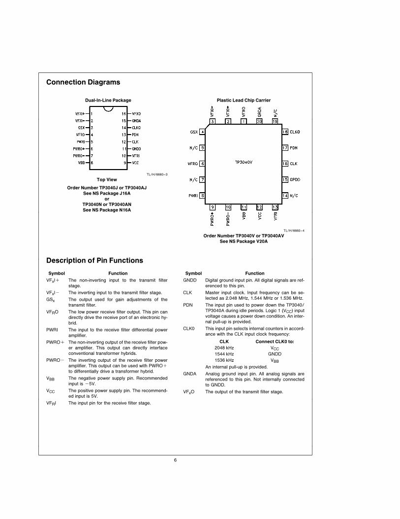
Connection Diagrams
Dual-In-Line Package
TL/H/6660–3
Top View
Order Number TP3040J or TP3040AJ
See NS Package J16A
or
TP3040N or TP3040AN
See NS Package N16A
Plastic Lead Chip Carrier
TL/H/6660–4
Order Number TP3040V or TP3040AV
See NS Package V20A
Description of Pin Functions
Symbol Function
VFxIa The non-inverting input to the transmit filter
stage.
VFxIb The inverting input to the transmit filter stage.
GSx The output used for gain adjustments of the
transmit filter.
VFRO The low power receive filter output. This pin can
directly drive the receive port of an electronic hy-
brid.
PWRI The input to the receive filter differential power
amplifier.
PWROa The non-inverting output of the receive filter pow-
er amplifier. This output can directly interface
conventional transformer hybrids.
PWROb The inverting output of the receive filter power
amplifier. This output can be used with PWROa
to differentially drive a transformer hybrid.
VBB The negative power supply pin. Recommended
input is b5V.
VCC The positive power supply pin. The recommend-
ed input is 5V.
VFRI The input pin for the receive filter stage.
Symbol Function
GNDD Digital ground input pin. All digital signals are ref-
erenced to this pin.
CLK Master input clock. Input frequency can be se-
lected as 2.048 MHz, 1.544 MHz or 1.536 MHz.
PDN The input pin used to power down the TP3040/
TP3040A during idle periods. Logic 1 (VCC) input
voltage causes a power down condition. An inter-
nal pull-up is provided.
CLK0 This input pin selects internal counters in accord-
ance with the CLK input clock frequency:
CLK Connect CLK0 to:
2048 kHz VCC
1544 kHz GNDD
1536 kHz VBB
An internal pull-up is provided.
GNDA Analog ground input pin. All analog signals are
referenced to this pin. Not internally connected
to GNDD.
VFxO The output of the transmit filter stage.
6
Functional DescriptionThe TP3040/TP3040A monolithic filter contains four main
sections; Transmit Filter, Receive Filter, Receive Filter Pow-
er Amplifier, and Frequency Divider/Select Logic (Figure 1).
A brief description of the circuit operation for each section is
provided below.
TRANSMIT FILTER
The input stage of the transmit filter is a CMOS operational
amplifier which provides an input resistance of greater than
10 MX, a voltage gain of greater than 5,000, low power
consumption (less than 3 mW), high power supply rejection,
and is capable of driving a 10 kX load in parallel with up to
25 pF. The inputs and output of the amplifier are accessible
for added flexibility. Non-inverting mode, inverting mode, or
differential amplifier mode operation can be implemented
with external resistors. It can also be connected to provide a
gain of up to 20 dB without degrading the overall filter per-
formance.
The input stage is followed by a prefilter which is a two-pole
RC active low pass filter designed to attenuate high fre-
quency noise before the input signal enters the switched-ca-
pacitor high pass and low pass filters.
A high pass filter is provided to reject 200 Hz or lower noise
which may exist in the signal path. The low pass portion of
the switched-capacitor filter provides stopband attenuation
which exceeds the D3 and D4 specifications as well as the
CCITT G712 recommendations (Figure 3).
The output stage of the transmit filter, the postfilter, is also a
two-pole RC active low pass filter which attenuates clock
frequency noise by at least 40 dB. The output of the trans-
mit filter is capable of driving a g3.2V peak to peak signal
into a 10 kX load in parallel with up to 25 pF.
RECEIVE FILTER
The input stage of the receive filter is a prefilter which is
similar to the transmit prefilter. The prefilter attenuates high
frequency noise that may be present on the receive input
signal. A switched capacitor low pass filter follows the prefil-
ter to provide the necessary passband flatness, stopband
rejection and sin x/x gain correction. A postfilter which is
similar to the transmit postfilter follows the low pass stage. It
attenuates clock frequency noise and provides a low output
impedance capable of directly driving an electronic sub-
scriber-line-interface circuit (Figure 3).
RECEIVE FILTER POWER AMPLIFIERS
Two power amplifiers are also provided to interface to trans-
former coupled line circuits. These two amplifiers are driven
by the output of the receive postfilter through gain setting
resistors, R3, R4 (Figure 2). The power amplifiers can be
deactivated, when not required, by connecting the power
amplifier input (pin 5) to the negative power supply VBB.
This reduces the total filter power consumption by approxi-
mately 10 mW–20 mW depending on output signal ampli-
tude.
POWER DOWN CONTROL
A power down mode is also provided. A logic 1 power down
command applied on the PDN pin (pin 13) will reduce the
total filter power consumption to less than 1 mW. Connect
PDN to GNDD for normal operation.
FREQUENCY DIVIDER AND SELECT LOGIC CIRCUIT
This circuit divides the external clock frequency down to the
switching frequency of the low pass and high pass switched
capacitor filters. The divider also contains a TTL-CMOS in-
terface circuit which converts the external TTL clock level to
the CMOS logic level required for the divider logic. This in-
terface circuit can also be directly driven by CMOS logic. A
frequency select circuit is provided to allow the filter to oper-
ate with 2.048 MHz, 1.544 MHz or 1.536 MHz clock frequen-
cies. By connecting the frequency select pin CLK0 (pin 14)
to VCC, a 2.048 MHz clock input frequency is selected. Digi-
tal ground selects 1.544 MHz and VBB selects 1.536 MHz.
Applications InformationGAIN ADJUST
Figure 2 shows the signal path interconnections between
the TP3040/TP3040A and the TP3020 signal-channel CO-
DEC. The transmit RC coupling components have been
chosen both for minimum passband droop and to present
the correct impedance to the CODEC during sampling.
Optimum noise and distortion performance will be obtained
from the TP3040/TP3040A filter when operated with sys-
tem peak overload voltages of g2.5V to g3.2V at VFxO
and VFRO. When interfacing to a PCM CODEC with a peak
overload voltage outside this range, further gain or attenua-
tion may be required.
BOARD LAYOUT
Care must be taken in PCB layout to minimize power supply
and ground noise. Analog ground (GNDA) of each filter
should be connected to digital ground (GNDD) at a single
point, which should be bypassed to both power supplies.
Further power supply decoupling adjacent to each filter and
CODEC is recommended. Ground loops should be avoided,
both between GNDA and GNDD and between the GNDA
traces of adjacent filters and CODECs.
7
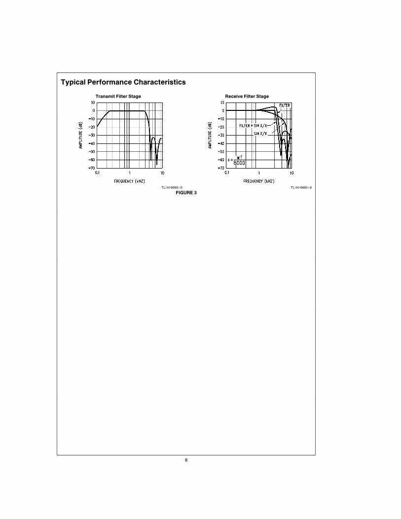
Typical Performance Characteristics
Transmit Filter Stage
TL/H/6660–5
Receive Filter Stage
TL/H/6660–6
FIGURE 3
8

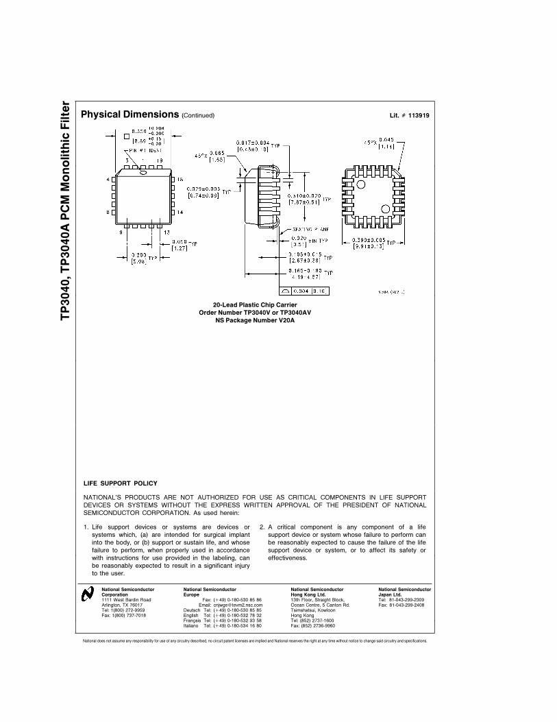
Physical Dimensions
Ceramic Dual-In-Line Package (J)
Order Number TP3040J or TP3040AJ
NS Package Number J16A
Molded Dual-In-Line Package (M)
Order Number TP3040N or TP3040AN
NS Package Number N16A
9
TP3040,TP3040A
PC
MM
onolith
icFilte
r
Physical Dimensions (Continued) Lit. Ý 113919
20-Lead Plastic Chip Carrier
Order Number TP3040V or TP3040AV
NS Package Number V20A
LIFE SUPPORT POLICY
NATIONAL’S PRODUCTS ARE NOT AUTHORIZED FOR USE AS CRITICAL COMPONENTS IN LIFE SUPPORT
DEVICES OR SYSTEMS WITHOUT THE EXPRESS WRITTEN APPROVAL OF THE PRESIDENT OF NATIONAL
SEMICONDUCTOR CORPORATION. As used herein:
1. Life support devices or systems are devices or 2. A critical component is any component of a life
systems which, (a) are intended for surgical implant support device or system whose failure to perform can
into the body, or (b) support or sustain life, and whose be reasonably expected to cause the failure of the life
failure to perform, when properly used in accordance support device or system, or to affect its safety or
with instructions for use provided in the labeling, can effectiveness.
be reasonably expected to result in a significant injury
to the user.
National Semiconductor National Semiconductor National Semiconductor National SemiconductorCorporation Europe Hong Kong Ltd. Japan Ltd.1111 West Bardin Road Fax: (a49) 0-180-530 85 86 13th Floor, Straight Block, Tel: 81-043-299-2309Arlington, TX 76017 Email: cnjwge@ tevm2.nsc.com Ocean Centre, 5 Canton Rd. Fax: 81-043-299-2408Tel: 1(800) 272-9959 Deutsch Tel: (a49) 0-180-530 85 85 Tsimshatsui, KowloonFax: 1(800) 737-7018 English Tel: (a49) 0-180-532 78 32 Hong Kong
Fran3ais Tel: (a49) 0-180-532 93 58 Tel: (852) 2737-1600Italiano Tel: (a49) 0-180-534 16 80 Fax: (852) 2736-9960
National does not assume any responsibility for use of any circuitry described, no circuit patent licenses are implied and National reserves the right at any time without notice to change said circuitry and specifications.