an557-easy-application-design-with-the-l4970a-monolithic ...
52
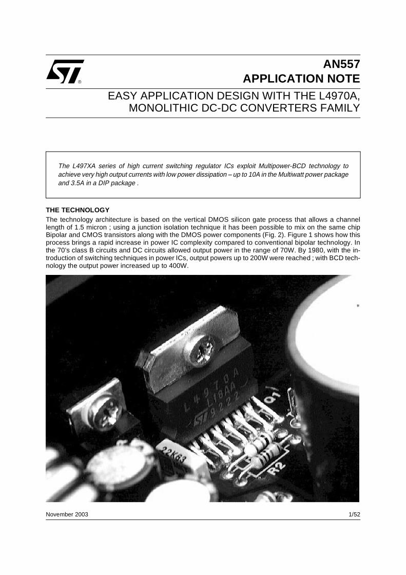
1/52 AN557 APPLICATION NOTE November 2003 THE TECHNOLOGY The technology architecture is based on the vertical DMOS silicon gate process that allows a channel length of 1.5 micron ; using a junction isolation technique it has been possible to mix on the same chip Bipolar and CMOS transistors along with the DMOS power components (Fig. 2). Figure 1 shows how this process brings a rapid increase in power IC complexity compared to conventional bipolar technology. In the 70’s class B circuits and DC circuits allowed output power in the range of 70W. By 1980, with the in- troduction of switching techniques in power ICs, output powers up to 200W were reached ; with BCD tech- nology the output power increased up to 400W. EASY APPLICATION DESIGN WITH THE L4970A, MONOLITHIC DC-DC CONVERTERS FAMILY The L497XA series of high current switching regulator ICs exploit Multipower-BCD technology to achieve very high output currents with low power dissipation – up to 10A in the Multiwatt power package and 3.5A in a DIP package .
-
Upload
khangminh22 -
Category
Documents
-
view
0 -
download
0
Transcript of an557-easy-application-design-with-the-l4970a-monolithic ...
1/52
AN557APPLICATION NOTE
November 2003
THE TECHNOLOGYThe technology architecture is based on the vertical DMOS silicon gate process that allows a channellength of 1.5 micron ; using a junction isolation technique it has been possible to mix on the same chipBipolar and CMOS transistors along with the DMOS power components (Fig. 2). Figure 1 shows how thisprocess brings a rapid increase in power IC complexity compared to conventional bipolar technology. Inthe 70’s class B circuits and DC circuits allowed output power in the range of 70W. By 1980, with the in-troduction of switching techniques in power ICs, output powers up to 200W were reached ; with BCD tech-nology the output power increased up to 400W.
EASY APPLICATION DESIGN WITH THE L4970A, MONOLITHIC DC-DC CONVERTERS FAMILY
The L497XA series of high current switching regulator ICs exploit Multipower-BCD technology toachieve very high output currents with low power dissipation – up to 10A in the Multiwatt power packageand 3.5A in a DIP package .

AN557 APPLICATION NOTE
2/52
Figure 1. BCD process and increase in power ICs complexity.
Figure 2. Cross Section of the BCD Mixed Technology.
THE STEP-DOWN CONFIGURATIONFig. 3 shows the simplified block diagram of the circuit realizing the step-down configuration. This circuitoperates as follows : Q1 acts as a switch at the frequency f and the ON and OFF times are suitably con-trolled by the pulse width modulator circuit. When Q1 is saturated, energy is absorbed from the input whichis transferred to the output through L. The emitter voltage of Q1, VE, is Vi-Vsat when Q is ON and -VF (withVF the forward voltage across the D diode as indicated) when Q1 is OFF. During this second phase thecurrent circulates again through L and D. Consequently a rectangular shaped voltage appears on the emit-ter of Q1 and this is then filtered by the L-C-D network and converted into a continuous mean value acrossthe capacitor C and therefore across the load. The current through L consists of a continuous component,ILOAD, and a triangular-shaped component super-imposed on it, ∆IL, due to the voltage across L.

3/52
AN557 APPLICATION NOTE
Figure 3. The Basic Step-down Switching Regulator Configuration
Fig. 4 shows the behaviour of the most significant waveforms, in different points of the circuit, which helpto understand better the operation of the power section of the switching regulator. For the sake of simplic-ity, the series resistance of the coil has been neglected. Fig. 2a shows the behaviour of the emitter voltage(which is practically the voltage across the recirculation diode), where the power saturation and the for-ward VF drop across the diode era taken into account.The ON and OFF times are established by the following expression :
Fig. 4b shows the current across the switching transistor. The current shape is trapezoidal and the oper-ation is in continuous mode. At this stage, the phenomena due to the catch diode, that we consider asdynamically ideal, are neglected. Fig. 4c shows the current circulating in the recirculation diode. The sumof the currents circulating in the power and in the diode is the current circulating in the coil as shown inFig. 4e. In balanced conditions the ∆IL
+ current increase occuring during TON has to be equal to the ∆IL–
decrease occurring during TOFF. The mean value of IL corresponds to the charge current. The current rip-ple is given by the following formula :
It is a good rule to respect to IoMIN ≥ IL/2 relationship, that implies good operation in continuous mode.When this is not done, the regulator starts operating in discontinuous mode. This operation is still safe butvariations of the switching frequency may occur and the output regulation decreases.Fig. 4d shows the behaviour of the voltage across coil L. In balanced conditions, the mean value of thevoltage across the coil is zero. Fig. 4f shows the current flowing through the capacitor, which is the differ-ence between IL and ILOAD.In balanced conditions, the mean current is equal to zero, and ∆IC = ∆IL. The current IC through the ca-pacitor gives rise to the voltage ripple.This ripple consists of two components : a capacitive component, ∆VC, and a resistive component, ∆VESR,due to the ESR equivalent series resistance of the capacitor. Fig. 4g shows the capacitive component ∆VCof the voltage ripple, which is the integral of a triangular-shaped current as a function of time. Moreover,it should be observed that vC (t) is in quadrature with iC(t) and therefore with the voltage VESR. The quantityof charge ∆Q+ supplied to the capacitor is given by the area enclosed by the ABC triangle in Fig. 4f :
Vo Vi Vsat–( )TON
TON TOFF+--------------------------------⋅=
IL+∆ IL
-∆Vi Vsat–( ) Vo–
L---------------------------------------- TON
Vo VF+
L--------------------TOFF= = =

AN557 APPLICATION NOTE
4/52
Figure 4. Principal Circuit Waveforms of the figure 1 Circuit.

5/52
AN557 APPLICATION NOTE
Which therefore gives:
Fig. 4h shows the voltage ripple VESR due to the resistive component of the capacitor. This component isVESR (t) = iC (t) × ESR. Fig. 4i shows the overall ripple Vo, which is the sum of the two previous compo-nents. As the frequency increases (> 20kHz), which is required to reduce both the cost and the sizes of Land C, the VESR component becomes dominant. Often it is necessary to use capacitors with greater ca-pacitance (or more capacitors connected in parallel to limit the value of ESR within the required level.We will now examine the stepdown configuration in more detail, referring to fig. 1 and taking the be-haviourshown in Fig. 4 into account.Starting from the initial conditions, where Q = ON, vC = Vo and iL = iD = 0, using Kirckoff second principlewe may write the following expression:Vi = vL + vC (Vsat is neglected against Vi).
(1)
which gives :
(2)
The current through the inductance is given by :
(3)
When Vi, Vo, and L are constant, IL varies linearly with t. Therefore, it follows that :
(4)
When Q is OFF the current through the coil has reached its maximum value, Ipeak and because it cannotvery instantaneously, the voltage across the ased to allow the recirculation of the current through the load.When Q switches OFF, the following situation is present:
vC(t) = Vo, iL (t) = iD (t) = Ipeak
And the equation associated to the following loop may be written :
(5)
where : vC = Vo
(6)
It follows therefore that :
(7)
Q∆ 12--- T
2---
IL∆2
--------⋅ ⋅=
VC∆ QC----
IL∆8fc--------= =
Vi LdIL
dt-------- vC+ L
dIL
dt-------- Vo+⋅= =
dIL
dt--------
Vi Vo–( )L
-----------------------=
ILVi Vo–( )
L-----------------------=
IL+∆
Vi Vo–( )TON
L-----------------------------------=
VF LdIL
dt-------- vC+ + 0=
dILdt--------
VF Vo+( )L
-------------------------–=
iL t( )VF Vo+
T-------------------- t–=

AN557 APPLICATION NOTE
6/52
The negative sign may be interpretated with the fact that the current is now decreasing. Assuming that VFmay be neglected against Vo, during the OFF time the following behaviour occurs :
(8)
therefore :
(9)
But, because ∆IL+ = ∆IL– if follows that :
which allows us to calculate Vo:
(10)
where T is the switching period.Expression (10) links the output voltage Vo to the input voltage Vi and to the duty cycle. The relation-shipbetween the currents is the following :
(11)
EFFICIENCY
The system efficiency is expressed by the following formula :
where Po = VoIo (with Io = ILOAD) is the output power to the load and Pi is the input power absorbed by thesystem. Pi is given by Po, plus all the other system losses. The expression of the efficiency becomes there-fore the following :
(12)
DC LOSSESPsat :saturation losses of the power transistor Q. These losses increase as Vi decreases.
(13)
where and Vsat is the power transistor saturation at current Io.
PD : losses due to the recirculation diode. These losses increase as Vi increases, as in this case the ONtime of the diode is greater.
(14)
ILVo
L------ t=
IL+∆
Vo
L------TOFF=
Vi Vo–( )TON
L-----------------------------------
VoTOFF
L---------------------=
Vo Vi
TON
TONTOFF-------------------------- Vi
TON
T-----------= =
IiDC IoDC
TON
T-----------⋅=
η%Po
Pi------ 100⋅=
ηPo
Po Psat PD PL Pq psw+ + + + +---------------------------------------------------------------------------------=
Psat Vsat IoTON
T----------- VsatIo
Vo
Vi------+⋅=
TON
T-----------
Vo
Vi------=
PD VFIoVi Vo–
Vi------------------ VFIo 1
Vo
Vi------–
= =

7/52
AN557 APPLICATION NOTE
where VF is the forward voltage of the recirculation diode at current Io.PL : losses due to the series resistance RS of the coil
PL = RS Io2 (15)
Pq: losses due to the stand-by current and to the power driving current:
Pq = Vi Iq, (16)
in which Iq is the operating supply current at the operating switching frequency. Iq includes the oscillatorcurrent.
SWITCHING LOSSESPsw: switching losses of the power transistor :
The switching losses of the recirculation diode are neglected (which are anyway negligible) as it is as-sumed that diode is used with recovery time much smaller than the rise time of the power transistor.We can neglect losses in the coil (it is assumed that ∆IL is very small compared to Io) and in the outputcapacitor, which is assumed to show a low ESR.
Calculation of the inductance value, LCalculation TON and TOFF through (4) and (9) respectively it follows that :
But because :TON + TOFF = T and ∆IL+ = ∆IL– = ∆IL, it follows that :
(17)
Calculating L, the previous relation becomes :
(18)
Fixing the current ripple in the coil required by the design (for instance 30% of Io), and introducing the fre-quency instead of the period, it follows that :
where L is in Henry and f in Hz Vi × 0.3 × Io × f
Calculation of the output capacitor CFrom the output node in fig. 3 it may be seen that the current through the output capacitor is given by:
ic (t) = iL (t) – Io
Psw ViIotr tf+
2T-------------=
TON
IL+∆ L⋅
Vi Vo–------------------= TOFF
IL-∆ L⋅Vo
----------------=
TON
IL∆ L⋅Vi Vo–------------------
IL∆ L⋅Vo
----------------+ T= =
LVi Vo–( )Vo
Vi IL∆------------------------------T=
LVi Vo–( )Vo
Vi 0.3 Io f⋅ ⋅ ⋅---------------------------------=

AN557 APPLICATION NOTE
8/52
Figure 5. Equivalent Circuit Showing Recirculation when Q1 is Turned Off.
From the behaviour shown in Fig. 4 it may be calculated that the charge current of the output capacitor,within a period, is ∆IL/4, which is supplied for a time T/2. It follows therefore that :
(19)
but, remembering expression (4) :
and
therefore equation (19) becomes :
Finally, calculating C it follows that :
(20)
where : L is in HenrysC is in Faradsf is in Hz Finally, the following expression should be true :
(21)
It may happen that to satisfy relation (21) a capacitance value much greater than the value calculatedthrough (20) must be used.
TRANSIENT RESPONSESudden variations of the load current give rise to overvoltages and undervoltages on the output voltage.Since ic = C (dvc/dt) (22), where dvc = ∆Vo, the instantaneous variation of the load current ∆Io is suppliedduring the transient by the output capacitor. During the transient, also current through the coil tends tochange its value. Moreover, the following is true :
(23)
where diL = ∆Io vL = Vi – Vo for a load increasevL = Vo for a load decrease
VC∆IL∆
4C--------T
2---
ILT∆8C
------------IL∆
8fc--------= = =
IL+∆
Vi Vo–( )TON
L-----------------------------------= TON
Vo
Vi------T=
VC∆Vi Vo–( )Vo
8 Vif2LC
------------------------------=
CVi Vo–( )Vo
8 Vi VC f∆ 2 L
--------------------------------------=
ESRmax
VCmax∆IL∆
---------------------=
vL LdiLdt--------=

9/52
AN557 APPLICATION NOTE
Calculating dt from (22) and (23) and equalizing, it follows that :
Calculating dvC and equalizing it to ∆Vo, it follows that :
(24) for + ∆Io
(25) for - ∆Io
From these two expressions the dependence of overshoots and undershoots on the L and C values maybe observed. To minimize ∆Vo it is therefore necessary to reduce the inductance value L and to increasethe capacitance value C. Should other auxiliary functions be required in the circuit like reset or crowbarprotections and very variable loads may be present, it is worthwhile to take special care for minimizingthese overshoots, which could cause spurious operation of the crowbar, and the under-shoot, which couldtrigger the reset function.
DEVICE DESCRIPTIONFor a better understanding of how the device functions, a description will be given of the principle blocksthat compose the device. The block diagram of the device is shown in fig.6
POWER SUPPLYThe device contains a stabilized regulator (Vstart = 12V) that provides power to the analogic and digitalcontrol blocks as well as the section of the bootstrap. The Vstart voltage also powers the blocks that op-erates the internal reference voltage of 5.1V, with a precision of ±2%, necessary for the feedback.
OSCILLATOR, SYNC. AND VOLTAGE FEED-FORWARD FUNCTIONSThe oscillator block generates a sawtooh wave signal that sets the switching frequency of the system. Thissignal, compared with the output voltage of the error amplifier, generates the PWM signal that will thensent to the power output stage. The oscillator also contains the voltage feedforward function that, beingcompletely integrated, does not require additional external components to function. The VFF function op-erates with supply voltages from 15V to 45V. The ∆V/∆t of the sawtooh is directly proportional to the supplyvoltage Vi.As Vi increases, the conduction time (ton) of the power transistor decreases in such way as to provide tothe coil, and therefore to the load, the product Volt x Sec constant.
Figure 6. Block Diagram of the 10A Monolithic Regulator L4970A.
LdiLdt-------- C
dvC
iC----------=
Vo∆L Io
2∆C Vi Vo–( )---------------------------=
Vo∆L Io
2∆C Vo-------------=

AN557 APPLICATION NOTE
10/52
Figure 7. Voltage Feeforward Waveform.
Fig. 7 shows the duty-cycle varies as a result of the changes in slope of the ramp with the input voltageVi. The output of the error amplifier should not change to maintain the output voltage in regulation. Thisfunction allows for the increase of speed in response to the rapid change of the supply voltage and for agreatly reduced ouput ripple at the mains frequency.In fact, the slope of the ramp is modulated by the ripple, generally present in the order of several volts onthe input of the regulator, particularly when the solution with a mains transformer is used.Fig. 8 shows the simplified electrical diagram of the oscillator.A resistor, connected between the Rosc pin and GND, sets the current that is internally reflected in the pinCosc, in order to charge the external capacitor to which it is connected. The voltage to the Rosc pin is notfixed, but is tied to the instantaneous value of Vi; this is needed to achieve the feedforward voltage func-tion, in which the slope of the ramp is directly proportional to the supply voltage. A comparator senses thevoltage at the Cosc capacitor. When the voltage reaches the value present at the inverting input of thecomparator, the output from the comparator goes high and is sent to the two transistors Q1 and Q2. Q1is responsible for discharging the external Cosc capacitor with a current of approx. 20mA, while Q2 im-poses at the inverted input of the comparator a voltage of 2Vbe (approx. 1.3V) that is the low-threshold ofthe ramp. Some useful formulas for calculating the various parameters of the oscillator block are:
Figure 8. Oscillator Circuit.
V2
V7
D93IN006
Vi=30V
Vi=15V
Vc
t
Vi=30V
Vi=15V
t
Vi
2R
1 3 2RR
Rosc
Cosc
PWMCOMP.
Q1 R Q2
CLOCK
D93IN007
-
+

11/52
AN557 APPLICATION NOTE
1) Oscillator charge current:
(For 15V < Vi < 45V)
2) Oscillator discharge current:
IDISCH = 20mA
3) Peak voltage ramp:
This formula is obtained in the following way: indicating with Ve the voltage of the emitter of the NPN tran-sistor connected to Vcc, and V- the voltage at the inverted input of the comparator, one has:
(a)
(b)
by substituting (a) into (b), one obtains:
4) Valley voltage ramp:
Vth-L = 2Vbe
5) Switching frequency:
It should be noted that formula (5) does not take into account the discharge time of Cosc which cannot beneglected when one is working at frequencies equal or higher than 200KHz. The discharge time is alsotied to the value of Cosc itself.Analitycally one has:
6)
from which is obtained the more closely approximate expression of the oscillator frequency:
7)
During the discharge time of Cosc, a clock pulse is generated internally that is made subsequently avail-able on the Sync. pin and that can be used to synchronize other regulators. (3 devices of the same familymaximum). The Sync. pulse generated has a typical range of 4.5V and the current availability is 4.5mA.In general, it is better that the Sync pulse is at least 300-400ns in order to be able to synchronize a rangeof existing regulators; to obtain this result, values of suggested capacitors, in different test circuits, have
ICHARGE
Vi 9Vbe–
Rosc-------------------------=
Vth H–
Vi 9Vbe–
Rosc------------------------- 2Vbe+=
Ve
Vi
3----- Vbe–=
VVe 2Vbe–
3R-------------------------- R⋅
2Vbe+=–
V
Vi
3----- Vbe–
2Vbe–
3---------------------------------------------- 2Vbe+=–
Vi 9Vbe–
9------------------------- 2Vbe+=
fSW9
RoscCosc--------------------------=
TDISCH
Vth H– Vth L––
20mA--------------------------------------- Cosc⋅=
fSW1
Rosc Cosc⋅9
------------------------------ TDISCH+
---------------------------------------------------------=

AN557 APPLICATION NOTE
12/52
been selected. The typical duration of the synchronizing pulse with the suggested values of Cosc are asfollows:
Obviously, synchronize pulses of eccessive duration can greatly reduce the max duty-cycle and producedistortions in the sawtooth of the synchronized regulator working as slave.
P.W.M.Comparing the sawtooth signal generated by the oscillator and the output of the error amplifier, generatesthe PWM signal which is sent to the driver of the output power stage. The PWM signal, in the path towardsthe output stage, also encounters a latch block to prevent other pulses from being sent at same period tothe output, possibly damaging the power stage. In the PWM block, a duty-cycle limiter has also been in-troduced. Such a limiter is obtained by taking advantage of the synchronizing pulse generated, the poweroutput stage is inhibited. Even if the error amplifier gives a large signal to the peak of the ramp, the powerstage will not be able to operate in DC, but will be switched off at each clock pulse. The max. obtainableduty-cycle is higher than 90%; this, however depends on the working frequency and the value of Cosc.Using the formulas 6) and 7) a precise calculation can be done.
SOFT STARTThe Soft Start function is essential for a correct startup of the device and for an output voltage that, at theswitch on, increases in a monotonous mode without dangerous output overvoltages and without over-stress for the power stage.Soft Start operates at the startup of the system and after an intervention of the thermal protection. Fig. 9shows the simplified diagram of the startup functions. The function is carried out by means of an externalcapacitor connected to the Soft Start pin, which is charged with a constant current of about 100µA to avalue of around 7V. During the charging time, the output of the error transcon-ductance amplifier, becauseof Q1, is forced to increase at the same rising edge time of the external softstart capacitor Css.
L497X Family (MULTIWATT PACKAGE)
Cosc (nf) - Rosc = 16KΩ Sync (ns)
0.68 140
1 230
1.2 270
1.5 330
2.2 450
3.3 680
4.7 1100
L497X Family (POWERDIP PACKAGE)
Cosc (nf) - R osc = 30KΩ Sync (ns)
1.2 230
1.5 280
2.2 420
3.3 600
4.7 900

13/52
AN557 APPLICATION NOTE
Figure 9. Soft Start Circuit.
Figure 10. Soft Start Waveforms.
The PWM signal begins to be generated as soon as the output voltage of the error amplifier crosses theramp; at this point the output stage begins to commutate, slowly increasing its ON time (see fig. 10).The charge of the Css capacitor, as already mentioned, begins each time the device is supplied with pow-er and after which an anomalous condition is created, as the intervention of thermal protection or of theundervoltage lockout.
CALCULATING THE DUTY-CYCLE AND SOFT-START TIMELet us suppose that the discharge time of the oscillator capacitor, Cosc, is neglected. This is an approx.valid for switching frequencies up to 200KHz. Let us indicate with Vr the output voltage of the error ampli-fier, and with Vc the voltage of the oscillator ramp.
Figure 11. Soft Sart Time Waveform.
CLAMPEDERROR AMPLIFIER
OUTPUTVc
OUTPUTCURRENT
SOFT START TIME
t
D93IN011
t

AN557 APPLICATION NOTE
14/52
The PWM comparator block commutates when Vr = Vc. Therefore:
8)
from which is obtained9)
The time t obtained from this equation is equal to the ON time of the power transistor. The correspondingduty-cycle is given by:
10)
Consequently, after leaving the discharged capacitor of Soft Start, the output of the regulator will reach itsvalue when the voltage across the Css capacitor, charged with constant current, has reached the valueVr - 0.5V.The time necessary in order that the output rises from zero to the nominal value is given by:
11)
in which Css is the Soft Start capacitor and Iss the Soft Start current. Considering Soft Start time as tss,the required time for the Soft Start capacitor to change itself approx from (2Vbe - 0.5V) = (1.2V - 0.5V) toVr - 0.5V, is:
12)
By taking Vr from (10):
13)
and substituting it in (12), we obtain:
14)
UNDERVOLTAGE LOCKOUTThe device contains the protection block of under-voltage lockout which keeps the power stage turned-offas long as the supply voltage does not reach at least 12V. At this point the device starts up with Soft Start.The function of undervoltage is also provided with an hysteresis of 1V to make it better immune to the rip-ple present on the supply voltage.
ERROR AMPLIFIERThe error amplifier is a transconductance type and deliver an output current proportional to the voltage in-balance of the two inputs. The simplified diagram is presented in fig 12.The principal characteristics of thisuncompensated operational amplifier are the following: Gm = 4mA/V, Ro = 2.5Mohm, Avo = 80dB, Isource-sink = 200µA, Input Bias Current = 0.3µA. The frequency response of the op. amp. is given in fig. 13.Ignoring the high frequency response and hypothesizing that the second pole is below the 0 dB axis in theall the conditions of loop compensation, it is possible to make a first approximation with the equivalent cir-cuit of fig. 14
Vr Vc
Vpp
T---------- t⋅
Vi 9Vbe–
9 T⋅------------------------- t⋅= = =
tVr T Vi 9Vbe–( )⋅ ⋅
9-------------------------------------------------=
Dton
T-------
Vr T Vi 9Vbe–( )⋅ ⋅9T
-------------------------------------------------Vr Vi 9Vbe–( )⋅
9----------------------------------------
Vo
Vi------= = = =
ts tart up– Css
Vr 0.5V–( )Iss
-----------------------------⋅=
tss Css
Vr 1.2V–( )Iss
-----------------------------⋅=
Vr
Vo
Vi------ 9
Vi 9Vbe–-------------------------⋅=
tss
Css
Iss---------
Vo
Vi------ 9
Vi 9Vbe–------------------------- 1.2V–⋅
=

15/52
AN557 APPLICATION NOTE
Figure 12. Error Amplifier Circuit.
Figure 13. Open loop gain (error amplifier only)
Figure 14. Error amplifier equivalent circuit.
In which:15) where Co = 3pF
The error amplifier can be easily compensated thanks to the high output impedance (see fig. 14) The re-sulting transfer function is as in the following:
(16)
Av s( ) GmRc
1 sRoCo+----------------------------⋅=
Av s( ) GmRo 1 sRcCc+( )⋅
s2RoCoRcCc s RoCc RoCo RcCc+ +( ) 1+ +
---------------------------------------------------------------------------------------------------------------------⋅=

AN557 APPLICATION NOTE
16/52
Figure 15. Compensation network of the error amplifier
The Bode diagram is shown in fig.16.
Figure 16. Bode plot showing gain and phase of compensated error amplifier
The compensation circuit introduces a pole at low frequency and a zero that is generally calculated to beput in the proximity of the resonance frequency of the output LC filter.The second pole at high frequency generally falls in a zone of no interest (for the system stability, one mustconsider the zero introduced by ESR characteristic of the output capacitor. Not all the designers agree onthis solution).If necessary, however, one can turn to more sophisticated compensation circuitry. An example is shownin fig. 17.
Figure 17. One pole, two zero compensation network
Such a circuit introduces a pole at low-frequency and two zeros.
17 Z11
2Π R1 C1----------------------------- Z2 1
2Π R2 C2-----------------------------==

17/52
AN557 APPLICATION NOTE
It must be remembered, however, that because of the high output impedance of the error amplifier, a sec-ond pole is also present:
18)
We normally suggest a high value for R1 to reduce the value of the capacitor C1 and allocate the pole P2at the highest possible frequency. The essential limitation to the max value of R1 is the offset introducedby the input bias current of the error amplifier. In the case of output voltage regulated higher than 5.1V, anexternal divider should be introduced. It’s than possible to introduce a second zero using the following net-work:
Figure 18. Compensation network for output voltages higher than 5.1V
Two zeros and two poles are introduced:
19)
Where
APPLICATION EXAMPLEConsider the block diagram of fig. 19, representing the internal control loop section, with the applicationvalues:Fswitch = 200KHz, L = 100µH, C = 1000µF, Po = 50W, Vo = 5.1V, Io = 10A and Fo = 500Hz. Gloop = PWM× Filter
Figure 19. Block diagram used in stability calculation
P2 Gm2Π C1------------------=
Z1 12Π Ro Cc--------------------------- Z2 1
2Π R1 C1-----------------------------==
P11
2Π Ro Cc--------------------------- P2 1
2Π Rx C1-----------------------------==
Rx R1 R2⋅R1 R2+----------------------=

AN557 APPLICATION NOTE
18/52
Figure 20. Frequency behaviour of the circuit of fig. 19
The system requires that DC gain is maximum to achieve good accuracy and line rejection. Beyond thisa bandwidth of some KHz is usually required for a good load transient response. The error amplifier trans-fer function must guarantee the above constrainst. A compensation network that could be used is shownin fig. 21.
Figure 21. Compensation network.
Figure 22. Bode plot of the regulation loop with the compensation network of fig. 21.
A s( ) 1 sR1 C1+( ) 1 sR2C2+( )
sR1 C1 (1+s C1Gm----------
----------------------------------------------------------------------=
ACSJGloop
PWM+FILTER
50Hz 500Hz 5Kz 50KHz
20
40
dB
D93IN012

19/52
AN557 APPLICATION NOTE
The criterium is to define Z1, Z2 close to the resonant pole of the output LC filter. The Gm/2ΠC1 pole mustbe placed at a frequency at which open loop gain is below 0dB axis (fig. 22).
CURRENT LIMITINGA complete regulation system will be equipped with a good current limiter able to protect from load break-ing and operator error controlls. The current limiting function is totally integrated and does not require anyexternal component. The output current is sensed by an internal low-value resistor, in series with the drainof the DMOS vertical power transistor..A precision current limitation of ± 10% relative at the peak current is guaranted. During overcurrent situa-tion the pulse by pulse current limitation produce an output stage switching frequency reduction. The blockdiagram of the current limiting is shown in fig. 23.
Figure 23. Current protection circuit.
In overcurrent situation the comparator send a signal at the flip-flop set input, an inhibit pulse is immediatlygenerated from it and sended at the output stage switching off the power mos.A reset pulse input in generated from an 40KHz internal oscillator.After the first reset pulse the control loop will start to regulate the system an the output current will increasefollowing the principal oscillator frequency. If overcurrent condition is still present the current limiting willbe activate again.This type of current limiting ensure a constant output current in overload or short circuit condition and allowa good reliability at high frequency (500KHz) reducing the problems relative at the internal signal delaythrough the protection blocks. The inductor current in overload condition in shown in fig. 24.
Figure 24. Overload inductance current.
AN557 APPLICATION NOTE
20/52
The 40KHz internal oscillator is synchronized with the principal one. If the system work with a oscillatortracks the principal oscillator frequency. In this way the switching frequency will not increase in overloadsituation.A particular care has to be taken in the inductor value in order to avoid problems during overload or shortcircuit conditions. A critical situation is present with high switching frequency, (more than 200KHz) wherea small inductor value is used and with high capacitive load.In order to return in nominal condition after a short circuit the inductor ripple at 40KHz with the nominaloutput voltage and current has to be lower than the current limitation value.
ExampleLet us consider L4970A, 10A. (the same approach can be used for all the family).The inductor ripple current is given by the following formula:
where fsw = 40KHz ±10%In order to get the maximum inductor ripple current, the previous formula becomes:
The current limitation for L4970A will start to work at 13A. therefore:
where Ionom = 10A for L4970A.
POWER FAIL-RESET CIRCUITThe L4970A include a voltage sensing circuit that may be used to generate a power on power off resetsignal for a microprocessor system. The circuit senses the input supply voltage and the output generatedvoltage and will generate the required reset signal only when both the sensed voltages have reached therequired value for correct system operation. The Reset signal is generated after a delay time programma-ble by an external capacitor on the delay pin. Fig 25 shows the circuit implementation of Reset circuit. Thesupply voltage is sensed on an external pin, for programmability of the threshold, by a first comparator.The second comparator has the reference threshold set at slightly less the ref. voltage for the regulationcircuit and the other input connected internally at the feedback point on the regulated voltage. When boththe supply voltage and the regulated voltage are in the correct range, transistor Q1 turns off and allowsthe current generator to charge the delay capacitor discharges completely before initialization of a newReset cycle. The output gate assures immediate take of reset signal without waiting for complete dis-charge of delay capacitor. Reset output is an open collector transistor capable of sinking 20mA at 200mVvoltage. Fig 26 shows reset waveforms.
IL∆Vi Vo–( ) Vo⋅Vi fsw L⋅⋅
----------------------------------=
IL∆Vimax Vomax–( ) Vomax⋅
Vimax fswmin L⋅ ⋅-----------------------------------------------------------------=
Il im min Ionom
IL∆2
--------+>

21/52
AN557 APPLICATION NOTE
Figure 25. Power fail and reset circuit.
Figure 26. Reset and power fail and reset circuit.
Figure 27. Power stage circuit.
Vi
RISING P.FAILTHRESHOLD
TURN-ONTHRESHOLD
11V
FALLING P.FAILTHRESHOLD
TURN-OFF THRESHOLD10Vt
5.1V
100mV
HISTERESIS4.9V
5V
FALLINGRESET
THRESHOLD
Vo=5.1VRISING RESETTHRESHOLD
OUTPUT RESET
tDR tDR
t
t
t
DELAY RESET POWER FAIL TIMED93IN013

AN557 APPLICATION NOTE
22/52
POWER STAGEThe simplified diagram of the output stage is shown in the fig. 27.The power stage and the circuit connected with it are by far the most important and critical componentswhen one wants to obtain good performance at high switching frequency.The power transistor must have excellent characteristics from the point of view of both the switching speedand the robustness.The transistor DMOS, with its intrinsic characteristics of elevated speed, no second breakdown phenomenom andeasy driving proves to be particularly suitable for this type of application that normally works at high frequency.For a properly driving of the DMOS gate it is necessary to use an external bootstrap capacitor. When thevoltage Vs is low the Cboot capacitor is charged through the internal diode D1, at the value of voltageequal to that of Vstart, which is about 12V; the next step oversees that Q3 is turned off, Q2 is driven ingate by Q1 so that Q1 can go in saturation, and its source can go up rise towards Vi.Cboot maintains its charge and guarantees a voltage equal Vi+12V at the gate of Q7, so that can enterinto region of low resistance.At this point the diode D1 turns on to be inversely polarized, disconnecting the 12V section from that ofthe driving power stage.When Q2 is ON the driven current of the power stage requires from the bootstrap capacitor a typical cur-rent of 400uA.When Q2 is Off a current of 2.5mA is required to mantain Q2 in that state. This current however is notdelivered from the bootstrap capacitor, but rather from the internal regulator of 12V, while the output cur-rent flowing in the freewheeling diode. The circuit described is capable of obtaining commutation, rise andfall time, a typical value of 50ns.In principle, it would have been feasible to reduce furthermore the commutation time whithout any reliabil-ity problems.This was not believed to be advantageous since it would not have been of any benefit if one thinks of thetrr time of the catch diode (with trise of 50ns also the Schottky diodes begin to show limitations) and of theconseguent increase of different disturbances caused bt too higly elevated dI/dt. The following tableshows the main features of the DMOS transistor.
Figure 28. Gate-charge curve for the power
Table 1.
BVDSS > 60V at ID = 1mA VGS = 0V
RDS(ON) = 100mΩ at ID = 10A Tj = 25°C VGS = 10V
RDS(ON) = 150mΩ at ID = 10A Tj = 150°C VGS = 10V
VTH = 3V at ID = 1mA

23/52
AN557 APPLICATION NOTE
THERMAL SHUTDOWNThe thermal protection intervenes when the junction temperature reaches 150°C; it intervenes directly onthe output stage turning it off quikly and in the meantime discharging the soft start capacitor.The reference voltage and the oscillator will continue to work regularly.The thermal shutdown has a hysteresis, after its intervention, it is necessary to wait for the junction tem-perature to lower around 30°C before the device will begin to work properly again.The device restart to work by using the soft start function.
Table 2. High Current Switching Regulator ICs.
APPLICATIONSEven though the regulators of the L4970A family has been designed to work only in step down configura-tion we will see next how these regulators can be use in large range of applications. In same cases theL4970A device will be used as an example for the entire family assembled in Multiwatt package and theL4974A will be used for the types in powerdip package.Anyway the suggested applications can be extended to any other device of the family by adjusting if nec-essary the external components using the given equation for the calculation.
Typical ApplicationThe Fig. 29 shows the electrical diagram of the typical application, complete with all the auxiliary functions.The same application suggested in the data sheet as test circuit and is the same used for the final dynamictest. All our devices are 100% tested both in static and dynamic conditions.Included in the dynamic test are obviously the external components: the coil, catch diode and output ca-pacitor which have been defined for all regulators.Shown below are the electrical diagrams of 5 devices that compose the family of this regulator complete
ParameterL497X FAMILY
L4970A L4977A L4975A L4974A L4972A L4972ADSurf. Mount.
Max. Input Operating Voltage
50V 50V 50V 50V 50V 50V
Output Voltage Range 5.1V (±2%) to 40V
Max. Output Current 10A 7A 5A 3.5A 2A 2A
Power SwitchRDSON at 25°C
0.13Ω typ.
Switching Mode Control System
Continuous Mode, Direct Duty Cycle Control with Voltage Feed-Forward
Max. Switching Freq. 500KHz 500KHz 500KHz 200KHz 200KHz 200KHz
EfficiencyVINPUT = 35VVOUT = 5.1V
10A80%
at 200KHz
7A80%
at 200KHz
5A85%
at 200KHz
3.5A85%
at 100KHz
2A85%
at 100KHz
2A85%
at 100KHz
Current Limiting Constant Current
Soft Start Yes
Reset and Power Fail Yes
Synch Yes
Crowbar No
Package
Max. Rth j-case (pin)Rth j-amb
Multiwatt15
1°C/W35°C/W
Multiwatt15
1°C/W35°C/W
Multiwatt15
1°C/W35°C/W
Powerdip 16+2+212°C/W60°C/W
Powerdip 16+2+212°C/W60°C/W
SO20L
6°C/W80°C/W

AN557 APPLICATION NOTE
24/52
with the value of the external components and with the relative pcb layout.Output voltages higher than 5.1V are possible using an output resistive divider. For Vo > 24V, for safetyreasons it must be avoided the zero load condition. In the application with high current, connected to theoutput divider are added two other resistances that permit the separation of sensing and forcing, in suchway as to compensate the fall of voltage on the connecting cables between the output and the load.Connecting directly the output to the feedback pin a 5.1V ±2% is obtained. The following table can be helpfor a rapid calculation of a resistor divider to obtain some of the most standard output voltage.
Figure 29. L4970A Typical Application Circuit.
Figure 30. Test and Evaluation Board Circuit
TYPICAL PERFORMANCES (using evaluation board) :n = 83% (Vi = 35V ; Vo = VREF ; Io = 10A ; fSW = 200KHz)Vo RIPPLE = 30mV (at 10A) with output filter capacitor ESR ≤ 60mΩLine regulation = 5mV (Vi = 15 to 50V)Load regulation = 15mV (Io = 2 to 10A)For component values, refer to test circuit part list.

25/52
AN557 APPLICATION NOTE
PARTS LIST
* 2 capacitors in parallel to increase input RMS current capability** 3 capacitors in parallel to reduce total output ESR
Table A
Table BSUGGESTED BOOTSTRAP CAPACITORS
R1 = 30KΩ * C1, C2 = 3300µF 63VL EYF (ROE)
R2 = 10KΩ C3, C4, C5, C6 = 2.2µF
R3 = 15KΩ C7 = 390pF Film
R4 = 16KΩ C8 = 22nF MKT 1817 (ERO)
R5 = 22Ω 0,5W
R6 = 4K7 C9 = 2.2nF KP1830
R7 = 10Ω C10 = 220nF MKT
R8 = see tab. A C11 = 2.2nF MP1830
R9 = OPTION **C12, C13, C14 = 220µF 40VL EKR
R10 = 4K7 C15 = 1µF Film
R11 = 10Ω
D1 = MBR 1560CT (or 16A/60V or equivalent)
L1 = 40µH core 58071 MAGNETICS 27 TURNS Ø 1,3mm (AWG 16) COGEMA 949178
V0 R10 R8
12V 4.7KΩ 6.2KΩ
15V 4.7KΩ 9.1KΩ
18V 4.7KΩ 12KΩ
24V 4.7KΩ 18KΩ
Operating Frequency Bootstrap Cap.c10
f = 20KHz ≥680nF
f = 50KHz ≥470nF
f = 100KHz ≥330nF
f = 200KHz ≥220nF
f = 500KHz ≥100nF

AN557 APPLICATION NOTE
26/52
Figure 31. P.C. Board (component side) and Components Layout of the Circuit of Fig. 30.
Figure 32. P.C. Board (back side) and Components Layout of the Circuit of Fig. 30.

27/52
AN557 APPLICATION NOTE
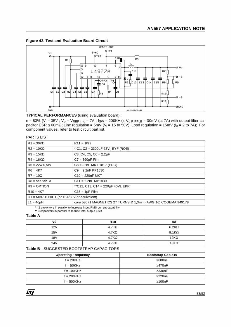
Figure 33. Test and Evaluation Board Circuit.
TYPICAL PERFORMANCES (using evaluation board) :n = 83% (Vi = 35V ; Vo = VREF ; Io = 2A ; fsw = 100KHz); Vo RIPPLE = 30mV (at 1A); Line regulation = 12mV(Vi = 15 to 50V); Load regulation = 7mV (Io = 0.5 to 2A); for component values Refer to the fig. 32 (Part list).
PARTS LIST
* 2 capacitors in parallel to increase input RMS current capability
** 3 capacitors in parallel to reduce total output ESR
Table A
Note: In the Test and Application Circuit for L4972D are not mounted C2, C14 and R8.
Table B - SUGGESTED BOOTSTRAP CAPACITORS
R1 = 30KΩ C3, C4, C5, C6 = 2.2µF 50V
R2 = 10KΩ C7 = 390pF Film
R3 = 15KΩ C8 = 22nF MKT 1837 (ERO)
R4 = 30KΩ C9 = 2.7nF KP1830 (ERO)
R5 = 22Ω C10 = 0.33µF Film
R6 = 4K7 C11 = 1nF
R7 = see tab. A **C12, C13, C14 = 100µF 40VL EKR (ROE)
R8 = OPTION C15 = 1µF Film
* C1, C2 = 1000µF 63V EYF (ROE) D1 = SB 560 (or equivalent)
L1 = 150µH core 58310 MAGNETICS 45 TURNS 0.91mm (AWG 16) COGEMA 949181
V0 R10 R8
12V 4.7KΩ 6.2KΩ15V 4.7KΩ 9.1KΩ18V 4.7KΩ 12KΩ24V 4.7KΩ 18KΩ
Operating Frequency Bootstrap Cap.c10
f = 20KHz ≥680nF
f = 50KHz ≥470nF
f = 100KHz ≥330nF
f = 200KHz ≥220nF
f = 500KHz ≥100nF

AN557 APPLICATION NOTE
28/52
Figure 34. Component Layout of fig. 33. Evaluation Board
Figure 35. Board and Component Layout of the ciruit of fig. 33.

29/52
AN557 APPLICATION NOTE
Figure 36. Test and Evaluation Board Circuit.
TYPICAL PERFORMANCES (using evaluation board) :n = 83% (Vi = 35V ; Vo = VREF ; Io = 3.5A ; fsw = 100KHz); Vo RIPPLE = 30mV (at 1A); Line regulation =12mV (Vi = 15 to 50V); Load regulation = 7mV (Io = 0.5 to 3.5A); for component values Refer to the fig. 35(Part list).
PARTS LIST
* 2 capacitors in parallel to increase input RMS current capability
** 3 capacitors in parallel to reduce total output ESR
Table A
Note: In the Test and Application Circuit for L4974D are not mounted C2, C14 and R8.
Table B - SUGGESTED BOOTSTRAP CAPACITORS
R1 = 30KΩ C3, C4, C5, C6 = 2.2µF 50V
R2 = 10KΩ C7 = 390pF Film
R3 = 15KΩ C8 = 22nF MKT 1837 (ERO)
R4 = 30KΩ C9 = 2.7nF KP1830 (ERO)
R5 = 22Ω C10 = 0.33µF Film
R6 = 4K7 C11 = 1nF
R7 = see tab. A **C12, C13, C14 = 100µF 40VL EKR (ROE)
R8 = OPTION C15 = 1µF Film
* C1, C2 = 1000µF 63V EYF (ROE) D1 = SB 560 (or equivalent)
L1 = 150µH core 58310 MAGNETICS 45 TURNS 0.91mm (AWG 16) COGEMA 949181
V0 R10 R8
12V 4.7KΩ 6.2KΩ15V 4.7KΩ 9.1KΩ18V 4.7KΩ 12KΩ24V 4.7KΩ 18KΩ
Operating Frequency Bootstrap Cap.c10
f = 20KHz ≥680nF
f = 50KHz ≥470nF
f = 100KHz ≥330nF
f = 200KHz ≥220nF
f = 500KHz ≥100nF

AN557 APPLICATION NOTE
30/52
Figure 37. Component Layout of fig. 36. Evaluation Board
Figure 38. Board and Component Layout of the ciruit of fig. 36.

31/52
AN557 APPLICATION NOTE
Figure 39. Test and Evaluation Board Circuit
TYPICAL PERFORMANCES (using evaluation board) :n = 83% (Vi = 35V ; Vo = VREF ; Io = 5A ; fSW = 200KHz); Vo RIPPLE = 30mV (at 10A) with output filtercapacitor ESR ≤ 60mΩ; Line regulation = 5mV (Vi = 15 to 50V); Load regulation = 15mV (Io = 2 to 5A);For component values, refer to test circuit part list.
PARTS LIST
* 2 capacitors in parallel to increase input RMS current capability** 3 capacitors in parallel to reduce total output ESR
Table A
Table B - SUGGESTED BOOTSTRAP CAPACITORS
R1 = 30KΩ R11 = 10ΩR2 = 10KΩ * C1, C2 = 3300µF 63VL EYF (ROE)
R3 = 15KΩ C3, C4, C5, C6 = 2.2µF
R4 = 16KΩ C7 = 390pF Film
R5 = 22Ω 0,5W C8 = 22nF MKT 1817 (ERO)
R6 = 4K7 C9 = 2.2nF KP1830
R7 = 10Ω C10 = 220nF MKT
R8 = see tab. A C11 = 2.2nF MP1830
R9 = OPTION **C12, C13, C14 = 220µF 40VL EKR
R10 = 4K7 C15 = 1µF Film
D1 = MBR 760CT (or 7.5A/60V or equivalent)
L1 = 80µH core 58930 MAGNETICS 47 TURNS Ø 1,13mm (AWG 76) COGEMA 949178
V0 R10 R8
12V 4.7KΩ 6.2KΩ15V 4.7KΩ 9.1KΩ18V 4.7KΩ 12KΩ24V 4.7KΩ 18KΩ
Operating Frequency Bootstrap Cap.c10
f = 20KHz ≥680nF
f = 50KHz ≥470nF
f = 100KHz ≥330nF
f = 200KHz ≥220nF
f = 500KHz ≥100nF

AN557 APPLICATION NOTE
32/52
Figure 40. P.C. Board (component side) and Components Layout of the Circuit of Fig. 39.
Figure 41. P.C. Board (back side) and Components Layout of the Circuit of Fig. 39.
33/52
AN557 APPLICATION NOTE
Figure 42. Test and Evaluation Board Circuit
TYPICAL PERFORMANCES (using evaluation board) :n = 83% (Vi = 35V ; Vo = VREF ; Io = 7A ; fSW = 200KHz); Vo RIPPLE = 30mV (at 7A) with output filter ca-pacitor ESR ≤ 60mΩ; Line regulation = 5mV (Vi = 15 to 50V); Load regulation = 15mV (Io = 2 to 7A); Forcomponent values, refer to test circuit part list.
PARTS LIST
* 2 capacitors in parallel to increase input RMS current capability** 3 capacitors in parallel to reduce total output ESR
Table A
Table B - SUGGESTED BOOTSTRAP CAPACITORS
R1 = 30KΩ R11 = 10ΩR2 = 10KΩ * C1, C2 = 3300µF 63VL EYF (ROE)
R3 = 15KΩ C3, C4, C5, C6 = 2.2µF
R4 = 16KΩ C7 = 390pF Film
R5 = 22Ω 0,5W C8 = 22nF MKT 1817 (ERO)
R6 = 4K7 C9 = 2.2nF KP1830
R7 = 10Ω C10 = 220nF MKT
R8 = see tab. A C11 = 2.2nF MP1830
R9 = OPTION **C12, C13, C14 = 220µF 40VL EKR
R10 = 4K7 C15 = 1µF Film
D1 = MBR 1560CT (or 16A/60V or equivalent)
L1 = 40µH core 58071 MAGNETICS 27 TURNS Ø 1,3mm (AWG 16) COGEMA 949178
V0 R10 R8
12V 4.7KΩ 6.2KΩ15V 4.7KΩ 9.1KΩ18V 4.7KΩ 12KΩ24V 4.7KΩ 18KΩ
Operating Frequency Bootstrap Cap.c10
f = 20KHz ≥680nF
f = 50KHz ≥470nF
f = 100KHz ≥330nF
f = 200KHz ≥220nF
f = 500KHz ≥100nF

AN557 APPLICATION NOTE
34/52
Figure 43. P.C. Board (component side) and Components Layout of the Circuit of Fig. 42.
Figure 44. P.C. Board (back side) and Components Layout of the Circuit of Fig. 42.

35/52
AN557 APPLICATION NOTE
Resistors value for standard output voltages.
Rx corresponds to R9 for L4974A and L4972A Rycorresponds to R10 for L4970A, L4977A andL4975ARx corresponds to R7 for L4974A and L4972A Rycorresponds to R8 for L4970A, L4977A andL4975AThe suggested switching frequency, and used inthe dynamic tests, is 200KHz for the Multiwatt®
package (MW) and 100KHz for the powerdip plas-tic package (PDIP). The maximum switching fre-quency allowed is 500KHz.For the types in plastic package (Powerdip), thelower switching frequency suggested is only de-pended by the minor dissipating power of a plasticpackage versus a "power package" because it iswell known that switching losses are directly pro-portional to the commutation frequency. Higherswitching frequencies are possible if limited outputcurrent is required and the operating ambient tem-perature are lower than 70°C. Infact the oscillatorof the devices assembled in dual in line is com-pletely equivalent to Multiwatt® package.The most important external components whichneed a little more attention (because a properly di-mensioning affects on the performance of the ap-plication) are the input and output capacitors, thefreewheeling diode and the coil.
Figure 45. Oscillator waveform and sync. pulse for V i = 35V
Figure 46. Oscillator waveform and sync. pulse for V i = 15V
Figure 47. Oscilloscope photograph showing the short circuit output voltage and current waveforms.
INPUT OUTPUT CAPACITORSThe output voltage ripple ∆Vo, essentially de-pends on the current ripple in the coil and the ESRof the output capacitor at the switching frequency.The capacitor that present a low ESR are capableof supporting higher current ripples.Today, the majority of the constructors of elec-troli-thic capacitors offer in their data book also a widerange of "low ESR" types generally suggested forswitching power supply application. In our caseEKR and EKE series (ROE) has been preferred.Such a series capacitors are designed for applica-tions at high frequency, 200KHz, and built to havea low ESR in order of supporting high current rip-ple.In order to minimize the effects caused by the ESRof the capacitors on the output voltage ripple 3 ca-pacitors of 220uF/40V (for high output current ap-plication) are connected in parallel.
Vo(V)
Rx(kΩ)
Ry(kΩ)
12 4.7 6.2
15 4.7 9.1
18 4.7 12
24 4.7 18

AN557 APPLICATION NOTE
36/52
It is necessary much attention also into the choice input capacitors. Also them be at low ESR, becausethey must sustain high current ripples. Such current ripples in presents of an inadeguate ESR, would pro-duce a heating of the capacitor itself (which could affect on the reliability of the component, since in gen-eral it is sensitive to temperature.Therefore choosing input capacitor at low ESR is necessary for problems of reliability. In fact such capac-itors, when used in applications that make use a mains transformer, must support quite elevated peak cur-rent for short periods a double the mains frequency and the same time be capable to deliver theinstantaneous peak of energy to the load at the switching frequency.Some other considerations of a general nature can be done on low ESR capacitors. For example of equalvalue and type (i.e.: 220µF - EKR), the ESR of the capacitor decreases at the increasing of its value volt-age rating, just like its RMS current.Still, two capacitors of the same value, connected in parallel, withstand an RMS current higher then theonly one of double value, and with the same voltage rating.When however, more capacitors are connected together in parallel, it is important to design with care thelayout of the printed circuit, in order to distribute as eventy as possible amongst between the different ca-pacitors the total current ripple.This is used to avoid dangerous current unbalances in the distribution of the total current between the var-ious capacitors charging some more others, that could damage the reliability of the system.Often it is very difficult to know exactly the RMS current flowing throught the capacitors. To know if theoperating condition is a "safe"operating condition or not, a measurement of the package temperature ofthe capacitor should be done.The following table 3 and 4, included in the dat-abook of electrical Roederstain, shows the maximum RMScurrent sustainable by the EKR and EKE capacitor versus the ambient temeperature and overtemperatureallowed on the capacitor package.
Table 3. Low-voltage electrolytic capacitors for switch-mode power supplies with low impedancevalues, radial, polarized styles
Rated cap.(µF)
Rated volt.(V DC)
DimensionsD x L (mm)(nominaldimen-sions)
Dissipationfactor tan δ
(100Hz;20°C) Lim.
Values
ImpedanceZ (Ω)
(10KHz;20°C)
(Lim. val-ues)
ImpedanceZ (Ω)
(10KHz;20°C)
(Lim. val-ues)
Admissibleripple curr.(mA/100Hz)
85°C
Admissibleripple curr.(mA/eff/10-
100Hz)85°C
EKR
100220470
101010
8.7 x 12.710 x 12.710 x 20
0.120.120.12
0.850.390.20
0.650.310.18
160300530
250450800
100220470
161616
10 x 12.710 x 16
12.5 x 20
0.110.110.11
0.600.320.16
0.400.250.13
200350600
300550900
100220470
252525
10 x 12.710 x 16
12.5 x 20
0.090.090.09
0.50.250.13
0.350.170.09
250450650
400700
1000
100220470
404040
10 x 1612.5 x 2012.5 x 30
0.080.080.08
0.40.170.09
0.230.130.08
450650
1000
70010001500

37/52
AN557 APPLICATION NOTE
Table 4. Admissible ripple current
Rated cap.(µF)
Rated volt.(V)
DimensionsD x L (mm)(nominaldimen-sions)
Dissipationfactor tan δ
(100Hz;20°C) Lim.
Values
ImpedanceZ (Ω)
(100KHz;20°C)
(Lim. val-ues)
ImpedanceZ (Ω)
(100KHz;-10°C)
(Lim. val-ues)
ImpedanceZ (Ω)
(100KHz;-40°C)
(Lim. val-ues)
Admissibleripple curr.(mA)100Hz)
105°C
EKE
223347
100220330330470
1010101010101010
5 x 115 x 115 x 115 x 11
6.3 x 118 x 11.5
8.5 x 12.58 x 11.5
0.190.190.190.190.190.190.190.19
1.301.301.301.300.600.330.330.33
3.903.903.903.901.800.990.990.99
20202020
9.805.805.805.80
1541541541 54260400400400
100220220330470
1616161616
6.3 x 118 x 11.5
8.5 x 12.58 x 11.5
10 x 12.5
0.160.160.160.160.16
0.600.330.330.330.25
1.800.990.990.990.75
9.805.805.805.803.20
260400400400510
100220330470
25252525
6.3 x 118 x 11.5
10 x 12.510 x 16
0.140.140.140.14
0.600.330.250.19
1.800.990.750.57
9.805.803.202.20
260400510635
100100220330470
3535353535
8 x 11.58.5 x 12.510 x 12.510 x 1610 x 20
0.120.120.120.120.12
0.330.330.250.190.14
0.990.990.750.570.42
5.805.803.202.201.50
400400510635860
Ambient Temp.δu in ×C
Admissible % of the85°C value
Surface Temp.in °C
Admissible % of the105°C value
Surface Temp.in °C
≤ 40 220 % 55 230 % 55
45 210 % 59 220 % 60
50 200 % 63 210 % 64
55 190 % 67 200 % 68
60 180 % 70 190 % 72
65 170 % 74 180 % 76
70 155 % 77 170 % 80
75 140 % 81 160 % 84
80 120 % 84 150 % 88
85 100 % 88 140 % 92
90 90 % 92 130 % 96
95 80 % 97 120 % 100
100 70 % 101 110 % 104
105 60 % 106 100 % 108
Table 3. Low-voltage electrolytic capacitors for switch-mode power supplies with low impedancevalues, radial, polarized styles (continued)

AN557 APPLICATION NOTE
38/52
CATCH DIODEBecause of quickly rise and fall time of the current(about 40-50ns) the use Schottky diode is recco-manded. Ultra-fast diodes with 30-50ns of trr (re-verse recovery time) are not consideredsufficiently fast for this family of converters, sincethey would give too elevated peaks of current atthe turn on of the internal power transistor, so highthatcould affect the reliability of the complete sys-tem, as well as drastically reduce the efficiency.The oscilloscope photographs show the OutputVoltage and Output Current waveforms obtainedwith diode having different trr value.
Figure 48. Schottky Diode.
Figure 49. Ultra Fast Diode (trr < 100ns).
In the test circuits used for this family of convert-ers, Schottky diodes from 60V (breakdown re-verse voltage) are suggested since the device can
support a max. input power voltage of 55V (forspecific applications, Schottky diodes with a re-verse breakdown voltage higher or equal to themaximum supply voltage should be used), withcurrent rating and packaging to satisfy all the con-ditions of duty cycle, and therefore also of powerdissipation.
COILConcerning the coil, a molypermalloy toroidalcores has been suggested, so that it would beeasy for everybody to obtain samples, wrap themwith a right number of turns in order to evaluateand correlate the measurements and performanceof the devices.In addition since the devices are dynamically test-ed 100% in production, with a "jig" of testing whichuses the same coil suggested in the applications,in the case of contests for example on a guaran-teed parameter like the efficiency, should be easi-er to solve the objections; in this case should beremembered that changing the magnetic material,the dimension, the wire and the number of thewinding, also change the losses in the coil reduc-ing the total efficiency of the application.This can be easily verify using for example toroi-dal cores in iron powered rather that those sug-gested in molypermalloy.Moreover, it is important to dimension properly thecoil in order to avoid its saturation, a good choiceis to dimension that its saturation; current is notequal to the maximum nominal current capable todeliver to the load, but rather higher by about 20%then the maximum guaranted current of the de-vice, in short circuit condition.Only in this way it is possible to guarantee that thecoil never saturate in all the possible working con-ditions, i.e.: in presence of a load transient, in shortcircuit in output and in the case of elevated tem-perature of the magnetic part.At last, it should be remembered that the suggest-ed inductors values, are referred to the inductorsvalues that the coil must have at the maximum out-put current of the application. Oscilloscope Photo-graphs showing the device output voltage andcurrent waveforms obtained with different induc-tor.

39/52
AN557 APPLICATION NOTE
Figure 50. Waveforms for L = 50 µH
Figure 51. Waveforms for L = 230 µH
Figure 52. Waveforms in case of core satura-tion
Anyway some general rules should be observed inorder to avoid any "poor functioning". These rulesinclude:a) the catch diode, that further to be the suggested
type in the test circuit, it has to be assembled onthe printed circuit very close to the output of theregulator, in order to minimize the leakage in-ductance and avoid over voltage due to the longconnection:
b) The inductor, avoiding the saturation at themaximum current guaranted by the currentlimitation of the device.
If oscillations on the output voltage at low ambienttemperature (i.e.: below 0°C) are originated anoutput low ESR capacitor has to be used. Oscilla-tions on the output al low frequency indicate insta-bility of the control loop; in this case a changing ofthe network compensation is suggested (see ErrorAmplifier section).
LOW COST APPLICATIONThe fig. 53 shows the low cost application of apower supply of 10A and 5.1V.In comparison of the complete application (andthis is valid for all the devices of the family) the ex-ternal components relative to the reset and powerfail functions can be missed.When a lower output voltage ripple is not requiredit is possible to eliminate the capacitors connectedat the reference voltage pin of 5.1V (i.e.: pin 14 forMultiwatt package. pin 13 for plastic package) Thereset input pin is suggested to connect it toground.The soft start capacitor value can be reduced to100nF for 5V output voltage.

AN557 APPLICATION NOTE
40/52
Figure 53. Low Cost Application Circuit.
POWER SUPPLY COMPLETE WITH MAINS TRANSFORMERThe fig. 54 shown a power supply with mains 110/220Vac transformer, diode bridge and filter capacitorwith output voltage adjustable between 5.1V. and 24V.Output capacitors have to be chosen with low ESR in order to reduce the output ripple.Particular care hasto be taken for input filter capacitors, in fact they have to support high current spikes at mains frequencyand at the same time current peak bigger than the output current at the switching frequency.Therefore they must be chosen with low ESR and able to substain high current ripple in order to guaranteea good reliability to all the system. The trasformer can be chosen with a single winding and 4 diodes or acenter tap with only 2 diodes with higher reverse voltage.A cost reduction of the trasformer can be reached using an active power factor corrector.It work at low voltage and the external components are relatively cheap, more details can be obtainedlooking on the power factor corrector application note.
POWER SUPPLY WITH MAINS HIGH FREQUENCY PREREGULATOR.When it is necessary to eliminate the mains trasformer at 50/60Hz for reasons like weight, dimensions orcost, a high frequency preregulator can be used.A ferrite trasformer reduces the rectifier and filtered mains voltage in a convenient voltage to supply direct-ly the device, providing for the isolation requirements.Using a free running solution or one of the voltage/current mode controller available, it is possible to com-pensate the input variation while the output voltage variations due to the load are usually very low. Someexamples regarding how to use this regulator in off-line power supply are now showed:
Flyback TopologyUsing a flyback topology with single or double transistors is possible to fix a single output voltage of 35-40V; it can be a bit increased if using a backup battery of 48 nominal Volts.From this preregulator (±10%) tolerancevoltage is possible to get one or more indipendent outputs, withits own current limitation and thermal protection.Moreover a possibility to syncronize more devices together is available, remembering to fix the masterfrequency at least 5% higher than the others device (working as slave) one.In case of necessity is possible to synronize devices on the trasformer secondary with the swith-cing fre-quency of the controller (See Fig. 55).

41/52
AN557 APPLICATION NOTE
Figure 54. Typical power supply showing the mains transformer.
Figure 55.
Forward TopologyFurther is showed an smps forward circuit, where the dc-dc converter is used as post-regulator for an aux-iliary output, (35V.) while the main one (5.1V. or 3.3V) is controlled directly with the feedback (See Fig. 56).
Using a PFC preregulationWhen an optimized power factor is required it is possible to use the following two pricinple diagram thatmake use of an active power factor corrector.1) using the standard boost topology (Fig. 57)2) using a flyback topology (Fig. 58)The idea is that to generate a stabilized voltage, around 30V - 35V, already isolated, avoiding to use anisolation after the PFC section.

AN557 APPLICATION NOTE
42/52
Figure 56.
Figure 57.
Figure 58.
POWER SUPPLY WITH 0 TO 25V ADJUSTABLE OUTPUT VOLTAGEa) It is a classical solution with high performance that make use of a negative reference voltage equal to
the value of the internal voltage of the device (5.1V).To generate this negative reference voltage, it is useful to equip the mains trnsformer with another sec-ondary winding at a low voltage of around 8Vac and capable of delivering a few dozen of mA.During the phase of starting up and stopping of the mains, it is important to avoid generating oscillationsaround the value of the output voltage , including the zero voltage.For this reason a network consisting of two NPN signal transistors TR1 and TR2 and some resistorshas been introduced.The transistor TR2 remains is saturation when TR1 is off, untill the output voltage of the negative reg-ulator reaches 4.3V At this point TR1 goes in saturation, sending off TR2. In this way the soft start is
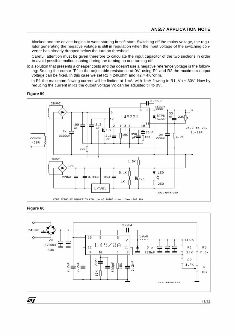
43/52
AN557 APPLICATION NOTE
blocked and the device begins to work starting in soft start. Switching off the mains voltage, the regu-lator generating the negative volatge is still in regulation when the input voltage of the switching con-verter has already dropped below the turn on threshold.Carefull attention must be given therefore to calculate the input capacitor of the two sections in orderto avoid possible malfunctioning during the turning on and turning off.
b) a solution that presents a cheaper costs and tha doesn’t use a negative reference voltage is the follow-ing: Setting the cursor "P" to the adjustable resistance at 0V, using R1 and R2 the maximum outputvoltage can be fixed. In this case we set R1 = 24Kohm and R2 = 4K7ohm.In R1 the maximum flowing current will be limited at 1mA; with 1mA flowing in R1, Vo = 30V. Now byreducing the current in R1 the output voltage Vo can be adjusted till to 0V.
Figure 59.
Figure 60.

AN557 APPLICATION NOTE
44/52
The current, flowing in backward, to have 0V it will be:
∆VR2 = R2 · 0.21 = 4.7k · 0.21 = 1VTherefore, when the cursor "P" reaches Vref + 1V the output voltage goes to zero.At this point we are able to define as well the values of P1 and R3. When the "P" cursor is completely moved to high, there should be 6V of dropping to "P", and in this way0.6mA will flow.The current flowing in R3, considering that the voltage at pin 15 has a typical value of 12V, it will be of0.8mA.In this case the R3 value will be 7K5ohm.
3.3V / 10A DC-DC CONVERTERWhen an output voltage lower to the reference voltage of 5.1V must be stabilized with a good result fromstability and regulation point of view, and not having available the not-inverting input of the error amplifier,it is possible to use an external reference.In this case a TL431C reference has been chosen, which is cheaper and widespread used. In this casemore than a simple reference, it is a true shunt regulator, containing a reference, an error amplifier and atransistor capable of absorbing a max current of 100mA.Such component can be compensated like a common OP/AMP, and therefore in our application can sub-stitute both the internal reference and the error amplifier.The fig. 61 represents the electrical diagram of the application at 3.3V.The operating input voltage is between 12V (due to the internal UVLO) and 35V, with a minimum operatingswitching frequency of 100KHz.The maximum operating input voltage is limited only 35V because the minimum "ON" time, which shouldnot be reduced below 1 microsecond. At input voltage of 35V, output voltage of 3.3V and fs=100KHz theTon time is already about of 1 microsecond.
Figure 61.
I1Vref
R1---------- 5.1V
24K------------ 0.21mA= = =
2.2µ
F
L4970A3
11
8
2.2µ
F
36K
2.2n
F
1 2 14 15
22K
TL431
1K
0.1µF
10
7
330Ω
1K
STPS1545
0.22µF
69
50µH
EKR1000µF
10V
Vo=3.3V
Io=10A
2200µF
12V <Vi <35V
CORE TYPE 58071 MAGNETICS D93IN001

45/52
AN557 APPLICATION NOTE
Infact we have:
therefore:
The inductor can be calculated using the usual for-mula, that is:
with ∆IL = 10% Iomax, L = 30µHWhen one operates with input voltage below of 5V,it’ very difficult to obtain a good efficiency. In ourcase having the conduction losses and switchinglosses of the internal power transistor fixed by bothexternal operating electrical condition and theelectrical characteristics of the itself power transis-tor, since integrate, it’s necessary to optimize thelosses of the catch diode, using new type at lowerforward voltage drop, as soon as available on themarket or by appropriately over-dimensioning. Insome case a Power MOS used as a synchro-nou-os switch can contribute to elevate the overall effi-ciency of the system.Following are citated the principle results obtainedby using our evaluation board: The same solution,obviously can be applied also to the other types ofthe family, adjusting if needed the compensationnetwork and the coil.
Figure 62. Efficiency vs. Input Voltage
Efficiency vs. Input Voltage
Figure 63. Load Transient Response
Figure 64. Load Transient Response
Output voltage ripple vs inductor value.Co = 1000µF/10V - EKR; ESR = 10mΩ
Vo Vi
Ton
T---------= Ton
Vo
Vi------T=
LVi Vo–( ) Vo⋅Vi IL∆ fsw⋅ ⋅----------------------------------=
0 5 10 15 20 25 30 35 Vi(V)60
65
70
75
80
85
(%)
Io=5A
Io=7A
Io=10A
Vo=3.3Vfsw=100KHz
D93IN002η
Vi (V) Io = 10A η% Io = 7A η% Io = 4A η%
12 70.9 76.2 82
15 72.1 76.7 82
20 72.9 77.3 81.2
25 72.9 77.2 80.6
30 71.9 76.4 79.6
35 68.3 75.9 78.5
L L = 30µH L = 50µH L = 60µH L = 100µH
∆VOmax 80mV 60mV 40mV 25mV

AN557 APPLICATION NOTE
46/52
CURRENT GENERATOROften it is required to generate constant current , fixed or adjustable, for various applications, such as chem-ical process, lamp powering, battery charger for lead acids, ni-cd and ni-me-hyd batteries.
Figure 65. Constant Current Generator and battery chargers.
Figure 66.
In this paragraph some suggestions will be given for how to abtain generators of constant current, moreor less sophisticated according to the need. The examples given are time by time applicable to the differ-ent devices of this family of regulators, with the necessary adjustement according to the current requiredby the application.The diagram of fig. 66 propose a simple solution that makes use of two esternal small signal-transistor
L4972A
11
15K
2.2µ
F
78
R2 2.4K
STPS64030K
13
20
330Ω
1K
220nF
1
9
150µH
470µF
Vo=12V/1A
2200µF
Vi≤40V
D93IN003A
22nF
18
17
2.7n
F
30K
390p
F
5
10K
0.1µF
Q2 Q1
R1 50Ω Rsense 100mΩ
Rx100K
OUTPUTSTAGE
PWME / A+
-
5.1
2 1 10 15 14 8
L4972A/74A
6
11
9
LM358+
-
100nF
100
4.7K100
Rs
V+
Iomax=V+
RsV+=
5.1 100
100+4.7K~100mV
D93IN004

47/52
AN557 APPLICATION NOTE
best if matched in Vbe, and some other passive components. For a cost reduction Q1 can be substituteby a simple diode 1N4148.The divider composed by R2 and R1 fixes a voltage at the whished voltage value (for example 50 -100mV)on the Q2 emitter.Q2 will be reversed bias untill the emitter voltage of Q1 will raech the same value as itself.At this point Q2 will be direct bias and will begin to absorb current from its collector; in the moment in whichQ2 will enter into conduction, a variation ∆Vsc at the current sense resistor will give a variation of the Q2current equal to:
When the current absorbed by Q2 will reach the maximum current delivered by the error amplifier output(or by the current of the soft-start if this pin is prefered to use), the error amplifier will fall out of regulationand its output voltage will begin to decrease reducing, conseguentely, the duty cycle; then the regulatorwill begin in this way to behave as a generator of current instead of voltage. The emitter voltage of Q2 isfixed by the following formula:
A general criterium, is that of fixing the divider "R1R2" in such way as to make a current flow that is greaterthan the necessary lowering the output voltage of the error amplifier.The maximum current delivered by the output of the transconduttance error amplifier is 200mA; the currentthat has to flow in the divider R1R2 should be around of 2-3mA to have a very precise inter-vation oraround only 1mA for slightly more soft interventions.By varying the value of R2, the point of intervention of the current limitation will be moved. The resistor Rxcontributes to introducing a more or less accentuate foldback effect, on the output current.In the following table suggest a few values of Rsense according to the nax output current.
The criterium used to defined the value of the sense resistor is essentially tied to the max power dissipatedby the resistance, as well as to the market availability.If the mains objective is to maximize the efficiency when (delivering for example 10A), it is convenient touse two current transformers instead of a dissipative resistor, one in series to the source of the internalDMOS and one in series to the catch diode.Using such solution, a quite simple and fine regulation of the current is possible to implement. Figure 66shows a current generator solution with high precision on the current, using an op/amp instead of twosmall signal transistors.
Higher input voltage.Since the maximum operating input voltage of this family is 50V, when one of these devices must be sup-plied with more elevated voltages, it is necessary to introduce a preregulator.Fixing the output voltage of the preregulator of 45V, the power dissipation of the preregulator is:Pd = Ii · VCE = Ii · (Vi - 45)
Rsense (mΩ) Io (A) Device
10153050
100
1075
3.52
L4970AL4977AL4975AL4974AL4972A
ICQ2∆VSC∆R1
---------------=
VEQ2
VREF
R1 R2+----------------------R1 5.1 V R1
R1 R2+----------------------
==

AN557 APPLICATION NOTE
48/52
In the buck converter, the average input current is:
DESIGN EXAMPLE FOR L4974A
Figure 67. Design Example for L4974A
Up Down ConverterIn some applications it is required to stabilize a voltage starting from an input voltage which can be loweror higher then the output regulated voltage.In this case a well known buck-boost topology is suggested.The fig. 68 which shows the electrical diagram of the up-down converter, makes use of the L4974A to gen-erate an output voltage of 12V at 3A. For output current lower or higher than 3A other devices of this familycan be used. For input voltage less than 20V the zener diode can be avoided.Such circuit can also be used as a simple step-up. In this case there is a structure of the "asymmetricaltwo transistor converter" type, that in the case of a short circuit is automatically protected since the internaltransistor turn-off, disconnecting the power supply.This doesn’t happen in the classical step-up converter topology, in which, during the short circuit only thepower transistor is protected, but the current in the coil and the freewheeling diode is not limited.
Negative Output VoltageOften it becomes necessary, in the multioutput power supplies, to generate negative voltages with current
(a) (b)
Vo = 5.1V Io = 3.5APo = 17.85W
Vo = 12V Io = 3.5APo = 42W
Ii = 0.388A Ii = 0.933A
With an operating input voltage of 60V the pre-regulator will dissipate:Pd = 5.82W Pd =13.4W
The overall efficiency will be:n = 68% n = 70%
Ii IoTon
T---------⋅ Io
Vo
Vi------⋅= =
2.7n
F
L4974A
11
30K
2.2µ
F
178 18 5
15K
22nF
20
SB560
220nF
1
150µH
3 x100µFEKR
2200µF
Vi=50 to 70V
D93IN005
BDW23C
3K
10µF
47V
3300
µF 5
0V 7
390pF
Vo=5V
9

49/52
AN557 APPLICATION NOTE
higher than 1A maintaining an elevated efficiency of the system.Such outputs must have a good precision and stability and must be protected from short circuiting.With the application circuit suggested below, one the aime is to satisfy the performance listed above, andto contributing to the simplification of the power trasformer, both at 50Hz and at high frequency.It’s important to remember not to exceed the absolute maximum voltage ratings of the device. In this casethe differential voltage applied to the device is the sum of the maximum input voltage (positive) and of thatcontrolled output negative.
Figure 68.
Figure 69. Circuit for negative output voltage
Linear low drop post regulationIn some application it becomes necessary to generate stable, precise fixed or adjustable output voltagesat high efficiency and with a truly negligible output ripple. Summarizing a regulator that offers the qualityof a linear type of control with the efficiency of a switching regulator. The fig. 70 shows the diagram of aswithcing preregulator at high efficiency followed by one or more series regulators of the type very "lowdrop", or in the case of elevated current, by a discret low drop solution.
2.7n
F
L4974A
11
30K
2.2µ
F
178 185,6
15,16
15K
22nF
20
SB
560
220nF
1 150µH
3 x100µFEKR
1000µF
12V<Vi≤50V
D93IN008A
7
390p
F
Vo=18V/3A
9
1K 56nF
12K
4.7K
SB560
Dz20V
2.7n
F
L4974A11
30K
2.2µ
F
178 185,6
15,16
15K
22nF
20
SB560
220nF
1 100µH
470µF
1000µF
12V<Vi≤35V
D93IN009
7
390p
F
9
6.2K
4.7K
-12V

AN557 APPLICATION NOTE
50/52
Figure 70.
LAYOUT CONSIDERATIONSBoth for linear and switching power supplies when the current exceeds 1A a careful layout becomes im-portant to achieve a good regulation. The problem becomes more evident when designing switching reg-ulators in which pulsed currents are over imposed on dc currents. In drawing the layout, therefore, specialcare has to be taken to separate ground paths for signal currents and ground paths for load currents,which generally show a much higher value.When operating at high frequencies the path lenght becomes extremely important. The paths introducedistributed inductances, producing ringing phenomena and radiating noise into the surrounding space.The recirculation diode must be connected close to output pin, to avoid giving rise to dangerous extranegative voltages, due to the distributed inductance.
HEATSINK DIMENSIONINGThe heatsink dissipates the heat produced by the device to prevent the internal temperature from reachingvalues which could be dangerous for device operation and reliability.Integrated circuits in plastic package must never exceed 150°C even in the worst conditions. This limit hasbeen set because the encapsulating resin has problems of vitrification if subjected to temperatures ofmore than 150°C for long periods or of more than 170°C for short periods. In any case the temperatureaccelerates the ageing process and therefore influences the device life. A well designed heatsink shouldkeep the junction temperature between 90°C and 110°C. Fig 71 shows the structure of a power device.As demonstrated in thermo-dynamics, a thermal circuit can be considered to be an electrical circuit whereR1, R2 represent the thermal resistance of the elements (expressed in °C/W) (see fig. 72).
C1, C2 are the thermal capacitance (expressed in
°C/W).
I is the dissipated power.
V is the temperature difference with respect to
the reference (ground).
This circuit can be simplified as shown in fig. 74, where:
CC is the thermal capacitance of the die plus that of the tab.
Ch is the thermal capacitance of the heatsink
Rjc is the junction case thermal resistance
Rth is the heatsink thermal resistance
HIGH POWERPREREGULATOR
L1 L2
C2
L7805
L7812
L4805
5V/1A
12V/1A
5V/0.4A
D93IN010A
L2 and C2 are necessary to reduce the switching frequency spikes

51/52
AN557 APPLICATION NOTE
Figure 71.
Figure 72.
Figure 73.
But since the aim of this section is not that of stud-ing the transistors, the circuit can be further re-duced as shown in figure 74.
Figure 74.
If we now consider the ground potential as ambi-ent temperature, we have:Tj = Ta + (Rjc + Rth) Pd a)
b)
Thermal contact resistance depends on variousfactors such as the mounting, contact area andplanarity of the heatsink. With no material betweenthe device and heatsink the thermal resistance isaround 0.5°C/W;; with silicone grease roughly0.3°C/W and with silicone grease plus a mica insu-lator about 0.4°C/W. See fig. 75. In applicationwhere one external transistor is used together, thedissipated power must be calculated for eachcomponent. The various junction temperature canbe calculated by solving the circuit shown in fig.75. This applies if the dissipating elements are fair-ly close with respect to the dissipator dimensions,otherwise the dissipator can no longer be consid-ered as a concentrated constant and the calcula-tion becomes difficult. This concept is betterexplained by the graph in fig.77 which shows thecase (and therefore junction) temperature varia-tion as a function of the distance between two dis-sipating elements with the same type of heatsinkand the same dissipated power. The graph in fig.77 refers to specific case of two elements dissipat-ing the same power, fixed on a rectangular alumin-ium plate with a ratio of 3 between the two sides.The temperature jump will depend on the total dis-sipated power and on the devices geometrical po-sitions. We want to show that there exists anoptimal position between the two devices:
· side of the plate
Figure 75.
Figure 76.
Rth
Tj Ta– RjcPd–
Pd---------------------------------------=
d 12---=

Information furnished is believed to be accurate and reliable. However, STMicroelectronics assumes no responsibility for the consequencesof use of such information nor for any infringement of patents or other rights of third parties which may result from its use. No license is grantedby implication or otherwise under any patent or patent rights of STMicroelectronics. Specifications mentioned in this publication are subjectto change without notice. This publication supersedes and replaces all information previously supplied. STMicroelectronics products are notauthorized for use as critical components in life support devices or systems without express written approval of STMicroelectronics.
The ST logo is a registered trademark of STMicroelectronics.All other names are the property of their respective owners
© 2003 STMicroelectronics - All rights reserved
STMicroelectronics GROUP OF COMPANIESAustralia - Belgium - Brazil - Canada - China - Czech Republic - Finland - France - Germany - Hong Kong - India - Israel - Italy - Japan -
Malaysia - Malta - Morocco - Singapore - Spain - Sweden - Switzerland - United Kingdom - United Stateswww.st.com
52/52
AN557 APPLICATION NOTE
Figure 77.
Figure 78.
Fig. 78 shows the trend of the temperature as a function of the distance between two dissipating elementswhose dissipated power is fairly different (ratio 1 to 4). This graph may be useful in applications with twodevices in MTW package are synchronized.
REFERENCES:1) AN244 "Designing with the L296 monolithic power switching regulator".2) Table1 (see page 36-37/52) – EKR & EKE Roederstein Low Voltage Electrolytic Capacitors.