
Antibody purification using porous metal–chelated monolithic columns
Upload
khangminh22Category
view
1download
0
HAL Id: tel-01317950https://tel.archives-ouvertes.fr/tel-01317950
Submitted on 19 May 2016
HAL is a multi-disciplinary open accessarchive for the deposit and dissemination of sci-entific research documents, whether they are pub-lished or not. The documents may come fromteaching and research institutions in France orabroad, or from public or private research centers.
L’archive ouverte pluridisciplinaire HAL, estdestinée au dépôt et à la diffusion de documentsscientifiques de niveau recherche, publiés ou non,émanant des établissements d’enseignement et derecherche français ou étrangers, des laboratoirespublics ou privés.
Design, fabrication and characterization of a VMOSmonolithic integrated optical detector
Raha Vafaei
To cite this version:Raha Vafaei. Design, fabrication and characterization of a VMOS monolithic integrated optical detec-tor. Electric power. Université de Grenoble, 2014. English. NNT : 2014GRENT120. tel-01317950
THESE
pour obtenir le grade de
DOCTEUR DE L’UNIVERSITE DE GRENOBLE
Specialite: Genie Electrique
Arrete ministeriel : 7 aout 2006
Presentee par
Raha Vafaei
These dirigee par Dr. Jean-Christophe Crebier et
coencadree par Dr. Nicolas Rouger
preparee au sein du
Grenoble Genie Electrique Laboratoire (G2ELAB)
dans l’Ecole Doctorale:Electronique, Electrotechnique, Automatique,
Telecommunication et Signal
Design, Fabrication And Characterization OfA VMOS Monolithic Integrated Optical Detector
These soutenue publiquement le 1 July 2014,
devant le jury compose de:
M. Laurent Vivien
Directeur de Recherche CNRS a IEF de Paris-Sud, President
M. Dominique TournierMaıtre de Conference HDR a l’INSA Lyon,
Chercheur au laboratoire AMPERE, Rapporteur
Ms. Nathalie BatutMaıtre de Conferences HDR a Polytech’ Tours,
Chercheuse au laboratoire GREMAN, Rapporteur
Ms. Anne Kaminski-CachopoProfesseure a PHELMA Grenoble,
Chercheuse a l’IMEP-LAHC, Examinatrice
M. Jean-Christophe Crebier
Directeur de Recherche CNRS au G2ELab, Directeur de these
M. Nicolas Rouger
Charge de Recherche CNRS au G2ELab, Co-encadrant de these


Dedicated to my loving parents,
Sara Montazemi and
Masoud Vafaei.


Acknowledgements
The achievements during my PhD project and the experiences I have gained throughout
my years here in Grenoble are the result of contributions from many people. I would like
to extend my appreciation especially to the following people who have made my time here
at the University of Grenoble memorable.
• First and foremost I would like to thank my supervisors Dr. Nicolas Rouger and
Prof. Jean Christophe Crebier for making this research project possible and for
their guidance and support throughout my thesis. Nicolas provided me with a di-
verse research topic that allowed me to gain experience in modelling, fabrication and
characterization. Nicolas’s passion and enthusiasm for scientific research had a very
positive presence in my work and it inspired me to work during the good and the
trying hours in the lab. Thanks to Nicolas’s support I had the opportunity to attend
conferences and workshops where I could interact with others in the field. I have
learned a great deal from Nicolas and I will surely miss him when I leave Grenoble. I
would also like to thank Jean Christophe for all his support and especially in prepa-
ration for my defense; I very much appreciated his input and advice. Having had a
very limited background in power electronics when I first started here at G2ELab, I
have benefited a lot from Jean Christophe’s and Nicolas’s in-depth knowledge in the
field. I hope that I will have the opportunity to work with you again in the future.
• All my committee members, Dr. Laurent Vivien, Dr. Dominique Tournier, Dr.
Nathalie Batut, Dr. Anne Kaminski-Cachopo, Dr. Jean-Christophe Crebier, and
Dr. Nicolas Rouger for participating in my PhD defense and for having taken the
time to read my manuscript. It is a privilege to have had the opportunity to present
my work with you as my jury. I very much enjoyed our scientific discussions and I
really appreciated your valuable suggestions and comments.
• Dr. Yvan Avenas for giving me the opportunity to join his research team in order to
assist with the development of thermal detectors suitable for mapping temperature
profiles of power components and dies.
• Dr.Benoit Thollin for his help and time in getting me up to date on the work already
accomplished regarding the thermal detector project

6 Acknowledgements
• Victor Gaude, Irene Pheng, Stephane Litaudon and Delphine Constantin for all their
input and assistance during the fabrication process.
• Loic Vincent and the Microsystem platform at Cime nanotech for their support in
providing a suitable space during the characterization stage of my project.
• Alexandre Chagoya for coming to my rescue every time I had a technical crisis with
software or with my computer account at Minatec. I very much enjoyed our pleasant
conversations.
• Duc Ngoc To, Thagh-Long Le, Timothe Simonot and Julian Fernandez for their
collaboration and a special thank you to Duc for his work on the first version of the
experimental setups during his master internship.
• The technical and administrative staff at G2ELab and Grenoble INP.
• The undergraduate students who worked with me during my PhD.
• Dr. Lukas Chrostowski, Dr. Wei shi, Dr. Behnam Faraji, Dr. Sahba Talebifard
and Miguel Angel Guillen Torres with whom I have had the pleasure of working, at
UBC. You have been an important part of my wonderful experience at UBC which
inspired me to continue with research and science.
• My dearest aunt Farideh, cousins Scherri and Kaveh and Gerson for driving down
from Germany, Switzerland and Italy in order to attend my PhD defense. Having
you there changed everything and it meant a lot to me.
• All my amazing friends, starting with my dearest friends from around the globe,
Ava Shui, Shahla Mazlooman, Hedyeh Rafii, Alison Schaap, Elin Lindon for all their
support. Our friendship seems to reach beyond any distances and I am so grateful
to have you as my friends.
• Raphaelle Roy, her sweet grandmother and wonderful family for being so welcoming
and making me feel at home.
• During my time here in Grenoble, I have had the opportunity to meet so many
wonderful friends. Julian Fernandez, Mathieu Leny, Jose Sanchez and Mariam
Ahmed, Nathalie Sette, Andres Ovalle Villamil, Davis Montenegro and Luisa Jimena,
Rachelle Hanna, Angelina Ortiz Arango, Dima Dalloul, Fanny Mesmin, Christophe
Rubeck, Ni Ding, Lyubomir and Ulrike, Luiz and Cecilia, Sylvie and Morgan, Fa-
zlollah and Nastaran, Farshid and Fatemeh, Kaustav and Ritun, and Kalle Rauma.
Thank you all for the wonderful moments that have made my time in G2Elab and
Grenoble unforgettable.
• I would like to thank Julian especially for his continuous support, encouragements
and kindness throughout my time here in Grenoble. Thank you for everything.
• Last but not least, I would like to thank my parents, who have supported me through-
out my life and years of education. From early on, my parents encouraged us to
pursue life with passion and to not forget to question everything deeply. If I didn’t

Acknowledgements 7
have their advice and love, I would not have become the person I am today. I would
also like to thank my brother and sister for their love and for being there for me
despite the gaping geographical distances.


Contents
Acknowledgements 5
List of Acronyms xi
Notations and Parameters xiii
General Introduction 1
I Introduction And Motivation: Integrated Galvanic Insulationfor Power Devices 3
I.1 Power Electronic Converters and Power Semiconductor Switches 4
I.1.a Gate Driver Topologies and Insulation . . . . . . . . . . . . . . . . . . . 7
I.1.b VDMOSFET/IGBT and their Gate Driver Requirements . . . . . . . . . 9
I.1.c Towards a Fully Integrated Power Function Solution . . . . . . . . . . . . 10
I.2 Galvanic Isolation for Power Semiconductor Devices . . . . . . . 14
I.2.a The Need for Isolation . . . . . . . . . . . . . . . . . . . . . . . . . . . 14
I.2.b Existing Isolation Methods . . . . . . . . . . . . . . . . . . . . . . . . . 17
I.2.b-i Optical Isolation: Optocouplers . . . . . . . . . . . . . . . 19
I.2.b-ii Inductive Isolation . . . . . . . . . . . . . . . . . . . . . . . 21
I.2.b-iii Optical Isolation: Fiber Optics . . . . . . . . . . . . . . . . 25
I.2.b-iv Capacitive Isolation . . . . . . . . . . . . . . . . . . . . . . 27
I.2.c Optical Isolation: State of the Arts Under Research . . . . . . . . . . . . 27
I.3 Optical Detection: Physics and Key Challenges . . . . . . . . . . 32
I.3.a Optical Absorption . . . . . . . . . . . . . . . . . . . . . . . . . . . . . 33
I.3.b Photodetectors . . . . . . . . . . . . . . . . . . . . . . . . . . . . . . . 36
I.3.b-i p-i-n and pn photodiodes . . . . . . . . . . . . . . . . . . . 37
I.3.b-ii Schottky Junction Photodetectors: M-S, M-S-M . . . . . . 40
I.4 Monolithic Galvanic Isolation by an Integrated Photo-Detector
(IPD) . . . . . . . . . . . . . . . . . . . . . . . . . . . . . . . . . . . . . . 42
I.5 Thesis Overview . . . . . . . . . . . . . . . . . . . . . . . . . . . . . . . . 50
I.5.a Methodology . . . . . . . . . . . . . . . . . . . . . . . . . . . . . . . . 50
I.5.b Organization . . . . . . . . . . . . . . . . . . . . . . . . . . . . . . . . 51
II Compatible Integrated Photodiodes (IPDs) for Power Switches:Modeling, Design and Technology 53
II.1 Introduction . . . . . . . . . . . . . . . . . . . . . . . . . . . . . . . . . . 55
II.1.a IPD Structure . . . . . . . . . . . . . . . . . . . . . . . . . . . . . . . 55

ii CONTENTS
II.1.b Design Constraints . . . . . . . . . . . . . . . . . . . . . . . . . . . . . 57
II.2 Fundamentals of Device Modelling and Simulation . . . . . . . . . 60
II.2.a Built-in Potential and Depletion Region Width . . . . . . . . . . . . . . 60
II.2.b Carrier Transport and Current Continuity . . . . . . . . . . . . . . . . . 65
II.2.c Photogeneration . . . . . . . . . . . . . . . . . . . . . . . . . . . . . . 68
II.2.d Photocurrent . . . . . . . . . . . . . . . . . . . . . . . . . . . . . . . . 73
II.3 Anti-reflection Coating . . . . . . . . . . . . . . . . . . . . . . . . . . 76
II.4 Static Analysis . . . . . . . . . . . . . . . . . . . . . . . . . . . . . . . . . 81
II.4.a DC Emitter and Collector biasing . . . . . . . . . . . . . . . . . . . . . 86
II.4.b Sensitivity to Carrier Lifetimes . . . . . . . . . . . . . . . . . . . . . . . 91
II.5 Dynamic Analysis . . . . . . . . . . . . . . . . . . . . . . . . . . . . . . . 94
II.5.a Wavelength Dependence . . . . . . . . . . . . . . . . . . . . . . . . . . 96
II.5.b Emitter DC biasing . . . . . . . . . . . . . . . . . . . . . . . . . . . . 100
II.6 Optical Beam Radius and Position Analysis . . . . . . . . . . . . . . 102
II.7 Parasitic Environment Constraints . . . . . . . . . . . . . . . . . . . 104
II.7.a Electrical Activation of Parasitic BJT . . . . . . . . . . . . . . . . . . . 104
II.7.b Optical Activation of Parasitic BJT . . . . . . . . . . . . . . . . . . . . 108
II.8 Simulation and Modelling Conclusions and Overview . . . . . . . 115
IIIIPD Fabrication and Characterization 119
III.1 Introduction . . . . . . . . . . . . . . . . . . . . . . . . . . . . . . . . . . 120
III.2VD-MOSFET Planar Fabrication Process Overview . . . . . . . . 121
III.3Power Bipolar IPD Fabrication Process . . . . . . . . . . . . . . . . 123
III.4 IPD Mask Layout Designs . . . . . . . . . . . . . . . . . . . . . . . . . 126
III.5Fabrication Results . . . . . . . . . . . . . . . . . . . . . . . . . . . . . 133
III.6DC Characterization: Setup and Measurement Approach . . . . . 138
III.6.a First Approach: LED Light Sources . . . . . . . . . . . . . . . . . . . . 138
III.6.b Second Approach: Xenon Light Source . . . . . . . . . . . . . . . . . . . 142
III.6.c MEASUREMENT RESULTS . . . . . . . . . . . . . . . . . . . . . . . 147
III.7AC Characterization: Setup and Measurement Approach . . . . . 151
III.7.a First Approach: Externally modulated LED Optical Source . . . . . . . . 151
III.7.b Second Approach: Externally modulated Laser . . . . . . . . . . . . . . 152
III.7.c Third Approach: Directly modulated Laser . . . . . . . . . . . . . . . . 154
III.8Summary . . . . . . . . . . . . . . . . . . . . . . . . . . . . . . . . . . . . . 156
IVConclusions and Future work 161
V Resume de la these en francais 165
V.1 Introduction et Motivation: Integration monolithique d’une
isolation optique . . . . . . . . . . . . . . . . . . . . . . . . . . . . . . . 166
V.1.a L’Etat de l’Art et les Objectifs du Projet . . . . . . . . . . . . . . . . . 167
V.1.b Approches d’integration et la Structure de IPD . . . . . . . . . . . . . . 171
V.2 Simulations et Caracterisation . . . . . . . . . . . . . . . . . . . . . . 173
V.3 Conclusions . . . . . . . . . . . . . . . . . . . . . . . . . . . . . . . . . . . 175

List of Figures
I.1 Multidisciplinary nature of power electronic design. . . . . . . . . . . . . . . 4
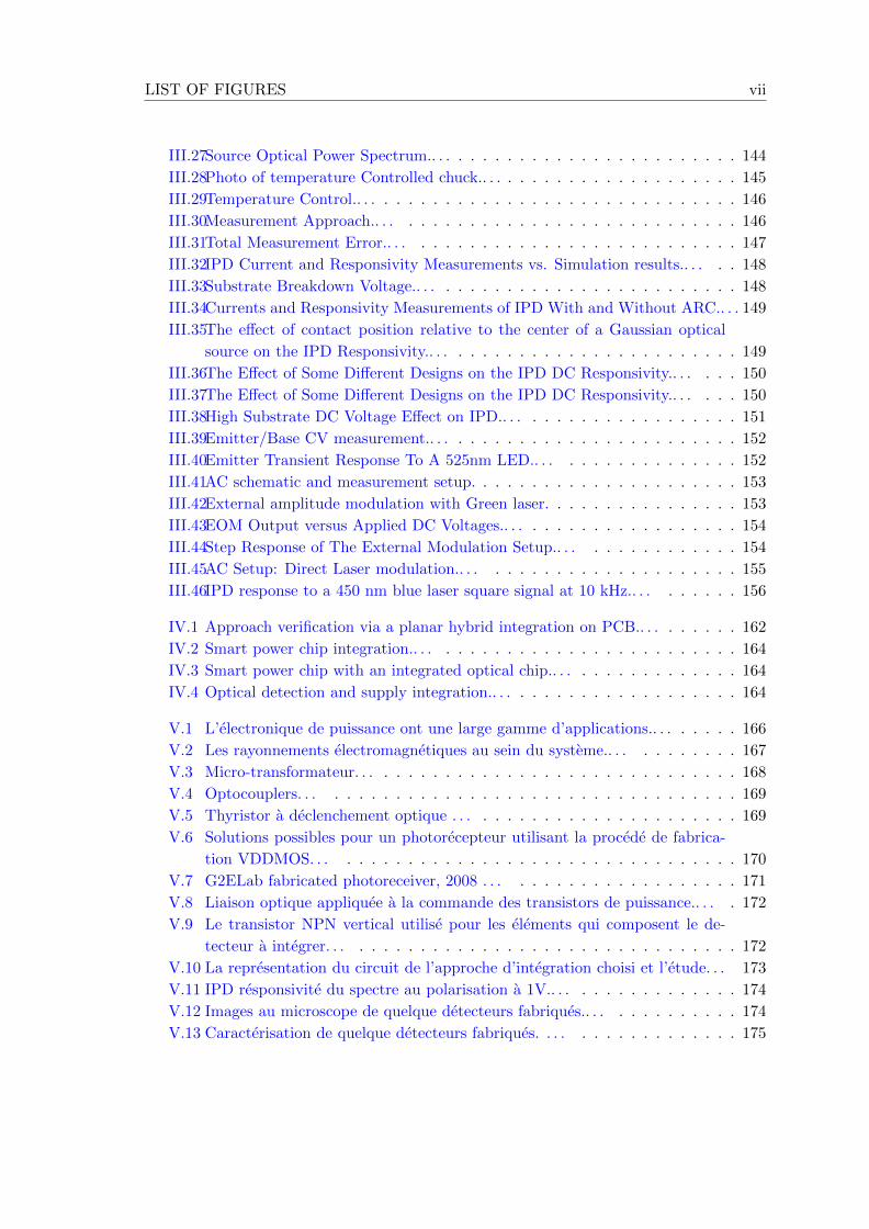
I.2 Power electronics wide application range.. . . . . . . . . . . . . . . . . . . . . 5
I.3 Time line of power semiconductor devices.. . . . . . . . . . . . . . . . . . . . 6
I.4 System ratings and applications for Silicon power devices.. . . . . . . . . . . 6
I.5 Example of a power converter and its elements.. . . . . . . . . . . . . . . . . 7
I.6 Principle topology of a power electronic system.. . . . . . . . . . . . . . . . . 8
I.7 Gate driver topology: energy and signal vs. signal only isolation.. . . . . . . 8
I.8 Gate driver topology: symmetric vs. asymmetric grounded DC link.. . . . . . 9
I.9 Gate driver topology, transmission and insulation techniques.. . . . . . . . . 9
I.10 State of the art and required future performance improvement of power
electronics systems.. . . . . . . . . . . . . . . . . . . . . . . . . . . . . . . . . 11
I.11 PN-insulation technology.. . . . . . . . . . . . . . . . . . . . . . . . . . . . . 12
I.12 Insulation methods for monolithic integration. . . . . . . . . . . . . . . . . . 13
I.13 Isolation applications.. . . . . . . . . . . . . . . . . . . . . . . . . . . . . . . . 15
I.14 Electromagnetic radiations within the system.. . . . . . . . . . . . . . . . . . 15
I.15 Isolated half-bridge gate driver.. . . . . . . . . . . . . . . . . . . . . . . . . . 16
I.16 Piezoelectric transformer and wireless transmission approach.. . . . . . . . . 18
I.17 Optocoupler layout and basic mechanism.. . . . . . . . . . . . . . . . . . . . 20
I.18 Commercial optocouplers.. . . . . . . . . . . . . . . . . . . . . . . . . . . . . 21
I.19 Discrete Pulse Transformer. . . . . . . . . . . . . . . . . . . . . . . . . . . . . 23
I.20 4-Channel isolation integrated. . . . . . . . . . . . . . . . . . . . . . . . . . . 24
I.21 Analog Devices icoupler power consumption. . . . . . . . . . . . . . . . . . . 24
I.22 Overview of the electromagnetic spectrum.. . . . . . . . . . . . . . . . . . . . 25
I.23 Attenuation: POF vs. GOF. . . . . . . . . . . . . . . . . . . . . . . . . . . . 26
I.24 Fiber optic isolation. . . . . . . . . . . . . . . . . . . . . . . . . . . . . . . . . 26
I.25 Short link fiber optic approach by avago. . . . . . . . . . . . . . . . . . . . . 27
I.26 PCB integrated capacitive coupling. . . . . . . . . . . . . . . . . . . . . . . . 27
I.27 Direct light triggered thyristor . . . . . . . . . . . . . . . . . . . . . . . . . . 28
I.28 Optical triggering of 12 kV, 1 cm2 4H-SiC thyristors . . . . . . . . . . . . . . 29
I.29 Hybrid-optical control by GaAs/AlGaAs based device . . . . . . . . . . . . . 29
I.30 Optical triggering by SiC bipolar transistor.. . . . . . . . . . . . . . . . . . . 30
I.31 4H-SiC photoconductive switch . . . . . . . . . . . . . . . . . . . . . . . . . . 31
I.32 Resonant gate-drive with optically isolated control signal and power supply.. . . 32
I.33 Optoelectronic material absorption spectrum. . . . . . . . . . . . . . . . . . . 34
I.34 Si absorption spectrum. . . . . . . . . . . . . . . . . . . . . . . . . . . . . . . 34
I.35 Direct versus indirect bangdap. . . . . . . . . . . . . . . . . . . . . . . . . . . 35
I.36 Photodetectors with gain. . . . . . . . . . . . . . . . . . . . . . . . . . . . . . 37
iv LIST OF FIGURES
I.37 Depletion width tuning in Si p-i-n photodiodes.. . . . . . . . . . . . . . . . . 39
I.38 Schematic structure of pn and p-i-n Photodiodes.. . . . . . . . . . . . . . . . 39
I.39 Ge pin integrated with Silicon waveguide.. . . . . . . . . . . . . . . . . . . . 39
I.40 pin-diode SFH 250 by Infineon.. . . . . . . . . . . . . . . . . . . . . . . . . . 40
I.41 Schematic structure of M-S and M-S-M photodiodes.. . . . . . . . . . . . . . 41
I.42 30 GHz MSM photodiode . . . . . . . . . . . . . . . . . . . . . . . . . . . . . 41
I.43 40 GHz waveguide-integrated Ge MSM photodiode . . . . . . . . . . . . . . . 42
I.44 Gate signal transfer approach . . . . . . . . . . . . . . . . . . . . . . . . . . . 42
I.45 Hybrid integration approach . . . . . . . . . . . . . . . . . . . . . . . . . . . 43
I.46 The possible solutions for an optical detector fabricated via the VDMOS
process. . . . . . . . . . . . . . . . . . . . . . . . . . . . . . . . . . . . . . . . 44
I.47 G2ELab fabricated photoreceiver, 2008 . . . . . . . . . . . . . . . . . . . . . 44
I.48 CMOS integration approach. . . . . . . . . . . . . . . . . . . . . . . . . . . . 46
I.49 Microscopic photos of IPDs. . . . . . . . . . . . . . . . . . . . . . . . . . . . 46
I.50 Optical Interface Approach. . . . . . . . . . . . . . . . . . . . . . . . . . . . . 48
I.51 Optical detector and optical supply integration approach. . . . . . . . . . . . 49
I.52 Abundance of elements in Earth crust. . . . . . . . . . . . . . . . . . . . . . 50
I.53 Project perspective and approach overview. . . . . . . . . . . . . . . . . . . . 51
II.1 IPD cross sectional view and polarization.. . . . . . . . . . . . . . . . . . . . 55
II.2 IPD simplified 1D structure cross section view showing the different regions
where photogeneration may take place.. . . . . . . . . . . . . . . . . . . . . . 56
II.3 VD-MOSFET And Optical Detector Cross Section.. . . . . . . . . . . . . . . 57
II.4 Integration and Control Approach. . . . . . . . . . . . . . . . . . . . . . . . . 59
II.5 IPD Input and Output Requirements. . . . . . . . . . . . . . . . . . . . . . . 60
II.6 Built-in junction potential and depletion region width according to the de-
pletion region approximation.. . . . . . . . . . . . . . . . . . . . . . . . . . . 62
II.7 Depletion Region Approximation versus Full Numerical Calculation.. . . . . 63
II.8 Doping Profile Effect on the Depletion Region Approximation versus Full
Numerical Calculation.. . . . . . . . . . . . . . . . . . . . . . . . . . . . . . . 64
II.9 Carrier Mobilities in Silicon at Room Temperature.. . . . . . . . . . . . . . . 65
II.10 Analytical modelling of the diffusion, generation and recombination dark
currents for a uniformly doped pn-junction.. . . . . . . . . . . . . . . . . . . 68
II.11 Analytical versus numerical modelling of a 1D uniformly doped pn-Junction
Dark IV characteristic.. . . . . . . . . . . . . . . . . . . . . . . . . . . . . . . 68
II.12 IPD Operation.. . . . . . . . . . . . . . . . . . . . . . . . . . . . . . . . . . . 70
II.13 Minority Carrier modulation Due to Photogeneration.. . . . . . . . . . . . . 71
II.14 Aluminium Transmittance.. . . . . . . . . . . . . . . . . . . . . . . . . . . . . 72
II.15 Shadow Effect Consideration in Simulation.. . . . . . . . . . . . . . . . . . . 72
II.16 Simple pn-Photodiode Structure.. . . . . . . . . . . . . . . . . . . . . . . . . 73
II.17 Analytical modelling of the electron and hole drift and diffusion currents.. . . 75
II.18 Analytical photocurrent model.. . . . . . . . . . . . . . . . . . . . . . . . . . 75
II.19 Analytical QE and Responsivity Model.. . . . . . . . . . . . . . . . . . . . . 76
II.20 Optical Reflection Losses.. . . . . . . . . . . . . . . . . . . . . . . . . . . . . 77
II.21 Power Reflectivity Coefficient for Si/air Interface.. . . . . . . . . . . . . . . . 78

LIST OF FIGURES v
II.22 Ideal ARC refractive Index.. . . . . . . . . . . . . . . . . . . . . . . . . . . . 78
II.23 24.7% Efficient Photocell Structure.. . . . . . . . . . . . . . . . . . . . . . . . 79
II.24 Si3N4 ARC Reflectance vs. ARC Thickness.. . . . . . . . . . . . . . . . . . . 80
II.25 Si3N4 ARC Reflectivity Spectrum.. . . . . . . . . . . . . . . . . . . . . . . . . 81
II.26 Si3N4 ARC Reflectance Sensitivity to ARC Thickness and Wavelength.. . . . 81
II.27 Analytical Modelling: Responsivity Spectrum as a function of Biasing and
Carrier Lifetime.. . . . . . . . . . . . . . . . . . . . . . . . . . . . . . . . . . . 82
II.28 Analytical Modelling: Responsivity spectrum as a function of biasing and
carrier lifetime.. . . . . . . . . . . . . . . . . . . . . . . . . . . . . . . . . . . 83
II.29 Analytical Modelling: Responsivity spectrum as a function of optical wave-
length and surface recombinations.. . . . . . . . . . . . . . . . . . . . . . . . 84
II.30 IPD Structure Cross Section View.. . . . . . . . . . . . . . . . . . . . . . . . 85
II.31 IPD dark current characteristics as a function of Emitter voltages.. . . . . . . 86
II.32 IPD Dark Current Characteristics as a function of Collector Voltages.. . . . . 87
II.33 IPD Responsivity Spectrum at 1V bias.. . . . . . . . . . . . . . . . . . . . . . 88
II.34 IPD responsivity spectrum dependence on Emitter DC voltages.. . . . . . . . 89
II.35 IPD responsivity spectrum dependence on Collector DC voltages.. . . . . . . 89
II.36 Emitter Responsivity Versus Emitter and Collector DC Voltages.. . . . . . . 90
II.37 Collector responsivity versus Emitter and Collector DC voltages.. . . . . . . 90
II.38 Effect of Collector DC voltages.. . . . . . . . . . . . . . . . . . . . . . . . . . 91
II.39 Recombination rates within the IPD structure.. . . . . . . . . . . . . . . . . . 92
II.40 Hole Concentration Gradient versus Carrier Lifetimes.. . . . . . . . . . . . . 92
II.41 Spectral Responsivity Sensitivity to Carrier Lifetimes.. . . . . . . . . . . . . 93
II.42 Emitter Current Sensitivity to Carrier Lifetimes.. . . . . . . . . . . . . . . . 93
II.43 Collector Current Sensitivity to Carrier Lifetimes.. . . . . . . . . . . . . . . . 93
II.44 IPD junction capacitances versus reverse voltage.. . . . . . . . . . . . . . . . 95
II.45 The IPD simplified equivalent circuit.. . . . . . . . . . . . . . . . . . . . . . . 96
II.46 Bode plot of the IPD frequency response.. . . . . . . . . . . . . . . . . . . . . 97
II.47 Collector to Emitter photocurrent ratio.. . . . . . . . . . . . . . . . . . . . . 98
II.48 IPD frequency response at 500 nm optical wavelength.. . . . . . . . . . . . . 98
II.49 IPD Emitter frequency response for different optical wavelengths.. . . . . . . 98
II.50 IPD Gain-frequency plots for different optical wavelengths.. . . . . . . . . . . 99
II.51 IPD bandwidth as a function of the optical wavelength.. . . . . . . . . . . . . 99
II.52 IPD Bandwidth as a Function of Optical Wavelength and Size.. . . . . . . . 100
II.53 IPD 3-dB Bandwidth as a function of Emitter biasing for different optical
wavelengths.. . . . . . . . . . . . . . . . . . . . . . . . . . . . . . . . . . . . . 100
II.54 IPD frequency response as a function of Emitter biasing for a 500 nm optical
wavelength.. . . . . . . . . . . . . . . . . . . . . . . . . . . . . . . . . . . . . 101
II.55 IPD 3-dB Bandwidth as a function of Emitter biasing for a 500 nm optical
wavelength.. . . . . . . . . . . . . . . . . . . . . . . . . . . . . . . . . . . . . 102
II.56 Photogeneration in the Base: Effect on IPD Responsivity.. . . . . . . . . . . 103
II.57 Bandwidth sensitivity to Optical Beam. . . . . . . . . . . . . . . . . . . . . . 103
II.58 VD-MOSFET Cross Section and Equivalent Circuit.. . . . . . . . . . . . . . 104
II.59 IPD Cross Section and Equivalent Circuit.. . . . . . . . . . . . . . . . . . . . 106
II.60 Substrate Transient Effect Under Dark Conditions.. . . . . . . . . . . . . . . 107
vi LIST OF FIGURES
II.61 Substrate Transient Effect Under Illumination.. . . . . . . . . . . . . . . . . . 107
II.62 Substrate Transient Effect as a Function of Ramp Time.. . . . . . . . . . . . 108
II.63 Photogeneration rate and Base potential gradient within the IPD structure
as a function of input optical intensity at a high Collector voltage.. . . . . . . 109
II.64 Base Potential Gradient and Emitter-Base Potential Barrier as a Function
of Input Optical Intensity at a High Collector Voltage.. . . . . . . . . . . . . 110
II.65 IPD Emitter and Collector behaviour versus input optical intensity at a
high Collector Voltage.. . . . . . . . . . . . . . . . . . . . . . . . . . . . . . . 111
II.66 IPD Base current behaviour versus input optical intensity at a high Collector
voltage.. . . . . . . . . . . . . . . . . . . . . . . . . . . . . . . . . . . . . . . . 111
II.67 IPD Emitter and Collector Behaviour versus Input Optical Intensity at a
Low Collector Voltage.. . . . . . . . . . . . . . . . . . . . . . . . . . . . . . . 112
II.68 Potential contours and current flow lines within the IPD structure as a
function of input optical intensity at a low Collector voltage.. . . . . . . . . . 113
II.69 Electron and Hole Concentration Profiles as a Function of Input Optical
Intensity at a Low Collector Voltage.. . . . . . . . . . . . . . . . . . . . . . . 114
II.70 Potential Profiles as a Function of Input Optical Intensity at a Low Collector
Voltage.. . . . . . . . . . . . . . . . . . . . . . . . . . . . . . . . . . . . . . . 114
III.1 VDMOS and VUMOS Structures.. . . . . . . . . . . . . . . . . . . . . . . . . 121
III.2 VD-MOSFET Planar Fabrication Process Flow.. . . . . . . . . . . . . . . . . 122
III.3 Bipolar IPD Process Flow.. . . . . . . . . . . . . . . . . . . . . . . . . . . . . 124
III.4 Alignment Process Summary.. . . . . . . . . . . . . . . . . . . . . . . . . . . 126
III.5 Mask Alignment Marks.. . . . . . . . . . . . . . . . . . . . . . . . . . . . . . 127
III.6 Mask Layout.. . . . . . . . . . . . . . . . . . . . . . . . . . . . . . . . . . . . 128
III.7 Test Modules.. . . . . . . . . . . . . . . . . . . . . . . . . . . . . . . . . . . . 129
III.8 Bipolar Transistors and Diodes.. . . . . . . . . . . . . . . . . . . . . . . . . . 130
III.9 Flip-Chip Integration Die Layout.. . . . . . . . . . . . . . . . . . . . . . . . . 130
III.10IPD Designs with P- and P+ Base.. . . . . . . . . . . . . . . . . . . . . . . . 131
III.11IPD Cross section with DRIE Termination.. . . . . . . . . . . . . . . . . . . 131
III.12IPD Designs with Nested Emitter Base regions.. . . . . . . . . . . . . . . . . 132
III.13Example Nested IPD Design Layout Detail.. . . . . . . . . . . . . . . . . . . 133
III.14Images of Critical Fabrication Steps.. . . . . . . . . . . . . . . . . . . . . . . 134
III.15Fabricated IPD Designs.. . . . . . . . . . . . . . . . . . . . . . . . . . . . . . 136
III.16P+ Mask Leakage Test.. . . . . . . . . . . . . . . . . . . . . . . . . . . . . . . 137
III.17IPD Emitter reverse IV.. . . . . . . . . . . . . . . . . . . . . . . . . . . . . . 137
III.18Previous IPD Designs.. . . . . . . . . . . . . . . . . . . . . . . . . . . . . . . 138
III.191st DC Setup Approach Using LED Sources.. . . . . . . . . . . . . . . . . . . 139
III.20Newport Calibrated Detector.. . . . . . . . . . . . . . . . . . . . . . . . . . . 139
III.212nd DC Setup Approach Using LED Sources.. . . . . . . . . . . . . . . . . . . 140
III.22IPD LIV with a 525 nm LED.. . . . . . . . . . . . . . . . . . . . . . . . . . . 141
III.23IPD Responsivity for 3 Different LEDs.. . . . . . . . . . . . . . . . . . . . . . 141
III.24Emitter Responsivity Versus Optical Power From A 525nm LED.. . . . . . . 142
III.25Second DC experimental setup.. . . . . . . . . . . . . . . . . . . . . . . . . . 143
III.26Schematic Diagram of DC experimental setup.. . . . . . . . . . . . . . . . . . 144
LIST OF FIGURES vii
III.27Source Optical Power Spectrum.. . . . . . . . . . . . . . . . . . . . . . . . . . 144
III.28Photo of temperature Controlled chuck.. . . . . . . . . . . . . . . . . . . . . . 145
III.29Temperature Control.. . . . . . . . . . . . . . . . . . . . . . . . . . . . . . . . 146
III.30Measurement Approach.. . . . . . . . . . . . . . . . . . . . . . . . . . . . . . 146
III.31Total Measurement Error.. . . . . . . . . . . . . . . . . . . . . . . . . . . . . 147
III.32IPD Current and Responsivity Measurements vs. Simulation results.. . . . . 148
III.33Substrate Breakdown Voltage.. . . . . . . . . . . . . . . . . . . . . . . . . . . 148
III.34Currents and Responsivity Measurements of IPD With and Without ARC.. . . 149
III.35The effect of contact position relative to the center of a Gaussian optical
source on the IPD Responsivity.. . . . . . . . . . . . . . . . . . . . . . . . . . 149
III.36The Effect of Some Different Designs on the IPD DC Responsivity.. . . . . . 150
III.37The Effect of Some Different Designs on the IPD DC Responsivity.. . . . . . 150
III.38High Substrate DC Voltage Effect on IPD.. . . . . . . . . . . . . . . . . . . . 151
III.39Emitter/Base CV measurement.. . . . . . . . . . . . . . . . . . . . . . . . . . 152
III.40Emitter Transient Response To A 525nm LED.. . . . . . . . . . . . . . . . . 152
III.41AC schematic and measurement setup. . . . . . . . . . . . . . . . . . . . . . 153
III.42External amplitude modulation with Green laser. . . . . . . . . . . . . . . . 153
III.43EOM Output versus Applied DC Voltages.. . . . . . . . . . . . . . . . . . . . 154
III.44Step Response of The External Modulation Setup.. . . . . . . . . . . . . . . 154
III.45AC Setup: Direct Laser modulation.. . . . . . . . . . . . . . . . . . . . . . . 155
III.46IPD response to a 450 nm blue laser square signal at 10 kHz.. . . . . . . . . 156
IV.1 Approach verification via a planar hybrid integration on PCB.. . . . . . . . . 162
IV.2 Smart power chip integration.. . . . . . . . . . . . . . . . . . . . . . . . . . . 164
IV.3 Smart power chip with an integrated optical chip.. . . . . . . . . . . . . . . . 164
IV.4 Optical detection and supply integration.. . . . . . . . . . . . . . . . . . . . . 164
V.1 L’electronique de puissance ont une large gamme d’applications.. . . . . . . . 166
V.2 Les rayonnements electromagnetiques au sein du systeme.. . . . . . . . . . . 167
V.3 Micro-transformateur. . . . . . . . . . . . . . . . . . . . . . . . . . . . . . . . 168
V.4 Optocouplers. . . . . . . . . . . . . . . . . . . . . . . . . . . . . . . . . . . . 169
V.5 Thyristor a declenchement optique . . . . . . . . . . . . . . . . . . . . . . . . 169
V.6 Solutions possibles pour un photorecepteur utilisant la procede de fabrica-
tion VDDMOS. . . . . . . . . . . . . . . . . . . . . . . . . . . . . . . . . . . 170
V.7 G2ELab fabricated photoreceiver, 2008 . . . . . . . . . . . . . . . . . . . . . 171
V.8 Liaison optique appliquee a la commande des transistors de puissance.. . . . 172
V.9 Le transistor NPN vertical utilise pour les elements qui composent le de-
tecteur a integrer. . . . . . . . . . . . . . . . . . . . . . . . . . . . . . . . . . 172
V.10 La representation du circuit de l’approche d’integration choisi et l’etude. . . 173
V.11 IPD responsivite du spectre au polarisation a 1V.. . . . . . . . . . . . . . . . 174
V.12 Images au microscope de quelque detecteurs fabriques.. . . . . . . . . . . . . 174
V.13 Caracterisation de quelque detecteurs fabriques. . . . . . . . . . . . . . . . . 175


List of Tables
I.1 Parameters for Different Digital Isolators.. . . . . . . . . . . . . . . . . . . . 18
I.2 Galvanic Isolation Methods . . . . . . . . . . . . . . . . . . . . . . . . . . . 19
I.3 Some Selected Properties of Semiconductors Interesting for Optical and
Power Electronics.. . . . . . . . . . . . . . . . . . . . . . . . . . . . . . . . . . 35
I.4 Typical values of gain and response time for common photodetectors. . . . . 36
II.1 Summery of VD-MOSFET performance parameters dependencies on design
variables.. . . . . . . . . . . . . . . . . . . . . . . . . . . . . . . . . . . . . . . 58
II.2 600V VDMOSFET, key layer specifications.. . . . . . . . . . . . . . . . . . . 58
II.3 Integrated Optical Detector Minimum Requirements . . . . . . . . . . . . . 60
III.1 Bipolar IPD process details and specifications . . . . . . . . . . . . . . . . . 125
III.2 Bulk and Epi Wafer Specifications . . . . . . . . . . . . . . . . . . . . . . . 134
III.3 Doping Process Parameters . . . . . . . . . . . . . . . . . . . . . . . . . . . 135


List of Acronyms
IPD Integrated Photo-Detector
QE Quantum efficiency
TIA TransImpedance Amplifier
SRP Spreading resistance profiling
QNR Quasi Neutral Region
ARC Anti Reflective Coating
DUT Device Under Test
VDMOSFET Vertical Diffused Metal Oxide Semiconductor Field Effect Transistor
IGBT Insulated-Gate Bipolar Transistor
BJT Bipolar Junction Transistor
SOI Silicon On Insulator
POF Polymer Optical Fiber
GOF Glass Optical Fiber
PWM Pulse width modulation
SRH Shockley Read Hall


Notations and Parameters
Variables and Physical Constants:

xiv Notations and Parameters
Num Symbol Value Unit
Acceptor Concentration NA cm−3
Donor Concentration ND cm−3
Temperature T K
Lifetime of electrons τn s
Lifetime of holes τp s
Charge of an electron q −1, 6.10−19 C
Permittivity of free space ε0 8, 85.10−14 F/cm
Relative permittivity of Si εR 11, 9
Boltzmann Constant k 1, 38667.10−23 J/K
Planck Constant h 6, 6.10−34 J.s
Electron rest mass m0 9, 1.10−31 kg
Effective mass of e− in the valence band m∗v 0, 59.m0 kg
Effective mass of e− in the conduction band m∗c 1, 06.m0 kg
Thermal voltage VTh k ∗ Tq V
Bandgap of Si at T=4 K Eg0 1, 12 eV
Bandgap of Si Eg (Eg0 − aT 2
T+b) eV
Coefficient a a 4, 73.10−4 eV/K
Coefficient b b 636 K
Effective density of states in the conduction band. Nc 2.(2πmckTh2
)32 .10−6 cm−3
Effective density of states in the valance band. Nv 2.(2πmvkTh2
)32 .10−6 cm−3
Intrinsic Carrier Concentration ni√Nc.Nv.e
−Eg2kT cm−3
Carrier thermal velocity vth
√2kTm∗ .102 cm/s
Carrier average drift velocity vd cm/s
Electron mobility µn cm2/V/s
Hole mobility µp cm2/V/s
Electron diffusion coefficient Dn µn.Ut cm2/s
Hole diffusion coefficient Dp µp.Ut cm2/s
Electron diffusion path length Ln√Dn.τn cm
Hole diffusion path length Lp√Dp.τp cm

Notations and Parameters xv
Electrical Variables and Physical Constants:
Name Symbol Value Unit
Built-in potential Vbi V
Charge density ρ(x) C/cm3
Electric Potential ψ(x) V
Electric Field E(x) V/cm
Minority e− current density in the P region Jn A/cm2
Minotrity h+ current density in the N region Jp A/cm2
Diffusion current density Jdiff A/cm2
Drift current density Jdr A/cm2
Current density due to thermal generation Jgn A/cm2
Current density due to thermal recombination Jre A/cm2
Current density due to net generation and recombination JRG A/cm2
Resistivity ρ Ω · cmResistance of the quasi neutral N-type region RN Ω
Resistance of the quasi neutral P-type region RP Ω
Geometric Variables:
Name Symbol Value Unit
Depletion Region on the P-side of a PN junction Xdp cm
Depletion Region on the N-side of a PN junction Xdn cm
Total Depletion Region Width of a PN junction WD Xdn+Xdp cm
Position of the metallurgical junction Xj cm
Junction surface area A cm2
Concentration of electrons in the N region nn cm−3
Concentration of electrons in the P region np cm−3
Concentration of holes in the P region pp cm−3
Concentration of holes in the N region pn cm−3

xvi Notations and Parameters
Optical Related Variables:
Name Symbol Value Unit
Optical refractive index n
Optical power reflection coefficient R
Wavelength λ µm
Speed of light in vacuum c 3.108 m/s
Optical absorption coefficient α cm−1
Front Surface recombination speed SF cm/s
Back Surface recombination speed SB cm/s
Incident optical power Popt W
Incident optical intensity Iopt W/cm2
Incident photon flux Φ Photons/cm2/s
Photon flux after surface reflections Φ0 (1−Ropt) · Φ Photons/cm2/s
Photo generation rate Gop Photons/cm3/s
h+ photocurrent density of Emitter QNR JEh A/cm2
Photocurrent density of depletion region JDe A/cm2
e− photocurrent density of Base QNR JBe A/cm2
Total Photocurrent density Jphoto A/cm2
Total Photocurrent Jphoto ·A A
Emitter Photocurrent Iph−E Jph−E ·A A
Base Photocurrent Iph−B Jph−B ·A A
Collector Photocurrent Iph−C Jph−C ·A A
Emitter dark current IDark−E A
Base dark current IDark−B A
Collector dark current IDark−C A
Emitter total current IE (Iph−E + IDark−E) A
Base total current IB (IPh−B + IDark−B) A
Collector total current IC (Iph−C + IDark−C) A
Dark current from calibrated detector ICal−Dark A
Total current from calibrated detector ICal A
Responsivity of calibrated detector Resp−Cal A
Dark current from device under test IDUT−Dark A
Total current from device under test IDUT A
Quantum efficiency η
Responsivity R
Emitter Responsivity REBase Responsivity RBCollector Responsivity RCRise time τR s
Carrier transit time τtr s
Carrier diffusion time τd s
Junction capacitance Cj F

General Introduction
In efforts of providing a high level optical solution for the galvanic isolation challenge in-
side power converters, more specifically between the power device and its control unit,
this thesis proposes a compatible optical detector design for monolithic integration with a
600V vertical MOSFET without any modifications to the power VMOS fabrication process.
The main field of this study, is related most generally to power conversion technolo-
gies. With the widespread use of electronics in the industrial, transportation, medical and
the consumer sectors, power electronic systems play a larger role in the energy equation
both in terms of efficiency and cost, and thus they can have a significant impact on the
environment and the economy. As a result, there is a continual interest in innovative de-
signs which can improve the quality of energy and power conversion and management at
high efficiency levels, meanwhile providing integrable generic solutions in a cost effective
manner.
Power converters can be very complicated systems with many internal subsystems;
nevertheless, at the heart of all power converter systems, is the power switch. The power
switch places many requirements and restraints on the driving circuitry; today, it is still
challenging to transfer the gating signal and sufficient energy to the power switch in a
reliable and efficient manner without weight, size, design complexity, and cost penalties.
Since light provides the highest level of galvanic isolation, methods that allow its mono-
lithic integration with the power device are of interest as the power electronic community
strives for a fully integrated power function. The optical galvanic solutions proposed in the
literature mainly target pulse applications based on wide bandgap semiconductors which
are favoured due to their high thermal conductivity and high breakdown voltage capabil-
ities. Compared to the recent state of the art where large laser sources are required to
transfer the command signal with sufficient energy, the proposed monolithically integrated
photodetector (IPD) isolates the command signal only and the required switching energy
is supplied via an amplification stage. The proposed IPD fabrication is 100% compatible
with the vertical power switch fabrication process and hence there are no additional cost
or processing complexity penalties. This IPD can be triggered by an optical beam with
a few µWs of power, thus it allows for a range of low power, low cost, and small optical
sources such as semiconductor lasers and LEDs. The output of the optical detector will be
2 General Introduction
a current signal in the range of a few 100s of nAs. This output current signal contains only
the control information; in order to provide the sufficient energy required to switch the
VD-MOSFET, the output of the optical detector will be amplified at a TIA stage before
feeding the gate of the VDMOSFET.
Chapter 1 of this thesis aims to motivate the reader via illustrating the dynamic con-
text surrounding the challenges involved in creating a novel integrated galvanic isolations
for drivers, as well as the current state of the art before finally introducing our proposed
integrable, low power, optical isolation approach. In chapter 2, the relevant modelling
approach and finite element simulation results for the possible IPD structures reveal the
operation mechanisms of the IPD and its static and dynamic performances as a function
of input optical wavelength, optical power, small signal frequency and IPD biasing condi-
tions. Moreover, the limitations imposed by the vertical power device structure and the
power device floating substrate potential, on the IPD performance and operation mode
are analysed through modelling and simulations. The results of these analysis are used to
develop best design practices for the IPDs and to identify the optimum range for values of
available design variables and the optimum operation settings. The fabrication procedure
and results as well as the characterization approach, the experimental setup and measure-
ment results are provided in chapter 3. A number of different IPDs were designed with
a variety of Emitter and Base doping region and contact geometrical features including
nested, pixelated, and comb structures. The IPDs were coated with a Si3N4 anti reflective
coating optimized for maximum optical transmission at a wavelength of 500 nm. The
spectral responsivity of the detectors from 400nm up to near infra-red wavelengths has
been measured and a peak Emitter responsivity of 0.2 A/W at 500nm was achieved with
the IPD Emitter reversed biased at 1V. Measurement results show a low Emitter capac-
itance in the range of 10pF-35pF for detectors of diameter 50µm to 200µm. Initial AC
measurements indicate a high bandwidth above 20MHz.

Chapter I
Introduction And Motivation: IntegratedGalvanic Insulation for Power Devices
Sommaire
I.1 Power Electronic Converters and Power Semiconductor Switches 4
I.1.a Gate Driver Topologies and Insulation . . . . . . . . . . . . . . . . . . . . . 7
I.1.b VDMOSFET/IGBT and their Gate Driver Requirements . . . . . . . . . . 9
I.1.c Towards a Fully Integrated Power Function Solution . . . . . . . . . . . . . 10
I.2 Galvanic Isolation for Power Semiconductor Devices . . . . . . . 14
I.2.a The Need for Isolation . . . . . . . . . . . . . . . . . . . . . . . . . . . . . . 14
I.2.b Existing Isolation Methods . . . . . . . . . . . . . . . . . . . . . . . . . . . . 17
I.2.c Optical Isolation: State of the Arts Under Research . . . . . . . . . . . . . 27
I.3 Optical Detection: Physics and Key Challenges . . . . . . . . . . . 32
I.3.a Optical Absorption . . . . . . . . . . . . . . . . . . . . . . . . . . . . . . . . 33
I.3.b Photodetectors . . . . . . . . . . . . . . . . . . . . . . . . . . . . . . . . . . 36
I.4 Monolithic Galvanic Isolation by an Integrated Photo-Detector(IPD) . . . . . . . . . . . . . . . . . . . . . . . . . . . . . . . . . . . . . . . . . . 42
I.5 Thesis Overview . . . . . . . . . . . . . . . . . . . . . . . . . . . . . . . . . . 50
I.5.a Methodology . . . . . . . . . . . . . . . . . . . . . . . . . . . . . . . . . . . 50
I.5.b Organization . . . . . . . . . . . . . . . . . . . . . . . . . . . . . . . . . . . 51
Abstract
In order to justify and show the function and placement of this project within the field
of power electronics, we begin by giving a brief overview of where the different power
transistor technologies can be applied as well as some basic information on power
electronic converter topologies; the power switch structure, its basic operation and re-
quirements with a focus on the gate driver and its galvanic isolation requirement is
also introduced. Since this thesis is also tackling an integration challenge, the different
integration methods used for the power switch environment are also presented in order
to explain the technology choice for the optical detector in terms of compatibility and
cost. A summary, comparing and contrasting the state of the art for different galvanic
isolation solutions is provided in order to describe where and why the monolithic op-
tical solution is appropriate. Also, the state of the art on optical detectors is included
in order to provide the reader with a complete list of solutions in terms of design,
material and technology and to justify our chosen optical detector design and system
approach. The overall system topology, design and mode of operation for the proposed
optical solution are presented in subsection I.4.

4 I. Introduction And Motivation: Integrated Galvanic Insulation for Power Devices
I.1 Power Electronic Converters and Power Semiconductor
Switches
Power Electronic is a multidisciplinary field that requires an in-depth knowledge of several
related fields as shown by the diagram of figure I.1 [1].
Figure I.1: Multidisciplinary nature of power electronic design. All these fields are governed
under power electronic standards.
The field of power electronics is a branch of electronics that is concerned with maintain-
ing and regulating electrical power conversions and exchanges between sources and loads
[2]. In order to efficiently convert electrical energy from one form to another or to change
the voltage or frequency levels or any combination of these, electrical systems called power
converters are designed specific to the application at hand. One approach in classifying
the different families of power converters is via considering the type of input and output
signals which are either alternating current (AC) or direct current (DC) signals:
• DC-DC (Choppers): DC-DC converters convert input DC voltages to other DC volt-
ages at the output and they can work with sources such as batteries and photovoltaic
cells. Some examples of DC-DC power converters include bulk, boost, bulk-boost,
half bridge and full bridge [3].
• AC-DC (Rectifier): AC-DC converters convert input AC voltages to DC voltages at
the output. These converters can be found on most house appliances where electrical
devices/systems require DC inputs meanwhile only AC sources are available. These
converters can cover applications with a wide range of power, voltage, and frequency
levels such as washers, dryers, computers, cellular phones and televisions [3].
• DC-AC (Inverters): DC-AC converters convert input DC voltages to AC voltages at
the output; the voltage and frequency levels may be fixed or variable. In variable
speed drives (ASDs) an input AC signal is first rectified to a DC signal and then
I.1. Power Electronic Converters and Power Semiconductor Switches 5
converted to another AC output with a different frequency and voltage level by em-
ploying a DC-AC inverter. Other examples include DC-AC inverters for photovoltaic
systems, for motors control and emergency lighting. [3]
• AC-AC (Cyclo-converter): AC-AC converters such as Cyclo-converters, convert in-
put AC waveforms to other AC waveforms with a different voltage and frequency.
Some applications include compressor and wind-tunnel drives, or for variable-speed
applications such as cement kilns [3].
As depicted in figure I.2, power converters are used for a wide rage of applications. The
voltage (volts to giga-volts) and current(milliamperes to hundreds of Amps) levels as well
as the power (watts to megawatts) conversions performed by power converters are far larger
than those encountered in linear electronics, making the manipulation of such large flows of
power challenging both in terms of safety and efficiency as well as system volume and cost.
These challenges are addressed by employing power semiconductor transistors and passive
elements to create switched mode based units or otherwise known as commutation cells,
that can regulate and manage flows of power between different power supplies and loads.
Thus, the power switch is at the heart of all power converter systems. The emergence
of power switches in the 1950s was initiated by the invention of solid state transistors at
bell-labs in 1947 [4] which has revolutionized the world of electronics. In case of interest,
a time line of the evolution of electronic devices with a focus on power devices is shown in
figure I.3. It should be noted that diamond devices are also of high interest in the power
electronic field, however, to this day there are no commercial diamond power devices
available in the market where as GaAs, SiC and GaN devices are commercially available.
Figure I.2: Power electronic solutions are used for a wide range of applications.
There are different types of power semiconductor devices available for a specified ap-
plication depending on the required control mode, voltage, current, power and frequency
ratings. As summarized in figure I.4, there is a compromise between the system power

6 I. Introduction And Motivation: Integrated Galvanic Insulation for Power Devices
Figure I.3: Evolution of power electronic semiconductor devices.
rating and its operating frequency. Thyristors have low bandwidths but they can handle
large voltages and currents, making them the optimum solution for such applications as
high power HVDC transmission lines. IGBTs are suitable for a wide range of medium
power and medium frequency applications that still demand a significant current handling
capability: from several hundred watts in small drives to megawatts in wind power instal-
lations. Applications with higher operating frequency requirements, lower power ratings
(under a few hundred watts) and lower current ratings (a few amperes), employ power
MOSFET devices [5].
Figure I.4: System ratings and applications for Silicon power devices. The orange arrows
indicate the possible extension of future devices into the not yet covered areas [5].
I.1. Power Electronic Converters and Power Semiconductor Switches 7
I.1.a Gate Driver Topologies and Insulation
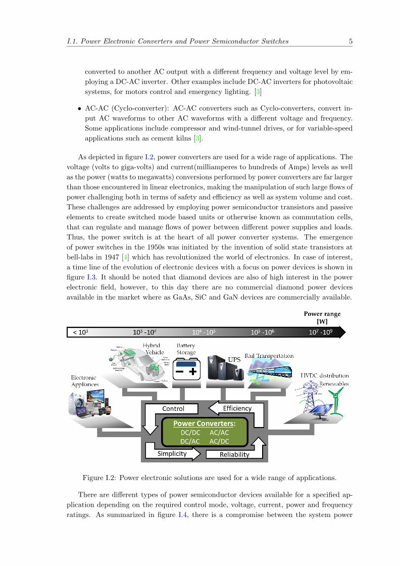
As shown in the DC-DC power converter example of figure I.5, a power converter may
include many different elements including many commutation cells, passive devices used
for filtering, printed circuit boards and cooling systems.
Figure I.5: Phase-shift dc/dc converter with current doubler output optimized with respect
to power density [6].
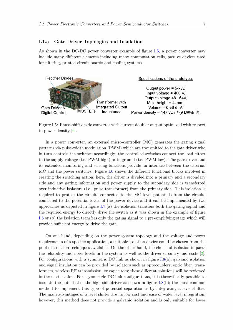
In a power converter, an external micro-controller (MC) generates the gating signal
patterns via pulse-width modulation (PWM) which are transmitted to the gate driver who
in turn controls the switches accordingly; the controlled switches connect the load either
to the supply voltage (i.e. PWM high) or to ground (i.e. PWM low). The gate driver and
its extended monitoring and sensing functions provide an interface between the external
MC and the power switches. Figure I.6 shows the different functional blocks involved in
creating the switching action; here, the driver is divided into a primary and a secondary
side and any gating information and power supply to the secondary side is transferred
over inductive isolators (i.e. pulse transformer) from the primary side. This isolation is
required to protect the circuits connected to the MC level potentials from the circuits
connected to the potential levels of the power device and it can be implemented by two
approaches as depicted in figure I.7:(a) the isolation transfers both the gating signal and
the required energy to directly drive the switch as it was shown in the example of figure
I.6 or (b) the isolation transfers only the gating signal to a pre-amplifying stage which will
provide sufficient energy to drive the gate.
On one hand, depending on the power system topology and the voltage and power
requirements of a specific application, a suitable isolation device could be chosen from the
pool of isolation techniques available. On the other hand, the choice of isolation impacts
the reliability and noise levels in the system as well as the driver circuitry and costs [2].
For configurations with a symmetric DC link as shown in figure I.8(a), galvanic isolation
and signal insulation can be provided by isolators such as optocouplers, optic fiber, trans-
formers, wireless RF transmission, or capacitors; these different solutions will be reviewed
in the next section. For asymmetric DC link configurations, it is theoretically possible to
insulate the potential of the high side driver as shown in figure I.8(b); the most common
method to implement this type of potential separation is by integrating a level shifter.
The main advantages of a level shifter are its low cost and ease of wafer level integration;
however, this method does not provide a galvanic isolation and is only suitable for lower

8 I. Introduction And Motivation: Integrated Galvanic Insulation for Power Devices
Figure I.6: Principle topology of a power electronic system showing the elements in the
power switch environment. This topology is often adapted for each half bridge [2].
Figure I.7: Principle gate driver topology: (a)energy and signal versus (b) signal only
isolation). The dashed lines represent functions that maybe be implemented discretely
but also have potential for integration. For example, the power supply, and the isolation
can be all integrated within the driver.

I.1. Power Electronic Converters and Power Semiconductor Switches 9
operation power levels [2]. Figure I.9 by Semikron Elektronik in 2010 shows a summary of
the different isolation methods available for different driver topologies and depending on
the requirement range of applications.
Figure I.8: (a) Example of symmetric grounded DC link with external isolation device and
(b) asymmetric grounded DC link with integrated level shifter [2].
Figure I.9: Gate driver topologies, insulation and transmission principles depending on
the application range [2].
I.1.b VDMOSFET/IGBT and their Gate Driver Requirements
As previously stated, power transistors are at the heart of the power converter. The power
transistors in commutation cells switch between two states, either with a terminal voltage
approximately equal to the nominal voltage level and a minimum possible current level or
visa versa. The most important characteristics for power switch elements are their:
• Blocking voltages

10 I. Introduction And Motivation: Integrated Galvanic Insulation for Power Devices
• Passing current levels (DC current levels are limited due to rising temperatures
meanwhile current pulses are limited by the layout.)
• Minimum on-state voltages which determine the conduction losses
• Minimum voltage drops during switching times which give the commutation losses
• Control mode (i.e. voltage vs. current control, turn-on and/or turn-off control).
The blocking voltage and current level are set by the specific requirements of different
applications and are implemented during the design process by mainly tuning the thick-
ness of the drift region, and the cross sectional area of the device. Although it is always
desired to minimize the power losses in any application, commutation losses can be more
problematic in higher frequency applications. In general, there are two main concerns
regarding the switch mode operation that must be considered in any converter, (1) switch-
ing power losses (2) and the electromagnetic interferences from the large electrical entities
being switched [7].
The insulating gate oxide of power MOSFET and IGBT means that no gate drive
current is required during steady state operation; however, when switching, a gate drive
current is required to charge and discharge the input capacitance. A large input capaci-
tance has 2 major effects: (1) longer switching time intervals and higher losses at higher
operating frequencies, and (2) a larger gate drive current requirement which in turn in-
creases the gate drive circuit cost and size. The input capacitance can be reduced by
reducing the device area, however, a smaller area translates to a higher on-state resistance
and higher current densities which result in higher power transistor on-state losses per
cm2. The main compromise in the gate driver design is between a fast drive for reduced
switching losses and a slow drive for reduced parasitic noises (EMC) from the voltage tran-
sients. Thus, it is desired to minimize the parasitic inductance of the drive loop in order
to reduce the required switching time (i.e. smaller input capacitance) and the parasitic
noises (i.e. smaller gate-drain capacitance to gate-source capacitance ratio to avoid a shoot
through current). Next, the gate resistance RG must be chosen appropriately to control
the switching time of the device; RG must be low enough to avoid a Miller drawback but
large enough to control the device speed [7]. Thus one approach is to employ two RGs
in parallel; initially a large RG is connected at the turn-on to minimize overshoots from
parasitics in the power converter loop, then a second RG is connected in parallel to reduce
the overall RG and avoid a Miller drawback. Equation I.1 evaluates the Miller drawback
limit.
[dVDdt
]max =VTH
RGCGD[7] (I.1)
Where VD = drain voltage, VTH = threshold voltage, and CGD = gate-drain capaci-
tance.
I.1.c Towards a Fully Integrated Power Function Solution
In order to identify the future of power electronics and to develop new technologies to sur-
pass the currently faced technological barriers, a set of workshops and meetings (i.e. AIST
I.1. Power Electronic Converters and Power Semiconductor Switches 11
Power Electronics New Wave Workshops, CPES Technology Roadmap Workshops, ECPE
Workshops on Power Electronics Research and Technology Roadmaps) are organized by
some of the large power electronic research centres (European Center for Power Electron-
ics (ECPE)[8], Center for Power Electronics Systems (CPES) of USA [9], Japan National
Institute of Advanced Science and Technology - Power Electronics Research Center (AIST-
PERC) [10]). The trends for improvements of power electronic systems was represented by
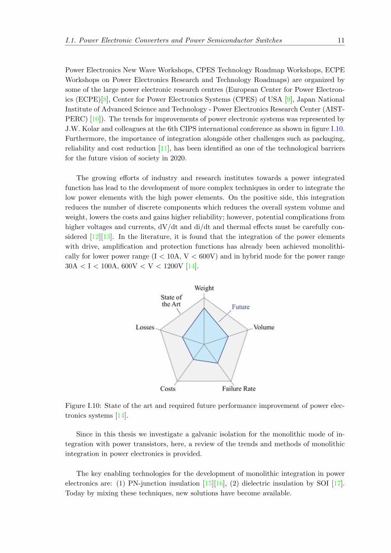
J.W. Kolar and colleagues at the 6th CIPS international conference as shown in figure I.10.
Furthermore, the importance of integration alongside other challenges such as packaging,
reliability and cost reduction [11], has been identified as one of the technological barriers
for the future vision of society in 2020.
The growing efforts of industry and research institutes towards a power integrated
function has lead to the development of more complex techniques in order to integrate the
low power elements with the high power elements. On the positive side, this integration
reduces the number of discrete components which reduces the overall system volume and
weight, lowers the costs and gains higher reliability; however, potential complications from
higher voltages and currents, dV/dt and di/dt and thermal effects must be carefully con-
sidered [12][13]. In the literature, it is found that the integration of the power elements
with drive, amplification and protection functions has already been achieved monolithi-
cally for lower power range (I < 10A, V < 600V) and in hybrid mode for the power range
30A < I < 100A, 600V < V < 1200V [14].
Figure I.10: State of the art and required future performance improvement of power elec-
tronics systems [14].
Since in this thesis we investigate a galvanic isolation for the monolithic mode of in-
tegration with power transistors, here, a review of the trends and methods of monolithic
integration in power electronics is provided.
The key enabling technologies for the development of monolithic integration in power
electronics are: (1) PN-junction insulation [15][16], (2) dielectric insulation by SOI [17].
Today by mixing these techniques, new solutions have become available.

12 I. Introduction And Motivation: Integrated Galvanic Insulation for Power Devices
In the literature, it has been reported that by controlling the thickness of the epitaxial
layer, the level of doping concentration and the size of the edge termination structures,
the PN-insulation method can be scaled for voltages from 600 V to 1200 V [2]. This tech-
nique allows the integration of sensitive analog systems that maybe required on the high
side driver. The cross section of 600 V/1200 V device structures with PN-insulation that
were presented by Dr. Takahashi at the 2000 CIPS meetings is demonstrated in figure
I.11 (a). Photos of chips with different driver topologies and PN-termination structures
fabricated by ST Microelectronics (STM) in 2003 and International Rectifier (IR) in 2008
are shown in figures I.11 (b), (c) and (d). The PN-insulation technology has its drawbacks.
The leakage currents from the PN structures lead to self-heating (limiting the maximum
operating temperature to roughly 150 C) and increased losses. Also and even more im-
portantly, the internal parasitic thyristor structures can be activated in case of negative
voltage transients at the driver output. Some solutions have been proposed [18], however
they do not completely eliminate this issue [2].
Figure I.11: (a) Fundamental device structures of a 600 V/1200 V PN-insulation technol-
ogy [19]. ICs in PN-junction insulation by different manufacturers: (b) 600 V, 650/400 mA
Halfbridge-driver with differential level-shifters embedded within the termination structure
by STM [16] (c) 600V, 500/250mA Sixpack-driver with level-shifters located separately by
IR [20] (d) 1200V, 500/250mA Sixpack-driver with differential level-shifters embedded
within the termination structure by IR [20].
The use of SOI technology provides insulation by means of a dielectric layer; as a
result, the issue of the parasitic turn-on of the internal thyristor that existed in the PN-
insulation structures is eliminated. This has allowed the full integration of bipolar devices
(i.e. IGBTs and diodes) and their driver and monitoring functions on a single chip. Figure
I.12 (a) shows the cross sectional view of some of the fundamental device structures of a
500 V SOI-CMOS platform by Mitsubishi [21]. Figure I.12 (b) shows an integrated gate
driver and 500 V, 1 A inverter in SOI [22]. In 2010, the university of Tennessee reported
a SOI based integrated gate driver for high voltage and high temperature SiC FETs [23].
The drawbacks of SOI insulation in comparison to PN-junction termination is mainly
the implementation cost. Although SOI technology allows the integration of high voltage
devices, current levels are still limited due to the lateral structure of the integrated devices.
Insulation of low voltage components by formations of P+ walls is a mixed technology
I.1. Power Electronic Converters and Power Semiconductor Switches 13
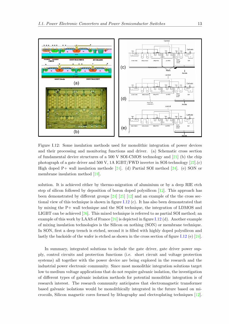
Figure I.12: Some insulation methods used for monolithic integration of power devices
and their processing and monitoring functions and driver. (a) Schematic cross section
of fundamental device structures of a 500 V SOI-CMOS technology and [21] (b) the chip
photograph of a gate driver and 500 V, 1A IGBT/FWD inverter in SOI-technology [22].(c)
High doped P+ wall insulation methode [24]. (d) Partial SOI method [24]. (e) SON or
membrane insulation method [24].
solution. It is achieved either by thermo-migration of aluminium or by a deep RIE etch
step of silicon followed by deposition of boron doped polysilicon [12]. This approach has
been demonstrated by different groups [24] [25] [12] and an example of the the cross sec-
tional view of this technique is shown in figure I.12 (c). It has also been demonstrated that
by mixing the P+ wall technique and the SOI technique, the integration of LDMOS and
LIGBT can be achieved [26]. This mixed technique is referred to as partial SOI method; an
example of this work by LAAS of France [24] is depicted in figure I.12 (d). Another example
of mixing insulation technologies is the Silicon on nothing (SON) or membrane technique.
In SON, first a deep trench is etched, second it is filled with highly doped polysilicon and
lastly the backside of the wafer is etched as shown in the cross section of figure I.12 (e) [24].
In summary, integrated solutions to include the gate driver, gate driver power sup-
ply, control circuits and protection functions (i.e. short circuit and voltage protection
systems) all together with the power device are being explored in the research and the
industrial power electronic community. Since most monolithic integration solutions target
low to medium voltage applications that do not require galvanic isolation, the investigation
of different types of galvanic isolation methods for potential monolithic integration is of
research interest. The research community anticipates that electromagnetic transformer
based galvanic isolations would be monolithically integrated in the future based on mi-
crocoils, Silicon magnetic cores formed by lithography and electroplating techniques [12].

14 I. Introduction And Motivation: Integrated Galvanic Insulation for Power Devices
Integration of piezo-resistive galvanic solutions fabricated on silicon membrane devices are
also anticipated to emerge in the future [12].
I.2 Galvanic Isolation for Power Semiconductor Devices
Isolation circuits provide protection against unwanted and/or hazardous voltages and cur-
rents. The maximum permissible signal noise level and EMI requirements are important
considerations in any power converter design and even more so when integrating sensitive
control functions closer to the power unit. It is crucial for the integrity of the system
to carefully consider the thermal and electromagnetic interactions between the different
functions in the system.
An EMI filter should provide immunity against high frequency current and voltage
transients, parasitics, stray inductances and coupling capacitances. There are internal
perturbation sources such as the magnetic fields around high power devices (e.g. power
transistors and power diodes), and external sources of EMI such as high power cables,
motors, RF radiations or other sources in the environment that must be considered in the
design process.
After giving a basic review on the needs for isolation, the existing isolation methods
are discussed, compared and contrasted.
I.2.a The Need for Isolation
Figure I.13 gives an overview of the basic applications for circuit isolation; their needs
are: (a) user safety, (b) equipment/circuit protection from high dv/dt or di/dt, (c) noise
perturbations, (d) and ground loops. In an electrical system there are different number
of signals flowing through different paths at all times; any unwanted interactions between
these signals may degrade high-fidelity signals, damage components, jeopardize the over-
all system and/or cause harm to the user. A signal flowing through an electrical system
may experience interferences from errors induced due to ground loops, floating supplies
and floating references [7]. Depending on the signal levels, distances between conducting
paths, and the surrounding material permittivity and permeability, electromagnetic inter-
ferences could be induced through capacitive or inductive coupling. Electromagnetic and
heat (thermal management challenges are not studied in this thesis) radiations between
the different power switch functions on the driver side are two main challenges that need
to be carefully considered during the design stage [27]; these interactions are depicted in
figure I.14. These problems are solved by implementing isolation components where neces-
sary such that the flow of information is uninterrupted meanwhile unwanted currents are
blocked [28].
Applications with a size limitation (i.e. cell phones), require high frequency gate drivers
in order to allow for the size reduction of the output passive filters. As already discussed,
MOSFETS are superior to IGBTs and power BJTs for higher frequency and medium to
low power applications where the switching losses dominate the overall power losses [7].

I.2. Galvanic Isolation for Power Semiconductor Devices 15
Figure I.13: Applications in need of Isolation. [29].
Figure I.14: Electromagnetic and thermal radiations between the power switch functions
within the system.
16 I. Introduction And Motivation: Integrated Galvanic Insulation for Power Devices
Fully integrated driver solutions are highly desirable, since bringing the driver as close as
possible to the power MOSFET will reduce interconnections and the parasitic elements
(inductances and capacitance) that could contribute to the switching losses. This trend of
miniaturizing and integrating all the power functions closer to the power switch requires
the design and implementation of integrated galvanic isolations in order to insure the safety
of the low power circuitries from the high power units.
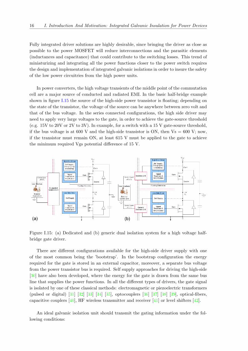
In power converters, the high voltage transients of the middle point of the commutation
cell are a major source of conducted and radiated EMI. In the basic half-bridge example
shown in figure I.15 the source of the high-side power transistor is floating; depending on
the state of the transistor, the voltage of the source can be anywhere between zero volt and
that of the bus voltage. In the series connected configurations, the high side driver may
need to apply very large voltages to the gate, in order to achieve the gate-source threshold
(e.g. 15V to 20V or 2V to 3V). In example, for a switch with a 15 V gate-source threshold,
if the bus voltage is at 600 V and the high-side transistor is ON, then Vs = 600 V; now,
if the transistor must remain ON, at least 615 V must be applied to the gate to achieve
the minimum required Vgs potential difference of 15 V.
Figure I.15: (a) Dedicated and (b) generic dual isolation system for a high voltage half-
bridge gate driver.
There are different configurations available for the high-side driver supply with one
of the most common being the ’bootstrap’. In the bootstrap configuration the energy
required for the gate is stored in an external capacitor, moreover, a separate bus voltage
from the power transistor bus is required. Self supply approaches for driving the high-side
[30] have also been developed, where the energy for the gate is drawn from the same bus
line that supplies the power functions. In all the different types of drivers, the gate signal
is isolated by one of these classical methods: electromagnetic or piezoelectric transformers
(pulsed or digital) [31] [32] [33] [34] [35], optocouplers [36] [37] [38] [39], optical-fibers,
capacitive couplers [40], HF wireless transmitter and receiver [41] or level shifters [42].
An ideal galvanic isolation unit should transmit the gating information under the fol-
lowing conditions:

I.2. Galvanic Isolation for Power Semiconductor Devices 17
• No signal degradation in terms of amplitude, frequency or phase
• No difference in propagation delay time between multiple channels also known as
channel to channel skew
• No propagation time delay for an isolator input event to appear at the isolator output
• Infinite immunity against electric and magnetic field radiations
• No power consumption penalty
• No cost penalty
• Infinite common-mode transient immunity (the ability to reject fast common-mode
transients such as high or noisy currents in ground conductors)
• No output impedance
• No footprint penalty
• Scalable and easy to integrate in the driver.
This ideal list considers only the galvanic isolation of the information signal; if the
galvanic isolation unit is also to provide the gating signal energy, then it must be able to
transfer the necessary gating signal voltage levels as well. These two different solutions
(i.e. signal only or signal + energy isolation unit) were presented earlier in figure I.7.
Although the ideal isolation solution does not exist, the functional list above serves as a
benchmark for evaluating the different types of isolation methods available in the industry
and the latests proposals made by research institutes.
I.2.b Existing Isolation Methods
The datasheets of different manufacturers and suppliers reveal that in general, the required
isolation for driving power semiconductors (e.g. IGBTs and MOSFETs) with reverse volt-
age ratings as high as 1200 V - 1700 V is provided by transformers [43]; however, for higher
blocking voltages, optical solutions are more suitable. Meanwhile, for blocking voltages
below 600 V - 800 V all the different isolation techniques can be employed such as: trans-
formers (integrated-planar or discrete pulse transformers), optocouplers, fiber optics (not
worth the costs here), capacitive isolators, magnito-resistors, piezoelectric isolators. RF
transmitter/receivers and piezoelectric drivers are under research [31] [44]; figure I.16 (a)
and (b) show examples of a piezoelectric transformer and wireless transmission approach
for MOSFET and IGBT drivers respectively.
From all the available solutions, the most common isolation techniques are achieved
through the following mechanisms: optical coupling, inductive coupling or capacitive cou-
pling. A comparison of the different digital isolation methods is shown in table I.1.
On one hand, optical couplers and digital transformers are much more efficient in terms
of size and cost in comparison to optical fibers and pulse transformers. On the other hand,

18 I. Introduction And Motivation: Integrated Galvanic Insulation for Power Devices
Figure I.16: (a) Typical structure of the piezoelectric transformer matched to the gate
driver [31] (b) The experimental transmitter and receiver used for the wireless IGBT drive
control [44].
Coupling Method Bandwidth Transient
Immunity
dV/dt
UL1577
(VRMS)
Magnetic
Field
ImmunityInductive 50-100 Mbps ∼ 25-75 kV/µs ∼ 2.5-5 KV
Optical (Discrete) 25-50 Mbps ∼ 10-50 kV/µs ∼ 3.75-7.5 KV +
Capacitive 150 Mbps ∼ 25 kV/µs ∼ 2500 V ++
Table I.1: Parameters for Different Digital Isolators. This information was collected from
the datasheets of different suppliers such as Texas Instruments[45], Avago Technology[46],
Fairchild, and Analog Devices[43]. Note that the transient immunity limit of optocouplers
is due to the close proximity of the LED and the detector as imposed by the packaging;
this is explained in section I.2.b-i.
optical couplers and digital transformers can’t transmit sufficient energy for the driver
electronics and thus they require an amplification step; moreover, they are suitable for
applications with small to medium voltages. Of course, pulse transformers can be used
to deliver both the signal and the energy for small to medium application, but at higher
voltages (>1200 V) the transformer starts to consume too much space on the PCB; this
is where optical fibers are most practical. A summary of the main advantages and disad-
vantages of each of the isolation methods is given in table I.2.

I.2. Galvanic Isolation for Power Semiconductor Devices 19
Method Advantages Disadvantages
Pulse Transformer • Energy + Data transfer
• High frequency
• High insulation
• AC signal transfer only
• Large footprint on PCB
• Hybrid construction meth-
ods only
• Suceptibility to transientsCoreless Transformer • Cost
• Ease of integration
• High frequency
• No energy transfer
• Suceptibility to transients
Piezoelectric Transformer • High frequency • No energy transfer
• Limited insulation voltageOptocoupler • AC + DC data transfer
• Cost
• Inherently immune to EMI
• No energy transfer
• Poor timing (propagation
delays + slow rise and fall
times)
• Power consumptionFiber Optic • AC + DC data transfer
• No coupling capacity
• Inherently immune to EMI
• No energy transfer
• Cost
Capacitive • Cost
• Immune to magnetic fields
• High coupling capacitance
•No energy transfer
•AC signal trasfer only
Table I.2: Galvanic Isolation Methods
I.2.b-i Optical Isolation: Optocouplers
The value of optical isolation through the use of a semiconductor emitter and a detector
was first recognized in 1963 by Akmenkalns,et al. (US patent 3,417,249) [47]. Today, opto-
couplers are the predominant form of isolation and are very reliable for isolating feedback
paths from the high power units to the control unit, for transmitting gating signals to a
circuit floating at high voltages, or for isolation of high precision and low-level circuitries
that are sensitive to noise [48].
In an optocoupler, an optical detector absorbs light emitted by an LED and converts it
back into a current that can be sensed at the output. The LED emission should match the
absorption spectrum of the detector for improved efficiency. Additional circuitry is needed
on the input side to drive the LED, and on the output side to treat (demodulate, amplify,
generate voltage) the induced current signal. The LED and the photodetector are pack-
aged together in close proximity. The space between the emitter and the detector is filled
by a transparent dielectric such as glass or plastic. The wire bonding configuration, the
distance between the LED and the detector and the dielectric constant of the transparent
filling determine the breakdown voltage and the transient limitations of the optocoupler.
Figure I.17 shows the cross section view of the two main physical layouts found inside
the standard dual in-line optocoupler packaging. In comparison to the planar layout, the
silicon dome layout offers a higher precision in alignment between components and allows
for larger gaps which in turn offer a higher voltage breakdown and transient performance.
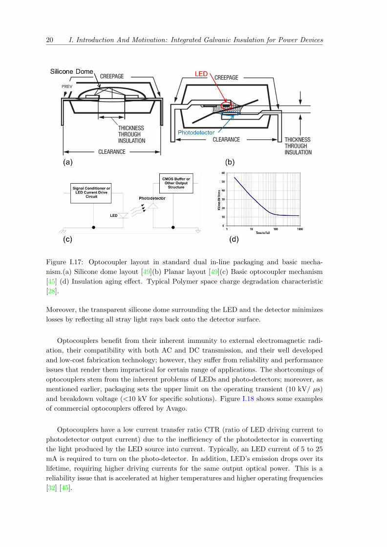
20 I. Introduction And Motivation: Integrated Galvanic Insulation for Power Devices
Figure I.17: Optocoupler layout in standard dual in-line packaging and basic mecha-
nism.(a) Silicone dome layout [49](b) Planar layout [49](c) Basic optocoupler mechanism
[45] (d) Insulation aging effect. Typical Polymer space charge degradation characteristic
[28].
Moreover, the transparent silicone dome surrounding the LED and the detector minimizes
losses by reflecting all stray light rays back onto the detector surface.
Optocouplers benefit from their inherent immunity to external electromagnetic radi-
ation, their compatibility with both AC and DC transmission, and their well developed
and low-cost fabrication technology; however, they suffer from reliability and performance
issues that render them impractical for certain range of applications. The shortcomings of
optocouplers stem from the inherent problems of LEDs and photo-detectors; moreover, as
mentioned earlier, packaging sets the upper limit on the operating transient (10 kV/ µs)
and breakdown voltage (<10 kV for specific solutions). Figure I.18 shows some examples
of commercial optocouplers offered by Avago.
Optocouplers have a low current transfer ratio CTR (ratio of LED driving current to
photodetector output current) due to the inefficiency of the photodetector in converting
the light produced by the LED source into current. Typically, an LED current of 5 to 25
mA is required to turn on the photo-detector. In addition, LED’s emission drops over its
lifetime, requiring higher driving currents for the same output optical power. This is a
reliability issue that is accelerated at higher temperatures and higher operating frequencies
[32] [45].

I.2. Galvanic Isolation for Power Semiconductor Devices 21
Figure I.18: Commercial optocouplers.(a) Some plastic optocouplers by Avago [50]. (b)
HCPL-665K, hermetically Sealed, High Speed: 10 Mbd, High CMR: > 10,000 V/µs, 2500
Vdc withstand test, Logic Gate Optocouplers [51].
Other problems with optocouplers originate from the fundamental characteristics of
phototransistors; these include speed, delays and timing errors. The time required to
charge/discharge the phototransistor capacitances cause propagation delays and limit the
operating speed; meanwhile the asymmetrical charge/discharge characteristics induce tim-
ing errors on the input pulse widths. Using a PIN photodiode in place of a phototransistor
can improve the operating frequency (or in other words the data transfer rate) of the op-
tocoupler at a cost of reduced CTR (since there is no transistor gain in a diode) [32] [52].
Another issue with optocouplers is channel to channel timing mismatches. A channel
to channel mismatch refers to the dead time that may occur if two transistors (two chan-
nels) are not switched at exactly the same time. For example, when the high-side switch
is turned off, ideally the low-side switch should turn on with zero timing mismatch; such
channel to channel mismatches manifest itself in a reduction in efficiency. This problem
emanates from the discrete fabrication of optocouplers [53].
I.2.b-ii Inductive Isolation
Inductive based coupling techniques use a changing magnetic field to transfer information
and energy across an isolation barrier. The most common form of magnetic coupling is
the transformer. A basic transformer consists of a fero-magnetic material at its core, and
two (or more) wire windings. As stated in Faraday’s Law of Induction, an alternating cur-

22 I. Introduction And Motivation: Integrated Galvanic Insulation for Power Devices
rent running through the primary coil generates a changing magnetic field which creates a
varying magnetic flux in the core of the transformer. This varying magnetic flux is shared
through the core with the secondary winding, which in turn induces a voltage across the
secondary winding. Now if a load is connected to the secondary winding, a current can
flow. The transformer core material has a high permeability relative to air; its purpose is
to minimize magnetizing currents, and to confine the magnetic flux close to the windings.
The strength of the transformer’s magnetic field depends on the current magnitude, the
permeability of the ferro-magnetic core, and the structure of the primary and secondary
coils [54]. The different types of transformers used for isolation are discussed next, includ-
ing: discrete pulse transformer, integrated planar coreless transformer, integrated planar
transformer with a fero-magnetic core.
Generally it is desired for the transformer to have a high transient response such that
the rectangular electrical pulses have highly steep edges; the slower the rising and falling
edges, the higher will be the commutation losses. The transient and breakdown voltage
performance of the transformer is limited by the coupling capacitance between its sec-
ondary and primary coils; high quality isolation and careful design is required. A useful
parameter that defines the transformer characteristic, is its voltage-time integral. The
voltage-time integral is the product of the pulse duration and its peak voltage. In general,
the larger the voltage-time integral of a pulse transformer, the more expensive and the
larger the size of the transformer [45] [53] [7]. There are many research groups working on
transformer solutions for the power switch driver control [55] [56].
There are two main approaches when using inductive coupling: (1) Integrated signal
and power approach (2)or discrete signal and power approach. The latter is implemented
most effectively with integrated digital micro-transformers and the former by discrete
medium-high power pulse-transformers.
High power pulse-transformers are classically used for fast high voltage drive applica-
tions. They are also used for pulsed power applications such as power generation for radar
and particle accelerators [57].
On the positive side, isolation transformers have a relatively high energy transfer effi-
ciency, accurate timing and small delays; thus, they have a low power consumption and
a speed (up to 1 MHz) advantage over optocouplers. Another strong advantage of trans-
formers, is their ability to deliver both the drive order and the required energy; thus, there
is no need for any additional amplification circuitry although other circuits may still be
required (ex. safety circuitry) [45] [53].
On the negative side, transformer performance may suffer in applications requiring
duty cycles above 50%. Transformers are ideal for AC signal transfer only and any energy
stored in their core must be dumped every half a cycle. Consequently, their output voltage
swings between positive and negative values in order to maintain a zero voltage-time as
depicted in I.19(b). The negative voltage drive guarantees the turn-off state of the power
switch despite noises from parasitics and unwanted dv/dt induced voltages;however, this

I.2. Galvanic Isolation for Power Semiconductor Devices 23
Figure I.19: (a) Power pulse transformer used for driving power switches [58]. (b) Volt-
seconds across winding must balance [59]. (c) Basic Transformer-Isolated Gate Drive [7].
negative voltage comes at a cost to efficiency. Since some of the applied voltage is in the
negative output voltage and some in the positive voltage, not all the applied voltage is
available for turning on the power switch; this can result in efficiency losses that increase
with an increasing duty cycle [45] [53] [60] [61]. Figure I.19(c) shows a basic isolated gate
drive approach via a discrete pulse transformer. Since the discrete pulse transformer trans-
fers the required energy to directly drive the gate of the power switch, a larger operating
voltage means a larger pulse voltage-time integral; this results in a significant increase of
the transformer size as can be seen in the example of figure I.19(a). Yet another problem
is ringing which emanates from the large transient gate drive currents flowing in the in-
ductive coils of the transformer; ringing can cause unwanted switching of the gate [53].
Unlike the pulse transformer discrete approach, digital isolator gate drivers adapt the
transformer approach to isolation to digital signals at semiconductor chip-scale level. These
digital micro-transformers use the metal process in standard CMOS integrated-circuits for
their coil formation; a polyimide insulation layer (around 20µm for 5 kV isolation) isolates
the primary and secondary coils. A cross sectional view of such a transformer by ADI is
depicted in figure I.20(b) and its use in a fully integrated converter on a single PCB board
is shown in figure I.20(c) . These micro-transformers can provide isolation between 3kV-
5kV with a CMTI of 50-kV/µs while switching at up to 1 MHz and operating temperatures
from -40C to +125C. Compared to optocouplers and pulse transformers, the monolithic
CMOS transformer technology provides superior timing accuracy, smaller footprint, lower
power consumption, and higher reliability [53].
Despite their many benefits, the core-less digital micro-transformers are still susceptible
to external magnetic fields and their isolation level is limited by the insulating Polyimide
layer and its packaging.
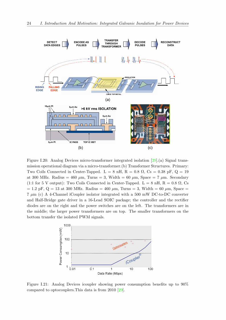
24 I. Introduction And Motivation: Integrated Galvanic Insulation for Power Devices
Figure I.20: Analog Devices micro-transformer integrated isolation [29].(a) Signal trans-
mission operational diagram via a micro-transformer.(b) Transformer Structures. Primary:
Two Coils Connected in Center-Tapped. L = 8 nH, R = 0.8 Ω, Cs = 0.38 pF, Q = 19
at 300 MHz. Radius = 460 µm, Turns = 3, Width = 60 µm, Space = 7 µm. Secondary
(1:1 for 5 V output): Two Coils Connected in Center-Tapped. L = 8 nH, R = 0.8 Ω, Cs
= 1.2 pF, Q = 13 at 300 MHz. Radius = 460 µm, Turns = 3, Width = 60 µm, Space =
7 µm (c) A 4-Channel iCoupler isolator integrated with a 500 mW DC-to-DC converter
and Half-Bridge gate driver in a 16-Lead SOIC package; the controller and the rectifier
diodes are on the right and the power switches are on the left. The transformers are in
the middle; the larger power transformers are on top. The smaller transformers on the
bottom transfer the isolated PWM signals.
Figure I.21: Analog Devices icoupler showing power consumption benefits up to 90%
compared to optocouplers.This data is from 2010 [29].
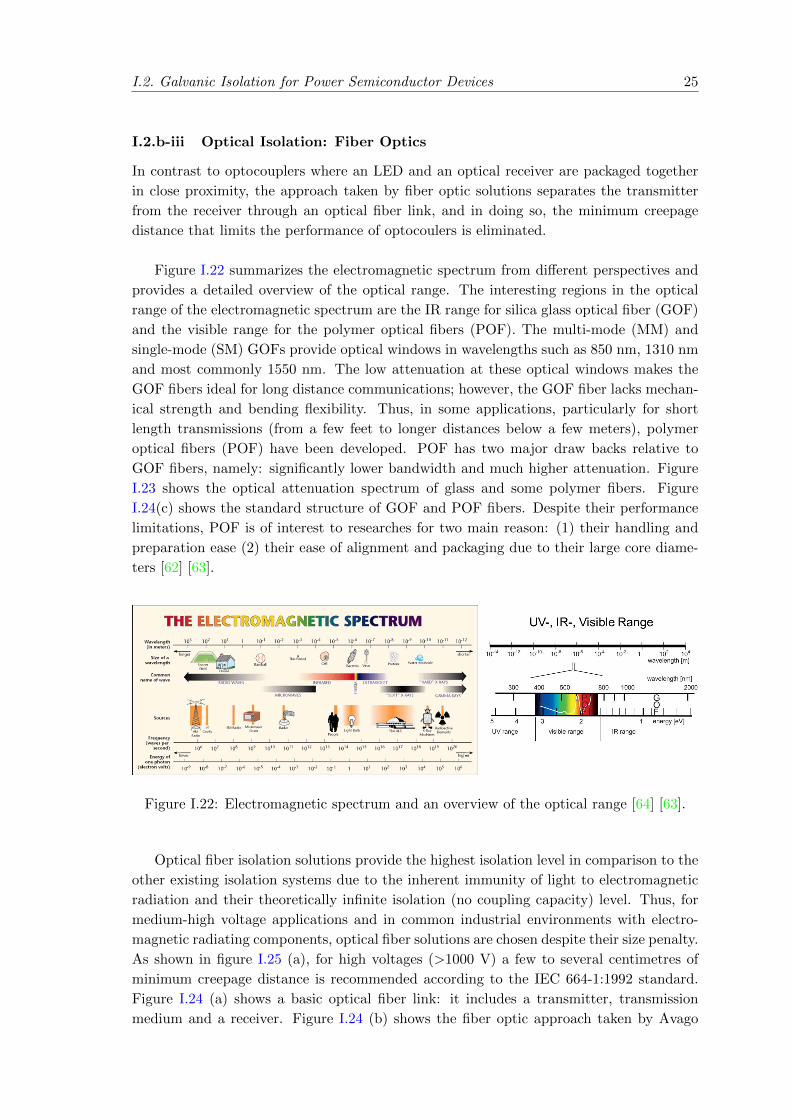
I.2. Galvanic Isolation for Power Semiconductor Devices 25
I.2.b-iii Optical Isolation: Fiber Optics
In contrast to optocouplers where an LED and an optical receiver are packaged together
in close proximity, the approach taken by fiber optic solutions separates the transmitter
from the receiver through an optical fiber link, and in doing so, the minimum creepage
distance that limits the performance of optocoulers is eliminated.
Figure I.22 summarizes the electromagnetic spectrum from different perspectives and
provides a detailed overview of the optical range. The interesting regions in the optical
range of the electromagnetic spectrum are the IR range for silica glass optical fiber (GOF)
and the visible range for the polymer optical fibers (POF). The multi-mode (MM) and
single-mode (SM) GOFs provide optical windows in wavelengths such as 850 nm, 1310 nm
and most commonly 1550 nm. The low attenuation at these optical windows makes the
GOF fibers ideal for long distance communications; however, the GOF fiber lacks mechan-
ical strength and bending flexibility. Thus, in some applications, particularly for short
length transmissions (from a few feet to longer distances below a few meters), polymer
optical fibers (POF) have been developed. POF has two major draw backs relative to
GOF fibers, namely: significantly lower bandwidth and much higher attenuation. Figure
I.23 shows the optical attenuation spectrum of glass and some polymer fibers. Figure
I.24(c) shows the standard structure of GOF and POF fibers. Despite their performance
limitations, POF is of interest to researches for two main reason: (1) their handling and
preparation ease (2) their ease of alignment and packaging due to their large core diame-
ters [62] [63].
Figure I.22: Electromagnetic spectrum and an overview of the optical range [64] [63].
Optical fiber isolation solutions provide the highest isolation level in comparison to the
other existing isolation systems due to the inherent immunity of light to electromagnetic
radiation and their theoretically infinite isolation (no coupling capacity) level. Thus, for
medium-high voltage applications and in common industrial environments with electro-
magnetic radiating components, optical fiber solutions are chosen despite their size penalty.
As shown in figure I.25 (a), for high voltages (>1000 V) a few to several centimetres of
minimum creepage distance is recommended according to the IEC 664-1:1992 standard.
Figure I.24 (a) shows a basic optical fiber link: it includes a transmitter, transmission
medium and a receiver. Figure I.24 (b) shows the fiber optic approach taken by Avago
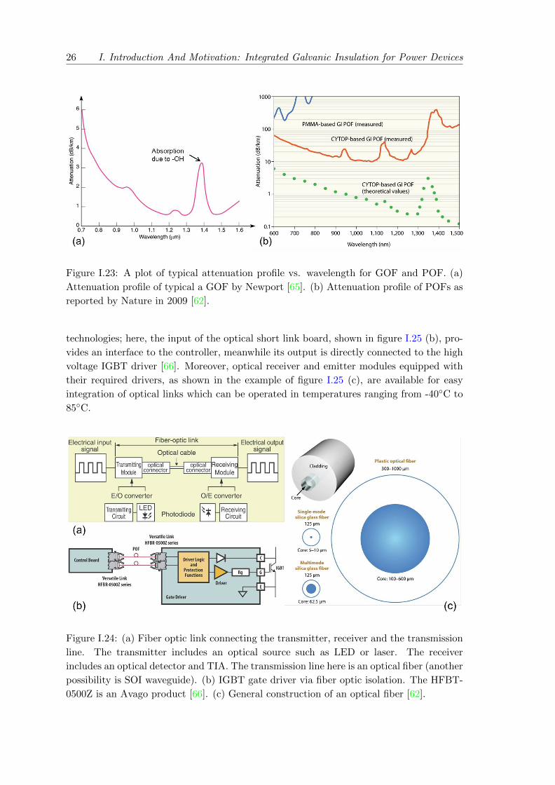
26 I. Introduction And Motivation: Integrated Galvanic Insulation for Power Devices
Figure I.23: A plot of typical attenuation profile vs. wavelength for GOF and POF. (a)
Attenuation profile of typical a GOF by Newport [65]. (b) Attenuation profile of POFs as
reported by Nature in 2009 [62].
technologies; here, the input of the optical short link board, shown in figure I.25 (b), pro-
vides an interface to the controller, meanwhile its output is directly connected to the high
voltage IGBT driver [66]. Moreover, optical receiver and emitter modules equipped with
their required drivers, as shown in the example of figure I.25 (c), are available for easy
integration of optical links which can be operated in temperatures ranging from -40C to
85C.
Figure I.24: (a) Fiber optic link connecting the transmitter, receiver and the transmission
line. The transmitter includes an optical source such as LED or laser. The receiver
includes an optical detector and TIA. The transmission line here is an optical fiber (another
possibility is SOI waveguide). (b) IGBT gate driver via fiber optic isolation. The HFBT-
0500Z is an Avago product [66]. (c) General construction of an optical fiber [62].

I.2. Galvanic Isolation for Power Semiconductor Devices 27
Figure I.25: (a) Minimum creepage distance by IEC 60664-1:2002 (b) HFBR-3810Z Optical
Short-Link. (c) HFBR-1629/2529Z Circuit Diagram for 50 MBd Data Rate [66].
I.2.b-iv Capacitive Isolation
Digital isolators using capacitive coupling employ a changing electric field to transmit
data across a dielectric barrier. Capacitive isolators are small in size and efficient in en-
ergy transfer which allows their integration at low costs. They are immune to magnetic
fields which enables their usage in environments with harsh magnetic radiation. Compared
to optocouplers, capacitive isolators can be two or three times faster but they are typically
larger than optocouplers. They can drive semiconductor switches with reverse voltages as
high as approximately 700 V. Their dV/dt is limited by their capacitance value and are
typically around 20kV/µs up to 50kV/µs. An isolating IGBT driver with PCB integrated
capacitive coupling elements was reported in 2010 that operated at a DC link of 400 V
with dV/dt stability as high as 240kV/µs [40]; this work is demonstrated in figure I.26.
Figure I.26: Insulating IGBT driver with PCB integrated capacitive coupling as reported
in CIPS 2010 conference [40]. (a) Proposed layout for PCB integrated capacitors to reach
large clearance and creepage distances. (b) Photo of the buck-boost measurement setup
(c) Prototype of an IGBT half bridge driver with PCB integrated capacitive coupling
elements.
I.2.c Optical Isolation: State of the Arts Under Research
In high voltage direct current (HVDC) applications, where several thyristors are stacked
in series to support several hundred kV, fiber optics are used to carry the isolated gate

28 I. Introduction And Motivation: Integrated Galvanic Insulation for Power Devices
triggering signals between the external command units and the high voltages of the thyris-
tor based AC/DC converters. The Light Triggered Thyristors (LTT) eliminate the high
voltage gating electronics that were a cause of lifetime issues in the past. Commercially
available LTT solutions require several tens of mWs of optical power and can handle hun-
dreds of kVs and tens of kAs; figure I.27 shows an example thyristor from Siemens and
demonstrates the difference between LTT and the traditional electrical triggered thyristor
(ETT) approach. LTTs have been demonstrated in the literature [67] [68]; in 2013, optical
triggering of a 12 kV, Imax=270A, 1cm2 4H-SiC thyristor was reported [69]. Figure I.28
shows the device cross section and top view as well as the device current and voltage time
dependencies. As explained earlier, the main advantage of using fiber optics over optocou-
plers is their infinite immunity to EMI whereas ouptocouplers are limited by capacitive
couplings in their small packaging environment.
Figure I.27: (a) Comparison of direct light triggered thyristor (LTT) and electrical trig-
gered thyristor (ETT). (b) Typical LTT thyristor module. (c) Direct-light triggered thyris-
tor [70].
There are some signal + energy optical solutions reported in the literature for power
MOSFETs and IGBTs. A group in Chicago, Illinois working with Dr. Mazumder have sev-
eral publications during the years 2006-2009, on optically-activated gate control of power
semiconductor devices based on externally optical triggered GaAs power transistors [71]
[36]. They have fabricated GaAs/AlGaAs lateral switches that are connected to the gate
of power switches. Photogeneration in the GaAs/AlGaAs devices modulates the gate re-
sistance of the power switch and in turn allows control of the switch by light. Figure I.29
demonstrates this approach as well as the device structure and hybrid packaging scheme.
These hybrid devices have much better optical properties compared to the SiC solutions

I.2. Galvanic Isolation for Power Semiconductor Devices 29
Figure I.28: Optical triggering of 12 kV, 1 cm2 4H-SiC thyristors [69]. (a) Cross sec-
tional, and (b) top views of 12 kV, 1 cm2 optically triggered 4H-SiC thyristor. (c) Time
dependencies of voltage and current during switch-on process of 12 kV, 1 cm2 4H-SiC
thyristor.
thanks to the optical properties of GaAs. Their switching control was demonstrated for
Si-based power MOSFET and IGBT, SiC based VJFET and SiC based DMOSFET when
triggered by a 800 nm wavelength light source [36]. The optical powers used are between
0.5 W to a couple of Watts; however we were not able to estimate their optical to electrical
efficiency due to lack of information provided. This hybrid solution, is much more expen-
sive than the optocouplers available in the market, however the major advantages here are
the compact hybrid integration, high temperature and high voltage tolerances that maybe
required for high demanding applications that are willing to pay the cost. Moreover, only
a part of the gate current is supplied by light since the transistor still needs a floating
supply to be operational.
Figure I.29: Hybrid-optical control by GaAs/AlGaAs based device. [36] (a) Variable-
gate-resistance based optically-activated gate control. (b) Device structure. (c) Hybrid
packaging scheme and a prototype with SiC power MOSFET.
A group at the University of South Carolina under direction of Dr. Islam have reported
optical solutions in SiC for pulsed power applications. Dr. Islam and team, reported in
2009, a 1 mm2 4H-SiC p-i-n diode solution that when triggered by a 337.1 laser pulse with
1.2 mJ in 600 ps, would generate a 0.5 A current pulse with FWHM of 180 ns [72]. In
2010, the same group at the university of South Carolina improved their overall optical
to electrical conversion efficiency be using a different approach. This time instead of a
p-i-n diode, they use the internal current gain (approximately 11) inside a SiC bipolar

30 I. Introduction And Motivation: Integrated Galvanic Insulation for Power Devices
transistor structure to amplify the photogenerated current [73]. The test circuit and the
reported SiC photo transistor design are shown in figure I.30; having biased the 0.5 mm2
SiC photo transistor at 1200 V, a 200 A/cm2 current pulse with a FWHM of 180 ns was
reported when triggering by a 337.1 nm laser pulse with 0.5 mJ in 600 ps [73]. Although
this solution is more efficient than the 2009 p-i-n diode and provides high temperature
and high power capabilities, it requires a lot of optical power (800 kW peak power com-
pared to 2 MW for the p-i-n diode solution) and the transistor responsivity is roughly
2 µA/W. In 2012 , a group at Kyoto University of Japan published results showing the
temperature-independent photo-response of a 4H-SiC photodiode for temperatures as high
as 300 degrees [74] when illuminated by a 300 W Xenon optical source for wavelengths in
the range of 280 nm to 365 nm.
Figure I.30: Optical triggering by SiC Bipolar Transistor [73]. (a) Schematic (b) Test
circuit for optical switching evaluation. (c) Collector voltage and current waveforms of the
optically activated transistor when activated by a single laser pulse. The applied reverse
voltage was 1200 V.
Another group at the Texas Tech. University reported a 4H-SiC photoconductive
switch that achieved a peak photocurrent of 14 A into a 25-Ω load when operated at 15
kV/cm and triggered by a pulsed Nd:YAG laser. An optical parametric oscillator was
used in conjunction with the pulsed laser, in order to scan the wavelength from 345 to
510 nm while monitoring the photocurrent and laser energy. The 14 A maximum reported
photocurrent corresponds to a 336 nm wavelength, a lasing energy of roughly 500 µJ.
The maximum efficiency point of the device is around 0.1 mA/µJ-V which is very low
as maybe expected due to the optical absorption properties of SiC. They implemented a
gridded semi-transparent contact for higher current uniformity and lower optical reflection
losses [75]. Figure I.31 shows their device and characterization results.
In the examples above, all the solutions share the same approach in terms of both
delivering the required gate-drive circuit power as well as optically isolating the gating
signal. In the signal and power approach, the optical isolation has to transfer the signal
voltage levels needed to switch the gate; thus, a large amount of optical power maybe
required depending on the gate-drive circuit power consumption and specially if the com-
bination of the optical coupling interface (i.e. reflection losses due to refractive index
mismatches and/or misalignment) and the photodetector (i.e. low optical power to cur-
rent conversion efficiency due to poor material optical absorption coefficient and/or short

I.2. Galvanic Isolation for Power Semiconductor Devices 31
Figure I.31: (a) Cross section of the vertical photoconductive showing the gridded thin-film
contact and the hollow electrode. (b) Dependence of photocurrent efficiency on wavelength.
(Inset) Detailed view of the photocurrent efficiency peak at 366 nm. (c) (top) Change in
photocurrent with various trigger energies. (bottom) Saturation of photocurrent and ON-
state resistance with increasing laser energy. Both tests with anode triggering [75].
carrier lifetimes, and/or the structural design) have a poor optical to electrical conversion
efficiency. Moreover, the works of the research teams above, all favour wide bandgap mate-
rials (i.e. SiC) due to their high thermal and voltage capabilities that are compatible with
power electronic applications. However, such wide bandgap devices are only sensitive in
the ultraviolet wavelength range of the electromagnetic spectrum where compact, efficient
and cost effective optical sources such as semiconductor laser diodes are either very limited
or not available.
In 2013, Dr.Fujita presented in IEEE power electronics transactions, an energy + sig-
nal optical isolation unit, where the DC power supply consisted of two 400 mW continuous
wave (CW) laser diodes (SDL-2320-L2: JDSU) connected via two 1.5m optical fibers, to
two 12V photovoltaic power converters (PPC-12E: JDSU) suitable in the 810nm wave-
length range. The gating control signal isolation was provided by an optical fiber con-
nection between an optical signal transmitter (GP1FAV55TK0F: SHARP) and receiver
(GP1FAV55RK0F: SHARP). The key to successfully lowering the optical power level re-
quirement was in lowering the driver power consumption. Dr.Fujita proposed a resonant
gate-drive circuit (figure I.32 (a)) that allowed a reduction in the power consumption of the
gate driver by up to 10 times (power consumptions as low as 25 mW at 100 kHz operating
frequency were reported). The concept was demonstrated on 500 V, 20 A MOSFET buck
converter with 600 V, 12 A flyback diodes, and also on 1400 V, 300 A, IGBTs as shown
in figures I.32(b) and (c) respectively.
Relative to the previous signal+power optical isolation approaches, the work demon-
strated by Dr.Fujita’s team shows the potential for a practical solution in terms of power
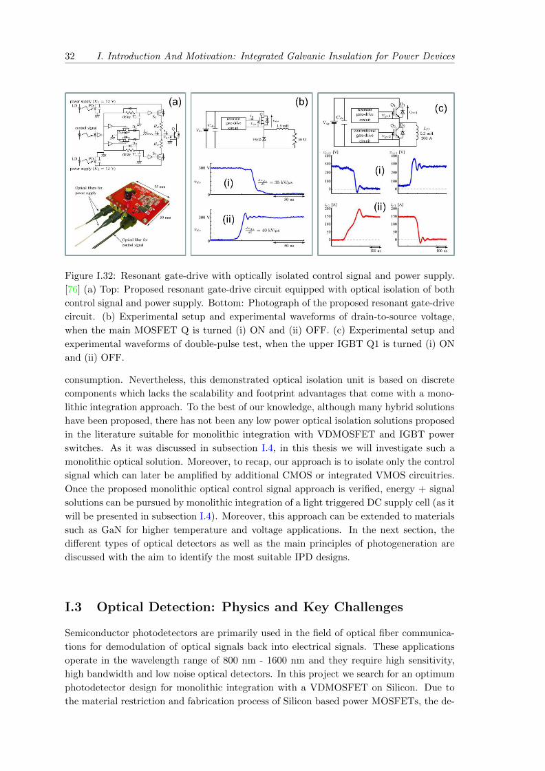
32 I. Introduction And Motivation: Integrated Galvanic Insulation for Power Devices
Figure I.32: Resonant gate-drive with optically isolated control signal and power supply.
[76] (a) Top: Proposed resonant gate-drive circuit equipped with optical isolation of both
control signal and power supply. Bottom: Photograph of the proposed resonant gate-drive
circuit. (b) Experimental setup and experimental waveforms of drain-to-source voltage,
when the main MOSFET Q is turned (i) ON and (ii) OFF. (c) Experimental setup and
experimental waveforms of double-pulse test, when the upper IGBT Q1 is turned (i) ON
and (ii) OFF.
consumption. Nevertheless, this demonstrated optical isolation unit is based on discrete
components which lacks the scalability and footprint advantages that come with a mono-
lithic integration approach. To the best of our knowledge, although many hybrid solutions
have been proposed, there has not been any low power optical isolation solutions proposed
in the literature suitable for monolithic integration with VDMOSFET and IGBT power
switches. As it was discussed in subsection I.4, in this thesis we will investigate such a
monolithic optical solution. Moreover, to recap, our approach is to isolate only the control
signal which can later be amplified by additional CMOS or integrated VMOS circuitries.
Once the proposed monolithic optical control signal approach is verified, energy + signal
solutions can be pursued by monolithic integration of a light triggered DC supply cell (as it
will be presented in subsection I.4). Moreover, this approach can be extended to materials
such as GaN for higher temperature and voltage applications. In the next section, the
different types of optical detectors as well as the main principles of photogeneration are
discussed with the aim to identify the most suitable IPD designs.
I.3 Optical Detection: Physics and Key Challenges
Semiconductor photodetectors are primarily used in the field of optical fiber communica-
tions for demodulation of optical signals back into electrical signals. These applications
operate in the wavelength range of 800 nm - 1600 nm and they require high sensitivity,
high bandwidth and low noise optical detectors. In this project we search for an optimum
photodetector design for monolithic integration with a VDMOSFET on Silicon. Due to
the material restriction and fabrication process of Silicon based power MOSFETs, the de-
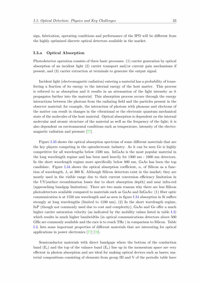
I.3. Optical Detection: Physics and Key Challenges 33
sign, fabrication, operating conditions and performance of the IPD will be different from
the highly optimized discrete optical detectors available in the market.
I.3.a Optical Absorption
Photodetector operation consists of three basic processes: (1) carrier generation by optical
absorption of an incident light (2) carrier transport and/or current gain mechanisms if
present, and (3) carrier extraction at terminals to generate the output signal.
Incident light (electromagnetic radiation) entering a material has a probability of trans-
ferring a fraction of its energy to the internal energy of the host matter. This process
is referred to as absorption and it results in an attenuation of the light intensity as it
propagates further into the material. This absorption process occurs through the energy
interactions between the photons from the radiating field and the particles present in the
observer material; for example, the interaction of photons with phonons and electrons of
the matter can result in changes in the vibrational or the electronic quantum mechanical
state of the molecules of the host material. Optical absorption is dependent on the internal
molecular and atomic structure of the material as well as the frequency of the light; it is
also dependent on environmental conditions such as temperature, intensity of the electro-
magnetic radiation and pressure [77].
Figure I.33 shows the optical absorption spectrum of some different materials that are
the key players competing in the optoelectronic industry. As it can be seen Ge is highly
competitive for all wavelengths below 1500 nm. InGaAs is the most popular material in
the long wavelength regime and has been used heavily for 1300 nm - 1600 nm detectors.
In the short wavelength regime more specifically below 800 nm, GaAs has been the top
candidate. Figure I.34 shows the optical absorption coefficient, α, of Silicon as a func-
tion of wavelength, λ, at 300 K. Although Silicon detectors exist in the market; they are
mostly used in the visible range due to their current conversion efficiency limitation in
the UV(surface recombination losses due to short absorption depth) and near infra-red
(approaching bandgap limitation). There are two main reasons why there are less Silicon
photodetectors available compared to materials such as GaAs and InGaAs: (1) fiber optic
communication is at 1550 nm wavelength and as seen in figure I.34 absorption in Si suffers
strongly at long wavelengths (limited to 1100 nm), (2) In the short wavelength regime,
InP (though not commonly used due to cost and complexity), GaAs and Ge offer a much
higher carrier saturation velocity (as indicated by the mobility values listed in table I.3)
which results in much higher bandwidths (in optical communications detectors above 500
GHz are commonly available and the race is to reach THz ) in comparison to Silicon. Table
I.3, lists some important properties of different materials that are interesting for optical
applications in power electronics [77] [78].
Semiconductor materials with direct bandgaps where the bottom of the conduction
band (Ec) and the top of the valance band (Ev) line up in the momentum space are very
efficient in photon absorption and are ideal for making optical devices such as lasers; ma-
terial compositions consisting of elements from group III and V of the periodic table have

34 I. Introduction And Motivation: Integrated Galvanic Insulation for Power Devices
Figure I.33: Optical absorption coefficients for different photodetector materials. [78]
Figure I.34: Silicon absorption spectrum
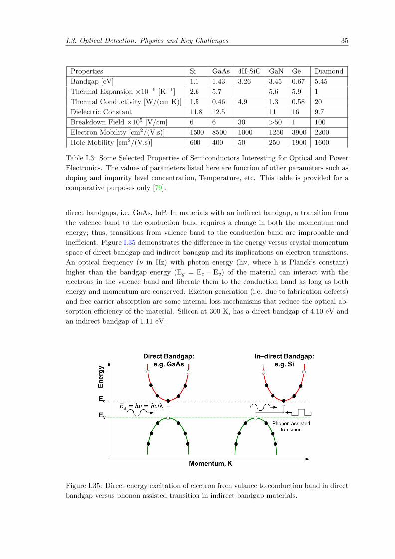
I.3. Optical Detection: Physics and Key Challenges 35
Properties Si GaAs 4H-SiC GaN Ge Diamond
Bandgap [eV] 1.1 1.43 3.26 3.45 0.67 5.45
Thermal Expansion ×10−6 [K−1] 2.6 5.7 5.6 5.9 1
Thermal Conductivity [W/(cm K)] 1.5 0.46 4.9 1.3 0.58 20
Dielectric Constant 11.8 12.5 11 16 9.7
Breakdown Field ×105 [V/cm] 6 6 30 >50 1 100
Electron Mobility [cm2/(V.s)] 1500 8500 1000 1250 3900 2200
Hole Mobility [cm2/(V.s)] 600 400 50 250 1900 1600
Table I.3: Some Selected Properties of Semiconductors Interesting for Optical and Power
Electronics. The values of parameters listed here are function of other parameters such as
doping and impurity level concentration, Temperature, etc. This table is provided for a
comparative purposes only [79].
direct bandgaps, i.e. GaAs, InP. In materials with an indirect bandgap, a transition from
the valence band to the conduction band requires a change in both the momentum and
energy; thus, transitions from valence band to the conduction band are improbable and
inefficient. Figure I.35 demonstrates the difference in the energy versus crystal momentum
space of direct bandgap and indirect bandgap and its implications on electron transitions.
An optical frequency (ν in Hz) with photon energy (hν, where h is Planck’s constant)
higher than the bandgap energy (Eg = Ec - Ev) of the material can interact with the
electrons in the valence band and liberate them to the conduction band as long as both
energy and momentum are conserved. Exciton generation (i.e. due to fabrication defects)
and free carrier absorption are some internal loss mechanisms that reduce the optical ab-
sorption efficiency of the material. Silicon at 300 K, has a direct bandgap of 4.10 eV and
an indirect bandgap of 1.11 eV.
Figure I.35: Direct energy excitation of electron from valance to conduction band in direct
bandgap versus phonon assisted transition in indirect bandgap materials.

36 I. Introduction And Motivation: Integrated Galvanic Insulation for Power Devices
I.3.b Photodetectors
The different kinds of photodetectors can be divided into two groups: (1) without gain,
and (2) with gain. The first group includes different types of photodiodes. The second
group includes: phototransistors, avalanche photodiodes and photoconductors. Table I.4
provides an overview of performance parameters for some common types of photodetectors.
Photodetector Gain Response
Time
[s]
Transit-Time Limited
3-dB Bandwidth
Photoconductor 1-106 10−8-10−3 35 MHz-350 Hz
Photodiodes p-n junction
p-i-n junction
M-S diode
1
1
1
10−11
10−10-10−8
10−11
35 GHz
3.5 GHz-35 MHz
35 GHzAvalanche Photodiode 102-104 10−10 3.5 GHz
Phototransistor 102-103 10−6 350 kHz
Table I.4: Typical values of gain and response time for common photodetectors [78].These
values are not exact as they depend on many parameters such as doping concentration
levels, design (size and structure), applied voltages, temperature, etc; these values are
given for comparative purposes. Moreover, the 3-dB bandwidths listed here are ideal as
they are based on transit-time limitations. It is most likely that the device bandwidth is
RC-limited which takes into account the packaging and contact parasitics.
As shown in table I.4, generally, photodetectors with gain are relatively slower than
the ones without gain (using materials other than Si, such as GaAs based structures,
bandwidths of several 100 MHz have been reported [80]). An exception to this rule is
the avalanche photodiode (APD), where electrons are produced in a highly doped layer
and are multiplied and accelerated by means of a local field [78]. Figure I.36 (a) shows a
typical structure of APDs. APDs can have a gain-bandwidth product in the hundreds of
giga hertz, however, this high gain (typically 10 dB more sensitive than p-i-n photodiodes
[63]) comes at a price of increased noise and a high reverse bias voltage (the voltage is
adjusted for the optimum gain condition) requirement. In our proposed application and
approach, the high voltage (i.e. 15V) supply of the gate driver is available on the receiver
side and thus, it could be used to bias the APD. Figure I.36 (b) shows the basic structure
of a phototransistor. In phototransistors, photogenerated carriers in the base can benefit
from the internal gain of a bipolar transistor; moreover, the extra noise complications and
high voltage requirements of the APD are eliminated. Thanks to the bipolar gain, the pho-
totransistor can offer an improved light to current transfer ratio compared to photodiode
structures which is one reason why it is widely used in optocouplers. On the negative side,
phototransistor switching speeds are limited (<several hundred kHz) by the charging and
discharging times of the emitter and collector capacitances [78]. Another photodetector
with gain abilities is the photoconductor structure shown in figure I.36 (c). Photocon-
ductors consist of a bulk absorbing layer with ohmic contacts to collect the photo current
generated in the bulk. Through careful design considerations such as short contact spac-
ings, and material choice and fabrication process allowing for high carrier mobilities, the
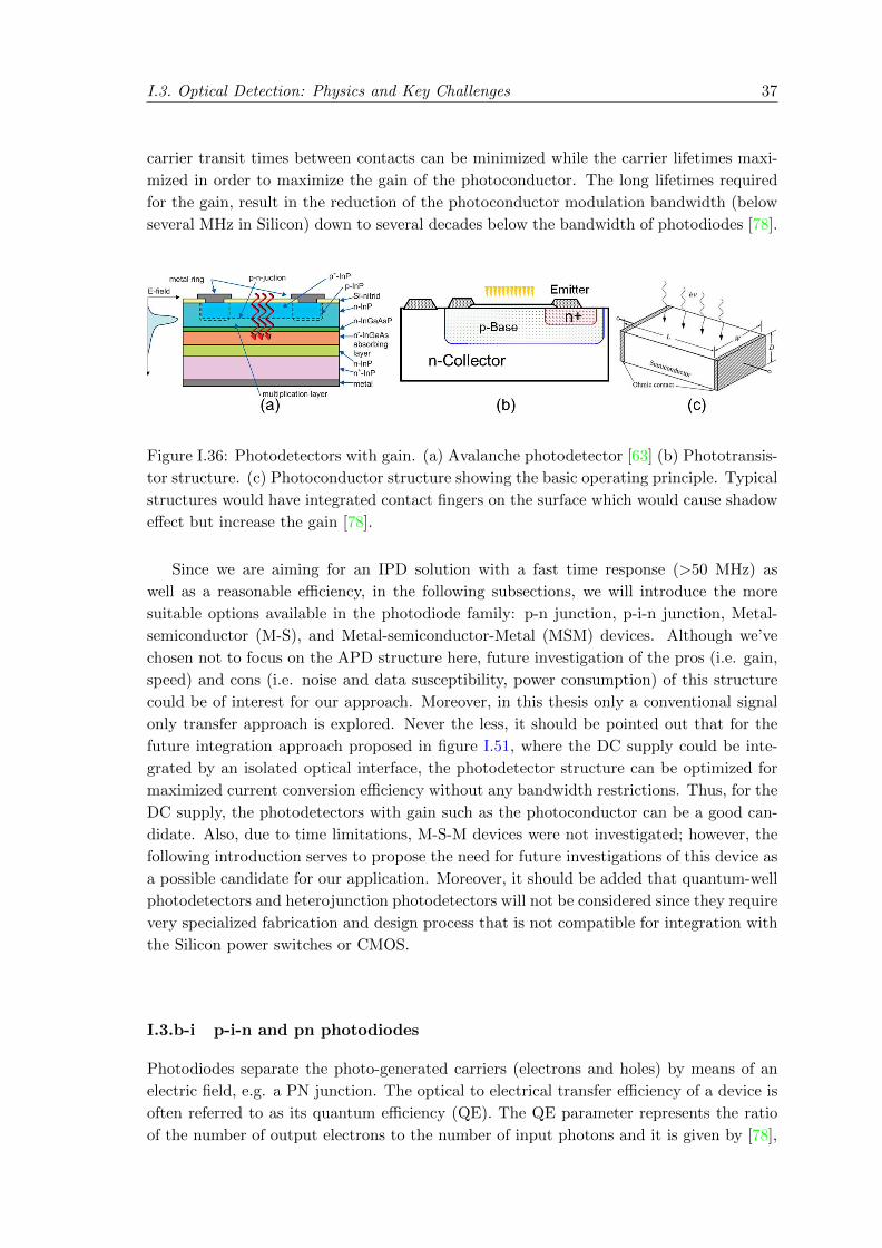
I.3. Optical Detection: Physics and Key Challenges 37
carrier transit times between contacts can be minimized while the carrier lifetimes maxi-
mized in order to maximize the gain of the photoconductor. The long lifetimes required
for the gain, result in the reduction of the photoconductor modulation bandwidth (below
several MHz in Silicon) down to several decades below the bandwidth of photodiodes [78].
Figure I.36: Photodetectors with gain. (a) Avalanche photodetector [63] (b) Phototransis-
tor structure. (c) Photoconductor structure showing the basic operating principle. Typical
structures would have integrated contact fingers on the surface which would cause shadow
effect but increase the gain [78].
Since we are aiming for an IPD solution with a fast time response (>50 MHz) as
well as a reasonable efficiency, in the following subsections, we will introduce the more
suitable options available in the photodiode family: p-n junction, p-i-n junction, Metal-
semiconductor (M-S), and Metal-semiconductor-Metal (MSM) devices. Although we’ve
chosen not to focus on the APD structure here, future investigation of the pros (i.e. gain,
speed) and cons (i.e. noise and data susceptibility, power consumption) of this structure
could be of interest for our approach. Moreover, in this thesis only a conventional signal
only transfer approach is explored. Never the less, it should be pointed out that for the
future integration approach proposed in figure I.51, where the DC supply could be inte-
grated by an isolated optical interface, the photodetector structure can be optimized for
maximized current conversion efficiency without any bandwidth restrictions. Thus, for the
DC supply, the photodetectors with gain such as the photoconductor can be a good can-
didate. Also, due to time limitations, M-S-M devices were not investigated; however, the
following introduction serves to propose the need for future investigations of this device as
a possible candidate for our application. Moreover, it should be added that quantum-well
photodetectors and heterojunction photodetectors will not be considered since they require
very specialized fabrication and design process that is not compatible for integration with
the Silicon power switches or CMOS.
I.3.b-i p-i-n and pn photodiodes
Photodiodes separate the photo-generated carriers (electrons and holes) by means of an
electric field, e.g. a PN junction. The optical to electrical transfer efficiency of a device is
often referred to as its quantum efficiency (QE). The QE parameter represents the ratio
of the number of output electrons to the number of input photons and it is given by [78],

38 I. Introduction And Motivation: Integrated Galvanic Insulation for Power Devices
η =IphqΦ
=AJtot/q
Popt/hν= (1−R)[1− exp(−αWD)
1 + αLp] (I.2)
where Iph is the photocurrent, Φ is the photon flux, Jtot is the total current density
including drift and diffusion currents, Popt is the average optical signal power, R is the
reflection coefficient, A is the device area, WD is the depletion region width, and Lp is the
minority carrier (holes) diffusion length. Another metric used for evaluating the sensitivity
of a detector in reference to the optical power is the responsivity [78],
< =IphPopt
=ηq
hν=ηλ(µm)
1.24[A/W ] (I.3)
As it can be seen from equation I.2, minimizing reflections and wider WD increases the
QE of the device. Reflections are minimized through the application of an anti-reflective
coating layer. The WD of a p-n photodiode is controlled by the impurity doping levels
and diffusion times.
The p-i-n photodiode is a special case of p-n photodiodes where the insertion of a thick
intrinsic region insures that a depletion region larger than the absorption depth (>1/α)
of the light can be created by applying only a small voltage. For a large QE, a wide ab-
sorption layer is necessary (absorption depth is a function of wavelength as it was shown
in figure I.34); however, this leads to longer transit times (time required for carriers to
drift across the depletion region) which in turn reduces the bandwidth performance of
the detector. Thus, the compromise between QE and frequency response is tuned by the
design of the depletion region width, WD as shown in the plot of figure I.37. Figure I.38
(a) shows the p-n and p-i-n photodiode schematic structures. In general, p-i-n photodiode
benefits from a much larger responsivity relative to a simple p-n photodiode; however,
for very wide intrinsic layers, long transit times through the intrinsic region can limit the
p-i-n bandwidth. Moreover, the neutral region in a p-n photodiode contributes to series
resistance which is a source of noise. The different characteristics of p-n photodiodes are
presented in detail in the following chapters as we discuss the modelling, fabrication and
characterization of the proposed p-n IPD.
In the research community, there has been a growing effort in optical detectors that are
compatible for integration with CMOS technology [81] [82] [83] [84] as well as its necessary
optical interconnection network. Since the main demand for such integrated photodetec-
tors is in the telecommunication field, a lot of attention have been focused on fabricating
Ge devices on Silicon and SOI wafers [85] [86] [87]. Recently, Dr.Laurent Vivien and his
team, reported a 120 GHz, 10 µm long lateral p-i-n Ge photodetector integrated with
silicon waveguides at its end with a responsivity of 0.8 A/W at 1550 nm.
To the best of our knowledge there aren’t a lot of research in the integration of visible
range (specially below 600 nm wavelength) photodetectors in Si. The visible range is spe-
cially of interest for short range POF communication systems. The p-i-n photodiode and
its parameters presented in figure I.40 , is a POF suitable, commercially available product
by Infinion [63].

I.3. Optical Detection: Physics and Key Challenges 39
Figure I.37: Depletion width tuning in Si p-i-n Photodiodes and its effect on transit-time
limited 3-dB bandwidth, QE and Responsivity. It is assumed that carriers are drifting at
saturation velocity of 107 cm/s and there are no diffusion currents. Thus, these curves over
estimated the ideal bandwidth limits as well as QE and Responsivity values, specially for
p-n diodes with small WD. Optical power reflection coefficient as a function of wavelength
is considered for a Silicon/air interface. Moreover, these trends are sensitive to carrier life
time values. A life time of 1 ns was assumed.
Figure I.38: Schematic structure of pn or p-i-n Photodiodes.
Figure I.39: (a) Schematic view of a lateral pin Ge photodetector integrated at the end
of a Si waveguide. The length was 10 µm. (b) Top-view optical microscopy and cross-
sectional SEM images of the Ge PD. (c) SEM cross-section (perpendicular to the waveguide
direction) [86].

40 I. Introduction And Motivation: Integrated Galvanic Insulation for Power Devices
Figure I.40: pin-diode SFH 250 by Infineon for 1.0 mm/2.2 mm POF (right with a housing
for clamping the POF with a screw) [63]
I.3.b-ii Schottky Junction Photodetectors: M-S, M-S-M
Metal-semiconductor (M-S) photodetectors are based on Schottky junctions which are
formed at the metal contact and semiconductor bulk interface. M-S photodetectors can
be operated in two modes [78]:
1. For hυ > Eg: As shown in figure I.41 (a), the layer under the contact could also
be lightly doped to create a Metal-i-n photodiode whose QE is defined by the same
expression I.2 used to define the QE of a p-i-n photodiode. In this case, light is
absorbed in the semiconductor and the metal layers should be very thin (roughly a
few 10s of nm in thickness) in order to minimize reflection and absorption losses due
to the metal contact layer.
2. For qϕB< hυ < Eg: As long as the incident light has energy higher than the Schottky
barrier (qϕB), photons can be absorbed in the metal layer and collected by the
semiconductor. In this case light can enter the device through the semiconductor
interface rather than the metal interface, allowing for a thicker (lower resistance)
metal layer. The structure of such a device is shown in figure I.41 (b).
Some of the main advantages of M-S photodetectors are: their high speeds (the p-n
junction minority charge storage is eliminated here since dark currents in Schottky diodes
are not based on minority diffusion currents) and their long wavelength detection abilities
without the need of thick devices or narrow bandgap semiconductors. In addition to long
wavelength detection, it is possible to have short wavelength detection (in the UV and
visible range) by choosing the right material and careful design. Moreover, a Schottky
barrier does not require high temperature annealing [78].
Another type of photodetector is the M-S-M photodetector which uses two Schottky
barriers back to back as shown in figure I.41(c). Unlike the M-S photodetector, light is
absorbed in the semiconductor and not in the metal layer. The main benefit of the M-
S-M structures are their high speed (they can have capacitance values roughly half the
capacitance value of a p-i-n photodiode with a similar QE) and compatibility with CMOS
technology [78]. Very fast M-S-M photodetectors suitable for the visible range have been
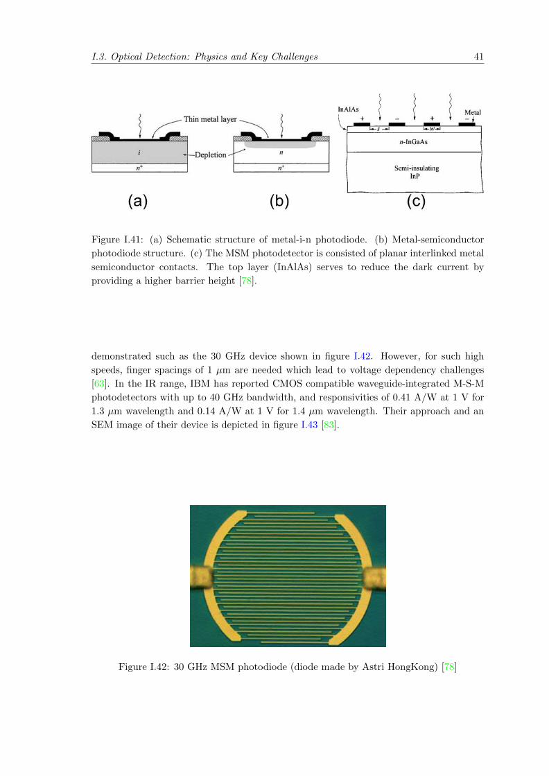
I.3. Optical Detection: Physics and Key Challenges 41
Figure I.41: (a) Schematic structure of metal-i-n photodiode. (b) Metal-semiconductor
photodiode structure. (c) The MSM photodetector is consisted of planar interlinked metal
semiconductor contacts. The top layer (InAlAs) serves to reduce the dark current by
providing a higher barrier height [78].
demonstrated such as the 30 GHz device shown in figure I.42. However, for such high
speeds, finger spacings of 1 µm are needed which lead to voltage dependency challenges
[63]. In the IR range, IBM has reported CMOS compatible waveguide-integrated M-S-M
photodetectors with up to 40 GHz bandwidth, and responsivities of 0.41 A/W at 1 V for
1.3 µm wavelength and 0.14 A/W at 1 V for 1.4 µm wavelength. Their approach and an
SEM image of their device is depicted in figure I.43 [83].
Figure I.42: 30 GHz MSM photodiode (diode made by Astri HongKong) [78]
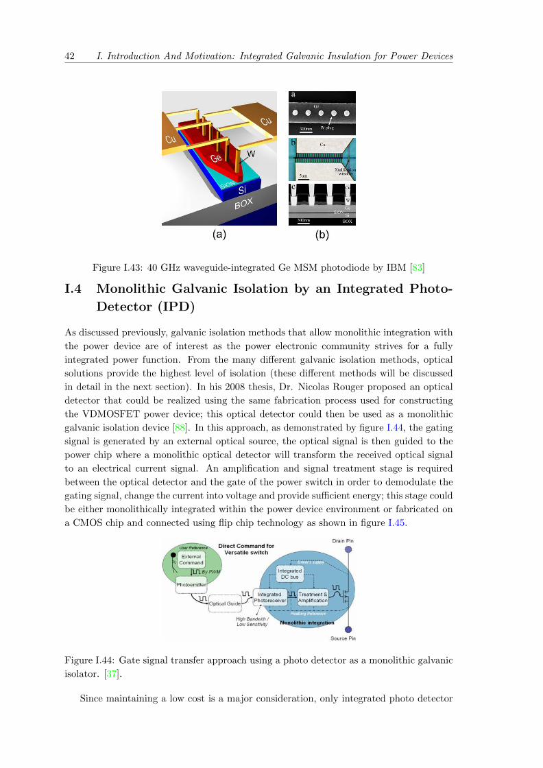
42 I. Introduction And Motivation: Integrated Galvanic Insulation for Power Devices
Figure I.43: 40 GHz waveguide-integrated Ge MSM photodiode by IBM [83]
I.4 Monolithic Galvanic Isolation by an Integrated Photo-
Detector (IPD)
As discussed previously, galvanic isolation methods that allow monolithic integration with
the power device are of interest as the power electronic community strives for a fully
integrated power function. From the many different galvanic isolation methods, optical
solutions provide the highest level of isolation (these different methods will be discussed
in detail in the next section). In his 2008 thesis, Dr. Nicolas Rouger proposed an optical
detector that could be realized using the same fabrication process used for constructing
the VDMOSFET power device; this optical detector could then be used as a monolithic
galvanic isolation device [88]. In this approach, as demonstrated by figure I.44, the gating
signal is generated by an external optical source, the optical signal is then guided to the
power chip where a monolithic optical detector will transform the received optical signal
to an electrical current signal. An amplification and signal treatment stage is required
between the optical detector and the gate of the power switch in order to demodulate the
gating signal, change the current into voltage and provide sufficient energy; this stage could
be either monolithically integrated within the power device environment or fabricated on
a CMOS chip and connected using flip chip technology as shown in figure I.45.
Figure I.44: Gate signal transfer approach using a photo detector as a monolithic galvanic
isolator. [37].
Since maintaining a low cost is a major consideration, only integrated photo detector
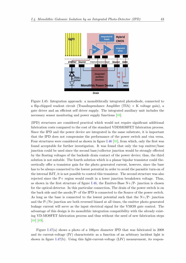
I.4. Monolithic Galvanic Isolation by an Integrated Photo-Detector (IPD) 43
Figure I.45: Integration approach: a monolithically integrated photodiode, connected to
a flip-chipped readout circuit (TransImpendance Amplifier (TIA) + K voltage gain), a
gate driver and an efficient self driver supply. The integrated auxiliary unit includes the
necessary sensor monitoring and power supply functions [89].
(IPD) structures are considered practical which would not require significant additional
fabrication costs compared to the cost of the standard VDDMOSFET fabrication process.
Since the IPD and the power device are integrated in the same substrate, it is important
that the IPD does not compromise the performance of the power switch and visa versa.
Four structures were considered as shown in figure I.46 [88], from which, only the first was
found acceptable for further investigation. It was found that only the top emitter/base
junction could be used since the second base/collector junction would be strongly effected
by the floating voltages of the backside drain contact of the power device; thus, the third
solution is not suitable. The fourth solution which is a planar bipolar transistor could the-
oretically offer a transistor gain for the photo generated current, however, since the base
has to be always connected to the lowest potential in order to avoid the parasitic turn-on of
the internal BJT, it is not possible to control this transistor. The second structure was also
rejected since the P+ region would result in a lower junction breakdown voltage. Thus,
as shown in the first structure of figure I.46, the Emitter-Base N+/P- junction is chosen
for the optical-detector. In this particular connection, The drain of the power switch is on
the back side and the anode/P- of the IPD is connected to the Source of the power switch.
As long as the base is connected to the lowest potential such that the N+/P- junction
and the P-/Nv junction are both reversed biased at all times, the emitter photo generated
leakage current will serve as the input electrical signal for the VMOS gate control. The
advantage of this design is its monolithic integration compatibility with the already exist-
ing VD-MOSFET fabrication process and thus without the need of new fabrication steps
[88] [89].
Figure I.47(a) shows a photo of a 100µm diameter IPD that was fabricated in 2008
and its current-voltage (IV) characteristic as a function of an arbitrary incident light is
shown in figure I.47(b). Using this light-current-voltage (LIV) measurement, its respon-
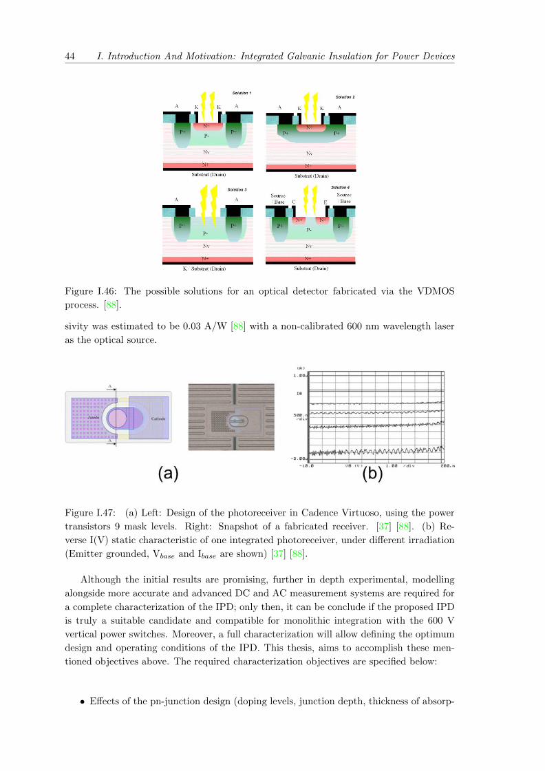
44 I. Introduction And Motivation: Integrated Galvanic Insulation for Power Devices
Figure I.46: The possible solutions for an optical detector fabricated via the VDMOS
process. [88].
sivity was estimated to be 0.03 A/W [88] with a non-calibrated 600 nm wavelength laser
as the optical source.
Figure I.47: (a) Left: Design of the photoreceiver in Cadence Virtuoso, using the power
transistors 9 mask levels. Right: Snapshot of a fabricated receiver. [37] [88]. (b) Re-
verse I(V) static characteristic of one integrated photoreceiver, under different irradiation
(Emitter grounded, Vbase and Ibase are shown) [37] [88].
Although the initial results are promising, further in depth experimental, modelling
alongside more accurate and advanced DC and AC measurement systems are required for
a complete characterization of the IPD; only then, it can be conclude if the proposed IPD
is truly a suitable candidate and compatible for monolithic integration with the 600 V
vertical power switches. Moreover, a full characterization will allow defining the optimum
design and operating conditions of the IPD. This thesis, aims to accomplish these men-
tioned objectives above. The required characterization objectives are specified below:
• Effects of the pn-junction design (doping levels, junction depth, thickness of absorp-
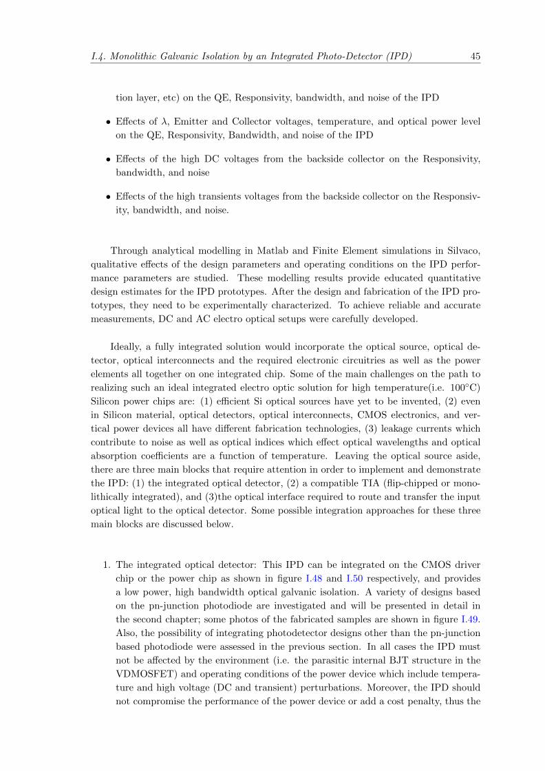
I.4. Monolithic Galvanic Isolation by an Integrated Photo-Detector (IPD) 45
tion layer, etc) on the QE, Responsivity, bandwidth, and noise of the IPD
• Effects of λ, Emitter and Collector voltages, temperature, and optical power level
on the QE, Responsivity, Bandwidth, and noise of the IPD
• Effects of the high DC voltages from the backside collector on the Responsivity,
bandwidth, and noise
• Effects of the high transients voltages from the backside collector on the Responsiv-
ity, bandwidth, and noise.
Through analytical modelling in Matlab and Finite Element simulations in Silvaco,
qualitative effects of the design parameters and operating conditions on the IPD perfor-
mance parameters are studied. These modelling results provide educated quantitative
design estimates for the IPD prototypes. After the design and fabrication of the IPD pro-
totypes, they need to be experimentally characterized. To achieve reliable and accurate
measurements, DC and AC electro optical setups were carefully developed.
Ideally, a fully integrated solution would incorporate the optical source, optical de-
tector, optical interconnects and the required electronic circuitries as well as the power
elements all together on one integrated chip. Some of the main challenges on the path to
realizing such an ideal integrated electro optic solution for high temperature(i.e. 100C)
Silicon power chips are: (1) efficient Si optical sources have yet to be invented, (2) even
in Silicon material, optical detectors, optical interconnects, CMOS electronics, and ver-
tical power devices all have different fabrication technologies, (3) leakage currents which
contribute to noise as well as optical indices which effect optical wavelengths and optical
absorption coefficients are a function of temperature. Leaving the optical source aside,
there are three main blocks that require attention in order to implement and demonstrate
the IPD: (1) the integrated optical detector, (2) a compatible TIA (flip-chipped or mono-
lithically integrated), and (3)the optical interface required to route and transfer the input
optical light to the optical detector. Some possible integration approaches for these three
main blocks are discussed below.
1. The integrated optical detector: This IPD can be integrated on the CMOS driver
chip or the power chip as shown in figure I.48 and I.50 respectively, and provides
a low power, high bandwidth optical galvanic isolation. A variety of designs based
on the pn-junction photodiode are investigated and will be presented in detail in
the second chapter; some photos of the fabricated samples are shown in figure I.49.
Also, the possibility of integrating photodetector designs other than the pn-junction
based photodiode were assessed in the previous section. In all cases the IPD must
not be affected by the environment (i.e. the parasitic internal BJT structure in the
VDMOSFET) and operating conditions of the power device which include tempera-
ture and high voltage (DC and transient) perturbations. Moreover, the IPD should
not compromise the performance of the power device or add a cost penalty, thus the
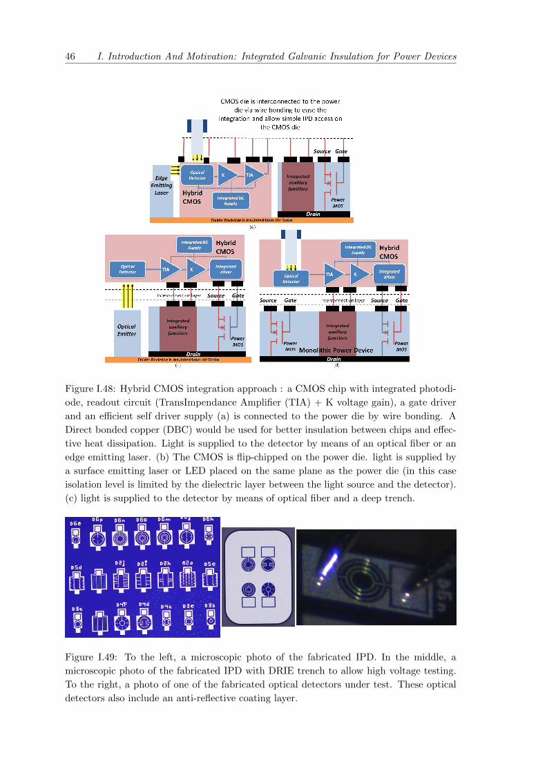
46 I. Introduction And Motivation: Integrated Galvanic Insulation for Power Devices
Figure I.48: Hybrid CMOS integration approach : a CMOS chip with integrated photodi-
ode, readout circuit (TransImpendance Amplifier (TIA) + K voltage gain), a gate driver
and an efficient self driver supply (a) is connected to the power die by wire bonding. A
Direct bonded copper (DBC) would be used for better insulation between chips and effec-
tive heat dissipation. Light is supplied to the detector by means of an optical fiber or an
edge emitting laser. (b) The CMOS is flip-chipped on the power die. light is supplied by
a surface emitting laser or LED placed on the same plane as the power die (in this case
isolation level is limited by the dielectric layer between the light source and the detector).
(c) light is supplied to the detector by means of optical fiber and a deep trench.
Figure I.49: To the left, a microscopic photo of the fabricated IPD. In the middle, a
microscopic photo of the fabricated IPD with DRIE trench to allow high voltage testing.
To the right, a photo of one of the fabricated optical detectors under test. These optical
detectors also include an anti-reflective coating layer.

I.4. Monolithic Galvanic Isolation by an Integrated Photo-Detector (IPD) 47
fabrication technology is highly constrained by the power device.
2. TIA: The design of the TIA is under progress by Thanh Long Le [90] who is a PHD
student at G2ELab currently working with Dr.Rouger and Dr.Crebier. The TIA
can be fabricated in the CMOS chip or it can be monolithically integrated in the
power chip as presented in figure I.45. The main challenge of the TIA is its ability to
provide a sufficient gain (an output voltage of a few 100s of mV for an input current
of less than 1µA) without increasing noise or limiting the bandwidth (minimizing
the input capacitance of the TIA is desired).
3. Optical interface: Fiber optics and waveguides are two different possible approaches;
optical fibers can be more practical than a waveguide network when the optical source
needs to be further from the IPD, however. For an IPD integrated in a CMOS chip,
figure I.48 demonstrates two possible approaches for the optical interface, (1) optical
fiber and deep trench, or (2) an optical source (i.e. LED or vertical-cavity surface
emitting laser (VCSEL)) aligned beneath the flip-chipped CMOS. For the power chip
integration mode, 4 possible optical interfacing approaches are presented in figure
I.50. Depending on the design of the IPD, the IPD could either be horizontally or
vertically triggered by light. Figure I.50 (a) shows the two triggering orientations of
an optical fiber. In figure I.50 (b) the IPD is edge triggered by an aligned optical
chip where light is coupled through free space from the optical source (an LED or an
edge emitting laser) to the IPD (note that edge triggered IPD designs are different
from vertically triggered designs). The optical interface can also be achieved through
waveguide based optical interconnections either via a hybrid mode as shown in figure
I.50 (c) or a monolithic mode as shown in figure I.50 (d). In all the cases presented
here, the waveguides and optical fibers must be chosen and designed to work with
the optical wavelengths used by the Silicon IPD. Using waveguides reduces optical
alignment challenges meanwhile allowing easy optical routing throughout the chip;
however, waveguide designs must have sufficiently low losses and compatible tem-
perature tolerances.
The different integration modes presented above all only deliver the control signal
through the optical interface and they all require a floating supply in order to supply the
required energy to switch the gate. Another novel integration approach is presented in
figure I.51 which includes a second IPD that would be biased under the conditions of a
solar cell; the generated voltage at terminals of this second IPD can then be converted by a
DC-DC converter to charge a storage capacitor for power supply purposes. This approach
can simplify the CMOS circuitry since the floating power supply is eliminated. In this
case, a more powerful optical source with a DC and AC component would be required in
order to deliver both the energy and the gating signal.
Even though Silicon is not the ideal material for making optical detectors, it has been
the dominant material of choice in electronics due to its excellent compromise between

48 I. Introduction And Motivation: Integrated Galvanic Insulation for Power Devices
Figure I.50: Hyprid Integration approach : a CMOS chip with readout circuit (TransIm-
pendance Amplifier (TIA) + K voltage gain), a gate driver and an efficient self driver
supply flip-chipped on the power chip with IPD. (a) Light can be edge or vertically cou-
pled to the IPD by means of an optical fiber. (b) A flip-chip optical interconnect chip can
provide light coupling by means of grating couplers and routing by waveguides. (c) An
optical source such as an LED or an edge emitting laser can be aligned to edge trigger the
IPD in free space. (d) Waveguides can be integrated directly onto the power chip to rout
the optical signals.
cost and performance. Although there are growing interests in developing power devices
in wide bandgap materials (advantages include higher thermal conductivity and breakdown
voltages) such as GaAs, SiC, GaN, and diamond, it is worth noting that Silicon contin-
ues to hold one major advantage, namely that Silicon technology is cheaper. Looking at
costs, it could be argued that Silicon has benefited from large amounts of investments for
many years that has led to its cost efficient and mature technology; this implies, that with
enough investments new technologies will be developed for wide bandgap materials that
can eventually surpass the cost barrier set by Silicon. In spite of the fast developments
of new materials, it could be also debated that Silicon technology will continue to grow,
develop and remain a key player in the future of electronics mainly thanks to its natural
abundance. Referring to figure I.52, Silicon and Oxygen (which is Silicon’s native oxide)
are the most two abundant elements on earth. Thus in this thesis, we will focus on silicon
compatible technologies with potential for monolithic integration; moreover, this work is
potentially transferable to other material platforms. Materials from group III-V such as
GaAs and GaN (GaN has a higher thermal and voltage capability over GaAs and SiC)
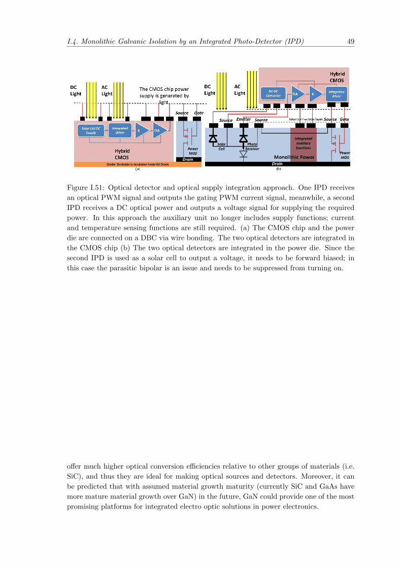
I.4. Monolithic Galvanic Isolation by an Integrated Photo-Detector (IPD) 49
Figure I.51: Optical detector and optical supply integration approach. One IPD receives
an optical PWM signal and outputs the gating PWM current signal, meanwhile, a second
IPD receives a DC optical power and outputs a voltage signal for supplying the required
power. In this approach the auxiliary unit no longer includes supply functions; current
and temperature sensing functions are still required. (a) The CMOS chip and the power
die are connected on a DBC via wire bonding. The two optical detectors are integrated in
the CMOS chip (b) The two optical detectors are integrated in the power die. Since the
second IPD is used as a solar cell to output a voltage, it needs to be forward biased; in
this case the parasitic bipolar is an issue and needs to be suppressed from turning on.
offer much higher optical conversion efficiencies relative to other groups of materials (i.e.
SiC), and thus they are ideal for making optical sources and detectors. Moreover, it can
be predicted that with assumed material growth maturity (currently SiC and GaAs have
more mature material growth over GaN) in the future, GaN could provide one of the most
promising platforms for integrated electro optic solutions in power electronics.

50 I. Introduction And Motivation: Integrated Galvanic Insulation for Power Devices
Figure I.52: Abundance (atom fraction) of the chemical elements in Earth’s upper conti-
nental crust as a function of atomic number. The rarest elements in the crust (shown in
yellow) are the most dense. They were further rarefied in the crust by being siderophile
(iron-loving) elements, in the Goldschmidt classification of elements. Siderophiles were de-
pleted by being relocated into the Earth’s core. Their abundance in meteoroid materials is
relatively higher. Additionally, tellurium and selenium have been depleted from the crust
due to formation of volatile hydrides. [91].
I.5 Thesis Overview
In efforts of providing a novel high level optical solution for the galvanic isolation challenge
inside power converters, more specifically between the power device and its control unit,
this thesis proposes a compatible optical detector design for monolithic integration with
a 600 V vertical MOSFET without any modifications to the power VMOS fabrication
process. The proposed optical detector can be triggered by an optical beam of minimum
1 µW, thus it allows for a range of low power, low cost, and small optical sources such
as semiconductor lasers and LEDs. The output of the optical detector will be a current
signal in the range of a few of µAs. This output current signal contains only the control
information; in order to provide the sufficient energy required to switch the VD-MOSFET,
the output of the optical detector will be amplified at a TIA stage before feeding the gate
of the VDMOSFET. The project perspective and approach are illustrated in figure I.53.
I.5.a Methodology
The optical detectors and VDMOSFET devices presented in this thesis were fabricated
using the standard VMOS process at the CIME Nanotech/Minatec cleanroom facilities in
Grenoble. Each research cycle starts with an idea emerging from literature review and
brain storming sessions. The models are chosen based on Silicon material, semiconductor
and optical theories and VMOS fabrication standards. The devices are simulated and

I.5. Thesis Overview 51
Figure I.53: Project perspective and approach overview.
optimized using analytical methods and numerical tools such as Silvaco and Athena. Next,
mask layouts were designed using Cadence tools. Once the designs were fabricated and
measured, the collected data were processed and analysed using Matlab tools. The designs
were then improved by feedbacks from comparing the experimental and the simulation
results (during the course of this thesis, only one fabrication run was done). Moreover, in
each research cycle, the limitations of the experimental setup were identified and improved,
the flexibility of the measurement procedure was enhanced, and further functionalities were
added. Furthermore, the fabrication tolerances, errors and effects were identified and can
be taken into consideration at the start of future research cycles.
I.5.b Organization
Chapter 2 introduces the optical detector structure and explains its compatibility with the
VD-MOSFET fabrication standards. The design and modelling approach for the detector
are provided in detail. In chapter 3, the characterization results of the optical detectors
as well as the DC and AC electro optical measurement set-ups used to characterize the
fabricated devices are presented.


Chapter II
Compatible Integrated Photodiodes(IPDs) for Power Switches: Modeling, Design andTechnology
Essentially, all models are wrong, but some are useful.
George Edward Pelham Box
Sommaire
II.1 Introduction . . . . . . . . . . . . . . . . . . . . . . . . . . . . . . . . . . . . . 55
II.1.a IPD Structure . . . . . . . . . . . . . . . . . . . . . . . . . . . . . . . . . . . 55
II.1.b Design Constraints . . . . . . . . . . . . . . . . . . . . . . . . . . . . . . . . 57
II.2 Fundamentals of Device Modelling and Simulation . . . . . . . . . 60
II.2.a Built-in Potential and Depletion Region Width . . . . . . . . . . . . . . . . 60
II.2.b Carrier Transport and Current Continuity . . . . . . . . . . . . . . . . . . . 65
II.2.c Photogeneration . . . . . . . . . . . . . . . . . . . . . . . . . . . . . . . . . 68
II.2.d Photocurrent . . . . . . . . . . . . . . . . . . . . . . . . . . . . . . . . . . . 73
II.3 Anti-reflection Coating . . . . . . . . . . . . . . . . . . . . . . . . . . . . 76
II.4 Static Analysis . . . . . . . . . . . . . . . . . . . . . . . . . . . . . . . . . . . 81
II.4.a DC Emitter and Collector biasing . . . . . . . . . . . . . . . . . . . . . . . . 86
II.4.b Sensitivity to Carrier Lifetimes . . . . . . . . . . . . . . . . . . . . . . . . . 91
II.5 Dynamic Analysis . . . . . . . . . . . . . . . . . . . . . . . . . . . . . . . . . . 94
II.5.a Wavelength Dependence . . . . . . . . . . . . . . . . . . . . . . . . . . . . . 96
II.5.b Emitter DC biasing . . . . . . . . . . . . . . . . . . . . . . . . . . . . . . . . 100
II.6 Optical Beam Radius and Position Analysis . . . . . . . . . . . . . . . 102
II.7 Parasitic Environment Constraints . . . . . . . . . . . . . . . . . . . . 104
II.7.a Electrical Activation of Parasitic BJT . . . . . . . . . . . . . . . . . . . . . 104
II.7.b Optical Activation of Parasitic BJT . . . . . . . . . . . . . . . . . . . . . . . 108
II.8 Simulation and Modelling Conclusions and Overview . . . . . . . 115
Abstract
In order to obtain an in-depth understanding of the proposed integrated photodetector
behaviour and its achievable performance range, suitable operation region and limi-
tations in consideration of the imposed vertical structure, parasitic environment and
operating conditions of the power switch, this chapter conducts a number of studies
via analytical modelling and finite element simulation. We start by reviewing the fun-
damental basis of physics of semiconductor devices specially relevant for modelling
pn-junction devices. Next, the static and dynamic performance of the IPD is modelled

54II. Compatible Integrated Photodiodes (IPDs) for Power Switches: Modeling, Design and
Technology
and simulated as function of design, material and operation input parameters such as
doping profile (limited by VDMOSFET), optical wavelength, optical intensity, applied
voltages, device area, optical beam size, shading, carrier lifetimes, and substrate DC
and transient high voltages.
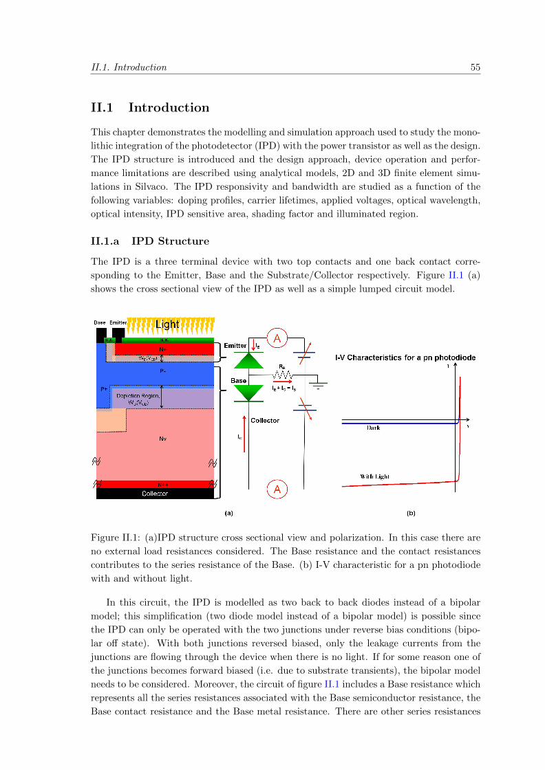
II.1. Introduction 55
II.1 Introduction
This chapter demonstrates the modelling and simulation approach used to study the mono-
lithic integration of the photodetector (IPD) with the power transistor as well as the design.
The IPD structure is introduced and the design approach, device operation and perfor-
mance limitations are described using analytical models, 2D and 3D finite element simu-
lations in Silvaco. The IPD responsivity and bandwidth are studied as a function of the
following variables: doping profiles, carrier lifetimes, applied voltages, optical wavelength,
optical intensity, IPD sensitive area, shading factor and illuminated region.
II.1.a IPD Structure
The IPD is a three terminal device with two top contacts and one back contact corre-
sponding to the Emitter, Base and the Substrate/Collector respectively. Figure II.1 (a)
shows the cross sectional view of the IPD as well as a simple lumped circuit model.
Figure II.1: (a)IPD structure cross sectional view and polarization. In this case there are
no external load resistances considered. The Base resistance and the contact resistances
contributes to the series resistance of the Base. (b) I-V characteristic for a pn photodiode
with and without light.
In this circuit, the IPD is modelled as two back to back diodes instead of a bipolar
model; this simplification (two diode model instead of a bipolar model) is possible since
the IPD can only be operated with the two junctions under reverse bias conditions (bipo-
lar off state). With both junctions reversed biased, only the leakage currents from the
junctions are flowing through the device when there is no light. If for some reason one of
the junctions becomes forward biased (i.e. due to substrate transients), the bipolar model
needs to be considered. Moreover, the circuit of figure II.1 includes a Base resistance which
represents all the series resistances associated with the Base semiconductor resistance, the
Base contact resistance and the Base metal resistance. There are other series resistances
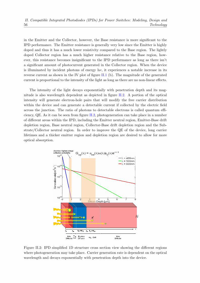
56II. Compatible Integrated Photodiodes (IPDs) for Power Switches: Modeling, Design and
Technology
in the Emitter and the Collector, however, the Base resistance is more significant to the
IPD performance. The Emitter resistance is generally very low since the Emitter is highly
doped and thus it has a much lower resistivity compared to the Base region. The lightly
doped Collector region has a much higher resistance relative to the Base region, how-
ever, this resistance becomes insignificant to the IPD performance as long as there isn’t
a significant amount of photocurrent generated in the Collector region. When the device
is illuminated by incident photons of energy hν, it experiences a notable increase in its
reverse current as shown in the IV plot of figure II.1 (b). The magnitude of the generated
current is proportional to the intensity of the light as long as there are no non-linear effects.
The intensity of the light decays exponentially with penetration depth and its mag-
nitude is also wavelength dependent as depicted in figure II.2. A portion of the optical
intensity will generate electron-hole pairs that will modify the free carrier distribution
within the device and can generate a detectable current if collected by the electric field
across the junction. The ratio of photons to detectable electrons is called quantum effi-
ciency, QE. As it can be seen from figure II.2, photogeneration can take place in a number
of different areas within the IPD, including the Emitter neutral region, Emitter-Base drift
depletion region, Base neutral region, Collector-Base drift depletion region and the Sub-
strate/Collector neutral region. In order to improve the QE of the device, long carrier
lifetimes and a thicker emitter region and depletion region are desired to allow for more
optical absorption.
Figure II.2: IPD simplified 1D structure cross section view showing the different regions
where photogeneration may take place. Carrier generation rate is dependent on the optical
wavelength and decays exponentially with penetration depth into the device.
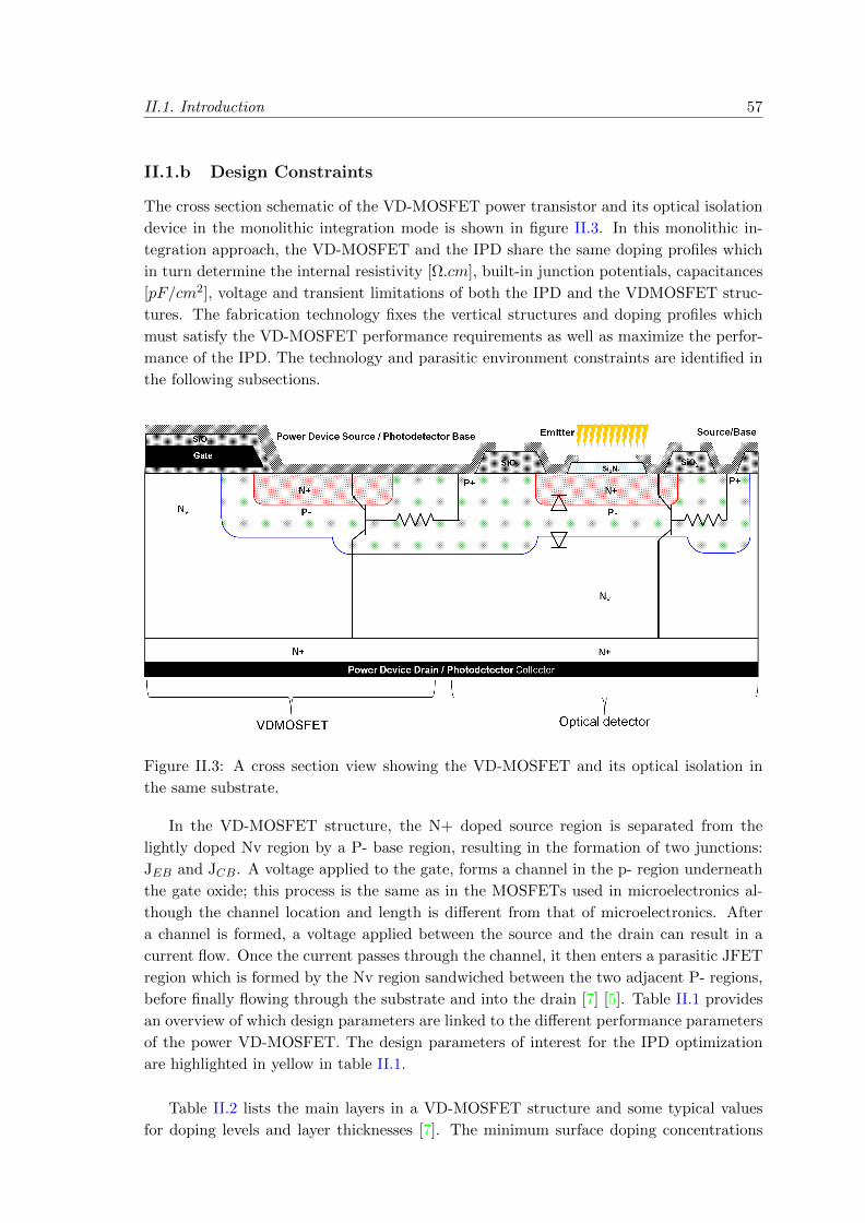
II.1. Introduction 57
II.1.b Design Constraints
The cross section schematic of the VD-MOSFET power transistor and its optical isolation
device in the monolithic integration mode is shown in figure II.3. In this monolithic in-
tegration approach, the VD-MOSFET and the IPD share the same doping profiles which
in turn determine the internal resistivity [Ω.cm], built-in junction potentials, capacitances
[pF/cm2], voltage and transient limitations of both the IPD and the VDMOSFET struc-
tures. The fabrication technology fixes the vertical structures and doping profiles which
must satisfy the VD-MOSFET performance requirements as well as maximize the perfor-
mance of the IPD. The technology and parasitic environment constraints are identified in
the following subsections.
Figure II.3: A cross section view showing the VD-MOSFET and its optical isolation in
the same substrate.
In the VD-MOSFET structure, the N+ doped source region is separated from the
lightly doped Nv region by a P- base region, resulting in the formation of two junctions:
JEB and JCB. A voltage applied to the gate, forms a channel in the p- region underneath
the gate oxide; this process is the same as in the MOSFETs used in microelectronics al-
though the channel location and length is different from that of microelectronics. After
a channel is formed, a voltage applied between the source and the drain can result in a
current flow. Once the current passes through the channel, it then enters a parasitic JFET
region which is formed by the Nv region sandwiched between the two adjacent P- regions,
before finally flowing through the substrate and into the drain [7] [5]. Table II.1 provides
an overview of which design parameters are linked to the different performance parameters
of the power VD-MOSFET. The design parameters of interest for the IPD optimization
are highlighted in yellow in table II.1.
Table II.2 lists the main layers in a VD-MOSFET structure and some typical values
for doping levels and layer thicknesses [7]. The minimum surface doping concentrations

58II. Compatible Integrated Photodiodes (IPDs) for Power Switches: Modeling, Design and
Technology
LG eOxide Emitter
N+D
Base
N−A
Substrate
Nv
Thickness
Emitter
Thickness
Base
Thickness
Nv
VBD X X X X
RChannel X X X X
RDrift X X
VT X X X
Bandwidth X X X X
Table II.1: Summery of VD-MOSFET performance parameters dependencies on design
variables, where VBD is the breakdown voltage, RChannel is the MOSFET channel resis-
tance, RDrift is the resistance of the substrate Nv region, and VT is the MOSFET threshold
voltage.
(roughly 5×10¹⁹ [atoms.cm−3] for N-type Si, and 1×10¹⁸ [atoms.cm−3] for P-type Si [92])
are fixed in order to create ohmic contacts.
Layer/Region Doping [cm−3] Thickness
SiO2 - Gate 50-100 nm
Si -Source N+ 0.5-0.7 µm
1019
Si - Base, Channel P- 2 µm
1016
Si - Base, Contact Well P+ 3 µm
1019
Si - Epi-Drift Layer Nv 50 µm
1014 − 1016
Si - Substrate, Drain N++ 300-600 µm
1019
Table II.2: 600V VDMOSFET, key layer specifications. The Nv doping concentration
range of 1014cm−3 to 1016cm−3 corresponds to a 600V to 100V VMOS respectively. [7]
Figure II.4 (a) shows the anatomy and the application of an optical interconnect link
for the optical control of a power transistor. First, light is generated by a continuous
wave laser and modulated by an electro optical modulator which requires its own elec-
trical driver. Then, the optical signal travels though a waveguide or an optical fiber or
free space to the receiving end where it is converted back into an electrical signal by a
photodetector. The photodetector output current is then converted into a voltage signal
and amplified via a TIA before being treated to drive the power transistor gate. Figure
II.4 (b), depicts the electrical circuit diagram of the integrated IPD and its associated
VDMOSFET as adapted in our approach. In this approach which was introduced and
discussed in chapter 1, the photodetector is integrated in the power die alongside the VD-
MOSFET.
The IPD needs to be optimized for successful interaction with three main subsystems:
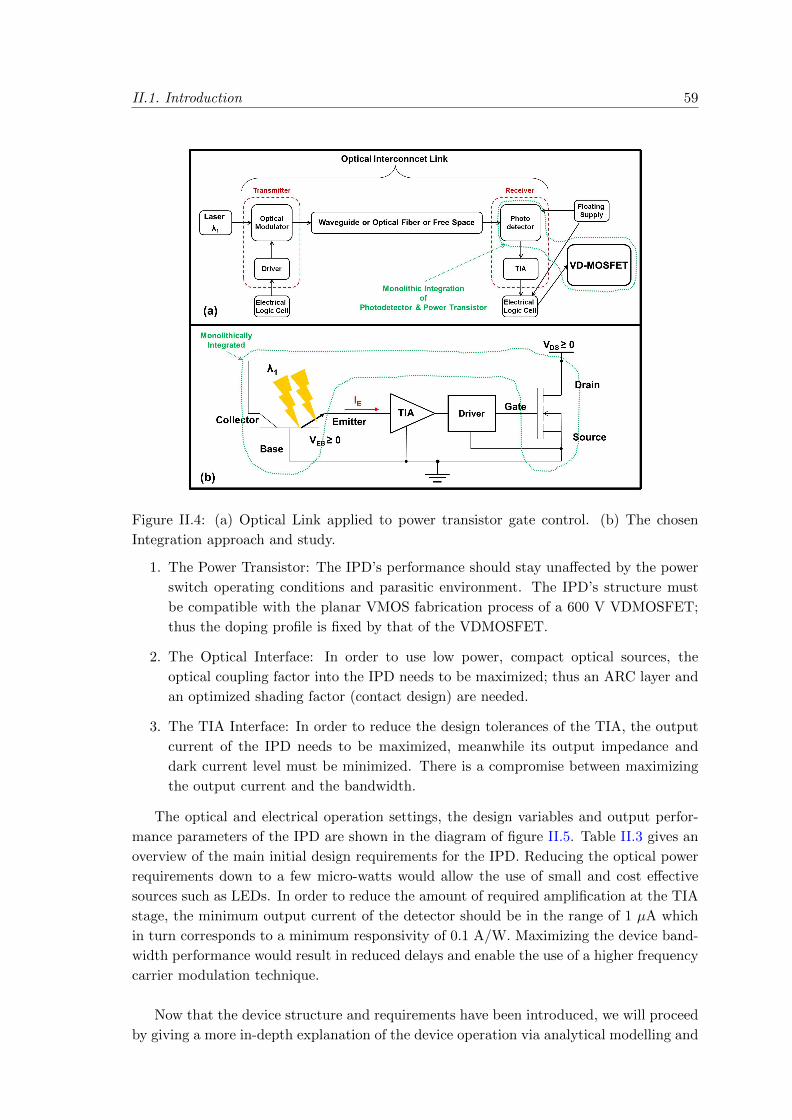
II.1. Introduction 59
Figure II.4: (a) Optical Link applied to power transistor gate control. (b) The chosen
Integration approach and study.
1. The Power Transistor: The IPD’s performance should stay unaffected by the power
switch operating conditions and parasitic environment. The IPD’s structure must
be compatible with the planar VMOS fabrication process of a 600 V VDMOSFET;
thus the doping profile is fixed by that of the VDMOSFET.
2. The Optical Interface: In order to use low power, compact optical sources, the
optical coupling factor into the IPD needs to be maximized; thus an ARC layer and
an optimized shading factor (contact design) are needed.
3. The TIA Interface: In order to reduce the design tolerances of the TIA, the output
current of the IPD needs to be maximized, meanwhile its output impedance and
dark current level must be minimized. There is a compromise between maximizing
the output current and the bandwidth.
The optical and electrical operation settings, the design variables and output perfor-
mance parameters of the IPD are shown in the diagram of figure II.5. Table II.3 gives an
overview of the main initial design requirements for the IPD. Reducing the optical power
requirements down to a few micro-watts would allow the use of small and cost effective
sources such as LEDs. In order to reduce the amount of required amplification at the TIA
stage, the minimum output current of the detector should be in the range of 1 µA which
in turn corresponds to a minimum responsivity of 0.1 A/W. Maximizing the device band-
width performance would result in reduced delays and enable the use of a higher frequency
carrier modulation technique.
Now that the device structure and requirements have been introduced, we will proceed
by giving a more in-depth explanation of the device operation via analytical modelling and
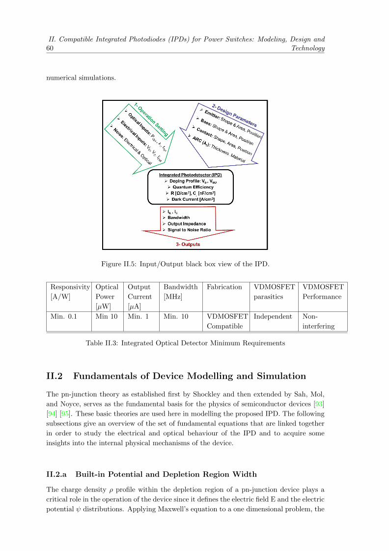
60II. Compatible Integrated Photodiodes (IPDs) for Power Switches: Modeling, Design and
Technology
numerical simulations.
Figure II.5: Input/Output black box view of the IPD.
Responsivity
[A/W]
Optical
Power
[µW]
Output
Current
[µA]
Bandwidth
[MHz]
Fabrication VDMOSFET
parasitics
VDMOSFET
Performance
Min. 0.1 Min 10 Min. 1 Min. 10 VDMOSFET
Compatible
Independent Non-
interfering
Table II.3: Integrated Optical Detector Minimum Requirements
II.2 Fundamentals of Device Modelling and Simulation
The pn-junction theory as established first by Shockley and then extended by Sah, Mol,
and Noyce, serves as the fundamental basis for the physics of semiconductor devices [93]
[94] [95]. These basic theories are used here in modelling the proposed IPD. The following
subsections give an overview of the set of fundamental equations that are linked together
in order to study the electrical and optical behaviour of the IPD and to acquire some
insights into the internal physical mechanisms of the device.
II.2.a Built-in Potential and Depletion Region Width
The charge density ρ profile within the depletion region of a pn-junction device plays a
critical role in the operation of the device since it defines the electric field E and the electric
potential ψ distributions. Applying Maxwell’s equation to a one dimensional problem, the

II.2. Fundamentals of Device Modelling and Simulation 61
relationship between net charge concentration, electric field and the electric potential as a
function of distance x can be stated as in equation II.1.
d2ψ(x)
dx2= −dE(x)
dx= −ρ(x)
ε=q
ε[n(x)− p(x) +N−
A (x)−N+D (x)] (II.1)
Equation II.1 is known as the Poisson’s equation and it states to important relations:
(1) the gradient of the electric field E(x) with respect to distance x is proportional to the
net charge concentration at x by the dielectric constant ε of the semiconductor material,
in our case that of Silicon. (2) The negative gradient of the electric potential ψ(x) with
respect to distance x is equal to the electric field E(x). Applying Maxwell Boltzmann
statistics, the charge density ρ(x) can be expressed as:
q[ND(x)− nieψ(x)/Vth ] 0 ≤ x ≤ xdn(V ) (II.2)
q[nie−ψ(x)/Vth −NA(x)] − xdp(V ) ≤ x ≤ 0 (II.3)
where the metallurgical junction is assumed to be at x = zero, with the depletion
region width on the n-side marked by xdn and the depletion region width on the p-side
marked by −xdp. In Atlas, equations II.2 and II.3 are substituted into equation II.1,
and the resulting non linear equation is numerically solved for the electric field and the
potential distributions. In order to avoid complex numerical calculations, the depletion
region approximation method is used for the analytical modelling of the IPD which assumes
that there are no free carriers within the depletion region, n(x) ≈ p(x) ≈ 0,
n(x), p(x) << ND(x) 0 ≤ x ≤ xdn(V ) (II.4)
n(x), p(x) << NA(x) − xdp(V ) ≤ x ≤ 0 (II.5)
The depletion region approximation simplifies the smooth transition of carrier densities
across the junction into a box profile, resulting in an abrupt change at xdn and −xdp. Thus
equation II.1 can be reduced to,
d2ψ(x)
dx2≈ qND(x)
ε0 ≤ x ≤ xdn(V ) (II.6)
d2ψ(x)
dx2≈ −qNA(x)
ε− xdp(V ) ≤ x ≤ 0 (II.7)
Integrating equations II.6 and II.7, gives the electric field distributions as a function
of distance space (x) and voltage (V),
E(x, V ) =−qND
ε(xdn(V )− x) 0 ≤ x ≤ xdn(V ) (II.8)
E(x, V ) = −qNA
ε(xdp(V ) + x) − xdp(V ) ≤ x ≤ 0 (II.9)
Integrating equations II.8 and II.9 gives the potential distribution:
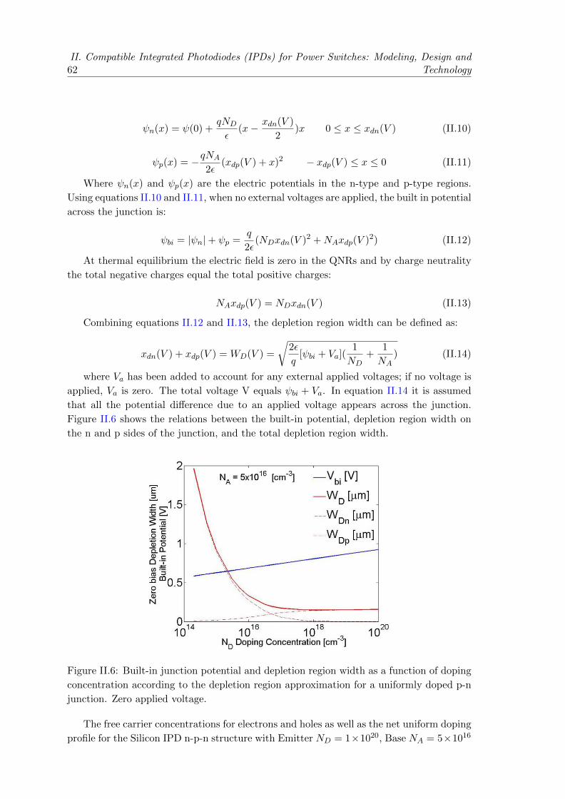
62II. Compatible Integrated Photodiodes (IPDs) for Power Switches: Modeling, Design and
Technology
ψn(x) = ψ(0) +qND
ε(x− xdn(V )
2)x 0 ≤ x ≤ xdn(V ) (II.10)
ψp(x) = −qNA
2ε(xdp(V ) + x)2 − xdp(V ) ≤ x ≤ 0 (II.11)
Where ψn(x) and ψp(x) are the electric potentials in the n-type and p-type regions.
Using equations II.10 and II.11, when no external voltages are applied, the built in potential
across the junction is:
ψbi = |ψn|+ ψp =q
2ε(NDxdn(V )2 +NAxdp(V )2) (II.12)
At thermal equilibrium the electric field is zero in the QNRs and by charge neutrality
the total negative charges equal the total positive charges:
NAxdp(V ) = NDxdn(V ) (II.13)
Combining equations II.12 and II.13, the depletion region width can be defined as:
xdn(V ) + xdp(V ) = WD(V ) =
√2ε
q[ψbi + Va](
1
ND+
1
NA) (II.14)
where Va has been added to account for any external applied voltages; if no voltage is
applied, Va is zero. The total voltage V equals ψbi + Va. In equation II.14 it is assumed
that all the potential difference due to an applied voltage appears across the junction.
Figure II.6 shows the relations between the built-in potential, depletion region width on
the n and p sides of the junction, and the total depletion region width.
Figure II.6: Built-in junction potential and depletion region width as a function of doping
concentration according to the depletion region approximation for a uniformly doped p-n
junction. Zero applied voltage.
The free carrier concentrations for electrons and holes as well as the net uniform doping
profile for the Silicon IPD n-p-n structure with Emitter ND = 1×10²⁰, Base NA = 5×10¹⁶

II.2. Fundamentals of Device Modelling and Simulation 63
and Collector ND = 2 × 10¹⁴ is depicted in figure II.7 (a) as evaluated by a full numeri-
cal simulation in Atlas. Figures II.7 (b) and II.7 (c) demonstrate the difference between
the Atlas simulation results and the depletion region approximation for the correspond-
ing Emitter junction electric field and the potential distributions. The small difference
in these results arises from the different charge density profiles considered; in Atlas, the
profile of charge density is given by ρ(x) = [n(x) − p(x) + N−A (x) − N+
D (x)]/q (the sum
of the three plots in figure II.7 (a)) where as in the depletion region approximation it is
given by ρ(x) = [N−A (x)−N+
D (x)]/q (represented by the net doping in figure II.7 (a)).
Figure II.7: The depletion region approximation versus the full numerical computation
(via Atlas) for the n-p-n structure of the IPD with uniform doping profiles. The depicted
distributions here correspond to a 0V applied bias.
The values of WD and ψ are strongly dependent on the doping profiles and applied
voltages. Although figure II.7 shows a promising consistency between the numerical and
the analytical evaluations of WD and ψ, a uniform doping profile based on the surface
doping concentration is not realistic. The doping profiles for the case of a double diffused
junction through ion implantation results in Gaussian distributions of the dopants. Solv-
ing the Poisson equations for a Gaussian distribution is a challenging task since there are
no analytical solutions for the integration of a Gaussian function within finite limits. Atlas
handles this challenge through numerical evaluations of the error function. The blue curve
in Figure II.8 (a), is an SRP measurement from a sample that has been processed via the
VMOS fabrication procedure at the CIME nanotech fabrication facilities. Assuming that
the SRP measurement depicted in figure II.8 (a) roughly represents the true doping profile,
the doping profile plotted in green as implemented by the Gaussian functions in Atlas, un-
derestimates the amount of dopants specially in the Base region. In order to have a more
accurate doping profile, the fabrication procedure can be simulated in Athena; however,
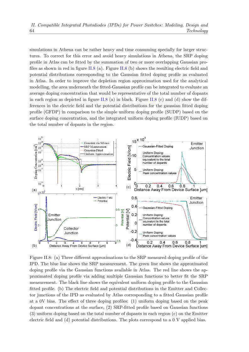
64II. Compatible Integrated Photodiodes (IPDs) for Power Switches: Modeling, Design and
Technology
simulations in Athena can be rather heavy and time consuming specially for larger struc-
tures. To correct for this error and avoid heavy simulations in Athena, the SRP doping
profile in Atlas can be fitted by the summation of two or more overlapping Gaussian pro-
files as shown in red in figure II.8 (a). Figure II.8 (b) shows the resulting electric field and
potential distributions corresponding to the Gaussian fitted doping profile as evaluated
in Atlas. In order to improve the depletion region approximation used for the analytical
modelling, the area underneath the fitted-Gaussian profile can be integrated to evaluate an
average doping concentration that would be representative of the total number of dopants
in each region as depicted in figure II.8 (a) in black. Figure II.8 (c) and (d) show the dif-
ferences in the electric field and the potential distributions for the gaussian fitted doping
profile (GFDP) in comparison to the simple uniform doping profile (SUDP) based on the
surface doping concentration, and the integrated uniform doping profile (IUDP) based on
the total number of dopants in the region.
Figure II.8: (a) Three different approximations to the SRP measured doping profile of the
IPD. The blue line shows the SRP measurement. The green line shows the approximated
doping profile via the Gaussian functions available in Atlas. The red line shows the ap-
proximated doping profile via adding multiple Gaussian functions to better fit the SRP
measurement. The black line shows the equivalent uniform doping profile to the Gaussian
fitted profile. (b) The electric field and potential distributions in the Emitter and Collec-
tor junctions of the IPD as evaluated by Atlas corresponding to a fitted Gaussian profile
at a 0V bias. The effect of three doping profiles: (1) uniform doping based on the peak
dopant concentrations at the surface, (2) SRP-fitted profile based on Gaussian functions
(3) uniform doping based on the total number of dopants in each region (c) on the Emitter
electric field and (d) potential distributions. The plots correspond to a 0 V applied bias.
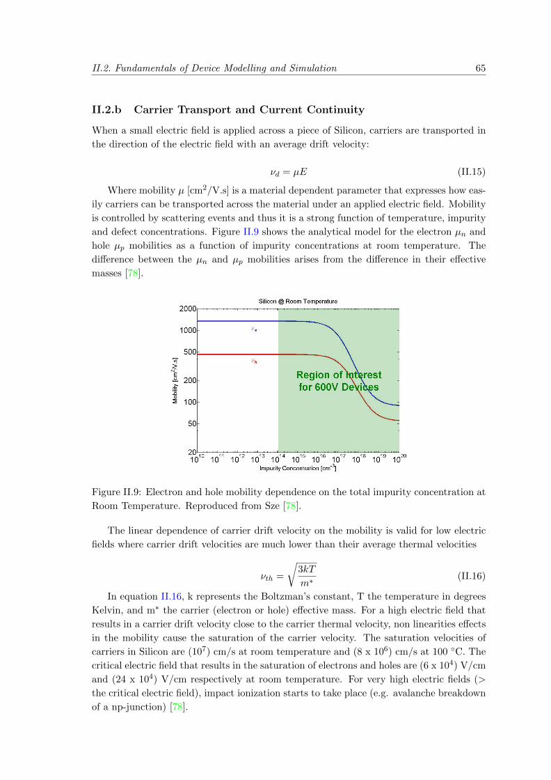
II.2. Fundamentals of Device Modelling and Simulation 65
II.2.b Carrier Transport and Current Continuity
When a small electric field is applied across a piece of Silicon, carriers are transported in
the direction of the electric field with an average drift velocity:
νd = µE (II.15)
Where mobility µ [cm2/V.s] is a material dependent parameter that expresses how eas-
ily carriers can be transported across the material under an applied electric field. Mobility
is controlled by scattering events and thus it is a strong function of temperature, impurity
and defect concentrations. Figure II.9 shows the analytical model for the electron µn and
hole µp mobilities as a function of impurity concentrations at room temperature. The
difference between the µn and µp mobilities arises from the difference in their effective
masses [78].
Figure II.9: Electron and hole mobility dependence on the total impurity concentration at
Room Temperature. Reproduced from Sze [78].
The linear dependence of carrier drift velocity on the mobility is valid for low electric
fields where carrier drift velocities are much lower than their average thermal velocities
νth =
√3kT
m∗ (II.16)
In equation II.16, k represents the Boltzman’s constant, T the temperature in degrees
Kelvin, and m∗ the carrier (electron or hole) effective mass. For a high electric field that
results in a carrier drift velocity close to the carrier thermal velocity, non linearities effects
in the mobility cause the saturation of the carrier velocity. The saturation velocities of
carriers in Silicon are (107) cm/s at room temperature and (8 x 10⁶) cm/s at 100 C. The
critical electric field that results in the saturation of electrons and holes are (6 x 10⁴) V/cm
and (24 x 104) V/cm respectively at room temperature. For very high electric fields (>
the critical electric field), impact ionization starts to take place (e.g. avalanche breakdown
of a np-junction) [78].
66II. Compatible Integrated Photodiodes (IPDs) for Power Switches: Modeling, Design and
Technology
Our analytical Matlab model uses equation II.15, and thus, this model is valid for the
case of a low electric field. Moreover, as long as device dimensions are not comparable
to the carrier mean free path, ballistic transport mechanisms can be ignored. Under the
influence of an electric field, carriers begin to contribute to a current flow in the direction
of the applied electric field referred to as the drift current,
Jdr = −q[nµn + pµp]E = σE =1
ρE (II.17)
where σ is the conductivity and ρ is the resistivity. From equation II.17, it is evident
that conductivity of Silicon has a direct and strong dependence on the doping densities
through the carrier concentrations, meanwhile, it has a weaker and inverse dependence on
the doping densities through the carrier mobilities. Overall, Silicon conductivity increases
(non-linearly) with increased doping densities. The models used in this thesis assume
complete ionization of the dopants.
Current may also flow in absence of an electric field as long as there is a carrier
concentration gradient present within the device, also known as diffusion current [78].
Jdiff = q[Dndn
dxn−Dp
dp
dxp] (II.18)
Dn and Dp are the carrier diffusivities and can be related to carrier mobilities through
Einstein’s relation [78],
D = [kT/q]µ (II.19)
where D and µ may represents electron and hole parameters. Combining equations
II.17 and II.18, the total steady state current densities for a one dimensional case yields
to the drift-diffusion equations [78],
Jn = −qnµnE + qDndn
dxn (II.20)
Jp = −qpµpE − qDpdp
dxp (II.21)
These equations do not consider the effects of external magnetic fields that can reduce
the current via magneto resistive mechanisms [78].
The steady-state continuity equations for electrons in the p-type Base region and the
holes in the n-type Emitter region are established according to [78] [96]:
∂n
∂t=
1
q
dJndx−Rn +Gn (II.22)
∂p
∂t= −1
q
dJpdx−Rp +Gp (II.23)
Where Rn and Rp are the electron and hole recombination rates, and Gn and Gp are
the electron and hole generation rates respectively. Under the low injection assumption

II.2. Fundamentals of Device Modelling and Simulation 67
(p << (n ≈ n0) in the n-type region), equations II.21 and II.20 can be combined with the
Einstein relation II.19 to solve for the electron and hole density functions:
pn(x, V )− pn0 = pn0[e( qVkT
) − 1]e(−x−xdn(V )
Lp)
(II.24)
np(x, V )− np0 = np0[e( qVkT
) − 1]e(−x−xdp(V )
Ln) (II.25)
Where np and pn are the electron and hole minority densities on the p-type and the
n-type region respectively. np0 and pn0 are the equilibrium electron and hole densities on
the p-type and the n-type region respectively. The electron diffusion current on the p-side
and the hole diffusion current on the n-side follow according to:
Jn(x, V ) = −qDndnpdx|−xdp =
qDnnp0Ln
[e(qVkT
) − 1] (II.26)
Jp(x, V ) = −qDpdpndx|xdn =
qDppn0Lp
[e(qVkT
) − 1] (II.27)
Where the total diffusion current is given by the sum of equations II.26 and II.27;
this result is the famous Shockley equation for an ideal diode. A homogeneously doped
semiconductor device at equilibrium will be in a steady state where pn = n2i , where ni is
the intrinsic carrier concentration. If an external force such as an applied voltage disturbs
the steady state balance (pn << n2i under reverse bias and pn >> n2i under forward
bias), generation and recombination mechanisms attempt to return the semiconductor to
its equilibrium state. There are a number of different generation and recombination pro-
cesses that may include phonon transitions, photon transitions, surface recombinations,
tunnelling, Auger transitions, and Shockley-Read-Hall (SRH) capture and emission pro-
cesses. Since this work is not concerned with sub-micron design, tunnelling is assumed
to be negligible. Also since Silicon has an indirect bandgap, direct radiative transitions
through photon emission are also assumed to be negligible [78] [96]. For the analytical
model, approximations of SRH generation, recombination processes through localized traps
within the energy bandgap are considered:
Jgn(V ) =qniWD(V )
tn + tp(II.28)
Jre(V ) =qniWD(V )
tn + tpe(
qV2kT
) (II.29)
In the above approximation it is assumed that all traps are halfway between the
bandgap and thus a maximum recombination rate is considered through most part of
the depletion region. Figure II.10 shows the diffusion, generation and recombination cur-
rents for a uniformly doped pn-junction under forward and reverse bias conditions.
The simulations in Atlas link together the electrostatic potential expressed in equation
II.1 with charge transport models in order to solve the electrical behaviour of a device.
The default transport model used within Atlas to express the continuity equations is the
drift-diffusion model. Figure II.11 shows the Emitter current as a function of Emitter

68II. Compatible Integrated Photodiodes (IPDs) for Power Switches: Modeling, Design and
Technology
Figure II.10: Analytical modelling of the diffusion, generation and recombination dark
currents for a uniformly doped pn-junction under (a) under reverse bias and (b) under
forward bias. Impact ionization is not considered here and thus the breakdown is not
modelled.
voltage as evaluated by Atlas compared to the analytical result for a 1D, uniformly doped
pn-Junction diode. The Atlas simulation of figure II.11 is performed under very simple
conditions with the following models activated only: the concentration dependent mobility
model and the Shockley-Read-Hall recombination model.
Figure II.11: Analytical versus numerical modelling of a 1D uniformly doped pn-Junction
Dark IV characteristic. Impact ionization is not considered here and thus the breakdown
is not modelled.
II.2.c Photogeneration
As depicted in the schematic representation of figure II.12 (a), the VD-MOSFET cross-
sectional structure provides a number of different regions for the optical generation of
carriers: N+ Emitter quasi-neutral region (QNR), Emitter/Base depletion region, p-Base
QNR, Collector/Base depletion region, and Nv Collector QNR. All generated carriers that
are not lost due to recombination processes, will either contribute to an Emitter current
or a Collector current. Figure II.12 (b), shows a schematic of the energy band diagram
II.2. Fundamentals of Device Modelling and Simulation 69
for the IPD with both the Emitter and the Collector junctions under reverse bias; this
configuration is the biasing requirement of the IPD under operation. Light absorption
generates electron-hole pairs that can be extracted by the metal contacts of the semi-
conductor device. Figure II.13 shows the minority carrier modulation from a dark state
to an illuminated state within the IPD structure as evaluated by numerical simulations
in Atlas. From this plot, it is observed that the minority carrier concentrations increase
tremendously relative to the dark state when the structure is illuminated by a 1 µW, 500
nm optical beam. This minority carrier concentration can then diffuse and be collected at
the junctions.
The electron-hole photogeneration rate can be defined as a function of incident photon
flux density per unit bandwidth φ0, device area A, optical absorption coefficient α(λ), and
a power reflection coefficient R. This relation is explained by the Beer-Lambert law and is
expressed in equation II.30.
Gop(x, λ) = φ0(λ)α(λ)e−α(λ)x (II.30)
φ0 =Popt(1−R(λ))
Ahν(II.31)
where wavelength and photon energy are related to each other through:
λ =c
ν=
1.24
hν(eV )[µm] (II.32)
As light travels deeper into the device its intensity drops exponentially due to absorp-
tion; thus, the electron and hole generation rates also decay exponentially with optical
propagation length as depicted in figure II.12 (c) (was also shown earlier in figure II.2).
This implies that there is a carrier concentration gradient, with the higher concentration
of carriers near the surface and a decrease in the carrier concentration deeper into the
device. Due to this gradient, electron-hole pairs generated in QNRs, move away from
the surface by diffusion and contribute to diffusion currents as long as they are generated
within a minority carrier diffusion length away from a depletion region. Near the IPD
surface, the Emitter responsivity suffers mostly by surface recombinations due to dan-
gling bonds of the last mono-layer of atoms caused by the disruption of the crystal lattice
periodicity at the surface of the device. The diffusing carriers inside the emitter region
suffer from low losses since the emitter region is not very thick (i.e. carrier diffusion path
lengths > distance to the junction). When the carriers reach the emitter/base region,
the electrons are reflected by the junction potential barrier where as the holes are swept
away across the junction by the electric field and will be collected by the base contact.
The carriers that are generated in the base will also move deeper into the device by dif-
fusion until they reach the base/collector junction. At this junction, it is the electrons
that are swept away across the junction meanwhile the holes are reflected by the build in
junction potential. Any carriers generated in the collector region will contribute to the
Collector current instead of the desired Emitter current. The carriers generated within
the Emitter/Base and Collector/Base depletion regions are separated by the electric field

70II. Compatible Integrated Photodiodes (IPDs) for Power Switches: Modeling, Design and
Technology
Figure II.12: (a) Cross-sectional view of the IPD. An optical interface with a power re-
flectivity coefficient of R, will transmit (1-RPopt) of an incident optical power Popt to the
device. (b) The energy band diagram with both the Emitter and the Collector junctions
under reverse bias. The widths of the drift regions are voltage dependent. (c) The op-
tical carrier generation for a 400 nm, 500 nm, and 600 nm light. Reflection coefficients
corresponding to an air-Silicon interface are considered.
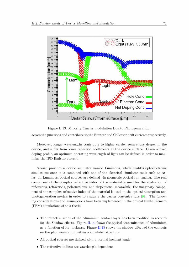
II.2. Fundamentals of Device Modelling and Simulation 71
Figure II.13: Minority Carrier modulation Due to Photogeneration.
across the junctions and contribute to the Emitter and Collector drift currents respectively.
Moreover, longer wavelengths contribute to higher carrier generations deeper in the
device, and suffer from lower reflection coefficients at the device surface. Given a fixed
doping profile, an optimum operating wavelength of light can be defined in order to max-
imize the IPD Emitter current.
Silvaco provides a device simulator named Luminous, which enables optoelectronic
simulations once it is combined with one of the electrical simulator tools such as At-
las. In Luminous, optical sources are defined via geometric optical ray tracing. The real
component of the complex refractive index of the material is used for the evaluation of
reflections, refractions, polarizations, and dispersions; meanwhile, the imaginary compo-
nent of the complex refractive index of the material is used in the optical absorption and
photogeneration models in order to evaluate the carrier concentrations [97]. The follow-
ing considerations and assumptions have been implemented in the optical Finite Element
(FEM) simulations of this thesis:
• The refractive index of the Aluminium contact layer has been modified to account
for the Shadow effects. Figure II.14 shows the optical transmittance of Aluminium
as a function of its thickness. Figure II.15 shows the shadow effect of the contacts
on the photogeneration within a simulated structure.
• All optical sources are defined with a normal incident angle
• The refractive indices are wavelength dependent
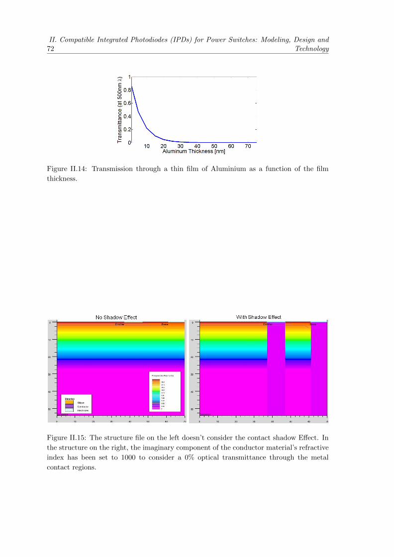
72II. Compatible Integrated Photodiodes (IPDs) for Power Switches: Modeling, Design and
Technology
Figure II.14: Transmission through a thin film of Aluminium as a function of the film
thickness.
Figure II.15: The structure file on the left doesn’t consider the contact shadow Effect. In
the structure on the right, the imaginary component of the conductor material’s refractive
index has been set to 1000 to consider a 0% optical transmittance through the metal
contact regions.
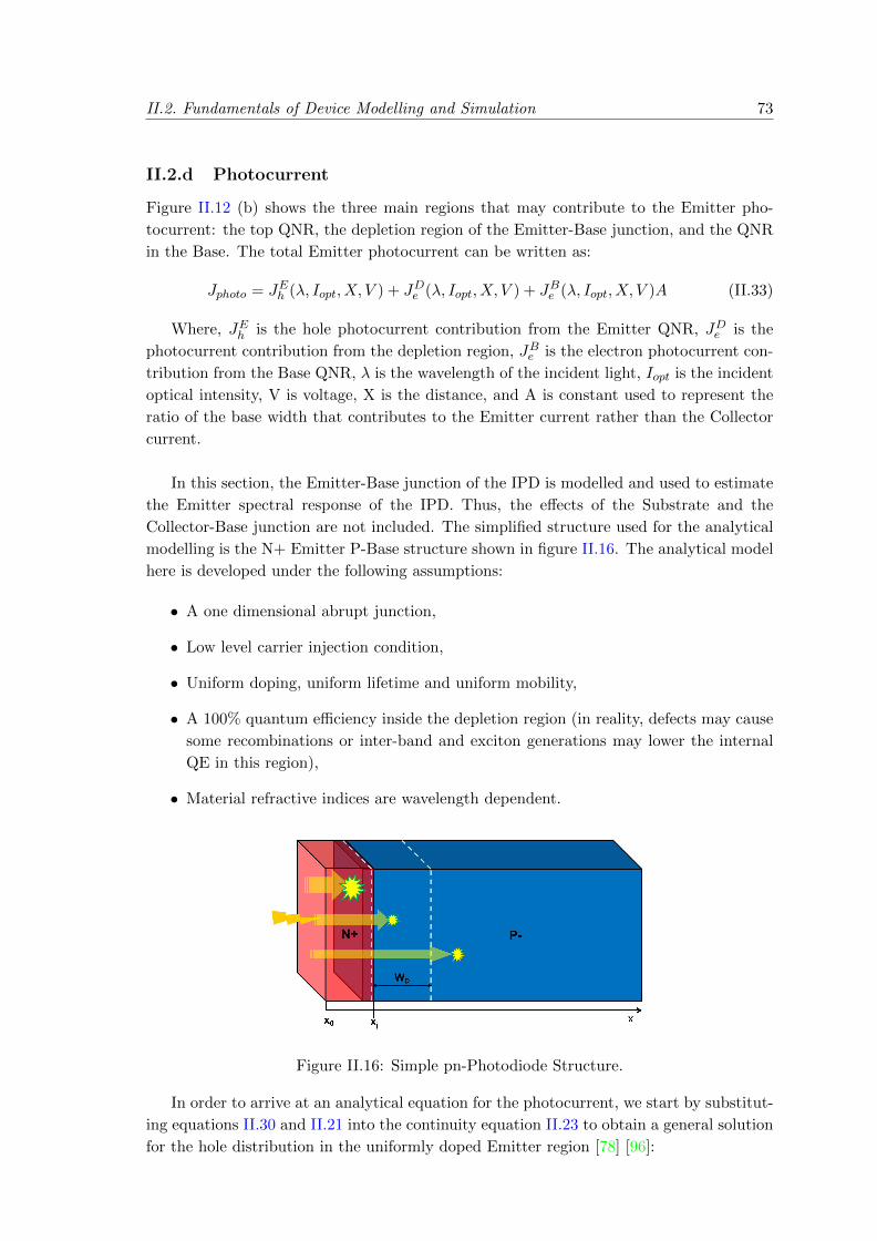
II.2. Fundamentals of Device Modelling and Simulation 73
II.2.d Photocurrent
Figure II.12 (b) shows the three main regions that may contribute to the Emitter pho-
tocurrent: the top QNR, the depletion region of the Emitter-Base junction, and the QNR
in the Base. The total Emitter photocurrent can be written as:
Jphoto = JEh (λ, Iopt, X, V ) + JDe (λ, Iopt, X, V ) + JBe (λ, Iopt, X, V )A (II.33)
Where, JEh is the hole photocurrent contribution from the Emitter QNR, JDe is the
photocurrent contribution from the depletion region, JBe is the electron photocurrent con-
tribution from the Base QNR, λ is the wavelength of the incident light, Iopt is the incident
optical intensity, V is voltage, X is the distance, and A is constant used to represent the
ratio of the base width that contributes to the Emitter current rather than the Collector
current.
In this section, the Emitter-Base junction of the IPD is modelled and used to estimate
the Emitter spectral response of the IPD. Thus, the effects of the Substrate and the
Collector-Base junction are not included. The simplified structure used for the analytical
modelling is the N+ Emitter P-Base structure shown in figure II.16. The analytical model
here is developed under the following assumptions:
• A one dimensional abrupt junction,
• Low level carrier injection condition,
• Uniform doping, uniform lifetime and uniform mobility,
• A 100% quantum efficiency inside the depletion region (in reality, defects may cause
some recombinations or inter-band and exciton generations may lower the internal
QE in this region),
• Material refractive indices are wavelength dependent.
Figure II.16: Simple pn-Photodiode Structure.
In order to arrive at an analytical equation for the photocurrent, we start by substitut-
ing equations II.30 and II.21 into the continuity equation II.23 to obtain a general solution
for the hole distribution in the uniformly doped Emitter region [78] [96]:

74II. Compatible Integrated Photodiodes (IPDs) for Power Switches: Modeling, Design and
Technology
pn − pn0 = C2 · cosh(x
Lp) + C3 · sinh(
x
Lp)− αφ(1−R)τp
α2L2p − 1
e(−αx) (II.34)
where Lp =√Dpτp is the minority carrier diffusion length, and C2 and C3 are con-
stants.
Considering that the excess carrier density near the edge of the depletion region at
X = Xj is almost entirely swept away by the electric field [78] [96]:
pn − pn0 ≈ 0 (II.35)
and that at the surface of the device, the carriers are removed via surface recombina-
tions at a velocity of SF [78] [96]:
Dpdp
dx|x=0 = SF (p(0)− p0) (II.36)
Solving for C2 and C3 using the boundary conditions of equations II.36 and II.35, the
hole photocurrent density at the edge of the depletion region on the Emitter side is [78]
[96]
JEh = [qφ(1−R)αLpα2L2
p − 1][
(SFLp
Dp+ αLp)− e(−αxj)[SFLp
Dpcosh(
xjLp
) + sinh(xjLp
)]
(SFLp/Dp)sin(xj/Lp) + cosh(xj/Lp)]− αLpe(−αxj)
(II.37)
The electron photocurrent from the Base region given by equation II.40, is evaluated
in a similar fashion to that described for the electron photocurrent in the Emitter using
the boundary conditions II.38 and II.39 [78] [96]:
np − np0|xj+WD≈ 0 (II.38)
(Dpdn
dx)|x=H = SB(n(0)− n0) (II.39)
JBe = [qφ(1−R)αLnα2L2
n − 1]e(−α(xj+WD))[αLn−
(SBLn
Dn)[cosh( HLn
)− e(−αH)] + sinh( HLn) + αLne
(−αH)
(SBLn/Dn)sinh(H/Ln) + cosh(H/Ln)]
(II.40)
Where H is the width of the Base region contributing to the Emitter current.
Due to the large built in electric field present in the depletion region, it is reasonable to
assume that the generated carriers are separated and swept away before having the chance
to recombine within the Emitter-Base depletion region. Thus, all the absorbed photons
contribute to the space charge drift photocurrent and the electron continuity equation can
be reduced to [96]:
1
q
JDedx
+Gop = 0 (II.41)
Using the depletion region approximation to solve for the depletion region width WD,
and integrating over Xj < X < (Xj +WD) the drift photocurrent is [96]:

II.2. Fundamentals of Device Modelling and Simulation 75
JDe = qφ(λ)[1−R(λ)]e−α(λ)xj [1− e−α(λ)WD ] (II.42)
Although equation II.42 is written for the electron photocurrent, it should be noted
that the photocurrent could be evaluated for the electrons or holes as per the explanation
given above.
We will apply this model to the Emitter-Base junction of figure II.16 with ND = 1× 10²⁰,
a 4 µm thick Base layer NA = 5 × 10¹⁶ and the junction position at Xj = 1µm. Figure
II.17 depicts the current-voltage characteristics of the different photocurrent components
from the different regions of the photodiode. The accuracy of the model is verified through
comparison with numerical results from Atlas as shown in figure II.18.
Figure II.17: Analytical modelling of the different current components in a 1D-uniformly
doped pn-junction photodiode. An Air-Silicon interface is considered.
Figure II.18: Analytical modelling of photocurrent(Iopt, V, λ) in a 1D-uniformly doped
pn-junction photodiode. An Air-Silicon interface is considered.
As it was introduced in Chapter 1, the quantum efficiency QE metric is used to express
the number of carriers per photon [78],
η(λ) =Iph(λ)
qΦ(λ)=AJtot(λ)/q
Popt(λ)/hν(II.43)

76II. Compatible Integrated Photodiodes (IPDs) for Power Switches: Modeling, Design and
Technology
where Iph is the photocurrent, Φ is the photon flux, Jtot is the total photocurrent
density including drift and diffusion currents, and Popt is the average optical signal power.
Equation II.44 gives the externally observed QE; dividing Iph by qΦ(λ)[1 − R(λ)], where
R(λ) represents the reflection coefficient, gives the internal QE. The ideal internal QE is
a step function that is equal to one for hν ≥ Eg and zero for hν ≤ Eg. Another metric
used for evaluating the sensitivity of a detector in reference to the optical power is the
responsivity [78],
<(λ) =Iph(λ)
Popt(λ)=η(λ)q
hν=η(λ)λ(µm)
1.24[A/W ] (II.44)
The QE and Responsivity corresponding to the photocurrent spectral response of figure
II.18 are shown in figure II.19.
Figure II.19: QE and Responsivity spectrum of a 1D-uniformly doped pn-junction photo-
diode when illuminated by a 1 µW uniform optical source.
II.3 Anti-reflection Coating
When a photodetector is illuminated by a light source, not all of the incident light intensity
have the chance to be absorbed by the photodetector. There are two main sources of optical
losses in photodetectors:
1. Material: The photodetector optical absorption efficiency is dependent on the mate-
rial absorption coefficient which is mathematically expressed as the imaginary part
of the refractive index of a material. Furthermore, the absorption coefficient is a
function of wavelength and the maximum wavelength of light absorb-able by a ma-
terial is given by the material’s bandgap. Any optical energy that is not absorbed
by the material contributes to the optical losses.
2. Reflections: Optical losses due to reflections may be divided into two categories.
(1) Losses from reflections at the air to Silicon interface, (2) and losses from any
unwanted absorptions in the contacts and/or reflections at the air to metal contact
interface also known as shading losses. Shading losses are considered when discussing
the contact design.
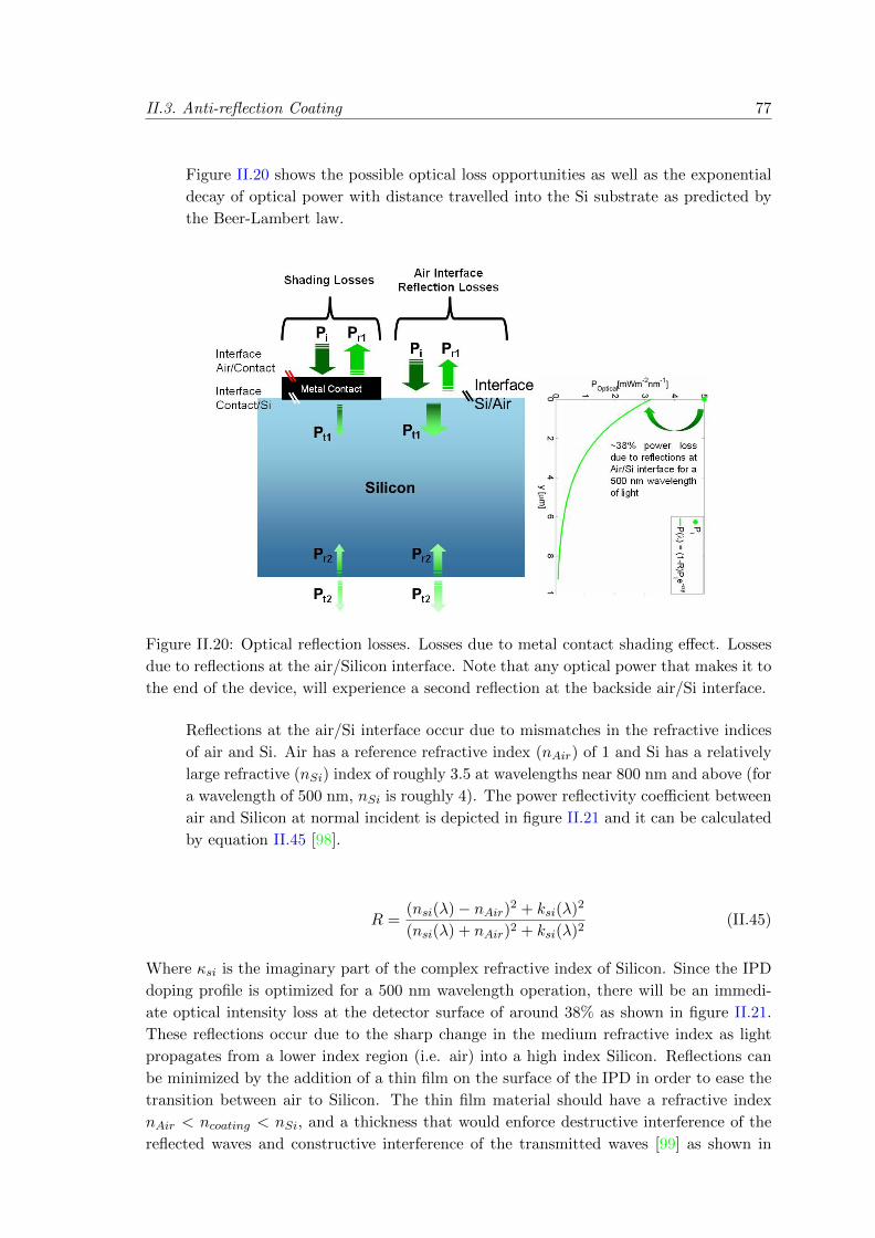
II.3. Anti-reflection Coating 77
Figure II.20 shows the possible optical loss opportunities as well as the exponential
decay of optical power with distance travelled into the Si substrate as predicted by
the Beer-Lambert law.
Figure II.20: Optical reflection losses. Losses due to metal contact shading effect. Losses
due to reflections at the air/Silicon interface. Note that any optical power that makes it to
the end of the device, will experience a second reflection at the backside air/Si interface.
Reflections at the air/Si interface occur due to mismatches in the refractive indices
of air and Si. Air has a reference refractive index (nAir) of 1 and Si has a relatively
large refractive (nSi) index of roughly 3.5 at wavelengths near 800 nm and above (for
a wavelength of 500 nm, nSi is roughly 4). The power reflectivity coefficient between
air and Silicon at normal incident is depicted in figure II.21 and it can be calculated
by equation II.45 [98].
R =(nsi(λ)− nAir)2 + ksi(λ)2
(nsi(λ) + nAir)2 + ksi(λ)2(II.45)
Where κsi is the imaginary part of the complex refractive index of Silicon. Since the IPD
doping profile is optimized for a 500 nm wavelength operation, there will be an immedi-
ate optical intensity loss at the detector surface of around 38% as shown in figure II.21.
These reflections occur due to the sharp change in the medium refractive index as light
propagates from a lower index region (i.e. air) into a high index Silicon. Reflections can
be minimized by the addition of a thin film on the surface of the IPD in order to ease the
transition between air to Silicon. The thin film material should have a refractive index
nAir < ncoating < nSi, and a thickness that would enforce destructive interference of the
reflected waves and constructive interference of the transmitted waves [99] as shown in

78II. Compatible Integrated Photodiodes (IPDs) for Power Switches: Modeling, Design and
Technology
figure II.22(a).
Figure II.21: Power Reflectivity Coefficient for Si/air Interface.
Figure II.22: (a) The thin film refractive index and thickness conditions required for ARC.
(b) the matching case of the refractive index of Si3N4 with that of an ideal ARC for Silicon.
For a thin dielectric film with thickness of no more than a few hundreds of nanometres,
it can be assumed that absorption is negligible (lossless media). At normal incidence,
the interface amplitude reflection coefficient of a thin film with a refractive index n2 and
thickness d2 sandwiched between air n1 and Silicon n3, is given by the Fresnel reflection
coefficient [99]
r =[n1−n2n1+n2
] + [n2−n3n2+n3
]e−i2φ
1 + [n1−n2n1+n2
] + [n2−n3n2+n3
]e−i2φ(II.46)
where the phase is φ = 2·π·n2·d2/λ. The reflection coefficient goes to zero when [99]

II.3. Anti-reflection Coating 79
r = [n1 − n2n1 + n2
] + [n2 − n3n2 + n3
]e−i2φ = 0 (II.47)
This zero condition is satisfied for [99]
n2 =√n1n3 and φ = π/2, 3π/2, 5π/2, 7π/2... (II.48)
A material with refractive index spectrum of n2 as shown in figure II.22(b), represents
an ideal ARC layer that would suppress reflections at any wavelength when designed with
an appropriate thickness. The refractive index of Si3N4 plotted in red in figure II.22(b),
reveals a close proximity to the ideal n2 specially for wavelengths above 450 nm (at 548
nm there is an exact match). At 500 nm, the refractive index of Si3N4 is roughly 1.8%
lower than that of n2; however, the refractive index of Si3N4 may vary due to the quality
of fabrication and so the values shown in figure II.22(b) maybe slightly different from case
to case. By adding a single Si3N4 ARC layer with an optimized thickness for the 500 nm
wavelength application, reflections of a single wavelength (500 nm in this case) can be
nearly eliminated. In a more complex approach, a multi-cavity etalon can be created by
stacking different ARC materials to eliminate reflections at different wavelengths. In solar
cell designs, the amount of light coupled-in can be enhanced further by texturing the front
surface of the solar cell as shown in the schematic of figure II.23. In this project, the IPDs
will have a single layer of Si3N4 ARC with a uniform thickness.
Figure II.23: Schematic of the solar cell structure for a Si cell with a 24.7% world-record
efficiency, via J.Zhao et al [100].
The phase condition in equation II.48 indicates that a thin film with a refractive index
of n2 and a thickness of a quarter-wave will result in zero reflections of the wave. Plugging
n2 in to φ for λ=500 nm results in a minimum ARC thickness requirement of around 61
nm. Periodic solutions for the ARC thickness exists for every half-wave increments in the
phase. Figure II.24 shows how the reflectance coefficient moves between a minimum when
the waves destructively interfere, and a maximum when the waves constructively interfere.
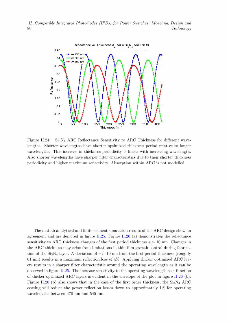
80II. Compatible Integrated Photodiodes (IPDs) for Power Switches: Modeling, Design and
Technology
Figure II.24: Si3N4 ARC Reflectance Sensitivity to ARC Thickness for different wave-
lengths. Shorter wavelengths have shorter optimized thickness period relative to longer
wavelengths. This increase in thickness periodicity is linear with increasing wavelength.
Also shorter wavelengths have sharper filter characteristics due to their shorter thickness
periodicity and higher maximum reflectivity. Absorption within ARC is not modelled.
The matlab analytical and finite element simulation results of the ARC design show an
agreement and are depicted in figure II.25. Figure II.26 (a) demonstrates the reflectance
sensitivity to ARC thickness changes of the first period thickness +/- 10 nm. Changes in
the ARC thickness may arise from limitations in thin film growth control during fabrica-
tion of the Si3N4 layer. A deviation of +/- 10 nm from the first period thickness (roughly
61 nm) results in a maximum reflection loss of 4%. Applying thicker optimized ARC lay-
ers results in a sharper filter characteristic around the operating wavelength as it can be
observed in figure II.25. The increase sensitivity to the operating wavelength as a function
of thicker optimized ARC layers is evident in the envelope of the plot in figure II.26 (b).
Figure II.26 (b) also shows that in the case of the first order thickness, the Si3N4 ARC
coating will reduce the power reflection losses down to approximately 1% for operating
wavelengths between 470 nm and 545 nm.
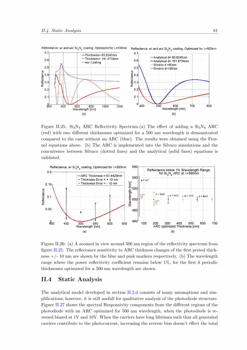
II.4. Static Analysis 81
Figure II.25: Si3N4 ARC Reflectivity Spectrum.(a) The effect of adding a Si3N4 ARC
(red) with two different thicknesses optimized for a 500 nm wavelength is demonstrated
compared to the case without an ARC (blue). The results were obtained using the Fres-
nel equations above. (b) The ARC is implemented into the Silvaco simulations and the
concurrence between Silvaco (dotted lines) and the analytical (solid lines) equations is
validated.
Figure II.26: (a) A zoomed in view around 500 nm region of the reflectivity spectrum from
figure II.25. The reflectance sensitivity to ARC thickness changes of the first period thick-
ness +/- 10 nm are shown by the blue and pink markers respectively. (b) The wavelength
range where the power reflectivity coefficient remains below 1%, for the first 6 periodic
thicknesses optimized for a 500 nm wavelength are shown.
II.4 Static Analysis
The analytical model developed in section II.2.d consists of many assumptions and sim-
plifications; however, it is still usefull for qualitative analysis of the photodiode structure.
Figure II.27 shows the spectral Responsivity components from the different regions of the
photodiode with an ARC optimized for 500 nm wavelength, when the photodiode is re-
versed biased at 1V and 10V. When the carriers have long lifetimes such that all generated
carriers contribute to the photocurrent, increasing the reverse bias doesn’t effect the total
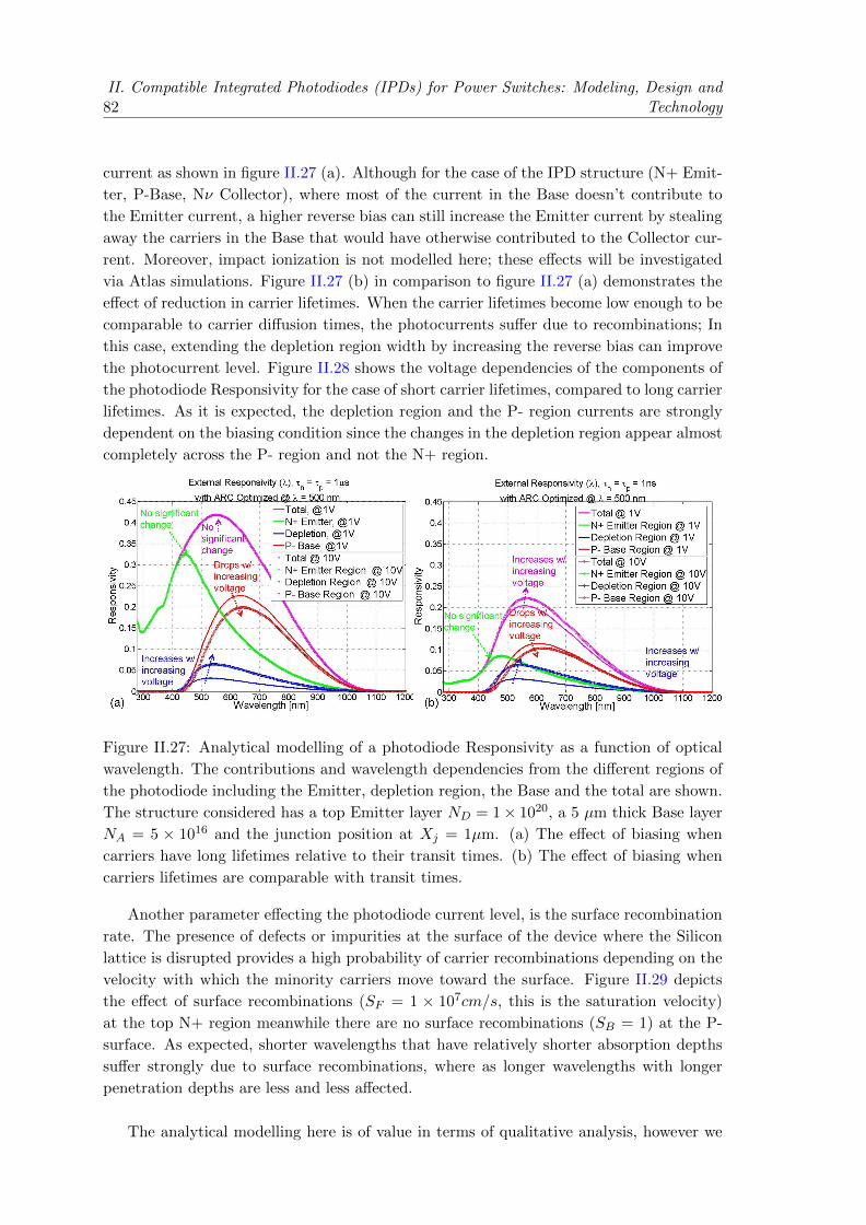
82II. Compatible Integrated Photodiodes (IPDs) for Power Switches: Modeling, Design and
Technology
current as shown in figure II.27 (a). Although for the case of the IPD structure (N+ Emit-
ter, P-Base, Nν Collector), where most of the current in the Base doesn’t contribute to
the Emitter current, a higher reverse bias can still increase the Emitter current by stealing
away the carriers in the Base that would have otherwise contributed to the Collector cur-
rent. Moreover, impact ionization is not modelled here; these effects will be investigated
via Atlas simulations. Figure II.27 (b) in comparison to figure II.27 (a) demonstrates the
effect of reduction in carrier lifetimes. When the carrier lifetimes become low enough to be
comparable to carrier diffusion times, the photocurrents suffer due to recombinations; In
this case, extending the depletion region width by increasing the reverse bias can improve
the photocurrent level. Figure II.28 shows the voltage dependencies of the components of
the photodiode Responsivity for the case of short carrier lifetimes, compared to long carrier
lifetimes. As it is expected, the depletion region and the P- region currents are strongly
dependent on the biasing condition since the changes in the depletion region appear almost
completely across the P- region and not the N+ region.
Figure II.27: Analytical modelling of a photodiode Responsivity as a function of optical
wavelength. The contributions and wavelength dependencies from the different regions of
the photodiode including the Emitter, depletion region, the Base and the total are shown.
The structure considered has a top Emitter layer ND = 1× 10²⁰, a 5 µm thick Base layer
NA = 5 × 10¹⁶ and the junction position at Xj = 1µm. (a) The effect of biasing when
carriers have long lifetimes relative to their transit times. (b) The effect of biasing when
carriers lifetimes are comparable with transit times.
Another parameter effecting the photodiode current level, is the surface recombination
rate. The presence of defects or impurities at the surface of the device where the Silicon
lattice is disrupted provides a high probability of carrier recombinations depending on the
velocity with which the minority carriers move toward the surface. Figure II.29 depicts
the effect of surface recombinations (SF = 1 × 107cm/s, this is the saturation velocity)
at the top N+ region meanwhile there are no surface recombinations (SB = 1) at the P-
surface. As expected, shorter wavelengths that have relatively shorter absorption depths
suffer strongly due to surface recombinations, where as longer wavelengths with longer
penetration depths are less and less affected.
The analytical modelling here is of value in terms of qualitative analysis, however we

II.4. Static Analysis 83
Figure II.28: Analytical modelling of the responsivity contributions from the different
regions of the photodiode including the Emitter, depletion region, and the Base as a
function of dependencies on biasing and carrier lifetimes. The structure considered has a
top Emitter layer NA = 5× 10¹⁶, a 5 µm thick Base layer ND = 1× 10²⁰ and the junction
position at Xj = 1µm. The effect of biasing when carriers have long or short lifetimes is
illustrated.
will continue by means of numerical simulations in order to better capture the complexity
of the design and to shed more light on the following problems:
• A more complex model to include the effects of Shockley-Read-hall transitions, Auger
recombination, band-gap narrowing, impact ionization, carrier mobilities dependence
on doping concentration and electric field levels
• 2D and 3D effects
• Gaussian doping Profiles
• The effects of the substrate DC and Transient voltages
• The effect of resistances in the neutral regions
• The effects of applied voltages on the Responsivity and Bandwidth
• The effects of light intensity on the Responsivity and Bandwidth
• The effect of carrier lifetimes on the Responsivity and Bandwidth
• The inherent parasitic bipolar effects
The schematic view of the IPD structure in figure II.30 depicts the two different pho-
tocurrents that can be measured when the IPD structure is exposed to light with energy
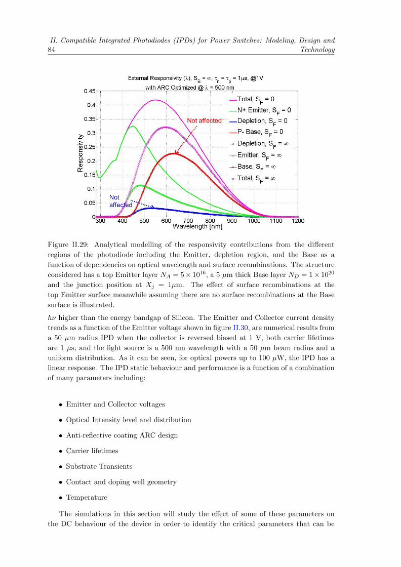
84II. Compatible Integrated Photodiodes (IPDs) for Power Switches: Modeling, Design and
Technology
Figure II.29: Analytical modelling of the responsivity contributions from the different
regions of the photodiode including the Emitter, depletion region, and the Base as a
function of dependencies on optical wavelength and surface recombinations. The structure
considered has a top Emitter layer NA = 5× 10¹⁶, a 5 µm thick Base layer ND = 1× 10²⁰
and the junction position at Xj = 1µm. The effect of surface recombinations at the
top Emitter surface meanwhile assuming there are no surface recombinations at the Base
surface is illustrated.
hν higher than the energy bandgap of Silicon. The Emitter and Collector current density
trends as a function of the Emitter voltage shown in figure II.30, are numerical results from
a 50 µm radius IPD when the collector is reversed biased at 1 V, both carrier lifetimes
are 1 µs, and the light source is a 500 nm wavelength with a 50 µm beam radius and a
uniform distribution. As it can be seen, for optical powers up to 100 µW, the IPD has a
linear response. The IPD static behaviour and performance is a function of a combination
of many parameters including:
• Emitter and Collector voltages
• Optical Intensity level and distribution
• Anti-reflective coating ARC design
• Carrier lifetimes
• Substrate Transients
• Contact and doping well geometry
• Temperature
The simulations in this section will study the effect of some of these parameters on
the DC behaviour of the device in order to identify the critical parameters that can be
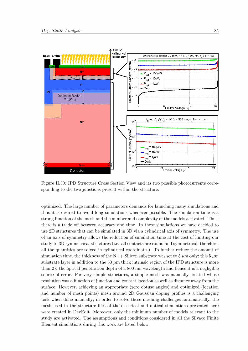
II.4. Static Analysis 85
Figure II.30: IPD Structure Cross Section View and its two possible photocurrents corre-
sponding to the two junctions present within the structure.
optimized. The large number of parameters demands for launching many simulations and
thus it is desired to avoid long simulations whenever possible. The simulation time is a
strong function of the mesh and the number and complexity of the models activated. Thus,
there is a trade off between accuracy and time. In these simulations we have decided to
use 2D structures that can be simulated in 3D via a cylindrical axis of symmetry. The use
of an axis of symmetry allows the reduction of simulation time at the cost of limiting our
study to 3D symmetrical structures (i.e. all contacts are round and symmetrical, therefore,
all the quantities are solved in cylindrical coordinates). To further reduce the amount of
simulation time, the thickness of the N++ Silicon substrate was set to 5 µm only; this 5 µm
substrate layer in addition to the 50 µm thick intrinsic region of the IPD structure is more
than 2× the optical penetration depth of a 800 nm wavelength and hence it is a negligible
source of error. For very simple structures, a simple mesh was manually created whose
resolution was a function of junction and contact location as well as distance away from the
surface. However, achieving an appropriate (zero obtuse angles) and optimized (location
and number of mesh points) mesh around 2D Gaussian doping profiles is a challenging
task when done manually; in order to solve these meshing challenges automatically, the
mesh used in the structure files of the electrical and optical simulations presented here
were created in DevEdit. Moreover, only the minimum number of models relevant to the
study are activated. The assumptions and conditions considered in all the Silvaco Finite
Element simulations during this work are listed below:

86II. Compatible Integrated Photodiodes (IPDs) for Power Switches: Modeling, Design and
Technology
• Gaussian fitted doping profiles as depicted in the GFDP curve of figure II.8 (a).
• Models activated: Shockley-Read-hall, Auger recombination, band-gap narrowing,
impact ionization (Grant), concentration and field dependent mobilities
• The refractive index of Aluminium contact layers have been modified to account for
the Shadow effects
• All optical sources are defined with a normal incident angle
• The refractive indices are wavelength dependent
• Constant carrier lifetimes
• Temperature = 300 K
II.4.a DC Emitter and Collector biasing
Figure II.31 and II.32 show the Emitter JE and the Collector JC dark current densities
as a function of the Emitter and the Collector reverse voltages respectively with carrier
lifetimes of 1 µs.
Figure II.31: Dark current voltage characteristics for a 50 µm IPD as modelled in Silvaco
with the carrier lifetimes set to 1 µs and having activated the Grant model in order
to represent the effect of avalanche ionization. The Emitter and Collector dark current
densities as a function of VE for a Gaussian-fitted doping profile are shown on the left, and
the current values are shown on the right.
As observed, when the two junctions are reversed biased, one junction’s dark current
is not a function of the other junction. The Emitter junction breakdown is around 15 V
and its dark current density is in the range of 15 nA/cm2 to 150 nA/cm2 for an Emitter
voltage range of 1 V to 14 V. The Collector junction breakdown is around 650 V and its
dark current density is in the range of 350 nA/cm2 at 1 V reverse bias, to 10 µA/cm2 at
600 V reverse bias at room temperature. These dark currents set the minimum detectable
photocurrent level which in turn determine the minimum optical intensity required for
an IPD responsivity. The junction dark current densities are a function of the diffusion
currents given in equations II.26 and II.27, and the generation current of equation II.28 all

II.4. Static Analysis 87
Figure II.32: Dark Current Voltage Characteristics for a 50 µm IPD as modelled in Silvaco
with the carrier lifetimes set to 1 µs and having activated the Grant model in order
to represent the effect of avalanche ionization. The Emitter and Collector dark current
densities as a function of VC for a Gaussian-fitted doping profile are shown on the left, and
the current values are shown on the right.
which are functions of temperature. The diffusion current has an exponential dependence
on temperature but since ni is not too large for the case of Si, the generation current
may dominate at room temperatures. The diffusion current may however dominate with
increasing temperatures. Thus, the noise floor will increase approximately as e(−Eg/(kT ))
with temperature, where Eg is the energy bandgap of Si [78]. In order to minimize the
dark current levels, IPDs with smaller Emitter junction cross sectional areas and enhanced
responsivities are preferred.
Another issue concerning the Emitter and Collector dark current levels is the resistive
IR drops in the Base region. Current flowing through the Base modifies local voltage levels
due to the resistances along its path. Since the current flowing through the Base is the
sum of the Emitter and Collector dark and photogenerated currents, lower dark current
levels allow higher photocurrent levels for a giving Base resistance.
Figure II.33 (a) shows the optical spectral response of the different currents flowing
through the structure. This result is in agreement with the discussion in section II.2.c.
The Emitter photocurrent is maximized for optical wavelengths around 500 nm, meanwhile
the Collector photocurrent is maximized for optical wavelengths around 850 nm. Figure
II.33 (b), shows the QEs of the IPD corresponding to the currents of figure II.33 (a). In
these simulations, an optical beam width equal to the exposed photo-sensitive area of the
Emitter region is used in order to show the maximum efficiency achievable without contact
shadow losses.
Figure II.33 (c) shows the responsivities for the case of 100% QE in red and after
reflection losses in green as well as the internal and external responsivities of the IPD
(Emitter) in blue and black respectively. As it can be seen, the IPD responsivity departs
substantially from the ideal case. The external responsivities from the different regions of
the structure are shown in figure II.33 (d).
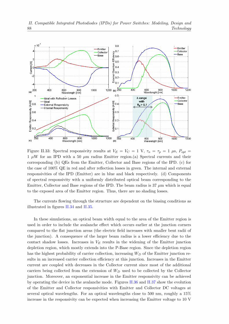
88II. Compatible Integrated Photodiodes (IPDs) for Power Switches: Modeling, Design and
Technology
Figure II.33: Spectral responsivity results at VE = VC = 1 V, τn = τp = 1 µs, Popt =
1 µW for an IPD with a 50 µm radius Emitter region.(a) Spectral currents and their
corresponding (b) QEs from the Emitter, Collector and Base regions of the IPD. (c) for
the case of 100% QE in red and after reflection losses in green. The internal and external
responsivities of the IPD (Emitter) are in blue and black respectively. (d) Components
of spectral responsivity with a uniformly distributed optical beam corresponding to the
Emitter, Collector and Base regions of the IPD. The beam radius is 37 µm which is equal
to the exposed area of the Emitter region. Thus, there are no shading losses.
The currents flowing through the structure are dependent on the biasing conditions as
illustrated in figures II.34 and II.35.
In these simulations, an optical beam width equal to the area of the Emitter region is
used in order to include the avalanche effect which occurs earlier at the junction corners
compared to the flat junction areas (the electric field increases with smaller bent radii of
the junction). A consequence of the larger beam radius is a lower efficiency due to the
contact shadow losses. Increases in VE results in the widening of the Emitter junction
depletion region, which mostly extends into the P-Base region. Since the depletion region
has the highest probability of carrier collection, increasing WD of the Emitter junction re-
sults in an increased carrier collection efficiency at this junction. Increases in the Emitter
current are coupled with decreases in the Collector current since most of the additional
carriers being collected from the extension of WD used to be collected by the Collector
junction. Moreover, an exponential increase in the Emitter responsivity can be achieved
by operating the device in the avalanche mode. Figures II.36 and II.37 show the evolution
of the Emitter and Collector responsivities with Emitter and Collector DC voltages at
several optical wavelengths. For an optical wavelengths close to 500 nm, roughly a 15%
increase in the responsivity can be expected when increasing the Emitter voltage to 10 V

II.4. Static Analysis 89
Figure II.34: Emitter and Collector responsivities as a function of VE with the Collector
reversed biased at 1 V, and 1 µs carrier lifetimes. The optical source has a 51 µm beam
radius and the Emitter radius is 50 µm.
Figure II.35: Emitter and Collector responsivities as a function of Collector voltage with
the Emitter reversed biased at 1 V, and 1 µs carrier lifetimes. The optical source has a 51
µm beam radius and the Emitter radius is 50 µm.
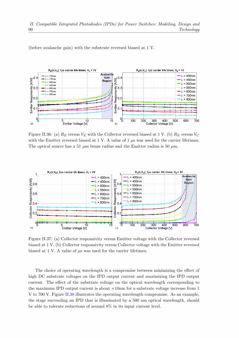
90II. Compatible Integrated Photodiodes (IPDs) for Power Switches: Modeling, Design and
Technology
(before avalanche gain) with the substrate reversed biased at 1 V.
Figure II.36: (a) RE versus VE with the Collector reversed biased at 1 V. (b) RE versus VCwith the Emitter reversed biased at 1 V. A value of 1 µs was used for the carrier lifetimes.
The optical source has a 51 µm beam radius and the Emitter radius is 50 µm.
Figure II.37: (a) Collector responsivity versus Emitter voltage with the Collector reversed
biased at 1 V. (b) Collector responsivity versus Collector voltage with the Emitter reversed
biased at 1 V. A value of µs was used for the carrier lifetimes.
The choice of operating wavelength is a compromise between minimizing the effect of
high DC substrate voltages on the IPD output current and maximizing the IPD output
current. The effect of the substrate voltage on the optical wavelength corresponding to
the maximum IPD output current is about +10nm for a substrate voltage increase from 1
V to 700 V. Figure II.38 illustrates the operating wavelength compromise. As an example,
the stage succeeding an IPD that is illuminated by a 500 nm optical wavelength, should
be able to tolerate reductions of around 8% in its input current level.

II.4. Static Analysis 91
Figure II.38: The effect of Collector voltages on the Emitter as a function of optical
wavelength. The range of wavelengths affected by the high DC substrate voltages depends
on the carrier lifetimes. Wavelengths with higher photogeneration rates within the Base
region have a stronger dependence on the substrate voltages. The green line defined as, %R,
represents the percent decrease in the Emitter spectral responsivity when the substrate
DC reverse voltage level is at 700V relative to when it is at 0V.
II.4.b Sensitivity to Carrier Lifetimes
The method used to fabricate a Silicon wafer and the photodetector processing have a
critical impact on the defect concentration levels within the material. The rate of SRH
recombination is contingent upon the number of defects present within the Silicon wafer
and moreover, it increases with higher doping levels [101]. Auger recombination is also
more likely in heavily doped material. The overall effect of the different recombination
processes within the device are reflected in the minority carrier diffusion length and the
minority carrier lifetime parameters. Thus, the minority carrier lifetime plays a key role
in the efficiency of the photodetector.
A number of simulations invoking the SRH and Auger recombination processes were
performed when the device is illuminated in steady state conditions using a number of dif-
ferent fixed carrier lifetimes. In order to decouple the effect of electron and hole lifetimes
on the device efficiency, when varying one carrier lifetime the other was kept constant at
1µs. The IPD structure shown in figure II.39 (a) shows the different regions of the device
where recombination occurs. The result of recombination rate gradient for minority (hole)
carrier lifetimes of 0.1 ns, 0.5 ns, 1ns, 5ns, 10ns, 50ns, 100ns, 500ns, and 1 µs, correspond-
ing to a vertical cut-line from the surface of the device to a depth of 1 µm is shown in
figure II.39 (b).
The effect of carrier lifetimes on the minority (holes) carrier concentration gradient and
hence the minority carrier the diffusion length is depicted in figure II.40. This decrease
in the minority diffusion length with shorter lifetime results in a lower number of carrier

92II. Compatible Integrated Photodiodes (IPDs) for Power Switches: Modeling, Design and
Technology
Figure II.39: (a) Recombination areas within the IPD structure where recombination
occurs are shown in red. Generation processes dominate within the depletion regions as
shown in purple. Note: A wide range of recombination rates have been saturated to the
zero recombination rate represented by the color red. (b) The effect of minority carrier
lifetime on the recombination rate corresponding to a vertical cut-line from the surface of
the device to a depth of 1 µm. The optical source has a uniform distribution and 1 µW of
power.
density reaching the junction and thus a reduced current density as shown in figure II.41.
This effect is more severe if the minority carriers have to travel longer distances before
being collected by the junction (i.e. a deep junction versus a shallow junction).
Figure II.40: Hole concentration gradient versus Carrier Lifetimes. Left: Emitter Region.
Right: Collector Region.
The Emitter and Collector responsivities of the IPD structure as a function of minority
carrier lifetimes are plotted in figure II.42 and II.43 respectively.
Minority carriers generated in shallower depths due to the absorption of shorter op-
tical wavelengths, have to travel longer distances relative to carriers generated by longer
wavelengths. Thus, the IPD Emitter efficiency is more sensitive to shorter lifetimes when
a short wavelength optical source is used. Since the diffusion currents in both the Emitter

II.4. Static Analysis 93
Figure II.41: Spectral Responsivity Sensitivity to Carrier Lifetimes. Left: Sensitivity to
the lifetime of holes. Right: Sensitivity to the lifetime of electrons.
Figure II.42: Emitter Current Sensitivity to Carrier Lifetimes. (a) Sensitivity to the
lifetime of holes. (b) Sensitivity to the lifetime of electrons.
Figure II.43: Collector Current Sensitivity to Carrier Lifetimes. (a) Sensitivity to the
lifetime of holes. (b) Sensitivity to the lifetime of electrons.

94II. Compatible Integrated Photodiodes (IPDs) for Power Switches: Modeling, Design and
Technology
and the Collector junction are almost entirely due to the diffusion of holes, the efficiency
of these two junctions are more coupled with the hole lifetime rather than the electron
lifetime. This result predicts that for structures with a lifetime shorter than 10 ns, the IPD
efficiency begins to suffer; the efficiency could be improved via using a shallower junction, a
wider depletion region, or having p-doped Emitter; however, as discussed earlier the doping
profile optimization is limited by the VD-MOSFET. The effect of the design constraints
on the IPD efficiency can be compensated by using high quality wafers with intrinsically
higher carrier lifetimes. In addition, long lifetimes can limit the frequency response of
a diffusion limited device; hence there is a compromise. In addition to the compromise
between efficiency and bandwidth of the IPD, the impact of lifetime on the body diode
and MOSFET should also be considered. Since MOSFETs are unipolar devices, in other
words there are no minority carriers, their performance is not much effected by the carrier
lifetimes. However the body diode is a bipolar device, in other words there are minority
and majority carriers flowing through the device; when switching this diode, the time re-
quired for the excess carrier density to diminish via recombination depends on the minority
carrier lifetimes which in turn determine the turn-off time of the device. Thus, the car-
rier lifetime optimization needs to consider both the IPD and the body diode requirements.
II.5 Dynamic Analysis
The speed of a photodiode can be limited due to one of the following factors:
• Long carrier transit times ttr: Carrier transit across the depletion region is a fast
process since carriers will be drifting at saturation velocities vsat [78] if the field is
high enough. Transit time across a depletion region with width WD is given by:
ttr =WD
vsat(II.49)
If the incident photons are all absorbed at the edge of the depletion region on the
N-type Emitter side, the response time will be limited by the saturation velocity of
the holes. In our IPD design, the depletion region width is rather thin specially at
low Emitter voltages. To approximate ttr, we can consider the maximum electric
field in the Emitter-Base depletion region at 1 V reverse bias from figure II.8 (b) to
be 5×10⁴V/cm, and the hole mobility of 50cm2/V.s from figure II.9 to calculate the
hole velocity of approximately 2.5 × 106cm/s. A depletion region of approximately
0.5 µm as estimated from figure II.8 (b), in combination with the calculated carrier
velocity results in a ttr of 0.2 ps which corresponds to a cut-off frequency above
hundreds of GHz. Hence, the IPD is most likely not transit limited.
• Long carrier diffusion times, td: If the incident photons are absorbed outside the
depletion region they will diffuse a distance x in a time given by [78]:
td =4x2
π2Dp(II.50)

II.5. Dynamic Analysis 95
Carrier diffusion is a much slower process compared to drift and can be as long as
the carrier lifetimes. The carrier lifetime limit can be observed in the long-tails of a
photodiode impulse response.
• The RC time constant, tRC : tRC includes series resistances (i.e. from the QNRs and
contacts) as well as junction capacitances of the photodiode equivalent circuit model.
The series resistance from the QNR is determined by the resistivity and the width
(with Emitter and Base top contacts, carriers move laterally between contacts) of
the region, and the distance between contacts. The junction capacitance is directly
proportional to the area of the diffused region (i.e. the Base), inversely proportional
to the width of the depletion region and also dependent on the reverse bias:
Cj =εSiε0A
WD(V )(II.51)
where εSi and ε0 are the relative permittivity of Silicon and the permittivity of free
space respectively, and V is the junction reverse bias. Figure II.44 shows the capac-
itance of the IPD versus reverse bias voltage as approximated by a uniformly doped
abrupt junction.
Figure II.44: IPD junction capacitances versus reverse voltage. The capacitance values
here are calculated based on the effective width of the depletion region and doesn’t consider
the sidewall contribution.
• The bandwidth limit imposed by the input impedance of the TIA stage,
• The RC limitations from packaging: This can be minimized by careful layout and
the use of short leads.
In the case of pin photodetector, the frequency response is transit limited. However, in
the case of our IPD since most of the active region of the device is not depleted, the device
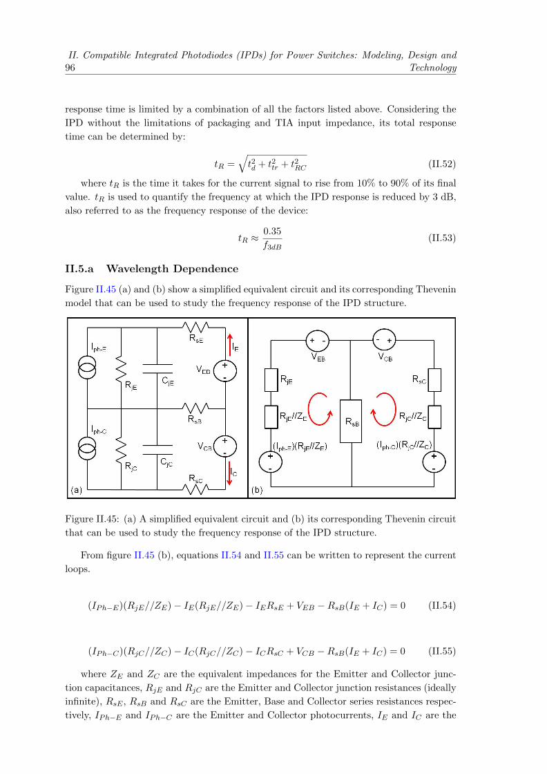
96II. Compatible Integrated Photodiodes (IPDs) for Power Switches: Modeling, Design and
Technology
response time is limited by a combination of all the factors listed above. Considering the
IPD without the limitations of packaging and TIA input impedance, its total response
time can be determined by:
tR =√t2d + t2tr + t2RC (II.52)
where tR is the time it takes for the current signal to rise from 10% to 90% of its final
value. tR is used to quantify the frequency at which the IPD response is reduced by 3 dB,
also referred to as the frequency response of the device:
tR ≈0.35
f3dB(II.53)
II.5.a Wavelength Dependence
Figure II.45 (a) and (b) show a simplified equivalent circuit and its corresponding Thevenin
model that can be used to study the frequency response of the IPD structure.
Figure II.45: (a) A simplified equivalent circuit and (b) its corresponding Thevenin circuit
that can be used to study the frequency response of the IPD structure.
From figure II.45 (b), equations II.54 and II.55 can be written to represent the current
loops.
(IPh−E)(RjE//ZE)− IE(RjE//ZE)− IERsE + VEB −RsB(IE + IC) = 0 (II.54)
(IPh−C)(RjC//ZC)− IC(RjC//ZC)− ICRsC + VCB −RsB(IE + IC) = 0 (II.55)
where ZE and ZC are the equivalent impedances for the Emitter and Collector junc-
tion capacitances, RjE and RjC are the Emitter and Collector junction resistances (ideally
infinite), RsE , RsB and RsC are the Emitter, Base and Collector series resistances respec-
tively, IPh−E and IPh−C are the Emitter and Collector photocurrents, IE and IC are the

II.5. Dynamic Analysis 97
output current responses from the IPD. Noise is not considered here. Considering DC bias
conditions, VCB and VCB can be omitted from equation II.54 and II.55. IE and IC can
then be written as:
IE =(IPh−E)(RjE//ZE)−RsBIC
(RjE//ZE) +RsE +RsB(II.56)
IC =(IPh−C)(RjC//ZC)−RsBIE
(RjC//ZC) +RsC +RsB(II.57)
Substituting equation II.57 into equation II.56 gives:
IE =
(IPh−E)(RjE//ZE)(RjE//ZE)+RsE+RsB
− (IPh−C)(RjC//ZC)RsB
[(RjC//ZC)+RsC+RsB ][(RjE//ZE)+RsE+RsB ]
1− R2sB
[(RjC//ZC)+RsC+RsB ][(RjE//ZE)+RsE+RsB ]
(II.58)
The result of equation II.58 shows that the dynamic response of IE is a function of the
Collector parameters. Using the result of equation II.58, the high frequency behaviour of
the IPD structure is modelled in matlab bode plots as shown in figure II.46.
Figure II.46: Bode plot of the IPD frequency response according to equation II.58 where,
RjE = RjC = 100 MΩ, RsE = 0.5 Ω, RsB = 10 Ω, RsC = 30 Ω, CjE = 30 pF, CjC = 8
pF.
In these plots, IPh−C is taken to be 0.1, 0.5, 1, 2, 4, and 6 times the value of IPh−E .
The ratio of IPh−C to IPh−E represents the operating wavelength; this ratio is lower for
shorter wavelengths where the Emitter has a high efficiency relative to the Collector, and
the ratio grows for longer wavelengths where the Collector efficiency dominates over that
of the Emitter as depicted in figure II.47. The frequency response is investigated further
via numerical simulations in Atlas for our specific IPD structure and the results for an
optical wavelength of 500 nm are shown in figure II.48. The Emitter and Collector current
responses and gain-frequency plots for optical wavelengths of 400 nm, 450 nm, 500 nm,

98II. Compatible Integrated Photodiodes (IPDs) for Power Switches: Modeling, Design and
Technology
Figure II.47: Collector to Emitter photocurrent ratio.
550 nm, 600 nm, 650 nm, 700 nm, 750 nm, and 800 nm are depicted in figures II.49 and
II.50.
Figure II.48: IPD frequency response at 500 nm optical wavelength as evaluated by numer-
ical analysis in Atlas. Left: Current levels including the small signal response plus the DC
levels. Right: Normalized gain as defined by 20·log10(Ii)/log10(ILFi), where Ii is the DC
plus small signal current magnitude of each region i being the Emitter, the Collector or
the Base, and ILFi is the corresponding region’s DC current magnitude at low frequencies.
Figure II.49: IPD Emitter frequency response for different optical wavelengths as evaluated
by numerical analysis in Atlas.
The results from Atlas show a wavelength dependence in the IPD frequency response

II.5. Dynamic Analysis 99
Figure II.50: IPD Gain-frequency plots for different optical wavelengths as evaluated by
numerical analysis in Atlas.
similar to that predicted by the transfer function of equation II.58; this dependency is sum-
marized in figure II.51 . Thus there is a wavelength region (∼ for λ ≤ 600 nm) where the
effect of the Collector on the Emitter bandwidth is insignificant. For longer wavelengths
where a larger Collector current is flowing through the Base region causes an increase in
the Emitter bandwidth.
Figure II.51: IPD bandwidth as a function of the optical wavelength as evaluated by
numerical analysis in Atlas.
The same simulation is then repeated for different device areas with the Emitter radius
of 50 µm, 40 µm and 25 µm, meanwhile maintaining a constant 33% shading factor. As
shown in the results of figure II.52, for wavelengths where the Collector doesn’t effect the
Emitter bandwidth, the Emitter bandwidth is inversely proportional with the device area.
Moreover, simulations using different small signal amplitudes showed no effect on the
frequency response.
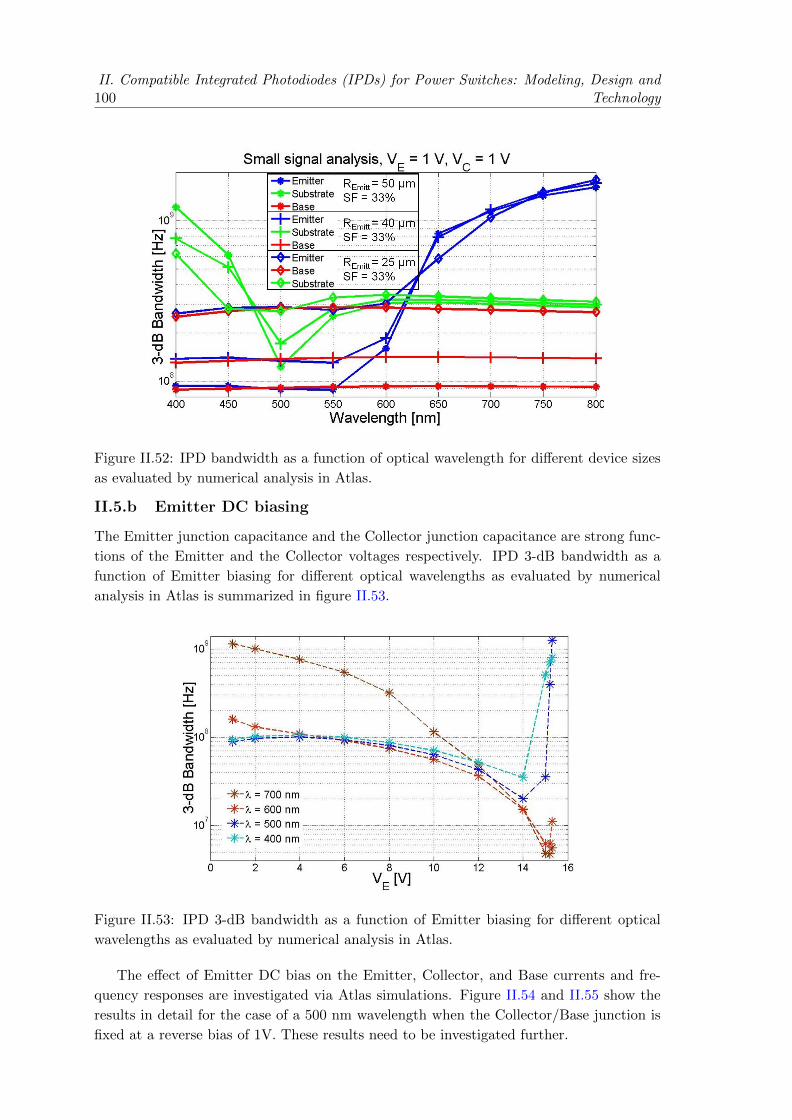
100II. Compatible Integrated Photodiodes (IPDs) for Power Switches: Modeling, Design and
Technology
Figure II.52: IPD bandwidth as a function of optical wavelength for different device sizes
as evaluated by numerical analysis in Atlas.
II.5.b Emitter DC biasing
The Emitter junction capacitance and the Collector junction capacitance are strong func-
tions of the Emitter and the Collector voltages respectively. IPD 3-dB bandwidth as a
function of Emitter biasing for different optical wavelengths as evaluated by numerical
analysis in Atlas is summarized in figure II.53.
Figure II.53: IPD 3-dB bandwidth as a function of Emitter biasing for different optical
wavelengths as evaluated by numerical analysis in Atlas.
The effect of Emitter DC bias on the Emitter, Collector, and Base currents and fre-
quency responses are investigated via Atlas simulations. Figure II.54 and II.55 show the
results in detail for the case of a 500 nm wavelength when the Collector/Base junction is
fixed at a reverse bias of 1V. These results need to be investigated further.

II.5. Dynamic Analysis 101
Figure II.54: IPD frequency response as a function of Emitter biasing for a 500 nm optical
wavelength as evaluated by numerical analysis in Atlas.
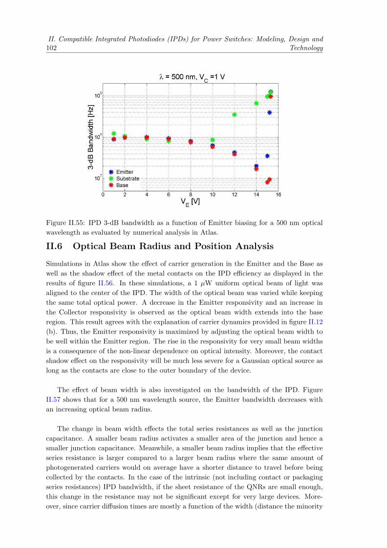
102II. Compatible Integrated Photodiodes (IPDs) for Power Switches: Modeling, Design and
Technology
Figure II.55: IPD 3-dB bandwidth as a function of Emitter biasing for a 500 nm optical
wavelength as evaluated by numerical analysis in Atlas.
II.6 Optical Beam Radius and Position Analysis
Simulations in Atlas show the effect of carrier generation in the Emitter and the Base as
well as the shadow effect of the metal contacts on the IPD efficiency as displayed in the
results of figure II.56. In these simulations, a 1 µW uniform optical beam of light was
aligned to the center of the IPD. The width of the optical beam was varied while keeping
the same total optical power. A decrease in the Emitter responsivity and an increase in
the Collector responsivity is observed as the optical beam width extends into the base
region. This result agrees with the explanation of carrier dynamics provided in figure II.12
(b). Thus, the Emitter responsivity is maximized by adjusting the optical beam width to
be well within the Emitter region. The rise in the responsivity for very small beam widths
is a consequence of the non-linear dependence on optical intensity. Moreover, the contact
shadow effect on the responsivity will be much less severe for a Gaussian optical source as
long as the contacts are close to the outer boundary of the device.
The effect of beam width is also investigated on the bandwidth of the IPD. Figure
II.57 shows that for a 500 nm wavelength source, the Emitter bandwidth decreases with
an increasing optical beam radius.
The change in beam width effects the total series resistances as well as the junction
capacitance. A smaller beam radius activates a smaller area of the junction and hence a
smaller junction capacitance. Meanwhile, a smaller beam radius implies that the effective
series resistance is larger compared to a larger beam radius where the same amount of
photogenerated carriers would on average have a shorter distance to travel before being
collected by the contacts. In the case of the intrinsic (not including contact or packaging
series resistances) IPD bandwidth, if the sheet resistance of the QNRs are small enough,
this change in the resistance may not be significant except for very large devices. More-
over, since carrier diffusion times are mostly a function of the width (distance the minority

II.6. Optical Beam Radius and Position Analysis 103
Figure II.56: Under illumination of a 500 nm uniform optical source, the effect of the spatial
dependence of photogeneration on the Emitter and Collector responsivities is demonstrated
by varying the optical beam width. Both junctions are reversed biased at 1 V. The data
presented via the circle marker correspond to a carrier lifetime of 1 µs. The data presented
via the cross marker correspond to a carrier lifetime of 1 ns.
Figure II.57: Under illumination of a 500 nm uniform optical source, the effect of the spatial
dependence of photogeneration on the Emitter and Collector Bandwidths is demonstrated
by varying the optical beam width. Both junctions are reversed biased at 1 V and the
carrier lifetimes are 1 ns. The optical signal has a 10 µW DC component and a 0.1 µW
amplitude small signal component.

104II. Compatible Integrated Photodiodes (IPDs) for Power Switches: Modeling, Design and
Technology
excess carriers must travel to reach the junction) of each region rather than the length,
they are not effected by the changes in the optical beam radius. Thus the effective change
in the IPD bandwidth as a function of the optical beam width is dominated by the mod-
ulation of the junction area contributing to the junction capacitance.
II.7 Parasitic Environment Constraints
The cross section of a classic power VD-MOSFET structure is shown in figure II.58. There
are some parasitic elements present in this structure, including: the pn-junction diodes,
the source/base/drain BJT, and the JFET (only half of the region in depicted) created by
the drift region sandwiched between the two base regions. As it was presented in figure
II.3, with the exception of the JFET, the monolithic optical detector inherits these para-
sitic elements.
Figure II.58: (a) Equivalent circuit of VD-MOSFET showing two possible mechanisms for
dv/dt induced turn-on [102]. (b) VD-MOSFET cross section showing the physical origin
of the parasitic BJT.
II.7.a Electrical Activation of Parasitic BJT
In a power VD-MOSFET, the turn on of the parasitic BJT formed by the n+ source, p-
base and the Nv drift region is avoided in the DC regime, via electrically shorting the
source and base regions together. Moreover, the metal contact overlapping the Source
and the p-type Base region also acts as a body contact for the MOS structure of the VD-
MOSFET. However, when switching, the parasitic BJT may turn on due to large dv/dt
transients. The cross section view of figure II.58 shows that the Drain of the VD-MOSFET
is connected to the Base of the parasitic BJT through the drift/Base junction capacitance
which is then connected to the Source contact through the Base resistance. Transients
appearing between the Drain and the Source of the power MOSFET induce a current I2through the Base resistance. If the voltage drop in the Base becomes higher than the

II.7. Parasitic Environment Constraints 105
potential barrier across the drift/Base junction, the parasitic BJT will turn on. Equation
II.59 shows the bipolar turn-on transient limit.
[dVDdt
]max =Vbi
RPBCDB(VD)[7] (II.59)
Where VD is the drain voltage, Vbi is the built in potential of the emitter-base junc-
tion, RPB is the resistance of the p-base region, CDB is the drain-base capacitance. A
small RPB value helps in suppressing the turn-on of the internal parasitic BJT present
in the VD-MOSFET body. The circuit of figure II.58 (a), shows the two mechanisms for
dv/dt turn-on: (1) turn-on via the parasitic BJT as discussed above, (2) and the Miller
drawback which was discussed in Chapter 1.
Unlike the VD-MOSFET, in the optical detector structure the device is no longer
functional if the n+ emitter and the base are shorted together, since this is the optical
detection junction used for controlling the emitter leakage current. In order to prevent the
parasitic BJT, the operating voltage settings must insure that the BJT is in its inverse-
off state at all times. By connecting the Base contact to the power transistor Source
and always applying positive or null voltages to the Emitter contact, the Emitter leakage
current can then be monitored as a function of the optical beam. In this configuration,
it is assured that the Emitter/Base and the Base/Collector are always reversed biased;
however, there are still the Emitter and the Collector leakage currents and photocurrents
flowing through the Base resistance.
Just like the case for the VD-MOSFET, transient limits should be identified in order to
insure a safe operating regime for the photodetector when switching the VD-MOSFET
Source-Drain voltage. From the equivalent circuit of the photodetector depicted in Figure
II.59 (b), the requirements for avoiding the parasitic turn-on of the BJT in transient mode
can be identified by equations II.60 and II.61.
Vcritic = RPB(iC + iE) = RPB[CDB(VD)dVDdt
+ iE ] < [VE + Vbi] (II.60)
dVDdt
= [VE + VbiRPB
− iE ]/CCB (II.61)
Where CCB is the Collector/Base junction capacitance (note that CCB and CDB are
the same capacitance), iE and iC are the Emitter and the Collector leakage currents when
transients appear between the Drain (note that the Drain of the VD-MOSFET is the same
as the Collector of the IPD) and Source. For maximum dV/dt, a low RPB and a large VE
are desired. Both in the DC and the transient case, a large Emitter current contributes to
an earlier parasitic turn-on (a lower VCritic tolerance); thus, there is a limit in maximizing
the IPD output Emitter current. Moreover, by comparing Equation II.61 with Equation
II.59, it is observed that as long as [(VE/RPB - iE)/CDB] is positive, the maximum dV/dt
is limited by the VD-MOSFET as expressed in Equation II.59. If [(VE/RPB - iE)/CDB]
is negative, then the maximum dV/dt is set by the IPD as expressed in Equation II.61.
Simulation results from Atlas depicted in figure II.60 shows the effect of a 400 V step
signal on the substrate in a 25 ns ramp time under dark conditions. As seen the substrate
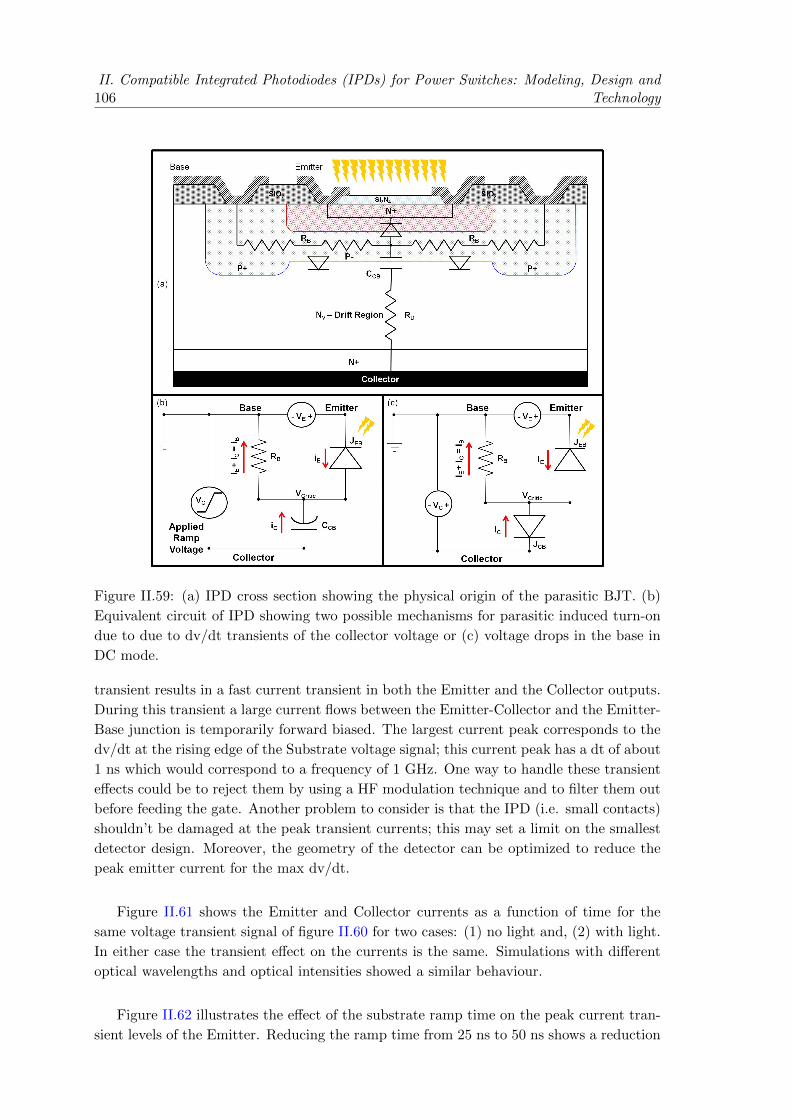
106II. Compatible Integrated Photodiodes (IPDs) for Power Switches: Modeling, Design and
Technology
Figure II.59: (a) IPD cross section showing the physical origin of the parasitic BJT. (b)
Equivalent circuit of IPD showing two possible mechanisms for parasitic induced turn-on
due to due to dv/dt transients of the collector voltage or (c) voltage drops in the base in
DC mode.
transient results in a fast current transient in both the Emitter and the Collector outputs.
During this transient a large current flows between the Emitter-Collector and the Emitter-
Base junction is temporarily forward biased. The largest current peak corresponds to the
dv/dt at the rising edge of the Substrate voltage signal; this current peak has a dt of about
1 ns which would correspond to a frequency of 1 GHz. One way to handle these transient
effects could be to reject them by using a HF modulation technique and to filter them out
before feeding the gate. Another problem to consider is that the IPD (i.e. small contacts)
shouldn’t be damaged at the peak transient currents; this may set a limit on the smallest
detector design. Moreover, the geometry of the detector can be optimized to reduce the
peak emitter current for the max dv/dt.
Figure II.61 shows the Emitter and Collector currents as a function of time for the
same voltage transient signal of figure II.60 for two cases: (1) no light and, (2) with light.
In either case the transient effect on the currents is the same. Simulations with different
optical wavelengths and optical intensities showed a similar behaviour.
Figure II.62 illustrates the effect of the substrate ramp time on the peak current tran-
sient levels of the Emitter. Reducing the ramp time from 25 ns to 50 ns shows a reduction
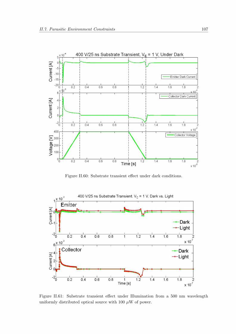
II.7. Parasitic Environment Constraints 107
Figure II.60: Substrate transient effect under dark conditions.
Figure II.61: Substrate transient effect under Illumination from a 500 nm wavelength
uniformly distributed optical source with 100 µW of power.

108II. Compatible Integrated Photodiodes (IPDs) for Power Switches: Modeling, Design and
Technology
in the current peak of the Emitter by roughly 45%.
Figure II.62: Substrate transient effect as a function of Collector voltage ramp time.
II.7.b Optical Activation of Parasitic BJT
Before optimizing the optical detector design, a closer look at the parasitic N-P-N bipolar
transistor is necessary in order to define some design and operation constraints. From the
equivalent circuit of the photodetector depicted in Figure II.59 (c), the requirements for
avoiding the parasitic turn-on of the BJT in DC mode can be identified by equation II.62.
Vcritic = RPB(IC + IE) < [VE + Vbi] (II.62)
IE is the Emitter dark current plus the Emitter photocurrent both of which increase
with increasing VE ; thus, there is a compromise in operating at a large VE bias. According
to equation II.62, RPB and IC should be minimized in order to avoid the BJT turn-on in
the DC mode of operation. RPB is a design parameter that can be minimized by reducing
the carrier path lengths through the design of the contacts and doping wells shape and
position. A higher dose of impurities in the Base will also reduce RPB, however, this is
limited by the performance requirement of the VD-MOSFET. IC is the Collector dark
current plus the Collector photocurrent both of which increase with large reverse voltages
on the Collector. Figure II.59 (a) shows the physical origin of the parasitic BJT in the
photodetector structure.
Keeping the same IPD area, structure and optical beam radius (51µm), numerical
simulations are repeated at different optical wavelengths while sweeping the optical power
from a minimum of Popt = 0.1µW to a maximum of Popt = 1 mW. Figure II.63 (a) and
(b) illustrate the photogeneration rate within the structure for an optical wavelength of
500 nm, with an optical power of 0.1 µW and 1 mW respectively, a collector reverse bias
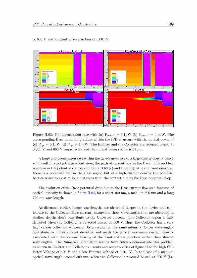
II.7. Parasitic Environment Constraints 109
of 600 V and an Emitter reverse bias of 0.001 V.
Figure II.63: Photogeneration rate with (a) Popt−1 = 0.1µW (b) Popt−1 = 1 mW. The
corresponding Base potential gradient within the IPD structure with the optical power of
(c) Popt = 0.1µW (d) Popt = 1 mW. The Emitter and the Collector are reversed biased at
0.001 V and 600 V respectively and the optical beam radius is 51 µm.
A large photogeneration rate within the device gives rise to a large carrier density which
will result in a potential gradient along the path of current flow in the Base. This problem
is shown in the potential contours of figure II.63 (c) and II.63 (d); at low current densities,
there is a potential well in the Base region but at a high current density the potential
barrier seizes to exist at long distances from the contact due to the Base potential drop.
The evolution of the Base potential drop due to the Base current flow as a function of
optical intensity is shown in figure II.64, for a short 400 nm, a medium 500 nm and a long
700 nm wavelength.
As discussed earlier, longer wavelengths are absorbed deeper in the device and con-
tribute to the Collector-Base current, meanwhile short wavelengths that are absorbed in
shallow depths don’t contribute to the Collector current. The Collector region is fully
depleted when the Collector is reversed biased at 600 V, thus, the Collector has a very
high carrier collection efficiency. As a result, for the same intensity, longer wavelengths
contribute to higher current densities and reach the critical maximum current density
associated with the forward biasing of the Emitter-Base junction earlier than shorter
wavelengths. The Numerical simulation results from Silvaco demonstrate this problem
as shown in Emitter and Collector currents and responsivities of figure II.65 for high Col-
lector Voltage of 600 V and a low Emitter voltage of 0.001 V. In the case of a medium
optical wavelength around 500 nm, when the Collector is reversed biased at 600 V (i.e.
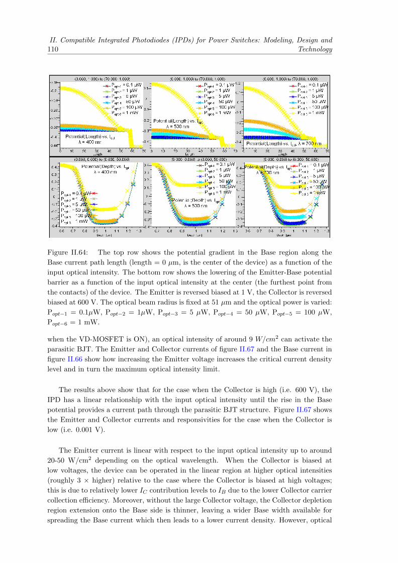
110II. Compatible Integrated Photodiodes (IPDs) for Power Switches: Modeling, Design and
Technology
Figure II.64: The top row shows the potential gradient in the Base region along the
Base current path length (length = 0 µm, is the center of the device) as a function of the
input optical intensity. The bottom row shows the lowering of the Emitter-Base potential
barrier as a function of the input optical intensity at the center (the furthest point from
the contacts) of the device. The Emitter is reversed biased at 1 V, the Collector is reversed
biased at 600 V. The optical beam radius is fixed at 51 µm and the optical power is varied:
Popt−1 = 0.1µW, Popt−2 = 1µW, Popt−3 = 5 µW, Popt−4 = 50 µW, Popt−5 = 100 µW,
Popt−6 = 1 mW.
when the VD-MOSFET is ON), an optical intensity of around 9 W/cm2 can activate the
parasitic BJT. The Emitter and Collector currents of figure II.67 and the Base current in
figure II.66 show how increasing the Emitter voltage increases the critical current density
level and in turn the maximum optical intensity limit.
The results above show that for the case when the Collector is high (i.e. 600 V), the
IPD has a linear relationship with the input optical intensity until the rise in the Base
potential provides a current path through the parasitic BJT structure. Figure II.67 shows
the Emitter and Collector currents and responsivities for the case when the Collector is
low (i.e. 0.001 V).
The Emitter current is linear with respect to the input optical intensity up to around
20-50 W/cm2 depending on the optical wavelength. When the Collector is biased at
low voltages, the device can be operated in the linear region at higher optical intensities
(roughly 3 × higher) relative to the case where the Collector is biased at high voltages;
this is due to relatively lower IC contribution levels to IB due to the lower Collector carrier
collection efficiency. Moreover, without the large Collector voltage, the Collector depletion
region extension onto the Base side is thinner, leaving a wider Base width available for
spreading the Base current which then leads to a lower current density. However, optical

II.7. Parasitic Environment Constraints 111
Figure II.65: IPD (a) Emitter and Collector currents and (b) their corresponding respon-
sivities versus input optical intensity. The Emitter is reversed biased at 1 V, the Collector
is reversed biased at 600 V, and the optical beam radius is 51 µm.
Figure II.66: IPD Base current behaviour versus input optical intensity. The dashed black
lines indicate the current limit after which the Emitter-base junction becomes forward
biased for the case where the Emitter is reversed biased at 0.001 V (i.e. floating Emitter)
and when it is reversed biased at 1 V. The Collector is reversed biased at 600 V and the
optical beam radius is fixed at 51 µm.

112II. Compatible Integrated Photodiodes (IPDs) for Power Switches: Modeling, Design and
Technology
Figure II.67: IPD (a) Emitter current and (b) responsivity and the (c) Collector current
and (d) responsivity versus Input optical intensity at a low collector voltage. The Emitter
and the Collector are reversed biased at 0.001 V, and the optical beam radius is fixed at
51 µm.
intensities above 20-40 W/cm2 cause a non-linear transition in the IPD behaviour that
allows for a temporary gain in the Emitter efficiency followed by a continuous reduction
of the Emitter efficiency.
This non-linear transition can be explained by the effective widening of the Base region
due to the disappearance of the Collector-Base depletion region at high charge densities
associated with high current densities flowing through the Collector-Base region. With no
Collector-Base depletion region, the Base current spreads out deeper into the substrate;
this is depicted in the current flow lines in the IPD cross sections of figure II.68 as a func-
tion of optical intensity. Figure II.69 shows the electron and hole concentration profiles
near the Collector-Base junction for a variety of input optical intensities. Figure II.70
shows the potential rise in the Base region both as a function of distance away from the
device surface and as a function distance along the Base length for a variety of input op-
tical intensities.
Approximating the optical intensity limit for a given IPD doping profile determines
the minimum permitted device area that results in a linear behaviour of the device for a
given optical power source. As an example, for an optical source with λ = 500 nm and
Popt = 10 µW, our IPD linear region is limited by the BJT turn-on at an intensity around
9 W/[cm2]; this implies that the smallest IPD circular design has a radius of around 6 µm.
Since the IPDs will be powered by optical sources with power levels of a few µWs, the
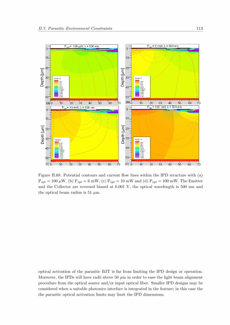
II.7. Parasitic Environment Constraints 113
Figure II.68: Potential contours and current flow lines within the IPD structure with (a)
Popt = 100 µW, (b) Popt = 6 mW, (c) Popt = 10 mW and (d) Popt = 100 mW. The Emitter
and the Collector are reversed biased at 0.001 V, the optical wavelength is 500 nm and
the optical beam radius is 51 µm.
optical activation of the parasitic BJT is far from limiting the IPD design or operation.
Moreover, the IPDs will have radii above 50 µm in order to ease the light beam alignment
procedure from the optical source and/or input optical fiber. Smaller IPD designs may be
considered when a suitable photonics interface is integrated in the feature; in this case the
the parasitic optical activation limits may limit the IPD dimensions.
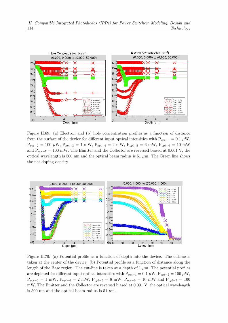
114II. Compatible Integrated Photodiodes (IPDs) for Power Switches: Modeling, Design and
Technology
Figure II.69: (a) Electron and (b) hole concentration profiles as a function of distance
from the surface of the device for different input optical intensities with Popt−1 = 0.1 µW,
Popt−2 = 100 µW, Popt−3 = 1 mW, Popt−4 = 2 mW, Popt−5 = 6 mW, Popt−6 = 10 mW
and Popt−7 = 100 mW. The Emitter and the Collector are reversed biased at 0.001 V, the
optical wavelength is 500 nm and the optical beam radius is 51 µm. The Green line shows
the net doping density.
Figure II.70: (a) Potential profile as a function of depth into the device. The cutline is
taken at the center of the device. (b) Potential profile as a function of distance along the
length of the Base region. The cut-line is taken at a depth of 1 µm. The potential profiles
are depicted for different input optical intensities with Popt−1 = 0.1 µW, Popt−2 = 100 µW,
Popt−3 = 1 mW, Popt−4 = 2 mW, Popt−5 = 6 mW, Popt−6 = 10 mW and Popt−7 = 100
mW. The Emitter and the Collector are reversed biased at 0.001 V, the optical wavelength
is 500 nm and the optical beam radius is 51 µm.

II.8. Simulation and Modelling Conclusions and Overview 115
II.8 Simulation and Modelling Conclusions and Overview
The vertical structure and doping profile of a 600 V power MOSFET was studied through
analytical modelling and finite element simulations in order to demonstrate the possibility
of using the Emitter-Base shallow junction as a photodetector capable of generating the
electrical gating signal for the power switch. The modelling and simulations are used to
illustrate the role of physical mechanisms responsible for the different phenomena within
the IPD. Moreover, some of the main links between the different performance parameters,
material properties, geometrical and technological parameters are demonstrated. In order
to expose the potential of our proposed approach, the simulation and modelling results
are analysed to answer two main questions: (1) can the IPD provide the a reliable out-
put gating signal given the power MOSFET structure, parasitic environment, and floating
substrate voltage? (2) What are the design parameter value/s and operating conditions
that maximize the IPD performance in terms of QE, DC output current level, bandwidth,
immunity to noise and the parasitic environment.
To answer the first question, modelling and simulation studies were performed to reveal
the sensitivity of the IPD output current signal to, (1) high DC substrate voltages and
(2) the input electrical (i.e. fast transient substrate voltages) and (3) optical (i.e. Iopt)
parameters that may activate the IPD’s parasitic BJT structure.
1. The IPD output DC current as a function of input DC substrate voltages up to
600V revealed that only Emitter currents generated by wavelengths longer than
UV (roughly above 430 nm) are reduced due to increasing substrate voltages as
was depicted in figure II.38; this reduction in Emitter current is stronger for longer
wavelengths absorbed deeper in the device and it can be as high as 20% in the IR
(roughly above 750 nm) range. The high DC substrate voltages are predicted to
reduce the maximum achievable QE of the device at around a 500 nm wavelength
by roughly 8%. This effect is not considered problematic since for an IPD triggered
by an optimal wavelength, the QE (i.e. > 0.1) of the device is predicted to generate
a current signal above 100s of nAs even after reductions due to the high substrate
voltages.
2. Simulations showed that fast (i.e. 25 ns ramp) substrate voltage (i.e. 4V = 400 V)
transients result in fast current peaks in the Emitter and the Collector that forward
bias the Emitter-Base junction for a short time in the range of a few ns as was
depicted in figure II.60. This current peak can be reduced by increasing the ramp
time, however this is not practical since the ramp times are limited by the power
transistor switching requirements and thus can not be made slower. Another way to
reduce the transient side effects on the IPD is to increase the Emitter voltage (i.e.
avalanche mode IPD), however this needs to be investigated in order to insure that
the increased noise levels are acceptable given the low output current levels of the
IPD. A third possibility of dealing with the transient currents is to filter them in
the signal processing stages following the IPD stage. The filtering solution should
be carefully designed so that it does not significantly limit the IPD bandwidth.
3. Simulation results predict that the DC optical activation of the parasitic BJT occurs

116II. Compatible Integrated Photodiodes (IPDs) for Power Switches: Modeling, Design and
Technology
earlier when the substrate is reversed biased at a high voltage level(i.e. 600 V);
however it is far from limiting the IPD design or operation for optical powers in the
range of few µWs and IPD radii above 10 µm, as was depicted in figures II.65 and
II.66.
Thus, according to the performed studies on the power MOSFET vertical structure,
parasitic environment, and floating substrate voltage, the parasitic turn on of the BJT
due to substrate transients is the only main challenge of the IPD in providing a reliable
output gating signal.
To answer the second question, the IPD static and dynamic performance was modelled
in Matlab and simulated in Silvaco as a function of optical wavelength, optical intensity,
Emitter and Collector voltages, IPD sensitive area, shading, illuminated region, and car-
rier lifetimes.
The most suitable operating optical wavelength is considered to be one which maxi-
mizes the Emitter output current and the ratio of the Emitter to Collector responsivity,
meanwhile, minimizes the Emitter current sensitivity to the Collector high voltages. The
static study of the IPD predicted a peak responsivity of 0.2 A/W at a 500 nm optical
wavelength with a 33% shading factor, when the Emitter and the Collector are reversed
biased at 1V and the Silicon wafer has long carrier lifetimes of 1 µs as was depicted in
figure II.33. At 500 nm, a high DC substrate reverse voltage up to 600 V is predicted to
reduce the maximum achievable responsivity of the IPD by no more than ∼8%. Moreover,
the ratio of Emitter to Collector photocurrent is approximately 5.3 as was depicted in
figure II.46(a) and a 90 MHz 3dB bandwidth is predicted according to Silvaco simulations
of figure II.55. Thus, a 500 nm optical wavelength is predicted to be most suitable for
the IPD structure with the same doping profile as a 600 V power MOSFET. In order to
improve the efficiency of the IPD at this wavelength, the design process for an optimized
ARC was also presented in this chapter which is predicted to improve the IPD efficiency
by ∼40%.
Both the modelling and simulation results confirm that the IPD Emitter reponsivity
and thus output current level improves when the Emitter junction is reversed biased at
higher voltages. If the IPD is polarized in the avalanche gain (due to avalanche multipli-
cation) operating region (i.e. > 15V), the responsivity and the 3 dB bandwidth of the
detector are predicted to increase above 0.3 A/W and 400 MHz respectively for a 500 nm
optical wavelength as were presented in figures II.36 and II.55. Moreover, as presented
in equations II.62 and II.60, the IPD immunity to electrical and optical activation of the
parasitic BJT structure can be improved by increasing the Emitter junction reverse volt-
age. These results suggest that the IPD performance in terms of responsivity, bandwidth
and immunity to parasitic turn-ons are improved when the device is polarized in avalanche
mode. However, the avalanche multiplication mechanism amplifies the Emitter signal cur-
rent, the dark current and the background currents indiscriminately. Thus, it is important
that the IPD dark current level is kept as low as possible in order not to limit the mini-
mum detectable optical power. Since the avalanche gain comes with a price of noise, noise

II.8. Simulation and Modelling Conclusions and Overview 117
analysis and temperature analysis are required for a complete investigation of the most
suitable biasing condition for the IPD.
Sensitivity studies of the IPD responsivity to the carrier lifetime parameters revealed
that the Emitter responsivity is not sensitive to electron lifetimes and it starts to suffer
for hole lifetimes shorter than 10ns as it was depicted in figure II.42. As it was discussed,
carrier lifetime values not only present a compromise between the responsivity and the
bandwidth of the IPD but they also impact the vertical bipolar diode in the power MOS-
FET structure.
The study of the optical beam radius for a fixed detector size and a fixed contact
position and a uniform optical beam source, confirmed the theoretical prediction that ab-
sorptions in the Base region contribute to the collector current rather than the Emitter
current. Moreover, small optical beam radii and small IPD Emitter radii are both pre-
dicted to improve the IPD bandwidth as were presented in figures II.57 and II.52. The
reduction in efficiency due to contact shadowing was also observed in results of figure II.56.
There are a number of different investigations via modelling and simulation that can
be done in the near future in order to add to and improve on the current conclusions and
predictions. Temperature and noise analysis are perhaps the two main areas in need of
investigation. Moreover, the effect of contact positioning and Gaussian optical beams on
the IPD performance should also be investigated.


Chapter III
IPD Fabrication and Characterization
Sommaire
III.1 Introduction . . . . . . . . . . . . . . . . . . . . . . . . . . . . . . . . . . . . . 120
III.2VD-MOSFET Planar Fabrication Process Overview . . . . . . . . . 121
III.3Power Bipolar IPD Fabrication Process . . . . . . . . . . . . . . . . . 123
III.4 IPD Mask Layout Designs . . . . . . . . . . . . . . . . . . . . . . . . . . . 126
III.5Fabrication Results . . . . . . . . . . . . . . . . . . . . . . . . . . . . . . . . 133
III.6DC Characterization: Setup and Measurement Approach . . . . . 138
III.6.a First Approach: LED Light Sources . . . . . . . . . . . . . . . . . . . . . . 138
III.6.b Second Approach: Xenon Light Source . . . . . . . . . . . . . . . . . . . . . 142
III.6.c MEASUREMENT RESULTS . . . . . . . . . . . . . . . . . . . . . . . . . . 147
III.7AC Characterization: Setup and Measurement Approach . . . . . 151
III.7.a First Approach: Externally modulated LED Optical Source . . . . . . . . . 151
III.7.b Second Approach: Externally modulated Laser . . . . . . . . . . . . . . . . 152
III.7.c Third Approach: Directly modulated Laser . . . . . . . . . . . . . . . . . . 154
III.8Summary . . . . . . . . . . . . . . . . . . . . . . . . . . . . . . . . . . . . . . . . 156
Abstract
Having introduced the integration approach and objectives along side the simulation and
modelling analysis of the power MOSFET compatible integrated photodetector (IPD)
design, in this chapter we will introduce the fabrication, electrical and optical charac-
terization approaches, challenges, procedures and results used for the proposed IPDs.

120 III. IPD Fabrication and Characterization
III.1 Introduction
The power bipolar and VDMOSFET fabrication procedures are being continually investi-
gated and have been used in previous projects at G2ELab. Most of the process steps have
been developed over time during previous projects at G2Elab and many of the required
recipes are available at the CIME Nanotech/Minatec cleanroom facilities. In the case of
the IPDs, the fabrication process needs to also accommodate an additional dielectric layer
for the anti reflective coating (ARC) which is not part of the power bipolar or VDMOSFET
fabrication. Since the IPDs will not be fabricated via standard manufacturers, no standard
design rule check (DRC) files are available. Thus, a DRC tailored for the IPD masks is
developed in consideration of the equipments available at the CIME cleanroom facilities
as well as the IPD designs. Meanwhile, some IPD dimensions are chosen to push beyond
the DRC safety margins in order to test the fabrication boundaries and potentially achieve
higher performance IPDs. Overall 8 masks are designed in Cadence Virtuoso, associated
with custom techfiles. The fabrication process, mask designs and results are presented in
detail in the following three sections.
A full investigation of the IPD performance demands the investigation of the static
and dynamic responses of the device to electrical and optical input signals as a function of
optical wavelength, Emitter and Collector biasing conditions, optical power, temperature,
geometry and design. The specific characterization objectives are, to identify:
• the range of achievable IPD QE using the VDMOSFET fabrication process,
• the IPD QE as a function of optical wavelength in order to find the most suitable
operating wavelength,
• the IPD QE as a function of Emitter voltages. The IPD performance at low voltages
versus in avalanche gain mode need to be compared and studied in order to find
the most suitable IPD operating condition; as it was uncovered in Chapter 2, the
IPD QE increases for increasing VE , meanwhile the IPD dark current levels (which
determine the minimum required optical power and noise levels), the optical parasitic
turn-on (not significant) and the IPD immunity level to substrate transients are also
functions of VE . Moreover, QE shifts in the optical wavelength domain depending
on VE should be quantified.
• the IPD QE dependence on the substrate should be quantified in order to verify the
effect of the VDMOSFET floating voltages on the IPD performance.
• the IPD design(s) that maximize the device QE
• the IPD QE as a function of optical intensity in order to locate the IPD’s linear
operating range,
• the IPD dark current level in order to determine the minimum required optical power
• the range of achievable IPD rise times and bandwidths using the VDMOSFET fab-
rication process,

III.2. VD-MOSFET Planar Fabrication Process Overview 121
• the IPD bandwidth as a function of optical wavelength in order to find the most
suitable operating wavelength in terms of frequency response,
• the IPD bandwidth as a function of small signal peak-to-peak optical power in order
to verify the linearity of the design
• the IPD bandwidth as a function of VE in order to identify the suitable Emitter
biasing condition for the device
• the IPD design(s) that maximize the device Bandwidth
• the IPD design(s) with the best QE, rise time, bandwidth and noise immunity com-
promise
• the temperature effects on the IPD performance and specially on the noise level. The
temperature can also shift the QE peak along the optical wavelength spectrum due
to ARC refractive index dependencies on the temperature.
Achieving the above characterization objectives requires the development of DC and
AC experimental setups that offer accuracy, repeatability and a wide range of tunable
inputs such as optical DC power levels, optical wavelengths (including visible range), AC
optical signals (square and sine waveforms for step and frequency response analysis), volt-
ages (DC and transient) and temperatures. The different challenges and approaches taken
in constructing the DC and AC experimental setups are introduced in this chapter and
the IPD characterization results are discussed. IPDs with responsivity of 0.2 A/W and
3-dB bandwidth in 10s of MHz have been measured.
III.2 VD-MOSFET Planar Fabrication Process Overview
Figure III.1 shows the VD-MOSFET and the U-MOSFET basic cell structures which are
the more prevalent structures amongst the vertical power MOSFET devices [7]. The U-
MOSFET benefits from lower internal resistance compared to the VD-MOSFET structure
due to the elimination of the parasitic junction gate field-effect transistor (JFET) region;
however, the UMOS fabrication process requires additional complex fabrication steps (i.e.
reactive-ion etching (RIE)) for the gate formation inside the U-trench.
Figure III.1: Cross sectional view of the (a) VUMOS and (b) VDMOS Structures.
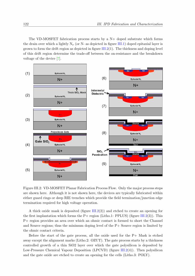
122 III. IPD Fabrication and Characterization
The VD-MOSFET fabrication process starts by a N+ doped substrate which forms
the drain over which a lightly Nν (or N- as depicted in figure III.1) doped epitaxial layer is
grown to form the drift region as depicted in figure III.2(1). The thickness and doping level
of this drift region determine the trade-off between the on-resistance and the breakdown
voltage of the device [7].
Figure III.2: VD-MOSFET Planar Fabrication Process Flow. Only the major process steps
are shown here. Although it is not shown here, the devices are typically fabricated within
either guard rings or deep RIE trenches which provide the field termination/junction edge
termination required for high voltage operation.
A thick oxide mask is deposited (figure III.2(2)) and etched to create an opening for
the first implantation which forms the P+ region (Litho.1: PPLUS) (figure III.2(3)). This
P+ region provides an area over which an ohmic contact is formed to short the Channel
and Source regions; thus the minimum doping level of the P+ Source region is limited by
the ohmic contact criteria.
Before the start of the gate process, all the oxide used for the P+ Mask is etched
away except the alignment marks (Litho.2: OZUT). The gate process starts by a thickness
controlled growth of a thin SiO2 layer over which the gate polysilicon is deposited by
Low-Pressure Chemical Vapour Deposition (LPCVD) (figure III.2(4)). Then polysilicon
and the gate oxide are etched to create an opening for the cells (Litho.3: POLY).

III.3. Power Bipolar IPD Fabrication Process 123
A second implementation/diffusion round forms the P- region (figure III.2(5)); the
MOS channel is defined by the diffusion of the P- dopants under the gate during the
implant activation stage (self-aligned process). A second thick oxide mask is deposited
and opened in preparation for the N+ source implantation (figure III.2(6)). Note that
instead of an oxide mask, photoresist masks are also available (Litho.4: NPLUS).
Before the contacts can be formed, an intermetal layer is deposited in order to isolate
the gate from the source III.2(7)). This intermetal layer must provide a reliable step
coverage over the gate surface and edges. Any defects in the intermetal layer near the
polysilicon gate, could result in a short between the gate and the source.
After opening the intermetal layer (Litho.5: OCON), the metal contacts are then
deposited III.2(8)) and contact pads are opened (Litho.6: MET1), after which, one final
oxide deposition is done to passivate the device III.2(9)).
Overall, there are 5 masks required plus 2 additional masks: one for the edge termina-
tion (Litho.7: DRIE) of the devices and a second for defining windows in the passivation
oxide layer (Litho.8: MET2) for the wire bonds of the gate and source [7]. It should be
added that every doping implantation is followed by a drive stage, moreover, contacts are
usually annealed (Rapid thermal annealing, RTA) for improved quality. Process variations
can slightly change the number of steps or mask levels.
III.3 Power Bipolar IPD Fabrication Process
Figure III.3 shows the power bipolar IPD fabrication process flow, and table III.1 lists the
bipolar IPD process details and specifications. The numbers used in figure III.3 correspond
to the fabrication process labels listed in table III.1. In table III.1, positive and negative
photoresists are abbreviated as +PR and -PR respectively. All wet etching of oxide and
nitride layers is done in Buffered oxide etch (BOE) baths. The Aluminum wet etching is
carried out in a Phosphoric acid (H3PO4) based bath. The P+ and P- implantations use
800 nm thick oxide hard masks; the N+ implantation uses a -PR mask.
In order to first prove the proposed concept and speed up the fabrication process
due to time limitations, the IPDs are fabricated via the power bipolar process without
the VDMOSFET polysilicon gate deposition. In total, eight masks are designed for the
bipolar IPD process PPLUS, PMNS, OZUT, NPLUS, ARC, OCON, MET1 and DRIE
as listed in table III.1. Comparing this with the masks required for the VDMOSFET,
PPLUS, OZUT, POLY, NPLUS, OCON, MET1, DRIE, and MET2 (as it was explained
in section III.1), reveals two differences:
1. In the VDMOSFET process a PMNS mask is not required since the P- region is self-
aligned with the gate as it was explained earlier in section III.1. However, a POLY
gate is required for defining the gate region which is not required in the bipolar IPD
process. In the bipolar IPD case, the same oxide mask used for the creation of the
P+ zone is used for the P- implantation meanwhile a PMNS mask is designed for
creating the openings through the oxide. This is depicted in steps 1.7 and 2.4 of
figure III.3 and explained in table III.1.

124 III. IPD Fabrication and Characterization
Figure III.3: Bipolar IPD process flow. The left column is followed either by the middle
column or the far right column depending on the type of process flow chosen. For a process
flow with 2 dielectric layers, Case A follows the left column. For a process flow with 1
dielectric layer dielectric Case B follows the left column.
2. A second etch mask in addition to the OCON mask is required required for defining
an optimized ARC for the IPD, namely the ARC mask. This ARC mask needs to
be added to the VDMOSFET process.
Using all the bipolar IPD (i.e. eight) Masks allows for depositing two different dielectric
materials as depicted in figure III.3 Case A; one material (i.e. Si3N4) could be used to
optimize an ARC layer for the optically sensitive surface, meanwhile, a second material
(i.e. SiO2) could be used to provide electrical isolation between the junction edges and the
metal contacts and to also reduce the optical transmissions in unwanted regions such as
the Base region. This would be an option to separate the constraints of the VDMOS (SiO2
CVD) from the ARC (thin SiN). Si3N4 has a dielectric field strength of roughly 107 V/cm;
for a 60-80 nm thick nitride layer (optimized for the ARC at wavelengths near 500 nm), a
≈ 2×10⁶ V/cm field is created in the nitride layer when a 15 V potential difference appears

III.3. Power Bipolar IPD Fabrication Process 125
# Mask Key Steps Min. Dimensions
1 PPLUS Clean and etch backside LTO 10 [µm]
1.1 Hard Mask deposition: 800nm-SiO2
1.2 Organic cleaning (Piranha solution)
1.3 1st Lithography (+ PR)
1.4 Wet etch in BOE at 33, PR removal
1.5 Boron implantation
1.6 Organic Cleaning (Piranha solution)
1.7 Annealing
2 PMNS 2nd Lithography (+ PR) 10 [µm]
2.1 Wet etch, PR removal
2.2 Boron implantation
2.3 Organic Cleaning (Piranha solution)
2.4 Annealing
3 OZUT 3rd Lithography (+ PR)
3.1 Wet etch all except Alignments, PR removal
4 NPLUS 4th Lithography (- PR) 10 [µm]
4.1 Arsenic implantation
4.2 PR stripping in RIE
4.3 Organic Cleaning (Piranha solution)
4.4 Deposit FrontSide Protection PR
4.5 Backside pre-etch
4.6 Backside Arsenic implantation
4.7 Remove FrontSide PR
4.8 Organic Cleaning (Piranha solution)
4.9 Annealing
5 ARC Deposit Si3N4 (60-80 nm)
5.1 Deposit Si2O2 [SKIPPED]
5.2 5th Lithography (+ PR) [SKIPPED]
5.3 Etch Oxide [SKIPPED]
6 OCON Clean 4 [µm]
6.1 6th Lithography (+ PR)
6.2 Wet etch, PR removal
7 MET1 Clean 10 [µm]
7.1 Aluminium Deposition
7.2 7th Lithography (- PR)
7.3 Aluminium Etch
7.4 PR removal
7.5 Deposit FrontSide Protection PR
7.6 Backside Metal (Plasma Ar,10nmTi, 1µm-Alu, 300nm-TiN)
7.7 Remove Protection PR and Anneal
8 DRIE 8th Lithography (+ PR)
8.1 Process etch Si TP CIME 40 cycles
8.2 Remove PR
Table III.1: Bipolar IPD process details and specifications
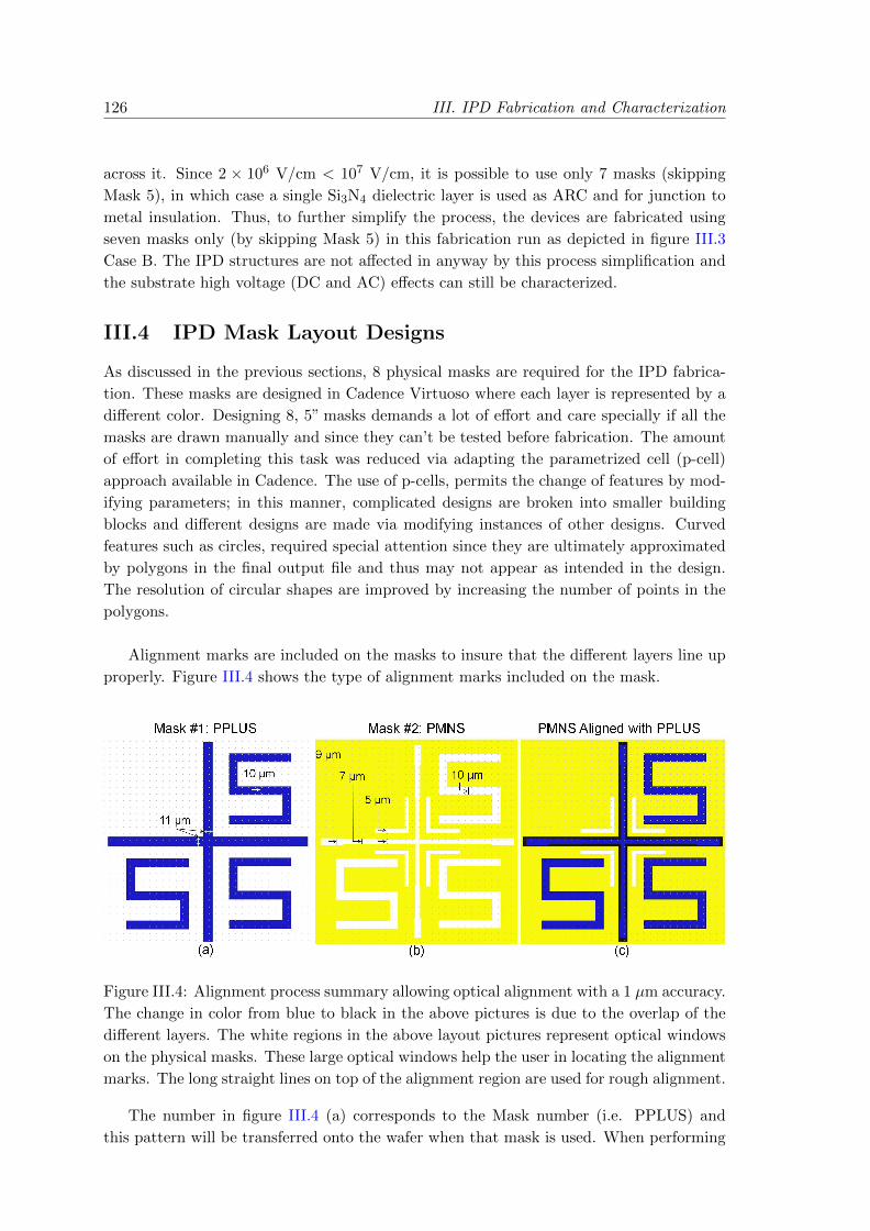
126 III. IPD Fabrication and Characterization
across it. Since 2 × 10⁶ V/cm < 107 V/cm, it is possible to use only 7 masks (skipping
Mask 5), in which case a single Si3N4 dielectric layer is used as ARC and for junction to
metal insulation. Thus, to further simplify the process, the devices are fabricated using
seven masks only (by skipping Mask 5) in this fabrication run as depicted in figure III.3
Case B. The IPD structures are not affected in anyway by this process simplification and
the substrate high voltage (DC and AC) effects can still be characterized.
III.4 IPD Mask Layout Designs
As discussed in the previous sections, 8 physical masks are required for the IPD fabrica-
tion. These masks are designed in Cadence Virtuoso where each layer is represented by a
different color. Designing 8, 5” masks demands a lot of effort and care specially if all the
masks are drawn manually and since they can’t be tested before fabrication. The amount
of effort in completing this task was reduced via adapting the parametrized cell (p-cell)
approach available in Cadence. The use of p-cells, permits the change of features by mod-
ifying parameters; in this manner, complicated designs are broken into smaller building
blocks and different designs are made via modifying instances of other designs. Curved
features such as circles, required special attention since they are ultimately approximated
by polygons in the final output file and thus may not appear as intended in the design.
The resolution of circular shapes are improved by increasing the number of points in the
polygons.
Alignment marks are included on the masks to insure that the different layers line up
properly. Figure III.4 shows the type of alignment marks included on the mask.
Figure III.4: Alignment process summary allowing optical alignment with a 1 µm accuracy.
The change in color from blue to black in the above pictures is due to the overlap of the
different layers. The white regions in the above layout pictures represent optical windows
on the physical masks. These large optical windows help the user in locating the alignment
marks. The long straight lines on top of the alignment region are used for rough alignment.
The number in figure III.4 (a) corresponds to the Mask number (i.e. PPLUS) and
this pattern will be transferred onto the wafer when that mask is used. When performing
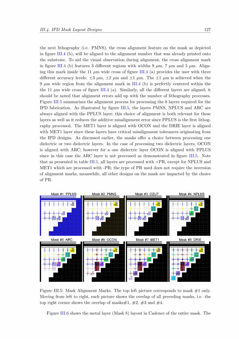
III.4. IPD Mask Layout Designs 127
the next lithography (i.e. PMNS), the cross alignment feature on the mask as depicted
in figure III.4 (b), will be aligned to the alignment number that was already printed onto
the substrate. To aid the visual observation during alignment, the cross alignment mark
in figure III.4 (b) features 3 different regions with widths 9 µm, 7 µm and 5 µm. Align-
ing this mark inside the 11 µm wide cross of figure III.4 (a) provides the user with three
different accuracy levels: ±3 µm, ±2 µm and ±1 µm. The ±1 µm is achieved when the
9 µm wide region from the alignment mark in III.4 (b) is perfectly centered within the
the 11 µm wide cross of figure III.4 (a). Similarly, all the different layers are aligned; it
should be noted that alignment errors add up with the number of lithography processes.
Figure III.5 summarizes the alignment process for processing the 8 layers required for the
IPD fabrication. As illustrated by figure III.5, the layers PMNS, NPLUS and ARC are
always aligned with the PPLUS layer; this choice of alignment is both relevant for these
layers as well as it reduces the additive misalignment error since PPLUS is the first lithog-
raphy processed. The MET1 layer is aligned with OCON and the DRIE layer is aligned
with MET1 layer since these layers have critical misalignment tolerances originating from
the IPD designs. As discussed earlier, the masks offer a choice between processing one
dielectric or two dielectric layers. In the case of processing two dielectric layers, OCON
is aligned with ARC; however for a one dielectric layer OCON is aligned with PPLUS
since in this case the ARC layer is not processed as demonstrated in figure III.5. Note
that as presented in table III.1, all layers are processed with +PR, except for NPLUS and
MET1 which are processed with -PR; the type of PR used does not require the inversion
of alignment marks, meanwhile, all other designs on the mask are impacted by the choice
of PR.
Figure III.5: Mask Alignment Marks. The top left picture corresponds to mask #1 only.
Moving from left to right, each picture shows the overlap of all preceding masks, i.e. the
top right corner shows the overlap of masks#1, #2, #3 and #4.
Figure III.6 shows the metal layer (Mask 8) layout in Cadence of the entire mask. The
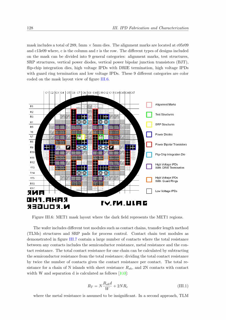
128 III. IPD Fabrication and Characterization
mask includes a total of 289, 5mm × 5mm dies. The alignment marks are located at c05r09
and c13r09 where, c is the column and r is the row. The different types of designs included
on the mask can be divided into 9 general categories: alignment marks, test structures,
SRP structures, vertical power diodes, vertical power bipolar junction transistors (BJT),
flip-chip integration dies, high voltage IPDs with DRIE termination, high voltage IPDs
with guard ring termination and low voltage IPDs. These 9 different categories are color
coded on the mask layout view of figure III.6.
Figure III.6: MET1 mask layout where the dark field represents the MET1 regions.
The wafer includes different test modules such as contact chains, transfer length method
(TLMs) structures and SRP pads for process control. Contact chain test modules as
demonstrated in figure III.7 contain a large number of contacts where the total resistance
between any contacts includes the semiconductor resistance, metal resistance and the con-
tact resistance. The total contact resistance for one chain can be calculated by subtracting
the semiconductor resistance from the total resistance; dividing the total contact resistance
by twice the number of contacts gives the contact resistance per contact. The total re-
sistance for a chain of N islands with sheet resistance Rsh, and 2N contacts with contact
width W and separation d is calculated as follows [103]:
RT = NRshd
W+ 2NRc (III.1)
where the metal resistance is assumed to be insignificant. In a second approach, TLM
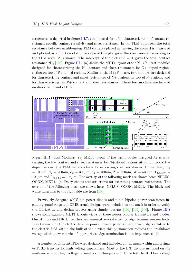
III.4. IPD Mask Layout Designs 129
structures as depicted in figure III.7, can be used for a full characterization of contact re-
sistance, specific contact resistivity and sheet resistance. In the TLM approach, the total
resistance between neighbouring TLM contacts placed at varying distances d is measured
and plotted as a function of d. The slope of this plot gives the sheet resistance as long as
the TLM width Z is known. The intercept of the plot at d = 0, gives the total contact
resistance 2Rc [103]. Figure III.7 (a) shows the MET1 layout of the N+/P+ test modules
designed for characterizing the N+ contact and sheet resistances for N+ doped regions
sitting on top of P+ doped regions. Similar to the N+/P+ case, test modules are designed
for characterizing contact and sheet resistances of N+ regions on top of P- regions, and
for characterising the P+ contact and sheet resistances. These test modules are located
on dies c07r07 and c11r07.
Figure III.7: Test Modules. (a) MET1 layout of the test modules designed for charac-
terizing the N+ contact and sheet resistances for N+ doped regions sitting on top of P+
doped regions. (b) TLM test structures for extracting sheet resistances. In our design d1
= 100µm, d2 = 200µm, d3 = 300µm, d4 = 400µm, Z = 500µm, W = 530µm, LOCON =
100µm and LMET1 = 106µm. The overlap of the following mask are shown here: NPLUS,
OCON, MET1. (c) Daisy chains test structures for extracting contact resistances. The
overlap of the following mask are shown here: NPLUS, OCON, MET1. The black and
white diagrams to the right side are from [103].
Previously designed 600V p-n power diodes and n-p-n bipolar power transistors in-
cluding guard rings and DRIE trench designs were included on the mask in order to verify
the fabrication and design process using simpler designs [104] [105] [106]. Figure III.8
shows some example MET1 layouts views of these power bipolar transistors and diodes.
Guard rings and DRIE trenches are amongst several existing edge termination methods.
It is known that the electric field in power devices peaks at the device edges relative to
the electric field within the bulk of the device; this phenomenon reduces the breakdown
voltage of the power device if appropriate edge termination is not implemented [5].
A number of different IPDs were designed and included on the mask within guard rings
or DRIE trenches for high voltage capabilities. Most of the IPD designs included on the
mask are without high voltage termination techniques in order to test the IPD low voltage

130 III. IPD Fabrication and Characterization
Figure III.8: Power bipolar Transistors and power diodes. Only the MET1 layer is de-
picted.
performance. Moreover IPDs were arranged in groups of four on a single die with large
access pads in anticipation for flip-chip integration techniques (i.e. columns 7, 8, 10, 11
and rows 9, 14). The flip-chip integration die design included 4 additional input/output
contacts pads and it is depicted in figure III.9. In such cases, a CMOS transimpedance
(TIA) circuit would be assembled as close as possible to the detectors in a flip chip assem-
bly, minimizing electrical parasitics.
Figure III.9: Flip-Chip Integration Die Layout. 4 IPDs are included in one flip-chip die.
All IPDs include an optimized anti-reflective coating suitable for optical wavelengths
near 500 nm. The most basic design is shown in the Cadence layout photo of figure III.10
and is labelled D3a. The cross sectional views in figure III.10, illustrate the cross section
of IPD D3a for a P+ and a P- Base region. Devices with P- base region may offer a higher
QE and a higher bandwidth due to a wider WD and thus a lower Cj when compared to
P+ base devices. In addition, devices are designed with a P+ Base region (i.e. P+/N+
Emitter junction) in order to minimize series resistances specially for larger designs and to
improve the IPD tolerance to the parasitic bipolar turn-on constraints. Some of the IPD
designs have been repeated for 3 different Emitter radii: 100 µm, 50 µm and 25 µm in
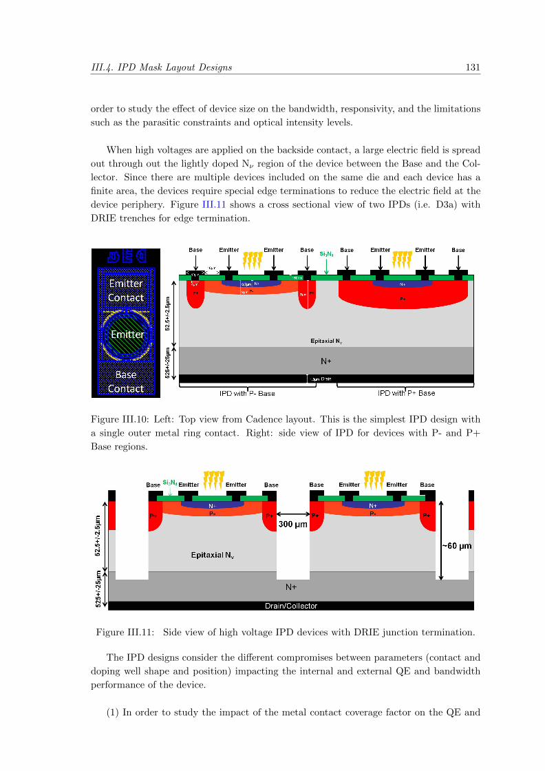
III.4. IPD Mask Layout Designs 131
order to study the effect of device size on the bandwidth, responsivity, and the limitations
such as the parasitic constraints and optical intensity levels.
When high voltages are applied on the backside contact, a large electric field is spread
out through out the lightly doped Nν region of the device between the Base and the Col-
lector. Since there are multiple devices included on the same die and each device has a
finite area, the devices require special edge terminations to reduce the electric field at the
device periphery. Figure III.11 shows a cross sectional view of two IPDs (i.e. D3a) with
DRIE trenches for edge termination.
Figure III.10: Left: Top view from Cadence layout. This is the simplest IPD design with
a single outer metal ring contact. Right: side view of IPD for devices with P- and P+
Base regions.
Figure III.11: Side view of high voltage IPD devices with DRIE junction termination.
The IPD designs consider the different compromises between parameters (contact and
doping well shape and position) impacting the internal and external QE and bandwidth
performance of the device.
(1) In order to study the impact of the metal contact coverage factor on the QE and
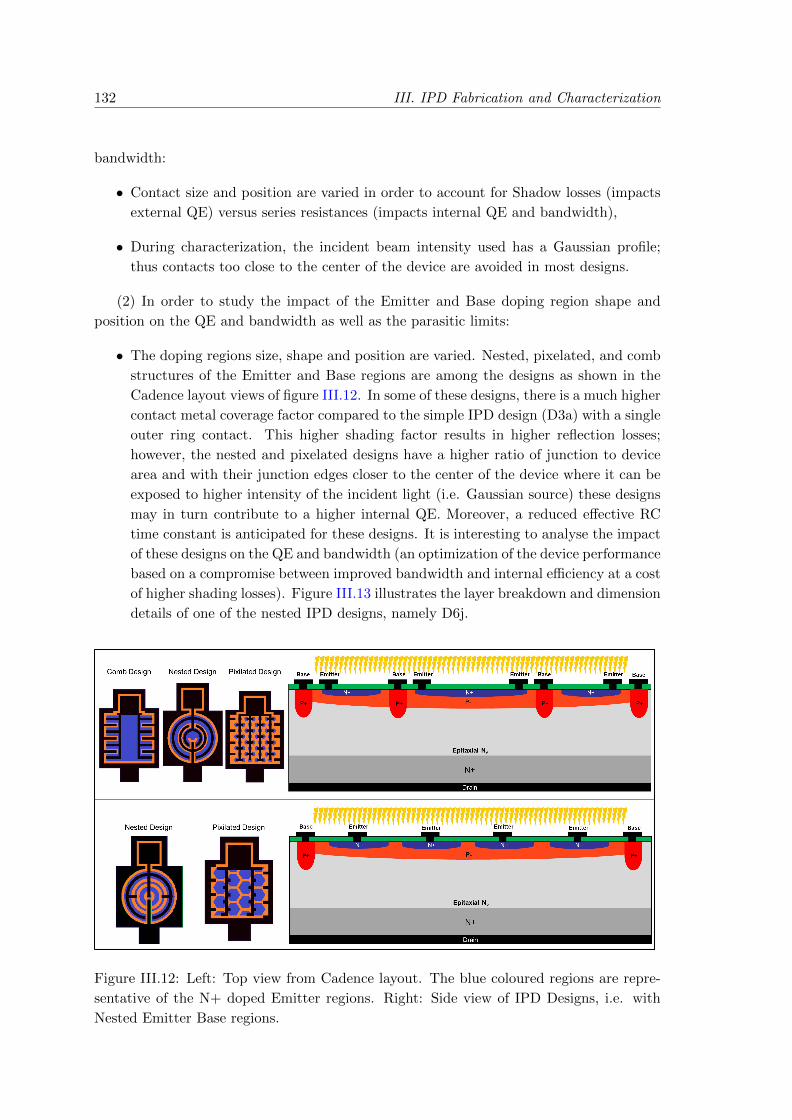
132 III. IPD Fabrication and Characterization
bandwidth:
• Contact size and position are varied in order to account for Shadow losses (impacts
external QE) versus series resistances (impacts internal QE and bandwidth),
• During characterization, the incident beam intensity used has a Gaussian profile;
thus contacts too close to the center of the device are avoided in most designs.
(2) In order to study the impact of the Emitter and Base doping region shape and
position on the QE and bandwidth as well as the parasitic limits:
• The doping regions size, shape and position are varied. Nested, pixelated, and comb
structures of the Emitter and Base regions are among the designs as shown in the
Cadence layout views of figure III.12. In some of these designs, there is a much higher
contact metal coverage factor compared to the simple IPD design (D3a) with a single
outer ring contact. This higher shading factor results in higher reflection losses;
however, the nested and pixelated designs have a higher ratio of junction to device
area and with their junction edges closer to the center of the device where it can be
exposed to higher intensity of the incident light (i.e. Gaussian source) these designs
may in turn contribute to a higher internal QE. Moreover, a reduced effective RC
time constant is anticipated for these designs. It is interesting to analyse the impact
of these designs on the QE and bandwidth (an optimization of the device performance
based on a compromise between improved bandwidth and internal efficiency at a cost
of higher shading losses). Figure III.13 illustrates the layer breakdown and dimension
details of one of the nested IPD designs, namely D6j.
Figure III.12: Left: Top view from Cadence layout. The blue coloured regions are repre-
sentative of the N+ doped Emitter regions. Right: Side view of IPD Designs, i.e. with
Nested Emitter Base regions.

III.5. Fabrication Results 133
Figure III.13: Example nested IPD design layout detail. From left to right the main mask
layouts are depicted. OZUT and DRIE layers are not shown here since they complicate
the visual presentation of the device. Note that NPLUS layer (third from left) will use a
-PR; thus this mask is inverted and the N+ doped regions are represented by the white
color. The far right picture shows the overlap of all the layers presented to its left. The
colors represent the following: yellow for N+ Emitter regions, green for P- Base regions,
black for metal contact regions.
III.5 Fabrication Results
Overall, 2 epitaxial (Epi) and 4 Bulk 4” Silicon wafers were fully processed, meanwhile,
4 Bulk wafers were used as dummies for verifying the steps during the fabrication. The
specifications for the different wafers are provided in table III.2. The wafers are chosen to
have a resistivity of 20 - 40 Ω.cm in the Nν region since this is appropriate for breakdown
voltages in the 600 V range. The main difference between the epi wafers compared to the
Bulk wafers is that the Nν region is roughly 52 µm thick and it is grown on top of a thick
525 µm N++ substrate; meanwhile, the Bulk wafers have a 350 µm thick Nν region. As a
result of this difference, the Bulk wafers offer a larger resistance in the vertical direction,
nevertheless they wouldn’t have a lower breakdown voltage compared to the epi wafers
since they have a very thick Nν region. The life time specifications are not provided for
these wafers by the manufacturer.
These devices are fabricated using the power bipolar process (compatible with the
VDMOSFET process) at the CIME Nanotech/Minatec cleanroom facilities in Grenoble.
The bipolar IPD implantation and annealing process parameters are the same as in the
VDMOSFET case; these process details are given in table III.3.
During fabrication, the height of PR and oxide layers were measured via a profilometer
and visual observation of the wafers under an optical microscope revealed the quality of
lithography (i.e. misalignment error, under or over development) and etch (i.e. under or
over etching) processes. Figure III.14 depicts some optical images used for process moni-
toring at some critical fabrication steps.
Figure III.15 shows macroscopic photos of some of the different IPD designs after fabri-
cation as well as a photo of a low voltage die. As previously presented a variety of contact

134 III. IPD Fabrication and Characterization
Wafer Description Epi-Wafer Bulk Wafer Dummy Bulk Wafer
Substrate type/dopant N++/Ars Nv/Phos Nv/Phos
Orientation <100> <100> <100>
Substrate Resistivity 0,001-0,007 ohm.cm
Substrate thickness 525 +/- 25 µm
Type/dopant Epi 1 N/Phos N/Phos N/Phos
Resitivity Epi 1 20 - 40 ohm.cm 20 - 40 ohm.cm 1-10 ohm.cm
Thickness Epi 1 52,5 -+2,5 µm
Type/dopant Epi 2 N/Phos
TTV/Bow/Warp (µm) 10 / 30 / 30
Flats primary Flat
SEMI Std
primary Flat
SEMI Std
primary Flat
SEMI Stdfront side surface polished polished polished
backside surface lapped,etched
with LTO Seal
lapped,etched lapped,etched
Total thickness 525 +-/ 25 µm 350 +/- 25 µm 350 +/- 25 µm
Quantities of stack 2 wafers 4 wafers 4 wafers
Final Quantities 2 4 0
Table III.2: Bulk and Epi Wafer Specifications
Figure III.14: Microscope images used for monitoring the fabrication quality while in
process. The top row shows the alignment accuracy for PMNS, NPLUS, OCON and
MET1. The bottom row shows some images from different areas of the wafer corresponding
to the process stage indicated by the column labels.

III.5. Fabrication Results 135
Process Process Parameter Equipment
P+ Implantation Surface: frontside Implanter
Type/dopant: Boron
Dose: 1015cm−2, Energy: 150 keV, Current: 40 µA
Tilt: 7
P+ Annealing Ramp-up: 15min nitro 3000sccm, 750C to 900C Furnace
Stabilisation: nitro 3000sccm, 900C 2min
Oxidation: dryo2 5000sccm, 900C 15min
Ramp-up: nitro 3000sccm 20min, 900C to 1100C
Stabilisation: nitro 3000sccm, 1100C 5min
Activation: nitro 3000sccm 1100C 40min
Ramp-down: nitro, 1100C to 750C 30min
Oxidation: dryo2 5000sccm, 900C 15min
P- Implantation Surface: frontside Implanter
Type/dopant: Boron
Dose: 1013cm−2, Energy: 150 keV, Current: 40 µA
Tilt: 7
P- Annealing Ramp-up: 15min nitro 3000sccm, 750C to 900C Furnace
Stabilisation: nitro 3000sccm, 900C 2min
Oxidation: dryo2 5000sccm, 900C 15min
Ramp-up: nitro 3000sccm 20min, 900C to 1100C
Stabilisation: nitro 3000sccm, 1100C 5min
Activation: nitro 3000sccm 1100C 300min
Ramp-down: nitro, 1100C to 750C 30min
Oxidation: dryo2 5000sccm, 900C 15min
N+ Implantation Surface: frontside Implanter
Type/dopant: Arsenic
Dose: 5× 1015cm−2, Energy: 150 keV, Current: 40 µA
Tilt: 7
N+ Implantation Surface: backside Implanter
Type/dopant: Arsenic
Dose: 5× 1015cm−2, Energy: 150 keV, Current: 100 µA
Tilt: 7
N+ Annealing Start temperature: 750C, Gas flow: 3000 sccm-N2 Furnace
Ramp-up: 10C/min, 3000sccm-N2
Stabilisation: 900C, 2min
Oxidation: 5000sccm-O2, 900C 10min
Ramp-up: 10C/min, 3000sccm-N2
Stabilisation: 5min, 1050C, N2
Activation: 1050C 25min, 3000sccm-N2
Ramp-down: -5C/min, 3000 sccm-N2
Table III.3: Doping Process Parameters
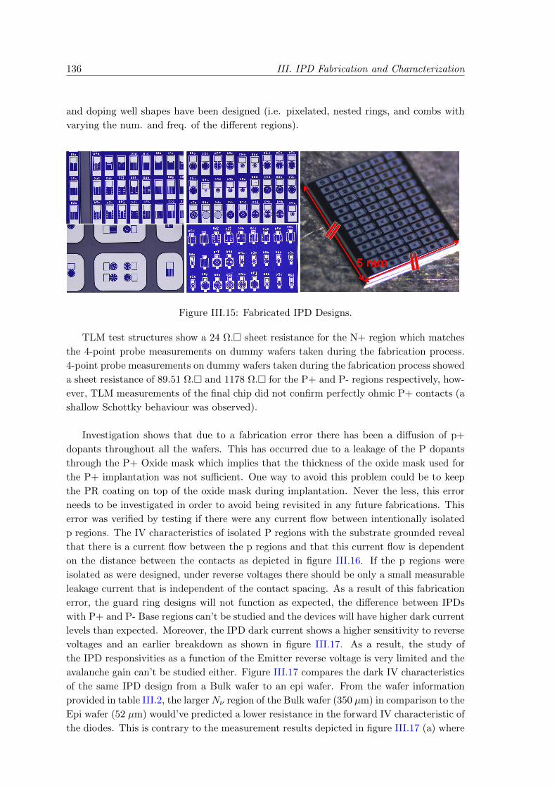
136 III. IPD Fabrication and Characterization
and doping well shapes have been designed (i.e. pixelated, nested rings, and combs with
varying the num. and freq. of the different regions).
Figure III.15: Fabricated IPD Designs.
TLM test structures show a 24 Ω. sheet resistance for the N+ region which matches
the 4-point probe measurements on dummy wafers taken during the fabrication process.
4-point probe measurements on dummy wafers taken during the fabrication process showed
a sheet resistance of 89.51 Ω. and 1178 Ω. for the P+ and P- regions respectively, how-
ever, TLM measurements of the final chip did not confirm perfectly ohmic P+ contacts (a
shallow Schottky behaviour was observed).
Investigation shows that due to a fabrication error there has been a diffusion of p+
dopants throughout all the wafers. This has occurred due to a leakage of the P dopants
through the P+ Oxide mask which implies that the thickness of the oxide mask used for
the P+ implantation was not sufficient. One way to avoid this problem could be to keep
the PR coating on top of the oxide mask during implantation. Never the less, this error
needs to be investigated in order to avoid being revisited in any future fabrications. This
error was verified by testing if there were any current flow between intentionally isolated
p regions. The IV characteristics of isolated P regions with the substrate grounded reveal
that there is a current flow between the p regions and that this current flow is dependent
on the distance between the contacts as depicted in figure III.16. If the p regions were
isolated as were designed, under reverse voltages there should be only a small measurable
leakage current that is independent of the contact spacing. As a result of this fabrication
error, the guard ring designs will not function as expected, the difference between IPDs
with P+ and P- Base regions can’t be studied and the devices will have higher dark current
levels than expected. Moreover, the IPD dark current shows a higher sensitivity to reverse
voltages and an earlier breakdown as shown in figure III.17. As a result, the study of
the IPD responsivities as a function of the Emitter reverse voltage is very limited and the
avalanche gain can’t be studied either. Figure III.17 compares the dark IV characteristics
of the same IPD design from a Bulk wafer to an epi wafer. From the wafer information
provided in table III.2, the largerNν region of the Bulk wafer (350 µm) in comparison to the
Epi wafer (52 µm) would’ve predicted a lower resistance in the forward IV characteristic of
the diodes. This is contrary to the measurement results depicted in figure III.17 (a) where
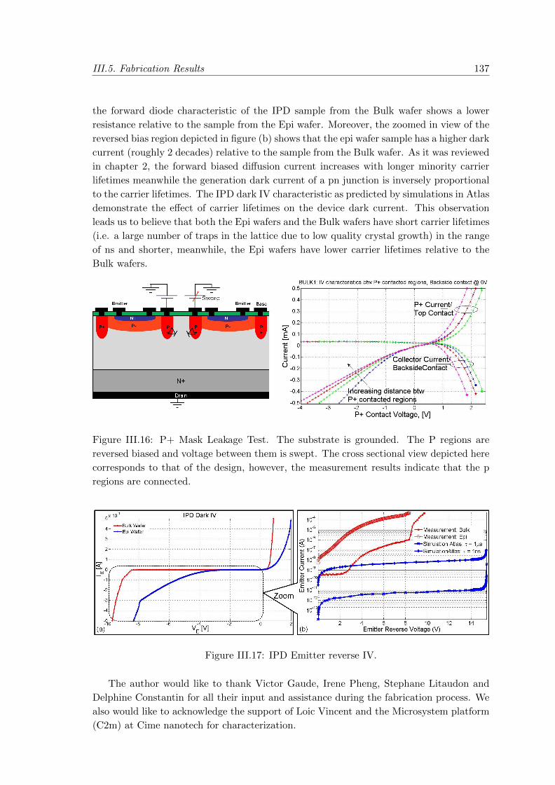
III.5. Fabrication Results 137
the forward diode characteristic of the IPD sample from the Bulk wafer shows a lower
resistance relative to the sample from the Epi wafer. Moreover, the zoomed in view of the
reversed bias region depicted in figure (b) shows that the epi wafer sample has a higher dark
current (roughly 2 decades) relative to the sample from the Bulk wafer. As it was reviewed
in chapter 2, the forward biased diffusion current increases with longer minority carrier
lifetimes meanwhile the generation dark current of a pn junction is inversely proportional
to the carrier lifetimes. The IPD dark IV characteristic as predicted by simulations in Atlas
demonstrate the effect of carrier lifetimes on the device dark current. This observation
leads us to believe that both the Epi wafers and the Bulk wafers have short carrier lifetimes
(i.e. a large number of traps in the lattice due to low quality crystal growth) in the range
of ns and shorter, meanwhile, the Epi wafers have lower carrier lifetimes relative to the
Bulk wafers.
Figure III.16: P+ Mask Leakage Test. The substrate is grounded. The P regions are
reversed biased and voltage between them is swept. The cross sectional view depicted here
corresponds to that of the design, however, the measurement results indicate that the p
regions are connected.
Figure III.17: IPD Emitter reverse IV.
The author would like to thank Victor Gaude, Irene Pheng, Stephane Litaudon and
Delphine Constantin for all their input and assistance during the fabrication process. We
also would like to acknowledge the support of Loic Vincent and the Microsystem platform
(C2m) at Cime nanotech for characterization.
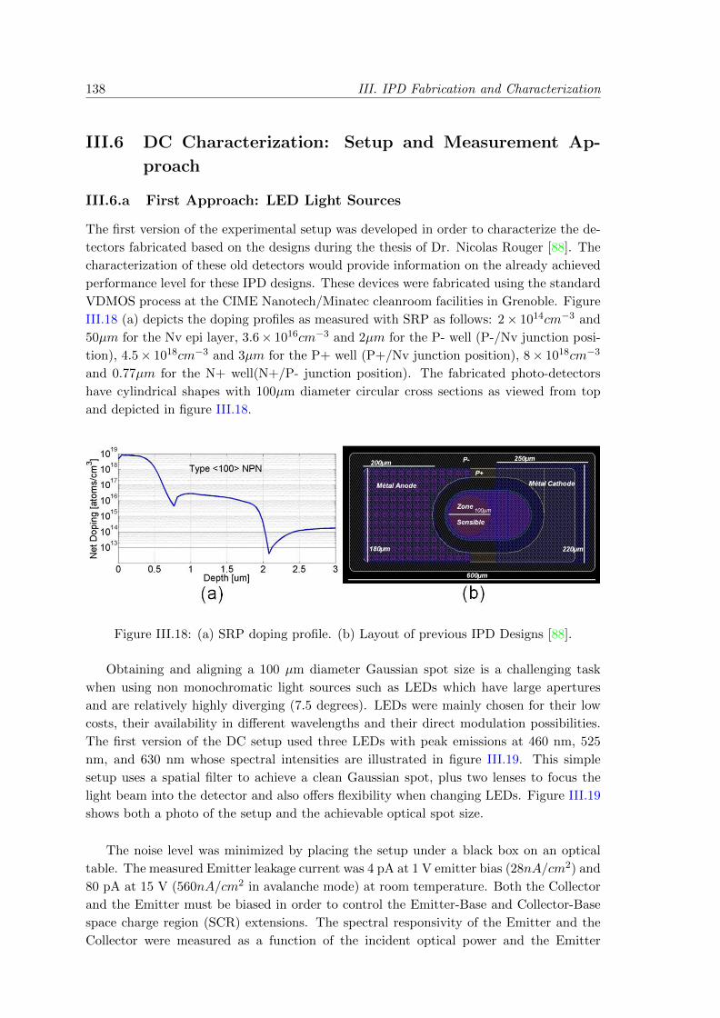
138 III. IPD Fabrication and Characterization
III.6 DC Characterization: Setup and Measurement Ap-
proach
III.6.a First Approach: LED Light Sources
The first version of the experimental setup was developed in order to characterize the de-
tectors fabricated based on the designs during the thesis of Dr. Nicolas Rouger [88]. The
characterization of these old detectors would provide information on the already achieved
performance level for these IPD designs. These devices were fabricated using the standard
VDMOS process at the CIME Nanotech/Minatec cleanroom facilities in Grenoble. Figure
III.18 (a) depicts the doping profiles as measured with SRP as follows: 2× 1014cm−3 and
50µm for the Nv epi layer, 3.6× 1016cm−3 and 2µm for the P- well (P-/Nv junction posi-
tion), 4.5× 1018cm−3 and 3µm for the P+ well (P+/Nv junction position), 8× 1018cm−3
and 0.77µm for the N+ well(N+/P- junction position). The fabricated photo-detectors
have cylindrical shapes with 100µm diameter circular cross sections as viewed from top
and depicted in figure III.18.
Figure III.18: (a) SRP doping profile. (b) Layout of previous IPD Designs [88].
Obtaining and aligning a 100 µm diameter Gaussian spot size is a challenging task
when using non monochromatic light sources such as LEDs which have large apertures
and are relatively highly diverging (7.5 degrees). LEDs were mainly chosen for their low
costs, their availability in different wavelengths and their direct modulation possibilities.
The first version of the DC setup used three LEDs with peak emissions at 460 nm, 525
nm, and 630 nm whose spectral intensities are illustrated in figure III.19. This simple
setup uses a spatial filter to achieve a clean Gaussian spot, plus two lenses to focus the
light beam into the detector and also offers flexibility when changing LEDs. Figure III.19
shows both a photo of the setup and the achievable optical spot size.
The noise level was minimized by placing the setup under a black box on an optical
table. The measured Emitter leakage current was 4 pA at 1 V emitter bias (28nA/cm2) and
80 pA at 15 V (560nA/cm2 in avalanche mode) at room temperature. Both the Collector
and the Emitter must be biased in order to control the Emitter-Base and Collector-Base
space charge region (SCR) extensions. The spectral responsivity of the Emitter and the
Collector were measured as a function of the incident optical power and the Emitter
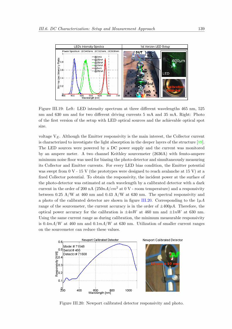
III.6. DC Characterization: Setup and Measurement Approach 139
Figure III.19: Left: LED intensity spectrum at three different wavelengths 465 nm, 525
nm and 630 nm and for two different driving currents 5 mA and 35 mA. Right: Photo
of the first version of the setup with LED optical sources and the achievable optical spot
size.
voltage VE . Although the Emitter responsivity is the main interest, the Collector current
is characterized to investigate the light absorption in the deeper layers of the structure [89].
The LED sources were powered by a DC power supply and the current was monitored
by an ampere meter. A two channel Keithley sourcemeter (2636A) with femto-ampere
minimum noise floor was used for biasing the photo-detector and simultaneously measuring
its Collector and Emitter currents. For every LED bias condition, the Emitter potential
was swept from 0 V - 15 V (the prototypes were designed to reach avalanche at 15 V) at a
fixed Collector potential. To obtain the responsivity, the incident power at the surface of
the photo-detector was estimated at each wavelength by a calibrated detector with a dark
current in the order of 200 nA (250nA/cm2 at 0 V - room temperature) and a responsivity
between 0.25 A/W at 460 nm and 0.43 A/W at 630 nm. The spectral responsivity and
a photo of the calibrated detector are shown in figure III.20. Corresponding to the 1µA
range of the sourcemeter, the current accuracy is in the order of ±400pA. Therefore, the
optical power accuracy for the calibration is ±4nW at 460 nm and ±1nW at 630 nm.
Using the same current range as during calibration, the minimum measurable responsivity
is 0.4mA/W at 460 nm and 0.1mA/W at 630 nm. Utilization of smaller current ranges
on the sourcemeter can reduce these values.
Figure III.20: Newport calibrated detector responsivity and photo.

140 III. IPD Fabrication and Characterization
The IE and IC currents were measured at the same time as a function of biasing
conditions and optical power POptical at the three mentioned wavelengths. The responsivity
of the detectors were measured to be around 0.007 A/W. This value is expected to be
underestimating the true efficiency of the IPD mainly due to calibration errors originating
from the large optical spot size relative to the detector size. In order to improve this
measurement a second version of the setup using LED sources was constructed as depicted
in figure III.21. In comparison to the first version of the setup, the setup of figure III.21
uses two additional aspherical lenses to correct for aspherical aberrations and the use of
an optical fiber further cleans out the optical beam resulting in a smaller Gaussian spot of
less than 200 µm in diameter. Overall optical power losses were estimated at ≈ 30dBm.
Figure III.22 illustrates the observed IPD reverse bias IE as a function of VE and POpticalwhen measured with the 525 nm LED at a 1V Collector bias.
Figure III.21: Left: Schematic of the 2nd DC setup approach using LED sources [107].
Middle: Photo of the 2nd DC setup approach using LED sources. Right: Reduced LED
spot size of less than 200 µm.
Figure III.23 summarizes the spectral responsivity results for the Emitter and Collec-
tor. At shorter wavelengths and low bias, the responsivity suffers from two effects: 1) a
slightly higher reflectivity at the surface interface reduces the external quantum efficiency
2) a reduced Emitter-Base SCR extension which limits the part of drift photo generated
currents to diffusion ones. The total QE for the Emitter is 12.3% at 465 nm, 10.2% at
525 nm and 6.9% at 630 nm at 0V Emitter bias. These values are satisfactory for a non
optimized device without any anti reflection coating. The total QE for the Collector is 8%
at 465 nm, 18.4% at 525 nm and 31% at 630 nm at 0 V Emitter bias - 1 V Collector bias.
It is also noted that the Collector responsivity is reduced by approximately 5 to 10% when
the Emitter voltage is increased to 15 V. This reduction is due to the Emitter-Base SCR
extension into the P well region which results in the removal of the diffused photo gen-
erated carriers from the Collector-Base diffusion current into the Emitter-Base diffusion
current.
Figure III.24 shows the Emitter responsivity of the detector as a function of optical
power at discrete Emitter biasing conditions when illuminated by a 525 nm wavelength
LED source. The DUT has a 100 µm radius which results in an approximate area of
0.03 mm2. The results of figure III.24 show the linearity of the photodetector for input

III.6. DC Characterization: Setup and Measurement Approach 141
−2 0 2 4 6 8 10 12 14 160
0.02
0.04
0.06
0.08
0.1
0.12
0.14
0.16
0.18
Emitter Voltage [V]
Em
itte
r C
urr
en
t [µ
A]
PDark
= 0 µW
POptical
= 0.205 µW
POptical
= 0.399 µW
POptical
= 0.566 µW
POptical
= 0.714 µW
POptical
= 0.857 µW
POptical
= 0.970 µW
POptical
= 1.097 µW
Figure III.22: LIV characterization of the Emitter current with a 525 nm LED [107].
450 500 550 600 6500.02
0.04
0.06
0.08
0.1
0.12
0.14
0.16
0.18
Wavelength [nm]
Em
itte
r a
nd
Co
llecto
r R
esp
on
siv
ity [
A/W
]
Optical Power = 1µW
Emitter VE=0V VC=1VEmitter VE=10V VC=1VEmitter VE=15V VC=1VCollector VC=1V VE=0VCollector VC=1V VE=10VCollector VC=1V VE=15V
Figure III.23: Emitter and Collector responsivity for three different LED wavelengths
[107].
optical powers up to 1.1 µW which corresponds to an optical intensity of approximately
30pW/cm2. In order to verify the linearity of the device at higher optical powers, different
optical sources (i.e. Lasers) that can be controlled at higher optical power levels are needed.
These initial measurements with LEDs at only three wavelengths showed a responsivity
of 0.046 A/W at 0 V Emitter bias when triggered with a 1 µW, 525 nm wavelength LED
as reported in [107]. The author would like to acknowledge the contributions of Duc Ngoc
To during his master internship. He was involved in both the set up development stage as
well as the measurement stage.
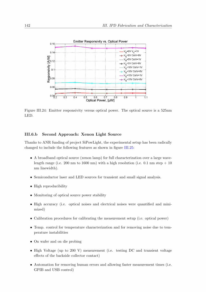
142 III. IPD Fabrication and Characterization
Figure III.24: Emitter responsivity versus optical power. The optical source is a 525nm
LED.
III.6.b Second Approach: Xenon Light Source
Thanks to ANR funding of project SiPowLight, the experimental setup has been radically
changed to include the following features as shown in figure III.25:
• A broadband optical source (xenon lamp) for full characterization over a large wave-
length range (i.e. 200 nm to 1600 nm) with a high resolution (i.e. 0.1 nm step + 10
nm linewidth).
• Semiconductor laser and LED sources for transient and small signal analysis.
• High reproducibility
• Monitoring of optical source power stability
• High accuracy (i.e. optical noises and electrical noises were quantified and mini-
mized)
• Calibration procedures for calibrating the measurement setup (i.e. optical power)
• Temp. control for temperature characterization and for removing noise due to tem-
perature instabilities
• On wafer and on die probing
• High Voltage (up to 200 V) measurement (i.e. testing DC and transient voltage
effects of the backside collector contact)
• Automation for removing human errors and allowing faster measurement times (i.e.
GPIB and USB control)
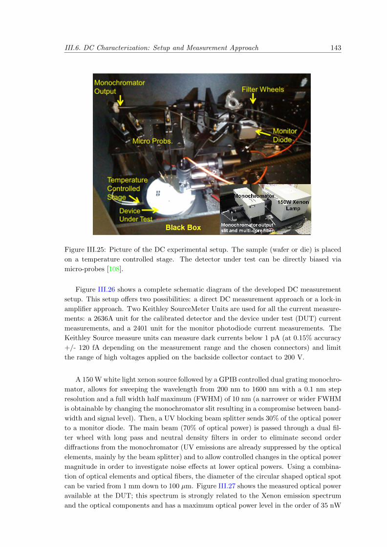
III.6. DC Characterization: Setup and Measurement Approach 143
Figure III.25: Picture of the DC experimental setup. The sample (wafer or die) is placed
on a temperature controlled stage. The detector under test can be directly biased via
micro-probes [108].
Figure III.26 shows a complete schematic diagram of the developed DC measurement
setup. This setup offers two possibilities: a direct DC measurement approach or a lock-in
amplifier approach. Two Keithley SourceMeter Units are used for all the current measure-
ments: a 2636A unit for the calibrated detector and the device under test (DUT) current
measurements, and a 2401 unit for the monitor photodiode current measurements. The
Keithley Source measure units can measure dark currents below 1 pA (at 0.15% accuracy
+/- 120 fA depending on the measurement range and the chosen connectors) and limit
the range of high voltages applied on the backside collector contact to 200 V.
A 150 W white light xenon source followed by a GPIB controlled dual grating monochro-
mator, allows for sweeping the wavelength from 200 nm to 1600 nm with a 0.1 nm step
resolution and a full width half maximum (FWHM) of 10 nm (a narrower or wider FWHM
is obtainable by changing the monochromator slit resulting in a compromise between band-
width and signal level). Then, a UV blocking beam splitter sends 30% of the optical power
to a monitor diode. The main beam (70% of optical power) is passed through a dual fil-
ter wheel with long pass and neutral density filters in order to eliminate second order
diffractions from the monochromator (UV emissions are already suppressed by the optical
elements, mainly by the beam splitter) and to allow controlled changes in the optical power
magnitude in order to investigate noise effects at lower optical powers. Using a combina-
tion of optical elements and optical fibers, the diameter of the circular shaped optical spot
can be varied from 1 mm down to 100 µm. Figure III.27 shows the measured optical power
available at the DUT; this spectrum is strongly related to the Xenon emission spectrum
and the optical components and has a maximum optical power level in the order of 35 nW
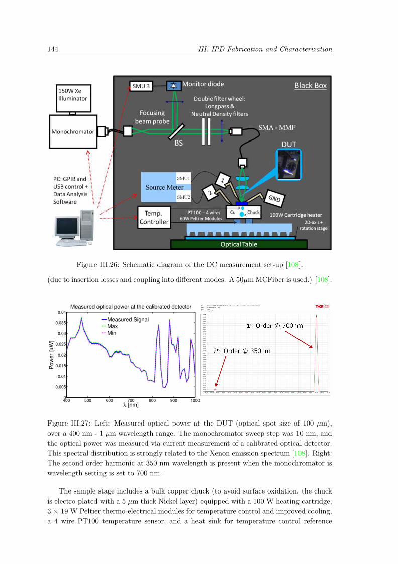
144 III. IPD Fabrication and Characterization
Figure III.26: Schematic diagram of the DC measurement set-up [108].
(due to insertion losses and coupling into different modes. A 50µm MCFiber is used.) [108].
Figure III.27: Left: Measured optical power at the DUT (optical spot size of 100 µm),
over a 400 nm - 1 µm wavelength range. The monochromator sweep step was 10 nm, and
the optical power was measured via current measurement of a calibrated optical detector.
This spectral distribution is strongly related to the Xenon emission spectrum [108]. Right:
The second order harmonic at 350 nm wavelength is present when the monochromator is
wavelength setting is set to 700 nm.
The sample stage includes a bulk copper chuck (to avoid surface oxidation, the chuck
is electro-plated with a 5 µm thick Nickel layer) equipped with a 100 W heating cartridge,
3 × 19 W Peltier thermo-electrical modules for temperature control and improved cooling,
a 4 wire PT100 temperature sensor, and a heat sink for temperature control reference

III.6. DC Characterization: Setup and Measurement Approach 145
purposes. A photo of the sample stage is depicted in figure III.28. The temperature
control loop is realized through a temperature controller (Thorlabs TED4015), which can
sink/source the Peltier modules (up to 225 W) by applying a numerical PID. This tem-
perature system is controlled via USB, and it can reach steady state in three minutes for
a 5C step in temperature, within a +/- 0.03C temperature window in the range of 20C
to 90C as shown in figure III.29. Faster dynamics can be achieved when the heating
cartridges are used (open loop control). Finally, placing the complete setup under a dark
box strongly reduces the dark currents and their modification from unwanted external op-
tical sources. Several current measurements under dark conditions were performed using
a calibrated detector in order to quantify the noise levels in the electrical measurement
systems which in turn set the minimum optical power level that can be reliably measured;
a low optical power source equivalent noise level of +/- 3 pW (maximum value, wavelength
dependent) was found [108].
Figure III.28: Photo of the temperature controlled chuck.
Figure III.30 shows a flow chart of the measurement procedure as well as the biasing
conditions of the IPD. For each DUT measurement, first, a calibration procedure is carried
out. During the calibration process, the wavelength is swept over the chosen wavelength
range and the total optical power transferred at each wavelength via the adjusted spot size
is calculated from DC current measurements of a commercially available calibrated optical
detector with a known responsivity spectrum. This chosen calibrated optical detector has
a 10 mm × 10 mm sensitive surface and a responsivity between 0.25 A/W at 460 nm and
0.43 A/W at 630 nm as it was depicted in figure III.20. Equation III.2 [109] shows the
optical power calculation, where POpt is the total optical power transmitted at the surface
of the detector, ICal is the total current from the calibrated detector, ICal Dark is the dark
current from the calibrated detector, and Resp Cal is the responsivity of the calibrated
detector as provided by its datasheet.

146 III. IPD Fabrication and Characterization
Figure III.29: (a) Temperature control: 20C - 90C within +/- 0.03C. (b) A settling
time of 2-4 min for a 5C temperature step change.
POpt(λ) =ICal(λ)− ICal Dark
Resp Cal(λ)(III.2)
Figure III.30: Measurement Approach. In the flow chart, biasing of the optical source only
applies to LEDs and lasers since the Xenon power is not controlled (stabilizes roughly 20
min after being turned-on).
Once the optical power calibration is done, the calibrated detector is replaced by the
sample and its currents are measured (photo generated currents and dark currents, both
for the emitter and the collector channels). Using the DUT current measurements and
the calculated optical power from the calibration stage, the responsivity of the DUT is
determined. Any errors in the extracted DUT Responsivity due to ultra low frequency
optical power changes can be taken into account by comparing the current in the monitor
diode from the calibration sequence to the DUT measurement sequence and applying a
correction factor as shown in III.3.
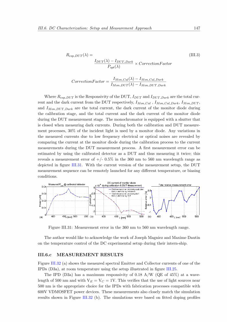
III.6. DC Characterization: Setup and Measurement Approach 147
Resp DUT (λ) = (III.3)
IDUT (λ)− IDUT Dark
Popt(λ)× CorrectionFactor
CorrectionFactor =IMon Cal(λ)− IMon Cal Dark
IMon DUT (λ)− IMon DUT Dark
Where Resp DUT is the Responsivity of the DUT, IDUT and IDUT Dark are the total cur-
rent and the dark current from the DUT respectively, IMon Cal , IMon Cal Dark, IMon DUT ,
and IMon DUT Dark are the total current, the dark current of the monitor diode during
the calibration stage, and the total current and the dark current of the monitor diode
during the DUT measurement stage. The monochromator is equipped with a shutter that
is closed when measuring dark currents. During both the calibration and DUT measure-
ment processes, 30% of the incident light is used by a monitor diode. Any variations in
the measured currents due to low frequency electrical or optical noises are revealed by
comparing the current at the monitor diode during the calibration process to the current
measurements during the DUT measurement process. A first measurement error can be
estimated by using the calibrated detector as a DUT and thus measuring it twice; this
reveals a measurement error of +/- 0.5% in the 360 nm to 560 nm wavelength range as
depicted in figure III.31. With the current version of the measurement setup, the DUT
measurement sequence can be remotely launched for any different temperature, or biasing
conditions.
Figure III.31: Measurement error in the 360 nm to 560 nm wavelength range.
The author would like to acknowledge the work of Joseph Magniez and Maxime Dautin
on the temperature control of the DC experimental setup during their intern-ship.
III.6.c MEASUREMENT RESULTS
Figure III.32 (a) shows the measured spectral Emitter and Collector currents of one of the
IPDs (D3a), at room temperature using the setup illustrated in figure III.25.
The IPD (D3a) has a maximum responsivity of 0.18 A/W (QE of 45%) at a wave-
length of 500 nm and with VE = VC = 1V. This verifies that the use of light sources near
500 nm is the appropriate choice for the IPDs with fabrication processes compatible with
600V VDMOSFET power devices. These measurements also closely match the simulation
results shown in Figure III.32 (b). The simulations were based on fitted doping profiles
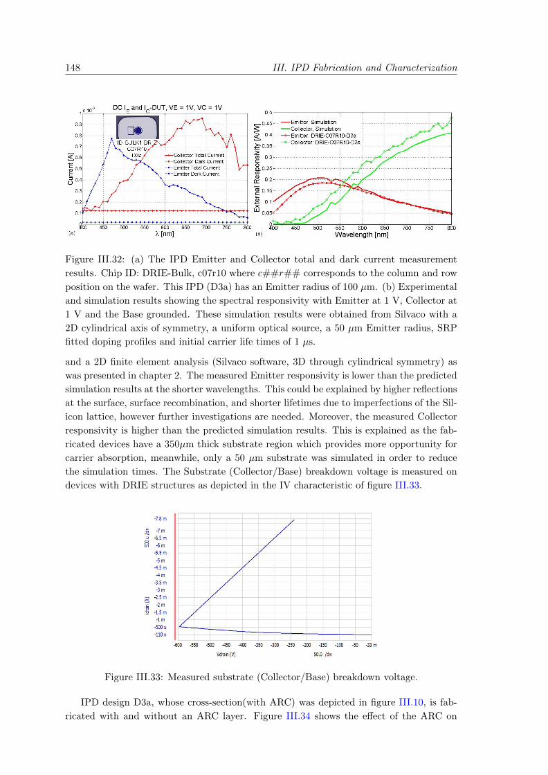
148 III. IPD Fabrication and Characterization
Figure III.32: (a) The IPD Emitter and Collector total and dark current measurement
results. Chip ID: DRIE-Bulk, c07r10 where c##r## corresponds to the column and row
position on the wafer. This IPD (D3a) has an Emitter radius of 100 µm. (b) Experimental
and simulation results showing the spectral responsivity with Emitter at 1 V, Collector at
1 V and the Base grounded. These simulation results were obtained from Silvaco with a
2D cylindrical axis of symmetry, a uniform optical source, a 50 µm Emitter radius, SRP
fitted doping profiles and initial carrier life times of 1 µs.
and a 2D finite element analysis (Silvaco software, 3D through cylindrical symmetry) as
was presented in chapter 2. The measured Emitter responsivity is lower than the predicted
simulation results at the shorter wavelengths. This could be explained by higher reflections
at the surface, surface recombination, and shorter lifetimes due to imperfections of the Sil-
icon lattice, however further investigations are needed. Moreover, the measured Collector
responsivity is higher than the predicted simulation results. This is explained as the fab-
ricated devices have a 350µm thick substrate region which provides more opportunity for
carrier absorption, meanwhile, only a 50 µm substrate was simulated in order to reduce
the simulation times. The Substrate (Collector/Base) breakdown voltage is measured on
devices with DRIE structures as depicted in the IV characteristic of figure III.33.
Figure III.33: Measured substrate (Collector/Base) breakdown voltage.
IPD design D3a, whose cross-section(with ARC) was depicted in figure III.10, is fab-
ricated with and without an ARC layer. Figure III.34 shows the effect of the ARC on
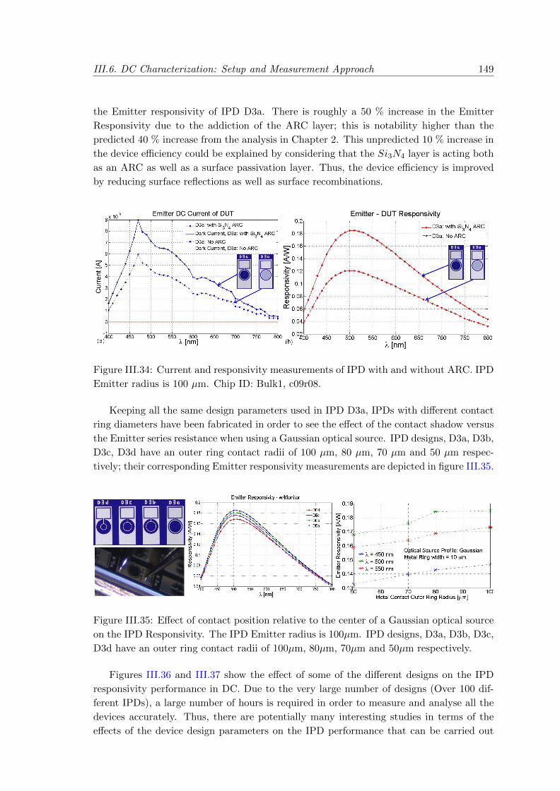
III.6. DC Characterization: Setup and Measurement Approach 149
the Emitter responsivity of IPD D3a. There is roughly a 50 % increase in the Emitter
Responsivity due to the addiction of the ARC layer; this is notability higher than the
predicted 40 % increase from the analysis in Chapter 2. This unpredicted 10 % increase in
the device efficiency could be explained by considering that the Si3N4 layer is acting both
as an ARC as well as a surface passivation layer. Thus, the device efficiency is improved
by reducing surface reflections as well as surface recombinations.
Figure III.34: Current and responsivity measurements of IPD with and without ARC. IPD
Emitter radius is 100 µm. Chip ID: Bulk1, c09r08.
Keeping all the same design parameters used in IPD D3a, IPDs with different contact
ring diameters have been fabricated in order to see the effect of the contact shadow versus
the Emitter series resistance when using a Gaussian optical source. IPD designs, D3a, D3b,
D3c, D3d have an outer ring contact radii of 100 µm, 80 µm, 70 µm and 50 µm respec-
tively; their corresponding Emitter responsivity measurements are depicted in figure III.35.
Figure III.35: Effect of contact position relative to the center of a Gaussian optical source
on the IPD Responsivity. The IPD Emitter radius is 100µm. IPD designs, D3a, D3b, D3c,
D3d have an outer ring contact radii of 100µm, 80µm, 70µm and 50µm respectively.
Figures III.36 and III.37 show the effect of some of the different designs on the IPD
responsivity performance in DC. Due to the very large number of designs (Over 100 dif-
ferent IPDs), a large number of hours is required in order to measure and analyse all the
devices accurately. Thus, there are potentially many interesting studies in terms of the
effects of the device design parameters on the IPD performance that can be carried out
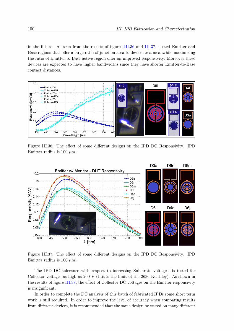
150 III. IPD Fabrication and Characterization
in the future. As seen from the results of figures III.36 and III.37, nested Emitter and
Base regions that offer a large ratio of junction area to device area meanwhile maximizing
the ratio of Emitter to Base active region offer an improved responsivity. Moreover these
devices are expected to have higher bandwidths since they have shorter Emitter-to-Base
contact distances.
Figure III.36: The effect of some different designs on the IPD DC Responsivity. IPD
Emitter radius is 100 µm.
Figure III.37: The effect of some different designs on the IPD DC Responsivity. IPD
Emitter radius is 100 µm.
The IPD DC tolerance with respect to increasing Substrate voltages, is tested for
Collector voltages as high as 200 V (this is the limit of the 2636 Keithley). As shown in
the results of figure III.38, the effect of Collector DC voltages on the Emitter responsivity
is insignificant.
In order to complete the DC analysis of this batch of fabricated IPDs some short term
work is still required. In order to improve the level of accuracy when comparing results
from different devices, it is recommended that the same design be tested on many different

III.7. AC Characterization: Setup and Measurement Approach 151
Figure III.38: High Substrate DC Voltage Effect on IPD. IE and RE versus VC . IPD
Emitter radius is 100 µm. Chip ID: DRIE-Bulk1, c09r07 where c##r## corresponds to
the column and row position on the wafer.
chips and error bars be added to the measurement plots. This would reduce any errors
originating from inconsistencies across the wafers due to fabrication limitations and thus
enable a more clear and conclusive comparison of the different designs. Moreover, the IPD
photocurrents, dark currents, QEs, and optical wavelength (corresponding to the peak QE
of the device) shifts levels need to be studied as a function of temperature effects. In order
to identify the effect of very large substrate voltages on the IPD performance, the IPDs
need to be tested with Collector voltages up to 600 V. Since the Keithley SMU can only
perform measurements up to 200 V, a higher voltage source is required.
III.7 AC Characterization: Setup and Measurement Ap-
proach
Capacitance-Voltage (CV) measurements of the IPDs show a low Emitter-Base capacitance
in the range of 35 pF for detectors of radius 100 µm as depicted in figure III.39. Emitter-
Base capacitances as low as 10 pF is measured for IPDs with a 25 µm radius. Collector-Base
capacitances for the IPDs are in the range of 120 pF; this maybe exceptionally higher than
the value corresponding to the original design due to the fabrication error which has led
to the connection of all the P-regions.
III.7.a First Approach: Externally modulated LED Optical Source
The dynamic behaviour of the IPD devices fabricated during the thesis of Dr. Nicolas
Rouger was introduced in [107] and it showed a bandwidth around 800 kHz. This mea-
surement was completed by Duc Ngoc To during his master internship. Duc designed a
current modulator to modulate the LED optical power. The Emitter contact of the detec-
tor was connected to a high speed / low noise transimpedance amplifier (TIA), while being
DC biased by the sourcemeter (Collector - Base junction biased at 1V). The response to a
2µW optical power step of the fabricated optical detector connected to a low noise 107V/A
TIA [110] is plotted in figure III.40.
However, due to low optical signal levels, high TIA gains were used, resulting in reduced

152 III. IPD Fabrication and Characterization
Figure III.39: Emitter/Base capacitance-voltage (CV) measurement of a 200 µm diameter
IPD at 1 MHz.
−6 −4 −2 0 2 4 6−2.5
−2
−1.5
−1
−0.5
0
0.5
1
1.5
2
Time [µs]
AC
Vo
lta
ge
[V
]
Detector OutputModulated LED Voltage
Figure III.40: Emitter transient response to an optical square wave signal at a 200kHz
frequency when triggered with the 525nm wavelength LED [107].
measurement bandwidths (limiting the bandwidth to roughly 1MHz). Unfortunately, the
measured 3dB bandwidths are in the order of the setup measurement bandwidths [107].
III.7.b Second Approach: Externally modulated Laser
In order to increase the modulated optical power levels at high frequencies over a wide
wavelength range, an extension of the setup for AC measurement has been realized. Figures
III.41 and III.42 show the schematic and the photo of the AC setup using a green laser
with an external electro optical modulator.
The possible solutions available for investigating the effects of the wavelength on the
modulation bandwidth measurements are limited since the wavelength region of interest
is in the visible range and near infra-red (460 nm - 800 nm) where high speed directly
modulated semiconductor laser sources are limited. The approach here is to apply both
external and direct laser modulation techniques. In the case of external modulation, vari-
ous low cost DC mW lasers can be modulated via a broadband electro optical modulator
III.7. AC Characterization: Setup and Measurement Approach 153
Function Generator
EOM
High Voltage Amplifier
Laser
Polarizer Analizer
Em
itter
Base
Collector
Isolated steel box
ShieldGnd
Mirror
USB
SMU
3
Sour
ce M
eter
IEEE
488
.2
DUT
Ch A
Ref.
TIA
SMU1
SMU2Source Meter
Lock-in Amplifier
Figure III.41: AC schematic and measurement setup.
Figure III.42: External amplitude modulation with Green laser.
(EOM, New Focus 4102, 200MHz). The EOM was set up such that a 2:1 modulation
extinction ratio at a 530 nm wavelength and a 120 Vπ were achieved as shown in the EOM
transmission of figure III.43.
A linear high voltage/high frequency modulator (Falco WMA-300, 5MHz 3 dB Band-
width with a 50 x fixed gain, +/- 150 V output) is required to drive the EOM in the case
of step response or harmonic response investigation. Although the modulation bandwidth
of the EOM is 200 MHz, the overall system bandwidth is limited to 5 MHz by the high
voltage amplifier. The overall system bandwidth is verified by measuring the step response
of a high speed detector with a bandwidth of 125 MHz and an integrated TIA as shown
in figure III.44. The main drawbacks of this system are the non linearity of the EOM and
the required high voltage electrical driving electronics.
In the case of indirect modulation, unfortunately large insertion losses due to coupling
light into and out of the EOM and the optical fiber resulted in very low optical power

154 III. IPD Fabrication and Characterization
0 20 40 60 80 100 120 140 160 180 200100
120
140
160
180
200
220
240
Applied DC Voltage [V]
Opti
cal
Pow
er [
µW
]
EOM Optical Power Transmission
Figure III.43: The optical power transmission of the EOM versus applied DC voltages.
DC voltages around 80 V are appropriate for linear region operations.
Figure III.44: The step response of the external modulation setup shows a rise time of
roughly 80 ns which corresponds to a bandwidth of 4.4MHz. The green line corresponds
to the high voltage amplifier input and the blue line corresponds to the voltage output
after the IPD and TIA stage.
levels that we were not able to pick up by the IPDs. Reducing these losses in the future
can allow the completion of this measurement approach.
III.7.c Third Approach: Directly modulated Laser
In the case of direct modulation, a 450 nm blue laser [111] is used; this setup is shown in
figure III.45.
This blue laser can only provide digital modulation of the signal and thus, only step
response analysis are possible. The advantages of this approach are the elimination of

III.7. AC Characterization: Setup and Measurement Approach 155
Figure III.45: Direct amplitude modulation with Blue laser.
the non linear EOM and its high voltage amplifier, moreover, the available optical power
is higher(there are losses in coupling the light beam into the EOM). The level of optical
power available directly effects the level of current available at the output of the IPD.
Increasing the output current, allows for lower amplification requirements on the TIA unit
and hence less restrictions on the TIA bandwidth. Thus, reducing the optical power inser-
tion losses in order to increase the available optical power at the DUT is highly desirable
for the AC characterization. In this setup, the blue laser is powered by a DC voltage
source and TTL modulation signal is supplied by a signal generator. The laser output
light is directly coupled into an optical fiber and taken into the same black box setup used
for the DC analysis and then the fiber is aligned with the DUT. The output of the DUT
is put into the TIA (with a low noise 103V/A gain corresponding to an 80 MHz cut-off
frequency) and the output of the TIA is monitored on an oscilloscope. A 10 MHz filter
on the Oscilloscope was used to remove external noises; however this resulted in a longer
tr. The devices have bandwidths above tens of MHz. Through visual inspection, it was
observed that when lower bandwidth filters were being added to smooth out the output
signal, the signal tr started to become larger for 20 MHz filters and lower. Thus, the initial
AC measurements with the blue laser indicate a high bandwidth above 20 MHz (the IPD
tested was IPD D3a). For a higher tr measurement accuracy, a PCB should be designed

156 III. IPD Fabrication and Characterization
in order to reduce the interconnection adaptors and wires and to bring the TIA as close as
possible to the IPD. The design of an integrated TIA is under progress by Thanh Long Le
[90] who is a PHD student at G2ELab currently working with Dr.Rouger and Dr.Crebier.
Figure III.46: IPD response to a 450 nm blue laser square signal at 10 kHz. A 10 MHz
filter was used to remove external noises.
III.8 Summary
In the duration of this thesis work, one round of fabrication was carried out, where IPDs
where fabricated via the power bipolar process. An unwanted leakage of P-type dopants
throughout the wafers affected the IPD characteristics resulting in a number of different
complications such as a higher dark current levels and an earlier Emitter-Base junction
breakdown voltage. As a result, the IPD Emitter responsivity could only be characterized
for Emitter reverse voltages below 2V, the IPD avalanche mode performance couldn’t be
tested and the difference between IPDs with P+ and P- Base regions couldn’t be studied.
Nevertheless, the DC characterization of the IPDs at 1V Emitter reverse bias and as a
function of Collector reverse voltages as high as 200V, show very promising results that also
match closely the spectral responsivities predicted via simulations. It was demonstrated
that these IPDs can have responsivities as high as 0.2 A/W when the Emitter junction
is reversed biased at only 1V and a 500 nm optical source is used. It was demonstrated
that the addition of an optimized (for a 500 nm wavelength) Si3N4 ARC can increase
the IPD responsivity by approximately 50% at a wavelength of 500 nm. No measurable
change in the Emitter responsivity was observed for substrate DC voltages up to 200V.
The AC characterization of the IPDs also show potentially high bandwidths above 10s of
MHz. Based on the current results a set of long term and short term work can be planned
in the future. The possible short term works on DC and AC characterization of the IPDs
are as follows:
• reproducibility study: There are a number of possible error sources that may affect
the measurement reproducibility and accuracy such as: the experimental setup and
III.8. Summary 157
fabrication non-uniformities throughout the wafer. The detailed explanation of the
DC experimental setup discussed how special care have been taken in reducing mea-
surement errors due to the setup (i.e. source meter current range settings that offer
current accuracy in the order of a few hundreds of pAs, temperature control of +/-
0.03C for temperatures between 20C to 90C, and optical power calibration with
0.5% accuracy). The impact of fabrication non-uniformities on the measurement re-
sults can be taken into account by measuring the same IPD design on many different
dies from the same wafer and plotting the average spectral responsivity with corre-
sponding error bars. The error bars are a result of measurement variation between
different dies on the wafer. These variations due to fabrication (i.e. non-uniform
PR thickness) are manifested as dispersions around the designed dimensions such
as the metal widths and contact opening widths. If large variations are observed,
optical inspections of the devices via microscope may also help reveal the source of
these variations only if they are visible in the finished devices (i.e. metal widths or
misalignments).
• Contact position effects: First, the IPDs designed for studying the effect of con-
tact positions need to be measured several times as explained above, in order to
insure the differences measured are not within the range of the non-uniformity error
bars. Second, changes in the IPD responsivities should be plotted as a function of
shading factor where the shading factor takes into account the Gaussian nature of
the optical source: Shading factor = (The amount of optical power shadowed by
contacts)/(Total amount of optical power). In order to demonstrate this result, the
optical power distribution of the source over the IPD illuminated area needs to be
measured.
• Temperature effects: Since the IPDs have higher dark currents and breakdown volt-
ages due to the unwanted p-type dopant leakage connecting all the p-regions through-
out the wafer, the effect of temperature on the IPD dark currents may not necessarily
corresponds to the intended IPD design. However, the temperature effects on the
ARC optimal wavelength and photocurrent can be characterized in the current IPD
devices.
• Substrate high DC voltage effects: Since the IPDs are to be integrated with 600
V VDMOSFETS, the effect of DC Substrate voltages up to 600V on the IPD per-
formance need to be demonstrated. The IPD substrate contact is on its backside
and it can be controlled by controlling the voltage of the chuck the die is place
upon. In the current DC setup a 2636 Keithley source is used to control the volt-
age of a conductive chuck via a banana connection; however this Keithley is limited
to 200Vs. Thus, a voltage source that can be operated upto at least 600V is required.
• Substrate transient effects: The setup needs to accommodate the application of fast
voltage transients (i.e. [400V to 600V]/[25ns to 100 ns]) on the chuck in order to
characterize the effect of substrate transients on the IPD performance.

158 III. IPD Fabrication and Characterization
• Improve AC setup: The current AC measurement setups suffer from two major chal-
lenges: (1) the reduced available optical power levels due to high insertion losses(i.e.
coupling into/out of fibers, coupling into the EOM in the case of external laser mod-
ulation) require a high amplification stage after the IPD which in turn introduce
bandwidth and noise limitations in the setup. (2) High noise levels from probe sta-
tions, cables, adapters, and the TIA further limit the possible measurable bandwidth
with the current AC setup. A PCB can be designed to remove the probe stations
and reduce the number of required cables and adapters in efforts to improve the
bandwidth measurement capabilities of the setup.
• Demonstrate switching control: Although VDMOSFETs were not fabricated along
side the IPDs during the first fabrication round, a discrete assembly can be used to
demonstrate the transfer of gating signals via the IPD to a VDMOSFET. A PCB
can be designed to assemble together the IPD, its appropriate TIA stage, signal
treatment stage, driver and the VDMOSFET. This approach requires that the IPDs
be wire-bonded and the TIA, driver and power switches will be commercial available
chips that can be soldered to the PCB tracks.
• Reduce optical spot size: The current achievable optical spot size is in the range of
200 µm diameter. There are many designed devices with diameters of 100 µm and
50 µm that require the same size or smaller optical spot size diameters. Controlling
the optical spot diameter down to 10s of µms would allow studying the effect of IPD
sizes and optical spot sizes on the IPD DC and AC performance.
In the long term to do list, a second round of fabrication is required with the following
objectives:
• To remove the fabrication P-type dopant leakage error and in turn remove its con-
sequent complications that limited the IPD characterizations during the first round
of fabrication (i.e. IPD avalanche performance, effect of P- and P+ Base region on
the different IPD designs).
• To include the IPD within the VDMOSFET. Since the first fabrication round demon-
strated a number of positive outcomes that seem to suggest a fair potential for suc-
cess in our proposed IPD galvanic isolation approach, the IPDs will be fabricated
in the second round via the full VDMOSFET process. The finished wafer will fea-
ture power dies that include VDMOSFETs and their associated IPDs (VDMOSFET
source contact connected with the IPD Base contact).
• To demonstrate the switching of a 600V VDMOSFET via the IPD on the same power
die.
• To demonstrate the switching of a 600V VDMOSFET via a cmos integrated detector
using flip-chip technology.

III.8. Summary 159
• To characterize the temperature effects on the IPD performance. Assuming there are
no complications in the second fabrication round, the IPD dark currents and break-
down voltages should be closer to the simulation predictions. Thus, an accurate
study of temperature effects can be performed for temperatures between 20C-90C
using the current DC setup. The setup would need to be upgraded to allow temper-
ature studies in the range of 100C to 200C as well since power chips could reach
temperatures in the range of 150C.

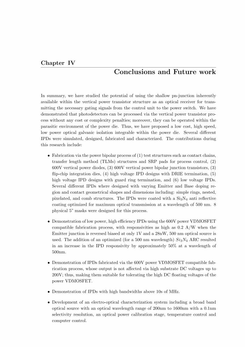
Chapter IV
Conclusions and Future work
In summary, we have studied the potential of using the shallow pn-junction inherently
available within the vertical power transistor structure as an optical receiver for trans-
mitting the necessary gating signals from the control unit to the power switch. We have
demonstrated that photodetectors can be processed via the vertical power transistor pro-
cess without any cost or complexity penalties; moreover, they can be operated within the
parasitic environment of the power die. Thus, we have proposed a low cost, high speed,
low power optical galvanic isolation integrable within the power die. Several different
IPDs were simulated, designed, fabricated and characterized. The contributions during
this research include:
• Fabrication via the power bipolar process of (1) test structures such as contact chains,
transfer length method (TLMs) structures and SRP pads for process control, (2)
600V vertical power diodes, (3) 600V vertical power bipolar junction transistors, (3)
flip-chip integration dies, (4) high voltage IPD designs with DRIE termination, (5)
high voltage IPD designs with guard ring termination, and (6) low voltage IPDs.
Several different IPDs where designed with varying Emitter and Base doping re-
gion and contact geometrical shapes and dimensions including: simple rings, nested,
pixelated, and comb structures. The IPDs were coated with a Si3N4 anti reflective
coating optimized for maximum optical transmission at a wavelength of 500 nm. 8
physical 5” masks were designed for this process.
• Demonstration of low power, high efficiency IPDs using the 600V power VDMOSFET
compatible fabrication process, with responsivities as high as 0.2 A/W when the
Emitter junction is reversed biased at only 1V and a 28nW, 500 nm optical source is
used. The addition of an optimized (for a 500 nm wavelength) Si3N4 ARC resulted
in an increase in the IPD responsivity by approximately 50% at a wavelength of
500nm.
• Demonstration of IPDs fabricated via the 600V power VDMOSFET compatible fab-
rication process, whose output is not affected via high substrate DC voltages up to
200V; thus, making them suitable for tolerating the high DC floating voltages of the
power VDMOSFET.
• Demonstration of IPDs with high bandwidths above 10s of MHz.
• Development of an electro-optical characterization system including a broad band
optical source with an optical wavelength range of 200nm to 1600nm with a 0.1nm
selectivity resolution, an optical power calibration stage, temperature control and
computer control.
162 IV. Conclusions and Future work
In order to complete the full characterization of the proposed IPD the following near
future work are suggested:
• Substrate Tests: The effect of high voltage transients (i.e. [400V to 600V]/[25ns to
100ns]) and DC voltages up to 600V on the IPD performance,
• Full Bandwidth Analysis: The IPD bandwidths as a function of optical wavelength,
applied voltages, optical beam radii and IPD size and geometry,
• Noise and Temperature: The effect of Temperature on the IPD DC and AC perfor-
mance (signal-to-noise ratio as a function of temperature).
• Planar Hybrid Integration: The driving approach can be validated by switching a
commercial VDMOSFET by the IPD. The IPD can be connected to its appropriate
CMOS processing chip (including the TIA + K voltage gain, a gate driver and an
efficient self driver supply) and a VDMOSFET via a planar integration approach on
a PCB as depicted in figure IV.1.
Figure IV.1: Approach verification via a planar hybrid integration on PCB.
The long term goal is to develop a fully integrated, power-efficient power function
including a suitable optical galvanic isolation, its associated signal processing and power
switch driver circuitries, and the power switch. The suggested long term future work
includes:
• Mixed (Monolithic + Hybrid) Planar Integration: The power die (this is the mono-
lithic component including the IPD and VDMOSFET) can be connected to its ap-
propriate CMOS processing chip (including the TIA + K voltage gain, a gate driver
and an efficient self driver supply) via a planar integration approach on a PCB in
order to demonstrate the switching action of the VDMOSFET as controlled by the
163
IPD. A direct bonded copper (DBC) would be used for better insulation between
chips and effective heat dissipation. Light can be supplied to the detector by means
of an optical fiber or an edge emitting laser depending on the IPD design. This pla-
nar hybrid integration can also be tested with the IPD integrated within the CMOS
chip rather than the power die,
• Flip-Chip Hybrid Integration: a CMOS chip with readout circuit (TIA + K voltage
gain), a gate driver and an efficient self driver supply, is flip-chipped on the power
die (including the IPD and VDMOSFET). In order to demonstrate the controlled
switching action of the VDMOSFET, the IPD can be triggered by (a) light that
is edge or vertically coupled by means of an optical fiber, (b) a flip-chip optical
interconnect chip that provides light coupling by means of grating couplers and
waveguides, (c) an optical source such as an LED or an edge emitting laser aligned
to edge trigger the IPD in free space, or (d) optical signals by waveguides and grating
couplers.
• Smart Power Chip Integration: The necessary TIA, processing and driver circuitry
are integrated within the power die along side the IPD and VDMOSFET in order
to investigate the potential of a fully integrated power function. This solution is
depicted in figure IV.2.
• Integrated optical routing interface: An compatible integrated optical routing and
interface needs to be designed for the opitcal triggering of the IPD as depicted
in figure IV.3. Specially in the case of integrating passive optical elements such
as waveguides and grating couplers, temperature effects need to be investigated to
insure reliability.
• Optical Detection and Supply Integration: In addition to the IPD that has been
developed in this thesis to transfer the gate signal, a second IPD biased under the
conditions of a solar cell could be integrated to provide the necessary power supply.
The generated voltage at terminals of this second IPD can be converted by a DC-DC
converter to charge a storage capacitor for power supply purposes. This approach
can simplify the CMOS circuitry since the floating power supply is eliminated. In
this case, a more powerful optical source with a DC and AC component would be
required in order to deliver both the energy and the gating signal. One option to
investigate is the integration of the two optical detectors in the CMOS processing
chip which is connected to the power die on a DBC via wire bonding. A second
option would be to integrate the two optical detectors in the smart power die as
depicted in figure IV.4. Since the second IPD is used as a solar cell to output a
voltage, it needs to be forward biased; in this case the parasitic bipolar is an issue
and needs to be suppressed from turning on.

164 IV. Conclusions and Future work
Figure IV.2: Smart power chip integration approach.
Figure IV.3: Smart power chip with an integrated photonic chip that provides at minimum
the optical routing interconnects as well as the necessariy grating couplers.
Figure IV.4: In addition to the IPD, a second IPD biased under the conditions of a solar
cell could be integrated to provide the necessary power supply.

Chapter V
Resume de la these en francais
Sommaire
V.1 Introduction et Motivation: Integration monolithique d’uneisolation optique . . . . . . . . . . . . . . . . . . . . . . . . . . . . . . . . . . 166
V.1.a L’Etat de l’Art et les Objectifs du Projet . . . . . . . . . . . . . . . . . . . 167
V.1.b Approches d’integration et la Structure de IPD . . . . . . . . . . . . . . . . 171
V.2 Simulations et Caracterisation . . . . . . . . . . . . . . . . . . . . . . . 173
V.3 Conclusions . . . . . . . . . . . . . . . . . . . . . . . . . . . . . . . . . . . . . 175
Abstract
Dans les convertisseurs de puissance, les interrupteurs de puissance peuvent fonc-
tionner a de niveaux de tension eleves. Dans ce cas, leurs commandes externes qui
fonctionnent a de tensions plus basses doivent etre electriquement isolees. Des trans-
formateurs ou d’optocoupleurs ont ete traditionnellement mis en ouvre afin d’isoler
les commandes rapprochees. Cette these presente une nouvelle solution optique dans
laquelle un detecteur optique est integre de facon monolithique au sein d’un transistor
de puissance de 600 V a l’aide de sa structure verticale. Ce detecteur optique integre
(IPD) fournit un faible courant a une commande rapprochee qui va ensuite l’amplifier
afin de commander le transistor de puissance. La commande rapprochee peut etre
representee par une composant type flip-chip ou elle peut egalement etre monolithique-
ment integree. L’IPD a une tres faible consommation, une bande passante elevee
(BW) et de l’isolation galvanique optique entre le dispositif d’alimentation et sa com-
mande. Les contraintes imposees par la structure du dispositif d’alimentation et sa
fabrication limitant les performances de l’IPD sont etudiees ainsi que son mode de
fonctionnement. Des analyses ont ete conduites suite a de travaux de modelisation
analytique, des simulations avec la methode des elements finis et de validation experi-
mentale. La responsivite spectrale (R) des detecteurs de 400 nm a de longueurs d’ondes
proches au spectre infrarouge a ete mesuree et une valeur maximale de la responsivite
de 0,2 A/W a 500 nm a ete atteinte. Les resultats des mesures montrent une faible
capacite de l’emetteur de l’ordre de 35 pF a 10 pF pour de detecteurs de diametre
dentre 50 µm a 200 µm. Les premieres mesures AC indiquent une BW au dessus de
20 MHz.
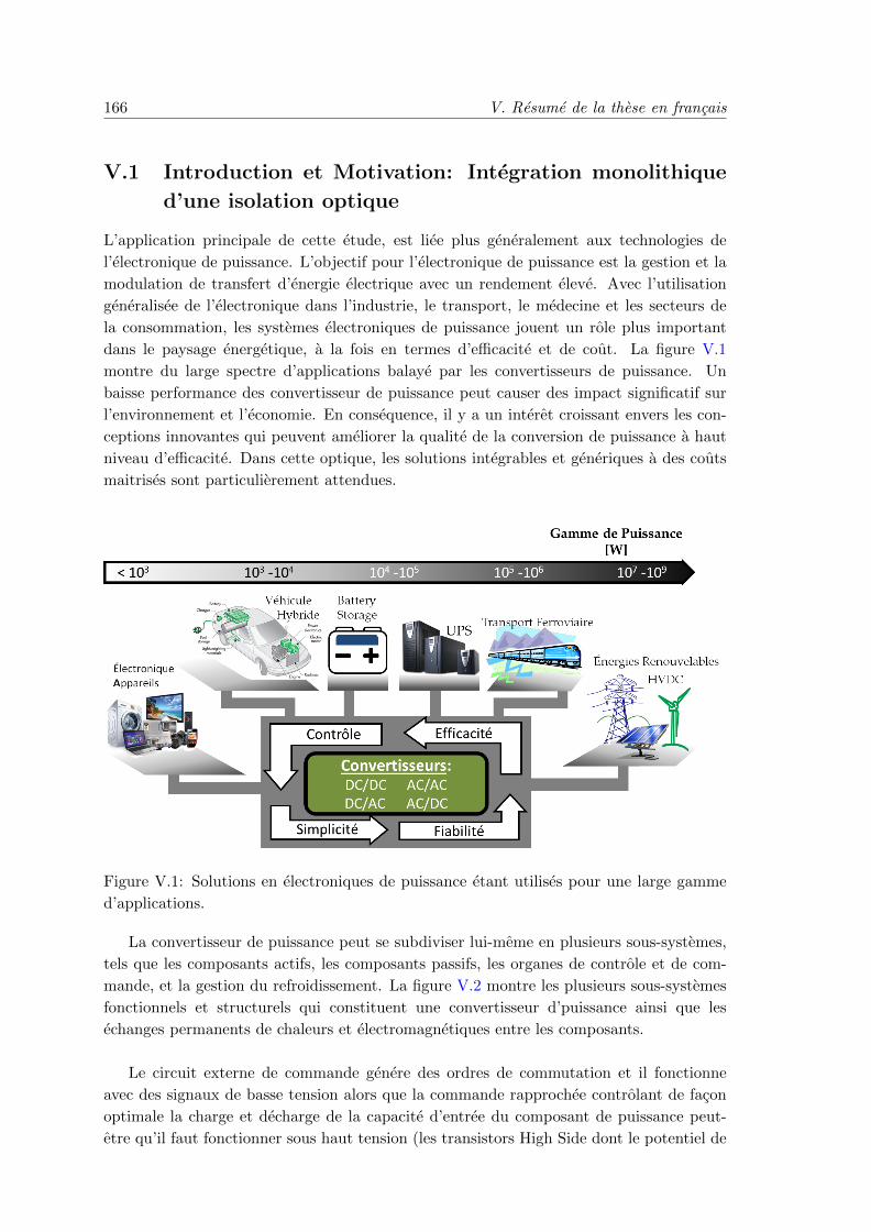
166 V. Resume de la these en francais
V.1 Introduction et Motivation: Integration monolithique
d’une isolation optique
L’application principale de cette etude, est liee plus generalement aux technologies de
l’electronique de puissance. L’objectif pour l’electronique de puissance est la gestion et la
modulation de transfert d’energie electrique avec un rendement eleve. Avec l’utilisation
generalisee de l’electronique dans l’industrie, le transport, le medecine et les secteurs de
la consommation, les systemes electroniques de puissance jouent un role plus important
dans le paysage energetique, a la fois en termes d’efficacite et de cout. La figure V.1
montre du large spectre d’applications balaye par les convertisseurs de puissance. Un
baisse performance des convertisseur de puissance peut causer des impact significatif sur
l’environnement et l’economie. En consequence, il y a un interet croissant envers les con-
ceptions innovantes qui peuvent ameliorer la qualite de la conversion de puissance a haut
niveau d’efficacite. Dans cette optique, les solutions integrables et generiques a des couts
maitrises sont particulierement attendues.
Figure V.1: Solutions en electroniques de puissance etant utilises pour une large gamme
d’applications.
La convertisseur de puissance peut se subdiviser lui-meme en plusieurs sous-systemes,
tels que les composants actifs, les composants passifs, les organes de controle et de com-
mande, et la gestion du refroidissement. La figure V.2 montre les plusieurs sous-systemes
fonctionnels et structurels qui constituent une convertisseur d’puissance ainsi que les
echanges permanents de chaleurs et electromagnetiques entre les composants.
Le circuit externe de commande genere des ordres de commutation et il fonctionne
avec des signaux de basse tension alors que la commande rapprochee controlant de facon
optimale la charge et decharge de la capacite d’entree du composant de puissance peut-
etre qu’il faut fonctionner sous haut tension (les transistors High Side dont le potentiel de
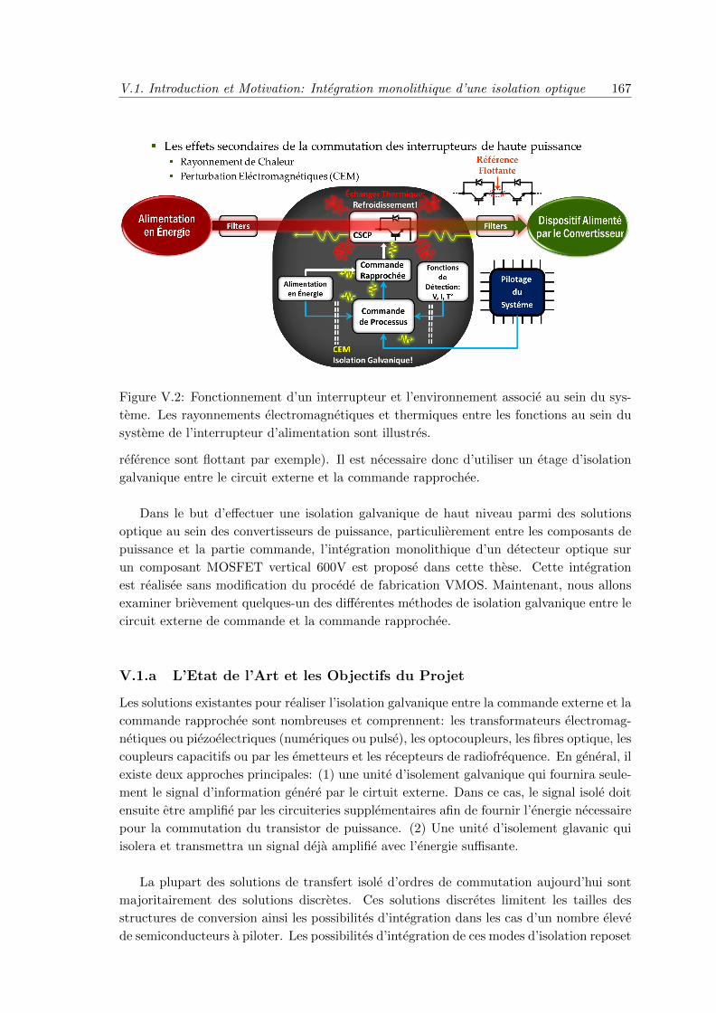
V.1. Introduction et Motivation: Integration monolithique d’une isolation optique 167
Figure V.2: Fonctionnement d’un interrupteur et l’environnement associe au sein du sys-
teme. Les rayonnements electromagnetiques et thermiques entre les fonctions au sein du
systeme de l’interrupteur d’alimentation sont illustres.
reference sont flottant par exemple). Il est necessaire donc d’utiliser un etage d’isolation
galvanique entre le circuit externe et la commande rapprochee.
Dans le but d’effectuer une isolation galvanique de haut niveau parmi des solutions
optique au sein des convertisseurs de puissance, particulierement entre les composants de
puissance et la partie commande, l’integration monolithique d’un detecteur optique sur
un composant MOSFET vertical 600V est propose dans cette these. Cette integration
est realisee sans modification du procede de fabrication VMOS. Maintenant, nous allons
examiner brievement quelques-un des differentes methodes de isolation galvanique entre le
circuit externe de commande et la commande rapprochee.
V.1.a L’Etat de l’Art et les Objectifs du Projet
Les solutions existantes pour realiser l’isolation galvanique entre la commande externe et la
commande rapprochee sont nombreuses et comprennent: les transformateurs electromag-
netiques ou piezoelectriques (numeriques ou pulse), les optocoupleurs, les fibres optique, les
coupleurs capacitifs ou par les emetteurs et les recepteurs de radiofrequence. En general, il
existe deux approches principales: (1) une unite d’isolement galvanique qui fournira seule-
ment le signal d’information genere par le cirtuit externe. Dans ce cas, le signal isole doit
ensuite etre amplifie par les circuiteries supplementaires afin de fournir l’energie necessaire
pour la commutation du transistor de puissance. (2) Une unite d’isolement glavanic qui
isolera et transmettra un signal deja amplifie avec l’energie suffisante.
La plupart des solutions de transfert isole d’ordres de commutation aujourd’hui sont
majoritairement des solutions discretes. Ces solutions discretes limitent les tailles des
structures de conversion ainsi les possibilites d’integration dans les cas d’un nombre eleve
de semiconducteurs a piloter. Les possibilites d’integration de ces modes d’isolation reposet
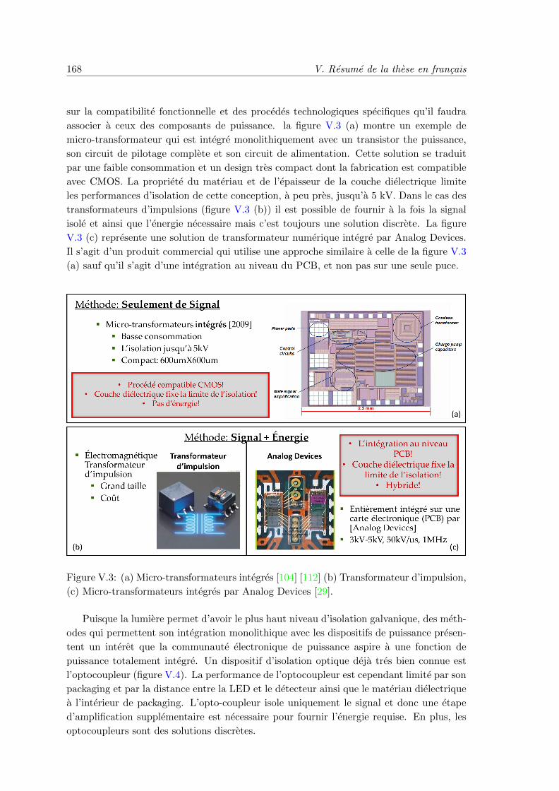
168 V. Resume de la these en francais
sur la compatibilite fonctionnelle et des procedes technologiques specifiques qu’il faudra
associer a ceux des composants de puissance. la figure V.3 (a) montre un exemple de
micro-transformateur qui est integre monolithiquement avec un transistor the puissance,
son circuit de pilotage complete et son circuit de alimentation. Cette solution se traduit
par une faible consommation et un design tres compact dont la fabrication est compatible
avec CMOS. La propriete du materiau et de l’epaisseur de la couche dielectrique limite
les performances d’isolation de cette conception, a peu pres, jusqu’a 5 kV. Dans le cas des
transformateurs d’impulsions (figure V.3 (b)) il est possible de fournir a la fois la signal
isole et ainsi que l’energie necessaire mais c’est toujours une solution discrete. La figure
V.3 (c) represente une solution de transformateur numerique integre par Analog Devices.
Il s’agit d’un produit commercial qui utilise une approche similaire a celle de la figure V.3
(a) sauf qu’il s’agit d’une integration au niveau du PCB, et non pas sur une seule puce.
Figure V.3: (a) Micro-transformateurs integres [104] [112] (b) Transformateur d’impulsion,
(c) Micro-transformateurs integres par Analog Devices [29].
Puisque la lumiere permet d’avoir le plus haut niveau d’isolation galvanique, des meth-
odes qui permettent son integration monolithique avec les dispositifs de puissance presen-
tent un interet que la communaute electronique de puissance aspire a une fonction de
puissance totalement integre. Un dispositif d’isolation optique deja tres bien connue est
l’optocoupleur (figure V.4). La performance de l’optocoupleur est cependant limite par son
packaging et par la distance entre la LED et le detecteur ainsi que le materiau dielectrique
a l’interieur de packaging. L’opto-coupleur isole uniquement le signal et donc une etape
d’amplification supplementaire est necessaire pour fournir l’energie requise. En plus, les
optocoupleurs sont des solutions discretes.
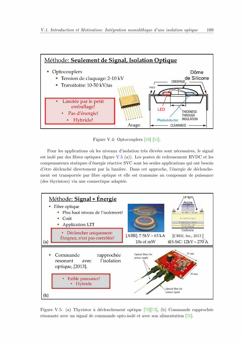
V.1. Introduction et Motivation: Integration monolithique d’une isolation optique 169
Figure V.4: Optocouplers [49] [51].
Pour les applications ou les niveaux d’isolation tres elevees sont necessaires, le signal
est isole par des fibres optiques (figure V.5 (a)). Les postes de redressement HVDC et les
compensateurs statiques d’energie reactive SVC sont les seules applications qui ont besoin
d’etre declenche directement par la lumiere. Dans cet approche, l’energie de declenche-
ment est transportee par fibre optique et elle est transmise au composant de puissance
(des thyristors) via une connectique adaptee.
Figure V.5: (a) Thyristor a declenchement optique [70][73], (b) Commande rapprochee
resonante avec un signal de commande opto-isole et avec son alimentation [76].
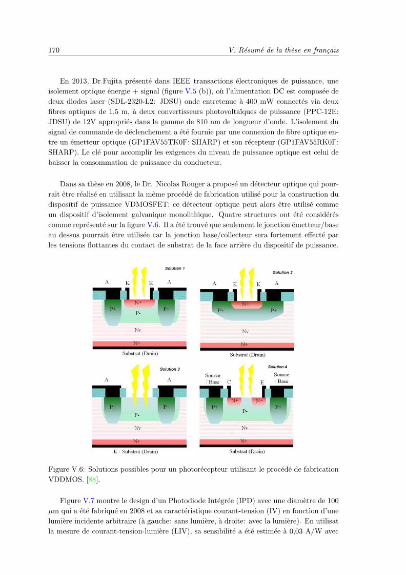
170 V. Resume de la these en francais
En 2013, Dr.Fujita presente dans IEEE transactions electroniques de puissance, une
isolement optique energie + signal (figure V.5 (b)), ou l’alimentation DC est composee de
deux diodes laser (SDL-2320-L2: JDSU) onde entretenue a 400 mW connectes via deux
fibres optiques de 1,5 m, a deux convertisseurs photovoltaıques de puissance (PPC-12E:
JDSU) de 12V appropries dans la gamme de 810 nm de longueur d’onde. L’isolement du
signal de commande de declenchement a ete fournie par une connexion de fibre optique en-
tre un emetteur optique (GP1FAV55TK0F: SHARP) et son recepteur (GP1FAV55RK0F:
SHARP). Le cle pour accomplir les exigences du niveau de puissance optique est celui de
baisser la consommation de puissance du conducteur.
Dans sa these en 2008, le Dr. Nicolas Rouger a propose un detecteur optique qui pour-
rait etre realise en utilisant la meme procede de fabrication utilise pour la construction du
dispositif de puissance VDMOSFET; ce detecteur optique peut alors etre utilise comme
un dispositif d’isolement galvanique monolithique. Quatre structures ont ete consideres
comme represente sur la figure V.6. Il a ete trouve que seulement le jonction emetteur/base
au dessus pourrait etre utilisee car la jonction base/collecteur sera fortement effecte par
les tensions flottantes du contact de substrat de la face arriere du dispositif de puissance.
Figure V.6: Solutions possibles pour un photorecepteur utilisant le procede de fabrication
VDDMOS. [88].
Figure V.7 montre le design d’un Photodiode Integree (IPD) avec une diametre de 100
µm qui a ete fabrique en 2008 et sa caracteristique courant-tension (IV) en fonction d’une
lumiere incidente arbitraire (a gauche: sans lumiere, a droite: avec la lumiere). En utilisat
la mesure de courant-tension-lumiere (LIV), sa sensibilite a ete estimee a 0,03 A/W avec
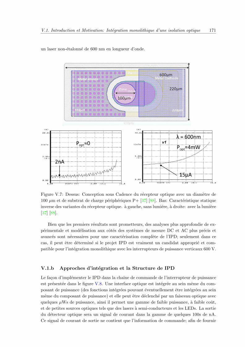
V.1. Introduction et Motivation: Integration monolithique d’une isolation optique 171
un laser non-etalonne de 600 nm en longueur d’onde.
Figure V.7: Dessus: Conception sous Cadence du recepteur optique avec un diametre de
100 µm et de substrat de charge peripheriques P+ [37] [88]. Bas: Caracteristique statique
inverse des variantes du recepteur optique. a gauche, sans lumiere, a droite: avec la lumiere
[37] [88].
Bien que les premiers resultats sont prometteurs, des analyses plus approfondie de ex-
perimentale et modelisation aux cotes des systemes de mesure DC et AC plus precis et
avances sont necessaires pour une caracterisation complete de l’IPD; seulement dans ce
cas, il peut etre determine si le projet IPD est vraiment un candidat approprie et com-
patible pour l’integration monolithique avec les interrupteurs de puissance verticaux 600 V.
V.1.b Approches d’integration et la Structure de IPD
Le facon d’implementer le IPD dans la chaıne de commande de l’interrupteur de puissance
est presentee dans le figure V.8. Une interface optique est integree au sein meme du com-
posant de puissance (des fonctions integrees pouvant eventuellement etre integrees au sein
meme du composant de puissance) et elle peut etre declenche par un faisceau optique avec
quelques µWs de puissance, ainsi il permet une gamme de faible puissance, a faible cout,
et de petites sources optiques tels que des lasers a semi-conducteurs et les LEDs. La sortie
du detecteur optique sera un signal de courant dans la gamme de quelques 100s de nA.
Ce signal de courant de sortie ne contient que l’information de commande; afin de fournir
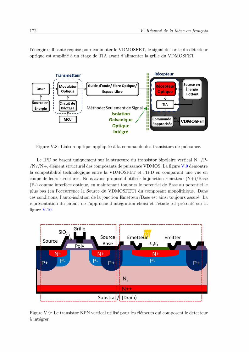
172 V. Resume de la these en francais
l’energie suffisante requise pour commuter le VDMOSFET, le signal de sortie du detecteur
optique est amplifie a un etage de TIA avant d’alimenter la grille du VDMOSFET.
Figure V.8: Liaison optique appliquee a la commande des transistors de puissance.
Le IPD se basent uniquement sur la structure du transistor bipolaire vertical N+/P-
/Nv/N+, element structurel des composants de puissance VDMOS. La figure V.9 demontre
la compatibilite technologique entre la VDMOSFET et l’IPD en comparant une vue en
coupe de leurs structures. Nous avons propose d’utiliser la jonction Emetteur (N+)/Base
(P-) comme interface optique, en maintenant toujours le potentiel de Base au potentiel le
plus bas (en l’occurrence la Source du VDMOSFET) du composant monolithique. Dans
ces conditions, l’auto-isolation de la jonction Emetteur/Base est ainsi toujours assure. La
representation du circuit de l’approche d’integration choisi et l’etude est presente sur la
figure V.10.
Figure V.9: Le transistor NPN vertical utilise pour les elements qui composent le detecteur
a integrer
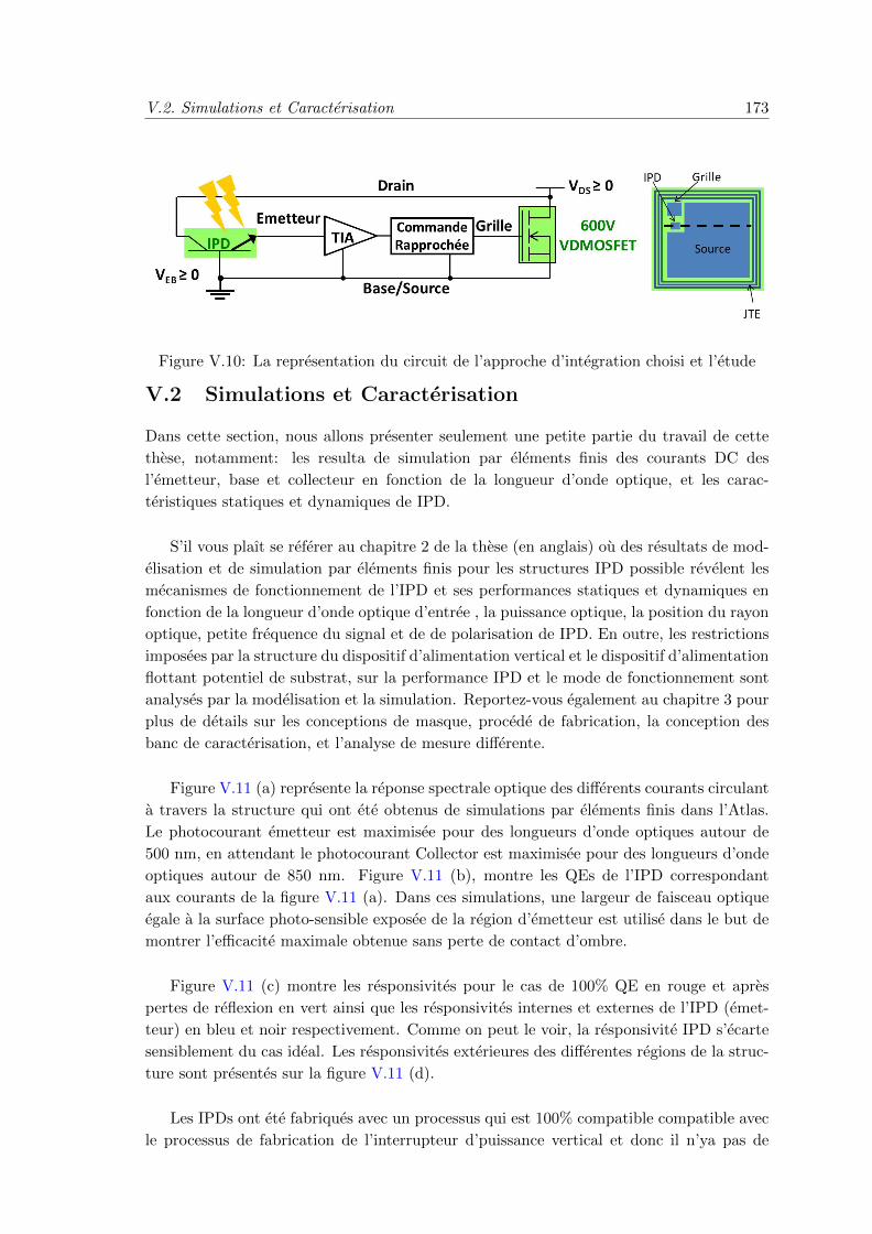
V.2. Simulations et Caracterisation 173
Figure V.10: La representation du circuit de l’approche d’integration choisi et l’etude
V.2 Simulations et Caracterisation
Dans cette section, nous allons presenter seulement une petite partie du travail de cette
these, notamment: les resulta de simulation par elements finis des courants DC des
l’emetteur, base et collecteur en fonction de la longueur d’onde optique, et les carac-
teristiques statiques et dynamiques de IPD.
S’il vous plaıt se referer au chapitre 2 de la these (en anglais) ou des resultats de mod-
elisation et de simulation par elements finis pour les structures IPD possible revelent les
mecanismes de fonctionnement de l’IPD et ses performances statiques et dynamiques en
fonction de la longueur d’onde optique d’entree , la puissance optique, la position du rayon
optique, petite frequence du signal et de de polarisation de IPD. En outre, les restrictions
imposees par la structure du dispositif d’alimentation vertical et le dispositif d’alimentation
flottant potentiel de substrat, sur la performance IPD et le mode de fonctionnement sont
analyses par la modelisation et la simulation. Reportez-vous egalement au chapitre 3 pour
plus de details sur les conceptions de masque, procede de fabrication, la conception des
banc de caracterisation, et l’analyse de mesure differente.
Figure V.11 (a) represente la reponse spectrale optique des differents courants circulant
a travers la structure qui ont ete obtenus de simulations par elements finis dans l’Atlas.
Le photocourant emetteur est maximisee pour des longueurs d’onde optiques autour de
500 nm, en attendant le photocourant Collector est maximisee pour des longueurs d’onde
optiques autour de 850 nm. Figure V.11 (b), montre les QEs de l’IPD correspondant
aux courants de la figure V.11 (a). Dans ces simulations, une largeur de faisceau optique
egale a la surface photo-sensible exposee de la region d’emetteur est utilise dans le but de
montrer l’efficacite maximale obtenue sans perte de contact d’ombre.
Figure V.11 (c) montre les responsivites pour le cas de 100% QE en rouge et apres
pertes de reflexion en vert ainsi que les responsivites internes et externes de l’IPD (emet-
teur) en bleu et noir respectivement. Comme on peut le voir, la responsivite IPD s’ecarte
sensiblement du cas ideal. Les responsivites exterieures des differentes regions de la struc-
ture sont presentes sur la figure V.11 (d).
Les IPDs ont ete fabriques avec un processus qui est 100% compatible compatible avec
le processus de fabrication de l’interrupteur d’puissance vertical et donc il n’ya pas de
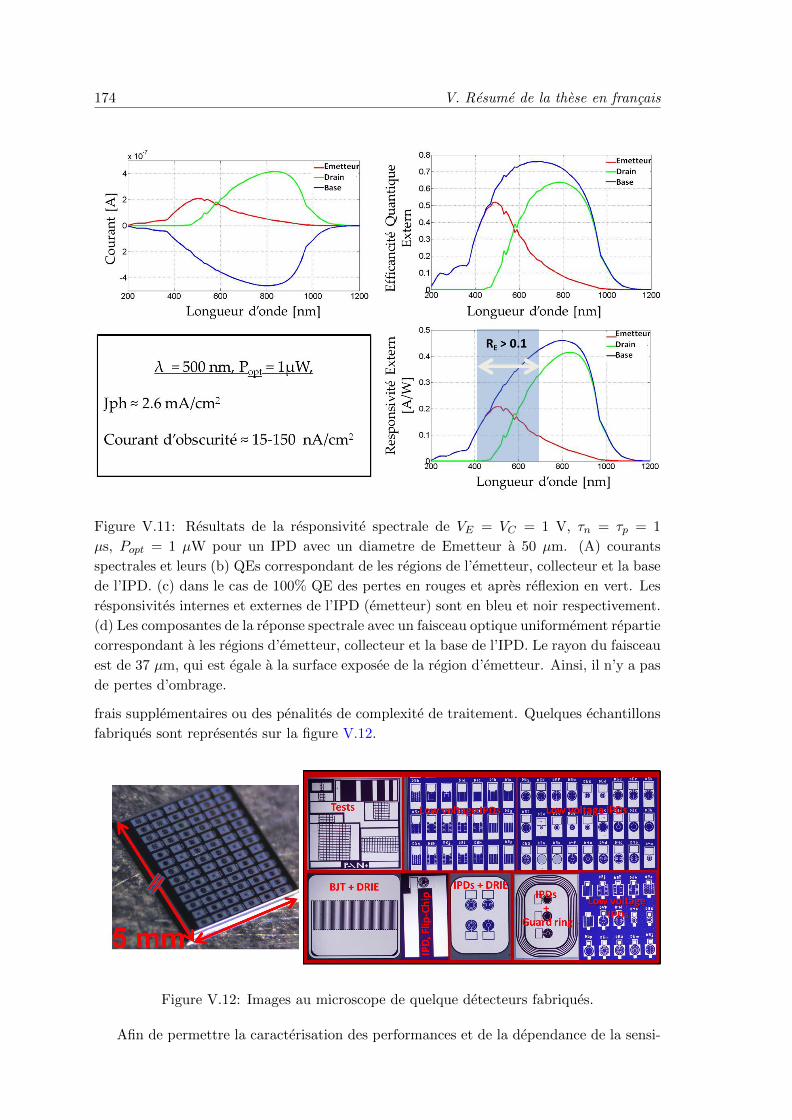
174 V. Resume de la these en francais
Figure V.11: Resultats de la responsivite spectrale de VE = VC = 1 V, τn = τp = 1
µs, Popt = 1 µW pour un IPD avec un diametre de Emetteur a 50 µm. (A) courants
spectrales et leurs (b) QEs correspondant de les regions de l’emetteur, collecteur et la base
de l’IPD. (c) dans le cas de 100% QE des pertes en rouges et apres reflexion en vert. Les
responsivites internes et externes de l’IPD (emetteur) sont en bleu et noir respectivement.
(d) Les composantes de la reponse spectrale avec un faisceau optique uniformement repartie
correspondant a les regions d’emetteur, collecteur et la base de l’IPD. Le rayon du faisceau
est de 37 µm, qui est egale a la surface exposee de la region d’emetteur. Ainsi, il n’y a pas
de pertes d’ombrage.
frais supplementaires ou des penalites de complexite de traitement. Quelques echantillons
fabriques sont representes sur la figure V.12.
Figure V.12: Images au microscope de quelque detecteurs fabriques.
Afin de permettre la caracterisation des performances et de la dependance de la sensi-
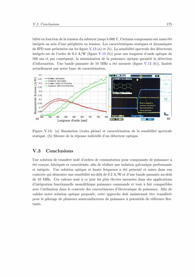
V.3. Conclusions 175
bilite en fonction de la tension du substrat jusqu’a 600 V, Certains composants ont aussi ete
integres au sein d’une peripherie en tension. Les caracteristiques statiques et dynamiques
de IPD sont presentees sur les figure V.13 (a) et (b). La sensibilite spectrale des detecteurs
integres est de l’ordre de 0.2 A/W (figure V.13 (b)) pour une longueur d’onde optique de
500 nm et par consequent, la minimisation de la puissance optique garantit la detection
d’information. Une bande passante de 10 MHz a ete mesuree (figure V.13 (b)), limitee
actuellement par notre banc de caracterisation.
Figure V.13: (a) Simulation (traits pleins) et caracterisation de la sensibilite spectrale
statique. (b) Mesure de la reponse indicielle d’un detecteur optique.
V.3 Conclusions
Une solution de transfert isole d’ordres de commutation pour composants de puissance a
ete concue, fabriquee et caracterisee, afin de realiser une isolation galvanique performante
et integree. Une solution optique et haute frequence a ete presente et mises dans son
contexte qui demontre une sensibilite au-dela de 0.2 A/W et d’une bande passante au-dela
de 10 MHz. Ces valeurs sont a ce jour les plus elevees mesurees dans des applications
d’integration fonctionnelle monolithique puissance commande et tout a fait compatibles
avec l’utilisation dans le contexte des convertisseurs d’electronique de puissance. Afin de
valider notre solution optique proposee, cette approche doit maintenant etre transferee
pour le pilotage de plusieurs semiconducteurs de puissance a potentiels de reference flot-
tants.
Monolithic integration of a photodetector for controlpurposes within vertical power transistors
Abstract The work presented in this PhD manuscript deals with the monolithic inte-
gration of an optical galvanic isolation unit within the vertical FET structure of a 600V
power transistor. The optical galvanic isolation unit is a photodetector that is responsible
for transferring the gating information signal from an external control unit to the power
switch. The necessary energy to switch the power device is provided by means of a TIA
followed by a gate driver. This document has four chapters: introduction and motivation:
Integrated glavanic isolation for power devices, Compatible integrated phootdiodes (IPDs)
for power switches: Modeling and design, IPD fabrication and characterization, and con-
clusions and future work. The results of this research work are interesting for a wide range
of applications specially as the power electronic community strives for a fully integrated
power function with lower implementation costs and reliable, high level galvanic isolation
solutions that are compact and cost effective.
Keywords photodetector modelling and design, low cost monolithic integration, optical
insulation, galvanic isolation, optical signal transmission, vertical FET technology.
L’integration monolithique d’un photodetecteur al’interieur des transistors de puissance verticaux pour
des fins de commande
Resume Les travaux presentes dans ce manuscrit traite de l’integration monolithique
d’une unite d’isolement galvanique optique a l’interieur de la structure d’un transistor de
puissance vertical a effet de champ 600V. L’unite d’isolement galvanique optique est un
photodetecteur qui est responsable du transfert du signal de commande de parti une unite
de commande externe a le transistor de puissance. L’energie necessaire pour commuter le
dispositif de puissance est fournie au moyen d’un TIA, suivie d’une commande de grille.
Le memoire de these se structure en quatre chapitres equivalents: Introduction et motiva-
tion: l’isolement glavanic integree pour les dispositifs de puissance, photodiodes integres
compatibles (JVP) pour les interrupteurs de puissance: Modelisation et conception, IPD
fabrication et la caracterisation, et les conclusions et les travaux futurs. Les resultats de ces
travaux de recherche sont interessants pour un large spectre d’applications, specialement
pour les fonctions d’alimentation entierement integres avec et cout de fabrication reduit
et des solutions fiables, de haut niveau galvaniques isolement qui sont compacts et rentable.
Mots cles Modelisation et conception de photodetecteur, integration monolithique
fonctionnelle bas cout, isolation et transmission par voie optique, la technologie de FET
vertical

Bibliography
[1] K. Sozanski, Digital Signal Processing in Power Electronics Control Circuits.
Springer Verlag Longdon, 2013, ch. 1.
[2] R. Herzer, “Integrated gate driver circuit solutions,” in Integrated Power Electronics
Systems (CIPS), 2010 6th International Conference, IEEE, 2010.
[3] T. L. Skvarenina, Ed., The Power Electronic Handbook. CRC Press LLC, 2002.
[4] Alcatel-lucent. Bell labs top 10 innovations. [Online]. Available: http://www3.
alcatel-lucent.com/wps/portal/!ut/p/kcxml/04 Sj9SPykssy0xPLMnMz0vM0Y
QjzKLd4w3MXMBSYGYRq6m-pEoYgbxjgiRIH1vfV-P
NxU QD9gtzQiHJHR0UAPA8KJg!!/delta/base64xml/
L3dJdyEvd0ZNQUFzQUMvNElVRS82X0FfNDZL
[5] B. Baliga, Fundamentals of Power Semiconductor Devices. Springer Science +
Business Media, LLC, 2008.
[6] J. Biela, M. Schweizer, S. Waffler, and J. Kolar, “SiC versus Si?evaluation of poten-
tials for performance improvement of inverter and DC-DC converter systems by sic
power semiconductors,” IEEE Industrial Electronics Society, vol. 58, no. 7, pp. 2872
– 2882, 2011.
[7] R. Perret, Ed., Power Electronics Semiconductor Devices. ISTE Ltd and John
Wiley & Sons, Inc, 2009.
[8] (ECPE). Homepage of the european center for power electronics. [Online]. Available:
http://www.ecpe.org
[9] (CPES). Homepage of the US center for power electronics systems. [Online].
Available: http://www.cpes.vt.edu
[10] (AIST-PERC). Homepage of the national institute of advanced industrial science
and technology - power electronics research center, japan. [Online]. Available:
http://www.aist.go.jp/aiste/annual/2005/environment/perc/percmain.html
[11] F. Blaabjerg, A. Consoli, J. Ferreira, and J. Van Wyk, “The future of electronic
power processing and conversion,” IEEE Industry Applications Society, 2005.

[12] J.-L. Sanchez, P. Austin, M. Breil, J.-P. Laur, J.-C. Crebier, L. Aubard, and C. Scha-
effer, “State of the art and trends in power integration,” in Integrated Power Systems
(CIPS), 4th International Conference, 2006, pp. 1 – 6.
[13] J.-L. Sanchez, “State of the art and trends in power integration,” in International
Conference on Modeling and Simulation of Microsystems, 1999, pp. 20 – 29.
[14] J. Kolar, J. Biela, S. Waffler, and T. Friedli, “Performance trends and limitations
of power electronic systems,” in Integrated Power Electronics Systems (CIPS), 6th
International Conference, Mar. 2010, pp. 1 – 20.
[15] I. Rectifier, “Data sheet IR 2135, IR 2235,” International Rectifier, Tech. Rep.
[16] S. Microelectronics, “Data sheet, L6384,” ST Microelectronics, Tech. Rep., 2003.
[17] M. S.Pawel, Rossberg and R. Herzer, “600V SOI gate drive HVIC for medium power
applications operating up to 200 c,” in Proc. ISPSD, 2005, pp. 55 – 58.
[18] S. K. S. Gupta, J.C. Beckman, “Improved latch up immunity in junction-isolated
smart power ICs with unbiased guard ring,” IEEE Electron Device Letters, vol. 22,
no. 12, 2001.
[19] T. Takahashi, “Power conversion processor architecture and HVIC technology for
AC motor drive,” in Proc. CIPS, 2000, pp. 73–81.
[20] D. Tam,“New 1200V integrated circuit changes the way 3-phase motor drive inverters
are designed,” International Rectifier, Tech. Rep., 2008.
[21] H. Akiyama, N. Yasuda, J. Moritani, and K. Takanashi, “A high breakdown voltage
IC with lateral power device based on SODI structure,” in Proc. ISPSD, 2004, pp.
375 – 378.
[22] T. Yamane, S. Ikeda, and A. Nakagawa, “Three-phase sinusoidal current PWM
brushless motor driver ICs,” in Proc. ISPSD, 2004, pp. 147 – 150.
[23] M. Huque, L. Tolbert, B. Blalock, and S. Islam, “Silicon-on-insulator-based high-
voltage, high-temperature integrated circuit gate driver for silicon carbide-based
power field effect transistors,” Power Electronics, IET, vol. 3, no. 6, pp. 1001 –
1009, Nov. 2010.
[24] C. Caramel, P. Austin, J.-L. Sanchez, E. Imbernon, and R. B., “Interaction analysis
and insulation techniques for short-circuit integrated protection structure,” in Proc.
ISPSD, 2006, pp. 1 – 4.
[25] J.-L. Sanchez and all,“Realization of P+ walls through-wafer for bidirectional current
and voltage power integrated devices,” in Proc. ISPSD, 2003, pp. 195 – 198.
[26] I. Bertrand and all, “New lateral dmos and igbt structures realized on a partial
soi substrate based on lego process,” in Bipolar/BiCMOS Circuits and Technology
Meeting, 2005, pp. 74 – 77.
[27] S. LEFEBVRE and B. MULTON, “Commande des semi-conducteurs de puissance:
contextes.” Techniques de lingenieur, no. D3230, August 2002.
[28] Avago, “Safety considerations when using optocouplers and alternative isolators for
providing protection against electrical hazards,” Avago Technologies, Tech. Rep.,
2010.
[29] B. Chen, “Fully integrated isolated DC-to-DC converter and half bridge gate driver
with integral power supply,” 1st International Workshop on Power Supply on Chip,
Analog Devices, Tech. Rep., 2008.
[30] J.-C. Crebier and N. Rouger, “Loss free gate driver unipolar power supply for high
side power transistors,” IEEE Transactions on Power Electronics, vol. 23, no. 3, pp.
1565 –1573, May 2008.
[31] D. Vasic, F. Costa, and E. Sarraute, “Piezoelectric transformer for integrated MOS-
FET and IGBT gate driver,” Power Electronics, IEEE Transactions on, 2005.
[32] R. Kliger, “Integrated transformer-coupled isolation,” Instrumentation & Measure-
ment Magazine, IEEE, 2003.
[33] D. Oliveira, M. Batista, L. Barreto, and P. Praca, “A bidirectional single stage
DC-DC converter with high frequency isolation,” in Applied Power Electronics Con-
ference and Exposition (APEC), 2013 Twenty-Eighth Annual IEEE, 2013.
[34] H. Fan and H. Li, “High-frequency transformer isolated bidirectional DC-DC con-
verter modules with high efficiency over wide load range for 20 kVA solid-state
transformer,” Power Electronics, IEEE Transactions on, vol. 26, no. 12, pp. 3599 –
3608, Dec. 2011.
[35] L. Peng, R. Wu, X. Fang, Y. Toyoda, M. Akahane, M. Yamaji, H. Sumida3, and
J. K. Sin, “A novel 3D TSV transformer technology for digital isolator gate driver
applications,” in Proceedings of The 25th International Symposium on Power Semi-
conductor Devices & ICs (ISPSD), 2013.
[36] S. Mazumder and T. Sarkar, “Optically-activated gate control of power semicon-
ductor device switching dynamics,” in IEEE International Symposium on Power
Semiconductor Devices IC’s, 2009, pp. 152 –155.
[37] N. Rouger and J.-C. Crebier, “Integrated photoreceiver for an isolated control signal
transfert in favour of power transistors,” in IEEE International Symposium on Power
Semiconductor Devices and IC’s, May 2008, pp. 213 –216.
[38] A. Alessandria, L. La Magna, M. Renna, and L. Fragapane, “Integrated si-based
opto-couplers: a novel approach to galvanic isolation,” in Solid-State Device Research
Conference, 2002. Proceeding of the 32nd European, 2002, pp. 647 – 650.
[39] M. Lazarus, K. Loungis, and V. Allen, “Optically controlled high-speed switching of
a power transistor,” Circuits and Systems I: Fundamental Theory and Applications,
IEEE Transactions on, vol. 47, no. 4, pp. 528 – 535, 2000.

[40] F. Zeltner, S. IISB and Erlangen, “Insulating IGBT driver with PCB integrated
capacitive coupling elements,” in Integrated Power Electronics Systems (CIPS), 6th
International Conference on, 2010.
[41] S. Brehaut and F. Costa, “Gate driving of high power igbt by wireless transmission,”
in IEEE Power Electronics and Motion Control Conference, 2006, pp. 1 –5.
[42] B. Wang, M. Riva, J. Bakos, and A. Monti, “Integrated circuit implementation for a
gan hfet driver circuit,” Industry Applications, IEEE Transactions on, vol. 46, no. 5,
pp. 2056 – 2067, Sept.-Oct. 2010.
[43] A. Devices. Digital isolators. [Online]. Available: http://www.analog.com/en/
interface-isolation/digital-isolators/products/index.html#Isolated Gate Drivers
[44] C. Batard et al., “Wireless transmission of igbt driver control,” in IEEE Applied
Power Electronics Conference and Exposition, 2009, pp. 1257 –1262.
[45] K. Gingerich and C. Sterzik, “The ISO72x family of high-speed digital isolators,”
Texas Instruments, Tech. Rep., 2006.
[46] Avago. Digital isolators. [Online]. Available: http://www.analog.com/en/
interface-isolation/digital-isolators/products/index.html#Isolated Gate Drivers
[47] Opto-isolator. [Online]. Available: http://en.wikipedia.org/wiki/Optical coupler
[48] J. Seah Eng Lee, A. Jaus, P. Sullivan, and C. Teck Bee, “Building a safe and robust
industrial system with avago technologies optocouplers,” Avago Technologies, Tech.
Rep., 2008.
[49] V. Ching and F. Chwan JYE, “Ensuring rigorous isolation in field bus designs,”
Avago Technologies, Tech. Rep., 2012.
[50] (Avago). Optoisolation and optical sensor products selection guide.
[Online]. Available: http://www.google.fr/url?sa=t&rct=j&q=&esrc=
s&source=web&cd=4&ved=0CEMQFjAD&url=http%3A%2F%2Fwww.avagotech.
com%2Fdocs%2FAV00-0263EN&ei=WvtaUuPJHePX0QXDvoCoAg&usg=
AFQjCNHrrJ4IYuZZcS6MJGfriqJA3WM9bw&sig2=4-vm1Vd
kBbXB6nmYnXaog&bvm=bv.53899372,d.d2k&cad=rja
[51] Avago. Hcpl-665k. [Online]. Available: http://www.avagotech.com/pages/en/
optocouplers hermetic/10 mbd high cmr four channel/hcpl-665k/
[52] P. Horowitz Winfield Hill, The Art Of Electronics. Cambridge University Press,
1989.
[53] B. Kennedy, “Implementing an isolated half-bridge gate driver,” Analog Devices,
Tech. Rep., 2012.
[54] Electromagnetic induction. [Online]. Available: http://en.wikipedia.org/wiki/
Faraday%27s law of induction#Faraday.27s law
[55] V. Nguyen, J.-C. Crebier, and P. Jeannin, “Compact, isolated and simple to imple-
ment gate driver using high frequency transformer,” in APEC, 2011.
[56] L. Ourak, A. Ghannam, D. Bourrier, and C. Viallon, “Solenoidal transformers for
magnetic materials integration,” in APMC, 2012.
[57] Transformer types. [Online]. Available: http://en.wikipedia.org/wiki/Transformer
types#Pulse transformer
[58] SCHURTER, “Efficient EMC solutions,” SCHURTER, Tech. Rep., 2009.
[59] B. Chen, “Application note AN-937: Gate drive characteristics and requirements for
HEXFET power MOSFETs,” International Rectifier, Tech. Rep., 1995-2013.
[60] B. Kennedy, “Reducing the size and complexity of an isolated,” Analog Devices,
Tech. Rep., 2011.
[61] B. Bell, “Gate drive transformers vs. fully integrated isolators in isolated DC-DC
power converters,” National Semiconductor Corporation, Tech. Rep., 2010.
[62] Y. Koike and M. Asai, “The future of plastic optical fiber,” Nature, NPG Asia
Materials, vol. 1, pp. 22–28, 2009.
[63] O. Ziemann, J. Krauser, P. Zamzow, and W. Daum, POF Handbook: Optical Short
range Transmission Systems. Springer, 2008.
[64] (Berkeley). Electromagnetic spectrum. [Online]. Available: http://www.lbl.gov/
MicroWorlds/ALSTool/EMSpec/EMSpec2.html
[65] Tutorial: Fiber Optic Basics, 1996-2013.
[66] M. Wappmannsberger, “Galvanic isolation for IGBT-driver,” Avago Technologies,
Tech. Rep., 2013.
[67] J. e. a. Nishizawa, “Fabrication and optical-switching results on the integrated light-
triggered and quenched static induction thyristor,” Electron Devices, IEEE Trans-
actions, vol. 33, no. 12, pp. 2031 – 2040, Dec. 1986.
[68] B. Danielsson and A. P. Syst., “Hvdc valve with light-triggered thyristors,” in IEEE
AC and DC Power Transmission, Sep. 1991.
[69] S. L. Rumyantsev, M. E. Levinshtein, M. Shur, T. Saxena, Q. Zhang, A. K. Agarwal,
L. Cheng, and J. W. Palmour, “Optical triggering of 12 kV 1 cm2 4H-SiC thyristors,”
Materials Science Forum, vol. 740 - 742, pp. 990–993, 2013.
[70] (Siemens). New static var compensator (SVC) for australia. [Online]. Available:
http://www.ptd.siemens.de/artikel0507.html
[71] T. Sarkar and S. K. Mazumder, “Epitaxial design of a direct optically controlled
gaas/algaas-based heterostructure lateral superjunction power device for fast repeti-
tive switching,” IEEE Transactions on Electron Devices, vol. 54, no. 3, pp. 589 –600,
2007.

[72] F. Zhao, M. Islam, P. Muzykov, and A. Bolotnikov, “Optically activated 4H-SiC
p-i-n diodes for high-power applications,” IEEE Electron Device Letters, vol. 30, pp.
1182 – 1184, 2009.
[73] F. Zhao and M. Islam, “Optically activated SiC power transistors for pulsed-power
application,” IEEE Electron Device Letters, vol. 31, pp. 1146 – 1148, 2010.
[74] W. Naoki, K. Tsunenobu, and S. Jun, “4H-SiC pn photodiodes with temperature-
independent photoresponse up to 300 C,” Applied Physics Express, vol. 5, 2012.
[75] C. James, C. Hettler, and J. Dickens, “Design and evaluation of a compact silicon
carbide photoconductive semiconductor switch,” IEEE Transactions on Electron De-
vices, vol. 58, pp. 508 – 511, 2011.
[76] H. Fujita, “A resonant gate-drive circuit with optically isolated control signal and
power supply for fast-switching and high-voltage power semiconductor devices,”
Power Electronics, IEEE Transactions, vol. 28, no. 11, pp. 5423 – 5430, 2013.
[77] M. E. Thomas, Optical Propagation in Linear Media: Atmospheric Gases and Par-
ticles, Solid-State Components, and Water. Oxford University Press, 2006.
[78] S. M. Sze and K. N. Kwok, Physics of Semiconductor Devices, Third Edition. JOHN
WILEY & SONS, JNC., 2007.
[79] C. o. E. Committee on Materials for High-Temperature Semiconductor Devices Na-
tional Advisory Board and T. Systems, Eds., Materials for high-temperature semi-
conductor devices. National Academy Press, Washington, DC, NMAB-474, 1995,
1995.
[80] M. Welker, D. Zipperer, S. Malzer, R. Windisch, P. Heremans, and G. Dohler, “High-
speed low-energy photoconductive receiver with high gain,” in SPIE, 2001.
[81] X. Li, J. E. Carey, J. W. Sickler, M. U. Pralle, C. Palsule, and C. J. Vineis, “Silicon
photodiodes with high photoconductive gain at room temperature,” Optics Express,
vol. 20, no. 5, pp. 5518–5523, 2012.
[82] M. Yang, J. Thomas, K. Rim, D. Rogers, and J. e. a. Schaub, “A high-speed,
high-sensitivity silicon lateral trench photodetector,” Electron Device Letters, IEEE,
vol. 23, no. 7, pp. 395 – 397, 2002.
[83] S. Assefa, F. Xia, S. W. Bedell, Y. Zhang, T. Topuria, P. M. Rice, and V. Y.A.,
“CMOS-integrated high-speed MSM germanium waveguide photodetector,” Optics
Express, vol. 18, no. 5, pp. 4986–4999, 2010.
[84] A. Pospischil, M. Humer, M. M. Furchi, D. Bachmann, R. Guider, T. Fromherz, and
T. Mueller, “Cmos-compatible graphene photodetector covering all optical commu-
nication bands,” Nature Photonics, 2013.
[85] J. Mathews, R. Roucka, C. Weng, J. Tolle, J. Menendez, and J. Kouvetakis, “Ger-
manium p-i-n photodiode on silicon for integrated photonic applications,” in Proc.
SPIE 7606, Silicon Photonics, 2012.

[86] L. Vivien, A. Polzer, D. M. Morini, J. Osmond, J. M. Hartmann, P. Crozat, E. Cas-
san, C. Kopp, H. Zimmermann, and J. M. Fedeli, “Zero-bias 40Gbit/s germanium
waveguide photodetector on silicon,” Optics Express, vol. 20, no. 2, pp. 1096–1101,
2012.
[87] S. Klinger, M. Berroth, M. Kaschel, and M. e. a. Oehme, “Ge-on-Si p-i-n photodiodes
with a 3-dB bandwidth of 49 GHz,” Photonics Technology Letters, IEEE, vol. 21,
no. 13, pp. 920 – 922, 2009.
[88] N. Rouger, “Integration monolithique des fonctions d’interface au sein de composants
de puissance a structure verticale,” Ph.D. dissertation, Institut Polytechnique de
Grenoble, laboratoire de Genie Electrique de Grenoble, 2008.
[89] N. Rouger, J.-C. Crebier, and O. Lesaint, “Integrated low power and high band-
width optical isolator for monolithic power mosfets driver,” in IEEE International
Symposium on Power Semiconductor Devices and ICs, may 2011.
[90] T. L. Le, “Isolation galvanique integree pour nouveaux transistors de puissance,”
Ph.D. dissertation, Institut Polytechnique de Grenoble, laboratoire de Genie Elec-
trique de Grenoble, 2015.
[91] Abundance of the chemical elements. [Online]. Available: http://en.wikipedia.org/
wiki/Abundance of the chemical elements#Abundance of elements in the Earth
[92] O. Trapp, R. Blanchard, L. Lopp, and T. Kamins, Eds., Semiconductor Technology
Handbook. Technology Associates, 1985.
[93] W. Shockley, “The Theory of p-n Junctions in Semiconductors and p-n Junction
Transistors,” Bell System Technical Journal, vol. 28, pp. 435 – 489, 1949.
[94] R.-Y. Sah, R. N. Noyce, and W. Shockley, “Carrier Generation and Recombination in
P-N Junctions and P-N Junction Characteristics,” in Proceedings of the IRE, vol. 45,
no. 9, Sep. 1957, pp. 1228 – 1243.
[95] J. Moll and N. Murray Hill, “The Evolution of the Theory for the Voltage-Current
Characteristic of P-N Junctions,” in Proceedings of the IRE, vol. 46, no. 6, Jun. 1958,
pp. 1076 – 1082.
[96] D. L. PULFREY, Understanding Modern Transistors and Diodes. Cambridge Uni-
versity Press, 2010.
[97] Silvaco, “Atlas User?s Manual Device Simulation Software,” Silvaco, Tech. Rep.,
2008.
[98] M. Fox, Optical Properties of Solids. New York, Oxford University Press, 2003.
[99] A. Yariv and Y. Pochi, Photonics, Optical Electronics in Modern Communications.
New York, Oxford University Press, 2007.
[100] J. Zhao, A. Wang, and M. Green, “24.5Substrates and 24.7Progress in Photovoltaics:
Research and Applications, vol. 7, pp. 471 ? 474”
Nov. 1999.

[101] W. Shockley and W. Read,“Statistics of the Recombinations of Holes and Electrons,”
Journal of Physical Review, vol. 87, p. 835, 1952.
[102] V. Barkhordarian, “Power MOSFET basics,” International Rectifier, Tech. Rep.
[103] D. K. SCHRODER, SEMICONDUCTOR MATERIAL AND DEVICE CHARAC-
TERIZATION. A JOHN WILEY & SONS, INC., PUBLICATION, 2006.
[104] T. Simonot, “Conception et hybridation de l’environnement electronique des com-
posants de puissance a structure verticale,” Ph.D. dissertation, Institut Polytech-
nique de Grenoble, laboratoire de Genie Electrique de Grenoble, 2011.
[105] H. N. XUAN, “Methodes et modeles pour une approche de dimensionnement
geometrique et technologique d’un semi-conducteur de puissance integre. application
a la conception d?un mosfet autonome,” Ph.D. dissertation, Institut Polytechnique
de Grenoble, laboratoire de Genie Electrique de Grenoble, 2011.
[106] K. Vladimirova, “Nouveaux concepts pour l’integration 3d et le refroidissement des
semi-conducteurs de puissance a structure verticale,” Ph.D. dissertation, Institut
Polytechnique de Grenoble, laboratoire de Genie Electrique de Grenoble, 2012.
[107] R. Vafaei, N. Rouger, D. To, and J.-C. Crebier, “Experimental investigation of an
integrated optical interface for power mosfets drivers,” IEEE Electron Device Letters,
vol. 33, 2012.
[108] R. Vafaei, N. Rouger, and J.-C. Crebier, “Performance Measurements of an Opti-
cal Detector Designed for Monolithic Integration with a Power VDMOS,” in IEEE
I2MTC, May 2013.
[109] M. Cvijetic, Optical Transmission Systems Engineering. ARTECH HOUSE, INC.,
2004.
[110] (Edmunds). Variable gain high speed current amplifier dhpca-100. [Online].
Available: http://www.femto.de/images/pdf-dokumente/de-dhpca-100 r9.pdf
[111] (Z-Laser). Z40m18h-f-450-lp45. [Online]. Available: http://www.datasheetlib.com/
datasheet/1167261/z40m18h-f-450-lp45 z-laser.html
[112] T. Simonot, N. Rouger, and J. Crebier, “Design and characterization of an integrated
cmos gate driver for vertical power mosfets,” in IEEE Energy Conversion Congress
and Exposition, 2010, pp. 2206 –2213.

Copyright © 2022 FDOKUMEN