Fabrication and characterization of sol-gel-derived zinc oxide thin-film transistor
6
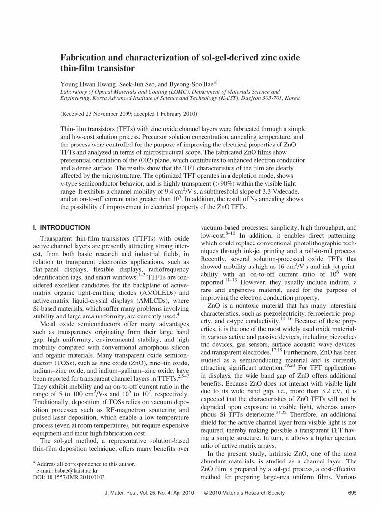
Fabrication and characterization of sol-gel-derived zinc oxide thin-film transistor Young Hwan Hwang, Seok-Jun Seo, and Byeong-Soo Bae a) Laboratory of Optical Materials and Coating (LOMC), Department of Materials Science and Engineering, Korea Advanced Institute of Science and Technology (KAIST), Daejeon 305-701, Korea (Received 23 November 2009; accepted 1 February 2010) Thin-film transistors (TFTs) with zinc oxide channel layers were fabricated through a simple and low-cost solution process. Precursor solution concentration, annealing temperature, and the process were controlled for the purpose of improving the electrical properties of ZnO TFTs and analyzed in terms of microstructural scope. The fabricated ZnO films show preferential orientation of the (002) plane, which contributes to enhanced electron conduction and a dense surface. The results show that the TFT characteristics of the film are clearly affected by the microstructure. The optimized TFT operates in a depletion mode, shows n-type semiconductor behavior, and is highly transparent (>90%) within the visible light range. It exhibits a channel mobility of 9.4 cm 2 /Vs, a subthreshold slope of 3.3 V/decade, and an on-to-off current ratio greater than 10 5 . In addition, the result of N 2 annealing shows the possibility of improvement in electrical property of the ZnO TFTs. I. INTRODUCTION Transparent thin-film transistors (TTFTs) with oxide active channel layers are presently attracting strong inter- est, from both basic research and industrial fields, in relation to transparent electronics applications, such as flat-panel displays, flexible displays, radiofrequency identification tags, and smart windows. 1–3 TTFTs are con- sidered excellent candidates for the backplane of active- matrix organic light-emitting diodes (AMOLEDs) and active-matrix liquid-crystal displays (AMLCDs), where Si-based materials, which suffer many problems involving stability and large area uniformity, are currently used. 4 Metal oxide semiconductors offer many advantages such as transparency originating from their large band gap, high uniformity, environmental stability, and high mobility compared with conventional amorphous silicon and organic materials. Many transparent oxide semicon- ductors (TOSs), such as zinc oxide (ZnO), zinc–tin oxide, indium–zinc oxide, and indium–gallium–zinc oxide, have been reported for transparent channel layers in TTFTs. 2,5–7 They exhibit mobility and an on-to-off current ratio in the range of 5 to 100 cm 2 /Vs and 10 6 to 10 7 , respectively. Traditionally, deposition of TOSs relies on vacuum depo- sition processes such as RF-magnetron sputtering and pulsed laser deposition, which enable a low-temperature process (even at room temperature), but require expensive equipment and incur high fabrication cost. The sol-gel method, a representative solution-based thin-film deposition technique, offers many benefits over vacuum-based processes: simplicity, high throughput, and low-cost. 8–10 In addition, it enables direct patterning, which could replace conventional photolithographic tech- niques through ink-jet printing and a roll-to-roll process. Recently, several solution-processed oxide TFTs that showed mobility as high as 16 cm 2 /Vs and ink-jet print- ability with an on-to-off current ratio of 10 6 were reported. 11–13 However, they usually include indium, a rare and expensive material, used for the purpose of improving the electron conduction property. ZnO is a nontoxic material that has many interesting characteristics, such as piezoelectricity, ferroelectric prop- erty, and n-type conductivity. 14–16 Because of these prop- erties, it is the one of the most widely used oxide materials in various active and passive devices, including piezoelec- tric devices, gas sensors, surface acoustic wave devices, and transparent electrodes. 17,18 Furthermore, ZnO has been studied as a semiconducting material and is currently attracting significant attention. 19,20 For TFT applications in displays, the wide band gap of ZnO offers additional benefits. Because ZnO does not interact with visible light due to its wide band gap, i.e., more than 3.2 eV, it is expected that the characteristics of ZnO TFTs will not be degraded upon exposure to visible light, whereas amor- phous Si TFTs deteriorate. 21,22 Therefore, an additional shield for the active channel layer from visible light is not required, thereby making possible a transparent TFT hav- ing a simple structure. In turn, it allows a higher aperture ratio of active matrix arrays. In the present study, intrinsic ZnO, one of the most abundant materials, is studied as a channel layer. The ZnO film is prepared by a sol-gel process, a cost-effective method for preparing large-area uniform films. Various a) Address all correspondence to this author. e-mail: [email protected] DOI: 10.1557/JMR.2010.0103 J. Mater. Res., Vol. 25, No. 4, Apr 2010 © 2010 Materials Research Society 695
-
Upload
independent -
Category
Documents
-
view
0 -
download
0
Transcript of Fabrication and characterization of sol-gel-derived zinc oxide thin-film transistor
Fabrication and characterization of sol-gel-derived zinc oxidethin-film transistor
Young Hwan Hwang, Seok-Jun Seo, and Byeong-Soo Baea)
Laboratory of Optical Materials and Coating (LOMC), Department of Materials Science andEngineering, Korea Advanced Institute of Science and Technology (KAIST), Daejeon 305-701, Korea
(Received 23 November 2009; accepted 1 February 2010)
Thin-film transistors (TFTs) with zinc oxide channel layers were fabricated through a simpleand low-cost solution process. Precursor solution concentration, annealing temperature, andthe process were controlled for the purpose of improving the electrical properties of ZnOTFTs and analyzed in terms of microstructural scope. The fabricated ZnO films showpreferential orientation of the (002) plane, which contributes to enhanced electron conductionand a dense surface. The results show that the TFT characteristics of the film are clearlyaffected by the microstructure. The optimized TFT operates in a depletion mode, showsn-type semiconductor behavior, and is highly transparent (>90%) within the visible lightrange. It exhibits a channel mobility of 9.4 cm2/V�s, a subthreshold slope of 3.3 V/decade,and an on-to-off current ratio greater than 105. In addition, the result of N2 annealing showsthe possibility of improvement in electrical property of the ZnO TFTs.
I. INTRODUCTION
Transparent thin-film transistors (TTFTs) with oxideactive channel layers are presently attracting strong inter-est, from both basic research and industrial fields, inrelation to transparent electronics applications, such asflat-panel displays, flexible displays, radiofrequencyidentification tags, and smart windows.1–3 TTFTs are con-sidered excellent candidates for the backplane of active-matrix organic light-emitting diodes (AMOLEDs) andactive-matrix liquid-crystal displays (AMLCDs), whereSi-based materials, which suffer many problems involvingstability and large area uniformity, are currently used.4
Metal oxide semiconductors offer many advantagessuch as transparency originating from their large bandgap, high uniformity, environmental stability, and highmobility compared with conventional amorphous siliconand organic materials. Many transparent oxide semicon-ductors (TOSs), such as zinc oxide (ZnO), zinc–tin oxide,indium–zinc oxide, and indium–gallium–zinc oxide, havebeen reported for transparent channel layers in TTFTs.2,5–7
They exhibit mobility and an on-to-off current ratio in therange of 5 to 100 cm2/V�s and 106 to 107, respectively.Traditionally, deposition of TOSs relies on vacuum depo-sition processes such as RF-magnetron sputtering andpulsed laser deposition, which enable a low-temperatureprocess (even at room temperature), but require expensiveequipment and incur high fabrication cost.
The sol-gel method, a representative solution-basedthin-film deposition technique, offers many benefits over
vacuum-based processes: simplicity, high throughput, andlow-cost.8–10 In addition, it enables direct patterning,which could replace conventional photolithographic tech-niques through ink-jet printing and a roll-to-roll process.Recently, several solution-processed oxide TFTs thatshowed mobility as high as 16 cm2/V�s and ink-jet print-ability with an on-to-off current ratio of 106 werereported.11–13 However, they usually include indium, arare and expensive material, used for the purpose ofimproving the electron conduction property.
ZnO is a nontoxic material that has many interestingcharacteristics, such as piezoelectricity, ferroelectric prop-erty, and n-type conductivity.14–16 Because of these prop-erties, it is the one of the most widely used oxide materialsin various active and passive devices, including piezoelec-tric devices, gas sensors, surface acoustic wave devices,and transparent electrodes.17,18 Furthermore, ZnO has beenstudied as a semiconducting material and is currentlyattracting significant attention.19,20 For TFT applicationsin displays, the wide band gap of ZnO offers additionalbenefits. Because ZnO does not interact with visible lightdue to its wide band gap, i.e., more than 3.2 eV, it isexpected that the characteristics of ZnO TFTs will not bedegraded upon exposure to visible light, whereas amor-phous Si TFTs deteriorate.21,22 Therefore, an additionalshield for the active channel layer from visible light is notrequired, thereby making possible a transparent TFT hav-ing a simple structure. In turn, it allows a higher apertureratio of active matrix arrays.
In the present study, intrinsic ZnO, one of the mostabundant materials, is studied as a channel layer. TheZnO film is prepared by a sol-gel process, a cost-effectivemethod for preparing large-area uniform films. Various
a)Address all correspondence to this author.e-mail: [email protected]
DOI: 10.1557/JMR.2010.0103
J. Mater. Res., Vol. 25, No. 4, Apr 2010 © 2010 Materials Research Society 695

conditions are carefully controlled and systematicallystudied, from synthesis of the precursor solution toannealing processes, to investigate the effects of eachprocess. The effects of the process conditions are stud-ied from the viewpoint of the electrical properties andstructure of the film.
II. EXPERIMENTAL PROCEDURE
The metal precursor solution for the ZnO channellayer was prepared by dissolving zinc acetate dihydrate[Zn(CH3COO)2�2H2O, Aldrich, St. Louis, MO] in2-methoxyethanol [CH3OCH2CH2OH, Aldrich], wherethe concentration of zinc acetate was 0.3 M (except foreffects of precursor concentration section). To form a sta-ble solution, the zinc acetate precursor was chelated withethanolamine (MEA, NH2CH2CH2OH, Aldrich). Thesolution was stirred at room temperature for 2 h to makea transparent and homogeneous solution. After sufficientreaction, the solution was filtered through a 0.22 mmsyringe filter [poly(tetrafluoroethylene), GE] and spincoated at a speed of 5000 rpm atop a SiO2/Si substrate(h100i orientation) for 30 s. The oxygen plasma treatmentwas applied immediately before the spin coating toremove unnecessary organics. A 100 nm thick SiO2 layer,which serves as a gate dielectric, was thermally grown onthe top of a heavily boron (p+) doped silicon wafer. Afterfilm deposition, two-step annealing processes werefollowed. The films were heat treated at 200 �C for 3 minto evaporate residual solvent, and the main annealing proc-ess was then applied. After annealing, 100 nm thickAl source/drain electrodes was deposited using e-beamevaporator under a pressure of 1 � 10�6 Torr.
The structural and electrical properties of the ZnO thinfilms were characterized using various analyzing tools.An x-ray diffractometer (XRD; Rigaku, Tokyo, Japan)with y–2y mode was used to investigate the crystallinityand crystal orientation of the film. The electrical prop-erty of ZnO TFTs was analyzed using a HP 4145B semi-conductor parameter analyzer and probe station.
III. RESULTS AND DISCUSSION
A. Themogravimetric analysis
Investigation of the proper heat treatment temperaturewas performed by a thermogravimetric analysis (TGA; TAInstrument Q50, New Castle, DE) under air at a heating rateof 5 �C/min. The resultant TGA curve of the metal precur-sor solution, dried at 135 �C to remove the solvent, isdisplayed in Fig. 1. The initial weight loss below 150 �Coriginates from evaporation of the residual solvent (i.e.,2-methoxyethanol). The abrupt weight loss around 200 to300 �C is attributed to decomposition of zinc acetatedihydrate, and the thermal decomposition was completedbefore 350 �Cwas reached. This suggests that 400 �Cwould
be a sufficient temperature for thermal decomposition of themetal–organic precursor and to fabricate ZnO film.
B. Effects of precursor concentration
To investigate the effects of the concentration of thezinc acetate dihydrate precursor in the precursor solu-tions, the concentration was controlled at 0.3, 0.5, 0.7,and 1.0 M, and the spin-coated film was annealed at500 �C for 1 h under ambient surroundings. Figure 2(a)shows the drain current versus drain-to-source voltage(ID–VDS) output characteristic of the ZnO TFT with aconcentration of 0.3 M at various gate voltages (VG).The transfer characteristic, ID versus VG at a fixed VDS =40 V, is displayed in Fig. 2(b). As the concentration ofthe precursor increases the on current and off currentincrease in the cases of 0.3, 0.5, and 0.7 M. In the caseof 1.0 M, however, the transfer curve shows abnormalbehavior: a decrease of the on current and off current wasobserved. Switching devices such as TFTs require sev-eral specificities for better performance, such as a highon-to-off current ratio for precise operation and reducingerror, high mobility for faster device operation, and lowoff current to reduce the power consumption at the offstate.23 In the transfer curve, the case of 0.3 M concen-tration showed the best switching property with reason-able on current. Thus, it is natural to conclude that 0.3 Mis a suitable concentration in terms of TFT applications.Figure 3 shows the XRD patterns obtained with differ-
ent concentrations of the precursor in the solutions. Thepeak shown at �33� is attributed to the silicon substrate.In the cases of 0.3, 0.5, and 0.7 M concentration, a (002)plane peak appearing at 34.4� is dominant. As the con-centration increases, the intensity of the peak increasessince thickness of the film gets thicker, in the case of 0.3,0.5, and 0.7 M concentration. It is believed that the in-crease of the on and off current are attributed to thicker
FIG. 1. TGA of ZnO precursor solution under air at a heating rate of
5 �C/min.
Y.H. Hwang et al.: Fabrication and characterization of sol-gel-derived zinc oxide thin-film transistor
J. Mater. Res., Vol. 25, No. 4, Apr 2010696
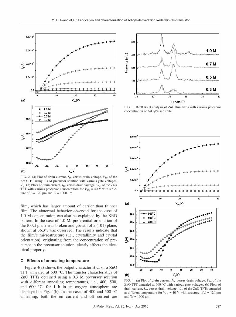
film, which has larger amount of carrier than thinnerfilm. The abnormal behavior observed for the case of1.0 M concentration can also be explained by the XRDpattern. In the case of 1.0 M, preferential orientation ofthe (002) plane was broken and growth of a (101) plane,shown at 36.3�, was observed. The results indicate thatthe film’s microstructure (i.e., crystallinity and crystalorientation), originating from the concentration of pre-cursor in the precursor solution, clearly affects the elec-trical property.
C. Effects of annealing temperature
Figure 4(a) shows the output characteristics of a ZnOTFT annealed at 600 �C. The transfer characteristics ofZnO TFTs obtained using a 0.3 M precursor solutionwith different annealing temperatures, i.e., 400, 500,and 600 �C, for 1 h in an oxygen atmosphere aredisplayed in Fig. 4(b). In the cases of 400 and 500 �Cannealing, both the on current and off current are
FIG. 4. (a) Plot of drain current, ID, versus drain voltage, VD, of the
ZnO TFT annealed at 600 �C with various gate voltages. (b) Plots of
drain current, ID, versus drain voltage, VG, of the ZnO TFTs annealed
at different temperature for VDS = 40 V with structure of L = 120 mmand W = 1000 mm.
FIG. 2. (a) Plot of drain current, ID, versus drain voltage, VD, of the
ZnO TFT using 0.3 M precursor solution with various gate voltages,
VG. (b) Plots of drain current, ID, versus drain voltage, VG, of the ZnO
TFT with various precursor concentration for VDS = 40 V with struc-
ture of L = 120 mm and W = 1000 mm.
FIG. 3. y–2y XRD analysis of ZnO thin films with various precursor
concentration on SiO2/Si substrate.
Y.H. Hwang et al.: Fabrication and characterization of sol-gel-derived zinc oxide thin-film transistor
J. Mater. Res., Vol. 25, No. 4, Apr 2010 697

increased with similar subthreshold slopes. It is knownthat the subthreshold slope is generally related to de-fects of the film and the interface property between thesemiconductor and gate dielectric.6 The XRD patterns
displayed in Fig. 5 indicate that all the films show pref-erential orientation of the (002) plane, which contributesto enhanced electron conduction.20 The increasing inten-sity of XRD peak at 34.4� with higher annealing tem-perature indicates that the crystallinity is improved asthe annealing temperature is increased. Therefore, it isreasonable to conclude that the property of films and theinterface are similar for both cases and the better oncurrent in the 500 �C annealed film is attributed to thesuperior crystallinity of the film. However, the 600 �Cannealed film shows higher on current, lower off cur-rent, and a lower subthreshold slope at the same time,features that are preferable for TFT application. Theabrupt improvement of the electrical properties in termsof mobility and subthreshold slope of the film annealedin a temperature range between 500 and 600 �C reflectsimprovements of the interface between the semiconduc-tor and gate dielectric and the defect level in the film aswell as better crystallinity.6
The electrical properties of the devices were analyzedusing a HP 4145B semiconductor parameter analyzer in adark room at ambient conditions. The channel length andwidth were 120 and 1000 mm, respectively. The electri-cal parameters that characterize TFTs are typically chan-nel mobility, threshold voltage, subthreshold slope, andon-to-off current ratio. Channel mobility and thresholdvoltage are derived from a linear fitting to the plot of thesquare root of drain current, ID, versus drain voltage, VG,using the following equation in the saturation region.
FIG. 6. SEM image of (a) surface and (b) cross section of ZnO thin film. (c) AFM image of ZnO thin film. (d) Transmittance spectra of ZnO thin
film deposited on quartz substrate.
FIG. 5. y–2y XRD analysis of ZnO thin films on SiO2/Si substrate
annealed at different temperature.
TABLE I. Electrical properties of ZnO TFTs annealed at different
temperature.
Temperature (�C) m (cm2/V�s) Ion/Ioff Vth (V) S (V/dec)
400 1.44 �104 �8 �7
500 2.55 �104 �6 �7
600 9.40 5.5 � 105 7.19 3.29
Y.H. Hwang et al.: Fabrication and characterization of sol-gel-derived zinc oxide thin-film transistor
J. Mater. Res., Vol. 25, No. 4, Apr 2010698
ID ¼ WCi
2LmðVG � VthÞ2 ;
where W and L are the channel width and length, respec-tively, m is the channel mobility, Ci is the capacitanceper unit area of a SiO2 gate insulator (dielectric constant� 3.9), and Vth is the threshold voltage.
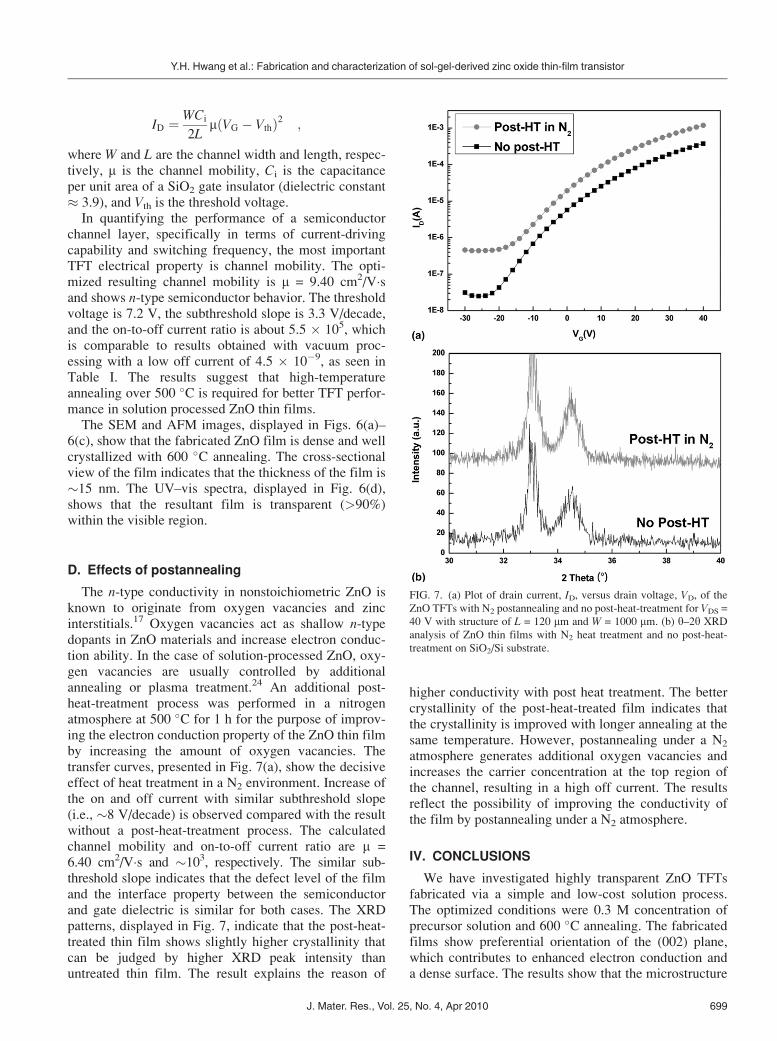
In quantifying the performance of a semiconductorchannel layer, specifically in terms of current-drivingcapability and switching frequency, the most importantTFT electrical property is channel mobility. The opti-mized resulting channel mobility is m = 9.40 cm2/V�sand shows n-type semiconductor behavior. The thresholdvoltage is 7.2 V, the subthreshold slope is 3.3 V/decade,and the on-to-off current ratio is about 5.5 � 105, whichis comparable to results obtained with vacuum proc-essing with a low off current of 4.5 � 10�9, as seen inTable I. The results suggest that high-temperatureannealing over 500 �C is required for better TFT perfor-mance in solution processed ZnO thin films.
The SEM and AFM images, displayed in Figs. 6(a)–6(c), show that the fabricated ZnO film is dense and wellcrystallized with 600 �C annealing. The cross-sectionalview of the film indicates that the thickness of the film is�15 nm. The UV–vis spectra, displayed in Fig. 6(d),shows that the resultant film is transparent (>90%)within the visible region.
D. Effects of postannealing
The n-type conductivity in nonstoichiometric ZnO isknown to originate from oxygen vacancies and zincinterstitials.17 Oxygen vacancies act as shallow n-typedopants in ZnO materials and increase electron conduc-tion ability. In the case of solution-processed ZnO, oxy-gen vacancies are usually controlled by additionalannealing or plasma treatment.24 An additional post-heat-treatment process was performed in a nitrogenatmosphere at 500 �C for 1 h for the purpose of improv-ing the electron conduction property of the ZnO thin filmby increasing the amount of oxygen vacancies. Thetransfer curves, presented in Fig. 7(a), show the decisiveeffect of heat treatment in a N2 environment. Increase ofthe on and off current with similar subthreshold slope(i.e., �8 V/decade) is observed compared with the resultwithout a post-heat-treatment process. The calculatedchannel mobility and on-to-off current ratio are m =6.40 cm2/V�s and �103, respectively. The similar sub-threshold slope indicates that the defect level of the filmand the interface property between the semiconductorand gate dielectric is similar for both cases. The XRDpatterns, displayed in Fig. 7, indicate that the post-heat-treated thin film shows slightly higher crystallinity thatcan be judged by higher XRD peak intensity thanuntreated thin film. The result explains the reason of
higher conductivity with post heat treatment. The bettercrystallinity of the post-heat-treated film indicates thatthe crystallinity is improved with longer annealing at thesame temperature. However, postannealing under a N2
atmosphere generates additional oxygen vacancies andincreases the carrier concentration at the top region ofthe channel, resulting in a high off current. The resultsreflect the possibility of improving the conductivity ofthe film by postannealing under a N2 atmosphere.
IV. CONCLUSIONS
We have investigated highly transparent ZnO TFTsfabricated via a simple and low-cost solution process.The optimized conditions were 0.3 M concentration ofprecursor solution and 600 �C annealing. The fabricatedfilms show preferential orientation of the (002) plane,which contributes to enhanced electron conduction anda dense surface. The results show that the microstructure
FIG. 7. (a) Plot of drain current, ID, versus drain voltage, VD, of the
ZnO TFTs with N2 postannealing and no post-heat-treatment for VDS =
40 V with structure of L = 120 mm and W = 1000 mm. (b) y–2y XRD
analysis of ZnO thin films with N2 heat treatment and no post-heat-
treatment on SiO2/Si substrate.
Y.H. Hwang et al.: Fabrication and characterization of sol-gel-derived zinc oxide thin-film transistor
J. Mater. Res., Vol. 25, No. 4, Apr 2010 699
of the film is clearly related to the electrical property.Improvements of the film crystallinity and the interfacebetween the semiconductor and gate dielectric areobserved at high annealing temperature. It is shown thatan additional postannealing process in N2 surroundingcan improve the electron conduction property of the film.The optimized ZnO TFT shows sufficient electricalproperties to drive various display devices, such asAMLCDs and AMOLEDs.
ACKNOWLEDGMENTS
This research was financially supported by the Ministryof Knowledge Economy (MKE) and Korea Institute forAdvancement of Technology (KIAT) through the HumanResource Training Project for Strategic Technology. Thiswork was also supported by Basic Science Research Pro-gram through National Research Foundation of Korea(NRF) funded by the Ministry of Education, Science andTechnology (Grant No. R11-2007-045-03002-0).
REFERENCES
1. P. Gorrn, M. Sander, J. Meyer, M. Kroger, E. Becker,
H. Johannes, W. Kowalsky, and T. Riedl: Toward see-through
displays: Fully transparent thin-film transistors driving transpar-
ent organic light-emitting diodes. Adv. Mater. 18, 738 (2006).
2. K. Nomura, H. Ohta, A. Takagi, T. Kamiya, M. Hirano, and
H. Hosono: Room-temperature fabrication of transparent flexible
thin-film transistors using amorphous oxide semiconductors.
Nature 432, 488 (2004).
3. V. Subramanian, J.M.J. Frechet, P.C. Channg, D.C. Huang,
J.B. Lee, S.E. Molesa, A.R. Murphy, D.R. Redinger, and
S.K. Volkman: Progress toward development of all-printed RFID
tags: Materials, processes, and devices. Proc. IEEE 93, 1330
(2005).
4. J.F. Wager: Transparent electronics. Science 300, 1245 (2003).
5. R.L. Hoffman, B.J. Norris, and J.F. Wager: ZnO-based transpar-
ent thin-film transistors. Appl. Phys. Lett. 82, 5 (2003).
6. H.Q. Chiang, J.F. Wager, R.L. Hoffman, J. Jeong, and
D.A. Keszler: High mobility transparent thin-film transistors with
amorphous zinc tin oxide channel layer. Appl. Phys. Lett. 86,013503 (2005).
7. B. Yaglioglu, H.Y. Yeom, R. Beresford, and D.C. Paine: High-
mobility amorphous In2O3–10 wt% ZnO thin film transistors.
Appl. Phys. Lett. 89, 062103 (2006).
8. B.J. Morris, J. Anderson, J.F. Wager, and D.A. Keszler: Spin
coated zinc oxide transparent transistors. J. Phys. D: Appl. Phys.36, L105 (2003).
9. S. Seo, C.G. Choi, Y.H. Hwang, and B. Bae: High performance
solution-processed amorphous zinc tin oxide thin film transistor.
J. Phys. D: Appl. Phys. 42, 035106 (2009).
10. Y.H. Hwang, J.H. Jeon, S. Seo, and B. Bae: Solution-processed,
high performance aluminum indium oxide thin-film transistors
fabricated at low temperature. Electrochem. Solid-State Lett. 12,H336 (2009).
11. D. Lee, Y. Chang, G.S. Herman, and C. Chang: A general route to
printable high-mobility transparent amorphous oxide semiconduc-
tors. Adv. Mater. 19, 843 (2007).
12. C.G. Choi, S. Seo, and B. Bae: Solution-processed indium-zinc
oxide transparent thin-film transistors. Electrochem. Solid-StateLett. 11, H7 (2008).
13. D. Lee, Y. Chang, W. Stickle, and C. Chang: Functional porous
tin oxide thin films fabricated by inkjet printing process.
Electrochem. Solid-State Lett. 10, K51 (2007).
14. J.G.E. Gardeniers, Z.M. Rittersma, and G.J. Burger: Preferred
orientation and piezoelectricity in sputtered ZnO films. J. Appl.Phys. 83, 7844 (1998).
15. Dhananjay, J. Nagaraju, and S.B. Krupanidhi: Characteristics of
ZrO2 gate dielectrics on O2- and N2O-plasma treated partially
strain-compensated Si0.69Ge0.3C0.01 layers. J. Appl. Phys. 99,034105 (2006).
16. V. Bhosle, A. Tiwari, and J. Narayan: Electrical properties of
transparent and conducting Ga doped ZnO. J. Appl. Phys. 100,033713 (2006).
17. U. Ozgur, Ya.I. Alivov, C. Liu, A. Teke, M.A. Reshchikov,
S. Dogan, V. Avrutin, S. Cho, and H. Morkoc: A comprehensive
review of ZnO materials and devices. J. Appl. Phys. 98, 041301(2005).
18. C. Woll: The chemistry and physics of zinc oxide surfaces. Prog.Surf. Sci. 82, 55 (2007).
19. E. Fortunato, P. Barquinha, A. Pimentel, A. Goncalves, A.Marques,
L. Pereira, and R. Martins: Recent advances in ZnO transparent
thin film transistors. Thin Solid Films 487, 205 (2005).20. B.S. Ong, C. Li, Y. Li, Y. Wu, and R. Loutfy: High performance
solution-processed indium oxide thin-film transistors. J. Am.Chem. Soc. 129, 2750 (2007).
21. B.W. Clare, J.C.L. Cornish, G.T. Hefter, P.J. Jennings, C.P. Lund,
D.J. Santjojo, and M.O.G. Talukder: Studies of photodegradation
in hydrogenated amorphous silicon. Thin Solid Films 288, 76(1996).
22. L. Yang, L. Chen, and A. Catalano: Intensity and temperature
dependence of photodegradation of amorphous silicon solar cells
under intense illumination. Appl. Phys. Lett. 59, 840 (1991).
23. K. Remashan, D. Hwang, S. Park, and J. Jang: Effect of rapid
thermal annealing on the electrical characteristics of ZnO thin-
film transistors. Jpn. J. Appl. Phys. 47, 2848 (2008).
24. P.F. Cai, J.B. You, X.W. Zhang, J.J. Dong, X.L. Yang, Z.G. Yin,
and N.F. Chen: Enhancement of conductivity and transmittance of
ZnO films by post hydrogen plasma treatment. J. Appl. Phys. 105,083713 (2009).
Y.H. Hwang et al.: Fabrication and characterization of sol-gel-derived zinc oxide thin-film transistor
J. Mater. Res., Vol. 25, No. 4, Apr 2010700