A dynamically reconfigurable monolithic cmos pressure sensor for smart fabric
10
966 IEEE JOURNAL OF SOLID-STATE CIRCUITS, VOL. 38, NO. 6, JUNE 2003 A Dynamically Reconfigurable Monolithic CMOS Pressure Sensor for Smart Fabric Maximilian Sergio, Nicolò Manaresi, Fabio Campi, Roberto Canegallo, Marco Tartagni, and Roberto Guerrieri Abstract—This paper presents a mixed-signal system-on-chip (SOC) for sensing capacitance variations, enabling the creation of pressure-sensitive fabric. The chip is designed to sit in the corner of a smart fabric such as elastic foam overlaid with a matrix of con- ductive threads. When pressure is applied to the matrix, an image is created from measuring the differences in capacitance among the rows and columns of fibers patterned on the two opposite sides of the elastic substrate. The SOC approach provides the flexibility to accommodate for different fabric sizes and to perform image enhancement and on-chip data processing. The chip has been de- signed in a 0.35- m five-metal one-poly CMOS process working up to 40 MHz at 3.3 V of power supply, in a fully reconfigurable arrangement of 128 I/O lines. The core area is 32 mm . Index Terms—Capacitive, CMOS, pressure sensor, smart textile. I. INTRODUCTION H UMAN BEINGS are able to manipulate and explore ob- jects in their environment using the sense of touch. Haptic exploration is an important mechanism by which humans learn about the properties of unknown objects. Through the sense of touch, we are able to learn about characteristics such as object shape and stiffness. Among a variety of human communication media, gesture and touch play an important role in our daily life. Therefore, it is important and effective to introduce haptic and gesture communication into industrial robots [1] and con- sumer products. As computing becomes more ubiquitous and distributed, there is a growing need for human–computer inter- faces that support a new interaction paradigm. As an example, the intelligent toy market is looking for new ways of using all available information sources, including human touch, in order to provide a smarter user interaction whereby the toy’s reaction reflects how it is handled. The reaction will thus be different if it is stroked or slapped, or even whether a child or an adult picks it up. This may be achieved by a device interfaced with a smart fabric wrapping the toy and providing information on the pressure field distribution and its temporal variation. A fabric substrate is very appealing: it is flexible and partially extensible [2] to conform to different shapes, supported by a well-known technology, and produced at low cost. Manuscript received July 18, 2002; revised March 3, 2003. This work was supported by Central R&D, STMicroelectronics, Italy. M. Sergio, F. Campi, M. Tartagni, and R. Guerrieri are with ARCES, University of Bologna, 40136 Bologna, Italy (e-mail: [email protected]; [email protected]; [email protected]). N. Manaresi is with Silicon Biosystems srl, 40125 Bologna, Italy (e-mail: [email protected]). R. Canegallo is with ARCES, University of Bologna, 40136 Bologna, Italy. He is also with Central R&D, STMicroelectronics, 40021 Agrate Brianza Milan, Italy (e-mail: [email protected]). Digital Object Identifier 10.1109/JSSC.2003.811977 Fig. 1. Concept of pressure-sensitive fabric. Some smart pressure sensors interfacing with a flexible substrate have been developed, but they are either based on electrooptical fabric [3], [4] which is not suitable for the low-cost market, or they need cumbersome printed circuit board (PCB) electronics [5]. Conversely, other devices such as tactile sensors arrays [6] enable an image of the pressure field to be grabbed, but they are based on sensing materials such as piezoelectric and piezoresistive substrates [7], [8] which are very difficult to embed into elastic fabric because strong mechanical stresses, such as impacts and compressions (that are very common situations during the use of toys), can seriously damage these sophisticated sensors. This paper presents an innovative single-chip solution to be interfaced with a pressure-sensitive fabric so that it can fit in a corner of the sensor and produce a digitally processed image. The main advantage of our approach is the possibility of using distributed pressure information, from sensors that are analo- gous to artificial skin, to achieve haptic awareness. To obtain this kind of intelligence (that cannot be achieved by merely col- lecting and displaying sensory information, as most pressure sensors do) the on-chip computational power is used to extract and compress information related to the pressure field exerted on the fabric. A palm of a hand being pushed over the fabric, for example, can be processed and compacted so as to result in a single bit word issuing from the digital I/O port. This paper is organized as follows. Section II presents an overview of the sensor working principle. Section III discusses the design constraints and specifications involved in acquiring the pressure image. In Section IV, the architecture of the sensor is described along with details of the solutions adopted to over- come the stringent system constraints. Section V reports mea- surement results, and conclusions are drawn in Section VI. 0018-9200/03$17.00 © 2003 IEEE
Transcript of A dynamically reconfigurable monolithic cmos pressure sensor for smart fabric
966 IEEE JOURNAL OF SOLID-STATE CIRCUITS, VOL. 38, NO. 6, JUNE 2003
A Dynamically Reconfigurable Monolithic CMOSPressure Sensor for Smart Fabric
Maximilian Sergio, Nicolò Manaresi, Fabio Campi, Roberto Canegallo, Marco Tartagni, and Roberto Guerrieri
Abstract—This paper presents a mixed-signal system-on-chip(SOC) for sensing capacitance variations, enabling the creation ofpressure-sensitive fabric. The chip is designed to sit in the cornerof a smart fabricsuch as elastic foam overlaid with a matrix of con-ductive threads. When pressure is applied to the matrix, an imageis created from measuring the differences in capacitance amongthe rows and columns of fibers patterned on the two opposite sidesof the elastic substrate. The SOC approach provides the flexibilityto accommodate for different fabric sizes and to perform imageenhancement and on-chip data processing. The chip has been de-signed in a 0.35- m five-metal one-poly CMOS process workingup to 40 MHz at 3.3 V of power supply, in a fully reconfigurablearrangement of 128 I/O lines. The core area is 32 mm2.
Index Terms—Capacitive, CMOS, pressure sensor, smart textile.
I. INTRODUCTION
H UMAN BEINGS are able to manipulate and explore ob-jects in their environment using the sense of touch. Haptic
exploration is an important mechanism by which humans learnabout the properties of unknown objects. Through the sense oftouch, we are able to learn about characteristics such as objectshape and stiffness. Among a variety of human communicationmedia, gesture and touch play an important role in our dailylife. Therefore, it is important and effective to introduce hapticand gesture communication into industrial robots [1] and con-sumer products. As computing becomes more ubiquitous anddistributed, there is a growing need for human–computer inter-faces that support a new interaction paradigm. As an example,the intelligent toymarket is looking for new ways of using allavailable information sources, including human touch, in orderto provide a smarter user interaction whereby the toy’s reactionreflects how it is handled. The reaction will thus be differentif it is stroked or slapped, or even whether a child or an adultpicks it up. This may be achieved by a device interfaced with asmart fabricwrapping the toy and providing information on thepressure field distribution and its temporal variation. A fabricsubstrate is very appealing: it is flexible and partially extensible[2] to conform to different shapes, supported by a well-knowntechnology, and produced at low cost.
Manuscript received July 18, 2002; revised March 3, 2003. This work wassupported by Central R&D, STMicroelectronics, Italy.
M. Sergio, F. Campi, M. Tartagni, and R. Guerrieri are with ARCES,University of Bologna, 40136 Bologna, Italy (e-mail: [email protected];[email protected]; [email protected]).
N. Manaresi is with Silicon Biosystems srl, 40125 Bologna, Italy (e-mail:[email protected]).
R. Canegallo is with ARCES, University of Bologna, 40136 Bologna, Italy.He is also with Central R&D, STMicroelectronics, 40021 Agrate Brianza Milan,Italy (e-mail: [email protected]).
Digital Object Identifier 10.1109/JSSC.2003.811977
Fig. 1. Concept of pressure-sensitive fabric.
Some smart pressure sensors interfacing with a flexiblesubstrate have been developed, but they are either based onelectrooptical fabric [3], [4] which is not suitable for the low-costmarket, or they need cumbersome printed circuit board (PCB)electronics [5]. Conversely, other devices such as tactile sensorsarrays [6] enable an image of the pressure field to be grabbed,but they are based on sensing materials such as piezoelectricand piezoresistive substrates [7], [8] which are very difficult toembed into elastic fabric because strong mechanical stresses,such as impacts and compressions (that are very commonsituations during the use of toys), can seriously damage thesesophisticated sensors.
This paper presents an innovative single-chip solution to beinterfaced with a pressure-sensitive fabric so that it can fit in acorner of the sensor and produce a digitally processed image.The main advantage of our approach is the possibility of usingdistributed pressure information, from sensors that are analo-gous to artificial skin, to achieve haptic awareness. To obtainthis kind of intelligence (that cannot be achieved by merely col-lecting and displaying sensory information, as most pressuresensors do) the on-chip computational power is used to extractand compress information related to the pressure field exertedon the fabric. A palm of a hand being pushed over the fabric,for example, can be processed and compacted so as to result ina single bit word issuing from the digital I/O port.
This paper is organized as follows. Section II presents anoverview of the sensor working principle. Section III discussesthe design constraints and specifications involved in acquiringthe pressure image. In Section IV, the architecture of the sensoris described along with details of the solutions adopted to over-come the stringent system constraints. Section V reports mea-surement results, and conclusions are drawn in Section VI.
0018-9200/03$17.00 © 2003 IEEE

SERGIOet al.: CMOS PRESSURE SENSOR FOR SMART FABRIC 967
Fig. 2. System level operation. The pressure exerted on the fabric is convertedinto an electric signal by means of a readout circuit. The image acquired is firstdigitized and then elaborated by MCU software.
II. SENSORWORKING PRINCIPLE AND SOC APPROACH
The working principle of the sensor is sketched in Fig. 1. Amap of the pressure applied over the fabric surface is achievedby detecting the capacitance variation between rows andcolumns of conductive fibers patterned on the two oppositesides of an elastic layer of synthetic foam. When pressureis exerted on thesmart fabric, the dielectric layer betweencorresponding rows and columns is reduced in thickness, thus,increasing the related coupling capacitance.
In our first implementation, the conductive columns and rowshave been drawn onto opposite sides of a piece of insulating ma-terial using conductive ink. The use of fabric for implementingboth substrates and conductive patterns allows us to obtain aflexible and partially extensible pressure sensor. Fig. 2 showsan example of the application principle. A piece ofsmart fabricis wrapped around the cylindric exterior of a bottle. Accordingto the pressure exerted on the smart fabric, a certain portion ofthe foam is squeezed, thus, increasing the coupling capacitanceof the electrodes patterned over it. The induced charge variationis converted into a voltage value by means of readout circuitryembedded into the chip. The analog signal is then converted intodigital and processed by a RISC microcontroller [9]. The mainbenefit of such an approach consists of a simplification of thesensor arrangement so that it can work in harsh environments.
In fact, the use of a simple capacitive sensing scheme results ina robust sensor even if exposed to strong mechanical stresses(e.g., impact, compression) that are incompatible with theworking conditions required by more sophisticated sensors.
III. SYSTEM REQUIREMENTS
The system needs to acquire an image of the pressure beingexerted over a large piece of fabric. Since the fabric is intendedto wrap up different shaped objects, its aspect ratio may varyfrom narrow rectangular boxes to large square canvas. Thedevice treats the sensor area as a matrix. Thus, each row andcolumn has to be separately addressable so that a completeimage may be achieved.
The main problem associated with this approach is relatedto the difficulty of sensing very small capacitances, typicallyvarying in the range of few hundred femtofarads. The valueof the addressed capacitance (sensed capacitance of Fig. 1)is measured by applying a voltage step and by reading outthe corresponding charge variation, as will be explained inSection IV. The generated signal is proportional to the valueof the capacitance, thus, it is inversely proportional to thedistance of the plates, i.e., the insulating layer thickness.
The use of simple and inexpensive materials (such as fabricand foam) for implementing both substrates and conductivethreads introduces a great spread in thickness among the sensorsurface at the rest position. This kind of noise [somethingsimilar to fixed pattern noise (FPN)] affects the measure of thecapacitance value. Since the pressure value is then convertedto digital by means of an embedded A/D converter (ADC), weface the choice to accept this inhomogeneity in pixel valueswhen its maximum value is comparable to the resolution of theconverter.
In order to measure the value of the addressed capacitance(sensed capacitance of Fig. 1), the readout circuitry must be in-sensitive to the parasitics due to neighboring rows and columnscoupling capacitance. Early experiments on textiles have re-ported a sensed capacitance value of about few hundreds offemtofarads, while the typical parasitic capacitance values varyfrom a few picofarads up to 10 pF. This kind of influence isvery similar to the crosstalk noise. In our system, we can dis-tinguish two types of crosstalk. The first is due to the mechan-ical deformation induced by the pressure exerted on a certainarea on the neighboring region, since the material used as di-electric is not perfectly elastic. The second kind of crosstalk isdue to the charge redistribution between the sensed capacitanceand the adjacent ones. This charge sharing has been reduced bymeans of the embedded readout circuitry, as will be explained isSection IV. More specifically, this contribution has been madenegligible with respect to the mechanical crosstalk.
To interact in real time with the human environment, thesystem may be required to implement gesture recognition soas to customize, for instance, the behavior of a toy to differentsituations. To achieve this task, at least 10 frames per secondhas to be attained. Assuming an image composed of 6464pixels, at the frame rate specified the pixel readout time is
s.In order to recognize different reactions, the system has to
perform a few elementary operations on the pixel value, such asaveraging, reference subtraction, and convolution.
Consider, as an example, a piece of smart textile wrappedaround an object used to discriminate if a child or an adult isholding it. Let us assume recognition is performed by meansof a square piece of fabric with 64 64 rows and columns.The simplest solution would be to count the number of points(pixels) that exceed a certain value of pressure (used as areference), given that the hand of an adult is larger than thehand of a child. The system has to perform a total of 6464
(2 address write 1 pixel read 1 reference subtraction1 sum operation) 20480 operations for each measurement.
968 IEEE JOURNAL OF SOLID-STATE CIRCUITS, VOL. 38, NO. 6, JUNE 2003
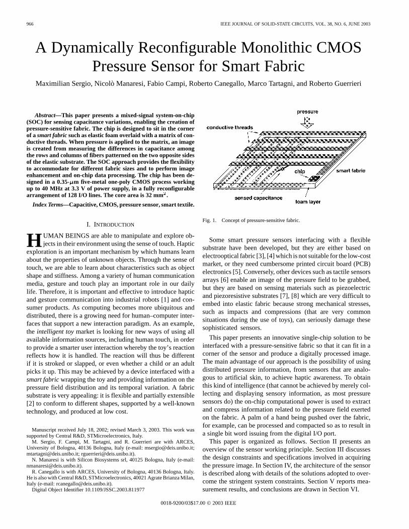
Fig. 3. System architecture and organization.
TABLE ISYSTEM REQUIREMENTS
Furthermore, the device has to store the computed value inorder to accomplish the subsequent comparison. Working ata frame rate of 10 frames per second, the resulting minimumsystem clock frequency is about 4.88 MHz. Only at the end ofthis process can the system perform an I/O operation issuinga single bit word to an output port. These estimates give alower bound of 5 million operations per second (MOPS) forthe minimum computational power required.
Table I gives the system level requirements.
IV. SYSTEM ARCHITECTURE
Following the constraints described in the previous section,the device has been designed with 128 analog I/O channels to
address any aspect ratio of pixels where .To cope with time requirements, the readout has been designedto acquire at least 64 64 pixels at 10 frames/s.
The chip embeds a special purpose block calledAnalogI/O (as depicted in Fig. 3) to separately address each analogpad. This block features the analog channels configuration asinput or output signals and will be described in detail later in thissection. TheAnalog I/O block contains two registers that de-fine the matrix aspect ratio; each line can be configured as a rowor as a column. A row register and a column register are used toselect each single row and column. The addressing block can beprogrammed at run time by the embedded microcontroller. Theaddressing operation is performed by writing the current valuein the row register and in the column register.
Pressure image acquisition can be divided into two pipelinedoperations: pixel acquisition and elaboration. During thefirst phase, pressure variation is translated into a voltage andconverted to digital, while during the second phase, the infor-mation embodied in this signal is treated by image processingtechniques.
The system level architecture reflects this HW/SW parti-tioning. The chip is based on two embedded macro blocks:an analog interface and a digital processing system. The

SERGIOet al.: CMOS PRESSURE SENSOR FOR SMART FABRIC 969
Fig. 4. Sensing scheme.
analog core translates the pressure information into an 8-bitdigital word. The digital core processes the digitized signal;in particular, it implements two compensation techniques,namely, FPN cancellation and gamma correction, in order toimprove the image quality. This simple image processing iscarried out by software routines that run on the embedded32-bit microcontroller. The digital macro also supports pixeladdressing and drives the analog block control signals. Thistask requires adoption of a specific block in order to reducepower consumption and roll back the overall microcontrollercomputational burden. Fig. 3 shows the system architectureand organization. The main tasks of the embedded architectureare outlined below.
A. Analog Signal Path
The capacitor array sensing scheme is sketched in Fig. 4. Themost critical part of the project was making sure that each pixelcapacitance value was insensitive to pixels from neighboringcolumns and rows. This can be achieved by grounding all rowsand columns except those selected.
In order to sense the capacitance value of the mea-surement setup must be insensitive to the value of other pixelsand to the value of parasitics between neighboring columns, andbetween neighboring rows, which can easily amount to two tothree orders of magnitude larger than the addressed pixel capac-itance as described in the previous section.
Since the virtual ground node is at a fixed voltage level:1) grounding all columns but the selected one allows us toavoid injection from the neighboring columns by way ofand 2) grounding all rows but the selected one allows us toavoid injection from pixels in the same column.
This mode of operation is of paramount importance for get-ting a good signal-to-noise ratio and contrast.
The charge amplifier (Fig. 4) operates as follows. The feed-back switch S1 is first closed to reset the operational amplifier.Then S1 is opened and a voltage step is applied tothe pixel’s row so that a charge flux is collected at pixel column
Fig. 5. Analog signal path block diagram.
to be readout by the chip charge amplifier. The voltage variationof the charge amplifier output is proportional to the valueof the capacitance of the addressed node, according to
where is the line capacitance, is the open-loop gain ofthe operational amplifier, and is the feedback capacitance.This relation makes clear how an high value ofis required toreduce the effect of the line capacitance.
The 128 analog I/O channels of the chip can be reconfiguredas inputs or outputs at power up, to accommodate for differentsizes and aspect ratios of the smart fabric. According to theaddressing scheme described above and illustrated in its basicblocks in Fig. 5, unselected channels are grounded, while se-lected channels are connected to eitheroutCom or inCom ofthe readout circuit.
The operational amplifier employed in the readout has beendesigned for 60 dB of open-loop gain using afolded cascodescheme. Its stability is ensured at closed-loop gain configura-tion with the minimum estimated output capacitance. The latterdesign rule ensures the stability of the system in any configu-ration of the readout circuit. To accommodate for a wide rangeof smart fabric implementations, it is very important to have themaximum flexibility in setting both dynamic range and responsetime. As far as the dynamic range is concerned, the feedback ca-pacitor can be varied from 25.2 fF to 12.8 pF by selectivelyswitching a bank of 256 elementary capacitors so as to controlthe gain of the system. On the other hand, the readout time hasto be adjusted to the different configurations of the smart fabricand of the gain. In fact, the readout time of the charge amplifieris set by
where is the gain-bandwidth product ofthe operational amplifier, in which and are the totalcapacitance at the output node and the transconductance ofthe operational amplifier, respectively. Therefore,is highlydependent on the values of and which are relatedto the choice of the readout gain, size of the smart fabric,type of connectors, and length of the connection. To adapt thereadout time to any possible configuration, a bank of 16 oper-
970 IEEE JOURNAL OF SOLID-STATE CIRCUITS, VOL. 38, NO. 6, JUNE 2003
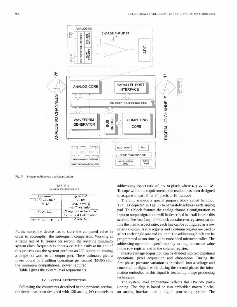
Fig. 6. Reconfigurable readout scheme.
ational amplifiers are selectively connected in parallel fashionas illustrated in Fig. 6. By selectively enabling the operationalamplifiers biases one can increase the gain-bandwidth product,thus, trading off time response for power consumption. Theconfiguration of the readout circuit is stored in special registersthat are used by the digital controller at startup time.
By adjusting the readout feedback capacitor and the inputstep , a wide dynamic range of fabric capacitors can be sup-ported even with a moderate ADC resolution. Accordingly, an8-bit successive approximation ADC [10] is employed to pro-vide a digital value for further processing by the microcontroller.
B. Digital Architecture
The embedded microprocessor has been mapped from a softmacro [9] and represents an evolution of the standard DLXRISC, while embedded memories are imported from standardhardware macro libraries. The layout of the system has beenintegrated using commercial place and route tools. The dig-ital core provides management of the whole operation in realtime. After the booting operation, it supports pixel acquisition,run time analog control signals, and pixel processing. The bootcode is stored in a specific ROM. During the system power-upsession, the microcontroller unit (MCU) downloads the codefrom the I/O interface and stores it in the instruction RAM. Thecommunication is driven by an interrupt protocol served by theMCU. A system configuration phase follows, where, accordingto the downloaded code, the various parameters for image ac-quisition are set. The readout block features a digital interface tosupport communication with the MCU via a data bus. The MCUacquires a pixel reading the ADC and elaborates it according tothe downloaded software. FPN compensation and gamma cor-rection are performed. These features are software implementedas lookup tables (LUTs) stored in the data RAM.
Programmable Waveform Generator: This block is in-tended to generate programmable control signals for the readout
Fig. 7. Programmable waveform generator architecture.
and ADC blocks (Fig. 7). Its main function is to generate thesignals of the readout and ADC blocks. It consists of a finitestate machine (FSM) and a set of four ring shift registers. TheFSM supports the communication protocol between the micro-processor and the analog blocks. For each output waveform, a128-bit word composed of the shift register pattern is initiallyfetched from the RAM and then loaded into the waveform gen-erator during the system configuration phase. When triggered,the patterns rotate once in the shifters, generating the signaldesired. This operation frees MCU processing cycles for pixelelaboration, thus, enabling pipelining. The waveform clockcycle can be set by means of a frequency divider. Each shiftregister is separately addressable. The FSM determines whichregisters have to be activated according to the MCU code. Theselected blocks receive anENABLEsignal used to gate thesystem clock. After generating the corresponding pattern, theENABLEsignal is deasserted until another start word is issuedby the MCU. The clock gating scheme reduces the system levelpower consumption.
Bus Architecture: The MCU and the memories communi-cate through a 32-bit multiplexed core bus featuring interruptsupport. This bus performs pixel elaboration and data transferbetween MCU and memories. An address bridge allows a pe-ripheral internal bus to be managed. The MCU accomplishestwo main tasks: pixel acquisition and devices configuration. Asimple handshake protocol has been developed to synchronizemicroprocessor activity with the waveform generator. This pro-tocol is managed by two control signals, START and BUSY,implemented via software by way of the chip data bus. As com-munication through the bus has been defined at the transactionlayer [11], it is independent of any special feature of the mainsystem’s blocks. This modular architecture makes the design
SERGIOet al.: CMOS PRESSURE SENSOR FOR SMART FABRIC 971
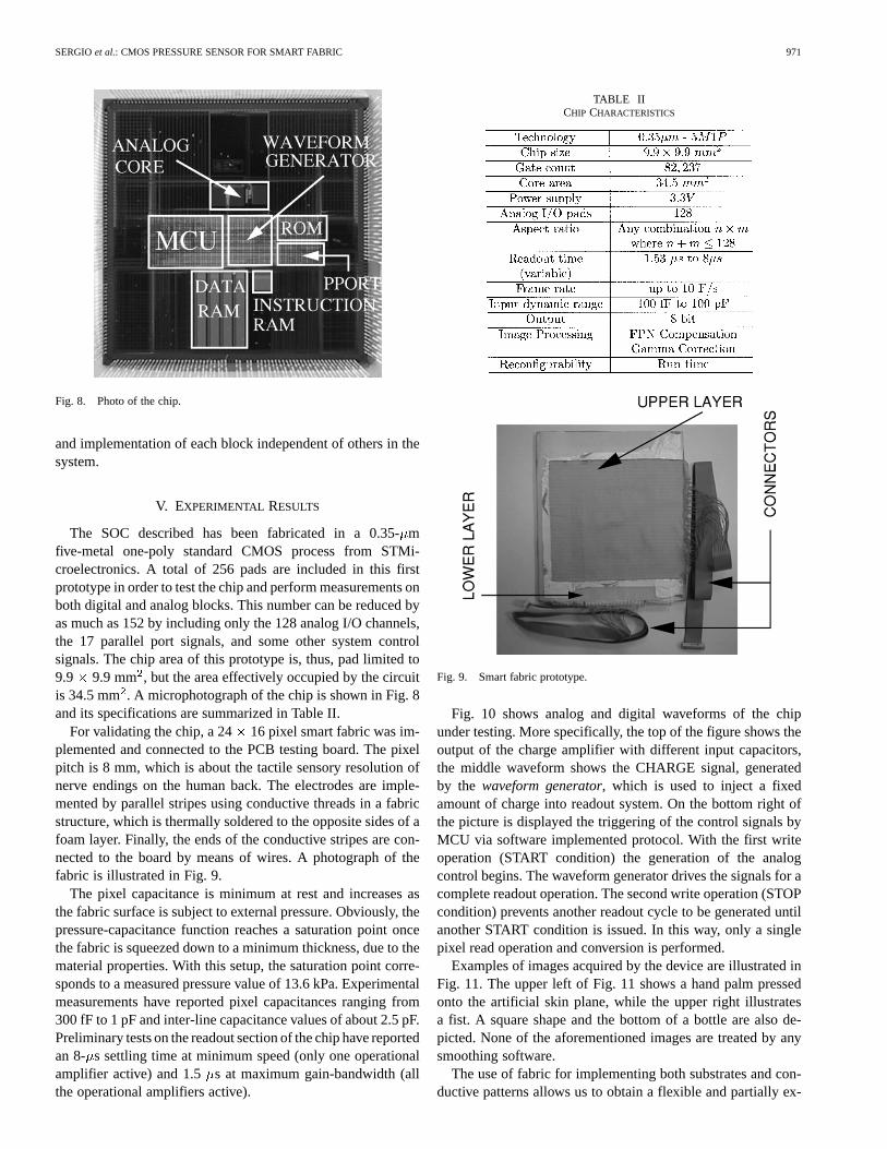
Fig. 8. Photo of the chip.
and implementation of each block independent of others in thesystem.
V. EXPERIMENTAL RESULTS
The SOC described has been fabricated in a 0.35-mfive-metal one-poly standard CMOS process from STMi-croelectronics. A total of 256 pads are included in this firstprototype in order to test the chip and perform measurements onboth digital and analog blocks. This number can be reduced byas much as 152 by including only the 128 analog I/O channels,the 17 parallel port signals, and some other system controlsignals. The chip area of this prototype is, thus, pad limited to9.9 9.9 mm , but the area effectively occupied by the circuitis 34.5 mm. A microphotograph of the chip is shown in Fig. 8and its specifications are summarized in Table II.
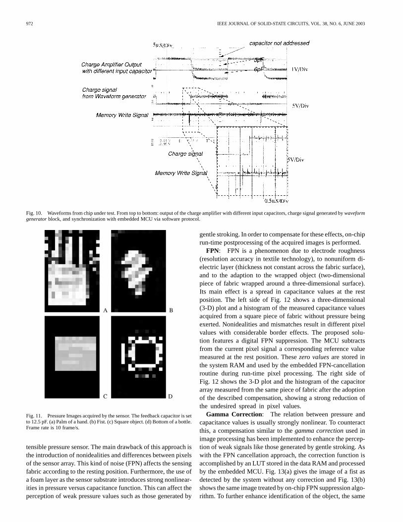
For validating the chip, a 24 16 pixel smart fabric was im-plemented and connected to the PCB testing board. The pixelpitch is 8 mm, which is about the tactile sensory resolution ofnerve endings on the human back. The electrodes are imple-mented by parallel stripes using conductive threads in a fabricstructure, which is thermally soldered to the opposite sides of afoam layer. Finally, the ends of the conductive stripes are con-nected to the board by means of wires. A photograph of thefabric is illustrated in Fig. 9.
The pixel capacitance is minimum at rest and increases asthe fabric surface is subject to external pressure. Obviously, thepressure-capacitance function reaches a saturation point oncethe fabric is squeezed down to a minimum thickness, due to thematerial properties. With this setup, the saturation point corre-sponds to a measured pressure value of 13.6 kPa. Experimentalmeasurements have reported pixel capacitances ranging from300 fF to 1 pF and inter-line capacitance values of about 2.5 pF.Preliminary tests on the readout section of the chip have reportedan 8- s settling time at minimum speed (only one operationalamplifier active) and 1.5 s at maximum gain-bandwidth (allthe operational amplifiers active).
TABLE IICHIP CHARACTERISTICS
Fig. 9. Smart fabric prototype.
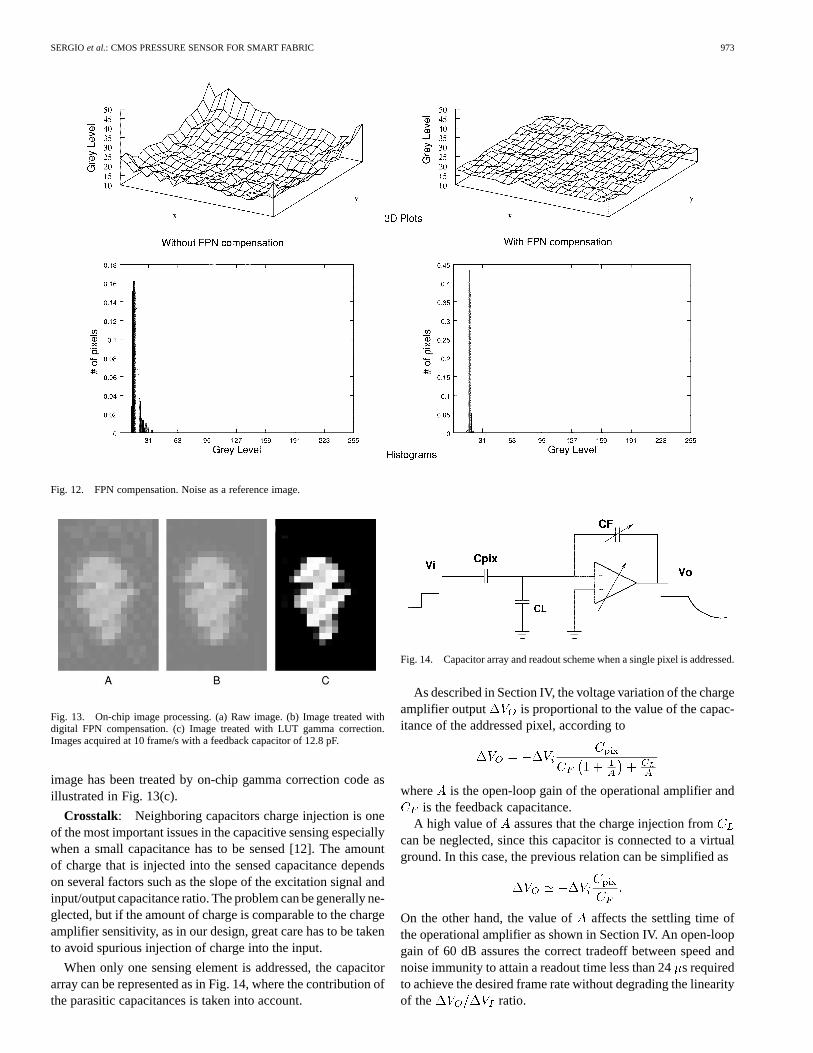
Fig. 10 shows analog and digital waveforms of the chipunder testing. More specifically, the top of the figure shows theoutput of the charge amplifier with different input capacitors,the middle waveform shows the CHARGE signal, generatedby the waveform generator, which is used to inject a fixedamount of charge into readout system. On the bottom right ofthe picture is displayed the triggering of the control signals byMCU via software implemented protocol. With the first writeoperation (START condition) the generation of the analogcontrol begins. The waveform generator drives the signals for acomplete readout operation. The second write operation (STOPcondition) prevents another readout cycle to be generated untilanother START condition is issued. In this way, only a singlepixel read operation and conversion is performed.
Examples of images acquired by the device are illustrated inFig. 11. The upper left of Fig. 11 shows a hand palm pressedonto the artificial skin plane, while the upper right illustratesa fist. A square shape and the bottom of a bottle are also de-picted. None of the aforementioned images are treated by anysmoothing software.
The use of fabric for implementing both substrates and con-ductive patterns allows us to obtain a flexible and partially ex-
972 IEEE JOURNAL OF SOLID-STATE CIRCUITS, VOL. 38, NO. 6, JUNE 2003
Fig. 10. Waveforms from chip under test. From top to bottom: output of the charge amplifier with different input capacitors, charge signal generated by waveformgeneratorblock, and synchronization with embedded MCU via software protocol.
Fig. 11. Pressure Images acquired by the sensor. The feedback capacitor is setto 12.5 pF. (a) Palm of a hand. (b) Fist. (c) Square object. (d) Bottom of a bottle.Frame rate is 10 frame/s.
tensible pressure sensor. The main drawback of this approach isthe introduction of nonidealities and differences between pixelsof the sensor array. This kind of noise (FPN) affects the sensingfabric according to the resting position. Furthermore, the use ofa foam layer as the sensor substrate introduces strong nonlinear-ities in pressure versus capacitance function. This can affect theperception of weak pressure values such as those generated by
gentle stroking. In order to compensate for these effects, on-chiprun-time postprocessing of the acquired images is performed.
FPN: FPN is a phenomenon due to electrode roughness(resolution accuracy in textile technology), to nonuniform di-electric layer (thickness not constant across the fabric surface),and to the adaption to the wrapped object (two-dimensionalpiece of fabric wrapped around a three-dimensional surface).Its main effect is a spread in capacitance values at the restposition. The left side of Fig. 12 shows a three-dimensional(3-D) plot and a histogram of the measured capacitance valuesacquired from a square piece of fabric without pressure beingexerted. Nonidealities and mismatches result in different pixelvalues with considerable border effects. The proposed solu-tion features a digital FPN suppression. The MCU subtractsfrom the current pixel signal a corresponding reference valuemeasured at the rest position. Thesezero valuesare stored inthe system RAM and used by the embedded FPN-cancellationroutine during run-time pixel processing. The right side ofFig. 12 shows the 3-D plot and the histogram of the capacitorarray measured from the same piece of fabric after the adoptionof the described compensation, showing a strong reduction ofthe undesired spread in pixel values.
Gamma Correction: The relation between pressure andcapacitance values is usually strongly nonlinear. To counteractthis, a compensation similar to thegamma correctionused inimage processing has been implemented to enhance the percep-tion of weak signals like those generated by gentle stroking. Aswith the FPN cancellation approach, the correction function isaccomplished by an LUT stored in the data RAM and processedby the embedded MCU. Fig. 13(a) gives the image of a fist asdetected by the system without any correction and Fig. 13(b)shows the same image treated by on-chip FPN suppression algo-rithm. To further enhance identification of the object, the same
SERGIOet al.: CMOS PRESSURE SENSOR FOR SMART FABRIC 973
Fig. 12. FPN compensation. Noise as a reference image.
Fig. 13. On-chip image processing. (a) Raw image. (b) Image treated withdigital FPN compensation. (c) Image treated with LUT gamma correction.Images acquired at 10 frame/s with a feedback capacitor of 12.8 pF.
image has been treated by on-chip gamma correction code asillustrated in Fig. 13(c).
Crosstalk: Neighboring capacitors charge injection is oneof the most important issues in the capacitive sensing especiallywhen a small capacitance has to be sensed [12]. The amountof charge that is injected into the sensed capacitance dependson several factors such as the slope of the excitation signal andinput/output capacitance ratio. The problem can be generally ne-glected, but if the amount of charge is comparable to the chargeamplifier sensitivity, as in our design, great care has to be takento avoid spurious injection of charge into the input.
When only one sensing element is addressed, the capacitorarray can be represented as in Fig. 14, where the contribution ofthe parasitic capacitances is taken into account.
Fig. 14. Capacitor array and readout scheme when a single pixel is addressed.
As described in Section IV, the voltage variation of the chargeamplifier output is proportional to the value of the capac-itance of the addressed pixel, according to
where is the open-loop gain of the operational amplifier andis the feedback capacitance.
A high value of assures that the charge injection fromcan be neglected, since this capacitor is connected to a virtualground. In this case, the previous relation can be simplified as
On the other hand, the value of affects the settling time ofthe operational amplifier as shown in Section IV. An open-loopgain of 60 dB assures the correct tradeoff between speed andnoise immunity to attain a readout time less than 24s requiredto achieve the desired frame rate without degrading the linearityof the ratio.
974 IEEE JOURNAL OF SOLID-STATE CIRCUITS, VOL. 38, NO. 6, JUNE 2003
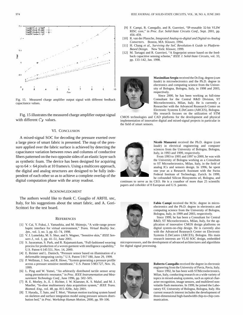
Fig. 15. Measured charge amplifier output signal with different feedbackcapacitance values.
Fig. 15 illustrates the measured charge amplifier output signalwith different values.
VI. CONCLUSION
A mixed-signal SOC for decoding the pressure exerted overa large piece of smart fabric is presented. The map of the pres-sure applied over the fabric surface is achieved by detecting thecapacitance variation between rows and columns of conductivefibers patterned on the two opposite sides of an elastic layer suchas synthetic foam. The device has been designed for acquiringup to 64 64 pixels at 10 frames/s. Using a multicore approach,the digital and analog structures are designed to be fully inde-pendent of each other so as to achieve a complete overlap of thedigital computation phase with the array readout.
ACKNOWLEDGMENT
The authors would like to thank C. Guaglio of ARFIL snc,Italy, for his suggestions about the smart fabric, and A. Gori-Scrittori for the test board.
REFERENCES
[1] Y. Cai, Y. Fukui, J. Yamashita, and M. Shimojo, “A wide-range powerhaptic interface for virtual environment,”Trans. Virtual Reality Soc.Jpn., vol. 3, no. 3, pp. 65–74, 1998.
[2] V. J. Lumelsky, M. S. Shur, and S. Wagner, “Sensitive skin,”IEEE Sen-sors J., vol. 1, pp. 41–51, June 2001.
[3] S. Jayaraman, S. Park, and R. Rajamanickam, “Full-fashioned weavingprocess for production of a woven garment with intelligence capability,”U.S. Patent 6 145 551, Nov. 14, 2000.
[4] E. Reimer and L. Danisch, “Pressure sensor based on illumination of adeformable integrating cavity,” U.S. Patent 5 917 180, June 29, 1999.
[5] P. Wellman, J. Son, and R. Howe, “System generating a pressure profileacross a pressure sensitive membrane,” U.S. Patent 5 983 727, Nov. 16,1999.
[6] L. Ping and W. Yumei, “An arbitrarily distributed tactile sensor arrayusing piezoelectric resonator,” inProc. IEEE Instrumentation and Mea-surement Technology Conf., June 1996, pp. 502–505.
[7] R. E. Morley, Jr., E. J. Richter, J. W. Klaesner, K. S. Maluf, and M. J.Mueller, “In-shoe multisensory data acquisition system,”IEEE Trans.Biomed. Eng., vol. 48, pp. 815–820e, July 2001.
[8] T. Harada,, T. Sato, and T. Mori, “Human motion tracking system basedon skeleton and surface integration model using pressure sensors distri-bution bed,” inProc. Workshop Human Motion, 2000, pp. 99–106.
[9] F. Campi, R. Canegallo, and R. Guerrieri, “IP-reusable 32-bit VLIWRISC core,” inProc. Eur. Solid-State Circuits Conf., Sept. 2001, pp.456–459.
[10] R. van der Plassche,Integrated Analog-to-digital and Digital-to-AnalogConverters. Boston, MA: Kluwer, 1994.
[11] H. Changet al., Surviving the SoC Revolution-A Guide to Platform-Based Design. New York: Kluwer, 1999.
[12] M. Tartagni and R. Guerrieri, “A fingerprint sensor based on the feed-back capacitive sensing scheme,”IEEE J. Solid-State Circuits, vol. 33,pp. 133–142, Jan. 1998.
Maximilian Sergio received the Dr.Eng. degree (cumlaude) in microelectronics and the Ph.D. degree inelectronics and computing science from the Univer-sity of Bologna, Bologna, Italy, in 1998 and 2003,respectively.
Since 2000, he has been working as full-timeConsultant for the Central R&D Division, STMicroelectronics, Milan, Italy. He is currently aResearcher with the Advanced Reasearch Center onElectronic Systems E.DeCastro (ARCES), Bologna.His research focuses on the utilization of STM
CMOS technologies and CAD platforms for the development and physicalimplementation of innovative digital and mixed-signal projects in particular inthe field of smart sensors.
Nicolò Manaresi received the Ph.D. degree (cumlaude) in electrical engineering and computersciences from the University of Bologna, Bologna,Italy, in 1993 and 1999, respectively.
From 1993 to 1995 and 1997 to 2000, he was withthe University of Bologna working as a Consultantto ST Microelectronics, Milan, Italy, in the field ofanalog ICs and sensors design. In 1996, he spentone year as a Research Assistant with the SwissFederal Institute of Technology, Zurich. In 1999,he cofounded Silicon Biosystems srl, Bologna, and
continues to serve as its CEO. He is a coauthor of more than 25 scientificpapers and coholder of 8 European and U.S. patents.
Fabio Campi received the M.Sc. degree in micro-electronics and the Ph.D. degree in electronics andcomputing science from the University of Bologna,Bologna, Italy, in 1999 and 2003, respectively.
Since 1999, he has been a Consultant for CentralR&D, ST Microelectronics, Milan, Italy, for the ap-plication of innovative CMOS design platforms ondigital system-on-chip design. He is currently alsowith the Advanced Reasearch Center on ElectronicSystems E.DeCastro (ARCES), Bologna. His mainresearch interests are VLSI SOC design, embedded
microprocessors, and the development of advanced architectures and algorithmsfor digital signal processing.
Roberto Canegalloreceived the degree in electronicengineering from the University of Pavia, Pavia, Italy.
Since 1992, he has been with STMicroelectronics,Milan, Italy, conducting research on a wide variety oftopics in mixed-analog systems, such as optical char-acter recognition, image sensors, and multilevel non-volatile flash memories. In 1999, he joined the Labo-ratory ST, University of Bologna, Bologna, Italy. Hiscurrent research interest includes the development ofthree-dimensional high-bandwidth chip-to-chip com-munication.

SERGIOet al.: CMOS PRESSURE SENSOR FOR SMART FABRIC 975
Marco Tartagni received the Laurea degree in elec-trical engineering and the Ph.D. degree in electricalengineering and computer sciences from the Univer-sity of Bologna, Bologna, Italy, in 1988 and 1993,respectively.
He joined the Department of Electrical En-gineering, California Institute of Technology,Pasadena, in 1992 as a Visiting Student and becamea Research Fellow in 1994, working on variousaspects of analog VLSI for imaging processing.Since 1995, he has been an Assistant Professor
with the Department of Electronics, University of Bologna, where he hasdesigned and tested low-noise optical and capacitive sensors. He is currentlyinvolved in research on sensors aiming at implementing a hybrid technologycomposed of self-assembling proteins with microelectronics technology, calledReceptronics.
Roberto Guerrieri received the electrical en-gineering degree and the Ph.D. degree from theUniversity of Bologna, Bologna, Italy.
He is currently an Associate Professor of electricalengineering with the University of Bologna. Since1986, he has visited the Department of Electrical En-gineering and Computer Science, University of Cali-fornia at Berkeley, for four years and the Departmentof Electrical Engineering, Massachusetts Institute ofTechnology, Boston. He has published more than 80papers in various fields including numerical simula-
tion of semiconductor devices, numerical solution of Maxwell’s equations, andparallel computation on massively parallel machines. Recently, his research hasfocused on integrated silicon systems to solve various problems such as opticaland capacitive smart sensors, integrated digital circuits for speech and video pro-cessing, and analog circuits for fuzzy controllers. In 1998, he became Directorof the Laboratory for Electronic Systems, a joint venture of the University ofBologna and ST Microelectronics for the development of innovative designs ofsystems on chip.
Dr. Guerrieri received the IEEE Best Paper Award in 1992 for his work in thearea of process modeling.